Document Outline
- COVER
- FEATURES
- ORDERING INFORMATION
- PIN NAMES
- BLOCK DIAGRAM
- 1. BLOCK FUNCTIONS
- 2. MEMORY MAP
- 3. DATA BUSES
- 3.1 16-bit data bus (BMODE = L)
- 3.2 8-bit data bus (BMODE = H)
- 4. RELATIONSHIP BETWEEN DATA BITS AND PIXELS
- 5. RELATIONSHIP BETWEEN DISPLAY DATA AND GRAY-SCALE LEVEL
- 6. LSI PLACEMENT AND ADDRESS MANAGEMENT
- 7. CPU INTERFACE
- 7.1 Function of the RDY (Ready) pin
- 7.2 Access timing
- 8. GRAY SCALE CONTROL
- 9. LIQUID-CRYSTAL TIMING GENERATION
- 9.1 Reset state
- 9.2 Liquid-crystal timing generation circuit
- 10. SELF-DIAGNOSIS FUNCTION
- 11. SYSTEM CONFIGURATION EXAMPLE
- 12. CHIP SET POWER SUPPLY INPUT SEQUENCE
- 13. EXAMPLE OF THE CONFIGURATION OF THE MODULE -INTERNAL SCHOTTKY BARRIER DIODE FOR POWER SUPPLY PROTECTION REINFORCEMENT
- 14. ELECTRICAL CHARACTERISTICS
- 15. RELATIONSHIP BETWEEN THE OSCILLATION , FRAME , AND STB FREQUENCIES
- 16. PACKAGE DRAWING

MOS INTEGRATED CIRCUIT
µ
µ
µ
µ
PD16661A
160-OUTPUT LCD COLUMN (SEGMENT) DRIVER WITH RAM
Document No. S11498EJ3V0DS00 (3rd edition)
Date Published November 1998 NS CP (K)
Printed in Japan
DATA SHEET
©
©
©
©
NEC Corporation 1996,1998
The
µ
PD16661A is a column (segment) driver containing a RAM capable of full-dot LCD drive. With 160 outputs,
this driver has an on-chip display RAM of 160
◊
240
◊
2 bits. The driver can be combined with the
µ
PD16666A to
display from 1/8 VGA to VGA (640
◊
480 dots).
The
µ
PD16661A is upwardly compatible with the
µ
PD16661.
FEATURES
∑ Display RAM incorporated : 160
◊
240
◊
2 bits
∑ Logic voltage : 3.0 to 3.6 V
∑ Duty : 1/240
∑ Output count : 160 outputs
∑ Capable of gray scale display : 4 gray scales (frame thinning-out)
∑ Memory management : packed pixel system
∑ 8/16-bit data bus
ORDERING INFORMATION
Part Number Package
µ
PD16661AN-
◊◊◊
µ
PD16661AN-051
TCP (TAB)
Standard TCP (OLB : 0.2 mm-pitch, pliable-output leads)
Remark The TCP package is custom made, so contact an NEC sales representative with your requirements.
The information in this document is subject to change without notice.
The mark
5
5
5
5
shows major revised points.
5
2
µ
µ
µ
µ
PD16661A
PIN NAMES
Classification
Pin Name
Note
I/O
Pad No.
Function
CPU interface
D0 to D15
A0 to A16
/CS
/OE
/WE
/UBE
RDY
I/O
I
I
I
I
I
O
Data bus : 16 bits
Address bus : 17 bits
Chip select
Read signal
Write signal
Upper byte enable
Ready signal to CPU (Ready state at "H")
Control signals
PL0
PL1
PL2
DIR
MS
BMODE
GMODE
/REFRH
TEST
/RESET
/DOFF
OSC1
OSC2
STB
/FRM
L1
L2
/DOUT
I
I
I
I
I
I
I
I/O
I
I
I
-
-
I/O
I/O
I/O
I/O
O
Specifies the LSI placement positions (No. 0 to 7)
Specifies the LSI placement positions (No. 0 to 7)
Specifies the LSI placement positions (No. 0 to 7)
Specifies the liquid-crystal panel placement direction
Master/slave selection pin (Master mode at "H")
Data bus bit selection pin ("H" = 8 bits, "L" = 16 bits)
Gray scale data weight reverse switching
(When data = [1,1], "L" = black, "H" = white)
Self-diagnosis reset pin (wired-OR connection)
Test pin ("H" = test mode, on-chip pull-down resistor)
Reset signal
Display OFF input signal
Oscillator externally-attached resistor pin
Oscillator externally-attached resistor pin
Column drive signal (MS pin "H" = output, MS pin "L" = input)
Frame signal (MS pin "H" = output, MS pin "L" = input)
Row driver drive level selection signal (1st line)
Row driver drive level selection signal (2nd line)
Display OFF output signal
Liquid-crystal drive
Y1 to Y160
O
Liquid-crystal drive output
Power supplies
GND
V
CC1
V
CC2
V
0
V
1
V
2
-
-
-
-
-
-
Ground (two pins for V
CC1
system , three pins for V
CC2
system)
5-V power supply
3.3-V power supply
Liquid-crystal drive analog power supply
Liquid-crystal drive analog power supply
Liquid-crystal drive analog power supply
Note 3.3-V pin : D0 to D15, A0 to A16, /CS, /OE, /WE, /UBE, RDY, BMODE, GMODE, PL0, PL1, PL2, DIR, OSC1,
OSC2, /RESET, /DOFF, TEST, MS
5-V pin : STB, /FRM, L1, L2, /DOUT
Remark /xxx indicates active low signal.
3.3 V
3.3 V
5.0 V
5
3
µ
µ
µ
µ
PD16661A
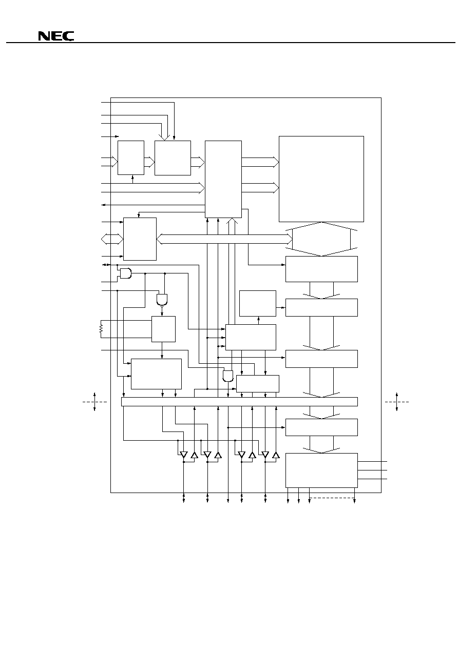
BLOCK DIAGRAM
DIR
PL0,1,2
TEST
A0 to A16
RDY
Control
/CS,/OE,
/WE,/UBE
BMODE
GMODE
/REFRH
D0 to D15
/DOFF
3.3 V operation
5.0V operation
3.3 V operation
5.0 V operation
/FRM
STB /DOUT L1
L2
Y1 Y2 Y3
Y160
DEC
Arbiter
Address
management
circuit
STOP
Data latch(2)
FRC control
Data latch(1)
RAM
160x240x2 bits
V
0
V
1
V
2
/RESET
MS
OSC1
OSC2
Internal timing
generation
Liquid-crystal
timing generation
/FRM STB
Liquid-crystal drive
circuit
160 outputs
Level shifter
Self-diagnosis
circuit
CR
oscillator
Address
input
control
Data bus
control
Frame
thinning-out

4
µ
µ
µ
µ
PD16661A
1. BLOCK FUNCTIONS
(1) Address management circuit
The address management circuit converts the addresses transferred from the system via A0 to A16 into
addresses compatible with the memory map of the on-chip RAM.
This function can be used to address up to VGA size (480
◊
640 dots) with 8 of these LSIs, thus making it
possible to configure a liquid-crystal display system without difficulty.
(2) Arbiter
The arbiter adjusts the contention between the RAM access from the system and the RAM read on the liquid-
crystal drive side.
(3) RAM
Static RAM (single port) of 160
◊
240
◊
2 bits
(4) Data bus control
The data bus controls the data transfer directions by means of Read/Write from the system.
The mode can be switched from 8 bits to 16 bits by the BMODE pin, and the relation between the display data
and the gray scale can be switched by the GMODE pin.
(5) Frame thinning-out control
The frame thinning-out control indicates the four gray scales with three thinning-out frames. The thinning-out
method can be changed in units of 9 pixels (3 columns
◊
3 lines).
(6) Internal timing generation
The internal timing to each block is generated from the /FRM and STB signals.
(7) CR oscillator
In master mode, this oscillator generates the clock that is the reference for the frame frequency. The frame
frequency is one 484th (1/484) of this oscillation. For example, if the frame frequency is 80 Hz, an oscillation
frequency of 38.72 kHz is necessary. As the CR has a built-in capacitance, adjust the required oscillation
frequency with an externally attached resistor.
In slave mode, oscillation is stopped.
(8) Liquid-crystal timing generation
In master mode, /FRM (the frame signal) and STB (the column drive signal strobe) are generated.
(9) FRC control
This circuit realizes the four gray-scale displays.
5
µ
µ
µ
µ
PD16661A
(10) Data latch (1)
This data latch reads and latches 160-pixel data from the RAM.
(11) Data latch (2)
This data latch synchronizes with the STB signal and latches 160-pixel data.
(12) Level shifter
The level shifter converts the voltage from the operating voltage of the internal circuit (3.3 V) to the voltage of the
liquid-crystal drive circuit and row driver interface (5.0 V).
(13) DEC
The DEC decodes the gray scale display data to make it compatible with the liquid-crystal drive voltages V0, V1,
and V2.
(14) Liquid-crystal drive circuit
This circuit selects one of the display OFF signal (/DOFF)-compatible liquid-crystal drive power supplies V0, V1,
or V2, and generates the liquid-crystal applied voltage.
(15) Self-diagnosis circuit
This circuit automatically detects any occurrence of an operation timing lag between the master chip and the
slave chip that has been caused by outside noise, and sends a refresh signal to all the column drivers.
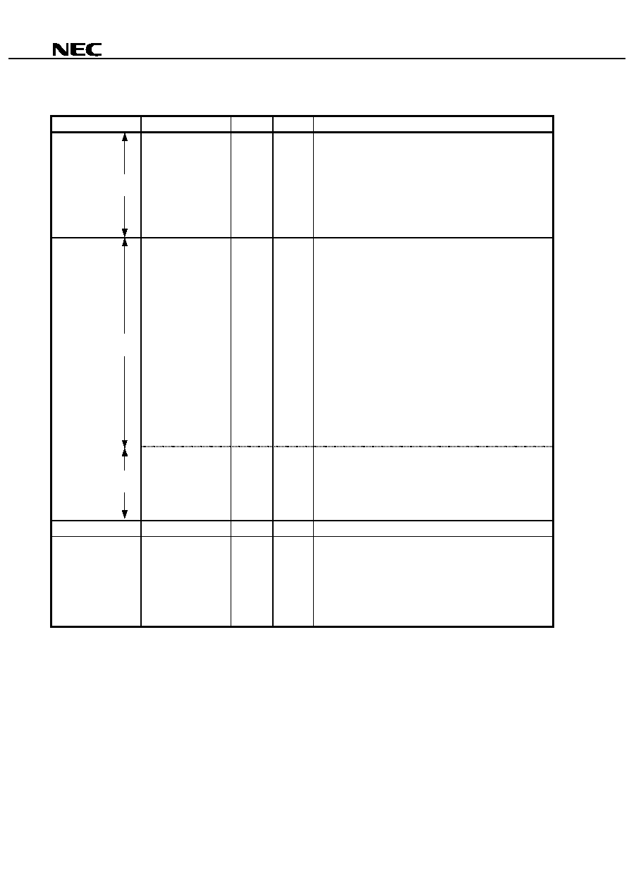
2. MEMORY MAP
Address
A16
A0
Description
0
0
0
0
0
H
:
:
Display data of Nos. 0, 2, 4, and 6
0
F
0
0
0
H
:
:
Display data of Nos. 1, 3, 5, and 7
1
D
F
A
0
H
:
1
F
F
F
F
H
Unused