 | –≠–ª–µ–∫—Ç—Ä–æ–Ω–Ω—ã–π –∫–æ–º–ø–æ–Ω–µ–Ω—Ç: UPD16750N | –°–∫–∞—á–∞—Ç—å:  PDF PDF  ZIP ZIP |
Document Outline
- COVER
- DESCRIPTION
- FEATURES
- ORDERING INFORMATION
- 1. BLOCK DIAGRAM
- 2. RELATIONSHIP BETWEEN OUTPUT CIRCUIT AND D/A CONVERTER
- 3. PIN CONFIGURATION ( uPD16750N-xxx)
- 4. PIN FUNCTIONS
- 5. RELATIONSHIP BETWEEN INPUT DATA AND OUTPUT VOLTAGE VALUE
- 6. RELATIONSHIP BETWEEN INPUT DATA AND OUTPUT PIN
- 7. RELATIONSHIP BETWEEN STB, POL AND OUTPUT WAVEFORM
- 8. ELECTRICAL SPECIFICATIONS
- 9. SWITCHING CHARACTERISTICH WAVEFORM (R,/L)
- 10. RECOMMENDED MOUNTING CONDITIONS

The information in this document is subject to change without notice. Before using this document, please
confirm that this is the latest version.
Not all devices/types available in every country. Please check with local NEC representative for
availability and additional information.
©
1998
MOS INTEGRATED CIRCUIT
µ
µ
µ
µ
PD16750
384-OUTPUT TFT-LCD SOURCE DRIVER
(COMPATIBLE WITH 256-GRAY SCALES)
DATA SHEET
Document No. S13719EJ4V0DS00 (4th edition)
Date Published April 2000 NS CP (K)
Printed in Japan
The mark
∑
∑
∑
∑
shows major revised points.
DESCRIPTION
The
µ
PD16750 is a source driver for TFT-LCDs capable of dealing with displays with 256-gray scales. Data input is
based on digital input configured as 8 bits by 6 dots (2 pixels), which can realize a full-color display of 16,777,216
colors by output of 256 values
-corrected by an internal D/A converter and 8-by-2 external power modules.
Because the output dynamic range is as large as V
DD2
-
0.2 V to V
SS2
+ 0.2 V, level inversion operation of the LCD's
common electrode is rendered unnecessary. Also, to be able to deal with dot-line inversion, n-line inversion and
column line inversion when mounted on a single side, this source driver is equipped with a built-in 8-bit D/A converter
circuit whose odd output pins and even output pins respectively output gray scale voltages of differing polarity.
Assuring a maximum clock frequency of 40 MHz when driving at 3.0 V, this driver is applicable to XGA-standard TFT-
LCD panels and SXGA TFT-LCD panels. This driver is applicable to SXGA TFT-LCD panels by input display signal 2
systems (Clock divide).
FEATURES
∑
CMOS level input
∑
384 outputs
∑
Input of 8 bits (gradation data) by 6 dots
∑
Capable of outputting 256 values by means of 8-by-2 external power modules (16 units) and a D/A converter
∑
Output dynamic range: V
DD2
≠ 0.2 V to V
SS2
+ 0.2 V
∑
High-speed data transfer: f
CLK
= 40 MHz (internal data transfer speed when operating at 3.0 V)
∑
Apply for dot-line inversion, n-line inversion and column line inversion
∑
Output voltage polarity inversion function (POL)
∑
Display data inversion function (POL21/22)
∑
Logic power supply voltage (V
DD1
) : 3.3 V
±
0.3 V
∑
Driver power supply voltage (V
DD2
) : 9.0 V
±
0.5 V
∑
Low power control function (LPC)
ORDERING INFORMATION
Part Number
Package
µ
PD16750N-xxx
TCP (TAB package)
Remark The TCP's external shape is customized. To order the required shape, please contact one of our sales
representatives.
Data Sheet S13719EJ4V0DS00
2
µ
µ
µ
µ
PD16750
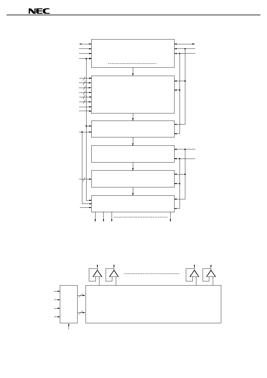
1. BLOCK DIAGRAM
64-bit bidirectional shift register
C
1
C
2
C
63
C
64
Data register
Latch
Level shifter
D/A converter
Voltage follower output
S
1
S
2
S
3
S
384
V
0
- V
15
POL
D
00
- D
07
D
10
- D
17
D
20
- D
27
STHR
R,/L
CLK
STB
STHL
V
DD1
V
SS1
V
DD2
V
SS2
POL21
POL22
D
30
- D
37
D
40
- D
47
D
50
- D
57
LPC
Remark /xxx indicates active low signal.
2. RELATIONSHIP BETWEEN OUTPUT CIRCUIT AND D/A CONVERTER
V
0
V
7
V
8
V
15
∑∑∑∑∑
∑∑∑∑∑
8
8
S
1
S
2
S
383
S
384
8-bit D/A converter
Multi-
plexer
POL
Data Sheet S13719EJ4V0DS00
3
µ
µ
µ
µ
PD16750
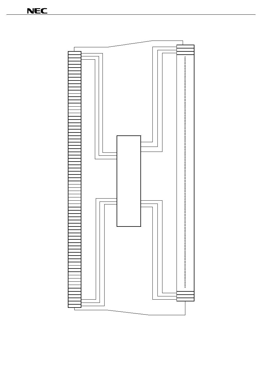
3. PIN CONFIGURATION (
µ
µ
µ
µ
PD16750N-xxx)
S
384
S
383
V
SS2
S
382
V
DD2
V
14
V
12
V
10
V
8
V
6
V
4
V
2
V
0
R,/L
D
50
D
51
D
52
D
53
D
54
D
55
D
56
D
57
D
40
D
41
D
42
D
43
D
44
D
45
D
46
D
47
D
30
D
31
D
32
D
33
D
34
D
35
D
36
D
37
POL21
POL22
POL
STB
STHL
V
DD1
CLK
V
SS1
LPC
STHR
D
20
D
21
D
22
D
23
D
24
D
25
D
26
D
27
D
10
D
11
D
12
D
13
D
14
D
15
D
16
D
17
D
00
D
01
D
02
D
03
D
04
D
05
D
06
D
07
V
1
V
3
V
5
V
7
V
9
V
11
S
3
V
13
S
2
V
15
S
1
V
DD2
V
SS2
Copper Foil
Surface
Remark This figure does not specify the TCP package.
∑
∑
Data Sheet S13719EJ4V0DS00
4
µ
µ
µ
µ
PD16750
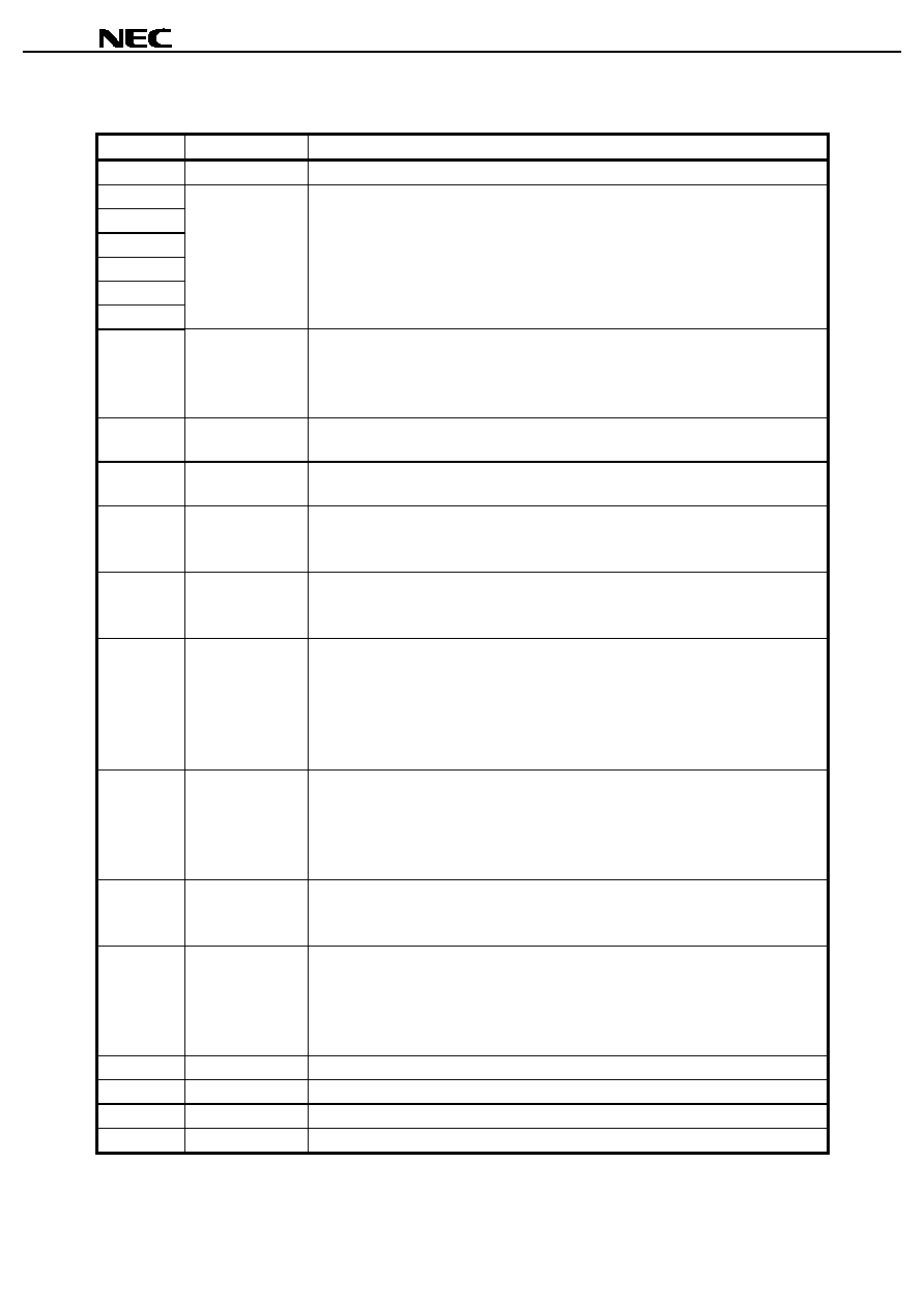
4. PIN FUNCTIONS
Pin Symbol
Pin Name
Description
S
1
to S
384
Driver output
The D/A converted 256-gray-scale analog voltage is output.
D
00
to D
07
D
10
to D
17
D
20
to D
27
D
30
to D
37
D
40
to D
47
D
50
to D
57
Display data input
The display data is input with a width of 48 bits, viz., the gray scale data (8 bits) by 6 dots (2
pixels).
D
X0
: LSB, D
X7
: MSB
R,/L
Shift direction control
input
These refer to the start pulse input/output pins when driver ICs are connected in cascade.
The shift directions of the shift registers are as follows.
R,/L = H
: STHR input, S
1
S
384
, STHL output
R,/L = L
: STHL input, S
384
S
1
, STHR output
STHR
Right shift start pulse
input/output
R,/L = H
: Becomes the start pulse input pin.
R,/L = L
: Becomes the start pulse output pin.
STHL
Left shift start pulse
input/output
R,/L = H
: Becomes the start pulse output pin.
R,/L = L
: Becomes the start pulse input pin.
CLK
Shift clock input
Refers to the shift register's shift clock input. The display data is incorporated into the data
register at the rising edge of the 64th clock after the start pulse input, the start pulse output
reaches the high level, thus becoming the start pulse of the next-level driver.
STB
Latch input
The contents of the data register are transferred to the latch circuit at the rising edge. And,
at the falling edge, the gray scale voltage is supplied to the driver. It is necessary to ensure
input of one pulse per horizontal period.
POL
Polarity input
POL = L
: The S
2n≠1
output uses V
0
to V
7
as the reference supply. The S
2n
output uses V
8
to V
15
as the reference supply.
POL = H : The S
2n≠1
output uses V
8
to V
15
as the reference supply. The S
2n
output uses V
0
to V
7
as the reference supply.
S
2n-1
indicates the odd output: and S
2n
indicates the even output. Input of the POL signal is
allowed the setup time(t
POL
-
STB
) with respect to STB's rising edge.
POL21
POL22
Data inversion
Data inversion can invert when display data is loaded.
POL21/22 = H : Data inversion loads display data after inverting it.
POL21/22 = L : Data inversion does not invert input data.
POL21: D
00
to D
07
, D
10
to D
17
, D
20
to D
27
POL22: D
30
to D
37
, D
40
to D
47
, D
50
to D
57
LPC
Low power control
input
The output buffer constant current source is blocked, reducing current consumption. In lower
power mode (LPC = L: DC-level input possible), the ordinary static current consumption can
be reduced by approx. 33 %.
V
0
to V
15
-corrected power
supplies
Input the
-corrected power supplies from outside by using operational amplifier. Make sure
to maintain the following relationships. During the gray scale voltage output, be sure to keep
the gray scale level power supply at a constant level.
V
DD2
-
0.2 V > V
0
> V
1
> V
2
> V
3
> V
4
> V
5
> V
6
> V
7
> 0.5 V
DD2
0.5 V
DD2
-
0.3 V > V
8
> V
9
> V
10
> V
11
> V
12
> V
13
> V
14
> V
15
> V
SS2
+ 0.2 V
V
DD1
Logic power supply
3.3 V
±
0.3 V
V
DD2
Driver power supply
9.0 V
±
0.5 V
V
SS1
Logic ground
Grounding
V
SS2
Driver ground
Grounding

Data Sheet S13719EJ4V0DS00
5
µ
µ
µ
µ
PD16750
Cautions 1. The power start sequence must be V
DD1
, logic input, and V
DD2
& V
0
to V
15
in that order.
Reverse this sequence to shut down (Simultaneous power application to V
DD2
and V
0
to V
15
is
possible.).
2. To stabilize the supply voltage, please be sure to insert a 0.1-
µ
µ
µ
µ
F bypass capacitor between
V
DD1
-V
SS1
and V
DD2
-V
SS2
. Furthermore, for increased precision of the D/A converter, insertion
of a bypass capacitor of about 0.01
µ
µ
µ
µ
F is also advised between the
-corrected power supply
terminals (V
0
, V
1
, V
2
,....., V
15
) and V
SS2
.