 | –≠–ª–µ–∫—Ç—Ä–æ–Ω–Ω—ã–π –∫–æ–º–ø–æ–Ω–µ–Ω—Ç: UPD16901 | –°–∫–∞—á–∞—Ç—å:  PDF PDF  ZIP ZIP |
©
1997
DATA SHEET
MOS INTEGRATED CIRCUIT
Document No. S10643EJ2V0DS00 (2nd edition)
Date Published May 1997 N
Printed in Japan
µ
PD16901
The
µ
PD16901 is a DC/DC converter IC which produces a 12 V output from a 5 V input source. The integration
of a control circuit and power MOSFET in the output stage on a single-chip allows a power supply for flash memory
write and erasure to be configured with a reduced number of external components.
FEATURES
∑
With an on-chip output stage power MOSFET, fewer external components are needed.
∑
The ALLMOS structure achieves low power consumption.
∑
Internally set output voltage eliminates the need for adjustment.
∑
Output can be turned ON/OFF via an external signal.
∑
A timer latch type overcurrent protection circuit on chip
ORDERING INFORMATION
Part Number
Package
µ
PD16901GS
14-pin plastic SOP (300 mil)
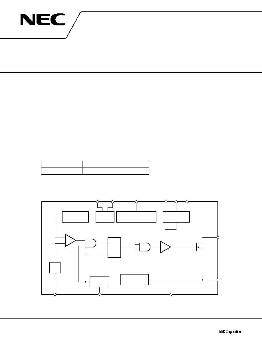
BLOCK DIAGRAM
ON/OFF
V
IN
C
DLY
C
1H
C
1L
C
2
FB
R
T
GND
C.S.
V
SW
F/F
Reference
voltage circuit
Startup
circuit
Timer latch short-circuit
protection circuit
Charge pump
circuit
Oscillation
circuit
Overcurrent
detection circuit
SW
FLASH MEMORY VOLTAGE STEPUP DC/DC CONVERTER IC
The information in this document is subject to change without notice.
2
µ
PD16901
ABSOLUTE MAXIMUM RATINGS (T
A
= 25 ∞C unless specified otherwise)
Item
Symbol
Condition
Rating
Unit
Supply voltage
V
IN
7.0
V
Output voltage
V
SW
20
V
Total power dissipation
P
T
Note
0.9
W
Operating ambient temperature
T
A
≠20 to 85
∞ C
Storage temperature range
T
stg
≠55 to +150
∞ C
Note When 90 mm
◊
90 mm
◊
1.6 mm thick glass epoxy board is mounted
RECOMMENDED OPERATING RANGE
Item
Symbol
MIN.
TYP.
MAX.
Unit
Supply voltage
V
DD
4.5
5.0
5.5
V
Charge pump capacitor
C1, C2
0.033
0.1
0.47
µ
F
Operating ambient temperature
T
A
0
70
∞ C
ELECTRICAL SPECIFICATIONS (T
A
= 25 ∞C, V
IN
= 5 V unless specified otherwise)
Item
Symbol
Condition
MIN.
TYP.
MAX.
Unit
(Oscillation block)
Oscillation frequency
f
OSC
R
T
= 68 k
153
167
181
kHz
On duty
DUTY
67
%
(Low voltage misoperation preventive circuit)
Operation start voltage
V
IN(start-up)
3.3
3.7
4.3
V
Operation stop voltage
V
IN(stop)
2.7
3.2
3.8
V
Hysteresis width
V
HYS
0.3
0.5
0.7
V
(Overcurrent detection block)
Overcurrent detection voltage
V
DET
270
300
330
mV
(On/off control block)
ON/OFF pin input voltage
V
IH
4.5 V
V
IN
5.5 V
V
IN
*0.7
V
V
IL
4.5 V
V
IN
5.5 V
V
IN
*0.3
V
ON/OFF pin input current
I
IL
ON/OFF pin voltage = 0
≠20
≠5
≠1
µ
A
(Charge pump circuit)
Output voltage
V
CHG
4.5 V
V
IN
5.5 V
8.0
11
V
0 ∞C
T
A
70 ∞C
(Short-circuit protection circuit)
Timer latch pin output current
I
SCP
R
T
= 68 k
2.0
3.3
4.5
µ
A
Timer latch detection voltage
V
DETT
0.85
1.0
1.15
V
(Output block)
Output stage on resistance
R
DS(ON)
I
PK
= 0.5 A
0.3
0.5
Output stage leakage current
I
DSOFF
V
DS
= 20 V
1.0
µ
A
3
µ
PD16901
PIN CONFIGURATION (Top View)
14
C
2
13
V
SW
12
NC
11
NC
10
NC
9
CS
8
FB
1
C
1H
2
C
1L
3
V
CC
4
ON/OFF
CONTROL
5
R
T
6
C
DLY
7
GND
4
µ
PD16901
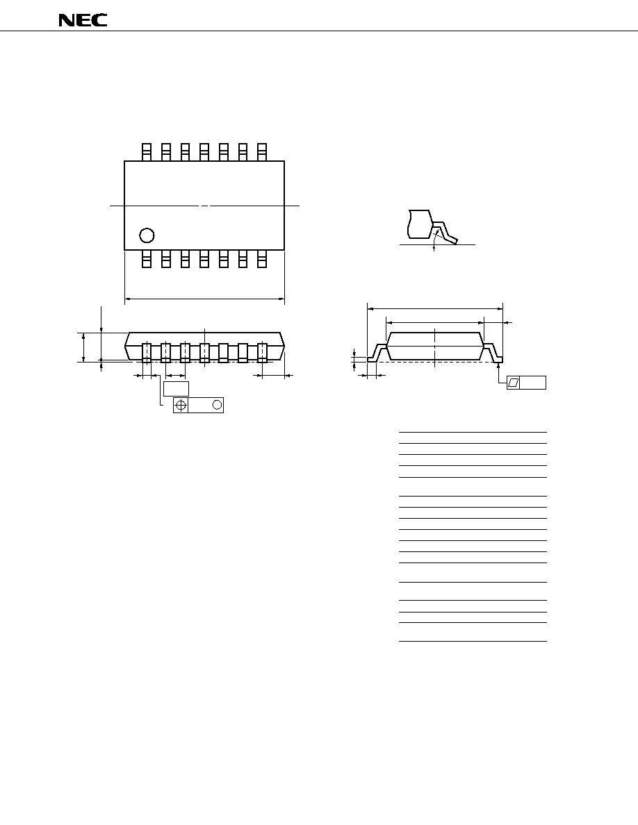
PACKAGE DRAWINGS
14 PIN PLASTIC SOP (300 mil)
ITEM
MILLIMETERS
INCHES
A
B
C
E
F
G
H
I
J
10.46 MAX.
1.27 (T.P.)
1.8 MAX.
1.55
7.7±0.3
1.42 MAX.
0.12
1.1
5.6
M
0.1±0.1
N
0.412 MAX.
0.056 MAX.
0.004±0.004
0.071 MAX.
0.061
0.303±0.012
0.220
0.043
0.005
0.050 (T.P.)
P14GM-50-300B-4
P
3
∞
3
∞
+7
∞
NOTE
Each lead centerline is located within 0.12 mm (0.005 inch) of
its true position (T.P.) at maximum material condition.
D
0.40
0.016
+0.10
≠0.05
K
0.20
0.008
+0.10
≠0.05
L
0.6±0.2
0.024
0.10
≠3
∞
+7
∞
≠3
∞
0.004
+0.008
≠0.009
+0.004
≠0.002
+0.004
≠0.003
A
C
D
G
P
detail of lead end
F
E
B
H
I
J
L
K
N
M
1
7
14
8
M
5
µ
PD16901
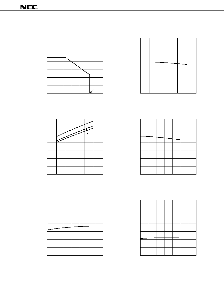
STANDARD CHARACTERISTIC CURVES
P
T
- T
A
characteristic
Total Power dissipation P
T
(W)
Ambient temperature T
A
(∞C)
f
OSC
-V
IN
characteristic
Oscillation frequency f
OSC
(kHz)
Input voltage V
IN
(V)
I
CC (ON)
- V
IN
characteristic
Operating circuit current I
CC (ON)
(mA)
Input voltage V
IN
(V)
f
OSC
- T
A
characteristic
Oscillation frequency f
OSC
(kHz)
Ambient temperature T
A
(∞C)
V
DET
- T
A
characteristic
Overcurrent detection voltage V
DET
(mV)
Ambient temperature T
A
(∞C)
V
DETT
- T
A
characteristic
Timer latch detection voltage V
DETT
(V)
Ambient temperature T
A
(∞C)
1.4
1.2
1.0
0.8
0.6
0.4
0.2
0
≠20
0
20
40
60
80
100
3.5
3.0
2.5
2.0
1.5
1.0
0.5
0
3.5
4.0
4.5
5.0
6.0
6.5
5.5
T
A
= 85 ∞C
T
A
= 0 ∞C
T
A
= 25 ∞C
85 ∞C
139 ∞C/W
340
330
320
310
300
290
280
270
≠20
0
20
40
60
80
100
180
175
170
165
160
155
3.5
4.0
4.5
5.0
6.0
6.5
5.5
1.12
1.1
1.08
1.06
1.04
1.02
1.0
0.98
≠20
0
20
40
60
80
100
180
175
170
165
160
155
150
145
≠20
0
20
40
60
80
100
V
IN
= 5 V
V
IN
= 5 V
V
IN
= 5 V
T
A
= 25 ∞C
When mounted on
90 mm
◊
90 mm
◊
1.6 mm
glass epoxy board
0.9 W