Document Outline
- COVER
- FEATURES
- ORDERING INFORMATION
- FUNCTION OVERVIEW
- BLOCK DIAGRAM
- PIN CONFIGURATION (TOP VIEW)
- PINS
- 1. PIN FUNCTIONS
- 1.1 LIST OF PIN FUNCTIONS
- 1.2 EQUIVALENT CIRCUIT OF EACH PIN
- 1.3 HANDLING UNUSED PINS
- 1.4 NOTES ON USE OF THE CE AND INTNC PINS
- 2. PROGRAM MEMORY (ROM)
- 2.1 OUTLINE OF PROGRAM MEMORY
- 2.2 PROGRAM MEMORY CONFIGURATION
- 2.3 PROGRAM COUNTER
- 2.3.1 Program Counter Configuration
- 2.3.2 Segment Register (SGR)
- 2.4 PROGRAM FLOW
- 2.4.1 Branch Instructions
- 2.4.2 Subroutines
- 2.4.3 Table Reference
- 2.4.4 System Call
- 2.5 NOTES ON USE OF PROGRAM MEMORY
- 2.5.1 Program Counter and Program Memory Size
- 2.5.2 Last Address of Each Segment
- 3. ADDRESS STACK (ASK)
- 3.1 OUTLINE OF ADDRESS STACK
- 3.2 ADDRESS STACK REGISTERS (ASR)
- 3.3 STACK POINTER (SP)
- 3.3.1 Configuration and Function of Stack Pointer
- 3.4 ADDRESS STACK OPERATION
- 3.4.1 Subroutine Call Instruction ("CALL addr" or "CALL @AR") and Return Instruction ("RET" or "RETSK")
- 3.4.2 Table Reference Instruction ("MOVT DBF, @AR")
- 3.4.3 Interrupt Reception and Return Instruction ("RETI")
- 3.4.4 Address Stack Manipulation Instructions ("PUSH AR", "POP AR")
- 3.4.5 System Call Instruction ("SYSCAL entry") and Return Instruction ("RET" or "RETSK")
- 3.5 NOTES ON USE OF ADDRESS STACK
- 4. DATA MEMORY (RAM)
- 4.1 OUTLINE OF DATA MEMORY
- 4.2 CONFIGURATION AND FUNCTIONS OF DATA MEMORY
- 4.2.1 System Register (SYSREG)
- 4.2.2 Data Buffer (DBF)
- 4.2.3 VRAM (Video RAM) for the IDC
- 4.2.4 Port Register
- 4.2.5 General-Purpose Data memory
- 4.2.6 Unmounted Data Memory
- 4.3 DATA MEMORY ADDRESSING
- 4.4 NOTES ON USING DATA MEMORY
- 4.4.1 Power-On Reset
- 4.4.2 Notes on Unmounted Data Memory
- 5. SYSTEM REGISTER (SYSREG)
- 5.1 OUTLINE OF SYSTEM REGISTER
- 5.2 FORMAT OF SYSTEM REGISTER
- 5.3 ADDRESS REGISTER (AR)
- 5.3.1 Format of Address Register
- 5.3.2 Address Register Functions
- 5.3.3 Address Register and Data Buffer
- 5.3.4 Notes on Using Address Register
- 5.4 WINDOW REGISTER (WR)
- 5.4.1 Format of Window Register
- 5.4.2 Window Register Functions
- 5.5 BANK REGISTER (BANK)
- 5.5.1 Format of Bank Register
- 5.5.2 Bank Register Functions
- 5.6 INDEX REGISTER (IX) AND DATA MEMORY ROW ADDRESS POINTER (MP : MEMORY POINTER)
- 5.6.1 Index Register (IX)
- 5.6.2 Data Memory Row Address Pointer (MP)
- 5.7 GENERAL-PURPOSE REGISTER POINTER (RP)
- 5.7.1 Format of General-Purpose Register Pointer
- 5.7.2 General-Purpose Register Pointer Functions
- 5.7.3 Notes on Using General-Purpose Register Pointer
- 5.8 PROGRAM STATUS WORD (PSWORD)
- 5.8.1 Format of Program Status Word
- 5.8.2 Program Status Word Functions
- 5.8.3 Notes on Using Program Status Word
- 5.9 NOTES ON USING SYSTEM REGISTER
- 6. GENERAL-PURPOSE REGISTER (GR)
- 6.1 OUTLINE OF GENERAL-PURPOSE REGISTER
- 6.2 GENERAL-PURPOSE REGISTER BODY
- 6.3 GENERAL-PURPOSE REGISTER ADDRESS GENERATION WITH INSTRUCTIONS
- 6.3.1 Addition Instructions (ADD r,m, ADDC r,m) Subtraction Instructions (SUB r,m, SUBC r,m) Logical Operation Instructions (AND
- 6.3.2 Indirect Transfer Instructions (MOV @r,m, MOV m,@r)
- 6.4 NOTES ON USING GENERAL-PURPOSE REGISTER
- 6.4.1 Row Address of General-Purpose Register
- 6.4.2 Operation between General-Purpose Register and Immediate Data
- 7. ARITHMETIC LOGIC UNIT (ALU) BLOCK
- 7.1 OVERVIEW
- 7.2 CONFIGURATION AND FUNCTIONS OF THE COMPONENTS OF THE ALU BLOCK
- 7.2.1 ALU
- 7.2.2 Temporary Storage Registers A and B
- 7.2.3 Program Status Word
- 7.2.4 Decimal Conversion Circuit
- 7.2.5 Address Controller
- 7.3 ALU OPERATIONS
- 7.4 NOTES ON USING THE ALU
- 7.4.1 Notes on Using the Program Status Word for Operations
- 7.4.2 Notes on Performing Decimal Operations
- 8. REGISTER FILE (RF)
- 8.1 OVERVIEW
- 8.2 CONFIGURATION AND FUNCTIONS OF THE REGISTER FILE
- 8.2.1 Register File Manipulation Instructions (PEEK WR, rf and POKE rf, WR)
- 8.3 CONTROL REGISTERS
- 8.4 NOTES ON USING THE REGISTER FILE
- 9. DATA BUFFER (DBF)
- 9.1 OVERVIEW
- 9.2 DATA BUFFER MAIN BODY
- 9.2.1 Configuration of the Data Buffer Main Body
- 9.2.2 Instruction to Reference a Table (MOVT DBF, @AR)
- 9.2.3 Instructions for Controlling the Peripheral Hardware (PUT, GET)
- 9.3 PERIPHERAL HARDWARE AND DATA BUFFER
- 9.4 NOTES ON USING THE DATA BUFFER
- 10. GENERAL-PURPOSE PORTS
- 10.1 OVERVIEW
- 10.2 GENERAL-PURPOSE I/O PORTS (P0A, P0B, P1B, P1C, P2D)
- 10.2.1 Configurations of the I/O ports
- 10.2.2 Using the I/O Port
- 10.2.3 Control Registers of the I/Ports
- 10.2.4 Using an I/O Port as an Input Port
- 10.2.5 Using an I/O Port as an Output Port
- 10.2.6 Notes on Using the I/O Port
- 10.2.7 Statuses of the I/O Ports upon Reset
- 10.3 GENERAL-PURPOSE INPUT PORT (P0D)
- 10.3.1 Configuration of the Input Port
- 10.3.2 Using the Input Port
- 10.3.3 Notes on Using the Input Port
- 10.3.4 Statuses of the Input Port upon Reset
- 10.4 GENERAL-PURPOSE OUTPUT PORTS (P0C, P1A, P1D, P2A, P2B, P2C)
- 10.4.1 Configurations of the Output Ports
- 10.4.2 Using the Output Port
- 10.4.3 Statuses of the Output Port upon Reset
- 11. INTERRUPT
- 11.1 OUTLINE OF THE INTERRUPT BLOCK
- 11.2 INTERRUPT CONTROL BLOCKS
- 11.2.1 Formats and Functions of Interrupt Request Flags (IRQxxx)
- 11.2.2 Interrupt Enable Flags (IPxxx)
- 11.2.3 Vector Address Generator (VAG)
- 11.3 INTERRUPT STACK REGISTER
- 11.3.1 Format and Functions of the Interrupt Stack Register
- 11.3.2 Interrupt Stack Operation
- 11.4 STACK POINTER, ADDRESS STACK REGISTER, AND PROGRAM COUNTER
- 11.5 INTERRUPT ENABLE FLIP-FLOP (INTE)
- 11.6 ACCEPTING INTERRUPTS
- 11.6.1 Operation for Accepting Interrupts and Priorities
- 11.6.2 Timing Charts for Accepting Interrupts
- 11.7 OPERATION AFTER AN INTERRUPT IS ACCEPTED
- 11.8 RETURN FROM THE INTERRUPT HANDLING ROUTINE
- 11.9 EXTERNAL INTERRUPTS (INT0 PIN, INTNC PIN, VSYNC# PIN, HSYNC# PIN)
- 11.9.1 Outline of External Interrupts
- 11.9.2 Edge Detection Blocks
- 11.9.3 Interrupt Control Block
- 11.9.4 Input Pin for Remote Control (INTNC)
- 11.10 INTERNAL INTERRUPTS
- 11.10.1 Timer 0 Interrupt
- 11.10.2 Timer 1 Interrupt
- 11.10.3 Basic Timer 2 Interrupt
- 11.10.4 VRAM Pointer Interrupt
- 11.10.5 Serial Interface 0 Interrupt
- 11.10.6 Serial Interface 1 Interrupt
- 11.10.7 Interrupts by Interrupt Group 0 and Interrupt Group Selection Register
- 12. TIMERS
- 12.1 OVERVIEW
- 12.2 BASIC TIMER 0
- 12.2.1 Overview of Basic Timer 0
- 12.2.2 Clock Selection Block
- 12.2.3 Flip-Flop and BTM0CY Flag
- 12.2.4 Example of using Basic Timer 0
- 12.2.5 Time Interval Error in Basic Timer 0
- 12.2.6 Cautions for Using Basic Timer 0
- 12.3 BASIC TIMER 1
- 12.3.1 Overview of Basic Timer 1
- 12.3.2 Clock Selection Block
- 12.3.3 Flip-Flop and BTM1CY Flag
- 12.3.4 Time Interval Error in Basic Timer 1
- 12.4 BASIC TIMER 2
- 12.4.1 Overview of Basic Timer 2
- 12.4.2 Clock Selection Block
- 12.4.3 Example of Using Basic Timer 2
- 12.4.4 Time Interval Error in Basic Timer 2
- 12.4.5 Cautions for Using Basic Timer 2
- 12.5 TIMER 0
- 12.5.1 Overview of Timer 0
- 12.5.2 Clock Selection Block
- 12.5.3 Count Block
- 12.5.4 Example of Using Timer 0
- 12.5.5 Time Interval Error in Timer 0
- 12.5.6 Cautions for Using Timer 0
- 12.6 TIMER 1
- 12.6.1 Overview of Timer 1
- 12.6.2 Clock Selection Block
- 12.6.3 Count Block
- 12.6.4 Time Interval Error in Timer 1
- 12.6.5 Cautions for Using Timer 1
- 12.7 CLOCK TIMER
- 12.7.1 Overview of the Clock Timer
- 12.7.2 Clock Frequency Divider Block
- 12.7.3 Count Block
- 12.7.4 Reset Control Block
- 12.7.5 32 kHz Oscillator and Oscillation Frequency Adjustment
- 12.7.6 Cautions for Using the Clock Timer
- 13. A/D CONVERTER
- 13.1 OUTLINE OF A/D CONVERTER
- 13.2 INPUT SWITCHING BLOCK
- 13.3 COMPARE VOLTAGE GENERATION BLOCK AND COMPARE BLOCK
- 13.4 COMPARE TIMING CHART
- 13.5 A/D CONVERTER PERFORMANCE
- 13.6 USING A/D CONVERTER
- 13.6.1 Comparison with One Reference Voltage
- 13.6.2 Successive Approximation Based on the Binary Search Method
- 13.7 NOTES ON USING A/D CONVERTER
- 13.8 STATES UPON RESET
- 13.8.1 Power-On Reset
- 13.8.2 Clock Stop
- 13.8.3 CE Reset
- 14. D/A CONVERTER (PWM METHOD)
- 14.1 OUTLINE OF D/A CONVERTER
- 14.2 OUTPUT SWITCHING BLOCK
- 14.3 DUTY CYCLE SETTING BLOCK
- 14.4 CLOCK GENERATION BLOCK
- 14.5 OUTPUT WAVEFORMS OF D/A CONVERTER
- 14.6 NOTES ON USING D/A CONVERTER
- 14.7 STATES UPON RESET
- 14.7.1 Power-On Reset
- 14.7.2 Clock Stop
- 14.7.3 CE Reset
- 14.7.4 Halt State
- 15. SERIAL INTERFACE
- 15.1 GENERAL
- 15.2 SERIAL INTERFACE 0
- 15.2.1 General
- 15.2.2 Clock I/O Control Block and Data I/O Control Block
- 15.2.3 Clock Control Block
- 15.2.4 Clock Counter and Start/Stop Detection Block
- 15.2.5 Presettable Shift Register 0
- 15.2.6 Wait Control Block and Acknowledge Control Block
- 15.2.7 Interrupt Control Block
- 15.2.8 I2C Bus Mode
- 15.2.9 Serial I/O Mode
- 15.2.10 Data Write and Read Cautions
- 15.2.11 Serial Interface 0 Operation
- 15.2.12 State When Serial Interface 0 Is Reset
- 15.3 SERIAL INTERFACE 1
- 15.3.1 General
- 15.3.2 Clock I/O Control Block and Data I/O Control Block
- 15.3.3 Clock Counter
- 15.3.4 Presettable Shift Register 1
- 15.3.5 Wait Control Block
- 15.3.6 Serial Interface 1 Operation
- 15.3.7 Data Write and Data Read Cautions
- 15.3.8 Serial Interface 1 Operation
- 15.3.9 State When Serial Interface 1 Is Reset
- 16. IMAGE DISPLAY CONTROLLER (IDC)
- 16.1 GENERAL
- 16.1.1 Configuration
- 16.1.2 IDC Functions
- 16.2 IDC DISPLAY CONTROL BLOCK
- 16.2.1 IDC Display Control Block Control Registers
- 16.2.2 Display Format
- 16.2.3 Space between Characters
- 16.2.4 Screen Background Color
- 16.3 IDC START POSITION CONTROL BLOCK
- 16.3.1 Configuration of IDC Start Position Setting Register
- 16.3.2 Horizontal Start Position Setting
- 16.3.3 Vertical Start Position Setting
- 16.4 CROM (CHARACTER ROM)
- 16.4.1 Character Pattern Data Configuration
- 16.4.2 Definition of Character Pattern Data with Assembler
- 16.5 VRAM (VIDEO RAM)
- 16.5.1 General
- 16.5.2 Configuration of VRAM Data
- 16.5.3 Character Pattern Selection Data
- 16.5.4 Carriage Return Data (C/R)
- 16.5.5 Control Data
- 16.5.6 VRAM Data Setting Example
- 16.5.7 VRAM Data Setting Cautions
- 16.6 VRAM POINTER
- 16.6.1 Configuration of VRAM Pointer
- 16.6.2 VRAM Pointer Buffer (IDCVP)
- 16.6.3 VRAM Pointer Register (IDCVPR)
- 16.7 IDC OUTPUT PINS (BLANK, RED, GREEN, BLUE, I PINS)
- 16.7.1 Functions of IDC Output Pins
- 16.7.2 IDC Output Waveforms
- 16.8 SAMPLE PROGRAM
- 16.8.1 Displaying Data Exceeding VRAM Capacity (Extended Display Mode)
- 17. HORIZONTAL SYNCHRONIZING SIGNAL COUNTER
- 17.1 GENERAL
- 17.2 GATE INPUT AMPLIFIER
- 17.3 GATE CONTROL
- 17.3.1 HSYNC Counter Gate Mode Selection Flag (HSCGTx)
- 17.3.2 HSYNC Counter Gate Open Status Flag (HSCGOSTT)
- 17.4 HSYNC COUNTER DATA REGISTER (HSC)
- 17.5 SAMPLE PROGRAM
- 17.6 STATE AT RESET
- 18. PLL FREQUENCY SYNTHESIZER
- 18.1 GENERAL
- 18.2 PROGRAMMABLE DIVIDER
- 18.2.1 Configuration
- 18.2.2 Programmable Divider and PLL Data Register
- 18.3 REFERENCE FREQUENCY GENERATOR
- 18.4 PHASE COMPARATOR (PHI-DET), CHARGE PUMP AND UNLOCK DETECTION BLOCK
- 18.4.1 Configuration of Phase Comparator, Charge Pump and Unlock Detection Block
- 18.4.2 Phase Comparator Functions
- 18.4.3 Charge Pump
- 18.4.4 Configuration and Functions of Unlock Detection Block
- 18.4.5 Organization and Functions of PLL Unlock Flip-Flop Judge Register
- 18.4.6 Organization and Functions of PLL Unlock Flip-Flop Sensibility Selection Register
- 18.5 PLL DISABLED STATE
- 18.6 PLL FREQUENCY SYNTHESIZER USE
- 18.7 SAMPLE PROGRAM
- 18.8 STATE AT RESET
- 18.8.1 At Power-On Reset
- 18.8.2 At Clock-Stop
- 18.8.3 At CE Reset
- 18.8.4 During the Halt State
- 19. STANDBY
- 19.1 STANDBY FUNCTIONS
- 19.2 HALT FUNCTION
- 19.2.1 General
- 19.2.2 Halt State
- 19.2.3 Halt Release Conditions
- 19.2.4 Halt Release by Key Input
- 19.2.5 Halt Release by Basic Timer 0
- 19.2.6 Halt Release by Interrupt
- 19.2.7 When Multiple Release Conditions Set Simultaneously
- 19.3 CLOCK-STOP FUNCTION
- 19.3.1 Clock-Stop State
- 19.3.2 Clock-Stop State Release
- 19.3.3 Clock-Stop Release by CE Reset
- 19.3.4 Clock-Stop Release by Power-On Reset
- 19.3.5 Clock-Stop Release by R1B2/RLSSTP Pin
- 19.3.6 Cautions When Using Clock-Stop Instruction
- 19.4 DEVICE OPERATION AT HALT AND CLOCK-STOP
- 19.5 PIN PROCESSING CAUTIONS IN HALT STATE AND CLOCK-STOP STATE
- 19.6 DEVICE OPERATION CONTROL BY CE PIN
- 19.6.1 Image Display Controller (IDC) Operation Control
- 19.6.2 PLL Frequency Synthesizer Operation Control
- 19.6.3 Clock-Stop Instruction Disable/Enable Control
- 19.6.4 Device Reset
- 19.6.5 Signal Input to CE Pin
- 19.6.6 Organization and Functions of CE Pin Level Judge Register
- 19.6.7 Organization and Functions of CE Pin Edge Detection Register
- 20. RESET
- 20.1 RESET BLOCK CONFIGURATION
- 20.2 RESET FUNCTION
- 20.3 CE RESET
- 20.3.1 CE Reset When Clock-Stop (STOP s Instruction) Not Used
- 20.3.2 CE Reset When Clock-Stop (STOP s Instruction) Used
- 20.3.3 Cautions at CE Reset
- 20.4 POWER-ON RESET
- 20.4.1 Power-On Reset at Normal Operation
- 20.4.2 Power-On Reset in Clock-Stop State
- 20.4.3 Power-On Reset When VDD Rises From 0 V
- 20.5 RELATIONSHIP BETWEEN CE RESET AND POWER-ON RESET
- 20.5.1 When VDD Pin and CE Pin Rise Simultaneously
- 20.5.2 When CE Pin Raised in Forced Halt State Caused by Power-On Reset.
- 20.5.3 When CE Pin Raised After Power-On Reset
- 20.5.4 Cautions When VDD Raised
- 20.6 POWER FAILURE DETECTION
- 20.6.1 Power Failure Detection Circuit
- 20.6.2 Cautions at Power Failure Detection with BTM0CY Flag
- 20.6.3 Power Failure Detection by RAM Judgment
- 20.6.4 Cautions at Power Failure Detection by RAM Judgment
- 21. INSTRUCTION SET
- 21.1 LIST OF INSTRUCTION SET
- 21.2 INSTRUCTIONS
- 21.3 ASSEMBLER (AS17K) BUILT-IN MACRO INSTRUCTIONS
- 22. RESERVED SYMBOLS
- 22.1 DATA BUFFER (DBF)
- 22.2 SYSTEM REGISTER (SYSREG)
- 22.3 VRAM BANK REGISTER
- 22.4 PORT REGISTER
- 22.5 REGISTER FILES
- 22.6 PERIPHERAL HARDWARE REGISTER
- 22.7 OTHERS
- 23. ELECTRICAL CHARACTERISTICS
- 24. PACKAGE DRAWINGS
- 25. RECOMMENDED SOLDERING CONDITIONS
- APPENDIX A. NOTES ON CONNECTING A CRYSTAL
- APPENDIX B. DEVELOPMENT TOOLS

The
�
PD17068 is a 4-bit single-chip microcontroller for digital tuning systems. It contains an image display
controller (IDC) that supports many types of display, and a PLL synthesizer.
The CPU of the
�
PD17068 is capable of 4-bit parallel addition, logical operations, bit tests, setting/resetting
of a carry flag, and supports a powerful interrupt function and timer function.
The image display controller for on-screen display is user-programmable, allowing a range of displays to
be programmed.
The peripheral hardware includes a full complement of I/O ports, controlled with powerful I/O instructions,
as well as a serial interface, a 6-bit A/D converter, and an 8-bit D/A converter (PWM output).
FEATURES
�
Program memory (ROM)
:
24K bytes (12032
�
16 bits)
�
Character ROM (CROM)
:
4086
�
24 bits (255 characters)
�
Data memory (RAM)
:
1007
�
4 bits
�
Video RAM (VRAM)
:
672
�
4 bits (can be used for data memory)
�
Address stack
:
12 levels
�
Interrupt stack
:
2 levels
�
Instruction execution time :
2
�
s (when an 8 MHz crystal is used)
�
PLL frequency synthesizer
�
8-bit serial interface
(2 channels: One for two-wire or three-wire mode, compatible with I
2
C bus, and one for three-wire mode only)
�
D/A converter: 8 bits
�
9 lines (PWM output)
�
A/D converter: 6 bits
�
8 lines
�
Horizontal synchronizing signal counter
�
Commercial power supply frequency counter
�
Power-failure detection circuit and power-on reset circuit
�
Interrupt input for remote-controller signal (with noise canceler)
�
User-programmable image display controller (IDC)
Displayed characters : Up to 192 per screen (more characters can be displayed when the use of the entire
screen is specified with a program)
Display mode
: 16
�
16 dots in 15 lines
�
24 columns
14
�
16 dots in 17 lines
�
24 columns
Character patterns
: 255
Character format
: 16
�
16 dots or 14
�
16 dots
Colors
: 15
Character sizes
: 16 sizes for height (can be specified per line)
24 sizes for width (can be specified per character)
�
Many I/O ports
I/O
: 19 ports
Input only
: 4 ports
Output only
: 21 ports
�
Operating supply voltage: 5 V
�
10 %
�
Low power dissipation by use of CMOS technology
The information in this document is subject to change without notice.
DATA SHEET
MOS INTEGRATED CIRCUIT
�
PD17068
4-BIT SINGLE-CHIP MICROCONTROLLER CONTAINING
IMAGE DISPLAY CONTROLLER AND PLL FREQUENCY
SYNTHESIZER FOR DIGITAL TUNING SYSTEMS
�
1994
Document No. IC-3525
(O.D. No. IC-8999)
Date Published November 1994 P
Printed in Japan

2
�
PD17068
ORDERING INFORMATION
Part number
Package
Quality grade
�
PD17068GF-
���
-3BA
100-pin plastic QFP (14
�
20 mm)
Standard
�
PD17068GF-E
��
-3BA
Note
100-pin plastic QFP (14
�
20 mm)
Standard
Note Product supporting an I
2
C bus interface. When using the I
2
C bus interface (including implementation
with a program that does not use peripheral hardware), make this point clear to your NEC sales
representative when ordering mask options.
Remark
���
is a ROM code.
Please refer to "Quality grade on NEC Semiconductor Devices" (Document number IEI-1209) published by
NEC Corporation to know the specification of quality grade on the devices and its recommended applications.

3
�
PD17068
FUNCTION OVERVIEW
Item
Function
Program memory (ROM)
� 24K bytes (12032
�
16 bits)
Table reference area: 12032
�
16 bits
Character ROM (CROM)
� 4086
�
24 bits (255 characters)
Data memory
RAM
� 1007
�
4 bits (including area also used for VRAM)
Data buffers: 4
�
4 bits, general-purpose registers: 16
�
4 bits
Video RAM (VRAM)
� 672
�
4 bits (can be used for data memory (RAM))
System registers
� 12
�
4 bits
Register files
� 12
�
4 bits
General-purpose port registers
� 12
�
4 bits
Instruction execution time
� 2
�
s (when 8 MHz crystal is used)
Stack levels
� 12 levels (stack manipulation possible)
General-purpose ports
� I/O
: 19 ports
Input only
: 4 ports
Output only : 21 ports
IDC
� Displayed characters : Up to 192 per screen (more characters can be displayed
(Image Display Controller)
when the use of the entire screen is specified with a
program)
� Display mode
: 16
�
16 dots in 15 lines
�
24 columns
14
�
16 dots in 17 lines
�
24 columns
� Character patterns
: 255 (user-programmable)
� Character format
: 16
�
16 dots or 14
�
16 dots
(2-dot interval can be specified between characters.)
� Colors
: 15
� Character sizes
: 16 different heights (can be specified per line)
24 different widths (can be specified per character)
PLL frequency synthesizer
� Frequency division method : Pulse swallow
� Reference frequency
: 5, 6.25, 10, 12.5, and 25 kHz
� Contains a charge pump for an external low-pass filter
� Phase comparator
: Unlock can be detected with a program.
The delay for the unlock flip-flop is selectable.
Serial interface
� 2 channels
Serial interface 0 (two-wire or three-wire mode, compatible with I
2
C bus)
Serial interface 1 (three-wire mode only)
D/A converter
� 8 bits
�
9 lines (PWM output with withstand voltage of 12.5 V max.)
A/D converter
� 6 bits
�
8 lines (successive approximation system with software)
Interrupts
� 10 channels (maskable interrupts)
External interrupts : 3 channels (INT
0
, INT
NC
, and V
SYNC
/H
SYNC
)
Internal interrupts
: 7 channels (timers 0 and 1, serial interfaces 0 and 1, basic
timer 2, VRAM pointer, and timer 0 overflow)

4
�
PD17068
Item
Function
Timers
Timer 0
: 10
�
s to 204.75 ms (interrupt)
Timer 1
: 1
�
s to 256 ms (interrupt)
Basic timer 0 : 1, 5, and 100 ms (carry)
Basic timer 1 : 125
�
s, 1 ms, 5 ms, 100 ms, and external (carry)
Basic timer 2 : 125
�
s, 1 ms, 5 ms, 100 ms, and external (interrupt)
Watch timer : Day, hour, minute, and second (count value)
Reset
� Power-on reset
� Reset with the CE pin (by switching the CE pin from low to high)
� Power-failure detection function
Supply voltage
5 V
�
10%
Package
100-pin plastic QFP (14
�
20 mm)
Remark Parentheses for timers indicate how to obtain the elapsed time for each timer.
Interrupt
: Receiving an interrupt
Carry
: Detecting the state of the carry flip-flop
Count value
: Reading the count value
5
�
PD17068
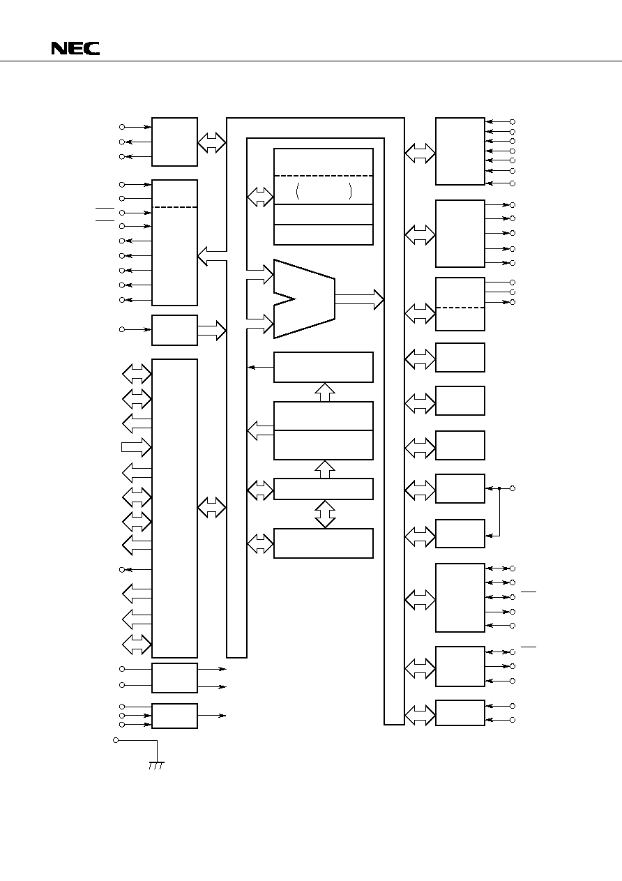
VCO
PSC
EO
OSC
IN
OSC
OUT
H
SYNC
V
SYNC
RED
GREEN
BLUE
BLANK
I (POB
2
)
HSCNT (P0B
3
)
P0A
0
-P0A
3
P0B
0
-P0B
3
P0C
0
-P0C
3
P0D
0
-P0D
3
P1A
0
-P1A
3
P1B
0
-P1B
3
P1C
0
-P1C
3
P1D
0
-P1D
3
P2A
0
P2B
0
-P2B
3
P2C
0
-P2C
3
P2D
0
-P2D
3
X
IN
X
OUT
V
DD
CE
RLS
STP
/PIB
2
GND
0
,
GND
1
Main
OSC
Reset
CPU
Peripheral
Port
PLL
OSC
circuit
IDC
Hsync
counter
RAM
1007
�
4 bits
VRAM
(672
�
4 bits)
System registers
RF
ALU
Instruction decoder
ROM
12032
�
16 bits
CROM
4086
�
24 bits
Program counter
Stack
12
�
14 bits
A/D
Converter
D/A
converter
OSC
Watch
timer
Timer 0
Timer 1
Basic
timer 0
Basic
timer 1
Basic
timer 2
Serial
interface 0
Serial
interface 1
Interrupt
ADC
0
ADC
1
(P0D
0
/XT
OUT
)
ADC
2
(P0D
1
/XT
IN
)
ADC
3
(P0D
2
)
ADC
4
(P0D
3
)
ADC
5
(P1C
0
)
ADC
7
(P1C
2
)
|
PWM
0
(P2C
0
)
PWM
3
(P2C
3
)
PWM
4
(P2B
0
)
PWM
7
(P2B
3
)
PWM
8
(P2A
0
)
|
|
XT
IN
(P0D
1
/ADC
2
)
XT
OUT
(P0D
0
/ADC
1
)
CKOUT (P1B
1
)
TMIN (P1B
3
)
SDA (P0A
0
)
SCL (P0A
1
)
SCK
0
(P0A
2
)
SO
0
(P0A
3
)
SI
0
(P0B
0
)
SCK
1
(P2D
0
)
SO
1
(P2D
1
)
SI
1
(P2D
2
)
INT
NC
INT
0
4
4
4
4
4
4
4
4
4
4
3
BLOCK DIAGRAM