
DESCRIPTION
�
PD17072 and 17073 are low-voltage 4-bit single-chip CMOS microcontrollers containing hardware ideal for
organizing a digital tuning system.
The CPU employs 17K architecture and can manipulate the data memory directly, perform arithmetic operations,
and control peripheral hardware with a single instruction. All the instructions are 16-bit one-word instructions.
As peripheral hardware, a prescaler that can operate at up to 230 MHz for a digital tuning system, a PLL frequency
synthesizer, and an intermediate frequency (IF) counter are integrated in addition to I/O ports, an LCD controller/driver,
A/D converter, and BEEP.
Therefore, a high-performance, multi-function digital tuning system can be configured with a single chip of
�
PD17072 or 17073.
Because the
�
PD17072 and 17073 can operate at low voltage (V
DD
= 1.8 to 3.6 V), they are ideal for controlling
battery-cell driven portable devices such as portable radio equipment, headphone stereos, or radio cassette
recorders.
FEATURES
� 17K architecture: general-purpose register system
� Program memory (ROM)
6 KB (3072
�
16 bits):
�
PD17072
8 KB (4096
�
16 bits):
�
PD17073
� General-purpose data memory (RAM)
176
�
4 bits
� Instruction execution time
53.3
�
s (with 75-kHz crystal resonator: normal operation)
106.6
�
s (with 75-kHz crystal resonator: low-speed mode)
� Decimal operation
� Table reference
� Hardware for PLL frequency synthesizer
Dual modulus prescaler (230 MHz max.), programmable divider, phase comparator, charge pump
� Various peripheral hardware
General-purpose I/O ports, LCD controller/driver, serial interface, A/D converter, BEEP, intermediate frequency
(IF) counter
� Many interrupts
External: 1 channel
Internal: 2 channels
�
Power-ON reset, CE reset, and power failure detector
� CMOS low power consumption
� Supply voltage: V
DD
= 1.8 to 3.6 V
Unless otherwise stated, the
�
PD17073 is taken as a representative product in this document.
4-BIT SINGLE-CHIP MICROCONTROLLER
WITH HARDWARE FOR DIGITAL TUNING SYSTEM
�
PD17072,17073
MOS INTEGRATED CIRCUIT
Document No. U11450EJ1V0DS00 (1st edition)
Date Published September 1996 P
Printed in Japan
The information in this document is subject to change without notice.
�
1996
DATA SHEET
3
�
PD17072,17073
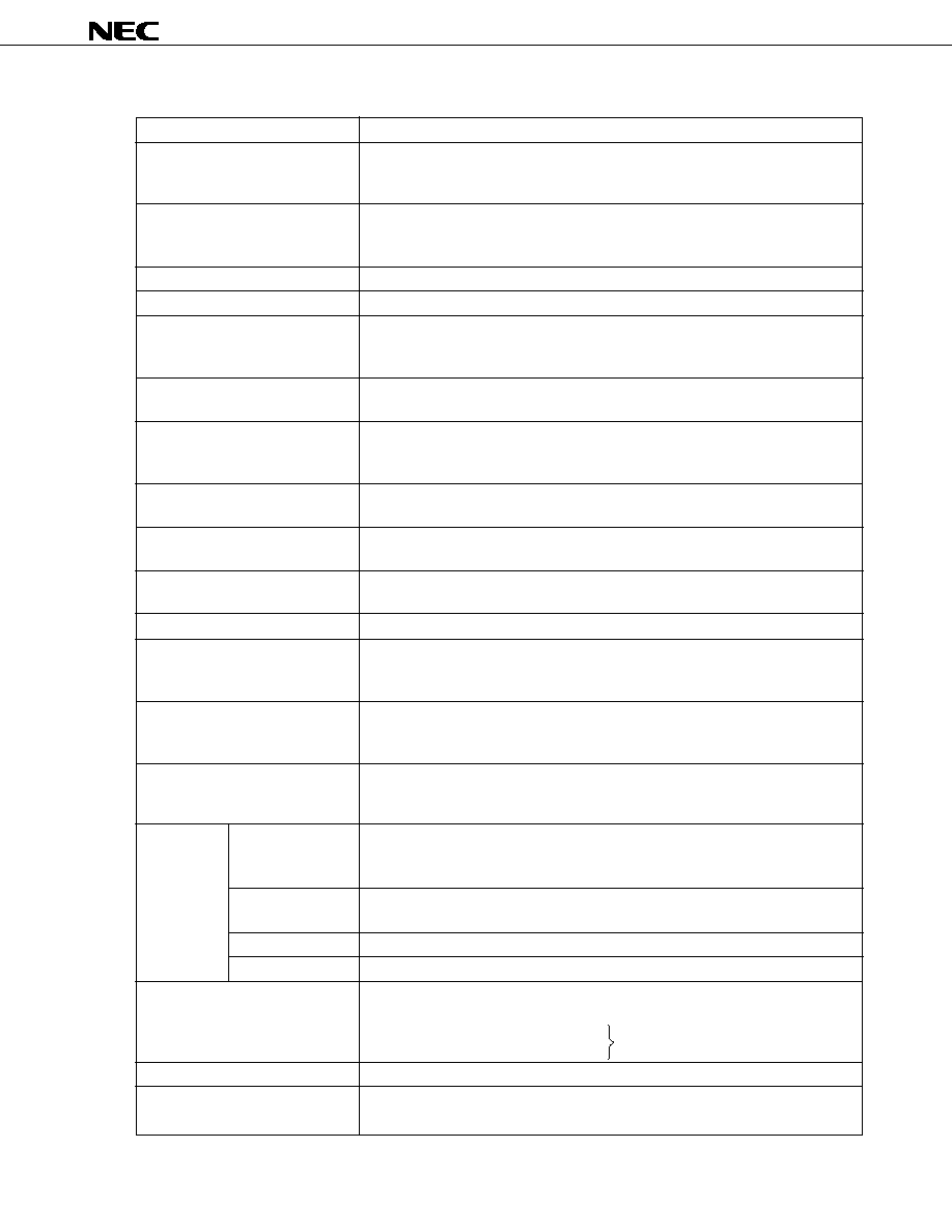
Item
Function
Program memory (ROM)
� 6K bytes (3072
�
16 bits):
�
PD17072
� 8K bytes (4096
�
16 bits):
�
PD17073
� Table reference area: 4096
�
16 bits
General-purpose data memory
� 176
�
4 bits
(RAM)
General-purpose register: 16
�
4 bits
(fixed at 00H through 0FH of BANK0, shared with data buffers.)
LCD segment register
15
�
4 bits
Peripheral control register
32
�
4 bits
Instruction execution time
� 53.3
�
s (with 75-kHz crystal resonator: normal operation)
� 106.6
�
s (with 75-kHz crystal resonator: low-speed mode)
Selectable by software
Stack level
� Address stack: 2 levels (stack can be manipulated)
� Interrupt stack: 1 level (stack cannot be manipulated)
General-purpose port
� I/O port: 8
� Input port: 4
� Output port: 9
BEEP
� 1 type
� Selectable frequency (1.5 kHz, 3 kHz)
LCD controller/driver
� 15 segments, 4 commons
1/4 duty, 1/2 bias, frame frequency of 62.5 Hz, drive voltage V
LCD1
= 3.1 V (TYP.)
Serial interface
� 1 channel (Serial I/O mode)
3-wire/2-wire mode selectable
A/D converter
4 bits
�
2 channels (successive approximation via software)
Interrupt
� 3 channels (maskable interrupt)
External interrupt: 1 (INT pin)
Internal interrupt: 2 (basic timer 1, serial interface)
Timer
� 2 channels
Basic timer 0: 125 ms
Basic timer 1: 8 ms, 32 ms
Reset
� Power-ON reset (on power application)
� Reset by CE pin (CE pin: low level
high level)
� Power failure detection function
PLL
Division method
� Direct division method
(VCOL pin: 8 MHz MAX.)
frequency
� Pulse swallow method
(VCOL pin: 55 MHz MAX.)
synthesizer
(VCOH pin: 230 MHz MAX.)
Reference
� 6 types selectable by program
frequency
1, 3, 5, 6.25, 12.5, 25 kHz
Charge pump
Error out output: 1 line (EO pin)
Phase comparator
Unlock detectable by program
Frequency counter
� Frequency measurement
P0D3/FMIFC/AMIFC pin: FMIF mode, 10 to 11 MHz
P0D3/FMIFC/AMIFC pin: AMIF mode
400 to 500 kHz
P0D2/AMIFC pin
Supply voltage
V
DD
= 1.8 to 3.6 V
Package
� 56-pin plastic QFP (10
�
10 mm, 0.65-mm pitch)
� 64-pin plastic TQFP (10
�
10 mm, 0.5-mm pitch)
FUNCTION OUTLINE


