Document Outline
- COVER
- FEATURES
- APPLICATIONS
- ORDERING INFORMATION
- FUNCTION LIST
- PIN CONFIGURATION (Top View)
- BLOCK DIAGRAM
- 1. PIN
- 1.1. Pin Function
- 1.2 Equivalent Circuit of Pin
- 1.3 Handling of Unused Pins
- 1.4 Note on Using RESET# and P0F0/RLS# Pins
- 2. PROGRAM MEMORY (ROM)
- 2.1 Configuration of Program Memory
- 3. PROGRAM COUNTER (PC)
- 3.1 Configuration of Program Counter
- 3.2 Operation of Program Counter
- 4. STACK
- 4.1 Configuration of Stack
- 4.2 Stack Function
- 5. DATA MEMORY (RAM)
- 5.1 Configuration of Data Memory
- 6. GENERAL REGISTER (GR)
- 6.1 General Register Pointer (RP)
- 7. SYSTEM REGISTER (SYSREG)
- 7.1 Configuration of System Register
- 8. REGISTER FILE (RF)
- 8.1 Configuration of Register File
- 8.2 Function of Register File
- 9. DATA BUFFER (DBF)
- 9.1 Configuration of Data Buffer
- 9.2 Function of Data Buffer
- 10. ALU BLOCK
- 10.1 Configuration of ALU Block
- 11. PORTS
- 11.1 Port 0A (P0A0, P0A1, P0A2, P0A3)
- 11.2 Port 0B (P0B0, P0B1, P0B2, P0B3)
- 11.3 Port 0C (P0C0/ADC0, P0C1/ADC1, P0C2/ADC2, P0C3/ADC3)
- 11.4 Port 0D (P0D0/SCK#, P0D1/SO, P0D2/SI, P0D3/TM1OUT#)
- 11.5 Port 0E (P0E0, P0E1, P0E2, P0E3)
- 11.6 Port 0F (P0F0/RLS#, P0F1/VREF)
- 12. 8-BIT TIMERS/COUNTERS (TM0, TM1)
- 12.1 Configuration of 8-Bit Timers/Counters
- 13. BASIC INTERVAL TIMER (BTM)
- 13.1 Configuration of Basic Interval Timer
- 13.2 Registers Controlling Basic Interval Timer
- 13.3 Watchdog Timer Function
- 14. A/D CONVERTER
- 14.1 Configuration of A/D Converter
- 14.2 Function of A/D Converter
- 14.3 Operation of A/D Converter
- 15. SERIAL INTERFACE (SIO)
- 15.1 Function of Serial Interface
- 15.2 Operation Mode of 3-Wire Serial Interface
- 16. INTERRUPT FUNCTION
- 16.1 Types of Interrupt Causes and Vector Addresses
- 16.2 Hardware of Interrupt Control Circuit
- 17. STANDBY FUNCTION
- 17.1 Outline of Standby Function
- 17.2 HALT Mode
- 17.3 STOP Mode
- 18. RESET
- 18.1 Reset Function
- 18.2 Reset Operation
- 19. POC CIRCUIT (MASK OPTION)
- 19.1 Function of POC Circuit
- 19.2 Conditions to Use POC Circuit
- 20. INSTRUCTION SET
- 20.1 Outline of Instruction Set
- 20.2 Legend
- 20.3 Instruction Set
- 20.4 Assembler (AS17K) Embedded Macro Instruction
- 21. ASSEMBLER RESERVED WORDS
- 21.1 Mask Option Directive
- 21.2 Reserved Symbols
- 22. ELECTRICAL SPECIFICATIONS
- 23. CHARACTERISTIC CURVE (REFERENCE VALUE)
- 24. PACKAGE DRAWINGS
- 25. RECOMMENDED SOLDERING CONDITIONS
- APPENDIX A. FUNCTION COMPARISON BETWEEN uPD17145 SUBSERIES AND THE uPD17135A AND 17137A
- APPENDIX B. DEVELOPMENT TOOLS

The information in this document is subject to change without notice.
MOS INTEGRATED CIRCUIT
Document No. U13233EJ1V1DS00 (1st edition)
(Previous No. IC-3580)
Date Published January 1998 N CP(K)
Printed in Japan
SMALL, GENERAL-PURPOSE
4-BIT SINGLE-CHIP MICROCONTROLLERS
�
PD17145(A1), 17147(A1), 17149(A1)
The
�
PD17145(A1), 17147(A1), and 17149(A1) are 4-bit single-chip microcontrollers integrating an 8-bit
A/D converter (4 channels), a timer function (3 channels), and a serial interface.
These microcontrollers employ a CPU of the general-purpose register type that can execute direct memory
operations and direct memory-to-memory data transfer for efficient programming. All the instructions consist
of 16 bits per word.
In addition, a one-time PROM version, the
�
PD17P149, is also available for program evaluation.
The functions of these microcontrollers are described in detail in the following User's Manual. Be sure
to read the following manual when designing your system:
�
PD17145 Subseries User's Manual: IEU-1383
FEATURES
�
17K architecture
: General-purpose register type
: Instruction length fixed to 16 bits
�
Program memory (ROM)
:
�
PD17145(A1) : 2 KB (1024
�
16 bits)
:
�
PD17147(A1) : 4 KB (2048
�
16 bits)
:
�
PD17149(A1) : 8 KB (4096
�
16 bits)
�
Data memory (RAM)
: 110
�
4 bits
�
External interrupt
: 1 (INT pin, with sense input)
�
Instruction execution time
: 2
�
s (at 8 MHz: ceramic oscillation)
�
8-bit A/D converter
: 4 channels, absolute accuracy:
�
1.5 LSB MAX. (V
DD
= 4.0 to 5.5 V)
�
Timer
: 3 channels
�
Serial interface
: 1 channel (clocked 3-wire)
�
POC circuit (mask option)
�
Operating voltage
: V
DD
= 2.7 to 5.5 V (at 400 kHz to 2 MHz)
: V
DD
= 4.5 to 5.5 V (at 400 kHz to 8 MHz)
�
Operating temperature
: T
a
= �40 to +110 �C
APPLICATIONS
Automotive electronics, etc.
Unless contextually excluded, references in this data sheet to the
�
PD17149 (A1) mean the
�
PD17145
(A1) and
�
PD17147 (A1).
�
1995
DATA SHEET

2
�
PD17145(A1), 17147(A1), 17149(A1)
ORDERING INFORMATION
Remark
���
indicates ROM code suffix.
Part Number
Package
Quality Grade
�
PD17145CT(A1)-
���
28-pin plastic shrink DIP (400 mil)
Special
�
PD17145GT(A1)-
���
28-pin plastic SOP (375 mil)
Special
�
PD17147CT(A1)-
���
28-pin plastic shrink DIP (400 mil)
Special
�
PD17147GT(A1)-
���
28-pin plastic SOP (375 mil)
Special
�
PD17149CT(A1)-
���
28-pin plastic shrink DIP (400 mil)
Special
�
PD17149GT(A1)-
���
28-pin plastic SOP (375 mil)
Special
Please refer to "Quality Grades on NEC Semiconductor Devices" (Document No. C11531E) published by
NEC Corporation to know the specification of quality grade on the devices and its recommended applications.
3
�
PD17145(A1), 17147(A1), 17149(A1)
POC circuit
Operating voltage
Package
One-time PROM version
�
PD17P149
Timer
3 channels
� Internal interrupt: 4
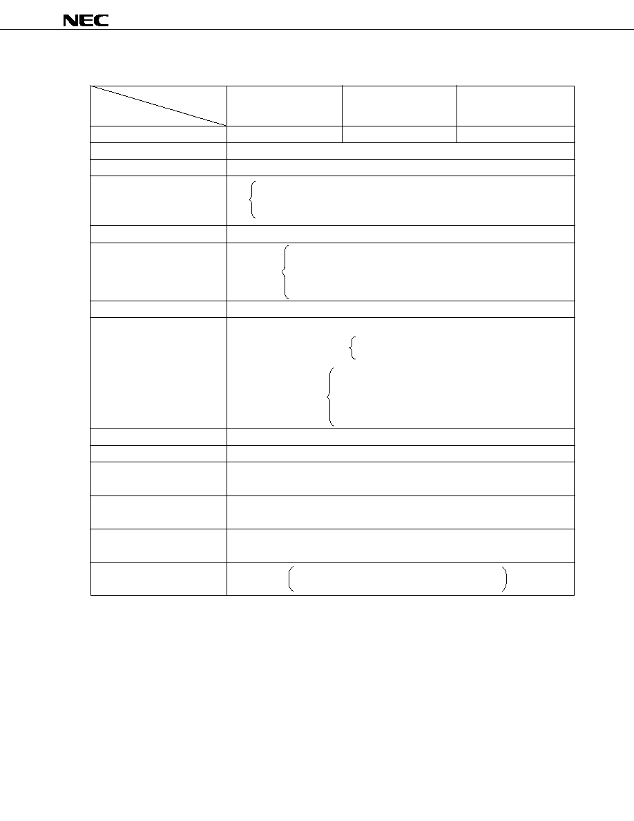
FUNCTION LIST
Part Number
�
PD17145 (A1)
�
PD17147 (A1)
�
PD17149 (A1)
Item
ROM capacity
2 KB (1024
�
16 bits)
4 KB (2048
�
16 bits)
8 KB (4096
�
16 bits)
RAM capacity
110
�
4 bits
Stack
Address stack
�
5, interrupt stack
�
3
� I/O
: 20
I/O ports
23
� Input
: 2
� Sense input (INT pin
Note
)
: 1
A/D converter input
4 channels (shared with port pins), absolute accuracy:
�
1.5 LSB MAX.
� 8-bit timer/counter:
2 channels (can be used as 1 channel of 16-bit timer)
� 7-bit basic interval timer:
1 channel (can be used as watchdog timer)
Serial interface
1 channel (3-wire)
� Multiple interrupt by hardware (3 levels MAX.)
� External interrupt (INT): 1
Rising edge, falling edge, or both rising and falling
edges selectable for detection.
Interrupt
� Timer 0 (TM0)
� Timer 1 (TM1)
� Basic interval timer (BTM)
� Serial interface (SIO)
Instruction execution time
2
�
s (at 8 MHz, ceramic oscillation)
Standby function
HALT, STOP
Mask option
(Can be used in application circuit that operates on V
DD
= 5 V
�
10 %, 400 kHz to 4 MHz)
2.7 to 5.5 V (at 400 kHz to 2 MHz)
4.5 to 5.5 V (at 400 kHz to 8 MHz)
28-pin plastic shrink DIP (400 mil)
28-pin plastic SOP (375 mil)
Quality grade is "standard" and not (A1).
Operating temperature range: T
a
= �40 to +85 �C
Note
The INT pin is used as an input pin (sense input) when the external interrupt function is not used.
The status of this pin is read by using the INT flag of a control register, not by a port register.
Caution
The PROM version is functionally compatible with the mask ROM versions but its internal
circuit and part of the electrical characteristics are different from those of the mask ROM
versions. To replace the PROM version with a mask ROM version, thoroughly conduct
application evaluation by using a sample of the mask ROM version.
4
�
PD17145(A1), 17147(A1), 17149(A1)
PIN CONFIGURATION (Top View)
28-pin plastic shrink DIP (400 mil)
28-pin plastic SOP (375 mil)
ADC
0
-ADC
3
: analog input
GND
: ground
INT
: external interrupt input
P0A
0
to P0A
3
: port 0A
P0B
0
to P0B
3
: port 0B
P0C
0
to P0C
3
: port 0C
P0D
0
to P0D
3
: port 0D
P0E
0
to P0E
3
: port 0E
P0F
0
and P0F
1
: port 0F
RESET
: reset input
RLS
: standby release signal input
SCK
: serial clock I/O
SI
: serial data input
SO
: serial data output
TM1OUT
: timer 1 output
V
DD
: power
V
REF
: A/D converter reference voltage
X
IN
, X
OUT
: for system clock oscillation
V
DD
P0F
1
/V
REF
P0C
3
/ADC
3
P0C
2
/ADC
2
P0C
1
/ADC
1
P0C
0
/ADC
0
P0B
3
P0B
2
P0B
1
P0B
0
P0A
3
P0A
2
P0A
1
P0A
0
GND
X
IN
X
OUT
RESET
INT
P0F
0
/RLS
P0D
0
/SCK
P0D
2
/SI
P0D
3
/TM1OUT
P0E
1
P0E
2
P0E
3
P0D
1
/SO
P0E
0
1
2
3
4
5
6
7
8
9
10
11
12
13
14
28
27
26
25
24
23
22
21
20
19
18
17
16
15
� � � � � �
PD17145CT(A1) -
���
PD17145GT(A1) -
���
PD17147CT(A1) -
���
PD17147GT(A1) -
���
PD17149CT(A1) -
���
PD17149GT(A1) -
���

5
�
PD17145(A1), 17147(A1), 17149(A1)
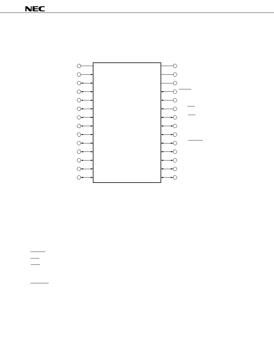
BLOCK DIAGRAM
Notes 1.
The ROM capacity of each product is as follows:
1024
�
16 bits:
�
PD17145(A1)
2048
�
16 bits:
�
PD17147(A1)
4096
�
16 bits:
�
PD17149(A1)
2.
The stack capacity of each product is as follows:
5
�
10 bits:
�
PD17145(A1)
5
�
11 bits:
�
PD17147(A1)
5
�
12 bits:
�
PD17149(A1)
Remark
CMOS or N-ch in ( ) indicate the output format of the port.
CMOS : CMOS push-pull output
N-ch
: N-ch open-drain output
V
DD
P0A
3
P0A
2
P0A
1
P0A
0
P0B
3
P0B
2
P0B
1
P0B
0
P0C
3
/ADC
3
P0C
2
/ADC
2
P0C
1
/ADC
1
P0C
0
/ADC
0
P0F
1
/V
REF
P0F
0
/RLS
P0D
3
/TM1OUT
P0D
2
/SI
P0D
1
/SO
P0D
0
/SCK
TM1
Serial
Interface
P0D
(N-ch)
P0F
A/D
Converter
P0C
(CMOS)
P0B
(CMOS)
P0A
(CMOS)
RF
RAM
110
�
4 bits
SYSTEM REG.
ALU
ROM
Note 1
Program Counter
Stack
Note 2
IRQSIO
Instruction
Decoder
P0E
(N-ch)
Timer 0
Timer 1
Basic Interval Timer
Interrupt
Controller
Clock
Divider
System Clock
Generator
fx/2
N
CPU CLOCK CLK STOP
X
IN
X
OUT
INT
IRQTM0
IRQTM1
IRQBTM
IRQSIO
IRQBTM
fx/2
N
fx/2
N
fx/2
N
IRQTM1
IRQTM0
P0E
3
P0E
2
P0E
1
P0E
0
RESET
GND