 | –≠–ª–µ–∫—Ç—Ä–æ–Ω–Ω—ã–π –∫–æ–º–ø–æ–Ω–µ–Ω—Ç: UPD17216 | –°–∫–∞—á–∞—Ç—å:  PDF PDF  ZIP ZIP |
Document Outline
- COVER
- DESCRIPTION
- FEATURES
- APPLICATION
- ORDERING INFORMATION
- PIN CONFIGURATION (TOP VIEW)
- BLOCK DIAGRAM
- 1. PIN FUNCTIONS
- 1.1 Pin Function List
- 1.2 Input/Output Circuits
- 1.3 Processing of Unused Pins
- 1.4 Notes on Using INT and RESET# Pins
- 2. MEMORY SPACE
- 2.1 Program Counter (PC)
- 2.2 Program Memory (ROM)
- 2.3 Stack
- 2.4 Data Memory (RAM)
- 2.5 Register File (RF)
- 3. PORTS
- 3.1 Port 0A (P0A0-P0A3)
- 3.2 Port 0B (P0B0-P0B3)
- 3.3 Port 0C (P0C0-P0C3)
- 3.4 Port 0D (P0D0-P0D3)
- 3.5 Port 0E (P0E0-P0E3)
- 3.6 INT Pin
- 3.7 Switching Bit I/O
- 3.8 Specifying Pull-up Resistor Connection
- 4. CLOCK GENERATOR CIRCUIT
- 4.1 Instruction Execution Time (CPU Clock) Selection
- 5. 8-BIT TIMER AND REMOTE CONTROLLER CARRIER GENERATOR CIRCUIT
- 5.1 Configuration of 8-bit Timer (with modulo function)
- 5.2 Function of 8-bit Timer (with modulo function)
- 5.3 Carrier Generator Circuit for Remote Controller
- 6. BASIC INTERVAL TIMER/WATCHDOG TIMER
- 6.1 Source Clock for Basic Interval Timer
- 6.2 Controlling Basic Interval Timer
- 6.3 Operation Timing for Watchdog Timer
- 7. INTERRUPT FUNCTIONS
- 7.1 Interrupt Sources
- 7.2 Hardware of Interrupt Control Circuit
- 7.3 Interrupt Sequence
- 8. STANDBY FUNCTIONS
- 8.1 HALT Mode
- 8.2 HALT Instruction Execution Conditions
- 8.3 STOP Mode
- 8.4 STOP Instruction Execution Conditions
- 8.5 Releasing Standby Mode
- 9. RESET
- 9.1 Reset by Reset Signal Input
- 9.2 Reset by Watchdog Timer (Connect RESET# and WDOUT# pins)
- 9.3 Reset by Stack Pointer (Connect RESET# and WDOUT# pins)
- 10. LOW-VOLTAGE DETECTOR CIRCUIT (CONNECT RESET# AND WDOUT# PINS)
- 11. ASSEMBLER RESERVED WORDS
- 11.1 Mask Option Directives
- 11.2 Reserved Symbols
- 12. INSTRUCTION SET
- 12.1 Instruction Set Outline
- 12.2 Legend
- 12.3 List of Instruction Sets
- 12.4 Assembler (AS17K) Built-In Macro Instruction
- 13. ELECTRICAL SPECIFICATIONS
- 14. CHARACTERISTIC WAVEFORMS (REFERENCE VALUE)
- 15. APPLICATION CIRCUIT EXAMPLE
- 16. PACKAGE DRAWINGS
- 17. RECOMMENDED SOLDERING CONDITIONS
- APPENDIX A. DIFFERENCES AMONG uPD17215, 17216, 17217, 17218 AND uPD17P218
- APPENDIX B. FUNCTIONAL COMPARISON OF uPD17215 SUBSERIES RELATED PRODUCTS
- APPENDIX C. DEVELOPMENT TOOLS
MOS INTEGRATED CIRCUIT
µ
PD17215, 17216, 17217, 17218
DESCRIPTION
µ
PD17215, 17216, 17217, 17218 (hereafter called
µ
PD17215 subseries) are 4-bit single-chip microcontrollers for
small general-purpose infrared remote control transmitters.
It employs a 17K architecture of general-purpose register type devices for the CPU, and can directly execute
operations between memories instead of the conventional method of executing operations through the accumulator.
Moreover, all the instructions are 16-bit 1-word instructions which can be programmed efficiently.
In addition, a one-time PROM model,
µ
PD17P218, to which data can be written only once, is also available. It is
convenient either for evaluating the
µ
PD17215 subseries programs or small-scale production of application systems.
Detailed functions are described in the follwing manual. Be sure to read this manual when designing your
system.
µ
PD172
◊◊
Subseries User's Manual: IEU-1317
FEATURES
∑ Infrared remote controller carrier generator circuit (REM output)
∑ 17K architecture: General-purpose register system
∑ Program memory (ROM), Data memory (RAM)
µ
PD17215
µ
PD17216
µ
PD17217
µ
PD17218
Program memory (ROM)
4 K bytes
8 K bytes
12 K bytes
16 K bytes
(2048
◊
16)
(4096
◊
16)
(6144
◊
16)
(8192
◊
16)
Data memory (RAM)
111
◊
4 bits
223
◊
4 bits
∑ 8-bit timer
:
1 channel
∑ Basic internal timer / Watchdog timer: 1 channel (WDOUT output)
∑ Instruction execution time (can be changed in two steps)
at f
X
4 MHz
:
4
µ
s (high-speed mode)/8
µ
s (ordinary mode)
at f
X
8 MHz
:
2
µ
s (high-speed mode)/4
µ
s (ordinary mode)
∑ External interrupt pin (INT)
:
1
∑ I/O pins
:
20
∑ Supply voltage
:
V
DD
= 2.2 to 5.5 V (at f
X
= 4 MHz (high-speed mode))
V
DD
= 2.0 to 5.5 V (at f
X
= 4 MHz (ordinary mode))
∑ Low-voltage detector circuit (mask opation)
Unless otherwise specified, the
µ
PD17215 is treated as the representative model throughout this document.
The mark
shows major revised points.
Document No. U12042EJ3V0DS00 (3rd edition)
(Previous No. IC≠3249)
Date Published January 1997 N
Printed in Japan
©
1993
DATA SHEET
The information in this document is subject to change without notice.
4-BIT SINGLE-CHIP MICROCONTROLLER
FOR SMALL GENERAL-PURPOSE INFRARED REMOTE CONTROL TRANSMITTER

µ
PD17215, 17216, 17217, 17218
2
APPLICATION
Preset remote controllers, toys, portable systems, etc.
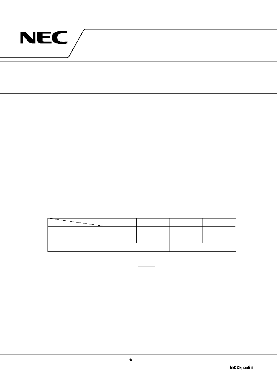
ORDERING INFORMATION
Part Number
Package
µ
PD17215CT-xxx
28-pin plastic shrink DIP (400 mil)
µ
PD17215GT-xxx
28-pin plastic SOP (375 mil)
µ
PD17216CT-xxx
28-pin plastic shrink DIP (400 mil)
µ
PD17216GT-xxx
28-pin plastic SOP (375 mil)
µ
PD17217CT-xxx
28-pin plastic shrink DIP (400 mil)
µ
PD17217GT-xxx
28-pin plastic SOP (375 mil)
µ
PD17218CT-xxx
28-pin plastic shrink DIP (400 mil)
µ
PD17218GT-xxx
28-pin plastic SOP (375 mil)
Remark: xxx is ROM code number.
µ
PD17215, 17216, 17217, 17218
3
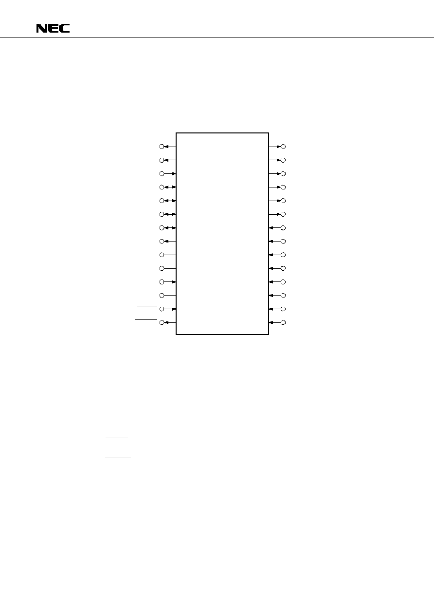
PIN CONFIGURATION (TOP VIEW)
∑
28-pin plastic SOP (375 mil)
µ
PD17215GT-xxx, 17216GT-xxx, 17217GT-xxx, 17218GT-xxx
∑
28-pin plastic shrink DIP (400 mil)
µ
PD17215CT-xxx, 17216CT-xxx, 17217CT-xxx, 17218CT-xxx
P0D
2
P0D
3
INT
P0E
0
P0E
1
P0E
2
P0E
3
REM
V
DD
X
OUT
X
IN
GND
RESET
WDOUT
P0D
1
P0D
0
P0C
3
P0C
2
P0C
1
P0C
0
P0B
3
P0B
2
P0B
1
P0B
0
P0A
3
P0A
2
P0A
1
P0A
0
1
2
3
4
5
6
7
8
9
10
11
12
13
14
28
27
26
25
24
23
22
21
20
19
18
17
16
15
GND
:
Ground
INT
:
External interrupt request signal input
P0A
0
-P0A
3
:
Input port (CMOS input)
P0B
0
-P0B
3
:
Input port (CMOS input)
P0C
0
-P0C
3
:
Output port (N-ch open-drain output)
P0D
0
-P0D
3
:
Output port (N-ch open-drain output)
P0E
0
-P0E
3
:
I/O port (CMOS push-pull output)
REM
:
Remote controller output (CMOS push-pull output)
RESET
:
Reset input
V
DD
:
Power supply
WDOUT
:
Hang-up/low voltage detection output (N-ch open-drain output)
X
IN
, X
OUT
:
Oscillator connection
µ
PD17215, 17216, 17217, 17218
4
BLOCK DIAGRAM
P0A
0
P0A
1
P0A
2
P0A
3
P0B
0
P0C
0
P0D
0
P0E
0
P0B
1
P0C
1
P0D
1
P0E
1
P0B
2
P0C
2
P0D
2
P0E
2
P0B
3
P0C
3
P0D
3
P0E
3
P0A
P0B
P0C
P0D
P0E
RF
SYSTEM REG.
ALU
Remote
Control
Divider
REM
INT
8-bit Timer
Interrupt
Controller
RESET
WDOUT
V
DD
GND
X
IN
X
OUT
Instruction
Decoder
Program Counter
Stack (5 levels)
Basic Interval/
Watchdog Timer
Power
Supply
Circuit
CPU Clock
OSC
PD17215, 17216 : 111
◊
4 bits
PD17217, 17218 : 223
◊
4 bits
µ
ROM
PD17215 : 2048
◊
16 bits
PD17216 : 4096
◊
16 bits
PD17217 : 6144
◊
16 bits
PD17218 : 8192
◊
16 bits
ROM
µ
µ
µ
µ
µ

µ
PD17215, 17216, 17217, 17218
5
CONTENTS
1.
PIN FUNCTIONS ..............................................................................................................................
7
1.1
Pin Function List .....................................................................................................................................
7
1.2
Input/Output Circuits ...............................................................................................................................
8
1.3
Processing of Unused Pins .....................................................................................................................
9
1.4
Notes on Using INT and RESET Pins .....................................................................................................
9
2.
MEMORY SPACE .............................................................................................................................
10
2.1
Program Counter (PC) ............................................................................................................................
10
2.2
Program Memory (ROM) ........................................................................................................................
10
2.3
Stack .......................................................................................................................................................
12
2.4
Data Memory (RAM) ...............................................................................................................................
14
2.5
Register File (RF) ...................................................................................................................................
21
3.
PORTS ..............................................................................................................................................
24
3.1
Port 0A (P0A
0
-P0A
3
) ...............................................................................................................................
24
3.2
Port 0B (P0B
0
-P0B
3
) ...............................................................................................................................
24
3.3
Port 0C (P0C
0
-P0C
3
) ..............................................................................................................................
24
3.4
Port 0D (P0D
0
-P0D
3
) ..............................................................................................................................
24
3.5
Port 0E (P0E
0
-P0E
3
) ...............................................................................................................................
24
3.6
INT Pin ....................................................................................................................................................
25
3.7
Switching Bit I/O .....................................................................................................................................
26
3.8
Specifying Pull-up Sesistor Connection ...................................................................................................
27
4.
CLOCK GENERATOR CIRCUIT ......................................................................................................
28
4.1
Instruction Execution Time (CPU Clock) Selection .................................................................................
28
5.
8-BIT TIMER AND REMOTE CONTROLLER CARRIER GENERATOR CIRCUIT ........................
29
5.1
Configuration of 8-bit Timer (with modulo function) .................................................................................
29
5.2
Function of 8-bit Timer (with modulo function) ........................................................................................
31
5.3
Carrier Generator Circuit for Remote Controller ......................................................................................
32
6.
BASIC INTERVAL TIMER/WATCHDOG TIMER .............................................................................
36
6.1
Source Clock for Basic Interval Timer .....................................................................................................
36
6.2
Controlling Basic Interval Timer ..............................................................................................................
36
6.3
Operation Timing for Watchdog Timer ....................................................................................................
38
7.
INTERRUPT FUNCTIONS ................................................................................................................
39
7.1
Interrupt Sources ....................................................................................................................................
39
7.2
Hardware of Interrupt Control Circuit ......................................................................................................
40
7.3
Interrupt Sequence .................................................................................................................................
44