Document Outline
- COVER
- FEATURES
- APPLICATIONS
- ORDERING INFORMATION
- OUTLINE OF FUNCTION
- 1. PIN CONFIGURATION (TOP VIEW)
- 2. BLOCK DIAGRAM
- 3. PIN FUNCTION LIST
- 3.1 PORT PINS
- 3.2 PINS OTHER THAN PORT PINS
- 3.3 INPUT/OUTPUT CIRCUITS AND RECOMMENDED CONNECTION OF UNUSED PINS
- 4. MEMORY SPACE
- 5. PERIPHERAL HARDWARE FUNCTION FEATURES
- 5.1 PORTS
- 5.2 CLOCK GENERATOR
- 5.3 TIMER
- 5.4 BUZZER OUTPUT CONTROL CIRCUIT
- 5.5 A/D CONVERTER
- 5.6 SERIAL INTERFACES
- 5.7 PLL FREQUENCY SYNTHESIZER
- 5.8 FREQUENCY COUNTER
- 6. INTERRUPT FUNCTIONS AND TEST FUNCTIONS
- 6.1 INTERRUPT FUNCTIONS
- 6.2 TEST FUNCTION
- 7. STANDBY FUNCTION
- 8. RESET FUNCTION
- 9. INSTRUCTION SET
- 10. ELECTRICAL SPECIFICATIONS
- 11. PACKAGE DRAWINGS
- 12. RECOMMENDED SOLDERING CONDITIONS
- APPENDIX A. DIFFERENCES BETWEEN uPD178018A AND uPD178018 SUBSERIES
- APPENDIX B. DEVELOPMENT TOOLS
- APPENDIX C. RELATED DOCUMENTS
©
1997
DATA SHEET
µ
PD178004A, 178006A, 178016A, 178018A
MOS INTEGRATED CIRCUIT
The
µ
PD178004A, 178006A, 178016A and 178018A are 8-bit single-chip CMOS microcontrollers that incorporate
hardware for digital tuning systems.
The CPU uses the 78K/0 architecture, which makes it easy to implement high-speed access to internal memory
and control of peripheral hardware. Also, the instructions used are the high-speed 78K/0 instructions, suitable for
system control.
The rich assortment of peripheral hardware includes an input/output port, 8-bit timer, A/D converter, serial interface,
power-ON clear circuits, as well as a pre-scaler for digital tuning, a PLL frequency synthesizer and a frequency counter.
The
µ
PD178P018A, one-time PROM or EPROM versions which can be operated in the same supply voltage range
as for the mask ROM versions, and various development tools, are also available.
For more information on functions, refer to the following User's Manuals. Be sure to read them when
designing.
µ
PD178018A Subseries User's Manual: to be prepared
78K/0 Series User's Manual Instruction: U12326E
FEATURES
∑ Internal high-capacity ROM and RAM
8-BIT SINGLE-CHIP MICROCONTROLLERS
∑ Instruction Cycle: 0.44
µ
s (4.5-MHz crystal oscillator used)
∑ Large array of on-chip peripheral hardware
General-purpose input/output port, A/D converter, serial interface, timer, frequency counter, power-ON clear
circuits.
∑ On-chip hardware for a PLL frequency synthesizer.
Dual modulus pre-scaler, programmable divider, phase comparator, charge pump.
∑ Vector interrupt sources: 17
∑ Supply Voltage: V
DD
= 4.5 to 5.5 V (during PLL operation)
V
DD
= 3.5 to 5.5 V (during CPU operation, when the system clock is f
X
/2 or lower)
V
DD
= 4.5 to 5.5 V (during CPU operation, when the system clock is f
X
)
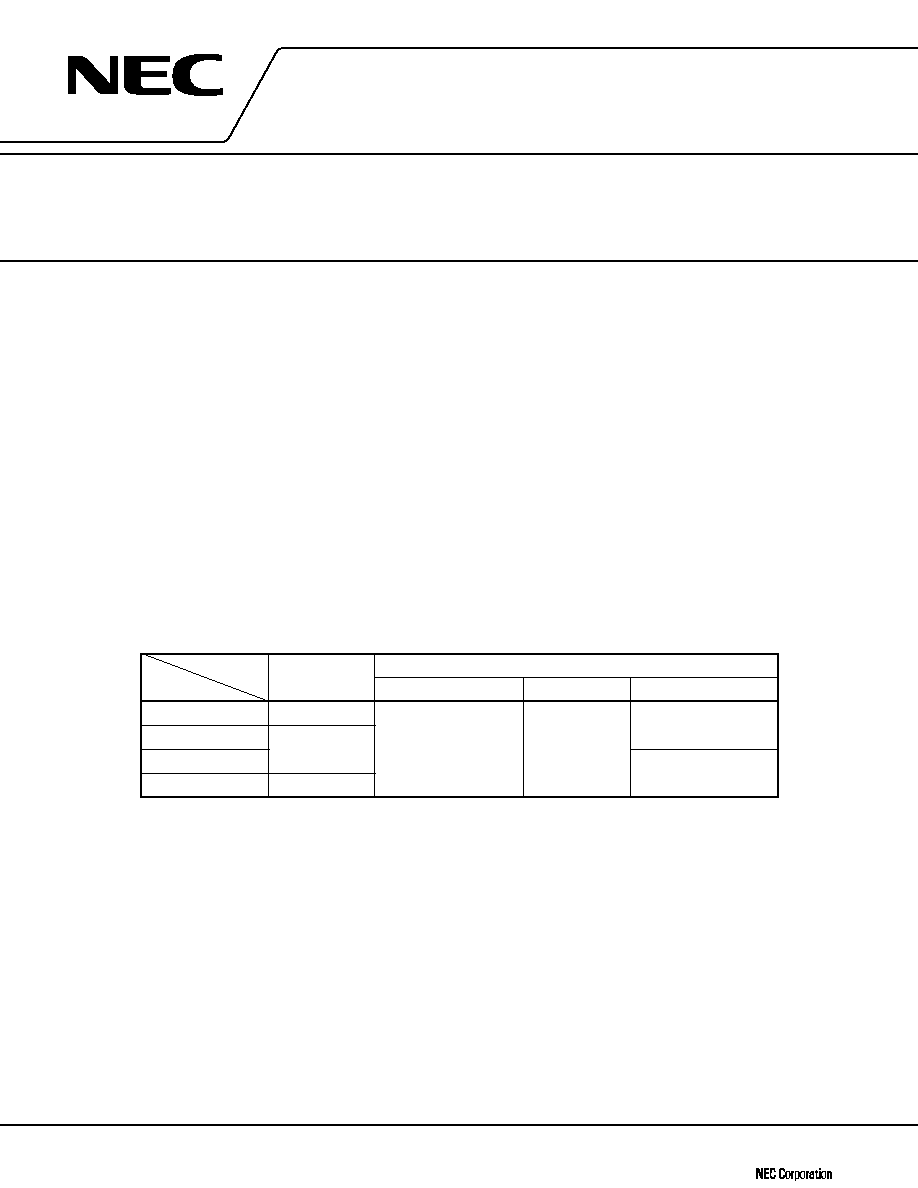
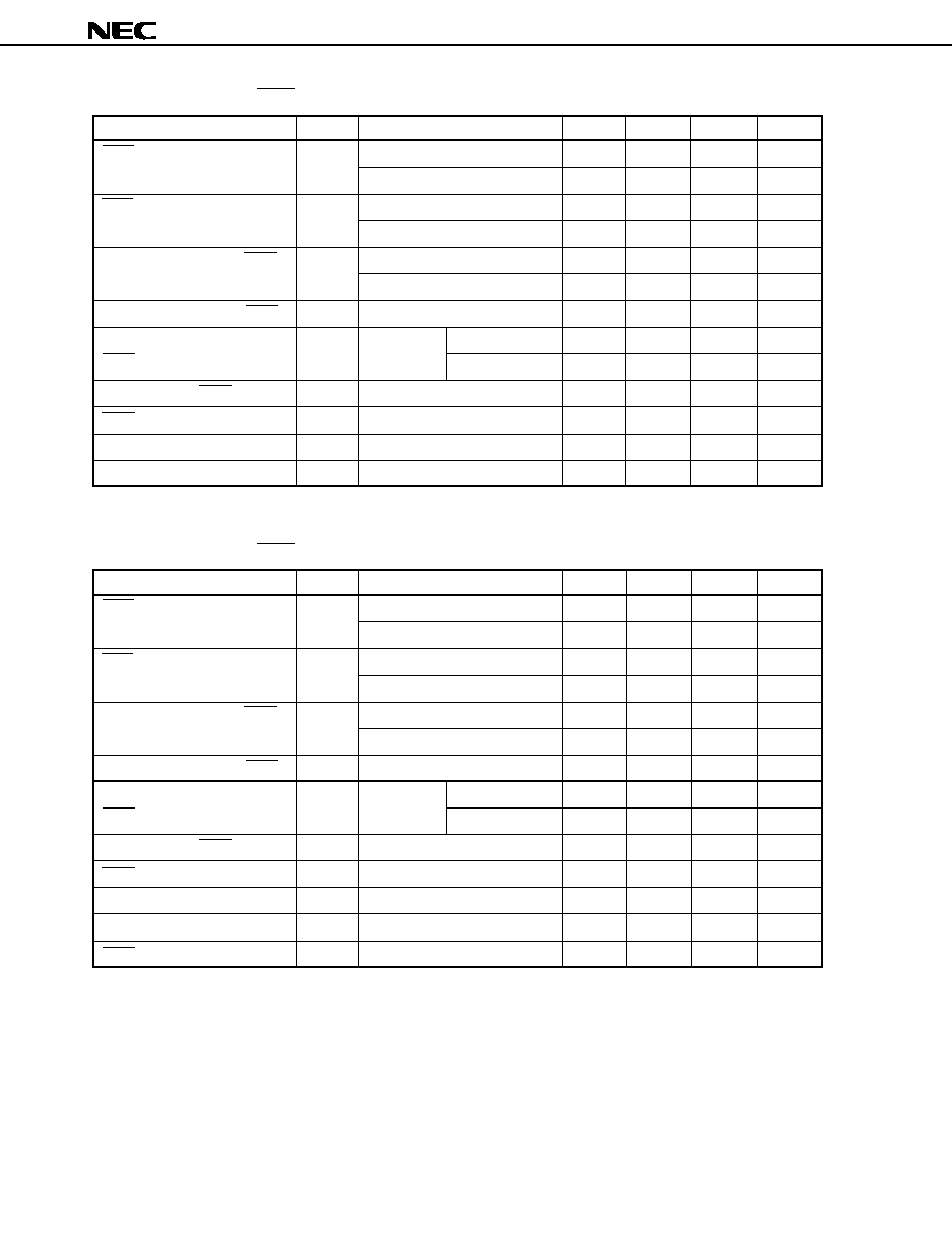
Items
Program Memory
Data Memory
Product Name
ROM
Internal High-Speed RAM
Buffer RAM
Internal Expanded RAM
µ
PD178004A
32 Kbytes
1 024 bytes
32 bytes
Not provided
µ
PD178006A
48 Kbytes
µ
PD178016A
2 048 bytes
µ
PD178018A
60 Kbytes
The information in this document is subject to change without notice.
Document No. U12641EJ1V0DS00 (1st Edition)
Date Published July 1997 N
Printed in Japan
µ
PD178004A, 178006A, 178016A, 178018A
2
APPLICATIONS
Car stereo, home stereo systems.
ORDERING INFORMATION
Part Number
Package
µ
PD178004AGC-
◊◊◊
-3B9
80-pin plastic QFP (14
◊
14 mm, 0.65-mm pitch)
µ
PD178006AGC-
◊◊◊
-3B9
80-pin plastic QFP (14
◊
14 mm, 0.65-mm pitch)
µ
PD178016AGC-
◊◊◊
-3B9
80-pin plastic QFP (14
◊
14 mm, 0.65-mm pitch)
µ
PD178018AGC-
◊◊◊
-3B9
80-pin plastic QFP (14
◊
14 mm, 0.65-mm pitch)
Remark
◊◊◊
denotes the ROM code number. Also, the ROM code number becomes E
◊◊
when the I
2
C bus is used.
µ
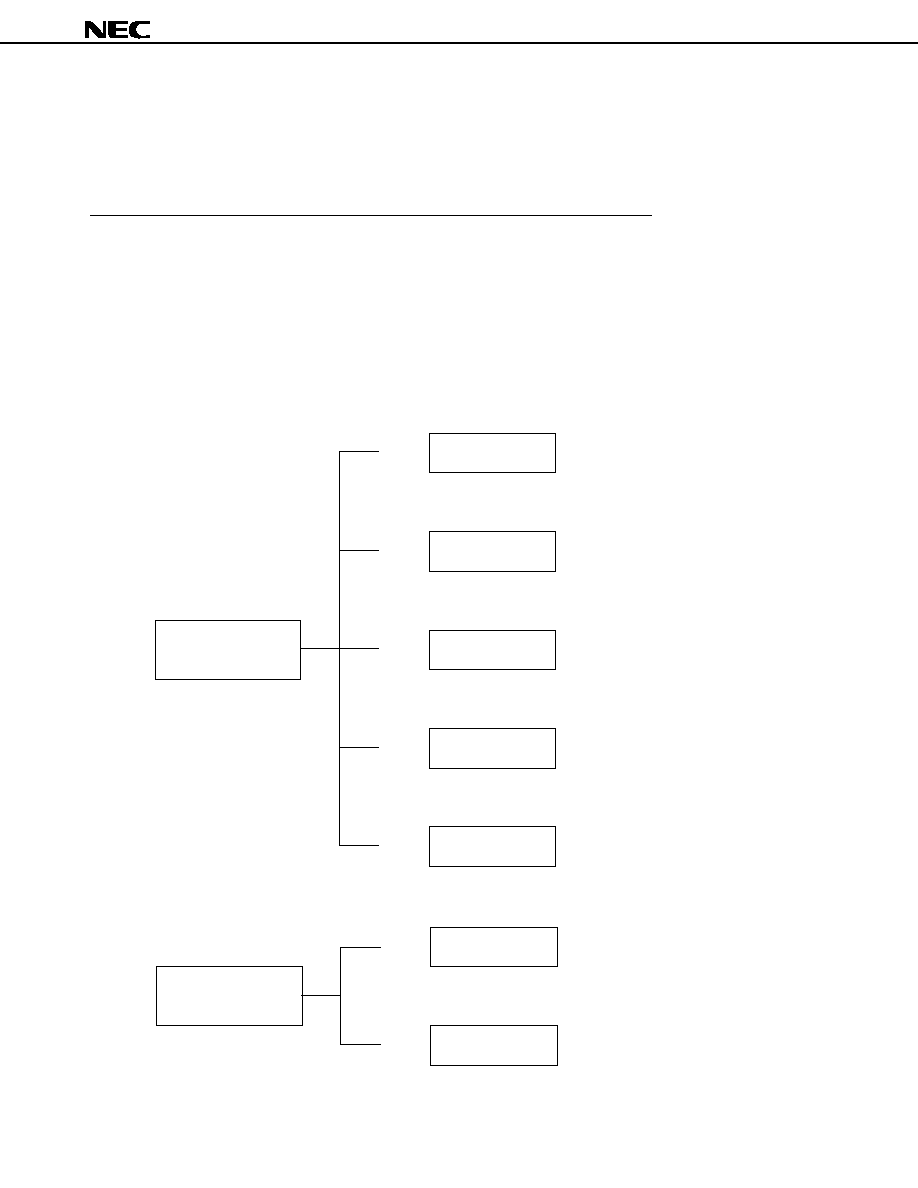
PD178018A SUBSERIES AND
µ
PD178003 SUBSERIES EXPANSION
Note
Under development
PD178018A Subseries
80 pins
PROM : 60 KB
RAM : 3 KB
PD178P018A
Note
80 pins
ROM : 60 KB
RAM : 3 KB
PD178018A
80 pins
ROM : 48 KB
RAM : 3 KB
PD178016A
80 pins
ROM : 48 KB
RAM : 1 KB
PD178006A
80 pins
ROM : 32 KB
RAM : 1 KB
PD178004A
µ
µ
µ
µ
µ
µ
PD178003 Subseries
80 pins
ROM : 24 KB
RAM : 0.5 KB
PD178003
Note
80 pins
ROM : 16 KB
RAM : 0.5 KB
PD178002
Note
µ
µ
µ
µ
PD178004A, 178006A, 178016A, 178018A
3
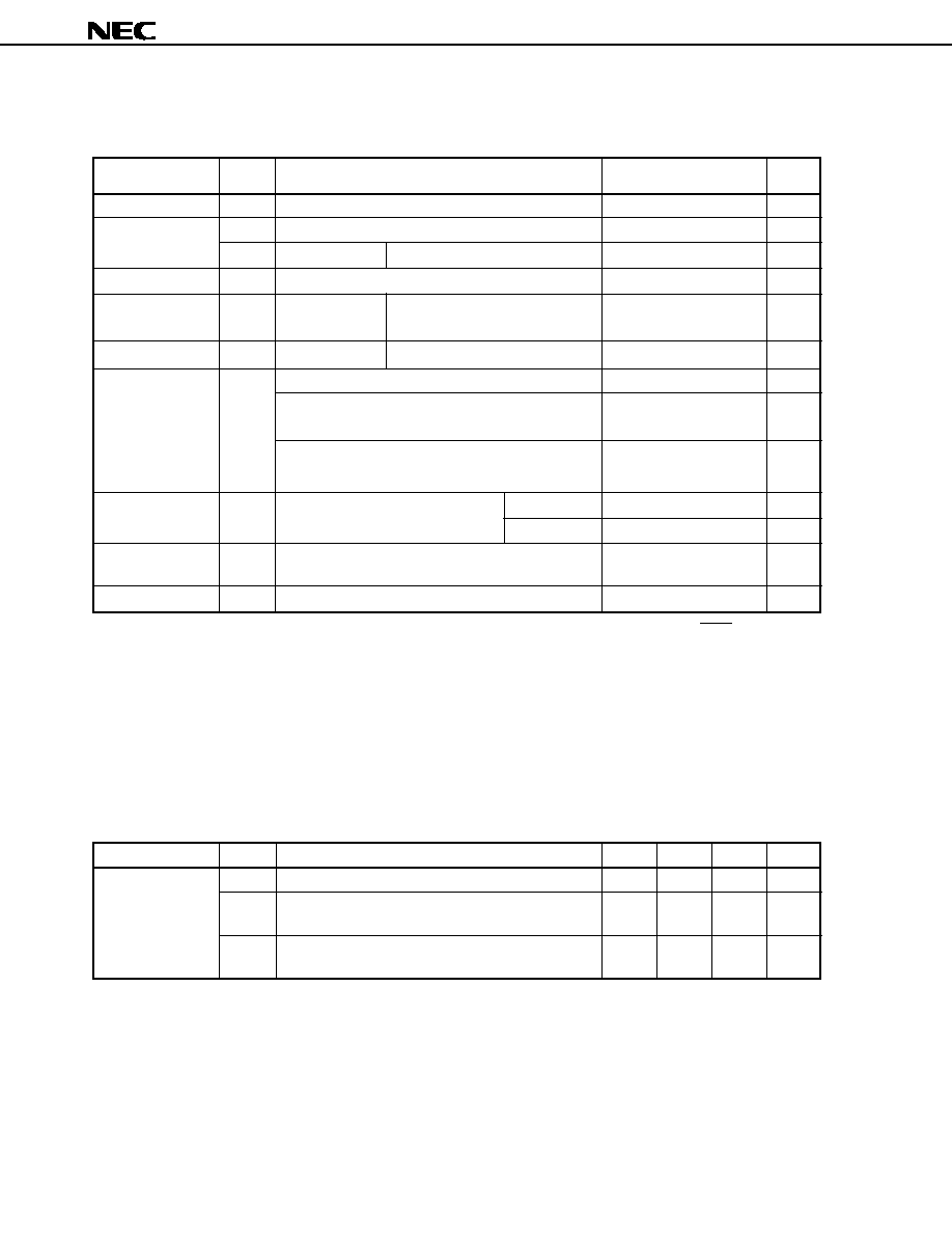
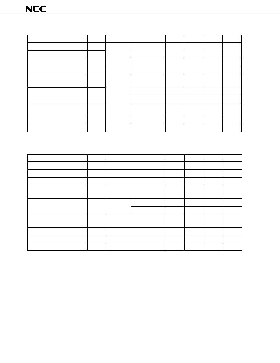
OUTLINE OF FUNCTION
Product name
µ
PD178004A
µ
PD178006A
µ
PD178016A
µ
PD178018A
Item
Internal
ROM (ROM configuration)
32 Kbytes
48 Kbytes
60 Kbytes
memory
(mask ROM)
(mask ROM)
(mask ROM)
High-speed RAM
1 024 bytes
Buffer RAM
32 bytes
Expansion RAM
Not provided
2 048 bytes
General-purpose register
8 bits
◊
32 registers (8 bits
◊
8 registers
◊
4 banks)
Instruction cycle
With variable instruction execution time function
0.44
µ
s/0.88
µ
s/1.78
µ
s/3.56
µ
s/7.11
µ
s/14.22
µ
s (with 4.5-MHz crystal resonator)
Instruction set
∑ 16-bit operation
∑ Multiplication/division (8 bits
◊
8 bits, 16 bits
˜
8 bits)
∑ Bit manipulation (set, reset, test, Boolean operation)
∑ BCD adjustment, etc.
I/O port
Total
: 62 pins
CMOS input
:
1 pin
CMOS I/O
: 54 pins
N-ch open-drain I/O
:
4 pins
N-ch open-drain output :
3 pins
A/D converter
8-bit resolution
◊
6 channels
Serial interface
∑ 3-wire/SBI/2-wire/I
2
C bus
Note
mode selectable
: 1 channel
∑ 3-wire serial I/O mode
(with automatic transfer/receive function of up to 32 byte) : 1 channel
Timer
∑ Basic timer (timer carry FF (10 Hz))
: 1 channel
∑ 8-bit timer/event counter
: 2 channels
∑ 8-bit timer (D/A converter: PWM output) : 1 channel
∑ Watchdog timer
: 1 channel
Buzzer (BEEP) output
1.5 kHz, 3 kHz, 6 kHz
Vectored
Maskable
Internal: 8, external: 7
interrupt
Non-maskable
Internal: 1
Source
Software
Internal: 1
Test input
Internal: 1
Note
When using the I
2
C bus mode (including when this mode is implemented by program without using the
peripheral hardware), consult your local NEC sales representative when you place an order for mask.
(1/2)
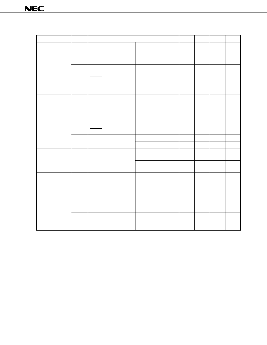
µ
PD178004A, 178006A, 178016A, 178018A
4
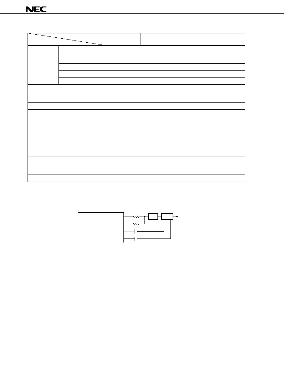
Product name
µ
PD178004A
µ
PD178006A
µ
PD178016A
µ
PD178018A
Item
PLL frequency
Division mode
Two types
synthesizer
∑ Direct division mode (VCOL pin)
∑ Pulse swallow mode (VCOH and VCOL pins)
Reference frequency
7 types selectable by program (1, 3, 5, 9, 10, 25, 50 kHz)
Charge pump
Error out output: 2 (EO0 and EO1 pins
Note 1
)
Phase comparator
Unlock detectable by program
Frequency counter
∑ Frequency measurement
∑ AMIFC pin: for 450-kHz count
∑ FMIFC pin: for 450-kHz/10.7-MHz count
D/A converter (PWM output)
8-/9-bit resolution
◊
3 channels (shared by 8-bit timer)
Standby function
∑ HALT mode
∑ STOP mode
Reset
∑ Reset by RESET pin
∑ Internal reset by watchdog timer
∑ Reset by power-ON clear circuit (3-value detection)
∑ Detection of less than 4.5 V
Note 2
(CPU clock: f
X
)
∑ Detection of less than 3.5 V
Note 2
(CPU clock: f
X
/2 or less and on power application)
∑ Detection of less than 2.5 V
Note 2
(in STOP mode)
Power supply voltage
∑ V
DD
= 4.5 to 5.5 V (with PLL operating)
∑ V
DD
= 3.5 to 5.5 V (with CPU operating, CPU clock: f
X
/2 or less)
∑ V
DD
= 4.5 to 5.5 V (with CPU operating, CPU clock: f
X
)
Package
∑ 80-pin plastic QFP (14
◊
14 mm, 0.65-mm pitch)
Notes 1. The EO1 pin can be set to high impedance for the
µ
PD178016A and 178018A.
The following shows an application example.
PD178016A
PD178018A
µ
µ
EO0
EO1
VCOH
VCOL
LPF
VCO
To Mixer
LPF : Low path filter
VCO : Voltage controlled oscillator
∑ To lock to a target frequency at high speed
Setting the EO0 and EO1 pins to error out output improves the output current potential and LPF
voltage control potential.
∑ Normal state
Setting only the EO0 pin to error out output maintains the LPF stable.
2. These voltage values are maximum values. Reset is actually executed at a voltage lower than these
values.
(2/2)

µ
PD178004A, 178006A, 178016A, 178018A
5
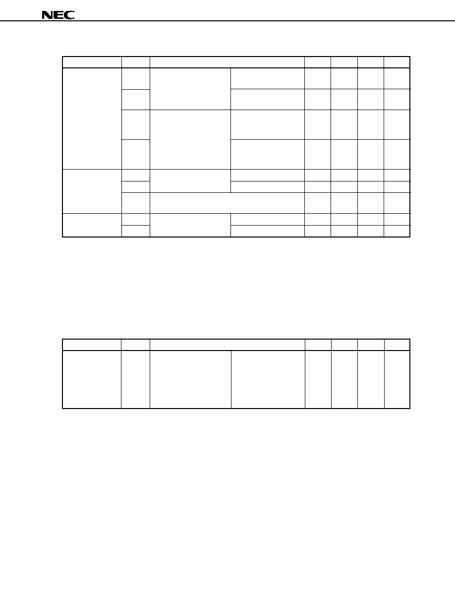
TABLE OF CONTENTS
1. PIN CONFIGURATION (TOP VIEW) ................................................................................................ 6
2. BLOCK DIAGRAM ........................................................................................................................... 8
3. PIN FUNCTION LIST ........................................................................................................................ 9
3.1 PORT PINS ................................................................................................................................ 9
3.2 PINS OTHER THAN PORT PINS ............................................................................................ 10
3.3 INPUT/OUTPUT CIRCUITS AND RECOMMENDED CONNECTION OF UNUSED PINS ..... 11
4. MEMORY SPACE .......................................................................................................................... 14
5. PERIPHERAL HARDWARE FUNCTION FEATURES .................................................................. 15
5.1 PORTS ..................................................................................................................................... 15
5.2 CLOCK GENERATOR ............................................................................................................ 16
5.3 TIMER ...................................................................................................................................... 16
5.4 BUZZER OUTPUT CONTROL CIRCUIT ................................................................................ 18
5.5 A/D CONVERTER ................................................................................................................... 19
5.6 SERIAL INTERFACES ............................................................................................................ 19
5.7 PLL FREQUENCY SYNTHESIZER ........................................................................................ 21
5.8 FREQUENCY COUNTER ........................................................................................................ 22
6. INTERRUPT FUNCTIONS AND TEST FUNCTIONS .................................................................... 23
6.1 INTERRUPT FUNCTIONS ...................................................................................................... 23
6.2 TEST FUNCTION .................................................................................................................... 26
7. STANDBY FUNCTION ................................................................................................................... 27
8. RESET FUNCTION ........................................................................................................................ 27
9. INSTRUCTION SET ....................................................................................................................... 28
10. ELECTRICAL SPECIFICATIONS .................................................................................................. 30
11. PACKAGE DRAWINGS ................................................................................................................. 46
12. RECOMMENDED SOLDERING CONDITIONS ............................................................................. 47
APPENDIX A. DIFFERENCES BETWEEN
µ
PD178018A AND
µ
PD178018 SUBSERIES ............... 48
APPENDIX B. DEVELOPMENT TOOLS ............................................................................................ 49
APPENDIX C. RELATED DOCUMENTS ........................................................................................... 51
6
µ
PD178004A, 178006A, 178016A, 178018A
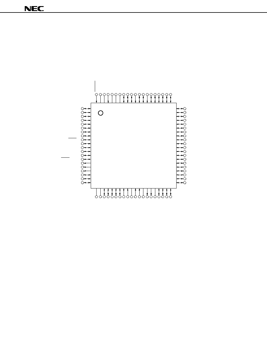
1. PIN CONFIGURATION (TOP VIEW)
∑ 80-PIN PLASTIC QFP (14
◊
14 mm, 0.65 mm pitch)
µ
PD178004AGC-
◊◊◊
-3B9, 178006AGC-
◊◊◊
-3B9
µ
PD178016AGC-
◊◊◊
-3B9, 178018AGC-
◊◊◊
-3B9
1
2
3
4
5
6
7
8
9
10
11
12
13
14
15
16
17
18
19
20
60
59
58
57
56
55
54
53
52
51
50
49
48
47
46
45
44
43
42
41
P10/ANI0
P11/ANI1
P12/ANI2
P13/ANI3
P14/ANI4
P15/ANI5
P20/SI1
P21/SO1
P22/SCK1
P23/STB
P24/BUSY
P25/SI0/SB0/SDA0
P26/SO0/SB1/SDA1
P27/SCK0/SCL
P132/PWM0
P133/PWM1
P134/PWM2
P40
P41
P42
P37
P36/BEEP
P35
P34/TI2
P33/TI1
P32
P31
P30
P67
P66
P65
P64
P63
P62
P61
P60
P57
P56
P55
P54
RESET
V
DD
REGOSC
X1
X2
GND
REGCPU
P06/INTP6
P05/INTP5
P04/INTP4
P03/INTP3
P02/INTP2
P01/INTP1
P00/INTP0
P125
P124
P123
P122
P121
P120
GNDPORT
V
DD
PORT
P43
P44
P45
P46
P47
AMIFC
FMIFC
V
DD
PLL
VCOH
VCOL
GNDPLL
EO0
EO1
IC
P50
P51
P52
P53
21 22 23 24 25 26 27 28 29 30 31 32 33 34 35 36 37 38 39 40
80 79 78 77 76 75 74 73 72 71 70 69 68 67 66 65 64 63 62 61
Cautions 1. Connect the Internally Connected (IC) pin to GND directly.
2. Connect V
DD
PORT and V
DD
PLL pins to V
DD
.
3. Connect the GNDPORT and GNDPLL pins to GND.
4. Connect each of the REGOSC and REGCPU pins to GND via a 0.1-
µ
F capacitor.

7
µ
PD178004A, 178006A, 178016A, 178018A
AMIFC
: AM Intermediate Frequency Counter Input
AN10 to AN15 : A/D Converter Input
BEEP
: Buzzer Output
BUSY
: Busy Output
EO0, EO1
: Error Out Output
FMIFC
: FM Intermediate Frequency Counter Input
GND
: Ground
GNDPLL
: PLL Ground
GNDPORT
: Port Ground
IC
: Internally Connected
INTP0 to INTP6 : Interrupt Inputs
P00 to P06
: Port 0
P10 to P15
: Port 1
P20 to P27
: Port 2
P30 to P37
: Port 3
P40 to P47
: Port 4
P50 to P57
: Port 5
P60 to P67
: Port 6
P120 to P125 : Port 12
P132 to P134 : Port 13
PWM0 to PWM2 : PWM Output
REGCPU
: Regulator for CPU Power Supply
REGOSC
: Regulator for Oscillator Circuit
RESET
: Reset Input
SB0, SB1
: Serial Data Bus Input/Output
SCK0, SCK1
: Serial Clock Input/Output
SCL
: Serial Clock Input/Output
SDA0, SDA1
: Serial Data Input/Output
SI0, SI1
: Serial Data Input
SO0, SO1
: Serial Data Output
STB
: Strobe Output
TI1, TI2
: Timer Clock Input
VCOL, VCOH : Local Oscillator Input
V
DD
: Power Supply
V
DD
PLL
: PLL Power Supply
V
DD
PORT
: Port Power Supply
X1, X2
: Crystal Oscillator Connection
8
µ
PD178004A, 178006A, 178016A, 178018A
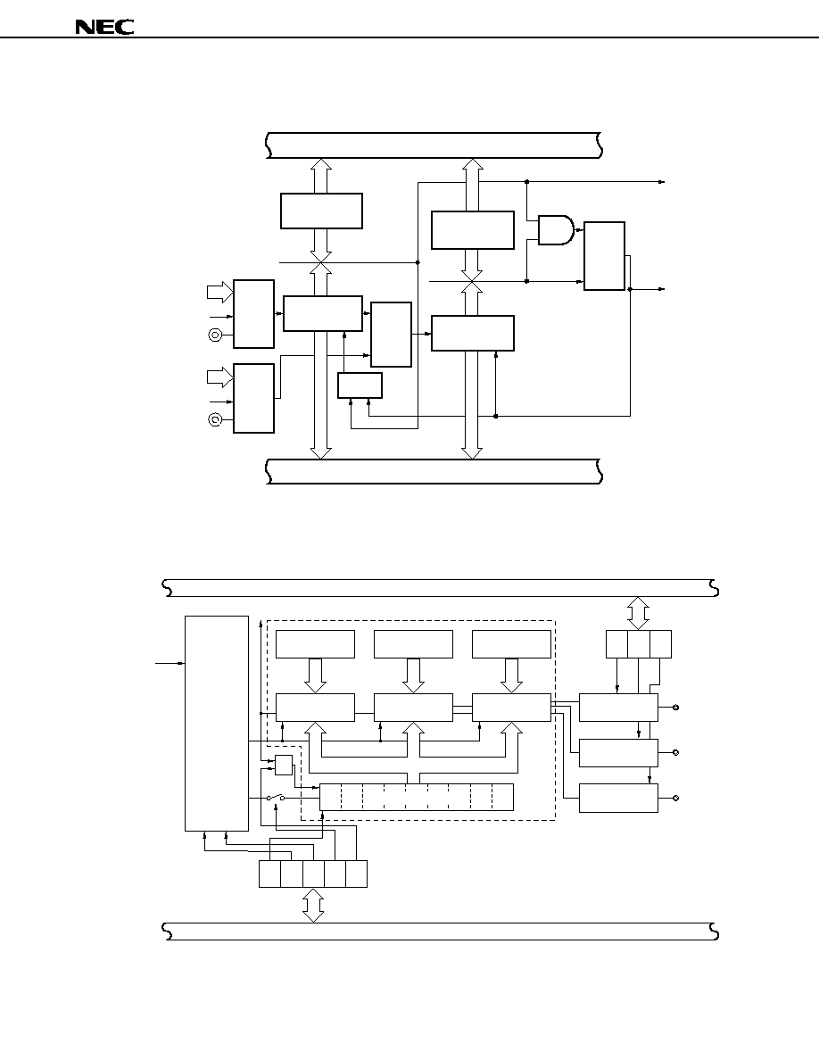
2. BLOCK DIAGRAM
8-bit TIMER/
EVENT COUNTER 1
8-bit TIMER/
EVENT COUNTER 2
8-bit TIMER 3
WATCHDOG TIMER
BASIC TIMER
SERIAL
INTERFACE 0
SERIAL
INTERFACE 1
A/D CONVERTER
INTERRUPT
CONTROL
BUZZER OUTPUT
SYSTEM
CONTROL
RAM
78K/0
CPU
CORE
ROM
6
6
8
8
8
8
8
6
3
6
7
3
P00
P01 to P06
D/A CONVERTER
(PWM)
PWM0/P132 to
PWM2/P134
FREQUENCY
COUNTER
PLL
VOLTAGE
REGULATOR
PLL
VOLTAGE
REGULATOR
TI1/P33
TI2/P34
SI0/SB0/SDA0/P25
SO0/SB1/SDA1/P26
SCK0/SCL/P27
SI1/P20
SO1/P21
SCK1/P22
STB/P23
BUSY/P24
RESET
X1
X2
V
DD
PORT
GNDPORT
V
DD
RESET
CPU
PERIPHERAL
REGOSC
REGCPU
GND
V
OSC
V
CPU
ANI0/P10 to
ANI5/P15
INTP0/P00 to
INTP6/P06
BEEP/P36
PORT 0
PORT 1
PORT 2
PORT 3
PORT 4
PORT 5
PORT 6
PORT 12
PORT 13
P10 to P15
P20 to P27
P30 to P37
P40 to P47
P50 to P57
P60 to P67
P120 to P125
P132 to P134
AMIFC
FMIFC
EO0
EO1
VCOL
VCOH
V
DD
PLL
GNDPLL
IC
Remark The internal ROM and RAM capacities depend on the version.

9
µ
PD178004A, 178006A, 178016A, 178018A
3. PIN FUNCTION LIST
3.1 PORT PINS
Pin Name
I/O
Function
After Reset Alternate Function
P00
Input
Port 0.
Input only
Input
INTP0
P01 to P06 I/O
7-bit input/output port.
Input/output mode can be specified bit-wise. Input
INTP1 to INTP6
P10 to P15 I/O
Port 1.
Input
ANI0 to ANI5
6-bit input/output port.
Input/output mode can be specified bit-wise.
P20
I/O
Port 2.
Input
SI1
P21
8-bit input/output port.
SO1
P22
Input/output mode can be specified bit-wise.
SCK1
P23
STB
P24
BUSY
P25
SI0/SB0/SDA0
P26
SO0/SB1/SDA1
P27
SCK0/SCL
P30 to P32 I/O
Port 3.
Input
--
P33
8-bit input/output port.
TI1
P34
Input/output mode can be specified bit-wise.
TI2
P35
--
P36
BEEP
P37
--
P40 to P47 I/O
Port 4.
Input
--
8-bit input/output port.
Input/output mode can be specified in 8-bit units.
Test input flag (KRIF) is set to 1 by falling edge detection.
P50 to P57 I/O
Port 5.
Input
--
8-bit input/output port.
Input/output mode can be specified bit-wise.
P60 to P63 I/O
Port 6.
Middle voltage N-ch open drain
Input
--
8-bit input/output port.
input/output port.
P64 to P67
Input/output mode can be
LEDs can be driven directly.
specified bit-wise.
P120 to
I/O
Port 12.
Input
--
P125
6-bit input/output port.
Input/output mode can be specified bit-wise.
P132 to
Output
Port 13.
--
PWM0 to
P134
3-bit output port.
PWM2
N-ch open-drain output port.

10
µ
PD178004A, 178006A, 178016A, 178018A
3.2 PINS OTHER THAN PORT PINS
Pin Name
I/O
Function
After Reset Alternate Function
INTP0 to
Input
External maskable interrupt inputs with specifiable valid edges (rising
Input
P00 to P06
INTP6
edge, falling edge, both rising and falling edges).
SI0
Input
Serial interface serial data input
Input
P25/SB0/SDA0
SI1
P20
SO0
Output
Serial interface serial data output
Input
P26/SB1/SDA1
SO1
P21
SB0
I/O
Serial interface serial data input/output
Input
P25/SI0/SDA0
SB1
P26/SO0/SDA1
SDA0
P25/SI0/SB0
SDA1
P26/SO0/SB1
SCK0
I/O
Serial interface serial clock input/output
Input
P27/SCL
SCK1
P22
SCL
P27/SCK0
STB
Output
Serial interface automatic transmit/receive strobe output
Input
P23
BUSY
Input
Serial interface automatic transmit/receive busy input
Input
P24
TI1
Input
External count clock input to 8-bit timer (TM1)
Input
P33
TI2
External count clock input to 8-bit timer (TM2)
P34
BEEP
Output
Buzzer output
Input
P36
ANI0 to ANI5 Input
A/D converter analog input
Input
P10 to P15
PWM0 to PWM2
Output
PWM output
--
P132 to P134
EO0, EO1
Output
Error out output from charge pump of the PLL frequency synthesizer
--
--
VCOL
Input
Inputs PLL local band frequency (In HF, MF mode)
--
--
VCOH
Input
Inputs PLL local band frequency (In VHF mode)
--
--
AMIFC
Input
Inputs AM intermediate frequency counter
--
--
FMIFC
Input
Inputs FM intermediate frequency counter
--
--
RESET
Input
System reset input
--
--
X1
Input
System clock oscillation resonator connection
--
--
X2
--
--
--
REGOSC
--
Oscillation regulator. Connected to GND via a 0.1-
µ
F capacitor.
--
--
REGCPU
--
CPU power supply regulator. Connected to GND via a 0.1-
µ
F capacitor.
--
--
V
DD
--
Positive power supply
--
--
GND
--
Ground
--
--
V
DD
PORT
--
Positive power supply for port block
--
--
GNDPORT --
Ground for port block
--
--
V
DD
PLL
Note
--
Positive power supply for PLL
--
--
GNDPLL
Note
--
Ground for PLL
--
--
IC
--
Internally connected. Connected to GND or GNDPORT.
--
--
Note
Connect a capacitor of approximately 1 000 pF between the V
DD
PLL pin and GNDPLL pin.
11
µ
PD178004A, 178006A, 178016A, 178018A
Pin Name
I/O Circuit Type
I/O
Recommended Connections of Unused Pins
P00/INTP0
2
Input
Connected to GND or GNDPORT
P01/INTP1 to P06/INTP6
8
I/O
Set in general-purpose input port mode by software and
P10/ANI0 to P15/ANI5
11-A
individually connected to V
DD
, V
DD
PORT, GND, or GNDPORT
P20/SI1
8
via resistor.
P21/SO1
5
P22/SCK1
8
P23/STB
5
P24/BUSY
8
P25/SI0/SB0/SDA0
10
P26/SO0/SB1/SDA1
P27/SCK0/SCL
P30 to P32
5
P33/TI1, P34/TI2
8
P35
5
P36/BEEP
P37
P40 to P47
5-G
P50 to P57
5
P60 to P63
13-D
P64 to P67
5
P120 to P125
P132/PWM0 to P134/PWM2
19
Output
Set to low-level output by software and open
EO0
DTS-EO1
Open
EO1
DTS-EO3
Note
VCOL, VCOH
DTS-AMP
Input
Set to disabled status by software and open
AMIFC, FMIFC
IC
--
--
Connected to GND or GNDPORT directly
Note
For the
µ
PD178004A and 178006A, the I/O circuit type is DTS-EO1.
3.3 INPUT/OUTPUT CIRCUITS AND RECOMMENDED CONNECTION OF UNUSED PINS
Table 3-1 shows the input/output circuit types of pins and the recommended conditions for unused pins.
Refer to Figure 3-1 for the configuration of the input/output circuit of each type.
Table 3-1. I/O Circuit Type of Each Circuit

12
µ
PD178004A, 178006A, 178016A, 178018A
Figure 3-1. Pin Input/Output Circuit of List (1/2)
IN
IN/OUT
input
enable
output
disable
data
V
DD
P-ch
N-ch
Type 2
Type 5
Schmitt-Triggered Input with
Hysteresis Characteristics
Type 5-G
Type 11-A
Type 10
Type 8
IN/OUT
output
disable
data
V
DD
P-ch
N-ch
IN/OUT
output
disable
data
V
DD
P-ch
N-ch
IN/OUT
open-drain
output disable
data
V
DD
P-ch
N-ch
IN/OUT
output
disable
data
V
DD
P-ch
N-ch
P-ch
comparator
N-ch
input
enable
V
REF
(Threshold voltage)
+
_
Remark All V
DD
and GND in the above figures are the positive power supply and ground potential of the ports,
and should be read as V
DD
PORT and GNDPORT, respectively.

13
µ
PD178004A, 178006A, 178016A, 178018A
Figure 3-1. Pin Input/Output Circuit of List (2/2)
IN
Type 19
Type 13-D
Type DTS-EO3
Type DTS-AMP
Type DTS-EO1
data
output disable
IN/OUT
N-ch
Middle-Voltage Input Buffer
V
DD
PLL
OUT
N-ch
DW
UP
P-ch
OUT
V
DD
PLL
GNDPLL
N-ch
P-ch
RD
DW
UP
P-ch
OUT
V
DD
PLL
GNDPLL
N-ch
V
DD
Remark All V
DD
and GND in the above figures are the positive power supply and ground potential of the ports,
and should be read as V
DD
PORT and GNDPORT, respectively.
14
µ
PD178004A, 178006A, 178016A, 178018A
4. MEMORY SPACE
Figure 4-1 shows the
µ
PD178004A, 178006A, 178016A, and 178018A memory map.
Figure 4-1. Memory Map
Special Function Registers
(SFR) 256
◊
8 bits
General-Purpose
Registers
32
◊
8 bits
Internal High-Speed
RAM
1 024
◊
8 bits
Use Prohibited
Buffer RAM 32
◊
8 bits
Use Prohibited
Internal ROM
Note 3
Data Memory
Space
Program Memory
Space
FFFFH
FF00H
FEFFH
FEE0H
FEDFH
FB00H
FAFFH
FAE0H
FADFH
FAC0H
FABFH
nnnnH + 1
nnnnH
0000H
Use Prohibited
Internal Expanded RAM
2 048
◊
8 bits
Use Prohibited
Note 2
FABFH
F800H
F7FFH
F000H
EFFFH
nnnnH + 1
Program Area
CALLF Entry Area
Program Area
CALLT Table Area
Vectored Table Area
nnnnH
1000H
0FFFH
0800H
07FFH
0080H
007FH
0040H
003FH
0000H
Note 1
Notes 1. Available only for
µ
PD178016A and 178018A
2. The
µ
PD178018A does not contain this use prohibited area.
3. The internal ROM capacity depends on the version (see the table below).
Corresponding Product
Internal ROM Last Address
Name
nnnnH
µ
PD178004A
7FFFH
µ
PD178006A, 178016A
BFFFH
µ
PD178018A
EFFFH

15
µ
PD178004A, 178006A, 178016A, 178018A
5. PERIPHERAL HARDWARE FUNCTION FEATURES
5.1 PORTS
The following 3 types of I/O ports are available.
∑ CMOS input (P00)
:
1
∑ CMOS input/output (P01 to P06, port 1 to port 5, P64 to P67, port 12) : 54
∑ N-channel open-drain input/output (P60 to P63)
:
4
∑ N-ch open drain output (Port 13)
:
3
Total
: 62
Table 5-1. Port Functions
Input/output port pins. Input/output specifiable bit-wise.
Dedicated input port pins
Port 0
P00
P01 to P06
Input/output port pins. Input/output specifiable bit-wise.
Port 1
P10 to P15
Input/output port pins. Input/output specifiable bit-wise.
Port 3
P30 to P37
Input/output port pins. Input/output specifiable bit-wise.
Port 2
P20 to P27
Port 4
P40 to P47
Input/output port pins. Input/output specifiable in 8-bit units.
Test flag (KRIF) is set to 1 by falling edge detection.
Input/output port pins. Input/output specifiable bit-wise.
Port 5
P50 to P57
N-channel open-drain input/output port pins. Input/output specifiable bit-wise.
LED direct drive capability.
Port 6
P60 to P63
P64 to P67
Port 12
P120 to P125
Input/output port pins. Input/output specifiable bit-wise.
Input/output port pins. Input/output specifiable bit-wise.
N-ch open drain output port.
Port 13
P132 to P134
Pin Name
Function
Name

16
µ
PD178004A, 178006A, 178016A, 178018A
5.2 CLOCK GENERATOR
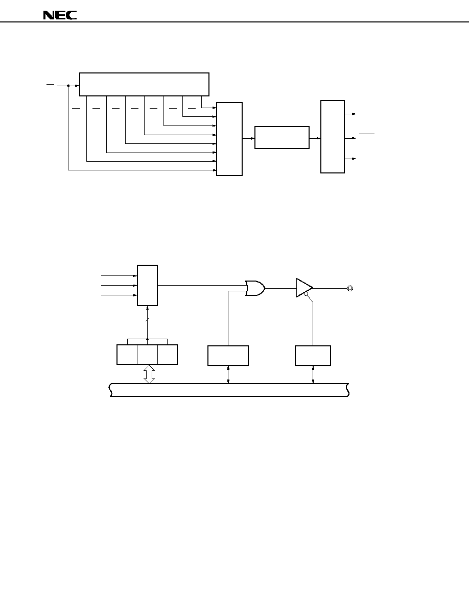
The instruction execution time can be changed as follows.
0.44
µ
s/0.88
µ
s/1.78
µ
s/3.56
µ
s/7.11
µ
s/14.22
µ
s (@ 4.5-MHz crystal oscillator with system clock.)
Figure 5-1. Clock Generator Block Diagram
X1
X2
f
XX
Prescaler
System
Clock
Oscillator
Clock to peripheral
hardware other than
the above.
Clock to the PLL
frequency synthesizer,
basic timer and buzzer
output control circuit.
CPU Clock
(f
CPU
)
Standby
Control
Circuit
Wait Control
Circuit
To INTP0
Sampling Clock
2
f
XX
2
2
f
XX
2
3
f
XX
2
4
f
XX
Prescaler
Selector
Selector
f
X
f
X
2
STOP
Scaler
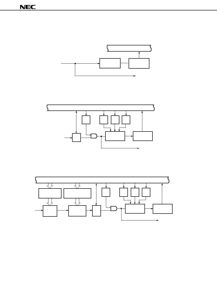
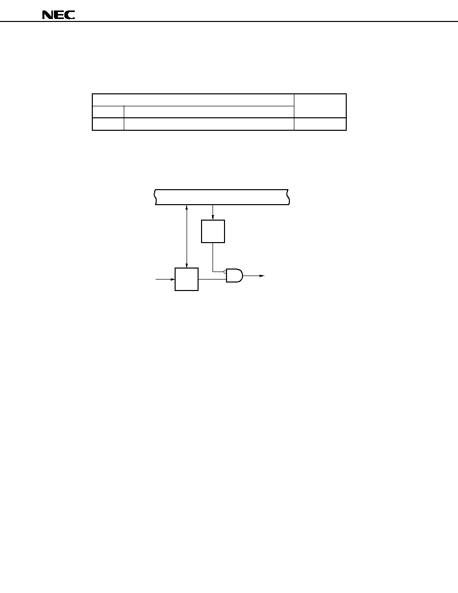
5.3 TIMER
The
µ
PD178004A, 178006A, 178016A, and 178018A incorporate 5 channels of the timer.
∑ Basic timer
: 1 channel
∑ 8-bit timer/event counter
: 2 channels
∑ 8-bit timer (D/A converter)
Note
: 1 channel
∑ Watchdog timer
: 1 channel
Note
Used is shared with the 8/9-bit resolution
◊
3-channel D/A converter (PWM output).
Figure 5-2. Basic Timer Block Diagram
Divider
4.5 MHz
INTTMC
17
µ
PD178004A, 178006A, 178016A, 178018A
Figure 5-3. 8-Bit Timer/Event Counter Block Diagram
Internal Bus
8-Bit Compare
Register (CR10)
8-Bit Timer
Register 1 (TM1)
Clear
Match
Selector
INTTM1
INTTM2
Clear
Match
Selector
Selector
Selector
Selector
8-Bit Compare
Register (CR20)
8-Bit Timer
Register 2 (TM2)
Internal Bus
f
xx
/2 to f
xx
/2
f
x
/2
9
11
TI1/P33
f
xx
/2 to f
xx
/2
f
x
/2
9
11
TI2/P34
Figure 5-4. 8-Bit Timer (D/A Converter) Block Diagram
4.5 MHz
Clock
Generation
Block
f
PWM
Clear
Circuit
Comparator
Comparator
Comparator
PWM Data Register 2
Note
(PWMR2)
PWM Data Register 1
(PWMR1)
PWM Data Register 0
(PWMR0)
INTPWM
Internal Bus
PWM Duty Setting Block
PWM Mode
Select Register
P132/PWM0
P133/PWM1
P134/PWM2
b8
b0
PWM Control Register
PWM
BIT
PWM
CK0
PWM
MD
PWM
ST
PWM
RES
PWM
2SE
PWM
1SE
PWM
0SE
Output Select
Block
Output Select
Block
Output Select
Block
9-Bit Binary Counter
Internal Bus
Note
The PWM data register 2 (PWMR2) is multiplexed with the PWM timer register (PWMTMR).
18
µ
PD178004A, 178006A, 178016A, 178018A
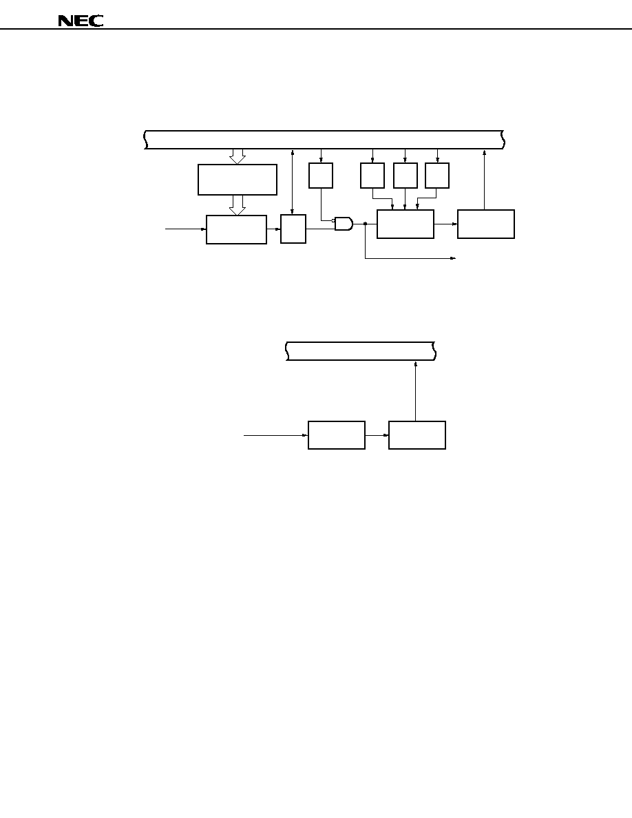
Figure 5-5. Watchdog Timer Block Diagram
Control
Circuit
8-Bit Counter
Prescaler
INTWDT
Non-Maskable
Interrupt Request
INTWDT
Maskable
Interrupt Request
Reset
Selector
2
f
xx
4
2
f
xx
5
2
f
xx
6
2
f
xx
7
2
f
xx
8
2
f
xx
9
2
f
xx
11
2
f
xx
3
5.4 BUZZER OUTPUT CONTROL CIRCUIT
The clock with the following frequency can be output as a buzzer output.
∑ 1.5 kHz/3 kHz/6 kHz (@ 4.5-MHz crystal oscillator with system clock)
Figure 5-6. Buzzer Output Control Circuit Block Diagram
Internal Bus
1.5 kHz
3 kHz
6 kHz
TCL27 TCL26 TCL25
3
PM36
Selector
Timer Clock Select Register 2
Port Mode Register 3
BEEP/P36
P36
Output Latch

19
µ
PD178004A, 178006A, 178016A, 178018A
3-wire serial I/O mode
Function
Serial Interface Channel 1
--
Serial Interface Channel 0
(MSB/LSB first switchable)
(MSB/LSB first switchable)
(MSB/LSB first switchable)
3-wire serial I/O mode with automatic
transmission/ reception function
SBI (serial bus interface) mode
2-wire serial I/O mode
--
--
I
2
C Bus Mode
--
(MSB first)
(MSB first)
(MSB first)
5.5 A/D CONVERTER
An A/D converter of 8-bit resolution
◊
6 channels is incorporated.
The following two types of the A/D conversion operation start-up methods are available.
∑ Hardware start
∑ Software start
Figure 5-7. A/D Converter Block Diagram
Tap
Selector
INTAD
V
DD
INTP3
Internal Bus
GND
A/D Conversion
Result Register (ADCR)
Control
Circuit
Succesive Approximation
Register (SAR)
Edge
Detection
Circuit
ANI0/P10
ANI1/P11
ANI2/P12
ANI3/P13
ANI4/P14
ANI5/P15
INTP3/P03
Selector
Sample & Hold Circuit
Voltage Comparator
Resistor String
5.6 SERIAL INTERFACES
2 channels of the clocked serial interface are incorporated.
∑ Serial interface channel 0
∑ Serial interface channel 1
Table 5-2. Types and Functions of Serial Interface

20
µ
PD178004A, 178006A, 178016A, 178018A
Figure 5-8. Serial Interface Channel 0 Block Diagram
Busy/Acknowledge
Output Circuit
Output
Latch
Serial I/O Shift
Register 0 (SIO0)
Internal Bus
Interrupt Request
Signal Generator
Serial Clock Counter
Bus Release/Command/
Acknowledge Detection
Circuit
Serial Clock
Control Circuit
Selector
Selector
Selector
SI0/SB0/SDA0/P25
SO0/SB1/SDA1/P26
SCK0/SCL/P27
INTCSI0
f
XX
/2 to f
XX
/2
8
Figure 5-9. Serial Interface Channel 1 Block Diagram
Internal Bus
Interrupt Request
Signal Generator
Handshake
Control
Circuit
Buffer RAM
Serial Clock Control Circuit
Selector
Serial Counter
Serial I/O Shift Register 1 (SIO1)
Automatic Data Transmit/
Receive Address Pointer
(ADTP)
Automatic Data
Transmit/Receive
Interval Specification
Register (ADTI)
5-Bit Counter
INTCSI1
f
XX
/2 to f
XX
/2
8
SI1/P20
SO1/P21
STB/P23
BUSY/P24
SCK1/P22
Match

21
µ
PD178004A, 178006A, 178016A, 178018A
5.7 PLL FREQUENCY SYNTHESIZER
Figure 5-10. PLL Frequency Synthesizer Block Diagram
Internal Bus
Internal Bus
PLL Mode
Select Register
PWM
Data Transfer Register
PLL
NS0
PLL
MD0
PLL
MD1
PLL
RF2
PLL
RF1
PLL
RF0
PLL
UL0
EO Select
Register
PLL Reference
Mode Register
PLL Unlock
FF Judge
Register
PLL
RF3
2
Input Select
Block
Programmable
Divider
Phase
Comparator
( -DET)
Unlock
FF
Reference
Frequency
Generator
4.5 MHz
4
Charge
Pump
EO1
EO0
VCOH
VCOL
Mixer
2
f
N
f
r
PLL Data Register
(PLLRL, PLLRH, PLLR0)
Voltage
Control
Generator
Low pass
Filter
Note
Note
EOC
ON1
EOC
ON0
Note
External circuit
Cautions 1. Be sure to set EOCON0 to 0.
2. For the
µ
PD178004A and 178006A, do not set EOCON1 to 1.

22
µ
PD178004A, 178006A, 178016A, 178018A
5.8 FREQUENCY COUNTER
Figure 5-11. Frequency Counter Block Diagram
Internal Bus
IFC
MD0
IFC
CK1
IFC
CK0
IFC
JG0
IF Counter
Mode Select
Register
IF Counter
Gate Judge
Register
IF Counter
Control
Register
IFC
MD1
IFC
RES
IFC
ST
Input Select
Block
Start/Stop
Control Block
Gate Time
Control Block
IF Counter
Register
(IFC)
Block
2
2
FMIFC
AMIFC

23
µ
PD178004A, 178006A, 178016A, 178018A
6. INTERRUPT FUNCTIONS AND TEST FUNCTIONS
6.1 INTERRUPT FUNCTIONS
Interrupt functions include three types and 17 sources, as shown below.
∑ Non-maskable:
1
∑ Maskable
: 15
∑ Software
:
1
Table 6-1. Interrupt Source List
Non-
maskable
0006H
0008H
000AH
000CH
000EH
0010H
0012H
Trigger
Internal/
External
External
Internal
0004H
0014H
Internal
Vector Table
Address
Interrupt Source
(B)
Basic
Configuration
Type
Note 2
(B)
(A)
(C)
(D)
Maskable
INTP0
INTP1
INTP2
INTP3
INTP4
INTP5
INTP6
1
2
3
4
5
6
7
Note 1
Default
Priority
Name
INTCSI0
8
INTWDT
INTWDT
0
Interrupt
Type
--
End of serial interface channel 0 transfer
Pin input edge detection
Watchdog timer overflow
(interval timer mode selected)
Watchdog timer overflow
(watchdog timer mode 1 selected)
0016H
9
INTCSI1
End of serial interface channel 1 transfer
0018H
10
INTTMC
Generation of match signal of basic timer
001AH
11
INTPWM
Generation of match signal of 8-bit timer
INTTM1
Generation of match signal of 8-bit timer/
event counter 1
12
001CH
INTTM2
Generation of match signal of 8-bit timer/
event counter 2
001EH
13
14
INTAD
End of conversion by A/D converter
0020H
--
BRK
BRK instruction execution
003EH
Software
(E)
Internal
Notes 1. The default priority is a priority order when two or more maskable interrupts are generated
simultaneously. 0 is the highest order and 14, the lowest.
2. Basic configuration types (A) to (E) correspond to (A) to (E) in Figure 6-1, respectively.
24
µ
PD178004A, 178006A, 178016A, 178018A
Figure 6-1. Interrupt Function Basic Configuration (1/2)
(A) Internal non-maskable interrupt
Internal Bus
Priority Control
Circuit
Vector Table
Address
Generator
Standby Release
Signal
Interrupt
Request
(B) Internal maskable interrupt
MK
Internal Bus
IE
PR
ISP
IF
Priority Control
Circuit
Vector Table
Address
Generator
Standby Release
Signal
Interrupt
Request
(C) External maskable interrupt (INTP0)
MK
IE
PR
ISP
IF
Priority Control
Circuit
Vector Table
Address
Generator
Sampling Clock
Select Register
(SCS)
External Interrupt
Mode Register
(INTM0)
Edge
Detection
Circuit
Sampling
Clock
Internal Bus
Standby Release
Signal
Interrupt
Request
25
µ
PD178004A, 178006A, 178016A, 178018A
Figure 6-1. Interrupt Function Basic Configuration (2/2)
(D) External maskable interrupt (except INTP0)
MK
IE
PR
ISP
IF
Priority Control
Circuit
Vector Table
Address
Generator
External Interrupt
Mode Register
(INTM0, INTM1)
Edge Detection
Circuit
Internal Bus
Standby Release
Signal
Interrupt
Request
(E) Software interrupt
Priority Control
Circuit
Vector Table
Address
Generator
Internal Bus
Interrupt
Request
IF
: Interrupt request flag
IE
: Interrupt enable flag
ISP : In-service priority flag
MK : Interrupt mask flag
PR : Priority specification flag
26
µ
PD178004A, 178006A, 178016A, 178018A
6.2 TEST FUNCTION
A test function with a single source is provided, as shown in Table 6-2.
Table 6-2. Test Input Source List
Figure 6-2. Test Function Basic Configuration
IF
MK
Internal Bus
Test Input
Standby Release
Signal
IF : Test input flag
MK : Test mask flag
Test Input Source
Name
Trigger
Internal/External
INTPT4
Port 4 falling edge detection
External
27
µ
PD178004A, 178006A, 178016A, 178018A
7. STANDBY FUNCTION
There are the following two standby functions to reduce the system power consumption.
∑ HALT mode : The CPU operating clock is stopped.
The average consumption current can be reduced by intermittent operation in combination with
the normal operating mode.
∑ STOP mode : The system clock oscillation is stopped. All operations by the system clock are stopped and
current consumption can be considerably reduced.
Figure 7-1. Stand-by Function
System Clock Operation
STOP Mode
(System clock
oscillation stopped)
HALT Mode
(Clock supply to CPU is
stopped, oscillation
continued)
Interrupt
Request
Interrupt
Request
HALT
Instruction
STOP
Instruction
8. RESET FUNCTION
There are the following three reset methods.
∑ External reset input by RESET pin
∑ Internal reset by watchdog timer runaway time detection
∑ Internal reset by Power-On Clear (POC).
28
µ
PD178004A, 178006A, 178016A, 178018A
9. INSTRUCTION SET
(1) 8-bit instructions
MOV, XCH, ADD ADDC, SUB, SUBC, AND, OR, XOR, CMP, MULU, DIVUW, INC, DEC, ROR,
ROL, RORC, ROLC, ROR4, ROL4, PUSH, POP, DBNZ
Note
Except r = A
Second
Operand
First
Operand
#byte
A
r
Note
sfr
saddr
!addr16
PSW
[DE]
[HL]
[HL + byte]
[HL + B]
[HL + C]
$addr16
1
None
A
r
ADD
ADDC
SUB
SUBC
AND
OR
XOR
CMP
MOV
XCH
ADD
ADDC
SUB
SUBC
AND
OR
XOR
CMP
MOV
XCH
MOV
XCH
ADD
ADDC
SUB
SUBC
AND
OR
XOR
CMP
MOV
XCH
ADD
ADDC
SUB
SUBC
AND
OR
XOR
CMP
MOV
MOV
XCH
MOV
XCH
ADD
ADDC
SUB
SUBC
AND
OR
XOR
CMP
MOV
XCH
ADD
ADDC
SUB
SUBC
AND
OR
XOR
CMP
ROR
ROL
RORC
ROLC
MOV
MOV
ADD
ADDC
SUB
SUBC
AND
OR
XOR
CMP
INC
DEC
B,C
sfr
MOV
MOV
DBNZ
MOV
ADD
ADDC
SUB
SUBC
AND
OR
XOR
CMP
saddr
MOV
DBNZ
INC
DEC
!addr16
MOV
PSW
MOV
MOV
PUSH
POP
[DE]
ROR4
ROL4
[HL]
MOV
[HL + byte]
[HL + B]
[HL + C]
MOV
X
C
MULU
DIVUW
29
µ
PD178004A, 178006A, 178016A, 178018A
(2) 16-bit instructions
MOVW, XCHW, ADDW, SUBW, CMPW, PUSH, POP, INCW, DECW
Note
Only when rp = BC, DE or HL
(3) Bit manipulation instructions
MOV1, AND1, OR1, XOR1, SET1, CLR1, NOT1, BT, BF, BTCLR
(4) Call instruction/branch instructions
CALL, CALLF, CALLT, BR, BC, BNC, BZ, BNZ, BT, BF, BTCLR, DBNZ
(5) Other instructions
ADJBA, ADJBS, BRK, RET, RETI, RETB, SEL, NOP, EI, DI, HALT, STOP
Second Operand
First Operand
AX
rp
sfrp
saddrp
!addr16
SP
#word
ADDW
SUBW
CMPW
MOVW
MOVW
MOVW
MOVW
AX
MOVW
Note
MOVW
MOVW
MOVW
MOVW
MOVW
XCHW
rp
Note
sfrp
MOVW
saddrp
MOVW
!addr16
MOVW
SP
MOVW
None
INCW
DECW
PUSH
POP
Second Operand
First Operand
A.bit
sfr.bit
saddr.bit
PSW.bit
[HL].bit
CY
$addr16
None
A.bit
sfr.bit
saddr.bit
PSW.bit
[HL].bit
CY
MOV1
MOV1
MOV1
MOV1
MOV1
BT
BF
BTCLR
BT
BF
BTCLR
SET1
CLR1
SET1
CLR1
BT
BF
BTCLR
SET1
CLR1
BT
BF
BTCLR
SET1
CLR1
BT
BF
BTCLR
SET1
CLR1
SET1
CLR1
NOT1
MOV1
AND1
OR1
XOR1
MOV1
AND1
OR1
XOR1
MOV1
AND1
OR1
XOR1
MOV1
AND1
OR1
XOR1
MOV1
AND1
OR1
XOR1
Second Operand
First Operand
AX
!addr16
!addr11
[addr5]
$addr16
Basic instruction
Compound
instruction
BR
CALL
BR
CALLF
CALLT
BR, BC, BNC
BZ, BNZ
BT, BF
BTCLR
DBNZ
30
µ
PD178004A, 178006A, 178016A, 178018A
10. ELECTRICAL SPECIFICATIONS
ABSOLUTE MAXIMUM RATINGS (T
A
= 25
∞
C)
Parameter
Symbol
Test Conditions
Rating
Unit
Power supply voltage
V
DD
≠0.3 to + 7.0
V
Input voltage
V
I1
Excluding P60 to P63
≠0.3 to V
DD
+ 0.3
V
V
I2
P60 to P63
N-ch Open-drain
≠0.3 to +16
V
Output voltage
V
O
≠0.3 to V
DD
+ 0.3
V
Output withstand
V
BDS
P132 to P134
N-ch Open-drain
16
V
voltage
Analog input voltage
V
AN
P10 to P15
Analog input pin
≠0.3 to V
DD
+ 0.3
V
Output current high
I
OH
1 pin
≠10
mA
P01 to P06, P30 to P37, P56, P57, P60 to P67,
≠15
mA
P120 to P125 total
P10 to P15, P20 to P27, P40 to P47, P50 to P55,
≠15
mA
P132 to P134 total
Output current low
I
OL
Note
1 pin
Peak value
15
mA
Effective value
7.5
mA
Operating ambient
T
A
≠40 to +85
∞
C
temperature
Storage temperature
T
stg
≠65 to +150
∞
C
Note
Effective value should be calculated as follows: [Effective value] = [Peak value]
◊
duty
Caution Product quality may suffer if the absolute maximum rating is exceeded for even a single
parameter even momentarily. That is, the absolute maximum ratings are rated values at which
the product is on the verge of suffering physical damage, and therefore the product must be
used under conditions which ensure that the absolute maximum ratings are not exceeded.
Remark The characteristics of alternate-function pins and port pins are the same unless specified otherwise.
RECOMMENDED SUPPLY VOLTAGE RANGES (T
A
= ≠40 to +85
∞
C)
Remark T
CY
: Cycle Time (Minimum instruction execution time)
Parameter
Symbol
Test Conditions
MIN.
TYP.
MAX.
Unit
Power supply voltage
V
DD1
During CPU operation and PLL operation.
4.5
5.5
V
V
DD2
While the CPU is operating and the PLL is stopped.
3.5
5.5
V
Cycle Time: T
CY
0.89
µ
s
V
DD3
While the CPU is operating and the PLL is stopped.
4.5
5.5
V
Cycle Time: T
CY
= 0.44
µ
s
31
µ
PD178004A, 178006A, 178016A, 178018A
DC CHARACTERISTICS (T
A
= ≠40 to +85
∞
C, V
DD
= 3.5 to 5.5 V)
Parameter
Symbol
Test Conditions
MIN.
TYP.
MAX.
Unit
Input voltage high
V
IH1
P10 to P15, P21, P23,
0.7 V
DD
V
DD
V
P30 to P32, P35 to P37,
P40 to P47, P50 to P57,
P64 to P67, P120 to P125
V
IH2
P00 to P06, P20, P22,
0.85 V
DD
V
DD
V
P24 to P27, P33, P34,
RESET
V
IH3
P60 to P63
0.7 V
DD
15
V
(N-ch Open-drain)
Input voltage low
V
IL1
P10 to P15, P21, P23,
0
0.3 V
DD
V
P30 to P32, P35 to P37,
P40 to P47, P50 to P57,
P64 to P67, P120 to P125
V
IL2
P00 to P06, P20, P22,
0
0.15 V
DD
V
P24 to P27, P33, P34,
RESET
V
IL3
P60 to P63
4.5 V
V
DD
5.5 V
0
0.3 V
DD
V
(N-ch Open-drain)
3.5 V
V
DD
< 4.5 V
0
0.2 V
DD
V
Output voltage high
V
OH1
4.5 V
V
DD
5.5 V
V
DD
≠ 1.0
V
I
OH
= ≠1 mA
3.5 V
V
DD
< 4.5 V
V
DD
≠ 0.5
V
I
OH
= ≠100
µ
A
Output voltage low
V
OL1
P50 to P57, P60 to P63
V
DD
= 4.5 to 5.5 V,
0.4
2.0
V
I
OH
= 15 mA
P01 to P06, P10 to P15,
V
DD
= 4.5 to 5.5 V,
0.4
V
P20 to P27, P30 to P37,
I
OL
= 1.6 mA
P40 to P47, P64 to P67,
P120 to P125,
P132 to P134
V
OL2
SB0, SB1, SCK0
V
DD
= 4.5 to 5.5 V,
0.2 V
DD
V
open-drain pulled-up
(R = 1 K
)
Remark The characteristics of alternate-function pins and port pins are the same unless specified otherwise.
(1/3)

32
µ
PD178004A, 178006A, 178016A, 178018A
DC CHARACTERISTICS (T
A
= ≠40 to +85
∞
C, V
DD
= 3.5 to 5.5 V)
Note
When an input instruction is executed, the low-level input leakage current for P60 to P63 becomes ≠200
µ
A (MAX.) only in one clock cycle (at no wait). It remains at ≠3
µ
A (MAX.) for other than an input instruction.
Remark The characteristics of alternate-function pins and port pins are the same unless specified otherwise.
REFERENCE CHARACTERISTICS (T
A
= 25
∞
C, V
DD
= 5 V)
Parameter
Symbol
Test Conditions
MIN.
TYP.
MAX.
Unit
Input leakage
I
LIH1
P00 to P06, P10 to P15,
V
IN
= V
DD
3
µ
A
current high
P20 to P27, P30 to P37,
P40 to P47, P50 to P57,
P64 to P67, P120 to P125,
RESET
I
LIH2
P60 to P63
V
IN
= 15 V
80
µ
A
Input leakage
I
LIL1
P00 to P06, P10 to P15,
V
IN
= 0 V
≠3
µ
A
current low
P20 to P27, P30 to P37,
P40 to P47, P50 to P57,
P64 to P67, P120 to P125,
RESET
I
LIL2
P60 to P63
≠3
Note
µ
A
Output leakage
I
LOH
P132 to P134
V
OUT
= 15 V
3
µ
A
current high
Output leakage
I
LOL
P132 to P134
V
OUT
= 0 V
≠3
µ
A
current low
Output off leak
I
LOF
EO0, EO1
V
OUT
= V
DD
,
±
1
µ
A
current
V
OUT
= 0 V
Parameter
Symbol
Test Conditions
MIN.
TYP.
MAX.
Unit
Output current high
I
OH1
EO0
V
OUT
= V
DD
≠ 1 V
≠4
mA
EO1 (EOCON0 = 0)
≠1.8
mA
Output current low
I
OL1
EO0
V
OUT
= 1 V
6
mA
EO1 (EOCON0 = 0)
3.5
mA
(2/3)
(1/2)
33
µ
PD178004A, 178006A, 178016A, 178018A
DC CHARACTERISTICS (T
A
= ≠40 to +85
∞
C, V
DD
= 3.5 to 5.5 V)
Parameter
Symbol
Test Conditions
MIN.
TYP.
MAX.
Unit
Power Supply
Note 1
I
DD1
While the CPU is operating
T
CY
= 0.89
µ
s
Note 2
2.5
15
mA
Current
and the PLL is stopped
I
DD2
f
X
= 4.5 MHz operation
T
CY
= 0.44
µ
s
Note 3
4.0
27
mA
V
DD
= 4.5 to 5.5 V
I
DD3
While the CPU is operating
T
CY
= 0.89
µ
s
Note 2
0.7
1.5
mA
and the PLL is stopped
HALT Mode
I
DD4
Pin X1 sine wave
T
CY
= 0.44
µ
s
Note 3
1.0
2.0
mA
input V
IN
= V
DD
.
V
DD
= 4.5 to 5.5 V
f
X
= 4.5 MHz operation
Data Hold
V
DR1
When the crystal is oscillating
T
CY
= 0.44
µ
s
4.5
5.5
V
Power Supply
V
DR2
T
CY
= 0.89
µ
s
3.5
5.5
V
Voltage
V
DR3
When the crystal oscillator is stopped
2.6
5.5
V
When power off by Power On Clear is detected
Data Hold
I
DR1
While the crystal oscillator
T
A
= 25
∞
C, V
DD
= 5V
2
4
µ
A
Power Supply Current
I
DR2
is stopped
2
30
µ
A
Notes 1. The port current is not included.
2. When the Processor Clock Control register (PCC) is set at 00H, and the Oscillation Mode Select
register (OSMS) is set at 00H.
3. When PCC is set at 00H and OSMS is set at 01H.
Remarks 1. T
CY
: Cycle Time (Minimum instruction execution time)
2. fx: System clock oscillator frequency.
REFERENCE CHARACTERISTICS (T
A
= 25
∞
C, V
DD
= 5 V)
Parameter
Symbol
Test Conditions
MIN.
TYP.
MAX.
Unit
Power Supply
I
DD5
During CPU operation
T
CY
= 0.44
µ
s
Note
7
mA
Current
and PLL operation.
VCOH pin sine wave
input
f
IN
= 130 MHz,
V
IN
= 0.15 V
p-p
Note
When the Processor Clock Control register (PCC) is set at 00H, and the Oscillation Mode Select register
(OSMS) is set at 01H.
Remark T
CY
: Cycle Time (Minimum instruction execution time)
(3/3)
(2/2)

34
µ
PD178004A, 178006A, 178016A, 178018A
AC CHARACTERISTICS
(1) BASIC OPERATION (T
A
= ≠40 to +85
∞
C, V
DD
= 3.5 to 5.5 V)
Parameter
Symbol
Test Conditions
MIN.
TYP.
MAX.
Unit
Cycle time
T
CY
f
XX
= f
X
/2
Note 1
, f
X
= 4.5 MHz operation
0.89
14.22
µ
s
(Minimum instruction
f
XX
= f
X
Note 2
,
4.5
V
DD
5.5 V
0.44
7.11
µ
s
execution time)
f
X
= 4.5 MHz operation
3.5
V
DD
< 4.5 V
0.89
7.11
µ
s
TI1, TI2 input
f
TI
4.5
V
DD
5.5 V
0
4.5
MHz
frequency
3.5 V
V
DD
4.5 V
0
275
kHz
TI1, TI2 input high/
t
TIH
,
4.5
V
DD
5.5 V
111
ns
low-level width
t
TIL
3.5 V
V
DD
4.5 V
1.8
µ
s
Interrupt input high/
T
INTH
,
INTP0
8/f
sam
Note 3
µ
s
low-level width
T
INTL
INTP1 to INTP6
10
µ
s
RESET low level
t
RSL
10
µ
s
width
Notes 1. When oscillation mode selection (OSMS) register is set at 00H.
2. When OSMS is set at 01H.
3. In combination with bits 0 (SCS0) and 1 (SCS1) of sampling clock select register (SCS), selection
of f
sam
is possible between f
XX
/2
N
, f
XX
/32, f
XX
/64 and f
XX
/128 (when N = 0 to 4).
Remarks 1. f
XX
: System clock frequency (f
X
or f
X
/2)
2. f
X
: System clock oscillation frequency
T
CY
vs V
DD
(At F
XX
= F
X
/2
system clock operation)
T
CY
vs V
DD
(At F
XX
= F
X
system clock operation)
Cycle Time T
CY
[
µ
s]
Cycle Time T
CY
[
µ
s]
60
10
2.0
1.0
0.5
0.4
0
1
2
3
4
5
6
Power Supply Voltage V
DD
[V]
Operation
Guaranteed
Range
60
10
2.0
1.0
0.5
0.4
0
1
2
3
4
5
6
Power Supply Voltage V
DD
[V]
Operation
Guaranteed
Range
35
µ
PD178004A, 178006A, 178016A, 178018A
(2) SERIAL INTERFACE (T
A
= ≠40 to +85
∞
C, V
DD
= 3.5 to 5.5 V)
(a) Serial interface channel 0
(i) 3-wire serial I/O mode (SCK0 ... internal clock output)
Parameter
Symbol
Test Conditions
MIN.
TYP.
MAX.
Unit
SCK0 cycle time
t
KCY1
4.5 V
V
DD
5.5 V
800
ns
3.5 V
V
DD
< 4.5 V
1 600
ns
SCK0 high-/low-level width
t
KH1
,
4.5 V
V
DD
5.5 V
t
KCY1
/2 ≠ 50
ns
t
KL1
3.5 V
V
DD
< 4.5 V
t
KCY1
/2 ≠ 100
ns
SI0 setup time (to SCK0
)
t
SIK1
4.5 V
V
DD
5.5 V
100
ns
3.5 V
V
DD
< 4.5 V
150
ns
SI0 hold time (from SCK0
)
t
KSI1
400
ns
SO0 output delay time from SCK0
t
KSO1
C = 100 pF
Note
300
ns
Note
C is the load capacitance of SO0 output line.
(ii) 3-wire serial I/O mode (SCK0 ... external clock input)
Parameter
Symbol
Test Conditions
MIN.
TYP.
MAX.
Unit
SCK0 cycle time
t
KCY2
4.5 V
V
DD
5.5 V
800
ns
3.5 V
V
DD
< 4.5 V
1 600
ns
SCK0 high-/low-level width
t
KH2
,
4.5 V
V
DD
5.5 V
400
ns
t
KL2
3.5 V
V
DD
< 4.5 V
800
ns
SI0 setup time (to SCK0
)
t
SIK2
100
ns
SI0 hold time (from SCK0
)
t
KSI2
400
ns
SO0 output delay time from SCK0
t
KSO2
C = 100 pF
Note
300
ns
SCK0 at rising or falling edge time
t
R2
, t
F2
1 000
ns
Note
C is the load capacitance of SO0 output line.
36
µ
PD178004A, 178006A, 178016A, 178018A
(iii) SBI mode (SCK0 ... internal clock output)
Parameter
Symbol
Test Conditions
MIN.
TYP.
MAX.
Unit
SCK0 cycle time
t
KCY3
4.5 V
V
DD
5.5 V
800
ns
3.5 V
V
DD
< 4.5 V
3 200
ns
SCK0 high-/low-level width
t
KH3
,
4.5 V
V
DD
5.5 V
t
KCY3
/2 ≠ 50
ns
t
KL3
3.5 V
V
DD
< 4.5 V
t
KCY3
/2 ≠ 150
ns
SB0, SB1 setup time (to SCK0
)
t
SIK3
4.5 V
V
DD
5.5 V
100
ns
3.5 V
V
DD
< 4.5 V
300
ns
SB0, SB1 hold time (from SCK0
)
t
KSI3
t
KCY3
/2
ns
SB0, SB1 output delay time from
t
KSO3
R = 1 k
4.5 V
V
DD
5.5 V
0
250
ns
SCK0
C = 100 pF
Note
3.5 V
V
DD
< 4.5 V
0
1 000
ns
SB0, SB1
from SCK0
t
KSB
t
KCY3
ns
SCK0
from SB0, SB1
t
SBK
t
KCY3
ns
SB0, SB1 high-level width
t
SBH
t
KCY3
ns
SB0, SB1 low-level width
t
SBL
t
KCY3
ns
Note R and C are the load resistance and load capacitance of SB0 and SB1 output line.
(iv) SBI mode (SCK0 ... external clock input)
Parameter
Symbol
Test Conditions
MIN.
TYP.
MAX.
Unit
SCK0 cycle time
t
KCY4
4.5 V
V
DD
5.5 V
800
ns
3.5 V
V
DD
< 4.5 V
3 200
ns
SCK0 high-/low-level width
t
KH4
,
4.5 V
V
DD
5.5 V
400
ns
t
KL4
3.5 V
V
DD
< 4.5 V
1 600
ns
SB0, SB1 setup time (to SCK0
)
t
SIK4
4.5 V
V
DD
5.5 V
100
ns
3.5 V
V
DD
< 4.5 V
300
ns
SB0, SB1 hold time (from SCK0
)
t
KSI4
t
KCY4
/2
ns
SB0, SB1 output delay time from
t
KSO4
R = 1 k
4.5 V
V
DD
5.5 V
0
300
ns
SCK0
C = 100 pF
Note
3.5 V
V
DD
< 4.5 V
0
1 000
ns
SB0, SB1
from SCK0
t
KSB
t
KCY4
ns
SCK0
from SB0, SB1
t
SBK
t
KCY4
ns
SB0, SB1 high-level width
t
SBH
t
KCY4
ns
SB0, SB1 low-level width
t
SBL
t
KCY4
ns
SCK0 at rising or falling edge time
t
R4
, t
F4
1 000
ns
Note
R and C are the load resistance and load capacitance of SB0 and SB1 output line.

37
µ
PD178004A, 178006A, 178016A, 178018A
(v) 2-wire serial I/O mode (SCK0 ... internal clock output)
Parameter
Symbol
Test Conditions
MIN.
TYP.
MAX.
Unit
SCK0 cycle time
t
KCY5
R = 1 k
1 600
ns
SCK0 high-level width
t
KH5
C = 100 pF
Note
t
KCY5
/2 ≠ 160
ns
SCK0 low-level width
t
KL5
4.5 V
V
DD
5.5 V t
KCY5
/2 ≠ 50
ns
3.5 V
V
DD
< 4.5 V t
KCY5
/2 ≠ 100
ns
SB0, SB1 setup time (to SCK0
)
t
SIK5
4.5 V
V
DD
5.5 V
300
ns
3.5 V
V
DD
< 4.5 V
350
ns
400
ns
SB0, SB1 hold time (from SCK0
)
t
KSI5
600
ns
SB0, SB1 output delay time from
t
KSO5
0
300
ns
SCK0
Note
R and C are the load resistance and load capacitance of SCK0, SB0 and SB1 output line.
(vi) 2-wire serial I/O mode (SCK0 ... external clock input)
Parameter
Symbol
Test Conditions
MIN.
TYP.
MAX.
Unit
SCK0 cycle time
t
KCY6
1 600
ns
SCK0 high-level width
t
KH6
650
ns
SCK0 low-level width
t
KL6
800
ns
SB0, SB1 setup time (to SCK0
)
t
SIK6
100
ns
SB0, SB1 hold time (from SCK0
)
t
KSI6
t
KCY6
/2
ns
SB0, SB1 output delay time from
t
KSO6
R = 1 k
4.5 V
V
DD
5.5 V
0
300
ns
SCK0
C = 100 pF
Note
3.5 V
V
DD
< 4.5 V
0
500
ns
SCK0 at rising or falling edge time
t
R6
, t
F6
1 000
ns
Note
R and C are the load resistance and load capacitance of SB0 and SB1 output line.
38
µ
PD178004A, 178006A, 178016A, 178018A
(vii) I
2
C Bus mode (SCL ... internal clock output)
Parameter
Symbol
Test Conditions
MIN.
TYP.
MAX.
Unit
SCL cycle time
t
KCY7
R = 1 k
10
µ
s
SCL high-level width
t
KH7
C = 100 pF
Note
t
KCY7
≠ 160
ns
SCL low-level width
t
KL7
t
KCY7
≠ 50
ns
SDA0, SDA1 setup time (to SCL
)
t
SIK7
200
ns
SDA0, SDA1 hold time
t
KSI7
0
ns
(from SCL
)
SDA0, SDA1 output delay time
t
KSO7
4.5 V
V
DD
5.5 V
0
300
ns
(from SCL
)
3.5 V
V
DD
< 4.5 V
0
500
ns
SDA0, SDA1
from SCL
or
t
KSB
200
ns
SDA0, SDA1
from SCL
SCL
from SDA0, SDA1
t
SBK
400
ns
SDA0, SDA1 high-level width
t
SBH
500
ns
Note
R and C are the load resistance and load capacitance of SCL, SDA0 and SDA1 output line.
(viii) I
2
C Bus mode (SCL ... external clock input)
Parameter
Symbol
Test Conditions
MIN.
TYP.
MAX.
Unit
SCL cycle time
t
KCY8
1 000
ns
SCL high-/low-level width
t
KH8,
t
KL8
400
ns
SDA0, SDA1 setup time (to SCL
)
t
SIK8
200
ns
SDA0, SDA1 hold time
t
KSI8
0
ns
(from SCL
)
SDA0, SDA1 output delay time
t
KSO8
R = 1 k
4.5 V
V
DD
5.5 V
0
300
ns
from SCL
C = 100 pF
Note
3.5 V
V
DD
< 4.5 V
0
500
ns
SDA0, SDA1
from SCL
or
t
KSB
200
ns
SDA0, SDA1
from SCL
SCL
from SDA0, SDA1
t
SBK
400
ns
SDA0, SDA1 high-level width
t
SBH
500
ns
SCL at rising or falling edge time
t
R8
, t
F8
1 000
ns
Note
R and C are the load resistance and load capacitance of SDA0 and SDA1 output line.
39
µ
PD178004A, 178006A, 178016A, 178018A
(b) Serial interface channel 1
(i) 3-wire serial I/O mode (SCK1 ... internal clock output)
Parameter
Symbol
Test Conditions
MIN.
TYP.
MAX.
Unit
SCK1 cycle time
t
KCY9
4.5 V
V
DD
5.5 V
800
ns
3.5 V
V
DD
< 4.5 V
1 600
ns
SCK1 high/low-level width
t
KH9
,
4.5 V
V
DD
5.5 V
t
KCY9
/2 ≠ 50
ns
t
KL9
3.5 V
V
DD
< 4.5 V
t
KCY9
/2 ≠ 100
ns
SI1 setup time (to SCK1
)
t
SIK9
4.5 V
V
DD
5.5 V
100
ns
3.5 V
V
DD
< 4.5 V
150
ns
SI1 hold time (from SCK1
)
t
KSI9
400
ns
SO1 output delay time (from SCK1
)
t
KSO9
C = 100 pF
Note
300
ns
Parameter
Symbol
Test Conditions
MIN.
TYP.
MAX.
Unit
SCK1 cycle time
t
KCY10
4.5 V
V
DD
5.5 V
800
ns
3.5 V
V
DD
< 4.5 V
1 600
ns
SCK1 high/low-level width
t
KH10
,
4.5 V
V
DD
5.5 V
400
ns
t
KL10
3.5 V
V
DD
< 4.5 V
800
ns
SI1 setup time (to SCK1
)
t
SIK10
100
ns
SI1 hold time (from SCK1
)
t
KSI10
400
ns
SO1 output delay time (from SCK1
)
t
KSO10
C = 100 pF
Note
300
ns
SCK1 at rising or falling edge time
t
R10
, t
F10
1 000
ns
Note
C is the load capacitance of SO1 output line.
(ii) 3-wire serial I/O mode (SCK1 ... external clock input)
Note
C is the load capacitance of SO1 output line.
40
µ
PD178004A, 178006A, 178016A, 178018A
(iii) 3-wire serial I/O mode with automatic transmit/receive function (SCK1 ... internal clock
output)
Parameter
Symbol
Test Conditions
MIN.
TYP.
MAX.
Unit
SCK1 cycle time
t
KCY11
4.5 V
V
DD
5.5 V
800
ns
3.5 V
V
DD
< 4.5 V
1 600
ns
SCK1 high/low-level width
t
KH11
,
4.5 V
V
DD
5.5 V
t
KCY11
/2 ≠ 50
ns
t
KL11
3.5 V
V
DD
< 4.5 V
t
KCY11
/2 ≠ 100
ns
SI1 setup time (to SCK1
)
t
SIK11
4.5 V
V
DD
5.5 V
100
ns
3.5 V
V
DD
< 4.5 V
150
ns
SI1 hold time (from SCK1
)
t
KSI11
400
ns
SO1 output delay time (from SCK1
)
t
KSO11
C = 100 pF
Note
300
ns
STB
from SCK1
t
SBD
t
KCY11
/2 ≠ 100
t
KCY11
/2 + 100
ns
Strobe signal high-level width
t
SBW
t
KCY11
/ ≠ 30
t
KCY11
+ 30
ns
Busy signal setup time
t
BYS
100
ns
(to busy signal detection timing)
Busy signal hold time
t
BYH
4.5 V
V
DD
5.5 V
100
ns
(from busy signal detection timing)
3.5 V
V
DD
< 4.5 V
150
ns
SCK1
from busy inactive
t
SPS
2t
KCY11
ns
Note
C is the load capacitance of SO1 output line.
(iv) 3-wire serial I/O mode with automatic transmit/receive function (SCK1 ... external clock
input)
Parameter
Symbol
Test Conditions
MIN.
TYP.
MAX.
Unit
SCK1 cycle time
t
KCY12
4.5 V
V
DD
5.5 V
800
ns
3.5 V
V
DD
< 4.5 V
1 600
ns
SCK1 high/low-level width
t
KH12
,
4.5 V
V
DD
5.5 V
400
ns
t
KL12
3.5 V
V
DD
< 4.5 V
800
ns
SI1 setup time (to SCK1
)
t
SIK12
100
ns
SI1 hold time (from SCK1
)
t
KSI12
400
ns
SO1 output delay time (from SCK1
)
t
KSO12
C = 100 pF
Note
300
ns
SCK1 at rising or falling edge time
t
R12
, t
F12
1 000
ns
Note
C is the load capacitance of SO1 output line.
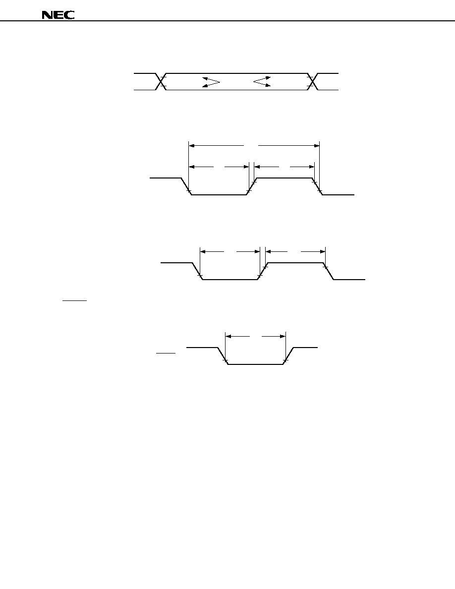
41
µ
PD178004A, 178006A, 178016A, 178018A
AC TIMING TEST POINT (EXCLUDING X1 INPUT)
0.8 V
DD
0.2 V
DD
0.8 V
DD
0.2 V
DD
Test Points
TI Timing
t
TIL
t
TIH
1/f
TI
TI1, TI2
Interrupt Input Timing
t
INTL
t
INTH
INTP0 to INTP6
RESET Input Timing
t
RSL
RESET

42
µ
PD178004A, 178006A, 178016A, 178018A
SERIAL TRANSFER TIMING
3-Wire Serial I/O Mode:
t
KCYm
t
KLm
t
KHm
SCK0, SCK1
SI0, SI1
SO0, SI1
t
SIKm
t
KSIm
t
KSOm
Input Data
Output Data
t
Rn
t
Fn
Remark m = 1, 2, 9, 10
n = 2, 10
SBI Mode (Bus Release Signal Transfer):
t
SIK3, 4
t
KCY3, 4
t
KL3, 4
t
KH3, 4
SCK0
t
SBL
t
SBH
t
KSB
t
SBK
t
KSI3, 4
t
KSO3, 4
SB0, SB1
t
R4
t
F4
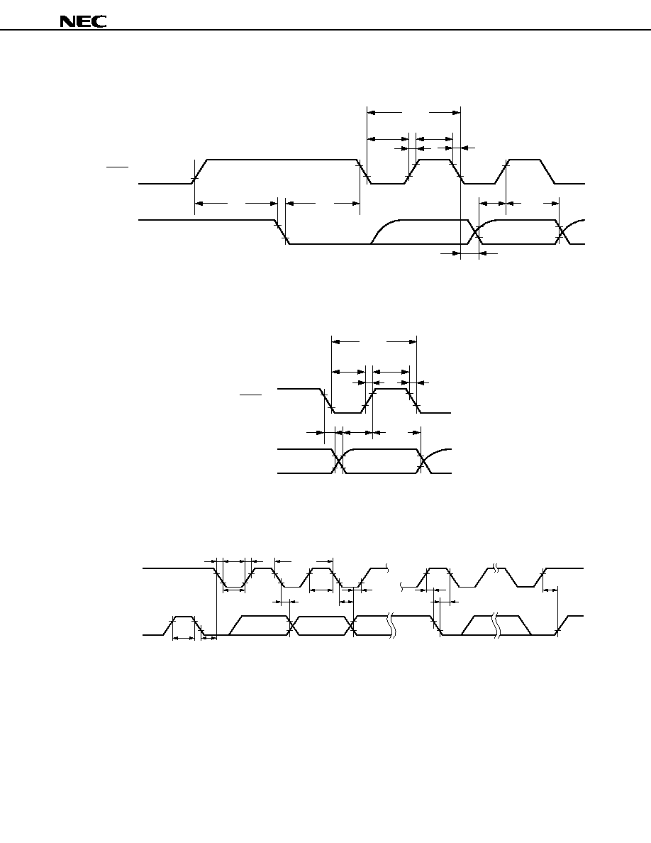
43
µ
PD178004A, 178006A, 178016A, 178018A
SBI Mode (Command Signal Transfer):
t
SIK3, 4
t
KCY3, 4
t
KL3, 4
t
KH3, 4
SCK0
t
KSB
t
SBK
t
KSI3, 4
t
KSO3, 4
SB0, SB1
t
R4
t
F4
2-Wire Serial I/O Mode:
t
KSO5, 6
t
SIK5, 6
t
KCY5, 6
t
KL5, 6
t
KH5, 6
SCK0
t
KSI5, 6
SB0, SB1
t
F6
t
R6
I
2
C Bus Mode:
SCL
SDA0, SDA1
t
SBH
t
KL7, 8
t
SBK
t
F8
t
R8
t
KCY7, 8
t
KSI7, 8
t
KH7, 8
t
SIK7, 8
t
KSO7, 8
t
SBK
t
KSB
t
KSB

44
µ
PD178004A, 178006A, 178016A, 178018A
3-Wire Serial I/O Mode with Automatic Transmit/Receive Function:
t
SBW
t
SBD
t
KCY11
,
12
t
KH11
,
12
t
KSI11
,
12
t
KSO11
,
12
t
SIK11
,
12
D2
D1
D0
D7
D7
D2
D1
D0
SO1
SI1
SCK1
STB
t
R12
t
KL11
,
12
t
F12
3-Wire Serial I/O Mode with Automatic Transmit/Receive Function (Busy Processing):
t
BYS
SCK1
t
SPS
BUSY
(Active high)
7
8
9
Note
10
Note
10 + n
Note
1
t
BYH
Note
The signal is not actually driven low here; it is shown as such to indicate the timing.
45
µ
PD178004A, 178006A, 178016A, 178018A
A/D CONVERTER CHARACTERISTICS (T
A
= ≠40 to +85
∞
C, V
DD
= 4.5 to 5.5 V)
Remarks 1. f
XX
: System clock frequency (f
X
/2)
2. f
X
: System clock oscillation frequency
PLL CHARACTERISTICS (T
A
= ≠40 to +85
∞
C, V
DD
= 4.5 to 5.5 V)
IFC CHARACTERISTICS (T
A
= ≠40 to +85
∞
C, V
DD
= 4.5 to 5.5 V)
Note
The condition of a sine wave input of V
IN
= 0.1 V
p-p
is the standard value for operation of this device during
stand-alone operation, so in consideration of the effect of noise, it is recommended that operation be at
an input amplitude condition of V
IN
= 0.15 V
p-p
.
Parameter
Symbol
Test Conditions
MIN.
TYP.
MAX.
Unit
Resolution
8
8
8
bit
Conversion total
±
3.0
LSB
error
Conversion time
t
CONV
22.2
44.4
µ
s
Sampling time
t
SAMP
15/f
XX
µ
s
Analog input
V
IAN
0
V
DD
V
voltage
Parameter
Symbol
Test Conditions
MIN.
TYP.
MAX.
Unit
Operating
f
IN1
VCOL Pin MF Mode Sine wave input V
IN
= 0.1 V
p-p
0.5
3
MHz
Frequency
f
IN2
VCOL Pin HF Mode Sine wave input V
IN
= 0.2 V
p-p
9
55
MHz
f
IN3
VCOH Pin VHF Mode Sine wave input V
IN
= 0.15 V
p-p
60
160
MHz
Parameter
Symbol
Test Conditions
MIN.
TYP.
MAX.
Unit
Operating
f
IN4
AMIFC Pin AMIF Count Mode
0.4
0.5
MHz
Frequency
Sine wave input V
IN
= 0.1 V
p-p
Note
f
IN5
FMIFC Pin FMIF Count Mode
10
11
MHz
Sine wave input V
IN
= 0.1 V
p-p
Note
f
IN6
FMIFC Pin AMIF Count Mode
0.4
0.5
MHz
Sine wave input V
IN
= 0.1 V
p-p
Note

46
µ
PD178004A, 178006A, 178016A, 178018A
11. PACKAGE DRAWINGS
80 PIN PLASTIC QFP (14
◊
14)
ITEM
MILLIMETERS
INCHES
NOTE
Each lead centerline is located within 0.13 mm (0.005 inch) of
its true position (T.P.) at maximum material condition.
L
0.8±0.2
0.031+0.009
≠0.008
M
0.15
0.006
N
0.10
0.004
P
2.7
0.106
A
17.2±0.4
0.677±0.016
B
14.0±0.2
0.551+0.009
≠0.008
C
14.0±0.2
0.551+0.009
≠0.008
D
17.2±0.4
0.677±0.016
F
0.825
0.032
G
0.825
0.032
H
0.30±0.10
0.012+0.004
≠0.005
I
0.13
0.005
J
0.65 (T.P.)
0.026 (T.P.)
Q
0.1±0.1
0.004±0.004
R
5
∞
±5
∞
5
∞
±5
∞
+0.10
≠0.05
+0.004
≠0.003
M
M
L
K
J
H
Q
P
N
R
detail of lead end
I
G
K
1.6±0.2
0.063±0.008
60
61
40
80
1
21
20
41
A
B
C D
F
S
S80GC-65-3B9-4
S
3.0 MAX.
0.119 MAX.

47
µ
PD178004A, 178006A, 178016A, 178018A
12. RECOMMENDED SOLDERING CONDITIONS
This product should be soldered and mounted under the conditions recommended in the table below.
For detail of recommended soldering conditions, refer to the information document Semiconductor Device
Mounting Technology Manual (C10535E).
For soldering methods and conditions other than those recommended below, contact an NEC sales representative.
Table 12-1. Surface Mounting Type Soldering Conditions
µ
PD178004AGC-
◊◊◊
-3B9 : 80-pin plastic QFP (14
◊
14 mm, 0.65 mm pitch)
µ
PD178006AGC-
◊◊◊
-3B9 : 80-pin plastic QFP (14
◊
14 mm, 0.65 mm pitch)
µ
PD178016AGC-
◊◊◊
-3B9 : 80-pin plastic QFP (14
◊
14 mm, 0.65 mm pitch)
µ
PD178018AGC-
◊◊◊
-3B9 : 80-pin plastic QFP (14
◊
14 mm, 0.65 mm pitch)
Package peak temperature: 235
∞
C, Duration: 30 sec. max. (at 210
∞
C or above),
Number of times: Three times max.
Package peak temperature: 215
∞
C, Duration: 40 sec. max. (at 200
∞
C or above),
Number of times: Three times max.
Solder bath temperature : 260
∞
C max., Duration : 10 sec. max., Number of times
: once, Preheating temperature : 120
∞
C max.
(package surface temperature)
Pin temperature: 300
∞
C max. Duration: 3 sec. max. (per pin row)
Infrared reflow
VPS
Wave soldering
Partial heating
IR35-00-3
VP15-00-3
WS60-00-1
--
Recommended
Condition Symbol
Soldering Conditions
Soldering Method
Caution Do not use different soldering method together (except for partial heating).
48
µ
PD178004A, 178006A, 178016A, 178018A
APPENDIX A. DIFFERENCES BETWEEN
µ
PD178018A AND
µ
PD178018 SUBSERIES
Product name
µ
PD178018A Subseries
µ
PD178018 Subseries
µ
PD178004A
µ
PD178006A
µ
PD178016A
µ
PD178018A
µ
PD178004
µ
PD178006
µ
PD178016
µ
PD178018
Item
µ
PD178P018A
Note
µ
PD178P018
PLL
Reference
7 types selectable by program
11 types selectable by program
frequency
frequency
(1, 3, 5, 9, 10, 25, 50 kHz)
(1, 1.25, 2.5, 3, 5, 6.25, 9, 10, 12.5, 25, 50 kHz)
synthe-
EO0 pin output
Buffer type
sizer
format
EO1 pin output
Buffer type
Constant-current power supply type
format
EO1 pin high-
Not supported
Supported
Not supported
impedance function
Note
Under development
Remark The mask ROM of mask versions (
µ
PD178018A and
µ
PD178018) is replaced with one-time PROM
or EPROM in the one-time PROM versions (
µ
PD178P018A and
µ
PD178P018).

49
µ
PD178004A, 178006A, 178016A, 178018A
RA78K/0
Notes 1, 2, 3, 4
78K/0 Series common assembler package
CC78K/0
Notes 1, 2, 3, 4
78K/0 Series common C compiler package
DF178018
Notes 1, 2, 3, 4, 8
µ
PD178018A Subseries common device file
CC78K/0-L
Notes 1, 2, 3, 4
78K/0 Series common C compiler library source file
PROM Writing Tools
PG-1500
PROM programmer
PG-178P018GC
Programmer adapters connected to a PG-1500
PA-178P018KK-T
PG-1500 controller
Notes 1, 2
PG-1500 control program
Debugging Tools
IE-78000-R
In-circuit emulator common to 78K/0 Series
IE-78000-R-A
In-circuit emulator common to 78K/0 Series (for the integration debugger)
IE-78000-R-BK
Break board common to 78K/0 Series
IE-178018-R-EM
Emulation board common to
µ
PD178018A Subseries
IE-78000-R-SV3
Interface adapter and cable when using EWS as a host machine (for IE-78000-R-A)
IE-70000-98-IF-B
Interface adapter when using the PC-9800 Series (except notebooks) as a host machine
(for IE-78000-R-A)
IE-70000-98N-IF
Interface adapter and cable when using the PC-9800 Series notebook as a host machine
(for IE-78000-R-A)
IE-70000-PC-IF-B
Interface adapter when using IBM PC/AT
TM
as a host machine (for IE-78000-R-A)
EP-78230GC-R
Emulation probe common to
µ
PD78234 Subseries
EV-9200GC-80
Socket for mounting on target system board created for 80-pin plastic QFP (GC-3B9 type)
EV-9900
Jig used when removing the
µ
PD178P018AKK-T from the EV-9200GC-80.
SM78K0
Notes 5, 6, 7
78K/0 Series common system simulator
ID78K0
Notes 4, 5, 6, 7
Integration debugger for IE-78000-R-A
SD78K/0
Notes 1, 2
IE-78000-R screen debugger
DF178018
Notes 1, 2, 4, 5, 6, 7, 8
µ
PD178018A Subseries device file
APPENDIX B. DEVELOPMENT TOOLS
The following development tools are available for system development using the
µ
PD178018A Subseries.
Language Processing Software
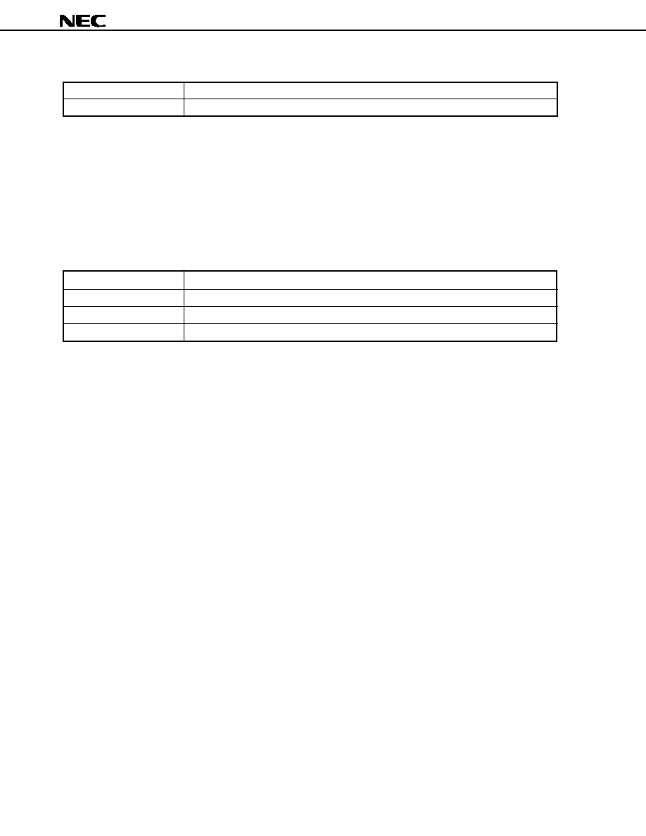
50
µ
PD178004A, 178006A, 178016A, 178018A
Fuzzy Inference Development Support System
FE9000
Note 1
/FE9200
Note 2
Fuzzy knowledge data creation tool
FT9080
Note 1
/FT9085
Note 3
Translator
FI78K0
Notes 1, 3
Fuzzy inference module
FD78K0
Notes 1, 3
Fuzzy inference debugger
Notes 1. PC-9800 Series (MS-DOS) based
2. IBM PC/AT and its compatibles (PC DOS/IBM DOS/MS-DOS + Windows) based
3. IBM PC/AT and its compatibles (PC DOS/IBM DOS/MS-DOS) based
Remarks 1. Please refer to the 78K/0 Series Selection Guide (U11126E) for information on third party
development tools.
2. The RA78K/0, CC78K/0, SD78K/0, ID78K/0, SM78K/0 and RX78K/0 are used in combination with
the DF178018.
Real-Time OS
RX78K/0
Notes 1, 2, 3, 4
78K/0 Series real-time OS
MX78K0
Notes 1, 2, 3, 4
78K/0 Series OS
Notes 1. PC-9800 Series (MS-DOS
TM
) based
2. IBM PC/AT and compatible (PC DOS
TM
/IBM-DOS
TM
/MS-DOS) based
3. HP9000 Series 300
TM
based
4. HP9000 Series 700
TM
(HP-UX
TM
) based, SPARCstation
TM
(SunOS
TM
) based, EWS4800 Series
(EWS-UX/V) based
5. PC-9800 Series (MS-DOS + Windows
TM
) based
6. IBM PC/AT and compatible (PC DOS/IBM DOS/MS-DOS + Windows) based
7. NEWS
TM
(NEWS-OS
TM
) based
8. Under development
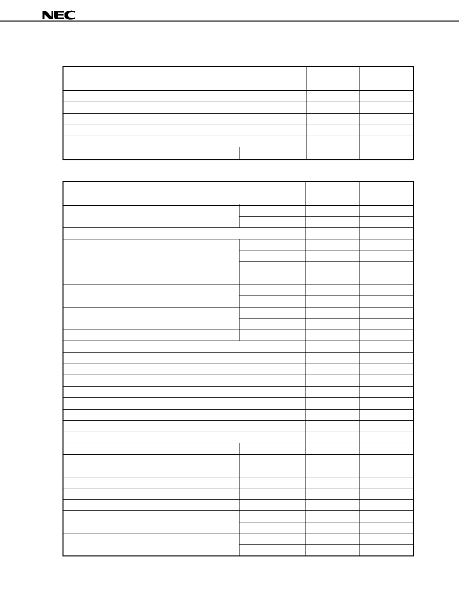
51
µ
PD178004A, 178006A, 178016A, 178018A
Device Documents
Title
Document No.
Document No.
(Japanese)
(English)
µ
PD178018A Subseries User's Manual
To be prepared
To be prepared
78K/0 Series User's Manual--Instruction
U12326J
U12326E
78K/0 Series Instruction Set
U10904J
--
78K/0 Series Instruction Table
U10903J
--
µ
PD178018A Subseries Special Function Register Table
To be prepared
--
78K/0 Series Application Note
Basics (II)
U10121J
U10121E
Development Tool Documents (User's Manual)
Title
Document No.
Document No.
(Japanese)
(English)
RA78K Series Assembler Package
Operation
EEU-809
EEU-1399
Language
EEU-815
EEU-1404
RA78K Series Structured Assembler Preprocessor
EEU-817
EEU-1402
RA78K0 Assembler Package
Operation
U11802J
U11802E
Assembly Language
U11801J
U11801E
Structured Assembly
U11789J
U11789E
Language
CC78K Series C Compiler
Operation
EEU-656
EEU-1280
Language
EEU-655
EEU-1284
CC78K/0 C Compiler
Operation
U11517J
U11517E
Language
U11518J
U11518E
CC78K/0 C Compiler Application Notes
Programming Know-how
EEA-618
EEA-1208
CC78K Series Library Source File
U12322J
--
PG-1500 PROM Programmer
U11940J
EEU-1335
PG-1500 Controller PC-9800 Series (MS-DOS) Based
EEU-704
EEU-1291
PG-1500 Controller IBM PC Series (PC DOS) Based
EEU-5008
U10540E
IE-78000-R
U11376J
U11376E
IE-78000-R-A
U10057J
U10057E
IE-78000-R-BK
EEU-867
EEU-1427
IE-178018-R-EM
U10668J
U10668E
EP-78230
EEU-985
EEU-1515
SM78K0 System Simulator Windows Based
Reference
U10181J
U10181E
SM78K Series System Simulator
U10092J
U10092E
ID78K0 Integrated Debugger EWS Based
Reference
U11151J
U11151E
ID78K0 Integrated Debugger PC Based
Reference
U11539J
U11539E
ID78K0 Integrated Debugger Windows Based
Guide
U11649J
U11649E
SD78K/0 Screen Debugger PC-9800 Series (MS-DOS) Based
Introduction
EEU-852
U10539E
Reference
U10952J
--
SD78K/0 Screen Debugger IBM PC/AT (PC DOS) Based
Introduction
EEU-5024
EEU-1414
Reference
U11279J
U11279E
APPENDIX C. RELATED DOCUMENTS
External Parts User
open Interface
Specifications
Caution The contents of the above documents are subject to change without notice. Please ensure that
the latest versions are used in design work, etc.
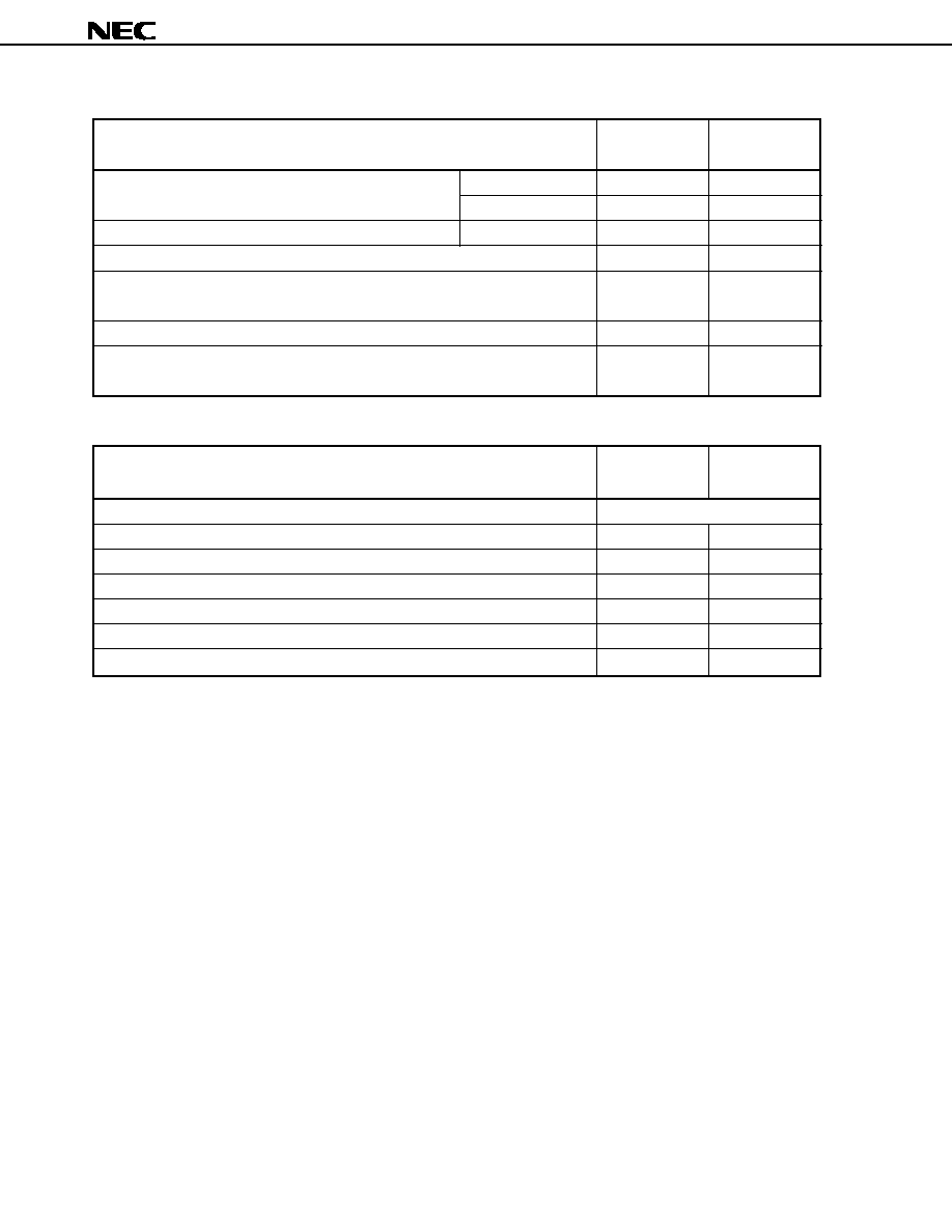
52
µ
PD178004A, 178006A, 178016A, 178018A
Title
Document No.
Document No.
(Japanese)
(English)
78K/0 Series Realtime OS
Basics
U11537J
--
Installation
U11536J
--
78K/0 Series OS MX78K0
Basics
U12257J
--
Fuzzy Knowledge Data Creation Tool
EEU-829
EEU-1438
78K/0, 78K/II, 87AD Series
EEU-862
EEU-1444
Fuzzy Inference Development Support System--Translator
78K/0 Series Fuzzy Inference Development Support System--Fuzzy Inference Module
EEU-858
EEU-1441
78K/0 Series Fuzzy Inference Development Support System
EEU-921
EEU-1458
--Fuzzy Inference Debugger
Other Documents
Title
Document No.
Document No.
(Japanese)
(English)
IC Package Manual
C10943X
Semiconductor Device Mounting Technology Manual
C10535J
C10535E
Quality Guides on NEC Semiconductor Devices
C11531J
C11531E
NEC Semiconductor Device Reliability and Quality Control
C10983J
C10983E
Electrostatic Discharge (ESD) Test
MEM-539
--
Semiconductor Device Quality Assurance Guide
C11893J
MEI-1202
Microcomputer-related Product Guide (Products by other Manufacturers)
U11416J
--
Related Documents for Embedded Software (User's Manual)
Caution The contents of the above documents are subject to change without notice. Ensure that the
latest versions are used in design work, etc.

53
µ
PD178004A, 178006A, 178016A, 178018A
[MEMO]

54
µ
PD178004A, 178006A, 178016A, 178018A
NOTES FOR CMOS DEVICES
1
PRECAUTION AGAINST ESD FOR SEMICONDUCTORS
Note: Strong electric field, when exposed to a MOS device, can cause destruction of
the gate oxide and ultimately degrade the device operation. Steps must be
taken to stop generation of static electricity as much as possible, and quickly
dissipate it once, when it has occurred. Environmental control must be
adequate. When it is dry, humidifier should be used. It is recommended to avoid
using insulators that easily build static electricity. Semiconductor devices
must be stored and transported in an anti-static container, static shielding bag
or conductive material. All test and measurement tools including work bench
and floor should be grounded. The operator should be grounded using wrist
strap. Semiconductor devices must not be touched with bare hands. Similar
precautions need to be taken for PW boards with semiconductor devices on it.
2
HANDLING OF UNUSED INPUT PINS FOR CMOS
Note: No connection for CMOS device inputs can be cause of malfunction. If no
connection is provided to the input pins, it is possible that an internal input level
may be generated due to noise, etc., hence causing malfunction. CMOS device
behave differently than Bipolar or NMOS devices. Input levels of CMOS devices
must be fixed high or low by using a pull-up or pull-down circuitry. Each unused
pin should be connected to V
DD
or GND with a resistor, if it is considered to have
a possibility of being an output pin. All handling related to the unused pins must
be judged device by device and related specifications governing the devices.
3
STATUS BEFORE INITIALIZATION OF MOS DEVICES
Note: Power-on does not necessarily define initial status of MOS device. Production
process of MOS does not define the initial operation status of the device.
Immediately after the power source is turned ON, the devices with reset function
have not yet been initialized. Hence, power-on does not guarantee out-pin
levels, I/O settings or contents of registers. Device is not initialized until the
reset signal is received. Reset operation must be executed immediately after
power-on for devices having reset function.

55
µ
PD178004A, 178006A, 178016A, 178018A
NEC Electronics Inc. (U.S.)
Santa Clara, California
Tel: 800-366-9782
Fax: 800-729-9288
NEC Electronics (Germany) GmbH
Duesseldorf, Germany
Tel: 0211-65 03 02
Fax: 0211-65 03 490
NEC Electronics (UK) Ltd.
Milton Keynes, UK
Tel: 01908-691-133
Fax: 01908-670-290
NEC Electronics Italiana s.r.1.
Milano, Italy
Tel: 02-66 75 41
Fax: 02-66 75 42 99
NEC Electronics Hong Kong Ltd.
Hong Kong
Tel: 2886-9318
Fax: 2886-9022/9044
NEC Electronics Hong Kong Ltd.
Seoul Branch
Seoul, Korea
Tel: 02-528-0303
Fax: 02-528-4411
NEC Electronics Singapore Pte. Ltd.
United Square, Singapore 1130
Tel: 253-8311
Fax: 250-3583
NEC Electronics Taiwan Ltd.
Taipei, Taiwan
Tel: 02-719-2377
Fax: 02-719-5951
NEC do Brasil S.A.
Sao Paulo-SP, Brasil
Tel: 011-889-1680
Fax: 011-889-1689
NEC Electronics (Germany) GmbH
Benelux Office
Eindhoven, The Netherlands
Tel: 040-2445845
Fax: 040-2444580
NEC Electronics (France) S.A.
Velizy-Villacoublay, France
Tel: 01-30-67 58 00
Fax: 01-30-67 58 99
NEC Electronics (France) S.A.
Spain Office
Madrid, Spain
Tel: 01-504-2787
Fax: 01-504-2860
NEC Electronics (Germany) GmbH
Scandinavia Office
Taeby, Sweden
Tel: 08-63 80 820
Fax: 08-63 80 388
Regional Information
Some information contained in this document may vary from country to country. Before using any NEC
product in your application, please contact the NEC office in your country to obtain a list of authorized
representatives and distributors. They will verify:
∑ Device availability
∑ Ordering information
∑ Product release schedule
∑ Availability of related technical literature
∑ Development environment specifications (for example, specifications for third-party tools and
components, host computers, power plugs, AC supply voltages, and so forth)
∑ Network requirements
In addition, trademarks, registered trademarks, export restrictions, and other legal issues may also vary
from country to country.
J96. 8
56
µ
PD178004A, 178006A, 178016A, 178018A
Purchase of NEC I
2
C components conveys a license under the Philips I
2
C Patent Rights to use these components in an I
2
C
system, provided that the system conforms to the I
2
C Standard Specification as defined by Philips.
M4 96.5
No part of this document may be copied or reproduced in any form or by any means without the prior written
consent of NEC Corporation. NEC Corporation assumes no responsibility for any errors which may appear in
this document.
NEC Corporation does not assume any liability for infringement of patents, copyrights or other intellectual property
rights of third parties by or arising from use of a device described herein or any other liability arising from use
of such device. No license, either express, implied or otherwise, is granted under any patents, copyrights or other
intellectual property rights of NEC Corporation or others.
While NEC Corporation has been making continuous effort to enhance the reliability of its semiconductor devices,
the possibility of defects cannot be eliminated entirely. To minimize risks of damage or injury to persons or
property arising from a defect in an NEC semiconductor device, customers must incorporate sufficient safety
measures in its design, such as redundancy, fire-containment, and anti-failure features.
NEC devices are classified into the following three quality grades:
"Standard", "Special", and "Specific". The Specific quality grade applies only to devices developed based on a
customer designated "quality assurance program" for a specific application. The recommended applications of
a device depend on its quality grade, as indicated below. Customers must check the quality grade of each device
before using it in a particular application.
Standard: Computers, office equipment, communications equipment, test and measurement equipment,
audio and visual equipment, home electronic appliances, machine tools, personal electronic
equipment and industrial robots
Special:
Transportation equipment (automobiles, trains, ships, etc.), traffic control systems, anti-disaster
systems, anti-crime systems, safety equipment and medical equipment (not specifically designed
for life support)
Specific:
Aircrafts, aerospace equipment, submersible repeaters, nuclear reactor control systems, life
support systems or medical equipment for life support, etc.
The quality grade of NEC devices is "Standard" unless otherwise specified in NEC's Data Sheets or Data Books.
If customers intend to use NEC devices for applications other than those specified for Standard quality grade,
they should contact an NEC sales representative in advance.
Anti-radioactive design is not implemented in this product.
The export of this product from Japan is regulated by the Japanese government. To export this product may be
prohibited without governmental license, the need for which must be judged by the customer. The export or re-
export of this product from a country other than Japan may also be prohibited without a license from that country.
Please call an NEC sales representative.
The related documents indicated in this publication may include preliminary versions.
However, preliminary versions are not marked as such.
MS-DOS and Windows are either registered trademarks or trademarks of Microsoft Corporation in the United
States and/or other countries.
IBM DOS, PC/AT, and PC DOS are trademarks of International Business Machines Corporation.
HP9000 Series 300, HP9000 series 700, and HP-UX are trademarks of Hewlett-Packard Company.
SPARCstation is a trademark of SPARC International, Inc.
SunOS is a trademark of Sun Microsystems, Inc.
NEWS and NEWS-OS are trademarks of Sony Corporation.