 | –≠–ª–µ–∫—Ç—Ä–æ–Ω–Ω—ã–π –∫–æ–º–ø–æ–Ω–µ–Ω—Ç: UPD178098 | –°–∫–∞—á–∞—Ç—å:  PDF PDF  ZIP ZIP |
Document Outline
- COVER
- DESCRIPTION
- FEATURES
- APPLICATION FIELD
- ORDERING INFORMATION
- DEVELOPMENT OF 8-BIT DTS SERIES
- FUNCTIONAL OUTLINE
- PIN CONFIGURATION (Top View)
- BLOCK DIAGRAM
- 1. PIN FUNCTION LIST
- 1.1 Port Pins
- 1.2 Pins Other Than Port Pins
- 1.3 I/O Circuits of Pins and Recommended Connections of Unused Pins
- 2. MEMORY SPACE
- 2.1 Memory Size Select Register (IMS)
- 2.2 Internal Extension RAM Size Select Register (IXS)
- 3. FEATURES OF PERIPHERAL HARDWARE FUNCTIONS
- 3.1 Ports
- 3.2 Clock Generation Circuit
- 3.3 Timers
- 3.4 Buzzer Output Control Circuit
- 3.5 A/D Converter
- 3.6 Serial Interface
- 3.7 IEBus Controller (uPD178096 and 178098 only)
- 3.8 PLL Frequency Synthesizer
- 3.9 Frequency Counter
- 4. INTERRUPT FUNCTION
- 5. STANDBY FUNCTION
- 6. RESET FUNCTION
- 7. INSTRUCTION SET
- 8. ELECTRICAL SPECIFICATIONS
- 9. PACKAGE DRAWING
- 10. RECOMMENDED SOLDERING CONDITIONS
- APPENDIX A. DEVELOPMENT TOOLS
- APPENDIX B. RELATED DOCUMENTS

©
1997, 2000
DATA SHEET
DESCRIPTION
The
µ
PD178076, 178078, 178096, and 178098 are 8-bit single-chip CMOS microcontrollers containing hardware
for digital tuning systems.
These microcontrollers employ a 78K/0 series architecture CPU and allow easy access to internal memories at
high speed and easy control of peripheral hardware units. The high-speed 78K/0 series instructions are ideal for
system control.
As peripheral hardware, a prescaler, PLL frequency synthesizer, and frequency counter for digital tuning systems
are provided, as well as many I/O ports, timers, A/D converter, serial interface, and a power-ON clear circuit. In
addition, the
µ
PD178076 and 178078 have an asynchronous serial interface (UART) mode, and the
µ
PD178096 and
178098 have an IEBus
TM
controller.
Moreover, a flash memory model, the
µ
PD178F098, that operates in the same supply voltage range as the mask
ROM models, and various development tools are also under development.
For the detailed functional description, refer to the following User's Manuals:
µ
PD178078, 178098 Subseries User's Manual : U12790E
78K/0 Series User's Manual - Instruction
: U12326E
FEATURES
∑
High-capacity ROM and RAM
Item Program Memory (ROM)
Data Memory
Part Number
Internal high-speed RAM Internal buffer RAM
Internal extension RAM
µ
PD178076, 178096
48K bytes
1024 bytes
32 bytes
1024 bytes
µ
PD178078, 178098
60K bytes
2048 bytes
MOS INTEGRATED CIRCUIT
µ
PD178076,178078,178096,178098
Document No. U12885EJ3V0DS00
Date Published June 2000 N CP(K)
Printed in Japan
8-BIT SINGLE-CHIP MICROCONTROLLER
∑
Instruction cycle:
0.32
µ
s (with crystal resonator of f
X
= 6.3 MHz)
∑
Many internal hardware units
General-purpose I/O ports, A/D converter, serial
interface (UART mode:
µ
PD178076 and 178078
only), IEBus controller (
µ
PD178096 and 178098
only), timers, frequency counter, power-ON clear
circuit
∑
Hardware for PLL frequency synthesizer
dual modulus prescaler, programmable divider,
phase comparator, charge pump
∑
Vectored interrupt sources
∑
µ
PD178076, 178078: 22
∑
µ
PD178096, 178098: 21
∑
Supply voltage
:V
DD
= 4.5 to 5.5 V (during PLL and CPU
operations)
:V
DD
= 3.5 to 5.5 V (during CPU operation)
The information in this document is subject to change without notice. Before using this document, please
confirm that this is the latest version.
Not all devices/types available in every country. Please check with local NEC representative for availability
and additional information.
The mark shows major revised points.

2
µ
PD178076, 178078, 178096, 178098
Data Sheet U12885EJ3V0DS00
APPLICATION FIELD
Car stereos
ORDERING INFORMATION
Part Number
Package
µ
PD178076GF-
◊◊◊
-3BA
100-pin plastic QFP (14
◊
20)
µ
PD178078GF-
◊◊◊
-3BA
100-pin plastic QFP (14
◊
20)
µ
PD178096GF-
◊◊◊
-3BA
100-pin plastic QFP (14
◊
20)
µ
PD178098GF-
◊◊◊
-3BA
100-pin plastic QFP (14
◊
20)
Remark
◊◊◊
indicates ROM code suffix, which is E
◊◊
when the I
2
C bus is used.
3
µ
PD178076, 178078, 178096, 178098
Data Sheet U12885EJ3V0DS00
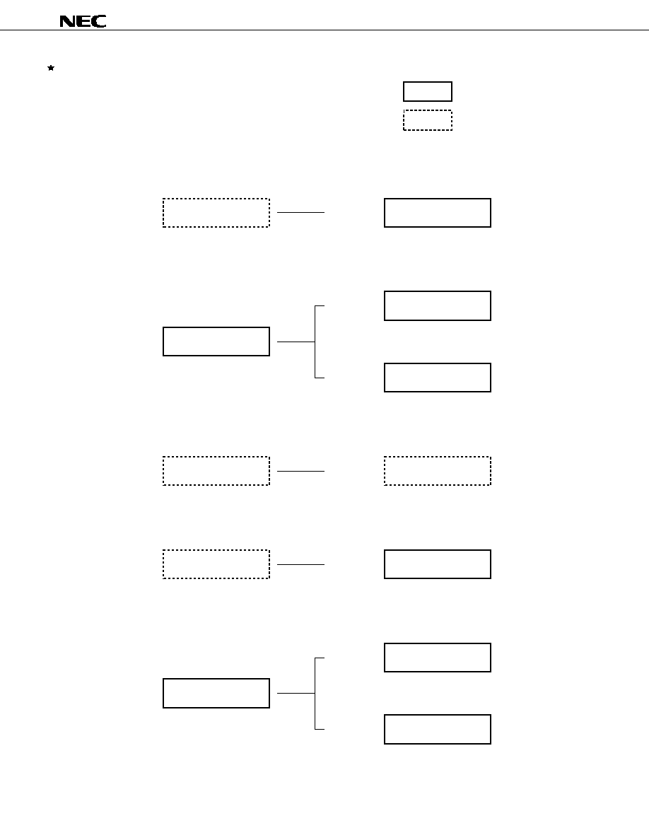
DEVELOPMENT OF 8-BIT DTS SERIES
Models under mass production
Models under development
100 pins
100 pins
100 pins
Internal IEBus controller
Internal IEBus controller and UART
Internal UART
PD178098 subseries
µ
PD178078 subseries
µ
PD178048 subseries
µ
µ
µ
µ
µ
80 pins
80 pins
Internal OSD controller
8-bit PWM
◊
4 channels
14-bit PWM
◊
1 channel
PD178F048
µ
PD178F098
µ
PD178F134
µ
PD178F124
µ
PD178P018A
µ
80 pins
80 pins
Internal LCD and UART
Internal LCD and UART
PD178034 subseries
Internal OSD controller
8-bit PWM
◊
4 channels
14-bit PWM
◊
1 channel
80 pins
80 pins
Internal UART
Internal UART
PD178024 subseries
80 pins
80 pins
80 pins
Limits functions of PD178018A subseries
µ
PD178018A subseries
PD178003 subseries
Flash memory model or
PROM model
Mask ROM model

4
µ
PD178076, 178078, 178096, 178098
Data Sheet U12885EJ3V0DS00
(1/2)
Item
µ
PD178076
µ
PD178078
µ
PD178096
µ
PD178098
Internal
ROM
48K bytes
60K bytes
48K bytes
60K bytes
memory
High-speed RAM 1024 bytes
Buffer RAM
32 bytes
Extension RAM
1024 bytes
2048 bytes
1024 bytes
2048 bytes
General-purpose register
8 bits
◊
32 registers (8 bits
◊
8 registers
◊
4 banks)
Minimum instruction execution
∑ 0.32
µ
s/0.64
µ
s/1.27
µ
s/2.54
µ
s/5.08
µ
s (with crystal resonator of f
X
= 6.3 MHz)
time
∑ 0.44
µ
s/0.89
µ
s/1.78
µ
s/3.56
µ
s/7.11
µ
s (with crystal resonator of f
X
= 4.5 MHz)
Note 1
Instruction set
∑ 16-bit operation
∑ Multiplication/division (8 bits
◊
8 bits, 16 bits
˜
8 bits)
∑ Bit manipulation (set, reset, test Boolean operation)
∑ BCD adjustment, etc.
I/O port
Total
: 80 pins
∑ CMOS input
:
8 pins
∑ CMOS I/O
: 64 pins
∑ N-ch open-drain output :
8 pins
A/D converter
8-bit resolution
◊
8 channels
Serial interface
∑ 3-wire/SBI/2-wire/I
2
C bus
Note 2
mode
selectable: 1 channel
∑ 3-wire mode: 1 channel
∑ 3-wire mode (with automatic transmit/
receive function of up to 32 bytes):
1 channel
∑ UART mode: 1 channel
IEBus controller
Not provided
Provided
Timer
∑ Basic timer (timer carry FF (10 Hz))
: 1 channel
∑ 16-bit timer/event counter
: 1 channel
∑ 8-bit timer/event counter
: 2 channels
∑ Watchdog timer
: 1 channel
Buzzer output
BEEP0 pin: 1 kHz, 1.5 kHz, 3 kHz, 4 kHz
BUZ pin: 0.77 kHz, 1.54 kHz, 3.08 kHz, 6.15 kHz (with crystal resonator of f
X
= 6.3 MHz)
∑ 3-wire/SBI/2-wire/I
2
C bus
Note 2
mode
selectable: 1 channel
∑ 3-wire mode: 1 channel
∑ 3-wire mode (with automatic transmit/
receive function of up to 32 bytes):
1 channel
FUNCTIONAL OUTLINE
Notes 1. When using the IEBus controller of the
µ
PD178096 or 178098, the 4.5-MHz crystal resonator cannot
be used. Use the 6.3-MHz crystal resonator.
2. When the I
2
C bus mode is used (including when the mode is implemented in software without using
the peripheral hardware), consult NEC when ordering a mask.

5
µ
PD178076, 178078, 178096, 178098
Data Sheet U12885EJ3V0DS00
(2/2)
Item
µ
PD178076
µ
PD178078
µ
PD178096
µ
PD178098
Vectored
Maskable
Internal : 13
Internal : 12
interrupt
External: 8
External: 8
source
Non-maskable
Internal: 1
Software
1
PLL
Division mode
2 types
frequency
∑ Direct division mode (VCOL pin)
synthesizer
∑ Pulse swallow mode (VCOL and VCOH pins)
Reference
Seven types selectable in software (1, 3, 9, 10, 12.5, 25, 50 kHz)
frequency
Charge pump
Error out output: 2 pins
Phase
Unlock detectable in software
comparator
Frequency counter
Frequency measurement
∑ AMIFC pin: For 450-kHz counting
∑ FMIFC pin: For 450-kHz/10.7-MHz counting
Standby function
∑ HALT mode
∑ STOP mode
Reset
∑ Reset by RESET pin
∑ Internal reset by watchdog timer
∑ Reset by power-ON clear circuit
∑ Detection of less than 4.5 V
Note
(Reset does not occur, however.)
∑ Detection of less than 3.5 V
Note
(during CPU operation)
∑ Detection of less than 2.3 V
Note
(in STOP mode)
Supply voltage
∑ V
DD
= 4.5 to 5.5 V (during CPU, PLL operation)
∑ V
DD
= 3.5 to 5.5 V (during CPU operation)
Package
∑ 100-pin plastic QFP (14
◊
20)
Note
These voltages are the maximum values. In practice, the chip may be reset at voltages lower than these.

6
µ
PD178076, 178078, 178096, 178098
Data Sheet U12885EJ3V0DS00
PIN CONFIGURATION (Top View)
∑ 100-pin plastic QFP (14
◊
20)
µ
PD178076GF-
◊◊◊
-3BA, 178078GF-
◊◊◊
-3BA
µ
PD178096GF-
◊◊◊
-3BA, 178098GF-
◊◊◊
-3BA
80
79
78
77
76
75
74
73
72
71
70
69
68
67
66
65
64
63
62
61
60
59
58
57
56
55
54
53
52
51
1
2
3
4
5
6
7
8
9
10
11
12
13
14
15
16
17
18
19
20
21
22
23
24
25
26
27
28
29
30
31 32 33 34 35 36 37 38 39 40 41 42 43 44 45 46 47 48 49 50
100 99 98 97 96 95 94 93 92 91 90 89 88 87 86 85 84 83 82 81
P06/INTP6
P05/INTP5
P04/INTP4
P124
P123
P122
P121 /RX0
P120 /TX0
P77
P76
P75[/TXD0]
P74[/RXD0]
P137
P136
P135
P134
P133
P132
P131/TO51
P130/TO50
P37/BUZ
P36/BEEP0
P35/TI51
P34/TI50
P33/TI01
P32/TI00
P31/TO0
P30/VM45
P03/INTP3
P02/INTP2
P00/INTP0
P01/INTP1
P20/SI1
P21/SO1
P22/SCK1
P23/STB
P24/BUSY
P25/SI0/SB0/SDA0
P26/SO0/SB1/SDA1
P27/SCK0/SCL
P70/SI3
P71/SO3
P72/SCK3
P73
P50
P51
P52
P53
P54
P55
P56
P57
P10/ANI0
P11/ANI1
P12/ANI2
P13/ANI3
AV
DD
P14/ANI4
P15/ANI5
P16/ANI6
GNDPORT
V
DD
PORT
P47
P46
P45
P44
P43
P42
P41
P40
P67
P66
P65
P64
P63
P62
P61
P60
GND1
P07/INTP7
P17/ANI7
AV
SS
REGCPU
V
DD
REGOSC
X2
X1
GND0
P100
GND2
P101/AMIFC
P102/FMIFC
V
DD
PLL
VCOH
VCOL
GNDPLL
EO0
EO1
IC
RESET

7
µ
PD178076, 178078, 178096, 178098
Data Sheet U12885EJ3V0DS00
Cautions 1. Directly connect the IC (Internally Connect) pin to GND0, GND1, or GND2.
2. Keep the voltage at AV
DD
, V
DD
PORT, and V
DD
PLL pins same as that at the V
DD
pin.
3. Keep the voltage at AV
SS
, GNDPORT, and GNDPLL pins same as that at GND0, GND1, or
GND2.
4. Connect each of the REGOSC and REGCPU pins to GND via a 0.1-
µ
F capacitor.
Remark [ ] :
µ
PD178076 and 178078 only
{ }:
µ
PD178096 and 178098 only
Pin Name
AMIFC
: AM intermediate frequency counter
input
ANI0-ANI7
: A/D converter input
AV
DD
: A/D converter power supply
AV
SS
: A/D converter ground
BUSY
: Busy output
BEEP0, BUZ
: Buzzer output
EO0, EO1
: Error out output
FMIFC
: FM intermediate frequency counter
input
GNDPLL
: PLL ground
GND0-GND2
: Ground
IC
: Internally connected
INTP0-INTP7
: Interrupt input
P00-P07
: Port 0
P10-P17
: Port 1
P20-P27
: Port 2
P30-P37
: Port 3
P40-P47
: Port 4
P50-P57
: Port 5
P60-P67
: Port 6
P70-P77
: Port 7
P100-P102
: Port 10
P120-P124
: Port 12
P130-P137
: Port 13
REGCPU
: Regulator for CPU power supply
REGOSC
: Regulator for oscillation circuit
RESET
: Reset input
RXD0
Note 1
: UART0 serial data input
RX0
Note 2
: IEBus serial data input
SB0, SB1
: Serial data bus input/output
SCK0, SCK1, SCK3 : Serial clock input/output
SCL
: Serial clock input/output
SDA0, SDA1
: Serial data input/output
SI0, SI1, SI3
: Serial data input
SO0, SO1, SO3
: Serial data output
STB
: Strobe output
TI00, TI01
: 16-bit timer capture trigger input
TI50, TI51
: 8-bit timer clock input
TO0
: 16-bit timer output
TO50, TO51
: 8-bit timer output
TXD0
Note 1
: UART0 serial data output
TX0
Note 2
: IEBus serial data output
VCOL, VCOH
: Local oscillation input
V
DD
PORT
: Port power supply
V
DD
PLL
: PLL power supply
V
DD
: Power supply
VM45
: V
DD
= 4.5 V monitor output
X1, X2
: Crystal resonator
Notes 1.
µ
PD178076 and 178078 only
2.
µ
PD178096 and 178098 only

8
µ
PD178076, 178078, 178096, 178098
Data Sheet U12885EJ3V0DS00
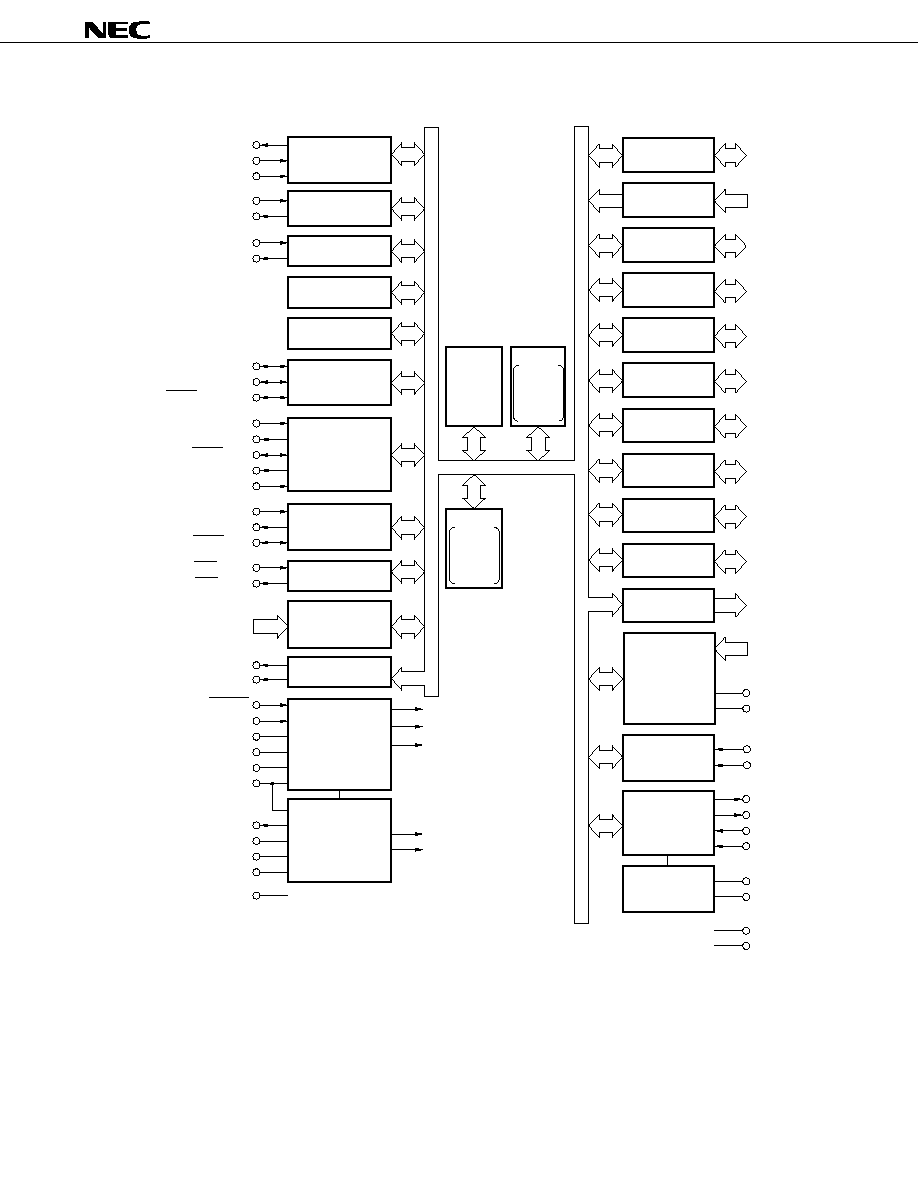
BLOCK DIAGRAM
(1)
µ
PD178076, 178078
16-bit TIMER/
EVENT COUNTER
8-bit TIMER/
EVENT COUNTER 50
8-bit TIMER/
EVENT COUNTER 51
WATCHDOG TIMER
BASIC TIMER
SERIAL
INTERFACE 0
SERIAL
INTERFACE 1
UART0
INTERRUPT
CONTROL
BUZZER OUTPUT
SYSTEM
CONTROL
78K/0
CPU
CORE
ROM
PD178078
: 60 Kbyte
PD178076
: 48 Kbyte
8
8
8
8
8
8
8
8
8
3
5
8
8
P00-P07
A/D
CONVERTER
ANI0/P10-
ANI7/P17
FREQUENCY
COUNTER
PLL
VOLTAGE
REGULATOR
PLL
VOLTAGE
REGULATOR
TI00/P32
TI01/P33
TO0/P31
TI50/P34
TO50/P130
TI51/P35
TO51/P131
SI0/SB0/SDA0/P25
SO0/SB1/SDA1/P26
SCK0/SCL/P27
SERIAL
INTERFACE 3
SI3/P70
SO3/P71
SCK3/P72
SI1/P20
SO1/P21
SCK1/P22
STB/P23
BUSY/P24
RESET
X1
X2
V
DD
PORT
GNDPORT
V
DD
RESET
CPU
PERIPHERAL
VM45/P30
REGOSC
REGCPU
GND0
V
OSC
V
CPU
TXD0/P75
RXD0/P74
INTP0/P00-
INTP7/P07
BEEP0/P36
BUZ/P37
PORT 0
PORT 1
PORT 2
PORT 3
PORT 4
PORT 5
PORT 6
PORT 7
PORT10
PORT 12
PORT 13
P10-P17
P20-P27
P30-P37
P40-P47
P50-P57
P60-P67
P70-P77
P100-P102
P120-P124
P130-P137
AMIFC/P101
FMIFC/P102
EO0
EO1
VCOL
VCOH
V
DD
PLL
GNDPLL
AV
DD
AV
SS
IC
GND2
GND1
RAM
PD178078
: 3 Kbyte
PD178076
: 2 Kbyte
µ
µ
µ
µ
9
µ
PD178076, 178078, 178096, 178098
Data Sheet U12885EJ3V0DS00
(2)
µ
PD178096, 178098
16-bit TIMER/
EVENT COUNTER
8-bit TIMER/
EVENT COUNTER 50
8-bit TIMER/
EVENT COUNTER 51
WATCHDOG TIMER
BASIC TIMER
SERIAL
INTERFACE 0
SERIAL
INTERFACE 1
IEBus0
INTERRUPT
CONTROL
BUZZER OUTPUT
SYSTEM
CONTROL
8
8
8
8
8
8
8
8
8
3
5
8
8
P00-P07
A/D
CONVERTER
ANI0/P10-
ANI7/P17
FREQUENCY
COUNTER
PLL
VOLTAGE
REGULATOR
PLL
VOLTAGE
REGULATOR
TI00/P32
TI01/P33
TO0/P31
TI50/P34
TO50/P130
TI51/P35
TO51/P131
SI0/SB0/SDA0/P25
SO0/SB1/SDA1/P26
SCK0/SCL/P27
SERIAL
INTERFACE 3
SI3/P70
SO3/P71
SCK3/P72
SI1/P20
SO1/P21
SCK1/P22
STB/P23
BUSY/P24
RESET
X1
X2
V
DD
PORT
GNDPORT
V
DD
RESET
CPU
PERIPHERAL
VM45/P30
REGOSC
REGCPU
GND0
V
OSC
V
CPU
RX0/P121
TX0/P120
INTP0/P00-
INTP7/P07
BEEP0/P36
BUZ/P37
PORT 0
PORT 1
PORT 2
PORT 3
PORT 4
PORT 5
PORT 6
PORT 7
PORT10
PORT 12
PORT 13
P10-P17
P20-P27
P30-P37
P40-P47
P50-P57
P60-P67
P70-P77
P100-P102
P120-P124
P130-P137
AMIFC/P101
FMIFC/P102
EO0
EO1
VCOL
VCOH
V
DD
PLL
GNDPLL
AV
DD
AV
SS
IC
GND2
GND1
78K/0
CPU
CORE
ROM
PD178098
: 60 Kbyte
PD178096
: 48 Kbyte
RAM
PD178098
: 3 Kbyte
PD178096
: 2 Kbyte
µ
µ
µ
µ

10
µ
PD178076, 178078, 178096, 178098
Data Sheet U12885EJ3V0DS00
CONTENTS
1.
PIN FUNCTION LIST ...................................................................................................................... 11
1.1 Port Pins .................................................................................................................................. 11
1.2 Pins Other Than Port Pins ...................................................................................................... 12
1.3 I/O Circuits of Pins and Recommended Connections of Unused Pins .............................. 14
2.
MEMORY SPACE ............................................................................................................................ 18
2.1 Memory Size Select Register (IMS) ....................................................................................... 19
2.2 Internal Extension RAM Size Select Register (IXS) ............................................................. 20
3.
FEATURES OF PERIPHERAL HARDWARE FUNCTIONS ......................................................... 21
3.1 Ports ......................................................................................................................................... 21
3.2 Clock Generation Circuit ........................................................................................................ 22
3.3 Timers ...................................................................................................................................... 22
3.4 Buzzer Output Control Circuit ............................................................................................... 26
3.5 A/D Converter .......................................................................................................................... 27
3.6 Serial Interface ........................................................................................................................ 28
3.7 IEBus Controller (
µ
PD178096 and 178098 only) .................................................................. 32
3.8 PLL Frequency Synthesizer ................................................................................................... 35
3.9 Frequency Counter ................................................................................................................. 36
4.
INTERRUPT FUNCTION ................................................................................................................. 37
5.
STANDBY FUNCTION .................................................................................................................... 43
6.
RESET FUNCTION .......................................................................................................................... 43
7.
INSTRUCTION SET ......................................................................................................................... 44
8.
ELECTRICAL SPECIFICATIONS ................................................................................................... 47
9.
PACKAGE DRAWING ..................................................................................................................... 63
10. RECOMMENDED SOLDERING CONDITIONS ............................................................................. 64
APPENDIX A. DEVELOPMENT TOOLS ............................................................................................. 65
APPENDIX B. RELATED DOCUMENTS ............................................................................................ 67

11
µ
PD178076, 178078, 178096, 178098
Data Sheet U12885EJ3V0DS00
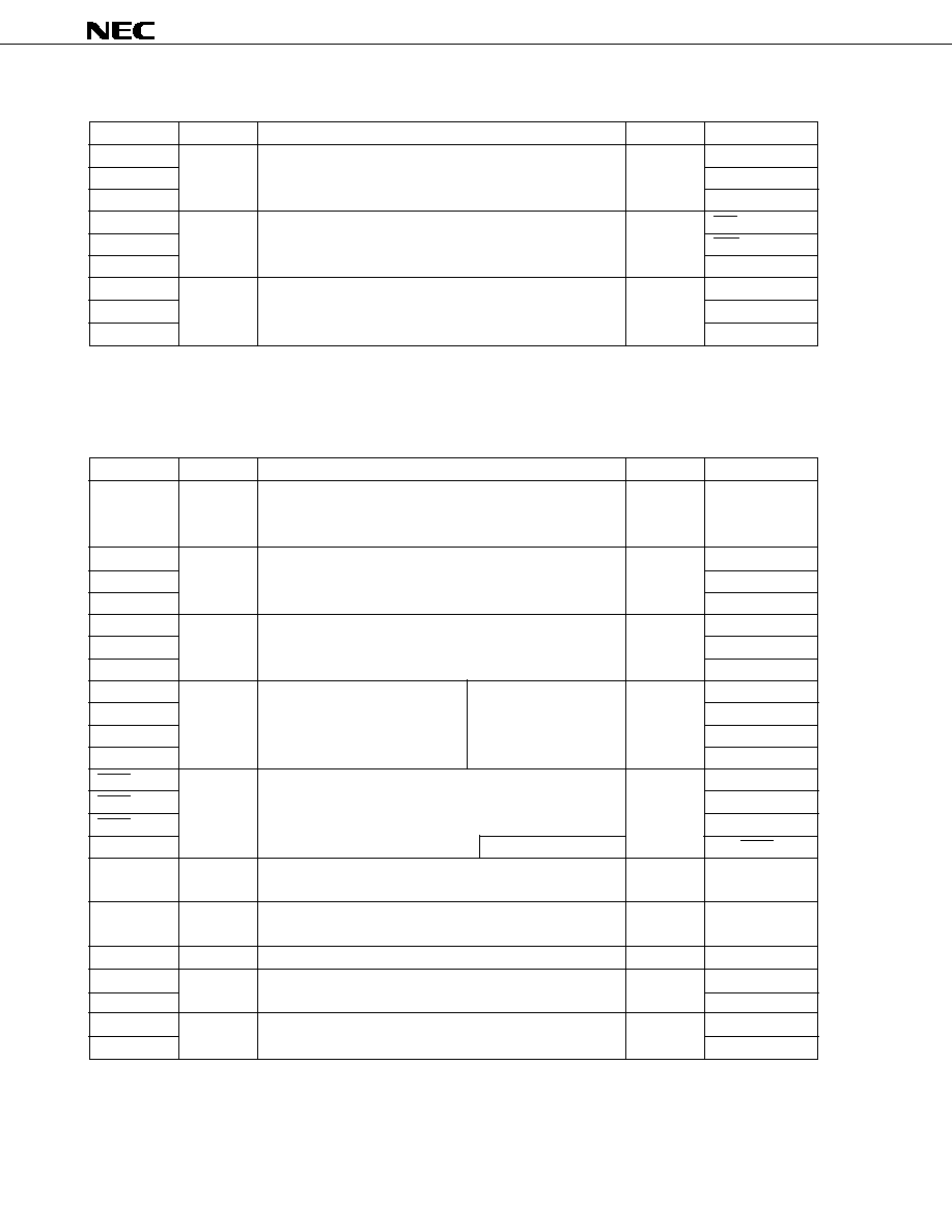
Pin Name
I/O
Function
At Reset
Shared by:
P00-P07
I/O
Port 0.
Input
INTP0-INTP7
8-bit I/O port.
Can be set in input or output mode in 1-bit units.
P10-P17
Input
Port 1.
Input
ANI0-ANI7
8-bit input port.
P20
I/O
Port 2.
Input
SI1
P21
8-bit I/O port.
SO1
P22
Can be set in input or output mode in 1-bit units.
SCK1
P23
STB
P24
BUSY
P25
SI0/SB0/SDA0
P26
SO0/SB1/SDA1
P27
SCK0/SCL
P30
I/O
Port 3.
Input
VM45
P31
8-bit I/O port.
TO0
P32
Can be set in input or output mode in 1-bit units.
TI00
P33
TI01
P34
TI50
P35
TI51
P36
BEEP0
P37
BUZ
P40-47
I/O
Port 4.
Input
≠
8-bit I/O port.
Can be set in input or output mode in 1-bit units.
P50-P57
I/O
Port 5.
Input
≠
8-bit I/O port.
Can be set in input or output mode in 1-bit units.
P60-P67
I/O
Port 6.
Input
≠
8-bit I/O port.
Can be set in input or output mode in 1-bit units.
P70
I/O
Port 7.
Input
SI3
P71
8-bit I/O port.
SO3
P72
Can be set in input or output mode in 1-bit units.
SCK3
P73
≠
P74
RXD0
Note 1
P75
TXD0
Note 1
P76, P77
≠
1. PIN FUNCTION LIST
1.1 Port Pins (1/2)
12
µ
PD178076, 178078, 178096, 178098
Data Sheet U12885EJ3V0DS00
Pin Name
I/O
Function
At Reset
Shared by:
P100
I/O
Port 10.
Input
≠
P101
3-bit I/O port.
AMIFC
P102
Can be set in input or output mode in 1-bit units.
FMIFC
P120
I/O
Port 12.
Input
TX0
Note 2
P121
5-bit I/O port.
RX0
Note 2
P122-P124
Can be set in input or output mode in 1-bit units.
≠
P130
Output
Port 13.
Low-level
TO50
P131
8-bit output port.
output
TO51
P132-P137
N-ch open-drain output port (15 V withstand)
≠
Notes 1.
µ
PD178076 and 178078 only.
2.
µ
PD178096 and 178098 only.
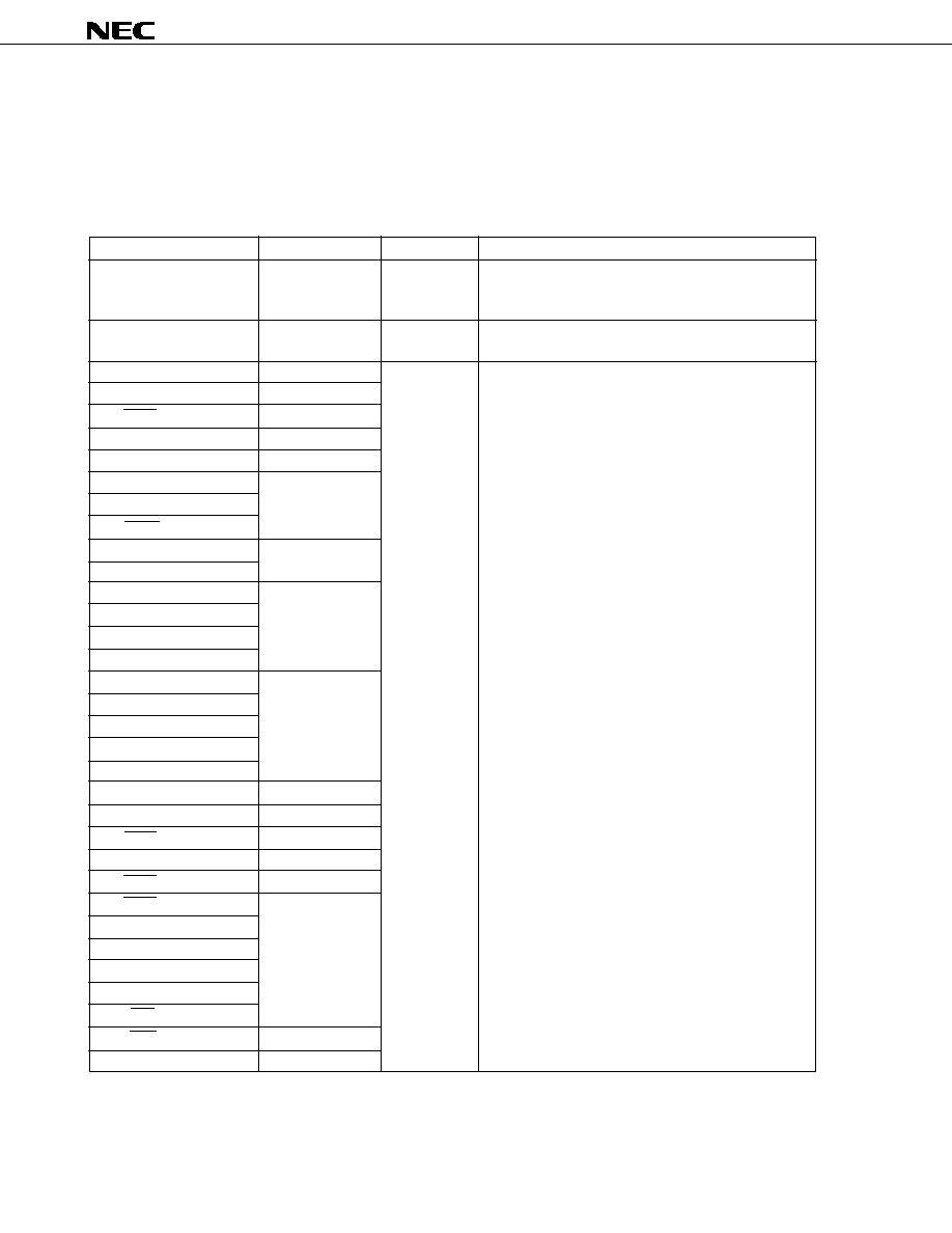
Pin Name
I/O
Function
At Reset
Shared by:
INTP0-INTP7
Input
External maskable interrupt input whose valid edge
Input
P00-P07
(rising edge, falling edge, or both rising and falling edges)
can be specified.
SI0
Input
Serial data input to serial interface.
Input
P25/SB0/SDA0
SI1
P20
SI3
P70
SO0
Output
Serial data output from serial interface.
Input
P26/SB1/SDA1
SO1
P21
SO3
P71
SB0
I/O
Serial data input/output to/from
N-ch open drain I/O
Input
P25/SI0/SDA0
SB1
serial interface.
P26/SO0/SDA1
SDA0
P25/SI0/SB0
SDA1
P26/SO0/SB1
SCK0
I/O
Serial clock input/output to/from serial interface.
Input
P27/SCL
SCK1
P22
SCK3
P72
SCL
N-ch open drain I/O
P27/SCK0
STB
Output
Strobe output for serial interface automatic transmission/
Input
P23
reception.
BUSY
Input
Busy input for serial interface automatic transmission/
Input
P24
reception.
VW45
Output
V
DD
= 4.5 V monitor output
Input
P30
TI00
Input
External count clock input to 16-bit timer 0.
Input
P32
TI01
P33
TI50
Input
External count clock input to 8-bit timer 50.
Input
P34
TI51
External count clock input to 8-bit timer 51.
P35
1.1 Port Pins (2/2)
1.2 Pins Other Than Port Pins (1/2)

13
µ
PD178076, 178078, 178096, 178098
Data Sheet U12885EJ3V0DS00
Pin Name
I/O
Function
At Reset
Shared by:
TO0
Output
16-bit timer 0 output.
Input
P31
TO50
8-bit timer 50 output.
Low-level
P130
TO51
8-bit timer 51 output.
output
P131
BEEP0
Output
Buzzer output.
Input
P36
BUZ
P37
ANI0-ANI7
Input
Analog input to A/D converter.
Input
P10-P17
EO0, EO1
Output
Error out output from charge pump of PLL frequency
≠
≠
synthesizer.
VCOL
Input
Inputs local oscillation frequency of PLL (in HF and MF
≠
≠
modes).
VCOH
Input
Inputs local oscillation frequency of PLL (in VHF mode).
≠
≠
AMIFC
Input
Input to AM intermediate frequency counter.
Input
P101
FMIFC
Input
Input to FM intermediate frequency or AM intermediate
Input
P102
frequency counter.
RXD0
Input
Serial data input to asynchronous serial interface (UART0).
Input
P74
µ
PD178076 and 178078 only.
TXD0
Output
Serial data output from asynchronous serial interface
Input
P75
(UART0).
µ
PD178076 and 178078 only.
TX0
Output
IEBus controller data output.
µ
PD178096 and 178098 only.
Input
P120
RX0
Input
IEBus controller data input.
µ
PD178096 and 178098 only.
Input
P121
RESET
Input
System reset input.
≠
≠
X1
Input
Connection of crystal resonator for system clock oscillation.
≠
≠
X2
≠
≠
≠
REGOSC
≠
Regulator for oscillation circuit. Connect this pin to GND via
≠
≠
0.1-
µ
F capacitor.
REGCPU
≠
Regulator for CPU power supply. Connect this pin to GND
≠
≠
via 0.1-
µ
F capacitor.
V
DD
≠
Positive power supply.
≠
≠
GND0-GND2
≠
Ground.
≠
≠
V
DD
PORT
≠
Port power supply.
≠
≠
GNDPORT
≠
Port ground.
≠
≠
AV
DD
≠
A/D converter positive power supply. Keep voltage at this
≠
≠
pin same as that at V
DD
.
AV
SS
≠
A/D converter ground. Keep voltage at this pin same as
≠
≠
that at GND0 through GND2.
V
DD
PLL
Note
≠
PLL positive power supply.
≠
≠
GNDPLL
Note
≠
PLL ground.
≠
≠
IC
≠
Internally connected. Directly connect this pin to GND0,
≠
≠
GND1, or GND2.
Note
Connect a capacitor of about 1000 pF between the V
DD
PLL and GNDPLL pins.
1.2 Pins Other Than Port Pins (2/2)
14
µ
PD178076, 178078, 178096, 178098
Data Sheet U12885EJ3V0DS00
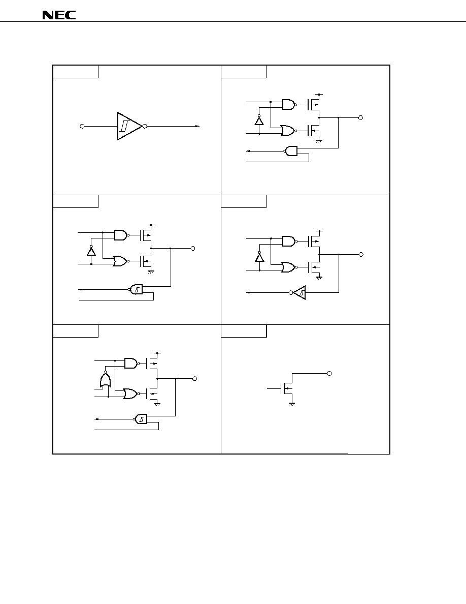
1.3 I/O Circuits of Pins and Recommended Connections of Unused Pins
Table 1-1 shows the types of the I/O circuits of the respective pins and the recommended connections of the pins
when they are not used.
For the configuration of the I/O circuit of each pin, refer to Figure 1-1.
Table 1-1. I/O Circuit Type of Each Pin (1/2)
Pin Name
I/O Circuit Type
I/O
Recommended Connection of Unused Pin
P00/INTP0-P07/INTP7
8
I/O
Input: Individually connect them to V
DD
, V
DD
PORT, GND0
to GND2, or GNDPORT via resistor.
Output: Leave open.
P10/ANI0-P17/ANI7
25
Input
Connect them to V
DD
, V
DD
PORT, GND0 to GND2, or
GNDPORT.
P20/SI1
5-K
I/O
Input: Individually connect them to V
DD
, V
DD
PORT, GND0
P21/SO1
5
to GND2, or GNDPORT via resistor.
P22/SCK1
5-K
Output: Leave open.
P23/STB
5
P24/BUSY
5-K
P25/SI0/SB0/SDA0
10-D
P26/SO0/SB1/SDA1
P27/SCK0/SCL
P30/VM45
5
P31/TO0
P32/TI00
5-K
P33/TI01
P34/TI50
P35/TI51
P36/BEEP0
5
P37/BUZ
P40-P47
P50-P57
P60-P67
P70/SI3
5-K
P71/SO3
5
P72/SCK3
5-K
P73
5
P74/RXD0
5-K
P75/TXD0
5
P76, P77
P100
P101/AMIFC
P102/FMIFC
P120/TX0
P121/RX0
5-K
P122-P124
5

15
µ
PD178076, 178078, 178096, 178098
Data Sheet U12885EJ3V0DS00
Table 1-1. I/O Circuit Type of Each Pin (2/2)
Pin Name
I/O Circuit Type
I/O
Recommended Connection of Unused Pin
P130/TO50
19
Output
Open these pins.
P131/TO51
P132-P137
EO0
DTS-EO1
EO1
VCOL, VCOH
DTS-AMP2
Input
Disable PLL in software and select pull-down.
REGOSC, REGCPU
≠
≠
Connect these pins to GND0, GND1, or GND2 via 0.1-
µ
F
capacitor.
RESET
2
Input
≠
AV
DD
≠
≠
Connect this pin to V
DD
or V
DD
PORT.
AV
SS
Directly connect these pins to GND0 to GND2, or GNDPORT.
IC
16
µ
PD178076, 178078, 178096, 178098
Data Sheet U12885EJ3V0DS00
Figure 1-1. I/O Circuits of Respective Pins (1/2)
Type 5-K
data
output
disable
P-ch
IN/OUT
V
DD
N-ch
Type 5
Type 2
data
output
disable
P-ch
IN/OUT
V
DD
N-ch
input
enable
data
output
disable
P-ch
IN/OUT
V
DD
N-ch
input
enable
Type 8
data
output disable
P-ch
IN/OUT
V
DD
N-ch
input
enable
open drain
Type 10-D
IN
Schmitt trigger input with hysteresis characteristics
Type 19
OUT
N-ch
Remark V
DD
and GND are the positive power supply and ground pins for all port pins. Take V
DD
and GND as
V
DD
PORT and GNDPORT.

17
µ
PD178076, 178078, 178096, 178098
Data Sheet U12885EJ3V0DS00
Figure 1-1. I/O Circuits of Respective Pins (2/2)
Type 25
input
enable
Comparator
+
≠
N-ch
P-ch
IN
V
REF
(Threshold voltage)
IN
Type DTS-AMP
Type DTS-EO1
V
DD
PLL
GNDPLL
DW
UP
P-ch
OUT
V
DD
PLL
GNDPLL
N-ch
Note
Note
This switch is selectable in software only for the VCOL and VCOH pins.
Remark V
DD
and GND are the positive power supply and ground pins for all port pins. Take V
DD
and GND as
V
DD
PORT and GNDPORT.
18
µ
PD178076, 178078, 178096, 178098
Data Sheet U12885EJ3V0DS00
2. MEMORY SPACE
Figure 2-1 shows the memory map of the
µ
PD178076, 178078, 178096, and 178098.
Figure 2-1. Memory Map
Notes 1. The internal ROM and internal extension RAM capacities differ depending on the model (refer to the
table below).
Target Model Name
Internal ROM End Address
Internal Extension RAM First Address
nnnnH
mmmmH
µ
PD178076, 178096
BFFFH
F400H
µ
PD178078, 178098
EFFFH
F000H
2. The
µ
PD178078 and 178098 do not have this unusable area.
Cannot be used
Data memory
space
Program
memory space
CALLT table area
Vector table area
FFFFH
Cannot be used
Program area
CALLF entry area
Program area
Special function registers
(SFR)
256
◊
8 bits
General-purpose
registers
32
◊
8 bits
Internal high-speed RAM
1024
◊
8 bits
Internal extension
RAM
Notes 1,3
Internal buffer RAM
32
◊
8 bits
Cannot be used
Note 2
Internal ROM
Notes 1, 3
FF00H
FEFFH
FEE0H
FEDFH
FB00H
FAFFH
FAE0H
FADFH
FAC0H
FABFH
F800H
F7FFH
mmmmH
mmmmH≠1
nnnnH+1
nnnnH
0000H
1000H
0FFFH
nnnnH
0800H
07FFH
0080H
007FH
0040H
003FH
0000H

19
µ
PD178076, 178078, 178096, 178098
Data Sheet U12885EJ3V0DS00
Note
3. The initial values of the memory size select register (IMS) and internal extension RAM size select
register (IXS) are CFH and 0CH, respectively. The following values must be set to the registers of
each model.
Part Number
IMS
IXS
µ
PD178076, 178096
CCH
0AH
µ
PD178078, 178098
CFH
08H
2.1 Memory Size Select Register (IMS)
This register is used to select the capacity of the internal memory.
Set CCH to this register of the
µ
PD178076 and 178096. Set CFH to the IMS of the
µ
PD178078 and 178098.
Use an 8-bit memory manipulation instruction to set the IMS.
This register is set to CFH at reset.
Figure 2-2. Format of Memory Size Select Register (IMS)
RAM2
RAM1 RAM0
Selects internal high-speed RAM capacity
1
1
0
1024 bytes
Others
Setting prohibited
RAM3 RAM2
RAM1
RAM0
Selects internal ROM capacity
1
1
0
0
48K bytes
1
1
1
1
60K bytes
Others
Setting prohibited
7
RAM2
6
RAM1
5
RAM0
4
0
3
ROM3
2
ROM2
1
ROM1
0
ROM0
Symbol
IMS
At reset
CFH
R/W
R/W
Address
FFF0H

20
µ
PD178076, 178078, 178096, 178098
Data Sheet U12885EJ3V0DS00
2.2 Internal Extension RAM Size Select Register (IXS)
This register is used to select the capacity of the internal extension RAM.
Set 0AH of this register of the
µ
PD178076 and 178096. Set 08H of the IXS of the
µ
PD178078 and 178098.
Use an 8-bit memory manipulation instruction to set the IXS.
This register is set to 0CH at reset.
Figure 2-3. Format of Internal Extension RAM Size Select Register (IXS)
IXRAM4 IXRAM3 IXRAM2 IXRAM1 IXRAM0
Selects internal extension RAM capacity
0
1
0
0
0
2048 bytes
0
1
0
1
0
1024 bytes
Others
Setting prohibited
7
0
6
0
5
0
4
IXRAM4
3
IXRAM3
2
IXRAM2
1
IXRAM1
0
IXRAM0
Symbol
IXS
At reset
0CH
R/W
R/W
Address
FFF4H

21
µ
PD178076, 178078, 178096, 178098
Data Sheet U12885EJ3V0DS00
3. FEATURES OF PERIPHERAL HARDWARE FUNCTIONS
3.1 Ports
The following three types of ports are available:
∑ CMOS input (port 1)
: 8 pins
∑ CMOS I/O (ports 0, 2 through 7, 10, and 12)
: 64 pins
∑ N-ch open-drain output (port 13)
: 8 pins
Total
: 80 pins
Table 3-1. Port Functions
Name
Pin Name
Function
Port 0
P00-P07
I/O port. Can be set in input or output mode in 1-bit units.
Port 1
P10-P17
Input-only port.
Port 2
P20-P27
I/O port. Can be set in input or output mode in 1-bit units.
Port 3
P30-P37
I/O port. Can be set in input or output mode in 1-bit units.
Port 4
P40-P47
I/O port. Can be set in input or output mode in 1-bit units.
Port 5
P50-P57
I/O port. Can be set in input or output mode in 1-bit units.
Port 6
P60-P67
I/O port. Can be set in input or output mode in 1-bit units.
Port 7
P70-P77
I/O port. Can be set in input or output mode in 1-bit units.
Port 10
P100-P102
I/O port. Can be set in input or output mode in 1-bit units.
Port 12
P120-P124
I/O port. Can be set in input or output mode in 1-bit units.
Port 13
P130-P137
N-ch open-drain output port.

22
µ
PD178076, 178078, 178096, 178098
Data Sheet U12885EJ3V0DS00
3.2 Clock Generation Circuit
The instruction execution time can be changed as follows:
∑ 0.32
µ
s/0.64
µ
s/1.27
µ
s/2.54
µ
s/5.08
µ
s (system clock: 6.3-MHz crystal resonator)
∑ 0.44
µ
s/0.89
µ
s/1.78
µ
s/3.56
µ
s/7.11
µ
s (system clock: 4.5-MHz crystal resonator)
Note
Note
When using the IEBus controller of the
µ
PD178096 and 178098, the 4.5-MHz crystal resonator cannot
be used. Use the 6.3-MHz crystal resonator.
Figure 3-1. Block Diagram of Clock Generation Circuit
X1
X2
System
clock
oscillator
STOP
Internal bus
0
0
0
0
0
PCC2 PCC1 PCC0
3
f
X
2
f
X
2
2
f
X
2
3
f
X
2
4
f
X
Prescaler
Selector
Standby
control
circuit
Wait
control
circuit
Prescaler
Processor clock control register (PCC)
Clock to other than
peripheral hardware
CPU clock
(f
CPU
)
3.3 Timers
Five timer channels are provided.
∑ Basic timer
: 1 channel
∑ 16-bit timer/event counter : 1 channel
∑ 8-bit timer/event counter
: 2 channels
∑ Watchdog timer
: 1 channel
Figure 3-2. Block Diagram of Basic Timer
Divider circuit
6.3 MHz or
4.5 MHz
Note
INTBTM0
Note
When using the IEBus controller of the
µ
PD178096 and 178098, the 4.5-MHz crystal resonator cannot
be used. Use the 6.3-MHz crystal resonator.

23
µ
PD178076, 178078, 178096, 178098
Data Sheet U12885EJ3V0DS00
Figure 3-3. Block Diagram of 16-Bit Timer/Event Counter
Internal bus
Output
control
circuit
Capture/compare
control register 0
(CPU)
TI01/P33
f
X
/2
f
X
/2
2
f
X
/2
6
f
X
/2
3
TI00/P32
Prescaler mode
register 0 (PRM0)
2
Selector
Noise
rejection
circuit
Noise
rejection
circuit
PRM01PRM00
CRC02
16-bit capture/compare
register 01 (CR01)
Coincidence
Coincidence
16-bit timer counter 0
(TM0)
Clear
Selector
Noise
rejection
circuit
CRC02 CRC01 CRC00
16-bit capture/compare
register 00 (CR00)
Selector
Selector
INTTM00
TO0/P31
INTTM01
Timer output control
register 0 (TOC0)
16-bit timer
mode control
register 0 (TMC0)
Internal bus
TMC03 TMC02 TMC01 OVF0
OSPT OSPE TOC04 LVS0 LVR0 TOC01 TOE0
Output latch
(P31)
PM31

24
µ
PD178076, 178078, 178096, 178098
Data Sheet U12885EJ3V0DS00
Figure 3-4. Block Diagram of 8-Bit Timer/Event Counter 50
Internal bus
8-bit compare
register 50 (CR50)
8-bit timer counter
50 (TM50)
TI50/P34
f
X
/2
5
f
X
/2
7
f
X
/2
9
f
X
/2
11
f
X
/2
3
Selector
Mask circuit
Selector
Coincidence
OVF
Clear
3
Selector
TCL502 TCL501 TCL500
Timer clock select
register 50 (TCL50)
Internal bus
TCE50 TMC506 TMC504 LVS50 LVR50 TMC501 TOE50
Level
inversion
Timer mode control
register 50 (TMC50)
S
R
S
Q
R
INV
Selector
INTTM50
TO50/P130
f
X
/2
Output latch
(P130)
Figure 3-5. Block Diagram of 8-Bit Timer/Event Counter 51
Internal bus
TI51/P35
f
X
/2
3
f
X
/2
5
f
X
/2
7
f
X
/2
9
f
X
/2
Coincidence
OVF
Clear
3
Selector
TCL512 TCL511 TCL510
Timer clock select
register 51 (TCL51)
Internal bus
TCE51 TMC516 TMC514 LVS51 LVR51 TMC511 TOE51
Timer mode control
register 51 (TMC51)
S
R
Q
R
INV
Selector
INTTM51
TO51/P131
S
f
X
/2
11
Selector
8-bit compare
register 51 (CR51)
8-bit timer counter
51 (TM51)
Selector
Mask circuit
Level
inversion
Output latch
(P131)

25
µ
PD178076, 178078, 178096, 178098
Data Sheet U12885EJ3V0DS00
Figure 3-6. Block Diagram of Watchdog Timer
OSTS2 OSTS1 OSTS0
WDCS2 WDCS1 WDCS0
RUN
WDTM4 WDTM3
Clock input
control circuit
Divided clock
select circuit
RUN
Divider circuit
f
X
/2
8
INTWDT
RESET
WDT mode signal
3
Watchdog timer clock
select register (WDCS)
Oscillation stabilization
time select register (OSTS)
Watchdog timer mode
register (WDTM)
Output
control
circuit
Division mode
select circuit
Internal bus

26
µ
PD178076, 178078, 178096, 178098
Data Sheet U12885EJ3V0DS00
3.4 Buzzer Output Control Circuit
Two types of buzzer output control circuits are provided.
∑ BEEP0 ... 1 kHz/1.5 kHz/3 kHz/4 kHz
∑ BUZ
... 0.77 kHz/1.54 kHz/3.08 kHz/6.15 kHz (system clock: 6.3-MHz crystal resonator)
Figure 3-7. Block Diagram of Buzzer Output Control Circuit (BEEP0)
Internal bus
BEEP
CL02
BEEP
CL01
BEEP
CL00
BEEP0 clock select
register (BEEPCL0)
BEEP0/P36
1 kHz
1.5 kHz
3 kHz
4 kHz
Selector
Output latch
(P36)
PM36
Figure 3-8. Block Diagram of Buzzer Output Control Circuit (BUZ)
Internal bus
BZOE BCS1 BCS0
Clock output
select register (CKS)
BUZ/P37
f
X
/2
10
f
X
/2
11
f
X
/2
12
f
X
/2
13
Output latch
(P37)
PM37
Selector
Remark f
X
: System clock frequency

27
µ
PD178076, 178078, 178096, 178098
Data Sheet U12885EJ3V0DS00
3.5 A/D Converter
An A/D converter with a resolution of 8 bits
◊
8 channels is provided.
Figure 3-9. Block Diagram of A/D Converter
ANI0/P10
ANI1/P11
ANI2/P12
ANI3/P13
ANI4/P14
ANI5/P15
ANI6/P16
ANI7/P17
Sample & hold circuit
AV
SS
Voltage comparator
Successive
approximation register
(SAR)
A/D conversion result
register 3 (ADCR3)
Control
circuit
Control
circuit
Tap selector
AV
DD
AV
SS
ADCS3
INTAD
Power-fail compare threshold
value register 3 (PFT3)
Voltage
comparator
PFEN3
ADCS3
ADS33 ADS32 ADS31 ADS30
0
FR32 FR31 FR30
0
0
0
PFCM3 PFHRM3
Power-fail compare mode register 3
(PFM3)
A/D converter mode register 3
(ADM3)
Analog input channel specification
register 3 (ADS3)
4
Internal bus
Selector
28
µ
PD178076, 178078, 178096, 178098
Data Sheet U12885EJ3V0DS00
3.6 Serial Interface
The
µ
PD178076 and 178078 have four serial interface channels, and the
µ
PD178096 and 178098 have three
channels.
∑ Serial interface 0
∑ Serial interface 1
∑ Serial interface 3
∑ Serial interface UART0:
µ
PD178076 and 178078 only
Table 3-2. Types and Functions of Serial Interfaces
Function
Serial interface 0
Serial interface 1
Serial interface 3
UART0
Note
3-wire serial I/O mode
(MSB/LSB first
(MSB/LSB first
(MSB first)
≠
selectable)
selectable)
3-wire serial I/O mode with
≠
(MSB/LSB first
≠
≠
automatic transmit/receive
selectable)
function
SBI (serial bus interface) mode
(MSB first)
≠
≠
≠
2-wire serial I/O mode
(MSB first)
≠
≠
≠
I
2
C bus mode
(MSB first)
≠
≠
≠
UART (asynchronous serial
≠
≠
≠
(Dedicated baud
interface) mode
rate generator)
Note
µ
PD178076 and 178078 only.

29
µ
PD178076, 178078, 178096, 178098
Data Sheet U12885EJ3V0DS00
Figure 3-10. Block Diagram of Serial Interface 0
SI0/SB0/SDA0/P25
SO0/SB1/SDA1/P26
SCK0/SCL/P27
CLD
PM27
PM26
PM25
Output control
Output control
Output control
Control circuit
BSYE
Selector
Selector
P26 output latch
P25
output latch
Serial operating mode register 0 (CSIM0)
CSIE0 COI
WUP
CSIM
04
CSIM
03
CSIM
02
CSIM
01
Coincidence
P27 output latch
Slave address register 0
(SVA0)
Serial I/O shift register
(SIO0)
SVAM
Stop condition/
start condition/
acknowledge
detector
Serial clock
counter
Serial clock
control circuit
CSIM01
CSIM01
CLR SET
D
Q
ACKD
CMDD
RELD
WUP
Acknowledge
output circuit
Interrupt request
signal generator
Selector
1/16
divider
Selector
2
4
Interrupt timing
specification register 0 (SINT0)
CLD
SIC SVAM CLC WREL WAT1 WAT0
SCL03 SCL02 SCL01 SCL00
f
X
/2
2
-f
X
/2
9
Internal bus
BSYE
0
ACKD ACKE ACKT CMDD RELD CMDT RELT
Serial bus interface control
register 0 (SBIC0)
INTCSI0
Internal bus
Note
Note
Serial interface clock
select register 0 (SCL0)
Note
Example in I
2
C bus mode operation.
Remark Output Control performs selection between CMOS output and N-ch open drain output.

30
µ
PD178076, 178078, 178096, 178098
Data Sheet U12885EJ3V0DS00
Figure 3-11. Block Diagram of Serial Interface 1
Internal bus
ATE
SI1/P20
SO1/P21
PM21
BUSY/P24
PM23
STB/P23
SCK1/P22
PM22
DIR1
P21 output latch
DIR1
Hand-
shake
ARLD
Serial clock counter
P22 output latch
CSIE1
LSCK1
Q
R
S
Clear
SIO1 write
Serial I/O shift register 1
(SIO1)
Internal buffer RAM
Automatic data transmit/
receive address pointer
register (ADTP)
Internal bus
ADTI7 ADTI4 ADTI3 ADTI2 ADTI1 ADTI0
Coincidence
5-Bit counter
ADTI0-ADTI4
RE ARLD ERCE ERR TRF STRB BUSY1 BUSY0
Selector
TRF
CSIE1 DIR1
ATE LSCK1 SCL11 SCL10
Serial operating
mode register 1 (CSIM1)
Selector
INTCSI1
f
X
/2
4
-f
X
/2
6
Automatic data transmit/receive
interval specification register (ADTI)
Automatic data transmit/receive
control register (ADTC)
Selector
Selector

31
µ
PD178076, 178078, 178096, 178098
Data Sheet U12885EJ3V0DS00
Figure 3-12. Block Diagram of Serial Interface 3
Internal bus
8
Interrupt request
signal generation
circuit
Selector
Serial clock
counter
Serial clock
control circuit
Serial I/O shift
register 3 (SIO3)
SI3/P70
SO3/P71
P71 output latch
PM71
PM72
SCK3/P72
INTCSI3
f
X
/2
4
f
X
/2
5
f
X
/2
6
P72 output latch
Figure 3-13. Block Diagram of Serial Interface UART0 (
µ
PD178076 and 178078 only)
Internal bus
(RXB0)
Receive buffer
register 0
(RX0)
Receive shift
register 0
(parity check)
Reception
control circuit
RXD0/P74
TXD0/P75
P75 output latch
PM75
PE0
FE0 OVE0
Transmit shift
register
(TXS0)
Transmission
control circuit
(parity append)
INTSER0
INTST0
Baud rate
generator
f
X
/2-f
X
/2
8
TXE0 RXE0 PS01 PS00 CL0
SL0 ISRM0
0
INTSR0
Asychronous serial interface
mode register 0 (ASIM0)
Asynchronous serial interface
status register 0 (ASIS0)
TPS02 TPS01 TPS00 MDL03 MDL02 MDL01 MDL00
Internal bus
Baud rate generator
control register 0 (BRGC0)

32
µ
PD178076, 178078, 178096, 178098
Data Sheet U12885EJ3V0DS00
3.7 IEBus Controller (
µ
PD178096 and 178098 only)
The
µ
PD178096 and 178098 have an IEBus controller. The functions of this IEBus controller are limited as
compared with the existing IEBus interface functions of the
µ
PD78098 subseries.
Table 3-3 compares the interfaces of the
µ
PD78098 subseries and
µ
PD178098 subseries.
Table 3-3. Comparison of IEBus Interface (between
µ
PD78098 Subseries and
µ
PD178098 Subseries)
Item
µ
PD78098 Subseries IEBus
µ
PD178098 Subseries IEBus
Communication mode
Modes 0, 1, and 2
Fixed to mode 1
Internal system clock
f
X
= 6.0 (6.29) MHz
f
X
= 6.3 MHz
Note
Internal buffer size
Transmit buffer: 33 bytes (FIFO)
Transmit buffer: 1 byte
Receive buffer: 40 bytes (FIFO)
Receive buffer: 1 byte
Up to 4 frames can be received.
CPU processing
Communication start processing
Communication start processing
(data setting)
(data setting)
Setting and management of each
Setting and management of each
communication status
communication status
Writing data to transmit buffer
Writing data per 1 byte
Reading data from receive buffer
Reading data per 1 byte
Management of transmission such as
slave status
Management of multiple frames, re-master
request processing
Hardware processing
Bit processing (modulation/demodulation,
Bit processing (modulation/demodulation,
error detection)
error detection)
Field processing (generation/management)
Field processing (generation/management)
Arbitration result detection
Arbitration result detection
Parity processing (generation/error detection)
Parity processing (generation/error detection)
Automatic answering of ACK/NACK
Automatic answering of ACK/NACK
Automatic data re-transmission processing
Automatic data re-transmission processing
Automatic re-master processing
Transmission processing such as automatic
slave status
Multiple frame reception processing
Note
The IEBus controller of the
µ
PD178098 subseries operates at f
X
= 6.3 MHz, and not at f
X
= 4.5 MHz.
Remark f
X
: System clock frequency

33
µ
PD178076, 178078, 178096, 178098
Data Sheet U12885EJ3V0DS00
Figure 3-14. Block Diagram of IEBus Controller (
µ
PD178096 and 178098 only)
BCR0 (8)
UAR (12)
SAR (12)
PAR (12)
CDR (8)
DLR (8)
DR (8) USR (8)
ISR (8)
SSR (8) SCR (8) CCR (8)
8
12
12
8
8
8
8
12
8
8
8
8
8
8
8
8
8
8
8
8
NF
RX0/P121
TX0/P120
MPX
MPX
12-bit latch
Comparator
Collision
detection
ACK
generation
Parity generation
error detection
TX/RX
Interrupt
control
circuit
Interrupt control block
INT request
CPU interface block
Internal registers
IEBus interface block
CLK
Bit processing block
Field processing block
Internal bus R/W
PSR (8 bits)
8
5
8
12
12
12
Internal bus
8
12

34
µ
PD178076, 178078, 178096, 178098
Data Sheet U12885EJ3V0DS00
The IEBus mainly consists of the following six internal blocks:
∑ CPU interface block
∑ Interrupt control block
∑ Internal registers
∑ Bit processing block
∑ Field processing block
∑ IEBus interface block
<CPU interface block>
This block interfaces between the CPU (78K/0) and IEBus.
<Interrupt control block>
This block passes interrupt request signals from the IEBus to the CPU.
<Internal registers>
These are control registers that are used to control the IEBus and settings of each field.
<Bit processing block>
This block generates and disassembles bit timing, and mainly consists of a bit sequence ROM, 8-bit preset timer,
and decision unit.
<Field processing block>
This block generates each field in a communication frame and mainly consists of a field sequence ROM, 4-bit
down counter, and decision unit.
<IEBus interface block>
This is the interface block for an external driver/receiver, and mainly consists of a noise filter, shift register, collision
detector, parity detector, parity generation circuit, and ACK/NACK generation circuit.

35
µ
PD178076, 178078, 178096, 178098
Data Sheet U12885EJ3V0DS00
3.8 PLL Frequency Synthesizer
Figure 3-15. Block Diagram of PLL Frequency Synthesizer
Internal bus
Internal bus
PLL mode
Select register
(PLLMD)
PLL
data transfer
register (PLLNS)
PLL
NS0
PLL
MD0
PLL
MD1
VCOH
DMD
VCOL
DMD
PLL
RF2
PLL
RF1
PLL
RF0
PLL
UL0
PLL reference
mode register
(PLLRF)
PLL unlock
F/F Judge register
(PLLUL)
PLL
RF3
2
Input select
block
Programmable
divider
Phase
comparator
( - DET)
Unlock
F/F
Reference
frequency
generator
6.3 MHz
or
4.5 MHz
Note 2
4
Charge pump
EO1
EO0
VCOH
VCOL
Note 1
Note 1
Mixer
Voltage control
generator
Lowpass filter
2
f
N
f
r
PLL data register
(PLLRL, PLLRH, PLLR0)
Notes 1. These are external circuits.
2. When the IEBus controller of the
µ
PD178096 and 178098 is used, the 4.5-MHz crystal resonator
cannot be used. Use the 6.3-MHz crystal resonator.

36
µ
PD178076, 178078, 178096, 178098
Data Sheet U12885EJ3V0DS00
3.9 Frequency Counter
Figure 3-16. Block Diagram of Frequency Counter
Internal bus
IFC
MD0
IFC
CK1
IFC
CK0
IFC
JG0
IF counter
mode select
register (IFCMD)
IF counter
gate judge
register
IF counter
control
register (IFCCR)
IFC
MD1
IFC
RES
IFC
ST
Input select
block
Start/stop
control
block
Gate time
control block
IF counter
register
(IFCR)
block
2
2
FMIFC/P102
AMIFC/P101

37
µ
PD178076, 178078, 178096, 178098
Data Sheet U12885EJ3V0DS00
4. INTERRUPT FUNCTION
(1)
µ
PD178076 and 178078
The
µ
PD178076 and 178078 have the following three types and 22 sources of interrupts:
∑ Non-maskable : 1
Note
∑ Maskable
: 21
Note
∑ Software
: 1
Note
Two types of watchdog interrupt sources (INTWDT), non-maskable and maskable, are available, and
either of them can be selected.
Table 4-1. Interrupt Sources (
µ
PD178076 and 178078) (1/2)
Default
Interrupt Source
Internal/
Vector
Basic
Interrupt Type
Priority
Note 1
External
Table
Configuration
Address
Type
Note 2
Non-maskable
≠
INTWDT
Overflow of watchdog timer
Internal
0004H
(A)
(when watchdog timer mode 1 is selected)
Maskable
0
INTWDT
Overflow of watchdog timer
(B)
(when interval timer mode is selected)
1
INTP0
Pin input edge detection
External
0006H
(C)
2
INTP1
0008H
3
INTP2
000AH
4
INTP3
000CH
5
INTP4
000EH
6
INTP5
0010H
7
INTP6
0012H
8
INTP7
0014H
9
INTCSI0
End of transfer by serial interface 0
Internal
0016H
(B)
10
INTCSI1
End of transfer by serial interface 1
0018H
11
INTCSI3
End of transfer by serial interface 3
001AH
12
INTTM50
Generation of coincidence signal of 8-bit
001CH
timer/event counter 50
13
INTTM51
Generation of coincidence signal of 8-bit
001EH
timer/event counter 51
14
INTSER0
Reception error of serial interface UART0
0020H
15
INTSR0
End of reception by serial interface UART0
0022H
16
INTST0
End of transmission by serial interface
0024H
UART0
17
INTBTM0 Generation of coincidence signal of basic
0026H
timer
Notes 1. If two or more maskable interrupts occur at the same time, they are acknowledged or kept pending
according to their default priorities. The default priority 0 is the highest, while 22 is the lowest.
2. (A) to (E) under the heading Basic Configuration Type corresponds to (A) to (E) in Figure 4-1.
Name
Trigger

38
µ
PD178076, 178078, 178096, 178098
Data Sheet U12885EJ3V0DS00
Table 4-1. Interrupt Sources (
µ
PD178076 and 178078) (2/2)
Default
Interrupt Source
Internal/
Vector
Basic
Interrupt Type
Priority
Note 1
External
Table
Configuration
Address
Type
Note 2
Maskable
18
INTTM00
Generation of signal indicating coincidence
Internal
0028H
(B)
between 16-bit timer counter (TM0) and
capture/compare register (CR00) (when
CR00 is used as compare register)
Detection of input edge of TI00/P32 pin
External
(D)
(when CR00 is used as capture register)
19
INTTM01
Generation of signal indicating coincidence
Internal
002AH
(B)
between 16-bit timer counter (TM0) and
capture/compare register (CR01) (when
CR01 is used as compare register)
Detection of input edge of TI01/P33 pin
External
(D)
(when CR01 is used as capture register)
20
≠
≠
≠
Note 3
≠
21
≠
≠
Note 3
22
INTAD
End of conversion by A/D converter
Internal
0030H
(B)
Software
≠
BRK
Execution of BRK instruction
≠
003EH
(E)
Notes 1. If two or more maskable interrupts occur at the same time, they are acknowledged or kept pending
according to their default priorities. The default priority 0 is the highest, while 22 is the lowest.
2. (A) to (E) under the heading Basic Configuration Type corresponds to (A) to (E) in Figure 4-1.
3. There are no interrupt sources corresponding to vector addresses 002CH and 002EH.
Name
Trigger

39
µ
PD178076, 178078, 178096, 178098
Data Sheet U12885EJ3V0DS00
(2)
µ
PD178096 and 178098
The
µ
PD178096 and 178098 have the following three types and 21 sources of interrupts:
∑ Non-maskable : 1
Note
∑ Maskable
: 20
Note
∑ Software
: 1
Note
Two types of watchdog interrupt sources (INTWDT), non-maskable and maskable, are available, and
either of them can be selected.
Table 4-2. Interrupt Sources (
µ
PD178096 and 178098) (1/2)
Default
Interrupt Source
Internal/
Vector
Basic
Interrupt Type
Priority
Note 1
External
Table
Configuration
Address
Type
Note 2
Non-maskable
≠
INTWDT
Overflow of watchdog timer
Internal
0004H
(A)
(when watchdog timer mode 1 is selected)
Maskable
0
INTWDT
Overflow of watchdog timer
(B)
(when interval timer mode is selected)
1
INTP0
Pin input edge detection
External
0006H
(C)
2
INTP1
0008H
3
INTP2
000AH
4
INTP3
000CH
5
INTP4
000EH
6
INTP5
0010H
7
INTP6
0012H
8
INTP7
0014H
9
INTCSI0
End of transfer by serial interface 0
Internal
0016H
(B)
10
INTCSI1
End of transfer by serial interface 1
0018H
11
INTCSI3
End of transfer by serial interface 3
001AH
12
INTTM50
Generation of coincidence signal of 8-bit
001CH
timer/event counter 50
13
INTTM51
Generation of coincidence signal of 8-bit
001EH
timer/event counter 51
14
≠
≠
≠
Note 3
≠
15
≠
≠
Note 3
16
≠
≠
Note 3
17
INTBTM0
Generation of coincidence signal of basic
Internal
0026H
(B)
timer
Notes 1. If two or more maskable interrupts occur at the same time, they are acknowledged or kept pending
according to their default priorities. The default priority 0 is the highest, while 22 is the lowest.
2. (A) to (E) under the heading Basic Configuration Type corresponds to (A) to (E) in Figure 4-1.
3. There are no interrupt sources corresponding to vector addresses 0020H, 0022H, and 0024H.
Name
Trigger
40
µ
PD178076, 178078, 178096, 178098
Data Sheet U12885EJ3V0DS00
Table 4-2. Interrupt Sources (
µ
PD178096 and 178098) (2/2)
Default
Interrupt Source
Internal/
Vector
Basic
Interrupt Type
Priority
Note 1
External
Table
Configuration
Address
Type
Note 2
Maskable
18
INTTM00
Generation of signal indicating coincidence
Internal
0028H
(B)
between 16-bit timer counter (TM0) and
capture/compare register (CR00) (when
CR00 is used as compare register)
Detection of input edge of TI00/P32 pin
External
(D)
(when CR00 is used as capture register)
19
INTTM01
Generation of signal indicating coincidence
Internal
002AH
(B)
between 16-bit timer counter (TM0) and
capture/compare register (CR01) (when
CR01 is used as compare register)
Detection of input edge of TI01/P33 pin
External
(D)
(when CR01 is used as capture register)
20
INTIE1
IEBus0 data access request
Internal
002CH
(B)
21
INTIE2
IEBus0 communication error and start/end
002EH
of communication
22
INTAD
End of conversion by A/D converter AD1
0030H
(B)
Software
≠
BRK
Execution of BRK instruction
≠
003EH
(E)
Notes 1. If two or more maskable interrupts occur at the same time, they are acknowledged or kept pending
according to their default priorities. The default priority 0 is the highest, while 22 is the lowest.
2. (A) to (E) under the heading Basic Configuration Type corresponds to (A) to (E) in Figure 4-1.
Name
Trigger

41
µ
PD178076, 178078, 178096, 178098
Data Sheet U12885EJ3V0DS00
Figure 4-1. Basic Configuration of Interrupt Function (1/2)
(A) Internal non-maskable interrupt
Interrupt
request
Priority control
circuit
Vector table
address generation
circuit
Standby release
signal
Internal bus
(B) Internal maskable interrupt
Interrupt
request
IF
MK
IE
PR
ISP
Standby release
signal
Priority control
circuit
Vector table
address generation
circuit
Internal bus
(C) External maskable interrupt (INTP0 through INTP7)
IF
MK
IE
PR
ISP
External interrupt
rising/falling edge enable
registers (EGP, EGN)
Interrupt
request
Standby release
signal
Priority control
circuit
Vector table
address generation
circuit
Internal bus
Edge detection
circuit

42
µ
PD178076, 178078, 178096, 178098
Data Sheet U12885EJ3V0DS00
Figure 4-1. Basic Configuration of Interrupt Function (2/2)
(D) External maskable interrupts (INTTM00, INTTM01)
ISP
IE
IF
MK
Prescaler mode register
(PRM0)
PR
Interrupt
request
Standby release
signal
Priority control
circuit
Vector table
address generation
circuit
Internal bus
Edge detection
circuit
(E) Software interrupt
Interrupt
request
Priority control
circuit
Vector table
address generation
circuit
Internal bus
Remark IF
: Interrupt request flag
IE : Interrupt enable flag
ISP : In-service priority flag
MK : Interrupt mask flag
PR : Priority specification flag

43
µ
PD178076, 178078, 178096, 178098
Data Sheet U12885EJ3V0DS00
5. STANDBY FUNCTION
There are the following two standby functions to reduce the system power consumption.
∑ HALT mode : The CPU operating clock is stopped.
The average consumption current can be reduced by intermittent operation in combination with
the normal operating mode.
∑ STOP mode : The system clock oscillation is stopped. All operations by the system clock are stopped and
current consumption can be considerably reduced.
Figure 5-1. Standby Function
System Clock Operation
STOP Mode
(System clock
oscillation stopped)
HALT Mode
(Clock supply to CPU is
stopped, oscillation
continued)
Interrupt
Request
Interrupt
Request
HALT
Instruction
STOP
Instruction
6. RESET FUNCTION
There are the following three reset methods.
∑ External reset input by RESET pin
∑ Internal reset by watchdog timer hang-up time detection
∑ Internal reset by Power-On Clear (POC).

44
µ
PD178076, 178078, 178096, 178098
Data Sheet U12885EJ3V0DS00
7. INSTRUCTION SET
(1) 8-bit instructions
MOV, XCH, ADD ADDC, SUB, SUBC, AND, OR, XOR, CMP, MULU, DIVUW, INC, DEC, ROR,
ROL, RORC, ROLC, ROR4, ROL4, PUSH, POP, DBNZ
Note
Except r = A
Second
Operand
First
Operand
#byte
A
r
Note
sfr
saddr
!addr16
PSW
[DE]
[HL]
[HL + byte]
[HL + B]
[HL + C]
$addr16
1
None
A
r
ADD
ADDC
SUB
SUBC
AND
OR
XOR
CMP
MOV
XCH
ADD
ADDC
SUB
SUBC
AND
OR
XOR
CMP
MOV
XCH
MOV
XCH
ADD
ADDC
SUB
SUBC
AND
OR
XOR
CMP
MOV
XCH
ADD
ADDC
SUB
SUBC
AND
OR
XOR
CMP
MOV
MOV
XCH
MOV
XCH
ADD
ADDC
SUB
SUBC
AND
OR
XOR
CMP
MOV
XCH
ADD
ADDC
SUB
SUBC
AND
OR
XOR
CMP
ROR
ROL
RORC
ROLC
MOV
MOV
ADD
ADDC
SUB
SUBC
AND
OR
XOR
CMP
INC
DEC
B,C
sfr
MOV
MOV
DBNZ
MOV
ADD
ADDC
SUB
SUBC
AND
OR
XOR
CMP
saddr
MOV
DBNZ
INC
DEC
!addr16
MOV
PSW
MOV
MOV
PUSH
POP
[DE]
ROR4
ROL4
[HL]
MOV
[HL + byte]
[HL + B]
[HL + C]
MOV
X
C
MULU
DIVUW

45
µ
PD178076, 178078, 178096, 178098
Data Sheet U12885EJ3V0DS00
(2) 16-bit instructions
MOVW, XCHW, ADDW, SUBW, CMPW, PUSH, POP, INCW, DECW
Note
Only when rp = BC, DE or HL
Second Operand
First Operand
AX
rp
sfrp
saddrp
!addr16
SP
#word
ADDW
SUBW
CMPW
MOVW
MOVW
MOVW
MOVW
AX
MOVW
Note
MOVW
MOVW
MOVW
MOVW
MOVW
XCHW
rp
Note
sfrp
MOVW
saddrp
MOVW
!addr16
MOVW
SP
MOVW
None
INCW
DECW
PUSH
POP

46
µ
PD178076, 178078, 178096, 178098
Data Sheet U12885EJ3V0DS00
(3) Bit manipulation instructions
MOV1, AND1, OR1, XOR1, SET1, CLR1, NOT1, BT, BF, BTCLR
(4) Call instruction/branch instructions
CALL, CALLF, CALLT, BR, BC, BNC, BZ, BNZ, BT, BF, BTCLR, DBNZ
(5) Other instructions
ADJBA, ADJBS, BRK, RET, RETI, RETB, SEL, NOP, EI, DI, HALT, STOP
Second Operand
First Operand
A.bit
sfr.bit
saddr.bit
PSW.bit
[HL].bit
CY
$addr16
None
A.bit
sfr.bit
saddr.bit
PSW.bit
[HL].bit
CY
MOV1
MOV1
MOV1
MOV1
MOV1
BT
BF
BTCLR
BT
BF
BTCLR
SET1
CLR1
SET1
CLR1
BT
BF
BTCLR
SET1
CLR1
BT
BF
BTCLR
SET1
CLR1
BT
BF
BTCLR
SET1
CLR1
SET1
CLR1
NOT1
MOV1
AND1
OR1
XOR1
MOV1
AND1
OR1
XOR1
MOV1
AND1
OR1
XOR1
MOV1
AND1
OR1
XOR1
MOV1
AND1
OR1
XOR1
Second Operand
First Operand
AX
!addr16
!addr11
[addr5]
$addr16
Basic instruction
Compound
instruction
BR
CALL
BR
CALLF
CALLT
BR, BC, BNC
BZ, BNZ
BT, BF
BTCLR
DBNZ

47
µ
PD178076,178078,178096,178098
Data Sheet U12885EJ3V0DS00
Parameter
Symbol
Conditions
Rating
Unit
Supply voltage
V
DD
≠0.3 to +6.0
V
V
DD
PORT
≠0.3 to V
DD
+ 0.3
Note 1
V
AV
DD
≠0.3 to V
DD
+ 0.3
Note 1
V
V
DD
PLL
≠0.3 to V
DD
+ 0.3
Note 1
V
Input voltage
V
I
≠0.3 to V
DD
+ 0.3
V
Output voltage
V
O
Excluding P130 to P137
≠0.3 to V
DD
+ 0.3
V
Output breakdown
V
BDS
P130-P137
N-ch open drain
16
V
voltage
Analog input voltage
V
AN
P10-P17
Analog input pin
≠0.3 to V
DD
+ 0.3
V
High-level output
I
OH
1 pin
≠8
mA
current
Total of P00-P01, P20-P27, P50-P57, and P70-P73
≠15
mA
Total of P02-P07, P30-P37, P40-P47, P60-P67,
≠15
mA
P74-P77, and P120-P124
Total of P100-P102
≠10
mA
Low-level output
I
OL
Note 2
1 pin
Peak value
16
mA
current
r.m.s
8
mA
Total of P00-P01, P20-P27, P50-P57, Peak value
30
mA
and P70-P73
r.m.s
15
mA
Total of P02-P07, P30-P37, P40-P47, Peak value
30
mA
P60-P67, P74-P77, P120-P124, and
r.m.s
15
mA
P130-P137
Total of P100-102
Peak value
20
mA
r.m.s
10
mA
Operating temperature
T
A
≠40 to +85
∞
C
Storage temperature
T
stg
≠55 to +125
∞
C
8. ELECTRICAL SPECIFICATIONS
Absolute Maximum Ratings (T
A
= 25
∞
C)
Notes 1. Keep the voltage at V
DD
PORT, AV
DD
, and V
DD
PLL same as that at the V
DD
pin.
2. Calculate the r.m.s as follows: [r.m.s] = [Peak value] x
Duty
Caution If the rated value of even one of the above parameters is exceeded even momentarily, the quality
of the product may be degraded. The absolute maximum ratings, therefore, are the values
exceeding which the product may be physically damaged. Be sure to use the product with these
ratings never being exceeded.
Remark Unless otherwise specified, the characteristics of a multiplexed pin are the same as those of the
corresponding port pin.

48
µ
PD178076,178078,178096,178098
Data Sheet U12885EJ3V0DS00
Recommended Supply Voltage Ranges (T
A
= ≠40 to +85
∞
C)
Parameter
Symbol
Conditions
MIN.
TYP.
MAX.
Unit
Supply voltage
V
DD1
When CPU and PLL are operating
4.5
5.0
5.5
V
V
DD2
When CPU is operating and PLL is stopped
3.5
5.0
5.5
V
Data retention voltage
V
DDR
When crystal oscillation stops
2.3
5.5
V
Output breakdown
V
BDS
P130-P137 (N-ch open drain)
15
V
voltage
DC Characteristics (T
A
= ≠40 to +85
∞
C, V
DD
= 3.5 to 5.5 V)
Parameter
Symbol
Test Conditions
MIN.
TYP.
MAX.
Unit
High-level input
V
IH1
P10-P17, P21, P23, P30, P31, P36, P37, P40-P47,
0.7 V
DD
V
DD
V
voltage
P50-P57, P60-P67, P71, P73, P75-P77, P100-P102,
P120, P122-P124
V
IH2
P00-P07, P20, P22, P24-P27, P32-P35, P70, P72,
0.8 V
DD
V
DD
V
P74, P121, RESET
Low-level input
V
IL1
P10-P17, P21, P23, P30, P31, P36, P37, P40-P47,
0
0.3 V
DD
V
voltage
P50-P57, P60-P67, P71, P73, P75-P77, P100-P102,
P120, P122-P124
V
IL2
P00-P07, P20, P22, P24-P27, P32-P35, P70, P72,
0
0.2 V
DD
V
P74, P121, RESET
High-level output
V
OH1
P00-P07, P20-P24, P30-P37,
4.5 V
V
DD
5.5 V,
V
DD
≠ 1.0
V
voltage
P40-P47, P50-P57, P60-P67,
I
OH
= ≠1 mA
P70-P77, P100-P102,
3.5 V
V
DD
< 4.5 V,
V
DD
≠ 0.5
V
P120-P124
I
OH
= ≠100
µ
A
V
OH2
EO0, EO1
V
DD
= 4.5 to 5.5 V,
V
DD
≠ 1.0
V
I
OH
= ≠3 mA
Low-level output
V
OH1
P00-P07, P20-P27, P30-P37,
4.5 V
V
DD
5.5 V,
1.0
V
voltage
P40-P47, P50-P57, P60-P67,
I
OL
= 1 mA
P70-P77, P100-P102,
3.5 V
V
DD
< 4.5 V,
0.5
V
P120-P124, P130-P137,
I
OL
= 100
µ
A
V
OL2
EO0, EO1
V
DD
= 4.5 to 5.5 V,
1.0
V
I
OL
= 3 mA
High-level input
I
LIH
P00-P07, P10-P17,
V
I
= V
DD
3
µ
A
leakage current
P20-P24, P30-P37,
P40-P47, P50-P57,
P60-P67, P70-P77,
P100-P102, P120-P124,
RESET
Remark Unless otherwise specified, the characteristics of a multiplexed pin are the same as those of the
corresponding port pin.

49
µ
PD178076,178078,178096,178098
Data Sheet U12885EJ3V0DS00
Parameter
Symbol
Conditions
MIN.
TYP.
MAX.
Unit
Low-level input
I
LIL
P00-P07, P10-P17,
V
I
= 0 V
≠3
µ
A
leakage current
P20-P27, P30-P37,
P40-P47, P50-P57,
P60-P67, P70-P77,
P100-P102, P120-P124,
RESET
I
LOH1
P130-P137
V
O
= 15 V
≠3
µ
A
I
LOL1
P130-P137
V
O
= 0 V
3
µ
A
I
LOH2
P25-P27
V
O
= V
DD
≠3
µ
A
(at N-ch open drain I/O)
I
LOL2
P25-P27
V
O
= 0 V
3
µ
A
(at N-ch open drain I/O)
I
LOH3
EO0, EO1
V
O
= V
DD
≠3
µ
A
I
LOL3
EO0, EO1
V
O
= 0 V
3
µ
A
Supply current
Note
I
DD1
fx = 4.5 MHz
2.5
15
mA
(
µ
PD178076, 178078)
I
DD2
fx = 6.3 MHz
4.0
20
mA
(
µ
PD178076, 178078,
178096, 178098)
I
DD3
fx = 4.5 MHz
0.2
0.8
mA
(
µ
PD178076, 178078)
I
DD4
fx = 6.3 MHz
0.3
1.0
mA
(
µ
PD178076, 178078,
178096, 178098)
V
DDR1
When crystal resonator is oscillating
3.5
5.5
V
V
DDR2
When crystal oscillation is
Power-failure detection
2.2
V
stopped
function
V
DDR3
Data memory retained
2.0
V
Data retention
I
DDR1
When crystal oscillation is
T
A
= 25
∞
C,
2.0
4.0
µ
A
current
stopped
V
DD
= 5 V
I
DDR2
2.0
20
µ
A
DC Characteristics (T
A
= ≠40 to +85
∞
C, V
DD
= 3.5 to 5.5 V)
Note
Excluding AV
DD
current and V
DD
PLL current.
Remarks 1. f
X
: System clock oscillation frequency
2. Unless otherwise specified, the characteristics of a multiplexed pin are the same as those of the
corresponding port pin.
Output off
leakage current
Data retention
voltage
When CPU is operating
and PLL is stopped.
Sine wave input to X1 pin
V
I
= V
DD
In HALT mode with PLL
stopped.
Sine wave input to X1 pin
V
I
= V
DD

50
µ
PD178076,178078,178096,178098
Data Sheet U12885EJ3V0DS00
Reference Characteristics (T
A
= ≠40 to +85
∞
C, V
DD
= 4.5 to 5.5 V)
Parameter
Symbol
Conditions
MIN.
TYP.
MAX.
Unit
Supply current
I
DD5
When CPU and PLL are operating.
5
mA
Sine wave input to VCOH pin
At f
IN
= 160 MHz, V
IN
= 0.15 V
P-P
AC Characteristics
(1) Basic operation (T
A
= ≠40 to +85
∞
C, V
DD
= 3.5 to 5.5 V)
Parameter
Symbol
Conditions
MIN.
TYP.
MAX.
Unit
T
CY
At f
X
= 6.3 MHz
0.32
5.08
µ
s
At f
X
= 4.5 MHz
Note 1
0.44
7.11
µ
s
TI00, TI01 input
t
TIH0
,
4/fsam
Note 2
s
high-/low-level
t
TIL0
widths
TI50, TI51 input
f
TI5
2
MHz
frequency
TI50, TI51 input
t
TIH5
,
200
ns
high-/low-level
t
TIL5
widths
Interrupt input
t
INTH
,
INTP0-INTP7
1
µ
s
high-/low-level
t
INTL
widths
RESET pin
t
RSL
10
µ
s
low-level width
Notes 1. When the IEBus controller of the
µ
PD178096 and 178098 is used, the 4.5-MHz crystal resonator
cannot be used. Use the 6.3-MHz crystal resonator.
2. f
sam
= f
X
/2, f
X
/4, f
X
/64 selectable by bits 0 and 1 (PRM00 and PRM01) of the prescaler mode register
0 (PRM0). However, f
sam
= f
X
/8 when the valid edge of TI00 is selected as the count clock.
Cycle time
(minimum instruction
execution time)

51
µ
PD178076,178078,178096,178098
Data Sheet U12885EJ3V0DS00
(2) Serial interface (T
A
= ≠40 to +85
∞
C, V
DD
= 3.5 to 5.5 V)
(a) Serial interface 0
(i) 3-wire serial I/O mode (SCK0 ... internal clock output)
Parameter
Symbol
Test Conditions
MIN.
TYP.
MAX.
Unit
SCK0 cycle time
t
KCY1
V
DD
= 4.5 to 5.5 V
800
ns
1600
ns
SCK0 high-/low-level width
t
KH1
,
V
DD
= 4.5 to 5.5 V
t
KCY1
/2 ≠ 50
ns
t
KL1
t
KCY1
/2 ≠ 100
ns
SI0 setup time (to SCK0
)
t
SIK1
V
DD
= 4.5 to 5.5 V
100
ns
150
ns
SI0 hold time (from SCK0
)
t
KSI1
400
ns
SO0 output delay time from SCK0
t
KSO1
C = 100 pF
Note
300
ns
Note
C is the load capacitance of SCK0 and SO0 output line.
(ii) 3-wire serial I/O mode (SCK0 ... external clock input)
Parameter
Symbol
Test Conditions
MIN.
TYP.
MAX.
Unit
SCK0 cycle time
t
KCY2
V
DD
= 4.5 to 5.5 V
800
ns
1600
ns
SCK0 high-/low-level width
t
KH2
,
V
DD
= 4.5 to 5.5 V
400
ns
t
KL2
800
ns
SI0 setup time (to SCK0
)
t
SIK2
100
ns
SI0 hold time (from SCK0
)
t
KSI2
400
ns
SO0 output delay time from SCK0
t
KSO2
C = 100 pF
Note
300
ns
SCK0 at rising or falling edge time
t
R2
, t
F2
1000
ns
Note
C is the load capacitance of SO0 output line.

52
µ
PD178076,178078,178096,178098
Data Sheet U12885EJ3V0DS00
(iii) SBI mode (SCK0 ... internal clock output)
Parameter
Symbol
Test Conditions
MIN.
TYP.
MAX.
Unit
SCK0 cycle time
t
KCY3
V
DD
= 4.5 to 5.5 V
800
ns
3200
ns
SCK0 high-/low-level width
t
KH3
,
V
DD
= 4.5 to 5.5 V
t
KCY3
/2 ≠ 50
ns
t
KL3
t
KCY3
/2 ≠ 150
ns
SB0, SB1 setup time (to SCK0
)
t
SIK3
V
DD
= 4.5 to 5.5 V
100
ns
300
ns
SB0, SB1 hold time (from SCK0
)
t
KSI3
t
KCY3
/2
ns
SB0, SB1 output delay time from
t
KSO3
R = 1 k
V
DD
= 4.5 to 5.5 V
0
250
ns
SCK0
C = 100 pF
Note
0
1000
ns
SB0, SB1
from SCK0
t
KSB
t
KCY3
ns
SCK0
from SB0, SB1
t
SBK
t
KCY3
ns
SB0, SB1 high-level width
t
SBH
t
KCY3
ns
SB0, SB1 low-level width
t
SBL
t
KCY3
ns
Note R and C are the load resistance and load capacitance of SCK0, SB0 and SB1 output line.
(iv) SBI mode (SCK0 ... external clock input)
Parameter
Symbol
Test Conditions
MIN.
TYP.
MAX.
Unit
SCK0 cycle time
t
KCY4
V
DD
= 4.5 to 5.5 V
800
ns
3200
ns
SCK0 high-/low-level width
t
KH4
,
V
DD
= 4.5 to 5.5 V
400
ns
t
KL4
1600
ns
SB0, SB1 setup time (to SCK0
)
t
SIK4
V
DD
= 4.5 to 5.5 V
100
ns
300
ns
SB0, SB1 hold time (from SCK0
)
t
KSI4
t
KCY4
/2
ns
SB0, SB1 output delay time from
t
KSO4
R = 1 k
V
DD
= 4.5 to 5.5 V
0
250
ns
SCK0
C = 100 pF
Note
0
1000
ns
SB0, SB1
from SCK0
t
KSB
t
KCY4
ns
SCK0
from SB0, SB1
t
SBK
t
KCY4
ns
SB0, SB1 high-level width
t
SBH
t
KCY4
ns
SB0, SB1 low-level width
t
SBL
t
KCY4
ns
SCK0 at rising or falling edge time
t
R4
, t
F4
1000
ns
Note
R and C are the load resistance and load capacitance of SB0 and SB1 output line.

53
µ
PD178076,178078,178096,178098
Data Sheet U12885EJ3V0DS00
(v) 2-wire serial I/O mode (SCK0 ... internal clock output)
Parameter
Symbol
Test Conditions
MIN.
TYP.
MAX.
Unit
SCK0 cycle time
t
KCY5
R = 1 k
1600
ns
SCK0 high-level width
t
KH5
C = 100 pF
Note
t
KCY5
/2 ≠ 160
ns
SCK0 low-level width
t
KL5
V
DD
= 4.5 to 5.5 V
t
KCY5
/2 ≠ 50
ns
t
KCY5
/2 ≠ 100
ns
SB0, SB1 setup time (to SCK0
)
t
SIK5
V
DD
= 4.5 to 5.5 V
300
ns
350
ns
SB0, SB1 hold time (from SCK0
)
t
KSI5
600
ns
SB0, SB1 output delay time from
t
KSO5
0
300
ns
SCK0
Note
R and C are the load resistance and load capacitance of SCK0, SB0 and SB1 output line.
(vi) 2-wire serial I/O mode (SCK0 ... external clock input)
Parameter
Symbol
Test Conditions
MIN.
TYP.
MAX.
Unit
SCK0 cycle time
t
KCY6
1600
ns
SCK0 high-level width
t
KH6
650
ns
SCK0 low-level width
t
KL6
800
ns
SB0, SB1 setup time (to SCK0
)
t
SIK6
100
ns
SB0, SB1 hold time (from SCK0
)
t
KSI6
t
KCY6
/2
ns
SB0, SB1 output delay time from
t
KSO6
R = 1 k
V
DD
= 4.5 to 5.5 V
0
300
ns
SCK0
C = 100 pF
Note
0
500
ns
SCK0 at rising or falling edge time
t
R6
, t
F6
1000
ns
Note
R and C are the load resistance and load capacitance of SB0 and SB1 output line.

54
µ
PD178076,178078,178096,178098
Data Sheet U12885EJ3V0DS00
Parameter
Symbol
Test Conditions
MIN.
TYP.
MAX.
Unit
SCL cycle time
t
KCY7
R = 1 k
10
µ
s
SCL high-level width
t
KH7
C = 100 pF
Note
t
KCY7
≠ 160
ns
SCL low-level width
t
KL7
t
KCY7
≠ 50
ns
SDA0, SDA1 setup time (to SCL
)
t
SIK7
200
ns
SDA0, SDA1 hold time
t
KSI7
0
ns
(from SCL
)
SDA0, SDA1 output delay time
t
KSO7
V
DD
= 4.5 to 5.5 V
0
300
ns
(from SCL
)
0
500
ns
SDA0, SDA1
from SCL
or
t
KSB
200
ns
SDA0, SDA1
from SCL
SCL
from SDA0, SDA1
t
SBK
400
ns
SDA0, SDA1 high-level width
t
SBH
500
ns
(vii) I
2
C Bus mode (SCL ... internal clock output)
Note
R and C are the load resistance and load capacitance of SCL, SDA0 and SDA1 output line.
(viii) I
2
C Bus mode (SCL ... external clock input)
Parameter
Symbol
Test Conditions
MIN.
TYP.
MAX.
Unit
SCL cycle time
t
KCY8
1000
ns
SCL high-/low-level width
t
KH8,
t
KL8
400
ns
SDA0, SDA1 setup time (to SCL
)
t
SIK8
200
ns
SDA0, SDA1 hold time
t
KSI8
0
ns
(from SCL
)
SDA0, SDA1 output delay time
t
KSO8
R = 1 k
V
DD
= 4.5 to 5.5 V
0
300
ns
from SCL
C = 100 pF
Note
0
500
ns
SDA0, SDA1
from SCL
or
t
KSB
200
ns
SDA0, SDA1
from SCL
SCL
from SDA0, SDA1
t
SBK
400
ns
SDA0, SDA1 high-level width
t
SBH
500
ns
SCL at rising or falling edge time
t
R8
, t
F8
1000
ns
Note
R and C are the load resistance and load capacitance of SDA0 and SDA1 output line.

55
µ
PD178076,178078,178096,178098
Data Sheet U12885EJ3V0DS00
Note
C is the load capacitance of SCK1 and SO1 output line.
(ii) 3-wire serial I/O mode (SCK1 ... external clock input)
(b) Serial interface 1
(i) 3-wire serial I/O mode (SCK1 ... internal clock output)
Parameter
Symbol
Test Conditions
MIN.
TYP.
MAX.
Unit
SCK1 cycle time
t
KCY9
800
ns
SCK1 high/low-level width
t
KH9
,
t
KCY9
/2 ≠ 50
ns
t
KL9
SI1 setup time (to SCK1
)
t
SIK9
100
ns
SI1 hold time (from SCK1
)
t
KSI9
400
ns
SO1 output delay time (from SCK1
)
t
KSO9
C = 100 pF
Note
300
ns
Parameter
Symbol
Test Conditions
MIN.
TYP.
MAX.
Unit
SCK1 cycle time
t
KCY10
800
ns
SCK1 high/low-level width
t
KH10
,
400
ns
t
KL10
SI1 setup time (to SCK1
)
t
SIK10
100
ns
SI1 hold time (from SCK1
)
t
KSI10
400
ns
SO1 output delay time (from SCK1
)
t
KSO10
C = 100 pF
Note
300
ns
SCK1 at rising or falling edge time t
R10
, t
F10
1000
ns
Note
C is the load capacitance of SO1 output line.

56
µ
PD178076,178078,178096,178098
Data Sheet U12885EJ3V0DS00
(iii) 3-wire serial I/O mode with automatic transmit/receive function (SCK1 ... internal clock
output)
Parameter
Symbol
Test Conditions
MIN.
TYP.
MAX.
Unit
SCK1 cycle time
t
KCY11
800
ns
SCK1 high/low-level width
t
KH11
,
t
KCY11
/2 ≠ 50
ns
t
KL11
SI1 setup time (to SCK1
)
t
SIK11
100
ns
SI1 hold time (from SCK1
)
t
KSI11
400
ns
SO1 output delay time (from SCK1
)
t
KSO11
C = 100 pF
Note
300
ns
STB
from SCK1
t
SBD
t
KCY11
/2 ≠ 100
t
KCY11
/2 + 100
ns
Strobe signal high-level width
t
SBW
t
KCY11
/2 ≠ 30
t
KCY11
/2 + 30
ns
Busy signal setup time
t
BYS
100
ns
(to busy signal detection timing)
Busy signal hold time
t
BYH
100
ns
(from busy signal detection timing)
SCK1
from busy inactive
t
SPS
200
ns
Note
C is the load capacitance of SO1 output line.
(iv) 3-wire serial I/O mode with automatic transmit/receive function (SCK1 ... external clock
input)
Parameter
Symbol
Test Conditions
MIN.
TYP.
MAX.
Unit
SCK1 cycle time
t
KCY12
800
ns
SCK1 high/low-level width
t
KH12
,
400
ns
t
KL12
SI1 setup time (to SCK1
)
t
SIK12
100
ns
SI1 hold time (from SCK1
)
t
KSI12
400
ns
SO1 output delay time (from SCK1
)
t
KSO12
C = 100 pF
Note
300
ns
SCK1 at rising or falling edge time t
R12
, t
F12
1000
ns
Note
C is the load capacitance of SO1 output line.

57
µ
PD178076,178078,178096,178098
Data Sheet U12885EJ3V0DS00
Note
C is the load capacitance of SCK3 and SO3 output line.
(ii) 3-wire serial I/O mode (SCK3 ... external clock input)
(c) Serial interface 3
(i) 3-wire serial I/O mode (SCK3 ... internal clock output)
Parameter
Symbol
Test Conditions
MIN.
TYP.
MAX.
Unit
SCK3 cycle time
t
KCY13
800
ns
SCK3 high/low-level width
t
KH13
,
t
KCY13
/2 ≠ 50
ns
t
KL13
SI3 setup time (to SCK3
)
t
SIK13
100
ns
SI3 hold time (from SCK3
)
t
KSI13
400
ns
SO3 output delay time (from SCK3
)
t
KSO13
C = 100 pF
Note
300
ns
Parameter
Symbol
Test Conditions
MIN.
TYP.
MAX.
Unit
SCK3 cycle time
t
KCY14
800
ns
SCK3 high/low-level width
t
KH14
,
400
ns
t
KL14
SI3 setup time (to SCK3
)
t
SIK14
100
ns
SI3 hold time (from SCK3
)
t
KSI14
400
ns
SO3 output delay time (from SCK3
)
t
KSO14
C = 100 pF
Note
300
ns
SCK3 at rising or falling edge time t
R14
, t
F14
1000
ns
Note
C is the load capacitance of SO3 output line.
(d) Serial interface UART0 (Dedicated baud rate generator output)
Note
Parameter
Symbol
Test Conditions
MIN.
TYP.
MAX.
Unit
Transfer rate
38400
bps
Note
µ
PD178076 and 178078 only.
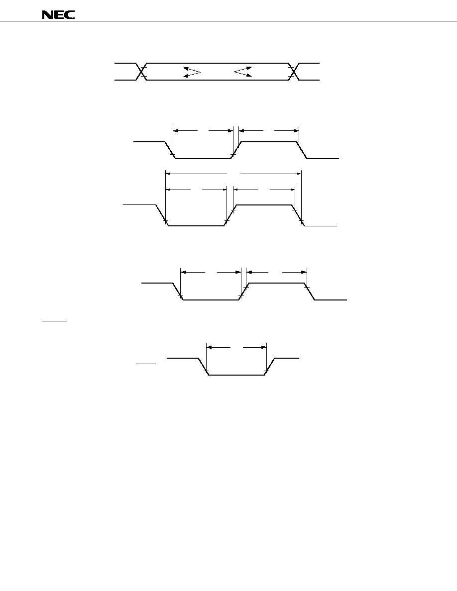
58
µ
PD178076,178078,178096,178098
Data Sheet U12885EJ3V0DS00
AC Timing Test Point (Excluding X1 Input)
0.8 V
DD
0.2 V
DD
0.8 V
DD
0.2 V
DD
Test Points
TI Timing
t
TIL0
t
TIH0
TI00, TI01
1/f
TI5
t
TIL5
t
TIH5
TI50,TI51
Interrupt Input Timing
t
INTL
t
INTH
INTP0 to INTP7
RESET Input Timing
t
RSL
RESET

59
µ
PD178076,178078,178096,178098
Data Sheet U12885EJ3V0DS00
Serial Transfer Timing
3-wire serial I/O mode:
t
KCYm
t
KLm
t
KHm
SCK0, SCK1, SCK3
SI0, SI1, SI3
SO0, SO1, SO3
t
SIKm
t
KSIm
t
KSOm
Input Data
Output Data
t
Rn
t
Fn
Remark m = 1, 2, 9, 10, 13, 14
n = 2, 10, 14
SBI mode (bus release signal transfer):
t
SIK3, 4
t
KCY3, 4
t
KL3, 4
t
KH3, 4
SCK0
t
SBL
t
SBH
t
KSB
t
SBK
t
KSI3, 4
t
KSO3, 4
SB0, SB1
t
R4
t
F4

60
µ
PD178076,178078,178096,178098
Data Sheet U12885EJ3V0DS00
SBI mode (command signal transfer):
t
SIK3, 4
t
KCY3, 4
t
KL3, 4
t
KH3, 4
SCK0
t
KSB
t
SBK
t
KSI3, 4
t
KSO3, 4
SB0, SB1
t
R4
t
F4
2-wire serial I/O mode:
t
KSO5, 6
t
SIK5, 6
t
KCY5, 6
t
KL5, 6
t
KH5, 6
SCK0
t
KSI5, 6
SB0, SB1
t
F6
t
R6
I
2
C bus mode:
SCL
SDA0, SDA1
t
SBH
t
KL7, 8
t
SBK
t
F8
t
R8
t
KCY7, 8
t
KSI7, 8
t
KH7, 8
t
SIK7, 8
t
KSO7, 8
t
SBK
t
KSB
t
KSB

61
µ
PD178076,178078,178096,178098
Data Sheet U12885EJ3V0DS00
3-wire serial I/O mode with automatic transmit/receive function:
t
SBW
t
SBD
t
KCY11
,
12
t
KH11
,
12
t
KSI11
,
12
t
KSO11
,
12
t
SIK11
,
12
D2
D1
D0
D7
D7
D2
D1
D0
SO1
SI1
SCK1
STB
t
R12
t
KL11
,
12
t
F12
3-wire serial I/O mode with automatic transmit/receive function (busy processing):
t
BYS
SCK1
t
SPS
BUSY
(Active high)
7
8
9
Note
10
Note
10 + n
Note
1
t
BYH
Note
The signal is not actually driven low here; it is shown as such to indicate the timing.
IEBus Controller Characteristics
Note 1
(T
A
= ≠40 to +85
∞
C, V
DD
= 3.5 to 5.5 V)
Parameter
Symbol
Conditions
MIN.
TYP.
MAX.
Unit
IEBus system
f
s
Fixed to mode 1
6.3
Note 2
MHz
clock frequency
Notes 1.
µ
PD178096 and 178098 only.
2. Although the system clock frequency is 6.0 MHz in the IEBus standard, in these products, normal
operation is guaranteed at 6.3 MHz.
Remark 6.0 MHz and 6.3 MHz cannot both be used as the IEBus system clock frequency.

62
µ
PD178076,178078,178096,178098
Data Sheet U12885EJ3V0DS00
Operating
frequency
A/D Converter Characteristics (T
A
= ≠40 to +85
∞
C, V
DD
= AV
DD
= 3.5 to 5.5 V)
Parameter
Symbol
Conditions
MIN.
TYP.
MAX.
Unit
Resolution
8
8
8
bit
V
DD
= 4.5 to 5.5 V
±
1.0
%FSR
±
1.4
%FSR
Conversion time
t
CONV
15.2
45.7
µ
s
Analog input voltage
V
IAN
0
V
DD
V
Notes 1. Excluding quantization error (
±
0.2%FSR)
2. This value is indicated as a ratio to the full-scall value.
PLL Characteristics (T
A
= ≠40 to +85
∞
C, V
DD
= 4.5 to 5.5 V)
Parameter
Symbol
Conditions
MIN.
TYP.
MAX.
Unit
f
IN1
VCOL pin, MF mode, sine wave input, V
IN
= 0.15 V
P-P
0.5
3.0
MHz
f
IN2
VCOL pin, HF mode, sine wave input, V
IN
= 0.15 V
P-P
10
40
MHz
f
IN3
VCOH pin, VHF mode, sine wave input, V
IN
= 0.15 V
P-P
60
130
MHz
f
IN4
VCOH pin, VHF mode, sine wave input, V
IN
= 0.3 V
P-P
40
160
MHz
Remark The above values are the result of NEC's evaluation of the device. If the device is likely to be affected
by noise in your application, it is recommended to use the device at a voltage higher than the above
values.
IFC Characteristics (T
A
= ≠40 to +85
∞
C, V
DD
= 4.5 to 5.5 V)
Parameter
Symbol
Conditions
MIN.
TYP.
MAX.
Unit
Operating
f
IN5
AMIFC pin, AMIF count mode, sine wave input,
0.4
0.5
MHz
frequency
V
IN
= 0.15 V
P-P
f
IN6
FMIFC pin, FMIF count mode, sine wave input,
10
11
MHz
V
IN
= 0.15 V
P-P
f
IN7
FMIFC pin, AMIF count mode, sine wave input,
0.4
0.5
MHz
V
IN
= 0.15 V
P-P
Remark The above values are the result of NEC's evaluation of the device. If the device is likely to be affected
by noise in your application, it is recommended to use the device at a voltage higher than the above
values.
Total conversion
error
Notes 1, 2
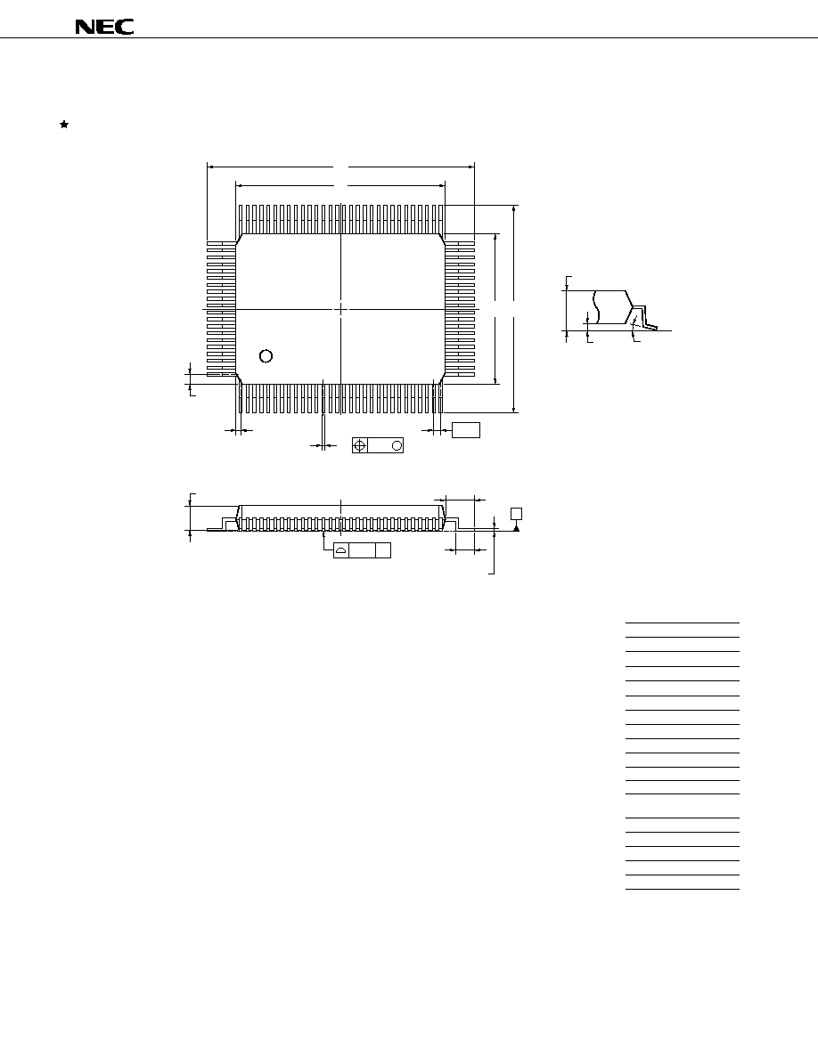
63
µ
PD178076,178078,178096,178098
Data Sheet U12885EJ3V0DS00
9. PACKAGE DRAWING
80
81
50
100
1
31
30
51
100-PIN PLASTIC QFP (14x20)
H
I
J
detail of lead end
M
Q
R
K
M
L
P
S
S
N
G
F
NOTE
Each lead centerline is located within 0.15 mm of
its true position (T.P.) at maximum material condition.
ITEM
MILLIMETERS
A
B
D
G
23.6
±
0.4
20.0
±
0.2
0.30
±
0.10
0.6
H
17.6
±
0.4
I
C
14.0
±
0.2
0.15
J
0.65 (T.P.)
K
1.8
±
0.2
L
0.8
±
0.2
F
0.8
P100GF-65-3BA1-4
N
P
Q
0.10
2.7
±
0.1
0.1
±
0.1
R
5
∞±
5
∞
S
3.0 MAX.
M
0.15
+
0.10
-
0.05
C D
A
B
S

64
µ
PD178076,178078,178096,178098
Data Sheet U12885EJ3V0DS00
10. RECOMMENDED SOLDERING CONDITIONS
Solder this product under the following recommended conditions.
For details of the recommended soldering conditions, refer to information document Semiconductor Device
Mounting Technology Manual (C10535E).
For soldering methods and conditions other than those recommended, consult NEC.
Table 10-1. Soldering Conditions for Surface-Mount Type
µ
PD178076GF-XXX-3BA: 100-pin plastic QFP (14
◊
20)
µ
PD178078GF-XXX-3BA: 100-pin plastic QFP (14
◊
20)
µ
PD178096GF-XXX-3BA: 100-pin plastic QFP (14
◊
20)
µ
PD178098GF-XXX-3BA: 100-pin plastic QFP (14
◊
20)
Soldering Method
Soldering Conditions
Recommended
Conditions Symbol
Infrared reflow
Package peak temperature: 235
∞
C, Time: 30 sec max. (210
∞
C min.),
IR35-00-3
Number of times: 3 max.
VPS
Package peak temperature: 215
∞
C, Time: 40 sec max. (200
∞
C min.),
VP15-00-3
Number of times: 3 max.
Wave soldering
Solder bath temperature: 260
∞
C max., Time: 10 sec max.,
WS60-00-1
Number of times: 1, Preheating temperature: 120
∞
C max.,
(Package surface temperature)
Partial heating
Pin temperature: 300
∞
C max., Time: 3 sec max (per device side)
≠
Caution Do not use two or more soldering methods in combination (except partial heating).

65
µ
PD178076, 178078, 178096, 178098
Data Sheet U12885EJ3V0DS00
APPENDIX A. DEVELOPMENT TOOLS
The following development tools are available for development of systems using the
µ
PD178078 and 178098
subseries.
Language processor software
RA78K/0
Notes 1, 2, 3
Assembler package common to 78K/0 series
CC78K/0
Notes 1, 2, 3
C compiler package common to 78K/0 series
DF178098
Notes 1, 2, 3
Device file for
µ
PD178078 subseries and
µ
PD178098 subseries
CC78K0-L
Notes 1, 2, 3
C compiler library source file common to 78K/0 series
Flash memory writing tools
Fashpro III
Dedicated flash programmer
(Part number:
FL-PR3
Note 4
, PG-FL3)
FA-100GF-3BA
Note 4
Flash programmer adapter
Debugging tools
∑ When in-circuit emulator IE-78K0-NS is used
IE-78K0-NS
In-circuit emulator common to 78K/0 series
IE-70000-MC-PS-B
Power supply unit for IE-78K0-NS
IE-78K0-NS-PA
Performance board for enhancing and expanding the IE-78K0-NS function
IE-70000-98-IF-C
Interface adapter necessary when PC-9800 series (except notebook type) is used as host machine
(C bus supported)
IE-70000-CD-IF-A
PC card and interface cable necessary when a notebook-type PC is used as host machine (PCMCIA
socket supported)
IE-70000-PC-IF-C
Interface adapter necessary when a IBM PC/AT
TM
compatible machine is used as host machine (ISA
bus supported)
IE-70000-PCI-IF
Interface adapter necessary when a PC with a PCI bus is used as host machine
IE-178098-NS-EM1
Emulation board to emulate
µ
PD178078 and 178098 subseries
NP-100GF
Note 4
Emulation probe for 100-pin plastic QFP (GF-3BA type)
EV-9200GF-100
Socket mounted on board of target system created for 100-pin plastic QFP (GF-3BA type)
SM78K0
Notes 1, 2
System simulator common to 78K/0 series
ID78K0-NS
Notes 1, 2
Integrated debugger common to 78K/0 series
DF178098
Notes 1, 2, 3
Device file for
µ
PD178078 subseries and
µ
PD178098 subseries
Notes 1. PC-9800 series (Japanese Windows
TM
) based
2. IBM PC/AT compatible machine (Japanese/English windows) based
3. HP9000 series 700
TM
(HP-UX
TM
) based, SPARCstation
TM
(SunOS
TM
, Solaris
TM
) based, NEWS
TM
(NEWS-OS
TM
) based
4. Products of Naito Densei Machida Mfg. Co., Ltd. (Tel: 044-822-3813).
Remark Use the RA78K0, CC78K0, and SM78K0 in combination with the DF178098.

66
µ
PD178076, 178078, 178096, 178098
Data Sheet U12885EJ3V0DS00
∑ When in-circuit emulator IE-78001-R-A is used
IE-78001-R-A
In-circuit emulator common to 78K/0 series
IE-70000-98-IF-C
Interface adapter necessary when PC-9800 series (except notebook type) is used as host machine
(C bus supported)
IE-70000-PC-IF-C
Interface adapter necessary when IBM PC/AT compatible machine is used as host machine (ISA
bus supported)
IE-70000-PCI-IF
Interface adapter necessary when a PC with a PCI bus is used as host machine
IE-78000-R-SV3
Interface adapter and cable necessary when EWS is used as host machine
IE-178098-NS-EM1
Emulation board to emulate
µ
PD178078 and 178098 subseries
IE-78K0-R-EX1
Emulation probe conversion board necessary when using IE-178098-NS-EM1 on IE-78001-R-A
EP-78064GF-R
Emulation probe for 100-pin plastic QFP (GF-3BA type)
EV-9200GF-100
Socket mounted on board of target system created for 100-pin plastic QFP (GF-3BA type)
SM78K0
Notes 1, 2
System simulator common to 78K/0 series
ID78K0
Notes 1, 2
Integrated debugger common to 78K/0 series
DF178098
Notes 1, 2, 3
Device file for
µ
PD178078 subseries and
µ
PD178098 subseries
Real-time OS
RX78K/0
Notes 1, 2, 3
Real-time OS for 78K/0 series
MX78K0
Notes 1, 2, 3
OS for 78K/0 series
Notes 1. PC-9800 series (Japanese Windows) based
2. IBM PC/AT compatible machine (Japanese/English windows) based
3. HP9000 series 700 (HP-UX) based, SPARCstation (SunOS, Solaris) based, NEWS (NEWS-OS)
based
Remark Use the SM78K0 in combination with the DF178098.
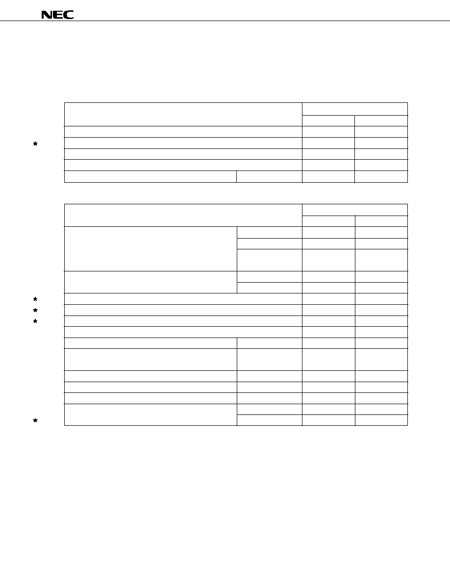
67
µ
PD178076, 178078, 178096, 178098
Data Sheet U12885EJ3V0DS00
Device Documents
Title
Document No.
Japanese
English
µ
PD178076, 178078, 178096, 178098 Data Sheet
U12885J
This document
µ
PD178F098 Data Sheet
U12920J
U12920E
µ
PD178078, 178098 Subseries User's Manual
U12790J
U12790E
78K/0 Series User's Manual - Instruction
U12326J
U12326E
78K/0 Series Application Note
Basics (I)
U12704J
U12704E
Development Tool Documents (User's Manual)
Title
Document No.
Japanese
English
RA78K0 Assembler Package
Operation
U11802J
U11802E
Assembly Language
U11801J
U11801E
Structured Assembly
U11789J
U11789E
Language
CC78K0 C Compiler
Operation
U11517J
U11517E
Language
U11518J
U11518E
IE-78001-R-A
U14142J
To be prepared
IE-78K0-NS
U13731J
U13731E
IE-178098-NS-EM1
U14013J
U14013E
EP-78064
EEU-934
EEU-1469
SM78K0 System Simulator Windows Based
Reference
U10181J
U10181E
SM78K Series System Simulator
U10092J
U10092E
ID78K0 Integrated Debugger EWS Based
Reference
U11151J
--
ID78K0 Integrated Debugger PC Based
Reference
U11539J
U11539E
ID78K0 Integrated Debugger Windows Based
Guide
U11649J
U11649E
ID78K0-NS Integrated Debugger Windows Based
Reference
U12900J
U12900E
Operation
U14379J
To be prepared
APPENDIX B. RELATED DOCUMENTS
The related documents indicated in this publication may include preliminary versions. However, preliminary
versions are not marked as such.
External Parts User
Open Interface
Specifications
Caution The contents of the above documents are subject to change without notice. Please ensure that
the latest versions are used in design work, etc.

68
µ
PD178076, 178078, 178096, 178098
Data Sheet U12885EJ3V0DS00
Title
Document No.
Japanese
English
78K/0 Series Real-time OS
Fundamental
U11537J
U11537E
Installation
U11536J
U11536E
78K/0 Series OS MX78K0
Fundamental
U12257J
U12257E
Other Documents
Title
Document No.
Japanese
English
SEMICONDUCTOR SELECTION GUIDE Products & Packages (CD-ROM)
X13769X
Semiconductor Device Mounting Technology Manual
C10535J
C10535E
Quality Guides on NEC Semiconductor Devices
C11531J
C11531E
NEC Semiconductor Device Reliability and Quality Control
C10983J
C10983E
Guide to Prevent Damage for Semiconductor Devices by Electrostatic Discharge (ESD)
C11892J
C11892E
Semiconductor Device Quality/Reliability Handbook
C12769J
--
Microcomputer Product Series Guide
U11416J
--
Related Documents for Embedded Software (User's Manual)
Caution The contents of the above documents are subject to change without notice. Ensure that the
latest versions are used in design work, etc.

69
µ
PD178076, 178078, 178096, 178098
Data Sheet U12885EJ3V0DS00
[MEMO]

70
µ
PD178076, 178078, 178096, 178098
Data Sheet U12885EJ3V0DS00
Purchase of NEC I
2
C components conveys a license under the Philips I
2
C Patent Rights to use these components in an I
2
C
system, provided that the system conforms to the I
2
C Standard Specification as defined by Philips.
IEBus is a trademark of NEC Corporation.
Windows is either a registered trademark or trademark of Microsoft Corporation in the United States and/
or other countries.
PC/AT is a trademark of IBM Corporation.
HP9000 series 700 and HP-UX are trademarks of Hewlett-Packard Company.
SPARCstation is a trademark of SPARC International, Inc.
Solaris and SunOS are trademarks of Sun Microsystems, Inc.
NEWS and NEWS-OS are trademarks of Sony Corporation.
NOTES FOR CMOS DEVICES
1
PRECAUTION AGAINST ESD FOR SEMICONDUCTORS
Note:
Strong electric field, when exposed to a MOS device, can cause destruction of the gate oxide and
ultimately degrade the device operation. Steps must be taken to stop generation of static electricity
as much as possible, and quickly dissipate it once, when it has occurred. Environmental control
must be adequate. When it is dry, humidifier should be used. It is recommended to avoid using
insulators that easily build static electricity. Semiconductor devices must be stored and trans-
ported in an anti-static container, static shielding bag or conductive material. All test and
measurement tools including work bench and floor should be grounded. The operator should be
grounded using wrist strap. Semiconductor devices must not be touched with bare hands. Similar
precautions need to be taken for PW boards with semiconductor devices on it.
2
HANDLING OF UNUSED INPUT PINS FOR CMOS
Note:
No connection for CMOS device inputs can be cause of malfunction. If no connection is provided
to the input pins, it is possible that an internal input level may be generated due to noise, etc., hence
causing malfunction. CMOS devices behave differently than Bipolar or NMOS devices. Input
levels of CMOS devices must be fixed high or low by using a pull-up or pull-down circuitry. Each
unused pin should be connected to V
DD
or GND with a resistor, if it is considered to have a
possibility of being an output pin. All handling related to the unused pins must be judged device
by device and related specifications governing the devices.
3
STATUS BEFORE INITIALIZATION OF MOS DEVICES
Note:
Power-on does not necessarily define initial status of MOS device. Production process of MOS
does not define the initial operation status of the device. Immediately after the power source is
turned ON, the devices with reset function have not yet been initialized. Hence, power-on does
not guarantee out-pin levels, I/O settings or contents of registers. Device is not initialized until
the reset signal is received. Reset operation must be executed immediately after power-on for
devices having reset function.

71
µ
PD178076, 178078, 178096, 178098
Data Sheet U12885EJ3V0DS00
NEC Electronics Inc. (U.S.)
Santa Clara, California
Tel: 408-588-6000
800-366-9782
Fax: 408-588-6130
800-729-9288
NEC Electronics (Germany) GmbH
Duesseldorf, Germany
Tel: 0211-65 03 02
Fax: 0211-65 03 490
NEC Electronics (UK) Ltd.
Milton Keynes, UK
Tel: 01908-691-133
Fax: 01908-670-290
NEC Electronics Italiana s.r.l.
Milano, Italy
Tel: 02-66 75 41
Fax: 02-66 75 42 99
NEC Electronics Hong Kong Ltd.
Hong Kong
Tel: 2886-9318
Fax: 2886-9022/9044
NEC Electronics Hong Kong Ltd.
Seoul Branch
Seoul, Korea
Tel: 02-528-0303
Fax: 02-528-4411
NEC Electronics Singapore Pte. Ltd.
United Square, Singapore 1130
Tel: 65-253-8311
Fax: 65-250-3583
NEC Electronics Taiwan Ltd.
Taipei, Taiwan
Tel: 02-2719-2377
Fax: 02-2719-5951
NEC do Brasil S.A.
Electron Devices Division
Rodovia Presidente Dutra, Km 214
07210-902-Guarulhos-SP Brasil
Tel: 55-11-6465-6810
Fax: 55-11-6465-6829
NEC Electronics (Germany) GmbH
Benelux Office
Eindhoven, The Netherlands
Tel: 040-2445845
Fax: 040-2444580
NEC Electronics (France) S.A.
Velizy-Villacoublay, France
Tel: 01-30-67 58 00
Fax: 01-30-67 58 99
NEC Electronics (France) S.A.
Spain Office
Madrid, Spain
Tel: 91-504-2787
Fax: 91-504-2860
NEC Electronics (Germany) GmbH
Scandinavia Office
Taeby, Sweden
Tel: 08-63 80 820
Fax: 08-63 80 388
Regional Information
Some information contained in this document may vary from country to country. Before using any NEC
product in your application, please contact the NEC office in your country to obtain a list of authorized
representatives and distributors. They will verify:
∑ Device availability
∑ Ordering information
∑ Product release schedule
∑ Availability of related technical literature
∑ Development environment specifications (for example, specifications for third-party tools and
components, host computers, power plugs, AC supply voltages, and so forth)
∑ Network requirements
In addition, trademarks, registered trademarks, export restrictions, and other legal issues may also vary
from country to country.
J99.1

µ
PD178076, 178078, 178096, 178098
The export of this product from Japan is regulated by the Japanese government. To export this product may be prohibited
without governmental license, the need for which must be judged by the customer. The export or re-export of this product
from a country other than Japan may also be prohibited without a license from that country. Please call an NEC sales
representative.
M8E 00. 4
The information in this document is current as of June, 2000. The information is subject to change
without notice. For actual design-in, refer to the latest publications of NEC's data sheets or data
books, etc., for the most up-to-date specifications of NEC semiconductor products. Not all products
and/or types are available in every country. Please check with an NEC sales representative for
availability and additional information.
No part of this document may be copied or reproduced in any form or by any means without prior
written consent of NEC. NEC assumes no responsibility for any errors that may appear in this document.
NEC does not assume any liability for infringement of patents, copyrights or other intellectual property rights of
third parties by or arising from the use of NEC semiconductor products listed in this document or any other
liability arising from the use of such products. No license, express, implied or otherwise, is granted under any
patents, copyrights or other intellectual property rights of NEC or others.
Descriptions of circuits, software and other related information in this document are provided for illustrative
purposes in semiconductor product operation and application examples. The incorporation of these
circuits, software and information in the design of customer's equipment shall be done under the full
responsibility of customer. NEC assumes no responsibility for any losses incurred by customers or third
parties arising from the use of these circuits, software and information.
While NEC endeavours to enhance the quality, reliability and safety of NEC semiconductor products, customers
agree and acknowledge that the possibility of defects thereof cannot be eliminated entirely. To minimize
risks of damage to property or injury (including death) to persons arising from defects in NEC
semiconductor products, customers must incorporate sufficient safety measures in their design, such as
redundancy, fire-containment, and anti-failure features.
NEC semiconductor products are classified into the following three quality grades:
"Standard", "Special" and "Specific". The "Specific" quality grade applies only to semiconductor products
developed based on a customer-designated "quality assurance program" for a specific application. The
recommended applications of a semiconductor product depend on its quality grade, as indicated below.
Customers must check the quality grade of each semiconductor product before using it in a particular
application.
"Standard": Computers, office equipment, communications equipment, test and measurement equipment, audio
and visual equipment, home electronic appliances, machine tools, personal electronic equipment
and industrial robots
"Special":
Transportation equipment (automobiles, trains, ships, etc.), traffic control systems, anti-disaster
systems, anti-crime systems, safety equipment and medical equipment (not specifically designed
for life support)
"Specific": Aircraft, aerospace equipment, submersible repeaters, nuclear reactor control systems, life
support systems and medical equipment for life support, etc.
The quality grade of NEC semiconductor products is "Standard" unless otherwise expressly specified in NEC's
data sheets or data books, etc. If customers wish to use NEC semiconductor products in applications not
intended by NEC, they must contact an NEC sales representative in advance to determine NEC's willingness
to support a given application.
(Note)
(1) "NEC" as used in this statement means NEC Corporation and also includes its majority-owned subsidiaries.
(2) "NEC semiconductor products" means any semiconductor product developed or manufactured by or for
NEC (as defined above).
∑
∑
∑
∑
∑
∑