
Data Sheet
August 2000
U13749EU2V0DS00
1
NEC VRC chipsets are designed and Verified for use with NEC VR SeriesTM microprocessors. NEC makes
no claim as to the suitability of VRC chipsets for use with non-NEC microprocessors and does not warrant
their performance, suitability or use in such applications.
V
RC
4375 System Controller
Description
The V
RC
4375
TM
system controller is a software-configurable chip that interfaces directly
with an NEC V
R
43xx
TM
64-bit MIPS
RISC CPU and PCI bus without external logic or
buffering. The system controller also interfaces with memory (SDRAM, EDO, fast-page
DRAM, and flash/boot ROM) with minimal to no buffering. The memory bus can also
interface with SRAM and general-purpose I/O devices. As an interface with the V
R
43xx
CPU, the V
RC
4375 acts as a memory controller, DMA controller, and PCI bridge. As an
interface with PCI agents, the V
RC
4375 acts as either a PCI bus master or a PCI bus
target. Alternatively, the V
RC
4375 may be located on a PCI bus add-on board.
Features
Y
CPU Interface
�
Direct connection to the 66 MHz V
R
43xx CPU bus
�
3.3-volt I/O
�
Support for all V
R
43xx bus cycles
�
Little-endian or big-endian byte ordering modes
Y
Memory Interface
�
Support for boot ROM/flash memory, base memory, and up to two SIMMs
�
SIMM capacity of up to 128 MB
�
Programmable address ranges for base and SIMM memory
�
Support for two-bank 4/16 Mb devices and four-bank 64/128/256 Mb devices
�
CAS latency of 2 or 3 in base memory or SIMM SDRAM, programmable to
support faster new devices or slower legacy devices
�
SIMM burst access time programmable in one or two cycle(s)
�
66 MHz memory bus
�
64 MB base memory range: SDRAM and EDO DRAM
�
256 MB SIMM memory range: SDRAM, EDO and fast-page DRAM
�
Several speed grades supported within each memory range
�
Open DRAM page maintained within base memory
�
Eight-word (32-byte) write FIFO (CPU to memory)
�
Two-word (8-byte) prefetch FIFO (memory to CPU or memory to PCI)
�
On-chip DRAM and SDRAM refresh generation
�
Up to 64 MB of write-protectable boot ROM or up to 64 MB of flash ROM
�
Flash/boot ROM devices with 8-/16-/32-bit configuration support
�
Programmable timing to interface general-purpose I/O device or boot ROM in
the boot ROM address range

2
V
RC
4375 System Controller
Y
PCI Interface
�
Master and target capabilities
�
Host bridge and add-on board modes
�
PCI bus arbiter with programmable arbitration scheme
�
Programmable arbitration scheme for PCI/CPU accessed to memory
�
Big-endian or little-endian byte ordering modes
�
4-word (16-byte) bidirectional PCI master FIFO (CPU is PCI bus master)
�
8-word (32-byte) bidirectional PCI target FIFO (memory is PCI bus target)
�
33 MHz PCI bus clock rate
�
132 MB/s burst transfers
�
Interrupt support for add-on board mode
�
3.3 V inputs; 5 V-tolerant inputs/outputs
Y
DMA Controller
�
Four highly robust DMA channels
�
CPU-initiated block transfers between memory and PCI bus
�
8-word (32-byte) bidirectional DMA FIFO
�
Sophisticated, programmable DMA channel arbitration priority scheme
�
Four sets of DMA control registers for chained transfers
�
Next address pointer in each channel to support scatter/gather operation
�
Programmable DMA arbitration priority
�
Bidirectional unaligned transfers
�
Transfers at maximum PCI bandwidth of 132 MB/s
Y
Interrupt Controller
�
Nonmaskable interrupt and interrupt signals (NMI# and INT#)
�
Maskable interrupt-causing events
Y
UART
�
NY16550L Universal Asynchronous Receiver/Transmitter
�
Modem control functions
�
Separate receiver and transmitter FIFOs (16 bytes each)
�
Even-, odd- or no-parity bit generation
�
Fully prioritized interrupt control
Y
Timers
�
One 32-bit loadable watchdog timer that generates a nonmaskable interrupt
�
Two 32-bit loadable general-purpose timers that generate interrupts
�
Highly sophisticated timers with programmable clock, start/stop, auto reload/
restart, and enable/disable interrupt bits
Ordering
Information
Part Number
Package
V
RC
4375
�
PD65948S1-068
256-pin TBGA
3
V
RC
4375 System Controller
System
Configuration
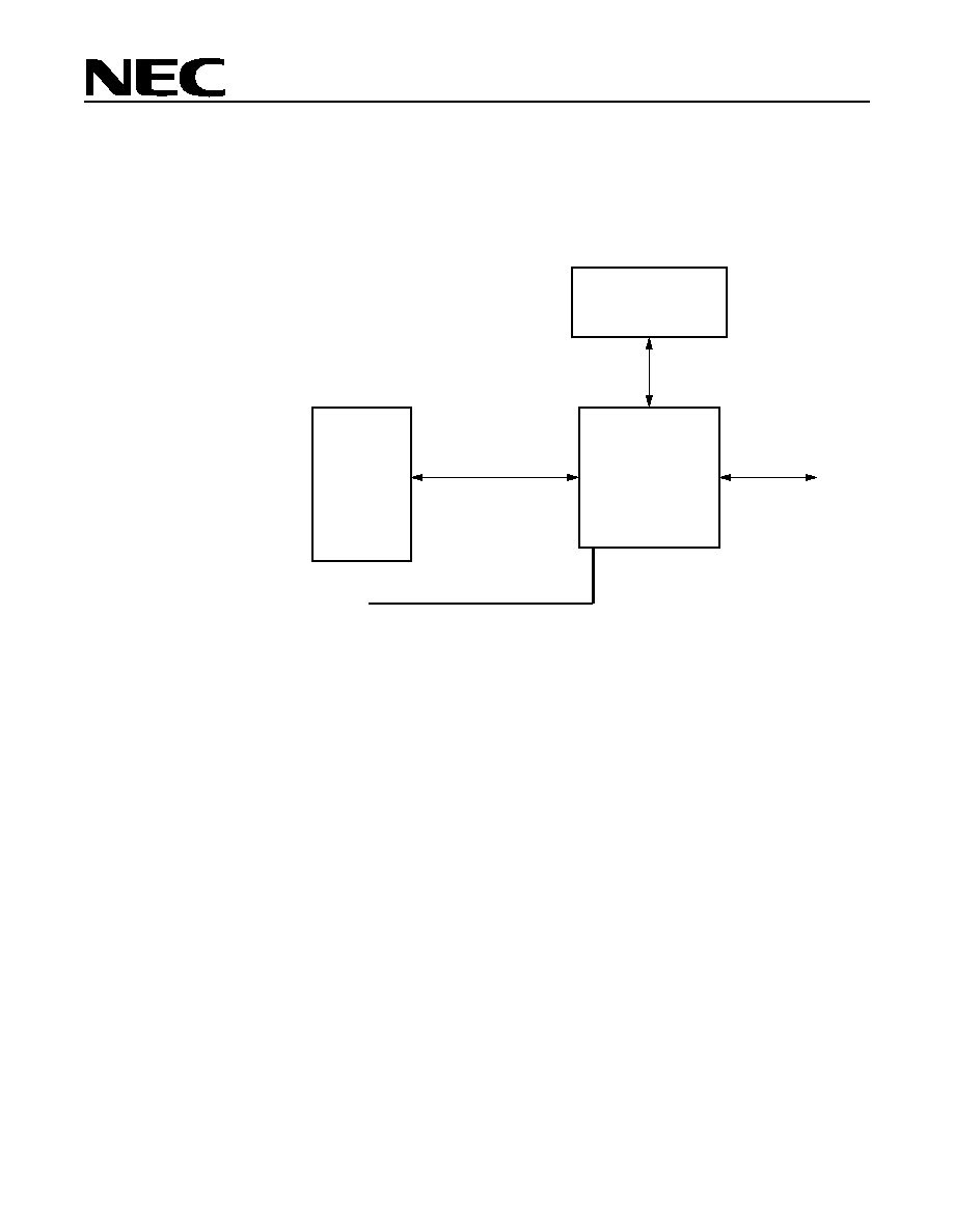
Figure 1 shows the controller used as a host bridge in a typical system. Alternatively,
the controller can be located on a PCI bus Add-On Board.
Figure 1. System Connection
Note: F244- or F245-type buffers may be needed on the MuxAD bus and, for DIMM, on certain chip-select
signals.
V
R
43xx
CPU
V
RC
4375
System
Controller
Memory
PCI Bus
UART
32 bits, 66 MHz
32 bits, 33 MHz
32 bits, 66 MHz

4
V
RC
4375 System Controller
Terminology
In this document:
Y
Signal names ending with # (such as NMI#)
are active-low signals
.
Y
Word
means 4 bytes. This definition of word differs from the definition in the
PCI
Local Bus Specification
, where a word is 2 bytes.
Y
B
means byte.
Y
b
means bit.
Y
CAS
means column address strobe.
Y
Memory
means the local memory attached to the V
RC
4375 controller.
Y
SIMM
TM
and
DIMM
TM
mean single and dual in-line memory module unless
explicitly stated otherwise.
Y
Module
means a set of chips, as in a SIMM or DIMM.
Y
EDO DRAM
means extended data out dynamic random access memory.
Y
SDRAM
means synchronous DRAM.
Y
RDRAM
means Rambus
DRAM, which is designed to conform to the interface
that defines the Rambus Channel.
Reference
Documents
The following documents were used in the creation of this data sheet. Unless other-
wise specified, the latest version of each document applies.
Y
MIPS
�
R4300 Preliminary RISC Processor Specification Revision 2.2
(available
from MIPS Technologies, Inc.)
Y
PCI Local Bus Specification Revision 2.1
and
PCI System Design Guide Revision
1.0
(available from the Peripheral Component Interconnect Special Interest
Group)
Y
NEC
V
R
4300
TM
Microprocessor User's Manual
(document number
U10504EJ6V0UM00)

5
V
RC
4375 System Controller
Contents
Description . . . . . . . . . . . . . . . . . . . . . . . . . . . . . . . . . . . . . . . . . . . . . 1
Features . . . . . . . . . . . . . . . . . . . . . . . . . . . . . . . . . . . . . . . . . . . . . . 1
Ordering Information . . . . . . . . . . . . . . . . . . . . . . . . . . . . . . . . . . . . . 2
System Configuration . . . . . . . . . . . . . . . . . . . . . . . . . . . . . . . . . . . . 3
Terminology . . . . . . . . . . . . . . . . . . . . . . . . . . . . . . . . . . . . . . . . . . . . 4
Reference Documents . . . . . . . . . . . . . . . . . . . . . . . . . . . . . . . . . . . . 4
1.0
Pin Configuration . . . . . . . . . . . . . . . . . . . . . . . . . . . . . . . . . . . . . . . . 6
2.0
Block Diagram . . . . . . . . . . . . . . . . . . . . . . . . . . . . . . . . . . . . . . . . . . 9
3.0
Signal Summary . . . . . . . . . . . . . . . . . . . . . . . . . . . . . . . . . . . . . . . . 11
4.0
Registers, Resources, and Implementation . . . . . . . . . . . . . . . . . . . 14
5.0
CPU Interface . . . . . . . . . . . . . . . . . . . . . . . . . . . . . . . . . . . . . . . . . . 17
6.0
Memory Interface . . . . . . . . . . . . . . . . . . . . . . . . . . . . . . . . . . . . . . . 18
7.0
PCI Bus Interface . . . . . . . . . . . . . . . . . . . . . . . . . . . . . . . . . . . . . . . 54
8.0
DMA Transfers . . . . . . . . . . . . . . . . . . . . . . . . . . . . . . . . . . . . . . . . . 73
9.0
Interrupts. . . . . . . . . . . . . . . . . . . . . . . . . . . . . . . . . . . . . . . . . . . . . . 83
10.0
Clocking . . . . . . . . . . . . . . . . . . . . . . . . . . . . . . . . . . . . . . . . . . . . . . 91
11.0
Reset Configuration Signals . . . . . . . . . . . . . . . . . . . . . . . . . . . . . . . 92
12.0
Endian Mode Software Issues . . . . . . . . . . . . . . . . . . . . . . . . . . . . . 93
13.0
Timing Diagrams. . . . . . . . . . . . . . . . . . . . . . . . . . . . . . . . . . . . . . . 102
14.0
Electrical Characteristics . . . . . . . . . . . . . . . . . . . . . . . . . . . . . . . . 149
15.0
Package Drawing . . . . . . . . . . . . . . . . . . . . . . . . . . . . . . . . . . . . . . 154