Document Outline
- COVER
- FEATURES
- APPLICATIONS
- ORDERING INFORMATION
- PIN CONFIGURATION
- PIN NAMES
- INTERNAL BLOCK DIAGRAM
- CONTENTS
- 1. PIN FUNCTIONS
- 2. ELECTRICAL SPECIFICATIONS
- 3. PACKAGE DRAWING
- 4. RECOMMENDED SOLDERING CONDITIONS
- APPENDIX DIFFERENCES AMONG VR5432, VR5000 TM , AND VR4310 TM

The information in this document is subject to change without notice. Before using this document, please
confirm that this is the latest version.
Not all devices/types available in every country. Please check with local NEC representative for
availability and additional information.
MOS INTEGRATED CIRCUIT
µ
µ
µ
µ
PD30541
V
R
5432
TM
64-BIT MICROPROCESSOR
Document No. U13504EJ3V0DS00 (3rd edition)
Date Published August 2000 J CP(K)
Printed in Japan
PRELIMINARY DATA SHEET
1998
The
µ
PD30541 (V
R
5432) is a member of the V
R
Series
TM
RISC (Reduced Instruction Set Computer)
microprocessors. It is a high-performance 64-bit microprocessor employing the RISC architecture developed by
MIPS
TM
.
The V
R
5432 employs a 32-bit bus for the system interface and can operate with a protocol compatible to that of
the V
R
4300 Series
TM
.
For the detailed functional description and when designing your system, refer to the following manual:
∑
∑
∑
∑
V
R
5432 Preliminary User's Manual (U14011E)
FEATURES
∑
MIPS 64-bit RISC architecture
∑
Maximum operating frequency
∑
High-speed operation processing
Internal: 167 MHz, External: 83.3 MHz
∑
Dual-issue superscaler 5-stage pipeline
∑
External/internal multiple selectable from
◊
2 to
◊
4
∑
6.6 SPECint95, 3.6 SPECfp95, 316 MIPS
∑
Conforms MIPS I, II, III, and IV instruction sets. Also
∑
High-speed translation lookaside buffer (TLB) (48 entries)
supports multimedia instructions
∑
Address space Physical: 32 bits, Virtual: 40 bits
∑
Supply voltage
∑
Floating-point unit (FPU)
Core block: 2.5 V
±
5%, I/O block: 3.3 V
±
0.3 V
∑
Supports sum-of-products instructions
∑
On-chip primary cache memory (instruction/data: 32 KB each)
∑
32-bit address/data multiplexed bus
∑
Operates with protocol compatible to V
R
4300 Series
APPLICATIONS
∑
Set-top-box
∑
Page printer controller
∑
Amusement machines, etc.
ORDERING INFORMATION
Part Number
Package
Maximum Operating Frequency (MHz)
µ
PD30541GD-167-WML
208-pin plastic QFP (fine pitch) (28
◊
28)
167
Preliminary Data Sheet U13504EJ3V0DS00
2
µ
µ
µ
µ
PD30541
PIN CONFIGURATION
∑
208-pin plastic QFP (fine pitch) (28
◊
28)
µ
PD30541GD-167-WML
V
SS
V
SS
SysAD21
V
CC
IO
SysAD20
V
CC
SysAD19
V
SS
V
SS
SysAD18
V
CC
IO
SysAD17
V
SS
SysAD16
V
CC
SysAD15
V
SS
SysAD14
V
CC
IO
V
SS
SysAD13
V
SS
SysAD12
V
CC
V
CC
IO
V
SS
SysAD11
V
SS
SysAD10
V
SS
V
CC
IO
V
CC
SysAD9
V
SS
SysAD8
V
CC
IO
V
SS
NMI
V
CC
Int0
V
CC
IO
Int1
V
SS
Int2
V
CC
Int3
V
SS
Int4
V
CC
RMode/BKTGIO
V
CC
IO
V
SS
V
SS
V
SS
V
CC
IO
TrcData0
V
CC
TrcData1
V
SS
TrcClk
V
SS
V
CC
IO
V
CC
TrcData2
V
SS
TrcData3
V
SS
V
CC
IO
TrcEnd
V
CC
IO
V
SS
V
CC
IOP
V
SS
Reserved
V
CC
SysClock
V
SS
V
CC
P
PLLCAP
V
SS
P
V
CC
IO
V
SS
V
CC
IO
V
CC
DivMode1
V
SS
DivMode0
V
CC
IO
BigEndian
V
SS
ColdReset
V
CC
Tristate
V
CC
IO
JTMS
V
SS
V
CC
JTCK
V
SS
JTDI
V
CC
IO
V
CC
V
SS
V
SS
1
2
3
4
5
6
7
8
9
10
11
12
13
14
15
16
17
18
19
20
21
22
23
24
25
26
27
28
29
30
31
32
33
34
35
36
37
38
39
40
41
42
43
44
45
46
47
48
49
50
51
52
53
54
55
56
57
58
59
60
61
62
63
64
65
66
67
68
69
70
71
72
73
74
75
76
77
78
79
80
81
82
83
84
85
86
87
88
89
90
91
92
93
94
95
96
97
98
99
100
101
102
103
104
156
155
154
153
152
151
150
149
148
147
146
145
144
143
142
141
140
139
138
137
136
135
134
133
132
131
130
129
128
127
126
125
124
123
122
121
120
119
118
117
116
115
114
113
112
111
110
109
108
107
106
105
208
207
206
205
204
203
202
201
200
199
198
197
196
195
194
193
192
191
190
189
188
187
186
185
184
183
182
181
180
179
178
177
176
175
174
173
172
171
170
169
168
167
166
165
164
163
162
161
160
159
158
157
V
CC
IO
V
SS
SysAD29
V
CC
WrRdy
V
SS
RdRdy
V
CC
IO
SysAD30
V
CC
ValidOut
V
SS
SysAD31
V
CC
IO
PReq
V
SS
SysAD0
V
CC
V
SS
V
CC
IO
SysAD1
V
SS
SysAD2
V
SS
SysAD3
V
CC
V
CC
IO
V
SS
SysAD4
V
SS
V
CC
IO
V
CC
SysAD5
V
SS
SysAD6
V
CC
IO
SysAD7
V
SS
V
CC
V
SS
V
CC
IO
SysADC3
V
SS
SysADC2
V
CC
SysADC1
V
CC
IO
SysADC0
V
SS
JTDO
V
SS
V
SS
V
SS
V
CC
IO
SysAD22
V
CC
V
SS
SysAD23
V
SS
SysAD24
V
CC
V
CC
IO
SysCmd8
V
SS
SysCmd7
V
SS
SysCmd6
V
CC
IO
SysCmd5
V
CC
SysCmd4
V
SS
SysCmd3
V
CC
IO
SysCmd2
V
SS
Validin
V
CC
OptionR43K
V
CC
IO
V
SS
Reset
V
CC
SysCmd1
V
CC
IO
SysCmd0
V
SS
ExtRqst
V
SS
V
CC
SysAD25
V
CC
IO
Release
V
SS
SysAD26
V
CC
SysAD27
V
SS
V
CC
IO
V
SS
SysAD28
V
CC
V
SS
V
SS
Caution Leave open for the Reserved pin.

Preliminary Data Sheet U13504EJ3V0DS00
3
µ
µ
µ
µ
PD30541
PIN NAMES
BigEndian:
Endian Mode Select
BKTGIO:
Break/Trigger I/O
ColdReset:
Cold Reset
DivMode (1:0):
Divide Mode
ExtRqst:
External Request
Int (4:0):
Interrupt Request
JTCK:
JTAG Clock
JTDI:
JTAG Data Input
JTDO:
JTAG Data Output
JTMS:
JTAG Mode Select
OptionR43K:
V
R
4300
TM
Mode Select
NMI:
Non-maskable Interrupt Request
PLLCAP:
PLL Capacitor
PReq:
Processor Request
RdRdy:
Read Ready
Release:
Release Interface
Reset:
Reset
Reserved:
Reserved
RMode:
Reset Mode
SysAD (31:0):
System Address/Data Bus
SysADC (3:0):
System Address/Data Check Bus
SysClock:
System Clock
SysCmd (8:0):
System Command/Data Identifier
TrcClk:
Trace Clock
TrcData (3:0):
Trace Data
TrcEnd:
Trace End
Tristate:
3-state
Validln:
Valid Input
ValidOut:
Valid Output
V
CC
:
Power Supply for Processor Core
V
CC
IO:
Power Supply for Processor I/O
V
CC
IOP:
Quiet V
CC
IO for PLL
V
CC
P:
Quiet V
CC
for PLL
V
SS
:
Ground
V
SS
P:
Quiet V
SS
for PLL
WrRdy:
Write Ready

Preliminary Data Sheet U13504EJ3V0DS00
4
µ
µ
µ
µ
PD30541
INTERNAL BLOCK DIAGRAM
SysAD bus
(32 bits)
Internal bus (64 bits)
Test interface
System interface
Instruction cache
ALU0
SysClock
V
R
5432
Vector unit
Sum-of-products
operation unit
ALU1
Data cache
Register file
Memory
management
unit
Clock generator

Preliminary Data Sheet U13504EJ3V0DS00
5
µ
µ
µ
µ
PD30541
CONTENTS
1. PIN FUNCTIONS ......................................................................................................................................6
2. ELECTRICAL SPECIFICATIONS ..........................................................................................................10
3. PACKAGE DRAWING ............................................................................................................................18
4. RECOMMENDED SOLDERING CONDITIONS .....................................................................................19
APPENDIX DIFFERENCES AMONG V
R
5432, V
R
5000
TM
, AND V
R
4310
TM
.................................................20

Preliminary Data Sheet U13504EJ3V0DS00
6
µ
µ
µ
µ
PD30541
1. PIN FUNCTIONS
Caution The functions of some pins change depending on the status of the OptionR43K signal. If this
signal is low, the signal names same as those of the V
R
4300 Series are used because these pins
have functions compatible to those of the V
R
4300 Series.
(1/4)
Pin Name
I/O
OptionR43K Signal
Signal Name
Function
SysAD (31:0)
I/O
High level/low level
SysAD (31:0)
System address/data bus
A 32-bit bus for communication between the
processor and external agent
High level
SysADC (3:0)
System address/data check bus
A parity bus for SysAD bus
SysADC (3:0)
I/O
Low level
-
Not used
High level
SysCmd (8:0)
System command/data ID bus
A 9-bit bus that transfers commands and data
identifiers between the processor and external agent
SysCmd (8:0)
I/O
Low level
SysCmd (4:0)
(SysCmd (8:5) are
not used.)
System command/data ID bus
A 5-bit bus that transfers commands and data
identifiers between the processor and external agent
High level
Validln
Valid In
A signal indicating that the external agent is driving a
valid address or data onto the SysAD bus, and a
valid command or data identifier onto the SysCmd
bus
Validln
Input
Low level
EValid
External valid
A signal indicating that the external agent is driving a
valid address or data onto the SysAD bus, and a
valid command or data identifier onto the SysCmd
bus
High level
ValidOut
Valid out
A signal indicating that the processor is driving a
valid address or data onto the SysAD bus, and a
valid command or data identifier onto the SysCmd
bus
ValidOut
Output
Low level
PValid
Processor valid
A signal indicating that the processor is driving a
valid address or data onto the SysAD bus, and a
valid command or data identifier onto the SysCmd
bus
High level
ExtRqst
External request
A signal allowing the external agent to request the
right to use the system interface
ExtRqst
Input
Low level
EReq
External request
A signal allowing the external agent to request the
right to use the system interface

Preliminary Data Sheet U13504EJ3V0DS00
7
µ
µ
µ
µ
PD30541
(2/4)
Pin Name
I/O
OptionR43K Signal
Signal Name
Function
High level
Release
Releases interface
A signal indicating that the processor releases the
system interface to a slave state
Release
Output
Low level
PMaster
Processor master
A signal indicating that the processor has a right to
control the system interface
High level
PReq
Processor request
A signal indicating that the processor has a request
that is pending
PReq
Output
Low level
PReq
Processor request
A signal allowing the processor to request the right to
use the system interface
High level
WrRdy
Write ready
A signal indicating that the external agent is ready to
accept a processor write request
WrRdy
Input
Low level
EOK
External OK
A signal indicating that the external agent is ready to
accept a processor read/write request
High level
RdRdy
Read ready
A signal indicating that the external agent is ready to
accept a processor read request
RdRdy
Input
Low level
-
Not used
High level
SysClock
System clock
Clock input to the processor
SysClock
Input
Low level
MasterClock
Master clock
Clock input to the processor
Int (4:0)
Input
High level/low level
Int (4:0)
Interrupts
These are general-purpose processor interrupt
requests. The input states can be checked by bits 14
to 10 of the Cause register.
NMI
Input
High level/low level
NMI
Non-maskable interrupt
This is the non-maskable interrupt request.
ColdReset
Input
High level/low level
ColdReset
Cold reset
This signal completely initializes the internal status of
the processor. Deassert it in synchronization with
SysClock.
Reset
Input
High level/low level
Reset
Reset
This signal logically initializes the internal status of
the processor. Deassert it in synchronization with
SysClock.
Preliminary Data Sheet U13504EJ3V0DS00
8
µ
µ
µ
µ
PD30541
(3/4)
Pin Name
I/O
OptionR43K Signal
Signal Name
Function
OptionR43K
Input
-
OptionR43K
V
R
4300 mode
Assert this signal when the system interface of the
V
R
5432 operates with a protocol compatible to the
V
R
4300 Series.
Set the input level of this signal before the power-on
reset. Make sure that the level of this signal does not
change while the V
R
5432 is operating.
DivMode (1:0)
Input
High level/low level
DivMode (1:0)
Division mode
These signals set the division ratio of PClock and
SysClock as follows:
11: 4:1
10: 3:1
01: 5:2
00: 2:1
Set the input levels of these signals before the
power-on reset. Make sure that the levels of these
signals do not change while the V
R
5432 operates.
BigEndian
Input
High level/low level
BigEndian
Endian mode
This signal sets a byte ordering for addressing. A big
endian mode is selected when this signal is active; a
little endian mode is selected when it is inactive.
Set the input level of this signal before the power-on
reset. Make sure that the level of this signal does not
change while the V
R
5432 is operating.
TrcData (3:0)
Output
High level/low level
TrcData (3:0)
Trace data
Data output by the test interface
TrcEnd
Output
High level/low level
TrcEnd
Trace end
A signal indicates the end of a trace data packet.
TrcClk
Output
High level/low level
TrcClk
Trace clock
Clock for the test interface. The same clock as
SysClock is output.
RMode/BKTGIO
I/O
High level/low level
RMode/BKTGIO
Reset mode/break trigger I/O
This signal serves as a debug reset input signal on
Cold Reset.
It serves as a break or trigger I/O signal during
normal operation.
Tristate
Input
High level/low level
Tristate
3-state
This signal sets all output signals to a high-
impedance state.
JTDI
Input
High level/low level
JTDI
JTAG data input
Serial data input for JTAG
JTDO
Output
High level/low level
JTDO
JTAG data output
Serial data output for JTAG

Preliminary Data Sheet U13504EJ3V0DS00
9
µ
µ
µ
µ
PD30541
(4/4)
Pin Name
I/O
OptionR43K Signal
Signal Name
Function
JTMS
Input
High level/low level
JTMS
JTAG mode select
This signal selects a JTAG test mode.
JTCK
Input
High level/low level
JTCK
JTAG clock input
Serial clock input for JTAG
PLLCAP
-
High level/low level
PLLCAP
PLL capacitor
Connect a capacitor to this pin to adjust the internal
PLL.
V
CC
P
-
High level/low level
V
CC
P
PLL V
CC
This pin supplies 2.5 V to the internal PLL.
V
CC
IOP
-
High level/low level
V
CC
IOP
PLL V
CC
IO
This pin supplies 3.3 V to the internal PLL.
V
SS
P
-
High level/low level
V
SS
P
PLL V
SS
This is the ground pin of the internal PLL.
V
CC
-
High level/low level
V
CC
Power supply pin for core
V
CC
IO
-
High level/low level
V
CC
IO
Power supply pin for I/O
V
SS
-
High level/low level
V
SS
Ground pin
Preliminary Data Sheet U13504EJ3V0DS00
10
µ
µ
µ
µ
PD30541
2. ELECTRICAL SPECIFICATIONS
Absolute Maximum Ratings
Parameter
Symbol
Conditions
Ratings
Unit
V
CC
IO
-
0.5 to +4.0
V
V
CC
IOP
-
0.5 to +4.0
V
V
CC
-
0.5 to +3.0
V
Supply voltage
V
CC
P
-
0.5 to +3.0
V
-
0.5 to V
CC
IO + 0.3
V
Input voltage
Note
V
I
Pulse of less than 10 ns
-
1.5 to V
CC
IO + 0.3
V
Operating case temperature
T
C
-
10 to +85
∞
C
Storage temperature
T
stg
-
65 to +150
∞
C
Note The upper-limit input voltage (V
CC
IO + 0.3) is +4.0 V.
Cautions 1. Do not short-circuit two or more outputs at the same time.
2. Product quality may suffer if the absolute maximum rating is exceeded even momentarily for
any parameter. That is, the absolute maximum ratings are rated values at which the product
is on the verge of suffering physical damage, and therefore the product must be used under
conditions that ensure that the absolute maximum ratings are not exceeded.
The specifications and conditions shown in the following DC Characteristics and AC
Characteristics sections are the ranges within which the product can normally operate and
the quality can be guaranteed.
DC Characteristics (T
C
=
-
-
-
-
10 to +85
∞
∞
∞
∞
C, V
CC
IO = V
CC
IOP = 3.3
±
±
±
±
0.3 V, V
CC
= V
CC
P = 2.5 V
±
±
±
±
5%)
Parameter
Symbol
Conditions
MIN.
MAX.
Unit
High-level output voltage
V
OH
V
CC
IO = MIN., I
OH
=
-
4 mA
2.4
V
Low-level output voltage
V
OL
V
CC
IO = MIN., I
OL
= 4 mA
0.4
V
High-level input voltage
Note 1
V
IH
2.0
V
CC
IO + 0.3
V
-
0.5
+0.8
V
Low-level input voltage
Note 1
V
IL
Pulse of less than 10 ns
-
1.5
+0.8
V
High-level input voltage
Note 2
V
IHC
0.8
◊
V
CC
IO
V
CC
IO + 0.3
V
-
0.5
0.2
◊
V
CC
IO
V
Low-level input voltage
Note 2
V
ILC
Pulse of less than 10 ns
-
1.5
0.2
◊
V
CC
IO
V
I
CC
0.75
A
Supply current
I
CC
IO
During internal operation at 167 MHz,
V
CC
IO = V
CC
IOP = 3.3 V,
V
CC
= V
CC
P = 2.5 V
0.15
A
Pd
2.0
W
Power consumption
PdIO
During internal operation at 167 MHz,
V
CC
IO = V
CC
IOP = 3.3 V,
V
CC
= V
CC
P = 2.5 V
0.5
W
High-level input leakage current
I
LIH
V
I
= V
CC
IO
5.0
µ
A
Low-level input leakage current
I
LIL
V
I
= 0 V
-
5.0
µ
A
High-level output leakage current
I
LOH
V
O
= V
CC
IO
5.0
µ
A
Low-level output leakage current
I
LOL
V
O
= 0 V
-
5.0
µ
A
Preliminary Data Sheet U13504EJ3V0DS00
11
µ
µ
µ
µ
PD30541
Notes 1. Not applied to the SysClock pin.
2. Applied to the SysClock pin only.
Remark The supply current during operation is almost proportional to the operating clock frequency.
Power-On Sequence
The V
R
5432 uses two systems of power supplies. These power supplies can be turned on any sequence.
However, make sure that one power supply is not turned on for 10 ms or longer while the other power supply is
turned off.
Parameter
Symbol
Conditions
MIN.
MAX.
Unit
Power-on delay
t
DF
0
10
ms
Capacitance (T
A
= 25
∞
∞
∞
∞
C, V
CC
IO = V
CC
IOP = V
CC
= V
CC
P = 0 V)
Parameter
Symbol
Conditions
MIN.
MAX.
Unit
Input capacitance
C
IN
5.0
pF
Output capacitance
C
OUT
f
C
= 1 MHz
Pins other than tested pin: 0 V
7.0
pF
AC Characteristics (T
C
=
-
-
-
-
10 to +85
∞
∞
∞
∞
C, V
CC
IO = V
CC
IOP = 3.3
±
±
±
±
0.3 V, V
CC
= V
CC
P = 2.5 V
±
±
±
±
5%)
Clock parameter
Parameter
Symbol
Conditions
MIN.
MAX.
Unit
System clock high-level width
t
CH
3.0
ns
System clock low-level width
t
CL
3.0
ns
DivMode = 2:1
41.7
83.3
MHz
DivMode = 5:2
33.3
66.6
MHz
DivMode = 3:1
27.7
55.5
MHz
System clock frequency
Note
DivMode = 4:1
20.8
41.6
MHz
DivMode = 2:1
12
24
ns
DivMode = 5:2
15
30
ns
DivMode = 3:1
18
36
ns
System clock cycle
t
CP
DivMode = 4:1
24
48
ns
System clock jitter
t
J
±250
ps
System clock rise time
t
CR
2.0
ns
System clock fall time
t
CF
2.0
ns
JTAG clock frequency
33
MHz
Note This is the frequency at which the operation of the internal PLL is guaranteed.
Remark The JTAG clock runs asynchronously to the system clock.
Preliminary Data Sheet U13504EJ3V0DS00
12
µ
µ
µ
µ
PD30541
System interface parameter
Parameter
Symbol
Conditions
MIN.
MAX.
Unit
Data output hold time
t
DM
1.0
ns
Data output delay time
t
DO
5.0
ns
Data input setup time
t
DS
2.0
ns
Data input hold time
t
DH
1.5
ns
Load coefficient
Parameter
Symbol
Conditions
MIN.
MAX.
Unit
Load coefficient
CLD
1.0
ns/25 pF
Preliminary Data Sheet U13504EJ3V0DS00
13
µ
µ
µ
µ
PD30541
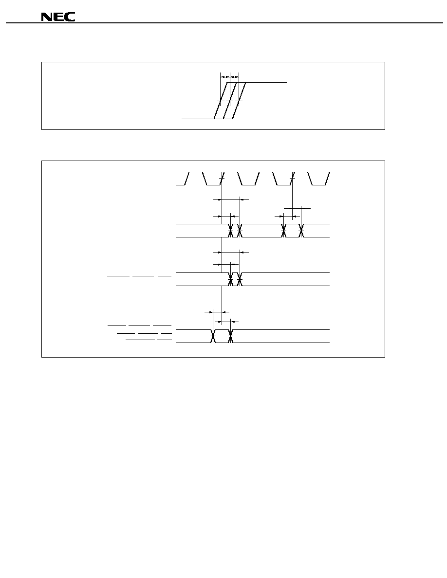
Measurement Conditions
Measurement point
t
DO
50%
50%
SysClock
All output pins
t
DM
Load condition
DUT
All output pins
C
L
= 50 pF
Timing Charts
Clock timing
t
CP
t
CH
t
CL
50%
SysClock
t
CR
t
CF
80%
20%
Preliminary Data Sheet U13504EJ3V0DS00
14
µ
µ
µ
µ
PD30541
Clock jitter
t
J
50%
t
J
SysClock
System interface edge timing
t
DO
t
DH
t
DH
Output
Output
Output
Output
Input
Input
t
DO
t
DM
t
DM
t
DS
t
DS
SysClock
SysAD (31:0), SysADC (3:0),
SysCmd (8:0)
ValidIn, ExtRqst, RdRdy,
WrRdy, Int (4:0), NMI
ColdReset, Reset
ValidOut, Release, PReq
Preliminary Data Sheet U13504EJ3V0DS00
15
µ
µ
µ
µ
PD30541
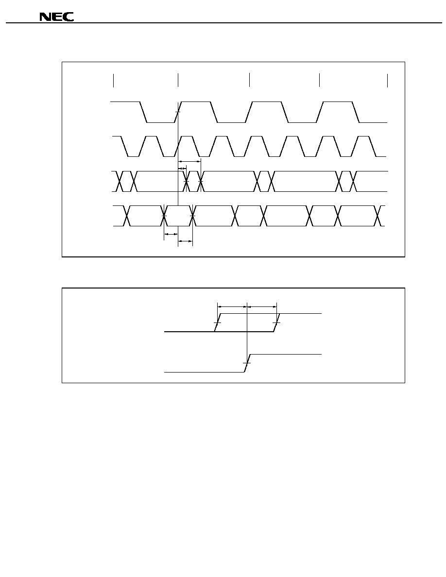
Clock relations (DivMode = 2:1)
1
2
3
4
Cycle
SysClock
(input)
PClock
(internal)
SysAD (31:0)
SysADC (3:0)
SysCmd (8:0)
(output)
SysAD (31:0)
SysADC (3:0)
SysCmd (8:0)
(input)
t
DS
t
DH
Data
Data
Data
Data
Data
Data
Data
t
DM
t
DO
Data
Power-on sequence
t
DF
t
DF
50%
50%
V
CC
IO
V
CC
Preliminary Data Sheet U13504EJ3V0DS00
16
µ
µ
µ
µ
PD30541
Reset Timing
Power-on reset timing
V
CC
IO
V
CC
64 K SysClock
SysClock
100 ms
ColdReset
Reset
t
DS
16 SysClock
t
DS
2.375 V
3.0 V
Cold Reset timing
V
CC
IO
64 K SysClock
SysClock
ColdReset
Reset
t
DS
16 SysClock
t
DS
t
DS
t
DS
H
V
CC
H
Preliminary Data Sheet U13504EJ3V0DS00
17
µ
µ
µ
µ
PD30541
Warm Reset timing
H
V
CC
IO
16 SysClock
SysClock
ColdReset
Reset
t
DS
t
DS
H
H
V
CC
Preliminary Data Sheet U13504EJ3V0DS00
18
µ
µ
µ
µ
PD30541
3. PACKAGE DRAWING
208-PIN PLASTIC QFP (FINE PITCH) (28x28)
ITEM
MILLIMETERS
F
G
1.25
1.25
B
C
28.0
±
0.2
28.0
±
0.2
H
0.22
I
0.10
S
3.8 MAX.
K
1.3
±
0.2
L
0.5
±
0.2
M
0.17
N
0.10
P
3.2
±
0.1
+
0.05
-
0.04
J
0.5 (T.P.)
P208GD-50-LML,MML,SML,WML-7
+
0.03
-
0.07
R
5
∞±
5
∞
J
I
N
S
S
detail of lead end
Q
0.4
±
0.1
M
NOTE
Each lead centerline is located within 0.10 mm of
its true position (T.P.) at maximum material condition.
1
208
52
53
156
157
105
104
C
A
B
Q
R
H
K
M
L
D
P
G
F
S
A
30.6
±
0.2
D
30.6
±
0.2

Preliminary Data Sheet U13504EJ3V0DS00
19
µ
µ
µ
µ
PD30541
4. RECOMMENDED SOLDERING CONDITIONS
This product should be soldered and mounted under the following recommended conditions.
For details of the recommended soldering conditions, refer to the Semiconductor Device Mounting Technology
Manual (C10535E).
For soldering methods and conditions other than those recommended below, contact an NEC sales
representative.
Table 4-1. Surface-Mount Technology Type Soldering Conditions
µ
µ
µ
µ
PD30541GD-167-WML: 208-pin plastic QFP (fine pitch) (28
◊
◊
◊
◊
28)
Soldering Method
Soldering Conditions
Recommended
Condition Symbol
Infrared reflow
Package peak temperature: 235
∞
C, Time: 30 seconds MAX. (at 210
∞
C
or higher), Count: Three times or less, Exposure limit: 7 days
Note
(after
that, prebake at 125
∞
C for 36 to 72 hours)
IR35-367-3
Partial heating
Pin temperature: 300
∞
C MAX., Time: 3 seconds MAX. (per pin row)
-
Note After opening the dry pack, store it at 25
∞
C or less and 65% RH or less for the allowable storage period.
Preliminary Data Sheet U13504EJ3V0DS00
20
µ
µ
µ
µ
PD30541
APPENDIX DIFFERENCES AMONG V
R
5432, V
R
5000
TM
, AND V
R
4310
TM
Item
V
R
5432
V
R
5000
V
R
4310
Internal
167 MHz
200 MHz
167 MHz
Maximum
operating
frequency
External
83.3 MHz
100 MHz
83.3 MHz
Pipeline
2-way superscaler 5-stage pipeline
5-stage pipeline
Primary instruction cache
32 KB
16 KB
Primary data cache
32 KB
8 KB
Secondary cache interface
None
Provided
None
Cache
Data protection
Byte parity/none
Byte parity
None
Bus width
32 bits
64 bits
32 bits
Data protection
Byte parity/none
Byte parity
None
System bus
Status after last data write
Completes
access./Holds last
data on setting of
transfer rate.
Completes access.
Holds last data on
setting of transfer
rate.
Pins for initial setting at reset
DivMode (1:0),
BigEndian,
OptionR43K
ModeIn (dedicated
serial pin)
DivMode (2:0)
Instruction set
MIPS I, II, III, IV +
multimedia + sum-of-
products operation
MIPS I, II, III, IV
MIPS I, II, III
Branch prediction mechanism
Provided
None
Hardware debug function
JTAG, N-Wire
None
JTAG
SyncOut-SyncIn path
None
Provided
Input vs. internal multiple
2, 2.5, 3, 4
2, 3, 4, 5, 6, 7, 8
2, 2.5, 3, 4, 5, 6
Input vs. bus division ratio
2, 2.5, 3, 4
2, 3, 4, 5, 6, 7, 8
2, 2.5, 3, 4, 5, 6
Clock interface
Clock output
None
TClock
Power management mode
None
Standby mode
None
PRId register
Imp = 0x54
Imp = 0x23
Imp = 0x0B

Preliminary Data Sheet U13504EJ3V0DS00
21
µ
µ
µ
µ
PD30541
[MEMO]
Preliminary Data Sheet U13504EJ3V0DS00
22
µ
µ
µ
µ
PD30541
NOTES FOR CMOS DEVICES
1
PRECAUTION AGAINST ESD FOR SEMICONDUCTORS
Note:
Strong electric field, when exposed to a MOS device, can cause destruction of the gate oxide and
ultimately degrade the device operation. Steps must be taken to stop generation of static electricity
as much as possible, and quickly dissipate it once, when it has occurred. Environmental control
must be adequate. When it is dry, humidifier should be used. It is recommended to avoid using
insulators that easily build static electricity. Semiconductor devices must be stored and transported
in an anti-static container, static shielding bag or conductive material. All test and measurement
tools including work bench and floor should be grounded. The operator should be grounded using
wrist strap. Semiconductor devices must not be touched with bare hands. Similar precautions need
to be taken for PW boards with semiconductor devices on it.
2
HANDLING OF UNUSED INPUT PINS FOR CMOS
Note:
No connection for CMOS device inputs can be cause of malfunction. If no connection is provided
to the input pins, it is possible that an internal input level may be generated due to noise, etc., hence
causing malfunction. CMOS devices behave differently than Bipolar or NMOS devices. Input levels
of CMOS devices must be fixed high or low by using a pull-up or pull-down circuitry. Each unused
pin should be connected to V
DD
or GND with a resistor, if it is considered to have a possibility of
being an output pin. All handling related to the unused pins must be judged device by device and
related specifications governing the devices.
3
STATUS BEFORE INITIALIZATION OF MOS DEVICES
Note:
Power-on does not necessarily define initial status of MOS device. Production process of MOS
does not define the initial operation status of the device. Immediately after the power source is
turned ON, the devices with reset function have not yet been initialized. Hence, power-on does
not guarantee out-pin levels, I/O settings or contents of registers. Device is not initialized until the
reset signal is received. Reset operation must be executed immediately after power-on for devices
having reset function.
Reference document Electrical Characteristics for Microcomputer (IEI-601)
Note
Note This document number is that of Japanese version.
The related documents in this publication may include preliminary versions. However, preliminary versions
are not marked as such.

Preliminary Data Sheet U13504EJ3V0DS00
23
µ
µ
µ
µ
PD30541
Regional Information
Some information contained in this document may vary from country to country. Before using any NEC
product in your application, pIease contact the NEC office in your country to obtain a list of authorized
representatives and distributors. They will verify:
∑
Device availability
∑
Ordering information
∑
Product release schedule
∑
Availability of related technical literature
∑
Development environment specifications (for example, specifications for third-party tools and
components, host computers, power plugs, AC supply voltages, and so forth)
∑
Network requirements
In addition, trademarks, registered trademarks, export restrictions, and other legal issues may also vary
from country to country.
NEC Electronics Inc. (U.S.)
Santa Clara, California
Tel: 408-588-6000
800-366-9782
Fax: 408-588-6130
800-729-9288
NEC Electronics (Germany) GmbH
Duesseldorf, Germany
Tel: 0211-65 03 02
Fax: 0211-65 03 490
NEC Electronics (UK) Ltd.
Milton Keynes, UK
Tel: 01908-691-133
Fax: 01908-670-290
NEC Electronics Italiana s.r.l.
Milano, Italy
Tel: 02-66 75 41
Fax: 02-66 75 42 99
NEC Electronics (Germany) GmbH
Benelux Office
Eindhoven, The Netherlands
Tel: 040-2445845
Fax: 040-2444580
NEC Electronics (France) S.A.
Velizy-Villacoublay, France
Tel: 01-30-67 58 00
Fax: 01-30-67 58 99
NEC Electronics (France) S.A.
Madrid Office
Madrid, Spain
Tel: 91-504-2787
Fax: 91-504-2860
NEC Electronics (Germany) GmbH
Scandinavia Office
Taeby, Sweden
Tel: 08-63 80 820
Fax: 08-63 80 388
NEC Electronics Hong Kong Ltd.
Hong Kong
Tel: 2886-9318
Fax: 2886-9022/9044
NEC Electronics Hong Kong Ltd.
Seoul Branch
Seoul, Korea
Tel: 02-528-0303
Fax: 02-528-4411
NEC Electronics Singapore Pte. Ltd.
United Square, Singapore
Tel: 65-253-8311
Fax: 65-250-3583
NEC Electronics Taiwan Ltd.
Taipei, Taiwan
Tel: 02-2719-2377
Fax: 02-2719-5951
NEC do Brasil S.A.
Electron Devices Division
Guarulhos-SP Brasil
Tel: 55-11-6462-6810
Fax: 55-11-6462-6829
J00.7
µ
µ
µ
µ
PD30541
V
R
4300, V
R
4300 Series, V
R
4310, V
R
5000, V
R
5432, and V
R
Series are trademarks of NEC Corporatipon.
MIPS is a registered trademark of MIPS Technologies, Inc. in the United States.
M8E 00. 4
The information in this document is current as of July, 2000. The information is subject to change
without notice. For actual design-in, refer to the latest publications of NEC's data sheets or data
books, etc., for the most up-to-date specifications of NEC semiconductor products. Not all products
and/or types are available in every country. Please check with an NEC sales representative for
availability and additional information.
No part of this document may be copied or reproduced in any form or by any means without prior
written consent of NEC. NEC assumes no responsibility for any errors that may appear in this document.
NEC does not assume any liability for infringement of patents, copyrights or other intellectual property rights of
third parties by or arising from the use of NEC semiconductor products listed in this document or any other
liability arising from the use of such products. No license, express, implied or otherwise, is granted under any
patents, copyrights or other intellectual property rights of NEC or others.
Descriptions of circuits, software and other related information in this document are provided for illustrative
purposes in semiconductor product operation and application examples. The incorporation of these
circuits, software and information in the design of customer's equipment shall be done under the full
responsibility of customer. NEC assumes no responsibility for any losses incurred by customers or third
parties arising from the use of these circuits, software and information.
While NEC endeavours to enhance the quality, reliability and safety of NEC semiconductor products, customers
agree and acknowledge that the possibility of defects thereof cannot be eliminated entirely. To minimize
risks of damage to property or injury (including death) to persons arising from defects in NEC
semiconductor products, customers must incorporate sufficient safety measures in their design, such as
redundancy, fire-containment, and anti-failure features.
NEC semiconductor products are classified into the following three quality grades:
"Standard", "Special" and "Specific". The "Specific" quality grade applies only to semiconductor products
developed based on a customer-designated "quality assurance program" for a specific application. The
recommended applications of a semiconductor product depend on its quality grade, as indicated below.
Customers must check the quality grade of each semiconductor product before using it in a particular
application.
"Standard": Computers, office equipment, communications equipment, test and measurement equipment, audio
and visual equipment, home electronic appliances, machine tools, personal electronic equipment
and industrial robots
"Special":
Transportation equipment (automobiles, trains, ships, etc.), traffic control systems, anti-disaster
systems, anti-crime systems, safety equipment and medical equipment (not specifically designed
for life support)
"Specific": Aircraft, aerospace equipment, submersible repeaters, nuclear reactor control systems, life
support systems and medical equipment for life support, etc.
The quality grade of NEC semiconductor products is "Standard" unless otherwise expressly specified in NEC's
data sheets or data books, etc. If customers wish to use NEC semiconductor products in applications not
intended by NEC, they must contact an NEC sales representative in advance to determine NEC's willingness
to support a given application.
(Note)
(1) "NEC" as used in this statement means NEC Corporation and also includes its majority-owned subsidiaries.
(2) "NEC semiconductor products" means any semiconductor product developed or manufactured by or for
NEC (as defined above).
∑
∑
∑
∑
∑
∑
Exporting this product or equipment that includes this product may require a governmental license from the U.S.A. for some
countries because this product utilizes technologies limited by the export control regulations of the U.S.A.