Document Outline
- COVER
- Features
- Ordering Information
- Pin Configurations
- Block Diagrams
- Electrical Specifications
- Package Drawing

The information in this document is subject to change without notice. Before using this document, please
confirm that this is the latest version.
Not all devices/types available in every country. Please check with local NEC representative for
availability and additional information.
©
2000
MOS INTEGRATED CIRCUIT
µ
PD4442161, 4442181, 4442321, 4442361
4M-BIT CMOS SYNCHRONOUS FAST SRAM
FLOW THROUGH OPERATION
Document No. M14519EJ2V0DS00 (2nd edition)
Date Published May 2001 NS CP(K)
Printed in Japan
PRELIMINARY DATA SHEET
The mark
5
5
5
5
shows major revised points.
Description
The
µ
PD4442161 is a 262,144-word by 16-bit, the
µ
PD4442181 is a 262,144-word by 18-bit, the
µ
PD4442321 is a
131,072-word by 32-bit and the
µ
PD4442361 is a 131,072-word by 36-bit synchronous static RAM fabricated with
advanced CMOS technology using Full-CMOS six-transistor memory cell.
The
µ
PD4442161,
µ
PD4442181,
µ
PD4442321 and
µ
PD4442361 integrate unique synchronous peripheral circuitry,
2-bit burst counter and output buffer as well as SRAM core. All input registers are controlled by a positive edge of the
single clock input (CLK).
The
µ
PD4442161,
µ
PD4442181,
µ
PD4442321 and
µ
PD4442361 are suitable for applications which require
synchronous operation, high speed, low voltage, high density and wide bit configuration, such as cache and buffer
memory.
ZZ has to be set LOW at the normal operation. When ZZ is set HIGH, the SRAM enters Power Down State ("Sleep").
In the "Sleep" state, the SRAM internal state is preserved. When ZZ is set LOW again, the SRAM resumes normal
operation.
The
µ
PD4442161,
µ
PD4442181,
µ
PD4442321 and
µ
PD4442361 are packaged in 100-pin PLASTIC LQFP with a
1.4 mm package thickness for high density and low capacitive loading.
Features
∑
3.3 V (A version) or 2.5 V (C version) Core Supply
∑
Synchronous operation
∑
Internally self-timed write control
∑
Burst read / write : Interleaved burst and linear burst sequence
∑
Fully registered inputs for flow through operation
∑
All registers triggered off positive clock edge
∑
3.3 V or 2.5 V LVTTL Compatible : All inputs and outputs
∑
Fast clock access time : 6.5 ns (133 MHz), 7.5 ns (117 MHz), 8.5 ns (100 MHz)
∑
Asynchronous output enable : /G
∑
Burst sequence selectable : MODE
∑
Sleep mode : ZZ (ZZ = Open or Low : Normal operation)
∑
Separate byte write enable : /BW1 - /BW4 (
µ
PD4442321,
µ
PD4442361), /BW1 - /BW2 (
µ
PD4442161,
µ
PD4442181), /BWE
Global write enable : /GW
∑
Three chip enables for easy depth expansion
∑
Common I/O using three state outputs
2
Preliminary Data Sheet M14519EJ2V0DS
µ
PD4442161, 4442181, 4442321, 4442361
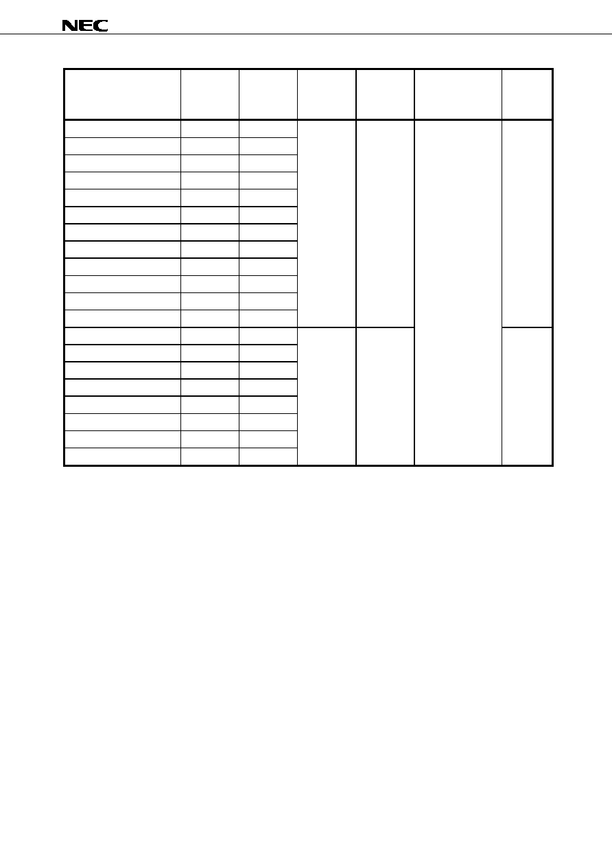
Ordering Information
Part number
Access
Clock
Core Supply
I/O
Package
Remark
Time
Frequency
Voltage
Interface
ns
MHz
V
µ
PD4442161GF-A65
6.5
133
3.3 ± 0.165
3.3 V or 2.5 V
100-pin PLASTIC
A version
µ
PD4442161GF-A75
7.5
117
LVTTL
LQFP (14
◊
20)
µ
PD4442161GF-A85
8.5
100
µ
PD4442181GF-A65
6.5
133
µ
PD4442181GF-A75
7.5
117
µ
PD4442181GF-A85
8.5
100
µ
PD4442321GF-A65
6.5
133
µ
PD4442321GF-A75
7.5
117
µ
PD4442321GF-A85
8.5
100
µ
PD4442361GF-A65
6.5
133
µ
PD4442361GF-A75
7.5
117
µ
PD4442361GF-A85
8.5
100
µ
PD4442161GF-C75
Note
7.5
117
2.5 ± 0.125
2.5 V LVTTL
C version
µ
PD4442161GF-C85
Note
8.5
100
µ
PD4442181GF-C75
Note
7.5
117
µ
PD4442181GF-C85
Note
8.5
100
µ
PD4442321GF-C75
Note
7.5
117
µ
PD4442321GF-C85
Note
8.5
100
µ
PD4442361GF-C75
Note
7.5
117
µ
PD4442361GF-C85
Note
8.5
100
Note Under development
5
5
5
5
3
Preliminary Data Sheet M14519EJ2V0DS
µ
PD4442161, 4442181, 4442321, 4442361
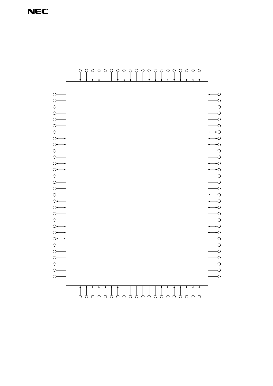
Pin Configurations (Marking Side)
/
◊◊◊
indicates active low signal.
100-pin PLASTIC LQFP (14
◊
◊
◊
◊
20)
[
µ
µ
µ
µ
PD4442161GF,
µ
µ
µ
µ
PD4442181GF ]
NC
NC
NC
V
DD
Q
V
SS
Q
NC
NC
I/O9
I/O10
V
SS
Q
V
DD
Q
I/O11
I/O12
NC
V
DD
NC
V
SS
I/O13
I/O14
V
DD
Q
V
SS
Q
I/O15
I/O16
I/OP2, NC
NC
V
SS
Q
V
DD
Q
NC
NC
NC
1
2
3
4
5
6
7
8
9
10
11
12
13
14
15
16
17
18
19
20
21
22
23
24
25
26
27
28
29
30
80
79
78
77
76
75
74
73
72
71
70
69
68
67
66
65
64
63
62
61
60
59
58
57
56
55
54
53
52
51
A17
NC
NC
V
DD
Q
V
SS
Q
NC
I/OP1, NC
I/O8
I/O7
V
SS
Q
V
DD
Q
I/O6
I/O5
V
SS
NC
V
DD
ZZ
I/O4
I/O3
V
DD
Q
V
SS
Q
I/O2
I/O1
NC
NC
V
SS
Q
V
DD
Q
NC
NC
NC
100 99 98 97 96 95 94 93 92 91 90 89 88 87 86 85 84 83 82 81
31 32 33 34 35 36 37 38 39 40 41 42 43 44 45 46 47 48 49 50
A6
A7
/CE
CE2
NC
NC
/BW2
/BW1
/CE2
V
DD
V
SS
CLK
/GW
/BWE
/G
/AC
/AP
/ADV
A8
A9
MODE
A5
A4
A3
A2
A1
A0
NC
NC
V
SS
V
DD
NC
NC
A10
A11
A12
A13
A14
A15
A16
Remark Refer to Package Drawing for 1-pin index mark.
4
Preliminary Data Sheet M14519EJ2V0DS
µ
PD4442161, 4442181, 4442321, 4442361
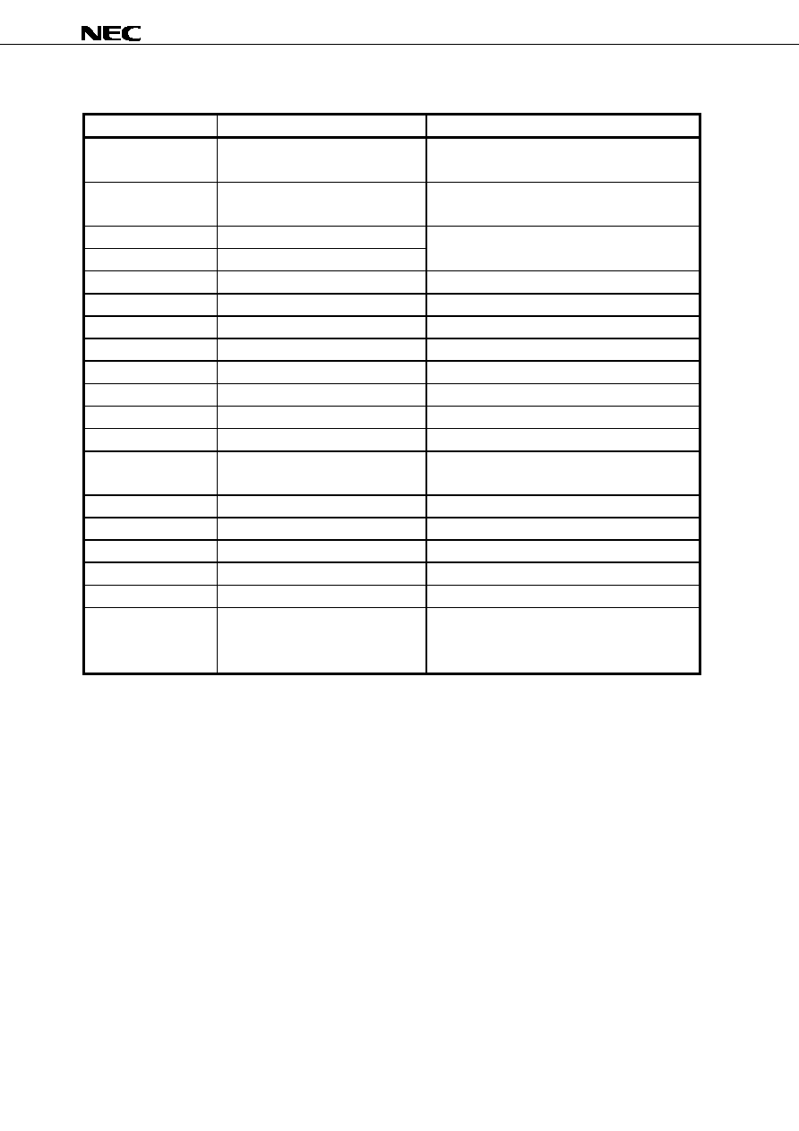
Pin Identifications
[
µ
µ
µ
µ
PD4442161GF,
µ
µ
µ
µ
PD4442181GF ]
Symbol
Pin No.
Description
A0 - A17
37, 36, 35, 34, 33, 32, 100, 99, 82, 81,
Synchronous Address Input
44, 45, 46, 47, 48, 49, 50, 80
I/O1 - I/O16
58, 59, 62, 63, 68, 69, 72, 73, 8, 9, 12,
Synchronous Data In,
13, 18, 19, 22, 23
Synchronous / Asynchronous Data Out
I/OP1, NC
Note
74
Synchronous Data In (Parity),
I/OP2, NC
Note
24
Synchronous / Asynchronous Data Out (Parity)
/ADV
83
Synchronous Burst Address Advance Input
/AP
84
Synchronous Address Status Processor Input
/AC
85
Synchronous Address Status Controller Input
/CE, CE2, /CE2
98, 97, 92
Synchronous Chip Enable Input
/BW1, /BW2, /BWE
93, 94, 87
Synchronous Byte Write Enable Input
/GW
88
Synchronous Global Write Input
/G
86
Asynchronous Output Enable Input
CLK
89
Clock Input
MODE
31
Asynchronous Burst Sequence Select Input
Do not change state during normal operation
ZZ
64
Asynchronous Power Down State Input
V
DD
15, 41, 65, 91
Power Supply
V
SS
17, 40, 67, 90
Ground
V
DD
Q
4, 11, 20, 27, 54, 61, 70, 77
Output Buffer Power Supply
V
SS
Q
5, 10, 21, 26, 55, 60, 71, 76
Output Buffer Ground
NC
1, 2, 3, 6, 7, 14, 16, 25, 28, 29, 30, 38,
No Connection
39, 42, 43, 51, 52, 53, 56, 57, 66, 75,
78, 79, 95, 96
Note NC (No Connection) is used in the
µ
PD4442161GF.
I/OP1 - I/OP2 are used in the
µ
PD4442181GF.
5
Preliminary Data Sheet M14519EJ2V0DS
µ
PD4442161, 4442181, 4442321, 4442361
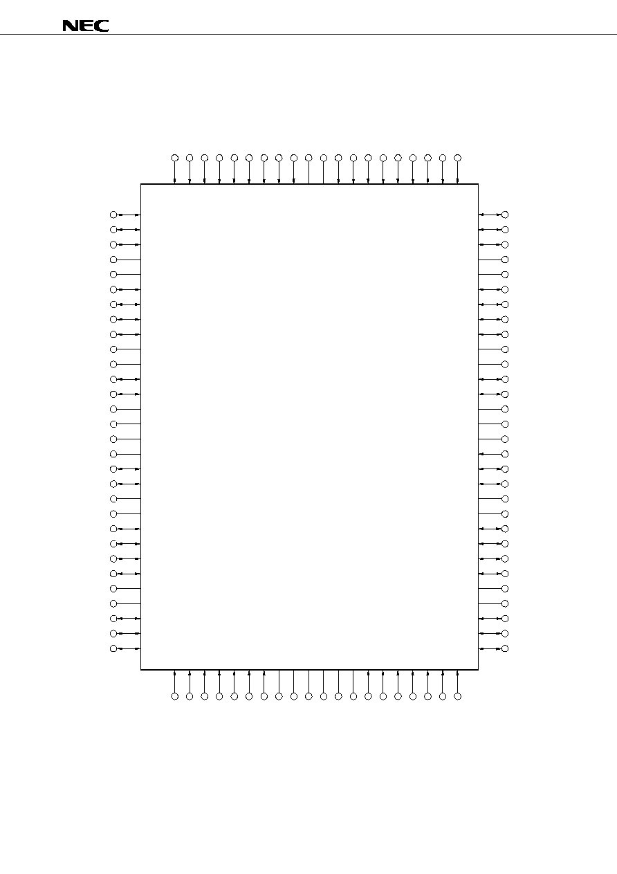
100-pin PLASTIC LQFP (14
◊
◊
◊
◊
20)
[
µ
µ
µ
µ
PD4442321GF,
µ
µ
µ
µ
PD4442361GF ]
I/OP3, NC
I/O17
I/O18
V
DD
Q
V
SS
Q
I/O19
I/O20
I/O21
I/O22
V
SS
Q
V
DD
Q
I/O23
I/O24
NC
V
DD
NC
V
SS
I/O25
I/O26
V
DD
Q
V
SS
Q
I/O27
I/O28
I/O29
I/O30
V
SS
Q
V
DD
Q
I/O31
I/O32
I/OP4, NC
1
2
3
4
5
6
7
8
9
10
11
12
13
14
15
16
17
18
19
20
21
22
23
24
25
26
27
28
29
30
80
79
78
77
76
75
74
73
72
71
70
69
68
67
66
65
64
63
62
61
60
59
58
57
56
55
54
53
52
51
I/OP2, NC
I/O16
I/O15
V
DD
Q
V
SS
Q
I/O14
I/O13
I/O12
I/O11
V
SS
Q
V
DD
Q
I/O10
I/O9
V
SS
NC
V
DD
ZZ
I/O8
I/O7
V
DD
Q
V
SS
Q
I/O6
I/O5
I/O4
I/O3
V
SS
Q
V
DD
Q
I/O2
I/O1
I/OP1, NC
100 99 98 97 96 95 94 93 92 91 90 89 88 87 86 85 84 83 82 81
31 32 33 34 35 36 37 38 39 40 41 42 43 44 45 46 47 48 49 50
A6
A7
/CE
CE2
/BW4
/BW3
/BW2
/BW1
/CE2
V
DD
V
SS
CLK
/GW
/BWE
/G
/AC
/AP
/ADV
A8
A9
MODE
A5
A4
A3
A2
A1
A0
NC
NC
V
SS
V
DD
NC
NC
A10
A11
A12
A13
A14
A15
A16
Remark Refer to Package Drawing for 1-pin index mark.