Document Outline
- COVER
- Features
- Ordering Information
- Pin Configurations
- Block Diagrams
- Electrical Specifications
- Package Drawing

The information in this document is subject to change without notice. Before using this document, please
confirm that this is the latest version.
Not all products and/or types are available in every country. Please check with an NEC Electronics
sales representative for availability and additional information.
MOS INTEGRATED CIRCUIT
µ
PD4481162, 4481182, 4481322, 4481362
8M-BIT ZEROSB
TM
SRAM
PIPELINED OPERATION
Document No. M15562EJ3V0DS00 (3rd edition)
Date Published December 2002 NS CP(K)
Printed in Japan
DATA SHEET
The mark shows major revised points.
2001
Description
The
µPD4481162 is a 524,288-word by 16-bit, the µPD4481182 is a 524,288-word by 18-bit, the µPD4481322 is a
262,144-word by 32-bit and the
µPD4481362 is a 262,144-word by 36-bit ZEROSB static RAM fabricated with
advanced CMOS technology using full CMOS six-transistor memory cell.
The
µPD4481162, µPD4481182, µPD4481322 and µPD4481362 are optimized to eliminate dead cycles for read to
write, or write to read transitions. These ZEROSB static RAMs integrate unique synchronous peripheral circuitry, 2-bit
burst counter and output buffer as well as SRAM core. All input registers are controlled by a positive edge of the
single clock input (CLK).
The
µPD4481162, µPD4481182, µPD4481322 and µPD4481362 are suitable for applications which require
synchronous operation, high speed, low voltage, high density and wide bit configuration, such as buffer memory.
ZZ has to be set LOW at the normal operation. When ZZ is set HIGH, the SRAM enters Power Down State ("Sleep").
In the "Sleep" state, the SRAM internal state is preserved. When ZZ is set LOW again, the SRAM resumes normal
operation.
The
µPD4481162, µPD4481182, µPD4481322 and µPD4481362 are packaged in 100-pin PLASTIC LQFP with a 1.4
mm package thickness for high density and low capacitive loading.
Features
∑ Low voltage core supply : V
DD
= 3.3 ± 0.165 V (-A44, -A50, -A60, -A75, -A44Y, -A50Y, -A60Y, -A75Y)
V
DD
= 2.5 ± 0.125 V (-C60, -C75, -C60Y, -C75Y)
∑ Synchronous operation
∑ Operating temperature : T
A
= 0 to 70
∞C (-A44, -A50, -A60, -A75, -C60, -C75)
T
A
=
-40 to +85 ∞C (-A44Y, -A50Y, -A60Y, -A75Y, -C60Y, -C75Y)
∑ 100 percent bus utilization
∑ Internally self-timed write control
∑ Burst read / write : Interleaved burst and linear burst sequence
∑ Fully registered inputs and outputs for pipelined operation
∑ All registers triggered off positive clock edge
∑ 3.3V or 2.5V LVTTL Compatible : All inputs and outputs
∑ Fast clock access time : 2.8 ns (225 MHz), 3.2 ns (200 MHz), 3.5 ns (167 MHz) , 4.2 ns (133 MHz)
∑ Asynchronous output enable : /G
∑ Burst sequence selectable : MODE
∑ Sleep mode : ZZ (ZZ = Open or Low : Normal operation)
∑ Separate byte write enable : /BW1 to /BW4 (
µPD4481322 and µPD4481362)
/BW1 and /BW2 (
µPD4481162 and µPD4481182)
∑ Three chip enables for easy depth expansion
∑ Common I/O using three state outputs

2
Data Sheet M15562EJ3V0DS
µPD4481162, 4481182, 4481322, 4481362
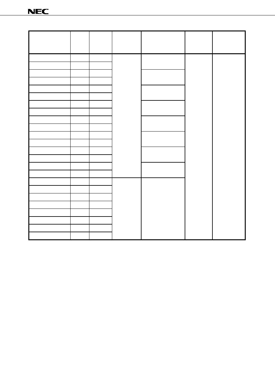
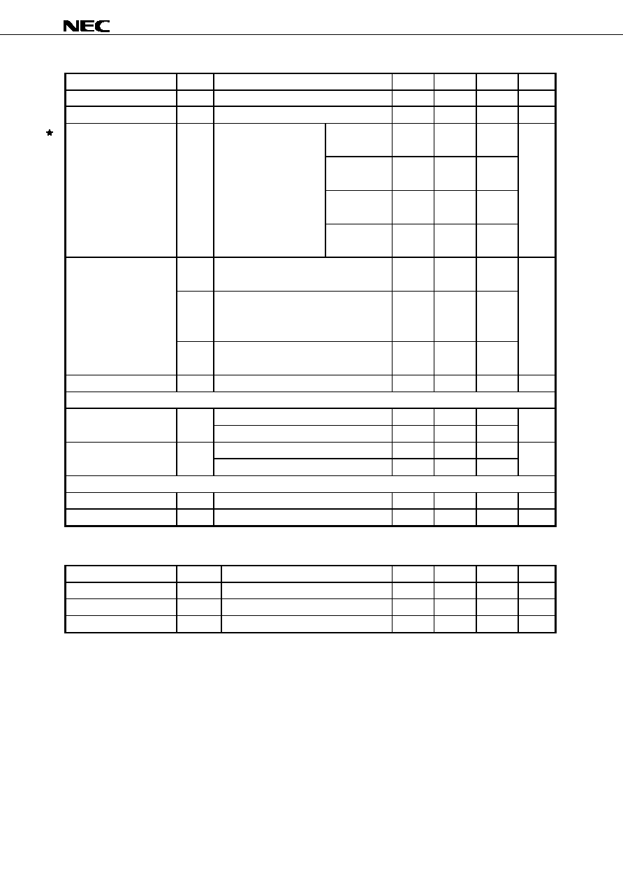
Ordering Information
(1/2)
Part number
Access
Clock
Core Supply
I/O Interface
Operating
Package
Time
Frequency
Voltage
Temperature
ns
MHz
V
∞C
µPD4481162GF-A44
2.8
225
3.3 ± 0.165
3.3 V LVTTL
Note
0 to 70
100-pin PLASTIC
µPD4481162GF-A50
3.2
200
LQFP (14 x 20)
µPD4481162GF-A60
3.5
167
3.3 V or 2.5 V LVTTL
µPD4481162GF-A75
4.2
133
µPD4481182GF-A44
2.8
225
3.3 V LVTTL
Note
µPD4481182GF-A50
3.2
200
µPD4481182GF-A60
3.5
167
3.3 V or 2.5 V LVTTL
µPD4481182GF-A75
4.2
133
µPD4481322GF-A44
2.8
225
3.3 V LVTTL
Note
µPD4481322GF-A50
3.2
200
µPD4481322GF-A60
3.5
167
3.3 V or 2.5 V LVTTL
µPD4481322GF-A75
4.2
133
µPD4481362GF-A44
2.8
225
3.3 V LVTTL
Note
µPD4481362GF-A50
3.2
200
µPD4481362GF-A60
3.5
167
3.3 V or 2.5 V LVTTL
µPD4481362GF-A75
4.2
133
µPD4481162GF-C60
3.5
167
2.5 ± 0.125
2.5 V LVTTL
µPD4481162GF-C75
4.2
133
µPD4481182GF-C60
3.5
167
µPD4481182GF-C75
4.2
133
µPD4481322GF-C60
3.5
167
µPD4481322GF-C75
4.2
133
µPD4481362GF-C60
3.5
167
µPD4481362GF-C75
4.2
133
Note Although 2.5V LVTTL interface can also be used, a performance becomes equivalent to -A60 (167 MHz).
3
Data Sheet M15562EJ3V0DS
µPD4481162, 4481182, 4481322, 4481362
(2/2)
Part number
Access
Clock
Core Supply
I/O Interface
Operating
Package
Time
Frequency
Voltage
Temperature
ns
MHz
V
∞C
µPD4481162GF-A44Y
2.8
225
3.3 ± 0.165
3.3 V LVTTL
Note
-40 to +85
100-pin PLASTIC
µPD4481162GF-A50Y
3.2
200
LQFP (14 x 20)
µPD4481162GF-A60Y
3.5
167
3.3 V or 2.5 V LVTTL
µPD4481162GF-A75Y
4.2
133
µPD4481182GF-A44Y
2.8
225
3.3 V LVTTL
Note
µPD4481182GF-A50Y
3.2
200
µPD4481182GF-A60Y
3.5
167
3.3 V or 2.5 V LVTTL
µPD4481182GF-A75Y
4.2
133
µPD4481322GF-A44Y
2.8
225
3.3 V LVTTL
Note
µPD4481322GF-A50Y
3.2
200
µPD4481322GF-A60Y
3.5
167
3.3 V or 2.5 V LVTTL
µPD4481322GF-A75Y
4.2
133
µPD4481362GF-A44Y
2.8
225
3.3 V LVTTL
Note
µPD4481362GF-A50Y
3.2
200
µPD4481362GF-A60Y
3.5
167
3.3 V or 2.5 V LVTTL
µPD4481362GF-A75Y
4.2
133
µPD4481162GF-C60Y
3.5
167
2.5 ± 0.125
2.5 V LVTTL
µPD4481162GF-C75Y
4.2
133
µPD4481182GF-C60Y
3.5
167
µPD4481182GF-C75Y
4.2
133
µPD4481322GF-C60Y
3.5
167
µPD4481322GF-C75Y
4.2
133
µPD4481362GF-C60Y
3.5
167
µPD4481362GF-C75Y
4.2
133
Note Although 2.5V LVTTL interface can also be used, a performance becomes equivalent to -A60Y (167 MHz).
4
Data Sheet M15562EJ3V0DS
µPD4481162, 4481182, 4481322, 4481362
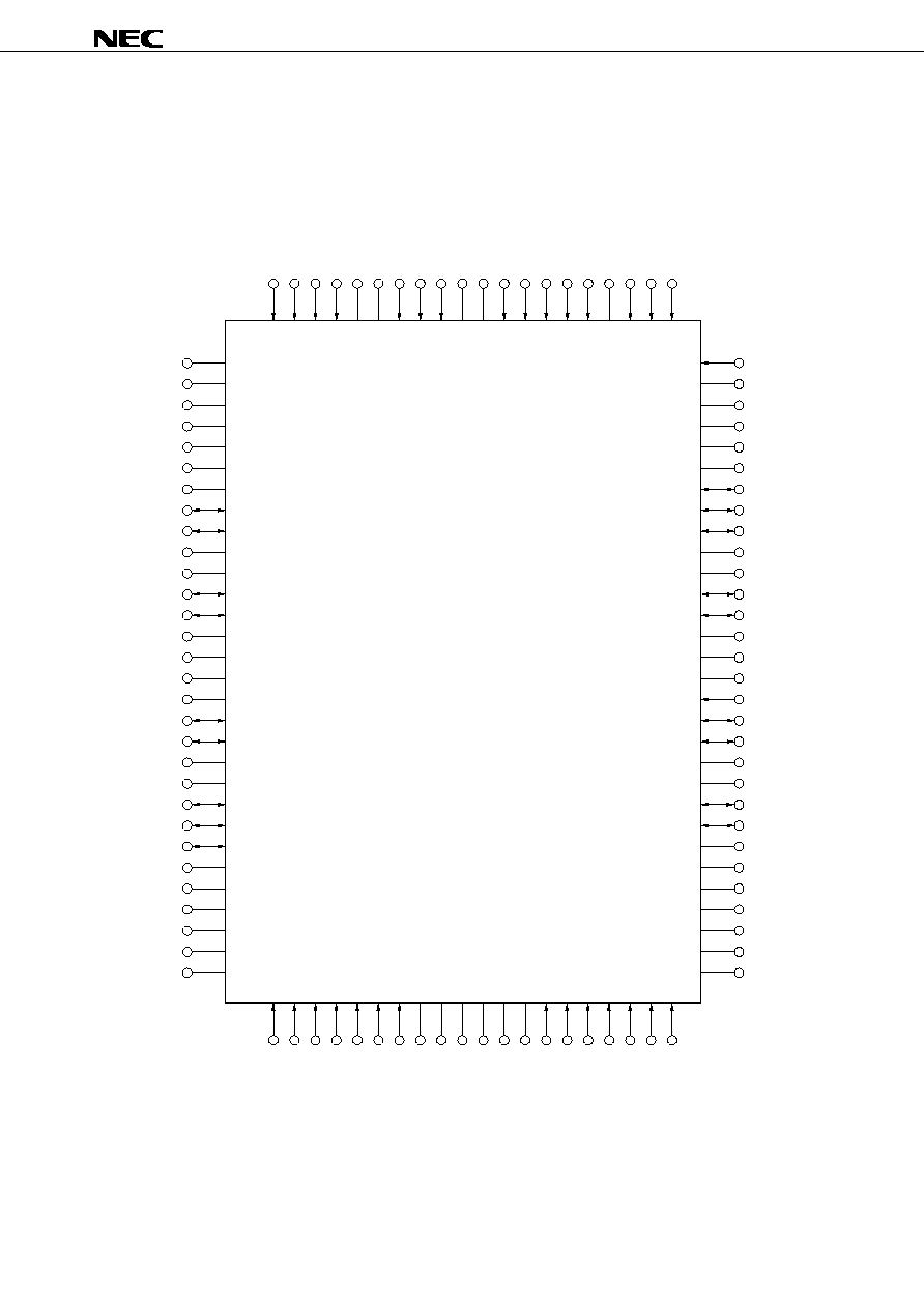
Pin Configurations
/
◊◊◊ indicates active low signal.
100-pin PLASTIC LQFP (14
◊
◊
◊
◊ 20)
[
µ
µ
µ
µPD4481162GF, µµµµPD4481182GF]
Marking Side
NC
NC
NC
V
DD
Q
V
SS
Q
NC
NC
I/O9
I/O10
V
SS
Q
V
DD
Q
I/O11
I/O12
V
DD
V
DD
V
DD
V
SS
I/O13
I/O14
V
DD
Q
V
SS
Q
I/O15
I/O16
I/OP2, NC
NC
V
SS
Q
V
DD
Q
NC
NC
NC
1
2
3
4
5
6
7
8
9
10
11
12
13
14
15
16
17
18
19
20
21
22
23
24
25
26
27
28
29
30
80
79
78
77
76
75
74
73
72
71
70
69
68
67
66
65
64
63
62
61
60
59
58
57
56
55
54
53
52
51
A18
NC
NC
V
DD
Q
V
SS
Q
NC
I/OP1, NC
I/O8
I/O7
V
SS
Q
V
DD
Q
I/O6
I/O5
V
SS
V
DD
V
DD
ZZ
I/O4
I/O3
V
DD
Q
V
SS
Q
I/O2
I/O1
NC
NC
V
SS
Q
V
DD
Q
NC
NC
NC
100 99 98 97 96 95 94 93 92 91 90 89 88 87 86 85 84 83 82 81
31 32 33 34 35 36 37 38 39 40 41 42 43 44 45 46 47 48 49 50
A6
A7
/CE
CE2
NC
NC
/BW2
/BW1
/CE2
V
DD
V
SS
CLK
/WE
/CKE
/G
ADV
NC
A17
A8
A9
MODE
A5
A4
A3
A2
A1
A0
NC
NC
V
SS
V
DD
NC
NC
A10
A11
A12
A13
A14
A15
A16
Remark Refer to Package Drawing for the 1-pin index mark.
5
Data Sheet M15562EJ3V0DS
µPD4481162, 4481182, 4481322, 4481362
Pin Identifications
[
µ
µ
µ
µPD4481162GF, µµµµPD4481182GF]
Symbol
Pin No.
Description
A0 to A18
37, 36, 35, 34, 33, 32, 100, 99, 82, 81,
Synchronous Address Input
44, 45, 46, 47, 48, 49, 50, 83, 80
I/O1 to I/O16
58, 59, 62, 63, 68, 69, 72, 73, 8, 9, 12, 13, Synchronous Data In,
18, 19, 22, 23
Synchronous / Asynchronous Data Out
I/OP1, NC
Note
74
Synchronous Data In (Parity),
I/OP2, NC
Note
24
Synchronous / Asynchronous Data Out (Parity)
ADV
85
Synchronous Address Load / Advance Input
/CE, CE2, /CE2
98, 97, 92
Synchronous Chip Enable Input
/WE
88
Synchronous Write Enable Input
/BW1, /BW2
93, 94
Synchronous Byte Write Enable Input
/G
86
Asynchronous Output Enable Input
CLK
89
Clock Input
/CKE
87
Synchronous Clock Enable Input
MODE
31
Asynchronous Burst Sequence Select Input
Have to tied to V
DD
or V
SS
during normal operation
ZZ
64
Asynchronous Power Down State Input
V
DD
14, 15, 16, 41, 65, 66, 91
Power Supply
V
SS
17, 40, 67, 90
Ground
V
DD
Q
4, 11, 20, 27, 54, 61, 70, 77
Output Buffer Power Supply
V
SS
Q
5, 10, 21, 26, 55, 60, 71, 76
Output Buffer Ground
NC
1, 2, 3, 6, 7, 25, 28, 29, 30, 38, 39, 42, 43, No Connection
51, 52, 53, 56, 57, 75, 78, 79, 84, 95, 96
Note NC (No Connection) is used in the
µPD4481162GF.
I/OP1 and I/OP2 are used in the
µPD4481182GF.

6
Data Sheet M15562EJ3V0DS
µPD4481162, 4481182, 4481322, 4481362
100-pin PLASTIC LQFP (14
◊
◊
◊
◊ 20)
[
µ
µ
µ
µPD4481322GF, µµµµPD4481362GF]
Marking Side
I/OP3, NC
I/O17
I/O18
V
DD
Q
V
SS
Q
I/O19
I/O20
I/O21
I/O22
V
SS
Q
V
DD
Q
I/O23
I/O24
V
DD
V
DD
V
DD
V
SS
I/O25
I/O26
V
DD
Q
V
SS
Q
I/O27
I/O28
I/O29
I/O30
V
SS
Q
V
DD
Q
I/O31
I/O32
I/OP4, NC
1
2
3
4
5
6
7
8
9
10
11
12
13
14
15
16
17
18
19
20
21
22
23
24
25
26
27
28
29
30
80
79
78
77
76
75
74
73
72
71
70
69
68
67
66
65
64
63
62
61
60
59
58
57
56
55
54
53
52
51
I/OP2, NC
I/O16
I/O15
V
DD
Q
V
SS
Q
I/O14
I/O13
I/O12
I/O11
V
SS
Q
V
DD
Q
I/O10
I/O9
V
SS
V
DD
V
DD
ZZ
I/O8
I/O7
V
DD
Q
V
SS
Q
I/O6
I/O5
I/O4
I/O3
V
SS
Q
V
DD
Q
I/O2
I/O1
I/OP1, NC
100 99 98 97 96 95 94 93 92 91 90 89 88 87 86 85 84 83 82 81
31 32 33 34 35 36 37 38 39 40 41 42 43 44 45 46 47 48 49 50
A6
A7
/CE
CE2
/BW4
/BW3
/BW2
/BW1
/CE2
V
DD
V
SS
CLK
/WE
/CKE
/G
ADV
NC
A17
A8
A9
MODE
A5
A4
A3
A2
A1
A0
NC
NC
V
SS
V
DD
NC
NC
A10
A11
A12
A13
A14
A15
A16
Remark Refer to Package Drawing for the 1-pin index mark.
7
Data Sheet M15562EJ3V0DS
µPD4481162, 4481182, 4481322, 4481362
[
µ
µ
µ
µPD4481322GF, µµµµPD4481362GF]
Symbol
Pin No.
Description
A0 to A17
37, 36, 35, 34, 33, 32, 100, 99, 82, 81, 44, Synchronous Address Input
45, 46, 47, 48, 49, 50, 83
I/O1 to I/O32
52, 53, 56, 57, 58, 59, 62, 63, 68, 69, 72,
Synchronous Data In,
73, 74, 75, 78, 79, 2, 3, 6, 7, 8, 9, 12, 13,
Synchronous / Asynchronous Data Out
18, 19, 22, 23, 24, 25, 28, 29
I/OP1, NC
Note
51
Synchronous Data In (Parity),
I/OP2, NC
Note
80
Synchronous / Asynchronous Data Out (Parity)
I/OP3, NC
Note
1
I/OP4, NC
Note
30
ADV
85
Synchronous Address Load / Advance Input
/CE, CE2, /CE2
98, 97, 92
Synchronous Chip Enable Input
/WE
88
Synchronous Write Enable Input
/BW1 to /BW4
93, 94, 95, 96
Synchronous Byte Write Enable Input
/G
86
Asynchronous Output Enable Input
CLK
89
Clock Input
/CKE
87
Synchronous Clock Enable Input
MODE
31
Asynchronous Burst Sequence Select Input
Have to tied to V
DD
or V
SS
during normal operation
ZZ
64
Asynchronous Power Down State Input
V
DD
14, 15, 16, 41, 65, 66, 91
Power Supply
V
SS
17, 40, 67, 90
Ground
V
DD
Q
4, 11, 20, 27, 54, 61, 70, 77
Output Buffer Power Supply
V
SS
Q
5, 10, 21, 26, 55, 60, 71, 76
Output Buffer Ground
NC
38, 39, 42, 43, 84
No Connection
Note NC (No Connection) is used in the
µPD4481322GF.
I/OP1 to I/OP4 are used in the
µPD4481362GF.
8
Data Sheet M15562EJ3V0DS
µPD4481162, 4481182, 4481322, 4481362
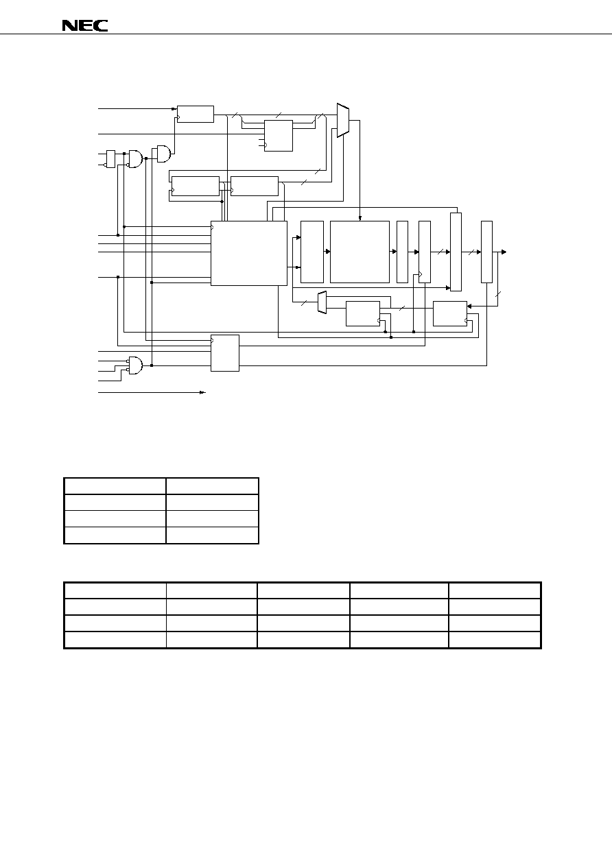
Block Diagrams
[
µ
µ
µ
µPD4481162, µ
µ
µ
µPD4481182]
A0 to A18
MODE
CLK
/CKE
ADV
/BW1
/BW2
/WE
/G
/CE
CE2
/CE2
Address
register 0
Burst
logic
Write address
register 0
Write registry and
data coherency
control logic
Write
drivers
Data steering
ADV
K
A1
A0
A1'
A0'
Sense amplifiers
Read
logic
Input
register 0
E
Output buffers
E
I/O1 to I/O16
I/OP1, I/OP2
19
17
19
19
19
16/18
16/18
16/18
16/18
Write address
register 1
Output registers
E
Input
register 1
E
16/18
ZZ
Power down control
K
Memory Cell Array
512 x 16 columns
(8,388,608 bits)
512 x 18 columns
(9,437,184 bits)
1,024 rows
Burst Sequence
[
µ
µ
µ
µPD4481162, µ
µ
µ
µPD4481182]
Interleaved Burst Sequence Table (MODE = V
DD
)
External Address
A18 to A2, A1, A0
1st Burst Address
A18 to A2, A1, /A0
2nd Burst Address
A18 to A2, /A1, A0
3rd Burst Address
A18 to A2, /A1, /A0
Linear Burst Sequence Table (MODE = V
SS
)
External Address
A18 to A2, 0, 0
A18 to A2, 0, 1
A18 to A2, 1, 0
A18 to A2, 1, 1
1st Burst Address
A18 to A2, 0, 1
A18 to A2, 1, 0
A18 to A2, 1, 1
A18 to A2, 0, 0
2nd Burst Address
A18 to A2, 1, 0
A18 to A2, 1, 1
A18 to A2, 0, 0
A18 to A2, 0, 1
3rd Burst Address
A18 to A2, 1, 1
A18 to A2, 0, 0
A18 to A2, 0, 1
A18 to A2, 1, 0

9
Data Sheet M15562EJ3V0DS
µPD4481162, 4481182, 4481322, 4481362
[
µ
µ
µ
µPD4481322, µ
µ
µ
µPD4481362]
A0 to A17
MODE
CLK
/CKE
ADV
/BW1
/BW2
/WE
/G
/CE
CE2
/CE2
Address
register 0
Burst
logic
Write address
register 0
Write registry and
data coherency
control logic
Write
drivers
Data steering
ADV
K
A1
A0
A1'
A0'
Sense amplifiers
Read
logic
Input
register 0
E
Output buffers
E
I/O1 to I/O32
I/OP1 to I/OP4
18
16
18
18
18
32/36
32/36
32/36
32/36
Write address
register 1
Output registers
E
Input
register 1
E
32/36
/BW3
/BW4
ZZ
Power down control
K
Memory Cell Array
256 x 32 columns
(8,388,608 bits)
256 x 36 columns
(9,437,184 bits)
1,024 rows
[
µ
µ
µ
µPD4481322, µ
µ
µ
µPD4481362]
Interleaved Burst Sequence Table (MODE = V
DD
)
External Address
A17 to A2, A1, A0
1st Burst Address
A17 to A2, A1, /A0
2nd Burst Address
A17 to A2, /A1, A0
3rd Burst Address
A17 to A2, /A1, /A0
Linear Burst Sequence Table (MODE = V
SS
)
External Address
A17 to A2, 0, 0
A17 to A2, 0, 1
A17 to A2, 1, 0
A17 to A2, 1, 1
1st Burst Address
A17 to A2, 0, 1
A17 to A2, 1, 0
A17 to A2, 1, 1
A17 to A2, 0, 0
2nd Burst Address
A17 to A2, 1, 0
A17 to A2, 1, 1
A17 to A2, 0, 0
A17 to A2, 0, 1
3rd Burst Address
A17 to A2, 1, 1
A17 to A2, 0, 0
A17 to A2, 0, 1
A17 to A2, 1, 0
10
Data Sheet M15562EJ3V0DS
µPD4481162, 4481182, 4481322, 4481362
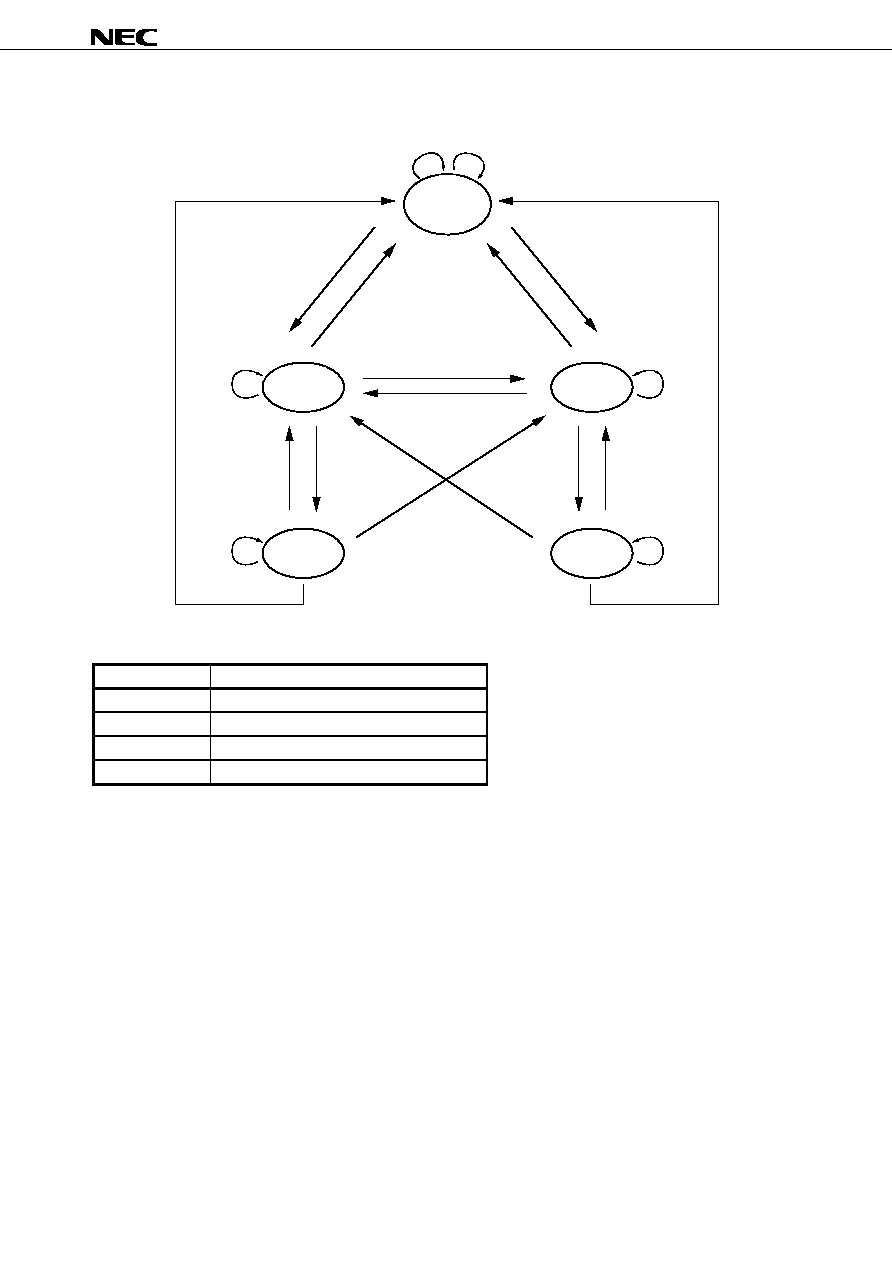
State Diagram
DESELECT
BEGIN
READ
BURST
READ
BEGIN
WRITE
BURST
WRITE
WRITE
READ
READ
DS
DS
WRITE
READ
BURST
BURST
WRITE
READ
WRITE
READ
BURST
WRITE
BURST
DS
BURST
DS
DS
Command
Operation
DS
Deselect
Read
New Read
Write
New Write
Burst
Burst Read, Burst Write or Continue Deselect
Remarks 1. States change on the rising edge of the clock.
2. A Stall or Ignore Clock Edge cycle is not shown in the above diagram. This is because /CKE HIGH only
blocks the clock (CLK) input and does not change the state of the device.
11
Data Sheet M15562EJ3V0DS
µPD4481162, 4481182, 4481322, 4481362
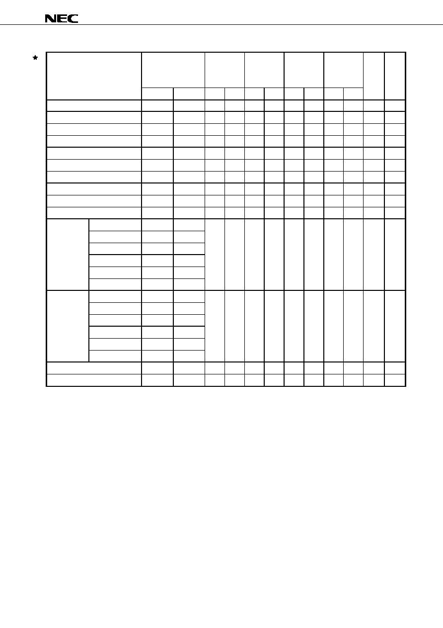
Asynchronous Truth Table
Operation
/G
I/O
Read Cycle
L
Dout
Read Cycle
H
High-Z
Write Cycle
◊
High-Z, Din
Deselected
◊
High-Z
Remark
◊ : don't care
Synchronous Truth Table
Operation
/CE
CE2
/CE2
ADV
/WE
/BWs
/CKE
CLK
I/O
Address
Note
Deselected
H
◊
◊
L
◊
◊
L
L
H
High-Z
None
1
Deselected
◊
L
◊
L
◊
◊
L
L
H
High-Z
None
1
Deselected
◊
◊
H
L
◊
◊
L
L
H
High-Z
None
1
Continue Deselected
◊
◊
◊
H
◊
◊
L
L
H
High-Z
None
1
Read Cycle / Begin Burst
L
H
L
L
H
◊
L
L
H
Dout
External
Read Cycle / Continue Burst
◊
◊
◊
H
◊
◊
L
L
H
Dout
Next
Write Cycle / Begin Burst
L
H
L
L
L
L
L
L
H
Din
External
Write Cycle / Continue Burst
◊
◊
◊
H
◊
L
L
L
H
Din
Next
Write Cycle / Write Abort
L
H
L
L
L
H
L
L
H
High-Z
External
Write Cycle / Write Abort
◊
◊
◊
H
◊
H
L
L
H
High-Z
Next
Stall / Ignore Clock Edge
◊
◊
◊
◊
◊
◊
H
L
H
-
Current
2
Notes
1. Deselect status is held until new "Begin Burst" entry.
2. If an Ignore Clock Edge command occurs during a read operation, the I/O bus will remain active (low
impedance). If it occurs during a write cycle, the bus will remain high impedance. No write operation will
be performed during the Ignore Clock Edge cycle.
Remarks 1.
◊ : don't care
2. /BWs = L means any one or more byte write enables (/BW1, /BW2, /BW3 or /BW4) are LOW.
/BWs = H means all byte write enables (/BW1, /BW2, /BW3 or /BW4) are HIGH.
12
Data Sheet M15562EJ3V0DS
µPD4481162, 4481182, 4481322, 4481362
Partial Truth Table for Write Enables
[
µ
µ
µ
µPD4481162, µ
µ
µ
µPD4481182]
Operation
/WE
/BW1
/BW2
Read Cycle
H
◊
◊
Write Cycle / Byte 1 (I/O [1:8], I/OP1)
L
L
H
Write Cycle / Byte 2 (I/O [9:16], I/OP2)
L
H
L
Write Cycle / All Bytes
L
L
L
Write Abort / NOP
L
H
H
Remark
◊ : don't care
[
µ
µ
µ
µPD4481322, µ
µ
µ
µPD4481362]
Operation
/WE
/BW1
/BW2
/BW3
/BW4
Read Cycle
H
◊
◊
◊
◊
Write Cycle / Byte 1 (I/O [1:8], I/OP1)
L
L
H
H
H
Write Cycle / Byte 2 (I/O [9:16], I/OP2)
L
H
L
H
H
Write Cycle / Byte 3 (I/O [17:24], I/OP3)
L
H
H
L
H
Write Cycle / Byte 4 (I/O [25:32], I/OP4)
L
H
H
H
L
Write Cycle / All Bytes
L
L
L
L
L
Write Abort / NOP
L
H
H
H
H
Remark
◊ : don't care
ZZ (Sleep) Truth Table
ZZ
Chip Status
0.2 V
Active
Open
Active
V
DD
- 0.2 V
Sleep

13
Data Sheet M15562EJ3V0DS
µPD4481162, 4481182, 4481322, 4481362
Electrical Specifications
Absolute Maximum Ratings
Parameter
Symbol
Conditions
MIN.
TYP.
MAX.
Unit
Supply voltage
V
DD
-A44, -A50, -A60, -A75
≠0.5
+4.0
V
-A44Y, -A50Y, -A60Y, -A75Y
-C60, -C75
≠0.5
+3.0
-C60Y, -C75Y
Output supply voltage
V
DD
Q
≠0.5
V
DD
V
Input voltage
V
IN
≠0.5
Note
V
DD
+ 0.5
V
Input / Output voltage
V
I/O
≠0.5
Note
V
DD
Q
+ 0.5
V
Operating ambient
T
A
-A44, -A50, -A60, -A75, -C60, -C75
0
70
∞C
temperature
-A44Y, -A50Y, -A60Y, -A75Y, -C60Y, -C75Y
≠40
+85
Storage temperature
T
stg
≠55
+125
∞C
Note ≠2.0 V (MIN.) (Pulse width : 2 ns)
Caution
Exposing the device to stress above those listed in Absolute Maximum Ratings could cause
permanent damage. The device is not meant to be operated under conditions outside the limits
described in the operational section of this specification. Exposure to Absolute Maximum Rating
conditions for extended periods may affect device reliability.
Recommended DC Operating Conditions
(1/2)
Parameter
Symbol
Conditions
-A44, -A50, -A60, -A75
Unit
-A44Y, -A50Y, -A60Y, -A75Y
MIN.
TYP.
MAX.
Supply voltage
V
DD
3.135
3.3
3.465
V
2.5 V LVTTL Interface
Output supply voltage
V
DD
Q
2.375
2.5
2.9
V
High level input voltage
V
IH
1.7
V
DD
Q
+ 0.3
V
Low level input voltage
V
IL
≠0.3
Note
+0.7
V
3.3 V LVTTL Interface
Output supply voltage
V
DD
Q
3.135
3.3
3.465
V
High level input voltage
V
IH
2.0
V
DD
Q
+ 0.3
V
Low level input voltage
V
IL
≠0.3
Note
+0.8
V
Note ≠0.8 V (MIN.) (Pulse width : 2 ns)
Recommended DC Operating Conditions
(2/2)
Parameter
Symbol
Conditions
-C60, -C75
Unit
-C60Y, -C75Y
MIN.
TYP.
MAX.
Supply voltage
V
DD
2.375
2.5
2.625
V
Output supply voltage
V
DD
Q
2.375
2.5
2.625
V
High level input voltage
V
IH
1.7
V
DD
Q
+ 0.3
V
Low level input voltage
V
IL
≠0.3
Note
+0.7
V
Note ≠0.8 V (MIN.) (Pulse width : 2 ns)
14
Data Sheet M15562EJ3V0DS
µPD4481162, 4481182, 4481322, 4481362
DC Characteristics (V
DD
= 3.3 ± 0.165 V or 2.5 ± 0.125 V)
Parameter
Symbol
Test condition
MIN.
TYP.
MAX.
Unit
Input leakage current
I
LI
V
IN
(except ZZ, MODE) = 0 V to V
DD
≠2
+2
µA
I/O leakage current
I
LO
V
I/O
= 0 V to V
DD
Q, Outputs are disabled.
≠2
+2
µA
Operating supply current
I
DD
Device selected,
-A44
440
mA
Cycle = MAX.
-A44Y
V
IN
V
IL
or V
IN
V
IH
,
-A50
400
I
I/O
= 0 mA
-A50Y
-A60, -C60
320
-A60Y, -C60Y
-A75, -C75
300
-A75Y, -C75Y
Standby supply current
I
SB
Device deselected, Cycle = 0 MHz,
30
mA
V
IN
V
IL
or V
IN
V
IH
, All inputs are static.
I
SB1
Device deselected, Cycle = 0 MHz,
15
V
IN
0.2 V or V
IN
V
DD
≠
0.2 V,
V
I/O
0.2 V, All inputs are static.
I
SB2
Device deselected, Cycle = MAX.
130
V
IN
V
IL
or V
IN
V
IH
Power down supply current
I
SBZZ
ZZ
V
DD
≠ 0.2 V, V
I/O
V
DD
Q + 0.2 V
15
mA
2.5 V LVTTL Interface
High level output voltage
V
OH
I
OH
= ≠2.0 mA
1.7
V
I
OH
= ≠1.0 mA
2.1
Low level output voltage
V
OL
I
OL
= +2.0 mA
0.7
V
I
OL
= +1.0 mA
0.4
3.3 V LVTTL Interface
High level output voltage
V
OH
I
OH
= ≠4.0 mA
2.4
V
Low level output voltage
V
OL
I
OL
= +8.0 mA
0.4
V
Capacitance (T
A
= 25
∞
∞
∞
∞C, f = 1MHz)
Parameter
Symbol
Test condition
MIN.
TYP.
MAX.
Unit
Input capacitance
C
IN
V
IN
= 0 V
6.0
pF
Input / Output capacitance
C
I/O
V
I/O
= 0 V
8.0
pF
Clock input capacitance
C
clk
V
clk
= 0 V
6.0
pF
Remark These parameters are periodically sampled and not 100
% tested.
15
Data Sheet M15562EJ3V0DS
µPD4481162, 4481182, 4481322, 4481362
AC Characteristics (V
DD
= 3.3 ± 0.165 V or 2.5 ± 0.125 V)
AC Test Conditions
2.5 V LVTTL Interface
Input waveform (Rise / Fall time
2.4 ns)
Test points
V
SS
2.4 V
1.2 V
1.2 V
Output waveform
Test points
1.2 V
1.2 V
3.3 V LVTTL Interface
Input waveform (Rise / Fall time
3.0 ns)
Test points
V
SS
3.0 V
1.5 V
1.5 V
Output waveform
Test points
1.5 V
1.5 V
Output load condition
C
L
: 30 pF
5 pF (TKHQX1, TKHQX2, TGLQX, TGHQZ, TKHQZ)
Figure External load at test
V
T
= +1.2 V / +1.5 V
I/O (Output)
50
Z
O
= 50
C
L
Remark C
L
includes capacitances of the probe and jig, and stray capacitances.

16
Data Sheet M15562EJ3V0DS
µPD4481162, 4481182, 4481322, 4481362
Read and Write Cycle (2.5 V LVTTL Interface)
Parameter
Symbol
-A44, -A50, -A60, -C60
-A75, -C75
Unit
Notes
-A44Y, -A50Y, -A60Y, -C60Y
-A75Y, -C75Y
(167 MHz)
(133 MHz)
Standard
Alias
MIN.
MAX.
MIN.
MAX.
Cycle time
TKHKH
TCYC
6
≠
7.5
≠
ns
Clock access time
TKHQV
TCD
≠
3.5
≠
4.2
ns
Output enable access time
TGLQV
TOE
≠
3.5
≠
4.2
ns
Clock high to output active
TKHQX1
TDC1
1.5
≠
1.5
≠
ns
1, 2
Clock high to output change
TKHQX2
TDC2
1.5
≠
1.5
≠
ns
Output enable to output active
TGLQX
TOLZ
0
≠
0
≠
ns
1
Output disable to output High-Z
TGHQZ
TOHZ
0
3.5
0
4.2
ns
1
Clock high to output High-Z
TKHQZ
TCZ
1.5
3.5
1.5
3.5
ns
1, 2
Clock high pulse width
TKHKL
TCH
1.8
≠
2.2
≠
ns
Clock low pulse width
TKLKH
TCL
1.8
≠
2.2
≠
ns
Setup times
Address
TAVKH
TAS
1.5
≠
1.5
≠
ns
Address advance TADVVKH
TADVS
Clock enable
TEVKH
TCES
Chip enable
TCVKH
TCSS
Data in
TDVKH
TDS
Write enable
TWVKH
TWS
Hold times
Address
TKHAX
TAH
0.5
≠
0.5
≠
ns
Address advance TKHADVX
TADVH
Clock enable
TKHEX
TCEH
Chip enable
TKHCX
TCSH
Data in
TKHDX
TDH
Write enable
TKHWX
TWH
Power down entry time
TZZE
TZZE
≠
12
≠
15
ns
Power down recovery time
TZZR
TZZR
≠
12
≠
15
ns
Notes 1. Transition is measured
±200 mV from steady state.
2. To avoid bus contention, the output buffers are designed such that TKHQZ (device turn-off) is faster than
TKHQX1 (device turn-on) at a given temperature and voltage. The specs as shown do not imply bus
contention because TKHQX1 is a min. parameter that is worse case at totally different conditions (T
A
min.,
V
DD
max.) than TKHQZ, which is a max. parameter (worse case at T
A
max., V
DD
min.).
17
Data Sheet M15562EJ3V0DS
µPD4481162, 4481182, 4481322, 4481362
Read and Write Cycle (3.3 V LVTTL Interface)
Parameter
Symbol
-A44
-A50
-A60
-A75
Unit
Notes
-A44Y
-A50Y
-A60Y
-A75Y
(225 MHz)
(200 MHz)
(167 MHz)
(133 MHz)
Standard
Alias
MIN. MAX. MIN. MAX. MIN. MAX. MIN. MAX.
Cycle time
TKHKH
TCYC
4.4
≠
5
≠
6
≠
7.5
≠
ns
Clock access time
TKHQV
TCD
≠
2.8
≠
3.2
≠
3.5
≠
4.2
ns
Output enable access time
TGLQV
TOE
≠
2.8
≠
3.2
≠
3.5
≠
4.2
ns
Clock high to output active
TKHQX1
TDC1
1.5
≠
1.5
≠
1.5
≠
1.5
≠
ns
1, 2
Clock high to output change
TKHQX2
TDC2
1.5
≠
1.5
≠
1.5
≠
1.5
≠
ns
Output enable to output active
TGLQX
TOLZ
0
≠
0
≠
0
≠
0
≠
ns
1
Output disable to output High-Z
TGHQZ
TOHZ
0
2.8
0
3.2
0
3.5
0
4.2
ns
1
Clock high to output High-Z
TKHQZ
TCZ
1.5
2.8
1.5
3.2
1.5
3.5
1.5
3.5
ns
1, 2
Clock high pulse width
TKHKL
TCH
1.8
≠
1.8
≠
1.8
≠
2.2
≠
ns
Clock low pulse width
TKLKH
TCL
1.8
≠
1.8
≠
1.8
≠
2.2
≠
ns
Setup times
Address
TAVKH
TAS
1.4
≠
1.5
≠
1.5
≠
1.5
≠
ns
Address advance TADVVKH
TADVS
Clock enable
TEVKH
TCES
Chip enable
TCVKH
TCSS
Data in
TDVKH
TDS
Write enable
TWVKH
TWS
Hold times
Address
TKHAX
TAH
0.4
≠
0.5
≠
0.5
≠
0.5
≠
ns
Address advance TKHADVX
TADVH
Clock enable
TKHEX
TCEH
Chip enable
TKHCX
TCSH
Data in
TKHDX
TDH
Write enable
TKHWX
TWH
Power down entry time
TZZE
TZZE
≠
8.8
≠
10
≠
12
≠
15
ns
Power down recovery time
TZZR
TZZR
≠
8.8
≠
10
≠
12
≠
15
ns
Notes 1. Transition is measured
±200 mV from steady state.
2. To avoid bus contention, the output buffers are designed such that TKHQZ (device turn-off) is faster than
TKHQX1 (device turn-on) at a given temperature and voltage. The specs as shown do not imply bus
contention because TKHQX1 is a min. parameter that is worse case at totally different conditions (T
A
min.,
V
DD
max.) than TKHQZ, which is a max. parameter (worse case at T
A
max., V
DD
min.).

18
Data Sheet M15562EJ3V0DS
µPD4481162, 4481182, 4481322, 4481362
READ / WRITE CYCLE
WRITE
D (A1)
CLK
/CKE
/CEs
ADV
/WE
Data In
Data Out
/G
/BWs
Address
Command
1
2
3
4
5
6
7
8
9
10
D (A1)
D (A2)
D (A2+1)
D (A5)
Q (A3)
Q (A4)
Q (A4+1)
Q (A6)
WRITE
D (A2)
BURST
WRITE
D (A2+1)
READ
Q (A3)
READ
Q (A4)
BURST
READ
Q (A4+1)
WRITE
D (A5)
READ
Q (A6)
WRITE
Q (A7)
DESELECT
TKHKH
TEVKH
TKHEX
TCVKH
TKHCX
TKHKL TKLKH
TDVKH
TKHDX
TKHQX1
TKHQV
TKHQX2
TGHQZ
TGLQX
TKHQX2
TGLQV TKHQZ
TADVVKH TKHADVX
TWVKH TKHWX
TWVKH TKHWX
Note 1
Note 2
A2
A7
TAVKH
TKHAX
A1
A3
A4
A5
A6
High-Z
High-Z
High-Z
High-Z
High-Z
Notes 1. /CEs refers to /CE, CE2 and /CE2. When /CEs is LOW, /CE and /CE2 are LOW and CE2 is HIGH. When
/CEs is HIGH, /CE and /CE2 are HIGH and CE2 is LOW.
2. /BWs refers to /BW1, /BW2, /BW3 and /BW4. When /BWs is LOW, any one or more byte write enables
(/BW1, /BW2, /BW3 or /BW4) are LOW.
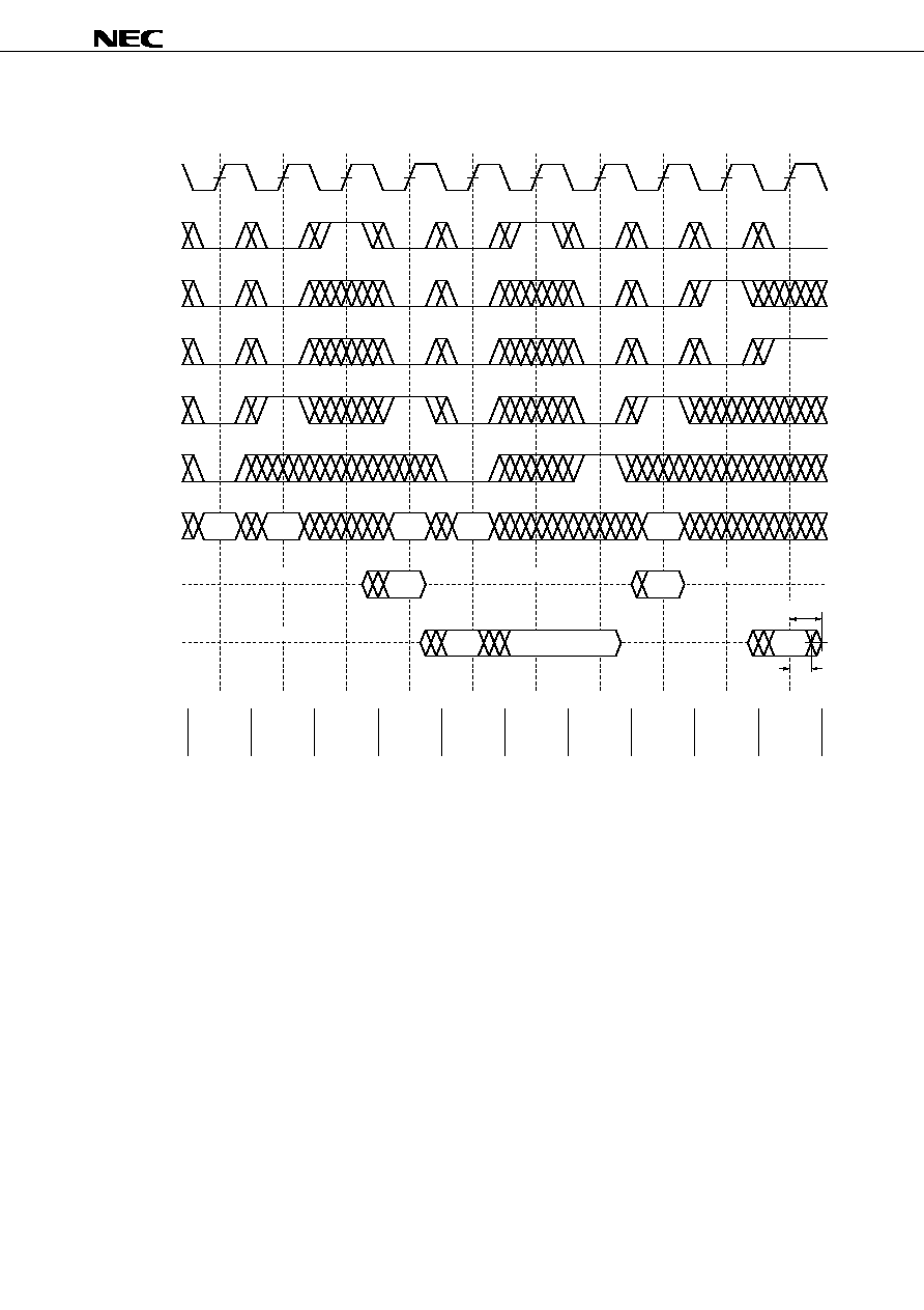
19
Data Sheet M15562EJ3V0DS
µPD4481162, 4481182, 4481322, 4481362
NOP, STALL AND DESELECT CYCLE
1
2
3
4
5
6
7
8
9
10
WRITE
D (A1)
CLK
/CKE
/CEs
ADV
/WE
Data In
Data Out
/BWs
Address
Command
D (A1)
D (A4)
Q (A2)
Q (A3)
Q (A5)
READ
Q (A2)
STALL
READ
Q (A3)
WRITE
D (A4)
STALL
NOP
READ
Q (A5)
DESELECT
CONTINUE
DESELECT
TKHQX2
TKHQZ
A2
A1
A3
A4
A5
High-Z
High-Z
High-Z
High-Z
High-Z
20
Data Sheet M15562EJ3V0DS
µPD4481162, 4481182, 4481322, 4481362
POWER DOWN (ZZ) CYCLE
1
2
3
4
5
6
7
8
9
10
CLK
/CKE
ADV
/WE
/G
Data Out
Address
Q (A1)
11
12
Q1 (A2)
ZZ
TKHKH
TKHKL
TZZE
TZZR
Power Down (I
SBZZ
) State
A1
A2
/CEs
Note
/BWs
Note
TKLKH
High-Z
High-Z
Note /WE or /CEs must be held HIGH at CLK rising edge (clock edge No.2 and No.3 in this figure) prior to power
down state entry.
21
Data Sheet M15562EJ3V0DS
µPD4481162, 4481182, 4481322, 4481362
Package Drawing
100-PIN PLASTIC LQFP (14x20)
NOTE
Each lead centerline is located within 0.13 mm of
its true position (T.P.) at maximum material condition.
ITEM
MILLIMETERS
A
B
D
G
22.0
±
0.2
20.0
±
0.2
0.65 (T.P.)
0.575
J
16.0
±
0.2
K
C
14.0
±
0.2
I
0.13
1.0
±
0.2
L
0.5
±
0.2
F
0.825
N
P
Q
0.10
1.4
0.125
±
0.075
S100GF-65-8ET-1
S
1.7 MAX.
H
0.32
+
0.08
-
0.07
M
0.17
+
0.06
-
0.05
R
3
∞+
7
∞
-
3
∞
M
80
81
51
50
30
31
100
1
S
S
N
J
detail of lead end
C
D
A
B
R
K
M
L
P
I
S
Q
G
F
H

22
Data Sheet M15562EJ3V0DS
µPD4481162, 4481182, 4481322, 4481362
Recommended Soldering Condition
Please consult with our sales offices for soldering conditions of the
µPD4481162, 4481182, 4481322 and 4481362.
Types of Surface Mount Devices
µPD4481162GF
: 100-pin PLASTIC LQFP (14 x 20)
µPD4481182GF
: 100-pin PLASTIC LQFP (14 x 20)
µPD4481322GF
: 100-pin PLASTIC LQFP (14 x 20)
µPD4481362GF
: 100-pin PLASTIC LQFP (14 x 20)

23
Data Sheet M15562EJ3V0DS
µPD4481162, 4481182, 4481322, 4481362
Revision History
Edition/
Page
Type of
Location
Description
Date
This
Previous
revision
(Previous edition
This edition)
edition
edition
3rd edition/
Throughout Throughout Modification
-
Preliminary Data Sheet
Data Sheet
Dec. 2002
Addition
-
Extended operating temperature products
(T
A
=
-40 to +85 ∞C)

24
Data Sheet M15562EJ3V0DS
µPD4481162, 4481182, 4481322, 4481362
[MEMO]

25
Data Sheet M15562EJ3V0DS
µPD4481162, 4481182, 4481322, 4481362
[MEMO]

26
Data Sheet M15562EJ3V0DS
µPD4481162, 4481182, 4481322, 4481362
[MEMO]
27
Data Sheet M15562EJ3V0DS
µPD4481162, 4481182, 4481322, 4481362
NOTES FOR CMOS DEVICES
1
PRECAUTION AGAINST ESD FOR SEMICONDUCTORS
Note:
Strong electric field, when exposed to a MOS device, can cause destruction of the gate oxide and
ultimately degrade the device operation. Steps must be taken to stop generation of static electricity
as much as possible, and quickly dissipate it once, when it has occurred. Environmental control
must be adequate. When it is dry, humidifier should be used. It is recommended to avoid using
insulators that easily build static electricity. Semiconductor devices must be stored and transported
in an anti-static container, static shielding bag or conductive material. All test and measurement
tools including work bench and floor should be grounded. The operator should be grounded using
wrist strap. Semiconductor devices must not be touched with bare hands. Similar precautions need
to be taken for PW boards with semiconductor devices on it.
2
HANDLING OF UNUSED INPUT PINS FOR CMOS
Note:
No connection for CMOS device inputs can be cause of malfunction. If no connection is provided
to the input pins, it is possible that an internal input level may be generated due to noise, etc., hence
causing malfunction. CMOS devices behave differently than Bipolar or NMOS devices. Input levels
of CMOS devices must be fixed high or low by using a pull-up or pull-down circuitry. Each unused
pin should be connected to V
DD
or GND with a resistor, if it is considered to have a possibility of
being an output pin. All handling related to the unused pins must be judged device by device and
related specifications governing the devices.
3
STATUS BEFORE INITIALIZATION OF MOS DEVICES
Note:
Power-on does not necessarily define initial status of MOS device. Production process of MOS
does not define the initial operation status of the device. Immediately after the power source is
turned ON, the devices with reset function have not yet been initialized. Hence, power-on does
not guarantee out-pin levels, I/O settings or contents of registers. Device is not initialized until the
reset signal is received. Reset operation must be executed immediately after power-on for devices
having reset function.

µPD4481162, 4481182, 4481322, 4481362
ZEROSB is a trademark of NEC Electronics Corporation.
The information in this document is current as of December, 2002. The information is subject to
change without notice. For actual design-in, refer to the latest publications of NEC Electronics data
sheets or data books, etc., for the most up-to-date specifications of NEC Electronics products. Not
all products and/or types are available in every country. Please check with an NEC Electronics sales
representative for availability and additional information.
No part of this document may be copied or reproduced in any form or by any means without the prior
written consent of NEC Electronics. NEC Electronics assumes no responsibility for any errors that may
appear in this document.
NEC Electronics does not assume any liability for infringement of patents, copyrights or other intellectual
property rights of third parties by or arising from the use of NEC Electronics products listed in this document
or any other liability arising from the use of such products. No license, express, implied or otherwise, is
granted under any patents, copyrights or other intellectual property rights of NEC Electronics or others.
Descriptions of circuits, software and other related information in this document are provided for illustrative
purposes in semiconductor product operation and application examples. The incorporation of these
circuits, software and information in the design of a customer's equipment shall be done under the full
responsibility of the customer. NEC Electronics assumes no responsibility for any losses incurred by
customers or third parties arising from the use of these circuits, software and information.
While NEC Electronics endeavors to enhance the quality, reliability and safety of NEC Electronics products,
customers agree and acknowledge that the possibility of defects thereof cannot be eliminated entirely. To
minimize risks of damage to property or injury (including death) to persons arising from defects in NEC
Electronics products, customers must incorporate sufficient safety measures in their design, such as
redundancy, fire-containment and anti-failure features.
NEC Electronics products are classified into the following three quality grades: "Standard", "Special" and
"Specific".
The "Specific" quality grade applies only to NEC Electronics products developed based on a customer-
designated "quality assurance program" for a specific application. The recommended applications of an NEC
Electronics product depend on its quality grade, as indicated below. Customers must check the quality grade of
each NEC Electronics product before using it in a particular application.
"Standard": Computers, office equipment, communications equipment, test and measurement equipment, audio
and visual equipment, home electronic appliances, machine tools, personal electronic equipment
and industrial robots.
"Special":
Transportation equipment (automobiles, trains, ships, etc.), traffic control systems, anti-disaster
systems, anti-crime systems, safety equipment and medical equipment (not specifically designed
for life support).
"Specific": Aircraft, aerospace equipment, submersible repeaters, nuclear reactor control systems, life
support systems and medical equipment for life support, etc.
The quality grade of NEC Electronics products is "Standard" unless otherwise expressly specified in NEC
Electronics data sheets or data books, etc. If customers wish to use NEC Electronics products in applications
not intended by NEC Electronics, they must contact an NEC Electronics sales representative in advance to
determine NEC Electronics' willingness to support a given application.
(Note)
(1) "NEC Electronics" as used in this statement means NEC Electronics Corporation and also includes its
majority-owned subsidiaries.
(2) "NEC Electronics products" means any product developed or manufactured by or for NEC Electronics (as
defined above).
∑
∑
∑
∑
∑
∑
M8E 02. 11-1