
The information in this document is subject to change without notice. Before using this document, please
confirm that this is the latest version.
Not all products and/or types are available in every country. Please check with an NEC Electronics
sales representative for availability and additional information.
Document No. M17506EJ1V1DS00 (1st edition)
Date Published September 2005 CP (K)
Printed in Japan
MOS INTEGRATED CIRCUIT
PD46128953-X
128M-BIT CMOS MOBILE SPECIFIED RAM
4M-WORD BY 32-BIT
ADDRESS / DATA MULTIPLEXED
EXTENDED TEMPERATURE OPERATION
PRELIMINARY DATA SHEET
2005
Description
The
PD46128953-X is a high speed, low power, 134,217,728 bits (4,194,304 words by 32 bits) CMOS Mobile
Specified RAM featuring synchronous burst read and synchronous burst write function.
The
PD46128953-X realizes high performance with the SDR interface, command and data inputs / outputs are
synchronized the rising edge of clock.
The
PD46128953-X is fabricated with advanced CMOS technology using one-transistor memory cell.
Features
∑ 4,194,304 words by 32 bits organization
∑ Low voltage operation: 1.7 to 2.0 V (1.85
±
0.15 V)
∑ Operating ambient temperature: T
A
=
-25 to +85 ∞C
∑ Synchronous burst mode
Burst length
: 8 double words (Wrap)
Burst sequence
: Linear burst
Maximum clock frequency : 83 / 66 MHz
∑ SDR (Single Data Rate) Architecture
One data transfers per one clock cycle
All inputs/outputs are synchronized with the positive edge of the clock
∑ Write data mask (DM) for write operation
∑ Output Enable: /OE pin
∑ Chip Enable input: /CE1 pin
∑ Standby Mode input: CE2 pin
∑ Standby Mode 1: Normal standby (Memory cell data hold valid)
∑ Standby Mode 2: Density of memory cell data hold is variable
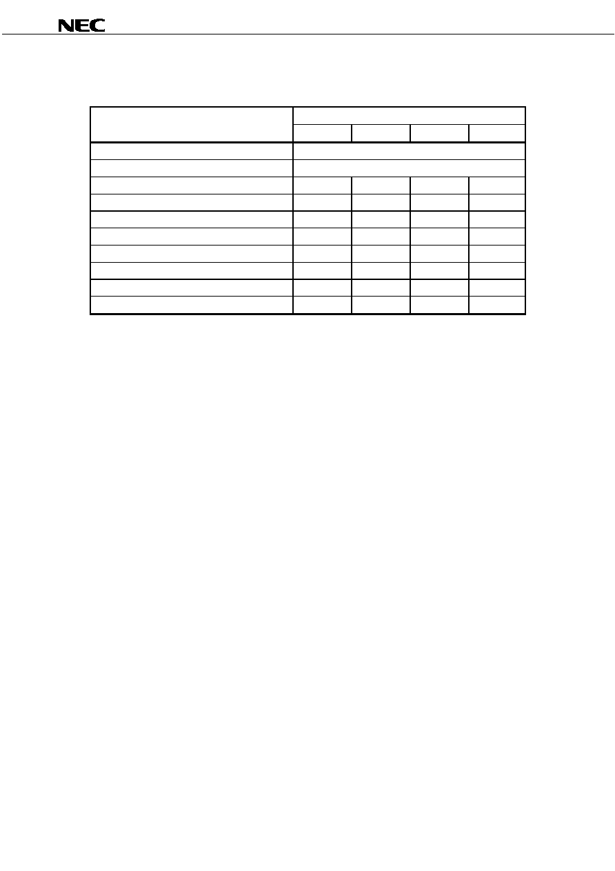
PD46128953 Clock Operating
Operating
Supply current
frequency
supply
ambient
At operating mA
At standby
A
MHz voltage
temperature (MAX.)
(MAX.)
(MAX.) V ∞C
-E12X
Note
83
1.7 to 2.0
-25 to +85 60
T.B.D.
-E15X
66
55
Note Under consideration

Preliminary Data Sheet M17506EJ1V1DS
2
PD46128953-X
Ordering Information
PD46128593-X is mainly shipping by wafer.
Please consult with our sales offices for package samples and ordering information.
Preliminary Data Sheet M17506EJ1V1DS
3
PD46128953-X
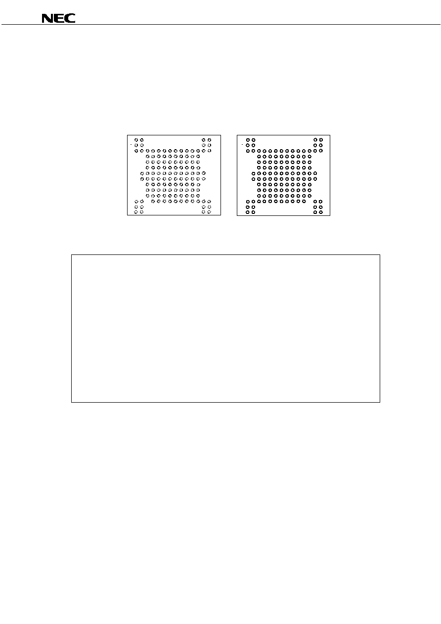
Pin Configuration
The following is pin configuration of package sample.
/xxx indicates active low signal.
127-pin PLASTIC FBGA (13.0 x 11.5)
Top View
Top View
Bottom View
C B A
D
E
F
G
H
J
K
L
M
N
P
M N P
L
K
J
H
G
F
E
D
C
B
A
14
13
12
11
10
9
8
7
6
5
4
3
2
1
NC
NC
NC
NC
NC
NC
NC
NC
/CE1
/OE
A/DQ20
A/DQ14
NC
NC
NC
NC
NC
NC
DM3
NC
DM1
A/DQ5
NC
V
DD
DM0
A/DQ9
A/DQ10
V
SS
NC
NC
A/DQ15
DQ22
A/DQ7
DQ27
DM2
NC
NC
A/DQ6
NC
V
SS
NC
NC
NC
V
DD
NC
A/DQ12
A/DQ13
NC
NC
NC
V
SS
Q
NC
A/DQ8
DQ24
A/DQ2
A/DQ0
NC
DQ23
V
SS
Q
DQ25
B
C
D
E
F
G
H
J
NC
NC
DQ26
NC
NC
N
L
M
K
14
13
12
11
10
9
8
7
6
5
4
3
2
1
NC
NC
NC
NC
P
NC
NC
DQ28
A/DQ19
A
NC
NC
NC
NC
DQ30
V
SS
Q
A/DQ17
NC
NC
A/DQ18
DQ29
V
SS
NC
NC
A/DQ21
/ADV
CLK
A/DQ3
V
DD
Q
NC
A/DQ1
A/DQ11
/WAIT
NC
V
DD
Q
CE2
/WE
A/DQ4
V
DD
Q
NC
V
DD
NC
NC
DQ31
A/DQ16
NC
NC
NC
NC
NC
NC
NC
NC
NC
NC
NC
NC
NC
NC
NC
NC
NC
NC
NC
A/DQ0 to A/DQ021 : Address inputs , Data inputs/ outputs
/WAIT
: Wait output
DQ22 to DQ31
: Data inputs / outputs
DM0 to DM3 : Write data mask input
/CE1
: Chip select input
V
DD
: Power supply
CE2
: Standby mode input
V
SS
:
Ground
/WE
: Write enable input
V
DD
Q
: Power supply for DQ
/OE
: Output enable input
V
SS
Q
: Ground for DQ
CLK
: Clock input
NC
Note
: No Connection
/ADV
: Address valid
Note Some signals can be applied because this pin is not internally connected.
Remark Refer
to
10. Package Drawing for the index mark.

Preliminary Data Sheet M17506EJ1V1DS
4
PD46128953-X
Pin Function
(1/2)
Symbol Description
A/DQ0 to A/DQ21
Synchronous address input/data input/output
These pins are used as address input pins and data input/output pins.
When they are used as address input pins, the input address is latched at the rising edge of CLK. When the
address is latched, the setup time and hold time must be satisfied at the rising edge of CLK.
When they are used as data input/output pins, the input data is latched at the rising edge of CLK. When
data is input, the setup time and hold time must be satisfied at the rising edge of CLK. Data is output from
these pins at the rising edge of CLK.
DQ22 to DQ31
Synchronous data input/output.
While the A/DQ pins function as address input pins and data input/output pins, these pins function only as
data input/output pins.
The input data is latched at the rising edge of CLK. When data is input, the setup time and hold time must
be satisfied at the rising edge of CLK. Data is output at the rising edge of CLK.
CLK Input
clock.
Addresses and control signals are latched in synchronization with this signal.
All the synchronous input signals must satisfy the setup time and hold time at the rising edge of CLK.
/ADV
Synchronous address valid input signal.
An address is latched at the rising edge of CLK while /ADV is LOW. When the address is latched, the setup
time and hold time must be satisfied at the rising edge of CLK.
Note: This signal serves as an asynchronous signal when the mode register set or read.
/CE1
Synchronous chip enable input.
This device is active while /CE1 is LOW. When inputting /CE1, the setup time and hold time must be
satisfied at the rising edge of CLK.
Remark This signal serves as an asynchronous signal when the mode register set or read.
CE2
Asynchronous power-down mode input
When this signal is made LOW, the device enters the power-down mode status.
CE2 is not synchronized with the clock. It is an asynchronous signal.
/OE
Synchronous output enable input.
When this signal is made LOW, read data is output.
When inputting /OE, the setup time and hold time must be satisfied at the rising edge of CLK.
Remark This signal serves as an asynchronous signal when the mode register set or read.
/WE
Synchronous write enable input.
When /WE inputs a LOW at the same time as /ADV, the device recognizes a write operation. When inputting
/WE, the setup time and hold time must be satisfied at the rising edge of CLK.
Remark This signal serves as an asynchronous signal when the mode register is set or read.

Preliminary Data Sheet M17506EJ1V1DS
5
PD46128953-X
(2/2)
Symbol Description
DM0 to DM3
Synchronous write data mask input.
These signals can mask write data during burst write.
To input data mask, the setup time and hold time must be satisfied at the rising edge of CLK.
Data mask can be controlled in byte units.
DM0: A/DQ0 to ADQ7
DM1: A/DQ8 to ADQ15
DM2: A/DQ16 to ADQ21, DQ22 to DQ23
DM3: DQ24 to DQ31
/WAIT
Synchronous wait output.
/WAIT is a status signal (output) that indicates the preparation for starting burst read/burst write
This pin outputs a LOW while the internal circuit is busy, and a HIGH when it is ready.
The wait signal is output at the rising edge of CLK.
V
DD
Supply
voltage:
Usually, the supply voltage is 1.85 V. Refer to DC Characteristics and Recommended Operation
Conditions.
V
SS
Supply
voltage:
Ground
V
DD
Q Supply
voltage:
Supply voltage for DQ. Usually, this voltage is 1.85 V. Refer to DC Characteristics and Recommended
Operation Conditions.
V
SS
Q
Supply voltage:
Ground for DQ.
NC No
connection
Some signals can be applied because this pin is not internally connected.

Preliminary Data Sheet M17506EJ1V1DS
6
PD46128953-X
Block Diagram
V
DD
V
SS
CE2
Memory cell array
134,217,728 bits
/CE1
/ADV
/OE
A/DQ0 to A/DQ21
/WE
CLK
/WAIT
DQ22 to DQ31
DM0 to DM3
V
DD
Q
V
SS
Q
Refresh
control
Refresh
counter
Command
control
Standby mode control
Refresh
state
control
Sense amplifier /
Switching circuit
Column decoder
Data control
Latch circuit
Input / Output buffer
Burst
counter
Address latch
Clock
control
Row
decoder
Address buffer

Preliminary Data Sheet M17506EJ1V1DS
7
PD46128953-X
Truth Table
Mode /CE1
CE2
CLK
/ADV
/OE
/WE
A/DQ0-A/DQ21 , DQ22-DQ31
Deselect (Standby Mode 1)
H
H
◊ ◊ ◊
High-Z
Power Down (Standby Mode 2)
Note1
◊
L
◊ ◊ ◊ ◊
High-Z
Output Disable
L
H
◊ H ◊ High-Z
Start Address Latch
Note2
L H
◊ High-Z
Start Address not Latch
Note3
H
◊
◊
Low-Z or High-Z
Read Command input
Note2
L H H
High-Z
Write Command input
Note2
L H L
High-Z
Burst Read Termination
Note4
L to H
◊
◊
◊
Low-Z to High-Z
Burst Write Termination
Note4
◊
◊
◊ High-Z
Notes 1. CE2 pin must be fixed HIGH except Standby Mode 2 (refer to 2.3 Standby Mode Status Transition).
2. Start address latch and read/write command input are performed at the next rising edge of clock when /ADV
is transferred HIGH to LOW.
3. It is impossible that Start address latch and read/write command input are performed at the first rising edge
of clock during /ADV is fixed HIGH.
4. Refer to 3.6 Burst Read Termination, 3.7 Burst Write Termination.
Remark H, HIGH: V
IH
, L, LOW: V
IL
,
◊: V
IH
or V
IL
For read/write operation, refer to 7 Timing Charts.

Preliminary Data Sheet M17506EJ1V1DS
8
PD46128953-X
CONTENTS
1. Initialization ................................................................................................................................................ 10
2. Partial Refresh ........................................................................................................................................... 11
2. 1 Standby Mode......................................................................................................................................................... 11
2. 2 Density Switching ................................................................................................................................................... 11
2. 3 Standby Mode Status Transition............................................................................................................................. 11
2. 4 Addresses for Which Partial Refresh Is Supported................................................................................................. 12
3. Burst Operation ......................................................................................................................................... 13
3. 1 Features of Burst Operation ................................................................................................................................... 13
3. 2 Latency ................................................................................................................................................................... 13
3. 3 Burst Length, Burst Sequence, Wrap Around......................................................................................................... 16
3. 4 Burst Read End ...................................................................................................................................................... 17
3. 5 Burst Write End ...................................................................................................................................................... 18
3. 6 Burst Read Termination.......................................................................................................................................... 19
3. 7 Burst Write Termination .......................................................................................................................................... 20
3. 8 /WAIT signal behavior............................................................................................................................................. 21
3. 9 /WAIT output........................................................................................................................................................... 21
4. Mode Register Settings............................................................................................................................. 23
4. 1 Mode Register Setting Method ............................................................................................................................... 23
4. 1. 1
Cautions for Setting Mode Register............................................................................................................. 23
4. 1. 2
Mode Register Setting/Reading................................................................................................................... 25
4. 1. 3
Partial refresh Density ................................................................................................................................. 25
4. 1. 4
Burst length ................................................................................................................................................. 25
4. 1. 5
Function mode............................................................................................................................................. 26
4. 1. 6
Driver strength............................................................................................................................................. 26
4. 1. 7
Read Latency .............................................................................................................................................. 26
4. 1. 8
Single Write ................................................................................................................................................. 26
4. 1. 9
Valid Clock Edge ......................................................................................................................................... 26
4. 1. 10
Reset to Asynchronous.............................................................................................................................. 26
4. 1. 11
/WE control................................................................................................................................................ 26
4. 1. 12
Setting of unused bits ................................................................................................................................ 26
4. 2 Mode Register Reading .......................................................................................................................................... 27
4. 2. 1
Cautions for Setting Mode Register............................................................................................................. 27
4. 2. 2
Data read from mode register...................................................................................................................... 27
5. Address, /OE, /WE, DM control ................................................................................................................ 29
5. 1 Relation of address inputs and /OE control ............................................................................................................ 29
5. 2 Address Latching .................................................................................................................................................... 30
5. 3 Read / Write Command Loading............................................................................................................................. 32
5. 4 /OE control during burst read operation.................................................................................................................. 34
5. 4. 1
/OE HIGH to LOW during burst read operation ........................................................................................... 34
5. 4. 2
/OE LOW to HIGH during burst read operation ........................................................................................... 35
5. 5 Write data mask signal (DM) control....................................................................................................................... 36
5. 5. 1
Controlling write data mask signal (DM) in write cycle................................................................................. 36
5. 5. 2
Write data mask (DM) truth table................................................................................................................. 37

Preliminary Data Sheet M17506EJ1V1DS
9
PD46128953-X
6. Electrical Specifications ........................................................................................................................... 38
7. Timing Charts............................................................................................................................................. 43
8. Mode Register Setting/Read Timing........................................................................................................ 49
8. 1 Mode Register Setting Timing ................................................................................................................................ 49
8. 2 Mode Register Setting Flow Chart .......................................................................................................................... 50
8. 3 Mode Register Read Timing ................................................................................................................................... 51
8. 4 Mode Register Read Flow Chart............................................................................................................................. 52
9. Standby Mode Timing Charts................................................................................................................... 53
10. Package Drawing..................................................................................................................................... 54
11. Recommended Soldering Conditions ................................................................................................... 55

Preliminary Data Sheet M17506EJ1V1DS
10
PD46128953-X
1. Initialization
Initialize the
PD46128953-X at power application using the following sequence to stabilize internal circuits.
(1) Following power application, make CE2 HIGH after fixing CE2 to LOW for the period of t
VHMH
.
Make /CE1 HIGH before making CE2 HIGH.
(2) /CE1 and CE2 are fixed HIGH for the period of t
MHCL
.
Normal operation is possible after the completion of initialization.
Figure 1-1. Initialization Timing Chart
/CE1 (Input)
V
DD
CE2 (Input)
t
MHCL
Initialization
t
CHMH
t
VHMH
V
DD
(MIN.)
Normal Operation
Cautions 1. Make CE2 LOW when starting the power supply.
2.
t
VHMH
is specified from when the power supply voltage reaches the prescribed minimum value
(V
DD
(MIN.)).
Initialization Timing
Parameter Symbol
MIN.
MAX.
Unit
Power application to CE2 LOW hold
t
VHMH
50
s
/CE1 HIGH to CE2 HIGH
t
CHMH
0
ns
Following power application CE2 HIGH hold to /CE1 LOW
t
MHCL
300
s

Preliminary Data Sheet M17506EJ1V1DS
11
PD46128953-X
2. Partial Refresh
2. 1 Standby Mode
In addition to the regular standby mode (Standby Mode 1) with a 128M bits density, Standby Mode 2, which performs
partial refresh, is also provided.
2. 2 Density Switching
In Standby Mode 2, the densities that can be selected for performing refresh are 64M bits, 32M bits, 16M bits, and 0M
bit.
The density for performing refresh can be set with the mode register. Once the refresh density has been set in the
mode register, these settings are retained until they are set again, while applying the power supply. However, the mode
register setting will become undefined if the power is turned off, so set the mode register again after power application.
(For how to perform mode register settings, refer to section 4. Mode Register Settings.)
2. 3 Standby Mode Status Transition
In Standby Mode 1, /CE1 and CE2 are HIGH. In Standby Mode 2, CE2 is LOW. In Standby Mode 2, if 0M bit is set as
the density, it is necessary to perform initialization the same way as after applying power, in order to return to normal
operation from Standby Mode 2. When the density has been set to 64M bits, 32M bits, or 16M bits in Standby Mode 2, it
is not necessary to perform initialization to return to normal operation from Standby Mode 2.
For the timing charts, refer to Figure 9-1. Standby Mode 2 (data hold: 64M bits / 32M bits / 16M bits) Entry / Exit
Timing Chart, Figure 9-2. Standby Mode 2 (data not held) Entry / Exit Timing Chart.

Preliminary Data Sheet M17506EJ1V1DS
12
PD46128953-X
Figure 2-1. Standby Mode State Machine
Power On
Active
CE2 = V
IH
CE2 = V
IL
CE2 = V
IL
/CE1 = V
IL
,
CE2 = V
IH
Standby
Mode 1
Standby Mode 2
(64M bits / 32M bits
/ 16M bits)
/CE1 = V
IL
Mode Register
Setting
Initialization
Standby Mode 2
(Data not held)
/CE1 = V
IL
,
CE2 = V
IH
CE2 = V
IL
CE2 = V
IL
/CE1 = V
IH
,
CE2 = V
IH
2. 4 Addresses for Which Partial Refresh Is Supported
Data hold density
Correspondence address
64M bits
000000H to 1FFFFFH
32M bits
000000H to 0FFFFFH
16M bits
000000H to 07FFFFH

Preliminary Data Sheet M17506EJ1V1DS
13
PD46128953-X
3. Burst Operation
3. 1 Features of Burst Operation
Function Features
Burst Length
8 double words
Burst Wrap
Wrap
Burst Sequence
Linear
Valid Clock Edge
CLK Rising Edge
Latency Count
Read Latency
6, 7, 8
Write Latency
5, 6, 7
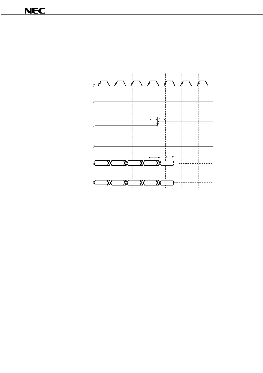
3. 2 Latency
Read Latency (RL) is the number of clock cycles between the address being latched and first read data becoming
available during synchronous burst read operation. It is set through Mode Register Set sequence after power-up. Once
RL is set through Mode Register Set sequence, write latency, that is the number of clock cycles between address being
latched and first write data being latched, is automatically set to RL
-1.
Latency Count
Grade
Clock Frequency
Read Latency
Write Latency
Note
-E12X
<83 MHz
7, 8
6, 7
-E15X
<66 MHz
6, 7, 8
5, 6, 7
Note Write Latency = Read Latency
-1

Preliminary Data Sheet M17506EJ1V1DS
14
PD46128953-X
Figure 3-1. Latency Configuration (Read)
/ADV (Input)
/CE1 (Input)
A/DQ0 to A/DQ21 (Input/Output)
CLK (Input)
Add
High-Z
Read Latency = 6
A/DQ0 to A/DQ21 (Input/Output)
Add
High-Z
Read Latency = 7
A/DQ0 to A/DQ21 (Input/Output)
Add
High-Z
Read Latency = 8
T0
T1
T2
T3
T4
T5
T6
T7
T8
T9
T10
T11
T12
T13
DQ22 to DQ31 (Output)
High-Z
DQ22 to DQ31 (Output)
High-Z
DQ22 to DQ31 (Output)
High-Z
Q0
Q1
Q2
Q3
Q4
Q5
Q6
Q7
Q0
Q1
Q2
Q3
Q4
Q5
Q6
Q7
Q0
Q1
Q2
Q3
Q4
Q5
Q6
Q0
Q1
Q2
Q3
Q4
Q5
Q6
Q0
Q1
Q2
Q3
Q4
Q5
Q0
Q1
Q2
Q3
Q4
Q5

Preliminary Data Sheet M17506EJ1V1DS
15
PD46128953-X
Figure 3-2. Latency Configuration (Write)
/ADV (Input)
/CE1 (Input)
A/DQ0 to A/DQ21 (Input)
CLK (Input)
Add
High-Z
Write Latency = 5
A/DQ0 to A/DQ21 (Input)
Add
High-Z
Write Latency = 6
A/DQ0 to A/DQ21 (Input)
Add
High-Z
Write Latency = 7
T0
T1
T2
T3
T4
T5
T6
T7
T8
T9
T10
T11
T12
T13
DQ22 to DQ31 (Input)
High-Z
DQ22 to DQ31 (Input)
High-Z
DQ22 to DQ31 (Input)
High-Z
D0
D1
D2
D3
D4
D5
D6
D7
D0
D1
D2
D3
D4
D5
D6
D7
D0
D1
D2
D3
D4
D5
D6
D7
D0
D1
D2
D3
D4
D5
D6
D7
D0
D1
D2
D3
D4
D5
D6
D0
D1
D2
D3
D4
D5
D6

Preliminary Data Sheet M17506EJ1V1DS
16
PD46128953-X
3. 3 Burst Length, Burst Sequence, Wrap Around
The burst length is 8 double words and the corresponding address is (A/DQ2, A/DQ1, A/DQ0). A burst operation that
extends over addresses higher than A/DQ3 cannot be executed.
Wrap-around is performed within the burst length of 8 double words. Refer to Table 3-1. Burst Sequence.
Table 3-1. Burst Sequence
Start Address
Burst Sequence
(A/DQ2 , A/DQ1, A/DQ0)
Linear , Wrap
1st data - 2nd data - 3rd data - 4th data - 5th data - 6th data - 7th data - 8th data
(0, 0, 0)
(0, 0, 0) - (0, 0, 1) - (0, 1, 0) - (0, 1, 1) - (1, 0, 0) - (1, 0, 1) - (1, 1, 0) - (1, 1, 1)
(0, 0, 1)
(0, 0, 1) - (0, 1, 0) - (0, 1, 1) - (1, 0, 0) - (1, 0, 1) - (1, 1, 0) - (1, 1, 1) - (0, 0, 0)
(0, 1, 0)
(0, 1, 0) - (0, 1, 1) - (1, 0, 0) - (1, 0, 1) - (1, 1, 0) - (1, 1, 1) - (0, 0, 0) - (0, 0, 1)
(0, 1, 1)
(0, 1, 1) - (1, 0, 0) - (1, 0, 1) - (1, 1, 0) - (1, 1, 1) - (0, 0, 0) - (0, 0, 1) - (0, 1, 0)
(1, 0, 0)
(1, 0, 0) - (1, 0, 1) - (1, 1, 0) - (1, 1, 1) - (0, 0, 0) - (0, 0, 1) - (0, 1, 0) - (0, 1, 1)
(1, 0, 1)
(1, 0, 1) - (1, 1, 0) - (1, 1, 1) - (0, 0, 0) - (0, 0, 1) - (0, 1, 0) - (0, 1, 1) - (1, 0, 0)
(1, 1, 0)
(1, 1, 0) - (1, 1, 1) - (0, 0, 0) - (0, 0, 1) - (0, 1, 0) - (0, 1, 1) - (1, 0, 0) - (1, 0, 1)
(1, 1, 1)
(1, 1, 1) - (0, 0, 0) - (0, 0, 1) - (0, 1, 0) - (0, 1, 1) - (1, 0, 0) - (1, 0, 1) - (1, 1, 0)

Preliminary Data Sheet M17506EJ1V1DS
17
PD46128953-X
3. 4 Burst Read End
The memory output goes into a high impedance state after completion of the burst read operation of the eighth double
word. Therefore, no data is output from the memory even if CLK is kept input while /CE1 = LOW after the burst read
operation of 8 words has been completed.
Figure 3-3. Burst Read End
CLK (Input)
/CE1 (Input)
/OE (Input)
A/DQ0 to A/DQ21 (Output)
High-Z
T9
T10
T11
T12
T13
T14
T15
DQ22 to DQ31 (Output)
Q5
Q6
Q7
L
/ADV (Input)
H
t
AC
t
HZ
L
High-Z
Q5
Q6
Q7
Remark Memory output goes into a high impedance state after the last data (Q7) read by the burst operation has
been output.

Preliminary Data Sheet M17506EJ1V1DS
18
PD46128953-X
3. 5 Burst Write End
The memory does not input write data to internal circuits even if CLK is kept input with /CE1 = LOW and write data is
input from the controller after completion of a burst write operation of 8 double words.
Figure 3-4. Burst Write End
CLK (Inout)
/CE1 (Input)
/WE (Input)
A/DQ0 to A/DQ21 (Input)
High-Z
T8
T9
T10
T11
T12
T13
T14
DQ22 to DQ31 (Input)
D5
D6
D7
L
/ADV (Input)
H
t
WDS
t
WDH
A
B
C
High-Z
D5
D6
D7
A
B
C
Remark The memory does not input any write data to internal circuits even if write data (A, B, or C) is input after the
last burst write data (D7) has been input, as shown in Figure 3-4.
Preliminary Data Sheet M17506EJ1V1DS
19
PD46128953-X
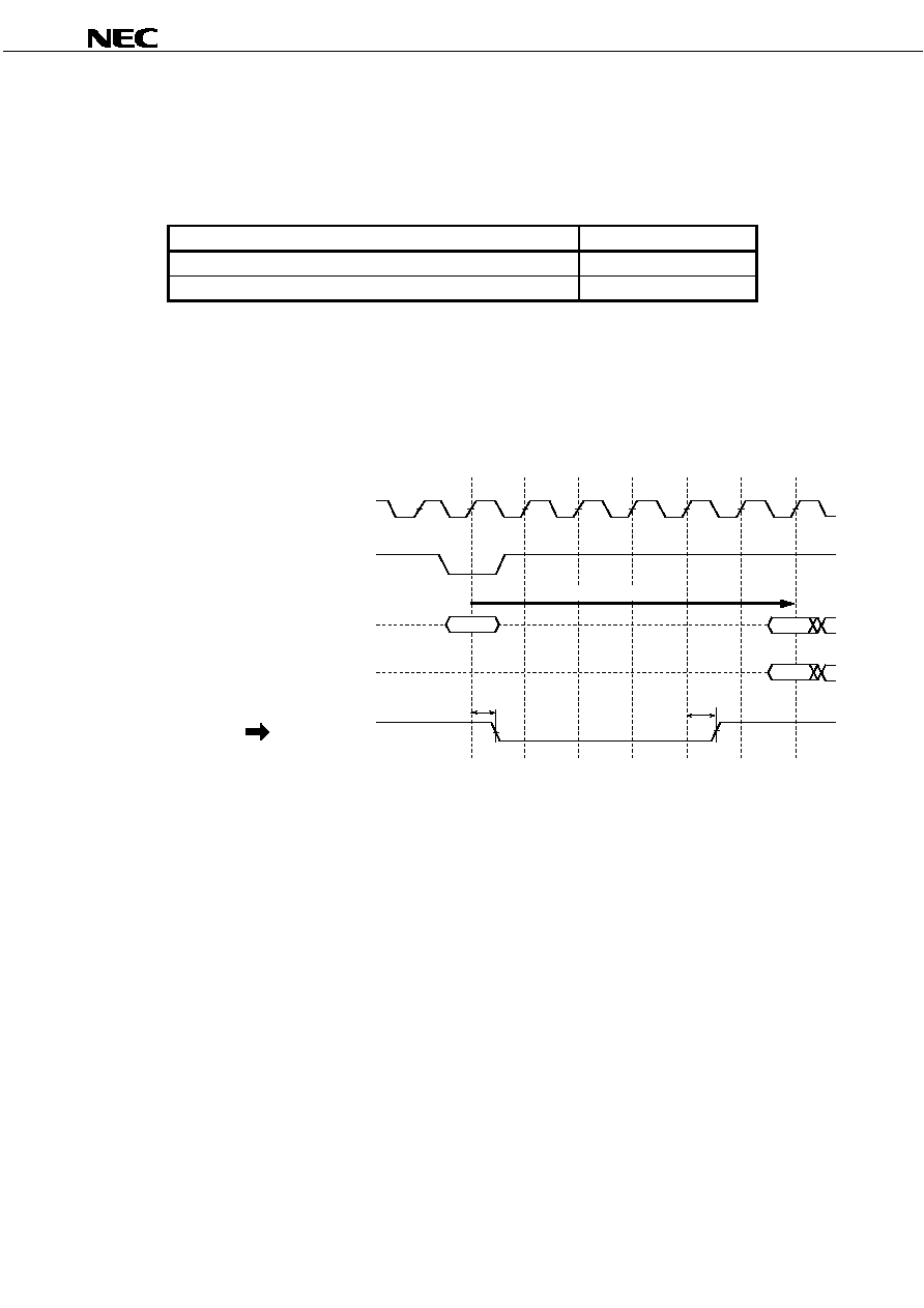
3. 6 Burst Read Termination
A burst read termination is executed when /CE1 is made HIGH during a burst read operation. The command that the
burst read termination (/CE1 = HIGH) is recognized at the next rising edge of CLK when /CE1 = HIGH, the read data is
output before the command of the burst read termination (/CE1 = HIGH) is input.
Figure 3-5. Burst Read Termination
CLK (Input)
/CE1 (Input)
/OE (Input)
A/DQ0-A/DQ21 (Output)
High-Z
T4
T5
T6
T7
T8
T9
T10
t
CES
DQ22-DQ31 (Output)
Q0
Q1
Q2
Q3
Q4
L
/ADV (Input)
H
t
CEH
t
AC
t
HZ
High-Z
Q0
Q1
Q2
Q3
Q4
Remark If the burst read termination is performed (/CE1: LOW
HIGH) before the rising edge of CLK in T8, as
shown in Figure 3-5, determined data is output as the read data (Q4) from the rising edge of CLK in T7.
The burst read termination is valid after the initial read data has been output.
(For the burst read termination, refer to Figure 7-5. Burst Read Termination Cycle Timing Chart (/CE1 control).)

Preliminary Data Sheet M17506EJ1V1DS
20
PD46128953-X
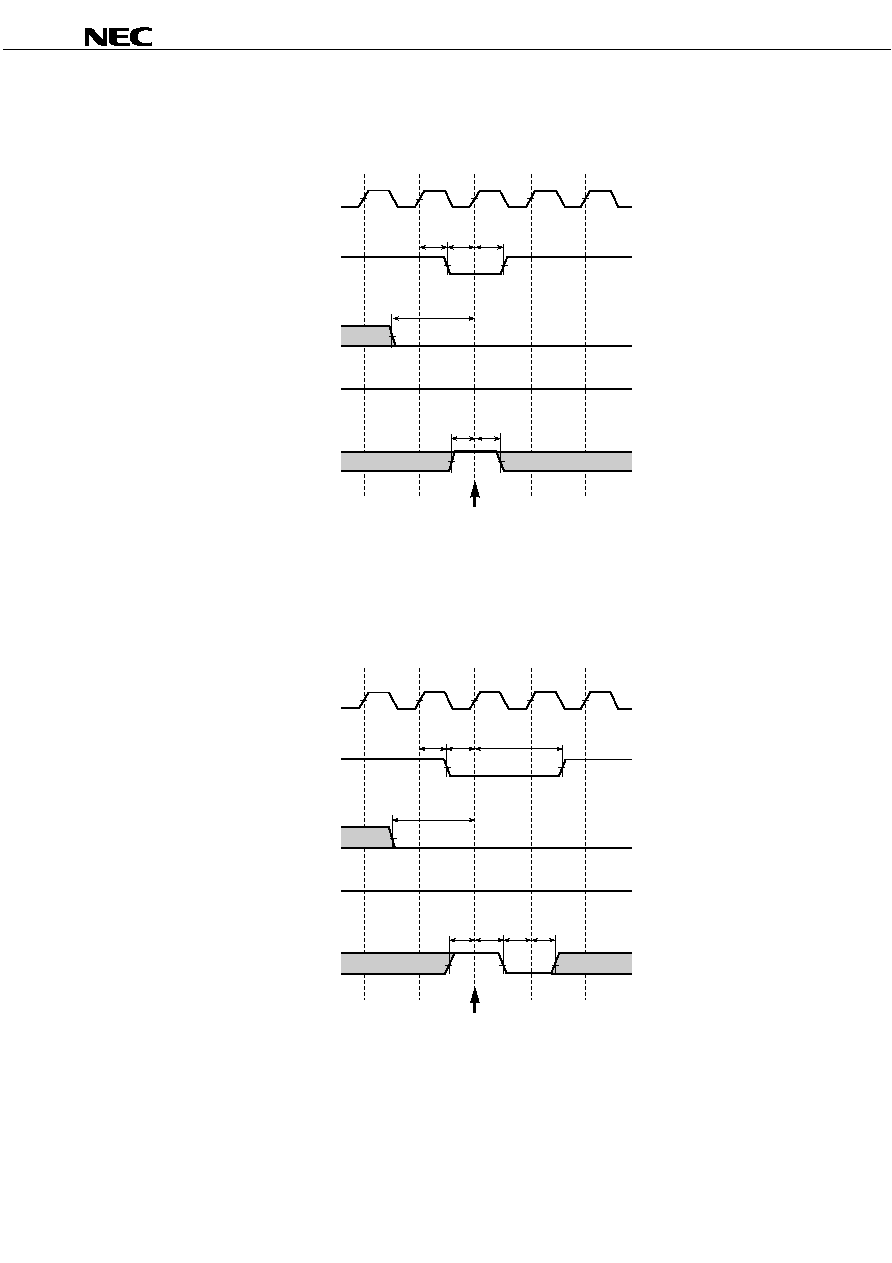
3. 7 Burst Write Termination
A burst write termination is executed when /CE1 is made HIGH during a burst write operation. The command that the
burst write termination (/CE1 = HIGH) is recognized at the next rising edge of CLK when /CE1 = HIGH, the write data is
written before the command of the burst write termination (/CE1 = HIGH) is input.
Figure 3-6. Burst Write Termination
CLK (Input)
/CE1 (Input)
/WE (Input)
A/DQ0 to A/DQ21 (Input)
High-Z
T3
T4
T5
T6
T7
T8
T9
DQ22 to DQ31 (Input)
D0
D1
D2
/ADV (Input)
H
t
WDS
t
WDH
t
CES
t
CEH
D3
D4
D5
High-Z
D0
D1
D2
D3
D4
D5
Remark If the burst write termination is performed (/CE1: LOW
HIGH) before the rising edge of CLK in T8, as
shown in Figure 3-6, the write data is input to memory at the rising edge of CLK in T7. The write data input
in cycle T8 (D5) is invalid.
The burst termination is valid after the initial write data has been input.
(For the burst write termination refer to Figure 7-6. Burst Write Termination Cycle Timing Chart (/CE1 control).)
Preliminary Data Sheet M17506EJ1V1DS
21
PD46128953-X
3. 8 /WAIT signal behavior
/WAIT is a status signal (output) that indicates the preparation for starting burst read/burst write
This pin outputs a LOW while the internal circuit is busy, and a HIGH when it is ready.
The wait signal is output at the rising edge of CLK.
Table 3-2. Relation Between Internal Operation of Memory and /WAIT Output
Internal Operation of Memory
/WAIT output
Preparation for burst read/burst write in progress
LOW
Completion of preparation for burst read/burst write
HIGH
3. 9 /WAIT output
The /WAIT output is enabled after specified time from CLK. /WAIT output is transferred LOW to HIGH one cycle before
1st burst read data output and 1st burst write data input.
Figure 3-7. /WAIT Output Timing (Read Cycle)
/ADV (Input)
CLK (Input)
T0
T1
T2
T3
T4
A/DQ0 to A/DQ21 (Input/Output)
High-Z
Q0
Read Latency = 6
/WAIT (Output)
DQ22 to DQ31 (Output)
High-Z
Q0
Add
T5
T6
1 cycle before latency cycle
t
CEWA
t
CLWA

Preliminary Data Sheet M17506EJ1V1DS
22
PD46128953-X
Figure 3-8. /WAIT Output Timing (Write Cycle)
T0
T1
T2
T3
T4
High-Z
D1
Write Latency = 5
t
CLWA
t
CEWA
High-Z
D1
D0
D0
Add
T5
T6
/ADV (Input)
CLK (Input)
A/DQ0 to A/DQ21 (Input)
/WAIT (Output)
DQ22 to DQ31 (Input)
1 cycle before latency cycle

Preliminary Data Sheet M17506EJ1V1DS
23
PD46128953-X
4. Mode Register Settings
The default value of the mode register of the
PD46128953-X is undefined upon power application. Therefore, be sure
to set the mode register after power application and initialization.
4. 1 Mode Register Setting Method
Each mode can be set by performing a total of six cycles of operations in succession after reading the most significant
address (3FFFFFH) ≠ two consecutive cycles for writing any data and three consecutive cycles for writing specific data
(codes 1 to 3) ≠ by an asynchronous access (with CLK fixed HIGH or LOW).
Table 4-1. Mode Register Settings
Cycle Operation
Address
Data
1st cycle
Read
3FFFFFH
Don't care
2nd cycle
Write
3FFFFFH
Don't care
3rd cycle
Write
3FFFFFH
Don't care
4th cycle
Write
3FFFFFH
Code 1 (A/DQ0 = 1)
5th cycle
Write
3FFFFFH
Code 2
6th cycle
Write
3FFFFFH
Code 3
Codes 1 to 3 are set at the register. The register has a function to latch an address and data necessary for instruction
execution, and does not occupy the memory.
Whether the mode register is set or read can be selected by code 1 in the 4th bus cycle. If setting of the mode register
is selected (A/DQ0 = 1) by code 1 in the 4th bus cycle, the contents of the mode register are set by code 2 in the 5th bus
cycle and code 3 in the 6th bus cycle.
The command contents are shown in Table 4-2. Mode Register Code 1 Definition (4th cycle), Table 4-3. Mode
Register Code 2 Definition (5th cycle), and Table 4-4. Mode Register Code 3 Definition (6th cycle).
For the timing chart and flowchart, refer to Figure 8-1. Mode Register Setting Timing Chart and Figure 8-2. Mode
Register Setting Flowchart.
If reading the mode register is selected by code 1 in the 4th bus cycle (A/DQ = 0), the contents of the mode register
currently set in the 5th and 6th bus cycles can be read. If the mode register is read before it is set, any (undefined) data
is read.
For the mode register, refer to 4.2 Mode Register Reading.
4. 1. 1
Cautions for Setting Mode Register
When the mode register is set, the status of the internal counter is identified by the toggle operation of /CE1 and /OE.
When setting a mod entry, therefore, perform a toggle operation of /CE1 in each cycle (one read cycle and five write
cycles).
In the 1st bus cycle (read cycle), perform a toggle operation of /OE in the same manner as /CE1. If an illegal address
or data is written or if an address and data are written in an incorrect sequence, the mode register is not correctly set.
If the most significant address (3FFFFFH) is read (in the 1st bus cycle), written (2nd bus cycle), and then written (3rd
bus cycle), a sequence of setting/reading the mode register is started. Therefore, setting of the mode register cannot be
stopped after the 4th bus cycle. If the normal sequence is executed up to the 5th bus cycle, setting of the mode register
cannot be stopped until the 6th bus cycle is completed.

Preliminary Data Sheet M17506EJ1V1DS
24
PD46128953-X
Once the mode register has been set, the setting is retained while power is supplied and CE2 = HIGH, until it is re-set.
If data is not retained by turning off the power or making CE2 LOW (except partial), however, the setting of the mode
register is undefined. Re-set the register after power application or when returning from a data non-retention status.
For the timing chart and flowchart, refer to Figure 8-1. Mode Register Setting Timing Chart and Figure 8-2. Mode
Register Setting Flowchart.
Table 4-2. Mode Register Code1 Definition (4th Bus Cycle)
Data Code
Symbol
Function
Value
Description
A/DQ0
RW
Mode Register Setting /
0
Mode Register Reading
Mode Register Reading
1
Mode Register Setting
A/DQ21 to A/DQ1
- - All
"1"
Reserved
DQ31 to DQ22
-
- All
"1"
Reserved
Table 4-3. Mode Register Code2 Definition (5th Bus Cycle)
Data Code
Symbol
Function
Value
Description
A/DQ1 to A/DQ0
PR
Partial Refresh Density
00
32M
01
16M
10
64M
11
0M
A/DQ4 to A/DQ2
BL
Burst length
000
Reserved
001
Reserved
010
8 double words
011
Reserved
100
Reserved
101
Reserved
110
Reserved
111
Reserved
A/DQ5
M
Function Mode
0
Synchronous Burst
1
Reserved
A/DQ7 to A/DQ6
DS
Driver Strength
00
Strong
01
Reserved
10
Weak
11
Middle
A/DQ21 to A/DQ8
≠
≠
All "1"
Reserved
DQ31 to DQ22
≠
≠
All "1"
Reserved

Preliminary Data Sheet M17506EJ1V1DS
25
PD46128953-X
Table 4-4. Mode Register Code3 Definition (6th Bus Cycle)
Data Code
Symbol
Function
Value
Description
A/DQ2 to A/DQ0
RL
Read Latency
000
Reserved
001
Reserved
010
Reserved
011
Reserved
100
6
101
7
110
8
111
Reserved
A/DQ3 N/A
N/A
1
Reserved
A/DQ4
SW
Single Write
0
Burst Read & Burst Write
1
Reserved
A/DQ5
VE
Valid Clock Edge
0
Reserved
1
Rising
Edge
A/DQ6
RP
Reset to Asynchronous
1
Reserved
A/DQ7
WC
/WE Control
0
/WE Pulse Control
1
Reserved
A/DQ21 to A/DQ8
-
-
1 Reserved
DQ31 to DQ22
-
- 1
Reserved
4. 1. 2
Mode Register Setting/Reading
Select whether to set the mode register or read the set contents of the register by this item.
If 1 is input to A/DQ0 in the 4th cycle, the mode register setting mode is set. If 0 is input to A/DQ0 in the 4th cycle, the
mode register reading mode is set.
For how to read the mode register, refer to 4.2 Mode Register Reading.
4. 1. 3
Partial refresh Density
The partial refresh area is set by this item. If 00 are input to A/DQ1 and A/DQ0 in the 5th cycle, it is set that 32M bits
are retained. If 01 are input to A/DQ1 and A/DQ0 in the 5th cycle, it is set that 16M bits are retained. If 10 are input to
A/DQ1 and A/DQ0 in the 5th cycle, it is set that 64M bits are retained. If 11 are input to A/DQ1 and A/DQ0 in the 5th
cycle, it is set that all bits are not retained.
4. 1. 4
Burst length
The burst length is set by this item. If 010 are input to A/DQ4, A/DQ3, and A/DQ2 in the 5th cycle, the burst length is
set to 8. This product supports only a burst length of 8.

Preliminary Data Sheet M17506EJ1V1DS
26
PD46128953-X
4. 1. 5
Function mode
The burst read mode is set by this item. If 0 is input to A/DQ5 in the 5th cycle, the burst mode is set.
Be sure to input 0 to A/DQ5.
4. 1. 6
Driver strength
The output driver strength is set by this item. If 00 are input to A/DQ7 and A/DQ6 in the 5th cycle, the output driver
strength is set to Strong. If 11 are input to A/DQ7 and A/DQ6 in the 5th cycle, the output driver strength is set to Middle.
If 10 are input to A/DQ7 and A/DQ6 in the 5th cycle, the output driver strength is set to Weak.
4. 1. 7
Read Latency
The read latency count is set by this item. If 100 are input to A/DQ2, A/DQ1, and A/DQ0 in the 6th cycle, the read
latency is set to 6. If 101 are input to A/DQ2, A/DQ1, and A/DQ0 in the 6th cycle, the read latency is set to 7. If 110 are
input to A/DQ2, A/DQ1, and A/DQ0 in the 6th cycle, the read latency is set to 8. Write latency is automatically set RL-1.
4. 1. 8
Single Write
The write mode is set by this item, if 0 is input to A/DQ4 in the 6th cycle, the write mode is set to burst write.
Be sure to input 0 to A/DQ4.
4. 1. 9
Valid Clock Edge
The valid clock edge (Rising edge or Falling edge) is set in the burst mode. If 1 is input to A/DQ5 in the 6th cycle,
rising edge is set to valid clock edge.
4. 1. 10
Reset to Asynchronous
This function is not available now and reserved for future function. Be sure to input 1 to A/DQ6.
4. 1. 11
/WE control
The input timing of /WE is set by this item. If 0 is input to A/DQ7 in the 6th cycle, the input timing of /WE is set to be
the same as the timing of loading an address (/WE = LOW while /ADV = LOW). Refer to 5.3 Loading Command
(read/write).
Be sure to input 0 to A/DQ7.
4. 1. 12
Setting of unused bits
Some of the undefined bits are used to enter a test mode that is not disclosed. Therefore, be sure to input 1 to the
undefined bits (A/DQ21 to A/DQ1 and DQ31 to DQ22 in the 4th cycle, A/DQ21 to A/DQ8 and DQ31 to DQ22 in the 5th
cycle, and A/DQ3, A/DQ21 to A/DQ8, and DQ31 to DQ22 in the 6th cycle).

Preliminary Data Sheet M17506EJ1V1DS
27
PD46128953-X
4. 2 Mode Register Reading
If 0 is set to A/DQ0 in the 4th cycle after reading the most significant address (3FFFFFH) ≠ two consecutive cycles for
writing any data, it is possible to read current setting value of code 2 in the 5th cycle and current setting value of code 3 in
the 6th cycle
Table 4-5. Mode Register Settings
Cycle Operation
Address
Data
1st cycle
Read
3FFFFFH
Don't care
2nd cycle
Write
3FFFFFH
Don't care
3rd cycle
Write
3FFFFFH
Don't care
4th cycle
Write
3FFFFFH
Code 1 (A/DQ0 = 0)
5th cycle
Read
3FFFFFH
Code 2
6th cycle
Read
3FFFFFH
Code 3
Codes 1 to 3 are written to the register. The register has a function to latch an address and data necessary for
instruction execution, and does not occupy the memory.
For the timing chart and flowchart, refer to Figure 8-3. Mode Register Read Timing Chart and Figure 8-4. Mode
Register Read Flowchart.
4. 2. 1
Cautions for Setting Mode Register
When the mode register is set, the status of the internal counter is identified by the toggle operation of /CE1 and /OE.
When setting the mode register, therefore, perform a toggle operation of /CE1 in each cycle (one read cycle, three write
cycles, and two mode register read cycles). In the 1st bus cycle (read cycle) and 5th and 6th bus cycles, perform a
toggle operation of /OE in the same manner as /CE1. If an illegal address or data is written or if the codes are written in
an incorrect sequence, reading the mode register fails and the mode register is not read correctly.
If the most significant address (3FFFFFH) is read (in the 1st bus cycle), written (2nd bus cycle), and then written (3rd
bus cycle), a sequence of setting/reading the mode register is started. Therefore, setting of the mode register cannot be
stopped after the 4th bus cycle. If the normal sequence is executed up to the 3rd bus cycle, setting of the mode register
cannot be stopped until the 6th bus cycle is completed.
4. 2. 2
Data read from mode register
If reading the mode register is started, the contents of currently set code 2 (partial refresh density, burst length, function
mode, and driver strength) can be read in the 5th bus cycle. In the 6th bus cycle, the contents of currently set code 3
(read latency, single write, valid clock edge, reset to asynchronous, and /WE control) can be read. If the mode register is
read before it is set, any (undefined) data is output.
Set or read the mode register in compliance with the AC specifications in Table 4-6.

Preliminary Data Sheet M17506EJ1V1DS
28
PD46128953-X
Table 4-6. AC Specification of Mode Register Setting / Reading
Item Symbol
-E12X,
-E15X
Unit
MIN.
MAX.
Specification of Mode Register Setting / Reading
Cycle time
t
MSC
90
10000
ns
Address setup time to /ADV = HIGH
t
AS
6
ns
Address hold time to /ADV = HIGH
t
AH
1
ns
/CE1 setup time to /ADV = HIGH
t
CS
6
ns
Address setup time to /OE = LOW
t
AOSM
0
ns
/ADV Low pulse width
t
VPL
6
ns
/OE to output in low impedance
t
OLZM
5
ns
/OE to output valid
t
ACM
30
ns
/CE1 to output in high impedance
t
CHZM
10
ns
/OE to output in high impedance
t
OHZM
10
ns
Write data setup time to /WE = HIGH
t
DW
20
ns
Write data hold time to /WE = HIGH
t
DH
0
ns
/CE1 HIGH pulse width
t
CP
10
ns
/WE LOW pulse width
t
WP
50
ns
/OE LOW pulse width
t
OVL
50
ns
For the timing chart and flowchart, refer to Figure 8-1. Mode Register Setting Timing Chart, Figure 8-2. Mode
Register Setting Flowchart, Figure 8-3. Mode Register Read Timing Chart and Figure 8-4. Mode Register Read
Flowchart.

Preliminary Data Sheet M17506EJ1V1DS
29
PD46128953-X
5. Address, /OE, /WE, DM control
5. 1 Relation of address inputs and /OE control
This product uses only one pin to input an address and input/output DQ. Consequently, a bus fight may occur between
an address input from the controller and data output from the memory and, therefore, the timing must be considered.
Data is output after specified t
OLZ
from the first rising edge of CLK when /OE has changes its level from HIGH to LOW.
Therefore, complete inputting an address from the controller before the first rising edge of CLK when /OE has changed
its level from HIGH to LOW.
Figure 5-1. Address inputs and /OE Timing
CLK (Input)
/CE1 (Input)
/OE (Input)
A/DQ0 to A/DQ21 (Input/Output)
T0
T1
T2
T3
T4
T5
T6
t
OES
DQ22 to DQ31 (Output)
High-Z
Q0
Q1
Q2
/ADV (Input)
t
OEH
Add
t
OLZ
t
AH
t
AOS
t
ACH
Read Latency = 6
High-Z
Q0
Q1
Q2
T7
T8
Remark Refer
to
6. Electrical Specifications, 7. Timing Charts in detail of AC specification.

Preliminary Data Sheet M17506EJ1V1DS
30
PD46128953-X
5. 2 Address Latching
An address is latched at the first rising edge of CLK when /ADV changes its level from HIGH to LOW while /CE1 =
LOW. An address can be latched and a read or write operation can be started as soon as the memory has changed its
status from standby (/CE1 = HIGH) to active (/CE1 = LOW). If the period in which /ADV = LOW while /CE1 = LOW
extends over two or more CLK as shown in Figure 5-4, an address is latched at the first rising edge of CLK after /ADV =
LOW.
Figure 5-2. Address Latched Timing 1
CLK (Input)
/CE1 (Input)
A/DQ0 to A/DQ21 (Input)
T0
T1
T2
/ADV (Input)
Add
t
AH
t
CHV
t
CSV
t
CHV
t
CES
t
ACS
t
ACH
Address Latched
Remark Refer to 6. Electrical Specifications, 7. Timing Charts in detail of AC specification.

Preliminary Data Sheet M17506EJ1V1DS
31
PD46128953-X
Figure 5-3. Address Latched Timing 2
T0
T1
T2
Add
t
AH
t
CHV
t
CSV
t
CHV
t
ACS
t
ACH
t
CES
CLK (Input)
/CE1 (Input)
A/DQ0 to A/DQ21 (Input)
/ADV (Input)
Address Latched
Remark Refer to 6. Electrical Specifications, 7. Timing Charts in detail of AC specification.
Figure 5-4. Address Latched Timing 3
T0
T1
T2
Add
t
AH
t
CHV
t
CSV
t
ACS
t
CES
t
ACH
t
CHV
CLK (Input)
/CE1 (Input)
A/DQ0 to A/DQ21 (Input)
/ADV (Input)
Address Latched
Remark Refer to 6. Electrical Specifications, 7. Timing Charts in detail of AC specification.

Preliminary Data Sheet M17506EJ1V1DS
32
PD46128953-X
5. 3 Read / Write Command Loading
A command (read/write) is loaded in the same timing as an address (refer to 6.2 Address Latching). If /WE = HIGH
at that time, a read operation is started; if /WE = LOW, a write operation is started. Figure 5-5 shows a read operation
and Figure 5-6 shows a write operation. If /WE = LOW in the cycle next to that in which an address is loaded as shown in
Figure 5-7, a write operation is not recognized. The operation in Figure 5-7 is a read operation.
Figure 5-5. Command Loading Timing 1
T0
T1
T2
H
t
CHV
t
CSV
t
CES
t
WES
t
WEH
t
CHV
CLK (Input)
/CE1 (Input)
/OE (Input)
/WE (Input)
/ADV (Input)
Command Input
Remarks 1. Figure 5-5 shows a read operation
2. Refer
to
6. Electrical Specifications, 7. Timing Charts in detail of AC specification.
Preliminary Data Sheet M17506EJ1V1DS
33
PD46128953-X
Figure 5-6. Command Loading Timing 2
T0
T1
T2
H
t
CHV
t
CSV
t
CES
t
WES
t
WEH
t
CHV
CLK (Input)
/CE1 (Input)
/OE (Input)
/WE (Input)
/ADV (Input)
Command Input
Remarks 1. Figure 5-6 shows a write operation
2. Refer
to
6. Electrical Specifications, 7. Timing Charts in detail of AC specification.
Figure 5-7. Command Loading Timing 3
T0
T1
T2
H
t
CHV
t
CSV
t
CES
t
WES
t
WEH
t
CHV
t
WEH
t
WES
CLK (Input)
/CE1 (Input)
/OE (Input)
/WE (Input)
/ADV (Input)
Command Input
Remarks 1. Figure 5-7 shows a read operation
2. Refer
to
6. Electrical Specifications, 7. Timing Charts in detail of AC specification.

Preliminary Data Sheet M17506EJ1V1DS
34
PD46128953-X
5. 4 /OE control during burst read operation
5. 4. 1
/OE HIGH to LOW during burst read operation
The output is controlled depending on the status of /OE (HIGH or LOW) when CLK rises. As shown in Figure 5-8, if
/OE is made from LOW to HIGH before the rising edge of CLK in T8 during burst read, the read data (Q4) output from the
rising edge of CLK in T7 is output. However, the read data that is output from the rising edge of CLK in T8 is not output.
Figure 5-8. /OE HIGH to LOW during burst read operation Timing
CLK (Input)
/CE1 (Input)
/OE (Input)
A/DQ0 to A/DQ21 (Output)
High-Z
T4
T5
T6
T7
T8
T9
T10
t
OES
DQ22 to DQ31 (Output)
High-Z
L
/ADV (Input)
H
t
OEH
t
AC
t
HZ
Q0
Q0
Q1
Q1
Q2
Q2
Q3
Q4
Q4
t
OH
Q3
Remark Refer to 6. Electrical Specifications, 7. Timing Charts in detail of AC specification.

Preliminary Data Sheet M17506EJ1V1DS
35
PD46128953-X
5. 4. 2
/OE LOW to HIGH during burst read operation
The output is controlled depending on the status of /OE (HIGH or LOW) when CLK rises. As shown in Figure 5-9, if
/OE is made from HIGH to LOW before the rising edge of CLK in T8 during burst read, the read data (Q5) output from the
rising edge of CLK in T8 is output. Because /OE = HIGH until cycle T7, the read data (Q0, Q1, Q2, Q3, and Q4) that
should be output when /OE = LOW are not output, but go into a high impedance state.
Figure 5-9. /OE LOW to HIGH during burst read operation Timing
T4
T5
T6
T7
T8
T9
T10
t
OES
t
OEH
H
L
t
OAC
t
OLZ
High-Z
High-Z
Q0
Q1
Q2
Q3
Q4
Q5
Q6
Q7
Q0
Q1
Q2
Q3
Q4
Q5
Q6
Q7
CLK (Input)
/CE1 (Input)
/OE (Input)
A/DQ0 to A/DQ21 (Output)
DQ22 to DQ31 (Output)
/ADV (Input)
Remark Refer to 6. Electrical Specifications, 7. Timing Charts in detail of AC specification.

Preliminary Data Sheet M17506EJ1V1DS
36
PD46128953-X
5. 5 Write data mask signal (DM) control
This section explains how to control the write data mask signal (DM). DM is a signal that masks input data.
Data mask is valid only in the write cycle. Therefore, data can be masked in the burst write cycle but cannot in the
burst read cycle.
The write data mask signal (DM) controls byte unit with one pin.
- DM0 controls A/DQ7 to A/DQ0.
- DM1 controls A/DQ15 to A/DQ8.
- DM2 controls A/DQ21 to A/DQ16 and DQ23 to DQ22.
- DM3 controls DQ31 to DQ24.
5. 5. 1
Controlling write data mask signal (DM) in write cycle
As shown in Figure 5-10, the corresponding write data is masked when the write data mask signal (DM) is HIGH.
Figure 5-10. Command Loading Timing 1
/ADV (Inout)
/WE (Input)
CLK (Input)
A/DQ0 to A/DQ21 (Input)
High-Z
D0
Add
T0
T1
T2
T3
T4
T5
T6
T7
DM (Input)
Mask
D2
Mask
D4
DQ22 to DQ31 (Input)
High-Z
D0
Mask
D2
Mask
D4
t
BDS
t
BDH
t
BDH
t
BDS
Remark Refer to 6. Electrical Specifications, 7. Timing Charts in detail of AC specification
Preliminary Data Sheet M17506EJ1V1DS
37
PD46128953-X
5. 5. 2
Write data mask (DM) truth table
Table 5-1. Write data mask (DM) truth table
Function DM
DM0 DM1 DM2 DM3
All A/DQ and DQ write permission
L
All A/DQ and DQ write prohibition
H
A/DQ7 to A/DQ0 write permission
L
◊
◊
◊
A/DQ15 to A/DQ8 write permission
◊ L ◊
◊
DQ23 to DQ22, A/DQ21 to A/DQ16 write permission
◊
◊ L ◊
DQ31 to DQ24 write permission
◊ ◊
◊ L
A/DQ7 to A/DQ0 write prohibition
H
◊
◊
◊
A/DQ15 to A/DQ8 write prohibition
◊ H ◊
◊
DQ23 to DQ22, A/DQ21 to A/DQ16 write prohibition
◊
◊ H ◊
DQ31 to DQ24 write prohibition
◊ ◊
◊ H
Remark H: V
IH
, L: V
IL
,
◊: V
IH
or V
IL

Preliminary Data Sheet M17506EJ1V1DS
38
PD46128953-X
6. Electrical Specifications
Absolute Maximum Ratings
Parameter Symbol Condition
Rating
Unit
Supply voltage
V
DD
-0.5
Note
to
+2.5 V
Input / Output Supply voltage
V
DD
Q
-0.5
Note
to
+2.5 V
Input / Output voltage
V
T
-0.5
Note
to
+2.5 V
Operating ambient temperature T
A
-25 to +85
∞C
Storage temperature
T
stg
-55 to +125
∞C
Note ≠1.0 V (MIN.) (Pulse width: 30 ns)
Caution Exposing the device to stress above those listed in Absolute Maximum Rating could cause
permanent damage. The device is not meant to be operated under conditions outside the limits
described in the operational section of this specification. Exposure to Absolute Maximum Rating
conditions for extended periods may affect device reliability.
Recommended Operating Conditions
Parameter Symbol Condition
MIN.
MAX.
Unit
Supply voltage
V
DD
Note1
1.7 2.0
V
Input / Output Supply voltage
V
DD
Q
Note1
1.7 2.0
V
Input HIGH voltage
V
IH
0.8V
DD
Q V
DD
Q
+0.3 V
Input LOW voltage
V
IL
-0.3
Note2
0.2V
DD
Q V
Operating ambient temperature T
A
-25
+85
∞C
Notes 1. Use same voltage condition (V
DD
= V
DD
Q).
2.
-0.5 V (MIN.) (Pulse width: 30 ns)
Capacitance (T
A
= 25
∞C, f = 1 MHz)
Parameter Symbol Test
condition
MIN.
TYP.
MAX.
Unit
Input capacitance
C
IN
V
IN
= 0 V, Input pins
8
pF
Output capacitance
C
OUT
V
OUT
= 0 V, /WAIT pin
8
pF
Input / Output capacitance
C
DQ
V
DQ
= 0 V, A/DQ, DQ pins
10
pF
Remarks 1. V
IN
: input voltage, V
OUT
: output voltage, V
DQ
: input / output voltage
2.
These parameters are not 100% tested.

Preliminary Data Sheet M17506EJ1V1DS
39
PD46128953-X
DC Characteristics (Recommended Operating Conditions Unless Otherwise Noted)
Parameter
Symbol
Test condition
Density of
MIN.
TYP.
MAX.
Unit
data
hold
Input leakage current
I
LI
V
IN
= 0 V to V
DD
Q
-1.0 +1.0
A
A/DQ, DQ, /WAIT
I
LO
V
DQ
, V
OUT
= 0 V to V
DD
Q, /CE1 = V
IH
-1.0 +1.0
A
leakage current
or /WE = V
IL
or /OE = V
IH
Operating supply current
I
CCA1
/CE1 = V
IL
, Burst length = 1, frequency = 83 MHz
60
mA
I
DQ
= 0 mA
frequency = 66 MHz
55
Operating supply
I
CCA2
/CE1 = V
IL
, Burst length = 8, frequency = 83MHz
40
mA
Burst current
I
DQ
= 0 mA
frequency = 66MHz
35
Standby supply current
I
SB1
/CE1
V
DD
Q
-0.2 V,
128M bits
T.B.D.
A
CE2
V
DD
Q
-0.2 V
I
SB2
/CE1
V
DD
Q
-0.2 V,
64M bits
T.B.D.
CE2
0.2 V
32M bits
T.B.D.
16M
bits
T.B.D.
0M
bit
T.B.D.
Output HIGH voltage
V
OH
I
OH
=
-0.5 mA
0.8V
DD
Q
V
Output LOW voltage
V
OL
I
OL
= 1 mA
0.2V
DD
Q
V
Remark V
IN
: Input voltage, V
OUT
: output voltage, V
DQ
: Input / Output voltage

Preliminary Data Sheet M17506EJ1V1DS
40
PD46128953-X
AC Characteristics (Recommended Operating Conditions Unless Otherwise Noted)
AC Test Conditions
Input Waveform (Rise and Fall Time
3 ns)
0.2V
DD
Q
0.8V
DD
Q
V
DD
Q
V
SS
Q
3 ns
Test points
V
DD
Q / 2
V
DD
Q / 2
Output Waveform
Test Points
V
DD
Q / 2
V
DD
Q / 2
Output Load
30 pF
Remark C
L
includes capacitance of the probe and jig, and stray capacitance.

Preliminary Data Sheet M17506EJ1V1DS
41
PD46128953-X
AC Specifications
(1/2)
Parameter Symbol
-E12X -E15X
Unit Note
MIN. MAX. MIN. MAX.
Clock Specifications
Cycle frequency
t
CLK
83 66
MHz
CLK HIGH width
t
CH
3 3 ns
CLK LOW width
t
CL
3 3 ns
CLK rise / fall time
t
CHCL
3 3 ns
Address Latching Specifications
Address hold time from /ADV = HIGH
t
AH
1 1 ns
Address setup time to CLK
t
ACS
5 5 ns
Address hold time to CLK
t
ACH
7 7 ns
/ADV = LOW setup time to CLK
t
CSV
5 5 ns
/ADV = LOW hold time from CLK
t
CHV
1 1 ns
Address setup time to /OE = LOW
t
AOS
0 0 ns
/ADV = LOW pulse width
t
VPL
6 6 ns
/ADV = LOW to next /ADV = LOW
t
CVCV
10 10
s 1
Control Signals Specifications
/CE1 setup time to CLK
t
CES
5 5 ns
/CE1 hold time to CLK
t
CEH
1 1 ns
/OE setup time to CLK
t
OES
5 5 ns
/OE hold time to CLK
t
OEH
1 1 ns
/WE setup time to CLK
t
WES
5 5 ns
/WE hold time to CLK
t
WEH
1 1 ns
Note 1. t
CVCV
(MAX.) is applied while /CE1 is being hold at LOW.

Preliminary Data Sheet M17506EJ1V1DS
42
PD46128953-X
(2/2)
Parameter Symbol
-E12X
-E15X
Unit Note
MIN.
MAX.
MIN.
MAX.
Read Specifications
Burst access time
t
AC
8 8 ns
1,
3
Output data hold
t
OH
2 2 ns
1
CLK to output in high impedance
t
HZ
7 7 ns
2
Write Specifications
Write data valid of CLK
t
WDS
5 5 ns
Write data hold of CLK
t
WDH
1 1 ns
DM setup time to CLK
t
BDS
5 5 ns
DM hold time to CLK
t
BDH
1 1 ns
/WAIT Specifications
/WAIT LOW output time from CLK
t
CEWA
8 8 ns
1
/WAIT HIGH output time from CLK
t
CLWA
8 8 ns
1
/WAIT in high impedance from CLK
t
CWHZ
10 10 ns
2
Others
/OE to output in low impedance
t
OLZ
1 1 ns
2
Output time from /OE HIGH to LOW
t
OAC
9 9 ns
1,
3,
4
during burst read
Notes 1. Output load: 30 pF
2. Output load: 5 pF
3. In case output driver size is `Middle'
4. For
t
OAC
, refer to Figure 5-9. /OE HIGH to LOW during burst read operation timing.

Preliminary Data Sheet M17506EJ1V1DS
43
PD46128953-X
7. Timing Charts
Figure 7-1. Burst Read Cycle Timing Chart (/CE1 = LOW Consecutive Access)
T0
T1
T2
T3
T4
T5
T6
T7
T8
T9
T10
T11
T12
T13
T14
T0
T1
Q0
Q1
Q2
Q3
Q4
Q5
Q7
Q6
Q0
Q1
Q2
Q3
Q4
Q5
Add
Q6
Add
Q7
t
CLK
CLK (Input)
/ADV (Input)
/CE1 (Input)
/WAIT (Output)
/OE (Input)
A/DQ0 to A/DQ21 (Input/Output)
t
CH
t
CL
High-Z
t
CHCL
t
CHCL
/WE (Input)
t
CSV
t
CHV
t
AH
t
CES
t
OLZ
t
CSV
t
CHV
t
CEWA
t
WES
t
WEH
t
WES
t
WEH
t
ACS
t
ACH
t
ACS
t
ACH
t
CVCV
t
VPL
t
AH
t
VPL
t
CEWA
DQ22 to DQ31 (Output)
t
OES
t
OEH
t
OES
t
OES
t
AOS
t
AOS
t
AOS
t
AOS
t
OLZ
t
OES
t
OEH
t
OLZ
t
OES
t
OEH
Read Latency = 6
t
CHV
t
CHV
t
AC
t
HZ
t
HZ
t
AC
t
OH
t
OEH
t
CLWA
High-Z
High-Z
High-Z
High-Z
High-Z
High-Z
t
OEH
Remark The above timing chart assumes read latency is set 6.

Preliminary Data Sheet M17506EJ1V1DS
44
PD46128953-X
Figure 7-2. Burst Read Cycle Timing Chart (/CE1 Toggle Access)
T0
T1
T2
T3
T4
T5
T6
T7
T8
T9
T10
T11
T12
T13
T14
T0
T1
Q0
Q1
Q2
Q3
Q4
Q5
Q7
Q6
Q0
Q1
Q2
Q3
Q4
Q5
Add
Q6
Add
Q7
t
CLK
t
CH
t
CL
High-Z
t
CHCL
t
CHCL
t
CSV
t
CHV
t
AH
t
CES
t
OLZ
t
CSV
t
CHV
t
CEWA
t
WES
t
WEH
t
WES
t
WEH
t
ACS
t
ACH
t
ACS
t
ACH
t
CVCV
t
VPL
t
AH
t
VPL
t
CEWA
t
CWHZ
t
OES
t
OEH
t
OES
t
OES
t
AOS
t
AOS
Read Latency = 6
t
CHV
t
CHV
t
AC
t
HZ
t
HZ
t
AC
t
OH
t
OEH
t
CEH
t
CES
t
CEH
t
CES
t
CEH
t
CES
t
CLWA
High-Z
High-Z
High-Z
High-Z
High-Z
High-Z
t
OEH
t
CLWA
CLK (Input)
/ADV (Input)
/CE1 (Input)
/WAIT (Output)
/OE (Input)
A/DQ0 to A/DQ21 (Input/Output)
/WE (Input)
DQ22 to DQ31 (Output)
Remark The above timing chart assumes read latency is set 6.

Preliminary Data Sheet M17506EJ1V1DS
45
PD46128953-X
Figure 7-3. Burst Write Cycle Timing Chart (/CE1 = LOW Consecutive Access)
T0
T1
T2
T3
T4
T5
T6
T7
T8
T9
T10
T11
T12
T13
T14
T0
T1
D0
D1
D2
D3
D4
D5
D7
D6
D0
D1
D2
D3
D4
D5
Add
D6
Add
D7
t
CLK
H
t
CH
t
CL
High-Z
t
CHCL
t
CHCL
t
CSV
t
CHV
t
AH
t
CES
t
CSV
t
CHV
t
CEWA
t
WES
t
WEH
t
WES
t
WEH
t
ACS
t
ACH
t
ACS
t
ACH
t
CVCV
t
VPL
t
AH
t
VPL
t
CEWA
Write Latency = 5
t
CHV
t
CHV
t
WDS
t
WDH
t
CLWA
t
BDS
t
BDH
High-Z
High-Z
High-Z
High-Z
High-Z
High-Z
CLK (Input)
/ADV (Input)
/CE1 (Input)
/WAIT (Output)
/OE (Input)
A/DQ0 to A/DQ21 (Input)
/WE (Input)
DM (Input)
DQ22 to DQ31 (Input)
Remark The above timing chart assumes write latency is set 5.

Preliminary Data Sheet M17506EJ1V1DS
46
PD46128953-X
Figure 7-4. Burst Write Cycle Timing Chart (/CE1 Toggle Access)
T0
T1
T2
T3
T4
T5
T6
T7
T8
T9
T10
T11
T12
T13
T14
T0
T1
D0
D1
D2
D3
D4
D5
D7
D6
D0
D1
D2
D3
D4
D5
Add
D6
Add
D7
t
CEWA
t
CWHZ
t
CLWA
t
CLK
H
t
CH
t
CL
High-Z
t
CHCL
t
CHCL
t
CSV
t
CHV
t
AH
t
CES
t
CSV
t
CHV
t
CEWA
t
WES
t
WEH
t
WES
t
WEH
t
ACS
t
ACH
t
ACS
t
ACH
t
CVCV
t
VPL
t
AH
t
VPL
Write Latency = 5
t
CHV
t
CHV
t
WDS
t
WDH
t
CLWA
t
BDS
t
BDH
High-Z
High-Z
High-Z
High-Z
High-Z
High-Z
t
CES
t
CEH
t
CEH
t
CEH
t
CES
t
CES
CLK (Input)
/ADV (Input)
/CE1 (Input)
/WAIT (Output)
/OE (Input)
A/DQ0 to A/DQ21 (Input/Output)
/WE (Input)
DM (Input)
DQ22 to DQ31 (Input)
Remark The above timing chart assumes write latency is set 5.

Preliminary Data Sheet M17506EJ1V1DS
47
PD46128953-X
Figure 7-5. Burst Read Termination Cycle Timing Chart (/CE1 Controlled)
T0
T1
T2
T3
T4
T5
T6
T7
T0
T1
T2
T3
T4
T5
T6
T7
Q0
Q1
Q2
Q0
Q0
Q1
Q2
Q0
Add
Add
t
CLK
t
CH
t
CL
High-Z
High-Z
t
CSV
t
CHV
t
AH
t
CES
t
OLZ
t
CEWA
t
WES
t
WEH
t
WES
t
WEH
t
VPL
t
CEWA
t
CWHZ
t
OES
t
OEH
t
AOS
Read Latency = 6
t
OLZ
t
OES
t
OEH
t
CHV
t
CSV
t
CHV
t
CHV
t
CES
t
CEH
t
CES
t
AH
t
VPL
t
CEH
t
OES
t
OEH
t
AC
t
OH
t
CLWA
t
CLWA
High-Z
t
ACS
t
ACH
t
AOS
t
ACS
t
ACH
High-Z
High-Z
High-Z
t
AC
t
AC
t
HZ
Read Latency = 6
High-Z
High-Z
CLK (Input)
/ADV (Input)
/CE1 (Input)
/WAIT (Output)
/OE (Input)
A/DQ0 to A/DQ21 (Input/Output)
/WE (Input)
DQ22 to DQ31 (Output)
Note Burst Read Termination is available after the first read data output.
Figure 7-5 is the minimum cycle at Burst Read Termination to next operation.
Remark The above timing chart assumes read latency is set 6.

Preliminary Data Sheet M17506EJ1V1DS
48
PD46128953-X
Figure 7-6. Burst Write Termination Cycle Timing Chart (/CE1 Controlled)
T0
T1
T2
T3
T4
T5
T6
T7
T0
T1
T2
T3
T4
T5
T6
D0
D1
D0
D0
D1
D0
Add
Add
t
CLK
t
CH
t
CL
High-Z
H
L
High-Z
t
CSV
t
CHV
t
AH
t
CES
t
CEWA
t
WES
t
WEH
t
WES
t
WEH
t
VPL
t
CEWA
t
CWHZ
Write Latency = 5
t
CHV
t
CSV
t
CHV
t
CHV
t
CES
t
CEH
t
CES
t
AH
t
VPL
t
CEH
t
CLWA
t
CLWA
High-Z
t
ACS
t
ACH
t
ACS
t
ACH
High-Z
High-Z
High-Z
t
WDH
t
WDS
t
WDH
t
WDS
Write Latency = 5
High-Z
High-Z
CLK (Input)
/ADV (Input)
/CE1 (Input)
/WAIT (Output)
/OE (Input)
A/DQ0 to A/DQ21 (Input)
/WE (Input)
DQ22 to DQ31 (Input)
DM0 to DM3 (Input)
Note Burst Write Termination is available after the first write data input.
Figure 7-6 is the minimum cycle at Burst Write Termination to next operation.
Remark The above timing chart assumes write latency is set 5.

Preliminary
Data Sheet M17506EJ1V1DS
49
PD46128953-X
8. Mode Register Setting/Read Timing
8
.
1
Mode
Re
gis
t
e
r
Se
tting Timing
Note
Note
Note
Note
Note
Note
Code1
Don't
Care
t
VPL
t
OVL
t
AS
t
AH
t
AOSM
t
OLZM
t
ACM
CLK (Input)
/ADV (Input)
/CE1 (Input)
/OE (Input)
A/DQ0 to A/DQ21 (Input/Output)
/WE (Input)
DQ22 to DQ31 (Input/Output)
L
H
t
OHZM
t
AS
t
AH
t
WP
t
WP
t
WP
t
WHP
t
WHP
t
WP
t
WP
t
DW
t
DH
t
WHP
t
WHP
t
WHP
1st Cycle
2nd Cycle
3rd Cycle
4th Cycle
5th Cycle
6th Cycle
t
CS
t
CHZM
t
CP
t
CS
t
CS
t
CS
t
CS
t
CS
t
MSC
t
MSC
t
MSC
t
MSC
t
MSC
t
MSC
t
CP
t
CP
t
CP
t
CP
t
CP
t
VPL
t
VPL
t
VPL
t
VPL
t
VPL
t
DW
t
DH
t
DW
t
DH
t
DW
t
DH
t
DW
t
DH
t
AS
t
AH
t
AS
t
AH
t
AS
t
AH
t
AS
t
AH
Don't
Care
Don't
Care
Don't
Care
Don't
Care
Don't
Care
Code1
Code2
Code2
Code3
Code3
Figure 8-1. Mode Register Setting Timing Chart
Note Address
All "1" (3FFFFFH)
Remark When setting the mode register, fix CLK to HIGH or LOW. If CLK is toggled, the mode register is not correctly set.
When the mode register is set, DM0 to DM3 are don't care (HIGH or LOW).

Preliminary Data Sheet M17506EJ1V1DS
50
PD46128953-X
8. 2 Mode Register Setting Flow Chart
Figure 8-2. Mode Register Setting Flow Chart
Start
Read Operation
Address = 3FFFFFH
toggled the
/CE1 and /OE
End
Yes
No
Write Operation
Address = 3FFFFFH
toggled the /CE1
Mode register setting exit
No
No
Yes
Yes
Yes
Yes
Yes
Yes
Yes
Re-setup the mode register
No
No
No
No
No
Write Operation
Address = 3FFFFFH
toggled the /CE1
Write Operation
Address = 3FFFFFH
toggled the /CE1
Write Operation
Address = 3FFFFFH
toggled the /CE1
Write Data = Code1
Note 1
(A/DQ = 1)
Write Operation
Address = 3FFFFFH
toggled the /CE1
Write Data = Code2
Note 2
Write Data = Code3
Note 3
Yes
No
Notes 1. Refer
to
Table 4-2.
2. Refer
to
Table 4-3.
3. Refer
to
Table 4-4.

Preliminary
Data Sheet M17506EJ1V1DS
51
PD46128953-X
8. 3 Mo
d
e
Reg
i
ster Read
T
i
min
g
t
VPL
t
OVL
t
AS
t
AH
L
H
t
OHZM
t
AS
t
AH
t
WP
t
WP
t
WP
t
WHP
t
WHP
t
DW
t
DH
t
CS
t
CHZM
t
CP
t
CS
t
CS
t
CS
t
CS
t
CS
t
MSC
t
MSC
t
MSC
t
MSC
t
MSC
t
MSC
t
CP
t
CP
t
CP
t
CP
t
CP
t
VPL
t
VPL
t
VPL
t
VPL
t
VPL
t
DW
t
DH
t
DW
t
DH
t
DW
t
DH
t
DW
t
DH
t
AS
t
AH
t
AS
t
AH
t
AS
t
AH
t
AS
t
AH
t
AOSM
t
OLZM
t
ACM
t
OVL
t
AOSM
t
OLZM
t
ACM
t
AOSM
t
OLZM
t
ACM
t
OVL
Note
Note
Note
Note
Note
Note
Code1
Don't
Care
CLK (Input)
/ADV (Input)
/CE1 (Input)
/OE (Input)
A/DQ0 to A/DQ21 (Input/Output)
/WE (Input)
DQ22 to DQ31 (Input/Output)
1st Cycle
2nd Cycle
3rd Cycle
4th Cycle
5th Cycle
6th Cycle
Don't
Care
Don't
Care
Don't
Care
Don't
Care
Don't
Care
Code1
Code2
Code2
Code3
Code3
Figure 8-3. Mode Register Read Timing Chart
Note Address
All "1" (3FFFFFH)
Remark When setting the mode register, fix CLK to HIGH or LOW. If CLK is toggled, the mode register is not correctly set.
When the mode register is set, DM0 to DM3 are don't care (HIGH or LOW).

Preliminary Data Sheet M17506EJ1V1DS
52
PD46128953-X
8. 4 Mode Register Read Flow Chart
Figure 8-4. Mode Register Read Flow Chart
Start
Read Operation
Address = 3FFFFFH
toggled the
/CE1 and /OE
End
No
Read Operation
Address = 3FFFFFH
toggled the
/CE1 and /OE
Mode register setting exit
No
No
Yes
Yes
Yes
Yes
Yes
Yes
Impossible Mode Register Read
No
No
No
No
Write Operation
Address = 3FFFFFH
toggled the /CE1
Write Operation
Address = 3FFFFFH
toggled the /CE1
Write Operation
Address = 3FFFFFH
toggled the /CE1
Write Data = Code1
Note 1
(A/DQ = 0)
Read Operation
Address = 3FFFFFH
toggled the
/CE1 and /OE
Read Data = Code2
Note 2
Read Data = Code3
Note 3
Yes
Notes 1. Refer
to
Table 4-2.
2. Refer
to
Table 4-3.
3. Refer
to
Table 4-4.
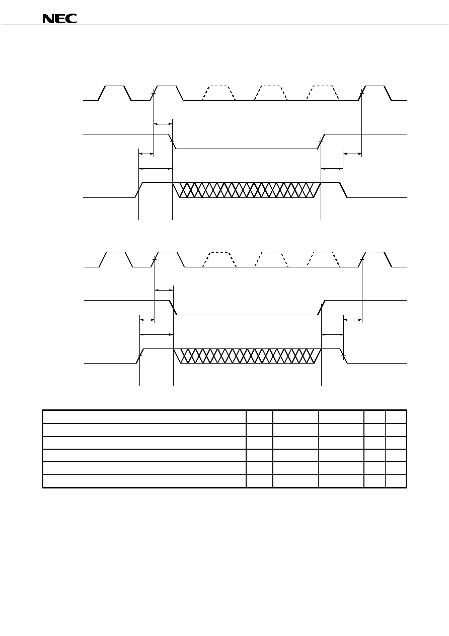
Preliminary Data Sheet M17506EJ1V1DS
53
PD46128953-X
9. Standby Mode Timing Charts
Figure 9-1. Standby Mode 2 (data hold: 64M bits / 32M bits / 16M bits) Entry / Exit Timing Chart
/CE1 (Input)
t
CHML
t
MHCL1
CE2 (Input)
Standby
mode 1
Standby mode 2
(Data hold: 64M bits / 32M bits / 16M bits)
t
CE2S
t
CES
t
CES
CLK (Input)
Figure 9-2. Standby Mode 2 (data not held) Entry / Exit Timing Chart
/CE1 (Input)
t
CHML
t
MHCL2
CE2 (Input)
Standby
mode 1
Standby mode 2
(Data not held)
t
CE2S
t
CES
t
CES
CLK (Input)
Standby Mode 2 Entry / Exit Timing
Parameter Symbol
MIN.
MAX.
Unit
Note
Standby mode 2 entry /CE1 HIGH to CE2 LOW
t
CHML
0
ns
Standby mode 2 exit to normal operation CE2 HIGH to /CE1 LOW
t
MHCL1
30
ns
1
Standby mode 2 exit to normal operation CE2 HIGH to /CE1 LOW
t
MHCL2
300
s 2
/CE1 setup time to CLK
t
CES
5
ns
CE2 hold time to CLK
t
CE2S
1
ns
Notes 1. This is the time it takes to return to normal operation from Standby Mode 2 (data hold: 64M bits / 32M bits /
16M bits).
2.
This is the time it takes to return to normal operation from Standby Mode 2 (data not held).

Preliminary Data Sheet M17506EJ1V1DS
54
PD46128953-X
10. Package Drawing
The following is a package drawing of package sample.
B
S
A
14
13
12
11
10
9
8
7
6
5
4
3
2
1
C B A
D
E
F
G
H
J
K
L
M
N
P
D
A
A1
A2
W S A
W
S B
x
S AB
M
b
y
S
y1
S
ZE
ZD
ITEM
MILLIMETERS
D
E
11.50
13.00
(UNIT :mm)
v
w
A
0.20
1.50
b
x
0.08
y
0.10
e
0.80
A1
0.22
A2
1.28
0.40
y1
0.20
ZD
1.30
ZE
0.55
0.15
e
E
v
x4
127-PIN PLASTIC FBGA (13.0x11.5)
INDEX MARK
This package drawing is a preliminary version. It may be changed in the future.

Preliminary Data Sheet M17506EJ1V1DS
55
PD46128953-X
11. Recommended Soldering Conditions
Please consult with our sales offices for soldering conditions of the
PD46128953-X.
Type of Surface Mount Device
PD46128953F1-EB1: 127-pin PLASTIC FBGA (13.0 x 11.5)

Preliminary Data Sheet M17506EJ1V1DS
56
PD46128953-X
[ MEMO ]

Preliminary Data Sheet M17506EJ1V1DS
57
PD46128953-X
[ MEMO ]

Preliminary Data Sheet M17506EJ1V1DS
58
PD46128953-X
[ MEMO ]

Preliminary Data Sheet M17506EJ1V1DS
59
PD46128953-X
1
2
3
4
VOLTAGE APPLICATION WAVEFORM AT INPUT PIN
Waveform distortion due to input noise or a reflected wave may cause malfunction. If the input of the
CMOS device stays in the area between V
IL
(MAX) and V
IH
(MIN) due to noise, etc., the device may
malfunction. Take care to prevent chattering noise from entering the device when the input level is fixed,
and also in the transition period when the input level passes through the area between V
IL
(MAX) and
V
IH
(MIN).
HANDLING OF UNUSED INPUT PINS
Unconnected CMOS device inputs can be cause of malfunction. If an input pin is unconnected, it is
possible that an internal input level may be generated due to noise, etc., causing malfunction. CMOS
devices behave differently than Bipolar or NMOS devices. Input levels of CMOS devices must be fixed
high or low by using pull-up or pull-down circuitry. Each unused pin should be connected to V
DD
or GND
via a resistor if there is a possibility that it will be an output pin. All handling related to unused pins must
be judged separately for each device and according to related specifications governing the device.
PRECAUTION AGAINST ESD
A strong electric field, when exposed to a MOS device, can cause destruction of the gate oxide and
ultimately degrade the device operation. Steps must be taken to stop generation of static electricity as
much as possible, and quickly dissipate it when it has occurred. Environmental control must be
adequate. When it is dry, a humidifier should be used. It is recommended to avoid using insulators that
easily build up static electricity. Semiconductor devices must be stored and transported in an anti-static
container, static shielding bag or conductive material. All test and measurement tools including work
benches and floors should be grounded. The operator should be grounded using a wrist strap.
Semiconductor devices must not be touched with bare hands. Similar precautions need to be taken for
PW boards with mounted semiconductor devices.
STATUS BEFORE INITIALIZATION
Power-on does not necessarily define the initial status of a MOS device. Immediately after the power
source is turned ON, devices with reset functions have not yet been initialized. Hence, power-on does
not guarantee output pin levels, I/O settings or contents of registers. A device is not initialized until the
reset signal is received. A reset operation must be executed immediately after power-on for devices
with reset functions.
POWER ON/OFF SEQUENCE
In the case of a device that uses different power supplies for the internal operation and external
interface, as a rule, switch on the external power supply after switching on the internal power supply.
When switching the power supply off, as a rule, switch off the external power supply and then the
internal power supply. Use of the reverse power on/off sequences may result in the application of an
overvoltage to the internal elements of the device, causing malfunction and degradation of internal
elements due to the passage of an abnormal current.
The correct power on/off sequence must be judged separately for each device and according to related
specifications governing the device.
INPUT OF SIGNAL DURING POWER OFF STATE
Do not input signals or an I/O pull-up power supply while the device is not powered. The current
injection that results from input of such a signal or I/O pull-up power supply may cause malfunction and
the abnormal current that passes in the device at this time may cause degradation of internal elements.
Input of signals during the power off state must be judged separately for each device and according to
related specifications governing the device.
NOTES FOR CMOS DEVICES
5
6

PD46128953-X
The information in this document is current as of September, 2005. The information is subject to
change without notice. For actual design-in, refer to the latest publications of NEC Electronics data
sheets or data books, etc., for the most up-to-date specifications of NEC Electronics products. Not
all products and/or types are available in every country. Please check with an NEC Electronics sales
representative for availability and additional information.
No part of this document may be copied or reproduced in any form or by any means without the prior
written consent of NEC Electronics. NEC Electronics assumes no responsibility for any errors that may
appear in this document.
NEC Electronics does not assume any liability for infringement of patents, copyrights or other intellectual
property rights of third parties by or arising from the use of NEC Electronics products listed in this document
or any other liability arising from the use of such products. No license, express, implied or otherwise, is
granted under any patents, copyrights or other intellectual property rights of NEC Electronics or others.
Descriptions of circuits, software and other related information in this document are provided for illustrative
purposes in semiconductor product operation and application examples. The incorporation of these
circuits, software and information in the design of a customer's equipment shall be done under the full
responsibility of the customer. NEC Electronics assumes no responsibility for any losses incurred by
customers or third parties arising from the use of these circuits, software and information.
While NEC Electronics endeavors to enhance the quality, reliability and safety of NEC Electronics products,
customers agree and acknowledge that the possibility of defects thereof cannot be eliminated entirely. To
minimize risks of damage to property or injury (including death) to persons arising from defects in NEC
Electronics products, customers must incorporate sufficient safety measures in their design, such as
redundancy, fire-containment and anti-failure features.
NEC Electronics products are classified into the following three quality grades: "Standard", "Special" and
"Specific".
The "Specific" quality grade applies only to NEC Electronics products developed based on a customer-
designated "quality assurance program" for a specific application. The recommended applications of an NEC
Electronics product depend on its quality grade, as indicated below. Customers must check the quality grade of
each NEC Electronics product before using it in a particular application.
"Standard": Computers, office equipment, communications equipment, test and measurement equipment, audio
and visual equipment, home electronic appliances, machine tools, personal electronic equipment
and industrial robots.
"Special":
Transportation equipment (automobiles, trains, ships, etc.), traffic control systems, anti-disaster
systems, anti-crime systems, safety equipment and medical equipment (not specifically designed
for life support).
"Specific": Aircraft, aerospace equipment, submersible repeaters, nuclear reactor control systems, life
support systems and medical equipment for life support, etc.
The quality grade of NEC Electronics products is "Standard" unless otherwise expressly specified in NEC
Electronics data sheets or data books, etc. If customers wish to use NEC Electronics products in applications
not intended by NEC Electronics, they must contact an NEC Electronics sales representative in advance to
determine NEC Electronics' willingness to support a given application.
(Note)
(1) "NEC Electronics" as used in this statement means NEC Electronics Corporation and also includes its
majority-owned subsidiaries.
(2) "NEC Electronics products" means any product developed or manufactured by or for NEC Electronics (as
defined above).
∑
∑
∑
∑
∑
∑
M8E 02. 11-1