©
1993
DATA SHEET
MOS INTEGRATED CIRCUIT
µ
PD4701A
INCREMENTAL ENCODER COUNTER
Document No. IC-3303 (1st edition)
(O. D. No. IC-6947A)
Date Published March 1997 P
Printed in Japan
DESCRIPTION
The
µ
PD4701A is a counter for an X, Y 2-axis incremental encoder. When a two-phase encoder signal is input
for the X and Y axes, direction discrimination and computation is performed, and count data is output in 8-bit parallel
form. In addition, a 3-contact-point input buffer is incorporated, which is useful for applications which use a pointing
device such as a mouse or track-ball. The CPU checks the switch input flag or count flag and reads the 12-bit count
data in two operations, one for the lower byte and one for the upper byte. The key input flag is output together with
the count data in the upper byte.
FEATURES
∑
X, Y 2-axis incremental encoder counter
∑
Counter input (Schmitt-triggered input)
X axis: X
A
, X
B
2-phase signal
4-multiplication count method used
Y axis: Y
A
, Y
B
2-phase signal
∑
Counters: 12-bit binary up/down counters (2 sets, X & Y)
Reset value: 000H
∑
Count data output: 8-bit parallel latch output
◊
2 (including key input flag)
∑
On-chip 3-contact-point key input buffer circuit
∑
CMOS
∑
Single +5 V power supply
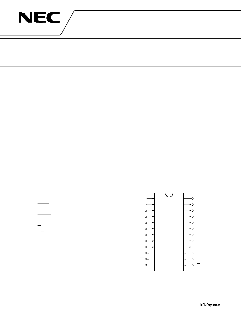
PIN CONFIGURATION (Top View)
PIN NAMES
X
A
, Y
A
: A-phase inputs
X
B
, Y
B
: B-phase inputs
RIGHT
LEFT Key inputs
MIDDLE
CS
: Chip Select
X/Y
: X/Y Counter Select
U/L
: Upper/Lower Byte Select
D
0 to 7
: Data outputs
CF
: Count flag
RESET X Counter
SF
: Count flag
RESET Y
reset inputs
1
2
3
4
5
6
7
8
9
10
11
12
X
A
X
B
RESET X
Y
A
Y
B
RESET Y
RIGHT
LEFT
MIDDLE
SF
CF
V
SS
24
23
22
21
20
19
18
17
16
15
14
13
V
DD
D
7
D
6
D
5
D
4
D
3
D
2
D
1
D
0
CS
X/Y
U/L

µ
PD4701A
2
ORDERING INFORMATION
Part Number
Package
µ
PD4701AC
24-pin plastic DIP (600 mil)
µ
PD4701AGT
24-pin plastic SOP (375 mil)
BLOCK DIAGRAM
X
A
X
B
Y
A
Y
B
RESET X
RESET Y
RIGHT
LEFT
MIDDLE
Phase
Determination
and
Edge Detection
Phase
Determination
and
Edge Detection
Button Input
Circuit
X-Axis Up/Down Counter
Data Multiplexer & Latch
Y-Axis Up/Down Counter
Count Flag
Circuit
Switch Flag
Circuit
CS
X/Y
U/L
CF
SF
D
0-7
DATA MULTIPLEXER/LATCH BLOCK
X-Axis Counter
Y-Axis Counter
Button Input
8
4
8
8
Data
Multiplexer
3-State
Buffer
OE
12-Bit
Latch
STB
12-Bit
Latch
STB
4-Bit
Latch
STB
X/Y
U/L
CS
D
0 - 7
To Count Flag Circuit
µ
PD4701A
3
PIN FUNCTIONS
Pin Name
Input/Output
Function
CS
Input
Chip Select input. "L" input activates outputs D0 to 7.
"H" input sets outputs D0 to 7 to high impedance.
Output data is latched on the fall edge of CS. "L" must be maintained during a
count data read.
X/Y
Input
Counter Select input. "L" input selects the X counter, and "H" input selects the
Y counter.
U/L
Input
Byte Select input. "L" input selects the lower byte and "H" input selects the
upper byte, controlling data output.
RESET X
Input
Counter reset inputs. RESET X input resets the X counter, and RESET Y input
RESET Y
resets the Y counter. Both are active-"H".
D
0 to 7
Output
Bus for data output to the CPU. Outputs the byte data selected by the X/Y and
(3-state)
U/L inputs.
The data latched on the fall of CS is output.
CF
Output
Counter flag output. Set (= "L" output) when the X or Y counter changes while
CS = "H". Reset (= "H" output) on the fall of CS. While CS = "L", count flag
output is disabled and the "H" level is output.
SF
Output
Switch flag output. Becomes active (= "L" output) when the RIGHT, LEFT or
MIDDLE switch input is "L".
X
A
, X
B
Input
X counter 2-phase signal input pins
(Schmitt input)
Y
A
, Y
B
Input
Y counter 2-phase signal input pins
(Schmitt input)
RIGHT
Input
Key switch input pins. Key switch input are read as the high-order 4 bits of the
LEFT
(Schmitt input)
X counter and Y counter upper byte as the internal status.
MIDDLE
V
DD
+5 V power supply connection pin
V
SS
Ground pin
CPU
interface
block
Mouse
interface
block
Power
supply
block
SF
Key Input Status
Upper Byte
Count Data
L
R
M
C
11
C
10
C
9
C
8
µ
PD4701A
4
DESCRIPTION OF OPERATIONS
1. COUNT OPERATION
The
µ
PD4701A executes an up-count and down-count by means of A & B 2-phase signals in the 12-bit up-down
counter. An up-count is performed when the A-phase signals (X
A
, Y
A
) are phase-advanced, and a down-count is
performed when the B-phase signals (X
B
, Y
B
) are phase-advanced. The edge of each signal is a count source. (4-
multiplication count method: see Fig. 1.)
Fig. 1 Count Operation Timing Chart
(X, Y)
A
Input
Count Operation
(X, Y)
B
Input
Forward (Up-Count)
Reverse (Down-Count)
1
2
3
4
5
4
3
2
1
0
This count operation is executed independently for the X axis (X
A
, X
B
) and Y axis (Y
A
, Y
B
). This operation is
initialized by reset input (RESET X, RESET Y) only.
In an up-count, the next value after FFFH is 000H, and in a down-count, the next value after 000H is FFFH.
2. OPERATION OF COUNT FLAG, CF
The count flag, CF, indicates that a count source (either X
A, B
or Y
A, B
edge input) has occurred while the CS signal
is "H", and is an active-low output. CF is reset (
"H") by CS signal "L" input. While CS = "L", count flag output is
disabled and the "H" level is output.
Fig. 2 Count Flag Output Timing Chart
X
A, B
Y
A, B
CF
CS
Count Flag Output Disabled in these Periods
µ
PD4701A
5
3. SWITCH INPUT OPERATION
The
µ
PD4701A can process up to 3 contact points as switch inputs (active-"L" input). Switch input is read as part
of the count data upper byte together with the switch flag status as an internal status (see Fig. 3). These are all active-
"H" outputs. The switch flag status, SF, is equivalent to the switch flag output, SF, described below.
Fig. 3 Data Output Format
7
SF
6
L
5
R
4
M
3
C
11
2
C
10
1
C
9
0
C
8
7
C
7
6
C
6
5
C
5
4
C
4
3
C
3
2
C
2
1
C
1
0
C
0
Bit No.
Upper Byte
Bit No.
Lower Byte
SF : Switch Flag
L : Left Switch
R : Right Switch
M : Middle Switch
C
11 - 0
: Count Data (12 bit )
4. OPERATION OF SWITCH FLAG, SF
The switch flag, SF, becomes active (active-"L" output) when the RIGHT, LEFT or MIDDLE switch input is "L".
SF can also be read as the switch flag status together with the count data.
5. DATA READ OPERATION
The CPU reads the count data and switch input status by controlling CS, X/Y and U/L. The relation between these
is shown in Table 1. (At this time, the data latched on the falling edge of CS is output. If X/Y or U/L is switched while
CS is still "L", the data at the point at which CS changes from "H" to "L" is read. When CS is set to "H", new data is
read into the latch, and the new data is confirmed on the next fall of CS.
Table 1 Data Output Table
CS
X/Y
U/L
D
7
D
6
D
5
D
4
D
3
D
2
D
1
D
0
0
0
0
X
C
7
X
C
6
X
C
5
X
C
4
X
C
3
X
C
2
X
C
1
X
C
0
0
0
1
SF
L
R
M
X
C
11
X
C
10
X
C
9
X
C
8
0
1
0
Y
C
7
Y
C
6
Y
C
5
Y
C
4
Y
C
3
Y
C
2
Y
C
1
Y
C
0
0
1
1
SF
L
R
M
Y
C
11
Y
C
10
Y
C
9
Y
C
8
1
◊
◊
FLOATING

µ
PD4701A
6
6. CONNECTION TO CPU SYSTEM
An example of connection to a CPU system is shown in Fig. 4.
Fig. 4 Example of Connection to CPU System
Output Port
A
1
A
0
DB
0 - 7
INT
FLAG
A
2
- A
n
and IORD
or MRD
CPU System
CS
X/Y
U/L
SF
RIGHT
MIDDLE
LEFT
CF
D
0 - 7
X
A
X
B
Y
A
Y
B
Mouse I/F
PD4701A
µ
RESET
Mouse
X Y
µ
PD4701A Pin Name
Description
X/Y
Connected to address line A
1
.
U/L
Connected to address line A
0
.
CS
Connects address lines A
2
to A
n
and the signal resulting from decoding IORD in the I/O
address mode or MRD in the memory address mode, or an output port. The low level must be
maintained during a count data read.
D
0 to 7
Connected to the data bus.
SF, CF
When these are used as interrupt signals, they are connected to the CPU INT pin.
RESET X
These are connected to a CPU output port or reset signal.
RESET Y
The above connections enable the CPU to read the X counter, Y counter and switch input status.
The application circuits and their parameters are for reference only and are not intended for use in actual design-ins.

µ
PD4701A
7
An example of a
µ
PD4701A data read is shown in Fig. 5.
Fig. 5 Example of
µ
PD4701A Data Read
Start
Count value latch
Count reset
X counter low byte read
Y counter low byte read
X counter high byte
& switch status read
Y counter high byte
& switch status read
Data bus
high impedance
CS = 0
RESET X = 1
RESET Y = 1
X/Y = 0
U/L = 0
End
X/Y = 0
U/L = 1
X/Y = 1
U/L = 0
X/Y = 1
U/L = 1
CS = 1
* CS must be kept at "0" during the read.
µ
PD4701A
8
7. APPLICATION AREAS
Two-phase incremental signals are used for detection and measurement of a vector quantity (a quantity that has
direction and magnitude), and are widely employed in measuring instruments such as micrometers and linear scales,
control systems for digital servo motors, X-Y tables, etc., head position control for printers, magnetic disks, etc., robot
arm position control, and so on.
The
µ
PD4701A incorporates the direction judgment circuit and count pulse generator required for 2-phase
incremental signal processing, up/down counters for counting these pulses, and a data latch to hold the read data,
in IC form, enabling an X, Y 2-axis incremental signal processing system to be implemented easily.
In addition, a 3 switch-input buffer is incorporated, enabling this device to be widely used in man-machine interface
and centronics interface application areas.
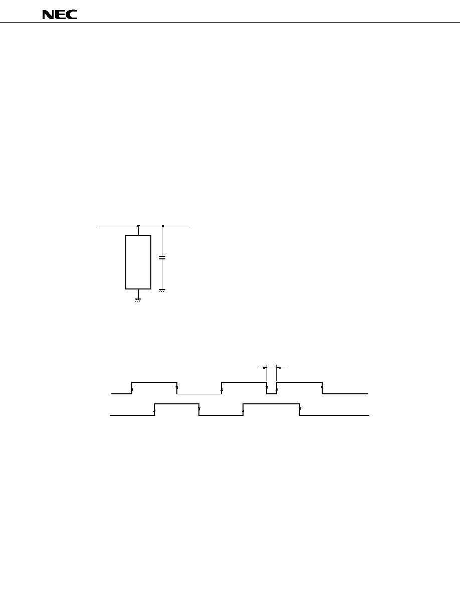
8. OPERATING PRECAUTIONS
1)
As the
µ
PD4701A incorporates two sets of 12-bit counters, large transient currents flow during a count operation.
Adecoupling capacitor of around 0.1
µ
F should therefore be inserted between V
DD
and V
SS
of the
µ
PD4701A.
+ 5 V
V
DD
V
SS
µ
PD4701A
Tantalum electrolytic, laminated ceramic, or similar capacitor
of around 0.1 F
(Should be mounted right next to the IC.)
µ
2)
If a pulse shorter than the signal phase difference time t
SAB
(350 ns) is input to the A/B phase inputs (X
A
, X
B
, Y
A
,
Y
B
) this will result in a miscount. Therefore, if pulses shorter than t
SAB
are to be input because of encoder bounds,
etc., a filter should be attached to the A/B phase inputs.
A or B Phase
B or A Phase
PW
If PW
t
SAB
(350 ns), the count value remains the same before and after pulse input.
(UP count
DOWN count or DOWN count
UP count is implemented, and therefore
the result is equivalent to no change in the count value.

µ
PD4701A
9
ABSOLUTE MAXIMUM RATINGS (T
a
= 25
∞
C, V
SS
= 0 V)
PARAMETER
SYMBOL
RATING
UNIT
Supply voltage
V
DD
≠0.5 to +7.0
V
Input voltage
V
I
≠1.0 to V
DD
+ 1.0
V
Output voltage
V
O
≠0.5 to V
DD
+ 0.5
V
Operating temperature
T
opt
≠40 to +85
∞
C
Storage temperature
T
stg
≠65 to +150
∞
C
Permissible loss
P
D
500
mW
DC CHARACTERISTICS (T
a
= ≠40 to +85
∞
C, V
DD
= +5 V
±
10 %)
PARAMETER
SYMBOL
RATING
UNIT
TEST CONDITIONS
MIN.
MAX.
Input voltage high
V
IL
0.8
V
Input voltage low
V
IH
2.6
V
X
A
, X
B
, Y
A
, Y
B
and
LEFT, RIGHT, MIDDLE
V
IH
2.2
V
Other than the above
Output voltage low
V
OL
0.45
V
I
OL
= 12 mA
Output voltage high
V
OH
V
DD
≠ 0.8
V
I
OH
= ≠4 mA
Static consumption current
I
DD
50
µ
A
V
I
= V
DD
, V
SS
Input current
I
I
≠1.0
1.0
µ
A
V
I
= V
DD
, V
SS
3-state output leak current
I
OFF
≠10
10
µ
A
Dynamic consumption current
I
DD dyn
2
mA
f
IN
= 500 kHz
Hysteresis voltage
V
H
0.25
V
X
A
, X
B
, Y
A
, Y
B
and
LEFT, RIGHT, MIDDLE

µ
PD4701A
10
AC CHARACTERISTICS (T
a
= ≠40 to +85
∞
C, V
DD
= +5 V
±
10 %)
PARAMETER
SYMBOL
RATING
UNIT
TEST CONDITIONS
MIN.
MAX.
X
A
, X
B
Input cycle
t
CYAB
2
µ
s
f
in
= 500 kHz
Y
A
, Y
B
High-level pulse width
t
PWABH
900
ns
Low-level pulse width
t
PWABL
900
ns
Signal phase difference time
t
SAB
350
ns
R, L
High-level pulse width
t
PWSWH
30
µ
s
Switch OFF
M
Low-level pulse width
t
PWSWL
30
µ
s
Switch ON
SF
Setting delay time
t
DSFL
50
ns
Switch ON
Reset delay time
t
DSFH
50
ns
Switch OFF
RESET
Pulse width
t
PWRS
100
ns
W, Y
Count enable time
t
SCTEN
0
ns
From RESET
X
,
Y
Count clear time
t
DCTCL
100
ns
From RESET
X
,
Y
CF
Flag setting time
t
DABCF
120
ns
From X
A
,
B
, Y
A
,
B
Flag reset time
t
DCSCF
100
ns
From CS
Count setting time
t
SCT
0
ns
From CF
CS
CF enable time
t
SCSCF
140
ns
From CF
CF disable time
t
HABCS
140
ns
From X
A
,
B
, Y
A
,
B
Pulse width
t
PWCS
200
ns
X/Y
Address setup time
t
SACS
0
ns
To CS
U/L
Address hold time
t
HCSAB
0
ns
From CS
D
0 to 7
Output delay time
t
DCSD
150
ns
From CS
Output delay time
t
DAD
100
ns
From X/Y, U/L
Floating time
t
FCSD
50
ns
From CS
AC TEST INPUT WAVEFORM
2.6 V
0.45 V
1.5 V
1.5 V
Test Point
AC test : The input is driven by 2.6 V for logic "1", and 0.45 V for logic "0".
Timing measurement is performed at 1.5 V for both logic "1" and logic "0".

µ
PD4701A
11
Fig. 6 Two-Phase Signal & Switch Signal Input Timing
t
CYAB
t
PWABH
t
PWSWL
t
PWSWH
t
SAB
t
SAB
t
SAB
t
SAB
t
PWABL
X
A
, Y
A
X
B
, Y
B
RIGHT
LEFT
MIDDLE
Fig. 7 Count Flag Output Timing
t
PWRS
t
SCTEN
t
DABCF
t
DCTCL
t
SCSCF
t
SCT
t
PWCS
t
HABCS
t
DCSCF
t
SAB
RESET X, Y
CF
CS
X
A, B
Y
A, B

µ
PD4701A
12
Fig. 8 Data Output Timing
t
SACS
t
DCSD
t
DAD
t
FCSD
t
HCSA
CS
X/Y
U/L
D
0 - 7
Fig. 9 Switch Flag Signal Output Timing
RIGHT
LEFT
MIDDLE
SF
t
DSFL
t
DSFH

µ
PD4701A
13
RECOMMENDED SOLDERING CONDITIONS
The following conditions (see table below) must be met when soldering this product.
Please consult with our sales offices in case other soldering process is used, or in case soldering is done under
different conditions.
TYPES OF SURFACE MOUNT DEVICE
µ
PD4701AGT
Soldering process
Soldering conditions
Symbol
Infrared ray reflow
Peak package's surface temperature: 235
∞
C or below,
IR35-00-2
Reflow time: 30 seconds or below (210
∞
C or higher),
Number of reflow process: 2, Exposure limit*: None
VPS
Peak package's surface temperature: 215
∞
C or below,
VP15-00-2
Reflow time: 40 seconds or below (200
∞
C or higher),
Number of reflow process: 2, Exposure limit*: None
Wave soldering
Solder temperature: 260
∞
C or below,
WS60-00-1
Flow time: 10 seconds or below,
Number of flow process: 1, Exposure limit*: None
Partial heating method
Terminal temperature: 300
∞
C or below,
Flow time: 10 seconds or below,
Exposure limit*: None
* Exposure limit before soldering after dry-pack package is opened.
Storage conditions: 25
∞
C and relative humidity at 65 % or less.
Note Do not apply more than a single process at once, except for "Partial heating method".
TYPE OF THROUGH HOLE MOUNT DEVICE
µ
PD4701AC
Soldering process
Soldering conditions
Symbol
Wave soldering
Solder temperature: 260
∞
C or below,
Flow time: 10 seconds or below
µ
PD4701A
14
24PIN PLASTIC DIP (600 mil)
NOTES
1) Each lead centerline is located within 0.25 mm (0.01 inch) of
its true position (T.P.) at maximum material condition.
ITEM
MILLIMETERS
INCHES
A
33.02 MAX.
1.300 MAX.
B
2.54 MAX.
0.100 MAX.
C
2.54 (T.P.)
0.100 (T.P.)
D
0.50±0.10
0.020+0.004
≠0.005
F
1.2 MIN.
0.047 MIN.
G
3.5±0.3
0.138±0.012
J
5.72 MAX.
0.226 MAX.
K
15.24 (T.P.)
0.600 (T.P.)
M
0.25
0.010+0.004
≠0.003
N
0.25
0.01
H
0.51 MIN.
0.020 MIN.
I
4.31 MAX.
0.170 MAX.
L
13.2
0.520
+0.10
≠0.05
2) Item "K" to center of leads when formed parallel.
P24C-100-600-1
R
0~15
∞
0~15
∞
24
13
1
12
N
B
I
M
R
M
C
D
F
H
G
A
J
K
L
µ
PD4701A
15
P24GT-50-375B-1
ITEM
MILLIMETERS
INCHES
NOTE
Each lead centerline is located within 0.12
mm (0.005 inch) of its true position (T.P.) at
maximum material condition.
15.71 MAX.
0.87 MAX.
1.27 (T.P.)
0.40
0.125±0.075
2.9 MAX.
2.50±0.2
10.3±0.3
7.2±0.2
1.6±0.2
0.15
0.8±0.2
0.12
0.10
0.619 MAX.
0.035 MAX.
0.050 (T.P.)
0.016
0.005±0.003
0.115 MAX.
0.098
0.406
0.283
0.063±0.008
0.006
0.031
0.005
0.004
+0.009
≠0.008
A
B
C
D
E
F
G
H
I
J
K
L
M
N
+0.10
≠0.05
+0.10
≠0.05
+0.004
≠0.002
+0.009
≠0.008
+0.012
≠0.013
+0.009
≠0.008
+0.004
≠0.003
24 PIN PLASTIC SOP (375 mil)
24
13
1
12
A
I
M
M
D
C
N
K
detail of lead end
E
F
G
B
H
L
J
3∞
+7∞ ≠3∞

µ
PD4701A
2
No part of this document may be copied or reproduced in any form or by any means without the prior written
consent of NEC Corporation. NEC Corporation assumes no responsibility for any errors which may appear in
this document.
NEC Corporation does not assume any liability for infringement of patents, copyrights or other intellectual property
rights of third parties by or arising from use of a device described herein or any other liability arising from use
of such device. No license, either express, implied or otherwise, is granted under any patents, copyrights or other
intellectual property rights of NEC Corporation or others.
While NEC Corporation has been making continuous effort to enhance the reliability of its semiconductor devices,
the possibility of defects cannot be eliminated entirely. To minimize risks of damage or injury to persons or
property arising from a defect in an NEC semiconductor device, customers must incorporate sufficient safety
measures in its design, such as redundancy, fire-containment, and anti-failure features.
NEC devices are classified into the following three quality grades:
"Standard", "Special", and "Specific". The Specific quality grade applies only to devices developed based on a
customer designated "quality assurance program" for a specific application. The recommended applications of
a device depend on its quality grade, as indicated below. Customers must check the quality grade of each device
before using it in a particular application.
Standard: Computers, office equipment, communications equipment, test and measurement equipment,
audio and visual equipment, home electronic appliances, machine tools, personal electronic
equipment and industrial robots
Special:
Transportation equipment (automobiles, trains, ships, etc.), traffic control systems, anti-disaster
systems, anti-crime systems, safety equipment and medical equipment (not specifically designed
for life support)
Specific:
Aircrafts, aerospace equipment, submersible repeaters, nuclear reactor control systems, life
support systems or medical equipment for life support, etc.
The quality grade of NEC devices is "Standard" unless otherwise specified in NEC's Data Sheets or Data Books.
If customers intend to use NEC devices for applications other than those specified for Standard quality grade,
they should contact an NEC sales representative in advance.
Anti-radioactive design is not implemented in this product.
M4 96.5
[MEMO]