 | –≠–ª–µ–∫—Ç—Ä–æ–Ω–Ω—ã–π –∫–æ–º–ø–æ–Ω–µ–Ω—Ç: UPD4702C | –°–∫–∞—á–∞—Ç—å:  PDF PDF  ZIP ZIP |

DESCRIPTION
The
µ
PD4702 is 8-bit up/down counters for an incremental encoder. Two-phase (A, B) incremental input signals
are phase-differentiated, and on each signal edge, an up-count is executed if the A phase is leading, or a down-count
if the B phase is leading. Eight-bit count data is output in real time. A carry output and borrow output are also
provided for counter overflow and underflow.
The
µ
PD4704 is also available; use of these enables the count width to be extended.
©
1994
DATA SHEET
1993
INCREMENTAL ENCODER 8-BIT UP/DOWN COUNTER
CMOS INTEGRATED CIRCUITS
µ
PD4702
MOS INTEGRATED CIRCUIT
FEATURES
∑
Incremental inputs (A, B)
∑
On-chip phase discrimination circuit (up-count mode
when the phase order is A
B, down-count mode
when B
A) 4-multiplication count method
∑
On-chip edge detection circuit
∑
8-bit up/down counter latch output o Carry output,
borrow output
∑
Count data output controllable (3-state output)
∑
CMOS, single +5 V power supply
ORDERING INFORMATION
Part Number
Package
µ
PD4702C
20-pin plastic DIP
(300 mil)
µ
PD4702G
20-pin plastic SOP
(300 mil)
1
2
3
4
5
6
7
8
9
10
Reset
A
B
NC
CD
0
CD
1
CD
2
CD
3
NC
V
SS
V
DD
Carry
Borrow
STB
OE
CD
7
CD
6
CD
5
CD
4
NC
20
19
18
17
16
15
14
13
12
11
PIN CONFIGURATION (Top View)
PIN NAMES
A
2-phase incremental signal inputs
B
Reset
: Counter reset input
STB
: Latch strobe signal input
OE
: Output control signal input
CD
0-7
: Count data outputs
Carry
: Carry pulse output
Borrow : Borrow pulse output
Document No.
IC-3304A (2nd edition)
(O. D. No.
IC-5403A)
Date Published April 1997 P
Printed in Japan

2
µ
PD4702
BLOCK DIAGRAM
Reset
A
B
Phase
Discrimination
Edge Detection
8-Bit Up/Down Counter
8-Bit Latch
3-State Output
Carry
Borrow
STB
OE
CD
0≠7
PIN FUNCTIONS
Function
Incremental signal A phase and B phase signal input pins (Schmitt input)
Count data output pins. Activated when OE is "L", high impedance outputs when OE
is "H".
8-bit counter carry signal output pin (active-low)
8-bit counter borrow signal output pin (active-low)
8-bit counter reset signal output pin
Counter is reset when this pin is "H".
Count data output control signal input pin
Counter data output latch signal. Data is latched on the fall of STB, and is held while
STB = "L".
Power supply input pin
Ground pin
Pin Name
Input/Output
A, B
Input
(Schmitt)
D
0 to 7
Output
(3-state)
Carry
Output
Borrow
Output
RESET
Input
(Schmitt)
OE
Input
STB
Input
V
DD
GND

3
µ
PD4702
1.
DESCRIPTION OF OPERATIONS
(1)
Count operation
The
µ
PD4702 incorporates a phase discrimination circuit, and counts by 4-multiplication of the A and B input 2-
phase pulses. Therefore, a count operation is performed by an A input edge and a B input edge.
Fig. 1 Count Operation Timing Chart
Forward (Up-Count)
Reverse (Down-Count)
A Input
Count Operation
B Input
2
4
3
1
1
3
5
4
2
0
(2)
Latch operation
An R-S flip-flop is inserted in the strobe input of the latch circuit as shown in Fig. 2, and when STB changes from
"H" to "L" during a count operation, the internal latch signal STB remains at "H" until the end of the count operation.
Therefore, the count value is latched correctly even if STB input is performed asynchronously from the A and B input
(if STB changes from "H" to "L" within t
SABSTB
(40 ns) after the A input or B input edge, the latch contents will be
either the pre-count or post-count value). However, when a
µ
PD4704 is added, the correct value cannot be latched
if all digits are latched simultaneously when a carry or borrow is generated (the high-order digit may be latched
before carry/borrow transmission).
Fig. 2 STB Input Circuit
From Phase Discrimination Circuit
(Count Pulse)
STB
STB
Latched
when L
A, B Inputs
STB
t
SABSTB
If t
SABSTB
is 40 ns or longer, the post-count value
is input to the latch.

4
µ
PD4702
(3)
Carry & borrow outputs
If the counter performs an up-count operation when the count value is 0FF
H
, an active-low pulse is output to the
Carry output (the pulse width is 25 ns MIN. 120 ns MAX. irrespective of the A/B phase input cycle. Similarly, if the
counter performs a down-count operation when the count value is 00
H
, an active-low pulse is output to the Borrow
output.
A Borrow pulse is also output if a down-count operation is performed while RESET is "H" (during a reset), and
therefore, when a
µ
PD4704 is added, a reset must be executed at the same time.

5
µ
PD4702
2.
OPERATING PRECAUTIONS
As the
µ
PD4702 incorporates an 8-bit counter, a large transient current flows in the case of a count value which
changes all the bits (such as 00
H
0FF
H
or 7F
H
080
H
). This will cause misoperation unless the impedance of the
power supply line is sufficiently low. It is therefore recommended that a decoupling capacitor (of around 0.1
µ
F)
be connected between V
DD
and V
SS
right next to the IC as shown in Fig. 3.
Fig. 3 Decoupling Capacitor
V
DD
V
SS
+5 V
C
C : 0.1
µ
F tantalum electrolytic laminated
ceramic capacitor, etc.
Also, if a pulse shorter than the phase difference time t
SAB
(70 ns) is input to the A/ B phase inputs, this will result
in a miscount. Therefore, if this kind of pulse is to be input because of encoder bounds, etc., a filter should be inserted
in the A & B phase inputs.
Fig. 4 A & B Phase Input Pulses
A Phase (or B Phase)
B Phase (or A Phase)
PW
If a pulse such that PW < 70 ns is input
in the A or B phase, there is a danger of
a miscount.
If PW is at 70 ns or more, the count value remains the same before and after pulse input. (UP count
DOWN
count or DOWN count
UP count is implemented, and therefore the the result is no change in the count value.)
µ
PD4702
6
µ
PD4702
PARAMETER
SYMBOL
RATING
UNIT
Supply voltage
V
DD
≠0.5 to +7.0
V
Input voltage
V
I
≠1.0 to V
DD
+1.0
V
Output voltage
V
O
≠0.5 to V
DD
+0.5
V
Operating temperature
T
opt
≠40 to +85
∞
C
Storage temperature
T
stg
≠65 to +150
∞
C
Permissible loss
P
D
500 (DIP)
200 (SOP)
mW
PARAMETER
SYMBOL
TEST CONDITIONS
RATING
UNIT
MIN.
MAX.
Input voltage high
V
IL
0.8
V
Input voltage low
V
IH
A, B, Reset
2.6
V
V
IH
Other than the above
2.2
V
Output voltage low
V
OL
I
OL
= 12 mA
0.45
V
Output voltage high
V
OH
I
OH
= ≠4 mA
V
DD
≠ 0.8
V
Static consumption current
I
DD
V
I
= V
DD
, V
SS
50
µ
A
Input current
I
I
V
I
= V
DD
, V
SS
≠1.0
1.0
µ
A
3-state output leak current
I
OFF
≠10
10
µ
A
Dynamic consumption current
I
DD dyn
f
IN
= 3.6 MHz, C
L
= 50 pF
12
mA
Hysteresis voltage
V
H
A, B, Reset
0.2
V
PARAMETER
SYMBOL
TEST CONDITIONS
MIN.
MAX.
UNIT
Cycle
t
CYAB
f
in
= 3.6 MHz
280
ns
High-level width
t
PWABH
140
ns
A, B
Low-level width
t
PWABL
140
ns
Phase difference time
t
SAB
70
ns
Setting time
t
SRSAB
0
ns
Reset time
t
DRSCD
60
ns
Output delay
t
DABCD
100
ns
CD
0 to 7
Output delay
t
DOECD
50
ns
Output delay
t
DSTBCD
60
ns
Float time
t
FOECD
40
ns
Carry
Output delay
t
DABCB
120
ns
Borrow
Output pulse width
t
PWCB
25
120
ns
RESET
Reset pulse width
t
PWRS
40
ns
STB
Setting time
t
SABSTB
40
ns
ABSOLUTE MAXIMUM RATINGS (T
A
= 25
∞
C, V
SS
= 0 V)
DC CHARACTERISTICS (T
A
= ≠40 to +85
∞
C, V
DD
= +5 V
±
10 %)
AC CHARACTERISTICS (T
A
= ≠40 to +85
∞
C, V
DD
= +5 V
±
10 %)
7
µ
PD4702
AC Timings
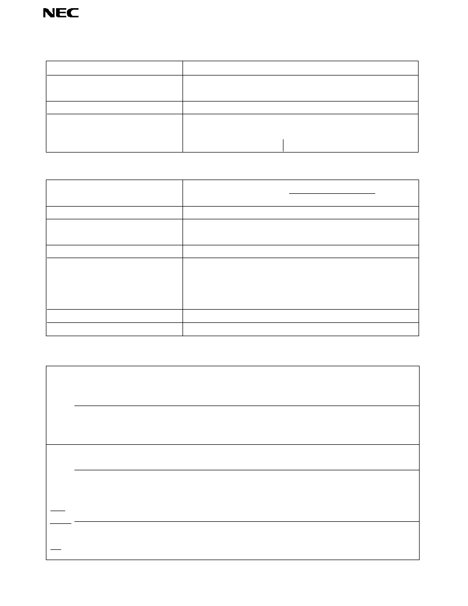
Fig. 1 Two-Phase Signal Input Timing
t
CYAB
t
PWABL
t
SAB
t
SAB
t
PWABL
t
PWABH
t
CYAB
t
SAB
t
SAB
t
PWABH
A
B
Fig. 2 Count Data Output Timing
Fig. 3 Carry/Borrow Signal Output Timing
t
PWRS
Reset
t
SRSAB
t
SABSTB
t
DRSCD
t
DABCD
t
DSTBCD
t
DOECD
t
FOECD
A/B
CD
0≠7
OE
STB
t
DABCB
t
PWCB
t
DABCB
t
PWCB
(0FEH)
(0FFH)
(00)
(01)
(00)
(0FEH)
(0FFH)
(0FDH)
(CD)
A/B
Carry
Borrow

8
µ
PD4702
Consumption Current Measurement Circuit
AC Test Input Waveform
V
IH
V
IL
V
IH
= 2.6 V (A, B, RESET inputs)
V
IH
= 2.2 V (inputs other than A, B, RESET)
V
IL
= 0.8 V
Timing measurement is performed at 1.5 V.
A
B
STB
OE
D
7
D
1
D
0
C
L
C
L
C
L
V
DD
2.6 V
0.8 V
STB input connected to V
DD
or
OE input connected to V
SS
.
Load on all outputs, C
L
= 50 pF.
Measurement Conditions
A, B inputs
f
IN
= 3.6 MHz

9
µ
PD4702
Sample Application Circuits
16-bit counter
µ
PD4702
µ
PD4704
Data Bus
Incremental Rotary Encoder
8
8
8
RESET
CS
L
CS
H
A
B
STB
OE
Carry
Borrow
CD
0
CD
7
R
UP
Down
STB
OE
CD
0
CD
7
R
The application circuits and their parameters are for references only and are not intended for use in actual design-in's.
10
µ
PD4702
RECOMMENDED SOLDERING CONDITIONS
The following conditions (see table below) must be met when soldering this product.
Please consult with our sales offices in case other soldering process is used, or in case soldering is done under
different conditions.
TYPES OF SURFACE MOUNT DEVICE
For more details, refer to our document "Semiconductor Device Mounting Technology Manual" (IEI-1207).
µ
PD4702G
Soldering process
Soldering conditions
Symbol
Infrared ray reflow
Peak package's surface temperature: 235
∞
C or below,
IR35-00-2
Reflow time: 30 seconds or below (210
∞
C or higher),
Number of reflow process: 2, Exposure limit*: None
VPS
Peak package's surface temperature: 215
∞
C or below,
VP15-00-2
Reflow time: 40 seconds or below (200
∞
C or higher),
Number of reflow process: 2, Exposure limit*: None
Wave soldering
Solder temperature: 260
∞
C or below,
WS60-00-1
Flow time: 10 seconds or below,
Number of flow process: 1, Exposure limit*: None
Partial heating method
Terminal temperature: 300
∞
C or below,
Flow time: 10 seconds or below,
Exposure limit*: None
*
Exposure limit before soldering after dry-pack package is opened.
Storage conditions: 25
∞
C and relative humidity at 65 % or less.
Note Do not apply more than a single process at once, except for "Partial heating method".
TYPES OF THROUGH HOLE MOUNT DEVICE
µ
PD4702C
Soldering process
Soldering conditions
Symbol
Wave soldering
Solder temperature: 260
∞
C or below,
Flow time: 10 seconds or below
REFERENCE
Dcodument name
Document No.
NEC semiconductor device reliability/quality control system
IEI-1212
Quality grade on NEC semiconductor devices
IEI-1209
Semiconductor device mounting technology manual
IEI-1207
Semiconductor device package manual
IEI-1213
Guide to quality assurance for semiconductor devices
MEI-1202
Semiconductor selection guide
MF-1134
11
µ
PD4702
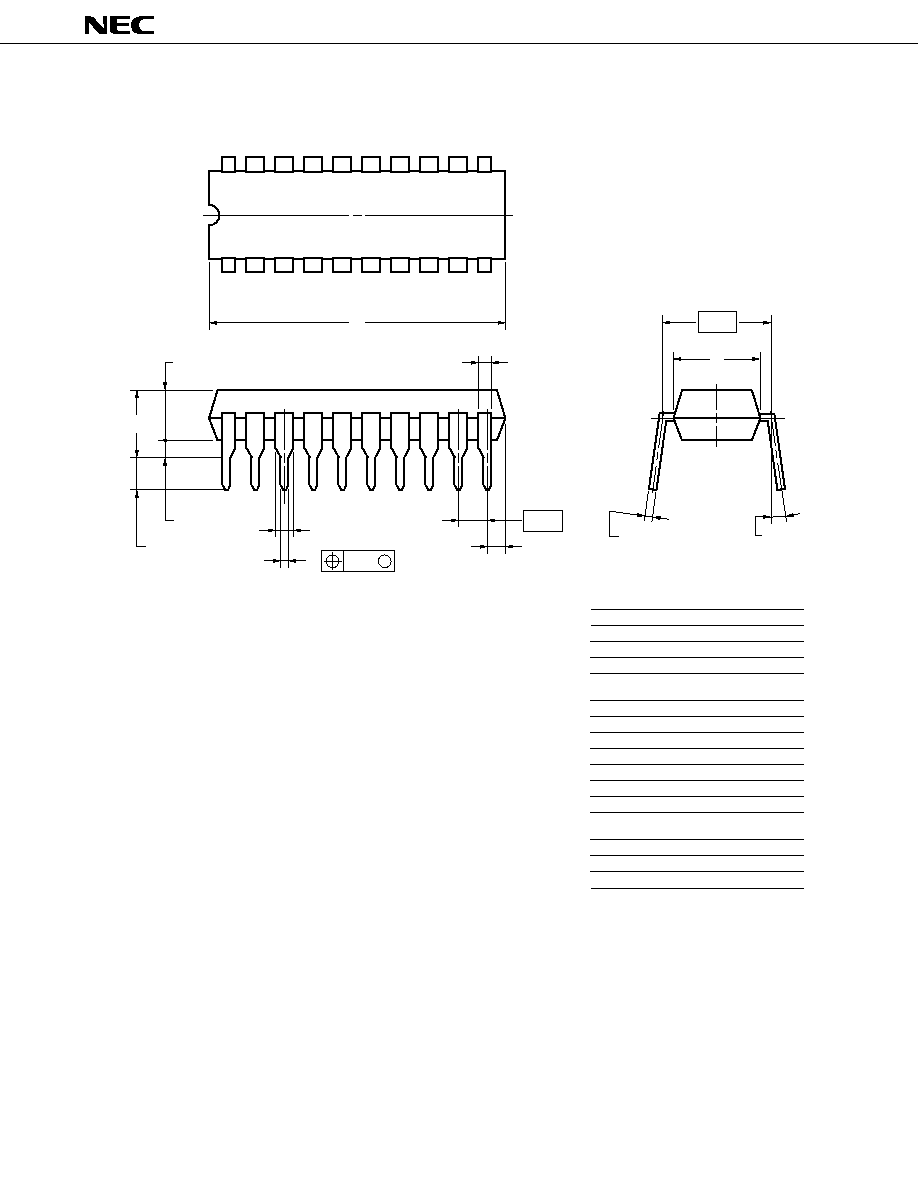
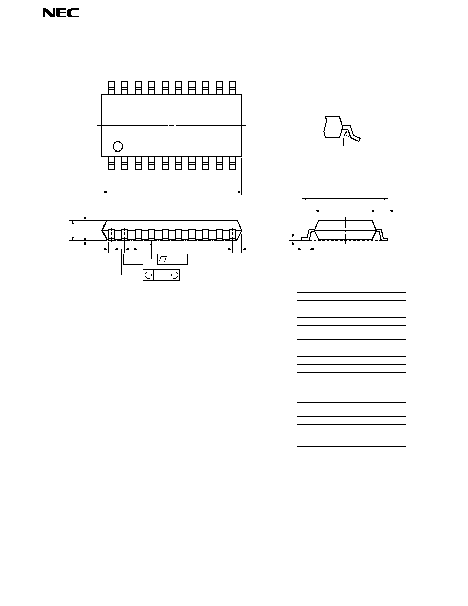
20PIN PLASTIC DIP (300 mil)
ITEM MILLIMETERS
INCHES
NOTES
1) Each lead centerline is located within 0.25 mm (0.01 inch) of
its true position (T.P.) at maximum material condition.
P20C-100-300A,C-1
N
0.25
0.01
R
0~15
∞
0~15
∞
A
25.40 MAX.
1.000 MAX.
B
1.27 MAX.
0.050 MAX.
F
1.1 MIN.
0.043 MIN.
G
3.5±0.3
0.138±0.012
J
5.08 MAX.
0.200 MAX.
K
7.62 (T.P.)
0.300 (T.P.)
C
2.54 (T.P.)
0.100 (T.P.)
D
0.50±0.10
0.020 +0.004
≠0.005
H
0.51 MIN.
0.020 MIN.
I
4.31 MAX.
0.170 MAX.
L
6.4
0.252
M
0.25
0.010 +0.004
≠0.003
+0.10
≠0.05
2) ltem "K" to center of leads when formed parallel.
M
R
M
I
H
G
F
D
N
C
B
K
P
0.9 MIN.
0.035 MIN.
1
10
20
11
P
L
A
J
12
µ
PD4702
20 PIN PLASTIC SOP (300 mil)
ITEM MILLIMETERS
INCHES
A
B
C
E
F
G
H
I
J
13.00 MAX.
1.27 (T.P.)
1.8 MAX.
1.55
7.7±0.3
0.78 MAX.
0.12
1.1
5.6
M
0.1±0.1
N
0.512 MAX.
0.031 MAX.
0.004±0.004
0.071 MAX.
0.061
0.303±0.012
0.220
0.043
0.005
0.050 (T.P.)
P20GM-50-300B, C-4
P
3
∞
3
∞
+7
∞
NOTE
Each lead centerline is located within 0.12 mm (0.005 inch) of
its true position (T.P.) at maximum material condition.
D
0.40
0.016
+0.10
≠0.05
K
0.20
0.008
+0.10
≠0.05
L
0.6±0.2
0.024
0.10
≠3
∞
+7
∞
≠3
∞
0.004
+0.008
≠0.009
+0.004
≠0.002
+0.004
≠0.003
A
C
D
G
P
detail of lead end
F
E
B
H
I
L
K
M
J
N
M
1
10
11
20

13
µ
PD4702
[MEMO]

14
µ
PD4702
[MEMO]

15
µ
PD4702
[MEMO]

µ
PD4702
[MEMO]
No part of this document may be copied or reproduced in any form or by any means without the prior written
consent of NEC Corporation. NEC Corporation assumes no responsibility for any errors which may appear in
this document.
NEC Corporation does not assume any liability for infringement of patents, copyrights or other intellectual property
rights of third parties by or arising from use of a device described herein or any other liability arising from use
of such device. No license, either express, implied or otherwise, is granted under any patents, copyrights or other
intellectual property rights of NEC Corporation or others.
While NEC Corporation has been making continuous effort to enhance the reliability of its semiconductor devices,
the possibility of defects cannot be eliminated entirely. To minimize risks of damage or injury to persons or
property arising from a defect in an NEC semiconductor device, customers must incorporate sufficient safety
measures in its design, such as redundancy, fire-containment, and anti-failure features.
NEC devices are classified into the following three quality grades:
"Standard", "Special", and "Specific". The Specific quality grade applies only to devices developed based on a
customer designated "quality assurance program" for a specific application. The recommended applications of
a device depend on its quality grade, as indicated below. Customers must check the quality grade of each device
before using it in a particular application.
Standard: Computers, office equipment, communications equipment, test and measurement equipment,
audio and visual equipment, home electronic appliances, machine tools, personal electronic
equipment and industrial robots
Special:
Transportation equipment (automobiles, trains, ships, etc.), traffic control systems, anti-disaster
systems, anti-crime systems, safety equipment and medical equipment (not specifically designed
for life support)
Specific:
Aircrafts, aerospace equipment, submersible repeaters, nuclear reactor control systems, life
support systems or medical equipment for life support, etc.
The quality grade of NEC devices is "Standard" unless otherwise specified in NEC's Data Sheets or Data Books.
If customers intend to use NEC devices for applications other than those specified for Standard quality grade,
they should contact an NEC sales representative in advance.
Anti-radioactive design is not implemented in this product.
M4 96.5