©
1995
DATA SHEET
MOS INTEGRATED CIRCUIT
µ
PD4711B
RS-232 LINE DRIVER/RECEIVER
The
µ
PD4711B is a high-voltage silicon gate CMOS line driver/reciever conforming to the EIA/TIA-232-E standard.
It can operate with a single +5 V power source because it is provided with a DC-DC converter. In addition, this line
driver/receiver has many ancillary functions, including output control, threshold select, and standby functions.
Because the
µ
PD4711B is provided with two output driver circuits and two receiver circuits, it can constitute an RS-
232 interface circuit with a single chip.
FEATURES
∑
Conforms to EIA/TIA-232-E (RS-232C) standard
∑
+5 V single power source
∑
Threshold select pin selecting two types of threshold voltages
∑
Standby mode can be set by making standby pin high to reduce circuit current.
∑
Three-state output configuration. Both driver and receiver outputs go into high-impedance state in standby mode.
ORDERING INFORMATION
Part Number
Package
µ
PD4711BCX
20-pin plastic DIP (300 mil)
µ
PD4711BGS
20-pin plastic SOP (300 mil)
The information in this document is subject to change without notice.
Document No. S10315EJ3V1DS00 (3rd edition)
Date Published April 1997 N
Printed in Japan

µ
PD4711B
2
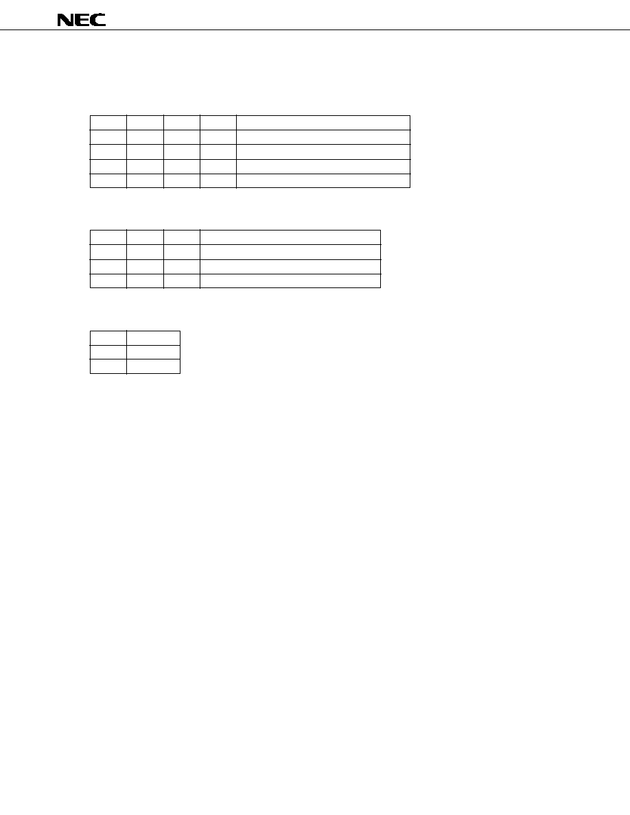
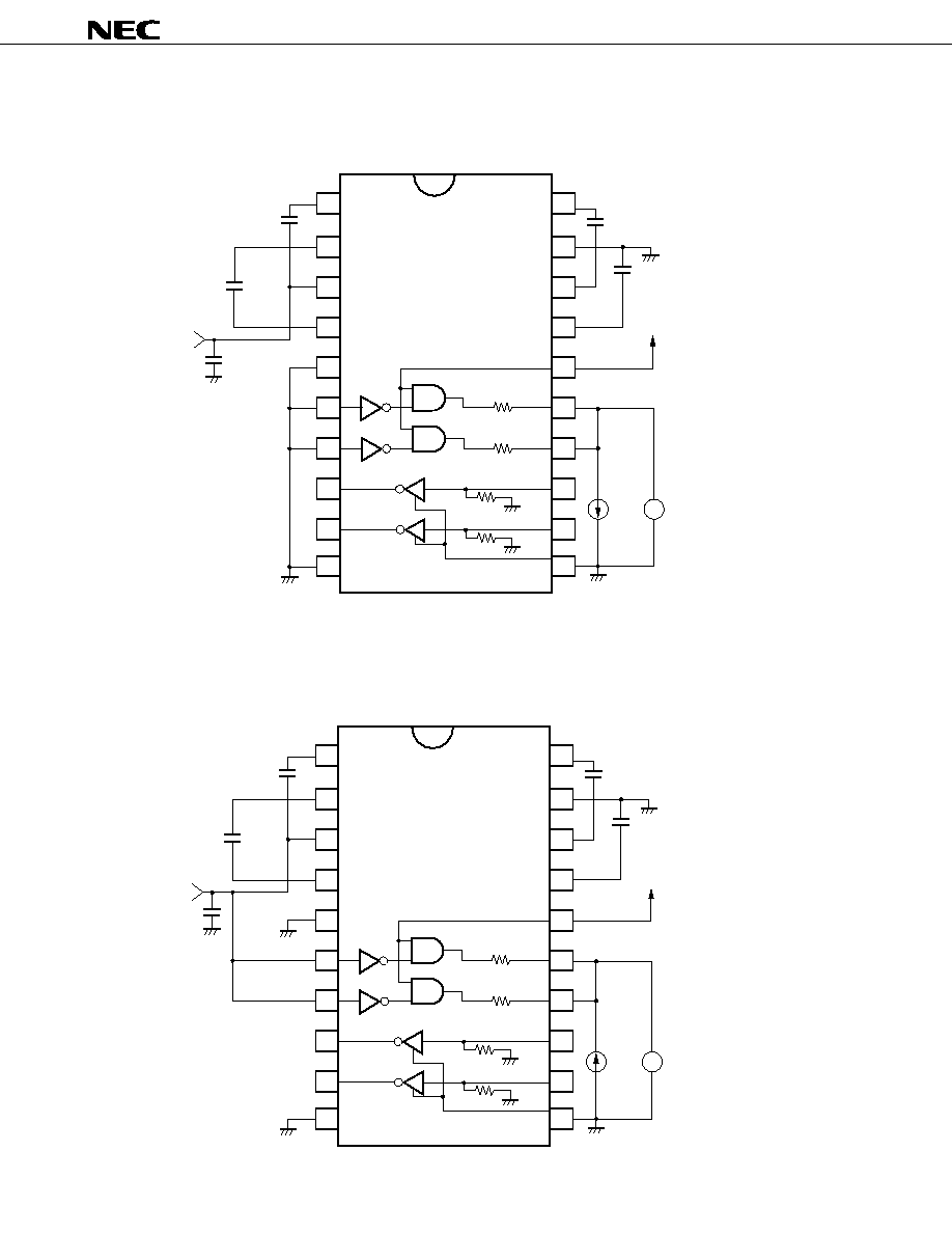
BLOCK DIAGRAM/PIN CONFIGURATION (Top View)
20
DC - DC
converter
V
DD
C
1
V
CC
C
1
GND
19
18
17
16
15
14
13
12
11
1
2
3
4
5
6
7
8
9
10
+5 V
C
1
+
+
C
3
+10 V
C
4
+
+
C
2
≠10 V
D
IN1
D
IN2
R
OUT1
R
OUT2
TTL/CMOS
OUTPUT
TTL/CMOS
INPUT
Threshold control
D
CON
D
OUT1
R
IN1
R
IN2
R
CON
RS-232
OUTPUT
RS-232
INPUT
C
4
+
+
≠
V
SS
C
4
≠
GND
300
5.5 k
Standby STBY
D
OUT2
Output contrtol
300
5.5 k
By pass
Capacitor
*
V
DD
and V
ss
are output pins of voltages internally boosted. Connecting a load directly to these pins is not
recommended.
**
The standby pin is internally pulled down.
***
Use capacitors with a working voltage of 16 V or higher as C
1
through C
4
. Insert a bypass capasitor about 0.1
to 1
µ
F between V
CC
pin to GND pin.
µ
PD4711B
3
TRUTH TABLE
Drivers
STBY
D
CON
D
IN
D
OUT
Remark
H
X
X
Z
Standby mode (DC-DC converter stops)
L
L
X
L
Mark level output
L
H
L
H
Space level output
L
H
H
L
Mark level output
Receivers
STBY
R
IN
R
OUT
Remark
H
X
Z
Stanby mode (DC-DC converter stops)
L
L
H
Mark level input
L
H
L
Space level input
Receiver input threshold voltage
R
CON
R
IN1
to R
IN2
L
A mode
H
B mode
H: high level, L: low level, Z: high impedance, X: H or L
µ
PD4711B
4
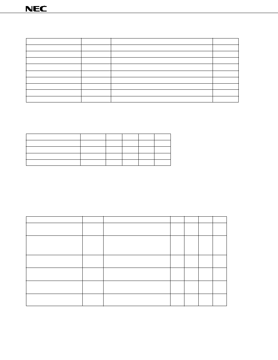
ABSOLUTE MAXIMUM RATINGS (T
A
= 25 ∞C)
Parameter
Symbol
Ratings
Unit
Supply voltage
V
CC
≠0.5 to +6.0
V
Driver input voltage
D
IN
≠0.5 to V
CC
+0.5
V
Receiver input voltage
R
IN
≠30.0 to +30.0
V
Driver output voltage
D
OUT
≠25.0 to +25.0
Note 1
V
Receiver output voltage
R
OUT
≠0.5 to V
CC
+ 0.5
V
Receiver input current
I
IN
±
60.0
mA
Operating temperature range
T
A
≠40 to +85
∞ C
Storage temperature range
T
stg
≠55 to +150
∞ C
Power dissipation
P
T
0.5
W
Note 1. Pulse width: 1 ms, duty factor: 10 % MAX.
RECOMMENDED OPERATING RANGE
Parameter
Symbol
MIN.
TYP.
MAX.
Unit
Supply voltage
V
CC
4.5
5.0
5.5
V
Receiver input voltage
R
IN
≠30
+30
V
Operating temperature range
T
A
≠20
80
∞ C
External capacitance
Note 2
1.0
22
47
µ
F
Note 2.
The capacitance of an electrolytic capacitor decreases at a low temperature (0 ∞C or lower). Determine
the capacitance of the capacitor to be used taking this into consideration when the
µ
PD4711B is used at
a low temperature. Keep the wiring length between the capacitor and IC as short as possible.
ELECTRICAL CHARACTERISTICS (OVERALL)
(Unless otherwise specified, V
CC
= +5 V
±
10 %, T
A
= ≠20 ∞C to +80 ∞C, C
1
to C
4
= 22
µ
F)
MIN.
TYP.
MAX.
Unit
4.5
9.0
mA
15.0
25.0
mA
50
120
µ
A
0.8
V
2.0
V
10
pF
Conditions
V
CC
= +5 V, no load, R
IN
pin open
(Standby pin open)
V
CC
= +5 V, R
L
= 3 k
(D
OUT
), D
IN
= GND,
R
IN
and R
OUT
pins open
(Standby pin open)
V
CC
= +5 V, no load, R
IN
pin open
(Standby pin high)
Note 3
Driver input and receiver input
V
CC
= +5 V, vs. GND, f = 1 MHz
Symbol
I
CC1
I
CC2
I
CC
(Standby)
V
IL
(Standby)
V
IH
(Standby)
C
IN
Parameter
Circuit current
Circuit current
Standby circuit current
Standby low-level
input voltage
Standby high-level
input voltage
Input capacitance
*
TYP.: Typical (reference) value at T
A
= 25 ∞C.
Note 3.
Because the standby pin is internally pulled down, if the standby pin is left open, operating mode is in effect.
µ
PD4711B
5
MIN.
TYP.
MAX.
Unit
0.8
V
2.0
V
0
≠1.0
µ
A
0
1.0
µ
A
V
±
5.5
V
±
5.0
V
±
40
mA
1.5
30
V/
µ
s
1.5
30
V/
µ
s
µ
s
300
10
µ
s
50
ms
Conditions
V
CC
= +5.0 V, R
L
=
, T
A
= 25 ∞C
V
CC
= +5.0 V, R
L
= 3 k
V
CC
= +4.5 V, R
L
= 3 k
V
CC
= +5.0 V, vs. GND
C
L
= 10 pF, R
L
= 3 to 7 k
C
L
= 2500 pF, R
L
= 3 to 7 k
R
L
= 3.5 k
, C
L
= 2500 pF
V
CC
= V
DD
= V
SS
= 0 V
V
OUT
=
±
2 V
Note 5
Note 5
Symbol
V
IL
V
IH
I
IL
I
IH
V
DO
I
SC
SR
t
PHL
t
PLH
R
O
t
DAZ
t
DZA
±
9.7
±
15
11
6
0.8
4
25
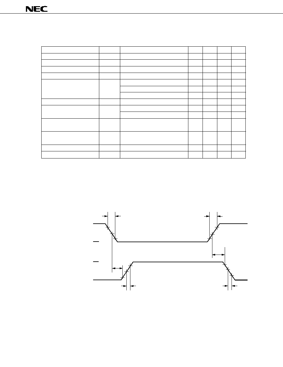
ELECTRICAL CHARACTERISTICS (DRIVER)
(Unless otherwise specified, V
CC
= +5 V
±
10 %, T
A
= ≠20 ∞C to +80 ∞C, C
1
to C4 = 22
µ
F)
Parameter
Low-level input voltage
High-level input voltage
Low-level input current
High-level input current
Output voltage
Output short current
Slew rate
Propagation delay time
Note 4
Output resistance
Standby output transition time
Standby output transition time
*
TYP.: Typical (reference) value at T
A
= 25 ∞C.
Note 4.
Test point
If the output control pin is made low, the driver output goes low regardless of the driver input state.
Driver input
Driver output
6 ns
6 ns
5
10 %
90 %
1.5 V
0
V
OH
V
OL
1.5 V
SR
t
PLH
≠3 V
3 V
≠3 V
3 V
SR
t
PHL
10 %
90 %
90 %
10 %

µ
PD4711B
6
Note 5.
Test Point
+5 V
≠5 V
High impedance
5 V
0 V
V
OH
V
OL
Standby input
Driver output
1.5 V
1.5 V
t
DAZ
t
DZA
+5 V
≠5 V
Do not perform communication within the standby output transition time t
DZA
on power application or on releasing
the standby mode.
ELECTRICAL CHARACTERISTICS (RECEIVER)
(Unless otherwise specified, V
CC
= +5 V
±
10 %, T
A
= ≠20 ∞C to +80 ∞C, C
1
to C
4
= 22
µ
F)
Parameter
Low-level output voltage
High-level output voltage
Low-level input voltage
High-level input voltage
Propagation delay time
Note 6
Input current
Input resistance
Input pin release voltage
Input threshold A mode
(R
CON
pin low)
Input threshold B mode
(R
CON
pin high)
Standby output transition time
Standby output transition time
Conditions
MIN.
TYP.
MAX.
I
OUT
= 4 mA
0.4
I
OUT
= ≠4 mA
V
CC
≠0.8
R
CON
pin
0.8
R
CON
pin
2.0
R
L
= 1 k
, C
L
= 150 pF
0.13
V
IN
=
±
5 V
1
V
IN
=
±
3 to
±
25
3
5
7
Input threshold A mode only
0.5
V
CC
= +5 V
1.6
2.2
2.6
V
CC
= +5 V
0.6
1
1.6
V
CC
= +5 V (hysteresis width)
0.5
1.2
1.8
V
CC
= +5 V
1.6
2.2
2.6
V
CC
= +5 V
≠0.4
≠1.8
≠3.0
V
CC
= +5 V (hysteresis width)
2.6
4.0
5.4
Note 7
0.4
1
Note 7
0.03
10
Symbol
V
OL
V
OH
V
IL
V
IH
t
PHL
t
PLH
I
IN
R
I
V
IO
V
IH
V
IL
V
H
V
IH
V
IL
V
H
t
DAZ
t
DZA
Unit
V
V
V
V
µ
s
mA
k
V
V
V
V
V
V
V
µ
s
ms
* TYP.: Typical (reference) value at T
A
= 25 ∞C.

µ
PD4711B
7
Note 6.
Test Point
Receiver input
Receiver output
10 ns
10 ns
5
10 %
90 %
1.5 V
≠5
V
OH
V
OL
t
PLH
1.5 V
t
PHL
10 %
90 %
1.5 V
1.5 V
Note 7.
Test Point
90 %
10 %
High impedance
5 V
0 V
V
OH
V
OL
Standby input
Receiver output
1.5 V
1.5 V
t
DAZ
t
DZA
The receiver output is undefined during the standby output transition time t
DZA
. Do not perform communication
in the standby output transition time t
DZA
on power application or on releasing the standby mode.
µ
PD4711B
8
TEST CIRCUIT
Driver output voltage/Output current (+ side)
Driver output voltage/Output current (≠ side)
20
DC - DC
converter
V
DD
C
1
V
CC
C
1
GND
19
18
17
16
15
14
13
12
11
1
2
3
4
5
6
7
8
9
10
+5 V
C
1
+
+
C
3
+10 V
C
4
+
+
C
2
≠10 V
C
4
+
+
≠
V
SS
C
4
≠
GND
300
5.5 k
300
5.5 k
STBY
+5 V
V V
DO
I
DO
20
DC - DC
converter
V
DD
C
1
V
CC
C
1
GND
19
18
17
16
15
14
13
12
11
1
2
3
4
5
6
7
8
9
10
+5 V
C
1
+
+
C
3
+10 V
C
4
+
+
C
2
≠10 V
C
4
+
+
≠
V
SS
C
4
≠
GND
300
5.5 k
300
5.5 k
STBY
+5 V
V V
DO
I
DO
µ
PD4711B
9
PACKAGE DRAWINGS
20PIN PLASTIC DIP (300 mil)
ITEM MILLIMETERS
INCHES
NOTES
1) Each lead centerline is located within 0.25 mm (0.01 inch) of
its true position (T.P.) at maximum material condition.
P20C-100-300A,C-1
N
0.25
0.01
R
0~15
∞
0~15
∞
A
25.40 MAX.
1.000 MAX.
B
1.27 MAX.
0.050 MAX.
F
1.1 MIN.
0.043 MIN.
G
3.5±0.3
0.138±0.012
J
5.08 MAX.
0.200 MAX.
K
7.62 (T.P.)
0.300 (T.P.)
C
2.54 (T.P.)
0.100 (T.P.)
D
0.50±0.10
0.020 +0.004
≠0.005
H
0.51 MIN.
0.020 MIN.
I
4.31 MAX.
0.170 MAX.
L
6.4
0.252
M
0.25
0.010 +0.004
≠0.003
+0.10
≠0.05
2) ltem "K" to center of leads when formed parallel.
M
R
M
I
H
G
F
D
N
C
B
K
P
0.9 MIN.
0.035 MIN.
1
10
20
11
P
L
A
J

µ
PD4711B
10
20 PIN PLASTIC SOP (300 mil)
ITEM MILLIMETERS
INCHES
A
B
C
E
F
G
H
I
J
13.00 MAX.
1.27 (T.P.)
1.8 MAX.
1.55
7.7±0.3
0.78 MAX.
0.12
1.1
5.6
M
0.1±0.1
N
0.512 MAX.
0.031 MAX.
0.004±0.004
0.071 MAX.
0.061
0.303±0.012
0.220
0.043
0.005
0.050 (T.P.)
P20GM-50-300B, C-4
P
3
∞
3
∞
+7
∞
NOTE
Each lead centerline is located within 0.12 mm (0.005 inch) of
its true position (T.P.) at maximum material condition.
D
0.40
0.016
+0.10
≠0.05
K
0.20
0.008
+0.10
≠0.05
L
0.6±0.2
0.024
0.10
≠3
∞
+7
∞
≠3
∞
0.004
+0.008
≠0.009
+0.004
≠0.002
+0.004
≠0.003
A
C
D
G
P
detail of lead end
F
E
B
H
I
L
K
M
J
N
M
1
10
11
20
µ
PD4711B
11
Soldering Condition
Package peak temperature: 235 ∞C, Time: 30 seconds MAX.
(210 ∞C MIN.), Number of times: 2, Number of days: not limited*
Package peak temperature: 215 ∞C, Time: 40 seconds MAX.
(200 ∞C MIN.), Number of times: 2, Number of days: not limited*
Soldering bath temperature: 260 ∞C MAX., Time: 10 seconds
MAX., Number of times: 1, Number of days: not limited*
Pin temperature: 300 ∞C MAX (lead temperature), Time: 3
seconds MAX. (per lead pin), Number of days: not
limited*
RECOMMENDED SOLDERING CONDITIONS
Soldering the
µ
PD4711B under the conditions listed in the table below is recommended.
For soldering methods and conditions other than those recommended, consult NEC.
Surface mount type
For the details of the recommended soldering conditions of the surface mount type, refer to Information
document "Semiconductor Device Mounting Technology Manual" C10535EJ7V0IF00.
µ
PD4711BGS
Recommended Condition Symbol
IR35-00-2
VP15-00-2
WS60-00-1
* The number of days the device can be stored at 25 ∞C, 65 % RH MAX. after the dry pack has been opened.
Caution Do not use two or more soldering methods in combination (except the pin partial heating method).
Throught-hole type
µ
PD4711BCX
Soldering Method
Soldering Conditions
Wave soldering
Soldering bath temperature: 260 ∞C MAX., Time: 10 seconds MAX.
Reference documents
"NEC Semiconductor Device Reliability/Quality Control System" (IEI-1212)
"Quality Grade on NEC Semiconductor Devices" (IEI-1209)
"Semiconductor Device Mounting Technology Manual" C10535EJ7V0IF00
Soldering Method
Infrared reflow
VPS
Wave soldering
Pin partial heating

12
µ
PD4711B
[MEMO]
No part of this document may be copied or reproduced in any form or by any means without the prior written
consent of NEC Corporation. NEC Corporation assumes no responsibility for any errors which may appear in
this document.
NEC Corporation does not assume any liability for infringement of patents, copyrights or other intellectual property
rights of third parties by or arising from use of a device described herein or any other liability arising from use
of such device. No license, either express, implied or otherwise, is granted under any patents, copyrights or other
intellectual property rights of NEC Corporation or others.
While NEC Corporation has been making continuous effort to enhance the reliability of its semiconductor devices,
the possibility of defects cannot be eliminated entirely. To minimize risks of damage or injury to persons or
property arising from a defect in an NEC semiconductor device, customers must incorporate sufficient safety
measures in its design, such as redundancy, fire-containment, and anti-failure features.
NEC devices are classified into the following three quality grades:
"Standard", "Special", and "Specific". The Specific quality grade applies only to devices developed based on a
customer designated "quality assurance program" for a specific application. The recommended applications of
a device depend on its quality grade, as indicated below. Customers must check the quality grade of each device
before using it in a particular application.
Standard: Computers, office equipment, communications equipment, test and measurement equipment,
audio and visual equipment, home electronic appliances, machine tools, personal electronic
equipment and industrial robots
Special:
Transportation equipment (automobiles, trains, ships, etc.), traffic control systems, anti-disaster
systems, anti-crime systems, safety equipment and medical equipment (not specifically designed
for life support)
Specific:
Aircrafts, aerospace equipment, submersible repeaters, nuclear reactor control systems, life
support systems or medical equipment for life support, etc.
The quality grade of NEC devices is "Standard" unless otherwise specified in NEC's Data Sheets or Data Books.
If customers intend to use NEC devices for applications other than those specified for Standard quality grade,
they should contact an NEC sales representative in advance.
Anti-radioactive design is not implemented in this product.
M4 96.5