Document Outline
- COVER
- Description
- Features
- Ordering Information
- Pin Configuration
- Block Diagram
- 1. Input/Output Pin Function
- 2. Operation Mode
- 2.1 Mode Set Cycle
- 2.2 Write Cycle
- 2.3 Read Cycle
- 2.4 Write Reset Cycle/Read Reset Cycle
- 3. Electrical Specifications
- 4. Application
- 4.1 1 H Delay Line
- 4.2 n Bit Delay
- 4.3 Double-speed Conversion
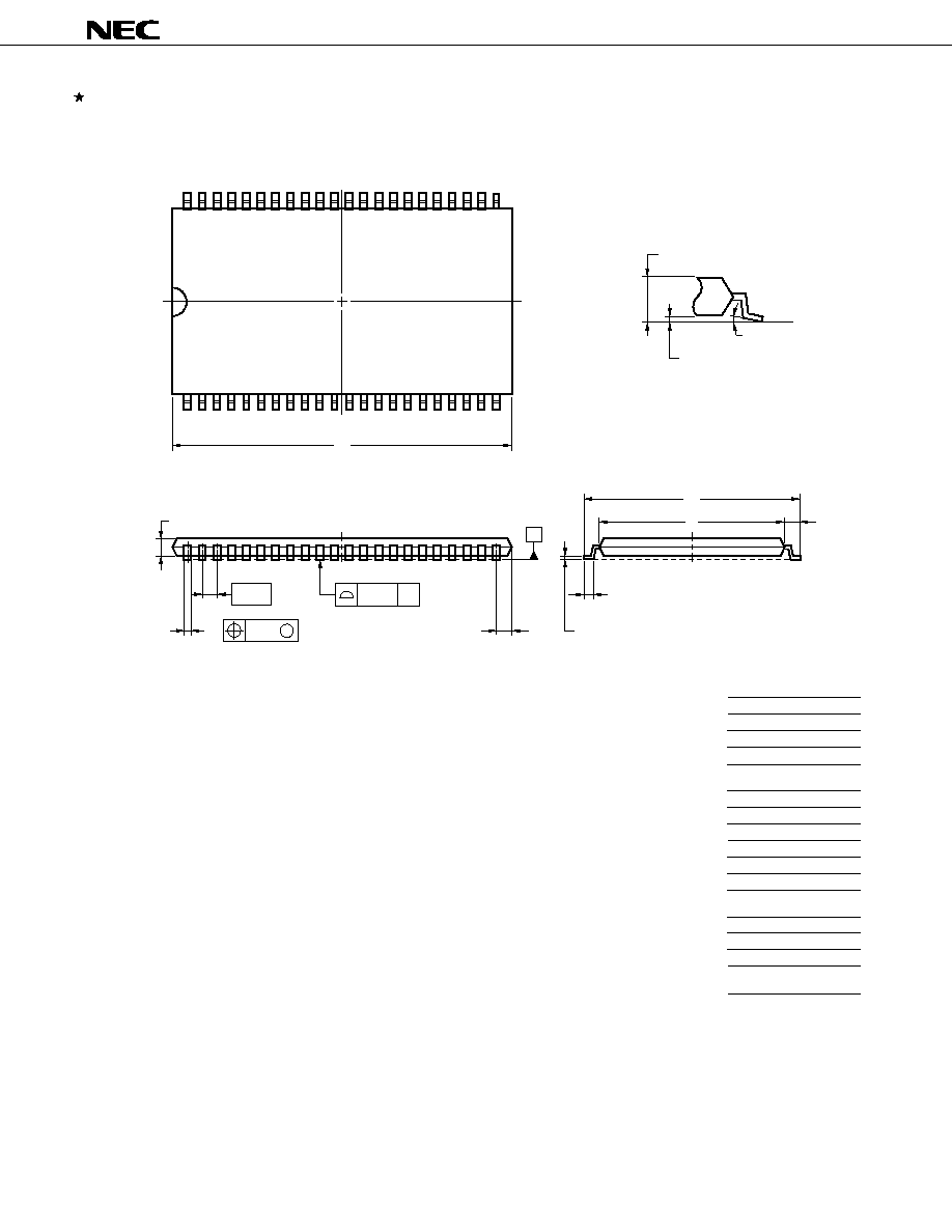
- 5. Package Drawing
- 6. Recommended Soldering Conditions
- 7. Example of Stamping
©
1994
DATA SHEET
MOS INTEGRATED CIRCUIT
µ
PD485506
LINE BUFFER
5K-WORD BY 16-BIT/10K-WORD BY 8-BIT
The mark shows major revised points.
Document No. M10060EJ7V0DSJ1 (7th edition)
Date Published December 2000 N CP(K)
Printed in Japan
Description
The
µ
PD485506 is a high speed FIFO (First In First Out) line buffer. Word organization can be changed either
5,048 words by 16 bits or 10,096 words by 8 bits. Its CMOS static circuitry provides high speed access and low power
consumption.
The
µ
PD485506 can be used for one line delay and time axis conversion in high speed facsimile machines and
digital copiers.
Moreover, the
µ
PD485506 can execute read and write operations independently on an asynchronous basis. Thus
the
µ
PD485506 is suitable as a buffer for data transfer between units with different transfer rates and as a buffer for
the synchronization of multiple input signals.
There are four versions, E, K, P, X and L. This data sheet can be applied to the version X and L. These versions
operate with different specifications. Each version is identified with its lot number (refer to 7. Example of Stamping).
Features
∑
5,048 words by 16 bits (Word mode) /10,096 words by 8 bits (Byte mode)
∑
Asynchronous read/write operations available
∑
Variable length delay bits; 21 to 5,048 bits or 10,096 bits (Cycle time: 25 ns)
15 to 5,048 bits or 10,096 bits (Cycle time: 35 ns)
∑
Power supply voltage V
CC
= 5.0 V
±
0.5 V
∑
Suitable for sampling two lines of A3 size paper (16 dots/mm)
∑
All input/output TTL compatible
∑
3-state output
∑
Full static operation; data hold time = infinity
Ordering Information
Part Number
R/W Cycle Time
Package
µ
PD485506G5-25-7JF
25 ns
44-pin plastic TSOP (II) (10.16 mm (400))
µ
PD485506G5-35-7JF
35 ns
The information in this document is subject to change without notice. Before using this document, please
confirm that this is the latest version.
Not all devices/types available in every country. Please check with local NEC representative for availability
and additional information.
µ
PD485506
2
Data Sheet M10060EJ7V0DS00
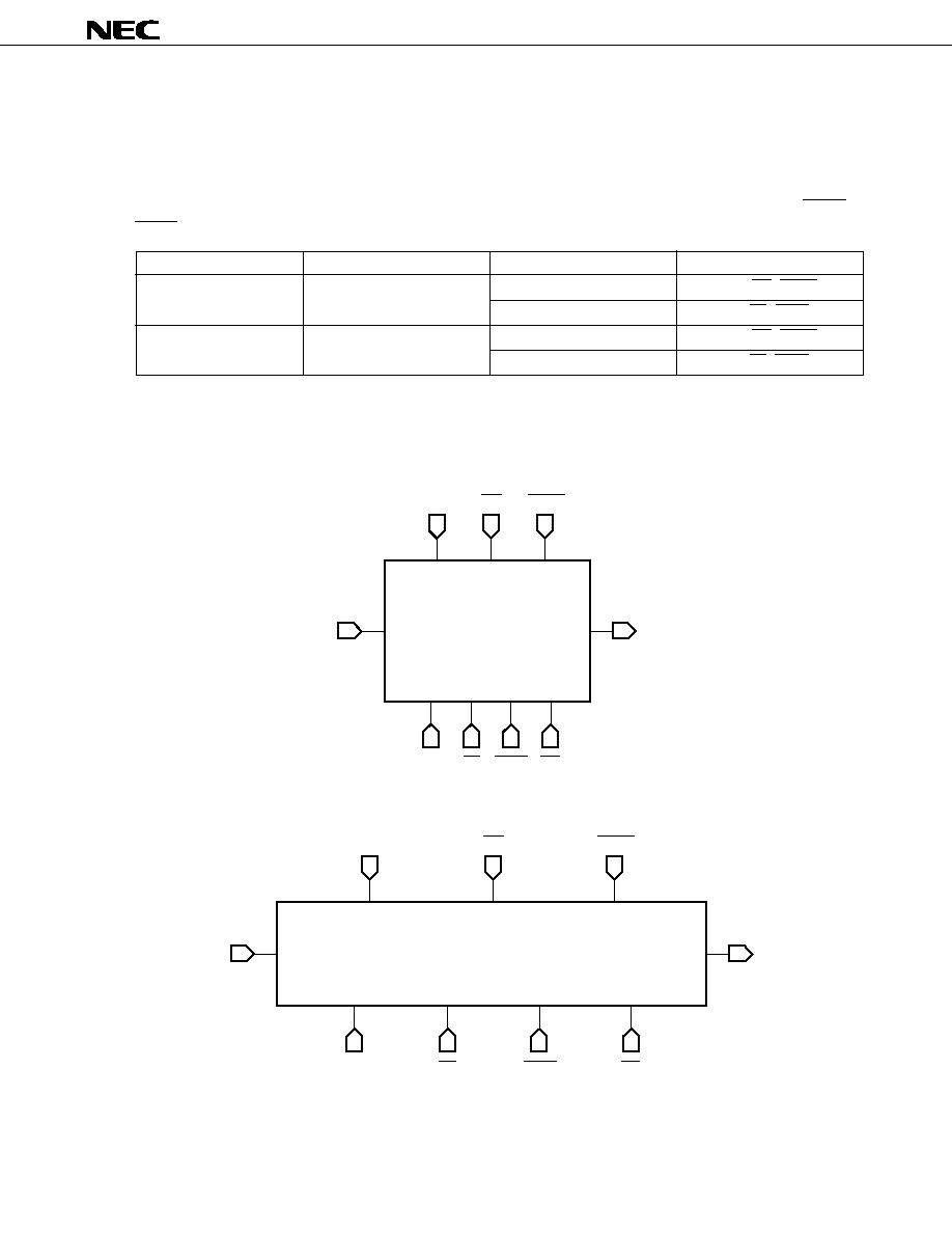
Pin Configuration (Marking side)
44-pin plastic TSOP (
II
) (10.16 mm (400))
[
µ
PD485506G5-7JF]
D
IN0
to D
IN15
: Data Inputs
D
OUT0
to D
OUT15
: Data Outputs
WCK
: Write Clock Input
RCK
: Read Clock Input
WE
: Write Enable Input
RE
: Read Enable Input
OE
: Output Enable Input
RSTW
: Reset Write Input
RSTR
: Reset Read Input
MD
: Mode Set Input
V
CC
: +5.0 V Power Supply
GND
: Ground
Remark
Refer to Package Drawing for the 1-pin index mark.
1
2
3
4
5
6
7
8
9
10
11
12
13
14
15
16
17
18
19
20
21
22
44
43
42
41
40
39
38
37
36
35
34
33
32
31
30
29
28
27
26
25
24
23
D
IN0
D
IN1
D
IN2
D
IN3
D
IN4
D
IN5
D
IN6
D
IN7
WE
MD
GND
RSTW
WCK
V
CC
D
IN8
D
IN9
D
IN10
D
IN11
D
IN12
D
IN13
D
IN14
D
IN15
D
OUT0
D
OUT1
D
OUT2
D
OUT3
D
OUT4
D
OUT5
D
OUT6
D
OUT7
RE
GND
RSTR
RCK
V
CC
D
OUT8
D
OUT9
D
OUT10
D
OUT11
D
OUT12
D
OUT13
D
OUT14
D
OUT15
OE
µ
PD485506
3
Data Sheet M10060EJ7V0DS00
Block Diagram
WE
D
OUT0
D
OUT1
D
OUT2
D
OUT3
D
OUT4
D
OUT5
D
OUT6
D
OUT7
RSTR
RE
V
CC
GND
Write Address Pointer
Mode Controller
40,384 bits
(5,048 words by 8 bits)
Memory Cell Array
RSTW
WCK
RCK
Output Buffer
Read Address Pointer
40,384 bits
(5,048 words by 8 bits)
Memory Cell Array
Input Buffer
Output Buffer
D
OUT8
D
OUT9
D
OUT10
D
OUT11
D
OUT12
D
OUT13
D
OUT14
D
OUT15
Output Controller
Output Controller
OE
MD
D
IN0
D
IN1
D
IN2
D
IN3
D
IN4
D
IN5
D
IN6
D
IN7
D
IN8
D
IN9
D
IN10
D
IN11
D
IN12
D
IN13
D
IN14
D
IN15
Input Buffer
Input Controller
Input Controller
µ
PD485506
4
Data Sheet M10060EJ7V0DS00
1. Input/Output Pin Function
Pin
Pin
Symbol
Pin
Number
Name
44 ≠ 37,
D
IN0
Data
|
Input
30 ≠ 23
D
IN15
1 ≠ 8,
D
OUT0
Data
|
Output
15 ≠ 22
D
OUT15
33
RSTW
Reset
Write
Input
12
RSTR
Reset
Read
Input
36
WE
Write
Enable
Input
10
RE
Read
Enable
Input
9
OE
Output
Enable
Input
32
WCK
Write
Clock
Input
13
RCK
Read
Clock
Input
35
MD
Mode
Set
Input
I/O
Function
In
Write data input pins.
The data inputs are strobed by the rising edge of WCK at the end of a cycle
and the setup and hold times (t
DS
, t
DH
) are defined at this point.
Out
Read data output pins.
The access time is regulated from the rising edge of RCK at the beginning of a
cycle and defined by t
AC
.
In
Reset input pin for the initialization of the write address pointer.
The state of RSTW is strobed by the rising edge of WCK at the beginning of a
cycle and the setup and hold times (t
RS
, t
RH
) are defined.
In
Reset input pin for the initialization of the read address pointer.
The state of RSTR is strobed by the rising edge of RCK at the beginning of a
cycle and the setup and hold times (t
RS
, t
RH
) are defined.
In
Write operation control signal input pin.
When WE is in the disable mode ("H" level), the internal write operation is
inhibited and the write address pointer stops at the current position.
In
Read operation control signal input pin.
When RE is in the disable mode ("H" level), the internal read operation is
inhibited and the read address pointer stops at the current position. The data
outputs remain valid for that address.
In
Output operation control signal input pin.
When OE is in the disable mode ("H" level), the data out is inhibited and the
output changes to high impedance. The internal read operation is executed at
that time and the read address pointer incremented in synchronization with the
read clock.
In
Write clock input pin.
When WE is enabled ("L" level), the write operation is executed in
synchronization with the write clock. The write address pointer is incremented
simultaneously.
In
Read clock input pin.
When RE is enabled ("L" level), the read operation is executed in synchroniza-
tion with the read clock. The read address pointer is incremented
simultaneously.
In
Mode set input pin.
The level of MD gives the operation mode. When MD is in "L" level,
5,048 words by 16 bits configuration with D
IN0
- D
IN15
, D
OUT0
- D
OUT15
is enabled.
When MD is in "H" level, 10,096 words by 8 bits configuration with D
IN0
- D
IN7
,
D
OUT0
- D
OUT7
is enabled.
µ
PD485506
5
Data Sheet M10060EJ7V0DS00
2. Operation Mode
µ
PD485506 is a synchronous memory. All signals are strobed at the rising edge of the clock (RCK, WCK).
For this reason, setup time and hold time are specified for the rising edge of the clock (RCK, WCK).
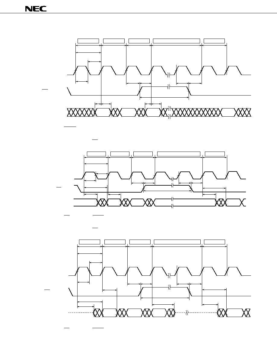
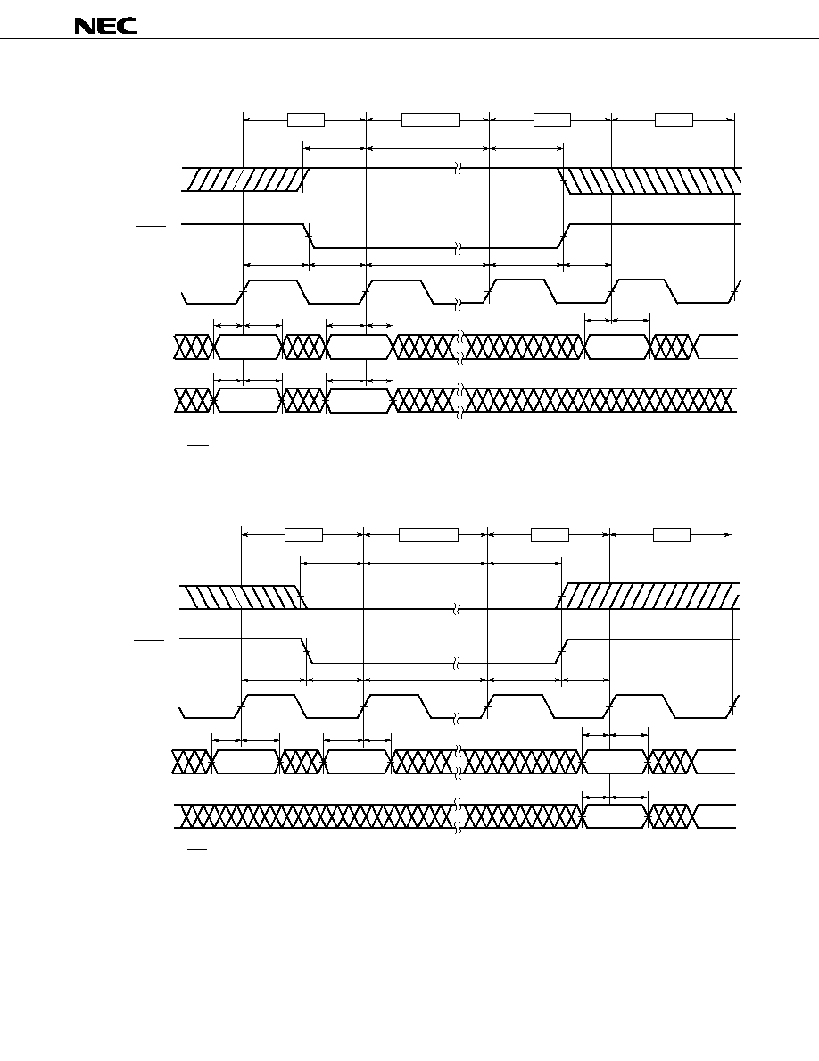
2.1 Mode Set Cycle (5,048 words by 16 bits or 10,096 words by 8 bits organization)
µ
PD485506 has a capability of selecting from two operation modes by judging the MD level when RSTW or
RSTR is enabled in the reset cycle.
MD Level
Bit Configuration
Data Inputs/Outputs
Control Signal
"L"
5,048 words by 16 bits
D
IN0
- D
IN15
WCK, WE, RSTW
D
OUT0
- D
OUT15
RCK, RE, RSTR
"H"
10,096 words by 8 bits
D
IN0
- D
IN7
WCK, WE, RSTW
D
OUT0
- D
OUT7
RCK, RE, RSTR
Caution
Don't change the MD level during a reset cycle. (See Figure 4.6, 7, 8, 9 Mode Set Cycle Timing
Chart)
5,048 Words by 16 Bits FIFO
WCK
WE
RSTW
D
IN0
- D
IN15
D
OUT0
- D
OUT15
OE
RSTR
RE
RCK
5,048 Words
by
16 Bits
10,096 Words by 8 Bits FIFO
OE
RSTR
RE
RCK
D
IN0
- D
IN7
D
OUT0
- D
OUT7
WCK
WE
RSTW
10,096 Words by 8 Bits
Remark
Fix D
IN8
- D
IN15
to "L" or "H" level in the 10,096 words by 8 bits mode.

µ
PD485506
6
Data Sheet M10060EJ7V0DS00
2.2 Write Cycle
When the WE input is enabled ("L" level), a write cycle is executed in synchronization with the WCK clock
input.
The data inputs are strobed by the rising edge of the clock at the end of a cycle so that read data after a one-
line (5,048 bits or 10,096 bits) delay and write data can be processed with the same clock. Refer to Write Cycle
Timing Chart.
When WE is disabled ("H" level) in a write cycle, the write operatoin is not performed during the cycle which
the WCK rising edge is in the WE = "H" level (t
WEW
). The WCK does not increment the write address pointer
at this time.
Unless inhibited by WE, the internal write address will automatically wrap around from 5,047 to 0 and begin
incrementing again.
2.3 Read Cycle
When the RE input is enabled ("L" level), a read cycle is executed in synchronization with the RCK clock input.
When the OE input is also enabled ("L" level) at that time, data is output after t
AC
. Refer to Read Cycle Timing
Chart.
When RE is disabled ("H" level) in a read cycle, the read operation is not performed during the cycle which
the RCK rising edge is in the RE = "H" level (t
REW
). The RCK does not increment the read address pointer at
this time.
2.4 Write Reset Cycle/Read Reset Cycle
After power up, the
µ
PD485506 requires the initialization of internal circuits because the read and write
address pointers are not defined at that time.
It is necessary to satisfy setup requirements and hold times as measured from the rising edge of WCK and
RCK, and then input the RSTW and RSTR signals to initialize the circuit.
Write and read reset cycles can be executed at any time and the address pointer returns zero. Refer to Write
Reset Cycle Timing Chart, Read Reset Cycle Timing Chart.
Remark
Write and read reset cycles can be executed at any time and do not depend on the state of RE, WE or
OE.
µ
PD485506
7
Data Sheet M10060EJ7V0DS00
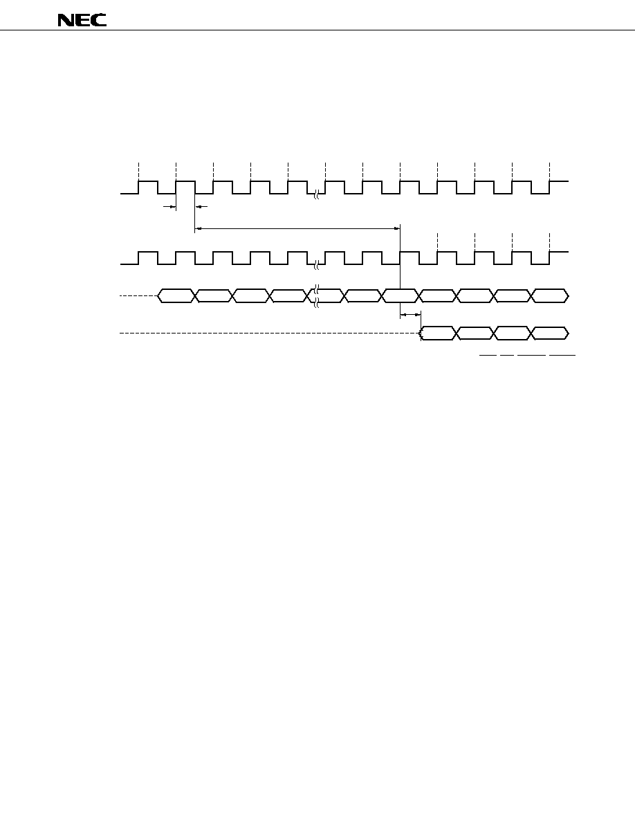
Operation-related Restriction
Following restriction exists to read data written in a write cycle.
Read the written data after an elapse of 1/2 write cycle + t
WAR
since the write cycle ends (see Figure 2.1).
If t
WAR
is not satisfied, the output data may undefined.
Figure 2.1 Delay Bits Restriction Timing Chart
Remark
This timing chart describes only the delay bits restriction, and does not defines the WE, RE, RSTW, RSTR
signals.
0
1
2
3
WCK
0
1
2
RCK
1/2 write cycle
t
WAR
D
IN
0
1
2
3
D
OUT
0
1
2
3
t
AC
High impedance
High impedance

µ
PD485506
8
Data Sheet M10060EJ7V0DS00
3. Electrical Specifications
All voltages are referenced to GND.
Absolute Maximum Ratings
Parameter
Symbol
Condition
Rating
Unit
Voltage on any pin relative to GND
V
T
≠0.5
Note
to V
CC
+ 0.5
V
Supply voltage
V
CC
≠0.5 to +7.0
V
Output current
I
O
20
mA
Operating ambient temperature
T
A
0 to 70
∞C
Storage temperature
T
stg
≠55 to +125
∞C
Note
≠3.0 V MIN. (Pulse width = 10 ns)
Caution
Exposing the device to stress above those listed in Absolute Maximum Ratings could cause
permanent damage. The device is not meant to be operated under conditions outside the limits
described in the operational section of this specification. Exposure to Absolute Maximum Rating
conditions for extended periods may affect device reliability.
Recommended Operating Conditions
Parameter
Symbol
Condition
MIN.
TYP.
MAX.
Unit
Supply voltage
V
CC
4.5
5.0
5.5
V
High level input voltage
V
IH
2.4
V
CC
+ 0.5
V
Low level input voltage
V
IL
≠0.3
Note
+0.8
V
Operating ambient temperature
T
A
0
70
∞C
Note
≠3.0 V MIN. (Pulse width = 10 ns)
DC Characteristics (Recommended Operating Conditions unless otherwise noted)
Parameter
Symbol
Test Condition
MIN.
TYP.
MAX.
Unit
Operating current
I
CC
140
mA
Input leakage current
I
I
V
I
= 0 to V
CC
, Other Input 0 V
≠10
+10
µ
A
Output leakage current
I
O
V
O
= 0 to V
CC
, D
OUT
: High impedance
≠10
+10
µ
A
High level output voltage
V
OH
I
OH
= ≠1 mA
2.4
V
Low level output voltage
V
OL
I
OL
= 2 mA
0.4
V
Capacitance (T
A
= 25 ∞C, f = 1 MHz)
Parameter
Symbol
Test Condition
MIN.
TYP.
MAX.
Unit
Input capacitance
C
I
10
pF
Output capacitance
C
O
10
pF
µ
PD485506
9
Data Sheet M10060EJ7V0DS00
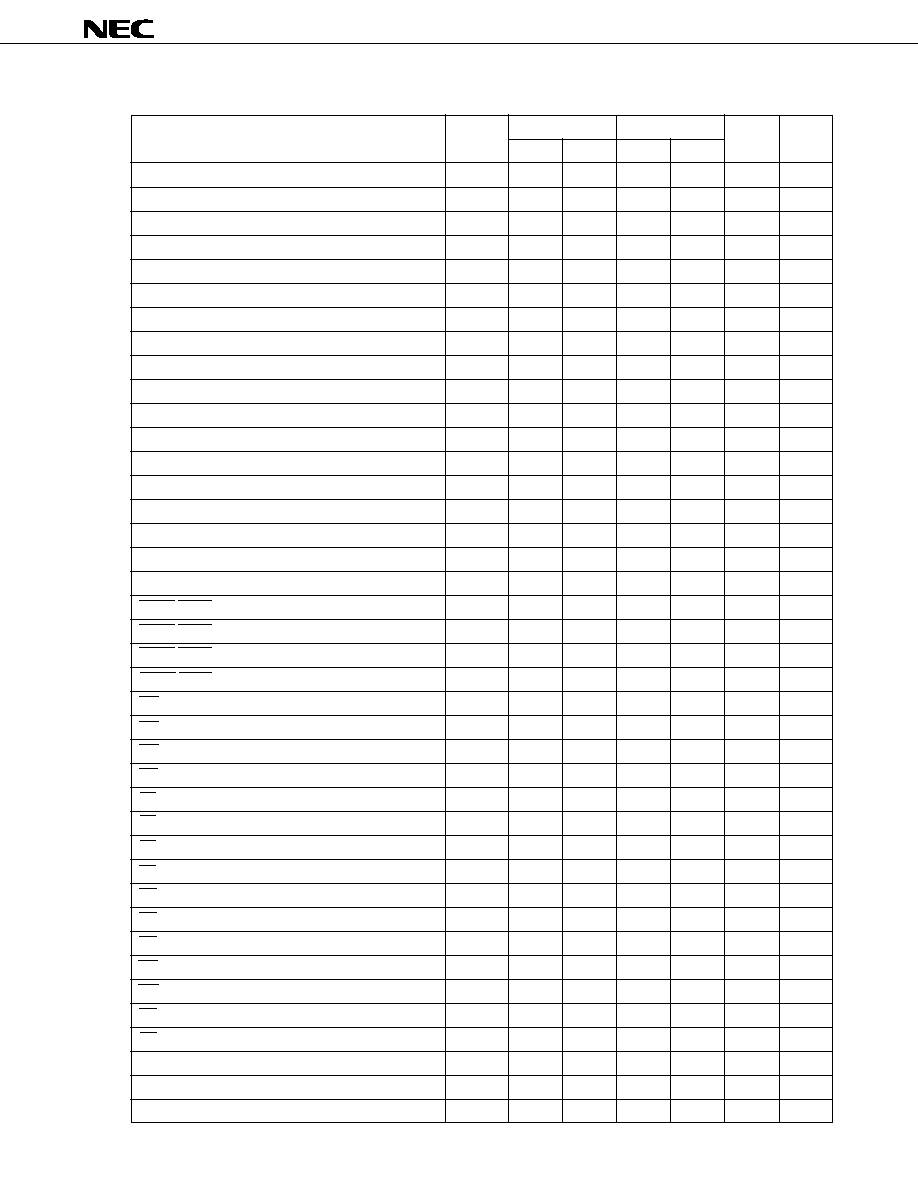
AC Characteristics (Recommended Operating Conditions unless otherwise noted)
Notes 1, 2, 3
Parameter
Symbol
µ
PD485506-25
µ
PD485506-35
Unit
Notes
MIN.
MAX.
MIN.
MAX.
Write clock cycle time
t
WCK
25
35
ns
Write clock pulse width
t
WCW
11
12
ns
Write clock precharge time
t
WCP
11
12
ns
Read clock cycle time
t
RCK
25
35
ns
Read clock pulse width
t
RCW
11
12
ns
Read clock precharge time
t
RCP
11
12
ns
Access time
t
AC
18
25
ns
Write data-read delay time
t
WAR
470
470
ns
Output hold time
t
OH
5
5
ns
Output low-impedance time
t
LZ
5
18
5
25
ns
4
Output high-impedance time
t
HZ
5
18
5
25
ns
4
Input data setup time
t
DS
7
10
ns
Input data hold time
t
DH
3
3
ns
MD Set setup time
t
MS
20
20
ns
MD Set hold time
t
MH
10
10
ns
MD Set time
t
MD
0
0
ns
5
Output low-impedance time (Mode change)
t
LZM
5
18
5
25
ns
4
Output high-impedance time (Mode change)
t
HZM
5
18
5
25
ns
4
RSTW/RSTR Setup time
t
RS
7
10
ns
6
RSTW/RSTR Hold time
t
RH
3
3
ns
6
RSTW/RSTR Deselected time (1)
t
RN1
3
3
ns
7
RSTW/RSTR Deselected time (2)
t
RN2
7
10
ns
7
WE Setup time
t
WES
7
10
ns
8
WE Hold time
t
WEH
3
3
ns
8
WE Deselected time (1)
t
WEN1
3
3
ns
9
WE Deselected time (2)
t
WEN2
7
10
ns
9
RE Setup time
t
RES
7
10
ns
10
RE Hold time
t
REH
3
3
ns
10
RE Deselected time (1)
t
REN1
3
3
ns
11
RE Deselected time (2)
t
REN2
7
10
ns
11
OE Setup time
t
OES
7
10
ns
10
OE Hold time
t
OEH
3
3
ns
10
OE Deselected time (1)
t
OEN1
3
3
ns
11
OE Deselected time (2)
t
OEN2
7
10
ns
11
WE Disable time
t
WEW
0
0
ms
RE Disable time
t
REW
0
0
ms
OE Disable time
t
OEW
0
0
ms
Write reset time
t
RSTW
0
0
ms
Read reset time
t
RSTR
0
0
ms
Transition time
t
T
3
35
3
35
ns
µ
PD485506
10
Data Sheet M10060EJ7V0DS00
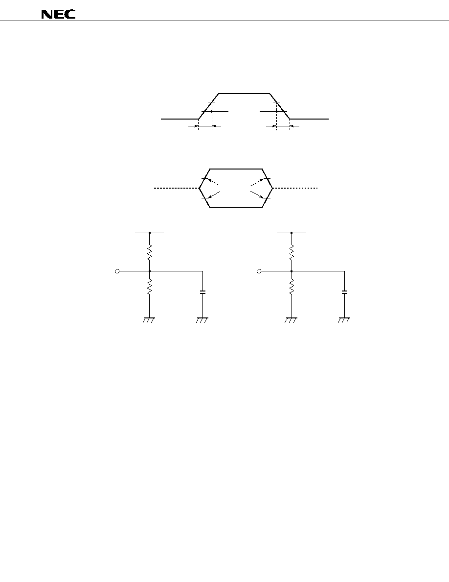
Notes 1. AC measurements assume t
T
= 5 ns.
2. AC Characteristics test condition
Input Timing Specification
3.0 V
0 V
t
T
= 5 ns
t
T
= 5 ns
1.5 V
Test points
Output Timing Specification
Output Loads for Timing
1.1 k
D
OUT
V
CC
5 pF
(t
LZ
,t
HZ
)
1.8 k
1.1 k
D
OUT
V
CC
30 pF
(t
AC
,t
OH
)
1.8 k
3. Input timing reference levels = 1.5 V. Output timing reference levels; V
OH
= 2.0 V, V
OL
= 0.8 V.
4. t
LZ
, t
HZ
, t
LZM
and t
HZM
are measured at
±
200 mV from the steady state voltage. Under any conditions,
t
LZ
t
HZ
and t
LZM
t
HZM
.
5. Mode set signal (MD) must be input synchronously with write reset signal (t
RSTW
period) or read reset signal
(t
RSTR
period). Under this condition, t
RSTW
= t
MD
(t
RSTR
= t
MD
).
6. If either t
RS
or t
RH
is less than the specified value, reset operations are not guaranteed.
7. If either t
RN1
or t
RN2
is less than the specified value, reset operations may extend to cycles preceding or
following the period of reset operations.
8. If either t
WES
or t
WEH
is less than the specified value, write disable operations are not guaranteed.
9. If either t
WEN1
or t
WEN2
is less than the specified value, internal write disable operations may extend to cycles
preceding or following the period of write disable operations.
10. If either t
RES
or t
REH
, t
OES
or t
OEH
is less than the specified value, read disable operations are not guaranteed.
11. If either t
REN1
or t
REN2
, t
OEN1
or t
OEN2
is less than the specified value, internal read disable operations may
extend to cycles preceding or following the period of read disable operations.
0.8 V
2.0 V
High impedance
High impedance
Test points
µ
PD485506
11
Data Sheet M10060EJ7V0DS00
Write Cycle Timing Chart
Remark
RSTW = "H" level
Read Cycle Timing Chart (RE Control)
Cycle n
Cycle n+1
Cycle n+2
Disable Cycle
Cycle n+3
t
WCW
t
WEN1
t
WES
t
WEW
t
WEH
t
WEN2
t
WCP
t
WCK
t
DS
t
DH
(n+1)
(n)
t
DS
t
DH
(n+2)
(n+3)
WCK (Input)
WE (Input)
D
IN
(Input)
Remark
OE = "L" level, RSTR = "H" level
Read Cycle Timing Chart (OE Control)
Cycle n
Cycle n+1
Cycle n+2
Disable Cycle
Cycle n+3
t
RCW
t
REN1
t
RES
t
REW
t
REH
t
REN2
t
RCP
t
RCK
(n+1)
t
OH
(n+2)
(n+3)
t
OH
t
AC
RCK (Input)
RE (Input)
D
OUT
(Output)
(n)
t
OH
t
AC
Remark
RE = "L" level, RSTR = "H" level
Cycle n
Cycle n+1
Cycle n+2
Disable Cycle
Cycle m
t
RCW
t
OEN1
t
OES
t
OEW
t
OEH
t
OEN2
t
RCP
t
RCK
(n+1)
(n)
t
AC
t
OH
(n+2)
(m)
t
HZ
t
LZ
t
AC
t
LZ
High impedance
RCK (Input)
OE (Input)
D
OUT
(Output)
High impedance
µ
PD485506
12
Data Sheet M10060EJ7V0DS00
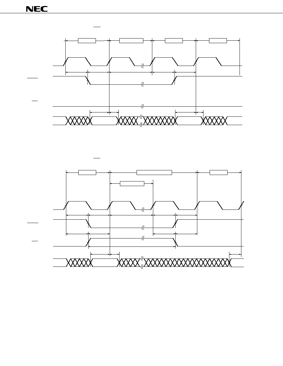
Write Reset Cycle Timing Chart (WE = Active)
Note
In write reset cycle, reset operation is executed even without a reset cycle (t
RSTW
).
WCK can be input any number of times in a reset cycle.
Write Reset Cycle Timing Chart (WE = Inactive)
Note
In write reset cycle, reset operation is executed even without a reset cycle (t
RSTW
).
WCK can be input any number of times in a reset cycle.
Cycle n
Reset Cycle
Cycle 0
Cycle 1
t
RN2
t
RH
t
RSTW
Note
t
RS
t
RN1
"L" Level
t
DS
t
DH
t
DS
t
DH
(1)
(0)
(n)
(n≠1)
D
IN
(Input)
WE (Input)
RSTW (Input)
WCK (Input)
Cycle n
Disable Cycle
Cycle 0
t
RN2
t
RH
t
RSTW
Note
t
RS
t
RN1
t
DS
t
DH
t
DS
(0)
(n)
(n≠1)
D
IN
(Input)
WE (Input)
RSTW (Input)
WCK (Input)
Reset Cycle
t
WEW
t
WEN1
t
WES
t
WEH
t
WEN2
µ
PD485506
13
Data Sheet M10060EJ7V0DS00
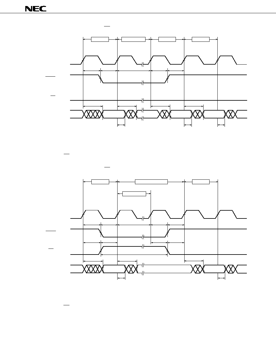
Read Reset Cycle Timing Chart (RE = Active)
Note
In read reset cycle, reset operation is executed even without a reset cycle (t
RSTR
).
RCK can be input any number of times in a reset cycle.
Remark
OE = "L" level
Read Reset Cycle Timing Chart (RE = Inactive)
Cycle n
Disable Cycle
Cycle 0
t
RN2
t
RH
t
RSTR
Note
t
RS
t
RN1
t
AC
t
OH
t
AC
t
OH
(0)
(n)
(n≠1)
D
OUT
(Output)
RE (Input)
RSTR (Input)
RCK (Input)
t
REH
t
AC
Reset Cycle
t
REN1
t
RES
t
REW
t
REN2
Indefinite Data
Note
In read reset cycle, reset operation is executed even without a reset cycle (t
RSTR
).
RCK can be input any number of times in a reset cycle.
Remark
OE = "L" level
Cycle n
Reset Cycle
Cycle 0
Cycle 1
t
RN2
t
RH
t
RSTR
Note
t
RS
t
RN1
"L" Level
t
AC
t
OH
t
AC
t
OH
(1)
(0)
(n)
(n ≠ 1)
D
OUT
(Output)
RE (Input)
RSTR (Input)
RCK (Input)
t
OH
t
AC
t
AC
(0)
µ
PD485506
14
Data Sheet M10060EJ7V0DS00
4. Application
4.1 1 H Delay Line
µ
PD485506 easily allows a 1 H (5,048 bits/10,096 bits) delay line (see Figure 4.1).
Figure 4.1 1 H Delay Line Circuit
WCK
D
IN
WE
RSTW
RCK
D
OUT
RE
RSTR
40 MHz Clock
Reset
Data Output
Data Input
8/16
8/16
Figure 4.2 1 H Delay Line Timing Chart
Note
5,048 cycles by 16 bits/10,096 cycles by 8 bits
Remark
RE, WE, OE = "L" level
t
WCK
t
RCK
Cycle 0
Cycle 1
Cycle 2
1 H
(5,048/10,096 Cycles)
Cycle 5,047
Note
2 H
(5,048/10,096 Cycles)
t
WCW
t
RCW
t
WCP
t
RCP
t
RS
t
RH
t
DH
t
DS
(0)
(1)
(2)
(5,046)
(5,047)
(0')
(1')
t
DS
t
DH
t
OH
t
AC
(0)
(1)
(2')
(3')
(2)
(3)
WCK/RCK
(Input)
RSTW/
RSTR
(Input)
D
IN
(Input)
D
OUT
(Output)
Write
Read
Cycle 0'
Cycle 1'
Cycle 2'
Cycle 3'
Cycle 0
Cycle 1
Cycle 2
Cycle 3
(10,095)
(10,094)
(10,095)

µ
PD485506
15
Data Sheet M10060EJ7V0DS00
4.2 n Bit Delay
It is possible to make delay read from the write data with the
µ
PD485506.
(1) Perform a reset operation in the cycle proportionate to the delay length (see Figure 4.3).
(2) Shift the input timing of write reset (RSTW) and read reset (RSTR) depending on the delay length (see Figure
4.4).
(3) Shift the address by disabling RE for the period proportionate to the delay length (see Figure 4.5).
n bit: Delay bits from write cycle to read cycle correspond to a same address cell.
Restrictions
Delay bits n can be set from minimum bits to maximum bits depending on the operating cycle time.
Refer to 2. Operation Mode Operation-related Restriction.
Cycle Time
MIN.
MAX.
MD = "L" Level
MD = "H" Level
25 ns
21 bits
5,048 bits
10,096 bits
35 ns
15 bits
5,048 bits
10,096 bits
Figure 4.3 n-Bit Delay Line Timing Chart (1)
Remark
RE, WE, OE = "L" level
t
WCK
t
RCK
Cycle 0
Cycle 1
Cycle 2
1 H
(n Cycles)
Cycle (n≠1)
2 H
(n Cycles)
t
WCW
t
RCW
t
WCP
t
RCP
t
RS
t
RH
t
DH
t
DS
(0)
(1)
(n≠2)
(n≠1)
(0')
(1')
t
DS
t
DH
t
OH
t
AC
(0)
(1)
(2')
(3')
(2)
(3)
WCK/RCK
(Input)
RSTW/
RSTR
(Input)
D
IN
(Input)
D
OUT
(Output)
(2)
Write
Read
Cycle 0'
Cycle 1'
Cycle 2'
Cycle 3'
Cycle 0
Cycle 1
Cycle 2
Cycle 3
t
WAR
t
RH
t
RS

µ
PD485506
16
Data Sheet M10060EJ7V0DS00
Figure 4.4 n-Bit Delay Line Timing Chart (2)
Remark
RE, WE, OE = "L" level
Figure 4.5 n-Bit Delay Line Timing Chart (3)
Remark
WE, OE = "L" level
t
WCK
t
RCK
Cycle 0
Cycle 1
Cycle 2
Cycle n≠1
t
WCW
t
RCW
t
WCP
t
RCP
t
RS
t
RH
t
DH
t
DS
(0)
(1)
(2)
(n≠2)
(n≠1)
(n)
(n+1)
t
DS
t
DH
t
OH
t
AC
(0)
(1)
(n+2)
(n+3)
(2)
(3)
WCK/RCK
(Input)
RSTW/
RSTR
(Input)
D
IN
(Input)
D
OUT
(Output)
t
REH
n Cycles
RE
(Input)
t
REN2
t
WAR
Cycle n
Cycle n+1
Cycle n+2
Cycle n+3
Cycle 0
Cycle 1
Cycle 2
Cycle 3
Write
Read
High impedance
t
WCK
t
RCK
Cycle 0
Cycle 1
Cycle 2
Cycle n≠1
t
WCW
t
RCW
t
WCP
t
RCP
t
RS
t
RH
t
DH
t
DS
(0)
(1)
(2)
(n≠2)
(n≠1)
(n)
(n+1)
t
DS
t
DH
t
OH
t
AC
(0)
(1)
(n+2)
(n+3)
(2)
(3)
WCK/RCK
(Input)
RSTW
(Input)
D
IN
(Input)
D
OUT
(Output)
t
RH
t
RS
n Cycles
RSTR
(Input)
Write
Read
Cycle n
Cycle n+1
Cycle n+2
Cycle n+3
Cycle 0
Cycle 1
Cycle 2
Cycle 3
t
WAR
µ
PD485506
17
Data Sheet M10060EJ7V0DS00
Figure 4.6 Mode Set Cycle Timing Chart (Write) (1)
Remark
WE = "L" level
Figure 4.7 Mode Set Cycle Timing Chart (Write) (2)
Cycle n
Reset Cycle
Cycle 0
Cycle 1
t
MH
t
MD
t
MS
t
RS
t
RN1
t
RSTW
t
RH
t
RN2
t
DS
t
DH
(0)
(1)
(n)
(n)
t
DS
t
DH
t
DS
t
DH
t
DS
t
DH
(n≠1)
(n≠1)
WCK
(Input)
RSTW
(Input)
MD
(Input)
D
IN0
- D
IN7
(Input)
D
IN8
- D
IN15
(Input)
t
DS
t
DH
Remark
WE = "L" level
Cycle n
Reset Cycle
Cycle 0
Cycle 1
t
MH
t
MD
t
MS
t
RS
t
RN1
t
RSTW
t
RH
t
RN2
t
DS
t
DH
(0)
(1)
(n)
t
DS
t
DH
(n≠1)
WCK
(Input)
RSTW
(Input)
MD
(Input)
D
IN0
- D
IN7
(Input)
D
IN8
- D
IN15
(Input)
t
DS
t
DH
t
DS
t
DH
(0)
(1)
µ
PD485506
18
Data Sheet M10060EJ7V0DS00
Figure 4.8 Mode Set Cycle Timing Chart (Read) (1)
Remark
RE, OE = "L" level
Figure 4.9 Mode Set Cycle Timing Chart (Read) (2)
Cycle n
Reset Cycle
Cycle 0
Cycle 1
t
MS
t
MD
t
MH
t
RN1
t
RS
t
RSTR
t
RH
t
RN2
t
AC
t
OH
t
AC
t
OH
t
AC
t
OH
t
AC
t
OH
t
OH
(n≠1)
(n)
(0)
(0)
(1)
t
AC
t
OH
t
HZM
t
OH
(n≠1)
(n)
High impedance
MD
(Input)
RSTR
(Input)
RCK
(Input)
D
OUT0
- D
OUT7
(Output)
D
OUT8
- D
OUT15
(Output)
Remark
RE, OE = "L" level
Cycle n
Reset Cycle
Cycle 0
Cycle 1
t
MS
t
MD
t
MH
t
RN1
t
RS
t
RSTR
t
RH
t
RN2
t
AC
t
OH
t
AC
t
OH
t
AC
t
OH
t
OH
(n≠1)
(n)
(0)
(0)
(1)
High impedance
MD
(Input)
RSTR
(Input)
RCK
(Input)
D
OUT0
- D
OUT7
(Output)
D
OUT8
- D
OUT15
(Output)
t
AC
t
OH
(0)
(1)
t
OH
(0)
t
AC
t
LZM
t
AC
t
OH
t
AC
t
OH
µ
PD485506
19
Data Sheet M10060EJ7V0DS00
4.3 Double-speed Conversion
Figure 4.10 shows an example timing chart of double-speed and twice reading operation (f
R
= 2f
W
, 5,048 by
2 cycles or 10,096 by 2 cycles
Note
) for a write operation (f
W
= 5,048 cycles or 10,096 cycles).
Caution
The read operation collide with the write operation on the same line, last n bits output data
(5,048 ≠n to 5,048/10,096 ≠n to 10,096) in the first read operation will be undefined (see Figure 4.10
Double-speed Conversion Timing Chart).
Undefined bits mentioned above depend on the cycle time.
Read Cycle Time
Undefined Bits
25 ns
21 bits
35 ns
15 bits
Note
5,048 cycles by 16 bits/10,096 cycles by 8 bits
µ
PD485506
20
Data Sheet M10060EJ7V0DS00
Figure 4.10 Double-speed Conversion Timing Chart
Note
5,048 cycles by 16 bits/10,096 cycles by 8 bits
Remark
RE, WE = "L" level
0
1
2
0'
1'
2'
5,047
(10,095)
5,046
Note
(10,094)
0"
5,047'
(10,095')
5,046'
(10,094')
1H
(5,048/10,096 Cycles
Note
)
2H
(5,048/10,096 Cycles)
WCK
(Input)
D
IN
(Input)
RSTW
(Input)
0
1
2
5,046
5,047
(10,094) (10,095)
Note
0'
1'
2'
5,047'
(10,094') (10,095')
0"
5,046'
1H
(5,048/10,096 Cycles
Note
)
First read cycle
1H
(5,048/10,096 Cycles)
Second read cycle
RCK
(Input)
D
OUT
(Output)
RSTR
(Input)
2H
(5,048/10,096 Cycles)
First read cycle
1
2
5,047
0
1
2
5,046
Note
(10,095)
(10,094)
5,047
0'
1'
2'
(10,095)
(10,094)
5,046
5,047'
0'
1'
(10,095')
(10,094')
5,046'
n bits output data will be undefined.
n bits output data will be undefined.
t
AC
0
µ
PD485506
21
Data Sheet M10060EJ7V0DS00
5. Package Drawing
44-PIN PLASTIC TSOP(
II
) (10.16 mm (400))
NOTE
Each lead centerline is located within 0.13 mm of
its true position (T.P.) at maximum material condition.
ITEM
MILLIMETERS
A
C
18.63 MAX.
0.93 MAX.
0.1
±
0.05
E
F
B
0.8 (T.P.)
1.2 MAX.
G
0.97
H
11.76
±
0.2
I
10.16
±
0.1
J
0.8
±
0.2
D
0.32
+
0.08
-
0.07
M
0.13
N
0.10
L
0.5
±
0.1
K
0.145
+
0.025
-
0.015
P
3
∞+
7
∞
-
3
∞
S44G5-80-7JF5-1
M
44
23
1
22
S
N
S
K
L
F
E
P
J
G
D
M
C
A
B
H
I
detail of lead end
µ
PD485506
22
Data Sheet M10060EJ7V0DS00
6. Recommended Soldering Conditions
Please consult with our sales offices for soldering conditions of the
µ
PD485506.
Type of Surface Mount Device
µ
PD485506G5-7JF: 44-pin plastic TSOP (
II
) (10.16 mm (400))
7. Example of Stamping
Letter E in the fifth character position in a lot number signifies version E, letter K, version K, letter P, version
P, letter X, version X, and letter L, version L.
JAPAN
D485506
Lot number
µ
PD485506
23
Data Sheet M10060EJ7V0DS00
NOTES FOR CMOS DEVICES
1
PRECAUTION AGAINST ESD FOR SEMICONDUCTORS
Note:
Strong electric field, when exposed to a MOS device, can cause destruction of the gate oxide and
ultimately degrade the device operation. Steps must be taken to stop generation of static electricity
as much as possible, and quickly dissipate it once, when it has occurred. Environmental control
must be adequate. When it is dry, humidifier should be used. It is recommended to avoid using
insulators that easily build static electricity. Semiconductor devices must be stored and transported
in an anti-static container, static shielding bag or conductive material. All test and measurement
tools including work bench and floor should be grounded. The operator should be grounded using
wrist strap. Semiconductor devices must not be touched with bare hands. Similar precautions
need to be taken for PW boards with semiconductor devices on it.
2
HANDLING OF UNUSED INPUT PINS FOR CMOS
Note:
No connection for CMOS device inputs can be cause of malfunction. If no connection is provided
to the input pins, it is possible that an internal input level may be generated due to noise, etc., hence
causing malfunction. CMOS devices behave differently than Bipolar or NMOS devices. Input
levels of CMOS devices must be fixed high or low by using a pull-up or pull-down circuitry. Each
unused pin should be connected to V
DD
or GND with a resistor, if it is considered to have a
possibility of being an output pin. All handling related to the unused pins must be judged device
by device and related specifications governing the devices.
3
STATUS BEFORE INITIALIZATION OF MOS DEVICES
Note:
Power-on does not necessarily define initial status of MOS device. Production process of MOS
does not define the initial operation status of the device. Immediately after the power source is
turned ON, the devices with reset function have not yet been initialized. Hence, power-on does
not guarantee out-pin levels, I/O settings or contents of registers. Device is not initialized until
the reset signal is received. Reset operation must be executed immediately after power-on for
devices having reset function.

µ
PD485506
[MEMO]
M8E 00. 4
The information in this document is current as of December, 2000. The information is subject to
change without notice. For actual design-in, refer to the latest publications of NEC's data sheets or
data books, etc., for the most up-to-date specifications of NEC semiconductor products. Not all
products and/or types are available in every country. Please check with an NEC sales representative
for availability and additional information.
No part of this document may be copied or reproduced in any form or by any means without prior
written consent of NEC. NEC assumes no responsibility for any errors that may appear in this document.
NEC does not assume any liability for infringement of patents, copyrights or other intellectual property rights of
third parties by or arising from the use of NEC semiconductor products listed in this document or any other
liability arising from the use of such products. No license, express, implied or otherwise, is granted under any
patents, copyrights or other intellectual property rights of NEC or others.
Descriptions of circuits, software and other related information in this document are provided for illustrative
purposes in semiconductor product operation and application examples. The incorporation of these
circuits, software and information in the design of customer's equipment shall be done under the full
responsibility of customer. NEC assumes no responsibility for any losses incurred by customers or third
parties arising from the use of these circuits, software and information.
While NEC endeavours to enhance the quality, reliability and safety of NEC semiconductor products, customers
agree and acknowledge that the possibility of defects thereof cannot be eliminated entirely. To minimize
risks of damage to property or injury (including death) to persons arising from defects in NEC
semiconductor products, customers must incorporate sufficient safety measures in their design, such as
redundancy, fire-containment, and anti-failure features.
NEC semiconductor products are classified into the following three quality grades:
"Standard", "Special" and "Specific". The "Specific" quality grade applies only to semiconductor products
developed based on a customer-designated "quality assurance program" for a specific application. The
recommended applications of a semiconductor product depend on its quality grade, as indicated below.
Customers must check the quality grade of each semiconductor product before using it in a particular
application.
"Standard": Computers, office equipment, communications equipment, test and measurement equipment, audio
and visual equipment, home electronic appliances, machine tools, personal electronic equipment
and industrial robots
"Special":
Transportation equipment (automobiles, trains, ships, etc.), traffic control systems, anti-disaster
systems, anti-crime systems, safety equipment and medical equipment (not specifically designed
for life support)
"Specific": Aircraft, aerospace equipment, submersible repeaters, nuclear reactor control systems, life
support systems and medical equipment for life support, etc.
The quality grade of NEC semiconductor products is "Standard" unless otherwise expressly specified in NEC's
data sheets or data books, etc. If customers wish to use NEC semiconductor products in applications not
intended by NEC, they must contact an NEC sales representative in advance to determine NEC's willingness
to support a given application.
(Note)
(1) "NEC" as used in this statement means NEC Corporation and also includes its majority-owned subsidiaries.
(2) "NEC semiconductor products" means any semiconductor product developed or manufactured by or for
NEC (as defined above).
∑
∑
∑
∑
∑
∑