 | –≠–ª–µ–∫—Ç—Ä–æ–Ω–Ω—ã–π –∫–æ–º–ø–æ–Ω–µ–Ω—Ç: UPD488448 | –°–∫–∞—á–∞—Ç—å:  PDF PDF  ZIP ZIP |
Document Outline
- COVER
- Features
- Ordering Information
- Pin Configurations
- Block Diagram
- 1. General Description
- 2. Packet Format
- 3. Field Encoding Summary
- 4. DQ Packet Timing
- 5. COLM Packet to D Packet Mapping
- 6. ROW-to-ROW Packet Interaction
- 7. ROW-to-COL Packet Interaction
- 8. COL-to-COL Packet Interaction
- 9. COL-to-ROW Packet Interaction
- 10. ROW-to-ROW Examples
- 11. Row and Column Cycle Description
- 12. Precharge Mechanisms
- 13. Read Transaction - Example
- 14. Write Transaction - Example
- 15. Write/Retire - Examples
- 16. Interleaved Write - Example
- 17. Interleaved Read - Example
- 18. Interleaved RRWW - Example
- 19. Control Register Transactions
- 20. Control Register Packets
- 21. Initialization
- 22. Control Register Summary
- 23. Power State Management
- 24. Refresh
- 25. Current and Temperature Control
- 26. Electrical Conditions
- 27. Timing Conditions
- 28. Electrical Characteristics
- 29. Timing Characteristics
- 30. RSL Clocking
- 31. RSL - Receive Timing
- 32. RSL - Transmit Timing
- 33. CMOS - Receive Timing
- 34. CMOS - Transmit Timing
- 35. RSL - Domain Crossing Window
- 36. Timing Parameters
- 37. Absolute Maximum Ratings
- 38. IDD - Supply Current Profile
- 39. Capacitance and Inductance
- 40. Glossary of Terms
- 41. Package Drawings
- 42. Recommended Soldering Conditions
The information in this document is subject to change without notice. Before using this document, please
confirm that this is the latest version.
Not all devices/types available in every country. Please check with local NEC representative for
availability and additional information.
©
2000
MOS INTEGRATED CIRCUIT
µ
PD488448 for Rev. P
128 M-bit Direct RambusTM DRAM
DATA SHEET
Document No. M14837EJ3V0DS00 (3rd edition)
Date Published August 2000 NS CP (K)
Printed in Japan
The mark
∑
∑
∑
∑
shows major revised points.
Description
The Direct Rambus DRAM (Direct RDRAM
TM
) is a general purpose high-performance memory device suitable for
use in a broad range of applications including computer memory, graphics, video, and any other application where
high bandwidth and low latency are required.
The
µ
PD488448 is 128M-bit Direct Rambus DRAM (RDRAM
Æ
), organized as 8M words by 16 bits.
The use of Rambus Signaling Level (RSL) technology permits 600 MHz to 800 MHz transfer rates while using
conventional system and board design technologies. Direct RDRAM devices are capable of sustained data transfers
at 1.25 ns per two bytes (10 ns per sixteen bytes).
The architecture of the Direct RDRAMs allows the highest sustained bandwidth for multiple, simultaneous randomly
addressed memory transactions. The separate control and data buses with independent row and column control
yield over 95% bus efficiency. The Direct RDRAM's thirty-two banks support up to four simultaneous transactions.
System oriented features for mobile, graphics and large memory systems include power management, byte
masking.
The
µ
PD488448 is offered in a CSP horizontal package suitable for desktop as well as low-profile add-in card and
mobile applications. Direct RDRAMs operate from a 2.5
volt supply.
Features
∑
Highest sustained bandwidth per DRAM device
- 1.6 GB/s sustained data transfer rate
- Separate control and data buses for maximized efficiency
- Separate row and column control buses for easy scheduling and highest performance
- 32 banks: four transactions can take place simultaneously at full bandwidth data rates
∑
Low latency features
- Write buffer to reduce read latency
- 3 precharge mechanisms for controller flexibility
- Interleaved transactions
∑
Advanced power management:
- Multiple low power states allows flexibility in power consumption versus time to transition to active state
- Power-down self-refresh
∑
Overdrive current mode
∑
Organization: 1 Kbyte pages and 32 banks, x 16
∑
Uses Rambus Signaling Level (RSL) for up to 800 MHz operation
∑
Package : 62-pin TAPE FBGA (
µ
BGA
Æ
) and 62-pin PLASTIC FBGA (D
2
BGA
TM
(Die Dimension Ball Grid Array) )

Data Sheet M14837EJ3V0DS00
2
µ
µ
µ
µ
PD488448 for Rev. P
Ordering Information
Part number
Organization
Note
Clock frequency
(MAX.)
RAS access time
(ns)
Package
µ
PD488448FF-C60-53-DQ1
256K x 16 x 32s
600 MHz
53
62-pin TAPE FBGA (
µ
BGA)
µ
PD488448FF-C71-45-DQ1
711 MHz
45
(Normal type)
µ
PD488448FF-C80-45-DQ1
800 MHz
45
µ
PD488448FF-C60-53-DQ2
600 MHz
53
62-pin TAPE FBGA (
µ
BGA)
µ
PD488448FF-C71-45-DQ2
711 MHz
45
(Mirrored type)
µ
PD488448FF-C80-45-DQ2
800 MHz
45
µ
PD488448FB-C60-53-DQ1
600 MHz
53
62-pin PLASTIC FBGA (D
2
BGA)
µ
PD488448FB-C71-45-DQ1
711 MHz
45
(Normal type)
µ
PD488448FB-C80-45-DQ1
800 MHz
45
µ
PD488448FB-C60-53-DQ2
600 MHz
53
62-pin PLASTIC FBGA (D
2
BGA)
µ
PD488448FB-C71-45-DQ2
711 MHz
45
(Mirrored type)
µ
PD488448FB-C80-45-DQ2
800 MHz
45
Note The "32s" designation indicates that this RDRAM core is composed of 32 banks which use a "split" bank
architecture.
Data Sheet M14837EJ3V0DS00
3
µ
µ
µ
µ
PD488448 for Rev. P
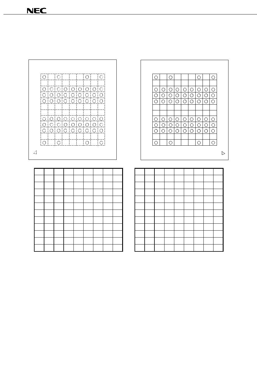
Pin Configurations
62-pin TAPE FBGA (
µ
µ
µ
µ
BGA) (Normal type)
62-pin PLASTIC FBGA (D
2
BGA) (Normal type)
D
F
E
B C
A
Ball View
Top View
H J
G
1
2
3
4
5
6
D
F E
B
C
A
7
8
9
10
11
12
H
J
G
1
2
3
4
5
6
7
8
9
10
11
12
12
GND
V
DD
V
DD
GND
GND
V
DD
V
DD
GND
12
11
11
10
DQA7 DQA4 CFM CFMN RQ5
RQ3 DQB0 DQB4 DQB7
DQB7 DQB4 DQB0 RQ3
RQ5 CFMN CFM DQA4 DQA7
10
9
GND
V
DD
GND GNDa
V
DD
GND
V
DD
V
DD
GND
GND
V
DD
V
DD
GND
V
DD
GNDa GND
V
DD
GND
9
8
CMD DQA5 DQA2 V
DD
a
RQ6
RQ2 DQB1 DQB5 SIO1
SIO1 DQB5 DQB1 RQ2
RQ6
V
DD
a DQA2 DQA5 CMD
8
7
7
6
6
5
SCK DQA6 DQA1 V
REF
RQ7
RQ1 DQB2 DQB6 SIO0
SIO0 DQB6 DQB2 RQ1
RQ7
V
REF
DQA1 DQA6 SCK
5
4
V
CMOS
GND
V
DD
GND
GND
V
DD
GND
GND V
CMOS
V
CMOS
GND
GND
V
DD
GND
GND
V
DD
GND V
CMOS
4
3
NC
Note
DQA3 DQA0 CTMN CTM
RQ4
RQ0 DQB3 NC
Note
NC
Note
DQB3 RQ0
RQ4
CTM CTMN DQA0 DQA3 NC
Note
3
2
2
1
GND
V
DD
V
DD
GND
GND
V
DD
V
DD
GND
1
A
B
C
D
E
F
G
H
J
J
H
G
F
E
D
C
B
A
Note Some signals can be applied because this pin is not connected to the inside of the chip.

Data Sheet M14837EJ3V0DS00
4
µ
µ
µ
µ
PD488448 for Rev. P
62-pin TAPE FBGA (
µ
µ
µ
µ
BGA) (Mirrored type)
62-pin PLASTIC FBGA (D
2
BGA) (Mirrored type)
D
F
E
B C
A
Ball View
Top View
H J
G
1
2
3
4
5
6
D
F E
B
C
A
7
8
9
10
11
12
H
J
G
1
2
3
4
5
6
7
8
9
10
11
12
12
GND
V
DD
V
DD
GND
GND
V
DD
V
DD
GND
12
11
11
10
NC
Note
DQA3 DQA0 CTMN CTM
RQ4
RQ0 DQB3 NC
Note
NC
Note
DQB3 RQ0
RQ4
CTM CTMN DQA0 DQA3 NC
Note
10
9
V
CMOS
GND
V
DD
GND
GND
V
DD
GND
GND V
CMOS
V
CMOS
GND
GND
V
DD
GND
GND
V
DD
GND V
CMOS
9
8
SCK DQA6 DQA1 V
REF
RQ7
RQ1 DQB2 DQB6 SIO0
SIO0 DQB6 DQB2 RQ1
RQ7
V
REF
DQA1 DQA6 SCK
8
7
7
6
6
5
CMD DQA5 DQA2 V
DD
a
RQ6
RQ2 DQB1 DQB5 SIO1
SIO1 DQB5 DQB1 RQ2
RQ6
V
DD
a DQA2 DQA5 CMD
5
4
GND
V
DD
GND GNDa
V
DD
GND
V
DD
V
DD
GND
GND
V
DD
V
DD
GND
V
DD
GNDa GND
V
DD
GND
4
3
DQA7 DQA4 CFM CFMN RQ5
RQ3 DQB0 DQB4 DQB7
DQB7 DQB4 DQB0 RQ3
RQ5 CFMN CFM DQA4 DQA7
3
2
2
1
GND
V
DD
V
DD
GND
GND
V
DD
V
DD
GND
1
A
B
C
D
E
F
G
H
J
J
H
G
F
E
D
C
B
A
Note Some signals can be applied because this pin is not connected to the inside of the chip.
Data Sheet M14837EJ3V0DS00
5
µ
µ
µ
µ
PD488448 for Rev. P
Pin Description
Signal
Input / Output
Type
#pins
Description
SIO0, SIO1
Input / Output CMOS
Note1
2
Serial input/output. Pins for reading from and writing to the control registers using
a serial access protocol. Also used for power management.
CMD
Input
CMOS
Note1
1
Command input. Pins used in conjunction with SIO0 and SIO1 for reading from
and writing to the control registers. Also used for power management.
SCK
Input
CMOS
Note1
1
Serial clock input. Clock source used for reading from and writing to the control
registers.
V
DD
10
Supply voltage for the RDRAM core and interface logic.
V
DDa
1
Supply voltage for the RDRAM analog circuitry.
V
CMOS
2
Supply voltage for CMOS input/output pins.
GND
13
Ground reference for RDRAM core and interface.
GND
a
1
Ground reference for RDRAM analog circuitry.
DQA7..DQA0
Input / Output
RSL
Note2
8
Data byte A. Eight pins which carry a byte of read or write data between the
Channel and the RDRAM.
CFM
Input
RSL
Note2
1
Clock from master. Interface clock used for receiving RSL signals from the
Channel. Positive polarity.
CFMN
Input
RSL
Note2
1
Clock from master. Interface clock used for receiving RSL signals from the
Channel. Negative polarity.
V
REF
1
Logic threshold reference voltage for RSL signals.
CTMN
Input
RSL
Note2
1
Clock to master. Interface clock used for transmitting RSL signals to the Channel.
Negative polarity.
CTM
Input
RSL
Note2
1
Clock to master. Interface clock used for transmitting RSL signals to the Channel.
Positive polarity.
RQ7..RQ5 or
ROW2..ROW0
Input
RSL
Note2
3
Row access control. Three pins containing control and address information for
row accesses.
RQ4..RQ0 or
COL4..COL0
Input
RSL
Note2
5
Column access control. Five pins containing control and address information for
column accesses.
DQB7..DQB0
Input / Output
RSL
Note2
8
Data byte B. Eight pins which carry a byte of read or write data between the
Channel and the RDRAM.
NC
2
These pins aren't connected to inside of the chip.
Total pin count per package
62
Notes 1. All CMOS signals are high-true ; a high voltage is a logic one and a low voltage is logic zero.
2. All RSL signals are low-true ; a low voltage is a logic one and a high voltage is logic zero.

Data Sheet M14837EJ3V0DS00
6
µ
µ
µ
µ
PD488448 for Rev. P
Block Diagram
11
5
5
9
ROP
AV
DR
BR
R
C
MB
MA
COP
S
DC
BC
XOP
M
DX
BX
Packet Decode
Control Registers
DEVID
REFR
PRER
PREX
PREC
RD, WR
ACT
DM
ROWR
ROWA
Packet Decode
COLM
COLC
COLX
1:8 Demux
RCLK
RQ7..RQ5 or
ROW2..ROW0
3
SCK, CMD
2
SIO0, SIO1
2
1:8 Demux
RCLK
RQ4..RQ0 or
COL4..COL0
5
TCLK
CTM
DQB7..DQB0
DQA7..DQA0
CTMN
RCLK
CFM CFMN
Power Modes
RCLK
TCLK
1:8 Demux
Write Buffer
8
8:1 Mux
8
TCLK
8:1 Mux
8
RCLK
1:8 Demux
Write Buffer
Write
Buffer
Bank 0
Bank 1
Bank 2
Bank 13
Bank 14
Bank 15
Bank 16
Bank 17
Bank 18
Bank 29
Bank 30
Bank 31
SAmp
0
8
8
8
8
8
8
64
64
64
Internal DQA Data Path
Internal DQB Data Path
Sense Amp
32x64
32x64
DRAM Core
512x64x128
64
8
Column Decode & Mask
Match
Match
Match
XOP Decode
Mux
Row Decode
8
8
Mux
Mux
SAmp
0/1
SAmp
1/2
SAmp
13/14
SAmp
14/15
SAmp
15
SAmp
16
SAmp
16/17
SAmp
17/18
SAmp
29/30
SAmp
30/31
SAmp
31
SAmp
31
SAmp
30/31
SAmp
29/30
SAmp
17/18
SAmp
16/17
SAmp
16
SAmp
15
SAmp
14/15
SAmp
13/14
SAmp
1/2
SAmp
0/1
SAmp
0
32x64
6
5
5
5
5
5
6
8
8
∑
∑
∑
∑
∑
∑
∑
∑
∑
∑
∑
∑
∑
∑
∑
∑
∑
∑

Data Sheet M14837EJ3V0DS00
7
µ
µ
µ
µ
PD488448 for Rev. P
CONTENTS
1. General Description .................................................................................................................................................9
2. Packet Format ........................................................................................................................................................11
3. Field Encoding Summary ......................................................................................................................................13
4. DQ Packet Timing ..................................................................................................................................................15
5. COLM Packet to D Packet Mapping ......................................................................................................................15
6. ROW-to-ROW Packet Interaction ..........................................................................................................................17
7. ROW-to-COL Packet Interaction ...........................................................................................................................19
8. COL-to-COL Packet Interaction ............................................................................................................................20
9. COL-to-ROW Packet Interaction ...........................................................................................................................21
10. ROW-to-ROW Examples ......................................................................................................................................22
11. Row and Column Cycle Description...................................................................................................................23
12. Precharge Mechanisms .......................................................................................................................................24
13. Read Transaction - Example ...............................................................................................................................26
14. Write Transaction - Example ...............................................................................................................................27
15. Write/Retire - Examples .......................................................................................................................................28
16. Interleaved Write - Example ................................................................................................................................30
17. Interleaved Read - Example ................................................................................................................................31
18. Interleaved RRWW - Example .............................................................................................................................32
19. Control Register Transactions............................................................................................................................33
20. Control Register Packets.....................................................................................................................................34
21. Initialization ..........................................................................................................................................................35
22. Control Register Summary..................................................................................................................................39
23. Power State Management....................................................................................................................................48
24. Refresh..................................................................................................................................................................53
25. Current and Temperature Control ......................................................................................................................55
26. Electrical Conditions ...........................................................................................................................................56
27. Timing Conditions................................................................................................................................................57
28. Electrical Characteristics ....................................................................................................................................59
29. Timing Characteristics ........................................................................................................................................59
30. RSL Clocking ........................................................................................................................................................60
31. RSL - Receive Timing ..........................................................................................................................................61
32. RSL - Transmit Timing .........................................................................................................................................62
33. CMOS - Receive Timing .......................................................................................................................................63
34. CMOS - Transmit Timing .....................................................................................................................................65
35. RSL - Domain Crossing Window ........................................................................................................................66
36. Timing Parameters ...............................................................................................................................................67
37. Absolute Maximum Ratings ................................................................................................................................68

Data Sheet M14837EJ3V0DS00
8
µ
µ
µ
µ
PD488448 for Rev. P
38. I
DD
- Supply Current Profile..................................................................................................................................68
39. Capacitance and Inductance...............................................................................................................................69
40. Glossary of Terms................................................................................................................................................71
41. Package Drawings ...............................................................................................................................................73
42. Recommended Soldering Conditions ................................................................................................................75

Data Sheet M14837EJ3V0DS00
9
µ
µ
µ
µ
PD488448 for Rev. P
1. General Description
The figure on page 6 is a block diagram of the
µ
PD488448. It consists of two major blocks : a "core" block built from
banks and sense amps similar to those found in other types of DRAM, and a Direct Rambus interface block which
permits an external controller to access this core at up to 1.6 GB/s.
Control Registers: The CMD, SCK, SIO0, and SIO1 pins appear in the upper center of the block diagram. They are
used to write and read a block of control registers. These registers supply the RDRAM configuration information to a
controller and they select the operating modes of the device. The nine bit REFR value is used for tracking the last
refreshed row. Most importantly, the five bits DEVID specifies the device address of the RDRAM on the Channel.
Clocking: The CTM and CTMN pins (Clock-To-Master) generate TCLK (Transmit Clock), the internal clock used to
transmit read data. The CFM and CFMN pins (Clock-From-Master) generate RCLK (Receive Clock), the internal
clock signal used to receive write data and to receive the ROW and COL pins.
DQA, DQB Pins: These 16 pins carry read (Q) and write (D) data across the Channel. They are multiplexed
/
de-
multiplexed from
/
to two 64-bit data paths (running at one-eighth the data frequency) inside the RDRAM.
Banks: The 16 Mbyte core of the RDRAM is divided into two sets of sixteen 0.5 Mbyte banks, each organized as 512
rows, with each row containing 64 dualocts, and each dualoct containing 16 bytes. A dualoct is the smallest unit of
data that can be addressed.
Sense Amps: The RDRAM contains two sets of 17 sense amps. Each sense amp consists of 512 bytes of fast
storage (256 for DQA and 256 for DQB) and can hold one-half of one row of one bank of the RDRAM. The sense
amp may hold any of the 512 half-rows of an associated bank. However, each sense amp is shared between two
adjacent banks of the RDRAM (except for numbers 0, 15, 16, and 31). This introduces the restriction that adjacent
banks may not be simultaneously accessed.
RQ Pins: These pins carry control and address information. They are broken into two groups. RQ7..RQ5 are also
called ROW2..ROW0, and are used primarily for controlling row accesses. RQ4..RQ0 are also called COL4..COL0,
and are used primarily for controlling column accesses.
ROW Pins: The principle use of these three pins is to manage the transfer of data between the banks and the sense
amps of the RDRAM. These pins are de-multiplexed into a 24-bit ROWA (row-activate) or ROWR (row-operation)
packet.
COL Pins: The principle use of these five pins is to manage the transfer of data between the DQA/DQB pins and the
sense amps of the RDRAM. These pins are de-multiplexed into a 23-bit COLC (column-operation) packet and either
a 17-bit COLM (mask) packet or a 17-bit COLX (extended-operation) packet.
ACT Command: An ACT (activate) command from an ROWA packet causes one of the 512 rows of the selected
bank to be loaded to its associated sense amps (two 256 byte sense amps for DQA and two for DQB).
PRER Command: A PRER (precharge) command from an ROWR packet causes the selected bank to release its
two associated sense amps, permitting a different row in that bank to be activated, or permitting adjacent banks to be
activated.

Data Sheet M14837EJ3V0DS00
10
µ
µ
µ
µ
PD488448 for Rev. P
RD Command: The RD (read) command causes one of the 64 dualocts of one of the sense amps to be transmitted
on the DQA/DQB pins of the Channel.
WR Command: The WR (write) command causes a dualoct received from the DQA/DQB data pins of the Channel to
be loaded into the write buffer. There is also space in the write buffer for the BC bank address and C column
address information. The data in the write buffer is automatically retired (written with optional bytemask) to one of the
64 dualocts of one of the sense amps during a subsequent COP command. A retire can take place during a RD, WR,
or NOCOP to another device, or during a WR or NOCOP to the same device. The write buffer will not retire during a
RD to the same device. The write buffer reduces the delay needed for the internal DQA/DQB data path turn-around.
PREC Precharge: The PREC, RDA and WRA commands are similar to NOCOP, RD and WR, except that a precharge
operation is scheduled at the end of the column operation. These commands provide a second mechanism for
performing precharge.
PREX Precharge: After a RD command, or after a WR command with no byte masking (M=0), a COLX packet may
be used to specify an extended operation (XOP). The most important XOP command is PREX. This command
provides a third mechanism for performing precharge.
Data Sheet M14837EJ3V0DS00
11
µ
µ
µ
µ
PD488448 for Rev. P
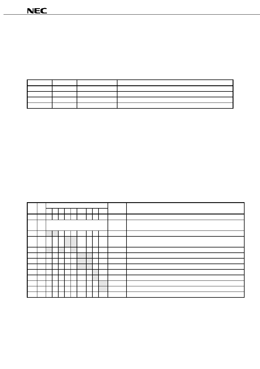
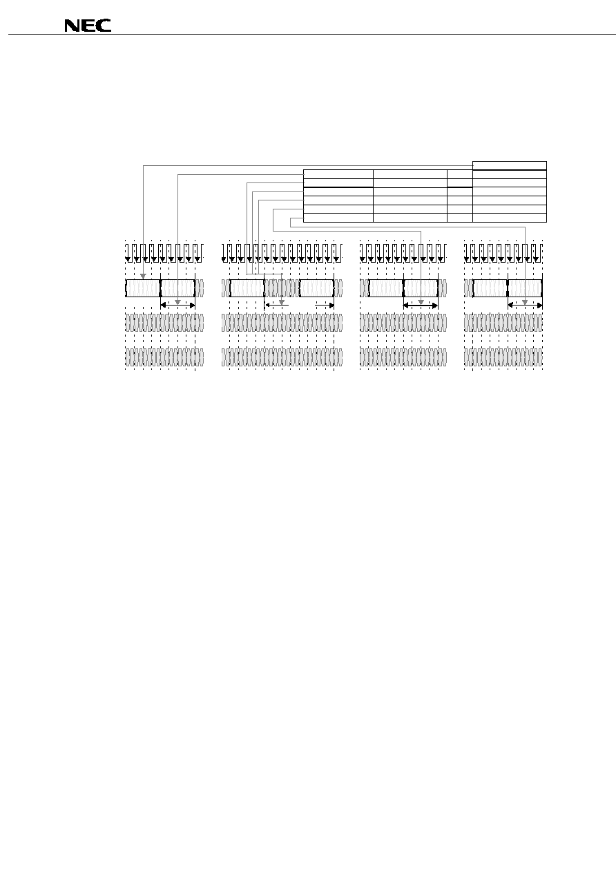
2. Packet Format
Figure 2-1 shows the formats of the ROWA and ROWR packets on the ROW pins. Table 2-1 describes the fields
which comprise these packets. DR4T and DR4F bits are encoded to contain both the DR4 device address bit and a
framing bit which allows the ROWA or ROWR packet to be recognized by the RDRAM.
The AV (ROWA/ROWR packet selection) bit distinguishes between the two packet types. Both the ROWA and
ROWR packet provide a five bit device address and a four bit bank address. An ROWA packet uses the remaining
bits to specify a nine bit row address, and the ROWR packet uses the remaining bits for an eleven bit opcode field.
Note the use of the "RsvX" notation to reserve bits for future address field extension.
Figure 2-1 also shows the formats of the COLC, COLM, and COLX packets on the COL pins. Table 2-2 describes
the fields which comprise these packets.
The COLC packet uses the S (Start) bit for framing. A COLM or COLX packet is aligned with this COLC packet, and
is also framed by the S bit.
The 23 bit COLC packet has a five bit device address, a four bit bank address, a six bit column address, and a four
bit opcode. The COLC packet specifies a read or write command, as well as some power management commands.
The remaining 17 bits are interpreted as a COLM (M=1) or COLX (M=0) packet. A COLM packet is used for a
COLC write command which needs bytemask control. The COLM packet is associated with the COLC packet from a
time t
RTR
earlier. An COLX packet may be used to specify an independent precharge command. It contains a five bit
device address, a four bit bank address, and a five bit opcode. The COLX packet may also be used to specify some
housekeeping and power management commands. The COLX packet is framed within a COLC packet but is not
otherwise associated with any other packet.
Table 2-1 Field Description for ROWA Packet and ROWR Packet
Field
Description
DR4T, DR4F
Bits for framing (recognizing) a ROWA or ROWR packet. Also encodes highest device address bit.
DR3..DR0
Device address for ROWA or ROWR packet.
BR4..BR0
Bank address for ROWA or ROWR packet. RsvB denotes bits ignored by the RDRAM.
AV
Selects between ROWA packet (AV=1) and ROWR packet (AV=0).
R8..R0
Row address for ROWA packet. RsvR denotes bits reserved for future row address extension.
ROP10..ROP0
Opcode field for ROWR packet. Specifies precharge, refresh, and power management functions.
Table 2-2 Field Description for COLC Packet, COLM Packet, and COLX Packet
Field
Description
S
Bit for framing (recognizing) a COLC packet, and indirectly for framing COLM and COLX packets.
DC4..DC0
Device address for COLC packet.
BC4..BC0
Bank address for COLC packet. RsvB denotes bits reserved for future extension (controller drivers 0's).
C5..C0
Column address for COLC packet. RsvC denotes bits ignored by the RDRAM.
COP3..COP0
Opcode field for COLC packet. Specifies read, write, precharge, and power management functions.
M
Selects between COLM packet (M=1) and COLX packet (M=0).
MA7..MA0
Bytemask write control bits. 1=write, 0=no-write. MA0 controls the earliest byte on DQA7..0.
MB7..MB0
Bytemask write control bits. 1=write, 0=no-write. MB0 controls the earliest byte on DQB7..0.
DX4..DX0
Device address for COLX packet.
BX4..BX0
Bank address for COLX packet. RsvB denotes bits reserved for future extension (controller drivers 0's).
XOP4..XOP0
Opcode field for COLX packet. Specifies precharge, I
OL
control, and power management functions.

Data Sheet M14837EJ3V0DS00
12
µ
µ
µ
µ
PD488448 for Rev. P
Figure 2-1 Packet Formats
CTM/CFM
COL4
COL3
COL2
COL1
COL0
T
8
T
9
T
10
T
11
T
12
T
13
T
14
T
15
T
8
T
9
T
10
T
11
T
0
T
1
T
2
T
3
T
0
T
1
T
2
T
3
MA7 MA5 MA3 MA1
M=1 MA6 MA4 MA2 MA0
MB7 MB4 MB1
MB6 MB3 MB0
MB5 MB2
R2
CTM/CFM
ROW2
DR4T DR2 BR0 BR3 RsvR
R8
R5
ROW1
DR4F DR1 BR1 BR4 RsvR
R7
R4
R1
ROW0
DR3 DR0 BR2 RsvB AV=1
R6
R3
R0
ACT a0
PREX d0
MSK (b1)
PRER c0
WR b1
C4
CTM/CFM
COL4
DC4
S=1
RsvC
COL3
DC3
C5
C3
COL2
DC2 COP1
RsvB BC2
C2
DC1 COP0
BC4 BC1
C1
DC0 COP2
COP3 BC3 BC0
C0
COL1
COL0
CTM/CFM
ROW2
ROW1
ROW0
CTM/CFM
COL4
COL3
COL2
COL1
COL0
ROP2
DR4T DR2 BR0 BR3
ROP10
ROP8ROP5
DR4F DR1 BR1 BR4 ROP9ROP7ROP4ROP1
DR3 DR0 BR2 RsvB AV=0 ROP6ROP3ROP0
DX4 XOP4 RsvB BX1
M=0 DX3 XOP3 BX4 BX0
DX2 XOP2 BX3
DX1 XOP1 BX2
DX0 XOP0
T
0
T
4
T
8
T
12
T
1
T
5
T
9
T
13
T
2
T
6
T
10
T
14
T
3
T
7
T
11
T
15
ROWA Packet
COLM Packet
COLC Packet
COLX Packet
ROWR Packet
CTM/CFM
DQA7..0
DQB7..0
COL4
..COL0
ROW2
..ROW0
t
PACKET
S=1
S=1
Notes 1. The COLM is associated with a previous COLC, and is aligned with the present COLC, indicated
by the Start bit (S=1) position.
2. The COLX is aligned with the present COLC, indicates by the Start bit (S=1) position.
Note1
Note2
Data Sheet M14837EJ3V0DS00
13
µ
µ
µ
µ
PD488448 for Rev. P
3. Field Encoding Summary
Table 3-1 shows how the six device address bits are decoded for the ROWA and ROWR packets. The DR4T and
DR4F encoding merges a fifth device bit with a framing bit. When neither bit is asserted, the device is not selected.
Note that a broadcast operation is indicated when both bits are set. Broadcast operation would typically be used for
refresh and power management commands. If the device is selected, the DM (DeviceMatch) signal is asserted and
an ACT or ROP command is performed.
Table 3-1 Device Field Encodings for ROWA Packet and ROWR Packet
DR4T
DR4F
Device Selection
Device Match signal (DM)
1
1
All devices (broadcast)
DM is set to 1
0
1
One device selected
DM is set to 1 if {DEVID4..DEVID0} == {0, DR3..DR0} else DM is set to 0
1
0
One device selected
DM is set to 1 if {DEVID4..DEVID0} == {1, DR3..DR0} else DM is set to 0
0
0
No packet present
DM is set to 0
Table 3-2 shows the encodings of the remaining fields of the ROWA and ROWR packets. An ROWA packet is
specified by asserting the AV bit. This causes the specified row of the specified bank of this device to be loaded into
the associated sense amps.
An ROWR packet is specified when AV is not asserted. An 11 bit opcode field encodes a command for one of the
banks of this device. The PRER command causes a bank and its two associated sense amps to precharge, so
another row or an adjacent bank may be activated.
The REFA (refresh-activate) command is similar to the ACT command, except the row address comes from an
internal register REFR, and REFR is incremented at the largest bank address. The REFP (refresh-precharge)
command is identical to a PRER command.
The NAPR, NAPRC, PDNR, ATTN, and RLXR commands are used for managing the power dissipation of the
RDRAM and are described in more detail in "23. Power State Management". The TCEN and TCAL commands are
used to adjust the output driver slew rate and they are described in more detail in "25. Current and Temperature
Control".
Table 3-2 ROWA Packet and ROWR Packet Field Encodings
DM
AV
ROP10..ROP0 Field
Name
Command Description
Note1
10 9
8
7
6
5
4
3
2 :
0
0
--
-- -- -- -- --
--
-- --
---
--
No operation.
1
1
Row address
ACT
Activate row R8..R0 of bank BR4..BR0 of device and move device to
ATTN
Note2
.
1
0
1
1
0
0
0
x
Note3
x
x
000 PRER
Precharge bank BR4..BR0 of this device.
1
0
0
0
0
1
1
0
0
x
000 REFA
Refresh (activate) row REFR8..REFR0 of bank BR4..BR0 of device.
Increment REFR if BR4..BR0=11111 (see Figure 24-1).
1
0
1
0
1
0
1
0
0
x
000 REFP
Precharge bank BR4..BR0 of this device after REFA (see Figure 24-1).
1
0
x
x
0
0
0
0
1
x
000 PDNR
Move this device into the powerdown (PDN) power state (see figure 23-3).
1
0
x
x
0
0
0
1
0
x
000 NAPR
Move this device into the nap (NAP) power state (see Figure 23-3).
1
0
x
x
0
0
0
1
1
x
000 NAPRC
Move this device into the nap (NAP) power state conditionally.
1
0
x
x
x
x
x
x
x
0
000 ATTN
Note2
Move this device into the attention (ATTN) power state (see Figure 23-1).
1
0
x
x
x
x
x
x
x
1
000 RLXR
Move this device into the standby (STBY) power state (see Figure 23-2).
1
0
0
0
0
0
0
0
0
x
001 TCAL
Temperature calibrate this device (see figure 25-2).
1
0
0
0
0
0
0
0
0
x
010 TCEN
Temperature calibrate/enable this device (see Figure 25-2).
1
0
0
0
0
0
0
0
0
0
000 NOROP
No operation.
Notes 1. The DM (Device Match signal) value is determined by the DR4T, DR4F, DR3..DR0 field of the ROWA and ROWR packets.
See Table 3-1.
2. The ATTN command does not cause a RLX-to-ATTN transition for a broadcast operation (RD4T/DR4F=1/1).
3. An "x" entry indicates which commands may be combined. For instance, the three commands PRER/NAPRC/RLXR may
be specified in one ROP value (011000111000).

Data Sheet M14837EJ3V0DS00
14
µ
µ
µ
µ
PD488448 for Rev. P
Table 3-3 shows the COP field encoding. The device must be in the ATTN power state in order to receive COLC
packets. The COLC packet is used primarily to specify RD (read) and WR (write) commands. Retire operations
(moving data from the write buffer to a sense amp) happen automatically. See Figure 15-1 for a more detailed
description.
The COLC packet can also specify a PREC command, which precharges a bank and its associated sense amps.
The RDA/WRA commands are equivalent to a combining RD/WR with a PREC. RLXC (relax) performs a power mode
transition. See 23. Power State Management.
Table 3-3 COLC Packet Field Encodings
S
DC4..DC0
(select device)
Note1
COP3..0
Name
Command Description
0
- - - -
- - - - -
--
No operation.
1
/= (DEVID4..0)
- - - - -
--
Retire write buffer of this device.
1
== (DEVID4..0)
x000
Note2
NOCOP
Retire write buffer of this device.
1
== (DEVID4..0)
x001
WR
Retire write buffer of this device, then write column C5..C0 of bank
BC4..BC0 to write buffer.
1
== (DEVID4..0)
x010
RSRV
Reserved, no operation.
1
== (DEVID4..0)
x011
RD
Read column C5..C0 of bank BC4..BC0 of this device.
1
== (DEVID4..0)
x100
PREC
Retire write buffer of this device, then precharge bank BC4..BC0 (see
Figure 12-2).
1
== (DEVID4..0)
x101
WRA
Same as WR, but precharge bank BC4..BC0 after write buffer (with new
data) is retired.
1
== (DEVID4..0)
x110
RSRV
Reserved, no operation.
1
== (DEVID4..0)
x111
RDA
Same as RD, but precharge bank BC4..BC0 afterward.
1
== (DEVID4..0)
1xxx
RLXC
Move this device into the standby (STBY) power state (see Figure 23-2).
Notes 1. "/=" means not equal, "==" means equal.
2. An "x" entry indicates which commands may be combined. For instance, the two commands WR/RLXC
may be specified in one COP value(1001).
Table 3-4 shows the COLM and COLX field encodings. The M bit is asserted to specify a COLM packet with two 8
bit bytemask fields MA and MB. If the M bit is not asserted, an COLX is specified. It has device and bank address
fields, and an opcode field. The primary use of the COLX packet is to permit an independent PREX (precharge)
command to be specified without consuming control bandwidth on the ROW pins. It is also used for the CAL
(calibrate) and SAM (sample) current control commands (see 25. Current and Temperature Control), and for the
RLXX power mode command (see 23. Power State Management).
Table 3-4 COLM Packet and COLX Packet Field Encodings
M
DX4..DX0
(select device)
XOP4..0
Name
Command Description
1
- - - -
-
MSK
MB/MA bytemasks used by WR/WRA.
0
/= (DEVID4..0)
-
--
No operation.
0
== (DEVID4..0) 00000
NOXOP
No operation.
0
== (DEVID4..0) 1xxx0
Note
PREX
Precharge bank BX4..BX0 of this device (see Figure 12-2).
0
== (DEVID4..0) x10x0
CAL
Calibrate (drive) I
OL
current for this device (see Figure 25-1).
0
== (DEVID4..0) x11x0
CAL / SAM Calibrate (drive) and Sample (update) I
OL
current for this device (see Figure 25-1).
0
== (DEVID4..0) xxx10
RLXX
Move this device into the standby (STBY) power state (see Figure 23-2).
0
== (DEVID4..0) xxxx1
RSRV
Reserved, no operation.
Note An "x" entry indicates which commands may be combined. For instance, the two commands PREX/RLXX
may be specified in one XOP value (10010).
Data Sheet M14837EJ3V0DS00
15
µ
µ
µ
µ
PD488448 for Rev. P
4. DQ Packet Timing
Figure 4-1 shows the timing relationship of COLC packets with D and Q data packets. This document uses a
specific convention for measuring time intervals between packets: all packets on the ROW and COL pins (ROWA,
ROWR, COLC, COLM, COLX) use the trailing edge of the packet as a reference point, and all packets on the
DQA/DQB pins (D and Q) use the leading edge of the packet as a reference point.
An RD or RDA command will transmit a dualoct of read data Q a time t
CAC
later. This time includes one to five
cycles of round-trip propagation delay on the Channel. The t
CAC
parameter may be programmed to a one of a range
of values (7, 8, 9, 10, 11, or 12 t
CYCLE
). The value chosen depends upon the number of RDRAM devices on the
Channel and the RDRAM timing bin. See Figure 22-1(5/7) "TPARM Register" for more information.
A WR or WRA command will receive a dualoct of write data D a time t
CWD
later. This time does not need to include
the round-trip propagation time of the Channel since the COLC and D packets are traveling in the same direction.
When a Q packet follows a D packet (shown in the left half of the figure), a gap (t
CAC
-t
CWD
) will automatically appear
between them because the t
CWD
value is always less than the t
CAC
value. There will be no gap between the two COLC
packets with the WR and RD commands which schedule the D and Q packets.
When a D packet follows a Q packet (shown in the right half of the figure), no gap is needed between them because
the t
CWD
value is less than the t
CAC
value. However, a gap of t
CAC
- t
CWD
or greater must be inserted between the
COLC packets with the RD WR commands by the controller so the Q and D packets do not overlap.
Figure 4-1 Read (Q) and Write (D) Data Packet - Timing for t
CAC
= 7,8,9,10,11 or 12 t
CYCLE
CTM/CFM
DQA7..0
DQB7..0
COL4
..COL0
ROW2
..ROW0
T
0
T
4
T
8
T
12
T
1
T
5
T
9
T
13
T
2
T
6
T
10
T
14
T
3
T
7
T
11
T
15
T
16
T
20
T
24
T
28
T
17
T
21
T
25
T
29
T
18
T
22
T
26
T
30
T
19
T
23
T
27
T
31
T
32
T
36
T
40
T
44
T
33
T
37
T
41
T
45
T
34
T
38
T
42
T
46
T
35
T
39
T
43
T
47
RD b1
WR a1
D (a1)
t
CWD
RD c1
This gap on the DQA/DQB pins appears automatically
This gap on the COL pins must be inserted by the controller
t
CAC
t
CAC
t
CAC
-t
CWD
t
CWD
Q (b1)
∑∑∑
∑∑∑
∑∑∑
WR d1
Q (c1)
D (d1)
∑∑∑
t
CAC
-t
CWD
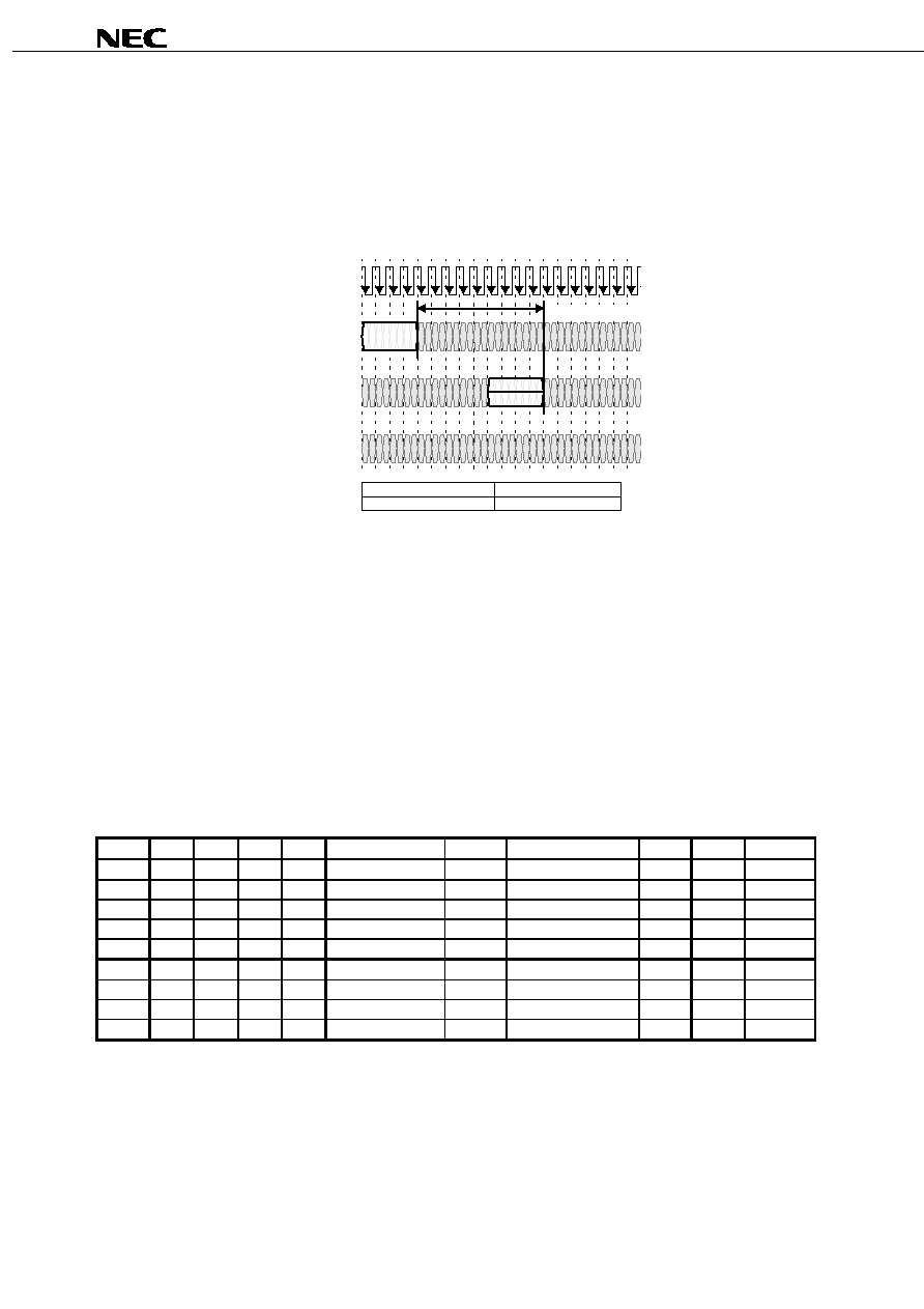
5. COLM Packet to D Packet Mapping
Figure 5-1 shows a write operation initiated by a WR command in a COLC packet. If a subset of the 16 bytes of
write data are to be written, then a COLM packet is transmitted on the COL pins a time t
RTR
after the COLC packet
containing the WR command. The M bit of the COLM packet is set to indicate that it contains the MA and MB mask
fields. Note that this COLM packet is aligned with the COLC packet which causes the write buffer to be retired. See
Figure 15-1 for more details.
If all 16 bytes of the D data packet are to be written, then no further control information is required. The packet slot
that would have been used by the COLM packet (t
RTR
after the COLC packet) is available to be used as an COLX
packet. This could be used for a PREX precharge command or for a housekeeping command (this case is not
shown). The M bit is not asserted in an COLX packet and causes all 16 bytes of the previous WR to be written
unconditionally. Note that a RD command will never need a COLM packet, and will always be able to use the COLX
packet option (a read operation has no need for the byte-write-enable control bits).
The figure 5-1 also shows the mapping between the MA and MB fields of the COLM packet and bytes of the D
packet on the DQA and DQB pins. Each mask bit controls whether a byte of data is written (=1) or not written (=0).
Data Sheet M14837EJ3V0DS00
16
µ
µ
µ
µ
PD488448 for Rev. P
Figure 5-1 Mapping between COLM Packet and D Packet for WR Command
CTM/CFM
COL4
COL3
COL2
COL1
COL0
T
17
T
18
T
19
T
20
MA7 MA5 MA3 MA1
M=1 MA6 MA4 MA2 MA0
MB7 MB4 MB1
MB6 MB3 MB0
MB5 MB2
CTM/CFM
DQA7..0
DQB7..0
COL4
..COL0
ROW2
..ROW0
T
0
T
4
T
8
T
12
T
1
T
5
T
9
T
13
T
2
T
6
T
10
T
14
T
3
T
7
T
11
T
15
T
16
T
20
T
24
T
28
T
17
T
21
T
25
T
29
T
18
T
22
T
26
T
30
T
19
T
23
T
27
T
31
T
32
T
36
T
40
T
44
T
33
T
37
T
41
T
45
T
34
T
38
T
42
T
46
T
35
T
39
T
43
T
47
MSK (a1)
retire (a1)
WR a1
D (a1)
ACT b0
ACT a0
Transaction a: WR
a0 = {Da,Ba,Ra}
a1 = {Da,Ba,Ca1}
a3 = {Da,Ba}
t
RTR
T
19
T
20
T
21
T
22
CTM/CFM
DQB7
DQB6
DQB1
DQB0
DB63
DB7
DB15 DB23 DB31 DB39 DB47 DB55
DB6
DB14 DB22 DB30 DB38 DB46 DB54 DB62
DB1
DB9
DB17 DB25 DB33 DB41 DB49 DB57
DB0
DB8
DB16 DB24 DB32 DB40 DB48 DB56
COLM Packet
PRER a2
DQA7
DQA6
DQA1
DQA0
D Packet
MB0
DA63
DA7
DA15 DA23 DA31 DA39 DA47 DA55
DA6
DA14 DA22 DA30 DA38 DA46 DA54 DA64
DA1
DA9
DA17 DA25 DA33 DA41 DA49 DA57
DA0
DA8
DA16 DA24 DA32 DA40 DA48 DA56
MA0
MB1
MA1
MB2
MA2
MB3
MA3
MB4
MA4
MB5
MA5
MB6
MA6
MB7
MA7
t
CWD
Each bit of the MB7..MB0 field
controls writing (=1) or no writing
(=0) of the indicated DB bits when
the M bit of the COLM packet is one.
Each bit of the MA7..MA0 field
controls writing (=1) or no writing
(=0) of the indicated DA bits when
the M bit of the COLM packet is one.
When M=1, the MA and MB
fields control writing of
individual data bytes.
When M=0, all data bytes are
written unconditionally.
∑
∑
∑
∑
∑
∑
Data Sheet M14837EJ3V0DS00
17
µ
µ
µ
µ
PD488448 for Rev. P
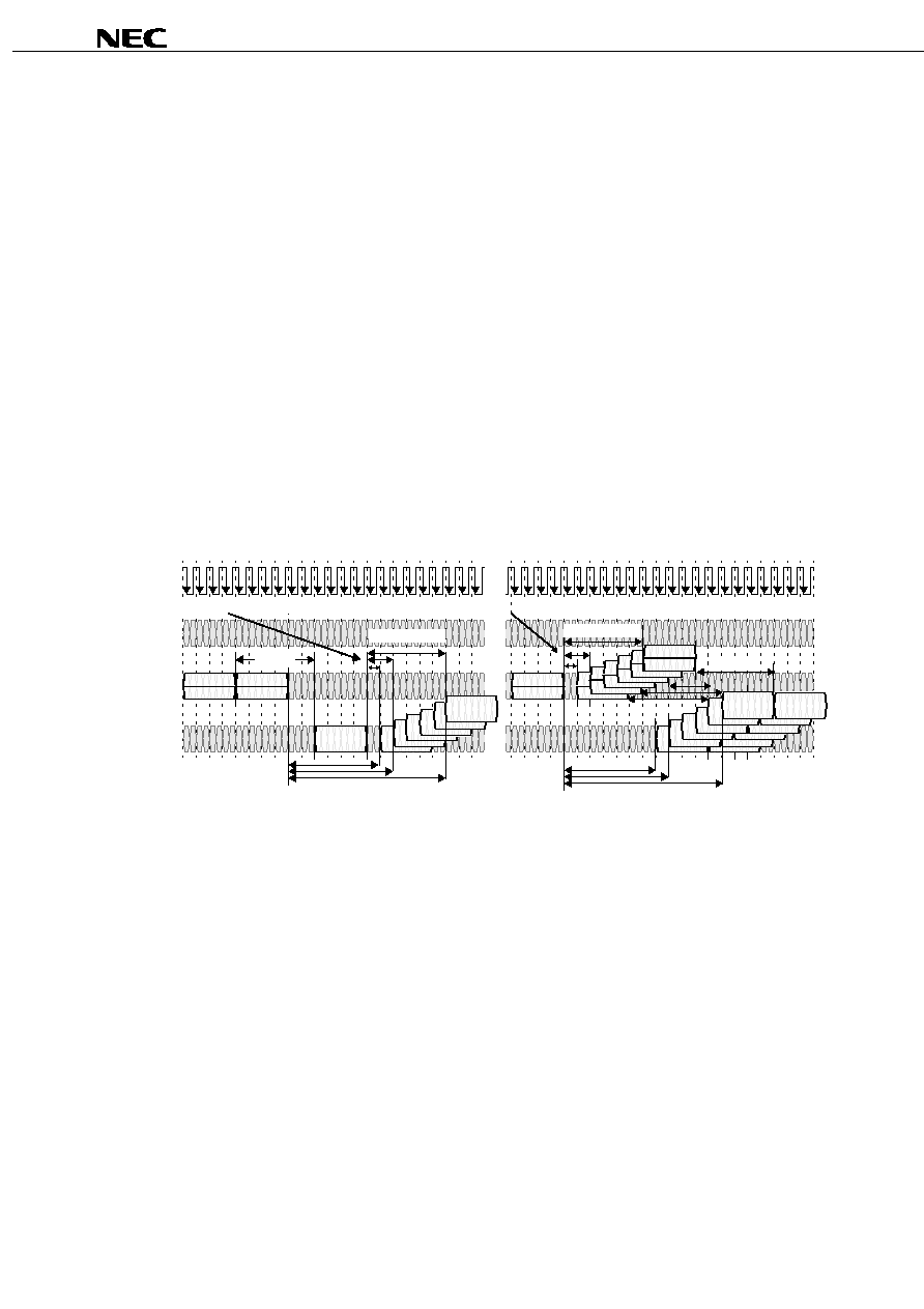
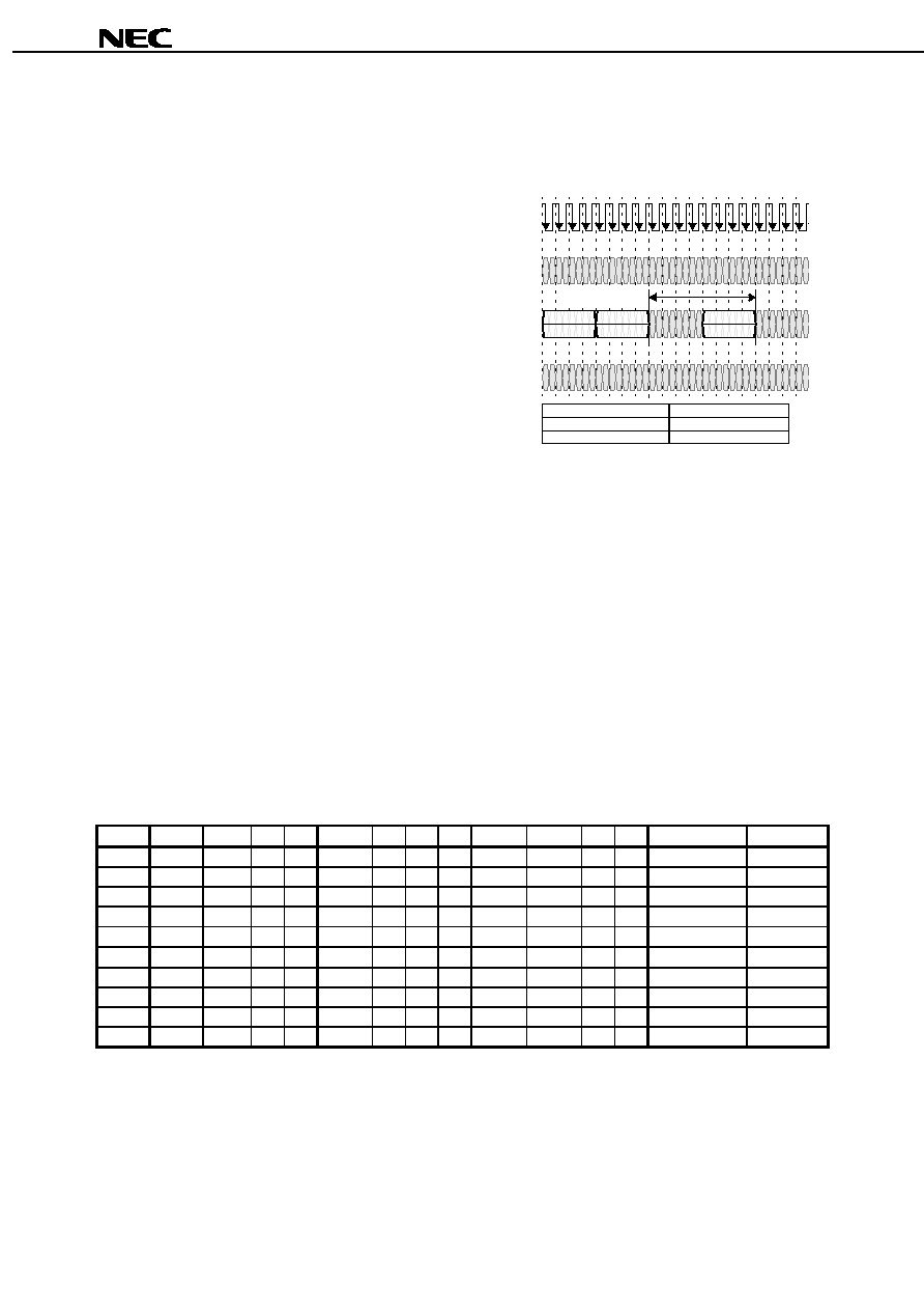
6. ROW-to-ROW Packet Interaction
Figure 6-1 shows two packets on the ROW pins separated by an interval t
RRDELAY
which depends upon the packet
contents. No other ROW packets are sent to banks {Ba, Ba+1, Ba-1} between packet "a" and packet "b" unless
noted otherwise.
Figure 6-1 ROW-to-ROW Packet Interaction - Timing
CTM/CFM
DQA7..0
DQB7..0
COL4
..COL0
ROW2
..ROW0
T
0
T
4
T
8
T
12
T
1
T
5
T
9
T
13
T
2
T
6
T
10
T
14
T
3
T
7
T
11
T
15
T
16
T
T
17
T
18
T
19
Transaction a: ROPa
Transaction b: ROPb
a0 = {Da,Ba,Ra}
b0= {Db,Bb,Rb}
t
RRDELAY
ROPa a0
ROPb b0
Table 6-1 summarizes the t
RRDELAY
values for all possible cases.
Cases RR1 through RR4 show two successive ACT commands. In case RR1, there is no restriction since the ACT
commands are to different devices. In case RR2, the t
RR
restriction applies to the same device with non-adjacent
banks. Cases RR3 and RR4 are illegal (as shown) since bank Ba needs to be precharged. If a PRER to Ba, Ba+1,
or Ba-1 is inserted, t
RRDELAY
is t
RC
(t
RAS
to the PRER command, and t
RP
to the next ACT).
Cases RR5 through RR8 show an ACT command followed by a PRER command. In cases RR5 and RR6, there are
no restrictions since the commands are to different devices or to non-adjacent banks of the same device. In cases
RR7 and RR8, the t
RAS
restriction means the activated bank must wait before it can be precharged.
Cases RR9 through RR12 show a PRER command followed by an ACT command. In cases RR9 and RR10, there
are essentially no restrictions since the commands are to different devices or to non-adjacent banks of the same
device. RR10a and RR10b depend upon whether a bracketed bank (Ba+-1) is precharged or activated. In cases
RR11 and RR12, the same and adjacent banks must all wait t
RP
for the sense amp and bank to precharge before
being activated.
Cases RR13 through RR16 summarize the combinations of two successive PRER commands. In case RR13 there
is no restriction since two devices are addressed. In RR14, t
PP
applies, since the same device is addressed. In
RR15 and RR16, the same bank or an adjacent bank may be given repeated PRER commands with only the t
PP
restriction.
Two adjacent banks can't be activate simultaneously. A precharge command to one bank will thus affect the state of
the adjacent banks (and sense amps). If bank Ba is activate and a PRER is directed to Ba, then bank Ba will be
precharged along with sense amps Ba-1/Ba and Ba/Ba+1. If bank Ba+1 is activate and a PRER is directed to Ba,
then bank Ba+1 will be precharged along with sense amps Ba/Ba+1 and Ba+1/Ba+2. If bank Ba-1 is activate and a
PRER is directed to Ba, then bank Ba-1 will be precharged along with sense amps Ba/Ba-1 and Ba-1/Ba-2.
A ROW packet may contain commands other than ACT or PRER. The REFA and REFP commands are equivalent
to ACT and PRER for interaction analysis purposes. The interaction rules of the NAPR, NAPRC, PDNR, RLXR,
ATTN, TCAL, and TCEN commands are discussed in later section (see Table 3-2 for cross-ref).

Data Sheet M14837EJ3V0DS00
18
µ
µ
µ
µ
PD488448 for Rev. P
Table 6-1 ROW-to-ROW Packet Interaction - Rules
Case #
ROPa Da
Ba
Ra
ROPb Db
Bb
Rb
t
RRDELAY
Example
RR1
ACT
Da
Ba
Ra
ACT
/= Da
xxxx
x..x
t
PACKET
Figure 10-2
RR2
ACT
Da
Ba
Ra
ACT
== Da /= {Ba, Ba+1, Ba-1}
x..x
t
RR
Figure 10-2
RR3
ACT
Da
Ba
Ra
ACT
== Da == {Ba+1, Ba-1}
x..x
t
RC
- illegal unless PRER to Ba / Ba+1 / Ba-1
Figure 10-1
RR4
ACT
Da
Ba
Ra
ACT
== Da == {Ba}
x..x
t
RC
- illegal unless PRER to Ba / Ba+1 / Ba-1
Figure 10-1
RR5
ACT
Da
Ba
Ra
PRER /= Da
xxxx
x..x
t
PACKET
Figure 10-2
RR6
ACT
Da
Ba
Ra
PRER == Da /= {Ba, Ba+1, Ba-1}
x..x
t
PACKET
Figure 10-2
RR7
ACT
Da
Ba
Ra
PRER == Da == {Ba+1, Ba-1}
x..x
t
RAS
Figure 10-1
RR8
ACT
Da
Ba
Ra
PRER == Da == {Ba}
x..x
t
RAS
Figure 13-1
RR9
PRER Da
Ba
Ra
ACT
/= Da
xxxx
x..x
t
PACKET
Figure 10-3
RR10
PRER Da
Ba
Ra
ACT
== Da /= {Ba, Ba+-1, Ba+-2}
x..x
t
PACKET
Figure 10-3
RR10a
PRER Da
Ba
Ra
ACT
== Da == {Ba+2}
x..x
t
PACKET
/t
RP
if Ba+1 is precharged/activated.
RR10b
PRER Da
Ba
Ra
ACT
== Da == {Ba-2}
x..x
t
PACKET
/t
RP
if Ba-1 is precharged/activated.
RR11
PRER Da
Ba
Ra
ACT
== Da == {Ba+1, Ba-1}
x..x
t
RP
Figure 10-1
RR12
PRER Da
Ba
Ra
ACT
== Da == {Ba}
x..x
t
RP
Figure 10-1
RR13
PRER Da
Ba
Ra
PRER /= Da
xxxx
x..x
t
PACKET
Figure 10-3
RR14
PRER Da
Ba
Ra
PRER == Da /= {Ba, Ba+1, Ba-1}
x..x
t
PP
Figure 10-3
RR15
PRER Da
Ba
Ra
PRER == Da == {Ba+1, Ba-1}
x..x
t
PP
Figure 10-3
RR16
PRER Da
Ba
Ra
PRER == Da == {Ba}
x..x
t
PP
Figure 10-3
Data Sheet M14837EJ3V0DS00
19
µ
µ
µ
µ
PD488448 for Rev. P
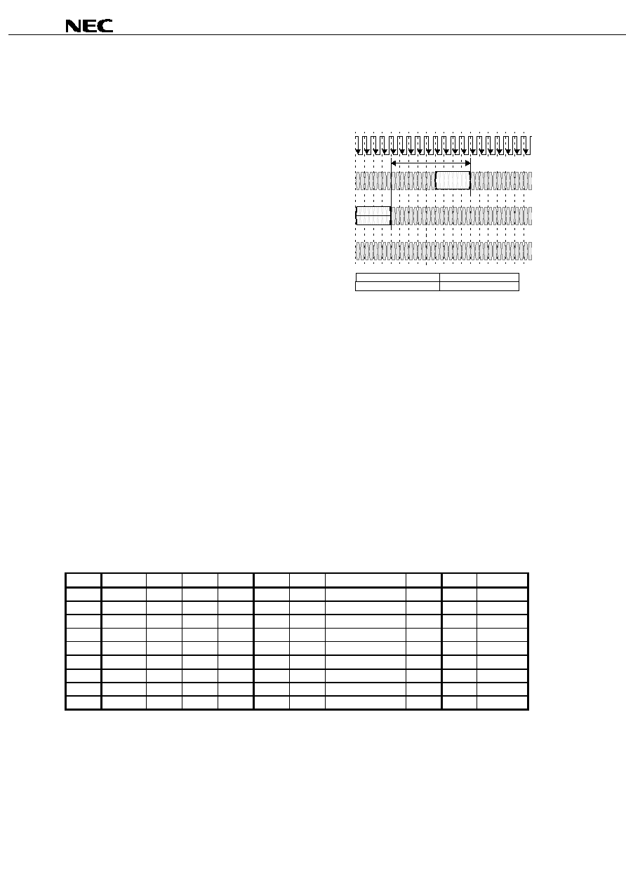
7. ROW-to-COL Packet Interaction
Figure 7-1 shows two packets on the ROW and COL pins. They must be separated by an interval t
RCDELAY
which
depends upon the packet contents.
Figure 7-1 ROW-to-COL Packet Interaction- Timing
CTM/CFM
DQA7..0
DQB7..0
COL4
..COL0
ROW2
..ROW0
T
0
T
4
T
8
T
12
T
1
T
5
T
9
T
13
T
2
T
6
T
10
T
14
T
3
T
7
T
11
T
15
T
16
T
T
17
T
18
T
19
Transaction a: ROPa
Transaction b: COPb
a0 = {Da,Ba,Ra}
b1= {Db,Bb,Cb1}
t
RCDELAY
ROPa a0
COPb b1
Table 7-1 summarizes the t
RCDELAY
values for all possible cases. Note that if the COL packet is earlier than the
ROW packet, it is considered a COL-to-ROW packet interaction.
Cases RC1 through RC5 summarize the rules when the ROW packet has an ACT command. Figure 13-1 and
Figure 14-1 show examples of RC5 - an activation followed by a read or write. RC4 is an illegal situation, since a
read or write of a precharged banks is being attempted (remember that for a bank to be activated, adjacent banks
must be precharged). In cases RC1, RC2, and RC3, there is no interaction of the ROW and COL packets.
Cases RC6 through RC8 summarize the rules when the ROW packet has a PRER command. There is either no
interaction (RC6 through RC9) or an illegal situation with a read or write of a precharged bank (RC9).
The COL pins can also schedule a precharge operation with a RDA, WRA, or PREC command in a COLC packet or
a PREX command in a COLX packet. The constraints of these precharge operations may be converted to equivalent
PRER command constraints using the rules summarized in Figure 12-2.
Table 7-1 ROW-to-COL Packet Interaction - Rules
Case # ROPa Da
Ba
Ra
COPb
Db
Bb
Cb1
t
RCDELAY
Example
RC1
ACT
Da
Ba
Ra
NOCOP, RD, retire
/= Da
xxxx
x..x
0
RC2
ACT
Da
Ba
Ra
NOCOP
== Da
xxxx
x..x
0
RC3
ACT
Da
Ba
Ra
RD, retire
== Da
/= {Ba, Ba+1, Ba-1}
x..x
0
RC4
ACT
Da
Ba
Ra
RD, retire
== Da
== {Ba+1, Ba-1}
x..x
Illegal
RC5
ACT
Da
Ba
Ra
RD, retire
== Da
== {Ba}
x..x
t
RCD
Figure 13-1
RC6
PRER Da
Ba
Ra
NOCOP, RD, retire
/= Da
xxxx
x..x
0
RC7
PRER Da
Ba
Ra
NOCOP
== Da
xxxx
x..x
0
RC8
PRER Da
Ba
Ra
RD, retire
== Da
/= {Ba, Ba+1, Ba-1}
x..x
0
RC9
PRER Da
Ba
Ra
RD, retire
== Da
== {Ba+1, Ba-1}
x..x
Illegal
Data Sheet M14837EJ3V0DS00
20
µ
µ
µ
µ
PD488448 for Rev. P
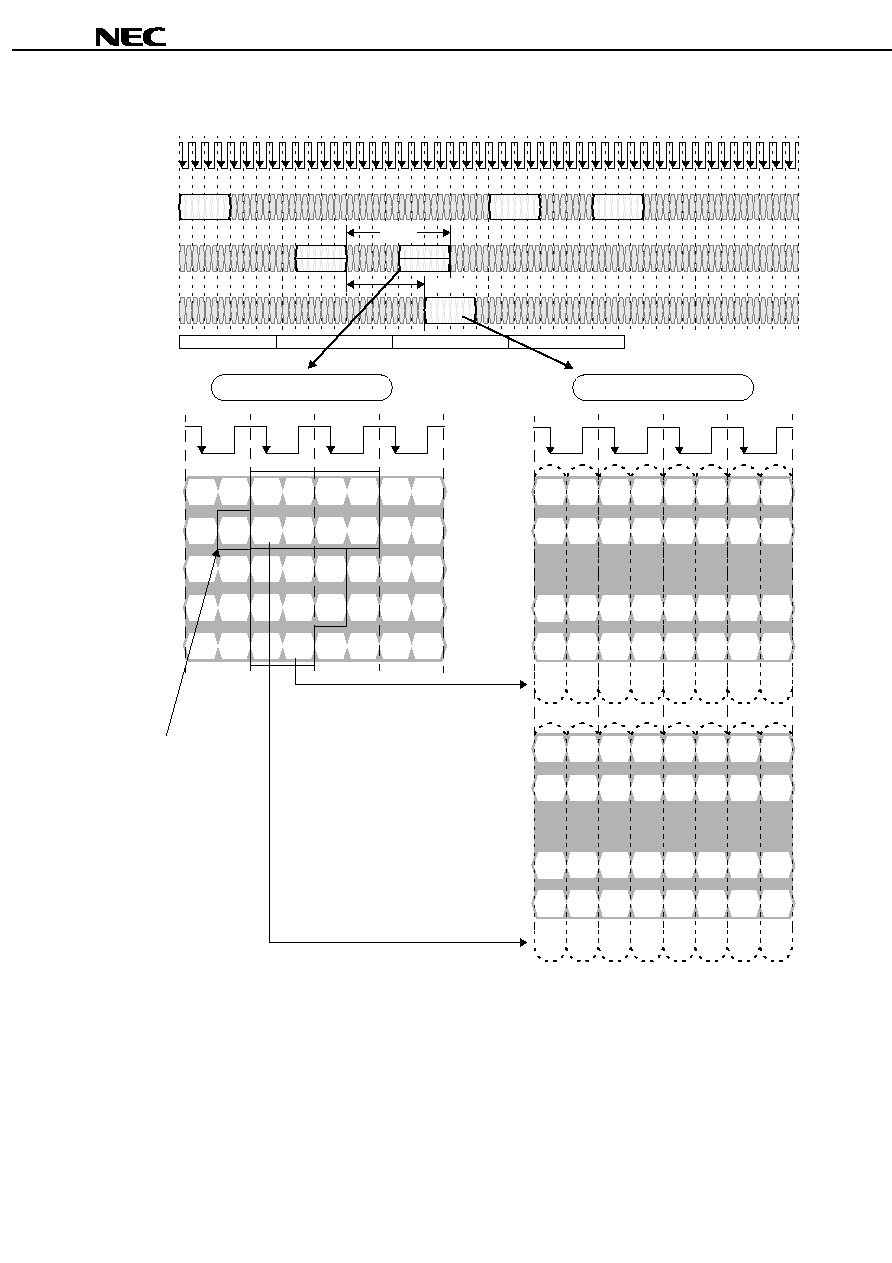
8. COL-to-COL Packet Interaction
Figure 8-1 shows three arbitrary packets on the
COL pins. Packets "b" and "c" must be separated by
an interval t
CCDELAY
which depends upon the
command and address values in all three packets.
Table 8-1 summarizes the t
CCDELAY
values for all
possible cases.
Cases CC1 through CC5 summarize the rules for
every situation other than the case when COPb is a
WR command and COPc is a RD command. In
CC3, when a RD command is followed by a WR
command, a gap of t
CAC
-
t
CWD
must be inserted
between the two COL packets. See Figure 4-1 for
more explanation of why this gap is needed. For
cases CC1, CC2, CC4, and CC5, there is no
restriction (t
CCDELAY
is t
CC
).
In cases CC6 through CC10, COPb is a WR command and COPc is a RD command. The t
CCDELAY
value needed
between these two packets depends upon the command and address in the packet with COPa. In particular, in case
CC6 when there is WR-WR-RD command sequence directed to the same device, a gap will be needed between the
packets with COPb and COPc. The gap will need a COLC packet with a NOCOP command directed to any device in
order to force an automatic retire to take place. Figure 15-2 (right) provides a more detailed explanation of this case.
In case CC10, there is a RD-WR-RD sequence directed to the same device. If a prior write to the same device is
unretired when COPa is issued, then a gap will be needed between the packets with COPb and COPc as in case
CC6. The gap will need a COLC packet with a NOCOP command directed to any device in order to force an
automatic retire to take place.
Cases CC7, CC8, and CC9 have no restriction (t
CCDELAY
is t
CC
).
For the purposes of analyzing COL-to-ROW interactions, the PREC, WRA, and RDA commands of the COLC
packet are equivalent to the NOCOP, WR, and RD commands. These commands also cause a precharge operation
PREC to take place. This precharge may be converted to an equivalent PRER command on the ROW pins using the
rules summarized in Figure 12-2.
Table 8-1 COL-to-COL Packet Interaction - Rules
Case #
COPa
Da
Ba
Ca1 COPb
Db
Bb
Cb1 COPc
Dc
Bc
Cc1 t
CCDELAY
Example
CC1
xxxx
xxxxx
x..x
x..x
NOCOP Db
Bb
Cb1 xxxx
xxxxx
x..x
x..x
t
CC
CC2
xxxx
xxxxx
x..x
x..x
RD, WR Db
Bb
Cb1 NOCOP xxxxx
x..x
x..x
t
CC
CC3
xxxx
xxxxx
x..x
x..x
RD
Db
Bb
Cb1 WR
xxxxx
x..x
x..x
t
CC
+
t
CAC
-
t
CWD
Figure 4-1
CC4
xxxx
xxxxx
x..x
x..x
RD
Db
Bb
Cb1 RD
xxxxx
x..x
x..x
t
CC
Figure 13-1
CC5
xxxx
xxxxx
x..x
x..x
WR
Db
Bb
Cb1 WR
xxxxx
x..x
x..x
t
CC
Figure 14-1
CC6
WR
== Db
x
x..x
WR
Db
Bb
Cb1 RD
== Db
x..x
x..x
t
RTR
Figure 15-1
CC7
WR
== Db
x
x..x
WR
Db
Bb
Cb1 RD
/= Db
x..x
x..x
t
CC
CC8
WR
/= Db
x
x..x
WR
Db
Bb
Cb1 RD
== Db
x..x
x..x
t
CC
CC9
NOCOP == Db
x
x..x
WR
Db
Bb
Cb1 RD
== Db
x..x
x..x
t
CC
CC10
RD
== Db
x
x..x
WR
Db
Bb
Cb1 RD
== Db
x..x
x..x
t
CC
Figure 8-1 COL-to-COL Packet Interaction- Timing
CTM/CFM
DQA7..0
DQB7..0
COL4
..COL0
ROW2
..ROW0
T
0
T
4
T
8
T
12
T
1
T
5
T
9
T
13
T
2
T
6
T
10
T
14
T
3
T
7
T
11
T
15
T
16
T
T
17
T
18
T
19
COPa a1
Transaction a: COPa
COPc c1
Transaction b: COPb
Transaction c: COPc
a1 = {Da,Ba,Ca1}
b1 = {Db,Bb,Cb1}
c1 = {Dc,Bc,Cc1}
t
CCDELAY
COPb b1
Data Sheet M14837EJ3V0DS00
21
µ
µ
µ
µ
PD488448 for Rev. P
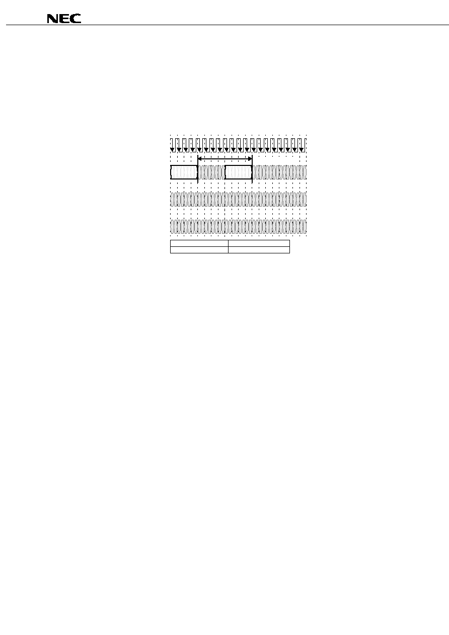
9. COL-to-ROW Packet Interaction
Figure 9-1 shows arbitrary packets on the COL
and ROW pins. They must be separated by an
interval t
CRDELAY
which depends upon the
command and address values in the packets.
Table 9-1 summarizes the t
CRDELAY
value for all
possible cases.
Cases CR1, CR2, CR3, and CR9 show no
interaction between the COL and ROW packets,
either because one of the commands is a NOP or
because the packets are directed to different
devices or to non-adjacent banks.
Case CR4 is illegal because an already-activated
bank is to be re-activated without being
precharged. Case CR5 is illegal because an
adjacent bank can't be activated or precharged
until bank Ba is precharged first.
In case CR6, the COLC packet contains a RD command, and the ROW packet contains a PRER command for the
same bank. The t
RDP
parameter specifies the required spacing.
Likewise, in case CR7, the COLC packet causes an automatic retire to take place, and the ROW packet contains a
PRER command for the same bank. The t
RTP
parameter specifies the required spacing.
Case CR8 is labeled "Hazardous" because a WR command should always be followed by an automatic retire before
a precharge is scheduled. Figure 15-3 shows an example of what can happen when the retire is not able to happen
before the precharge.
For the purposes of analyzing COL-to-ROW interactions, the PREC, WRA, and RDA commands of the COLC
packet are equivalent to the NOCOP, WR, and RD commands. These commands also cause a precharge operation
to take place. This precharge may converted to an equivalent PRER command on the ROW pins using the rules
summarized in Figure 12-2.
A ROW packet may contain commands other than ACT or PRER. The REFA and REFP commands are equivalent
to ACT and PRER for interaction analysis purposes. The interaction rules of the NAPR, PDNR, and RLXR
commands are discussed in a later section.
Table 9-1 COL-to-ROW Packet Interaction - Rules
Case #
COPa
Da
Ba
Ca1
ROPb
Db
Bb
Rb
t
CRDELAY
Example
CR1
NOCOP
Da
Ba
Ca1
x..x
xxxxx
xxxxx
x..x
0
CR2
RD/WR
Da
Ba
Ca1
x..x
/= Da
xxxxx
x..x
0
CR3
RD/WR
Da
Ba
Ca1
x..x
== Da
/= {Ba, Ba+1, Ba-1} x..x
0
CR4
RD/WR
Da
Ba
Ca1
ACT
== Da
== {Ba}
x..x
Illegal
CR5
RD/WR
Da
Ba
Ca1
ACT
== Da
== {Ba+1, Ba-1}
x..x
Illegal
CR6
RD
Da
Ba
Ca1
PRER
== Da
== {Ba, Ba+1, Ba-1} x..x
t
RDP
Figure 13-1
CR7
retire
Note 1
Da
Ba
Ca1
PRER
== Da
== {Ba, Ba+1, Ba-1} x..x
t
RTP
Figure 14-1
CR8
WR
Note 2
Da
Ba
Ca1
PRER
== Da
== {Ba, Ba+1, Ba-1} x..x
0
Figure 15-3
CR9
xxxx
Da
Ba
Ca1
NOROP xxxxx
xxxxx
x..x
0
Notes 1. This is any command which permits the write buffer of device Da to retire (see Table 3-3). "Ba" is the bank
address in the write buffer.
2. This situation is hazardous because the write buffer will be left unretired while the targeted bank is
precharged. See Figure 15-3.
Figure 9-1 COL-to-ROW Packet Interaction- Timing
CTM/CFM
DQA7..0
DQB7..0
COL4
..COL0
ROW2
..ROW0
T
0
T
4
T
8
T
12
T
1
T
5
T
9
T
13
T
2
T
6
T
10
T
14
T
3
T
7
T
11
T
15
T
16
T
T
17
T
18
T
19
Transaction a: COPa
Transaction b: ROPb
a1= {Da,Ba,Ca1}
b0= {Db,Bb,Rb}
t
CRDELAY
ROPb b0
COPa a1
Data Sheet M14837EJ3V0DS00
22
µ
µ
µ
µ
PD488448 for Rev. P
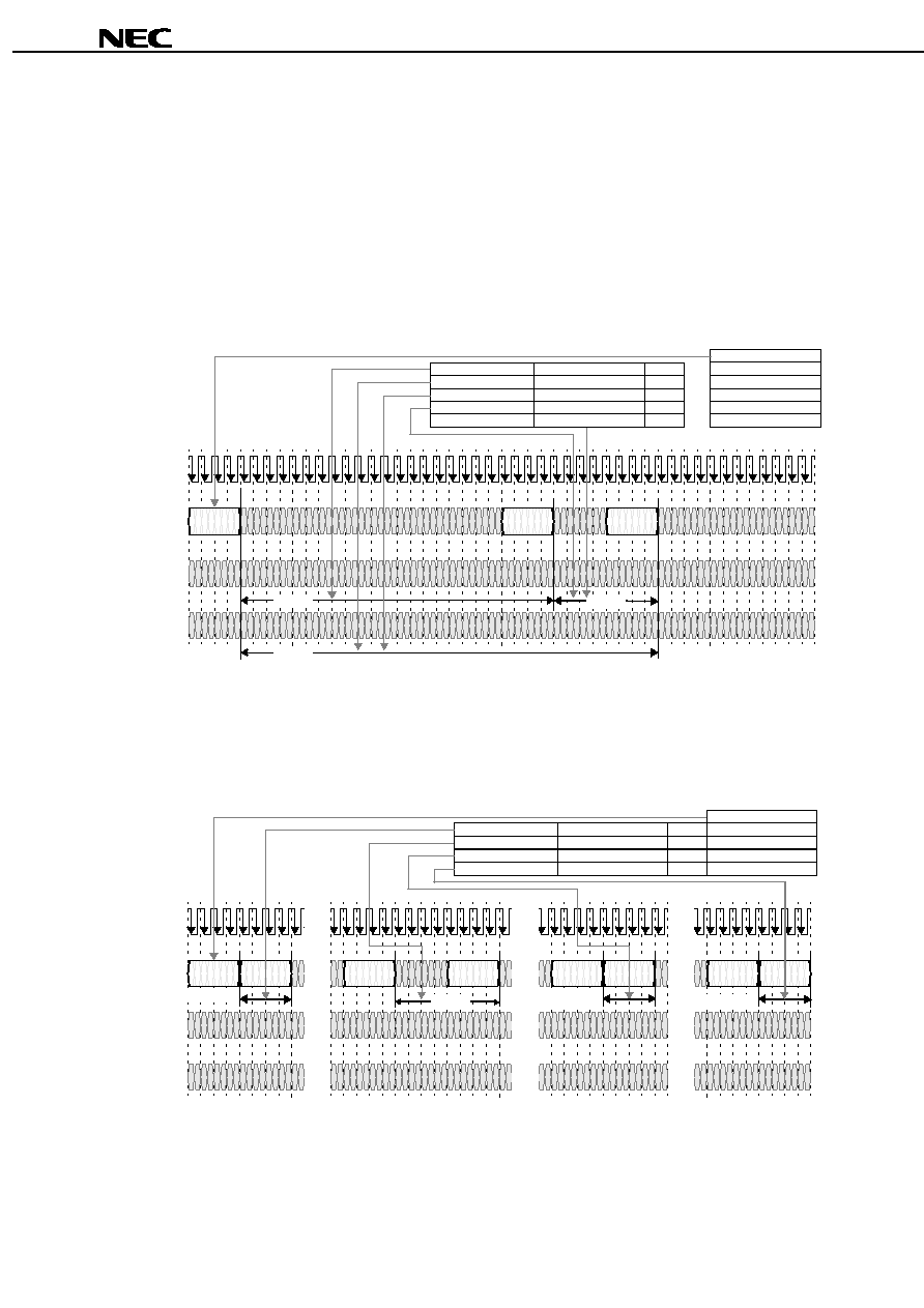
10. ROW-to-ROW Examples
Figure 10-1 shows examples of some of the ROW-to-ROW packet spacings from Table 6-1. A complete sequence
of activate and precharge commands is directed to a bank. The RR8 and RR12 rules apply to this sequence. In
addition to satisfying the t
RAS
and t
RP
timing parameters, the separation between ACT commands to the same bank
must also satisfy the t
RC
timing parameter (RR4).
When a bank is activated, it is necessary for adjacent banks to remain precharged. As a result, the adjacent banks
will also satisfy parallel timing constraints; in the example, the RR11 and RR3 rules are analogous to the RR12 and
RR4 rules.
Figure 10-1 Row Packet Example
CTM/CFM
DQA7..0
DQB7..0
COL4
..COL0
ROW2
..ROW0
T
0
T
4
T
8
T
12
T
1
T
5
T
9
T
13
T
2
T
6
T
10
T
14
T
3
T
7
T
11
T
15
T
16
T
20
T
24
T
28
T
17
T
21
T
25
T
29
T
18
T
22
T
26
T
30
T
19
T
23
T
27
T
31
T
32
T
36
T
40
T
44
T
33
T
37
T
41
T
45
T
34
T
38
T
42
T
46
T
35
T
39
T
43
T
47
ACT a0
PRER a1
t
RAS
t
RC
a0 = {Da,Ba,Ra}
a1 = {Da,Ba+1}
b0 = {Da,Ba+1,Rb}
Same Device
Adjacent Bank
RR7
t
RP
Same Device
Adjacent Bank
RR11
ACT b0
b0 = {Da,Ba,Rb}
Same Device
Same Bank
RR12
b0 = {Da,Ba+1,Rb}
Same Device
Adjacent Bank
RR3
b0 = {Da,Ba,Rb}
Same Device
Same Bank
RR4
Figure 10-2 shows examples of the ACT-to-ACT (RR1, RR2) and ACT-to-PRER (RR5, RR6) command spacings
from Table 6-1. In general, the commands in ROW packets may be spaced an interval t
PACKET
apart unless they are
directed to the same or adjacent banks or unless they are a similar command type (both PRER or both ACT)
directed to the same device.
Figure 10-2 Row Packet Example
CTM/CFM
DQA7..0
DQB7..0
COL4
..COL0
ROW2
..ROW0
T
0
T
4
T
8
T
12
T
1
T
5
T
9
T
13
T
2
T
6
T
10
T
14
T
3
T
7
T
11
T
15
T
16
T
20
T
24
T
28
T
17
T
21
T
25
T
29
T
18
T
22
T
26
T
30
T
19
T
23
T
27
T
31
T
32
T
36
T
40
T
44
T
33
T
37
T
41
T
45
T
34
T
38
T
42
T
46
T
35
T
39
T
43
T
47
ACT a0
PRER b0
t
PACKET
ACT c0
t
RR
a0 = {Da,Ba,Ra}
b0 = {Db,Bb,Rb}
c0 = {Da,Bc,Rc}
Different Device
Any Bank
Same Device
Non-adjacent Bank
RR1
RR2
ACT a0
ACT a0
ACT b0
PRER c0
t
PACKET
t
PACKET
b0 = {Db,Bb,Rb}
c0 = {Da,Bc,Rc}
Different Device
Any Bank
Same Device
Non-adjacent Bank
RR5
RR6
ACT a0
Data Sheet M14837EJ3V0DS00
23
µ
µ
µ
µ
PD488448 for Rev. P
Figure 10-3 shows examples of the PRER-to-PRER (RR13, RR14) and PRER-to-ACT (RR9, RR10) command
spacings from Table 6-1. The RR15 and RR16 cases (PRER-to-PRER to same or adjacent banks) are not shown,
but are similar to RR14. In general, the commands in ROW packets may be spaced an interval t
PACKET
apart unless
they are directed to the same or adjacent banks or unless they are a similar command type (both PRER or both ACT)
directed to the same device.
Figure 10-3 Row Packet Example
CTM/CFM
DQA7..0
DQB7..0
COL4
..COL0
ROW2
..ROW0
T
0
T
4
T
8
T
12
T
1
T
5
T
9
T
13
T
2
T
6
T
10
T
14
T
3
T
7
T
11
T
15
T
16
T
20
T
24
T
28
T
17
T
21
T
25
T
29
T
18
T
22
T
26
T
30
T
19
T
23
T
27
T
31
T
32
T
36
T
40
T
44
T
33
T
37
T
41
T
45
T
34
T
38
T
42
T
46
T
35
T
39
T
43
T
47
PRER a0
ACT b0
t
PACKET
PRER c0
t
PP
a0 = {Da,Ba,Ra}
b0 = {Db,Bb,Rb}
c0 = {Da,Bc,Rc}
Different Device
Any Bank
Same Device
Non-adjacent Bank
RR13
RR14
PRER a0
PRER a0
PRER b0
ACT c0
t
PACKET
t
PACKET
b0 = {Db,Bb,Rb}
c0 = {Da,Bc,Rc}
Different Device
Any Bank
Same Device
Non-adjacent Bank
RR9
RR10
PRER a0
c0 = {Da,Ba,Rc}
Same Device
Ajacent Bank
RR15
c0 = {Da,Ba+1Rc}
Same Device
Same Bank
RR16
11. Row and Column Cycle Description
Activate: A row cycle begins with the activate (ACT) operation. The activation process is destructive; the act of
sensing the value of a bit in a bank's storage cell transfers the bit to the sense amp, but leaves the original bit in the
storage cell with an incorrect value.
Restore: Because the activation process is destructive, a hidden operation called restore is automatically performed.
The restore operation rewrites the bits in the sense amp back into the storage cells of the activated row of the bank.
Read/Write: While the restore operation takes place, the sense amp may be read (RD) and written (WR) using
column operations. If new data is written into the sense amp, it is automatically forwarded to the storage cells of the
bank so the data in the activated row and the data in the sense amp remain identical.
Precharge: When both the restore operation and the column operations are completed, the sense amp and bank are
precharged (PRE). This leaves them in the proper state to begin another activate operation.
Intervals: The activate operation requires the interval t
RCD,MIN
to complete. The hidden restore operation requires the
interval t
RAS,MIN
- t
RCD,MIN
to complete. Column read and write operations are also performed during the t
RAS,MIN
-
t
RCD,MIN
interval (if more than about four column operations are performed, this interval must be increased). The
precharge operation requires the interval t
RP,MIN
to complete.
Adjacent Banks: An RDRAM with a "s" designation (256K
x
16 x
32s) indicates it contains "split banks". This means
the sense amps are shared between two adjacent banks. The only exception is that sense amp 0, 15, 16, and 31 are
not shared. When a row in a bank is activated, the two adjacent sense amps are connected to (associated with) that
bank and are not available for use by the two adjacent banks. These two adjacent banks must remain precharged
while the selected bank goes through its activate, restore, read/write, and precharge operations.
For example (referring to the block diagram), if bank 5 is accessed, sense amp 4/5 and sense amp 5/6 will both be
loaded with one of the 512 rows (with 512 bytes loaded into each sense amp from the 1K
byte row ≠ 256 bytes to the
DQA side and 256 bytes to the DQB side). While this row from bank 5 is being accessed, no rows may be accessed
in banks 4 or 6 because of the sense amp sharing.

Data Sheet M14837EJ3V0DS00
24
µ
µ
µ
µ
PD488448 for Rev. P
12. Precharge Mechanisms
Figure 12-1 shows an example of precharge with the ROWR packet mechanism. The PRER command must occur
a time t
RAS
after the ACT command, and a time t
RP
before the next ACT command. This timing will serve as a
baseline against which the other precharge mechanisms can be compared.
Figure 12-1 Precharge via PRER Command in ROWR Packet
CTM/CFM
DQA7..0
DQB7..0
COL4
..COL0
ROW2
..ROW0
T
0
T
4
T
8
T
12
T
1
T
5
T
9
T
13
T
2
T
6
T
10
T
14
T
3
T
7
T
11
T
15
T
16
T
20
T
24
T
28
T
17
T
21
T
25
T
29
T
18
T
22
T
26
T
30
T
19
T
23
T
27
T
31
T
32
T
36
T
40
T
44
T
33
T
37
T
41
T
45
T
34
T
38
T
42
T
46
T
35
T
39
T
43
T
47
ACT a0
PRER a5
t
RAS
t
RC
a0 = {Da,Ba,Ra}
a5 = {Da,Ba}
b0 = {Da,Ba,Rb}
t
RP
ACT b0
Figure 12-2 (top) shows an example of precharge with a RDA command. A bank is activated with an ROWA packet
on the ROW pins. Then, a series of four dualocts are read with RD commands in COLC packets on the COL pins.
The fourth of these commands is a RDA, which causes the bank to automatically precharge when the final read has
finished. The timing of this automatic precharge is equivalent to a PRER command in an ROWR packet on the ROW
pins that is offset a time t
OFFP
from the COLC packet with the RDA command. The RDA command should be treated
as a RD command in a COLC packet as well as a simultaneous (but offset) PRER command in an ROWR packet
when analyzing interactions with other packets.
Figure 12-2 (middle) shows an example of precharge with a WRA command. As in the RDA example, a bank is
activated with an ROWA packet on the ROW pins. Then, two dualocts are written with WR commands in COLC
packets on the COL pins. The second of these commands is a WRA, which causes the bank to automatically
precharge when the final write has been retired. The timing of this automatic precharge is equivalent to a PRER
command in an ROWR packet on the ROW pins that is offset a time t
OFFP
from the COLC packet that causes the
automatic retire. The WRA command should be treated as a WR command in a COLC packet as well as a
simultaneous (but offset) PRER command in an ROWR packet when analyzing interactions with other packets. Note
that the automatic retire is triggered by a COLC packet a time t
RTR
after the COLC packet with the WR command
unless the second COLC contains a RD command to the same device. This is described in more detail in Figure 15-
1.
Figure 12-2 (bottom) shows an example of precharge with a PREX command in an COLX packet. A bank is
activated with an ROWA packet on the ROW pins. Then, a series of four dualocts are read with RD commands in
COLC packets on the COL pins. The fourth of these COLC packets includes an COLX packet with a PREX
command. This causes the bank to precharge with timing equivalent to a PRER command in an ROWR packet on
the ROW pins that is offset a time t
OFFP
from the COLX packet with the PREX command.
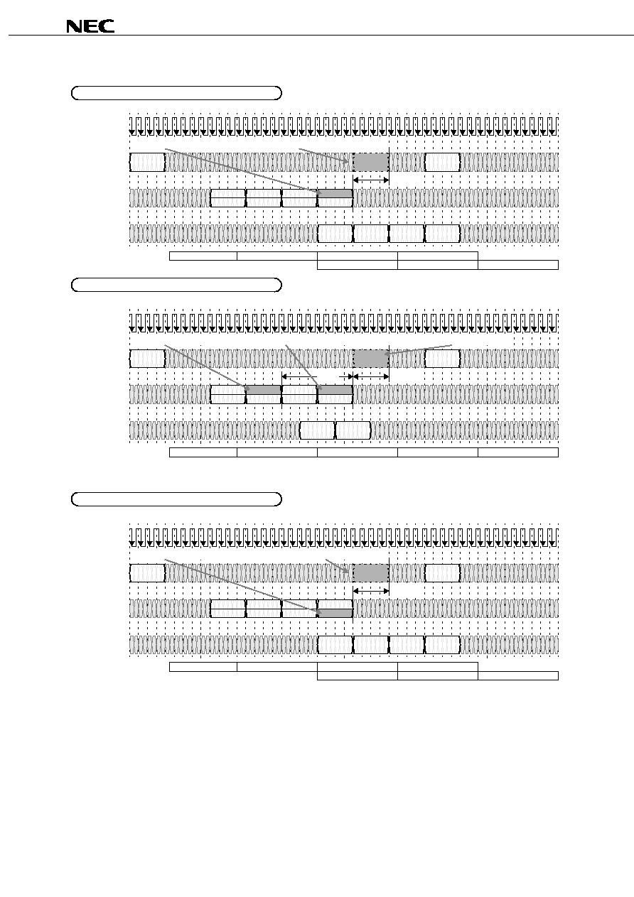
Data Sheet M14837EJ3V0DS00
25
µ
µ
µ
µ
PD488448 for Rev. P
Figure 12-2 Offsets for Alternate Precharge Mechanisms
CTM/CFM
DQA7..0
DQB7..0
COL4
..COL0
ROW2
..ROW0
T
0
T
4
T
8
T
12
T
1
T
5
T
9
T
13
T
2
T
6
T
10
T
14
T
3
T
7
T
11
T
15
T
16
T
20
T
24
T
28
T
17
T
21
T
25
T
29
T
18
T
22
T
26
T
30
T
19
T
23
T
27
T
31
T
32
T
36
T
40
T
44
T
33
T
37
T
41
T
45
T
34
T
38
T
42
T
46
T
35
T
39
T
43
T
47
CTM/CFM
DQA7..0
DQB7..0
COL4
..COL0
ROW2
..ROW0
T
0
T
4
T
8
T
12
T
1
T
5
T
9
T
13
T
2
T
6
T
10
T
14
T
3
T
7
T
11
T
15
T
16
T
20
T
24
T
28
T
17
T
21
T
25
T
29
T
18
T
22
T
26
T
30
T
19
T
23
T
27
T
31
T
32
T
36
T
40
T
44
T
33
T
37
T
41
T
45
T
34
T
38
T
42
T
46
T
35
T
39
T
43
T
47
CTM/CFM
DQA7..0
DQB7..0
COL4
..COL0
ROW2
..ROW0
T
0
T
4
T
8
T
12
T
1
T
5
T
9
T
13
T
2
T
6
T
10
T
14
T
3
T
7
T
11
T
15
T
16
T
20
T
24
T
28
T
17
T
21
T
25
T
29
T
18
T
22
T
26
T
30
T
19
T
23
T
27
T
31
T
32
T
36
T
40
T
44
T
33
T
37
T
41
T
45
T
34
T
38
T
42
T
46
T
35
T
39
T
43
T
47
RD a1
ACT a0
RD a2
Q (a2)
Q (a1)
ACT b0
MSK (a2)
MSK (a1)
retire (a1)
t
OFFP
WR a1
D (a2)
D (a1)
ACT b0
ACT a0
Transaction a: RD
a0 = {Da,Ba,Ra}
a5 = {Da,Ba}
COLC Packet: RDA Precharge Offset
COLC Packet: WDA Precharge Offset
Transaction a: WR
a0 = {Da,Ba,Ra}
a1 = {Da,Ba,Ca1}
a2 = {Da,Ba,Ca2}
a5 = {Da,Ba}
COLX Packet: PREX Precharge Offset
RD a3
Q (a4)
Q (a3)
RDA a4
PRER a5
The RDA precharge is equivalent to a PRER command here
t
OFFP
PRER a5
The WRA precharge (triggered by the automatic retire) is equivalent to a PRER command here
WRA a2
retire (a2)
t
RTR
a3 = {Da,Ba,Ca3}
a4 = {Da,Ba,Ca4}
a1 = {Da,Ba,Ca1}
a2 = {Da,Ba,Ca2}
RD a1
ACT a0
RD a2
Q (a2)
Q (a1)
ACT b0
t
OFFP
Transaction a: RD
a0 = {Da,Ba,Ra}
a5 = {Da,Ba}
RD a3
Q (a4)
Q (a3)
PRER a5
The PREX precharge command is equivalent to a PRER command here
a3 = {Da,Ba,Ca3}
a4 = {Da,Ba,Ca4}
a1 = {Da,Ba,Ca1}
a2 = {Da,Ba,Ca2}
RD a4
PREX a5
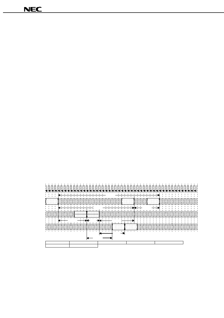
Data Sheet M14837EJ3V0DS00
26
µ
µ
µ
µ
PD488448 for Rev. P
13. Read Transaction - Example
Figure 13-1 shows an example of a read transaction. It begins by activating a bank with an ACT a0 command in an
ROWA packet. A time t
RCD
later a RD a1 command is issued in a COLC packet. Note that the ACT command
includes the device, bank, and row address (abbreviated as a0) while the RD command includes device, bank, and
column address (abbreviated as a1). A time t
CAC
after the RD command the read data dualoct Q (a1) is returned by
the device. Note that the packets on the ROW and COL pins use the end of the packet as a timing reference point,
while the packets on the DQA/DQB pins use the beginning of the packet as a timing reference point.
A time t
CC
after the first COLC packet on the COL pins a second is issued. It contains a RD a2 command. The a2
address has the same device and bank address as the a1 address (and a0 address), but a different column address.
A time t
CAC
after the second RD command a second read data dualoct Q(a2) is returned by the device.
Next, a PRER a3 command is issued in an ROWR packet on the ROW pins. This causes the bank to precharge so
that a different row may be activated in a subsequent transaction or so that an adjacent bank may be activated. The
a3 address includes the same device and bank address as the a0, a1, and a2 addresses. The PRER command
must occur a time t
RAS
or more after the original ACT command (the activation operation in any DRAM is destructive,
and the contents of the selected row must be restored from the two associated sense amps of the bank during the
t
RAS
interval). The PRER command must also occur a time t
RDP
or more after the last RD command. Note that the
t
RDP
value shown is greater than the t
RDP,MIN
specification in "36.Timing Parameters". This transaction example reads
two dualocts, but there is actually enough time to read three dualocts before t
RDP
becomes the limiting parameter
rather than t
RAS
. If four dualocts were read, the packet with PRER would need to shift right (be delayed) by one t
CYCLE
(note-this case is not shown).
Finally, an ACT b0 command is issued in an ROWR packet on the ROW pins. The second ACT command must
occur a time t
RC
or more after the first ACT command and a time t
RP
or more after the PRER command. This ensures
that the bank and its associated sense amps are precharged. This example assumes that the second transaction
has the same device and bank address as the first transaction, but a different row address. Transaction b may not
be started until transaction a has finished. However, transactions to other banks or other devices may be issued
during transaction a.
Figure 13-1 Read Transaction Example
CTM/CFM
DQA7..0
DQB7..0
COL4
..COL0
ROW2
..ROW0
T
0
T
4
T
8
T
12
T
1
T
5
T
9
T
13
T
2
T
6
T
10
T
14
T
3
T
7
T
11
T
15
T
16
T
20
T
24
T
28
T
17
T
21
T
25
T
29
T
18
T
22
T
26
T
30
T
19
T
23
T
27
T
31
T
32
T
36
T
40
T
44
T
33
T
37
T
41
T
45
T
34
T
38
T
42
T
46
T
35
T
39
T
43
T
47
RD a1
ACT a0
PRER a3
RD a2
Q (a2)
t
RCD
t
CAC
t
CC
Q (a1)
ACT b0
t
RAS
t
RC
t
RP
Transaction a: RD
a0 = {Da,Ba,Ra}
a1 = {Da,Ba,Ca1}
a2 = {Da,Ba,Ca2}
a3 = {Da,Ba}
t
CAC
t
RDP
Transaction b: xx
b0 = {Da,Ba,Rb}
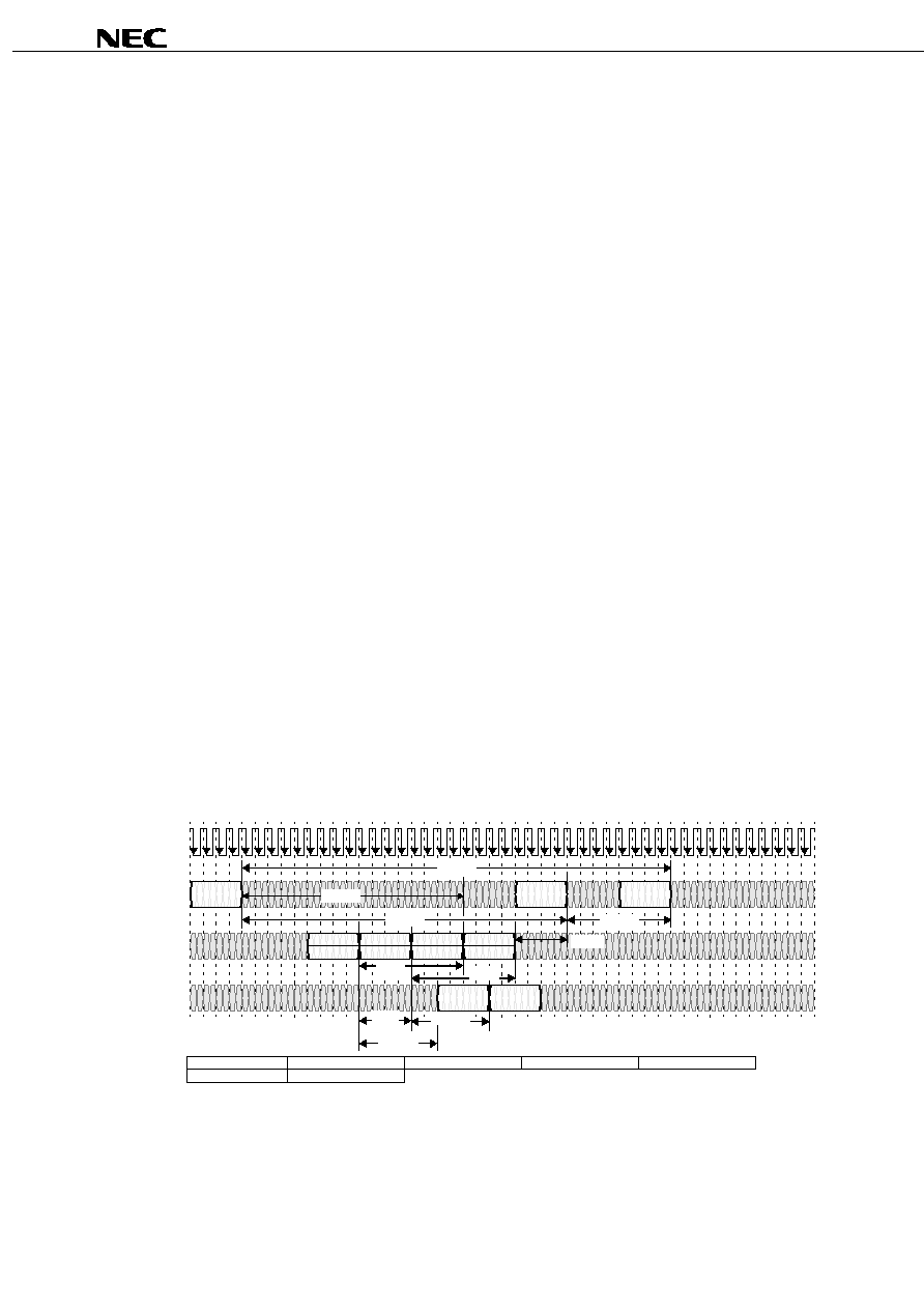
Data Sheet M14837EJ3V0DS00
27
µ
µ
µ
µ
PD488448 for Rev. P
14. Write Transaction - Example
Figure 14-1 shows an example of a write transaction. It begins by activating a bank with an ACT a0 command in an
ROWA packet. A time t
RCD
- t
RTR
later a WR a1 command is issued in a COLC packet (note that the t
RCD
interval is
measured to the end of the COLC packet with the first retire command). Note that the ACT command includes the
device, bank, and row address (abbreviated as a0) while the WR command includes device, bank, and column
address (abbreviated as a1). A time t
CWD
after the WR command the write data dualoct D(a1) is issued. Note that
the packets on the ROW and COL pins use the end of the packet as a timing reference point, while the packets on
the DQA/DQB pins use the beginning of the packet as a timing reference point.
A time t
CC
after the first COLC packet on the COL pins a second COLC packet is issued. It contains a WR a2
command. The a2 address has the same device and bank address as the a1 address (and a0 address), but a
different column address. A time t
CWD
after the second WR command a second write data dualoct D(a2) is issued.
A time t
RTR
after each WR command an optional COLM packet MSK (a1) is issued, and at the same time a COLC
packet is issued causing the write buffer to automatically retire. See Figure 15-1 for more detail on the write/retire
mechanism. If a COLM packet is not used, all data bytes are unconditionally written. If the COLC packet which
causes the write buffer to retire is delayed, then the COLM packet (if used) must also be delayed.
Next, a PRER a3 command is issued in an ROWR packet on the ROW pins. This causes the bank to precharge so
that a different row may be activated in a subsequent transaction or so that an adjacent bank may be activated. The
a3 address includes the same device and bank address as the a0, a1, and a2 addresses. The PRER command
must occur a time t
RAS
or more after the original ACT command (the activation operation in any DRAM is destructive,
and the contents of the selected row must be restored from the two associated sense amps of the bank during the
t
RAS
interval).
A PRER a3 command is issued in an ROWR packet on the ROW pins. The PRER command must occur a time t
RTP
or more after the last COLC which causes an automatic retire.
Finally, an ACT b0 command is issued in an ROWR packet on the ROW pins. The second ACT command must
occur a time t
RC
or more after the first ACT command and a time t
RP
or more after the PRER command. This ensures
that the bank and its associated sense amps are precharged. This example assumes that the second transaction
has the same device and bank address as the first transaction, but a different row address. Transaction b may not
be started until transaction a has finished. However, transactions to other banks or other devices may be issued
during transaction a.
Figure 14-1 Write Transaction Example
CTM/CFM
DQA7..0
DQB7..0
COL4
..COL0
ROW2
..ROW0
T
0
T
4
T
8
T
12
T
1
T
5
T
9
T
13
T
2
T
6
T
10
T
14
T
3
T
7
T
11
T
15
T
16
T
20
T
24
T
28
T
17
T
21
T
25
T
29
T
18
T
22
T
26
T
30
T
19
T
23
T
27
T
31
T
32
T
36
T
40
T
44
T
33
T
37
T
41
T
45
T
34
T
38
T
42
T
46
T
35
T
39
T
43
T
47
MSK (a2)
retire (a2)
MSK (a1)
retire (a1)
WR a1
PRER a3
WR a2
D (a2)
D (a1)
ACT b0
t
RC
t
RP
ACT a0
t
CWD
Transaction a: WR
a0 = {Da,Ba,Ra}
a1 = {Da,Ba,Ca1}
a2 = {Da,Ba,Ca2}
a3 = {Da,Ba}
t
CC
t
CWD
t
RTR
t
RAS
t
RTR
t
RTP
Transaction b: xx
b0 = {Da,Ba,Rb}
RCD
t
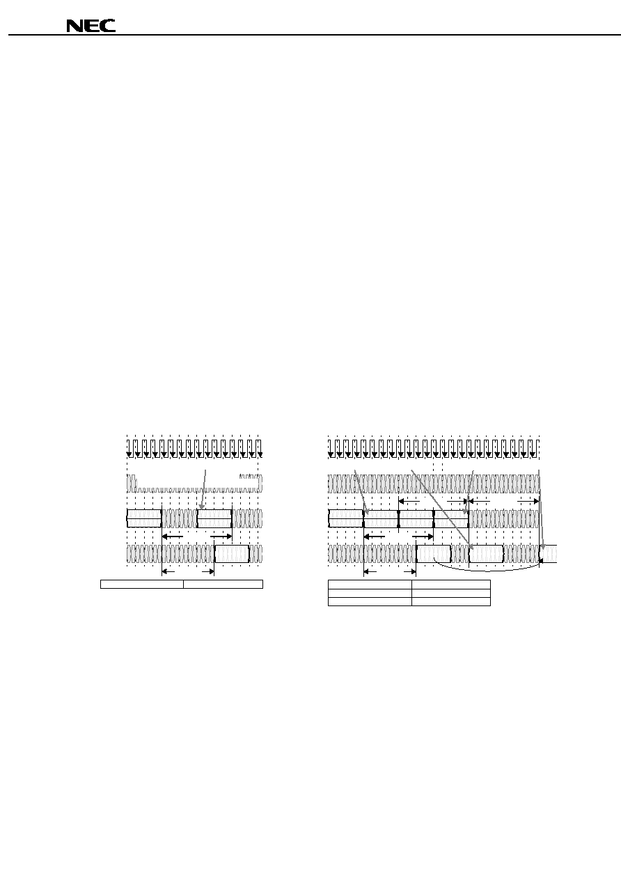
Data Sheet M14837EJ3V0DS00
28
µ
µ
µ
µ
PD488448 for Rev. P
15. Write/Retire - Examples
The process of writing a dualoct into a sense amp of an RDRAM bank occurs in two steps. The first step consists of
transporting the write command, write address, and write data into the write buffer. The second step happens when
the RDRAM automatically retires the write buffer (with an optional bytemask) into the sense amp. This two-step write
process reduces the natural turn-around delay due to the internal bidirectional data pins.
Figure 15-1 (left) shows an example of this two step process. The first COLC packet contains the WR command
and an address specifying device, bank and column. The write data dualoct follows a time t
CWD
later. This
information is loaded into the write buffer of the specified device. The COLC packet which follows a time t
RTR
later
will retire the write buffer. The retire will happen automatically unless (1) a COLC packet is not framed (no COLC
packet is present and the S bit is zero), or (2) the COLC packet contains a RD command to the same device. If the
retire does not take place at time t
RTR
after the original WR command, then the device continues to frame COLC
packets, looking for the first that is not a RD directed to itself. A bytemask MSK(a1) may be supplied in a COLM
packet aligned with the COLC that retires the write buffer at time t
RTR
after the WR command.
The memory controller must be aware of this two-step write/retire process. Controller performance can be
improved, but only if the controller design accounts for several side effects.
Figure 15-1 (right) shows the first of these side effects. The first COLC packet has a WR command which loads the
address and data into the write buffer. The third COLC causes an automatic retire of the write buffer to the sense
amp. The second and fourth COLC packets (which bracket the retire packet) contain RD commands with the same
device, bank and column address as the original WR command. In other words, the same dualoct address that is
written is read both before and after it is actually retired. The first RD returns the old dualoct value from the sense
amp before it is overwritten. The second RD returns the new dualoct value that was just written.
Figure 15-1 Normal Retire (left) and Retire/Read Ordering (right)
CTM/CFM
DQA7..0
DQB7..0
COL4
..COL0
ROW2
..ROW0
T
0
T
4
T
8
T
12
T
1
T
5
T
9
T
13
T
2
T
6
T
10
T
14
T
3
T
7
T
11
T
15
T
16
T
20
T
17
T
21
T
18
T
22
T
19
T
23
Transaction a: WR
a1= {Da,Ba,Ca1}
D (a1)
WR a1
CTM/CFM
DQA7..0
DQB7..0
COL4
..COL0
ROW2
..ROW0
T
0
T
4
T
8
T
12
T
1
T
5
T
9
T
13
T
2
T
6
T
10
T
14
T
3
T
7
T
11
T
15
T
16
T
20
T
17
T
21
T
18
T
22
T
19
T
23
Transaction a: WR
Transaction b: RD
a1= {Da,Ba,Ca1}
b1= {Da,Ba,Ca1}
retire (a1)
MSK (a1)
t
RTR
t
CWD
D (a1)
WR a1
retire (a1)
MSK (a1)
t
RTR
RD b1
RD c1
Q (b1)
t
CWD
Transaction c: RD
c1= {Da,Ba,Ca1}
t
CAC
This RD gets the old data
This RD gets the new data
Retire is automatic here unless:
t
CAC
(1) No COLC packet (S=0) or
(2) COLC packet is RD to device Da
Q (
Figure 15-2 (left) shows the result of performing a RD command to the same device in the same COLC packet slot
that would normally be used for the retire operation. The read may be to any bank and column address; all that
matters is that it is to the same device as the WR command. The retire operation and MSK(a1) will be delayed by a
time t
PACKET
as a result. If the RD command used the same bank and column address as the WR command, the old
data from the sense amp would be returned. If many RD commands to the same device were issued instead of the
single one that is shown, then the retire operation would be held off an arbitrarily long time. However, once a RD to
another device or a WR or NOCOP to any device is issued, the retire will take place. Figure 15-2 (right) illustrates a
situation in which the controller wants to issue a WR-WR-RD COLC packet sequence, with all commands addressed
to the same device, but addressed to any combination of banks and columns.
The RD will prevent a retire of the first WR from automatically happening. But the first dualoct D(a1) in the write

Data Sheet M14837EJ3V0DS00
29
µ
µ
µ
µ
PD488448 for Rev. P
buffer will be overwritten by the second WR dualoct D(b1) if the RD command is issued in the third COLC packet.
Therefore, it is required in this situation that the controller issue a NOCOP command in the third COLC packet,
delaying the RD command by a time of t
PACKET
. This situation is explicitly shown in Table 8-1 for the cases in which
t
CCDELAY
is equal to t
RTR
.
Figure 15-2 Retire Held Off by Read (left) and Controller Forces WWR Gap (right)
CTM/CFM
DQA7..0
DQB7..0
COL4
..COL0
ROW2
..ROW0
T
0
T
4
T
8
T
12
T
1
T
5
T
9
T
13
T
2
T
6
T
10
T
14
T
3
T
7
T
11
T
15
T
16
T
20
T
17
T
21
T
18
T
22
T
19
T
23
Transaction a: WR
Transaction b: RD
a1= {Da,Ba,Ca1}
b1= {Da,Bb,Cb1}
Transaction a: WR
Transaction b: WR
a1= {Da,Ba,Ca1}
b1= {Da,Bb,Cb1}
D (a1)
WR a1
retire (a1)
MSK (a1)
RD b1
Q (b1)
t
CWD
t
CAC
CTM/CFM
DQA7..0
DQB7..0
COL4
..COL0
ROW2
..ROW0
T
0
T
4
T
8
T
12
T
1
T
5
T
9
T
13
T
2
T
6
T
10
T
14
T
3
T
7
T
11
T
15
T
16
T
20
T
17
T
18
T
19
D (a1)
WR a1
RD c1
t
RTR
retire (a1)
MSK (a1)
t
CWD
t
CAC
WR b1
D (b1)
Transaction c: RD
c1= {Da,Bc,Cc1}
The controller must insert a NOCOP to retire (a1)
to make room for the data (b1) in the write buffer
The retire operation for a write can be
held off by a read to the same device
t
RTR
+ t
PACKET
Figure 15-3 shows a possible result when a retire is held off for a long time (an extended version of Figure 15-2-left).
After a WR command, a series of six RD commands are issued to the same device (but to any combination of bank
and column addresses). In the meantime, the bank Ba to which the WR command was originally directed is
precharged, and a different row Rc is activated. When the retire is automatically performed, it is made to this new
row, since the write buffer only contains the bank and column address, not the row address. The controller can
insure that this doesn't happen by never precharging a bank with an unretired write buffer. Note that in a system with
more than one RDRAM, there will never be more than two RDRAMs with unretired write buffers. This is because a
WR command issued to one device automatically retires the write buffers of all other devices written a time t
RTR
before or earlier.
Figure 15-3 Retire Held Off by Reads to Same Device, Write Buffer Retired to New Row
CTM/CFM
DQA7..0
DQB7..0
COL4
..COL0
ROW2
..ROW0
T
0
T
4
T
8
T
12
T
1
T
5
T
9
T
13
T
2
T
6
T
10
T
14
T
3
T
7
T
11
T
15
T
16
T
20
T
24
T
28
T
17
T
21
T
25
T
29
T
18
T
22
T
26
T
30
T
19
T
23
T
27
T
31
T
32
T
36
T
40
T
44
T
33
T
37
T
41
T
45
T
34
T
38
T
42
T
46
T
35
T
39
T
43
T
47
MSK (a1)
retire (a1)
RD b1
WR a1
PRER a2
t
RCD
ACT c0
t
RAS
t
RC
t
RP
ACT a0
t
CWD
t
RTR
Transaction a: WR
a0 = {Da,Ba,Ra}
a1 = {Da,Ba,Ca1}
a2 = {Da,Ba}
RD b2
RD b3
RD b4
RD b5
RD b6
Transaction b: RD
b1 = {Da,Bb,Cb1}
b2 = {Da,Bb,Cb2}
b3= {Da,Bb,Cb3}
b4 = {Da,Bb,Cb4}
b5 = {Da,Bb,Cb5}
b6 = {Da,Bb,Cb6}
Q (b1)
t
CAC
Q (b2)
Q (b3)
Q (b4)
Q (b5)
Transaction c: WR
c0 = {Da,Ba,Rc}
D (a1)
The retire operation puts the
write data in the new row
WARNING
This sequence is hazardous
and must be used with caution
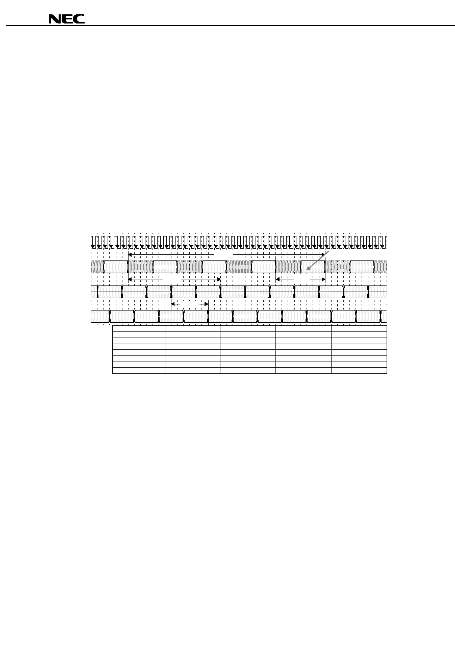
Data Sheet M14837EJ3V0DS00
30
µ
µ
µ
µ
PD488448 for Rev. P
16. Interleaved Write - Example
Figure 16-1 shows an example of an interleaved write transaction. Transactions similar to the one presented in
Figure 14-1 are directed to non-adjacent banks of a single RDRAM. This allows a new transaction to be issued once
every t
RR
interval rather than once every t
RC
interval (four times more often). The DQ data pin efficiency is 100% with
this sequence.
With two dualocts of data written per transaction, the COL, DQA, and DQB pins are fully utilized. Banks are
precharged using the WRA autoprecharge option rather than the PRER command in an ROWR packet on the ROW
pins.
In this example, the first transaction is directed to device Da and bank Ba. The next three transactions are directed
to the same device Da, but need to use different, non-adjacent banks Bb, Bc, Bd so there is no bank conflict. The
fifth transaction could be redirected back to bank Ba without interference, since the first transaction would have
completed by then (t
RC
has elapsed). Each transaction may use any value of row address (Ra, Rb, ...) and column
address (Ca1, Ca2, Cb1, Cb2, ...).
Figure 16-1 Interleaved Write Transaction with Two Dualoct Data Length
CTM/CFM
DQA7..0
DQB7..0
COL4
..COL0
ROW2
..ROW0
T
0
T
4
T
8
T
12
T
1
T
5
T
9
T
13
T
2
T
6
T
10
T
14
T
3
T
7
T
11
T
15
T
16
T
20
T
24
T
28
T
17
T
21
T
25
T
29
T
18
T
22
T
26
T
30
T
19
T
23
T
27
T
31
T
32
T
36
T
40
T
44
T
33
T
37
T
41
T
45
T
34
T
38
T
42
T
46
T
35
T
39
T
43
T
47
ACT a0
MSK (b2)
WRA c2
MSK (b1)
WR c1
WR b1
MSK (a1)
WRA b2
MSK (a2)
D (b2)
D (b1)
ACT b0
ACT c0
ACT d0
ACT e0
D (a2)
D (a1)
WR d1
MSK (c1)
D(c1)
ACT f0
WR d2
MSK (c2)
WR e1
MSK (d1)
D (c2)
D (d1)
WR e2
MSK (d2)
D (z2)
D (z1)
D (x2)
D (y1)
D (y2)
MSK (z2)
WRA a2
MSK (z1)
WR a1
WR z1
MSK (y1)
WRA z2
MSK (y2)
Q (
t
RCD
t
CWD
t
RC
Transaction e can use the
same bank as transaction a
t
RR
f3 = {Da,Ba+2}
Transaction f: WR
f0 = {Da,Ba+2,Rf}
f1 = {Da,Ba+2,Cf1}
f2= {Da,Ba+2,Cf2}
e3 = {Da,Ba}
Transaction e: WR
e0 = {Da,Ba,Re}
e1 = {Da,Ba,Ce1}
e2= {Da,Ba,Ce2}
d3 = {Da,Ba+6}
Transaction d: WR
d0 = {Da,Ba+6,Rd}
d1 = {Da,Ba+6,Cd1}
d2= {Da,Ba+6,Cd2}
c3 = {Da,Ba+4}
Transaction c: WR
c0 = {Da,Ba+4,Rc}
c1 = {Da,Ba+4,Cc1}
c2= {Da,Ba+4,Cc2}
b3 = {Da,Ba+2}
Transaction b: WR
b0 = {Da,Ba+2,Rb}
b1 = {Da,Ba+2,Cb1}
b2= {Da,Ba+2,Cb2}
a3 = {Da,Ba}
Transaction a: WR
a0 = {Da,Ba,Ra}
a1 = {Da,Ba,Ca1}
a2= {Da,Ba,Ca2}
z3 = {Da,Ba+6}
Transaction z: WR
z0 = {Da,Ba+6,Rz}
z1 = {Da,Ba+6,Cz1}
z2= {Da,Ba+6,Cz2}
y3 = {Da,Ba+4}
Transaction y: WR
y0 = {Da,Ba+4,Ry}
y1 = {Da,Ba+4,Cy1}
y2= {Da,Ba+4,Cy2}
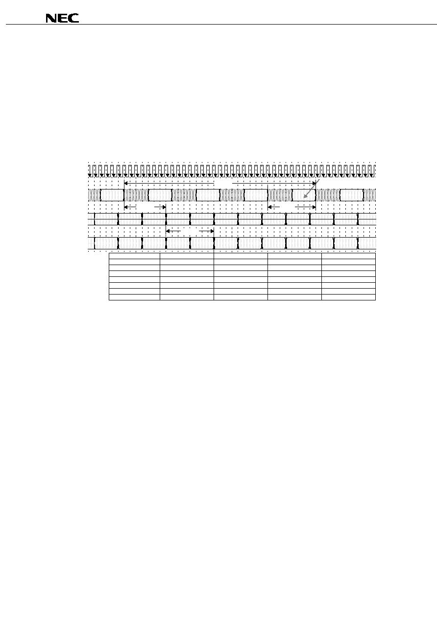
Data Sheet M14837EJ3V0DS00
31
µ
µ
µ
µ
PD488448 for Rev. P
17. Interleaved Read - Example
Figure 17-1 shows an example of interleaved read transactions. Transactions similar to the one presented in Figure
13-1 are directed to non-adjacent banks of a single RDRAM. The address sequence is identical to the one used in
the previous write example. The DQ data pins efficiency is also 100%. The only difference with the write example
(aside from the use of the RD command rather than the WR command) is the use of the PREX command in a COLX
packet to precharge the banks rather than the RDA command. This is done because the PREX is available for a
readtransaction but is not available for a masked write transaction.
Figure 17-1 Interleaved Read Transaction with Two Dualoct Data Length
CTM/CFM
DQA7..0
DQB7..0
COL4
..COL0
ROW2
..ROW0
T
0
T
4
T
8
T
12
T
1
T
5
T
9
T
13
T
2
T
6
T
10
T
14
T
3
T
7
T
11
T
15
T
16
T
20
T
24
T
28
T
17
T
21
T
25
T
29
T
18
T
22
T
26
T
30
T
19
T
23
T
27
T
31
T
32
T
36
T
40
T
44
T
33
T
37
T
41
T
45
T
34
T
38
T
42
T
46
T
35
T
39
T
43
T
47
ACT a0
PREX b3
RD c2
RD c1
RD b1
RD b2
PREX a3
ACT b0
ACT c0
ACT d0
ACT e0
RD a1
RD a2
PREX z3
RD d1
RDd2
PREX c3
RD e1
RD e2
PREX d3
RD z1
RD z2
PREX y3
Q (b2)
Q (b1)
Q (a2)
Q (a1)
Q (c1)
Q (c2)
Q (d1)
Q (z2)
Q (z1)
Q (x2)
Q (y1)
Q (y2)
t
RCD
t
CAC
Transaction e can use the
same bank as transaction a
t
RC
t
RR
f3 = {Da,Ba+2}
Transaction f: RD
f0 = {Da,Ba+2,Rf}
f1 = {Da,Ba+2,Cf1}
f2= {Da,Ba+2,Cf2}
e3 = {Da,Ba}
Transaction e: RD
e0 = {Da,Ba,Re}
e1 = {Da,Ba,Ce1}
e2= {Da,Ba,Ce2}
d3 = {Da,Ba+6}
Transaction d: RD
d0 = {Da,Ba+6,Rd}
d1 = {Da,Ba+6,Cd1}
d2= {Da,Ba+6,Cd2}
c3 = {Da,Ba+4}
Transaction c: RD
c0 = {Da,Ba+4,Rc}
c1 = {Da,Ba+4,Cc1}
c2= {Da,Ba+4,Cc2}
b3 = {Da,Ba+2}
Transaction b: RD
b0 = {Da,Ba+2,Rb}
b1 = {Da,Ba+2,Cb1}
b2= {Da,Ba+2,Cb2}
a3 = {Da,Ba}
Transaction a: RD
a0 = {Da,Ba,Ra}
a1 = {Da,Ba,Ca1}
a2= {Da,Ba,Ca2}
z3 = {Da,Ba+6}
Transaction z: RD
z0 = {Da,Ba+6,Rz}
z1 = {Da,Ba+6,Cz1}
z2= {Da,Ba+6,Cz2}
y3 = {Da,Ba+4}
Transaction y: RD
y0 = {Da,Ba+4,Ry}
y1 = {Da,Ba+4,Cy1}
y2= {Da,Ba+4,Cy2}
ACT f0

Data Sheet M14837EJ3V0DS00
32
µ
µ
µ
µ
PD488448 for Rev. P
18. Interleaved RRWW - Example
Figure 18-1 shows a steady-state sequence of 2-dualoct RD/RD/WR/WR.. transactions directed to non-adjacent
banks of a single RDRAM. This is similar to the interleaved write and read examples in Figure 16-1 and Figure 17-1
except that bubble cycles need to be inserted by the controller at read/write boundaries. The DQ data pin efficiency
for the example in Figure 18-1 is 32/42 or 76%. If there were more RDRAMs on the Channel, the DQ pin efficiency
would approach 32/34 or 94% for the two-dualoct RRWW sequence (this case is not shown).
In Figure 18-1, the first bubble type t
CBUB1
is inserted by the controller between a RD and WR command on the COL
pins. This bubble accounts for the round-trip propagation delay that is seen by read data, and is explained in detail in
Figure 4-1. This bubble appears on the DQA and DQB pins as t
DBUB1
between a write data dualoct D and read data
dualoct Q. This bubble also appears on the ROW pins as t
RBUB1
.
The second bubble type t
CBUB2
is inserted (as a NOCOP command) by the controller between a WR and RD
command on the COL pins when there is a WR-WR-RD sequence to the same device. This bubble enables write
data to be retired from the write buffer without being lost, and is explained in detail in Figure 15-2. There would be no
bubble if address c0 and address d0 were directed to different devices. This bubble appears on the DQA and DQB
pins as t
DBUB2
between a write data dualoct D and read data dualoct Q. This bubble also appears on the ROW pins
as t
RBUB2
.
Figure 18-1 Interleaved RRWW Sequence with Two Dualoct Data Length
CTM/CFM
DQA7..0
DQB7..0
COL4
..COL0
ROW2
..ROW0
T
0
T
4
T
8
T
12
T
1
T
5
T
9
T
13
T
2
T
6
T
10
T
14
T
3
T
7
T
11
T
15
T
16
T
20
T
24
T
28
T
17
T
21
T
25
T
29
T
18
T
22
T
26
T
30
T
19
T
23
T
27
T
31
T
32
T
36
T
40
T
44
T
33
T
37
T
41
T
45
T
34
T
38
T
42
T
46
T
35
T
39
T
43
T
47
ACT a0
MSK (b2)
WRA c2
MSK (b1)
WR c1
WR b1
MSK (y2)
WRA b2
PREX a3
D (b2)
D (b1)
ACT b0
ACT c0
ACT d0
ACT e0
RD a1
RD a2
PREX z3
Q (a2)
Q (a1)
MSK (c1)
D (c1)
NOCOP
RDd0
D (c2)
t
RBUB1
RD f
Q (z2)
Q (z1)
D (y2)
RD z1
RD z2
t
CBUB1
t
DBUB1
t
DBUB1
t
DBUB2
t
CBUB2
t
RBUB2
t
CBUB2
NOCOP
f3 = {Da,Ba+2}
Transaction f: WR
f0 = {Da,Ba+2,Rf}
f1 = {Da,Ba+2,Cf1}
f2= {Da,Ba+2,Cf2}
e3 = {Da,Ba}
Transaction e: RD
e0 = {Da,Ba,Re}
e1 = {Da,Ba,Ce1}
e2= {Da,Ba,Ce2}
d3 = {Da,Ba+6}
Transaction d: RD
d0 = {Da,Ba+6,Rd}
d1 = {Da,Ba+6,Cd1}
d2= {Da,Ba+6,Cd2}
c3 = {Da,Ba+4}
Transaction c: WR
c0 = {Da,Ba+4,Rc}
c1 = {Da,Ba+4,Cc1}
c2= {Da,Ba+4,Cc2}
b3 = {Da,Ba+2}
Transaction b: WR
b0 = {Da,Ba+2,Rb}
b1 = {Da,Ba+2,Cb1}
b2= {Da,Ba+2,Cb2}
a3 = {Da,Ba}
Transaction a: RD
a0 = {Da,Ba,Ra}
a1 = {Da,Ba,Ca1}
a2= {Da,Ba,Ca2}
z3 = {Da,Ba+6}
Transaction z: RD
z0 = {Da,Ba+6,Rz}
z1 = {Da,Ba+6,Cz1}
z2= {Da,Ba+6,Cz2}
y3 = {Da,Ba+4}
Transaction y: WR
y0 = {Da,Ba+4,Ry}
y1 = {Da,Ba+4,Cy1}
y2= {Da,Ba+4,Cy2}
Transaction e can use the
same bank as transaction a
MSK (c2)
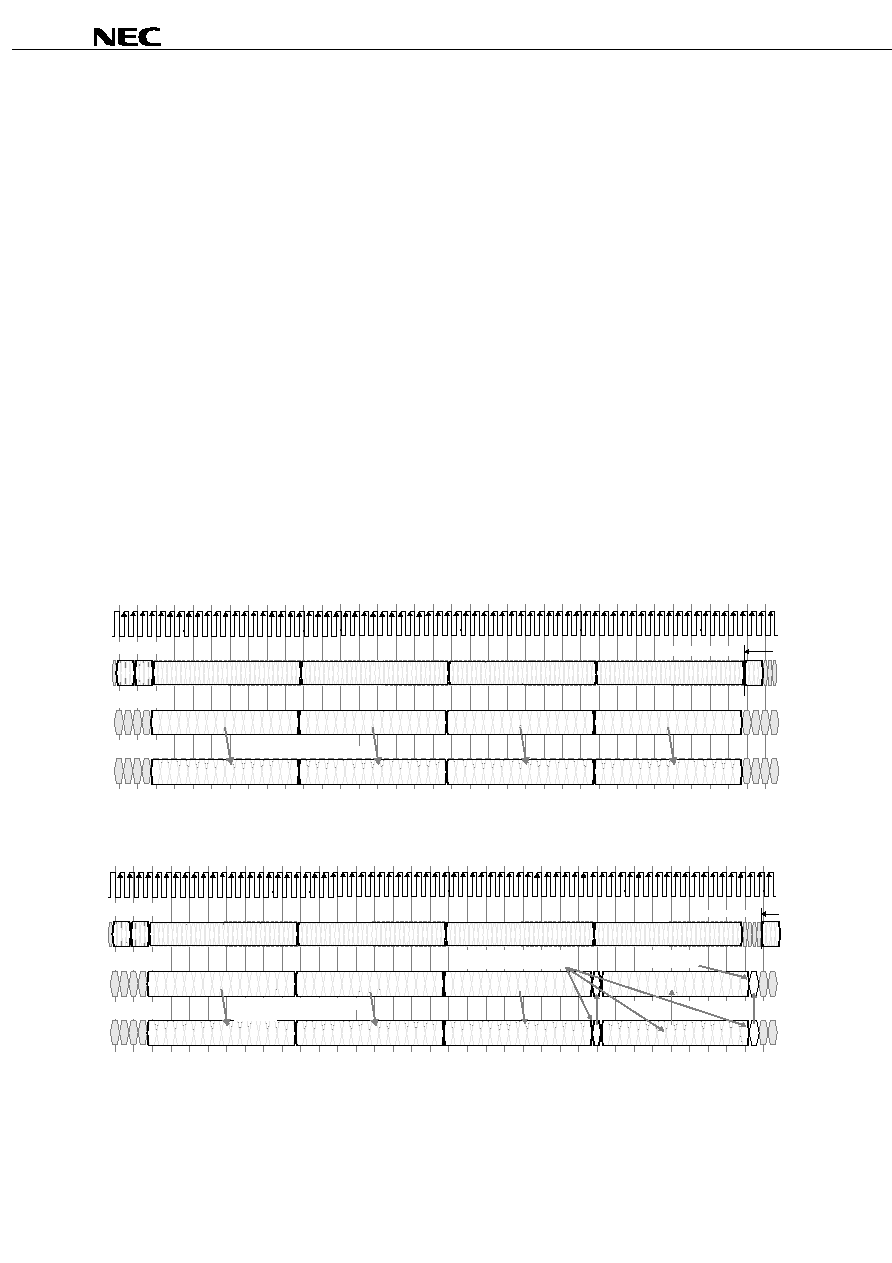
Data Sheet M14837EJ3V0DS00
33
µ
µ
µ
µ
PD488448 for Rev. P
19. Control Register Transactions
The RDRAM has two CMOS input pins SCK and CMD and two CMOS input/output pins SIO0 and SIO1. These
provide serial access to a set of control registers in the RDRAM. These control registers provide configuration
information to the controller during the initialization process. They also allow an application to select the appropriate
operating mode of the RDRAM. SCK (serial clock) and CMD (command) are driven by the controller to all RDRAMs
in parallel. SIO0 and SIO1 are connected (in a daisy chain fashion) from one RDRAM to the next. In normal
operation, the data on SIO0 is repeated on SIO1, which connects to SIO0 of the next RDRAM (the data is repeated
from SIO1 to SIO0 for a read data packet). The controller connects to SIO0 of the first RDRAM.
Write and read transactions are each composed of four packets, as shown in Figure 19-1 and Figure 19-2. Each
packet consists of 16 bits, as summarized in Table 20-1 and Table 20-2. The packet bits are sampled on the falling
edge of SCK. A transaction begins with a SRQ (Serial Request) packet. This packet is framed with a 11110000
pattern on the CMD input (note that the CMD bits are sampled on both the falling edge and the rising edge of SCK).
The SRQ packet contains the SOP3..SOP0 (Serial Opcode) field, which selects the transaction type. The
SDEV5..SDEV0 (Serial Device address) selects one of the 32 RDRAMs. If SBC (Serial Broadcast) is set, then all
RDRAMs are selected. The SA (Serial Address) packet contains a 12 bit address for selecting a control register.
A write transaction has a SD (Serial Data) packet next. This contains 16 bits of data that is written into the selected
control register. A SINT (Serial Interval) packet is last, providing some delay for any side-effects to take place. A
read transaction has a SINT packet, then a SD packet. This provides delay for the selected RDRAM to access the
control register. The SD read data packet travels in the opposite direction (towards the controller) from the other
packet types. The SCK cycle time will accommodate the total delay.
Figure 19-1 Serial Write (SWR) Transaction to Control Register
SRQ - SWR command
1111
00000000...00000000
SRQ - SWR command
0000
SA
SA
SD
SD
SINT
SINT
00000000...00000000
00000000...00000000
00000000...00000000
SCK
CMD
SIO0
SIO1
T
4
T
36
T
20
T
52
T
68
Each packet is repeated
from SIO0 to SIO1
1
1
1
1
0
0
0
0
1111
next transaction
Figure 19-2 Serial Read (SRD) Transaction Control Register
SRQ - SRD command
1111
00000000...00000000
SRQ - SRD command
0000
SA
SA
SINT
SINT
SD
SD
00000000...00000000
00000000...00000000
00000000...00000000
SCK
CMD
SIO
0
SIO
1
T
4
T
36
T
20
T
52
T
68
First 3 packets are repeated
from SIO0 to SIO1
1
1
1
1
0
0
0
0
1111
next transaction
0
0
addressed RDRAM devices
0/SD15..SD0/0 on SIO0
controller drives
0 on SIO0
non addressed RDRAMs pass
0/SD15..SD0/0 from SIO1 to SIO0
0
0
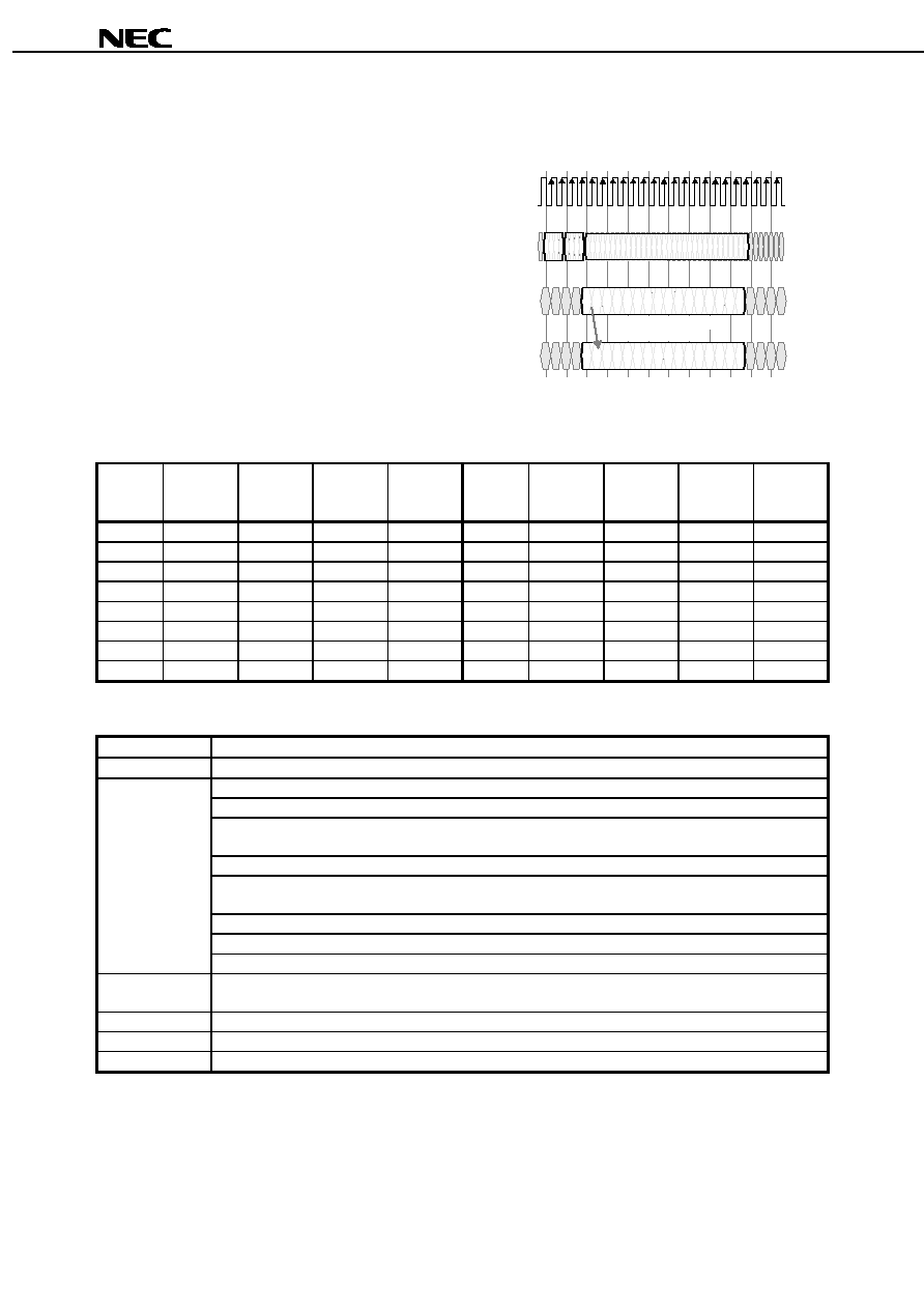
Data Sheet M14837EJ3V0DS00
34
µ
µ
µ
µ
PD488448 for Rev. P
20. Control Register Packets
Table 20-1 summarizes the formats of the four packet
types for control register transactions. Table 20-2
summarizes the fields that are used within the packets.
Figure 20-1 shows the transaction format for the SETR,
CLRR, and SETF commands. These transactions consist
of a single SRQ packet, rather than four packets like the
SWR and SRD commands. The same framing sequence
on the CMD input is used, however. These commands are
used during initialization prior to any control register read
or write transactions.
Table 20-1 Control Register Packet Formats
SCK
Cycle
SIO0 or
SIO1
for SRQ
SIO0 or
SIO1
for SA
SIO0 or
SIO1
for SINT
SIO0 or
SIO1
for SD
SCK
Cycle
SIO0 or
SIO1
for SRQ
SIO0 or
SIO1
for SA
SIO0 or
SIO1
for SINT
SIO0 or
SIO1
for SD
0
rsrv
rsrv
0
SD15
8
SOP1
SA7
0
SD7
1
rsrv
rsrv
0
SD14
9
SOP0
SA6
0
SD6
2
rsrv
rsrv
0
SD13
10
SBC
SA5
0
SD5
3
rsrv
rsrv
0
SD12
11
SDEV4
SA4
0
SD4
4
rsrv
SA11
0
SD11
12
SDEV3
SA3
0
SD3
5
SDEV5
SA10
0
SD10
13
SDEV2
SA2
0
SD2
6
SOP3
SA9
0
SD9
14
SDEV1
SA1
0
SD1
7
SOP2
SA8
0
SD8
15
SDEV0
SA0
0
SD0
Table 20-2 Field Description for Control Register Packets
Field
Description
rsrv
Reserved. Should be driven as "0" by controller.
SOP3..SOP0
0000 - SRD. Serial read of control register {SA11..SA0} of RDRAM {SDEV5..SDEV0}.
0001 - SWR. Serial write of control register {SA11..SA0} of RDRAM {SDEV5..SDEV0}.
0010 - SETR. Set Reset bit, all control registers assume their reset values.
Note
16 t
SCYCLE
delay until CLRR
command.
0100 - SETF. Set fast (normal) clock mode. 4 t
SCYCLE
delay until next command.
1011 - CLRR. Clear Reset bit, all control registers retain their reset values.
Note
4 t
SCYCLE
delay until next
command.
1111 - NOP. No serial operation.
0011, 0101 ≠ 1010, 1100 ≠ 1110 ≠ RSRV. Reserved encodings.
SDEV5..SDEV0
Serial device. Compared to SDEVID5..SDEVID0 field of INIT control register field to select the RDRAM to
which the transaction is directed.
SBC
Serial broadcast. When set, RDRAMs ignore {SDEV5..SDEV0} for RDRAM selection.
SA11..SA0
Serial address. Selects which control register of the selected RDRAM is read or written.
SD15..SD0
Serial data. The 16 bits of data written to or read from the selected control register of the selected RDRAM.
Note The SETR and CLRR commands must always be applied in two successive transactions to RDRAMs; i.e. they may not be
used in isolation. This is called "SETR/CLRR Reset".
Figure 20-1 SETR, CLRR, SETF Transaction
SCK
CMD
SIO0
T
20
SRQ packet - SETR/CLRR/SETF
1111
00000000...00000000
SRQ packet - SETR/CLRR/SETF
0000
SIO1
T
4
The packet is repeated
from SIO0 to SIO1
1
1
1
1
0
0
0
0
Data Sheet M14837EJ3V0DS00
35
µ
µ
µ
µ
PD488448 for Rev. P
21. Initialization
Figure 21-1 SIO Pin Reset Sequence
SCK
CMD
SIO0
T
16
0000000000000000
00000000...00000000
0000000000000000
SIO1
T
0
The packet is repeated
from SIO0 to SIO1
1
1
1
1
0
0
0
0
00001100
Initialization refers to the process that a controller must go through after power is applied to the system or the system
is reset. The controller prepares the RDRAM sub-system for normal Channel operation by (primarily) using a
sequence of control register transactions on the serial CMOS pins. The following steps outline the sequence seen by
the various memory subsystem components (including the RDRAM components) during initialization. This sequence
is available in the form of reference code. Contact Rambus Inc. for more information.
1.0 Start Clocks
This step calculates the proper clock frequencies for PClk (controller logic), SynClk (RAC block), RefClk (DRCG
component), CTM (RDRAM component), and SCK (SIO block).
2.0 RAC Initialization
This step causes the INIT block to generate a sequence of pulses which resets the RAC, performs RAC
maintainance operations, and measures timing intervals in order to ensure clock stability.
3.0 RDRAM Initialization
This stage performs most of the steps needed to initialize the RDRAMs. The rest are performed in stages 5.0,
6.0, and 7.0. All of the steps in 3.0 are carried out through the SIO block interface.
3.1/3.2 SIO Reset
This reset operation is performed before any SIO control register read or write transactions. It clears six
registers (TEST34, CCA, CCB, SKIP, TEST78, and TEST79) and places the INIT register into a special state
(all bits cleared except SKP and SDEVID fields are set to ones).
3.3 Write TEST77 Register
The TEST77 register must be explicitly written with zeros before any other registers are read or written.
3.4 Write TCYCLE Register
The TCYCLE register is written with the cycle time t
CYCLE
of the CTM clock (for Channel and RDRAMs) in
units of 64ps. The t
CYCLE
value is determined in stage 1.0.
3.5 Write SDEVID Register
The SDEVID (serial device identification) register of each RDRAM is written with a unique address value so
that directed SIO read and write transactions can be performed. This address value increases from 0 to 31
according to the distance an RDRAM is from the ASIC component on the SIO bus (the closest RDRAM is
address 0).

Data Sheet M14837EJ3V0DS00
36
µ
µ
µ
µ
PD488448 for Rev. P
3.6 Write DEVID Register
The DEVID (device identification) register of each RDRAM is written with a unique address value so that
directed memory read and write transactions can be performed. This address value increases from 0 to 31.
The DEVID value is not necessarily the same as the SDEVID value. RDRAMs are sorted into regions of the
same core configuration (number of bank, row, and column address bits and core type).
3.7 Write PDNX, PDNXA Registers
The PDNX and PDNXA registers are written with values that are used to measure the timing intervals
connected with an exit from the PDN (powerdown) power state.
3.8 Write NAPX Register
The NAPX register is written with values that are used to measure the timing intervals connected with an exit
from the NAP power state.
3.9 Write TPARM Register
The TPARM register is written with values which determine the time interval between a COL packet with a
memory read command and the Q packet with the read data on the Channel. The values written set each
RDRAM to the minimum value permitted for the system. This will be adjusted later in stage 6.0.
3.10 Write TCDLY1 Register
The TCDLY1 register is written with values which determine the time interval between a COL packet with a
memory read command and the Q packet with the read data on the Channel. The values written set each
RDRAM to the minimum value permitted for the system. This will be adjusted later in stage 6.0.
3.11 Write TFRM Register
The TFRM register is written with a value that is related to the t
RCD
parameter for the system. The t
RCD
parameter is the time interval between a ROW packet with an activate command and the COL packet with a
read or write command.
3.12 SETR/CLRR
First write the following registers with the indicated values:
TEST78
0004
16
TEST34
0040
16
Next, each RDRAM is given a SETR command and a CLRR command through the SIO block. This sequence
performs a second reset operation on the RDRAMs. Then the TEST34 and TEST78 registers are rewritten
with zero, in that order.
3.13 Write CCA and CCB Registers
These registers are written with a value halfway between their minimum and maximum values. This shortens
the time needed for the RDRAMs to reach their steady-state current control values in stage 5.0.
3.14 Powerdown Exit
The RDRAMs are in the PDN power state at this point. A broadcast PDNExit command is performed by the
SIO block to place the RDRAMs in the RLX (relax) power state in which they are ready to receive ROW
packets.
3.15 SETF
Each RDRAM is given a SETF command through the SIO block. One of the operations performed by this step
is to generate a value for the AS (autoskip) bit in the SKIP register and fix the RDRAM to a particular read
domain.

Data Sheet M14837EJ3V0DS00
37
µ
µ
µ
µ
PD488448 for Rev. P
4.0 Controller Configuration
This stage initializes the controller block. Each step of this stage will set a field of the ConfigRMC[63:0] bus to the
appropriate value. Other controller implementations will have similar initialization requirements, and this stage
may be used as a guide.
4.1 Initial Read Data Offset
The ConfigRMC bus is written with a value which determines the time interval between a COL packet with a
memory read command and the Q packet with the read data on the Channel. The value written sets RMC.d1
to the minimum value permitted for the system. This will be adjusted later in stage 6.0.
4.2 Configure Row/Column Timing
This step determines the values of the t
RAS,MIN
, t
RP,MIN
, t
RC,MIN
, t
RCD,MIN
, t
RR,MIN
, and t
PP,MIN
RDRAM timing
parameters that are present in the system. The ConfigRMC bus is written with values that will be compatible
with all RDRAM devices that are present.
4.3 Set Refresh Interval
This step determines the values of the t
REF,MAX
RDRAM timing parameter that are present in the system. The
ConfigRMC bus is written with a value that will be compatible with all RDRAM devices that are present.
4.4 Set Current Control Interval
This step determines the values of the t
CCTRL,MAX
RDRAM timing parameter that are present in the system.
The ConfigRMC bus is written with a value that will be compatible with all RDRAM devices that are present.
4.5 Set Slew Rate Control Interval
This step determines the values of the t
TEMP,MAX
RDRAM timing parameter that are present in the system. The
ConfigRMC bus is written with a value that will be compatible with all RDRAM devices that are present.
4.6 Set Bank/Row/Col Address Bits
This step determines the number of RDRAM bank, row, and column address bits that are present in the
system. It also determines the RDRAM core types (independent, doubled, or split) that are present. The
ConfigRMC bus is written with a value that will be compatible with all RDRAM devices that are present.
5.0 RDRAM Current Control
This step causes the INIT block to generate a sequence of pulses which performs RDRAM maintenance
operations.
6.0 RDRAM Core, Read Domain Initialization
This stage completes the RDRAM initialization
6.1 RDRAM Core Initialization
A sequence of 192 memory refresh transactions is performed in order to place the cores of all RDRAMs into
the proper operating state.
6.2 RDRAM Read Domain Initialization
A memory write and memory read transaction is performed to each RDRAM to determine which read domain
each RDRAM occupies. The programmed delay of each RDRAM is then adjusted so the total RDRAM read
delay (propagation delay plus programmed delay) is constant. The TPARM and TCDLY1 registers of each
RDRAM are rewritten with the appropriate read delay values. The ConfigRMC bus is also rewritten with an
updated value.

Data Sheet M14837EJ3V0DS00
38
µ
µ
µ
µ
PD488448 for Rev. P
7.0 Other RDRAM Register Fields
This stage rewrites the INIT register with the final values of the LSR, NSR, and PSR fields.
In essence, the controller must read all the read-only configuration registers of all RDRAMs (or it must read the
SPD device present on each RIMM), it must process this information, and then it must write all the read-write
registers to place the RDRAMs into the proper operating mode.
Initialization Note :
1. During the initialization process, it is necessary for the controller to perform 128 current control operations
(3xCAL, 1xCAL/SAM) and one temperature calibrate operation (TCEN/TCAL) after reset or after powerdown
(PDN) exit.
2. The behavior of
µ
PD488448 Rev. P at initialization is as follows. It is distinguished by the "S28IECO" bit in the
SPD.
S28IECO=1: Upon powerup, the device enters PDN state. The serial operations SETR, CLRR, and SETF
require a SDEVID match.
See the document detailing the reference initialization procedure for more information on how to handle this in
a system.
3. After the step of equalizing the total read delay of each RDRAM has been completed (i.e. after the TCDLY0
and TCDLY1 fields have been written for the final time), a single final memory read transaction should be
made to each RDRAM in order to ensure that the output pipeline stages have been cleared.
4. The SETF command (in the serial SRQ packet) should only be issued once during the Initialization process,
as should the SETR and CLRR commands.
5. The CLRR command (in the serial SRQ packet) leaves some of the contents of the memory core in an
indeterminate state.
Data Sheet M14837EJ3V0DS00
39
µ
µ
µ
µ
PD488448 for Rev. P
22. Control Register Summary
Table 22-1 summarizes the RDRAM control registers. Detail is provided for each control register in Figure 22-1.
Read-only bits which are shaded gray are unused and return zero. Read-write bits which are shaded gray are
reserved and should always be written with zero. The RIMM
TM
SPD Application Note (DL-0054) of Rambus Inc.
describes additional read-only configuration registers which are present on Direct RIMMs.
The state of the register fields are potentially affected by the IO Reset operation or the SETR/CLRR operation. This
is indicated in the text accompanying each register diagram.
Table 22-1 Control Register Summary (1/2)
SA11..SA0
Register
Field
read-write/ read-only
Description
021
16
INIT
SDEVID
read-write, 6 bits
Serial device ID. Device address for control register read/write.
PSX
read-write, 1 bit
Power select exit. PDN/NAP exit with device addr on DQA5..0.
SRP
read-write, 1 bit
SIO repeater. Used to initialize RDRAM.
NSR
read-write, 1 bit
NAP self-refresh. Enables self-refresh in NAP mode.
PSR
read-write, 1 bit
PDN self-refresh. Enables self-refresh in PDN mode.
LSR
read-write, 1 bit
Low power self-refresh. Enables low power self-refresh.
TEN
read-write, 1 bit
Temperature sensing enable.
TSQ
read-write, 1 bit
Temperature sensing output.
DIS
read-write, 1 bit
RDRAM disable.
022
16
TEST34
TEST34
read-write, 16 bits
Test register.
023
16
CNFGA
REFBIT
read-only, 3 bits
Refresh bank bits. Used for multi-bank refresh.
DBL
read-only, 1 bit
Double. Specifies doubled-bank architecture.
MVER
read-only, 6 bits
Manufacturer version. Manufacturer identification number.
PVER
read-only, 6 bits
Protocol version. Specifies version of Direct protocol supported.
024
16
CNFGB
BYT
read-only, 1 bit
Byte. Specifies an 8-bit or 9-bit byte size.
DEVTYP
read-only, 3 bits
Device type. Device can be RDRAM or some other device category.
SPT
read-only, 1 bit
Split-core. Each core half is an individual dependent core.
CORG
read-only, 6 bits
Core organization. Bank, row, column address field sizes.
SVER
read-only, 6 bits
Stepping version. Mask version number.
040
16
DEVID
DEVID
read-write, 5 bits
Device ID. Device address for memory read/write.
041
16
REFB
REFB
read-write, 4 bits
Refresh bank. Next bank to be refreshed by self-refresh.
042
16
REFR
REFR
read-write, 9 bits
Refresh row. Next row to be refreshed by REFA, self-refresh.
043
16
CCA
CCA
read-write, 7 bits
Current control A. Controls I
OL
output current for DQA.
ASYMA
read-write, 1 bits
Asymmetry control. Controls asymmetry of V
OL
/V
OH
swing for DQA.
044
16
CCB
CCB
read-write, 7 bits
Current control B. Controls I
OL
output current for DQB.
ASYMB
read-write, 1 bits
Asymmetry control. Controls asymmetry of V
OL
/V
OH
swing for DQB.
045
16
NAPX
NAPXA
read-write, 5 bits
NAP exit. Specifies length of NAP exit phase A.
NAPX
read-write, 5 bits
NAP exit. Specifies length of NAP exit phase A + phase B.
DQS
read-write, 1 bit
DQ select. Selects CMD framing for NAP/PDN exit.
046
16
PDNXA
PDNXA
read-write, 13 bits
PDN exit. Specifies length of PDN exit phase A.
Data Sheet M14837EJ3V0DS00
40
µ
µ
µ
µ
PD488448 for Rev. P
Table 22-1 Control Register Summary (2/2)
SA11..SA0
Register
Field
read-write/ read-only
Description
047
16
PDNX
PDNX
read-write, 13 bits
PDN exit. Specifies length of PDN exit phase A + phase B.
048
16
TPARM
TCAS
read-write, 2 bits
t
CAS-C
core parameter. Determines t
OFFP
datasheet parameter.
TCLS
read-write, 2 bits
t
CLS-C
core parameter. Determines t
CAC
and t
OFFP
datasheet parameters.
TCDLY0
read-write, 3 bits
t
CDLY0-C
core parameter. Programmable delay for read data.
049
16
TFRM
TFRM
read-write, 4 bits
t
FRM-C
core parameter. Determines ROW - COL packet framing interval.
04a
16
TCDLY1 TCDLY1
read-write, 3 bits
t
CDLY-1
core parameter. Programmable delay for read data.
04c
16
TCYCLE TCYCLE
read-write, 14 bits
t
CYCLE
datasheet parameter. Specifies cycle time in 64ps units.
04b
16
SKIP
AS
read-only, 1 bit
Autoskip value established by the SETF command.
MSE
read-write, 1 bit
Manual skip enable. Allows the MS value to override the AS value.
MS
read-write, 1 bit
Manual skip value.
04d
16
TEST77 TEST77
read-write, 16 bits
Test register. Write with zero after SIO reset.
04e
16
TEST78 TEST78
read-write, 16 bits
Test register.
04f
16
TEST79 TEST79
read-write, 16 bits
Test register. Do not read or write after SIO reset.
080
16
-Off
16
reserved reserved
vendor-specific
Vendor-specific test registers. Do not read or write after SIO reset.

Data Sheet M14837EJ3V0DS00
41
µ
µ
µ
µ
PD488448 for Rev. P
Figure 22-1 Control Registers (1/7)
Control Register : INIT
Address : 021
16
15
14
13
12
11
10
9
8
7
6
5
4
3
2
1
0
0
SDE
VID5
DIS
TSQ
TEN
LSR
PSR
NSR
SRP
PSX
0
SDEVID4..0
Read/write register.
Reset values are undefined except as affected by SIO Reset as noted below. SETR/CLRR Reset does not affect this register.
Field
Description
Reset
value
SDEVID5..0 Serial Device Identification. Compared to SDEVID5..0 serial address field of serial request packet for register
read/write transactions. This determines which RDRAM is selected for the register read or write operation.
3f
16
DIS
RDRAM disable. DIS=1 causes RDRAM to ignore NAP/PDN exit sequence, DIS=0 permit normal operation.
This mechanism disables an RDRAM.
0
TSQ
Temperature Sensing Output. TSQ=1 when a temperature trip point has been exceeded, TSQ=0 when it has
not. TSQ is available during a current control operation (see Figure 25-1).
TEN
Temperature Sensing Enable. TEN=1 enables temperature sensing circuitry, permitting the TSQ bit to be
read to determine if a thermal trip point has been exceeded.
0
LSR
Low Power Self-Refresh. LSR=1 enables longer self-refresh interval. The self-refresh supply current is
reduced.
0
PSR
PDN Self-Refresh. PSR=1 enables self-refresh in PDN mode. PSR can't be set while in PDN mode.
0
NSR
NAP Self-Refresh. NSR=1 enables self-refresh in NAP mode. NSR can't be set while in NAP mode.
0
SRP
SIO Repeater. Controls value on SIO1; SIO1=SIO0 if SRP=1, SIO1=1 if SRP=0.
1
PSX
Power Exit Select. PDN and NAP are exited with (=0) or without (=1) a device address on the DQA5..0 pins.
PDEV5 (on DQA5) selectes broadcast (1) or directed (0) exit. For a dircted exit, PDEV4..0 (on DQA4..0) is
compared to DEVID4..0 to select a device.
Control Register : CNFGA
Address : 023
16
15
14
13
12
11
10
9
8
7
6
5
4
3
2
1
0
PVER5..0=000001
MVER5..0=mmmmmm
DBL1
REFBIT2..0=100
Read only register.
Field
Description
PVER5..0
Protocol Version. Specifies the Direct Protocol version used by this device:
0 ≠ Compliant with version 0.62.
1 ≠ Compliant with version 0.7 through this version
2 to 63 ≠ Reserved
MVER5..0
Manufacturer Version. Specifies the manufacturer identification number.
DBL
Doubled-Bank. DBL=1 means the device uses a doubled-bank architecture with adjacent-bank dependency. DBL=0
means no dependency.
REFBIT2..0 Refresh Bank Bits. Specifies the number of bank address bits to used by REFA and REFP commands.
Permits multi-bank refresh in future RDRAMs.
Caution In RDRAMs with protocol version 1 PVER[5:0] =000001, the range of the PDNX field (PDNX[2:0] in the PDNX
register) may not be large enough to specify the location of the restricted interval in Figure 23-3. In this case,
the effective t
S4
parameter must increase and no row or column packets may overlap the restricted interval.
See Figure 23-3 and Timing conditions table.
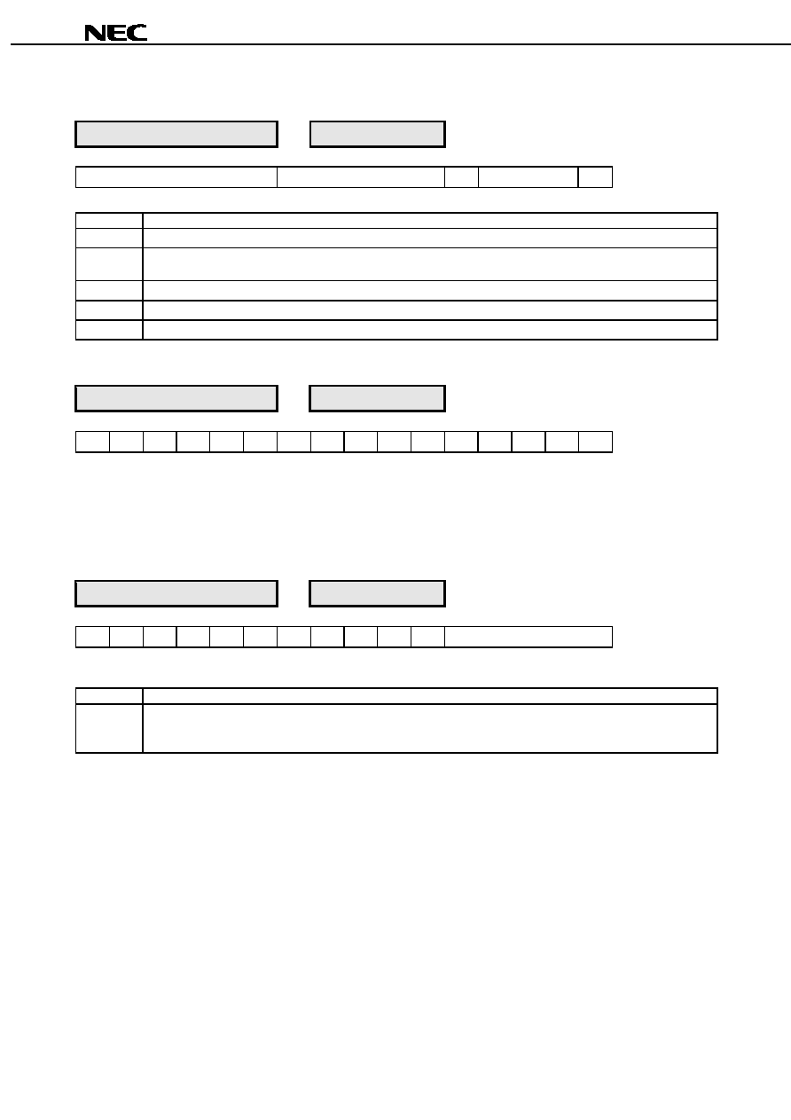
Data Sheet M14837EJ3V0DS00
42
µ
µ
µ
µ
PD488448 for Rev. P
Figure 22-1 Control Registers (2/7)
Control Register : CNFGB
Address : 024
16
15
14
13
12
11
10
9
8
7
6
5
4
3
2
1
0
SVER5..0=ssssss
CORG4..0=xxxxx
SPT0
DEVTYP2..0=000
BYTB
Read only register.
Field
Description
SVER5..0
Stepping version. Specifies the mask version number of this device.
CORG4..0
Core organization. This field specifies the number of bank (3, 4, 5, or 6 bits), row (9, 10, 11, or 12 bits), and column (5,
6, or 7 bits) address bits. The encoding of this field will be specified in a later version of this document.
SPT
Split-core. SPT=1 means the core is split, SPT=0 means it is not.
DEVTYP2..0
Device type. DEVTYP=000 means that this device is an RDRAM.
BYT
Byte width. B=1 means the device reads and writes 9-bit memory bytes.B=0 means 8 bits.
Control Register : TEST34
Address : 022
16
15
14
13
12
11
10
9
8
7
6
5
4
3
2
1
0
0
0
0
0
0
0
0
0
0
0
0
0
0
0
0
0
Read/write register.
Reset values of TEST34 is zero (from SIO Reset).
This register are used for testing purposes. It must not be read or written after SIO Reset except prior to the SETR/CLRR sequence
when it is written with the value 0040
16
.
After SETR/CLRR it is rewritten to 0000
16
.
Control Register : DEVID
Address : 040
16
15
14
13
12
11
10
9
8
7
6
5
4
3
2
1
0
0
0
0
0
0
0
0
0
0
0
0
DEVID4..0
Read/write register.
Reset value is undefined.
Field
Description
DEVID4..0
Device Identification register. DEVID4..DEVID0 is compared to DR4..DR0, DC4..DC0, and DX4..DX0 fields for all
memory read or write transactions. This determines which RDRAM is selected for the memory read or write
transaction.
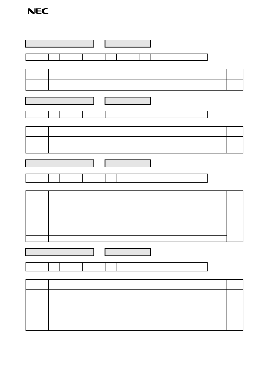
Data Sheet M14837EJ3V0DS00
43
µ
µ
µ
µ
PD488448 for Rev. P
Figure 22-1 Control Registers (3/7)
Control Register : REFB
Address : 041
16
15
14
13
12
11
10
9
8
7
6
5
4
3
2
1
0
0
0
0
0
0
0
0
0
0
0
0
REFB4..0
Read/write register.
Field
Description
Reset
value
REFB4..0
Refresh Bank Register. REFB4..REFB0 is the bank that will be refreshed next during self-refresh. REFB4..0
is incremented after each self-refresh activate and precharge operation pair.
0
Control Register : REFR
Address : 042
16
15
14
13
12
11
10
9
8
7
6
5
4
3
2
1
0
0
0
0
0
0
0
0
REFR8..0
Read/write register.
Field
Description
Reset
value
REFR8..0
Refresh Row register. REFR8..REFR0 is the row that will be refreshed next by the REFA command or by
self-refresh. REFR8..0 is incremented when BR4..0=11111 for the REFA command. REFR8..0 is
incremented when REFB4..0=11111 for self-refresh.
0
Control Register : CCA
Address : 043
16
15
14
13
12
11
10
9
8
7
6
5
4
3
2
1
0
0
0
0
0
0
0
0
0
ASYM
A0
CCA6..0
Read/write register.
Field
Description
Reset
value
ASYMA0 control the asymmetry of the V
OL
/V
OH
voltage swing about the V
REF
reference voltage for the
DQA7..0 pins.
ASYMA0
ODF
0
0.00
1
0.12
ASYMA0
Where ODF is the Over Drive Factor (the extra I
OL
current sunk by an RSL output when ASYMA0 is set).
CCA6..0
Current Control A. Controls the I
OL
output current for the DQA7..DQA0 pins.
0
Control Register : CCB
Address : 044
16
15
14
13
12
11
10
9
8
7
6
5
4
3
2
1
0
0
0
0
0
0
0
0
0
ASYM
B0
CCB6..0
Read/write register.
Field
Description
Reset
value
ASYMB0 control the asymmetry of the V
OL
/V
OH
voltage swing about the V
REF
reference voltage for the
DQB7..0 pins.
ASYMB0
ODF
0
0.00
1
0.12
ASYMB0
Where ODF is the Over Drive Factor (the extra I
OL
current sunk by an RSL output when ASYMB0 is set).
CCB6..0
Current Control B. Controls the I
OL
output current for the DQB7..DQB0 pins.
0
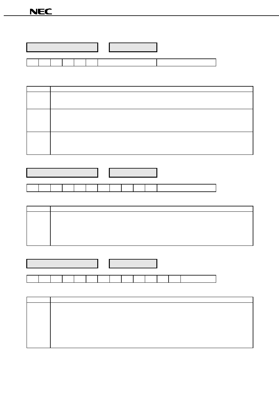
Data Sheet M14837EJ3V0DS00
44
µ
µ
µ
µ
PD488448 for Rev. P
Figure 22-1 Control Registers (4/7)
Control Register : NAPX
Address : 045
16
15
14
13
12
11
10
9
8
7
6
5
4
3
2
1
0
0
0
0
0
0
DQS
NAPX4..0
NAPXA4..0
Read/write register.
Reset value is undefined.
Note t
SCYCLE
is
t
CYCLE1
(SCK cycle time).
Field
Description
DQS
DQ Select. This field specifies the number of SCK cycles (0
0.5 cycles, 1
1.5 cycles) between the CMD pin
framing sequence and the device selection on DQ5..0. see Figure 23-4. This field must be written with a "1" for this
RDRAM.
NAPX4..0
Nap Exit Phase A plus B. This field specifies the number of SCK cycles during the first plus second phases for exiting
NAP mode. It must satisfy:
NAPX
∑
t
SCYCLE
NAPXA
∑
t
SCYCLE
+t
NAPXB
,
MAX
Do not set this field to zero.
NAPXA4..0
Nap Exit Phase A. This field specifies the number of SCK cycles during the first phase for exiting NAP mode. It must
satisfy:
NAPXA
∑
t
SCYCLE
t
NAPXA
,
MAX
Do not set this field to zero.
Control Register : PDNXA
Address : 046
16
15
14
13
12
11
10
9
8
7
6
5
4
3
2
1
0
0
0
0
0
0
0
0
0
0
0
0
PDNXA4..0
Read/write register.
Reset value is undefined.
Field
Description
PDNXA4..0
PDN Exit Phase A. This field specifies the number of (64
∑
SCK cycle) units during the first phase for exiting PDN
mode. It must satisfy:
PDNXA
∑
64
∑
t
SCYCLE
t
PDNXA
,
MAX
Do not set this field to zero.
Note ≠ only PDNXA4..0 are implemented.
Note ≠ t
SCYCLE
is t
CYCLE1
(SCK cycle time).
Control Register : PDNX
Address : 047
16
15
14
13
12
11
10
9
8
7
6
5
4
3
2
1
0
0
0
0
0
0
0
0
0
0
0
0
0
0
PDNX2..0
Read/write register.
Reset value is undefined.
Field
Description
PDNX2..0
PDN Exit Phase A puls B. This field specifies the number of (256
∑
SCK cycle) units during the first plus second phases
for exiting PDN mode. It must satisfy:
PDNX
∑
256
∑
t
SCYCLE
PDNXA
∑
64
∑
t
SCYCLE
+t
PDNXB
,
MAX
It this equation can't be satisfied, then the maximum PDNX value should be written, and the t
S4
/ t
H4
timing window will
be modified (see Figure 23-4).
Do not set this field to zero.
Note ≠ only PDNX2..0 are implemented.
Note ≠ t
SCYCLE
is t
CYCLE1
(SCK cycle time).

Data Sheet M14837EJ3V0DS00
45
µ
µ
µ
µ
PD488448 for Rev. P
Figure 22-1 Control Registers (5/7)
Control Register : TPARM
Address : 048
16
15
14
13
12
11
10
9
8
7
6
5
4
3
2
1
0
0
0
0
0
0
0
0
0
0
TCDLY0
TCLS
TCAL
Read/write register.
Reset value is undefined.
Field
Description
TCDLY0
Specifies the t
CDLY0-C
core parameter in t
CYCLE
units. This adds a programmable delay to Q (read data) packets,
permitting round trip read delay to all device to be equalized. This field may be written with the values "010" (2
∑
t
CYCLE
)
through "101" (5
∑
t
CYCLE
).
TCLS1..0
Specifies the t
CLS-C
core parameter in t
CYCLE
units. Should be "10" (2
∑
t
CYCLE
).
TCAS1..0
Specifies the t
CAS-C
core parameter in t
CYCLE
units. This should be "10" (2
∑
t
CYCLE
).
The equations relating the core parameters to the datasheet parameters follow:
t
CAS-C
=2
∑
t
CYCLE
t
CLS-C
=2
∑
t
CYCLE
t
CPS-C
=1
∑
t
CYCLE
Not programmable
t
OFFP
=t
CPS-C
+ t
CAS-C
+ t
CLS-C
- 1
∑
t
CYCLE
=4
∑
t
CYCLE
t
RCD
=t
RCD-C
+ 1
∑
t
CYCLE
≠ t
CLS-C
=t
RCD-C
- 1
∑
t
CYCLE
t
CAC
=3
∑
t
CYCLE
+ t
CLS-C
+ t
CDLY0-C
+ t
CDLY1-C
(see table below programming ranges)
TCDLY0
t
CDLY0-C
TCDLY1
t
CDLY1-C
t
CAC
@t
CYCLE
=3.30 ns t
CAC
@t
CYCLE
=2.50 ns
010
2
∑
t
CYCLE
000
0
∑
t
CYCLE
7
∑
t
CYCLE
not allowed
011
3
∑
t
CYCLE
000
0
∑
t
CYCLE
8
∑
t
CYCLE
8
∑
t
CYCLE
011
3
∑
t
CYCLE
001
1
∑
t
CYCLE
9
∑
t
CYCLE
9
∑
t
CYCLE
011
3
∑
t
CYCLE
010
2
∑
t
CYCLE
10
∑
t
CYCLE
10
∑
t
CYCLE
100
4
∑
t
CYCLE
010
2
∑
t
CYCLE
11
∑
t
CYCLE
11
∑
t
CYCLE
101
5
∑
t
CYCLE
010
2
∑
t
CYCLE
12
∑
t
CYCLE
12
∑
t
CYCLE
Control Register : TFRM
Address : 049
16
15
14
13
12
11
10
9
8
7
6
5
4
3
2
1
0
0
0
0
0
0
0
0
0
0
0
0
0
TFRM3..0
Read/write register.
Reset value is undefined.
Field
Description
TFRM3..0
Specifies the position of the framing point in t
CYCLE
units. This value must be greater than or equal to the t
FRM,MIN
parameter. This is the minimum offset between a ROW packet (which places a device at ATTN) and the first COL
packet (directed to that device) which must be framed. This field may be written with the value "0111" (7
∑
t
CYCLE
)
through "1010" (10
∑
t
CYCLE
). TFRM is usually set to the value which matches the lagest t
RCD,MIN
parameter (modulo
4
∑
t
CYCLE
) that is present in an RDRAM in the memory system. Thus, if an RDRAM with t
RCD,MIN
=11
∑
t
CYCLE
were
present, then TFRM would be programmed to 7
∑
t
CYCLE
.
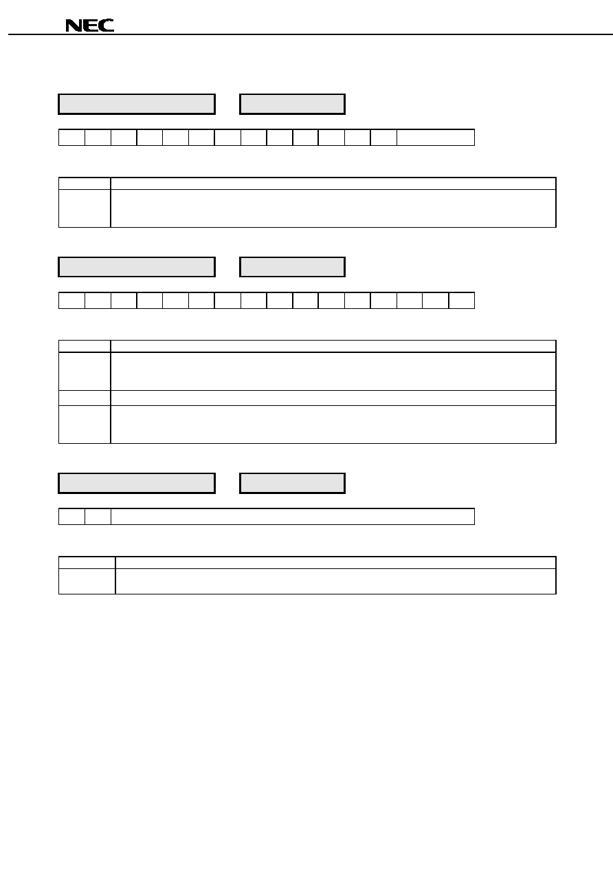
Data Sheet M14837EJ3V0DS00
46
µ
µ
µ
µ
PD488448 for Rev. P
Figure 22-1 Control Registers (6/7)
Control Register : TCDLY1
Address : 04a
16
15
14
13
12
11
10
9
8
7
6
5
4
3
2
1
0
0
0
0
0
0
0
0
0
0
0
0
0
0
TCDLY1
Read/write register.
Reset value is undefined.
Field
Description
TCDLY1
Specifies the value of the t
CDLY1-C
core parameter in t
CYCLE
units. This adds a programmable delay to Q (read data)
packets, permitting round trip read to delay all devices to be equalized. This field may be written with the values "000"
(0
∑
t
CYCLE
) through "010" (2
∑
t
CYCLE
). Refer to TPARM Register for more details.
Control Register : SKIP
Address : 04b
16
15
14
13
12
11
10
9
8
7
6
5
4
3
2
1
0
0
0
0
AS
MSE
MS
0
0
0
0
0
0
0
0
0
0
Read/write register (except AS field).
Reset value is zero.
Field
Description
MS
Manual skip (MS must be 1 when MSE=1). > During initialization, the RDRAMs at the furthest point in the fifth read
domain may have selected the AS=0 value, placing them at the closest point in a sixth read domain. Setting the
MSE/MS fields to 1/1 overrides the autoskip value and returns hem to 111 he furthest point of the fifth read domain.
MSE
Manual skip enable (0=auto, 1=manual ).
AS
Autoskip. Read-only value determined by autoskip circuit and stored when SETF serial command is received by
RDRAM during initialization. In Figure34-1, AS=1 corresponds to the early Q(a1) packet and AS=0 to the Q(a1) packet
one t
CYCLE
later for the four uncertain cases.
Control Register : TCYCLE
Address : 04c
16
15
14
13
12
11
10
9
8
7
6
5
4
3
2
1
0
0
0
TCYCLE13..0
Read/write register.
Reset value is undefined.
Field
Description
TCYCLE13..0
Specifies the value of the t
CYCLE
datasheet parameter in 64ps units. For the t
CYCLE,MIN
of 2.50 ns (2500ps), this field
should be written with the "00027
16
" (39
∑
64ps).

Data Sheet M14837EJ3V0DS00
47
µ
µ
µ
µ
PD488448 for Rev. P
Figure 22-1 Control Registers (7/7)
Control Register : TEST77
Address : 04d
16
Control Register : TEST78
Address : 04e
16
Control Register : TEST79
Address : 04f
16
15
14
13
12
11
10
9
8
7
6
5
4
3
2
1
0
0
0
0
0
0
0
0
0
0
0
0
0
0
0
0
0
Read/write register.
These registers must only be used for testing purposes.
Field
Description
Reset
value
TEST77
It must be written with zero after SIO reset. These registers must only be used for testing purposes
except prior to the SETR/CLRR sequence when TEST78 is written with the value 0004
16
. After
SETR/CLRR it is rewritten to 0000
16
.
TEST78
Do not read or written after SIO reset.
0
TEST79
Do not read or written after SIO reset.
0
∑
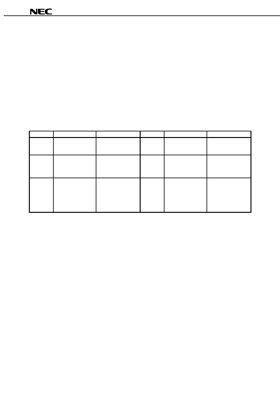
Data Sheet M14837EJ3V0DS00
48
µ
µ
µ
µ
PD488448 for Rev. P
23. Power State Management
Table 23-1 summarizes the power states available to a Direct RDRAM. In general, the lowest power states have
the longest operational latencies. For example, the relative power levels of PDN state and STBY state have a ratio of
about 1:110, and the relative access latencies to get read data have a ratio of about 250:1.
PDN state is the lowest power state available. The information in the RDRAM core is usually maintained with self-
refresh; an internal timer automatically refreshes all rows of all banks. PDN has a relatively long exit latency because
the TCLK/RCLK block must resynchronize itself to the external clock signal.
NAP state is another low-power state in which either self-refresh or REFA-refresh are used to maintain the core.
See 24. Refresh for a description of the two refresh mechanisms. NAP has a shorter exit latency than PDN because
the TCLK/RCLK block maintains its synchronization state relative to the external clock signal at the time of NAP
entry. This imposes a limit (t
NLIMIT
) on how long an RDRAM may remain in NAP state before briefly returning to STBY
or ATTN to update this synchronization state.
Table 23-1 Power State Summary
Power State Description
Blocks consuming power Power state
Description
Blocks consuming power
PDN
Powerdown state.
Self-refresh
NAP
Nap state. Similar to
PDN except lower
wake-up latency.
Self-refresh or
REFA-refresh
TCLK/RCLK-Nap
STBY
Standby state.
Ready for ROW
packets.
REFA-refresh
TCLK/RCLK
ROW demux receiver
ATTN
Attention state.
Ready for ROW and
COL packets.
REFA-refresh
TCLK/RCLK
ROW demux receiver
COL demux receiver
ATTNR
Attention read state.
Ready for ROW and
COL packets.
Sending Q (read data)
packets.
REFA-refresh
TCLK/RCLK
ROW demux receiver
COL demux receiver
DQ mux transmitter
Core power
ATTNW
Attention write state.
Ready for ROW and
COL packets.
Ready for D (write data)
packets.
REFA-refresh
TCLK/RCLK
ROW demux receiver
COL demux receiver
DQ demux receiver
Core power
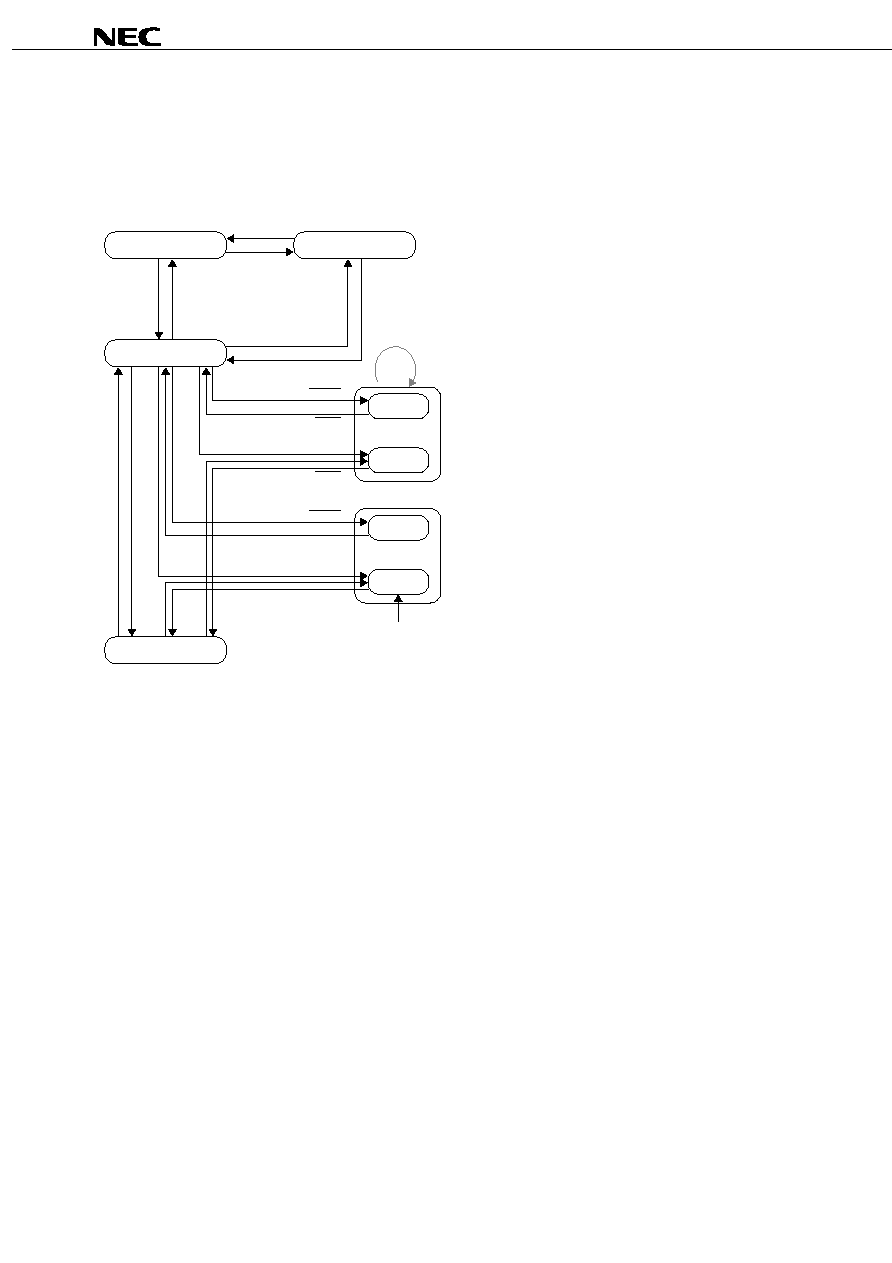
Data Sheet M14837EJ3V0DS00
49
µ
µ
µ
µ
PD488448 for Rev. P
Figure 23-1 summarizes the transition conditions needed for moving between the various power states. Note that
NAP and PDN have been divided into two substates (NAP-A/NAP-S and PDN-A/PDN-S) to account for the fact that a
NAP or PDN exit may be made to either ATTN or STBY states.
Figure 23-1 Power State Transition Diagram
automatic
automatic
automatic
automatic
automatic
automatic
ATTNR
ATTNW
ATTN
STBY
SETR/CLRR
NAP-A
NAPR ∑ RLXR
Notation:
SETR/CLRR - SETR/CLRR Reset sequence in SRQ packet
PDNR - PDNR command in ROWR packet
NAPR - NAPR command in ROWR packet
RLXR - RLX command in ROWR packet
RLX - RLX command in ROWR,COLC,COLX packets
SIO0 - SIO0 input value
PDEV.CMD - (PDEV=DEVID)∑(CMD=01)
ATTN - ROWA packet(non-broadcast) or ROWR packet
(non-broadcast) with ATTN command
t
NLIMIT
NAP
NAP-S
PDEV.CMD∑SIO0
NAPR ∑ RLXR
PDEV.CMD∑SIO0
PDN-A
PDNR ∑ RLXR
PDN
PDN-S
PDEV.CMD∑SIO0
PDNR ∑ RLXR
PDEV.CMD∑SIO0
NAPR
PDNR
ATTN
RLX
At initialization, the SETR/CLRR Reset sequence will put the RDRAM into PDN-S state. The PDN exit sequence
involves an optional PDEV specification and bits on the CMD and SIO
IN
pins.
Once the RDRAM is in STBY, it will move to the ATTN/ATTNR/ATTNW states when it receives a non-broadcast
ROWA packet or non-broadcast ROWR packet with the ATTN command. The RDRAM returns to STBY from these
three states when it receives a RLX command. Alternatively, it may enter NAP or PDN state from ATTN or STBY
states with a NAPR or PDNR command in an ROWR packet. The PDN or NAP exit sequence involves an optional
PDEV specification and bits on the CMD and SIO0
pins. The RDRAM returns to the ATTN or STBY state it was
originally in when it first entered NAP or PDN.
An RDRAM may only remain in NAP state for a time t
NLIMIT
. It must periodically return to ATTN or STBY.
The NAPRC command causes a napdown operation if the RDRAM's NCBIT is set. The NCBIT is not directly visible.
It is undefined on reset. It is set by a NAPR command to the RDRAM, and it is cleared by an ACT command to the
RDRAM. It permits a controller to manage a set of RDRAMs in a mixture of power states.
STBY state is the normal idle state of the RDRAM. In this state all banks and sense amps have usually been left
precharged and ROWA and ROWR packets on the ROW pins are being monitored. When a non-broadcast ROWA
packet or non-broadcast ROWR packet(with the ATTN command) packet addressed to the RDRAM is seen, the
RDRAM enters ATTN state (see the right side of Figure 23-2). This requires a time t
SA
during which the RDRAM
activates the specified row of the specified bank. A time TFRM
∑
t
CYCLE
after the ROW packet, the RDRAM will be able
to frame COL packets (TFRM is a control register field ≠ see Figure 22-1(5/7) " TFRM Register"). Once in ATTN
state, the RDRAM will automatically transition to the ATTNW and ATTNR states as it receives WR and RD
commands.

Data Sheet M14837EJ3V0DS00
50
µ
µ
µ
µ
PD488448 for Rev. P
Once the RDRAM is in ATTN, ATTNW, or ATTNR states, it will remain there until it is explicitly returned to the STBY
state with a RLX command. A RLX command may be given in an ROWR, COLC, or COLX packet (see the left side
of Figure 23-2). It is usually given after all banks of the RDRAM have been precharged; if other banks are still
activated, then the RLX command would probably not be given.
If a broadcast ROWA packet or ROWR packet (with the ATTN command) is received, the RDRAM's power state
doesn't change. If a broadcast ROWR packet with RLXR command is received, the RDRAM goes to STBY.
Figure 23-2 STBY Entry (left) and STBY Exit (right)
STBY
ATTN
CTM/CFM
DQA7..0
DQB7..0
COL4
..COL0
ROW2
..ROW0
T
0
T
4
T
8
T
12
T
1
T
5
T
9
T
13
T
2
T
6
T
10
T
14
T
3
T
7
T
11
T
15
T
16
T
20
T
17
T
21
T
18
T
22
T
19
T
23
CTM/CFM
DQA7..0
DQB7..0
COL4
..COL0
ROW2
..ROW0
T
0
T
4
T
8
T
12
T
1
T
5
T
9
T
13
T
2
T
6
T
10
T
14
T
3
T
7
T
11
T
15
T
16
t
AS
RLXR
Power
State
ATTN
Power
State
STBY
t
SA
ROP a0
RLXC
RLXX
TFRM∑t
CYCLE
COP a1
COP a1
COP a1
COP a1
XOP a1
COP a0
XOP a0
ROP=non-broadcast
ROWA or ROWR/ATTN
a0={d0, b0, r0}
a1={d1, b1, c1}
No COL packets may be
placed in the three
indicated positions; i.e. at
(TFRM-{1,2,3})∑t
CYCLE
.
A COL packet to device d0
(or any other device) is okay at
(TFRM)∑t
CYCLE
or later.
A COL packet to another device
(d1!=d0) is okay at
(TFRM-4)∑t
CYCLE
or earlier.
Figure 23-3 shows the NAP entry sequence (left). NAP state is entered by sending a NAPR command in a ROW
packet. A time t
ASN
is required to enter NAP state (this specification is provided for power calculation purposes). The
clock on CTM/CFM must remain stable for a time t
CD
after the NAPR command.
Figure 23-3 NAP Entry (left) and PDN Entry (right)
CTM/CFM
DQA7..0
DQB7..0
COL4
..COL0
ROW2
..ROW0
T
0
T
4
T
8
T
12
T
1
T
5
T
9
T
13
T
2
T
6
T
10
T
14
T
3
T
7
T
11
T
15
T
16
T
20
T
17
T
21
T
18
T
22
T
19
T
23
CTM/CFM
DQA7..0
DQB7..0
COL4
..COL0
ROW2
..ROW0
T
0
T
4
T
8
T
12
T
1
T
5
T
9
T
13
T
2
T
6
T
10
T
14
T
3
T
7
T
11
t
ASN
ROP a0
(NAPR)
Power
State
ATTN/STBY
Note
Power
State
NAP
ATTN/STBY
Note
PDN
t
ASP
ROP a0
(PDNR)
Note The(eventual) NAP/PDN exit will be to the same ATTN/STBY state the RDRAM was in prior to NAP/PDN entry
t
CD
t
CD
a0={d0, b0, r0, c0}
a1={d1, b1, c1, c1}
No ROW or COL packets directed
to device d0 may overlap the
restricted interval. No broadcast
ROW packets may overlap
the quiet interval.
ROW or COL packets to a device
other than d0 may overlap the
restricted interval.
restricted
ROP a1
COP a0
XOP a0
COP a1
XOP a1
restricted
restricted
ROP a1
COP a0
XOP a0
COP a1
XOP a1
restricted
ROW or COL packets directed
to device d0 after the restricted
interval will be ignored.
t
NPQ
t
NPQ
The RDRAM may be in ATTN or STBY state when the NAPR command is issued. When NAP state is exited, the
RDRAM will return to the original starting state (ATTN or STBY). If it is in ATTN state and a RLXR command is
specified with NAPR, then the RDRAM will return to STBY state when NAP is exited.
Figure 23-3 also shows the PDN entry sequence (right). PDN state is entered by sending a PDNR command in a
ROW packet. A time t
ASP
is required to enter PDN state (this specification is provided for power calculation
purposes). The clock on CTM/CFM must remain stable for a time t
CD
after the PDNR command.

Data Sheet M14837EJ3V0DS00
51
µ
µ
µ
µ
PD488448 for Rev. P
The RDRAM may be in ATTN or STBY state when the PDNR command is issued. When PDN state is exited, the
RDRAM will return to the original starting state (ATTN or STBY). If it is in ATTN state and a RLXR command is
specified with PDNR, then the RDRAM will return to STBY state when PDN is exited. The current- and slew-rate-
control levels are re-established.
The RDRAM's write buffer must be retired with the appropriate COP command before NAP or PDN are entered.
Also, all the RDRAM's banks must be precharged before NAP or PDN are entered. The exception to this is if NAP is
entered with the NSR bit of the INIT register cleared(disabling self-refresh in NAP). The commands for relaxing,
retiring, and precharging may be given to the RDRAM as late as the ROPa0, COPa0, and XOPa0 packets in Figure
23-3. No broadcast packets nor packets directed to the RDRAM entering NAP or PDN may overlay the quiet window.
This window extends for a time t
NPQ
after the packet with the NAPR or PDNR command.
Figure 23-4 shows the NAP and PDN exit sequences. These sequences are virtually identical; the minor
differences will be highlighted in the following description.
Before NAP or PDN exit, the CTM/CFM clock must be stable for a time t
CE
. Then, on a falling and rising edge of
SCK, if there is a "01" on the CMD input, NAP or PDN state will be exited. Also, on the falling SCK edge the SIO0
input must be at a 0 for NAP exit and 1 for PDN exit.
If the PSX bit of the INIT register is 0, then a device PDEV5..0 is specified for NAP or PDN exit on the DQA5..0 pins.
This value is driven on the rising SCK edge 0.5 or 1.5 SCK cycles after the original falling edge, depending upon the
value of the DQS bit of the NAPX register. If the PSX bit of the INIT register is 1, then the RDRAM ignores the
PDEV5..0 address packet and exits NAP or PDN when the wake-up sequence is presented on the CMD wire. The
ROW and COL pins must be quiet at a time t
S4
/
t
H4
around the indicated falling SCK edge(timed with the PDNX or
NAPX register fields). After that, ROW and COL packets may be directed to the RDRAM which is now in ATTN or
STBY state.
Figure 23-5 shows the constraints for entering and exiting NAP and PDN states. On the left side, an RDRAM exits
NAP state at the end of cycle T
3
. This RDRAM may not re-enter NAP or PDN state for an interval of t
NU0
. The RDRAM
enters NAP state at the end of cycle T
13
. This RDRAM may not re-exit NAP state for an interval of t
NU1
. The equations
for these two parameters depend upon a number of factors, and are shown at the bottom of the figure. NAPX is the
value in the NAPX field in the NAPX register.
On the right side of Figure23-4, an RDRAM exits PDN state at the end of cycle T
3
. This RDRAM may not re-enter
PDN or NAP state for an interval of t
PU0
. The RDRAM enters PDN state at the end of cycle T
13
. This RDRAM may not
re-exit PDN state for an interval of t
PU1
. The equations for these two parameters depend upon a number of factors,
and are shown at the bottom of the figure. PDNX is the value in the PDNX field in the PDNX register.

Data Sheet M14837EJ3V0DS00
52
µ
µ
µ
µ
PD488448 for Rev. P
Figure 23-4 NAP and PDN Exit
CTM/CFM
DQA7..0
DQB7..0
COL4
..COL0
ROW2
..ROW0
T
0
T
4
T
8
T
12
T
1
T
5
T
9
T
13
T
2
T
6
T
10
T
14
T
3
T
7
T
11
T
15
T
16
T
20
T
24
T
28
T
17
T
21
T
25
T
29
T
18
T
22
T
26
T
30
T
19
T
23
T
27
T
31
T
32
T
36
T
40
T
44
T
33
T
37
T
41
T
45
T
34
T
38
T
42
T
46
T
35
T
39
T
43
T
47
ROP
SCK
CMD
SIO0
SIO1
0 1
0/1
0/1
PDEV5..0
t
S3
t
H3
t
CE
The packet is repeated
from SIO0 to SIO1
restricted
Power
State
t
S4
t
H4
NAP/PDN
(NAPX
∑t )/(256∑PDNX∑t )
SCYCLE
t
S4
t
H4
COP
XOP
Notes 1. Use 0 for NAP exit, 1 for PDN exit
2. Device selection timing slot is selected by DQS field of NAPX register
Note 1
Note 1
STBY/ATTN
Note 4
ROP
COP
XOP
restricted
No ROW packets may overlap
the restricted interval
No COL packets may overlap
the restricted interval if device
PDEV is exiting the NAP-A or
PDN-A states
SCYCLE
4. Exit to STBY or ATTN depends upon whether RLXR was asserted at NAP or PDN entry time
Note 2
PDEV5..0
Note 2
t
S3
t
H3
DQS=0
DQS=1
Note 2,3
Note 2
DQS=0
DQS=1
Note 2
Note 2
If PSX=1 in Init register,
then NAP/PDN exit is
broadcast (no PDEV field).
Effective hold becomes
t
H4
' = t
H4
+[PDNXA
∑
64
∑
t
SCYCLE
+ t
PDNXB,MAX
] - [PDNX
∑
256
∑
t
SCYCLE
]
if [PDNX
∑
256
∑
t
SCYCLE
] < [PDNXA
∑
64
∑
t
SCYCLE
+ t
PDNXB,MAX
].
3. The DQS field must be written with "1" for this RDRAM.
Figure 23-5 NAP Entry/Exit Windows (left) and PDN Entry/Exit Windows (right)
CTM/CFM
ROW2
..ROW0
T
0
T
4
T
8
T
12
T
1
T
5
T
9
T
13
T
2
T
6
T
10
T
14
T
3
T
7
T
11
T
15
T
16
T
20
T
24
T
0
T
17
T
21
T
25
T
1
T
18
T
22
T
26
T
2
T
19
T
23
T
27
T
3
T
4
T
8
T
12
T
16
T
5
T
9
T
13
T
17
T
6
T
10
T
14
T
18
T
7
T
11
T
15
T
19
SCK
CMD
0 1
NAPR
t =5∑t +(2+NAPX)∑t
0 1
CTM/CFM
ROW2
..ROW0
SCK
CMD
PDNR
PDN entry
0 1
t
PU0
t
PU1
no entry to NAP or PDN no exit
t
NU0
t
NU1
no entry to NAP or PDN
no exit
CYCLE
SCYCLE
NU0
t =8∑t - (0.5∑t )
CYCLE
SCYCLE
NU1
=23∑t
CYCLE
if NSR=0
if NSR=1
t =5∑t +(2+256∑PDNX)∑t
CYCLE
SCYCLE
PU0
t =8∑t - (0.5∑t )
CYCLE
SCYCLE
PU1
=23∑t
CYCLE
if PSR=0
if PSR=1
0
NAP exit
PDN exit
NAP entry

Data Sheet M14837EJ3V0DS00
53
µ
µ
µ
µ
PD488448 for Rev. P
24. Refresh
RDRAMs, like any other DRAM technology, use volatile storage cells which must be periodically refreshed. This is
accomplished with the REFA command. Figure 24-1 shows an example of this.
The REFA command in the transaction is typically a broadcast command (DR4T and DR4F are both set in the
ROWR packet), so that in all devices bank number Ba is activated with row number REFR, where REFR is a control
register in the RDRAM. When the command is broadcast and ATTN is set, the power state of the RDRAMs (ATTN or
STBY) will remain unchanged. The controller increments the bank address Ba for the next REFA command. When
Ba is equal to its maximum value, the RDRAM automatically increments REFR for the next REFA command.
On average, these REFA commands are sent once every t
REF
/
2
BBIT+RBIT
(where BBIT are the number of bank address
bits and RBIT are the number of row address bits) so that each row of each bank is refreshed once every t
REF
interval.
The REFA command is equivalent to an ACT command, in terms of the way that it interacts with other packets (see
Table 6-1). In the example, an ACT command is sent after t
RR
to address b0, a different (non-adjacent) bank than the
REFA command.
A second ACT command can be sent after a time t
RC
to address c0, the same bank (or an adjacent bank) as the
REFA command.
Note that a broadcast REFP command is issued a time t
RAS
after the initial REFA command in order to precharge
the refreshed bank in all RDRAMs. After a bank is given a REFA command, no other core operations(activate or
precharge) should be issued to it until it receives a REFP.
It is also possible to interleave refresh transactions (not shown). In the figure, the ACT b0 command would be
replaced by a REFA b0 command. The b0 address would be broadcast to all devices, and would be {Broadcast,
Ba+2,REFR}. Note that the bank address should skip by two to avoid adjacent bank interference. A possible bank
incrementing pattern would be: {12, 10, 5, 3, 0, 14, 9, 7, 4, 2, 13, 11, 8, 6, 1, 15, 28, 26, 21, 19, 16, 30, 25, 23, 20, 18,
29, 27, 24, 22, 17, 31}. Every time bank 31 is reached, a REFA command would increment the REFR register.
A second refresh mechanism is available for use in PDN and NAP power states. This mechanism is called self-
refresh mode. When the PDN power state is entered, or when NAP power state is entered with the NSR control
register bit set, then self-refresh is automatically started for the RDRAM.
Self-refresh uses an internal time base reference in the RDRAM. This causes an activate and precharge to be
carried out once in every t
REF
/
2
BBIT+RBIT
interval. The REFB and REFR control registers are used to keep track of the
bank and row being refreshed.
Before a controller places an RDRAM into self-refresh mode, it should perform REFA/REFP refreshes until the bank
address is equal to the maximum value. This ensures that no rows are skipped. Likewise, when a controller returns
an RDRAM to REFA/REFP refresh, it should start with the minimum bank address value (zero).
Figure 24-2 illustrates the requirement imposed by the t
BURST
parameter. After PDN or NAP (when self-refresh is
enabled) power states are exited, the controller must refresh all banks of the RDRAM once during the interval t
BURST
after the restricted interval on the ROW and COL buses. This will ensure that regardless of the state of self-refresh
during PDN or NAP, the t
REF, MAX
parameter is met for all banks. During the t
BURST
interval, the banks may be
refreshed in a single burst, or they may be scattered throughout the interval. Note that the first and last banks to be
refreshed in the t
BURST
interval are numbers 12 and 31, in order to match the example refresh sequence.
∑

Data Sheet M14837EJ3V0DS00
54
µ
µ
µ
µ
PD488448 for Rev. P
Figure 24-1 REFA/REFP Refresh Transaction Example
CTM/CFM
DQA7..0
DQB7..0
COL4
..COL0
ROW2
..ROW0
T
0
T
4
T
8
T
12
T
1
T
5
T
9
T
13
T
2
T
6
T
10
T
14
T
3
T
7
T
11
T
15
T
16
T
20
T
24
T
28
T
17
T
21
T
25
T
29
T
18
T
22
T
26
T
30
T
19
T
23
T
27
T
31
T
32
T
36
T
40
T
44
T
33
T
37
T
41
T
45
T
34
T
38
T
42
T
46
T
35
T
39
T
43
T
47
REFA a0
ACT c0
t
RAS
t
RC
t
RP
Transaction a: REFA
a0 = {Broadcast,Ba,REFR}
a1 = {Broadcast,Ba}
Transaction c: xx
c0 = {Dc, ==Ba, Rc}
REFA d0
t
REF
/2
BBIT+RBIT
BBIT = #bank address bits
RBIT = #row address bits
ACT b0
Transaction d: REFA
d0 = {Broadcast,Ba+1,REFR}
REFB = REFB3..REFB0
REFR = REFR8..REFR0
t
RR
Transaction b: xx
b0 = {Db, /={Ba,Ba+1,Ba-1}, Rb}
REFP a1
Figure 24-2 NAP/PDN Exit - t
BURST
Requirement
CTM/CFM
DQA7..0
DQB7..0
COL4
..COL0
ROW2
..ROW0
T
0
T
4
T
8
T
12
T
1
T
5
T
9
T
13
T
2
T
6
T
10
T
14
T
3
T
7
T
11
T
15
T
16
T
20
T
24
T
28
T
17
T
21
T
25
T
29
T
18
T
22
T
26
T
30
T
19
T
23
T
27
T
31
T
32
T
36
T
40
T
44
T
33
T
37
T
41
T
45
T
34
T
38
T
42
T
46
T
35
T
39
T
43
T
47
ROP
REFA b12
REFA b31
SCK
CMD
SIO0
SIO1
0 1
0/1
0/1
t
CE
The packet is repeated
from SIO0 to SIO1
restricted
Power
State
t
S4
t
H4
NAP/PDN
t
S4
t
H4
COP
XOP
Notes 1. Use 0 for NAP exit, 1 for PDN exit
2. Device selection timing slot is selected by DQS field of NAPX register
Note 1
Note 1
ROP
COP
XOP
restricted
DQS=0
DQS=1
Note 2
Note 2
STBY
SCYCLE
SCYCLE
(NAPX
∑t )/(256∑PDNX∑t )
32 bank refresh sequence
BURST
t
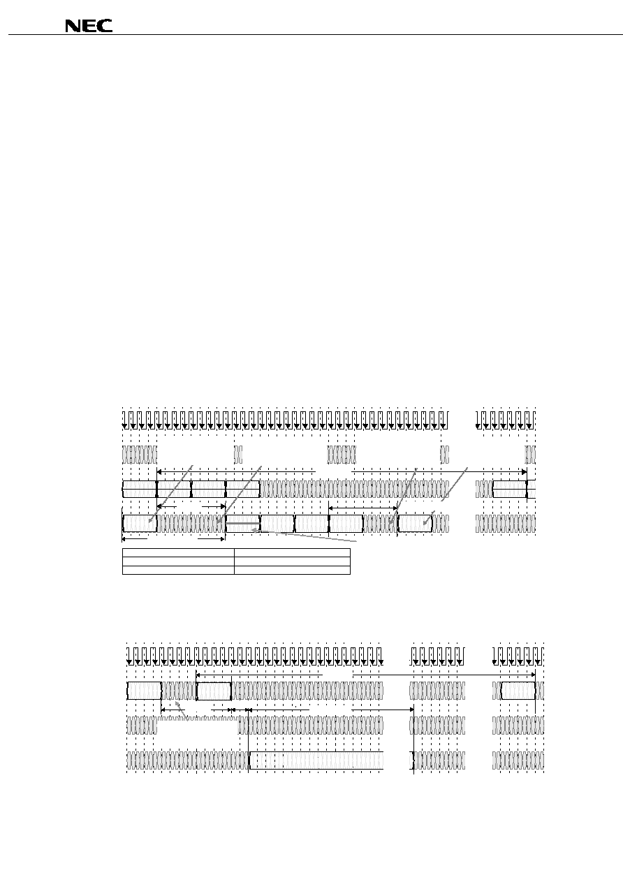
Data Sheet M14837EJ3V0DS00
55
µ
µ
µ
µ
PD488448 for Rev. P
25. Current and Temperature Control
Figure 25-1 shows an example of a transaction which performs current control calibration. It is necessary to
perform this operation once to every RDRAM in every t
CCTRL
interval in order to keep the I
OL
output current in its
proper range.
This example uses four COLX packets with a CAL command. These cause the RDRAM to drive four calibration
packets Q(a0) a time t
CAC
later. An offset of t
RDTOCC
must be placed between the Q(a0) packet and read data Q(a1)
from the same device. These calibration packets are driven on the DQA4..3 and DQB4..3 wires. The TSQ bit of the
INIT register is driven on the DQA5 wire during same interval as the calibration packets. The remaining DQA and
DQB wires are not used during these calibration packets. The last COLX packet also contains a SAM command
(concatenated with the CAL command). The RDRAM samples the last calibration packet and adjusts its I
OL
current
value.
Unlike REF commands, CAL and SAM commands cannot be broadcast. This is because the calibration packets
from different devices would interfere. Therefore, a current control transaction must be sent every t
CCTRL
/N, where N
is the number of RDRAMs on the Channel. The device field Da of the address a0 in the CAL/SAM command should
be incremented after each transaction.
Figure 25-2 shows an example of a temperature calibration sequence to the RDRAM. This sequence is broadcast
once every t
TEMP
interval to all the RDRAMs on the Channel. The TCEN and TCAL are ROP commands, and cause
the slew rate of the output drivers to adjust for temperature drift. During the quiet interval t
TCQUIET
the devices being
calibrated can't be read, but they can be written.
Figure 25-1 Current Control CAL/SAM Transaction Example
CTM/CFM
DQA7..0
DQB7..0
COL4
..COL0
ROW2
..ROW0
T
0
T
4
T
8
T
12
T
1
T
5
T
9
T
13
T
2
T
6
T
10
T
14
T
3
T
7
T
11
T
15
T
16
T
20
T
24
T
28
T
17
T
21
T
25
T
29
T
18
T
22
T
26
T
30
T
19
T
23
T
27
T
31
T
32
T
36
T
40
T
44
T
33
T
37
T
41
T
45
T
34
T
38
T
42
T
46
T
35
T
39
T
43
T
47
Transaction a0: CAL/SAM
a0 = {Da, Bx}
t
CCTRL
Transaction a1: RD
a1 = {Da, Bx}
CAL a0
CAL a2
Q (a0)
t
CAC
CAL a0
CAL a0
CAL/SAM a0
Read data from a different
device from an earlier RD
command can be anywhere
prior to the Q(a0) packet.
Read data from a different
device from a later RD
command can be anywhere
after to the Q(a0) packet.
Read data from the same
device from a later RD
command must be at this
packet position or later.
Read data from the same
device from an earlier RD
command must be at this
packet position or earier.
Transaction a2: CAL/SAM
a2 = {Da, Bx}
DQA5 of the first calibrate packet has the inverted TSQ bit of INIT
control register; i.e. logic 0 or high voltage means hot temperature.
When used for monitoring, it should be enabled with the DQA3
bit (current control one value) in case there is no RDRAM present:
HotTemp = /DQA5
∑
DQA3
Note that DQB3 could be used instead of DQA3.
t
READTOCC
Q (a1)
Q (a1)
CCSAMTOREAD
t
Figure 25-2 Temperature Calibration (TCEN-TCAL) Transactions to RDRAM
CTM/CFM
DQA7..0
DQB7..0
COL4
..COL0
ROW2
..ROW0
T
0
T
4
T
8
T
12
T
1
T
5
T
9
T
13
T
2
T
6
T
10
T
14
T
3
T
7
T
11
T
15
T
16
T
20
T
24
T
28
T
17
T
21
T
25
T
29
T
18
T
22
T
26
T
30
T
19
T
23
T
27
T
31
T
32
T
36
T
40
T
44
T
33
T
37
T
41
T
45
T
34
T
38
T
42
T
46
T
35
T
39
T
43
T
47
CA L
TCEN
TCAL
TCEN
t
TCAL
Any ROW packet may be
placed in the gap between the
ROW packets with the
TCEN and TCAL commands.
No read data from devices
being calibrated
t
TEMP
t
TCEN
t
TCQUIET
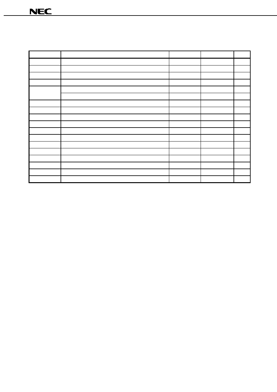
Data Sheet M14837EJ3V0DS00
56
µ
µ
µ
µ
PD488448 for Rev. P
26. Electrical Conditions
Electrical Conditions
Symbol
Parameter and Conditions
MIN.
MAX.
Unit
Tj
Junction temperature under bias
100
∞
C
V
DD,
V
DDa
Supply voltage
2.50
≠
0.13
2.50
+
0.13
V
V
DD
,
N
,V
DDa
,
N
Supply voltage droop (DC) during NAP interval (t
NLIMT
)
--
2.0
%
V
DD
,
N
,V
DDa
,
N
Supply voltage ripple (AC) during NAP interval (t
NLIMT
)
≠2.0
+2.0
%
V
CMOS
Supply voltage for CMOS pins (2.5V controllers)
2.50
≠
0.13
2.50
+
0.25
V
Supply voltage for CMOS pins (1.8V controllers)
1.80
≠
0.1
1.80
+
0.2
V
V
TERM
Termination voltage
1.80 ≠ 0.1
1.80 + 0.1
V
V
REF
Reference voltage
1.40
≠
0.2
1.40
+
0.2
V
V
DIL
RSL data input - low voltage
V
REF
≠
0.5
V
REF
≠
0.2
V
V
DIH
RSL data input - high voltage
V
REF
+
0.2
V
REF
+
0.5
V
V
DIS
RSL data input swing : V
DIS
= V
DIH
≠ V
DIL
0.4
1.0
V
A
DI
RSL data asymmetry : A
DI
= [(V
DIH
≠ V
REF
) + (V
DIL
≠ V
REF
)] / V
DIS
0
≠20
%
V
X
RSL clock input - crossing point of true and complement signals
1.3
1.8
V
V
CM
RSL clock input - common mode V
CM
= (V
CIH
+ V
CIL
) / 2
1.4
1.7
V
V
CIS, CTM
RSL clock input swing : V
CIS
= V
CIH
≠ V
CIL
(CTM, CTMN pins).
0.35
0.70
V
V
CIS, CFM
RSL clock input swing : V
CIS
= V
CIH
≠ V
CIL
(CFM, CFMN pins).
0.125
0.70
V
V
IL, CMOS
CMOS input low voltage
≠
0.3
+ (V
CMOS
/ 2≠
0.25)
V
V
IH, CMOS
CMOS input high voltage
V
CMOS
/ 2+0.25
V
CMOS
+
0.3
V
Data Sheet M14837EJ3V0DS00
57
µ
µ
µ
µ
PD488448 for Rev. P
27. Timing Conditions
Timing Conditions
Symbol
Parameter
MIN.
MAX.
Unit
Figures
t
CYCLE
CTM and CFM cycle times
-C60
3.33
3.83
ns
Figure 30-1
-C71
2.81
3.83
-C80
2.50
3.83
t
CR
, t
CF
CTM and CFM input rise and fall times
0.2
0.5
ns
Figure 30-1
t
CH
, t
CL
CTM and CFM high and low times
40%
60%
t
CYCLE
Figure 30-1
t
TR
CTM-CFM differential
(MSE/MS=0/0)
0.0
1.0
t
CYCLE
Figure 22-1
(MSE/MS=1/1)
Note1
0.9
1.0
Figure 30-1
t
DCW
Domain crossing window
≠0.1
+0.1
t
CYCLE
Figure 35-1
t
DR
, t
DF
DQA/DQB/ROW/COL input rise/fall times
0.2
0.65
ns
Figure 31-1
t
S
, t
H
DQA/DQB/ROW/COL-to-CFM
t
CYCLE
=2.50ns
0.200
Note4
--
ns
Figure 31-1
setup/hold time
t
CYCLE
=2.81ns
0.240
Note3,4
--
t
CYCLE
=3.33ns
0.275
Note2,4
--
t
DR1
, t
DF1
SIO0, SIO1 input rise and fall times
--
5.0
ns
Figure 33-1
t
DR2,
t
DF2
CMD,SCK input rise and fall times
--
2.0
ns
Figure 33-1
t
CYCLE1
SCK cycle time - Serial control register transactions
1,000
--
ns
Figure 33-1
SCK cycle time - Power transitions
10
--
ns
Figure 33-1
t
CH1
, t
CL1
SCK high and low times
4.25
--
ns
Figure 33-1
t
S1
CMD setup time to SCK rising or falling edge
Note5
1.25
--
ns
Figure 33-1
t
H1
CMD hold time to SCK rising or falling edge
Note5
1
--
ns
Figure 33-1
t
S2
SIO0
setup time to SCK falling edge
40
--
ns
Figure 33-1
t
H2
SIO0
hold time to SCK falling edge
40
--
ns
Figure 33-1
t
S3
PDEV setup time on DQA5..0 to SCK rising edge
0
--
ns
Figure 23-4, 33-2
t
H3
PDEV hold time on DQA5..0 to SCK rising edge
5.5
--
ns
Figure 23-4, 33-2
t
S4
ROW2..0, COL4..0 setup time for quiet window
Note6
≠1
--
t
CYCLE
Figure 23-4
t
H4
ROW2..0, COL4..0 hold time for quiet window
5
--
t
CYCLE
Figure 23-4
V
IL, CMOS
CMOS input low voltage - over / undershoot voltage
duration is less than or equal to 5 ns
≠0.7
+(V
CMOS
/2≠0.6)
V
V
IH, CMOS
CMOS input high voltage - over / undershoot voltage
duration is less than or equal to 5ns
V
CMOS
/2 + 0.6
V
CMOS
+ 0.7
V
t
NPQ
Quiet on ROW / COL bits during NAP / PDN entry
4
--
t
CYCLE
Figure 23-3
t
READTOCC
Offset between read data and CC packets (same device)
12
--
t
CYCLE
Figure 25-1
t
CCSAMTOREAD
Offset between CC packet and read data (same device)
8
--
t
CYCLE
Figure 25-1
t
CE
CTM/CFM stable before NAP/PDN exit
2
--
t
CYCLE
Figure 23-4
t
CD
CTM/CFM stable after NAP/PDN entry
100
--
t
CYCLE
Figure 23-3
t
FRM
ROW packet to COL packet ATTN framing delay
7
--
t
CYCLE
Figure 23-2
t
NLIMIT
Maximum time in NAP mode
--
10
µs
Figure 23-1
t
REF
Refresh interval
--
32
ms
Figure 24-1
t
CCTRL
Current control interval
34 t
CYCLE
100 ms
--
Figure 25-1
t
TEMP
Temperature control interval
--
100
ms
Figure 25-2
t
TCEN
TCE command to TCAL command
150
--
t
CYCLE
Figure 25-2
t
TCAL
TCAL command to quiet window
2
2
t
CYCLE
Figure 25-2
t
TCQUIET
Quiet window (no read data)
140
--
t
CYCLE
Figure 25-2
t
PAUSE
RDRAM delay (no RSL operations allowed)
--
200
µs
Figure 22-1
t
BURST
Interval after PDN or NAP (with self-refresh) exit in which
all banks of the RDRAM must be refreshed at least once.
--
200
µs
Figure 24-2

Data Sheet M14837EJ3V0DS00
58
µ
µ
µ
µ
PD488448 for Rev. P
Notes 1. MSE/MS are fields of the SKIP register. For this combination (skip override) the t
DCW
parameter range is
effectively 0.0 to 0.0.
2. This parameter also applies to a -C80 or -C71 part when operated with t
CYCLE
= 3.33 ns.
3. This parameter also applies to a -C80 part when operated with t
CYCLE
= 2.81ns.
4. t
S,MIN
and t
H,MIN
for other t
CYCLE
values can be interpolated between or extrapolated from the timings at the 3
specified t
CYCLE
values.
5. With V
IL,CMOS
= 0.5 V
CMOS
-
0.6 V and V
IH,CMOS
= 0.5 V
CMOS
+ 0.6 V
6. Effective hold becomes t
H4
'=t
H4
+ [PDNXA
∑
64
∑
t
SCYCLE
+ t
PDNXB,MAX
]
-
[PDNX
∑
256
∑
t
SCYCLE
]
if [PDNX
∑
256
∑
t
SCYCLE
] < [PDNXA
∑
64
∑
t
SCYCLE
+ t
PDNXB,MAX
]. See Figure 23-4.

Data Sheet M14837EJ3V0DS00
59
µ
µ
µ
µ
PD488448 for Rev. P
28. Electrical Characteristics
Electrical Characteristics
Symbol
Parameter and Conditions
MIN.
MAX.
Unit
JC
Junction-to-Case thermal resistance
--
0.5
∞
C/Watt
I
REF
V
REF
current
@
V
REF,MAX
≠10
+10
µA
I
OH
RSL output high current
@
(0
V
OUT
V
DD
)
≠10
+10
µA
I
ALL
RSL I
OL
current
@
V
OL
=0.9 V, V
DD,MIN
, T
j,MAX
Note
30
90
mA
I
OL
RSL I
OL
current resolution step
--
2.0
mA
r
OUT
Dynamic output impedance
150
--
I
I,CMOS
CMOS input leakage current
@
(0
V
I,CMOS
V
CMOS
)
≠10.0
+10.0
µA
V
OL,CMOS
CMOS output low voltage
@
I
OL,CMOS
= 1.0 mA
--
0.3
V
V
OH,CMOS
CMOS output high voltage
@
I
OH,CMOS
=
≠
0.25 mA
V
CMOS
≠
0.3
--
V
Note This measurement is made in manual current control mode; i.e. with all output device legs sinking current.
29. Timing Characteristics
Timing Characteristics
Symbol
Parameter
MIN.
MAX.
Unit
Figure(s)
t
Q
CTM-to-DQA/DQB output time
t
CYCLE
= 2.50 ns
≠0.260
Note3
+0.260
Note3
ns
Figure 32-1
t
CYCLE
= 2.81 ns
≠0.300
Note2,3
+0.300
Note2,3
t
CYCLE
= 3.33 ns
≠0.350
Note1,3
+0.350
Note1,3
t
QR
, t
QF
DQA/DQB output rise and fall times
0.2
0.45
ns
Figure 32-1
t
Q1
SCK-to-SIO0
delay
@
C
LOAD,MAX
= 20 pF (SD read packet)
--
10
ns
Figure 34-1
t
HR
SCK(pos)-to-SIO0 delay @ C
LOAD,MAX
= 20pF (SD read data hold)
2
--
ns
Figure 34-1
t
QR1
, t
QF1
SIO
OUT
rise/fall
@
C
LOAD,MAX
=
20 pF
--
5
ns
Figure 34-1
t
PROP1
SIO0-to-SIO1 or SIO1-to-SIO0
delay
@
C
LOAD,MAX
=
20 pF
--
10
ns
Figure 34-1
t
NAPXA
NAP exit delay - phase A
--
50
ns
Figure 23-4
t
NAPXB
NAP exit delay - phase B
--
40
ns
Figure 23-4
t
PDNXA
PDN exit delay - phase A
--
4
µ
s
Figure 23-4
t
PDNXB
PDN exit delay - phase B
--
9,000
t
CYCLE
Figure 23-4
t
AS
ATTN-to-STBY power state delay
--
1
t
CYCLE
Figure 23-2
t
SA
STBY-to-ATTN power state delay
--
0
t
CYCLE
Figure 23-2
t
ASN
ATTN/STBY-to-NAP power state delay
--
8
t
CYCLE
Figure 23-3
t
ASP
ATTN/STBY-to-PDN power state delay
--
8
t
CYCLE
Figure 23-3
Notes 1. This parameter also applies to a -C80 or -C71 part when operated with t
CYCLE
=3.33 ns.
2. This parameter also applies to a -C80 part when operated with t
CYCLE
=2.81 ns.
3. t
Q,MIN
and t
Q,MAX
for other t
CYCLE
values can be interpolated between or extrapolated from the timings at the
3 specified t
CYCLE
values.
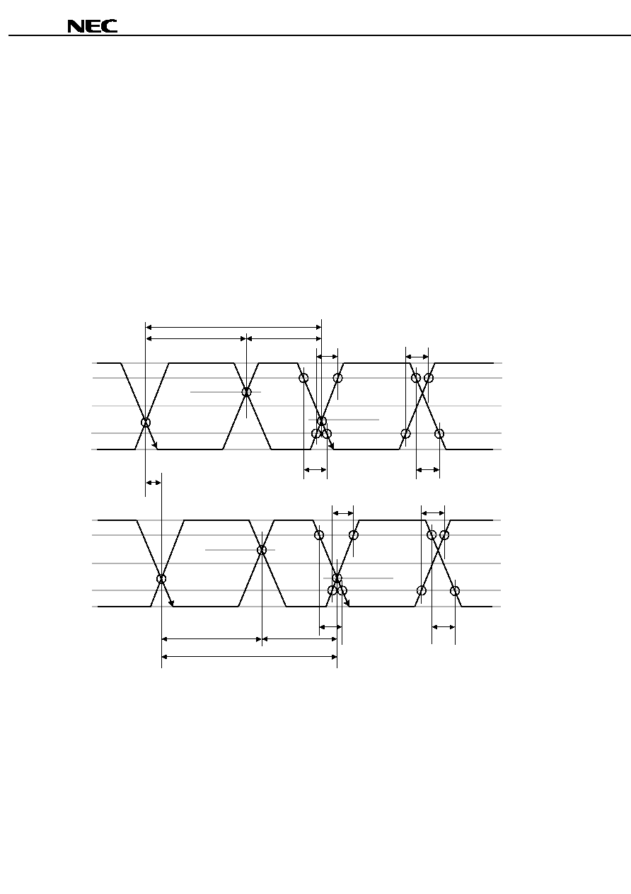
Data Sheet M14837EJ3V0DS00
60
µ
µ
µ
µ
PD488448 for Rev. P
30. RSL Clocking
Figure 30-1 is a timing diagram which shows the detailed requirements for the RSL clock signals on the Channel.
The CTM and CTMN are differential clock inputs used for transmitting information on the DQA and DQB, outputs.
Most timing is measured relative to the points where they cross. The t
CYCLE
parameter is measured from the falling
CTM edge to the falling CTM edge. The t
CL
and t
CH
parameters are measured from falling to rising and rising to falling
edges of CTM. The t
CR
and t
CF
rise-and fall-time parameters are measured at the 20 % and 80 % points.
The CFM and CFMN are differential clock outputs used for receiving information on the DQA, DQB, ROW and COL
outputs. Most timing is measured relative to the points where they cross. The t
CYCLE
parameter is measured from the
falling CFM edge to the falling CFM edge. The t
CL
and t
CH
parameters are measured from falling to rising and rising to
falling edges of CFM. The t
CR
and t
CF
rise- and fall-time parameters are measured at the 20 % and 80 % points. The
t
TR
parameters specifies the phase difference that may be tolerated with respect to the CTM and CFM differential
clock inputs (the CTM pair is always earlier).
Figure 30-1 RSL Timing - Clock Signals
V
CIH
80%
50%
20%
V
CIL
CTM
CTMN
t
CL
t
CH
t
CYCLE
t
CR
t
CF
t
CR
t
CF
V
CIH
80%
50%
20%
V
CIL
CFM
CFMN
t
CR
t
CF
t
CR
t
CF
t
CL
t
CH
t
CYCLE
t
TR
V
X-
V
X-
V
X+
V
X+
V
CM
V
CM

Data Sheet M14837EJ3V0DS00
61
µ
µ
µ
µ
PD488448 for Rev. P
31. RSL - Receive Timing
Figure 31-1 is a timing diagram which shows the detailed requirements for the RSL input signals on the Channel.
The DQA, DQB, ROW, and COL signals are inputs which receive information transmitted by a Direct RAC on the
Channel. Each signal is sampled twice per t
CYCLE
interval. The set/hold window of the sample points is t
S
/t
H
. The
sample points are centered at the 0 % and 50 % points of a cycle, measured relative to the crossing points of the
falling CFM clock edge. The set and hold parameters are measured at the V
REF
voltage point of the input transition.
The t
DR
and t
DF
rise- and fall-time parameters are measured at the 20 % and 80 % points of the input transition.
Figure 31-1 RSL Timing - Data Signals for Receive
V
CIH
80%
50%
20%
V
CIL
CFM
CFMN
even
t
H
odd
CYCLE
V
DIH
80%
20%
V
DIL
DQA
DQB
t
DR
t
DF
t
S
t
H
t
S
0.5∑t
V
REF
ROW
COL
V
X-
V
X+
V
CM
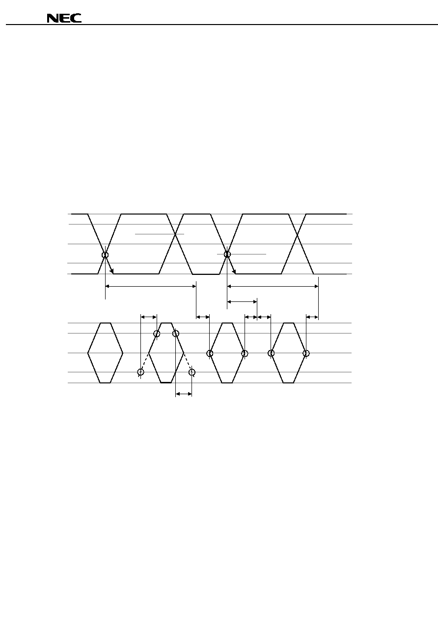
Data Sheet M14837EJ3V0DS00
62
µ
µ
µ
µ
PD488448 for Rev. P
32. RSL - Transmit Timing
Figure 32-1 is a timing diagram which shows the detailed requirements for the RSL output signals on the Channel.
The DQA and DQB signals are outputs to transmit information that is received by a Direct RAC on the Channel.
Each signal is driven twice per t
CYCLE
interval. The beginning and end of the even transmit window is at the 75 %
point of the previous cycle and at the 25 % point of the current cycle. The beginning and end of the odd transmit
window is at the 25 % point and at the 75 % point of the current cycle. These transmit points are measured relative to
the crossing points of the falling CTM clock edge. The size of the actual transmit window is less than the ideal
t
CYCLE
/2, as indicated by the non-zero valued of t
Q,MIN
and t
Q,MAX
. The t
Q
parameters are measured at the 50 % voltage
point of the output transition.
The t
QR
and t
QF
rise- and fall-time parameters are measured at the 20 % and 80 % points of the output transition.
Figure 32-1 RSL Timing - Data Signals for Transmit
V
CIH
80%
50%
20%
V
CIL
CTM
CTMN
even
t
Q,MIN
odd
CYCLE
V
QH
80%
20%
V
QL
DQA
DQB
t
QR
t
QF
t
Q,MAX
t
Q,MIN
t
Q,MAX
0.25∑t
50%
CYCLE
0.75∑t
CYCLE
0.75∑t
V
X-
V
X+
V
CM
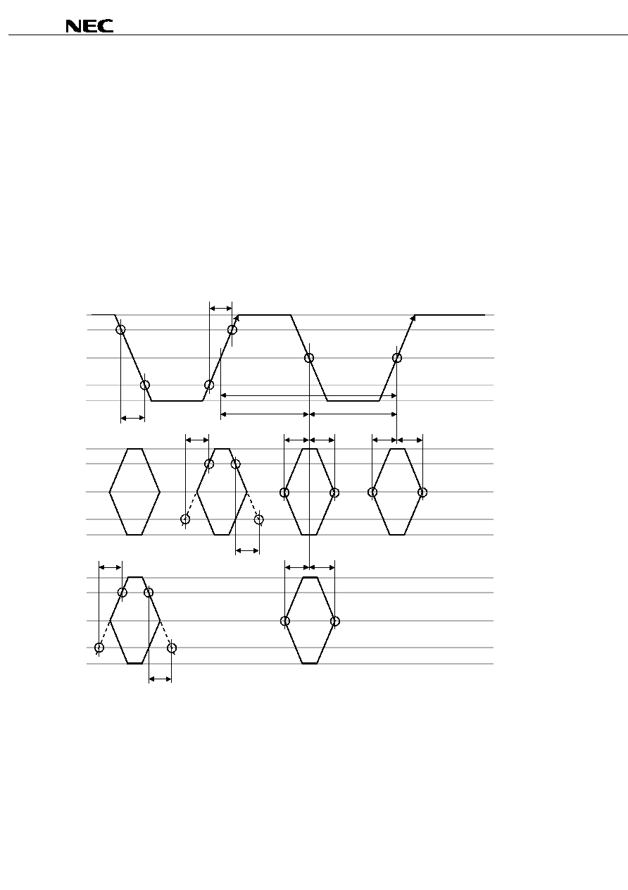
Data Sheet M14837EJ3V0DS00
63
µ
µ
µ
µ
PD488448 for Rev. P
33. CMOS - Receive Timing
Figure 33-1 is a timing diagram which shows the detailed requirements for the CMOS input signals.
The CMD and SIO0 signals are inputs which receive information transmitted by a controller (or by another RDRAM's
SIO1 output). SCK is the CMOS clock signal driven by the controller. All signals are high true.
The cycle time, high phase time, and low phase time of the SCK clock are t
CYCLE1
, t
CH1
and t
CL1
, all measured at the
50 % level. The rise and fall times of SCK, CMD, and SIO0 are t
DR1
and t
DF1
, measured at the 20 % and 80 % levels.
The CMD signal is sampled twice per t
CYCLE1
interval, on the rising edge (odd data) and the falling edge (even data).
The set/hold window of the sample points is t
S1
/t
H1
. The SCK and CMD timing points are measured at the 50 % level.
The SIO0 signal is sampled once per t
CYCLE1
interval on the falling edge. The set/hold window of the sample points
is t
S2
/t
H2
. The SCK and SIO0 timing points are measured at the 50 % level.
Figure 33-1 CMOS Timing - Data Signals for Receive
V
IH,CMOS
80%
50%
20%
V
IL,CMOS
SCK
even
odd
V
IH,CMOS
80%
20%
V
IL,CMOS
CMD
t
DR2
t
DF2
t
S1
50%
t
DR2
t
DF2
CYCLE1
t
CH1
t
CL1
t
t
H1
t
S1
t
H1
V
IH,CMOS
80%
20%
V
IL,CMOS
SIO0
t
DR1
t
DF1
t
S2
50%
t
H2
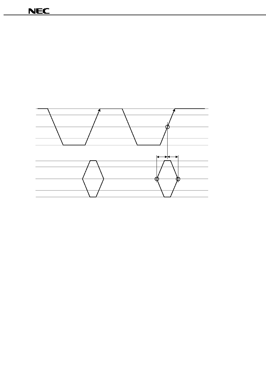
Data Sheet M14837EJ3V0DS00
64
µ
µ
µ
µ
PD488448 for Rev. P
The SCK clock is also used for sampling data on RSL input in one situation. Figure23-4 shows the PDN and NAP
exit sequences. If the PSX field of the INIT register is one (Figure 22-1 control registers (1/7) "INIT Register"), then
the PDN and NAP exit sequences are broadcast; i.e. all RDRAMs that are in PDN or NAP will perform the exit
sequence. If the PSX field of the INIT register is zero, then the PDN and NAP exit sequences are directed; i.e. only
one RDRAM that is in PDN or NAP will perform the exit sequence.
The address of that RDRAM is specified on the DQA[5:0] bus in the set hold window t
S3
/t
H3
around the rising edge of
SCK. This is shown Figure 33-2. The SCK timing point is measured at the 50 % level, and the DQA [5:0] bus signals
are measured at the V
REF
level.
Figure 33-2 CMOS Timing - Device Address for NAP or PDN Exit
V
IH,CMOS
80%
50%
20%
V
IL,CMOS
SCK
PDEV
V
DIH
80%
20%
V
DIL
DQA[5:0]
V
t
S3
t
H3
REF
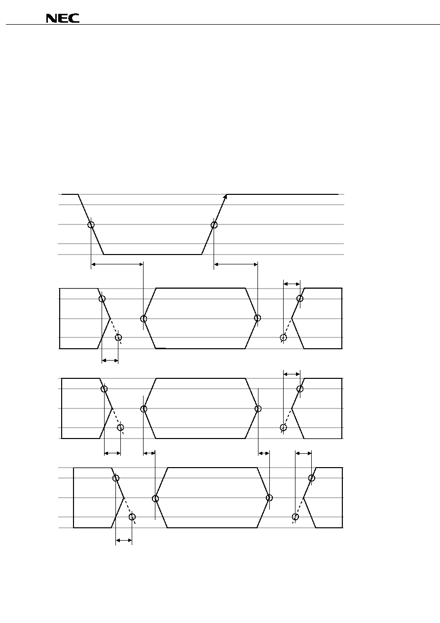
Data Sheet M14837EJ3V0DS00
65
µ
µ
µ
µ
PD488448 for Rev. P
34. CMOS - Transmit Timing
Figure 34-1 is a timing diagram which shows the detailed requirements for the CMOS output signals. The SIO0
signal is driven once per t
CYCLE1
interval on the falling edge. The clock-to-output window is t
Q1,MIN
/t
Q1,MAX
. The SCK
and SIO0 timing points are measured at the 50 % level. The rise and fall times of SIO0 are t
QR1
and t
QF1
, measured at
the 20 % and 80 % levels.
Figure34-1 also shows the combinational path connecting SIO0 to SIO1 and the path connecting SIO1 to SIO0
(read data only). The t
PROP1
parameter specified this propagation delay. The rise and fall times of SIO0 and SIO1
input must be t
DR1
and t
DF1
, measured at the 20 % and 80 % levels. The rise and fall times of SIO0 and SIO1 outputs
are t
QR1
and t
QF1
, measured at the 20 % and 80 % levels.
Figure 34-1 CMOS Timing - Data Signals for Transmit
V
IH,CMOS
80%
50%
20%
V
IL,CMOS
SCK
V
OH,CMOS
80%
20%
V
OL,CMOS
SIO0
50%
t
Q1,MAX
HR,MIN
t
V
IH,CMOS
80%
20%
V
IL,CMOS
50%
QF1
t
QR1
t
SIO0
or
SIO1
DF1
t
DR1
t
SIO0
or
SIO1
QF1
t
QR1
t
PROP1,MAX
t
PROP1,MIN
t
V
OH,CMOS
80%
20%
V
OL,CMOS
50%
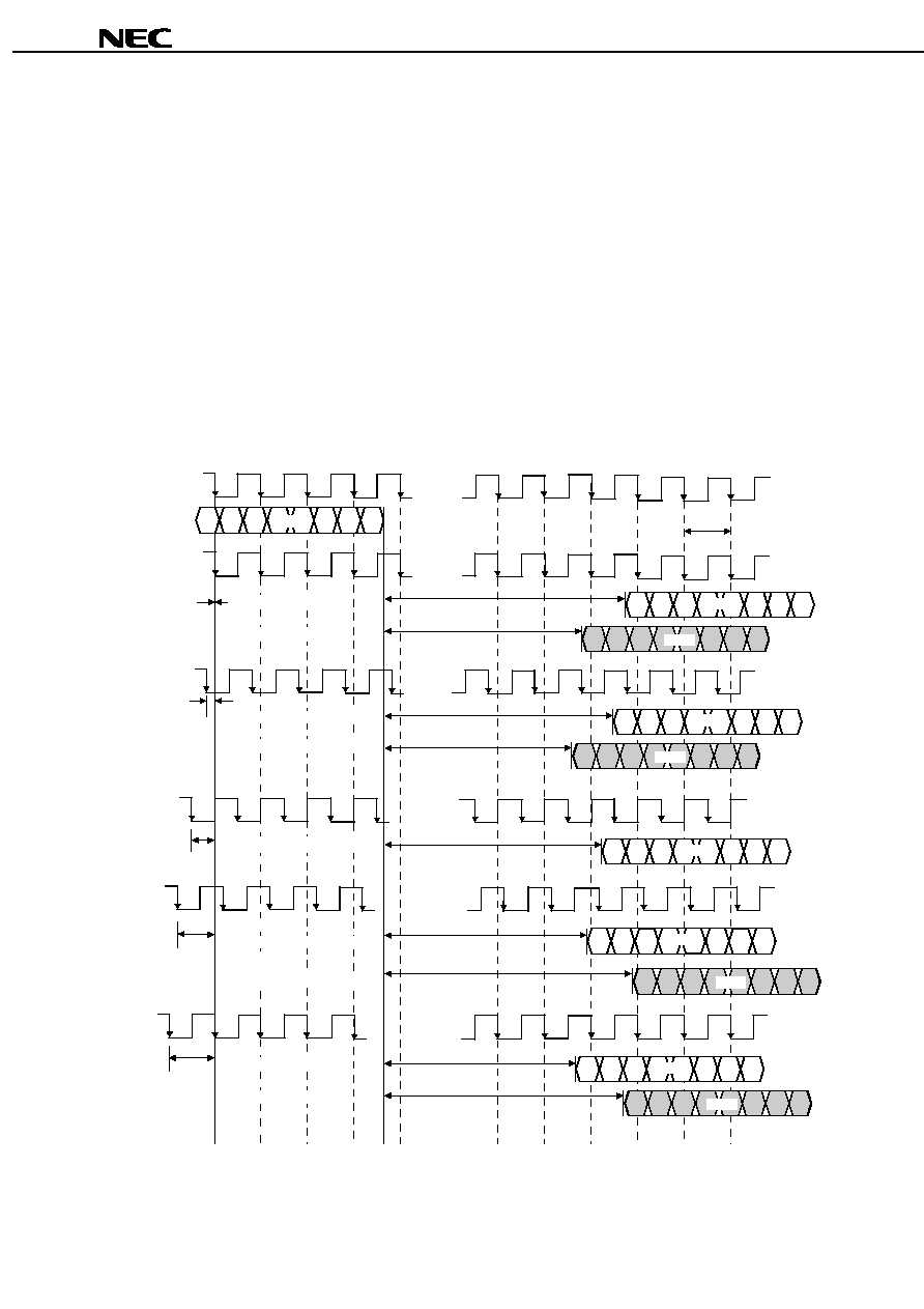
Data Sheet M14837EJ3V0DS00
66
µ
µ
µ
µ
PD488448 for Rev. P
35. RSL - Domain Crossing Window
When read data is returned by the RDRAM, information must cross from the receive clock domain (CFM) to the
transmit clock domain (CTM). The t
TR
parameter permits the CFM to CTM phase to vary though an entire cycle ; i.e.
there is no restriction on the alignment of these two clocks. A second parameter t
DCW
is needed in order to describe
how the delay between a RD command packet and read data packet varies as a function of the t
TR
value.
Figure 35-1 shows this timing for five distinct values of t
TR
. Case A (t
TR
=0) is what has been used throughout this
document. The delay between the RD command and read data is t
CAC
. As t
TR
varies from zero to t
CYCLE
(cases A
through E), the command to data delay is (t
CAC
-t
TR
). When the t
TR
value is in the range 0 to t
DCW,MAX
, the command to
data delay can also be (t
CAC
-t
TR
-t
CYCLE
). This is shown as cases A' and B' (the gray packets). Similarly, when the t
TR
value is in the range (t
CYCLE
+t
DCW,MIN
) to t
CYCLE
, the command to data delay can also be (t
CAC
-t
TR
+t
CYCLE
). This is shown
as cases D' and E' (the gray packets). The RDRAM will work reliably with either the white or gray packet timing. The
delay value is selected at initialization, and remains fixed thereafter.
Figure 35-1 RSL Timing - Crossing Read Domains
CFM
RDa1
∑∑∑
CYCLE
t
Q(a1)
Q(a1)
TR
t
TR
t
Q(a1)
Q(a1)
TR
t
Q(a1)
Q(a1)
Q(a1)
Q(a1)
Q(a1)
CAC TR
t
-t
CAC TR CYCLE
t
-t
+t
TR
t
TR
t
COL
CTM
DQA/B
DQA/B
CTM
DQA/B
DQA/B
CTM
DQA/B
CTM
DQA/B
DQA/B
CTM
DQA/B
DQA/B
∑∑∑
∑∑∑
∑∑∑
∑∑∑
∑∑∑
Case A t
=0
TR
Case A' t =0
TR
Case B t =t
TR
DCW,MAX
Case B' t =t
TR
DCW,MAX
Case C t =0.5
∑
t
CYCLE
TR
Case D
t =t + t
CYCLE
TR
DCW,MIN
Case D'
t =t + t
CYCLE
TR
DCW,MIN
Case E t =t
CYCLE
TR
Case E' t =t
CYCLE
TR
CAC TR
-t
t
CAC TR CYCLE
-t
t
-t
CAC TR
t
-t
CAC TR CYCLE
t
-t -t
CAC TR
t
-t
CAC TR
t
-t
CAC
TR
CYCLE
-t +t
t

Data Sheet M14837EJ3V0DS00
67
µ
µ
µ
µ
PD488448 for Rev. P
36. Timing Parameters
Timing Parameters Summary
Para-
Description
MIN.
MAX.
Units
Figures
meter
-C80
-C71
-C60
-45
-45
-53
t
RC
Row Cycle time of RDRAM banks - the interval between ROWA packets
with ACT commands to the same bank.
28
28
28
--
t
CYCLE
Figure13-1
Figure14-1
t
RAS
RAS-asserted time of RDRAM bank - the interval between ROWA packet
with ACT command and next ROWR packet with PRER
Note 1
command to the
same bank.
20
20
20
Note 2
64
µ
s
t
CYCLE
Figure13-1
Figure14-1
t
RP
Row Precharge time of RDRAM banks - the interval between ROWR packet
with PRER
Note 1
command and next ROWA packet with ACT command to the
same bank.
8
8
8
--
t
CYCLE
Figure13-1
Figure14-1
t
PP
Precharge-to-precharge time of RDRAM device - the interval between
successive ROWR packets with PRER
Note 1
commands to any banks of
the same device.
8
8
8
--
t
CYCLE
Figure10-3
t
RR
RAS-to-RAS time of RDRAM device - the interval between successive
ROWA packets with ACT commands to any banks of the same device.
8
8
8
--
t
CYCLE
Figure12-1
t
RCD
RAS-to-CAS Delay - the interval from ROWA packet with ACT
command to COLC packet with RD or WR command. Note - the RAS-
to-CAS delay seen by the RDRAM core (t
RCD-C
) is equal to t
RCD-C
=
1
+
t
RCD
because of differences in the row and column paths through the
RDRAM interface.
9
7
7
--
t
CYCLE
Figure13-1
Figure14-1
t
CAC
CAS Access delay - the interval from RD command to Q read data. The
equation for t
CAC
is given in the TPARM register in Figure 22-1(5/7).
8
8
8
12
t
CYCLE
Figure4-1
t
CWD
CAS Write Delay - interval from WR command to D write data.
6
6
6
6
t
CYCLE
Figure4-1
t
CC
CAS-to-CAS time of RDRAM bank - the interval between successive
COLC commands.
4
4
4
--
t
CYCLE
Figure13-1
Figure14-1
t
PACKET
Length of ROWA, ROWR, COLC, COLM or COLX packet.
4
4
4
4
t
CYCLE
Figure2-1
t
RTR
Interval from COLC packet with WR command to COLC packet which
causes retire, and to COLM packet with bytemask.
8
8
8
--
t
CYCLE
Figure15-1
t
OFFP
The interval (offset) from COLC packet with RDA command, or from
COLC packet with retire command (after WRA automatic precharge), or
from COLC packet with PREC command, or from COLX packet with
PREX command to the equivalent ROWR packet with PRER. The
equation for t
OFFP
is given in the TPARM register in Figure 22-1(5/7).
4
4
4
4
t
CYCLE
Figure14-2
t
RDP
Interval from last COLC packet with RD command to ROWR packet
with PRER.
4
4
4
--
t
CYCLE
Figure13-1
t
RTP
Interval from last COLC packet with automatic retire command to
ROWR packet with PRER.
4
4
4
--
t
CYCLE
Figure14-1
Notes 1. Or equivalent PREC or PREX command. See Figure 12-2.
2. This is a constraint imposed by the core, and is therefore in units of ms rather than t
CYCLE
.
Data Sheet M14837EJ3V0DS00
68
µ
µ
µ
µ
PD488448 for Rev. P
37. Absolute Maximum Ratings
Absolute Maximum Ratings
Symbol
Parameter
MIN.
MAX.
Unit
V
I,ABS
Voltage applied to any RSL or CMOS pin with respect to GND
≠0.3
V
DD
+0.3
V
V
DD,ABS
,V
DDa,ABS
Voltage on V
DD
and V
DDa
with respect to GND
≠0.5
V
DD
+1.0
V
T
STORE
Storage temperature
≠50
+100
∞
C
Caution
Exposing the device to stress above those listed in Absolute Maximum Ratings could cause
permanent damage. The device is not meant to be operated under conditions outside the limits
described in the operational section of this specification. Exposure to Absolute Maximum Rating
conditions for extended periods may affect device reliability.
38. I
DD
- Supply Current Profile
I
DD
- Supply Current Profile
I
DD
value
RDRAM blocks consuming power
@ t
CYCLE
Note 1
MIN.
MAX.
Unit
I
DD,PDN
Self-refresh only for INIT.LSR=0
3.0
mA
I
DD,NAP
T/RCLK-Nap
4.2
mA
I
DD,STBY
T/RCLK,ROW-demux
2.50 ns
110
mA
2.81 ns
105
3.33 ns
95
3.83 ns
85
I
DD,ATTN
T/RCLK, ROW-demux, COL-demux
2.50 ns
180
mA
2.81 ns
165
3.33 ns
145
3.83 ns
135
I
DD,ATTN-W
T/RCLK, ROW-demux, COL-demux,
2.50 ns
650
mA
DQ-demux, 1
∑
WR-SenseAmp, 4
∑
ACT-Bank
2.81 ns
595
3.33 ns
515
3.83 ns
470
I
DD,ATTN-R
T/RCLK, ROW-demux, COL-demux,
2.50 ns
690
mA
DQ-mux, 1
∑
RD-SenseAmp, 4
∑
ACT-Bank
Note 2
2.81 ns
625
3.33 ns
540
3.83 ns
480
Notes 1. The CMOS interface consumes power in all power states.
2. This does not include the I
OL
sink current. The RDRAM dissipates I
OL
∑
V
OL
in each output driver when a logic
one is driven.
Data Sheet M14837EJ3V0DS00
69
µ
µ
µ
µ
PD488448 for Rev. P
39. Capacitance and Inductance
Figure 39-1 shows the equivalent load circuit of the RSL and CMOS pins. The circuit models the load that the device
presents to the Channel.
This circuit does not include pin coupling effects that are often present in the packaged device. Because coupling
effects make the effective single-pin inductance L
I
, and capacitance C
I
, a function of neighboring pins, these
parameters are intrinsically data-dependent. For purposes of specifying the device electrical loading on the Channel,
the effective L
I
and C
I
are defined as the worst-case values over all specified operating conditions.
L
I
is defined as the effective pin inductance based on the device pin assignment. Because the pad assignment
places each RSL signal adjacent to an AC ground (a GND or V
DD
pin), the effective inductance must be defined
based on this configuration. Therefore, L
I
assumes a loop with the RSL pin adjacent to an AC ground.
C
I
is defined as the effective pin capacitance based on the device pin assignment. It is the sum of the effective
package pin capacitance and the IO pad capacitance.
Figure 39-1 Equivalent Load Circuit for RSL Pins
L
C
R
I
I
I
Pad
L
C
R
I
I
I
Pad
CTM,CTMN,
CFM,CFMN Pin
L
C
I,CMOS
I
Pad
L
C
I,CMOS
I,CMOS,SIO
Pad
DQA,DQB,RQ Pin
GND Pin
GND Pin
SCK,CMD Pin
GND Pin
SIO0,SIO1 Pin
GND Pin

Data Sheet M14837EJ3V0DS00
70
µ
µ
µ
µ
PD488448 for Rev. P
RSL Pin Parasitics
Symbol
Parameter and Conditions - RSL pins
MIN.
MAX.
Unit
L
I
RSL effective input inductance
≠
4.0
nH
L
12
Mutual inductance between any DQA or DQB RSL signals.
≠
0.2
nH
Mutual inductance between any ROW or COL RSL signals.
≠
0.6
nH
L
I
Difference in L
I
value between any RSL pins of a single device.
≠
1.8
nH
C
I
RSL effective input capacitance
Note
800 MHz
2.0
2.4
pF
711 MHz
2.0
2.4
600 MHz
2.0
2.6
C
12
Mutual capacitance between any RSL signals.
≠
0.1
pF
C
I
Difference in C
I
value between any RSL pins of a single device.
≠
0.06
pF
R
I
RSL effective input resistance
4
15
Note This value is a combination of the device IO circuitry and package capacitances.
CMOS Pin Parasitics
Symbol
Parameter and Conditions - CMOS pins
MIN.
MAX.
Unit
L
I,CMOS
CMOS effective input inductance
≠
8.0
nH
C
I,CMOS
CMOS effective input capacitance (SCK,CMD)
Note
1.7
2.1
pF
C
I,CMOS,SIO
CMOS effective input capacitance (SIO1,SIO0)
Note
≠
7.0
pF
Note This value is a combination of the device IO circuitry and package capacitances.

Data Sheet M14837EJ3V0DS00
71
µ
µ
µ
µ
PD488448 for Rev. P
40. Glossary of Terms
ACT
Activate command from AV field.
D
Write data packet on DQ pins.
activate
To access a roe and place in sense amp.
DBL
CNFGB register field ≠ doubled-bank.
activate
To access a row and place in sense amp.
DC
Device address field in COLC packet.
adjacent
device
An RDRAM on a Channel.
Two RDRAM banks which share sense amps
(also called doubled banks).
DEVID
ASYM
CCA register field for RSL V
OL
/ V
OH
.
Control register with device address that is
matched against DR, DC, and DX fields.
ATTN
Power state ≠ ready for ROW / COL packets.
DM
Device match for ROW packet decode.
ATTNR
Power state ≠ transmitting Q packets.
Doubled-bank
RDRAM with shared sense amp.
ATTNW
Power state ≠ receiving D packets.
DQ
DQA and DQB pins.
AV
Opcode field in ROW packets.
DQA
Pins for data byte A.
bank
DQB
Pins for data byte B.
A block of 2
RBIT
∑
2
CBIT
storage cells in the core
of the RDRAM.
DQS
NAPX register field ≠ PDN/NAP exit.
BC
Bank address field in CLC packet.
DR,DR4T,DR4F
BBIT
CNFGA register field - # bank address bits.
Device address field and packet framing fields
in ROW and ROWE packets.
broadcast
An operation executed by all RDRAMs.
dualoct
16 bytes ≠ the smallest addressable datum.
BR
Bank address field in ROW packets.
DX
Device address field in COLX packet.
bubble
field
A collection of bits in a packet.
Idle cycle(s) on RDRAM pins needed
because of a resource constraint.
INIT
Control register with initialization fields.
BYT
CNFGB register field ≠ 9 bits per byte.
initialization
BX
Bank address field in COLX packet.
Configuring a Channel of RDRAMs so they
are ready to respond to transactions.
C
Column address field in COLC packet.
LSR
CNFGA register field ≠ low-power self-refresh.
CAL
Calibrate (I
OL
) command in XOP field.
M
Mask opcode field (COLM/COLX packet).
CBIT
CNFGB register field - # column address bits.
MA
Field in COLM packet for masking byte A.
CCA
Control register ≠ current control A.
MB
Field in COLM packet for masking byte B.
CCB
Control register ≠ current control B.
MSK
Mask command in M field.
CFM,CFMN
Clock pins for receiving packets.
MVER
Control register ≠ manufacturer ID.
Channel
ROW / COL / DQ pins and external wires.
NAP
Power state ≠ needs SCK/CMD wakeup.
CLRR
Clear reset command from SOP field.
NAPR
Nap command in ROP field.
CMD
CMOS pins for initialization / power control.
NAPRC
Conditional nap command in ROP field.
CNFGA
Control register with configuration fields.
NAPXA
NAPX register field ≠ NAP exit delay A.
CNFGB
Control register with configuration fields.
NAPXB
NAPX register field ≠ NAP exit delay B.
COL
Pins for column-access control.
NOCOP
No-operation command in COP field.
COLC
Column operation packet on COL pins.
NOROP
No-operation command in ROP field.
COLM
Write mask packet on COL pins.
NOXOP
No-operation command in XOP field.
column
NSR
INIT register field ≠ NAP self-refresh.
Rows in a bank or activated in sense amps
have 2
CBTI
dualocts column storage.
packet
A collection of bits carried on the Channel.
Command
A decoded bit-combination from a field.
PDN
Power state ≠ needs SCK/CMD wakeup.
COLX
Extended operation packet on COL pins.
PDNR
Powerdown command in ROP field.
controller
PDNXA
Control register ≠ PDN exit delay A.
A logic-device which drives the ROW / COL
/ DQ wires for a Channel of RDRAMs.
PDNXB
Control register ≠ PDN exit delay B.
COP
Column opcode field in COLC packet.
pin efficiency
The fraction of non-idle cycles on a pin.
core
The banks and sense amps of an RDRAM.
PRE
PREC, PRER, PREX precharge commands.
CTM, CTMN
Clock pins for transmitting packets.
PREC
Precharge command in COP field.
Current control
precharge
Prepares sense amp and bank for activate.
Periodic operations to update the proper I
OL
Value of RSL output drivers.
PRER
Precharge command in ROP field.

Data Sheet M14837EJ3V0DS00
72
µ
µ
µ
µ
PD488448 for Rev. P
PREX
Precharge command in XOP field.
SETF
Set fast clock command from SOP field.
PSX
INIT register field ≠ PDN/NAP exit.
SETR
Set reset command from SOP field.
PSR
INIT register field ≠ PDN self-refresh.
SINT
PVER
CNFGB register field ≠ protocol version.
Serial interval packet for control register
read/write transactions.
Q
Read data packet on DQ pins.
SIO0,SIO1
CMOS serial pins for control registers.
R
Row address field of ROWA packet.
SOP
Serial opcode field in SRQ.
RBIT
CNFGB register field - #row address bits.
SRD
Serial read opcode command from SOP.
RD/RDA
Read (/precharge) command in COP field.
SRP
INIT register field ≠ Serial repeat bit.
read
Operation of accessing sense amp data.
SRQ
receive
Serial request packet for control register
read/write transactions.
Moving information from the Channel into the
RDRAM (a serial stream is demuxed).
STBY
Power state ≠ ready for ROW packets.
REFA
Refresh-activate command in ROP field.
SVER
Control register ≠ stepping version.
REFB
Control register ≠ next bank (self-refresh).
SWR
Serial write opcode command from SOP.
REFBIT
TCAS
TCLSCAS register field ≠ t
CAS
core delay.
CNFGA register field ≠ ignore bank bits (for
REFA and self-refresh).
TCLS
TCLSCAS register field ≠ t
CLS
core delay.
REFP
Refresh-precharge command in ROP field.
TCLSCAS
Control register ≠ t
CAS
and t
CLS
delay.
REFR
Control register ≠ next row for REFA.
TCYCLE
Control register ≠ t
CYCLE
delay.
refresh
Periodic operations to restore storage cells.
TDAT
Control register ≠ t
DAC
delay.
retire
TEST77
Control register ≠ for test purposes.
The automatic operation that stores write
buffer into sense amp after WR command.
TEST78
Control register ≠ for test purposes.
RLX
RLXC, RLXR, RLXX relax commands.
TRDLY
Control register ≠ t
RDLY
delay.
RLXC
Relax command in COP field.
transaction
ROW, COL, DQ packets for memory access.
RLXR
Relax command in ROP field.
transmit
RLXX
Relax command in XOP field.
Moving information from the RDRAM onto
the Channel (parallel word is muxed).
ROP
Row-opcode field in ROWR packet.
WR/WRA
Write (/precharge) command in COP field.
row
2
CBIT
dualocts of cells (bank/sense amp).
write
Operation of modifying sense amp data.
ROW
Pins for row-access control
XOP
Extended opcode field in COLX packet.
ROW
ROWA or ROWR packets on ROW pins.
ROWA
Activate packet on ROW pins.
ROWR
Row operation packet on ROW pins.
RQ
Alternate name for ROW/COL pins.
RSL
Rambus Signal levels.
SAM
Sample (I
OL
) command in XOP field.
SA
Serial address packet for control register
transactions w/ SA address field.
SBC
Serial broadcast field in SRQ.
SCK
CMOS clock pin.
SD
Serial data packet for control register
transactions w/ SD data field.
SDEV
Serial device address in SRQ packet.
SDEVID
INIT register field ≠ Serial device ID.
self-refresh
Refresh mode for PDN and NAP.
sense amp
Fast storage that holds copy of bank's row.
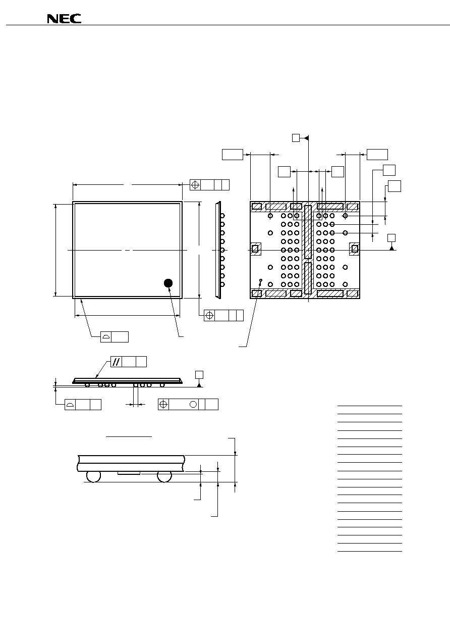
Data Sheet M14837EJ3V0DS00
73
µ
µ
µ
µ
PD488448 for Rev. P
41. Package Drawings
[
µ
µ
µ
µ
PD488448FF:
µ
µ
µ
µ
BGA]
62-PIN TAPE FBGA (11.26x13)
ITEM
MILLIMETERS
D
13.0
±
0.1
11.26
±
0.1
A
eD
eE
w
0.96
±
0.10
A1
0.40
±
0.05
v
E
0.15
0.2
SD
1.2
ZD1
2.465
ZD2
1.735
ZE
1.63
P62FF-80-DQ1
INDEX MARK
INDEX MARK
w
y1
y
A4
0.3 MIN.
b
0.50
±
0.05
x
0.08
0.8
1.0
y
0.1
y1
0.2
ZE
SD
b
A
SECTION A-A
NOTE
It applies to hatching part.
ZD1
A4
A1
eE
ZD2
eD
S
x
A B
B
S
A
A
J
H
G
F
E
D
C
B
A
A
S A
S
w
B
1 2 3 4 5 6 7 8 9 101112
S
x4
v
12.4
10.66
S
M
D
E
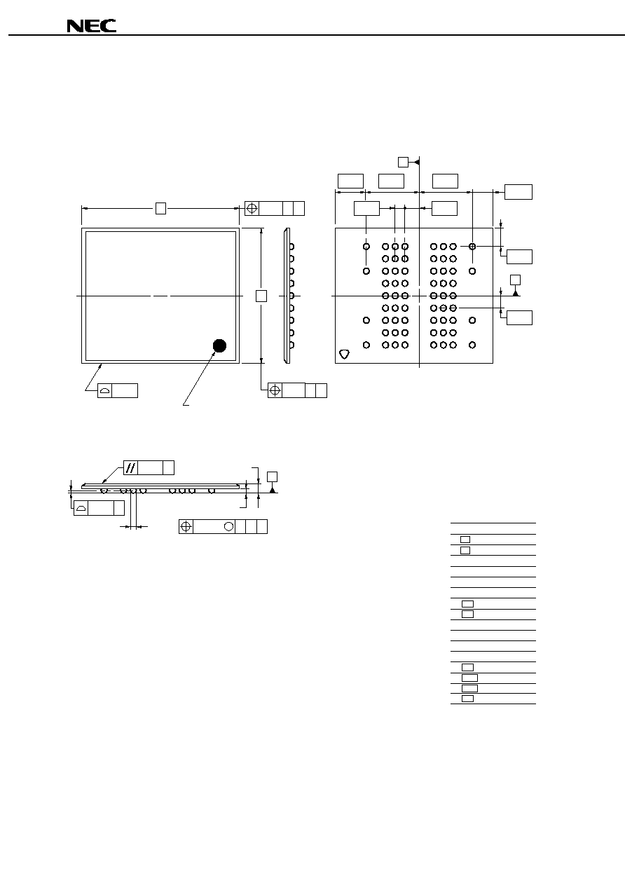
Data Sheet M14837EJ3V0DS00
74
µ
µ
µ
µ
PD488448 for Rev. P
[
µ
µ
µ
µ
PD488448FB:D
2
BGA]
62-PIN PLASTIC FBGA (11.26x13.00)
ITEM
MILLIMETERS
D
13.00
E
11.26
A
0.77
±
0.10
A1
0.40
±
0.05
v
0.15
w
0.20
ZD1
2.465
ZD2
1.735
ZE
1.63
P62FB-80-DQ1
Index mark
ZD1
4.40
SD
ZE
ZD2
A
SD
eD
0.80
x
0.08
y
0.10
eE
1.00
b
0.50
±
0.05
y1
0.20
1.20
eD
A1
B
eE
A
S
4
S
y
S
x
A
S
w
A
B
S
y1
S
w
v
B
1
3 4 5
11
2
6 7
9 10
8
12
J
H
G
F
E
D
C
B
A
M
62≠ b
4.40
D
E

Data Sheet M14837EJ3V0DS00
75
µ
µ
µ
µ
PD488448 for Rev. P
42. Recommended Soldering Conditions
Please consult our sales office for soldering conditions of the
µ
PD488448.
Type of Surface Mount Device
µ
PD488448FF-DQ1 : 62-pin TAPE FBGA (
µ
BGA) (Normal type)
µ
PD488448FF-DQ2 : 62-pin TAPE FBGA (
µ
BGA) (Mirrored type)
µ
PD488448FB-DQ1 : 62-pin PLASTIC FBGA (D
2
BGA) (Normal type)
µ
PD488448FB-DQ2 : 62-pin PLASTIC FBGA (D
2
BGA) (Mirrored type)

Data Sheet M14837EJ3V0DS00
76
µ
µ
µ
µ
PD488448 for Rev. P
[ MEMO ]

Data Sheet M14837EJ3V0DS00
77
µ
µ
µ
µ
PD488448 for Rev. P
[ MEMO ]

Data Sheet M14837EJ3V0DS00
78
µ
µ
µ
µ
PD488448 for Rev. P
[ MEMO ]
Data Sheet M14837EJ3V0DS00
79
µ
µ
µ
µ
PD488448 for Rev. P
NOTES FOR CMOS DEVICES
1
PRECAUTION AGAINST ESD FOR SEMICONDUCTORS
Note:
Strong electric field, when exposed to a MOS device, can cause destruction of the gate oxide and
ultimately degrade the device operation. Steps must be taken to stop generation of static electricity
as much as possible, and quickly dissipate it once, when it has occurred. Environmental control
must be adequate. When it is dry, humidifier should be used. It is recommended to avoid using
insulators that easily build static electricity. Semiconductor devices must be stored and transported
in an anti-static container, static shielding bag or conductive material. All test and measurement
tools including work bench and floor should be grounded. The operator should be grounded using
wrist strap. Semiconductor devices must not be touched with bare hands. Similar precautions need
to be taken for PW boards with semiconductor devices on it.
2
HANDLING OF UNUSED INPUT PINS FOR CMOS
Note:
No connection for CMOS device inputs can be cause of malfunction. If no connection is provided
to the input pins, it is possible that an internal input level may be generated due to noise, etc., hence
causing malfunction. CMOS devices behave differently than Bipolar or NMOS devices. Input levels
of CMOS devices must be fixed high or low by using a pull-up or pull-down circuitry. Each unused
pin should be connected to V
DD
or GND with a resistor, if it is considered to have a possibility of
being an output pin. All handling related to the unused pins must be judged device by device and
related specifications governing the devices.
3
STATUS BEFORE INITIALIZATION OF MOS DEVICES
Note:
Power-on does not necessarily define initial status of MOS device. Production process of MOS
does not define the initial operation status of the device. Immediately after the power source is
turned ON, the devices with reset function have not yet been initialized. Hence, power-on does
not guarantee out-pin levels, I/O settings or contents of registers. Device is not initialized until the
reset signal is received. Reset operation must be executed immediately after power-on for devices
having reset function.

µ
µ
µ
µ
PD488448 for Rev. P
[MEMO]
M8E 00. 4
The information in this document is current as of August, 2000. The information is subject to
change without notice. For actual design-in, refer to the latest publications of NEC's data sheets or
data books, etc., for the most up-to-date specifications of NEC semiconductor products. Not all
products and/or types are available in every country. Please check with an NEC sales representative
for availability and additional information.
No part of this document may be copied or reproduced in any form or by any means without prior
written consent of NEC. NEC assumes no responsibility for any errors that may appear in this document.
NEC does not assume any liability for infringement of patents, copyrights or other intellectual property rights of
third parties by or arising from the use of NEC semiconductor products listed in this document or any other
liability arising from the use of such products. No license, express, implied or otherwise, is granted under any
patents, copyrights or other intellectual property rights of NEC or others.
Descriptions of circuits, software and other related information in this document are provided for illustrative
purposes in semiconductor product operation and application examples. The incorporation of these
circuits, software and information in the design of customer's equipment shall be done under the full
responsibility of customer. NEC assumes no responsibility for any losses incurred by customers or third
parties arising from the use of these circuits, software and information.
While NEC endeavours to enhance the quality, reliability and safety of NEC semiconductor products, customers
agree and acknowledge that the possibility of defects thereof cannot be eliminated entirely. To minimize
risks of damage to property or injury (including death) to persons arising from defects in NEC
semiconductor products, customers must incorporate sufficient safety measures in their design, such as
redundancy, fire-containment, and anti-failure features.
NEC semiconductor products are classified into the following three quality grades:
"Standard", "Special" and "Specific". The "Specific" quality grade applies only to semiconductor products
developed based on a customer-designated "quality assurance program" for a specific application. The
recommended applications of a semiconductor product depend on its quality grade, as indicated below.
Customers must check the quality grade of each semiconductor product before using it in a particular
application.
"Standard": Computers, office equipment, communications equipment, test and measurement equipment, audio
and visual equipment, home electronic appliances, machine tools, personal electronic equipment
and industrial robots
"Special":
Transportation equipment (automobiles, trains, ships, etc.), traffic control systems, anti-disaster
systems, anti-crime systems, safety equipment and medical equipment (not specifically designed
for life support)
"Specific": Aircraft, aerospace equipment, submersible repeaters, nuclear reactor control systems, life
support systems and medical equipment for life support, etc.
The quality grade of NEC semiconductor products is "Standard" unless otherwise expressly specified in NEC's
data sheets or data books, etc. If customers wish to use NEC semiconductor products in applications not
intended by NEC, they must contact an NEC sales representative in advance to determine NEC's willingness
to support a given application.
(Note)
(1) "NEC" as used in this statement means NEC Corporation and also includes its majority-owned subsidiaries.
(2) "NEC semiconductor products" means any semiconductor product developed or manufactured by or for
NEC (as defined above).
∑
∑
∑
∑
∑
∑
D
2
BGA is a trademark of NEC Corporation.
µ
µ
µ
µ
BGA is a registered trademark of Tessera, Inc.
Rambus and RDRAM are registered trademarks of Rambus Inc.
Direct Rambus, Direct RDRAM and RIMM are trademarks of Rambus Inc.