 | –≠–ª–µ–∫—Ç—Ä–æ–Ω–Ω—ã–π –∫–æ–º–ø–æ–Ω–µ–Ω—Ç: UPD5710TK | –°–∫–∞—á–∞—Ç—å:  PDF PDF  ZIP ZIP |

UPD5710TK
NEC's WIDE BAND
SINGLE CONTROL CMOS SPDT SWITCH
California Eastern Laboratories
∑ SUPPLY VOLTAGE :
1.8 to 3.3 V (2.8 V TYP.)
∑ SINGLE SWITCH CONTROL VOLTAGE:
V
cont (H)
= 1.8 to 3.3 V (2.8 V TYP.)
V
cont (L)
=
-
0.2 to +0.2 V (0 V TYP.)
∑
LOW
INSERTION
LOSS:
0.6 dB TYP. @ DC to 1.0 GHz
0.8 dB TYP. @ 1.0 to 2.0 GHz
0.95 dB TYP. @ 2.0 to 2.5 GHz
∑
HIGH
ISOLATION:
32.5 dB TYP. @ DC to 1.0 GHz
25 dB TYP. @ 1.0 to 2.0 GHz
22.5 dB TYP. @ 2.0 to 2.5 GHz
∑ POWER
HANDLING:
P
in (0.1 dB)
= +17.0 dBm TYP. @ 1.0GHz, V
DD
= 2.8 V
P
in (1 dB)
= +21.0 dBm TYP. @ 1.0 GHz, V
DD
= 2.8 V
∑ HIGH-DENSITY SURFACE MOUNT PACKAGE:
6-pin minimold package (1.5
◊
1.1
◊
0.55 mm)
∑ Pb-FREE
FEATURES
DATA SHEET
ORDERING INFORMATION
Remark To order evaluation samples, contact your nearby sales offi ce.
Part number for sample order: UPD5710TK
NEC's UPD5710TK is a wide-band single control
CMOS MMIC SPDT (Single Pole Double Throw)
switch for mobile communications, instrumentation,
short range wireless, and general-purpose RF
switching applications.
This device can operate from DC to 2.5GHz with low
insertion loss and high isolation, and generally does
not require blocking capacitors on the RF lines.
The UPD5710TK is housed in a Pb-Free 6-pin
minimold (1511) package, suitable for high-density
surface mounting.
DESCRIPTION
∑ MOBILE
COMMUNICATIONS
∑ SET TOP BOXES
∑ SHORT RANGE WIRELESS
∑ INSTRUMENTATION
APPLICATIONS
PART NUMBER
PACKAGE
MARKING
SUPPLYING FORM
PD5710TK-E2-A
6-pinlead-less minimold (1511)
C3L
∑
Embossed tape 8 mm wide
∑
Pin 1, 6 face the perforation side of the tape
∑
Qty 5 kpcs/reel

UPD5710TK
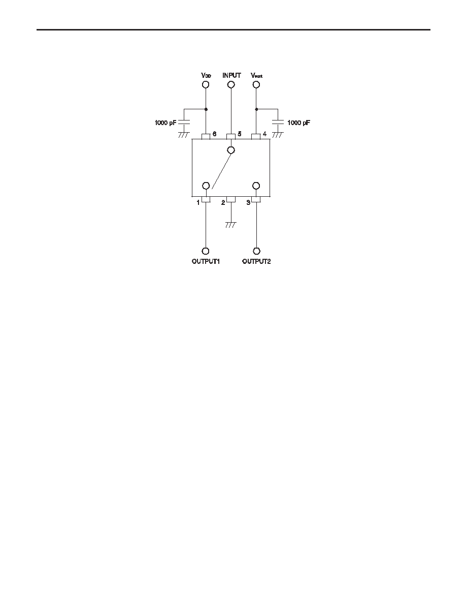
PIN CONNECTIONS AND INTERNAL BLOCK DIAGRAM
TRUTH TABLE
ABSOLUTE MAXIMUM RATINGS
(T
A
=+25∫C, unless otherwise specifi ed)
Notes 1.
|
V
cont(H)
-
V
cont(L)
|
0.1 V
PIN NO.
PIN NAME
1
OUTPUT1
2
GND
3
OUTPUT2
4
V
cont
5
INPUT
6
V
DD
V
CONT
INPUT
-
OUTPUT1
INPUT
-
OUTPUT2
Low
OFF
ON
High
ON
OFF
PARAMETER
SYMBOL
RATINGS
UNIT
Supply Voltage
V
DD
+4.6
V
Switch Control Voltage
V
cont
+4.6
V
Continuous Current
I
dc
60
mA
Input Power
P
in
+27
dBm
Operating Ambient Temperature
T
A
-
45 to +85
∞
C
Storage Temperature
T
stg
-
65 to +150
∞
C
PARAMETER
SYMBOL
MIN.
TYP.
MAX.
UNIT
Supply Voltage
V
DD
+1.8
+2.8
+3.3
V
Switch Control Voltage (H)
V
cont (H)
+1.8
+2.8
+3.3
V
Switch Control Voltage (L)
V
cont (L)
-
0.2
0
+0.2
V
RECOMMENDED OPERATING RANGE
(T
A
=+25∫C, unless otherwise specifi ed)

UPD5710TK
ELECTRICAL CHARACTERISTICS
(T
A
= +25
∞
C, V
DD
= 2.8V, V
cont(H)
= 2.8 V , V
cont(L)
= 0 V, unless otherwise specifi ed)
PARAMETER
SYMBOL
TEST CONDITIONS
MIN.
TYP.
MAX.
UNIT
Insertion Loss 1
L
ins1
f = DC to 1.0 GHz
-
0.6
0.8
dB
Insertion Loss 2
L
ins2
f = 1.0 to 2.0 GHz
-
0.8
1.0
dB
Insertion Loss 3
L
ins3
f = 2.0 to 2.5 GHz
-
0.95
1.2
dB
Isolation 1
ISL1
f = DC to 1.0 GHz
30
32.5
-
dB
Isolation 2
ISL2
f = 1.0 to 2.0 GHz
22
25
-
dB
Isolation 3
ISL3
f = 2.0 to 2.5 GHz
-
22.5
-
dB
Input Return Loss
RL
in
f = DC to 2.5 GHz
15
20
-
dB
Output Return Loss
RL
out
f = DC to 2.5 GHz
15
20
-
dB
0.1 dB Loss Compression
Input Power
Note
P
in (0.1 dB)
f = 1.0 GHz
+13.5
+17.0
-
dBm
1 dB Loss Compression
Input Power
Note
P
in (1 dB)
f = 1.0 GHz
-
+21.0
-
dBm
Intermodulation Intercept Point
IIP
3
2 tone, 1.000/1.001GHz,
1 MHz spacing
-
+33
-
dBm
Supply Current
I
DD
No RF
-
0.01
1.0
A
Switch Control Current
I
cont
No RF
-
0.01
1.0
A
Switch Control Speed
t
SW
-
30
500
ns
Notes . P
in (0.1 dB)
or P
in (1 dB)
are the measured input power level when the insertion loss increases 0.1 dB more
or 1dB than that of linear range.

UPD5710TK
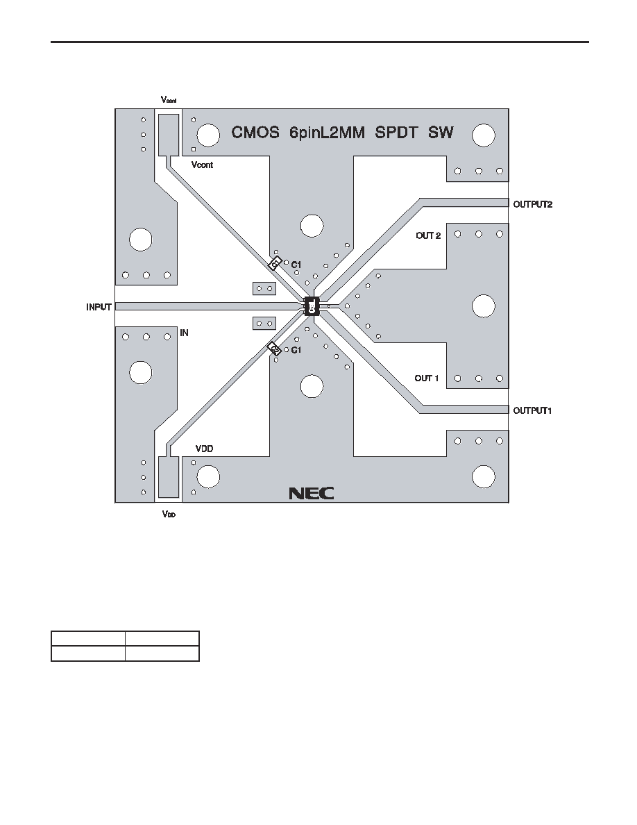
EVALUATION CIRCUIT
The application circuits and their parameters are for reference only and are not intended for use in actual design-ins.

UPD5710TK
ILLUSTRATION OF THE TEST CIRCUIT ASSEMBLED ON EVALUATION BOARD
USING THE NEC EVALUATION BOARD
SYMBOL
VALUES
C1, C2
1,000 pF

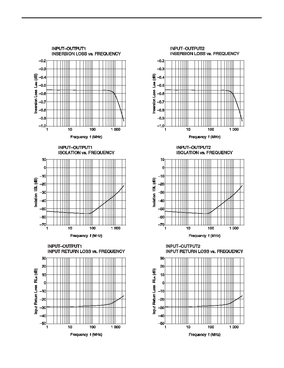
TYPICAL CHARACTERISTIC
(T
A
= +25∞C, V
DD
= 2.8 V, V
cont (H)
= 2.8 V, V
cont (L)
= 0 V, unless otherwise specifi ed)
Remark The graphs indicate nominal characteristics.
UPD5710TK

UPD5710TK
TYPICAL CHARACTERISTIC
(T
A
= +25∞C, V
DD
= 2.8 V, V
cont (H)
= 2.8 V, V
cont (L)
= 0 V, unless otherwise specifi ed)
Remark The graphs indicate nominal characteristics.

UPD5710TK
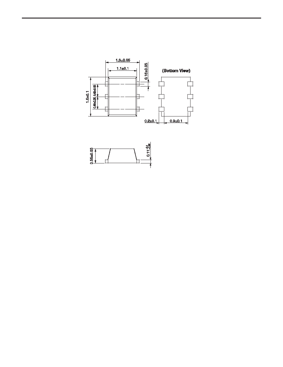
PACKAGE DIMENSIONS
6-PIN LEAD-LESS MINIMOLD (1511) (UNIT:mm)

UPD5710TK
RECOMMENDED SOLDERING CONDITIONS
This product should be soldered and mounted under the following recommended conditions. For soldering
methods and conditions other than those recommended below, contact your nearby sales offi ce.
Soldering Method
Soldering Conditions
Condition Symbol
Infrared Refl ow
Peak temperature (package surface temperature)
: 260
∞
C or below
Time at peak temperature
: 10 seconds or less
Time at temperature of 220
∞
C or higher
: 60 seconds or less
Preheating time at 120 to 180
∞
C :
120
±
30 seconds
Maximum number of refl ow processes
: 3 times
Maximum chlorine content of rosin fl ux (% mass)
: 0.2%(Wt.) or below
IR260
VPS
Peak temperature (package surface temperature)
: 215
∞
C or below
Time at temperature of 200
∞
C or higher
: 25 to 40 seconds
Preheating time at 120 to 150
∞
C
: 30 to 60 seconds
Maximum number of refl ow processes
: 3 times
Maximum chlorine content of rosin fl ux (% mass)
: 0.2%(Wt.) or below
VP215
Wave Soldering
Peak temperature (molten solder temperature)
: 260
∞
C or below
Time at peak temperature
: 10 seconds or less
Preheating temperature (package surface temperature) : 120
∞
C or below
Maximum number of fl ow processes
: 1 time
Maximum chlorine content of rosin fl ux (% mass)
: 0.2%(Wt.) or below
WS260
Partial Heating
Peak temperature (pin temperature)
: 350
∞
C or below
Soldering time (per side of device)
: 3 seconds or less
Maximum chlorine content of rosin fl ux (% mass)
: 0.2%(Wt.) or below
HS350
Caution
Do not use different soldering methods together (except for partial heating).
A Business Partner of NEC Compound Semiconductor Devices, Ltd.
07/29/2004


