 | –≠–ª–µ–∫—Ç—Ä–æ–Ω–Ω—ã–π –∫–æ–º–ø–æ–Ω–µ–Ω—Ç: UPD61052 | –°–∫–∞—á–∞—Ç—å:  PDF PDF  ZIP ZIP |
Document Outline
- COVER
- FEATURES
- APPLICATION
- ORDERING INFORMATION
- BLOCK DIAGRAM
- PERIPHERAL CONNECTION
- PIN CONFIGURATION (TOP VIEW)
- PIN LIST
- 1. PIN FUNCTION
- 1.1 Video Input Interface
- 1.2 Video Output Interface
- 1.3 Audio Input Interface
- 1.4 Audio Input/output Interface
- 1.5 Stream Input Interface
- 1.6 Stream Output Interface
- 1.7 SDRAM Interface
- 1.8 Host CPU Interface
- 1.8.1 Parallel bus interface
- 1.8.2 Serial bus interface
- 1.9 Clock, Reset
- 1.10 N-Wire
- 1.11 GPIO
- 1.12 Power Supply
- 1.13 Recommended Connections of Unused Pins
- 2. FEATURE OVERVIEW
- 2.1 Video
- 2.1.1 Encoding
- 2.1.2 Transcoding
- 2.1.3 Input/output processing
- 2.2 Audio
- 2.2.1 Encoding
- 2.2.2 Transcoding (DEMUX, MUX)
- 2.2.3 Input/output processing
- 2.3 MPEG System Processing
- 2.3.1 System time clock
- 2.3.2 Multiplex
- 2.3.3 De-multiplex
- 2.3.4 Transcode
- 2.4 Stream Interface
- 2.4.1 Parallel steam data interface
- 2.4.2 Serial stream data interface
- 2.5 Host CPU Interface
- 2.6 SDRAM Interface
- 2.7 Memory Connection Diagram
- 2.8 Memory Map
- 3. SYSTEM INTERFACE REGISTER
- 3.1 Register Mapping (General Mapping)
- 3.2 Register Functions
- 3.2.1 Common register
- 3.2.2 Data transfer register
- 3.2.3 Internal CPU interrupt register
- 3.2.4 Interrupt mask register
- 3.2.5 Download interrupt register
- 3.2.6 Interrupt register
- 3.2.7 Reset register
- 3.2.8 ROM access cycle register
- 3.2.9 Port setup register
- 4. SYSTEM INTERFACE PROCEDURE
- 4.1 Outline
- 4.2 Firmware Download
- 4.2.1 Host CPU to instruction RAM of internal CPU
- 4.2.2 External ROM to instruction RAM of internal CPU
- 4.2.3 Host CPU to SDRAM
- 4.2.4 External ROM to SDRAM
- 4.3 SDRAM Write during Executing
- 4.4 SDRAM Read during Executing
- 4.5 SDRAM Initialization
- 4.6 Operation Mode Setting by Changing Firmware
- 4.7 Transfer Ending
- 4.8 Transfer Error Handling
- 4.8.1 Transfer error handling 1
- 4.8.2 Transfer error handling 2
- 4.8.3 Transfer error handling 3
- 5. EXAMPLE FOR COMMON REGISTER USAGE
- 5.1 Register Map Example
- 5.2 Example of the Common Register Which A Firmware Defines
- 5.2.1 COMCODE: Command code register
- 5.2.2 ESTS: Status register
- 6. ELECTRICAL CHARACTERISTICS
- 7. PACKAGE DRAWING
- 8. RECOMMENDED SOLDERING CONDITIONS

The information in this document is subject to change without notice. Before using this document, please
confirm that this is the latest version.
Not all products and/or types are available in every country. Please check with an NEC Electronics
sales representative for availability and additional information.
MOS INTEGRATED CIRCUIT
µ
PD61051, 61052
MPEG2 AUDIO/VIDEO ENCODER
Document No.
S15082EJ4V0DS00 (4th edition)
Date Published November 2003 NS CP (K)
Printed in Japan
DATA SHEET
The
µ
PD61051 and
µ
PD61052 are LSIs of MPEG audio and video encoding, decoding and transcoding.
The
µ
PD61051 has MPEG2 video encoder, MPEG audio encoding DSP, 32-bit RISC CPU, video input/output unit
which contains a processing filter and a time base corrector (TBC), and MPEG system layer which contains the
multiplexer and de-multiplexer. It combines with 64 M or 128 Mbit SDRAM and it uses. The
µ
PD61052 has a DolbyTM
Digital Consumer Encoder in addition to the
µ
PD61051.
The
µ
PD61051, 61052 are the optimal choice for consumer digital video recording replay equipment to process a
MPEG.
FEATURES
∑
Video encode
-
Stream standard: MPEG2 video MP@ML, SP@ML standard, MPEG1 standard
-
Picture size:
Horizontal: 720, 704, 544, 480, 352 dots/line
Vertical:
480, 240, 576, 288 line/frame
-
Single pass variable bit rate (VBR), constant bit rate (CBR) encoding
-
Transcoding:
Bit rate conversion, VBR
CBR
-
Video input/output
Format:
8-bit Y/Cb/Cr 4:2:2 (ITU-R BT.656)
Pre analysis: Film detect, scene changing detect, and motion estimation assist
TBC, VBI data slicer
∑ Audio encoding
-
Bit length:
16 bits, 20 bits, 24 bits
-
Sampling rate: 32 kHz, 44.1 kHz, 48 kHz
-
MPEG1 audio layer 2 standard based
-
Dolby Digital Consumer Encoder standard based (Only the
µ
PD61052)
-
Elementary stream and PCM audio input/output
∑ MPEG system processing
-
Multiplex: MPEG2-PS,
MPEG2-TS, DVD-Video, and DVD-VR
-
De-multiplex: MPEG2-PS, MPEG2-TS
-
Transcoding: MPEG2 format conversion (MPEG2-TS
MPEG2-PS)
-
Partial TS generation
∑ Package: 208-pin fine pitch QFP
∑ Power supply: 1200 mW (Typ.)
∑ Power supply voltage: 3.3±0.165 V, 2.5±0.2 V (Internal circuit power)
"Dolby" is a trademark of Dolby Laboratories.
To use the
µ
PD61052, a license from Dolby Laboratories Licensing Corporation is necessary.
2002
The mark
shows major revised points.
Data Sheet S15082EJ4V0DS
2
µ
PD61051, 61052
APPLICATION
D-VHS, DVD video recorder, HDD video recorder
ORDERING INFORMATION
Part Number
Package
µ
PD61051GD-LML
208-pin plastic QFP (Fine pitch) (28
◊28)
µ
PD61051GD-LML-A
Note
208-pin plastic QFP (Fine pitch) (28
◊28)
µ
PD61052GD-LML
208-pin plastic QFP (Fine pitch) (28
◊28)
µ
PD61052GD-LML-A
Note
208-pin plastic QFP (Fine pitch) (28
◊28)
Note Lead-free product
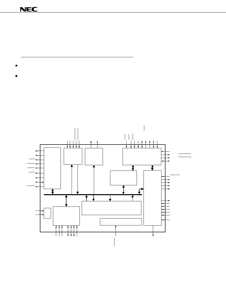
BLOCK DIAGRAM
SDRAM
Interface
Unit
MCLKE
CMODE2
CCS
OVOUT7-OVOUT0/FA19-FA14
OVCLK
IVHSYNC
IVVSYNC
IVFLD
IVIN7-IVIN0
IVCLK
CRE
CWE/CSDI
CA5-CA0/FA5-FA0
CD7-CD0/FD7-FD0
CWAIT/FOE
CINT
CMODE1/CSDO
OSREQ
OSVLD/OSRDY
OSSYNC
OSCLK/OSSTB
OS7-OS0/FA13-FA6
ISREQ
ISVLD
ISCLK/ISSTB
IS7-IS2
RESET
IABD
IABCK
IALRCK
OABD
OABCK
OALRCK
AMCLK
PWM
MCLK
MCS
MRAS
MCAS
MWE
MDQM
PSTOP
SCLK
(27 MHz)
MA13-MA0
MD31-MD0
Video
Input
Unit
Video
Output
Unit
Internal CPU
System Control Unit
PLL
Audio DSP
Engine
Video Encode/Transcode Unit
Host CPU
Interface
Unit
Stream
Interface
Unit
GPO6/OVVSYNC
GPO5/OVHSYNC
GPIO4-GPIO0
CMODE0/CSCLK
IS1/ISERR
IS0
STCLK

Data Sheet S15082EJ4V0DS
3
µ
PD61051, 61052
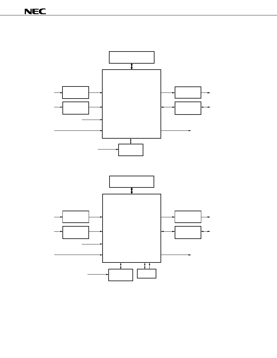
PERIPHERAL CONNECTION
Video
Input
NTSC/PAL
Decoder
MPEG2 AV Encoder
µPD61051/61052
1394
AV Link
1394
PHY
ADC
DAC
SDRAM
SDRAM
TS Decoder
MPEG Decoder
Stream Interface
PCM
PCM
BT.656
Audio
Input
1394
In/Out
Video
Output
Audio
Output
Host
CPU
TS
AV HDD
Data Sheet S15082EJ4V0DS
4
µ
PD61051, 61052
This LSI deals with two kinds of methods to connect a system controller.
Parallel Bus Interface
64M SDRAM
NTSC/PAL
Decoder
NTSC/PAL
Encoder
Audio ADC
Audio
ADC/DAC
27 MHz
STC Clock
MPEG TS/PS
User
Interface
Host CPU
MPEG TS/PS
BT.656
PCM
BT.656
PCM
µPD61051/61052
Serial Bus Interface
64M SDRAM
NTSC/PAL
Decoder
NTSC/PAL
Encoder
Audio ADC
Audio
ADC/DAC
27 MHz
STC Clock
MPEG TS/PS
User
Interface
Host CPU
SPI
Instruction
ROM
MPEG TS/PS
BT.656
PCM
BT.656
PCM
µPD61051/61052
Data Sheet S15082EJ4V0DS
5
µ
PD61051, 61052
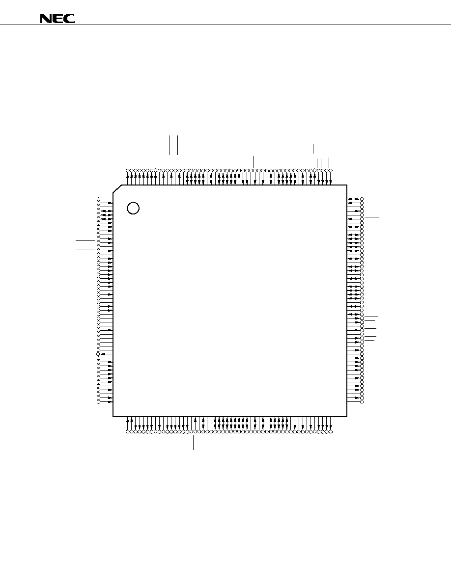
PIN CONFIGURATION (TOP VIEW)
∑ 208-pin plastic QFP (Fine pitch) (28◊28)
µ
PD61051GD-LML
µ
PD61051GD-LML-A
µ
PD61052GD-LML
µ
PD61052GD-LML-A
V
DD2
AMCLK
GND
OALRCK
OABCK
OABD
IALRCK
IABCK
IABD
GND
IVFLD
IVHSYNC
V
DD2
IVVSYNC
GND
IVIN0
IVIN1
IVIN2
IVIN3
IVIN4
IVIN5
IVIN6
IVIN7
V
DD2
IVCLK
GND
GND
SCLK
PSTOP
PV
DD2
PGND
PV
DD2
PGND
STCLK
GND
V
DD2
GND
GND
V
DD3
PWM
GND
IS0
IS1/ISERR
IS2
IS3
IS4
IS5
V
DD2
IS6
GND
IS7
ISSYNC
1
2
3
4
5
6
7
8
9
10
11
12
13
14
15
16
17
18
19
20
21
22
23
24
25
26
27
28
29
30
31
32
33
34
35
36
37
38
39
40
41
42
43
44
45
46
47
48
49
50
51
52
53
54
55
56
57
58
59
60
61
62
63
64
65
66
67
68
69
70
71
72
73
74
75
76
77
78
79
80
81
82
83
84
85
86
87
88
89
90
91
92
93
94
95
96
97
98
99
100
101
102
103
104
ISCLK/ISSTB
ISVLD
ISREQ
OS0/FA6
OS1/FA7
OS2/FA8
OS3/FA9
V
DD2
OS4/FA10
GND
OS5/FA11
OS6/FA12
OS7/FA13
OSCLK/OSSTB
OSSYNC
OSVLD/OSRDY
V
DD3
OSREQ
V
DD2
MD23
GND
GND
MD22
MD21
MD20
MD19
MD18
MD17
MD16
V
DD2
MD24
GND
MD25
V
DD3
MD26
GND
MD27
MD28
MD29
MD30
MD31
V
DD2
MA0
GND
MA1
V
DD3
MA2
GND
MA3
MA10
MA12
MA13
208
207
206
205
204
203
202
201
200
199
198
197
196
195
194
193
192
191
190
189
188
187
186
185
184
183
182
181
180
179
178
177
176
175
174
173
172
171
170
169
168
167
166
165
164
163
162
161
160
159
158
157
OVOUT7
OVOUT6
OVOUT5/FA19
OVOUT4/FA18
OVOUT3/FA17
OVOUT2/FA16
OVOUT1/FA15
OVOUT0/FA14
GND
OVCLK
V
DD2
GPO6/OVVSYNC
GND
GPO5/OVHSYNC
V
DD3
GPIO4
GPIO3
GPIO2
GPIO1
GPIO0
GND
CA5/FA5
V
DD2
CA4/FA4
CA3/FA3
CA2/FA2
CA1/FA1
CA0/FA0
NDO
NDI
NMOD
GND
NRST
V
DD2
NCLK
GND
CD7/FD7
V
DD3
CD6/FD6
CD5/FD5
CD4/FD4
CD3/FD3
CD2/FD2
GND
CD1/FD1
V
DD2
CD0/FD0
CWAIT/FOE
CRE
CCS
CMODE2
CWE/CSDI
156
155
154
153
152
151
150
149
148
147
146
145
144
143
142
141
140
139
138
137
136
135
134
133
132
131
130
129
128
127
126
125
124
123
122
121
120
119
118
117
116
115
114
113
112
111
110
109
108
107
106
105
CMODE1/CSDO
CMODE0/CSCLK
GND
CINT
V
DD2
RESET
GND
MD15
V
DD3
MD14
MD13
MD12
MD11
MD10
GND
MD9
V
DD2
MD8
MD0
GND
MD1
V
DD3
MD2
MD3
MD4
MD5
GND
MD6
V
DD2
MD7
MDQM
MWE
GND
MCAS
V
DD3
MRAS
MCS
GND
MCLK
V
DD2
MCLKE
MA11
MA9
MA8
GND
MA7
V
DD3
MA6
MA5
GND
MA4
V
DD2

Data Sheet S15082EJ4V0DS
6
µ
PD61051, 61052
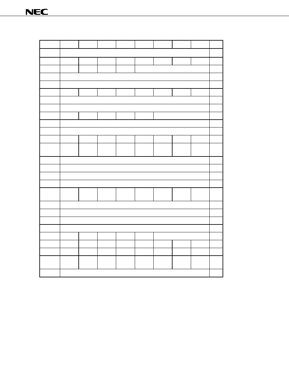
PIN LIST
AMCLK
:Audio Main Clock
MA0 to MA13
:Memory Address
CA0/FA0 to CA5/FA5 :Host CPU Address/
MCAS
:Memory Column Address Strobe
Instruction ROM Address MCLK :Memory Clock
CCS
:Host CPU Chip Select
MCLKE
:Memory Clock Enable
CD0/FD0 to CD7/FD7 :Host CPU Data/
MCS
:Memory Chip Select
Instruction ROM Data
MD0 to MD31
:Memory Data
CINT :Host
CPU
Interrupt
MDQM
:Memory DQ Mask Enable
CMODE0/CSCLK
:Host CPU Mode/
MRAS
:Memory Row Address Strobe
SPI Clock
MWE
:Memory Write Enable
CMODE1/CSDO
:Host CPU Mode/
NCLK
:N-wire Clock
SPI Data Output
NDI
:N-wire Data Input
CMODE2
:Host CPU Mode
NDO
:N-wire Data Output
CRE
:Host CPU Read Enable
NMOD
:N-wire Mode
CWAIT/FOE
:Host CPU Wait/
NRST
:N-wire Reset
Instruction ROM Output Enable
OABCK
:Output Audio Bit Clock
CWE/CSDI
:Host CPU Write Enable/
OABD
:Output Audio Bit Data
SPI Data Input
OALRCK
:Output Audio LR Clock
GND
:Ground
OS0/FA6 to OS7/FA13 :Output Stream Data/
GPIO0 to GPIO4
:General Purpose IO
Instruction ROM Address
GPO5/OVHSYNC
:General Purpose Output/
OSCLK/OSSTB
:Output Stream Data Clock/
Output Video Horizontal Sync
Output Stream Data Strobe
GPO6/OVVSYNC
:General Purpose Output/
OSREQ
:Output Stream Data Request
Output Video Vertical Sync
OSSYNC
:Output Stream Data Sync
IABCK
:Input Audio Bit Clock
OSVLD/OSRDY
:Output Stream Data Valid/
IABD
:Input Audio Bit Data
Output Stream Data Ready
IALRCK
:Input Audio LR Clock OVCLK
:Output
Video
Clock
IS0, IS2 to IS7
:Input Stream Data
OVOUT0/FA14 to
:Output Video Data/
IS1/ISERR
:Input Stream Data/ Input Stream Error
OVOUT5/FA19
Instruction ROM Address
ISCLK/ISSTB
:Input Stream Data Clock/
OVOUT6,OVOUT7
:Output Video Data
Input Stream Data Strobe
PGND
:PLL Ground
ISREQ
:Input Stream Data Request
PSTOP
:PLL Stop
ISSYNC
:Input Stream Data Sync
PV
DD2
:PLL 2.5 V Power Supply
ISVLD
:Input Stream Data Valid
PWM
:PWM Output
IVCLK
:Input Video Clock
RESET
:Reset
IVFLD
:Input Video Field Index SCLK
:System
Clock
IVHSYNC
:Input Video Horizontal Sync
STCLK
:System Time Clock
IVIN0 to IVIN7
:Input Video Data
V
DD2
:2.5 V Power Supply
IVVSYNC
:Input Video Vertical Sync
V
DD3
:3.3 V Power Supply

Data Sheet S15082EJ4V0DS
7
µ
PD61051, 61052
CONTENTS
1. PIN FUNCTION ............................................................................................................................... 9
1.1 Video
Input Interface............................................................................................................................. 9
1.2 Video
Output Interface.......................................................................................................................... 9
1.3 Audio
Input Interface ............................................................................................................................ 9
1.4 Audio
Input/output Interface .............................................................................................................. 10
1.5 Stream
Input Interface ........................................................................................................................ 10
1.6 Stream
Output Interface ..................................................................................................................... 11
1.7 SDRAM
Interface ................................................................................................................................. 11
1.8 Host
CPU Interface.............................................................................................................................. 12
1.8.1 Parallel
bus interface................................................................................................................. 12
1.8.2 Serial
bus interface.................................................................................................................... 12
1.9 Clock, Reset......................................................................................................................................... 13
1.10 N-Wire................................................................................................................................................... 13
1.11 GPIO ..................................................................................................................................................... 14
1.12 Power Supply ...................................................................................................................................... 14
1.13 Recommended Connections of Unused Pins ................................................................................... 15
2. FEATURE OVERVIEW.................................................................................................................. 16
2.1 Video .................................................................................................................................................... 16
2.1.1 Encoding ................................................................................................................................... 16
2.1.2 Transcoding............................................................................................................................... 16
2.1.3 Input/output processing ............................................................................................................. 17
2.2 Audio .................................................................................................................................................... 19
2.2.1 Encoding ................................................................................................................................... 19
2.2.2 Transcoding
(DEMUX, MUX) .................................................................................................... 19
2.2.3 Input/output processing ............................................................................................................. 19
2.3 MPEG
System Processing.................................................................................................................. 22
2.3.1 System
time clock ..................................................................................................................... 22
2.3.2 Multiplex .................................................................................................................................... 23
2.3.3 De-multiplex .............................................................................................................................. 23
2.3.4 Transcode ................................................................................................................................. 24
2.4 Stream
Interface .................................................................................................................................. 25
2.4.1 Parallel
steam data interface ..................................................................................................... 25
2.4.2 Serial
stream data interface....................................................................................................... 29
2.5 Host
CPU Interface.............................................................................................................................. 32
2.6 SDRAM
Interface ................................................................................................................................. 33
2.7 Memory
Connection Diagram ............................................................................................................ 34
2.8 Memory Map ........................................................................................................................................ 36
3. SYSTEM INTERFACE REGISTER .............................................................................................. 38
3.1 Register
Mapping (General Mapping)................................................................................................ 39
3.2 Register Functions.............................................................................................................................. 40
3.2.1 Common
register....................................................................................................................... 40
3.2.2 Data
transfer register................................................................................................................. 40
3.2.3 Internal
CPU
interrupt register................................................................................................... 47
3.2.4 Interrupt
mask register .............................................................................................................. 47

Data Sheet S15082EJ4V0DS
8
µ
PD61051, 61052
3.2.5 Download
interrupt register ....................................................................................................... 47
3.2.6 Interrupt register ........................................................................................................................ 48
3.2.7 Reset
register ............................................................................................................................ 48
3.2.8 ROM
access
cycle register ........................................................................................................ 49
3.2.9 Port
setup register ..................................................................................................................... 49
4. SYSTEM INTERFACE PROCEDURE.......................................................................................... 50
4.1 Outline .................................................................................................................................................. 51
4.2 Firmware
Download ............................................................................................................................ 52
4.2.1 Host CPU to instruction RAM of internal CPU ........................................................................... 52
4.2.2 External ROM to instruction RAM of internal CPU..................................................................... 53
4.2.3 Host
CPU to SDRAM................................................................................................................. 54
4.2.4 External
ROM to SDRAM .......................................................................................................... 55
4.3 SDRAM
Write
during Executing ......................................................................................................... 56
4.4 SDRAM
Read
during Executing ......................................................................................................... 57
4.5 SDRAM
Initialization............................................................................................................................ 58
4.6
Operation Mode Setting by Changing Firmware .............................................................................. 59
4.7 Transfer Ending................................................................................................................................... 60
4.8 Transfer
Error Handling ...................................................................................................................... 61
4.8.1 Transfer
error handling 1 ........................................................................................................... 61
4.8.2 Transfer
error handling 2 ........................................................................................................... 62
4.8.3 Transfer
error handling 3 ........................................................................................................... 63
5. EXAMPLE FOR COMMON REGISTER USAGE....................................................................... 64
5.1 Register
Map Example ........................................................................................................................ 65
5.2
Example of the Common Register Which A Firmware Defines ....................................................... 67
5.2.1 COMCODE:
Command code register........................................................................................ 66
5.2.2 ESTS:
Status register ................................................................................................................ 66
6. ELECTRICAL CHARACTERISTICS............................................................................................. 68
7. PACKAGE DRAWING ................................................................................................................ 102
8. RECOMMENDED SOLDERING CONDITIONS......................................................................... 103
Data Sheet S15082EJ4V0DS
9
µ
PD61051, 61052
1.
PIN FUNCTION
Sharing pin is bold faced in name and explains the feature shown.
1.1
Video Input Interface
The video input is based on the ITU-R BT.656 format. The horizontal synchronization signal, and the vertical
synchronization signal, the field index can be used without using SAV and EAV to provide at ITU-R BT. 656, too.
Name IO
Pin
Number
Function Active
Polarity
IVIN7 to IVIN0
I
23 to 16
Video data
IVCLK
I
25
Video clock (27 MHz)
IVHSYNC I
12
Horizontal
synchronization
L
IVVSYNC I
14
Vertical
synchronization
L
IVFLD I
11
Field
index
1.2
Video Output Interface
The video output is based on the ITU-R BT.656 format. It is able to output horizontal and vertical synchronization
signals with SAV/EAV. These synchronization signals are chosen output by the firmware. These ports become GPO
until the firmware initializes after hardware reset.
At the time of the odd field, OVVSYNC falls in the 4th clock after falling of OVHSYNC.
At the time of the even field, OVVSYNC falls in to the H/2+4th clock the OVHSYNC falling.
Name IO
Pin
Number
Function Active
Polarity
OVOUT7, OVOUT6
O
208, 207
Video data
OVOUT5 to OVOUT0/
FA19 to FA14
O 206
to
201
Video data
OVCLK
O
199
Video clock (27 MHz)
GPO5/OVHSYNC O
195 Horizontal
synchronization
L
GPO6/OVVSYNC O
197 Vertical
synchronization
L
1.3
Audio Input Interface
Name IO
Pin
Number
Function Active
Polarity
IALRCK I
7
Left/Right
clock
IABCK I
8
Bit
clock
IABD I
9
Bit
data

Data Sheet S15082EJ4V0DS
10
µ
PD61051, 61052
1.4
Audio Input/output Interface
After hardware reset, it becomes input. OALRCK, OABCK and OABD connect with 3.3 V V
DD
through the 10 k
pull up resistance. Firmware controls input/output of those pins.
Name IO
Pin
Number
Function Active
Polarity
OALRCK IO
4
Left/Right
clock
OABCK IO
5
Bit
clock
OABD IO
6
Bit
data
AMCLK I
2
Audio
clock
1.5
Stream Input Interface
Stream input corresponds to MPEG TS/PS stream. When slave mode (MPEG2-TS input with using valid signal),
data input is possible to select 8 bits parallel data or serial data mode. When serial data mode, data input to IS0.
Active polarity of ISREQ is selected by the port setup register.
Active polarity of ISCLK/ISSTB, ISSYNC ISERR and ISVLD are selected by firmware. These are unsettled after
the turning on.
Name IO
Pin
Number
Function Active
Polarity
ISREQ O
55
Stream
data
request
Only parallel interface, this pin is active.
After reset, default is active low.
ISCLK/ISSTB I
53
Stream
data
strobe
After reset, default is ISCLK.
ISCLK/ISSTB I
53
Stream
data
clock
After reset, default is active high edge.
ISSYNC I
52
Stream
data
synchronization
After reset, default is active high.
ISVLD I
54
Stream
data
valid
After reset, default is active low.
IS1/ISERR I
43
Stream
error
After reset, default is active high.
IS1/ISERR
I
43
Stream data input
IS7 to IS2, IS0
I
51,49, 47
to 44, 42
Stream data input
Remark
In this table, means of reset are hardware reset by the RESET pin and ALL RESET of the reset register.

Data Sheet S15082EJ4V0DS
11
µ
PD61051, 61052
1.6
Stream Output Interface
This interface outputs MPEG TS/PS stream. When in master mode (MPEG2-TS output with using valid signal),
data output is possible to select 8bits parallel data or serial data mode. In serial mode, data output from OS0.
Active polarity of OSVLD is selected by the port setup register.
Active polarity of OSCLK/OSSTB and OSSYNC are selected by firmware. These are unsettled after the turning on.
Name IO
Pin
Number
Function Active
Polarity
OSREQ
I
70
Stream data request in slave mode
L
OSCLK/OSSTB O
66 Stream
data
strobe
After reset, default is active high edge.
OSCLK/OSSTB O
66 Stream
data
clock
After reset, default is OSSTB.
OSSYNC O
67
Stream
data
synchronization
After reset, default is active high.
OSVLD/OSRDY O
68 Stream
data
valid
After reset, default is OSRDY.
OSVLD/OSRDY
O
68
Stream data ready prepared
After reset, default is active low.
OS7 to OS0/
FA13 to FA6
O
65 to 63,
61, 59 to
56
Stream data output
Remark
In this table, means of reset are hardware reset by the RESET pin and ALL RESET of the reset register.
1.7
SDRAM Interface
Name IO
Pin
Number
Function
Active
Polarity
MA13 to MA0
O
104, 103, 115, 102, 114, 113, 111,
109, 108, 106, 101, 99, 97, 95
Address of row/column
MD31 to MD0
IO
93 to 89, 87, 85, 83, 72, 75 to 81,
149, 147 to 143, 141, 139, 127,
129, 131 to 134, 136, 138
Data
(Built-in 50 k
pull up resistor)
MCLK O
118
Clock
MCKE O
116
Clock
enable
H
MCS
O
120
Chip selection
L
MRAS
O
121
Row address strobe
L
MCAS
O
123
Column address strobe
L
MWE
O
125
Write enable
L
MDQM
O
126
Data input/output mask enable
L
Data Sheet S15082EJ4V0DS
12
µ
PD61051, 61052
1.8
Host CPU Interface
It chooses a parallel bus connection and a serial bus connection by the setting of CMODE2.
Name IO
Pin
Number
Function Active
Polarity
CMODE2
I
158
Host CPU interface select
L: Parallel, H: Serial
1.8.1
Parallel bus interface
Name IO
Pin
Number
Function
Active
Polarity
CA5 to CA0/
FA5 to FA0
I
187, 185 to 181
Address
CD7 to CD0/
FD7 to FD0
IO
172, 170 to
166, 164, 162
Data
CWE/CSDI I
157 Write
enable
L
CRE I
160
Read
enable
L
CCS
I
159
Chip selection
L
CINT O
153
Interrupt
H
CWAIT/FOE O
161 Wait
CMODE0/CSCLK
I
155
Setting of polarity of CWAIT
L: Low wait, H: High wait
CMODE1/CSDO
I
156
Setting of operation of CWAIT
(Built-in 50 k
pull up resistor)
L: Wait operation.(after ready, pin continues ready)
H: Ready operation.(after ready, pin turns to wait)
1.8.2
Serial bus interface
When connecting a serial bus, it downloads instruction of internal CPU from instruction ROM.
(1)
Serial bus interface
Name IO
Pin
Number
Function Active
Polarity
CMODE0/CSCLK
I
155
SPI serial interface clock
Fix CSCLK to high level during CCS is disable (high level).
CWE/CSDI
I
157
SPI serial interface data input
CMODE1/CSDO
O
156
SPI serial interface data output
(Built-in 50 k
pull up resistor)
CCS I
159
Chip
selection
L
CINT O
153
Interrupt
H

Data Sheet S15082EJ4V0DS
13
µ
PD61051, 61052
(2)
Instruction ROM interface
Name IO
Pin
Number
Function
Active
Polarity
CA5 to CA0/
FA5 to FA0
O
187, 185 to 181
Address
OS7 to OS0/
FA13 to FA6
O
65 to 63, 61, 59
to 56
Address
OVOUT5 to OVOUT0/
FA19 to FA14
O
206 to 201
Address
CD7 to CD0/
FD7 to FD0
I
172, 170 to
166, 164, 162
Data
CWAIT/FOE O
161 Output
enable
L
1.9
Clock, Reset
Name IO
Pin
Number
Function
Active
Polarity
SCLK I
28
System
clock
STCLK
I
34
System time clock
PSTOP
I
29
Internal PLL operation control
L: Normal, H: Internal PLL stop
H
PWM O
40
PWM
output
RESET I
151
Reset
L
1.10
N-Wire
IE Port for firmware of Internal CPU evaluation
When not connecting an in-circuit emulator, take countermeasures against noise by pulling up the NDI pin to avoid
the pin becoming low level.
Name IO
Pin
Number
Function
Active
Polarity
NMOD
I
178
Pin used when connecting IE
Pull up when connecting IE
H
NCLK I
174
Serial
clock
NRST I
176
N-wire
reset
L
NDI I
179
Data
input
NDO O
180
Data
output
Data Sheet S15082EJ4V0DS
14
µ
PD61051, 61052
1.11
GPIO
GPIO becomes input after hardware reset by the RESET pin and ALL RESET by the reset register. GPIO connect
with 3.3 V V
DD
through the 10 k
pull up resistance.
Name IO
Pin
Number
Function Active
Polarity
GPIO0
IO
189
Firmware use pin
GPIO1
IO
190
Firmware use pin
GPIO2
IO
191
Firmware use pin
GPIO3
IO
192
Firmware use pin
GPIO4
IO
193
Firmware use pin
GPO5/OVHSYNC
O
195
Firmware use pin
GPO6/OVVSYNC
O
197
Firmware use pin
1.12
Power Supply
Name IO
Pin
Number
Function
Active
Polarity
V
DD3
-
39, 69, 86, 98, 110, 122, 135, 148,
171, 194
3.3 V power supply for interface
V
DD2
-
1, 13, 24, 36, 48, 60, 71, 82, 94,
105, 117, 128, 140, 152, 163, 175,
186, 198
2.5 V power supply for the internal
circuit
GND
-
3, 10, 15, 26, 27, 35, 37, 38, 41,
50, 62, 73, 74, 84, 88, 96, 100,
107, 112, 119, 124, 130, 137, 142,
150, 154, 165, 173, 177, 188, 196,
200
GND
PV
DD2
-
30, 32
2.5 V power supply for PLL
PGND
-
31, 33
GND for PLL

Data Sheet S15082EJ4V0DS
15
µ
PD61051, 61052
1.13
Recommended Connections of Unused Pins
Connect unused pins as follows.
Name IO
Connection
IVIN7 to IVIN0
I
GND
IVCLK I
GND
IVHSYNC I
GND
IVVSYNC I
GND
IVFLD I
GND
OVOUT7, OVOUT6
O
Open
OVOUT5 to OVOUT0/FA19 to FA14
O
Open
OVCLK O
Open
IALRCK I
GND
IABCK I
GND
IABD I
GND
OALRCK
IO
Pull up with 10 k
resistor
OABCK
IO
Pull up with 10 k
resistor
OABD
IO
Pull up with 10 k
resistor
AMCLK I
GND
ISREQ O
Open
ISCLK/ISSTB I
GND
ISSYNC I
GND
ISVLD I
GND
IS7 to IS0
I
GND
OSREQ I
GND
OSSYNC O
Open
CA5 to CA0/FA5 to FA0
IO
Open
CD7 to CD0/FD7 to FD0
IO
Pull up with 10 k
resistor
CRE I
GND
CINT O
Open
CWAIT/FOE O
Open
PWM O
Open
NMOD
I
Pull up with 4.7 k
resistor
NCLK
I
Pull up with 4.7 k
resistor
NRST
I
Pull down with 50 k
resistor
NDI
I
Pull up with 4.7 k
resistor
NDO
O
Pull up with 4.7 k
resistor
GPIO4 to GPIO0
IO
Pull up with 10 k
resistor
GPO5/OVHSYNC O
Open
GPO6/OVVSYNC O
Open
Data Sheet S15082EJ4V0DS
16
µ
PD61051, 61052
2.
FEATURE OVERVIEW
The functions and I/O interfaces are set using firmware.
Supported functions differ depending on firmware.
2.1
Video
This LSI can do flexible encoding and transcoding by using the firmware control of internal CPU and an exclusive
use circuit. NTSC/PAL video format, which is possible of the encoding is as in Table 2-1. NTSC/PAL video format of
the transcoding is under 720 dots by 480/576 line/frame.
Table 2-1. Video Format
MPEG2 MPEG1
Video
format
Yes
No
720 dots by 480/576 line/frame
Yes
No
704 dots by 480/576 line/frame
Yes
No
544 dots by 480/576 line/frame
Yes
No
480 dots by 480/576 line/frame
Yes
No
352 dots by 480/576 line/frame
Yes
Yes
352 dots by 240/288 line/frame
2.1.1
Encoding
It encodes the video that was converted from the 4:2:2 format into the 4:2:0 format in the video input/output unit
with MPEG2 standard MP@ML, SP@ML and the MPEG1 standard. It is encoding in variable bit rate (single path
VBR encoding) or constant bit rate (CBR). The pre analysis supports high quality picture encoding. Encode supports
frame structure.
∑ Using the following, only 64 Mbits SDRAM is needed.
Encoding with locally decoding and/or time base corrector (TBC)
PAL encoding
∑ DVD encoding needs equal to 128 Mbits SDRAM area.
∑ The motion estimation size
P picture:
±128 dots (H) by ±64 lines (V)
B picture:
±96 dots (H) by ±48 lines (V), ±64 dots (H) by ±32 lines (V)
∑ I/P picture period in MP@ML : M
3
∑ Dual prime estimate, only at the time of M = 1.
2.1.2
Transcoding
It transcodes the stream of MPEG2 standard MP@ML based. It is possible for the bit rate conversion.
Data Sheet S15082EJ4V0DS
17
µ
PD61051, 61052
2.1.3
Input/output processing
(1)
Video input
The video input format is ITU-R BT.656 (8-bit Y/Cb/Cr the 4:2:2 format) and 8-bit Y/Cb/Cr which deals with the
4:2:0 format. The horizontal synchronization signal, the vertical synchronization signal and the field index can be
used without using SAV and EAV. In this case, IVFLD can be used by taking with IVVSYNC or it judges a field
judgment in the polarity of IVHSYNC behind the falling edge two clock of IVVSYNC. It judges that an odd field is
'H' and an even field is 'L'. IVVSYNC and IVHSYNC need the high / low period more than 3 IVCLK. The
video-input unit watches over the synchronization signals and detects synchronous error.
(2)
Picture size conversion filter
For adapting to the bit rate of the stream, the picture size of the encoding can be changed. In addition, picture
size changed with the external filter to the 4:2:0 format can be inputted directly, too.
Table 2-2. Input Video Data Arrangement
Format Line
Data
arrangement
4:2:2
Odd/even lines
Cb0, Y0, Cr0, Y1, Cb1, Y2, Cr1, Y3, Cb2, Y4, Cr2, Y5, ...
4:2:0
Odd lines
Cb0, Y0, Cr0, Y1, Cb1, Y2, Cr1, Y3, Cb2, Y4, Cr2, Y5, ...
Even lines
(-), Y0, (-), Y1, (-), Y2, (-), Y3, (-), Y4, (-), Y5, ...
(3)
Time base corrector (TBC)
It has a frame-type TBC. It is possible to make stable encoding of the channel changing and the nonstandard
video signal such as VTR. When using TBC, it needs over 64 Mbits SDRAM. The following video signals can be
corrected.
Table 2-3. Correctable Video Signals
Horizontal Sync
Vertical Sync
NTSC
1626 to 1806 IVCLK/H
246 to 278 H/V
PAL
1628 to 1828 IVCLK/H
294 to 330 H/V
Remark IVCLK: 27 MHz
(4)
Noise reduction
Respectively the noise reduction of the luminance signal and the color signal can be set three levels
(5)
Slicer
Slicer decodes the luminance signal to the vertical blanking data. It detects VBID, Closed Caption, and Wide
Screen Signal. The host CPU can read, and stop encoding and re-write the copy control information in VBID and
the Wide Screen Signal, on the host CPU interface.

Data Sheet S15082EJ4V0DS
18
µ
PD61051, 61052
Table 2-4. Slicer
TV method
VBI data
Detection line
NTSC VBID
20,
283
Closed
caption
21,
284
PAL
Wide screen signal
23 (336)
(6)
Video output
It converts an input video or a local-decoded video into picture size of 720 dots by 480/576 line and outputs with
the ITU-R BT.656 format.
Horizontal and vertical synchronization signals are switched from GPO.
Field detection is easy due to vertical synchronization signal delays 4VCLK since horizontal synchronization
signal.
Figure 2-1. Video Output
(a) Odd Field
OVVSYNC
(PAL)
OVHSYNC
OVVSYNC
(NTSC)
3H
2.5H
OVHSYNC
OVCLK
OVVSYNC
4OVCLK
(b) Even Field
OVVSYNC
(PAL)
OVHSYNC
OVVSYNC
(NTSC)
3H
2.5H
H/2+4 OVCLK
Data Sheet S15082EJ4V0DS
19
µ
PD61051, 61052
2.2
Audio
This LSI encodes the MPEG audio encoding and transcode with the internal DSP.
2.2.1
Encoding
It encodes MPEG1 audio layer 2 or Dolby Digital Consumer Encoder (only the
µ
PD61052). In addition, it is
possible to bypass internal audio encode DSP, when the audio elementary stream is encoded by an external audio
encoder are inputted.
2.2.2
Transcoding (DEMUX, MUX)
It is possible to multiplex two de-multiplexed audio streams. It analyzes MPEG1 audio stream, and extracts the
information to multiplex and notify to the host CPU.
2.2.3
Input/output processing
Two PCM audio signals can be inputted to the audio input interface and the audio input-output interface. When
inputting two audio signals, an audio signal is encoded, and another one bypasses the audio encoding DSP, and
transfers to the multiplexer. When inputting an audio elementary stream that has been encoded by the external audio
encoder and PCM audio, it can multiplex two audio elementary streams.
The PCM audio or the audio elementary stream can be outputted from the audio input-output interface. The audio
clock (AMCLK) types the clock by which a phase was locked up STC clock (STCLK).
Table 2-4. Audio Input/output
Item Input/output
format
Data length
16 bits, 20 bits, 24 bits
Sampling frequency
32 kHz, 44.1 kHz, 48 kHz
Justification of transfer
MSB first
I
2
S Compatible/Left justified/Right justified
Format
PCM Audio, IEC60958 based
Data Sheet S15082EJ4V0DS
20
µ
PD61051, 61052
Figure 2-2. Audio Input
(a) MSB First Right Justified Mode
Don't care
MSB
IABD
(OABD)
IABCK
(OABCK)
IALRCK
(OALRCK)
LSB
Lch
16/32 IABCK (OABCK)
Rch
MSB
LSB
Don't care
Audio data
(b) MSB First Left Justified Mode
Lch
Rch
LSB
MSB
MSB
LSB
IABD
(OABD)
IABCK
(OABCK)
IALRCK
(OALRCK)
16/32 IABCK (OABCK)
Audio data
(c) I
2
S Mode
Lch
Rch
LSB
MSB
MSB
LSB
IABD
(OABD)
IABCK
(OABCK)
IALRCK
(OALRCK)
32 IABCK (OABCK)
Audio data

Data Sheet S15082EJ4V0DS
21
µ
PD61051, 61052
Figure 2-3. Audio Output
(a) MSB First Right Justified Mode
MSB
OABD
OABCK
OALRCK
LSB
Lch
Rch
MSB
MSB
Audio data
16/32 OABCK
MSB
LSB
(b) MSB First Left Justified Mode
OABD
OABCK
OALRCK
Lch
Rch
Audio data
16/32 OABCK
LSB
MSB
MSB
LSB
(c) I
2
S Mode
OABD
OABCK
OALRCK
Lch
Rch
Audio data
32 OABCK
LSB
MSB
MSB
LSB
Data Sheet S15082EJ4V0DS
22
µ
PD61051, 61052
2.3
MPEG System Processing
This LSI multiplexes and/or de-multiplexes Audio and video streams based on MPEG2-TS/PS and MPEG1. By
combining the multiplexer and de-multiplexer, it does the transcode which is accompanied by MPEG2-TS
MPEG2
PS conversion.
2.3.1
System time clock
(1)
Encoding system
When the encoding system operates, it uses the clock input to STCLK that is generated with the 27 MHz
oscillator.
Audio master clock is made with 27 MHz of STCLK, and then Audio synchronizes to STC.
Figure 2-4. System Time Clock Input (Encoding System)
µPD61051/61052
Video Decoder
XTAL
PWM
IVCLK
AMCLK
SCLK
STCLK
PLL
IVIN7 to IVIN0
27 MHz
Audio in
27 MHz
27 MHz
27 MHz
Audio ADC
Data Sheet S15082EJ4V0DS
23
µ
PD61051, 61052
(2)
Encoding and Transcoding system
It can output the signal, which generates the pulse wide modulation (PWM) with comparing PCR/SCR of the
stream and system time clock value, for making the reference clock of the system.
Figure 2-5. System Time Clock Input (Encoding and Transcoding System)
µPD61051/61052
Video Decoder
XTAL
PWM
IVCLK
AMCLK
SCLK
STCLK
VCO
Filter
PLL
IVIN7 to IVIN0
OS
IS
27 MHz
Audio in
27 MHz
27 MHz
27 MHz
Audio ADC
2.3.2
Multiplex
It stamps SCR, PCR, DTS and PTS after multiplexing streams that are from the video encoder and the audio
encoder based on MPEG2-TS/PS.
Partial TS can be made by forming SIT packet from PSI and SI data of base on DVB.
It is possible to multiplex the packet that inputted from the host CPU interface.
2.3.3
De-multiplex
(1)
MPEG2-TS
Using the PID filter corresponding to 16 PIDs, It separates MPEG2-TS to one video stream, two audio streams,
and two user data streams. Internal CPU extracts section data in PSI and SI of base on DVB.
(2)
MPEG2-PS
With the stream ID filter, it separates MPEG2-PS to one video stream, one audio stream, and two user data
streams.

Data Sheet S15082EJ4V0DS
24
µ
PD61051, 61052
(3)
VBI data
The user data stream, the wide screen signal, the closed caption, VBID and format of the video and the audio can
be read from the host CPU interface.
2.3.4
Transcode
The transcode is a combined multiplexer and de-multiplexer. MPEG2-TS/PS separates into a video stream, two
audio streams, and two user data streams. The video stream and the audio stream are multiplexed to MPEG2-TS/PS
after transcode on the elementary. PCR, SCR, PTS and DTS are corrected when multiplexing.
In the transcode of MPEG2-TS, it can generate partial TS using the data detected by the PID filter and the section
filter.
Figure 2-6. Transcode
Stream
Stream
MPEG2-TS/PS
De-multiplexer
MPEG2 Video
Bit Rate Conversion
Audio ES
Stream Buffer
Audio ES
Stream Buffer
MPEG2-TS/PS
Multiplexer
The change of the MPEG system layer is shown below.
MPEG2-TS
MPEG2-TS
MPEG2-TS
MPEG2-PS
MPEG2-PS
MPEG2-TS
MPEG2-PS
MPEG2-PS
MPEG1
MPEG1
Data Sheet S15082EJ4V0DS
25
µ
PD61051, 61052
2.4
Stream Interface
When it inputs MPEG2-TS, it is able to connect parallel data or serial data with the
µ
PD61051/61052. When it
inputs MPEG2-PS, it should connect parallel data with the
µ
PD61051/61052.
2.4.1
Parallel steam data interface
This LSI connects to external device by the master mode or the slave mode. When parallel interface, the
maximum stream input rate is 100 Mbps, the maximum stream output rate is 30 Mbps. The stream of MPEG encoding
and transcode is limited to 15 Mbps on MPEG MP@ML.
(1)
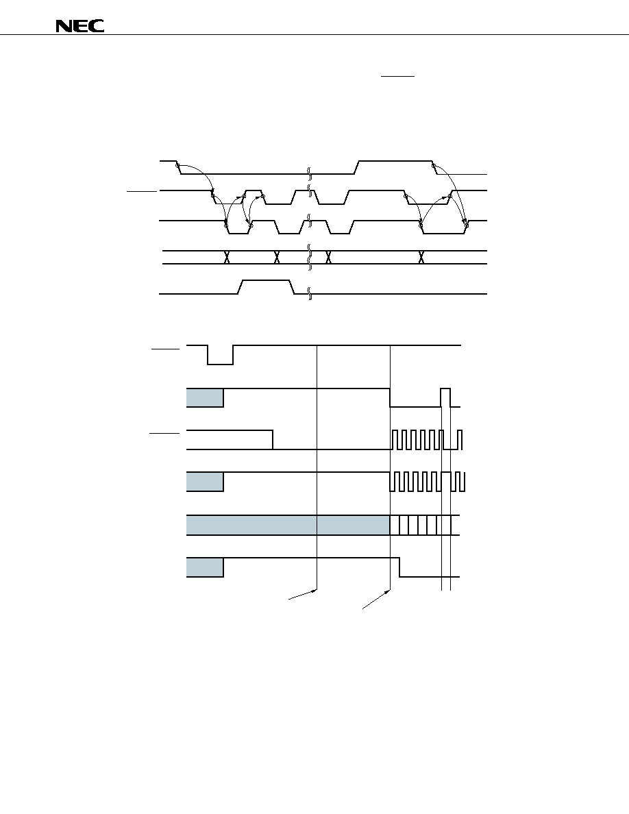
Stream Input
It is possible to receive 4 bytes data after invalid of ISREQ of the stream input.
Remark ISSTB and ISCLK are identical pins.
Figure 2-7. Parallel Stream Receiving Mode (1/2)
(a) Example for Receiving of MPEG2-TS
No
recei-
ved
data
Valid
data
Valid
data
Valid
data
Valid
data
Valid
data
Valid
data
Valid
data
Valid
data
Valid
data
1st
Valid
data
ISVLD
ISCLK
IS7 to IS0
ISSYNC
1 packet (188 bytes)
Release in a TS packet
No
received
data
ISCLK shall be under 13.5 MHz.
Data Sheet S15082EJ4V0DS
26
µ
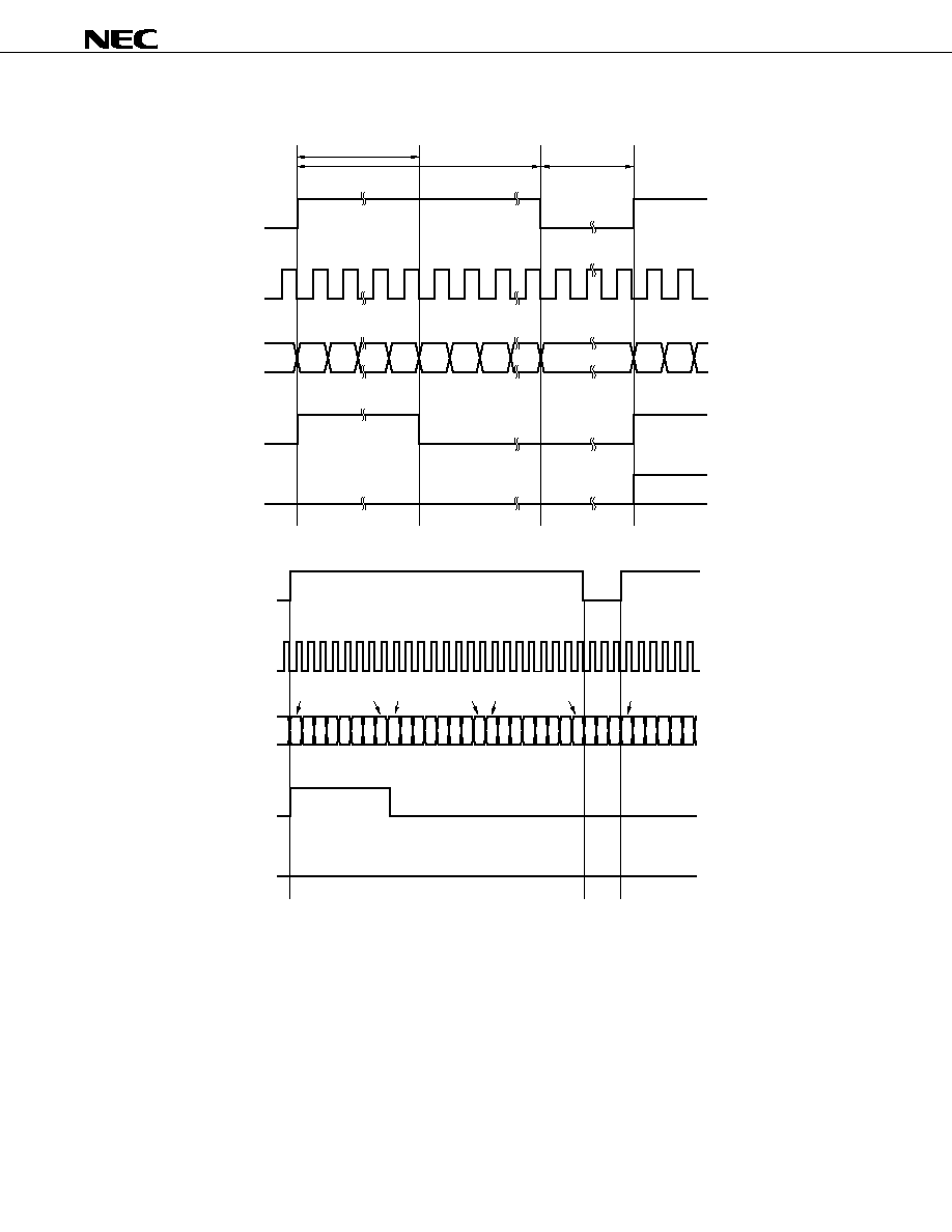
PD61051, 61052
Figure 2-7. Parallel Stream Receiving Mode (2/2)
(b) Example of Receiving MPEG2-PS, ES with Valid and Clock
Valid
data
Valid
data
Valid
data
Valid
data
Valid
data
Valid
data
Valid
data
Valid
data
No
recei-
ved
data
No
recei-
ved
data
No
recei-
ved
data
No
recei-
ved
data
ISCLK
IS7 to IS0
ISSYNC
No
received
data
ISREQ
ISVLD
Don't care
It is possible to receive till 4 bytes
(c) Example of Receiving MPEG2-PS, MPEG2-ES with a Strobe
Valid
data
Valid
data
Valid
data
Valid
data
Valid
data
Valid
data
Valid
data
Valid
data
No
recei-
ved
data
No
recei-
ved
data
No
recei-
ved
data
No
recei-
ved
data
ISREQ
ISSTB
IS7 to IS0
ISSYNC
No
received
data
Don't care
It is possible to receive till 4 bytes
(2)
Stream output
There are two modes: valid operation master mode and strobe operation byte transfer mode.
The appropriate transfer mode for the system can be selected by setting the two stream output mode and transfer
rate.
Remark OSSTB and OSRDY are the same pins as OSCLK and OSVLD, respectively. Operation can be
selected using combinations of OSSTB and OSRDY or OSCLK and OSVLD.
Data Sheet S15082EJ4V0DS
27
µ
PD61051, 61052
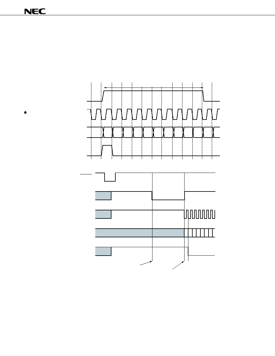
(a) Master Mode Valid
This is the MPEG2-TS dedicated output mode.
The period of OSCLK can be selected from n times 37 ns (1/27 MHz) (3
n 255, n is an integer). If using local
decode or input video display, the period is 4
n 255 (n is an integer).
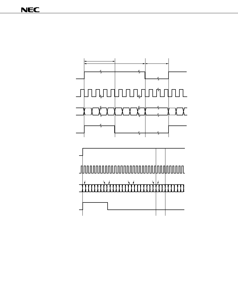
Figure 2-8. Parallel Stream Transmission Mode ; Transmission of MPEG2-TS (Packet Length is 188 Bytes)
(a) Master Mode, Valid
Valid
data
Valid
data
Valid
data
Valid
data
Valid
data
Valid
data
Valid
data
Valid
data
Valid
data
1st
Valid
data
OSVLD
OSCLK
OS7 to OS0
OSSYNC
Invalid
Invalid Invalid
1 packet (188 bytes)
(b) The Transfer Condition from Reset
OSVLD
RESET
OSCLK
OSSYNC
OS7 to OS0
Unsettled
Unsettled
Unsettled
The setting of an interface mode
The stream preparation completion
Unsettled (Data does not change)
Data Sheet S15082EJ4V0DS
28
µ
PD61051, 61052
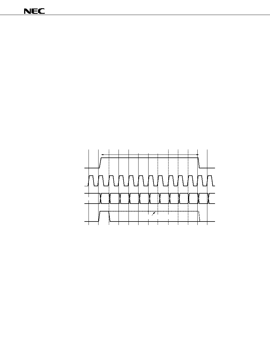
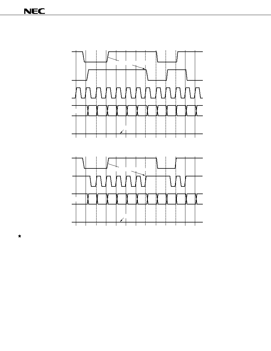
(b) Bytes Transfer Mode, Strobe
In byte transfer mode, the transfer rate is determined by the handshake of OSREQ and OSSTB.
Figure 2-9. Parallel Stream Transmission Mode (Transmission of MPEG2-PS, MPEG2-ES)
(a) Example for Transmission of Strobe Mode One Byte Transfer
OSRDY
OSREQ
OSSTB
OS7 to OS0
OSSYNC
(b) The Transfer Condition from Reset
OSRDY
RESET
OSREQ
OSSYNC
OS7 to OS0
Unsettiled
Unsettiled
The setting of an interface mode
The stream preparation completion
Unsettled (Data does not change)
OSSTB
Unsettiled

Data Sheet S15082EJ4V0DS
29
µ
PD61051, 61052
2.4.2
Serial stream data interface
This LSI is able to input a serial stream. Bit rate of serial input is limited less than parallel interface. Serial Stream
Interface can transfer only MPEG2-TS stream. Maximum bit rate of stream input is less then 64 Mbps. Bit rate of
stream out is 27 Mbps. Additionally, encoding and transcoding bit rate is limited to 15 Mbps on MPEG2 MP@ML.
(1)
Stream input
ISCLK is input by less than 64 MHz clock. Data is MSB first. ISSYNC should active while first byte each packet.
If packet error occurred, ISERR should active from ISSYNC of the packet. ISVLD should valid while each byte.
ISVLD shall invalid while 8 bits between each packets.
Data Sheet S15082EJ4V0DS
30
µ
PD61051, 61052
Figure 2-10. Serial Stream Input
ISCLK
IS0
ISVLD
IS1/ISERR
MSB
ISSYNC
Bit1
Bit6
Bit0 MSB
First Byte of TS packet
One packet
More than 8 ISCLK
MSB
Invalid
Bit0
ISCLK
IS0
ISVLD
IS1/ISERR
"L"
ISSYNC
MSB
LSB
MSB
LSB
MSB
LSB
MSB
Remark Example for ISVLD, ISSYNC, ISERR active high, ISCLK active high
edge
Data Sheet S15082EJ4V0DS
31
µ
PD61051, 61052
(2)
Stream Output
OSCLK is fixed 27 MHz OSSYNC active at first byte in each packet. OSVLD is active of 1 packet continuously.
Data is the MSB first outputs. ISSYNC becomes active among 1 byte at the head of the packet.
Figure 2-11. Serial Stream Output
OSCLK
OS0
OSVLD
MSB
OSSYNC
Bit1
Bit6
Bit0 MSB
First Byte of TS packet
One packet
More than 8 ISCLK
MSB
Invalid
Bit0
OSCLK
OS0
OSVLD
OSSYNC
MSB
LSB
MSB
LSB
MSB
LSB
MSB
Remark
Example for OSVLD, OSSYNC, OSERR active high
Data Sheet S15082EJ4V0DS
32
µ
PD61051, 61052
2.5
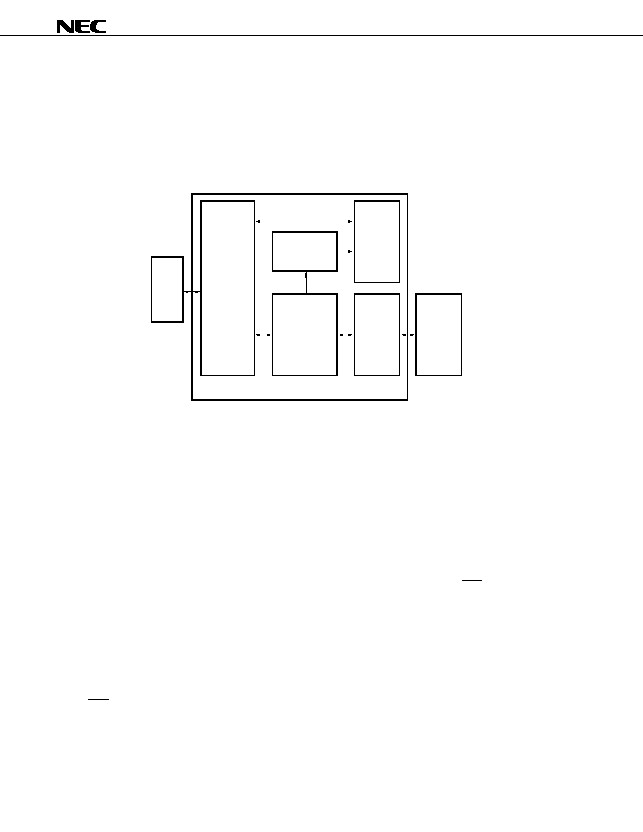
Host CPU Interface
The connection of the host CPU can select the eight bits parallel data interface and serial interface (SPI). Internal
CPU sends and receives command status through the System Interface Register, which is in the host CPU interface
unit. In addition, to control an internal DMA controller through the system interface register, it loads an instruction for
internal CPU to the instruction RAM and the transfer of the large-volume data can be sent to the data area on SDRAM.
Figure 2-12. Host CPU Interface
Host
CPU
System
Interface
Register
Instruction
RAM of
Internal CPU
Internal
CPU
SDRAM
Interface
SDRAM
DMA
Controller
µPD61051/61052
The following describes loading of internal CPU instruction.
(1)
Parallel interface
When parallel interface is selected, host interface has 6-bit address, 8-bit data bus and control ports.
CWAIT is selected with CMODE1 to wait on ready signal mode, CMODE1 selects active polarity of CWAIT.
(2)
Serial interface
The
µ
PD61051/61052 communicates with the host CPU using the SPI (serial peripheral interface) serial bus. The
host CPU becomes a bus master.
The low edge of the chip selection is communication beginning. Its high edge is communication ending.
An address and the reading / writing mode are shown at the first byte after the chip selection becomes low.
It is the MSB first of six bits of addresses, eight bits of data. Fix CSCLK to high level during CCS is disabled (high
level).
The
µ
PD61051/61052 becomes a master and downloads the instruction of the internal CPU from external ROM.
CSCLK:
The serial clock
CSDI:
The data input
CSDO:
The data output
CCS:
The chip selection
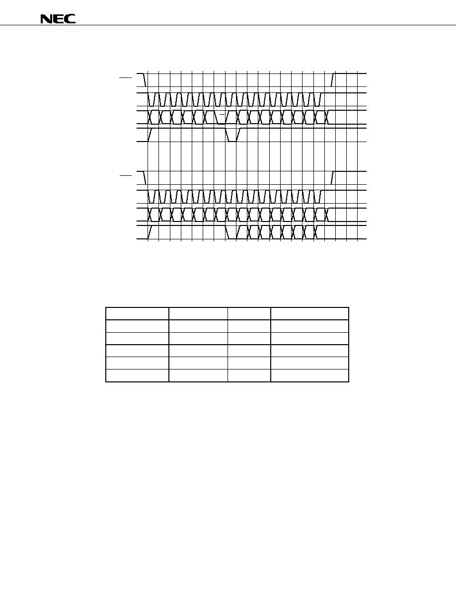
Data Sheet S15082EJ4V0DS
33
µ
PD61051, 61052
Figure 2-13. Serial Interface
A5 A4 A3 A2 A1 A0 W x
D5 D4 D3 D2 D1 D0
D7 D6
xx
x
A5 A4 A3 A2 A1 A0
R
x
x
x
x
x
x
x
x
x
xx
x
xx
D5 D4 D3 D2 D1 D0
D7 D6
[Data Write]
[Data Read]
CCS
CSCLK
CSDI
CSDO
CCS
CSCLK
CSDI
CSDO
xx
2.6
SDRAM Interface
External memory is SDRAM. It is possible to use the following.
Table 2-6. Use Memory
Memory
Data bus width
Quantity
Use memory capacity
16 Mbit SDRAM
16 bits
2
32 Mbits
64 Mbit SDRAM
32 bits
1
64 Mbits
64 Mbit SDRAM
16 bits
2
128 Mbits
128 Mbit SDRAM
16 bits
2
128 Mbits
128 Mbit SDRAM
32 bits
1
128 Mbits
The
µ
PD61051/61052 preserves the part of the parameter that is necessary to generate the stream, entry video
image, a video stream, an audio stream, a stream header, user data, and the instruction of the firmware at this
memory.
This system uses only CAS latency = 3, burst length = 4.
When encode using time base corrector and/or displays local decoding picture, it needs equal to or more than 64
Mbits SDRAM.
When PAL encoding, it needs equal to or more than 64 Mbit SDRAM.
When transcoding, it needs equal to or more than 64 Mbit SDRAM.
Data Sheet S15082EJ4V0DS
34
µ
PD61051, 61052
2.7
Memory Connection Diagram
Each memory connection is as follows.
Figure 2-14. Memory Connection Diagram (1/2)
(a) 16 Mbit SDRAM by 2
A11
A10 to A0
D15 to D0
1 Mbits◊16
SDRAM
A11
MA13
µPD61051/61052
Bank A: SDRAM address = 0x xxxx xxxx xxxxB
Bank B: SDRAM address = 1x xxxx xxxx xxxxB
MA12
MA11
MA10 to MA0
MD31 to MD16
MD15 to MD0
A10 to A0
D15 to D0
1 Mbits◊16
SDRAM
(b) 64 Mbit SDRAM by 1
A12
A11
MA13
µPD61051/61052
Bank A: SDRAM address = 00 xxxx xxxx xxxxB
Bank B: SDRAM address = 10 xxxx xxxx xxxxB
Bank C: SDRAM address = 01 xxxx xxxx xxxxB
Bank D: SDRAM address = 11 xxxx xxxx xxxxB
MA12
MA11
MA10 to MA0
MD31 to MD16
MD15 to MD0
A10 to A0
D31 to D16
D15 to D0
2 Mbits◊32
SDRAM
Data Sheet S15082EJ4V0DS
35
µ
PD61051, 61052
Figure 2-14. Memory Connection Diagram (2/2)
(c) 64 Mbit SDRAM by 2 or 128 Mbit SDRAM by 2
D15 to D0
4 Mbits◊16
SDRAM
A13
A12
A11
MA13
µPD61051/61052
Bank A: SDRAM address = 00 xxxx xxxx xxxxB
Bank B: SDRAM address = 10 xxxx xxxx xxxxB
Bank C: SDRAM address = 01 xxxx xxxx xxxxB
Bank D: SDRAM address = 11 xxxx xxxx xxxxB
MA12
MA11
MA10 to MA0
MD31 to MD16
MD15 to MD0
A10 to A0
MA13
MA12
MA11
MA10 to MA0
D15 to D0
4 Mbits◊16
SDRAM
Data Sheet S15082EJ4V0DS
36
µ
PD61051, 61052
2.8
Memory Map
Firmware sets memory map such as video image area and usable work area. Firmware cabinet (temporal buffered
area) is the area which firmware does not use. Video Image area size is changed NTSC or PAL. Each area are
changed by the firmware.
Figure 2-15. Memory Map (1/2)
(a) 16 Mbit SDRAM by 2
00000H
Bank A
Video Stream
Audio Stream
User Data 0
Header
Firmware
Firmware
Firmware
7FFFFH
Bank B
Video Stream
Video
Image
Area
(b) Example for 64 Mbit SDRAM by 1
00000H
Bank A
Video Stream 0
Audio stream 0
User data 0
Header
Unused
Audio stream 1
User data 1
7FFFFH
7FFFFH
00000H
Bank B
Video Stream 0
Video
Image
Area
Bank C
Video Stream 1
Bank D
Video Stream 1
Instruction Pool
Instruction Pool
Usable Work Area
Usable Work Area
Video
Image
Area
Firmware
Firmware
Firmware
Firmware
Firmware

Data Sheet S15082EJ4V0DS
37
µ
PD61051, 61052
Figure 2-15. Memory Map (2/2)
(c) Example for 64 Mbit SDRAM by 2 or 128 Mbit SDRAM by 2
00000H
Bank A
Video Stream
Unused
Header
FFFFFH
00000H
80000H
FFFFFH
Bank B
Video Stream
Bank C
Unused
Bank D
Unused
Audio Stream
Audio Stream
Video Stream
Video Stream
User data 0
User data 1
Instruction Pool
Instruction Pool
Unused
Unused
Usable Work Area
Usable Work Area
Video
Image
Area
Firmware
Firmware
Firmware
Firmware
Video
Image
Area
Data Sheet S15082EJ4V0DS
38
µ
PD61051, 61052
3.
SYSTEM INTERFACE REGISTER
This LSI corresponds to the various operation modes in exchange instruction of internal CPU from SDRAM to
instruction RAM (iRAM).
This has 64 byte Registers. They are defined to common registers, interrupt registers and interrupt mask registers.
When there is access in the same address from both of the internal CPU and the host CPU, the later data is left at the
register.
Also, when the writing occurs to the same address at the same time about the common register, the data of the
host CPU is left at the register
Figure 3-1. System Interface Register
Host
CPU
System
Interface
Register
Instruction
RAM of
Internal CPU
Internal
CPU
SDRAM
Interface
SDRAM
DMA
Controller
µPD61051/61052
Data Sheet S15082EJ4V0DS
39
µ
PD61051, 61052
3.1
Register Mapping (General Mapping)
Address
Bit7 Bit6 Bit5 Bit4 Bit3 Bit2 Bit1 Bit0
R/W
00H to 1FH
Defined by firmware
R/W
20H SI
SSD
SDI
MSD
MI
SDW SDR
R/W
Download
mode
21H
SA19 to SA16
R/W
Source address
22H
SA15 to SA8
R/W
Source address
23H
SA7 to SA0
R/W
Source address
24H
DA16
R/W
Destination
address
25H
DA15 to DA8
R/W
Destination address
26H
DA7 to DA0
R/W
Destination address
27H
TC18
to
TC16 R/W
Transfer
data
count
28H
TC15 to TC8
R/W
Transfer data count
29H
TC7 to TC0
R/W
Transfer data count
2AH
iCPU-INT
R/W
Int.
to
internal
CPU
2BH
DMA-
ERR-M
DMA-
RDY-M
DMA-
DONE-M
R/W Interrupt
mask0
2CH
Defined by firmware
R/W
Interrupt mask1
2DH
Defined by firmware
R/W
Interrupt mask2
2EH
Defined by firmware
R/W
Interrupt mask3
2FH
Defined by firmware
R/W
Interrupt mask4
30H
DMA-ERR
DMA-RDY
DMA-
DONE
R/W Interrupt0
31H Defined
by
firmware
R/W
Interrupt1
32H Defined
by
firmware
R/W
Interrupt2
33H Defined
by
firmware
R/W
Interrupt3
34H Defined
by
firmware
R/W
Interrupt4
35H
iROM2 to iROM0
R/W
Mask ROM cycle
36H
ISREQ
OSVLD
R/W
Port
setup
37H
to
3DH
3EH
NBR
ALL
RESET
R/W Reset
3FH
TD7 to TD0
R/W
Transfer data
Data Sheet S15082EJ4V0DS
40
µ
PD61051, 61052
3.2
Register Functions
3.2.1
Common register
Address
Bit7 Bit6 Bit5 Bit4 Bit3 Bit2 Bit1 Bit0
R/W
00H to 1FH
Defined by firmware
R/W
Each firmware defines these registers.
These registers are used to communicate with host CPU and internal CPU.
For the details of the register, refer to the application notebook.
The reset of the RESET pin or ALL RESET of the reset register initializes addresses 00H and 01H addresses to 0H.
The original value of the other register is unsettled. It keeps a setting value before reset.
3.2.2
Data transfer register
These registers are defined data transfer such as host CPU
SDRAM, SDRAM host CPU, host CPU iRAM
of internal CPU, SDRAM
iRAM of internal CPU and instruction ROM iRAM of internal CPU.
The host CPU transfers with SDRAM via had a transfer buffer of 128 bytes on this LSI.
The transfer with the instruction RAM becomes 4 bytes.
A transfer error occurs if the transfer mode register, source address register, destination address register, or
transfer counter register is changed before releasing the transfer mode register following transfer completion after
setting the transfer mode register and starting the transfer. When transferring data as follows: host CPU
instruction
RAM of internal CPU, host CPU
SDRAM, SDRAM instruction RAM of internal CPU, instruction ROM SDRAM,
instruction ROM
instruction RAM of internal CPU, execute a software reset of the internal CPU (address 3EH
02H) before transfer and release the reset after transfer.
Data Sheet S15082EJ4V0DS
41
µ
PD61051, 61052
(1)
Data transfer register
Address
Bit7 Bit6 Bit5 Bit4 Bit3 Bit2 Bit1 Bit0
R/W
20H SI
SSD
SDI
MSD
MI
SDW SDR
R/W
Download
mode
Bit Field
Function
Initial
value
7 SI Host
CPU
instruction RAM of internal CPU
0: Releasing of transfer, 1: Transfer
Note
0
6 SSD
Host
CPU
SDRAM
0: Releasing of transfer, 1: Transfer
Note
0
5 SDI
SDRAM
instruction RAM of internal CPU
0: Releasing of transfer, 1: Transfer
Note
0
4 MSD
Instruction
ROM
SDRAM
0: Releasing of transfer, 1: Transfer
Note
0
3 MI
Instruction
ROM
instruction RAM of internal CPU
0: Releasing of transfer, 1: Transfer
Note
0
2
Reserved (set only 0)
0
1 SDW
Host
CPU
SDRAM
0: Releasing of transfer,1: Transfer
0
0 SDR
SDRAM
host CPU
0: Releasing of transfer, 1: Transfer
0
Note Set internal CPU reset (with Register 3EH
02H)
More than one bit cannot be set to 1 at the same time. It becomes a transfer error when writing at the transfer
mode register while transferring. When canceling a transfer while transferring, it stops a transfer. At this time, the
data in the transfer buffer becomes invalid. The transfer of SDR with once is to a maximum of 128 bytes. If host CPU
stops the transfer, host CPU should operate transfer error handling.
Data Sheet S15082EJ4V0DS
42
µ
PD61051, 61052
(2)
Source address register
Address
Bit7 Bit6 Bit5 Bit4 Bit3 Bit2 Bit1 Bit0
R/W
21H
SA19
to
SA16
R/W
Source
address
22H
SA15 to SA8
R/W
Source address
23H
SA7 to SA0
R/W
Source address
It sets the address of the data to transfer. It becomes effective in case of transfer from SDRAM or instruction ROM.
Until it releases a transfer mode after setting a transfer mode register, it isn't possible to change. The transfer error
occurs when rewriting this register before releasing a transfer mode. The relation with the address of SDRAM,
external instruction ROM is shown in Figure 3-2 and 3-3. The addressing of SDRAM becomes a 32 address by
4-word unit (128 bytes).
The relation with the SDRAM bank and address is shown in Table 3-1.
Figure 3-2. Relation of Source Address and SDRAM Address
0 0 0 0
0 0 0 0 0
SDRAM address
Host CPU
interface register
21H to 23H
The µPD61051/61052
adds 0 automatically
SA19
SA18
SA17
SA16
SA11
SA10
SA9
SA8
SA15
SA14
SA13
SA12
A19
A18
A17
A16
A21
A20
A11
A10
A9
A8
A15
A14
A13
A12
A7
A6
A5
SA3
SA2
SA1
SA0
SA7
SA6
SA5
SA4
Bank select
Figure 3-3. Relation of Source Address and External Instruction ROM Address
0 0 0 0
Extemal
instruction ROM
address
Host CPU
interface register
21H to 23H
SA19
SA18
SA17
SA16
SA11
SA10
SA9
SA8
SA15
SA14
SA13
SA12
FA19
FA18
FA17
FA16
FA11
FA10
FA9
FA8
FA15
FA14
FA13
FA12
FA3
FA2
FA1
FA0
FA7
FA6
FA5
FA4
SA3
SA2
SA1
SA0
SA7
SA6
SA5
SA4
Table 3-1. Relation of SDRAM Bank and Address
Memory
Bank A
Bank B
Bank C
Bank D
16 Mbit SDRAM by 2
000000H to 07FFFFH
200000H to 27FFFFH
-
-
16 Mbit SDRAM by 1
000000H to 07FFFFH
200000H to 27FFFFH
100000H to 17FFFFH
300000H to 37FFFFH
64 Mbit SDRAM by 2
128 Mbit SDRAM by 1
128 Mbit SDRAM by 2
000000H to 0FFFFFH
200000H to 2FFFFFH
100000H to 1FFFFFH
300000H to 3FFFFFH
128 Mbit SDRAM by 1
000000H to 0FFFFFH
200000H to 2FFFFFH
100000H to 1FFFFFH
300000H to 3FFFFFH
Data Sheet S15082EJ4V0DS
43
µ
PD61051, 61052
(3)
Destination address register
Address
Bit7 Bit6 Bit5 Bit4 Bit3 Bit2 Bit1 Bit0
R/W
24H
DA16
R/W
Destination
address
25H
DA15 to DA8
R/W
Destination address
26H
DA7 to DA0
R/W
Destination address
It sets Destination address. It becomes effective in case of transfer to SDRAM or instruction RAM of internal CPU.
It isn't possible to change until it cancels a transfer mode after setting a transfer mode register. It becomes a transfer
error when rewriting before canceling a transfer mode. The relation of the address of SDRAM and instruction RAM of
internal CPU is as in Figure 3-4 and 3-5. The addressing of SDRAM becomes a 32 address by 4-word unit (128
bytes).
Figure 3-4. Relation of Destination Address and SDRAM Address
0 0 0 0 0 0 0
0 0 0 0 0
SDRAM address
Host CPU
interface register
24H to 26H
Bank select
The µPD61051/61052
adds 0 automatically
DA16
DA11
DA10
DA9
DA8
DA15
DA14
DA13
DA12
A19
A18
A17
A16
A21
A20
A11
A10
A9
A8
A15
A14
A13
A12
A7
A6
A5
DA3
DA2
DA1
DA0
DA7
DA6
DA5
DA4
Figure 3-5. Relation of Destination Address and Instruction ROM Address of Internal CPU
0 0 0 0 0 0 0
Instruction RAM
address of
intemal CPU
Host CPU
interface register
24H to 26H
DA16
DA11
DA10
DA9
DA8
DA15
DA14
DA13
DA12
A11
A10
A9
A8
A14
A13
A12
A3
A2
A1
A0
A7
A6
A5
A4
DA3
DA2
DA1
DA0
DA7
DA6
DA5
DA4
Data Sheet S15082EJ4V0DS
44
µ
PD61051, 61052
(4)
Transfer data counter register
Address
Bit7 Bit6 Bit5 Bit4 Bit3 Bit2 Bit1 Bit0
R/W
27H
TC18
to
TC16 R/W
Transfer
data
count
28H
TC15 to TC8
R/W
Transfer data count
29H
TC7 to TC0
R/W
Transfer data count
It sets the transfer data number of the bytes.
In case of transfer between host CPU and SDRAM, it sets the number of the transfer bytes by 4 bytes unit. In case
of transfer from instructions ROM, SDRAM host CPU to the instruction RAM of internal CPU, it sets the number of the
transfer bytes /4 by the 4 byte unit.
(5)
Transfer data register
Address
Bit7 Bit6 Bit5 Bit4 Bit3 Bit2 Bit1 Bit0
R/W
3FH
TD7 to TD0
R/W
Transfer data
This register is transfer data window.
Figure 3-6. SDRAM Write
Byte3
Byte7
Byte19
Byte11
Byte15
Byte2
Byte6
Byte18
Byte10
Byte14
Byte1
Byte5
Byte17
Byte9
Byte13
Byte0
Byte4
Byte16
Byte8
Byte12
Byte0
Byte1
Byte4
Byte2
Byte3
Byte7
Byte8
Byte5
Byte6
TD7 to TD0
SDRAM
Lower byte first
Host CPU write
Transfer buffer
(128 bytes)
SDRAM address
= DA16 to DA0◊128
SDRAM address
= DA16 to DA0◊128+5

Data Sheet S15082EJ4V0DS
45
µ
PD61051, 61052
SDRAM read
<1> Interrupt mask
Host CPU sets mask bit to interrupt mask register (2CH to 2FH) for the interrupt that needs a data transfer.
<2> Set source address
Host CPU sets the address of SDRAM to the source address register (21H to 23H) of the
µ
PD61051/61052.
<3> Set the number (equal to or less than 128 bytes) of the data to read by 4 bytes unit
Host CPU sets the data number of the bytes to the transfer data counter register (27H to 29H) of the
µ
PD61051/61052.
<4> Set the transfer of SDRAM
host CPU.
Host CPU sets 01H to the transfer mode register (20H) of the
µ
PD61051/61052.
<5> CINT interrupt (Interrupt pin)
<6> Confirms that the interrupt factor and clear interrupt factor
Host CPU confirms that the interrupt register 0 (30H) of the
µ
PD61051/61052 becomes 02H or 01H and clears
writing a same value of the interrupt register 0 (30H) to the interrupt register 0 (30H) of the
µ
PD61051/61052.
<7> Data read
Host CPU reads data from the number of times with the set number of bytes, the transfer data register (3FH) of
the
µ
PD61051/61052.
<8> CINT interrupt (Interrupt pin)
<9> Confirm the interrupt factor
Host CPU confirms that the interrupt register 0 (30H) of the
µ
PD61051/61052 becomes 01H. (It clears a writing
interrupt factor in 01H at the interrupt register 0 (30H) register of the
µ
PD61051/61052.)
<10> Release of SDRAM
host CPU mode
Host CPU clears a writing interrupt factor in 01H at the interrupt register 0 (30H) register of the
µ
PD61051/61052
after setting 00H to the transfer mode register (20H) of the
µ
PD61051/61052.
<11> Release of interrupt mask
It releases the limitation on interrupt which set by <1>.

Data Sheet S15082EJ4V0DS
46
µ
PD61051, 61052
SDRAM write
<1> Interrupt mask
Host CPU sets mask bit to interrupt mask register (2CH to 2FH) for the interrupt that needs a data transfer.
<2> Set destination address
Host CPU sets the address of SDRAM to the destination address register (24H to 26H) of the
µ
PD61051/61052.
<3> Set the number of the data to write by a 4 byte unit
Host CPU sets the data number of the bytes by 4 bytes unit to the transfer data counter register (27H to 29H) of
the
µ
PD61051/61052.
<4> Set the transfer of host CPU
SDRAM
Host CPU sets 02H to the transfer mode register (20H) of the
µ
PD61051/61052.
<5> Data write
Host CPU writes data to the transfer data register (3FH) of the
µ
PD61051/61052 at times with more few 128 bytes
or transfer data count register setting value.
<6> CINT interrupt (Interrupt pin)
<7> Confirm the interrupt factor
When the number of the transfer data is less then 128 bytes, host CPU confirms that the interrupt register 0 (30H)
of the
µ
PD61051/61052 becomes 01H, and go to <9>.
<8> Confirm that next data transfer prepare completed
Host CPU confirms that the interrupt register 0 (30H) of the
µ
PD61051/61052 becomes 02H or 01H and clears a
writing sane value of the interrupt register 0 (30H) to the interrupt register 0 (30H) of the
µ
PD61051/61052.
Return to <5> and next data write.
<9> Release of SDRAM
host CPU
Host CPU clears a writing interrupt factor in 01H at the interrupt register 0 (30H) register of the
µ
PD61051/61052
after setting 00H to the transfer mode register (20H) of the
µ
PD61051/61052.
<10> Release of interrupt mask
It releases the limitation on interrupt which is set by <1>.
<11> In the case of an interrupt to internal CPU, it is necessary
Host CPU sets a data bank number and the number of the bytes to the address that defined with the firmware.
It sets 01H to the 2AH address of the
µ
PD61051/61052 and it notifies an interrupt to internal CPU.
Data Sheet S15082EJ4V0DS
47
µ
PD61051, 61052
3.2.3
Internal CPU interrupt register
Address
Bit7 Bit6 Bit5 Bit4 Bit3 Bit2 Bit1 Bit0
R/W
2AH
iCPU-INT
R/W
Int.
to
internal
CPU
Host CPU set interrupt to internal CPU. Internal CPU clears this bit after interrupt operation.
The reset of the RESET pin or ALL RESET of the reset register initializes this address to 0H.
3.2.4
Interrupt mask register
Address
Bit7 Bit6 Bit5 Bit4 Bit3 Bit2 Bit1 Bit0
R/W
2BH
DMA-ERR
-M
DMA-RDY
-M
DMA-DON
E-M
R/W Interrupt
mask0
2CH
Defined by firmware
R/W
Interrupt mask1
2DH
Defined by firmware
R/W
Interrupt mask2
2EH
Defined by firmware
R/W
Interrupt mask3
2FH
Defined by firmware
R/W
Interrupt mask4
These registers are interrupt masks for next interrupt. Interrupt mask can be set bit by bit. When setting an
interrupt mask, CINT does not become high even if the interrupt register becomes 1.
The reset of the RESET pin or ALL RESET of the reset register initializes this address to 0H.
3.2.5
Download interrupt register
Address
Bit7 Bit6 Bit5 Bit4 Bit3 Bit2 Bit1 Bit0
R/W
30H
DMA-ERR
DMA-RDY
DMA-DON
E
R/W Interrupt0
It is set for 1 when the interrupt factor occurs.
The interrupt bit clears when host CPU writes to this register after the interrupt processing.
The reset of the RESET pin or ALL RESET of the reset register initializes this address to 0H.
Clear processing continues until interrupt registers is cleared.
Bit Field
Function
Initial
value
7 to 3
Reserved (set 0)
2
DMA-ERR
Data transfer error
0: Normal, 1: Error
0
1
DMA-RDY
Data transfer prepared
0: Normal, 1: Transfer
0
0
DMA-DONE
Data transfer ended
0: Normal, 1: Transfer ended
0
It outputs DMA-RDY or DMA-DONE every 128-byte transfer. DMA-DONE is output when the transfer ends.
Data Sheet S15082EJ4V0DS
48
µ
PD61051, 61052
3.2.6
Interrupt register
Address
Bit7 Bit6 Bit5 Bit4 Bit3 Bit2 Bit1 Bit0
R/W
31H Defined
by
firmware
R/W
Interrupt1
32H Defined
by
firmware
R/W
Interrupt2
33H Defined
by
firmware
R/W
Interrupt3
34H Defined
by
firmware
R/W
Interrupt4
It is set for 1 when the interrupt factor occurs.
The interrupt bit clears when host CPU writes 1 in the bit of the interrupt after the interrupt processing.
When the other interrupt (which isn't masked) is set to 1 when clearing a interrupt, CINT becomes high 1
µ
s later.
The reset of the RESET pin or ALL RESET of the reset register initializes this address to 0H.
Clear processing continues until interrupt registers is cleared.
Address Bit
Field
Function
Initial
value
31H to
34H
7 to 0
Firmware define
0: Normal, 1: Interrupt
0H
3.2.7
Reset register
Address
Bit7 Bit6 Bit5 Bit4 Bit3 Bit2 Bit1 Bit0
R/W
3EH
NBR
ALL
RESET
R/W Reset
When the host CPU sets 1 to ALL RESET, it resets the inside and it returns to 0 automatically.
The reset of the RESET pin or ALL RESET of the reset register initializes this address to 0H.
Bit Field
Function
Initial
value
7 to 2
Reserved (Set 0)
1 NBR
Internal
CPU
reset
0: Normal, 1: Reset
0
0
ALL RESET
Same hardware reset
0: Normal, 1: Reset
0
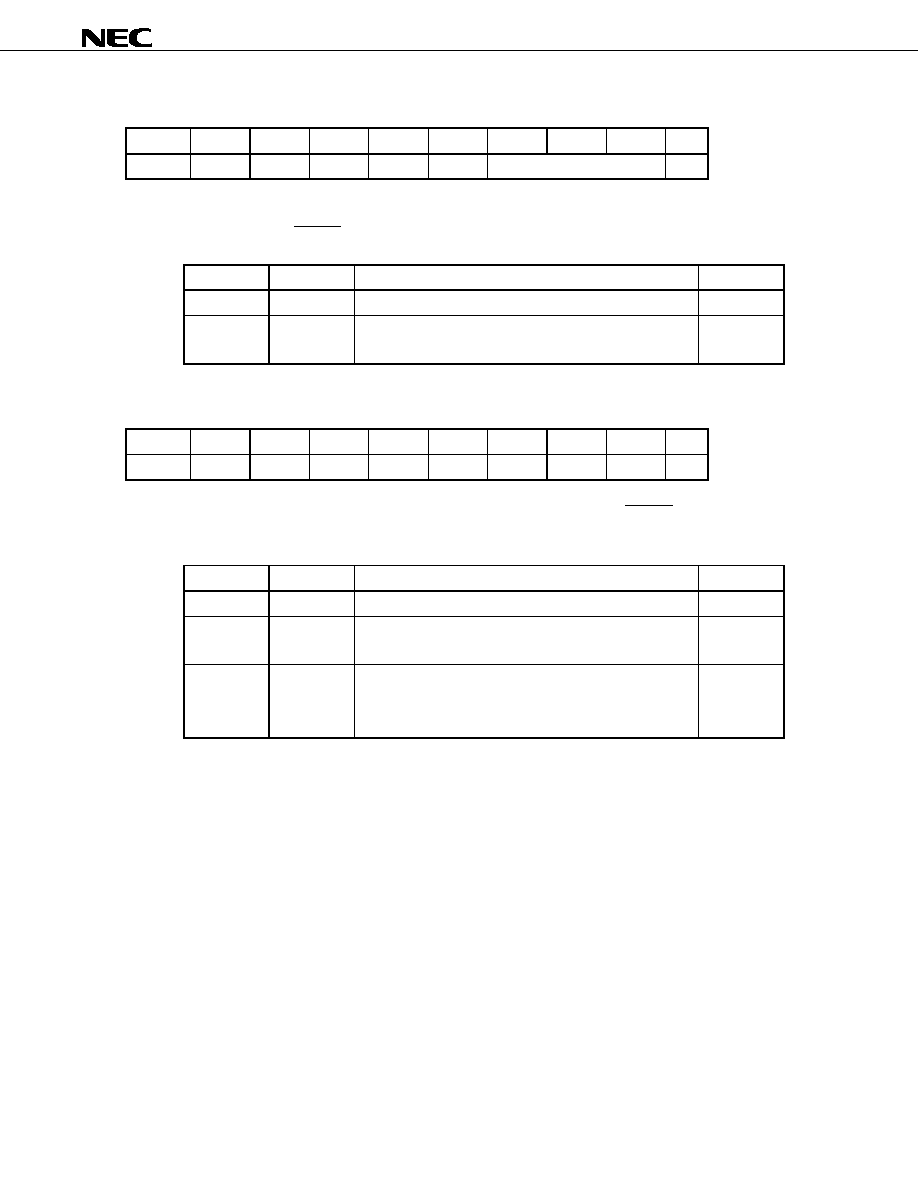
Data Sheet S15082EJ4V0DS
49
µ
PD61051, 61052
3.2.8
ROM access cycle register
Address
Bit7 Bit6 Bit5 Bit4 Bit3 Bit2 Bit1 Bit0
R/W
35H
iROM2 to iROM0
R/W
Mask ROM cycle
It specifies the access cycle of the instruction ROM of internal CPU when connecting host CPU interface with the
serial bus. The reset of the RESET pin or ALL RESET of the reset register initializes this address to 7H.
Bit Field
Function
Initial
value
7 to 3
Reserved (Set 0)
2 to 0
iROM2 to
iROM0
Access cycle of instruction ROM
0: Reserved, 1 to 7: (Setting value+2) by 24.6 MHz
7H
3.2.9
Port setup register
Address
Bit7 Bit6 Bit5 Bit4 Bit3 Bit2 Bit1 Bit0
R/W
36H
ISREQ
OSVLD
R/W
Port
setup
This register sets the active polarity of ISREQ and OSVLD. The reset of the RESET pin or ALL RESET of the
reset register initializes this address to 0H.
Bit Field
Function
Initial
value
7 to 2
Reserved (Set 0)
1
ISREQ
Active polarity of ISREQ
0: Low active of request, 1: High active of request
0
0
OSVLD
Active polarity of OSVLD/OSRDY
0: Low active of valid/ready
1: High active of valid/ready
0

Data Sheet S15082EJ4V0DS
50
µ
PD61051, 61052
4.
SYSTEM INTERFACE PROCEDURE
The host CPU transfers the firmware of each operation mode to the instruction RAM of the internal CPU and works
it.
This LSI stores up firmware in SDRAM. Host CPU sets to load the firmware of each operation mode in the
instruction RAM of internal CPU from SDRAM.
When using a parallel bus interface for the host CPU interface, the host CPU sets a data transfer register after
hardware reset and transfers the initialization program of SDRAM to instruction RAM of internal CPU and executing.
Host CPU writes firmware to SDRAM.
When using a serial bus interface for the host CPU interface, the host CPU sets a data transfer register after
hardware ware reset and transfers the initialization program of SDRAM to instruction RAM of internal CPU from
external instruction ROM and executing. Host CPU loads firmware in SDRAM from instruction ROM outside.
It stores the firmware of the encoding and the transcode to SDRAM from ROM in case of start-up of the system,
and then it can do the changing of a feature at short time by the high-speed transfer of SDRAM.
The host CPU sets the mode of the terminal of the
µ
PD61051/61052 and the access cycle of ROM to the system
interface register after hardware reset and sets the transfer of the instruction of the internal CPU after SDRAM is
initialized.
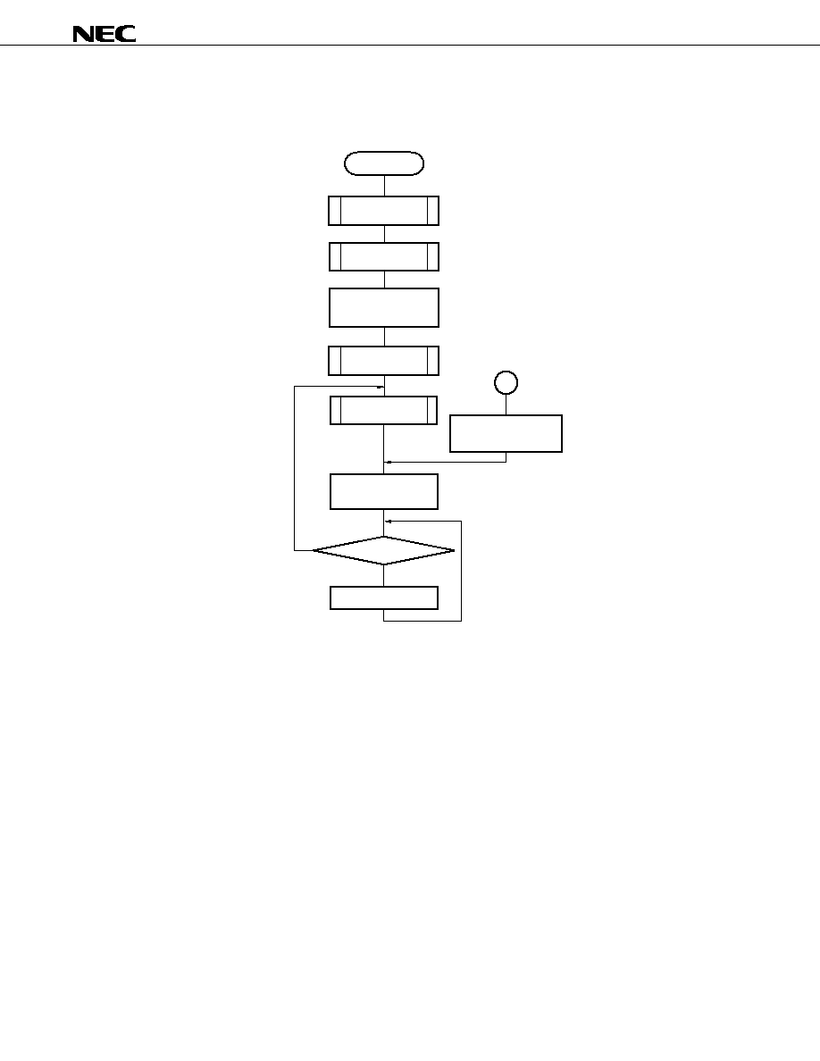
Data Sheet S15082EJ4V0DS
51
µ
PD61051, 61052
4.1
Outline
An overview from the reset of the hardware to the setting of an operation mode is shown.
Y
N
Initialization
Mode setting
Mode change
Operation continuation
Internal CPU start-up
Reset address (3EH)
00H
Hardware reset
Instruction
download
SDRAM
initialization
Note
Software reset
of internal CPU
Reset address (3EH)
02H
Internal CPU software reset
Software reset
of internal CPU
Reset address (3EH)
02H
Note This is not necessary in case that the SDRAM
initialization firmware is not separated.
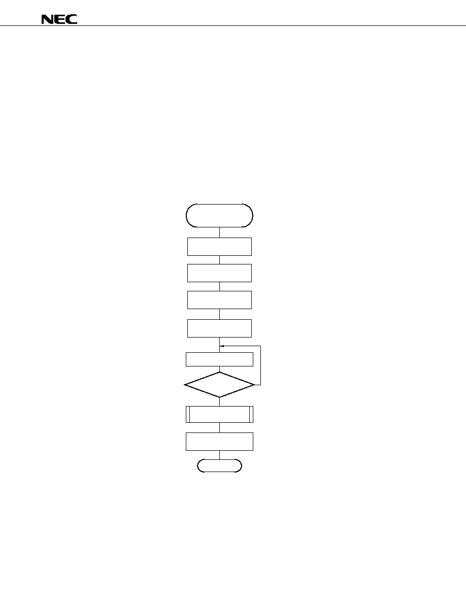
Data Sheet S15082EJ4V0DS
52
µ
PD61051, 61052
4.2
Firmware Download
The host CPU downloads the firmware at the instruction RAM for the internal CPU.
When a host CPU is connected with the serial bus, the firmware can be downloaded from the external ROM for the
download processing to speed up. In addition, it stores more than one piece of firmware in the instruction pool area of
SDRAM and it can be replaced depending on the need, too.
When transferring to the instruction RAM of the internal CPU, the transfer counter register setting value (number of
the transfer bytes / 4) is (program size +3)/ 4.
4.2.1
Host CPU to instruction RAM of internal CPU
Host CPU transmits the firmware to instruction RAM of the internal CPU.
When transferring data continuously, transfer during resetting an internal CPU, If reset of internal CPU is can
canceled on the way, the internal CPU sometime malfunction.
Y
N
Return
Host CPU
to instruction RAM
of internal CPU
Internal CPU reset
Reset register (3EH)
02H setting
Destination address register
(24H to 26H) setting
(Program size + 3)/4
Transfer counter register
(27H to 29H) setting
Host CPU
iRAM transfer
Transfer mode register
(20H)
80H setting
Transfer data register
(3FH)
Instruction
Transfer ending (refer to 4.7)
All instruction written ?
Internal CPU reset is canceled
Reset register
(3EH)
00H setting
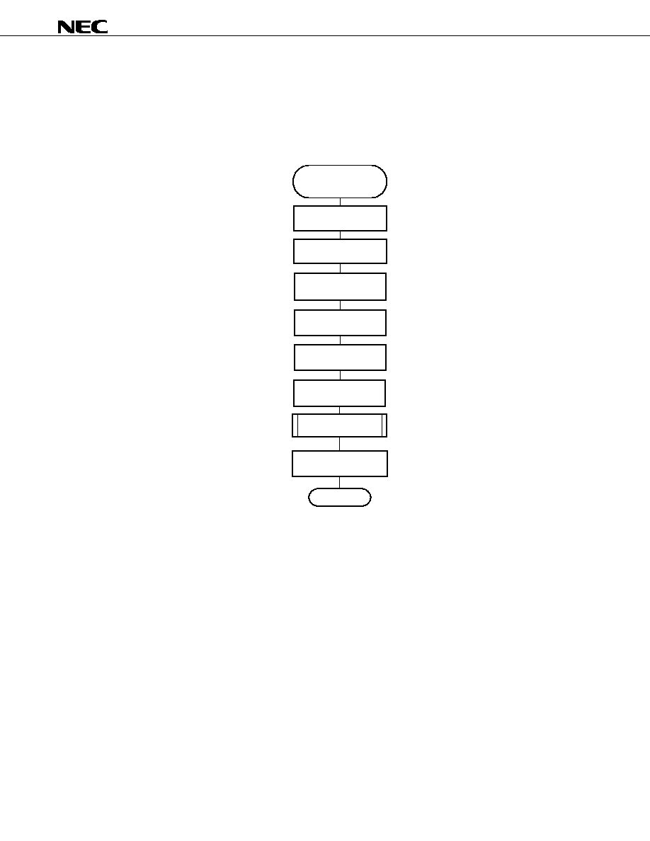
Data Sheet S15082EJ4V0DS
53
µ
PD61051, 61052
4.2.2
External ROM to instruction RAM of internal CPU
When the host CPU is a serial bus type, CPU transmits the instruction of a mode from external ROM to instruction
RAM of Internal CPU.
When transferring data continuously, transfer during resetting an internal CPU, If reset of internal CPU is can
canceled on the way, the internal CPU sometime malfunction.
External ROM
to instruction RAM
of internal CPU
Internal CPU reset
Reset register (3EH)
02H setting
Destination address register
(24H to 26H) setting
Source address register
(21H to 23H) setting
ROM access cycle register
(35H) setting
(Program size + 3)/4
Transfer counter register
(27H to 29H) setting
iROM
iRAM transfer
Transfer mode register
(20H)
80H setting
Return
Transfer ending (refer to 4.7)
Internal CPU reset is canceled
Reset register
(3EH)
00H setting
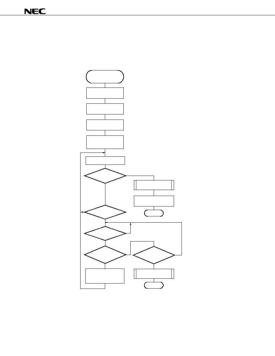
Data Sheet S15082EJ4V0DS
54
µ
PD61051, 61052
4.2.3
Host CPU to SDRAM
The host CPU can store firmware in the instruction pool area of SDRAM for the internal CPU. It stores more than
one piece of firmware and it can be replaced depending on the need, too.
When transferring data continuously, transfer during resetting an internal CPU, If reset of internal CPU is can
canceled on the way, the internal CPU sometime malfunction. The number of the transfer bytes is a 4-byte unit.
Y
Y
Y
Y
N
N
N
N
Instruction
download
Destination address register
(24H to 26H) setting
Internal CPU reset
Reset register (3EH)
02H setting
Number of transefer bytes
Transfer counter register
(27H to 29H) setting
Host CPU
SDRAM transfer
Transfer mode register
(20H)
40H setting
CINT?
Transfer data register
(3FH)
Instruction
Interrupt register 0
(30H): (02H or 01H)
Y
N
Interrupt register 0
(30H): 04H
Interrupt register 0 clear
Interrupt register 0 (30H)
Interrupt register 0 (30H)
All instruction
writing ending?
128 bytes
writing ending?
Return
Transfer error handling
(refer to 4.8)
Return
Transfer ending (refer to 4.7)
Internal CPU reset is canceled
Reset register
(3EH)
00H setting
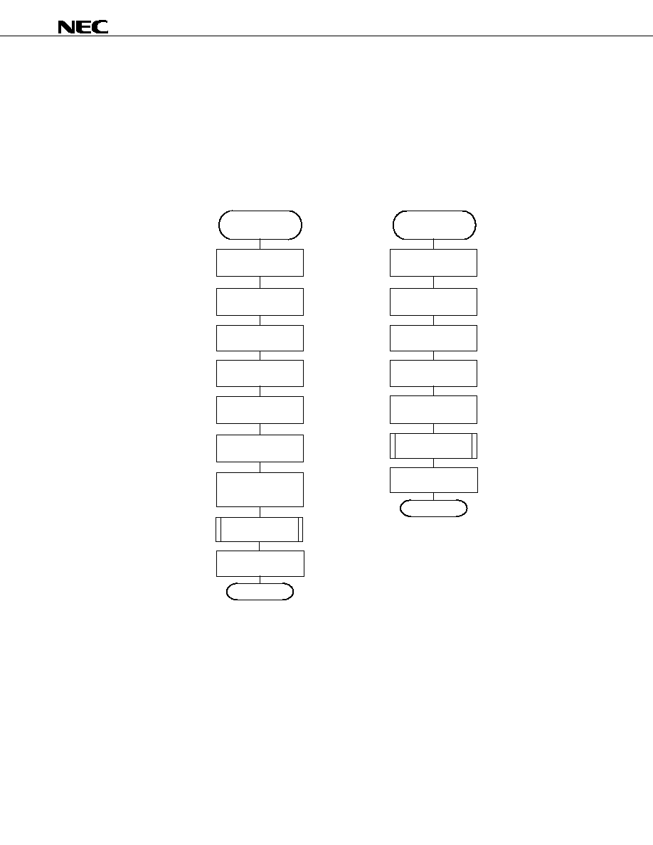
Data Sheet S15082EJ4V0DS
55
µ
PD61051, 61052
4.2.4
External ROM to SDRAM
The firmware for the internal CPU can be stored in the firmware cabinet of SDRAM from the external ROM. It
stores more than one piece of firmware beforehand and it can be replaced according to need, too.
When transferring data continuously, transfer during resetting an internal CPU, If reset of internal CPU is can
canceled on the way, the internal CPU sometime malfunction. When transferring data below the 1k-byte, transfer,
dividing every 128 bytes. The number of the transfer bytes is a 4-byte unit.
(a) Transfer over 1 Kbytes
(b) Transfer below 128 bytes
Instruction
download
(Serial bus)
Destination address register
(24H to 26H) setting
Source address register
(21H to 23H) setting
Internal CPU reset
Reset register (3EH)
02H setting
Number of transfer bytes /4
Transfer counter register
(27H to 29H) setting
After 70
µsec
Clear mask transfer interrupt
Interrupt mask0 (2BH)
00H
iROM
SDRAM transfer
Transfer mode register
(20H)
10H setting
Interrupt mask0 (2BH)
03H setting
Transfer ending
(refer to 4.7)
Return
Internal CPU reset is canceled
Reset register
(3EH)
00H setting
Instruction
download
(Serial bus)
Destination address register
(24H to 26H) setting
Source address register
(21H to 23H) setting
Internal CPU reset
Reset register (3EH)
02H setting
Number of transfer bytes /4
Transfer counter register
(27H to 29H) setting
iROM
SDRAM transfer
Transfer mode register
(20H)
10H setting
Transfer ending
(refer to 4.7)
Return
Internal CPU reset is canceled
Reset register
(3EH)
00H setting
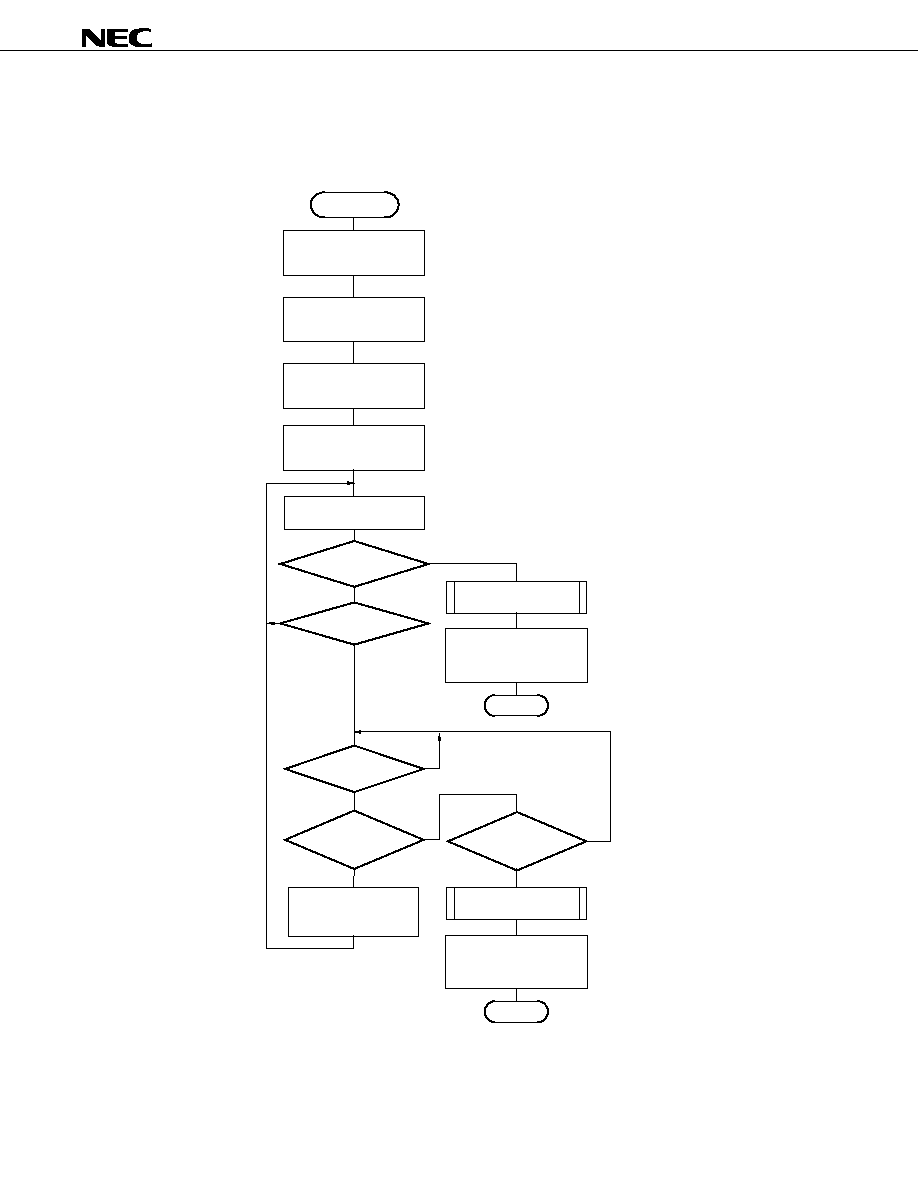
Data Sheet S15082EJ4V0DS
56
µ
PD61051, 61052
4.3
SDRAM Write during Executing
While encoding, the host CPU can transfer parameters to the internal CPU through SDRAM. The number of the
transfer bytes is a 4-byte unit.
Y
N
N
SDRAM writing,
during executing
Mask Interrupt
which requests data transfer
Interrupt mask register
(2CH to 2FH) setting
Clear mask Interrupt
which requests data transfer
Interrupt mask register
(2CH to 2FH) setting
Destination address register
(24H to 26H) setting
Number of transfer bytes
Transfer counter register
(27H to 29H) setting
Host CPU
SDRAM transfer
Transfer mode register
(20H)
02H setting
Return
Transfer data register
(3FH)
Data
All data
writing ending?
128 bytes
writing ending?
Transfer ending (refer to 4.7)
Clear mask Interrupt
which requests data transfer
Interrupt mask register
(2CH to 2FH) setting
Return
Transfer error handling
(refer to 4.8)
Y
Y
Y
N
N
CINT?
Interrupt register 0
(30H): (02H or 01H)
Y
N
Interrupt register 0
(30H): 04H
Interrupt register 0 clear
Interrupt register 0 (30H)
Interrupt register 0 (30H)
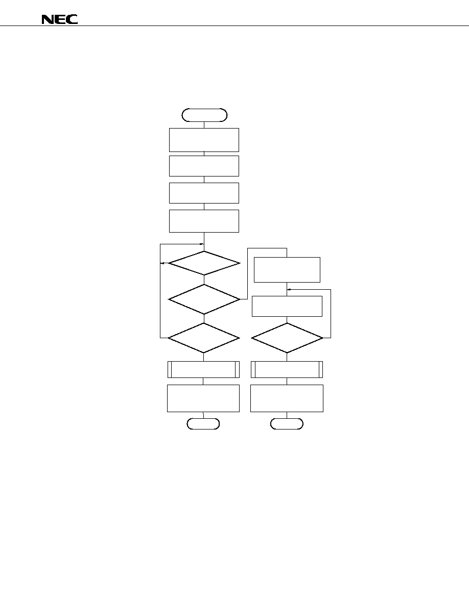
Data Sheet S15082EJ4V0DS
57
µ
PD61051, 61052
4.4
SDRAM Read during Executing
While encoding, the host CPU reads parameters of usable work area of SDRAM. The maximum data of the
reading once is 128 bytes. When reading is equal to or more than 128 byte data, execute reading processing
repeatedly. The number of the transfer bytes is a 4 bytes unit.
SDRAM reading,
during executing
Mask Interrupt
which requests data transfer
Interrupt mask register
(2CH to 2FH) settin
Source address register
(21H to 23H) setting
Transfer data register
(3FH)
Read data
Number of transfer bytes
Transfer counter register
(27H to 29H) setting
SDRAM
host CPU transfer
Transfer mode register
(20H)
01H setting
Clear mask Interrupt
which requests data transfer
Interrupt mask register
(2CH to 2FH) setting
Return
Transfer error handling
(refer to 4.8)
Clear mask Interrupt
which requests data transfer
Interrupt mask register
(2CH to 2FH) setting
Return
Transfer ending (refer to 4.7)
Y
N
Y
N
CINT?
N
All instructions
reading ending?
Interrupt register 0
(30H): (02H or 01H)
Y
Y
N
Interrupt register 0
(30H): 04H
Interrupt register 0 clear
Interrupt register 0 (30H)
Interrupt register 0 (30H)
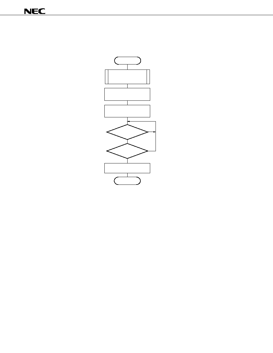
Data Sheet S15082EJ4V0DS
58
µ
PD61051, 61052
4.5
SDRAM Initialization
The host CPU transfers the firmware which makes SDRAM a standby condition to the instruction RAM of the
internal CPU and executes it.
N
Y
Y
N
Return
SDRAM initialization
SDRAM initialize firmware
to instruction RAM
of internal CPU
Release of software reset
of internal CPU
Reset register (3EH)
00H
100 µs wait
Interrupt register x
Initialization ending interrupt
release
CINT?
Interrupt register x
initialization ending
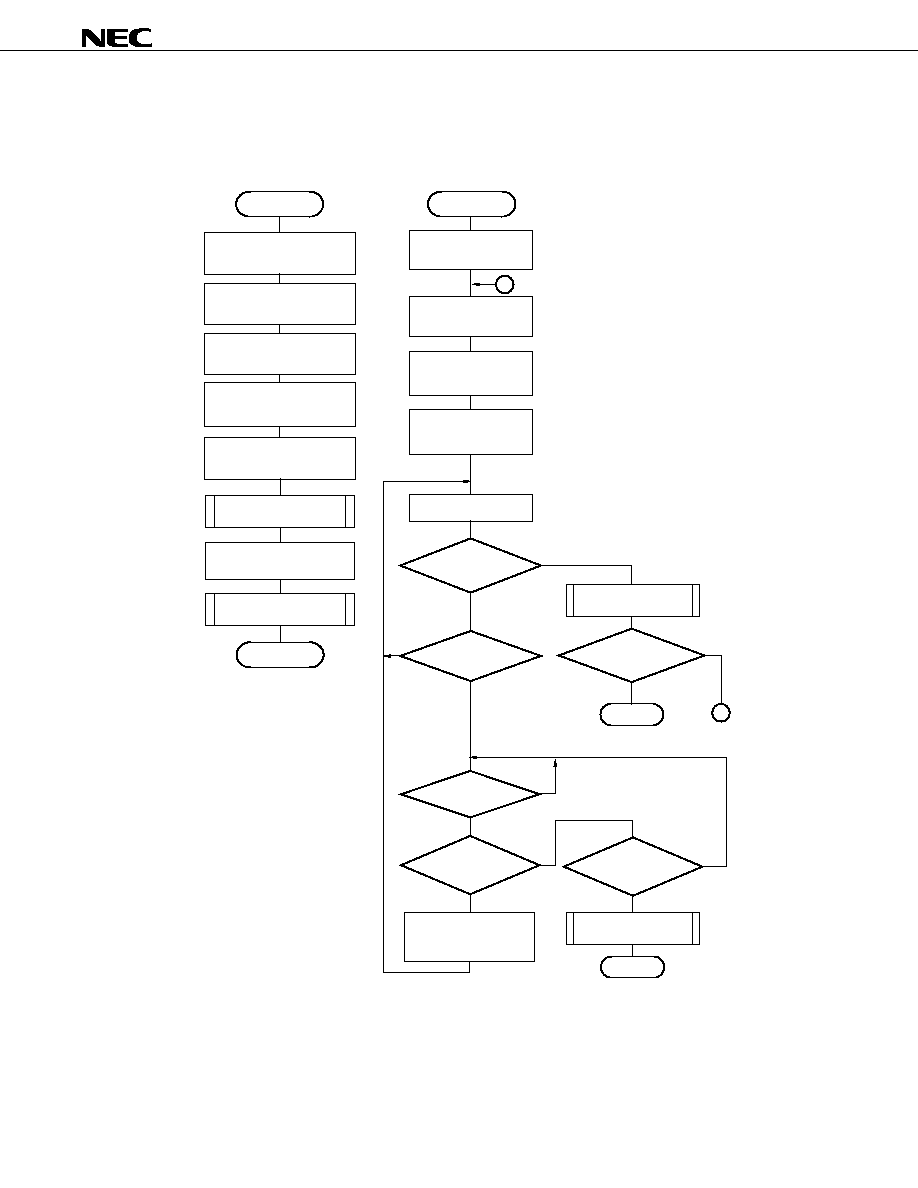
Data Sheet S15082EJ4V0DS
59
µ
PD61051, 61052
4.6
Operation Mode Setting by Changing Firmware
When changing a mode, host CPU transfers the instruction of each mode from SDRAM to the instruction RAM of
the internal CPU and restarts.
Return
Mode setting
Software reset of internal CPU
Reset register (3EH)
02H
Source address register
(21H to 23H) setting
Destination address register
(24H to 26H) setting
Number of transfer bytes/4
Transfer counter register
(27H to 29H) setting
SDRAM
iRAM transfer
Transfer mode register
(20H)
20H setting
Parameter setting
Transfer ending (refer to 4.7)
Internal CPU reset is canceled
Reset register
(3EH)
00H setting
Y
Y
N
N
N
Y
Parameter setting
Mode setting A
Mode setting A
Destination address register
(24H to 26H) setting
System interface register
setting
Number of transfer bytes
Transfer counter register
(27H to 29H) setting
Host CPU
SDRAM transfer
Transfer mode register
(20H)
40H setting
Transfer data register
(3FH)
Parameter
All parameters
writing ending?
All parameters
in SDRAM
writing ending?
128 bytes
writing ending?
Return
Transfer ending (refer to 4.7)
Y
Y
N
N
CINT?
Interrupt register 0
(30H): (02H or 01H)
Y
N
Interrupt register 0
(30H): 04H
Interrupt register 0 clear
Interrupt register 0 (30H)
Interrupt register 0 (30H)
Return
Transfer error handling
(refer to 4.8)
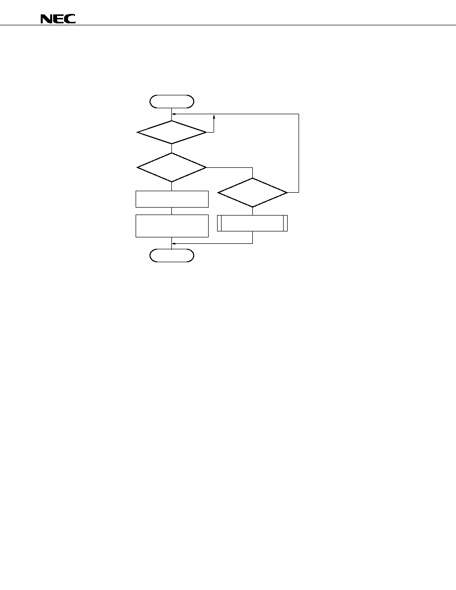
Data Sheet S15082EJ4V0DS
60
µ
PD61051, 61052
4.7
Transfer Ending
The host CPU confirms a transfer error when the instruction or data transfer ends.
The host CPU clears transfer mode and interrupt registers.
Transfer ending
Interrupt register 0 clear
Interrupt register 0
(30H)
01H
Transfer mode register
(20H)
00H setting
Return
Transfer error handling
(refer to 4.8)
Y
Y
N
N
CINT?
Interrupt register 0
(30H): 01H
Y
N
Interrupt register 0
(30H): 04H
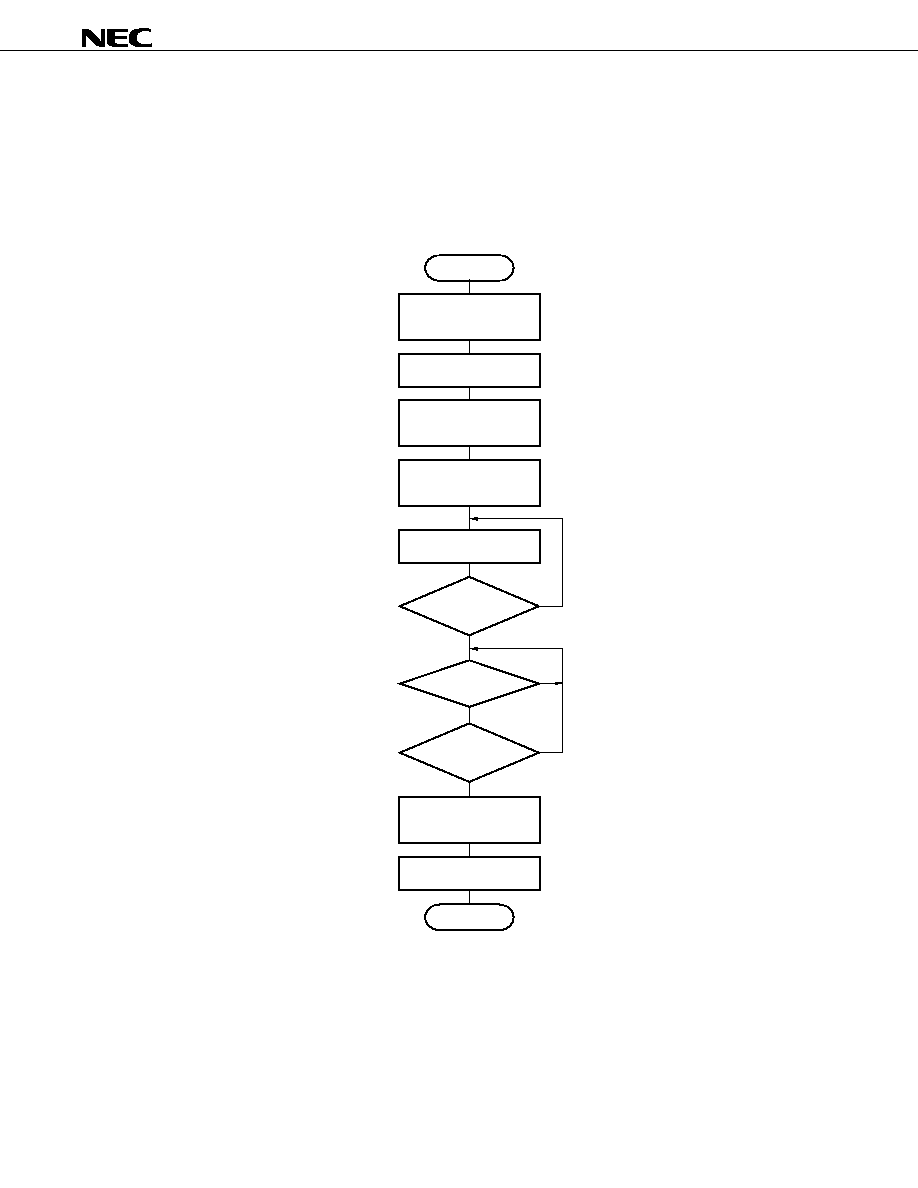
Data Sheet S15082EJ4V0DS
61
µ
PD61051, 61052
4.8
Transfer Error Handling
4.8.1
Transfer error handling 1
It is the error handling of DMA-ERR which occurs when interrupting the transfers (the host CPU
the instruction
RAM of internal CPU transfer, the host CPU
SDRAM transfer (SSD, SDW), the external ROM SDRAM transfer
and the external ROM
the instruction RAM of internal CPU transfer)
Transfer error
handling 1
Host CPU
SDRAM transfer
release
Transfer mode register
(20H)
00H setting
Set destination address register
(24H to 26H)
to unused area of SDRAM
Host CPU
SDRAM transfer
Transfer mode register
(20H)
02H setting
Interrupt register 0
(30H)
01H setting
Transfer counter register
(27H to 29H)
04H setting
Transfer data register
(3FH)
Dummy data
Clear the transfer error
Interrupt register 0 (30H)
04H setting
Return
Y
Y
N
N
CINT?
Interrupt register 0
(30H): 01H
Y
N
All data
writing ending?
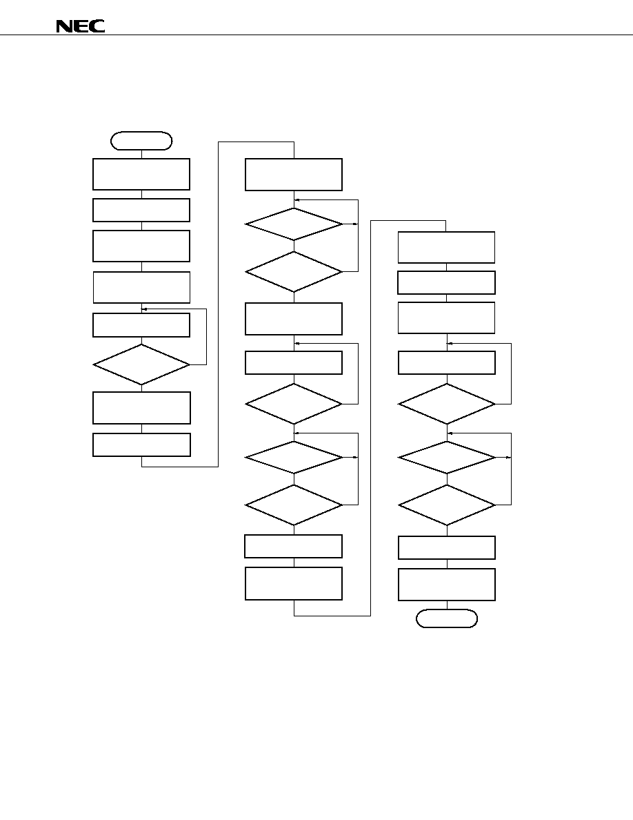
Data Sheet S15082EJ4V0DS
62
µ
PD61051, 61052
4.8.2
Transfer error handling 2
This is a error handling of DMA-ERR which occurs when interrupting the transfers (SDRAM read during executing
and SDRAM
instruction RAM of internal CPU transfer)
Transfer error
handling 2
SDRAM
host CPU transfer
release
Transfer mode register
(20H)
00H setting
Interrupt register 0
(30H)
01H setting
Transfer counter register
(27H to 29H)
04H setting
Transfer counter register
(27H to 29H)
04H setting
Transfer data register
(3FH)
Dummy data
Destination address register
(24H to 26H)
Unusing area setting
Transfer data register
(3FH)
Data read
SDRAM
host CPU transfer
Transfer mode register
(20H)
01H setting
Host CPU
SDRAM transfer
Transfer mode register
(20H)
02H setting
Clear Interrupt register 0
Interrupt register 0 (30H)
Y
Y
N
N
CINT?
Interrupt register 0
(30H): 01H
Y
N
All data
reading ending?
Y
Y
N
N
CINT?
Interrupt register 0
(30H): 02 H
Host CPU
SDRAM transfer
release
Transfer mode register
(20H)
00H setting
Interrupt register 0
(30H)
01H setting
Transfer data register
(3FH)
Dummy data
Return
Y
Y
N
N
CINT?
Interrupt register 0
(30H): 01H
Y
N
All data
writing ending?
Clear transfer error
Interrupt register 0 (30H)
04H setting
N
Host CPU
SDRAM transfer
release
Transfer mode register
(20H)
00H setting
Y
All data
writing ending?
Transfer counter register
(27H to 29H)
04H setting
Destination address register
(24H to 26H)
Unusing area setting
Host CPU
SDRAM transfer
Transfer mode register
(20H)
02H setting
Interrupt register 0 (30H) setting
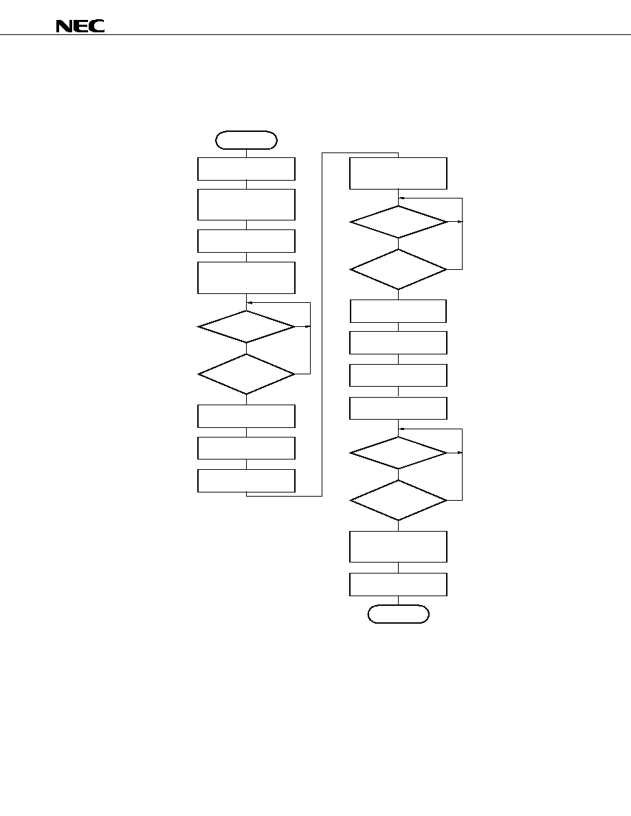
Data Sheet S15082EJ4V0DS
63
µ
PD61051, 61052
4.8.3
Transfer error handling 3
It is the error handling of DMA-ERR which occurs when transfer operation in case of host CPU serial connection
with SPI.
Transfer error
handling 3
SDRAM
host CPU transfer
Transfer mode register
(20H)
01H setting
Interrupt register 0
(30H)
02H setting
Transfer counter register
(27H to 29H)
01H setting
Transfer data register
(3FH)
Data read
Source address register
(21H to 23H) setting
Transfer counter register
(27H to 29H)
03H setting
SDRAM
host CPU transfer
Transfer mode register
(20H)
01H setting
SDRAM
host CPU transfer
release
Transfer mode register
(20H)
00H setting
Transfer data register
(3FH)
Data read
Interrupt register 0
(30H)
01H setting
Transfer data register
(3FH)
Data read
Transfer data register
(3FH)
Data read
SDRAM
host CPU transfer
release
Transfer mode register
(20H)
00H setting
Return
Y
Y
N
Interrupt register 0
(30H)
01H
N
CINT?
Interrupt register 0
(30H): 02H
Interrupt register 0
(30H): 01H
Y
Y
N
N
CINT?
Interrupt register 0
(30H): 01H
Y
Y
N
N
CINT?

Data Sheet S15082EJ4V0DS
64
µ
PD61051, 61052
5.
EXAMPLE FOR COMMON REGISTER USAGE
The
µ
PD61051, 61052 operates while the "command code register" is in "start". When "command code register"
becomes "start", internal CPU reads parameter registers, then starts the operation. Additionally, internal register sets
"status register". Register map for system interface register is defined by firmware.
With each application, parameter registers are changed by the firmware.
Figure 5-1. Host Interface Register
Host
CPU
System
Interface
Register
Instruction
RAM of
Internal CPU
Internal
CPU
SDRAM
Interface
SDRAM
DMA
Controller
µPD61051/61052
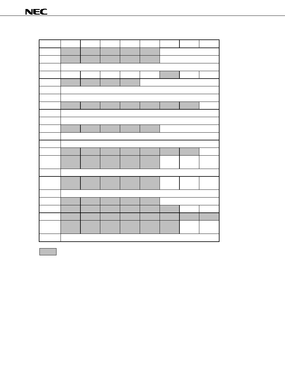
Data Sheet S15082EJ4V0DS
65
µ
PD61051, 61052
5.1
Register Map Example
Address
Bit7 Bit6 Bit5 Bit4 Bit3 Bit2 Bit1 Bit0
00H
COMCODE
01H
ESTS
02H to 1FH
Parameters (Defined by each firmware)
20H SI
SSD
SDI
MSD
MI
SDW
SDR
21H
SA19
to
SA16
22H SA15
to
SA8
23H
SA7 to SA0
24H
DA16
25H
DA15 to DA8
26H
DA7 to DA0
27H
TC18 to TC16
28H
TC15 to TC8
29H
TC7 to TC0
2AH
iCPU-INT
2BH
DMA-
ERR-M
DMA-
RDY-M
DMA-
DONE-M
2CH to 2FH
Interrupt Mask (Defined by each firmware)
30H
DMA-ERR
DMA-RDY
DMA-
DONE
31H to 34H
Interrupt (Defined by each firmware)
35H
iROM2 to iROM0
36H
ISREQ
OSVLD
37H to 3DH
3EH
NBR
ALL
RESET
3FH
TD7 to TD0
: Reserved
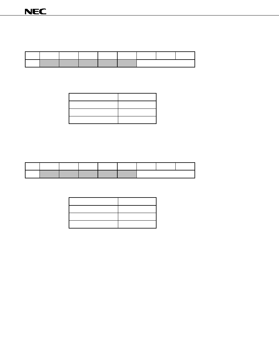
Data Sheet S15082EJ4V0DS
66
µ
PD61051, 61052
5.2
Example of the Common Register Which A Firmware Defines
5.2.1
COMCODE: Command code register
Address
Bit7 Bit6 Bit5 Bit4 Bit3 Bit2 Bit1 Bit0
00H
COMCODE
The host CPU can change the state of operation to the command code register. The
µ
PD61051/61052 accepts
commands to operate in three states as shown in the table below.
Command Code
Standby / Stop
001
Start 011
Reserved Others
The command which it is possible to set depend on the internal state.
In case of the command whose state transfer is possible, the state transfers according to the command.
5.2.2
ESTS: Status register
Address
Bit7 Bit6 Bit5 Bit4 Bit3 Bit2 Bit1 Bit0
01H
ESTS
This register shows processing state, when command is illegal, the state doesn't transfer.
ESTS Code
Initial State
000
Standby State
001
Encoding State
011
Data Sheet S15082EJ4V0DS
67
µ
PD61051, 61052
Figure 5-2. Command Status Transition
Hardware reset
Initial State
(000)
Standby State
(001)
001 : Standby
001 : Stop
011 : Start
Encoding State
(011)
Valid Command in Initial State:
Standby
Valid Command in Standby State:
Start
Valid Command in Operation State: Stop
Data Sheet S15082EJ4V0DS
68
µ
PD61051, 61052
6.
ELECTRICAL CHARACTERISTICS
Absolute Maximum Ratings (T
A
= 25∞C)
Parameter Symbol Conditions
Rating
Unit
V
DD3
V
DD3
, vs GND
4.6
V
Supply Voltage
V
DD2
V
DD2
, vs GND
PV
DD2
, vs PGND
3.6 V
Input Voltage
V
IN
Vs
GND3
-0.5 to +4.6 V
Output Voltage
V
OUT
Vs
GND3
-0.5 to +4.6 V
Output Current
I
OUT
20
mA
Permissible Loss
P
D
2
W
Operating Ambient
Temperature
T
A
0 to +70
∞C
Storage Temperature
T
stg
-55 to +125 ∞C
Caution If any of the parameters exceeds the absolute maximum ratings, even momentarily, the quality of
the product may be impaired. The absolute maximum ratings are values that may physically
damage the products. Be sure to use the products within the ratings.
DC Characteristics (T
A
= 0 to
+70∞C, V
DD3
= 3.3
±0.165 V, V
DD2
= 2.5
±0.2 V)
Parameter Symbol Condition
Min.
Typ.
Max.
Unit
V
DD3
V
DD3
,
vs
GND
3.135 3.3 3.465 V
Supply voltage
V
DD2
V
DD2,
vs GND
PV
DD2,
vs PGND
2.3 2.5 2.7 V
High-level input voltage
V
IH
2.2
V
DD3
+0.5 V
SCLK
-0.5 +0.6 V
Low-level input voltage
V
IL
Except SCLK
-0.5 +0.7 V
High-level output voltage
V
OH
2.4
V
Low-level output voltage
V
OL
0.4
V
Input leakage current
I
LI
Except MD31 to MD0 and
CMODE1
±10
µ
A
I
DD3
3.3 V power supply
70
mA
I
PDD
2.5 V PLL power supply
15
mA
Operating current
I
DD2
Internal logic power supply of
2.5 V
510
mA
Data Sheet S15082EJ4V0DS
69
µ
PD61051, 61052
Pin Capacitance (T
A
= 25∞C)
Parameter Symbol Conditions
Min.
Typ.
Max.
Unit
Input capacitance
C
I
20
pF
Output capacitance
C
O
20
pF
I/O capacitance
C
IO
20
pF
AC Characteristics (T
A
= 0 to
+70∞C, V
DD3
= 3.3
±0.165 V, V
DD2
= 2.5
±0.2 V, C
L
= 15 pF, t
R
= t
F
= 1 ns)
(1)
System
Parameter Symbol Conditions
Min.
Typ.
Max.
Unit
SCLK frequency
f
SCK
27.0
MHz
SCLK high-level width
t
SCKH
Duty
40:60
13.2
ns
SCLK low-level width
t
SCKL
Duty
40:60
13.2
ns
PSTOP release time1
t
STP1
Vs
V
DD3
1
µ
s
PSTOP release time2
t
STP2
Vs
V
DD2
1
µ
s
PSTOP release time3
t
STP3
Vs
PV
DD2
1
µ
s
PSTOP release time4
t
STP4
Vs
SCLK
1
µ
s
PSTOP pulse width
t
WSTP
1
µ
s
RESET release time
t
RES
Vs falling edge of PSTOP
100
µ
s
Video input reset time
t
lVRES
After stable IVCLK
600
ns
Audio reset time
t
AURES
After stable AMCLK
600
ns
STC reset time
t
STRES
After stable STCLK
600
ns
Reset pulse width
t
RESW
After stable all clock
600
ns
Input rising time
t
IR
Vs AMCLK, STCLK, SCLK,
ISCLK
3
ns
Vs
IVCLK
5
ns
Input falling time
t
IF
Vs AMCLK, STCLK, SCLK,
ISCLK
3
ns
Vs
IVCLK
5
ns
Output rising time
t
OR
3 ns
Output falling time
t
OF
3 ns
High level, low level
Clock input
V
IH
t
IR
, t
OR
t
IF
, t
OF
V
IL
V
IH
V
IL
t
SCK
= 1/f
SCK
t
SCKH
t
SCKL
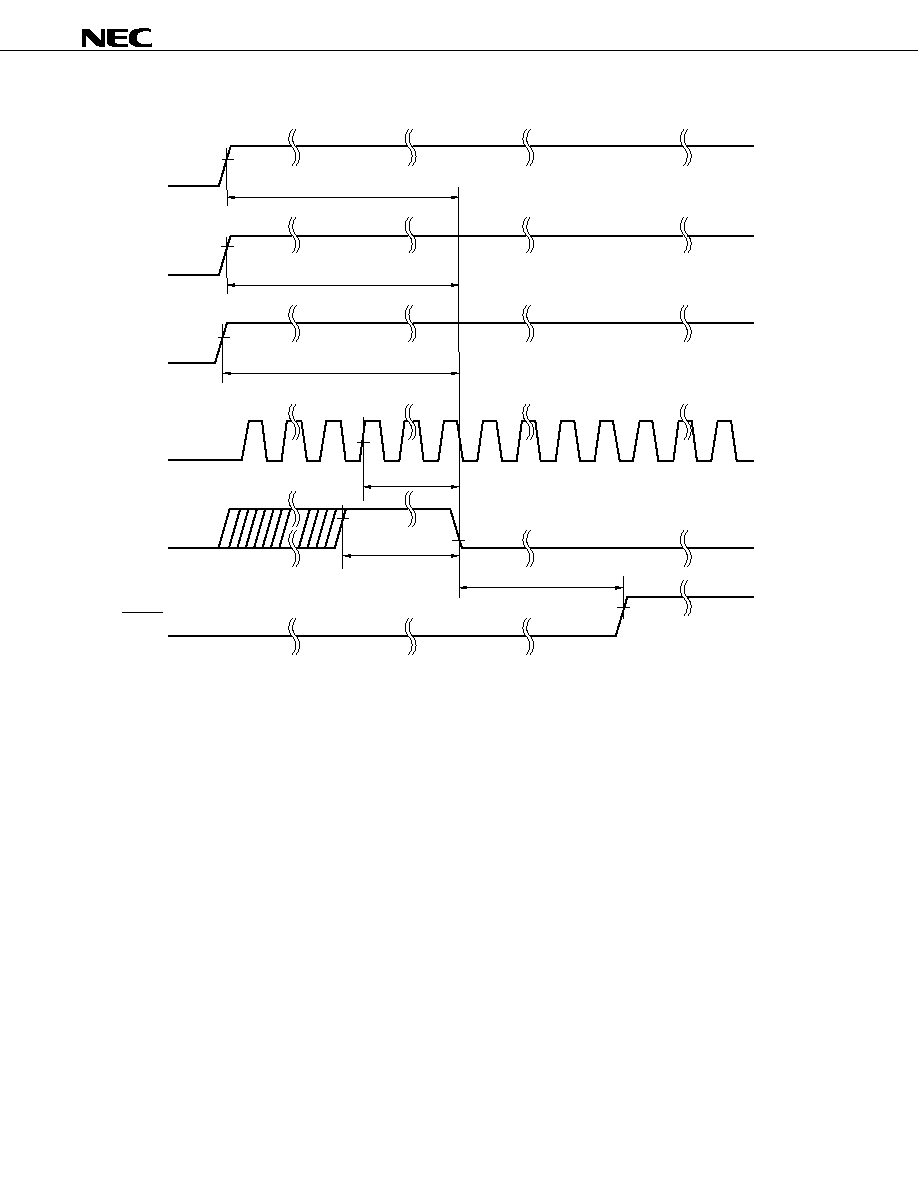
Data Sheet S15082EJ4V0DS
70
µ
PD61051, 61052
Reset input
V
DD3
t
STP1
Frequency stabilization (±10% max. )
t
STP3
t
STP2
t
STP4
t
WSTP
t
RES
V
DD2
PV
DD2
SCLK
PSTOP
RESET
Caution Notes on power on/off
∑ Apply power to V
DD3
, and V
DD2
and PV
DD2
at the same time.
∑ If it is difficult to apply the power to these pins at the same time, apply the power to V
DD2
and PV
DD2
first.
∑ Cut the power of V
DD3
, and V
DD2
and PV
DD2
at the same time.
∑ If it is difficult to cut the power of these pins at the same time, cut the power of V
DD2
and PV
DD2
last.
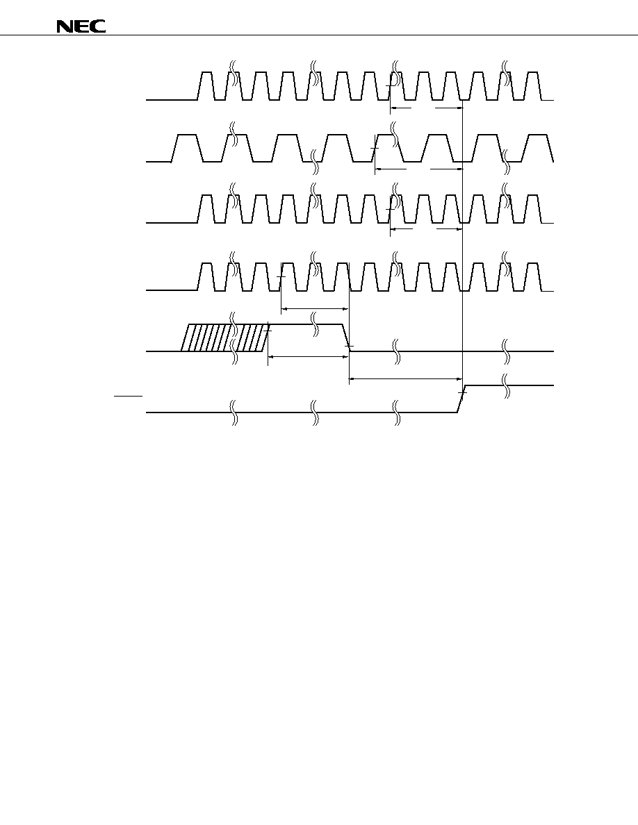
Data Sheet S15082EJ4V0DS
71
µ
PD61051, 61052
IVCLK
t
IVRES
t
STRES
t
AURES
t
STP4
t
WSTP
t
RES
AMCLK
STCLK
SCLK
PSTOP
RESET
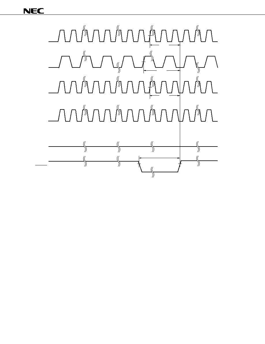
Data Sheet S15082EJ4V0DS
72
µ
PD61051, 61052
IVCLK
t
RESW
AMCLK
STCLK
SCLK
PSTOP
RESET
''L''
t
IVRES
t
AURES
t
STRES
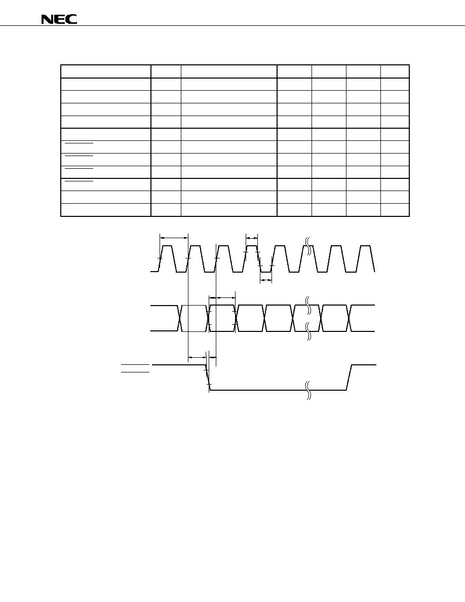
Data Sheet S15082EJ4V0DS
73
µ
PD61051, 61052
(2)
Video input interface
Parameter Symbol Conditions
Min.
Typ.
Max.
Unit
IVCLK frequency
f
IVCKS
27
MHz
IVCLK high-level width
t
VCKH
10
ns
IVCLK low-level width
t
VCKL
10
ns
IVIN7 to IVIN0 setup time
t
IVDS
Vs rising edge of IVCLK
5
ns
IVIN7 to IVIN0 hold time
t
IVDH
Vs rising edge of IVCLK
4
ns
IVVSYNC-input setup time
t
IVVS
Vs rising edge of IVCLK
5
ns
IVVSYNC-input hold time
t
IVVH
Vs rising edge of IVCLK
4
ns
IVHSYNC-input setup time
t
IVHS
Vs rising edge of IVCLK
5
ns
IVHSYNC-input hold time
t
IVHH
Vs rising edge of IVCLK
4
ns
IVFLD-input setup time
t
IVFS
Vs rising edge of IVCLK
5
ns
IVFLD-input hold time
t
IVFH
Vs rising edge of IVCLK
4
ns
Y
Y
Cb
Cr
Cr
IVCLK
IVIN7 to IVIN0
IVHSYNC
IVVSYNC
IVFLD
f
IVCKS
t
IVCKH
t
IVDS
t
IVVH
t
IVHH
t
IVFH
t
IVVS
t
IVHS
t
IVFS
t
IVDH
t
IVCKL
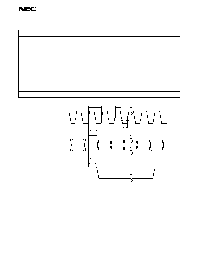
Data Sheet S15082EJ4V0DS
74
µ
PD61051, 61052
(3)
Video output interface
Parameter Symbol Conditions
Min.
Typ.
Max.
Unit
OVCLK frequency
f
OVCKS
27
MHz
OVCLK high-level width
t
OVCKH
8
ns
OVCLK low-level width
t
OVCKL
8
ns
OVOUT7 to OVOUT0 hold
time
t
OVHO
Vs rising edge of OVCLK
7
ns
OVOUT7 to OVOUT0 delay
time
t
OVDO
Vs rising edge of OVCLK
28
ns
OVVSYNC hold time
t
OVVHO
Vs rising edge of OVCLK
7
ns
OVVSYNC delay time
t
OVVD
Vs rising edge of OVCLK
28
ns
OVHSYNC hold time
t
OVHHO
Vs rising edge of OVCLK
7
ns
OVHSYNC delay time
t
OVHD
Vs rising edge of OVCLK
28
ns
Y
Y
Cb
Cr
OVCLK
OVOUT7 to OVOUT0
f
OVCKS
t
OVCKH
t
OVHO
t
OVDO
t
OVCKL
t
OVHHO
t
OVVHO
t
OVHD
t
OVVD
OVHSYNC
OVVSYNC
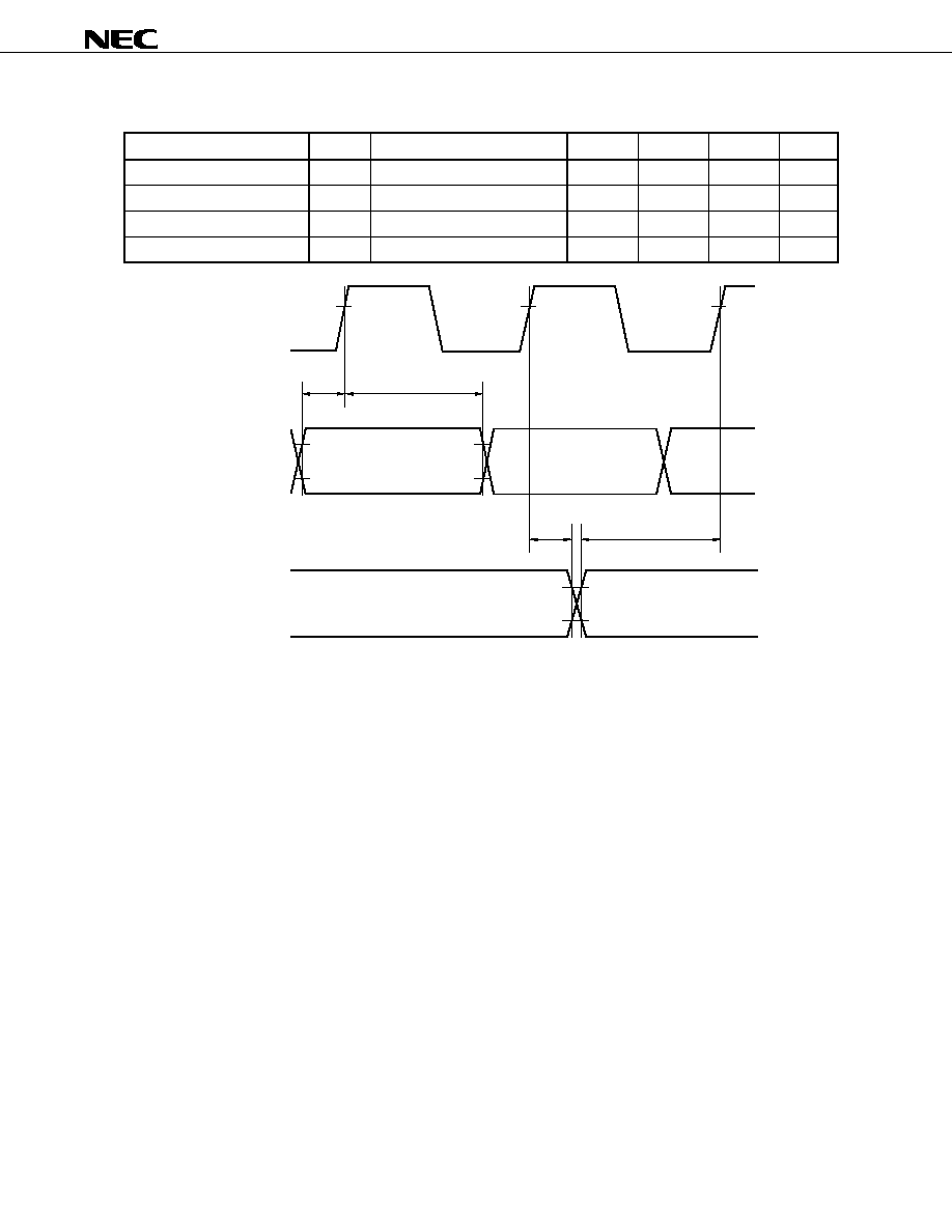
Data Sheet S15082EJ4V0DS
75
µ
PD61051, 61052
(4)
Audio input interface
Parameter Symbol Conditions
Min.
Typ.
Max.
Unit
Bit data-in setup time
t
ACDS
Vs
IABCK
37
ns
Bit data-in hold time
t
ACDH
Vs
IABCK
37
ns
LRCK-in setup time
t
ACLS
Vs
IABCK
100
ns
LRCK-in hold time
t
ACLH
Vs
IABCK
37
ns
IABCK
IABD
IALRCK
t
ACDS
t
ACDH
t
ACLH
t
ACLS

Data Sheet S15082EJ4V0DS
76
µ
PD61051, 61052
(5)
Audio output interface
Parameter Symbol Conditions
Min.
Typ.
Max.
Unit
Bit data-out hold time
t
ACDHO
Vs
OABCK
-5 ns
Bit data-out delay time
t
ACDD
Vs
OABCK
25
ns
LRCK-out hold time
t
ACLHO
Vs
OABCK
-5 ns
LRCK-out delay
t
ACLD
Vs
OABCK
25
ns
BCK-out duty ratio
d
BCK
50 %
AMCLK duty ratio
d
AMCLK
50 %
AMCLK frequency
f
AMCLK
18.432 MHz
OABCK
OABD
OALRCK
t
ACDHO
t
ACDD
t
ACLHO
t
ACLD
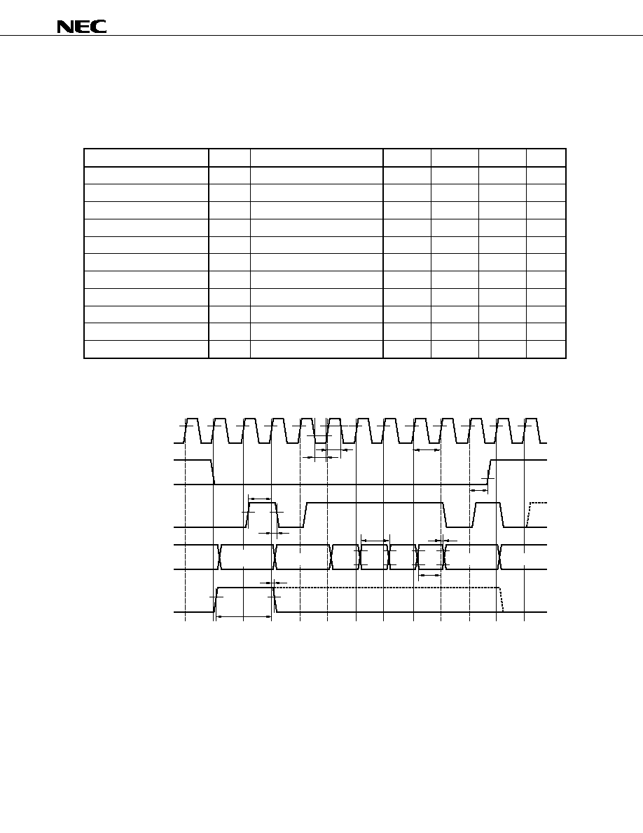
Data Sheet S15082EJ4V0DS
77
µ
PD61051, 61052
(6)
Stream input interface
(a)
Parallel stream input
Valid mode
Parameter Symbol Conditions
Min.
Typ.
Max.
Unit
ISCLK cycle
t
ISCcyc
80
ns
ISCLK low-level width
t
ISCLW
37
ns
ISCLK high-level width
t
ISCHW
37
ns
ISREQ output hold time
t
ISRQHO
Vs active edge of ISCLK
0
ns
ISVLD setup time
t
ISVS
Vs active edge of ISCLK
7
ns
ISVLD hold time
t
ISVH
Vs active edge of ISCLK
3
ns
ISSYNC setup time
t
ISSS
Vs active edge of ISCLK
7
ns
ISSYNC hold time
t
ISSH
Vs active edge of ISCLK
3
ns
IS7 to IS0 setup time
t
ISDS
Vs active edge of ISCLK
7
ns
IS7 to IS0 hold time
t
ISDH
Vs active edge of ISCLK
3
ns
Data cycle time
t
DCYC
80
ns
Remark ISREQ is effective only when it works by the master mode. ISREQ becomes invalid asynchronously to
ISCLK. ISREQ output delay time doesn't prescribe to ISCLK.
ISVLD (I)
IS7 to IS0 (I)
ISSYNC (I)
ISCLK (I)
ISREQ (O)
Valid
data
Valid
data
Valid
data
Valid
data
No
received
data
t
ISCLW
t
ISVS
t
ISVH
t
DCYC
t
ISDH
t
ISSH
t
ISDS
t
ISSS
t
ISCHW
t
ISCYC
t
ISRQHO
Valid data
Valid data
Valid data
Valid data
1st of packet
Remark ISSYNC is active high, SREQ is active high and ISCLK is active high edge.

Data Sheet S15082EJ4V0DS
78
µ
PD61051, 61052
Strobe mode
Parameter Symbol Conditions
Min.
Typ.
Max.
Unit
ISSTB low-level width
t
ISSTLW
37
ns
ISSTB high-level width
t
ISSTHW
37
ns
ISREQ output hold time
t
ISRQHO
Vs active edge of ISSTB
0
ns
ISSYNC setup time
t
ISSS
Vs active edge of ISSTB
7
ns
ISSYNC hold time
t
ISSH
Vs active edge of ISSTB
3
ns
IS7 to IS0 setup time
t
ISDS
Vs active edge of ISSTB
7
ns
IS7 to IS0 hold time
t
ISDH
Vs active edge of ISSTB
3
ns
Data cycle time
t
DCYC
80
ns
Remark ISREQ becomes invalid asynchronously to ISSTB. ISREQ output delay time doesn't prescribe to ISSTB.
ISSTB (I)
IS7 to IS0 (I)
ISSYNC (I)
ISREQ (O)
Valid
data
Valid
data
Valid
data
Valid
data
Valid data
Valid data
Valid data
Valid data
1st of packet
No
received
data
t
ISSTHW
t
ISSTLW
t
DCYC
t
ISDH
t
ISSH
t
ISDS
t
ISSS
t
ISRQHO
Remark ISSYNC is active high, ISREQ is active low and ISSTB is active high edge.
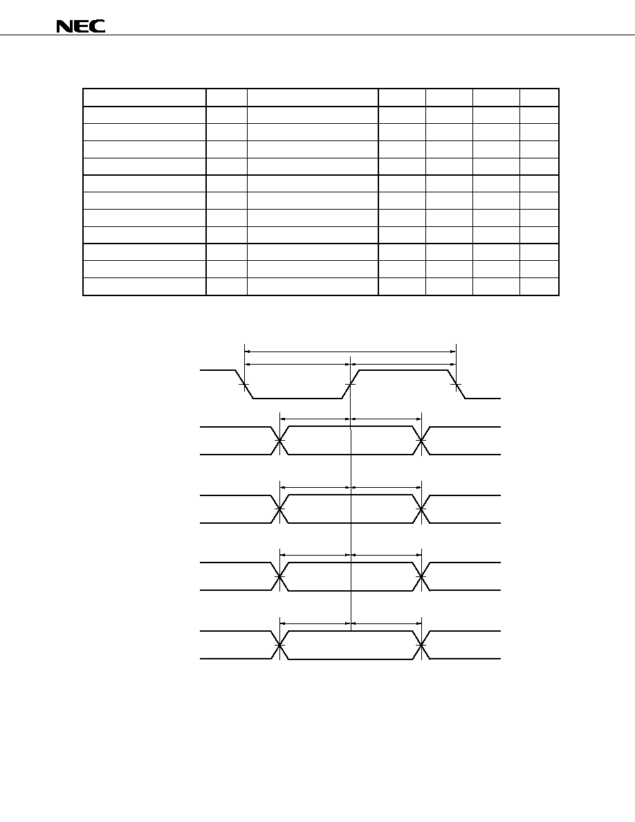
Data Sheet S15082EJ4V0DS
79
µ
PD61051, 61052
(b)
Serial stream input
Parameter Symbol Conditions
Min.
Typ.
Max.
Unit
ISCLK period
t
ISSCW
15.6
ns
ISCLK low-level width
t
ISSCLW
5.0
ns
ISCLK high-level width
t
ISSCHW
5.0
ns
ISVLD setup time
t
ISSVS
Vs active edge of ISCLK
2.5
ns
ISVLD hold time
t
ISSVH
Vs active edge of ISCLK
2.5
ns
ISSYNC setup time
t
ISSSS
Vs active edge of ISCLK
2.5
ns
ISSYNC hold time
t
ISSSH
Vs active edge of ISCLK
2.5
ns
ISERR setup time
t
ISSES
Vs active edge of ISCLK
2.5
ns
ISERR hold time
t
ISSEH
Vs active edge of ISCLK
2.5
ns
IS0 setup time
t
ISSDS
Vs active edge of ISCLK
2.5
ns
IS0 hold time
t
ISSDH
Vs active edge of ISCLK
2.5
ns
Remark Setup and hold time provide to the activist edge of ISCLK.
ISCLK
ISERR
t
ISSCW
t
ISSCLW
t
ISSCHW
t
ISSES
t
ISSEH
ISSYNC
t
ISSSS
t
ISSSH
ISVLD
t
ISSVS
t
ISSVH
IS0
t
ISSDS
t
ISSDH
Remark ISCLK is active high edge.
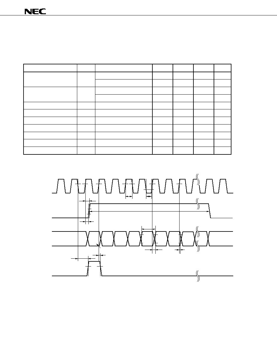
Data Sheet S15082EJ4V0DS
80
µ
PD61051, 61052
(7)
Stream output interface
(a)
Parallel stream data output
Valid and master mode
Parameter Symbol Conditions
Min.
Typ.
Max.
Unit
Active rising edge
30
ns
OSCLK low-level width
t
OSCLW
Active falling edge
70
ns
Active rising edge
70
ns
OSCLK high-level width
t
OSCHW
Active falling edge
30
ns
OSVLD hold time
t
OSVHO
Vs active edge of OSCLK
30
ns
OSVLD delay time
t
OSVD
Vs non active edge of OSCLK
-5 +5 ns
OSSYNC hold time
t
OSSHO
Vs active edge of OSCLK
30
ns
OSSYNC delay time
t
OSSD
Vs non active edge of OSCLK
-5 +5 ns
OS7 to OS0 hold time
t
OSDHO
Vs active edge of OSCLK
30
ns
OS7 to OS0 delay time
t
OSDD
Vs non active edge of OSCLK
-5 +5 ns
Data cycle time
t
DCYC2
105
ns
Remark OSVLD is active high, OSSYNC is active high and OSCLK is active high edge.
OSCLK
OSVLD
OS7 to OS0
Valid
data
Valid
data
Valid
data
Valid
data
Valid
data
Valid
data
Valid
data
Invalid data
Invalid data
OSSYNC
t
OSSD
t
OSSHO
188 bytes
1st of packet
t
OSVHO
t
DCYC2
t
OSVD
t
OSDD
t
OSDHO
t
OSCHW
t
OSCLW

Data Sheet S15082EJ4V0DS
81
µ
PD61051, 61052
Strobe and byte mode
Parameter Symbol Conditions
Min.
Typ.
Max.
Unit
OSREQ high-level time
t
OSRHW
2
STCLK
Active rising edge
100
ns
OSSTB high-level width
t
OSSTHW
Active falling edge
70
ns
Active rising edge
70
ns
OSSTB low-level width
t
OSSTLW
Active falling edge
100
ns
OSREQ hold time
t
OSRRD
Vs active edge of OSRDY
0
ns
t
OSTRQ1
Vs active edge of OSSTB
0
ns
OSREQ hold time
t
OSTRQ2
Vs non active edge of OSSTB
0
ns
t
OSRSTD1
Vs active edge of OSREQ
2
3
STCLK
OSSTB delay time
t
OSRSTD2
Vs non active edge of OSREQ
3
STCLK
OSRDY delay time
t
OSSTRD1
Vs non active edge of OSSTB
3
STCLK
OSSYNC-out delay time
t
OSSD
Vs non active edge of OSSTB
-5 +5 ns
OSSYNC-out hold time
t
OSSHO
Vs active edge of OSSTB
70
ns
OS7 to OS0 out delay time
t
OSDD
Vs non active edge of OSSTB
-5 +5 ns
OS7 to OS0 out hold time
t
OSDHO
Vs active edge of OSSTB
70
ns
OSSYNC
OS7-OS0
OSSTB
OSREQ
OSRDY
t
OSSD
t
OSDD
t
OSSTRD1
t
OSRSTD1
t
OSRSTD2
t
OSSHO
t
OSDHO
t
OSTRQ1
t
OSRHW
t
OSRRD
t
OSSTLW
t
OSSTHW
t
OSTRQ2
Remark OSSYNC is active high, OSRDY is active low and OSSTB is active high edge.
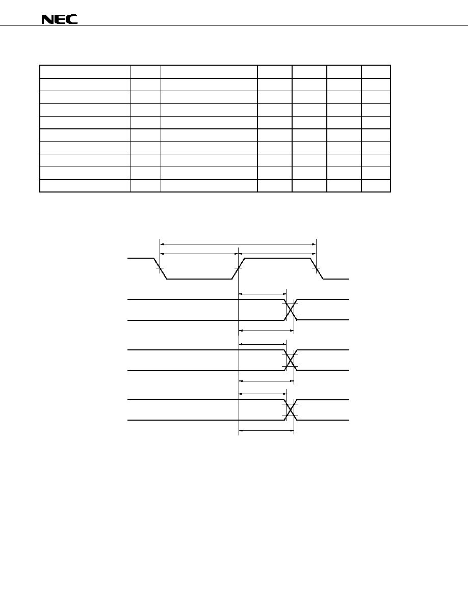
Data Sheet S15082EJ4V0DS
82
µ
PD61051, 61052
(b)
Serial stream data output
Parameter Symbol Conditions
Min.
Typ.
Max.
Unit
OSCLK period
t
OSSCW
37 ns
OSCLK low-level width
t
OSSCLW
10
ns
OSCLK high-level width
t
OSSCHW
10
ns
OS0 delay time
t
OSSDD
Vs active edge of OSCLK
27
ns
OS0 hold time
t
OSSDHO
Vs active edge of OSCLK
5.0
ns
OSVLD delay time
t
OSSVD
Vs active edge of OSCLK
27
ns
OSVLD hold time
t
OSSVHO
Vs active edge of OSCLK
5.0
ns
OSSYNC delay time
t
OSSSD
Vs active edge of OSCLK
27
ns
OSSYNC hold time
t
OSSSHO
Vs active edge of OSCLK
5.0
ns
Remarks 1. Active edge of OSCLK is able to change according to the following circuit.
2. Period of the OSCLK is provided by STCLK.
OSCLK
t
OSSCW
t
OSSCLW
t
OSSCHW
OSSYNC
t
OSSSHO
t
OSSSD
OSVLD
t
OSSHO
t
OSSVD
OS0
t
OSSDHO
t
OSSD
Remark OSCLK is active high edge.
Data Sheet S15082EJ4V0DS
83
µ
PD61051, 61052
(8)
SDRAM interface
Parameter Symbol
Conditions
Min.
Typ.
Max.
Unit
MCLK cycle time
t
CK
12.3 ns
MCLK high-level width
t
CH
3.5
ns
MCLK low-level width
t
CL
3.5
ns
MD31 to MD0-out hold time
t
OH
Vs
MCLK
1.5
ns
MD31 to MD0-out delay time
t
OD
Vs
MCLK
9 ns
MD31 to MD0 low-Z output time
t
LZ
Vs
MCLK
0
ns
MD31 to MD0 high-Z output time
t
HZ
Vs
MCLK
9 ns
MD31 to MD0-in setup time
t
DS
Vs
MCLK
6
ns
MD31 to MD0-in hold time
t
DH
Vs
MCLK
2
ns
MA13 to MA0 delay time
t
AD
Vs
MCLK
9 ns
MA13 to MA0 hold time
t
AH
Vs
MCLK
1.5
ns
MCLKE delay time
t
CKS
Vs
MCLK
9
ns
MCLKE hold time
t
CKH
Vs
MCLK
1.5
ns
Command delay time
t
CMD
Vs
MCLK
9
ns
Command hold time
t
CMH
Vs
MCLK
1.5
ns
ACT
REF/ACT command period
t
RC
12
MCLK
REF
REF/ACT command period
t
RC1
12
MCLK
ACT
PRE command period
t
RAS
12
MCLK
PRE
ACT command period
t
RP
12
MCLK
ACT
R/W command delay time
t
RCD
3
MCLK
ACT (0)
ACT (1) command
period
t
RRD
4
MCLK
Data-in to PRE command period
t
DPL
2
MCLK
Data-in to ACT (REF) command
period (Auto pre-charge)
t
DAL
6
MCLK
Mode register set cycle period
t
RSC
2
MCLK
Refresh Time (4096 refresh cycle)
t
REF
50 ms
Remark REF: Refresh, ACT: Active, PRE: Pre-charge

Data Sheet S15082EJ4V0DS
84
µ
PD61051, 61052
Read timing (Manual pre-charge, burst length = 4, CAS latency = 3)
T0
MCLK
MCLKE
MCS
MRAS
MCAS
MWE
MA13
MA12
MA10
MA9 to MA0
MDQM
MD31 to MD0
Active command for bank A
Active command for bank A
Read command for bank A
Precharge command for bank A
Low
Hi-Z
Hi-Z
T1
T2
T3
T4
T5
T6
T7
T8
T9
T10
T11
T12
T13
t
RCD
t
AH
t
CK
t
RAS
t
RC
t
DS
t
DH
t
RP
t
AD
t
CKH
t
CK
t
CL
t
CH
t
CMD
t
CMH

Data Sheet S15082EJ4V0DS
85
µ
PD61051, 61052
Read timing (Auto pre-charge, burst length = 4, CAS latency = 3)
T0
MCLK
MCLKE
MCS
MRAS
MCAS
MWE
MA13
MA12
MA10
MA9 to MA0
MDQM
MD31 to MD0
Active command for bank A
Active command for bank B
Active command for bank A
Read with Auto Precharge
command for bank A
Low
Hi-Z
Hi-Z
T1
T2
T3
T4
T5
T6
T7
T8
T9
T10
T11
T12
T13
t
RCD
t
AH
t
CK
t
RRD
t
RAS
t
RC
t
DS
t
DH
t
AD
t
CKH
t
CK
t
CL
t
CH
t
CMD
t
CMH
Data Sheet S15082EJ4V0DS
86
µ
PD61051, 61052
Write timing (Burst length = 4, CAS latency = 3)
T0
MCLK
MCLKE
MCS
MRAS
MCAS
MWE
MA13
MA12
MA10
MA9 to MA0
MDQM
MD31 to MD0
Active command for bank A
Active command of bank B
Active command for bank B
Low
Hi-Z
Hi-Z
T1
T2
T3
T4
T5
T6
T7
T8
T9
T10
T11
T12
T13
Precharge command for bank B
t
RCD
t
DAL
t
RP
t
DPL
t
AH
t
RC
t
RRD
t
RCD
t
RAS
t
RC
t
OH
t
HZ
t
LZ
t
OD
t
AD
t
CKH
t
CK
t
CH
t
CKD
t
CL
t
CMD
t
CMH
T14
T15
T16
T17
T18
T19
T20
T21
DAa1
DAa2
DAa3
DAa4
DBa1
DBa2
DBa3
DBa4
Write with Auto Precharge command for bank A
Write with Auto Precharge command for bank B
Active command for bank A
Data Sheet S15082EJ4V0DS
87
µ
PD61051, 61052
(9)
Host CPU interface
(a)
Parallel bus interface: Wait mode
(1/2)
Parameter Symbol
Conditions Min.
Typ.
Max.
Unit
CCS
CA5 to CA0 delay time
t
CAD
Vs falling edge of CCS
Do not care
- - -
ns
CCS
CWAIT delay time
t
CWAD1
Vs falling edge of CCS
CCS later than CRE/CWE
15
ns
CCS
CWAIT release time
t
CRDY
Vs falling edge of CCS
CCS later than CRE/CWE
175
ns
CA5 to CA0
CRE delay time
t
ARD
Vs CA5 to CA0
-20 ns
CCS
CRE delay time
t
CRD
Vs falling edge of CCS
-20 ns
CRE
CWAIT delay time
t
RWD1
Vs falling edge of CRE
15
ns
CRE
CWAIT release time
t
RRD
Vs falling edge of CRE
175
ns
CCS
CD7 to CD0 low-Z time
t
CDLD
Vs falling edge of CCS
Data not fixed
0
ns
CRE
CD7 to CD0 low-Z time
t
RDLD
Vs falling edge of CRE
Data not fixed
0
ns
CCS
CD7 to CD0 delay time
t
CDD
Vs falling edge of CCS
Data fixed
150
ns
CRE
CD7 to CD0 delay time
t
RDD
Vs falling edge of CRE
Data fixed
150
ns
CRE
CD7 to CD0 hold time
t
RDH
Vs rising edge of CRE
Earlier than rising edge of
CCS
0
ns
CRE
CA5 to CA0 hold time
t
RAH
Vs rising edge of CRE
-27 ns
CRE
CCS hold time
t
RCH
Vs rising edge of CRE
-27 ns
CCS
CD7 to CD0 hold time
t
CDRH
Vs rising edge of CCS
Earlier than rising edge of
CRE
0
ns
CD7 to CD0
CWAIT release
time
t
CDW
Vs CD7 to CD0 fixed
10
ns
CD7 to CD0 Hi-Z delay time
t
CDZD
Vs rising edge of CRE or CCS
12
ns
CA5 to CA0
CWE delay time
t
AWD
Vs CA5 to CA0
-28 ns
CCS
CWE delay time
t
CWD
Vs falling edge of CCS
-20 ns
CWE
CWAIT delay time
t
WWD1
Vs falling edge of CWE
15
ns
CWE
CWAIT release time
t
WRD
Vs falling edge of CWE
150
ns
CWE
CD7 to CD0 delay time
t
WDD
Vs falling edge of CWE
Until data fixed
30
ns
CWE
CD7 to CD0 hold time
t
WDH
Vs rising edge of CWE
-7 ns
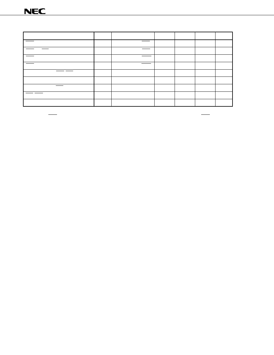
Data Sheet S15082EJ4V0DS
88
µ
PD61051, 61052
(2/2)
Parameter Symbol
Conditions
Min.
Typ.
Max.
Unit
CWE
CA5 to CA0 hold time
t
WAH
Vs rising edge of CWE
-27 ns
CWE
CCS hold time
t
WCH
Vs rising edge of CWE
-27 ns
CCS
CD7 to CD0 hold time
t
CDWH
Vs rising edge of CCS
0
ns
CCS
CWAIT release time
t
CWAD2
Vs rising edge of CCS
0
15
ns
CWAIT release
CWE/CRE hold time
t
CWR
Vs
CWAIT
release
0
ns
CWAIT release
CD5 to CD0 hold time
t
CWA
Vs
CWAIT
release
0
ns
CWAIT release
CSS hold time
t
CWC
Vs
CWAIT
release
0
ns
CRE/CWE recovery time
t
CAC
25
ns
Access cycle after other device
t
CCYC
200
ns
Remark If CCS change to "H" in wait cycle, it cancels CWAIT. In access time, don't make CCS "H" until wait
released.

Data Sheet S15082EJ4V0DS
89
µ
PD61051, 61052
Wait mode (Wait active low, read cycle)
CCS
CA5 to CA0
CRE
CD7 to CD0
CWAIT
CWE
t
ARD
t
CAD
t
CDLD
t
CDD
t
CAC
t
CWAD1
t
CRDY
t
CDRH
t
RCH
t
RAH
t
RWD1
t
RRD
t
CRD
t
CDZD
t
RDLD
t
RDD
t
CDZD
t
RDH
t
CWR
t
CDW
t
CWC
t
CWA
t
CAC
Wait mode (Wait active low, write cycle)
CCS
CA5 to CA0
CRE
CD7 to CD0
CWAIT
CWE
t
AWD
t
CAD
t
CAC
t
CWAD1
t
CRDY
t
CDWH
t
WCH
t
WAH
t
WWD1
t
WRD
t
CWD
t
WDD
t
WDH
t
CWR
t
CWC
t
CWA
t
WDD
t
CAC
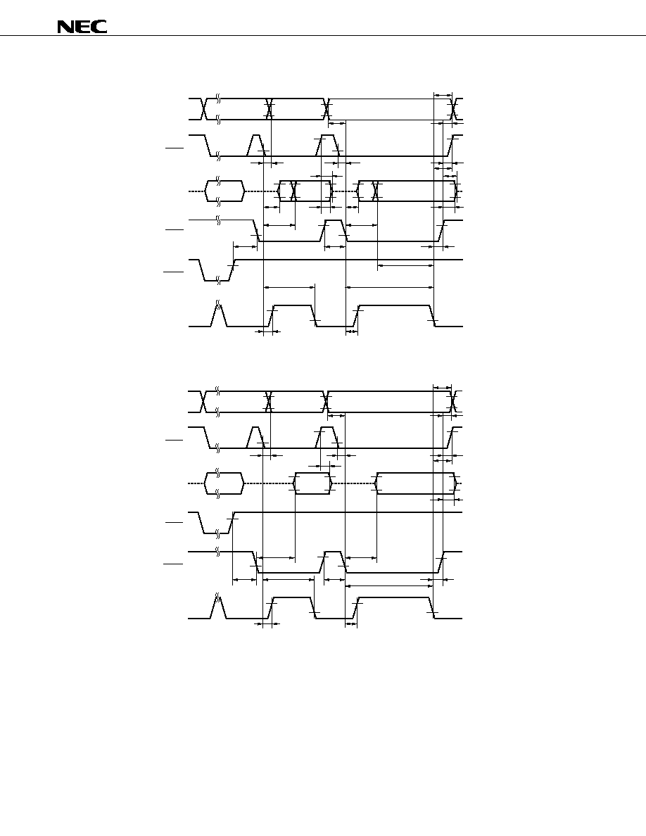
Data Sheet S15082EJ4V0DS
90
µ
PD61051, 61052
Wait mode (Wait active high, read cycle)
CCS
CA5 to CA0
CRE
CD7 to CD0
CWAIT
CWE
t
ARD
t
CAD
t
CDLD
t
CDD
t
CAC
t
CWAD1
t
CRDY
t
CDRH
t
RCH
t
RAH
t
RWD1
t
RRD
t
CRD
t
CDZD
t
RDLD
t
RDD
t
CDZD
t
RDH
t
CWR
t
CDW
t
CWC
t
CWA
t
CAC
Wait mode (Wait active high, write cycle)
CCS
CA5 to CA0
CRE
CD7 to CD0
CWAIT
CWE
t
AWD
t
CAD
t
CAC
t
CWAD1
t
CRDY
t
CDWH
t
WCH
t
WAH
t
WWD1
t
WRD
t
CWD
t
WDD
t
WDH
t
CWR
t
CWC
t
CWA
t
WDD
t
CAC
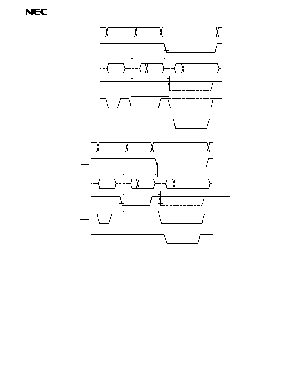
Data Sheet S15082EJ4V0DS
91
µ
PD61051, 61052
CCS
CA5 to CA0
CRE
CD7 to CD0
CWAIT
CWE
t
CCYC
t
CCYC
t
CCYC
CCS
CA5 to CA0
CRE
CD7 to CD0
CWAIT
CWE
t
CCYC
t
CCYC
t
CCYC

Data Sheet S15082EJ4V0DS
92
µ
PD61051, 61052
(b)
Parallel bus interface: Ready mode
(1/2)
Parameter Symbol
Conditions Min.
Typ.
Max.
Unit
CCS
CA5 to CA0 delay time
t
CAD
Vs falling edge of CCS
Do not care
- - -
ns
CCS
CWAIT delay time
t
CWAD1
Vs falling edge of CCS
CCS later than CRE/CWE
15
CCS
CWAIT ready time
t
CRDY
Vs falling edge of CCS
CCS later than CRE/CWE
175
ns
CA5 to CA0
CRE delay time
t
ARD
Vs CA5 to CA0
-20 ns
CCS
CRE delay time
t
CRD
Vs falling edge of CCS
-20 ns
CRE
CWAIT ready time
t
RRD
Vs falling edge of CRE
175
ns
CCS
CD7 to CD0 low-Z time
t
CDLD
Vs falling edge of CCS
Data not fixed
0
ns
CRE
CD7 to CD0 low-Z time
t
RDLD
Vs falling edge of CRE
Data not fixed
0
ns
CCS
CD7 to CD0 delay time
t
CDD
Vs falling edge of CCS
Data fixed
150
ns
CRE
CD7 to CD0 delay time
t
RDD
Vs falling edge of CRE
Data fixed
150
ns
CRE
CD7 to CD0 hold time
t
RDH
Vs rising edge of CRE
Earlier than rising edge of
CCS
0
ns
CRE
CA5 to CA0 hold time
t
RAH
Vs rising edge of CRE
-27 ns
CRE
CCS hold time
t
RCH
Vs rising edge of CRE
-27 ns
CCS
CD7 to CD0 hold time
t
CDRH
Vs rising edge of CCS
Earlier than rising edge of
CRE
0
ns
CD7 to CD0
CWAIT ready
time
t
CDW
Vs CD7 to CD0 fixed
10
ns
CD7 to CD0 high-Z delay time
t
CDZD
Vs rising edge of CRE or CCS
12
ns
CA5 to CA0
CWE delay time
t
AWD
Vs CA5 to CA0
-28 ns
CCS
CWE delay time
t
CWD
Vs falling edge of CCS
-20 ns
CWE
CWAIT ready time
t
WRD
Vs falling edge of CWE
150
ns
CWE
CD7 to CD0 delay time
t
WDD
Vs falling edge of CWE
Until data fixed
30
ns
CWE
CD7 to CD0 hold time
t
WDH
Vs rising edge of CWE
-7 ns
CWE
CA5 to CA0 hold time
t
WAH
Vs rising edge of CWE
-27 ns
CWE
CCS hold time
t
WCH
Vs rising edge of CWE
-27 ns
CCS
CD7 to CD0 hold time
t
CDWH
Vs rising edge of CCS
0
ns
CRE
CWAIT release time
t
RWD2
Vs rising edge of CRE
0
15
ns
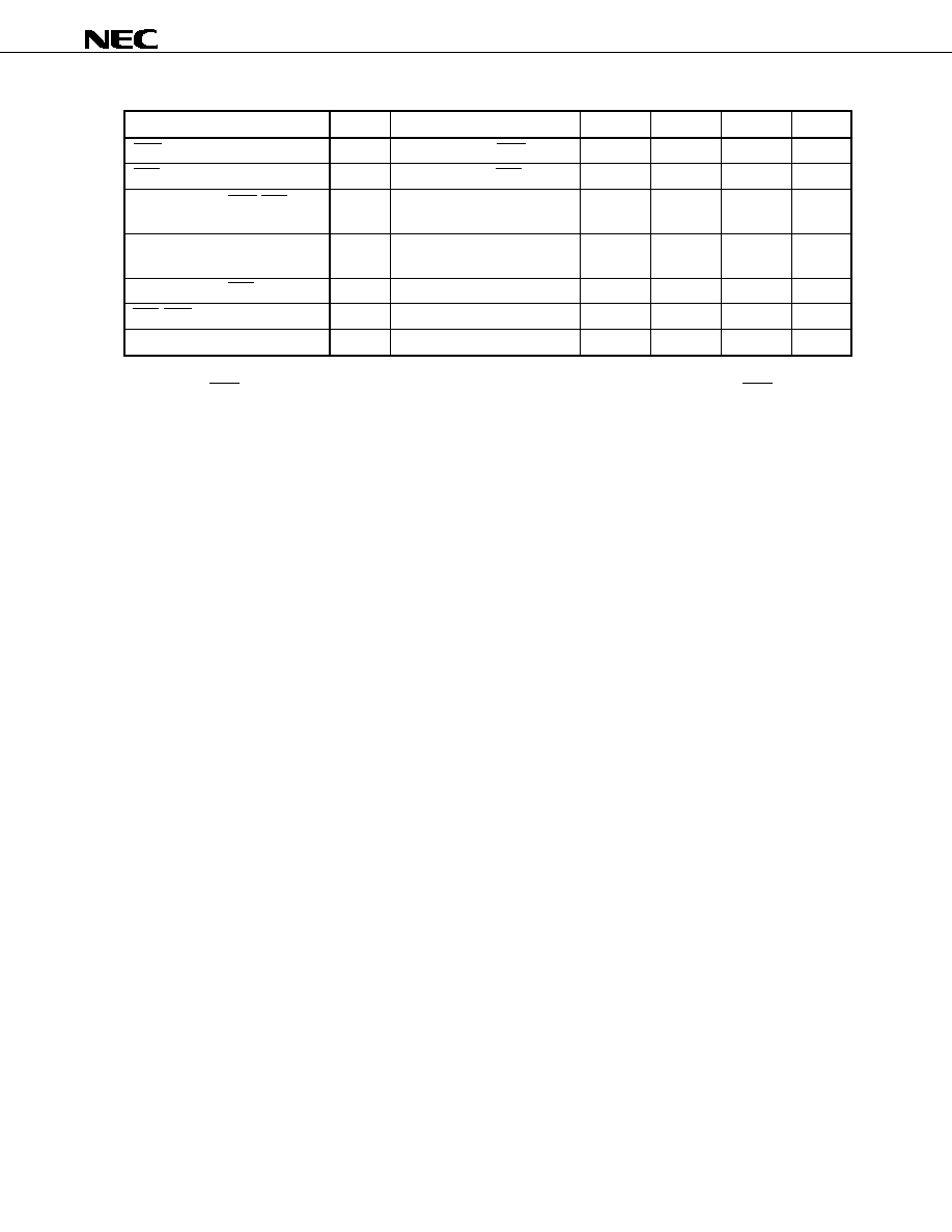
Data Sheet S15082EJ4V0DS
93
µ
PD61051, 61052
(2/2)
Parameter Symbol
Conditions Min.
Typ.
Max.
Unit
CWE
CWAIT release time
t
WWD2
Vs rising edge of CWE
0
15
ns
CCS
CWAIT release time
t
CWAD2
Vs rising edge of CCS
0
15
ns
CWAIT ready
CWE/CRE hold
time
t
CWR
Vs
CWAIT
ready
0
ns
CWAIT ready
CA5 to CA0 hold
time
t
CWA
Vs
CWAIT
ready
0
ns
CWAIT ready
CCS hold time
t
CWC
Vs
CWAIT
ready
0
ns
CRE/CWE recovery time
t
CAC
25
ns
Access cycle after other device
t
CCYC
200
ns
Remark If CCS change to "H" in wait cycle, it cancels CWAIT. In access time, don't make CCS "H" until wait
becomes ready.
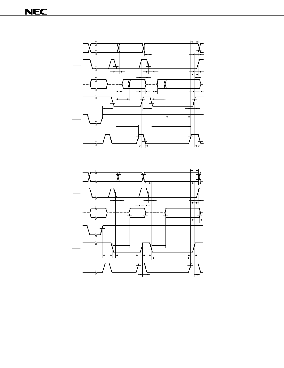
Data Sheet S15082EJ4V0DS
94
µ
PD61051, 61052
Ready mode (Ready active high, read cycle)
CCS
CA5 to CA0
CRE
CD7 to CD0
CWAIT
CWE
t
ARD
t
CAD
t
CDLD
t
CDD
t
CAC
t
CWAD2
t
CRDY
t
CDRH
t
RCH
t
RAH
t
RWD2
t
RRD
t
CRD
t
CDZD
t
RDLD
t
RDD
t
CDZD
t
RDH
t
CWR
t
CDW
t
CWC
t
CWA
t
CAC
Ready mode (Ready active high, write cycle)
CCS
CA5 to CA0
CRE
CD7 to CD0
CWAIT
CWE
t
AWD
t
CAD
t
CAC
t
CRDY
t
CDWH
t
WCH
t
WAH
t
WRD
t
CWD
t
WDD
t
WDH
t
CWR
t
CWC
t
CWA
t
WDD
t
CAC
t
CWAD2
t
WWD2
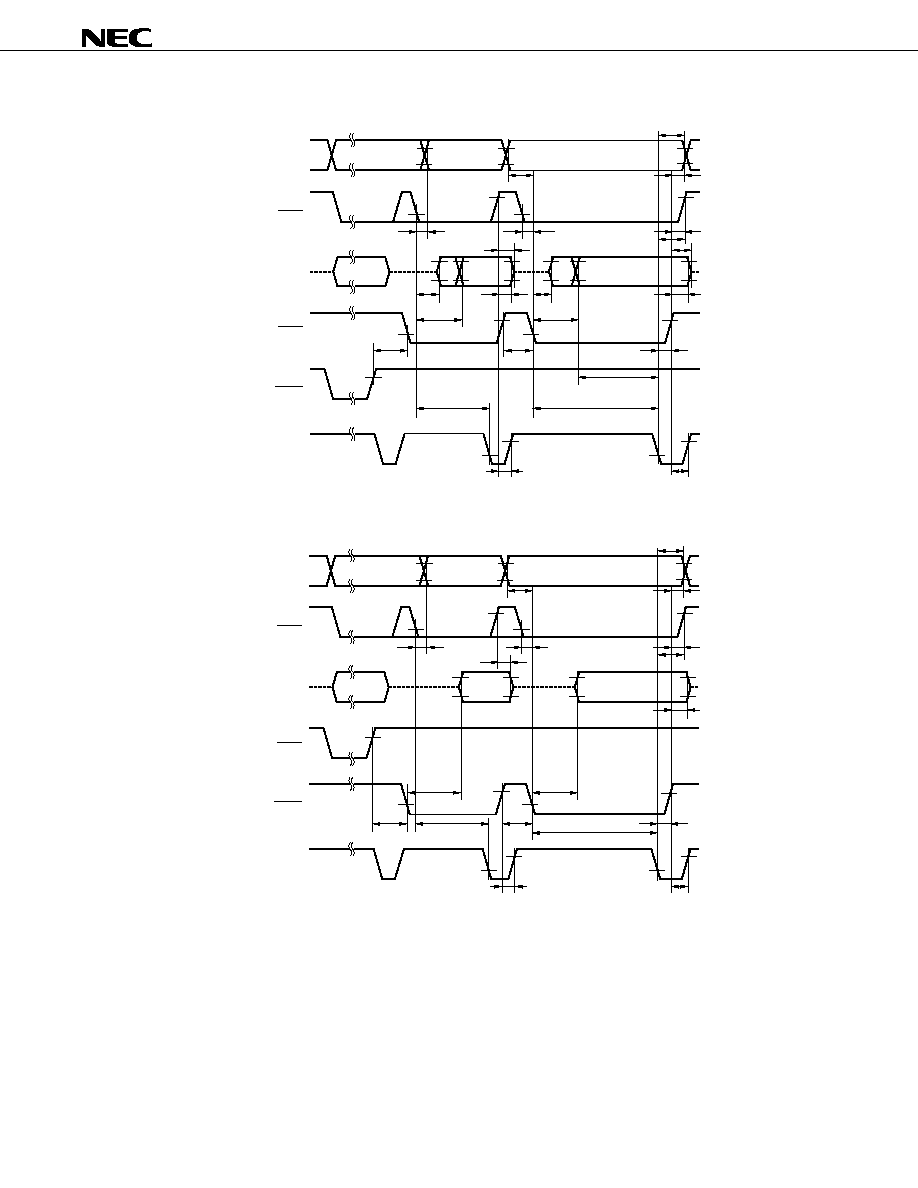
Data Sheet S15082EJ4V0DS
95
µ
PD61051, 61052
Ready mode (Ready active low, read cycle)
CCS
CA5 to CA0
CRE
CD7 to CD0
CWAIT
CWE
t
ARD
t
CAD
t
CDLD
t
CDD
t
CAC
t
CWAD2
t
CRDY
t
CDRH
t
RCH
t
RAH
t
RWD2
t
RRD
t
CRD
t
CDZD
t
RDLD
t
RDD
t
CDZD
t
RDH
t
CWR
t
CDW
t
CWC
t
CWA
t
CAC
Ready mode (Ready active low, write cycle)
CCS
CA5 to CA0
CRE
CD7 to CD0
CWAIT
CWE
t
AWD
t
CAD
t
CAC
t
CRDY
t
CDWH
t
WCH
t
WAH
t
WRD
t
CWD
t
WDD
t
WDH
t
CWR
t
CWC
t
CWA
t
WDD
t
CAC
t
CWAD2
t
WWD2
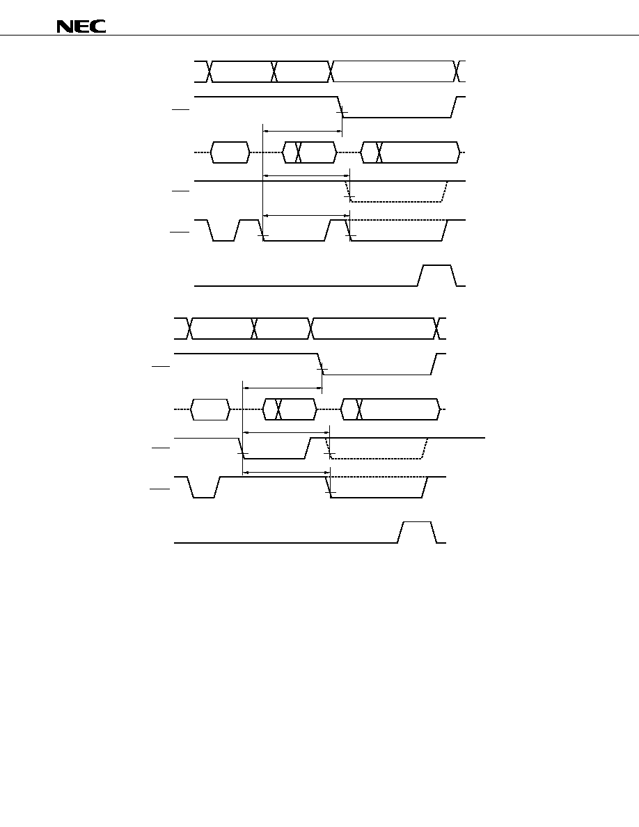
Data Sheet S15082EJ4V0DS
96
µ
PD61051, 61052
CCS
CA5 to CA0
CRE
CD7 to CD0
CWAIT
CWE
t
CCYC
t
CCYC
t
CCYC
CCS
CA5 to CA0
CRE
CD7 to CD0
CWAIT
CWE
t
CCYC
t
CCYC
t
CCYC
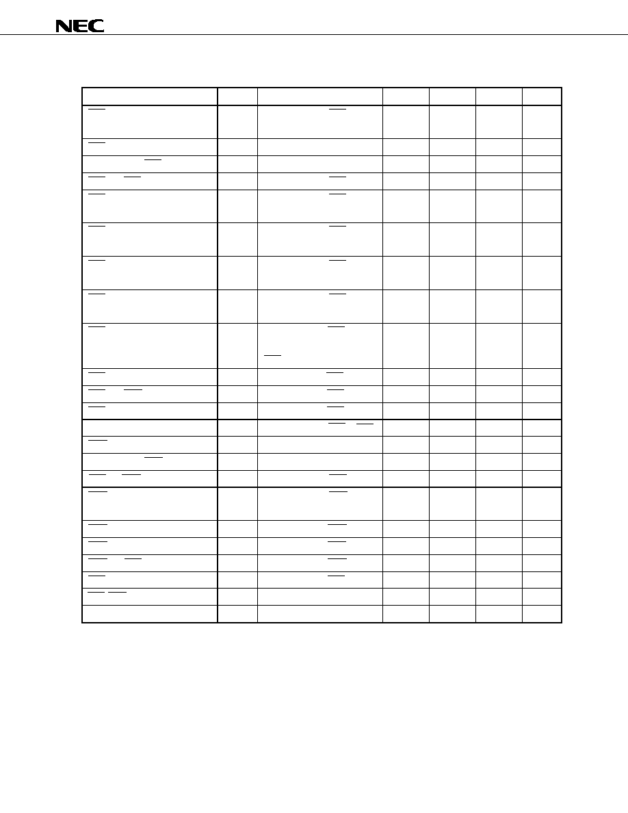
Data Sheet S15082EJ4V0DS
97
µ
PD61051, 61052
(c)
Parallel bus interface: Fixed wait mode
Parameter Symbol
Conditions Min.
Typ.
Max.
Unit
CCS
CA5 to CA0 delay time
t
CAD
Vs falling edge of CCS
Do not care
- - -
ns
CRE pulse width
t
RW
175
ns
CA5 to CA0
CRE delay time
t
ARD
Vs CA5 to CA0
-20 ns
CCS
CREdelay time
t
CRD
Vs falling edge of CCS
-20 ns
CCS
CD7 to CD0 low-Z time
t
CDLD
Vs falling edge of CCS
Data not fixed
0
ns
CRE
CD7 to CD0 low-Z time
t
RDLD
Vs falling edge of CRE
Data not fixed
0
ns
CCS
CD7 to CD0 delay time
t
CDD
Vs falling edge of CCS
Data fixed
150
ns
CRE
CD7 to CD0 delay time
t
RDD
Vs falling edge of CRE
Data fixed
150
ns
CRE
CD7 to CD0 hold time
t
RDH
Vs rising edge of CRE
Earlier than rising edge of
CCS
0
ns
CRE
CA5 to CA0 hold time
t
FRAH
Vs rising edge of CRE
-27 ns
CRE
CCS hold time
t
FRCH
Vs rising edge of CRE
-27 ns
CCS
CD7 to CD0 hold time
t
CDRH
Vs rising edge of CCS
0
ns
CD7 to CD0 high-Z delay time
t
CDZD
Vs rising edge of CRE or CCS
12
ns
CWE pulse width
t
WW
150
ns
CA5 to CA0
CWE delay time
t
AWD
Vs CA5 to CA0
-28 ns
CCS
CWE delay time
t
CWD
Vs falling edge of CCS
-20 ns
CWE
CD7 to CD0 delay time
t
WDD
Vs falling edge of CWE
Until data fixed
30
ns
CWE
CD7 to CD0 hold time
t
WDH
Vs rising edge of CWE
-7 ns
CWE
CA5 to CA0 hold time
t
FWAH
Vs rising edge of CWE
-27 ns
CWE
CCS hold time
t
FWCH
Vs rising edge of CWE
-27 ns
CCS
CD7 to CD0 hold time
t
CDWH
Vs rising edge of CCS
0
ns
CRE/CWE recovery time
t
CAC
25
ns
Access cycle after other device
t
CCYC
200
ns

Data Sheet S15082EJ4V0DS
98
µ
PD61051, 61052
Fixed wait mode (Read cycle)
CCS
CA5 to CA0
CRE
CD7 to CD0
CWE
t
ARD
t
CAD
t
CDLD
t
CDD
t
CAC
t
CDRH
t
FRCH
t
FRAH
t
CRD
t
CDZD
t
RDLD
t
RDD
t
CDZD
t
RDH
t
RW
t
CAC
Fixed wait mode (Write cycle)
CCS
CA5 to CA0
CRE
CD7 to CD0
CWE
t
AWD
t
CAD
t
CAC
t
CDWH
t
FWCH
t
FWAH
t
WW
t
CWD
t
WDD
t
WDH
t
WDD
t
CAC
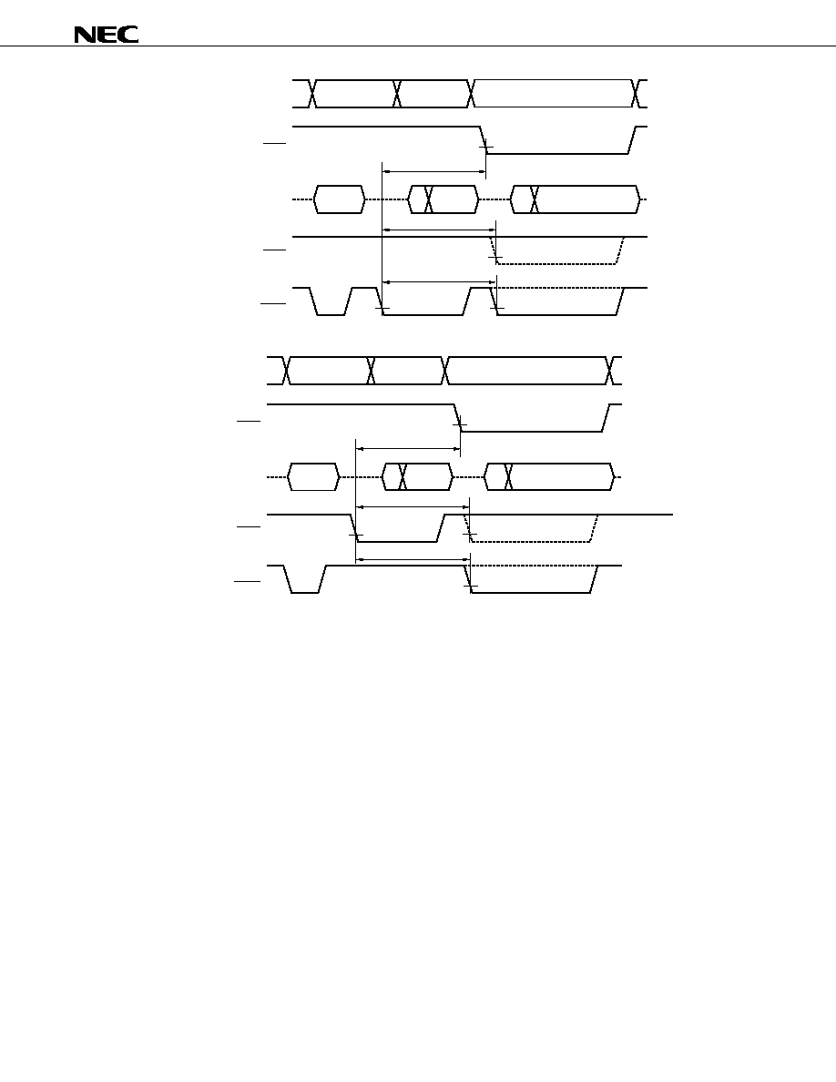
Data Sheet S15082EJ4V0DS
99
µ
PD61051, 61052
CCS
CA5 to CA0
CRE
CD7 to CD0
CWE
t
CCYC
t
CCYC
t
CCYC
CCS
CA5 to CA0
CRE
CD7 to CD0
CWE
t
CCYC
t
CCYC
t
CCYC
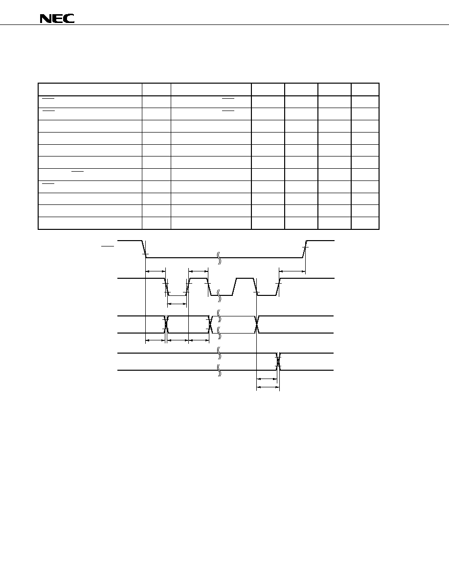
Data Sheet S15082EJ4V0DS
100
µ
PD61051, 61052
(10)
Serial bus interface
(a)
Serial bus interface
Parameter Symbol
Conditions
Min.
Typ.
Max.
Unit
CCS
CSCLK delay time
t
CSCK
Vs falling edge of CCS
10
ns
CCS
CSDI delay time
t
CSDI
Vs falling edge of CCS
10
ns
CSDI setup time
t
CSDS
Vs rising edge of CSCLK
10
ns
CSDI hold time
t
CSDH
Vs rising edge of CSCLK
10
ns
CSDO hold time
t
CSDHO
Vs falling edge of CSCLK
0
ns
CSDO delay time
t
CSDD
Vs falling edge of CSCLK
15
ns
CSCLK
CCS hold time
t
CCKS
Vs rising edge of CSCLK
75
ns
CCS high-level width
t
CSHW
125
ns
CSCLK cycle time
t
CKCYC
100
ns
CSCLK high-level width
t
CSCHW
40
ns
CSCLK high-level width
t
CSCLW
40
ns
CCS
CSCLK
CSDI
CSDO
t
CSCK
t
CSDI
t
CSDS
t
CSDH
t
CSDHO
t
CSDD
t
CKCS
t
CSCHW
t
CSCLW
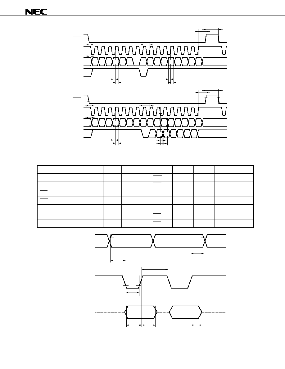
Data Sheet S15082EJ4V0DS
101
µ
PD61051, 61052
A5 A4 A3
A1 A0 W x
D5
D3 D2 D1 D0
D7 D6
xx
x
A5 A4 A3
A1 A0
R
x
x
x
x
x
x
x
x
x
xx
x
xx
D4 D3 D2 D1 D0
D7
[Data Write]
[Data Read]
CCS
CSCLK
CSDI
CSDO
CCS
CSCLK
CSDI
CSDO
xx
t
CSCK
t
CKCYC
t
CSDI
t
CSDS
t
CSDH
t
CSDS
t
CSDH
t
CSDS
t
CSDH
t
CKCS
t
CSHW
t
CSCK
t
CKCYC
t
CSDI
t
CSDHO
t
CSDD
t
CKCS
t
CSHW
A2
D4
A2
D5
D6
(b)
Instruction ROM interface
Parameter Symbol
Conditions
Min.
Typ.
Max.
Unit
Address setup time
t
FARS
Vs falling edge of FOE
0
ns
Address hold time
t
FARH
Vs rising edge of FOE
5
ns
FOE low-level width
t
FRLW
70
225
ns
FOE high-level width
t
FRHW
24
ns
Data setup time
t
FDS
Vs rising edge of FOE
25
ns
Data hold time
t
FDH
Vs rising edge of FOE
0
ns
Data high-Z output time
t
FDHL
Vs rising edge of FOE
60
ns
FA19 to FA0
FOE
FD7 to FD0
t
FARS
Hi-Z
Hi-Z
Hi-Z
t
FARH
t
FRHW
t
FRLW
t
FDS
t
FDH
t
FDHL
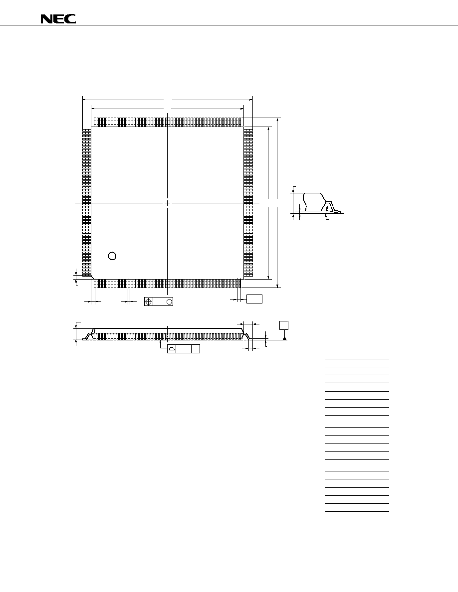
Data Sheet S15082EJ4V0DS
102
µ
PD61051, 61052
7.
PACKAGE DRAWING
208-PIN PLASTIC QFP (FINE PITCH) (28x28)
ITEM
MILLIMETERS
F
G
1.25
1.25
B
C
28.0
±0.2
28.0
±0.2
H
0.22
I
0.10
S
3.8 MAX.
K
1.3
±0.2
L
0.5
±0.2
M
0.17
N
0.10
P
3.2
±0.1
+0.05
-0.04
J
0.5 (T.P.)
P208GD-50-LML,MML,SML,WML-7
+0.03
-0.07
R
5
∞±5∞
J
I
N
S
S
detail of lead end
Q
0.4
±0.1
M
NOTE
Each lead centerline is located within 0.10 mm of
its true position (T.P.) at maximum material condition.
1
208
52
53
156
157
105
104
C
A
B
Q
R
H
K
M
L
D
P
G
F
S
A
30.6
±0.2
D
30.6
±0.2
Data Sheet S15082EJ4V0DS
103
µ
PD61051, 61052
8.
RECOMMENDED SOLDERING CONDITIONS
The
µ
PD61051, 61052 should be soldered and mounted under the following recommended conditions.
For soldering methods and conditions other than those recommended below, contact an NEC Electronics sales
representative.
For technical information, see the following website.
Semiconductor Device Mount Manual (http://www.necel.com/pkg/en/mount/index.html)
Table 8-1. Surface-Mounted Soldering Conditions
µ
PD61051GD-LML:
208-pin plastic QFP (Fine pitch) (28
◊28)
µ
PD61051GD-LML-A
Note1
:
208-pin plastic QFP (Fine pitch) (28
◊28)
µ
PD61052GD-LML:
208-pin plastic QFP (Fine pitch) (28
◊28)
µ
PD61052GD-LML-A
Note1
:
208-pin plastic QFP (Fine pitch) (28
◊28)
Soldering Method
Soldering Conditions
Recommended
Condition Symbol
Infrared reflow
Package peak temperature: 235∞C
IR35-207-3
Time: 30 sec. max. (at 210∞C or higher)
Count: Three times or fewer
Exposure limit: 7 days
Note2
(After that, prebake at 125∞C for 20 to 72 hours)
VPS
Package peak temperature: 215∞C
VP15-207-3
Time: 40 sec. max. (at 200∞C or higher)
Count: Three times or fewer
Exposure limit: 7 days
Note2
(After that, prebake at 125∞C for 20 to 72 hours)
Partial heating
Pin temperature: 300∞C max.
Time: 3 sec. max. (per pin row)
Notes 1. Lead-free product
2. After opening the dry pack, store it at 25∞C or less and 65% RH or less for the allowable storage period.
Caution Do not use two or more soldering methods in combination (except for partial heating method).
Data Sheet S15082EJ4V0DS
104
µ
PD61051, 61052
NOTES FOR CMOS DEVICES
1
PRECAUTION AGAINST ESD FOR SEMICONDUCTORS
Note:
Strong electric field, when exposed to a MOS device, can cause destruction of the gate oxide and
ultimately degrade the device operation. Steps must be taken to stop generation of static electricity
as much as possible, and quickly dissipate it once, when it has occurred. Environmental control
must be adequate. When it is dry, humidifier should be used. It is recommended to avoid using
insulators that easily build static electricity. Semiconductor devices must be stored and transported
in an anti-static container, static shielding bag or conductive material. All test and measurement
tools including work bench and floor should be grounded. The operator should be grounded using
wrist strap. Semiconductor devices must not be touched with bare hands. Similar precautions need
to be taken for PW boards with semiconductor devices on it.
2
HANDLING OF UNUSED INPUT PINS FOR CMOS
Note:
No connection for CMOS device inputs can be cause of malfunction. If no connection is provided
to the input pins, it is possible that an internal input level may be generated due to noise, etc., hence
causing malfunction. CMOS devices behave differently than Bipolar or NMOS devices. Input levels
of CMOS devices must be fixed high or low by using a pull-up or pull-down circuitry. Each unused
pin should be connected to V
DD
or GND with a resistor, if it is considered to have a possibility of
being an output pin. All handling related to the unused pins must be judged device by device and
related specifications governing the devices.
3
STATUS BEFORE INITIALIZATION OF MOS DEVICES
Note:
Power-on does not necessarily define initial status of MOS device. Production process of MOS
does not define the initial operation status of the device. Immediately after the power source is
turned ON, the devices with reset function have not yet been initialized. Hence, power-on does
not guarantee out-pin levels, I/O settings or contents of registers. Device is not initialized until the
reset signal is received. Reset operation must be executed immediately after power-on for devices
having reset function.

Data Sheet S15082EJ4V0DS
105
µ
PD61051, 61052
[MEMO]

µ
PD61051, 61052
Dolby is a trademark of Dolby Laboratories.
The information in this document is current as of November, 2003. The information is subject to
change without notice. For actual design-in, refer to the latest publications of NEC Electronics data
sheets or data books, etc., for the most up-to-date specifications of NEC Electronics products. Not
all products and/or types are available in every country. Please check with an NEC Electronics sales
representative for availability and additional information.
No part of this document may be copied or reproduced in any form or by any means without the prior
written consent of NEC Electronics. NEC Electronics assumes no responsibility for any errors that may
appear in this document.
NEC Electronics does not assume any liability for infringement of patents, copyrights or other intellectual
property rights of third parties by or arising from the use of NEC Electronics products listed in this document
or any other liability arising from the use of such products. No license, express, implied or otherwise, is
granted under any patents, copyrights or other intellectual property rights of NEC Electronics or others.
Descriptions of circuits, software and other related information in this document are provided for illustrative
purposes in semiconductor product operation and application examples. The incorporation of these
circuits, software and information in the design of a customer's equipment shall be done under the full
responsibility of the customer. NEC Electronics assumes no responsibility for any losses incurred by
customers or third parties arising from the use of these circuits, software and information.
While NEC Electronics endeavors to enhance the quality, reliability and safety of NEC Electronics products,
customers agree and acknowledge that the possibility of defects thereof cannot be eliminated entirely. To
minimize risks of damage to property or injury (including death) to persons arising from defects in NEC
Electronics products, customers must incorporate sufficient safety measures in their design, such as
redundancy, fire-containment and anti-failure features.
NEC Electronics products are classified into the following three quality grades: "Standard", "Special" and
"Specific".
The "Specific" quality grade applies only to NEC Electronics products developed based on a customer-
designated "quality assurance program" for a specific application. The recommended applications of an NEC
Electronics product depend on its quality grade, as indicated below. Customers must check the quality grade of
each NEC Electronics product before using it in a particular application.
"Standard": Computers, office equipment, communications equipment, test and measurement equipment, audio
and visual equipment, home electronic appliances, machine tools, personal electronic equipment
and industrial robots.
"Special":
Transportation equipment (automobiles, trains, ships, etc.), traffic control systems, anti-disaster
systems, anti-crime systems, safety equipment and medical equipment (not specifically designed
for life support).
"Specific": Aircraft, aerospace equipment, submersible repeaters, nuclear reactor control systems, life
support systems and medical equipment for life support, etc.
The quality grade of NEC Electronics products is "Standard" unless otherwise expressly specified in NEC
Electronics data sheets or data books, etc. If customers wish to use NEC Electronics products in applications
not intended by NEC Electronics, they must contact an NEC Electronics sales representative in advance to
determine NEC Electronics' willingness to support a given application.
(Note)
(1) "NEC Electronics" as used in this statement means NEC Electronics Corporation and also includes its
majority-owned subsidiaries.
(2) "NEC Electronics products" means any product developed or manufactured by or for NEC Electronics (as
defined above).
∑
∑
∑
∑
∑
∑
M8E 02. 11-1