 | –≠–ª–µ–∫—Ç—Ä–æ–Ω–Ω—ã–π –∫–æ–º–ø–æ–Ω–µ–Ω—Ç: UPD62 | –°–∫–∞—á–∞—Ç—å:  PDF PDF  ZIP ZIP |
Document Outline
- COVER
- DESCRIPTION
- FEATURES
- APPLICATION
- ORDERING INFORMATION
- PIN CONFIGURATION (TOP VIEW)
- BLOCK DIAGRAM
- LIST OF FUNCTIONS
- 1. PIN FUNCTIONS
- 1.1 List of Pin Functions
- 1.2 INPUT/OUTPUT Circuits of Pins
- 1.3 Dealing with Unused Pins
- 2. INTERNAL CPU FUNCTIONS
- 2.1 Program Counter (PC): 10 Bits
- 2.2 Stack Pointer (SP): 1 Bit
- 2.3 Address Stack Register (ASR (RF)): 10 Bits
- 2.4 Program Memory (ROM): 512 steps x 10 bits
- 2.5 Data Memory (RAM): 32 x 4 Bits
- 2.6 Data Pointer (DP): 10 Bits
- 2.7 Accumulator (A): 4 Bits
- 2.8 Arithmetic and Logic Unit (ALU): 4 Bits
- 2.9 Flags
- 2.9.1 Status flag (F)
- 2.9.2 Carry flag (CY)
- 3. PORT REGISTERS (PX)
- 3.1 KI/O Port (P0)
- 3.2 KI Port/Special Ports (P1)
- 3.2.1 KI port (P11: bits 4-7 of P1)
- 3.2.2 S0 port (bit 2 of P1)
- 3.2.3 S1/LED# (bit 3 of P1)
- 3.3 Control Register 0 (P3)
- 3.4 Control Register 1 (P4)
- 4. TIMER
- 4.1 Timer Configuration
- 4.2 Timer Operation
- 4.3 Carrier Output
- 4.4 Software Control of Timer Output
- 5. STANDBY FUNCTION
- 5.1 Outline of Standby Function
- 5.2 Standby Mode Setup and Release
- 5.3 Standby Mode Release Timing
- 6. RESET# PIN
- 7. POC CIRCUIT (MASK OPTION)
- 7.1 Functions of POC Circuit
- 7.2 Oscillation Check at Low Supply Voltage
- 8. SYSTEM CLOCK OSCILLATION CIRCUIT
- 9. INSTRUCTION SET
- 9.1 Machine Language Output by Assembler
- 9.2 Circuit Symbol Description
- 9.3 Mnemonic to/from Machine Language (Assembler Output) Contrast Table
- 9.4 Accumulator Operation Instructions
- 9.5 Input/Output Instructions
- 9.6 Data Transfer Instruction
- 9.7 Branch Instructions
- 9.8 Subroutine Instructions
- 9.9 Timer Operation Instructions
- 9.10 Others
- 10. ASSEMBLER RESERVED WORDS
- 10.1 Mask Option Directives
- 10.1.1 OPTION and ENDOP directives
- 10.1.2 Mask option definition directive
- 11. ELECTRICAL SPECIFICATIONS
- 12. CHARACTERISTIC CURVE (REFERENCE VALUES)
- 13. APPLIED CIRCUIT EXAMPLE
- 14. PACKAGE DRAWINGS
- 15. RECOMMENDED SOLDERING CONDITIONS
- APPENDIX A. DEVELOPMENT TOOLS
- APPENDIX B. FUNCTIONAL COMPARISON BETWEEN uPD62 AND OTHER SUBSERIES
- APPENDIX C. EXAMPLE OF REMOTE-CONTROL TRANSMISSION FORMAT (in the case of NEC transmission format in command one-shot transmiss

©
1999
DATA SHEET
4-BIT SINGLE-CHIP MICROCONTROLLER
FOR INFRARED REMOTE CONTROL TRANSMISSION
DESCRIPTION
Equipped with low-voltage 1.8 V operation, a carrier generation circuit for infrared remote control transmission,
a standby release function through key entry, and a programmable timer, the
µ
PD62 is suitable for infrared remote
control transmitters.
For the
µ
PD62, we have made available the one-time PROM product
µ
PD6P4B for program evaluation or small-
quantity production.
FEATURES
∑ Program memory (ROM): 512
◊
10 bits
∑ Data memory (RAM): 32
◊
4 bits
∑ Built-in carrier generation circuit for infrared remote control
∑ 9-bit programmable timer
: 1 channel
∑ Command execution time
: 8
µ
s (when operating at f
X
= 8 MHz: ceramic oscillation)
∑ Stack level
: 1 level (Stack RAM is for data memory RF as well.)
∑ I/O pins (K
I/O
)
: 8 units
∑ Input pins (K
I
)
: 4 units
∑ Sense input pin (S
0
)
: 1 unit
∑ S
1
/LED pin (I/O)
: 1 unit (When in output mode, this is the remote control transmission display
pin.)
∑ Power supply voltage
: V
DD
= 1.8 to 3.6 V (when operating at f
X
= 4 MHz)
V
DD
= 2.2 to 3.6 V (when operating at f
X
= 8 MHz)
∑ Operating ambient temperature : T
A
= ≠40 to +85 ∞C
∑ Oscillator frequency
: f
X
= 2.4 to 8 MHz
∑ POC circuit (Mask option)
APPLICATION
Infrared remote control transmitter (for AV and household electric appliances)
MOS INTEGRATED CIRCUIT
µ
PD62
Document No. U14208EJ1V0DS00 (1st edition)
Date Published May 1999 N CP(K)
Printed in Japan
The information in this document is subject to change without notice. Before using this document, please
confirm that this is the latest version.
Not all devices/types available in every country. Please check with local NEC representative for availability
and additional information.

2
µ
PD62
Data Sheet U14208EJ1V0DS00
ORDERING INFORMATION
Part Number
Package
µ
PD62MC-
◊◊◊
-5A4
20-pin plastic SSOP (300 mil)
Remark
◊◊◊
indicates ROM code suffix.
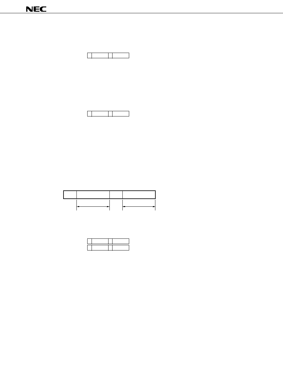
PIN CONFIGURATION (TOP VIEW)
20-pin Plastic SSOP (300 mil)
∑
µ
PD62MC-
◊◊◊
-5A4
Caution The pin numbers of K
I
and K
I/O
are in the reverse order of the
µ
PD6600A, and 6124A.
1
2
3
4
5
6
7
8
9
10
K
I/O6
K
I/O7
S
0
S
1
/LED
REM
V
DD
X
OUT
X
IN
GND
RESET
20
19
18
17
16
15
14
13
12
11
K
I/O5
K
I/O4
K
I/O3
K
I/O2
K
I/O1
K
I/O0
K
I3
K
I2
K
I1
K
I0
3
µ
PD62
Data Sheet U14208EJ1V0DS00
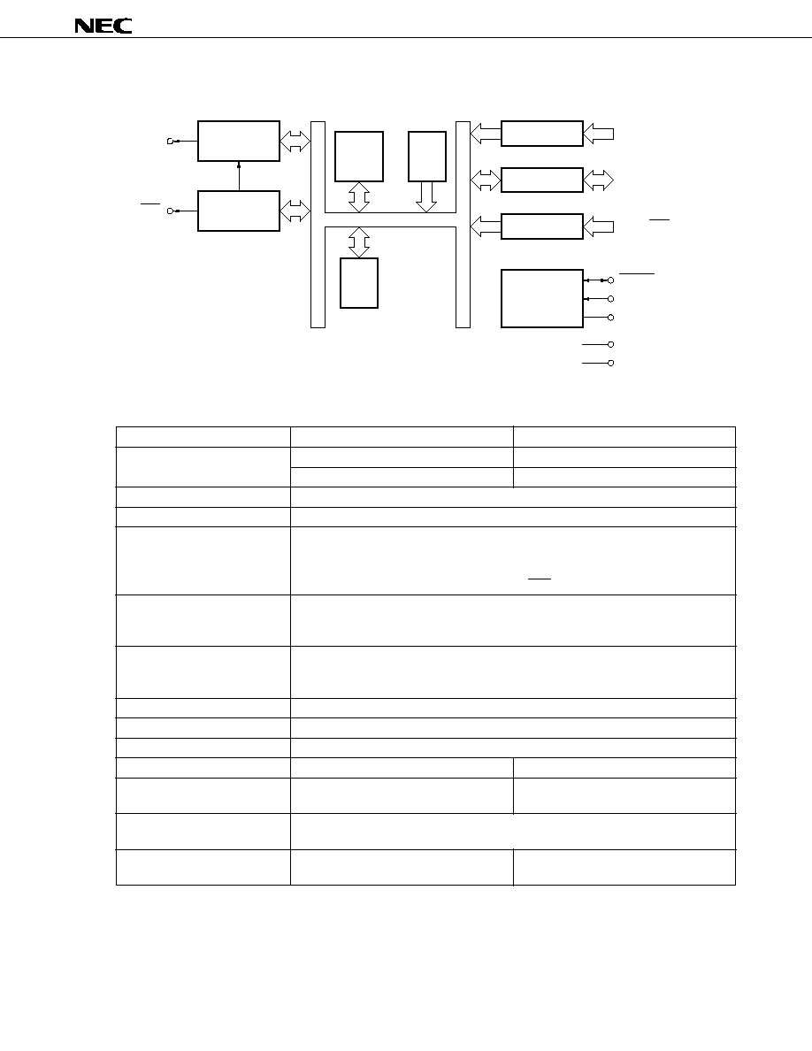
BLOCK DIAGRAM
K
I0
-K
I3
K
I/O0
-K
I/O7
S
0
, S
1
/LED
PORT K
I
PORT K
I/O
PORT S
4
8
2
4
8
2
ROM
RAM
SYSTEM
CONTROL
CARRIER
GENERATOR
9-bit
TIMER
CPU
CORE
RESET
X
IN
X
OUT
V
DD
GND
REM
S
1
/LED
LIST OF FUNCTIONS
Item
µ
PD62
µ
PD6P4B
ROM capacity
512
◊
10 bits
1002
◊
10 bits
Mask ROM
One-time PROM
RAM capacity
32
◊
4 bits
Stack
1 level (multiplexed with RF of RAM)
I/O pins
∑ Key input (K
I
)
: 4
∑ Key I/O (K
I/O
)
: 8
∑ Key extended input (S
0
, S
1
)
: 2
∑ Remote control transmission display output (LED) : 1 (multiplexed with S
1
pin)
Number of keys
∑ 32 keys
∑ 48 keys (when extended by key extension input)
∑ 96 keys (when extended by key extension input and diode)
Clock frequency
Ceramic oscillation
∑ f
X
= 2.4 to 8 MHz
∑ f
X
= 2.4 to 4 MHz
Instruction execution time
8
µ
s (f
X
= 8 MHz)
Carrier frequency
f
X
/8, f
X
/16, f
X
/64, f
X
/96, f
X
/128, f
X
/192, no carrier (high level)
Timer
9-bit programmable timer: 1 channel
POC circuit
Mask option
Internal
Supply voltage
V
DD
= 1.8 to 3.6 V
V
DD
= 2.2 to 3.6 V (f
X
= 2.4 to 4 MHz)
V
DD
= 2.7 to 3.6 V (f
X
= 4 to 8 MHz)
Operating ambient temperature
∑ T
A
= ≠40 to +85
∞
C
∑ T
A
= ≠20 to +70
∞
C (with POC circuit)
Package
∑ 20-pin plastic SSOP (300 mil)
∑ 20-pin plastic SOP (300 mil)
∑ 20-pin plastic SSOP (300 mil)

4
µ
PD62
Data Sheet U14208EJ1V0DS00
TABLE OF CONTENTS
1.
PIN FUNCTIONS .........................................................................................................................
6
1.1
List of Pin Functions .........................................................................................................................
6
1.2
INPUT/OUTPUT Circuits of Pins ......................................................................................................
7
1.3
Dealing with Unused Pins ................................................................................................................
8
2.
INTERNAL CPU FUNCTIONS ....................................................................................................
9
2.1
Program Counter (PC) ......................................................................................................................
9
2.2
Stack Pointer (SP) .............................................................................................................................
9
2.3
Address Stack Register (ASR (RF)) .................................................................................................
9
2.4
Program Memory (ROM) ................................................................................................................... 10
2.5
Data Memory (RAM) .......................................................................................................................... 10
2.6
Data Pointer (DP) ............................................................................................................................... 11
2.7
Accumulator (A) ................................................................................................................................ 11
2.8
Arithmetic and Logic Unit (ALU) ...................................................................................................... 12
2.9
Flags ................................................................................................................................................... 12
2.9.1
Status flag (F) .......................................................................................................................... 12
2.9.2
Carry flag (CY) ........................................................................................................................ 13
3.
PORT REGISTERS (PX) ............................................................................................................. 14
3.1
K
I/O
Port (P0) .......................................................................................................................................
15
3.2
K
I
Port/Special Ports (P1) ................................................................................................................. 16
3.2.1
K
I
port (P
11
: bits 4-7 of P1) ...................................................................................................... 16
3.2.2
S
0
port (bit 2 of P1) .................................................................................................................. 16
3.2.3
S
1
/LED (bit 3 of P1) ................................................................................................................. 16
3.3
Control Register 0 (P3) .....................................................................................................................
17
3.4
Control Register 1 (P4) .....................................................................................................................
18
4.
TIMER ......................................................................................................................................... 19
4.1
Timer Configuration ..........................................................................................................................
19
4.2
Timer Operation .................................................................................................................................
20
4.3
Carrier Output .................................................................................................................................... 21
4.4
Software Control of Timer Output ...................................................................................................
21
5.
STANDBY FUNCTION ................................................................................................................ 22
5.1
Outline of Standby Function ............................................................................................................ 22
5.2
Standby Mode Setup and Release ...................................................................................................
23
5.3
Standby Mode Release Timing ........................................................................................................
24
6.
RESET PIN .................................................................................................................................. 26
7.
POC CIRCUIT (MASK OPTION) ................................................................................................ 27
7.1
Functions of POC Circuit .................................................................................................................. 28
7.2
Oscillation Check at Low Supply Voltage .......................................................................................
28
8.
SYSTEM CLOCK OSCILLATION CIRCUIT ............................................................................... 29

5
µ
PD62
Data Sheet U14208EJ1V0DS00
9.
INSTRUCTION SET .................................................................................................................... 30
9.1
Machine Language Output by Assembler ....................................................................................... 30
9.2
Circuit Symbol Description .............................................................................................................. 31
9.3
Mnemonic to/from Machine Language (Assembler Output) Contrast Table ...............................
32
9.4
Accumulator Operation Instructions ............................................................................................... 36
9.5
Input/Output Instructions ................................................................................................................. 39
9.6
Data Transfer Instructions ................................................................................................................ 40
9.7
Branch Instructions .......................................................................................................................... 42
9.8
Subroutine Instructions .................................................................................................................... 43
9.9
Timer Operation Instruction ............................................................................................................. 44
9.10 Others ................................................................................................................................................. 45
10. ASSEMBLER RESERVED WORDS .......................................................................................... 47
10.1 Mask Option Directives ..................................................................................................................... 47
10.1.1 OPTION and ENDOP directives ............................................................................................. 47
10.1.2 Mask option definition directive ............................................................................................... 47
11. ELECTRICAL SPECIFICATIONS ............................................................................................... 48
12. CHARACTERISTIC CURVE (REFERENCE VALUES) .............................................................. 53
13. APPLIED CIRCUIT EXAMPLE ................................................................................................... 55
14. PACKAGE DRAWINGS .............................................................................................................. 56
15. RECOMMENDED SOLDERING CONDITIONS .......................................................................... 57
APPENDIX A. DEVELOPMENT TOOLS ......................................................................................... 58
APPENDIX B. FUNCTIONAL COMPARISON BETWEEN
µ
PD62 AND OTHER SUBSERIES ...... 59
APPENDIX C. EXAMPLE OF REMOTE-CONTROL TRANSMISSION FORMAT .......................... 60

6
µ
PD62
Data Sheet U14208EJ1V0DS00
1. PIN FUNCTIONS
1.1 List of Pin Functions
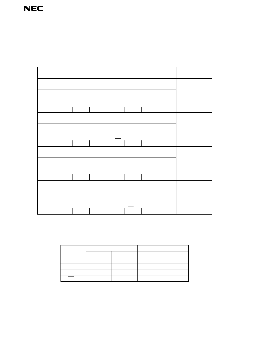
Pin No.
Symbol
Function
Output Format
When Reset
1
K
I/O0
-K
I/O7
CMOS
High-level output
2
push-pull
Note 1
15-20
3
S
0
--
High-impedance
(OFF mode)
4
S
1
/LED
CMOS push-pull
High-level output
(LED)
5
REM
CMOS push-pull
Low-level output
6
V
DD
--
--
7
X
OUT
--
Low level
8
X
IN
(oscillation stopped)
9
GND
--
--
10
RESET
--
--
11-14
K
I0
-K
I3
Note 2
--
Input (low-level)
Notes 1. Be careful about this because the drive capability of the low-level output side is held low.
2. In order to prevent malfunction, be sure to input a low level to more than one of pins K
I0
to K
I3
when
reset is released (when RESET pin changes from low level to high level, or POC is released due to
supply voltage startup).
These pins refer to the 8-bit I/O ports. I/O switching can
be made in 8-bit units.
In INPUT mode, a pull-down resistor is added.
In OUTPUT mode, they can be used as the key scan
output of the key matrix.
Refers to the input port.
Can also be used as the key return input of the key
matrix.
In INPUT mode, the availability of the pull-down resistor
of the S
0
and S
1
ports can be specified by software in
terms in 2-bit units.
If INPUT mode is canceled by software, this pin is placed
in OFF mode and enters the high-impedance state.
Refers to the I/O port.
In INPUT mode (S
1
), this pin can also be used as the key
return input of the key matrix.
The availability of the pull-down resistor of the S
0
and S
1
ports can be specified by software in 2-bit units.
In OUTPUT mode (LED), it becomes the remote control
transmission display output (active low). When the
remote control carrier is output from the REM output, this
pin outputs the low level from the LED output synchronously
with the REM signal.
Refers to the infrared remote control transmission output.
The output is active high.
Carrier frequency: f
X
/8, f
X
/64, f
X
/96, high-level, f
X
/16,
f
X
/128, f
X
/192 (usable on software)
Refers to the power supply.
These pins are connected to system clock ceramic
resonators.
Refers to the ground.
Normally, this pin is a system reset input. By inputting
a low level, the CPU can be reset. When resetting with
the POC circuit (mask option) a low level is output. A
pull-up resistor is incorporated.
These pins refer to the 4-bit input ports.
They can be used as the key return input of the key
matrix.
The use of the pull-down resistor can be specified by
software in 4-bit units.

7
µ
PD62
Data Sheet U14208EJ1V0DS00
N-ch
P-ch
POC circuit
Internal reset signal
other than POC
Input buffer
V
DD
Mask option
P-ch
N-ch
V
DD
Output
latch
Carrier
generator
data
1.2 INPUT/OUTPUT Circuits of Pins
The input/output circuits of the
µ
PD62 pins are shown in partially simplified forms below.
(1) K
I/O0
-K
I/O7
(4) S
0
(5) S
1
/LED
Note The drive capability is held low.
(2) K
I0
-K
I3
(3) REM
(6) RESET
P-ch
N-ch
Note
N-ch
V
DD
Output
latch
Input buffer
data
output
disable
Selector
N-ch
Input buffer
pull-down flag
standby
release
OFF mode
pull-down flag
N-ch
standby
release
Input buffer
P-ch
N-ch
N-ch
V
DD
REM
output latch
Input buffer
output
disable
pull-down flag
standby
release

8
µ
PD62
Data Sheet U14208EJ1V0DS00
1.3 Dealing with Unused Pins
The following connections are recommended for unused pins.
Table 1-1. Connections for Unused Pins
Pin
Connection
Inside the microcontroller
Outside the microcontroller
K
I/O
INPUT mode
--
Leave open
OUTPUT mode
High-level output
REM
--
S
1
/LED
OUTPUT mode (LED) setting
S
0
OFF mode setting
Directly connect these
K
I
--
pins to GND
RESET
Note
Built-in POC circuit
Leave open
Note If the circuit is an applied one requiring high reliability, be sure to design it in such a manner that the RESET
signal is entered externally.
Caution The I/O mode and the terminal output level are recommended to be fixed by setting them
repeatedly in each loop of the program.

9
µ
PD62
Data Sheet U14208EJ1V0DS00
2. INTERNAL CPU FUNCTIONS
2.1 Program Counter (PC): 10 Bits
Refers to the binary counter that holds the address information of the program memory.
Figure 2-1. Program Counter Organization
PC9
PC0
PC8
PC7
PC6
PC5
PC4
PC3
PC2
PC1
PC
The program counter contains the address of the instruction that should be executed next. Normally, the counter
contents are automatically incremented in accordance with the instruction length (byte count) each time an
instruction is executed.
However, when executing JUMP instructions (JMP, JC, JNC, JF, JNF), the program counter contains the jump
destination address written in the operand.
When executing the subroutine call instruction (CALL), the call destination address written in the operand is
entered in the PC after the PC contents at the time are saved in the address stack register (ASR). If the return
instruction (RET) is executed after the CALL instruction is executed, the address saved in the ASR is restored to
the PC.
When reset, the value of the program counter becomes "000H".
2.2 Stack Pointer (SP): 1 Bit
Refers to the 1-bit register which holds the status of the address stack register.
The stack pointer contents are incremented when the call instruction (CALL) is executed; they are decremented
when the return instruction (RET) is executed.
When reset, the stack pointer contents are cleared to "0".
When the stack pointer overflows (stack level 2 or more) or underflows, the CPU is hung up thus a system reset
signal is generated and the PC becoming "000H".
As no instruction is available to set a value directly for the stack pointer, it is not possible to operate the pointer
by means of a program.
2.3 Address Stack Register (ASR (RF)): 10 Bits
The address stack register saves the return address of the program after a subroutine call instruction is executed.
The low-order 8 bits are arranged in the RF of the data memory as a dual-function RAM. The register holds
the ASR value even after the RET is executed.
When reset, it holds the previous data (undefined when turning on the power).
Caution If the RF is accessed as the data memory, the high-order 2 bits of the ASR become undefined.
Figure 2-2. Address Stack Register Organization
ASR9
ASR8
ASR7
ASR6
ASR5
ASR4
ASR3
ASR2
ASR1
ASR0
ASR
RF
10
µ
PD62
Data Sheet U14208EJ1V0DS00
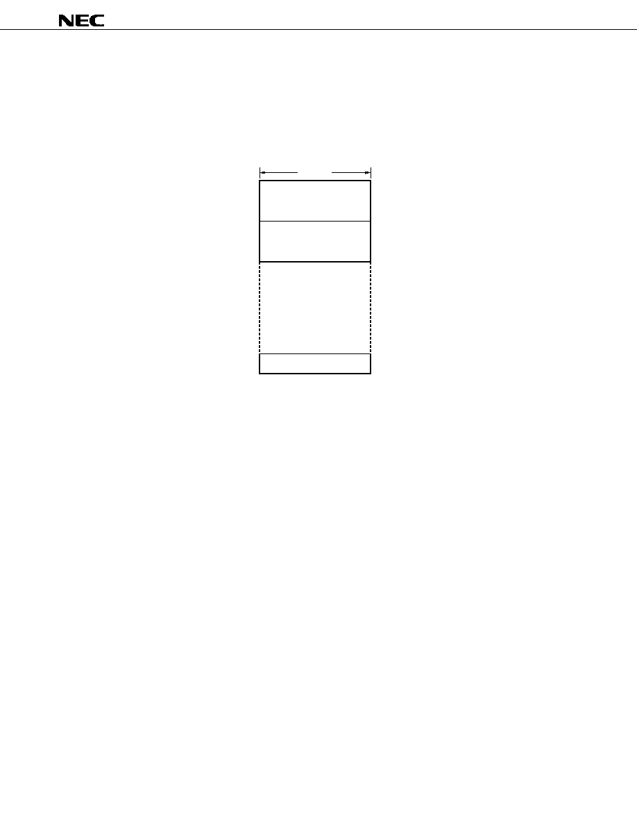
2.4 Program Memory (ROM): 512 steps
◊
10 bits
The ROM consists of 10 bits per step, and is addressed by the program counter.
The program memory stores programs and table data, etc.
The 22 steps from 3EAH to 3FFH cannot be used in the test program area.
Figure 2-3. Program Memory Map
000H
0FFH
100H
1FFH
10 bits
Unmounted area
Note
3EAH
3FFH
Test program area
Note
200H
3E9H
Note The unmounted area and the test program area are so designed that a program or data placed in either
of them by mistake is returned to the 000H address.
2.5 Data Memory (RAM): 32
◊
4 Bits
The data memory, which is a static RAM consisting of 32
◊
4 bits, is used to retain processed data. The data
memory is sometimes processed in 8-bit units. R0 can be used as the ROM data pointer.
RF is also used as the ASR.
When reset, R0 is cleared to "00H" and R1 to RF retain the previous data (undefined when turning on the power).
11
µ
PD62
Data Sheet U14208EJ1V0DS00
Figure 2-4. Data Memory Organization
R0
R1
R2
R3
R4
R5
R6
R7
R8
R9
RA
RB
RC
RD
RE
RF
R
10
R
00
R
11
R
01
R
12
R
02
R
13
R
03
R
14
R
04
R
15
R
05
R
16
R
06
R
17
R
07
R
18
R
08
R
19
R
09
R
1A
R
0A
R
1B
R
0B
R
1C
R
0C
R
1D
R
0D
R
1E
R
0E
R
1F
R
0F
DP (refer to 2.6 Data Pointer (DP))
ASR (refer to 2.3 Address Stack Register (ASR (RF)))
R
1n
(high-order 4 bits) R
0n
(low-order 4 bits)
2.6 Data Pointer (DP): 10 Bits
The ROM data table can be referenced by setting the ROM address in the data pointer to call the ROM contents.
The low-order 8 bits of the ROM address are specified by R0 of the data memory; and the high-order 2 bits by
bits 4 and 5 of the P3 register (CR0).
When reset, the pointer contents become "000H".
Figure 2-5. Data Pointer Organization
2.7 Accumulator (A): 4 Bits
The accumulator, which refers to a register consisting of 4 bits, plays a leading role in performing various
operations.
When reset, the accumulator contents are left undefined.
Figure 2-6. Accumulator Organization
A
3
A
2
A
1
A
0
A
R
00
DP
9
DP
8
DP
7
DP
6
DP
5
DP
4
DP
3
DP
2
DP
1
DP
0
R
10
P3
R0
b
4
b
5
P3
Register
12
µ
PD62
Data Sheet U14208EJ1V0DS00
2.8 Arithmetic and Logic Unit (ALU): 4 Bits
The arithmetic and logic unit (ALU), which refers to an arithmetic circuit consisting of 4 bits, executes simple
manipulations with priority given to logical operations.
2.9 Flags
2.9.1 Status flag (F)
Pin and timer statuses can be checked by executing the STTS instruction to check the status flag.
The status flag is set (to 1) in the following cases.
∑ If the condition specified with the operand is met when the STTS instruction has been executed
∑ When STANDBY mode is canceled.
∑ When the cancelation condition is met at the point of executing the HALT instruction. (In this case, the system
is not placed in STANDBY mode.)
Conversely, the status flag is cleared (to 0) in the following cases:
∑ If the condition specified with the operand is not met when the STTS instruction has been executed.
∑ When the status flag has been set (to 1), the HALT instruction executed, but the cancelation condition is not
met at the point of executing the HALT instruction. (In this case, the system is not placed in STANDBY mode.)
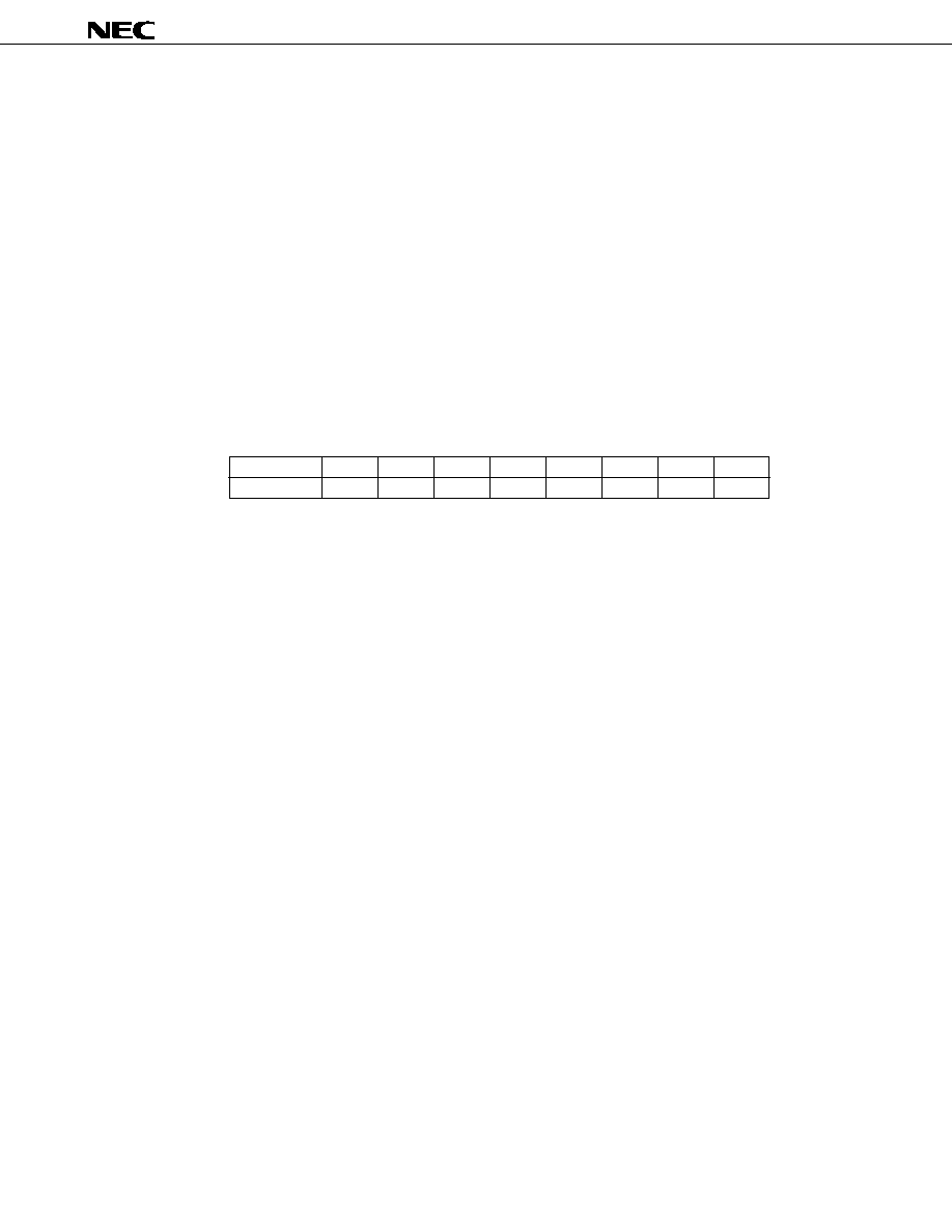
Table 2-1. Conditions for Status Flag (F) to be Set by STTS Instruction
Operand Value of STTS Instruction
Condition for Status Flag (F) to be Set
b
3
b
2
b
1
b
0
0
0
0
0
High level is input to at least one of K
I
pins.
0
1
1
High level is input to at least one of K
I
pins.
1
1
0
High level is input to at least one of K
I
pins.
1
0
1
The down counter of the timer is 0.
1
Either of the combinations
[The following condition is added in addition to the above.]
of b
2
, b
1
, and b
0
above.
High level is input to at least one of S
0
and S
1
pins.

13
µ
PD62
Data Sheet U14208EJ1V0DS00
2.9.2 Carry flag (CY)
The carry flag is set (to 1) in the following cases:
∑ If the ANL instruction or the XRL instruction is executed when bit 3 of the accumulator is "1" and bit 3 of the
operand is "1".
∑ If the RL instruction or the RLZ instruction is executed when bit 3 of the accumulator is "1".
∑ If the INC instruction or the SCAF instruction is executed when the value of the accumulator is 0FH.
The carry flag is cleared (to 0) in the following cases:
∑ If the ANL instruction or the XRL instruction is executed when at least either bit 3 of the accumulator or bit
3 of the operand is "0".
∑ If the RL instruction or the RLZ instruction is executed when bit 3 of the accumulator is "0".
∑ If the INC instruction or the SCAF instruction is executed when the value of the accumulator is other than 0FH.
∑ If the ORL instruction is executed.
∑ When Data is written to the accumulator by the MOV instruction or the IN instruction.
14
µ
PD62
Data Sheet U14208EJ1V0DS00
3. PORT REGISTERS (PX)
The K
I/O
port, the K
I
port, the special ports (S
0
, S
1
/LED), and the control register are treated as port registers.
At reset, port register values are shown below.
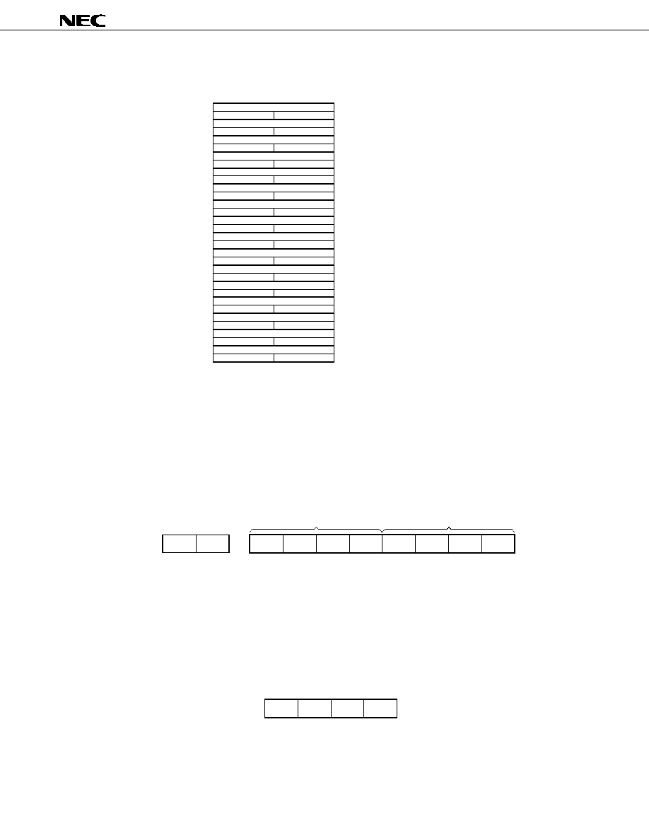
Figure 3-1. Port Register Organization
Note
◊
: Refers to the value based on the K
I
pin state.
Table 3-1. Relationship between Ports and their Read/Write
Port Name
INPUT Mode
OUTPUT Mode
Read
Write
Read
Write
K
I/O
Pin state
Output latch
Output latch
Output latch
K
I
Pin state
--
--
--
S
0
Pin state
--
Note
--
S
1
/LED
Pin state
--
Pin state
--
Note When in OFF mode, "1" is normally read.
Port Register
P0
K
I/O7
P
00
At Reset
FFH
K
I/O6
K
I/O5
K
I/O4
K
I/O3
K
I/O2
K
I/O1
K
I/O0
P
10
P1
K
I3
P
01
◊
FH
Note
K
I2
K
I1
K
I0
S
1
/LED
S
0
1
1
P
11
P3 (Control register 0)
0
P
03
03H
0
DP
9
DP
8
TCTL
CARY
MOD
1
MOD
0
P
13
P4 (Control register 1)
0
P
04
26H
0
K
I
pull-down
S
0
/S
1
pull-down
0
S
1
/LED mode
K
I/O
mode
S
0
mode
P
14
15
µ
PD62
Data Sheet U14208EJ1V0DS00
3.1 K
I/O
Port (P0)
The K
I/O
port is an 8-bit input/output port for key scan output.
INPUT/OUTPUT mode is set by bit 1 of the P4 register.
If a read instruction is executed, the pin state can be read in INPUT mode, whereas the output latch contents
can be read in OUTPUT mode.
If the write instruction is executed, data can be written to the output latch regardless of INPUT or OUTPUT mode.
When reset, the port is placed in OUTPUT mode; and the value of the output latch (P0) becomes 1111 1111B.
The K
I/O
port contains the pull-down resistor, allowing pull-down in INPUT mode only.
Caution During double pressing of a key, a high-level output and a low-level output may coincide with
each other at the K
I/O
port. To avoid this, the low-level output current of the K
I/O
port is held
low. Therefore, be careful when using the K
I/O
port for purposes other than key scan output.
The K
I/O
port is so designed that, even when connected directly to V
DD
within the normal supply
voltage range (V
DD
= 1.8 to 3.6 V), no problem may occur.
Table 3-2. K
I/O
Port (P0)
Bit
b
7
b
6
b
5
b
4
b
3
b
2
b
1
b
0
Name
K
I/O7
K
I/O6
K
I/O5
K
I/O4
K
I/O3
K
I/O2
K
I/O1
K
I/O0
b
0
-b
7
: In reading : In INPUT mode, the K
I/O
pin's state is read.
In OUTPUT mode, the K
I/O
pin's output latch contents are read.
In writing
: Data is written to the K
I/O
pin's output latch regardless of INPUT or OUTPUT mode.
16
µ
PD62
Data Sheet U14208EJ1V0DS00
3.2 K
I
Port/Special Ports (P1)
3.2.1 K
I
port (P
11
: bits 4-7 of P1)
The K
I
port is to the 4-bit input port for key entry.
The pin state can be read.
Software can be used to set the availability of the pull-down resistor of the K
I
port in 4-bit units by means of bit
5 of the P4 register.
When reset, the pull-down resistor is connected.
Table 3-3. K
I
/Special Port Register (P1)
Bit
b
7
b
6
b
5
b
4
b
3
b
2
b
1
b
0
Name
K
I3
K
I2
K
I1
K
I0
S
1
/LED
S
0
(Fixed to "1")
b
2
: In INPUT mode, state of the S
0
pin is read (Read only).
In OFF mode, this bit is fixed to "1".
b
3
: The state of the S
1
/LED pin is read regardless of INPUT/OUTPUT mode (Read only).
b
4
-b
7
: The state of the K
I
pin is read (Read only).
Caution In order to prevent malfunction, be sure to input a low level to more than one of pins K
I0
to K
I3
when reset is released (when RESET pin changes from low level to high level, or POC is released
due to supply voltage startup).
3.2.2 S
0
port (bit 2 of P1)
The S
0
port is the INPUT/OFF mode port.
The pin state can be read by setting this port to INPUT mode with bit 0 of the P4 register.
In INPUT mode, software can be used to set the availability of the pull-down resistor of the S
0
and S
1
/LED port
in 2-bit units by means of bit 4 of the P4 register.
If INPUT mode is canceled (thus set to OFF mode), the pin becomes high-impedance but it also makes that the
through current does not flow internally. In OFF mode, "1" can be read regardless of the pin state.
When reset, it is set to OFF mode, thus becoming high-impedance.
3.2.3 S
1
/LED (bit 3 of P1)
The S
1
/LED port is the input/output port.
It uses bit 2 of the P4 register to set INPUT or OUTPUT mode. The pin state can be read in both INPUT mode
and OUTPUT mode.
When in INPUT mode, software can be used to set the availability of the pull-down resistor of the S
0
and
S
1
/LED ports in 2-bit units by means of bit 4 of the P4 register.
When in OUTPUT mode, the pull-down resistor is automatically disconnected thus becoming the remote control
transmission display pin (refer to 4. TIMER).
When reset, it is placed in OUTPUT mode, and high level is output.
17
µ
PD62
Data Sheet U14208EJ1V0DS00
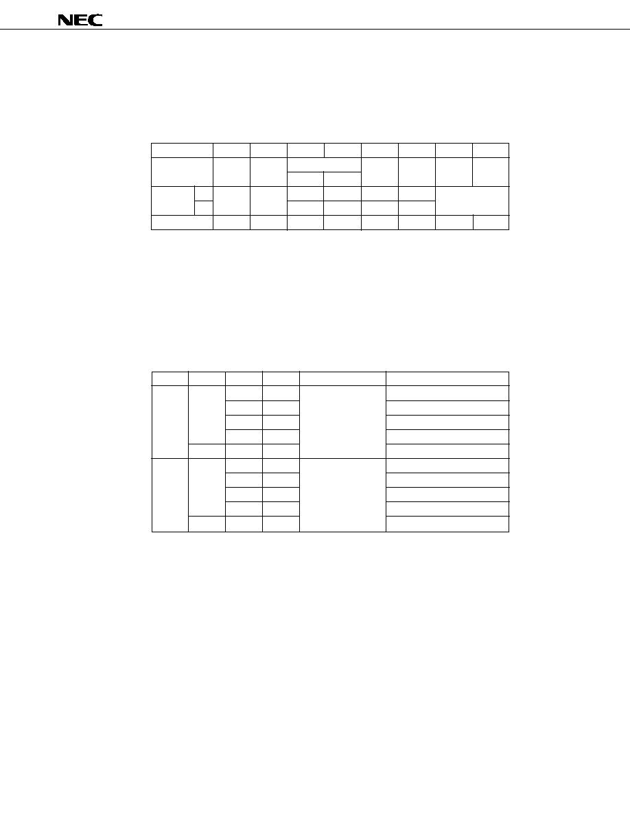
3.3 Control Register 0 (P3)
Control register 0 consists of 8 bits. The contents that can be controlled are as shown below.
When reset, the register becomes 0000 0011B.
Table 3-4. Control Register 0 (P3)
Bit
b
7
b
6
b
5
b
4
b
3
b
2
b
1
b
0
Name
--
--
DP (Data pointer) TCTL
CARY
MOD
1
MOD
0
DP
9
DP
8
Set
0
Fixed
Fixed
0
0
1/1
ON
Refer to Table 3-5.
value
1
to "0"
to "0"
1
1
1/2
OFF
When reset
0
0
0
0
0
0
1
1
b
0
, b
1
: These bits specify the carrier frequency and duty ratio of the REM output.
b
2
: This bit specifies the availability of the carrier of the frequency specified by b
0
and b
1
.
"0" = ON (with carrier); "1" = OFF (without carrier; high level)
b
3
: This bit changes the carrier frequency and the timer clock's frequency division ratio.
"0" = 1/1 (carrier frequency: the specified value of b
0
and b
1
; timer clock: f
X
/64)
"1" = 1/2 (carrier frequency: half of the specified value of b
0
and b
1
; timer clock: f
X
/128)
Table 3-5. Timer Clock and Carrier Frequency Setup
b
3
b
2
b
1
b
0
Timer Clock
Carrier Frequency (Duty Ratio)
0
0
0
0
f
X
/64
f
X
/8 (Duty 1/2)
0
1
f
X
/64 (Duty 1/2)
1
0
f
X
/96 (Duty 1/2)
1
1
f
X
/96 (Duty 1/3)
1
◊
◊
Without carrier (high level)
0
0
0
0
f
X
/128
f
X
/16 (Duty 1/2)
0
1
f
X
/128 (Duty 1/2)
1
0
f
X
/192 (Duty 1/2)
1
1
f
X
/192 (Duty 1/3)
1
◊
◊
Without carrier (high level)
b
4
and b
5
: These bits specify the high-order 2 bits (DP
8
and DP
9
) of ROM's data pointer.
Remark
◊
: don't care

18
µ
PD62
Data Sheet U14208EJ1V0DS00
3.4 Control Register 1 (P4)
Control register 1 consists of 8 bits. The contents that can be controlled are as shown below.
When reset, the register becomes 0010 0110B.
Table 3-6. Control Register 1 (P4)
Bit
b
7
b
6
b
5
b
4
b
3
b
2
b
1
b
0
Name
--
--
K
I
S
0
/S
1
--
S
1
/LED
K
I/O
S
0
Pull-down Pull-down
mode
mode
mode
Set
0
Fixed
Fixed
OFF
OFF
Fixed
S
1
IN
OFF
value
1
to "0"
to "0"
ON
ON
to "0"
LED
OUT
IN
When reset
0
0
1
0
0
1
1
0
b
0
: Specifies the input mode of the S
0
port. "0" = OFF mode (high impedance); "1" = IN (INPUT mode).
b
1
: Specifies the I/O mode of the K
I/O
port.
"0" = IN (INPUT mode); "1" = OUT (OUTPUT mode).
b
2
: Specifies the I/O mode of the S
1
/LED port. "0" = S
1
(INPUT mode); "1" = LED (output mode).
b
4
: Specifies the availability of the pull-down resistor in S
0
/S
1
port INPUT mode. "0" = OFF (unavailable);
"1" = ON (available)
b
5
: Specifies the availability of the pull-down resistor in K
I
port. "0" = OFF (unavailable);
"1" = ON (available).
Remark In OUTPUT mode or in OFF mode, all the pull-down resistors are automatically disconnected.
19
µ
PD62
Data Sheet U14208EJ1V0DS00
4. TIMER
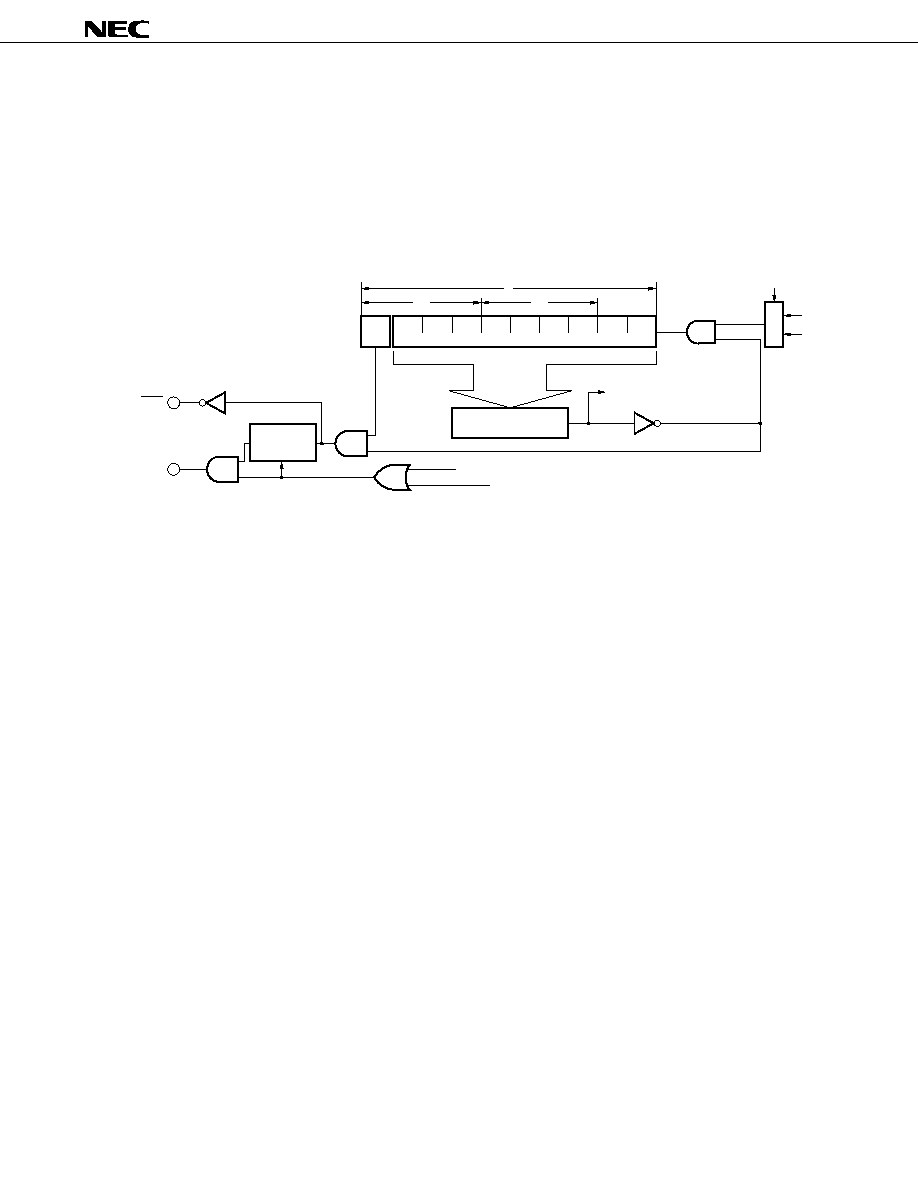
4.1 Timer Configuration
The timer is the block used for creating a remote control transmission pattern. As shown in Figure 4-1, it consists
of a 9-bit down counter (t
8
to t
0
), a flag (t
9
) permitting the 1-bit timer output, and a zero detecting circuit.
Figure 4-1. Timer Configuration
S
1
/LED
REM
Carrier
synchronous
circuit
Bit 2 of control register 0 (P3)
Carrier signal
Zero detecting circuit
9-bit down counter
t
9
t
8
t
7
t
6
t
5
t
4
t
3
t
2
t
1
t
0
T
T1
Bit 3 of control register 0 (P3)
f
X
/64
f
X
/128
Timer operation end signal
(HALT #
◊
101B release
signal)
Count
clock
T0
Selector
20
µ
PD62
Data Sheet U14208EJ1V0DS00
4.2 Timer Operation
The timer starts (counting down) when a value other than 0 is set for the down counter with a timer operation
instruction. The timer operation instructions for making the timer start operation are shown below:
MOV T0, A
MOV T1, A
MOV T, #data10
MOV T, @R0
The down counter is decremented (≠1) in the cycle of 64/f
X
or 128/f
X
Note
. If the value of the down counter becomes
0, the zero detecting circuit generates the timer operation end signal to stop the timer operation. At this time, if
the timer is in HALT mode (HALT #
◊
101B) waiting for the timer to stop its operation, the HALT mode is canceled
and the instruction following the HALT instruction is executed. The output of the timer operation end signal is
continued while the down counter is 0 and the timer is stopped. There is the following relational expression between
the timer's time and the down counter's set value.
Timer time = (Set value + 1)
◊
64/f
X
(or 128/f
X
Note
)
Note This becomes 128/f
X
if bit 3 of the control register is set (to 1).
By setting 1 for the flag (t
9
) which enables the timer output, the timer can output its operation status from the
S
1
/LED pin and the REM pin. The REM pin can also output the carrier while the timer is in operation.
Table 4-1. Timer Output (at t
9
= 1)
S
1
/LED Pin
REM Pin
Timer operating
L
H (or carrier output
Note
)
Timer halting
H
L
Note The carrier output results if bit 2 of the control register 0 is cleared (to 0).
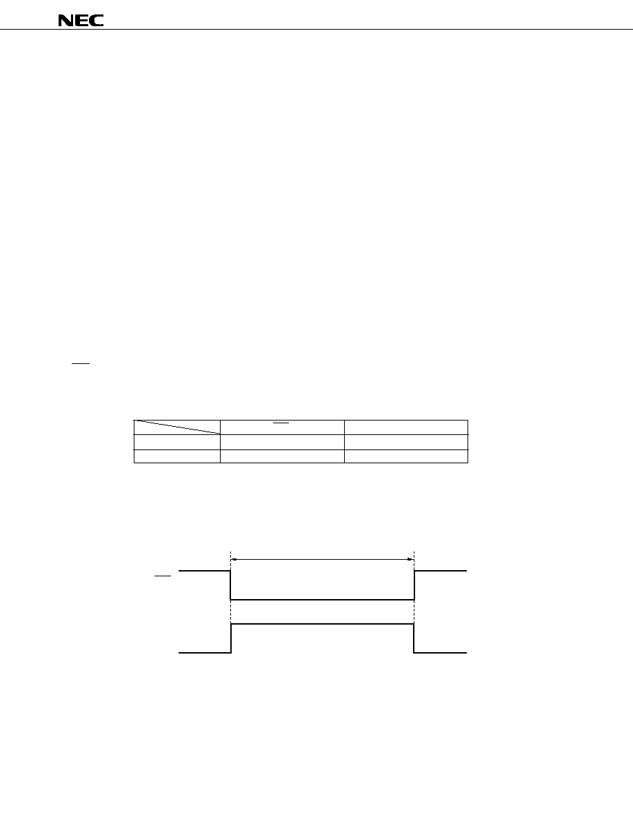
Figure 4-2. Timer Output (when carrier is not output)
Timer value: (set value + 1)
◊
64/f
X
(or 128/f
X
)
LED
REM
21
µ
PD62
Data Sheet U14208EJ1V0DS00
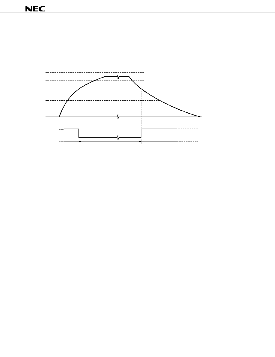
4.3 Carrier Output
The carrier for remote-controlled transmission can be output from the REM pin by clearing (to 0) bit 2 of the control
register 0.
As shown in Figure 4-3, in the case where the timer stops when the carrier is at a high level, the carrier continues
to be output until its next fall and then stops due to the function of the carrier synchronous circuit. When the timer
starts operation, however, the high-level width of the first carrier may become shorter than the specified width.
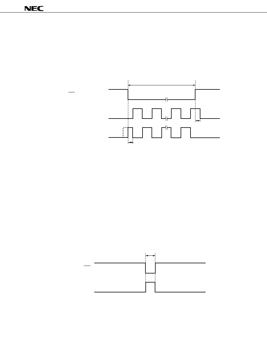
Figure 4-3. Timer Output (when carrier is output)
Timer value: (Set value+1)
◊
64/f
X
(or 128/f
X
)
LED
REM (at low-level start)
REM (at high-level start)
Note 1
Note 2
Notes 1. Error when the REM output ends: Lead by "the carrier's low-level width" to lag by "the carrier's high-
level width"
2. Error of the carrier's high-level width: 0 to "the carrier's high-level width"
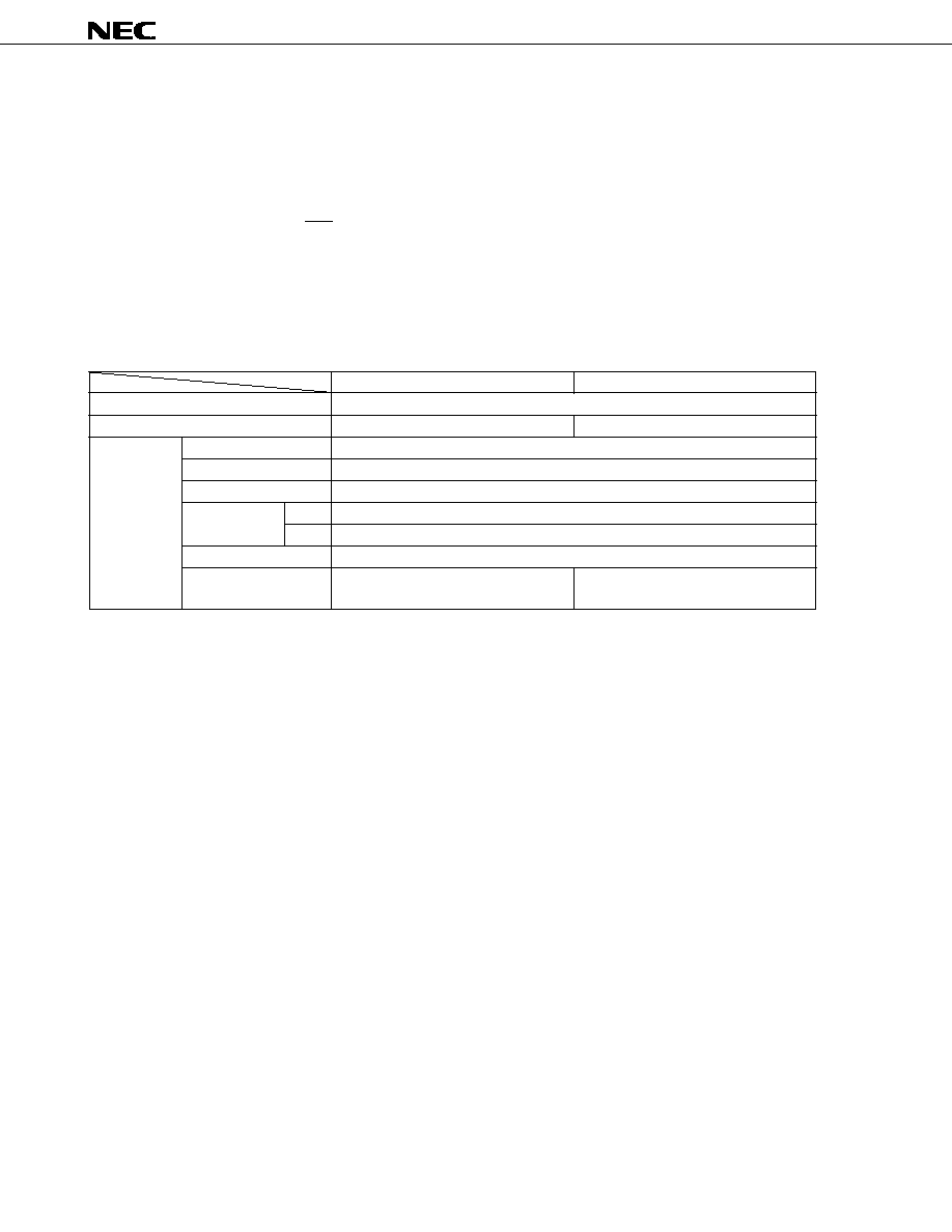
4.4 Software Control of Timer Output
The timer output can be controlled by software. As shown in Figure 4-4, the pulse with a minimum width of 1-
instruction cycle (64/f
X
) can be output.
Figure 4-4. Pulse Output of 1-Instruction Cycle Width
MOV T, #0000000000B; low-level output from the REM pin
MOV T, #1000000000B; high-level output from the REM pin
MOV T, #0000000000B; low-level output from the REM pin
64/f
X
LED
REM
...
...
...
22
µ
PD62
Data Sheet U14208EJ1V0DS00
5. STANDBY FUNCTION
5.1 Outline of Standby Function
To save current consumption, two types of standby modes, i.e., HALT mode and STOP mode, are made available.
In STOP mode, the system clock stops oscillation. At this time, the X
IN
and X
OUT
pins are fixed at a low level.
In HALT mode, CPU operation halts, while the system clock continues oscillation. When in HALT mode, the
timer (including REM output and LED output) operates.
In either STOP mode or HALT mode, the statuses of the data memory, accumulator, and port register, etc.
immediately before the standby mode is set are retained. Therefore, make sure to set the port status for the system
so that the current consumption of the whole system is suppressed before the standby mode is set.
Table 5-1. Statuses During Standby Mode
STOP Mode
HALT Mode
Setting instruction
HALT instruction
Clock oscillation circuit
Oscillation stopped
Oscillation continued
CPU
∑ Operation halted
Data memory
∑ Immediately preceding status retained
Operation
Accumulator
∑ Immediately preceding status retained
statuses
Flag
F
∑ 0 (When 1, the flag is not placed in the standby mode.)
CY
∑ Immediately preceding status retained
Port register
∑ Immediately preceding status retained
Timer
∑ Operation halted
∑ Operable
(The count value is reset to "0")
Cautions 1. Write the NOP instruction as the first instruction after STOP mode is canceled.
2. When standby mode is canceled, the status flag (F) is set (to 1).
3. If, at the point the standby mode has been set, its cancelation condition is met, then the
system is not placed in the standby mode. However, the status flag (F) is set (1).
23
µ
PD62
Data Sheet U14208EJ1V0DS00
5.2 Standby Mode Setup and Release
The standby mode is set with the HALT #b
3
b
2
b
1
b
0
B instruction for both STOP mode and HALT mode. For the
standby mode to be set, the status flag (F) is required to have been cleared (to 0).
The standby mode is released by the release condition specified with the RESET (RESET input; POC) or the
operand of HALT instruction. If the standby mode is released, the status flag (F) is set (to 1).
Even when the HALT instruction is executed in the state that the status flag (F) has been set (to 1), the standby
mode is not set. If the release condition is not met at this time, the status flag is cleared (to 0). If the release condition
is met, the status flag remains set (to 1).
Even in the case when the release condition has been already met at the point that the HALT instruction is
executed, the standby mode is not set. Here, also, the status flag (F) is set (to 1).
Caution Depending on the status of the status flag (F), the HALT instruction may not be executed. Be
careful about this. For example, when setting HALT mode after checking the key status with
the STTS instruction, the system does not enter HALT mode as long as the status flag (F)
remains set (to 1) thus sometimes performing an unintended operation. In this case, the
intended operation can be realized by executing the STTS instruction immediately after timer
setting to clear (to 0) the status flag.
Example
STTS
#03H
;To check the K
I
pin status.
MOV
T, #0xxH
;To set the timer
STTS
#05H
;To clear the status flag
(During this time, be sure not to execute an instruction that may set the status flag.)
HALT
#05H
;To set HALT mode
Table 5-2. Addresses Executed After Standby Mode Release
Release Condition
Address Executed After Release
Reset
0 address
Release condition shown in Table 5-3
The address following the HALT instruction
...
...
24
µ
PD62
Data Sheet U14208EJ1V0DS00
Table 5-3. Standby Mode Setup (HALT #b
3
b
2
b
1
b
0
B) and Release Conditions
Operand Value of
HALT Instruction
Setting Mode
Precondition for Setup
Release Condition
b
3
b
2
b
1
b
0
0
0
0
0
STOP
All K
I/O
pins are high-level output.
High level is input to at least one
of K
I
pins.
0
1
1
STOP
All K
I/O
pins are high-level output.
High level is input to at least one
of K
I
pins.
1
1
0
STOP
Note 1
The K
I/O0
pin is high-level output.
High level is input to at least one
of K
I
pins.
1
Any of the
STOP
[The following condition is added in addition to the above.]
combinations of
--
High level is input to at least one
b
2
b
1
b
0
above
of S
0
and S
1
pins
Note 2
.
0/1
1
0
1
HALT
--
When the timer's down counter is 0
Notes 1. When setting HALT #
◊
110B, configure a key matrix by using the K
I/O0
pin and the K
I
pin so that an
internal reset takes effect at the time of program hang-up.
2. At least one of the S
0
and S
1
pins (the pin used for releasing the standby) must be in INPUT mode.
(The internal reset does not take effect even when both pins are in OUTPUT mode.)
Cautions 1. The internal reset takes effect when the HALT instruction is executed with an operand value
other than that above or when the precondition has not been satisfied when executing the
HALT instruction.
2. If STOP mode is set when the timer's down counter is not 0 (timer operating), the system
is placed in STOP mode only after all the 10 bits of the timer's down counter and the timer
output permit flag are cleared to 0.
3. Write the NOP instruction as the first instruction after STOP mode is released.
5.3 Standby Mode Release Timing
(1) STOP Mode Release Timing
Figure 5-1. STOP Mode Cancelation by Release Condition
Caution When a release condition is established in the STOP mode, the device is released from the STOP
mode, and goes into a wait state. At this time, if the release condition is not held, the device
goes into STOP mode again after the wait time has elapsed. Therefore, when releasing the STOP
mode, it is necessary to hold the release condition longer than the wait time.
Wait
(52/f
X
+
)
HALT mode
OPERATING
mode
STOP mode
Oscillation
stopped
Oscillation
OPERATING
mode
Oscillation
HALT instruction
(STOP mode)
Standby
release signal
Clock
: Oscillation growth time
25
µ
PD62
Data Sheet U14208EJ1V0DS00
Figure 5-2. STOP Mode Release by RESET Input
(2) HALT Mode Release Timing
Figure 5-3. HALT Mode Release by Cancelation Condition
HALT mode
OPERATING mode
Oscillation
OPERATING
mode
HALT instruction
(HALT mode)
Standby
release signal
Clock
Figure 5-4. HALT Mode Release by RESET Input
Wait
(246 to 694)/f
X
+
HALT mode
OPERATING
mode
STOP
mode
Oscillation stopped
Oscillation
OPERATING
mode
Oscillation
HALT instruction
(STOP mode)
RESET
Clock
Reset
0 address start
: Oscillation growth time
Wait
(246 to 694)/f
X
+
HALT mode
OPERATING
mode
HALT mode
Oscillation
stopped
Oscillation
OPERATING
mode
Oscillation
HALT instruction
(HALT mode)
RESET
Clock
Reset
0 address start
: Oscillation growth time
26
µ
PD62
Data Sheet U14208EJ1V0DS00
6. RESET PIN
The system reset takes effect by inputting low level to the RESET pin.
While the RESET pin is at low level, the system clock oscillator is stopped and the X
IN
and X
OUT
pins are fixed
to the GND.
If the RESET pin is raised from low level to high level, it executes the program from the 0 address after counting
246 to 694 of the system clock (f
X
).
Figure 6-1. Reset Operation by RESET Input
The RESET pin outputs low level when the POC circuit (mask option) is in operation.
Caution When connecting a reset IC to the RESET pin, ensure that the IC is of the N-ch open drain output
type.
Table 6-1. Hardware Statuses After Reset
∑ RESET Input in Operation
∑ RESET Input During STANDBY Mode
Hardware
∑ Resetting by Internal POC Circuit in Operation
∑ Resetting by the Internal POC Circuit During
∑ Resetting by Other Factors
Note 1
STANDBY Mode
PC (10 bits)
000H
SP (1 bit)
0B
Data
R0 = DP
000H
memory
R1-RF
Undefined
Previous status retained
Accumulator (A)
Undefined
Status flag (F)
0B
Carry flag (CY)
0B
Timer (10 bits)
000H
Port register
P0
FFH
P1
◊
FH
Note 2
Control register P3
03H
P4
26H
Notes 1. The following resets are available.
∑ Reset when executing the HALT instruction (when the operand value is illegal or does not satisfy
the precondition)
∑ Reset when executing the RLZ instruction (when A = 0)
∑ Reset by stack pointer's overflow or underflow
2. Refers to the value by the K
I
pin status.
In order to prevent malfunction, be sure to input a low level to more than one of pins K
I0
to K
I3
when
reset is released (when RESET pin changes from low level to high level, or POC is released due to
supply voltage startup).
Wait
(246 to 694)/f
X
+
HALT mode
Oscillation
stopped
OPERATING mode or
STANDBY mode
RESET
0 address start
: Oscillation growth time
OPERATING
mode

27
µ
PD62
Data Sheet U14208EJ1V0DS00
7. POC CIRCUIT (MASK OPTION)
The POC circuit monitors the power supply voltage and applies an internal reset in the microcontroller at the
time of battery replacement. If the applied circuit satisfies the following conditions, the POC circuit can be
incorporated by the mask option.
∑ High reliability is not required.
∑ Clock frequency f
X
=2.4 to 4 MHz
∑ Operating ambient temperature T
A
= ≠20 to +70 ∞C
Cautions 1. The one-time PROM product (
µ
PD6P4B) originally contains the POC circuit.
2. There are cases in which the POC circuit cannot detect a low power supply voltage of less
than 1 ms. Therefore, if the power supply voltage has become low for a period of less than
1 ms, the POC circuit may malfunction because it does not generate an internal reset signal.
3. Clock oscillation is stopped by the resonator due to low power supply voltage before the
POC circuit generates the internal reset signal. In this case, malfunction may result, for
example when the power supply voltage is recovered after the oscillation is stopped. This
type of phenomenon takes place because the POC circuit does not generate an internal reset
signal (because the power supply voltage recovers before the low power supply voltage is
detected) even though the clock has stopped. If, by any chance, a malfunction has taken
place, remove the battery for a short time and put it back. In most cases, normal operation
will be resumed.
4. If the applied circuit does not satisfy the conditions above, design the applied circuit in such
a manner that the reset takes effect without failure within the power supply voltage range
by means of an external reset circuit.
5. In order to prevent malfunction, be sure to input a low level to more than one of pins K
I0
to
K
I3
when reset is released (when RESET pin changes from low level to high level, or POC
is released due to supply voltage startup).
Remarks 1. It is recommended that the POC circuit be incorporated when applied circuits are infrared remote-
control transmitters for household appliances.
2. Even when a POC circuit is incorporated, the externally entered RESET input is valid with the OR
condition; therefore, the POC circuit and the RESET input can be used at the same time. However,
if the POC circuit detects a low power supply voltage, the RESET pin will be forced to low level;
therefore, use an N-ch open drain output or NPN open collector output for the external reset circuit.
28
µ
PD62
Data Sheet U14208EJ1V0DS00
7.1 Functions of POC Circuit
The POC circuit has the following functions:
∑ Generates an internal reset signal when V
DD
V
POC
.
∑ Cancels an internal reset signal when V
DD
> V
POC
.
Here, V
DD
: power supply voltage, V
POC
: POC-detected voltage.
Notes 1. In reality, there is the oscillation stabilization wait time until the circuit is switched to OPERATING
mode. The oscillation stabilization wait time is about 252/f
X
to 700/f
X
(when about 70 to 190
µ
s; f
X
= 3.64 MHz).
2. For the POC circuit to generate an internal reset signal when the power supply voltage has fallen,
it is necessary for the power supply voltage to be kept less than the V
POC
for the period of 1 ms or
more. Therefore, in reality, there is the time lag of up to 1 ms until the reset takes effect.
3. The POC-detected voltage (V
POC
) varies between 0.9 to 2.2 V; thus, the resetting may be canceled
at a power supply voltage smaller than the assured range (V
DD
= 1.8 to 3.6 V). However, as long as
the conditions for operating the POC circuit are met, the actual lowest operating power supply voltage
becomes lower than the POC-detected voltage. Therefore, there is no malfunction occurring due to
the shortage of power supply voltage. However, malfunction for such reasons as the clock not
oscillating due to low power supply voltage may occur (refer to Cautions 3. in 7. POC CIRCUIT).
7.2 Oscillation Check at Low Supply Voltage
A reliable resetting operation can be expected of the POC circuit if it satisfies the condition that the clock can
oscillate even at low power supply voltage (the oscillation start voltage of the resonator being even lower than the
POC-detected voltage). Whether this condition is being met or not can be checked by measuring the oscillation
status on a product which actually contains a POC circuit, as follows.
<1> Connect a storage oscilloscope to the X
OUT
pin so that the oscillation status can be measured.
<2> Connect a power supply whose output voltage can be varied and then gradually raise the power supply
voltage V
DD
from 0 V (making sure to avoid V
DD
> 3.6V).
At first (during V
DD
< 0.9 V), the X
OUT
pin is 0 V regardless of the V
DD
. However, at the point that V
DD
reaches
the POC-detected voltage (voltage somewhere between V
POC
= 0.9 to 2.2 V), the voltage of the X
OUT
pin jumps to
about 0.5 V
DD
. Maintain this power supply voltage for a while to measure the waveform of the X
OUT
pin. If, by any
chance, the oscillation start voltage of the resonator is lower than the POC-detected voltage, the growing oscillation
of the X
OUT
pin can be confirmed within several ms after the V
DD
has reached the V
POC
.
V
DD
3.6 V
2.2 V
V
POC
0.9 V
0 V
Internal reset signal
Reset
Operating ambient temperature T
A
= ≠ 20 to + 70∞C
Clock frequency f
X
= 2.4 to 4 MHz
POC-detected voltage V
POC
= 0.9 to 2.2 V
Note 3
t
OPERATING mode
Reset
Note 2
Note 1
29
µ
PD62
Data Sheet U14208EJ1V0DS00
8. SYSTEM CLOCK OSCILLATION CIRCUIT
The system clock oscillation circuit consists of oscillation circuits for ceramic resonators (f
X
= 2.4 to 8 MHz).
Figure 8-1. System Clock
The system clock oscillator stops its oscillation when reset or in STOP mode.
Caution When using the system clock oscillator, wire area indicated by the dotted-line in the diagram
as follows to reduce the effects of the wiring capacitance, etc.
∑
Make the wiring as short as possible.
∑
Do not allow the wiring to intersect other signal lines. Do not wire close to lines through
which large fluctuating currents flow.
∑
Make sure that the point where the oscillation circuit capacitor is installed is always at the
same electric potential as the ground. Never earth with a ground pattern through which large
currents flow.
∑
Do not extract signals from the oscillator.
PD62
X
OUT
X
IN
GND
Ceramic resonator
µ

30
µ
PD62
Data Sheet U14208EJ1V0DS00
9. INSTRUCTION SET
9.1 Machine Language Output by Assembler
The bit length of the machine language of this product is 10 bits per word. However, the machine language that
is output by the assembler is extended to 16 bits per word. As shown in the example below, the expansion is made
by inserting 3-bit extended bits (111) in two locations.
Figure 9-1. Example of Assembler Output (10 bits extended to 16 bits)
<1> In the case of "ANL A, @R0H"
1
1
1 0 1 0
1
0 0 0 0
1 0 1 0
1
0 0 0 0
1 1 1
1 1 1
Extended bits
Extended bits
= FAF0
<2> In the case of "OUT P0, #data8"
0
0
0 1 1 0
1
1 0 0 0
0 1 1 0
1
1 0 0 0
1 1 1
1 1 1
Extended bits
Extended bits
= E6F8

31
µ
PD62
Data Sheet U14208EJ1V0DS00
9.2 Circuit Symbol Description
A
: Accumulator
ASR
: Address Stack Register
addr
: Program memory address
CY
: Carry flag
data4
: 4-bit immediate data
data8
: 8-bit immediate data
data10
: 10-bit immediate data
F
: Status flag
PC
: Program Counter
Pn
: Port register pair (n = 0, 1, 3, 4)
P0n
: Port register (low-order 4 bits)
P1n
: Port register (high-order 4 bits)
ROMn
: Bit n of the program memory's (n = 0-9)
Rn
: Register pair
R0n
: Data memory (General-purpose register; n = 0-F)
R1n
: Data memory (General-purpose register; n = 0-F)
SP
: Stack Pointer
T
: Timer register
T0
: Timer register (low-order 4 bits)
T1
: Timer register (high-order 4 bits)
(
◊
)
: Content addressed with
◊
32
µ
PD62
Data Sheet U14208EJ1V0DS00
9.3 Mnemonic to/from Machine Language (Assembler Output) Contrast Table
Accumulator Operation Instructions
Mnemonic
Operand
Instruction Code
Operation
Instruction
Instruction
1st Word
2nd Word
3rd Word
Length
Cycle
ANL
A, R0n
FBEn
(A)
(A)
(Rmn)
m = 0, 1
n = 0-F
1
1
A, R1n
FAEn
CY
A
3
∑ Rmn
3
A, @R0H
FAF0
(A)
(A)
((P13), (R0))
7-4
CY
A
3
∑ ROM
7
A, @R0L
FBF0
(A)
(A)
((P13), (R0))
3-0
CY
A
3
∑ ROM
3
A, #data4
FBF1
data4
(A)
(A)
data4
2
CY
A
3
∑ data4
3
ORL
A, R0n
FDEn
(A)
(A)
(Rmn)
m = 0, 1
n = 0-F
1
A, R1n
FCEn
CY
0
A, @R0H
FCF0
(A)
(A)
((P13), (R0))
7-4
CY
0
A, @R0L
FDF0
(A)
(A)
((P13), (R0))
3-0
CY
0
A, #data4
FDF1
data4
(A)
(A)
data4
2
CY
0
XRL
A, R0n
F5En
(A)
(A)
(Rmn)
m = 0, 1
n = 0-F
1
A, R1n
F4En
CY
A
3
∑ Rmn
3
A, @R0H
F4F0
(A)
(A)
((P13), (R0))
7-4
CY
A
3
∑ ROM
7
A, @R0L
F5F0
(A)
(A)
((P13), (R0))
3-0
CY
A
3
∑ ROM
3
A, #data4
F5F1
data4
(A)
(A)
data4
2
CY
A
3
∑ data4
3
INC
A
F4F3
(A)
(A) + 1
1
if (A) = 0
CY
1
else CY
1
RL
A
FCF3
(A
n+1
)
(A
n
), (A
0
)
(A
3
)
CY
A
3
RLZ
A
FEF3
if A = 0
reset
else (A
n+1
)
(A
n
), (A
0
)
(A
3
)
CY
A
3

33
µ
PD62
Data Sheet U14208EJ1V0DS00
Input/output Instructions
Mnemonic
Operand
Instruction Code
Operation
Instruction
Instruction
1st Word
2nd Word
3rd Word
Length
Cycle
IN
A, P0n
FFF8 + n
--
--
(A)
(Pmn)
m = 0, 1
n = 0, 1, 3, 4
1
1
A, P1n
FEF8 + n
--
--
CY
0
OUT
P0n, A
E5F8 + n
--
--
(Pmn)
(A)
m = 0, 1
n = 0, 1, 3, 4
P1n, A
E4F8 + n
--
--
ANL
A, P0n
FBF8 + n
--
--
(A)
(A)
(Pmn) m = 0, 1 n = 0, 1, 3, 4
A, P1n
FAF8 + n
--
--
CY
A
3
∑ Pmn
3
ORL
A, P0n
FDF8 + n
--
--
(A)
(A)
(Pmn) m = 0, 1 n = 0, 1, 3, 4
A, P1n
FCF8 + n
--
--
CY
0
XRL
A, P0n
F5F8 + n
--
--
(A)
(A)
(Pmn) m = 0, 1 n = 0, 1, 3, 4
A, P1n
F4F8 + n
--
--
CY
A
3
∑ Pmn
3
Mnemonic
Operand
Instruction Code
Operation
Instruction
Instruction
1st Word
2nd Word
3rd Word
Length
Cycle
OUT
Pn, #data8 E6F8 + n
data8
(Pn)
data8
n = 0, 1, 3, 4
2
1
Remark
Pn: P1n-P0n are dealt with in pairs.
Data Transfer Instruction
Mnemonic
Operand
Instruction Code
Operation
Instruction
Instruction
1st Word
2nd Word
3rd Word
Length
Cycle
MOV
A, R0n
FFEn
(A)
(Rmn)
m = 0, 1
n = 0-F
1
1
A, R1n
FEEn
CY
0
A, @R0H
FEF0
(A)
((P13), (R0))
7-4
CY
0
A, @R0L
FFF0
(A)
((P13), (R0))
7-4
CY
0
A, #data4
FFF1
data4
(A)
data4
2
CY
0
R0n, A
E5En
(Rmn)
(A)
m = 0, 1
n = 0-F
1
R1n, A
E4En
Mnemonic
Operand
Instruction Code
Operation
Instruction
Instruction
1st Word
2nd Word
3rd Word
Length
Cycle
MOV
Rn, #data8
E6En
data8
--
(R1n-R0n)
data8
n = 0-F
2
1
Rn, @R0
E7En
--
--
(R1n-R0n)
((P13), (R0))
n = 1-F
1
Remark
Rn: R1n-R0n are dealt with in pairs.
34
µ
PD62
Data Sheet U14208EJ1V0DS00
Branch Instructions
Mnemonic
Operand
Instruction Code
Operation
Instruction
Instruction
1st Word
2nd Word
3rd Word
Length
Cycle
JMP
addr (Page 0)
E8F1
addr
PC
addr
2
1
addr (Page 1)
E9F1
addr
JC
addr (Page 0)
ECF1
addr
if CY = 1
PC
addr
addr (Page 1)
EAF1
addr
else PC
PC + 2
JNC
addr (Page 0)
EDF1
addr
if CY = 0
PC
addr
addr (Page 1)
EBF1
addr
else PC
PC + 2
JF
addr (Page 0)
EEF1
addr
if F = 1
PC
addr
addr (Page 1)
F0F1
addr
else PC
PC + 2
JNF
addr (Page 0)
EFF1
addr
if F = 0
PC
addr
addr (Page 1)
F1F1
addr
else PC
PC + 2
Caution 0 and 1, which refer to PAGE0 and 1, are not written when describing mnemonics.
Subroutine Instructions
Mnemonic
Operand
Instruction Code
Operation
Instruction
Instruction
1st Word
2nd Word
3rd Word
Length
Cycle
CALL
addr (Page 0)
E6F2
E8F1
addr
SP
SP + 1, ASR
PC, PC
addr
3
2
addr (Page 1)
E6F2
E9F1
addr
RET
E8F2
PC
ASR, SP
SP ≠ 1
1
1
Caution 0 and 1, which refer to PAGE0 and 1, are not written when describing mnemonics.
Timer Operation Instructions
Mnemonic
Operand
Instruction Code
Operation
Instruction
Instruction
1st Word
2nd Word
3rd Word
Length
Cycle
MOV
A, T0
FFFF
(A)
(Tn)
n = 0, 1
1
1
A, T1
FEFF
CY
0
T0, A
E5FF
(Tn)
(A)
n = 0, 1
T1, A
F4FF
(T) n
0
Mnemonic
Operand
Instruction Code
Operation
Instruction
Instruction
1st Word
2nd Word
3rd Word
Length
Cycle
MOV
T, #data10
E6FF
data10
(T)
data10
1
1
T, @R0
F4FF
(T)
((P13), (R0))

35
µ
PD62
Data Sheet U14208EJ1V0DS00
Others
Mnemonic
Operand
Instruction Code
Operation
Instruction
Instruction
1st Word
2nd Word
3rd Word
Length
Cycle
HALT
#data4
E2F1
data4
Standby mode
2
1
STTS
#data4
E3F1
data4
if statuses match
F
1
else
F
0
R0n
E3En
if statuses match
F
1
1
else
F
0
n = 0-F
SCAF
FAF3
if A = 0FH
CY
1
else
CY
0
NOP
E0E0
PC
PC + 1
36
µ
PD62
Data Sheet U14208EJ1V0DS00
9.4 Accumulator Operation Instructions
ANL A, R0n
ANL A, R1n
<1> Instruction code
:
1 1 0 1 R
4
0 R
3
R
2
R
1
R
0
<2> Cycle count
: 1
<3> Function
: (A)
(A)
(Rmn)
m = 0, 1
n = 0 to F
CY
A
3
∑ Rmn
3
The accumulator contents and the register Rmn contents are ANDed and the results are entered in the
accumulator.
ANL A, @R0H
ANL A, @R0L
<1> Instruction code
:
1 1 0 1 0/1 1 0 0 0 0
<2> Cycle count
: 1
<3> Function
: (A)
(A)
((P13), (R0))
7-4
(in the case of ANL A, @R0H)
CY
A
3
∑ ROM
7
(A)
(A)
((P13), (R0))
3-0
(in the case of ANL A, @R0L)
CY
A
3
∑ ROM
3
The accumulator contents and the program memory contents specified with the control register P13 and
register pair R
10
-R
00
are ANDed and the results are entered in the accumulator.
If H is specified, b
7
, b
6
, b
5
and b
4
take effect. If L is specified, b
3
, b
2
, b
1
and b
0
take effect.
∑ Program memory (ROM) organization
b
9
b
8
b
7
b
6
b
5
b
4
b
3
b
2
b
1
b
0
H
L
Valid bits at the time of accumulator operation
ANL A, #data4
<1> Instruction code
:
1 1 0 1 1 1 0 0 0 1
0 0 0 0 0 0 d
3
d
2
d
1
d
0
<2> Cycle count
: 1
<3> Function
: (A)
(A)
data4
CY
A
3
∑ data4
3
The accumulator contents and the immediate data are ANDed and the results are entered in the
accumulator.
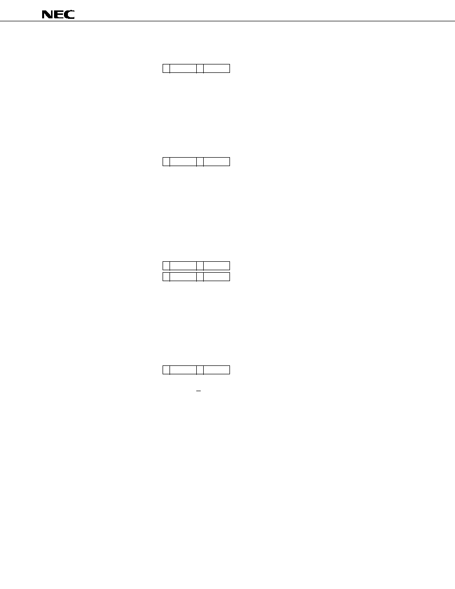
37
µ
PD62
Data Sheet U14208EJ1V0DS00
ORL A, R0n
ORL A, R1n
<1> Instruction code
:
1 1 1 0 R
4
0 R
3
R
2
R
1
R
0
<2> Cycle count
: 1
<3> Function
: (A)
(A)
(Rmn)
m = 0, 1
n = 0 to F
CY
0
The accumulator contents and the register Rmn contents are ORed and the results are entered in the
accumulator.
ORL A, @R0H
ORL A, @R0L
<1> Instruction code
:
1 1 1 0 0/1 1 0 0 0 0
<2> Cycle count
: 1
<3> Function
: (A)
(A)
(P13), (R0))
7-4
(in the case of ORL A, @R0H)
(A)
(A)
(P13), (R0))
3-0
(in the case of ORL A, @R0L)
CY
0
The accumulator contents and the program memory contents specified with the control register P13 and
register pair R
10
-R
00
are ORed and the results are entered in the accumulator.
If H is specified, b
7
, b
6
, b
5
and b
4
take effect. If L is specified, b
3
, b
2
, b
1
and b
0
take effect.
ORL A, #data4
<1> Instruction code
:
1 1 1 0 1 1 0 0 0 1
0 0 0 0 0 0 d
3
d
2
d
1
d
0
<2> Cycle count
: 1
<3> Function
: (A)
(A)
data4
CY
0
The accumulator contents and the immediate data are exclusive-ORed and the results are entered in
the accumulator.
XRL A, R0n
XRL A, R1n
<1> Instruction code
:
1 0 1 0 R
4
0 R
3
R
2
R
1
R
0
<2> Cycle count
: 1
<3> Function
: (A)
(A)
(Rmn)
m = 0, 1
n = 0 to F
CY
A
3
∑ Rmn
3
The accumulator contents and the register Rmn contents are ORed and the results are entered in the
accumulator.
38
µ
PD62
Data Sheet U14208EJ1V0DS00
XRL A, @R0H
XRL A, @R0L
<1> Instruction code
:
1 0 1 0 0/1 1 0 0 0 0
<2> Cycle count
: 1
<3> Function
: (A)
(A)
(P13), (R0))
7-4
(in the case of XRL A, @R0H)
CY
A
3
∑ ROM
7
(A)
(A)
(P13), (R0))
3-0
(in the case of XRL A, @R0L)
CY
A
3
∑ ROM
3
The accumulator contents and the program memory contents specified with the control register P13 and
register pair R
10
-R
00
are exclusive-ORed and the results are entered in the accumulator.
If H is specified, b
7
, b
6
, b
5
, and b
4
take effect. If L is specified, b
3
, b
2
, b
1
, and b
0
take effect.
XRL A, #data4
<1> Instruction code
:
1 0 1 0 1 1 0 0 0 1
0 0 0 0 0 0 d
3
d
2
d
1
d
0
<2> Cycle count
: 1
<3> Function
: (A)
(A)
data4
CY
A
3
∑ data4
3
The accumulator contents and the immediate data are exclusive-ORed and the results are entered in
the accumulator.
INC A
<1> Instruction code
:
1 0 1 0 0 1 0 0 1 1
<2> Cycle count
: 1
<3> Function
: (A)
(A) + 1
if
A = 0
CY
1
else
CY
0
The accumulator contents are incremented (+1).
RL A
<1> Instruction code
:
1 1 1 0 0 1 0 0 1 1
<2> Cycle count
: 1
<3> Function
: (A
n + 1
)
(An), (A
0
)
(A
3
)
CY
A
3
The accumulator contents are rotated anticlockwise bit by bit.
RLZ A
<1> Instruction code
:
1 1 1 1 0 1 0 0 1 1
<2> Cycle count
: 1
<3> Function
: if
A = 0
reset
else
(A
n + 1
)
(An), (A
0
)
(A
3
)
CY
A
3
The accumulator contents are rotated anticlockwise bit by bit.
If A = 0H at the time of command execution, an internal reset takes effect.
39
µ
PD62
Data Sheet U14208EJ1V0DS00
9.5 Input/Output Instructions
IN A, P0n
IN A, P1n
<1> Instruction code
:
1 1 1 1 P
4
1 1 P
2
P
1
P
0
<2> Cycle count
: 1
<3> Function
: (A)
(Pmn)
m = 0, 1
n = 0, 1, 3, 4
CY
0
The port Pmn data is loaded (read) onto the accumulator.
OUT P0n, A
OUT P1n, A
<1> Instruction code
:
0 0 1 0 P
4
1 1 P
2
P
1
P
0
<2> Cycle count
: 1
<3> Function
: (Pmn)
(A)
m = 0, 1
n = 0, 1, 3, 4
The accumulator contents are transferred to port Pmn to be latched.
ANL A, P0n
ANL A, P1n
<1> Instruction code
:
1 1 0 1 P
4
1 1 P
2
P
1
P
0
<2> Cycle count
: 1
<3> Function
: (A)
(A)
(Pmn)
m = 0, 1
n = 0, 1, 3, 4
CY
A
3
∑ Pmn
The accumulator contents and the port Pmn contents are ANDed and the results are entered in the
accumulator.
ORL A, P0n
ORL A, P1n
<1> Instruction code
:
1 1 1 0 P
4
1 1 P
2
P
1
P
0
<2> Cycle count
: 1
<3> Function
: (A)
(A)
(Pmn)
m = 0, 1
n = 0, 1, 3, 4
CY
0
The accumulator contents and the port Pmn contents are ORed and the results are entered in the
accumulator.
XRL A, P0n
XRL A, P1n
<1> Instruction code
:
1 0 1 0 P
4
1 1 P
2
P
1
P
0
<2> Cycle count
: 1
<3> Function
: (A)
(A)
(Pmn)
m = 0, 1
n = 0, 1, 3, 4
CY
A
3
∑ Pmn
The accumulator contents and the port Pmn contents are exclusive-ORed and the results are entered
in the accumulator.
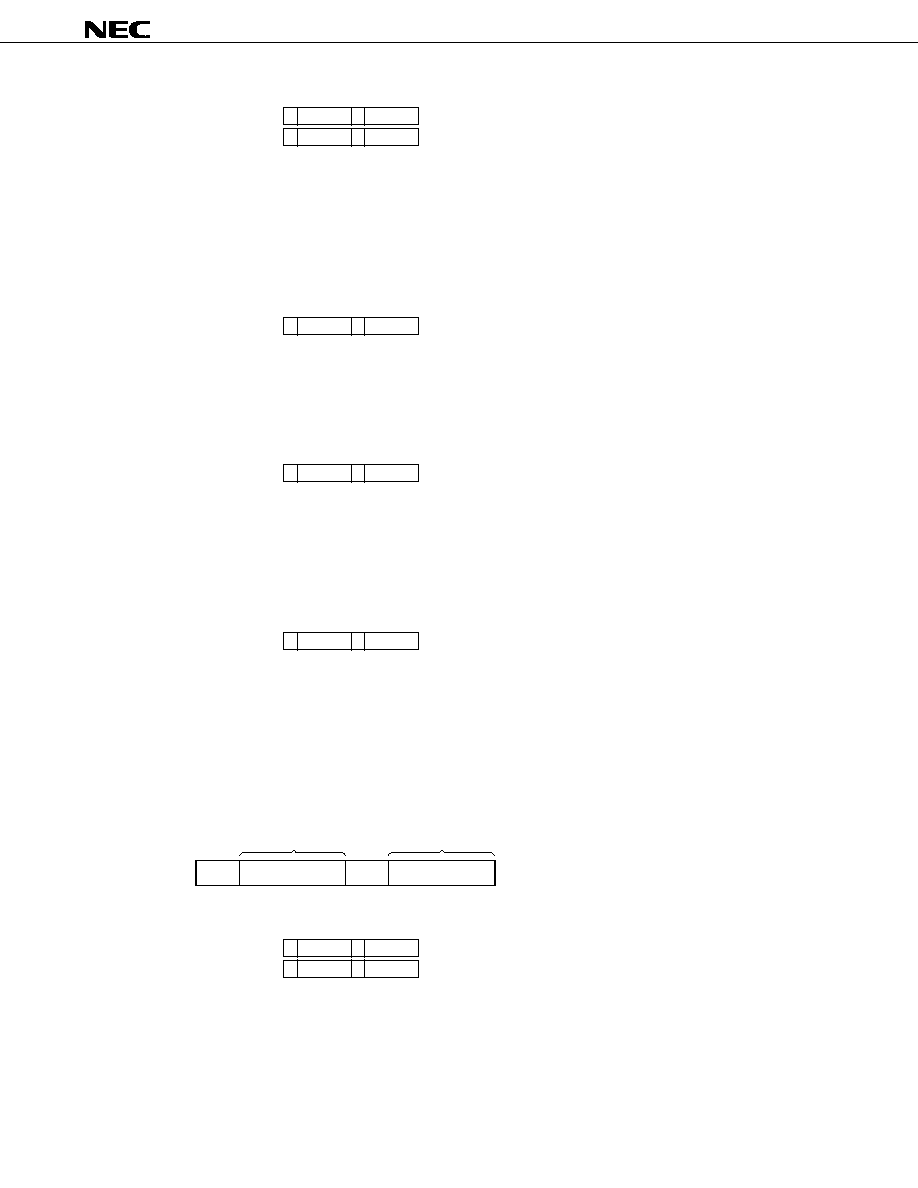
40
µ
PD62
Data Sheet U14208EJ1V0DS00
OUT Pn, #data8
<1> Instruction code
:
0 0 1 1 0 1 1 P
2
P
1
P
0
:
0 d
7
d
6
d
5
d
4
0 d
3
d
2
d
1
d
0
<2> Cycle count
: 1
<3> Function
: (Pn)
data8
n = 0, 1, 3, 4
The immediate data is transferred to port Pn. In this case, port Pn refers to P
1n
-P
0n
operating in pairs.
9.6 Data Transfer Instruction
MOV A, R0n
MOV A, R1n
<1> Instruction code
:
1 1 1 1 R
4
0 R
3
R
2
R
1
R
0
<2> Cycle count
: 1
<3> Function
: (A)
(Rmn)
m = 0, 1
n = 0 to F
CY
0
The register Rmn contents are transferred to the accumulator.
MOV A, @R0H
<1> Instruction code
:
1 1 1 1 0 1 0 0 0 0
<2> Cycle count
: 1
<3> Function
: (A)
((P13), (R0))
7-4
CY
0
The high-order 4 bits (b
7
b
6
b
5
b
4
) of the program memory specified with control register P13 and register
pair R
10
-R
00
are transferred to the accumulator. b
9
is ignored.
MOV A, @R0L
<1> Instruction code
:
1 1 1 1 1 1 0 0 0 0
<2> Cycle count
: 1
<3> Function
: (A)
((P13), (R0))
3-0
CY
0
The low-order 4 bits (b
3
b
2
b
1
b
0
) of the program memory specified with control register P13 and register
pair R
10
-R
00
are transferred to the accumulator. b
8
is ignored.
∑ Program memory (ROM) contents
b
9
b
8
b
7
b
6
b
5
b
4
b
3
b
2
b
1
b
0
@R
0
H
@R
0
L
MOV A, #data4
<1> Instruction code
:
1 1 1 1 1 1 0 0 0 1
:
0 0 0 0 0 0 d
3
d
2
d
1
d
0
<2> Cycle count
: 1
<3> Function
: (A)
data4
CY
0
The immediate data is transferred to the accumulator.
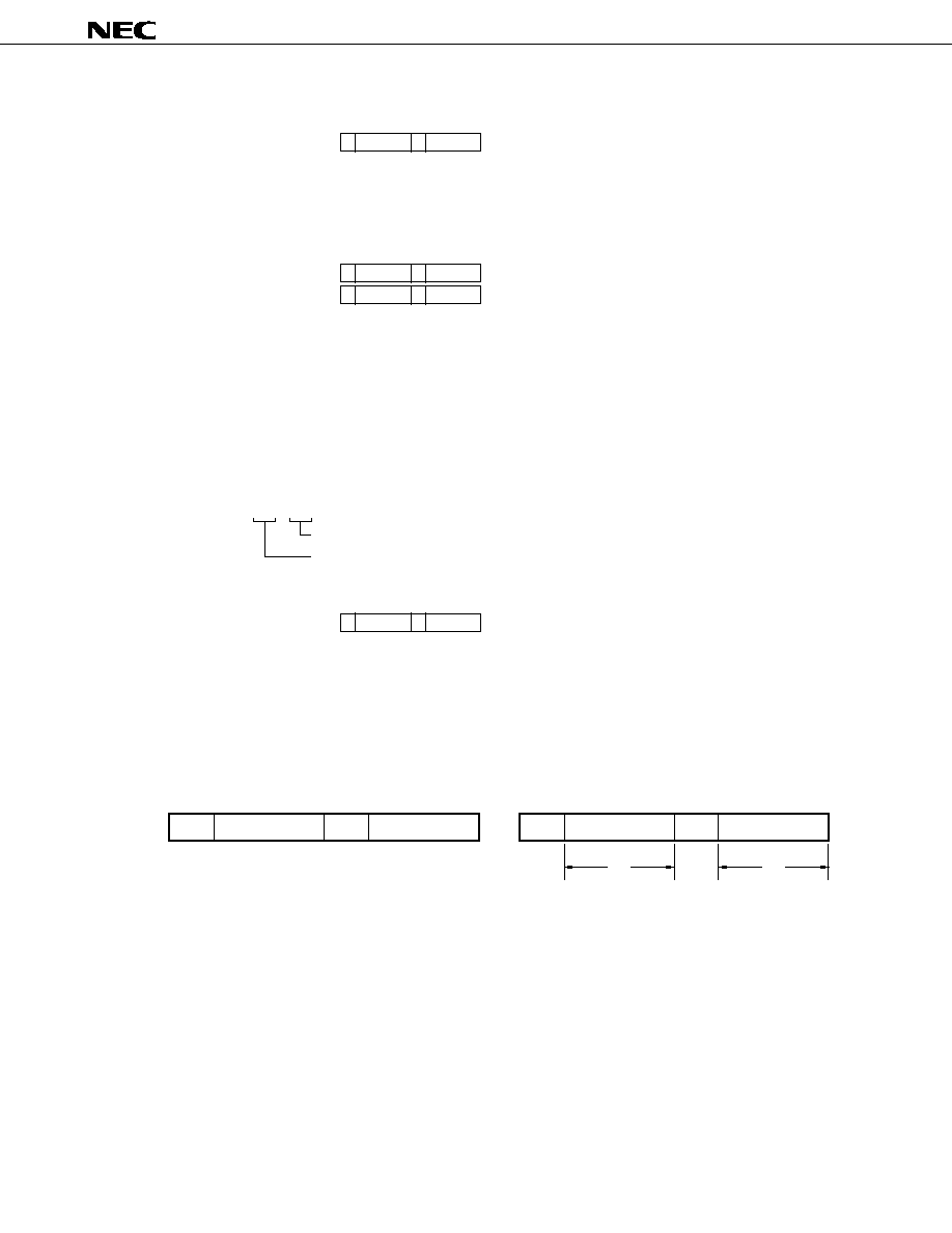
41
µ
PD62
Data Sheet U14208EJ1V0DS00
MOV R0n, A
MOV R1n, A
<1> Instruction code
:
0 0 1 0 R
4
0 R
3
R
2
R
1
R
0
<2> Cycle count
: 1
<3> Function
: (Rmn)
(A)
m = 0, 1
n = 0 to F
The accumulator contents are transferred to register Rmn.
MOV Rn, #data8
<1> Instruction code
:
0 0 1 1 0 0 R
3
R
2
R
1
R
0
:
0 d
7
d
6
d
5
d
4
0 d
3
d
2
d
1
d
0
<2> Cycle count
: 1
<3> Function
: (R1n-R0n)
data8
n = 0 to F
The immediate data is transferred to the register. Using this instruction, registers operate as register
pairs.
The pair combinations are as follows:
R
0
: R
10
- R
00
R
1
: R
11
- R
01
:
R
E
: R
1E
- R
0E
R
F
: R
1F
- R
0F
Lower column
Higher column
MOV Rn, @R0
<1> Instruction code
:
0 0 1 1 1 0 R
3
R
2
R
1
R
0
<2> Cycle count
: 1
<3> Function
: (R1n-R0n)
((P13), R0))
n = 1 to F
The program memory contents specified with control register P13 and register pair R
10
-R
00
are
transferred to register pair R1n-R0n. The program memory consists of 10 bits and has the following
state after the transfer to the register.
b
9
b
8
b
7
b
6
b
5
b
4
b
3
b
2
b
1
b
0
b
9
b
8
b
7
b
6
b
5
b
4
b
3
b
2
b
1
b
0
@R0
R1n
R0n
Program memory
The high-order 2 bits of the program memory address is specified with the control register (P13).
42
µ
PD62
Data Sheet U14208EJ1V0DS00
9.7 Branch Instructions
The program memory consists of pages in steps of 1K (000H to 3FFH). However, as the assembler automatically
performs page optimization, it is unnecessary to designate pages. The pages allowed for each product are as
follows.
µ
PD62 (ROM: 0.5K steps)
: page 0
µ
PD6P4B (PROM: 1K steps) : page 0
JMP addr
<1> Instruction code
: page 0
0 1 0 0 0 1 0 0 0 1
; page 1
0 1 0 0 1 1 0 0 0 1
a
9
a
7
a
6
a
5
a
4
a
8
a
3
a
2
a
1
a
0
<2> Cycle count
: 1
<3> Function
: PC
addr
The 10 bits (PC
9-0
) of the program counter are replaced directly by the specified address addr (a
9
to
a
0
).
JC addr
<1> Instruction code
: page 0
0 1 1 0 0 1 0 0 0 1
; page 1
0 1 0 1 0 1 0 0 0 1
a
9
a
7
a
6
a
5
a
4
a
8
a
3
a
2
a
1
a
0
<2> Cycle count
: 1
<3> Function
: if
CY = 1
PC
addr
else
PC
PC + 2
If the carry flag CY is set (to 1), a jump is made to the address specified with addr (a
9
to a
0
).
JNC addr
<1> Instruction code
: page 0
0 1 1 0 1 1 0 0 0 1
; page 1
0 1 0 1 1 1 0 0 0 1
a
9
a
7
a
6
a
5
a
4
a
8
a
3
a
2
a
1
a
0
<2> Cycle count
: 1
<3> Function
: if
CY = 0
PC
addr
else
PC
PC + 2
If the carry flag CY is cleared (to 0), a jump is made to the address specified with addr (a
9
to a
0
).
JF addr
<1> Instruction code
: page 0
0 1 1 1 0 1 0 0 0 1
; page 1
1 0 0 0 0 1 0 0 0 1
a
9
a
7
a
6
a
5
a
4
a
8
a
3
a
2
a
1
a
0
<2> Cycle count
: 1
<3> Function
: if
F = 1
PC
addr
else
PC
PC + 2
If the status flag F is set (to 1), a jump is made to the address specified with addr (a
9
to a
0
).
JNF addr
<1> Instruction code
: page 0
0 1 1 1 1 1 0 0 0 1
; page 1
1 0 0 0 1 1 0 0 0 1
a
9
a
7
a
6
a
5
a
4
a
8
a
3
a
2
a
1
a
0
<2> Cycle count
: 1
<3> Function
: if
F = 0
PC
addr
else
PC
PC + 2
If the status flag F is cleared (to 0), a jump is made to the address specified with addr (a
9
to a
0
).
43
µ
PD62
Data Sheet U14208EJ1V0DS00
9.8 Subroutine Instructions
The program memory consists of pages in steps of 1K (000H to 3FFH). However, as the assembler automatically
performs page optimization, it is unnecessary to designate pages. The pages allowed for each product are as
follows.
µ
PD62 (ROM: 0.5K steps)
: page 0
µ
PD6P4B (PROM: 1K steps) : page 0
CALL addr
<1> Instruction code
:
0 0 1 1 0 1 0 0 1 0
page 0
0 1 0 0 0 1 0 0 0 1
; page 1
0 1 0 0 1 1 0 0 0 1
a
9
a
7
a
6
a
5
a
4
a
8
a
3
a
2
a
1
a
0
<2> Cycle count
: 2
<3> Function
: SP
SP + 1
ASR
PC
PC
addr
Increments (+1) the stack pointer value and saves the program counter value in the address stack
register. Then, enters the address specified with the operand addr (a
9
to a
0
) into the program counter.
If a carry is generated when the stack pointer value is incremented (+1), an internal reset takes effect.
RET
<1> Instruction code
:
0 1 0 0 0 1 0 0 1 0
<2> Cycle count
: 1
<3> Function
: PC
ASR
SP
SP ≠ 1
Restores the value saved in the address stack register to the program counter. Then, decrements
(≠1) the stack pointer.
If a borrow is generated when the stack pointer value is decremented (≠1), an internal reset takes effect.
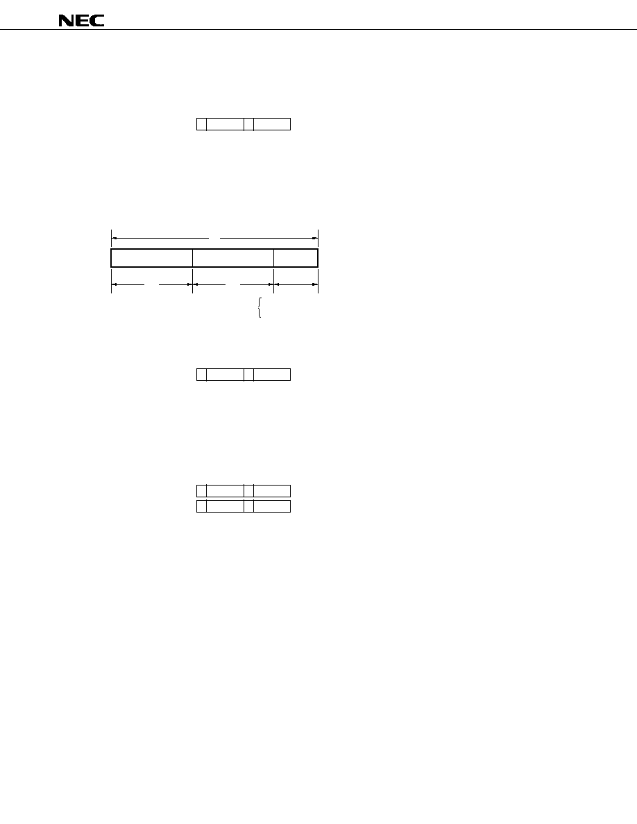
44
µ
PD62
Data Sheet U14208EJ1V0DS00
9.9 Timer Operation Instructions
MOV A, T0
MOV A, T1
<1> Instruction code
:
1 1 1 1 0/1 1 1 1 1 1
<2> Cycle count
: 1
<3> Function
: (A)
(Tn)
n = 0, 1
CY
0
The timer Tn contents are transferred to the accumulator. T1 corresponds to (t
9
, t
8
, t
7
, t
6
); T0 corresponds
to (t
5
, t
4
, t
3
, t
2
).
t
9
t
8
t
7
t
6
t
5
t
4
t
3
t
2
t
1
t
0
Can be set with
T1
T0
MOV T, #data10
MOV T, @R0
T
MOV T0, A
MOV T1, A
<1> Instruction code
:
0 0 1 0 0/1 1 1 1 1 1
<2> Cycle count
: 1
<3> Function
: (Tn)
(A)
n = 0, 1
The accumulator contents are transferred to the timer register Tn. T1 corresponds to (t
9
, t
8
, t
7
, t
6
); T0
corresponds to (t
5
, t
4
, t
3
, t
2
). After executing this instruction, if data is transferred to T1, t
1
becomes
0; if data is transferred to T0, t
0
becomes 0.
MOV T, #data10
<1> Instruction code
:
0 0 1 1 0 1 1 1 1 1
t
1
t
9
t
8
t
7
t
6
t
0
t
5
t
4
t
3
t
2
<2> Cycle count
: 1
<3> Function
: (T)
data10
The immediate data is transferred to the timer register T (t
9
-t
0
).
Remark The timer time is set with (set value + 1)
◊
64/f
X
or 128/f
X
.

45
µ
PD62
Data Sheet U14208EJ1V0DS00
MOV T, @R0
<1> Instruction code
:
0 0 1 1 1 1 1 1 1 1
<2> Cycle count
: 1
<3> Function
: (T)
((P13), (R0))
Transfers the program memory contents to the timer register T (t
9
to t
0
) specified with the control register
P13 and the register pair R
10
-R
00
.
The program memory, which consists of 10 bits, is placed in the following state after the transfer to the
register.
t
9
t
8
t
7
t
6
t
5
t
4
t
3
t
2
t
1
t
0
T1
T0
t
1
t
0
t
9
t
8
t
7
t
6
t
5
t
4
t
3
t
2
@R
0
Program memory
Timer
T
The high-order 2 bits of the program memory address are specified with the control register (P13).
Caution When setting a timer value in the program memory, ensure to use the DT directive.
9.10 Others
HALT #data4
<1> Instruction code
:
0 0 0 1 0 1 0 0 0 1
:
0 0 0 0 0 0 d
3
d
2
d
1
d
0
<2> Cycle count
: 1
<3> Function
: Sandby mode
Places the CPU in standby mode.
The condition for having the standby mode (HALT/STOP mode) canceled is specified with the immediate
data.
STTS R0n
<1> Instruction code :
0 0 0 1 1 0 R
3
R
2
R
1
R
0
<2> Cycle count
: 1
<3> Function
: if statuses match
F
1
else
F
0
n = 0 to F
Compares the S
0
, S
1
, K
I/O
, K
I
, and TIMER statuses with the register R
0n
contents. If at least one of the
statuses coincides with the bits that have been set, the status flag F is set (to 1).
If none of them coincide, the status flag F is cleared (to 0).
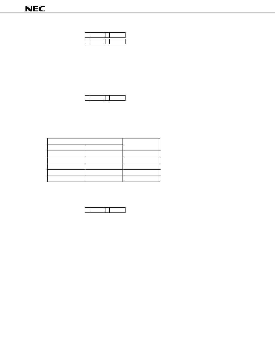
46
µ
PD62
Data Sheet U14208EJ1V0DS00
STTS #data4
<1> Instruction code
:
0 0 0 1 1 1 0 0 0 1
:
0 0 0 0 0 0 d
3
d
2
d
1
d
0
<2> Cycle count
: 1
<3> Function
: if statuses match
F
1
else
F
0
Compares the S
0
, S
1
, K
I/O
, K
I
, and TIMER statuses with the immediate data contents. If at least one
of the statuses coincides with the bits that have been set, the status flag F is set (to 1).
If none of them coincide, the status flag F is cleared (to 0).
SCAF (Set Carry If A
CC
= F
H
)
<1> Instruction code
:
1 1 0 1 0 1 0 0 1 1
<2> Cycle count
: 1
<3> Function
: if
A = 0FH
CY
1
else
CY
0
Sets the carry flag CY (to 1) if the accumulator contents are FH.
The accumulator values after executing the SCAF instruction are as follows:
Accumulator Value
Carry Flag
Before execution
After execution
◊◊◊
0
0000
0 (clear)
◊◊
01
0001
0 (clear)
◊
011
0011
0 (clear)
0111
0111
0 (clear)
1111
1111
1 (set)
Remark
◊
: don't care
NOP
<1> Instruction code
:
0 0 0 0 0 0 0 0 0 0
<2> Cycle count
: 1
<3> Function
: PC
PC + 1
No operation

47
µ
PD62
Data Sheet U14208EJ1V0DS00
10. ASSEMBLER RESERVED WORDS
10.1 Mask Option Directives
When creating the
µ
PD62 program, it is necessary to use a mask option directive in the assembler's source
program to specify a mask option.
10.1.1 OPTION and ENDOP directives
From the OPTION directive on to the ENDOP directive are called the mask option definition block. The format
of the mask option definition block is as follows:
Format
Symbol field
Mnemonic field
Operand field
Comment field
[Label:]
OPTION
[; Comment]
:
:
ENDOP
10.1.2 Mask option definition directive
The directives that can be used in the mask option definition block are listed in Table 10-1.
An example of the mask option definition is shown below.
Example
Symbol field
Mnemonic field
Operand field
Comment field
OPTION
USEPOC
; POC circuit incorporated
ENDOP
Table 10-1. List of Mask Option Definition Directives
Name
Mask Option Definition Directive
PRO File
Address value
Data value
POC
USEPOC
2044H
01
(POC circuit incorporated)
NOUSEPOC
00
(Without POC circuit)
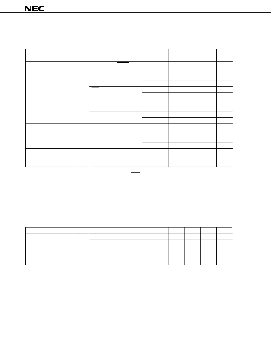
48
µ
PD62
Data Sheet U14208EJ1V0DS00
11. ELECTRICAL SPECIFICATIONS
Absolute Maximum Ratings (T
A
= +25 ∞C)
Parameter
Symbol
Test Conditions
Rating
Unit
Power supply voltage
V
DD
≠0.3 to +5.0
V
Input voltage
V
I
K
I/O
, K
I
, S
0
, S
1
, RESET
≠0.3 to V
DD
+ 0.3
V
Output voltage
V
O
≠0.3 to V
DD
+ 0.3
V
High-level output current
I
OH
Note
REM
Peak value
≠30
mA
rms
≠20
mA
LED
Peak value
≠7.5
mA
rms
≠5
mA
One K
I/O
pin
Peak value
≠13.5
mA
rms
≠9
mA
Total of LED and K
I/O
pins
Peak value
≠18
mA
rms
≠12
mA
Low-level output current
I
OL
Note
REM
Peak value
7.5
mA
rms
5
mA
LED
Peak value
7.5
mA
rms
5
mA
Operating ambient
T
A
≠40 to +85
∞C
temperature
Storage temperature
T
stg
≠65 to +150
∞C
Note Work out the rms with: [rms] = [Peak value]
◊
Duty.
Caution Product quality may suffer if the absolute rating is exceeded for any parameter, even momen-
tarily. In other words, an absolute maxumum rating is a value at which the possibility of psysical
damage to the product cannnot be ruled out. Care must therefore be taken to ensure that the
these ratings are not exceeded during use of the product.
Recommended Power Supply Voltage Range (T
A
= ≠40 to +85 ∞C)
Parameter
Symbol
Test Conditions
MIN.
TYP.
MAX.
Unit
Power supply voltage
V
DD
f
X
= 2.4 to 4 MHz
1.8
3.0
3.6
V
f
X
= 4 to 8 MHz
2.2
3.0
3.6
V
When using the POC circuit (mask option)
2.2
3.0
3.6
V
T
A
= ≠20 to +70 ∞C
f
X
= 2.4 to 4 MHz
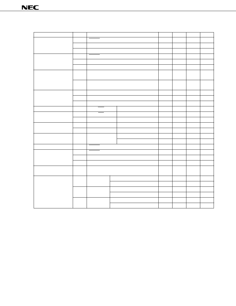
49
µ
PD62
Data Sheet U14208EJ1V0DS00
DC Characteristics (T
A
= ≠40 to +85 ∞C, V
DD
= 1.8 to 3.6 V)
Parameter
Symbol
Test Conditions
MIN.
TYP.
MAX.
Unit
High-level input voltage
V
IH1
RESET
0.8 V
DD
V
DD
V
V
IH2
K
I/O
0.65 V
DD
V
DD
V
V
IH3
K
I
, S
0
, S
1
0.65 V
DD
V
DD
V
Low-level input voltage
V
IL1
RESET
0
0.2 V
DD
V
V
IL2
K
I/O
0
0.3 V
DD
V
V
IL3
K
I
, S
0
, S
1
0
0.15 V
DD
V
High-level input
I
LH1
K
I
3
µ
A
leakage current
V
I
= V
DD
, pull-down resistor not incorporated
I
LH2
S
0
, S
1
3
µ
A
V
I
= V
DD
, pull-down resistor not incorporated
Low-level input leakage
I
UL1
K
I
V
I
= 0 V
≠3
µ
A
current
I
UL2
K
I/O
V
I
= 0 V
≠3
µ
A
I
UL3
S
0
, S
1
V
I
= 0 V
≠3
µ
A
High-level output voltage
V
OH1
REM, LED, K
I/O
I
OH
= ≠0.3 mA
0.8 V
DD
V
Low-level output voltage
V
OL1
REM, LED
I
OL
= 0.3 mA
0.3
V
V
OL2
K
I/O
I
OL
= 15
µ
A
0.4
V
High-level output current
I
OH1
REM
V
DD
= 3.0 V, V
OH
= 1.0 V
≠5
≠9
mA
I
OH2
K
I/O
V
DD
= 3.0 V, V
OH
= 2.2 V
≠2.5
≠5
mA
Low-level output current
I
OL1
K
I/O
V
DD
= 3.0 V, V
OL
= 0.4 V
30
70
µ
A
V
DD
= 3.0 V, V
OL
= 2.2 V
100
220
µ
A
Built-in pull-up resistor
R
1
RESET
25
50
100
k
Built-in pull-down resistor
R
2
RESET
2.5
5
15
k
R
3
K
I
, S
0
, S
1
75
150
300
k
R
4
K
I/O
130
250
500
k
Data hold power supply
V
DDOR
In STOP mode
0.9
3.6
V
voltage
Supply current
Note
I
DD1
OPERATING
f
X
= 8.0 MHz, V
DD
= 3 V
±
10 %
0.8
1.6
mA
mode
f
X
= 4.0 MHz, V
DD
= 3 V
±
10 %
0.7
1.4
mA
I
DD2
HALT mode
f
X
= 8.0 MHz, V
DD
= 3 V
±
10 %
0.75
1.5
mA
f
X
= 4.0 MHz, V
DD
= 3 V
±
10 %
0.65
1.3
mA
I
DD3
STOP mode
V
DD
= 3 V
±
10 %
1.0
8.0
µ
A
V
DD
= 3 V
±
10 %, T
A
= 25 ∞C
0.1
1.0
µ
A
Note The POC circuit current and the current flowing in the built-in pull-up resistor are not included.
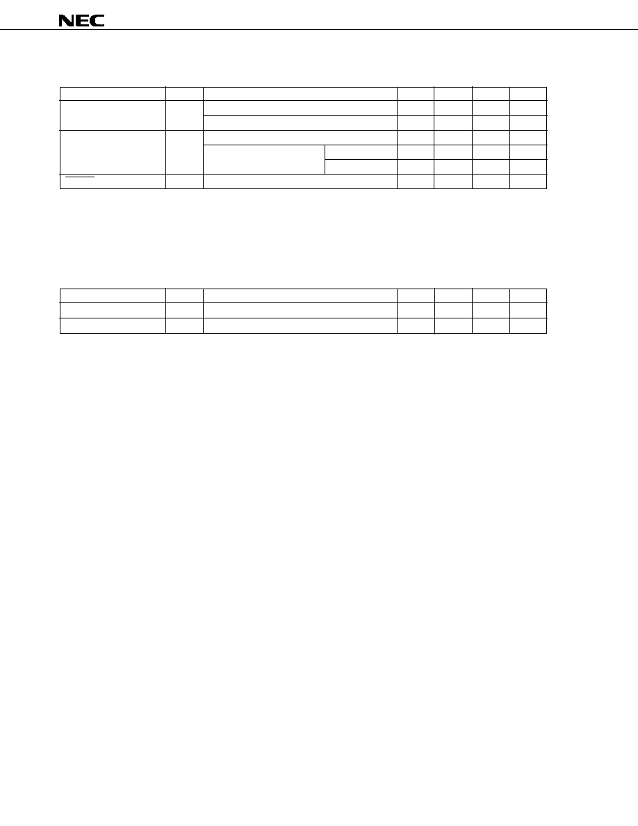
50
µ
PD62
Data Sheet U14208EJ1V0DS00
AC Characteristics (T
A
= ≠40 to +85 ∞C, V
DD
= 1.8 to 3.6 V)
Parameter
Symbol
Test Conditions
MIN.
TYP.
MAX.
Unit
Command execution time
t
CY
V
DD
= 2.2 to 3.6 V
7.9
27
µ
s
15.9
27
µ
s
K
I
, S
0
, S
1
high-level width
t
H
10
µ
s
When releasing
at HALT mode
10
µ
s
STANDBY mode
at STOP mode
Note
µ
s
RESET low-level width
t
RSL
10
µ
s
Note 10 + 52/f
X
+ oscillation growth time
Remark t
CY
= 64/f
X
(f
X
: System clock oscillator frequency)
POC Circuit (mask option
Note 1
) (T
A
= ≠20 to +70 ∞C)
Parameter
Symbol
Test Conditions
MIN.
TYP.
MAX.
Unit
POC-detected voltage
Note 2
V
POC
0.9
1.6
2.2
V
POC circuit current
I
POC
0.9
1.0
µ
A
Notes 1. Operates effectively under the conditions of f
X
= 2.4 to 4 MHz.
2. Refers to the voltage with which the POC circuit cancels an internal reset. If V
POC
< V
DD
, the internal
reset is released.
From the time of V
POC
V
DD
until the internal reset takes effect, lag of up to 1 ms occurs. When the
period of V
POC
V
DD
lasts less than 1 ms, the internal reset may not take effect.

51
µ
PD62
Data Sheet U14208EJ1V0DS00
System Clock Oscillator Characteristics (T
A
= ≠40 to +85 ∞C, V
DD
= 1.8 to 3.6 V)
Parameter
Symbol
Test Conditions
MIN.
TYP.
MAX.
Unit
Oscillator frequency
f
X
2.4
3.64
4.0
MHz
(ceramic resonator)
V
DD
= 2.2 to 3.6 V
2.4
3.64
8.0
MHz
Recommended Ceramic Resonator (T
A
= ≠40 to +85 ∞C)
(1/2)
Manufacturer
Recommended Constant
Power Supply
(Order Disregarded)
Part Number
Voltage [V]
Note
Remark
C1 [pF]
C2 [pF]
Rd [k
]
MIN.
MAX.
TDK Corp.
FCR3.64MC5
0
1.8
3.6
FCR3.84MC5
0
1.8
3.6
FCR4.0MC5
0
1.8
3.6
FCR6.0MC5
0
2.2
3.6
CCR3.2MC3
0
1.8
3.6
Surface-mount type
CCR4.0MC3
0
1.8
3.6
CCR6.0MC3
0
2.2
3.6
CCR8.0MC5
0
2.2
3.6
Matsushita
EFOEC3204A4
0
1.8
3.6
Electronics
EFOEC3604A4
0
1.8
3.6
Components Co., Ltd
EFOEC4004A4
0
1.8
3.6
EFOEC5124A4
0
2.2
3.6
EFOEC6004A4
0
2.2
3.6
EFOEC8004A4
0
2.2
3.6
Murata Mfg. Co., Ltd
CSA3.64MG
30
30
0
1.8
3.6
CSA6.00MG
30
30
0
2.2
3.6
CSA8.00MTZ
30
30
0
2.2
3.6
CSA8.00MTZ093
30
30
0
2.2
3.6
CST3.64MGW
0
1.8
3.6
CST6.00MGW
0
2.2
3.6
CST8.00MTW
0
2.2
3.6
CST8.00MTW093
0
2.2
3.6
Note When a POC circuit (mask option) is not incorporated
Unnecessary
(C-containing type)
Unnecessary
(C-containing type)
Unnecessary
(C-containing type)
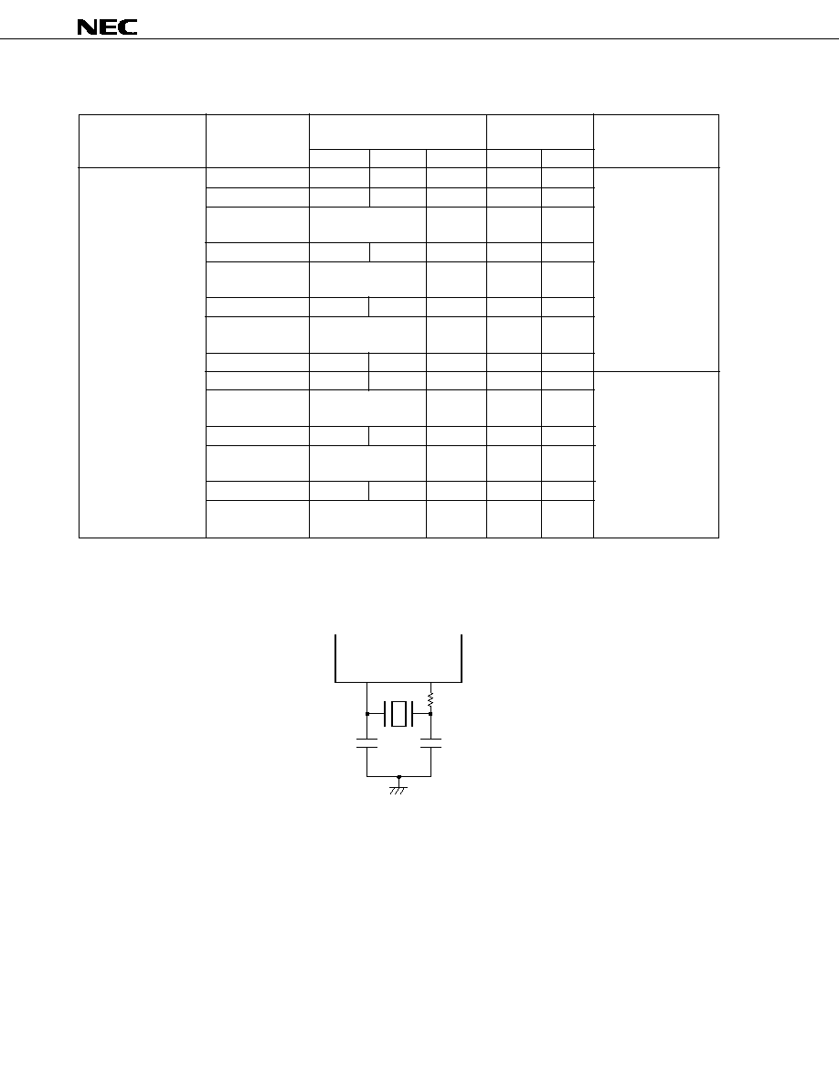
52
µ
PD62
Data Sheet U14208EJ1V0DS00
Recommended Ceramic Resonator (T
A
= ≠40 to +85 ∞C)
(2/2)
Manufacturer
Recommended Constant
Power Supply
(Order Disregarded)
Part Number
Voltage [V]
Note
Remark
C1 [pF]
C2 [pF]
Rd [k
]
MIN.
MAX.
Kyocera Corp.
KBR-2.5MS
33
33
0
1.8
3.6
KBR-3.58MSB
33
33
0
1.8
3.6
KBR-3.58MKC
Unnecessary
0
1.8
3.6
(C-containing type)
KBR-4.0MSB
33
33
0
1.8
3.6
KBR-4.0MKC
Unnecessary
0
1.8
3.6
(C-containing type)
KBR-6.0MSB
33
33
0
2.2
3.6
KBR-6.0MKC
Unnecessary
0
2.2
3.6
(C-containing type)
KBR-8.0M
33
33
0
2.2
3.6
PBRC3.58A
33
33
0
1.8
3.6
Surface-mount type
PBRC3.58B
Unnecessary
0
1.8
3.6
(C-containing type)
PBRC4.00A
33
33
0
1.8
3.6
PBRC4.00B
Unnecessary
0
1.8
3.6
(C-containing type)
PBRC6.00A
33
33
0
2.2
3.6
PBRC6.00B
Unnecessary
0
2.2
3.6
(C-containing type)
Note When a POC circuit (mask option) is not incorporated
An external circuit example
X
IN
X
OUT
C1
C2
Rd
53
µ
PD62
Data Sheet U14208EJ1V0DS00
12. CHARACTERISTIC CURVE (REFERENCE VALUES)
2
1.8
1.6
1.4
1.2
1.0
0.8
0.6
0.4
0.2
0
1
2
3
4
3.6
1.8
I
DD
vs V
DD
(
f
X
= 4 MHz)
Power supply current I
DD
[mA]
Power supply voltage V
DD
[V]
I
OL
vs V
OL
(REM, LED)
Low-level output current I
OL
[mA]
Low-level output voltage V
OL
[V]
2
1.8
1.6
1.4
1.2
1.0
0.8
0.6
0.4
0.2
0
1
2
3
4
3.6
2.2
I
DD
vs V
DD
(
f
X
= 8 MHz)
Power supply current I
DD
[mA]
Power supply voltage V
DD
[V]
I
OH
vs V
OH
(REM)
High-level output current I
OH
[mA]
High-level output voltage V
OH
[V]
I
OH
vs V
OH
(LED)
High-level output current I
OH
[mA]
High-level output voltage V
OH
[V]
10
0.6
1.8
2.4
3
1.2
9
8
7
6
5
4
3
2
1
0
≠20
V
DD
≠ 0.6
V
DD
≠ 1.8 V
DD
≠ 2.4 V
DD
≠ 3
V
DD
≠ 1.2
≠18
≠16
≠14
≠12
≠10
≠8
≠6
≠4
≠2
0
V
DD
≠10
V
DD
≠ 0.6
V
DD
≠ 1.8 V
DD
≠ 2.4 V
DD
≠ 3
V
DD
≠ 1.2
≠9
≠8
≠7
≠6
≠5
≠4
≠3
≠2
≠1
0
V
DD
OPERATING mode
HALT mode
OPERATING mode
HALT mode
(T
A
= 25 ∞C)
(T
A
= 25 ∞C, V
DD
= 3.0 V)
(T
A
= 25 ∞C , V
DD
= 3.0 V)
(T
A
= 25 ∞C , V
DD
= 3.0 V)
(T
A
= 25 ∞C)
54
µ
PD62
Data Sheet U14208EJ1V0DS00
I
OL
vs V
OL
(
K
I/O
)
Low-level output current I
OL
[ A]
Low-level output voltage V
OL
[V]
I
OH
vs V
OH
(
K
I/O
)
High-level output current I
OH
[mA]
High-level output voltage V
OH
[V]
320
0.6
1.8
2.4
3
1.2
0
≠15
V
DD
≠ 0.6
V
DD
≠ 1.8 V
DD
≠ 2.4 V
DD
≠ 3
V
DD
≠ 1.2
0
V
DD
280
240
200
160
120
80
40
≠14
≠13
≠12
≠11
≠10
≠9
≠8
≠7
≠6
≠5
≠4
≠3
≠2
≠1
(T
A
= 25 ∞C, V
DD
= 3.0 V)
(T
A
= 25 ∞C, V
DD
= 3.0 V)
µ
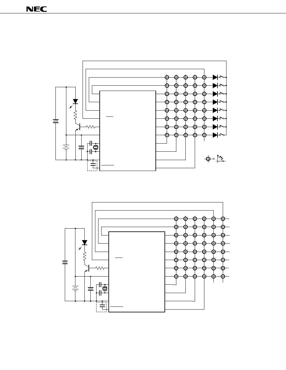
55
µ
PD62
Data Sheet U14208EJ1V0DS00
13. APPLIED CIRCUIT EXAMPLE
Example of Application to System
∑ Remote-control transmitter (40 keys; mode selection switch accommodated)
∑ Remote-control transmitter (48 keys accommodated)
Remark When the POC circuit of the mask option is used effectively, it is not necessary to connect the capacitor
enclosed in the dotted lines.
K
I/O6
K
I/O7
S
0
S
1
/LED
REM
V
DD
X
OUT
X
IN
GND
RESET
K
I/O5
K
I/O4
K
I/O3
K
I/O2
K
I/O1
K
I/O0
K
I3
K
I2
K
I1
K
I0
Key matrix
8
◊
5 = 40 keys
Mode selection switch
+
+
K
I/O6
K
I/O7
S
0
S
1
/LED
REM
V
DD
X
OUT
X
IN
GND
RESET
K
I/O5
K
I/O4
K
I/O3
K
I/O2
K
I/O1
K
I/O0
K
I3
K
I2
K
I1
K
I0
Key matrix
8
◊
6 = 48 keys
+
+
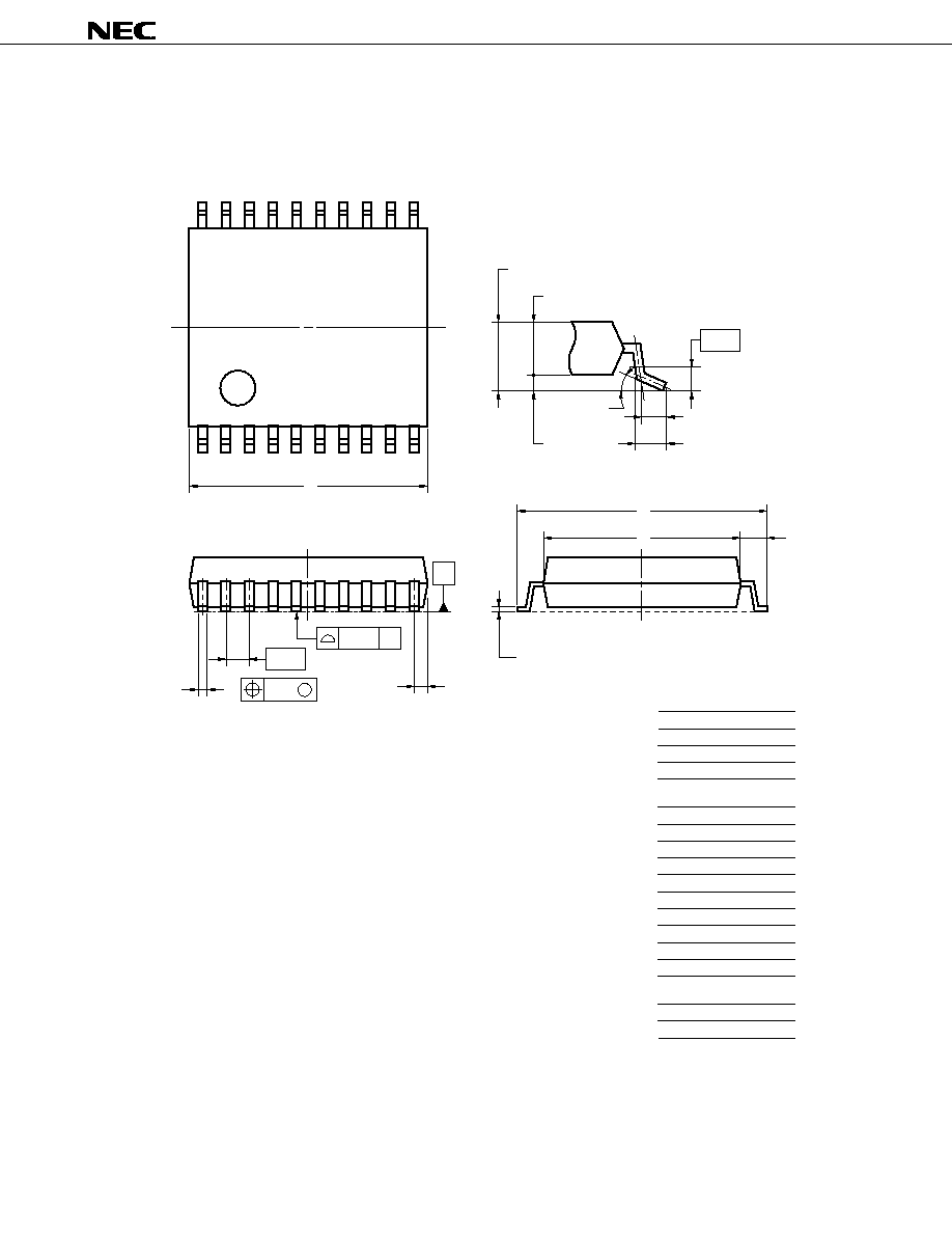
56
µ
PD62
Data Sheet U14208EJ1V0DS00
14. PACKAGE DRAWINGS
N
S
C
D
M
M
P
L
U
T
G
F
E
B
K
J
detail of lead end
S
20
11
1
10
A
H
I
20 PIN PLASTIC SSOP (300 mil)
NOTE
S20MC-65-5A4-1
ITEM
MILLIMETERS
A
B
C
D
E
F
G
H
I
J
0.65 (T.P.)
1.3
±
0.1
1.2
8.1
±
0.2
0.475 MAX.
K
L
0.13
0.5
1.0
±
0.2
6.1
±
0.2
0.17
±
0.03
M
0.10
0.24
0.1
±
0.05
N
P
3
∞
6.65
±
0.15
Each lead centerline is located within 0.12 mm of
its true position (T.P.) at maximum material condition.
+
0.08
-
0.07
+
5
∞
-
3
∞
0.25
T
0.6
±
0.15
U
Remark The dimensions and materials of the ES model are the same as those of the mass production model.
57
µ
PD62
Data Sheet U14208EJ1V0DS00
15. RECOMMENDED SOLDERING CONDITIONS
Carry out the soldered packaging of this product under the following recommended conditions.
For details of the soldering conditions, refer to information material Semiconductor Device Mounting
Technology Manual (C10535E).
For soldering methods and conditions other than the recommended conditions, please consult one of our NEC
sales representatives.
Table 15-1. Soldering Conditions for Surface-Mount Type
µ
PD62MC-
◊◊◊
-5A4: 20-pin plastic SSOP (300 mil)
Soldering Method
Soldering Condition
Recommended
Condition Symbol
Infrared reflow
Package peak temperature: 235
∞
C; time: within 30 secs. max. (210
∞
C or higher);
IR35-00-3
count: no more than three times
VPS
Package peak temperature: 215
∞
C; time: 40 secs. max. (200
∞
C or higher); count:
VP15-00-3
no more than three times
Wave soldering
Solder bath temperature: 260
∞
C max.; time: 10 secs. max.; count: once;
WS60-00-1
Preliminary heat temperature: 120
∞
C max. (Package surface temperature)
Partial heating
Pin temperature: 300
∞
C or less ; time: 3 secs or less (for each side of the device)
--
Caution Using more than one soldering method should be avoided (except in the case of partial
heating).
58
µ
PD62
Data Sheet U14208EJ1V0DS00
APPENDIX A. DEVELOPMENT TOOLS
An emulator is provided for the
µ
PD62.
Hardware
∑ Emulator (EB-6133
Note
)
It is used to emulate the
µ
PD62.
Note This is a product of Naito Densei Machida Mfg. Co., Ltd. For details, consult Naito Densei Machida Mfg.
Co., Ltd. (044-822-3813).
Software
∑ Assembler (AS6133)
∑ This is a development tool for remote control transmitter software.
Part Number List of AS6133
Host Machine
OS
Supply Medium
Part Number
PC-9800 series
MS-DOS
TM
(Ver. 5.0 to Ver. 6.2)
3.5-inch 2HD
µ
S5A13AS6133
(CPU: 80386 or more)
IBM PC/AT
TM
compatible
MS-DOS
(Ver. 6.0 to Ver. 6.22)
3.5-inch 2HC
µ
S7B13AS6133
PC DOS
TM
(Ver. 6.1 to Ver. 6.3)
Caution Although Ver.5.0 or later has a task swap function, this function cannot be used with this
software.
59
µ
PD62
Data Sheet U14208EJ1V0DS00
Item
µ
PD62
µ
PD63A
µ
PD64
µ
PD6134
µ
PD6600A
ROM capacity
512
◊
10 bits
768
◊
10 bits
1002
◊
10 bits
1002
◊
10 bits
512
◊
10 bits
RAM capacity
32
◊
4 bits
32
◊
5 bits
Stack
1 level (multiplexed with RF of RAM)
3 levels
(multiplexed with RAM)
Key matrix
8
◊
6 = 48 keys
8
◊
4 = 32 keys
S
0
(S-IN) input
Read by P
01
register (with function to release standby mode)
Read by left shift
instruction
S
1
/LED (S-OUT)
I/O (with function to release standby mode)
Output
Clock frequency
Ceramic oscillation
Ceramic oscillation
∑ f
X
= 2.4 to 8 MHz
∑ f
X
= 300 kHz to 1 MHz ∑ f
X
= 400 to 500 kHz
∑ f
X
= 2.4 to 4 MHz (with POC circuit)
∑ f
X
= 300 to 500 kHz
(with POC circuit)
Timer
Clock
f
X
/64, f
X
/128
f
X
/8, f
X
/16
f
X
/8
Count start
Writing count value
Writing count value
and P1 register value
Carrier
Frequency
∑ f
X
/8, f
X
/64, f
X
/96 (timer clock: f
X
/64)
∑ f
X
, f
X
/8, f
X
/12
∑ f
X
/8, f
X
/12
∑ f
X
/16, f
X
/128, f
X
/192 (timer clock: f
X
/128)
(timer clock: f
X
/8)
∑ No carrier
∑ f
X
/2, f
X
/16, f
X
/24
(timer clock: f
X
/16)
∑ No carrier
Output start
Synchronized with timer
Not synchronized
with timer
Instruction execution time
8
µ
s (f
X
= 8 MHz)
8
µ
s (f
X
= 1 MHz)
16
µ
s (f
X
= 500 kHz)
Relative branch instruction
None
Provided
Left shift instruction
None
Provided
"MOV Rn, @RO" instruction
n = 1 to F
n = 0 to F
Standby mode
HALT mode for timer only.
HALT/STOP mode
(HALT instruction)
STOP mode for only releasing K
I
set by P1 register
(K
I/O
high-level output or K
I/O0
high-level output)
value
Relation between HALT
HALT instruction not executed when F = 1
HALT instruction
instruction execution and
executed regardless
status flag (F)
of status of F
Reset function by charging/
None
Provided
discharging capacitor
POC circuit
Mask option
Provided (low-voltage
Low level output to RESET pin on detection
detection circuit)
Low level output to
S-OUT pin on detection
Mask option
POC circuit only
∑ Pull-down resistor
∑ Variable duty
∑ Hang-up detection
Supply voltage
V
DD
= 1.8 to 3.6 V
V
DD
= 2.2 to 3.6 V
Operating temperature
∑ T
A
= ≠40 to +85
∞
C
T
A
= ≠20 to +70
∞
C
∑ T
A
= ≠20 to +70
∞
C (with POC circuit)
Package
∑ 20-pin plastic ∑ 20-pin plastic ∑ 20-pin plastic SOP
∑ 20-pin plastic SOC
SSOP
SOP
∑ 20-pin plastic SSOP
∑ 20-pin plastic shrink
DIP
One-time PROM model
µ
PD6P4B
µ
PD61P34B
µ
PD61P24
APPENDIX B. FUNCTIONAL COMPARISON BETWEEN
µ
PD62 AND OTHER SUBSERIES

60
µ
PD62
Data Sheet U14208EJ1V0DS00
APPENDIX C. EXAMPLE OF REMOTE-CONTROL TRANSMISSION FORMAT
(in the case of NEC transmission format in command one-shot transmission mode)
Caution When using the NEC transmission format, please apply for a custom code at NEC.
(1) REM output waveform (From <2> on, the output is made only when the key is kept pressed.)
REM output
58.5 to 76.5 ms
108 ms
108 ms
< 1 >
< 2 >
Remark If the key is repeatedly pressed, the power consumption of the infrared light-emitting diode (LED) can
be reduced by sending the reader code and the stop bit from the second time.
(2) Enlarged waveform of <1>
REM output
13.5 ms
Leader code
9 ms
4.5 ms
Custom Code
8 bits
Custom Code'
8 bits
Data code
8 bits
Data Code
8 bits
27 ms
18 to 36 ms
58.5 to 76.5 ms
Stop bit
1 bit
< 3 >
(3) Enlarged waveform of <3>
REM output
9 ms
13.5 ms
0
4.5 ms
1
1
0
0
2.25 ms
1.125 ms
0.56 ms
(4) Enlarged waveform of <2>
REM output
9 ms
11.25 ms
2.25 ms
0.56 ms
Stop bit
Leader code
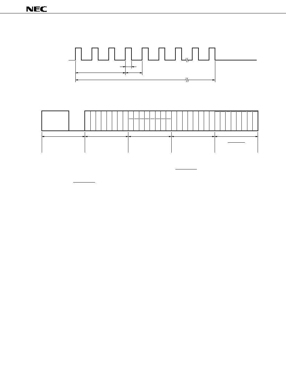
61
µ
PD62
Data Sheet U14208EJ1V0DS00
(5) Carrier waveform (Enlarged waveform of each code's high period)
REM output
8.77 s
9 ms or 0.56 ms
Carrier frequency : 38 kHz
26.3 s
µ
µ
(6) Bit array of each code
C
0
C
1
C
2
C
3
C
4
C
5
C
6
C
7
C
0
'
C
0
or
C
o
C
1
'
C
1
or
C
1
C
2
'
C
2
or
C
2
C
3
'
C
3
or
C
3
C
4
'
C
4
or
C
4
C
5
'
C
5
or
C
5
C
6
'
C
6
or
C
6
C
7
'
C
7
or
C
7
D
0
D
1
D
2
D
3
D
4
D
5
D
6
D
7
D
0
D
1
D
2
D
3
D
4
D
5
D
6
D
7
=
=
=
=
=
=
=
=
Data code
Data code
Custom code'
Custom code
Leader code
Caution To prevent malfunction with other systems when receiving data in the NEC transmission
format, not only fully decode (make sure to check Data Code as well) the total 32 bits of the
16-bit custom codes (Custom Code, Custom Code') and the 16-bit data codes (Data Code,
Data Code) but also check to make sure that no signals are present.

62
µ
PD62
Data Sheet U14208EJ1V0DS00
NOTES FOR CMOS DEVICES
1
PRECAUTION AGAINST ESD FOR SEMICONDUCTORS
Note:
Strong electric field, when exposed to a MOS device, can cause destruction of the gate oxide and
ultimately degrade the device operation. Steps must be taken to stop generation of static
electricity as much as possible, and quickly dissipate it once, when it has occurred. Environmental
control must be adequate. When it is dry, humidifier should be used. It is recommended to avoid
using insulators that easily build static electricity. Semiconductor devices must be stored and
transported in an anti-static container, static shielding bag or conductive material. All test and
measurement tools including work bench and floor should be grounded. The operator should be
grounded using wrist strap. Semiconductor devices must not be touched with bare hands. Similar
precautions need to be taken for PW boards with semiconductor devices on it.
2
HANDLING OF UNUSED INPUT PINS FOR CMOS
Note:
No connection for CMOS device inputs can be cause of malfunction. If no connection is provided
to the input pins, it is possible that an internal input level may be generated due to noise, etc., hence
causing malfunction. CMOS devices behave differently than Bipolar or NMOS devices. Input
levels of CMOS devices must be fixed high or low by using a pull-up or pull-down circuitry. Each
unused pin should be connected to V
DD
or GND with a resistor, if it is considered to have a
possibility of being an output pin. All handling related to the unused pins must be judged device
by device and related specifications governing the devices.
3
STATUS BEFORE INITIALIZATION OF MOS DEVICES
Note:
Power-on does not necessarily define initial status of MOS device. Production process of MOS
does not define the initial operation status of the device. Immediately after the power source is
turned ON, the devices with reset function have not yet been initialized. Hence, power-on does
not guarantee out-pin levels, I/O settings or contents of registers. Device is not initialized until
the reset signal is received. Reset operation must be executed immediately after power-on for
devices having reset function.

63
µ
PD62
Data Sheet U14208EJ1V0DS00
NEC Electronics Inc. (U.S.)
Santa Clara, California
Tel: 408-588-6000
800-366-9782
Fax: 408-588-6130
800-729-9288
NEC Electronics (Germany) GmbH
Duesseldorf, Germany
Tel: 0211-65 03 02
Fax: 0211-65 03 490
NEC Electronics (UK) Ltd.
Milton Keynes, UK
Tel: 01908-691-133
Fax: 01908-670-290
NEC Electronics Italiana s.r.l.
Milano, Italy
Tel: 02-66 75 41
Fax: 02-66 75 42 99
NEC Electronics Hong Kong Ltd.
Hong Kong
Tel: 2886-9318
Fax: 2886-9022/9044
NEC Electronics Hong Kong Ltd.
Seoul Branch
Seoul, Korea
Tel: 02-528-0303
Fax: 02-528-4411
NEC Electronics Singapore Pte. Ltd.
United Square, Singapore 1130
Tel: 65-253-8311
Fax: 65-250-3583
NEC Electronics Taiwan Ltd.
Taipei, Taiwan
Tel: 02-2719-2377
Fax: 02-2719-5951
NEC do Brasil S.A.
Electron Devices Division
Rodovia Presidente Dutra, Km 214
07210-902-Guarulhos-SP Brasil
Tel: 55-11-6465-6810
Fax: 55-11-6465-6829
NEC Electronics (Germany) GmbH
Benelux Office
Eindhoven, The Netherlands
Tel: 040-2445845
Fax: 040-2444580
NEC Electronics (France) S.A.
Velizy-Villacoublay, France
Tel: 01-30-67 58 00
Fax: 01-30-67 58 99
NEC Electronics (France) S.A.
Spain Office
Madrid, Spain
Tel: 91-504-2787
Fax: 91-504-2860
NEC Electronics (Germany) GmbH
Scandinavia Office
Taeby, Sweden
Tel: 08-63 80 820
Fax: 08-63 80 388
Regional Information
Some information contained in this document may vary from country to country. Before using any NEC
product in your application, please contact the NEC office in your country to obtain a list of authorized
representatives and distributors. They will verify:
∑ Device availability
∑ Ordering information
∑ Product release schedule
∑ Availability of related technical literature
∑ Development environment specifications (for example, specifications for third-party tools and
components, host computers, power plugs, AC supply voltages, and so forth)
∑ Network requirements
In addition, trademarks, registered trademarks, export restrictions, and other legal issues may also vary
from country to country.
J99.1

µ
PD62
MS-DOS is either a registered trademark or a trademark of Microsoft Corporation in the United States
and/or other countries.
PC/AT and PC DOS are trademarks of IBM Corp.
∑
The information in this document is subject to change without notice. Before using this document, please
confirm that this is the latest version.
∑
No part of this document may be copied or reproduced in any form or by any means without the prior written
consent of NEC Corporation. NEC Corporation assumes no responsibility for any errors which may appear in
this document.
∑
NEC Corporation does not assume any liability for infringement of patents, copyrights or other intellectual
property rights of third parties by or arising from use of a device described herein or any other liability arising
from use of such device. No license, either express, implied or otherwise, is granted under any patents, copyrights
or other intellectual property rights of NEC Corporation or others.
∑
Descriptions of circuits, software, and other related information in this document are provided for illustrative
purposes in semiconductor product operation and application examples. The incorporation of these circuits,
software, and information in the design of the customer's equipment shall be done under the full responsibility
of the customer. NEC Corporation assumes no responsibility for any losses incurred by the customer or third
parties arising from the use of these circuits, software, and information.
∑
While NEC Corporation has been making continuous effort to enhance the reliability of its semiconductor devices,
the possibility of defects cannot be eliminated entirely. To minimize risks of damage or injury to persons or
property arising from a defect in an NEC semiconductor device, customers must incorporate sufficient safety
measures in its design, such as redundancy, fire-containment, and anti-failure features.
∑
NEC devices are classified into the following three quality grades:
"Standard", "Special", and "Specific". The Specific quality grade applies only to devices developed based on a
customer designated "quality assurance program" for a specific application. The recommended applications of
a device depend on its quality grade, as indicated below. Customers must check the quality grade of each device
before using it in a particular application.
Standard: Computers, office equipment, communications equipment, test and measurement equipment,
audio and visual equipment, home electronic appliances, machine tools, personal electronic
equipment and industrial robots
Special:
Transportation equipment (automobiles, trains, ships, etc.), traffic control systems, anti-disaster
systems, anti-crime systems, safety equipment and medical equipment (not specifically designed
for life support)
Specific:
Aircraft, aerospace equipment, submersible repeaters, nuclear reactor control systems, life
support systems or medical equipment for life support, etc.
The quality grade of NEC devices is "Standard" unless otherwise specified in NEC's Data Sheets or Data Books.
If customers intend to use NEC devices for applications other than those specified for Standard quality grade,
they should contact an NEC sales representative in advance.
M7 98.8
The export of this product from Japan is regulated by the Japanese government. To export this product may be prohibited
without governmental license, the need for which must be judged by the customer. The export or re-export of this product
from a country other than Japan may also be prohibited without a license from that country. Please call an NEC sales
representative.