 | –≠–ª–µ–∫—Ç—Ä–æ–Ω–Ω—ã–π –∫–æ–º–ø–æ–Ω–µ–Ω—Ç: UPD6326 | –°–∫–∞—á–∞—Ç—å:  PDF PDF  ZIP ZIP |
©
1995
DATA SHEET
QUAD/OCTAL 6BIT D/A CONVERTER
CMOS LSI
µ
PD6325,
µ
PD6326,
µ
PD6335,
µ
PD6336
MOS INTEGRATED CIRCUIT
DESCRIPTION
µ
PD6325 Serise are 6 bit D/A Converter for control volumn, brightness, contrast, color or tone of TV set.
The data are transferring serially from micro-computer.
µ
PD6325 Serise Line-up
QUAD D/A
OCTAL D/A
D/A output is consist of Emitter follower buffer
µ
PD6325C, 6325G
µ
PD6326C
Non buffer output
µ
PD6335C, 6335G
µ
PD6336C
FEATURES
∑ R-2R ladder D/A
∑ Serial Data input (DATA IN, CLOCK, LOAD)
∑ Power supply voltage of interface is 5 V (V
CC
) and D/A reference voltage is free (V
CC
to 15 V).
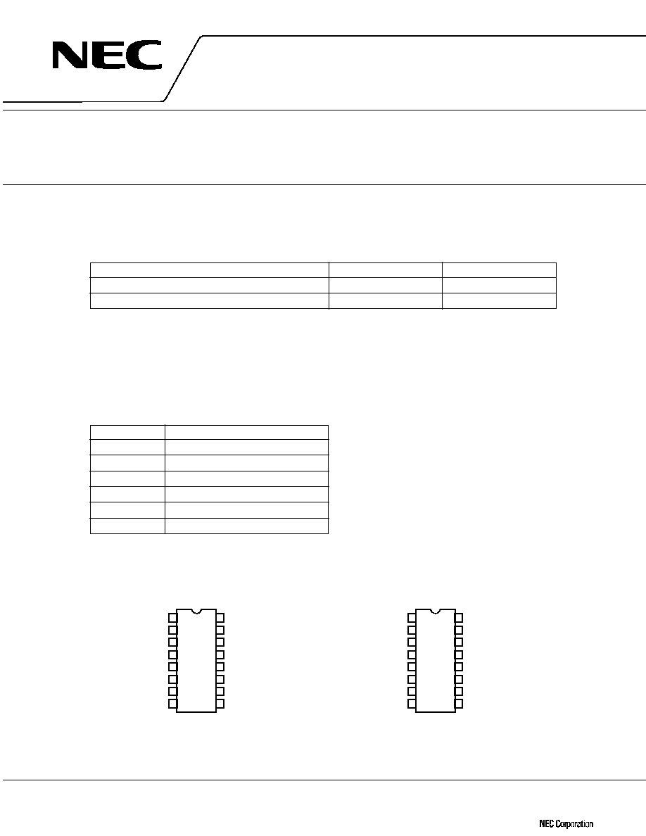
ORDERING INFORMATION
Part No.
Package
µ
PD6325C
16-pin plastic DIP (300 mil)
µ
PD6325G
16-pin plastic SOP (300 mil)
µ
PD6326C
16-pin plastic DIP (300 mil)
µ
PD6335C
16-pin plastic DIP (300 mil)
µ
PD6335G
16-pin plastic SOP (300 mil)
µ
PD6336C
16-pin plastic DIP (300 mil)
PIN CONNECTION DIAGRAM (Top View)
PD6325, PD6335
µ
µ
V
DD
16
DA
1
15
DA
2
14
DA
3
13
DA
4
12
N.C.
11
OPTION
1
10
OPTION
2
V
CC
DATA IN
N.C.
CLOCK
LOAD
N.C.
DATA OUT
V
SS
9
1
2
3
4
5
6
7
8
PD6326, PD6336
µ
µ
V
DD
16
DA
1
15
DA
2
14
DA
3
13
DA
4
12
DA
5
11
DA
6
10
DA
7
V
CC
DATA IN
CLOCK
LOAD
OPTION
1
DATA OUT
DA
8
V
SS
9
1
2
3
4
5
6
7
8
Document No. G10654EJ6V0DS00 (6th edition)
Date Published November 1997 N
Printed in Japan
µ
PD6325,
µ
PD6326,
µ
PD6335,
µ
PD6336
2
BLOCK DIAGRAM
D
0
D
1
D
2
D
3
D
4
D
5
D
6
Line Decoder
Latch
Level Shifter
Level Shifter
OPTION
2
V
CC
V
CC
CLOCK
DATA IN
LOAD
V
DD
V
CC
V
SS
V
DD
B
A
DA
1
V
DD
B
*A ------ PD6335, PD6336
A
DA
8
OPTION
1
DATA OUT
12 bit Shift Resister
D
7
D
8
D
9
D
10
D
11
LSB
MSB
6 bit Latch
6 bit Latch
6 bit R-2R ladder
D/A Converter
6 bit R-2R ladder
D/A Converter
V
V
µ
µ
µ
µ
B ------ PD6325, PD6326
PD6325, PD6326 have Quad D/As.
µ
µ
3
µ
PD6325,
µ
PD6326,
µ
PD6335,
µ
PD6336
PIN CONFIGURATION
Pin No.
Symbol
Pin Name
Function
µ
PD
µ
PD
1
1
V
CC
Interface Power Supply
2
2
DATA IN
Serial Data Input
4
3
CLOCK
Shift Clock Input
5
4
LOAD
Load Pulse Input
7
6
DATA OUT
Serial Data Output
8
8
V
SS
Ground
≠
7
DA
8
Analog Output Channel 8
Analog Output
≠
9
DA
7
Analog Output Channel 7
Analog Output
≠
10
DA
6
Analog Output Channel 6
Analog Output
≠
11
DA
5
Analog Output Channel 5
Analog Output
12
12
DA
4
Analog Output Channel 4
Analog Output
13
13
DA
3
Analog Output Channel 3
Analog Output
14
14
DA
2
Analog Output Channel 2
Analog Output
15
15
DA
1
Analog Output Channel 1
Analog Output
This pin is used to interface with the control IC
(ex. micro processor). Supply the voltage high
level of the control IC.
Control data input terminal. Data is read in syn-
chronization with the clocks input to the CLOCK
terminal.
Data read clock input terminal. The Data input
to the DATA IN terminal is read at the leading
edge of the clock.
This terminal is used to input Load signals after
inputting serial data. 12 bit data is read after
leading edge of a pulse input to the LOAD terminal.
Serial data output terminal. The final stage data
of 12 bit shift register appeares on this terminal
in synchronization with shift clock.
System ground.
D
7
the data of the shift register appears on this
terminal. (Only
µ
PD6325 and
µ
PD6335)
D
6
the data of the shift register appears on this
terminal.
Reference Voltage for D/A converters. Analog
output voltage range is GND
to V
DD
.
16
16
V
DD
Power Supply
9
≠
OPTION
2
Expantion Output Port
10
5
OPTION
1
Expanttion Output Port
6325
6335
6326
6336
µ
PD6325,
µ
PD6326,
µ
PD6335,
µ
PD6336
4
ABSOLUTE MAXIMUM RATINGS (T
A
= 25
∞
C)
Supply Voltage
V
DD
,V
CC
≠0.5 to +18, V
CC
V
DD
V
Output Voltage
V
OUT
≠0.5 to V
DD
+0.5
V
Input Voltage
V
IN
≠0.5 to V
CC
+0.5
V
Input Current
I
IN
10
mA
Emitter Follower Current
I
OE
10
mA
Power Dissipation
P
D
500*/200**
mW
Operating Temperature
T
A
≠40 to +85
∞
C
Storage Temperature
T
stg
≠65 to +125
∞
C
*DIP
**SOP
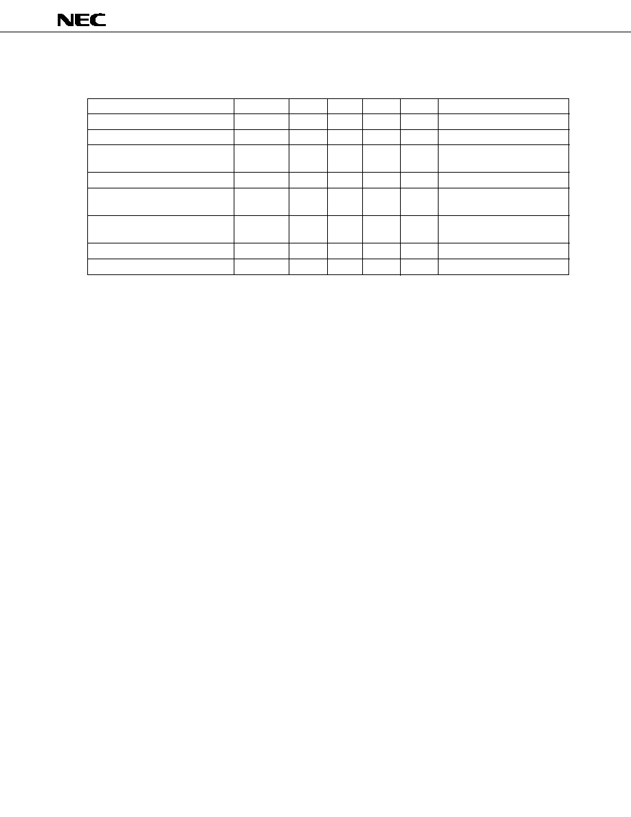
RECOMMENDED OPERATING CONDITIONS
PARAMETER
SYMBOL
MIN.
TYP.
MAX.
UNIT
CONDITION
Supply Voltage
V
DD
V
CC
15
V
V
CC
V
DD
Supply Voltage of Interface
V
CC
4.5
5.0
5.5
V
V
CC
V
DD
Low Level Input Voltage
V
IL
0.8
V
V
CC
= 5 V, V
DD
= 5 to 15 V
High Level Input Voltage
V
IH
3.5
V
V
CC
= 5 V, V
DD
= 5 to 15 V
Only
µ
PD6325 &
µ
PD6326
Emitter Follower Power Dissipation 1
P
E
/unit
5
mW
T
A
= 85
∞
C
Emitter Follower Power Dissipation 2
P
E
/unit
15
mW
T
A
= 70
∞
C
Emitter Follower Power Dissipation 3
P
E
total
25
mW
T
A
= 85
∞
C
Emitter Follower Power Dissipation 4
P
E
total
75
mW
T
A
= 70
∞
C
TIMING CONDITIONS (T
A
= ≠40 to +85
∞
C, V
SS
= 0 V, V
CC
= 5 V, V
DD
= V
CC
to 15 V)
CLOCK High Level Width
t
CH
4.0
µ
s
CLOCK Low Level Width
t
CL
10.0
µ
s
CLOCK Rise Time
t
cr
1.0
µ
s
CLOCK Fall Time
t
cf
1.0
µ
s
DATA IN Setup Time
t
Dsetup
2
µ
s
DATA IN Hold Time
t
Dhold
10
µ
s
Pulse Width, LOAD High
t
W(LOAD)
4
µ
s
LOAD Lead Time
t
LIead
10
µ
s
LOAD Lag Time
t
LIag
10
µ
s
5
µ
PD6325,
µ
PD6326,
µ
PD6335,
µ
PD6336
ELECTRICAL CHARACTERISTICS
(T
A
= ≠40 to +85
∞
C, V
SS
= 0 V, V
CC
= 4.5 to 5.5 V, V
DD
= V
CC
to 15 V)
PARAMETER
SYMBOL
MIN.
TYP.
MAX.
UNIT
CONDITION
Current Consumption
I
DD
15
mA
No Load, for
µ
PD6326, 6336
Current Consumption
I
DD
10
mA
No Load, for
µ
PD6325, 6335
No Load of DATA OUT,
Static Consumption
Input Leak Current
I
ILEAK
±
1
µ
A
V
IN
= V
CC
or V
SS
High Level
Output Voltage
Low Level
Output Voltage
Emitter Follower Leak Current
I
OLEAK
20
µ
A
for
µ
PD6325, 6326
Setling Time
t
DA set
10
µ
s
Note
Note
µ
PD6325, 6326: R
L
= 20 k
, C
L
= 50 pF
µ
PD6335, 6336: No Load.
Current Consumption of Interface
I
CC
10
µ
A
DATA OUT
I
OL
100
µ
A
V
OL
= 0.5 V
DATA OUT
I
OH
≠100
µ
A
V
OH
= V
DD
≠0.5 V