 | –≠–ª–µ–∫—Ç—Ä–æ–Ω–Ω—ã–π –∫–æ–º–ø–æ–Ω–µ–Ω—Ç: UPD64084 | –°–∫–∞—á–∞—Ç—å:  PDF PDF  ZIP ZIP |
Document Outline
- COVER
- DESCRIPTION
- FEATURES
- ORDERING INFORMATION
- PIN CONFIGURATION (TOP VIEW)
- PIN NAME
- BLOCK DIAGRAM
- TERMINOLOGY
- 1. PIN FUNCTIONS
- 2. SYSTEM OVERVIEW
- 2.1 Operation Modes
- 2.2 Filter Processing
- 2.3 System Delay
- 2.4 Start-up of Power Supply and Reset
- 3. VIDEO SIGNAL INPUT BLOCK
- 3.1 Video Signal Inputs
- 3.2 Pedestal Level Reproduction
- 3.3 Video Signal Input Level
- 3.4 Pin Treatment
- 3.5 External ADC Connection Method
- 4. CLOCK/TIMING GENERATION BLOCK
- 4.1 Sync Separator and Timing Generator
- 4.2 Composite Sync Signal Input
- 4.3 Horizontal/Burst Phase Detection Circuit
- 4.4 PLL Filter Circuit
- 4.5 Killer Detection Circuit
- 4.6 fSC Generator
- 4.7 8fSC-PLL Circuit
- 4.8 Pin Treatment
- 5. COMB FILTER BLOCK
- 5.1 Line Comb Filter
- 5.2 Frame Comb Filter
- 5.3 Mixer Circuit
- 5.4 C Signal Subtraction
- 6. MOTION DETECTION BLOCK
- 6.1 Line Comb Filter
- 6.2 DY Detection Circuit
- 6.3 DC Detection Circuit
- 6.4 Motion Factor Generation Circuit
- 6.5 Forcible Control for The Motion Factor
- 7. YNR/CNR BLOCK
- 7.1 YNR/CNR Processing
- 7.2 Nonlinear Filter
- 7.3 YNR/CNR Operation Stop
- 8. NONSTANDARD SIGNAL DETECTION BLOCK
- 8.1 Horizontal Sync Nonstandard Signal Detection
- 8.2 Vertical Sync Nonstandard Signal Detection
- 8.3 Frame Sync Nonstandard Signal Detection
- 8.4 Forced Standard or Nonstandard Signal Control
- 8.5 Noise Level Detection
- 9. WCV-ID DECODER / ID-1 DECODER BLOCK
- 9.1 WCV-ID Decoder
- 9.2 ID-1 Decoder
- 10. Y SIGNAL OUTPUT PROCESSING BLOCK
- 10.1 Y High-Frequency Coring Circuit
- 10.2 Y Peaking Filter Circuit
- 10.3 Vertical Aperture Compensation Circuit
- 10.4 Turning On/Off Y Peaking and Vertical Aperture Compensation
- 10.5 ID-1 Encoder
- 11. C SIGNAL OUTPUT PROCESSING BLOCK
- 11.1 C Signal Delay Adjustment
- 11.2 BPF and Gain Processing
- 12. VIDEO SIGNAL OUTPUT BLOCK
- 12.1 Digital YC Output Processing
- 12.2 Video Signal Output Level
- 12.3 Pin Treatment
- 13. EXTEND DIGITAL INPUT / OUTPUT
- 13.1 Usage of extend digital I/O terminals
- 13.2 Digital YC output format
- 13.3 Pin Treatment
- 14. DIGITAL CONNECTION WITH GHOST REDUCER IC uPD64031A
- 14.1 Outline
- 14.2 System Configuration and Control Method
- 14.2.1 Selecting video signal input path
- 14.2.2 Selecting mode according to clock and video signal input path
- 14.3 Setting of Digital Direct-Connected System
- 14.3.1 Hardware setting
- 14.3.2 Register setting
- 15. I2C BUS INTERFACE
- 15.1 Basic Specification
- 15.2 Data Transfer Formats
- 15.3 Initialization
- 15.4 Serial Bus Registers
- 15.5 Serial Bus Register Functions
- 16. ELECTRICAL CHARACTERISTICS
- 17. APPLICATION CIRCUIT EXAMPLE
- 18. PACKAGE DRAWING
- 19. RECOMMENDED SOLDERING CONDITIONS

The information in this document is subject to change without notice. Before using this document, please
confirm that this is the latest version.
Not all products and/or types are available in every country. Please check with an NEC Electronics
sales representative for availability and additional information.
MOS INTEGRATED CIRCUIT
µ
µ
µ
µ
PD64084
THREE-DIMENSIONAL Y/C SEPARATION LSI WITH ON-CHIP MEMORY
Document No. S16021EJ2V0DS00 (2nd edition)
Date Published March 2003 NS CP (K)
Printed in Japan
DATA SHEET
2002
The mark
shows major revised points.
DESCRIPTION
The
µPD64084 realizes a high precision Y/C separation by the three-dimension signal processing for NTSC signal.
This product has the on-chip 4-Mbit memory for flame delay, a high precision internal 10-bit A/D converter and D/A
converter, and adapting 10-bit signal processing (only for luminance signal) and high picture quality. The
µPD64084 is
completely single-chip system of 3D Y/C separation.
This LSI includes the Wide Clear Vision ID signal (Japanese local format) decoder and ID-1 signal decoder.
FEATURES
∑
On-chip 4-Mbit frame delay memory.
∑
2 operation mode
Motion adaptive 3D Y/C separation
2D Y/C separation + Frame recursive Y/C NR
∑
Embedded 10-bit A/D converter (1ch), 10-bit D/A converters (2ch), and System clock generator.
∑
Embedded Y coring, Vertical enhancer, Peaking filter, and Noise detector.
∑
Embedded ID-1 signal decoder, and WCV-ID signal decoder.
∑
I
2
C bus control.
∑
Dual power supply of 2.5 V and 3.3 V.
For digital : DV
DD
= 2.5 V
For analog : AV
DD
= 2.5 V
For DRAM : DV
DDRAM
= 2.5 V
For I/O : DV
DDIO
= 3.3 V
ORDERING INFORMATION
Part number
Package
µPD64084GC-8EA-A
Note1
100-pin plastic LQFP (fine pitch) (14
◊ 14 mm)
µPD64084GC-8EA-Y
Note2
100-pin plastic LQFP (fine pitch) (14
◊ 14 mm)
Notes 1. Lead-free product
2. High-thermal-resistance product
µ
µ
µ
µ
PD64084
2
Data Sheet S16021EJ2V0DS
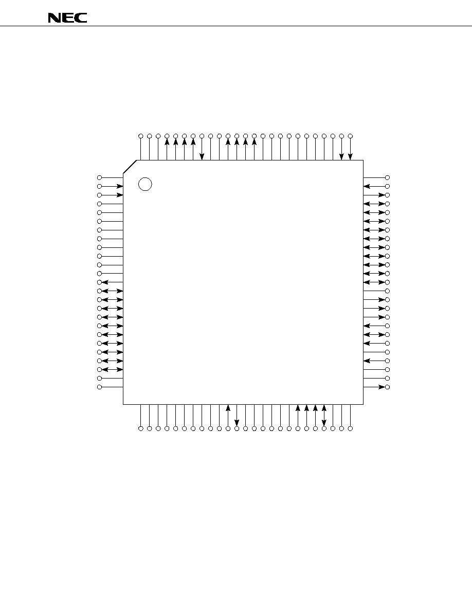
PIN CONFIGURATION (TOP VIEW)
∑
100-pin plastic LQFP (fine pitch) (14
◊ 14 mm)
µPD64084GC-8EA-A
µPD64084GC-8EA-Y
DGND
1
2
3
4
TESTIC1
5
TESTIC2
6
TEST01
7
TEST02
8
TEST03
9
TEST04
10
TEST05
11
TEST06
12
TEST07
13
TEST08
14
TEST09
15
16
17
18
EXTALTF
19
EXTDYCO0
20
EXTDYCO1
21
EXTDYCO2
22
EXTDYCO3
23
EXTDYCO4
24
EXTDYCO5
25
EXTDYCO6
26
EXTDYCO7
27
EXTDYCO8
28
EXTDYCO9
29
DGNDRAM
30
80
79
78
77
76
75
74
73
72
71
70
69
68
67
66
65
64
63
62
61
60
59
58
57
56
55
54
53
52
51
31
DGNDRAM
DGND
LINE
ALTF
DYCO9
DYCO8
DYCO7
DYCO6
DYCO5
DYCO4
DYCO3
DYCO2
DYCO1
DYCO0
DVDD
NSTD
ST1
ST0
RSTB
CLK8
CKMD
AVDD
FSCI
FSCO
AGND
AGND
D
VDDRAM
32
D
VDDRAM
33
TEST10
34
TEST11
35
TEST12
TEST14
TEST15
TEST16
TEST17
36
37
38
D
VDDIO
39
TEST13
40
DGND
41
RPLL
42
SLA0
43
SCL
44
SD
A
45
A
GND
46
A
GND
DGND
A
GND
A
VDD
47
XI
48
XO
49
A
VDD
50
100
99
98
97
96
95
94
93
92
91
90
89
88
87
86
85
84
83
82
81
D
VDD
D
VDD
TEST26
A
VDD
A
VDD
VR
TY
VRBY
VCL
Y
AY
I
A
GND
A
GND
CBPY
AY
O
AC
O
CBPC
VCOMY
KIL
CSI
TEST18
TEST19
TEST20
TEST21
TEST22
TEST23
TEST24
TEST25

µ
µ
µ
µ
PD64084
3
Data Sheet S16021EJ2V0DS
PIN NAME
ACO
: Analog C (Chroma) Signal Output
AGND
: Analog Section Ground
ALTF
: Alternate Flag for Digital YC Output
AVDD
: Analog Section Power Supply
AYI
: Analog Composite Signal Input
AYO
: Analog Y (Luma) Signal Output
CBPC
: C-DAC Phase Compensation Output
CBPY
: Y-DAC Phase Compensation Output
CKMD
: Clock Mode Selection
CLK8
: 8f
SC
Clock Input / Output
CSI
: Composite Sync. Input (Active-low)
DGND
: Digital Section Ground
DVDD
: Digital Section Power Supply
DVDDIO
: Digital I/O Section Power Supply
DVDDRAM
: Internal DRAM Section Power Supply
DYCO0 to DYCO9
: Digital YC Signal (Alternative) Input / Outputs
EXTALTF
: Extend Alternate Flag for Digital YC Output
EXTDYCO0 to EXTDYCO9 : Extend Digital YC Signal (Alternative) Input / Outputs
FSCI
: f
SC
(Subcarrier) Input
FSCO
: f
SC
(Subcarrier) Output
KIL
: Killer Selection
LINE
: Inter-Line Separate Selection
NSTD
: Non Standard Detection Monitor
RPLL
: Testing Selection
RSTB
: System Reset (Active-low)
SCL
: Serial Clock Input
SDA
: Serial Data Input / Output
SLA0
: Slave Address Selection
ST1, ST0
: Inner States Monitor
TEST01 to TEST26
: Testing Selection
TESTIC1, TESTIC2
: IC Testing Section
VCLY
: Clamp Voltage Output for ADC
VRTY
: Top Voltage Reference Output for ADC
VRBY
: Bottom Voltage Reference Output for ADC
VCOMY
: Common Mode Reference Output for ADC
XI
: X'tal input
XO
: X'tal output

µ
µ
µ
µ
PD64084
4
Data Sheet S16021EJ2V0DS
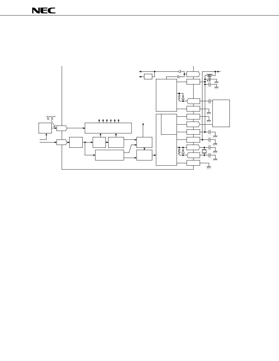
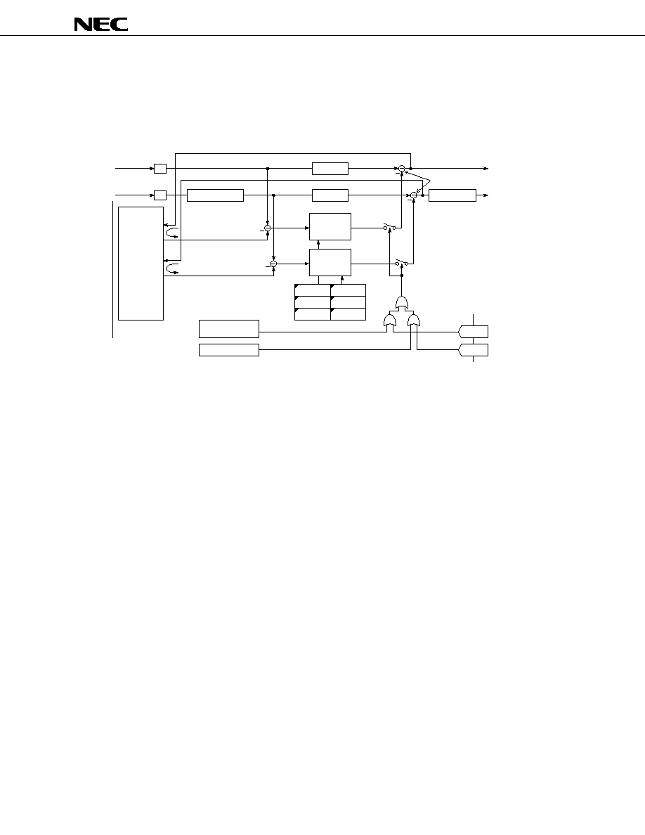
BLOCK DIAGRAM
10-bit
ADC
Y/C Separator &
Y Noise Reducer
3-Line Comb Filter
10-bit
C-DAC
C Delay &
C Noise Reducer
4-Mbit Frame
Memory
WCV-ID Dec.
ID-1 Dec.
Non-Std.
Detector
Timing
Generator
4f
SC
I
2
C Bus
I/F
Power
Down cont.
Sync.
Separate
Ext. Sync.
Separate
20 MHz
Comp. Input
10-bit Digital
Comp. Input
C Output
Y Output
Digital YC
Output
I
2
C Bus
Line
f
SC
/227.5f
H
Dec.
8-bit
f
SC
DAC
8f
SC
PLL
4f
SC
C
Y
8f
SC
Clamp
BPF
Motion Detector
3-Line Comb Filter
3-Line Comb Filter
Y-Coring
Y-Peaking
Y-Enhancer
ID-1 Enc.
SEL
10-bit
Y-DAC
SEL
SEL

µ
µ
µ
µ
PD64084
5
Data Sheet S16021EJ2V0DS
TERMINOLOGY
This manual use the abbreviation listed below:
ADC
: A/D (Analog to Digital) converter
DAC
: D/A (Digital to Analog) converter
LPF
: Low-pass filter
BPF
: Band-pass filter
Y signal, or Luma
: Luminance, or luminance signal
C signal, or Chroma : Color signal, or chrominance signal
f
SC
: Color subcarrier frequency = 3.579545 MHz
4f
SC
: 4 times f
SC
, burst locked clock = 14.318180 MHz
8f
SC
: 8 times f
SC
, burst locked clock = 28.636360 MHz
f
H
: Horizontal sync frequency = 15.734 kHz
910f
H
: 910 times f
H
, line locked clock = 14.318180 MHz
1820f
H
: 1820 times f
H
, line locked clock = 28.636360 MHz
f
V
: Vertical sync frequency = 59.94 Hz
NR
: Noise reduction
YNR
: Luminance (Y) noise reduction
CNR
: Chrominance (C) noise reduction
WCV-ID
: Wide Clear Vision standard ID signal (Japan only)
ID-1
: ID signal of EIAJ CPR-1204
In the following diagrams, a serial bus register is enclosed in a box:

µ
µ
µ
µ
PD64084
6
Data Sheet S16021EJ2V0DS
CONTENTS
1.
PIN FUNCTIONS .....................................................................................................................................................9
1.1 Pin Functions ..................................................................................................................................................9
2.
SYSTEM OVERVIEW ............................................................................................................................................11
2.1 Operation Modes ..........................................................................................................................................11
2.2 Filter Processing ...........................................................................................................................................12
2.3 System Delay ................................................................................................................................................12
2.4 Start-up of Power Supply and Reset.............................................................................................................13
3.
VIDEO SIGNAL INPUT BLOCK ............................................................................................................................14
3.1 Video Signal Inputs .......................................................................................................................................14
3.2 Pedestal Level Reproduction ........................................................................................................................14
3.3 Video Signal Input Level ...............................................................................................................................15
3.4 Pin Treatment................................................................................................................................................15
3.5 External ADC Connection Method ................................................................................................................16
4.
CLOCK/TIMING GENERATION BLOCK...............................................................................................................17
4.1 Sync Separator and Timing Generator .........................................................................................................17
4.2 Composite Sync Signal Input........................................................................................................................17
4.3 Horizontal/Burst Phase Detection Circuit......................................................................................................17
4.4 PLL Filter Circuit ...........................................................................................................................................17
4.5 Killer Detection Circuit...................................................................................................................................17
4.6 f
SC
Generator.................................................................................................................................................18
4.7 8f
SC
-PLL Circuit .............................................................................................................................................18
4.8 Pin Treatment................................................................................................................................................18
5.
COMB FILTER BLOCK .........................................................................................................................................19
5.1 Line Comb Filter............................................................................................................................................19
5.2 Frame Comb Filter ........................................................................................................................................19
5.3 Mixer Circuit ..................................................................................................................................................19
5.4 C Signal Subtraction .....................................................................................................................................19
6.
MOTION DETECTION BLOCK..............................................................................................................................20
6.1 Line Comb Filter............................................................................................................................................20
6.2 DY Detection Circuit ......................................................................................................................................20
6.3 DC Detection Circuit .....................................................................................................................................20
6.4 Motion Factor Generation Circuit ..................................................................................................................20
6.5 Forcible Control for The Motion Factor..........................................................................................................20
7.
YNR/CNR BLOCK .................................................................................................................................................21
7.1 YNR/CNR Processing ...................................................................................................................................21
7.2 Nonlinear Filter..............................................................................................................................................21
7.3 YNR/CNR Operation Stop.............................................................................................................................21

µ
µ
µ
µ
PD64084
7
Data Sheet S16021EJ2V0DS
8.
NONSTANDARD SIGNAL DETECTION BLOCK ................................................................................................. 22
8.1 Horizontal Sync Nonstandard Signal Detection............................................................................................ 22
8.2 Vertical Sync Nonstandard Signal Detection ................................................................................................ 22
8.3 Frame Sync Nonstandard Signal Detection.................................................................................................. 22
8.4 Forced Standard or Nonstandard Signal Control.......................................................................................... 22
8.5 Noise Level Detection................................................................................................................................... 22
9.
WCV-ID DECODER / ID-1 DECODER BLOCK..................................................................................................... 23
9.1 WCV-ID Decoder .......................................................................................................................................... 23
9.2 ID-1 Decoder ................................................................................................................................................ 24
10. Y SIGNAL OUTPUT PROCESSING BLOCK........................................................................................................ 25
10.1 Y High-Frequency Coring Circuit ................................................................................................................. 25
10.2 Y Peaking Filter Circuit ................................................................................................................................ 26
10.3 Vertical Aperture Compensation Circuit ...................................................................................................... 26
10.4 Turning On/Off Y Peaking and Vertical Aperture Compensation ................................................................. 26
10.5 ID-1 Encoder ............................................................................................................................................... 26
11. C SIGNAL OUTPUT PROCESSING BLOCK........................................................................................................ 27
11.1 C Signal Delay Adjustment .......................................................................................................................... 27
11.2 BPF and Gain Processing ........................................................................................................................... 27
12. VIDEO SIGNAL OUTPUT BLOCK........................................................................................................................ 28
12.1 Digital YC Output Processing ...................................................................................................................... 28
12.2 Video Signal Output Level ........................................................................................................................... 28
12.3 Pin Treatment .............................................................................................................................................. 29
13. EXTEND DIGITAL INPUT / OUTPUT .................................................................................................................... 30
13.1 Usage of extend digital I/O terminals........................................................................................................... 30
13.2 Digital YC output format .............................................................................................................................. 30
13.3 Pin Treatment .............................................................................................................................................. 30
14. DIGITAL CONNECTION WITH GHOST REDUCER IC
µ
µ
µ
µ PD64031A................................................................... 31
14.1 Outline ......................................................................................................................................................... 31
14.2 System Configuration and Control Method.................................................................................................. 33
14.2.1 Selecting video signal input path...................................................................................................... 33
14.2.2 Selecting mode according to clock and video signal input path ....................................................... 33
14.3 Setting of Digital Direct-Connected System ................................................................................................ 34
14.3.1 Hardware setting .............................................................................................................................. 34
14.3.2 Register setting ................................................................................................................................ 35
15. I
2
C BUS INTERFACE............................................................................................................................................. 36
15.1 Basic Specification ...................................................................................................................................... 36
15.2 Data Transfer Formats ................................................................................................................................. 37
15.3 Initialization.................................................................................................................................................. 38
15.4 Serial Bus Registers .................................................................................................................................... 39
15.5 Serial Bus Register Functions ..................................................................................................................... 41

µ
µ
µ
µ
PD64084
8
Data Sheet S16021EJ2V0DS
16. ELECTRICAL CHARACTERISTICS .....................................................................................................................57
17. APPLICATION CIRCUIT EXAMPLE .....................................................................................................................62
18. PACKAGE DRAWING............................................................................................................................................63
19. RECOMMENDED SOLDERING CONDITIONS.....................................................................................................64
µ
µ
µ
µ
PD64084
9
Data Sheet S16021EJ2V0DS
1.
PIN FUNCTIONS
1.1
Pin Functions
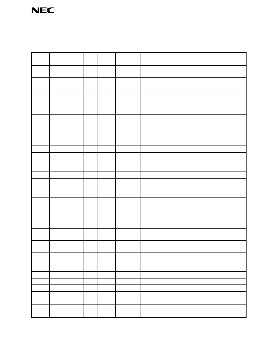
Table 1-1. Pin Functions (1/2)
No.
Symbol
I/O
Level
Buffer type
PU/PD [k
]
Description
1, 33,
48, 75
DGND
-
-
-
Digital section ground
2, 3
TESTIC1,
TESTIC2
I
LVTTL
3.3 V
PD:50
IC testing (Grounded)
4-12,
28-30,
78-85,
99
TEST01-TEST09,
TEST10-TEST12,
TEST18-TEST25,
TEST26
-
-
-
Device test (Open)
13
EXTALTF
O
LVTTL
3.3 V
3 mA
Extended alternate flag output
(This pin is enable in EXTDYCO = 1)
14 - 23
EXTDYCO0-
EXTDYCO9
I/O
LVTTL
3-state
3.3 V
3 mA
Extended digital I/O
(These pins are enable in EXTDYCO = 1)
24, 25
DGNDRAM
-
-
-
DRAM section ground
26, 27
DVDDRAM
-
-
-
DRAM section 2.5 V supply voltage
31
DVDDIO
-
-
-
I/O terminal section 3.3 V supply voltage
32,
40-43
TEST13,
TEST14-TEST17
-
-
-
Device Test (Grounded)
34, 35
AGND
-
-
-
X'tal oscillation circuit section gound
36
XI
I
Analog
2.5 V
f
SC
generator reference clock input (X'tal is connected.)
37
XO
O
Analog
2.5 V
f
SC
generator reference clock inverted output (X'tal is
connected.)
38
AVDD
-
-
-
X'tal oscillation circuit section 2.5 V supply voltage
39, 62,
100
DVDD
-
-
-
Digital section 2.5 V supply voltage
44
RPLL
I
LVTTL
3.3 V
PD:50
Test pin (Grounded)
45
SLA0
I
LVTTL
3.3 V
I
2
C bus slave address selection input
(L : B8h / B9h, H : BAh / BBh)
46
SCL
I
Schmitt
Fail Safe
3.3 V
I
2
C bus clock input (Connected to system SCL line)
47
SDA
I/O
Schmitt
Fail Safe
3.3 V
6 mA
I
2
C bus data input/output (Connected to system SDA line)
49
AGND
-
-
-
f
SC
generator DAC section ground
50
AVDD
-
-
-
f
SC
generator DAC section 2.5 V supply voltage
51
FSCO
O
Analog
2.5 V
f
SC
generator f
SC
output
52, 53
AGND
-
-
-
8f
SC
-PLL ground
54
FSCI
I
Analog
2.5 V
8f
SC
-PLL f
SC
input
55
AVDD
-
-
-
8f
SC
-PLL section 2.5 V supply voltage
56
CKMD
I
LVTTL
3.3 V
PD:50
Clock mode test input (Grounded)
('L' : Normal mode, 'H' : 8fsc clock external input mode)
µ
µ
µ
µ
PD64084
10
Data Sheet S16021EJ2V0DS
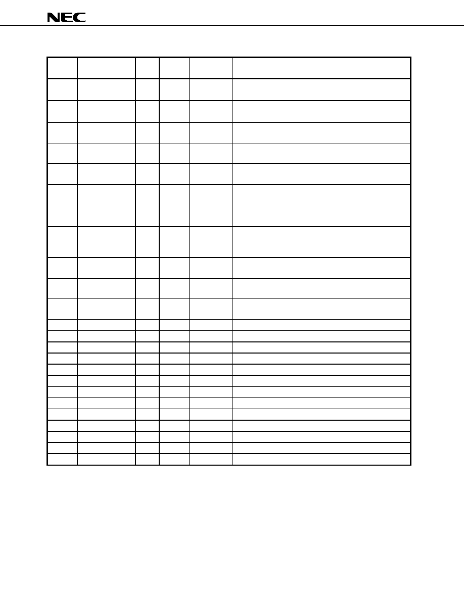
Table 1-1. Pin Functions (2/2)
No.
Symbol
I/O
Level
Buffer type
PU/PD [k
]
Description
57
CLK8
I/O
LVTTL
3-state
3.3 V
6 mA
CKMD = 0 : 8f
SC
clock output
CKMD = 1 : 8fsc clock input
58
RSTB
I
Schmitt
3.3 V
PU:50
System reset input (Active-low)
(Active-low reset pulse is input from the outside.)
59
ST0
O
LVTTL
3.3 V
3 mA
Internal signal monitor output 0
60
ST1
O
LVTTL
3.3 V
3 mA
Internal signal monitor output 1
61
NSTD
O
LVTTL
3.3 V
3 mA
Nonstandard signal detection monitor output
('L' : standard, 'H' : nonstandard)
63-
72
DYCO0-
DYCO9
I/O
LVTTL
3-state
3.3 V
3 mA
EXADINS=0: Digital YC signal alternate output
EXADINS=1: Digital video data input for external ADC (Pull
down unuse lower bit pins via resistor)
DYCO0 is the LSB, DYCO9 is the MSB.
73
ALTF
O
LVTTL
3.3 V
3 mA
EXADINS=0: Digital YC signal alternate flag output
('L' : C, 'H' : Y)
EXADINS=1: 4f
SC
clock output for external ADC
74
LINE
I
LVTTL
3.3 V
PD:50
Forced inter-line processing selection input
('L' : ordinary processing, 'H' : forced inter-line processing)
76
KIL
I
LVTTL
3.3 V
PD:50
External killer input
('L' : ordinary processing, 'H' : forced Y/C separation stop)
77
CSI
I
Schmitt
3.3 V
PU:50
Composite sync input (Active-low)
86
AVDD
-
-
-
Y-DAC and C-DAC 2.5 V supply voltage
87
CBPC
O
Analog
2.5 V
C-DAC phase compensation output
88
ACO
O
Analog
2.5 V
C-DAC analog C signal output
89
AYO
O
Analog
2.5 V
Y-DAC analog Y signal output
90
CBPY
O
Analog
2.5 V
Y-DAC phase compensation output
91
AGND
-
-
-
Y-DAC and C-DAC ground
92
AGND
-
-
-
ADC ground
93
AYI
I
Analog
2.5 V
ADC analog composite signal input
94
VCLY
O
Analog
2.5 V
ADC clamp potential output
95
VRBY
O
Analog
2.5 V
ADC bottom reference voltage output
96
VRTY
O
Analog
2.5 V
ADC top reference voltage output
97
VCOMY
O
Analog
2.5 V
ADC common mode reference voltage
98
AVDD
-
-
-
ADC 2.5 V supply voltage
µ
µ
µ
µ
PD64084
11
Data Sheet S16021EJ2V0DS
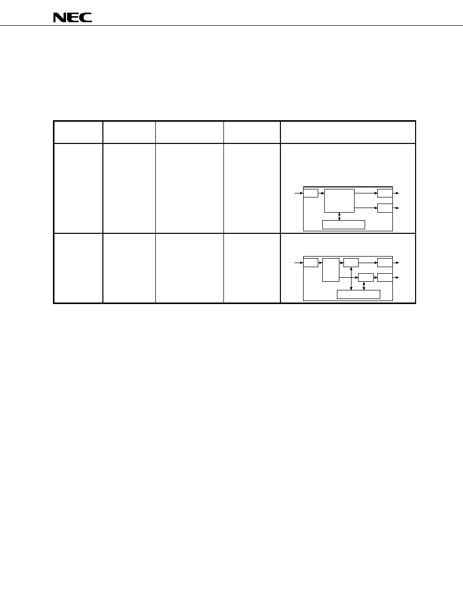
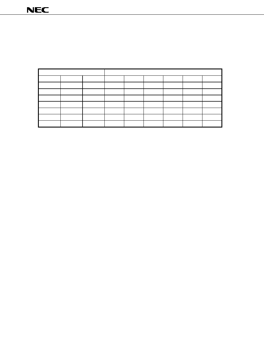
2.
SYSTEM OVERVIEW
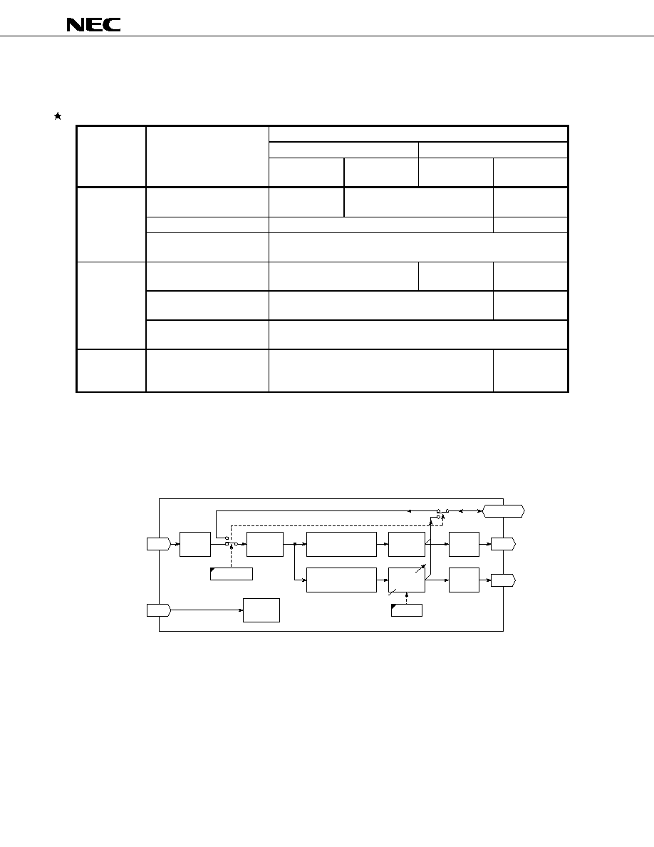
2.1
Operation Modes
The
µPD64084 can operate in the following major four signal processing modes. Mode selection is performed
according to NRMD on the serial bus.
Table 2-1. Operation Modes
Serial bus setting
Mode name
Function
Note
Pin input
System clock
Feature Model diagram
NRMD = 0
YCS mode
Y/C separation
AYI : Composite signal
Burst locked clock
(4f
SC
, 8f
SC
)
∑ For standard signals, motion-adaptive three-
dimensional Y/C separation is performed.
∑ For nonstandard signals, inter-line Y/C
separation is performed.
Y
C
4f
SC
YCS
(3D/2D)
Comp.
4-Mbit memory
ADC
DAC
DAC
NRMD = 1
YCS+ mode
2D Y/C
separation
and YCNR
AYI : Composite signal
Burst locked clock
(4f
SC
, 8f
SC
)
∑ Inter-line Y/C separation and Frame recursive
YNR and CNR is performed.
Y
C
DAC
YNR
CNR
DAC
ADC
4f
SC
YCS
(2D)
Comp.
4-Mbit memory
Note
3D Y/C separation, Frame-recursive YNR/CNR, each function is independence. So these don't operate at the
same time.
µ
µ
µ
µ
PD64084
12
Data Sheet S16021EJ2V0DS
2.2
Filter Processing
Table 2-2 lists filters used in each mode.
Table 2-2. Filter Matrix
Filter selected
Mode
Standard / nonstandard / killer
signal detection
Effective-picture period
Blanking period
Still picture
portion
Moving picture
portion
Horizontal
(11
µs)
Vertical
(1H to 22H)
YCS mode
(NRMD = 0)
Standard signal detected
Frame comb
Line comb
Band-pass
Note
Nonstandard signal detected
Line comb
Band-pass
Note
Killer signal detected
Y output: Through (Y/C separation stop)
C output: Separated C signal
YCS+ mode
(NRMD = 1)
Standard or horizontal
nonstandard signal detected
Line comb + Frame recursive
Line comb
Band-pass
Note
Vertical nonstandard signal
detected
Line comb
Band-pass
Note
Killer signal detected
Y output: Through (Y/C separation stop)
C output: Separated C signal
Vertical contour
compensation /
Y peaking
-
Active
Through
Note Setting serial bus register SA09h: D0 (VFLTH) enables through output.
2.3
System Delay
The following diagram shows a model of system delays (video signal delays).
Figure 2-1. System Delay Model
AYI
ADC
10
Y-DAC
1
C-DAC
1
CSI
0
1
AYO
DYCO9-2
ACO
Y Outpur
C Output
C Sync. Input
Composite
Input
1H Delay
910
Delay
0~7
Filter
4
YCS/YNR
21
CNR/Delay
21
SA02h:D5
Timing
Gen.
CDL
SA03h:D2-D0
EXADINS
Remark
1 corresponds to a one-clock pulse delay (4f
SC
or 910 f
H
= about 69.8 ns).

µ
µ
µ
µ
PD64084
13
Data Sheet S16021EJ2V0DS
2.4
Start-up of Power Supply and Reset
It is necessary to reset the I
2
C bus interface immediately when it is supplied with power. When reset, the I
2
C bus
interface releases its SDA line and becomes operative. In addition, its write register is previously loaded with an initial
value.
<1> When the power is switched on, wait until the power supply line reaches and settles on a 3.3-V/2.5-V level
before starting initialization.
<2> Initialize the I
2
C bus interface circuit by keeping the RSTB pin at a low level for at least 10
µs.
<3> Start communication on the I
2
C bus interface after 100
µs from pull up the RSTB pin to a high level.
Figure 2-2. I
2
C Bus Interface Reset Sequence
DVDDIO
RSTB='L'
3.3 V start-up
Power ON
I
2
C bus access disable
I
2
C bus access enable
Serial bus register data setting
3.3 V
0 V
2.5 V
0 V
3.3 V
0 V
RSTB='H'
DVDD
RSTB
2.5 V start-up
3.3 V cut-off
2.5 V cut-off
s
MIN.
10
µ
s
MIN.
100
µ
Don't care
Caution
Reset is always necessary whether using the serial bus register or not.
µ
µ
µ
µ
PD64084
14
Data Sheet S16021EJ2V0DS
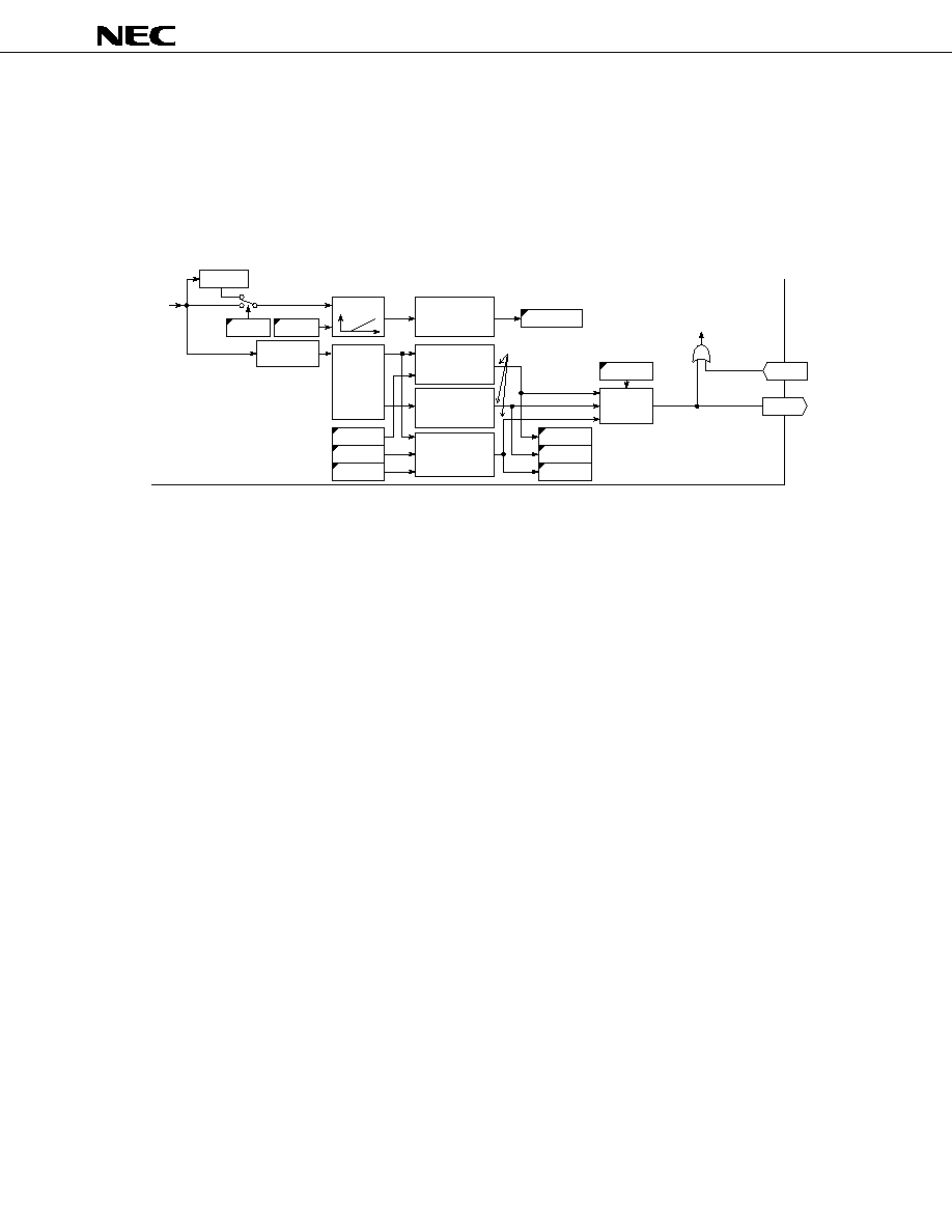
3.
VIDEO SIGNAL INPUT BLOCK
This block converts analog video signals to digital form.
Figure 3-1. Video Signal Input Block Diagram
Analog section supply voltage 2.5
V
Composite input
(When the external
ADC used)
Composite input
(When the internal ADC used)
Clamp
Internal
Clamp pulse generator
Sampling clock
Clamp level
feedback
Pedestal level error
detection
AGND
AVDD
ST0
ALTF
VCLY
VRBY
VRTY
V
IN
DB
1
-DB
8
PCL
CLK
V
RT
V
CL
V
RB
10-bit
ADC
(
10)
CLK
140
IRE
=
0.8
V
p-p
AYI
4f
SC
,910f
H
4f
SC
8
2
1
0
10
10
100
◊2
15
k
47
k
100
◊8
DYCO9-2
DYCO1-0
F
1
µ
PC659A
µ
F
10
to
47
µ
F
0.1
µ
F
0.1
µ
F
0.1
µ
F
0.1
µ
VCOMY
F
0.1
µ
10
EXADINS
256
ST0S=01
3.1
Video Signal Inputs
The composite signal is input to the AYI pin. This analog video (composite) signal converts to digital video signal at
internal 10-bit ADC (EXADINS = 0).
In case of external ADC used, 10-bit composite signals in digital form are input to the DYCO9 to DYCO0 pins
(EXADINS = 1).
3.2
Pedestal Level Reproduction
This circuit reproduces the pedestal level of a video signal. The pedestal level error detection circuit detects the
difference between that level and the internal fixed value of 256 LSB levels, and outputs the feedback level.
This output signal is connected to VCLY pin via internal resistor to feed back to video signal for fixing pedestal level
to 256 LSB. Pull down the VCLY pin via a 0.1
µF bypass capacitor and a 10 to 47 µF electrolysis capacitor for loop
filter.
Caution In case of H-Sync input level is bigger than 256LSB, this pedestal level also becomes over 256LSB.
Do not use this circuit when the external ADC is used.
µ
µ
µ
µ
PD64084
15
Data Sheet S16021EJ2V0DS
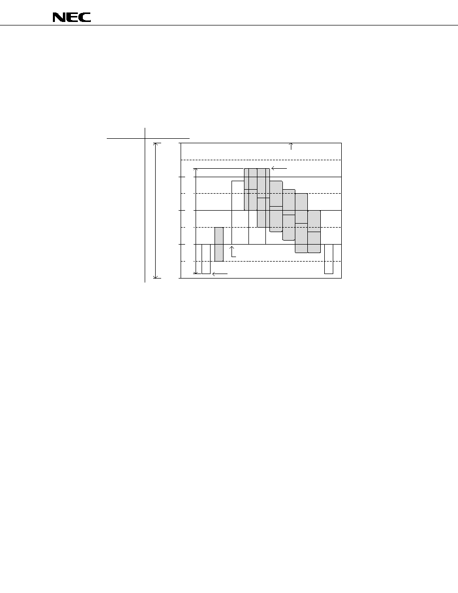
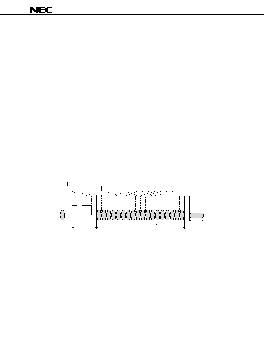
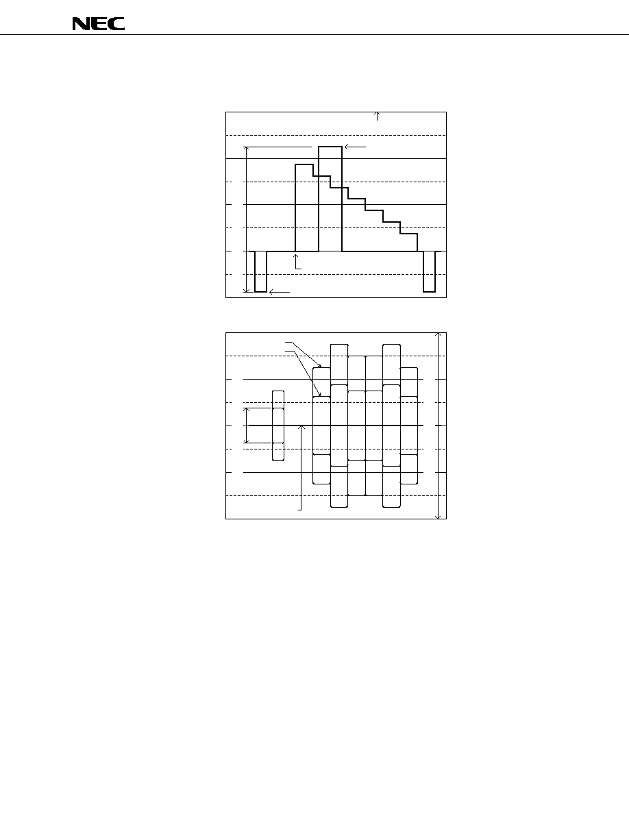
3.3
Video Signal Input Level
It is necessary to limit the level of video (composite) signal inputs to within a certain range to cope with the maximum
amplitude of the video signal and variations in it. Figure 3-2 shows the waveform of the video signal input whose
amplitude is 140 IRE
p-p
= 820 LSB (0.8 times a maximum input range of 1024 LSB). In this case, it is possible to input a
white level of up to 131 IRE for the Y signal and up to 175 IRE
p-p
for the C signal.
Figure 3-2. Video Signal Input Waveform Example (for 75% Color Bar Input)
Pedestal: 0
IRE
=
256
LSB
Sync-tip:
-40
IRE
=
20
LSB
1.6
V
AYI pin input
0.6
V
+131
IRE
±0
IRE
-43
IRE
100
IRE
=
840
LSB
140
IRE
p-p
=
0.8
◊
1024
LSB
=
820
LSB
1.00
V
p-p
1023
896
768
640
512
384
256
128
0
D
YCO9-0 Input / Digital le
v
el (LSB)
MAX. 131
IRE
=
1023
LSB
Remark The recommended input level of video signals is 140 IRE
p-p
= 0.8 V
p-p
(1.00 V
◊ 0.8).
3.4
Pin Treatment
∑
Supply 2.5 V to the AVDD pins. Isolate them sufficiently from the digital section power supply.
∑
Use as wide wiring patterns as possible for the ground lines of each bypass capacitor and the AGND pins so as
to minimize their impedance.
∑
Connect a video signal to the AYI pin by capacitive coupling. Maintain low input impedance for video signals. Be
sure to keep the wiring between the capacitor and the AYI pin as short as possible.
∑
Pull down the VRTY, VRBY and VCOMY reference voltage pins via a 0.1
µF bypass capacitor.
∑
Pull down the VCLY pin via a 0.1
µF bypass capacitor and a 10 to 47 µF electrolysis capacitor.
∑
Do not bring the digital system wiring (especially the memory system) close to this block and the straight
downward of the IC.
µ
µ
µ
µ
PD64084
16
Data Sheet S16021EJ2V0DS
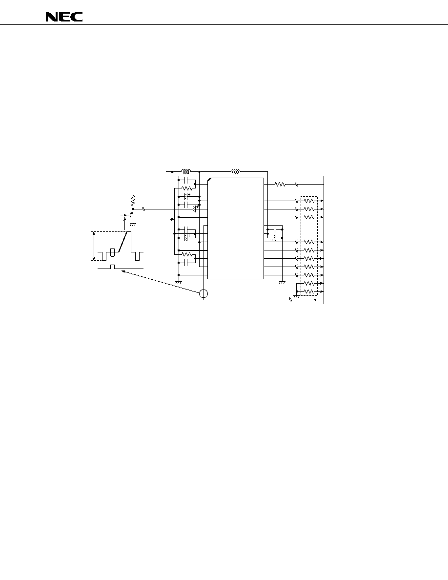
3.5
External ADC Connection Method
Setting up EXADINS = 1 on the serial bus puts the IC in the external ADC mode. In this mode, the ALTF pin is used
to output 4f
SC
sampling clock pulses, and the DYCO9 to DYCO0 pins are used to receive digital data inputs. Setting up
ST0S = 01 on the serial bus causes a clamp pulse to be output from the ST0 pin. It is used as a pedestal clamp pulse
for external ADC. The clamp potential for the pedestal level of external ADC must be determined so that the sampled
value becomes about 256 ±8LSB. Supply converted 10-bit data to the DYCO9 to DYCO0 pins via a 100
resistor. For
using 8-bit ADC (exp.
µPC659A), Pull down the DYCO1 and DYCO0 pins via 100 resistor.
In this mode, for ADC in the
µPD64084, keep the VRTY, VRBY and VCOMY pins open, and pull down the VCLY and
AYI pins via a 0.1
µF capacitor.
Figure 3-3. Example of Application Circuit Set Up for External ADC
CLK
OVER
Clamp Bias
MSB:
DB
1
DB
2
DB
3
DGND
DV
CC
DB
4
DB
5
DB
6
DB
7
LSB:
DB
8
V
RT
(Pin 1)
ALTF (Pin 73)
DYCO9 (Pin 72): MSB
DYCO8 (Pin 71)
DYCO7 (Pin 70)
DYCO6 (Pin 69)
DYCO5 (Pin 68)
DYCO4 (Pin 67)
DYCO3 (Pin 66)
DYCO1 (Pin 64)
DYCO0 (Pin 63)
ST0 (Pin 59)
DYCO2 (Pin 65): LSB
NC
AV
CC
V
IN
AGND
PCL
V
CL
AV
CC
AGND
V
RB
AV
CC
AGND
140
IRE
=
0.8
V
p-p
100
◊10
10
4f
SC
5
V
Composite input
Clamp pulse
47
k
: 1%
15
k
: 1%
PC659AGS
µ
F
0.1
µ
F
0.1
µ
F
2.2
µ
F
10
µ
F
0.1
µ
F
0.1
µ
F
10
µ
F
0.1
µ
F
1
µ
Remark Serial bus registers setting: EXADINS = 1, ST0S = 01
µ
µ
µ
µ
PD64084
17
Data Sheet S16021EJ2V0DS
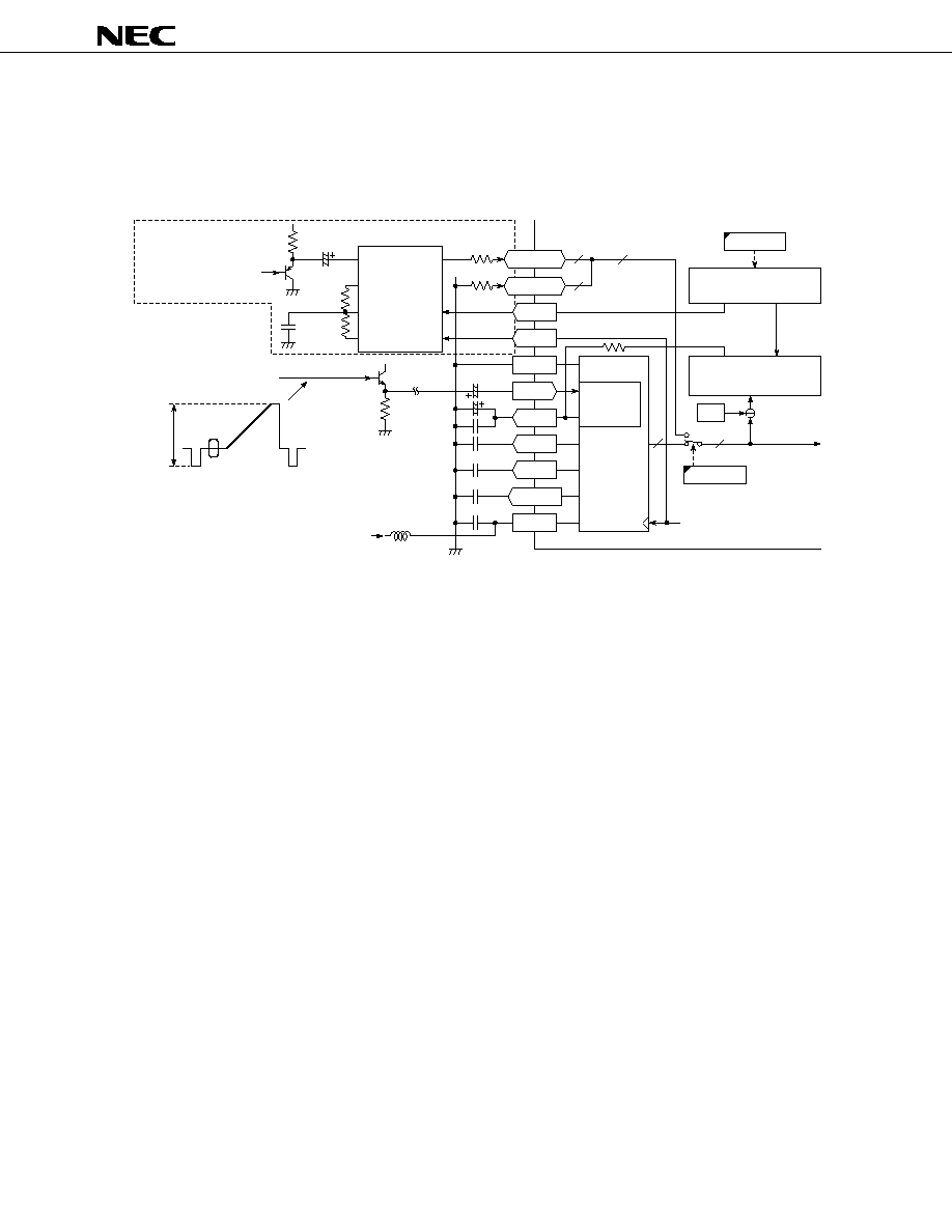
4.
CLOCK/TIMING GENERATION BLOCK
This block generates system clock pulses and timing signals from video signals.
Figure 4-1. Clock/Timing Generation Block Diagram
DGND
AGND
AGND
AVDD
AVDD
1/2
DVDD
22 to 33
pF
20
MHz,16
pF
22 to 33
pF
DAC
XI
FSCI
CSI
AYI
ADC
Composite
input
Composite
sync signal
Horizontal
phase
detection
Killer
detection
Y/C separation
stop, CNR stop
System clock (4f
SC
, 910f
H
)
System clock (8f
SC
, 1820f
H
)
2.5
V power
supply voltage
f
SC
BPF
PLL
filter
Burst phase
detection
Timing generator
System timing
f
SC
generator
8f
SC
PLL
Sync.
separator
Sync.
separator
XO
FSCO
CLK8
F
0.1
µ
F
0.1
µ
F
0.01
µ
F
0.1
µ
F
10
µ
4.1
Sync Separator and Timing Generator
These sections separate horizontal and vertical sync signals from the composite signal sampled at 4f
SC
or 910f
H
,
and generate system timing signals by using them as references.
4.2
Composite Sync Signal Input
An active-low composite sync signal separated from the video signal is input at the CSI pin. This input is used as a
reference signal to lock onto sync at the timing generator.
4.3
Horizontal/Burst Phase Detection Circuit
The horizontal phase detection circuit extracts the horizontal sync signal from the Y signal sampled at 4f
SC
or 910f
H
to detect a horizontal phase error. This phase error is used for generation of 227.5f
H
and timing generator. The burst
phase detection circuit extracts the burst signal from the composite signal sampled at 4f
SC
to detect a burst phase error.
This phase error is used for f
SC
generation.
4.4
PLL Filter Circuit
The PLL filter circuit integrates a burst or horizontal phase error to determine the oscillation frequency of the f
SC
generator ahead.
4.5
Killer Detection Circuit
The killer detection circuit compares the amplitude of the burst signal with the KILR value set on the serial bus to
judge on a color killer. If the burst amplitude becomes smaller than or equal to the set KILR value when the burst
locked clock is operating, the f
SC
generator is allowed to free-run.
µ
µ
µ
µ
PD64084
18
Data Sheet S16021EJ2V0DS
4.6
f
SC
Generator
The f
SC
generator generates f
SC
(or 227.5f
H
when the line locked clock is running) from an oscillation frequency
determined in the PLL filter. f
SC
is converted by internal DAC to an analog sine waveform before it is output from the
FSCO pin. Because this output contains harmonic components, they must be removed using an external band-pass
filter (BPF) connected via a buffer, before the analog sine waveform is input to the FSCI pin via a capacitor. The f
SC
generator uses a 20 MHz free-run clock pulse as a reference.
4.7
8f
SC
-PLL Circuit
The 8f
SC
-PLL circuit generates 8f
SC
(or 1820f
H
) from f
SC
(or 227.5f
H
) input at the FSCI pin. The 8f
SC
signal is output
from the CLK8 pin. It is also used as the internal system clock.
4.8
Pin Treatment
∑
Supply 2.5 V to the AVDD pins. Isolate them sufficiently from the digital section power supply.
∑
Use as wide wiring patterns as possible for the ground lines of each bypass capacitor and the DGND and AGND
pins so as to minimize their impedance.
∑
Connect a 20-MHz Crystal resonator across the XI and XO pins. Provide guard areas using ground patterns to
keep these pins from interfering with other blocks. Table 4-1 shows the crystal resonator specification example.
∑
Connect a BPF to the FSCO pin via an emitter follower. Supply the f
SC
signal to the FSCI pin via a capacitor.
∑
Pull down the RPLL pin via a 0
resistor.
∑
Input an active-low composite sync signal to the CSI pin. Figure 4-2 shows the external composite sync separator
application circuit example.
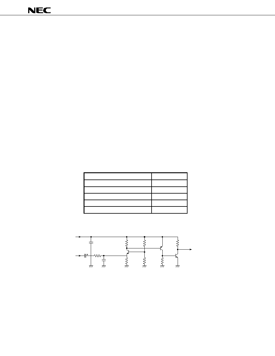
Table 4-1. Crystal Resonator Specification Example
Parameter
Specification
Frequency
20.000000 MHz
Load Capacitance
16 pF
Equivalent Serial Resistance
40
or less
Frequency Permitted Tolerance
50 ppm or less
Frequency Temperature Tolerance
50 ppm or less
Figure 4-2. External Composite Sync Separator Application Circuit Example
Power Supply
(3.3 V)
Composite
Signal (1 V
p-p
)
Composite Sync.
Output
220
F
1
µ
F
0.1
µ
220
k
470
22
k
2.2
k
1
k
4.7
k
1000
pF
to 2200
pF
µ
µ
µ
µ
PD64084
19
Data Sheet S16021EJ2V0DS
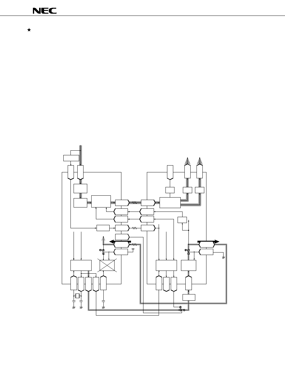
5.
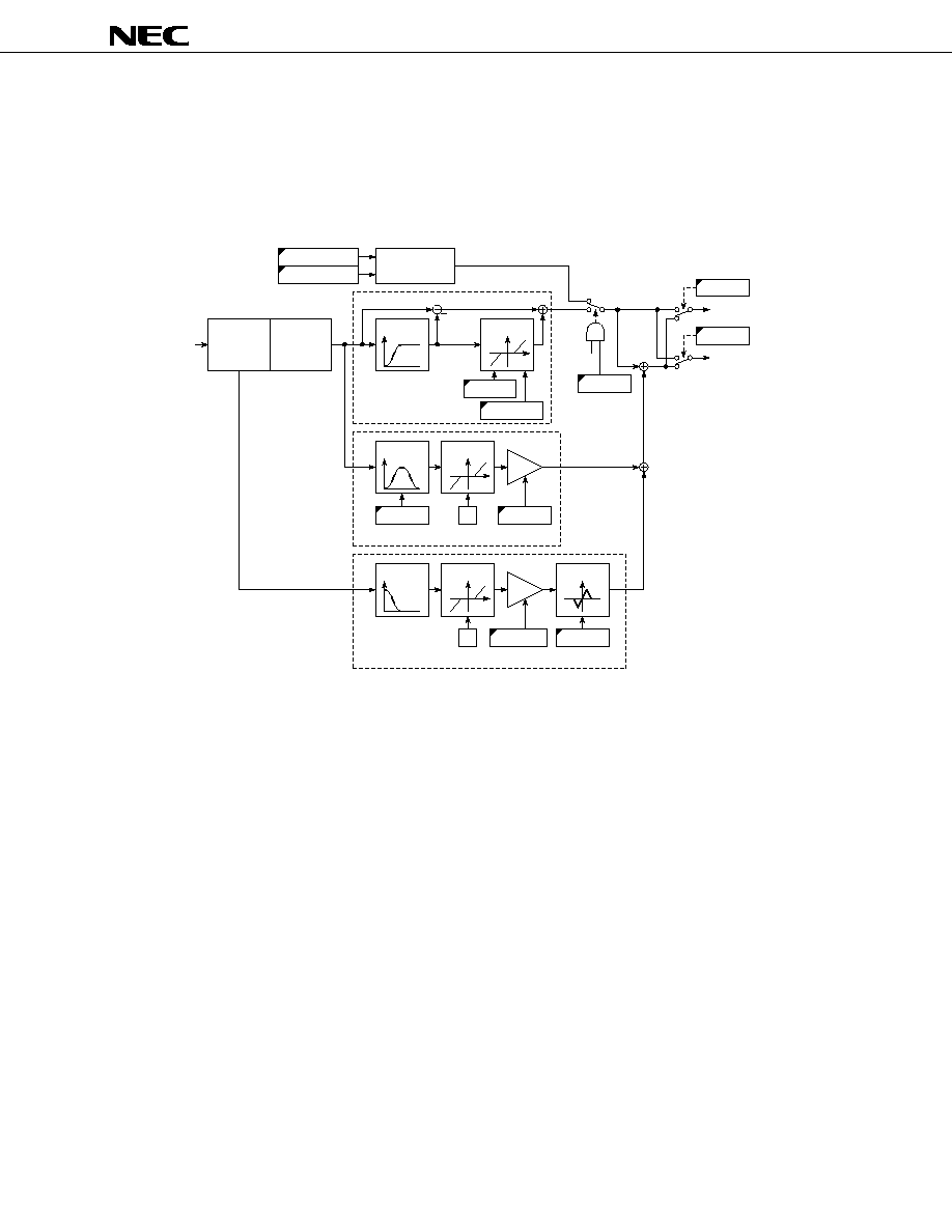
COMB FILTER BLOCK
This block performs Y/C separation or frame comb type YNR according to the result of checks in various detection
circuits.
Figure 5-1. Comb Filter Block Diagram
H
H
0H
C
2
C
3
C
OUT
Y
OUT
H
L
H
L
1H
2H
526H
k
0
Line comb
filter
Frame
Memory
Composite
input
Y signal output
C signal output
Motion
detection
Nonstandard
signal detection
Killer detection
H: Killer signal detected
H: Nonstandard signal detected
Mixer circuit
Frame
comb
filter
Delay
Delay
k
=1
k
1
-
H
H
k
LINE
KIL
5.1
Line Comb Filter
The C signal is separated from video signals that have been delayed by 0H, 1H, and 2H. This filter serves as a
logical comb filter based on inter-line correlation to reduce dot and cross-color interference. The filter output (C
2
) is
used in the moving picture portion of standard signals, nonstandard signals, and blanking periods.
5.2
Frame Comb Filter
The C signal is separated from video signals that have been delayed by 1H and 526H. The filter output (C
3
) is used
in still picture portions by the motion detection circuit.
5.3
Mixer Circuit
The mixer circuit mixes C signals to adapt to the motion according to the motion factor from the motion detection
circuit. In other words, C
OUT
is generated by mixing the line comb filter output (C
2
) and the frame comb filter output (C
3
)
by a mixture ratio according to the motion factor k (0 to 1). If the input signal is a nonstandard signal, or if the LINE pin
is at a high level, C
2
is output without performing motion-adaptive mixture.
5.4
C Signal Subtraction
The Y
OUT
signal is separated by subtracting the C
OUT
signal from a composite video signal that has been delayed by
1H. Subtraction is quitted when the killer detection circuit detects that the input signal is a color killer signal
(monochrome signal or non-burst signal) or that the KIL pin is at an 'H' level.
µ
µ
µ
µ
PD64084
20
Data Sheet S16021EJ2V0DS
6.
MOTION DETECTION BLOCK
This block generates a 4-bit motion factor indicating an inter-frame motion level from the video signal inter-frame
difference. This motion factor is used as a mixture ratio to indicate how the frame and line comb filter outputs are
mixed. This block is used in the YCS mode.
Figure 6-1. Motion Detection Block Diagram
C
2
C
1
Y
2
Y
1
4
0
0
LIM
LIM
|x|
|x|
|x|
Line comb
filter
(current frame)
Frame
memory
Composite
input
To the mixer circuit
MD[3:0]
DC detection
circuit
Motion factor
generation circuit
Maximum
value
section
Expansion
circuit
Coring
DC
DY
DY detection
circuit
LPF
H
H
Line comb
filter
(previous frame)
H
H
|x|
LPF
DYCOR
DCCOR
Gain
Gain
DYGAIN
MSS
0
DCGAIN
Coring
F
0
MSS
1
6.1
Line Comb Filter
Before obtaining an inter-frame difference, the line comb filter performs Y/C separation for the composite signals of
both frames.
6.2
DY Detection Circuit
The DY detection circuit detects a Y signal inter-frame difference. After a Y signal difference between the current
and previous frames is obtained, its absolute value, obtained by limiting the frequency band for the Y signal difference
using an LPF, is output as a Y frame difference signal, or a DY signal.
6.3
DC Detection Circuit
The DC detection circuit detects a C signal inter-frame difference. After a C signal difference between the current
and previous frames is obtained, its absolute value, obtained by limiting the frequency band for the C signal difference
using an LPF, is output as a C frame difference signal, or a DC signal. Because the phase of the C signal is inverted
between frames, the absolute values of the C signals of both frames have been obtained before the difference is
obtained.
6.4
Motion Factor Generation Circuit
The motion factor generation circuit generates a 4-bit motion factor from the DY and DC signals. The first coring
circuit performs coring according to the DYCOR and DCCOR settings on the serial bus to block weak signals like noise.
The gain adjustment circuits ahead perform gain adjustment according to the DYGAIN and DCGAIN settings on the
serial bus to specify the sensitivity of the motion factor. These outputs are limited to a 4-bit width, and one having a
higher level is selected for output by the maximum value selection circuit. The selected signal is expanded horizontally,
then output as a final motion factor.
6.5
Forcible Control for The Motion Factor
The motion factor can be set to 0 (forced stop) or a maximum value (forced motion) using the MSS signal on the
serial bus.
µ
µ
µ
µ
PD64084
21
Data Sheet S16021EJ2V0DS
7.
YNR/CNR BLOCK
This block performs frame recursive YNR and CNR. It is used in the YCS+ mode.
Figure 7-1. YNR/CNR Block Diagram
Y
C
Frame
Memory
Y signal input
C signal input
Y signal output
C signal output
CNR
nonlinear
filter
YNR
nonlinear
filter
Killer signal detected
Current C
Current Y
Substraction of noise component
Previous frame Y
Previous frame C
YNR/CNR stop signal
Frame
difference
Frame
difference
Y'
C'
Noise
component
Noise
component
Delay
Delay
Demodulation
Modulation
1H
+
526H
1H
+
526H
LINE
KIL
H
H
YNRINV
YNRLIM
YNRK
CNRINV
CNRLIM
CNRK
Nonstandard
signal detection
Killer detection
7.1
YNR/CNR Processing
The frame difference (
Y) signal is generated by subtracting the previous frame Y signal from the current frame Y
signal. The noise component
Y' signal is extracted by eliminating the motion component of the Y signal at the
nonlinear filter. Noise components are reduced by subtracting the noise component
Y' signal from the current frame Y
signal. At the same time, the Y signal submitted to noise reduction is delayed by a frame to be used to generate
Y for
the next frame. This way the frame recursive YNR is configured. Much the same processing is performed for the C
signal to reduce noise components.
7.2
Nonlinear Filter
The
Y' and C' noise components are extracted from Y and C. Y and C contain inter-frame motion
components and noise components. Subtracting
Y and C from the current frame Y and C signals causes inter-frame
motion components to remain in the output picture. To solve this problem, a nonlinear filter that passes only low-
amplitude signals is used; generally, motion components have a large amplitude, while noise components have a small
amplitude. How nonlinear the filter is to be is specified using YNRK, YNRLIM, YNRINV, CNRK, CNRLIM, and CNRINV
on the serial bus.
7.3
YNR/CNR Operation Stop
If the nonstandard signal detection circuit detects a vertical nonstandard signal or frame sync nonstandard signal, or
the LINE pin is at a high level, the killer detection circuit detects a color killer signal, or the KIL pin is at a high level,
YNR and CNR operations are stopped.
µ
µ
µ
µ
PD64084
22
Data Sheet S16021EJ2V0DS
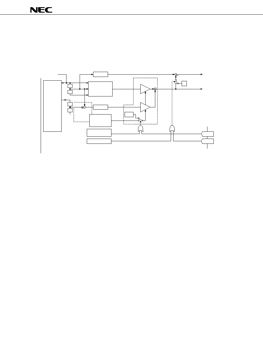
8.
NONSTANDARD SIGNAL DETECTION BLOCK
This block detects nonstandard signals not conforming to the NTSC standard, such as VCR playback signals, home
TV game signals, and Laser-Disc special playback signals. The detection result is used to stop inter-frame video
processing. (and selects intra-field video processing forcibly.)
Figure 8-1. Nonstandard Signal Detection Block Diagram
Video
signal
input
H: Nonstandard
signal detected
Read register
Forced standard or
nonstandard signal
control
Inter-frame processing control
Signal to stop using YNR, CNR,
and frame comb filter
Sync
separation
f
SC
trap
HV
counter
Noise level
detection
Mixer
Frame sync
nonstandard
signal detection
Vertical sync
nonstandard
signal detection
Horizontal sync
nonstandard
signal detection
LINE
NSTD
VTRH
VTRR
LDSR
OVSDF
OHSDF
NSDS
LDSDF
WSC
WSS
WSL
Coring
8.1
Horizontal Sync Nonstandard Signal Detection
The horizontal sync nonstandard signal detection circuit detects signals not having a standard relationship between
f
SC
and f
H
(f
SC
= 227.5f
H
) like a VCR playback signal. The sensitivity of detection is set using VTRR and VTRH on the
serial bus. If the circuit detects a nonstandard signal, it stops using the frame comb filter. The detection result can be
read using OHSDF on the serial bus.
8.2
Vertical Sync Nonstandard Signal Detection
The vertical sync nonstandard signal detection circuit detects signals not having a standard relationship between f
H
and f
V
(f
H
= 262.5f
V
) like a VCR special playback signal and home TV game signal. The sensitivity of detection cannot
be set. If the circuit detects a nonstandard signal, it stops using the frame comb filter, YNR, and CNR. The detection
result can be read using OVSDF on the serial bus.
8.3
Frame Sync Nonstandard Signal Detection
The frame sync nonstandard signal detection circuit detects signals out of horizontal sync phase between frames,
such as a laser-disc special playback signal. The sensitivity of detection is set using LDSR on the serial bus. If the
circuit detects a nonstandard signal, it stops using the frame comb filter, YNR, and CNR. The detection result can be
read using LDSDF on the serial bus.
8.4
Forced Standard or Nonstandard Signal Control
It is possible to specify either forced standard or nonstandard signal control using NSDS on the serial bus.
8.5
Noise Level Detection
The noise level detection circuit detects a noise level in the flat portion of a video signal. The sensitivity of detection
is set using WSCOR on the serial bus. The detection result can be read using WSL on the serial bus; it is not used in
the IC. The detection result can be processed in a microprocessor to find a weak electric field.
µ
µ
µ
µ
PD64084
23
Data Sheet S16021EJ2V0DS
9.
WCV-ID DECODER / ID-1 DECODER BLOCK
This block decodes ID-1 signal of 20H/283H and an identification control signal superimposed on a wide clear vision
signal of 22H and 285H (The wide clear vision standard applies only in Japan).
9.1
WCV-ID Decoder
The WCV-ID decoder checks whether the video signal contains an ID signal by examining mainly the following seven
items. If all these items turn out to be normal, an ID signal is detected. The check and decode results are output to the
ED2 bit and bits B3 to B17 on the serial bus, respectively. In addition, the phase of the confirmation signal is detected.
<1>
A difference in DC level between B1 and B2 is not smaller than a certain value.
<2>
The DC level of the SCH part is not higher than a certain value.
<3>
The f
SC
amplitude of the NRZ part is not larger than a certain value.
<4>
The f
SC
amplitude of the SCH part is not smaller than a certain value (if FSCOFF = 0),
<5>
Items <1> to <4> continue for at least 12 fields.
<6>
The parity of the NRZ part (B3 to B5) is normal.
Note
<7>
The CRC of the NRZ part and SCH part (B3 to B23) is normal.
Note
Note If an error is detected in item <6> or <7>, bits B3 to B17 on the serial bus hold the decoded value for the
previous field.
Figure 9-1. Wide Clear Vision ID Signal Configuration
ED2 bit (0: No ID signal, 1: ID signal)
NRZ part
SCH part
CRC code
Confirmation
signal
MSB
SA02
1
Color
burst
B1
B2
B3
B4
B5
B6
B7
B8
B9
B10
B11
B12
B13
B14
B15
B16
B17
B18
B19
B20
B21
B22
B23
B24
B25
B26
B27
0
0
LSB
MSB
SA03
LSB
µ
µ
µ
µ
PD64084
24
Data Sheet S16021EJ2V0DS
9.2
ID-1 Decoder
The ID-1 decoder checks whether the video signal contains an ID-1 signal by examining mainly the following five
items. If all these items turn out to be normal, an ID signal is detected.
<1> A difference of DC level between Ref signal and the pedestal level is not smaller than a certain value.
<2> The width of each bit is not smaller than a certain value.
<3> Items <1> to <2> continue for at least 6 fields. (When FELCHK register is set to zero, this check is disable)
<4> CRC check is passed.
Remark
If any errors are detected in item <1> to <3>, the output for serial bus hold the decoded value for the
previous field.
If item <3> is disabled by setting FELCHK register to zero, CRC check is also disabled.
If any errors are detected by CRC check, the output for serial bus will be initialized.
Initial values of serial bus registers are WORD0 = 00, WORD1 = 1111, WORD2 = 00h.
Figure 9-2. ID-1 Signal Configuration
CRC code
WORD2
WORD1
MSB
SA04
1
Color
burst
B1
Ref
B2
B3
B4
B5
B6
B7
B8
B9
B10
B11
B12
B13
B14
B15
B16
B17
B18
B20
B19
0
LSB
MSB
SA05
LSB
WORD0
µ
µ
µ
µ
PD64084
25
Data Sheet S16021EJ2V0DS
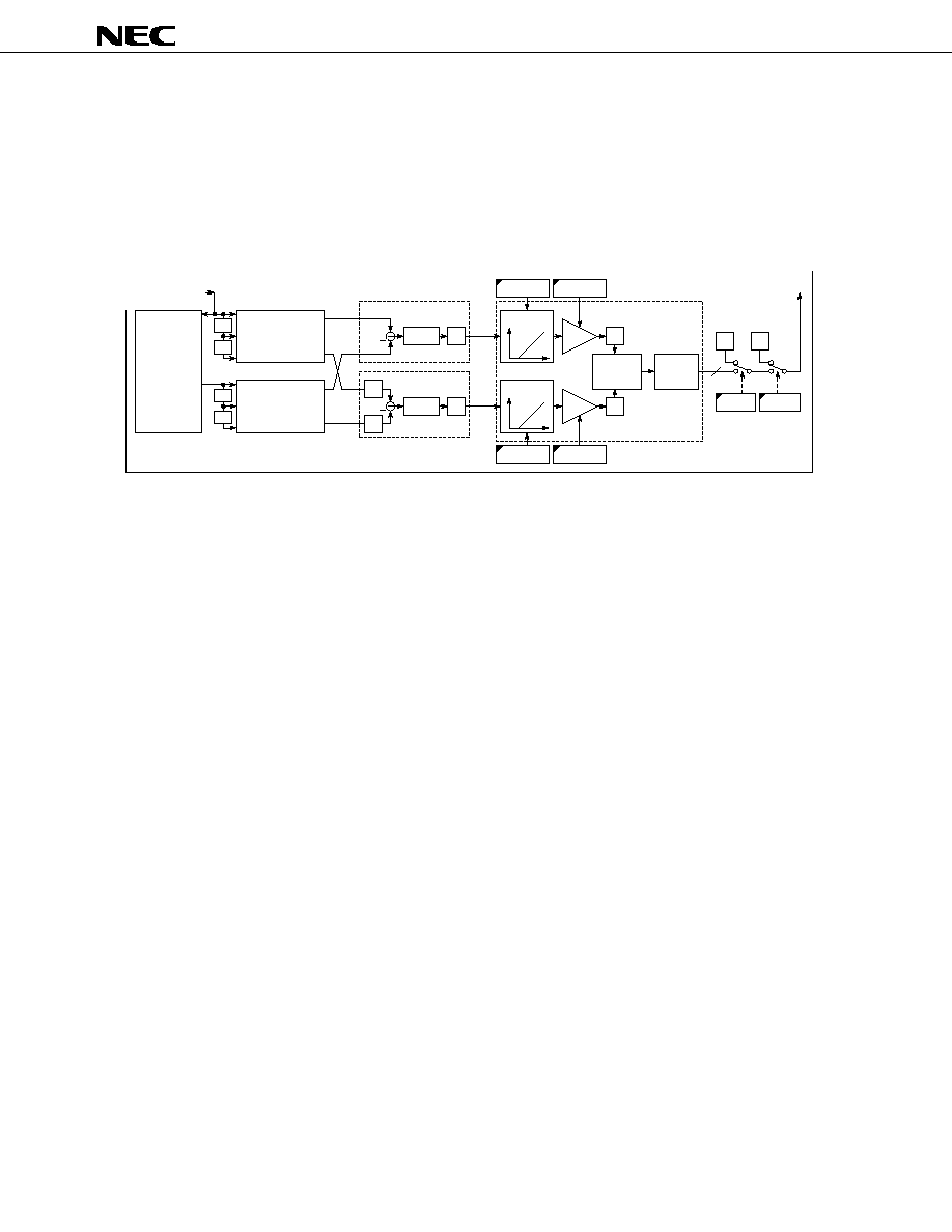
10.
Y SIGNAL OUTPUT PROCESSING BLOCK
After Y/C separation or Y Noise reduction, this block performs high-frequency coring, peaking, and vertical aperture
compensation for the Y signal submitted to YNR processing.
Figure 10-1. Y Signal Output Processing Block Diagram
HPF
YPFT
YPFG
YHCOR
YHCGAIN
ID1ON
YAPS0
YAPS1
ID1ENW0A1
ID1ENW0A2
LPF
BPF
Coring
Coring
Coring
Limiter
0
1
1
0
1
0
2
20/283H
Y
Y signal output
(to the DTCO pin)
Y signal output
(to the Y-DAC pin)
Y high-frequency
coring circuit
ID-1
encoder
Y peaking filter circuit
Vertical aperture compensation circuit
Vertical high-frequency
component
Y high-
frequency
Y low-frequency
k
Line
comb
filter
Y/C
separation
HH decoding
YNR
VAPINV
1
VAPGAIN
k
Composite
input
Peaking component + vertical
aperture conpensation component
10.1
Y High-Frequency Coring Circuit
The Y high-frequency coring circuit performs coring for the high-frequency component of the Y main line signal. It
works as a simplified noise reducer, because it can eliminate high-frequency components at 1 LSB to 3 LSB levels.
The coring level is set using YHCOR on the serial bus.
<1> HPF circuit
: Separates the input Y signal into the low- and high-frequency components.
<2> Coring circuit : Performs coring for Y high-frequency components according to the YHCOR setting, and
outputs a Y signal by adding the Y high- and low-frequency components after they are
submitted to coring. The coring effect can set 1/2 times by the YHCGAIN setting.

µ
µ
µ
µ
PD64084
26
Data Sheet S16021EJ2V0DS
10.2
Y Peaking Filter Circuit
The Y peaking filter circuit performs peaking processing for the Y signal to correct the frequency response of the Y
signal.
<1> BPF circuit
: Extracts high-frequency components from the original Y signal according to the
YPFT setting on the serial bus. The center frequency of the BPF can be selected
from 3.58, 3.86, 4.08, and 4.22 MHz.
<2> Coring circuit
: Performs ±2LSB (in 8-bit terms) coring for Y high-frequency components to prevent
S/N deterioration during peaking processing.
<3> Gain adjustment circuit : Performs gain adjustment for peaking components according to the YPFG setting on
the serial bus. The gain to be added can be changed in 16 steps over a range
between
-1.000 times and +0.875 times.
<4> Addition to the main line : Y peaking components, together with vertical aperture compensation components,
are added to the Y signal.
10.3
Vertical Aperture Compensation Circuit
The vertical aperture compensation circuit extracts vertical contour components from a Y signal and adds them to
the Y signal to emphasize contours.
<1> Line comb filter
: Extracts vertical high-frequency components from the video signal.
<2> LPF circuit
: Eliminates C signal components and Y signal slant components to extract vertical
contour components.
<3> Coring circuit
: Performs ±1LSB (in 8-bit terms) coring for vertical high-frequency components to
prevent S/N deterioration during aperture compensation.
<4> Gain adjustment circuit : Performs gain adjustment for aperture compensation components according to the
VAPGAIN setting on the serial bus.
<5> Limiter circuit (nonlinear processing) :
Performs limit processing for aperture compensation components according to the
VAPINV setting on the serial bus. Signals for which contours are to be emphasized
are rather weak ones. Uniform emphasis would result in initially large signals
becoming too large. To solve this problem, the limiter circuit blocks signals larger
than the VAPINV setting, thereby disabling contour emphasis for large signals.
<6> Addition to the main line : Vertical aperture compensation components, together with Y peaking components,
are added to the Y signal.
10.4
Turning On/Off Y Peaking and Vertical Aperture Compensation
The YAPS setting on the serial bus can be used to turn Y peaking and vertical aperture compensation on and off.
10.5
ID-1 Encoder
Bit information conforming to the ID-1 standard (CPX-1204) can be superimposed on the Y signal output at
20H/283H. ID1ENON on the serial bus specifies whether to turn on or off superimposition. ID1ENW0A1 and
ID1ENW0A2 specify the bit information to be superimposed.
If ID-1 information has already be superimposed on the original signal, it will be replaced with the newly specified
ID-1 information.
µ
µ
µ
µ
PD64084
27
Data Sheet S16021EJ2V0DS
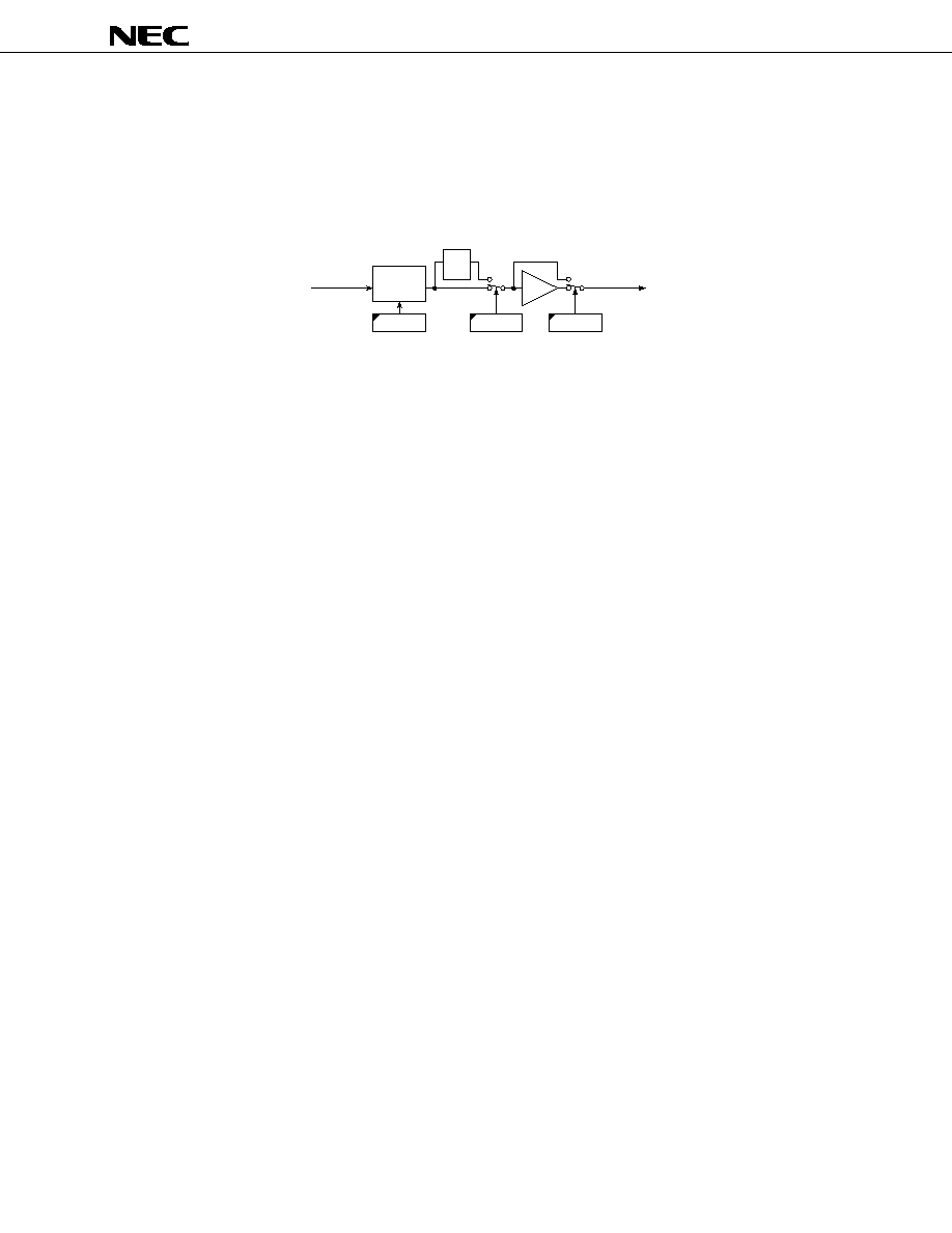
11.
C SIGNAL OUTPUT PROCESSING BLOCK
After Y/C separation, the C signal output processing block performs delay adjustment, BPF processing, and gain
adjustment for the C signal submitted to CNR processing.
Figure 11-1. C Signal Output Processing Block Diagram
COUTS1
◊2
COUTS0
BPF
(f
SC
)
Variable
delay
(
0~7)
CDL
C signal output
C signal input
11.1
C Signal Delay Adjustment
The delay time of the C signal can be varied in a range between 0 and 7 clock pulses (4f
SC
) according to CDL on the
serial bus. This way, the delay of the C signal relative to the Y signal can be set to anywhere between
-4 clock pulses
(
-280 ns) and +3 clock pulses (+210 ns).
11.2
BPF and Gain Processing
COUTS on the serial bus can be used to specify whether to insert a BPF. It can also be used to specify the gain (
◊2
or
◊1).
µ
µ
µ
µ
PD64084
28
Data Sheet S16021EJ2V0DS
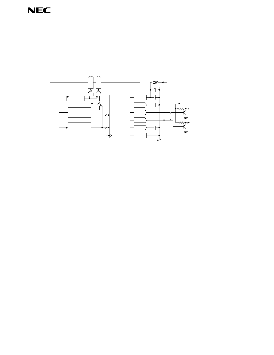
12.
VIDEO SIGNAL OUTPUT BLOCK
The video signal output block can convert digital video signals to analog form. It can also output digital video signals
without performing D/A conversion.
Figure 12-1. Video Signal Output Block Diagram
AGND
AVDD
CBPY
AL
TF
D
YCO
AYO
ACO
CBPC
2ch
10-bit DAC
(Z
-1
)
CLK
System clock (4f
SC
)
4f
SC
,910f
H
C signal input
Supply voltage
Analog Y output
Digital YC / alternate flag output
Analog C output
Supply voltage 2.5 V for analog block
C signal output
processing
Y signal input
Y signal output
processing
10
10
DYCOS1
F
0.1
µ
F
0.1
µ
F
0.1
µ
F
10
µ
12.1
Digital YC Output Processing
When setting up DYCOS = 00 on the serial bus, DYCO9 (MSB) to DYCO0 (LSB) pins alternately output 10 bits of Y
signals in straight binary and 10 bits of C signals in offset binary. And ALTF pin outputs alternative flag of Y or C
signals. When ALTF = 'L' means "C Signal Outputs", when ALTF = 'H' means "Y Signal Outputs".
When setting up DYCOS = 1x on the serial bus, DYCO9 (MSB) to DYCO0 (LSB) and ALTF pins are high-impedance.
When the DYCO pins are not used, setting DYCOS = 1x on the serial bus reduces radiation noise of these pins.
When the external ADC is used, DYCO9 to DYCO0 pins are used as the digital input terminal of video signal. So the
digital YC output is not available.
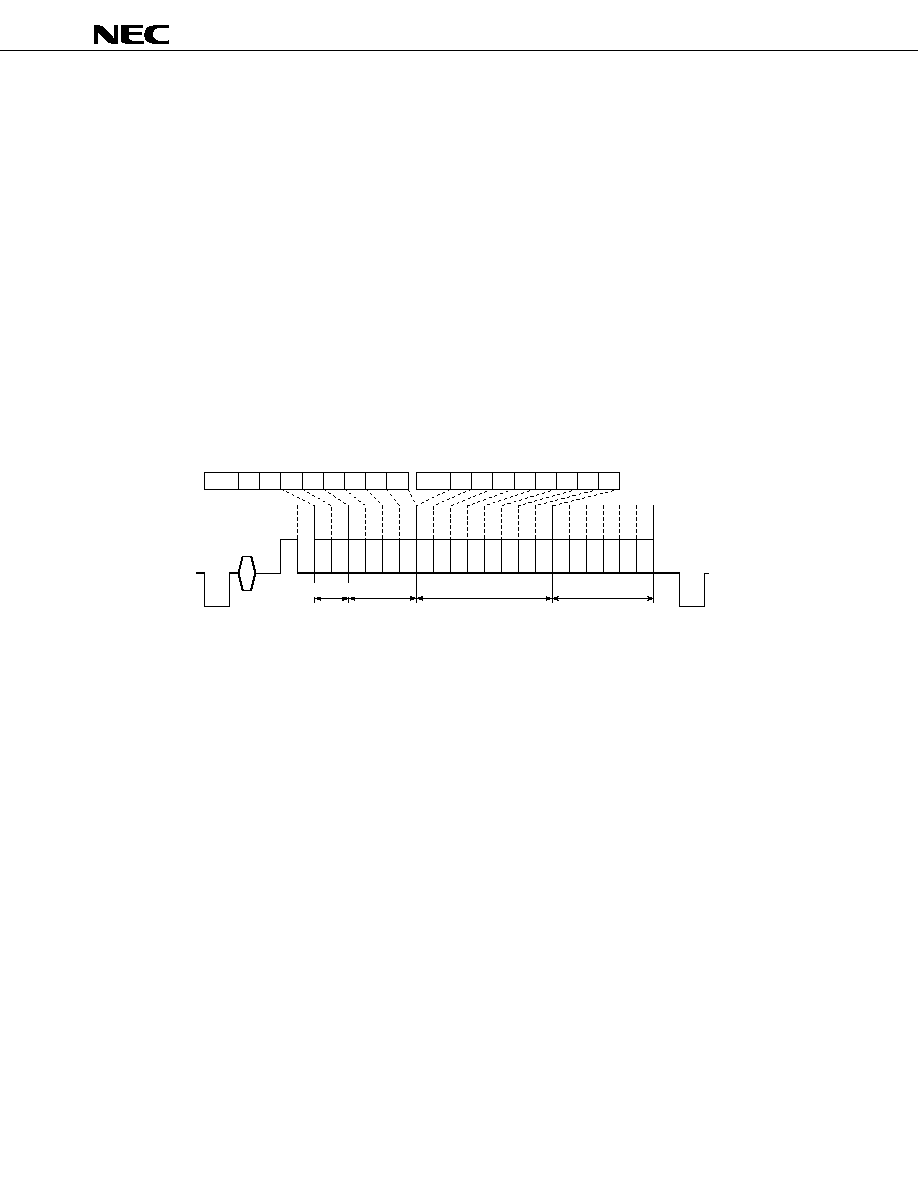
12.2
Video Signal Output Level
Figure 12-2 shows sample waveforms that would be observed at the AYO and ACO pins after a typical video signal
is input (see 3. VIDEO SIGNAL INPUT BLOCK).
µ
µ
µ
µ
PD64084
29
Data Sheet S16021EJ2V0DS
Figure 12-2. Video Signal Output Waveform Example (for 75 % Color Bar Input)
Pedestal: 0
IRE
=
256
LSB
Sync-tip:
-40
IRE
=
20
LSB
100
IRE
=
840
LSB
MAX. 131
IRE
=
1023
LSB
1.94
V
0.94
V
140
IRE
p-p
=
0.8
V
p-p
=
820
LSB
Center
=
512
LSB
COUTS
=
0x
COUTS
=
1x
Burst:
40
IRE
p-p
=
0.23
V
p-p
=
234
LSB
MAX.:
175
IRE
p-p
=
1
V
p-p
=
1023
LSB
+131
IRE: 1023
896
768
640
512
384
0
IRE: 256
128
-43
IRE: 0
IRE:
D
YCO output (LSB)
+87
IRE: 1023
896
768
640
0
IRE: 512
384
256
128
-87
IRE: 0
IRE:
D
YCO output (LSB)
A
Y
O output (V
,
TYP
.)
1.94
V
0.94
V
A
CO output (V
,
TYP
.)
12.3
Pin Treatment
∑
Supply 2.5 V to the AVDD pins and supply 3.3 V to the DVDDIO pin. Isolate them sufficiently from the digital
section power supply.
∑
Use as wide wiring patterns as possible as the ground lines of each bypass capacitor and the AGND pins so as
to minimize their impedance.
∑
Pull down the CBPY and CBPC pins via a 0.1
µF bypass capacitor.
∑
When DAC aren't used, connect AGND pin to digital ground, AVDD pin to digital power supply, and AYO, ACO,
CBPY and CBPC pins set open.
∑
When the digital I/O pin DYCO9 to DYCO0 aren't used, these pins set open.
µ
µ
µ
µ
PD64084
30
Data Sheet S16021EJ2V0DS
13.
EXTEND DIGITAL INPUT / OUTPUT
This device have the extend digital I/O terminals EXTDYCO9-EXTDYCO0 in addition to DYCO9-DYCO0.
Using these terminals, the digital in to digital out system is available.
Table 13-1. Mode setting for extend digital I/O terminals
Serial bus
Condition of each terminals
EXTDYCO
EXADINS
DYCOS[1]
DYCOn
EXTDYCOn
ALTF
EXTALTF
A/D
D/A
0
0
0
OUT
Low
Note
FLAG
Low
ON
ON
0
1
x
IN
Low
Note
4fsc
Low
OFF
ON
0
0
1
Low
Note
Low
Note
Low
Low
ON
ON
1
0
0
OUT
Low
Note
FLAG
Low
ON
ON
1
1
0
OUT
IN
FLAG
4fsc
OFF
ON
1
0
1
Low
Note
OUT
Low
FLAG
ON
ON
1
1
1
IN
OUT
4fsc
FLAG
OFF
ON
Note By setting HIZEN (SA16h, D4) = 1, these pin status are set to Hi-Z.
13.1
Usage of extend digital I/O terminals
The extended digital I/O pin EXTDYCO9 to EXTDYCO0 becomes effective by setting serial bus to EXTDYCO = 1.
At this time, internal ADC can not be available. The I/O mode selection of EXTDYCO9 to EXTDYCO0 are set by
serial bus DYCOS.
When using input mode of DYCOn or EXTDYCOn pins, insert serial resistor in the lines.
13.2
Digital YC output format
The specification of the digital input and output for the extended digital I/O pin EXTDYCO9 to EXTDYCO0 is same as
usual digital I/O pin DYCO9 to DYCO0. When using in input mode, input 10-bit digitized composite video signal that is
sampled by 4fsc. And when using in output mode, EXTDYCO9 (MSB) to EXTDYCO0 (LSB) pins alternately output 10
bits of Y signals in straight binary and 10 bits of C signals in offset binary. And EXTALTF pin outputs alternative flag of
Y or C signals. When ALTF = 'L' means "C Signal Outputs", when ALTF = 'H' means "Y Signal Outputs".
The internal ADC and extended digital I/O can't work at the same time. And extended digital I/O pins have 3.3 V
resistant.
13.3
Pin Treatment
∑
When the extended digital I/O pin EXTDYCO9 to EXTDYCO0 aren't used, these pins set open.
µ
µ
µ
µ
PD64084
31
Data Sheet S16021EJ2V0DS
14.
DIGITAL CONNECTION WITH GHOST REDUCER IC
µ
µ
µ
µ
PD64031A
The
µPD64084 can perform processing from ghost reduction to three-dimension Y/C separation digitally in 10-bit
units when it is directly connected to NEC Electronics' ghost reducer IC
µPD64031A.
Figure 14-1 shows the system configuration when the
µPD64031A and µPD64084 are digitally connected directly.
14.1
Outline
When signals are input from a ground wave tuner, the composite video signal is first input to the A/D converter of the
µPD64031A, where the ghost of the signal is reduced. The digital clamp circuit then adjusts the pedestal level, and the
digital amplifier circuit adjusts the amplitude of the signal. As a result, a 10-bit digital composite video signal is sent to
the three-dimension Y/C separation IC
µPD64084. The µPD64084 then performs processing such as Y/C separation
and outputs a Y/C video signal that has been converted into an analog signal (see Figure 14-1).
Figure 14-1. Example of Digital Connection System with Ghost Reducer
(when signals are input from tuner)
DO9 to DO0
ALTF
OCP
CSO
Delay
C sync separation
f
SC
BPF
1/2
ADC
DAC
DAC
WP1
CLK8
CKMD
DYCO9 to
DYCO0
ALTF
ST0
CSI
CLK8
CKMD
XI
XO
FSCO
CSI
VIN
C20O
FSCI
XI
XO
FSCO
FSCI
AY
I
AY
O
AC
O
GR filter
ADC
8f
SC
PLL
f
SC
generator
8f
SC
PLL
f
SC
/227.5f
H
generator
Y/C
separation
Digital clamp
amplifier
Chroma signal
Burst flag
Burst flag
8f
SC
system clock
8f
SC
system clock
Y/C video output
Clamp pulse
Chroma, sync signal
4f
SC
f
SC
f
SC
path selection
8f
SC
10-bit digital
composite
video signal
20 MHz
Tuner input
Composite video signal input
CLK8
input
and 8f
SC
PL
L stop
µ PD64031A
µ PD64084
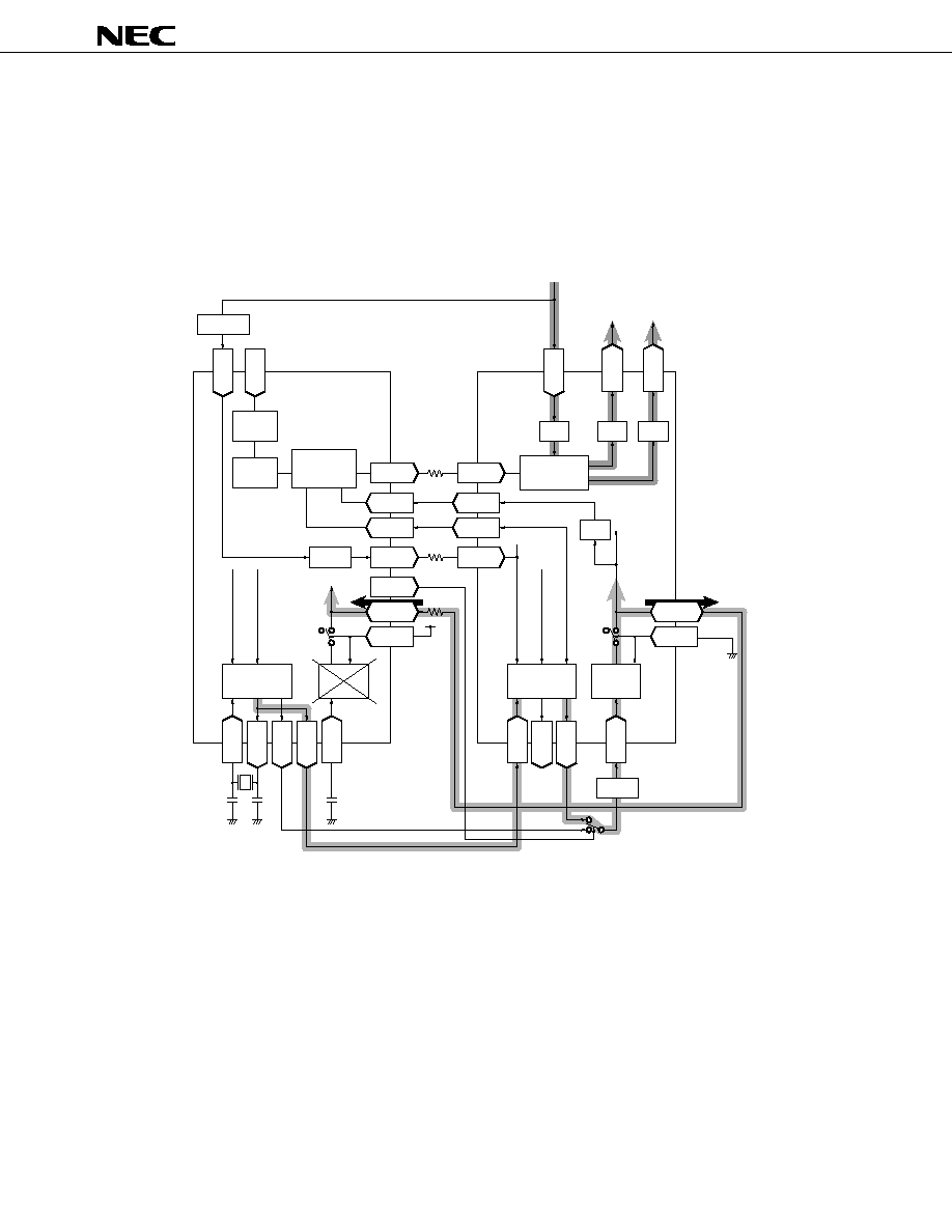
µ
µ
µ
µ
PD64084
32
Data Sheet S16021EJ2V0DS
When signals are input from video (composite or S input), the
µPD64031A is not used, and the video signal is
directly input to the A/D converter of the
µPD64084 (see Figure 14-2).
Figure 14-2. Example of Digital Connection System without Ghost Reducer
(when signals are input from external source)
DO9 to DO0
ALTF
OCP
CSO
Delay
C sync separation
f
SC
BPF
1/2
ADC
DAC
DAC
WP1
CLK8
CKMD
ALTF
ST0
CSI
CLK8
CKMD
XI
XO
FSCO
CSI
VIN
C20O
FSCI
XI
XO
FSCO
FSCI
AY
I
AY
O
AC
O
GR filter
ADC
8f
SC
PLL
f
SC
generator
8f
SC
PLL
f
SC
/227.5f
H
generator
Y/C
separation
Digital
clamp
amplifier
Chroma signal
Burst clamp
Burst clamp
8f
SC
system cloc
k
8f
SC
system cloc
k
Y/C video output
Clamp pulse
Chroma, sync signal
4f
SC
f
SC
3DYC/GR selection
8f
SC
10-bit digital
composite
video signal
20 MHz
Composite video signal input
External pin input, etc.
CLK8 input
and 8f
SC
PLL stop
DYCO9 to
DYCO0
µ
PD64031A
µ
PD64084

µ
µ
µ
µ
PD64084
33
Data Sheet S16021EJ2V0DS
14.2
System Configuration and Control Method
14.2.1
Selecting video signal input path
When a video signal is input from a tuner or external pin, the input path of the video signal must be selected. This
selection is made by a serial bus register of the
µPD64084. If the signal is input from a tuner when the ghost reducer is
used, a digital video signal input pin is selected by the
µPD64084. When signals are input from other external pins
(such as those of a VCR, DVD, video camera, or game machine), the internal A/D converter of the
µPD64084 is made
valid, so that the video signal directly input to the
µPD64084 becomes valid.
For details on how to set the pins and registers, see Table 14-1 and Table 14-2 in Section 14.3.
14.2.2
Selecting mode according to clock and video signal input path
When the
µPD64031A and µPD64084 are digitally connected directly, the system clock must be shared by the two
ICs. When the ghost reducer is used (when signals are input from a tuner), the
µPD64031A generates burst lock clock
f
SC
, as shown in Figure 14-1. This f
SC
goes through an external BPF and is input to the 8f
SC
PLL of the
µPD64084,
where system clocks (8f
SC
and 4f
SC
) are generated. These system clocks are used by the
µPD64084, and are also
supplied to the
µPD64031A by the µPD64084 from the CLK8 pin.
When the ghost reducer is not used (when signals are input from an external source), the video signal is not input to
the
µPD64031A, and only the µPD64084 operates. It is therefore necessary that the burst clock generated by the
µPD64084 be used.
To switch the path of inputting f
SC
to the f
SC
BPF between the FSCO pin of the
µPD64031A and the FSCO pin of the
µPD64084, an analog switch is necessary in the input block of the f
SC
BPF.
This analog switch is controlled by the WP1 pin of the
µPD64031A. The WP1 pin is controlled by register DIR3DYC
(SA08h: D7 and D6) of the
µPD64031A (that selects a three-dimension Y/C separation digital connection mode). By
changing the setting of this register depending on whether the ghost reducer is used or not, the analog switch can be
controlled by the signal output from the WP1 pin. In this way, the f
SC
path can be changed.
A 20-MHz crystal oscillator that generates the basic clock for the f
SC
generator should be provided to the
µPD64031A. When the ghost reducer is not used and the µPD64084 operates alone, the 20-MHz clock output from
the C20O pin of the
µPD64031A is used.
For details on how to set the pins and registers, see Table 14-1 and Table 14-2 in Section 14.3.
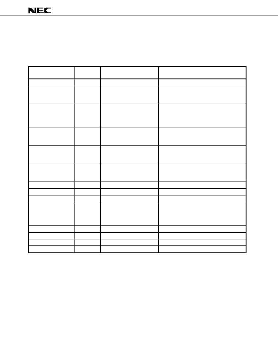
µ
µ
µ
µ
PD64084
34
Data Sheet S16021EJ2V0DS
14.3
Setting of Digital Direct-Connected System
14.3.1
Hardware setting
See the pin connection and setting in the following table to digitally connect the
µPD64031A and µPD64084 directly.
Table 14-1. Pin Setting for Digital Direct-Connection
µ PD64031A Pin
Signal
Direction
µ PD64084 Pin
Function
DO9 to DO0 (pins 6 to 15)
DYCO0 to DYCO9 (pins 63 to 72)
10-bit digital video signal interface
N3D (pin 3)
LINE (pin 74)
Three-dimension processing prohibiting flag
Register N3D1STEN of the
µ PD64031A (SA01h:
D5) must be set.
CSO (pin 4)
CSI (pin 77)
Composite sync signal
The signal from the sync separation circuit
connected to the
µ PD64031A is shared by the
µ PD64084.
ALTF (pin 5)
ALTF (pin 73)
Digital clamp clock (4f
SC
)
Register ADCLKS of the
µ PD64084 (SA15h: D7
and D6) must be set.
OCP (pin 18)
ST0 (pin 59)
Clamp pulse for digital clamp circuit
Register ST0S of the
µ PD64084 (SA07h: D1 and
D0) must be set.
CLK8 (pin 30)
CLK8 (pin 57)
System clock (8f
SC
)
Register CLK8OFF of the
µ PD64084 (SA07h: D4)
must be set.
FSCO (pin 47)
FSCI (pin 54)
Burst lock clock (connected via an analog switch)
C20O (pin 54)
XI (pin 36)
20-MHz reference clock
CKMD (pin 31)
≠
≠
Fixed to high level (external clock mode)
WP1 (pin 35)
≠
≠
Connected to analog switch (control signal output)
This pin is controlled by register DIR3DYC of the
µ PD64031A (SA08h: D7 and D6) to select a clock
path.
EXDAS (pin 58)
≠
≠
Fixed to high level (digital output is valid)
FSCI (pin 40)
≠
≠
Fixed to GND (f
SC
generator is not used)
≠
≠
FSCO (pin 51)
Connected to analog switch
≠
≠
XO (pin 37)
Open

µ
µ
µ
µ
PD64084
35
Data Sheet S16021EJ2V0DS
14.3.2
Register setting
Correctly set the following registers when digitally connecting the
µPD64031A and µPD64084 directly.
Also refer to the following table for register setting to specify whether the ghost reducer is used or not.
Table 14-2. Register Setting
Register
With Ghost Reducer
Used
With Ghost Reducer
Not Used
Remark
µ PD64031A
EXDAS (SA01h: D7)
1
Don't care
Digital data output setting
N3D1STEN (SA01h: D5)
1
Don't care
3-dimesnion processing prohibiting flag setting
CLK20LOW (SA01h: D2)
0
Don't care
20-MHz clock output setting
ADCPMD (SA04h: D5, D4)
10
ADC input bias mode setting
DIR3DYC (SA08h: D7, D6)
10
11
Mode selection (WP1 pin control)
DCPAG (SA08h: D5 to D3)
101
Don't care
Digital clamp characteristic setting
DCPEN (SA09h: D6)
1
Don't care
Digital clamp selection
DCPLPFS (SA09h: D5)
1
Don't care
Error calculation block LPF selection
DCPVEN (SA09h: D4)
1
Don't care
Clamp timing setting
DCP_TEST (SA09h: D3 to D0)
1111
Don't care
Permissible error range during clamping
µ PD64084
EXADINS (SA02h: D5)
1
0
Internal ADC selection
CLK8OFF (SA07h: D4)
0
8f
SC
output setting
ST0S (SA07h: D1, D0)
01
Don't care
Clamp pulse output setting
ADCLKS (SA15h: D7, D6)
01
11
ALTF clock delay setting
HIZEN (SA16h: D4)
1
Digital input / output status select
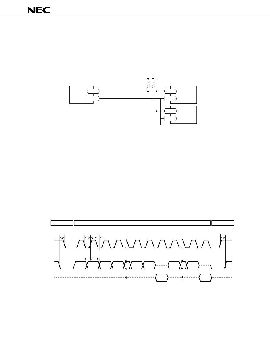
µ
µ
µ
µ
PD64084
36
Data Sheet S16021EJ2V0DS
15.
I
2
C BUS INTERFACE
15.1
Basic Specification
The I
2
C bus is a two-wire bi-directional serial bus developed by Philips. It consists of a serial data line (SDA) for
communication between ICs and a serial clock line (SCL) for establishing sync in communication.
Figure 15-1. I
2
C Bus Interface
Serial data line
Master IC
Slave IC
3.3 V supply voltage
Serial clock line
SCL
SDA
SCL
SDA
Slave IC
SCL
SDA
The following procedure is used to transfer data from the master IC to a slave IC.
<1> Start condition : To start communication, hold the SCL at a high level, then pull down the SDA from a high to a
low level.
<2> Data transfer
: To transfer data, pull up the SCL from a low to a high, while holding the current state of the
SDA. Data transfer is carried out in units of 9 bits, that is, 8 data bits (D7 to D0, MSB first) plus
an acknowledgment bit (ACK). A selected slave IC sets the SDA to a low when it receives bit
9 to send acknowledgment.
<3> Stop condition : To terminate communication, pull up the SDA from a low to a high upon acknowledgment,
while keeping the SCL at a high.
Figure 15-2. Start Condition, Data Transfer, and Stop Condition Formats
Start condition
s
0.1
µ
MIN.
s
0.1
µ
MIN.
s
0.6
µ
MIN.
s
0.6
µ
MIN.
s
1.3
µ
MIN.
Data acceptance
SCL
SDA (Master)
SDA (Slave)
D7
D6
Stop condition
0 ns MIN.
D5
D4
D1
D0
ACK
ACK
Hi-Z
D0
D7
s
0.6
µ
MIN.
Hi-Z
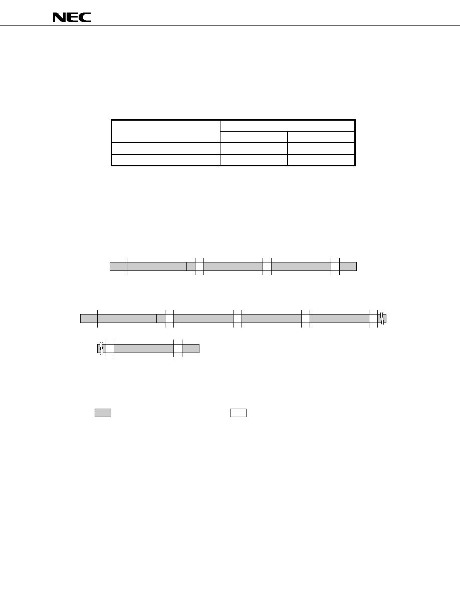
µ
µ
µ
µ
PD64084
37
Data Sheet S16021EJ2V0DS
15.2
Data Transfer Formats
Immediately when the master IC satisfies the start condition, each slave receives a slave address. If the received
slave address matches that of a slave IC, communication begins between the slave IC and the master IC. If not, the
SDA line is released. Two sets of slave addresses can be specified according to the SLA pin.
Table 15-1. Slave Address
SLA pin setting
Slave address
(Unchangeable when power is on)
Write mode
Read mode
L or open
B8h (1011 1000b)
B9h (1011 1001b)
H
BAh (1011 1010b)
BBh (1011 1011b)
(1)
Write mode formats (reception mode for slaves)
If a slave IC receives its write-mode slave address in byte 1, it continues to receive a subaddress in byte 2 and data
in the subsequent bytes. The subaddress auto-increment function enables continuous data reception.
Figure 15-3. Write Mode Formats
(a) One-byte write format
Start
Stop
Slave Address
W
1
bit
1
bit
8
bits
8
bits
1
bit
8
bits
A
A
A
Sub Address n
Data (Sub Address n)
(b) Multiple-byte write format
Start
Stop
Slave Address
W
1
bit
1
bit
8
bits
8
bits
1
bit
8
bits
1
bit
8
bits
A
A
A
A
A
Sub Address n
Data (Sub Address n)
Data (Sub Address n+1)
1
bit
1
bit
8
bits
A Data (Sub Address 17h)
Remark
Start : Start condition
Stop : Stop condition
Sr
: Restart condition
W
: Write mode specification (= 0)
R
: Read mode specification (= 1)
A
: Acknowledgment
N
: No-acknowledgment
XXX
: Master Device
XXX
: Slave Device (
µPD64084)

µ
µ
µ
µ
PD64084
38
Data Sheet S16021EJ2V0DS
(2)
Read mode format (transmission mode for slaves)
If a slave IC receives its read-mode slave address in byte 1, it sends data in byte 2 and the subsequent bytes. No
subaddress is specified in this mode. Transmission begins always at address 0. Before establishing a stop condition,
the master IC must send no-acknowledgment and release the SDA line.
Figure 15-4. Read Mode Format
(a) Single read format
Start
Stop
Slave Address
R
1
bit
1
bit
8
bits
8
bits
1
bit
8
bits
1
bit
A
A
A
A
N
Data (Sub Address 0)
Data (Sub Address 1)
8
bits
Data (Sub Address n)
(b) Multiple read format
Start
Stop
Slave Address
Sub Address n
R
Slave Address
W
1
bit
1
bit
8
bits
8
bits
1
bit
8
bits
1
bit
1
bit
A
Sr
N
8
bits
Data (Sub Address 06h)
A
A
1
bit
8
bits
A
Data (Sub Address n)
A
Remark
Start : Start condition
Stop : Stop condition
Sr
: Restart condition
W
: Write mode specification (= 0)
R
: Read mode specification (= 1)
A
: Acknowledgment
N
: No-acknowledgment
XXX
: Master Device
XXX
: Slave Device (
µPD64084)
15.3
Initialization
The serial bus registers are initialized when the
µPD64084 is reset (RSTB). The I
2
C bus interface become operative
after 100
µs from reset operation. In addition, its write register is previously loaded with an initial value.
For the reset operation, refer to 2.4 Start-up of Power Supply and Reset.
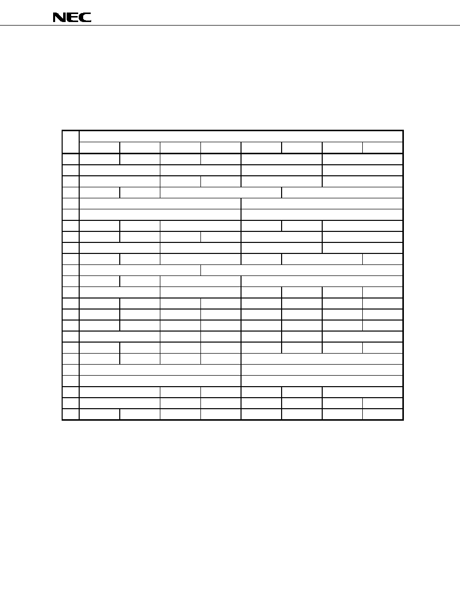
µ
µ
µ
µ
PD64084
39
Data Sheet S16021EJ2V0DS
15.4
Serial Bus Registers
The
µ PD64084 incorporates twenty-four 8-bit write registers and seven 8-bit read registers. Writing to the write
registers is possible in the write mode (with a slave in reception mode), while reading from the read registers is possible
in the read mode (with a slave in transmission mode). The following table lists how each serial bus register is mapped.
(1)
Write register mapping
Slave address: 10111000b = B8h (SLA0 = L), 10111010b = BAh (SLA0 = H)
Data Map (SA00-SA17)
SA
D7
D6
D5
D4
D3
D2
D1
D0
00
0
NRMD
0
1
COUTS
YAPS
01
CLKS
NSDS
MSS
KILS
02
DYCOS
EXADINS
MFREEZE
PECS
EXCSS
03
0
CPP
HDP
CDL
04
DYCOR
DYGAIN
05
DCCOR
DCGAIN
06
YNRK
YNRINV
YNRLIM
CNRK
CNRINV
CNRLIM
07
ID1ON
ID1W0A1
ID1W0A2
CLK8OFF
ST1S
ST0S
08
WSC
VTRH
VTRR
LDSR
09
WSS
ID1DECON
TH
FELCHK
TT
VFLTH
0A
VAPGAIN
VAPINV
0B
0
0
YPFT
YPFG
0C
V1PSEL
VEGSEL
CC3N
C0HS
CLPH
SELD2FH
0D
0
0
SELD1FL
0
0
1
0
1
0E
0
0
0
0
1
0
0
0
0F
0
1
0
0
0
1
0
0
10
YHCOR
YHCGAIN
ED2OFF
OVST
CSHDT
KCTT
11
SHT0
SHT1
VCT
OTT
CLKG2D
CLKGGT
CLKGEB
CLKGT
12
HPLLFS
BPLLFS
FSCFG
PLLFG
KILR
13
HSSL
VSSL
14
BGPS
BGPW
15
ADCLKS
ADPDS
NSDSW
NRZOFF
FSCOFF
VTVH
16
SYSPDS
EXTDYCO
HIZEN
VLSEL
VLTYPE
0
0
17
CNROFS
HCNTFSYN
ADCLPFSW
ADCLPSTP
0
0
0
0
Caution
It may be necessary to change set values on the serial bus depending on the results of
performance evaluation conducted by NEC Electronics.

µ
µ
µ
µ
PD64084
40
Data Sheet S16021EJ2V0DS
(2)
Read register mapping
Slave address: 10111001b = B9h (SLA0 = L), 10111011b = BBh (SLA0 = H)
Data Map (SA00 - SA06)
SA
D7
D6
D5
D4
D3
D2
D1
D0
00
VER
-
KILF
NSDF
LDSDF
OVSDF
OHSDF
01
WSL
02
ED2
B3
B4
B5
B6
B7
B8
B9
03
B10
B11
B12
B13
B14
B15
B16
B17
04
-
-
ID1W0
ID1W1
05
ID1W2
06
DCLEVH
CRCCH
DCFEL
CRCCFEL
HOLD1
-
-
-
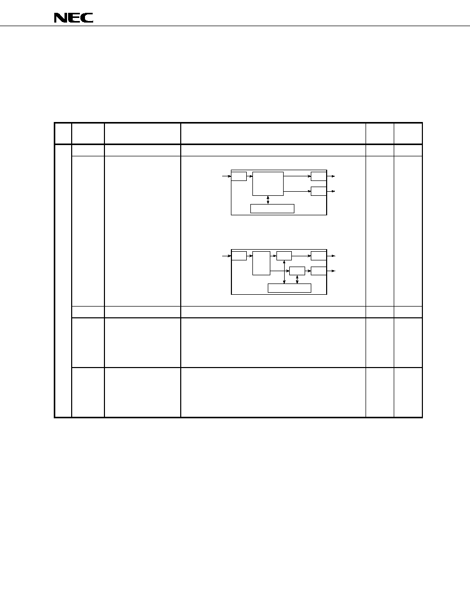
µ
µ
µ
µ
PD64084
41
Data Sheet S16021EJ2V0DS
15.5
Serial Bus Register Functions
Table 15-2 lists the function of each write register. The initial and typical values for each register were determined
for evaluation purposes by NEC Electronics. They are not necessarily optimum values.
(1)
Write Register
Table 15-2. Write Register Functions (1/14)
SA
Bit
Name and function
Description
Typical
value
Initial
value
00
D7
-
Undefined
0
0
D6
NRMD
Specifies an operation
mode.
0 : YCS mode :
Y/C separation (burst locked clocking)
Y
C
4f
SC
YCS
(3D/2D)
Comp.
Memory
ADC
DAC
DAC
1 : YCS+ mode :
2D Y/C separation and YNR/CNR (burst
locked clocking)
Y
C
DAC
YNR
CNR
DAC
ADC
4f
SC
YCS
(2D)
Comp.
Memory
-
0
D5-D4
-
Undefined
01
01
D3-D2
COUTS
Specifies the way the C
signal is output.
(Common to digital and
analog outputs)
00: Input-to-output gain of 2, without BPF processing
01: Input-to-output gain of 2, with BPF processing
10: Input-to-output gain of 1, without BPF processing
11: Input-to-output gain of 1, with BPF processing
11
11
D1-D0
YAPS
Specifies Y signal output
correction. (Vertical
aperture compensation
and Y peaking filtering)
00: Correction is disabled for both analog and digital outputs.
01: Correction is enabled for only analog outputs.
10: Correction is enabled for only digital outputs.
11: Correction is enabled for both analog and digital outputs.
11
11
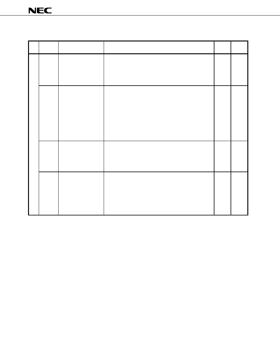
µ
µ
µ
µ
PD64084
42
Data Sheet S16021EJ2V0DS
Table 15-2. Write Register Functions (2/14)
SA
Bit
Name and function
Description
Typical
value
Initial
value
01
D7-D6
CLKS
Specifies whether to
force use of the system
clock.
00: Automatic setting (in an operation mode specified by NRMD)
01: Forced burst locked clocking
1x: Forced line (horizontal) locked clocking
Caution If the specified setting does not match the input
signal, a malfunction may occur.
00
00
D5-D4
NSDS
Specifies whether to
force
standard/nonstandard
signal processing.
00: Adaptive processing (performed according to whether a
nonstandard signal is detected)
01: Forced standard signal processing (performed regardless of
whether a nonstandard signal is detected)
10: Forced horizontal sync nonstandard signal processing
11: Forced vertical sync nonstandard signal processing (forced
inter-line processing)
Caution If the specified setting does not match the input
signal, a malfunction may occur.
00
00
D3-D2
MSS
Specifies whether to
force inter-frame or inter-
line processing.
00: Adaptive processing (performed according to the LINE pin
input and motion detection signal)
01: Forced inter-frame processing (performed according to the
LINE pin input)
1x: Forced inter-line processing
00
00
D1-D0
KILS
Specifies whether to
force killer processing
00: Adaptive processing (performed according to the KIL pin
input and internal killer detection results)
01: Internal killer detection is not used (processing is performed
according to the KIL pin input only).
1x: Forced killer processing
In killer processing, subtraction of the C signal from Comp. Signal
is disabled.
01
01
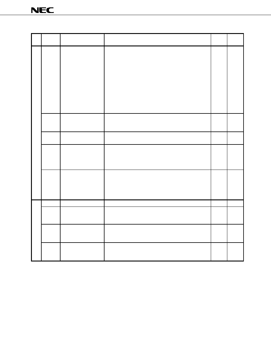
µ
µ
µ
µ
PD64084
43
Data Sheet S16021EJ2V0DS
Table 15-2. Write Register Functions (3/14)
SA
Bit
Name and function
Description
Typical
value
Initial
value
02
D7-D6
DYCOS
Specifies DYCO pin
input/output.
In case of EXTDYCO = 0
00: Y/C separation signal alternate output
01: Test mode (setting prohibited)
1x: Low* High impedance
In case of EXDYCO = 1
00: DYCO9-0 : Output,
EXTDYCO9-0 : Input (When EXADINS=0, Low
Note
)
01: Test mode (setting prohibited)
1x: DYCO9-0 : Input (When EXADINS=0, Low
Note
),
EXTDYCO9-0 : Output
Note If HIZEN (SA16h, D4) = 1, then HI-Z.
10
10
D5
EXADINS
Specifies whether to
select external ADC.
0: Internal ADC
1: External ADC (digital video signal, converted from analog
form, is input to the DYCO9 to DYCO0 pins)
0
0
D4
MFREEZE
External memory test bit
0: Normal mode
1: Test mode (setting prohibited)
0
0
D3-D2
PECS
Specifies a pedestal error
correction test bit.
00: Normal setting
01: Test setting (setting prohibited)
10: Test setting (setting prohibited)
11: Test setting (setting prohibited)
00
00
D1-D0
EXCSS
Specifies whether to use
external C sync input.
00: Internally separated sync signal is always used (CSI input is
not used).
01: Sync signal input at the CSI pin is used during out-of-sync
state.
1x: Sync signal input at the CSI pin is always used.
01
01
03
D7
-
Undefined
0
0
D6
CPP
Specifies the clamp pulse
width of internal ADC
0 : 2.2
µs
1 : 1.1
µs
0
0
D5-D3
HDP
Fine adjustment of
system horizontal phase
000:
-1.12
µs to 100: ±0.00 µs (Typ.) to 111: +0.84 µs
Fine-adjusts the horizontal-processing phase with respect to the
horizontal sync signal (0.28
µs/step).
100
100
D2-D0
CDL
Fine adjustment of C
signal output delay
000:
-280 ns to 100: ±0 ns (Typ.) to 111: +210 ns
Fine-adjusts the C signal phase with respect to the Y signal
(70 ns/step).
100
100
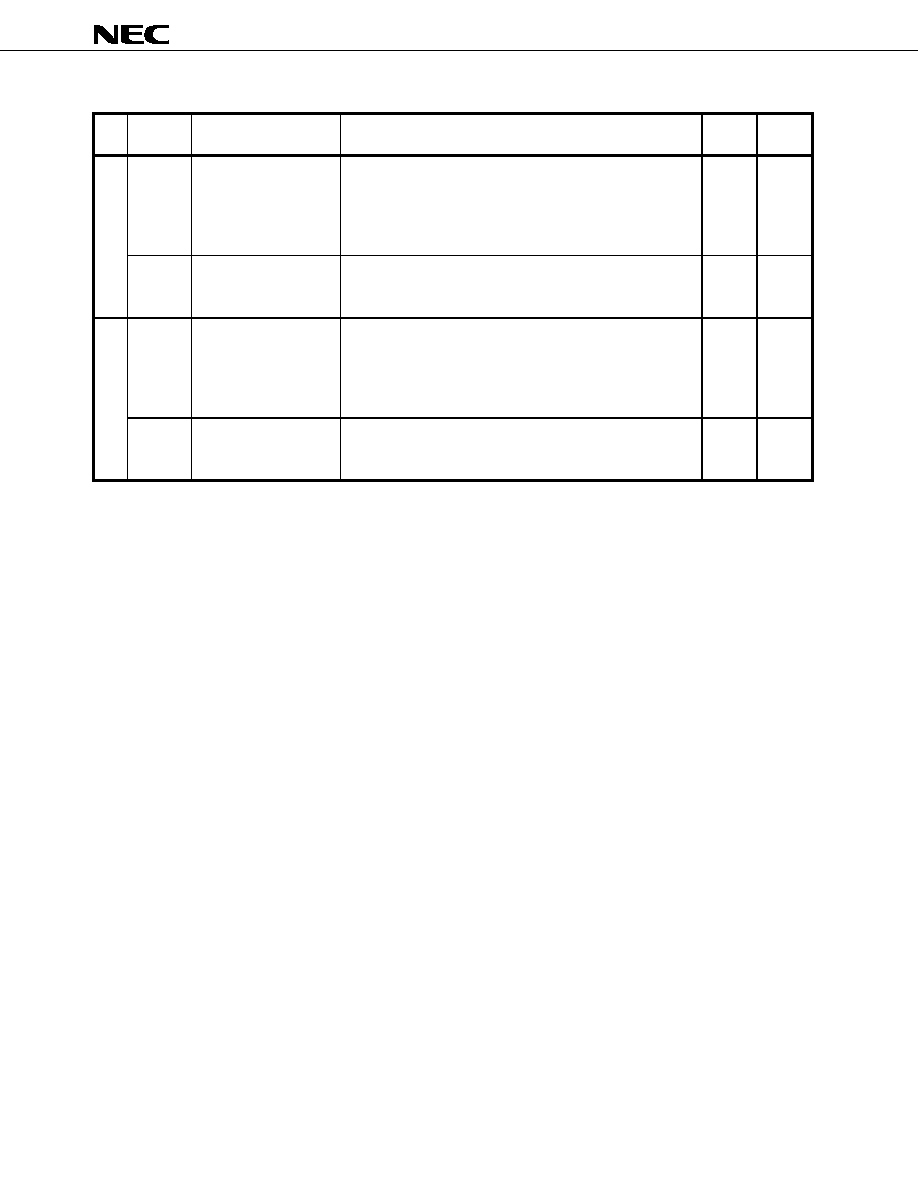
µ
µ
µ
µ
PD64084
44
Data Sheet S16021EJ2V0DS
Table 15-2. Write Register Functions (4/14)
SA
Bit
Name and function
Description
Typical
value
Initial
value
04
D7-D4
DYCOR
DY detection coring level
(Y motion detection
coring)
0000: Coring 0 (Closer to motion pictures) to
1111: Large amount of coring (Closer to still pictures)
The coring level for inter-frame Y difference detection is specified.
A signal smaller than specified is assumed to be noise, resulting
in '0' being output.
0010
0010
D3-D0
DYGAIN
DY detection gain (Y
motion detection gain)
0000: Gain of 0 (Closer to still pictures) to
1111: Maximum gain (Closer to motion pictures)
Inter-frame Y difference detection gain is specified.
1001
1001
05
D7-D4
DCCOR
DC detection coring level
(C motion detection
coring)
0000: Coring 0 (Closer to motion pictures) to
1111: Large amount of coring (Closer to still pictures)
The coring level for inter-frame C difference detection is specified.
A signal smaller than specified is assumed to be noise, resulting
in 0 being output.
0011
0011
D3-D0
DCGAIN
DC detection gain (C
motion detection gain)
0000: Gain of 0 (Closer to still pictures) to
1111: Maximum gain (Closer to motion pictures)
Inter-frame C difference detection gain is specified.
0110
0110
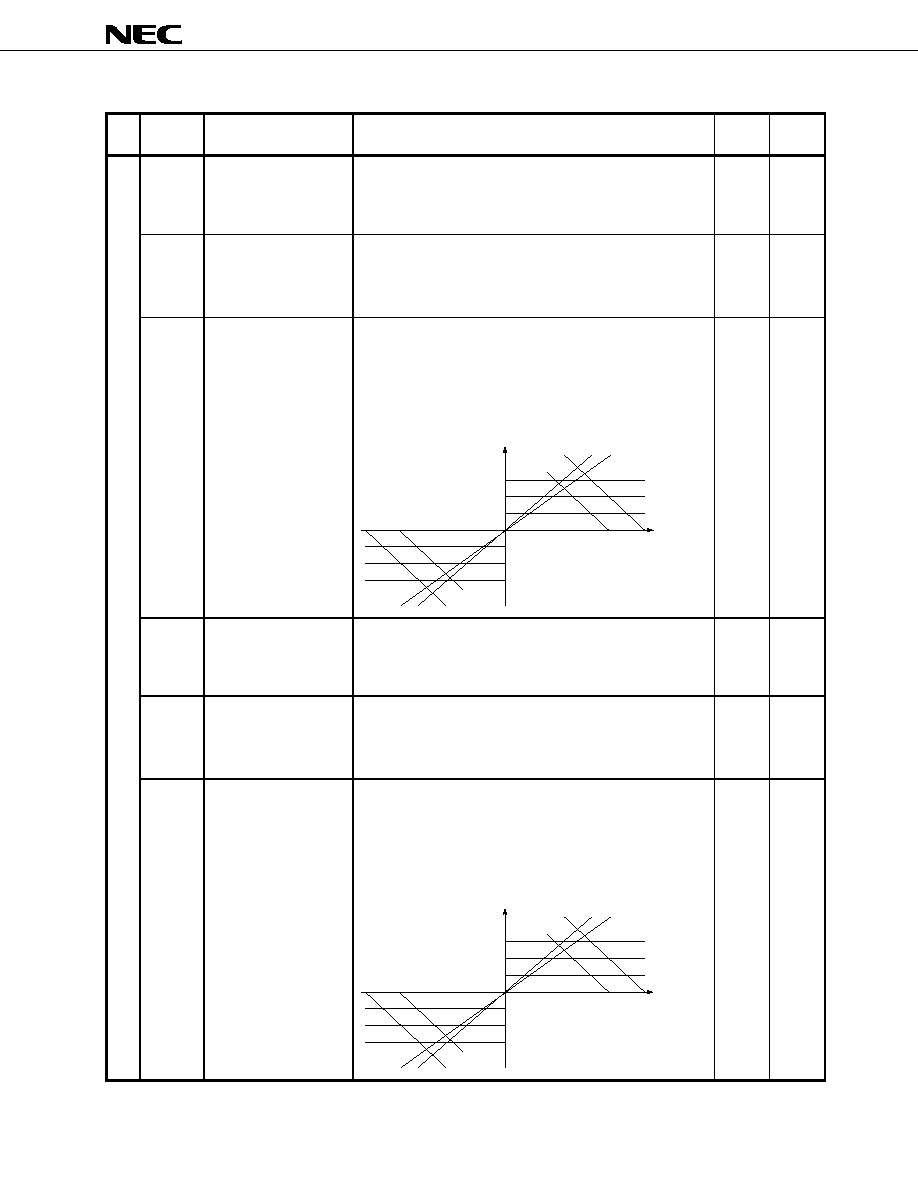
µ
µ
µ
µ
PD64084
45
Data Sheet S16021EJ2V0DS
Table 15-2. Write Register Functions (5/14)
SA
Bit
Name and function
Description
Typical
value
Initial
value
06
D7
YNRK
Specifies the frame
recursive YNR nonlinear
filter gain.
0: x 6/8 (small noise reduction effect and small after-image)
1: x 7/8 (large noise reduction effect and large after-image)
The magnitude of the NR effect is specified.
0
0
D6
YNRINV
Specifies the frame
recursive YNR nonlinear
filter convergence level.
0: 6 LSB (small noise reduction effect and small after-image)
1: 8 LSB (large noise reduction effect and large after-image)
An input larger than specified is assumed to be a motion
component, resulting in 0 being output.
0
0
D5-D4
YNRLIM
Specifies the frame
recursive YNR nonlinear
filter limit level.
00: 0 LSB (YNR off) to
11: 3 LSB (large noise reduction effect and large after-image)
An input larger than specified is assumed to be a motion
component, resulting in a limit value being output.
Nonlinear characteristic curve based on YNRK, YNRINV, and
YNRLIM
Y' output (LSB)
Y
input (LSB)
YNRINV=1
YNRLIM=3
YNRLIM=2
YNRLIM=1
YNRINV=0
4
-4
-8
3
-3
-6
2
-2
1
6
8
-1
YNRK=1 (k=7/8)
YNRK=0 (k=6/8)
Remarks1. The Characteristic are
symmetrical with respect to
the origin.
2. The levels shown are in 8-bit
terms.
01
01
D3
CNRK
Specifies the frame
recursive CNR nonlinear
filter gain.
0: x 6/8 (small noise reduction effect and small after-image)
1: x 7/8 (large noise reduction effect and large after-image)
The magnitude of the NR effect is specified.
0
0
D2
CNRINV
Specifies the frame
recursive CNR nonlinear
filter convergence level.
0: 6 LSB (small noise reduction effect and small after-image)
1: 8 LSB (large noise reduction effect and large after-image)
An input larger than specified is assumed to be a motion
component, resulting in 0 being output.
0
0
D1-D0
CNRLIM
Specifies the frame
recursive CNR nonlinear
filter limit level.
00: 0 LSB (CNR off) to
11: 3 LSB (large noise reduction effect and large after-image)
An input larger than specified is assumed to be a motion
component, resulting in a limit value being output.
Nonlinear characteristic curve based on CNRK, CNRINV, and
CNRLIM
C' output (LSB)
C
input (LSB)
CNRINV=1
CNRLIM=3
CNRLIM=2
CNRLIM=1
CNRINV=0
4
-4
-8
3
-3
-6
2
-2
1
6
8
-1
CNRK=1 (k=7/8)
CNRK=0 (k=6/8)
Remarks1. The Characteristic are
symmetrical with respect to
the origin.
2. The levels shown are in 8-bit
terms.
01
01

µ
µ
µ
µ
PD64084
46
Data Sheet S16021EJ2V0DS
Table 15-2. Write Register Functions (6/14)
SA
Bit
Name and function
Description
Typical
value
Initial
value
07
D7
ID1ENON
Specifies whether to
superimpose ID-1
specification ID signal.
0: Through (no superimposition)
1: Forced superimposition
Caution Do not set this bit to 1 during no-signal state.
-
0
D6
ID1ENW0A1
Specifies whether to set
bit A1 of ID-1 word 0.
0: 0 (transmission aspect of 4:3)
1: 1 (transmission aspect of 16:9)
-
0
D5
ID1ENW0A2
Specifies whether to set
bit A2 of ID-1 word 0.
0: 0 (image display format = normal)
1: 1 (image display format = letter box)
-
0
D4
CLK8OFF
Specifies the state of the
CLK8 pin output.
0: Active-low (to output 8f
SC
clock pulse)
1: Fixed to low level (to reduce radiation noise)
1
0
D3-D2
ST1S
Specifies internal signal
monitor output for the
ST1 pin.
00: I
2
C SDA inversed pulse
01: Internal ADC clamp pulse (active-high)
10: Composite sync (active-low)
11: H sync (active-high)
-
00
D1-D0
ST0S
Specifies internal signal
monitor output for the
ST0 pin.
00: Reserved
01: External ADC clamp pulse (active-high)
10: HV blanking (active-high)
11: V sync (active-low)
-
00
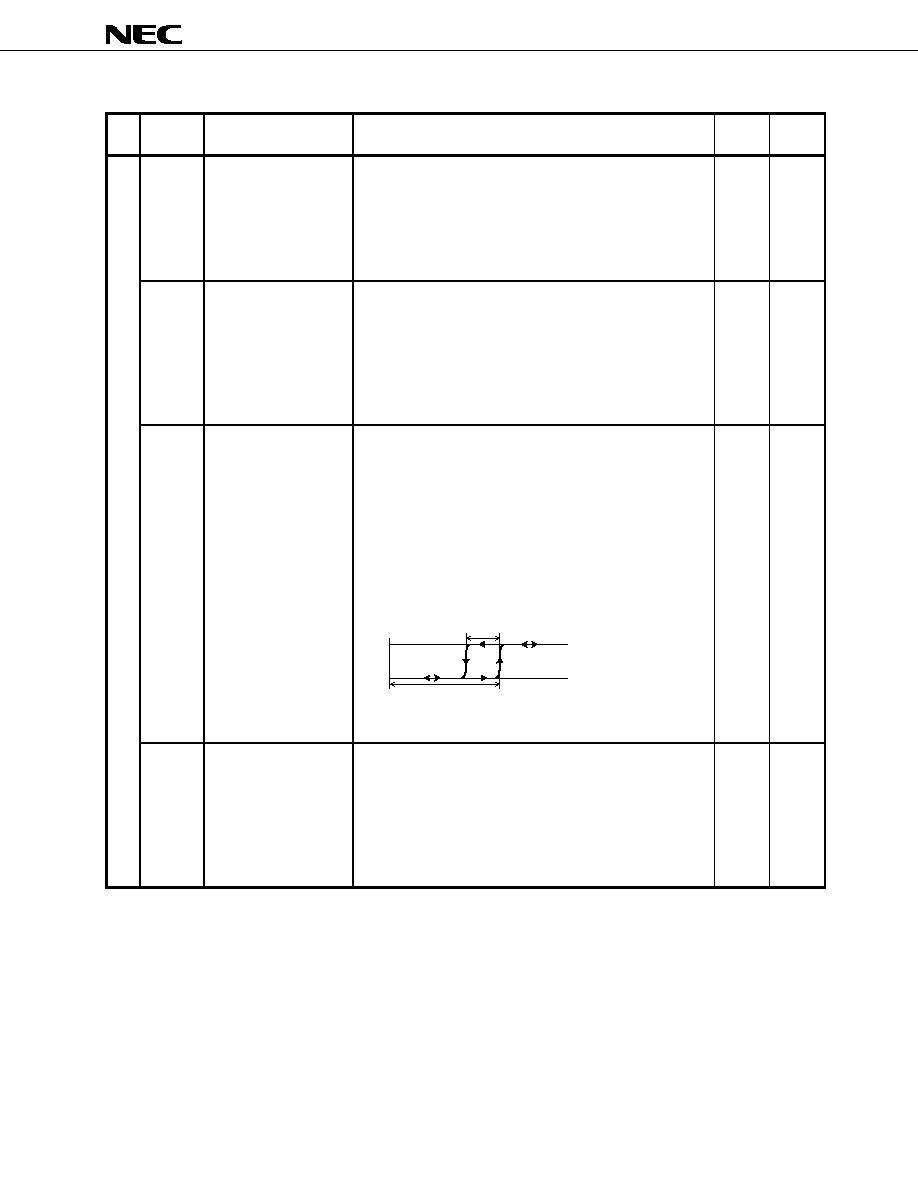
µ
µ
µ
µ
PD64084
47
Data Sheet S16021EJ2V0DS
Table 15-2. Write Register Functions (7/14)
SA
Bit
Name and function
Description
Typical
value
Initial
value
08
D7-D6
WSC
Specifies the amount of
noise detection coring.
00: 0LSB (high detection sensitivity)
01: 1LSB
10: 2LSB
11: 3LSB (low detection sensitivity)
Specifies an input coring value for the noise detection circuit.
Detection results are not used within the device.
01
01
D5-D4
VTRH
Specifies hysteresis for
horizontal sync
nonstandard signal
detection (out-of-
horizontal sync intra-field)
00: Hysteresis off (width of 0 clock pulses)
01: Low hysteresis (width of 2 clock pulses)
10: Medium hysteresis (width of 4 clock pulses)
11: High hysteresis (width of 6 clock pulses)
For horizontal sync nonstandard signal detection, a criterion
value to detect an out-of-horizontal sync state intra-field is
decreased by a value indicated above.
01
01
D3-D2
VTRR
Specifies sensitivity for
horizontal sync
nonstandard signal
detection (out-of-
horizontal sync intra-field)
00: High detection sensitivity (width of ±4 clock pulses)
01: Medium detection sensitivity (width of ±8 clock pulses)
10: Low detection sensitivity (width of ±12 clock pulses)
11: Detection off
If the degree of out-of-horizontal sync state intra-field becomes
larger than specified, a horizontal sync nonstandard signal is
assumed to have been detected.
Horizontal sync nonstandard signal detection characteristic curve
Standard-to-nonstandard hysteresis width
Standard-to-nonstandard
decision criterion
Note 2
OHSD=1 (nonstandard
signal detected)
OHSD=0 (standard
signal detected)
VTRH
◊2(clk)
Note 1
(VTRR+1)
◊4(clk)
Note 1
Notes 1. clk is in 4f
SC
units.
2. Excluding when
VTRR = 11
01
01
D1-D0
LDSR
Specifies sensitivity for
frame sync nonstandard
signal detection (out-of-
horizontal sync inter-
frame)
00: High detection sensitivity (width of 0.5 clock pulses)
01: Medium detection sensitivity (width of 1 clock pulse)
10: Low detection sensitivity (width of 1.5 clock pulses)
11: Detection off
If the degree of out-of-horizontal sync state inter-frame becomes
larger than specified, a frame sync nonstandard signal is
assumed to have been detected.
10
10
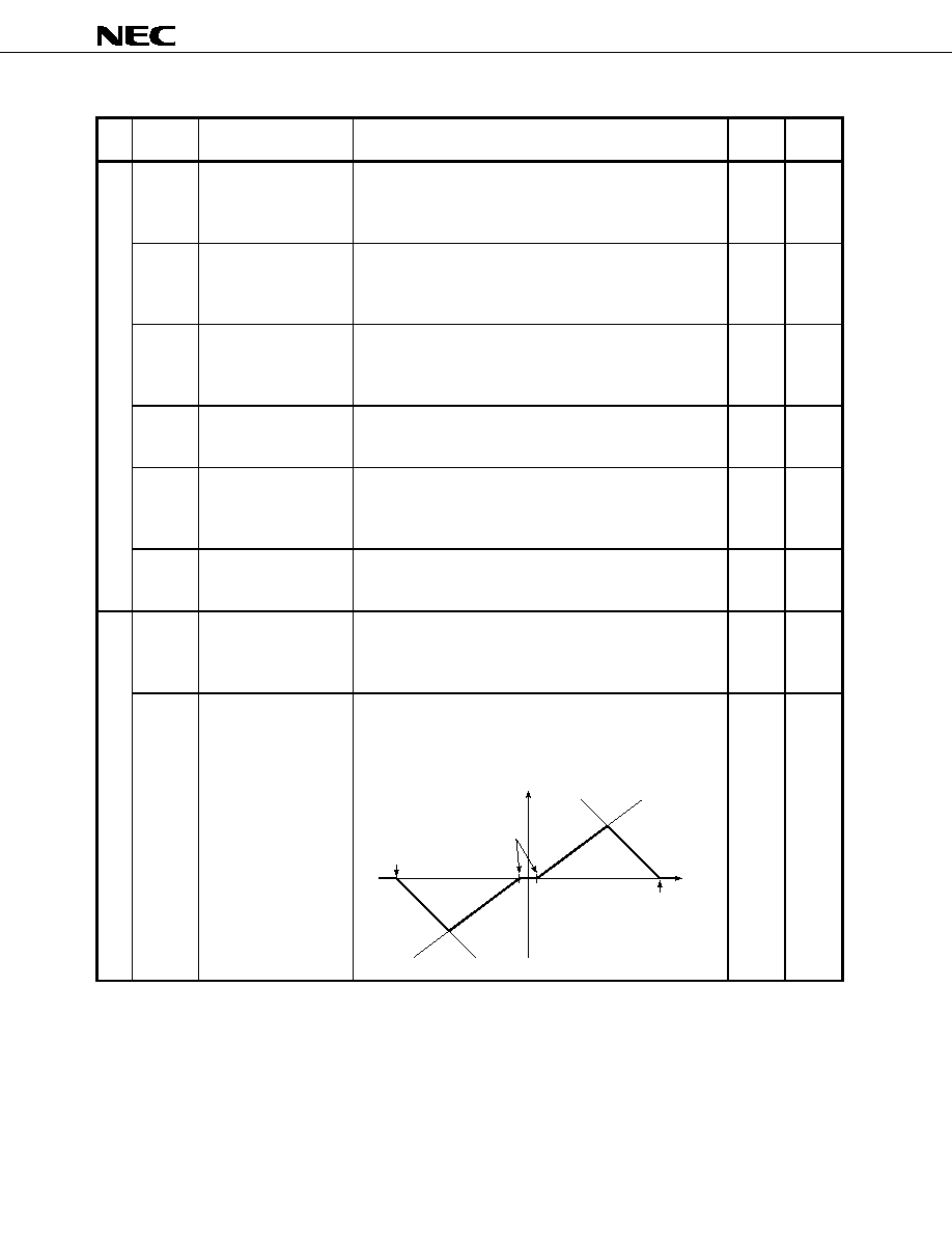
µ
µ
µ
µ
PD64084
48
Data Sheet S16021EJ2V0DS
Table 15-2. Write Register Functions (8/14)
SA
Bit
Name and function
Description
Typical
value
Initial
value
09
D7
WSS
Specifies the pre-filter
characteristic of noise
detection.
0 : Normal (
µPD64082 compatible)
1 : fsc trap
0
0
D6
ID1DECON
ID-1 decoder
0 : disable
1 : enable
When decoding is disable, The output of register is following.
WORD0=00, WORD1=1111, WORD2=00h
1
1
D5-D4
TH
ID-1 decorder
check level
01 : Strict
00 :
10 :
11 : Loose
00
00
D3
FELCHK
ID-1 decoder
Field check enable
0 : 6 fields check is disable
1 : 6 fields check is enable
1
1
D2-D1
TT
ID-1 decoder
pulse width level
00 : 8CLK
01 : 2CLK
10 : 4CLK
11 : 16CLK
00
00
D0
VFILTH
Specifies the vertical
blanking (1H to 22H) BPF
0: BPF enable
1: BPF disable (through)
0
0
0A
D7-D5
VAPGAIN
Specifies a vertical
aperture compensation
gain.
000: Correction off to
111: Maximum correction (0.875 times)
-
000
D4-D0
VAPINV
Specifies a vertical
aperture compensation
convergence point.
00000: Correction off to
11111: Maximum correction
Vertical aperture compensation characteristic curve based on
VAPGAIN and VAPINV
Input
Output
VAPINV
-VAPINV
Tilt: VAPGAIN/8
Note
Tilt: Fixed at -1
Note The curve is symmetrical
with resept to the origin
Coring: Fixed at
±1
-
00000

µ
µ
µ
µ
PD64084
49
Data Sheet S16021EJ2V0DS
Table 15-2. Write Register Functions (9/14)
SA
Bit
Name and function
Description
Typical
value
Initial
value
0B
D7
TEST
Test bit
0: Normal mode
1: Test mode (setting prohibited)
0
0
D6
TEST
Test bit
0: Normal mode
1: Test mode (setting prohibited)
0
0
D5-D4
YPFT
Specifies the Y peaking
filter (BPF) center
frequency.
00: 3.58 MHz, 01: 3.86 MHz, 10: 4.08 MHz, 11: 4.22 MHz
Y-peaking filter BPF characteristic curve
Gain
f (MHz)
k=0
k=1
k=2
k=3
1.25
1.13
1.00
0.88
0.75
0.63
0.50
0.38
0.25
0.13
0.00
0.89
1.79
2.68
3.58
4.47
5.37
6.26
7.16
11
11
D3-D0
YPFG
Specifies a Y peaking
filter gain.
0000:
-1.0 times to 1000: ±0.0 times to 1111: +0.875 times
Y signal output frequency characteristic curve based
on YPFT and YPFG
1.875
YPFT=2
YPFT=0
YPFG=15
YPFG=12
YPFG=8
YPFG=4
YPFG=0
Output
Input freq.
1.5
1.0
0.5
0
0.5f
SC
f
SC
1.5f
SC
1000
1000
µ
µ
µ
µ
PD64084
50
Data Sheet S16021EJ2V0DS
Table 15-2. Write Register Functions (10/14)
SA
Bit
Name and function
Description
Typical
value
Initial
value
0C
D7-D6
V1PSEL
Line comb filter horizontal
dot interference
suppression level
00: Suppression off
01: Low suppression level
10: Medium suppression level
11: High suppression level
Horizontal dot interference is reduced at inter-line Y/C separation.
10
10
D5-D4
VEGSEL
Line comb filter vertical
dot interference
suppression level
00: Suppression off
01: Low suppression level
10: Medium suppression level
11: High suppression level
Vertical dot interference is reduced at inter-line Y/C separation.
10
10
D3
CC3N
Selects a line comb filter
C separation filter
characteristic.
0: Narrow bandwidth
1: Wide bandwidth
0
0
D2
C0HS
Specifies C signal delay
time extension at NR
0: 1H delay
1: No 1H delay
0
0
D1
CLPH
ADC clamp test bit
0: Normal mode
1: Test mode (setting prohibited)
0
0
D0
SELD2FH
Specifies DC detection
High-frequency
sensitivity.
0: Low sensitivity, Closer to still pictures
1: High sensitivity, Closer to motion pictures
0
0
0D
D7
-
0
0
0
D6
-
0
0
0
D5
SELD1FL
Specifies DY detection
low-frequency sensitivity.
0: Low sensitivity, Closer to still pictures
1: High sensitivity, Closer to motion pictures
0
0
D4
-
0
0
0
D3
-
0
0
0
D2-D0
-
101
101
101
0E
D7-D4
-
0000
0000
0000
D3-D0
-
1000
1000
1000
0F
D7-D4
-
0100
0100
0100
D3-D0
-
0100
0100
0100
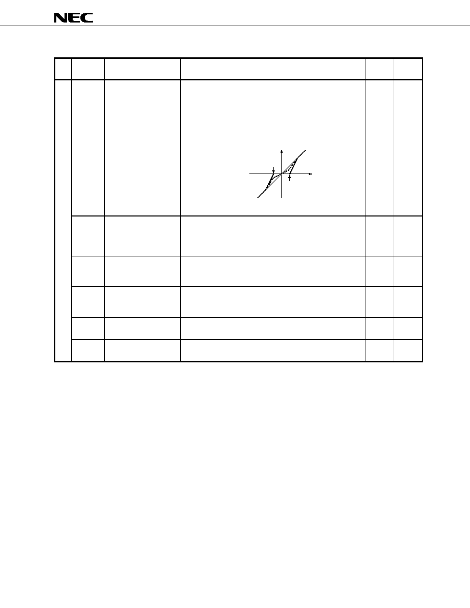
µ
µ
µ
µ
PD64084
51
Data Sheet S16021EJ2V0DS
Table 15-2. Write Register Functions (11/14)
SA
Bit
Name and function
Description
Typical
value
Initial
value
10
D7-D6
YHCOR
Specifies Y output high
frequency component
coring.
00: Coring off
01: Small amount of coring (±1 LSB: 8-bit terms)
10: Medium amount of coring (±2 LSB: 8-bit terms)
11: Large amount of coring (±3 LSB: 8-bit terms)
Coring characteristic curve (for high-frequency component only)
Remark Converted into 8 bits
Input (LSB)
-YHCOR
YHCOR
Output (LSB)
Solid line: YHCGAIN = 0
Dotted line: YHCGAIN = 1
00
00
D5
YHCGAIN
Specifies Y output high-
frequency component
coring gain.
0: Normal (
◊1) 1 :1/2 gain
Refer to YHCOR (SA10h, D7-D6)
0
0
D4
ED2OFF
Specifies WCV-ID
detection circuit.
0: Normal mode
1: Forced WCV-ID detection circuit turned off
0
0
D3
OVST
Nonstandard signal
detection test bit
0: Normal mode
1: Test mode
0
0
D2
CSHDT
H / V counter test bit
0: Normal mode
1: Test mode
0
0
D1-D0
KCTT
H / V counter test bit
0x: Normal mode
1x: Test mode
00
00
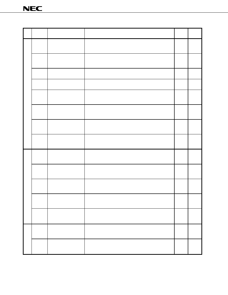
µ
µ
µ
µ
PD64084
52
Data Sheet S16021EJ2V0DS
Table 15-2. Write Register Functions (12/14)
SA
Bit
Name and function
Description
Typical
value
Initial
value
11
D7
SHT1
Nonstandard signal
detection test bit
0: Normal mode
1: Test mode
0
0
D6
SHT0
Nonstandard signal
detection test bit
0: Normal mode
1: Test mode
0
0
D5
VCT
H / V counter test bit
0: Normal mode
1: Test mode
0
0
D4
OTT
H / V counter test bit
0: Normal mode
1: Test mode
0
0
D3
CLKG2D
Clock generator section
test bit
0: Test mode
1: Normal mode
1
1
D2
CLKGGT
Clock generator section
test bit
0: Normal mode
1: Test mode
0
0
D1
CLKGEB
Clock generator section
test bit
0: Normal mode
1: Test mode
0
0
D0
CLKGT
Clock generator section
test bit
0: Normal mode
1: Test mode
0
0
12
D7
HPLLFS
Specifies the horizontal
PLL filter.
0: Slow convergence
1: Quick convergence
-
1
D6
BPLLFS
Specifies the burst PLL
filter.
0: Quick convergence
1: Slow convergence
1
1
D5
FSCFG
Specifies the burst
extraction gain.
0: High gain
1: Low gain
0
0
D4
PLLFG
Specifies the PLL loop
gain.
0: Low gain (slow convergence)
1: High gain (quick convergence)
1
1
D3-D0
KILR
Killer detection reference
0000: Detection off
0001: Low detection sensitivity to
1111: High detection sensitivity
0010
1010
13
D7-D4
HSSL
Horizontal sync slice
level
0000: 4LSB to 1111: 19LSB
(in 8-bit input terms, 1LSB/step)
1111
1111
D3-D0
VSSL
Vertical sync slice level
0000: HSSL setting + 0LSB to
1111: HSSL setting + 15LSB
(in 8-bit input terms, 1LSB/step)
1000
1000
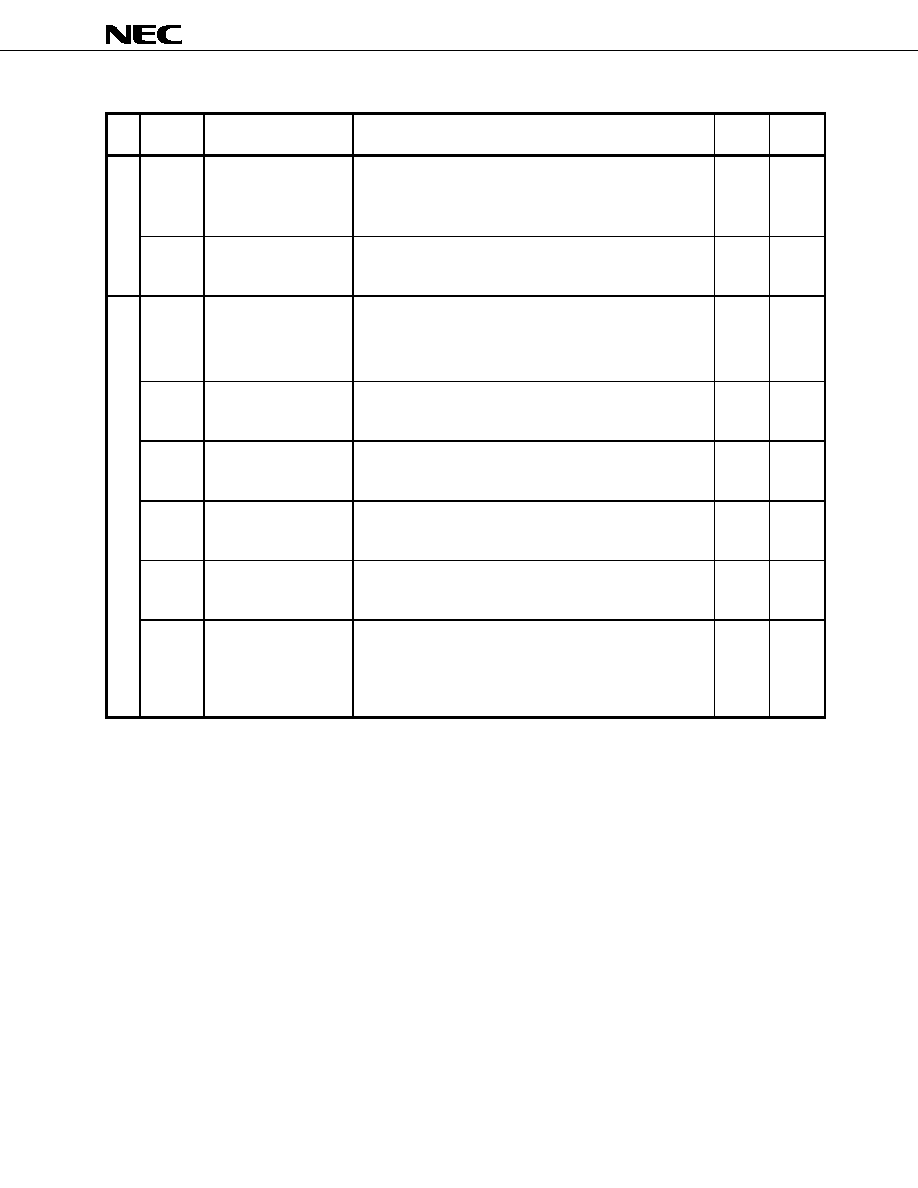
µ
µ
µ
µ
PD64084
53
Data Sheet S16021EJ2V0DS
Table 15-2. Write Register Functions (13/14)
SA
Bit
Name and function
Description
Typical
value
Initial
value
14
D7-D4
BGPS
Specifies the internal
burst gate start position.
0000: H sync center + 2
µs to
1111: H sync center + 5.75
µs
Calculation of gate start position from the H sync center :
0.25
◊ BGPS + 2.0 (
µs)
0101
0101
D3-D0
BGPW
Specifies the internal
burst gate width.
0000: 0.5
µs to 1111: 4.25 µs
Calculation of gate width : 0.25
◊ BGPW + 0.5 (
µs)
0011
0011
15
D7-D6
ADCLKS
Specifies the ADC clock
delay.
00: 0 ns typically (setting prohibited)
01: 3 ns typically
10: 17.5 ns typically
11: 20.5 ns typically
11
11
D5
ADPDS
Specifies whether to use
ADC power-down.
0: Do not stop operation of ADC not in use.( High current drain)
1: Stop operation of ADC not in use. (Low current drain)
1
1
D4
NRDSW
Nonstandard detection
section test
0: Normal mode
1: Test mode
0
0
D3
NRZOFF
WCV-ID detection NRZ
section check
0: NRZ section amplitude check on
1: NRZ section amplitude check off
0
0
D2
FSCOFF
WCV-ID detection FSC
section check
0: FSC amplitude check on
1: FSC amplitude check off
0
0
D1-D0
VTVH
Specifies WCV signal no-
image section processing
(only letter box signal is
valid).
00: Ordinary processing
01: Forced inter-frame Y/C separation
10: Forced inter-line Y/C separation
11: Forced through (composite signal is output.)
00
00
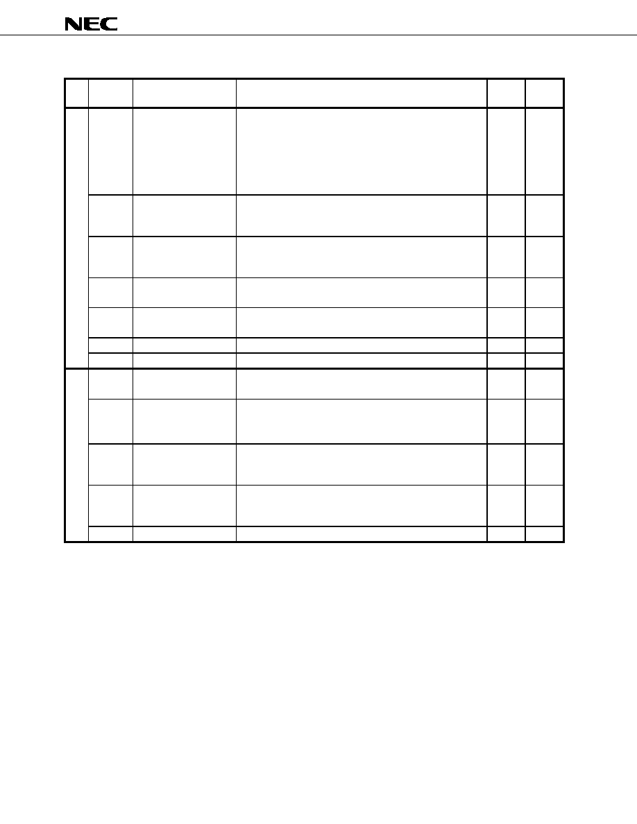
µ
µ
µ
µ
PD64084
54
Data Sheet S16021EJ2V0DS
Table 15-2. Write Register Functions (14/14)
SA
Bit
Name and function
Description
Typical
value
Initial
value
16
D7-D6
SYSPDS
System power down
00: Normal operation
01: Mode1 (D/A, Memory Access stop, Total current :mid)
10: Mode2 (Memory Access stop, Total current: High
11: Mode3 (A/D, D/A, Memory Access stop, Total current : Low)
Remark All register data are kept in power down term.Reset is
not required for re-start.
00
00
D5
EXTDYCO
Extended digital I/O
enable
0: EXTDYCO9-EXTDYCO0 disable
1: EXTDYCO9-EXTDYCO0 enable
0
0
D4
HIZEN
Digital input / output
status select
0: Low
1: Hi-Z
0
0
D3
VLSEL
Test bit
0: Normal mode
1: Test mode
0
0
D2
VLTYPE
Test bit
0: Normal mode
1: Test mode
0
0
D1
-
Undefined
0
0
D0
-
Undefined
0
0
17
D7
CNROFS
CNR section test bit
0: Normal mode
1: Test mode
0
0
D6
HCNTFSYN
Nonstandard signal
detection test bit
0: Normal mode
1: Test mode (Forced H counter synchronize)
Do not use "1" setting in the YCS mode.
0
0
D5
ADCLPFSW
ADC clamp
test bit
0: Normal mode
1: Clamp level feedback disable
0
0
D4
ADCLPSTP
ADC clamp
test bit
0: Normal mode
1: Clamp disable
0
0
D3-D0
-
Undefined
0000
0000

µ
µ
µ
µ
PD64084
55
Data Sheet S16021EJ2V0DS
(2)
Read Register
Table 15-3. Read Register Functions (1/2)
SA
Bit
Name and function
Description
Initial
value
00
D7-D6
VER
Product Version Code
Version code of
µPD64084 is `01'(Fixed)
-
D5
-
Undefined
-
D4
KILF
Killer detection flag
0: Color signal detected
1: Killer signal (non-burst signal) detected
-
D3
NSDF
Horizontal sync signal
detection flag
0: Sync signal detected
1: No sync signal detected
-
D2
LDSDF
Frame sync nonstandard
signal detection flag
0: Standard signal detected
1: Nonstandard signal detected
(such as laser disc special playback signal)
-
D1
OVSDF
Vertical sync
nonstandard signal
detection flag
0: Standard signal detected
1: Nonstandard signal detected
(such as VCR special playback signal and home TV game signal)
-
D0
OHSDF
Horizontal sync
nonstandard signal
detection flag
0: Standard signal detected
1: Nonstandard signal detected
(such as VCR ordinary playback signal)
-
01
D7-D0
WSL
Noise level detection data
00000000: Closer to low noise
11111111: Closer to high noise
-
02
D7
ED2
WCV-ID signal detection
flag
0: Invalid (no WCV-ID signal detected)
1: Valid (WCV-ID signal detected)
-
D6-D0
B3-B9
WCV-ID signal decoding
result
-
03
D7-D0
B10-B17
WCV-ID signal decoding
result
-
04
D7-D6
-
Undefined
-
D5-D4
ID1W0
Decoded Data of
ID-1 WORD0
Decoded data of WORD0 (2 bits)
00
D3-D0
ID1W1
Decoded Data of
ID-1 WORD1
Decoded data of WORD0 (4 bits)
1111
05
D7-D0
ID1W1
Decoded Data of
ID-1 WORD2
Decoded data of WORD0 (8 bits)
00h
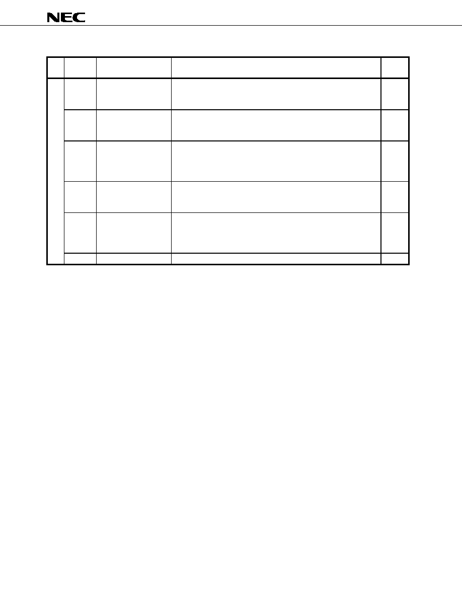
µ
µ
µ
µ
PD64084
56
Data Sheet S16021EJ2V0DS
Table 14-3. Read Register Functions (2/2)
SA
Bit
Name and function
Description
Initial
value
06
D7
DCLEVH
ID-1 Decode
Reference signal detect
0 : Reference signal is not detected
1 : Reference signal is detected
-
D6
CRCCH
ID-1 Decode
CRC check
0 : Error
1 : Normal
-
D5
DCFEL
ID-1 Decode
Reference signal Field
check
0 : Error
1 : Normal
-
D4
CRCCFEL
ID-1 Decode
CRC field check
0 : Error
1 : Normal
-
D3
HOLD1
ID-1 Decode signal
availability check
detection result
0 : Error
1 : Normal
-
D2-D0
-
Undefined
-

µ
µ
µ
µ
PD64084
57
Data Sheet S16021EJ2V0DS
16.
ELECTRICAL CHARACTERISTICS
Absolute Maximum Ratings (T
A
= +25
∞
∞
∞
∞C Unless otherwise specified)
Parameter
Symbol
Conditions
Rating
Unit
Digital section supply voltage
DV
DD
-0.3 to +3.6
V
Analog section supply voltage
AV
DD
-0.3 to +3.6
V
DRAM section supply voltage
DV
DDRAM
-0.3 to +3.6
V
I/O section supply voltage
DV
DDIO
-0.3 to +4.6
V
Input voltage
V
I
3.3 V-resistant input pins
-0.3 to +4.6
V
Output current
I
O
-10 to +10
mA
Package allowable dissipation
P
D
When mounted on an epoxy-glass board
(T
A
= +70
∞C, 100 mm ◊ 100 mm, 2
layer, 1.6-mm thick)
964
mW
Operating ambient temperature
T
A
Device ambient temperature
0 to +70
∞C
Operating junction temperature
T
J:MAX
Upper limit to junction temperature
+125
∞C
Storage temperature
T
stg
-40 to +125
∞C
Caution Product quality may suffer if the absolute maximum rating is exceeded even momentarily for any
parameter. That is, the absolute maximum ratings are rated values at which the product is on the
verge of suffering physical damage, and therefore the product must be used under conditions that
ensure that the absolute maximum ratings are not exceeded.
Recommended Operating Conditions
Parameter
Symbol
Conditions
MIN.
TYP.
MAX.
Unit
Digital section supply voltage
DV
DD
2.3
2.5
2.7
V
Analog section supply voltage
AV
DD
2.3
2.5
2.7
V
DRAM section supply voltage
DV
DDRAM
2.3
2.5
2.7
V
I/O section supply voltage
DV
DDIO
3.0
3.3
3.6
V
High-level input voltage
V
IH
3.3 V-resistant buffer
2.0
3.6
V
Low-level input voltage
V
IL
0
0.8
V
High-level input voltage
V
IH
Schmitt input pin
0.7
◊
DV
DDIO
3.6
V
Low-level input voltage
V
IL
0
0.3
◊
DV
DDIO
V
Reference clock input frequency
f
XI
XI pin
19.998
20.000
20.002
MHz
Reference clock input amplitude
V
XI
0.8
DV
DDIO
V
p-p
Subcarrier input frequency
f
FSCI
FSCI pin
3.579545
MHz
Subcarrier input amplitude
V
FSCI
0.45
AV
DD
V
p-p
Composite
Video signal input amplitude
V
AYI
AYI pin,
Picture + Sync. amp. (140 IRE
p-p
),
AV
DD
= 2.5 V
0.8
V
p-p
Composite signal
Sync. signal input amplitude
V
AYI(S)
AYI pin, Sync. amp. (40 IRE
p-p
),
AV
DD
= 2.5 V
229
(
±0 dB)
288
(+2 dB)
mV
p-p
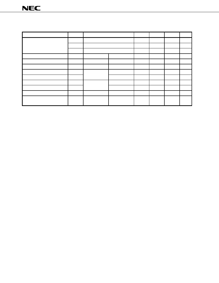
µ
µ
µ
µ
PD64084
58
Data Sheet S16021EJ2V0DS
Digital Section DC Characteristics
(DV
DD
= DV
DDRAM
= 2.5 ±0.2 V, DV
DDIO
= 3.3 ±0.3 V, DGND = DGNDRAM = 0 V, T
A
= 0 to +70∞C)
Parameter
Symbol
Conditions
MIN.
TYP.
MAX.
Unit
Digital section current drain
DI
DD
DVDD and DGND pins
37
100
mA
DI
DDRAM
DVDDRAM and DGNDRAM pins
15
50
mA
DI
DDIO
DVDDIO and DGND pins
12
20
mA
Input leakage current
I
LI
Ordinary input
V
I
= DV
DDIO
or 0 V
-10
0
+10
µA
High-level input current
I
IH
Pull-down type
V
I
= DV
DDIO
20
83
200
µA
Low-level input current
I
IL
Pull-up type
V
I
= 0 V
-200
-83
-20
µA
High-level output current 1
I
OH1
6.0 mA type
V
OH1
= 2.4 V
-6.0
mA
Low-level output current 1
I
OL1
V
OL1
= 0.4 V
+6.0
mA
High-level output current 2
I
OH2
3.0 mA type
V
OH2
= 2.4 V
-2.0
mA
Low-level output current 2
I
OL2
V
OL2
= 0.4 V
+3.0
mA
Low-level output current 3
I
OL3
N-ch. open drain
V
OL3
= 0.4 V
+6.0
mA
Output leakage current
I
LO
3-state, open drain V
O
= DV
DDIO
to
DGND
-10
0
+10
µA
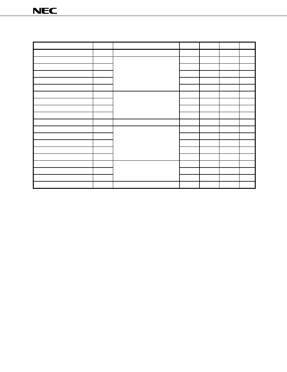
µ
µ
µ
µ
PD64084
59
Data Sheet S16021EJ2V0DS
Analog Section DC Characteristics
(AV
DD
= 2.5 ±0.2 V, AGND = 0 V, T
A
= +25
∞
∞
∞
∞C Unless otherwise specified)
Parameter
Symbol
Conditions
MIN.
TYP.
MAX.
Unit
Analog section current drain
AI
DD
AVDD and AGND pins
50
100
mA
ADC resolution
RES
ADY
-
10
-
bit
ADC integral linearity error
ILE
ADY
±3.0
±6.0
LSB
ADC differential linearity error
DLE
ADY
±1.0
±2.0
LSB
ADC differential gain
DG
ADY
±2.0
±3.0
%
ADC differential phase
DP
ADY
AYI pin, AV
DD
= 2.5 V, f
S
= 4 f
SC
,
DG
AD
, DP
AD
: NTSC 100 IRE RAMP
±1.0
±3.0
Deg
ADC reference voltage(low)
V
RBADY
0.75
V
ADC reference voltage(high)
V
RTADY
1.25
V
ADC analog input range
V
INAY
1.00
V
ADC clamp pin voltage
V
CLY
0.70
V
ADC analog input capacitance
C
INAD
AV
DD
= V
IN
= 0 V, f
IN
= 1 MHz
10
pF
DAC resolution
RES
DA
-
10
-
bit
DAC integral linearity error
ILE
DA
±3.5
±4.5
LSB
DAC differential linearity error
DLE
DA
±0.5
±1.0
LSB
DAC differential gain
DG
DA
±1.0
±3.0
%
DAC differential phase
DP
DA
AYO and ACO pins,
AV
DD
= 2.5 V, f
S
= 4f
SC
DG
AD
, DP
AD
: NTSC 100 IRE RAMP
±1.0
±3.0
deg
DAC full-scale output voltage
V
FSDA
1.77
1.94
2.08
V
DAC zero-scale output voltage
V
ZSDA
0.77
0.94
1.07
V
DAC output amplitude
V
OPPDA
AYO and ACO pins, AV
DD
= 2.5 V
1.00
V
p-p
f
SC
DAC resolution
RES
FSC
FSCO pin
-
8
-
bit
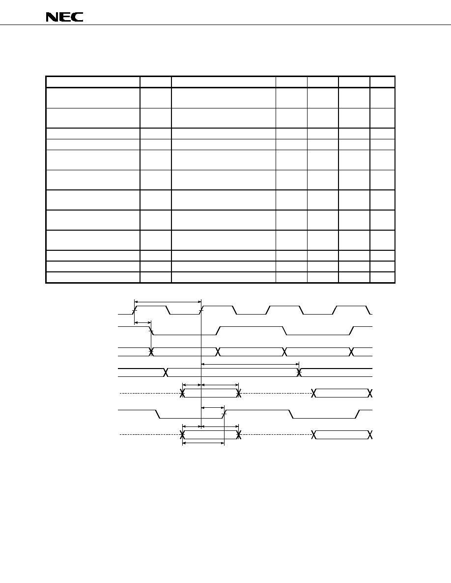
µ
µ
µ
µ
PD64084
60
Data Sheet S16021EJ2V0DS
Digital Section AC Characteristics
(DV
DD
= DV
DDRAM
= 2.5 ±0.2 V, DV
DDIO
= 3.3 ±0.3 V, DGND = DGNDRAM = 0 V, CL = 15 pF, t
r
= t
f
= 2 ns,
T
A
= 0 to +70∞C)
Parameter
Symbol
Conditions
MIN.
TYP.
MAX.
Unit
Video data output delay
t
D:DAT
CLK8
DYCOn, ALTF
(EXADINS = 0)
3
9
20
ns
Internal signal monitor output
delay
t
D:STAT
CLK8
NSTD, ST1, ST0
35
45
55
ns
CSI input set-up time
t
S:CSI
CSI
CLK8
0
ns
CSI input hold time
t
H:CSI
CLK8
CSI
15
ns
ALTF output delay + DYCOn
input set-up time
t
D:DYCO-ALTF
CLK8
ALTF + : t
S:DYCO
: EXADINS = 1, ADCLKS = xx
35
ns
ALTF output delay 0
t
D:ALTF0
CLK8
ALTF : EXADINS = 1,
ADCLKS = 00
3
23
ns
ALTF output delay 1
t
D:ALTF1
CLK8
ALTF : EXADINS = 1,
ADCLKS = 01
5
25
ns
ALTF output delay 2
t
D:ALTF2
CLK8
ALTF : EXADINS = 1,
ADCLKS = 10
18
38
ns
ALTF output delay 3
t
D:ALTF3
CLK8
ALTF : EXADINS = 1,
ADCLKS = 11
20
40
ns
DYCOn input set-up time
t
S:DYCO
DYCOn
CLK8 : EXADINS = 1
0
ns
DYCOn hold time
t
H:DYCO
CLK8
DYCOn : EXADINS = 1
10
ns
Input capacitance
C
I
DV
DD
= V
I
= 0 V, f
IN
= 1 MHz
10
15
pF
CLK8
1/f
CLK8OUT
t
D:DAT
t
D:ALTF
t
D:STAT
t
H:DYCO
t
S:DYCO
t
D:DYCO-ALTF
ALTF
(EXADINS=0)
ALTF
(EXADINS=1)
DYCO[9:0]
(EXADINS=0)
DYCO[9:0]
(EXADINS=1)
Hi-Z
Hi-Z
NSTD, ST1, ST0
t
S:CSI
t
H:CSI
CSI
(input)
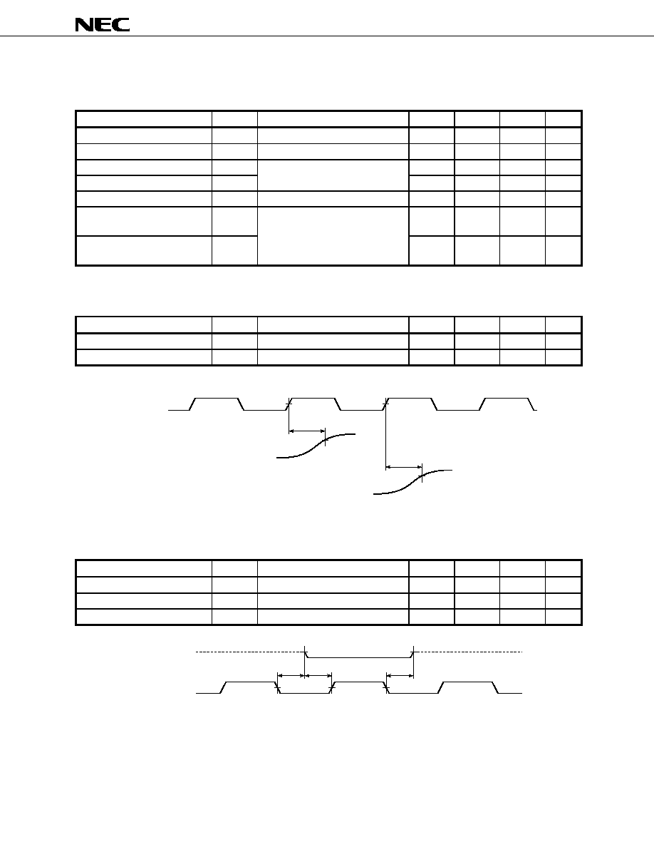
µ
µ
µ
µ
PD64084
61
Data Sheet S16021EJ2V0DS
Clock and Timing Generation Section AC Characteristics
(DV
DD
= DV
DDRAM
= AV
DD
= 2.5 ±0.2 V, DV
DDIO
= 3.3 ±0.3 V, DGND = DGNDRAM = AGND = 0 V, C
L
= 15 pF,
T
A
= 0 to + 70∞C)
Parameter
Symbol
Conditions
MIN.
TYP.
MAX.
Unit
Subcarrier output frequency
f
FSCO
FSCO pin
3.579545
MHz
Subcarrier output amplitude
V
FSCO
FSCO pin, AV
DD
= 3.3 V
1.00
V
p-p
Clock output frequency
f
CLK8OUT
28.63636
MHz
Clock output duty factor
D
CLK8OUT
CLK8 pin, CKMD pin = DGND,
CLK8OFF (SA07:D4) = 0
45
50
55
%
f
SC
pull-in range (in f
SC
terms)
f
bp
When the burst locked clock operation
±600
Hz
Horizontal sync attenuation
(Capture range)
V
hi
-8
0
dB
Vertical sync attenuation
(Capture range)
V
vi
Sync input amplitude, HSSL = 1111,
VSSL = 1000
(assumed to be 0dB when inputting
40IRE = 59LSB)
-6
0
dB
ADC and DAC Section AC Characteristics (AV
DD
= 2.5 ± 0.2 V, AGND = 0 V, C
L
= 15 pF, T
A
= +25 ∞C)
Parameter
Symbol
Conditions
MIN.
TYP.
MAX.
Unit
ADC acquisition time
Note
t
ACKAD
CLK8
AYI
7
ns
DAC setting time
Note
t
SETDA
CLK8
AYO, ACO
15
ns
Note
Excluding data conversion delay
CLK8
t
ACKAD
AYI
AYO, ACO
t
SETDA
I
2
C Bus Interface Section AC Characteristics
(DV
DD
= 2.5 ± 0.2 V, DGND = 0 V, C
L
= 15 pF, T
A
= 0 to +70 ∞C)
Parameter
Symbol
Conditions
MIN.
TYP.
MAX.
Unit
SDA pin ACK response delay
t
ACK
SCL
SDA
500
ns
SDA data set-up time
t
SU:DAT
SDA:L
SCL
100
ns
SDA data hold time
t
HD:DAT
SCL
SDA:Hi-Z
0
ns
t
ACK
t
SU:DAT
t
HD:DAT
SDA
(Slave)
SCL
(from Master)
Hi-Z
8th Clock
9th Clock
1st Clock
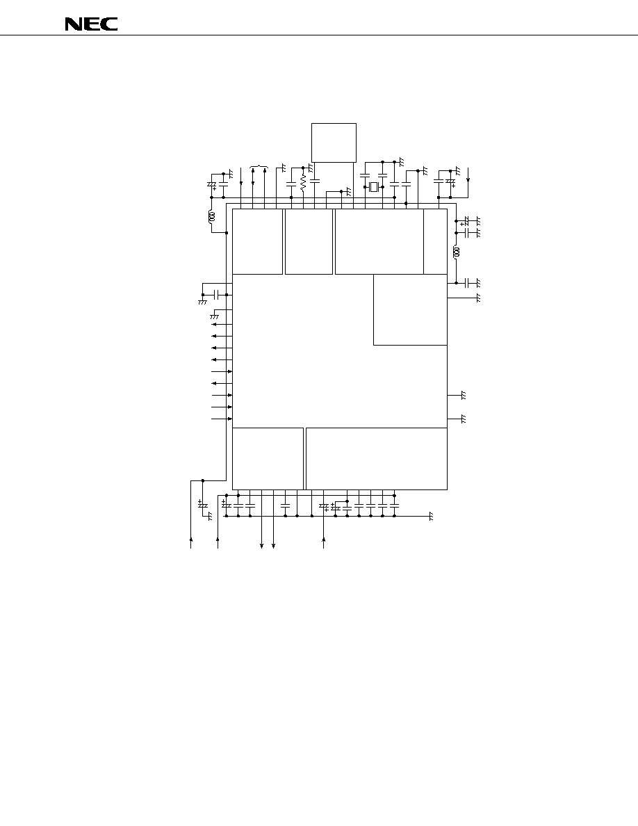
µ
µ
µ
µ
PD64084
62
Data Sheet S16021EJ2V0DS
17.
APPLICATION CIRCUIT EXAMPLE
KIL
LINE
CSI
ALTF
NSTD
ST1
ST0
CLK8
CKMD
DYCO9-DYCO0
TEST13-TEST17
Open
Open
TEST01-TEST12
TEST18-TEST26
D
VDDIO
Internal memory
DVDDRAM
◊ 2
DGNDRAM
◊ 2
TESTIC1, TESTIC2
Killer input (option)
Forced 2D
C-sync. input
Ext. ADC clock
Digital Y input
Non standard detection
States 1 [HD, etc.]
States 0 [VD, etc.]
8f
SC
clock output
Clock mode (GND)
I/O b
loc
k
po
w
er supply (3.3
V)
F
0.1
µ
PD64084
µ
F
47
µ
A
VDD
VCOMY
A
VDD
C-D
A
C
Y-
D
A
C
ADC
AG
N
D
CBPC
AC
O
AY
O
AY
I
VCL
Y
VRBY
CBPY
AG
N
D
Analog comp
.
input
Analog Y
output
Analog C output
Analog b
loc
k
po
w
er supply (2.5
V)
VR
TY
F
10
µ
F
10
µ
F
1
µ
F
0.1
µ
F
0.1
µ
F
0.1
µ
F
0.1
µ
F
0.1
µ
F
0.1
µ
F
0.1
µ
F
0.1
µ
F
0.1
µ
F
◊ 2
0.1
µ
F
10
µ
DVDD
◊ 3
0
SD
A
SCL
SLA0
A
VDD
AV
D
D
D
VDD
DGND
DGND
◊ 4
RPLL
FSCI
AG
N
D
AG
N
D
FSCO
XO
XI
I
2
C b
u
s
interf
ace
I
2
C b
us interf
ace
8f
SC
/
1820f
H
PLL
f
SC
/
(455/2)f
H
Gener
ator
Digital b
loc
k
po
w
er supply (2.5
V)
System reset
RSTB
F
0.1
µ
F
0.1
µ
F
0.1
µ
F
◊ 3
0.1
µ
F
0.1
µ
F
10
µ
F
47
µ
F
0.01
µ
22~33
pF
20
MHz X'tal
22~33
pF
BPF
Caution
This application circuit and the circuit parameters are for reference only, and not intended for use in
actual design-ins.
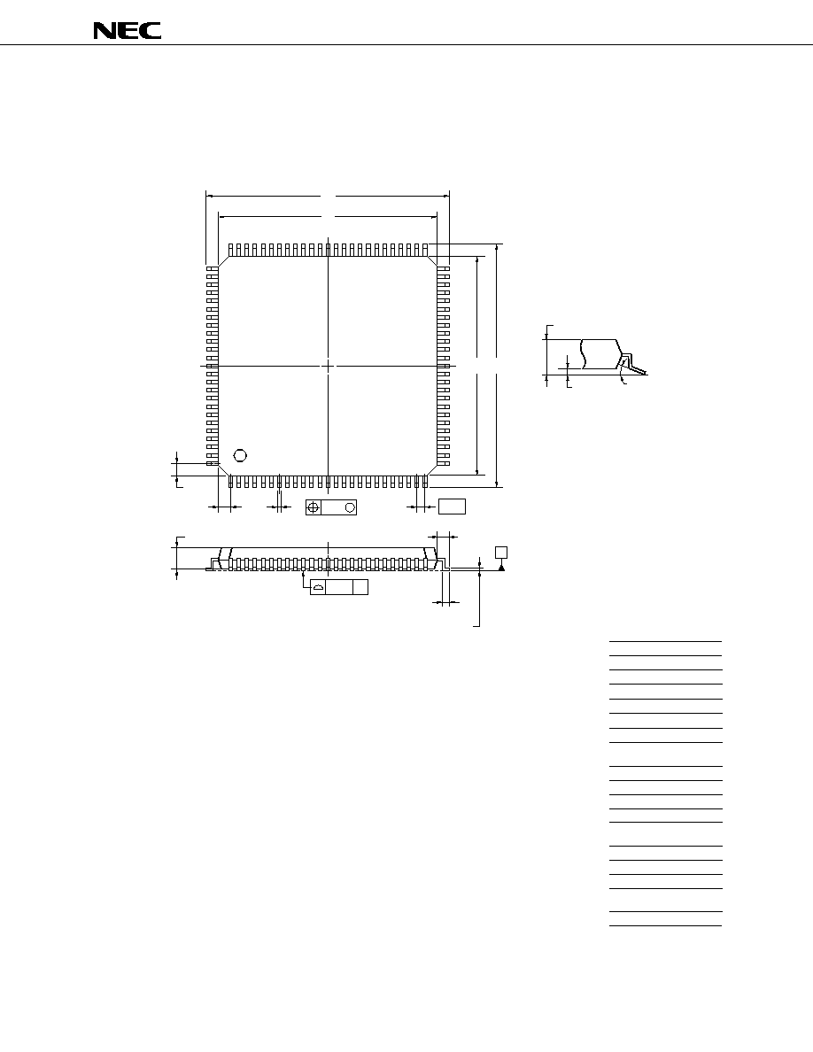
µ
µ
µ
µ
PD64084
63
Data Sheet S16021EJ2V0DS
18.
PACKAGE DRAWING
100-PIN PLASTIC LQFP (FINE PITCH) (14x14)
NOTE
Each lead centerline is located within 0.08 mm of
its true position (T.P.) at maximum material condition.
ITEM
MILLIMETERS
A
B
D
G
16.00
±0.20
14.00
±0.20
0.50 (T.P.)
1.00
J
16.00
±0.20
K
C
14.00
±0.20
I
0.08
1.00
±0.20
L
0.50
±0.20
F
1.00
N
P
Q
0.08
1.40
±0.05
0.10
±0.05
S100GC-50-8EU, 8EA-2
S
1.60 MAX.
H
0.22+0.05
-0.04
M
0.17+0.03
-0.07
R
3
∞+7∞
-3∞
1
25
26
50
100
76
75
51
S
S
N
J
detail of lead end
C
D
A
B
R
K
M
L
P
I
S
Q
G
F
M
H
µ
µ
µ
µ
PD64084
64
Data Sheet S16021EJ2V0DS
19.
RECOMMENDED SOLDERING CONDITIONS
The
µPD64084 should be solderd and mounted under the following recommended conditions.
For soldering methods and conditions other than those recommended below, content an NEC Electronics sales
representative.
For technical information, see the following website.
Semiconductor Device Mount Manual (http://www.necel.com/pkg/en/mount/index.html)
Table 19-1. Surface Mounting Type Soldering Conditions
∑
∑
∑
∑
µ
µ
µ
µPD64084GC-8EA-A
Note1
: 100-pin plastic LQFP (fine pitch) (14
◊
◊
◊
◊ 14 mm)
∑
∑
∑
∑
µ
µ
µ
µPD64084GC-8EA-Y
Note2
: 100-pin plastic LQFP (fine pitch) (14
◊
◊
◊
◊ 14 mm)
Soldering Method
Soldering Conditions
Recommended
Condition Symbol
Infrared reflow
Package peak temperature: 260
∞C or below, Time: 30 s. Max. (at 210∞C or higher),
Count: three times or less,
Exposure limit: 7 days
Note3
(after that, prebake at 125
∞C for 10 to 72 hours)
<Caution>
Products packed in a medium other than a heat-resistance tray (such as a magazine,
taping, and non-heat-resistance tray) cannot be baked.
IR60-107-3
Partial heating
Pin temperature: 300
∞C Max., Time: 3 s. Max. (per pin row)
-
Notes 1. Lead-free product
2. High-thermal-resistance product
3. After opening the dry pack, store it at 25
∞C or less and 65 % RH or less for the allowable storage period.
Caution Do not use different soldering methods together (except for partial heating).
µ
µ
µ
µ
PD64084
65
Data Sheet S16021EJ2V0DS
NOTES FOR CMOS DEVICES
1
PRECAUTION AGAINST ESD FOR SEMICONDUCTORS
Note:
Strong electric field, when exposed to a MOS device, can cause destruction of the gate oxide and
ultimately degrade the device operation. Steps must be taken to stop generation of static electricity
as much as possible, and quickly dissipate it once, when it has occurred. Environmental control
must be adequate. When it is dry, humidifier should be used. It is recommended to avoid using
insulators that easily build static electricity. Semiconductor devices must be stored and transported
in an anti-static container, static shielding bag or conductive material. All test and measurement
tools including work bench and floor should be grounded. The operator should be grounded using
wrist strap. Semiconductor devices must not be touched with bare hands. Similar precautions need
to be taken for PW boards with semiconductor devices on it.
2
HANDLING OF UNUSED INPUT PINS FOR CMOS
Note:
No connection for CMOS device inputs can be cause of malfunction. If no connection is provided
to the input pins, it is possible that an internal input level may be generated due to noise, etc., hence
causing malfunction. CMOS devices behave differently than Bipolar or NMOS devices. Input levels
of CMOS devices must be fixed high or low by using a pull-up or pull-down circuitry. Each unused
pin should be connected to V
DD
or GND with a resistor, if it is considered to have a possibility of
being an output pin. All handling related to the unused pins must be judged device by device and
related specifications governing the devices.
3
STATUS BEFORE INITIALIZATION OF MOS DEVICES
Note:
Power-on does not necessarily define initial status of MOS device. Production process of MOS
does not define the initial operation status of the device. Immediately after the power source is
turned ON, the devices with reset function have not yet been initialized. Hence, power-on does
not guarantee out-pin levels, I/O settings or contents of registers. Device is not initialized until the
reset signal is received. Reset operation must be executed immediately after power-on for devices
having reset function.

µ
µ
µ
µ
PD64084
Purchase of NEC Electronics l
2
C components conveys a license under the Philips l
2
C Patent Rights to
use these components in an l
2
C system, provided that the system conforms to the l
2
C Standard
Specification as defined by Philips.
The information in this document is current as of March, 2003. The information is subject to change
without notice. For actual design-in, refer to the latest publications of NEC Electronics data sheets or
data books, etc., for the most up-to-date specifications of NEC Electronics products. Not all
products and/or types are available in every country. Please check with an NEC Electronics sales
representative for availability and additional information.
No part of this document may be copied or reproduced in any form or by any means without the prior
written consent of NEC Electronics. NEC Electronics assumes no responsibility for any errors that may
appear in this document.
NEC Electronics does not assume any liability for infringement of patents, copyrights or other intellectual
property rights of third parties by or arising from the use of NEC Electronics products listed in this document
or any other liability arising from the use of such products. No license, express, implied or otherwise, is
granted under any patents, copyrights or other intellectual property rights of NEC Electronics or others.
Descriptions of circuits, software and other related information in this document are provided for illustrative
purposes in semiconductor product operation and application examples. The incorporation of these
circuits, software and information in the design of a customer's equipment shall be done under the full
responsibility of the customer. NEC Electronics assumes no responsibility for any losses incurred by
customers or third parties arising from the use of these circuits, software and information.
While NEC Electronics endeavors to enhance the quality, reliability and safety of NEC Electronics products,
customers agree and acknowledge that the possibility of defects thereof cannot be eliminated entirely. To
minimize risks of damage to property or injury (including death) to persons arising from defects in NEC
Electronics products, customers must incorporate sufficient safety measures in their design, such as
redundancy, fire-containment and anti-failure features.
NEC Electronics products are classified into the following three quality grades: "Standard", "Special" and
"Specific".
The "Specific" quality grade applies only to NEC Electronics products developed based on a customer-
designated "quality assurance program" for a specific application. The recommended applications of an NEC
Electronics product depend on its quality grade, as indicated below. Customers must check the quality grade of
each NEC Electronics product before using it in a particular application.
The quality grade of NEC Electronics products is "Standard" unless otherwise expressly specified in NEC
Electronics data sheets or data books, etc. If customers wish to use NEC Electronics products in applications
not intended by NEC Electronics, they must contact an NEC Electronics sales representative in advance to
determine NEC Electronics' willingness to support a given application.
(Note)
∑
∑
∑
∑
∑
∑
M8E 02. 11-1
(1)
(2)
"NEC Electronics" as used in this statement means NEC Electronics Corporation and also includes its
majority-owned subsidiaries.
"NEC Electronics products" means any product developed or manufactured by or for NEC Electronics (as
defined above).
Computers, office equipment, communications equipment, test and measurement equipment, audio
and visual equipment, home electronic appliances, machine tools, personal electronic equipment
and industrial robots.
Transportation equipment (automobiles, trains, ships, etc.), traffic control systems, anti-disaster
systems, anti-crime systems, safety equipment and medical equipment (not specifically designed
for life support).
Aircraft, aerospace equipment, submersible repeaters, nuclear reactor control systems, life
support systems and medical equipment for life support, etc.
"Standard":
"Special":
"Specific":