 | –≠–ª–µ–∫—Ç—Ä–æ–Ω–Ω—ã–π –∫–æ–º–ø–æ–Ω–µ–Ω—Ç: UPD6465CS | –°–∫–∞—á–∞—Ç—å:  PDF PDF  ZIP ZIP |
Document Outline
- COVER
- FEATURES
- ORDERING INFORMATION
- BLOCK DIAGRAM
- PIN CONFIGURATION (Top View)
- PIN FUNCTIONS
- 1. COMMANDS
- 1.1 Command Format
- 1.2 Command List
- 1.3 Power-ON Clear Function
- 2. COMMAND DETAILS
- 2.1 Video RAM Batch Clear Command
- 2.2 Display Control Command
- 2.3 Internal Video Signal Color Control Command
- 2.4 Background Control Command
- 2.5 Internal/external Mode Control, Crystal Oscillation Control Command
- 2.6 Video Signal Method Control Command
- 2.7 Oscillation Method Control Command
- 2.8 Display Position Control Command
- 2.9 Write Address Control Command
- 2.10 Output Level Control Command
- 2.11 Character Size Control Command
- 2.12 Test Mode Command
- 2.13 Display Character Control Command (2-byte contiguous command)
- 3. TRANSFERRING COMMANDS
- 3.1 1-Byte Command
- 3.2 2-Byte Command
- 3.3 2-Byte Contiguous Command
- 3.4 Successive Command Input
- 3.4.1 When 2-byte contiguous command end code is not used
- 3.4.2 When 2-byte contiguous command end code is used
- 3.5 BUSY Period for Command Input
- 3.5.1 When inputting 1-byte or 2-byte command
- 3.5.2 When inputting 2-byte contiguous command
- 4. ADJUSTING
- 4.1 Adjusting Oscillation Frequency
- 4.1.1 Adjusting x 4 multiplier and crystal oscillation frequency
- 4.1.2 Adjusting LC oscillation frequency (dot clock)
- 4.2 Test Mode Clear Command
- 4.3 Clamp Level of Video Signal
- 5. COMPOSITE SYNC. SIGNAL SEPARATION CIRCUIT
- 6. CHARACTER PATTERN DATA
- 6.1 Standard Character Patterns of the uPD6464A
- 6.2 Standard Character Patterns of the uPD6465
- 7. ELECTRICAL SPECIFICATIONS
- 8. APPLICATION CIRCUIT DIAGRAM
- 9. PACKAGE DRAWINGS
- 10. RECOMMENDED SOLDERING CONDITIONS
©
1995, 1996
DATA SHEET
The
µ
PD6464A,6465 are CMOS LSIs for on-screen character display that control various display systems (such
as tape counters) including the program screens of deck-type VCRs and LD players. These LSIs are used in
combination with a microcomputer.
It can display characters each consisting of 12 (horizontal) by 18 (vertical) dots. Some chinese characters and
some pictograms can also be displayed by combining two or more characters.
The
µ
PD6464A,6465 include a power-ON clear function and a video RAM batch clear command that mitigate the
workload of the host microcomputer. It also has a synchronization separator and a
◊
4 multiplier on chip, eliminating
the need of connecting an external separator IC and a crystal resonator, which reduces the mounting area and the
total cost.
FEATURES
∑
Video signal input/output
: Composite video signal
∑
Number of display characters
: 12 lines, 24 columns (288 characters)
∑
Number of character types
: 128 (
µ
PD6464A)/256 (
µ
PD6465) (ROM). Variable by mask code option.
∑
Character size
: 1 dot/1 line. 2 lines (field) can be displayed in line units.
∑
Character color
: White (single color)
∑
Background
: No background, black framing, black-on-white, and black filling
∑
Dot matrix
: 12 (horizontal)
◊
18 (vertical) dots without gap between adjacent characters
∑
Blinking
: Blinking can be turned ON/OFF in character units. Blinking ratio is 1:1.
Blinking frequency is selectable from about 0.5 Hz, 1 Hz, and 2 Hz in screen
units.
∑
Character signal output:
: Can support VCRs with S pins if external mixer is connected because
character signal and blanking signal output pins are provided.
∑
Video RAM data clear
: Video RAM data are cleared by video RAM clear command and power-ON
clear function.
∑
Supported video signal method
: NTSC/PAL/PAL-M/SECAM/PAL-N (
µ
PD6464A only)
∑
Internal circuit
: Synchronization separation circuit for composite synchronizing signal and
◊
4
multiplier
∑
Interface with microcomputer
: Serial input type of 8-bit variable word length
∑
Supply voltage
: +5 V, single power supply
ORDERING INFORMATION
Part Number
Package
µ
PD6464ACS-
◊◊◊
24-pin plastic shrink DIP (300 mil)
µ
PD6465CS-
◊◊◊
24-pin plastic shrink DIP (300 mil)
µ
PD6464AGT-
◊◊◊
24-pin plastic SOP (375 mil)
µ
PD6465GT-
◊◊◊
24-pin plastic SOP (375 mil)
Remark
◊◊◊
: ROM code suffix (CS-001, GT-101 : NEC standard device)
The information in this document is subject to change without notice.
Document No. S11043EJ4V0DS00 (4th edition)
Date Published May 1998 N CP(K)
Printed in Japan
MOS INTEGRATED CIRCUIT
µ
PD6464A,6465
ON-SCREEN CHARACTER DISPLAY CMOS LSI FOR 12-LINE,
24-COLUMN DECK-TYPE VCR
The mark shows major revised points.
µ
PD6464A,6465
2
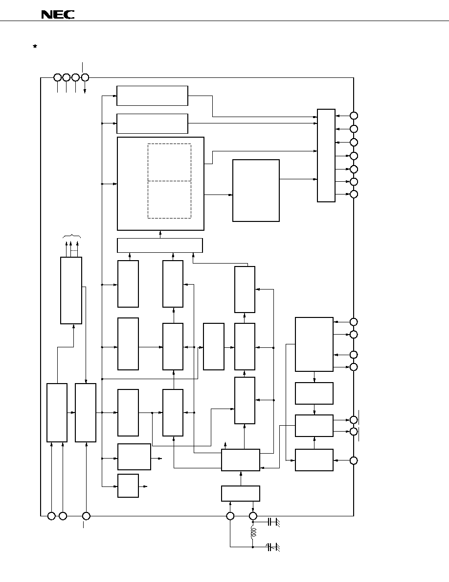
BLOCK DIAGRAM
Note
µ
PD6464A only
3
1
2
6
5
17
15
13
14
23
24
4
8
19
7
V
DD
GND
TEST
PCL
VBSI
V
CNT
V
BLK
V
C
XOSI
XOSO
HSYO
CSYIN
OSC
OUT
OSC
IN
DATA
CLK
CS
Data input
shift register
Data buffer register
Instruction decoder
Control signal
External/
internal
register
NTSC/
PAL/
PAL-M/
SECAM/
PAL-N
Note
register
Character size
register
Horizontal address
register
Write address
counter
Data selector
Video RAM
Background control
data register
Display control
data register
Horizontal size
counter
Horizontal
position counter
Horizontal
address counter
Character
data
7 bits ( PD6464A)
8 bits ( PD6465)
◊
288 words
Blink data
1 bit
◊
288 words
Vertical address
register
Oscillation
circuit
Timing
generator
Vertical size
counter
Vertical position
counter
Vertical address
counter
Synchronization
signal separa-
tion circuit
Mode selection
Synchronization
signal
generator
◊
4 multiplier/
4f
SC
Crystal
oscillation circuit
Output controller
Character generator
ROM
12
◊
18 bits
◊
128 words ( PD6464A)
256 words ( PD6465)
OSC
L
OSCIN
C
OSCOUT
C
16
VSYO
10
9
11
12
FSCI
FSCO
20
NRE
21
VBSO
22
SECAM
µ
µ
µ
µ
µ
PD6464A,6465
3
PCL
: Power-on Clear
SECAM
: SECAM subcarrier Input
TEST
: Test Pin
V
BLK
: Blanking Signal Output
VBSI
: Composite Video Signal Input
VBSO
: Composite Video Signal Output
V
C
: Character Signal Output
V
CNT
: Video Signal Output Level Adjustment
V
DD
: Power Supply
VSYO
: Vertical Synchronization Signal Output
XOSO
: Quadruple Oscillation Output
XOSI
: Quadruple Oscillation Input
CLK
: Clock Input
CS
: Chip Select Input
CSYIN
: Composite Synchronization Signal Input
DATA
: Serial Data Input
FSCI
: f
SC
Signal Input
FSCO
: Frequency Error Output
GND
: Ground
HSYO
: Horizontal Synchronization Signal Output
N.C.
: No Connection
NRE
: Noise Reduction Constant Append
OSC
IN
: LC Oscillation Input
OSC
OUT
: LC Oscillation Output
PIN CONFIGURATION (Top View)
24-pin plastic shrink DIP (300 mil)
µ
PD6464ACS-
◊◊◊
µ
PD6465CS-
◊◊◊
24-pin plastic SOP (375 mil)
µ
PD6464AGT-
◊◊◊
µ
PD6465GT-
◊◊◊
1
2
3
4
5
6
7
8
9
10
11
12
24
23
22
21
20
19
18
17
16
15
14
13
CLK
CS
DATA
V
DD
OSC
OUT
OSC
IN
PCL
GND
FSCI
FSCO
XOSO
XOSI
VBSI
V
CNT
SECAM
VBSO
NRE
TEST
N.C.
CSYIN
VSYO
HSYO
V
BLK
V
C
Remark
◊◊◊
: ROM code suffix (CS-001, GT-101: NEC standard device)
µ
PD6464A,6465
4
PIN FUNCTIONS
No.
Symbol
Pin Name
1
CLK
Clock input
2
CS
Chip select input
3
DATA
Serial data input
4
V
DD
Power supply
5
OSC
OUT
LC oscillation output
6
OSC
IN
LC oscillation input
7
PCL
Power-ON clear
8
GND
Ground
9
FSCI
f
SC
signal input
10
FSCO
Frequency error output
11
XOSO
Quadruple oscillation output
12
XOSI
Quadruple oscillation input
13
V
C
Character signal output
14
V
BLK
Blanking signal output
15
HSYO
Horizontal synchronization signal
output
16
VSYO
Vertical synchronization signal
output
17
CSYIN
Composite synchronization signal
input
18
N. C.
Non connection
19
TEST
Test pin
20
NRE
Noise reduction constant append
21
VBSO
Composite video signal output
22
SECAM
SECAM subcarrier input
23
V
CNT
Video signal output level adjust-
ment
24
VBSI
Composite video signal input
Function
Inputs clock for data read. Data input to the DATA pin is read at
the rising edge of the clock input to this pin.
Serial transfer can be acknowledged by making this CS pin low.
Inputs control data. Data is read in synchronization with the clock
input to the CLK pin.
Supplies power to the IC.
These are input and output pins of an oscillator that generates
dot clocks. Connect a coil and a capacitor to these pins for
oscillation.
Power-ON clear pin. Make this pin high on power application. It
initializes the internal circuitry of the IC.
Ground pin of the IC.
In case of the
◊
4 multiplier, the color sub-carrier (f
SC
) is input to
this pin. In case of the 4f
SC
Crystal oscillation, connect this pin to
GND or V
DD
.
The frequency error signal of the
◊
4 multiplier is output to this
pin. In case of the 4f
SC
Crystal oscillation, this pin should be
open.
A quadruple oscillation LC for internal video signal generation is
connected to these pins. A crystal oscillator can also be
connected.
Character signal output pin. Positive signal output.
This pin outputs a blanking signal that cuts the video signal. It
corresponds to the output of V
C
. Positive signal output.
Outputs a horizontal synchronization signal separated from a
composite synchronization signal.
Outputs a vertical synchronization signal separated from a
composite synchronization signal.
A composite synchronization signal is input to this pin for
synchronization signal separation. In case of the external signal
mode, input the signal certainly. Input a positive synchronization
signal.
Non connection. Leave this pin open.
Test mode select pin. Connect this pin to GND.
Constant append pin for noise reduction.
Outputs a composite video signal mixing a character signal.
SECAM sub-carrier signal mixing pin. In cases of any system
except for SECAM, this pin should be open.
Adjusts the output level of the composite video signal and
luminance signal.
Inputs a composite video signal. Inputs a signal with the leading
edge clamped, consisting of a negative synchronization signal
and a positive video signal.

µ
PD6464A,6465
5
CONTENTS
1.
COMMANDS ....................................................................................................................................
7
1.1
Command Format .................................................................................................................
7
1.2
Command List .......................................................................................................................
7
1.3
Power-ON Clear Function ....................................................................................................
8
2.
COMMAND DETAILS .....................................................................................................................
8
2.1
Video RAM Batch Clear Command .....................................................................................
8
2.2
Display Control Command ...................................................................................................
9
2.3
Internal Video Signal Color Control Command ..................................................................
10
2.4
Background Control Command ...........................................................................................
10
2.5
Internal/external Mode Control, Crystal Oscillation Control Command ..........................
14
2.6
Video Signal Method Control Command ............................................................................
15
2.7
Oscillation Method Control Command ...............................................................................
16
2.8
Display Position Control Command ....................................................................................
17
2.9
Write Address Control Command .......................................................................................
19
2.10 Output Level Control Command ..........................................................................................
20
2.11 Character Size Control Command .......................................................................................
21
2.12 Test Mode Command ............................................................................................................
22
2.13 Display Character Control Command (2-byte contiguous command) ............................
22
3.
TRANSFERRING COMMANDS .....................................................................................................
23
3.1
1-Byte Command ..................................................................................................................
23
3.2
2-Byte Command ..................................................................................................................
23
3.3
2-Byte Contiguous Command .............................................................................................
23
3.4
Successive Command Input ................................................................................................
24
3.4.1 When 2-byte contiguous command end code is not used .....................................
24
3.4.2 When 2-byte contiguous command end code is used ............................................
24
3.5
BUSY Period for Command Input ........................................................................................
25
3.5.1 When inputting 1-byte or 2-byte command ..............................................................
25
3.5.2 When inputting 2-byte contiguous command ..........................................................
25
4.
ADJUSTING .....................................................................................................................................
27
4.1
Adjusting Oscillation Frequency .........................................................................................
27
4.1.1 Adjusting
◊
4 multiplier and crystal oscillation frequency ......................................
27
4.1.2 Adjusting LC oscillation frequency (dot clock) .......................................................
27
4.2
Test Mode Clear Command ..................................................................................................
28
4.3
Clamp Level of Video Signal ................................................................................................
28
5.
COMPOSITE SYNC. SIGNAL SEPARATION CIRCUIT .................................................................
30
6.
CHARACTER PATTERN DATA ....................................................................................................
32
6.1
Standard Character Patterns of the
µ
PD6464A ..................................................................
33
6.2
Standard Character Patterns of the
µ
PD6465 ....................................................................
36