 | –≠–ª–µ–∫—Ç—Ä–æ–Ω–Ω—ã–π –∫–æ–º–ø–æ–Ω–µ–Ω—Ç: UPD6466GS | –°–∫–∞—á–∞—Ç—å:  PDF PDF  ZIP ZIP |
Document Outline
- COVER
- FEATURES
- ORDERING INFORMATION
- BLOCK DIAGRAM
- PIN CONFIGURATION (Top View)
- PIN FUNCTIONS
- 1. INITIAL STATUS SETTING
- 1.1 Initial Status Setting
- 1.2 Application Block Diagram
- 1.3 Display with RGB + VC1 + VC2 Pins
- 1.3.1 Character signal output with output select option A
- 1.3.2 Character signal output with output select option B
- 1.3.3 Character signal output with output select option C
- 1.3.4 Displaying characters specified by VC2
- 2. COMMAND
- 2.1 Command Format
- 2.2 Command List
- 2.3 Power-ON Clear Function
- 3. DETAILS OF COMMANDS
- 3.1 Video RAM Batch Clear Command
- 3.2 Display Control Command
- 3.3 Background Color/Frame Color Control Command
- 3.4 3-Channel Independent Display ON/OFF Command
- 3.5 Character Color Reverse ON/OFF Command
- 3.6 Blue Back ON/OFF Command
- 3.7 Character Address Bank Select Command
- 3.8 Output Switch Control Command
- 3.9 Character Display Position Control Command
- 3.10 Write Address Control Command
- 3.11 Output Pin Control Command
- 3.12 Character Size Control Command
- 3.13 3-Channel Background Control Command
- 3.14 Initial Status Setting Command
- 3.15 Display Character Control Command
- 3.16 Test Mode
- 4. TRANSFERRING COMMANDS
- 4.1 1-Byte Command
- 4.2 2-Byte Command
- 4.3 2-Byte Successive Commands
- 4.4 Successive Input of Command
- 4.4.1 When 2-byte successive command end code is not used
- 4.4.2 When 2-byte successive command end code is used
- 5. CHARACTER PATTERNS
- 6. ELECTRICAL CHARACTERISTICS
- 7. APPLICATION CIRCUIT EXAMPLE
- 8. PACKAGE DRAWINGS
- 9. RECOMMENDED SOLDERING CONDITIONS
©
1997
DATA SHEET
The mark
shows major revised points.
µ
PD6466
MOS INTEGRATED CIRCUIT
Document No. S10991EJ2V2DS00 (2nd edition)
Date Published November 1998 N CP(K)
Printed in Japan
ON-SCREEN CHARACTER DISPLAY CMOS IC FOR 512-CHARACTER,
12-ROW, 24-COLUMN, CAMERA-CONTAINED VCR
The information in this document is subject to change without notice.
The
µ
PD6466 is a CMOS LSI for on-screen character display, and can be used in combination with a microcomputer
to display the tape counter, time, and date in the view finder of a video camera, or the time of a video tape, messages
such as dates on pictures, and channel number on a TV screen.
Characters are displayed in 12 (horizontal) by 18 (vertical) dots. Two or more characters can be combined to display
Kanji (Japanese characters) and symbols. This LSI supports color view finders and is provided with three sets of
character output signals (RGB output: for color view finder, V
C1
output: for recording (or monitor pin), V
C2
output: for
monitor pin (or recording)).
In addition, the
µ
PD6466 is also equipped with a power-ON clear function and a video RAM batch clear command
so that it can mitigate the workload of the microcomputer.
The command format of this LSI is identical to that of the existing models, the
µ
PD6461 and 6462, and therefore,
the
µ
PD6466 is compatible with the existing models, and the software resources for the existing models can be used.
FEATURES
∑ Number of display characters
: 12 rows, 24 columns (288 characters)
∑ Types of character
: 512 types (ROM). Changeable by using mask code option.
∑ Character size
: Can be expanded up to four-fold in vertical and horizontal directions
independently, in units of lines.
∑ Number of character colors
: 8 colors
∑ Framing
: Framing or no framing, or white or black framing selectable in screen units.
∑ Dot matrix
: 12 (horizontal)
◊
18 (vertical) dot configuration. No gap between adjacent
characters.
∑ Blinking
: Blinking can be turned ON/OFF in character units. The blinking ratio is 1:1.
The blinking frequency can be selected from about 1 Hz, about 2 Hz, and
about 0.5 Hz in screen unit.
∑ Character color reversing function : The color of the character and that of the background can be reversed.
∑ Character left and right reverse
: Left and right can be reversed for display in character units.
∑ Background
: No background, blank background, or filled background selectable in screen
units.
∑ Blue back function
: Blue or white can be selected as the background.
∑ Signal output
: 3 sets (output (1) R, G, B + BLK/V
C1
+ V
BLK1
/V
C2
+ V
BLK2
and output (2) R +
R
BLK
/B + B
BLK
/G + G
BLK
selectable by command)
When output (1) is selected, V
C1
and V
C2
outputs can be selected from three
types.
∑ Video RAM data clear
: Implemented by video RAM batch clear command or by clear function on
power-ON.
∑ Interface with microcomputer
: 8-bit variable word length serial input (LSB first/MSB first selectable by
command)
∑ Supply voltage
: Supports low voltage (2.7 to 5.5 V)
∑ Process
: CMOS low power consumption

2
µ
PD6466
ORDERING INFORMATION
Part Number
Package
µ
PD6466GS-xxx
20-pin plastic shrink SOP (300 mil)
µ
PD6466GT-xxx
24-pin plastic SOP (375 mil)
Remarks 1. NEC's standard model is the
µ
PD6466GS-001/GT-201.
For the details of the character generator ROM, refer to 5. CHARACTER PATTERNS.
2. xxx indicates a ROM code suffix.
3
µ
PD6466
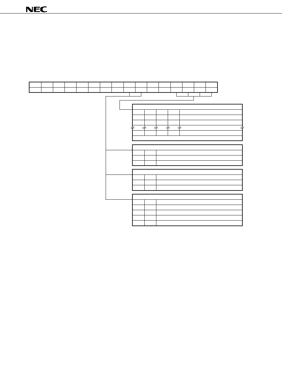
CMDCT
Data input shift
register
DATA
CLK
CS
Instruction decoder
Data selector
...
Control signals
Display
control
register
Character size
register
Horizontal
address
register
Write
address
counter
Horizontal size
counter
Horizontal
position
counter
Horizontal
address
counter
Vertical
address
register
Oscilla-
tion
circuit
Synchro-
nization
protection
circuit
TEST
V
DD
GND
PCL
Character
data
9 bits
◊
288 words
Color
data
3 bits
◊
288 words
Blink
data
1 bit
◊
288 words
Reverse
data
1 bit
◊
288 words
Output
specification
data 1 bit
◊
288 words
Video RAM
Back-
ground
control
data
register
Hsync
Vsync
Vertical
position
counter
Vertical size
counter
Output controller
V
R
V
BLK
V
B
V
G
BLK2
V
C2
BLK1
V
C1
(G
BLK
)
(R
BLK
)
(B
BLK
)
Character
generator
ROM
12
◊
18 bits
◊
512 words
OSC
IN
OSC
OUT
Vertical
address
counter
BLOCK DIAGRAM
Remark
Signals in ( ) are set by using an initial status setting command (RGB + RGB compatible blanking).
4
µ
PD6466
PIN CONFIGURATION (Top View)
20-pin plastic shrink SOP (300 mil)
µ
PD6466GS-xxx
CLK
1
CS
2
DATA
3
PCL
4
V
DD
5
CMDCT
6
OSC
OUT
7
OSC
IN
8
TEST
9
GND
10
20
19
18
17
16
15
14
13
12
11
Hsync
Vsync
V
B
V
G
V
R
V
BLK
(B
BLK
)
V
C2
(G
BLK
)
BLK2 (R
BLK
)
V
C1
BLK1
24-pin plastic SOP (375 mil)
µ
PD6466GT-xxx
CLK
1
CS
2
N.C.
3
DATA
4
PCL
5
V
DD
6
CMDCT
7
OSC
OUT
8
OSC
IN
9
TEST
10
24
23
Hsync
Vsync
N.C.
V
C1
GND
N.C.
11
12
22
21
20
19
18
17
16
15
14
13
BLK1
N.C.
V
B
V
G
V
R
V
BLK
(B
BLK
)
V
C2
(G
BLK
)
BLK2 (R
BLK
)
Remarks 1. xxx indicates a ROM code suffix.
2. Signals in ( ) are set by using an initial status setting command (RGB + RGB compatible blanking).

5
µ
PD6466
B
BLK
: Blanking B
BLK1, BLK2
: Blanking Output 1, 2
CLK
: Clock
CMDCT
: Command Control
CS
: Chip Select
DATA
: Data Input
G
BLK
: Blanking G
GND
: Ground
Hsync
: Horizontal Synchronous Signal Input
N.C.
: No Connection
OSC
IN
: Oscillator Input
OSC
OUT
: Oscillator Output
PCL
: Power-ON Clear
R
BLK
: Blanking R
TEST
: Test
V
B
: Character Signal Output
V
BLK
: Blanking Signal Output for V
R
, V
G
, V
B
V
C1
, V
C2
: Character Signal Output 1, 2
V
DD
: Power Supply
V
G
: Character Signal Output
V
R
: Character Signal Output
Vsync
: Vertical Synchronous Signal Input

6
µ
PD6466
PIN FUNCTIONS
Pin No.
Note 1
Pin
Pin Name
Note 2
Function
Symbol
Note 2
1
CLK
Clock input
This pin inputs a clock for reading data. Data input to the DATA pin
is read at the rising edge of this clock.
2
CS
Chip select input
Serial transfer can be accepted if this pin is made low.
3 (4)
DATA
Serial data input
This pin inputs control data. Data is read in synchronization with the
clock input to the CLK pin.
4 (5)
PCL
Power-ON clear
This pin, when high, initializes the internal circuitry of the IC on power
application.
5 (6)
V
DD
Power supply
This pin supplies power.
6 (7)
CMDCT
Command specification
This pin selects whether a command is input with the LSB first or MSB
select
first.
When this pin is low, the command is input with the LSB first; when
it is high, the command is input with the MSB first. To input the
command with the LSB first, this pin may be opened.
7 (8)
OSC
OUT
LC oscillation I/O
These are an input and an output pin for an oscillation circuit that
8 (9)
OSC
IN
(OSC
IN
: external clock
generates a dot clock.
input)
A coil and capacitor for oscillation are connected to these pins. (If
the input of an external clock is selected by the initial status setting
command, an external clock (clock synchronized with Hsync) is input.
OSC
OUT
is opened at this time.)
9 (10)
TEST
Test pin
This pin is used to test the IC. Normally, connect this pin to GND.
When the TEST pin is connected to GND, the test mode is not set.
10 (11)
GND
Ground pin
Connect this pin to GND of the system.
11 (14)
BLK1
Blanking signal output 1
This pin outputs a blanking signal to cut the video signal.
It supports output of V
C1
, and is high-active.
(If RGB compatible blanking is selected by a command, this pin
outputs the logical sum of R
BLK
, G
BLK
, and B
BLK
.)
12 (15)
V
C1
Character signal output 1
This pin outputs a character signal, and is high-active.
(If RGB compatible blanking is selected by a command, this pin
outputs the logical sum of V
R
, V
G
, and V
B
.)
13 (16)
BLK2
Blanking signal output 2
This pin outputs a blanking signal to cut the video signal. It supports
(R
BLK
)
(blanking R)
output of V
C2
, and is high-active.
(This pin outputs a blanking signal supporting output of V
R
and is
high-active.)
14 (17)
V
C2
Character signal output 2
This pin outputs a character signal, and is high-active.
(G
BLK
)
(blanking G)
(This pin outputs a blanking signal supporting output of V
G
and is
high-active.)
15 (18)
V
BLK
Blanking signal output
This pin outputs a blanking signal to cut the video signal. It supports
(B
BLK
)
(blanking B)
output of V
R
, V
G
, and V
B
, and is high-active (this pin outputs a blanking
signal supporting output of V
B
and is high-active).
16 (19)
V
R
Character signal output
This pin outputs a character signal, and is high-active.
17 (20)
V
G
18 (21)
V
B
19 (23)
Vsync
Vertical sync signal input
This pin inputs a vertical sync signal. Input a negative sync signal.
20 (24)
Hsync
Horizontal sync signal input
This pin inputs a horizontal sync signal. Input a negative sync signal.
(3, 12, 13, 22)
N.C.
Vacant
Vacant pin
Notes 1.
( ): Pin numbers of
µ
PD6466GT-xxx
2.
Signals in ( ) are set by the initial status setting command (RGB + RGB compatible blanking).

7
µ
PD6466
CONTENTS
1.
INITIAL STATUS SETTING ................................................................................................................. 9
1.1
Initial Status Setting ................................................................................................................. 9
1.2
Application Block Diagram .................................................................................................... 11
1.3
Display with RGB + V
C1
+ V
C2
Pins ........................................................................................ 12
1.3.1 Character signal output with output select option A ..................................................................... 15
1.3.2 Character signal output with output select option B ..................................................................... 16
1.3.3 Character signal output with output select option C ..................................................................... 17
1.3.4 Displaying characters specified by V
C2
.......................................................................................... 18
2.
COMMAND .........................................................................................................................................19
2.1
Command Format ................................................................................................................... 19
2.2
Command List ......................................................................................................................... 19
2.3
Power-ON Clear Function ...................................................................................................... 21
3.
DETAILS OF COMMANDS ................................................................................................................ 22
3.1
Video RAM Batch Clear Command ....................................................................................... 22
3.2
Display Control Command ..................................................................................................... 23
3.3
Background Color/Frame Color Control Command ........................................................... 26
3.4
3-Channel Independent Display ON/OFF Command .......................................................... 27
3.5
Character Color Reverse ON/OFF Command ..................................................................... 28
3.6
Blue Back ON/OFF Command ............................................................................................... 30
3.7
Character Address Bank Select Command ......................................................................... 31
3.8
Output Switch Control Command ......................................................................................... 32
3.9
Character Display Position Control Command ................................................................... 34
3.10 Write Address Control Command ......................................................................................... 36
3.11 Output Pin Control Command ............................................................................................... 37
3.12 Character Size Control Command ........................................................................................ 38
3.13 3-Channel Background Control Command ......................................................................... 39
3.14 Initial Status Setting Command ............................................................................................ 43
3.15 Display Character Control Command .................................................................................. 45
3.16 Test Mode .................................................................................................................................48
4.
TRANSFERRING COMMANDS ........................................................................................................ 49
4.1
1-Byte Command .....................................................................................................................49
4.2
2-Byte Command .....................................................................................................................49
4.3
2-Byte Successive Commands ............................................................................................. 50
4.4
Successive Input of Command ............................................................................................. 51
4.4.1 When 2-byte successive command end code is not used ........................................................... 51
4.4.2 When 2-byte successive command end code is used ................................................................. 51
5.
CHARACTER PATTERNS ................................................................................................................. 52
6.
ELECTRICAL CHARACTERISTICS ................................................................................................. 60
7.
APPLICATION CIRCUIT EXAMPLE ................................................................................................. 65

8
µ
PD6466
8.
PACKAGE DRAWINGS ......................................................................................................................66
9.
RECOMMENDED SOLDERING CONDITIONS ................................................................................ 68
9
µ
PD6466
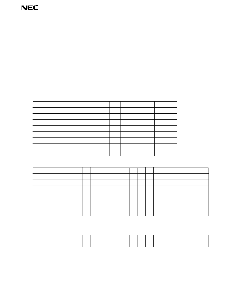
1. INITIAL STATUS SETTING
1.1 Initial Status Setting
The
µ
PD6466 selects the following parameters that are selected by mask code options with the
µ
PD6461 and 6462,
by using an initial status setting command.
Parameter
Selected by:
(1)
Dot clock
LC oscillation
External clock input
(2)
Vertical display start position
3-row unit setting
9-row unit setting
(3)
Pin selection
RGB + V
C1
+ V
C2
RGB + RGB compatible BLK
(RGB + 3BLK)
(4)
Output selection
Option A
Option B
Option C
(5)
Character color reversal
Black character
White character
specification selection
(6)
Function selection
Character blinking
Character left/right reversal
(1) Dot clock
To select a dot clock for character display. If an external clock input is selected, refer to External Clock Input
in 6. ELECTRICAL CHARACTERISTICS.
(2) Vertical display start position
To select the setting accuracy of the vertical display start position of the character display area. In 3-row units,
the vertical display start position can be set more finely than in 9-row units.
(3) Pin selection
To select the setting of the output pins.
When RGB + V
C1
+ V
C2
is selected, character signals are output from pins V
R
, V
G
, V
B
, V
BLK
, V
C1
, BLK1, V
C2
,
and BLK2. When RGB + 3BLK is selected, character signals are output from pins V
R
, V
G
, V
B
, R
BLK
, G
BLK
, B
BLK
,
V
C1
, and BLK1.
When RGB + V
C1
+ V
C2
is selected with a video camera with a color view finder, colored characters can be
displayed in the view finder. When RGB + 3BLK is selected, character signals can be separated color
specification.
(4) Output selection
To set the output format of the character signal where the setting of the output pin is RGB + V
C1
+ V
C2
(setting
the output format of the character signal is invalid where the setting of the output pin is RGB + 3BLK).
When an on-screen character display IC is used in a video camera, some items of information (such as date
and title) are displayed on the video tape, and the others (such as battery alarm, focus, and counter indication)
are only displayed in the view finder. The
µ
PD6466 can select these items of information in row or half-row
units by using the output pin. Select the output format from three types: option A, option B, and option C (when
3BLK is selected, however, be sure to select option B).
(5) Character color reversal specification selection
To select the specifications when the character color is reversed (valid only for RGB output).
∑
Black character: Outputs an area with dots in black and prohibits framing.
∑
White character: Outputs an area with dots in white and prohibits framing.

10
µ
PD6466
(6) Function selection
To select either of the character blinking or character left/right reversal functions.
The default setting assumed on power application is as follows:
(1) Dot clock
= LC oscillation
(2) Vertical display start position
= 3-row unit
(3) Pin selection
= RGB + V
C1
+ V
C2
(4) Output selection
= Option B
(5) Character color reversal specification selection = Black characters
(6) Function selection
= Character blinking

11
µ
PD6466
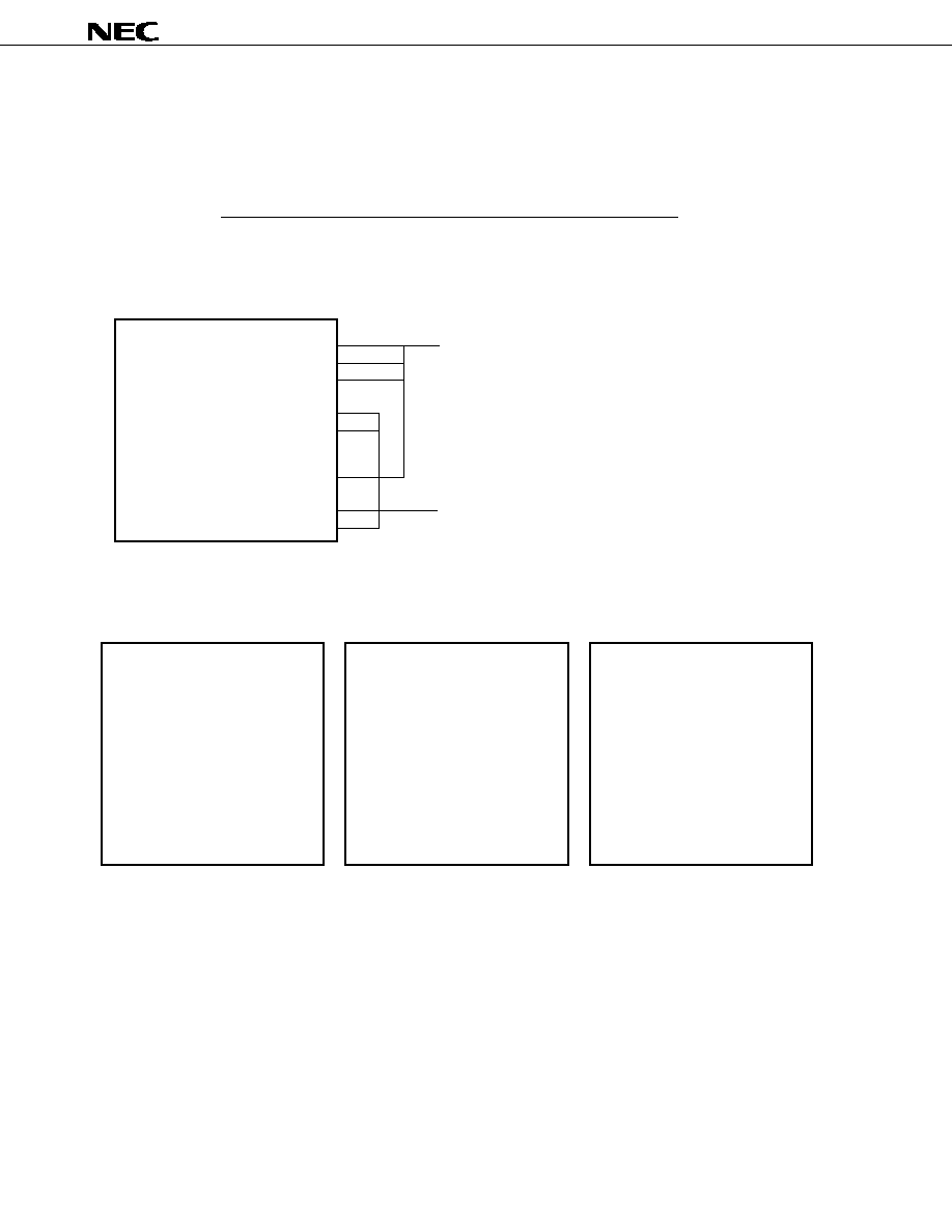
1.2 Application Block Diagram
Example of application in a video camera (1) (in the case of RGB + V
C1
+ V
C2
)
(When V
R
, V
G
, V
B
, V
BLK
, V
C1
, BLK1, V
C2
, and BLK2 pins are used)
DATA
CLK
CS
PCL
Hsync
Vsync
RGB
V
C2
V
C1
Character
mixing circuit
Video
Video+character
Character
mixing circuit
Color view finder
Recording block
(deck block)
PD6466
RGB : V
R
, V
G
, V
B
, V
BLK
V
C1
: V
C1
, BLK1 V
C2
: V
C2
, BLK2
Character
mixing circuit
Monitor pin block
(video signal output)
µ
Microcontroller
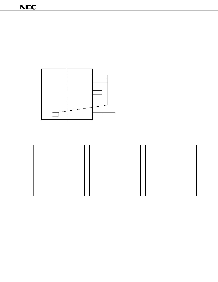
Example of application in a video camera (2) (RGB + 3BLK (RGB compatible BLK))
(When V
R
, V
G
, V
B
, R
BLK
, G
BLK
, and B
BLK
pins are used)
DATA
CLK
CS
PCL
Hsync
Vsync
R
G
B
Video
Video+character
Character
mixing circuit
Color view finder
Recording block
(deck block)
Monitor pin block
(video signal output)
PD6466
R : V
R
, R
BLK
G : V
G
, G
BLK
B : V
B
, B
BLK
Video
Video
Character
mixing circuit
Character
mixing circuit
µ
Microcontroller
12
µ
PD6466
1.3 Display with RGB + V
C1
+ V
C2
Pins
The
µ
PD6466 has three output options: A, B, and C. The following figure shows the output with each option
specified (the output is controlled by an output pin control command (refer to 3.11 Output Pin Control Command)).
Output pin control command (with MSB first (The command is input from the MSB (D15).)
(because this command is a 2-byte command, input of 16 bits is necessary when this command is input more than
once successively.)
D15
D14
D13
D12
D11
D10
D9
D8
D7
D6
D5
D4
D3
D2
D1
D0
1
0
0
1
1
1
0
0
OD1
OD0
0
0
AR3
AR2
AR1
AR0
(MSB)
(LSB)
Row specification bits
Function
Specifies row 0.
Specifies row 1.
Specifies row 11.
Setting prohibited
AR3
0
0
1
AR2
0
0
0
AR1
0
0
1
AR0
0
1
1
Output pin control bits
Pin output
V
C1
: Outputs specified row, V
C2
: Fixed to low level
V
C1
: Fixed to low level, V
C2
: Outputs specified row
OD1
0
0
OD0
0
1
Option A
Output pin control bits
Pin output
V
C1
: Outputs all rows, V
C2
: Fixed to low level
V
C1
: Outputs all rows, V
C2
: Outputs specified row
OD1
0
0
OD0
0
1
Option B
Output pin control bits
Pin output
V
C1
: Outputs columns 0-23, V
C2
: Fixed to low level
V
C1
: Outputs columns 0-11, V
C2
: Outputs columns 12-23
V
C1
: Outputs columns 12-23, V
C2
: Outputs columns 0-11
V
C1
: Fixed to low level, V
C2
: Outputs columns 0-23
OD1
0
0
1
1
OD0
0
1
0
1
Option C
∑
Row specification control
Specify whether the character signal is output to the V
C1
or V
C2
pin in row units (or 12-column units).
∑
Output pin control
The output of the V
C1
and V
C2
pins can be selected from three types, A, B, and C, by using the initial status setting
command (the blanking signal is output in the same manner).
13
µ
PD6466
Output with option A
Output pin control bit
OD1
OD0
Pin output
0
0
V
C1
: Outputs specified row, V
C2
: Fixed to low level
(1)
0
1
V
C1
: Fixed to low level, V
C2
: Outputs specified row
(2)
Output
Character signal
Background signal (with background specified)
In the case of (1)
V
C1
output
Outputs character signal resulting from
Outputs background signal to area other
ORing V
R
, V
G
, and V
B
pins (specified row).
than that specified by V
C2
.
However, character specified by V
C2
is not
output.
V
C2
output
Fixed to low level (specified row)
Outputs background signal to only area
specified by V
C2
In the case of (2)
V
C1
output
Fixed to low level (specified row)
Outputs background signal to area other
than that specified by V
C2
V
C2
output
Outputs character specified by V
C2
Outputs background signal to only area
(specified row)
specified by V
C2
Output with option B
Output pin control bit
OD1
OD0
Pin output
0
0
V
C1
: Outputs all rows, V
C2
: Fixed to low level
(1)
0
1
V
C1
: Outputs all rows, V
C2
: Outputs specified row
(2)
Output
Character signal
Background signal (with background specified)
In the case of (1)
V
C1
output
Outputs character signal resulting from
Outputs background signal to area other
ORing V
R
, V
G
, and V
B
pins (all rows).
than that specified by V
C2
.
However, character specified by V
C2
is not
output.
V
C2
output
Fixed to low level (specified row)
Outputs background signal to only area
specified by V
C2
.
In the case of (2)
V
C1
output
Outputs character signal resulting from
Outputs background signal to area other
ORing V
R
, V
G
, and V
B
pins (all rows).
than that specified by V
C2
.
However, character specified by V
C2
is not
output.
V
C2
output
Outputs character specified by V
C2
Outputs background signal to only area
(specified row).
specified by V
C2
.

14
µ
PD6466
Output with option C
Output pin control bit
OD1
OD0
Pin output
0
0
V
C1
: Outputs columns 0-23, V
C2
: Fixed to low level
(1)
0
1
V
C1
: Outputs columns 0-11, V
C2
: Outputs columns 12-23
(2)
1
0
V
C1
: Outputs columns 12-23, V
C2
: Outputs columns 0-11
(3)
1
1
V
C1
: Fixed to low level, V
C2
: Outputs columns 0-23
(4)
Output
Character signal
Background signal (with background specified)
In the case of (1)
V
C1
output
Outputs character signal resulting from
Outputs background signal to area other
ORing V
R
, V
G
, and V
B
pins (columns 0-23 of
than that specified by V
C2
.
specified row). However, character specified
by V
C2
is not output.
V
C2
output
Fixed to low level (specified row)
Outputs background signal to only area
specified by V
C2
.
In the case of (2)
V
C1
output
Outputs character signals resulting from
Outputs background signal to area other
ORing V
R
, V
G
, and V
B
pins (columns 0-11 of
than that specified by V
C2
.
specified row). However, character specified
by V
C2
is not output.
V
C2
output
Outputs character specified by V
C2
(columns
Outputs background signal to only area
12-23 of specified row).
specified by V
C2
.
In the case of (3)
V
C1
output
Outputs character signal resulting from
Outputs background signal to area other
ORing V
R
, V
G
, and V
B
pins (columns 12-23 of
than that specified by V
C2
.
specified row). However, character specified
by V
C2
is not output.
V
C2
output
Outputs character specified by V
C2
(columns
Outputs background signal to only area
0-11 of specified row).
specified by V
C2
.
In the case of (4)
V
C1
output
Fixed to low level (specified row)
Outputs background signal to area other
than that specified by V
C2
.
V
C2
output
Outputs character specified by V
C2
(columns
Outputs background signal to only area
0-23 of specified row).
specified by V
C2
.
The signal of the character specified by V
C2
is not output from the RGB or V
C1
output channel, but the background
is output as described above.
When the
µ
PD6466 is set to output RGB, V
C1
, or V
C2
signal, the following setting can be performed as well as the
above output control.
∑
Independent ON/OFF control of character display of each channel (3-channel independent display ON/OFF
command)
∑
Independent background control of each channel (3-channel background control command)

15
µ
PD6466
1.3.1 Character signal output with output select option A
Option A
Whether a signal is output to the character signal output pin V
C1
in row units can be specified by the OD0 bit
that selects an output pin. The V
C2
output can be specified in character units, and the V
C1
outputs only characters
for which the V
C2
in the rows for which the OD0 bit is set to 1. The character specified by V
C2
is not output to
the RGB and V
C1
output.
Display example (to use V
C2
channel for information for recording)
REC
TAPE
BATT
1/1000
0000
AM 11:30
1991. 2.22
YOKOHAMA
BAY BRIDGE
Displayed information such as alarm and tape counter
Recording information such as date and title
Example of view finder display
(RGB and V
C2
output)
Output example
REC
TAPE
BATT
1/1000
0000
RGB character output
(color character)
Character output of V
C2
channel
(specified row, character specified by V
C2
)
AM 11:30
1991. 2.22
YOKOHAMA
BAY BRIDGE
REC
TAPE
BATT
1/1000
0000
Character output of V
C1
channel
(specified row)
∑ Character information on the row
specified by clearing the OD0 bit to 0 is
output from V
C1
. However, the
characterspecified by V
C2
is not output.
∑ The row specified by setting the OD0
bit to 1 is not output (fixed to low level).
∑ The row specified by clearing the OD0
bit to 0 is not output (fixed to low level).
∑ Only the character information specified
by V
C2
on the row specified by setting
the OD0 bit to 1 is output from V
C2
.
∑ The character specified to V
C2
is not
output.
16
µ
PD6466
1.3.2 Character signal output with output select option B
Option B
The V
C1
outputs characters of all rows regardless of setting of the OD0 and OD1 bits. The V
C2
output can be
specified in character units, and the V
C2
outputs only characters for which the V
C2
in the rows for which the OD0
bit is set to 1. The character specified to V
C2
is not output to the RGB and V
C1
output.
Display example (to use V
C2
channel for information for recording)
REC
TAPE
BATT
1/1000
0000
AM 11:30
1991. 2.22
YOKOHAMA
BAY BRIDGE
Displayed information such as alarm and tape counter
Recording information such as date and title
Recording information at the leftmost position (e.g., weather).
RAIN
Example of view finder display
(RGB and V
C2
output)
Output example
REC
TAPE
BATT
1/1000
0000
RGB character output
(color character)
Character output of V
C2
channel
(specified row, character specified to V
C2
)
AM 11:30
1991. 2.22
YOKOHAMA
BAY BRIDGE
REC
TAPE
BATT
1/1000
0000
Character output of V
C1
channel
(all rows)
RAIN
∑ The character information on all the
rows is output from V
C1
regardless of
the OD0 bit. However, the character
specified to V
C2
is not output.
∑ Only the character information specified
to V
C2
on the row specified by setting
the OD0 bit to 1 is output from V
C2
.
∑ The character information specified to
V
C2
is not output on the row specified
by clearing the OD0 bit to 0 is not
output.
∑ The character specified to V
C2
is not
output.
17
µ
PD6466
1.3.3 Character signal output with output select option C
Option C
Columns 0 through 11, and 12 through 23 on each row can be output to the V
C1
and V
C2
pins by using the OD0
and OD1 bits of the "output pin control command".
Display example
TAPE
BATT
1/1000
AM 11:30
1991. 2.22
Displayed information such as alarm and tape counter
Recording information such as date and title
0000
REC
0
11 12
23
Example of view finder display
YOKOHAMA
BAY BRIDGE
Output example
TAPE
BATT
1/1000
RGB character output
(color character)
Character output of V
C2
channel
(character specified by V
C2
)
AM 11:30
1991. 2.22
YOKOHAMA
BAY BRIDGE
TAPE
BATT
1/1000
Character output of V
C1
channel
(specified row)
0000
REC
∑ In the case of setting OD1 bit to 0, the
V
C1
outputs the characters of columns
0 to 23 in specified rows for which the
OD0 bit is set to 0, or the characters of
columns 0 to 11 in specified rows for
which the OD0 bit is set to 1, excluding
the characters for which the V
C2
specified.
∑ In the case of setting OD1 bit to 1, the
V
C1
outputs the characters of columns
12 to 23 in specified rows for which
the OD0 bit is set to 0, and the rows for
which the OD0 bit is set to 1 are not
output (the V
C1
pin is fixed to low level),
excluding the characters for which the
V
C2
specified.
∑ In the case of setting OD0 bit to 0, the
V
C2
outputs the characters of columns
0 to 11 in specified rows for which the
OD1 bit is set to 1, and the rows for
which the OD1 bit is set to 0 are not
output (the V
C2
pin is fixed to low level).
∑ In the case of setting OD0 bit to 1, the
V
C2
outputs the characters of columns
12 to 23 in specified rows for which the
OD1 bit is set to 0, or the characters of
columns 0 to 23 in specified rows for
which the OD1 bit is set to 1.
∑ The character specified to V
C2
is not
output.

18
µ
PD6466
1.3.4 Displaying characters specified by V
C2
The characters specified by V
C2
by the display character control command are not output to the RGB and V
C1
output
channels (the RGB and V
C1
output channels display
Note
the same manner as when Display Off Data is written).
Therefore, even if a background is specified by the RGB and V
C1
output channel (no background/filled background),
no background is displayed at the specified portion.
Note
The display is slightly different from Display Off Data.
Filling data: Character filling all 12
◊
18 dots
∑
When Display Off Data is displayed with RGB, V
C1
, and V
C2
channel
In the case of Display Off Data, framing (or background, if any) of
adjacent characters is displayed with the framing or background
overlapping the area of Display Off Data by one dot of the minimum
size (the framing overlaps the area of Display Off Data, when there
are dots at the leftmost or rightmost position of the adjacent character
area).
∑
Displaying character area specified by V
C2
with RGB and V
C
1
channels
In the case of a character specified by V
C2
, the framing of the adjacent
characters is displayed with the framing overlapping the V
C2
-specified
character area by one dot of the minimum size, but the background
does not overlap to the V
C2
-specified area.
∑
Displaying V
C2
-specified character area with V
C2
channel
Even if the V
C2
-specified character exists with the V
C2
output, the
framing also overlaps the adjacent character area, but the background
does not (the framing overlaps the V
C2
-specified character area, when
there are dots at the leftmost or rightmost position of the adjacent
character area).
∑
If V
C2
character specification area exists at the edge of display
area
(The figure shows the leftmost position of the display area. The same
applies to the rightmost position of the display area.)
Portion output with framing or background overlapping
(Width is 1 dot of the minimum character width.)
Portion where framing overlaps
Portion where background overlaps
(1)-(5)
(2)-(5)
The background is not output overlapping the V
C2
-specified character
area.
Filling
Data
Display
Off
Data
Filling
Data
Filling
Data
V
C2
-specified
character
area
Filling
Data
Display
Off
Data
Display
Off
Data
V
C2
-specified
character
area
Filling
Data
Filling
Data
Filling
Data
Filling
Data
(1)
(3)
(4)
(5)
(2)
19
µ
PD6466
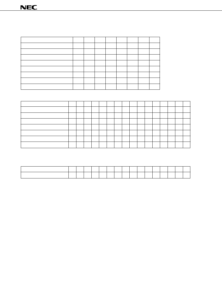
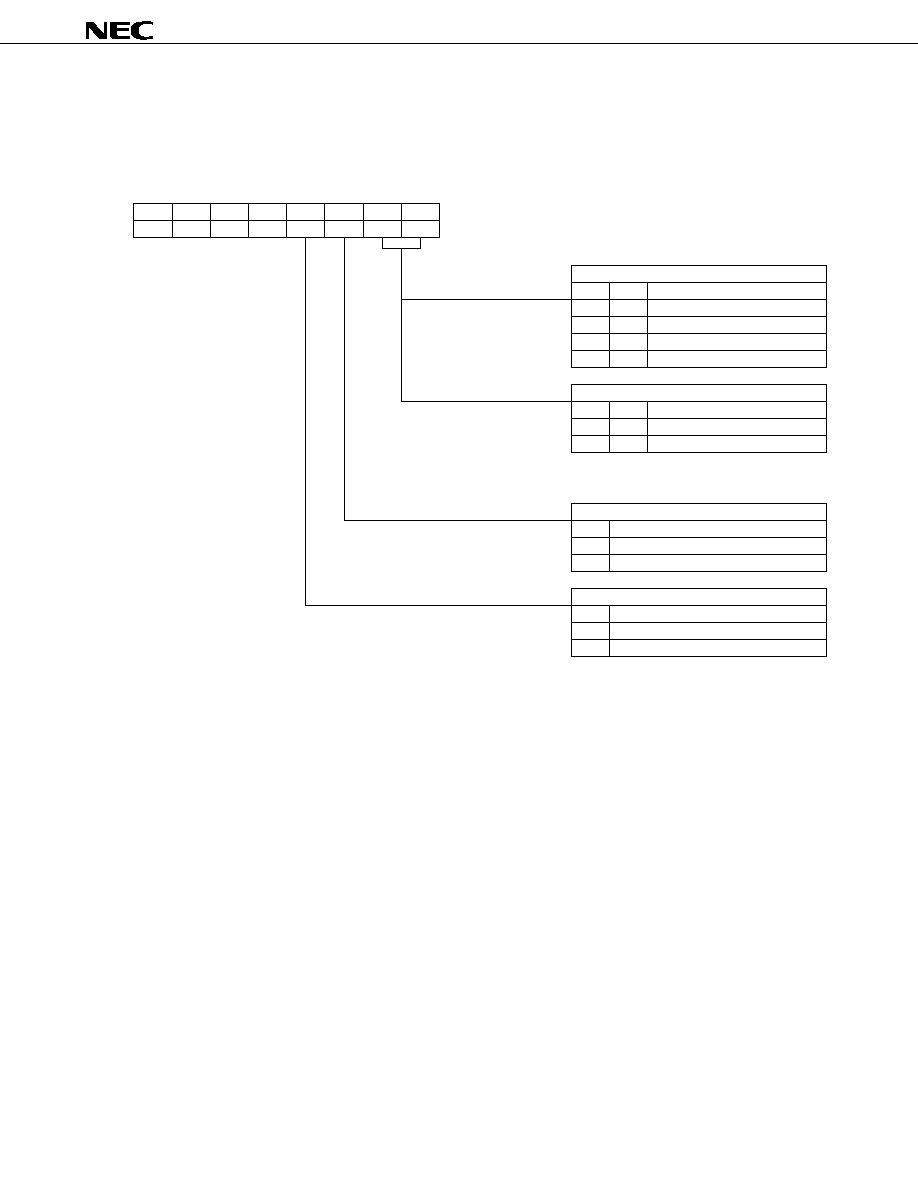
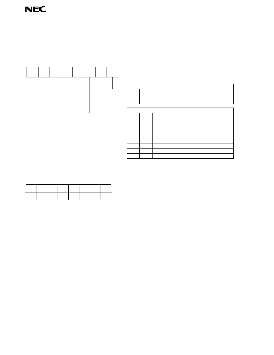
2. COMMAND
2.1 Command Format
Control commands can be serially input in 8-bit units. The word length of a command is variable.
Three types of commands are available: 1-byte commands that consist of 8 bits including the instruction and data,
2-byte commands, and 2-byte successive commands that can be input in an abbreviated form.
Inputting command data with the MSB first or LSB first can be selected by using the CMDCT pin.
When the CMDCT pin is high, the data is input with the MSB first; when it is low, the data is input with the LSB
first.
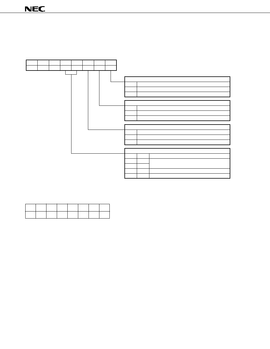
2.2 Command List
(1) MSB first
1-byte commands
(MSB)
Function
D7
D6
D5
D4
D3
D2
D1
D0
Video RAM batch clear
0
0
0
0
0
0
0
0
Display control
0
0
0
1
DO
LC
BL1
BL0
Background color/frame color control
0
0
1
0
R
G
B
BFC
3-channel independent display ON/OFF
0
1
1
1
0
DOA
DOB
DOC
Character color reverse ON/OFF
0
1
1
1
1
0
0
BCRE
Blue back ON/OFF
0
1
1
1
1
CLR
0
BB
Character address bank select
0
1
1
1
1
1
1
BC
Output switch control
0
1
0
S3A
S3B
SW4
SW2
SW1
2-byte commands
(MSB)
Function
D15 D14 D13 D12 D11 D10
D9
D8
D7
D6
D5
D4
D3
D2
D1
D0
Character display position control
1
0
0
0
0
0
V4
V3
V2
V1
V0
H4
H3
H2
H1
H0
Write address control
1
0
0
0
1
0
0
AR3 AR2 AR1 AR0 AC4 AC3 AC2 AC1 AC0
Output pin control
1
0
0
1
1
1
0
0
OD1 OD0
0
0
AR3 AR2 AR1 AR0
Character size control
1
0
0
1
1
0
SV1 SV0 SH1 SH0
0
0
AR3 AR2 AR1 AR0
3-channel background control
1
0
1
1
0
0
1
BA1 BA0 BFA BB1 BB0 BFB BC1 BC0 BFC
Initial status setting
1
0
1
1
0
1
0
0
0
BR
RS OP1 OP0 COC VST OSC
Test mode
Note
1
0
1
1
0
0
0
0
T7
T6
T5
T4
T3
T2
T1
T0
Note
Must not be used.
2-byte successive command
(MSB)
Function
D15 D14 D13 D12 D11 D10
D9
D8
D7
D6
D5
D4
D3
D2
D1
D0
Display character control
1
1
RV
R
G
B
BL
V
C2
C7
C6
C5
C4
C3
C2
C1
C0
20
µ
PD6466
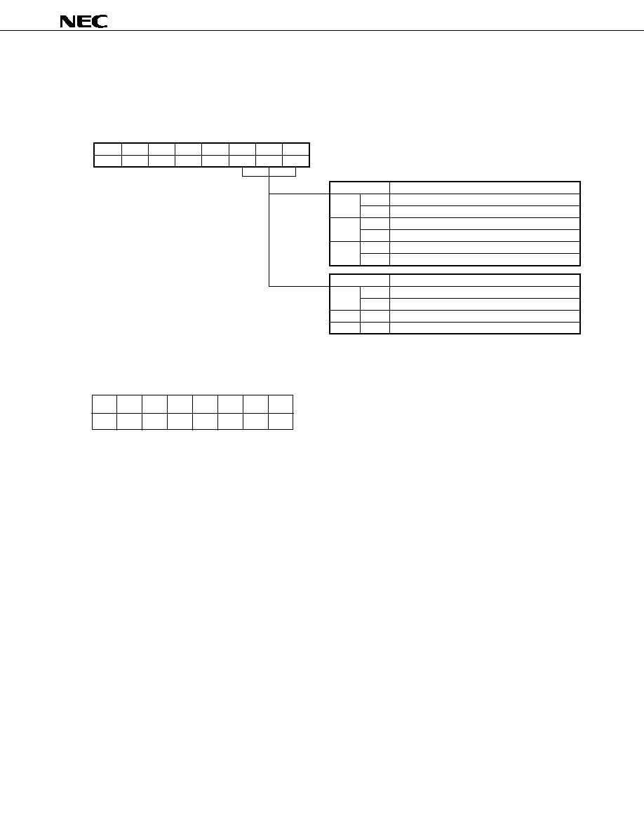
(2) LSB first
1-byte commands
(LSB)
Function
D0
D1
D2
D3
D4
D5
D6
D7
Video RAM batch clear
0
0
0
0
0
0
0
0
Display control
BL0
BL1
LC
DO
1
0
0
0
Background color/frame color control
BFC
B
G
R
0
1
0
0
3-channel independent display ON/OFF
DOC
DOB
DOA
0
1
1
1
0
Character color reverse ON/OFF
BCRE
0
0
1
1
1
0
0
Blue back ON/OFF
BB
0
CLR
1
1
1
1
0
Character address bank select
BC
1
1
1
1
1
1
0
Output switch control
SW1
SW2
SW4
S3B
S3A
0
1
0
2-byte commands
(LSB)
Function
D0
D1
D2
D3
D4
D5
D6
D7
D8
D9
D10 D11 D12 D13 D14 D15
Character display position control
V3
V4
0
0
0
0
0
1
H0
H1
H2
H3
H4
V0
V1
V2
Write address control
AR3
0
0
1
0
0
0
1
AC0 AC1 AC2 AC3 AC4 AR0 AR1 AR2
Output pin control
0
0
1
1
1
0
0
1
AR0 AR1 AR2 AR3
0
0
OD0 OD1
Character size control
SV0 SV1
0
1
1
0
0
1
AR0 AR1 AR2 AR3
0
0
SH0 SH1
3-channel background control
BA1
1
0
0
1
1
0
1
BFC BC0 BC1 BFB BB0 BB1 BFA BA0
Initial status setting
0
0
1
0
1
1
0
1
OSC VST COC OP0 OP1 RS
BR
0
Test mode
Note
0
0
0
0
1
1
0
1
T0
T1
T2
T3
T4
T5
T6
T7
Note
Must not be used.
2-byte successive command
(LSB)
Function
D0
D1
D2
D3
D4
D5
D6
D7
D8
D9
D10 D11 D12 D13 D14 D15
Display character control
V
C2
BL
B
G
R
RV
1
1
C0
C1
C2
C3
C4
C5
C6
C7

21
µ
PD6466
2.3 Power-ON Clear Function
Because the internal status of the IC is undefined on power application, execute power-ON clear by lowering the
PCL pin for the duration described below.
Command setting on power-ON clear is as follows:
∑
Clears test mode
∑
Default setting of initial status (Refer to 3.14 Initial Status Setting Command.)
∑
Clears all character data (12 rows, 24 columns) of video RAM (Display Off Data (FEH)). No data blinks.
∑
Video RAM write address (row 0, digit 0)
∑
Standard size for all rows as character size (SV1, SV0, SH1, SH0) = (0, 0, 0, 0)
∑
All rows specified for output pin selection (OD1, OD0) = (0, 0)
∑
Display OFF, LC oscillation ON, blinking OFF
∑
Display of each channel OFF
∑
No background and framing for all three channels
∑
Blue back OFF
∑
Low-order (0) bank for character address
The time required for power-ON clear can be calculated by the following expression. Do not input any command
during this time.
t (Time required for power-ON clearing) = t
PCLL
Note
+ Video RAM clear time
= 10 (
µ
s) + 10 (
µ
s) + 12/f
OSC
(MHz)
◊
288
f
OSC
(MHz): LC oscillation frequency or external input clock frequency
Note
Refer to Power-ON Clear Specifications in 6. ELECTRICAL
CHARACTERISTICS.
To clear the video RAM, the dot clock (OSC
IN
pin) must be input. Be sure to input the clock when the input of an
external clock is selected.
22
µ
PD6466
3. DETAILS OF COMMANDS
3.1 Video RAM Batch Clear Command
This command can be used to clear the video RAM with a single command (regardless of whether the MSB or LSB
comes first)
(MSB)
(LSB)
D7
D6
D5
D4
D3
D2
D1
D0
0
0
0
0
0
0
0
0
The following contents are set by the video RAM batch clear command.
∑
Clears all the character data (Display Off Data (FEH)) of the video RAM (12 rows, 24 columns). No data blinks.
∑
Video RAM write address: (Row 0, column 0)
∑
Standard size for all rows as character size (SV1, SV0, SH1, SH0) = (0, 0, 0, 0)
∑
All rows specified for output pin selection (OD1, OD0) = (0, 0)
∑
Display OFF, LC oscillation ON, blinking OFF
The time required for clearing the video RAM can be calculated by the following expression. Do not input any
command during this time.
t (Time required for video RAM clearing) = Video RAM clear time
= 10 (
µ
s) + 12/f
OSC
(MHz)
◊
288
f
OSC
(MHz): LC oscillation frequency or external input clock frequency
To clear the video RAM, the dot clock (OSC
IN
pin) must be input. Be sure to input the clock when the input of an
external clock is selected.
Remark
This command resets the hardware of the IC by inputting a signal to the PCL pin. While initializing the
IC including clearing the video RAM and the test mode, the video RAM batch clear command executes
software reset to initialize the IC, and does not clear the test mode.
23
µ
PD6466
3.2 Display Control Command
This command controls the display output, LC oscillation, blinking the characters, and left to right reverse.
(1) With MSB first (The command is input from MSB (D7).)
D7
D6
D5
D4
D3
D2
D1
D0
0
0
0
1
DO
LC
BL1
BL0
(MSB)
(LSB)
Blinking control bit (screen unit)
Function
Blinking OFF
Blinking frequency: approx. 2 Hz
Blinking frequency: approx. 1 Hz
Blinking frequency: approx. 0.5 Hz
BL0
0
1
0
1
LC oscillation control bit
Function
LC oscillation OFF
LC oscillation ON
LC
0
1
Character display ON/OFF control bit
Function
Display OFF
Display ON
DO
0
1
Left to right reverse control bit
Function
Character left to right reverse OFF
Character left to right reverse ON
BL1
≠
≠
BL1
0
0
1
1
BL0
0
1
≠ : "0" or "1"
With blinking character
selected
Note
With character left and right
reverse selected
Note
Note
Set with the initial setting command.
24
µ
PD6466
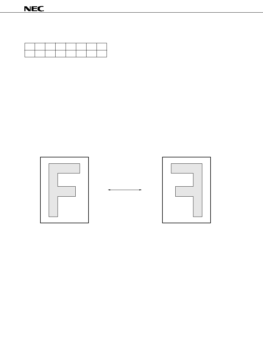
(2) With LSB first (Use of each bit is the same as (1). The command is input from LSB (D0).)
(LSB)
(MSB)
D0
D1
D2
D3
D4
D5
D6
D7
BL0
BL1
LC
DO
1
0
0
0
∑
Blinking control (screen units)
The function selected by the initial setting command is controlled.
∑
Blinking control (screen units)
Whether the characters written to the video RAM blink or not is controlled in screen units. The character
specified to blink by the display character control command blinks.
The blinking ratio is 1:1, and the blinking frequency can be selected from three types.
∑
Left to right reverse control
The character specified to be reversed left to right by the display character control command is reversed
(this is valid only if character left to right reverse is selected by the initial setting command).
Display example of character specified to be reversed left to right (character "F" is displayed)
When left to right reverse is OFF
When left to right reverse is ON
∑
LC oscillation control
The oscillation circuit can be turned ON/OFF by the oscillation control bit. Oscillation is stopped during the
period in which the characters are not displayed, to reduce the power consumption.
Nothing can be written to the video RAM while the oscillation is stopped. To write data to the video RAM,
be sure to turn ON oscillation.

25
µ
PD6466
Cautions 1. When LC oscillation is used : Oscillation is synchronized with Hsync when the
character display is ON, and is stopped while Hsync
is low. When character display is OFF, oscillation
continues regardless of Hsync.
2. When external clock is input : When an external clock is used, the clock is supplied
to the IC's internal circuitry when oscillation is turned
ON. When oscillation is OFF, the clock supply to the
internal circuitry is stopped.
∑
Character display ON/OFF control
Character display output can be turned ON/OFF. The display is turned ON/OFF in synchronization with
the falling of Hsync.
26
µ
PD6466
3.3 Background Color/Frame Color Control Command
This command specifies the background color and frame color. This command is valid when filling of the
background, blank background, or framing is specified.
(1) With MSB first (The command is input from MSB (D7).)
D7
D6
D5
D4
D3
D2
D1
D0
0
0
1
0
R
G
B
BFC
(MSB)
(LSB)
Background color control bit
Function
Black
Blue
Green
Cyan
Red
Magenta
Yellow
White
R
0
0
0
0
1
1
1
1
Frame color control bit
Function
Frame color: Black
Frame color: White
BFC
0
1
G
0
0
1
1
0
0
1
1
B
0
1
0
1
0
1
0
1
(2) With LSB first (Use of each bit is the same as (1). The command is input from LSB (D0).)
(LSB)
(MSB)
D0
D1
D2
D3
D4
D5
D6
D7
BFC
B
G
R
0
1
0
0
∑
Frame color control
The frame color (white/black) can be selected in screen units (RGB output). If the frame is specified with
V
C1
and V
C2
output, the frame color is fixed to black.
∑
Background color control
The background color can be selected (from eight colors) in screen units (RGB output). If the background
is specified with V
C1
and V
C2
output (blank background or filled background), the background color is fixed
to black.
27
µ
PD6466
3.4 3-Channel Independent Display ON/OFF Command
This command can turn ON/OFF the display of character output of 3 channels independently.
(1) With MSB first (The command is input from MSB (D7).)
D7
D6
D5
D4
D3
D2
D1
D0
0
1
1
1
0
DOA
DOB
DOC
(MSB)
(LSB)
Control bit
DOA
DOB
DOC
0
1
0
1
0
1
DOA
DOB
DOC
0
1
≠
≠
Control bit
Function
RGB display OFF
RGB display ON
V
C1
display OFF
V
C1
display ON
V
C2
display OFF
V
C2
display ON
Function
Character display OFF
Character display ON
Don't care
Don't care
With support of RGB/V
C1
/V
C2
output selected
With R/G/B/3BLK output selected
(2) With LSB first (Use of each bit is the same as (1). The command is input from LSB (D0).)
(LSB)
(MSB)
D0
D1
D2
D3
D4
D5
D6
D7
DOC DOB DOA
0
1
1
1
0
∑
Displaying the character signal of the 3 channels (RGB, V
C1
, and V
C2
) can be independently turned ON/
OFF.
When RGB + RGB compatible BLK is selected, it is controlled by the display ON/OFF command.
∑
Turning ON display each output channel by using this command is valid only when the display is turned
ON by the display control command.
∑
If the display is turned OFF by the display control command, the display remains OFF even if it is specified
to be ON by this command.

28
µ
PD6466
3.5 Character Color Reverse ON/OFF Command
This command specifies reversal of character color in screen units.
(1) With MSB first (The command is input from MSB (D7).)
D7
D6
D5
D4
D3
D2
D1
D0
0
0
1
1
1
0
0
BCRE
(MSB)
(LSB)
BCRE
0
1
Function
Character color not reversed
Character color reversed
Character color reverse control bit
(2) With LSB first (Use of each bit is the same as (1). The command is input from LSB (D0).)
(LSB)
(MSB)
D0
D1
D2
D3
D4
D5
D6
D7
BCRE
0
0
1
1
1
0
0
The color of the character specified by the display character control command is reversed for the whole screen
with the reverse specifications (character color: black or white) specified by the initial status setting command.
Example of display of reversed character (example of reversing character "I")
or
No framing
Framing
Color reverse OFF
Color reverse ON
Character color: Black, no framing
Character color: White, no framing
Selected from two
types by initial
setting command
Character
color with
reverse OFF
Character color: White, black frame
or
Specification of framing is invalid for black character.
Specification of framing is invalid for white character.
Character color
with reverse OFF

29
µ
PD6466
The character color/background color (with blank background or filled background) can be selected from eight
types in the case of RGB output when reversing character color is specified to be OFF.
In the case of V
C1
and V
C2
, the character color is white and the background color is black.
The Display Off Data is not affected even when inverted.
If Blank Data is reversed, it is filled with the character color originally specified.
The character color and the color of the framing in the above figure are valid with the RGB.
Only black and white are displayed in the case of V
C1
and V
C2
.
In the case of V
C1
and V
C2
, framing in the character color reverse area is invalid (same as the
µ
PD6461 and
6462).
30
µ
PD6466
3.6 Blue Back ON/OFF Command
This command turns ON/OFF the blue back function in screen units.
(1) With MSB first (The command is input from MSB (D7).)
(MSB)
(LSB)
D7
D0
0
BB
D6
1
D5
1
D4
1
D3
1
D2
CLR
D1
0
Blue back control bit
BB
0
1
Function
Blue back OFF
Blue back ON
Color specification bit
CLR
0
1
Function
White
Blue
(2) With LSB first (Use of each bit is the same as (1). The command is input from LSB (D0).)
(LSB)
(MSB)
D0
D1
D2
D3
D4
D5
D6
D7
BB
0
CLR
1
1
1
1
0
By turning ON the blue back function, the character, framing, and area where no background is output are all
displayed in blue. This command is valid only for RGB output.

31
µ
PD6466
3.7 Character Address Bank Select Command
This command selects the area of the character address specified by the character address specification bit of the
display character control command.
(1) With MSB first (The command is input from MSB (D7).)
D7
D6
D5
D4
D3
D2
D1
D0
0
1
1
1
1
1
1
BC
(MSB)
(LSB)
Character address bank select control bit
Function
Low-order bank (0)
High-order bank (1)
BC
0
1
(2) With LSB first (Use of each bit is the same as (1). The command is input from LSB (D0).)
(LSB)
(MSB)
D0
D1
D2
D3
D4
D5
D6
D7
BC
1
1
1
1
1
1
0
If the low-order bank (0) is specified by the 8-bit data (the second byte of the display character control
command) of the character data, character addresses 00H through FFH (common addresses 000H through
0FFH) of the low-order (0) bank are specified. If the high-order bank (1) is specified, character addresses 00H
through FFH (common addresses 100H through 1FFH) of the high-order (1) bank are specified.
If FEH is specified at the character address of the display character control command for both banks, the
command can be used as the Display Off code. If FFH is specified, it can be used as a 2-byte successive
command end code.
32
µ
PD6466
3.8 Output Switch Control Command
This command controls ON/OFF of SW1 through SW4, and selects the output format of RGB and V
C1
.
(1) With MSB first (The command is input from MSB (D7).)
(MSB)
(LSB)
D7
D0
0
SW1
D6
1
D5
0
D4
S3A
D3
S3B
D2
SW4
D1
SW2
SW1 control bit
SW1
0
1
Function
OFF
ON
SW2 control bit
SW2
0
1
Function
OFF
ON
SW4 control bit
SW4
0
1
Function
OFF
ON
SW3 control bit
S3A
0
0
Function
Controlled by row unit data (OD1)
OD1 = 0 : OFF, OD1 = 1 : ON
S3B
0
1
1
1
OFF regardless of OD1
ON regardless of OD1
0
1
(2) With LSB first (Use of each bit is the same as (1). The command is input from LSB (D0).)
(LSB)
(MSB)
D0
D1
D2
D3
D4
D5
D6
D7
SW1 SW2 SW4
S3B
S3A
0
1
0

33
µ
PD6466
Output format in each switch status
Mode
SW1
SW2
SW4
SW3
RGB
V
C1
V
C2
1
ON
OFF
OFF
ON
RGB
V
C1
V
C2
2
ON
OFF
OFF
OFF
RGB
V
C1
V
C2
3
ON
ON
OFF
ON
RGB+V
C2
V
C1
V
C2
4
ON
ON
OFF
OFF
RGB
V
C1
V
C2
5
ON
OFF
ON
ON
RGB
V
C1
+V
C2
V
C2
6
ON
OFF
ON
OFF
RGB
V
C1
V
C2
7
ON
ON
ON
ON
RGB+V
C2
V
C1
+V
C2
V
C2
8
ON
ON
ON
OFF
RGB
V
C1
V
C2
9
OFF
ON
ON
ON
RGB+V
C2
V
C2
V
C2
10
OFF
ON
ON
OFF
RGB
V
C1
V
C2
11
OFF
OFF
ON
ON
RGB
V
C2
V
C2
12
OFF
OFF
ON
OFF
RGB
V
C1
V
C2
13
OFF
OFF
OFF
ON
RGB
V
C1
V
C2
14
OFF
OFF
OFF
OFF
RGB
V
C1
V
C2
15
OFF
ON
OFF
ON
RGB+V
C2
V
C1
V
C2
16
OFF
ON
OFF
OFF
RGB
V
C1
V
C2
Caution The V
C2
character is output by each channel as follows. The V
C2
outputs only V
C2
regardless of the
status of SW1 to SW4 (same as
µ
PD6461 and 6462).
∑ If RGB channel is RGB, RGB + V
C2
: Not controlled at all by output pin control command.
∑ If V
C1
channel is V
C1
, V
C1
+ V
C2
: Output pins at V
C1
side are controlled.
∑ If V
C1
channel is V
C2
: Output pins at V
C2
side are controlled.
34
µ
PD6466
3.9 Character Display Position Control Command
This command can be used to set the character display start position in 32 steps in units of 3 dots in the horizontal
direction, and in 32 steps in units of 3 rows in the vertical direction (because this command is a 2-byte command, input
of 16 bits is necessary when this command is input more than once successively).
(1) With MSB first (The command is input from MSB (D15).)
D15
D14
D13
D12
D11
D10
D9
D8
D7
D6
D5
D4
D3
D2
D1
D0
1
0
0
0
0
0
V4
V3
V2
V1
V0
H4
H3
H2
H1
H0
(MSB)
(LSB)
Horizontal display start position control bit
Function
H4
0
0
1
H0
0
1
1
Time from rising of Hsync ( s)
(22+3
◊
0)/f
OSC
(MHz)
H3
0
0
1
H2
0
0
1
H1
0
0
1
Time from rising of Hsync ( s)
(22+3
◊
1)/f
OSC
(MHz)
Time from rising of Hsync ( s)
(22+3
◊
31)/f
OSC
(MHz)
Remark f
OSC
: LC oscillation frequency or external input clock frequency
Vertical display start position control bit
Function
V4
0
0
1
V0
0
1
1
3H
◊
0+2H (9H
◊
0+2H) from rising of
Vsync
V3
0
0
1
V2
0
0
1
V1
0
0
1
3H
◊
1+2H (9H
◊
1+2H) from rising of
Vsync
3H
◊
31+2H from rising of Vsync
Remarks 1. H: row
2. ( ): If 9H unit is selected by the initial status setting
command.
µ
µ
µ
(2) With LSB first (Use of each bit is the same as (1). The command is input from LSB (D0).)
(LSB)
(MSB)
D0
D1
D2
D3
D4
D5
D6
D7
D8
D9
D10
D11
D12
D13
D14
D15
V3
V4
0
0
0
0
0
1
H0
H1
H2
H3
H4
V0
V1
V2

35
µ
PD6466
∑
Horizontal display start position control
The horizontal display start position can be set in 32 steps in units of 3 dots (3/f
OSC
(MHz)) 22 clocks (22/
f
OSC
(MHz)) after the rising of the horizontal sync signal input to the Hsync pin (f
OSC
: LC oscillation frequency
or external input clock frequency).
∑
Vertical display start position control
The vertical display start position can be set in 32 steps in units of 3 or 9 rows (refer to 3.14 Initial Status
Setting Command) from the rising of the vertical sync signal input to the Vsync pin.
B
A
Vertical sync signal (Vsync)
Horizontal sync signal (Hsync)
Display area: 12 rows, 24 columns
A : 3H
◊
(2
4
V4 + 2
3
V3 + 2
2
V2 + 2
1
V1 + 2
0
V0) + 2H
B :
◊
(2
4
H4 + 2
3
H3 + 2
2
H2 + 2
1
H1 + 2
0
H0) +
fosc(MHz)
3
fosc(MHz)
22
9H if 9H unit is selected by the initial status setting command.
f
OSC
: LC oscillation frequency or external input clock frequency, H: row

36
µ
PD6466
3.10 Write Address Control Command
This command is used to specify a write address when characters are written to the display area (video RAM) of
12 rows and 24 columns (because this command is a 2-byte command, input of 16 bits is necessary when this
command is input more than once successively).
(1) With MSB first (The command is input from MSB (D15).)
D15
D14
D13
D12
D11
D10
D9
D8
D7
D6
D5
D4
D3
D2
D1
D0
1
0
0
0
1
0
0
AR3
AR2
AR1
AR0
AC4
AC3
AC2
AC1
AC0
(MSB)
(LSB)
Write column address control bit
Function
Sets column 0
Sets column 1
Sets column 23
Setting prohibited
AC4
0
0
1
AC3
0
0
0
AC2
0
0
1
AC1
0
0
1
Write row address control bit
Function
Sets row 0
Sets row 1
Sets row 11
Setting prohibited
AR3
0
0
1
AR2
0
0
0
AR1
0
0
1
AR0
0
1
1
AC0
0
1
1
(2) With LSB first (Use of each bit is the same as (1). The command is input from LSB (D0).)
(LSB)
(MSB)
D0
D1
D2
D3
D4
D5
D6
D7
D8
D9
D10
D11
D12
D13
D14
D15
AR3
0
0
1
0
0
0
1
AC0
AC1
AC2 AC3
AC4 AR0
AR1
AR2
∑
Write column address control
One row consists of 24 columns in the horizontal direction. Specify to which column data is to be written.
∑
Write row address control
One column consists of 12 rows in the vertical direction. Specify to which row data is to be written.
37
µ
PD6466
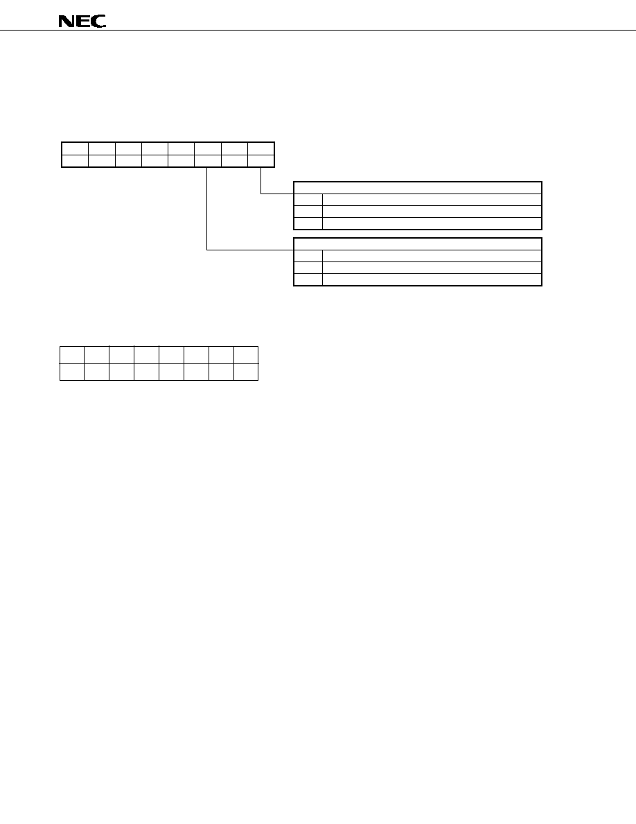
3.11 Output Pin Control Command
This command selects the format of pin output of the option (A, B, or C) specified by the initial status setting
command (because this is a 2-byte command, input of 16 bits is necessary if this command is input more than once
successively).
Remark
This command is invalid when RGB + RGB compatible BLK output is selected.
(1) With MSB first (The command is input from MSB (D15).)
D15
D14
D13
D12
D11
D10
D9
D8
D7
D6
D5
D4
D3
D2
D1
D0
1
0
0
1
1
1
0
0
OD1
OD0
0
0
AR3
AR2
AR1
AR0
(MSB)
(LSB)
Row specification bit
Function
Sets row 0
Sets row 1
Sets row 11
Setting prohibited
AR3
0
0
1
AR2
0
0
0
AR1
0
0
1
AR0
0
1
1
Output pin control bit
Pin output
V
C1
: Outputs specified row, V
C2
: Fixed to low level
V
C1
: Fixed to low level, V
C2
: Outputs specified row
OD1
0
0
OD0
0
1
Option A
Output pin control bit
Pin output
V
C1
: Outputs all rows, V
C2
: Fixed to low level
V
C1
: Outputs all rows, V
C2
: Outputs specified row
OD1
0
0
OD0
0
1
Option B
Output pin control bit
Pin output
V
C1
: Outputs columns 0-23, V
C2
: Fixed to low level
V
C1
: Outputs columns 0-11, V
C2
: Outputs columns 12-23
V
C1
: Outputs columns 12-23, V
C2
: Outputs columns 0-11
V
C1
: Fixed to low level, V
C2
: Outputs columns 0-23
OD1
0
0
1
1
OD0
0
1
0
1
Option C
(2) With LSB first (Use of each bit is the same as (1). The command is input from LSB (D0).)
(LSB)
(MSB)
D0
D1
D2
D3
D4
D5
D6
D7
D8
D9
D10
D11
D12
D13
D14
D15
0
0
1
1
1
0
0
1
AR0
AR1
AR2
AR3
0
0
OD0 OD1
∑
Row specification control
Specify to which of the V
C1
or V
C2
pin the character signal is to be output in row units (or 12-column units).
∑
Output pin control
Output of the V
C1
and V
C2
pin can be selected from A, B, or C by using the initial status setting command
(the blanking signal is output in the same manner).

38
µ
PD6466
3.12 Character Size Control Command
The character size can be specified in row units (independently in the horizontal and vertical directions. Because
this is a 2-byte command, input of 16 bits is necessary when this command is input more than once successively).
(1) With MSB first (The command is input from MSB (D15).)
D15
D14
D13
D12
D11
D10
D9
D8
D7
D6
D5
D4
D3
D2
D1
D0
1
0
0
1
1
0
SV1
SV0
SH1
SH0
0
0
AR3
AR2
AR1
AR0
(MSB)
(LSB)
Row specification control bit
Function
Sets row 0
Sets row 1
Sets row 11
Setting prohibited
AR3
0
0
1
AR2
0
0
0
AR1
0
0
1
AR0
0
1
1
Horizontal character size control bit
Function
SH1
0
0
1
1
1 dot = 1t dots (horizontal standard size)
1 dot = 2t dots (horizontal
◊
2 size)
1 dot = 3t dots (horizontal
◊
3 size)
1 dot = 4t dots (horizontal
◊
4 size)
1t dots ( s) =
(f
OSC
: LC oscillation frequency
or external clock
frequency)
f
OSC
(MHz)
1
SH0
0
1
0
1
Vertical character size control bit
Function
SV1
0
0
1
1
1 dot = 1H (vertical standard size)
1 dot = 2H (vertical
◊
2 size)
1 dot = 3H (vertical
◊
3 size)
1 dot = 4H (vertical
◊
4 size)
SV0
0
1
0
1
µ
(2) With LSB first (Use of each bit is the same as (1). The command is input from LSB (D0).)
(LSB)
(MSB)
D0
D1
D2
D3
D4
D5
D6
D7
D8
D9
D10
D11
D12
D13
D14
D15
SV0
SV1
0
1
1
0
0
1
AR0
AR1
AR2
AR3
0
0
SH0
SH1
∑
Row specification control
The character size is specified in row units. Which row is specified is controlled.
∑
Character size control
Four steps (16 types) of character size can be selected in the vertical and horizontal directions independently.
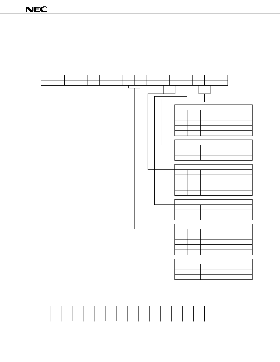
39
µ
PD6466
3.13 3-Channel Background Control Command
This command can be used to independently specify the background for the output of the 3 channels (because
this command is a 2-byte command, input of 16 bits is necessary when this command is input more than once
successively).
(1) With MSB first (The command is input from MSB (D15).)
D15
D14
D13
D12
D11
D10
D9
D8
D7
D6
D5
D4
D3
D2
D1
D0
1
0
1
1
0
0
1
BA1
BA0
BFA
BB1
BB0
BFB
BC1
BC0
BFC
(MSB)
(LSB)
V
C2
background control bit
Function
No background
Blank background
Must not be specified
Filled background
BC1
0
0
1
1
BC0
0
1
0
1
V
C2
framing control bit
Function
Framing OFF
Framing ON
BFC
0
1
V
C1
background control bit
Function
No background
Blank background
Must not be specified
Filled background
BB1
0
0
1
1
BB0
0
1
0
1
V
C1
framing control bit
Function
Framing OFF
Framing ON
BFB
0
1
RGB background control bit
Function
No background
Blank background
Must not be specified
Filled background
BA1
0
0
1
1
BA0
0
1
0
1
RGB framing control bit
Function
Framing OFF
Framing ON
BFA
0
1
V
C2
output
V
C1
output
RGB output
(2) With LSB first (Use of each bit is the same as (1). The command is input from LSB (D0).)
(LSB)
(MSB)
D0
D1
D2
D3
D4
D5
D6
D7
D8
D9
D10
D11
D12
D13
D14
D15
BA1
1
0
0
1
1
0
1
BFC
BC0
BC1
BFB
BB0
BB1
BFA BA0

40
µ
PD6466
∑
Framing control
Whether a character is framed is specified in screen units.
Framing: If the rightmost or leftmost dots of the dot matrix forming a character are used, the frame is
displayed in the adjacent character display area. If the rightmost or leftmost dots of the dot matrix
are not used, the frame is displayed on the left or the right of, above, or upper or lower left or
right of the character. Even when the top or bottom dot is used, framing does not overlap the
line above or below. Dots other than those at the top or bottom of the dot matrix are framed
vertically, horizontally, and diagonally.
Character dots
Framing
The size of the framing is fixed to one dot of the minimum size even if the character size changes.
∑
Background control
No background, blank background, or filled background can be selected in screen units. The background
color is selected by the background color/framing color control command.
No background
: Only character data is output.
Blank background : The background is displayed in the display area of the characters written to the video
RAM and the portion overlapping by one dot of the minimum size from the rightmost
and leftmost position of that area.
Filled background : In addition to the area where the background is displayed in the blank background
mode above, the background is displayed in the areas other than the character display
area.
∑
Background and frame display in the case of RGB + V
C1
+ V
C2
output
The portion of the character for which V
C2
is specified by the display character control command is not output
to the RGB and V
C1
channels. Therefore, even if a background (blank background or filled background)
is specified for the RGB or V
C1
output, no background is displayed in the V
C2
-specified area. In addition,
no background is displayed at the portion of the character other than those specified by V
C2
in the case
of V
C2
output (for the details of display of V
C2
-specified character area for RGB and V
C1
output, refer to 1.3
Display with RGB + V
C1
+ V
C2
Pins and 1.3.4 Displaying characters specified by V
C2
).
When RGB + RGB compatible BLK output is selected, only the background control bit of RGB output is valid,
and the background control bit of V
C1
output and V
C2
output is invalid (when RGB + RGB compatible BLK
output is selected, the V
C2
output pin is not used. The V
C1
channel outputs the logical sum of the RGB
output).
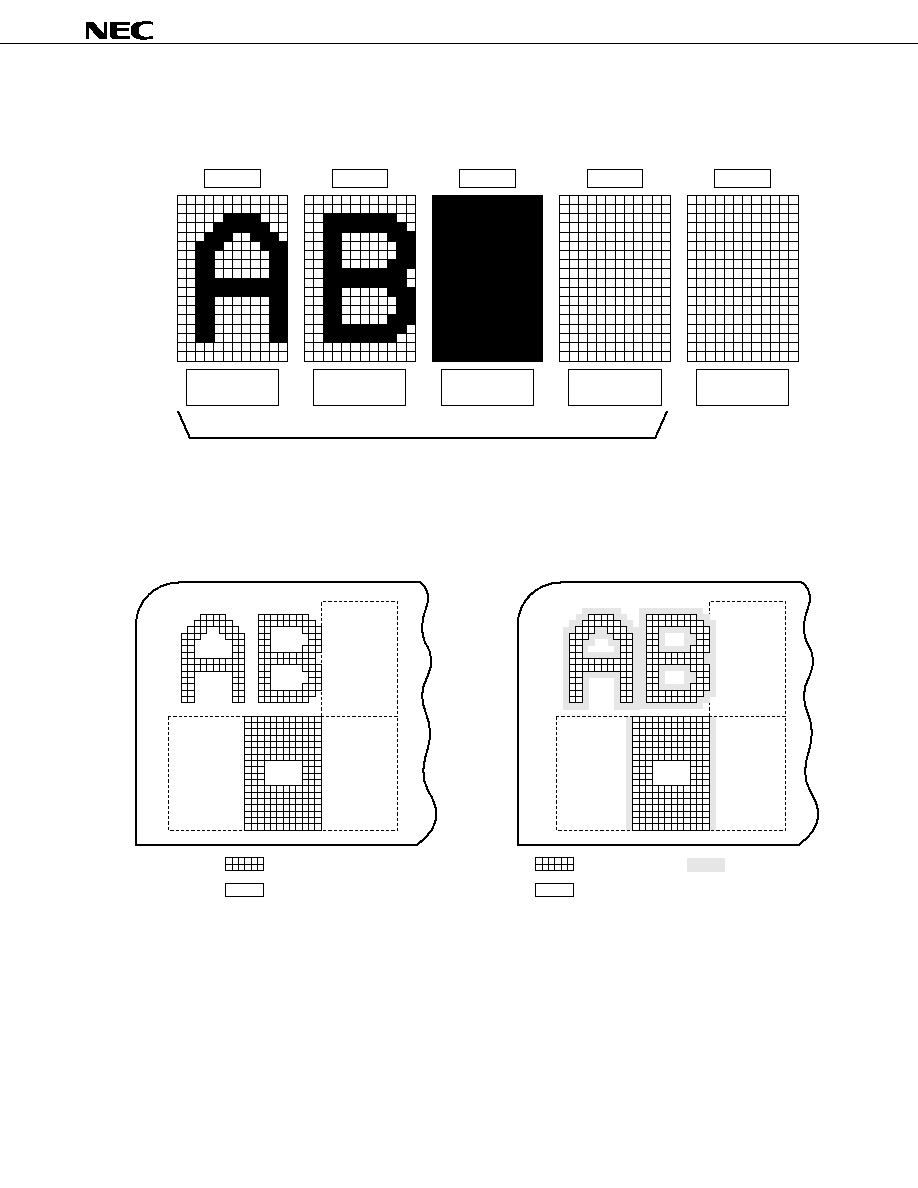
41
µ
PD6466
Display format of background and frame
Display example with character
XXH
Character A
XYH
Character B
YYH
Filled Data
YZH
Blank Data
FEH
Display Off Data
Cannot be changed
with mask code option
(address fixed)
Can be designed with mask code option
No background + no frame
Display Off
Data
Blank
Data
Display Off
Data
Filled
Data
Character
Video
No background + frame
Display Off
Data
Blank
Data
Display Off
Data
Filled
Data
Character
Video
Frame
Eight colors can be selected for the character and background, and two colors (black and white) can be selected
for the frame, in screen units.
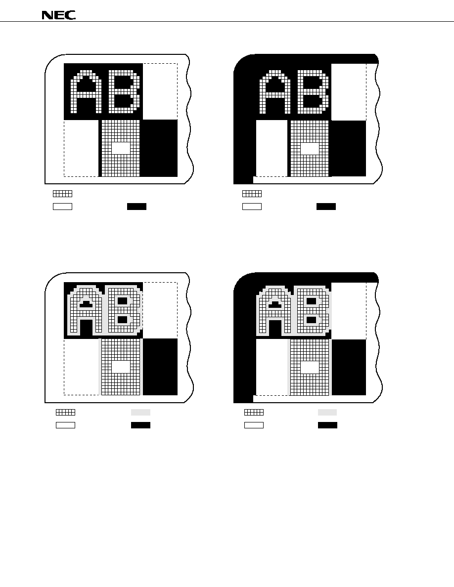
42
µ
PD6466
Display Off
Data
Blank
Data
Display Off
Data
Blank background + no frame
Display Off
Data
Display Off
Data
Character
Video
Filled background + no frame
Character
Video
Blank background + frame
Character
Video
Filled background + frame
Filled
Data
Character
Video
Display Off
Data
Blank
Data
Display Off
Data
Filled
Data
Display Off
Data
Frame
Background
Frame
Background
Background
Background
Blank
Data
Filled
Data
Blank
Data
Display Off
Data
Filled
Data

43
µ
PD6466
3.14 Initial Status Setting Command
This command initializes the operation mode.
Execute this command first on power application.
To change the initial setting, be sure to execute this command with the display OFF.
(1) With MSB first (The command is input from MSB (D15).)
D15
D14
D13
D12
D11
D10
D9
D8
D7
D6
D5
D4
D3
D2
D1
D0
1
0
1
1
0
1
0
0
0
BR
RS
OP1
OP0
COC
VST
OSC
(MSB)
(LSB)
Vertical display start position control bit
Function
Vertical display start position setting unit = 3 rows
Vertical display start position setting unit = 9 rows
VST
0
1
Output selection control bit
Function
Option A
Option B
Option C
Must not be specified
OP1
0
0
1
1
OP0
0
1
0
1
Pin selection control bit
Function
RGB + V
C1
+ V
C2
RGB + RGB compatible BLK (3BLK)
COC
0
1
Dot clock control bit
Function
LC oscillation
External clock input
OSC
0
1
Character color reverse control bit
Function
RS
0
1
Character color: Black (frame specification is invalid)
Character color: White (frame specification is valid)
Function selection bit
Function
BR
0
1
Character blinks
Character left to right reverse
(2) With LSB first (Use of each bit is the same as (1). The command is input from LSB (D0).)
(LSB)
(MSB)
D0
D1
D2
D3
D4
D5
D6
D7
D8
D9
D10
D11
D12
D13
D14
D15
0
0
1
0
1
1
0
1
OSC VST COC OP0
OP1
RS
BR
0

44
µ
PD6466
This command sets the information selected by a mask code option in the
µ
PD6461 and 6462.
The default setting is as follows:
OSC
= 0
: LC oscillation
VST
= 0
: 3-row units
COC
= 0
: RGB + V
C1
+ V
C2
(OP1, OP0) = (0, 1) : Option B
RS
= 0
: Black character
BR
= 0
: Character blinks
∑
Dot clock control
The dot clock for character display is set.
The dot clock is selected from LC oscillation and external clock input.
∑
Vertical display start position control
The character display start position and setting accuracy are set.
The setting accuracy is selected from 3 rows and 9 rows.
∑
Pin selection control
The output pins of the character and blanking signals are set.
The output pins are selected from the following two types:
∑
RGB + V
C1
+ V
C2
: Signal output pins = V
R
, V
G
, V
B
, V
BLK
, V
C1
, BLK1, V
C2
, BLK2
∑
RGB + RGB compatible BLK : Signal output pins = V
R
, V
G
, V
B
, R
BLK
, G
BLK
, B
BLK
, V
C1
, BLK1
∑
Output selection control
The output formats of V
C1
and V
C2
are set.
The output formats are selected from options A, B, and C (refer to 1.3 Display with RGB + V
C1
+ V
C2
Pins).
The output formats are set only when RGB + V
C1
+ V
C2
is selected by means of pin selection control. Select
option B when RGB + RGB compatible BLK is selected.
∑
Character color reverse control
The character when color displayed is turned ON is specified.
Select the character from black character (with frame specification invalid) or white character (with frame
specification valid) (refer to 3.5 Character Color Reverse ON/OFF Command).
45
µ
PD6466
3.15 Display Character Control Command
This command specifies the character data to be written to the video RAM, blinking data, and character color.
When inputting this command, turn ON LC oscillation (if the oscillation is OFF, characters cannot be written to the
video RAM).
This command is a 2-byte successive command. To write character data successively without changing the blinking
data, character color, and character address bank, the second character and those that follow can be input in the
abbreviated form by using only the low-order 8 bits (D7 through D0). In this case, the write column address is
automatically incremented (If a character is written to the 23rd column, the next write address is automatically
incremented to column 0 (leftmost) on one row below. If characters have been written to the 23rd column on the 11th
row, the next write address is automatically incremented to column 0 on row 0).
0 1
2
21 22 23
Row n
Row n+1
Row address ( )
Row address increment
Column address ( )
0 1 2
21 22 23
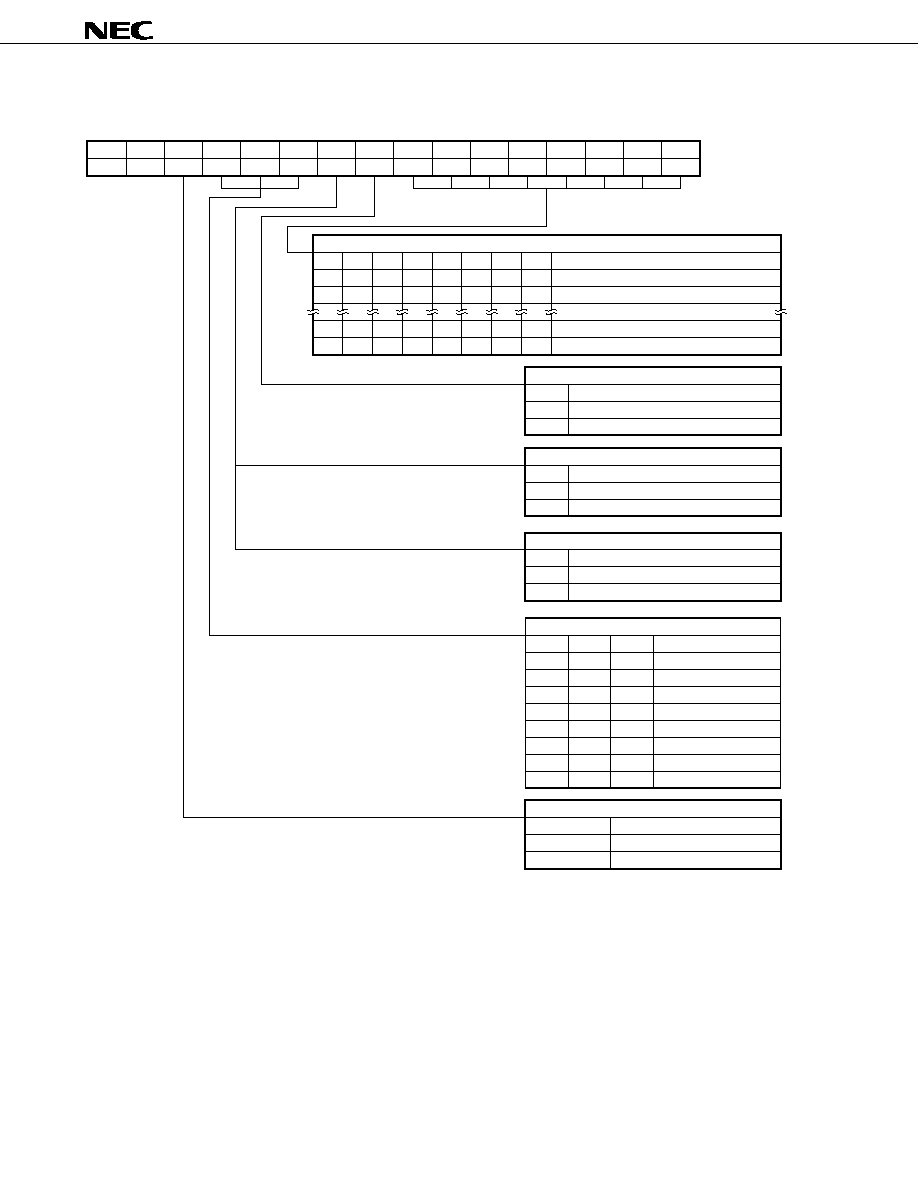
46
µ
PD6466
(1) With MSB first (The command is input from MSB (D15).)
D15
D14
D13
D12
D11
D10
D9
D8
D7
D6
D5
D4
D3
D2
D1
D0
1
1
RV
R
G
B
BL
V
C2
C7
C6
C5
C4
C3
C2
C1
C0
(MSB)
(LSB)
Character specification bit
Function
Outputs data of 00H
Outputs data of 01H
Outputs FEH (Display Off Data)
FFH (2-byte successive command end code)
C4
0
0
1
1
C0
0
1
0
1
C3
0
0
1
1
C2
0
0
1
1
C1
0
0
1
1
V
C2
output specification bit
Function
V
C2
specification OFF
V
C2
specification ON
V
C2
0
1
Blinking control bit (character units)
Function
Character color specification bit
Function
Black
Blue
Green
Cyan
Red
Magenta
Yellow
White
R
0
0
0
0
1
1
1
1
G
0
0
1
1
0
0
1
1
Character color reverse specification bit
Function
Character color reverse specification OFF
Character color reverse specification ON
RV
0
1
C5
0
0
1
1
C6
0
0
1
1
C7
0
0
1
1
B
0
1
0
1
0
1
0
1
BL
0
1
Character does not blink.
Character blinks.
Left and right reverse character control bit
Function
BL
0
1
Left and right reverse character specification OFF
Left and right reverse character specification ON
With character blinking selected
Note
With character left and right reverse selected
Note
Note
Set these bits with the initial setting command.

47
µ
PD6466
(2) With LSB first (Use of each bit is the same as (1). The command is input from LSB (D0).)
(LSB)
(MSB)
D0
D1
D2
D3
D4
D5
D6
D7
D8
D9
D10
D11
D12
D13
D14
D15
V
C2
RB
B
G
R
RV
1
1
C0
C1
C2
C3
C4
C5
C6
C7
∑
Character specification
Specify the addresses of the 256 types of characters in each bank. Note, however, that addresses FEH
and FFH are respectively fixed to Display Off Data and a 2-byte successive command end code (these
addresses are also fixed when characters are changed by using a mask code option, and no characters
can be stored to these addresses). The design of the characters can be created by using a mask code
option.
∑
V
C2
output specification
The character output from the V
C2
pin can be specified in character units. The character specified by V
C2
is not output from the RGB output or V
C1
output channel (this specification is invalid when RGB + RGB
compatible BLK output selected).
∑
Blinking control (character units)
Note
Whether the character written to the video RAM blinks is specified in character units. Blinking is turned
ON/OFF in screen units by using the character display control command (refer to 3.2 Display Control
Command).
∑
Left to right reverse character specification
Note
Left to right reverse can be turned ON/OFF in character units (this specification is valid when left and right
reverse is turned ON by the display control command).
Note
Character blinking or character left to right reverse, whichever selected by the initial setting
command, is valid.
∑
Character color control
A character color can be set in units of one character (valid for RGB output only. The color is fixed for the
V
C1
and V
C2
output).
∑
Character color reverse specification
It can be specified whether the color of a character can be reversed or not, in character units. Turning ON/
OFF the character color reverse is specified in screen units by the character color reverse ON/OFF
command (refer to 3.5 Character Color Reverse ON/OFF Command).
48
µ
PD6466
3.16 Test Mode
This command is used to test the IC and must not be used for any other purposes.
The IC cannot be set in the test mode when the TEST pin (
µ
PD6466GS-xxx: pin 9/GT-xxx: pin 10) is connected
to GND.
(1) With MSB first (The command is input from MSB (D15).)
(MSB)
(LSB)
D15
D14
D13
D12
D11
D10
D9
D8
D7
D6
D5
D4
D3
D2
D1
D0
1
0
1
1
0
0
0
0
T7
T6
T5
T4
T3
T2
T1
T0
(2) With LSB first (Use of each bit is the same as (1). The command is input from LSB (D0).)
(LSB)
(MSB)
D0
D1
D2
D3
D4
D5
D6
D7
D8
D9
D10
D11
D12
D13
D14
D15
0
0
0
0
1
1
0
1
T0
T1
T2
T3
T4
T5
T6
T7
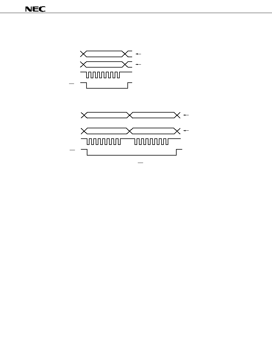
49
µ
PD6466
4. TRANSFERRING COMMANDS
4.1 1-Byte Command
D7-D0
With MSB first: The command is input from bit D7.
DATA
DATA
CLK
CS
D0-D7
With LSB first: The command is input from bit D0.
4.2 2-Byte Command
D15-D8
With MSB first
1st byte: D15-D8
2nd byte: D7-D0
DATA
D0-D7
D7-D0
D8-D15
1st byte
2nd byte
1st byte
2nd byte
DATA
CLK
CS
With LSB first
1st byte: D0-D7
2nd byte: D8-D15
When transferring a 2-byte command, do not make CS high and keep it low between the first and second bytes.

50
µ
PD6466
4.3 2-Byte Successive Commands
D15-D8
MSB first
DATA
D0-D7
D7-D0
D8-D15
1st byte
2nd byte
1st byte
2nd byte
DATA
CLK
CS
LSB first
D7-D0
D8-D15
2nd byte
2nd byte
The 2-byte successive command writes characters to the video RAM. To successively write characters without
changing the blinking data, reverse specification data, and V
C2
specification data, first transfer the first byte and then
transfer the second byte (character address).
To change the contents of the above data, change the contents of the data and then input the command from the
first byte after terminating the 2-byte successive command once (by either making CS high or transferring the 2-byte
successive command end code).
However, the command cannot be transferred successively across banks.
When the low-order bank is selected, the command can be transferred successively in a character address range
of 000H to 0FFH; when the high-order bank is selected, the character address range is from 100H to 1FFH.
It is recommended that characters that are frequently used be stored to both the high-order and low-order banks.
To write a character that across the banks, complete successive transfer once, and then transfer the command
from the first byte after changing the bank.
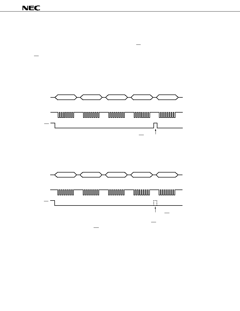
51
µ
PD6466
4.4 Successive Input of Command
Transfer each of the 1-byte, 2-byte, and 2-byte successive commands from a microcontroller to the
µ
PD6466 as
follows.
To transfer a 1-byte or 2-byte command, or a 2-byte successive command with blinking data changed after a 2-
byte successive command has been transferred, either make CS high once, or transfer FFH (2-byte successive
command end code) at the end of the 2-byte successive command. In the latter case, it is not necessary to make
CS high.
4.4.1 When 2-byte successive command end code is not used
Example 1-byte command
2-byte successive command
1-byte command
DATA
CLK
CS
Make CS low once and then back high again.
2nd byte
(D0-D7)
MSB first (LSB first)
2nd byte
(D8-D15)
00H-FEH
(normal character)
2-byte successive
command
1st byte
(D0-D7)
1-byte command
(D0-D7)
(D8-D15)
00H-FEH
(normal character)
D7-D0
D7-D0
D15-D8
D7-D0
D7-D0
1-byte command
4.4.2 When 2-byte successive command end code is used
Example 1-byte command
2-byte successive command
1-byte command
DATA
CLK
CS
1-byte command
2nd byte
(D0-D7)
MSB first (LSB first)
2nd byte
(D8-D15)
00H to FFH
(normal character)
2-byte successive
command
1st byte
(D0-D7)
1-byte command
(D0-D7)
(D8-D15)
FFH (2-byte successive
command end code)
D7-D0
D7-D0
D15-D8
D7-D0
D7-D0
It is not necessary to make CS low and then back high again.
Remark
By using the 2-byte successive command end code, the CS pin may remain low. However, it is
recommended to make CS pin high to improve the noise immunity.
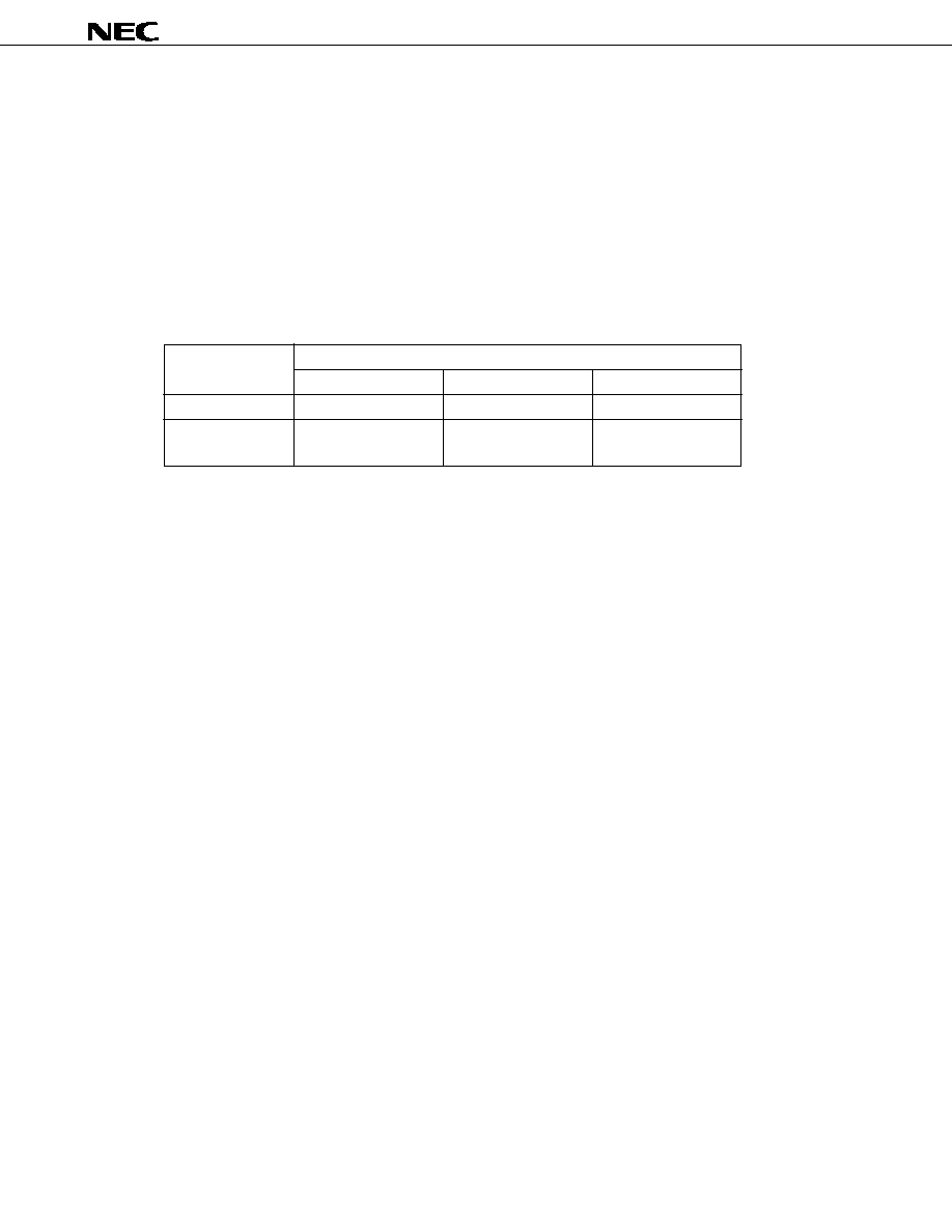
52
µ
PD6466
5. CHARACTER PATTERNS
The
µ
PD6466 can display 512 character patterns, including alphanumeric characters, Kanji characters, and
symbols, which are stored in the character generator ROM. Each pattern in the character generator ROM can be
modified by specifying a mask code option. However, the Display Off Data at character address FEH and 2-byte
continuous command end code at FFH cannot be modified because they are fixed in both high-order (1) and low-order
(0) banks. Therefore, no character pattern can be input at these addresses.
When none of the 12
◊
18 dots are filled for a character pattern at addresses 000H to 0FDH and 100H to 1FDH,
the character pattern is called Blank Data. Character address FEH in both banks is called Display Off Data. Blank
Data and Display Off Data are represented in the same way (with no dots filled) in character patterns (of the
µ
PD6466GS-001) shown on the following pages, but they are different as follows:
Character Code
Display of Character Area in Each Background Mode
No background
Minimum background
Overall background
Blank Data
Displays image
Displays background
Displays background
Display Off Data
Displays image
Displays image only
Displays image only
(without background)
(without background)
You cannot specify Display Off Data for addresses other than FEH when using a mask code option. Blank Data,
however, can be specified at any address from 000H to 0FDH or 100H to 1FDH (address 0FFH and 1FFH cannot
be used because they are fixed to the 2-byte continuous command end code).
The character patterns of the
µ
PD6466GS-001/GT-201 (NEC's standard model) are shown on the following pages.
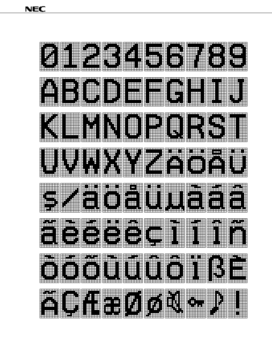
53
µ
PD6466
µ
PD6466GS-001/GT-201 Character Patterns
[000H]
[001H]
[002H]
[003H]
[004H]
[005H]
[006H]
[007H]
[008H]
[009H]
[00AH]
[00BH]
[00CH]
[00DH]
[00EH]
[00FH]
[010H]
[011H]
[012H]
[013H]
[014H]
[015H]
[016H]
[017H]
[018H]
[019H]
[01AH]
[01BH]
[01CH]
[01DH]
[01EH]
[01FH]
[020H]
[021H]
[022H]
[023H]
[024H]
[025H]
[026H]
[027H]
[028H]
[029H]
[02AH]
[02BH]
[02CH]
[02DH]
[02EH]
[02FH]
[030H]
[031H]
[032H]
[033H]
[034H]
[035H]
[036H]
[037H]
[038H]
[039H]
[03AH]
[03BH]
[03CH]
[03DH]
[03EH]
[03FH]
[040H]
[041H]
[042H]
[043H]
[044H]
[045H]
[046H]
[047H]
[048H]
[049H]
[04AH]
[04BH]
[04CH]
[04DH]
[04EH]
[04FH]

54
µ
PD6466
[050H]
[051H]
[052H]
[053H]
[054H]
[055H]
[056H]
[057H]
[058H]
[059H]
[05AH]
[05BH]
[05CH]
[05DH]
[05EH]
[05FH]
[060H]
[061H]
[062H]
[063H]
[064H]
[065H]
[066H]
[067H]
[068H]
[069H]
[06AH]
[06BH]
[06DH]
[06CH]
[06EH]
[06FH]
[070H]
[071H]
[072H]
[073H]
[074H]
[075H]
[077H]
[076H]
[078H]
[079H]
[07AH]
[07BH]
[07CH]
[07DH]
[07EH]
[07FH]
[081H]
[080H]
[082H]
[083H]
[084H]
[085H]
[086H]
[087H]
[088H]
[089H]
[08BH]
[08AH]
[08CH]
[08DH]
[08EH]
[08FH]
[090H]
[091H]
[092H]
[093H]
[095H]
[094H]
[096H]
[097H]
[098H]
[099H]
[09AH]
[09BH]
[09CH]
[09DH]
[09EH]
[09FH]
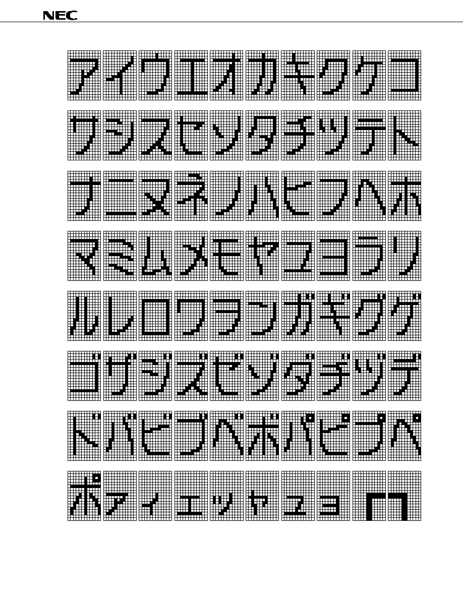
55
µ
PD6466
[0A0H]
[0A1H]
[0A2H]
[0A3H]
[0A4H]
[0A5H]
[0A6H]
[0A7H]
[0A8H]
[0A9H]
[0AAH]
[0ABH]
[0ACH]
[0ADH]
[0AEH]
[0AFH]
[0B0H]
[0B1H]
[0B2H]
[0B3H]
[0EFH]
[0B4H]
[0B5H]
[0B6H]
[0B7H]
[0B8H]
[0B9H]
[0BAH]
[0BBH]
[0BCH]
[0BDH]
[0BEH]
[0BFH]
[0C0H]
[0C1H]
[0C2H]
[0C3H]
[0C4H]
[0C5H]
[0C6H]
[0C7H]
[0C8H]
[0C9H]
[0CAH]
[0CBH]
[0CCH]
[0CDH]
[0CEH]
[0CFH]
[0D0H]
[0D1H]
[0D2H]
[0D3H]
[0D4H]
[0D5H]
[0D6H]
[0D7H]
[0D8H]
[0D9H]
[0DAH]
[0DBH]
[0DCH]
[0DDH]
[0DEH]
[0DFH]
[0E0H]
[0E1H]
[0E2H]
[0E3H]
[0E5H]
[0E4H]
[0E6H]
[0E7H]
[0E8H]
[0E9H]
[0EAH]
[0EBH]
[0ECH]
[0EDH]
[0EEH]

56
µ
PD6466
[0F0H]
[0F1H]
[0F2H]
[0F3H]
[0F4H]
[0F5H]
[0F6H]
[0F7H]
[0F9H]
[0F8H]
[0FAH]
[0FBH]
[0FCH]
[0FDH]
Note 1
[0FEH]
Note 2
[0FFH]
Note 3
[100H]
[101H]
[103H]
[102H]
[104H]
[105H]
[106H]
[107H]
[108H]
[109H]
[10AH]
[10BH]
[10DH]
[10CH]
[10EH]
[10FH]
[110H]
[111H]
[112H]
[113H]
[114H]
[115H]
[116H]
[117H]
[118H]
[119H]
[11AH]
[11BH]
[11CH]
[11DH]
[11EH]
[11FH]
[120H]
[121H]
[122H]
[123H]
[124H]
[125H]
[126H]
[127H]
[128H]
[129H]
[12AH]
[12BH]
[12CH]
[12DH]
[12EH]
[12FH]
[130H]
[131H]
[132H]
[133H]
[134H]
[135H]
[136H]
[137H]
[138H]
[139H]
[13AH]
[13BH]
[13CH]
[13DH]
[13EH]
[13FH]
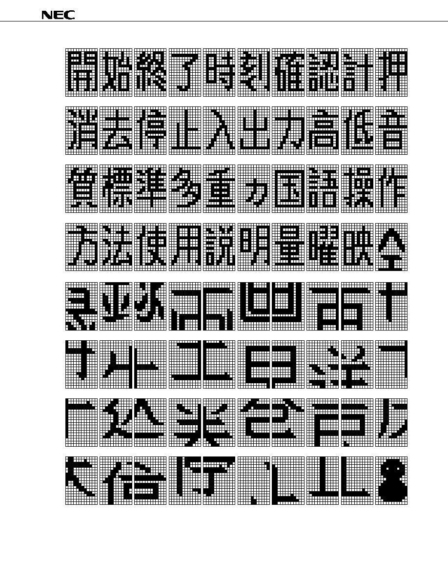
57
µ
PD6466
[140H]
[141H]
[142H]
[143H]
[144H]
[145H]
[146H]
[147H]
[148H]
[149H]
[14AH]
[14BH]
[14CH]
[14DH]
[14EH]
[14FH]
[150H]
[151H]
[152H]
[153H]
[154H]
[155H]
[156H]
[157H]
[158H]
[159H]
[15AH]
[15BH]
[15CH]
[15DH]
[15EH]
[15FH]
[160H]
[161H]
[162H]
[163H]
[164H]
[165H]
[166H]
[167H]
[168H]
[169H]
[16AH]
[16BH]
[16CH]
[16DH]
[16EH]
[16FH]
[170H]
[171H]
[172H]
[173H]
[174H]
[175H]
[176H]
[177H]
[178H]
[179H]
[17AH]
[17BH]
[17CH]
[17DH]
[17EH]
[17FH]
[180H]
[181H]
[182H]
[183H]
[184H]
[185H]
[186H]
[187H]
[188H]
[189H]
[18AH]
[18BH]
[18CH]
[18DH]
[18EH]
[18FH]
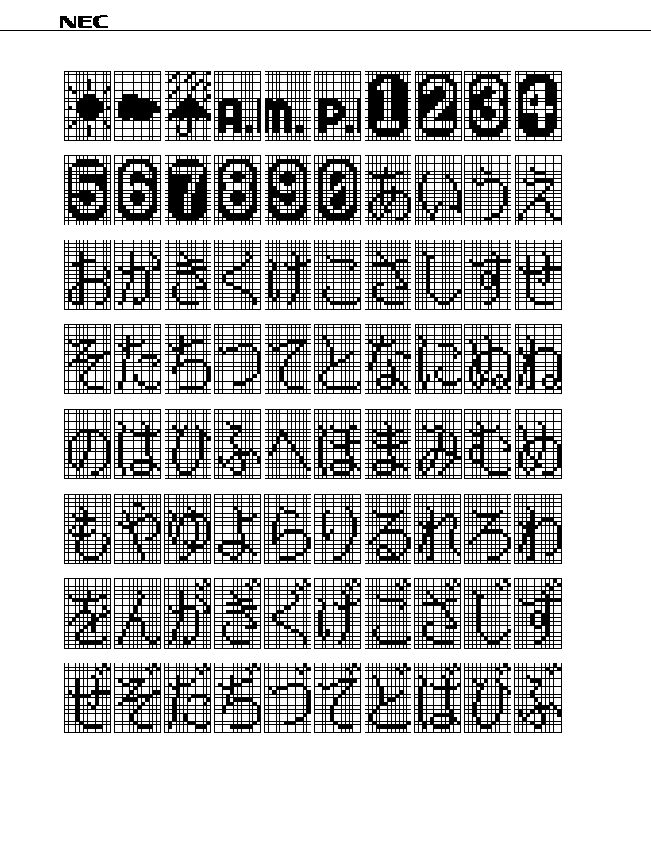
58
µ
PD6466
[190H]
[191H]
[192H]
[193H]
[194H]
[195H]
[196H]
[197H]
[198H]
[199H]
[19AH]
[19BH]
[19CH]
[19DH]
[19EH]
[19FH]
[1A0H]
[1A1H]
[1A2H]
[1A3H]
[1A4H]
[1A5H]
[1A6H]
[1A7H]
[1A8H]
[1A9H]
[1AAH]
[1ABH]
[1ACH]
[1ADH]
[1AEH]
[1AFH]
[1B0H]
[1B1H]
[1B2H]
[1B3H]
[1B4H]
[1B5H]
[1B6H]
[1B7H]
[1B8H]
[1B9H]
[1BAH]
[1BBH]
[1BCH]
[1BDH]
[1BEH]
[1BFH]
[1C0H]
[1C1H]
[1C2H]
[1C3H]
[1C4H]
[1C5H]
[1C6H]
[1C7H]
[1C8H]
[1C9H]
[1CAH]
[1CBH]
[1CCH]
[1CDH]
[1CEH]
[1CFH]
[1D0H]
[1D1H]
[1D2H]
[1D3H]
[1D4H]
[1D5H]
[1D6H]
[1D7H]
[1D8H]
[1D9H]
[1DAH]
[1DBH]
[1DCH]
[1DDH]
[1DEH]
[1DFH]

59
µ
PD6466
[1E0H]
[1E1H]
[1E2H]
[1E3H]
[1E4H]
[1E5H]
[1E6H]
[1E7H]
[1E8H]
[1E9H]
[1EAH]
[1EBH]
[1ECH]
[1EDH]
[1EEH]
[1EFH]
[1F0H]
[1F1H]
[1F2H]
[1F3H]
[1F4H]
[1F5H]
[1F6H]
[1F7H]
[1F8H]
[1F9H]
[1FAH]
[1FBH]
[1FCH]
[1FDH]
Note 1
[1FEH]
Note 2
[1FFH]
Note 3
Notes 1.
Blank data
2.
Display Off Data (character addresses are fixed)
3.
2-byte continuous input end code (character addresses are fixed)
Remark
0xxH indicates character address of the low-order (0) bank, and 1xxH indicates that of the high-order
(1) bank.
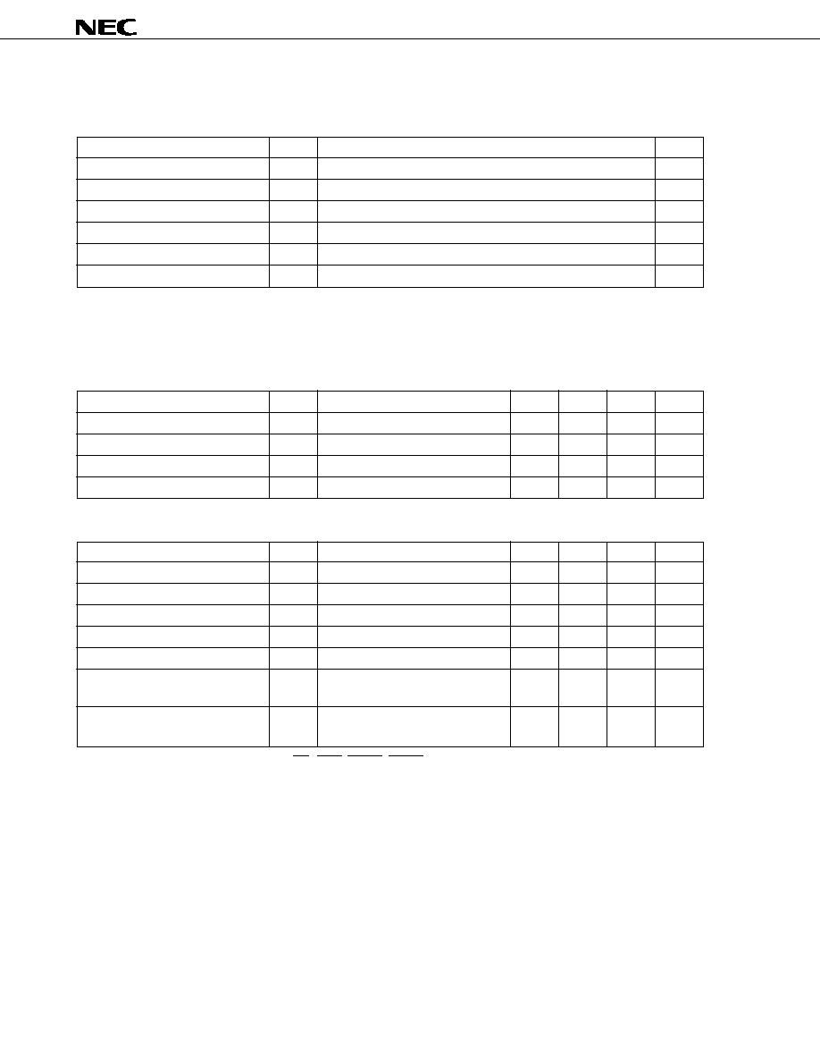
60
µ
PD6466
6. ELECTRICAL CHARACTERISTICS
Absolute Maximum Ratings
Parameter
Symbol
Ratings
Unit
Supply voltage
V
DD
7
V
Input pin voltage
V
IN
≠0.3 to V
DD
+ 0.3
V
Output pin voltage
V
OUT
≠0.3 to V
DD
+ 0.3
V
Operating ambient temperature
T
A
≠20 to +75
∞
C
Storage temperature
T
stg
≠40 to +125
∞
C
Output current
I
O
±
5
mA
Caution Exposure to Absolute Maximum Ratings for extended periods may affect device reliability; exceeding
the ratings could cause permanent damage. The parameters apply independently. The device
should be operated within the limits specified under DC and AC Characteristics.
Recommended Operating Range
Parameter
Symbol
Conditions
MIN.
TYP.
MAX.
Unit
Supply voltage range
V
DD
2.7
5.5
V
Oscillation frequency (LC oscillation)
f
OSC
V
DD
= 2.7 to 5.5 V
6.0
8.0
MHz
Oscillation frequency (external clock)
f
OSC
V
DD
= 2.7 to 5.5 V
4.0
8.0
MHz
Operating ambient temperature
T
A
≠20
+75
∞
C
Electrical Characteristics (T
A
= 25
∞
C, unless otherwise specified, V
DD
= 2.7 to 5.5 V)
Parameter
Symbol
Conditions
MIN.
TYP.
MAX.
Unit
Supply voltage range
V
DD
2.7
5.0
5.5
V
Current consumption 1
I
DD
f
OSC
= 8.0 MHz, V
DD
= 5.0 V
5.0
10.0
mA
Current consumption 2
I
DD
f
OSC
= 8.0 MHz, V
DD
= 3.0 V
3.0
5.0
mA
Signal input high-level voltage
V
ISH
0.7 V
DD
V
Signal input low-level voltage
V
ISL
0.3 V
DD
V
Signal output high-level voltage
V
OSH
I
OSL
= ≠1 mA (V
DD
= 5 V)/≠0.5 mA
0.9 V
DD
V
(V
DD
= 3 V)
Signal output low-level voltage
V
OSL
I
OSL
= 1 mA (V
DD
= 5 V)/0.5 mA
0.1 V
DD
V
(V
DD
= 3 V)
Remark
Signal input
: DATA, CLK, CS, PCL, Hsync, Vsync, CMDCT
Signal output : V
R
, V
G
, V
B
, V
C1
, V
C2
, V
BLK
, BLK1, BLK2 (R
BLK
, G
BLK
, B
BLK
)
( ): Set by initial status setting command
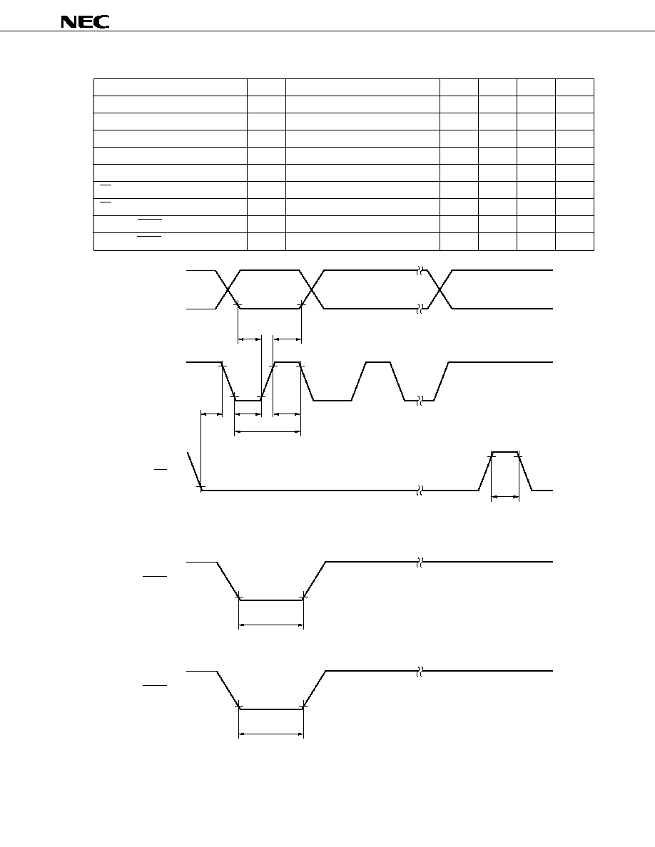
61
µ
PD6466
Recommended Operation Timing (T
A
= ≠20 to +75
∞
C, V
DD
= 2.7 to 5.5 V)
Parameter
Symbol
Conditions
MIN.
TYP.
MAX.
Unit
Setup time
t
SET
200
ns
Hold time
t
HOLD
200
ns
Minimum clock low-level width
t
CKL
400
ns
Minimum clock high-level width
t
CKH
400
ns
Clock cycle
t
TCK
1.0
µ
s
CS setup time
t
CSS
400
ns
CS hold time
t
CSH
400
ns
Minimum Hsync low-level width
t
HWL
4
µ
s
Minimum Vsync low-level width
t
VWL
4
µ
s
10 %
t
HWL
Hsync
10 %
t
VWL
Vsync
CS
CLK
DATA
t
CSH
90 %
t
CKH
t
CKL
t
CSS
t
TCK
10 %
10 %
90 %
90 %
t
SET
t
HOLD
10 %

62
µ
PD6466
Power-ON Clear Specifications
Parameter
Symbol
Conditions
MIN.
TYP.
MAX.
Unit
PCL pin low retention period
t
PCLL
10
µ
s
t
PCLL
0.8 V
DD
0 V
0 V
V
DD
V
DD
0.16 V
DD
V
DD
PCL
External clock input
External clock input timing (valid when selected by initial status setting command)
t
C-H
50 %
t
H-C
50 %
t
S
10 %
90 %
Hsync
External
input clock
Parameter
Symbol
Conditions
MIN.
TYP.
MAX.
Unit
External clock falling
t
C-H
30
ns
sync signal rise time
Sync signal rise time
t
H-C
30
ns
external clock falling
t
S
(rising slew rate)
t
S
Note
ns
Note
10% of cycle of external clock
Example
Where the external clock frequency is 8 MHz
Clock cycle = 125 ns
12.5 ns (MAX.) because 125 ns
◊
10% (MAX.)
Remarks 1. Always keep the phase relation between the rising of Hsync and external input clock.
2. Make sure that noise of greater than 100 ns is not superimposed on the input of Hsync.
3. Keep the OSC
OUT
pin open when the external clock is input.
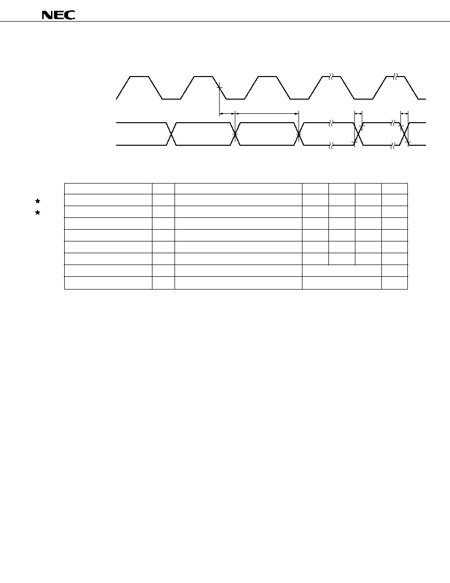
63
µ
PD6466
Character and BLK Signal Output
Characters and BLK signal are output in synchronization with the falling of the dot clock.
CDS
CUS
DTW
CDL
50 %
50 %
10 %
90 %
External
input clock
Character signal
BLK signal
Output Timing (T
A
= ≠20 to +75
∞
C, pins: V
R
, V
G
, V
B
, V
BLK
, V
C1
, BLK1, V
C2
, BLK2, (R
BLK
, G
BLK
, B
BLK
))
( ): Set by initial status setting command
Parameter
Symbol
Conditions
MIN.
TYP.
MAX.
Unit
Character/BLK signal output delay
CDL
V
DD
= 4.5 to 5.5 V, output load capacitance = 10 pF
10
18
30
ns
Character/BLK signal output delay
CDL
V
DD
= 2.7 to 3.3 V, output load capacitance = 10 pF
15
35
80
ns
Character/BLK signal rise time
CUS
V
DD
= 4.5 to 5.5 V, output load capacitance = 10 pF
2
10
ns
Character/BLK signal rise time
CUS
V
DD
= 2.7 to 3.3 V, output load capacitance = 10 pF
4
25
ns
Character/BLK signal falling
CDS
V
DD
= 4.5 to 5.5 V, output load capacitance = 10 pF
2
10
ns
Character/BLK signal falling
CDS
V
DD
= 2.7 to 3.3 V, output load capacitance = 10 pF
4
25
ns
Minimum size of 1 dot width
DTW
V
DD
= 4.5 to 5.5 V, output load capacitance = 10 pF (1/oscillation frequency (MHz))
±
5
ns
Minimum size of 1 dot width
DTW
V
DD
= 2.7 to 3.3 V, output load capacitance = 10 pF (1/oscillation frequency (MHz))
±
5
ns

64
µ
PD6466
Command Successive Input Permissible Time
Successively input commands under the following timing conditions:
(T
A
= ≠20 to +75
∞
C, V
DD
= 2.7 to 5.5 V)
Parameter
Symbol
Conditions
MIN.
TYP.
MAX.
Unit
Command successive
T1
Common to all commands
2.0
µ
s
input enable time
T2
Video RAM write
Display ON
LC oscillation
Note 1
µ
s
command
External clock
Note 2
Display OFF
2.0+19/f
OSC
µ
s
f
OSC
: LC oscillation or external input clock frequency (MHz)
Notes 1.
(1) 2.0 + (14/f
OSC
)
◊
S1 + 19/f
OSC
+ (1/f
OSC
)
◊
S2 + t
HWL
(2) 2.0 + (19/f
OSC
)
◊
S
S
: Character size (
◊
1 (MIN.) to
◊
4)
S1 : Horizontal character size before Hsync
S2 : Horizontal character size before Hsync
t
HWL
: Hsync width
Because the clock is not supplied to the internal circuitry during LC oscillation and Hsync, if Hsync is input
while the video RAM write command is executed, the width directly influences the execution time (1).
If Hsync is not input in the middle, the execution time is as (2) above.
Whether (1) or (2) is longer in time depending on the horizontal character size before and after Hsync and
Hsync width is not known. The longer time is the permissible minimum time.
2.
2.0 + 31/f
OSC
(S = 1)
2.0 + (19/f
OSC
)
◊
S (S = 2, 3, 4)
The restriction of T2 is not applied to the commands other than the video RAM write command if the clock
cycle for control satisfies the specifications.
DATA
Hi-Z
Hi-Z
T1
T2
Hi-Z
CLK

65
µ
PD6466
7. APPLICATION CIRCUIT EXAMPLE
CLK
CS
DATA
PCL
V
DD
CMDCT
OSC
OUT
OSC
IN
TEST
GND
Hsync
Vsync
V
B
V
G
V
R
V
BLK
V
C2
BLK2
V
C1
BLK1
Note 4
(B
BLK
)
Note 4
(G
BLK
)
Note 4
(R
BLK
)
PD6466GS/GT
µ
20 (24)
19 (23)
18 (21)
17 (20)
16 (19)
15 (18)
14 (17)
13 (16)
12 (15)
11 (14)
Output
Inputs a negative Hsync
or Vsync signal
1 (1)
2 (2)
3 (4)
4 (5)
5 (6)
6 (7)
7 (8)
Note 3
8 (9)
Note 3
9 (10)
10 (11)
Connected to microcomputer
V
DD
10 F
µ
100 k
10 F
µ
Note 1
0.01 F
µ
+
+
V
DD
Note 2
Note 5
33 F
µ
5 to 30 pF
30 pF
MSB first
LSB first
LC module
pin No. 1
LC module
pin No. 3
Notes 1.
CR constant must be satisfied with Power-ON Clear Specification (refer to 6. ELECTRICAL
CHARACTERISTICS).
2.
This circuit can reduce the number of external components and facilitates the adjustment of oscillation
frequency, using LC module (part number: Q285NCIS-11181, manufactured by Toko, Inc.)
3.
Connect these pins as follows when inputting external clock:
OSC
IN
pin: external clock input, OSC
OUT
pin: open
4.
Signals in ( ) are set by using an initial status setting command (RGB + RGB compatible blanking).
5.
When this connection is open, LSB first is selected.
Remarks 1. The number in the parentheses indicates the pin number of the
µ
PD6466GT-xxx.
2. With the
µ
PD6466GT-xxx, influence by noise via lead frame can be surpressed by connecting the
N.C. pins (3, 12, 13, 22) to GND.

66
µ
PD6466
8. PACKAGE DRAWINGS
N
S
C
D
M
M
P
F
G
E
B
L
K
J
detail of lead end
20 PIN PLASTIC SHRINK SOP (300 mil)
NOTE
2. Each lead centerline is located within 0.12 mm (0.005 inch) of
its true position (T.P.) at maximum material condition.
P20GM-65-300B-3
ITEM
MILLIMETERS
INCHES
A
B
C
D
E
F
G
H
I
J
0.65 (T.P.)
2.0 MAX.
1.7±0.1
8.1±0.3
0.575 MAX.
K
L
0.12
0.5±0.2
1.0±0.2
6.1±0.2
0.15
M
0.10
0.32
0.125±0.075
N
+0.10
≠0.05
0.023 MAX.
0.013
0.005±0.003
0.079 MAX.
0.067
0.319±0.012
0.240±0.008
0.039
0.006
0.020
0.005
0.004
+0.008
≠0.009
0.026 (T.P.)
P
3∞
3∞
+0.004
≠0.005
+0.004
≠0.002
6.7±0.3
0.264+0.012
≠0.013
1. Controlling dimension millimeter.
S
+0.003
≠0.004
+0.08
≠0.07
+7∞
≠3∞
+7∞
≠3∞
+0.009
≠0.008
20
11
1
10
A
H
I
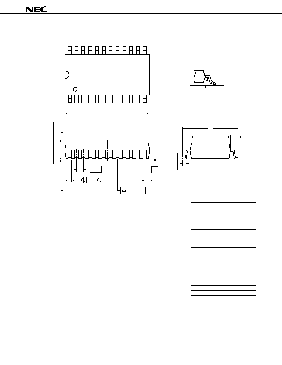
67
µ
PD6466
24 PIN PLASTIC SOP (375 mil)
NOTE
1. Controlling dimention
ITEM
MILLIMETERS
INCHES
E
F
2.9 MAX.
0.125±0.075
0.005±0.003
0.115 MAX.
B
C
1.27 (T.P.)
0.87 MAX.
0.035 MAX.
0.050 (T.P.)
G
2.50±0.2
0.098
detail of lead end
B
K
L
P
G
E
F
A
15.3
0.602
+0.41
≠0.2
+0.017
≠0.008
D
0.42
0.017
+0.08
≠0.07
H
10.3±0.2
0.406
I
7.2±0.2
0.283
J
1.6±0.2
0.063±0.008
K
0.17
0.007
+0.08
≠0.07
L
0.8±0.2
0.031
M
N
0.10
0.12
0.005
0.004
P
3
∞
3
∞
+7
∞
≠3
∞
P24GT-50-375B-2
+7
∞
≠3
∞
+0.009
≠0.008
+0.003
≠0.004
+0.009
≠0.008
+0.008
≠0.009
+0.009
≠0.008
+0.003
≠0.004
M
C
M
J
D
2. Each lead centerline is located within 0.12 mm (0.005 inch) of
its true position (T.P.) at maximum material condition.
millimeter.
24
13
1
12
S
S
A
N
H
I

68
µ
PD6466
9. RECOMMENDED SOLDERING CONDITIONS
When soldering this product, it is highly recommended to observe the conditions as shown below. If other soldering
processes are used, or if the soldering is performed under different conditions, please make sure to consult with our
sales offices.
For more details, refer to our document "SEMICONDUCTOR DEVICE MOUNTING TECHNOLOGY MANUAL"
(C10535E).
Surface mount devices
µ
PD6466GS-xxx: 20-pin plastic shrink SOP (300 mil)
µ
PD6466GT-xxx: 24-pin plastic SOP (375 mil)
Process
Conditions
Symbol
Infrared ray reflow
Peak temperature: 235
∞
C or below (Package surface temperature),
IR35-00-2
Reflow time: 30 seconds or less (at 210
∞
C or higher),
Maximum number of reflow processes: 2 times.
VPS
Peak temperature: 215
∞
C or below (Package surface temperature),
VP15-00-2
Reflow time: 40 seconds or less (at 200
∞
C or higher),
Maximum number of reflow processes: 2 times.
Wave soldering
Solder temperature: 260
∞
C or below, Flow time: 10 seconds or less,
WS60-00-1
Maximum number of flow processes: 1 time,
Pre-heating temperature: 120
∞
C or below (Package surface temperature).
Partial heating method
Pin temperature: 300
∞
C or below,
≠
Heat time: 3 seconds or less (Per each side of the device).
Caution Apply only one kind of soldering condition to a device, except for "partial heating method", or the
device will be damaged by heat stress.
69
µ
PD6466
NOTES FOR CMOS DEVICES
1
PRECAUTION AGAINST ESD FOR SEMICONDUCTORS
Note: Strong electric field, when exposed to a MOS device, can cause destruction
of the gate oxide and ultimately degrade the device operation. Steps must
be taken to stop generation of static electricity as much as possible, and
quickly dissipate it once, when it has occurred. Environmental control must
be adequate. When it is dry, humidifier should be used. It is recommended
to avoid using insulators that easily build static electricity. Semiconductor
devices must be stored and transported in an anti-static container, static
shielding bag or conductive material. All test and measurement tools
including work bench and floor should be grounded. The operator should
be grounded using wrist strap. Semiconductor devices must not be touched
with bare hands. Similar precautions need to be taken for PW boards with
semiconductor devices on it.
2
HANDLING OF UNUSED INPUT PINS FOR CMOS
Note: No connection for CMOS device inputs can be cause of malfunction. If no
connection is provided to the input pins, it is possible that an internal input
level may be generated due to noise, etc., hence causing malfunction. CMOS
device behave differently than Bipolar or NMOS devices. Input levels of
CMOS devices must be fixed high or low by using a pull-up or pull-down
circuitry. Each unused pin should be connected to V
DD
or GND with a
resistor, if it is considered to have a possibility of being an output pin. All
handling related to the unused pins must be judged device by device and
related specifications governing the devices.
3
STATUS BEFORE INITIALIZATION OF MOS DEVICES
Note: Power-on does not necessarily define initial status of MOS device. Produc-
tion process of MOS does not define the initial operation status of the device.
Immediately after the power source is turned ON, the devices with reset
function have not yet been initialized. Hence, power-on does not guarantee
out-pin levels, I/O settings or contents of registers. Device is not initialized
until the reset signal is received. Reset operation must be executed imme-
diately after power-on for devices having reset function.

µ
PD6466
No part of this document may be copied or reproduced in any form or by any means without the prior written
consent of NEC Corporation. NEC Corporation assumes no responsibility for any errors which may appear in
this document.
NEC Corporation does not assume any liability for infringement of patents, copyrights or other intellectual property
rights of third parties by or arising from use of a device described herein or any other liability arising from use
of such device. No license, either express, implied or otherwise, is granted under any patents, copyrights or other
intellectual property rights of NEC Corporation or others.
While NEC Corporation has been making continuous effort to enhance the reliability of its semiconductor devices,
the possibility of defects cannot be eliminated entirely. To minimize risks of damage or injury to persons or
property arising from a defect in an NEC semiconductor device, customers must incorporate sufficient safety
measures in its design, such as redundancy, fire-containment, and anti-failure features.
NEC devices are classified into the following three quality grades:
"Standard", "Special", and "Specific". The Specific quality grade applies only to devices developed based on a
customer designated "quality assurance program" for a specific application. The recommended applications of
a device depend on its quality grade, as indicated below. Customers must check the quality grade of each device
before using it in a particular application.
Standard: Computers, office equipment, communications equipment, test and measurement equipment,
audio and visual equipment, home electronic appliances, machine tools, personal electronic
equipment and industrial robots
Special:
Transportation equipment (automobiles, trains, ships, etc.), traffic control systems, anti-disaster
systems, anti-crime systems, safety equipment and medical equipment (not specifically designed
for life support)
Specific:
Aircrafts, aerospace equipment, submersible repeaters, nuclear reactor control systems, life
support systems or medical equipment for life support, etc.
The quality grade of NEC devices is "Standard" unless otherwise specified in NEC's Data Sheets or Data Books.
If customers intend to use NEC devices for applications other than those specified for Standard quality grade,
they should contact an NEC sales representative in advance.
Anti-radioactive design is not implemented in this product.
M4 96.5
[MEMO]
The application circuits and their parameters are for reference only and are not intended for use in actual design-ins.