Äîêóìåíòàöèÿ è îïèñàíèÿ www.docs.chipfind.ru
©
1998,1999
DATA SHEET
4-BIT SINGLE-CHIP MICROCONTROLLER
FOR INFRARED REMOTE CONTROL TRANSMISSION
DESCRIPTION
The
µ
PD66P04B is a microcontroller for infrared remote control transmitters which is provided with a one-time
PROM as the program memory.
Because users can write programs for the
µ
PD66P04B, it is ideal for program evaluation and small-scale
production of the application systems using the
µ
PD6604.
When reading this document, also refer to the
µ
PD6604 Data Sheet (U11281E).
FEATURES
· Program memory (one-time PROM) : 1002
×
10 bits
· Data memory (RAM)
: 32
×
4 bits
· Built-in carrier generation circuit for infrared remote control
· 9-bit programmable timer
: 1 channel
· Command execution time
: 16
µ
s (when operating at f
OSC
= 500 kHz: RC oscillation)
· Stack level
: 1 level (Stack RAM is for data memory RF as well.)
· I/O pins (K
I/O
)
: 8 units
· Input pins (K
I
)
: 4 units
· Sense input pin (S
0
)
: 1 unit
· S
1
/LED pin (I/O)
: 1 unit (When in output mode, this is the remote control transmission
display pin.)
· Power supply voltage
: V
DD
= 2.2 to 3.6 V
· Operating ambient temperature
: T
A
= 40 to +85
°
C
· Oscillator frequency
: f
OSC
= 300 kHz to 1 MHz
· POC circuit
APPLICATION
Infrared remote control transmitter (for AV and household electric appliances)
Because the
µ
PD66P04B uses an RC oscillation system clock, its accuracy and stability are lower than
the models using ceramic oscillation.
In applications where the clock accuracy and stability pose a problem, use the
µ
PD61P34B (ceramic
oscillation type).
MOS INTEGRATED CIRCUIT
µ
PD66P04B
Document No. U13596EJ2V0DS00 (2nd edition)
Date Published June 1999 N CP(K)
Printed in Japan
The information in this document is subject to change without notice. Before using this document, please
confirm that this is the latest version.
Not all devices/types available in every country. Please check with local NEC representative for availability
and additional information.
The mark shows major revised points.
2
µ
PD66P04B
Data Sheet U13596EJ2V0DS00
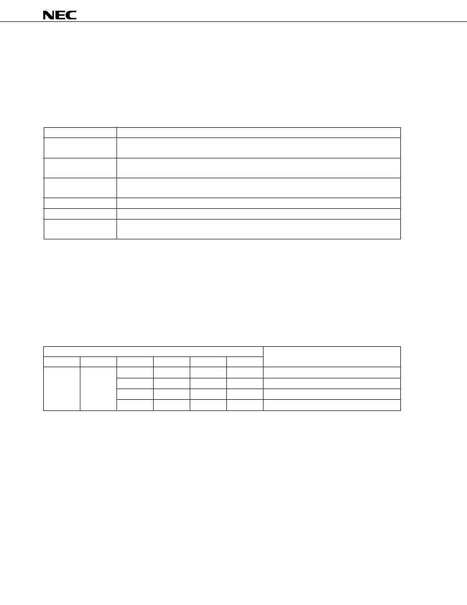
ORDERING INFORMATION
Part Number
Package
µ
PD66P04BGS
20-pin plastic SOP (300 mil)
µ
PD66P04BGS-GJG
20-pin plastic shrink SOP (300 mil)
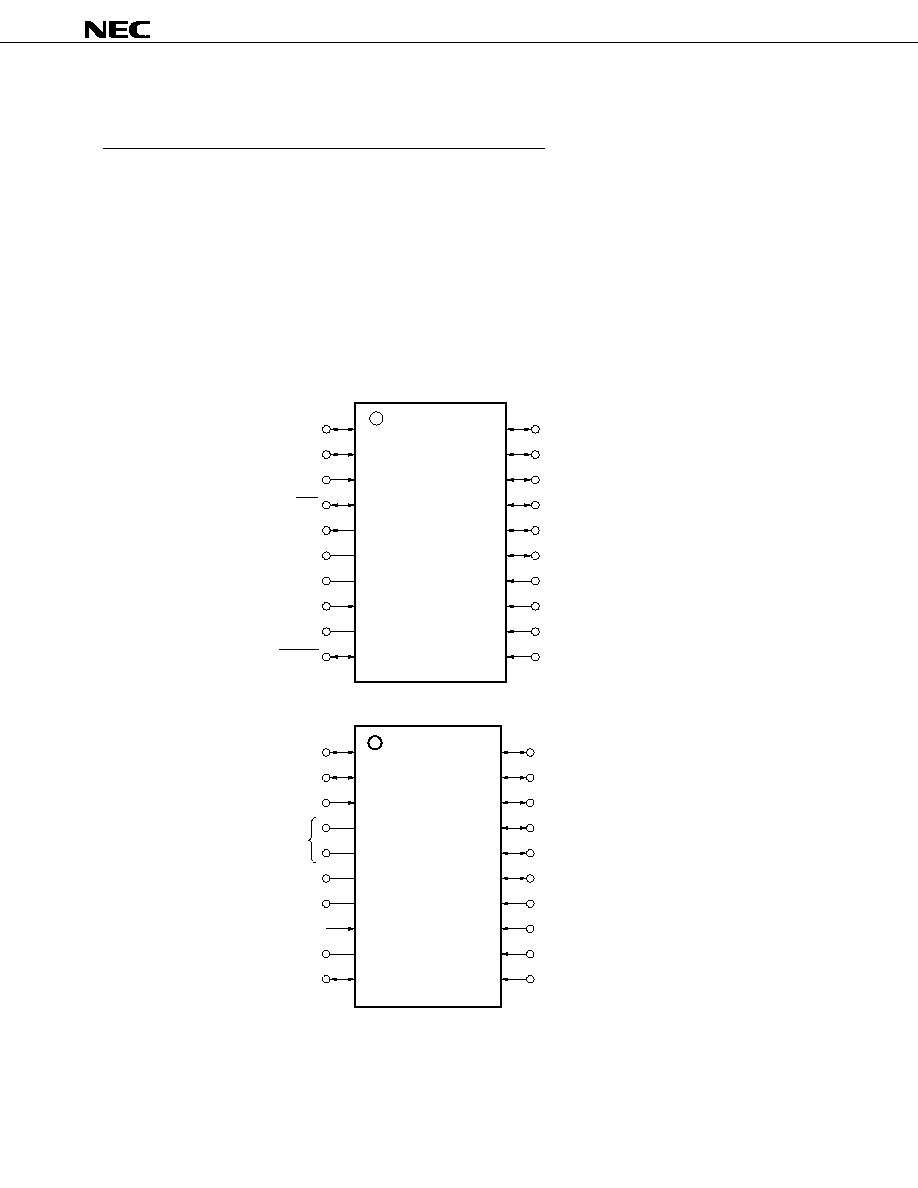
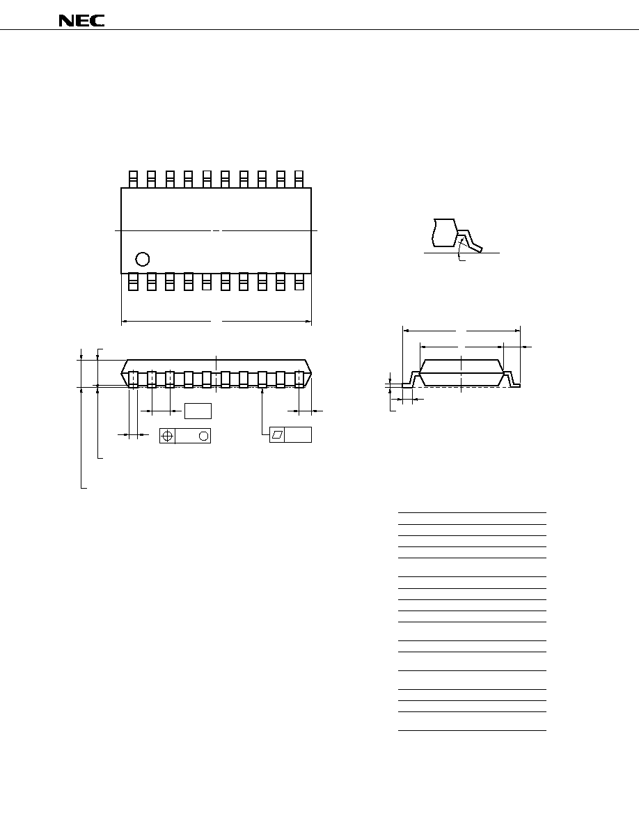
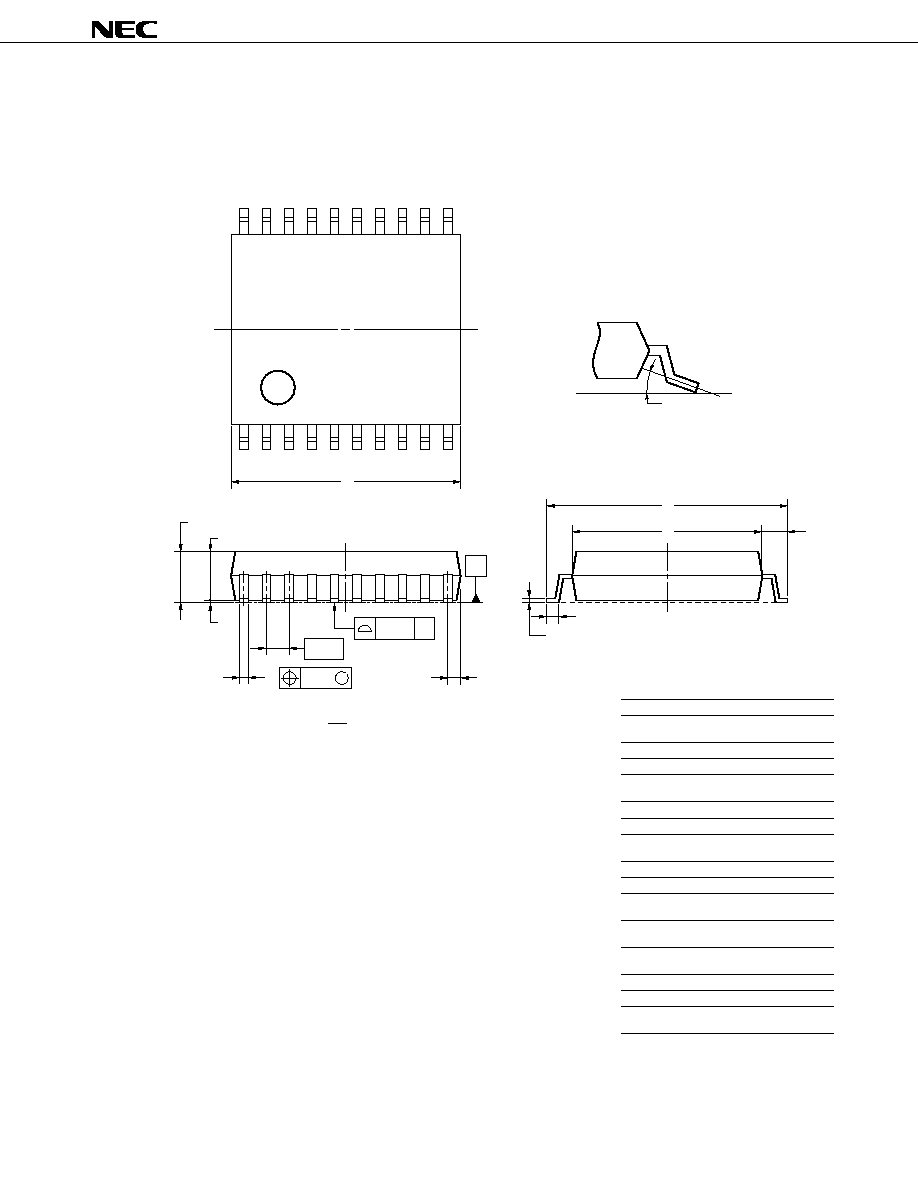
PIN CONFIGURATION (TOP VIEW)
20-pin Plastic SOP (300 mil)
·
µ
PD66P04BGS
20-pin Plastic Shrink SOP (300 mil)
·
µ
PD66P04BGS-GJG
(1) Normal operating mode
1
2
3
4
5
6
7
8
9
10
K
I/O6
K
I/O7
S
0
S
1
/LED
REM
V
DD
OSC
OUT
OSC
IN
GND
RESET
20
19
18
17
16
15
14
13
12
11
K
I/O5
K
I/O4
K
I/O3
K
I/O2
K
I/O1
K
I/O0
K
I3
K
I2
K
I1
K
I0
Caution Round brackets ( ) indicate the pins not used in the PROM programming mode.
L
: Connect each of these pins to GND via a pull-down resistor.
1
2
3
4
5
6
7
8
9
10
20
19
18
17
16
15
14
13
12
11
D
6
D
7
CLK
(L)
V
DD
OSC
OUT
OSC
IN
GND
V
PP
D
5
D
4
D
3
D
2
D
1
D
0
MD
3
MD
2
MD
1
MD
0
(2) PROM programming mode
3
µ
PD66P04B
Data Sheet U13596EJ2V0DS00
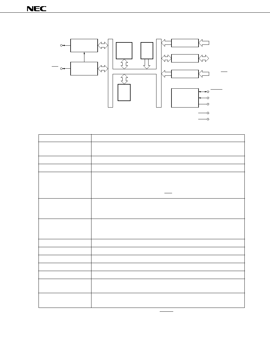
BLOCK DIAGRAM
LIST OF FUNCTIONS
Item
µ
PD66P04B
ROM capacity
1002
×
10 bits
One-time PROM
RAM capacity
32
×
4 bits
Stack
1 level (shared with RF of RAM)
I/O pin
Key input (K
I
)
: 4 pins
Key I/O (K
I/O
)
: 8 pins
Key expansion input (S
0
, S
1
)
: 2 pins
Remote control transmitter display output (LED) : 1 pin (shared with S
1
pin)
Number of keys
32 keys
48 keys (when expanded by key expansion input)
96 keys (when expanded by key expansion input and diode)
Clock frequency
RC oscillation
f
OSC
= 300 to 500 kHz
f
OSC
= 500 kHz to 1 MHz
Note
Instruction execution time
16
µ
s (at f
OSC
= 500 kHz)
Carrier frequency
f
OSC
, f
OSC
/2, f
OSC
/8, f
OSC
/12, f
OSC
/16, f
OSC
/24, no carrier (high level)
Timer
9-bit programmable timer : 1 channel
POC circuit
Internal
Supply voltage
V
DD
= 2.2 to 3.6 V
Operating ambient
· T
A
= 40 to +85
°
C
temperature
· T
A
= 20 to +70
°
C (when POC circuit used)
Package
· 20-pin plastic SOP (300 mil)
· 20-pin plastic shrink SOP (300 mil)
Note It is necessary to design the application circuit so that the RESET pin goes low at a supply voltage of less
than 2.2 V.
K
I0
-K
I3
K
I/O0
-K
I/O7
S
0
, S
1
/LED
PORT K
I
PORT K
I/O
PORT S
4
8
2
4
8
2
ONE-
TIME
PROM
RAM
SYSTEM
CONTROL
CARRIER
GENERATOR
9-bit
TIMER
CPU
CORE
RESET
OSC
IN
OSC
OUT
V
DD
GND
REM
S
1
/LED

4
µ
PD66P04B
Data Sheet U13596EJ2V0DS00
TABLE OF CONTENTS
1.
PIN FUNCTIONS .........................................................................................................................
5
1.1
Normal Operating Mode ....................................................................................................................
5
1.2
PROM Programming Mode ...............................................................................................................
6
1.3
INPUT/OUTPUT Circuits of Pins ......................................................................................................
7
1.4
Dealing with Unused Pins ................................................................................................................
8
1.5
Notes on Using K
I
Pin at Reset ........................................................................................................
8
2.
DIFFERENCES BETWEEN
µ
PD6604 AND
µ
PD66P04B ..........................................................
9
3.
WRITING AND VERIFYING ONE-TIME PROM (PROGRAM MEMORY) .................................. 10
3.1
Operating Mode When Writing/Verifying Program Memory ..........................................................
10
3.2
Program Memory Writing Procedure .............................................................................................. 11
3.3
Program Memory Reading Procedure ............................................................................................. 12
4.
ELECTRICAL SPECIFICATIONS ............................................................................................... 13
5.
CHARACTERISTIC CURVE (REFERENCE VALUES) .............................................................. 19
6.
APPLIED CIRCUIT EXAMPLE ................................................................................................... 21
7.
PACKAGE DRAWINGS .............................................................................................................. 22
8.
RECOMMENDED SOLDERING CONDITIONS .......................................................................... 24
APPENDIX A. DEVELOPMENT TOOLS ........................................................................................ 25
APPENDIX B. EXAMPLE OF REMOTE-CONTROL TRANSMISSION FORMAT .......................... 26
5
µ
PD66P04B
Data Sheet U13596EJ2V0DS00
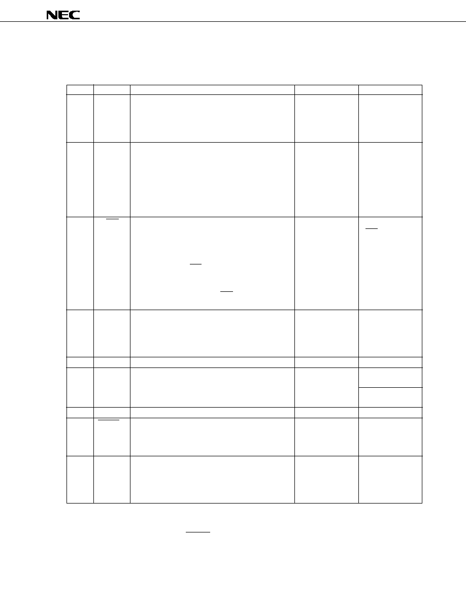
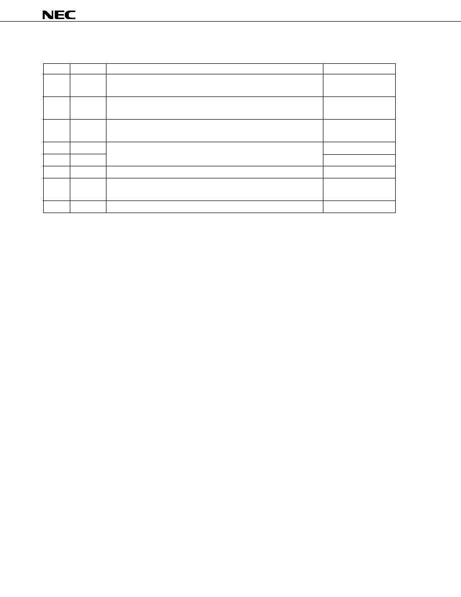
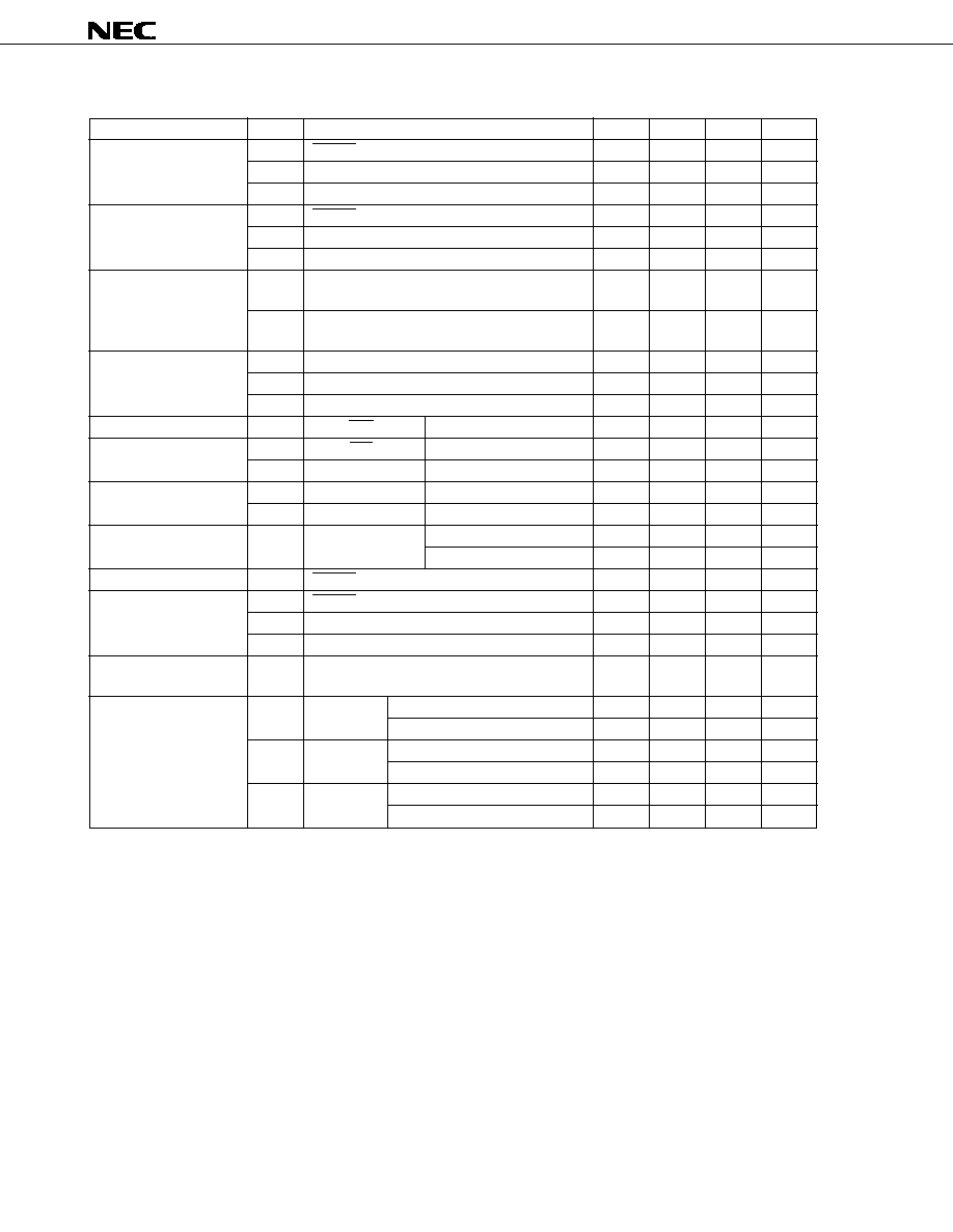
1. PIN FUNCTIONS
1.1 Normal Operating Mode
Pin No.
Symbol
Function
Output Format
When Reset
1
K
I/O0
-K
I/O7
CMOS
High-level output
2
push-pull
Note 1
15-20
3
S
0
--
High-impedance
(OFF mode)
4
S
1
/LED
CMOS push-pull
High-level output
(LED)
5
REM
CMOS push-pull
Low-level output
6
V
DD
--
--
7
OSC
OUT
--
High-impedance
8
OSC
IN
(oscillation stopped)
Low level
(oscillation stopped)
9
GND
--
--
10
RESET
--
--
11-14
K
I0
-K
I3
Note 2
--
Input (low-level)
Notes 1. Be careful about this because the drive capability of the low-level output side is held low.
2. In order to prevent malfunction, be sure to input a low level to more than one of pins K
I0
to K
I3
when
reset is released (when RESET pin changes from low level to high level, or POC is released due to
supply voltage startup).
These pins refer to the 8-bit I/O ports. I/O switching can
be made in 8-bit units.
In INPUT mode, a pull-down resistor is added.
In OUTPUT mode, they can be used as the key scan
output of the key matrix.
Refers to the input port.
Can also be used as the key return input of the key
matrix.
In INPUT mode, the availability of the pull-down resistor
of the S
0
and S
1
ports can be specified by software in
terms in 2-bit units.
If INPUT mode is canceled by software, this pin is placed
in OFF mode and enters the high-impedance state.
Refers to the I/O port.
In INPUT mode (S
1
), this pin can also be used as the key
return input of the key matrix.
The availability of the pull-down resistor of the S
0
and S
1
ports can be specified by software in 2-bit units.
In OUTPUT mode (LED), it becomes the remote control
transmission display output (active low). When the
remote control carrier is output from the REM output, this
pin outputs the low level from the LED output synchronously
with the REM signal.
Refers to the infrared remote control transmission output.
The output is active high.
Carrier frequency: f
OSC
, f
OSC
/8, f
OSC
/12, high-level,
f
OSC
/2, f
OSC
/16, f
OSC
/24
(usable on software)
Refers to the power supply.
These pins are used for RC oscillation.
Refers to the ground.
Normally, this pin is a system reset input. By inputting
a low level, the CPU can be reset. When resetting with
the POC circuit a low level is output. A pull-up resistor
is incorporated.
These pins refer to the 4-bit input ports.
They can be used as the key return input of the key
matrix.
The use of the pull-down resistor can be specified by
software in 4-bit units.
6
µ
PD66P04B
Data Sheet U13596EJ2V0DS00
1.2 PROM Programming Mode
Pin No.
Symbol
Function
I/O
1, 2
D
0
-D
7
8-bit data input/output when writing/verifying program memory
I/O
15-20
3
CLK
Clock input for updating address when writing/verifying program
Input
memory
6
V
DD
Power Supply.
Supply +6 V to this pin when writing/verifying program memory.
7
OSC
OUT
Clock necessary for writing program memory. Connect a resistor
8
OSC
IN
(R = 47 k
) and a capacitor (C = 27 pF) to these pins.
Input
9
GND
GND
10
V
PP
Supplies voltage for writing/verifying program memory.
Apply +12.5 V to this pin.
11-14
MD
0
-MD
3
Input for selecting operation mode when writing/verifying program memory.
Input
7
µ
PD66P04B
Data Sheet U13596EJ2V0DS00
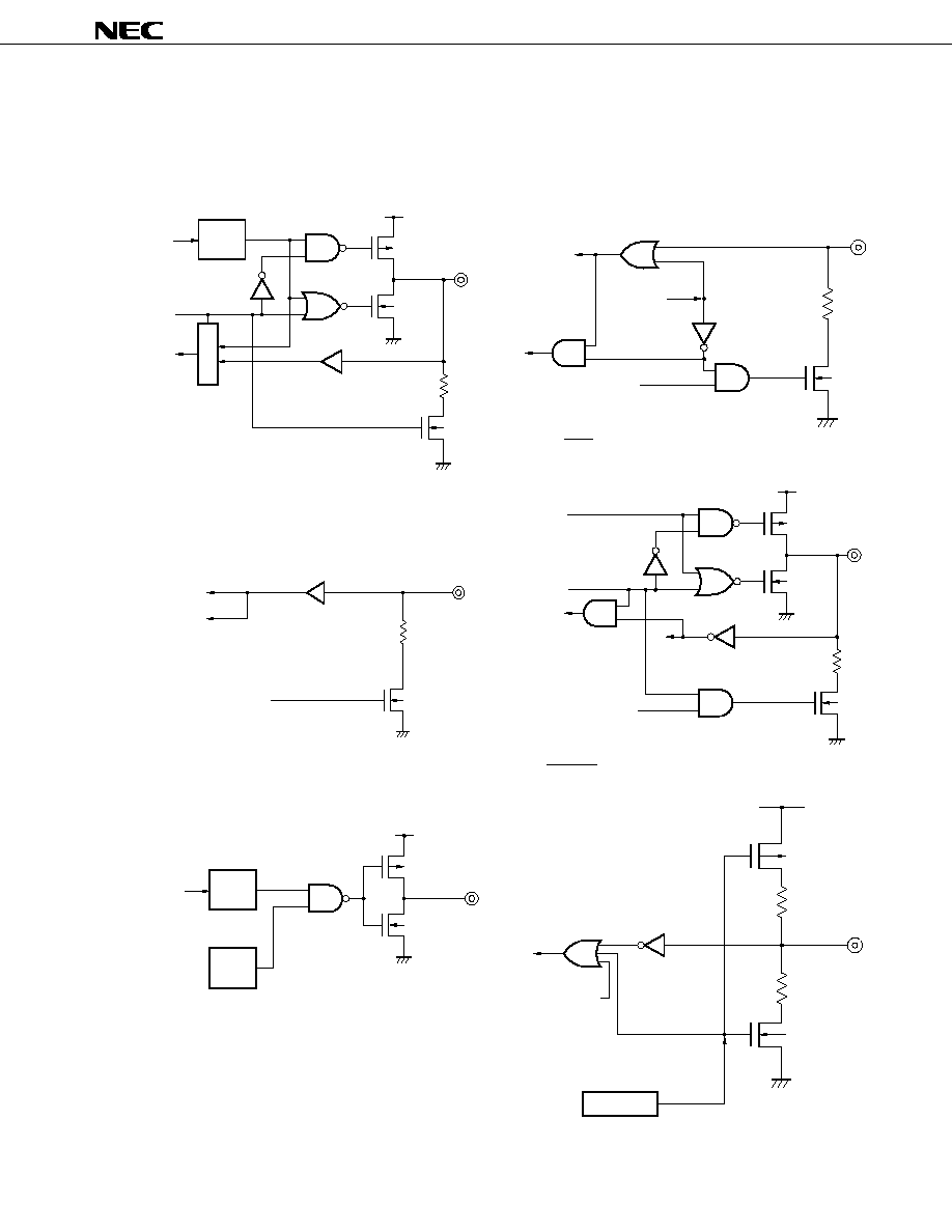
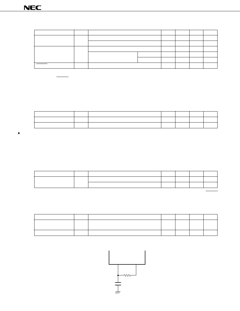
1.3 INPUT/OUTPUT Circuits of Pins
The input/output circuits of the
µ
PD66P04B pins are shown in partially simplified forms below.
(1) K
I/O0
-K
I/O7
(4) S
0
(5) S
1
/LED
Note The drive capability is held low.
(2) K
I0
-K
I3
(3) REM
(6) RESET
P-ch
N-ch
V
DD
Output
latch
Carrier
generator
data
OFF mode
pull-down flag
N-ch
Input buffer
standby
release
P-ch
N-ch
Note
N-ch
V
DD
Output
latch
Input buffer
data
output
disable
Selector
P-ch
N-ch
N-ch
V
DD
REM
output latch
Input buffer
output
disable
pull-down flag
standby
release
N-ch
P-ch
POC circuit
Internal reset signal
other than POC
Input buffer
V
DD
N-ch
Input buffer
pull-down flag
standby
release
8
µ
PD66P04B
Data Sheet U13596EJ2V0DS00
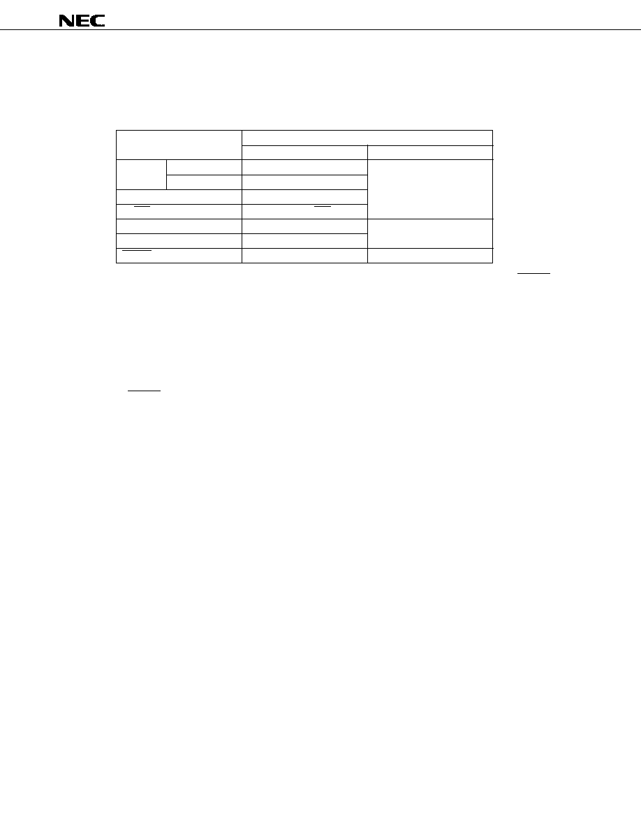
1.4 Dealing with Unused Pins
The following connections are recommended for unused pins in the normal operation mode.
Table 1-1. Connections for Unused Pins
Pin
Connection
Inside the microcontroller
Outside the microcontroller
K
I/O
INPUT mode
--
Open
OUTPUT mode
High-level output
REM
--
S
1
/LED
OUTPUT mode (LED) setting
S
0
OFF mode setting
Directly connected to GND
K
I
--
RESET
Note
Built-in POC circuit
Open
Note If the circuit is an applied one requiring high reliability, be sure to design it in such a manner that the RESET
signal is entered externally.
Caution The I/O mode and the terminal output level are recommended to be fixed by setting them
repeatedly in each loop of the program.
1.5 Notes on Using K
I
Pin at Reset
In order to prevent malfunction, be sure to input a low level to more than one of pins K
I0
to K
I3
when reset is
released (when RESET pin changes from low level to high level, or POC is released due to supply voltage startup).
9
µ
PD66P04B
Data Sheet U13596EJ2V0DS00
2. DIFFERENCES BETWEEN
µ
PD6604 AND
µ
PD66P04B
Table 2-1 shows the differences between the
µ
PD6604 and
µ
PD66P04B.
The only differences among these models are the program memory, supply voltage, system clock frequency,
oscillation stabilization wait time, and POC circuit (mask option), and the CPU function and internal peripheral
hardware are the same.
The electrical characteristics also differ slightly. For the electrical characteristics, refer to the Data Sheet of each
model.
Table 2-1. Differences between
µ
PD6604 and
µ
PD66P04B
(1) When POC circuit (mask option) is provided to
µ
PD6604
Item
µ
PD66P04B
µ
PD6604
ROM
One-time PROM
Mask ROM
Oscillation stabilization wait time
· On releasing STOP mode by release
260/f
OSC
36/f
OSC
condition
· On releasing STOP or HALT mode by
284/f
OSC
to 340/f
OSC
60/f
OSC
to 116/f
OSC
RESET input and at reset
V
PP
pin and operating mode select pin
Provided
Not provided
Electrical specifications
Some electrical specifications, such as data retention voltage and current
consumption, differ. For details, refer to Data Sheet of each model.
(2) When POC circuit (mask option) is not provided to
µ
PD6604
Item
µ
PD66P04B
µ
PD6604
ROM
One-time PROM
Mask ROM
Oscillation stabilization wait time
· On releasing STOP mode by release
260/f
OSC
36/f
OSC
condition
· On releasing STOP or HALT mode by
284/f
OSC
to 340/f
OSC
60/f
OSC
to 116/f
OSC
RESET input and at reset
V
PP
pin and operating mode select pin
Provided
Not provided
POC circuit
Incorporated
Not provided
Supply voltage
V
DD
= 2.2 to 3.6 V
V
DD
= 1.8 to 3.6 V
(T
A
= 40 to +85
°
C)
(T
A
= 40 to +85
°
C)
System clock frequency
· f
OSC
= 300 to 500 kHz
· f
OSC
= 300 to 500 kHz
· f
OSC
= 500 kHz to 1MHz
Note
· f
OSC
= 300 kHz to 1 MHz (V
DD
= 2.2 to 3.6 V)
Electrical specifications
Some electrical specifications, such as data retention voltage and current
consumption, differ. For details, refer to Data Sheet of each model.
Note It is necessary to design the application circuit so that the RESET pin goes low when the supply voltage
is less than 2.2 V.
10
µ
PD66P04B
Data Sheet U13596EJ2V0DS00
3. WRITING AND VERIFYING ONE-TIME PROM (PROGRAM MEMORY)
The program memory of the
µ
PD66P04B is a one-time PROM of 1002
×
10 bits.
To write or verify this one-time PROM, the pins shown in Table 3-1 are used. Note that no address input pin
is used. Instead, the address is updated by using the clock input from the CLK pin.
Table 3-1. Pins Used to Write/Verify Program Memory
Pin Name
Function
V
PP
Supplies voltage when writing/verifying program memory.
Apply +12.5 V to this pin.
V
DD
Power supply.
Supply +6 V to this pin when writing/verifying program memory.
CLK
Inputs clock to update address when writing/verifying program memory.
By inputting pulse four times to CLK pin, address of program memory is updated.
MD
0
-MD
3
Input to select operation mode when writing/verifying program memory.
D
0
-D
7
Inputs/outputs 8-bit data when writing/verifying program memory.
OSC
IN
, OSC
OUT
Clock necessary for writing program memory. Connect a resistor (R = 47 k
) and a capacitor
(C = 27 pF) to these pins.
3.1 Operating Mode When Writing/Verifying Program Memory
The
µ
PD66P04B is set in the program memory write/verify mode when +6 V is applied to the V
DD
pin and +12.5
V is applied to the V
PP
pin after the
µ
PD66P04B has been in the reset status (V
DD
= 5 V, V
PP
= 0 V) for a specific
time. In this mode, the operating modes shown in Table 3-2 can be set by setting the MD
0
through MD
3
pins. Connect
all the pins other than those shown in Table 3-1 to GND via pull-down resistor.
Table 3-2. Setting Operation Mode
Setting of Operating Mode
Operation Mode
V
PP
V
DD
MD
0
MD
1
MD
2
MD
3
+12.5 V
+6 V
H
L
H
L
Clear program address to 0
L
H
H
H
Write mode
L
L
H
H
Verify mode
H
×
H
H
Program inhibit mode
×
: don't care (L or H)
11
µ
PD66P04B
Data Sheet U13596EJ2V0DS00
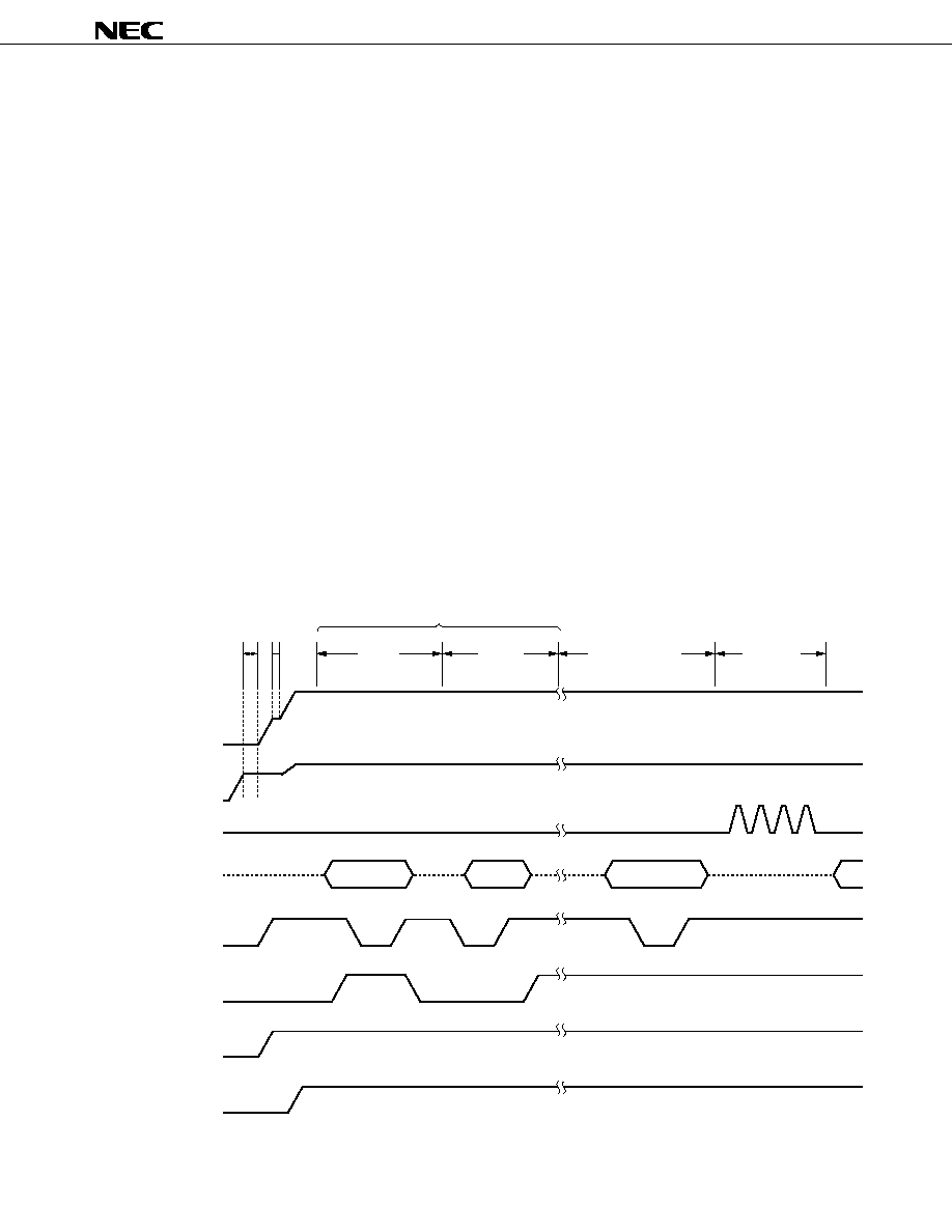
3.2 Program Memory Writing Procedure
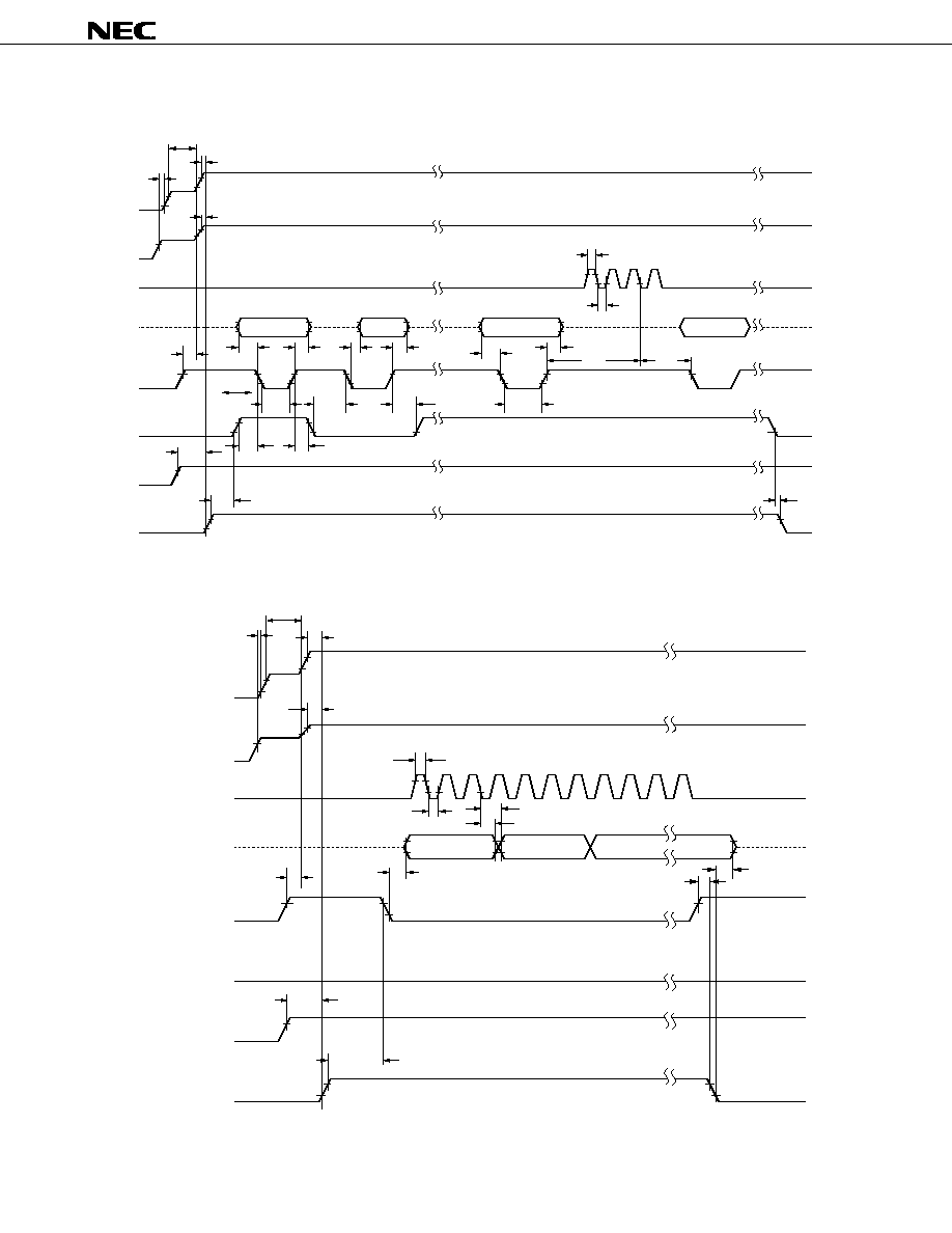
The program memory is written at high speed in the following procedure.
(1)
Pull down the pins not used to GND via resistor. Keep the CLK pin low.
(2)
Supply 5 V to the V
DD
pin. Keep the V
PP
pin low.
(3)
Supply 5 V to the V
PP
pin after waiting for 10
µ
s.
(4)
Wait for 2 ms until oscillation of the clock connected across the OSC
IN
and OSC
OUT
pins stabilizes.
(5)
Set the program memory address 0 clear mode by using the mode setting pins.
(6)
Supply 6 V to V
DD
and 12.5 V to V
PP
.
(7)
Set the program inhibit mode.
(8)
Write data to the program memory in the 1-ms write mode.
(9)
Set the program inhibit mode.
(10) Set the verify mode. If the data have been written to the program memory, proceed to (11). If not, repeat
steps (8) through (10).
(11) Additional writing of (number of times of writing in (8) through (10): X)
×
1 ms.
(12) Set the program inhibit mode.
(13) Input a pulse to the CLK pin four times to update the program memory address (+1).
(14) Repeat steps (8) through (13) up to the last address.
(15) Set the 0 clear mode of the program memory address.
(16) Change the voltages on the V
DD
and V
PP
pins to 5 V.
(17) Turn off power.
The following figure illustrates steps (2) through (13) above.
Repeated X time
Reset
Oscillation stabilization
wait time
Write
Verify
Additional write
Address
increment
Data input
Hi-Z
Hi-Z
Hi-Z
Data output
Data input
Hi-Z
V
PP
V
DD
GND
V
DD
+1
V
DD
GND
CLK
V
PP
D
0
-D
7
MD
0
MD
1
MD
2
MD
3
V
DD
12
µ
PD66P04B
Data Sheet U13596EJ2V0DS00
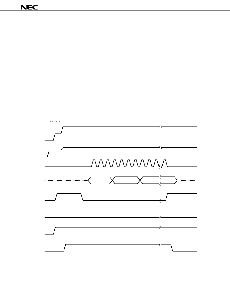
3.3 Program Memory Reading Procedure
(1)
Pull down the pins not used to GND via resistor. Keep the CLK pin low.
(2)
Supply 5 V to the V
DD
pin. Keep the V
PP
pin low.
(3)
Supply 5 V to the V
PP
pin after waiting for 10
µ
s.
(4)
Wait for 2 ms until oscillation of the clock connected across the OSC
IN
and OSC
OUT
pins stabilizes.
(5)
Set the program memory address 0 clear mode by using the mode setting pins.
(6)
Supply 6 V to V
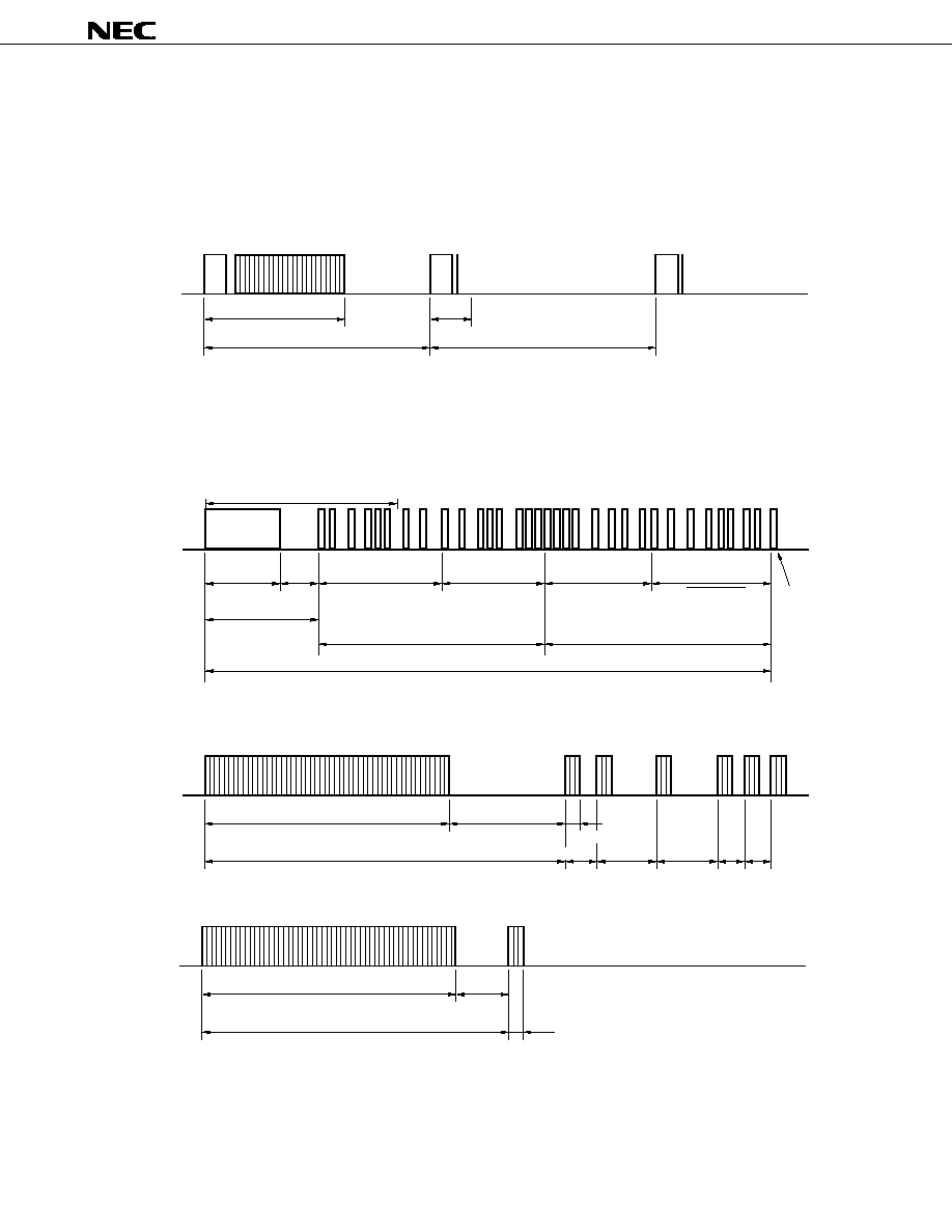
DD
and 12.5 V to V
PP
.
(7)
Set the program inhibit mode.
(8)
Set the verify mode. Data of each address is output sequentially each time the clock pulse is input to
the CLK pin four times.
(9)
Set the program inhibit mode.
(10) Set the program memory address 0 clear mode.
(11) Change the voltage on the V
DD
and V
PP
pins to 5 V.
(12) Turn off power.
The following figure illustrates steps (2) through (10) above.
Reset
Oscillation stabilization
wait time
Hi-Z
Hi-Z
V
PP
V
DD
GND
V
DD
+1
V
DD
GND
CLK
V
PP
D
0
-D
7
MD
0
MD
1
MD
2
MD
3
Data output
Data output
"L"
V
DD
13
µ
PD66P04B
Data Sheet U13596EJ2V0DS00
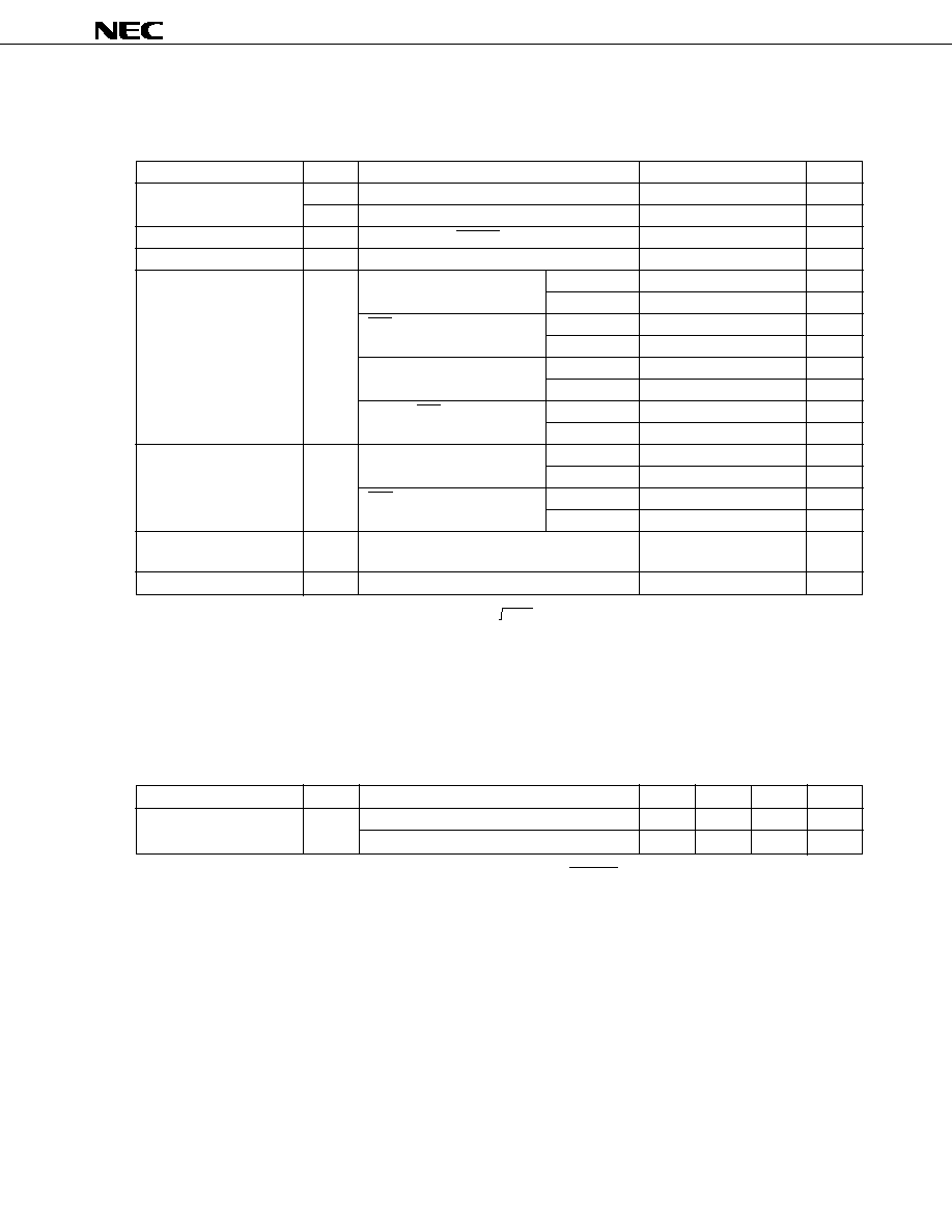
4. ELECTRICAL SPECIFICATIONS
Absolute Maximum Ratings (T
A
= +25
°
C)
Parameter
Symbol
Test Conditions
Rating
Unit
Power supply voltage
V
DD
0.3 to +7.0
V
V
PP
0.3 to +13.5
V
Input voltage
V
I
K
I/O
, K
I
, S
0
, S
1
, RESET
0.3 to V
DD
+ 0.3
V
Output voltage
V
O
0.3 to V
DD
+ 0.3
V
High-level output current
I
OH
Note
REM
Peak value
30
mA
rms
20
mA
LED
Peak value
7.5
mA
rms
5
mA
One K
I/O
pin
Peak value
13.5
mA
rms
9
mA
Total of LED and K
I/O
pins
Peak value
18
mA
rms
12
mA
Low-level output current
I
OL
Note
REM
Peak value
7.5
mA
rms
5
mA
LED
Peak value
7.5
mA
rms
5
mA
Operating ambient
T
A
40 to +85
°
C
temperature
Storage temperature
T
stg
65 to +150
°
C
Note Work out the rms with: [rms] = [Peak value]
×
Duty.
Caution Product quality may suffer if the absolute rating is exceeded for any parameter, even momen-
tarily. In other words, an absolute maxumum rating is a value at which the possibility of psysical
damage to the product cannnot be ruled out. Care must therefore be taken to ensure that the
these ratings are not exceeded during use of the product.
Recommended Power Supply Voltage Range (T
A
= 40 to +85
°
C)
Parameter
Symbol
Test Conditions
MIN.
TYP.
MAX.
Unit
Power supply voltage
V
DD
f
OSC
= 300 to 500 kHz
2.2
3.0
3.6
V
f
OSC
= 500 kHz to 1 MHz
Note
2.2
3.0
3.6
V
Note It is necessary to design the application circuit so that the RESET pin goes low when the supply voltage
is less than 2.2 V.
14
µ
PD66P04B
Data Sheet U13596EJ2V0DS00
DC Characteristics (T
A
= 40 to +85
°
C, V
DD
= 2.2 to 3.6 V)
Parameter
Symbol
Test Conditions
MIN.
TYP.
MAX.
Unit
High-level input voltage
V
IH1
RESET
0.8 V
DD
V
DD
V
V
IH2
K
I/O
0.65 V
DD
V
DD
V
V
IH3
K
I
, S
0
, S
1
0.65 V
DD
V
DD
V
Low-level input voltage
V
IL1
RESET
0
0.2 V
DD
V
V
IL2
K
I/O
0
0.3 V
DD
V
V
IL3
K
I
, S
0
, S
1
0
0.15 V
DD
V
High-level input
I
LH1
K
I
3
µ
A
leakage current
V
I
= V
DD
, pull-down resistor not incorporated
I
LH2
S
0
, S
1
3
µ
A
V
I
= V
DD
, pull-down resistor not incorporated
Low-level input leakage
I
UL1
K
I
V
I
= 0 V
3
µ
A
current
I
UL2
K
I/O
V
I
= 0 V
3
µ
A
I
UL3
S
0
, S
1
V
I
= 0 V
3
µ
A
High-level output voltage
V
OH1
REM, LED, K
I/O
I
OH
= 0.3 mA
0.8 V
DD
V
Low-level output voltage
V
OL1
REM, LED
I
OL
= 0.3 mA
0.3
V
V
OL2
K
I/O
I
OL
= 15
µ
A
0.4
V
High-level output current
I
OH1
REM
V
DD
= 3.0 V, V
OH
= 1.0 V
5
9
mA
I
OH2
K
I/O
V
DD
= 3.0 V, V
OH
= 2.2 V
2.5
5
mA
Low-level output current
I
OL1
K
I/O
V
DD
= 3.0 V, V
OL
= 0.4 V
30
70
µ
A
V
DD
= 3.0 V, V
OL
= 2.2 V
100
220
µ
A
Built-in pull-up resistor
R
1
RESET
25
50
100
k
Built-in pull-down resistor
R
2
RESET
2.5
5
15
k
R
3
K
I
, S
0
, S
1
75
150
300
k
R
4
K
I/O
130
250
500
k
Data hold power supply
V
DDDR
In STOP mode
1.2
3.6
V
voltage
Supply current
Note
I
DD1
Operating
f
OSC
= 1.0 MHz, V
DD
= 3 V
±
10 %
0.6
1.2
mA
mode
f
OSC
= 455 kHz, V
DD
= 3 V
±
10 %
0.5
1.0
mA
I
DD2
HALT mode
f
OSC
= 1.0 MHz, V
DD
= 3 V
±
10 %
0.5
1.0
mA
f
OSC
= 455 kHz, V
DD
= 3 V
±
10 %
0.4
0.8
mA
I
DD3
STOP mode
V
DD
= 3 V
±
10 %
1.0
8.0
µ
A
V
DD
= 3 V
±
10 %, T
A
= 25
°
C
1.0
2.0
µ
A
Note The POC circuit current and the current flowing in the built-in pull-up resistor are not included.
15
µ
PD66P04B
Data Sheet U13596EJ2V0DS00
OSC
IN
OSC
OUT
C
R
AC Characteristics (T
A
= 40 to +85
°
C, V
DD
= 2.2 to 3.6 V)
Parameter
Symbol
Test Conditions
MIN.
TYP.
MAX.
Unit
Instruction execution time t
CY
15.9
27
µ
s
Note 1
7.9
27
µ
s
K
I
, S
0
, S
1
high-level width
t
H
10
µ
s
When canceling standby mode
HALT mode
10
µ
s
STOP mode
Note 2
µ
s
RESET low-level width
t
RSL
10
µ
s
Notes 1. When using at f
OSC
= 500 kHz or higher, it is necessary to design the application circuit so that the
RESET pin goes low when the supply voltage is less than 2.2 V.
2. 10 + 260/f
OSC
Remark t
CY
= 8/f
OSC
(f
OSC
: System clock oscillator frequency)
POC Circuit
Note 1
(T
A
= 20 to +70
°
C)
Parameter
Symbol
Test Conditions
MIN.
TYP.
MAX.
Unit
POC-detected voltage
Note 2
V
POC
1.8
2.0
2.2
V
POC circuit current
I
POC
1.2
1.5
µ
A
Notes 1. Operates effectively under the conditions of f
OSC
= 300 to 500 kHz.
2. Refers to the voltage with which the POC circuit cancels an internal reset. If V
POC
< V
DD
, the internal
reset is canceled.
From the time of V
POC
V
DD
until the internal reset takes effect, lag of up to 1 ms occurs. When the
period of V
POC
V
DD
lasts less than 1 ms, the internal reset may not take effect.
System Clock Oscillator Characteristics (T
A
= 40 to +85
°
C, V
DD
= 2.2 to 3.6 V)
Parameter
Symbol
Test Conditions
MIN.
TYP.
MAX.
Unit
Oscillator frequency
f
OSC
300
455
500
kHz
Note
300
455
1000
kHz
Note When using at f
OSC
= 500 kHz or higher, it is necessary to design the application circuit so that the RESET
pin goes low when the supply voltage is less than 2.2 V.
Recommended Oscillator Constant (T
A
= 40 to +85
°
C, V
DD
= 2.2 to 3.6 V)
Parameter
Symbol
Test Conditions
MIN.
TYP.
MAX.
Unit
Capacity of oscillation
C
22
27
33
pF
capacitor
Oscillation resistance
R
47
k
An external circuit example
16
µ
PD66P04B
Data Sheet U13596EJ2V0DS00
PROM Programming Mode
DC Programming Characteristics (T
A
= 25
°
C, V
DD
= 6.0
±
0.25 V, V
PP
= 12.5
±
0.3 V)
Parameter
Symbol
Test Conditions
MIN.
TYP.
MAX.
Unit
High-level input voltage
V
IH1
Other than CLK
0.7 V
DD
V
DD
V
V
IH2
CLK
V
DD
0.5
V
DD
V
Low-level input voltage
V
IL1
Other than CLK
0
0.3 V
DD
V
V
IL2
CLK
0
0.4
V
Input leakage current
I
LI
V
IN
= V
IL
or V
IH
10
µ
A
High-level output voltage
V
OH
I
OH
= 1 mA
V
DD
1.0
V
Low-level output voltage
V
OL
I
OL
= 1.6 mA
0.4
V
V
DD
supply current
I
DD
30
mA
V
PP
supply current
I
PP
MD
0
= V
IL
, MD
1
= V
IH
30
mA
Cautions 1. Keep V
PP
to within +13.5 V including overshoot.
2. Apply V
DD
before V
PP
and turns it off after V
PP
.
17
µ
PD66P04B
Data Sheet U13596EJ2V0DS00
AC Programming Characteristics (T
A
= 25
°
C, V
DD
= 6.0
±
0.25 V, V
PP
= 12.5
±
0.3 V)
Parameter
Symbol
Note1
Test Conditions
MIN.
TYP.
MAX.
Unit
Address setup time
Note 2
(vs. MD
0
)
t
AS
t
AS
2
µ
s
MD
1
setup time (vs. MD
0
)
t
M1S
t
OES
2
µ
s
Data setup time (vs. MD
0
)
t
DS
t
DS
2
µ
s
Address hold time
Note 2
(vs. MD
0
)
t
AH
t
AH
2
µ
s
Data hold time (vs. MD
0
)
t
DH
t
DH
2
µ
s
MD
0
data output float delay time
t
DF
t
DF
0
130
ns
V
PP
setup time (vs. MD
3
)
t
VPS
t
VPS
2
µ
s
V
DD
setup time (vs. MD
3
)
t
VDS
t
VCS
2
µ
s
Initial program pulse width
t
PW
t
PW
0.95
1.0
1.05
ms
Additional program pulse width
t
OPW
t
OPW
0.95
21.0
ms
MD
0
setup time (vs. MD
1
)
t
MOS
t
CES
2
µ
s
MD
0
data output delay time
t
DV
t
DV
MD0 = MD1 = V
IL
1
µ
s
MD
1
hold time (vs. MD
0
)
t
M1H
t
OEH
t
M1H
+t
M1R
50
µ
s
2
µ
s
MD
1
recovery time (vs. MD
0
)
t
M1R
t
OR
2
µ
s
Program counter reset time
t
PCR
10
µ
s
CLK input high-, low-level width
t
XH
, t
XL
0.125
µ
s
CLK input frequency
f
X
8
MHz
Initial mode set time
t
I
2
µ
s
MD
3
setup time (vs. MD
1
)
t
M3S
2
µ
s
MD
3
hold time (vs. MD
1
)
t
M3H
2
µ
s
MD
3
setup time (vs. MD
0
)
t
M3SR
When program memory is read
2
µ
s
Address
Note 2
data output delay time
t
OAD
t
ACC
When program memory is read
2
µ
s
Address
Note 2
data output hold time
t
HAD
t
OH
When program memory is read
0
130
ns
MD
3
hold time (vs. MD
0
)
t
M3HR
When program memory is read
2
µ
s
MD
3
data output float delay time
t
DFR
When program memory is read
2
µ
s
Reset setup time
t
RES
10
µ
s
Oscillation stabilization wait time
Note 3
t
WAIT
2
ms
Notes 1. Equivalent symbol of the corresponding
µ
PD27C256A (The
µ
PD27C256A is a maintenance product.)
2. The internal address signal is incremented at the falling edge of the third clock of CLK.
3. Connect a resistor (R = 47 k
) and a capacitor (C = 27 pF) between the OSC
IN
and OSC
OUT
pins.
18
µ
PD66P04B
Data Sheet U13596EJ2V0DS00
Program Memory Write Timing
Program Memory Read Timing
t
M3SR
t
PCR
Data output
t
DV
t
MAD
t
VDS
t
I
Hi-Z
Hi-Z
"L"
t
M3HR
V
PP
V
DD
GND
V
DD
+1
V
DD
GND
CLK
V
PP
D
0
-D
7
MD
0
MD
1
MD
2
MD
3
t
DAD
t
XL
Data output
t
DFR
t
XH
t
WAIT
t
RES
t
VPS
V
DD
t
M3S
t
PCR
t
M1S
t
M1H
t
PW
t
M1R
t
MOS
t
OPW
t
M3H
Data input
Data output
Data input
Data input
t
DS
t
DH
t
DV
t
DF
t
DS
t
DH
t
XL
t
XH
t
VPS
t
VDS
t
WAIT
t
RES
t
t
Hi-Z
Hi-Z
Hi-Z
Hi-Z
Hi-Z
t
AH
t
AS
V
PP
V
DD
GND
V
DD
+1
V
DD
GND
CLK
V
PP
V
DD
D
0
-D
7
MD
0
MD
1
MD
2
MD
3
19
µ
PD66P04B
Data Sheet U13596EJ2V0DS00
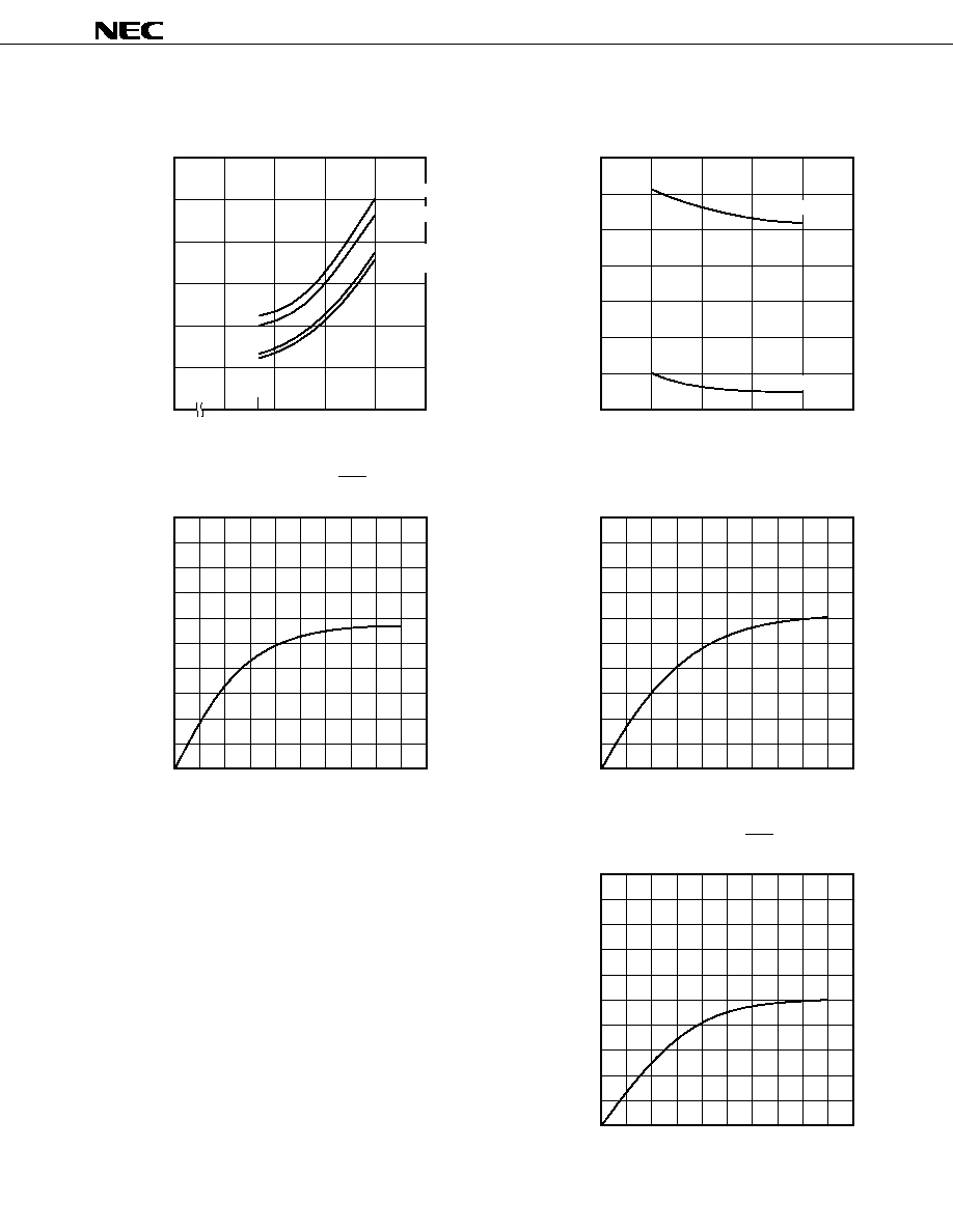
5. CHARACTERISTIC CURVE (REFERENCE VALUES)
I
OL
vs V
OL
(REM, LED)
Low-level output current I
OL
[mA]
Low-level output voltage V
OL
[V]
I
OH
vs V
OH
(REM)
High-level output current I
OH
[mA]
High-level output voltage V
OH
[V]
I
OH
vs V
OH
(LED)
High-level output current I
OH
[mA]
High-level output voltage V
OH
[V]
10
0.6
1.8
2.4
3
1.2
9
8
7
6
5
4
3
2
1
0
20
V
DD
0.6
V
DD
1.8 V
DD
2.4 V
DD
3
V
DD
1.2
18
16
14
12
10
8
6
4
2
0
V
DD
10
V
DD
0.6
V
DD
1.8 V
DD
2.4 V
DD
3
V
DD
1.2
9
8
7
6
5
4
3
2
1
0
V
DD
(T
A
= 25 °C, V
DD
= 3.0 V)
(T
A
= 25 °C , V
DD
= 3.0 V)
(T
A
= 25 °C , V
DD
= 3.0 V)
I
DD
vs V
DD
Power supply current I
DD
[mA]
Power supply voltage V
DD
[V]
(T
A
= 25 °C)
1100
1000
900
800
700
600
500
400
1.2
2.4
3.0
4.2
3.6
1.8
f
OSC
vs V
DD
Oscillator frequency fosc [kHz]
Power supply voltage V
DD
[V]
(C = 27 pF, T
A
= 25 °C)
R = 47 k
R = 22 k
1.2
1.0
0.8
0.6
0.4
0.2
0
1.8
2.4
3.0
1 MHz operating mode
1 MHz HALT mode
455 kHz operating mode
455 kHz HALT mode
3.6
4.2
2.2
20
µ
PD66P04B
Data Sheet U13596EJ2V0DS00
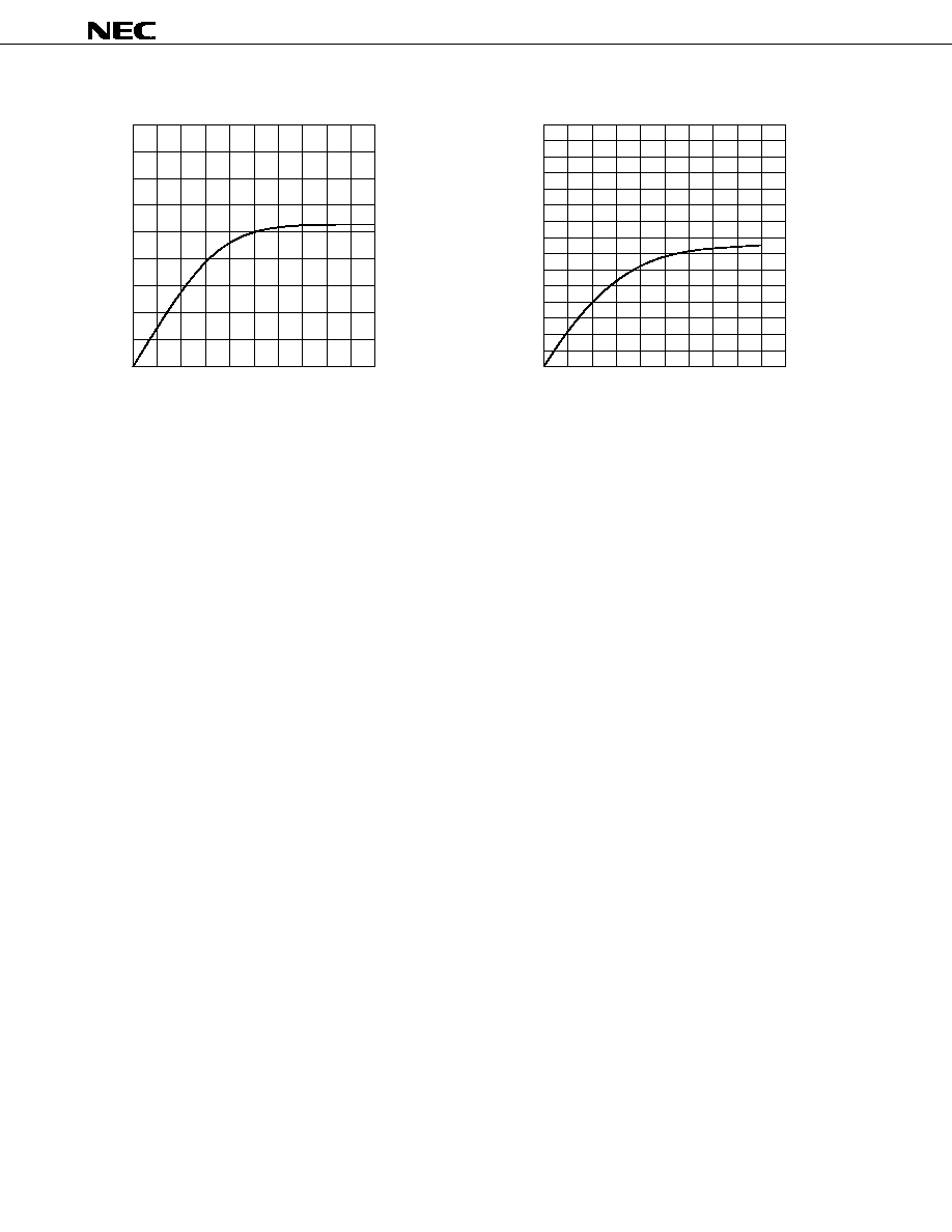
I
OL
vs V
OL
(
K
I/O
)
Low-level output current I
OL
[ A]
Low-level output voltage V
OL
[V]
I
OH
vs V
OH
(
K
I/O
)
High-level output current I
OH
[mA]
High-level output voltage V
OH
[V]
320
0.6
1.8
2.4
3
1.2
0
15
V
DD
0.6
V
DD
1.8 V
DD
2.4 V
DD
3
V
DD
1.2
0
V
DD
280
240
200
160
120
80
40
14
13
12
11
10
9
8
7
6
5
4
3
2
1
(T
A
= 25 °C, V
DD
= 3.0 V)
(T
A
= 25 °C, V
DD
= 3.0 V)
µ
21
µ
PD66P04B
Data Sheet U13596EJ2V0DS00
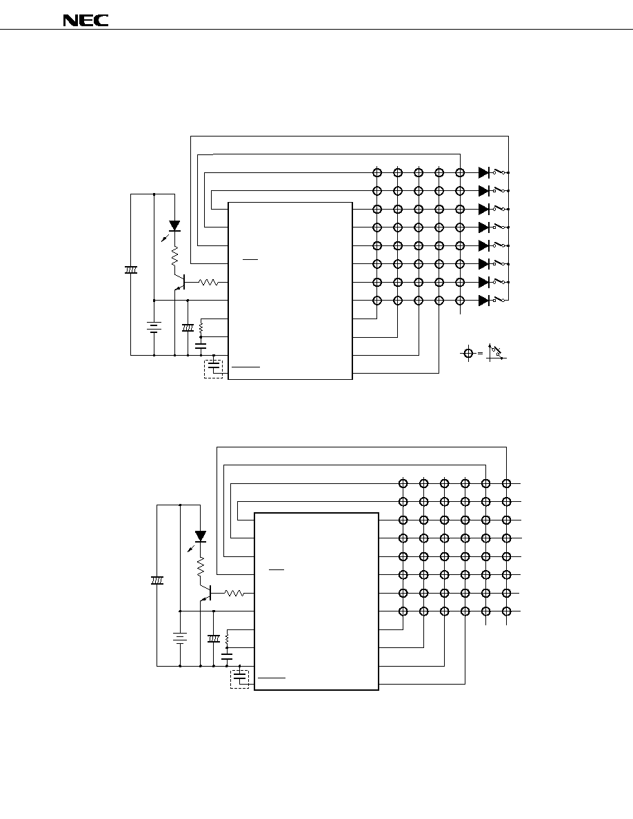
6. APPLIED CIRCUIT EXAMPLE
Example of Application to System
· Remote-control transmitter (40 keys; mode selection switch accommodated)
· Remote-control transmitter (48 keys accommodated)
Remark When the POC circuit is used effectively, it is not necessary to connect the capacitor enclosed in the
dotted lines.
K
I/O6
K
I/O7
S
0
S
1
/LED
REM
V
DD
OSC
OUT
OSC
IN
GND
RESET
K
I/O5
K
I/O4
K
I/O3
K
I/O2
K
I/O1
K
I/O0
K
I3
K
I2
K
I1
K
I0
Key matrix
8
×
5 = 40 keys
Mode selection switch
+
+
R
C
K
I/O6
K
I/O7
S
0
S
1
/LED
REM
V
DD
OSC
OUT
OSC
IN
GND
RESET
K
I/O5
K
I/O4
K
I/O3
K
I/O2
K
I/O1
K
I/O0
K
I3
K
I2
K
I1
K
I0
Key matrix
8
×
6 = 48 keys
+
+
R
C
22
µ
PD66P04B
Data Sheet U13596EJ2V0DS00
7. PACKAGE DRAWINGS
(1)
µ
PD66P04BGS
20 PIN PLASTIC SOP (300 mil)
ITEM
MILLIMETERS
INCHES
A
B
C
E
F
G
H
J
12.7±0.3
1.27 (T.P.)
1.8 MAX.
1.55±0.05
7.7±0.3
0.78 MAX.
0.12
1.1
M
0.1±0.1
N
0.500±0.012
0.031 MAX.
0.004±0.004
0.071 MAX.
0.061±0.002
0.303±0.012
0.043
0.005
0.050 (T.P.)
P20GM-50-300B, C-5
P
3
°
3
°
+7
°
NOTE
Each lead centerline is located within 0.12 mm (0.005 inch) of
its true position (T.P.) at maximum material condition.
D
0.42
0.017
+0.08
0.07
K
0.22
0.009
+0.08
0.07
L
0.6±0.2
0.024
0.10
3
°
+7
°
3
°
0.004
+0.008
0.009
+0.003
0.004
+0.003
0.004
detail of lead end
M
1
10
11
20
I
5.6±0.2
0.220 +0.009
0.008
A
B
H
K
M
L
P
J
I
G
C
D
E
F
N
23
µ
PD66P04B
Data Sheet U13596EJ2V0DS00
(2)
µ
PD66P04BGS-GJG
N
S
C
D
M
M
P
F
G
E
B
L
K
J
detail of lead end
20 PIN PLASTIC SHRINK SOP (300 mil)
NOTE
2. Each lead centerline is located within 0.12 mm (0.005 inch) of
its true position (T.P.) at maximum material condition.
P20GM-65-300B-3
ITEM
MILLIMETERS
INCHES
A
B
C
D
E
F
G
H
I
J
0.65 (T.P.)
2.0 MAX.
1.7±0.1
8.1±0.3
0.575 MAX.
K
L
0.12
0.5±0.2
1.0±0.2
6.1±0.2
0.15
M
0.10
0.32
0.125±0.075
N
+0.10
0.05
0.023 MAX.
0.013
0.005±0.003
0.079 MAX.
0.067
0.319±0.012
0.240±0.008
0.039
0.006
0.020
0.005
0.004
+0.008
0.009
0.026 (T.P.)
P
3°
3°
+0.004
0.005
+0.004
0.002
6.7±0.3
0.264+0.012
0.013
1. Controlling dimension millimeter.
S
+0.003
0.004
+0.08
0.07
+7°
3°
+7°
3°
+0.009
0.008
20
11
1
10
A
H
I
24
µ
PD66P04B
Data Sheet U13596EJ2V0DS00
8. RECOMMENDED SOLDERING CONDITIONS
Carry out the soldered packaging of this product under the following recommended conditions.
For details of the soldering conditions, refer to information material Semiconductor Device Mounting
Technology Manual (C10535E).
For soldering methods and conditions other than the recommended conditions, please consult one of our NEC
sales representatives.
Table 8-1. Soldering Conditions for Surface-Mount Type
µ
PD66P04BGS
: 20-pin plastic SOP (300 mil)
µ
PD66P04BGS-GJG : 20-pin plastic SSOP (300 mil)
Soldering Method
Soldering Condition
Recommended
Condition Symbol
Infrared reflow
Package peak temperature: 235
°
C, Time: 30 secs. max. (210
°
C min.),
IR35-00-2
Number of times: Twice max.
VPS
Package peak temperature: 215
°
C, Time: 40 secs. max. (200
°
C min.),
VP15-00-2
Number of times: Twice max.
Wave soldering
Solder bath temperature: 260
°
C max., Time: 10 secs. max.,
WS60-00-1
Number of times: once, Preheating temperature: 120
°
C max. (package
surface temperature.)
Partial heating
Pin temperature: 300
°
C or less ; time: 3 secs or less (for each side of the device)
--
Caution Do not use two or more soldering methods in combination (except partial heating).
25
µ
PD66P04B
Data Sheet U13596EJ2V0DS00
APPENDIX A. DEVELOPMENT TOOLS
A PROM programmer, program adapter, and emulator are provided for the
µ
PD66P04B.
Hardware
·
PROM programmer (AF-9704
Note
, AF-9705
Note
, AF-9706
Note
)
This PROM programmer supports the
µ
PD66P04B.
By connecting a program adapter to this PROM programmer, the
µ
PD66P04B can be programmed.
Note These are products of Ando Electric. For details, consult Ando Electric (03-3733-1163).
·
Program adapter (PA-61P34, PA-61P34BMC)
It is used to program the
µ
PD66P04B in combination with AF-9704, AF-9705, or AF-9706.
·
Emulator (EB-6133
Note
)
It is used to emulate the
µ
PD66P04B.
Note This is a product of Naito Densei Machida Mfg. Co., Ltd. For details, consult Naito Densei Machida
Mfg. Co., Ltd. (044-822-3813).
Software
·
Assembler (AS6133)
· This is a development tool for remote control transmitter software.
Part Number List of AS6133
Host Machine
OS
Supply Medium
Part Number
PC-9800 series
MS-DOS
TM
(Ver. 5.0 to Ver. 6.2)
3.5-inch 2HD
µ
S5A13AS6133
(CPU: 80386 or more)
IBM PC/AT
TM
compatible
MS-DOS (Ver. 6.0 to Ver. 6.22)
3.5-inch 2HC
µ
S7B13AS6133
PC DOS
TM
(Ver. 6.1 to Ver. 6.3)
Caution Although Ver.5.0 or later has a task swap function, this function cannot be used with this
software.
26
µ
PD66P04B
Data Sheet U13596EJ2V0DS00
APPENDIX B. EXAMPLE OF REMOTE-CONTROL TRANSMISSION FORMAT
(in the case of NEC transmission format in command one-shot transmission mode)
Caution When using the NEC transmission format, please apply for a custom code at NEC.
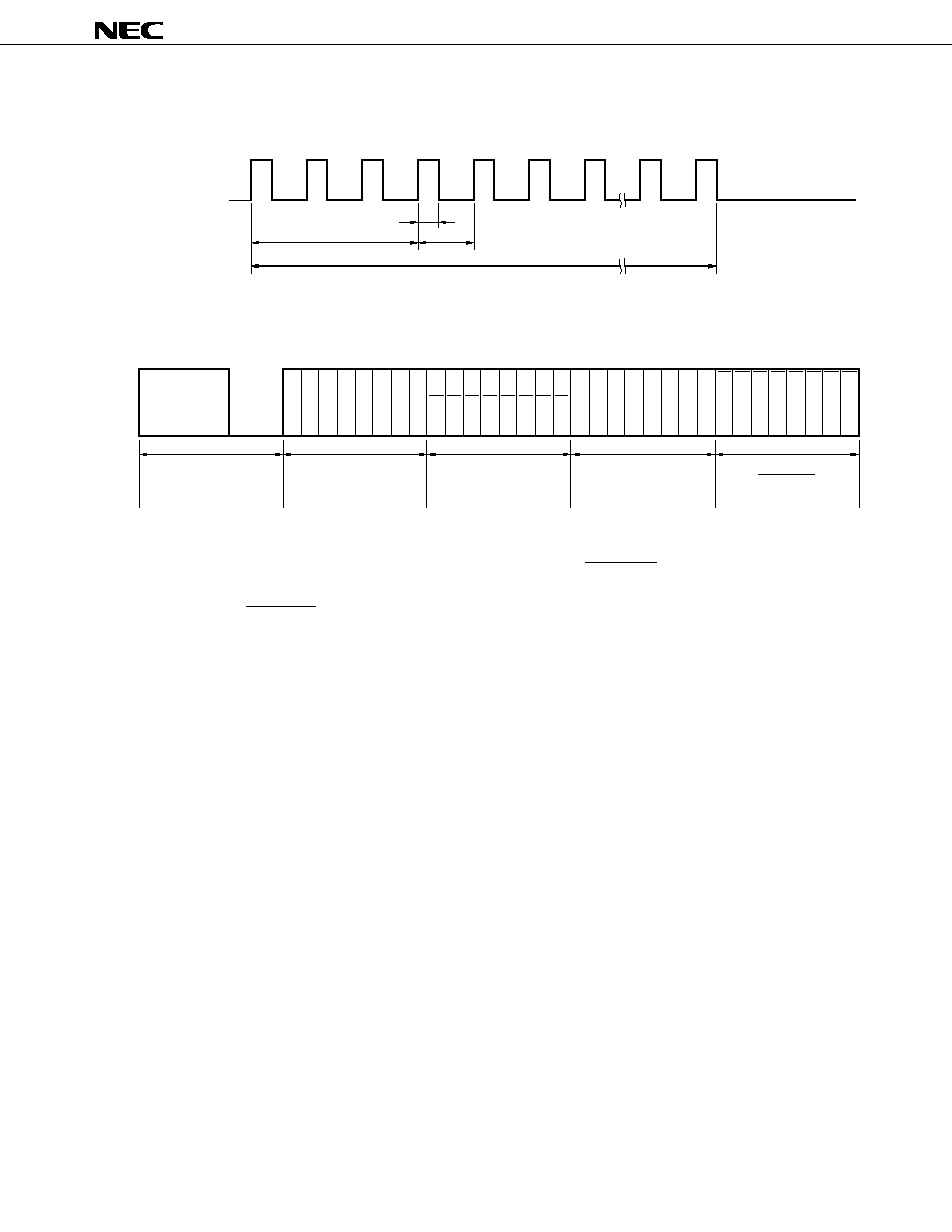
(1) REM output waveform (From <2> on, the output is made only when the key is kept pressed.)
REM output
58.5 to 76.5 ms
108 ms
108 ms
< 1 >
< 2 >
Remark If the key is repeatedly pressed, the power consumption of the infrared light-emitting diode (LED) can
be reduced by sending the reader code and the stop bit from the second time.
(2) Enlarged waveform of <1>
(3) Enlarged waveform of <3>
REM output
9 ms
13.5 ms
0
4.5 ms
1
1
0
0
2.25 ms
1.125 ms
0.56 ms
(4) Enlarged waveform of <2>
REM output
9 ms
11.25 ms
2.25 ms
0.56 ms
Stop Bit
Leader code
REM output
13.5 ms
Leader code
9 ms
4.5 ms
Custom code
8 bits
Custom code'
8 bits
Data code
8 bits
Data code
8 bits
27 ms
18 to 36 ms
58.5 to 76.5 ms
Stop Bit
1 bit
< 3 >
27
µ
PD66P04B
Data Sheet U13596EJ2V0DS00
(5) Carrier waveform (Enlarged waveform of each code's high period)
REM output
8.77 s
9 ms or 0.56 ms
Carrier frequency : 38 kHz
26.3 s
µ
µ
(6) Bit array of each code
C
0
C
1
C
2
C
3
C
4
C
5
C
6
C
7
C
0
'
C
0
or
C
o
C
1
'
C
1
or
C
1
C
2
'
C
2
or
C
2
C
3
'
C
3
or
C
3
C
4
'
C
4
or
C
4
C
5
'
C
5
or
C
5
C
6
'
C
6
or
C
6
C
7
'
C
7
or
C
7
D
0
D
1
D
2
D
3
D
4
D
5
D
6
D
7
D
0
D
1
D
2
D
3
D
4
D
5
D
6
D
7
=
=
=
=
=
=
=
=
Data code
Data code
Custom code'
Custom code
Leader code
Caution To prevent malfunction with other systems when receiving data in the NEC transmission
format, not only fully decode (make sure to check Data Code as well) the total 32 bits of the
16-bit custom codes (Custom Code, Custom Code') and the 16-bit data codes (Data Code,
Data Code) but also check to make sure that no signals are present.

28
µ
PD66P04B
Data Sheet U13596EJ2V0DS00
[MEMO]

29
µ
PD66P04B
Data Sheet U13596EJ2V0DS00
[MEMO]

30
µ
PD66P04B
Data Sheet U13596EJ2V0DS00
NOTES FOR CMOS DEVICES
1
PRECAUTION AGAINST ESD FOR SEMICONDUCTORS
Note:
Strong electric field, when exposed to a MOS device, can cause destruction of the gate oxide and
ultimately degrade the device operation. Steps must be taken to stop generation of static
electricity as much as possible, and quickly dissipate it once, when it has occurred. Environmental
control must be adequate. When it is dry, humidifier should be used. It is recommended to avoid
using insulators that easily build static electricity. Semiconductor devices must be stored and
transported in an anti-static container, static shielding bag or conductive material. All test and
measurement tools including work bench and floor should be grounded. The operator should be
grounded using wrist strap. Semiconductor devices must not be touched with bare hands. Similar
precautions need to be taken for PW boards with semiconductor devices on it.
2
HANDLING OF UNUSED INPUT PINS FOR CMOS
Note:
No connection for CMOS device inputs can be cause of malfunction. If no connection is provided
to the input pins, it is possible that an internal input level may be generated due to noise, etc., hence
causing malfunction. CMOS devices behave differently than Bipolar or NMOS devices. Input
levels of CMOS devices must be fixed high or low by using a pull-up or pull-down circuitry. Each
unused pin should be connected to V
DD
or GND with a resistor, if it is considered to have a
possibility of being an output pin. All handling related to the unused pins must be judged device
by device and related specifications governing the devices.
3
STATUS BEFORE INITIALIZATION OF MOS DEVICES
Note:
Power-on does not necessarily define initial status of MOS device. Production process of MOS
does not define the initial operation status of the device. Immediately after the power source is
turned ON, the devices with reset function have not yet been initialized. Hence, power-on does
not guarantee out-pin levels, I/O settings or contents of registers. Device is not initialized until
the reset signal is received. Reset operation must be executed immediately after power-on for
devices having reset function.

31
µ
PD66P04B
Data Sheet U13596EJ2V0DS00
NEC Electronics Inc. (U.S.)
Santa Clara, California
Tel: 408-588-6000
800-366-9782
Fax: 408-588-6130
800-729-9288
NEC Electronics (Germany) GmbH
Duesseldorf, Germany
Tel: 0211-65 03 02
Fax: 0211-65 03 490
NEC Electronics (UK) Ltd.
Milton Keynes, UK
Tel: 01908-691-133
Fax: 01908-670-290
NEC Electronics Italiana s.r.l.
Milano, Italy
Tel: 02-66 75 41
Fax: 02-66 75 42 99
NEC Electronics Hong Kong Ltd.
Hong Kong
Tel: 2886-9318
Fax: 2886-9022/9044
NEC Electronics Hong Kong Ltd.
Seoul Branch
Seoul, Korea
Tel: 02-528-0303
Fax: 02-528-4411
NEC Electronics Singapore Pte. Ltd.
United Square, Singapore 1130
Tel: 65-253-8311
Fax: 65-250-3583
NEC Electronics Taiwan Ltd.
Taipei, Taiwan
Tel: 02-2719-2377
Fax: 02-2719-5951
NEC do Brasil S.A.
Electron Devices Division
Rodovia Presidente Dutra, Km 214
07210-902-Guarulhos-SP Brasil
Tel: 55-11-6465-6810
Fax: 55-11-6465-6829
NEC Electronics (Germany) GmbH
Benelux Office
Eindhoven, The Netherlands
Tel: 040-2445845
Fax: 040-2444580
NEC Electronics (France) S.A.
Velizy-Villacoublay, France
Tel: 01-30-67 58 00
Fax: 01-30-67 58 99
NEC Electronics (France) S.A.
Spain Office
Madrid, Spain
Tel: 91-504-2787
Fax: 91-504-2860
NEC Electronics (Germany) GmbH
Scandinavia Office
Taeby, Sweden
Tel: 08-63 80 820
Fax: 08-63 80 388
Regional Information
Some information contained in this document may vary from country to country. Before using any NEC
product in your application, please contact the NEC office in your country to obtain a list of authorized
representatives and distributors. They will verify:
· Device availability
· Ordering information
· Product release schedule
· Availability of related technical literature
· Development environment specifications (for example, specifications for third-party tools and
components, host computers, power plugs, AC supply voltages, and so forth)
· Network requirements
In addition, trademarks, registered trademarks, export restrictions, and other legal issues may also vary
from country to country.
J99.1

µ
PD66P04B
MS-DOS is either a registered trademark or a trademark of Microsoft Corporation in the United States and/
or other countries.
PC/AT and PC DOS are trademarks of IBM Corp.
·
The information in this document is subject to change without notice. Before using this document, please
confirm that this is the latest version.
·
No part of this document may be copied or reproduced in any form or by any means without the prior written
consent of NEC Corporation. NEC Corporation assumes no responsibility for any errors which may appear in
this document.
·
NEC Corporation does not assume any liability for infringement of patents, copyrights or other intellectual
property rights of third parties by or arising from use of a device described herein or any other liability arising
from use of such device. No license, either express, implied or otherwise, is granted under any patents, copyrights
or other intellectual property rights of NEC Corporation or others.
·
Descriptions of circuits, software, and other related information in this document are provided for illustrative
purposes in semiconductor product operation and application examples. The incorporation of these circuits,
software, and information in the design of the customer's equipment shall be done under the full responsibility
of the customer. NEC Corporation assumes no responsibility for any losses incurred by the customer or third
parties arising from the use of these circuits, software, and information.
·
While NEC Corporation has been making continuous effort to enhance the reliability of its semiconductor devices,
the possibility of defects cannot be eliminated entirely. To minimize risks of damage or injury to persons or
property arising from a defect in an NEC semiconductor device, customers must incorporate sufficient safety
measures in its design, such as redundancy, fire-containment, and anti-failure features.
·
NEC devices are classified into the following three quality grades:
"Standard", "Special", and "Specific". The Specific quality grade applies only to devices developed based on a
customer designated "quality assurance program" for a specific application. The recommended applications of
a device depend on its quality grade, as indicated below. Customers must check the quality grade of each device
before using it in a particular application.
Standard: Computers, office equipment, communications equipment, test and measurement equipment,
audio and visual equipment, home electronic appliances, machine tools, personal electronic
equipment and industrial robots
Special:
Transportation equipment (automobiles, trains, ships, etc.), traffic control systems, anti-disaster
systems, anti-crime systems, safety equipment and medical equipment (not specifically designed
for life support)
Specific:
Aircraft, aerospace equipment, submersible repeaters, nuclear reactor control systems, life
support systems or medical equipment for life support, etc.
The quality grade of NEC devices is "Standard" unless otherwise specified in NEC's Data Sheets or Data Books.
If customers intend to use NEC devices for applications other than those specified for Standard quality grade,
they should contact an NEC sales representative in advance.
M7 98.8
The export of this product from Japan is regulated by the Japanese government. To export this product may be prohibited
without governmental license, the need for which must be judged by the customer. The export or re-export of this product
from a country other than Japan may also be prohibited without a license from that country. Please call an NEC sales
representative.
Document Outline
- COVER
- DESCRIPTION
- FEATURES
- APPLICATION
- ORDERING INFORMATION
- PIN CONFIGURATION (TOP VIEW)
- BLOCK DIAGRAM
- LIST OF FUNCTIONS
- 1. PIN FUNCTIONS
- 1.1 Normal Operating Mode
- 1.2 PROM Programming Mode
- 1.3 INPUT/OUTPUT Circuits of Pins
- 1.4 Dealing with Unused Pins
- 1.5 Notes on Using KI Pin at Reset
- 2. DIFFERENCES BETWEEN uPD6604 AND uPD66P04B
- 3. WRITING AND VERIFYING ONE-TIME PROM (PROGRAM MEMORY)
- 3.1 Operating Mode When Writing/Verifying Program Memory
- 3.2 Program Memory Writing Procedure
- 3.3 Program Memory Reading Procedure
- 4. ELECTRICAL SPECIFICATIONS
- 5. CHARACTERISTIC CURVE (REFERENCE VALUES)
- 6. APPLIED CIRCUIT EXAMPLE
- 7. PACKAGE DRAWINGS
- 8. RECOMMENDED SOLDERING CONDITIONS
- APPENDIX A. DEVELOPMENT TOOLS
- APPENDIX B. EXAMPLE OF REMOTE-CONTROL TRANSMISSION FORMAT