 | –≠–ª–µ–∫—Ç—Ä–æ–Ω–Ω—ã–π –∫–æ–º–ø–æ–Ω–µ–Ω—Ç: UPD6708 | –°–∫–∞—á–∞—Ç—å:  PDF PDF  ZIP ZIP |
Document Outline
- COVER
- DESCRIPTION
- FEATURES
- ORDERING INFORMATION
- APPLICATION FIELD
- PIN CONFIGURATION (TOP VIEW)
- 1. PIN FUNCTIONS
- 1.1 List of Pin Functions
- 2. IEBus OPERATION
- 2.1 Operation Overview
- 2.2 IEBus Communication Protocol
- 2.2.1 Bus mastership determination (arbitration)
- 2.2.2 Communication modes
- 2.2.3 Communication address
- 2.2.4 Broadcast communication
- 2.3 Transfer Protocol
- 2.4 Transfer Data (Contents of Data Field)
- 2.5 Bit Format
- 3. INTERNAL CONFIGURATION
- 3.1 Data Link Layer Controller
- 3.2 Physical Layer Controller
- 3.3 IEBus Driver/Receiver
- 3.4 Host Interface
- 4. INTERFACING WITH HOST CONTROLLER
- 4.1 Accessible Buffers and Registers from Host Controller
- 4.1.1 Write data buffer (WDB)
- 4.1.2 Read data buffer (RDB)
- 4.1.3 Command register (CMR)
- 4.1.4 Status register (STR)
- 4.2 Host Interface Modes
- 4.2.1 Switching through pin control
- 4.2.2 Switching through software control
- 4.3 Reset Mode
- 5. COMMUNICATION CONTROL COMMANDS
- 5.1 Overview of Communication Control Commands
- 5.2 Communication Control Command Functions
- 5.2.1 INIT command (command code: 0000)
- 5.2.2 SETSA command (command code: 0001)
- 5.2.3 MREQ1 command (command code: 0010)
- 5.2.4 MREQ2 command (command code: 0011)
- 5.2.5 ABORT command (command code: 0100)
- 5.2.6 SETSD command (command code: 0101)
- 5.2.7 GETSTA command (command code: 0110)
- 5.2.8 SETREV command (command code: 0111)
- 6. RETURN CODES
- 6.1 Return Codes in Master/Slave Data Transmission
- 6.2 Return Codes in Master Reception
- 6.3 Return Codes in Slave Reception
- 6.4 Return Codes in Broadcast Reception
- 6.5 Return Codes Generation Intervals
- 7. COMMUNICATING WITH HOST CONTROLLER
- 7.1 Master Transmission
- 7.1.1 Master transmission by MREQ1 command
- 7.1.2 Master transmission by MREQ2 command
- 7.2 Slave Transmission
- 7.2.1 Data transmission
- 7.2.2 Transmitting slave status address and lock address
- 7.3 Master Reception
- 7.4 Slave Reception
- 7.5 Broadcast Reception
- 8. EXAMPLE OF HOST CONTROLLER PROCESSING FLOW
- 8.1 Main Routine
- 8.2 Interrupt Service Routine
- 8.3 Processing Routine
- 8.3.1 uPD6708 initialization routine
- 8.3.2 Communication control command processing routine
- 8.3.3 Master transmission processing routine
- 8.3.4 Slave data transmission processing routine
- 8.3.5 Master reception processing routine
- 9. ELECTRICAL SPECIFICATIONS
- 10. PACKAGE DRAWINGS
- 11. RECOMMENDED SOLDERING CONDITIONS
- APPENDIX MAJOR DIFFERENCES BETWEEN uPD6708 AND uPD72042A, uPD72042B
©
MOS INTEGRATED CIRCUIT
µ
PD6708
IEBus
TM
(Inter Equipment Bus
TM
) PROTOCOL CONTROL LSI
Document No. U10680EJ2V0DS00 (2nd edition)
(Previous No. IC-3282)
Date Published January 1996 P
Printed in Japan
DATA SHEET
The information in this document is subject to change without notice.
The mark
5
shows major revised points.
DESCRIPTION
The
µ
PD6708 is a peripheral LSI for microcontrollers that controls the protocol of the IEBus.
This LSI processes the protocol of the IEBus. Because it is provided with a transmit/receive buffer, the microcontroller
can concentrate on the application processing of the IEBus. Because the
µ
PD6708 also contains an IEBus driver/receiver,
it can be directly connected to the bus.
FEATURES
∑
Protocol control of IEBus
∑ Multi-master system
∑ Broadcast communication function (commu-
nication between one unit and multiple units)
∑ Choice of three modes with different trans-
mission speeds
At 12 MHz
At 12.58 MHz
Mode 0
Approx. 3.9 Kbps
Approx. 4.1 Kbps
Mode 1
Approx. 17 Kbps
Approx. 18 Kbps
Mode 2
Approx. 26 Kbps
Approx. 27 Kbps
ORDERING INFORMATION
Part Number
Package
µ
PD6708CX
16-pin plastic DIP (300 mil)
µ
PD6708GS
16-pin plastic SOP (300 mil)
∑
On-chip IEBus driver/receiver
∑
Transmit/receive buffer
Transmit: 4-byte FIFO
Receive: 20-byte FIFO
∑
Interface with microcontroller
∑ Three-line serial I/O (SCK, SO, SI pins)
∑ Transfer with MSB first
∑
Oscillation frequency (f
X
): 12 MHz, 12.58 MHz
∑ In modes 0 and 1:
±
1.5 %
∑ In mode 2:
±
0.5 %
∑
Supply voltage: V
DD
= 5 V
±
10 %
APPLICATION FIELD
Fields where a small-scale digital data transfer system is required between equipment, such as automobile electronic
systems and industrial equipment
1993
2
µ
PD6708
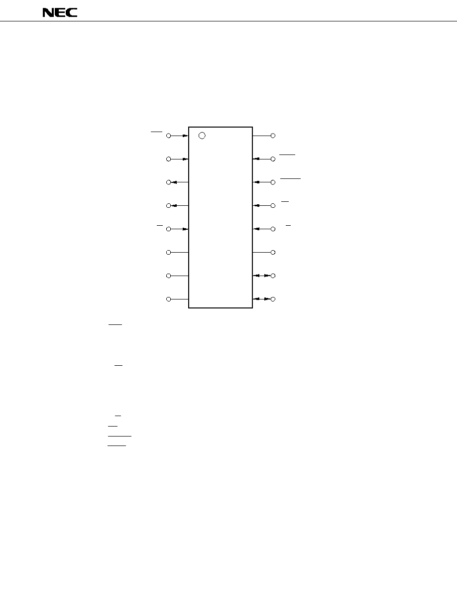
PIN CONFIGURATION (TOP VIEW)
∑ 16 pin plastic DIP (300 mil)
µ
PD6708CX
∑ 16 pin plastic SOP (300 mil)
µ
PD6708GS
SCK
: Serial clock input
SI
: Serial data input
SO
: Serial data output
IRQ
: Interrupt request output
R/W
: Read/write switchover input
XI, XO
: System clock
GND
: Ground
BUS≠, BUS+
: IEBus input/output
AV
DD
: IEBus analog power supply (connected to V
DD
pin)
C/D
: Command/data switchover input
CS
: Chip select input
RESET
: Reset input
TEST
: Test input (connected to V
DD
pin)
V
DD
: Positive power supply
SCK
SI
SO
IRQ
R/W
XI
XO
GND
V
DD
TEST
RESET
CS
C/D
AV
DD
BUS+
BUS≠
16
15
14
13
12
11
10
9
1
2
3
4
5
6
7
8

3
µ
PD6708
CONTENTS
1.
PIN FUNCTIONS ......................................................................................................................................... 5
1.1
List of Pin Functions ......................................................................................................................................... 5
2.
IEBus OPERATION .................................................................................................................................... 6
2.1
Operation Overview ........................................................................................................................................... 6
2.2
IEBus Communication Protocol ...................................................................................................................... 7
2.2.1
Bus mastership determination (arbitration) ................................................................................... 8
2.2.2
Communication modes ...................................................................................................................... 8
2.2.3
Communication address ................................................................................................................... 9
2.2.4
Broadcast communication ................................................................................................................ 9
2.3
Transfer Protocol ............................................................................................................................................. 10
2.4
Transfer Data (Contents of Data Field) ......................................................................................................... 16
2.5
Bit Format ......................................................................................................................................................... 19
3.
INTERNAL CONFIGURATION ................................................................................................................. 20
3.1
Data Link Layer Controller ............................................................................................................................. 21
3.2
Physical Layer Controller ............................................................................................................................... 21
3.3
IEBus Driver/Receiver ..................................................................................................................................... 21
3.4
Host Interface ................................................................................................................................................... 21
4.
INTERFACING WITH HOST CONTROLLER .......................................................................................... 22
4.1
Accessible Buffers and Registers from Host Controller ........................................................................... 22
4.1.1
Write data buffer (WDB) .................................................................................................................. 22
4.1.2
Read data buffer (RDB) ................................................................................................................... 22
4.1.3
Command register (CMR) ................................................................................................................ 22
4.1.4
Status register (STR) ....................................................................................................................... 23
4.2
Host Interface Modes ...................................................................................................................................... 23
4.2.1
Switching through pin control ....................................................................................................... 24
4.2.2
Switching through software control .............................................................................................. 26
4.3
Reset Mode ....................................................................................................................................................... 28
5.
COMMUNICATION CONTROL COMMANDS ......................................................................................... 30
5.1
Overview of Communication Control Commands....................................................................................... 30
5.2
Communication Control Command Functions ............................................................................................ 31
5.2.1
INIT command (command code: 0000) .......................................................................................... 31
5.2.2
SETSA command (command code: 0001) .................................................................................... 32
5.2.3
MREQ1 command (command code: 0010) ................................................................................... 33
5.2.4
MREQ2 command (command code: 0011) ................................................................................... 34
5.2.5
ABORT command (command code: 0100) ................................................................................... 34
5.2.6
SETSD command (command code: 0101) .................................................................................... 35
5.2.7
GETSTA command (command code: 0110) .................................................................................. 36
5.2.8
SETREV command (command code: 0111) .................................................................................. 37
6.
RETURN CODES ...................................................................................................................................... 38
6.1
Return Codes in Master/Slave Data Transmission ..................................................................................... 38
6.2
Return Codes in Master Reception ............................................................................................................... 38
6.3
Return Codes in Slave Reception ................................................................................................................. 39
6.4
Return Codes in Broadcast Reception ......................................................................................................... 39
6.5
Return Codes Generation Intervals ............................................................................................................... 40
7.
COMMUNICATING WITH HOST CONTROLLER ................................................................................... 43
7.1
Master Transmission ....................................................................................................................................... 43
7.1.1
Master transmission by MREQ1 command .................................................................................. 43
7.1.2
Master transmission by MREQ2 command .................................................................................. 44

4
µ
PD6708
7.2
Slave Transmission ......................................................................................................................................... 44
7.2.1
Data transmission ............................................................................................................................ 44
7.2.2
Transmitting slave status address and lock address ................................................................. 45
7.3
Master Reception ............................................................................................................................................. 45
7.4
Slave Reception ............................................................................................................................................... 46
7.5
Broadcast Reception ....................................................................................................................................... 47
8.
EXAMPLE OF HOST CONTROLLER PROCESSING FLOW ................................................................ 48
8.1
Main Routine ..................................................................................................................................................... 48
8.2
Interrupt Service Routine ................................................................................................................................ 49
8.3
Processing Routine ......................................................................................................................................... 50
8.3.1
µ
PD6708 initialization routine ......................................................................................................... 50
8.3.2
Communication control command processing routine .............................................................. 51
8.3.3
Master transmission processing routine ...................................................................................... 57
8.3.4
Slave data transmission processing routine ............................................................................... 58
8.3.5
Master reception processing routine ............................................................................................ 59
9.
ELECTRICAL SPECIFICATIONS ............................................................................................................ 63
10. PACKAGE DRAWINGS ............................................................................................................................ 67
11. RECOMMENDED SOLDERING CONDITIONS ....................................................................................... 69
APPENDIX MAJOR DIFFERENCES BETWEEN
µ
PD6708 AND
µ
PD72042A,
µ
PD72042B ................... 70
5
µ
PD6708
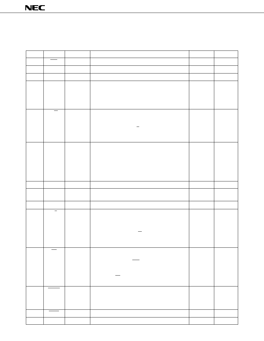
1.
PIN FUNCTIONS
1.1
List of Pin Functions
Pin No.
Pin Name
Input/Output
Function
I/O Format
At Reset
1
SCK
Input
Input for serial clock used to interface with microcontroller.
CMOS input
Input
2
SI
Input
Input for serial data used to interface with microcontroller.
CMOS input
Input
3
SO
Output
Output for serial data used to interface with microcontroller.
CMOS output
High level
4
IRQ
Output
Output used by interrupt request signals generated by
CMOS output
Low level
communication and command execution results.
Used as operation start request signal to microcontroller.
The interrupt request signal is output for 8
µ
s or longer
at high level.
5
R/W
Input
Input for switching serial interface read/write mode.
CMOS input
Input
When high, it is in the read mode. When low, it is in the
write mode.
When this pin is low and C/D pin high, the read and write
modes can be switched by commands input from the serial
interface.
6
XI
≠≠
Connection pins for system clock resonator.
≠≠
(Oscillation
7
XO
Use a 12- or 12.58-MHz crystal, or ceramic resonator.
continues)
Frequency precision depends on the communication mode
used.
Mode 0
:
±
1.5 %
Mode 1
:
±
1.5 %
Mode 2
:
±
0.5 %
8
GND
≠≠
Ground
≠≠
≠≠
9
BUS≠
Input/output
Input/output for IEBus.
≠≠
High
10
BUS+
impedance
11
AV
DD
≠≠
IEBus driver/receiver analog power supply. Connect to V
DD
.
≠≠
≠≠
12
C/D
Input
Input used to switch between processing data input to the
CMOS input
Input
serial interface as commands or data.
When set to high, data is processed as commands; when
low, data is processed as data.
When this pin is high and R/W pin low, the read and write
modes can be switched by commands input from the serial
interface.
13
CS
Input
Chip select input.
CMOS input
Input
When low, serial interface input is enabled.
When high, serial clock (SCK) input is disabled, SO pin
becomes high impedance, and the serial clock counter is
reset.
The status of CS pin is not affected by IEBus transmit and
receive operations.
14
RESET
Input
System reset signal input pin.
CMOS input
Input
Low input effects a reset.
Always input the low signal for 6
µ
s or longer after turning
on the power.
15
TEST
Input
Always connect this pin to the V
DD
.
CMOS input
≠≠
16
V
DD
≠≠
Positive power supply input. Apply a voltage of 5 V
±
10 %.
≠≠
≠≠