V853 32-Bit Single-Chip Microcontrollers Hardware UM

User's Manual
Printed in Japan
©
V853
TM
32-Bit Single-Chip Microcontrollers
Hardware
µµ
µµµ
PD703003A
µµ
µµµ
PD703003A(A)
µµ
µµµ
PD703004A
µµ
µµµ
PD703025A
µµ
µµµ
PD703025A(A)
µµ
µµµ
PD70F3003A
µµ
µµµ
PD70F3003A(A)
µµ
µµµ
PD70F3025A
Document No. U10913EJ6V0UM00 (6th edition)
Date Published September 2001 N CP(K)
1996

2
User's Manual U10913EJ6V0UM
[MEMO]

3
User's Manual U10913EJ6V0UM
V853 and V850 Family are trademarks of NEC Corporation.
Windows is either a registered trademark or a trademark of Microsoft Corporation in the United
States and/or other countries.
NOTES FOR CMOS DEVICES
1
PRECAUTION AGAINST ESD FOR SEMICONDUCTORS
Note:
Strong electric field, when exposed to a MOS device, can cause destruction of the gate oxide and
ultimately degrade the device operation. Steps must be taken to stop generation of static electricity
as much as possible, and quickly dissipate it once, when it has occurred. Environmental control
must be adequate. When it is dry, humidifier should be used. It is recommended to avoid using
insulators that easily build static electricity. Semiconductor devices must be stored and transported
in an anti-static container, static shielding bag or conductive material. All test and measurement
tools including work bench and floor should be grounded. The operator should be grounded using
wrist strap. Semiconductor devices must not be touched with bare hands. Similar precautions need
to be taken for PW boards with semiconductor devices on it.
2
HANDLING OF UNUSED INPUT PINS FOR CMOS
Note:
No connection for CMOS device inputs can be cause of malfunction. If no connection is provided
to the input pins, it is possible that an internal input level may be generated due to noise, etc., hence
causing malfunction. CMOS devices behave differently than Bipolar or NMOS devices. Input levels
of CMOS devices must be fixed high or low by using a pull-up or pull-down circuitry. Each unused
pin should be connected to V
DD
or GND with a resistor, if it is considered to have a possibility of
being an output pin. All handling related to the unused pins must be judged device by device and
related specifications governing the devices.
3
STATUS BEFORE INITIALIZATION OF MOS DEVICES
Note:
Power-on does not necessarily define initial status of MOS device. Production process of MOS
does not define the initial operation status of the device. Immediately after the power source is
turned ON, the devices with reset function have not yet been initialized. Hence, power-on does
not guarantee out-pin levels, I/O settings or contents of registers. Device is not initialized until the
reset signal is received. Reset operation must be executed immediately after power-on for devices
having reset function.

4
User's Manual U10913EJ6V0UM
License not needed:
µ
PD70F3003A, 70F3003A(A), 70F3025A
The customer must judge
the need for license:
µ
PD703003A, 703003A(A), 703004A, 703025A, 703025A(A)
The export of these products from Japan is regulated by the Japanese government. The export of some or all of these
products may be prohibited without governmental license. To export or re-export some or all of these products from a
country other than Japan may also be prohibited without a license from that country. Please call an NEC sales
representative.
M8E 00. 4
The information in this document is current as of September, 2001. The information is subject to
change without notice. For actual design-in, refer to the latest publications of NEC's data sheets or
data books, etc., for the most up-to-date specifications of NEC semiconductor products. Not all
products and/or types are available in every country. Please check with an NEC sales representative
for availability and additional information.
No part of this document may be copied or reproduced in any form or by any means without prior
written consent of NEC. NEC assumes no responsibility for any errors that may appear in this document.
NEC does not assume any liability for infringement of patents, copyrights or other intellectual property rights of
third parties by or arising from the use of NEC semiconductor products listed in this document or any other
liability arising from the use of such products. No license, express, implied or otherwise, is granted under any
patents, copyrights or other intellectual property rights of NEC or others.
Descriptions of circuits, software and other related information in this document are provided for illustrative
purposes in semiconductor product operation and application examples. The incorporation of these
circuits, software and information in the design of customer's equipment shall be done under the full
responsibility of customer. NEC assumes no responsibility for any losses incurred by customers or third
parties arising from the use of these circuits, software and information.
While NEC endeavours to enhance the quality, reliability and safety of NEC semiconductor products, customers
agree and acknowledge that the possibility of defects thereof cannot be eliminated entirely. To minimize
risks of damage to property or injury (including death) to persons arising from defects in NEC
semiconductor products, customers must incorporate sufficient safety measures in their design, such as
redundancy, fire-containment, and anti-failure features.
NEC semiconductor products are classified into the following three quality grades:
"Standard", "Special" and "Specific". The "Specific" quality grade applies only to semiconductor products
developed based on a customer-designated "quality assurance program" for a specific application. The
recommended applications of a semiconductor product depend on its quality grade, as indicated below.
Customers must check the quality grade of each semiconductor product before using it in a particular
application.
"Standard": Computers, office equipment, communications equipment, test and measurement equipment, audio
and visual equipment, home electronic appliances, machine tools, personal electronic equipment
and industrial robots
"Special":
Transportation equipment (automobiles, trains, ships, etc.), traffic control systems, anti-disaster
systems, anti-crime systems, safety equipment and medical equipment (not specifically designed
for life support)
"Specific": Aircraft, aerospace equipment, submersible repeaters, nuclear reactor control systems, life
support systems and medical equipment for life support, etc.
The quality grade of NEC semiconductor products is "Standard" unless otherwise expressly specified in NEC's
data sheets or data books, etc. If customers wish to use NEC semiconductor products in applications not
intended by NEC, they must contact an NEC sales representative in advance to determine NEC's willingness
to support a given application.
(Note)
(1) "NEC" as used in this statement means NEC Corporation and also includes its majority-owned subsidiaries.
(2) "NEC semiconductor products" means any semiconductor product developed or manufactured by or for
NEC (as defined above).
·
·
·
·
·
·

5
User's Manual U10913EJ6V0UM
Regional Information
Some information contained in this document may vary from country to country. Before using any NEC
product in your application, pIease contact the NEC office in your country to obtain a list of authorized
representatives and distributors. They will verify:
·
Device availability
·
Ordering information
·
Product release schedule
·
Availability of related technical literature
·
Development environment specifications (for example, specifications for third-party tools and
components, host computers, power plugs, AC supply voltages, and so forth)
·
Network requirements
In addition, trademarks, registered trademarks, export restrictions, and other legal issues may also vary
from country to country.
NEC Electronics Inc. (U.S.)
Santa Clara, California
Tel: 408-588-6000
800-366-9782
Fax: 408-588-6130
800-729-9288
NEC Electronics (Germany) GmbH
Duesseldorf, Germany
Tel: 0211-65 03 02
Fax: 0211-65 03 490
NEC Electronics (UK) Ltd.
Milton Keynes, UK
Tel: 01908-691-133
Fax: 01908-670-290
NEC Electronics Italiana s.r.l.
Milano, Italy
Tel: 02-66 75 41
Fax: 02-66 75 42 99
NEC Electronics (Germany) GmbH
Benelux Office
Eindhoven, The Netherlands
Tel: 040-2445845
Fax: 040-2444580
NEC Electronics (France) S.A.
Velizy-Villacoublay, France
Tel: 01-3067-5800
Fax: 01-3067-5899
NEC Electronics (France) S.A.
Madrid Office
Madrid, Spain
Tel: 091-504-2787
Fax: 091-504-2860
NEC Electronics (Germany) GmbH
Scandinavia Office
Taeby, Sweden
Tel: 08-63 80 820
Fax: 08-63 80 388
NEC Electronics Hong Kong Ltd.
Hong Kong
Tel: 2886-9318
Fax: 2886-9022/9044
NEC Electronics Hong Kong Ltd.
Seoul Branch
Seoul, Korea
Tel: 02-528-0303
Fax: 02-528-4411
NEC Electronics Singapore Pte. Ltd.
Novena Square, Singapore
Tel: 253-8311
Fax: 250-3583
NEC Electronics Taiwan Ltd.
Taipei, Taiwan
Tel: 02-2719-2377
Fax: 02-2719-5951
NEC do Brasil S.A.
Electron Devices Division
Guarulhos-SP, Brasil
Tel: 11-6462-6810
Fax: 11-6462-6829
J01.2

6
User's Manual U10913EJ6V0UM
Major Revisions in This Edition
Page
Description
Throughout
· Deletion of following products from target devices
µPD703003, 70F3003
· Addition of following products to target devices
µPD703003A(A), 703025A(A), 70F3003A(A)
· Deletion of description on ROMless mode
p.22
Change of
1.3 Application Fields
p.22
Change of
1.4 Ordering Information
p.34
Modification of description in
2.2 Pin Status
p.46
Modification of description in
3.2 CPU Register Set
p.47
Modification of description in
3.2.1 Program register set
p.47
Modification of
Table 3-1 Program Registers
p.49
Modification of
Figure 3-3 Program Status Word (PSW)
p.50
Change of description in
3.3.2 (2) Flash memory programming mode
p.75
Addition of
Caution 3
in
3.4.10 Specific registers
p.95
Modification of description in
CHAPTER 5 INTERRUPT/EXCEPTION PROCESSING FUNCTION
p.126
Addition of
5.8 (1) Acknowledgement of interrupt servicing following EI instruction
p.128
Modification of description in
6.3.2 PLL mode
p.129
Change of description in
6.3.3 Clock control resister (CKC)
p.141
Addition of
6.5.6 Cautions
p.183
Addition of
Note
in
8.2.1 Features
p.198
Addition of description in
8.3.1 Features
p.204
Addition of
8.3.4 (2) (c) Initialization of serial clock controller and serial clock counter
p.218
Addition of
Caution 2
in
9.3 (1) A/D converter mode register 0 (ADM0)
p.289
Addition of description in
12.3.8 Port 7
p.299
Modification of
Table 13-1 Operating Status of Each Pin During Reset Period
p.300
Change of description and addition of
Note
in
13.2 (2) Power-on reset
p.303
Addition of
Caution
in
CHAPTER 14 FLASH MEMORY (
µ
PD70F3003A AND 70F3025A)
p.303
Change of description in
14.1 Features
p.304
Addition of
Figure 14-1 V853 Flash Memory Writing Adapter (FA-100GC-8EU) Wiring Example
p.305
Addition of
Table 14-1 Wiring Table of V853 Flash Writing Adapter (FA-100GC08EU)
p.307
Change of description in
14.4 (1) UART0
p.307
Change of description in
14.4 (2) CSI0
p.307
Addition of
14.4 (3) CSI communication mode supporting handshake
p.308
Addition of description and
Note 1
in
14.4 Communication Mode
p.309
Change of description in
14.5.1 V
PP
pin
p.310
Addition of description in
14.5.2 Serial interface pin
p.312
Change of description in
14.5.5 MODE pin
p.314
Change of description in
14.6.2 Flash memory programming mode
p.314
Addition of description in
Table 14-2 Communication Modes
p.315
Modification of description in
14.6.4 Communication command
The mark
shows major revised points.

7
User's Manual U10913EJ6V0UM
INTRODUCTION
Target Readers
This manual is intended for users who wish to understand the functions of the V853
to design application systems using the V853.
The target devices are as follows.
·
Standard version:
µ
PD703003A, 703004A, 703025A, 70F3003A, 70F3025A
·
Special version:
µ
PD703003A(A), 703025A(A), 70F3003A(A)
Purpose
This manual is intended to give users an understanding of the functions described
in the Organization below.
Organization
Two volumes of the V853 User's Manual are available: hardware (this manual) and
architecture (V850 Family
TM
Architecture User's Manual). The organization of
each manual is as follows:
Hardware
Architecture
· Pin functions
· Data type
· CPU function
· Register set
· On-chip peripheral functions
· Instruction format and instruction set
· Flash memory programming
· Interrupts and exceptions
mode
· Pipeline operation
How to Read This Manual
It is assumed that the reader of this manual has general knowledge in the fields of
electrical engineering, logic circuits, and microcontrollers.
Cautions 1.
The examples in this manual are for products used in general
electrical equipment with a "standard" quality grade. If
examples in this manual are used for applications requiring a
"special" quality grade, check the quality grade for the parts and
circuits actually used before use.
2.
If this manual is used as for special products, read as follows.
µ
PD703003A
µ
PD703003A(A)
µ
PD703025A
µ
PD703025A(A)
µ
PD70F3003A
µ
PD70F3003A(A)
· To find the details of a register where the name is known
Refer to APPENDIX A REGISTER INDEX.
· To find the details of a function, etc. where the name is known
Refer to APPENDIX C INDEX.
· To understand the details of an instruction function
Refer to the V850 Family Architecture User's Manual.
· To understand the electrical specifications of the V853
Refer to the Data Sheet.
· To understand the overall functions of the V853
Read this manual according to the CONTENTS.

8
User's Manual U10913EJ6V0UM
Conventions
Data significance:
Higher digits on the left and lower digits on the right
Active low representation:
xxx (overscore over pin or signal name)
Memory map address:
Higher address on the top and lower address on the
bottom
Note:
Footnote for item marked with Note in the text
Caution:
Information requiring particular attention
Remark:
Supplementary information
Numeric representation:
Binary ... xxxx or xxxxB
Decimal ... xxxx
Hexadecimal ... xxxxH
Prefix indicating power of 2: K (kilo): 2
10
= 1024
M (mega): 2
20
= 1024
2
G (giga): 2
30
= 1024
3
Related Documents
The related documents indicated in this publication may include preliminary versions.
However, preliminary versions are not marked as such.
· Documents related to devices
Document Name
Document No.
V850 Family Architecture User's Manual
U10243E
µ
PD703003A, 703004A, 703025A, 703003A(A), 703025A(A) Data Sheet
U13188E
µ
PD70F3003A, 70F3025A, 70F3003A(A) Data Sheet
U13189E
V853 Hardware User's Manual
This manual

9
User's Manual U10913EJ6V0UM
· Documents related to development tools (user's manuals)
Document Name
Document No.
IE-703002-MC (In-Circuit Emulator)
U11595E
IE-703003-MC-EM1 (In-Circuit Emulator Option Board)
U11596E
CA850 (Ver. 2.30 or Later) (C Compiler Package)
Operation
U14568E
C Language
U14566E
Project Manager
U14569E
Assembly Language
U14567E
CA850 (Ver. 2.40 or Later) (C Compiler Package)
Operation
U15024E
C Language
U15025E
Project Manager
U15026E
Assembly Language
U15027E
ID850 (Ver. 2.40 or Later) (Integrated Debugger)
Operation Windows
TM
Based
U15181E
SM850 (Ver. 2.40 or Later) (System Simulator)
Operation Windows Based
U15182E
External Part User Open
U14873E
Interface Specifications
RX850 (Ver. 3.13 or Later) (Real-Time OS)
Basics
U13430E
Installation
U13410E
Technical
U13431E
RX850 Pro (Ver. 3.13) (Real-Time OS)
Fundamental
U13773E
Installation
U13774E
Technical
U13772E
RD850 (Ver. 3.01) (Task Debugger)
U13737E
RD850 Pro (Ver. 3.01) (Task Debugger)
U13916E
AZ850 (Ver. 3.0) (System Performance Analyzer)
U14410E
PG-FP3 (Flash Memory Programmer)
U13502E

10
User's Manual U10913EJ6V0UM
CONTENTS
CHAPTER 1 INTRODUCTION ...............................................................................................................20
1.1
General .....................................................................................................................................20
1.2
Features ....................................................................................................................................21
1.3
Applications .............................................................................................................................22
1.4
Ordering Information .............................................................................................................. 22
1.5
Pin Configuration (Top View) ................................................................................................23
1.6
Function Block Configuration ...............................................................................................25
1.6.1
Internal block diagram ................................................................................................................ 25
1.6.2
Internal units ............................................................................................................................... 26
1.7
Differences Among Products ................................................................................................28
CHAPTER 2 PIN FUNCTIONS .............................................................................................................. 29
2.1
Pin Function List .....................................................................................................................29
2.2
Pin Status .................................................................................................................................34
2.3
Pin Functions ..........................................................................................................................35
2.4
Pin I/O Circuits and Recommended Connection of Unused Pins ................................... 43
2.5
Pin I/O Circuits ........................................................................................................................44
CHAPTER 3 CPU FUNCTIONS ............................................................................................................45
3.1
Features ....................................................................................................................................45
3.2
CPU Register Set .................................................................................................................... 46
3.2.1
Program register set ................................................................................................................... 47
3.2.2
System register set ..................................................................................................................... 48
3.3
Operation Modes .....................................................................................................................50
3.3.1
Operation modes ........................................................................................................................ 50
3.3.2
Specifying operation mode ......................................................................................................... 50
3.4
Address Space ........................................................................................................................51
3.4.1
CPU address space .................................................................................................................... 51
3.4.2
Image ........................................................................................................................................... 52
3.4.3
Wrap-around of CPU address space ......................................................................................... 53
3.4.4
Memory map ............................................................................................................................... 54
3.4.5
Area ............................................................................................................................................. 56
3.4.6
External expansion mode ........................................................................................................... 63
3.4.7
Memory expansion mode register (MM) .................................................................................... 64
3.4.8
Recommended use of address space ....................................................................................... 65
3.4.9
Peripheral I/O registers .............................................................................................................. 69
3.4.10
Specific registers ........................................................................................................................ 74
CHAPTER 4 BUS CONTROL FUNCTION ............................................................................................ 78
4.1
Features ....................................................................................................................................78
4.2
Bus Control Pins .....................................................................................................................78
4.3
Bus Access ..............................................................................................................................79
4.3.1
Number of access clocks ........................................................................................................... 79
4.3.2
Bus width ..................................................................................................................................... 79

11
User's Manual U10913EJ6V0UM
4.4
Memory Block Function .........................................................................................................81
4.5
Wait Function ...........................................................................................................................82
4.5.1
Programmable wait function ....................................................................................................... 82
4.5.2
External wait function ................................................................................................................. 83
4.5.3
Relationship between programmable wait and external wait ................................................... 83
4.6
Idle State Insertion Function ................................................................................................. 84
4.7
Bus Hold Function ..................................................................................................................85
4.7.1
Outline of function ....................................................................................................................... 85
4.7.2
Bus hold procedure .................................................................................................................... 85
4.7.3
Operation in power save mode .................................................................................................. 85
4.8
Bus Timing ...............................................................................................................................86
4.9
Bus Priority ..............................................................................................................................93
4.10 Memory Boundary Operation Condition .............................................................................. 93
4.10.1
Program space ............................................................................................................................ 93
4.10.2
Data space .................................................................................................................................. 93
4.11 On-Chip Peripheral I/O Interface ........................................................................................... 94
CHAPTER 5 INTERRUPT/EXCEPTION PROCESSING FUNCTION .................................................. 95
5.1
Features ....................................................................................................................................95
5.2
Non-Maskable Interrupt ..........................................................................................................98
5.2.1
Acknowledgement operation ...................................................................................................... 99
5.2.2
Restore operation ..................................................................................................................... 101
5.2.3
Non-maskable interrupt status flag (NP) ................................................................................. 102
5.2.4
Noise elimination of NMI pin .................................................................................................... 102
5.2.5
Edge detection function of NMI pin .......................................................................................... 102
5.3
Maskable Interrupts ............................................................................................................. 103
5.3.1
Block diagram ........................................................................................................................... 104
5.3.2
Operation ................................................................................................................................... 105
5.3.3
Restore ...................................................................................................................................... 107
5.3.4
Priorities of maskable interrupts .............................................................................................. 108
5.3.5
Interrupt control register (xxICn) .............................................................................................. 112
5.3.6
Noise eliminator ........................................................................................................................ 114
5.3.7
Edge detection function ............................................................................................................ 115
5.3.8
In-service priority register (ISPR) ............................................................................................ 116
5.3.9
Maskable interrupt status flag (ID) ........................................................................................... 116
5.4
Software Exception ............................................................................................................... 117
5.4.1
Operation ................................................................................................................................... 117
5.4.2
Restore ...................................................................................................................................... 118
5.4.3
Exception status flag (EP) ........................................................................................................ 119
5.5
Exception Trap ..................................................................................................................... 120
5.5.1
Illegal op code definition ........................................................................................................... 120
5.5.2
Operation ................................................................................................................................... 120
5.5.3
Restore ...................................................................................................................................... 121
5.6
Multiple Interrupts ................................................................................................................ 122
5.7
Interrupt Latency Time ........................................................................................................ 124
5.8
Periods in Which Interrupts Are Not Acknowledged ...................................................... 125

12
User's Manual U10913EJ6V0UM
CHAPTER 6 CLOCK GENERATOR FUNCTION .............................................................................. 127
6.1
Features ................................................................................................................................. 127
6.2
Configuration ........................................................................................................................ 127
6.3
Selecting Input Clock .......................................................................................................... 128
6.3.1
Direct mode ............................................................................................................................... 128
6.3.2
PLL mode .................................................................................................................................. 128
6.3.3
Clock control register (CKC) .................................................................................................... 129
6.4
PLL Lockup ........................................................................................................................... 131
6.5
Power Save Control ............................................................................................................. 132
6.5.1
General ...................................................................................................................................... 132
6.5.2
Control registers ....................................................................................................................... 134
6.5.3
HALT mode ............................................................................................................................... 135
6.5.4
IDLE mode ................................................................................................................................ 137
6.5.5
Software STOP mode ............................................................................................................... 139
6.5.6
Cautions .................................................................................................................................... 141
6.6
Securing Oscillation Stabilization Time ........................................................................... 142
6.7
Clock Output Control .......................................................................................................... 145
CHAPTER 7 TIMER/COUNTER FUNCTION (REAL-TIME PULSE UNIT) ...................................... 146
7.1
Features ................................................................................................................................. 146
7.2
Basic Configuration ............................................................................................................. 147
7.2.1
Timer 1 ...................................................................................................................................... 149
7.2.2
Timer 4 ...................................................................................................................................... 151
7.3
Control Registers ................................................................................................................. 152
7.4
Timer 1 Operation ................................................................................................................ 160
7.4.1
Count operation ........................................................................................................................ 160
7.4.2
Selecting count clock frequency .............................................................................................. 161
7.4.3
Overflow .................................................................................................................................... 162
7.4.4
Clearing/starting timer by TCLR signal input ........................................................................... 163
7.4.5
Capture operation ..................................................................................................................... 164
7.4.6
Compare operation ................................................................................................................... 167
7.5
Timer 4 Operation ................................................................................................................ 169
7.5.1
Count operation ........................................................................................................................ 169
7.5.2
Selecting count clock frequency .............................................................................................. 169
7.5.3
Overflow .................................................................................................................................... 169
7.5.4
Compare operation ................................................................................................................... 170
7.6
Application Examples ......................................................................................................... 172
7.7
Cautions ................................................................................................................................ 180
CHAPTER 8 SERIAL INTERFACE FUNCTION ................................................................................ 182
8.1
Features ................................................................................................................................. 182
8.2
Asynchronous Serial Interface 0 and 1 (UART0 and UART1) ....................................... 183
8.2.1
Features .................................................................................................................................... 183
8.2.2
Configuration of asynchronous serial interface ....................................................................... 184
8.2.3
Control registers ....................................................................................................................... 186
8.2.4
Interrupt request ....................................................................................................................... 193
8.2.5
Operation ................................................................................................................................... 194
8.3
Clocked Serial Interface 0 to 3 (CSI0 to CSI3) ................................................................. 198

13
User's Manual U10913EJ6V0UM
8.3.1
Features .................................................................................................................................... 198
8.3.2
Configuration ............................................................................................................................. 198
8.3.3
Control registers ....................................................................................................................... 200
8.3.4
Basic operation ......................................................................................................................... 202
8.3.5
Transmission in CSI0 to CSI3 .................................................................................................. 205
8.3.6
Reception in CSI0 to CSI3 ....................................................................................................... 206
8.3.7
Transmission/reception in CSI0 to CSI3 .................................................................................. 207
8.3.8
System configuration example ................................................................................................. 208
8.4
Baud Rate Generators 0 to 2 (BRG0 to BRG2) ................................................................ 209
8.4.1
Configuration and function ....................................................................................................... 209
8.4.2
Baud rate generator compare registers 0 to 2 (BRGC0 to BRGC2) ...................................... 213
8.4.3
Baud rate generator prescaler mode registers 0 to 2 (BPRM0 to BPRM2) .......................... 214
CHAPTER 9 A/D CONVERTER ......................................................................................................... 215
9.1
Features ................................................................................................................................. 215
9.2
Configuration ........................................................................................................................ 215
9.3
Control Registers ................................................................................................................. 218
9.4
A/D Converter Operation .................................................................................................... 221
9.4.1
Basic operation of A/D converter ............................................................................................. 221
9.4.2
Input voltage and conversion results ....................................................................................... 222
9.4.3
Operation mode and trigger mode ........................................................................................... 223
9.5
Operation in A/D Trigger Mode .......................................................................................... 228
9.5.1
Select mode operations ............................................................................................................ 228
9.5.2
Scan mode operations .............................................................................................................. 230
9.6
Operation in Timer Trigger Mode ....................................................................................... 231
9.6.1
Select mode operations ............................................................................................................ 232
9.6.2
Scan mode operations .............................................................................................................. 236
9.7
Operation in External Trigger Mode .................................................................................. 240
9.7.1
Select mode operations (external trigger select) .................................................................... 240
9.7.2
Scan mode operations (external trigger scan) ........................................................................ 242
9.8
Cautions in Use of A/D Converter ..................................................................................... 244
9.9
Cautions ................................................................................................................................ 245
9.10 How to Read A/D Converter Characteristics Table ......................................................... 246
CHAPTER 10 D/A CONVERTER ....................................................................................................... 249
10.1 Features ................................................................................................................................. 249
10.2 Configuration ........................................................................................................................ 249
10.3 Control Registers ................................................................................................................. 250
10.4 D/A Converter Operations ................................................................................................... 251
10.4.1
D/A converter operation during reset ....................................................................................... 251
10.4.2
D/A converter operation during normal operation ................................................................... 251
10.4.3
Operations during power save ................................................................................................. 251
CHAPTER 11 PWM UNIT ................................................................................................................... 252
11.1 Features ................................................................................................................................. 252
11.2 Configuration ........................................................................................................................ 252
11.3 Control Registers ................................................................................................................. 253
11.4 Operations ............................................................................................................................ 255

14
User's Manual U10913EJ6V0UM
11.4.1
Basic operations ....................................................................................................................... 255
11.4.2
Repeating frequency ................................................................................................................ 257
11.5 Caution ................................................................................................................................... 257
CHAPTER 12 PORT FUNCTION ....................................................................................................... 258
12.1 Features ................................................................................................................................. 258
12.2 Basic Configuration of Port ................................................................................................ 259
12.3 Port Pin Functions ............................................................................................................... 263
12.3.1
Port 0 ......................................................................................................................................... 263
12.3.2
Port 1 ......................................................................................................................................... 267
12.3.3
Port 2 ......................................................................................................................................... 272
12.3.4
Port 3 ......................................................................................................................................... 277
12.3.5
Port 4 ......................................................................................................................................... 283
12.3.6
Port 5 ......................................................................................................................................... 285
12.3.7
Port 6 ......................................................................................................................................... 287
12.3.8
Port 7 ......................................................................................................................................... 289
12.3.9
Port 9 ......................................................................................................................................... 290
12.3.10 Port 11 ....................................................................................................................................... 293
12.4 Switching Between External Maskable Interrupt Request Input/Timer External
Capture Trigger Input and CSI Pins .................................................................................. 296
12.5 Specifying Pull-up Resistors .............................................................................................. 298
CHAPTER 13 RESET FUNCTION ..................................................................................................... 299
13.1 Features ................................................................................................................................. 299
13.2 Pin Function .......................................................................................................................... 299
13.3 Initialize ................................................................................................................................. 300
CHAPTER 14 FLASH MEMORY (
µµ
µµ
µ
PD70F3003A AND 70F3025A) ................................................. 303
14.1 Features ................................................................................................................................. 303
14.2 Writing by Flash Programmer ............................................................................................ 303
14.3 Programming Environment ................................................................................................. 306
14.4 Communication Mode .......................................................................................................... 307
14.5 Pin Handling .......................................................................................................................... 309
14.5.1 V
PP
pin ......................................................................................................................................... 309
14.5.2 Serial interface pin ...................................................................................................................... 310
14.5.3 Reset pin ..................................................................................................................................... 312
14.5.4 NMI pin ........................................................................................................................................ 312
14.5.5 MODE pin ................................................................................................................................... 312
14.5.6 Port pin ........................................................................................................................................ 312
14.5.7 WAIT pin ..................................................................................................................................... 312
14.5.8 Other signal pin .......................................................................................................................... 312
14.5.9 Power supply .............................................................................................................................. 312
14.6 Programming Method .......................................................................................................... 313
14.6.1 Flash memory control ................................................................................................................. 313
14.6.2 Flash memory programming mode ............................................................................................ 314
14.6.3 Selection of communication mode ............................................................................................. 314
14.6.4 Communication commands ........................................................................................................ 315
14.6.5 Resources used .......................................................................................................................... 316

15
User's Manual U10913EJ6V0UM
APPENDIX A REGISTER INDEX ....................................................................................................... 317
APPENDIX B INSTRUCTION SET LIST ............................................................................................ 322
APPENDIX C INDEX ........................................................................................................................... 329

16
User's Manual U10913EJ6V0UM
LIST OF FIGURES (1/3)
Figure No.
Title
Page
3-1
Program Counter (PC) ............................................................................................................................. 47
3-2
Interrupt Source Register (ECR) ............................................................................................................. 48
3-3
Program Status Word (PSW) .................................................................................................................. 49
3-4
CPU Address Space ................................................................................................................................ 51
3-5
Image on Address Space ........................................................................................................................ 52
3-6
External Memory Area (When Expanded to 64 KB, 128 KB, 256 KB, 512 KB, or 1 MB) .................... 62
3-7
Recommended Memory Map .................................................................................................................. 66
4-1
Example of Inserting Wait States ............................................................................................................ 83
5-1
Non-Maskable Interrupt Servicing ........................................................................................................... 99
5-2
Acknowledging Non-Maskable Interrupt Request ................................................................................ 100
5-3
RETI Instruction Processing .................................................................................................................. 101
5-4
Maskable Interrupt Block Diagram ........................................................................................................ 104
5-5
Maskable Interrupt Servicing ................................................................................................................. 106
5-6
RETI Instruction Processing .................................................................................................................. 107
5-7
Example of Interrupt Nesting Process .................................................................................................. 109
5-8
Example of Processing Interrupt Requests Simultaneously Generated .............................................. 111
5-9
Example of Noise Elimination Timing ................................................................................................... 114
5-10
Software Exception Processing ............................................................................................................ 117
5-11
RETI Instruction Processing .................................................................................................................. 118
5-12
Exception Trap Processing .................................................................................................................... 120
5-13
RETI Instruction Processing .................................................................................................................. 121
5-14
Pipeline Operation upon Reception of Interrupt Request (Outline) ..................................................... 124
6-1
Block Configuration ................................................................................................................................ 144
7-1
Basic Operation of Timer 1 .................................................................................................................... 160
7-2
Operation After Occurrence of Overflow (When ECLR1n = 0, OSTn = 1) .......................................... 162
7-3
Clearing/Starting Timer by TCLR1n Signal Input (When ECLR1n = 1, OSTn = 0) ............................ 163
7-4
Relationship Between Clear/Start by TCLR1n Signal Input and Overflow
(When ECLR1n, OSTn = 1) .................................................................................................................. 164
7-5
Example of Capture Operation .............................................................................................................. 165
7-6
Example of TM11 Capture Operation (When Both Edges Are Specified) ........................................... 166
7-7
Example of Compare Operation ............................................................................................................ 167
7-8
Example of TM11 Compare Operation (Set/Reset Output Mode) ....................................................... 168
7-9
Basic Operation of Timer 4 .................................................................................................................... 169
7-10
Examples of TM4 Compare Operation ................................................................................................. 170
7-11
Example of Timing of Interval Timer Operation .................................................................................... 172
7-12
Example of Setting Procedure of Interval Timer Operation ................................................................. 172
7-13
Example of Pulse Width Measurement Timing ..................................................................................... 173
7-14
Example of Setting Procedure for Pulse Width Measurement ............................................................ 174
7-15
Example of Interrupt Request Servicing Routine Calculating Pulse Width ......................................... 174

17
User's Manual U10913EJ6V0UM
LIST OF FIGURES (2/3)
Figure No.
Title
Page
7-16
Example of PWM Output Timing ........................................................................................................... 175
7-17
Example of Programming Procedure of PWM Output ......................................................................... 176
7-18
Example of Interrupt Request Servicing Routine, Modifying Compare Value .................................... 177
7-19
Example of Frequency Measurement Timing ....................................................................................... 178
7-20
Example of Setup Procedure for Frequency Measurement ................................................................. 179
7-21
Example of Interrupt Request Servicing Routine Calculating Cycle ................................................... 179
8-1
Block Diagram of Asynchronous Serial Interface ................................................................................. 185
8-2
Format of Transmit/Receive Data of Asynchronous Serial Interface .................................................. 194
8-3
Asynchronous Serial Interface Transmission Completion Interrupt Timing ........................................ 195
8-4
Asynchronous Serial Interface Reception Completion Interrupt Timing .............................................. 197
8-5
Receive Error Timing ............................................................................................................................. 197
8-6
Block Diagram of Clocked Serial Interface ........................................................................................... 199
8-7
Timing of 3-Wire Serial I/O Mode (Transmission) ................................................................................ 205
8-8
Timing of 3-Wire Serial I/O Mode (Reception) ..................................................................................... 206
8-9
Timing of 3-Wire Serial I/O Mode (Transmission/Reception) .............................................................. 208
8-10
Example of CSI System Configuration ................................................................................................. 208
8-11
Block Diagram of Baud Rate Generator ............................................................................................... 209
9-1
Block Diagram of A/D Converter ........................................................................................................... 217
9-2
Relationship Between Analog Input Voltage and A/D Conversion Result ........................................... 222
9-3
Select Mode Operation Timing: 1-Buffer Mode (ANI1) ........................................................................ 225
9-4
Select Mode Operation Timing: 4-Buffer Mode (ANI6) ........................................................................ 226
9-5
Scan Mode Operation Timing: 4-Channel Scan (ANI0 to ANI3) .......................................................... 227
9-6
Example of 1-Buffer Mode (A/D Trigger Select 1-Buffer) Operation ................................................... 228
9-7
Example of 4-Buffer Mode (A/D Trigger Select 4-Buffer) Operation ................................................... 229
9-8
Example of Scan Mode (A/D Trigger Scan) Operation ........................................................................ 230
9-9
Example of 1-Trigger Mode (Timer Trigger Select 1-Buffer 1-Trigger) Operation .............................. 232
9-10
Example of 4-Trigger Mode (Timer Trigger Select 1-Buffer 4-Trigger) Operation .............................. 233
9-11
Example of 1-Trigger Mode (Timer Trigger Select 4-Buffer 1-Trigger) Operation .............................. 234
9-12
Example of 4-Trigger Mode (Timer Trigger Select 4-Buffer 4-Trigger) Operation .............................. 235
9-13
Example of 1-Trigger Mode (Timer Trigger Scan 1-Trigger) Operation .............................................. 237
9-14
Example of 4-Trigger Mode (Timer Trigger Scan 4-Trigger) Operation .............................................. 239
9-15
Example of 1-Buffer Mode (External Trigger Select 1-Buffer) Operation ............................................ 240
9-16
Examples of 4-Buffer Mode (External Trigger Select 4-Buffer) Operation .......................................... 241
9-17
Example of Scan Mode (External Trigger Scan) Operation ................................................................. 243
9-18
Relationships Among A/D Converter, Ports, INTC, and RPU .............................................................. 244
9-19
Overall Error ........................................................................................................................................... 246
9-20
Quantization Error .................................................................................................................................. 246
9-21
Zero Scale Error ..................................................................................................................................... 247
9-22
Full Scale Error ...................................................................................................................................... 247
9-23
Nonlinearity Error ................................................................................................................................... 247

18
User's Manual U10913EJ6V0UM
LIST OF FIGURES (3/3)
Figure No.
Title
Page
11-1
Basic Operation Timing of PWM ........................................................................................................... 256
11-2
Operation Timing When 000H and FFFH Are Set in PWM Buffer Register ........................................ 256
12-1
Block Diagram of P00 and P01 (Port 0) ............................................................................................... 264
12-2
Block Diagram of P02 to P07 (Port 0) .................................................................................................. 264
12-3
Block Diagram of P10 and P11 (Port 1) ............................................................................................... 268
12-4
Block Diagram of P12 to P14 (Port 1) .................................................................................................. 268
12-5
Block Diagram of P15 (Port 1) .............................................................................................................. 269
12-6
Block Diagram of P16 (Port 1) .............................................................................................................. 269
12-7
Block Diagram of P17 (Port 1) .............................................................................................................. 270
12-8
Block Diagram of P20 and P21 (Port 2) ............................................................................................... 273
12-9
Block Diagram of P22 and P25 (Port 2) ............................................................................................... 273
12-10
Block Diagram of P23 and P26 (Port 2) ............................................................................................... 274
12-11
Block Diagram of P24 and P27 (Port 2) ............................................................................................... 274
12-12
Block Diagram of P30 and P31 (Port 3) ............................................................................................... 278
12-13
Block Diagram of P32 to P34 (Port 3) .................................................................................................. 278
12-14
Block Diagram of P35 (Port 3) .............................................................................................................. 279
12-15
Block Diagram of P36 (Port 3) .............................................................................................................. 279
12-16
Block Diagram of P37 (Port 3) .............................................................................................................. 280
12-17
Block Diagram of P40 to P47 (Port 4) .................................................................................................. 283
12-18
Block Diagram of P50 to P57 (Port 5) .................................................................................................. 285
12-19
Block Diagram of P60 to P63 (Port 6) .................................................................................................. 287
12-20
Block Diagram of P70 to P77 (Port 7) .................................................................................................. 289
12-21
Block Diagram of P90 to P95 (Port 9) .................................................................................................. 291
12-22
Block Diagram of P96 (Port 9) .............................................................................................................. 291
12-23
Block Diagram of P110 and P111 (Port 11) .......................................................................................... 294
12-24
Block Diagram of P112 to P117 (Port 11) ............................................................................................. 294
14-1
V853 Flash Writing Adapter (FA100GC-8EU) Wiring Example ........................................................... 304

19
User's Manual U10913EJ6V0UM
LIST OF TABLES
Table No.
Title
Page
3-1
Program Registers ................................................................................................................................... 47
3-2
System Register Numbers ....................................................................................................................... 48
3-3
Interrupt/Exception Table ......................................................................................................................... 59
4-1
Bus Priority ............................................................................................................................................... 93
5-1
Interrupt List ............................................................................................................................................. 96
5-2
Address and Bits of Interrupt Control Register .................................................................................... 113
6-1
Operation of Clock Generator by Power Save Control ........................................................................ 133
6-2
Operating Status in HALT Mode ........................................................................................................... 135
6-3
Operating Status in IDLE Mode ............................................................................................................ 137
6-4
Operating Status in Software STOP Mode ........................................................................................... 139
6-5
Example of Count Time ......................................................................................................................... 144
7-1
Configuration of Real-Time Pulse Unit (RPU) ...................................................................................... 147
7-2
Capture Trigger Signal to 16-Bit Capture Register (TM1n) ................................................................. 164
7-3
Interrupt Request Signal from 16-Bit Compare Register (TM1n) ........................................................ 167
8-1
Default Priority of Interrupts .................................................................................................................. 193
8-2
Setting Values of Baud Rate Generators 0 to 2 ................................................................................... 211
13-1
Operating Status of Each Pin During Reset Period ............................................................................. 299
13-2
Initial Values of Each Register After Reset ........................................................................................... 301
14-1
Wiring Table of V853 Flash Writing Adapter ......................................................................................... 305
14-2
List of Communication Modes ............................................................................................................... 314

20
User's Manual U10913EJ6V0UM
CHAPTER 1 INTRODUCTION
The V853 is a product of NEC's V850 Family of single-chip microcontrollers for real-time control applications. This
chapter briefly outlines the V853.
1.1 General
The V853 is a 32-bit single-chip microcontroller that employs the CPU core of the V850 Family of high-performance
32-bit single-chip microcontrollers for real-time control applications, and integrates peripheral functions such as ROM/
RAM, a real-time pulse unit, serial interface, A/D converter, and PWM.
The V853 is provided with multiplication instructions that are executed with a hardware multiplier, saturated
operation instructions, and bit manipulation instructions that are ideal for digital servo control applications, in addition
to the basic instructions that have a high real-time response speed and can be executed in 1 clock cycle. This
microcontroller can be employed for many applications including real-time control systems such as cameras and VCRs
and other AV applications; engine control and ABS (Anti-lock Braking System); various automobile electronic
applications; office equipment applications including PPCs (Plain Paper Copiers), printers, and facsimiles; and
industrial applications such as NC (Numerical Control) machine tools. In any of these applications, the V853
demonstrates an extremely high cost effectiveness.
CHAPTER 1 INTRODUCTION
21
User's Manual U10913EJ6V0UM
1.2 Features
Number of instructions:
74
Minimum instruction execution time: 30 ns (at internal 33 MHz)
General-purpose registers:
32 bits
×
32
Instruction set:
Signed multiply (16 bits
×
16 bits
32 bits): 1 to 2 clocks
Saturated operation instructions (with overflow/underflow detection function)
32-bit shift instructions: 1 clock
Bit manipulation instructions
Load/store instructions with long/short format
Memory space:
16 MB linear address space (up to 1 MB external expansion)
Memory block division function: 2 MB/block
Programmable wait function
Idle state insertion function
External bus interface:
16-bit data bus (address/data multiplexed)
Bus hold function
External wait function
Internal memory
Part Number
Internal ROM
Internal RAM
µ
PD703003A
Mask ROM: 128 KB
4 KB
µ
PD70F3003A
Flash memory: 128 KB
4 KB
µ
PD703004A
Mask ROM: 96 KB
4 KB
µ
PD703025A
Mask ROM: 256 KB
8 KB
µ
PD70F3025A
Flash memory: 256 KB
8 KB
Interrupts/exceptions:
External interrupt: 17 (including NMI)
Internal interrupt: 32 sources
Exception:
1 source
Eight levels of priorities can be set.
I/O lines:
Input ports: 8
I/O ports:
67
Real-time pulse unit:
16-bit timer/event counter: 4 channels
16-bit timer: 4
16-bit capture/compare register: 16
16-bit interval timer: 1 channel
Serial interface:
Asynchronous serial interface (UART)
Clocked serial interface (CSI)
UART/CSI: 2 channels
CSI: 2 channels
Dedicated baud rate generator: 3 channels
PWM (Pulse Width Modulation):
8-/9-/10-/12-bit resolution PWM: 2 channels
A/D converter:
10-bit resolution A/D converter: 8 channels
D/A converter:
8-bit resolution D/A converter: 2 channels
Clock generator:
Multiplication function by PLL clock synthesizer

22
CHAPTER 1 INTRODUCTION
User's Manual U10913EJ6V0UM
Power save function:
HALT/IDLE/software STOP mode
Clock output stop function
Package:
100-pin plastic LQFP (fine pitch) (14
×
14)
CMOS technology
1.3 Applications
µ
PD703003A, 703004A, 703025A, 70F3003A, 70F3025A: Camcorders, VCRs, PPC, LBP, printers, motor control,
NC machine tools, portable phones, etc.
µ
PD703003A(A), 703025A(A), 70F3003A(A): Medical equipment, automotive electricals, etc.
1.4 Ordering Information
Part number
Package Quality Grade
µ
PD703003AGC-33-
×××
-8EU 100-pin plastic LQFP (fine pitch) (14
×
14) Standard
(for general electrical equipment)
µ
PD703004AGC-33-
×××
-8EU 100-pin plastic LQFP (fine pitch) (14
×
14) Standard
(for general electrical equipment)
µ
PD703025AGC-33-
×××
-8EU 100-pin plastic LQFP (fine pitch) (14
×
14) Standard
(for general electrical equipment)
µ
PD70F3003AGC-33-8EU
100-pin plastic LQFP (fine pitch) (14
×
14) Standard
(for general electrical equipment)
µ
PD70F3025AGC-33-8EU
100-pin plastic LQFP (fine pitch) (14
×
14) Standard
(for general electrical equipment)
µ
PD703003AGC(A)-33-
×××
-8EU 100-pin plastic LQFP (fine pitch) (14
×
14) Special
(for high-reliability electrical equipment)
µ
PD703025AGC(A)-33-
×××
-8EU 100-pin plastic LQFP (fine pitch) (14
×
14) Special
(for high-reliability electrical equipment)
µ
PD70F3003AGC(A)-33-8EU 100-pin plastic LQFP (fine pitch) (14
×
14) Special
(for high-reliability electrical equipment)
Remark
×××
indicates ROM code suffix.
No differences other than the quality grade exist between the
µ
PD703003A, 703025A, and 70F3003A and the
µ
PD703003A(A), 703025A(A), and 70F3003A(A).
For details of the quality grade and its application fields, refer to Quality Grades on NEC Semiconductor Devices
(C11531E).
CHAPTER 1 INTRODUCTION
23
User's Manual U10913EJ6V0UM
1.5 Pin Configuration (Top View)
· 100 pin plastic LQFP (fine pitch) (14
×
14)
µ
PD703003AGC-33-
×××
-8EU
µ
PD703003AGC(A)-33-
×××
-8EU
µ
PD703004AGC-33-
×××
-8EU
µ
PD703025AGC(A)-33-
×××
-8EU
µ
PD703025AGC-33-
×××
-8EU
µ
PD70F3003AGC(A)-33-8EU
µ
PD70F3003AGC-33-8EU
µ
PD70F3025AGC-33-8EU
Note
µ
PD703003A, 703004A, 703025A: IC
µ
PD70F3003A, 70F3025A: V
PP
Cautions 1. When the
µµ
µµ
µ
PD70F3003A and 70F3025A are used in normal operation mode, connect the V
PP
pin to V
SS
via a resistor (R
VPP
).
2. Connect the IC pin directly to V
SS
.
1
2
3
4
5
6
7
8
9
10
11
12
13
14
15
16
17
18
19
20
21
22
23
24
25
75
74
73
72
71
70
69
68
67
66
65
64
63
62
61
60
59
58
57
56
55
54
53
52
51
P75/ANI5
P74/ANI4
P73/ANI3
P72/ANI2
P71/ANI1
P70/ANI0
ANO0
ANO1
AV
REF2
AV
REF3
P07/INTP113/ADTRG
P06/INTP112
P05/INTP111
P04/INTP110
P03/TI11
P02/TCLR11
P01/TO111
P00/TO110
P117/INTP143
P116/INTP142
P115/INTP141
P114/INTP140
P113/TI14
P112/TCLR14
P111/TO141
P31/TO131
P32/TCLR13
P33/TI13
P34/INTP130
P35/INTP131/SO3
P36/INTP132/SI3
P37/INTP133/SCK3
P63/A19
P62/A18
P61/A17
P60/A16
V
SS
V
DD
P57/AD15
P56/AD14
P55/AD13
P54/AD12
P53/AD11
P52/AD10
P51/AD9
P50/AD8
P47/AD7
P46/AD6
P45/AD5
P44/AD4
P43/AD3
P42/AD2
V
SS
V
DD
P41/AD1
P40/AD0
P90/LBEN
P91/UBEN
P92/R/W
P93/DSTB
P94/ASTB
P95/HLDAK
P96/HLDRQ
WAIT
Note
MODE
RESET
CV
DD
/CKSEL
X2
X1
CV
SS
CLKOUT
V
SS
V
DD
P110/TO140
P30/TO130
P27/SCK1
P26/RXD1/SI1
P25/TXD1/SO1
P24/SCK0
P23/RXD0/SI0
P22/TXD0/SO0
P21/PWM1
P20/PWM0
NMI
V
DD
V
SS
P17/INTP123/SCK2
P16/INTP122/SI2
P15/INTP121/SO2
P14/INTP120
P13/TI12
P12/TCLR12
P11/TO121
P10/TO120
AV
DD
AV
SS
AV
REF1
P77/ANI7
P76/ANI6
26
27
28
29
30
31
32
33
34
35
36
37
38
39
40
41
42
43
44
45
46
47
48
49
50
100
99
98
97
96
95
94
93
92
91
90
89
88
87
86
85
84
83
82
81
80
79
78
77
76

24
CHAPTER 1 INTRODUCTION
User's Manual U10913EJ6V0UM
Pin identification
A16 to A19:
Address bus
AD0 to AD15:
Address/data bus
ADTRG:
AD trigger input
ANI0 to ANI7:
Analog input
ANO0, ANO1:
Analog output
ASTB:
Address strobe
AV
DD
:
Analog power supply
AV
REF1
to AV
REF3
:
Analog reference voltage
AV
SS
:
Analog ground
CKSEL:
Clock select
CLKOUT:
Clock output
CV
DD
:
Clock generator power supply
CV
SS
:
Clock generator ground
DSTB:
Data strobe
HLDAK:
Hold acknowledge
HLDRQ:
Hold request
IC:
Internally connected
INTP110 to INTP113,: Interrupt request from peripherals
INTP120 to INTP123,
INTP130 to INTP133,
INTP140 to INTP143
LBEN:
Lower byte enable
MODE:
Mode
NMI:
Non-maskable interrupt request
P00 to P07:
Port0
P10 to P17:
Port1
P20 to P27:
Port2
P30 to P37:
Port3
P40 to P47:
Port4
P50 to P57:
Port5
P60 to P63:
Port6
P70 to P77:
Port7
P90 to P96:
Port9
P110 to P117:
Port11
PWM0, PWM1:
Pulse width modulation
RESET:
Reset
R/W:
Read/write status
RXD0, RXD1:
Receive data
SCK0 to SCK3:
Serial clock
SI0 to SI3:
Serial input
SO0 to SO3:
Serial output
TCLR11 to TCLR14: Timer clear
TI11 to TI14:
Timer input
TO110, TO111,: Timer output
TO120, TO121,
TO130, TO131,
TO140, TO141
TXD0, TXD1:
Transmit data
UBEN:
Upper byte enable
V
DD
:
Power supply
V
PP
:
Programming power supply
V
SS
:
Ground
WAIT:
Wait
X1, X2:
Crystal
CHAPTER 1 INTRODUCTION
25
User's Manual U10913EJ6V0UM
1.6 Function Block Configuration
1.6.1 Internal block diagram
Notes
1.
µ
PD703003A:
128 KB (Mask ROM)
µ
PD70F3003A:
128 KB (Flash memory)
µ
PD703004A:
96 KB (Mask ROM)
µ
PD703025A:
256 KB (Mask ROM)
µ
PD70F3025A:
256 KB (Flash memory)
2.
µ
PD703003A, 703004A, 70F3003A: 4 KB
µ
PD703025A, 70F3025A: 8 KB
3.
µ
PD70F3003A, 70F3025A
NMI
TO110, TO111
TO120, TO121
TO130, TO131
TO140, TO141
INTP110 to INTP113
INTP120 to INTP123
INTP130 to INTP133
INTP140 to INTP143
TCLR11 to TCLR14
TI11 to TI14
INTC
RPU
SIO
ROM
Note 1
RAM
Note 2
CPU
PC
32-bit
barrel shifter
System
registers
General-
purpose
registers
32 bits x 32
ALU
Multiplier
16 x 16
32
Port
P110 to P117
P90 to P96
P70 to P77
P60 to P63
P50 to P57
P40 to P47
P30 to P37
P20 to P27
P10 to P17
P00 to P07
CG
BCU
Instruction
queue
ASTB
DSTB
R/W
UBEN
LBEN
WAIT
A16 to A19
AD0 to AD15
HLDRQ
HLDAK
CLKOUT
CKSEL
X1
X2
MODE
RESET
V
DD
V
SS
CV
DD
CV
SS
V
PP
Note 3
UART0/CSI0
BRG0
UART1/CSI1
BRG1
CSI2
BRG2
CSI3
PWM
SO0/TXD0
SI0/RXD0
SCK0
SO1/TXD1
SI1/RXD1
SCK1
SO2
SI2
SCK2
SO3
SI3
SCK3
PWM0, PWM1
A/D
converter
ANI0
to
ANI7
AV
REF1
AV
SS
AV
DD
ADTRG
D/A
converter
ANO0, ANO1
AV
REF2
, AV
REF3

26
CHAPTER 1 INTRODUCTION
User's Manual U10913EJ6V0UM
1.6.2 Internal units
(1) CPU
Executes almost all instruction processing such as address calculation, arithmetic/logic operation, and data
transfer in 1 clock by using a 5-stage pipeline.
Dedicated hardware devices such as a multiplier (16 bits
×
16 bits
32 bits) and a barrel shifter (32 bits)
are provided to increase the speed of processing complicated instructions.
(2) Bus control unit (BCU)
Initiates the necessary number of external bus cycles based on the physical address obtained by the CPU.
If the CPU does not issue a request to start a bus cycle when an instruction is fetched from the external memory
area, generates a prefetch address to prefetch an instruction code. The prefetched instruction code is loaded
to the internal instruction queue.
(3) ROM
The internal ROM is mapped starting from address 00000000H. The ROM is fixed to access-enabled
irrespective of the MODE pin status.
This internal ROM is accessed in 1 clock by the CPU when an instruction is fetched.
(4) RAM
The internal RAM is mapped starting from address FFFFE000H. This internal RAM can be accessed in 1 clock
by the CPU when data is accessed.
(5) Interrupt controller (INTC)
Processes interrupt requests (NMI, INTP110 to INTP113, INTP120 to INTP123, INTP130 to INTP133, and
INTP140 to INTP143) from the on-chip peripheral hardware and external sources. Eight levels of priorities
can be specified for these interrupt requests, and multiplexed processing control can be performed on an
interrupt source.
(6) Clock generator (CG)
Supplies a CPU clock whose frequency is five times, one time, or 1/2 times the frequency of the oscillator
connected across the X1 and X2 pins via the internal PLL. Input from an external clock source can also be
referenced instead of using the oscillator.
(7) Real-time pulse unit (RPU)
Provides four 16-bit timer/event counter channels, one 16-bit interval timer channel, and capabilities for
measuring pulse width and generation of programmable pulse outputs.
(8) Serial interface (SIO)
The serial interface consists of a four asynchronous serial interface (UART) and clocked serial interface (CSI)
channels that can be used simultaneously. Two of these channels can be switched between UART and CSI,
and the other two channels are fixed to CSI.
UART transfers data by using the TXD and RXD pins and CSI transfers data by using the SO, SI, and SCK
pins.
The output of the baud rate generator and system clock can be selected as the serial interface clock source.
Of the fixed CSI channels, one channel is the serial clock output. The serial output is an open drain output.

CHAPTER 1 INTRODUCTION
27
User's Manual U10913EJ6V0UM
(9) Ports
The ports have functions as general-purpose ports and functions as control pins as shown below.
Port
I/O
Port Function
Control Function
Port 0
8-bit I/O
General-
Timer I/O, external interrupt
Port 1
purpose port
Timer I/O, external interrupt, serial interface
Port 2
PWM output, serial interface
Port 3
Timer I/O, external interrupt
Port 4
External address/data bus
Port 5
External address/data bus
Port 6
4-bit I/O
External address bus
Port 7
8-bit input
A/D analog input
Port 9
7-bit I/O
External bus interface control signal I/O
Port 11
8-bit I/O
Timer I/O, external interrupt
(10) PWM (Pulse Width Modulation)
The V853 is provided with two PWM signal output channels for which 8-/9-/10-/12-bit resolution can be
selected.
The PWM output can be used as a D/A converter output by connecting an external low pass filter. It is suitable
for controlling the actuator of motors, etc.
(11) A/D converter (ADC)
The ADC is a high speed, high resolution 10-bit A/D converter with eight analog input pins and uses the
successive-approximation method.
(12) D/A converter (DAC)
The DAC incorporates two 8-bit resolution D/A converter channels and uses the R-2R conversion method.
28
CHAPTER 1 INTRODUCTION
User's Manual U10913EJ6V0UM
1.7 Differences Among Products
Item
µ
PD703003A
µ
PD703004A
µ
PD703025A
µ
PD703003A(A)
µ
PD703025A(A)
µ
PD70F3003A
µ
PD70F3025A
µ
PD70F3003A(A)
Internal ROM
Mask ROM
Flash memory
128 KB
96 KB
256 KB
128 KB
256 KB
128 KB
256 KB
128 KB
Internal RAM
4 KB
8 KB
4 KB
8 KB
4 KB
8 KB
4 KB
Flash memory
Not available
Available
programming mode
V
PP
pin
Not available
Available
Quality grade
Standard
Special
Standard
Special
Electrical specifications Current dissipation varies (refer to the relevant Data Sheet).
Other
The noise immunity and noise radiation differ due to differences in the circuit
scale and mask layout.

29
User's Manual U10913EJ6V0UM
CHAPTER 2 PIN FUNCTIONS
The following table shows the names and functions of the V853's pins. These pins can be divided by function
into port pins and non-port pins.
2.1 Pin Function List
(1) Port pins
(1/2)
Pin Name
I/O
Function
Alternate Function
P00
I/O
TO110
P01
TO111
P02
TCLR11
P03
TI11
P04
INTP110
P05
INTP111
P06
INTP112
P07
INTP113/ADTRG
P10
I/O
TO120
P11
TO121
P12
TCLR12
P13
TI12
P14
INTP120
P15
INTP121/SO2
P16
INTP122/SI2
P17
INTP123/SCK2
P20
I/O
PWM0
P21
PWM1
P22
TXD0/SO0
P23
RXD0/SI0
P24
SCK0
P25
TXD1/SO1
P26
RXD1/SI1
P27
SCK1
P30
I/O
TO130
P31
TO131
P32
TCLR13
P33
TI13
P34
INTP130
P35
INTP131/SO3
P36
INTP132/SI3
P37
INTP133/SCK3
Port 0.
8-bit I/O port.
Input/output can be specified in 1-bit units.
Port 1.
8-bit I/O port.
Input/output can be specified in 1-bit units.
Port 3.
8-bit I/O port.
Input/output can be specified in 1-bit units.
Port 2.
8-bit I/O port.
Input/output can be specified in 1-bit units.

30
CHAPTER 2 PIN FUNCTIONS
User's Manual U10913EJ6V0UM
(2/2)
Pin Name
I/O
Function
Alternate Function
P40 to P47
I/O
AD0 to AD7
P50 to P57
I/O
AD8 to AD15
P60 to P63
I/O
Port 6.
A16 to A19
4-bit I/O port.
Input/output can be specified in 1-bit units.
P70 to P77
Input
ANI0 to ANI7
P90
I/O
LBEN
P91
UBEN
P92
R/W
P93
DSTB
P94
ASTB
P95
HLDAK
P96
HLDRQ
P110
I/O
TO140
P111
TO141
P112
TCLR14
P113
TI14
P114
INTP140
P115
INTP141
P116
INTP142
P117
INTP143
Port 4.
8-bit I/O port.
Input/output can be specified in 1-bit units.
Port 5.
8-bit I/O port.
Input/output can be specified in 1-bit units.
Port 7.
8-bit input only port.
Port 9.
7-bit I/O port.
Input/output can be specified in 1-bit units.
Port 11.
8-bit I/O port.
Input/output
can be specified in 1-bit units.

31
CHAPTER 2 PIN FUNCTIONS
User's Manual U10913EJ6V0UM
External capture trigger input to timer 11. Also used to input external
maskable interrupt request.
External capture trigger input to timer 13. Also used to input external
maskable interrupt request.
External capture trigger input to timer 12. Also used to input external
maskable interrupt request.
External capture trigger input to timer 14. Also used to input external
maskable interrupt request.
(2) Non-port pins
(1/3)
Pin Name
I/O
Function
Alternate Function
TO110
Output
Pulse signal output from timer 11 to 14.
P00
TO111
P01
TO120
P10
TO121
P11
TO130
P30
TO131
P31
TO140
P110
TO141
P111
TCLR11
Input
External clear signal input to timer 11 to 14.
P02
TCLR12
P12
TCLR13
P32
TCLR14
P112
TI11
Input
External count clock input to timer 11 to 14.
P03
TI12
P13
TI13
P33
TI14
P113
INTP110
Input
P04
INTP111
P05
INTP112
P06
INTP113
P07/ADTRG
INTP120
Input
P14
INTP121
P15/SO2
INTP122
P16/SI2
INTP123
P17/SCK2
INTP130
Input
P34
INTP131
P35/SO3
INTP132
P36/SI3
INTP133
P37/SCK3
INTP140
Input
P114
INTP141
P115
INTP142
P116
INTP143
P117
SO0
Output
Serial transmit data output from CSI0 to CSI3 (3-wire).
P22/TXD0
SO1
P25/TXD1
SO2
P15/INTP121
SO3
P35/INTP131
SI0
Input
Serial receive data input to CSI0 to CSI3 (3-wire).
P23/RXD0
SI1
P26/RXD1
SI2
P16/INTP122
SI3
P36/INTP132

32
CHAPTER 2 PIN FUNCTIONS
User's Manual U10913EJ6V0UM
(2/3)
Pin Name
I/O
Function
Alternate Function
SCK0
I/O
Serial clock I/O from/to CSI0 to CSI3 (3-wire).
P24
SCK1
P27
SCK2
P17/INTP123
SCK3
P37/INTP133
TXD0
Output
Serial transmit data output from UART0 and UART1.
P22/SO0
TXD1
P25/SO1
RXD0
Input
Serial receive data input to UART0 and UART1.
P23/SI0
RXD1
P26/SI1
PWM0
Output
Pulse signal output from PWM.
P20
PWM1
P21
AD0 to AD7
I/O
16-bit multiplexed address/data bus when external memory is used.
P40 to P47
AD8 to AD15
P50 to P57
A16 to A19
Output
Higher address bus when external memory is used.
P60 to P63
LBEN
Output
Lower byte enable signal output of external data bus.
P90
UBEN
Higher byte enable signal output of external data bus.
P91
R/W
External read/write status output.
P92
DSTB
External data strobe signal output.
P93
ASTB
External address strobe signal output.
P94
HLDAK
Output
Bus hold acknowledge output.
P95
HLDRQ
Input
Bus hold request input.
P96
ANI0 to ANI7
Input
Analog input to A/D converter.
P70 to P77
ANO0, ANO1
Output
Analog output for D/A converter.
NMI
Input
Non-maskable interrupt request input.
CLKOUT
Output
System clock output.
CKSEL
Input
Input that specifies clock generator operation mode.
CV
DD
WAIT
Input
Control signal input inserting wait state to bus cycle.
MODE
Input
Specifies operation mode of the V853.
RESET
Input
System reset input.
X1
Input
System clock oscillator connecting pins. Supply external clock to X1.
X2
ADTRG
Input
A/D converter external trigger input.
P07/INTP113
AV
REF1
Input
Reference voltage input for A/D converter.
AV
REF2
Input
Reference voltage input for D/A converter.
AV
REF3

33
CHAPTER 2 PIN FUNCTIONS
User's Manual U10913EJ6V0UM
(3/3)
Pin Name
I/O
Function
Alternate Function
AV
DD
Positive power supply for A/D converter.
AV
SS
Ground for A/D converter.
CV
DD
Positive power supply for on-chip clock generator.
CKSEL
CV
SS
Ground for on-chip clock generator.
V
DD
Positive power supply
V
SS
Ground
V
PP
Note 1
High-voltage application pin for writing/verifying programs.
IC
Note 2
Internal connection pin (Connect directly to V
SS
)
Notes
1.
µ
PD70F3003A, 70F3025A
2.
µ
PD703003A, 703004A, 703025A
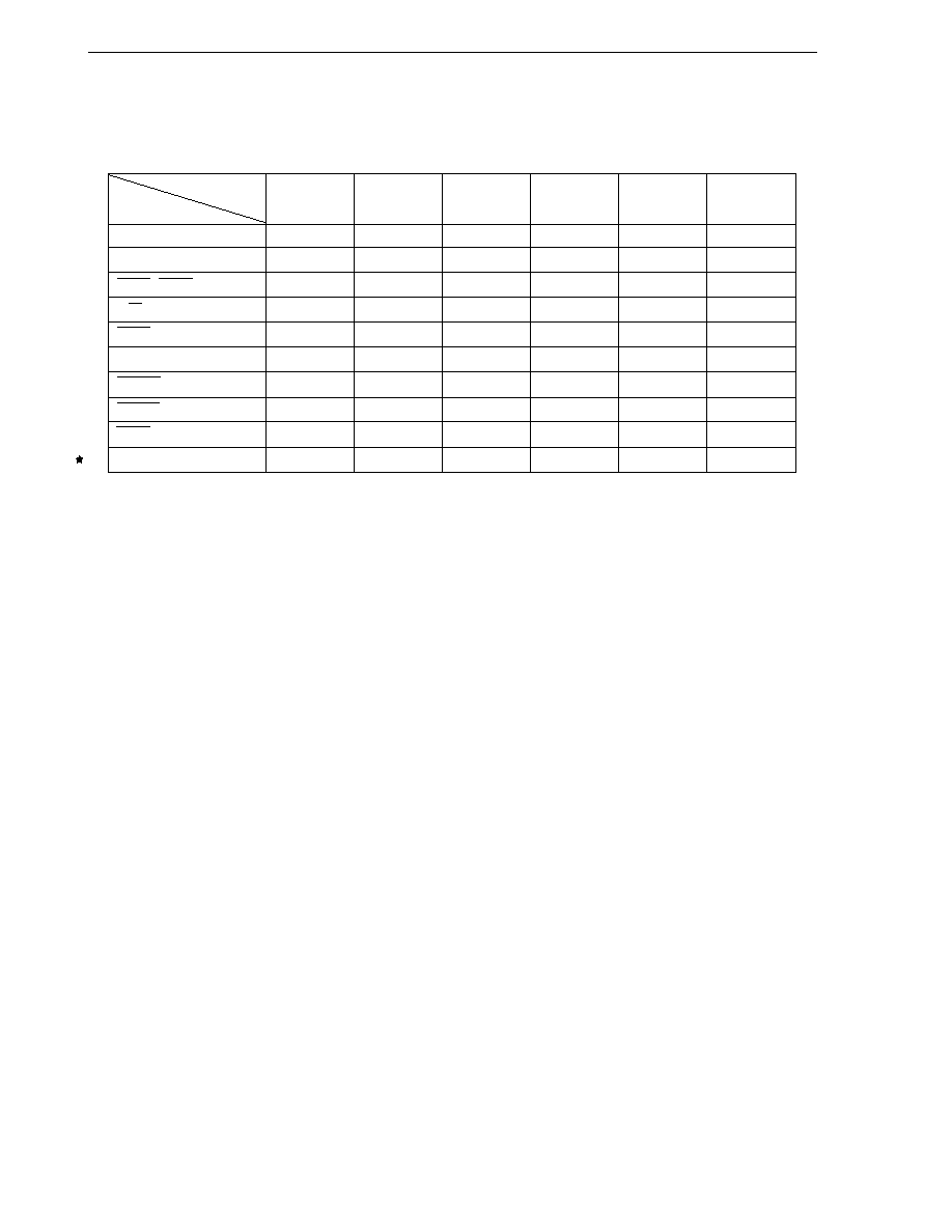
34
CHAPTER 2 PIN FUNCTIONS
User's Manual U10913EJ6V0UM
2.2 Pin Status
The operating status of each pin in each operation mode is as follows.
AD0 to AD15
Hi-Z
Hi-Z
Hi-Z
Hi-Z
Hi-Z
Hi-Z
A16 to A19
Hi-Z
Hi-Z
Hi-Z
Hi-Z
Retained
Note 1
Retained
LBEN, UBEN
Hi-Z
Hi-Z
Hi-Z
Hi-Z
Retained
Note 1
Retained
R/W
Hi-Z
Hi-Z
Hi-Z
Hi-Z
H
H
DSTB
Hi-Z
Hi-Z
Hi-Z
Hi-Z
H
H
ASTB
Hi-Z
Hi-Z
Hi-Z
Hi-Z
H
H
HLDRQ
Operating
Operating
Operating
HLDAK
Hi-Z
Hi-Z
Hi-Z
L
Operating
Operating
WAIT
CLKOUT
Hi-Z
L
L
Operating
Note 2
Operating
Note 2
Operating
Note 2
Hi-Z:
High-impedance
Retained: Retains status in external bus cycle immediately before
L:
Low-level output
H:
High-level output
:
Input not sampled
Notes
1. Undefined immediately after the end of bus hold.
2. In clock output inhibit mode, the operating status is low-level output (L).
Operating Status
Pin
Reset
Bus Hold
Idle State
IDLE Mode
HALT Mode
STOP Mode

35
CHAPTER 2 PIN FUNCTIONS
User's Manual U10913EJ6V0UM
2.3 Pin Functions
(1) P00 to P07 (Port 0) ... 3-state I/O
These pins constitute an 8-bit I/O port, port 0. They also serve as control signal pins.
P00 to P07 function not only as I/O port pins, but also as the I/O pins of the real-time pulse unit (RPU) and
external interrupt request input pins. Each bit of port 0 can be specified in the port or control mode by the
port 0 mode control register (PMC0).
(a) Port mode
P00 to P07 can be set in the input or output mode in 1-bit units by the port 0 mode register (PM0).
(b) Control mode
P00 to P07 can be set in the port or control mode in 1-bit units by the PMC0 register.
(i)
TO110, TO111 (Timer Output) ... output
These pins output pulse signals from timer 1.
(ii)
TCLR11 (Timer Clear) ... input
This pin inputs an external clear signal to timer 1.
(iii) TI11 (Timer Input) ... input
This pin inputs an external count clock to timer 1.
(iv) INTP110 to INTP113 (Interrupt Request from Peripherals) ... input
These pins are the external interrupt request input pins of timer 1.
(v)
ADTRG (AD Trigger Input) ... input
This pin inputs an external trigger to A/D converter.
(2) P10 to P17 (Port 1) ... 3-state I/O
These pins constitute an 8-bit I/O port, port 1, which can be set in the input or output mode in 1-bit units.
P10 to P17 function not only as ports, but also as the I/O pins of the RPU, external interrupt request input
pins, and serial interface (CSI2) I/O pins. Each bit of port 1 can be specified in the port or control mode by
the port 1 mode control register (PMC1).
(a) Port mode
P10 to P17 can be set in the input or output mode in 1-bit units by the port 1 mode register (PM1).
(b) Control mode
P10 to P17 can be set in the port or control mode in 1-bit units by the PMC1 register.
(i)
TO120, TO121 (Timer Output) ... output
These pins output pulse signals from timer 1.
(ii)
TCLR12 (Timer Clear) ... input
This pin inputs an external clear signal to timer 1.

36
CHAPTER 2 PIN FUNCTIONS
User's Manual U10913EJ6V0UM
(iii) TI12 (Timer Input) ... input
This pin inputs an external count clock to timer 1.
(iv) INTP120 to INTP123 (Interrupt Request from Peripherals) ... input
These pins are the external interrupt request input pins of timer 1.
(v)
SO2 (Serial Output 2) ... output
This pin outputs serial transmit data from CSI.
(vi) SI2 (Serial Input 2) ... input
This pin inputs serial receive data to CSI.
(vii) SCK2 (Serial Clock 2) ... 3-state I/O
This pin inputs/outputs serial clock to/from CSI.
(3) P20 to P27 (Port 2) ... 3-state I/O
These pins constitute an I/O port, port 2, which can be set in the input or output mode in 1-bit units. These
pins function not only as port pins but also as PWM output pins and I/O pins for the serial interface
(UART0, 1/CSI0, 1).
Each bit of this port can be specified in the port or control mode by the port 2 mode control register (PMC2).
(a) Port mode
P20 to P27 can be set in the input or output mode in 1-bit units by the port 2 mode register (PM2).
(b) Control mode
P20 to P27 can be set in the port or control mode in 1-bit units by the PMC2 register.
(i)
PWM0, PWM1 (Pulse Width Modulation) ... output
These pins output pulse signals from PWM.
(ii)
TXD0, TXD1 (Transmit Data) ... output
These pins output serial transmit data from UART.
(iii) RXD0, RXD1 (Receive Data) ... input
These pins input serial receive data to UART.
(iv) SO0, SO1 (Serial Output 0, 1) ... output
These pins output serial transmit data from CSI.
(v)
SI0, SI1 (Serial Input 0, 1) ... input
These pins input serial receive data to CSI.
(vi) SCK0, SCK1 (Serial Clock 0, 1) ... 3-state I/O
These pins input/output serial clock to/from CSI.

37
CHAPTER 2 PIN FUNCTIONS
User's Manual U10913EJ6V0UM
(4) P30 to P37 (Port 3) ... 3-state I/O
These pins constitute an 8-bit I/O port, port 3. They also function as control signal pins. P30 to P37 function
not only as I/O port pins but also as I/O pins for the RPU, external interrupt request pins, and serial interface
(CSI3) I/O pins in the control mode.
(a) Port mode
P30 to P37 can be set in the input or output mode in 1-bit units by the port 3 mode register (PM3).
(b) Control mode
P30 to P37 can be set in the port or control mode in 1-bit units by the PMC3 register.
(i)
TO130, TO131 (Timer Output) ... output
These pins output pulse signals from timer 1.
(ii)
TCLR13 (Timer Clear) ... input
This pin inputs an external clear signal to timer 1.
(iii) TI13 (Timer Input) ... input
This pin inputs an external count clock to timer 1.
(iv) INTP130 to INTP133 (Interrupt Request from Peripherals) ... input
These pins are the external interrupt request input pins of timer 1.
(v)
SO3 (Serial Output 3) ... output
This pin outputs the serial transmit data of CSI.
(vi) SI3 (Serial Input 3) ... input
This pin inputs the serial receive data of CSI.
(vii) SCK3 (Serial Clock 3) ... 3-state I/O
This pin inputs/outputs the serial clock of CSI.
(5) P40 to P47 (Port 4) ... 3-state I/O
These pins constitute an 8-bit I/O port, port 4. They also form a portion of the address/data bus connected
to external memory.
P40 to P47 function not only as I/O port pins but also as multiplexed address/data bus pins (AD0 to AD7) in
the control mode (external expansion mode) when an external memory is connected.
Each bit of this port can be set in the port or control mode in 1-bit units by the memory expansion mode register
(MM).
(a) Port mode
P40 to P47 can be set in the input or output port mode in 1-bit units by the port 4 mode register (PM4).
(b) Control mode (External Expansion Mode)
P40 to P47 can be specified as AD0 to AD7 by the MM register.

38
CHAPTER 2 PIN FUNCTIONS
User's Manual U10913EJ6V0UM
(i)
AD0 to AD7 (Address/Data 0 to 7) ... 3-state I/O
These pins constitute a multiplexed address/data bus when the external memory is accessed. They
function as the A0 to A7 output pins of a 20-bit address in the address timing state (T1), and as the
lower 8-bit data I/O bus pins of 16-bit data in the data timing state (T2, TW, T3).
The output status of these pins changes in synchronization with the rising edge of the clock in each
state of the bus cycle. AD0 to AD7 go into a high-impedance state in the idle state (TI).
(6) P50 to P57 (Port 5) ... 3-state I/O
These pins constitute an 8-bit I/O port, port 5. They also form a portion of the address/data bus connected
to external memory.
P50 to P57 function not only as I/O port pins but also as multiplexed address/data bus pins (AD8 to AD15)
in the control mode (external expansion mode) when an external memory is connected.
Each bit of this port can be set in the port or control mode in 1-bit units by the memory expansion mode register
(MM).
(a) Port mode
P50 to P57 can be set in the input or output port mode in 1-bit units by the port 5 mode register (PM5).
(b) Control mode (External Expansion Mode)
P50 to P57 can be specified as AD8 to AD15 by the MM register.
(i)
AD8 to AD15 (Address/Data 8 to 15) ... 3-state I/O
These pins constitute a multiplexed address/data bus when the external memory is accessed. They
function as the A8 to A15 output pins of a 20-bit address in the address timing state (T1), and as
the higher 8-bit data I/O bus pins of 16-bit data in the data timing state (T2, TW, T3).
The output status of these pins changes in synchronization with the rising of the clock in each state
of the bus cycle. AD8 to AD15 go into a high-impedance state in the idle state (TI).
(7) P60 to P63 (Port 6) ... 3-state I/O
These pins constitute a 4-bit I/O port, port 6. They also form a portion of the address bus connected to external
memory.
P60 to P63 function not only as I/O port pins but also as address bus pins (A16 to A19) in the control mode
(external expansion mode) when an external memory is connected. This port can be set in the port or control
mode in 2-bit units by the memory expansion mode register (MM).
(a) Port mode
P60 to P63 can be set in the input or output port mode in 1-bit units by the port 6 mode register (PM6).
(b) Control mode (External Expansion Mode)
P60 to P63 can be specified as A16 to A19 by the MM register.
(i)
A16 to A19 (Address 16 to 19) ... output
These pins constitute the higher 4 bits of a 20-bit address bus when the external memory is accessed.
The output status of these pins changes in synchronization with the rising edge of the clock in the
T1 state. During the idle state (TI), the address of the bus cycle immediately before entering the
idle state is retained.

39
CHAPTER 2 PIN FUNCTIONS
User's Manual U10913EJ6V0UM
(8) P70 to P77 (Port 7) ... input
Port 7 is an 8-bit input-only port whose pins are all fixed to input.
P70 to P77 function as input ports, as well as A/D converter analog inputs in the control mode. However, the
input port and analog input pin cannot be switched.
(a) Port mode
P70 to P77 are dedicated input ports.
(b) Control mode
P70 to P77 also function as the ANI0 to ANI7 pins and cannot be switched.
(i)
ANI0 to ANI7 (Analog Input) ... input
These pins are analog input pins for the A/D converter.
To prevent malfunction due to noise, connect a capacitor between these pins and AV
SS
.
Make sure that a voltage outside the range of AV
SS
and AV
REF
is not applied to the input pin used
for A/D converter input. If there is the possibility that noise whose voltage is AV
REF
or more or noise
whose voltage is AV
SS
or less may be generated, clamp the voltage using a diode with a small V
F
.
(9) P90 to P96 (Port 9) ... 3-state I/O
These pins constitute a 7-bit I/O port, port 9, and are also used to output control signals.
P90 to P96 function not only as I/O port pins, but also as control signal output pins and bus hold control signal
I/O pins when an external memory is used in the control mode (external expansion mode).
If port 9 is accessed in 8-bit units, the higher 1-bit is ignored if the access is a write, and undefined if the access
is a read.
This port can be set in the port or control mode in 1-bit units by the memory expansion mode register (MM).
(a) Port mode
P90 to P96 can be set in the input or output port mode in 1-bit units by the port 9 mode register (PM9).
(b) Control mode (External Expansion Mode)
P90 to P96 can be used to output control signals when so specified by the MM register when an external
memory is used.
(i)
LBEN (Lower Byte Enable) ... output
This is the lower byte enable signal of the 16-bit external data bus.
This signal changes in synchronization with the rising edge of the clock in the T1 state of the bus
cycle. The status of the bus signal remains unchanged in the idle state (TI).
(ii)
UBEN (Upper Byte Enable) ... output
This is the upper byte enable signal of the 16-bit external data bus. It becomes inactive (high) during
byte access to an even address and becomes active (low) during byte access to an odd address.
This signal changes in synchronization with the rising of the clock in the T1 state of the bus cycle.
The status of the bus signal remains unchanged in the idle state (TI).
Access
UBEN
LBEN
A0
Word Access
0
0
0
Halfword Access
0
0
0
Byte Access
Even address
1
0
0
Odd address
0
1
1

40
CHAPTER 2 PIN FUNCTIONS
User's Manual U10913EJ6V0UM
(iii) R/W (Read/Write Status) ... output
This is a status signal that indicates whether the bus cycle for external access is a read or write cycle.
It goes high in the read cycle and low in the write cycle.
This signal changes in synchronization with the rising edge of the clock in the T1 state of the bus
cycle. It goes high in the idle state (TI).
(iv) DSTB (Data Strobe) ... output
This is the access strobe signal of the external data bus.
It becomes active (low) in the T2 or TW state of the bus cycle, and becomes inactive (high) in the
idle state (TI).
(v)
ASTB (Address Strobe) ... output
This is the latch strobe signal of the external address bus.
It becomes active (low) in synchronization with the falling edge of the clock in the T1 state of the
bus cycle, and becomes inactive (high) in synchronization with the falling edge of the clock in the
T3 state. It goes high in the idle state (TI).
(vi) HLDAK (Hold Acknowledge) ... output
This is an acknowledge signal output pin that indicates that the V853 has set the address bus, data
bus, and control bus in the high-impedance state in response to a bus hold request.
As long as this signal is active, the address bus, data bus, and control bus remain in a high impedance
state.
(vii) HLDRQ (Hold Request) ... input
This input pin is used by an external device to request that the V853 relinquish control of the address
bus, data bus, and control bus. This signal can be input asynchronously to CLKOUT. When this
signal becomes active, the V853 sets the address bus, data bus, and control bus in the high-
impedance state, after the current bus cycle completes. If there is no current bus activity, the address
bus, data bus, and control bus are immediately set to high-impedance. HLDAK is then made active
and the bus and control lines are released.
(10) P110 to P117 (Port 11) ... 3-state I/O
Port 11 is an 8-bit I/O port that can be set in the input or output mode in 1-bit units. In addition to the function
as a port, the pins constituting port 11 are used as input/output of RPU and external interrupt request.
(a) Port mode
P110 to P117 can be set in the input or output mode, in 1-bit units, by the port mode register (PM11).
(b) Control mode
P110 to P117 can be set in the port or control mode, in 1-bit units, by port 11 mode control register
(PMC11).
(i)
TO140, TO141 (Timer Output) ... output
These pins output pulse signals from timer 1.
(ii)
TCLR14 (Timer Clear) ... input
This pin inputs an external clear signal to timer 1.
(iii) TI14 (Timer Input) ... input

41
CHAPTER 2 PIN FUNCTIONS
User's Manual U10913EJ6V0UM
This pin inputs an external count clock to timer 1.
(iv) INTP140 to INTP143 (Interrupt Request from Peripherals) ... input
These pins are the external interrupt request input pins of timer 1.
(11) CLKOUT (Clock Output) ... output
This pin outputs the system clock. In the single-chip mode, this pin does not output the CLKOUT signal until
the PSC register is set.
(12) WAIT (Wait) ... input
This control signal input pin inserts a data wait state to the bus cycle, and can be activated asynchronously
to CLKOUT. This pin is sampled at the falling edge of the clock in the T2 and TW states of the bus cycle.
If the set/hold time for the sampling timing is not satisfied, the wait state may not be inserted.
(13) MODE (Mode) ... input
This pin specifies the value after the clock control register (CKC) is reset.
MODE
Value after CKC Register Reset
0
03H
1
00H
For details, refer to 6.3.3 Clock control register (CKC).
(14) RESET (Reset) ... input
The RESET signal is an asynchronous input signal. A valid low-level signal on the RESET pin initiates a system
reset, regardless of the clock operation.
In addition to normal system initialization/start functions, the RESET signal is also used for exiting power save
modes (HALT, IDLE, or STOP).
(15) X1, X2 (Crystal) ... input
An oscillator for system clock generation is connected across these pins.
An external clock source can also be referenced by connecting the external clock input to the X1 pin and leaving
the X2 pin open.
(16) CV
DD
(Power Supply for Clock Generator)
This pin supplies positive power to the internal clock generator.
(17) CKSEL (Clock Select) ... input
This pin specifies the operation mode of clock generator. The input value of this pin cannot be changed during
operation.
(18) CV
SS
(Ground for Clock Generator)
This is the ground pin of the internal clock generator.
(19) V
DD
(Power Supply)
This pin supplies positive power. Connect all the V
DD
pins to a positive power supply.

42
CHAPTER 2 PIN FUNCTIONS
User's Manual U10913EJ6V0UM
(20) V
SS
(Ground)
This is a ground pin. Connect all the V
SS
pins to ground.
(21) AV
DD
(Analog Power Supply)
Analog power supply pin for A/D converter.
(22) AV
SS
(Analog Ground)
Ground pin for A/D converter.
(23) AV
REF1
to AV
REF3
(Analog Reference Voltage) ... input
Reference voltage supply pins for A/D and D/A converter.
(24) ANO0, ANO1 (Analog Output) ... output
Analog output pins for D/A converter.
(25) NMI (Non-Maskable Interrupt Request) ... input
This pin inputs non-maskable interrupt requests.
(26) V
PP
(Programming Power Supply)
This pin supplies positive power for the flash memory programming mode.
This pin is for the
µ
PD70F3003A, 70F3025A.
(27) IC (Internally Connected)
This is internal connection pin. Connect to V
SS
directly.
This pin is for the
µ
PD703003A, 703004A, and 703025A.
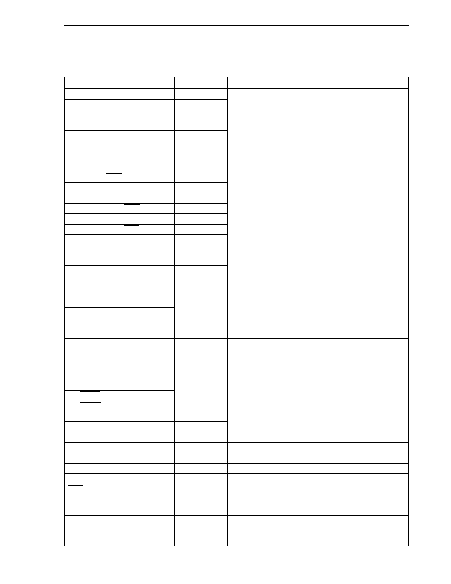
43
CHAPTER 2 PIN FUNCTIONS
User's Manual U10913EJ6V0UM
2.4 Pin I/O Circuits and Recommended Connection of Unused Pins
When connected to V
DD
or V
SS
via a resistor, it is recommended to use a resistor of 1 to 10 k
.
Pin
I/O Circuit Type
Recommended Connection
P00/TO110, P01/TO111
5
Input:
Independently connect to V
DD
or V
SS
via a resistor
P02/TCLR11, P03/TI11
8
Output: Leave open
P04/INTP110 to P07/INTP113/ADTRG
P10/TO120, P11/TO121
5
P12/TCLR12, P13/TI12
8
P14/INTP120
P15/INTP121/SO2
P16/INTP122/SI2
P17/INTP123/SCK2
P20/PWM0, P21/PWM1
5
P22/TXD0/SO0
P23/RXD0/SI0, P24/SCK0
8
P25/TXD1/SO1
5
P26/RXD1/SI1, P27/SCK1
8
P30/TO130, P31/TO131
5
P32/TCLR13, P33/TI13
8
P34/INTP130
P35/INTP131/SO3
10-A
P36/INTP132/SI3
P37/INTP133/SCK3
P40/AD0 to P47/AD7
5
P50/AD8 to P57/AD15
P60/A16 to P63/A19
P70/ANI0 to P77/ANI7
9
Directly connect to V
SS
P90/LBEN
5
Input: Independently connect to V
DD
or V
SS
via a resistor
P91/UBEN
Output: Leave open
P92/R/W
P93/DSTB
P94/ASTB
P95/HLDAK
P96/HLDRQ
P110/TO140, P111/TO141
P112/TCLR14, P113/TI14
8
P114/INTP140 to P117/INTP143
ANO0, ANO1
12
Leave open
NMI
2
Directly Connect to V
SS
CLKOUT
3
Leave open
CV
DD
/CKSEL
2
--
WAIT
1
Directly connect to V
DD
MODE
2
--
RESET
AV
REF1
to AV
REF3
, AV
SS
Directly connect to V
SS
AV
DD
Directly connect to V
DD
V
PP
Connect to V
SS
via a resistor (R
VPP
)
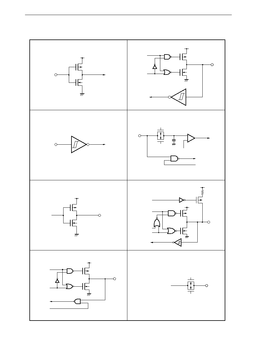
44
CHAPTER 2 PIN FUNCTIONS
User's Manual U10913EJ6V0UM
2.5 Pin I/O Circuits
Type 1
Type 2
Type 8
Type 3
P-ch
N-ch
IN
V
DD
IN
Schmitt-triggered input with hysteresis characteristics
P-ch
N-ch
V
DD
OUT
P-ch
N-ch
V
DD
IN/OUT
Data
Output
disable
Type 5
P-ch
N-ch
V
DD
IN/OUT
Data
Output
disable
Input
enable
IN
Comparator
+
V
REF
(threshold voltage)
P-ch
N-ch
Input enable
Type 9
Data
Output disable
P-ch
IN/OUT
V
DD
N-ch
P-ch
V
DD
Pullup
enable
Open-drain
Type 10-A
OUT
Analog output voltage
Type 12
P-ch
N-ch

45
User's Manual U10913EJ6V0UM
CHAPTER 3 CPU FUNCTIONS
The CPU of the V853 is based on RISC architecture and executes most instructions in one clock cycle by using
a 5-stage pipeline.
3.1 Features
Minimum instruction cycle: 30 ns (at 33 MHz operation)
Address space: 16 MB linear
32-bit general-purpose registers
×
32
Internal 32-bit architecture
Five-stage pipeline control
Multiplication/division instructions
Saturated operation instructions
32-bit shift instruction: 1 clock
Long/short instruction format
Four types of bit manipulation instructions
· SET1
· CLR1
· NOT1
· TST1
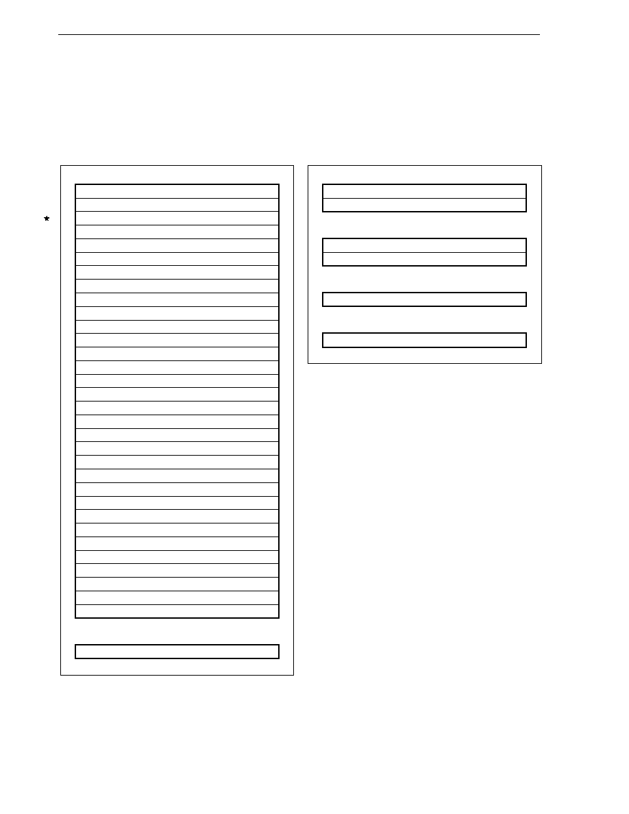
46
CHAPTER 3 CPU FUNCTIONS
User's Manual U10913EJ6V0UM
3.2 CPU Register Set
The registers of the V853 can be classified into two categories: a general-purpose program register set and a
dedicated system register set. All the registers are 32 bits wide.
For details, refer to V850 Family Architecture User's Manual.
r0
r1
r2
r3
r4
r5
r6
r7
r8
r9
r10
r11
r12
r13
r14
r15
r16
r17
r18
r19
r20
r21
r22
r23
r24
r25
r26
r27
r28
r29
r30
r31
Zero Register
Reserved for Address Generation
Stack Pointer (SP)
Global Pointer (GP)
Text Pointer (TP)
Element Pointer (EP)
Link Pointer (LP)
PC
Program Counter
PSW
Program Status Word
ECR
Exception Cause Register
FEPC
FEPSW
Fatal Error PC
Fatal Error PSW
EIPC
EIPSW
Exception/Interrupt PC
Exception/Interrupt PSW
31
0
31
0
31
0
31
0
31
0
31
0
System register set
Program register set
47
CHAPTER 3 CPU FUNCTIONS
User's Manual U10913EJ6V0UM
3.2.1 Program register set
The program register set includes general-purpose registers and a program counter.
(1) General-purpose registers
Thirty-two general-purpose registers, r0 to r31, are available. Any of these registers can be used as a data
variable or address variable.
However, r0 and r30 are implicitly used by instructions, and care must be exercised when using these registers.
Also, r1, r3 to r5 and r31 are implicitly used by the assembler and C compiler. Therefore, before using these
registers, their contents must be saved so that they are not lost. The contents must be restored to the registers
after the registers have been used. In some case, r2 is used by the real-time OS. Consequently, r2 can be
used as a variable register only when r2 is not used by the real-time OS to be used.
Table 3-1. Program Registers
Name
Usage
Operation
r0
Zero register
Always holds 0
r1
Assembler-reserved register
Working register for generating immediate
r2
Address/data variable registers (when r2 is not used by the real-time OS to be used)
r3
Stack pointer
Used to generate stack frame when function is called
r4
Global pointer
Used to access global variable in data area
r5
Text pointer
Register to indicate the start of the text area
Note
r6 to r29
Address/data variable registers
r30
Element pointer
Base pointer register when memory is accessed
r31
Link pointer
Used by compiler when calling function
PC
Program counter
Holds instruction address during program execution
Note
Area where program code is allocated.
(2) Program counter
This register holds the address of the instruction under execution. The lower 24 bits of this register are valid,
and bits 31 to 24 are fixed to 0. If a carry occurs from bit 23 to 24, it is ignored.
Bit 0 is fixed to 0, and branching to an odd address cannot be performed.
Figure 3-1. Program Counter (PC)
31
Fixed to 0
24 23
Instruction address under execution
1 0
0
PC
After reset
00000000H
48
CHAPTER 3 CPU FUNCTIONS
User's Manual U10913EJ6V0UM
3.2.2 System register set
System registers control the status of the CPU and hold interrupt information.
Table 3-2. System Register Numbers
To read/write these system registers, specify the system register number indicated by the system register load/
store instruction (LDSR or STSR instruction).
Figure 3-2. Interrupt Source Register (ECR)
Bit position
Bit name
Function
31 to 16
FECC
Fatal Error Cause Code
Exception code of NMI (refer to Table 5-1 Interrupt List)
15 to 0
EICC
Exception/Interrupt Cause Code
Exception code of exception/interrupt (refer to Table 5-1 Interrupt List)
System Register Name
No.
0
1
2
3
4
5
6 to 31
Usage
Operation
These registers save the PC and PSW when an exception
or interrupt occurs. Because only one set of these
registers is available, their contents must be saved when
multiple interrupts are enabled.
These registers save PC and PSW when NMI occurs.
If an exception, maskable interrupt, or NMI occurs, this
register will contain information referencing the interrupt
source. The high-order 16 bits of this register are called
FECC, to which exception code of NMI is set. The low-
order 16 bits are called EICC, to which exception code
of exception/interrupt is set (refer to Figure 3-2).
Program status word is collection flags that indicate
program status (instruction execution result) and CPU
status (refer to Figure 3-3).
EIPC
EIPSW
FEPC
FEPSW
ECR
PSW
Status saving registers during
interrupt
Status saving registers for NMI
Interrupt source register
Reserved
Program status word
31
FECC
16 15
EICC
0
0
ECR
After reset
00000000H

49
CHAPTER 3 CPU FUNCTIONS
User's Manual U10913EJ6V0UM
Figure 3-3. Program Status Word (PSW)
Bit position
Bit name
Function
31 to 8
RFU
Reserved field (fixed to 0)
7
NP
Indicates that non-maskable interrupt (NMI) servicing is in progress. This flag is
set when an NMI is acknowledged, and disables multiple interrupts.
0: NMI servicing not under execution.
1: NMI servicing under execution.
6
EP
Indicates that exception processing is in progress. This flag is set when an
exception is generated. Moreover, interrupt requests can be acknowledged
when this bit is set.
0: Exception processing not under execution.
1: Exception processing under execution.exception is generated.
5
ID
Indicates whether a maskable interrupt request can be acknowledged or not.
0: Interrupt enabled.
1: Interrupt disabled.
4
SAT
Note
Indicates that the operation result of a saturated operation processing
instruction is saturated due to overflow. Due to the cumulative flag, if the
operation result is saturated by the saturation operation instruction, this bit is
set (1), but is not cleared (0) even if the operation results of subsequent
instructions are not saturated. To clear (0) this bit, load data in PSW. Note
that in a general arithmetic operation, this bit is neither set (1) nor cleared (0).
0: Not saturated.
1: Saturated.
3
CY
This flag is set if a carry or borrow occurs as the result of an operation (if a
carry or borrow does not occur, it is reset).
0: Carry or borrow does not occur.
1: Carry or borrow occurs.
2
OV
Note
This flag is set if an overflow occurs during operation (if an overflow does not
occur, it is reset).
0: Overflow does not occur.
1: Overflow occurs.
1
S
Note
This flag is set if the result of an operation is negative (it is reset if the result
is positive).
0: The operation result was positive or 0.
1: The operation result was negative.
0
Z
This flag is set if the result of an operation is zero (if the result is not zero, it
is reset).
0: The operation result was not 0.
1: The operation result was 0.
Note
The result of a saturation-processed operation is determined by the contents of the OV and S flags in the
saturation operation. Simply setting the OV flag (1) will set the SAT flag (1) in a saturation operation.
Status of operation result
Flag status
Saturation-processed
SAT
OV
S
operation result
Maximum positive value exceeded
1
1
0
7FFFFFFFH
Maximum negative value exceeded
1
1
1
80000000H
Positive (not exceeding the maximum)
0
0
Operation result itself
Negative (not exceeding the maximum)
1
31
RFU
1 0
Z
PSW
2
S
3
OV
4
CY
5
SAT
6
ID
7
EP
8
NP
After reset
00000020H
Retains
the value
before
operation

50
CHAPTER 3 CPU FUNCTIONS
User's Manual U10913EJ6V0UM
3.3 Operation Modes
3.3.1 Operation modes
The V853 has the following operation modes.
(1) Normal operation mode (Single-chip mode)
After the system has been released from the reset status, the pins related to the bus interface are set to port
mode, execution branches to the reset entry address of the internal ROM, and instruction processing is started.
However, access to external memory and peripheral devices can be enabled by setting the external memory
expansion mode register using an instruction (MM: refer to 3.4.7).
(2) Flash memory programming mode (
µµ
µµ
µ
PD70F3003A and 70F3025A only)
Specifying this mode enables the program operations to the internal flash memory via the flash programmer.
3.3.2 Specifying operation mode
(1) Normal operation mode
The operation mode is fixed to single-chip mode.
(2) Flash memory programming mode
The operation mode of the V853 is specified depending on the MODE pin and V
PP
pin. The MODE pin
specification should be fixed in the application system and should not be changed during operation.
The operation is not guaranteed if the status is changed during operation.
Pin Status
Operation Mode
V
PP
MODE
0 V
1
Normal operation mode
10.3 V
1
Flash memory programming mode
Refer to CHAPTER 14 FLASH MEMORY (
µµ
µµ
µ
PD70F3003A AND 70F3025A).
51
CHAPTER 3 CPU FUNCTIONS
User's Manual U10913EJ6V0UM
3.4 Address Space
3.4.1 CPU address space
The CPU of the V853 is of 32-bit architecture and supports up to 4 GB of linear address space (data space) during
operand addressing (data access). When referencing instruction addresses, a linear address space (program space)
of up to 16 MB is supported.
Figure 3-4 shows the CPU address space.
Figure 3-4. CPU Address Space
FFFFFFFFH
CPU address space
Program area
(16 MB linear)
Data area
(4 GB linear)
01000000H
00FFFFFFH
00000000H
52
CHAPTER 3 CPU FUNCTIONS
User's Manual U10913EJ6V0UM
3.4.2 Image
The core CPU supports 4 GB of "virtual" addressing space, or 256 memory blocks, each containing 16 MB memory
locations. In actuality, the same 16 MB block is accessed regardless of the values of bits 31 to 24 of the CPU address.
Figure 3-5 shows the image of the virtual addressing space.
Because the higher 8 bits of a 32-bit CPU address are ignored and the CPU address is only seen as a 24-bit external
physical address, the physical location XX000000H is equally referenced by multiple address values 00000000H,
010000000H, 02000000H... through FE000000H, FF000000H.
Figure 3-5. Image on Address Space
FFFFFFFFH
FF000000H
FEFFFFFFH
Image
CPU address space
Image
Image
Image
Image
FE000000H
FDFFFFFFH
02000000H
01FFFFFFH
01000000H
00FFFFFFH
00000000H
Physical address space
Peripheral I/O
Internal RAM
External memory
Internal ROM
XXFFFFFFH
XX000000H

53
CHAPTER 3 CPU FUNCTIONS
User's Manual U10913EJ6V0UM
3.4.3 Wrap-around of CPU address space
(1) Program space
Of the 32 bits of the PC (program counter), the higher 8 bits are set to 0, and only the lower 24 bits are valid.
Even if a carry or borrow occurs from bit 23 to 24 as a result of branch address calculation, the higher 8 bits
ignore the carry or borrow and remain 0.
Therefore, the lower-limit address of the program space, address 00000000H, and the upper-limit address
00FFFFFFH become contiguous addresses. Wrap-around refers to the situation that the lower-limit address
and upper-limit address become contiguous like this.
Caution No instruction can be fetched from the 4 KB area of 00FFF000H to 00FFFFFFH because this
area is defined as peripheral I/O area. Therefore, do not execute any branch operation
instructions in which the destination address will reside in any part of this area.
(2) Data space
The result of operand address calculation that exceeds 32 bits is ignored.
Therefore, the lower-limit address of the program space, address 00000000H, and the upper-limit address
FFFFFFFFH are contiguous addresses, and the data space is wrapped around at the boundary of these
addresses.
00FFFFFEH
00FFFFFFH
00000000H
00000001H
Program space
Program space
(+) direction
() direction
FFFFFFFEH
FFFFFFFFH
00000000H
00000001H
Data space
Data space
(+) direction
() direction
54
CHAPTER 3 CPU FUNCTIONS
User's Manual U10913EJ6V0UM
(1) For
µµ
µµ
µ
PD703003A, 70F3003A, and 703004A
Note
Although the program space of the V853 is 16 MB, the space for physical external memory is 1 MB (see
Figure 3-6).
3.4.4 Memory map
Area is reserved in the V853 as shown below. The external expansion mode is specified by the MM register.
XXFFFFFFH
Peripheral I/O area
Internal RAM area
(access prohibited)
Internal
ROM area
Internal
ROM area
Peripheral I/O area
Internal RAM area
External memory
area
Note
Single-chip mode
Single-chip mode
(external expansion mode)
16 MB
1 MB
4 KB
XXFFF000H
XXFFEFFFH
XX100000H
XX0FFFFFH
XX000000H
XXFFE000H
XXFFDFFFH
4 KB
55
CHAPTER 3 CPU FUNCTIONS
User's Manual U10913EJ6V0UM
(2) For
µµ
µµ
µ
PD703025A and 70F3025A
Note
Although the program space of the V853 is 16 MB, the space for physical external memory is 1 MB
(see Figure 3-6).
XXFFFFFFH
Peripheral I/O area
Internal RAM area
(access prohibited)
Internal
ROM area
Internal
ROM area
Peripheral I/O area
Internal RAM area
External memory
area
Note
Single-chip mode
Single-chip mode
(external expansion mode)
16 MB
1 MB
4 KB
XXFFF000H
XXFFEFFFH
XX100000H
XX0FFFFFH
XX000000H
XXFFC000H
XXFFBFFFH
12 KB
56
CHAPTER 3 CPU FUNCTIONS
User's Manual U10913EJ6V0UM
3.4.5 Area
(1) Internal ROM area
(a) Memory map
<1>
µ
PD703003A and 70F3003A
A 1 MB area in addresses 000000H to 0FFFFFH is reserved for the internal ROM area, and 128 KB
area in addresses 000000H to 01FFFFH is provided for physical internal ROM. The image of
000000H to 01FFFFH can be seen in the remaining area (020000H to 0FFFFFH).
XX0FFFFFH
XX0E0000H
XX0DFFFFH
XX040000H
XX03FFFFH
XX020000H
XX01FFFFH
XX000000H
Image
Image
Image
Physical internal ROM
01FFFFH
000000H
Interrupt/exception table
57
CHAPTER 3 CPU FUNCTIONS
User's Manual U10913EJ6V0UM
<2>
µ
PD703004A
A 1 MB area in addresses 000000H to 0FFFFFH is reserved for the internal ROM area, 96 KB area
in addresses 000000H to 017FFFH is provided for physical internal ROM, and 32 KB area in
addresses 018000H to 01FFFFH is undefined. Also the image of 000000H to 01FFFFH can be seen
in the remaining area (020000H to 0FFFFFH).
X X 0 F F F F F H
X X 0 E 0 0 0 0 H
X X 0 D F F F F H
0 1 F F F F H
0 0 0 0 0 0 H
0 1 8 0 0 0 H
0 1 7 F F F H
X X 0 4 0 0 0 0 H
X X 0 3 F F F F H
X X 0 2 0 0 0 0 H
X X 0 1 F F F F H
X X 0 0 0 0 0 0 H
Image
Image
Image
Physical internal ROM
Undefined
Interrupt/exception table
58
CHAPTER 3 CPU FUNCTIONS
User's Manual U10913EJ6V0UM
<3>
µ
PD703025A and 70F3025A
A 1 MB area in addresses 000000H to 0FFFFFH is reserved for the internal ROM area, and 256 KB
area in addresses 000000H to 03FFFFH is provided for physical internal ROM. Also, the image of
000000H to 03FFFFH can be seen in the remaining area (040000H to 0FFFFFH).
XX0FFFFFH
XX0C0000H
XX0BFFFFH
XX080000H
XX07FFFFH
03FFFFH
000000H
XX040000H
XX03FFFFH
XX000000H
Image
Image
Image
Interrupt/exception table
Physical internal ROM
Image
(b) Interrupt/exception table
The V853 increases the interrupt response speed by assigning destination addresses corresponding to
interrupts/exceptions.
The collection of these destination addresses is called an interrupt/exception table, which is located in
the internal ROM area. When an interrupt/exception request is granted, execution jumps to the
corresponding destination address, and the program written at that memory address is executed. Table
3-3 shows the sources of interrupts/exceptions, and the corresponding addresses.

59
CHAPTER 3 CPU FUNCTIONS
User's Manual U10913EJ6V0UM
Table 3-3. Interrupt/Exception Table
Start Address of Interrupt/Exception Table
Interrupt/Exception Source
00000000H
RESET
00000010H
NMI
00000040H
TRAP0n (n = 0 to FH)
00000050H
TRAP1n (n = 0 to FH)
00000060H
ILGOP
00000080H
INTOV11
00000090H
INTOV12
000000A0H
INTOV13
000000B0H
INTOV14
000000C0H
INTP110/INTCC110
000000D0H
INTP111/INTCC111
000000E0H
INTP112/INTCC112
000000F0H
INTP113/INTCC113
00000100H
INTP120/INTCC120
00000110H
INTP121/INTCC121
00000120H
INTP122/INTCC122
00000130H
INTP123/INTCC123
00000140H
INTP130/INTCC130
00000150H
INTP131/INTCC131
00000160H
INTP132/INTCC132
00000170H
INTP133/INTCC133
00000180H
INTP140/INTCC140
00000190H
INTP141/INTCC141
000001A0H
INTP142/INTCC142
000001B0H
INTP143/INTCC143
000001C0H
INTCM4
000001D0H
INTCSI0
000001E0H
INTCSI1
000001F0H
INTCSI2
00000200H
INTCSI3
00000210H
INTSER0
00000220H
INTSR0
00000230H
INTST0
00000240H
INTSER1
00000250H
INTSR1
00000260H
INTST1
00000270H
INTAD

60
CHAPTER 3 CPU FUNCTIONS
User's Manual U10913EJ6V0UM
(2) Internal RAM area
(a)
µµ
µµ
µ
PD703003A, 70F3003A, and 703004A
The V853 is provided with 4 KB of addresses FFE000H to FFEFFFH as a physical internal RAM area.
(b)
µµ
µµ
µ
PD703025A and 70F3025A
Up to 12 MB area in addresses FFC000H to FFEFFFH is reserved for the internal RAM area, and 8 KB
area in addresses FFD000H to FFEFFFH is provided for physical internal RAM. Also, the image of
FFE000H to FFEFFFH can be seen in the remaining area (FFC000H to FFCFFFH).
XXFFEFFFH
XXFFE000H
Internal RAM
Internal RAM
Internal RAM
Image
XXFFE000H
XXFFDFFFH
XXFFD000H
XXFFCFFFH
XXFFEFFFH
XXFFC000H
61
CHAPTER 3 CPU FUNCTIONS
User's Manual U10913EJ6V0UM
(3) Peripheral I/O area
A 4 KB area of addresses FFF000H to FFFFFFH is reserved as a peripheral I/O area. The V853 is provided
with a 1 KB area of addresses FFF000H to FFF3FFH as a physical peripheral I/O area, and the image of
FFF000H to FFF3FFH can be seen on the rest of the area (FFF400H to FFFFFFH).
Peripheral I/O registers associated with the operation mode specification and the state monitoring for the on-
chip peripherals are all memory-mapped to the peripheral I/O area. Program fetches are not allowed in this
area.
Cautions 1. The least significant bit of an address is not decoded since all registers reside at an
even address. If an odd address (2n + 1) in the peripheral I/O area is referenced, the
register at the next lowest even address (2n) will be accessed.
2. The V853 does not have a peripheral I/O register that can be accessed in word units.
If a register is accessed with a word operation, a word area whose lower 2 bits are ignored
is accessed twice in halfword units. The lower halfword is accessed first, and the higher
halfword is accessed next.
3. If a register that can be accessed in byte units is accessed in halfword units, the higher
8 bits become undefined, if the access is a read operation. If a write access is made,
only the data in the lower 8 bits is written to the register.
4. Addresses that are not defined as registers are reserved for future expansion. If these
addresses are accessed, the operation is undefined and not guaranteed.
XXFFFFFFH
XXFFFC00H
XXFFFBFFH
XXFFF800H
XXFFF7FFH
XXFFF400H
XXFFF3FFH
XXFFF000H
Image
Image
Image
Physical peripheral I/O
3FFH
000H
Image
Peripheral I/O
62
CHAPTER 3 CPU FUNCTIONS
User's Manual U10913EJ6V0UM
(4) External memory area
The V853 can use an area of up to xx100000H to xxFFDFFFH in the single-chip mode for external memory
accesses.
In the external memory area, 64 KB, 128 KB, 256 KB, 512 KB, or 1 MB of physical external memory can be
allocated when the external expansion mode is specified. The same image as that of the physical external
memory can be seen continuously on the external memory area, as shown in Figure 3-6.
The internal RAM area, peripheral I/O area, and internal ROM area in the single-chip mode are not subject
to external memory access.
Figure 3-6. External Memory Area (When Expanded to 64 KB, 128 KB, 256 KB, 512 KB, or 1 MB)
XXFFFFFFH
XX000000H
Physical external memory
XFFFFH
X0000H
Peripheral I/O
Internal RAM
Image
Image
Image
Internal ROM
XXFFDFFFH
XX100000H
External memory

63
CHAPTER 3 CPU FUNCTIONS
User's Manual U10913EJ6V0UM
3.4.6 External expansion mode
The V853 allows external devices to be connected to the external memory space by using the pins of ports
4, 5, 6, and 9.
The port/control mode alternate-function pins at reset become port mode, and the external devices cannot be used.
To connect an external device, the port pins must be set in the external expansion mode by the memory expansion
mode register (MM).
64
CHAPTER 3 CPU FUNCTIONS
User's Manual U10913EJ6V0UM
3.4.7 Memory expansion mode register (MM)
This register sets the mode of each pin of ports 4, 5, 6, and 9. In the external expansion mode, an external device
can be connected to the external memory area of up to 1 MB. However, the external device cannot be connected
to the internal RAM area, peripheral I/O area, and internal ROM area in the single-chip mode (access is restricted
to external locations 100000H through FFE00H).
The MM register can be read/written in 8-bit or 1-bit units. Bits 4 to 7 of this register are fixed to 0.
Bit position
Bit name
Function
3
MM3
Memory Expansion Mode
Specifies operation mode of P95 and P96 of port 9.
MM3
Operation mode
P95
P96
0
Port mode
Port
1
External expansion mode
HLDAK HLDRQ
2 to 0
MM2 to MM0
Memory Expansion Mode
Specifies operation mode of ports 4, 5, 6 (P60 to P63), and 9 (P90 to P94).
MM2
MM1
MM0
Address
Port 4
Port 5
Port 6
Port 9
space
(P60 to P63) (P90 to P94)
0
0
0
Port mode
0
1
1
64 KB
AD0 to
AD8 to
expansion
AD7
AD15
1
0
0
256 KB
expansion
1
0
1
1 MB
expansion
1
1
1
1 MB
expansion
Note
Other than above
RFU (reserved)
Note
Maximum external space
Remark
For details of the operation of each port pin, refer to 2.3 Pin Functions.
LBEN,
UBEN,
R/W,
DSTB,
ASTB
A16,
A17
A18,
A19
Address
FFFFF04CH
7
0
MM
6
0
5
0
4
0
3
MM3
2
MM2
1
MM1
0
MM0
After reset
00H
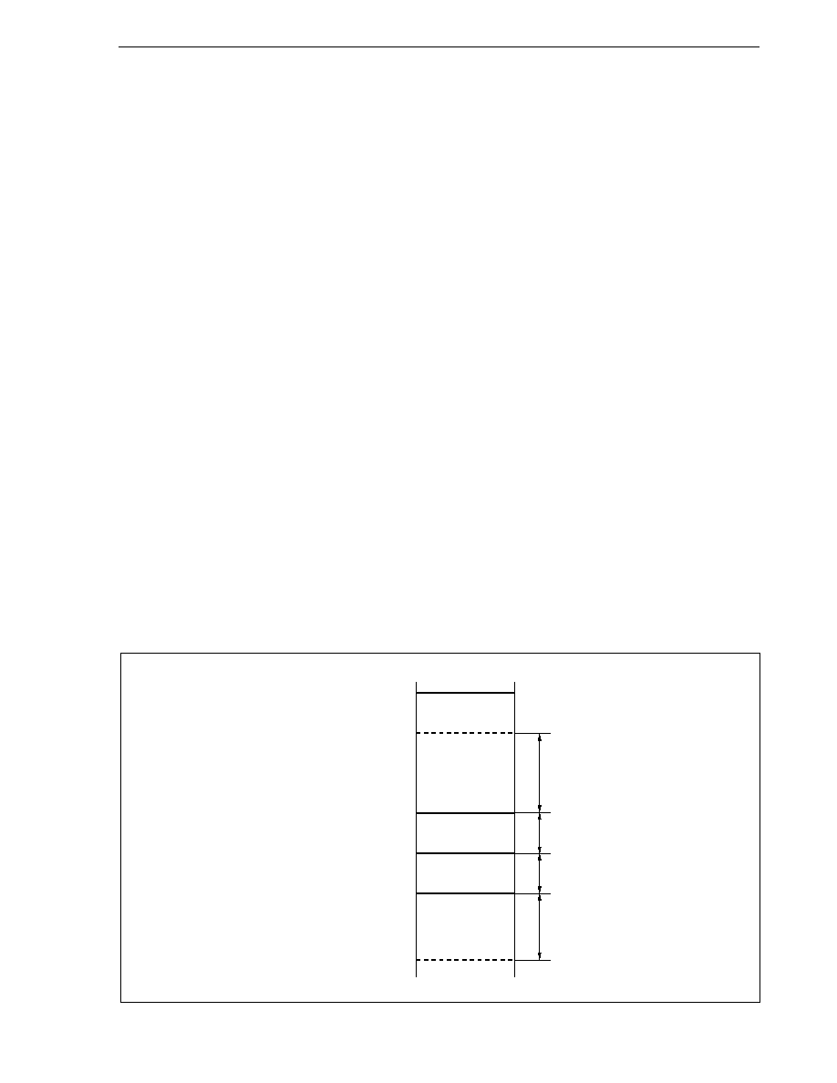
65
CHAPTER 3 CPU FUNCTIONS
User's Manual U10913EJ6V0UM
3.4.8 Recommended use of address space
The architecture of the V853 requires that a register that serves as a pointer be secured for address generation
in accessing operand data in the data space. At the address in this pointer register
±
32 KB operand data can be
accessed directly from an instruction. However, the general register used as a pointer has limitations. Therefore,
by minimizing the deterioration of the address calculation performance when changing the pointer value, the number
of usable general-purpose registers for handling variables is maximized, and the program size can be saved because
instructions for calculating pointer addresses are not required.
To enhance the efficiency of using the pointer in connection with the memory map of the V853, the following points
are recommended.
(1) Program space
Of the 32 bits of the PC (program counter), the higher 8 bits are fixed to 0, and only the lower 24 bits are
valid. Therefore, a contiguous 16 MB space, starting from address 00000000H, unconditionally corresponds
to the memory map of the program space.
(2) Data space
For the efficient use of resources to be performed through the wrap-around feature of the data space, the
continuous 8 MB address spaces 00000000H to 007FFFFFH and FF800000H to FFFFFFFFH of the 4 GB
CPU are used as the data space. With the V853, 16 MB physical address space is seen as 256 images
in the 4 GB CPU address space. The highest bit (bit 23) of this 24-bit address is assigned as address sign-
extended to 32 bits.
Application of wrap-around
For example, when R = r0 (zero register) is specified for the LD/ST disp16 [R] instruction, an addressing
range of 00000000H
±
32 KB can be referenced with the sign-extended, 16-bit displacement value. By
mapping the external memory in the 24 KB area in the figure, all resources including on-chip hardware can
be accessed with one pointer.
The zero register (r0) is a register set to 0 by the hardware, and eliminates the need for additional registers
for the pointer.
00007FFFH
(R =) 00000000H
FFFFF000H
FFFF8000H
Internal
ROM area
Peripheral I/O
External memory
area
FFFFE000H
Internal RAM area
32 KB
4 KB
4 KB
24 KB
0001FFFFH
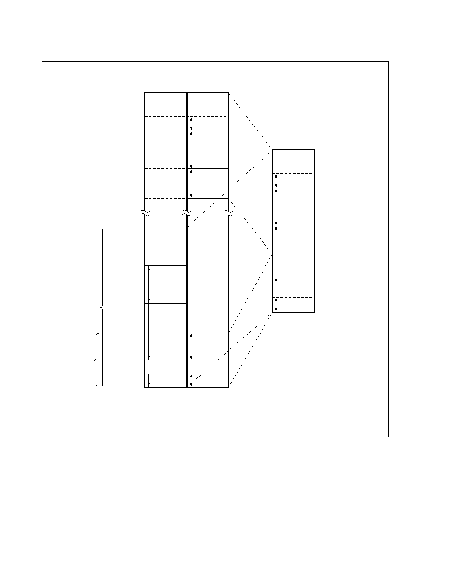
66
CHAPTER 3 CPU FUNCTIONS
User's Manual U10913EJ6V0UM
Figure 3-7. Recommended Memory Map (1/3)
(a)
µµ
µµ
µ
PD703003A and 70F3003A
Note This area cannot be used as a program area.
Remark The arrows indicate the recommended area.
FFFFFFFFH
FFFFF3D1H
FFFFF3D0H
00000000H
16 MB
8 MB
Internal
ROM
Internal
ROM
External
memory
Internal
RAM
Peripheral
I/O
Note
Program space
Data space
Peripheral I/O
Internal
RAM
External
memory
Peripheral I/O
Internal
RAM
External
memory
External
memory
Internal
ROM
XXFFFFFFH
XXFFF3D1H
XXFFF3D0H
XXFFF000H
XXFFEFFFH
XXFFE000H
XXFFDFFFH
XX100000H
XX0FFFFFH
XX020000H
XX01FFFFH
XX800000H
XX7FFFFFH
XX000000H
FFFFF000H
FFFFEFFFH
FFFFE000H
FFFFDFFFH
FF800000H
FF7FFFFFH
01000000H
00FFFFFFH
00FFF000H
00FFEFFFH
00FFE000H
00FFDFFFH
00800000H
007FFFFFH
00100000H
000FFFFFH
00020000H
0001FFFFH
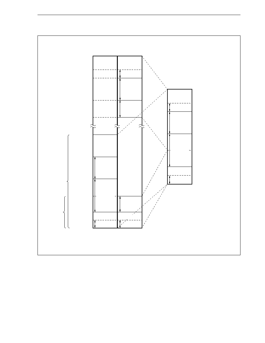
67
CHAPTER 3 CPU FUNCTIONS
User's Manual U10913EJ6V0UM
Figure 3-7. Recommended Memory Map (2/3)
(b)
µµ
µµ
µ
PD703004A
Note This area cannot be used as a program area.
Remark The arrows indicate the recommended area.
16 MB
8 MB
Internal ROM
Internal ROM
External
memory
Internal
RAM
Peripheral
I/O
Note
Program space
Data space
Peripheral I/O
Internal
RAM
External
memory
Peripheral I/O
Internal
RAM
External
memory
External
memory
Internal ROM
F F F F F F F F H
F F F F F 3 D 1 H
F F F F F 3 D 0 H
F F F F F 0 0 0 H
F F F F E F F F H
F F F F E 0 0 0 H
F F F F D F F F H
X X F F F F F F H
X X F F F 3 D 1 H
X X F F F 3 D 0 H
X X F F F 0 0 0 H
X X F F E F F F H
X X 1 0 0 0 0 0 H
X X 0 F F F F F H
X X 0 1 8 0 0 0 H
X X 0 1 7 F F F H
X X 0 0 0 0 0 0 H
X X F F E 0 0 0 H
X X F F D F F F H
X X 8 0 0 0 0 0 H
X X 7 F F F F F H
F F 8 0 0 0 0 0 H
F F 7 F F F F F H
0 1 0 0 0 0 0 0 H
0 0 F F F F F F H
0 0 F F F 0 0 0 H
0 0 F F E F F F H
0 0 F F E 0 0 0 H
0 0 F F D F F F H
0 0 8 0 0 0 0 0 H
0 0 7 F F F F F H
0 0 1 0 0 0 0 0 H
0 0 0 F F F F F H
0 0 0 1 8 0 0 0 H
0 0 0 1 7 F F F H
0 0 0 0 0 0 0 0 H
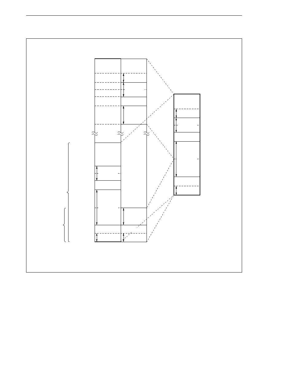
68
CHAPTER 3 CPU FUNCTIONS
User's Manual U10913EJ6V0UM
Figure 3-7. Recommended Memory Map (3/3)
(c)
µµ
µµ
µ
PD703025A and 70F3025A
Note This area cannot be used as a program area.
Remark The arrows indicate the recommended area.
FFFFFFFFH
FFFFF3D1H
FFFFF3D0H
FFFFF000H
FFFFEFFFH
FFFFD000H
FFFFCFFFH
FFFFE000H
FFFFDFFFH
FFFFC000H
FFFFBFFFH
FF800000H
FF7FFFFFH
01000000H
00FFFFFFH
00FFF000H
00FFEFFFH
00FFD000H
00FFCFFFH
00FFE000H
00FFDFFFH
00FFC000H
00FFBFFFH
00800000H
007FFFFFH
00100000H
000FFFFFH
00040000H
0003FFFFH
00000000H
16 MB
8 MB
Internal ROM
Internal ROM
External
memory
Image
Peripheral
I/O
Note
Program space
Data space
Peripheral I/O
Image
External
memory
Peripheral I/O
Image
External
memory
External
memory
Internal ROM
XXFFFFFFH
XXFFF3D1H
XXFFF3D0H
XXFFF000H
XXFFEFFFH
XXFFE000H
XXFFDFFFH
XXFFD000H
XXFFCFFFH
XXFFC000H
XXFFBFFFH
XX100000H
XX0FFFFFH
XX040000H
XX03FFFFH
XX800000H
XX7FFFFFH
XX000000H
Internal RAM
Internal RAM
Internal RAM
69
CHAPTER 3 CPU FUNCTIONS
User's Manual U10913EJ6V0UM
3.4.9 Peripheral I/O registers
1 Bit
8 Bits 16 Bits
FFFFF000H
Port 0
P0
R/W
Undefined
FFFFF002H
Port 1
P1
FFFFF004H
Port 2
P2
FFFFF006H
Port 3
P3
FFFFF008H
Port 4
P4
FFFFF00AH
Port 5
P5
FFFFF00CH
Port 6
P6
FFFFF00EH
Port 7
P7
R
FFFFF012H
Port 9
P9
R/W
FFFFF016H
Port 11
P11
FFFFF020H
Port 0 mode register
PM0
FFH
FFFFF022H
Port 1 mode register
PM1
FFFFF024H
Port 2 mode register
PM2
FFFFF026H
Port 3 mode register
PM3
FFFFF028H
Port 4 mode register
PM4
FFFFF02AH
Port 5 mode register
PM5
FFFFF02CH
Port 6 mode register
PM6
XFH
FFFFF032H
Port 9 mode register
PM9
X1111111B
FFFFF036H
Port 11 mode register
PM11
FFH
FFFFF040H
Port 0 mode control register
PMC0
00H
FFFFF042H
Port 1 mode control register
PMC1
FFFFF044H
Port 2 mode control register
PMC2
FFFFF046H
Port 3 mode control register
PMC3
FFFFF04CH
Memory expansion mode register
MM
FFFFF056H
Port 11 mode control register
PMC11
FFFFF05CH
Port control mode register
PCM
FFFFF05EH
Pull-up resistor option register
PUO
FFFFF060H
Data wait control register
DWC
FFFFH
FFFFF062H
Bus cycle control register
BCC
AAAAH
FFFFF070H
Power save control register
PSC
C0H
FFFFF072H
Clock control register
CKC
00H/03H
FFFFF078H
System status register
SYS
0000000XB
FFFFF084H
Baud rate generator compare register 0
BRGC0
Undefined
FFFFF086H
Baud rate generator prescaler mode register 0
BPRM0
00H
FFFFF088H
Clocked serial interface mode register 0
CSIM0
FFFFF08AH
Serial I/O shift register 0
SIO0
Undefined
Bit Units for
Manipulation
Address
Function Register Name
Symbol
R/W
After Reset
70
CHAPTER 3 CPU FUNCTIONS
User's Manual U10913EJ6V0UM
1 Bit
8 Bits 16 Bits
FFFFF094H
Baud rate generator compare register 1
BRGC1
R/W
Undefined
FFFFF096H
Baud rate generator prescaler mode register 1
BPRM1
00H
FFFFF098H
Clocked serial interface mode register 1
CSIM1
FFFFF09AH
Serial I/O shift register 1
SIO1
Undefined
FFFFF0A4H
Baud rate generator compare register 2
BRGC2
FFFFF0A6H
Baud rate generator prescaler mode register 2
BPRM2
00H
FFFFF0A8H
Clocked serial interface mode register 2
CSIM2
FFFFF0AAH
Serial I/O shift register 2
SIO2
Undefined
FFFFF0B8H
Clocked serial interface mode register 3
CSIM3
00H
FFFFF0BAH
Serial I/O shift register 3
SIO3
Undefined
FFFFF0C0H
Asynchronous serial interface mode register 00
ASIM00
00H
FFFFF0C2H
Asynchronous serial interface mode register 01
ASIM01
FFFFF0C4H
Asynchronous serial interface status register 0
ASIS0
R
FFFFF0C8H
Receive buffer 0 (9 bits)
RXB0
Undefined
FFFFF0CAH
Receive buffer 0L (lower 8 bits)
RXB0L
FFFFF0CCH
Transmit shift register 0 (9 bits)
TXS0
W
FFFFF0CEH
Transmit shift register 0L (lower 8 bits)
TXS0L
FFFFF0D0H
Asynchronous serial interface mode register 10
ASIM10
R/W
00H
FFFFF0D2H
Asynchronous serial interface mode register 11
ASIM11
FFFFF0D4H
Asynchronous serial interface status register 1
ASIS1
R
FFFFF0D8H
Receive buffer 1 (9 bits)
RXB1
Undefined
FFFFF0DAH
Receive buffer 1L (lower 8 bits)
RXB1L
FFFFF0DCH
Transmit shift register 1 (9 bits)
TXS1
W
FFFFF0DEH
Transmit shift register 1L (lower 8 bits)
TXS1L
FFFFF100H
Interrupt control register
OVIC11
R/W
47H
FFFFF102H
Interrupt control register
OVIC12
FFFFF104H
Interrupt control register
OVIC13
FFFFF106H
Interrupt control register
OVIC14
FFFFF108H
Interrupt control register
P11IC0
FFFFF10AH
Interrupt control register
P11IC1
FFFFF10CH
Interrupt control register
P11IC2
FFFFF10EH
Interrupt control register
P11IC3
FFFFF110H
Interrupt control register
P12IC0
FFFFF112H
Interrupt control register
P12IC1
FFFFF114H
Interrupt control register
P12IC2
FFFFF116H
Interrupt control register
P12IC3
FFFFF118H
Interrupt control register
P13IC0
FFFFF11AH
Interrupt control register
P13IC1
Bit Units for
Manipulation
Address
Function Register Name
Symbol
R/W
After Reset
71
CHAPTER 3 CPU FUNCTIONS
User's Manual U10913EJ6V0UM
1 Bit
8 Bits 16 Bits
FFFFF11CH
Interrupt control register
P13IC2
R/W
47H
FFFFF11EH
Interrupt control register
P13IC3
FFFFF120H
Interrupt control register
P14IC0
FFFFF122H
Interrupt control register
P14IC1
FFFFF124H
Interrupt control register
P14IC2
FFFFF126H
Interrupt control register
P14IC3
FFFFF128H
Interrupt control register
CMIC4
FFFFF12AH
Interrupt control register
CSIC0
FFFFF12CH
Interrupt control register
CSIC1
FFFFF12EH
Interrupt control register
CSIC2
FFFFF130H
Interrupt control register
CSIC3
FFFFF132H
Interrupt control register
SEIC0
FFFFF134H
Interrupt control register
SRIC0
FFFFF136H
Interrupt control register
STIC0
FFFFF138H
Interrupt control register
SEIC1
FFFFF13AH
Interrupt control register
SRIC1
FFFFF13CH
Interrupt control register
STIC1
FFFFF13EH
Interrupt control register
ADIC
FFFFF166H
In-service priority register
ISPR
R
00H
FFFFF170H
Command register
PRCMD
W
XXH
FFFFF180H
External interrupt mode register 0
INTM0
R/W
00H
FFFFF182H
External interrupt mode register 1
INTM1
FFFFF184H
External interrupt mode register 2
INTM2
FFFFF186H
External interrupt mode register 3
INTM3
FFFFF188H
External interrupt mode register 4
INTM4
FFFFF230H
Timer overflow status register
TOVS
FFFFF240H
Timer unit mode register 11
TUM11
0000H
FFFFF242H
Timer control register 11
TMC11
00H
FFFFF244H
Timer output control register 11
TOC11
FFFFF250H
Timer 11
TM11
R
0000H
FFFFF252H
Capture/compare register 110
CC110
R/W
undefined
FFFFF254H
Capture/compare register 111
CC111
FFFFF256H
Capture/compare register 112
CC112
FFFFF258H
Capture/compare register 113
CC113
FFFFF260H
Timer unit mode register 12
TUM12
0000H
FFFFF262H
Timer control register 12
TMC12
00H
FFFFF264H
Timer output control register 12
TOC12
FFFFF270H
Timer 12
TM12
R
0000H
FFFFF272H
Capture/compare register 120
CC120
R/W
Undefined
Bit Units for
Manipulation
Address
Function Register Name
Symbol
R/W
After Reset
72
CHAPTER 3 CPU FUNCTIONS
User's Manual U10913EJ6V0UM
1 Bit
8 Bits 16 Bits
FFFFF274H
Capture compare register 121
CC121
R/W
Undefined
FFFFF276H
Capture compare register 122
CC122
FFFFF278H
Capture compare register 123
CC123
FFFFF280H
Timer unit mode register 13
TUM13
0000H
FFFFF282H
Timer control register 13
TMC13
00H
FFFFF284H
Timer output control register 13
TOC13
FFFFF290H
Timer 13
TM13
R
0000H
FFFFF292H
Capture/compare register 130
CC130
R/W
Undefined
FFFFF294H
Capture/compare register 131
CC131
FFFFF296H
Capture/compare register 132
CC132
FFFFF298H
Capture/compare register 133
CC133
FFFFF2A0H
Timer unit mode register 14
TUM14
0000H
FFFFF2A2H
Timer control register 14
TMC14
00H
FFFFF2A4H
Timer output control register 14
TOC14
FFFFF2B0H
Timer 14
TM14
R
0000H
FFFFF2B2H
Capture/compare register 140
CC140
R/W
Undefined
FFFFF2B4H
Capture/compare register 141
CC141
FFFFF2B6H
Capture/compare register 142
CC142
FFFFF2B8H
Capture/compare register 143
CC143
FFFFF342H
Timer control register 4
TMC4
00H
FFFFF350H
Timer 4
TM4
R
0000H
FFFFF352H
Compare register 4
CM4
R/W
Undefined
FFFFF360H
PWM control register
PWMC
00H
FFFFF362H
PWM prescaler register
PWPR
FFFFF364H
PWM buffer register 0 (12 bits)
PWM0
Undefined
FFFFF366H
PWM buffer register 0L (lower 8 bits)
PWM0L
FFFFF368H
PWM buffer register 1 (12 bits)
PWM1
FFFFF36AH
PWM buffer register 1L (lower 8 bits)
PWM1L
FFFFF380H
A/D converter mode register 0
ADM0
00H
FFFFF382H
A/D converter mode register 1
ADM1
07H
FFFFF390H
A/D conversion result register 0
ADCR0
R
Undefined
FFFFF392H
A/D conversion result register 0H
ADCR0H
FFFFF394H
A/D conversion result register 1
ADCR1
FFFFF396H
A/D conversion result register 1H
ADCR1H
FFFFF398H
A/D conversion result register 2
ADCR2
FFFFF39AH
A/D conversion result register 2H
ADCR2H
FFFFF39CH
A/D conversion result register 3
ADCR3
FFFFF39EH
A/D conversion result register 3H
ADCR3H
FFFFF3A0H
A/D conversion result register 4
ADCR4
Bit Units for
Manipulation
Address
Function Register Name
Symbol
R/W
After Reset
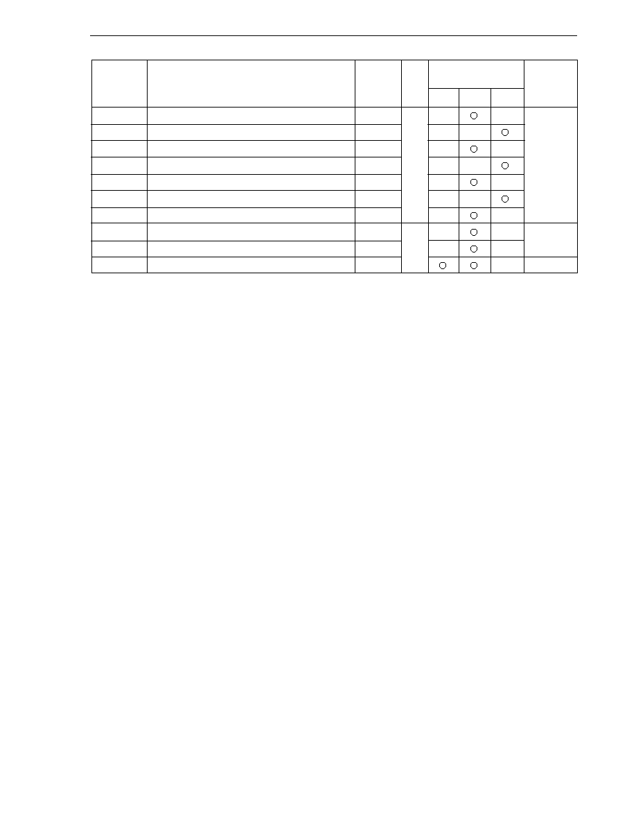
73
CHAPTER 3 CPU FUNCTIONS
User's Manual U10913EJ6V0UM
1 Bit
8 Bits 16 Bits
FFFFF3A2H
A/D conversion result register 4H
ADCR4H
R
Undefined
FFFFF3A4H
A/D conversion result register 5
ADCR5
FFFFF3A6H
A/D conversion result register 5H
ADCR5H
FFFFF3A8H
A/D conversion result register 6
ADCR6
FFFFF3AAH
A/D conversion result register 6H
ADCR6H
FFFFF3ACH
A/D conversion result register 7
ADCR7
FFFFF3AEH
A/D conversion result register 7H
ADCR7H
FFFFF3C0H
D/A converter converted data coefficient register 0
DACS0
R/W
00H
FFFFF3C2H
D/A converter converted data coefficient register 1
DACS1
FFFFF3D0H
D/A converter mode register
DAM
03H
Bit Units for
Manipulation
Address
Function Register Name
Symbol
R/W
After Reset

74
CHAPTER 3 CPU FUNCTIONS
User's Manual U10913EJ6V0UM
3.4.10 Specific registers
Specific registers are registers that are protected from being written with illegal data due to erroneous program
execution, etc. The write access of these specific registers is executed in a specific sequence, and if abnormal
store operations occur, it is reported by the system status register (SYS). The V853 has two specific registers, the
clock control register (CKC) and power save control register (PSC). For details of the CKC register, refer to 6.3.3,
and for details of the PSC register, refer to 6.5.2.
The following shows the access sequence of the specific registers.
A specific register is programmed in the following special sequence.
<1> Interrupt-disable is set (PSW NP bit is set to 1).
<2> Any 8-bit data is written in the command register (PRCMD).
<3> The setting data is written in the specific register (using the following instructions).
· Store instruction (ST/SST instruction)
· Bit manipulation instruction (SET1/CLR1/NOT1 instruction)
<4> Interrupt-disable is released (PSW NP bit is set to 0).
<5> The NOP instruction (2 or 5 instructions) is inserted.
No special sequence is necessary for reading a specific register.
Cautions 1. If interrupts are acknowledged in the time between the PRCMD issuance (<2>) and the
specific register writing (<3>) directly after, the specific register is not written and a
protection error (SYS register PRERR bit is "1") is generated in some cases. Therefore, set
the PSW NP bit to 1 (<1>) to disable INT/NMI acknowledgement.
The same applies when a bit manipulation instruction is used to set a specific register.
Insert a NOP instruction (<5>) as a dummy instruction so that the routine is executed correctly
after the STOP/IDLE mode is released. If the PSW ID bit value is not to be changed by the
execution of the instruction which returns the NP bit to 0 (<4>), insert two NOP instructions.
If it is to be changed, insert five.
The following are examples.
[Example] : Case of PSC register
LDSR
rX,5
; NP bit = 1
ST.B
r0,PRCMD [r0] ; Writing in PRCMD
ST.B
rD,PSC [r0]
; Sets PSC register
LDSR
rY,5
; NP bit = 0
NOP
; Dummy instruction (2 or 5 instructions)
.
.
.
NOP
(next instruction)
; Execution routine after STOP/IDLE mode has been
; released
.
.
.
rX: Value written in PSW
rY: Value written back to PSW
rD: PSC setting value

75
CHAPTER 3 CPU FUNCTIONS
User's Manual U10913EJ6V0UM
When saving the PSW value, it is necessary to transfer the PSW value before setting the NP
bit to the rY register.
2. The instruction (<4> interrupt disable release, <5> NOP instruction) after the store instruction
for the specific register to be set to the software STOP mode and IDLE mode is executed
before each power save mode is set.
3. When setting power save mode (IDLE mode or STOP mode) during instruction execution in
the external ROM, refer to 6.5.6 Cautions.

76
CHAPTER 3 CPU FUNCTIONS
User's Manual U10913EJ6V0UM
(1) Command Register (PRCMD)
The command register (PRCMD) is a register used when write-accessing a specific register to prevent incorrect
writing to the specific register due to erroneous program execution.
This register can be read/written in 8-bit units. It becomes undefined in a read cycle.
The occurrence of illegal store operations can be checked by the PRERR bit of the SYS register.
Bit position
Bit name
Function
7 to 0
REG7 to
Registration Code
REG0
Specific register
Registration code
CKC
Arbitrary 8-bit data
PSC
Arbitrary 8-bit data
Address
FFFFF170H
7
REG7
PRCMD
6
REG6
5
REG5
4
REG4
3
REG3
2
REG2
1
REG1
0
REG0
After reset
Undefined

77
CHAPTER 3 CPU FUNCTIONS
User's Manual U10913EJ6V0UM
(2) System status register (SYS)
This register is allocated with status flags showing the operating state of the entire system. This register can
be read/written in 8-bit or 1-bit units.
Bit position
Bit name
Function
4
PRERR
Protection Error Flag
Indicates that writing to a specific register has not be executed in the correct sequence, and a
protection error occurred.
Accumulate flag
0: Protection error did not occur.
1: Protection error occurred.
0
UNLOCK
Unlock Status Flag
Read-only flag. Indicates the PLL unlock state. (For details, refer to 6.4 PLL Lockup.)
0: Locked
1: Unlocked
Operation conditions of PRERR flag
· Set conditions:
(1) If a write operation to a specific register is executed when the store
(PRERR = "1")
instruction operation to peripheral I/Os most recently executed is not a write
operation to the PRCMD register.
(2) If the first store instruction executed after a write operation to the PRCMD
register is to a peripheral I/O register other than a specific register.
· Reset conditions:
(1) When "0" is written to the PRERR flag of the SYS register.
(PRERR = "0")
(2) After system reset.
Address
FFFFF078H
7
0
SYS
6
0
5
0
4
PRERR
3
0
2
0
1
0
0
UNLOCK
After reset
0000000XB
78
User's Manual U10913EJ6V0UM
CHAPTER 4 BUS CONTROL FUNCTION
The V853 is provided with an external bus interface function by which external memories such as ROM and RAM,
and I/O can be connected.
4.1 Features
16-bit data bus
External devices connected through multiplexed I/O port pins
Wait function
· Programmable wait function, capable of inserting up to 3 wait states per 2 blocks
· External wait control through WAIT pin
Idle state insertion function
Bus mastership arbitration function
Bus hold function
4.2 Bus Control Pins
The following pins are used for interfacing to external devices.
External Bus Interface Function
Corresponding Port
Address/data bus (AD0 to AD7)
Port 4 (P40 to P47)
Address/data bus (AD8 to AD15)
Port 5 (P50 to P57)
Address bus (A16 to A19)
Port 6 (P60 to P63)
Read/write control (LBEN, UBEN, R/W, DSTB)
Port 9 (P90 to P93)
Address strobe (ASTB)
Port 9 (P94)
Bus hold control (HLDRQ, HLDAK)
Port 9 (P95, P96)
External wait control (WAIT)
--
The bus interface function of each pin is enabled by the memory expansion mode register (MM). For details of
specifying the operation mode of the external bus interface, refer to 3.4.7 Memory expansion mode register (MM).
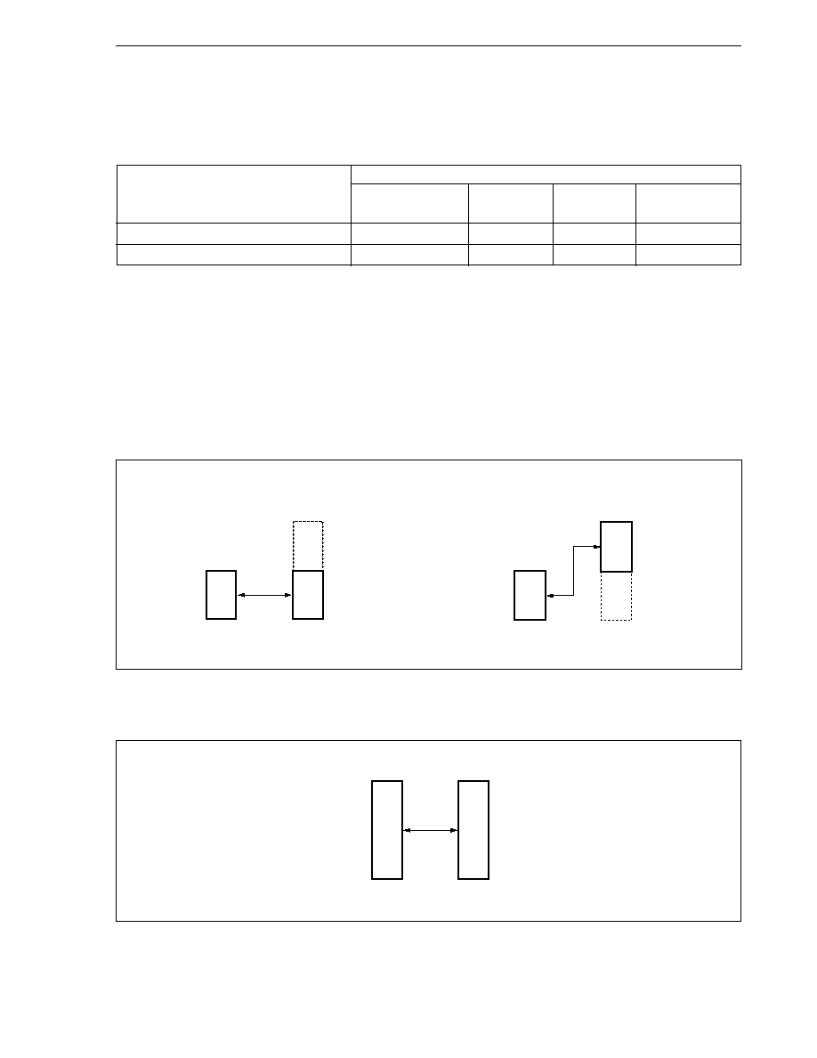
79
CHAPTER 4 BUS CONTROL FUNCTION
User's Manual U10913EJ6V0UM
4.3 Bus Access
4.3.1 Number of access clocks
The number of basic clocks necessary for accessing each resource is as follows.
Bus Cycle Type
Resource (Bus Width)
Internal ROM
Internal RAM
Peripheral I/O
External Memory
(32 Bits)
(32 Bits)
(16 Bits)
(16 Bits)
Instruction fetch
1
3
Disabled
3 + n
Operand data access
3
1
3 + n
3 + n
Remarks 1. Unit: clock/access
2. n: Number of inserted wait clock
4.3.2 Bus width
The V853 carries out peripheral I/O access and external memory access in 8-, 16-, or 32-bit units. The following
shows the operation for each access.
(1) Byte access (8 bits)
Byte access is divided into two types, the access to even address and the access to odd address.
(2) Halfword access (16 bits)
In halfword access to external memory, data is dealt with as it is because the data bus is 16-bit fixed.
0
7
0
7
8
15
Byte data
External data bus
(a) Access to even address
0
7
0
7
8
15
Byte data
External data bus
(b) Access to odd address
0
0
15
15
Halfword data
External data bus
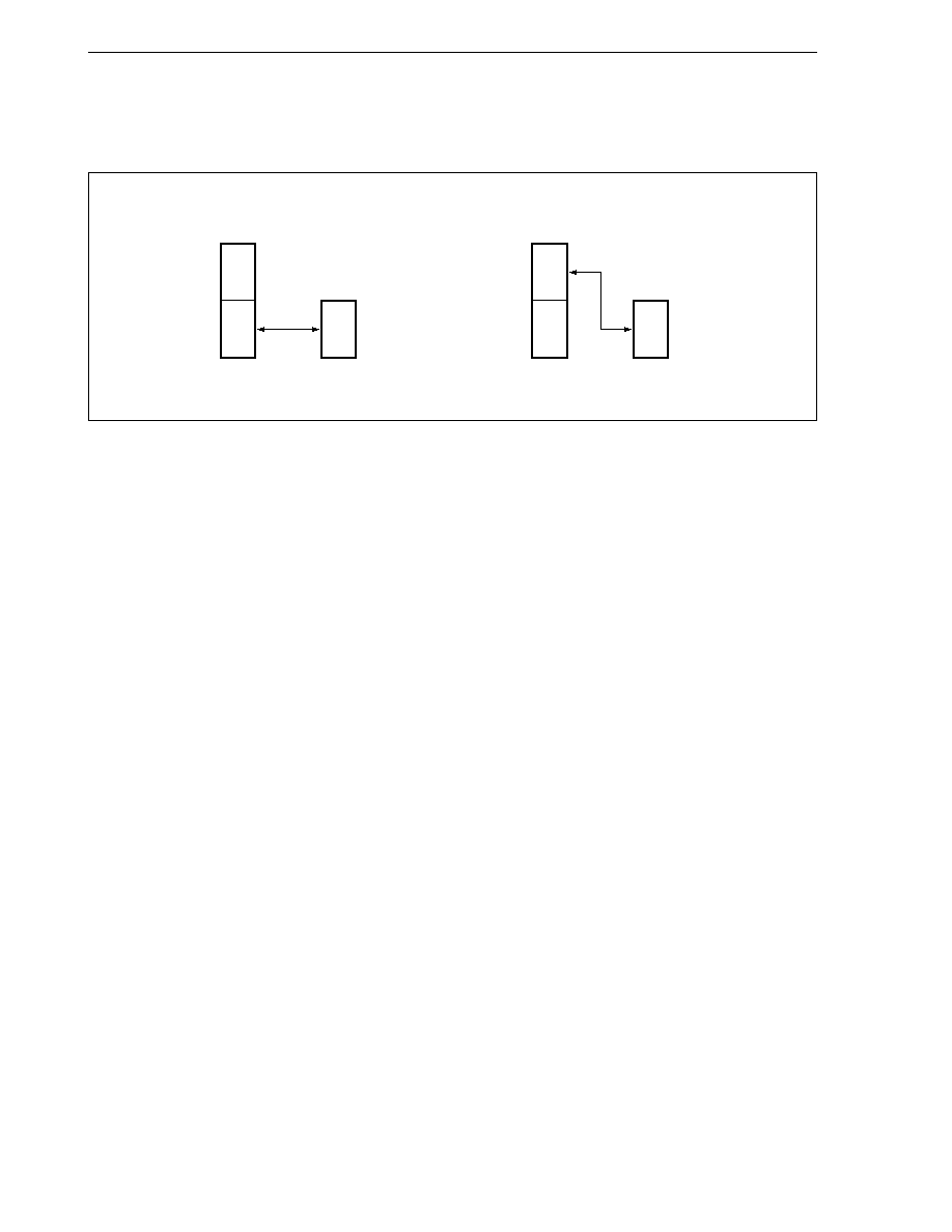
80
CHAPTER 4 BUS CONTROL FUNCTION
User's Manual U10913EJ6V0UM
(3) Word access (32 bits)
In word access to external memory, the lower halfword is accessed first and then the higher halfword is
accessed.
0
15
0
15
16
31
Word data
External data bus
First
0
15
0
15
16
31
Word data
External data bus
Second
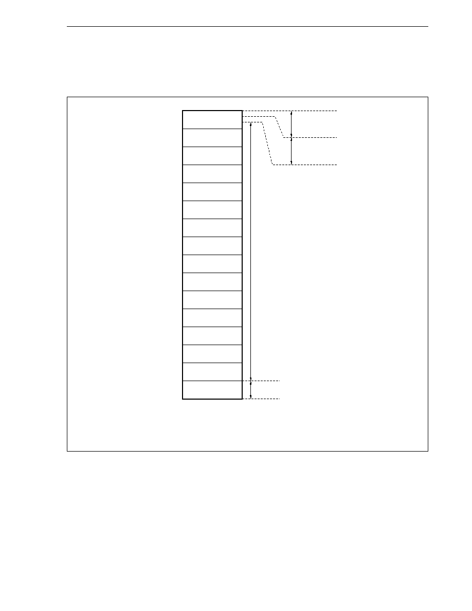
81
CHAPTER 4 BUS CONTROL FUNCTION
User's Manual U10913EJ6V0UM
4.4 Memory Block Function
The 16 MB memory space is divided into memory blocks of 1 MB units. The programmable wait function and bus
cycle operation mode can be independently controlled for every two memory blocks.
Note
The first address of the internal RAM area is as follows.
µ
PD703003A, 70F3003A, 703004A: FFE000H
µ
PD703025A, 70F3025A: FFC000H
Block 15
Block 14
Block 13
Block 12
Block 11
Block 10
Block 9
Block 8
Block 7
Block 6
Block 5
Block 4
Block 3
Block 2
Block 1
Block 0
Peripheral I/O area
Internal RAM area
Note
FFFFFFH
FFF000H
FFEFFFH
External memory area
FFFFFFH
F00000H
EFFFFFH
E00000H
DFFFFFH
D00000H
CFFFFFH
C00000H
BFFFFFH
B00000H
AFFFFFH
A00000H
9FFFFFH
900000H
8FFFFFH
800000H
7FFFFFH
700000H
6FFFFFH
600000H
5FFFFFH
500000H
4FFFFFH
400000H
3FFFFFH
300000H
2FFFFFH
200000H
1FFFFFH
100000H
0FFFFFH
000000H
Internal ROM area

82
CHAPTER 4 BUS CONTROL FUNCTION
User's Manual U10913EJ6V0UM
4.5 Wait Function
4.5.1 Programmable wait function
To facilitate interfacing with low-speed memories and I/O devices, up to 3 data wait states can be inserted in a
bus cycle for two memory blocks. The number of wait states can be programmed by using data wait control register
(DWC). Immediately after the system has been reset, three data wait states are automatically programmed for all
memory blocks.
(1) Data wait control register (DWC)
This register can be read/written in 16-bit units.
Bit position
Bit name
Function
15 to 0
DWn1
Data Wait
DWn0
Specifies number of wait states to be inserted.
(n = 0 to 7)
DWn1
DWn0
Number of wait states to be inserted
0
0
0
0
1
1
1
0
2
1
1
3
n
Blocks into which wait states are inserted
0
Blocks 0/1
1
Blocks 2/3
2
Blocks 4/5
3
Blocks 6/7
4
Blocks 8/9
5
Blocks 10/11
6
Blocks 12/13
7
Blocks 14/15
Cautions 1. Block 0 is reserved for the internal ROM area in the single-chip mode. It is not subject
to programmable wait control, regardless of the setting of DWC, and is always accessed
without wait states.
2. The internal RAM area of block 15 is not subject to programmable wait control and is
always accessed without wait states. The peripheral I/O area of this block is not subject
to programmable wait control, either. The only wait control is dependent upon the
execution of each peripheral function.
15
DW71
DWC
Address
FFFFF060H
After reset
FFFFH
14
DW70
13
DW61
12
DW60
11
DW51
10
DW50
9
DW41
8
DW40
7
DW31
6
DW30
5
DW21
4
DW20
3
DW11
2
DW10
1
DW01
0
DW00
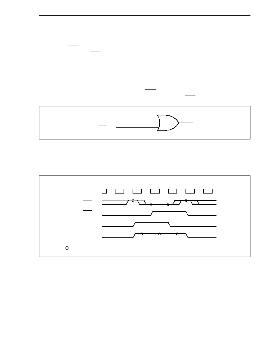
83
CHAPTER 4 BUS CONTROL FUNCTION
User's Manual U10913EJ6V0UM
4.5.2 External wait function
When an extremely slow device, I/O, or asynchronous system is connected, any number of wait states can be
inserted in a bus cycle by sampling the external wait pin (WAIT) to synchronize with the external device.
The external WAIT signal does not affect the access times of the internal ROM, internal RAM, and peripheral I/O
areas. Input of the external WAIT signal can be done asynchronously to CLKOUT and is sampled at the falling edge
of the clock in the T2 and TW states of a bus cycle. If the setup and hold time of the WAIT input are not satisfied,
the wait state may or may not be inserted in the next state.
4.5.3 Relationship between programmable wait and external wait
A wait cycle is inserted as a result of an OR operation between the wait cycle specified by the set value of
programmable wait and the wait cycle controlled by the WAIT pin. In other words, the number of wait cycles is
determined by the programmable wait value or the length of evaluation at the WAIT input pin.
For example, if the number of programmable wait states is 2 and the timing of the WAIT pin input signal is as
illustrated below, three wait states will be inserted in the bus cycle.
Figure 4-1. Example of Inserting Wait States
Remark
: Sampling timing
Wait control
Programmable wait
Wait by WAIT pin
CLKOUT
T1
T2
TW
TW
TW
T3
WAIT pin
Wait by WAIT pin
Programmable wait
Wait control

84
CHAPTER 4 BUS CONTROL FUNCTION
User's Manual U10913EJ6V0UM
4.6 Idle State Insertion Function
To facilitate interfacing with low-speed memory devices and meeting the data output float delay time (t
DF
) on
memory read accesses, one idle state (TI) can be inserted into the current bus cycle after the T3 state. The bus cycle
following continuous bus cycles starts after one idle state.
Specifying insertion of the idle state is programmable by using the bus cycle control register (BCC).
Immediately after the system has been reset, idle state insertion is automatically programmed for all memory
blocks.
(1) Bus cycle control register (BCC)
This register can be read/written in 16-bit units.
Bit position
Bit name
Function
15, 13, 11,
BCn1
Bus Cycle
9, 7, 5, 3, 1
(n = 0 to 7)
Specifies insertion of idle state.
0: Not inserted
1: Inserted
n
Blocks into which idle state is inserted
0
Blocks 0/1
1
Blocks 2/3
2
Blocks 4/5
3
Blocks 6/7
4
Blocks 8/9
5
Blocks 10/11
6
Blocks 12/13
7
Blocks 14/15
Cautions 1. Block 0 is reserved for the internal ROM area in the single-chip mode; therefore, no idle state
is specified regardless of the BCC setting.
2. The internal RAM area and peripheral I/O area of block 15 are not subject to insertion of the
idle state.
3. Be sure to set bits 0, 2, 4, 6, 8, 10, 12, and 14 to 0. If these bits are set to 1, the operation
is not guaranteed.
15
BC71
BCC
Address
FFFFF062H
After reset
AAAAH
14
0
13
BC61
12
0
11
BC51
10
0
9
BC41
8
0
7
BC31
6
0
5
BC21
4
0
3
BC11
2
0
1
BC01
0
0

85
CHAPTER 4 BUS CONTROL FUNCTION
User's Manual U10913EJ6V0UM
- - - - - - - - - - -
- - - - - - - - - - -
Normal status
Bus hold status
Normal status
4.7 Bus Hold Function
4.7.1 Outline of function
When P95 and P96 of port 9 are programmed to be in the control mode, the functions of the HLDRQ and HLDAK
pins become valid.
When the HLDRQ pin becomes active (low) indicating that another bus master is requesting acquisition of the bus,
the external address/data bus and strobe pins go into a high-impedance state, and the bus is released (bus hold
status). When the HLDRQ pin becomes inactive (high) indicating that the request for the bus is cleared, these pins
are driven again.
During bus hold period, the V853 continues internal operation until external memory access.
In the bus hold status, the HLDAK pin becomes active (low).
This feature can be used to design a system where two or more bus masters exist, such as when multi-processor
configuration is used and when a DMA controller is connected.
Bus hold request is not acknowledged between the first and the second access in word access. Bus hold request
is not acknowledged between read access and write access in read modify write access of bit manipulation instruction.
4.7.2 Bus hold procedure
The procedure of the bus hold function is illustrated below.
<1> HLDRQ = 0 acknowledged
<2> All bus cycle start request pending
<3> End of current bus cycle
<4> Bus idle status
<5> HLDAK = 0
<6> HLDRQ = 1 acknowledged
<7> HLDAK = 1
<8> Clears bus cycle start request pending
<9> Start of bus cycle
4.7.3 Operation in power save mode
In the software STOP or IDLE mode, the system clock is stopped. Consequently, the bus hold status is not set
even if the HLDRQ pin becomes active.
In the HALT mode, the HLDAK pin immediately becomes active when the HLDRQ pin becomes active, and the
bus hold status is set. When the HLDRQ pin becomes inactive, the HLDAK pin becomes inactive. As a result, the
bus hold status is cleared, and the HALT mode is set again.
HLDRQ
HLDAK
<1> <2> <3><4><5>
<7><8><9>
<6>
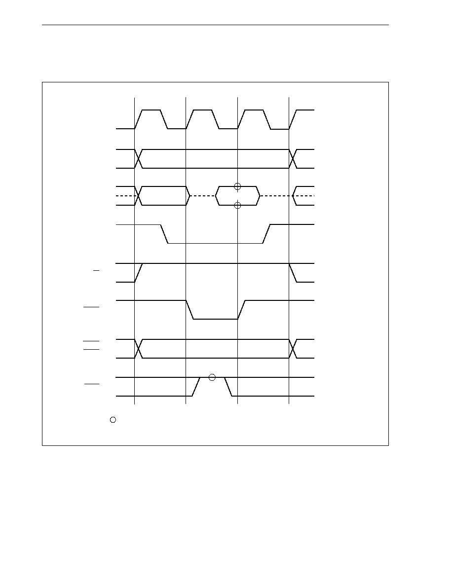
86
CHAPTER 4 BUS CONTROL FUNCTION
User's Manual U10913EJ6V0UM
4.8 Bus Timing
(1) Memory read (0 waits)
Remarks
1. indicates the sampling timing when the number of programmable waits is set to 0.
2. The broken lines indicate the high-impedance state.
T1
T2
T3
CLKOUT
A16 to A19
AD0 to AD15
Address
Data
Address
ASTB
R/W
DSTB
UBEN
LBEN
WAIT
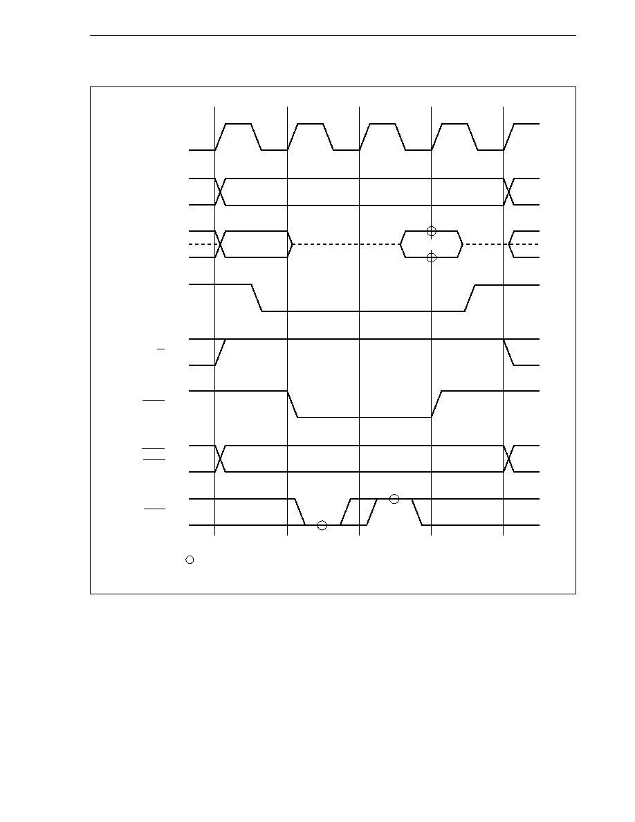
87
CHAPTER 4 BUS CONTROL FUNCTION
User's Manual U10913EJ6V0UM
(2) Memory read (1 wait)
Remarks
1.
indicates the sampling timing when the number of programmable waits is set to 0.
2. The broken lines indicate the high-impedance state.
T1
T2
TW
CLKOUT
A16 to A19
AD0 to AD15
Address
Address
ASTB
R/W
DSTB
UBEN
LBEN
WAIT
T3
Data
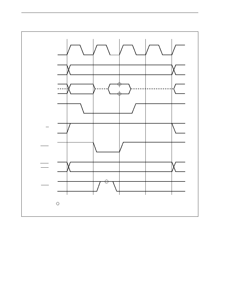
88
CHAPTER 4 BUS CONTROL FUNCTION
User's Manual U10913EJ6V0UM
(3) Memory read (0 waits, idle state)
Remarks
1.
indicates the sampling timing when the number of programmable waits is set to 0.
2. The broken lines indicate the high-impedance state.
T1
T2
T3
CLKOUT
A16 to A19
AD0 to AD15
Address
Address
ASTB
R/W
DSTB
UBEN
LBEN
WAIT
TI
Data
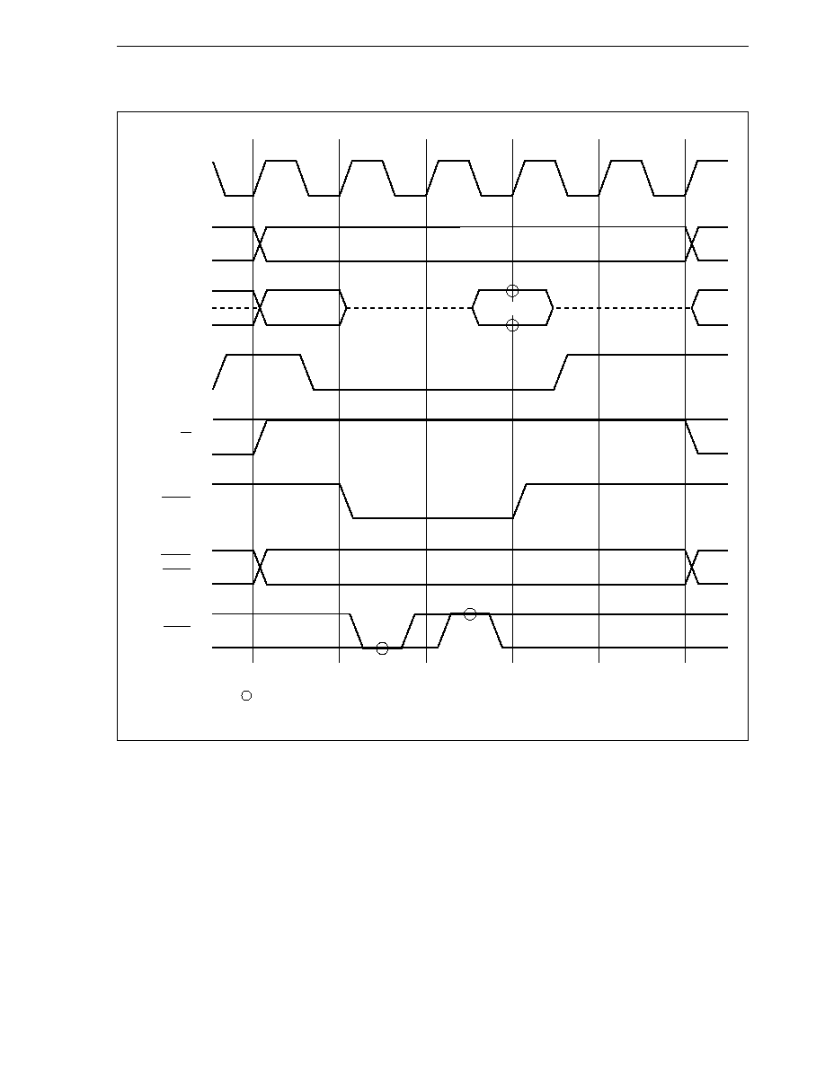
89
CHAPTER 4 BUS CONTROL FUNCTION
User's Manual U10913EJ6V0UM
(4) Memory read (1 wait, idle state)
Remarks
1.
indicates the sampling timing when the number of programmable waits is set to 0.
2. The broken lines indicate the high-impedance state.
T1
T2
TW
CLKOUT
A16 to A19
AD0 to AD15
Address
Address
ASTB
R/W
DSTB
UBEN
LBEN
WAIT
T3
Data
TI
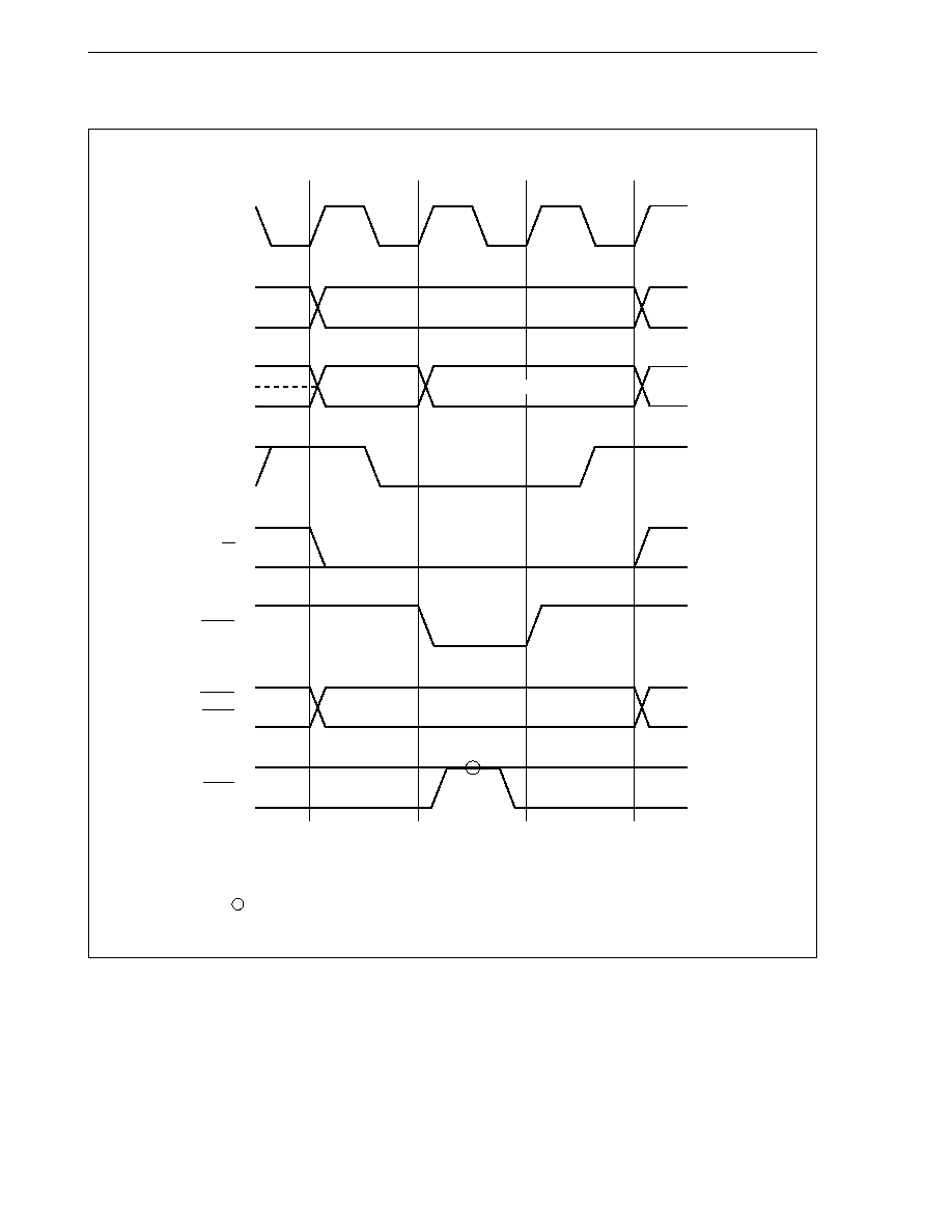
90
CHAPTER 4 BUS CONTROL FUNCTION
User's Manual U10913EJ6V0UM
(5) Memory write (0 waits)
Note
AD0 to AD7 output invalid data when odd address byte data is accessed.
AD8 to AD15 output invalid data when even address byte data is accessed.
Remarks
1.
indicates the sampling timing when the number of programmable waits is set to 0.
2. The broken lines indicate the high-impedance state.
T1
T2
T3
CLKOUT
A16 to A19
AD0 to AD15
Address
Data
Note
Address
ASTB
R/W
DSTB
UBEN
LBEN
WAIT
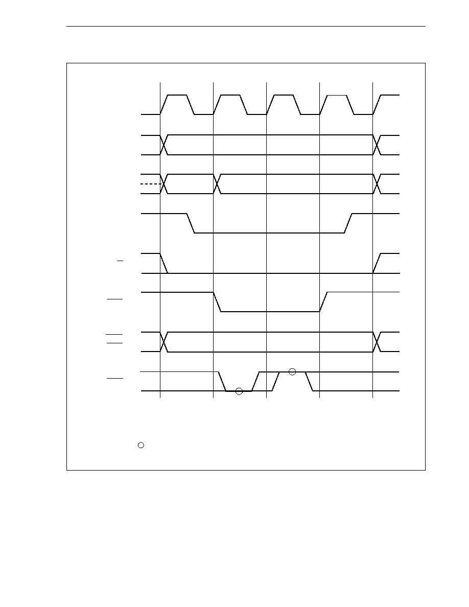
91
CHAPTER 4 BUS CONTROL FUNCTION
User's Manual U10913EJ6V0UM
(6) Memory write (1 wait)
Note
AD0 to AD7 output invalid data when odd address byte data is accessed.
AD8 to AD15 output invalid data when even address byte data is accessed.
Remarks
1.
indicates the sampling timing when the number of programmable waits is set to 0.
2. The broken lines indicate the high-impedance state.
T1
T2
TW
CLKOUT
A16 to A19
AD0 to AD15
Address
ASTB
R/W
DSTB
UBEN
LBEN
WAIT
T3
Data
Note
Address
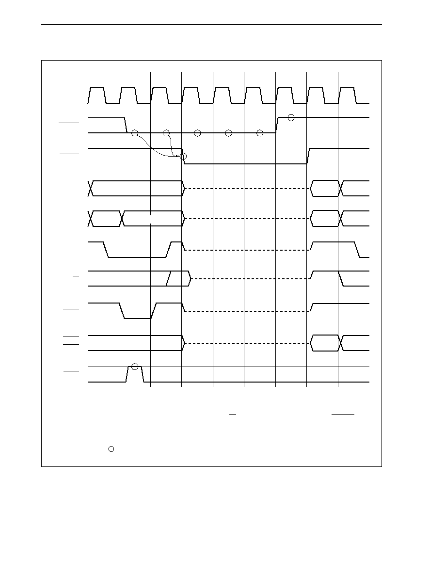
92
CHAPTER 4 BUS CONTROL FUNCTION
User's Manual U10913EJ6V0UM
CLKOUT
R/W
DSTB
UBEN
LBEN
WAIT
HLDRQ
T2
T3
TH
TH
TH
TH
TI
T1
HLDAK
A16 to A19
AD0 to AD15
Address
Address
Data
Address
ASTB
Undefined
Undefined
Undefined
Address
(7) Bus hold timing
Caution
If the transition to the bus hold status takes place after a write cycle, a high-level signal
may be output momentarily from the R/W pin immediately before the HLDAK signal
changes from the high level to the low level.
Remarks
1.
indicates the sampling timing.
2. The broken lines indicate the high-impedance state.

93
CHAPTER 4 BUS CONTROL FUNCTION
User's Manual U10913EJ6V0UM
4.9 Bus Priority
There are four external bus cycles: bus hold, operand data access, instruction fetch (branch), and instruction fetch
(continuous). The bus hold cycle is given the highest priority, followed by operand data access, instruction fetch
(branch), and instruction fetch (continuous) in that order.
The instruction fetch cycle may be inserted in between the read access and write access of read-modify-write
access.
Instruction fetch and bus hold cycle are not inserted between the lower halfword access and higher halfword access
of word operations.
Table 4-1. Bus Priority
External Bus Cycle
Priority
Bus hold
1
Operand data access
2
Instruction fetch (branch)
3
Instruction fetch (continuous)
4
4.10 Memory Boundary Operation Condition
4.10.1 Program space
(1) Do not execute a branch to the peripheral I/O area or a continuous fetch from the internal RAM area to the
peripheral I/O area. If a branch or continuous fetch is executed, the NOP instruction code is continuously
fetched, and no processing such as a fetch from the external memory is performed.
(2) A prefetch operation straddling over the peripheral I/O area (invalid fetch) does not take place if a branch
instruction exists at the upper-limit address of the internal RAM area.
4.10.2 Data space
Only the address aligned at the halfword (when the least significant bit of the address is "0")/word (when the lowest
2 bits of the address are "0") boundary is accessed for halfword (16 bits)/word (32 bits) length data .
Therefore, access that straddles over the memory or memory block boundary does not take place. A word access
to the external memory is executed in the order of lower halfword followed by higher halfword.
For details, refer to V850 Family Architecture User's Manual.

94
CHAPTER 4 BUS CONTROL FUNCTION
User's Manual U10913EJ6V0UM
4.11 On-Chip Peripheral I/O Interface
Access to the on-chip peripheral I/O area is not output to the external bus. Therefore, the on-chip peripheral
I/O area can be accessed in parallel with instruction fetch access.
Accesses to the on-chip peripheral I/O area take, in most cases, three clock cycles. However, accesses to the
following timer/counter registers may take from 3 to 4 cycles.
Peripheral I/O Register
Access
TM1n
Read
TM4
CC1n0
Read/write
CC1n1
CC1n2
CC1n3
CM4
Write
Remark
n = 1 to 4

95
User's Manual U10913EJ6V0UM
CHAPTER 5 INTERRUPT/EXCEPTION PROCESSING FUNCTION
The V853 is provided with a dedicated interrupt controller (INTC) for interrupt servicing and can service a total
of 33 interrupt requests.
An interrupt is an event that occurs independently of program execution, and an exception is an event that occurs
dependent on program execution.
The V853 can service interrupt requests from the on-chip peripheral hardware and external sources. Moreover,
exception processing can be started by the TRAP instruction (software exception) or by generation of an exception
event (fetching of an illegal op code).
5.1 Features
Interrupt
· Non-maskable interrupt: 1 source
· Maskable interrupt: 32 sources
· 8 levels programmable priorities
· Multiple interrupt control according to priority
· Mask specification to each maskable interrupt request
· Noise elimination, edge detection, and valid edge specification of external interrupt request
Exception
· Software exception: 32 sources
· Exception trap: 1 source (illegal op code exception)
These interrupt/exception sources are listed in Table 5-1.

96
CHAPTER 5 INTERRUPT/EXCEPTION PROCESSING FUNCTION
User's Manual U10913EJ6V0UM
Table 5-1. Interrupt List (1/2)
Reset
Interrupt
RESET
Reset input
0000H
00000000H
Undefined
Non-maskable
Interrupt
NMI
NMI input
0010H
00000010H
nextPC
Exception
TRAP0n (n = 0 to FH)
TRAP instruction
004nH
00000040H
nextPC
Exception
TRAP1n (n = 0 to FH)
TRAP instruction
005nH
00000050H
nextPC
Exception trap
Exception
ILGOP
Illegal op code
0060H
00000060H
nextPC
Maskable
Interrupt
INTOV11
OVIC11
Timer 11 overflow
RPU
0
0080H
00000080H
nextPC
Interrupt
INTOV12
OVIC12
Timer 12 overflow
RPU
1
0090H
00000090H
nextPC
Interrupt
INTOV13
OVIC13
Timer 13 overflow
RPU
2
00A0H
000000A0H
nextPC
Interrupt
INTOV14
OVIC14
Timer 14 overflow
RPU
3
00B0H
000000B0H
nextPC
Interrupt
INTP110/
P11IC0
INTP110 pin/CC110
Pin/RPU
4
00C0H
000000C0H
nextPC
INTCC110
match
Interrupt
INTP111/
P11IC1
INTP111 pin/CC111
Pin/RPU
5
00D0H
000000D0H
nextPC
INTCC111
match
Interrupt
INTP112/
P11IC2
INTP112 pin/CC112
Pin/RPU
6
00E0H
000000E0H
nextPC
INTCC112
match
Interrupt
INTP113/
P11IC3
INTP113 pin/CC113
Pin/RPU
7
00F0H
000000F0H
nextPC
INTCC113
match
Interrupt
INTP120/
P12IC0
INTP120 pin/CC120
Pin/RPU
8
0100H
00000100H
nextPC
INTCC120
match
Interrupt
INTP121/
P12IC1
INTP121 pin/CC121
Pin/RPU
9
0110H
00000110H
nextPC
INTCC121
match
Interrupt
INTP122/
P12IC2
INTP122 pin/CC122
Pin/RPU
10
0120H
00000120H
nextPC
INTCC122
match
Interrupt
INTP123/
P12IC3
INTP123 pin/CC123
Pin/RPU
11
0130H
00000130H
nextPC
INTCC123
match
Interrupt
INTP130/
P13IC0
INTP130 pin/CC130
Pin/RPU
12
0140H
00000140H
nextPC
INTCC130
match
Interrupt
INTP131/
P13IC1
INTP131 pin/CC131
Pin/RPU
13
0150H
00000150H
nextPC
INTCC131
match
Interrupt
INTP132/
P13IC2
INTP132 pin/CC132
Pin/RPU
14
0160H
00000160H
nextPC
INTCC132
match
Interrupt
INTP133/
P13IC3
INTP133 pin/CC133
Pin/RPU
15
0170H
00000170H
nextPC
INTCC133
match
Caution The INTP1nm (external interrupt) and INTCC1nm (compare register match interrupt) are controlled
by the same control registers (when n = 1 to 4, m = 0 to 3). Set either INTP1nm or INTCC1nm
interrupt request to be used, using bits 3 to 0 (IMS1nm) of timer unit mode registers 11 to 14
(TUM11 to TUM14) (refer to 7.3 (1) Timer unit mode registers 11 to 14 (TUM11 to TUM14).
Remarks 1. Default Priority: Priority when two or more maskable interrupt requests occur at the same time.
The highest priority is 0.
Restored PC:
The value of the PC saved to EIPC or FEPC when interrupt/exception processing
is started. However, the value of the PC saved when an interrupt is granted during
the DIVH (division) instruction execution is the value of the PC of the current
instruction (DIVH).
2. The execution address of the illegal instruction when an illegal op code exception occurs is
calculated with (Restored PC 4).
Software
exception
Generating Source
Type
Name
Generating
Unit
Default
Priority
Vector
Address
Restored
PC
Exception
Code
Interrupt/Exception Source
Control
Register
Classification

97
CHAPTER 5 INTERRUPT/EXCEPTION PROCESSING FUNCTION
User's Manual U10913EJ6V0UM
Table 5-1. Interrupt List (2/2)
Maskable
Interrupt
INTP140/
P14IC0
INTP140 pin/CC140
Pin/RPU
16
0180H
00000180H
nextPC
INTCC140
match
Interrupt
INTP141/
P14IC1
INTP141 pin/CC141
Pin/RPU
17
0190H
00000190H
nextPC
INTCC141
match
Interrupt
INTP142/
P14IC2
INTP142 pin/CC142
Pin/RPU
18
01A0H
000001A0H
nextPC
INTCC142
match
Interrupt
INTP143/
P14IC3
INTP143 pin/CC143
Pin/RPU
19
01B0H
000001B0H
nextPC
INTCC143
match
Interrupt
INTCM4
CMIC4
CM4 match
RPU
20
01C0H
000001C0H
nextPC
Interrupt
INTCSI0
CSIC0
CSI0 transmission/
SIO
21
01D0H
000001D0H
nextPC
reception completion
Interrupt
INTCSI1
CSIC1
CSI1 transmission/
SIO
22
01E0H
000001E0H
nextPC
reception completion
Interrupt
INTCSI2
CSIC2
CSI2 transmission/
SIO
23
01F0H
000001F0H
nextPC
reception completion
Interrupt
INTCSI3
CSIC3
CSI3 transmission/
SIO
24
0200H
00000200H
nextPC
reception completion
Interrupt
INTSER0
SEIC0
UART0 reception
SIO
25
0210H
00000210H
nextPC
error
Interrupt
INTSR0
SRIC0
UART0 reception
SIO
26
0220H
00000220H
nextPC
completion
Interrupt
INTST0
STIC0
UART0 transmission
SIO
27
0230H
00000230H
nextPC
completion
Interrupt
INTSER1
SEIC1
UART1 reception
SIO
28
0240H
00000240H
nextPC
error
Interrupt
INTSR1
SRIC1
UART1 reception
SIO
29
0250H
00000250H
nextPC
completion
Interrupt
INTST1
STIC1
UART1 transmission
SIO
30
0260H
00000260H
nextPC
completion
Interrupt
INTAD
ADIC
A/D conversion end
ADC
31
0270H
00000270H
nextPC
Caution The INTP1nm (external interrupt) and INTCC1nm (compare register match interrupt) are controlled
by the same control registers (when n = 1 to 4, m = 0 to 3). Set either INTP1nm or INTCC1nm
interrupt request to be used, using bits 3 to 0 (IMS1nm) of timer unit mode registers 11 to 14
(TUM11 to TUM14) (refer to 7.3 (1) Timer unit mode registers 11 to 14 (TUM11 to TUM14).
Remarks 1. Default Priority: Priority when two or more maskable interrupt requests occur at the same time.
The highest priority is 0.
Restored PC:
The value of the PC saved to EIPC or FEPC when interrupt/exception processing
is started. However, the value of the PC saved when an interrupt is granted during
the DIVH (division) instruction execution is the value of the PC of the current
instruction (DIVH).
2. The execution address of the illegal instruction when an illegal op code exception occurs is
calculated with (Restored PC 4).
Generating Source
Type
Name
Generating
Unit
Default
Priority
Vector
Address
Restored
PC
Exception
Code
Interrupt/Exception Source
Control
Register
Classification

98
CHAPTER 5 INTERRUPT/EXCEPTION PROCESSING FUNCTION
User's Manual U10913EJ6V0UM
5.2 Non-Maskable Interrupt
The non-maskable interrupt is acknowledged unconditionally, even when interrupts are disabled (DI states) in the
interrupt disabled (DI) status. The NMI is not subject to priority control and takes precedence over all the other
interrupts.
The non-maskable interrupt request is input from the NMI pin. When the valid edge specified by bit 0 (ESN0) of
the external interrupt mode register 0 (INTM0) is detected on the NMI pin, the interrupt occurs.
While the service routine of the non-maskable interrupt is being executed (PSW.NP = 1), the acknowledgement
of another non-maskable interrupt request is held pending. The pending NMI is acknowledged after the original service
routine of the non-maskable interrupt under execution has been terminated (by the RETI instruction), or when PSW.NP
is cleared to 0 by the LDSR instruction. Note that if two or more NMI requests are input during the execution of the
service routine for an NMI, the number of NMIs that will be acknowledged after PSW.NP goes to "0", is only one.
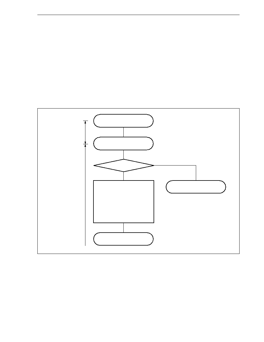
99
CHAPTER 5 INTERRUPT/EXCEPTION PROCESSING FUNCTION
User's Manual U10913EJ6V0UM
5.2.1 Acknowledgement operation
If the non-maskable interrupt is generated by NMI input, the CPU performs the following processing, and transfers
control to the handler routine:
(1) Saves the restored PC to FEPC.
(2) Saves the current PSW to FEPSW.
(3) Writes exception code 0010H to the higher halfword (FECC) of ECR.
(4) Sets the NP and ID bits of PSW and clears the EP bit.
(5) Loads the handler address (00000010H) of the non-maskable interrupt routine to the PC, and transfers control.
Figure 5-1 illustrates how the non-maskable interrupt is serviced.
Figure 5-1. Non-Maskable Interrupt Servicing
NMI input
Non-maskable interrupt request
Interrupt servicing
Interrupt request pending
FEPC
FEPSW
ECR.FECC
PSW.NP
PSW.EP
PSW.ID
PC
restored PC
PSW
0010H
1
0
1
00000010H
INTC acknowledged
CPU processing
PSW.NP
1
0
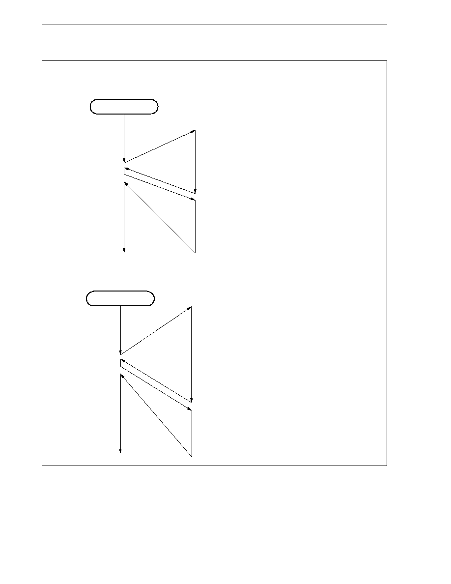
100
CHAPTER 5 INTERRUPT/EXCEPTION PROCESSING FUNCTION
User's Manual U10913EJ6V0UM
Figure 5-2. Acknowledging Non-Maskable Interrupt Request
(a) If a new NMI request is generated while an NMI service routine is executing:
(b) If a new NMI request is generated twice while an NMI service routine is executing:
Main routine
NMI request
NMI
request
(PSW.NP = 1)
NMI request pending because PSW.NP = 1
Pending NMI request processed
Main routine
NMI request
NMI request
Kept pending because NMI service program is being processed
Kept pending because NMI service program is being processed
NMI request
Only one NMI request is acknowledged even though
two or more NMI requests are generated
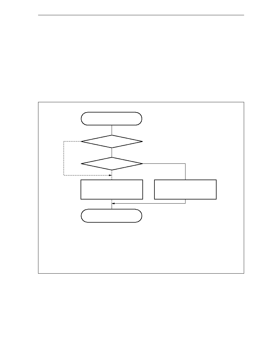
101
CHAPTER 5 INTERRUPT/EXCEPTION PROCESSING FUNCTION
User's Manual U10913EJ6V0UM
5.2.2 Restore operation
Execution is restored from the non-maskable interrupt servicing by the RETI instruction.
When the RETI instruction is executed, the CPU performs the following processing, and transfers control to the
address of the restored PC.
(1) Restores the values of PC and PSW from FEPC and FEPSW, respectively, because the EP bit of PSW is 0
and the NP bit of PSW is 1.
(2) Transfers control back to the address of the restored PC and the state of PSW.
Figure 5-3 illustrates how the RETI instruction is processed.
Figure 5-3. RETI Instruction Processing
Caution When the PSW.EP bit and PSW.NP bit are changed by the LDSR instruction during the non-
maskable interrupt servicing, in order to restore the PC and PSW correctly during recovery
by the RETI instruction, it is necessary to reset PSW.EP to 0 and PSW.NP to 1 using the LDSR
instruction immediately before the RETI instruction.
Remark
The solid line shows the CPU processing flow.
RETI instruction
Original processing restored
PC
PSW
EIPC
EIPSW
PSW.EP
1
0
1
0
PC
PSW
FEPC
FEPSW
PSW.NP
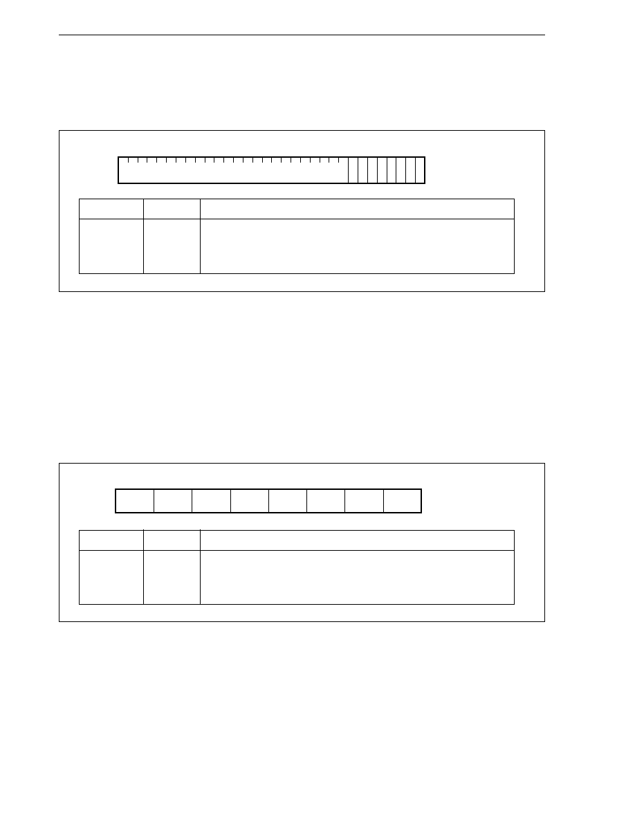
102
CHAPTER 5 INTERRUPT/EXCEPTION PROCESSING FUNCTION
User's Manual U10913EJ6V0UM
5.2.3 Non-maskable interrupt status flag (NP)
The NP flag is a status flag that indicates that non-maskable interrupt (NMI) processing is under execution. This
flag is set when the NMI interrupt has been acknowledged, and masks all interrupt and exceptions to prohibit multiple
interrupts from being acknowledged.
Bit position
Bit name
Function
7
NP
NMI Pending
Indicates that NMI interrupt servicing is under execution.
0: No NMI interrupt servicing
1: NMI interrupt currently being serviced
5.2.4 Noise elimination of NMI pin
NMI pin noise is eliminated with analog delay. The delay time is 60 to 220 ns. The signal input that changes in
less than this time period is not internally acknowledged.
The NMI pin is used for releasing the software stop mode. In the software stop mode, noise elimination does not
use system clock for noise elimination because the internal system clock is stopped.
5.2.5 Edge detection function of NMI pin
The external interrupt mode resister 0 (INTM0) is a register that specifies the valid edge of the non-maskable
interrupt (NMI). The valid edge of NMI can be specified as the rising or falling edge by the ESN0 bit of this register.
This register can be read or written in 8-bit or 1-bit units.
Bit position
Bit name
Function
0
ESN0
Edge Select NMI
Specifies valid edge of NMI pin.
0: Falling edge
1: Rising edge
31
0
PSW
After reset
00000020H
7
NP
6
EP
5
ID
4
SAT
3
CY
2
OV
1
S Z
8
0
0
0
0
0
0
0
0
0
0
0
0
0
0
0
0
0
0
0
0
0
0
0
0
Address
FFFFF180H
7
0
INTM0
6
0
5
0
4
0
3
0
2
0
1
0
0
ESN0
After reset
00H

103
CHAPTER 5 INTERRUPT/EXCEPTION PROCESSING FUNCTION
User's Manual U10913EJ6V0UM
5.3 Maskable Interrupts
Maskable interrupt requests can be masked by interrupt control registers. The V853 has 32 maskable interrupt
sources.
If two or more maskable interrupt requests are generated at the same time, they are acknowledged according to
the default priority. In addition to the default priority, eight levels of priorities can be specified by using the interrupt
control registers, allowing programmable priority control.
When an interrupt request has been acknowledged, the acknowledgement of other maskable interrupts is disabled
and the interrupt disabled (DI) status is set.
When the EI instruction is executed in an interrupt servicing routine, the interrupt enabled (EI) status is set which
enables interrupts having a higher priority to immediately interrupt the current service routine in progress. Note that
only interrupts with a higher priority will have this capability; interrupts with the same priority level cannot be nested.
To use multiple interrupts, the following processes are necessary.
<1> Saves EIPC and EIPSW to memory or general-purpose registers before executing the EI instruction.
<2> Executes the DI instruction, then restores the saving values at <1> to EIPC and EIPSW, before executing
the RETI instruction.
104
CHAPTER 5 INTERRUPT/EXCEPTION PROCESSING FUNCTION
User
'
s Manual U10913EJ6V0UM
5.3.1 Block diagram
Figure 5-4. Maskable Interrupt Block Diagram
xx: Peripheral unit identification name (OV, P11 to P14, CM, CS, SE, SR, ST, AD)
n:
Peripheral unit number (none, or 0 to 4 and 11 to 14)
RPU
Selector
32
1
0
32
1
032
1
0
3
2
1
0
3
210
32
10
32
1032
1032
10
32
1
032
1
0
32
1
0
INTM1
INTM2
INTM3
INTM4
SIO
INTCSI0
INTOV11
Internal Bus
XXMKn (Interrupt mask flag)
ISPR
Handler
address
generator
CPU
PSW
ID
Interrupt request
Interrupt request
acknowledge
HALT mode
release signal
XXPRn (Priority controller)
7
0
OVIF11
OVIF12
OVIF13
OVIF14
P11IF0
P11IF1
P11IF2
P11IF3
P12IF0
P12IF1
P12IF2
P12IF3
P13IF0
P13IF1
P13IF2
P13IF3
P14IF0
P14IF1
P14IF2
P14IF3
CSIF0
CSIF1
CSIF2
CSIF3
SEIF0
SRIF0
STIF0
SEIF1
SRIF1
STIF1
ADIF
CMIF4
INTOV12
INTOV13
INTOV14
INTP110/INTCC110
INTP111/INTCC111
INTP112/INTCC112
INTP113/INTCC113
INTP120/INTCC120
INTP121/INTCC121
INTP122/INTCC122
INTP123/INTCC123
INTP130/INTCC130
INTP131/INTCC131
INTP132/INTCC132
INTP133/INTCC133
INTP140/INTCC140
INTP141/INTCC141
INTP142/INTCC142
INTP143/INTCC143
INTCM4
INTAD
INTCSI1
INTCSI2
INTCSI3
INTSER0
INTSR0
INTST0
INTSER1
INTSR1
INTST1
A/D Converter
INTP110
INTP111
INTP112
INTP113
INTP120
INTP121
INTP122
INTP123
INTP130
INTP131
INTP132
INTP133
INTP140
INTP141
INTP142
INTP143

105
CHAPTER 5 INTERRUPT/EXCEPTION PROCESSING FUNCTION
User's Manual U10913EJ6V0UM
5.3.2 Operation
If a maskable interrupt occurs, the CPU performs the following processing, and transfers control to a handler
routine.
(1) Saves the restored PC to EIPC.
(2) Saves the current PSW to EIPSW.
(3) Writes an exception code to the lower halfword of ECR (EICC).
(4) Sets the ID bit of PSW and clears the EP bit.
(5) Loads the corresponding handler address to the PC, and transfers control.
Figure 5-5 illustrates how the maskable interrupts are processed.
106
CHAPTER 5 INTERRUPT/EXCEPTION PROCESSING FUNCTION
User's Manual U10913EJ6V0UM
Figure 5-5. Maskable Interrupt Servicing
The INT input masked by the interrupt controllers and the INT input that occurs while the other interrupt is being
serviced (when PSW.NP = 1 or PSW.ID = 1) are internally pended by the interrupt controller. When the interrupts
are unmasked, or when PSW.NP = 0 and PSW.ID = 0 by using the RETI and LDSR instructions, the pending INT
input starts the new maskable interrupt servicing.
Maskable interrupt request
Interrupt servicing
EIPC
EIPSW
ECR.EICC
PSW.EP
PSW.ID
PC
INTC acknowledged
CPU processing
XXIF = 1
No
Yes
XXMK = 0
Priority higher than
that of interrupt currently
processed?
Interrupt request pending
PSW.NP
PSW.ID
Interrupt servicing pending
No
No
No
No
1
0
1
0
Interrupt request?
INT input
Yes
Yes
Yes
Yes
Priority higher
than that of other interrupt
request?
Highest default
priority of interrupt requests
with same priority?
Interrupt unmasked?
restored PC
PSW
exception code
0
1
vector address
107
CHAPTER 5 INTERRUPT/EXCEPTION PROCESSING FUNCTION
User's Manual U10913EJ6V0UM
5.3.3 Restore
To restore execution from the maskable interrupt servicing, the RETI instruction is used.
When the RETI instruction is executed, the CPU performs the following steps, and transfers control to the address
of the restored PC.
(1) Restores the values of PC and PSW from EIPC and EIPSW because the EP bit of PSW is 0 and the NP bit
of PSW is 0.
(2) Transfers control to the address of the restored PC and the state of PSW.
Figure 5-6 illustrates the processing of the RETI instruction.
Figure 5-6. RETI Instruction Processing
Caution When the PSW.EP bit and the PSW.NP bit are changed by the LDSR instruction during the
maskable interrupt servicing, in order to restore the PC and PSW correctly during recovery
by the RETI instruction, it is necessary to reset PSW.EP to 0 and PSW.NP to 0 using the LDSR
instruction immediately before the RETI instruction.
Remark
The solid line shows the CPU processing flow.
RETI instruction
Restores original processing
PC
PSW
EIPC
EIPSW
PSW.EP
1
0
1
0
PC
PSW
FEPC
FEPSW
PSW.NP

108
CHAPTER 5 INTERRUPT/EXCEPTION PROCESSING FUNCTION
User's Manual U10913EJ6V0UM
5.3.4 Priorities of maskable interrupts
The V853 provides multiple interrupt servicing in which an interrupt is acknowledged while another interrupt is being
serviced. Multiple interrupts can be controlled by priority levels.
There are two types of priority level control: control based on the default priority levels, and control based on the
programmable priority levels specified by the interrupt priority level specification bit (xxPRn) in an interrupt control
register (xxICn). When two or more interrupts having the same priority level specified by xxPRn are generated at
the same time, interrupts are serviced in order depending on the priority level allocated to each interrupt request type
(default priority level) beforehand. For more information, refer to Table 5-1. The programmable priority control
customizes interrupt requests into eight levels by setting the priority level specification flag.
Note that when an interrupt is acknowledged, the ID flag of PSW is automatically set to 1. Therefore, when multiple
interrupts are to be used, clear the ID flag to 0 beforehand (for example, by placing the EI instruction into the interrupt
service program) to set the interrupt enable mode.
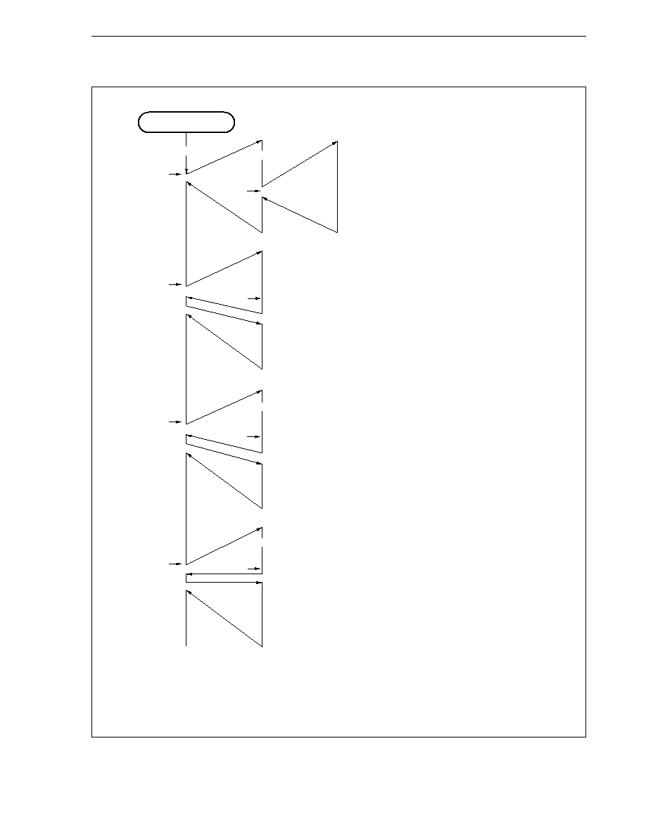
109
CHAPTER 5 INTERRUPT/EXCEPTION PROCESSING FUNCTION
User's Manual U10913EJ6V0UM
Figure 5-7. Example of Interrupt Nesting Process (1/2)
Remarks 1. a to u in the figure are the names of interrupt requests shown for the sake of explanation.
2. The default priority in the figure indicates the relative priority between two interrupt requests.
Caution The values of EIPC and EIPSW registers must be saved before executing multiple interrupts.
Main routine
EI
EI
Interrupt request a
(level 3)
Processing of a
Processing of b
Interrupt
request b
(level 2)
Processing of c
Interrupt request c
(level 3)
Interrupt request d
(level 2)
Processing of d
Processing of e
EI
Interrupt request e
(level 2)
Interrupt request f
(level 3)
Processing of f
EI
Processing of g
Interrupt request g
(level 1)
Interrupt request h
(level 1)
Processing of h
Interrupt request h is held pending even if interrupts are
enabled because its priority is the same as that of g
(default priority is ignored).
Interrupt request f is held pending even if interrupts are
enabled because its priority is lower than that of e.
Interrupt request b is acknowledged because the priority of
b is higher than that of a and interrupts are enabled.
Although the priority of interrupt request d is higher
than that of c, d is held pending because interrupts
are disabled.
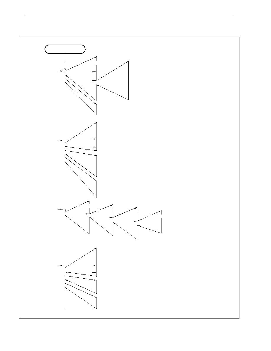
110
CHAPTER 5 INTERRUPT/EXCEPTION PROCESSING FUNCTION
User's Manual U10913EJ6V0UM
Figure 5-7. Example of Interrupt Nesting Process (2/2)
Notes 1. Lower default priority
2. Higher default priority
Main routine
EI
Interrupt request i
(level 2)
Processing of i
Processing of k
Interrupt
request j
(level 3)
Processing of j
Interrupt request l
(level 2)
EI
EI
EI
EI
Interrupt request o
(level 3)
Interrupt request s
(level 1)
Interrupt request k
(level 1)
Processing of l
Processing of n
Processing of m
Processing of s
Processing of u
Processing of t
Interrupt
request m
(level 3)
Interrupt request n
(level 1)
Processing of o
Interrupt
request p
(level 2)
Interrupt
request q
(level 1)
Interrupt
request r
(level 0)
Interrupt request u
(level 2)
Note 2
Interrupt
request t
(level 2)
Note 1
Processing of p
Processing of q
Processing of r
EI
If levels 3 to 0 are acknowledged
Pending interrupt requests t and u are acknowledged
after processing of s.
Because the priorities of t and u are the same, u is
acknowledged first because it has the higher default
priority, regardless of the order in which the interrupt
requests have been generated.
Pending interrupt requests are acknowledged after
processing of interrupt request l.
At this time, interrupt requests n is acknowledged first
even though m has occurred first because the priority of
n is higher than that of m.
Interrupt requests m and n are held pending because
processing of l is performed in the interrupt disabled
status.
Interrupt request j is held pending because its priority is
lower than that of i. k that occurs after j is acknowledged
because it has the higher priority.

111
CHAPTER 5 INTERRUPT/EXCEPTION PROCESSING FUNCTION
User's Manual U10913EJ6V0UM
Figure 5-8. Example of Processing Interrupt Requests Simultaneously Generated
Main routine
EI
Interrupt request a (level 2)
Interrupt request b (level 1)
Interrupt request c (level 1)
Default priority a > b > c
Processing of interrupt request b
Processing of interrupt request c
Processing of interrupt request a
·
·
Interrupt request b and c are acknowledged
first according to their priorities.
Because the priorities of b and c are the same,
b is acknowledged first because it has the
higher default priority.

112
CHAPTER 5 INTERRUPT/EXCEPTION PROCESSING FUNCTION
User's Manual U10913EJ6V0UM
5.3.5 Interrupt control register (xxICn)
An interrupt control register is assigned to each maskable interrupt and sets the control conditions for each
maskable interrupt request.
The interrupt control register can be read/written in 8-bit or 1-bit units.
Bit position
Bit name
Function
7
xxIFn
Interrupt Request Flag
Interrupt request flag
0: Interrupt request not issued
1: Interrupt request issued
xxIFn flag is automatically reset by hardware when interrupt request is acknowledged.
6
xxMKn
Mask Flag
Interrupt mask flag
0: Enables interrupt servicing
1: Disables interrupt servicing (pending)
2 to 0
xxPRn2 to
Priority
xxPRn0
Specifies eight levels of priorities for each interrupt.
xxPRn2
xxPRn1
xxPRn0
Interrupt priority specification bit
0
0
0
Specifies level 0 (highest)
0
0
1
Specifies level 1
0
1
0
Specifies level 2
0
1
1
Specifies level 3
1
0
0
Specifies level 4
1
0
1
Specifies level 5
1
1
0
Specifies level 6
1
1
1
Specifies level 7 (lowest)
Remark
xx: identification name of each peripheral unit (OV, P11 to P14, CM, CS, SE, SR, ST, or AD)
n:
Peripheral unit number (none, 0 to 4, or 11 to 14)
Address
FFFFF100H to
FFFFF13EH
7
xxIFn
xxICn
6
xxMKn
5
0
4
0
3
0
2
xxPRn2
1
xxPRn1
0
xxPRn0
After reset
47H

113
CHAPTER 5 INTERRUPT/EXCEPTION PROCESSING FUNCTION
User's Manual U10913EJ6V0UM
The address and bits of each interrupt control register are shown below.
Table 5-2. Address and Bits of Interrupt Control Register
Address
Register
Bit
7
6
5
4
3
2
1
0
FFFFF100H
OVIC11
OVIF11
OVMK11
0
0
0
OVPR112
OVPR111
OVPR110
FFFFF102H
OVIC12
OVIF12
OVMK12
0
0
0
OVPR122
OVPR121
OVPR120
FFFFF104H
OVIC13
OVIF13
OVMK13
0
0
0
OVPR132
OVPR131
OVPR130
FFFFF106H
OVIC14
OVIF14
OVMK14
0
0
0
OVPR142
OVPR141
OVPR140
FFFFF108H
P11IC0
P11IF0
P11MK0
0
0
0
P11PR02
P11PR01
P11PR00
FFFFF10AH
P11IC1
P11IF1
P11MK1
0
0
0
P11PR12
P11PR11
P11PR10
FFFFF10CH
P11IC2
P11IF2
P11MK2
0
0
0
P11PR22
P11PR21
P11PR20
FFFFF10EH
P11IC3
P11IF3
P11MK3
0
0
0
P11PR32
P11PR31
P11PR30
FFFFF110H
P12IC0
P12IF0
P12MK0
0
0
0
P12PR02
P12PR01
P12PR00
FFFFF112H
P12IC1
P12IF1
P12MK1
0
0
0
P12PR12
P12PR11
P12PR10
FFFFF114H
P12IC2
P12IF2
P12MK2
0
0
0
P12PR22
P12PR21
P12PR20
FFFFF116H
P12IC3
P12IF3
P12MK3
0
0
0
P12PR32
P12PR31
P12PR30
FFFFF118H
P13IC0
P13IF0
P13MK0
0
0
0
P13PR02
P13PR01
P13PR00
FFFFF11AH
P13IC1
P13IF1
P13MK1
0
0
0
P13PR12
P13PR11
P13PR10
FFFFF11CH
P13IC2
P13IF2
P13MK2
0
0
0
P13PR22
P13PR21
P13PR20
FFFFF11EH
P13IC3
P13IF3
P13MK3
0
0
0
P13PR32
P13PR31
P13PR30
FFFFF120H
P14IC0
P14IF0
P14MK0
0
0
0
P14PR02
P14PR01
P14PR00
FFFFF122H
P14IC1
P14IF1
P14MK1
0
0
0
P14PR12
P14PR11
P14PR10
FFFFF124H
P14IC2
P14IF2
P14MK2
0
0
0
P14PR22
P14PR21
P14PR20
FFFFF126H
P14IC3
P14IF3
P14MK3
0
0
0
P14PR32
P14PR31
P14PR30
FFFFF128H
CMIC4
CMIF4
CMMK4
0
0
0
CMPR42
CMPR41
CMPR40
FFFFF12AH
CSIC0
CSIF0
CSMK0
0
0
0
CSPR02
CSPR01
CSPR00
FFFFF12CH
CSIC1
CSIF1
CSMK1
0
0
0
CSPR12
CSPR11
CSPR10
FFFFF12EH
CSIC2
CSIF2
CSMK2
0
0
0
CSPR22
CSPR21
CSPR20
FFFFF130H
CSIC3
CSIF3
CSMK3
0
0
0
CSPR32
CSPR31
CSPR30
FFFFF132H
SEIC0
SEIF0
SEMK0
0
0
0
SEPR02
SEPR01
SEPR00
FFFFF134H
SRIC0
SRIF0
SRMK0
0
0
0
SRPR02
SRPR01
SRPR00
FFFFF136H
STIC0
STIF0
STMK0
0
0
0
STPR02
STPR01
STPR00
FFFFF138H
SEIC1
SEIF1
SEMK1
0
0
0
SEPR12
SEPR11
SEPR10
FFFFF13AH
SRIC1
SRIF1
SRMK1
0
0
0
SRPR12
SRPR11
SRPR10
FFFFF13CH
STIC1
STIF1
STMK1
0
0
0
STPR12
STPR11
STPR10
FFFFF13EH
ADIC
ADIF
ADMK
0
0
0
ADPR2
ADPR1
ADPR0
114
CHAPTER 5 INTERRUPT/EXCEPTION PROCESSING FUNCTION
User's Manual U10913EJ6V0UM
5.3.6 Noise eliminator
Pins INTPn0 to INTPn3, TIn, TCLRn, and ADTRG are provided with timing controllers for maintaining the following
noise elimination time (n = 11 to 14).
A signal input, which changes a level in the time less than the noise elimination time, is not acknowledged internally.
Pin
Noise Elimination Time
TCLR11 to TCLR14
2 to 3 T
CY
TI11 to TI14
(T
CY
: 1 system clock period)
INTP110 to INPT112
INTP120 to INTP123
INTP130 to INTP133
INTP140 to INTP143
INTP113/ADTRG
Figure 5-9. Example of Noise Elimination Timing
Cautions 1. When the input pulse width is 2 to 3 sampling clocks, it is undefined whether that pulse is
detected as a valid edge or eliminated as noise.
2. In order to detect as a pulse, input a signal with same level for more than 3 sampling clocks.
3. When noise is generated in synchronization with the sampling, it may not be recognized as
noise. In this case, eliminate the noise by placing filters on the input pins.
CLKOUT
Input signal
Internal signal
Rising edge
detected
Falling edge
detected
3 clocks max.
2 clocks min.
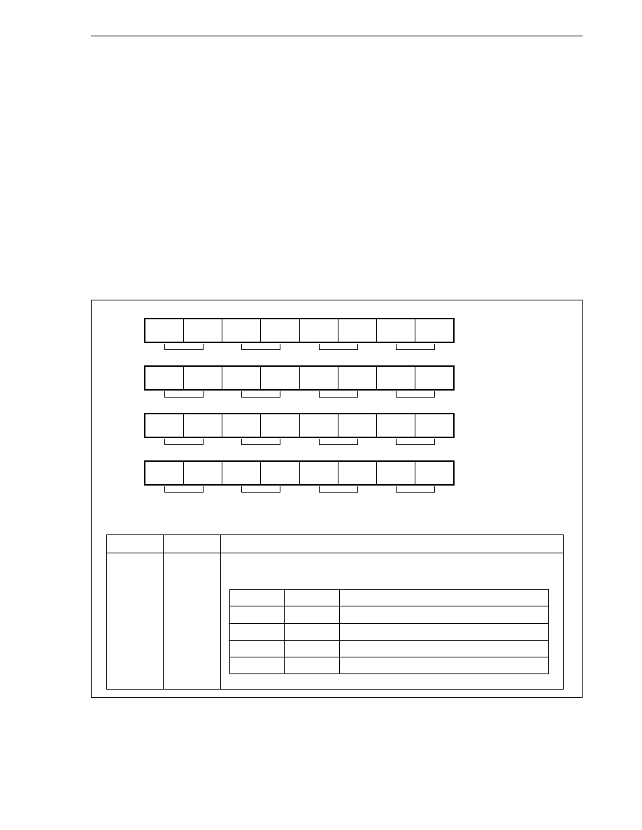
115
CHAPTER 5 INTERRUPT/EXCEPTION PROCESSING FUNCTION
User's Manual U10913EJ6V0UM
5.3.7 Edge detection function
External interrupt mode registers 1 to 4 (INTM1 to INTM4) specify the valid edges of external interrupt requests
INTP110 to INTP112, INTP113/ADTRG, INTP120 to INTP123, INTP130 to INTP133, and INTP140 to INTP143 that
are input from external pins. The correspondence of each register and the external interrupt request controlled by
the register is shown below.
· INTM1: INTP110 to INTP112, INTP113/ADTRG
· INTM2: INTP120 to INTP123
· INTM3: INTP130 to INTP133
· INTM4: INTP140 to INTP143
The INTP113 is also used as the external trigger input (ADTRG) of the A/D converter. Therefore, the ES031 and
ES030 bits of the INTM1 are used for specifying the valid edges of the external trigger input (ADTRG) if the A/D
converter mode register 1 (ADM1) TRG bit is set to the external trigger mode.
The valid edge of each pin can be specified to be the rising, falling, and both rising and falling edges.
Both the registers can be read/written in 8-bit or 1-bit units.
Bit position
Bit name
Function
7, 5, 3, 1
ES (m 1) n1
Edge Select
6, 4, 2, 0
ES (m 1) n0
Specifies valid edge of INTP1mn pin and ADTRG pin.
(m = 4 to 1,
n = 3 to 0)
ES (m 1) n1 ES (m 1) n0
Operation
0
0
Falling edge
0
1
Rising edge
1
0
RFU (reserved)
1
1
Both rising and falling edges
Address
FFFFF182H
7
ES031
INTM1
Control
pin
6
ES030
INTP113/ADTRG
5
ES021
4
ES020
3
ES011
2
ES010
1
ES001
0
ES000
After reset
00H
FFFFF184H
INTM2
00H
FFFFF186H
INTM3
00H
FFFFF188H
INTM4
00H
ES331
ES330
ES321
ES320
ES311
ES310
ES301
ES300
ES131
ES130
ES121
ES120
ES111
ES110
ES101
ES100
ES231
ES230
ES221
ES220
ES211
ES210
ES201
ES200
INTP112
INTP111
INTP110
Control
pin
INTP123
INTP122
INTP121
INTP120
Control
pin
INTP133
INTP132
INTP131
INTP130
Control
pin
INTP143
INTP142
INTP141
INTP140

116
CHAPTER 5 INTERRUPT/EXCEPTION PROCESSING FUNCTION
User's Manual U10913EJ6V0UM
5.3.8 In-service priority register (ISPR)
This register holds the priority level of the maskable interrupt currently acknowledged. When an interrupt request
is acknowledged, the bit of this register corresponding to the priority level of that interrupt is set to 1 and remains
set while the interrupt is serviced.
When the RETI instruction is executed, the bit corresponding to the interrupt request having the highest priority
is automatically reset to 0 by hardware. However, it is not reset when execution is returned from non-maskable
processing or exception processing.
This register is read-only in 8-bit or 1-bit units.
Bit position
Bit name
Function
7 to 0
ISPR7 to
In-Service Priority Flag
ISPR0
Indicates priority of interrupt currently acknowledged.
0: Interrupt request with priority n not acknowledged
1: Interrupt request with priority n acknowledged
Remark
n: 0 to 7 (priority level)
5.3.9 Maskable interrupt status flag (ID)
The interrupt disable status flag (ID) of the PSW controls the enabling and disabling of maskable interrupt requests.
Bit position
Bit name
Function
5
ID
Interrupt Disable
Indicates enabling/disabling of maskable interrupt servicing.
0: Maskable interrupt acknowledgement enabled
1: Maskable interrupt acknowledgement disabled (pending)
It is set to 1 by the DI instruction and reset to 0 by the EI instruction. Its value is also
modified by the RETI instruction or LDSR instruction when referencing the PSW.
Non-maskable interrupts and exceptions are acknowledged regardless of this flag.
When a maskable interrupt is acknowledged, ID flag is automatically set to 1 by
hardware.
Interrupt requests generated while interrupts are disabled (ID = 1) are acknowledged
when the xxIFn bit of the xxICn register is set (1) and ID flag is reset (0).
Address
FFFFF166H
7
ISPR7
ISPR
6
ISPR6
5
ISPR5
4
ISPR4
3
ISPR3
2
ISPR2
1
ISPR1
0
ISPR0
After reset
00H
31
0
PSW
After reset
00000020H
7
NP
6
EP
5
ID
4
SAT
3
CY
2
OV
1
S Z
8
0
0
0
0
0
0
0
0
0
0
0
0
0
0
0
0
0
0
0
0
0
0
0
0

117
CHAPTER 5 INTERRUPT/EXCEPTION PROCESSING FUNCTION
User's Manual U10913EJ6V0UM
5.4 Software Exception
The software exception is generated when the CPU executes the TRAP instruction, and can be always
acknowledged.
5.4.1 Operation
If the software exception occurs, the CPU performs the following processing, and transfers control to the handler
routine.
(1) Saves the restored PC to EIPC.
(2) Saves the current PSW to EIPSW.
(3) Writes an exception code to the lower 16 bits (EICC) of ECR (interrupt source).
(4) Sets the EP and ID bits of PSW.
(5) Loads the handler address (00000040H or 00000050H) of the software exception routine in the PC, and
transfers control.
Figure 5-10 illustrates how the software exception is processed.
Figure 5-10. Software Exception Processing
Note
TRAP instruction format: TRAP vector (where vector is 0 to 1FH)
The handler address is determined by the operand of the TRAP instruction (vector). If vector is 0 to 0FH, the handler
address is 00000040H; if the operand is 10H to 1FH, it is 00000050H.
TRAP instruction
Note
EIPC
EIPSW
ECR.EICC
PSW.EP
PSW.ID
PC
restored PC
PSW
exception code
1
1
handler address
CPU processing
Exception processing
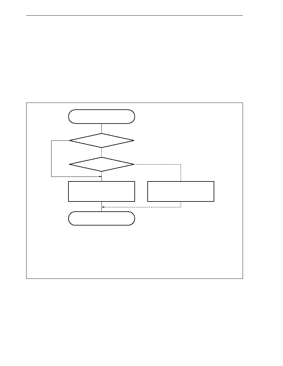
118
CHAPTER 5 INTERRUPT/EXCEPTION PROCESSING FUNCTION
User's Manual U10913EJ6V0UM
5.4.2 Restore
To restore or return execution from the software exception service routine, the RETI instruction is used.
When the RETI instruction is executed, the CPU performs the following steps, and transfers control to the address
of the restored PC.
(1) Restores the restored PC and PSW from EIPC and EIPSW because the EP bit of PSW is 1.
(2) Transfers control to the address of the restored PC and the state of PSW.
Figure 5-11 illustrates the processing of the RETI instruction.
Figure 5-11. RETI Instruction Processing
Caution
When the PSW.EP bit and the PSW.NP bit are changed by the LDSR instruction during the
software exception process, in order to restore the PC and PSW correctly during recovery
by the RETI instruction, it is necessary to reset PSW.EP to 1 using the LDSR instruction
immediately before the RETI instruction.
Remark
The solid line shows the CPU processing flow.
PSW.EP
RETI instruction
PC
PSW
EIPC
EIPSW
PSW.NP
Original processing restored
PC
PSW
FEPC
FEPSW
1
1
0
0

119
CHAPTER 5 INTERRUPT/EXCEPTION PROCESSING FUNCTION
User's Manual U10913EJ6V0UM
5.4.3 Exception status flag (EP)
The EP flag in the PSW is a status flag used to indicate that exception processing is in progress. It is set when
an exception occurs.
Bit position
Bit name
Function
6
EP
Exception Pending
Indicates that trap processing is in progress.
0: Exception processing is not in progress
1: Exception processing is in progress
31
0
PSW
After reset
00000020H
7
NP
6
EP
5
ID
4
SAT
3
CY
2
OV
1
S Z
8
0
0
0
0
0
0
0
0
0
0
0
0
0
0
0
0
0
0
0
0
0
0
0
0
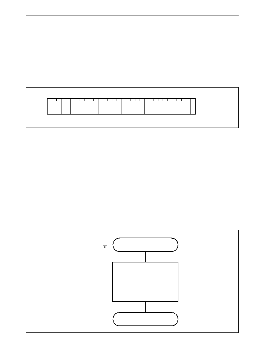
120
CHAPTER 5 INTERRUPT/EXCEPTION PROCESSING FUNCTION
User's Manual U10913EJ6V0UM
5.5 Exception Trap
The exception trap is an interrupt that is requested when illegal execution of an instruction takes place. In the
V853, an illegal op code exception (ILGOP: ILleGal OPcode trap) is considered as an exception trap.
Illegal op code exception occurs if the subop code field of an instruction to be executed next is not a valid op code.
5.5.1 Illegal op code definition
An illegal op code is defined to be a 32-bit word with bits 5 to 10 being 111111B and bits 23 to 26 being 0011B
to 1111B.
x: don't care
Caution Since a new instruction could be allocated to the illegal op code in future, it is recommended
not to use this illegal op code.
5.5.2 Operation
If an exception trap occurs, the CPU performs the following processing, and transfers control to the handler routine.
(1) Saves the restored PC to EIPC.
(2) Saves the current PSW to EIPSW.
(3) Writes an exception code (0060H) to the lower 16 bits (EICC) of ECR.
(4) Sets the EP and ID bits of PSW.
(5) Loads the handler address (00000060H) for the exception trap routine to the PC, and transfers control.
Figure 5-12 illustrates how the exception trap is processed.
Figure 5-12. Exception Trap Processing
15
16
23 22
x
21
x
20
x x x x x
x
x
x
x
x
x
x
x
x
x
1
1
1
1
1
1
x
x
x
x
x
27 26
31
0
4
5
10
11
12
13
1
1
1
1
0
to
1
0
1
Exception trap (ILGOP) occurs
EIPC
EIPSW
ECR.EICC
PSW.EP
PSW.ID
PC
restored PC
PSW
exception code
1
1
00000060H
CPU processing
Exception processing
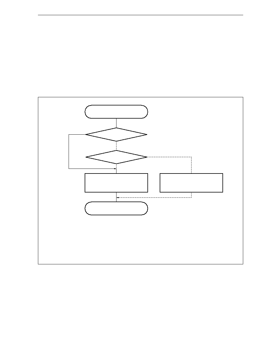
121
CHAPTER 5 INTERRUPT/EXCEPTION PROCESSING FUNCTION
User's Manual U10913EJ6V0UM
5.5.3 Restore
To restore or return execution from the exception trap, the RETI instruction is used.
When the RETI instruction is executed, the CPU performs the following processing, and transfers control to the
address of the restored PC.
(1) Restores the restored PC and PSW from EIPC and EIPSW because the EP bit of PSW is 1.
(2) Transfers control to the address of the restored PC and the state of PSW.
Figure 5-13 illustrates the processing of the RETI instruction.
Figure 5-13. RETI Instruction Processing
Caution
When the PSW.EP bit and the PSW.NP bit are changed by the LDSR instruction during the
exception trap process, in order to restore the PC and PSW correctly during recovery by the
RETI instruction, it is necessary to reset PSW.EP to 1 using the LDSR instruction immediately
before the RETI instruction.
Remark
The solid line shows the CPU processing flow.
PSW.EP
RETI instruction
PC
PSW
EIPC
EIPSW
PSW.NP
Original processing restored
PC
PSW
FEPC
FEPSW
1
1
0
0

122
CHAPTER 5 INTERRUPT/EXCEPTION PROCESSING FUNCTION
User's Manual U10913EJ6V0UM
5.6 Multiple Interrupts
Multiple interrupt servicing is a function that allows the nesting of interrupts. If a higher priority interrupt is generated
and acknowledged, it will be allowed to stop a current interrupt service routine in progress. Execution of the original
routine will resume once the higher priority interrupt routine is completed.
If an interrupt with a lower or equal priority is generated and a service routine is currently in progress, the later
interrupt will be held pending.
Multiple interrupt servicing control is performed when interrupt acknowledgement is enabled (ID = 0). Even in an
interrupt servicing routine, the state must be set to interrupt acknowledgement enabled (ID = 0). If a maskable interrupt
or exception is generated while a maskable interrupt or exception is being serviced, EIPC and EIPSW must be saved.
The following example shows the procedure of interrupt nesting.

123
CHAPTER 5 INTERRUPT/EXCEPTION PROCESSING FUNCTION
User's Manual U10913EJ6V0UM
(1) To acknowledge maskable interrupts in service routine
Service routine of maskable interrupt or exception
...
...
· Saves EIPC to memory or register
· Saves EIPSW to memory or register
· EI instruction (enables interrupt acknowledgement)
...
...
Acknowledges maskable interrupts
...
...
· DI instruction (disables interrupt acknowledgement)
· Restores saved value to EIPSW
· Restores saved value to EIPC
· RETI instruction
(2) To generate exception in service program
Service program of maskable interrupt or exception
...
...
· Saves EIPC to memory or register
· Saves EIPSW to memory or register
...
· TRAP instruction
Acknowledges exception such as TRAP
instruction
· Illegal op code
Acknowledges illegal op code exception
...
· Restores saved value to EIPSW
· Restores saved value to EIPC
· RETI instruction
Eight levels of priorities 0 to 7 (0 is the highest) can be programmed for each maskable interrupt request for
multiple interrupt servicing control. To set a priority level, write values to the xxPRn0 to xxPRn2 bits of the
interrupt request control register (xxICn) corresponding to each maskable interrupt request. After system
reset, the interrupt request is masked by the xxMKn bit, and the priority level is set to 7 by the xxPRn0 to xxPRn2
bits.
The priorities of maskable interrupts are as follows.
(High) Level 0 > Level 1 > Level 2 > Level 3 > Level 4 > Level 5 > Level 6 > Level 7 (Low)
Interrupt servicing that has been suspended as a result of multiple interrupt servicing is resumed after the interrupt
servicing of the higher priority has been completed and the RETI instruction has been executed.
A pending interrupt request is acknowledged after the current interrupt servicing has been completed and the RETI
instruction has been executed.
Caution In the non-maskable interrupt servicing routine (time until the RETI instruction is executed),
maskable interrupts are not acknowledged but are suspended.
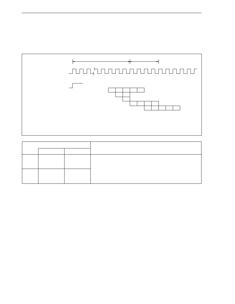
124
CHAPTER 5 INTERRUPT/EXCEPTION PROCESSING FUNCTION
User's Manual U10913EJ6V0UM
5.7 Interrupt Latency Time
The following table describes the V853 interrupt latency time.
Figure 5-14. Pipeline Operation upon Reception of Interrupt Request (Outline)
Interrupt Latency Time (Internal system clock)
Condition
Internal Interrupt External Interrupt
Minimum
11
13
Except:
· In IDLE/software STOP mode
· When external bus is accessed
Maximum
18
20
· When two or more interrupt request non-sample instructions are
executed in succession
· When interrupt control register is accessed
IF
ID
EX MEM WB
7 to 14 system clocks
4 system clocks
Internal system clock
(CLKOUT output)
Interrupt request
Instruction 1
Instruction 2
Instruction 3
Interrupt acknowledgement operation
Instruction (first instruction of
interrupt servicing routine)
INT1 to INT4: Interrupt acknowledgement processing
IFx: Instruction fetch to be invalid
IDx: Instruction decode to be invalid
IF
ID
EX MEM WB
IFx
IDx
IFx
INT1 INT2 INT3 INT4

125
CHAPTER 5 INTERRUPT/EXCEPTION PROCESSING FUNCTION
User's Manual U10913EJ6V0UM
5.8 Periods in Which Interrupts Are Not Acknowledged
An interrupt is acknowledged while an instruction is being executed. However, no interrupt will be acknowledged
between an interrupt request non-sample instruction and the next instruction.
Interrupt request non sample instructions are as follows.
· EI instruction
· DI instruction
· LDSR reg2, 0x5 instruction (vs. PSW)

126
CHAPTER 5 INTERRUPT/EXCEPTION PROCESSING FUNCTION
User's Manual U10913EJ6V0UM
(1) Acknowledgement of interrupt servicing following EI instruction
The V853 requires a minimum of 7 clocks from the occurrence of an interrupt request until the interrupt request
is acknowledged as the interrupt request determination period. Since instructions can continue to be executed
during this period, executing the DI (Disable Interrupt) instruction results in the interrupt disabled state. As
a result, all interrupt requests are held pending until the EI (Enable Interrupt) instruction is executed.
Moreover, since an interrupt determination period is also required when the EI instruction is executed, at least
7 clocks are required between execution of the EI instruction and acknowledgement of the interrupt request.
Therefore, if the DI instruction is executed before 7 clocks have elapsed following execution of the EI
instruction, interrupts will be held pending. To reliably acknowledge interrupts, insert instructions whose
execution clocks total 7 clocks or more between the EI instruction and DI instruction. This does not apply,
however, to the following instructions.
· IDLE/STOP mode setting
· EI instruction, DI instruction
· RETI instruction
· LDSR instruction (for PSW register)
· Access to interrupt control register (
××
lCn)
Example: When EI instruction processing is not enabled
[Program Example]
DI
;MK flag = 0 (interrupt request enable)
;Interrupt request occurrence (IF flag = 1)
EI
JR LP1
;7 clocks have not elapsed between EI instruction and DI
;instruction (3 clocks)
LP1:
DI
;Interrupt request not acknowledged
.
.
.
.
.
.
.
.
.
.
.
.
.
.
.
[Workaround Program Example]
DI
;MK flag = 0 (interrupt request enable)
;Interrupt request occurrence (IF flag = 1)
EI
NOP
;1 system clock
NOP
;1 system clock
NOP
;1 system clock
NOP
;1 system clock
JR LP1
;3 system clocks (branching to LP1 routine)
LP1:
DI
;Interrupt servicing executed at 8th system clock following
;execution of EI instruction
.
.
.
.
.
.
.
.
.
.
.
.
.
.
.
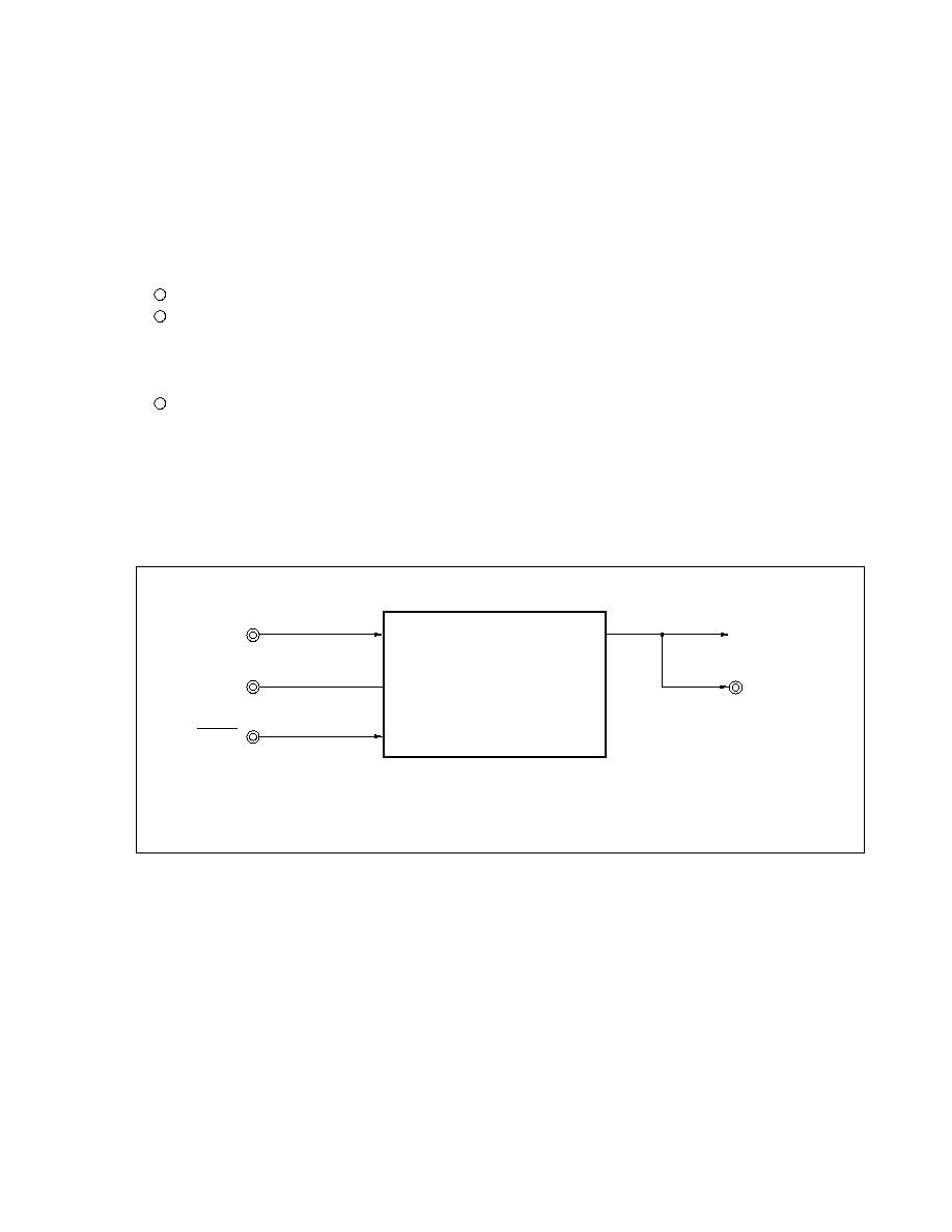
127
User's Manual U10913EJ6V0UM
CHAPTER 6 CLOCK GENERATOR FUNCTION
The clock generator (CG) generates and controls the internal system clock (
), which is supplied to all the internal
hardware units including the CPU.
6.1 Features
Multiplication function by PLL (Phase Locked Loop) synthesizer
Clock source
· Oscillation by connecting a resonator (PLL mode): fxx =
, 2
×
,
/5
· External clock (PLL mode): fxx =
, 2
×
,
/5
· External clock (direct mode): fxx = 2
×
Power save control
· HALT mode
· IDLE mode
· Software STOP mode
· Clock output inhibit mode
6.2 Configuration
Remark
: Internal system clock frequency
f
XX
: External oscillator or external clock frequency
X1
X2
CKSEL
(f
XX
)
Clock generator
CLKOUT
CPU, internal
peripheral I/O
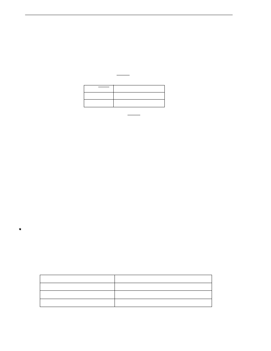
128
CHAPTER 6 CLOCK GENERATOR FUNCTION
User's Manual U10913EJ6V0UM
6.3 Selecting Input Clock
The clock generator consists of an oscillator and a PLL synthesizer. When a 6.5536 MHz crystal resonator or
ceramic resonator is connected across the X1 and X2 pins for example, the clock generator can generate a 32.768
(Max. 33) MHz internal system clock (
) in
×
5 mode.
An external clock can be directly connected to the oscillator. In this case, input the clock signal only to the X1
pin, and leave the X2 pin open.
The clock generator has two modes as the basic operation mode: PLL mode and direct mode.
The operation mode is selected with the CV
DD
/CKSEL pin.
CV
DD
/CKSEL
Operation Mode
V
DD
PLL mode
Low level
Direct mode
Caution Fix the input level when using the CV
DD
/CKSEL pin (this pin becomes the power source for the
PLL synthesizer in PLL mode). Switching during operation may cause erroneous operation.
6.3.1 Direct mode
An external clock is input in the direct mode. The external clock that is input is divided by the division ratio specified
in the clock control register (CKC), and an internal system clock which is 1/2 the frequency of the external clock (fxx)
is generated. This mode is mainly used for the applications requiring operation at a lower frequency. To minimize
adverse affect by noise, operation under an external clock frequency (f
XX
) lower than 32 MHz (internal system clock
frequency (
) = 16 MHz) is recommended.
6.3.2 PLL mode
In the PLL mode, an external clock is input by connecting an external oscillator, which is multiplied by the PLL
synthesizer to generate an internal system clock (
).
The multiplied PLL output is frequency-divided by the frequency division ratio specified by the clock control register
(CKC) to generate internal system clocks that are 5, 1, or 1/2 times the external oscillator or external clock frequency
(f
XX
).
When a system clock (5 x fxx) that is 5 times fxx is generated, because a frequency of up to 33 MHz can be generated
based on an external oscillator of 4 to 6.6 MHz and an external clock, a low-noise, power saving system can be
designed.
If the external oscillator or external clock source fails, the clock generator continues to provide the internal system
clock
based on the free-running frequency of the voltage control oscillator (VCO) inside the clock generator.
However, do not devise an application method in which you expect to use this free-running frequency.
Example Clock selecting PLL mode (
= 5
×
f
XX
)
Internal System Clock Frequency (
)
External Oscillator/External Clock Frequency (fxx)
32.768 MHz
6.5536 MHz
25.000 MHz
5.0000 MHz
20.000 MHz
4.0000 MHz
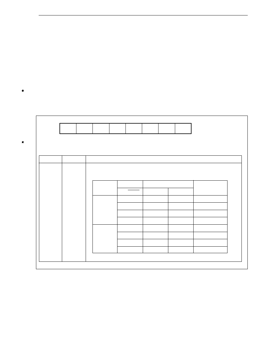
129
CHAPTER 6 CLOCK GENERATOR FUNCTION
User's Manual U10913EJ6V0UM
Operation
Pin
CKC register
Internal
mode
CV
DD
/CKSEL
CKDIV1
CKDIV0
system clock (
)
Direct mode
L
0
0
f
xx
/2
L
0
1
Setting prohibited
L
1
0
Setting prohibited
L
1
1
Setting prohibited
PLL mode
V
DD
0
0
5
×
f
xx
V
DD
0
1
Setting prohibited
V
DD
1
0
f
xx
V
DD
1
1
f
xx
/2
Caution when selecting PLL mode (
= 1/2
×
f
XX
,
= 1
×
f
XX
)
= 1/2
×
fxx,
= 1
×
fxx are used when there is no need to operate the V853 at a high frequency. Power
consumption can be reduced by lowering the internal system clock frequency using software.
Because
= 5
×
fxx is selected at reset, only an fxx value is used which makes 5
×
fxx smaller than the internal
system clock maximum frequency for the oscillator frequency and external clock frequency.
6.3.3 Clock control register (CKC)
This is an 8-bit register that controls the internal system clock frequency in PLL mode. It can be written only by
a specific combination of instruction sequences so that its contents are not overwritten by mistake due to erroneous
program execution (refer to 3.4.10 Specific registers).
In PLL mode, the internal system clock frequency (
) (5
×
f
XX
, f
XX
, f
XX
/2) setting can be changed during operation.
However, be sure to stop all the on-chip peripheral I/O when changing the internal system clock frequency setting
in order to prevent malfunction.
This register can be read/written in 8-bit or 1-bit units.
Note
00H (MODE = 1)
03H (MODE = 0)
Bit position
Bit name
Function
1, 0
CKDIV1,
Clock Divide
CKDIV0
Sets the internal system clock to the external clock (f
XX
).
Address
FFFFF072H
7
0
CKC
6
0
5
0
4
0
3
0
2
0
1
CKDIV1
0
CKDIV0
After reset
Note
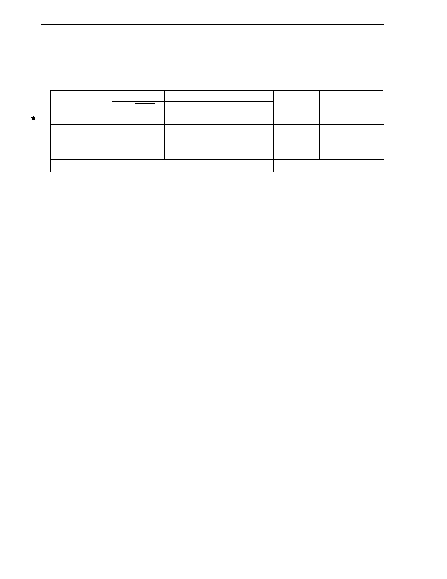
130
CHAPTER 6 CLOCK GENERATOR FUNCTION
User's Manual U10913EJ6V0UM
The sequence of setting data in this register is the same as the power save control register (PSC). However, the
limitation items listed in Caution 2 for the 3.4.10 Specific registers do not apply.
A setting example is shown below.
Operation
Pin CKC Register
External Clock
Internal
Mode
CV
DD
/CKSEL
CKDIV1
CKDIV0
(f
xx
)
System Clock (
)
Direct mode
Low level input
0
0
66 MHz
33 MHz
PLL mode
V
DD
0
0
6.6 MHz
33 MHz
V
DD
1
0
6.6 MHz
6.6 MHz
V
DD
1
1
6.6 MHz
3.3 MHz
Other than above
Setting prohibited

131
CHAPTER 6 CLOCK GENERATOR FUNCTION
User's Manual U10913EJ6V0UM
6.4 PLL Lockup
Following a power-on reset or when releasing the STOP mode, an amount of time will be required for the PLL to
stabilize before using any of the V853 hardware functions (PLL lockup time). The state in which the frequency is
not stable is called an unlocked state and the state in which it has been stabilized is called a locked status.
Two flags in the system status register are available to check the stabilization of the PLL frequency: the UNLOCK
flag, which indicates the stabilization status of the PLL frequency, and the PRERR flag, which indicates the occurrence
of a protection error (for the details of the PRERR flag, refer to 3.4.10 (2) System status register (SYS)).
The SYS register, which contains these UNLOCK and PREERR flags, can be read/written in 8-bit or 1-bit units.
Bit position
Bit name
Function
0
UNLOCK
Unlock Status Flag
This is a read-only flag and indicates unlocked state of PLL.
It holds "0" as long as the locked state is maintained, and is not changed even if the system
is reset.
0: Indicates locked state
1: Indicates unlocked state
Remark
For the description of the PRERR flag, refer to 3.4.10 (2) System status register (SYS).
If the unlocked state condition should arise, due to a power or clock source failure, the UNLOCK flag should be
checked to verify that the PLL has stabilized before performing any operations dependent on the execution speed,
such as real-time processing.
Static processing such as setting the on-chip hardware units and initialization of the register data and memory data,
however, can be executed before the UNLOCK flag is reset.
The following is the relationship between the oscillation stabilization time (the time from when the oscillator starts
oscillating until the input waveform stabilizes) and the PLL lockup time (the time until the frequency stabilizes) when
using an oscillator.
Oscillation stabilization time < PLL lockup time
Address
FFFFF078H
7
0
SYS
6
0
5
0
4
PRERR
3
0
2
0
1
0
0
UNLOCK
After reset
0000000xB

132
CHAPTER 6 CLOCK GENERATOR FUNCTION
User's Manual U10913EJ6V0UM
6.5 Power Save Control
6.5.1 General
The V853 is provided with the following power save or standby modes to reduce power consumption when CPU
operation is not required.
(1) HALT mode
In this mode, the clock generator (oscillator and PLL synthesizer) continues operation but the operating clock
of the CPU stops. Supply of clocks to the other on-chip peripherals continues and they continue to operate.
Through intermittent operation by combining normal operation and the HALT mode, the total power consumption
of the system can be reduced.
The HALT mode is entered by a dedicated instruction (HALT instruction).
(2) IDLE mode
In this mode, both the CPU clock and the internal system clock are stopped to further reduce power con-
sumption. However, since the clock generator continues to run, normal operation can resume without having
to wait for the oscillator and PLL circuits to stabilize.
The IDLE mode is entered by setting the specific register PSC.
The IDLE mode is categorized between the software STOP and HALT modes in terms of clock stabilization
time and power consumption, and is used in applications where it is desirable to eliminate the clock oscillation
time after standby release but low power consumption is needed.
(3) Software STOP mode
In this mode, the CPU clock, the internal system clock, and the clock generator are stopped, reducing power
consumption to only leakage current. In this state, power consumption is minimized.
The STOP mode is entered by setting the specific register PSC.
(a) In PLL mode
As soon as the oscillator stops, the clock output of the PLL synthesizer is stopped. After the software
STOP mode has been released, it is necessary to allow for the stabilization time of the oscillator and
system clock. Moreover, the lockup or stabilization time of the PLL may also be necessary, depending
on the application. However, when the processor operates on an external clock, the oscillation
stabilization time of the oscillator does not need to be secured.
(b) In direct mode
When stopping the clock, set the X1 pin to low level.
Lockup time is not necessary.
(4) Clock output inhibit
Output of the system clock from the CLKOUT pin is inhibited.
The operations of the clock generator in the normal, HALT, IDLE, and software STOP modes are shown in Table
6-1.
By combining and selecting the mode best suited for a specific application, the power consumption of the system
can be effectively reduced.
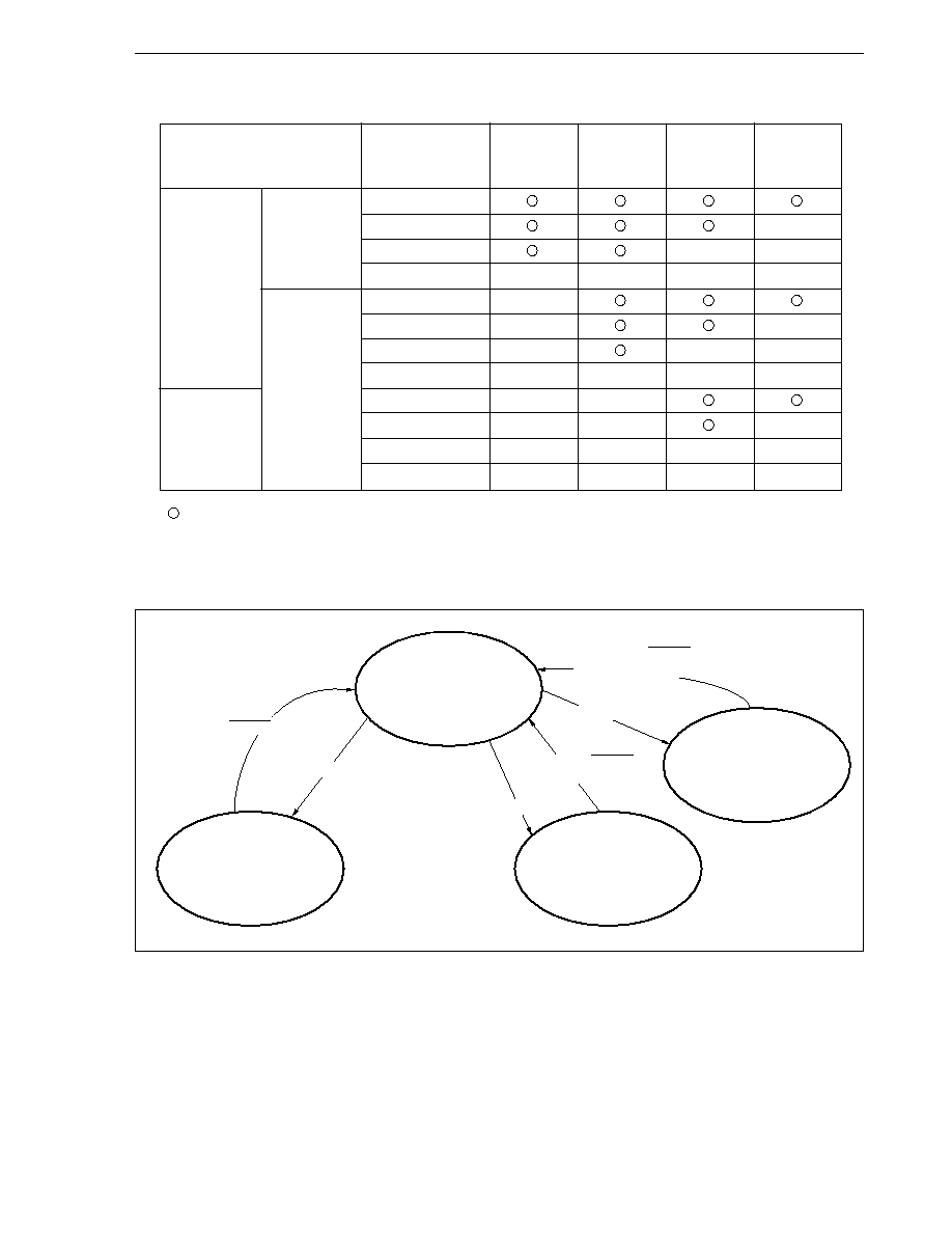
133
CHAPTER 6 CLOCK GENERATOR FUNCTION
User's Manual U10913EJ6V0UM
Table 6-1. Operation of Clock Generator by Power Save Control
PLL mode
Oscillation
Normal
with resonator
HALT
×
IDLE
×
×
Software STOP
×
×
×
×
External clock
Normal
×
HALT
×
×
IDLE
×
×
×
Software STOP
×
×
×
×
Direct mode
Normal
×
×
HALT
×
×
×
IDLE
×
×
×
×
Software STOP
×
×
×
×
: operates
×
: stops
Status Transition Diagram
Clock Source
Standby Mode
Oscillator
Circuit
(OSC)
PLL
Synthesizer
Clock Supply
to Peripheral
I/O
Clock Supply
to CPU
Normal
Software STOP
Released by RESET or NMI input
Software STOP mode is entered
IDLE
IDLE mode is entered
Released by RESET or
NMI input
HALT mode is entered
Released by RESET, NMI input, or
maskable interrupt request
HALT

134
CHAPTER 6 CLOCK GENERATOR FUNCTION
User's Manual U10913EJ6V0UM
6.5.2 Control registers
(1) Power save control register (PSC)
This is an 8-bit register that controls the power save mode. This is a specific register, and only access by
the specific sequence is valid during write cycles. For details, refer to 3.4.10 Specific registers.
Bit position
Bit name
Function
7, 6
DCLKn
Disable CLKOUT
(n = 1, 0)
Specifies operation mode of CLKOUT pin
DCLK1
DCLK0
Mode
0
0
Normal output mode
0
1
RFU (reserved)
1
0
RFU (reserved)
1
1
Clock output inhibit mode
5
TBCS
Time Base Count Select
Selects clock of time base counter
0: fxx/2
8
1: fxx/2
9
For details, refer to explanation of "Time base counter (TBC)" in section 6.6 Securing
Oscillation Stabilization Time.
4
CESEL
Crystal/External Select
Specifies functions of X1 and X2 pins
0: Oscillator connected to X1 and X2 pins
1: External clock connected to X1 pin
When CESEL = 1, the feedback loop of the oscillator is cut off to prevent current leakage in
the software STOP mode. Time base counter (TBC) does not count the oscillation
stabilization time after the software STOP mode is released.
2
IDLE
IDLE Mode
Specifies IDLE mode.
When "1" is written to this bit, IDLE mode is entered.
When IDLE mode is released, this bit is automatically reset to 0.
1
STP
STOP Mode
Specifies software STOP mode.
When "1" is written to this bit, STOP mode is entered.
When software STOP mode is released, this bit is automatically reset to 0.
Address
FFFFF070H
7
DCLK1
PSC
6
DCLK0
5
TBCS
4
CESEL
3
0
2
IDLE
1
STP
0
0
After reset
C0H
135
CHAPTER 6 CLOCK GENERATOR FUNCTION
User's Manual U10913EJ6V0UM
6.5.3 HALT mode
(1) Entering and operation status
In the HALT mode, the clock generator (oscillator and PLL synthesizer) operates, while the operating clock
of the CPU stops. Supply of clocks to the other on-chip peripherals continues and they continue to operate.
By entering the HALT mode during the idle time of the CPU, the total power consumption of the system can
be reduced.
This mode is entered by the HALT instruction.
In the HALT mode, program execution is stopped, but the contents of the registers and internal RAM
immediately before entering the HALT mode are retained. The on-chip peripheral functions that are not
dependent on the instruction processing of the CPU continue to operate.
Table 6-2 shows the status of each hardware unit in the HALT mode.
Table 6-2. Operating Status in HALT Mode
Function
Operating Status
Clock generator
Operates
Internal system clock
Operates
CPU
Stops
I/O ports
Retained
Peripheral functions
Operates
Internal data
Status of internal data before setting of HALT mode, such
as CPU registers, status, data, and internal RAM contents,
are retained.
AD0 to AD15
High impedance
Note
A16 to A19
Retained
Note
High-impedance when HLDAK = 0
LBEN, UBEN
R/W
High-level
DSTB
output
Note
ASTB
HLDAK
Operates
CLKOUT
Clock output (when clock output is not inhibited)
Note
The instruction fetch operation continues even after the HALT instruction
has been executed, until the internal instruction prefetch queue becomes
full. After the queue has become full, the operation is stopped in the status
indicated in Table 6-2.
External
expansion
mode

136
CHAPTER 6 CLOCK GENERATOR FUNCTION
User's Manual U10913EJ6V0UM
(2) Releasing HALT mode
The HALT mode can be released by the non-maskable interrupt request, an unmasked maskable interrupt
request, or RESET signal input.
(a) Releasing by interrupt request
The HALT mode is unconditionally released by the NMI request or an unmasked maskable interrupt
request, regardless of the priority. However, if the HALT mode is set in an interrupt servicing routine,
the operation will differ as follows.
(i)
If an interrupt request with a priority lower than that of the interrupt request under execution is
generated, the HALT mode is released, but the newly generated interrupt request is not acknowledged.
The new interrupt request will be held pending.
(ii) If an interrupt request with a priority higher (including NMI request) than the interrupt request under
execution is generated, the HALT mode is released, and the interrupt request is also acknowledged.
Operation after HALT mode has been released by interrupt request
Releasing Source
Interrupt Enable (EI) Status
Interrupt Disable (DI) Status
NMI request
Branches to handler address
Maskable interrupt request
Branches to handler address
Executes next instruction
or executes next instruction
(b) Releasing by RESET signal input
The same operation as the normal reset operation is performed.

137
CHAPTER 6 CLOCK GENERATOR FUNCTION
User's Manual U10913EJ6V0UM
6.5.4 IDLE mode
(1) Entering and operation status
In this mode, both the CPU clock and the internal system clock are stopped to further reduce power
consumption. However, since the clock generator continues to run, normal operation can resume without
having to wait for the oscillator and PLL circuit to stabilize.
The IDLE mode is entered when the PSC register is set by a store (ST/SST) instruction or bit manipulation
(SET1/CLR1/NOT1) instruction (Refer to 3.4.10 Specific registers).
Execution of the program is stopped in the IDLE mode, but the contents of the registers and internal RAM
immediately before entering the IDLE mode are retained. The on-chip peripheral functions are stopped in
this mode. External bus hold request (HLDRQ) is not acknowledged.
Table 6-3 shows the hardware status in the IDLE mode.
Table 6-3. Operating Status in IDLE Mode
Function
Operating Status
Clock generator
Operates
Internal system clock
Stops
CPU
Stops
I/O ports
Retained
Peripheral functions
Stops
Internal data
Status of all internal data immediately before IDLE mode
is entered, such as CPU registers, status, data, and
internal RAM contents, are retained.
AD0 to AD15
High impedance
A16 to A19
LBEN, UBEN
R/W
DSTB
ASTB
HLDAK
CLKOUT
Low-level output
External
expansion
mode

138
CHAPTER 6 CLOCK GENERATOR FUNCTION
User's Manual U10913EJ6V0UM
(2) Releasing IDLE mode
The IDLE mode is released by the NMI signal input or RESET signal input.
(a) Releasing by NMI signal input
The NMI request is acknowledged and serviced as soon as the IDLE mode has been released.
If the IDLE mode is entered in the NMI processing routine, however, only the IDLE mode is released, and
the interrupt will not be acknowledged. The interrupt request will be retained and held pending.
The interrupt servicing that is started by the NMI signal input when the IDLE mode is released is treated
in the same manner as a normal NMI interrupt that is processed (because there is only one vector address
of the NMI interrupt). Therefore, if it is necessary to distinguish between the two types of NMI interrupts,
a software flag should be defined in advance, and the flag must be set before setting the IDLE flag by
the store/bit manipulation instruction. By checking this flag during the NMI interrupt servicing, the NMI
used to released the IDLE mode can be distinguished from the normal NMI.
(b) Releasing by RESET signal input
The same operation as the normal reset operation is performed.
139
CHAPTER 6 CLOCK GENERATOR FUNCTION
User's Manual U10913EJ6V0UM
6.5.5 Software STOP mode
(1) Entering and operation status
In this mode, the CPU clock, the internal system clock, and the clock generator are stopped, reducing power
consumption to only leakage current. In this state, power consumption is minimized.
The software STOP mode is entered by setting the PSC register (specific register) using a store (ST/SST)
or bit manipulation (SET1/CLR1/NOT1) instruction (refer to 3.4.10 Specific registers).
In the oscillator connection mode (CESEL bit = 0), it is necessary to secure the oscillation stabilization time
of the oscillator after the software STOP mode has been released.
In the software STOP mode, program execution is stopped, but all the contents of the registers and internal
RAM immediately before entering the STOP mode are retained. The on-chip peripheral functions also stop
operation.
Table 6-4 shows the hardware status in the software STOP mode.
Table 6-4. Operating Status in Software STOP Mode
Function
Operating Status
Clock generator
Stops
Internal system clock
Stops
CPU
Stops
I/O ports
Note
Retained
Peripheral functions
Stops
Internal data
Note
Status of all internal data immediately before software
STOP mode is set, such as CPU registers, status, data,
and internal RAM contents, are retained.
AD0 to AD15
High impedance
A16 to A19
LBEN, UBEN
R/W
DSTB
ASTB
HLDAK
CLKOUT
Low-level output
Note
When the value of V
DD
is within the operating range.
Even if V
DD
drops below the minimum operating voltage, the contents of the
internal RAM can be retained if the data retention voltage V
DDDR
is maintained.
External
expansion
mode

140
CHAPTER 6 CLOCK GENERATOR FUNCTION
User's Manual U10913EJ6V0UM
(2) Releasing software STOP mode
The software STOP mode is released by the NMI signal input or RESET signal input.
It is necessary to ensure the oscillation stabilization time when releasing from the software STOP mode in
the PLL mode and oscillator connection mode (CESEL bit of the PSC register = 0).
Moreover, the lock up time of the PLL may also be necessary, depending on the application. For details, refer
to 6.4 PLL Lockup.
(a) Releasing by NMI signal input
When the software STOP mode is released by the NMI signal, the NMI request is also acknowledged.
If the software STOP mode is set in an NMI processing routine, however, only the software STOP mode
is released, and the interrupt is not acknowledged. The interrupt request is retained and held pending.
NMI interrupt servicing on releasing software STOP mode
The interrupt servicing that is started by the NMI signal input when the software STOP mode is released
is treated in the same manner as a normal NMI interrupt that is serviced (because there is only one handler
address of the NMI interrupt). Therefore, if it is necessary to distinguish between the two types of NMI
interrupts, a software flag should be defined in advance, and the flag must be set before setting the STOP
flag by a store/bit manipulation instruction. By checking this flag during the NMI interrupt servicing, the
NMI used to released the software STOP mode can be distinguished from a normal NMI.
(b) Releasing by RESET signal input
The operation same as the normal reset operation is performed.

141
CHAPTER 6 CLOCK GENERATOR FUNCTION
User's Manual U10913EJ6V0UM
6.5.6 Cautions
If the V853 is used under the following conditions
Note
, a discrepancy occurs between the address indicated by the
program counter (PC) and the address at which an instruction is actually read after the power save mode is released.
This may result in the CPU ignoring a 4-byte or 8-byte instruction from between 4 bytes and 16 bytes after an
instruction is executed to write to the PSC register, which could in turn result in the execution of an erroneous
instruction.
Note
PC errors occur only when conditions (i) to (iii) below are all satisfied. If even one of these conditions is
not satisfied, a PC error does not occur.
[Conditions]
(i)
Setting of power save mode (IDLE mode or STOP mode) while an instruction is being executed on external
ROM
(ii) Cancelation of power save mode as the result of an NMI interrupt request
(iii) Execution of the next instruction when an interrupt request is held pending following release of the power
save mode
Conditions for interrupt request to be held pending:
When NP flag of PSW register is "1" (NMI servicing in progress/set by software)
Therefore, use the V853 under the following conditions.
[Usage Conditions]
(i)
Do not use a power save mode (IDLE mode or STOP mode) during instruction execution on external ROM.
(ii) If it is necessary to use a power save mode during instruction execution on external ROM, implement the
following software measures.
· Insert 6 NOP instructions 4 bytes after an instruction that writes to the PSC register.
· After the NOP instructions, insert a br$+2 instruction to cancel the PC discrepancy.
[Workaround program example]
LDST rX,5
;Sets rX value to PSW
ST.B r0,PRCMD[r0]
;Writes to PRCMD
ST.B rD,PSC[r0]
;Sets PSC register
LDST rY,5
;Returns PSW value
NOP
;6 or more NOP instructions
NOP
NOP
NOP
NOP
NOP
BR $+2
;Cancels PC discrepancy
Remark
It is assumed that
rD
(PSC setting value),
rX
(value written to PSW), and
rY
(value written back to
PSW) have been set.
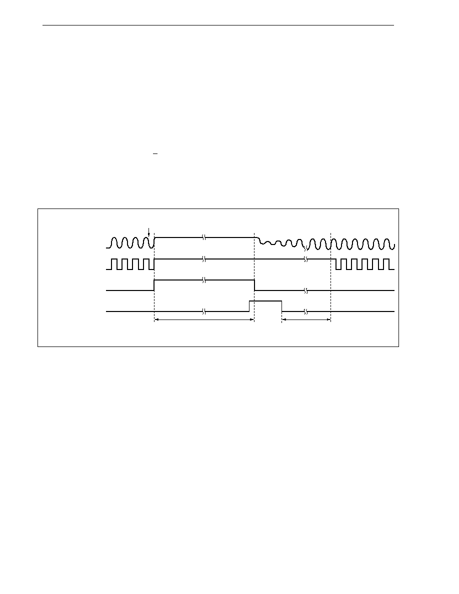
142
CHAPTER 6 CLOCK GENERATOR FUNCTION
User's Manual U10913EJ6V0UM
6.6 Securing Oscillation Stabilization Time
The time required for the oscillator to become stabilized after the software STOP mode has been released can
be secured in the following two ways.
(1) By using internal time base counter (NMI signal input)
When a valid edge is input to the NMI pin, the software STOP mode is released. When an inactive edge is
input to the pin, the time base counter (TBC) starts counting, and the time required for the clock output from
the oscillator to become stabilized is specified by that count time.
Oscillation stabilization time
~
(Active level width after valid edge of NMI input has been detected) + (Count
time of TBC)
After a specific time has elapsed, the system clock output is started, and execution branches to the handler
address of the NMI interrupt.
During inactivity, the NMI pin should be held at the inactive level (e.g. when the valid edge is specified to be
the falling edge).
If the software STOP mode is set in the period between the valid edge input timing of NMI and the interrupt
acknowledgement by the CPU, the software STOP mode is immediately released. Program execution is
immediately started if the clock generator is driven in direct mode or the external clock connection mode
(CESEL = 1). If the clock generator is driven in the PLL mode or the resonator connection mode (CESEL
= 0), program execution is started after the oscillation stabilization time specified in the time base counter has
elapsed.
Oscillation waveform
Software STOP mode set
Oscillator stops
System clock
STOP status
NMI input
Count time of time
base counter
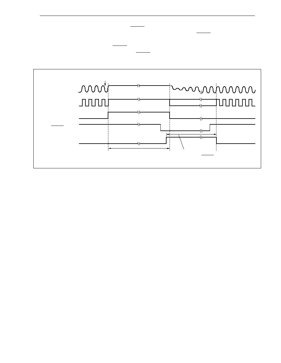
143
CHAPTER 6 CLOCK GENERATOR FUNCTION
User's Manual U10913EJ6V0UM
(2) To secure time by signal level width (RESET pin input)
The software STOP mode is released when the falling edge is input to the RESET pin.
The time required for the clock output from the oscillator to become stabilized is specified by the low-level
width of the signal input to the RESET pin.
After the rising edge has been input to the RESET pin, operation of the internal system clock begins, and
execution branches to the vector address that is used when the system is reset.
Time base counter (TBC)
The time base counter is used to secure the oscillation stabilization time of the oscillator when the software
STOP mode is released.
· External clock connected (CESEL bit of PSC register = 1)
TBC does not count the oscillation stabilization time, and the execution of a program is started
immediately after the software STOP mode is released.
· Resonator connected (CESEL bit of PSC register = 0)
TBC counts the oscillation stabilization time after the software STOP mode is released, and the
execution of a program is started after counting is completed.
The count clock of TBC is selected by the TBCS bit of the PSC register, and the following count time can
be set.
Oscillation waveform
Software STOP mode set
Undefined
Oscillator stops
System clock
STOP status
Internal system
reset signal
Oscillation stabilization time
secured by RESET
RESET signal
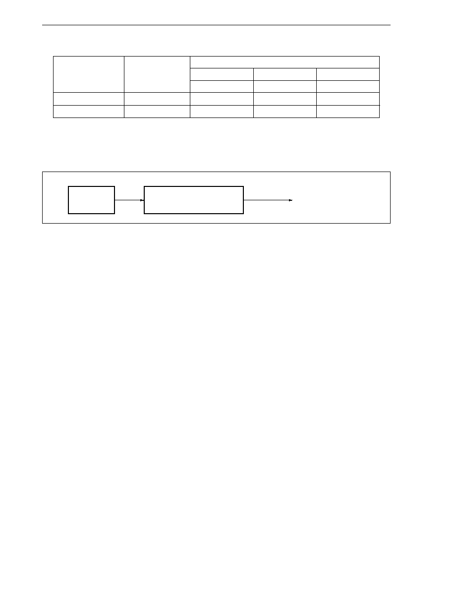
144
CHAPTER 6 CLOCK GENERATOR FUNCTION
User's Manual U10913EJ6V0UM
Table 6-5. Example of Count Time
Count Time
TBCS
Count Clock
fxx = 4.0000 MHz
fxx = 5.0000 MHz
fxx = 6.5536 MHz
= 20.000 MHz
= 25.000 MHz
= 32.768 MHz
0
fxx/2
8
16.3 ms
13.1 ms
10.0 ms
1
fxx/2
9
32.7 ms
26.2 ms
20.0 ms
f
xx
: external resonator frequency
:
internal system clock frequency
Figure 6-1. Block Configuration
f
XX
/2
8
f
XX
/2
9
TBC (8 bits)
Overflow
Oscillation stabilization time
controller

145
CHAPTER 6 CLOCK GENERATOR FUNCTION
User's Manual U10913EJ6V0UM
6.7 Clock Output Control
The operation mode of the CLKOUT pin can be selected by the DCLK0 and DCLK1 bits of the PSC register.
By using this operation mode in combination with the HALT, IDLE, or software STOP mode, the power consumption
can be effectively reduced (for how to write these bits, refer to 6.5.2 Control registers).
Clock output inhibit mode
The clock output from the CLKOUT pin is inhibited.
This mode is ideal for single-chip mode systems or systems that fetch instructions to external expansion devices
or asynchronously access data.
Because the operation of CLKOUT is completely stopped in this mode, the power consumption can be minimized
and radiation noise from the CLKOUT pin can be suppressed.
In the single-chip mode, the CLKOUT signal is not output until the DCLK1 and DCLK0 bits of the PSC register
are set to 00 after releasing reset (low level output).
In the flash memory programming mode, the CLKOUT signal cannot be output (low level output).
(Fixed to low level)
L
CLKOUT
(normal mode)
CLKOUT
(clock output inhibit mode)

146
User's Manual U10913EJ6V0UM
CHAPTER 7 TIMER/COUNTER FUNCTION (REAL-TIME PULSE UNIT)
7.1 Features
Measures pulse intervals and frequency, and outputs programmable pulse
· 16-bit measurement possible
· Generates pulses of various shapes (interval pulse, one-shot pulse)
Timer 1
· 16-bit timer/event counter
· Count clock sources: 2 types (divided internal system clock and external pulse input)
· Capture/compare registers: 16
· Count clear pins: TCLR11 to TCLR14
· Interrupt sources: 20 types
· External pulse outputs: 8
Timer 4
· 16-bit interval timer
· Count clock selected from divided internal system clock
· Compare registers: 1
· Interrupt sources: 1

147
CHAPTER 7 TIMER/COUNTER FUNCTION (REAL-TIME PULSE UNIT)
User's Manual U10913EJ6V0UM
7.2 Basic Configuration
Table 7-1. Configuration of Real-Time Pulse Unit (RPU)
Timer
Count Clock
Register
Read/Write
Other Function
Timer 1
TM1
Read
INTOV11
External clear
CC110
Read/write
INTCC110
INTP110
TO110 (S)
CC111
Read/Write
INTCC111
INTP111
TO110 (R)
CC112
Read/Write
INTCC112
INTP112
TO111 (S)
CC113
Read/Write
INTCC113
INTP113
TO111 (R)
TM12
Read
INTOV12
External clear
CC120
Read/Write
INTCC120
INTP120
TO120 (S)
TI1n pin input
CC121
Read/Write
INTCC121
INTP121
TO120 (R)
(n = 1 to 4)
CC122
Read/Write
INTCC122
INTP122
TO121 (S)
CC123
Read/Write
INTCC123
INTP123
TO121 (R)
TM13
Read
INTOV13
External clear
CC130
Read/Write
INTCC130
INTP130
TO130 (S)
CC131
Read/Write
INTCC131
INTP131
TO130 (R)
CC132
Read/Write
INTCC132
INTP132
TO131 (S)
CC133
Read/Write
INTCC133
INTP133
TO131 (R)
TM14
Read
INTOV14
External clear
CC140
Read/Write
INTCC140
INTP140
TO140 (S)
CC141
Read/Write
INTCC141
INTP141
TO140 (R)
CC142
Read/Write
INTCC142
INTP142
TO141 (S)
CC143
Read/Write
INTCC143
INTP143
TO141 (R)
Timer 4
TM4
Read
CM4
Read/write
INTCM4
Remark
:
Internal system clock
S/R: Set/reset
Timer Output
S/R
Generated
Interrupt
Signal
Capture
Trigger
/2
/4
/8
/16
/32
/64
/128
/2
/4
/16
/32
/64
/128
/512
/1024
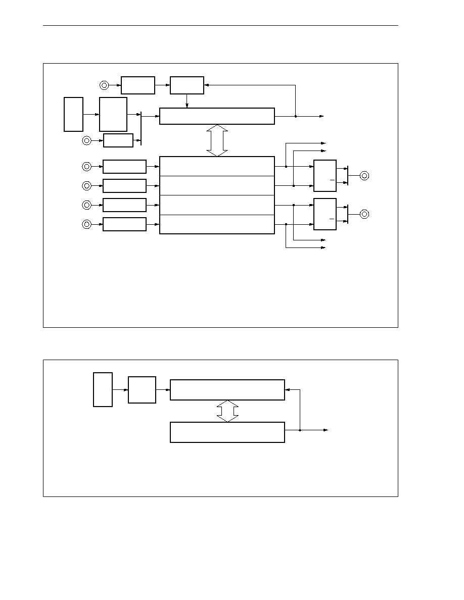
148
CHAPTER 7 TIMER/COUNTER FUNCTION (REAL-TIME PULSE UNIT)
User's Manual U10913EJ6V0UM
(1) Timer 1 (16-bit timer/event counter)
Notes
1. Internal count clock
2. External count clock
3. Reset priority
Remark
n = 1 to 4
: Internal system clock
(2) Timer 4 (16-bit interval timer)
Note
Internal count clock
Remark
: Internal system clock
INTP1n0
INTP1n1
INTP1n2
INTP1n3
Edge detection
CC1n0
CC1n1
CC1n2
CC1n3
S
INTCC1n0
INTCC1n1
TO1n0
R
Q
Q
S
TO1n1
R
Q
Q
INTCC1n2
INTCC1n3
Note 3
Note 3
TM1n (16 bits)
Edge
detection
m
m
m/4
m/8
m/32
/2
/4
TCLR1n
INTOV1n
Note 1
Edge
detection
Edge detection
Edge detection
Edge detection
Clear & start
Note 2
TI1n
Clear & start
CM4
INTCM4
TM4 (16 bits)
m
m
m/32
/2
/4
/16
/32
Clear & start
Note
149
CHAPTER 7 TIMER/COUNTER FUNCTION (REAL-TIME PULSE UNIT)
User's Manual U10913EJ6V0UM
7.2.1 Timer 1
(1) Timers 11 to 14 (TM11 to TM14)
TM1n functions as a 16-bit free-running timer or event counter. Timers 11 to 14 are used to measure cycles
and frequency, and also for programmable pulse generation.
TM1n is read-only in 16-bit units (n = 1 to 4).
TM1n counts up the internal count clock or external count clock. The timer is started or stopped by the CE1n
bits of timer control register 1n (TMC1n).
Whether the internal or external count clock is used is specified by the TMC1n register.
(a) When external count clock is selected
TM1n operates as an event counter. The valid edge is specified by timer unit mode register 1n (TUM1n),
and TM1n counts up the signal input from the TI1n pin.
(b) When internal count clock is selected
TM1n operates as a free-running timer, and counts up the internal clock. The internal count clock
frequency division by the prescaler is selected from
/2,
/4,
/8,
/16,
/32,
/64, and
/128 by the TMC1
register.
When the timer overflows, an overflow interrupt can be generated. The timer can be stopped after an
overflow has occurred, if so specified by the TUM1n register.
The timer can be cleared and started by external TCLR1n input. At this time, the prescaler is also cleared.
As a result, the time from the TCLR1n input to the first count up by the timer is held constant, according
to the division ratio of the prescaler. The operation is set by the TUM1n register.
Caution The count clock cannot be changed during timer operation.
15
TM11
Address
FFFFF250H
After reset
0000H
0
15
TM12
FFFFF270H
0000H
0
15
TM13
FFFFF290H
0000H
0
15
TM14
FFFFF2B0H
0000H
0
150
CHAPTER 7 TIMER/COUNTER FUNCTION (REAL-TIME PULSE UNIT)
User's Manual U10913EJ6V0UM
(2) Capture/compare registers 1n0 to 1n3 (CC1n0 to CC1n3) (n = 1 to 4)
The capture/compare registers are 16-bit registers and are connected to TM1n. These registers can be used
as capture or compare registers depending on the specification of timer unit mode register 1n (TUM1n). They
can be read/written in 16-bit units.
(a) When used as capture register
When a capture/compare register is used as a capture register, it detects the valid edge of the
corresponding external interrupt (INTP1n0 to INTP1n3 signals) as a capture trigger. Timer 1n latches
the count value in synchronization with the capture trigger (capture operation). The capture operation
is performed asynchronously to the count clock. The latched value is held by the capture register, until
the next capture operation is performed.
If the capture (latch) timing of the capture register conflicts with a register write operation by an instruction,
the latter takes precedence, and the capture operation is ignored.
The valid edge of the external interrupt (rising, falling, or both edges) can be selected by the external
interrupt mode register (INTM2).
When a capture/compare register is used as a capture register, and when the valid edge of the INTP1n0
to INTP1n3 signals is detected, an interrupt is generated. During this time, no interrupt can be generated
by the compare register match signals INTCC1n0 to INTCC1n3.
(b) When used as compare register
When a capture/compare register is used as a compare register, it compares its contents with the value
of the timer at each clock tick. When the two values match, an interrupt is generated. Compare registers
support a set/reset output function. In other words, they set or reset the corresponding timer output (TO1n0
and TO1n1) synchronously with match signal generation.
Whether the interrupt source is used as a capture or compare register depends on the register mode.
When used as a compare register, the match signals INTCC1n0 to INTCC1n3 or the valid edge of the
INTP1n0 to INTP1n3 signals can be selected as an interrupt signal, depending on the specification of
the TUM1n register.
When the INTP1n0 to INTP1n3 signals are selected, the acknowledgement of an external interrupt request
and the timer output by the set/reset output function of the compare register can be executed simultaneously.
Address
FFFFF252H to
FFFFF258H
CC11n
After reset
Undefined
15
0
Address
FFFFF272H to
FFFFF278H
CC12n
After reset
Undefined
15
0
Address
FFFFF292H to
FFFFF298H
CC13n
After reset
Undefined
15
0
Address
FFFFF2B2H to
FFFFF2B8H
CC14n
After reset
Undefined
15
0
151
CHAPTER 7 TIMER/COUNTER FUNCTION (REAL-TIME PULSE UNIT)
User's Manual U10913EJ6V0UM
7.2.2 Timer 4
(1) Timer 4 (TM4)
TM4 is a 16-bit timer and is mainly used as an interval timer for software.
This timer is read-only in 16-bit units.
TM4 is started or stopped by the CE4 bit of timer control register 4 (TMC4).
The count clock is selected by the TMC4 register from
/2,
/4,
/16,
/32,
/64,
/128,
/512, or
/1024.
Caution When the value of the timer matches the value of the compare register (CM4), the timer is
cleared by the next clock tick. If the division ratio is large and results in a slow clock period,
the timer value may not have been cleared to zero if the timer is read immediately after the
occurrence of the match signal interrupt.
The count clock cannot be changed during timer operation.
(2) Compare register 4 (CM4)
CM4 is a 16-bit register and is connected to TM4. This register can be read/written in 16-bit units.
CM4 compares its value with the value of TM4 at each clock tick of TM4, and generates an interrupt (INTCM4)
when the two values match. TM4 is cleared in synchronization with this match.
15
TM4
Address
FFFFF350H
After reset
0000H
0
Address
FFFFF352H
CM4
After reset
Undefined
15
0
152
CHAPTER 7 TIMER/COUNTER FUNCTION (REAL-TIME PULSE UNIT)
User's Manual U10913EJ6V0UM
7.3 Control Registers
(1) Timer unit mode registers 11 to 14 (TUM11 to TUM14)
TUM1n controls the operation of timer 1, and specifies the operation mode of the capture/compare registers
(n = 1 to 4).
These registers can be read/written in 16-bit units.
(1/2)
Bit position
Bit name
Function
13
OSTn
Overflow Stop
Specifies operation of timer after occurrence of overflow. This flag is valid only for TM1n.
0: Timer continues counting after overflow has occurred.
1: Timer holds 0000H and stops after overflow has occurred.
At this time, CE1n bit of TMC1n remains "1".
The timer resumes counting when the following operation is performed:
When ECLR1n = "0": Writing "1" to CE1n bit
When ECLR1n = "1": Trigger input to timer clear pin (TCLR1n)
12
ECLR1n
External Input Timer Clear
Enables clearing TM1n by external clear input (TCLR1n)
0: TM1n not cleared by external input
1: TM1n cleared by external input
After TM1n has been cleared, it starts counting.
11, 10
TES1n1, TES1n0
TI1n Edge Select
Specifies valid edge of external clock input (TI1n)
TES1n1 TES1n0
Valid edge
0
0
Falling edge
0
1
Rising edge
1
0
RFU (reserved)
1
1
Both rising and falling edges
Remark
n = 1 to 4
15
0
TUM11
Address
FFFFF240H
After reset
0000H
14
0
13
OST1
12
ECLR
11
11
TES
111
10
TES
110
9
CES
111
8
CES
110
7
CMS
113
6
CMS
112
5
CMS
111
4
CMS
110
3
IMS
113
2
IMS
112
1
IMS
111
0
IMS
110
0
TUM12
FFFFF260H
0000H
0
OST2
ECLR
12
TES
121
TES
120
CES
121
CES
120
CMS
123
CMS
122
CMS
121
CMS
120
IMS
123
IMS
122
IMS
121
IMS
120
0
TUM13
FFFFF280H
0000H
0
OST3
ECLR
13
TES
131
TES
130
CES
131
CES
130
CMS
133
CMS
132
CMS
131
CMS
130
IMS
133
IMS
132
IMS
131
IMS
130
0
TUM14
FFFFF2A0H
0000H
0
OST4
ECLR
14
TES
141
TES
140
CES
141
CES
140
CMS
143
CMS
142
CMS
141
CMS
140
IMS
143
IMS
142
IMS
141
IMS
140

153
CHAPTER 7 TIMER/COUNTER FUNCTION (REAL-TIME PULSE UNIT)
User's Manual U10913EJ6V0UM
Bit position
Bit name
Function
9, 8
CES1n1, CES1n0
TCLR1n Edge Select
Specifies valid edge of external clear input (TCLR1n).
CES1n1 CES1n0
Valid edge
0
0
Falling edge
0
1
Rising edge
1
0
RFU (reserved)
1
1
Both rising and falling edge
7 to 4
CMS1n3 to
Capture/Compare Mode Select
CMS1n0
Selects operation mode of capture/compare registers (CC1n0 to CC1n3).
0: Capture register. However, capture operation is performed only when CE1 of
TMC1n = "1".
1: Compare register
3 to 0
IMS1n3 to
Interrupt Mode Select
IMS1n0
Selects INTP1nm or INTCC1nm as interrupt source (m = 0 to 3).
0: Uses match signal of INTCC1nm of compare registers as interrupt signal
1: Uses external input signal INTP1nm as interrupt signal
Remark
n = 1 to 4
(2/2)

154
CHAPTER 7 TIMER/COUNTER FUNCTION (REAL-TIME PULSE UNIT)
User's Manual U10913EJ6V0UM
Precautions in use of A/D converter
(1) When the A/D converter is set to the timer trigger mode
The match interrupt of the compare register becomes the A/D conversion start trigger and conversion
operations are started. At this time, the match interrupt of the compare register also functions as the match
interrupt of the compare register for the CPU. To prevent generation of the match interrupt of the compare
register for the CPU, disable interrupts using the interrupt mask bit (P11MK0 to P11MK3) of the interrupt control
register (P11IC0 to P11IC3).
(2) When the A/D converter is set to the external trigger mode
The external trigger input becomes the A/D conversion start trigger and conversion operations are started.
At this time, the external trigger input also functions as a capture trigger and the external interrupt of timer
1. To prevent generation of the capture trigger and external interrupt, set timer 1 as a compare register and
disable interrupts using the interrupt mask bit of the interrupt control register.
The operations performed when timer 1 is set as a compare register and interrupts are not disabled by the
interrupt control register are as follows.
(a) When the interrupt mask bit (IMS113) of the TUM11 register is 0
Also functions as the match interrupt of the compare register for the CPU.
(b) When the interrupt mask bit (IMS113) of the TUM11 register is 1
The external trigger input of the A/D converter also functions as the external interrupt for the CPU.
155
CHAPTER 7 TIMER/COUNTER FUNCTION (REAL-TIME PULSE UNIT)
User's Manual U10913EJ6V0UM
(2) Timer control registers 11 to 14 (TMC11 to TMC14)
TMC11 to TMC14 control operation of TM11 to TM14.
These registers can be read/written in 8-bit or 1-bit units.
(1/2)
Bit position
Bit name
Function
7
CE1n
Count Enable
Controls timer operation.
0: Timer stops at "0000H" and does not operate.
1: Timer performs count operation. However, it does not start counting when
TUM1n register's ECLR1n = 1, until TCLR1n signal is input.
When ECLR1n = 0, starting counting of the timer by CE1n = 1 is triggered by writing "1" to
the CE1n bit. Therefore, the timer is not started even when ECLR1n = 0 after CE1n has
been set with ECLR1n = 1.
4
ETI1n
External TI1n Input
Specifies external or internal count clock.
0:
(internal)
1: TI1n (external)
3, 2
PRS1n1, PRS1n0
Prescaler Clock Select
Selects internal count clock (
m is intermediate clock)
PRS1n1 PRS1n0
Count clock frequency
0
0
m
0
1
m/4
1
0
m/8
1
1
m/32
Caution Do not change the count clock frequency while the timer is operating.
Remark
n = 1 to 4
Address
FFFFF242H
7
CE11
TMC11
6
0
5
0
4
ETI11
3
PRS111
2
PRS110
1
PRM111
0
0
After reset
00H
FFFFF262H
CE12
TMC12
0
0
ETI12
PRS121 PRS120 PRM121
0
00H
FFFFF282H
CE13
TMC13
0
0
ETI13
PRS131 PRS130 PRM131
0
00H
FFFFF2A2H
CE14
TMC14
0
0
ETI14
PRS141 PRS140 PRM141
0
00H

156
CHAPTER 7 TIMER/COUNTER FUNCTION (REAL-TIME PULSE UNIT)
User's Manual U10913EJ6V0UM
Bit position
Bit name
Function
1
PRM1n1
Prescaler Clock Mode
Selects intermediate clock (
m) of count clock (
is internal system clock).
0:
/2
1:
/4
Caution Do not change the count clock frequency while the timer is operating.
Remark
n = 1 to 4
(2/2)

157
CHAPTER 7 TIMER/COUNTER FUNCTION (REAL-TIME PULSE UNIT)
User's Manual U10913EJ6V0UM
(3) Timer control register 4 (TMC4)
TMC4 controls the operation of TM4.
This register can be read/written in 8-bit or 1-bit units.
Bit position
Bit name
Function
7
CE4
Count Enable
Controls operation of timer.
0: Timer stops at "0000H" and does not operate.
1: Timer performs count operation.
2
PRS40
Prescaler Clock Select
Selects internal count clock (
m is intermediate clock).
0:
m
1:
m/32
1, 0
PRM41, PRM40
Prescaler Clock Mode
Selects intermediate clock (
m) of count clock (
is internal system clock).
PRM41 PRM40
m
0
0
/2
0
1
/4
1
0
/16
1
1
/32
Caution Do not change the count clock frequency while the timer is operating.
Address
FFFFF342H
7
CE4
TMC4
6
0
5
0
4
0
3
0
2
PRS40
1
PRM41
0
PRM40
After reset
00H
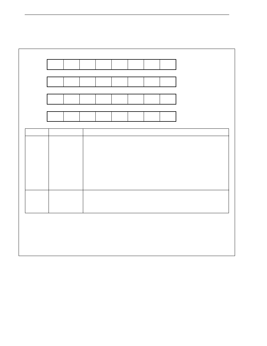
158
CHAPTER 7 TIMER/COUNTER FUNCTION (REAL-TIME PULSE UNIT)
User's Manual U10913EJ6V0UM
(4) Timer output control registers 11 to 14 (TOC11 to TOC14)
TOC1n control the timer outputs from the TO1n0 and TO1n1 pins (n = 1 to 4).
These registers can be read/written in 8-bit or 1-bit units.
Bit position
Bit name
Function
7, 5
ENTO1n1, ENTO1n0
Enable TO pin
Enables corresponding timer output (TO1n0, TO1n1).
0: Timer output is disabled. The reverse-phase levels of ALV1n0 and ALV1n1 bits
(inactive levels) are output from the TO1n0 and TO1n1 pins. Even if a match
signal is generated from the corresponding compare register, the levels of the
TO1n0 and TO1n1 pins do not change.
1: Timer output function is enabled. The timer output changes when match signal
is generated from the corresponding compare register. After the timer output
has been enabled before the first match signal is generated, the reverse-phase
levels of the ALV1n0 and ALV1n1 bits (inactive levels) are output.
6, 4
ALV1n1, ALV1n0
Active Level TO pin
Specifies active level of timer output.
0: Active-low
1: Active-high
Remarks
1. The flip-flops of the TO1n0 and TO1n1 outputs give priority to reset.
2. n = 1 to 4
Caution The TO1n0 and TO1n1 outputs are not changed by the external interrupt signals (INTP1n0
to INTP1n3). When using the TO1n0 and TO1n1 signals, specify capture/compare registers
as compare registers (CMS = 1).
(5) External interrupt mode registers 1 to 4 (INTM1 to INTM4)
If CC1n0 through CC1n3 of TM1n are used as capture registers, the active edge of the external interrupt
INTP1n0 to INTP1n3 signals is used as a capture trigger (n = 1 to 4). For details, refer to CHAPTER 5
INTERRUPT/EXCEPTION PROCESSING FUNCTION.
Address
FFFFF244H
7
ENTO111
TOC11
6
ALV111
5
ENTO110
4
ALV110
3
0
2
0
1
0
0
0
After reset
00H
FFFFF264H
ENTO121
TOC12
ALV121 ENTO120 ALV120
0
0
0
0
00H
FFFFF284H
ENTO131
TOC13
ALV131 ENTO130 ALV130
0
0
0
0
00H
FFFFF2A4H
ENTO141
TOC14
ALV141 ENTO140 ALV140
0
0
0
0
00H

159
CHAPTER 7 TIMER/COUNTER FUNCTION (REAL-TIME PULSE UNIT)
User's Manual U10913EJ6V0UM
(6) Timer overflow status register (TOVS)
This register is assigned flags that indicate the occurrence of an overflow from TM11 to TM14 and TM4.
This register can be read/written in 8-bit or 1-bit units.
By testing and resetting the TOVS register via software, the occurrence of an overflow can be polled.
Bit position
Bit name
Function
4, 1
OVF4,
Overflow Flag
OVF11 to
TM4/1n overflow flag.
OVF14
0: No overflow
1: Overflow
Caution
From TM1n, the interrupt request (INTOV1n) is generated for the
interrupt controller in synchronization with the overflow. However,
the interrupt operation and TOVS are independent from each
other, so the overflow flag OVF1n from TM1n can be manipulated
by software in the same manner as other overflow flags.
The interrupt request flag (OVF1n) corresponding to INTOV1n is
not affected.
No transmission is executed to the TOVS register during access from the CPU.
Therefore, even if an overflow occurs when the TOVS register is being read, the
overflow flag value will not be updated and this overflow condition will be reflected
the next time the TOVS register is read.
Remark
n = 1 to 4
Address
FFFFF230H
7
0
TOVS
6
0
5
0
4
OVF4
3
OVF14
2
OVF13
1
OVF12
0
OVF11
After reset
00H
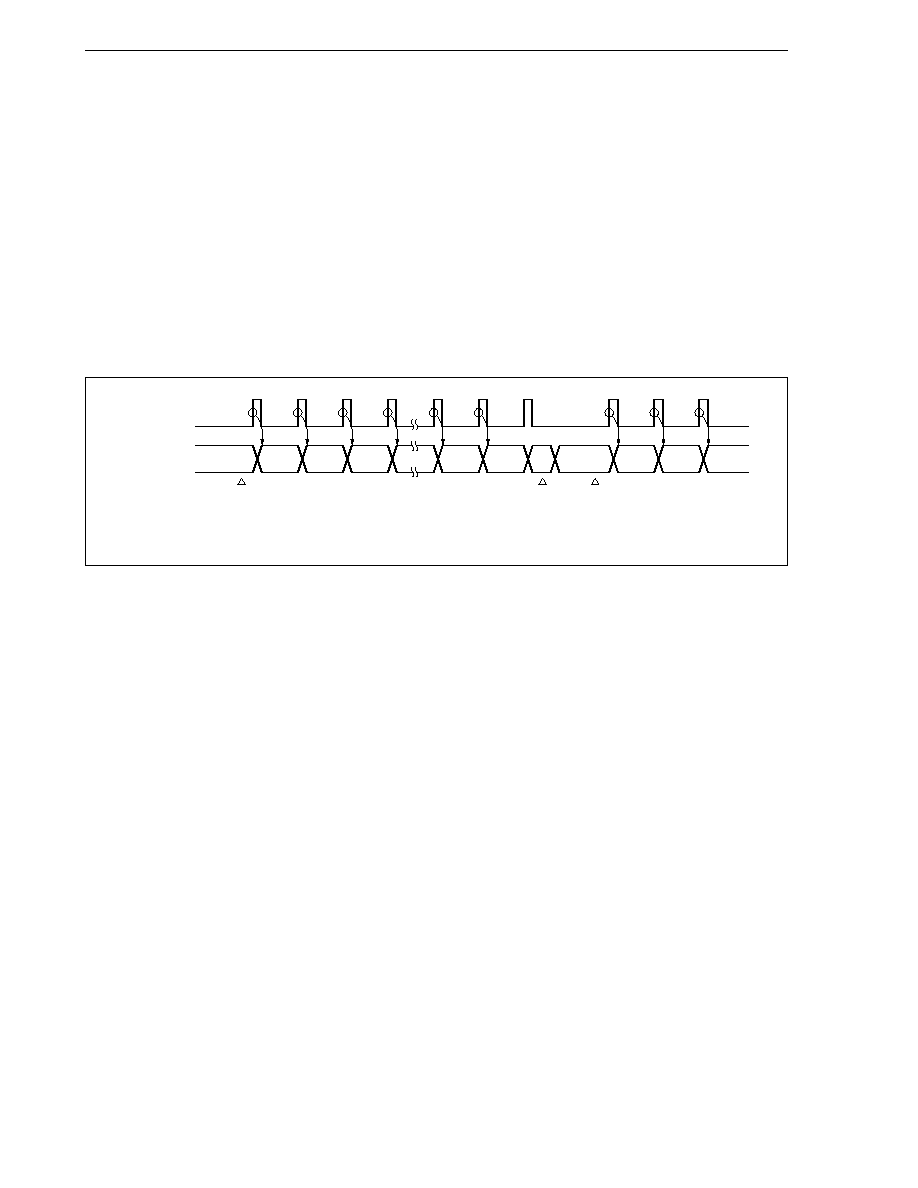
160
CHAPTER 7 TIMER/COUNTER FUNCTION (REAL-TIME PULSE UNIT)
User's Manual U10913EJ6V0UM
7.4 Timer 1 Operation
7.4.1 Count operation
Timer 1 functions as a 16-bit free-running timer or event counter, as specified by timer control register 1n (TMC1n)
(n = 1 to 4).
When it is used as a free-running timer, and when the count values of TM1n match the value of any of the CC1n0
to CC1n3 registers, an interrupt signal is generated, and the timer output signals (TO1n0 and TO1n1) can be set/
reset. In addition, a capture operation that holds the current count value of TM1n and loads it into one of the four
registers CC1n0 to CC1n3, is performed in synchronization with the valid edge detected from the corresponding
external interrupt request pin as an external trigger. The captured value is retained until the next capture trigger is
generated.
Figure 7-1. Basic Operation of Timer 1
Remark
n = 1 to 4
0001H 0002H 0003H
FBFEH FBFFH
0000H
0001H 0002H
0003H
0000H
TM1n
Count starts
CE1n
1
Count disabled
CE1n
0
Count starts
CE1n
1
Count clock

161
CHAPTER 7 TIMER/COUNTER FUNCTION (REAL-TIME PULSE UNIT)
User's Manual U10913EJ6V0UM
7.4.2 Selecting count clock frequency
An internal or external count clock can be output to timer 1, selectable by the ETI1n bit of the TMC1n register
(n = 1 to 4).
Caution Do not change the count clock frequency while the timer is operating.
(1) Internal count clock (ETI1n bit = 0)
The internal count clock frequency is selected by the PRM1n1, PRS1n0, and PRS1n1 bits of the TMC1n
register, from
/2,
/4,
/8,
/16,
/32,
/64, and
/128.
PRS1n1
PRS1n0 PRM1n1
Internal Count Clock Frequency
0
0
0
/2
0
0
1
/4
0
1
0
/8
0
1
1
/16
1
0
0
/16
1
0
1
/32
1
1
0
/64
1
1
1
/128
Remark
n = 1 to 4
(2) External count clock (ETI1n bit = 1)
The signal input to the TI1n pin is counted. At this time, timer 1 can operate as an event counter.
The valid edge of TI1n is specified by the TES1n0 and TES1n1 bits of the TUM1n register.
TES1n1
TES1n0
Valid Edge
0
0
Falling edge
0
1
Rising edge
1
0
RFU (reserved)
1
1
Both rising and falling edges
Remark
n = 1 to 4
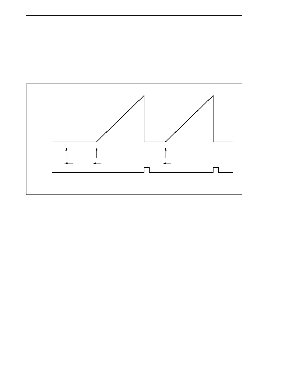
162
CHAPTER 7 TIMER/COUNTER FUNCTION (REAL-TIME PULSE UNIT)
User's Manual U10913EJ6V0UM
7.4.3 Overflow
If the TM1n register overflows as a result of counting the count clock frequency up to FFFFH, the OVF1n bit of
the TOVS register is set (to 1), and an overflow interrupt (INTOV1n) is generated.
After the overflow has occurred, the timer can be stopped by setting the OSTn bit of the TUM1n register to 1. If
the timer is stopped due to overflow, the counting operation is not resumed until the CE1n bit is set to 1 by software.
The operation is not affected even if CE1n bit is set to 1 during a count operation.
Figure 7-2. Operation After Occurrence of Overflow (When ECLR1n = 0, OSTn = 1)
Remark
n = 1 to 4
TM1n
INTOV1n
0
OSTn
1
CE1n
1
CE1n
1
Count starts
Overflow
FFFFH
Overflow
FFFFH
163
CHAPTER 7 TIMER/COUNTER FUNCTION (REAL-TIME PULSE UNIT)
User's Manual U10913EJ6V0UM
7.4.4 Clearing/starting timer by TCLR signal input
Timer 1 usually starts a count operation when the CE1n bit of the TMC1n register is set to 1. It is also possible
to clear TM1n and start a count operation by using the external input TCLR1n (n = 1 to 4).
When the valid edge is input to the TCLR1n signal after ECLR1n bit = 1, OSTn bit = 0 is set, and the CE1n bit
is set to 1, a count operation is started. If the valid edge is input to TCLR1n signal during operation, the values of
TM1n are cleared and TM1n resumes the count operation (refer to Figure 7-3).
When the valid edge is input to the TCLR1n signal after setting both the ECLR1n and OSTn bits to 1, and the CE1n
bit is set from 0 to 1, a count operation is started. When TM1n overflows, the count operation is stopped once and
is not resumed until the valid edge is input to the TCLR1n signal. If the valid edge of the TCLR1n signal is detected
during a count operation, TM1n is cleared and continues counting (refer to Figure 7-4). The count operation is not
resumed even if CE1n bit is set to 1 after an overflow.
Figure 7-3. Clearing/Starting Timer by TCLR1n Signal Input (When ECLR1n = 1, OSTn = 0)
Remark
n = 1 to 4
TM1n
INTOV1n
0
ECLR1n
1
CE1n
1
TCLR1n
TCLR1n
Count starts
Overflow
FFFFH
Clear & start
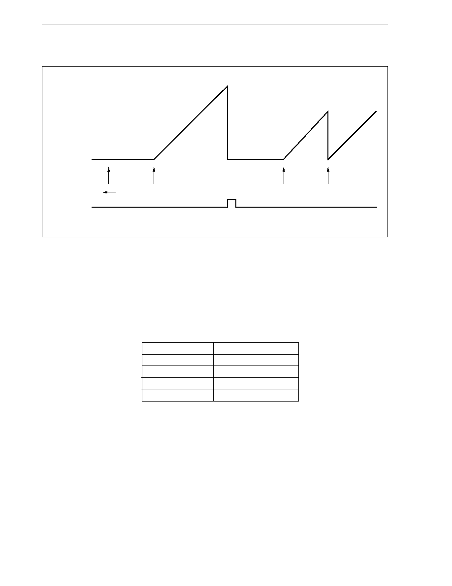
164
CHAPTER 7 TIMER/COUNTER FUNCTION (REAL-TIME PULSE UNIT)
User's Manual U10913EJ6V0UM
Figure 7-4. Relationship Between Clear/Start by TCLR1n Signal Input and Overflow
(When ECLR1n = 1, OSTn = 1)
Remark
n = 1 to 4
7.4.5 Capture operation
A capture operation that captures and holds the count value of TM1n and loads it to a capture register
asynchronously to an external trigger can be performed (n = 1 to 4). The valid edge from the external interrupt request
input pins INTP1n0 to INTP1n3 is used as the capture trigger. In synchronization with this capture trigger signal,
the count value of TM1n during counting is captured and loaded to the capture register. The value of the capture
register is retained until the next capture trigger is generated.
Interrupt requests (INTCC1n0 to INTCC1n3) are generated from the INTP1n0 to INTP1n3 input signals.
Table 7-2. Capture Trigger Signal to 16-Bit Capture Register (TM1n)
Capture Register
Capture Trigger Signal
CC1n0
INTP1n0
CC1n1
INTP1n1
CC1n2
INTP1n2
CC1n3
INTP1n3
Remarks 1. CC1n0 to CC1n3 are capture/compare registers. Whether these registers are used as capture or
compare registers is specified by timer unit mode register 1n (TUM1n).
2. n = 1 to 4
TM1n
INTOV1n
0
CE1n
1
TCLR1n
TCLR1n
TCLR1n
Count starts
Overflow
FFFFH
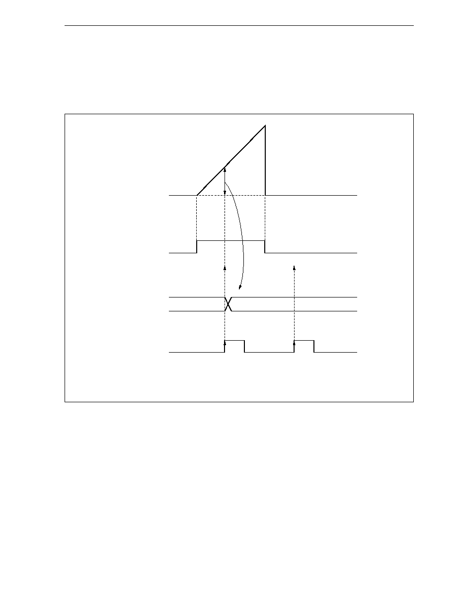
165
CHAPTER 7 TIMER/COUNTER FUNCTION (REAL-TIME PULSE UNIT)
User's Manual U10913EJ6V0UM
The valid edge of the capture trigger is set by the external interrupt mode register (INTMn).
When both the rising and falling edges are specified as the capture trigger, the width of an externally input pulse
can be measured. If either the rising or falling edge is specified as the capture trigger, the frequency of the input pulse
can be measured.
Figure 7-5. Example of Capture Operation
Remark
A capture operation is not performed even if the interrupt request (INTP110) is input when CE11 is cleared
to 0.
TM11
CE11
n
0
n
CC110
INTP110
(Capture trigger)
(Capture trigger)
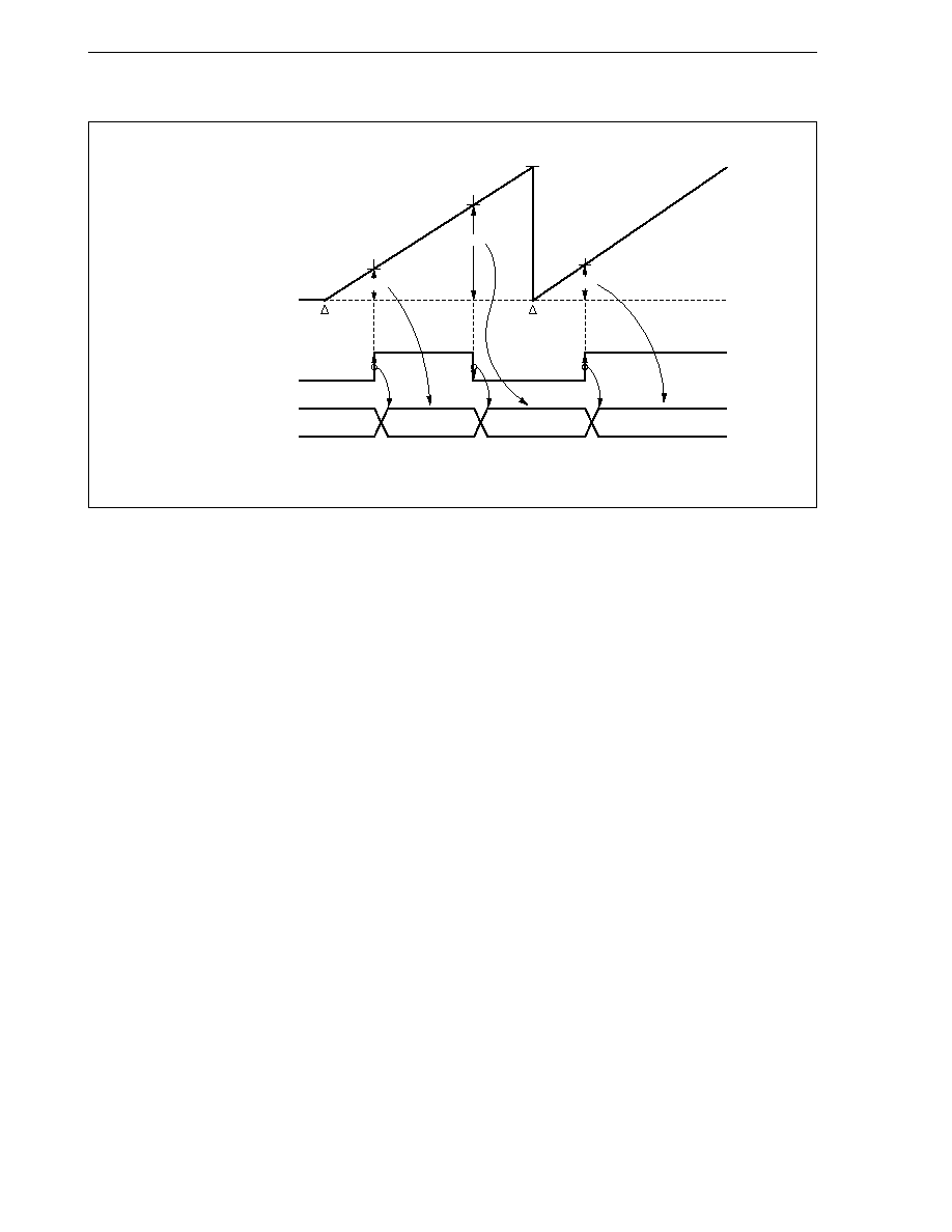
166
CHAPTER 7 TIMER/COUNTER FUNCTION (REAL-TIME PULSE UNIT)
User's Manual U10913EJ6V0UM
Figure 7-6. Example of TM11 Capture Operation (When Both Edges Are Specified)
Remark D0 to D2: Count value of TM11
TM11 count value
Interrupt request
(INTP110)
Capture register
(CC110)
CE11
1
(Count start)
OVF11
1
(overflow)
D0
D1
D2
D1
D0
D2
FFFFH
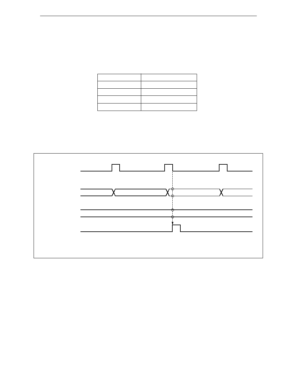
167
CHAPTER 7 TIMER/COUNTER FUNCTION (REAL-TIME PULSE UNIT)
User's Manual U10913EJ6V0UM
7.4.6 Compare operation
A comparison between the value in a compare register the count value of TM1n can be performed (n = 1 to 4).
When the count value of TM1n matches the value of the compare register programmed in advance, a match signal
is sent to the output controller (refer to Figure 7-7). The levels of the timer output pins (TO1n0, TO1n1) can be changed
by the match signal, and an interrupt request signal can be generated at the same time.
Table 7-3. Interrupt Request Signal from 16-Bit Compare Register (TM1n)
Compare Register
Interrupt Request Signal
CC1n0
INTCC1n0
CC1n1
INTCC1n1
CC1n2
INTCC1n2
CC1n3
INTCC1n3
Remarks 1. CC1n0 to CC1n3 are capture/compare registers. Whether these registers are used as capture or
compare registers is specified by timer unit mode register 1n (TUM1n).
2. n = 1 to 4
Figure 7-7. Example of Compare Operation
Remark
Note that the match signal is generated immediately after TM1 is incremented as shown above.
Count up
CC110
(INTCC110)
Match detected
n 1
n
n + 1
n
TM11
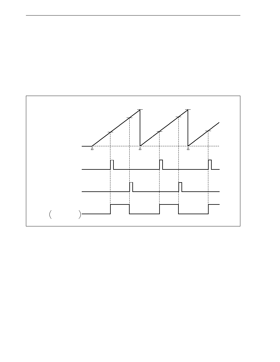
168
CHAPTER 7 TIMER/COUNTER FUNCTION (REAL-TIME PULSE UNIT)
User's Manual U10913EJ6V0UM
Timer 1 has eight timer output pins (TO1n0, TO1n1).
The count value of TM1n is compared with the value of CC1n2. If the two values match, the output level of the
TO1n1 pin is set. The count value of TM1n is also compared with the value of CC1n3. If the two values match, the
output level of the TO1n1 pin is reset.
Similarly, the count value of TM1n is compared with the value of CC1n0. If the two values match, the output level
of the TO1n0 pin is set. The count value of TM1n is also compared with the value of CC1n1. If the two values match,
the output level of TO1n1 pin is reset.
The output levels of the TO1n0 and TO1n1 pins can be specified by the TOC1n register.
Figure 7-8. Example of TM11 Compare Operation (Set/Reset Output Mode)
TM11 count value
0
Interrupt request
(INTCC110)
Interrupt request
(INTCC111)
TO110 pin
ENTO110
1
ALV110
1
CC110
CC111
FFFFH
FFFFH
CC111
CC110
CC110
CE11
1
(Count starts)
OVF11
1
(overflow)
OVF11
1
(overflow)
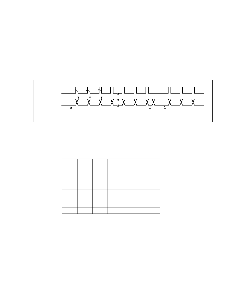
169
CHAPTER 7 TIMER/COUNTER FUNCTION (REAL-TIME PULSE UNIT)
User's Manual U10913EJ6V0UM
7.5 Timer 4 Operation
7.5.1 Count operation
Timer 4 functions as a 16-bit interval timer. The operation is specified by timer control register 4 (TMC4).
The operation of timer 4 counts the internal count clocks (
/2
to
/1024) specified by the PRS40, PRM41, and
PRM40 bits of the TMC4 register.
If the count value of TM4 matches the value of CM4, the value TM4 is cleared while a match interrupt (INTCM4)
is simultaneously generated.
Figure 7-9. Basic Operation of Timer 4
7.5.2 Selecting count clock frequency
An internal count clock frequency is selected by the PRS40, PRM40, and PRM41 bits of the TMC4 register, from
/2,
/4,
/16,
/32,
/64,
/128,
/512, and
/1024.
Caution Do not change the internal count clock frequency while the timer is operating.
PRS40
PRM41
PRM40
Internal Count Clock Frequency
0
0
0
/2
0
0
1
/4
0
1
0
/16
0
1
1
/32
1
0
0
/64
1
0
1
/128
1
1
0
/512
1
1
1
/1024
7.5.3 Overflow
If TM4 overflows as a result of counting the internal count clock, the OVF4 bit of the TOVS register is set (1).
0000H
0001H 0002H 0003H
FBFEH FBFFH
0000H
0001H 0002H
0003H
Count clock
TM4
Count starts
CE4 <- 1
Count disabled
CE4 <- 0
Count starts
CE4 <- 1
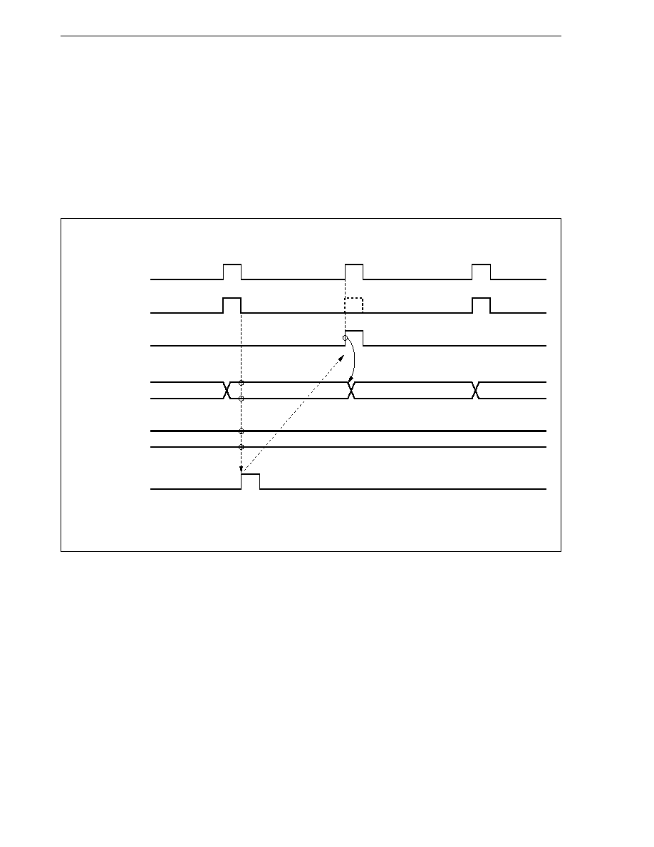
170
CHAPTER 7 TIMER/COUNTER FUNCTION (REAL-TIME PULSE UNIT)
User's Manual U10913EJ6V0UM
7.5.4 Compare operation
A comparison can be performed between the count value of TM4 and the value of the compare register (CM4).
If the count value of TM4 matches the value of the compare register, a match interrupt (INTCM4) is generated.
As a result, TM4 is cleared to 0 at the next count timing (refer to Figure 7-10 (a)). This function allows timer 4 to
be used as an interval timer.
CM4 can be also set to 0. In this case, a match is detected when TM4 overflows and is cleared to 0, and INTCM4
is generated. The value of TM4 is cleared to 0 at the next count timing, but INTCM4 is not generated when a match
occurs at this time (refer to Figure 7-10 (b)).
Figure 7-10. Examples of TM4 Compare Operation (1/2)
(a) Setting FFFFH to CM4
Remark
Interval time = (n + 1)
×
count clock cycle
n = 1 to 65535 (FFFFH)
Count clock
Count up
TM4 clear
TM4
CM4
Match detection
(INTCM4)
clear
n
0
1
n
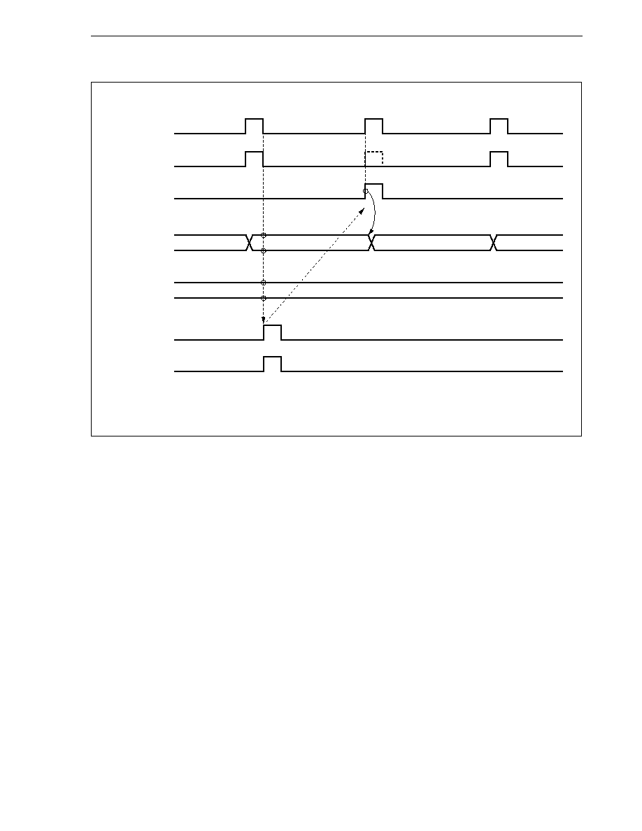
171
CHAPTER 7 TIMER/COUNTER FUNCTION (REAL-TIME PULSE UNIT)
User's Manual U10913EJ6V0UM
Figure 7-10. Examples of TM4 Compare Operation (2/2)
(b) Setting 0 to CM4
Remark
Interval time = (FFFFH + 1)
×
count clock cycle
Count clock
Count up
TM4 clear
TM4
CM4
Match detected
(INTCM4)
Overflow
FFFFH
0
0
1
0
Clear
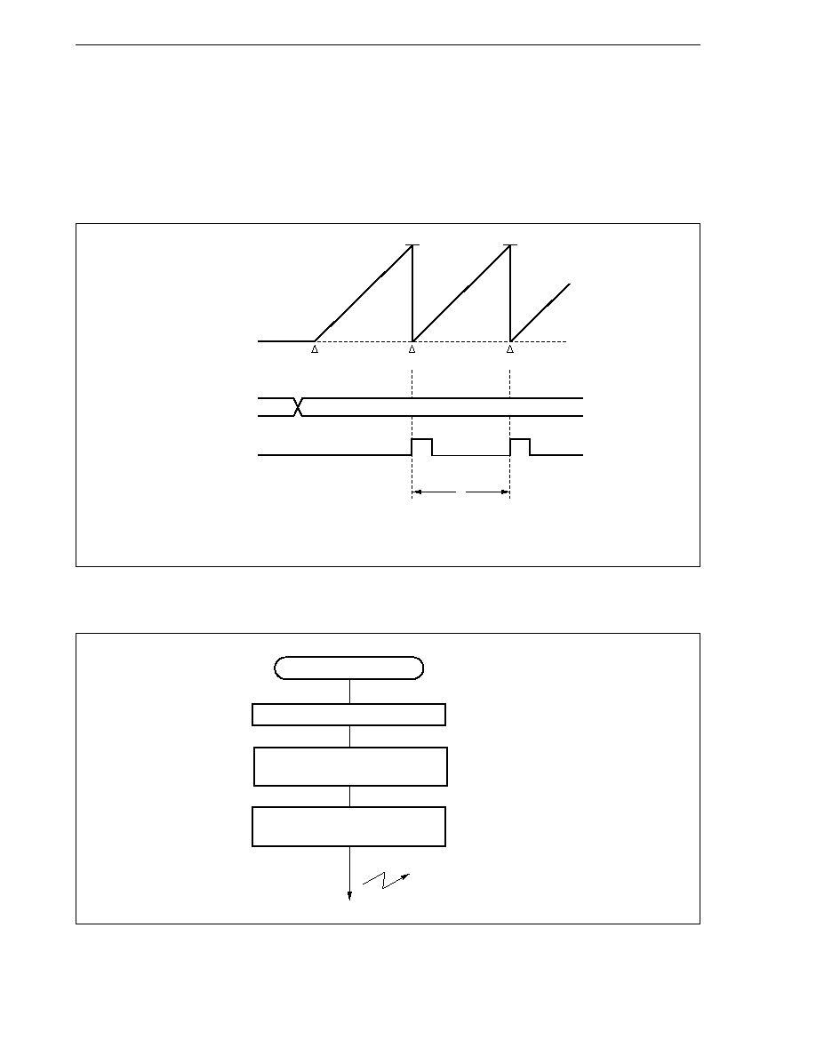
172
CHAPTER 7 TIMER/COUNTER FUNCTION (REAL-TIME PULSE UNIT)
User's Manual U10913EJ6V0UM
7.6 Application Examples
(1) Operation as interval timer (timer 4)
Timer 4 is used as an interval timer that repeatedly generates an interrupt request at time intervals specified
by the count value preset to compare register CM4.
Figure 7-11. Example of Timing of Interval Timer Operation
Remark
n: Value of CM4 register
t: Interval time = (n + 1)
×
count clock cycle
Figure 7-12. Example of Setting Procedure of Interval Timer Operation
TM4
count value
0
Compare register
(CM4)
Interrupt request
(INTCM4)
n
Count starts
Clear
Clear
t
Interval timer initial setting
Setting of TMC4 register
Sets count value to CM4 register
Count starts
TMC4. CE4
1
; Specifies count clock
; Sets CE4 bit to 1
INTCM4 interrupt
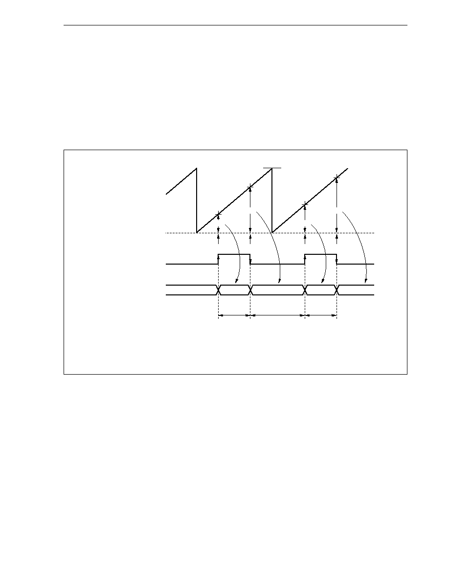
173
CHAPTER 7 TIMER/COUNTER FUNCTION (REAL-TIME PULSE UNIT)
User's Manual U10913EJ6V0UM
(2) Pulse width measurement (timer 1)
Timer 1 is used to measure the pulse width.
In this example, the width of the high or low level of an external pulse input to the INTP112 pins is measured.
The value of timer 1 (TM11) is captured to a capture/compare register (CC112) in synchronization with the
valid edge of the INTP112 pin (both the rising and falling edges) and is held, as shown in Figure 7-13.
To calculate the pulse width, the difference between the count value of TM11 captured to the CC112 register
on detection of the nth valid edge (Dn), and the count value on detection of the (n 1)th valid edge
(Dn 1) is calculated. This difference is multiplied by the count clock.
Figure 7-13. Example of Pulse Width Measurement Timing
Remark
D0 to D3: Count value of TM11
FFFFH
D0
D1
D3
D2
TM11 count value
0
External pulse input
(INTP112)
Capture/compare register
(CC112)
Capture
Capture
Capture
Capture
D3
D2
D1
D0
t1
t2
t3
t1 = (D1 D0)
×
count clock cycle
t2 = {(10000H D1) + D2}
×
count clock cycle
t3 = (D3 D2)
×
count clock cycle
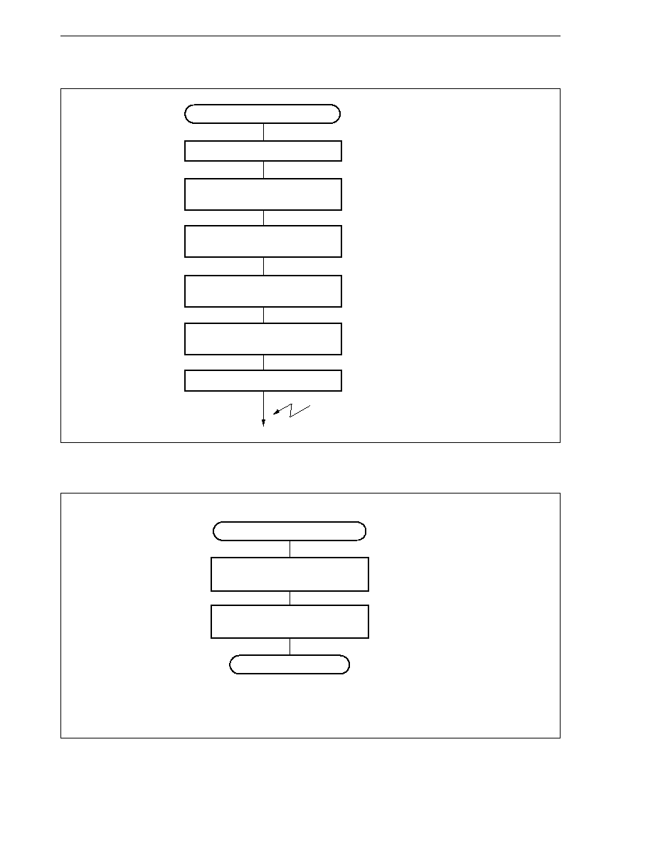
174
CHAPTER 7 TIMER/COUNTER FUNCTION (REAL-TIME PULSE UNIT)
User's Manual U10913EJ6V0UM
Figure 7-14. Example of Setting Procedure for Pulse Width Measurement
Figure 7-15. Example of Interrupt Request Servicing Routine Calculating Pulse Width
Caution If an overflow occurs two times or more between the (n 1)th capture and nth capture,
the pulse width cannot be measured.
Setting of TMC11 register
Setting of INTM1 register
INTM1. ES021 <- 1
INTM1. ES020 <- 1
Setting of TUM11 register
TUM11. CMS112 <- 0
Initialization of buffer memory
for capture data storage
X0 <- 0
Count starts
TMC11. CE11 <- 1
Enables interrupt
INTP112 interrupt
; Specifies count clock
; Specifies both edges as valid
edge of INTP112 input signal
; Sets capture register
; Sets CE11 bit to 1
Pulse width measurement initial setting
INTP112 interrupt servicing
Calculation of pulse width
Yn = CC112 X
n1
tn = Yn x count clock cycle
Stores nth capture data in
buffer memory
Xn <- CC112
RETI
; Xn, Yn : Variable
; tn : Pulse width
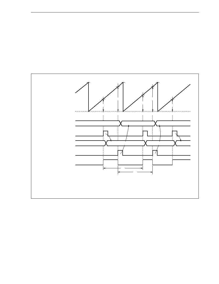
175
CHAPTER 7 TIMER/COUNTER FUNCTION (REAL-TIME PULSE UNIT)
User's Manual U10913EJ6V0UM
(3) PWM output (timer 1)
Any square wave can be output to the timer output pins (TO1n0, TO1n1) by combining timer 1 and the timer
output function and can be used as a PWM output (n = 1 to 4).
Eight capture/compare registers, CC1n0 and CC1n1, are used in this example of PWM output.
A PWM signal with an accuracy of 16 bits can be output from the TO1n0 pin. Figure 7-16 shows the timing.
When timer 1 is used as a 16-bit timer, the rise timing of the PWM output is determined by the value set to
capture/compare register CC1n0, and the fall timing is determined by the value set to capture/compare register
CC1n1 as shown in Figure 7-16.
Figure 7-16. Example of PWM Output Timing
Remark
D00 to D02, D10 to D12: Set value of compare register
t1 = {(10000H D00) + D01}
×
count clock cycle
t2 = {(10000H D10) + D11}
×
count clock cycle
n = 1 to 4
FFFFH
FFFFH
FFFFH
CC1n0
CC1n1
CC1n1
CC1n0
CC1n0
TM1n count value
0
Match
Match
Match
Match
Match
Capture/compare register
(CC1n0)
Interrupt request
(INTCC1n0)
Capture/compare register
(CC1n1)
Interrupt request
(INTCC1n1)
Timer output
(TO1n0 pin)
D00
D01
D12
t1
t2
D02
D10
D11
D00
D01
D11
D02
D10
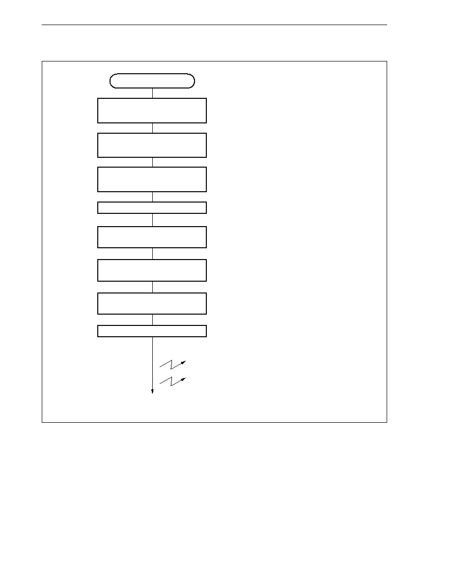
176
CHAPTER 7 TIMER/COUNTER FUNCTION (REAL-TIME PULSE UNIT)
User's Manual U10913EJ6V0UM
Figure 7-17. Example of Programming Procedure of PWM Output
Remark
n = 1 to 4
PWM output initial setting
Setting of TOC1n register
TOC1n. ENTO1n0 1
TOC1n. ALV1n0 1
Setting of TUM1n register
TUM1n. CMS1n0 1
TUM1n. CMS1n1 1
Specifies P00 pin as timer
output pin TO1n0 by PMC0 register
PMC0. PMC00 1
Setting of TMC1n register
Sets count value to CC1n0 register
CC1n0 D00
Enables interrupt
Count starts
TMC1n. CE1n 1
Sets count value to CC1n1 register
CC1n1 D10
; Specifies active level (high level)
Enables timer output
; Specifies operation of CC1n0 and CC1n1 registers
(specifies compare operation)
; Sets CE1n bit to 1
; Specifies count clock of TM1n
INTCC1n0 interrupt
INTCC1n1 interrupt
<-
<-
<-
<-
<-
<-
<-
<-

177
CHAPTER 7 TIMER/COUNTER FUNCTION (REAL-TIME PULSE UNIT)
User's Manual U10913EJ6V0UM
Figure 7-18. Example of Interrupt Request Servicing Routine, Modifying Compare Value
Remark
n = 1 to 4
INTCC1n0 interrupt servicing
Sets time (number of counts) to reset TO1n0
RETI
INTCC1n1 interrupt servicing
Sets time (number of counts) to set TO1n0
output to 1 next, to compare register CC1n0
RETI
output to 0 next, to compare register CC1n1
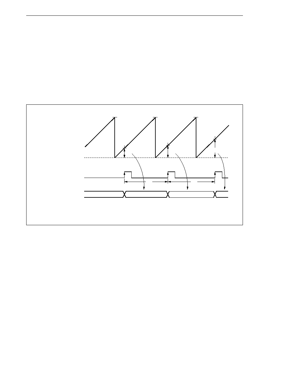
178
CHAPTER 7 TIMER/COUNTER FUNCTION (REAL-TIME PULSE UNIT)
User's Manual U10913EJ6V0UM
(4) Frequency measurement (timer 1)
Timer 1 can be used to measure the cycle or frequency of an external pulse input to the INTP1n0 to INTP1n3
pins (n = 1 to 4).
In this example, the frequency of the external pulse input to the INTP110 pin is measured with an accuracy
of 16 bits, by combining the use of timer 1 and the capture/compare register CC110.
The valid edge of the INTP110 input signal is specified by the INTM1 register to be the rising edge.
To calculate the frequency, the difference between the count value of TM11 captured to the CC110 register
at the nth rising edge (Dn), and the count value captured at the (n 1)th rising edge (Dn 1), is calculated,
and the value multiplied by the count clock frequency.
Figure 7-19. Example of Frequency Measurement Timing
Remark
D0 to D2: Count value of TM11
FFFFH
FFFFH
FFFFH
TM11 count value
0
Interrupt request
(INTP110)
Capture/compare register
(CC110)
D0
D1
D2
t1
t2
D2
D1
D0
t1 = {(10000H D0) + D1}
×
t2 = {(10000H D1) + D2}
×
count clock cycle frequency
count clock cycle frequency
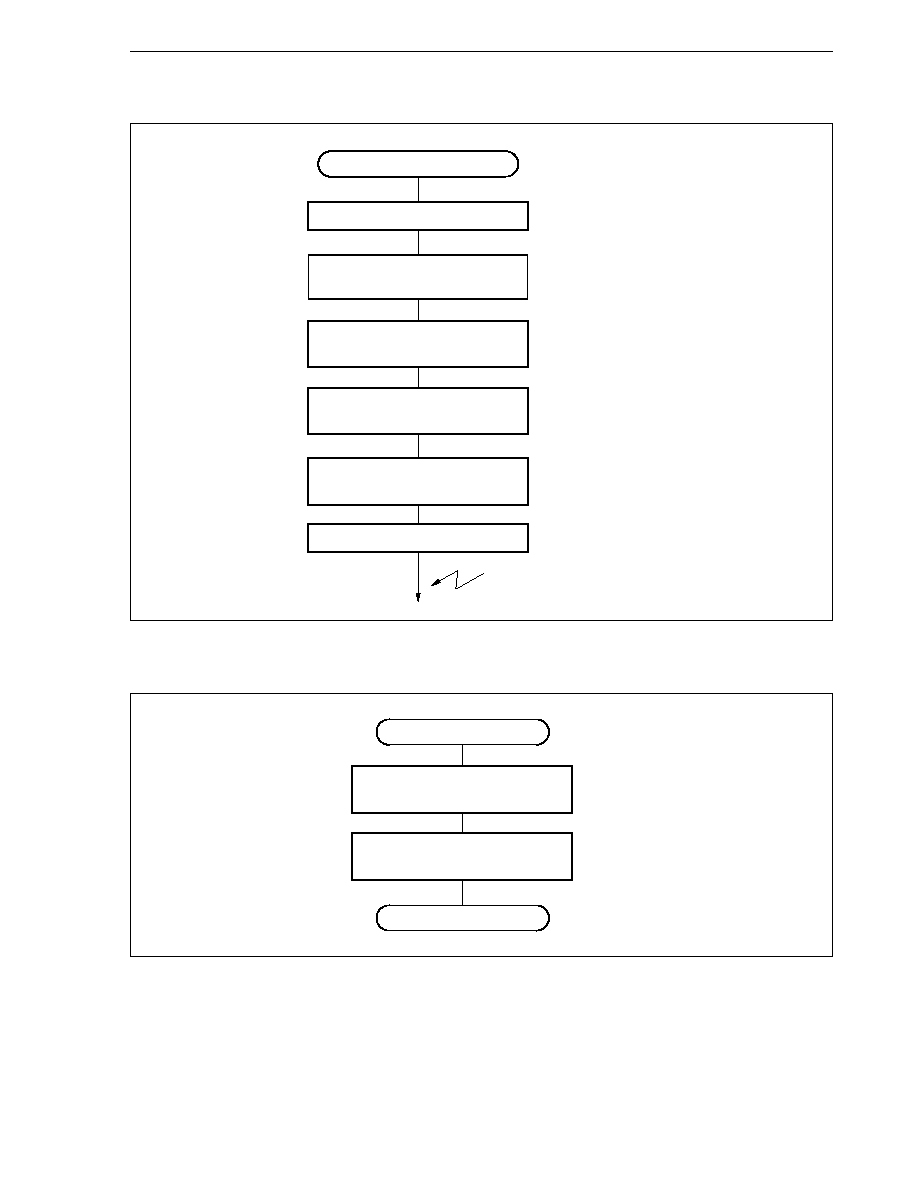
179
CHAPTER 7 TIMER/COUNTER FUNCTION (REAL-TIME PULSE UNIT)
User's Manual U10913EJ6V0UM
Figure 7-20. Example of Setup Procedure for Frequency Measurement
Figure 7-21. Example of Interrupt Request Servicing Routine Calculating Cycle
Setting of TMC11 register
Setting of TUM11 register
TUM11. CMS110 <- 0
Setting of INTM1 register
INTM1. ES001 <- 0
INTM1. ES000 <- 1
Initialization of buffer memory
for capture data storage
X0 <- 0
Count starts
TMC11. CE11 <- 1
Enables interrupt
INTP110 interrupt
; Specifies count clock
; Specifies CC110 register
as capture register
; Specifies rising edge as valid
edge of INTP110 signal
; Sets CE11 bit to 1
Cycle measurement initial setting
INTP110 interrupt servicing
Calculation of cycle
Yn = (10000H X
n1
) + CC110
tn = Yn
×
count clock cycle
Stores nth capture data to
buffer memory
Xn <- CC10
RETI
; tn : Cycle
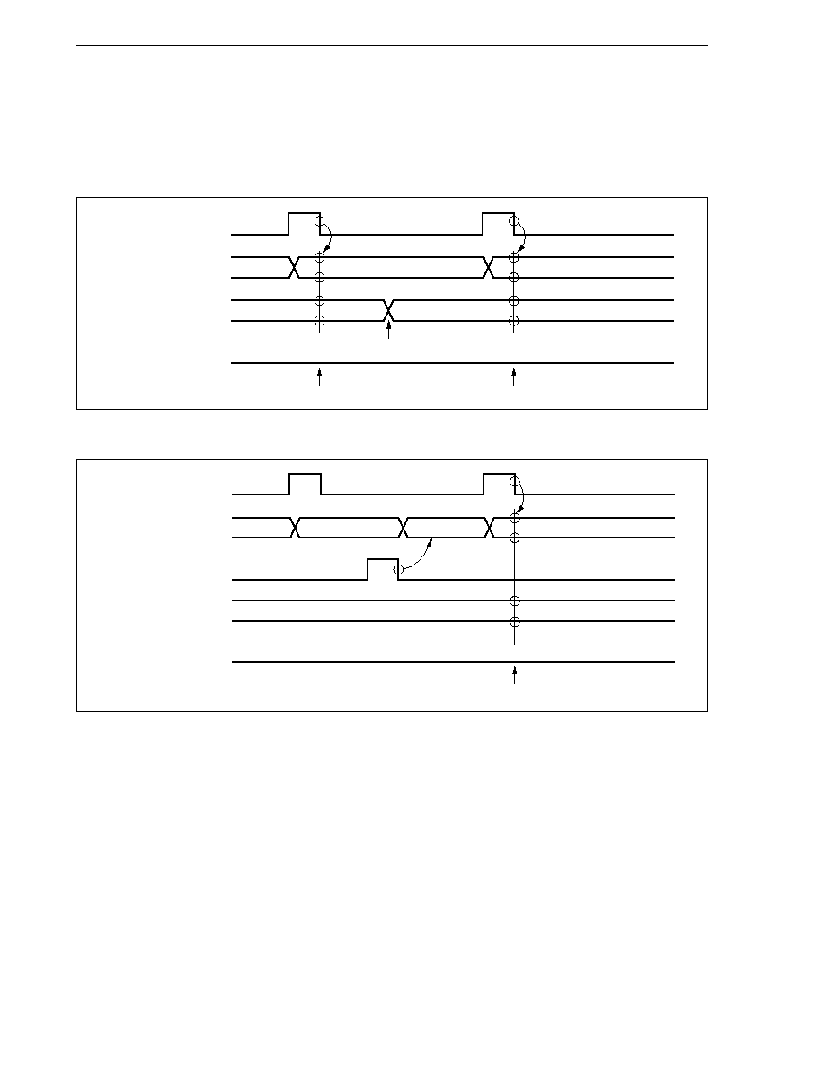
180
CHAPTER 7 TIMER/COUNTER FUNCTION (REAL-TIME PULSE UNIT)
User's Manual U10913EJ6V0UM
7.7 Cautions
A match is detected by the compare register immediately after the timer value matches the compare register value,
and does not take place in the following cases.
(1) When compare register is rewritten (TM11 to TM14, TM4)
(2) When timer is cleared by external input (TM11 to TM14)
Count clock
Value of timer
Compare register value
Match detection
n 1
n
n + 1
m
Writing to register
Match does not occur
Match does not occur
L
n
Value of timer
External clear input
Match detection
Count clock
Compare register value
n 1
n
0
1
0000H
Match does not occur
L
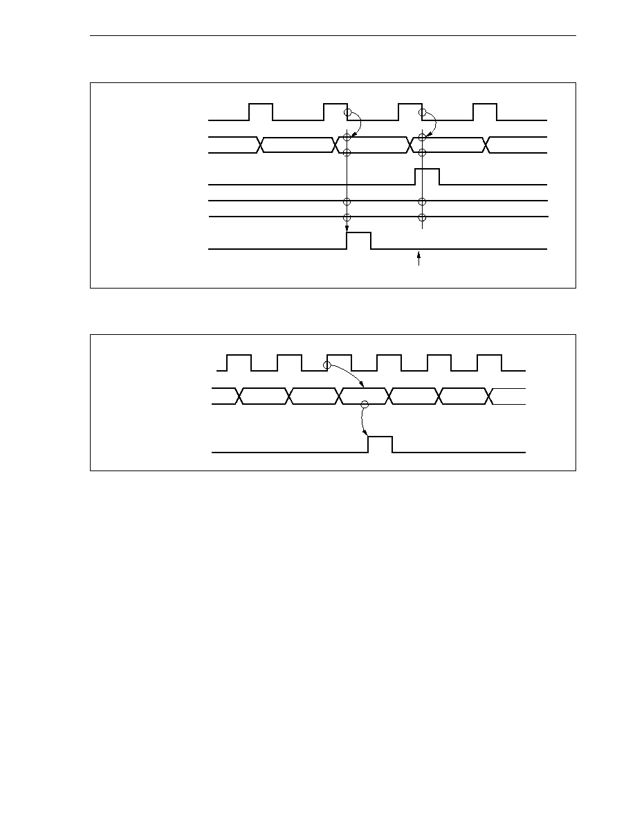
181
CHAPTER 7 TIMER/COUNTER FUNCTION (REAL-TIME PULSE UNIT)
User's Manual U10913EJ6V0UM
FFFEH
FFFFH
1
Count clock
Value of timer
Overflow interrupt
0
3
2
(3) When timer is cleared (TM4)
Remark
When timer 1 is used as a free-running timer, the timer value is cleared to 0 when the timer overflows.
Count clock
Value of timer
Internal match clear
Match detection
FFFEH
FFFFH
0
0
1
Match does not occur
0000H
Compare register value

182
User's Manual U10913EJ6V0UM
CHAPTER 8 SERIAL INTERFACE FUNCTION
8.1 Features
The V853 is provided with two types of serial interfaces which operate as 6-channel transmission/reception
channels. Four channels can be used simultaneously.
There are the following two types of interfaces.
(1) Asynchronous serial interface (UART0, UART1): 2 channels
(2) Clocked serial interface (CSI0 to CSI3):
4 channels
UART0 and UART1 transmit/receive 1-byte serial data following a start bit and can perform full-duplex communication.
CSI0 to CSI3 use three kinds of signal lines to transfer data (3-wire serial I/O): serial clock (SCK0 to SCK3), serial
input (SI0 to SI3), and serial output (SO0 to SO3) lines.
Caution UART0 and CSI0, and UART1 and CSI1 share the same pins respectively. Either one of these
is selected according to ASIM00 and ASIM10 registers.

183
CHAPTER 8 SERIAL INTERFACE FUNCTION
User's Manual U10913EJ6V0UM
8.2 Asynchronous Serial Interface 0 and 1 (UART0 and UART1)
8.2.1 Features
Transfer rate: 150 bps to 76800 bps
Note
(baud rate generator and
= 33 MHz operation)
110 bps to 307200 bps
Note
(baud rate generator and
= 20 MHz operation)
Max. 1031 Kbps
Note
(
/2 and
= 33 MHz operation)
Full-duplex communication: Internal receive buffer (RXBn)
Two-pin configuration: TXDn: Transmit data output pin
RXDn: Receive data input pin
Receive error detection function
· Parity error
· Framing error
· Overrun error
Three interrupt sources
· Receive error interrupt (INTSERn)
· Reception completion interrupt (INTSRn)
· Transmission completion interrupt (INTSTn)
Character length of transmit/receive data is specified by ASIMn0 and ASIMn1 registers.
Character length: 7, 8 bits
9 bits (when extended)
Parity function: Odd, even, 0, none
Transmit stop bit: 1, 2 bits
Internal baud rate generator
Note
For the baud rate error, refer to Table 8-2 Setting Values of Baud Rate Generators 0 to 2.
Remark
n = 0, 1
: Internal system clock

184
CHAPTER 8 SERIAL INTERFACE FUNCTION
User's Manual U10913EJ6V0UM
8.2.2 Configuration of asynchronous serial interface
The asynchronous serial interface is controlled by the asynchronous serial interface mode register (ASIMn0,
ASIMn1) and the asynchronous serial interface status register (ASISn) (n = 0, 1). The receive data is stored in the
receive buffer (RXBn), and the transmit data is written to the transmit shift register (TXSn).
Figure 8-1 shows the configuration of the asynchronous serial interface.
(1) Asynchronous serial interface mode registers (ASIM00, ASIM01, ASIM10, ASIM11)
ASIMn0 and ASIMn1 are 8-bit registers that specify the operation of the asynchronous serial interface.
(2) Asynchronous serial interface status registers (ASIS0, ASIS1)
ASISn are registers containing flags that indicate receive errors, if any, and a transmit status flag. Each receive
error flag is set to 1 when a receive error occurs, and is reset to 0 when data is read from the receive buffer
(RXBn), or when new data is received (if the next data contains an error, the corresponding error flag is set
(1)).
The transmit status flag is set to 1 when transmission is started, and reset to 0 when transmission ends.
(3) Reception control parity check
The reception operation is controlled according to the contents programmed in the ASIMn0 and ASIMn1
registers. During the receive operation, errors such as parity error are also checked. If an error is found, the
appropriate value is set to the ASISn registers.
(4) Receive shift register
This shift register converts the serial data received on the RXDn pin into parallel data. When it receives 1
byte of data, it transfers the receive data to the receive buffer.
This register cannot be accessed directly.
(5) Receive buffers (RXB0, RXB0L, RXB1, RXB1L)
RXBn are 9-bit buffer registers that hold receive data. If data of 7 or 8 bits/character is received, 0 is stored
to the most significant bit position of these registers.
If these registers are accessed in 16-bit units, RXB0 and RXB1 are specified. To access in lower 8-bit units,
RXB0L and RXB1L are specified.
While reception is enabled, the receive data is transferred from the receive shift register to the receive buffer
in synchronization with shift-in processing of 1 frame.
When the data is transferred to the receive buffer, a reception completion interrupt request (INTSRn) occurs.
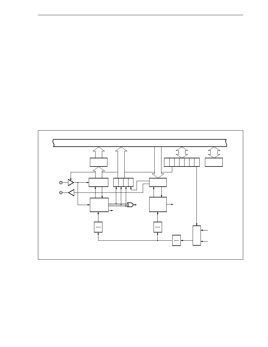
185
CHAPTER 8 SERIAL INTERFACE FUNCTION
User's Manual U10913EJ6V0UM
(6) Transmit shift registers (TXS0, TXS0L, TXS1, TXS1L)
TXSn are 9-bit shift registers used for transmit operation. When data is written to these registers, the
transmission operation is started.
A transmission complete interrupt request (INTSTn) is generated after each complete data frame is
transmitted.
When these registers are accessed in 16-bit units, TXS0 and TXS1 are specified. To access in lower 8-bit
units, TXS0L and TXS1L are specified.
(7) Transmission parity control
A start bit, parity bit, and stop bit are appended to the data written to the TXSn registers, according to the
contents programmed in the ASIMn0 and ASIMn1 registers, to control the transmission operation.
(8) Selector
Selects the source of the serial clock.
Figure 8-1. Block Diagram of Asynchronous Serial Interface
Remark
n = 0, 1
Internal bus
16/8
8
Receive
buffer
Receive
shift register
Receive
control parity
check
1
16
1
16
1
2
INTSTn
INTSRn
INTSERn
Transmission
parity control
Selector
Baud rate
generator
8
8
16/8
ASISn
RXDn
TXDn
PEn FEn OVEn SOTn
RXEn
TXEn
PSn1 PSn0 CLn SLn SOLSn
EBSn
ASIMn0
ASIMn1
RXBn
RXBnL
TXSn
TXSnL
Transmit
shift register
Internal system
clock ( )

186
CHAPTER 8 SERIAL INTERFACE FUNCTION
User's Manual U10913EJ6V0UM
8.2.3 Control registers
(1) Asynchronous serial interface mode registers 00, 01, 10, and 11 (ASIM00, ASIM01, ASIM10, ASIM11)
These registers specify the transfer mode of UART0 and UART1.
They can be read/written in 8-bit or 1-bit units.
(1/3)
Bit position
Bit name
Function
7, 6
TXEn,
Transmit/Receive Enable
RXEn
Enable/disable transmission/reception.
TXEn
RXEn
Operation
0
0
Disables transmission/reception (selection of CSIn)
0
1
Enables reception
1
0
Enables transmission
1
1
Enables transmission/reception
When reception is disabled, the receive shift register does not detect the start bit.
Data is not shifted into the receive shift register and neither is any transfer to the receive
buffer performed. Therefore, the previous contents of the receive buffer are retained. When
reception is enabled, the data is shifted into the receive shift register and transferred to the
receive buffer when one complete frame has been received. A reception completion interrupt
(INTSRn) is generated in synchronization with the transfer to the receive buffer.
When transmission is disabled, TXDn pin becomes high impedance, and when transmission
is enabled and not being performed, high level is output.
Remark
n = 0, 1
7
TXE0
ASIM00
6
RXE0
5
PS01
4
PS00
3
CL0
2
SL0
1
0
0
SCLS0
FFFFF0D0H
TXE1
ASIM10
RXE1
PS11
PS10
CL1
SL1
0
SCLS1
00H
Address
FFFFF0C0H
After reset
00H

187
CHAPTER 8 SERIAL INTERFACE FUNCTION
User's Manual U10913EJ6V0UM
(2/3)
Bit position
Bit name
Function
5, 4
PSn1, PSn0
Parity Select
Specifies parity bit.
PSn1
PSn0
Operation
0
0
No parity. Extended bit operation
0
1
0 parity
Transmission side
Transmits with parity bit 0
Reception side
Does not generate parity error on reception
1
0
Odd parity
1
1
Even parity
· Even parity
Parity bit is set to 1 when number of bits that are "1" in received data is odd. If number of bits
that are "1" is even, the parity bit is cleared to 0. In this way, number of bits that are "1" in
transmit data and parity bit is controlled to be even. During reception, number of bits that are
"1" in receive data and parity bit are counted. If it is odd, parity error occurs.
· Odd parity
In contrast to even parity, number of bits included in transmit data and parity bit that are "1"
is controlled to become odd.
During reception, parity error occurs if the number of bits that are "1" in the receive data and
parity bit are added up to become even.
· 0 parity
Parity bit is cleared to 0 during transmission, regardless of transmit data.
During reception, the parity bit is not checked and a parity error does not occur.
· No parity
No parity bit is appended to the transmit data.
Reception is performed on the assumption that there is no parity bit. Because no parity bit
is used, a parity error does not occur.
Extended bit operation can be specified by the EBSn bit of the ASIMn1 register.
3
CLn
Character Length
Specifies character length of one frame.
0: 7 bits
1: 8 bits
2
SLn
Stop Bit Length
Specifies the stop bit length.
0: 1 bit
1: 2 bits
Remark
n = 0, 1
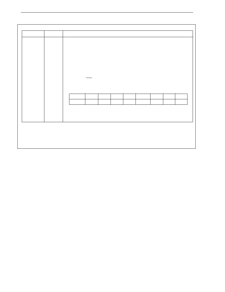
188
CHAPTER 8 SERIAL INTERFACE FUNCTION
User's Manual U10913EJ6V0UM
(3/3)
Bit position
Bit name
Function
0
SCLSn
Serial Clock Source
Specifies serial clock.
0: Specified by BRGCn and BPRMn
1:
/2
· When SCLSn = 1
/2 (system clock) is selected as the serial clock source. In asynchronous mode, the baud
rate is expressed as follows because a sampling rate of
×
16 is used.
Baud rate = bps
The value of baud rate when a typical clock is used based on the above expression is as
follows.
33 MHz 25 MHz 20 MHz 16 MHz 12.5 MHz 10 MHz
8 MHz
5 MHz
Baud rate
1031 K
781 K
625 K
500 K
390 K
312 K
250 K
156 K
· When SCLSn = 0
The baud rate generator output is selected as the serial clock source. For details of the
baud rate generator, refer to 8.4 Baud Rate Generators 0 to 2 (BRG0 to BRG2).
Caution The operation of UARTn is not guaranteed if these registers are changed while UARTn is
transmitting/receiving data.
Remark
n = 0, 1
: Internal system clock
/2
16

189
CHAPTER 8 SERIAL INTERFACE FUNCTION
User's Manual U10913EJ6V0UM
Bit position
Bit name
Function
0
EBSn
Extended Bit Select
Specifies extended bit operation of transmit/receive data when no parity is specified (PSn1,
PSn0 = 00).
0: Disables extended bit operation
1: Enables extended bit operation
When extended bit operation is enabled, 1 data bit is appended as the most significant bit to the
8-bit transmit/receive data, and therefore 9-bit data is communicated.
Extended bit operation is valid only when no parity is specified by the ASIMn0 register. If zero,
even, or odd parity is specified, specification by the EBSn bit is invalid, and the extended bit is
not appended.
Remark
n = 0, 1
Address
FFFFF0C2H
7
0
ASIM01
6
0
5
0
4
0
3
0
2
0
1
0
0
EBS0
After reset
00H
FFFFF0D2H
0
ASIM11
0
0
0
0
0
0
EBS1
00H

190
CHAPTER 8 SERIAL INTERFACE FUNCTION
User's Manual U10913EJ6V0UM
(2) Asynchronous serial interface status registers 0 and 1 (ASIS0, ASIS1)
These registers consist of a 3-bit error flag that indicates error status when UARTn receive is completed and
a transmit status flag.
The error flags always indicate the status of an error that has occurred most recently. If two or more errors
occur before the current received data, only the status of the error that has occurred last is retained.
If a receive error occurs, read the receive buffer (RXBn or RXBnL) after reading the ASISn registers, and then
clear the error flag. If RXBn or RXBnL are not read, an overrun error will occur at the next data reception and
the reception error state will continue. These registers are read-only in 8-bit or 1-bit units.
Bit position
Bit name
Function
7
SOTn
Status Of Transmission
Status flag that indicates transmission operation status.
Set (1):
Beginning of transmission of a data frame (writing to TXSn or TXSnL register)
Clear (0): End of transmission of a data frame (occurrence of INTSTn interrupt)
When serial data transfer begins, this flag will indicate if the transmit shift register is ready to be
written or not.
2
PEn
Parity Error
Status flag that indicates parity error.
Set (1):
Transmit parity and receive parity do not match
Clear (0): Processing to read out the data from the receive buffer.
1
FEn
Framing Error
Status flag that indicates framing error.
Set (1):
Stop bit is not detected
Clear (0): Processing to read out the data from the receive buffer.
0
OVEn
Overrun Error
Status flag that indicates overrun error.
Set (1):
Set when UARTn has completed the next receive processing before obtaining the
receive data from the receive buffer.
Clear (0): Processing to read out the receive data from the receive buffer.
Because the contents of receive shift register are transferred to a receive buffer each time one
frame of data has been received, if an overrun error occurs, the next receive data is written over
the contents of the receive buffer, and the previous receive data is discarded.
Remark
n = 0, 1
Address
FFFFF0C4H
7
SOT0
ASIS0
6
0
5
0
4
0
3
0
2
PE0
1
FE0
0
OVE0
After reset
00H
FFFFF0D4H
SOT1
ASIS1
0
0
0
0
PE1
FE1
OVE1
00H
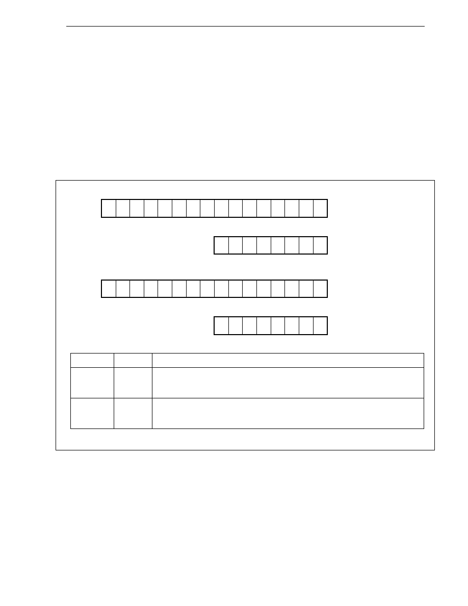
191
CHAPTER 8 SERIAL INTERFACE FUNCTION
User's Manual U10913EJ6V0UM
(3) Receive buffers 0, 0L, 1, and 1L (RXB0, RXB0L, RXB1, RXB1L)
RXBn are 9-bit buffer registers that hold the receive data. When 7- or 8-bit character data is received, the
higher bit of these registers are 0.
When these registers are accessed in 16-bit units, RXB0 and RXB1 are specified. When accessed in lower
8-bit units, RXB0L and RXB1L are specified.
When reception is enabled, the receive data is transferred from the receive shift register to the receive buffer
when one complete frame of data has been received.
When the receive data is transferred to the receive buffer, a reception completion interrupt request (INTSRn)
occurs.
When reception is disabled, the data is not shifted into the receive shift register and the reception completion
interrupt is not generated. The previous contents of the receive buffer are retained.
RXB0 and RXB1 are read-only in 16-bit units, and RXB0L and RXB1L are read-only in 8-bit or 1-bit units.
Bit position
Bit name
Function
8
RXEBn
Receive Extended Buffer
Extended bit when 9-bit character data is received.
These bits are cleared to zero when 7- or 8-bit character data is received.
7 to 0
RXBn7 to
Receive Buffer
RXBn0
These bits store receive data.
RXBn7 is cleared to zero when 7-bit character data is received.
Remark
n = 0, 1
15
0
RXB0
Address
FFFFF0C8H
After reset
Undefined
14
0
13
0
12
0
11
0
10
0
9
0
8
RXEB0
7
RXB07
6
RXB06
5
RXB05
4
RXB04
3
RXB03
2
RXB02
1
RXB01
0
RXB00
RXB0L
Address
FFFFF0CAH
After reset
Undefined
7
RXB07
6
RXB06
5
RXB05
4
RXB04
3
RXB03
2
RXB02
1
RXB01
0
RXB00
15
0
RXB1
Address
FFFFF0D8H
After reset
Undefined
14
0
13
0
12
0
11
0
10
0
9
0
8
RXEB1
7
RXB17
6
RXB16
5
RXB15
4
RXB14
3
RXB13
2
RXB12
1
RXB11
0
RXB10
RXB1L
Address
FFFFF0DAH
After reset
Undefined
7
RXB17
6
RXB16
5
RXB15
4
RXB14
3
RXB13
2
RXB12
1
RXB11
0
RXB10
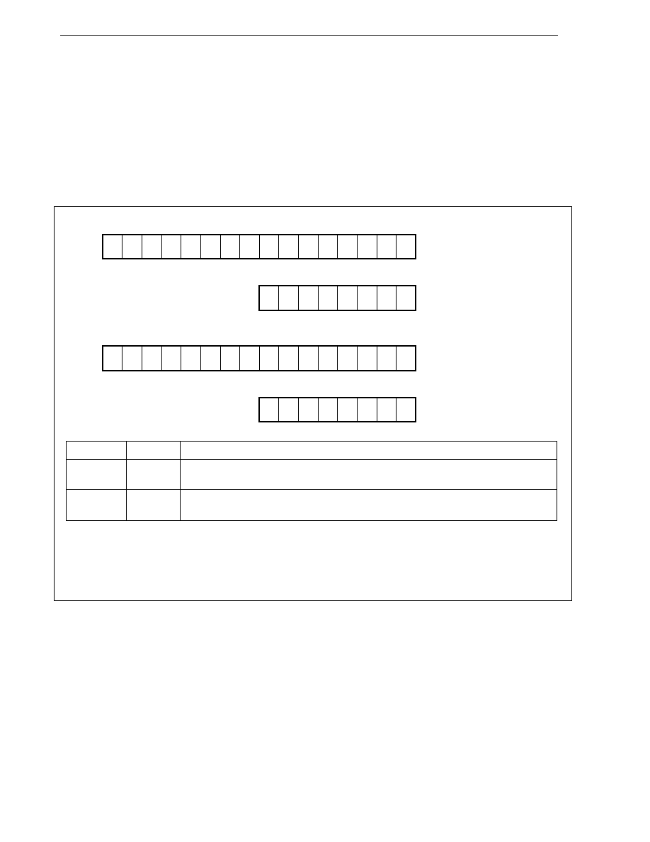
192
CHAPTER 8 SERIAL INTERFACE FUNCTION
User's Manual U10913EJ6V0UM
(4) Transmit shift registers 0, 0L, 1, and 1L (TXS0, TXS0L, TXS1, TXS1L)
TXSn are 9-bit shift registers for data transmission. The transmit operation is started when data is written
to these registers during transmission enable status.
If data is written to the transmit shift register in the transmission disabled status, the values written are ignored.
Transmission complete interrupt request (INTSTn) is generated after each complete data frame including
TXSn is transmitted.
When these registers are accessed in 16-bit units, TXS0 and TXS1 are specified. When accessed in lower
8-bit units, TXS0L and TXS1L are specified.
TXS0 and TXS1 are write-only in 16-bit units, and TXS0L and TXS1L are write-only in 8-bit units.
Bit position
Bit name
Function
8
TXEDn
Transmit Extended Data
Extended bit on transmission of 9-bit character data.
7 to 0
TXSn7 to
Transmit Shifter
TXSn0
Writes transmit data.
Caution Note that UARTn does not have a transmit buffer. This means that an interrupt request (INTSTn)
is generated in synchronization with the end of transmission of one frame of data.
Remark
n = 0, 1
15
0
TXS0
Address
FFFFF0CCH
After reset
Undefined
14
0
13
0
12
0
11
0
10
0
9
0
8
TXED0
7
TXS07
6
TXS06
5
TXS05
4
TXS04
3
TXS03
2
TXS02
1
TXS01
0
TXS00
TXS0L
Address
FFFFF0CEH
After reset
Undefined
7
TXS07
6
TXS06
5
TXS05
4
TXS04
3
TXS03
2
TXS02
1
TXS01
0
TXS00
15
0
TXS1
Address
FFFFF0DCH
After reset
Undefined
14
0
13
0
12
0
11
0
10
0
9
0
8
TXED1
7
TXS17
6
TXS16
5
TXS15
4
TXS14
3
TXS13
2
TXS12
1
TXS11
0
TXS10
TXS1L
Address
FFFFF0DEH
After reset
Undefined
7
TXS17
6
TXS16
5
TXS15
4
TXS14
3
TXS13
2
TXS12
1
TXS11
0
TXS10

193
CHAPTER 8 SERIAL INTERFACE FUNCTION
User's Manual U10913EJ6V0UM
8.2.4 Interrupt request
UARTn generates the following three interrupt requests (n = 0, 1).
· Receive error interrupt (INTSERn)
· Reception completion interrupt (INTSRn)
· Transmission completion interrupt (INTSTn)
Of these three, the receive error interrupt has the highest default priority, followed by the reception completion
interrupt and transmission completion interrupt.
Table 8-1. Default Priority of Interrupts
Interrupt
Priority
Receive error
1
Reception completion
2
Transmission completion
3
(1) Receive error interrupt (INTSERn)
A receive error interrupt occurs as a result of ORing the three types of receive errors described in the description
of the ASISn registers when reception is enabled.
This interrupt does not occur when reception is disabled.
(2) Reception completion interrupt (INTSRn)
The reception completion interrupt occurs if data is received in the receive shift register and then transferred
to the receive buffer when reception is enabled.
Reception completion interrupt request also occurs when a receive error occurs, but the receive error interrupt
has higher priority.
The reception completion interrupt does not occur when reception is disabled.
(3) Transmission completion interrupt (INTSTn)
Because UARTn does not have a transmit buffer, a transmission completion interrupt occurs when one frame
of transmit data containing a 7-/8-/9-bit character is shifted out from the transmit shift register.
The transmission completion interrupt is output when the last bit of data has been transmitted.
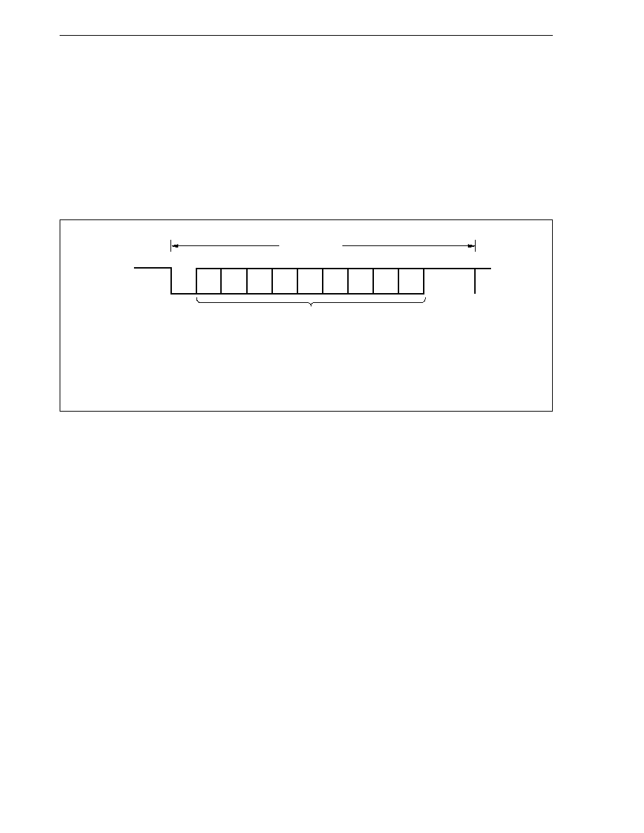
194
CHAPTER 8 SERIAL INTERFACE FUNCTION
User's Manual U10913EJ6V0UM
8.2.5 Operation
(1) Data format
Full-duplex serial data is transmitted/received.
One data frame of the transmit/receive data consists of a start bit, character bits, parity bit, and stop bit, as
shown in Figure 8-2.
The length of the character bit, parity, and the length of the stop bit in one data frame are specified by the
asynchronous serial interface mode registers (ASIMn0, ASIMn1) (n = 0, 1).
Figure 8-2. Format of Transmit/Receive Data of Asynchronous Serial Interface
· Start bit ...................... 1 bit
· Character bit ............. 7/8 bits
· Parity/extension bit ... Even/odd/0/none/extended bit
· Stop bit ...................... 1/2 bits
(2) Transmission
Transmission is started when data is written to the transmit shift registers (TXSn or TXSnL). The next data
is written to the TXSn or TXSnL registers by the service routine of the transmission completion interrupt
servicing routine (INTSTn).
(a) Transmission enabled status
Set using the TXEn bit of the ASIMn0 register.
TXEn = 1: Transmission enabled status
TXEn = 0: Transmission disabled status
However, to set the transmission enabled status, set both the CTXEn and CRXEn bits of the clocked serial
interface mode register (CSIMn) to 0.
Because UARTn does not have a CTS (transmission enabled signal) input pin, use a general input port
when checking whether the transmission destination is in the reception enabled status.
(b) Starting transmission
In the transmission enabled status, transmission starts when data is written to the transmission shift
register (TXSn or TXSnL). The transmit data is transferred LSB first starting from the start bit. The start
bit, parity/extended bit, and stop bit are automatically appended.
Data cannot be written to the transmission shift register in the transmission disabled status, and values
written in this state are ignored.
D0
D1
D2
D3
D4
D5
D6
D7
Parity/
Stop
bit
Start
bit
Character bit
1 data frame
extension
bit
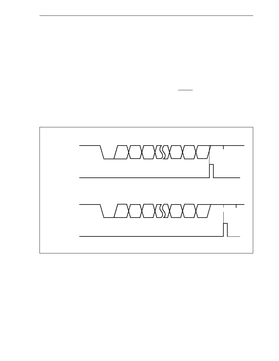
195
CHAPTER 8 SERIAL INTERFACE FUNCTION
User's Manual U10913EJ6V0UM
(c) Transmission interrupt request
When one frame of data or character has been completely transferred, a transmission completion interrupt
request (INTSTn) occurs.
Unless the data to be transmitted next is written to the TXSn or TXSnL registers, the transmission is
aborted.
The communication rate drops unless the next transmit data is written to the TXSn or TXSnL registers
immediately after transmission has been completed.
Cautions 1. The transmission completion interrupt request (INTSTn) is generated after each
complete data frame is transmitted out of the transmit shift register (TXSn or TXSnL).
However, if TXSn or TXSnL becomes empty by RESET input, INTSTn is not generated.
2. During the transmit operation, writing data into the TXSn or TXSnL register is ignored
(the data is discarded) until INTSTn is generated.
Figure 8-3. Asynchronous Serial Interface Transmission Completion Interrupt Timing
(a) Stop bit length: 1
(b) Stop bit length: 2
Remark
n = 0, 1
TXDn (output)
INTSTn interrupt
Start
D0
D1
D2
D6
D7
Parity/
extension
Parity/
extension
Stop
D0
D1
D2
D6
D7
Stop
Start
TXDn (output)
INTSTn interrupt

196
CHAPTER 8 SERIAL INTERFACE FUNCTION
User's Manual U10913EJ6V0UM
(3) Reception
When reception is enabled, sampling of the RXDn pin is started, and reception of data begins when the start
bit is detected. Each time one frame of data or character has been received, the reception completion interrupt
(INTSRn) occurs. Usually, the receive data is transferred from the receive buffer (RXBn or RXBnL) to memory
by this interrupt servicing.
(a) Reception enabled status
Reception is enabled when the RXEn bits of the ASIMn0 registers are set to 1.
RXEn = 1: Reception is enabled
RXEn = 0: Reception is disabled
However, to set the reception enabled status, set both the CTXEn and CRXEn bits of the clocked serial
interface mode register (CSIMn) to 0.
When reception is disabled, the reception hardware stands by in the initial status.
At this time, the reception completion interrupt/receive error interrupt does not occur, and the contents
of the receive buffer are retained.
(b) Starting reception
Reception is started when the start bit is detected.
The RXDn pin is sampled with the serial clock from baud rate generator n (BRGn). The RXDn pin is
sampled again eight clocks after the low level of the RXDn pin has been detected. If the RXDn pin is
low at this time, it is recognized as the start bit, and reception is started. After that, the RXDn pin is sampled
every 16 clock ticks.
If the RXDn pin is high eight clocks after the low level of the RXDn pin has been detected, this low level
is not recognized as the start bit. The serial clock counter is reinitialized, and UARTn waits for the input
of the next low level or valid start bit.
(c) Reception completion interrupt request
When one frame of data has been received with RXEn = 1, the receive data in the shift register is
transferred to RXBn, and a reception completion interrupt request (INTSRn) is generated.
If an error occurs, the receive data that contains an error is transferred to the receive buffer (RXBn or
RXBnL), and the transmission completion interrupt (INTSRn) and receive error interrupt (INTSERn) occur
simultaneously.
If the RXEn bit is reset (0) during receive operation, the receive operation stops immediately. In this case,
the contents of the receive buffer (RXBn or RXBnL) and the asynchronous serial interface status register
(ASISn) do not change, and neither reception completion interrupt (INTSRn) nor reception error interrupt
(INTSERn) is generated.
When RXEn = 0 (reception disabled), reception completion interrupt does not occur.
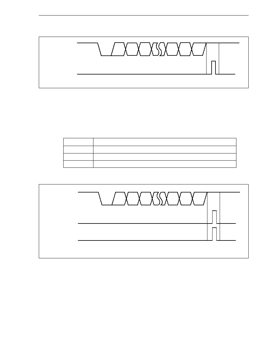
197
CHAPTER 8 SERIAL INTERFACE FUNCTION
User's Manual U10913EJ6V0UM
Figure 8-4. Asynchronous Serial Interface Reception Completion Interrupt Timing
Remark
n = 0, 1
(d) Reception error flag
Three error flags, parity error, framing error, and overrun error flags, are related to the reception operation.
The receive error interrupt request occurs as a result of ORing these three error flags.
By reading the contents of the ASISn register, the error which caused the receive error interrupt (INTSERn)
can be identified.
The contents of the ASISn register are reset to 0 when the receive buffer (RXBn or RXBnL) is read or
the next data frame is received (if the next data contains an error, the corresponding error flag is set).
Receive
Error Cause
Parity error
Parity specified during transmission does not match parity of receive data
Framing error
Stop bit is not detected
Overrun error
Next data is completely received before data is read from receive buffer
Figure 8-5. Receive Error Timing
Remark
n = 0, 1
RXDn (input)
INTSRn interrupt
Start
D0
D1
D2
D6
D7
Parity/
extension
Stop
INTSERn interrupt
RXDn (input)
INTSRn interrupt
Start
D0
D1
D2
D6
D7
Parity/
extended
Stop

198
CHAPTER 8 SERIAL INTERFACE FUNCTION
User's Manual U10913EJ6V0UM
8.3 Clocked Serial Interface 0 to 3 (CSI0 to CSI3)
8.3.1 Features
Number of channels: 4 channels (CSIn)
High transfer speed: 8.25 Mbps max. (@
= 33 MHz operation: CSI0 to CSI2)
2 Mbps max. (@
= 33 MHz operation: CSI3)
Half-duplex communication
Character length: 8 bits
MSB first/LSB first selectable
External serial clock input/internal serial clock output selectable
3 wires:
SOn:
Serial data output
SIn:
Serial data input
SCKn: Serial clock I/O
Interrupt sources: 1
· Transmission/reception completion interrupt (INTCSIn)
Remark
n = 0 to 3
: Internal system clock
8.3.2 Configuration
CSIn is controlled by the clocked serial interface mode register (CSIMn). The transmit/receive data is read/written
from/to the serial I/O shift register (SIOn).
(1) Clocked serial interface mode register (CSIMn)
CSIMn is an 8-bit register that specifies the operation of CSIn.
(2) Serial I/O shift register (SIO0 to SIO3)
SIOn is an 8-bit register that converts serial data into parallel data, and vice versa. SIOn is used for both
transmission and reception.
Data is shifted in (received) or shifted out (transmitted) from the MSB or LSB side.
The actual transmitting and receiving of data is performed by writing data to and reading data from the SIOn
register.
(3) Selector
Selects the serial clock to be used.
(4) Serial clock controller
Controls supply of the serial clock to the shift register. When the internal clock is used, it also controls the
clock output to the SCKn pin.
(5) Serial clock counter
Counts the serial clocks being output and the serial clocks received during transmission/reception to check
whether 8-bit data has been transmitted or received.
(6) Interrupt controller
Controls whether an interrupt request is generated when the serial clock counter has counted eight serial
clocks.
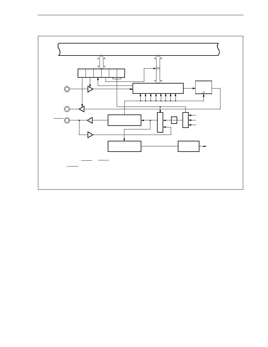
199
CHAPTER 8 SERIAL INTERFACE FUNCTION
User's Manual U10913EJ6V0UM
Figure 8-6. Block Diagram of Clocked Serial Interface
Note
SO0 to SO2, SCK0 to SCK2: CMOS output
SO3, SCK3:
N-ch open drain output
Remark
n = 0 to 3
Internal bus
CSIMn
CTXEn CRXEn CSOTn MODn CLSn1 CLSn0
SO latch
D
Q
Shift register (SIOn)
SIn
SOn
SCKn
Serial clock
controller
Selector
Selector
1
2
Baud rate generator
/2
Interrupt
controller
Serial clock counter
Note
Note
INTCSIn

200
CHAPTER 8 SERIAL INTERFACE FUNCTION
User's Manual U10913EJ6V0UM
8.3.3 Control registers
(1) Clocked serial interface mode registers 0 to 3 (CSIM0 to CSIM3)
These registers specify the basic operation mode of CSI0 to CSI3.
They can be read/written in 8-bit or 1-bit units (note, however, that bit 5 can only be read).
(1/2)
Bit position
Bit name
Function
7
CTXEn
CSI Transmit Enable
Enables or disables transmission.
0: Disables transmission
1: Enables transmission
When CTXEn = 0, the output buffers of both the SOn and SIn pins go into the high-
impedance state.
6
CRXEn
CSI Receive Enable
Disables or enables reception.
0: Disables reception
1: Enables reception
If serial clock is received when transmission is enabled (CTXEn = 1) and reception is disabled,
"0" is input to shift register.
If this bit is set to the reception disabled status (CRXEn = 0) during a receive operation, the
contents of the SIOn register become undefined.
5
CSOTn
CSI Status Of Transmission
Indicates that transfer operation is in progress.
Set (1):
Transfer start timing (writing to SIOn register)
Clear (0): Transfer end timing (INTCSIn occurs)
This bit is used to check whether writing to serial I/O shift register n (SIOn) is permitted or
not. Serial data transfer is started by enabling transmission (CTXEn = 1).
2
MODn
Mode
Specifies operation mode.
0: MSB first
1: LSB first
Remark
n = 0 to 3
Address
FFFFF088H
7
CTXE0
CSIM0
6
CRXE0
5
CSOT0
4
0
3
0
2
MOD0
1
CLS01
0
CLS00
After reset
00H
FFFFF098H
CTXE1
CSIM1
CRXE1
CSOT1
0
0
MOD1
CLS11
CLS10
00H
FFFFF0A8H
CTXE2
CSIM2
CRXE2
CSOT2
0
0
MOD2
CLS21
CLS20
00H
FFFFF0B8H
CTXE3
CSIM3
CRXE3
CSOT3
0
0
MOD3
CLS31
CLS30
00H
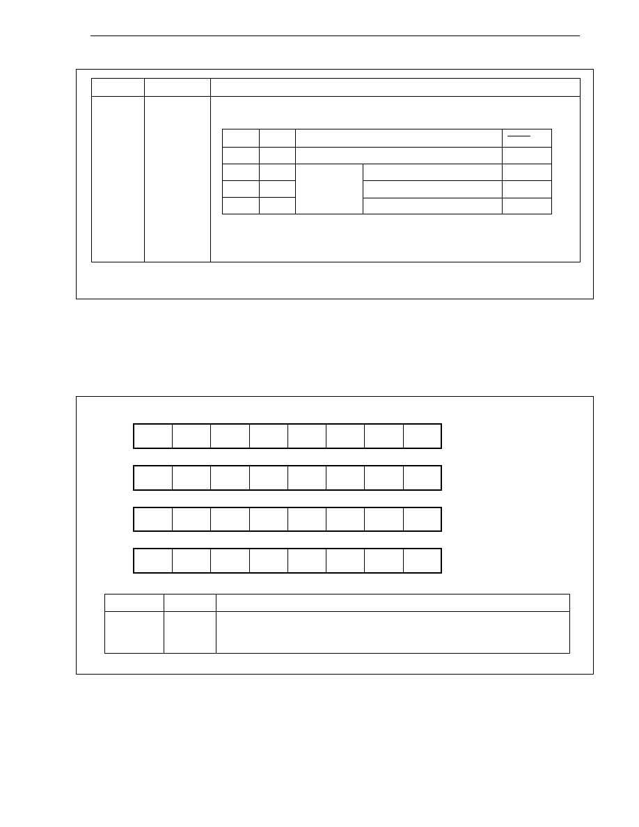
201
CHAPTER 8 SERIAL INTERFACE FUNCTION
User's Manual U10913EJ6V0UM
(2/2)
Bit position
Bit name
Function
1, 0
CLSn1, CLSn0
Clock Source
Specifies serial clock.
CLSn1
CLSn0
Specifies Serial Clock
SCKn pin
0
0
External clock
Input
0
1
Internal clock
Specified by BPRMn register
Note 1
Output
1
0
/4
Note 2
Output
1
1
/2
Note 2
Output
Notes 1. For setting of BPRMn register, refer to section 8.4 Baud Rate Generators 0 to 2
(BRG0 to BRG2).
2.
/4 and
/2 indicate divided signals (
: Internal system clock).
Remark
n = 0 to 3
(2) Serial I/O shift registers 0 to 3 (SIO0 to SIO3)
These registers convert 8-bit serial data into parallel data, and vice versa. The actual transmitting and receiving
of data is performed by writing data to and reading data from the SIOn register.
A shift operation is performed when CTXEn = "1" or CRXEn = "1".
These registers can be read/written in 8-bit or 1-bit units.
Bit position
Bit name
Function
7 to 0
SIOn7 to
Serial I/O
SIOn0
Data is shifted in (received) or out (transmitted) from the MSB or LSB side.
(n = 0 to 3)
Address
FFFFF08AH
7
SIO07
SIO0
6
SIO06
5
SIO05
4
SIO04
3
SIO03
2
SIO02
1
SIO01
0
SIO00
After reset
Undefined
FFFFF09AH
SIO17
SIO1
SIO16
SIO15
SIO14
SIO13
SIO12
SIO11
SIO10
Undefined
FFFFF0AAH
SIO27
SIO2
SIO26
SIO25
SIO24
SIO23
SIO22
SIO21
SIO20
Undefined
FFFFF0BAH
SIO37
SIO3
SIO36
SIO35
SIO34
SIO33
SIO32
SIO31
SIO30
Undefined
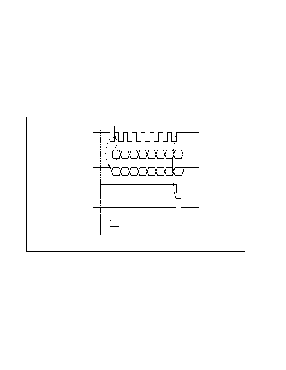
202
CHAPTER 8 SERIAL INTERFACE FUNCTION
User's Manual U10913EJ6V0UM
8.3.4 Basic operation
(1) Transfer format
CSIn transmits/receives data using three lines: one clock line and two data lines (n = 0 to 3).
Serial transfer is started by executing an instruction that writes transfer data to the SIOn register.
During transmission, the data is output from the SOn pin in synchronization with the falling edge of SCKn.
During reception, the data input to the SIn pin is latched in synchronization with the rising of SCKn. SCKn
stops when the serial clock counter overflows (at the rising edge of the 8th count), and SCKn remains high
until the next data transmission or reception is started. At the same time, a transmission/reception completion
interrupt (INTCSIn) is generated.
Caution If the CTXEn bit is changed from 0 to 1 after the transmit data is sent to the SIOnL register,
serial transfer will not begin.
Remark
n = 0 to 3
DI7 DI6 DI5 DI4 DI3 DI2 DI1 DI0
DO7 DO6 DO5 DO4 DO3 DO2 DO1 DO0
Input data latched
1
2
3
4
5
6
7
8
SCKn
SIn
SOn
CSOTn bit
INTCSIn interrupt
Transfer starts in synchronization with falling of SCKn
Execution of SIOn write instruction
Serial transmission/
reception completion
interrupt occurs

203
CHAPTER 8 SERIAL INTERFACE FUNCTION
User's Manual U10913EJ6V0UM
(2) Enabling transmission/reception
CSIn has only one 8-bit shift register and does not have a buffer. Transmission and reception are therefore
performed simultaneously.
(a) Transmission/reception enabling condition
The CTXEn and CRXEn bits of the CSIMn register specify the conditions of CSIn transmission/reception
enable.
The following conditions must be set beforehand.
ASIM00 register TXE0 bit = RXE0 bit = 0 in CSI0
ASIM10 register TXE1 bit = RXE1 bit = 0 in CSI1
CTXEn
CRXEn
Transmission/Reception Operation
0
0
Transmission/reception disable
0
1
Reception enable
1
0
Transmission enable
1
1
Transmission/reception enable
Remark
n = 0 to 3
Remarks 1. When CTXEn bit = 0, CSIn is as follows.
CSI0, CSI1: The serial output becomes high impedance or UARTn output.
CSI2, CSI3: The serial output becomes high impedance.
When CTXEn = 1, the data of the shift register is output.
2. When CRXEn bit = 0, the shift register input is "0".
When CRXEn bit = 1, the serial input data is input to the shift register.
3. To receive the transmit data and to check whether bus conflict occurs, set the CTXEn and CRXEn
bits to 1.
204
CHAPTER 8 SERIAL INTERFACE FUNCTION
User's Manual U10913EJ6V0UM
(b) Starting transmission/reception
Transmission/reception is started by reading/writing the SIOn register. Transmission/reception is controlled
by setting the transmission enable bit (CTXEn) and reception enable bit (CRXEn) as follows.
CTXEn
CRXEn
Start Condition
0
0
Does not start
0
1
Reads SIOn register
1
0
Writes SIOn register
1
1
Writes SIOn register
0
0
1
Rewrites CRXEn bit
Remark n = 0 to 3
In the above table, note that these bits should be set in advance of data transfer. For example,
if the CTXEn bit is not changed from 0 to 1 before reading data from or writing data to the SIOn register,
transfer will not begin. The bottom of the table means that, if the CRXEn bit is changed from 0 to 1
when the CTXEn bit is 0, the serial clock will be generated to initiate receive operation.
(c) Initialization of serial clock controller and serial clock counter
The serial clock controller and serial clock counter are initialized by setting the CTXEn and CRXEn bits
as follows.
CTXEn
CRXEn
Initialization Condition
1
0
Writes SIOn register
1
1
Writes SIOn register
0
0
1
Rewrites CRXEn bit
Remark n = 0 to 3
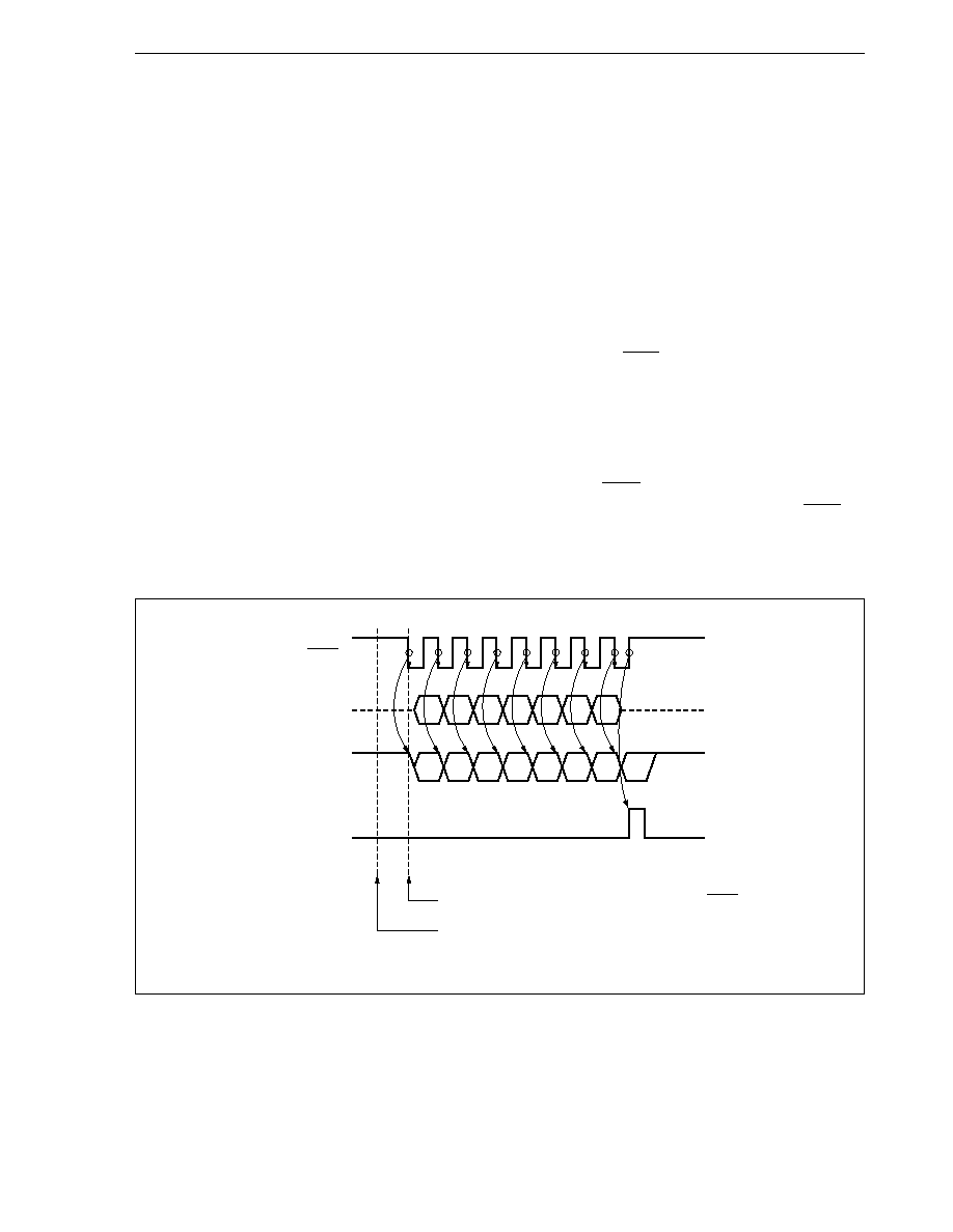
205
CHAPTER 8 SERIAL INTERFACE FUNCTION
User's Manual U10913EJ6V0UM
8.3.5 Transmission in CSI0 to CSI3
Transmission is started when data is written to the SIOn register after transmission has been enabled by clocked
serial interface mode register n (CSIMn) (n = 0 to 3).
(1) Starting transmission
Transmission is started by writing the transmit data to shift register n (SIOn) after the CTXEn bit of
clocked serial interface mode register n (CSIMn) has been set (the CRXEn bit is cleared to 0).
If the CTXEn bit is reset to 0, the SOn pin goes into a high-impedance state.
(2) Transmitting data in synchronization with serial clock
(a) When internal clock is selected as serial clock
When transmission is started, the serial clock is output from the SCKn pin, and at the same time, data
is sequentially output to the SOn pin from the SIOn register in synchronization with the falling edge of
the serial clock.
(b) When external clock is selected as serial clock
When transmission is started, the data is sequentially output from the SIOn register to the SOn pin in
synchronization with the falling of the serial clock input to the SCKn pin immediately after transmission
has been started. The shift operation is not performed even if the serial clock is input to the SCKn pin
if transmission is not enabled, and the output level of the SOn pin will not change.
Figure 8-7. Timing of 3-Wire Serial I/O Mode (Transmission)
Remark
n = 0 to 3
DO7 DO6 DO5 DO4 DO3 DO2 DO1 DO0
1
2
3
4
5
6
7
8
SCKn
SIn
SOn
INTCSIn interrupt
Transfer starts in synchronization with falling of SCKn
Execution of SIOn register write instruction
Serial transmission/
reception completion
interrupt occurs
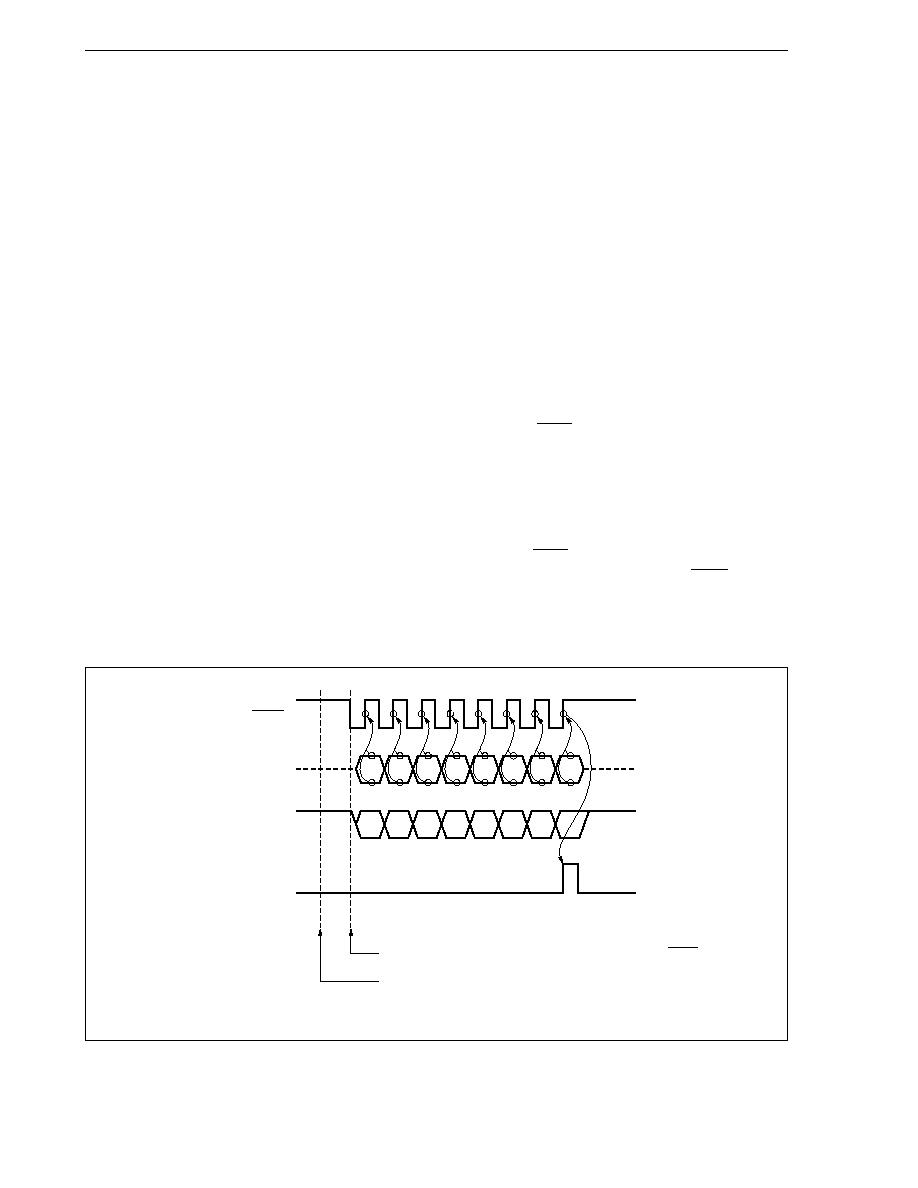
206
CHAPTER 8 SERIAL INTERFACE FUNCTION
User's Manual U10913EJ6V0UM
8.3.6 Reception in CSI0 to CSI3
Reception is started if the status is changed from reception disabled to reception enabled by the clocked serial
interface mode register (CSIMn) or if the SIOn register is read by the CPU with reception enabled (n = 0 to 3).
(1) Starting reception
Reception can be started in the following two ways.
<1> Changing the status of the CRXEn bit of the CSIMn register from "0" (reception disabled) to "1" (reception
enabled)
<2> Reading the receive data from the shift registers (SIOn) when the CRXEn bit of the CSIMn register is
"1" (reception enabled)
If the CRXEn bit of the CSIMn register has already been set to 1, writing "1" to these bits does not initiate
a receive operation. When the CRXEn bit = 0, the shift register inputs are "0".
(2) Receiving data in synchronization with serial clock
(a) When internal clock is selected as serial clock
When reception is started, the serial clock is output from the SCKn pin, and at the same time, data is
sequentially loaded from the SIn pin to the SIOn register in synchronization with the rising edge of the
serial clock.
(b) When external clock is selected as serial clock
When reception is started, the data is sequentially loaded from the SIn pin to the SIOn register in
synchronization with the rising of the serial clock input to the SCKn pin immediately after reception has
been started. The shift operation is not performed even if the serial clock is input to the SCKn pin when
reception is not enabled.
Figure 8-8. Timing of 3-Wire Serial I/O Mode (Reception)
Remark
n = 0 to 3
DI7 DI6 DI5 DI4 DI3 DI2 DI1 DI0
1
2
3
4
5
6
7
8
SCKn
SIn
SOn
INTCSIn interrupt
Transfer starts in synchronization with falling edge of SCKn
Execution of SIOn register write instruction
Serial transmission/
reception completion
interrupt occurs

207
CHAPTER 8 SERIAL INTERFACE FUNCTION
User's Manual U10913EJ6V0UM
8.3.7 Transmission/reception in CSI0 to CSI3
Transmission and reception can be executed simultaneously if both transmission and reception are enabled by
clocked serial interface mode register n (CSIMn) (n = 0 to 3).
(1) Starting transmission/reception
Transmission and reception can be performed simultaneously (transmission/reception operation) when both
the CTXEn and CRXEn bits of clocked serial interface mode register n (CSIMn) are set to 1.
Transmission/reception can be started by writing the transmit data to shift register n (SIOn) when both the
CTXEn and CRXEn bits of the CSIMn register are "1" (transmission/reception enabled).
If CRXEn has already been set to 1, writing "1" to this bit does not initiate transmit/receive operation.
(2) Transmitting data in synchronization with serial clock
(a) When internal clock is selected as serial clock
When transmission/reception is started, the serial clock is output from the SCKn pin, and at the same
time, data is sequentially set to the SOn pin from the SIOn register in synchronization with the falling edge
of the serial clock. Simultaneously, the data of the SIn pin is sequentially loaded to the SIOn register in
synchronization with the rising edge of the serial clock.
(b) When external clock is selected as serial clock
When transmission/reception is started, the data is sequentially output from the SIOn register to the SOn
pin in synchronization with the falling edge of the serial clock input to the SCKn pin immediately after
transmission/reception has been started. The data of the SIn pin is sequentially loaded to the SIOn register
in synchronization with the rising edge of the serial clock. The shift operation is not performed even if the
serial clock is input to the SCKn pin when transmission/reception is not enabled, and the output level of
the SOn pin does not change.
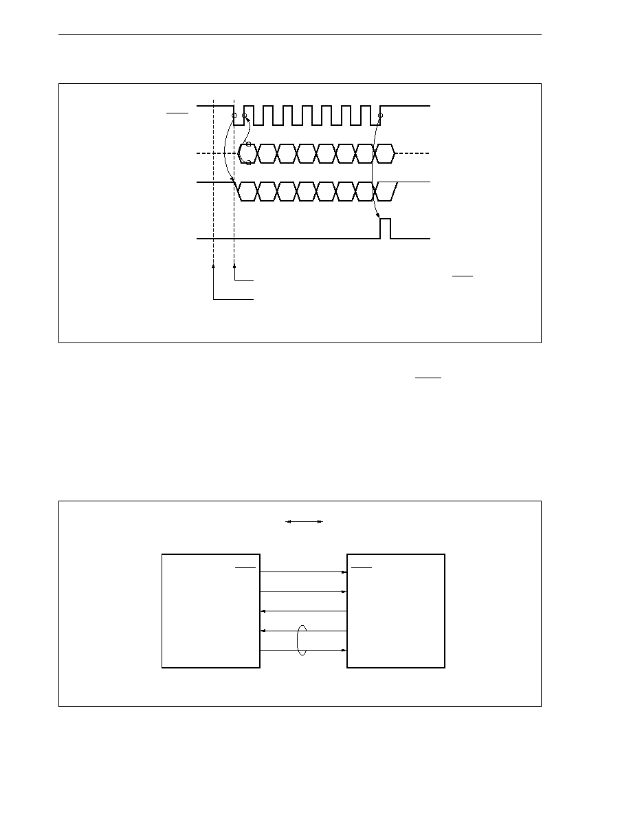
208
CHAPTER 8 SERIAL INTERFACE FUNCTION
User's Manual U10913EJ6V0UM
Figure 8-9. Timing of 3-Wire Serial I/O Mode (Transmission/Reception)
Remark
n = 0 to 3
8.3.8 System configuration example
Data 8 bits long is transferred by using three types of signal lines: a serial clock (SCKn), serial input (SIn), and
serial output (SOn). This feature is effective for connecting peripheral I/Os and display controllers that have a
conventional clocked serial interface (n = 0 to 3).
To connect two or more devices, a handshake line is necessary.
Various devices can be connected, because it can be specified whether the data is transmitted starting from the
MSB or LSB.
Figure 8-10. Example of CSI System Configuration
Remark
n = 0 to 3
(3-wire serial l/O 3-wire serial I/O)
Master CPU
SCKn
SOn
SIn
Port (Interrupt)
Port
SCKn
SIn
SOn
Port
Interrupt (Port)
Slave CPU
Handshake line
DI7 DI6 DI5 DI4 DI3 DI2 DI1 DI0
DO7 DO6 DO5 DO4 DO3 DO2 DO1 DO0
1
2
3
4
5
6
7
8
SCKn
SIn
SOn
INTCSIn
Transfer starts in synchronization with falling edge of SCKn
Execution of SIOn register write instruction
Serial transmission/
reception completion
interrupt occurs
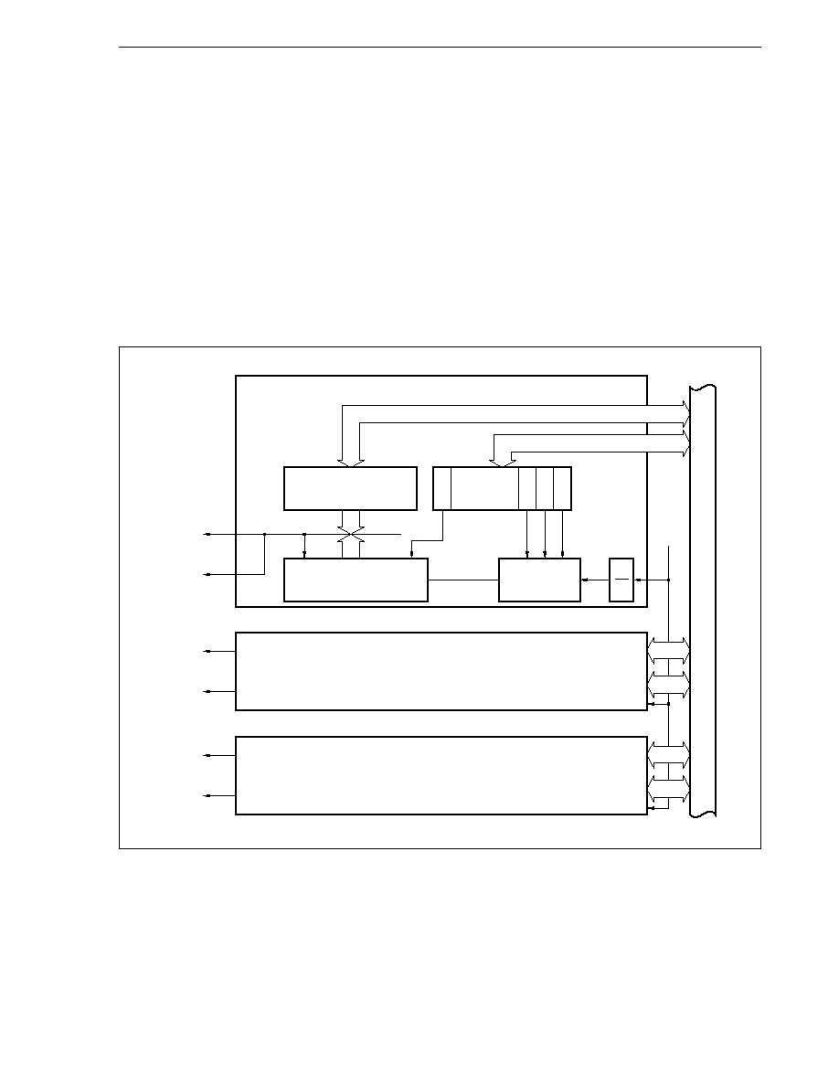
209
CHAPTER 8 SERIAL INTERFACE FUNCTION
User's Manual U10913EJ6V0UM
8.4 Baud Rate Generators 0 to 2 (BRG0 to BRG2)
8.4.1 Configuration and function
The serial clock of the serial interface can be selected for each channel from the baud rate generator output or
(internal system clock).
The serial clock source for UART0 and UART1 is specified by the SCLS0 and SCLS1 bits of the ASIM00 and
ASIM10 registers. The serial clock source for CSI0 to CSI3 is specified by the CLSn1 and CLSn0 (n = 0 to 3) bits
of the CSIM0 to CSIM3 registers.
When the output of the baud rate generator is specified, the baud rate generator will be used as the clock source.
Because the serial clock for transmission/reception is shared by both the transmission and reception portions, the
same baud rate is used for both transmission and reception.
Figure 8-11. Block Diagram of Baud Rate Generator
Baud rate generator 0
Baud rate generator 1
Baud rate generator 2
Internal bus
1
2
Prescaler
TMBRG0
Clear
BRG0
Match
BPRM0
BRCE0
BPR02
BPR01
BPR00
UART0
CSI0
UART1
CSI1
CSI2
CSI3

210
CHAPTER 8 SERIAL INTERFACE FUNCTION
User's Manual U10913EJ6V0UM
(1) Dedicated baud rate generators 0 to 2 (BRG0 to BRG2)
Dedicated baud rate generator n (BRGn) consists of an 8-bit timer (TMBRGn) that generates a serial clock
for transmission/reception, a compare register (BRGCn), and a prescaler (n = 0 to 2).
(a) Input clock
The internal system clock (
) is input to BRGn.
(b) Setting value of BRGn
(i)
UART0 and UART1
If the dedicated baud rate generator is specified for UART0 and UART1 as a serial clock source, the
actual baud rate can be calculated by the following expression, because a sampling rate of x16 is
used.
Baud rate = [bps]
where,
= internal system clock frequency [Hz]
k = timer count value (1
k
256
Note
):
Set by BRGCn
m = prescaler setup value (m = 0, 1, 2, 3, 4): Set by BPRMn
Note
The value k = 256 is set by writing 0 to the BRGCn register.
(ii) CSI0 to CSI3
If the dedicated baud rate generator is specified for CSI0 to CSI3, the actual baud rate can be
calculated by the following expression.
Baud rate = [bps]
where,
= internal system clock frequency [Hz]
k = timer count value (1
k
256
Note
):
Set by BRGCn
m = prescaler setup value (m = 0, 1, 2, 3, 4): Set by BPRMn
Note
The value k = 256 is set by writing 0 to the BRGCn register.
Table 8-2 shows the setting values of the baud rate generator when a typical clock is used.
2
×
k
×
2
m
×
16
×
2
2
×
k
×
2
m
×
2

211
CHAPTER 8 SERIAL INTERFACE FUNCTION
User's Manual U10913EJ6V0UM
Table 8-2. Setting Values of Baud Rate Generators 0 to 2
Note
Cannot be used because the error is too great.
Remark BPR: Prescaler setup value (Set by BPRMn register)
BRG: Timer count value (Set by BRGCn register)
:
Internal system clock
Error
0.26%
0.0%
0.0%
0.0%
0.0%
0.0%
0.0%
0.0%
1.5%
0.0%
0.0%
0.0%
0.0%
BRG
175
128
128
128
128
64
32
16
15
8
4
2
1
BPR
3
3
2
1
0
0
0
0
0
0
0
0
0
Error
0.08%
0.0%
0.0%
0.0%
0.0%
0.0%
0.0%
0.0%
2.6%
0.0%
0.0%
16.7%
Note
BRG
218
160
160
160
160
80
40
20
18
10
5
3
BPR
3
3
2
1
0
0
0
0
0
0
0
0
BRG
131
192
192
192
192
96
48
24
22
12
6
3
2
BPR
4
3
2
1
0
0
0
0
0
0
0
0
0
BPR
4
4
3
2
1
0
0
0
0
0
0
0
0
0
BRG
222
163
163
163
163
81
41
20
19
10
5
3
Error
0.03%
0.16%
0.16%
0.16%
0.16%
0.16%
0.16%
0.16%
1.16%
1.16%
6.99%
Note
BRG
142
208
208
208
208
104
52
26
24
13
7
BPR
4
3
2
1
0
0
0
0
0
0
0
Error
0.02%
0.15%
0.15%
0.15%
0.15%
0.15%
0.47%
0.76%
1.16%
1.73%
1.73%
1.73%
27.2%
Note
BRG
222
163
163
163
163
163
81
41
38
20
10
5
2
BPR
4
4
3
2
1
0
0
0
0
0
0
0
0
Error
--
0.07%
0.07%
0.07%
0.07%
0.07%
0.39%
0.54%
0.84%
0.54%
3.29%
4.09%
11.90%
Note
BPR
--
4
3
2
1
0
0
0
0
0
0
0
0
Error
0.02%
0.15%
0.15%
0.15%
0.15%
0.47%
0.76%
1.73%
1.16%
1.73%
1.73%
15.2%
Note
Baud Rate [bps]
UART0 , UART1
110
150
300
600
1200
2400
4800
9600
10400
19200
38400
76800
153600
CSI0 to CSI3
1760
2400
4800
9600
19200
38400
76800
153600
166400
307200
614400
1228800
2457600
= 33 MHz
= 25 MHz
= 16 MHz
= 12.5 MHz
BRG
--
215
215
215
215
215
107
54
50
27
13
7
3
BPR
3
3
2
1
0
0
0
0
0
0
0
0
UART0 , UART1
110
150
300
600
1200
2400
4800
9600
10400
19200
38400
76800
153600
307200
CSI0 to CSI3
1760
2400
4800
9600
19200
38400
76800
153600
166400
307200
614400
1228800
2457600
4915200
Baud Rate [bps]
= 20 MHz
= 14.746 MHz
= 12.288 MHz
= 9.830 MHz
BRG
178
130
130
130
130
130
65
33
30
16
8
4
2
1
Error
0.25%
0.16%
0.16%
0.16%
0.16%
0.16%
0.16%
1.36%
0.16%
1.73%
1.73%
1.73%
1.73%
1.73%
Error
0.07%
0.0%
0.0%
0.0%
0.0%
0.0%
0.0%
0.0%
0.7%
0.0%
0.0%
0.0%
25.0%
Note

212
CHAPTER 8 SERIAL INTERFACE FUNCTION
User's Manual U10913EJ6V0UM
Actual baud rate (baud rate with error)
Desired baud rate (normal baud rate)
(c) Baud rate error
The baud rate error is calculated as follows.
Error [%] = 1
×
100
Example: (9520/9600 1)
×
100 = 0.833 [%]
(5000/4800 1)
×
100 = +4.167 [%]
(2) Allowable baud rate error range
The allowable error range depends on the number of bits of one frame.
The basic limit is
±
5% of the baud rate error and
±
4.5% of the sample timing with an accuracy of 16 bits.
However, the practical limit should be
±
2.3% of the baud rate error, assuming that both the transmission and
reception sides contain an error.
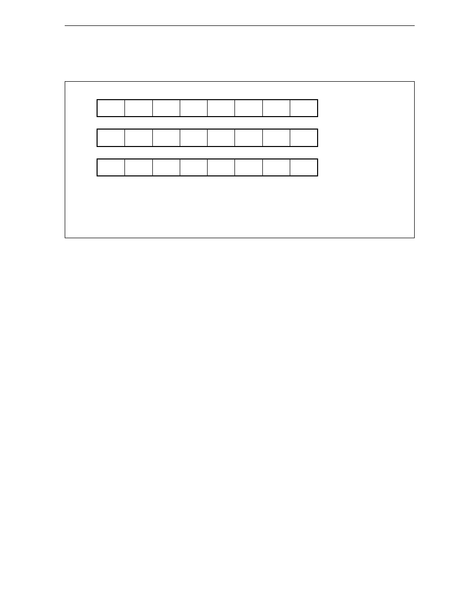
213
CHAPTER 8 SERIAL INTERFACE FUNCTION
User's Manual U10913EJ6V0UM
8.4.2 Baud rate generator compare registers 0 to 2 (BRGC0 to BRGC2)
These are 8-bit compare registers that set a timer/count value for the baud rate generator.
These registers can be read/written in 8-bit or 1-bit units.
Caution The internal timer (TMBRGn) is cleared by writing the BRGCn registers. Therefore, do not
rewrite or program the BRGCn registers during a transmission/reception operation.
Remark
n = 0 to 2
Address
FFFFF084H
7
BRG07
BRGC0
6
BRG06
5
BRG05
4
BRG04
3
BRG03
2
BRG02
1
BRG01
0
BRG00
After reset
Undefined
FFFFF094H
BRG17
BRGC1
BRG16
BRG15
BRG14
BRG13
BRG12
BRG11
BRG10
Undefined
FFFFF0A4H
BRG27
BRGC2
BRG26
BRG25
BRG24
BRG23
BRG22
BRG21
BRG20
Undefined

214
CHAPTER 8 SERIAL INTERFACE FUNCTION
User's Manual U10913EJ6V0UM
Address
FFFFF086H
7
BRCE0
BPRM0
6
0
5
0
4
0
3
0
2
BPR02
1
BPR01
0
BPR00
After reset
00H
FFFFF096H
BRCE1
BPRM1
0
0
0
0
BPR12
BPR11
BPR10
00H
FFFFF0A6H
BRCE2
BPRM2
0
0
0
0
BPR22
BPR21
BPR20
00H
8.4.3 Baud rate generator prescaler mode registers 0 to 2 (BPRM0 to BPRM2)
These registers control the timer/count operation of the baud rate generator and select a count clock.
They can be read/written in 8-bit or 1-bit units.
Bit position
Bit name
Function
7
BRCEn
Baud Rate Generator Count Enable
Controls count operation of BRGn.
0: Stops count operation with this bit cleared
1: Enables count operation
2 to 0
BPRn2 to BPRn0
Baud Rate Generator Prescaler
Specifies count clock input to internal timer (TMBRGn).
BPRn2
BPRn1
BPRn0
Count clock
0
0
0
/2
(m = 0)
0
0
1
/4
(m = 1)
0
1
0
/8
(m = 2)
0
1
1
/16 (m = 3)
1
×
×
/32 (m = 4)
m: Set value of prescaler,
: Internal system clock,
×
: Don't care
Caution Do not change the count clock during a transmission/reception operation.
Remark
n = 0 to 2

215
User's Manual U10913EJ6V0UM
CHAPTER 9 A/D CONVERTER
9.1 Features
Analog input: 8 channels
10-bit A/D converter
On-chip A/D conversion result register (ADCR0 to ADCR7)
10 bits
×
8
A/D conversion trigger mode
A/D trigger mode
Timer trigger mode
External trigger mode
Sequential conversion
9.2 Configuration
The A/D converter of the V850
TM
adopts the sequential conversion method, and uses the A/D converter mode
register (ADM0, ADM1), and ADCRn register to perform A/D conversion operations (n = 0 to 7).
(1) Input circuit
Selects the analog input (ANI0 to ANI7) according to the mode set to the ADM0 and ADM1 registers.
(2) Sample & hold circuit
The sample & hold circuit samples each of the analog input signals sequentially sent from the input circuit,
and sends the sample to the voltage comparator. This circuit also holds the sampled analog input signal
voltage during A/D conversion.
(3) Voltage comparator
The voltage comparator compares the analog input signal with the output voltage of the series resistor string.
(4) Series resistor string
The series resistor string is used to generate voltages to match the analog inputs.
The series resistor string is connected between the reference voltage pin (AV
REF1
) for the A/D converter and
the GND pin (AV
SS
) for the A/D converter. In order to make 1024 equal voltage steps between these 2 pins,
it is configured from 1023 equal resistors and 2 resistors with 1/2 those values.
The voltage tap of the series resistor string is selected by a tap selector controlled by the successive
approximation register (SAR).

216
CHAPTER 9 A/D CONVERTER
User's Manual U10913EJ6V0UM
(5) Successive approximation register (SAR)
The SAR is a 10-bit register in which series resistor string voltage tap data, which have values that match
the analog input voltage values, is set 1 bit at a time beginning with the most significant bit (MSB).
If data is set in the SAR all the way to the least significant bit (LSB) (A/D conversion completed), the contents
of the SAR (conversion results) are held in the A/D conversion result register (ADCRn).
(6) A/D conversion result register (ADCRn)
ADCR is a 10-bit register that holds A/D conversion results. Each time A/D conversion is completed, the
conversion results are loaded from the successive approximation register (SAR).
This register becomes undefined if RESET is input.
(7) Controller
Selects the analog input, generates the sample & hold circuit operation timing, and controls the conversion
trigger according to the mode set to the ADM0 and ADM1 registers.
(8) ANI0 to ANI7 pins
8-channel analog input pin for the A/D converter. Inputs the analog signal to be A/D converted.
Caution Make sure that the voltages input to ANI0 through ANI7 do not exceed the rated values. If
a voltage higher than V
DD
or lower than V
SS
(even within the range of the absolute maximum
ratings) is input to a channel, the conversion value of the channel is undefined, and the
conversion values of the other channels may also be affected.
(9) AV
REF1
pin
Pin for inputting the reference voltage of the A/D converter. Converts signals input to the ANIn pin to digital
signals based on the voltage applied between AV
REF1
and AV
SS
.
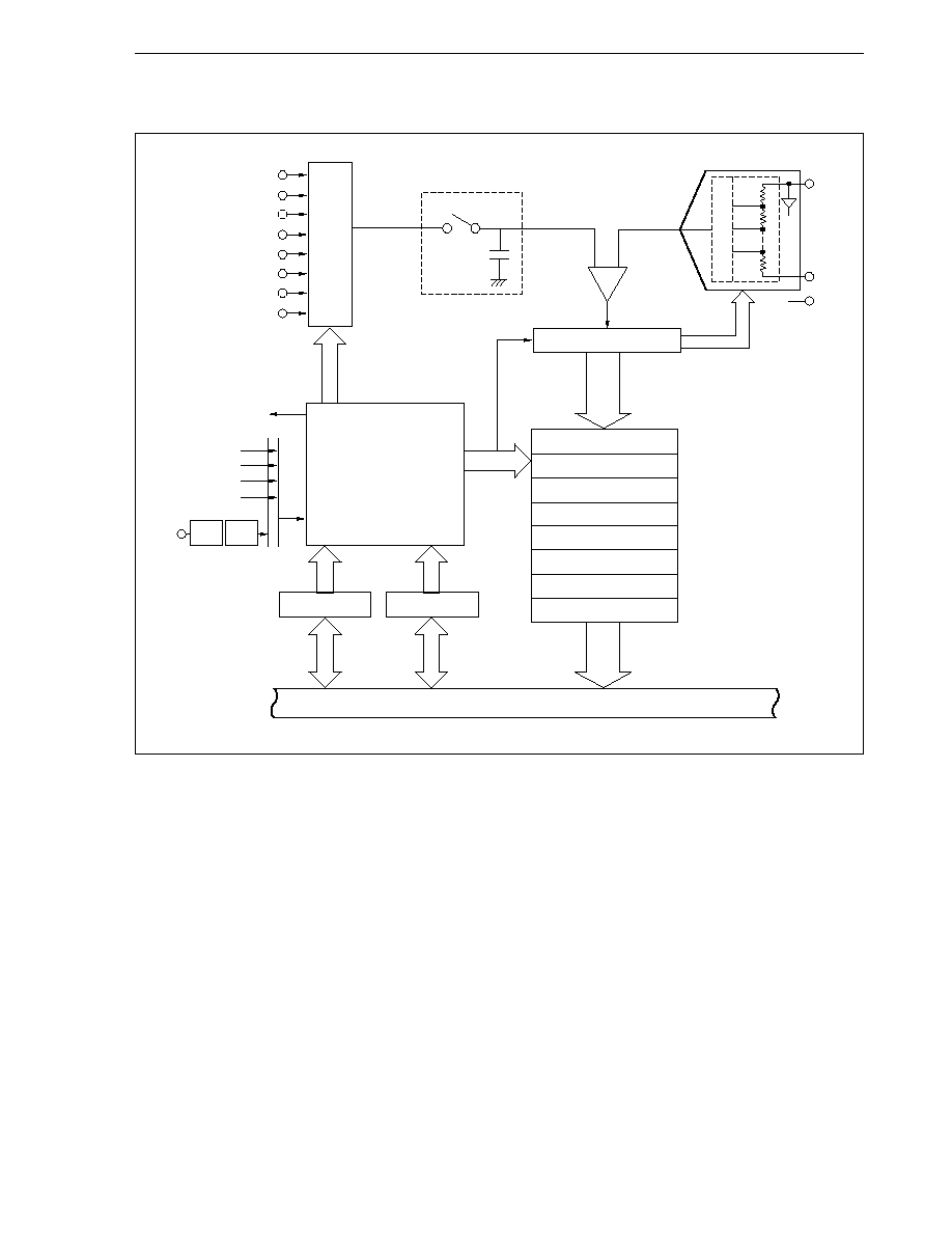
CHAPTER 9 A/D CONVERTER
217
User's Manual U10913EJ6V0UM
Figure 9-1. Block Diagram of A/D Converter
Cautions 1. If noise is carried on the analog input pins (ANI0 to ANI7) and the reference voltage input
pin (AV
REF1
), illegal conversion results may occur due to the noise.
In order to avoid negative effects to the system from these illegal conversion results,
software processing is necessary.
The following is an example of software processing.
·
Use the average value of multiple A/D conversions as the A/D conversion result.
·
Perform A/D conversion multiple times continuously, and if an unusual conversion
result is obtained, exclude this value from the conversion results.
·
If A/D conversion results are obtained from which it can be judged that an error has
occurred in the system, do not immediately begin error processing, but carry out error
processing after confirming that the error occurs again.
2. Ensure that voltages outside the range of AV
SS
to AV
REF1
are not applied to the pins that
are used as A/D converter input pins.
Internal bus
ANI0
ANI1
ANI2
ANI3
ANI4
ANI5
ANI6
ANI7
INTAD
Controller
ADM0 (8)
ADM1 (8)
7
8
8
10
10
10
ADCR0
SAR (10)
Voltage comparator
Tap selector
ADCR1
ADCR2
ADCR3
ADCR4
ADCR5
ADCR6
ADCR7
7
0
0
0
9
0
R/2
Series resistor string
Sample & hold circuit
AV
REF1
AV
SS
AV
DD
R
R/2
9
INTCC110
INTCC111
INTCC112
Noise
elimination
Edge
detection
INTCC113
ADTRG
Input circuit

218
CHAPTER 9 A/D CONVERTER
User's Manual U10913EJ6V0UM
9.3 Control Registers
(1) A/D converter mode register 0 (ADM0)
ADM0 is an 8-bit register that selects the analog input pin, specifies the operation mode, and executes
conversion operations.
This register can be read/written in 8-bit or 1-bit units, however, when the data is written to the ADM0 register
during an A/D conversion operation, the conversion operation is initialized and conversion is executed from
the beginning. Bit 6 cannot be written and any writing executed is ignored.
(1/2)
Bit position
Bit name
Function
7
CE
Convert Enable
Enables or disables A/D conversion operation.
0: Disabled
1: Enabled
6
CS
Converter Status
Indicates the status of A/D converter. This bit is read only.
0: Stops
1: Operates
5
BS
Buffer Select
Specifies buffer mode in the select mode.
0: 1-buffer mode
1: 4-buffer mode
4
MS
Mode Select
Specifies operation mode of A/D converter.
0: Scan mode
1: Select mode
Cautions 1.
When the CE bit is 1 in the timer trigger mode and external trigger mode, the trigger signal
standby state is set. To clear the CE bit, write "0" or reset.
In the A/D trigger mode, the conversion trigger is set by writing 1 to the CE bit. After the
operation, when the mode is changed to the timer trigger mode or external trigger mode
without clearing the CE bit, the trigger input standby state is set immediately after the
change.
2. It takes 3 clocks from the start of A/D conversion to when the CS bit is set to 1. When
reading an A/D conversion value, use the A/D conversion end interrupt (INTAD).
Address
FFFFF380H
7
CE
ADM0
6
CS
5
BS
4
MS
3
0
2
ANIS2
1
ANIS1
0
ANIS0
After reset
00H

CHAPTER 9 A/D CONVERTER
219
User's Manual U10913EJ6V0UM
(2/2)
Bit position
Bit name
Function
2 to 0
ANIS2 to
Analog Input Select
ANIS0
Specifies analog input pin to be A/D converted.
ANIS2 ANIS1 ANIS0
Select mode
Scan mode
A/D trigger
Timer trigger
A/D trigger
Timer trigger
mode
mode
mode
mode
Note
0
0
0
ANI0
ANI0
ANI0
1
0
0
1
ANI1
ANI1
ANI0, ANI1
2
0
1
0
ANI2
ANI2
ANI0 to ANI2
3
0
1
1
ANI3
ANI3
ANI0 to ANI3
4
1
0
0
ANI4
Setting prohibited
ANI0 to ANI4
4 + ANI4
1
0
1
ANI5
Setting prohibited
ANI0 to ANI5
4 + ANI4, ANI5
1
1
0
ANI6
Setting prohibited
ANI0 to ANI6
4 + ANI4 to ANI6
1
1
1
ANI7
Setting prohibited
ANI0 to ANI7
4 + ANI4 to ANI7
Note
In the timer trigger mode during the scan mode, because the scanning sequence of the ANI0 to ANI3 pins
is specified by the sequence in which the match signals are generated from the compare register, the
number of trigger inputs should be specified instead of a certain analog input pin. When set as ANIS2 =
1, after the trigger input is counted 4 times, the mode is shifted to A/D scan mode and the conversion begins.
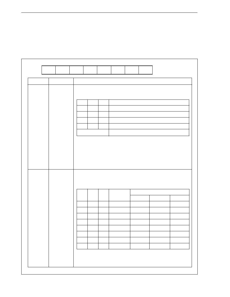
220
CHAPTER 9 A/D CONVERTER
User's Manual U10913EJ6V0UM
(2) A/D converter mode register 1 (ADM1)
ADM1 is an 8-bit register that specifies the conversion operation time and trigger mode.
This register can be read/written in 8-bit or 1-bit units. However, when the data is written to the ADM1 register
during an A/D conversion operation, the conversion operation is initialized and conversion is executed from
the beginning.
Bit position
Bit name
Function
6 to 4
TRG2 to
Trigger Mode
TRG0
Specifies trigger mode.
TRG2 TRG1 TRG0
Trigger mode
0
0
x
A/D trigger mode
0
1
0
Timer trigger mode (1-trigger mode)
0
1
1
Timer trigger mode (4-trigger mode)
1
1
0
External trigger mode
Other than above
Setting prohibited
Remarks 1. x: Don't care
2. The valid edge of the external input signal in the external
trigger mode is specified by bits 7 and 6 (ES031, ES030)
of the external interrupt mode register (INTM1). For
details, refer to the external interrupt mode registers 1 to
4 (INTM1 to INTM4) in 5.3.7 Edge detection function .
2 to 0
FR2 to FR0
Frequency
Specifies conversion operation time. These are control bits to prevent a drastic
change of the A/D conversion time even if the oscillation frequency is changed.
FR2
FR1
FR0
Conversion
Conversion operation time (
µ
s)
Note
clock
= 33 MHz
= 25 MHz
= 16 MHz
0
0
0
36
--
--
2.25
0
0
1
48
--
1.92
3.00
0
1
0
60
1.82
2.40
3.75
0
1
1
72
2.18
2.88
4.50
1
0
0
96
2.91
3.84
6.00
1
0
1
120
3.64
4.80
7.50
1
1
0
144
4.36
5.76
9.00
1
1
1
192
5.82
7.68
12.00
Note
Figures in the conversion operation time are target values.
Remark
= Internal system clock frequency
Address
FFFFF382H
7
0
ADM1
6
TRG2
5
TRG1
4
TRG0
3
0
2
FR2
1
FR1
0
FR0
After reset
07H
CHAPTER 9 A/D CONVERTER
221
User's Manual U10913EJ6V0UM
(3) A/D conversion result register (ADCR0 to ADCR7, ADCR0H to ADCR7H)
ADCRn is a 10-bit register that holds the A/D conversion results. ADCRn consists of eight 10-bit registers
(n = 0 to 7).
This register is read-only in 16-bit or 8-bit units.
During 16-bit access to this register, the ADCRn register is specified, and during higher 8-bit access, the
ADCRnH register is specified.
When reading the 10-bit data of A/D conversion results from the ADCRn register, only the lower 10 bits are
valid and the higher 6 bits are always read as 0.
Remark
n = 0 to 7
9.4 A/D Converter Operation
9.4.1 Basic operation of A/D converter
A/D conversion is executed in the following order.
(1) The selection of the analog input and specification of the operation mode and trigger mode, etc. should
be set in the ADM0 and ADM1 registers
Note 1
.
When the CE bit of the ADM0 register is set (1), A/D conversion starts in the A/D trigger mode. In the
timer trigger mode and external trigger mode, the trigger standby state
Note 2
is set.
(2) The voltage generated from the voltage tap of the series resistor string and analog input are compared
by the comparator.
(3) When the comparison of the 10 bits ends, the conversion results are stored in the ADCRn register. When
the A/D conversion has been performed for the specified number of times, the A/D conversion end interrupt
(INTAD) is generated (n = 0 to 7).
Notes
1. When the ADM0 and ADM1 registers are changed during an A/D conversion operation, the A/D
conversion operation before the change is stopped and the conversion results are not stored in the
ADCRn register.
2. In the timer trigger mode and external trigger mode, if the CE bit of the ADM0 register is set to 1, the
mode changes to the trigger standby state. The A/D conversion operation is started by the trigger
signal, and the trigger standby state is returned when the A/D conversion operation ends.
15
0
ADCRn
Address
FFFFF390H to
FFFFF3AH
After reset
Undefined
14
0
13
0
12
0
11
0
10
0
9
AD9
8
AD8
7
AD7
6
AD6
5
AD5
4
AD4
3
AD3
2
AD2
1
AD1
0
AD0
ADCRnH
FFFFF392H to
FFFFF3AEH
Undefined
7
AD9
6
AD8
5
AD7
4
AD6
3
AD5
2
AD4
1
AD3
0
AD2
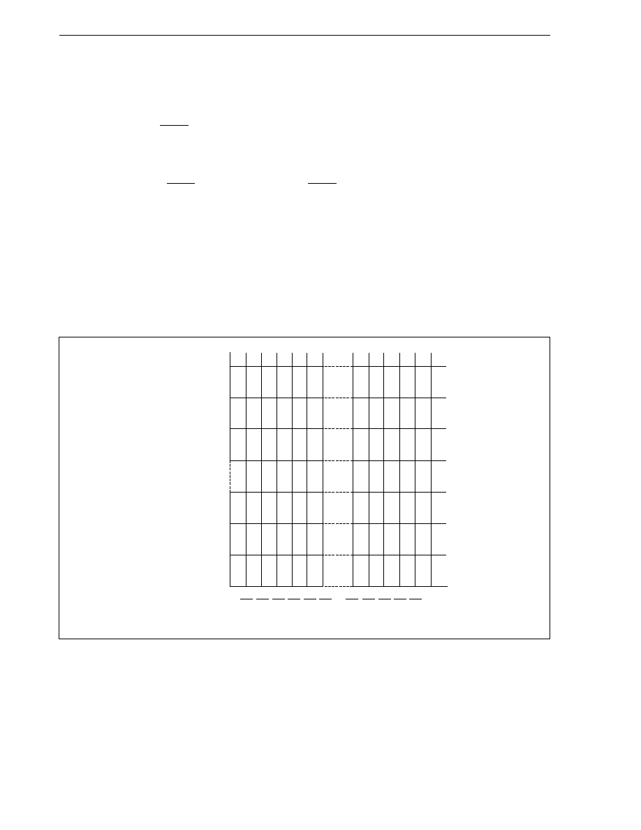
222
CHAPTER 9 A/D CONVERTER
User's Manual U10913EJ6V0UM
9.4.2 Input voltage and conversion results
The following relationship exists between the analog input voltage input to the analog input pins (ANI0 to ANI7)
and the A/D conversion results (A/D conversion result register (ADCRn)).
ADCRn = INT (
×
1024 + 0.5)
or,
(ADCRn 0.5)
×
V
IN
< (ADCRn + 0.5)
×
INT ( ): Function with the integer portion of the value in parentheses ( ) returned
V
IN
:
Analog input voltage
AV
REF1
:
AV
REF1
pin voltage
ADCRn:
Value of A/D conversion result register (ADCRn)
Figure 9-2 shows the relationship between the analog input voltage and the A/D conversion results.
Figure 9-2. Relationship Between Analog Input Voltage and A/D Conversion Result
1023
1022
1021
A/D conversion
results (ADCRn)
3
2
1
0
1
2048
1
1024
3
2048
2
1024
3
1024
5
Input voltage/AV
REF1
2048
2043
2048
1022
1024
2045
2048
1023
1024
1
2047
2048
V
IN
AV
REF1
AV
REF1
1024
AV
REF1
1024
CHAPTER 9 A/D CONVERTER
223
User's Manual U10913EJ6V0UM
9.4.3 Operation mode and trigger mode
Various conversion operations can be specified for the A/D converter by specifying the operation mode and trigger
mode. The operation mode and trigger mode are set by the ADM0 and ADM1 registers.
The following shows the relationship between the operation mode and trigger mode.
Trigger Mode
Operation Mode
Setting Value
Analog Input
ADM0
ADM1
A/D trigger
Select
1 buffer
xx010xxxB
000x0xxxB
ANI0 to ANI7
4 buffers
xx110xxxB
000x0xxxB
Scan
xxx00xxxB
000x0xxxB
Timer trigger
1 trigger
Select
1 buffer
xx010xxxB
00100xxxB
ANI0 to ANI3
4 buffers
xx110xxxB
00100xxxB
Scan
xxx00xxxB
00100xxxB
4 trigger
Select
1 buffer
xx010xxxB
00110xxxB
4 buffers
xx110xxxB
00110xxxB
Scan
xxx00xxxB
00110xxxB
External trigger
Select
1 buffer
xx010xxxB
01100xxxB
4 buffers
xx110xxxB
01100xxxB
Scan
xxx00xxxB
01100xxxB
(1) Trigger mode
There are three types of trigger modes that serve as the start timing of the A/D conversion processing: the A/D
trigger mode, timer trigger mode, and external trigger mode. The ANI0 to ANI3 pins are able to specify all
of these modes, but pins ANI4 to ANI7 can only specify the A/D trigger mode. The timer trigger mode consists
of the one-trigger mode and four-trigger mode as the sub-trigger modes. These trigger modes are set by the
ADM1 register.
(a) A/D trigger mode
Generates the conversion timing of the analog input for the ANI0 to ANI7 pins inside the A/D converter
unit. The ANI4 to ANI7 pins are always set in this mode.
(b) Timer trigger mode
Specifies the conversion timing of the analog input set for the ANI0 to ANI3 pins using the values set to
the TM11 compare register. This mode can only be specified by the ANI0 to ANI3 pins.
This register creates the analog input conversion timing by generating the match interrupts of the four
capture/compare registers (CC110 to CC113) connected to 16-bit TM11.
There are two types of sub-trigger modes: the 1-trigger mode and 4-trigger mode.
· 1-trigger mode
Mode in which one match interrupt from timer 11 is used as the A/D conversion start timing.
· 4-trigger mode
Mode in which four match interrupts from timer 11 are used as the A/D conversion start timing.

224
CHAPTER 9 A/D CONVERTER
User's Manual U10913EJ6V0UM
(c) External trigger mode
Mode in which the conversion timing of the analog input to the ANI0 to ANI3 pins is specified using the
ADTRG pin. This mode can be specified only with the ANI0 to ANI3 pins.
(2) Operation mode
There are two types of operation modes that set the ANI0 to ANI7 pins: the select mode and the scan mode.
The select mode has the 1-buffer mode and 4-buffer mode as sub-modes. These modes are set by the ADM0
register.
(a) Select mode
A/D converts one analog input specified by the ADM0 register. The conversion results are stored in the
ADCRn register corresponding to the analog input. For this mode, the 1-buffer mode and 4-buffer mode
are provided for storing the A/D conversion results (n = 0 to 7).
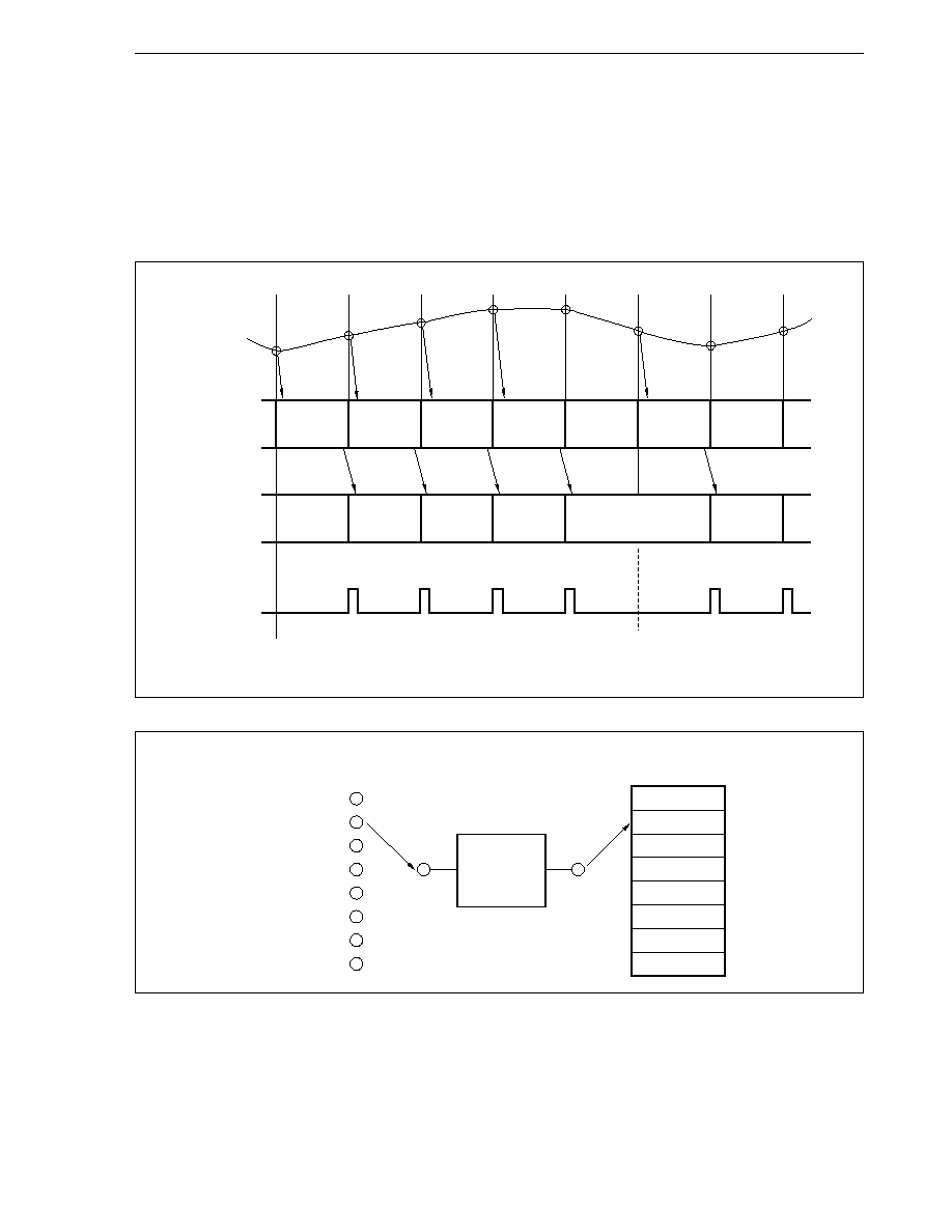
CHAPTER 9 A/D CONVERTER
225
User's Manual U10913EJ6V0UM
· 1-buffer mode
A/D converts one analog input specified by the ADM0 register. The conversion results are stored in
the ADCRn register corresponding to the analog input. The analog input and ADCRn register
correspond one to one, and an A/D conversion end interrupt (INTAD) is generated each time one
A/D conversion ends.
Figure 9-3. Select Mode Operation Timing: 1-Buffer Mode (ANI1)
ANI1
Data 1
(ANI1)
Data 2
(ANI1)
Data 3
(ANI1)
Data 4
(ANI1)
Data 5
(ANI1)
Data 6
(ANI1)
Data 7
(ANI1)
Data 1
Data 2
Data 3
Data 4
Data 5
Data 6
Data 7
Data 1
(ANI1)
Data 2
(ANI1)
Data 3
(ANI1)
Data 4
(ANI1)
Data 6
(ANI1)
ADCR1
INTAD
Conversion start
ADM setting
Conversion start
ADM setting
A/D
Conversion
ANI0
ANI1
ANI2
ANI3
ANI4
ANI5
ANI6
ANI7
ADCR0
ADCR1
ADCR2
ADCR3
ADCR4
ADCR5
ADCR6
ADCR7
A/D converter
ADCR register
Analog input
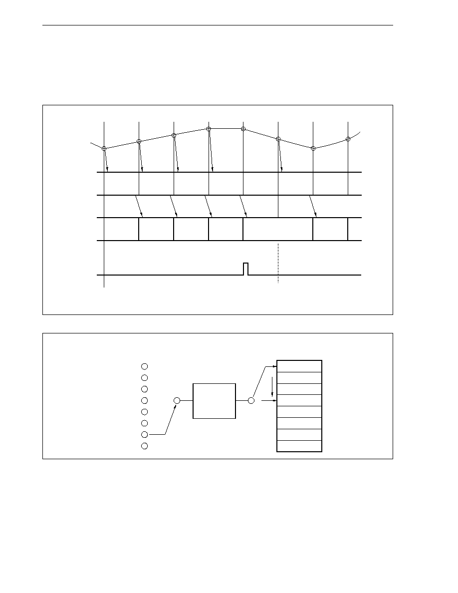
226
CHAPTER 9 A/D CONVERTER
User's Manual U10913EJ6V0UM
· 4-buffer mode
A/D converts one analog input four times and stores the results in the ADCR0 to ADCR3 registers. The
A/D conversion end interrupt (INTAD) is generated when the four A/D conversions end.
Figure 9-4. Select Mode Operation Timing: 4-Buffer Mode (ANI6)
ANI6
A/D
Conversion
Data 1
(ANI6)
Data 2
(ANI6)
Data 3
(ANI6)
Data 4
(ANI6)
Data 5
(ANI6)
Data 6
(ANI6)
Data 7
(ANI6)
Data 1
Data 2
Data 3
Data 4
Data 5
Data 6
Data 7
Data 1
(ANI6)
ADCR0
Data 2
(ANI6)
ADCR1
Data 3
(ANI6)
ADCR2
Data 4
(ANI6)
ADCR3
Data 6
(ANI6)
ADCR0
ADCRn
INTAD
Conversion start
ADM setting
Conversion start
ADM setting
ANI0
ANI1
ANI2
ANI3
ANI4
ANI5
ANI6
ANI7
ADCR0
ADCR1
ADCR2
ADCR3
ADCR4
ADCR5
ADCR6
ADCR7
A/D converter
ADCR register
Analog input
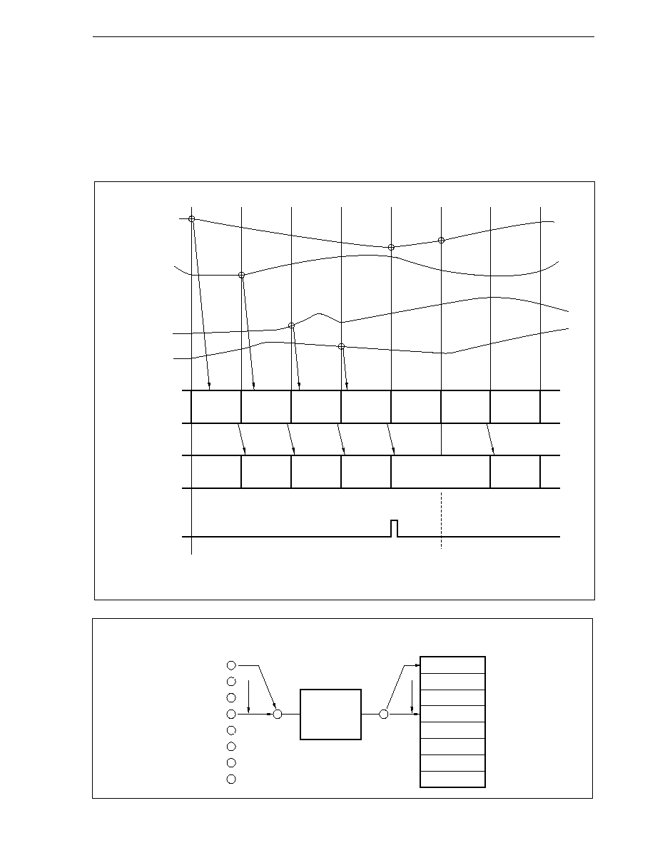
CHAPTER 9 A/D CONVERTER
227
User's Manual U10913EJ6V0UM
(b) Scan mode
Selects the analog inputs specified by the ADM0 register sequentially from the ANI0 pin, after which
A/D conversion is executed. The A/D conversion results are stored in the ADCRn register corresponding
to the analog input. When the conversion of the specified analog input ends, the INTAD interrupt is
generated.
Figure 9-5. Scan Mode Operation Timing: 4-Channel Scan (ANI0 to ANI3)
ANI3
ANI0
ANI1
ANI2
A/D
Conversion
Data 1
(ANI0)
Data 2
(ANI1)
Data 3
(ANI2)
Data 4
(ANI3)
Data 5
(ANI0)
Data 6
(ANI0)
Data 7
(ANI1)
Data 1
Data 2
Data 3
Data 4
Data 5
Data 6
Data 7
Data 1
(ANI0)
ADCR0
Data 2
(ANI1)
ADCR1
Data 3
(ANI2)
ADCR2
Data 4
(ANI3)
ADCR3
Data 6
(ANI0)
ADCR0
ADCRn
INTAD
Conversion start
ADM setting
Conversion start
ADM setting
ANI0
ANI1
ANI2
ANI3
ANI4
ANI5
ANI6
ANI7
ADCR0
ADCR1
ADCR2
ADCR3
ADCR4
ADCR5
ADCR6
ADCR7
A/D converter
ADCR register
Analog input
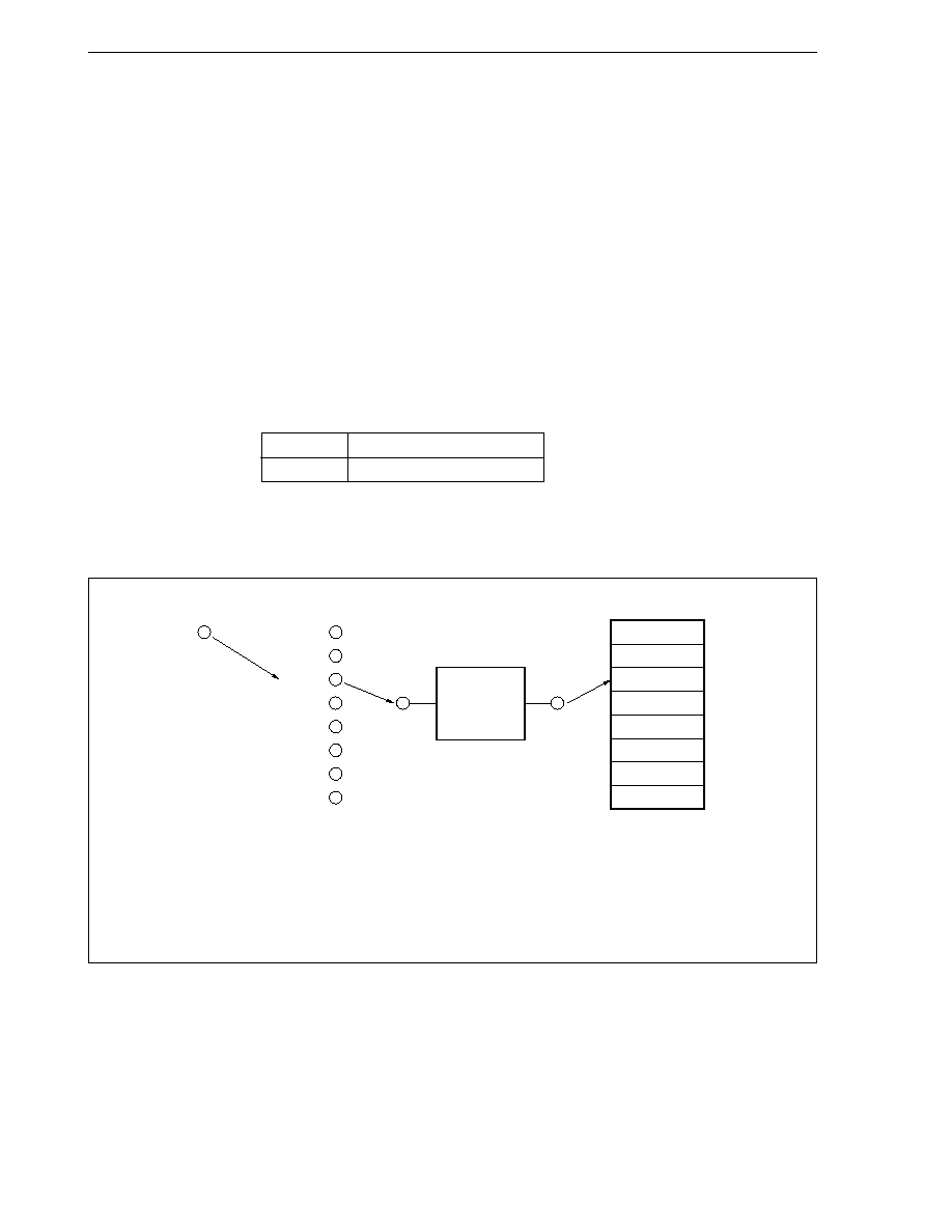
228
CHAPTER 9 A/D CONVERTER
User's Manual U10913EJ6V0UM
9.5 Operation in A/D Trigger Mode
When the CE bit of the ADM0 register is set to 1, A/D conversion is started.
9.5.1 Select mode operations
A/D converts the analog input specified by the ADM0 register. The conversion results are stored in the ADCRn
register corresponding to the analog input. For the select mode, the 1-buffer mode and 4-buffer mode are supported
according to the storage method of the A/D conversion results (n = 0 to 7).
(1) 1-buffer mode (A/D trigger select: 1-buffer)
A/D converts one analog input once. The conversion results are stored in one ADCRn register. The analog
input and ADCRn register correspond one to one.
Each time an A/D conversion is executed, an INTAD interrupt is generated and the AD conversion terminates.
When 1 is written to the CE bit of the ADM0 register, A/D conversion can be restarted.
This mode is suitable for applications that read out the result in each A/D conversion.
Analog Input
A/D Conversion Result Register
ANIn
ADCRn
Remark n = 0 to 7
Figure 9-6. Example of 1-Buffer Mode (A/D Trigger Select 1-Buffer) Operation
(1) Set CE bit of ADM0 to 1 (enabled)
(2) ANI2 A/D conversion
(3) Save conversion result to ADCR2
(4) INTAD interrupt generation
ANI0
ANI1
ANI2
ANI3
ANI4
ANI5
ANI6
ANI7
ADCR0
ADCR1
ADCR2
ADCR3
ADCR4
ADCR5
ADCR6
ADCR7
A/D converter
ADM0
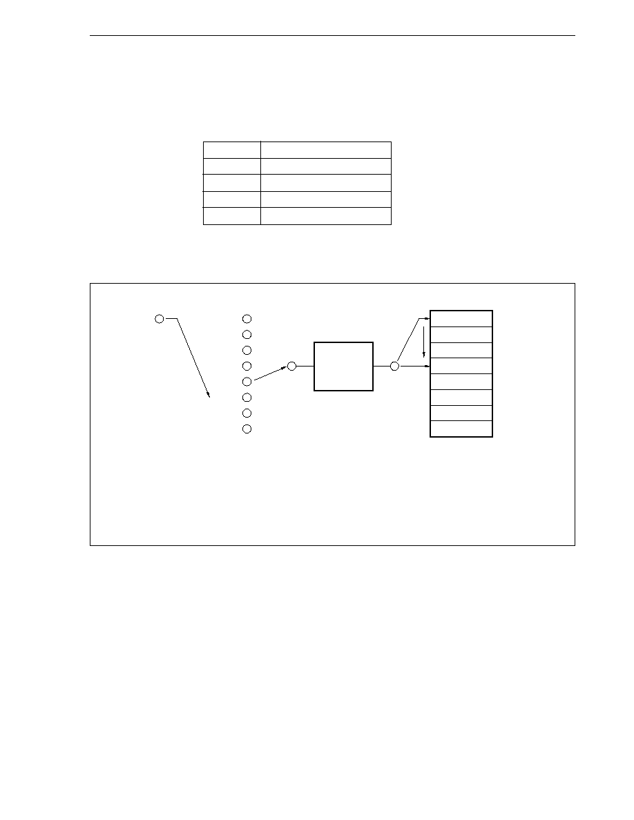
CHAPTER 9 A/D CONVERTER
229
User's Manual U10913EJ6V0UM
(2) 4-buffer mode (A/D trigger select: 4-buffer)
A/D converts one analog input four times and stores the results in four ADCRn registers. When
A/D conversion ends four times, an INTAD interrupt is generated and the A/D conversion terminates.
When 1 is written to the CE bit of the ADM0 register, A/D conversion can be restarted.
This mode is suitable for applications that calculate the average of the A/D conversion result.
Analog Input
A/D Conversion Result Register
ANIn
ADCR0
ANIn
ADCR1
ANIn
ADCR2
ANIn
ADCR3
Remark n = 0 to 7
Figure 9-7. Example of 4-Buffer Mode (A/D Trigger Select 4-Buffer) Operation
(1) Set CE bit of ADM0 to 1 (enabled)
(6) ANI4 A/D conversion
(2) ANI4 A/D conversion
(7) Save conversion result to ADCR2
(3) Save conversion result to ADCR0
(8) ANI4 A/D conversion
(4) ANI4 A/D conversion
(9) Save conversion result to ADCR3
(5) Save conversion result to ADCR1
(10) INTAD interrupt generation
ANI0
ANI1
ANI2
ANI3
ANI4
ANI5
ANI6
ANI7
ADCR0
ADCR1
ADCR2
ADCR3
ADCR4
ADCR5
ADCR6
ADCR7
A/D converter
ADM0
(
×
4)
(
×
4)
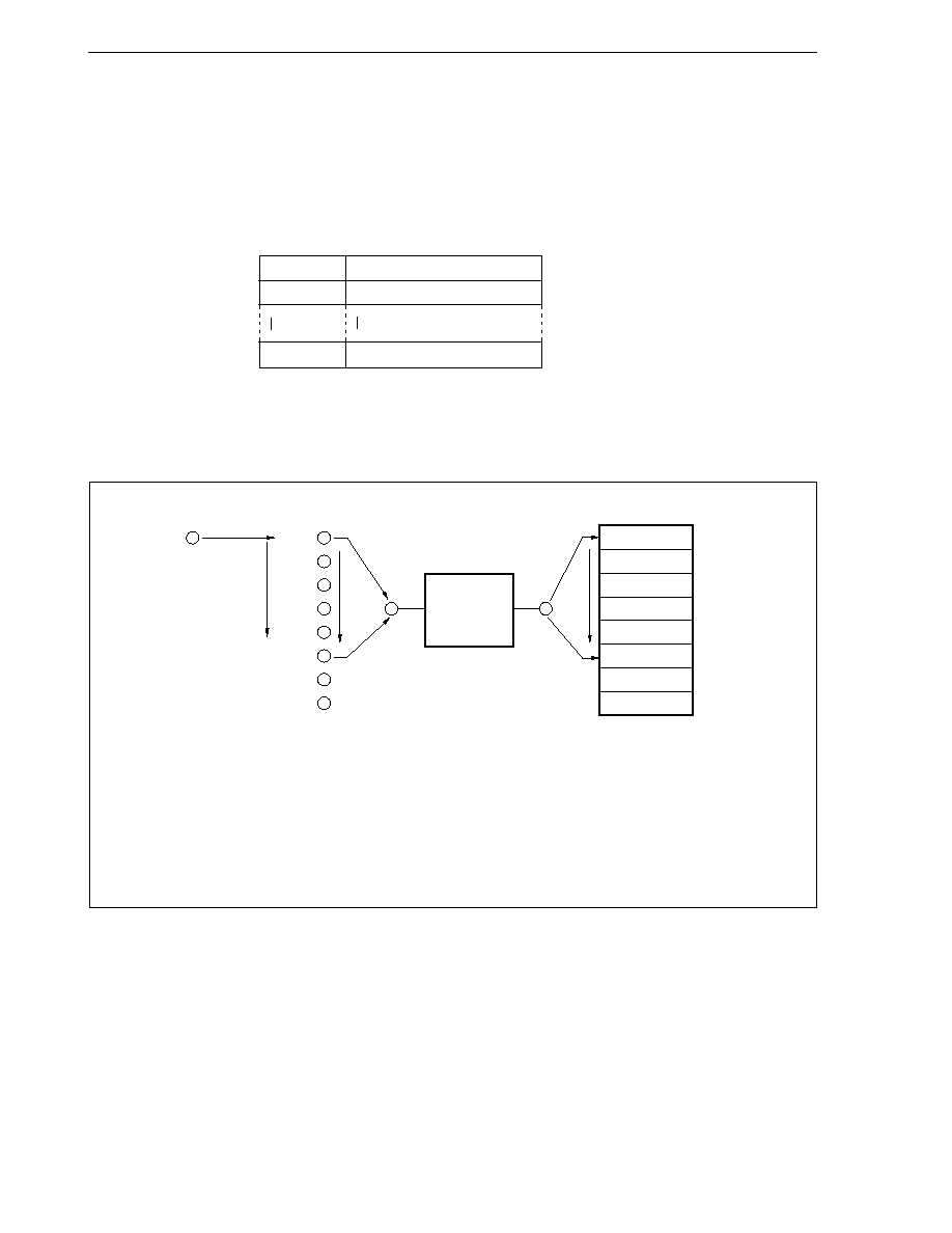
230
CHAPTER 9 A/D CONVERTER
User's Manual U10913EJ6V0UM
9.5.2 Scan mode operations
Selects the analog inputs specified by the ADM0 register sequentially from the ANI0 pin, and A/D conversion is
executed. The A/D conversion results are stored in the ADCRn register corresponding to the analog input.
When the conversion of all the specified analog input ends, the INTAD interrupt is generated, and A/D conversion
is terminated.
When 1 is written to the CE bit of the ADM0 register, A/D conversion can be restarted.
This mode is suitable for applications that continuously monitor two or more analog inputs.
Analog Input
A/D Conversion Result Register
ANIn
ADCR0
ANIn
Note
ADCR1
Note Set in bits ANIS2 to ANIS0 of the ADM0 register.
Remark n = 0 to 7
Figure 9-8. Example of Scan Mode (A/D Trigger Scan) Operation
(1)
Set CE bit of ADM0 to 1 (enabled)
(8)
ANI3 A/D conversion
(2)
ANI0 A/D conversion
(9)
Save conversion result to ADCR3
(3)
Save conversion result to ADCR0
(10) ANI4 A/D conversion
(4)
ANI1 A/D conversion
(11) Save conversion result to ADCR4
(5)
Save conversion result to ADCR1
(12) ANI5 A/D conversion
(6)
ANI2 A/D conversion
(13) Save conversion result to ADCR5
(7)
Save conversion result to ADCR2
(14) INTAD interrupt generation
ANI0
ANI1
ANI2
ANI3
ANI4
ANI5
ANI6
ANI7
ADCR0
ADCR1
ADCR2
ADCR3
ADCR4
ADCR5
ADCR6
ADCR7
A/D converter
ADM0

CHAPTER 9 A/D CONVERTER
231
User's Manual U10913EJ6V0UM
9.6 Operation in Timer Trigger Mode
The A/D converter is the match interrupt signal of the TM11 compare register, and can set conversion timings to
a maximum of four channel analog inputs (ANI0 to ANI3).
TM11 and four capture/compare registers (CC110 to CC113) are used for the timer for specifying the analog
conversion trigger.
The following two modes are provided according to the specification of the TUM11 register.
(1) One-shot mode
To use the one-shot mode, 1 should be set to the OST bit of the TUM11 register (one-shot mode).
When the A/D conversion period is longer than the TM11 period, the TM11 generates an overflow, holds 0000H
and stops. Thereafter, TM11 does not output the match interrupt signal (A/D conversion trigger) of the compare
register, and the A/D converter sets into the A/D conversion standby state. The TM11 count operation restarts
when the valid edge of the TCLR11 pin input is detected or when 1 is written to the CE11 bit of the TMC11
register.
(2) Loop mode
To use the loop mode, 0 should be set to the OST bit (normal mode) of the TUM11 register.
When the TM11 generates an overflow, the TM11 starts counting from 0000H again, and the match interrupt
signal (A/D conversion trigger) of the compare register is repeatedly output and A/D conversion is also
repeated.
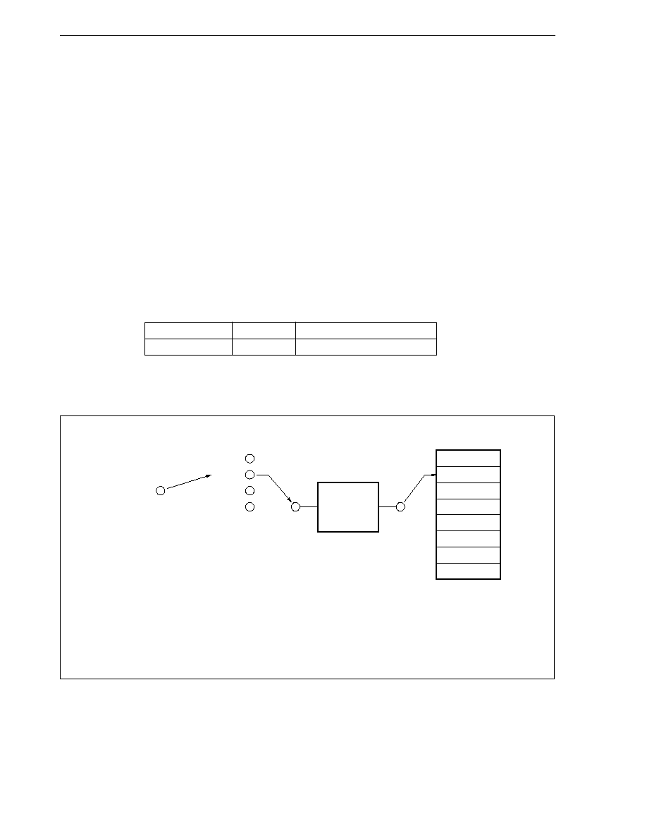
232
CHAPTER 9 A/D CONVERTER
User's Manual U10913EJ6V0UM
9.6.1 Select mode operations
A/D converts an analog input (ANI0 to ANI3) specified by the ADM0 register. The conversion results are stored
in the ADCRn register corresponding to the analog input. For the select mode, the 1-buffer mode and 4-buffer mode
are provided according to the storage method of the A/D conversion results (n = 0 to 7).
(1) 1-buffer mode operations (Timer trigger select: 1-buffer)
A/D converts one analog input once and stores the conversion results in one ADCRn register.
There are two one-buffer modes, the 1-trigger mode and 4-trigger mode, according to the number of triggers.
(a) 1-trigger mode (Timer trigger select: 1-buffer, 1-trigger)
A/D converts one analog input once using the trigger of the match interrupt signal (INTCC110) and stores
the results in one ADCRn register.
Generates an INTAD interrupt for each A/D conversion and ends the A/D conversion.
When the TM11 is set to the one-shot mode, A/D conversion is ended in one conversion. To restart the
A/D conversion, input the valid edge to the TCLR11 pin or write 1 to the CE11 bit of the TMC11 register.
When set to the loop mode, unless the CE bit of the ADM0 register is set to 0, A/D conversion is repeated
each time the match interrupt is generated.
Trigger
Analog Input
A/D Conversion Result Register
INTCC110 interrupt
ANIn
ADCRn
Remark n = 0 to 3
Figure 9-9. Example of 1-Trigger Mode (Timer Trigger Select 1-Buffer 1-Trigger) Operation
(1) Set CE bit of ADM0 to 1 (enabled)
(2) CC110 compare generation
(3) ANI1 A/D conversion
(4) Save conversion result to ADCR1
(5) INTAD interrupt generation
ANI0
ANI1
ANI2
ANI3
ADCR0
ADCR1
ADCR2
ADCR3
ADCR4
ADCR5
ADCR6
ADCR7
A/D converter
INTCC110
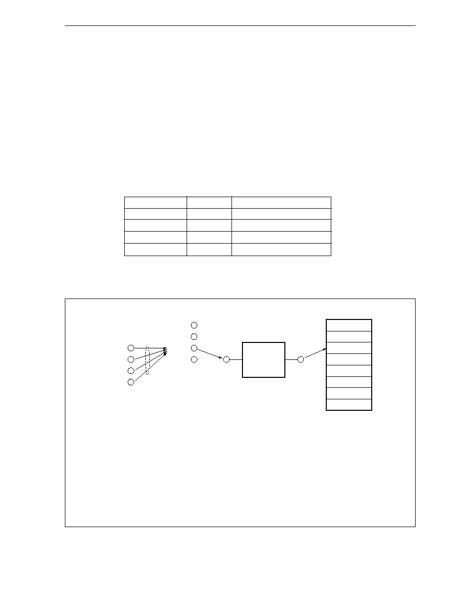
CHAPTER 9 A/D CONVERTER
233
User's Manual U10913EJ6V0UM
(b) 4-trigger mode (Timer trigger select: 1-buffer, 4-trigger)
A/D converts one analog input four times using four match interrupt signals (INTCC110 to INTCC113)
as triggers and stores the results in one ADCRn register. The INTAD interrupt is generated with each
A/D conversion, and the CS bit of the ADM0 register is reset (0). The results of one A/D conversion are
held by the ADCRn register until the next A/D conversion ends. Perform transmission of the conversion
results to the memory, and other operations using the INTAD interrupt after each A/D conversion ends.
When the TM11 is set to the one-shot mode, A/D conversion ends after four conversions. To restart the
A/D conversion, input the valid edge to the TCLR11 pin or write 1 to the CE11 bit of the TMC11 register
to restart TM11. When the first match interrupt after TM11 is restarted is generated, the CS bit is set
(1) and A/D conversion is started.
When set to the loop mode, unless the CE bit of the ADM0 register is set to 0, A/D conversion is repeated
each time the match interrupt is generated.
The match interrupts (INTCC110 to INTCC113) can be generated in any order. The same trigger, even
when it enters several times consecutively, is accepted as a trigger each time.
Trigger
Analog Input
A/D Conversion Result Register
INTCC110 interrupt
ANIn
ADCRn
INTCC111 interrupt
ANIn
ADCRn
INTCC112 interrupt
ANIn
ADCRn
INTCC113 interrupt
ANIn
ADCRn
Remark n = 0 to 3
Figure 9-10. Example of 4-Trigger Mode (Timer Trigger Select 1-Buffer 4-Trigger) Operation
(1)
Set CE bit of ADM0 to 1 (enabled)
(10) CC113 compare generation (random order)
(2)
CC112 compare generation (random order)
(11) ANI2 A/D conversion
(3)
ANI2 A/D conversion
(12) Save conversion result to ADCR2
(4)
Save conversion result to ADCR2
(13) INTAD interrupt generation
(5)
INTAD interrupt generation
(14) CC110 compare generation (random order)
(6)
CC111 compare generation (random order)
(15) ANI2 A/D conversion
(7)
ANI2 A/D conversion
(16) Save conversion result to ADCR2
(8)
Save conversion result to ADCR2
(17) INTAD interrupt generation
(9)
INTAD interrupt generation
ANI0
ANI1
ANI2
ANI3
ADCR0
ADCR1
ADCR2
ADCR3
ADCR4
ADCR5
ADCR6
ADCR7
A/D converter
INTCC110
INTCC111
INTCC112
INTCC113
Any order
(
×
4)
(
×
4)
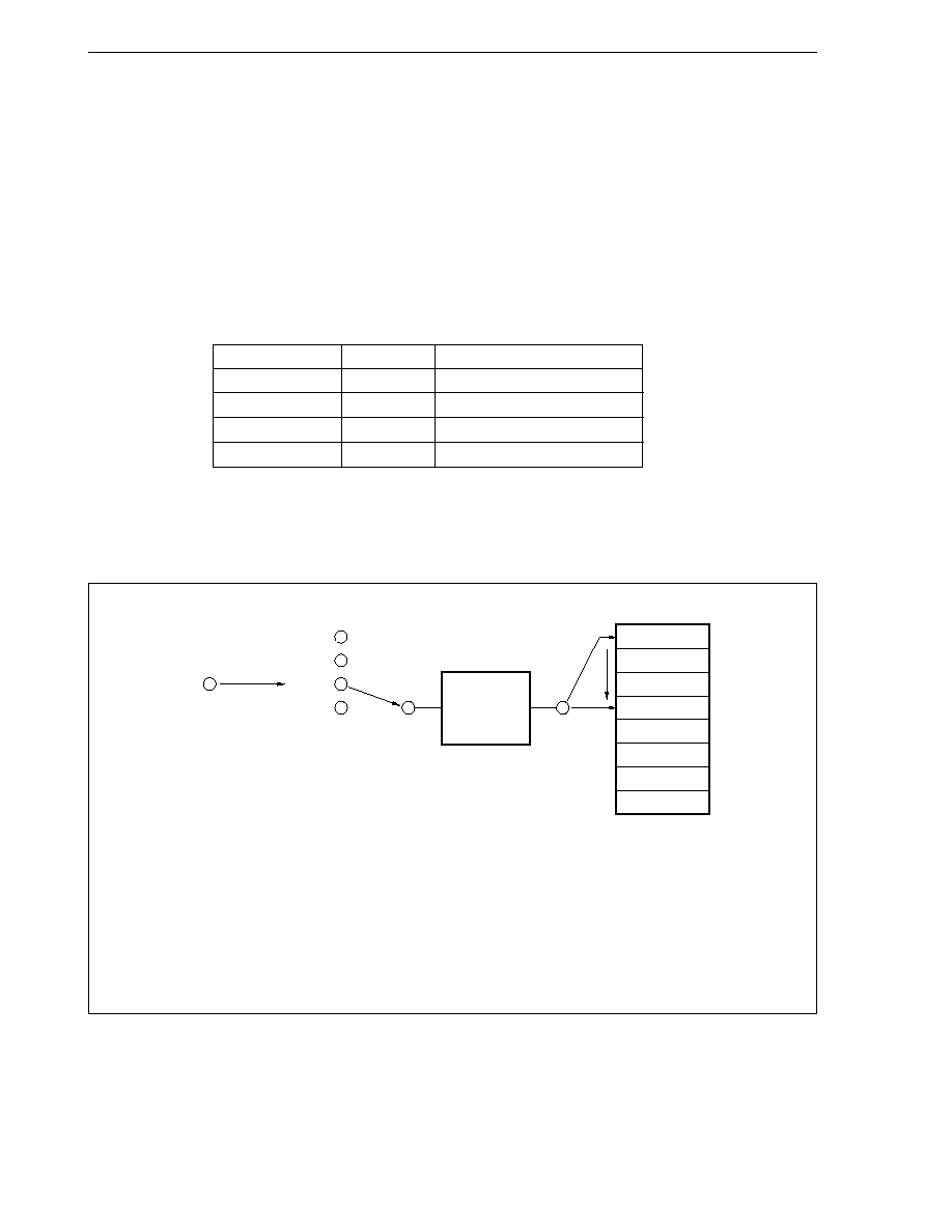
234
CHAPTER 9 A/D CONVERTER
User's Manual U10913EJ6V0UM
(2) 4-buffer mode operations (Timer trigger select: 4-buffer)
A/D conversion of one analog input is executed four times, and the results are stored in the ADCRn register.
There are two 4-buffer modes, 1-trigger mode and 4-trigger mode, according to the number of triggers.
This mode is suitable for applications that calculate the average of the A/D conversion result.
(a) 1-trigger mode (Timer trigger select: 4-buffer, 1-trigger)
A/D converts one analog input four times using the match interrupt signal (INTCC110) as a trigger, and
stores the results in four ADCRn registers.
An INTAD interrupt is generated when the four A/D conversions end and the A/D conversion is terminated.
When TM11 is set to the one-shot mode, and less than four match interrupts are generated, if the CE
bit is set to 0, the INTAD interrupt is not generated and the standby state is set.
Trigger
Analog Input
A/D Conversion Result Register
INTCC110 interrupt
ANIn
ADCR0
INTCC110 interrupt
ANIn
ADCR1
INTCC110 interrupt
ANIn
ADCR2
INTCC110 interrupt
ANIn
ADCR3
Remark n = 0 to 3
Figure 9-11. Example of 1-Trigger Mode (Timer Trigger Select 4-Buffer 1-Trigger) Operation
(1)
Set CE bit of ADM0 to 1 (enabled)
(8)
CC110 compare generation
(2)
CC110 compare generation
(9)
ANI2 A/D conversion
(3)
ANI2 A/D conversion
(10) Save conversion result to ADCR2
(4)
Save conversion result to ADCR0
(11) CC110 compare generation
(5)
CC110 compare generation
(12) ANI2 A/D conversion
(6)
ANI2 A/D conversion
(13) Save conversion result to ADCR3
(7)
Save conversion result to ADCR1
(14) INTAD interrupt generation
ANI0
ANI1
ANI2
ANI3
ADCR0
ADCR1
ADCR2
ADCR3
ADCR4
ADCR5
ADCR6
ADCR7
A/D converter
INTCC110
(
×
4)
(
×
4)

CHAPTER 9 A/D CONVERTER
235
User's Manual U10913EJ6V0UM
(b) 4-trigger mode (Timer trigger select: 4-buffer, 4-trigger)
A/D converts one analog input four times using four match interrupt signals (INTCC110 to INTCC113)
as triggers and stores the results in four ADCRn registers. The INTAD interrupt is generated when the
four A/D conversions end, the CS bit is reset (0), and A/D conversion ends.
When the TM11 is set to the one-shot mode, A/D conversion ends after four conversions. To restart the
A/D conversion, input the valid edge to the TCLR11 pin or write 1 to the CE11 bit of the TMC11 register
to restart TM11. When the first match interrupt after TM11 is restarted is generated, the CS bit is set (1)
and A/D conversion is started.
When set to the loop mode, unless the CE bit is set to 0, A/D conversion is repeated each time the match
interrupt is generated.
The match interrupts (INTCC110 to INTCC113) can be generated in any order. The conversion result
is stored in the ADCRn register corresponding to the input trigger. The same trigger, even when it enters
several times consecutively, is accepted as a trigger each time.
Trigger
Analog Input
A/D Conversion Result Register
INTCC110 interrupt
ANIn
ADCR0
INTCC111 interrupt
ANIn
ADCR1
INTCC112 interrupt
ANIn
ADCR2
INTCC113 interrupt
ANIn
ADCR3
Remark n = 0 to 3
Figure 9-12. Example of 4-Trigger Mode (Timer Trigger Select 4-Buffer 4-Trigger) Operation
(1)
Set CE bit of ADM0 to 1 (enabled)
(8)
CC112 compare generation (random order)
(2)
CC111 compare generation (random order)
(9)
ANI2 A/D conversion
(3)
ANI2 A/D conversion
(10) Save conversion result to ADCR2
(4)
Save conversion result to ADCR1
(11) CC110 compare generation (random order)
(5)
CC113 compare generation (random order)
(12) ANI2 A/D conversion
(6)
ANI2 A/D conversion
(13) Save conversion result to ADCR0
(7)
Save conversion result to ADCR3
(14) INTAD interrupt generation
ANI0
ANI1
ANI2
ANI3
ADCR0
ADCR1
ADCR2
ADCR3
ADCR4
ADCR5
ADCR6
ADCR7
A/D converter
INTCC110
INTCC111
INTCC112
INTCC113
Any order
(
×
4)
(
×
4)
No particular
order

236
CHAPTER 9 A/D CONVERTER
User's Manual U10913EJ6V0UM
9.6.2 Scan mode operations
Selects the analog inputs specified by the ADM0 register sequentially from the ANI0 pin and A/D converts them
for the specified number of times using the match interrupt signal as a trigger.
In the conversion operation, first the analog input lower channels (ANI0 to ANI3) are A/D converted for the specified
number of times. In the ADM0 register, if the lower channels (ANI0 to ANI3) of the analog input are set so that they
are scanned, and when the set number of A/D conversions ends, the INTAD interrupt is generated and A/D conversion
ends.
When the higher channels (ANI4 to ANI7) of the analog input are set so that they are scanned in the ADM0 register,
after the conversion of the lower channel is ended, the mode is shifted to the A/D trigger mode, and the remaining
A/D conversions are executed.
The conversion results are stored in the ADCRn register corresponding to the analog input. When the conversion
of all the specified analog inputs has ended, the INTAD interrupt is generated and A/D conversion ends.
There are two scan modes, 1-trigger mode and 4-trigger mode, according to the number of triggers.
This mode is suitable for applications that always monitor two or more analog inputs.
(1) 1-trigger mode (Timer trigger scan: 1-trigger)
A/D converts the analog input for the specified number of times using the match interrupt signal (INTCC110)
as a trigger.
The analog input and ADCRn register correspond one to one.
When all the A/D specified conversions have ended, the INTAD interrupt is generated and A/D conversion
ends. When the match interrupt is generated after all the specified A/D conversions end, A/D conversion is
restarted.
When TM11 is set to the one-shot mode, and less than the specified number of match interrupts are
generated, if the CE bit is set to 0, the INTAD interrupt is not generated and the standby state is set.
Trigger
Analog Input
A/D Conversion Result Register
INTCC110 interrupt
ANI0
ADCR0
INTCC110 interrupt
ANI1
ADCR1
INTCC110 interrupt
ANI2
ADCR2
INTCC110 interrupt
ANI3
ADCR3
(A/D trigger mode)
ANI4
ADCR4
ANI5
ADCR5
ANI6
ADCR6
ANI7
ADCR7
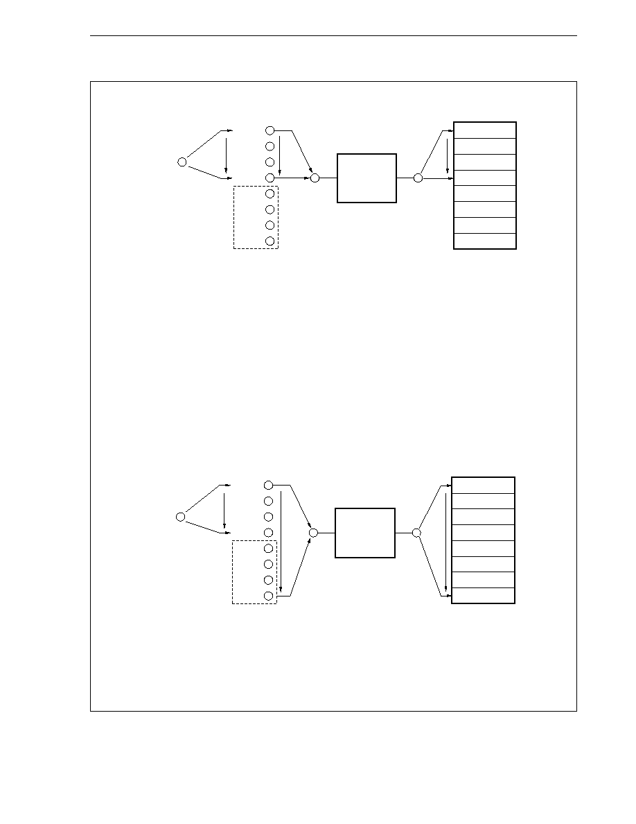
CHAPTER 9 A/D CONVERTER
237
User's Manual U10913EJ6V0UM
Figure 9-13. Example of 1-Trigger Mode (Timer Trigger Scan 1-Trigger) Operation
(a) When ANI0 to ANI3 are set for scanning
(1)
Set CE bit of ADM0 to 1 (enabled)
(8)
CC110 compare generation
(2)
CC110 compare generation
(9)
ANI2 A/D conversion
(3)
ANI0 A/D conversion
(10) Save conversion result to ADCR2
(4)
Save conversion result to ADCR0
(11) CC110 compare generation
(5)
CC110 compare generation
(12) ANI3 A/D conversion
(6)
ANI1 A/D conversion
(13) Save conversion result to ADCR3
(7)
Save conversion result to ADCR1
(14) INTAD interrupt generation
Caution Analog inputs enclosed by broken lines cannot use INTCC11n as a trigger (n = 0 to 3). When
ANI0 to ANI7 are set for scanning, ANI4 to ANI7 are converted in A/D trigger mode (see (b)).
(b) When ANI0 to ANI7 are set for scanning
(1) to (13) Same as (a)
(18) ANI6 A/D conversion
(14) ANI4 A/D conversion
(19) Save conversion result to ADCR6
(15) Save conversion result to ADCR4
(20) ANI7 A/D conversion
(16) ANI5 A/D conversion
(21) Save conversion result to ADCR7
(17) Save conversion result to ADCR5
(22) INTAD interrupt generation
ANI0
ANI1
ANI2
ANI3
ANI4
ANI5
ANI6
ANI7
ADCR0
ADCR1
ADCR2
ADCR3
ADCR4
ADCR5
ADCR6
ADCR7
INTCC110
A/D converter
ANI0
ANI1
ANI2
ANI3
ANI4
ANI5
ANI6
ANI7
ADCR0
ADCR1
ADCR2
ADCR3
ADCR4
ADCR5
ADCR6
ADCR7
A/D converter
INTCC110

238
CHAPTER 9 A/D CONVERTER
User's Manual U10913EJ6V0UM
(2) 4-trigger mode (Timer trigger scan: 4-trigger)
A/D converts analog inputs for the number of times specified using the match interrupt signal (INTCC110 to
INTCC113) as a trigger.
The analog input and ADCRn register correspond one to one.
When all the A/D specified conversions have ended, the INTAD interrupt is generated and A/D conversion
ends.
To restart conversion when TM11 is set to the one-shot mode, restart TM11. If set to the loop mode and the
CE bit is 1, A/D conversion is restarted when a match interrupt is generated after conversion ends.
The match interrupts can be generated in any order. However, because the trigger signal and the analog
input correspond one to one, the scanning sequence is determined according to the order in which the match
signals of the compare register are generated.
Trigger
Analog Input
A/D Conversion Result Register
INTCC110 interrupt
ANI0
ADCR0
INTCC111 interrupt
ANI1
ADCR1
INTCC112 interrupt
ANI2
ADCR2
INTCC113 interrupt
ANI3
ADCR3
(A/D trigger mode)
ANI4
ADCR4
ANI5
ADCR5
ANI6
ADCR6
ANI7
ADCR7
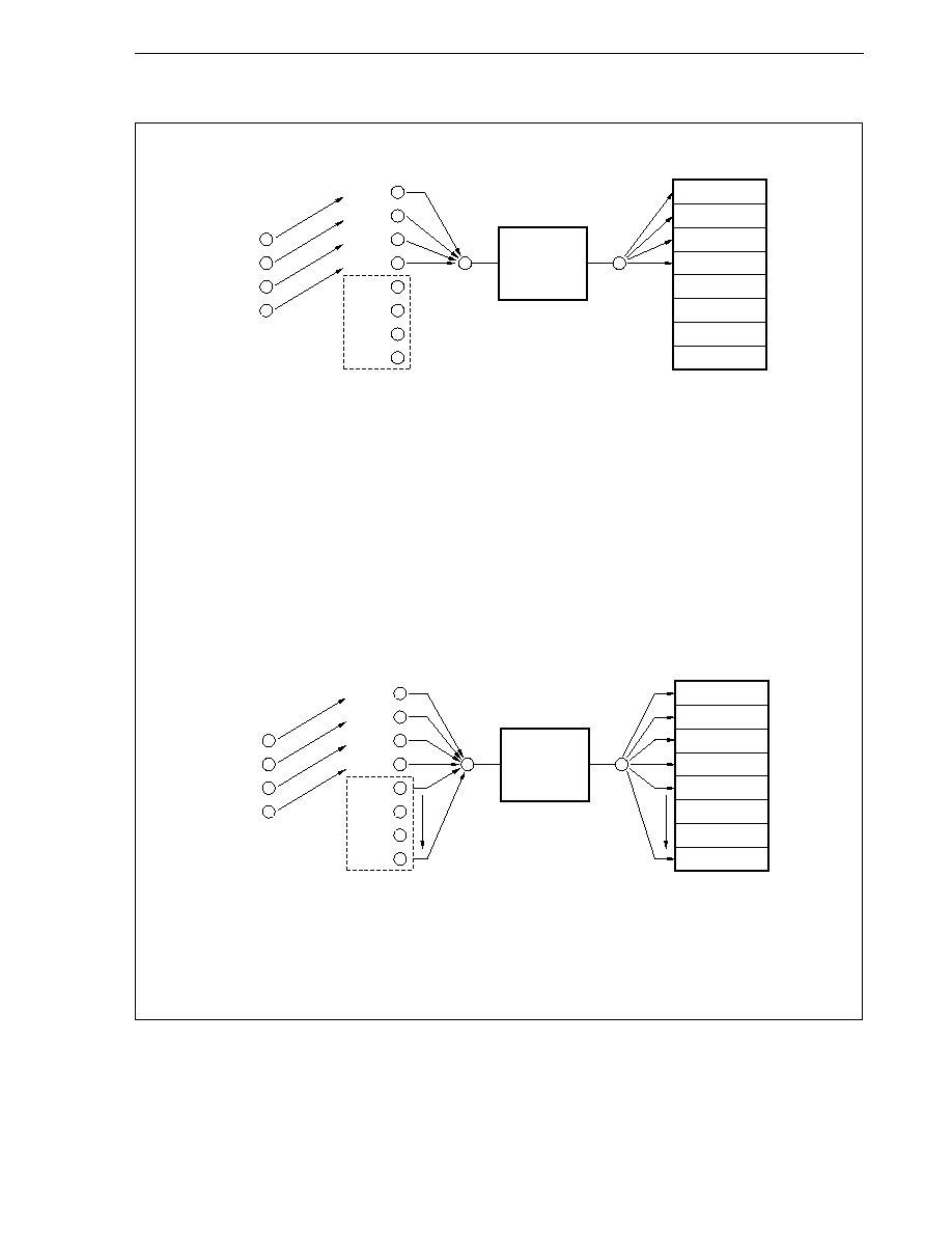
CHAPTER 9 A/D CONVERTER
239
User's Manual U10913EJ6V0UM
Figure 9-14. Example of 4-Trigger Mode (Timer Trigger Scan 4-Trigger) Operation
(a) When ANI0 to ANI3 are set for scanning
(1)
Set CE bit of ADM0 to 1 (enabled)
(8)
CC110 compare generation (random order)
(2)
CC111 compare generation (random order)
(9)
ANI0 A/D conversion
(3)
ANI1 A/D conversion
(10) Save conversion result to ADCR0
(4)
Save conversion result to ADCR1
(11) CC112 compare generation (random order)
(5)
CC113 compare generation (random order)
(12) ANI2 A/D conversion
(6)
ANI3 A/D conversion
(13) Save conversion result to ADCR2
(7)
Save conversion result to ADCR3
(14) INTAD interrupt generation
Caution Analog inputs enclosed by broken lines cannot use INTCC11n as a trigger (n = 0 to 3). When
ANI0 to ANI7 are set for scanning, ANI4 to ANI7 are converted in A/D trigger mode (see (b)).
(b) When ANI0 to ANI7 are set for scanning
(1) to (13) Same as (a)
(18) ANI6 A/D conversion
(14) ANI4 A/D conversion
(19) Save conversion result to ADCR6
(15) Save conversion result to ADCR4
(20) ANI7 A/D conversion
(16) ANI5 A/D conversion
(21) Save conversion result to ADCR7
(17) Save conversion result to ADCR5
(22) INTAD interrupt generation
ANI0
ANI1
ANI2
ANI3
ANI4
ANI5
ANI6
ANI7
ADCR0
ADCR1
ADCR2
ADCR3
ADCR4
ADCR5
ADCR6
ADCR7
A/D converter
INTCC110
INTCC111
INTCC112
INTCC113
Any order
ANI0
ANI1
ANI2
ANI3
ANI4
ANI5
ANI6
ANI7
ADCR0
ADCR1
ADCR2
ADCR3
ADCR4
ADCR5
ADCR6
ADCR7
A/D converter
INTCC110
INTCC111
INTCC112
INTCC113
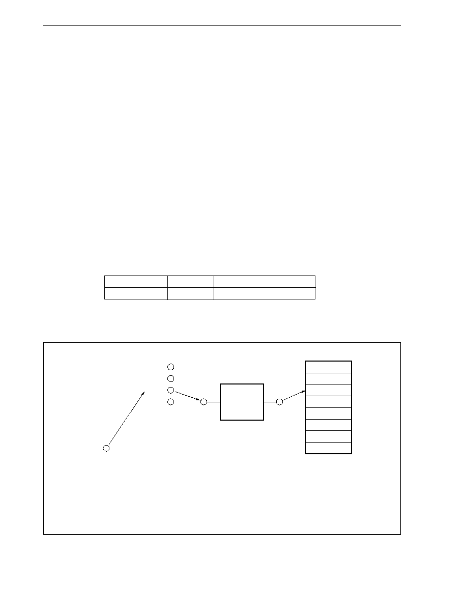
240
CHAPTER 9 A/D CONVERTER
User's Manual U10913EJ6V0UM
9.7 Operation in External Trigger Mode
In the external trigger mode, the analog inputs (ANI0 to ANI3) are A/D converted at the ADTRG pin input timing.
The ADTRG pin is also used as the P07 and INTP113 pins. To set the external trigger mode, set the PMC07 bit
of the PMC0 register to 1 and the TRG2 to TRG0 bits of the ADM1 register to 110.
For the valid edge of the external input signal in the external trigger mode, the rising edge, falling edge, or both
rising and falling edges can be specified using the ES031 and ES030 bits of the INTM1 register. For details, refer
to 5.3.7 Edge detection function.
9.7.1 Select mode operations (external trigger select)
A/D converts one analog input (ANI0 to ANI3) specified by the ADM0 register. The conversion results are stored
in the ADCRn register corresponding to the analog input. There are two select modes, 1-buffer mode and 4-buffer
mode, for storing the conversion results (n = 0 to 7).
(1) 1-buffer mode (external trigger select: 1-buffer)
A/D converts one analog input using the ADTRG signal as a trigger. The conversion results are stored in one
ADCRn register. The analog input and the A/D conversion result register correspond one to one. INTAD
interrupts are generated after each A/D conversion, and A/D conversion ends.
While the CE bit of the ADM0 register is 1, the A/D conversion is repeated every time a trigger is input from
the ADTRG pin.
This mode is suitable for applications that read out the result after each A/D conversion.
Trigger
Analog Input
A/D Conversion Result Register
ADTRG signal
ANIn
ADCRn
Remark n = 0 to 3
Figure 9-15. Example of 1-Buffer Mode (External Trigger Select 1-Buffer) Operation
(1)
Set CE bit of ADM0 to 1 (enabled)
(2)
External trigger generation
(3)
ANI2 A/D conversion
(4)
Save conversion result to ADCR2
(5)
INTAD interrupt generation
ANI0
ANI1
ANI2
ANI3
ADCR0
ADCR1
ADCR2
ADCR3
ADCR4
ADCR5
ADCR6
ADCR7
A/D converter
ADTRG
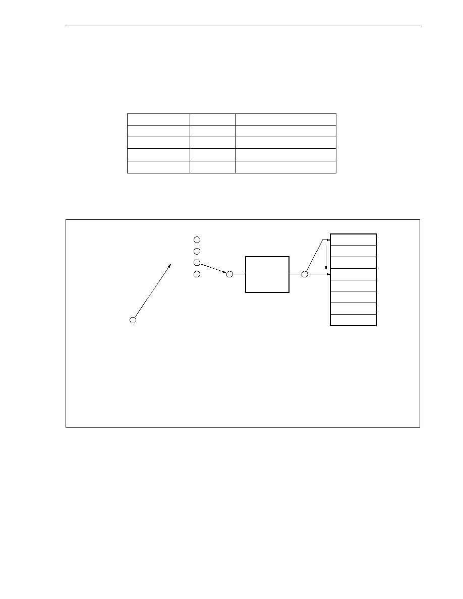
CHAPTER 9 A/D CONVERTER
241
User's Manual U10913EJ6V0UM
(2) 4-buffer mode (external trigger select: 4-buffer)
A/D converts one analog input four times using the ADTRG signal as a trigger and stores the results in four
ADCRn registers. The INTAD interrupt is generated and conversion ends when the four A/D conversions end.
While the CE bit of the ADM0 register is 1, the A/D conversion is repeated every time a trigger is input from
the ADTRG pin.
This mode is suitable for applications that calculate the average of the A/D conversion result.
Trigger
Analog Input
A/D Conversion Result Register
ADTRG signal
ANIn
ADCR0
ADTRG signal
ANIn
ADCR1
ADTRG signal
ANIn
ADCR2
ADTRG signal
ANIn
ADCR3
Remark n = 0 to 3
Figure 9-16. Examples of 4-Buffer Mode (External Trigger Select 4-Buffer) Operation
(1)
Set CE bit of ADM0 to 1 (enabled)
(8)
External trigger generation
(2)
External trigger generation
(9)
ANI2 A/D conversion
(3)
ANI2 A/D conversion
(10) Save conversion result to ADCR2
(4)
Save conversion result to ADCR0
(11) External trigger generation
(5)
External trigger generation
(12) ANI2 A/D conversion
(6)
ANI2 A/D conversion
(13) Save conversion result to ADCR3
(7)
Save conversion result to ADCR1
(14) INTAD interrupt generation
ANI0
ANI1
ANI2
ANI3
ADCR0
ADCR1
ADCR2
ADCR3
ADCR4
ADCR5
ADCR6
ADCR7
A/D converter
ADTRG
(
×
4)
(
×
4)

242
CHAPTER 9 A/D CONVERTER
User's Manual U10913EJ6V0UM
9.7.2 Scan mode operations (external trigger scan)
Selects the analog inputs specified by the ADM0 register sequentially from the ANI0 pin using the ADTRG signal
as a trigger, and A/D converts them. The A/D conversion results are stored in the ADCRn register corresponding
to the analog input (n = 0 to 7).
When the lower 4 channels (ANI0 to ANI3) of the analog input are set so that they are scanned in the ADM0 register,
the INTAD interrupt is generated when the number of A/D conversions specified end, and A/D conversion ends.
When the higher 4 channels (ANI4 to ANI7) of the analog input are set so that they are scanned in the ADM0 register,
after the conversion of the lower 4 channels ends, the mode is shifted to the A/D trigger mode, and the remaining
A/D conversions are executed. The conversion results are stored in the ADCRn register corresponding to the analog
input. When the conversion of all the specified analog inputs ends, the INTAD interrupt is generated and A/D
conversion ends.
When a trigger is input to the ADTRG pin while the CE bit of the ADM0 register is 1, the A/D conversion is started
again.
This mode is suitable for applications that continuously monitor two or more analog inputs.
Trigger
Analog Input
A/D Conversion Result Register
ADTRG signal
ANI0
ADCR0
ADTRG signal
ANI1
ADCR1
ADTRG signal
ANI2
ADCR2
ADTRG signal
ANI3
ADCR3
(A/D trigger mode)
ANI4
ADCR4
ANI5
ADCR5
ANI6
ADCR6
ANI7
ADCR7
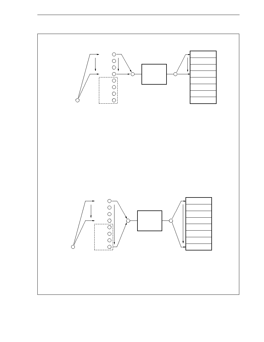
CHAPTER 9 A/D CONVERTER
243
User's Manual U10913EJ6V0UM
Figure 9-17. Example of Scan Mode (External Trigger Scan) Operation
(a) When ANI0 to ANI3 are set for scanning
(1)
Set CE bit of ADM0 to 1 (enabled)
(8)
External trigger generation
(2)
External trigger generation
(9)
ANI2 A/D conversion
(3)
ANI0 A/D conversion
(10) Save conversion result to ADCR2
(4)
Save conversion result to ADCR0
(11) External trigger generation
(5)
External trigger generation
(12) ANI3 A/D conversion
(6)
ANI1 A/D conversion
(13) Save conversion result to ADCR3
(7)
Save conversion result to ADCR1
(14) INTAD interrupt generation
Caution Analog inputs enclosed by broken lines cannot use ADTRG as a trigger. When ANI0 to ANI7
are set for scanning, ANI4 to ANI7 are converted in A/D trigger mode (see (b)).
(b) When ANI0 to ANI7 are set for scanning
(1) to (13) Same as (a)
(18) ANI6 A/D conversion
(14) ANI4 A/D conversion
(19) Save conversion result to ADCR6
(15) Save conversion result to ADCR4
(20) ANI7 A/D conversion
(16) ANI5 A/D conversion
(21) Save conversion result to ADCR7
(17) Save conversion result to ADCR5
(22) INTAD interrupt generation
ANI0
ANI1
ANI2
ANI3
ANI4
ANI5
ANI6
ANI7
ADCR0
ADCR1
ADCR2
ADCR3
ADCR4
ADCR5
ADCR6
ADCR7
A/D converter
ADTRG
ANI0
ANI1
ANI2
ANI3
ANI4
ANI5
ANI6
ANI7
ADCR0
ADCR1
ADCR2
ADCR3
ADCR4
ADCR5
ADCR6
ADCR7
A/D converter
ADTRG
244
CHAPTER 9 A/D CONVERTER
User's Manual U10913EJ6V0UM
PORT
RPU
PMC0 register
PMC07
TUM11 register
CMS113
Capture
trigger
Capture
Compare
TUM11 register
IMS113
A/D
Timer trigger
External trigger
Timer/external
interrupt request
INTM1 register
ES031, ES030
P11IC3 register
P11MK3
Interrupt
control
Interrupt
enable/disable
Trigger
ADM1 register
TRG2 to TRG0
Noise
elimination
Edge
selection
P07/INTP113/
ADTRG
External interrupt request
Timer interrupt request
INTC
9.8 Cautions in Use of A/D Converter
(1) When A/D converter is set in the timer trigger mode
The match interrupt of the compare register becomes the A/D conversion start trigger and conversion
operations are started. At this time, the match interrupt of the compare register also functions as the match
interrupt of the compare register for the CPU. To prevent generation of the match interrupt of the compare
register for the CPU, disable interrupt using the interrupt mask bit (P11MK0 to P11MK3) of the interrupt control
register (P11IC0 to P11IC3).
(2) When A/D converter is set in the external trigger mode
The external trigger input becomes the A/D conversion start trigger and conversion operations are started.
At this time, the external trigger input also functions as a capture trigger and the external interrupt of timer
1. To prevent capture trigger and external interrupt from generating, set timer 1 to the compare register and
disable the interrupt with the interrupt mask bit of the interrupt control register.
The operations performed when timer 1 is set to the compare register and interrupt is not disabled by the
interrupt control register are as follows.
(a) When the interrupt mask bit (IMS113) of the TUM11 register is 0
Functions as the match interrupt of the compare register for the CPU.
(b) When the interrupt mask bit (IMS113) of the TUM11 register is 1
The external trigger input of the A/D converter functions as the external interrupt for the CPU.
Figure 9-18. Relationships Among A/D Converter, Ports, INTC, and RPU

CHAPTER 9 A/D CONVERTER
245
User's Manual U10913EJ6V0UM
9.9 Cautions
(1) When 0 is written to the CE bit of the ADM0 register during a conversion operation, the conversion operation
stops and the conversion results are not stored in the ADCRn register (n = 0 to 7).
(2) Set the interval (input time interval) of the trigger in the external or timer trigger mode to longer than the
conversion time specified by the FR2 to FR0 bits of the ADM1 register.
When interval = 0
When several triggers are input simultaneously, the analog input with the smaller ANIn pin number
is converted. The other trigger signals input simultaneously are ignored, and the number of triggers
input is not counted. Therefore, the generation of interrupts and storage of results to be stored in
the ADCRn register will become abnormal.
When 0 < interval
conversion operation time
When the timer trigger is input during a conversion operation, the conversion operation stops and
conversion starts according to the last timer trigger input.
When a conversion operation is stopped, the conversion results are not stored in the ADCRn register.
However, the number of triggers input are counted, and when the interrupt is generated, the value
at which conversion ended is stored in the ADCRn register.
(3) Standby operations are as follows.
(a) HALT mode
A/D conversion continues. When released by NMI input, the ADM0 and ADM1 registers and ADCRn
register hold their values.
(b) IDLE mode, software STOP mode
As clock supply to the A/D converter is stopped, no conversion operations are performed. When these
modes are released by NMI input, the ADM0 and ADM1 registers and the ADCRn register hold their
values. However, when the IDLE and software STOP modes are set during a conversion operation,
the conversion operation is stopped. At this time, if released by NMI input, the conversion operation
resumes, but the conversion result written to the ADCRn register will become undefined.
In the IDLE and software STOP modes, the operation of the comparator is also stopped to reduce
the power consumption. However, to further reduce current consumption, set the voltage of the AV
REF1
pin to V
SS
.
246
CHAPTER 9 A/D CONVERTER
User's Manual U10913EJ6V0UM
9.10 How to Read A/D Converter Characteristics Table
Here, special terms unique to the A/D converter are explained.
(1) Resolution
This is the minimum analog input voltage that can be identified. That is, the percentage of the analog input
voltage per bit of digital output is called 1LSB (Least Significant Bit). The percentage of 1LSB with respect
to the full scale is expressed by %FSR (Full Scale Range).
When the resolution is 10 bits,
1LSB = 1/2
10
= 1/1024
= 0.098%FSR
Accuracy has no relation to resolution, but is determined by overall error.
(2) Overall error
This shows the maximum error value between the actual measured value and the theoretical value.
Zero scale error, full scale error, nonlinearity error and errors which are combinations of these express the
overall error.
Note that the quantization error is not included in the overall error in the characteristics table.
(3) Quantization error
When analog values are converted to digital values, a
±
1/2LSB error naturally occurs. In an A/D converter,
an analog input voltage in a range of
±
1/2LSB is converted to the same digital code, so a quantization error
cannot be avoided.
Note that the quantization error is not included in the overall error, zero scale error, full scale error and
nonlinearity error in the characteristics table.
Figure 9-19. Overall Error
Figure 9-20. Quantization Error
Ideal line
0......0
1......1
Digital output
Overall
error
Analog input
AV
REF1
0
0......0
1......1
Digital output
Quantization error
1/2LSB
1/2LSB
Analog input
AV
REF1
0
CHAPTER 9 A/D CONVERTER
247
User's Manual U10913EJ6V0UM
(4) Zero-scale error
This shows the difference between the actual measurement value of the analog input voltage and the
theoretical value (1/2 LSB) when the digital output changes from 0......000 to 0......001. If the actual
measurement value is greater than the theoretical value, it shows the difference between the actual
measurement value of the analog input voltage and the theoretical value (3/2LSB) when the digital output
changes from 0......000 to 0......010.
(5) Full-scale error
This shows the difference between the actual measurement value of the analog input voltage and the
theoretical value (3/2 LSB) when the digital output changes from 1......110 to 1......111.
(6) Nonlinearity error
This shows the degree to which the conversion characteristics deviate from the ideal linear relationship. It
expresses the maximum value of the difference between the actual measurement value and the ideal straight
line when the zero scale error and full scale error are 0.
Figure 9-21. Zero Scale Error
Figure 9-22. Full Scale Error
Figure 9-23. Nonlinearity Error
0
AV
REF1
Digital output
Analog input
Nonlinearity
error
Ideal line
1......1
0......0
111
011
010
001
Zero-scale error
Ideal line
000
0
1
2
3
AV
REF1
Digital output (Lo
w
er order 3 bits)
Analog input (LSB)
111
110
101
000
0
AV
REF1
AV
REF1
1
AV
REF1
2
AV
REF1
3
Digital output (Lo
w
er order 3 bits)
Analog input (LSB)
Ideal line
Full-scale error
248
CHAPTER 9 A/D CONVERTER
User's Manual U10913EJ6V0UM
(7) Conversion time
This expresses the time from when the analog input voltage was applied to the time when the digital output
was obtained.
The sampling time is included in the conversion time in the characteristics table.
(8) Sampling time
This is the time the analog switch is turned on for the analog voltage to be sampled by the sample & hold circuit.
Sampling
time
Conversion time
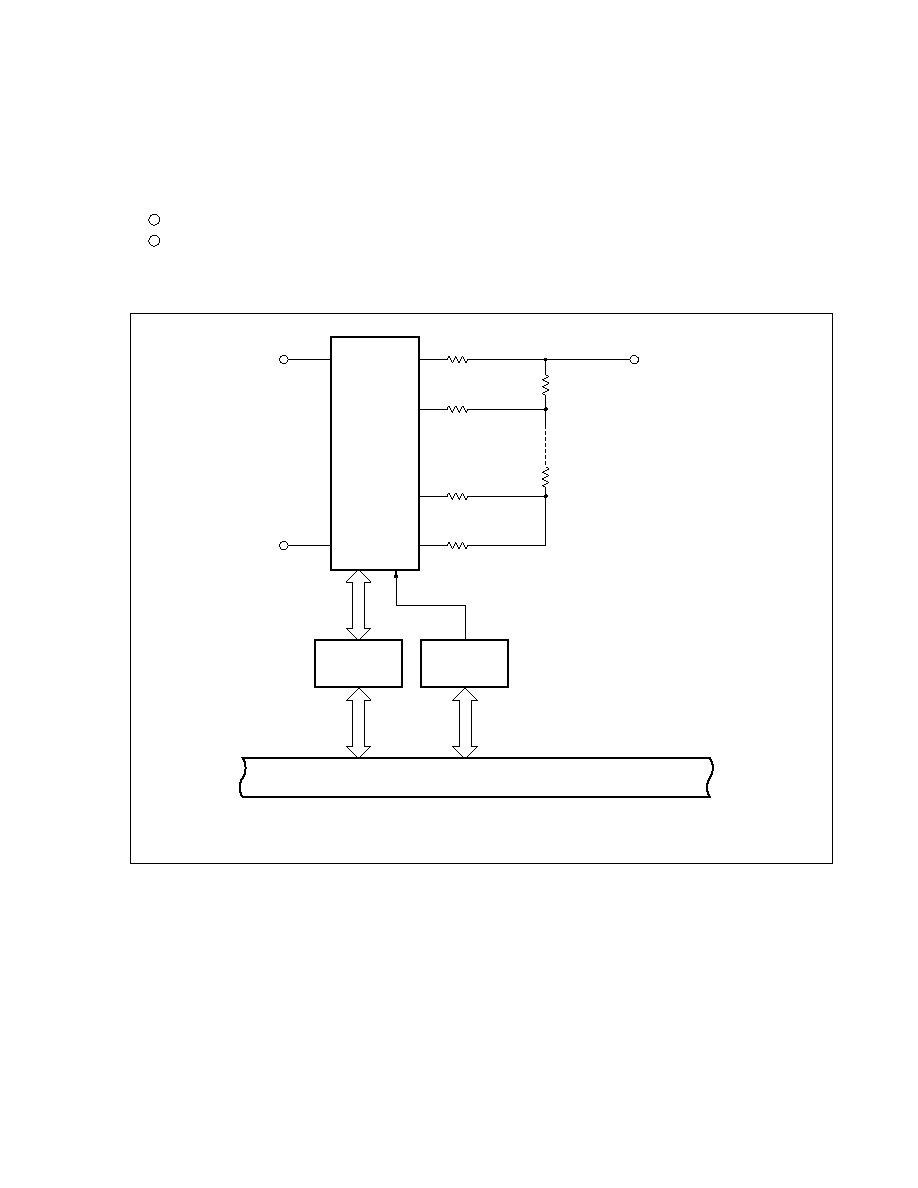
249
User's Manual U10913EJ6V0UM
CHAPTER 10 D/A CONVERTER
10.1 Features
8-bit resolution D/A converter: 2 channels
R-2R mode
10.2 Configuration
Remark
n = 0, 1
DACSn
DACEn
2R
2R
2R
2R
R
R
ANOn
AV
REF2
AV
REF3
Selector
Internal bus
250
CHAPTER 10 D/A CONVERTER
User's Manual U10913EJ6V0UM
10.3 Control Registers
(1) D/A converted data coefficient register (DACS0, DACS1)
The DACSn register writes the value to be output using the D/A conversion value setting register and outputs
the analog value to the ANOn pin (n = 0, 1).
This register can be read/written in 8-bit or 1-bit units.
(2) D/A converter mode register (DAM)
The DAM register controls the D/A converter.
This register can be read/written in 8-bit or 1-bit units. However, the higher 6 bits are fixed to 0 by hardware,
and even if 1 is written, it will be ignored.
Bit position
Bit name
Function
1, 0
DACEn
D/A Converter
Controls conversion operation of channel n.
DACEn
Channel n
ANOn pin
0
Operation disabled
High impedance
1
Operation enabled
Analog voltage output
Remark
n = 0, 1
7
DA07
DACS0
6
DA06
5
DA05
4
DA04
3
DA03
2
DA02
1
DA01
0
DA00
FFFFF3C2H
DA17
DACS1
DA16
DA15
DA14
DA13
DA12
DA11
DA10
00H
Address
FFFFF3C0H
After reset
00H
Address
FFFFF3D0H
7
0
DAM
6
0
5
0
4
0
3
0
2
0
1
DACE1
0
DACE0
After reset
03H

CHAPTER 10 D/A CONVERTER
251
User's Manual U10913EJ6V0UM
10.4 D/A Converter Operations
When values to be output are written in the DACSn register and analog voltage corresponding to the value written
from the ANOn pin is immediately output (n = 0, 1). The output voltage is held until the next time a value is written
in the DACSn register.
The output voltage from ANOn pin is determined by the following expression.
ANOn =
×
DACSn + AV
REF3
[V] (n = 1, 0)
10.4.1 D/A converter operation during reset
When system reset is generated by the RESET pin, the ANOn pin becomes high impedance. The DACSn register
is initialized to 00H. After reset is released, the ANOn pin outputs the AV
REF3
voltage until the DACSn register is set.
10.4.2 D/A converter operation during normal operation
When the value to be output is written in the DACSn register, and D/A converter operation is enabled by the DAM
register, the D/A converter performs D/A conversion and outputs the conversion results from the ANOn pin.
10.4.3 Operations during power save
(1) HALT mode
D/A conversion continues. When released by NMI input, the DACSn register and DAM register hold their
values.
(2) IDLE mode, software STOP mode
When the DACEn bit is 1, clock supply to the D/A converter is stopped. Therefore, although the ANOn pin
continues output, no new conversion operations are performed. When these modes are released by NMI input,
the DACSn register and DAM register hold their values.
To reduce the power consumption, set the DACSn register to 0 before setting the IDLE/software STOP mode
or set the voltage of the AV
REF2
pin and AV
REF3
pin to V
SS
.
AV
REF2
AV
REF3
256
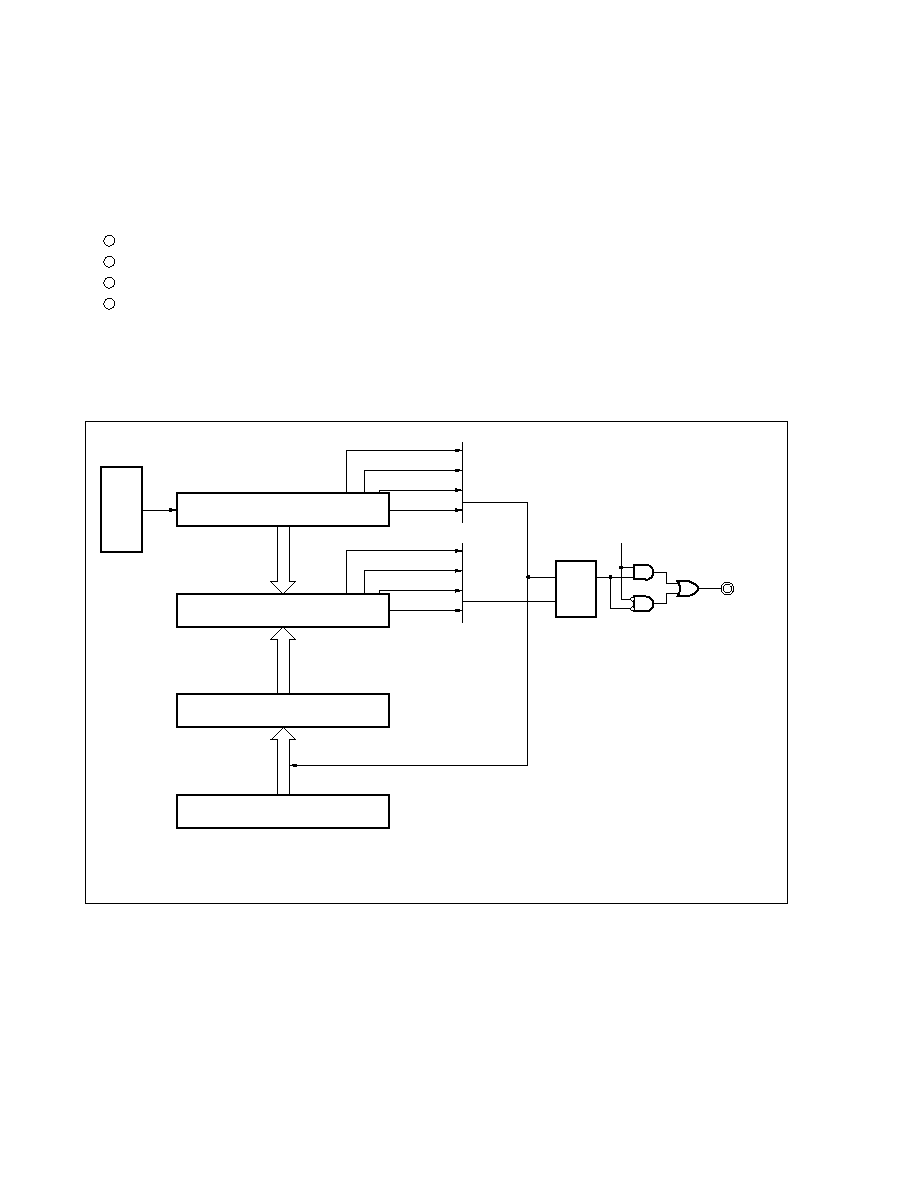
252
User's Manual U10913EJ6V0UM
CHAPTER 11 PWM UNIT
11.1 Features
PWMn: 2 channels
Active level of PWMn output pulse can be selected.
Operating clock: Can be selected from
,
/2,
/4,
/8, and
/16. (
is the internal system clock)
PWMn output resolution: Can be selected from 8, 9, 10, and 12 bits
Remark
n = 0, 1
11.2 Configuration
Note
Gives priority to reset
Remark
n = 0, 1
TMPn (12 bits)
Comparator
CMPn (12 bits)
PWMn (12 bits)
/2
/4
/8
/16
Overflow
Match
7
8
9
11
0 to 7
0 to 8
0 to 9
0 to 11
S
Q
R
Note
ALVn
PWMn

CHAPTER 11 PWM UNIT
253
User's Manual U10913EJ6V0UM
11.3 Control Registers
(1) PWM control register (PWMC)
Controls PWMn operation, specifies the output active level, and specifies the bit length of the timer counters
(TMPn) and compare registers (CMPn) (n = 0, 1).
This register can be read/written in 8-bit or 1-bit units.
Bit position
Bit name
Function
7, 3
PWMEn
PWM enable
Note
`
Controls PWM operation.
0: Stops operation
1: Enables operation
6, 2
ALVn
Active level
Specifies active levels of PWM.
0: Active-low
1: Active-high
5, 4, 1, 0
PRMn1,
Prescaler mode
PRMn0
Specifies bit length of counter (TMPn) and compare register (CMPn).
PRMn1 PRMn0
Bit length
0
0
8 bits
0
1
9 bits
1
0
10 bits
1
1
12 bits
Note
When PWMEn is set from 0 to 1, the counter (TMPn) is reset and counting starts from 000H (for 12
bits). The PWMn signal becomes active in the first overflow. By setting the bit length of PWM0 and
PWM1 and the operation clock (prescale value) to the same values, the timing at which the two PWMn
signals become active can be matched. Even if "1" is written to PWMEn when it is already set to 1,
the counter cannot be reset. Set "0" to it once, and then set "1" again.
Remark
n = 0, 1
Address
FFFFF360H
7
PWME1
PWMC
6
ALV1
5
PRM11
4
PRM10
3
PWME0
2
ALV0
1
PRM01
0
PRM00
After reset
00H
254
CHAPTER 11 PWM UNIT
User's Manual U10913EJ6V0UM
(2) PWM prescaler register (PWPR)
This register selects the operation clock of PWMn, and can be read/written in 8-bit or 1-bit units. However,
bit 7 and bit 3 are fixed to 0 by hardware, so writing 1 in these bits will be ignored.
Bit position
Bit name
Function
6 to 4, 2 to 0 PWPn2,
PWM prescaler clock mode
PWPn1,
Selects operation clock of PWMn.
PWPn0
PWPn2
PWPn1 PWPn0
Operation clock
0
0
0
0
0
1
/2
0
1
0
/4
0
1
1
/8
1
0
0
/16
Other than above
RFU (reserved)
Remark
n = 0, 1
Address
FFFFF362H
7
0
PWPR
6
PWP12
5
PWP11
4
PWP10
3
0
2
PWP02
1
PWP01
0
PWP00
After reset
00H
CHAPTER 11 PWM UNIT
255
User's Manual U10913EJ6V0UM
(3) PWM buffer registers (PWM0, PWM0L, PWM1, PWM1L)
These registers are 12-bit buffer registers that set the control data of the active signal width of the PWMn output.
Bits 15 to 12 are fixed to 0 by hardware, so even if 1 is written, it will be ignored. Bits 11 to 8 are not affected
by the bit length by the PWMC register, and the written values are read as they are.
During 16-bit access to this register, PWMn is specified. During lower 8-bit access, PWMnL is specified.
The contents of the PWMn and PWMnL registers are transmitted to the compare registers (CMPn) at the timing
at which the overflow from the PWMn output control counter (TMPn) is generated (n = 0, 1).
11.4 Operations
11.4.1 Basic operations
When outputting the PWMn pulse, after setting the data required for the PWPR register and PWMn register, the
PWMEn bits of the PWMC register should be set (1). This resets TMPn, the PWMn output is set to the active level,
and the data is transmitted from PWMn to CMPn upon the first overflow. After that, when TMPn and CMPn match,
the PWMn output becomes inactive. This is repeated and the active-level PWMn signal specified by the ALVn bit
of the PWMC register is output from the PWMn pin.
When the PWMEn bit of the PWMC register is cleared (0), the PWMn output unit stops PWMn output immediately,
and the PWMn output becomes the level of ALVn set by the PWMC register.
When the settings of the PWPn0 to PWPn2 bits and PRMn0 and PRMn1 bits are changed while the PWMn signal
is being output, the period width and pulse width of the PWMn signal in the changed period cannot be guaranteed.
15
0
PWM0
Address
FFFFF364H
After reset
Undefined
14
0
13
0
12
0
11
PWM11
10
PWM10
9
PWM9
8
PWM8
7
PWM7
6
PWM6
5
PWM5
4
PWM4
3
PWM3
2
PWM2
1
PWM1
0
PWM0
PWM0L
Address
FFFFF366H
After reset
Undefined
7
PWM7
6
PWM6
5
PWM5
4
PWM4
3
PWM3
2
PWM2
1
PWM1
0
PWM0
15
0
PWM1
Address
FFFFF368H
After reset
Undefined
14
0
13
0
12
0
11
PWM11
10
PWM10
9
PWM9
8
PWM8
7
PWM7
6
PWM6
5
PWM5
4
PWM4
3
PWM3
2
PWM2
1
PWM1
0
PWM0
PWM1L
Address
FFFFF36AH
After reset
Undefined
7
PWM7
6
PWM6
5
PWM5
4
PWM4
3
PWM3
2
PWM2
1
PWM1
0
PWM0
256
CHAPTER 11 PWM UNIT
User's Manual U10913EJ6V0UM
Figure 11-1. Basic Operation Timing of PWM
Figure 11-2. Operation Timing When 000H and FFFH Are Set in PWM Buffer Register
PWME0, PWME1
PWM timer overflow
PWM0, PWM1
CMP0, CMP1
CMP match
PWM output 0, 1
TMPn count starts
Full count
n count
n + 1 count
n
n + 1
xxx
n
n + 1
n + 2
PWM timer overflow
PWM0, PWM1
CMP0, CMP1
CMP match
PWM output 0, 1
FFFH count
n count
FFFH
n
FFFH
n
000H
000H
Active level is not set
1 count

CHAPTER 11 PWM UNIT
257
User's Manual U10913EJ6V0UM
11.4.2 Repeating frequency
The repeating frequency of the PWMn is shown below.
PWMn Operation Frequency
Resolution
Repeating Frequency
8 bits
/2
8
9 bits
/2
9
10 bits
/2
10
12 bits
/2
12
/2
8 bits
/2
9
9 bits
/2
10
10 bits
/2
11
12 bits
/2
13
/4
8 bits
/2
10
9 bits
/2
11
10 bits
/2
12
12 bits
/2
14
/8
8 bits
/2
11
9 bits
/2
12
10 bits
/2
13
12 bits
/2
15
/16
8 bits
/2
12
9 bits
/2
13
10 bits
/2
14
12 bits
/2
16
11.5 Caution
The PWM0 pin and PWM1 pin are also used as P20 and P21 of port 2. When using them as a PWMn output,
set the bit corresponding to the PMC2 register to 1.
When the setting of the corresponding bit of the PMC2 register is changed during PWMn pulse output, the PWMn
pulse output cannot be guaranteed.

258
User's Manual U10913EJ6V0UM
CHAPTER 12 PORT FUNCTION
12.1 Features
The ports of the V853 have the following features.
Number of pins: Input: 8
I/O:
67
Multiplexed with I/O pins of other peripheral functions
Can be set in input/output mode in 1-bit units
Noise elimination
Edge detection
259
CHAPTER 12 PORT FUNCTION
User's Manual U10913EJ6V0UM
12.2 Basic Configuration of Port
The V853 is provided with a total of 75 input/output port pins (of which eight are input-only port pins) that make
up ports 0 to 11. The configuration of the V853's ports is shown below.
Port 0
P00
to
P07
Port 1
P10
to
P17
Port 2
P20
to
P27
Port 3
P30
to
P37
Port 4
P40
to
P47
Port 5
P50
to
P57
Port 6
P60
to
P63
Port 7
Port 9
P70
to
P77
P90
to
P96
Port 11
P110
to
P117

260
CHAPTER 12 PORT FUNCTION
User's Manual U10913EJ6V0UM
(1) Function of each port
The ports of the V853 have the functions shown in the table below.
Each port can be manipulated in 8-bit or 1-bit units and performs various types of control operations. In addition
to port functions, the ports also have functions as internal hardware I/O pins, when placed in the control mode.
Port Name
Port Function
Function in Control Mode
Remarks
Port 0
8-bit I/O port
Real-time pulse unit (RPU) I/O
Can be set to port or control
Can be set to input or
External interrupt input
mode in 1-bit units.
output mode in 1-bit
A/D converter external trigger input
units.
(Port 6 is a 4-bit port.)
Port 1
Real-time pulse unit (RPU) I/O
External interrupt input
Serial interface (CSI2) I/O
Port 2
PWM0, PWM1 output
Serial interface (UART0/CSI0, UART1/CSI1)
I/O
Port 3
Real-time pulse unit (RPU) I/O
External interrupt input
Serial interface (CSI3) I/O
Port 4
Address/data bus (AD0 to AD7) for external memory
Can be set to port or control
Port 5
Address/data bus (AD8 to AD15) for external memory
mode in 8-bit units.
Port 6
Address bus (A16 to A19) for external memory
Can be set to port or control
mode in 2-bit units.
Port 7
8-bit input only port
A/D converter (ADC) analog input
--
Port 9
7-bit I/O port
Control signal output for external memory
Can be set to port or control
Can be set to input or
Control signal I/O for system expansion
mode in 5- or 1-bit units.
output mode in 1-bit
units.
Port 11
8-bit I/O port
Real-time pulse unit (RPU) I/O
Can be set to port or control
Can be set to input or
External interrupt input
mode in 1-bit units.
output mode in 1-bit
units.
Caution Be sure to follow the following steps when switching a port that operates as an output pin or an
I/O pin in control mode, to the control mode.
<1> Set the inactive level of the signal output in the control mode to the relevant bit of port n
(Pn) (n = 0 to 6, 9 and 11).
<2> Switch to the control mode by the port n mode control register (PMCn).
If the above <1> is not executed, the contents of port n (Pn) may be output momentarily when
switching from the port mode to the control mode.

261
CHAPTER 12 PORT FUNCTION
User's Manual U10913EJ6V0UM
(2) Register for setting function after reset and port/control mode of each port pin
(1/2)
Port Name
Pin Name
Function After Reset
Register for
In Single-Chip Mode
Setting Mode
Port 0
P00/TO110
P00 (Input mode)
PMC0
P01/TO111
P01 (Input mode)
P02/TCLR11
P02 (Input mode)
P03/TI11
P03 (Input mode)
P04/INTP110
P04 (Input mode)
P05/INTP111
P05 (Input mode)
P06/INTP112
P06 (Input mode)
P07/INTP113/ADTRG
P07 (Input mode)
PMC0, ADM1
Note
Port 1
P10/TO120
P10 (Input mode)
PMC1
P11/TO121
P11 (Input mode)
P12/TCLR12
P12 (Input mode)
P13/TI12
P13 (Input mode)
P14/INTP120
P14 (Input mode)
P15/INTP121/SO2
P15 (Input mode)
PMC1, PCM
Note
P16/INTP122/SI2
P16 (Input mode)
P17/INTP123/SCK2
P17 (Input mode)
Port 2
P20/PWM0
P20 (Input mode)
PMC2
P21/PWM1
P21 (Input mode)
P22/TXD0/SO0
P22 (Input mode)
PMC2, ASIM00
Note
P23/RXD0/SI0
P23 (Input mode)
P24/SCK0
P24 (Input mode)
PMC2
P25/TXD1/SO1
P25 (Input mode)
PMC2, ASIM10
Note
P26/RXD1/SI1
P26 (Input mode)
P27/SCK1
P27 (Input mode)
PMC2
Port 3
P30/TO130
P30 (Input mode)
PMC3
P31/TO131
P31 (Input mode)
P32/TCLR13
P32 (Input mode)
P33/TI13
P33 (Input mode)
P34/INTP130
P34 (Input mode)
P35/INTP131/SO3
P35 (Input mode)
PMC3, PCM
Note
P36/INTP132/SI3
P36 (Input mode)
P37/INTP133/SCK3
P37 (Input mode)
Port 4
P40/AD0 to P47/AD7
P40 to P47 (All input mode)
MM
Port 5
P50/AD8 to P57/AD15
P50 to P57 (All input mode)
MM
Port 6
P60/A16 to P63/A19
P60 to P63 (All input mode)
MM
Port 7
P70/ANI0 to P77/ANI7
P70/ANI0 to P77/ANI7
--
Note
Select the pin function in the control mode.

262
CHAPTER 12 PORT FUNCTION
User's Manual U10913EJ6V0UM
(2/2)
Port Name
Pin Name
Function After Reset
Register for
In Single-Chip Mode
Setting Mode
Port 9
P90/LBEN
P90 (Input mode)
MM
P91/UBEN
P91 (Input mode)
P92/R/W
P92 (Input mode)
P93/DSTB
P93 (Input mode)
P94/ASTB
P94 (Input mode)
P95/HLDAK
P95 (Input mode)
P96/HLDRQ
P96 (Input mode)
Port 11
P110/TO140
P110 (Input mode)
PMC11
P111/TO141
P111 (Input mode)
P112/TCLR14
P112 (Input mode)
P113/TI14
P113 (Input mode)
P114/INTP140
P114 (Input mode)
P115/INTP141
P115 (Input mode)
P116/INTP142
P116 (Input mode)
P117/INTP143
P117 (Input mode)

263
CHAPTER 12 PORT FUNCTION
User's Manual U10913EJ6V0UM
12.3 Port Pin Functions
12.3.1 Port 0
Port 0 is an 8-bit I/O port that can be set to input or output mode in 1-bit units.
Bit position
Bit name
Function
7 to 0
P0n
Port 0
(n = 7 to 0)
I/O port
In addition to the function as a general I/O port, this port can also be used to input/output signals of the real-time
pulse unit (RPU), input external interrupt requests, and input the A/D converter external trigger when placed in the
control mode.
Operation in control mode
Port
Control Mode
Remarks
Port 0
P00
TO110
Real-time pulse unit (RPU) output
P01
TO111
P02
TCLR11
Real-time pulse unit (RPU) input
P03
TI11
P04 to P06
INTP110 to INTP112
External interrupt input
P07
INTP113/ADTRG
External interrupt input, A/D converter external trigger input
7
P07
P0
6
P06
5
P05
4
P04
3
P03
2
P02
1
P01
0
P00
Address
FFFFF000H
After reset
Undefined
264
CHAPTER 12 PORT FUNCTION
User's Manual U10913EJ6V0UM
(1) Hardware configuration
Figure 12-1. Block Diagram of P00 and P01 (Port 0)
Remark n = 0, 1
Figure 12-2. Block Diagram of P02 to P07 (Port 0)
Remark n = 2 to 7
WR
PMC
WR
PM
PMC0n
PM0n
P0n
WR
PORT
RD
IN
Address
TO11n
P0n
Selector
Selector
Selector
Internal bus
WR
PMC
WR
PM
PMC0n
PM0n
P0n
WR
PORT
RD
IN
P0n
Selector
Selector
Internal bus
INTP110 to INTP112,
INTP113/ADTRG
TCLR11, TI11
Noise elimination
Edge detection
Address

265
CHAPTER 12 PORT FUNCTION
User's Manual U10913EJ6V0UM
(2) Setting input/output mode and control mode
The input/output mode of port 0 is set by the port 0 mode register (PM0). The control mode is set by the port
0 mode control register (PMC0).
Port 0 mode register (PM0)
This register can be read/written in 8-bit or 1-bit units.
Bit position
Bit name
Function
7 to 0
PM00 to PM07
Port Mode
Sets P00 to P07 pins to input/output mode.
0: Output mode (output buffer on)
1: Input mode (output buffer off)
7
PM07
PM0
6
PM06
5
PM05
4
PM04
3
PM03
2
PM02
1
PM01
0
PM00
Address
FFFFF020H
After reset
FFH

266
CHAPTER 12 PORT FUNCTION
User's Manual U10913EJ6V0UM
Port 0 mode control register (PMC0)
This register can be read/written in 8-bit or 1-bit units.
Bit position
Bit name
Function
7
PMC07
Port mode Control
Sets operation mode of P07 pin.
0: I/O port mode
1: External interrupt request input (INTP113)/A/D converter external trigger
input (ADTRG)
Note
6 to 4
PMC06 to
Port Mode Control
PMC04
Sets operation mode of P0n pin (n = 6 to 4).
0: I/O port mode
1: External interrupt request input (INTP112 to INTP110)
3
PMC03
Port Mode Control
Sets operation mode of P03 pin.
0: I/O port mode
1: TI11 input mode
2
PMC02
Port Mode Control
Sets operation mode of P02 pin.
0: I/O port mode
1: TCLR11 input mode
1
PMC01
Port Mode Control
Sets operation mode of P01 pin.
0: I/O port mode
1: TO111 output mode
0
PMC00
Port Mode Control
Sets operation mode of P00 pin.
0: I/O port mode
1: TO110 output mode
Note
The P07 pin functions as the A/D converter external trigger input (ADTRG) when the PMC07 bit
is 1 and the TRG bit of the A/D converter mode register (ADM1) is set in the external trigger mode.
7
PMC07
PMC0
6
PMC06
5
PMC05
4
PMC04
3
PMC03
2
PMC02
1
PMC01
0
PMC00
Address
FFFFF040H
After reset
00H
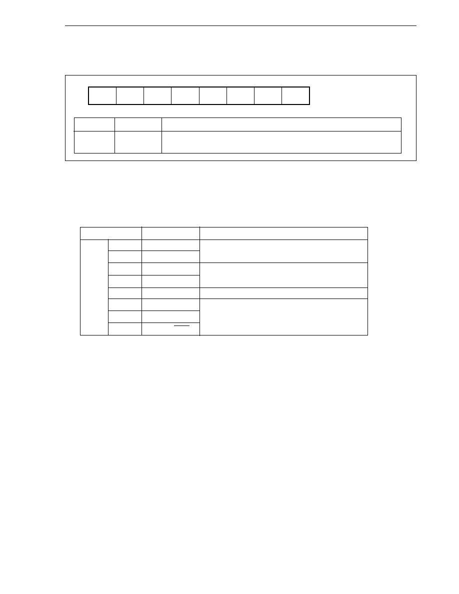
267
CHAPTER 12 PORT FUNCTION
User's Manual U10913EJ6V0UM
12.3.2 Port 1
Port 1 is an 8-bit I/O port that can be set to input or output mode in 1-bit units.
Bit position
Bit name
Function
7 to 0
P1n
Port 1
(n = 7 to 0)
I/O port
In addition to the function as a general I/O port, this port can also be used to input/output signals of the real-time
pulse unit (RPU), input external interrupts, and input/output signals of the serial interface (CSI2), when placed in the
control mode.
Operations in control mode
Port
Control Mode
Remarks
Port 1
P10
TO120
Real-time pulse unit (RPU) output
P11
TO121
P12
TCLR12
Real-time pulse unit (RPU) input
P13
TI12
P14
INTP120
External interrupt input
P15
INTP121/SO2
External interrupt input
P16
INTP122/SI2
Serial interface (CSI2) input/output
P17
INTP123/SCK2
7
P17
P1
6
P16
5
P15
4
P14
3
P13
2
P12
1
P11
0
P10
Address
FFFFF002H
After reset
Undefined
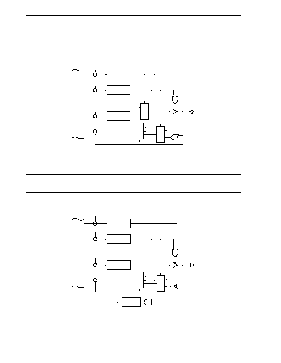
268
CHAPTER 12 PORT FUNCTION
User's Manual U10913EJ6V0UM
(1) Hardware configuration
Figure 12-3. Block Diagram of P10 and P11 (Port 1)
Remark n = 0, 1
Figure 12-4. Block Diagram of P12 to P14 (Port 1)
Remark n = 2 to 4
Internal bus
PMC1n
PM1n
P1n
Selector
Selector
RD
IN
Address
WR
PORT
WR
PM
WR
PMC
TO12n
P1n
Selector
Internal bus
PMC1n
PM1n
P1n
Selector
Selector
RD
IN
Address
WR
PORT
WR
PM
WR
PMC
P1n
TCLR12, TI12
INTP120
Noise elimination
Edge detection
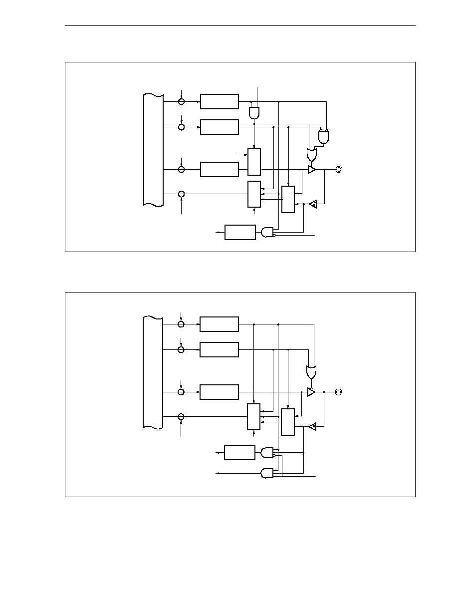
269
CHAPTER 12 PORT FUNCTION
User's Manual U10913EJ6V0UM
Figure 12-5. Block Diagram of P15 (Port 1)
Figure 12-6. Block Diagram of P16 (Port 1)
Internal bus
PMC15
PM15
P15
Selector
Selector
RD
IN
Address
WR
PORT
WR
PM
WR
PMC
P15
INTP121
Noise elimination
Edge detection
Selector
SO2
PCM1
PCM1
Internal bus
PMC16
PM16
P16
Selector
Selector
RD
IN
Address
WR
PORT
WR
PM
WR
PMC
P16
INTP122
Noise elimination
Edge detection
SI2
PCM1
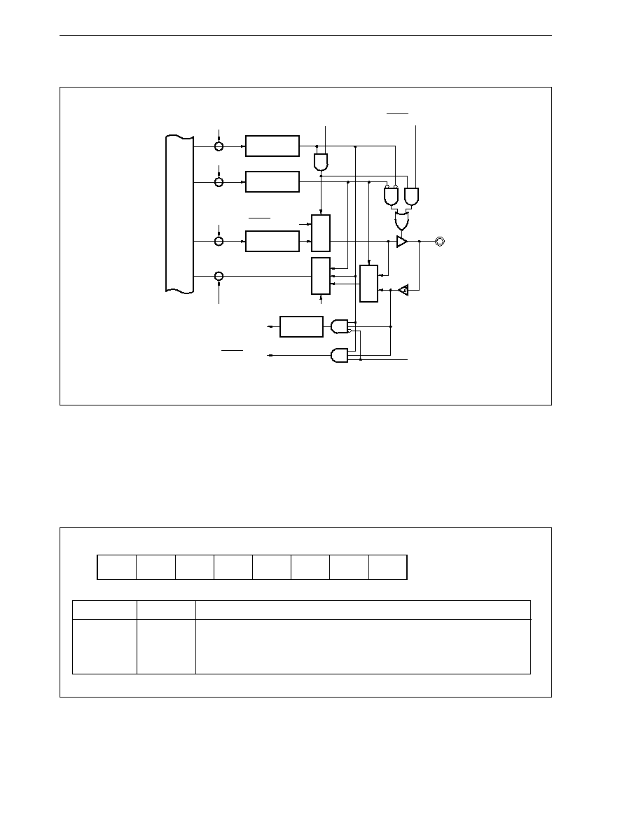
270
CHAPTER 12 PORT FUNCTION
User's Manual U10913EJ6V0UM
Figure 12-7. Block Diagram of P17 (Port 1)
(2) Setting input/output mode and control mode
The input/output mode of port 1 is set by the port 1 mode register (PM1). The control mode is set by the port
1 mode control register (PMC1) and port control mode register (PCM).
Port 1 mode register (PM1)
This register can be read/written in 8-bit or 1-bit units.
Bit position
Bit name
Function
7 to 0
PM1n
Port Mode
(n = 7 to 0)
Sets P1n pin to input/output mode.
0: Output mode (output buffer on)
1: Input mode (output buffer off)
Internal bus
PMC17
PM17
P17
Selector
Selector
RD
IN
Address
WR
PORT
WR
PM
WR
PMC
P17
INTP123
Noise elimination
Edge detection
SCK2 input
Selector
PCM1
SCK2 output
SCK2 I/O switch
PCM1
7
PM17
PM1
6
PM16
5
PM15
4
PM14
3
PM13
2
PM12
1
PM11
0
PM10
Address
FFFFF022H
After reset
FFH
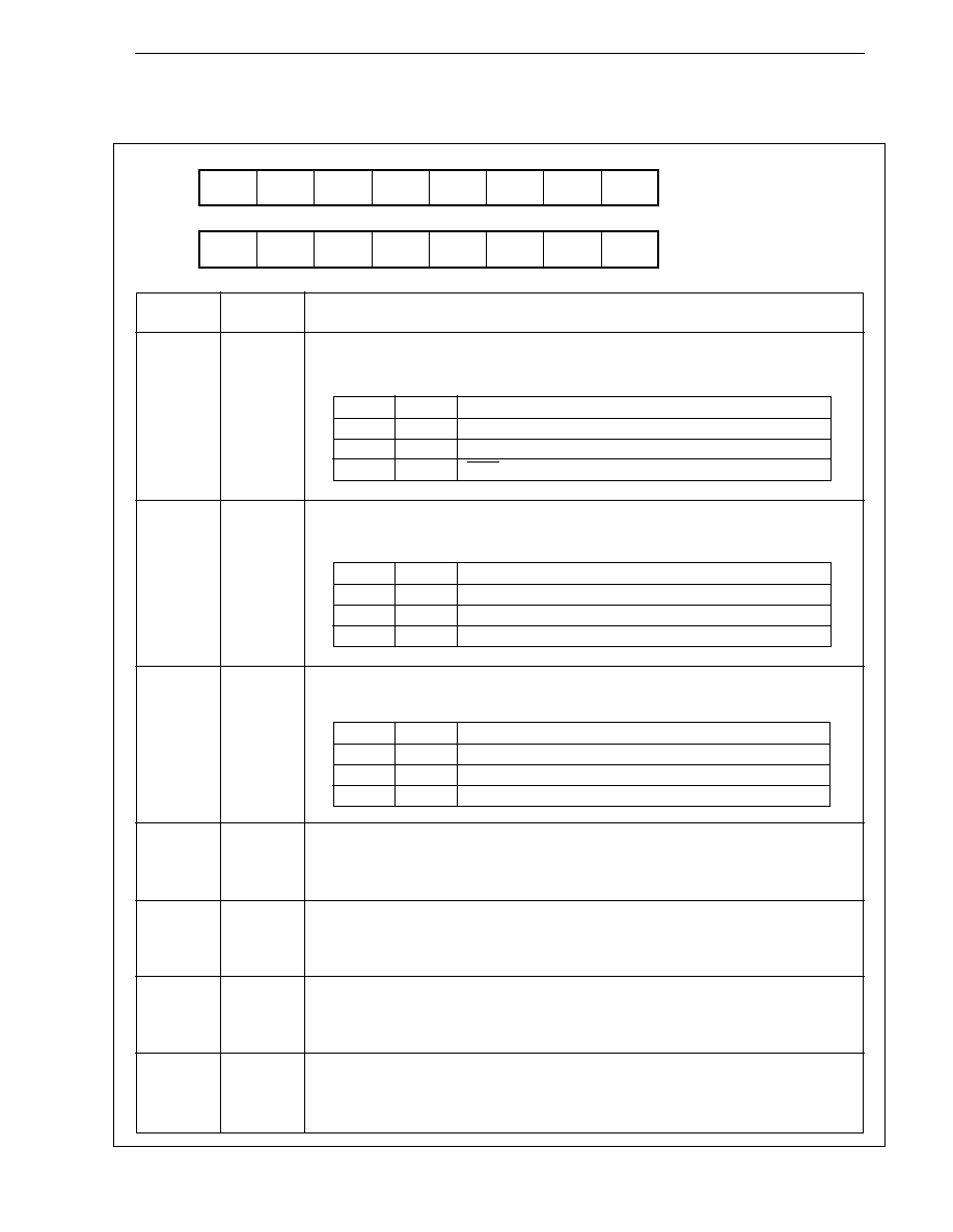
271
CHAPTER 12 PORT FUNCTION
User's Manual U10913EJ6V0UM
Port 1 mode control register (PMC1)
This register can be read/written in 8-bit or 1-bit units.
Bit position
Bit name
Function
(PMC1)
7
PMC17
Port Mode Control
Sets operation mode of P17 pin. Set in combination with PCM1.
PMC17
PCM1
Function
0
x
I/O port mode
1
0
INTP 123 input mode
1
1
SCK2 I/O mode
6
PMC16
Port Mode Control
Sets operation mode of P16 pin. Set in combination with PCM1.
PMC16
PCM1
Function
0
x
I/O port mode
1
0
INTP122 input mode
1
1
SI2 input mode
5
PMC15
Port Mode Control
Sets operation mode of P15 pin. Set in combination with PCM1.
PMC15
PCM1
Function
0
x
I/O port mode
1
0
INTP121 input mode
1
1
SO2 output mode
4
PMC14
Port Mode Control
Sets operation mode of P14 pin.
0: I/O port mode
1: INTP120 input mode
3
PMC13
Port Mode Control
Sets operation mode of P13 pin.
0: I/O port mode
1: TI12 input mode
2
PMC12
Port Mode Control
Sets operating mode of P12 pin.
0: I/O port mode
1: TCLR12 input mode
1, 0
PMC11,
Port Mode Control
PMC10
Sets operation mode of P11, P10 pin.
0: I/O port mode
1: TO121, TO120 output mode
For the description of PCM, refer to Port control mode register (PCM) in section 12.4.
7
PMC17
PMC1
6
PMC16
5
PMC15
4
PMC14
3
PMC13
2
PMC12
1
PMC11
0
PMC10
FFFFF05CH
0
PCM
0
0
0
PCM3
0
PCM1
0
00H
Address
FFFFF042H
After reset
00H

272
CHAPTER 12 PORT FUNCTION
User's Manual U10913EJ6V0UM
12.3.3 Port 2
Port 2 is an 8-bit I/O port that can be set to input or output mode in 1-bit units.
Bit position
Bit name
Function
7 to 0
P2n
Port 2
(n = 7 to 0)
I/O port
In addition to the function as a port, this port can also be used to output PWM0 and PWM1 and input/output signals
of the serial interface (UART0/CSI0, UART1/CSI1), when placed in the control mode.
Operation in control mode
Port
Control Mode
Remarks
Port 2
P20
PWM0
PWM0 and PWM1 outputs
P21
PWM1
P22
TXD0/SO0
I/O for serial interface (UART0/CSI0,
P23
RXD0/SI0
UART1/CSI1)
P24
SCK0
P25
TXD1/SO1
P26
RXD1/SI1
P27
SCK1
7
P27
P2
6
P26
5
P25
4
P24
3
P23
2
P22
1
P21
0
P20
Address
FFFFF004H
After reset
Undefined
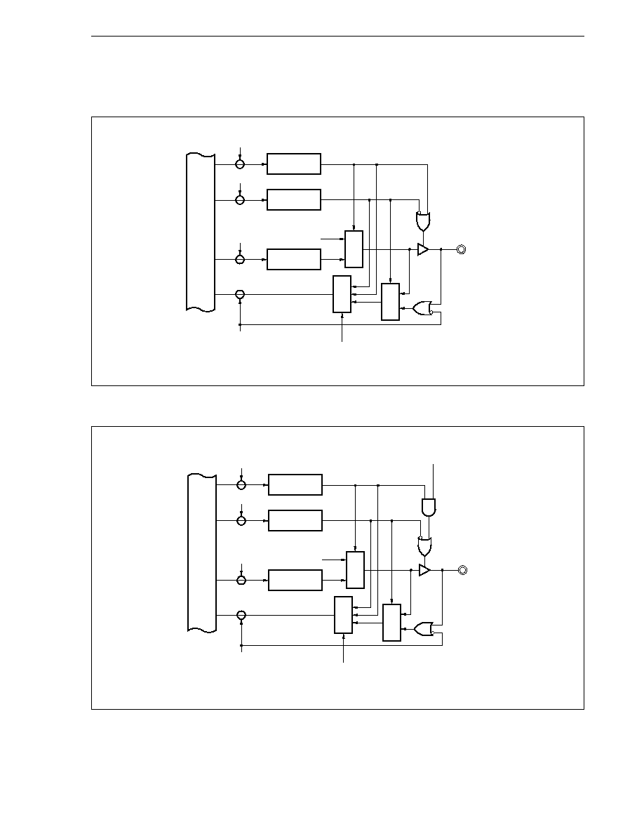
273
CHAPTER 12 PORT FUNCTION
User's Manual U10913EJ6V0UM
(1) Hardware configuration
Figure 12-8. Block Diagram of P20 and P21 (Port 2)
Remark n = 0, 1
Figure 12-9. Block Diagram of P22 and P25 (Port 2)
Remark n = 2, 5
Internal bus
PMC2n
PM2n
P2n
Selector
Selector
Selector
RD
IN
Address
WR
PORT
WR
PM
WR
PMC
PWM0, PWM1
P2n
Internal bus
PMC2n
PM2n
P2n
Selector
Selector
Selector
RD
IN
Address
WR
PORT
WR
PM
WR
PMC
TXD0/SO0
TXD1/SO1
P2n
SO0, SO1
output enable
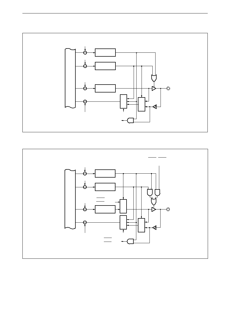
274
CHAPTER 12 PORT FUNCTION
User's Manual U10913EJ6V0UM
Figure 12-10. Block Diagram of P23 and P26 (Port 2)
Remark n = 3, 6
Figure 12-11. Block Diagram of P24 and P27 (Port 2)
Remark n = 4, 7
Internal bus
PMC2n
PM2n
P2n
Selector
Selector
RD
IN
Address
WR
PORT
WR
PM
WR
PMC
P2n
RXD0/SI0
RXD1/SI1
Internal bus
PMC2n
PM2n
P2n
Selector
Selector
RD
IN
Address
WR
PORT
WR
PM
WR
PMC
P2n
SCK0 input,
SCK1 input
Selector
SCK0 output,
SCK1 output
SCK0, SCK1
I/O switch

275
CHAPTER 12 PORT FUNCTION
User's Manual U10913EJ6V0UM
(2) Setting input/output mode and control mode
The input/output mode of port 2 is set by the port 2 mode register (PM2). The control mode is set by the port
2 mode control register (PMC2).
Port 2 mode register (PM2)
This register can be read/written in 8-bit or 1-bit units.
Bit position
Bit name
Function
7 to 0
PM2n
Port Mode
(n = 7 to 0)
Sets P2n pin to input/output mode.
0: Output mode (output buffer on)
1: Input mode (output buffer off)
7
PM27
PM2
6
PM26
5
PM25
4
PM24
3
PM23
2
PM22
1
PM21
0
PM20
Address
FFFFF024H
After reset
FFH

276
CHAPTER 12 PORT FUNCTION
User's Manual U10913EJ6V0UM
Port 2 mode control register (PMC2)
This register can be read/written in 8-bit or 1-bit units.
Bit position
Bit name
Function
7
PMC27
Port Mode Control
Sets operation mode of P27 pin.
0: I/O port mode
1: SCK1 I/O mode
6
PMC26
Port Mode Control
Sets operation mode of P26 pin.
0: I/O port mode
1: RXD1/SI1 input mode
5
PMC25
Port Mode control
Sets operation mode of P25 pin.
0: I/O port mode
1: TXD1/SO1 output mode
4
PMC24
Port Mode Control
Sets operation mode of P24 pin.
0: I/O port mode
1: SCK0 I/O mode
3
PMC23
Port Mode Control
Sets operation mode of P23 pin.
0: I/O port mode
1: RXD0/SI0 input mode
2
PMC22
Port Mode Control
Sets operation mode of P22 pin.
0: I/O port mode
1: TXD0/SO0 output mode
0, 1
PMC21,
Port Mode Control
PMC20
Sets operation mode of P21 and P20 pin.
0: I/O port mode
1: PWM1, PWM0 output mode
7
PMC27
PMC2
6
PMC26
5
PMC25
4
PMC24
3
PMC23
2
PMC22
1
PMC21
0
PMC20
Address
FFFFF044H
After reset
00H
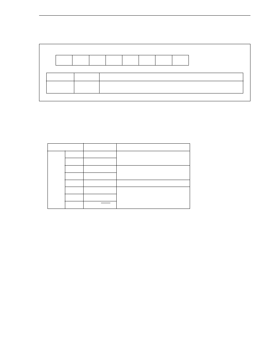
277
CHAPTER 12 PORT FUNCTION
User's Manual U10913EJ6V0UM
12.3.4 Port 3
Port 3 is an 8-bit I/O port that can be set to input or output mode in 1-bit units.
Bit position
Bit name
Function
7 to 0
P3n
Port 3
(n = 7 to 0)
I/O port
In addition to the function as a port, this port can also be used to input /output signals of the real-time pulse unit
(RPU), input signals of external interrupt, and input/output signals of the serial interface (CSI3), when placed in the
control mode.
Operation in control mode
Port
Control Mode
Remarks
Port 3
P30
TO130
Real-time pulse unit (RPU) I/O
P31
TO131
P32
TCLR13
Real-time pulse unit (RPU) input
P33
TI13
P34
INTP130
External interrupt input
P35
INTP131/SO3
External interrupt input
P36
INTP132/SI3
Serial interface (CSI3) I/O
P37
INTP133/SCK3
7
P37
P3
6
P36
5
P35
4
P34
3
P33
2
P32
1
P31
0
P30
Address
FFFFF006H
After reset
Undefined
278
CHAPTER 12 PORT FUNCTION
User's Manual U10913EJ6V0UM
(1) Hardware configuration
Figure 12-12. Block Diagram of P30 and P31 (Port 3)
Remark n = 0, 1
Figure 12-13. Block Diagram of P32 to P34 (Port 3)
Remark n = 2 to 4
WR
PMC
WR
PM
PMC3n
PM3n
P3n
WR
PORT
RD
IN
Address
TO13n
P3n
Selector
Selector
Selector
Internal bus
Internal bus
PMC3n
PM3n
P3n
Selector
Selector
RD
IN
Address
WR
PORT
WR
PM
WR
PMC
P3n
TCLR13, TI13
INTP130
Noise elimination
Edge detection
279
CHAPTER 12 PORT FUNCTION
User's Manual U10913EJ6V0UM
Figure 12-14. Block Diagram of P35 (Port 3)
Figure 12-15. Block Diagram of P36 (Port 3)
Internal bus
PMC35
PM35
P35
Selector
Selector
RD
IN
Address
WR
PORT
WR
PM
WR
PMC
P35
INTP131
Selector
PCM3
SO3
SO3 output
enable
Noise elimination
Edge detection
PCM3
PUO3
V
DD
P
N
P
Internal bus
PMC36
PM36
P36
Selector
Selector
RD
IN
Address
WR
PORT
WR
PM
WR
PMC
P36
INTP132
Noise elimination
Edge detection
PCM3
PUO3
V
DD
P
N
SI3
P
280
CHAPTER 12 PORT FUNCTION
User's Manual U10913EJ6V0UM
Figure 12-16. Block Diagram of P37 (Port 3)
(2) Setting input/output mode and control mode
The input/output mode of port 3 is set by the port 3 mode register (PM3). The control mode is set by the port
3 mode control register (PMC3) and port control mode register (PCM).
Port 3 mode register (PM3)
This register can be read/written in 8-bit or 1-bit units.
Bit position
Bit name
Function
7 to 0
PM3n
Port Mode
(n = 7 to 0)
Sets P3n pin to input/output mode.
0: Output mode (output buffer on)
1: Input mode (output buffer off)
7
PM37
PM3
6
PM36
5
PM35
4
PM34
3
PM33
2
PM32
1
PM31
0
PM30
Address
FFFFF026H
After reset
FFH
Internal bus
PMC37
PM37
P37
Selector
Selector
RD
IN
Address
WR
PORT
WR
PM
WR
PMC
P37
INTP133
Noise elimination
Edge detection
PCM3
PUO3
V
DD
P
N
SCK3 input
Selector
SCK3 output
P
SCK3 I/O switch
PCM3
281
CHAPTER 12 PORT FUNCTION
User's Manual U10913EJ6V0UM
Port 3 mode control register (PMC3)
This register can be read/written in 8-bit or 1-bit units.
(1/2)
Bit position
Bit name
Function
(PMC1)
7
PMC37
Port Mode Control
Sets operation mode of P37 pin. Set in combination with PCM3.
PMC37
PCM3
Function
0
x
I/O port mode
1
0
INTP133 input mode
1
1
SCK3 input/output mode
6
PMC36
Port Mode Control
Sets operation mode of P36 pin. Set in combination with PCM3.
PMC36
PCM3
Function
0
x
I/O port mode
1
0
INTP132 input mode
1
1
SI3 input mode
5
PMC35
Port Mode Control
Sets operation mode of P35 pin. Set in combination with PCM3.
PMC35
PCM3
Function
0
x
I/O port mode
1
0
INTP131 input mode
1
1
SO3 output mode
4
PMC34
Port Mode Control
Sets operation mode of P34 pin.
0: I/O port mode
1: INTP130 input mode
3
PMC33
Port Mode Control
Sets operation mode of P33 pin.
0: I/O port mode
1: TI13 input mode
Address
FFFFF046H
7
PMC37
PMC3
6
PMC36
5
PMC35
4
PMC34
3
PMC33
2
PMC32
1
PMC31
0
PMC30
After reset
00H
FFFFF05CH
0
PCM
0
0
0
PCM3
0
PCM1
0
00H

282
CHAPTER 12 PORT FUNCTION
User's Manual U10913EJ6V0UM
(2/2)
Bit position
Bit name
Function
(PMC1)
2
PMC32
Port Mode Control
Sets operation mode of P32 pin.
0: I/O port mode
1: TCLR13 input mode
1
PMC31
Port Mode Control
Sets operation mode of P31 pin.
0: I/O port mode
1: TO131 output mode
0
PMC30
Port Mode Control
Sets operation mode of P30 pin.
0: I/O port mode
1: TO130 output mode
For the description of PCM, refer to Port control mode register (PCM) in section 12.4.
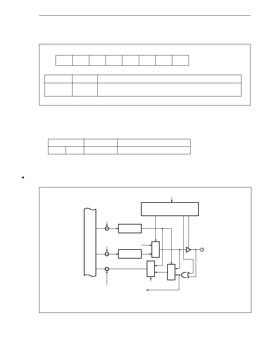
283
CHAPTER 12 PORT FUNCTION
User's Manual U10913EJ6V0UM
12.3.5 Port 4
Port 4 is an 8-bit I/O port that can be set to input or output mode in 1-bit units.
Bit position
Bit name
Function
7 to 0
P4n
Port 4
(n = 7 to 0)
I/O port
In addition to the function as a general I/O port, this port also serves as an external address/data bus for external
memory expansion, when placed in the control mode (external expansion mode).
Operation in control mode
Port
Control Mode
Remarks
Port 4
P40 to 47
AD0 to AD7
Address/data bus for external memory
(1) Hardware configuration
Figure 12-17. Block Diagram of P40 to P47 (Port 4)
Remark n = 0 to 7
7
P47
P4
6
P46
5
P45
4
P44
3
P43
2
P42
1
P41
0
P40
Address
FFFFF008H
After reset
Undefined
Internal bus
PM4n
P4n
Selector
Selector
Selector
RD
IN
Address
WR
PORT
WR
PM
AD0 to AD7 output
P4n
AD0 to AD7 input
I/O controller
MM0 to MM2
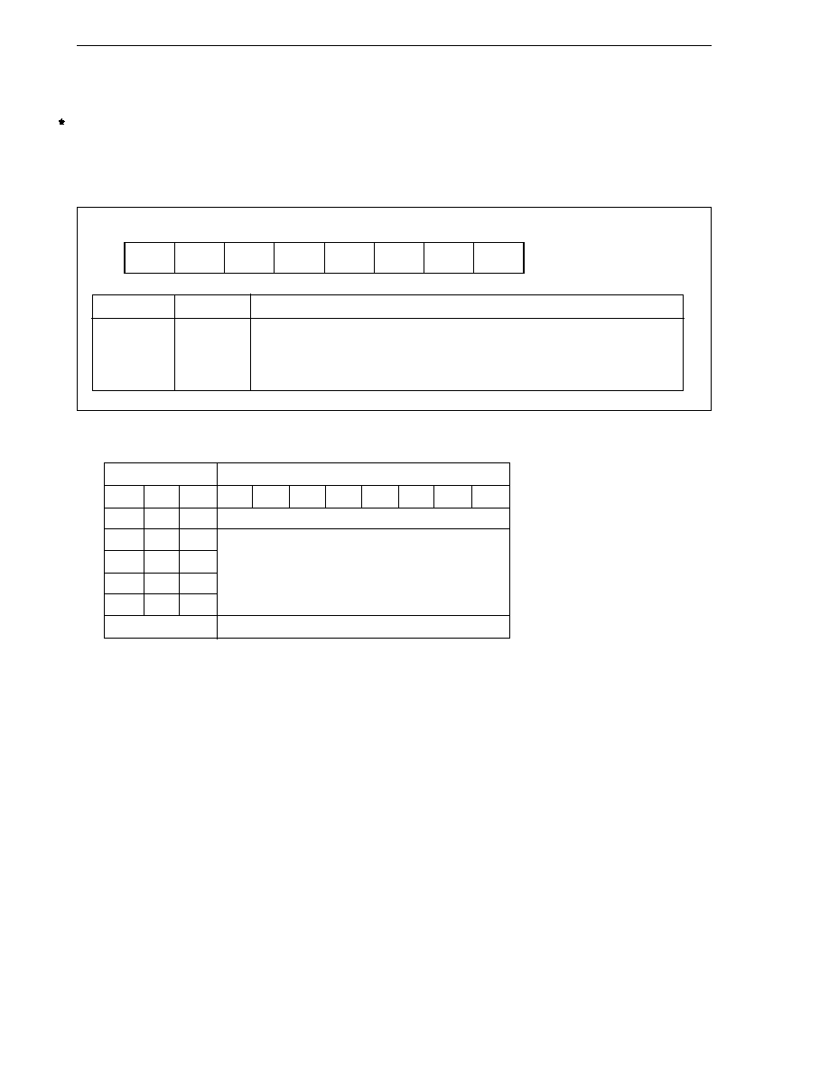
284
CHAPTER 12 PORT FUNCTION
User's Manual U10913EJ6V0UM
(2) Setting input/output mode and control mode
The input/output mode of port 4 is set by the port 4 mode register (PM4). The control mode (external expansion
mode) is set by the memory expansion mode register (MM: refer to 3.4.7).
Port 4 mode register (PM4)
This register can be read/written in 8-bit or 1-bit units.
Bit position
Bit name
Function
7 to 0
PM4n
Port Mode
(n = 7 to 0)
Sets P4n pin to input/output mode.
0: Output mode (output buffer on)
1: Input mode (output buffer off)
Operation mode of port 4
Bit of MM Register
Operation Mode
MM2
MM1
MM0
P40
P41
P42
P43
P44
P45
P46
P47
0
0
0
Port
0
1
1
1
0
0
Address/data bus
1
0
1
(AD0 to AD7)
1
1
1
Other than above
RFU (reserved)
Address
FFFFF028H
7
PM47
PM4
6
PM46
5
PM45
4
PM44
3
PM43
2
PM42
1
PM41
0
PM40
After reset
FFH
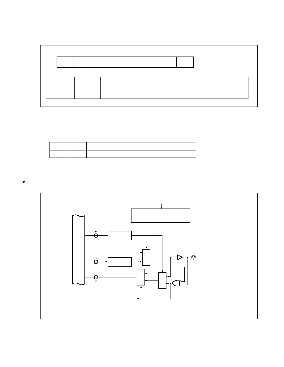
285
CHAPTER 12 PORT FUNCTION
User's Manual U10913EJ6V0UM
12.3.6 Port 5
Port 5 is an 8-bit I/O port that can be set to input or output mode in 1-bit units.
Bit position
Bit name
Function
7 to 0
P5n
Port 5
(n = 7 to 0)
I/O port
In addition to the function as a general I/O port, this port also serves as an external address/data bus for external
memory expansion, when placed in the control mode (external expansion mode).
Operation in control mode
Port
Control Mode
Remarks
Port 5
P50 to 57
AD8 to AD15
Address/data bus for external memory
(1) Hardware configuration
Figure 12-18. Block Diagram of P50 to P57 (Port 5)
Remark n = 0 to 7
7
P57
P5
6
P56
5
P55
4
P54
3
P53
2
P52
1
P51
0
P50
Address
FFFFF00AH
After reset
Undefined
Internal bus
PM5n
P5n
Selector
Selector
Selector
RD
IN
Address
WR
PORT
WR
PM
AD8 to AD15 output
P5n
AD8 to AD15 input
I/O controller
MM0 to MM2
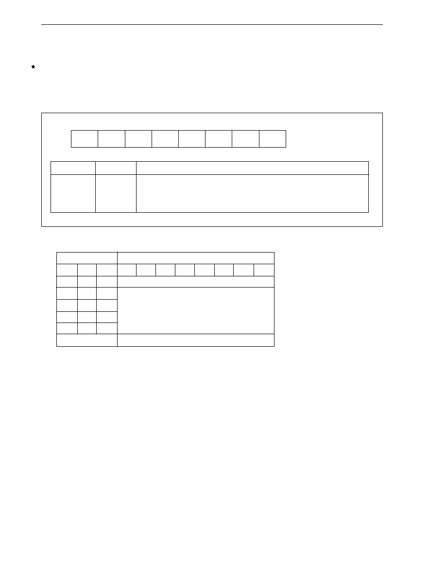
286
CHAPTER 12 PORT FUNCTION
User's Manual U10913EJ6V0UM
(2) Setting input/output mode and control mode
The input/output mode of port 5 is set by the port 5 mode register (PM5). The control mode (external expansion
mode) is set by the memory expansion mode register (MM: refer to 3.4.7).
Port 5 mode register (PM5)
This register can be read/written in 8-bit or 1-bit units.
Bit position
Bit name
Function
7 to 0
PM5n
Port Mode
(n = 7 to 0)
Sets P5n pin to input/output mode.
0: Output mode (output buffer on)
1: Input mode (output buffer off)
Operation mode of port 5
Bit of MM Register
Operation Mode
MM2
MM1
MM0
P50
P51
P52
P53
P54
P55
P56
P57
0
0
0
Port
0
1
1
1
0
0
Address/data bus
1
0
1
(AD8 to AD15)
1
1
1
Other than above
RFU (reserved)
7
PM57
PM5
6
PM56
5
PM55
4
PM54
3
PM53
2
PM52
1
PM51
0
PM50
Address
FFFFF02AH
After reset
FFH
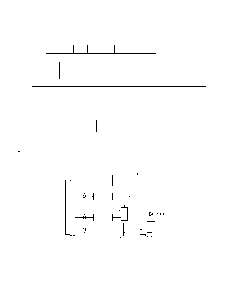
287
CHAPTER 12 PORT FUNCTION
User's Manual U10913EJ6V0UM
12.3.7 Port 6
Port 6 is a 4-bit I/O port that can be set to input or output mode in 1-bit units.
Bit position
Bit name
Function
3 to 0
P6n
Port 6
(n = 3 to 0)
I/O port
In addition to the function as a general I/O port, this port also serves as an external address bus for external memory
expansion, when placed in the control mode (external expansion mode). When port 6 is accessed in 8-bit units for
write, the higher 4 bits are ignored. When it is accessed in 8-bit units for read, undefined data is read.
Operation in control mode
Port
Control Mode
Remarks
Port 6
P60 to 63
A16 to A19
Address bus for external memory
(1) Hardware configuration
Figure 12-19. Block Diagram of P60 to P63 (Port 6)
Remark n = 0 to 3
7
--
P6
6
--
5
--
4
--
3
P63
2
P62
1
P61
0
P60
Address
FFFFF00CH
After reset
Undefined
Internal bus
PM6n
P6n
Selector
Selector
Selector
RD
IN
Address
WR
PORT
WR
PM
A16 to A19 output
P6n
I/O controller
MM0 to MM2
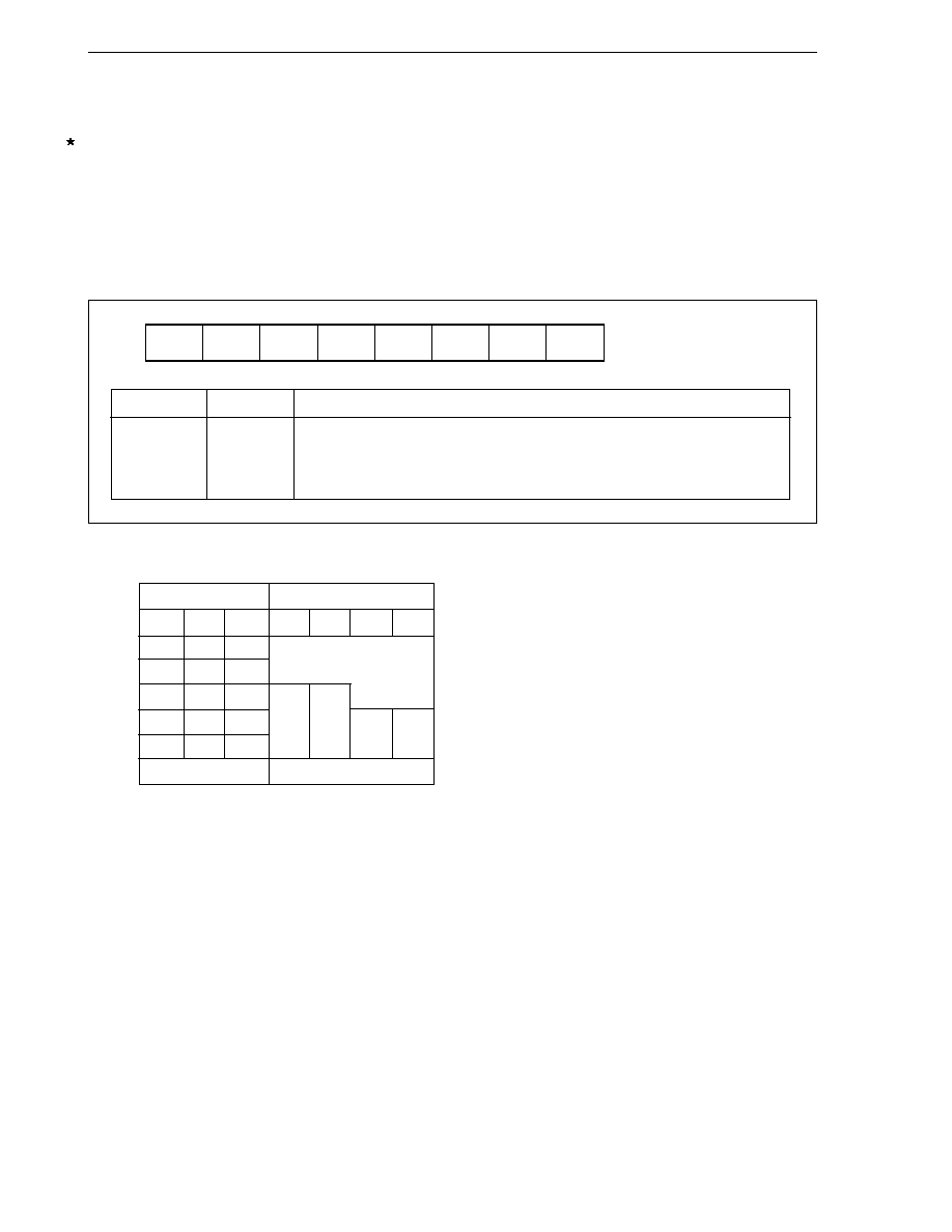
288
CHAPTER 12 PORT FUNCTION
User's Manual U10913EJ6V0UM
(2) Setting input/output mode and control mode
The input/output mode of port 6 is set by the port 6 mode register (PM6). To enable the external address/
data bus function, the control mode (external expansion mode) is set by the memory expansion mode register
(MM: refer to 3.4.7).
Port 6 mode register (PM6)
This register can be read/written in 8-bit or 1-bit units. However, the higher 4 bits are ignored if the access is
a write, and undefined if the access is a read.
Bit position
Bit name
Function
3 to 0
PM6n
Port Mode
(n = 3 to 0)
Sets P6n pin to input/output mode.
0: Output mode (output buffer on)
1: Input mode (output buffer off)
Operation mode of port 6
Bit of MM Register
Operation Mode
MM2
MM1
MM0
P60
P61
P62
P63
0
0
0
Port
0
1
1
1
0
0
1
0
1
1
1
1
Other than above
RFU (reserved)
A16
A17
A18
A19
7
PM6
6
5
4
3
PM63
2
PM62
1
PM61
0
PM60
Address
FFFFF02CH
After reset
XFH
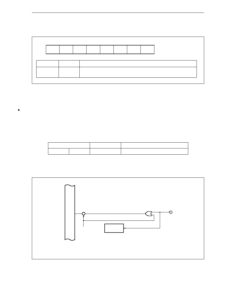
289
CHAPTER 12 PORT FUNCTION
User's Manual U10913EJ6V0UM
12.3.8 Port 7
Port 7 is an 8-bit input-only port and all the pins of port 7 are fixed to the input mode.
Bit position
Bit name
Function
7 to 0
P7n
Port 7
(n = 7 to 0)
Input-only port
In addition to the function as a port, this port can also be used to input analog voltages for the A/D converter in
the control mode.
This port is used also as the analog input pins (ANI0 to ANI7), but the input port and analog input pin cannot be
switched. By reading the port, the state of each pin can be read.
The value read from the pin specified as the analog input pin is undefined. In addition, do not read the P7 value
during A/D conversion. When some pins of port 7 are used as analog inputs, the rest of the pins cannot be used
as input port pins (for example, when the ANI0 to ANI2 pins are used as A/D converter inputs, do not use the P73
to P77 pins as input port pins).
Operation in control mode
Port
Control Mode
Remarks
Port 7
P70 to P77
ANI0 to ANI7
Analog input for A/D converter
Figure 12-20. Block Diagram of P70 to P77 (Port 7)
Remark n = 0 to 7
Address
FFFFF0EH
7
P77
P7
6
P76
5
P75
4
P74
3
P73
2
P72
1
P71
0
P70
After reset
Undefined
Internal bus
RD
IN
P7n
ANI0 to ANI7
Sample & hold
circuit
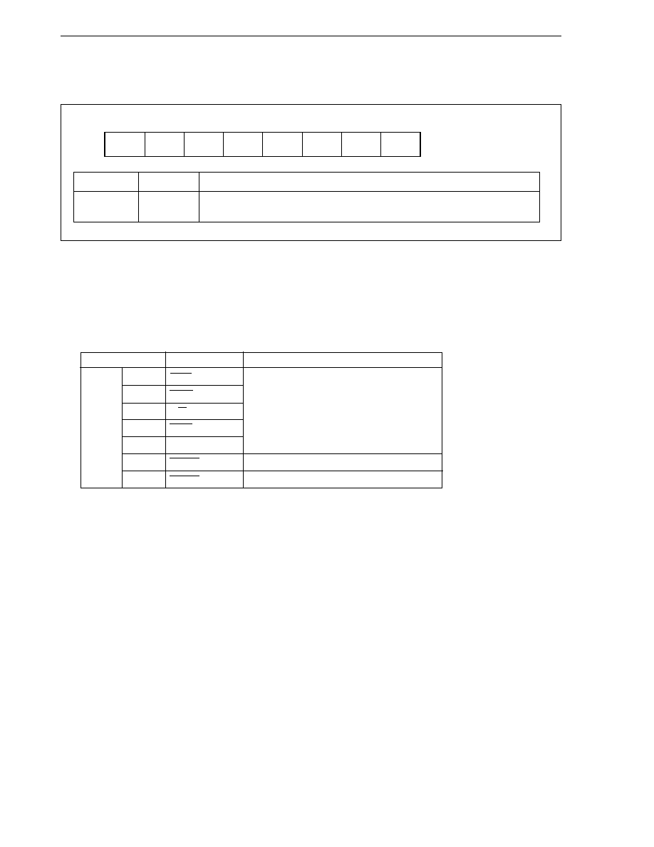
290
CHAPTER 12 PORT FUNCTION
User's Manual U10913EJ6V0UM
12.3.9 Port 9
Port 9 is a 7-bit I/O port that can be set to input or output mode in 1-bit units.
Bit position
Bit name
Function
6 to 0
P9n
Port 9
(n = 6 to 0)
I/O port
In addition to the function as a general I/O port, this port can also be used to output external bus control signals
and output bus hold control signals, when placed in the control mode (external expansion mode). When port 9 is
accessed in 8-bit units for write, the highest bit is ignored. When it is accessed in 8-bit units for read, undefined data
is read.
Operation in control mode
Port
Control Mode
Remarks
Port 9
P90
LBEN
Control signal output for external memory
P91
UBEN
P92
R/W
P93
DSTB
P94
ASTB
P95
HLDAK
Bus hold acknowledge signal output
P96
HLDRQ
Bus hold request signal input
Address
FFFFF012H
7
P9
6
P96
5
P95
4
P94
3
P93
2
P92
1
P91
0
P90
After reset
Undefined
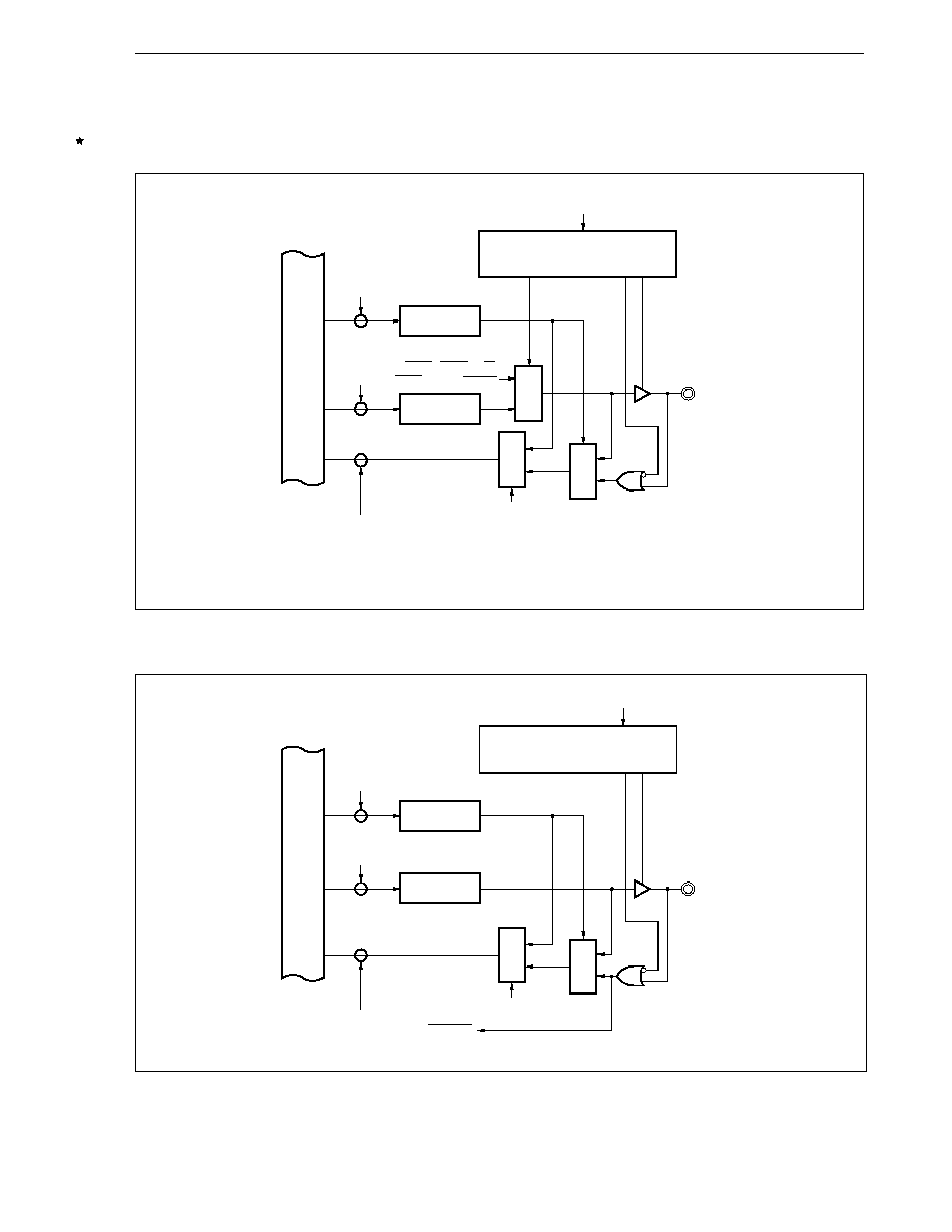
291
CHAPTER 12 PORT FUNCTION
User's Manual U10913EJ6V0UM
(1) Hardware configuration
Figure 12-21. Block Diagram of P90 to P95 (Port 9)
Remark
n = 0 to 5
Figure 12-22. Block Diagram of P96 (Port 9)
Internal bus
PM9n
P9n
Selector
Selector
Selector
RD
IN
Address
WR
PORT
WR
PM
LBEN, UBEN, R/W,
DSTB, ASTB, HLDAK
P9n
I/O controller
MM0 to MM3
Internal bus
PM96
P96
Selector
Selector
RD
IN
Address
WR
PORT
WR
PM
P96
I/O controller
MM3
HLDRQ
292
CHAPTER 12 PORT FUNCTION
User's Manual U10913EJ6V0UM
(2) Setting input/output mode and control mode
The input/output mode of port 9 is set by the port 9 mode register (PM9). The control mode (external expansion
mode) is set by the memory expansion mode register (MM: refer to 3.4.7).
Port 9 mode register (PM9)
This register can be read/written in 8- or 1-bit units. However, bit 7 is ignored if the access is a write, and
undefined if the access is a read.
Bit position
Bit name
Function
6 to 0
PM9n
Port Mode
(n = 6 to 0)
Sets P9n pin to input/output mode.
0: Output mode (output buffer on)
1: Input mode (output buffer off)
Operation mode of port 9
P90 to P94
P95, P96
Bit of MM Register
Operation Mode
MM3
Operation Mode
P95
P96
MM2
MM1
MM0
P90
P91
P92
P93
P94
0
Port mode Port
0
0
0
Port
1
External expansion mode
HLDAK HLDRQ
0
1
1
LBEN UBEN
R/W
DSTB ASTB
1
0
0
1
0
1
1
1
1
Other than above
RFU (reserved)
7
PM9
6
PM96
5
PM95
4
PM94
3
PM93
2
PM92
1
PM91
0
PM90
Address
FFFFF032H
After reset
X1111111B
293
CHAPTER 12 PORT FUNCTION
User's Manual U10913EJ6V0UM
12.3.10 Port 11
Port 11 is an 8-bit I/O port that can be set to input or output mode in 1-bit units.
Bit position
Bit name
Function
7 to 0
P11n
Port 11
(n = 7 to 0)
I/O port
In addition to the function as a port, this port can also be used to input/output signals of the real-time pulse unit
(RPU) and input external interrupt requests, when placed in the control mode.
Operation in control mode
Port
Control Mode
Remarks
Port 11
P110
TO140
Real-time pulse unit (RPU) output
P111
TO141
P112
TCLR14
Real-time pulse unit (RPU) input
P113
TI14
P114 to P117
INTP140 to
External interrupt request input
INTP143
Address
FFFFF016H
7
P117
P11
6
P116
5
P115
4
P114
3
P113
2
P112
1
P111
0
P110
After reset
Undefined
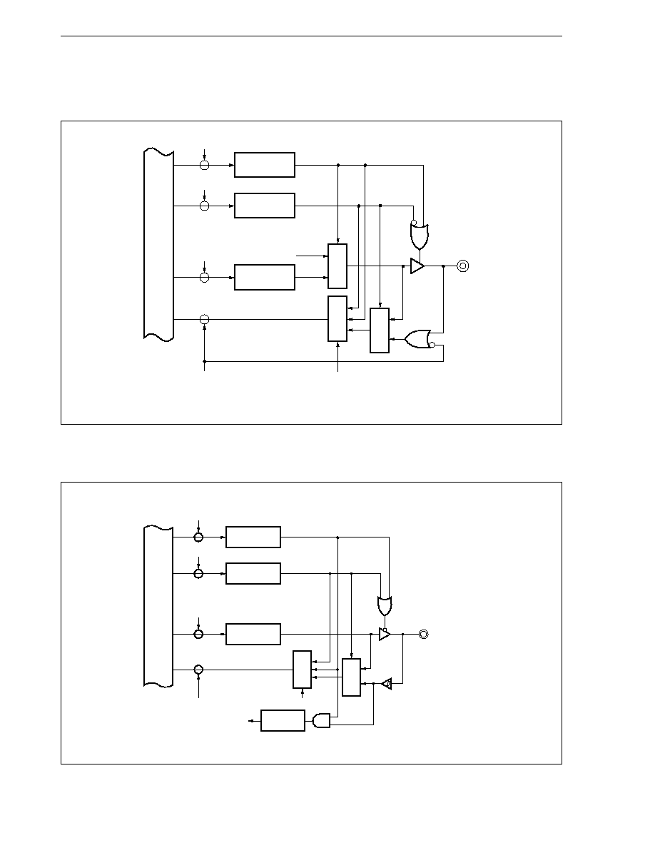
294
CHAPTER 12 PORT FUNCTION
User's Manual U10913EJ6V0UM
(1) Hardware configuration
Figure 12-23. Block Diagram of P110 and P111 (Port 11)
Remark
n = 0, 1
Figure 12-24. Block Diagram of P112 to P117 (Port 11)
Remark
n = 2 to 7
WR
PMC
WR
PM
PMC11n
PM11n
P11n
WR
PORT
RD
IN
Address
TO14n
P11n
Selector
Selector
Selector
Internal bus
Internal bus
PMC11n
PM11n
P11n
Selector
Selector
RD
IN
Address
WR
PORT
WR
PM
WR
PMC
P11n
TCLR14, TI14
INTP140 to INTP143
Noise elimination
Edge detection

295
CHAPTER 12 PORT FUNCTION
User's Manual U10913EJ6V0UM
(2) Setting input/output mode and control mode
The input/output mode of port 11 is set by the port 11 mode register (PM11). The control mode is set by the
port 11 mode control register (PMC11).
Port 11 mode register (PM11)
This register can be read/written in 8-bit or 1-bit units.
Bit position
Bit name
Function
7 to 0
PM11n
Port Mode
(n = 7 to 0)
Sets P10n pin to input/output mode.
0: Output mode (output buffer on)
1: Input mode (output buffer off)
Port 11 mode control register (PMC11)
This register can be read/written in 8-bit or 1-bit units.
Bit position
Bit name
Function
7 to 4
PMC117 to
Port Mode Control
PMC114
Sets operation mode of P117 to P114
0: I/O port mode
1: INTP143 to INTP140 input mode
3
PMC113
Port Mode Control
Sets operation mode of P113 pin.
0: I/O port mode
1: TI14 input mode
2
PMC112
Port Mode Control
Sets operation mode of P112 pin
0: I/O port mode
1: TCLR14 input mode
1, 0
PMC111,
Port Mode Control
PMC110
Sets operation mode of P111, P110 pin.
0: I/O port mode
1: TO141, TO140 output mode
Address
FFFFF036H
7
PM117
PM11
6
PM116
5
PM115
4
PM114
3
PM113
2
PM112
1
PM111
0
PM110
After reset
FFH
Address
FFFFF056H
7
PMC117
PMC11
6
PMC116
5
PMC115
4
PMC114
3
PMC113
2
PMC112
1
PMC111
0
PMC110
After reset
00H

296
CHAPTER 12 PORT FUNCTION
User's Manual U10913EJ6V0UM
12.4
Switching Between External Maskable Interrupt Request Input/Timer External Capture
Trigger Input and CSI Pins
The higher 3 bits of port 1 of the V853 are used by the external maskable interrupt request input/timer external
capture trigger input (INTP121 to INTP123) as well as the CSI2 output (S02, SI2, SCK2) together in the control mode.
The higher 3 bits of port 3 are used by the external maskable interrupt request input/timer external capture trigger
input (INTP131 to INTP133) as well as the CSI3 output (S03, SI3, SCK3) together in the control mode.
The switching of these pins can be specified in units of the above 3 bits by software using the port control mode
register (PCM).
Port control mode register (PCM)
This register can be read/written in 8-bit or 1-bit units. However, bits other than bit 1 and bit 3 are fixed to
0 by hardware, so even if 1 is written, it is ignored.
Bit position
Bit name
Function
3
PCM3
Port Control Mode
Sets operation mode of P37 to P35 pins.
0: INTP133 to INTP131 input mode
1: CSI3 input/output mode
1
PCM1
Port Control Mode
Sets operation mode of P17 to P15 pins.
0: INTP123 to INTP121 input mode
1: CSI2 input/output mode
Caution When the port mode is specified using the PMC1 and PMC3 registers, the setting of this register
is invalid.
Address
FFFFF05CH
7
0
PCM
6
0
5
0
4
0
3
PCM3
2
0
1
PCM1
0
0
After reset
00H

297
CHAPTER 12 PORT FUNCTION
User's Manual U10913EJ6V0UM
Unselected functions operate as follows.
(1) CSI operations when the INTP signal input mode is selected
Even when the INTP signal is selected, the CSI2, CSI3, and BRG3 registers can be accessed. However, serial
data input and serial clock input from the pins, and serial data output and serial clock output to the pins can
not be performed.
To reduce power consumption, it is recommended that CSI2 and CSI3 be set to the transmission/reception
disabled state and BRG3 to the count operation stopped state during INTP signal input mode.
(2) Timer (TM12, TM13), external maskable interrupt operations in CSI2 and CSI3 I/O mode
Although an external maskable interrupt can be specified by the corresponding INTP signal using the timer
unit mode register (TUM2, TUM3) in the CSI2 and CSI3 I/O mode, the external maskable interrupt function
cannot be used.
Although it is possible to specify the corresponding capture/compare register for the capture register using
TUM2 and TUM3, because capture trigger input cannot be performed using the INTP signal, the capture
register function cannot be used. There are no restrictions on other timer functions.

298
CHAPTER 12 PORT FUNCTION
User's Manual U10913EJ6V0UM
12.5 Specifying Pull-up Resistors
The V853 has on-chip pull-up resistors, which can be specified for use at the higher three bits (P35 to P37) of port
3 by means of software.
Whether to use an internal pull-up resistor can be specified for each pin using the pull-up resistor option register
(PUO) and port mode register (PM).
When PUO3 is 1, if the corresponding bit is set to the input mode in the PM3 register, the internal pull-up resistor
becomes valid.
Pull-up resistor option register (PUO)
This register can be read/written in 8-bit or 1-bit units. However, bits other than bit 3 are fixed to 0 by hardware,
so even if 1 is written, it is ignored. Set in combination with the PM3 register.
Bit position
Bit name
Function
(PUO)
3
PUO3
Pull-up Option
Specifies the internal pull-up resistor of the P3n pin.
PUO3
PM3n
Function
0
0
Pull-up resistor not used
0
1
1
0
1
1
Pull-up resistor used
Remark
n = 7 to 5
For the description of PM3 register, refer to Port 3 mode register (PM3) in section 12.3.4 (2).
7
0
PUO
6
0
5
0
4
0
3
PUO3
2
0
1
0
0
0
FFFFF026H
PM37
PM3
PM36
PM35
PM34
PM33
PM32
PM31
PM30
FFH
Address
FFFFF05EH
After reset
00H

299
User's Manual U10913EJ6V0UM
CHAPTER 13 RESET FUNCTION
When a low level is input to the RESET pin, the system is reset and each on-chip hardware is initialized to its initial
state.
When the RESET pin changes from low level to high level, the reset state is released and the CPU starts executing
the program. Initialize the contents of each register in the program as necessary.
13.1 Features
Analog noise eliminator (delay of approx. 60 ns) provided on reset pin
13.2 Pin Function
During the reset state, all the pins (except CLKOUT, RESET, X2, V
DD
, V
SS
, CV
DD
/CKSEL, CV
SS
, AV
DD
, AV
SS
, and
the AV
REF1
to AV
REF3
pins) are in the high-impedance state.
When an external memory is connected, a pull-up (or pull-down) resistor must be connected to each pin of ports
4, 5, 6, and 9. Otherwise, the memory contents may be lost if these pins go into a high-impedance state.
Also handle the signal outputs of the on-chip peripheral I/O functions and the output ports so that they will not be
affected.
In the single-chip mode, the CLKOUT signal is not output until the PSC register is set.
Table 13-1 shows the operating status of each pin during the reset period.
Table 13-1. Operating Status of Each Pin During Reset Period
Pin
Operating Status
AD0 to AD15
Hi-Z
A16 to A19
LBEN, UBEN
R/W
DSTB
ASTB
HLDRQ
HLDAK
Hi-Z
WAIT
CLKOUT
Hi-Z
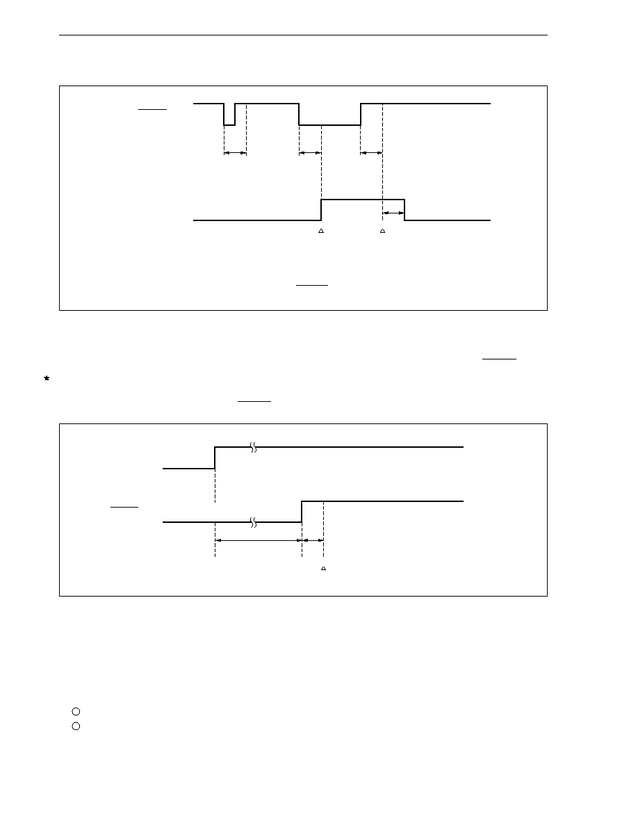
300
CHAPTER 13 RESET FUNCTION
User's Manual U10913EJ6V0UM
(1) Acknowledging reset signal
Note
The internal system reset signal remains active for the duration of at least 4 system clocks after
the reset condition is removed from the RESET pin.
(2) Power-on reset
In the reset operations at power-on (when the power is turned on), oscillation stabilization time must be secured
from the start up of the power until reset is acknowledged by the low-level width
Note
of the RESET pin.
Sufficiently evaluate the oscillation stabilization time.
Note
Retain a low-level input at RESET pin from power on to reset signal acknowledgement.
13.3 Initialize
Table 13-2 shows the initial value of each register after reset.
The contents of the registers must be initialized in the program as necessary. Especially, set the following registers
as necessary because they are related to system setting.
Power save control register (PSC) ... X1 and X2 pin function, CLKOUT pin operation, etc.
Data wait control register (DWC) ... Number of data wait states
V
DD
RESET pin
Oscillation
stabilization
time
Analog delay
Reset released
RESET pin
Internal system
reset signal
Analog
delay
Eliminated as noise
Analog
delay
Analog
delay
Note
Reset
acknowledged
Reset
released

301
CHAPTER 13 RESET FUNCTION
User's Manual U10913EJ6V0UM
Table 13-2. Initial Values of Each Register After Reset (1/2)
Register
Initial Value After Reset
r0
00000000H
r1 to r31
Undefined
PC
00000000H
PSW
00000020H
EIPC
Undefined
EIPSW
Undefined
FEPC
Undefined
FEPSW
Undefined
ECR
00000000H
Internal RAM
Undefined
Port
I/O latch (P0 to P6, P9, P11)
Undefined
Input latch (P7)
Undefined
Mode register (PM0 to PM5, PM11)
FFH
Mode register (PM6)
×
FH
Mode register (PM9)
×
1111111B
Mode control register (PMC0 to PMC3, PMC11)
00H
Memory expansion mode register (MM)
00H
Port control mode register (PCM)
00H
Pull-up resistor option register (PUO)
00H
Clock generator
Clock control register (CKC)
00H/03H
System status register (SYS)
0000000
×
B
Real-time pulse unit
Timer unit mode register (TUM11 to TUM14)
0000H
Timer control register (TMC11 to TMC14, TMC4)
00H
Timer output control register 1 (TOC11 to TOC14)
00H
Timer (TM11 to TM14, TM4)
0000H
Capture/compare register (CC110 to CC113,
Undefined
CC120 to CC123, CC130 to CC133, CC140 to CC143)
Compare register 4 (CM4)
Undefined
Timer overflow status register (TOVS)
00H
A/D converter
A/D converter mode register (ADM0)
00H
A/D converter mode register (ADM1)
07H
A/D conversion result register
Undefined
(ADCR0 to ADCR7, ADCR0H to ADCR7H)
D/A converter
D/A-converted data coefficient register (DACS0, DACS1)
00H
D/A converter mode register (DAM)
03H
Remark
×
: Don't care

302
CHAPTER 13 RESET FUNCTION
User's Manual U10913EJ6V0UM
Table 13-2. Initial Values of Each Register After Reset (2/2)
Register
Initial Value After Reset
Serial interface
Asynchronous serial interface mode register
00H
(ASIM00, ASIM10)
Asynchronous serial interface mode register
00H
(ASIM01, ASIM11)
Asynchronous serial interface status register
00H
(ASIS0, ASIS1)
Receive buffer (RXB0, RXB0L, RXB1, RXB1L)
Undefined
Transmit shift register (TXS0, TXS0L, TXS1, TXS1L)
Undefined
Clocked serial interface mode register 0 (CSIM0 to CSIM3)
00H
Serial I/O shift register (SIO0 to SIO3)
Undefined
Baud rate generator register (BRGC0 to BRGC2)
Undefined
Baud rate generator prescaler mode register
00H
(BPRM0 to BPRM2)
PWM
PWM control register (PWMC)
00H
PWM prescaler register (PWPR)
00H
PWM buffer register (PWM0, PWM0L, PWM1, PWM1L)
Undefined
Interrupt/exception processing function
Interrupt control register (xxICn)
47H
In-service priority register (ISPR)
00H
External interrupt mode register (INTM0 to INTM4)
00H
Memory management function
Data wait control register (DWC)
FFFFH
Bus cycle control register (BCC)
AAAAH
Power save control
Command register (PRCMD)
Undefined
Power save control register (PSC)
C0H
Caution "Undefined" means an undefined value due to power-on reset or data corruption when a falling
edge of RESET coincides with a data write operation. The previous status of data is retained by
a falling edge of RESET in cases other than the above.

303
User's Manual U10913EJ6V0UM
CHAPTER 14 FLASH MEMORY (
µµ
µµ
µ
PD70F3003A AND 70F3025A)
The
µ
PD70F3003A and 70F3025A are V853 on-chip flash memory products. The
µ
PD70F3003A incorporates
a 128 KB flash memory and the
µ
PD70F3025A incorporates a 256 KB flash memory. In the instruction fetch to this
flash memory, 4 bytes can be accessed by a single clock, in the same way as in the mask ROM version.
Writing to a flash memory can be performed with the memory mounted on the target system (on board). A dedicated
flash programmer is connected to the target system to perform writing.
The following can be considered as the development environment and the applications using a flash memory.
Software can be altered after the V853 is solder-mounted on the target system.
Small scale production of various models is made easier by differentiating software.
Data adjustment in starting mass production is made easier.
Caution There are differences in noise immunity and noise radiation between the flash memory and mask
ROM versions. When pre-producing and application set with the flash memory version and then
mass-producing it with the mask ROM version, be sure to conduct sufficient evaluations for the
commercial samples (not engineering samples) of the mask ROM version.
14.1 Features
· 4-byte/1-clock access (in instruction fetch access)
· All area one-shot erase
· Communication through serial interface from the dedicated flash programmer
· Erase/write voltage: V
PP
= 10.3 V
· On-board programming
14.2 Writing by Flash Programmer
Writing can be performed either on-board or off-board using the dedicated flash programmer.
(1) On-board programming
The contents of the flash memory is rewritten after the V853 is mounted on the target system. Mount
connectors, etc., on the target system to connect the dedicated flash programmer.
(2) Off-board programming
Writing to flash memory is performed by the dedicated program adapter (FA series), etc., before mounting
the V853 on the target system.
Remark
The FA series are products of Naito Densei Machida Mfg. Co., Ltd.
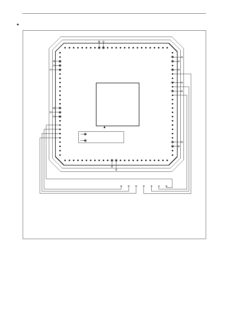
304
CHAPTER 14 FLASH MEMORY (
µ
µ
µ
µ
µ
PD70F3003A AND 70F3025A)
User's Manual U10913EJ6V0UM
Figure 14-1. V853 Flash Writing Adapter (FA100GC-8EU) Wiring Example
Remarks
1. Pins not described above should be handled according to the recommended connection of
unused pins (refer to 2.4 Pin I/O Circuits and Recommended Connection of Unused
Pins). When connecting to V
DD
via a resistor, connecting a resistor of 1 k
to 10 k
is
recommended.
2. This adapter is for a 100-pin plastic LQFP package.
3. This figure indicates the connection when CSI supporting handshake is used.
PD70F3003A,
PD70F3025A,
PD70F3003A(A)
SI
SO
SCK
/RESET
V
PP
RESERVE/HS
X1
V
D
D
G
N
D
GND
VDD
GND
VDD
V
D
D
G
N
D
41
28
29
40
42
45
43
48
49
46
67
66
Connected to VDD
Connected to GND
80
78
79
89
90
91
93
94
95
96
13
12
µ
µ
µ
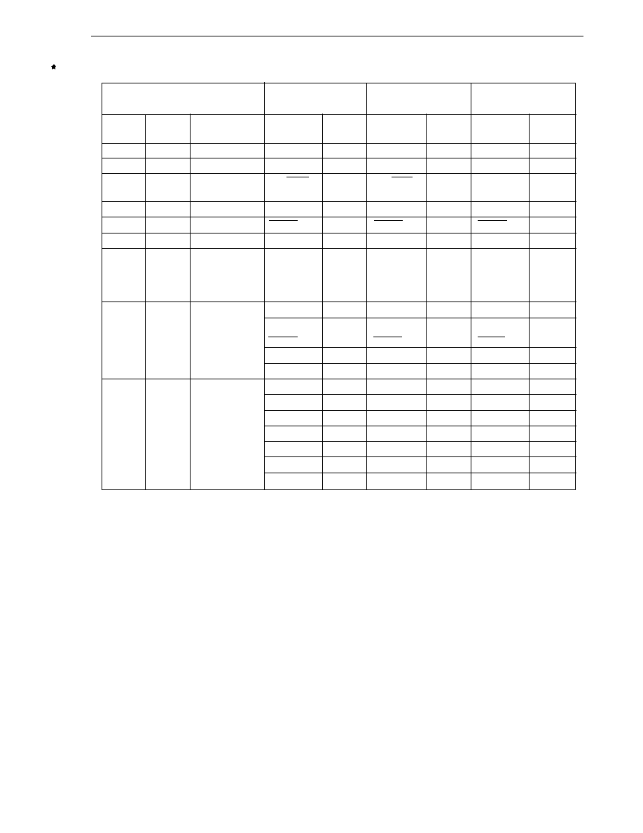
305
CHAPTER 14 FLASH MEMORY (
µ
µ
µ
µ
µ
PD70F3003A AND 70F3025A)
User's Manual U10913EJ6V0UM
Table 14-1. Wiring Table of V853 Flash Writing Adapter
Flash Programmer (PG-FP3)
When Using CSI + HS
When Using CSI0
When Using UART0
Connection Pins
Signal
I/O
Pin Function
Pin Name
Pin No.
Pin Name
Pin No.
Pin Name
Pin No.
Name
SI/RxD
Input
Receive signal
P22/SO0
94
P22/SO0
94
P22/TXD0
94
SO/TxD
Output
Transmit signal
P23/SI0
95
P23/SI0
95
P23/TXD0
95
SCK
Output
Transfer clock
P24/SCK0
96
P24/SCK0
96
Not
Not
required
required
CLK
Output
Clock to V853
X1
45
X1
45
X1
45
/RESET
Output
Reset signal
RESET
42
RESET
42
RESET
42
VPP
Output
Write voltage
V
PP
40
V
PP
40
V
PP
40
HS
Input
Handshake
P21/PWM1
93
Not required
Not
Not required
Not
signal of CSI0
required
required
+ HS
communication
VDD
I/O
VDD voltage
V
DD
Note 1
V
DD
Note 1
V
DD
Note 1
generation/
CV
DD
/
43
CV
DD
/
43
CV
DD
/
43
voltage
CKSEL
CSKEL
CSKEL
monitoring
AV
DD
80
AV
DD
80
AV
DD
80
MODE
41
MODE
41
MODE
41
GND
--
Ground
V
SS
Note 2
V
SS
Note 2
V
SS
Note 2
CV
SS
46
CV
SS
46
CV
SS
46
AV
SS
79
AV
SS
79
AV
SS
79
AV
REF1
78
AV
REF1
78
AV
REF1
78
AV
REF2
67
AV
REF2
67
AV
REF2
67
AV
REF3
66
AV
REF3
66
AV
REF3
66
NMI
91
NMI
91
NMI
91
Notes 1. 13, 29, 49, 90
2. 12, 28, 48, 89
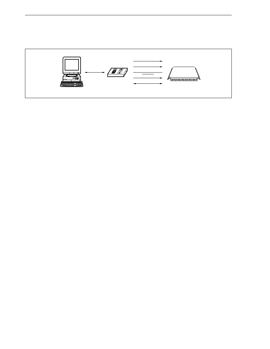
306
CHAPTER 14 FLASH MEMORY (
µ
µ
µ
µ
µ
PD70F3003A AND 70F3025A)
User's Manual U10913EJ6V0UM
14.3 Programming Environment
The following shows the environment required for writing programs to the flash memory of the V853.
A host machine is required for controlling the dedicated flash programmer.
UART0 or CSI0 is used for the interface between the dedicated flash programmer and the V853 to perform writing,
erasing, etc. A dedicated program adapter (FA series) is required for off-board writing.
V853
Dedicated flash programmer
V
PP
V
DD
V
SS
UART0/CSI0
RESET
RS-232-C
Host machine
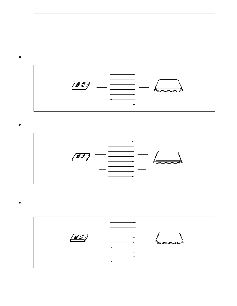
307
CHAPTER 14 FLASH MEMORY (
µ
µ
µ
µ
µ
PD70F3003A AND 70F3025A)
User's Manual U10913EJ6V0UM
14.4 Communication Mode
The communication between the dedicated flash programmer and the V853 is performed by serial communication
using UART0 or CSI0.
(1) UART0
Transfer rate: 4800 to 76800 bps (LSB first)
(2) CSI0
Transfer rate: 200 kHz to 1 MHz (MSB first)
The dedicated flash programmer outputs the transfer clock, and the V853 operates as a slave.
(3) CSI communication mode supporting handshake
Transfer rate: 200 kHz to 1 MHz (MSB first)
When PG-FP3 is used as the dedicated flash programmer, it generates the following signals to the V853. For the
details, refer to PG-FP3 Flash Memory Programmer User's Manual (U13502E).
V853
Dedicated flash
programmer
V
PP
V
DD
GND
RESET
SO
SI
SCK
CLK
HS (V
PP
2)
V
PP
V
DD
V
SS
RESET
SI0
SO0
SCK0
X1
P21
V853
Dedicated flash
programmer
V
PP
V
DD
GND
RESET
SO
SI
SCK
CLK
V
PP
V
DD
V
SS
RESET
SI0
SO0
SCK0
X1
V853
Dedicated flash
programmer
V
PP
V
DD
GND
RESET
TxD
RxD
CLK
V
PP
V
DD
V
SS
RESET
RxD0
TxD0
X1
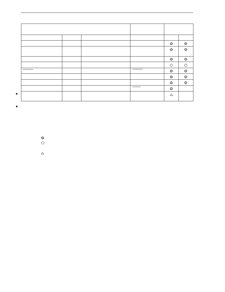
308
CHAPTER 14 FLASH MEMORY (
µ
µ
µ
µ
µ
PD70F3003A AND 70F3025A)
User's Manual U10913EJ6V0UM
PG-FP3
V853
Measurement
When Connected
Signal Name
I/O
Pin Function
Pin Name
Note 1
CSI0
UART0
V
PP
Output
Writing voltage
V
PP
V
DD
I/O
V
DD
voltage generation/
V
DD
voltage monitoring
GND
Ground
V
SS
CLK
Output
Clock output to V853
X1
Note 2
RESET
Output
Reset signal
RESET
SI/RxD
Input
Receive signal
SO0/TXD0
SO/TxD
Output
Transmit signal
SI0/RXD0
SCK
Output
Transfer clock
SCK0
×
HS (V
PP
2)
Input
Handshake signal of CSI0 + HS
P21
×
communication
Notes 1. Shifting to the flash memory programming mode sets all pins not used for flash memory programming
to the same state as immediately after reset. Therefore, if the external devices do not acknowledge the
port state immediately after reset, handling such as connecting to V
DD
via a resistor or connecting to
V
SS
via a resistor is required.
2. Only for off-board writing
Remark
: Always connected
: Do not need to connect, if generated on the target board
×
: Do not need to connect
: In handshake mode
309
CHAPTER 14 FLASH MEMORY (
µ
µ
µ
µ
µ
PD70F3003A AND 70F3025A)
User's Manual U10913EJ6V0UM
14.5 Pin Handling
When performing on-board writing, install a connector on the target system to connect to the dedicated flash
programmer. Also, install a function on-board to switch from the normal operation mode (single-chip mode) to the
flash memory programming mode.
When switched to the flash memory programming mode, all the pins not used for the flash memory programming
become the same status as that immediately after reset in the single-chip mode. Therefore, all the ports become
high-impedance, so pin handling is required when the external device does not acknowledge the high-impedance
status.
14.5.1 V
PP
pin
In the normal operation mode, 0 V is input to the V
PP
pin. In the flash memory programming mode, a 10.3 V writing
voltage is supplied to the V
PP
pin. The following shows an example of the connection of the V
PP
pin.
V
PP
Dedicated flash programmer connection pin
Pull-down resistor (R
VPP
)
V853
310
CHAPTER 14 FLASH MEMORY (
µ
µ
µ
µ
µ
PD70F3003A AND 70F3025A)
User's Manual U10913EJ6V0UM
14.5.2 Serial interface pin
The following shows the pins used by each serial interface.
Serial Interface
Pins Used
CSI0
SO0, SI0, SCK0
CSI0 + HS
SO0, SI0, SCK0, P21
UART0
TXD0, RXD0
When connecting a dedicated flash programmer to a serial interface pin that is connected to other devices on-
board, care should be taken to avoid a conflict of signals and the malfunction of the other device, etc.
(1) Conflict of signals
When connecting a dedicated flash programmer (output) to a serial interface pin (input) that is connected to
another device (output), a conflict of signals occurs. To avoid the conflict of signals, isolate the connection
to the other device or set the other device to the high-impedance status.
Input pin
Dedicated flash programmer connection pin
Conflict of signals
Output pin
Other device
V853
In the flash memory programming mode, the signal that the
dedicated flash programmer sends out conflicts with signals the
other device outputs. Therefore, isolate the signals on the
other device side.
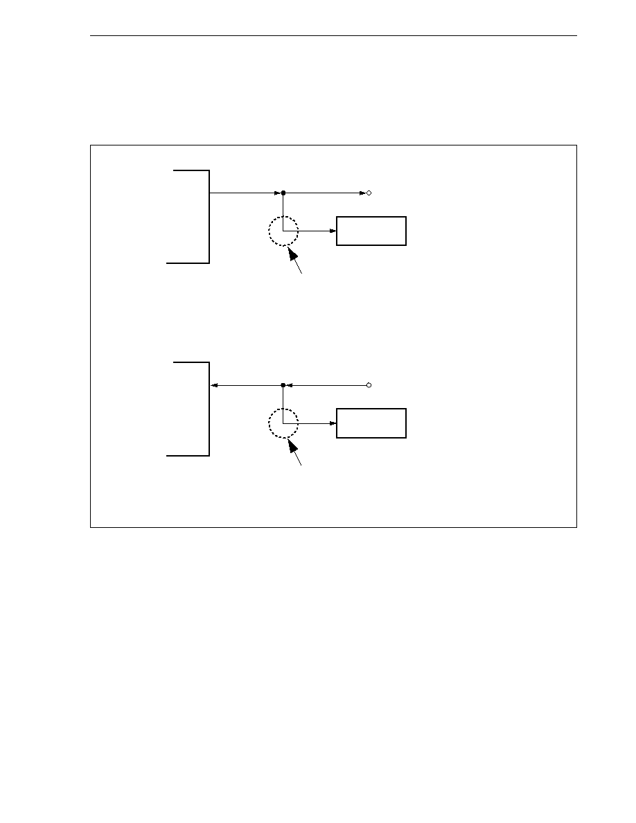
311
CHAPTER 14 FLASH MEMORY (
µ
µ
µ
µ
µ
PD70F3003A AND 70F3025A)
User's Manual U10913EJ6V0UM
(2) Malfunction of other device
When connecting a dedicated flash programmer (output or input) to a serial interface pin (input or output)
connected to another device (input), the signal output to the other device may cause the device to malfunction.
To avoid this, isolate the connection to the other device or make the setting so that the input signal to the other
device is ignored.
Pin
Dedicated flash programmer connection pin
Input pin
Other device
V853
Pin
Dedicated flash programmer connection pin
Input pin
Other device
V853
In the flash memory programming mode, if the
signal the V853 outputs affects the other device,
isolate the signal on the other device side.
In the flash memory programming mode, if the
signal the dedicated flash programmer outputs
affects the other device, isolate the signal on the
other device side.
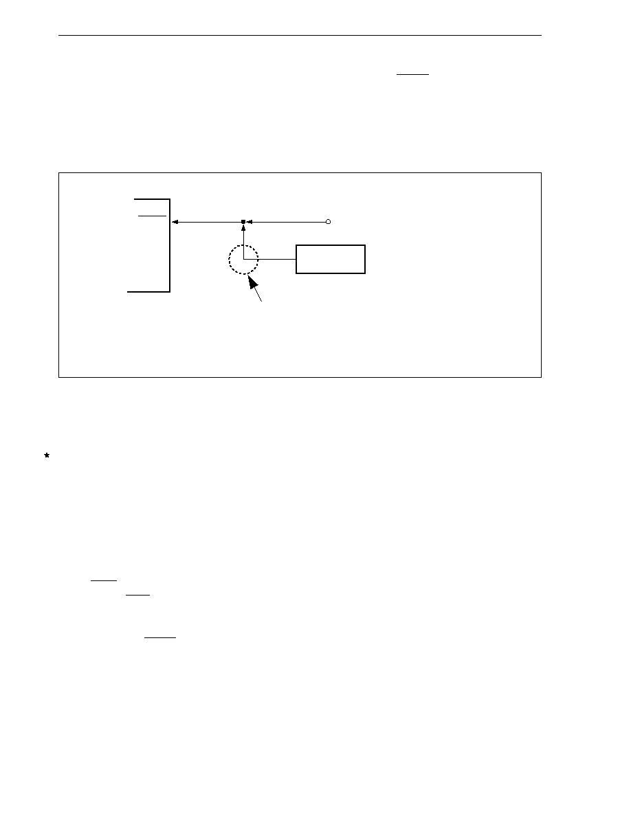
312
CHAPTER 14 FLASH MEMORY (
µ
µ
µ
µ
µ
PD70F3003A AND 70F3025A)
User's Manual U10913EJ6V0UM
14.5.3 Reset pin
When connecting the reset signals of the dedicated flash programmer to the RESET pin connected to the reset
signal generator on-board, a conflict of signals occurs. To avoid the conflict of signals, isolate the connection to the
reset signal generator.
When a reset signal is input from the user system in the flash memory programming mode, the programming
operation will not be performed correctly. Therefore, do not input signals other than the reset signals from the
dedicated flash programmer.
14.5.4 NMI pin
The input signal to the NMI pin is ignored in the flash memory programming mode.
14.5.5 MODE pin
To switch to the flash memory programming mode, connect the MODE pin to V
DD
, apply a writing voltage
(10.3 V) to the V
PP
pin, and release the reset.
14.5.6 Port pin
When the flash memory programming mode is set, all the port pins except the pins that communicate with the
dedicated flash programmer become output high impedance. These port pins do not require handling. If problems
such as disabling the output high-impedance status should occur in the external devices connected to the port, connect
them to V
DD
or V
SS
via resistors.
14.5.7 WAIT pin
Connect the WAIT pin directly to V
DD
.
14.5.8 Other signal pin
Connect X1, X2, CKSEL, and AV
REF1
to AV
REF3
to the same state as that in the normal operation mode.
14.5.9 Power supply
Supply the power supply (V
DD
, V
SS
, AV
DD
, AV
SS
, CV
DD
, CV
SS
) in the same way as in normal operation mode. Connect
V
DD
and GND of the dedicated flash programmer to V
DD
and V
SS
. Always connect V
DD
of the dedicated flash
programmer because it is provided with a power supply monitoring function.
RESET
Dedicated flash programmer connection pin
Conflict of signals
Output pin
Reset signal generator
V853
In the flash memory programming mode, the
signal the reset signal generator outputs conflicts
with the signal the dedicated flash programmer
outputs. Therefore, isolate the signals on the
reset signal generator side.
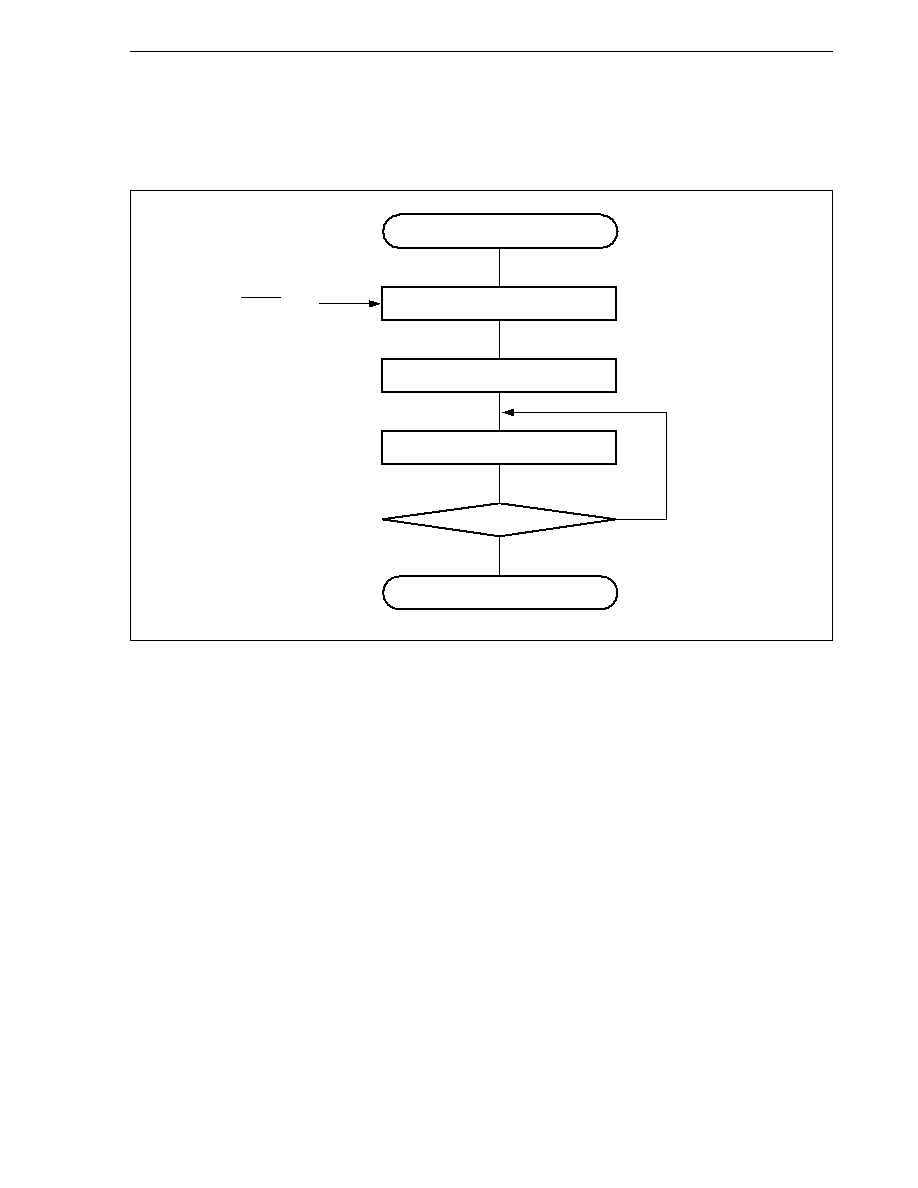
313
CHAPTER 14 FLASH MEMORY (
µ
µ
µ
µ
µ
PD70F3003A AND 70F3025A)
User's Manual U10913EJ6V0UM
14.6 Programming Method
14.6.1 Flash memory control
The following shows the procedure for manipulating the flash memory.
Start
Switch to flash memory programming mode
Select communication mode
Manipulate flash memory
End ?
Yes
No
End
Supply RESET pulse
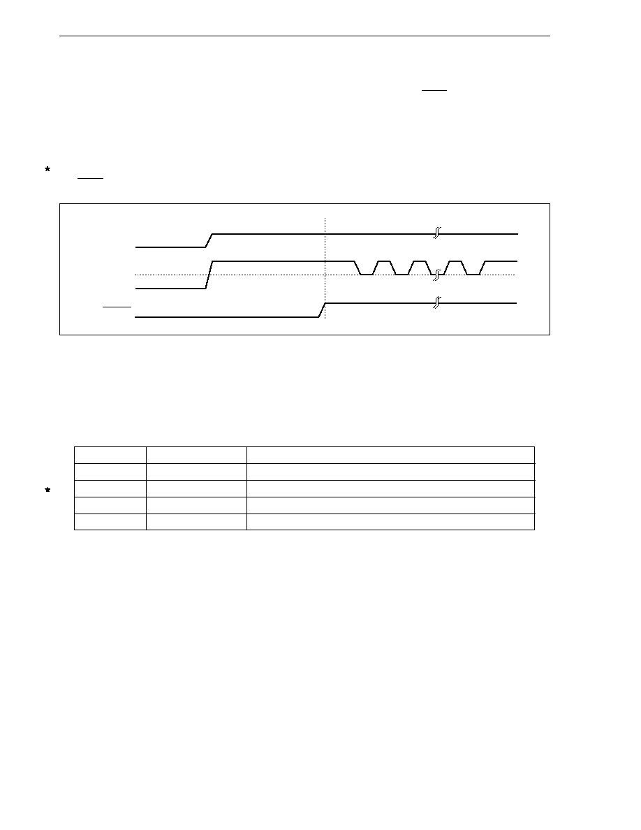
314
CHAPTER 14 FLASH MEMORY (
µ
µ
µ
µ
µ
PD70F3003A AND 70F3025A)
User's Manual U10913EJ6V0UM
14.6.2 Flash memory programming mode
When rewriting the contents of a flash memory using the dedicated flash programmer, set the V853 in the flash
memory programming mode. When switching modes, set the MODE, V
PP
,
and WAIT pins as follows before
releasing reset.
When performing on-board writing, change modes using jumpers, etc.
· MODE: V
DD
· V
PP
:
10.3 V
· WAIT:
V
DD
14.6.3 Selection of communication mode
In the V853, a communication mode is selected by inputting a pulse (16 pulses max.) to the V
PP
pin after switching
to the flash memory programming mode. The V
PP
pulse is generated by the dedicated flash programmer.
The following shows the relationship between the number of pulses and the communication mode.
Table 14-2. List of Communication Modes
V
PP
Pulse
Communication Mode
Remarks
0
CSI0
V853 performs slave operation, MSB first
3
CSI0 + HS
V853 performs slave operation, MSB first
8
UART0
Communication rate: 9600 bps (after reset), LSB first
Other than above
RFU
Setting prohibited
Caution When UART0 is selected, the receive clock is calculated based on the reset command sent
from the dedicated flash programmer after receiving the V
PP
pulse.
MODE
Flash memory programming mode
1
10.3 V
2
· · ·
n
V
PP
V
DD
0 V
RESET
315
CHAPTER 14 FLASH MEMORY (
µ
µ
µ
µ
µ
PD70F3003A AND 70F3025A)
User's Manual U10913EJ6V0UM
14.6.4 Communication commands
The V853 communicates with the dedicated flash programmer by means of commands. The command sent from
the dedicated flash programmer to the V853 is called a "command". The response signal sent from the V853 to the
dedicated flash programmer is called a "response command".
The following shows the commands for controlling the flash memory of the V853. All of these commands are issued
from the dedicated flash programmer, and the V853 performs the various processing corresponding to the command.
Category
Command Name
Function
Area verify
Area verify command
Compares the contents of the specified memory
area and the input data.
Area erase
Area erase command
Erases the contents of the specified memory
area.
Area blank check
Area blank check command
Checks the erase state of the specified memory
area.
Data write
High-speed write command
Writes data to the specified write address and
the number of bytes to be written, and executes
verify check.
Continuous write command
Writes data from the address following the high-
speed write command executed immediately
before, and executes verify check.
System setting and control
Status read out command
Acquires the status of operations.
Oscillation frequency setting command
Sets the oscillation frequency.
Erase time setting command
Sets the erasing time of area erase.
Write time setting command
Sets the writing time of data write.
Baud rate setting command
Sets the baud rate when using UART0.
Silicon signature command
Reads outs the silicon signature information.
Reset command
Escapes from each state.
V853
Dedicated flash programmer
Command
Response command

316
CHAPTER 14 FLASH MEMORY (
µ
µ
µ
µ
µ
PD70F3003A AND 70F3025A)
User's Manual U10913EJ6V0UM
The V853 sends back response commands to the commands issued from the dedicated flash programmer. The
following shows the response commands the V853 sends out.
Response Command Name
Function
ACK (acknowledge)
Acknowledges command/data, etc.
NAK (not acknowledge)
Acknowledges illegal command/data, etc.
14.6.5 Resources used
The resources used by the flash memory programming mode setting and are all the areas except FFE000H to
FFE7FFH of the internal RAM and all the registers. The FFE800H to FFEFFFH area of the internal RAM retains data
as long as the power is on. The registers that are initialized by reset are changed to their default values.

317
User's Manual U10913EJ6V0UM
APPENDIX A REGISTER INDEX
(1/5)
Symbol
Name
Unit
Page
ADCR0
A/D conversion result register 0
ADC
221
ADCR0H
A/D conversion result register 0H
ADC
221
ADCR1
A/D conversion result register 1
ADC
221
ADCR1H
A/D conversion result register 1H
ADC
221
ADCR2
A/D conversion result register 2
ADC
221
ADCR2H
A/D conversion result register 2H
ADC
221
ADCR3
A/D conversion result register 3
ADC
221
ADCR3H
A/D conversion result register 3H
ADC
221
ADCR4
A/D conversion result register 4
ADC
221
ADCR4H
A/D conversion result register 4H
ADC
221
ADCR5
A/D conversion result register 5
ADC
221
ADCR5H
A/D conversion result register 5H
ADC
221
ADCR6
A/D conversion result register 6
ADC
221
ADCR6H
A/D conversion result register 6H
ADC
221
ADCR7
A/D conversion result register 7
ADC
221
ADCR7H
A/D conversion result register 7H
ADC
221
ADIC
Interrupt control register
INTC
112
ADM0
A/D converter mode register 0
ADC
218
ADM1
A/D converter mode register 1
ADC
220
ASIM00
Asynchronous serial interface mode register 00
UART
186
ASIM01
Asynchronous serial interface mode register 01
UART
186
ASIM10
Asynchronous serial interface mode register 10
UART
186
ASIM11
Asynchronous serial interface mode register 11
UART
186
ASIS0
Asynchronous serial interface status register 0
UART
140
ASIS1
Asynchronous serial interface status register 1
UART
140
BCC
Bus cycle control register
BCU
84
BPRM0
Baud rate generator prescaler mode register 0
BRG
214
BPRM1
Baud rate generator prescaler mode register 1
BRG
214
BPRM2
Baud rate generator prescaler mode register 2
BRG
214
BRGC0
Baud rate generator compare register 0
BRG
213
BRGC1
Baud rate generator compare register 1
BRG
213
BRGC2
Baud rate generator compare register 2
BRG
213
CC110
Capture/compare register 110
RPU
150
CC111
Capture/compare register 111
RPU
150
CC112
Capture/compare register 112
RPU
150
CC113
Capture/compare register 113
RPU
150
CC120
Capture/compare register 120
RPU
150
CC121
Capture/compare register 121
RPU
150

318
APPENDIX A REGISTER INDEX
User's Manual U10913EJ6V0UM
(2/5)
Symbol
Name
Unit
Page
CC122
Capture/compare register 122
RPU
150
CC123
Capture/compare register 123
RPU
150
CC130
Capture/compare register 130
RPU
150
CC131
Capture/compare register 131
RPU
150
CC132
Capture/compare register 132
RPU
150
CC133
Capture/compare register 133
RPU
150
CC140
Capture/compare register 140
RPU
150
CC141
Capture/compare register 141
RPU
150
CC142
Capture/compare register 142
RPU
150
CC143
Capture/compare register 143
RPU
150
CKC
Clock control register
CG
129
CM4
Compare register 4
RPU
151
CMIC4
Interrupt control register
INTC
112
CSIC0
Interrupt control register
INTC
112
CSIC1
Interrupt control register 1
INTC
112
CSIC2
Interrupt control register 2
INTC
112
CSIC3
Interrupt control register 3
INTC
112
CSIM0
Clocked serial interface mode register 0
CSI
200
CSIM1
Clocked serial interface mode register 1
CSI
200
CSIM2
Clocked serial interface mode register 2
CSI
200
CSIM3
Clocked serial interface mode register 3
CSI
200
DACS0
D/A converted data coefficient register 0
DAC
250
DACS1
D/A converted data coefficient register 1
DAC
250
DAM
D/A converter mode register
DAC
250
DWC
Data wait control register
BCU
82
ECR
Interrupt source register
CPU
48
EIPC
Interrupt status save register
CPU
48
EIPSW
Interrupt status save register
CPU
48
FEPC
NMI status save register
CPU
48
FEPSW
NMI status save register
CPU
48
INTM0
External interrupt mode register 0
INTC
102
INTM1
External interrupt mode register 1
INTC
115
INTM2
External interrupt mode register 2
INTC
115
INTM3
External interrupt mode register 3
INTC
115
INTM4
External interrupt mode register 4
INTC
115
ISPR
In-service priority register
INTC
116
MM
Memory expansion mode register
Port
64
OVIC11
Interrupt control register
INTC
112
OVIC12
Interrupt control register
INTC
112
OVIC13
Interrupt control register
INTC
112

319
APPENDIX A REGISTER INDEX
User's Manual U10913EJ6V0UM
(3/5)
Symbol
Name
Unit
Page
OVIC14
Interrupt control register
INTC
112
P0
Port 0
Port
263
P1
Port 1
Port
267
P2
Port 2
Port
272
P3
Port 3
Port
277
P4
Port 4
Port
283
P5
Port 5
Port
285
P6
Port 6
Port
287
P7
Port 7
Port
289
P9
Port 9
Port
290
P11
Port 11
Port
293
P11IC0
Interrupt control register
INTC
112
P11IC1
Interrupt control register
INTC
112
P11IC2
Interrupt control register
INTC
112
P11IC3
Interrupt control register
INTC
112
P12IC0
Interrupt control register
INTC
112
P12IC1
Interrupt control register
INTC
112
P12IC2
Interrupt control register
INTC
112
P12IC3
Interrupt control register
INTC
112
P13IC0
Interrupt control register
INTC
112
P13IC1
Interrupt control register
INTC
112
P13IC2
Interrupt control register
INTC
112
P13IC3
Interrupt control register
INTC
112
P14IC0
Interrupt control register
INTC
112
P14IC1
Interrupt control register
INTC
112
P14IC2
Interrupt control register
INTC
112
P14IC3
Interrupt control register
INTC
112
PCM
Port control mode register
Port
296
PM0
Port 0 mode register
Port
265
PM1
Port 1 mode register
Port
270
PM2
Port 2 mode register
Port
275
PM3
Port 3 mode register
Port
280
PM4
Port 4 mode register
Port
284
PM5
Port 5 mode register
Port
286
PM6
Port 6 mode register
Port
288
PM9
Port 9 mode register
Port
292
PM11
Port 11 mode register
Port
295
PMC0
Port 0 mode control register
Port
266
PMC1
Port 1 mode control register
Port
271
PMC2
Port 2 mode control register
Port
276

320
APPENDIX A REGISTER INDEX
User's Manual U10913EJ6V0UM
(4/5)
Symbol
Name
Unit
Page
PMC3
Port 3 mode control register
Port
281
PMC11
Port 11 mode control register
Port
295
PRCMD
Command register
CG
76
PSC
Power save control register
CG
134
PSW
Program status word
CPU
49
PUO
Pull-up resistor option register
Port
298
PWM0
PWM buffer register 0 (12 bits)
PWM
255
PWM0L
PWM buffer register 0L (lower 8 bits)
PWM
255
PWM1
PWM buffer register 1 (12 bits)
PWM
255
PWM1L
PWM buffer register 1L (lower 8 bits)
PWM
255
PWMC
PWM control register
PWM
253
PWPR
PWM prescaler register
PWM
254
RXB0
Receive buffer 0
UART
191
RXB0L
Receive buffer 0L
UART
191
RXB1
Receive buffer 1
UART
191
RXB1L
Receive buffer 1L
UART
191
SEIC0
Interrupt control register
INTC
112
SEIC1
Interrupt control register
INTC
112
SIO0
Serial I/O shift register 0
CSI
201
SIO1
Serial I/O shift register 1
CSI
201
SIO2
Serial I/O shift register 2
CSI
201
SIO3
Serial I/O shift register 3
CSI
201
SRIC0
Interrupt control register
INTC
112
SRIC1
Interrupt control register
INTC
112
STIC0
Interrupt control register
INTC
112
STIC1
Interrupt control register
INTC
112
SYS
System status register
CG
77, 131
TM11
Timer 11
RPU
149
TM12
Timer 12
RPU
149
TM13
Timer 13
RPU
149
TM14
Timer 14
RPU
149
TM4
Timer 4
RPU
151
TMC11
Timer control register 11
RPU
155
TMC12
Timer control register 12
RPU
155
TMC13
Timer control register 13
RPU
155
TMC14
Timer control register 14
RPU
155
TMC4
Timer control register 4
RPU
157
TOC11
Timer output control register 11
RPU
158
TOC12
Timer output control register 12
RPU
158
TOC13
Timer output control register 13
RPU
158

321
APPENDIX A REGISTER INDEX
User's Manual U10913EJ6V0UM
(5/5)
Symbol
Name
Unit
Page
TOC14
Timer output control register 14
RPU
158
TOVS
Timer overflow status register
RPU
159
TUM11
Timer unit mode register 11
RPU
152
TUM12
Timer unit mode register 12
RPU
152
TUM13
Timer unit mode register 13
RPU
152
TUM14
Timer unit mode register 14
RPU
152
TXS0
Transmit shift register 0
UART
192
TXS0L
Transmit shift register 0L
UART
192
TXS1
Transmit shift register 1 (9 bits)
UART
192
TXS1L
Transmit shift register 1L (lower 8 bits)
UART
192

322
User's Manual U10913EJ6V0UM
APPENDIX B INSTRUCTION SET LIST
Conventions
(1) Symbols used for operand description
Symbol
Description
reg1
General-purpose register (r0 to r31): Used as source register
reg2
General-purpose register (r0 to r31): Mainly used as destination register
immx
x-bit immediate
dispx
x-bit displacement
reglD
System register number
bit#3
3-bit data for bit number specification
ep
Element pointer (r30)
cccc
4-bit data for condition code
vector
5-bit data for trap vector number (00H to 1FH)
(2) Symbols used for op code
Symbol
Description
R
1-bit data of code that specifies reg1 or regID
r
1-bit data of code that specifies reg2
d
1-bit data of displacement
i
1-bit data of immediate
cccc
4-bit data that indicates condition code
bbb
3-bit data specified by bit number
(3) Symbols used for operation description (1/2)
Symbol
Description
Assignment
GR[ ]
General-purpose register
SR[ ]
System register
zero-extend(n)
Zero-extends n to word length
sign-extend(n)
Sign-extends n to word length
load-memory(a,b)
Reads data of size b from address a
store-memory(a,b,c)
Writes data b of size c to address a
load-memory-bit(a,b)
Reads bit b of address a
store-memory-bit(a,b,c)
Writes c to bit b of address a
saturated(n)
Performs saturated processing of n (n is 2's complement).
If n is n
7FFFFFFFH as result of calculation, 7FFFFFFFH.
If n is n
80000000H as result of calculation, 80000000H.
result
Reflects result on flag
Byte
Byte (8 bits)

323
APPENDIX B INSTRUCTION SET LIST
User's Manual U10913EJ6V0UM
(3) Symbols used for operation description (2/2)
Symbol
Description
Halfword
Halfword (16 bits)
Word
Word (32 bits)
+
Add
Subtract
||
Bit concatenation
x
Multiply
÷
Divide
AND
Logical product
OR
Logical sum
XOR
Exclusive logical sum
NOT
Logical negate
logically shift left by
Logical left shift
logically shift right by
Logical right shift
arithmetically shift right by
Arithmetic right shift
(4) Symbols used for execution clock description
Symbol
Description
i : issue
To execute another instruction immediately after instruction execution
r: repeat
To execute same instruction immediately after instruction execution
l : latency
To reference result of instruction execution by the next instruction
(5) Symbols used for flag operation
Identifier
Description
(Blank)
Not affected
0
Cleared to 0
x
Set or cleared according to result
R
Previously saved value is restored

324
APPENDIX B INSTRUCTION SET LIST
User's Manual U10913EJ6V0UM
Condition Code
V
0 0 0 0
OV = 1
Overflow
NV
1 0 0 0
OV = 0
No overflow
C/L
0 0 0 1
CY = 1
Carry
Lower (Less than)
NC/NL
1 0 0 1
CY = 0
No carry
No lower (Greater than or equal)
Z/E
0 0 1 0
Z = 1
Zero
Equal
NZ/NE
1 0 1 0
Z = 0
Not zero
Not equal
NH
0 0 1 1
(CY or Z) = 1
Not higher (Less than or equal)
H
1 0 1 1
(CY or Z) = 0
Higher (Greater than)
N
0 1 0 0
S = 1
Negative
P
1 1 0 0
S = 0
Positive
T
0 1 0 1
--
Always (unconditional)
SA
1 1 0 1
SAT = 1
Saturated
LT
0 1 1 0
(S xor OV) = 1
Less than signed
GE
1 1 1 0
(S xor OV) = 0
Greater than or equal signed
LE
0 1 1 1
((S xor OV) or Z) = 1
Less than or equal signed
GT
1 1 1 1
((S xor OV) or Z) = 0
Greater than signed
Condition Name
(cond)
Condition
Code (cccc)
Conditional Expression
Description

325
APPENDIX B INSTRUCTION SET LIST
User's Manual U10913EJ6V0UM
Instruction Set (Alphabetical Order) (1/4)
i
r
l CY OV S
Z SAT
ADD
reg1, reg2
GR[reg2]
GR[reg2]+GR[reg1]
1
1
1
x
x
x
x
imm5, reg2
GR[reg2]
GR[reg2]+sign-extend(imm5)
1
1
1
x
x
x
x
ADDI
imm16, reg1, reg2
GR[reg2]
GR[reg1]+sign-extend(imm16)
1
1
1
x
x
x
x
AND
reg1, reg2
GR[reg2]
GR[reg2]AND GR[reg1]
1
1
1
0
x
x
ANDI
imm16, reg1, reg2
GR[reg2]
GR[reg1]AND zero-extend(imm16)
1
1
1
0
0
x
Bcond
disp9
if conditions are satisfied
3
3
3
then PC
PC+sign-extned(disp9)
1
1
1
CLR1
bit#3, disp16[reg1]
adr
GR[reg1]+sign-extend(disp16)
4
4
4
x
Z flag
Not(Load-memory-bit(adr, bit#3))
Store-memory-bit(adr, bit#3.0)
CMP
reg1, reg2
result
GR[reg2]GR[reg1]
1
1
1
x
x
x
x
imm5, reg2
result
GR[reg2]sign-extend(imm5)
1
1
1
x
x
x
x
DI
PSW.ID
1
1
1
1
(Maskable interrupt disabled)
DIVH
reg1, reg2
GR [reg2]
GR [reg2]
÷
GR [reg1]
Note 2
36 36 36
x
x
x
(signed division)
EI
PSW.ID
0
1
1
1
(Maskable interrupt enabled)
HALT
Stops
1
1
1
JARL
disp22, reg2
GR[reg2]
PC+4
3
3
3
PC
PC+sign-extend(disp22)
JMP
[reg1]
PC
GR[reg1]
3
3
3
JR
disp22
PC
PC+sign-extend(disp22)
3
3
3
LD.B
disp16[reg1], reg2
adr
GR[reg1]+sign-extend(disp16)
1
1
2
GR[reg2]
sign-extend(Load-memory(adr, Byte))
LD.H
disp16[reg1], reg2
adr
GR[reg1]+sign-extend(disp16)
1
1
2
GR[reg2]sign-extend(Load-memory(adr, Halfword))
LD.W
disp16[reg1], reg2
adr
GR[reg1]+sign-extend(disp16)
1
1
2
GR[reg2]
Load-memory(adr, Word)
Notes
1. dddddddd is the higher 8 bits of disp9.
2. Only the lower halfword is valid.
3. ddddddddddddddd dddddd is the higher 21 bits of disp22.
4. ddddddddddddddd is the higher 15 bits of disp16.
Operation
Mnemonic
Operand
Op Code
When condition
satisfied
When condition
not satisfied
1 0 b b b 1 1 1 1 1 0RRRRR
d d d d d d d d d d d d d d d d
r r r r r 0 0 1 1 1 1RRRRR
r r r r r 0 1 0 0 1 1 i i i i i
0 0 0 0 0 1 1 1 1 1 1 0 0 0 0 0
0 0 0 0 0 0 0 1 0 1 1 0 0 0 0 0
r r r r r 0 0 0 0 1 0RRRRR
1 0 0 0 0 1 1 1 1 1 1 0 0 0 0 0
0 0 0 0 0 0 0 1 0 1 1 0 0 0 0 0
0 0 0 0 0 1 1 1 1 1 1 0 0 0 0 0
0 0 0 0 0 0 0 1 0 0 1 0 0 0 0 0
r r r r r 1 1 1 1 0 d d d d d d
d d d d d d d d d d d d d d d 0
Note 3
0 0 0 0 0 0 0 0 0 1 1RRRRR
0 0 0 0 0 1 1 1 1 0 d d d d d d
d d d d d d d d d d d d d d d 0
Note 3
r r r r r 1 1 1 0 0 0RRRRR
d d d d d d d d d d d d d d d d
r r r r r 1 1 1 0 0 1RRRRR
d d d d d d d d d d d d d d d 0
Note 4
r r r r r 1 1 1 0 0 1RRRRR
d d d d d d d d d d d d d d d 1
Note 4
r r r r r 0 0 1 1 1 0RRRRR
r r r r r 0 1 0 0 1 0 i i i i i
r r r r r 1 1 0 0 0 0RRRRR
i i i i i i i i i i i i i i i i
r r r r r 0 0 1 0 1 0RRRRR
r r r r r 1 1 0 1 1 0RRRRR
i i i i i i i i i i i i i i i i
Execution
Clock
Flag
d d d d d 1 0 1 1 d d d c c c c
Note 1

326
APPENDIX B INSTRUCTION SET LIST
User's Manual U10913EJ6V0UM
Instruction Set (Alphabetical Order) (2/4)
i
r
l CY OV S
Z SAT
LDSR
reg2, regID
SR[regID]
GR[reg2] regID = EIPC, FEPC
1
1
3
regID = EIPSW, FEPSW
1
regID = PSW
1
x
x
x
x
x
MOV
reg1, reg2
GR[reg2]
GR[reg1]
1
1
1
imm5, reg2
GR[reg2]
sign-extend(imm5)
1
1
1
MOVEA
imm16, reg1, reg2
GR[reg2]
GR[reg1]+sign-extend(imm16)
1
1
1
MOVHI
imm16, reg1, reg2
GR[reg2]
GR[reg1]+(imm16 || 0
16
)
1
1
1
MULH
reg1, reg2
GR[reg2]
GR[reg2]
Note 2
xGR[reg1]
Note 2
1
1
2
(Signed multiplication)
imm5, reg2
GR[reg2]
GR[reg2]
Note 2
xsign-extend(imm5)
1
1
2
(Signed multiplication)
MULHI
imm16, reg1, reg2
GR[reg2]
GR[reg1]
Note 2
ximm16
1
1
2
(Signed multiplication)
NOP
Uses 1 clock cycle without doing anything
1
1
1
NOT
reg1, reg2
GR[reg2]
NOT(GR[reg1])
1
1
1
0
x
x
NOT1
bit#3, disp16[reg1]
adr
GR[reg1]+sign-extend(disp16)
4
4
4
x
Z flag
Not(Load-memory-bit(adr, bit#3))
Store-memory-bit(adr, bit#3, Z flag)
OR
reg1, reg2
GR[reg2]
GR[reg2]OR GR[reg1]
1
1
1
0
x
x
ORI
imm16, reg1, reg2
GR[reg2]
GR[reg1]OR zero-extend(imm16)
1
1
1
0
x
x
RETI
if PSW.EP=1
4
4
4
R
R
R
R
R
then PC
EIPC
PSW
EIPSW
else if PSW.NP=1
then PC
FEPC
PSW
FEPSW
else PC
EIPC
PSW
EIPSW
SAR
reg1, reg2
GR[reg2]
GR[reg2]arithmetically shift right
1
1
1
x
0
x
x
by GR[reg1]
imm5, reg2
GR[reg2]
GR[reg2]arithmetically shift right
1
1
1
x
0
x
x
by zero-extend(imm5)
Notes
1. The op code of this instruction uses the field of reg1, even though the source register is shown as
reg2 in the above table. Therefore, the meaning of register specification for the mnemonic description
and op code is different from that of the other instructions.
rrrrr = regID specification
RRRRR = reg2 specification
2. Only the lower halfword data is valid.
Operation
Operand
Op Code
r r r r r 1 1 1 1 1 1RRRRR
0 0 0 0 0 0 0 0 0 0 1 0 0 0 0 0
Note 1
r r r r r 0 0 0 0 0 0RRRRR
r r r r r 0 1 0 0 0 0 i i i i i
r r r r r 1 1 0 0 0 1RRRRR
i i i i i i i i i i i i i i i i
r r r r r 1 1 0 0 1 0RRRRR
i i i i i i i i i i i i i i i i
r r r r r 0 0 0 1 1 1RRRRR
r r r r r 0 1 0 1 1 1 i i i i i
r r r r r 1 1 0 1 1 1RRRRR
i i i i i i i i i i i i i i i i
0 0 0 0 0 0 0 0 0 0 0 0 0 0 0 0
r r r r r 0 0 0 0 0 1RRRRR
0 1 b b b 1 1 1 1 1 0RRRRR
d d d d d d d d d d d d d d d d
r r r r r 0 0 1 0 0 0RRRRR
r r r r r 1 1 0 1 0 0RRRRR
i i i i i i i i i i i i i i i i
0 0 0 0 0 1 1 1 1 1 1 0 0 0 0 0
0 0 0 0 0 0 0 1 0 1 0 0 0 0 0 0
r r r r r 1 1 1 1 1 1RRRRR
0 0 0 0 0 0 0 0 1 0 1 0 0 0 0 0
r r r r r 0 1 0 1 0 1 i i i i i
Mnemonic
Execution
Clock
Flag

327
APPENDIX B INSTRUCTION SET LIST
User's Manual U10913EJ6V0UM
Instruction Set (Alphabetical Order) (3/4)
i
r
l CY OV S
Z SAT
SATADD
reg1, reg2
GR[reg2]
saturated(GR[reg2]+GR[reg1])
1
1
1
x
x
x
x
x
imm5, reg2
GR[reg2]
saturated(GR[reg2]+sign-extend(imm5))
1
1
1
x
x
x
x
x
SATSUB
reg1, reg2
GR[reg2]
saturated(GR[reg2]GR[reg1])
1
1
1
x
x
x
x
x
SATSUBI
imm16, reg1, reg2
GR[reg2]
saturated(GR[reg1]sign-extend(imm16))
1
1
1
x
x
x
x
x
SATSUBR reg1, reg2
GR[reg2]
saturated(GR[reg1]GR[reg2])
1
1
1
x
x
x
x
x
SETF
cccc, reg2
if conditions are satisfied
1
1
1
then GR[reg2]
00000001H
else GR[reg2]
00000000H
SET1
bit#3, disp16[reg1]
adr
GR[reg1]+sign-extend(disp16)
4
4
4
x
Z flag
Not(Load-memory-bit(adr, bit#3))
Store-memory-bit(adr, bit#3, 1)
SHL
reg1, reg2
GR[reg2]
GR[reg2] logically shift left by GR[reg1]
1
1
1
x
0
x
x
imm5, reg2
GR[reg2]
GR[reg1] logically shift left by
1
1
1
x
0
x
x
zero-extend(imm5)
SHR
reg1, reg2
GR[reg2]
GR[reg2] logically shift right by GR[reg1]
1
1
1
x
0
x
x
imm5, reg2
GR[reg2]
GR[reg2] logically shift right by
1
1
1
x
0
x
x
zero-extend(imm5)
SLD.B
disp7[ep], reg2
adr
ep+zero-extend(disp7)
1
1
2
GR[reg2]
sign-extend(Load-memory(adr, Byte))
SLD.H
disp8[ep], reg2
adr
ep+zero-extend(disp8)
1
1
2
GR[reg2]
sign-extend(Load-memory(adr, Halfword))
SLD.W
disp8[ep], reg2
adr
ep+zero-extend(disp8)
1
1
2
GR[reg2]
Load-memory(adr, Word)
SST.B
reg2, disp7[ep]
adr
ep+zero-extend(disp7)
1
1
1
Store-memory(adr, GR[reg2], Byte)
SST.H
reg2, disp8[ep]
adr
ep+zero-extend(disp8)
1
1
1
Store-memory(adr, GR[reg2], Halfword)
SST.W
reg2, disp8[ep]
adr
ep+zero-extend(disp8)
1
1
1
Store-memory(adr, GR[reg2], Word)
ST.B
reg2, disp16[reg1]
adr
GR[reg1]+sign-extend(disp16)
1
1
1
Store-memory(adr, GR[reg2], Byte)
Notes
1. ddddddd is the higher 7 bits of disp8.
2. dddddd is the higher 6 bits of disp8.
Operation
Operand
Op Code
r r r r r 0 0 0 1 1 0RRRRR
r r r r r 0 1 0 0 0 1 i i i i i
r r r r r 0 0 0 1 0 1RRRRR
r r r r r 1 1 0 0 1 1RRRRR
i i i i i i i i i i i i i i i i
r r r r r 0 0 0 1 0 0RRRRR
r r r r r 1 1 1 1 1 1 0 c c c c
0 0 0 0 0 0 0 0 0 0 0 0 0 0 0 0
0 0 b b b 1 1 1 1 1 0RRRRR
d d d d d d d d d d d d d d d d
r r r r r 1 1 1 1 1 1RRRRR
0 0 0 0 0 0 0 0 1 1 0 0 0 0 0 0
r r r r r 0 1 0 1 1 0 i i i i i
r r r r r 1 1 1 1 1 1RRRRR
0 0 0 0 0 0 0 0 1 0 0 0 0 0 0 0
r r r r r 0 1 0 1 0 0 i i i i i
r r r r r 0 1 1 0 d d d d d d d
r r r r r 1 0 0 0 d d d d d d d
Note 1
r r r r r 1 0 1 0 d d d d d d 0
Note 2
r r r r r 0 1 1 1 d d d d d d d
r r r r r 1 0 0 1 d d d d d d d
Note 1
r r r r r 1 0 1 0 d d d d d d 1
Note 2
r r r r r 1 1 1 0 1 0RRRRR
d d d d d d d d d d d d d d d d
Flag
Mnemonic
Execution
Clock

328
APPENDIX B INSTRUCTION SET LIST
User's Manual U10913EJ6V0UM
Instruction Set (Alphabetical Order) (4/4)
i
r
l CY OV S
Z SAT
ST.H
reg2, disp16[reg1]
adr
GR[reg1]+sign-extend(disp16)
1
1
1
Store-memory(adr, GR[reg2], Halfword)
ST.W
reg2, disp16[reg1]
adr
GR[reg1]+sign-extend(disp16)
1
1
1
Store-memory(adr, GR[reg2], Word)
STSR
regID, reg2
GR[reg2]
SR[regID]
1
1
1
SUB
reg1, reg2
GR[reg2]
GR[reg2]GR[reg1]
1
1
1
x
x
x
x
SUBR
reg1, reg2
GR[reg2]
GR[reg1]GR[reg2]
1
1
1
x
x
x
x
TRAP
vector
EIPC
PC+4(Restored PC)
4
4
4
EIPSW
PSW
ECR.EICC
Interrupt code
PSW.EP
1
PSW.ID
1
PC
00000040H(vector = 00H to 0FH)
00000050H(vector = 10H to 1FH)
TST
reg1, reg2
result
GR[reg2] AND GR[reg1]
1
1
1
0
x
x
TST1
bit#3, disp16[reg1]
adr
GR[reg1]+sign-extend(disp16)
3
3
3
x
Z flag
Not(Load-memory-bit(adr, bit#3))
XOR
reg1, reg2
GR[reg2]
GR[reg2] XOR GR[reg1]
1
1
1
0
x
x
XORI
imm16, reg1, reg2
GR[reg2]
GR[reg1] XOR zero-extend(imm16)
1
1
1
0
x
x
Note
ddddddddddddddd is the higher 15 bits of disp16.
Operation
Operand
Op Code
r r r r r 1 1 1 0 1 1RRRRR
d d d d d d d d d d d d d d d 0
Note
r r r r r 1 1 1 0 1 1RRRRR
d d d d d d d d d d d d d d d 1
Note
r r r r r 1 1 1 1 1 1RRRRR
0 0 0 0 0 0 0 0 0 1 0 0 0 0 0 0
r r r r r 0 0 1 1 0 1RRRRR
r r r r r 0 0 1 1 0 0RRRRR
0 0 0 0 0 1 1 1 1 1 1 i i i i i
0 0 0 0 0 0 0 1 0 0 0 0 0 0 0 0
r r r r r 0 0 1 0 1 1RRRRR
1 1 b b b 1 1 1 1 1 0RRRRR
d d d d d d d d d d d d d d d d
r r r r r 0 0 1 0 0 1RRRRR
r r r r r 1 1 0 1 0 1RRRRR
i i i i i i i i i i i i i i i i
Flag
Mnemonic
Execution
Clock

329
User's Manual U10913EJ6V0UM
APPENDIX C INDEX
[0]
1-buffer mode ....................................................... 225
4-buffer mode ....................................................... 226
100-pin plastic LQFP .............................................. 22
[A]
A/D conversion result register ............................. 221
A/D converter ................................................. 27, 215
mode register 0 ........................................... 218
mode register 1 ........................................... 220
A/D trigger mode ......................................... 223, 228
A16 to A19 .............................................................. 38
AD0 to AD7 ............................................................. 38
AD8 to AD15 ........................................................... 38
ADC ......................................................................... 27
ADCR0 to ADCR7 ................................................ 221
ADCR0H to ADCR7H ........................................... 221
Address/data variable register ............................... 47
Address space ................................................. 51, 65
ADIC ............................................................. 112, 113
ADIF ............................................................. 112, 113
ADM0 .................................................................... 218
ADM1 .................................................................... 220
ADMK ........................................................... 112, 113
ADPR0 to ADPR2 ........................................ 112, 113
ADTRG .................................................................... 35
ALV0, ALV1 .......................................................... 253
ALV1n0, ALV1n1 (n = 1 to 4) .............................. 158
ANI0 to ANI7 ........................................................... 39
ANIS0 to ANIS2 .................................................... 218
ANO0, ANO1 .......................................................... 42
Applications ............................................................. 22
ASIM00, ASIM01, ASIM10, ASIM11 ................... 186
ASIS0, ASIS1 ....................................................... 190
Assembler-reserved register .................................. 47
ASTB ....................................................................... 40
Asynchronous serial interface .............................. 183
mode registers 00, 01, 10, 11 ..................... 186
status registers 0, 1 ..................................... 190
AV
DD
........................................................................ 42
AV
REF1
to AV
REF3
..................................................... 42
AV
SS
........................................................................ 42
[B]
Baud rate generator 0 to 2 ................................... 210
compare registers 0 to 2 ............................. 213
prescaler mode registers 0 to 2 .................. 214
setting value ................................................. 211
BCC ......................................................................... 84
BCn1 (n = 0 to 7) .................................................... 84
BCU ......................................................................... 26
BPRM0 to BPRM2 ................................................ 214
BPRn0 to BPRn2 (n = 0 to 2) .............................. 214
BRCE0 to BRCE2 ................................................. 214
BRG ....................................................................... 210
BRGC0 to BRGC2 ................................................ 213
BRGn0 to BRGn7 (n = 0 to 2) ............................. 213
BS .......................................................................... 218
Bus
access ............................................................ 79
control function .............................................. 78
control pin ...................................................... 78
control unit ..................................................... 26
cycle control register ..................................... 84
hold .......................................................... 85, 92
priority ............................................................ 93
timing .............................................................. 86
width ............................................................... 79
Byte access ............................................................. 79
[C]
Capture operation (timer 1) .................................. 164
Capture/compare registers 1n0 to 1n3
(n = 1 to 4) ............................................................ 150
Cautions (A/D converter) ...................................... 245
Cautions (power save function) ........................... 141
Cautions (PWM unit) ............................................ 257
Cautions (timer/counter function) ........................ 180
CC1n0 to CC1n3 (n = 1 to 4) .............................. 153
CE .......................................................................... 218
CE11 to CE14 ....................................................... 155
CE4 ....................................................................... 157
CES1n0, CES1n1 (n = 1 to 4) ............................. 153
CESEL ................................................................... 134
CG ........................................................................... 26
CKC ....................................................................... 129
CKDIV0, CKDIV1 .................................................. 129
CKSEL ..................................................................... 41
CL0, CL1 ............................................................... 187
Clearing/starting timer (timer 1) ........................... 166

330
APPENDIX C INDEX
User's Manual U10913EJ6V0UM
CLKOUT .................................................................. 41
Clock
control register ............................................. 129
generator ........................................................ 26
generator function ....................................... 127
output control ............................................... 145
output inhibit ....................................... 132, 145
Clocked serial interface ........................................ 198
Clocked serial interface mode registers 0 to 3 ... 200
CLSn0, CLSn1 (n = 0 to 3) .................................. 201
CM4 ....................................................................... 151
CMIC4 .......................................................... 112, 113
CMIF4 ........................................................... 112, 113
CMMK4 ........................................................ 112, 113
CMPR40 to CMPR42 .................................. 112, 113
CMS1n0 to CMS1n3 (n = 1 to 4) ......................... 152
Command register .................................................. 76
Compare operation (timer 1) ................................ 167
Compare operation (timer 4) ................................ 170
Compare register 4 ............................................... 151
Connection of unused pins .................................... 43
Conversion time .................................................... 248
Count operation (timer 1) ..................................... 160
Count operation (timer 4) ..................................... 169
CPU ......................................................................... 26
address space ........................................ 51, 53
function ........................................................... 45
register set ..................................................... 46
CRXE0 to CRXE3 ................................................. 200
CS .......................................................................... 218
CSI ........................................................................ 198
CSIC0 to CSIC3 .......................................... 112, 113
CSIF0 to CSIF3 ........................................... 112, 113
CSIM0 to CSIM3 ................................................... 200
CSMK0 to CSMK3 ....................................... 112, 113
CSOT0 to CSOT3 ................................................. 200
CSPRmn (m = 0 to 3, n = 0 to 2) ............... 112, 113
CTXE0 to CTXE3 ................................................. 200
CV
DD
........................................................................ 41
CV
SS
........................................................................ 41
CY ............................................................................ 49
[D]
D/A converted data coefficient register ............... 250
D/A converter ................................................. 27, 249
D/A converter mode register ................................ 250
DAC ......................................................................... 27
DACE0, DACE1 .................................................... 250
DACS0, DACS1 .................................................... 250
DAM ...................................................................... 250
DAn0 to DAn7 (n = 0, 1) ...................................... 250
Data space ................................................. 53, 65, 93
Data wait control register ....................................... 82
DCLK0, DCLK1 ..................................................... 134
DSTB ....................................................................... 40
DWC ........................................................................ 82
DWn0, DWn1 (n = 0 to 7) ...................................... 82
[E]
EBS0, EBS1 .......................................................... 189
ECLR11 to ECLR14 ............................................. 152
ECR ......................................................................... 48
Edge detection function of NMI pin ..................... 102
EICC ........................................................................ 48
EIPC ........................................................................ 48
EIPSW ..................................................................... 48
Element pointer ....................................................... 47
ENTO1n0, ENTO1n1 (n = 1 to 4) ........................ 158
EP ................................................................... 49, 119
ESN0 ..................................................................... 102
ESn0, ESn1 (n = 00 to 03, 10 to 13,
20 to 23, 30 to 33) ................................................ 115
ETI11 to ETI14 ..................................................... 155
Example of inserting wait states ............................ 83
Exception processing function ............................... 95
Exception status flag ............................................ 119
Exception table ....................................................... 58
Exception trap ....................................................... 120
External expansion mode ....................................... 63
External interrupt mode register 0 ....................... 102
External interrupt mode register 1 to 4 ...... 115, 158
External memory area ............................................ 62
External trigger mode .................................. 224, 240
External wait function ............................................. 83
[F]
FE0, FE1 ............................................................... 190
FECC ....................................................................... 48
FEPC ....................................................................... 48
FEPSW .................................................................... 48
Flash memory ....................................................... 303
Flash memory programming mode ........................ 50
FR0 to FR2 ........................................................... 220
Frequency measurement ..................................... 178
Full scale error ...................................................... 247
Function block configuration .................................. 25

331
APPENDIX C INDEX
User's Manual U10913EJ6V0UM
[G]
General-purpose registers ..................................... 47
Global pointer ......................................................... 47
[H]
Halfword access ..................................................... 79
HALT mode ........................................................... 135
HLDAK .................................................................... 40
HLDRQ .................................................................... 40
[I]
IC ............................................................................. 42
I/O circuits of pins ............................................ 43, 44
ID .................................................................... 49, 116
IDLE ...................................................................... 134
IDLE mode ............................................................ 137
Idle state insertion function .................................... 84
ILGOP ..................................................................... 96
Illegal op code definition ...................................... 120
IMS1n0 to IMS1n3 (n = 1 to 4) ............................ 152
In-service priority register ..................................... 116
Initial value of each register after reset ............... 301
Initialize ................................................................. 300
Instruction set list .................................................. 322
INTAD ...................................................................... 96
INTC ........................................................................ 26
INTCM4 ................................................................... 96
INTCSI0 to INTCSI3 ............................................... 96
Internal block diagram ............................................ 25
Internal RAM area .................................................. 60
Internal ROM area .................................................. 56
Internal units ........................................................... 26
Interrupt
control register ............................................. 112
controller ........................................................ 26
latency time .................................................. 124
list ................................................................... 96
processing function ....................................... 95
source register ............................................... 48
table ................................................................ 58
Interval timer ......................................................... 172
INTM0 .................................................................... 102
INTM1 to INTM4 .......................................... 115, 158
INTOV11 to INTOV14 ............................................ 96
INTP110 to INTP113 .............................................. 35
INTP120 to INTP123 .............................................. 36
INTP130 to INTP133 .............................................. 37
INTP140 to INTP143 .............................................. 41
INTP1mn/INTCC1mn
(m = 1 to 4, n = 0 to 3) .......................................... 96
INTSER0, INTSER1 ...................................... 96, 193
INTSR0, INTSR1 ........................................... 96, 193
INTST0, INTST1 ............................................ 96, 193
ISPR ...................................................................... 116
ISPR0 to ISPR7 .................................................... 116
[L]
LBEN ....................................................................... 39
Link pointer ............................................................. 47
[M]
Maskable interrupt ................................................ 103
Maskable interrupt status flag .............................. 116
Memory
block function ................................................. 81
boundary operation condition ....................... 93
expansion mode register ............................... 64
map ................................................................ 54
read ................................................................ 86
write ................................................................ 90
MM ........................................................................... 64
MM0 to MM3 ........................................................... 64
MOD0 to MOD3 .................................................... 200
MODE ...................................................................... 41
MS ......................................................................... 218
Multiple interrupt servicing ................................... 122
[N]
NMI .......................................................................... 42
Noise elimination of NMI pin ................................ 102
Noise eliminator .................................................... 114
Nonlinearity error .................................................. 247
Non-maskable interrupt .......................................... 98
Non-maskable interrupt status flag ...................... 102
Normal operation mode .......................................... 50
NP ................................................................... 49, 102
[O]
Off-board programming ........................................ 303
On-board programming ........................................ 303
On-chip peripheral I/O interface ............................ 94
Operation in power save mode .............................. 85
Operation mode ...................................................... 50
Ordering information ............................................... 22
OST1 to OST4 ...................................................... 152
OV ........................................................................... 49

332
APPENDIX C INDEX
User's Manual U10913EJ6V0UM
OVE0, OVE1 ......................................................... 190
Overall error .......................................................... 246
Overflow (timer 1) ................................................. 162
Overflow (timer 4) ................................................. 169
OVFn (n = 4, 11 to 14) ......................................... 159
OVIC11 to OVIC14 ...................................... 112, 113
OVIF11 to OVIF14 ....................................... 112, 113
OVMK11 to OVMK14 .................................. 112, 113
OVPR1mn (m = 1 to 4, n = 0 to 2) ............. 112, 113
[P]
P0 .......................................................................... 263
P1 .......................................................................... 267
P2 .......................................................................... 272
P3 .......................................................................... 277
P4 .......................................................................... 283
P5 .......................................................................... 285
P6 .......................................................................... 287
P7 .......................................................................... 289
P9 .......................................................................... 290
P11 ........................................................................ 293
P00 to P07 ..................................................... 35, 263
P10 to P17 ..................................................... 35, 267
P20 to P27 ..................................................... 36, 272
P30 to P37 ..................................................... 37, 277
P40 to P47 ..................................................... 37, 283
P50 to P57 ..................................................... 38, 285
P60 to P63 ..................................................... 38, 287
P70 to P77 ..................................................... 39, 289
P90 to P96 ..................................................... 39, 290
P110 to P117 ................................................. 40, 293
P11IC0 to P11IC3 ........................................ 112, 113
P11IF0 to P11IF3 ........................................ 112, 113
P11MK0 to P11MK3 .................................... 112, 113
P11PRmn (m = 0 to 3, n = 0 to 2) ............. 112, 113
P12IC0 to P12IC3 ........................................ 112, 113
P12IF0 to P12IF3 ........................................ 112, 113
P12MK0 to P12MK3 .................................... 112, 113
P12PRmn (m = 0 to 3, n = 0 to 2) ............. 112, 113
P13IC0 to P13IC3 ........................................ 112, 113
P13IF0 to P13IF3 ........................................ 112, 113
P13MK0 to P13MK3 .................................... 112, 113
P13PRmn (m = 0 to 3, n = 0 to 2) ............. 112, 113
P14IC0 to P14IC3 ........................................ 112, 113
P14IF0 to P14IF3 ........................................ 112, 113
P14MK0 to P14MK3 .................................... 112, 113
P14PRmn (m = 0 to 3, n = 0 to 2) ............. 112, 113
PC ............................................................................ 47
PCM ...................................................................... 296
PCM1, PCM3 ........................................................ 296
PE0, PE1 .............................................................. 190
Periods where interrupt is not acknowledged ..... 125
Peripheral I/O area ................................................. 61
Peripheral I/O register ............................................ 69
Pin configuration ..................................................... 23
Pin function ...................................................... 29, 35
Pin status ................................................................ 34
PLL lockup ............................................................ 131
PLL mode .............................................................. 128
PM0 ....................................................................... 265
PM1 ....................................................................... 270
PM2 ....................................................................... 275
PM3 ....................................................................... 280
PM4 ....................................................................... 284
PM5 ....................................................................... 286
PM6 ....................................................................... 288
PM9 ....................................................................... 292
PM11 ..................................................................... 295
PM00 to PM07 ...................................................... 265
PM10 to PM17 ...................................................... 270
PM20 to PM27 ...................................................... 275
PM30 to PM37 ...................................................... 280
PM40 to PM47 ...................................................... 284
PM50 to PM57 ...................................................... 286
PM60 to PM63 ...................................................... 288
PM90 to PM96 ...................................................... 292
PM110 to PM117 .................................................. 295
PMC0 .................................................................... 266
PMC1 .................................................................... 271
PMC2 .................................................................... 276
PMC3 .................................................................... 281
PMC11 .................................................................. 295
PMC00 to PMC07 ................................................. 266
PMC10 to PMC17 ................................................. 271
PMC20 to PMC27 ................................................. 276
PMC30 to PMC37 ................................................. 281
PMC110 to PMC117 ............................................. 295
Port ................................................................. 27, 258
port 0 ............................................................ 263
port 1 ............................................................ 267
port 2 ............................................................ 272
port 3 ............................................................ 277
port 4 ............................................................ 283
port 5 ............................................................ 285
port 6 ............................................................ 287
port 7 ............................................................ 289

333
APPENDIX C INDEX
User's Manual U10913EJ6V0UM
port 9 ............................................................ 290
port 11 .......................................................... 293
Port control mode register ................................... 296
Port function .......................................................... 258
Port mode control register
port 0 mode control register ........................ 266
port 1 mode control register ........................ 271
port 2 mode control register ........................ 276
port 3 mode control register ........................ 281
port 11 mode control register ..................... 295
Port mode register
port 0 mode register .................................... 265
port 1 mode register .................................... 270
port 2 mode register .................................... 275
port 3 mode register .................................... 280
port 4 mode register .................................... 284
port 5 mode register .................................... 286
port 6 mode register .................................... 288
port 9 mode register .................................... 292
port 11 mode register .................................. 295
Power save control ............................................... 132
Power save control register ................................. 134
PRCMD ................................................................... 76
PRERR ........................................................... 77, 131
PRM00, PRM01, PRM10, PRM11 ....................... 253
PRM1n1 (n = 1 to 4) ............................................ 156
PRM40, PRM41 .................................................... 157
Program counter ..................................................... 47
Program register set ............................................... 47
Program space .......................................... 53, 65, 93
Program status word ....................................... 48, 49
Programmable wait function .................................. 82
PRS1n0, PRS1n1 (n = 1 to 4) ............................. 155
PRS40 ................................................................... 157
PS00, PS01, PS10, PS11 .................................... 187
PSC ....................................................................... 134
PSW ........................................................................ 49
Pull-up resistor option register ............................. 298
Pulse width measurement .................................... 173
PUO ....................................................................... 298
PUO3 ..................................................................... 298
PWM ........................................................................ 27
buffer register .............................................. 255
control register ............................................. 253
output ........................................................... 175
prescaler register ......................................... 254
unit ................................................................ 252
PWM0 to PWM11 ........................................ 255
PWM0, PWM0L, PWM1, PWM1L ............... 255
PWM0, PWM1 ............................................... 36
PWMC .......................................................... 253
PWME0, PWME1 ........................................ 253
PWPn0 to PWPn2 (n = 0, 1) ................................ 254
PWPR .................................................................... 254
[Q]
Quantization error ................................................. 246
[R]
R/W ......................................................................... 40
r0 to r31 .................................................................. 47
RAM ........................................................................ 26
Real-time pulse unit ....................................... 26, 146
Receive buffers 0, 0L, 1, 1L ................................ 191
Receive error interrupt ......................................... 193
Reception completion interrupt ............................ 193
REG0 to REG7 ....................................................... 76
RESET .................................................................... 96
RESET .................................................................... 41
Reset function ....................................................... 299
Resolution ............................................................. 246
ROM ........................................................................ 26
RPU ......................................................................... 26
RXB0, RXB0L, RXB1, RXB1L ............................. 191
RXBn0 to RXBn7 (n = 0, 1) ................................. 191
RXD0, RXD1 ........................................................... 36
RXE0, RXE1 ......................................................... 184
RXEB0, RXEB1 .................................................... 191
[S]
S .............................................................................. 49
Sampling time ....................................................... 248
SAT ......................................................................... 49
Scan mode ........................................... 230, 236, 242
SCK0, SCK1 ........................................................... 36
SCK2 ....................................................................... 36
SCK3 ....................................................................... 37
SCLS0, SCLS1 ..................................................... 188
Securing oscillation stabilization time .................. 142
SEIC0, SEIC1 .............................................. 112, 113
SEIF0, SEIF1 ............................................... 112, 113
Selecting count clock frequency (timer 1) ........... 161
Selecting count clock frequency (timer 4) ........... 169
Selecting input clock ............................................ 128
Select mode ......................................... 228, 232, 240
SEMK0, SEMK1 .......................................... 112, 113

334
APPENDIX C INDEX
User's Manual U10913EJ6V0UM
SEPRmn (m = 0, 1, n = 0 to 2) .................. 112, 113
Serial I/O shift register 0 to 3 ............................... 201
Serial interface ........................................................ 26
Serial interface function ....................................... 182
SI0, SI1 ................................................................... 36
SI2 ........................................................................... 36
SI3 ........................................................................... 37
Single-chip mode .................................................... 50
SIO .......................................................................... 26
SIO0 to SIO3 ........................................................ 201
SIOn0 to SIOn7 (n = 0 to 3) ................................ 201
SL0, SL1 ............................................................... 187
SO0, SO1 ................................................................ 36
SO2 ......................................................................... 36
SO3 ......................................................................... 37
Software exception ............................................... 117
Software STOP mode .......................................... 139
SOT0, SOT1 ......................................................... 190
Specific register ...................................................... 74
Specifying operation mode .................................... 50
SRIC0, SRIC1 .............................................. 112, 113
SRIF0, SRIF1 .............................................. 112, 113
SRMK0, SRMK1 .......................................... 112, 113
SRPRmn (m = 0, 1, n = 0 to 2) .................. 112, 113
Stack pointer ........................................................... 47
Status saving register during interrupt .................. 48
Status saving register for NMI ............................... 48
Status transition diagram ..................................... 133
STIC0, STIC1 .............................................. 112, 113
STIF0, STIF1 ............................................... 112, 113
STMK0, STMK1 ........................................... 112, 113
STP ....................................................................... 134
STPRmn (m = 0, 1, n = 0 to 2) ................... 112, 113
SYS ................................................................ 77, 131
System register set ................................................. 48
System status register ............................................ 77
[T]
TBC ....................................................................... 143
TBCS ..................................................................... 134
TCLR11 ................................................................... 35
TCLR12 ................................................................... 35
TCLR13 ................................................................... 37
TCLR14 ................................................................... 40
TES1n0, TES1n1 (n = 1 to 4) .............................. 152
Text pointer ............................................................. 47
TI11 ......................................................................... 35
TI12 ......................................................................... 36
TI13 ......................................................................... 37
TI14 ......................................................................... 40
Time base counter ................................................ 143
Timer
control register 4 .......................................... 157
control register 11 to 14 .............................. 155
output control register 11 to 14 .................. 158
overflow status register ............................... 159
trigger mode ........................................ 223, 231
unit mode register 11 to 14 ......................... 152
Timer 1 .................................................................. 149
Timer 1 operation ................................................. 160
Timer 4 .................................................................. 151
Timer 4 operation ................................................. 169
Timer 11 to 14 ...................................................... 149
Timer/counter function .......................................... 146
TM4 ....................................................................... 151
TM11 to TM14 ...................................................... 149
TMC4 ..................................................................... 157
TMC11 to TMC14 ................................................. 155
TO110, TO111 ........................................................ 35
TO120, TO121 ........................................................ 35
TO130, TO131 ........................................................ 37
TO140, TO141 ........................................................ 40
TOC11 to TOC14 ................................................. 158
TOVS ..................................................................... 159
Transmission completion interrupt ....................... 193
Transmit shift register 0, 0L, 1, 1L ...................... 192
TRAP0n, TRAP1n (n = 0 to FH) ............................ 96
TRG0 to TRG2 ...................................................... 220
TUM11 to TUM14 ................................................. 151
TXD0, TXD1 ............................................................ 36
TXE0, TXE1 .......................................................... 186
TXED0, TXED1 ..................................................... 192
TXS0, TXS0L, TXS1, TXS1L ...................... 185, 192
TXSn0 to TXSn7 (n = 0, 1) .................................. 192
[U]
UART0, UART1 .................................................... 183
UBEN ...................................................................... 39
UNLOCK ........................................................ 77, 131
[V]
V
DD
........................................................................... 41
V
PP
........................................................................... 42
V
SS
........................................................................... 42

335
APPENDIX C INDEX
User's Manual U10913EJ6V0UM
[W]
WAIT ....................................................................... 41
Wait function ........................................................... 82
Word access ........................................................... 80
Wrap-around .................................................... 53, 65
[X]
X1, X2 ..................................................................... 41
[Z]
Z .............................................................................. 49
Zero register ........................................................... 47
Zero scale error .................................................... 247

336
User's Manual U10913EJ6V0UM
[MEMO]
Although NEC has taken all possible steps
to ensure that the documentation supplied
to our customers is complete, bug free
and up-to-date, we readily accept that
errors may occur. Despite all the care and
precautions we've taken, you may
encounter problems in the documentation.
Please complete this form whenever
you'd like to report errors or suggest
improvements to us.
Hong Kong, Philippines, Oceania
NEC Electronics Hong Kong Ltd.
Fax: +852-2886-9022/9044
Korea
NEC Electronics Hong Kong Ltd.
Seoul Branch
Fax: +82-2-528-4411
Taiwan
NEC Electronics Taiwan Ltd.
Fax: +886-2-2719-5951
Address
North America
NEC Electronics Inc.
Corporate Communications Dept.
Fax: +1-800-729-9288
+1-408-588-6130
Europe
NEC Electronics (Europe) GmbH
Technical Documentation Dept.
Fax: +49-211-6503-274
South America
NEC do Brasil S.A.
Fax: +55-11-6462-6829
Asian Nations except Philippines
NEC Electronics Singapore Pte. Ltd.
Fax: +65-250-3583
Japan
NEC Semiconductor Technical Hotline
Fax: +81- 44-435-9608
I would like to report the following error/make the following suggestion:
Document title:
Document number:
Page number:
Thank you for your kind support.
If possible, please fax the referenced page or drawing.
Excellent
Good
Acceptable
Poor
Document Rating
Clarity
Technical Accuracy
Organization
CS 01.2
Name
Company
From:
Tel.
FAX
Facsimile
Message
Document Outline
- COVER
- Major Revisions in This Edition
- INTRODUCTION
- CHAPTER 1 INTRODUCTION
- 1.1 General
- 1.2 Features
- 1.3 Applications
- 1.4 Ordering Information
- 1.5 Pin Configuration (Top View)
- 1.6 Function Block Configuration
- 1.6.1 Internal block diagram
- 1.6.2 Internal units
- 1.7 Differences Among Products
- CHAPTER 2 PIN FUNCTIONS
- 2.1 Pin Function List
- 2.2 Pin Status
- 2.3 Pin Functions
- 2.4 Pin I/O Circuits and Recommended Connection of Unused Pins
- 2.5 Pin I/O Circuits
- CHAPTER 3 CPU FUNCTIONS
- 3.1 Features
- 3.2 CPU Register Set
- 3.2.1 Program register set
- 3.2.2 System register set
- 3.3 Operation Modes
- 3.3.1 Operation modes
- 3.3.2 Specifying operation mode
- 3.4 Address Space
- 3.4.1 CPU address space
- 3.4.2 Image
- 3.4.3 Wrap-around of CPU address space
- 3.4.4 Memory map
- 3.4.5 Area
- 3.4.6 External expansion mode
- 3.4.7 Memory expansion mode register (MM)
- 3.4.8 Recommended use of address space
- 3.4.9 Peripheral I/O registers
- 3.4.10 Specific registers
- CHAPTER 4 BUS CONTROL FUNCTION
- 4.1 Features
- 4.2 Bus Control Pins
- 4.3 Bus Access
- 4.3.1 Number of access clocks
- 4.3.2 Bus width
- 4.4 Memory Block Function
- 4.5 Wait Function
- 4.5.1 Programmable wait function
- 4.5.2 External wait function
- 4.5.3 Relationship between programmable wait and external wait
- 4.6 Idle State Insertion Function
- 4.7 Bus Hold Function
- 4.7.1 Outline of function
- 4.7.2 Bus hold procedure
- 4.7.3 Operation in power save mode
- 4.8 Bus Timing
- 4.9 Bus Priority
- 4.10 Memory Boundary Operation Condition
- 4.10.1 Program space
- 4.10.2 Data space
- 4.11 On-Chip Peripheral I/O Interface
- CHAPTER 5 INTERRUPT/EXCEPTION PROCESSING FUNCTION
- 5.1 Features
- 5.2 Non-Maskable Interrupt
- 5.2.1 Acknowledgement operation
- 5.2.2 Restore operation
- 5.2.3 Non-maskable interrupt status flag (NP)
- 5.2.4 Noise elimination of NMI pin
- 5.2.5 Edge detection function of NMI pin
- 5.3 Maskable Interrupts
- 5.3.1 Block diagram
- 5.3.2 Operation
- 5.3.3 Restore
- 5.3.4 Priorities of maskable interrupts
- 5.3.5 Interrupt control register (xxICn)
- 5.3.6 Noise eliminator
- 5.3.7 Edge detection function
- 5.3.8 In-service priority register (ISPR)
- 5.3.9 Maskable interrupt status flag (ID)
- 5.4 Software Exception
- 5.4.1 Operation
- 5.4.2 Restore
- 5.4.3 Exception status flag (EP)
- 5.5 Exception Trap
- 5.5.1 Illegal op code definition
- 5.5.2 Operation
- 5.5.3 Restore
- 5.6 Multiple Interrupts
- 5.7 Interrupt Latency Time
- 5.8 Periods in Which Interrupts Are Not Acknowledged
- CHAPTER 6 CLOCK GENERATOR FUNCTION
- 6.1 Features
- þÿ
- 6.3 Selecting Input Clock
- 6.3.1 Direct mode
- 6.3.2 PLL mode
- 6.3.3 Clock control register (CKC)
- 6.4 PLL Lockup
- 6.5 Power Save Control
- 6.5.1 General
- 6.5.2 Control registers
- 6.5.3 HALT mode
- 6.5.4 IDLE mode
- 6.5.5 Software STOP mode
- 6.5.6 Cautions
- 6.6 Securing Oscillation Stabilization Time
- 6.7 Clock Output Control
- CHAPTER 7 TIMER/COUNTER FUNCTION (REAL-TIME PULSE UNIT)
- 7.1 Features
- 7.2 Basic Configuration
- 7.2.1 Timer 1
- 7.2.2 Timer 4
- 7.3 Control Registers
- 7.4 Timer 1 Operation
- 7.4.1 Count operation
- 7.4.2 Selecting count clock frequency
- 7.4.3 Overflow
- 7.4.4 Clearing/starting timer by TCLR signal input
- 7.4.5 Capture operation
- 7.4.6 Compare operation
- 7.5 Timer 4 Operation
- 7.5.1 Count operation
- 7.5.2 Selecting count clock frequency
- 7.5.3 Overflow
- 7.5.4 Compare operation
- 7.6 Application Examples
- 7.7 Cautions
- CHAPTER 8 SERIAL INTERFACE FUNCTION
- 8.1 Features
- 8.2 Asynchronous Serial Interface 0 and 1 (UART0 and UART1)
- 8.2.1 Features
- 8.2.2 Configuration of asynchronous serial interface
- 8.2.3 Control registers
- 8.2.4 Interrupt request
- 8.2.5 Operation
- 8.3 Clocked Serial Interface 0 to 3 (CSI0 to CSI3)
- 8.3.1 Features
- 8.3.2 Configuration
- 8.3.3 Control registers
- 8.3.4 Basic operation
- 8.3.5 Transmission in CSI0 to CSI3
- 8.3.6 Reception in CSI0 to CSI3
- 8.3.7 Transmission/reception in CSI0 to CSI3
- 8.3.8 System configuration example
- 8.4 Baud Rate Generators 0 to 2 (BRG0 to BRG2)
- 8.4.1 Configuration and function
- 8.4.2 Baud rate generator compare registers 0 to 2 (BRGC0 to BRGC2)
- 8.4.3 Baud rate generator prescaler mode registers 0 to 2 (BPRM0 to BPRM2)
- CHAPTER 9 A/D CONVERTER
- 9.1 Features
- 9.2 Configuration
- 9.3 Control Registers
- 9.4 A/D Converter Operation
- 9.4.1 Basic operation of A/D converter
- 9.4.2 Input voltage and conversion results
- 9.4.3 Operation mode and trigger mode
- 9.5 Operation in A/D Trigger Mode
- 9.5.1 Select mode operations
- 9.5.2 Scan mode operations
- 9.6 Operation in Timer Trigger Mode
- 9.6.1 Select mode operations
- 9.6.2 Scan mode operations
- 9.7 Operation in External Trigger Mode
- 9.7.1 Select mode operations (external trigger select)
- 9.7.2 Scan mode operations (external trigger scan)
- 9.8 Cautions in Use of A/D Converter
- 9.9 Cautions
- 9.10 How to Read A/D Converter Characteristics Table
- CHAPTER 10 D/A CONVERTER
- 10.1 Features
- 10.2 Configuration
- 10.3 Control Registers
- 10.4 D/A Converter Operations
- 10.4.1 D/A converter operation during reset
- 10.4.2 D/A converter operation during normal operation
- 10.4.3 Operations during power save
- CHAPTER 11 PWM UNIT
- 11.1 Features
- 11.2 Configuration
- 11.3 Control Registers
- 11.4 Operations
- 11.4.1 Basic operations
- 11.4.2 Repeating frequency
- 11.5 Caution
- CHAPTER 12 PORT FUNCTION
- 12.1 Features
- 12.2 Basic Configuration of Port
- 12.3 Port Pin Functions
- 12.3.1 Port 0
- 12.3.2 Port 1
- 12.3.3 Port 2
- 12.3.4 Port 3
- 12.3.5 Port 4
- 12.3.6 Port 5
- 12.3.7 Port 6
- 12.3.8 Port 7
- 12.3.9 Port 9
- 12.3.10 Port 11
- 12.4 Switching Between External Maskable Interrupt Request Input/Timer External Capture Trigger Input and CSI Pins
- 12.5 Specifying Pull-up Resistors
- CHAPTER 13 RESET FUNCTION
- 13.1 Features
- 13.2 Pin Function
- 13.3 Initialize
- CHAPTER 14 FLASH MEMORY ( µPD70F3003A AND 70F3025A)
- 14.1 Features
- 14.2 Writing by Flash Programmer
- 14.3 Programming Environment
- 14.4 Communication Mode
- 14.5 Pin Handling
- 14.5.1 VPP pin
- 14.5.2 Serial interface pin
- 14.5.3 Reset pin
- 14.5.4 NMI pin
- 14.5.5 MODE pin
- 14.5.6 Port pin
- 14.5.7 WAIT# pin
- 14.5.8 Other signal pin
- 14.5.9 Power supply
- 14.6 Programming Method
- 14.6.1 Flash memory control
- 14.6.2 Flash memory programming mode
- 14.6.3 Selection of communication mode
- 14.6.4 Communication commands
- 14.6.5 Resources used
- APPENDIX A REGISTER INDEX
- APPENDIX B INSTRUCTION SET LIST
- APPENDIX C INDEX