Document Outline
- COVER
- FEATURES
- APPLICATIONS
- ORDERING INFORMATION
- PIN CONFIGURATION
- PIN NAMES
- INTERNAL BLOCK DIAGRAM
- 1. DIFFERENCES AMONG PRODUCTS
- 2. LIST OF PIN FUNCTIONS
- 2.1 Port Pins
- 2.2 Non-port Pins
- 2.3 I/O Circuits of Pins and Processing of Unused Pins
- 3. FUNCTION BLOCKS
- 4. CPU FUNCTIONS
- 5. BUS CONTROL FUNCTIONS
- 6. INTERRUPT/EXCEPTION HANDLING FUNCTIONS
- 7. CLOCK GENERATION FUNCTIONS
- 8. TIMER/COUNTER FUNCTIONS (REAL-TIME PULSE UNIT)
- 9. SERIAL INTERFACE FUNCTIONS (SIO)
- 9.1 Asynchronous Serial Interfaces 0, 1 (UART0, UART1)
- 9.2 Clock-synchronized Serial Interfaces 0 to 3 (CSI0 to CSI3)
- 9.3 Baud Rate Generators 0 to 2 (BRG0 to BRG2)
- 10. PWM UNIT
- 11. A/D CONVERTER
- 12. D/A CONVERTER
- 13. PORT FUNCTIONS
- 14. RESET FUNCTIONS
- 15. INSTRUCTION SET
- 16. ELECTRICAL SPECIFICATIONS
- 17. PACKAGE DRAWINGS
- 18. RECOMMENDED SOLDERING CONDITIONS

©
1997
DATA SHEET
µ
PD703003
MOS INTEGRATED CIRCUIT
The
µ
PD703003 is a member of the V850 Family
TM
of 32-bit single-chip microcontrollers designed for real-time
control operations. This microcontroller provides on-chip features, including a 32-bit CPU core, ROM, RAM, interrupt
controller, real-time pulse unit, a serial interface, an A/D converter, a D/A converter, and PWM signal units.
See the following manuals for a detailed description of this product's functions. Be sure to use these
manuals as a reference for design.
V853 USER'S MANUAL, HARDWARE:
U10913E
V850 FAMILY USER'S MANUAL, ARCHITECTURE:
U10243E
FEATURES
∑ Number of instructions: 74
∑ Minimum instruction execution time
30 ns (during 33-MHz operation)
∑ General registers
32 bits
◊
32 registers
∑ Instruction set optimized for control applications
∑
On-chip memory
ROM: 128 Kbytes
RAM:
4 Kbytes
∑ Advanced on-chip interrupt controller
∑ Real-time pulse unit suitable for control operations
∑ Powerful serial interface (on-chip dedicated baud rate generator)
∑ On-chip clock generator
∑ 10-bit resolution A/D converter: 8 channels
∑ 8-bit resolution D/A converter: 2 channels
∑ 8/9/10/12-bit resolution PWM: 2 channels
∑ Power saving functions
APPLICATIONS
∑ AV: Video cameras, VCRs, etc.
∑ Office equipment: PPCs, LBPs, printers, etc.
∑ Industrial equipment: motor controllers, NC machine tools, etc.
∑ Communications equipment: Mobile telephones, etc.
V853
TM
32/16-BIT SINGLE-CHIP MICROCONTROLLER
The mark shows major revised points.
Document No. U12261EJ2V1DS00 (2nd edition)
Date Published April 1999 N CP(K)
Printed in Japan
The information in this document is subject to change without notice. Before using this document, please
confirm that this is the latest version.
Not all devices/types available in every country. Please check with local NEC representative for availability
and additional information.

µ
PD703003
2
Data Sheet U12261EJ2V1DS00
ORDERING INFORMATION
Part Number
Package
Maximum operating frequency (MHz)
µ
PD703003GC-25-xxx-7EA 100-pin plastic QFP (fine pitch) (14
◊
14 mm)
25
µ
PD703003GC-33-xxx-7EA 100-pin plastic QFP (fine pitch) (14
◊
14 mm)
33
Remark "xxx" indicates ROM code suffix.
PIN CONFIGURATION
∑ 100-Pin Plastic QFP (fine pitch) (14
◊
14 mm)
µ
PD703003GC-25-xxx-7EA
µ
PD703003GC-33-xxx-7EA
Caution
Connect the IC pin directly to V
SS
.
1
2
3
4
5
6
7
8
9
10
11
12
13
14
15
16
17
18
19
20
21
22
23
24
25
75
74
73
72
71
70
69
68
67
66
65
64
63
62
61
60
59
58
57
56
55
54
53
52
51
P75/ANI5
P74/ANI4
P73/ANI3
P72/ANI2
P71/ANI1
P70/ANI0
ANO0
ANO1
AV
REF2
AV
REF3
P07/INTP113/ADTRG
P06/INTP112
P05/INTP111
P04/INTP110
P03/TI11
P02/TCLR11
P01/TO111
P00/TO110
P117/INTP143
P116/INTP142
P115/INTP141
P114/INTP140
P113/TI14
P112/TCLR14
P111/TO141
P31/TO131
P32/TCLR13
P33/TI13
P34/INTP130
P35/INTP131/SO3
P36/INTP132/SI3
P37/INTP133/SCK3
P63/A19
P62/A18
P61/A17
P60/A16
V
SS
V
DD
P57/AD15
P56/AD14
P55/AD13
P54/AD12
P53/AD11
P52/AD10
P51/AD9
P50/AD8
P47/AD7
P46/AD6
P45/AD5
P44/AD4
P43/AD3
P42/AD2
V
SS
V
DD
P41/AD1
P40/AD0
P90/LBEN
P91/UBEN
P92/R/W
P93/DSTB
P94/ASTB
P95/HLDAK
P96/HLDRQ
WAIT
IC
MODE
RESET
CV
DD
/CKSEL
X2
X1
CV
SS
CLKOUT
V
SS
V
DD
P110/TO140
P30/TO130
P27/SCK1
P26/RXD1/SI1
P25/TXD1/SO1
P24/SCK0
P23/RXD0/SI0
P22/TXD0/SO0
P21/PWM1
P20/PWM0
NMI
V
DD
V
SS
P17/INTP123/SCK2
P16/INTP122/SI2
P15/INTP121/SO2
P14/INTP120
P13/TI12
P12/TCLR12
P11/TO121
P10/TO120
AV
DD
AV
SS
AV
REF1
P77/ANI7
P76/ANI6
26
27
28
29
30
31
32
33
34
35
36
37
38
39
40
41
42
43
44
45
46
47
48
49
50
100
99
98
97
96
95
94
93
92
91
90
89
88
87
86
85
84
83
82
81
80
79
78
77
76

3
µ
PD703003
Data Sheet U12261EJ2V1DS00
PIN NAMES
A16 to A19
: Address Bus
P30 to P37
: Port3
AD0 to AD15
: Address/Data Bus
P40 to P47
: Port4
ADTRG
: AD Trigger Input
P50 to P57
: Port5
ANI0 to ANI7
: Analog Input
P60 to P63
: Port6
ANO0, ANO1
: Analog Output
P70 to P77
: Port7
ASTB
: Address Strobe
P90 to P96
: Port9
AV
DD
: Analog V
DD
P110 to P117
: Port11
AV
REF1
to AV
REF3
: Analog Reference Voltage
PWM0, PWM1
: Pulse Width Modulation
AV
SS
: Analog V
SS
RESET
: Reset
CV
DD
: Power Supply for Clock Generator
R/W
: Read/Write Status
CV
SS
: Ground for Clock Generator
RXD0, RXD1
: Receive Data
CKSEL
: Clock Select
SCK0 to SCK3
: Serial Clock
CLKOUT
: Clock Output
SI0 to SI3
: Serial Input
DSTB
: Data Strobe
SO0 to SO3
: Serial Output
HLDAK
: Hold Acknowledge
TO110, TO111,
: Timer Output
HLDRQ
: Hold Request
TO120, TO121,
IC
: Internally Connected
TO130, TO131,
INTP110 to INTP113, : Interrupt Request from Peripherals
TO140, TO141
INTP120 to INTP123,
TCLR11 to TCLR14 : Timer Clear
INTP130 to INTP133,
TI11 to TI14
: Timer Input
INTP140 to INTP143
TXD0, TXD1
: Transmit Data
LBEN
: Lower Byte Enable
UBEN
: Upper Byte Enable
MODE
: Mode
WAIT
: Wait
NMI
: Non-maskable Interrupt Request
X1, X2
: Crystal
P00 to P07
: Port0
V
DD
: Power Supply
P10 to P17
: Port1
V
SS
: Ground
P20 to P27
: Port2

µ
PD703003
4
Data Sheet U12261EJ2V1DS00
INTERNAL BLOCK DIAGRAM
NMI
TO110, TO111
TO120, TO121
TO130, TO131
TO140, TO141
INTP110 to INTP113
INTP120 to INTP123
INTP130 to INTP133
INTP140 to INTP143
TCLR11 to TCLR14
TI11 to TI14
INTC
RPU
SIO
Mask ROM
RAM
4
Kbytes
128
Kbytes
CPU
PC
32-bit
barrel shifter
System
register
General
register
32 bits
◊
32
ALU
Multiplier
16
◊
16
32
Port
P110 to P117
P90 to P96
P70 to P77
P60 to P63
P50 to P57
P40 to P47
P30 to P37
P20 to P27
P10 to P17
P00 to P07
CG
BCU
Instruction
queue
ASTB
DSTB
R/W
UBEN
LBEN
WAIT
A16 to A19
AD0 to AD15
HLDRQ
HLDAK
CLKOUT
X1
X2
MODE
RESET
UART0/CSI0
BRG0
UART1/CSI1
BRG1
CSI2
BRG2
CSI3
PWM
SO0/TXD0
SI0/RXD0
SCK0
SO1/TXD1
SI1/RXD1
SCK1
SO2
SI2
SCK2
SO3
SI3
SCK3
PWM0, PWM1
A/D
converter
ANI0 to ANI7
AV
REF1
AV
SS
AV
DD
ADTRG
D/A
converter
ANO0, ANO1
AV
REF2
, AV
REF3
V
DD
V
SS
CV
DD
CV
SS
CKSEL

5
µ
PD703003
Data Sheet U12261EJ2V1DS00
CONTENTS
1.
DIFFERENCES AMONG PRODUCTS ...........................................................................................
6
2.
LIST OF PIN FUNCTIONS ...............................................................................................................
7
2.1
Port Pins ................................................................................................................................................
7
2.2
Non-port Pins ........................................................................................................................................
9
2.3
I/O Circuits of Pins and Processing of Unused Pins .........................................................................
11
3.
FUNCTION BLOCKS .......................................................................................................................
14
3.1
Internal Units .........................................................................................................................................
14
4.
CPU FUNCTIONS ............................................................................................................................
16
5.
BUS CONTROL FUNCTIONS .........................................................................................................
17
6.
INTERRUPT/EXCEPTION HANDLING FUNCTIONS .....................................................................
18
7.
CLOCK GENERATION FUNCTIONS ..............................................................................................
21
8.
TIMER/COUNTER FUNCTIONS (REAL-TIME PULSE UNIT) ........................................................
22
9.
SERIAL INTERFACE FUNCTIONS (SIO) .......................................................................................
24
9.1
Asynchronous Serial Interface 0, 1 (UART0, UART1) ........................................................................
24
9.2
Clock-synchronized Serial Interface 0 to 3 (CSI0 to CSI3) ................................................................
26
9.3
Baud Rate Generator 0 to 2 (BRG0 to BRG2) .....................................................................................
28
10. PWM UNIT .......................................................................................................................................
29
11. A/D CONVERTER ............................................................................................................................
30
12. D/A CONVERTER ............................................................................................................................
31
13. PORT FUNCTIONS ..........................................................................................................................
32
14. RESET FUNCTIONS ........................................................................................................................
45
15. INSTRUCTION SET .........................................................................................................................
46
16. ELECTRICAL SPECIFICATIONS ....................................................................................................
53
17. PACKAGE DRAWINGS ...................................................................................................................
77
18. RECOMMENDED SOLDERING CONDITIONS ...............................................................................
78

µ
PD703003
6
Data Sheet U12261EJ2V1DS00
1. DIFFERENCES AMONG PRODUCTS
Item
µ
PD703003
µ
PD703003A
µ
PD703004A
µ
PD703025A
µ
PD70F3003
µ
PD70F3003A
µ
PD70F3025A
Internal ROM
Mask ROM
Flash memory
128 Kbytes
96 Kbytes
256 Kbytes 128 Kbytes
256 Kbytes
Internal RAM
4 Kbytes
8 Kbytes
4 Kbytes
8 Kbytes
Operation Normal
Single-chip Implemented
mode
operation
mode
mode
ROM-less
Implemented Not implemented
Implemented Not implemented
mode
Flash memory
Not implemented
Implemented
programming mode
V
PP
pin
Not implemented
Implemented
Value of CKC register when reset 00H
MODE = 0 : 03H
00H
MODE = 0 : 03H
MODE = 1 : 00H
MODE = 1 : 00H
Electrical specifications
Power consumption levels vary (see specific product's data sheet).
Others
Noise tolerance and noise emission vary, depending on the circuit scale and mask layout.

7
µ
PD703003
Data Sheet U12261EJ2V1DS00
2. LIST OF PIN FUNCTIONS
2.1 Port Pins
(1/2)
Pin Name
I/O
Function
Alternate Function Pin
P00
I/O
Port 0
TO110
P01
8-bit I/O port
TO111
P02
Input/output mode can be specified bitwise
TCLR11
P03
TI11
P04
INTP110
P05
INTP111
P06
INTP112
P07
INTP113/ADTRG
P10
I/O
Port 1
TO120
P11
8-bit I/O port
TO121
P12
Input/output mode can be specified bitwise
TCLR12
P13
TI12
P14
INTP120
P15
INTP121/SO2
P16
INTP122/SI2
P17
INTP123/SCK2
P20
I/O
Port 2
PWM0
P21
8-bit I/O port
PWM1
P22
Input/output mode can be specified bitwise
TXD0/SO0
P23
RXD0/SI0
P24
SCK0
P25
TXD1/SO1
P26
RXD1/SI1
P27
SCK1
P30
I/O
Port 3
TO130
P31
8-bit I/O port
TO131
P32
Input/output mode can be specified bitwise
TCLR13
P33
TI13
P34
INTP130
P35
INTP131/SO3
P36
INTP132/SI3
P37
INTP133/SCK3
P40 to P47
I/O
Port 4
AD0 to AD7
8-bit I/O port
Input/output mode can be specified bitwise
P50 to P57
I/O
Port 5
AD8 to AD15
8-bit I/O port
Input/output mode can be specified bitwise

µ
PD703003
8
Data Sheet U12261EJ2V1DS00
(2/2)
Pin Name
I/O
Function
Alternate Function Pin
P60 to P63
I/O
Port 6
A16 to A19
4-bit I/O port
Input/output mode can be specified bitwise
P70 to P77
Input
Port 7
ANI0 to ANI7
8-bit input port
P90
I/O
Port 9
LBEN
P91
7-bit I/O port
UBEN
P92
Input/output mode can be specified bitwise
R/W
P93
DSTB
P94
ASTB
P95
HLDAK
P96
HLDRQ
P110
I/O
Port 11
TO140
P111
8-bit I/O port
TO141
P112
Input/output mode can be specified bitwise
TCLR14
P113
TI14
P114
INTP140
P115
INTP141
P116
INTP142
P117
INTP143

9
µ
PD703003
Data Sheet U12261EJ2V1DS00
2.2 Non-port Pins
(1/2)
Pin Name
I/O
Function
Alternate Function Pin
TO110
Output
Pulse signal output from timers 11 to 14
P00
TO111
P01
TO120
P10
TO121
P11
TO130
P30
TO131
P31
TO140
P110
TO141
P111
TCLR11
Input
External clear signal input for timers 11 to 14
P02
TCLR12
P12
TCLR13
P32
TCLR14
P112
TI11
Input
External count clock input for timers 11 to 14
P03
TI12
P13
TI13
P33
TI14
P113
INTP110
Input
External maskable interrupt request input,
P04
INTP111
shared as external capture trigger input for timer 11
P05
INTP112
P06
INTP113
P07/ADTRG
INTP120
Input
External maskable interrupt request input,
P14
INTP121
shared as external capture trigger input for timer 12
P15/SO2
INTP122
P16/SI2
INTP123
P17/SCK2
INTP130
Input
External maskable interrupt request input,
P34
INTP131
shared as external capture trigger input for timer 13
P35/SO3
INTP132
P36/SI3
INTP133
P37/SCK3
INTP140
Input
External maskable interrupt request input,
P114
INTP141
shared as external capture trigger input for timer 14
P115
INTP142
P116
INTP143
P117
SO0
Output
Serial transmit data output (3-wire) for CSI0 to CSI3
P22/TXD0
SO1
P25/TXD1
SO2
P15/INTP121
SO3
P35/INTP131
SI0
Input
Serial receive data input (3-wire) for CSI0 to CSI3
P23/RXD0
SI1
P26/RXD1
SI2
P16/INTP122
SI3
P36/INTP132

µ
PD703003
10
Data Sheet U12261EJ2V1DS00
(2/2)
Pin Name
I/O
Function
Alternate Function Pin
SCK0
I/O
Serial clock I/O (3-wire) for CSI0 to CSI3
P24
SCK1
P27
SCK2
P17/INTP123
SCK3
P37/INTP133
TXD0
Output
Serial transmit data output for UART0 and UART1
P22/SO0
TXD1
P25/SO1
RXD0
Input
Serial receive data input for UART0 and UART1
P23/SI0
RXD1
P26/SI1
PWM0
Output
PWM pulse signal output
P20
PWM1
P21
AD0 to AD7
I/O
16-bit multiplexed address/data bus for external memory expansion
P40 to P47
AD8 to AD15
P50 to P57
A16 to A19
Output
High-order address bus used for external memory expansion
P60 to P63
LBEN
Output
External data bus's low-order byte enable signal output
P90
UBEN
External data bus's high-order byte enable signal output
P91
R/W
Output
External read/write status output
P92
DSTB
External data strobe signal output
P93
ASTB
External address strobe signal output
P94
HLDAK
Output
Bus hold acknowledge output
P95
HLDRQ
Input
Bus hold request input
P96
ANI0 to ANI7
Input
Analog input to A/D converter
P70 to P77
ANO0, ANO1
Output
Analog output to D/A converter
--
NMI
Input
Nonmaskable interrupt request input
--
CLKOUT
Output
System clock output
--
CKSEL
Input
Input for specifying clock generator's operation mode
CV
DD
WAIT
Input
Control signal input for inserting wait in bus cycle
--
MODE
Input
Operation mode select
--
RESET
Input
System reset input
--
X1
Input
Oscillator connection for system clock. Input is via X1 when using an
--
X2
--
external clock.
--
ADTRG
Input
A/D converter external trigger input
P07/INTP113
AV
REF1
Input
Reference voltage input for A/D converter
--
AV
REF2
Input
Reference voltage input for D/A converter
--
AV
REF3
--
AV
DD
--
Positive power supply for A/D converter
--
AV
SS
--
Ground potential for A/D converter
--
CV
DD
--
Positive power supply for on-chip clock generator
CKSEL
CV
SS
--
Ground potential for on-chip clock generator
--
V
DD
--
Positive power supply
--
V
SS
--
Ground potential
--
IC
--
Internally connected pin (connect directly to V
SS
)
--

11
µ
PD703003
Data Sheet U12261EJ2V1DS00
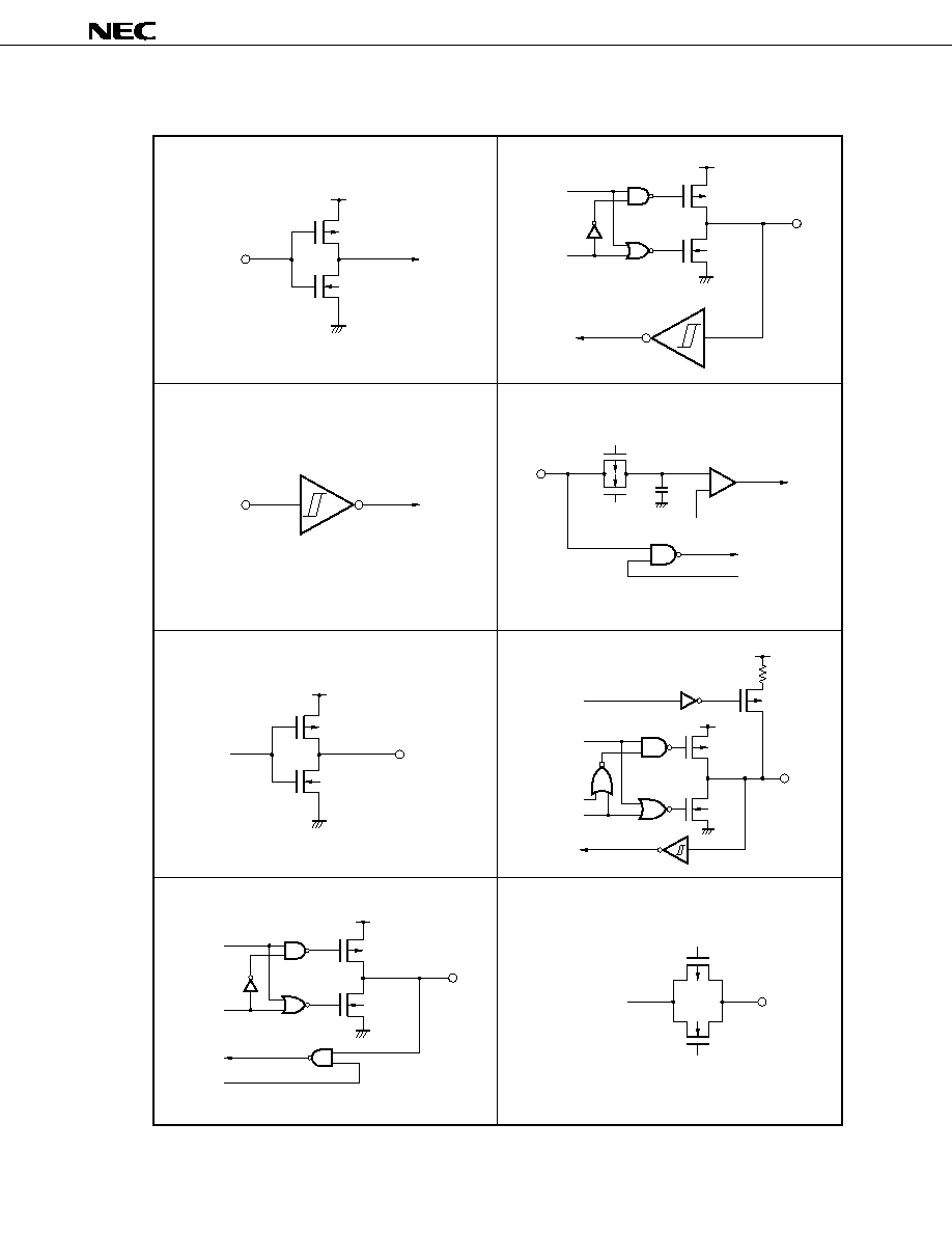
2.3 I/O Circuits of Pins and Processing of Unused Pins
Table 2-1 lists I/O circuit type of respective pins and processing method (recommended connection method) when
not used. Figure 2-1 illustrates the various circuit types using partially abridged diagrams.
When connecting to V
DD
or V
SS
via a resistor, a resistance value in the range of 1 to 10 k
is recommended.
Table 2-1. I/O Circuits of Pins and Processing of Unused Pins (1/2)
Pin
I/O Circuit Type
Recommended Connection Method
P00/TO110, P01/TO111
5
Input: Connect to V
DD
or V
SS
separately via a resistor
P02/TCLR11, P03/TI11,
8
Output: Leave open
P04/INTP110 to P07/INTP113/ADTRG
P10/TO120, P11/TO121
5
P12/TCLR12, P13/TI12
8
P14/INTP120
P15/INTP121/SO2
P16/INTP122/SI2
P17/INTP123/SCK2
P20/PWM0, P21/PWM1
5
P22/TXD0/SO0
P23/RXD0/SI0, P24/SCK0
8
P25/TXD1/SO1
5
P26/RXD1/SI1, P27/SCK1
8
P30/TO130, P31/TO131
5
P32/TCLR13, P33/TI13
8
P34/INTP130
P35/INTP131/SO3
10-A
P36/INTP132/SI3
P37/INTP133/SCK3
P40/AD0 to P47/AD7
5
P50/AD8 to P57/AD15
P60/A16 to P63/A19
P70/ANI0 to P77/ANI7
9
Connect directly to V
SS
P90/LBEN
5
Input: Connect to V
DD
or V
SS
separately via a resistor
P91/UBEN
Output: Leave open
P92/R/W
P93/DSTB
P94/ASTB
P95/HLDAK
P96/HLDRQ
P110/TO140, P111/TO141
P112/TCLR14, P113/TI14
8
P114/INTP140 to P117/INTP143
ANO0, ANO1
12
Leave open
NMI
2
Connect directly to V
SS

µ
PD703003
12
Data Sheet U12261EJ2V1DS00
Table 2-1. I/O Circuits of Pins and Processing of Unused Pins (2/2)
Pin
I/O Circuit Type
Recommended Connection Method
CLKOUT
3
Leave open
WAIT
1
Connect directly to V
DD
MODE
2
--
RESET
CV
DD
/CKSEL
AV
REF1
to AV
REF3
, AV
SS
--
Connect directly to V
SS
AV
DD
--
Connect directly to V
DD
IC
--
Connect directly to V
SS
13
µ
PD703003
Data Sheet U12261EJ2V1DS00
Figure 2-1. I/O Circuits of Pins
Type 1
Type 2
Type 8
Type 3
P-ch
N-ch
IN
V
DD
IN
Schmitt trigger input with hysteresis characteristics
P-ch
N-ch
V
DD
OUT
P-ch
N-ch
V
DD
IN/OUT
Data
Output
disable
Type 5
P-ch
N-ch
V
DD
IN/OUT
Data
Output
disable
Input
enable
IN
Comparator
+
≠
V
REF
(threshold voltage)
P-ch
N-ch
Input enable
Type 9
Data
output disable
P-ch
IN/OUT
V
DD
N-ch
P-ch
V
DD
Pull-up
enable
Open-drain
Type 10-A
OUT
P-ch
N-ch
Analog output voltage
Type 12

µ
PD703003
14
Data Sheet U12261EJ2V1DS00
3. FUNCTION BLOCKS
3.1 Internal Units
3.1.1 CPU
The CPU uses five-stage pipeline control to enable single-clock execution of address calculations, arithmetic logic
operations, data transfers, and almost all other instruction processing.
Other dedicated on-chip hardware, such as the multiplier (16 bits
◊
16 bits) and the barrel shifter (32 bits) help
accelerate processing of complex instructions.
3.1.2 Bus control unit (BCU)
The BCU starts a required bus cycle based on the physical address obtained by the CPU. When an instruction
is fetched from external memory space and the CPU does not send a bus cycle start request, the BCU generates a
prefetch address and prefetches the instruction code. The prefetched instruction code is stored in a prefetch queue.
3.1.3 ROM
ROM is mapped to the address space starting at 00000000H. The MODE pin can be used to select an access
enable/disable setting. ROM can be accessed by the CPU in one clock cycle when an instruction is fetched.
3.1.4 RAM
RAM is mapped to the address space starting at FFFFE000H. RAM can be accessed by the CPU in one clock
cycle when data accessed.
3.1.5 Ports
In addition to the 75 pins (port 0 to port 11) comprising I/O ports (of which eight pins comprise an input-only port),
various port pin and control pin functions can be selected for these pins.
3.1.6 Interrupt controller (INTC)
This controller handles hardware interrupt requests (NMI, INTP110 to INTP113, INTP120 to INTP123, INTP130
to INTP133, and INTP140 to INTP143) from on-chip peripheral hardware and external hardware. Eight interrupt
priority levels can be specified for these interrupt requests, and multiplexed servicing control can be performed for
interrupt sources.
3.1.7 Clock generator (CG)
An on-chip PLL enables the CPU operating clock to be supplied to resonators connected to pins X1 and X2 at 5
◊
frequency, 1
◊
frequency, and 1/2
◊
frequency. It can also be connected to an external clock instead of to the resonator.
3.1.8 Real-time pulse unit (RPU)
The RPU includes a four-channel 16-bit timer/event counter and a one-channel 16-bit interval timer, which enables
measurement of pulse intervals and frequency as well as programmable pulse output.

15
µ
PD703003
Data Sheet U12261EJ2V1DS00
3.1.9 Serial interface (SIO)
Four channels are comprised of two kinds of serial interfaces: an asynchronous serial interface (UART) and a clock-
synchronized serial interface (CSI). Two of these four channels are switchable between the UART and CSI and the
other two channels are fixed as CSI.
For UART, data is transferred via the TXD and RXD pins. The baud rate is determined by the on-chip baud rate
generator. For CSI, data is transferred via the SO, SI, and SCK pins. The baud rate can be determined by the on-
chip baud rate generator or it can be supplied from an external source.
One of the two CSI-fixed channels is used as the serial clock output, and serial output is sent via an N-ch open
drain output.
3.1.10 Pulse width modulation (PWM)
There are two channels of selectable 8/9/10/12-bit resolution PWM signal outputs. When a low pass filter is
externally connected, PWM output can be used as D/A converter output. This is suitable for actuator control
applications, such as in motors.
3.1.11 A/D converter (ADC)
This is a high-speed, high-resolution 10-bit A/D converter that includes eight analog input pins. It converts using
the sequential conversion method.
3.1.12 D/A converter (DAC)
This is an 8-bit resolution D/A converter that includes two channels. It converts using the R-2R conversion method.

µ
PD703003
16
Data Sheet U12261EJ2V1DS00
4. CPU FUNCTIONS
The CPU employs a RISC-based architecture and uses five-stage pipeline control to enable single-clock execution
of almost all instructions.
The features of the CPU functions are shown below.
∑ Minimum instruction execution time
30 ns (during internal 33-MHz operation)
∑ Address space: 16-Mbyte linear
∑ General registers: 32 bits
◊
32 registers
∑ Internal 32-bit architecture
∑ 5-stage pipeline control
∑ Multiply/divide instructions
∑ Saturated operation instructions
∑ 32-bit shift instruction: 1 clock
∑ Long/short format
∑ Four types of bit manipulation instructions
∑ Set
∑ Clear
∑ Not
∑ Test

17
µ
PD703003
Data Sheet U12261EJ2V1DS00
5. BUS CONTROL FUNCTIONS
The features of the bus control functions are shown below.
∑ Shared as port pins, connectable to external device
∑ Wait functions
∑ Programmable wait function for up to three states per two blocks
∑ External wait function using WAIT pin
∑ Idle state insertion function
∑ Bus mastering arbitration function
∑ Bus hold function

µ
PD703003
18
Data Sheet U12261EJ2V1DS00
6. INTERRUPT/EXCEPTION HANDLING FUNCTIONS
The features of the interrupt/exception handling functions are shown below.
∑ Interrupts
∑ Nonmaskable interrupt: 1 source
∑ Maskable interrupt: 32 sources
∑ 8-level programmable priority control
∑ Multiple interrupt control based on priority levels
∑ Mask specification for each maskable interrupt request
∑ Noise elimination, edge detection, and valid edge specification for external interrupt requests
∑ Exceptions
∑ Software exceptions: 32 sources
∑ Exception trap: 1 source (invalid instruction code exception)
The configuration of the interrupt/exception handling functions is shown below.
Figure 6-1. Block Diagram of Maskable Interrupt
RPU
Selector
3
210
3
210
3
2103
210
3
210
32
10
32
1032
1032
10
3
210
3
2103
210
INTM1
INTM2
INTM3
INTM4
SIO
INTCSI0
INTOV11
Internal bus
XXMKn (interrupt mask flag)
ISPR
Handler
address
generator
CPU
PSW
ID
Interrupt
request
Interrupt
request
acknowledge
HALT mode
release signal
XXPRn (priority controller)
7
0
OVIF11
OVIF12
OVIF13
OVIF14
P11IF0
P11IF1
P11IF2
P11IF3
P12IF0
P12IF1
P12IF2
P12IF3
P13IF0
P13IF1
P13IF2
P13IF3
P14IF0
P14IF1
P14IF2
P14IF3
CSIF0
CSIF1
CSIF2
CSIF3
SEIF0
SRIF0
STIF0
SEIF1
SRIF1
STIF1
ADIF
CMIF4
INTOV12
INTOV13
INTOV14
INTP110/INTCC110
INTP111/INTCC111
INTP112/INTCC112
INTP113/INTCC113
INTP120/INTCC120
INTP121/INTCC121
INTP122/INTCC122
INTP123/INTCC123
INTP130/INTCC130
INTP131/INTCC131
INTP132/INTCC132
INTP133/INTCC133
INTP140/INTCC140
INTP141/INTCC141
INTP142/INTCC142
INTP143/INTCC143
INTCM4
INTAD
INTCSI1
INTCSI2
INTCSI3
INTSER0
INTSR0
INTST0
INTSER1
INTSR1
INTST1
A/D converter
INTP110
INTP111
INTP112
INTP113
INTP120
INTP121
INTP122
INTP123
INTP130
INTP131
INTP132
INTP133
INTP140
INTP141
INTP142
INTP143
XX: Name of peripheral unit (OV, P11 to P14, CM, CS, SE, SR, ST, AD)
n: Peripheral unit number (if none exists, then 0 to 4 or 11 to 14)
19
µ
PD703003
Data Sheet U12261EJ2V1DS00
Interrupt/exception sources are shown in Table 6-1.
Table 6-1. List of Interrupts (1/2)
Interrupt/Exception Source
Default
Exception
Handler
Restored
Type
Category
Name
Control
Trigger Source
Unit
Priority
Register
Level
Code
Address
PC
Reset
Interrupt
RESET
--
Reset input
--
--
0000H
00000000H
Undefined
Nonmaskable
Interrupt
NMI
--
NMI input
--
--
0010H
00000010H
nextPC
Software
Exception TRAP0n
Note
--
TRAP instruction
--
--
004nH
Note
00000040H
nextPC
exception
Exception TRAP1n
Note
--
TRAP instruction
--
--
005nH
Note
00000050H
nextPC
Exception trap
Exception ILGOP
--
Undefined instruction code
--
--
0060H
00000060H
nextPC
Maskable
Interrupt
INTOV11
OVIC11 Timer 11 overflow
RPU
0
0080H
00000080H
nextPC
Interrupt
INTOV12
OVIC12 Timer 12 overflow
RPU
1
0090H
00000090H
nextPC
Interrupt
INTOV13
OVIC13 Timer 13 overflow
RPU
2
00A0H
000000A0H
nextPC
Interrupt
INTOV14
OVIC14 Timer 14 overflow
RPU
3
00B0H
000000B0H
nextPC
Interrupt
INTP110/INTCC110 P11IC0
Match between INTP110 and CC110
Pin/RPU
4
00C0H
000000C0H nextPC
Interrupt
INTP111/INTCC111 P11IC1
Match between INTP111 and CC111
Pin/RPU
5
00D0H
000000D0H nextPC
Interrupt
INTP112/INTCC112 P11IC2
Match between INTP112 and CC112
Pin/RPU
6
00E0H
000000E0H
nextPC
Interrupt
INTP113/INTCC113 P11IC3
Match between INTP113 and CC113
Pin/RPU
7
00F0H
000000F0H
nextPC
Interrupt
INTP120/INTCC120 P12IC0
Match between INTP120 and CC120
Pin/RPU
8
0100H
00000100H
nextPC
Interrupt
INTP121/INTCC121 P12IC1
Match between INTP121 and CC121
Pin/RPU
9
0110H
00000110H
nextPC
Interrupt
INTP122/INTCC122 P12IC2
Match between INTP122 and CC122
Pin/RPU
10
0120H
00000120H
nextPC
Interrupt
INTP123/INTCC123 P12IC3
Match between INTP123 and CC123
Pin/RPU
11
0130H
00000130H
nextPC
Interrupt
INTP130/INTCC130 P13IC0
Match between INTP130 and CC130
Pin/RPU
12
0140H
00000140H
nextPC
Interrupt
INTP131/INTCC131 P13IC1
Match between INTP131 and CC131
Pin/RPU
13
0150H
00000150H
nextPC
Interrupt
INTP132/INTCC132 P13IC2
Match between INTP132 and CC132
Pin/RPU
14
0160H
00000160H
nextPC
Interrupt
INTP133/INTCC133 P13IC3
Match between INTP133 and CC133
Pin/RPU
15
0170H
00000170H
nextPC
Interrupt
INTP140/INTCC140 P14IC0
Match between INTP140 and CC140
Pin/RPU
16
0180H
00000180H
nextPC
Interrupt
INTP141/INTCC141 P14IC1
Match between INTP141 and CC141
Pin/RPU
17
0190H
00000190H
nextPC
Interrupt
INTP142/INTCC142 P14IC2
Match between INTP142 and CC142
Pin/RPU
18
01A0H
000001A0H
nextPC
Interrupt
INTP143/INTCC143 P14IC3
Match between INTP143 and CC143
Pin/RPU
19
01B0H
000001B0H
nextPC
Interrupt
INTCM4
CMIC4
Signal matches CM4
RPU
20
01C0H
000001C0H nextPC
Interrupt
INTCSI0
CSIC0
CSI0 send/receive completion
SIO
21
01D0H
000001D0H nextPC
Interrupt
INTCSI1
CSIC1
CSI1 send/receive completion
SIO
22
01E0H
000001E0H
nextPC
Interrupt
INTCSI2
CSIC2
CSI2 send/receive completion
SIO
23
01F0H
000001F0H
nextPC
Note n represents a value between 0 and FH.
Remarks 1. Default priority: The default priority level is the level that takes precedence when multiple
maskable interrupt requests having the same priority level occur at the same
time. The highest priority level is level 0.
Restored PC: This is the PC value that is saved to EIPC or FEPC when interrupt or exception
handling is activated. However, if an interrupt occurs during execution of the
DIVH (divide) instruction, the recovered PC value is the PC value of the current
instruction (DIVH).
2. The invalid instruction execution address can be obtained (using restored PC-4) when an invalid
instruction code exception occurs.
µ
PD703003
20
Data Sheet U12261EJ2V1DS00
Table 6-1. List of Interrupts (2/2)
Interrupt/Exception Source
Default
Exception
Handler
Restored
Type
Category
Name
Control
Trigger Source
Unit
Priority
Register
Level
Code
Address
PC
Maskable
Interrupt
INTCSI3
CSIC3
CSI3 transmit/receive completion
SIO
24
0200H
00000200H
nextPC
Interrupt
INTSER0
SEIC0
UART0 receive error
SIO
25
0210H
00000210H
nextPC
Interrupt
INTSR0
SRIC0
UART0 receive completion
SIO
26
0220H
00000220H
nextPC
Interrupt
INTST0
STIC0
UART0 transmit completion
SIO
27
0230H
00000230H
nextPC
Interrupt
INTSER1
SEIC1
UART1 receive error
SIO
28
0240H
00000240H
nextPC
Interrupt
INTSR1
SRIC1
UART1 receive completion
SIO
29
0250H
00000250H
nextPC
Interrupt
INTST1
STIC1
UART1 transmit completion
SIO
30
0260H
00000260H
nextPC
Interrupt
INTAD
ADIC
A/D conversion completion
ADC
31
0270H
00000270H
nextPC
Remarks 1. Default priority: The default priority level is the level that takes precedence when multiple
maskable interrupt requests having the same priority level occur at the same
time. The highest priority level is level 0.
Restored PC: This is the PC value that is saved to EIPC or FEPC when interrupt or exception
handling is started. However, if an interrupt occurs during execution of the DIVH
(divide) instruction, the restored PC value is the PC value of the current instruction
(DIVH).
2. The invalid instruction execution address can be obtained using (restored PC-4) when an invalid
instruction code exception occurs.

21
µ
PD703003
Data Sheet U12261EJ2V1DS00
7. CLOCK GENERATION FUNCTIONS
The features of the clock generation functions are shown below.
∑ Multiplier function using PLL clock synthesizer
∑ Clock sources
∑ Oscillation via resonator connection (PLL mode): f
XX
=
, 2
◊
,
/5
∑ External clock (PLL mode): f
XX
=
, 2
◊
,
/5
∑ External clock (direct mode): f
XX
= 2
◊
∑ Power saving control
∑ HALT mode
∑ IDLE mode
∑ Software STOP mode
∑ Clock output inhibit mode
The configuration of the clock generation functions is shown below.
Figure 7-1. Block Diagram of Clock Generation Functions
X1
X2
CKSEL
(f
XX
)
CLKOUT
CPU, On-chip peripheral I/O
Clock generator
Remark
: internal system clock

µ
PD703003
22
Data Sheet U12261EJ2V1DS00
8. TIMER/COUNTER FUNCTIONS (REAL-TIME PULSE UNIT)
The features of the timer/counter functions are shown below.
∑ Measurement of pulse interval and frequency, programmable pulse output
∑ 16-bit measurements enabled
∑ Generates a variety of pulse patterns (interval pulse, one-shot pulse, etc.)
∑ Timer 1
∑ 16-bit timer/event counter
∑ Count clock sources: two types (selection of an internal system clock division, external pulse input)
∑ Capture/compare (shared) registers: 16
∑ Count clear pins: TCLR11 to TCLR14
∑ Interrupt sources: 20 types
∑ External pulse outputs: 8
∑ Timer 4
∑ 16-bit interval timer
∑ Count clock: selected from an internal system clock division
∑ Compare register: 1
∑ Interrupt sources: 1
23
µ
PD703003
Data Sheet U12261EJ2V1DS00
The configurations of the timer/counter functions are shown below.
Figure 8-1. Block Diagram of Timer 1 (16-bit timer/event counter)
Notes 1. Internal count clock
2. External count clock
3. Priority to reset
Remark
: internal system clock
n = 1 to 4
Figure 8-2. Block Diagram of Timer 4 (16-bit interval timer)
Note Internal count clock
Remark
: Internal system clock
m
m/4
m/8
m/32
/2
/4
m
TCLR1n
TI1n
INTP1n0
INTP1n1
INTP1n2
INTP1n3
Note 2
Note 1
Clear and start
TM1n (16 bits)
CC1n0
CC1n1
CC1n2
CC1n3
INTOV1n
INTCC1n0
INTCC1n1
S
R
Note3
Q
Q
S
Q
Q
R
Note3
INTCC1n2
INTCC1n3
TO1n0
TO1n1
Edge
detect
Clear and
start
Edge detect
Edge detect
Edge detect
Edge detect
Edge detect
TM4 (16-bit)
CM4
Clear and start
INTCM4
Note
m
m/32
m
/2
/4
/16
/32

µ
PD703003
24
Data Sheet U12261EJ2V1DS00
9. SERIAL INTERFACE FUNCTIONS (SIO)
Two types and six channels of serial interfaces are provided.
Up to four channels may be used at the same time.
(1) Asynchronous serial interfaces 0, 1 (UART0, UART1): 2 channels
(2) Clock-synchronized serial interfaces 0 to 3 (CSI0 to CSI3): 4 channels
Caution
UART0 and CSI0 are a shared pin, as are UART1 and CSI1. Either one can be selected via a
register (ASIM00, ASIM10).
9.1 Asynchronous Serial Interfaces 0, 1 (UART0, UART1)
The features of the asynchronous serial interfaces 0, 1 (UART0, UART1) are shown below.
∑ Transfer rate
150 bps to 76800 bps (@
= 33-MHz operation, using baud rate generator)
110 bps to 307200 bps (@
= 20-MHz operation, using baud rate generator)
Maximum 1031 Kbytes (@
= 33-MHz operation, using
/2)
∑ Full duplex communications: Receive buffer (RXBn) included
∑ Two-pin configuration
TXDn: output pin for transmit data
RXDn: input pin for receive data
∑ Reception error detection function
∑ Parity error
∑ Framing error
∑ Overrun error
∑ Three types of interrupt sources
∑ Reception error interrupt (INTSERn)
∑ Reception completion interrupt (INTSRn)
∑ Transmission completion interrupt (INTSTn)
∑ The character length of transmit and receive data is specified via the ASIMn0, ASIMn1 register
∑ Character lengths: 7 or 8 bits, or 9 bits (if using expansion bit)
∑ Parity function: even, odd, zero, or no parity
∑ Transmission stop bits: 1 or 2 bits
∑ On-chip baud rate generator
Remark n = 0, 1
: internal system clock

25
µ
PD703003
Data Sheet U12261EJ2V1DS00
The configuration of the asynchronous serial interfaces 0, 1 (UART0, UART1) are shown below.
Figure 9-1. Block Diagram of Asynchronous Serial Interfaces 0, 1 (UART0, UART1)
Internal bus
16/8
Receive
buffer
8
RXBn
RXBnL
Receive
shift register
Transmit
shift register
RXDn
TXDn
Reception
control
parity check
Transmission
control parity
attachment
1
16
INTSRn
INTSERn
PEn FEn OVEn SOTn
ASISn
16/8
TXSn
TXSnL
INTSTn
Selector
1
16
1
2
Baud rate generator
8
8
ASIMn0
ASIMn1
EBSn
RXEn
TXEn
PSn1 PSn0 CLn SLn SCLSn
Remark n = 0, 1
: internal system clock

µ
PD703003
26
Data Sheet U12261EJ2V1DS00
9.2 Clock-synchronized Serial Interfaces 0 to 3 (CSI0 to CSI3)
The features of the clock-synchronized serial interfaces 0 to 3 (CSI0 to CSI3) are shown below.
∑ Number of channels: 4 channels (CSIn)
∑ High-speed transfer
MAX 8.25 Mbps (@
= 33-MHz operation)
∑ Half-duplex communications
∑ Character length uses 8-bit unit
∑ Switchable byte ordering (MSB first or LSB first)
∑ Selectable external serial clock input/internal serial clock output
∑ 3-wire type
SOn: Serial data output
SIn:
Serial data input
SCKn: Serial clock I/O
∑ Interrupt source: 1 type
∑
Transmission/reception completion interrupt (INTCSIn)
Remark n = 0 to 3
: internal system clock

27
µ
PD703003
Data Sheet U12261EJ2V1DS00
The configuration of the clock-synchronized serial interfaces 0 to 3 (CSI0 to CSI3) is shown below.
Figure 9-2. Block Diagram of Clock-synchronized Serial Interfaces 0 to 3 (CSI0 to CSI3)
Note
SO0 to SO2, SCK0 to SCK2: CMOS outputs
SO3, SCK3:
N-ch open-drain outputs
Remark n = 0 to 3
: internal system clock
Internal bus
CTXEn CRXEn CSOTn MODn
CLSn1 CLSn0
CSIMn
SIn
SOn
SCKn
Shift register (SIOn)
SO latch
D
Q
2
1
Serial clock
control circuit
Serial clock
counter
Interrupt
control circuit
INTCSIn
Baud rate generator
/2
Note
Note
Selector
Selector

µ
PD703003
28
Data Sheet U12261EJ2V1DS00
9.3 Baud Rate Generators 0 to 2 (BRG0 to BRG2)
The features of the baud rate generators 0 to 2 (BRG0 to BRG2) are shown below.
∑ Serial clock can be selected via baud rate generator output and
(internal system clock)
∑ Identical baud rates during transmission and reception
The configuration of the baud rate generators 0 to 2 (BRG0 to BRG2) is shown below.
Figure 9-3. Block Diagram of Baud Rate Generators 0 to 2 (BRG0 to BRG2)
Baud rate generator 0
Baud rate generator 1
Baud rate generator 2
Internal bus
1
2
Prescaler
TMBRG0
Clear
BRG0
Match
BPRM0
BRCE0
BPR02
BPR01
BPR00
UART0
CSI0
UART1
CSI1
CSI2
CSI3

29
µ
PD703003
Data Sheet U12261EJ2V1DS00
10. PWM UNIT
The features of the PWM unit are shown below.
∑ PWMn: 2 channels
∑ Selectable active level for PWMn output pulse
∑ Operating clock selectable as
,
/2,
/4,
/8, or
/16 (
: internal system clock)
∑ PWMn output resolution selectable as 8, 9, 10, or 12 bits
Remark n = 0, 1
The configuration of the PWM unit is shown below.
Figure 10-1. Block Diagram of PWM Unit
Note Priority to reset
Remark n = 0, 1
: internal system clock
TMPn (12 bits)
Comparator
CMPn (12 bits)
PWMn (12 bits)
/2
/4
/8
/16
Overflow
Match
7
8
9
11
0-7
0-8
0-9
0-11
S
Q
R
Note
ALVn
PWMn

µ
PD703003
30
Data Sheet U12261EJ2V1DS00
11. A/D CONVERTER
The features of the A/D converter are shown below.
∑ Analog inputs: 8 channels
∑ On-chip 10-bit A/D converter
∑ On-chip A/D conversion result registers (ADCR0 to ADCR7)
10 bits
◊
8 registers
∑ A/D conversion trigger modes
A/D trigger mode
Timer trigger mode
External trigger mode
∑ Sequential conversion method
The configuration of the A/D converter is shown below.
Figure 11-1. Block Diagram of A/D Converter
Internal bus
ANI0
ANI1
ANI2
ANI3
ANI4
ANI5
ANI6
ANI7
INTAD
Controller
ADM0 (8)
ADM1 (8)
7
8
8
10
10
10
ADCR0
SAR (10)
Voltage comparator
Tap selector
ADCR1
ADCR2
ADCR3
ADCR4
ADCR5
ADCR6
ADCR7
7
0
0
0
9
0
R/2
Series resistor string
Sample & hold circuit
AV
REF1
AV
SS
AV
DD
R
R/2
9
INTCC110
INTCC111
INTCC112
Noise
elimination
Edge
detection
INTCC113
ADTRG
Input circuit

31
µ
PD703003
Data Sheet U12261EJ2V1DS00
12. D/A CONVERTER
The features of the D/A converter are shown below.
∑ 8-bit resolution D/A converter: 2 channels
∑ R-2R conversion method
The configuration of the D/A converter is shown below.
Figure 12-1. Block Diagram of D/A Converter
Remark n = 0, 1
DACSn
Selector
DACEn
2R
2R
2R
2R
R
R
ANOn
AV
REF2
AV
REF3
Internal bus

µ
PD703003
32
Data Sheet U12261EJ2V1DS00
13. PORT FUNCTIONS
The features of the port functions are shown below.
∑
Number of ports
Input-only ports:
8
I/O ports:
67
∑ Alternated as I/O pins for other peripheral functions
∑ I/O setting can be specified bitwise
∑ Noise elimination
∑ Edge detection
The configurations of the port functions are shown below.
Figure 13-1. Block Diagram of P00 and P01 (Port 0)
Remark
n = 0, 1
WR
PMC
WR
PM
WR
PORT
RD
IN
PMC0n
Internal bus
PM0n
P0n
Selector
Selector
Selector
TO11n
P0n
Address

33
µ
PD703003
Data Sheet U12261EJ2V1DS00
Figure 13-2. Block Diagram of P02 to P07 (Port 0)
Remark
n = 2 to 7
Figure 13-3. Block Diagram of P10 and P11 (Port 1)
Remark
n = 0, 1
WR
PMC
WR
PM
WR
PORT
RD
IN
PMC0n
Internal bus
PM0n
P0n
Noise elimination
Edge detection
P0n
INTP110-INTP112,
INTP113/ADTRG,
TCLR11, TI11
Address
Selector
Selector
WR
PM
WR
PORT
RD
IN
PM1n
TO12n
WR
PMC
PMC1n
P1n
P1n
Internal bus
Address
Selector
Selector
Selector

µ
PD703003
34
Data Sheet U12261EJ2V1DS00
Figure 13-4. Block Diagram of P12 to P14 (Port 1)
Remark
n = 2 to 4
Figure 13-5. Block Diagram of P15 (Port 1)
PMC1n
PM1n
P1n
RD
IN
WR
PORT
WR
PM
WR
PMC
P1n
TCLR12, TI12
INTP120
Internal bus
Noise elimination
Edge detection
Address
Selector
Selector
PMC15
PM15
P15
RD
IN
WR
PORT
WR
PM
WR
PMC
P15
INTP121
SO2
PCM1
PCM1
Internal bus
Noise elimination
Edge detection
Address
Selector
Selector
Selector

35
µ
PD703003
Data Sheet U12261EJ2V1DS00
Figure 13-6. Block Diagram of P16 (Port 1)
Figure 13-7. Block Diagram of P17 (Port 1)
PMC16
PM16
P16
RD
IN
WR
PORT
WR
PM
WR
PMC
P16
INTP122
SI2
PCM1
Internal bus
Noise elimination
Edge detection
Address
Selector
Selector
PMC17
PM17
P17
RD
IN
WR
PORT
WR
PM
WR
PMC
P17
INTP123
SCK2 output
PCM1
SCK2 output
SCK2 I/O
switch
PCM1
Internal bus
Noise elimination
Edge detection
Address
Selector
Selector
Selector

µ
PD703003
36
Data Sheet U12261EJ2V1DS00
Figure 13-8. Block Diagram of P20 and P21 (Port 2)
Remark
n = 0, 1
Figure 13-9. Block Diagram of P22 and P25 (Port 2)
Remark
n = 2, 5
PMC2n
PM2n
P2n
RD
IN
WR
PORT
WR
PM
WR
PMC
PWM0, PWM1
P2n
Internal bus
Address
Selector
Selector
Selector
PMC2n
PM2n
P2n
RD
IN
WR
PORT
WR
PM
WR
PMC
TXD0/SO0
TXD1/SO1
P2n
SO0, SO1 output
enable
Internal bus
Address
Selector
Selector
Selector

37
µ
PD703003
Data Sheet U12261EJ2V1DS00
Figure 13-10. Block Diagram of P23 and P26 (Port 2)
Remark
n = 3, 6
Figure 13-11. Block Diagram of P24 and P27 (Port 2)
Remark
n = 4, 7
PMC2n
PM2n
P2n
RD
IN
WR
PORT
WR
PM
WR
PMC
P2n
RXD0/SI0
RXD1/SI1
Internal bus
Address
Selector
Selector
PMC2n
PM2n
P2n
RD
IN
WR
PORT
WR
PM
WR
PMC
P2n
SCK0 input
SCK1 input
SCK0 output
SCK1 output
SCK0, SCK1
I/O switch
Internal bus
Address
Selector
Selector
Selector

µ
PD703003
38
Data Sheet U12261EJ2V1DS00
Figure 13-12. Block Diagram of P30 and P31 (Port 3)
Remark
n = 0, 1
Figure 13-13. Block Diagram of P32 to P34 (Port 3)
Remark
n = 2 to 4
WR
PMC
WR
PM
WR
PORT
RD
IN
PMC3n
PM3n
P3n
TO13n
P3n
Internal bus
Address
Selector
Selector
Selector
PMC3n
PM3n
P3n
RD
IN
WR
PORT
WR
PM
WR
PMC
P3n
TCLR13, TI13
INTP130
Internal bus
Noise elimination
Edge detection
Address
Selector
Selector

39
µ
PD703003
Data Sheet U12261EJ2V1DS00
Figure 13-14. Block Diagram of P35 (Port 3)
Figure 13-15. Block Diagram of P36 (Port 3)
PMC35
PM35
P35
RD
IN
WR
PORT
WR
PM
WR
PMC
P35
INTP131
PCM3
SO3
SO3 output
enable
PCM3
PUO3
V
DD
P
N
P
Internal bus
Noise elimination
Edge detection
Address
Selector
Selector
Selector
PMC36
PM36
P36
RD
IN
WR
PORT
WR
PM
WR
PMC
P36
INTP132
PCM3
PUO3
V
DD
P
N
SI3
P
Internal bus
Noise elimination
Edge detection
Address
Selector
Selector

µ
PD703003
40
Data Sheet U12261EJ2V1DS00
Figure 13-16. Block Diagram of P37 (Port 3)
Figure 13-17. Block Diagram of P40 to P47 (Port 4)
Remark
n = 0 to 7
PMC37
PM37
P37
RD
IN
WR
PORT
WR
PM
WR
PMC
P37
INTP133
PCM3
PUO3
V
DD
P
N
SCK3 input
SCK3 output
P
SCK3 I/O
switch
PCM3
Internal bus
Noise elimination
Edge detection
Address
Selector
Selector
Selector
PM4n
P4n
RD
IN
WR
PORT
WR
PM
AD0 to AD7 output
P4n
AD0 to AD7 input
I/O control circuit
MODE
MM0 to MM2
Internal bus
Address
Selector
Selector
Selector

41
µ
PD703003
Data Sheet U12261EJ2V1DS00
Figure 13-18. Block Diagram of P50 to P57 (Port 5)
Remark
n = 0 to 7
Figure 13-19. Block Diagram of P60 to P63 (Port 6)
Remark
n = 0 to 3
PM5n
P5n
RD
IN
WR
PORT
WR
PM
P5n
I/O control circuit
MODE
MM0 to MM2
AD8 to AD15 output
AD8 to AD15 input
Internal bus
Address
Selector
Selector
Selector
PM6n
P6n
RD
IN
WR
PORT
WR
PM
A16 to A19 output
P6n
MODE
MM0 to MM2
I/O control circuit
Internal bus
Address
Selector
Selector
Selector

µ
PD703003
42
Data Sheet U12261EJ2V1DS00
Figure 13-20. Block Diagram of P70 to P77 (Port 7)
Remark
n = 0 to 7
Figure 13-21. Block Diagram of P90 to P95 (Port 9)
Remark
n = 0 to 5
RD
IN
P7n
ANI0 to ANI7
Sample & hold
circuit
Internal bus
PM9n
P9n
RD
IN
WR
PORT
WR
PM
LBEN, UBEN, R/W,
DSTB, ASTB, HLDAK
P9n
MODE
MM0 to MM3
Internal bus
Address
Selector
Selector
Selector
I/O control circuit

43
µ
PD703003
Data Sheet U12261EJ2V1DS00
Figure 13-22. Block Diagram of P96 (Port 9)
Figure 13-23. Block Diagram of P110 and P111 (Port 11)
Remark
n = 0, 1
PM96
P96
RD
IN
WR
PORT
WR
PM
P96
MM3
HLDRQ
I/O control circuit
Internal bus
Address
Selector
Selector
WR
PMC
WR
PM
WR
PORT
RD
IN
PMC11n
PM11n
P11n
TO14n
P11n
Internal bus
Address
Selector
Selector
Selector

µ
PD703003
44
Data Sheet U12261EJ2V1DS00
Figure 13-24. Block Diagram of P112 to P117 (Port 11)
Remark
n = 2 to 7
PMC11n
PM11n
P11n
RD
IN
WR
PORT
WR
PM
WR
PMC
P11n
TCLR14, TI14
INTP140 to INTP143
Internal bus
Noise elimination
Edge detection
Selector
Selector
Address

45
µ
PD703003
Data Sheet U12261EJ2V1DS00
14. RESET FUNCTIONS
When low-level input occurs at the RESET pin, a system reset is performed and the various on-chip hardware
devices are reset to their initial settings.
When the input at the RESET pin changes from low level to high level, the reset status is canceled and the CPU
resumes program execution. The contents of the various registers should be initialized within the program as
necessary.
The feature of the reset functions is shown below.
∑ On-chip noise elimination circuit which uses analog delay (
60 ns) for the RESET pin

µ
PD703003
46
Data Sheet U12261EJ2V1DS00
15. INSTRUCTION SET
∑ How to read instruction set tables
Table 15-1. Symbols Used to Indicate Operands
Symbol
Description
reg1
General registers (r0 to r31): used as source registers
reg2
General registers (r0 to r31): mainly used as destination registers
ep
Element pointer (r30)
bit#3
3-bit data used to specify bit number
immX
X bits immediate
dispX
X bits displaced
regID
System register number
vector
5-bit data used to specify trap vector (00H to 1FH)
cccc
4-bit data used to indicate condition code
Indicates the instruction group. Instructions are listed in these table according to their respective groups.
Indicates the mnemonic abbreviation for the instruction.
Indicates the instruction's operands (see Table 15-1).
Indicates the instruction binary code. The binary codes for 32-bit
instructions are shown in two levels (see Table 15-2).
Indicates instruction operation (see Table 15-3).
Indicates flag operations
(see Table 15-4).
Mnemonic
Operand
Opcode
Operation
Flags
CY
OV
S
Z
SAT
Instruction
group

47
µ
PD703003
Data Sheet U12261EJ2V1DS00
Table 15-2. Symbols Used to Indicate Opcodes
Symbol
Description
R
1-bit data of code specifying reg1 or regID
r
1-bit data of code specifying reg2
d
1 bit of displaced data
i
1 bit of immediate data
cccc
4-bit data used to indicate condition code
bbb
3-bit data used to specify bit number
Table 15-3. Symbols Used to Indicate Operations
Symbol
Description
Assign
GR [ ]
General register
SR [ ]
System register
zero-extend (n)
Zero-extend n up until word length
sign-extend (n)
Sign-extend n up until word length
load-memory (a, b)
Read data having size b from address a
store-memory (a, b, c)
Replace data b at address a with data having size c
load-memory-bit (a, b)
Read bit b from address a
store-memory-bit (a, b, c)
Write c to bit b from address a
saturated (n)
Execute saturation processing for n (n = complement to 2)
Calculation of n:
When n
7FFFFFFFH, result is 7FFFFFFFH.
When n
80000000H, result is 80000000H.
result
Result is indicated by flag operations
Byte
Byte (8 bits)
Halfword
Half word (16 bits)
Word
Word (32 bits)
+
Add
≠
Subtract
||
Bit linkage
◊
Multiply
˜
Divide
AND
Logical AND
OR
Logical OR
XOR
Exclusive OR
NOT
Logical NOT
logically shift left by
Logical shift left
logically shift right by
Logical shift right
arithmetically shift right by
Arithmetic shift right

µ
PD703003
48
Data Sheet U12261EJ2V1DS00
Table 15-4. Flag Operations
Identifier
Description
(Blank)
No change
0
Clear to zero
◊
Set or clear according to result
R
Restore previously saved value(s)
Table 15-5. Condition Codes
Condition name (cond)
Condition code (cccc)
Conditional expression
Description
V
0000
OV = 1
Overflow
NV
1000
OV = 0
No overflow
C/L
0001
CY = 1
Carry
Lower (Less than)
NC/NL
1001
CY = 0
No carry
No lower (Greater than or equal)
Z/E
0010
Z = 1
Zero
Equal
NZ/NE
1010
Z = 0
Not zero
Not equal
NH
0011
(CY OR Z) = 1
Not higher (Less than or equal)
H
1011
(CY OR Z) = 0
Higher (Greater than)
N
0100
S = 1
Negative
P
1100
S = 0
Positive
T
0101
≠
Always (unconditional)
SA
1101
SAT = 1
Saturated
LT
0110
(S XOR OV) = 1
Less than signed
GE
1110
(S XOR OV) = 0
Greater than or equal signed
LE
0111
((S XOR OV) OR Z) = 1
Less than or equal signed
GT
1111
((S XOR OV) OR Z) = 0
Greater than signed

49
µ
PD703003
Data Sheet U12261EJ2V1DS00
Instruction Set List
Instruction Mnemonic
Operand
Opcode
Operation
Flags
group
CY OV S
Z
SAT
Load/store
SLD.B
disp7[ep], reg2
r r r r r 0 1 1 0 d d d d d d d adr
ep + zero-extend (disp7)
instructions
GR[reg2]
sign-extend (Load-memory (adr, Byte))
SLD.H
disp8[ep], reg2
r r r r r 1 0 0 0 d d d d d d d adr
ep + zero-extend (disp8)
Note 1 GR[reg2]
sign-extend (Load-memory (adr, Halfword))
SLD.W
disp8[ep], reg2
r r r r r 1 0 1 0 d d d d d d 0 adr
ep + zero-extend (disp8)
Note 2 GR[reg2]
Load-memory (adr, Word)
LD.B
disp16[reg1], reg2
r r r r r 1 1 1 0 0 0 RRRRR adr
GR[reg1] + sign-extend (disp16)
d d d d d d d d d d d d d d d d GR[reg2]
sign-extend (Load-memory (adr, Byte))
LD.H
disp16[reg1], reg2
r r r r r 1 1 1 0 0 1 RRRRR adr
GR[reg1] + sign-extend (disp16)
d d d d d d d d d d d d d d d 0 GR[reg2]
sign-extend (Load-memory (adr, Halfword))
Note 3
LD.W
disp16[reg1], reg2
r r r r r 1 1 1 0 0 1 RRRRR adr
GR[reg1] + sign-extend (disp16)
d d d d d d d d d d d d d d d 1 GR[reg2]
Load-memory (adr, Word)
Note 3
SST.B
reg2, disp7[ep]
r r r r r 0 1 1 1 d d d d d d d adr
ep + zero-extend (disp7)
Store-memory (adr, GR[reg2], Byte)
SST.H
reg2, disp8[ep]
r r r r r 1 0 0 1 d d d d d d d adr
ep + zero-extend (disp8)
Note 1 Store-memory (adr, GR[reg2], Halfword)
SST.W
reg2, disp8[ep]
r r r r r 1 0 1 0 d d d d d d 1 adr
ep + zero-extend (disp8)
Note 2 Store-memory (adr, GR[reg2], Word)
ST.B
reg2, disp16[reg1]
r r r r r 1 1 1 0 1 0 RRRRR adr
GR[reg1] + sign-extend (disp16)
d d d d d d d d d d d d d d d d Store-memory (adr, GR[reg2], Byte)
ST.H
reg2, disp16[reg1]
r r r r r 1 1 1 0 1 1 RRRRR adr
GR[reg1] + sign-extend (disp16)
d d d d d d d d d d d d d d d 0 Store-memory (adr, GR[reg2], Halfword)
Note 3
ST.W
reg2, disp16[reg1]
r r r r r 1 1 1 0 1 1 RRRRR adr
GR[reg1] + sign-extend (disp16)
d d d d d d d d d d d d d d d 1 Store-memory (adr, GR[reg2], Word)
Note 3
Arithmetic MOV
reg1, reg2
r r r r r 0 0 0 0 0 0 RRRRR GR[reg2]
GR[reg1]
operation
MOV
imm5, reg2
r r r r r 0 1 0 0 0 0 i i i i i
GR[reg2]
sign-extend (imm5)
instructions
MOVHI
imm16, reg1, reg2
r r r r r 1 1 0 0 1 0 RRRRR GR[reg2]
GR[reg1] + (imm16 || 0
16
)
i i i i i i i i i i i i i i i i
MOVEA
imm16, reg1, reg2
r r r r r 1 1 0 0 0 1 RRRRR GR[reg2]
GR[reg1] + sign-extend (imm16)
i i i i i i i i i i i i i i i i
ADD
reg1, reg2
r r r r r 0 0 1 1 1 0 RRRRR GR[reg2]
GR[reg2] + GR[reg1]
◊ ◊ ◊ ◊
ADD
imm5, reg2
r r r r r 0 1 0 0 1 0 i i i i i
GR[reg2]
GR[reg2] + sign-extend (imm5)
◊ ◊ ◊ ◊
ADDI
imm16, reg1, reg2
r r r r r 1 1 0 0 0 0 RRRRR GR[reg2]
GR[reg1] + sign-extend (imm16)
◊ ◊ ◊ ◊
i i i i i i i i i i i i i i i i
SUB
reg1, reg2
r r r r r 0 0 1 1 0 1 RRRRR GR[reg2]
GR[reg2] ≠ GR[reg1]
◊ ◊ ◊ ◊
SUBR
reg1, reg2
r r r r r 0 0 1 1 0 0 RRRRR GR[reg2]
GR[reg1] ≠ GR[reg2]
◊ ◊ ◊ ◊
Notes 1. ddddddd = high-order 7 bits of disp8
2. dddddd = high-order 6 bits of disp8
3. ddddddddddddddd = high-order 15 bits of disp16

µ
PD703003
50
Data Sheet U12261EJ2V1DS00
Instruction Mnemonic
Operand
Opcode
Operation
Flags
group
CY OV S Z
SAT
Arithmetic MULH
reg1, reg2
r r r r r 0 0 0 1 1 1 RRRRR GR[reg2]
GR[reg2]
Note
◊
GR[reg1]
Note
operation
(signed multiplication)
instructions
MULH
imm5, reg2
r r r r r 0 1 0 1 1 1 i i i i i
GR[reg2]
GR[reg2]
Note
◊
sign-extend (imm5)
(signed multiplication)
MULHI
imm16, reg1, reg2
r r r r r 1 1 0 1 1 1 RRRRR GR[reg2]
GR[reg1]
Note
◊
imm16
i i i i i i i i i i i i i i i i
(signed multiplication)
DIVH
reg1, reg2
r r r r r 0 0 0 0 1 0 RRRRR GR[reg2]
GR[reg2]
˜
GR[reg1]
Note
(signed division)
◊ ◊ ◊
CMP
reg1, reg2
r r r r r 0 0 1 1 1 1 RRRRR result
GR[reg2] ≠ GR[reg1]
◊ ◊ ◊ ◊
CMP
imm5, reg2
r r r r r 0 1 0 0 1 1 i i i i i
result
GR[reg2] ≠ sign-extend (imm5)
◊ ◊ ◊ ◊
SETF
cccc, reg2
r r r r r 1 1 1 1 1 1 0 c c c c if conditions are satisfied
0 0 0 0 0 0 0 0 0 0 0 0 0 0 0 0 then GR[reg2]
00000001H
else GR[reg2]
00000000H
Saturated SATADD reg1, reg2
r r r r r 0 0 0 1 1 0 RRRRR GR[reg2]
saturated (GR[reg2] + GR[reg1])
◊ ◊ ◊ ◊ ◊
operation
SATADD imm5, reg2
r r r r r 0 1 0 0 0 1 i i i i i
GR[reg2]
saturated (GR[reg2] + sign-extend (imm5))
◊ ◊ ◊ ◊ ◊
instructions
SATSUB reg1, reg2
r r r r r 0 0 0 1 0 1 RRRRR GR[reg2]
saturated (GR[reg2] ≠ GR[reg1])
◊ ◊ ◊ ◊ ◊
SATSUBI imm16, reg1, reg2
r r r r r 1 1 0 0 1 1 RRRRR GR[reg2]
saturated (GR[reg1] ≠ sign-extend (imm16))
◊ ◊ ◊ ◊ ◊
i i i i i i i i i i i i i i i i
SATSUBR reg1, reg2
r r r r r 0 0 0 1 0 0 RRRRR GR[reg2]
saturated (GR[reg1] ≠ GR[reg2])
◊ ◊ ◊ ◊ ◊
Logical
TST
reg1, reg2
r r r r r 0 0 1 0 1 1 RRRRR result
GR[reg2]AND GR[reg1]
0
◊ ◊
operation
OR
reg1, reg2
r r r r r 0 0 1 0 0 0 RRRRR GR[reg2]
GR[reg2]OR GR[reg1]
0
◊ ◊
instruction
ORI
imm16, reg1, reg2
r r r r r 1 1 0 1 0 0 RRRRR GR[reg2]
GR[reg1]OR zero-extend (imm16)
0
◊ ◊
i i i i i i i i i i i i i i i i
AND
reg1, reg2
r r r r r 0 0 1 0 1 0 RRRRR GR[reg2]
GR[reg2]AND GR[reg1]
0
◊ ◊
ANDI
imm16, reg1, reg2
r r r r r 1 1 0 1 1 0 RRRRR GR[reg2]
GR[reg1]AND zero-extend (imm16)
0 0
◊
i i i i i i i i i i i i i i i i
XOR
reg1, reg2
r r r r r 0 0 1 0 0 1 RRRRR GR[reg2]
GR[reg2]XOR GR[reg1]
0
◊ ◊
XORI
imm16, reg1, reg2
r r r r r 1 1 0 1 0 1 RRRRR GR[reg2]
GR[reg1]XOR zero-extend (imm16)
0
◊ ◊
i i i i i i i i i i i i i i i i
NOT
reg1, reg2
r r r r r 0 0 0 0 1 RRRRR
GR[reg2]
NOT (GR[reg1])
0
◊ ◊
SHL
reg1, reg2
r r r r r 1 1 1 1 1 1 RRRRR GR[reg2]
GR[reg2]logically shift left by GR[reg1]
◊
0
◊ ◊
0 0 0 0 0 0 0 0 1 1 0 0 0 0 0 0
SHL
imm5, reg2
r r r r r 0 1 0 1 1 0 i i i i i
GR[reg2]
GR[reg2]logically shift left by
◊
0
◊ ◊
zero-extend (imm5)
SHR
reg1, reg2
r r r r r 1 1 1 1 1 1 RRRRR GR[reg2]
GR[reg2]logically shift right by GR[reg1]
◊
0
◊ ◊
0 0 0 0 0 0 0 0 1 0 0 0 0 0 0 0
SHR
imm5, reg2
r r r r r 0 1 0 1 0 0 i i i i i
GR[reg2]
GR[reg2]logically shift right by
◊
0
◊ ◊
zero-extend (imm5)
SAR
reg1, reg2
r r r r r 1 1 1 1 1 1 RRRRR GR[reg2]
GR[reg2]arithmetically shift right by
◊
0
◊ ◊
0 0 0 0 0 0 0 0 1 0 1 0 0 0 0 0
GR[reg1]
SAR
imm5, reg2
r r r r r 0 1 0 1 0 1 i i i i i
GR[reg2]
GR[reg2]arithmetically shift right by
◊
0
◊ ◊
zero-extend (imm5)
Note Only the low-order half word is valid.

51
µ
PD703003
Data Sheet U12261EJ2V1DS00
Instruction Mnemonic
Operand
Opcode
Operation
Flags
group
CY OV S
Z
SAT
Branch
JMP
[reg1]
0 0 0 0 0 0 0 0 0 1 1 RRRRR PC
GR[reg1]
instructions
JR
disp22
0 0 0 0 0 1 1 1 1 0 d d d d d d PC
PC + sign-extend (disp22)
d d d d d d d d d d d d d d d 0
Note 1
JARL
disp22, reg2
r r r r r 1 1 1 1 0 d d d d d d GR[reg2]
PC + 4
d d d d d d d d d d d d d d d 0 PC
PC + sign-extend (disp22)
Note 1
Bcond
disp9
d d d d d 1 0 1 1 d d d c c c c if conditions are satisfied
Note 2 then PC
PC + sign-extend (disp9)
Bit
SET1
bit#3, disp16[reg1] 0 0 b b b 1 1 1 1 1 0 RRRRR adr
GR[reg1] + sign-extend (disp16)
◊
manipulation
d d d d d d d d d d d d d d d d Z flag
Not (Load-memory-bit (adr, bit#3))
instructions
Store-memory-bit (adr, bit#3, 1)
CLR1
bit#3, disp16[reg1] 1 0 b b b 1 1 1 1 1 0 RRRRR adr
GR[reg1] + sign-extend (disp16)
◊
d d d d d d d d d d d d d d d d Z flag
Not (Load-memory-bit (adr, bit#3))
Store-memory-bit (adr, bit#3, 0)
NOT1
bit#3, disp16[reg1] 0 1 b b b 1 1 1 1 1 0 RRRRR adr
GR[reg1] + sign-extend (disp16)
◊
d d d d d d d d d d d d d d d d Z flag
Not (Load-memory-bit (adr, bit#3))
Store-memory-bit (adr, bit#3, Z flag)
TST1
bit#3, disp16[reg1] 1 1 b b b 1 1 1 1 1 0 RRRRR adr
GR[reg1] + sign-extend (disp16)
◊
d d d d d d d d d d d d d d d d Z flag
Not (Load-memory-bit (adr, bit#3))
Notes 1. ddddddddddddddddddddd = high-order 21 bits of disp22
2. dddddddd = high-order 8 bits of disp9

µ
PD703003
52
Data Sheet U12261EJ2V1DS00
Instruction Mnemonic
Operand
Opcode
Operation
Flags
group
CY OV S Z
SAT
Special
LDSR
reg2, regID
r r r r r 1 1 1 1 1 1 RRRRR SR[regID]
GR[reg2]
regID = EIPC, FEPC
instructions
0 0 0 0 0 0 0 0 0 0 1 0 0 0 0 0
regID = EIPSW, FEPSW
Note
regID = PSW
◊ ◊ ◊ ◊ ◊
STSR
regID, reg2
r r r r r 1 1 1 1 1 1 RRRRR GR[reg2]
SR[regID]
0 0 0 0 0 0 0 0 0 1 0 0 0 0 0 0
TRAP
vector
0 0 0 0 0 1 1 1 1 1 1 i i i i i
EIPC
PC + 4 (restored PC)
0 0 0 0 0 0 0 1 0 0 0 0 0 0 0 0 EIPSW
PSW
ECR.EICC
Interrupt code
PSW.EP
1
PSW.ID
1
PC
00000040H (when vector is 00H to 0FH)
00000050H (when vector is 10H to 1FH)
RETI
0 0 0 0 0 1 1 1 1 1 1 0 0 0 0 0 if PSW.EP = 1
R
R R R R
0 0 0 0 0 0 0 1 0 1 0 0 0 0 0 0 then PC
EIPC
PSW
EIPSW
else if PSW.NP = 1
then PC
FEPC
PSW
FEPSW
else PC
EIPC
PSW
EIPSW
HALT
0 0 0 0 0 1 1 1 1 1 1 0 0 0 0 0 Stops
0 0 0 0 0 0 0 1 0 0 1 0 0 0 0 0
DI
0 0 0 0 0 1 1 1 1 1 1 0 0 0 0 0 PSW.ID
1
0 0 0 0 0 0 0 1 0 1 1 0 0 0 0 0 (maskable interrupt prohibit)
EI
1 0 0 0 0 1 1 1 1 1 1 0 0 0 0 0 PSW.ID
0
0 0 0 0 0 0 0 1 0 1 1 0 0 0 0 0 (maskable interrupt enable)
NOP
0 0 0 0 0 0 0 0 0 0 0 0 0 0 0 0 No operation, uses at least one clock
Note In this instructions, "reg2" is the mnemonic abbreviation for the source register, but the reg1 field is used
for the opcode. Consequently, these instructions differ from other instructions in a way registers are
specified in mnemonics description and opcodes.
rrrrr = regID specification
RRRRR = reg2 specification

53
µ
PD703003
Data Sheet U12261EJ2V1DS00
16. ELECTRICAL SPECIFICATIONS
Absolute Maximum Ratings (T
A
= 25
∞
C)
Parameter
Symbol
Condition
Rating
Units
Power supply voltage
V
DD
V
DD
pin
≠0.5 to +7.0
V
CV
DD
CV
DD
pin
≠0.5 to V
DD
+ 0.3
V
CV
SS
CV
SS
pin
≠0.5 to +0.5
V
AV
DD
AV
DD
pin
≠0.5 to V
DD
+ 0.3
V
AV
SS
AV
SS
pin
≠0.5 to +0.5
V
Input voltage
V
I1
Note, V
DD
= 5.0 V
±
10 %
≠0.5 to V
DD
+ 0.3
V
Clock input voltage
V
K
X1 pin, V
DD
= 5.0 V
±
10 %
≠0.5 to V
DD
+ 1.0
V
Low-level output current
I
OL
1 pin
4.0
mA
Total for all pins
100
mA
High-level output current
I
OH
1 pin
≠4.0
mA
Total for all pins
≠100
mA
Output voltage
V
O
V
DD
= 5.0 V
±
10 %
≠0.5 to V
DD
+ 0.3
V
Analog input voltage
V
IAN
P70/ANI0 to P77/ANI7
AV
DD
> V
DD
≠0.5 to V
DD
+ 0.3
V
V
DD
AV
DD
≠0.5 to AV
DD
+ 0.3
V
Analog reference input voltage
AV
REF
AV
REF1
to AV
REF3
AV
DD
> V
DD
≠0.5 to V
DD
+ 0.3
V
V
DD
AV
DD
≠0.5 to AV
DD
+ 0.3
V
Operating temperature
T
A
≠40 to +85
∞
C
Storage temperature
T
stg
≠65 to +150
∞
C
Note X1, P70/ANI0 to P77/ANI7, and AV
REF1
to AV
REF3
are excluded.
Cautions 1. Be sure to avoid direct connections among the IC device output (or I/O) pins and between
V
DD
or V
CC
and GND. However, open-drain pins and open collector pins can be directly
connected. A direct connection to an external circuit can be made to avoid conflicting
output from high-impedance pins if the external circuit is designed for the correct timing.
2. If the absolute maximum rating for any of the above parameters is exceeded even
momentarily, it may adversely affect the quality of this product. In other words, these
absolute maximum ratings have been set to prevent physical damage to the product. Do
not use the product in such a way as to exceed any of these ratings.
The ratings and conditions shown below for DC characteristics and AC characteristics
are within the range for normal operation and quality assurance.
Capacitance (T
A
= 25
∞
C, V
DD
= V
SS
= 0 V)
Parameter
Symbol
Condition
MIN.
TYP.
MAX.
Units
Input capacitance
C
I
f
C
= 1 MHz
15
pF
I/O capacitance
C
IO
All pins are 0 V except for testing pin.
15
pF
Output capacitance
C
O
15
pF

µ
PD703003
54
Data Sheet U12261EJ2V1DS00
Recommended Operating Conditions
Operation Mode
Internal Operating
Operating Ambient
Power Supply
Clock Frequency (
)
Temperature (T
A
)
Voltage (V
DD
)
Direct mode
0 to 33 MHz
Note 1
≠40 to +85
∞
C
5.0 V
±
10%
5 to 33 MHz
Note 2
≠40 to +85
∞
C
5.0 V
±
10%
PLL mode
Free-running oscillation frequency to 33 MHz
≠40 to +85
∞
C
5.0 V
±
10%
Notes 1. When not using A/D converter
2. When using A/D converter
Remark The range of internal operating clock frequency in PLL mode is the assured range of function
operation. PLL locked frequency is specified by t
CYX
.
Recommended Oscillator
(a) Ceramic oscillation resonator connection (T
A
= ≠40 to +85
∞
C)
X1
X2
C1
C2
Oscillation
Recommended Circuit
Oscillation Voltage Oscillation Stabilization
Manufacturer
Part Number
Frequency
Constant
Range
Time (MAX.)
f
XX
(MHz)
C1 (pF)
C2 (pF)
MIN. (V) MAX. (V)
T
OST
(ms)
TDK
CCR5.0MC3
5.0
On-chip
On-chip
4.5
5.5
0.36
FCR5.0MC5
5.0
On-chip
On-chip
4.5
5.5
0.32
CCR6.6MC3
6.6
On-chip
On-chip
4.5
5.5
0.28
Murata Mfg. CSA5.00MG040
5.0
100
100
4.5
5.5
0.46
CST5.00MGW040
5.0
On-chip
On-chip
4.5
5.5
0.46
CSA6.60MTZ040
6.6
100
100
4.5
5.5
0.42
CST6.60MTW040
6.6
On-chip
On-chip
4.5
5.5
0.42
Cautions 1. Set the oscillator as close to the X1 and X2 pins as possible.
2. No other signal lines should be wired in the area enclosed by broken lines.
3. When matching
µ
PD703003 with a resonator, be sure to perform sufficient evaluation.

55
µ
PD703003
Data Sheet U12261EJ2V1DS00
(b) External clock input
X1
High-speed CMOS inverter
External clock
X2
Open
Cautions 1. Set high-speed CMOS inverter as close as possible to the X1 pin.
2. When matching
µ
PD703003 and a high-speed CMOS inverter, be sure to perform
sufficient evaluation.

µ
PD703003
56
Data Sheet U12261EJ2V1DS00
DC Characteristics (T
A
= ≠40 to +85
∞
C, V
DD
= 5.0 V
±
10%, V
SS
= 0 V)
(1/2)
Parameter
Symbol
Condition
MIN.
TYP.
MAX.
Units
High-level input voltage
V
IH
Except for X1 and pins listed in Note
2.2
V
DD
+ 0.3
V
Note
0.8 V
DD
V
DD
+ 0.3
V
Low-level input voltage
V
IL
Except for X1 and pins listed in Note
≠0.5
+0.8
V
Note
≠0.5
0.2 V
DD
V
High-level clock input voltage
V
XH
X1
0.8 V
DD
V
DD
+ 0.5
V
Low-level clock input voltage
V
XL
X1
≠0.5
+0.6
V
Schmitt trigger input
V
T
+
Note, rising edge
3.0
V
Threshold voltage
V
T
≠
Note, falling edge
2.0
V
Schmitt trigger input hysteresis width
V
T
+
≠ V
T
≠
Note
0.5
V
High-level output voltage
V
OH
I
OH
= ≠2.5 mA
0.7 V
DD
V
I
OH
= ≠100
µ
A
V
DD
≠ 0.5
V
Low-level output voltage
V
OL
I
OL
= 2.5 mA
0.45
V
High-level input leak current
I
LIH
V
I
= V
DD
10
µ
A
Low-level input leak current
I
LIL
V
I
= 0 V
≠10
µ
A
High-level output leak current
I
LOH
V
O
= V
DD
10
µ
A
Low-level output leak current
I
LOL
V
O
= 0 V
≠10
µ
A
Software pull-up resistance
R
P35/INTP131/SO3,
15
40
90
k
P36/INTP132/SI3,
P37/INTP133/SCK3
Note P02/TCLR11, P03/TI11, P04/INTP110 to P07/INTP113, P12/TCLR12, P13/TI12, P14/INTP120, P15/
INTP121/SO2, P16/INTP122/SI2, P17/INTP123/SCK2, P23/RXD0/SI0, P24/SCK0, P26/RXD1/SI1,
P27/SCK1, P32/TCLR32, P33/TI13, P34/INTP130, P35/INTP131/SO3, P36/INTP132/SI3, P37/INTP133/
SCK3, P112/TCLR14, P113/TI14, P114/INTP140 to P117/INTP143, RESET, NMI, MODE
Remarks 1. TYP. values are reference values for when T
A
= 25
∞
C and V
DD
= 5.0 V.
2.
= Internal system clock frequency

57
µ
PD703003
Data Sheet U12261EJ2V1DS00
DC Characteristics (T
A
= ≠40 to +85
∞
C, V
DD
= 5.0 V
±
10%, V
SS
= 0 V)
(2/2)
Parameter
Symbol
Condition
MIN.
TYP.
MAX.
Units
Power supply current When
I
DD1
Direct mode
Note
2.4
◊
+ 6 2.8
◊
+ 19
mA
operating
PLL mode
2.5
◊
+ 8 2.9
◊
+ 22
mA
During
I
DD2
Direct mode
Note
1.4
◊
+ 5 1.5
◊
+ 18
mA
HALT mode
PLL mode
1.5
◊
+ 7 1.6
◊
+ 20
mA
During
I
DD3
Direct mode
Note
18.6
◊
+ 100 22
◊
+ 200
µ
A
IDLE mode
PLL mode
0.05
◊
+ 4 0.1
◊
+ 8
mA
During
I
DD4
≠40
∞
C
T
A
+50
∞
C
2
50
µ
A
STOP mode
50
∞
C < T
A
85
∞
C
2
200
µ
A
Note When using A/D converter:
= 5 to 33 MHz
When not using A/D converter:
= 0 to 33 MHz
Remarks 1. TYP. values are reference values for when T
A
= 25
∞
C and V
DD
= 5.0 V. The power supply current
does not include AV
REF1
to AV
REF3
or the current that flows across the software pull-up resistance.
2.
= Internal system clock frequency

µ
PD703003
58
Data Sheet U12261EJ2V1DS00
Data Hold Characteristics (T
A
= ≠40 to +85
∞
C)
Parameter
Symbol
Conditions
MIN.
TYP.
MAX.
Units
Data hold voltage
V
DDDR
STOP mode
1.5
5.5
V
Data hold current
I
DDDR
V
DD
= V
DDDR
≠40
∞
C
T
A
+50
∞
C
0.2 V
DDDR
50
µ
A
50
∞
C < T
A
85
∞
C
0.2 V
DDDR
200
µ
A
Power supply voltage rise time
t
RVD
200
µ
s
Power supply voltage fall time
t
FVD
200
µ
s
Power supply voltage hold time
t
HVD
0
ms
(vs. STOP mode setting)
STOP mode release signal input time t
DREL
0
ns
Data hold high-level input voltage
V
IHDR
Note
0.9 V
DDDR
V
DDDR
V
Data hold low-level input voltage
V
ILDR
Note
0
0.1 V
DDDR
V
Note P02/TCLR11, P03/TI11, P04/INTP110 to P07/INTP113, P12/TCLR12, P13/TI12, P14/INTP120, P15/
INTP121/SO2, P16/INTP122/SI2, P17/INTP123/SCK2, P23/RXD0/SI0, P24/SCK0, P26/RXD1/SI1,
P27/SCK1, P32/TCLR32, P33/TI13, P34/INTP130, P35/INTP131/SO3, P36/INTP132/SI3, P37/INTP133/
SCK3, P112/TCLR14, P113/TI14, P114/INTP140 to P117/INTP143, RESET, NMI, MODE, X1
Remark TYP. values are reference values for when T
A
= 25
∞
C and V
DD
= 5.0 V.
t
HVD
V
DD
V
DD
t
FVD
t
RVD
t
DREL
V
DD
V
DDDR
RESET (input)
V
IHDR
NMI (input)
(Released at falling edge)
V
IHDR
V
ILDR
NMI (input)
(Released at rising edge)
STOP mode setting (fifth clock after PSC register is set)

59
µ
PD703003
Data Sheet U12261EJ2V1DS00
AC Characteristics (T
A
= ≠40 to +85
∞
C, V
DD
= 5 V
±
10%, V
SS
= 0 V)
AC test input waveform
(a) P02/TCLR11, P03/TI11, P04/INTP110 to P07/INTP113, P12/TCLR12, P13/TI12, P14/INTP120, P15/INTP121/
SO2, P16/INTP122/SI2, P17/INTP123/SCK2, P23/RXD0/SI0, P24/SCK0, P26/RXD1/SI1, P27/SCK1, P32/
TCLR32, P33/TI13, P34/INTP130, P35/INTP131/SO3, P36/INTP132/SI3, P37/INTP133/SCK3, P112/TCLR14,
P113/TI14, P114/INTP140 to P117/INTP143, RESET, NMI, MODE, X1
(b) Pins other than those listed in (a) above
AC test output test points
Load condition
Caution
In cases where the load capacitance is greater than 50 pF due to the circuit configuration,
insert a buffer or other element to reduce the device's load capacitance to below 50 pF.
Test points
0.8 V
DD
0.2 V
DD
0.8 V
DD
0.2 V
DD
V
DD
0 V
Test points
2.2 V
0.8 V
2.2 V
0.8 V
2.4 V
0.4 V
Test points
2.2 V
0.8 V
2.2 V
0.8 V
C
L
= 50 pF
DUT
(Device Under Testing)

µ
PD703003
60
Data Sheet U12261EJ2V1DS00
(1) Clock timing
Parameter
Symbol
Conditions
25-MHz Version
33-MHz Version
Units
MIN.
MAX.
MIN.
MAX.
X1 input cycle
<1>
t
CYX
Direct mode
20
Note 1
15
Note 1
ns
PLL mode (PLL locked)
200
250
150
250
ns
X1 input high-level width
<2>
t
WXH
Direct mode
7
6
ns
PLL mode
80
60
ns
X1 input low-level width
<3>
t
WXL
Direct mode
7
6
ns
PLL mode
80
60
ns
X1 input rise time
<4>
t
XR
Direct mode
7
7
ns
PLL mode
15
10
ns
X1 input fall time
<5>
t
XF
Direct mode
7
7
ns
PLL mode
15
10
ns
CPU operating frequency
--
Direct mode
Note 2
25
Note 2
33
MHz
PLL mode
Note 3
25
Note 3
33
MHz
CLKOUT output cycle
<6>
t
CYK
40
Note 4
30
Note 4
ns
CLKOUT input high-level width
<7>
t
WKH
0.5T ≠ 5
0.5T ≠ 5
ns
CLKOUT input low-level width
<8>
t
WKL
0.5T ≠ 5
0.5T ≠ 5
ns
CLKOUT input rise time
<9>
t
KR
5
5
ns
CLKOUT input fall time
<10> t
KF
5
5
ns
X1
CLKOUT delay time
<11> t
DXK
Direct mode
3
17
3
17
ns
Notes 1. When using A/D converter
: 100 ns
When not using A/D converter
: DC
2. When using A/D converter
: 5 MHz
When not using A/D converter
: 0 MHz
3. Free-running oscillation frequency
4. When using A/D converter
: 200 ns
When not using A/D converter
: DC
Remark T = t
CYK
Parameter
Symbol
Conditions
TYP.
Units
Free-running oscillation frequency
--
P
PLL mode
5
MHz
X1 (input)
CLKOUT (output)
<1>
<2>
<4>
<5>
<6>
<7>
<11>
<11>
<8>
<9>
<10>
<3>

61
µ
PD703003
Data Sheet U12261EJ2V1DS00
(2) Input waveform
(a) P02/TCLR11, P03/TI11, P04/INTP110 to P07/INTP113, P12/TCLR12, P13/TI12, P14/INTP120, P15/
INTP121/SO2, P16/INTP122/SI2, P17/INTP123/SCK2, P23/RXD0/SI0, P24/SCK0, P26/RXD1/SI1, P27/
SCK1, P32/TCLR32, P33/TI13, P34/INTP130, P35/INTP131/SO3, P36/INTP132/SI3, P37/INTP133/
SCK3, P112/TCLR14, P113/TI14, P114/INTP140 to P117/INTP143, RESET, NMI, MODE
Parameter
Symbol
Conditions
25-MHz Version
33-MHz Version
Units
MIN.
MAX.
MIN.
MAX.
Input rise time
<12> t
IR2
20
20
ns
Input fall time
<13> t
IF2
20
20
ns
(b) Pins other than those listed in (a) above
Parameter
Symbol
Conditions
25-MHz Version
33-MHz Version
Units
MIN.
MAX.
MIN.
MAX.
Input rise time
<14> t
IR1
10
10
ns
Input fall time
<15> t
IF1
10
10
ns
0.8 V
DD
0.2 V
DD
0.8 V
DD
0.2 V
DD
V
DD
0 V
<13>
<12>
Input signal
2.2 V
<15>
<14>
0.8 V
2.2 V
0.8 V
2.4 V
0.4 V
Input signal

µ
PD703003
62
Data Sheet U12261EJ2V1DS00
(3) Output waveform (other than CLKOUT)
Parameter
Symbol
Conditions
25-MHz Version
33-MHz Version
Units
MIN.
MAX.
MIN.
MAX.
Output rise time
<16> t
OR
12
12
ns
Output fall time
<17> t
OF
12
12
ns
(4) Reset timing
Parameter
Symbol
Conditions
25-MHz Version
33-MHz Version
Units
MIN.
MAX.
MIN.
MAX.
RESET high-level width
<18> t
WRSH
500
500
ns
RESET low-level width
<19> t
WRSL
When power supply is ON
500 + T
OST
500 + T
OST
ns
and STOP mode has been
released
Other than when power
500
500
ns
supply is ON and STOP
mode has been released
Remark T
OST
: Oscillation stabilization time
0.8 V
<16>
<17>
2.2 V
2.2 V
0.8 V
Output signal
RESET (input)
<18>
<19>

63
µ
PD703003
Data Sheet U12261EJ2V1DS00
[MEMO]

µ
PD703003
64
Data Sheet U12261EJ2V1DS00
(5) Read timing (1/2)
Parameter
Symbol
Conditions
25-MHz Version
33-MHz Version
Units
MIN.
MAX.
MIN.
MAX.
CLKOUT
address delay time <20> t
DKA
3
20
3
20
ns
CLKOUT
R/W, UBEN, LBEN delay time <78> t
DKA2
≠2
+13
≠2
+13
ns
CLKOUT
address float delay time <21> t
FKA
3
15
3
15
ns
CLKOUT
ASTB delay time
<22> t
DKST
≠2
+13
≠2
+13
ns
CLKOUT
DSTB delay time
<23> t
DKD
≠2
+13
≠2
+13
ns
Data input setup time (to CLKOUT
) <24> t
SIDK
7
7
ns
Data input hold time (from CLKOUT
) <25> t
HKID
5
5
ns
WAIT setup time (to CLKOUT
) <26> t
SWTK
8
8
ns
WAIT hold time (from CLKOUT
) <27> t
HKWT
5
5
ns
Address hold time (from CLKOUT
) <28> t
HKA
0
0
ns
Address setup time (to ASTB
)
<29> t
SAST
0.5T ≠ 10
0.5T ≠ 10
ns
Address hold time (from ASTB
) <30> t
HSTA
0.5T ≠ 10
0.5T ≠ 10
ns
DSTB
address float delay time <31> t
FDA
0
0
ns
Data input setup time (to address) <32> t
SAID
(2 + n)T ≠ 20
(2 + n)T ≠ 20
ns
Data input setup time (to DSTB
) <33> t
SDID
(1 + n)T ≠ 20
(1 + n)T ≠ 20
ns
ASTB
DSTB
delay time
<34> t
DSTD
0.5T ≠ 10
0.5T ≠ 10
ns
Data input hold time (from DSTB
) <35> t
HDID
0
0
ns
DSTB
address output delay time <36> t
DDA
(1 + i)T ≠ 3
(1 + i)T ≠ 3
ns
DSTB
ASTB
delay time
<37> t
DDSTH
0.5T ≠ 10
0.5T ≠ 10
ns
DSTB
ASTB
delay time
<38> t
DDSTL
(1.5 + i)T ≠ 10
(1.5 + i)T ≠ 10
ns
DSTB low-level width
<39> t
WDL
(1 + n)T ≠ 10
(1 + n)T ≠ 10
ns
ASTB high-level width
<40> t
WSTH
T ≠ 10
T ≠ 10
ns
WAIT setup time (to address)
<41> t
SAWT1
n
1
1.5T ≠ 20
1.5T ≠ 20
ns
<42> t
SAWT2
(1.5 + n)T ≠ 20
(1.5 + n)T ≠ 20
ns
WAIT hold time (from address)
<43> t
HAWT1
n
1
(0.5 + n)T
(0.5 + n)T
ns
<44> t
HAWT2
(1.5 + n)T
(1.5 + n)T
ns
WAIT setup time (to ASTB
)
<45> t
SSTWT1
n
1
T ≠ 15
T ≠ 15
ns
<46> t
SSTWT2
(1 + n)T ≠ 15
(1 + n)T ≠ 15
ns
WAIT hold time (from ASTB
)
<47> t
HSTWT1
n
1
nT
nT
ns
<48> t
HSTWT2
(1 + n)T
(1 + n)T
ns
Remarks 1. T = t
CYK
2. n indicates the number of wait clocks that are inserted during a bus cycle. The sampling timing may
vary when using the programmable wait insertion function.
3. i indicates the number of idle states (0 or 1) that are inserted after a read cycle.
4. Maintain at least one of the two data input hold times, either t
HKID
(<25>) or t
HDID
(<35>).

65
µ
PD703003
Data Sheet U12261EJ2V1DS00
(5) Read timing (2/2): 1 wait
Remark Broken line indicates high impedance.
T1
T2
TW
T3
CLKOUT (output)
A16 to A19 (output)
AD0 to AD15 (I/O)
ASTB (output)
DSTB (output)
WAIT (input)
<32>
<20>
R/W (output)
UBEN (output)
LBEN (output)
<78>
<28>
<25>
<24>
<21>
A0 to A15 (output)
D0 to D15 (input)
<22>
<29>
<30>
<22>
<35>
<37>
<36>
<23>
<31>
<34>
<40>
<33>
<23>
<39>
<38>
<26>
<27>
<26>
<47>
<46>
<48>
<27>
<45>
<41>
<44>
<43>
<42>

µ
PD703003
66
Data Sheet U12261EJ2V1DS00
(6) Write timing (1/2)
Parameter
Symbol
Conditions
25-MHz Version
33-MHz Version
Units
MIN.
MAX.
MIN.
MAX.
CLKOUT
address delay time <20> t
DKA
3
20
3
20
ns
CLKOUT
R/W, UBEN, LBEN delay time <78> t
DKA2
≠2
+13
≠2
+13
ns
CLKOUT
ASTB delay time
<22> t
DKST
≠2
+13
≠2
+13
ns
CLKOUT
DSTB delay time
<23> t
DKD
≠2
+13
≠2
+13
ns
WAIT setup time (to CLKOUT
) <26> t
SWTK
8
8
ns
WAIT hold time (from CLKOUT
) <27> t
HKWT
5
5
ns
Address hold time (from CLKOUT
) <28> t
HKA
0
0
ns
Address setup time (to ASTB
)
<29> t
SAST
0.5T ≠ 10
0.5T ≠ 10
ns
Address hold time (from ASTB
) <30> t
HSTA
0.5T ≠ 10
0.5T ≠ 10
ns
ASTB
DSTB
delay time
<34> t
DSTD
0.5T ≠ 10
0.5T ≠ 10
ns
DSTB
ASTB
delay time
<37> t
DDSTH
0.5T ≠ 10
0.5T ≠ 10
ns
DSTB low-level width
<39> t
WDL
(1 + n)T ≠ 10
(1 + n)T ≠ 10
ns
ASTB high-level width
<40> t
WSTH
T ≠ 10
T ≠ 10
ns
WAIT setup time (to address)
<41> t
SAWT1
n
1
1.5T ≠ 20
1.5T ≠ 20
ns
<42> t
SAWT2
(1.5 + n)T ≠ 20
(1.5 + n)T ≠ 20
ns
WAIT hold time (from address)
<43> t
HAWT1
n
1
(0.5 + n)T
(0.5 + n)T
ns
<44> t
HAWT2
(1.5 + n)T
(1.5 + n)T
ns
WAIT setup time (to ASTB
)
<45> t
SSTWT1
n
1
T ≠ 15
T ≠ 15
ns
<46> t
SSTWT2
(1 + n)T ≠ 15
(1 + n)T ≠ 15
ns
WAIT hold time (from ASTB
)
<47> t
HSTWT1
n
1
nT
nT
ns
<48> t
HSTWT2
(1 + n)T
(1 + n)T
ns
CLKOUT
data output delay time <49> t
DKOD
20
20
ns
DSTB
data output delay time <50> t
DDOD
10
10
ns
Data output hold time (from CLKOUT
) <51> t
HKOD
0
0
ns
Data output setup time (to DSTB
) <52> t
SODD
(1 + n)T ≠ 15
(1 + n)T ≠ 15
ns
Data output hold time (from DSTB
) <53> t
HDOD
T ≠ 10
T ≠ 10
ns
Remarks 1. T = t
CYK
2. n indicates the number of wait clocks that are inserted during a bus cycle. The sampling timing may
vary when using the programmable wait insertion function.

67
µ
PD703003
Data Sheet U12261EJ2V1DS00
(6) Write timing (2/2): 1 wait
Remark Broken line indicates high impedance.
T1
T2
TW
T3
CLKOUT (output)
A16 to A19 (output)
AD0 to AD15 (I/O)
ASTB (output)
DSTB (output)
WAIT (input)
<20>
<78>
<28>
<49>
A0 to A15 (output)
D0 to D15 (output)
<22>
<29>
<30>
<22>
<37>
<53>
<23>
<50>
<23>
<40>
<52>
<34>
<39>
<26>
<27>
<26>
<47>
<46>
<48>
<27>
<45>
<41>
<44>
<43>
<42>
<51>
R/W (output)
UBEN (output)
LBEN (output)

µ
PD703003
68
Data Sheet U12261EJ2V1DS00
(7) Bus hold timing (1/2)
Parameter
Symbol
Conditions
25-MHz Version
33-MHz Version
Units
MIN.
MAX.
MIN.
MAX.
HLDRQ setup time (to CLKOUT
) <54> t
SHQK
8
8
ns
HLDRQ hold time (from CLKOUT
) <55> t
HKHQ
5
5
ns
CLKOUT
HLDAK delay time <56> t
DKHA
20
20
ns
HLDRQ high-level width
<57> t
WHQH
T + 10
T + 10
ns
HLDAK low-level width
<58> t
WHAL
T ≠ 10
T ≠ 10
ns
CLKOUT
bus float delay time <59> t
DKF
20
20
ns
HLDAK
bus output delay time <60> t
DHAC
≠3
≠3
ns
HLDRQ
HLDAK
delay time <61> t
DHQHA1
(2n + 7.5)T + 20
(2n + 7.5)T + 20
ns
HLDRQ
HLDAK
delay time <62> t
DHQHA2
0.5T
1.5T + 20
0.5T
1.5T + 20
ns
Remarks 1. T = t
CYK
2. n indicates the number of wait clocks that are inserted during a bus cycle. The sampling timing may
vary when using the programmable wait insertion function.

69
µ
PD703003
Data Sheet U12261EJ2V1DS00
(7) Bus hold timing (2/2)
TH
TH
TH
TI
TH
CLKOUT (output)
A16 to A19 (output)
Note
HLDAK (output)
DSTB (output)
R/W (output)
HLDRQ (input)
ASTB (output)
AD0 to AD15 (I/O)
D0 to D15
(input or output)
<55>
<61>
<62>
<57>
<54>
<54>
<56>
<58>
<56>
<60>
<59>
Note UBEN (output), LBEN (output)
Remark Broken line indicates high impedance.

µ
PD703003
70
Data Sheet U12261EJ2V1DS00
(8) Interrupt timing
Parameter
Symbol
Conditions
25-MHz Version
33-MHz Version
Units
MIN.
MAX.
MIN.
MAX.
NMI high-level width
<63> t
WNIH
500
500
ns
NMI low-level width
<64> t
WNIL
500
500
ns
INTPn high-level width
<65> t
WITH
n = 110 to 113, 120 to 123,
3T + 10
3T + 10
ns
130 to 133, 140 to 143
INTPn low-level width
<66> t
WITL
n = 110 to 113, 120 to 123,
3T + 10
3T + 10
ns
130 to 133, 140 to 143
Remark T = t
CYK
Remark n = 110 to 113, 120 to 123, 130 to 133, 140 to 143
NMI (input)
<63>
<64>
INTPn (input)
<65>
<66>

71
µ
PD703003
Data Sheet U12261EJ2V1DS00
[MEMO]

µ
PD703003
72
Data Sheet U12261EJ2V1DS00
(9) CSI timing (1/2)
(a) Master mode
(i)
Timing of CSI0 to CSI2
Parameter
Symbol
Conditions
25-MHz Version
33-MHz Version
Units
MIN.
MAX.
MIN.
MAX.
SCKn cycle
<67> t
CYSK1
Output
160
120
ns
SCKn high-level width
<68> t
WSKH1
Output
0.5t
CYSK1
≠ 20
0.5t
CYSK1
≠ 20
ns
SCKn low-level width
<69> t
WSKL1
Output
0.5t
CYSK1
≠ 20
0.5t
CYSK1
≠ 20
ns
SIn setup time (to SCKn
)
<70> t
SSISK1
50
50
ns
SIn hold time (from SCKn
)
<71> t
HSKSI1
0
0
ns
SOn output delay time (to SCKn
) <72> t
DSKSO1
18
18
ns
SOn output hold time (from SCKn
) <73> t
HSKSO1
0.5t
CYSK1
≠ 5
0.5t
CYSK1
≠ 5
ns
Remark n = 0 to 2
(ii) Timing of CSI3
Parameter
Symbol
Conditions
25-MHz Version
33-MHz Version
Units
MIN.
MAX.
MIN.
MAX.
SCK3 cycle
<67> t
CYSK3
Output
R
L
= 1.5 k
500
500
ns
SCK3 high-level width
<68> t
WSKH3
Output
C
L
= 50 pF
0.5t
CYSK3
≠ 150
0.5t
CYSK3
≠ 150
ns
SCK3 low-level width
<69> t
WSKL3
Output
0.5t
CYSK3
≠ 70
0.5t
CYSK3
≠ 70
ns
SI3 setup time (to SCK3
)
<70> t
SSISK3
100
100
ns
SI3 hold time (from SCK3
)
<71> t
HSKSI3
50
50
ns
SO3 output delay time (to SCK3
) <72> t
DSKSO3
R
L
= 1.5 k
150
150
ns
SO3 output hold time (from SCK3
) <73> t
HSKSO3
C
L
= 50 pF
t
WSKH3
t
WSKH3
ns
Remark R
L
and C
L
are the load resistance and load capacitance of the output line for SCK3 and SO3.
(b) Slave mode
(i)
Timing of CSI0 to CSI2
Parameter
Symbol
Conditions
25-MHz Version
33-MHz Version
Units
MIN.
MAX.
MIN.
MAX.
SCKn cycle
<67> t
CYSK2
Input
160
120
ns
SCKn high-level width
<68> t
WSKH2
Input
50
30
ns
SCKn low-level width
<69> t
WSKL2
Input
50
30
ns
SIn setup time (to SCKn
)
<70> t
SSISK2
10
10
ns
SIn hold time (from SCKn
)
<71> t
HSKSI2
10
10
ns
SOn output delay time (to SCKn
) <72> t
DSKSO2
45
45
ns
SOn output hold time (from SCKn
) <73> t
HSKSO2
t
WSKH2
t
WSKH2
ns
Remark n = 0 to 2

73
µ
PD703003
Data Sheet U12261EJ2V1DS00
(9) CSI timing (2/2)
(ii) Timing of CSI3
Parameter
Symbol
Conditions
25-MHz Version
33-MHz Version
Units
MIN.
MAX.
MIN.
MAX.
SCK3 cycle
<67> t
CYSK4
Input
500
500
ns
SCK3 high-level width
<68> t
WSKH4
Input
100
100
ns
SCK3 low-level width
<69> t
WSKL4
Input
180
180
ns
SI3 setup time (to SCK3
)
<70> t
SSISK4
100
100
ns
SI3 hold time (from SCK3
)
<71> t
HSKSI4
50
50
ns
SO3 output delay time (to SCK3
) <72> t
DSKSO4
R
L
= 1.5 k
150
150
ns
SO3 output hold time (from SCK3
) <73> t
HSKSO4
C
L
= 50 pF
t
WSKH4
t
WSKH4
ns
Remark R
L
is the load resistance and C
L
is the load capacitance of the output line for SCK3 and SO3.
SCKn (I/O)
SIn (Input)
SOn (output)
<67>
<69>
<68>
<70>
<71>
<72>
<73>
Input data
Output data
Remarks 1. Broken line indicates high impedance.
2. n = 0 to 3

µ
PD703003
74
Data Sheet U12261EJ2V1DS00
(10) RPU timing
Parameter
Symbol
Conditions
25-MHz Version
33-MHz Version
Units
MIN.
MAX.
MIN.
MAX.
TI1n high-level width
<74> t
WTIH
3T + 10
3T + 10
ns
TI1n low-level width
<75> t
WTIL
3T + 10
3T + 10
ns
TCLR1n high-level width
<76> t
WTCH
3T + 10
3T + 10
ns
TCLR1n low-level width
<77> t
WTCL
3T + 10
3T + 10
ns
Remark T = t
CYK
TI1n (input)
<74>
<75>
TCLR1n (input)
<76>
<77>
Remark n = 1 to 4

75
µ
PD703003
Data Sheet U12261EJ2V1DS00
A/D Converter Characteristics (T
A
= ≠40 to +85
∞
C, V
DD
= AV
DD
= 5 V
±
10%, V
SS
= AV
SS
= 0 V)
Parameter
Symbol
Conditions
25-MHz Version
33-MHz Version
Units
MIN.
TYP.
MAX.
MIN.
TYP.
MAX.
Resolution
--
10
10
bit
Total error
Note 1
--
4.5 V
AV
REF1
AV
DD
±
0.55
±
0.55
%FSR
--
3.5 V
AV
REF1
AV
DD
±
0.7
±
0.7
%FSR
Quantization error
--
±
1/2
±
1/2
LSB
Conversion time
t
CONV
4.5 V
AV
REF1
AV
DD
48
60
t
CYK
3.5 V
AV
REF1
AV
DD
48
60
t
CYK
Sampling time
t
SAMP
4.5 V
AV
REF1
AV
DD
8
10
t
CYK
3.5 V
AV
REF1
AV
DD
8
10
t
CYK
Zero scale error
Note 1
--
4.5 V
AV
REF1
AV
DD
±
3.0
±
4.5
±
3.0
±
4.5
LSB
--
3.5 V
AV
REF1
AV
DD
±
3.0
±
5.5
±
3.0
±
5.5
LSB
Full scale error
Note 1
--
4.5 V
AV
REF1
AV
DD
±
1.5
±
2.5
±
1.5
±
2.5
LSB
--
3.5 V
AV
REF1
AV
DD
±
1.5
±
4.5
±
1.5
±
4.5
LSB
Nonlinearity error
Note 1
--
4.5 V
AV
REF1
AV
DD
±
1.5
±
3.5
±
1.5
±
3.5
LSB
--
3.5 V
AV
REF1
AV
DD
±
1.5
±
4.5
±
1.5
±
4.5
LSB
Analog input
V
IAN
≠0.3
AV
DD
≠0.3
AV
DD
V
voltage
Note 2
+0.3
+0.3
Reference voltage
AV
REF1
3.5
AV
DD
3.5
AV
DD
V
AV
REF1
current
AI
REF1
1.2
3.0
1.2
3.0
mA
AV
DD
power supply
AI
DD
2.3
6.0
2.3
6.0
mA
current
Notes 1. Does not include quantization error.
2. When V
IAN
= 0, the conversion result becomes 000H.
When 0 < V
IAN
< AV
REF1
, conversion has 10-bit resolution.
When AV
REF1
V
IAN
AV
DD
, the conversion result becomes 3FFH.

µ
PD703003
76
Data Sheet U12261EJ2V1DS00
D/A Converter Characteristics (T
A
= ≠40 to +85
∞
C, V
DD
= AV
DD
= 5 V
±
10%, V
SS
= AV
SS
= 0 V)
Parameter
Symbol
Conditions
25-MHz Version
33-MHz Version
Units
MIN.
TYP.
MAX.
MIN.
TYP.
MAX.
Resolution
--
8
8
bit
Total error
--
Load condition: 2 M
, 30 pF
0.8
0.8
%
AV
REF2
= V
DD
AV
REF3
= 0
--
Load condition: 2 M
, 30 pF
1.0
1.0
%
AV
REF2
= 0.75 V
DD
AV
REF3
= 0.25 V
DD
--
Load condition: 4 M
, 30 pF
0.6
0.6
%
AV
REF2
= V
DD
AV
REF3
= 0
--
Load condition: 4 M
, 30 pF
0.8
0.8
%
AV
REF2
= 0.75 V
DD
AV
REF3
= 0.25 V
DD
Settling time
--
Load condition: 2 M
, 30 pF
10
10
µ
s
Output resistance
RO
10
10
k
AV
REF2
input voltage
AV
REF2
0.75 V
DD
V
DD
0.75 V
DD
V
DD
V
AV
REF3
input voltage
AV
REF3
0
0.25 V
DD
0
0.25 V
DD
V
AV
REF2
to AV
REF3
R
AIREF
DACS0, DACS1 = 55H
2
5
2
5
k
resistance value
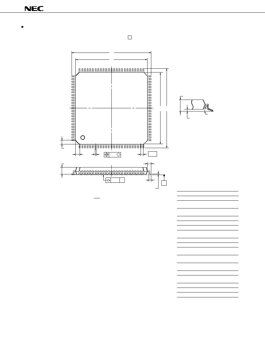
77
µ
PD703003
Data Sheet U12261EJ2V1DS00
17. PACKAGE DRAWINGS
100 PIN PLASTIC QFP (FINE PITCH) ( 14)
ITEM
MILLIMETERS
INCHES
I
J
0.5 (T.P.)
0.10
0.004
0.020 (T.P.)
A
16.0
±
0.2
0.630
±
0.008
B
14.0
±
0.2
0.551+0.009
≠0.008
C
14.0
±
0.2
0.551+0.009
≠0.008
D
16.0
±
0.2
0.630
±
0.008
F
G
1.0
1.0
0.039
0.039
H
0.22
0.009
±
0.002
P100GC-50-7EA-3
K
1.0
±
0.2
0.039+0.009
≠0.008
L
0.5
±
0.2
0.020+0.008
≠0.009
M
0.17
0.007
N
0.10
0.004
+0.05
≠0.04
+0.03
≠0.07
Q
0.125
±
0.075
0.005
±
0.003
R
S
1.7 MAX.
5
∞±
5
∞
5
∞±
5
∞
0.067 MAX.
+0.001
≠0.003
P
1.45
±
0.05
0.057 +0.003
≠0.002
NOTE
1. Controlling dimension millimeter.
2. Each lead centerline is located within 0.10 mm (0.004 inch) of
its true position (T.P.) at maximum material condition.
1
25
26
50
100
76
75
51
M
S
S
C
Q
R
K
M
L
P
G
F
A
B
D
J
H
I
N
S
detail of lead end

µ
PD703003
78
Data Sheet U12261EJ2V1DS00
18. RECOMMENDED SOLDERING CONDITIONS
The
µ
PD703003 should be soldered and mounted under the following recommended conditions.
For the recommended soldering conditions, refer to the document Semiconductor Device Mounting Technology
Manual (C10535E).
For soldering methods and conditions other than those recommended below, contact your NEC sales represen-
tative.
Table 18-1. Soldering Conditions
Soldering Method
Soldering Conditions
Symbol
Infrared reflow
IR35-107-2
VPS
VP15-107-2
Partial heating
--
Note Exposure limit after dry-pack is opened. Storage conditions: temperature of 25
∞
C and relative humidity
of 65% or less.
Caution
Do not use different soldering methods together (except for partial heating).
Package peak temperature: 235
∞
C, Reflow time: 30 seconds or
below (210
∞
C or higher), Number of reflow processes: 2 max.,
Exposure limit: 7 days
Note
(after that, prebaking is necessary at
125
∞
C for 10 hours)
Package peak temperature: 215
∞
C, Reflow time: 40 seconds or
below (200
∞
C or higher), Number of reflow processes: 2 max.,
Exposure limit: 7 days
Note
(after that, prebaking is necessary at
125
∞
C for 10 hours)
Pin temperature: 300
∞
C or below, Time: 3 seconds or below
(per side of device)

79
µ
PD703003
Data Sheet U12261EJ2V1DS00
[MEMO]

µ
PD703003
80
Data Sheet U12261EJ2V1DS00
NOTES FOR CMOS DEVICES
1
PRECAUTION AGAINST ESD FOR SEMICONDUCTORS
Note: Strong electric field, when exposed to a MOS device, can cause destruction
of the gate oxide and ultimately degrade the device operation. Steps must
be taken to stop generation of static electricity as much as possible, and
quickly dissipate it once, when it has occurred. Environmental control must
be adequate. When it is dry, humidifier should be used. It is recommended
to avoid using insulators that easily build static electricity. Semiconductor
devices must be stored and transported in an anti-static container, static
shielding bag or conductive material. All test and measurement tools
including work bench and floor should be grounded. The operator should
be grounded using wrist strap. Semiconductor devices must not be touched
with bare hands. Similar precautions need to be taken for PW boards with
semiconductor devices on it.
2
HANDLING OF UNUSED INPUT PINS FOR CMOS
Note: No connection for CMOS device inputs can be cause of malfunction. If no
connection is provided to the input pins, it is possible that an internal input
level may be generated due to noise, etc., hence causing malfunction. CMOS
device behave differently than Bipolar or NMOS devices. Input levels of
CMOS devices must be fixed high or low by using a pull-up or pull-down
circuitry. Each unused pin should be connected to V
DD
or GND with a
resistor, if it is considered to have a possibility of being an output pin. All
handling related to the unused pins must be judged device by device and
related specifications governing the devices.
3
STATUS BEFORE INITIALIZATION OF MOS DEVICES
Note: Power-on does not necessarily define initial status of MOS device. Production
process of MOS does not define the initial operation status of the device.
Immediately after the power source is turned ON, the devices with reset
function have not yet been initialized. Hence, power-on does not guarantee
out-pin levels, I/O settings or contents of registers. Device is not initialized
until the reset signal is received. Reset operation must be executed immediately
after power-on for devices having reset function.

81
µ
PD703003
Data Sheet U12261EJ2V1DS00
NEC Electronics Inc. (U.S.)
Santa Clara, California
Tel: 408-588-6000
800-366-9782
Fax: 408-588-6130
800-729-9288
NEC Electronics (Germany) GmbH
Duesseldorf, Germany
Tel: 0211-65 03 02
Fax: 0211-65 03 490
NEC Electronics (UK) Ltd.
Milton Keynes, UK
Tel: 01908-691-133
Fax: 01908-670-290
NEC Electronics Italiana s.r.l.
Milano, Italy
Tel: 02-66 75 41
Fax: 02-66 75 42 99
NEC Electronics Hong Kong Ltd.
Hong Kong
Tel: 2886-9318
Fax: 2886-9022/9044
NEC Electronics Hong Kong Ltd.
Seoul Branch
Seoul, Korea
Tel: 02-528-0303
Fax: 02-528-4411
NEC Electronics Singapore Pte. Ltd.
United Square, Singapore 1130
Tel: 65-253-8311
Fax: 65-250-3583
NEC Electronics Taiwan Ltd.
Taipei, Taiwan
Tel: 02-2719-2377
Fax: 02-2719-5951
NEC do Brasil S.A.
Electron Devices Division
Rodovia Presidente Dutra, Km 214
07210-902-Guarulhos-SP Brasil
Tel: 55-11-6465-6810
Fax: 55-11-6465-6829
NEC Electronics (Germany) GmbH
Benelux Office
Eindhoven, The Netherlands
Tel: 040-2445845
Fax: 040-2444580
NEC Electronics (France) S.A.
Velizy-Villacoublay, France
Tel: 01-30-67 58 00
Fax: 01-30-67 58 99
NEC Electronics (France) S.A.
Spain Office
Madrid, Spain
Tel: 91-504-2787
Fax: 91-504-2860
NEC Electronics (Germany) GmbH
Scandinavia Office
Taeby, Sweden
Tel: 08-63 80 820
Fax: 08-63 80 388
Regional Information
Some information contained in this document may vary from country to country. Before using any NEC
product in your application, please contact the NEC office in your country to obtain a list of authorized
representatives and distributors. They will verify:
∑ Device availability
∑ Ordering information
∑ Product release schedule
∑ Availability of related technical literature
∑ Development environment specifications (for example, specifications for third-party tools and
components, host computers, power plugs, AC supply voltages, and so forth)
∑ Network requirements
In addition, trademarks, registered trademarks, export restrictions, and other legal issues may also vary
from country to country.
J99.1

µ
PD703003
RELATED DOCUMENTS
µ
PD703003A, 703004A, 703025A Data Sheet (Under preparation)
µ
PD70F3003 Data Sheet (U12036E)
µ
PD70F3003A, 70F3025A Data Sheet (U13189E)
V850 Family, Instruction Table (U10229J)
Note
Note Japanese version
The related documents indicated in this publication may include preliminary version. However, preliminary versions
are not marked as such.
V850 Family and V853 are trademarks of NEC Corporation.
∑
The information in this document is subject to change without notice. Before using this document, please
confirm that this is the latest version.
∑
No part of this document may be copied or reproduced in any form or by any means without the prior written
consent of NEC Corporation. NEC Corporation assumes no responsibility for any errors which may appear in
this document.
∑
NEC Corporation does not assume any liability for infringement of patents, copyrights or other intellectual
property rights of third parties by or arising from use of a device described herein or any other liability arising
from use of such device. No license, either express, implied or otherwise, is granted under any patents, copyrights
or other intellectual property rights of NEC Corporation or others.
∑
Descriptions of circuits, software, and other related information in this document are provided for illustrative
purposes in semiconductor product operation and application examples. The incorporation of these circuits,
software, and information in the design of the customer's equipment shall be done under the full responsibility
of the customer. NEC Corporation assumes no responsibility for any losses incurred by the customer or third
parties arising from the use of these circuits, software, and information.
∑
While NEC Corporation has been making continuous effort to enhance the reliability of its semiconductor devices,
the possibility of defects cannot be eliminated entirely. To minimize risks of damage or injury to persons or
property arising from a defect in an NEC semiconductor device, customers must incorporate sufficient safety
measures in its design, such as redundancy, fire-containment, and anti-failure features.
∑
NEC devices are classified into the following three quality grades:
"Standard", "Special", and "Specific". The Specific quality grade applies only to devices developed based on a
customer designated "quality assurance program" for a specific application. The recommended applications of
a device depend on its quality grade, as indicated below. Customers must check the quality grade of each device
before using it in a particular application.
Standard: Computers, office equipment, communications equipment, test and measurement equipment,
audio and visual equipment, home electronic appliances, machine tools, personal electronic
equipment and industrial robots
Special:
Transportation equipment (automobiles, trains, ships, etc.), traffic control systems, anti-disaster
systems, anti-crime systems, safety equipment and medical equipment (not specifically designed
for life support)
Specific:
Aircraft, aerospace equipment, submersible repeaters, nuclear reactor control systems, life
support systems or medical equipment for life support, etc.
The quality grade of NEC devices is "Standard" unless otherwise specified in NEC's Data Sheets or Data Books.
If customers intend to use NEC devices for applications other than those specified for Standard quality grade,
they should contact an NEC sales representative in advance.
M7 98.8
The export of this product from Japan is regulated by the Japanese government. To export this product may be prohibited
without governmental license, the need for which must be judged by the customer. The export or re-export of this product
from a country other than Japan may also be prohibited without a license from that country. Please call an NEC sales
representative.