Document Outline
- Cover
- DESCRIPTION
- FEATURES
- APPLICATIONS
- ORDERING INFORMATION
- PIN CONFIGURATION (Top View)
- PIN IDENTIFICATION
- INTERNAL BLOCK DIAGRAM
- 1. DIFFERENCES AMONG PRODUCTS
- 1.1 Differences of m mm mPD703034A, 703034AY, 703035A, 703035AY, 70F3035A, and 70F3035AY
- 2. PIN FUNCTIONS
- 2.1 Port Pins
- 2.2 Non-Port Pins
- 2.3 Pin I/O Circuits and Recommended Connection of Unused Pins
- 3. PROGRAMMING FLASH MEMORY ( m mm mPD70F3035A, 70F3035AY ONLY)
- 3.1 Selecting Communication Mode
- 3.2 Function of Flash Memory Programming
- 3.3 Connecting Dedicated Flash Programmer
- 4. ELECTRICAL SPECIFICATIONS
- 4.1 Flash Memory Programming Mode ( m mm mPD70F3035A, 70F3035AY only)
- 5. PACKAGE DRAWINGS
- 6. RECOMMENDED SOLDERING CONDITIONS
MOS INTEGRATED CIRCUIT
µ
µ
µ
µ
PD703034A, 703034AY, 703035A,
703035AY, 70F3035A, 70F3035AY
V850/SB2
TM
32-/16-BIT SINGLE-CHIP MICROCONTROLLERS
Document No. U14780EJ1V0DS00 (1st edition)
Date Published May 2000 N CP(K)
Printed in Japan
DATA SHEET
©
2000
The information in this document is subject to change without notice. Before using this document, please
confirm that this is the latest version.
Not all devices/types available in every country. Please check with local NEC representative for
availability and additional information.
DESCRIPTION
The
µ
PD703034A, 703034AY, 703035A, 703035AY, 70F3035A, and 70F3035AY (V850/SB2) are 32-/16-bit
single-chip microcontrollers of the V850 Family
TM
for AV equipment. 32-bit CPU, ROM, RAM, timer/counters, serial
interfaces, A/D converter, DMA controller, and so on are integrated on a single chip.
The
µ
PD70F3035A and 70F3035AY have flash memory in place of the internal mask ROM of the
µ
PD703035A
and 703035AY. Because flash memory allows the program to be written and erased electrically with the device
mounted on the board, these products are ideal for the evaluation stages of system development, small-scale
production, and rapid development of new products.
Detailed function descriptions are provided in the following user's manuals. Be sure to read them before
designing.
V850/SB1
TM
, V850/SB2 User's Manual Hardware: U13850E
V850 Family User's Manual Architecture:
U10243E
FEATURES
{
Number of instructions: 74
{
Minimum instruction execution time: 76.9 ns (@ internal 13 MHz operation)
{
General-purpose registers: 32 bits
◊
32 registers
{
Instruction set: Signed multiplication, saturation operations, 32-bit shift instructions, bit manipulation instructions,
load/store instructions
{
Memory space: 16 MB linear address space
{
Internal memory ROM: 128 KB (
µ
PD703034A, 703034AY: mask ROM)
256 KB (
µ
PD703035A, 703035AY: mask ROM)
256 KB (
µ
PD70F3035A, 70F3035AY: flash memory)
RAM: 12 KB (
µ
PD703034A, 703034AY)
16 KB (
µ
PD703035A, 703035AY, 70F3035A, 70F3035AY)
{
Interrupt/exception:
µ
PD703034A, 703035A, 70F3035A (external: 8, internal: 32 sources, exception: 1 source)
µ
PD703034AY, 703035AY, 70F3035AY (external: 8, internal: 33 sources, exception: 1 source)
{
I/O lines Total: 83
{
Timer/counters: 16-bit timer (2 channels: TM0, TM1)
8-bit timer (6 channels: TM2 to TM7)
{
Watch timer: 1 channel
{
Watchdog timer: 1 channel
{
IEBus controller: 1 channel

Data Sheet U14780EJ1V0DS00
2
µ
µ
µ
µ
PD703034A, 703034AY, 703035A, 703035AY, 70F3035A, 70F3035AY
{
Serial interface
∑
Asynchronous serial interface (UART0, UART1)
∑
Clocked serial interface (CSI0 to CSI3)
∑
3-wire variable length serial interface (CSI4)
∑
I
2
C bus interface (I
2
C0, I
2
C1) (
µ
PD703034AY, 703035AY, 70F3035AY only)
{
10-bit resolution A/D converter: 12 channels
{
DMA controller: 6 channels
{
Real-time output port: 8 bits
◊
1 channel or 4 bits
◊
2 channels
{
ROM correction: 4 places can be corrected
{
Power-saving function: HALT/IDLE/STOP modes
{
Packages: 100-pin plastic LQFP (fine pitch) (14
◊
14)
100-pin plastic QFP (14
◊
20)
{
µ
PD70F3035A, 70F3035AY
∑
Can be replaced with
µ
PD703035A and 703035AY (internal mask ROM) in mass production
APPLICATIONS
{
AV equipment (audio, car audio, VCR, TV, etc.)
ORDERING INFORMATION
Part Number
Package
Internal ROM
µ
PD703034AGC-
◊◊◊
◊◊◊
◊◊◊
◊◊◊
-8EU
µ
PD703034AYGC-
◊◊◊
◊◊◊
◊◊◊
◊◊◊
-8EU
µ
PD703034AGF-
◊◊◊
◊◊◊
◊◊◊
◊◊◊
-3BA
µ
PD703034AYGF-
◊◊◊
◊◊◊
◊◊◊
◊◊◊
-3BA
µ
PD703035AGC-
◊◊◊
◊◊◊
◊◊◊
◊◊◊
-8EU
µ
PD703035AYGC-
◊◊◊
◊◊◊
◊◊◊
◊◊◊
-8EU
µ
PD703035AGF-
◊◊◊
◊◊◊
◊◊◊
◊◊◊
-3BA
µ
PD703035AYGF-
◊◊◊
◊◊◊
◊◊◊
◊◊◊
-3BA
µ
PD70F3035AGC-8EU
Note
µ
PD70F3035AYGC-8EU
Note
µ
PD70F3035AGF-3BA
Note
µ
PD70F3035AYGF-3BA
Note
100-pin plastic LQFP (fine pitch) (14
◊
14)
100-pin plastic LQFP (fine pitch) (14
◊
14)
100-pin plastic QFP (14
◊
20)
100-pin plastic QFP (14
◊
20)
100-pin plastic LQFP (fine pitch) (14
◊
14)
100-pin plastic LQFP (fine pitch) (14
◊
14)
100-pin plastic QFP (14
◊
20)
100-pin plastic QFP (14
◊
20)
100-pin plastic LQFP (fine pitch) (14
◊
14)
100-pin plastic LQFP (fine pitch) (14
◊
14)
100-pin plastic QFP (14
◊
20)
100-pin plastic QFP (14
◊
20)
Mask ROM (128 KB)
Mask ROM (128 KB)
Mask ROM (128 KB)
Mask ROM (128 KB)
Mask ROM (256 KB)
Mask ROM (256 KB)
Mask ROM (256 KB)
Mask ROM (256 KB)
Flash memory (256 KB)
Flash memory (256 KB)
Flash memory (256 KB)
Flash memory (256 KB)
Note Under development
Remarks 1.
◊◊◊
indicates ROM code suffix.
2. ROMless versions are not provided.
Data Sheet U14780EJ1V0DS00
3
µ
µ
µ
µ
PD703034A, 703034AY, 703035A, 703035AY, 70F3035A, 70F3035AY
PIN CONFIGURATION (Top View)
100-pin plastic LQFP (fine pitch) (14
◊
◊
◊
◊
14)
∑
µ
PD703034AGC-
◊◊◊
-8EU
∑
µ
PD70F3035AGC-8EU
∑
µ
PD703034AYGC-
◊◊◊
-8EU
∑
µ
PD70F3035AYGC-8EU
∑
µ
PD703035AGC-
◊◊◊
-8EU
∑
µ
PD703035AYGC-
◊◊◊
-8EU
1
2
3
4
5
6
7
8
9
10
11
12
13
14
15
16
17
18
19
20
21
22
23
24
25
P21/SO2
P22/SCK2/SCL1
Note 2
P23/RXD1/SI3
P24/TXD1/SO3
P25/ASCK1/SCK3
EV
DD
EV
SS
P26/TI2/TO2
P27/TI3/TO3
P30/TI00
P31/TI01
P32/TI10/SI4
P33/TI11/SO4
P34/TO0/A13/SCK4
P35/TO1/A14
P36/TI4/TO4/A15
P37/TI5/TO5
IC/V
PP
Note 1
P100/RTP0/KR0/A5
P101/RTP1/KR1/A6
P102/RTP2/KR2/A7
P103/RTP3/KR3/A8
P104/RTP4/KR4/A9/IERX
P105/RTP5/KR5/A10/IETX
P106/RTP6/KR6/A11
P71/ANI1
P70/ANI0
AV
REF
AV
SS
AV
DD
P65/A21
P64/A20
P63/A19
P62/A18
P61/A17
P60/A16
P57/AD15
P56/AD14
P55/AD13
P54/AD12
P53/AD11
P52/AD10
P51/AD9
P50/AD8
BV
SS
BV
DD
P47/AD7
P46/AD6
P45/AD5
P44/AD4
P107/RTP7/KR7/A12
P110/WAIT/A1
P111/A2
P112/A3
P113/A4
RESET
XT1
XT2
REGC
X2
X1
V
SS
V
DD
CLKOUT
P90/LBEN/WRL
P91/UBEN
P92/R/W/WRH
P93/DSTB/RD
P94/ASTB
P95/HLDAK
P96/HLDRQ
P40/AD0
P41/AD1
P42/AD2
P43/AD3
P20/SI2/SDA1
Note 2
P15/SCK1/ASCK0
P14/SO1/TXD0
P13/SI1/RXD0
P12/SCK0/SCL0
Note 2
P11/SO0
P10/SI0/SDA0
Note 2
P07/INTP6
P06/INTP5/RTPTRG
P05/INTP4/ADTRG
P04/INTP3
P03/INTP2
P02/INTP1
P01/INTP0
P00/NMI
P83/ANI11
P82/ANI10
P81/ANI9
P80/ANI8
P77/ANI7
P76/ANI6
P75/ANI5
P74/ANI4
P73/ANI3
P72/ANI2
75
74
73
72
71
70
69
68
67
66
65
64
63
62
61
60
59
58
57
56
55
54
53
52
51
100
99
98
97
96
95
94
93
92
91
90
89
88
87
86
85
84
83
82
81
80
79
78
77
76
26
27
28
29
30
31
32
33
34
35
36
37
38
39
40
41
42
43
44
45
46
47
48
49
50
Notes 1.
IC: Connect directly to V
SS
(
µ
PD703034A, 703034AY, 703035A, 703035AY).
V
PP
: Connect to V
SS
in normal operation mode (
µ
PD70F3035A, 70F3035AY).
2.
SCL0, SCL1, SDA0, and SDA1 are available only in the
µ
PD703034AY, 703035AY,
and 70F3035AY.
Data Sheet U14780EJ1V0DS00
4
µ
µ
µ
µ
PD703034A, 703034AY, 703035A, 703035AY, 70F3035A, 70F3035AY
100-pin plastic QFP (14
◊
◊
◊
◊
20)
∑
µ
PD703034AGF-
◊◊◊
-3BA
∑
µ
PD70F3035AGF-3BA
∑
µ
PD703034AYGF-
◊◊◊
-3BA
∑
µ
PD70F3035AYGF-3BA
∑
µ
PD703035AGF-
◊◊◊
-3BA
∑
µ
PD703035AYGF-
◊◊◊
-3BA
P13/SI1/RXD0
P12/SCK0/SCL0
Note 2
P11/SO0
P10/SI0/SDA0
Note 2
P07/INTP6
P06/INTP5/RTPTRG
P05/INTP4/ADTRG
P04/INTP3
P03/INTP2
P02/INTP1
P01/INTP0
P00/NMI
P83/ANI11
P82/ANI10
P81/ANI9
P80/ANI8
P77/ANI7
P76/ANI6
P75/ANI5
P74/ANI4
100
99
98
97
96
95
94
93
92
91
90
89
88
87
86
85
84
83
82
81
P111/A2
P112/A3
P113/A4
RESET
XT1
XT2
REGC
X2
X1
V
SS
V
DD
CLKOUT
P90/LBEN/WRL
P91/UBEN
P92/R/W/WRH
P93/DSTB/RD
P94/ASTB
P95/HLDAK
P96/HLDRQ
P40/AD0
31
32
33
34
35
36
37
38
39
40
41
42
43
44
45
46
47
48
49
50
P73/ANI3
P72/ANI2
P71/ANI1
P70/ANI0
AV
REF
AV
SS
AV
DD
P65/A21
P64/A20
P63/A19
P62/A18
P61/A17
P60/A16
P57/AD15
P56/AD14
P55/AD13
P54/AD12
P53/AD11
P52/AD10
P51/AD9
P50/AD8
BV
SS
BV
DD
P47/AD7
P46/AD6
P45/AD5
P44/AD4
P43/AD3
P42/AD2
P41/AD1
80
79
78
77
76
75
74
73
72
71
70
69
68
67
66
65
64
63
62
61
60
59
58
57
56
55
54
53
52
51
1
2
3
4
5
6
7
8
9
10
11
12
13
14
15
16
17
18
19
20
21
22
23
24
25
26
27
28
29
30
P14/SO1/TXD0
P15/SCK1/ASCK0
P20/SI2/SDA1
Note 2
P21/SO2
P22/SCK2/SCL1
Note 2
P23/RXD1/SI3
P24/TXD1/SO3
P25/ASCK1/SCK3
EV
DD
EV
SS
P26/TI2/TO2
P27/TI3/TO3
P30/TI00
P31/TI01
P32/TI10/SI4
P33/TI11/SO4
P34/TO0/A13/SCK4
P35/TO1/A14
P36/TI4/TO4/A15
P37/TI5/TO5
IC/V
PP
Note 1
P100/RTP0/KR0/A5
P101/RTP1/KR1/A6
P102/RTP2/KR2/A7
P103/RTP3/KR3/A8
P104/RTP4/KR4/A9/IERX
P105/RTP5/KR5/A10/IETX
P106/RTP6/KR6/A11
P107/RTP7/KR7/A12
P110/WAIT/A1
Notes 1.
IC: Connect directly to V
SS
(
µ
PD703034A, 703034AY, 703035A, 703035AY).
V
PP
: Connect to V
SS
in normal operation mode (
µ
PD70F3035A, 70F3035AY).
2.
SCL0, SCL1, SDA0, and SDA1 are available only in the
µ
PD703034AY, 703035AY,
and 70F3035AY.

Data Sheet U14780EJ1V0DS00
5
µ
µ
µ
µ
PD703034A, 703034AY, 703035A, 703035AY, 70F3035A, 70F3035AY
PIN IDENTIFICATION
A1 to A21:
Address Bus
P70 to P77:
Port 7
AD0 to AD15:
Address/Data Bus
P80 to P83:
Port 8
ADTRG:
AD Trigger Input
P90 to P96:
Port 9
ANI0 to ANI11:
Analog Input
P100 to P107:
Port 10
ASCK0, ASCK1:
Asynchronous Serial Clock
P110 to P113:
Port 11
ASTB:
Address Strobe
RD:
Read
AV
DD
:
Analog Power Supply
REGC:
Regulator Clock
AV
REF
:
Analog Reference Voltage
RESET:
Reset
AV
SS
:
Analog Ground
RTP0 to RTP7:
Real-time Output Port
BV
DD
:
Power Supply for Bus Interface
RTPTRG:
RTP Trigger Input
BV
SS
:
Ground for Bus Interface
R/W:
Read/Write Status
CLKOUT:
Clock Output
RXD0, RXD1:
Receive Data
DSTB:
Data Strobe
SCK0 to SCK4:
Serial Clock
EV
DD
:
Power Supply for Port
SCL0, SCL1:
Serial Clock
EV
SS
:
Ground for Port
SDA0, SDA1:
Serial Data
HLDAK:
Hold Acknowledge
SI0 to SI4:
Serial Input
HLDRQ:
Hold Request
SO0 to SO4:
Serial Output
IC:
Internally Connected
TI00, TI01, TI10, :
Timer Input
IERX:
IEBus Receive Data
TI11, TI2 to TI5
IETX: IEBus Transmit Data
TO0 to TO5:
Timer Output
INTP0 to INTP6:
Interrupt Request from Peripherals
TXD0, TXD1:
Transmit Data
KR0 to KR7:
Key Return
UBEN:
Upper Byte Enable
LBEN:
Lower Byte Enable
V
DD
:
Power Supply
NMI:
Non-Maskable Interrupt Request
V
PP
:
Programming Power Supply
P00 to P07:
Port 0
V
SS
:
Ground
P10 to P15:
Port 1
WAIT:
Wait
P20 to P27:
Port 2
WRH:
Write Strobe High Level Data
P30 to P37:
Port 3
WRL:
Write Strobe Low Level Data
P40 to P47:
Port 4
X1, X2:
Crystal for Main Clock
P50 to P57:
Port 5
XT1, XT2:
Crystal for Sub-clock
P60 to P65:
Port 6
Data Sheet U14780EJ1V0DS00
6
µ
µ
µ
µ
PD703034A, 703034AY, 703035A, 703035AY, 70F3035A, 70F3035AY
INTERNAL BLOCK DIAGRAM
ROM
CPU
PC
ROM
correction
HLDRQ (P96)
HLDAK (P95)
A13 to A15 (P34 to P36)
A16 to A21 (P60 to P65)
A1 to A12
(P100 to P107, P110 to P113)
AD0 to AD15
(P40 to P47, P50 to P57)
CLKOUT
X1
X2
XT1
XT2
RESET
V
DD
V
SS
BV
DD
BV
SS
EV
DD
EV
SS
V
PP
Note 4
IC
Note 5
RTP0 to RTP7
RTPTRG
REGC
AV
DD
AV
REF
AV
SS
ANI0 to ANI11
ADTRG
P110 to P113
P100 to P107
P90 to P96
P80 to P83
P70 to P77
P60 to P65
P50 to P57
P40 to P47
P30 to P37
P20 to P27
P10 to P15
P00 to P07
ASTB (P94)
DSTB/RD (P93)
R/W/WRH (P92)
UBEN (P91)
LBEN/WRL (P90)
WAIT (P110)
Multiplier
16
◊
16
32
32-bit barrel
shifter
System
registers
General-purpose
registers
32 bits
◊
32
Note 1
Note 2
RAM
INTC
SIO
CSI0/I
2
C0
Note 3
CSI2/I
2
C1
Note 3
CSI1/UART0
CSI3/UART1
Variable length
CSI4
Key return
function
DMAC: 6ch
SO0
SI0/SDA0
Note 3
SCK0/SCL0
Note 3
Watch timer
Watchdog timer
NMI
INTP0 to INTP6
TI00, TI01,
TI10, TI11
TO0, TO1
TI2/TO2
TI3/TO3
TI4/TO4
TI5/TO5
SO2
SI2/SDA1
Note 3
SCK2/SCL1
Note 3
SO1/TXD0
SI1/RXD0
SCK1/ASCK0
SO3/TXD1
SI3/RXD1
SCK3/ASCK1
SO4
SI4
SCK4
KR0 to KR7
ALU
Ports
RTP
CG
3.0 V
Regulator
A/D
converter
Instruction
queue
BCU
Timer/counters
16-bit timer
: TM0, TM1
8-bit timer
: TM2 to TM7
IEBus
IETX
IERX
Notes 1.
µ
PD703034A, 703034AY:
128 KB (mask ROM)
µ
PD703035A, 703035AY:
256 KB (mask ROM)
µ
PD70F3035A, 70F3035AY: 256 KB (flash memory)
2.
µ
PD703034A, 703034AY:
12 KB
µ
PD703035A, 703035AY, 70F3035A, 70F3035AY:
16 KB
3.
I
2
C bus interface and SDAn and SCLn pins are available only in the
µ
PD703034AY, 703035AY,
and 70F3035AY.
4.
µ
PD70F3035A, 70F3035AY
5.
µ
PD703034A, 703034AY, 703035A, 703035AY

Data Sheet U14780EJ1V0DS00
7
µ
µ
µ
µ
PD703034A, 703034AY, 703035A, 703035AY, 70F3035A, 70F3035AY
CONTENTS
1.
DIFFERENCES AMONG PRODUCTS ............................................................................................... 8
1.1
Differences of
µ
µ
µ
µ
PD703034A, 703034AY, 703035A, 703035AY, 70F3035A, and 70F3035AY................. 8
2.
PIN FUNCTIONS.................................................................................................................................. 9
2.1
Port Pins..................................................................................................................................................... 9
2.2
Non-Port Pins........................................................................................................................................... 11
2.3
Pin I/O Circuits and Recommended Connection of Unused Pins ....................................................... 15
3.
PROGRAMMING FLASH MEMORY (
µ
µ
µ
µ
PD70F3035A, 70F3035AY ONLY) ................................... 19
3.1
Selecting Communication Mode ............................................................................................................ 19
3.2
Function of Flash Memory Programming.............................................................................................. 20
3.3
Connecting Dedicated Flash Programmer ............................................................................................ 20
4.
ELECTRICAL SPECIFICATIONS...................................................................................................... 22
4.1
Flash Memory Programming Mode (
µ
µ
µ
µ
PD70F3035A, 70F3035AY only) ............................................... 47
5.
PACKAGE DRAWINGS..................................................................................................................... 48
6.
RECOMMENDED SOLDERING CONDITIONS ............................................................................... 50
Data Sheet U14780EJ1V0DS00
8
µ
µ
µ
µ
PD703034A, 703034AY, 703035A, 703035AY, 70F3035A, 70F3035AY
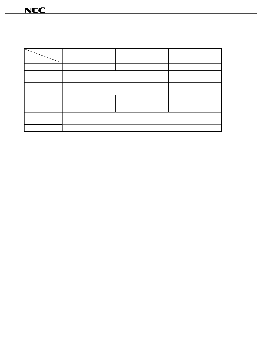
1. DIFFERENCES AMONG PRODUCTS
1.1 Differences of
µ
µ
µ
µ
PD703034A, 703034AY, 703035A, 703035AY, 70F3035A, and 70F3035AY
Part Number
Item
µ
PD703034A
µ
PD703034AY
µ
PD703035A
µ
PD703035AY
µ
PD70F3035A
µ
PD70F3035AY
Internal ROM
128 KB (mask ROM)
256 KB (mask ROM)
256 KB (flash memory)
Flash memory
programming pin
None
Provided (V
PP
)
Flash memory
programming mode
None
Provided (V
PP
= 7.8 V)
I
2
C bus interface
pins (SCL0, SCL1,
SDA0, SDA1)
None
Provided
None
Provided
None
Provided
Electrical
specifications
Current consumption, etc. differs.
Others
Noise immunity and noise radiation differ because circuit scale and mask layout differ.
Cautions 1.
There are differences in noise immunity and noise radiation between the flash memory and
mask ROM versions. When pre-producing an application set with the flash memory version
and then mass-producing it with the mask ROM version, be sure to conduct sufficient
evaluations for the commercial samples (not engineering samples) of the mask ROM
version.
2. When replacing the flash memory versions with mask ROM versions, write the same code
in the empty area of the internal ROM.
Data Sheet U14780EJ1V0DS00
9
µ
µ
µ
µ
PD703034A, 703034AY, 703035A, 703035AY, 70F3035A, 70F3035AY
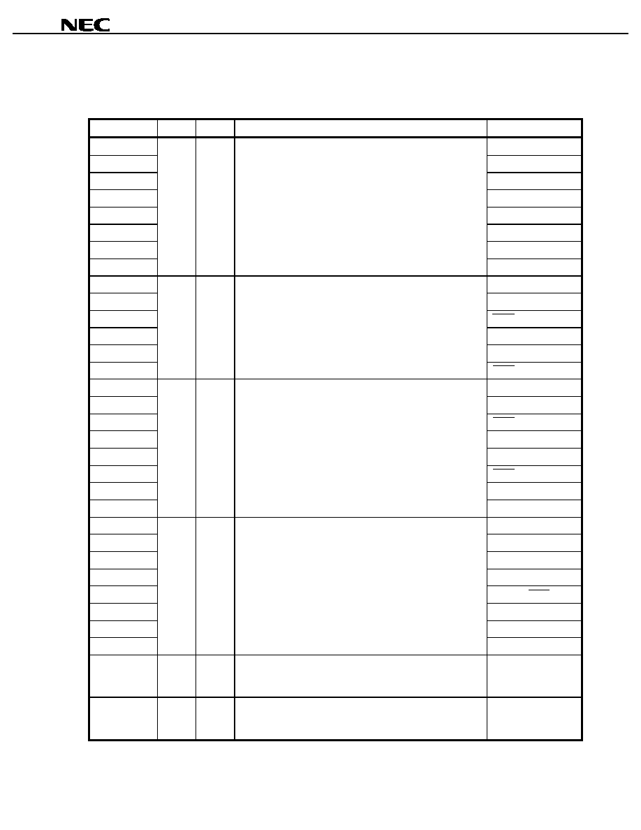
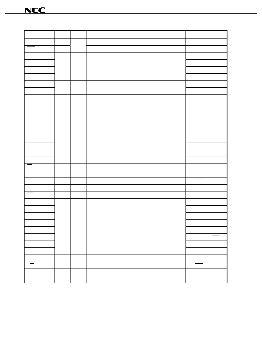
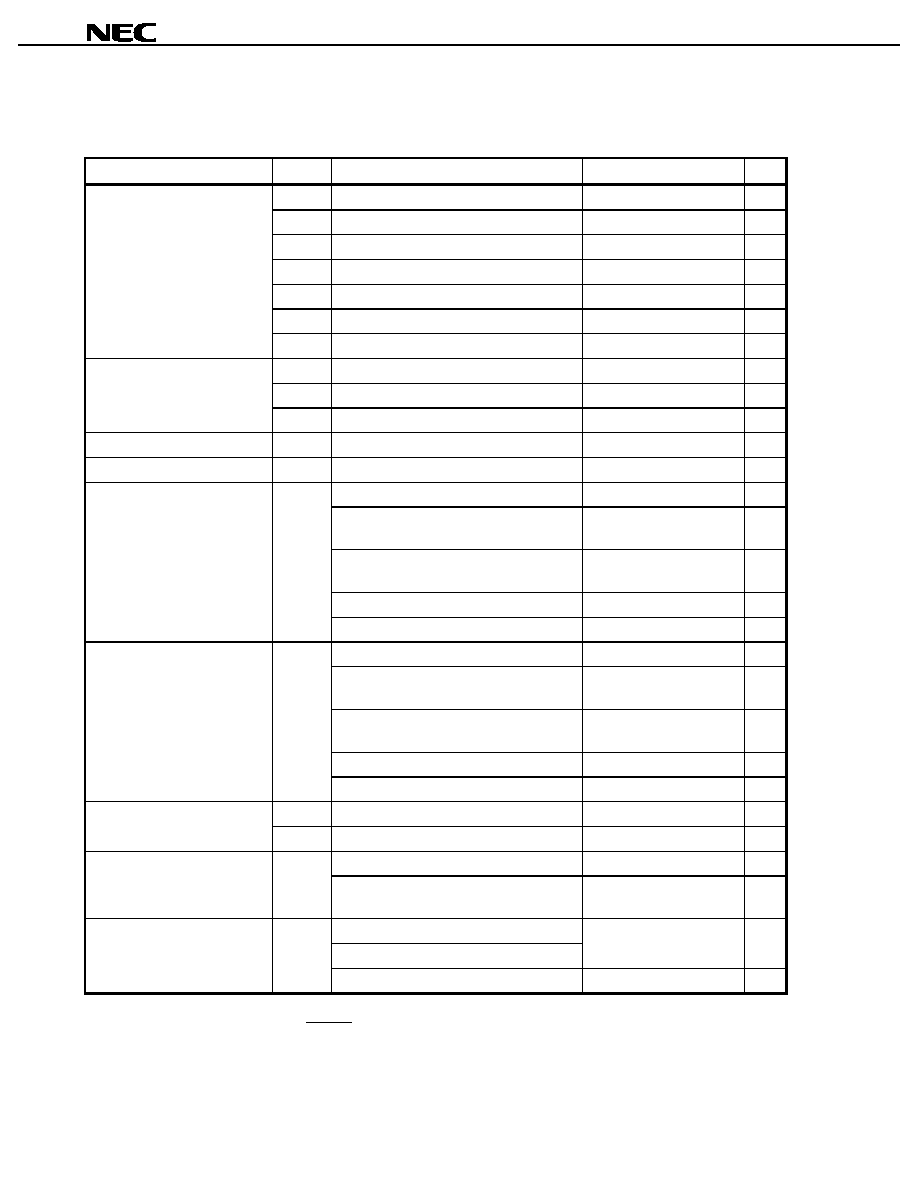
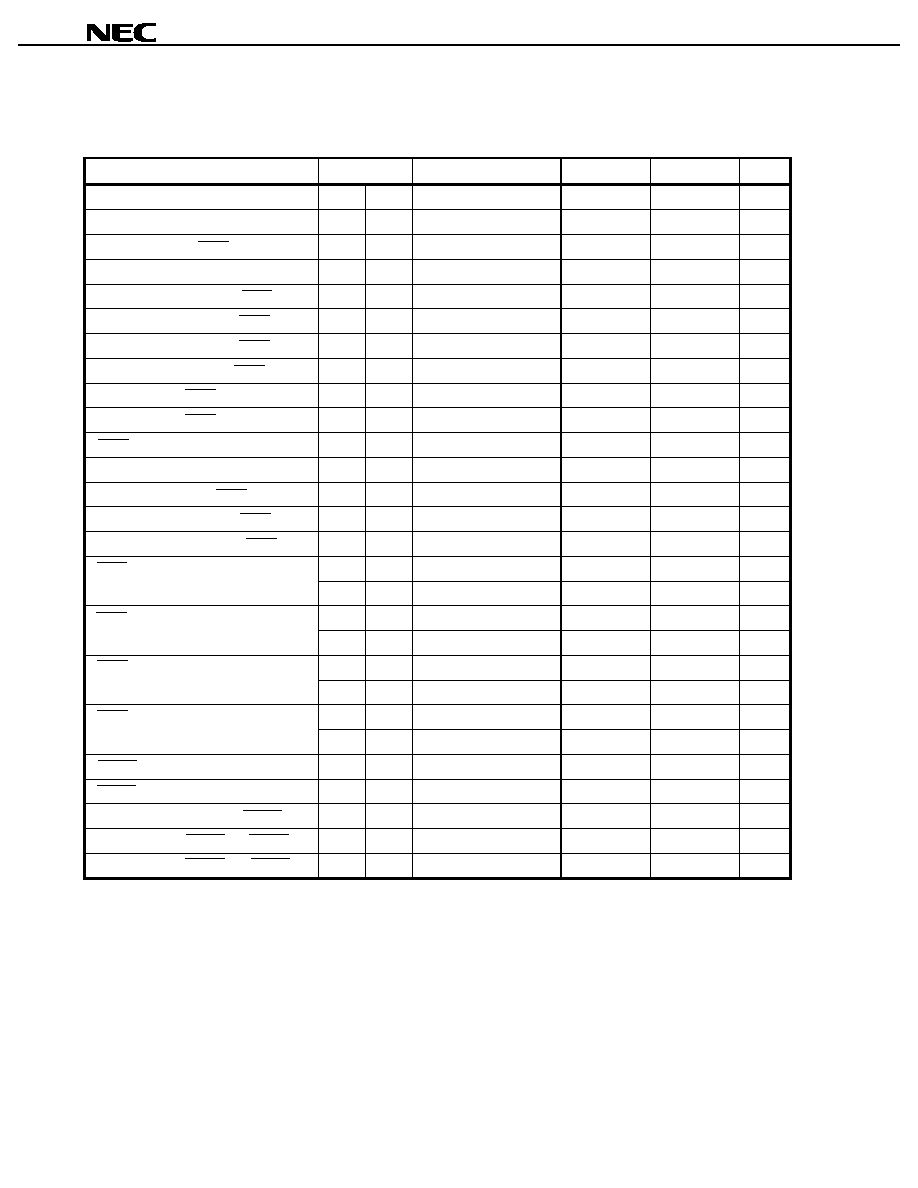
2. PIN FUNCTIONS
2.1 Port Pins
(1/2)
Pin Name
I/O
PULL
Function
Alternate Function
P00
NMI
P01
INTP0
P02
INTP1
P03
INTP2
P04
INTP3
P05
INTP4/ADTRG
P06
INTP5/RTPTRG
P07
I/O
Yes
Port 0
8-bit I/O port
Input/output can be specified in 1-bit units.
INTP6
P10
SI0/SDA0
P11
SO0
P12
SCK0/SCL0
P13
SI1/RXD0
P14
SO1/TXD0
P15
I/O
Yes
Port 1
6-bit I/O port
Input/output can be specified in 1-bit units.
SCK1/ASCK0
P20
SI2/SDA1
P21
SO2
P22
SCK2/SCL1
P23
SI3/RXD1
P24
SO3/TXD1
P25
SCK3/ASCK1
P26
TI2/TO2
P27
I/O
Yes
Port 2
8-bit I/O port
Input/output can be specified in 1-bit units.
TI3/TO3
P30
TI00
P31
TI01
P32
TI10/SI4
P33
TI11/SO4
P34
TO0/A13/SCK4
P35
TO1/A14
P36
TI4/TO4/A15
P37
I/O
Yes
Port 3
8-bit I/O port
Input/output can be specified in 1-bit units.
TI5/TO5
P40 to P47
I/O
No
Port 4
8-bit I/O port
Input/output can be specified in 1-bit units.
AD0 to AD7
P50 to P57
I/O
No
Port 5
8-bit I/O port
Input/output can be specified in 1-bit units.
AD8 to AD15
Remark
PULL: On-chip pull-up resistor
Data Sheet U14780EJ1V0DS00
10
µ
µ
µ
µ
PD703034A, 703034AY, 703035A, 703035AY, 70F3035A, 70F3035AY
(2/2)
Pin Name
I/O
PULL
Function
Alternate Function
P60 to P65
I/O
No
Port 6
6-bit I/O port
Input/output can be specified in 1-bit units.
A16 to A21
P70 to P77
Input
No
Port 7
8-bit input port
ANI0 to ANI7
P80 to P83
Input
No
Port 8
4-bit input port
ANI8 to ANI11
P90
LBEN/WRL
P91
UBEN
P92
R/W/WRH
P93
DSTB/RD
P94
ASTB
P95
HLDAK
P96
I/O
No
Port 9
7-bit I/O port
Input/output can be specified in 1-bit units.
HLDRQ
P100
RTP0/A5/KR0
P101
RTP1/A6/KR1
P102
RTP2/A7/KR2
P103
RTP3/A8/KR3
P104
RTP4/A9/KR4/IERX
P105
RTP5/A10/KR5/IETX
P106
RTP6/A11/KR6
P107
I/O
Yes
Port 10
8-bit I/O port
Input/output can be specified in 1-bit units.
RTP7/A12/KR7
P110
A1/WAIT
P111
A2
P112
A3
P113
I/O
Yes
Port 11
4-bit I/O port
Input/output can be specified in 1-bit units.
A4
Remark
PULL: On-chip pull-up resistor
Data Sheet U14780EJ1V0DS00
11
µ
µ
µ
µ
PD703034A, 703034AY, 703035A, 703035AY, 70F3035A, 70F3035AY
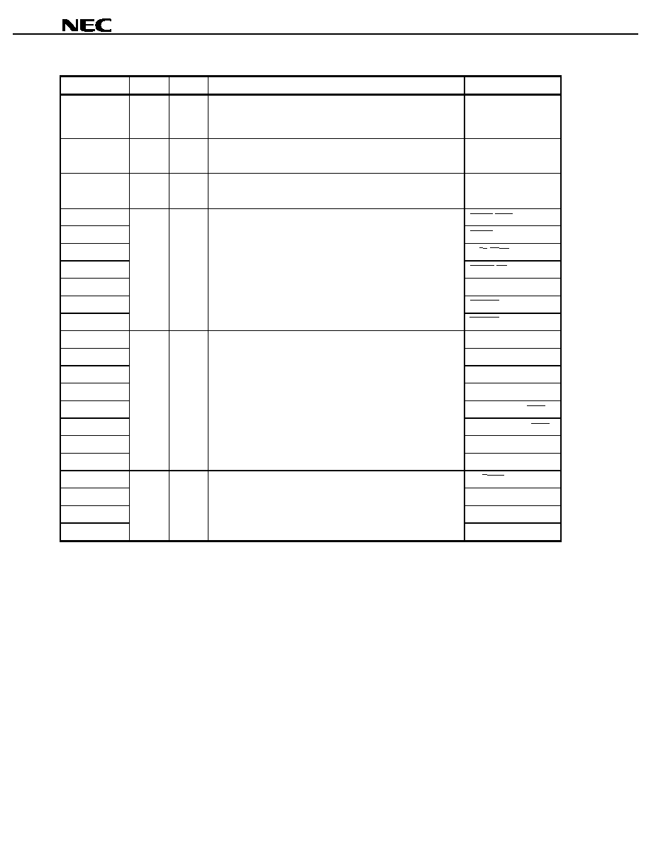
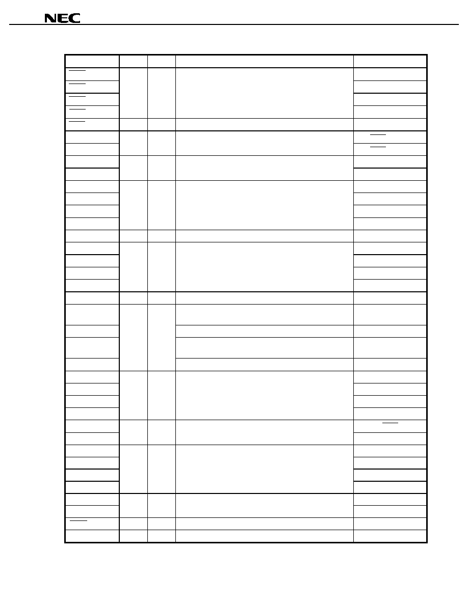
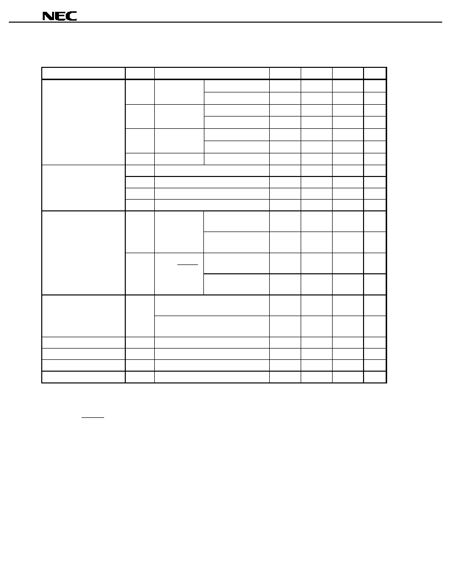
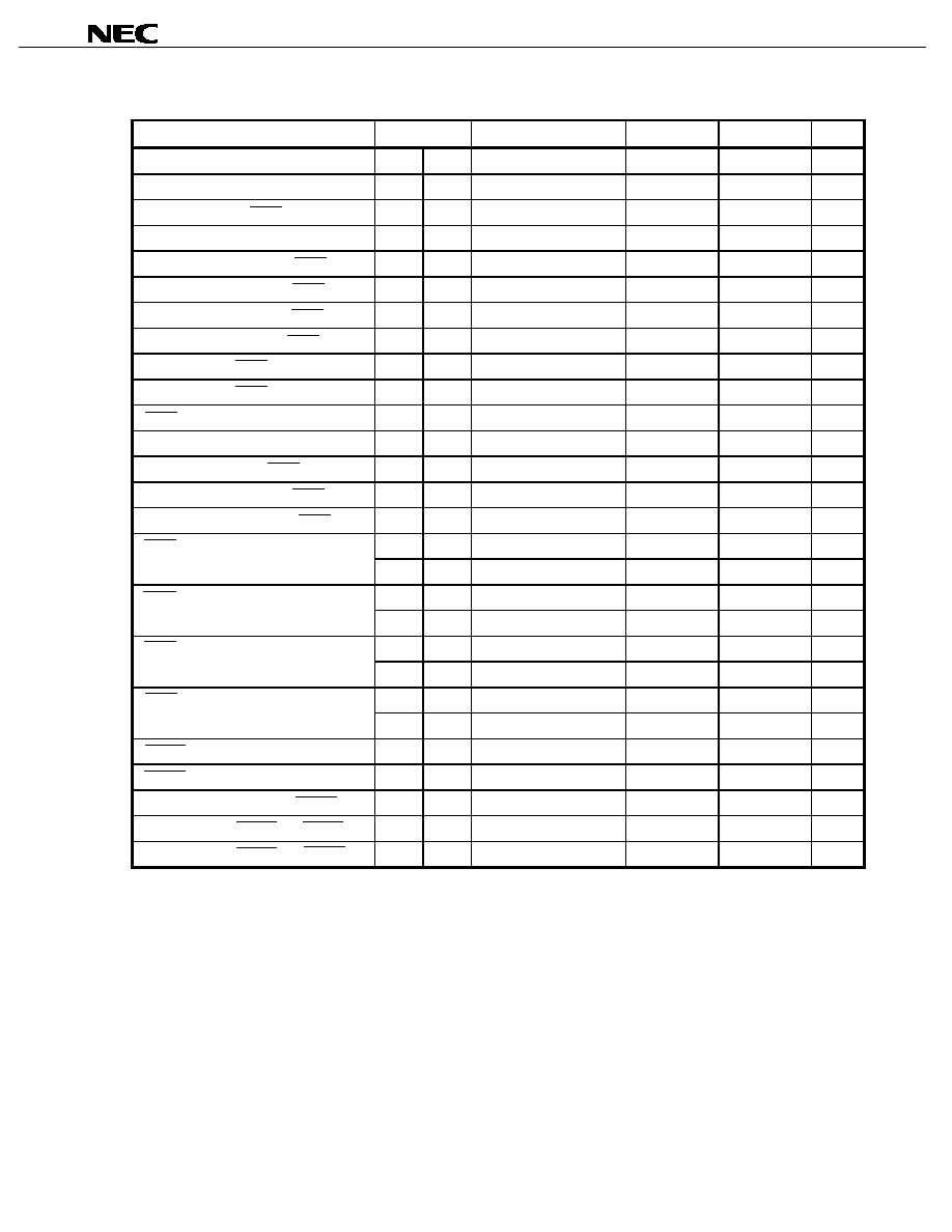
2.2 Non-Port Pins
(1/4)
Pin Name
I/O
PULL
Function
Alternate Function
A1
P110/WAIT
A2
P111
A3
P112
A4
P113
A5
P100/RTP0/KR0
A6
P101/RTP1/KR1
A7
P102/RTP2/KR2
A8
P103/RTP3/KR3
A9
P104/RTP4/KR4/IERX
A10
P105/RTP5/KR5/IETX
A11
P106/RTP6/KR6
A12
P107/RTP7/KR7
A13
P34/TO0/SCK4
A14
P35/TO1
A15
Output
Yes
Low-order address bus used for external memory expansion
P36/TO4/TI4
A16 to A21
Output
No
High-order address bus used for external memory expansion
P60 to P65
AD0 to AD7
P40 to P47
AD8 to AD15
I/O
No
16-bit multiplexed address/data bus used for external memory
expansion
P50 to P57
ADTRG
Input
Yes
A/D converter external trigger input
P05/INTP4
ANI0 to ANI7
P70 to P77
ANI8 to ANI11
Input
No
Analog input to A/D converter
P80 to P83
ASCK0
Baud rate clock input for UART0
P15/SCK1
ASCK1
Input
Yes
Baud rate clock input for UART1
P25/SCK3
ASTB
Output
No
External address strobe output
P94
AV
DD
-
-
Positive power supply for A/D converter and alternate port
-
AV
REF
Input
-
Reference voltage input for A/D converter
-
AV
SS
-
-
Ground potential for A/D converter and alternate port
-
BV
DD
-
-
Positive power supply for bus interface and alternate port
-
BV
SS
-
-
Ground potential for bus interface and alternate port
-
CLKOUT
Output
-
Internal system clock output
-
DSTB
Output
No
External data strobe output
P93/RD
EV
DD
-
-
Positive power supply for I/O ports and alternate-function pins
(except bus interface alternate port)
-
EV
SS
-
-
Ground potential for I/O ports and alternate-function pins
(except bus interface alternate port)
-
HLDAK
Output
No
Bus hold acknowledge output
P95
HLDRQ
Input
No
Bus hold request input
P96
IC
-
-
Internally connected
(
µ
PD703034A, 703034AY, 703035A, 703035AY only)
-
Remark
PULL: On-chip pull-up resistor
Data Sheet U14780EJ1V0DS00
12
µ
µ
µ
µ
PD703034A, 703034AY, 703035A, 703035AY, 70F3035A, 70F3035AY
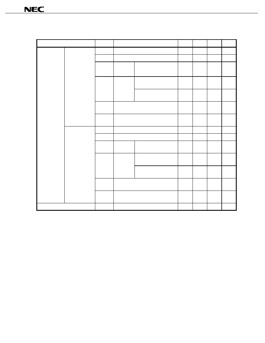
(2/4)
Pin Name
I/O
PULL
Function
Alternate Function
IERX
Input
IEBus data input
P104/RTP4/A9/KR4
IETX
Output
Yes
IEBus data output
P105/RTP5/A10/KR5
INTP0
P01
INTP1
P02
INTP2
P03
INTP3
Input
Yes
External interrupt request input (analog noise elimination)
P04
INTP4
P05/ADTRG
INTP5
Input
Yes
External interrupt request input (digital noise elimination)
P06/RTPTRG
INTP6
Input
Yes
External interrupt request input (digital noise elimination
supporting remote controller)
P07
KR0
P100/RTP0/A5
KR1
P101/RTP1/A6
KR2
P102/RTP2/A7
KR3
P103/RTP3/A8
KR4
P104/RTP4/A9/IERX
KR5
P105/RTP5/A10/IETX
KR6
P106/RTP6/A11
KR7
Input
Yes
Key return input
P107/RTP7/A12
LBEN
Output
No
External data bus's low-order byte enable output
P90/WRL
NMI
Input
Yes
Non-maskable interrupt request input
P00
RD
Output
No
Read strobe output
P93/DSTB
REGC
-
-
Regulator output stabilization capacitance connection
-
RESET
Input
-
System reset input
-
RTP0
P100/KR0/A5
RTP1
P101/KR1/A6
RTP2
P102/KR2/A7
RTP3
P103/KR3/A8
RTP4
P104/KR4/A9/IERX
RTP5
P105/KR5/A10/IETX
RTP6
P106/KR6/A11
RTP7
Output
Yes
Real-time output port
P107/KR7/A12
RTPTRG
Input
Yes
Real-time output port external trigger input
P06/INTP5
R/W
Output
No
External read/write status output
P92/WRH
RXD0
P13/SI1
RXD1
Input
Yes
Serial receive data input for UART0 and UART1
P23/SI3
Remark
PULL: On-chip pull-up resistor
Data Sheet U14780EJ1V0DS00
13
µ
µ
µ
µ
PD703034A, 703034AY, 703035A, 703035AY, 70F3035A, 70F3035AY
(3/4)
Pin Name
I/O
PULL
Function
Alternate Function
SCK0
P12/SCL0
SCK1
P15/ASCK0
SCK2
P22/SCL1
SCK3
I/O
Yes
Serial clock I/O (3-wire type) for CSI0 to CSI3
P25/ASCK1
SCK4
I/O
Yes
Serial clock I/O (3-wire type) for variable length CSI4
P34/TO0/A13
SCL0
P12/SCK0
SCL1
I/O
Yes
Serial clock I/O for I
2
C0 and I
2
C1
(
µ
PD703034AY, 703035AY, 70F3035AY only)
P22/SCK2
SDA0
P10/SI0
SDA1
I/O
Yes
Serial transmit/receive data I/O for I
2
C0 and I
2
C1
(
µ
PD703034AY, 703035AY, 70F3035AY only)
P20/SI2
SI0
P10/SDA0
SI1
P13/RXD0
SI2
P20/SDA1
SI3
Input
Yes
Serial receive data input (3-wire type) for CSI0 to CSI3
P23/RXD1
SI4
Input
Yes
Serial receive data input (3-wire type) for variable length CSI4
P32/TI10
SO0
P11
SO1
P14/TXD0
SO2
P21
SO3
Output
Yes
Serial transmit data output (3-wire type) for CSI0 to CSI3
P24/TXD1
SO4
Output
Yes
Serial transmit data output (3-wire type) for variable length CSI4
P33/TI11
TI00
External count clock input for TM0/external capture trigger
input for TM0
P30
TI01
External capture trigger input for TM0
P31
TI10
External count clock input for TM1/external capture trigger
input for TM1
P32/SI4
TI11
Input
Yes
External capture trigger input for TM1
P33/SO4
TI2
P26/TO2
TI3
P27/TO3
TI4
P36/TO4/A15
TI5
Input
Yes
External count clock input for TM2 to TM5
P37/TO5
TO0
P34/A13/SCK4
TO1
Output
Yes
Pulse signal output for TM0 and TM1
P35/A14
TO2
P26/TI2
TO3
P27/TI3
TO4
P36/TI4/A15
TO5
Output
Yes
Pulse signal output for TM2 to TM5
P37/TI5
TXD0
P14/SO1
TXD1
Output
Yes
Serial transmit data output for UART0 and UART1
P24/SO3
UBEN
Output
No
High-order byte enable output for external data bus
P91
V
DD
-
-
Positive power supply pin
-
Remark
PULL: On-chip pull-up resistor
Data Sheet U14780EJ1V0DS00
14
µ
µ
µ
µ
PD703034A, 703034AY, 703035A, 703035AY, 70F3035A, 70F3035AY
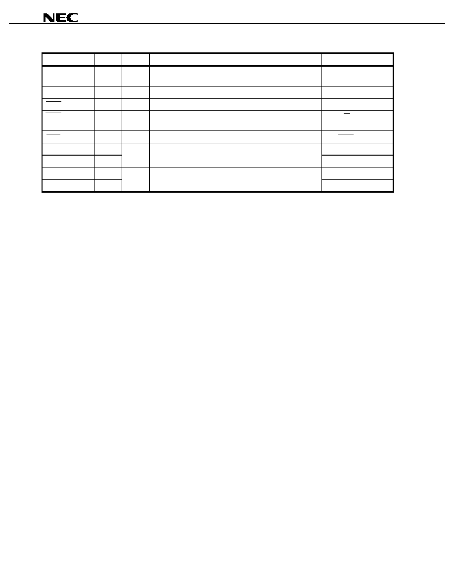
(4/4)
Pin Name
I/O
PULL
Function
Alternate Function
V
PP
-
-
High voltage apply pin for program write/verify
(
µ
PD70F3035A, 70F3035AY only)
-
V
SS
-
-
Ground potential
-
WAIT
Input
Yes
Control signal input for inserting wait in bus cycle
P110/A1
WRH
Output
No
High-order byte write strobe signal output for external data
bus
P92/R/W
WRL
Output
No
Low-order byte write strobe signal output for external data bus
P90/LBEN
X1
Input
-
X2
-
No
Resonator connection for main clock
-
XT1
Input
-
XT2
-
No
Resonator connection for subsystem clock
-
Remark
PULL: On-chip pull-up resistor
Data Sheet U14780EJ1V0DS00
15
µ
µ
µ
µ
PD703034A, 703034AY, 703035A, 703035AY, 70F3035A, 70F3035AY
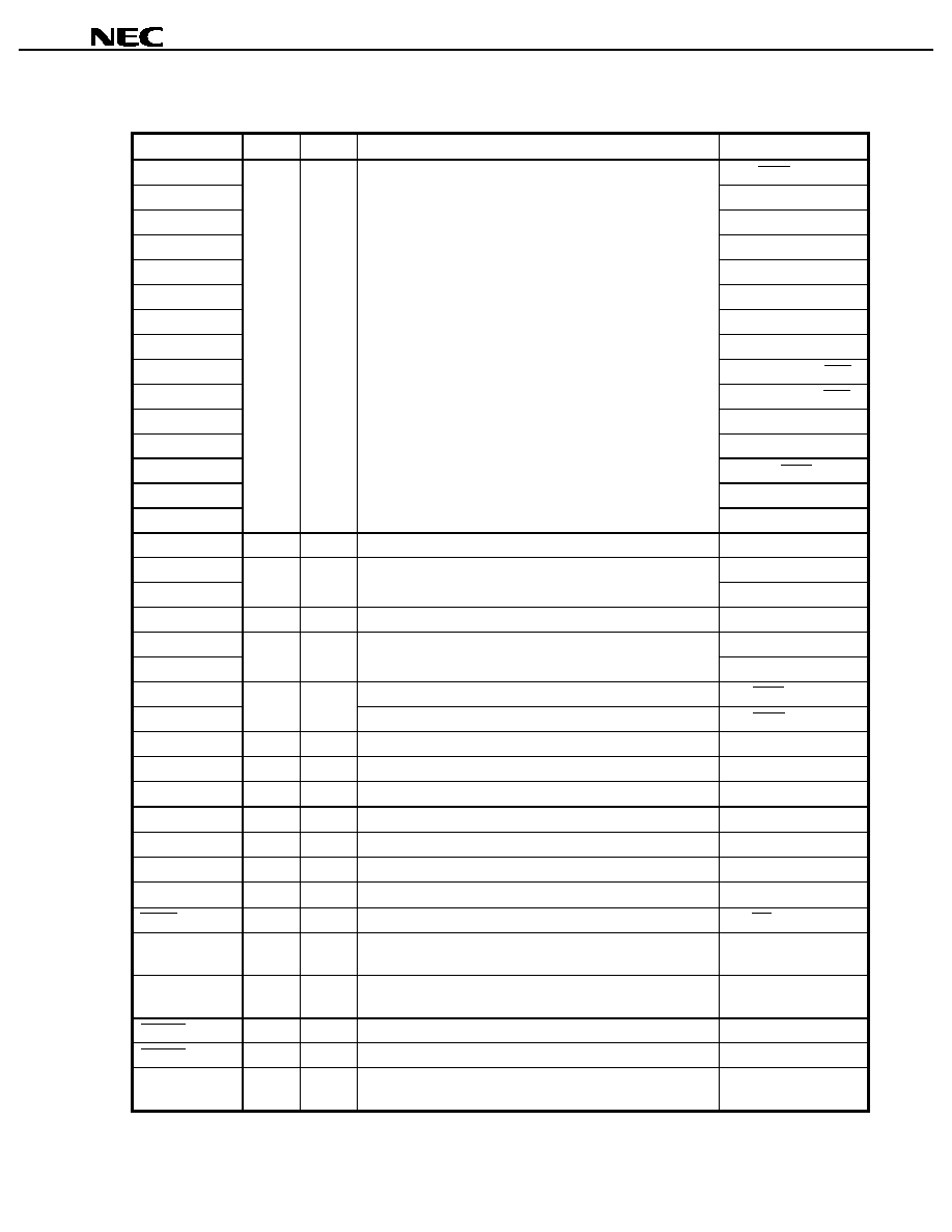
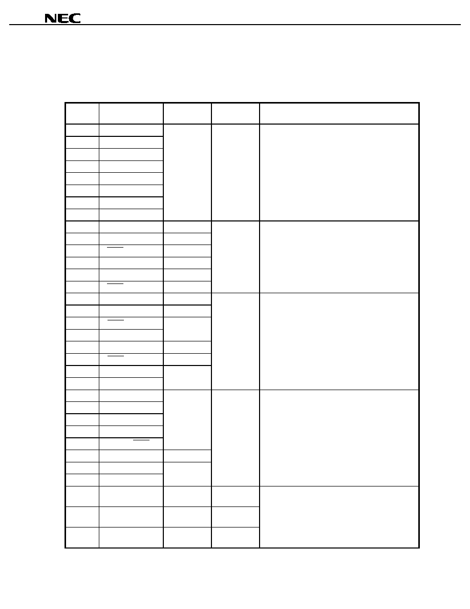
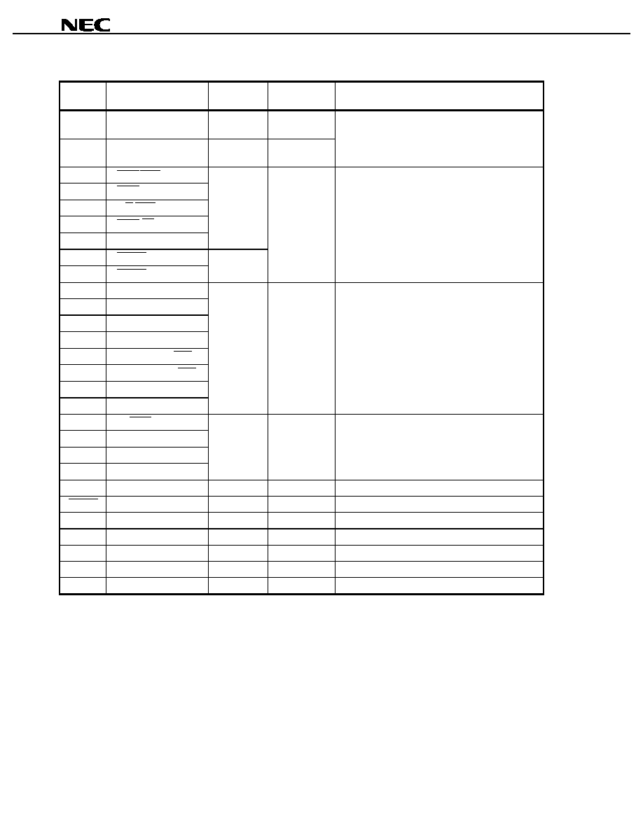
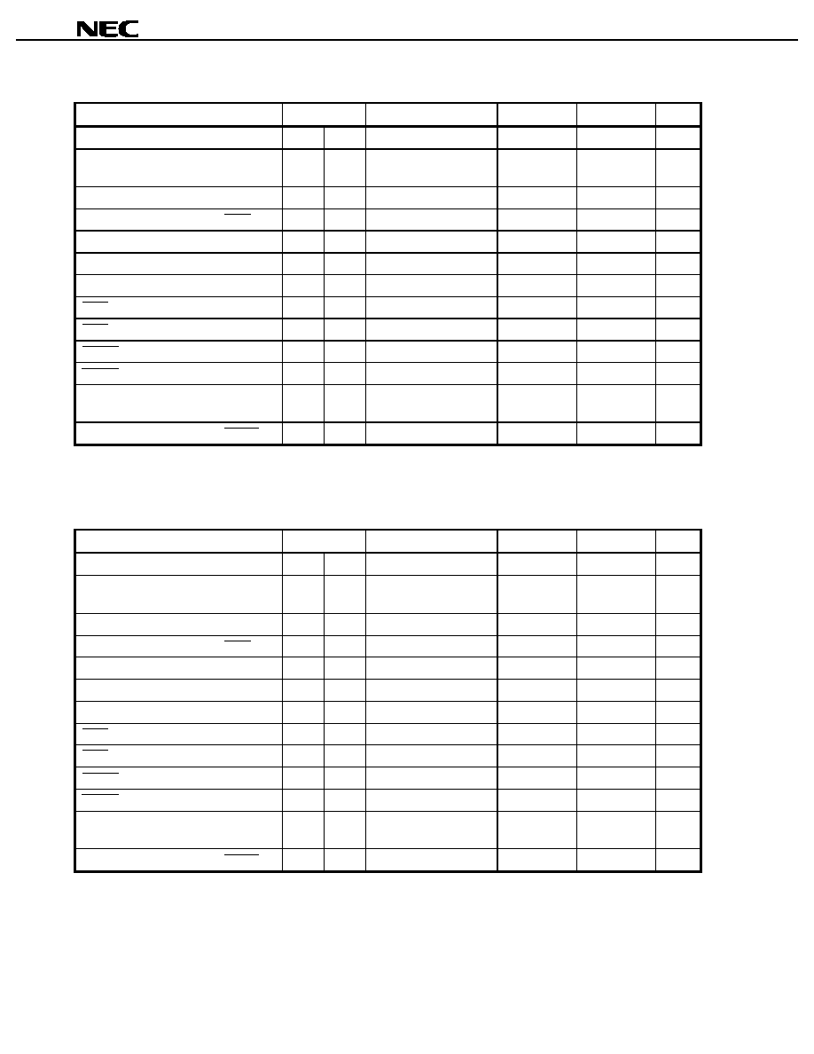
2.3 Pin I/O Circuits and Recommended Connection of Unused Pins
The input/output circuit type of each pin and recommended connection of unused pins are show in Table 2-1. For
the input/output schematic circuit diagram of each type, refer to Figure 2-1.
Table 2-1. Types of Pin I/O Circuits (1/2)
Pin
Alternate Function
I/O Circuit
Type
I/O Buffer
Power Supply
Recommended Connection of Unused Pins
P00
NMI
P01
INTP0
P02
INTP1
P03
INTP2
P04
INTP3
P05
INTP4/ADTRG
P06
INTP5/RTPTRG
P07
INTP6
8-A
EV
DD
Input state:
Independently connect to EV
DD
or
EV
SS
via a resistor.
Output state: Leave open.
P10
SI0/SDA0
10-A
P11
SO0
26
P12
SCK0/SCL0
10-A
P13
SI1/RXD0
8-A
P14
SO0/TXD0
26
P15
SCK1/ASCK0
10-A
EV
DD
Input state:
Independently connect to EV
DD
or
EV
SS
via a resistor.
Output state: Leave open.
P20
SI2/SDA1
10-A
P21
SO2
26
P22
SCK2/SCL1
P23
SI3/RXD1
10-A
P24
SO3/TXD1
26
P25
SCK3/ASCK1
10-A
P26
TI2/TO2
P27
TI3/TO3
8-A
EV
DD
Input state:
Independently connect to EV
DD
or
EV
SS
via a resistor.
Output state: Leave open.
P30
TI00
P31
TI01
P32
TI10/SI4
P33
TI11/SO4
P34
TO0/A13/SCK4
8-A
P35
TO1/A14
5-A
P36
TI4/TO4/A15
P37
TI5/TO5
8-A
EV
DD
Input state:
Independently connect to EV
DD
or
EV
SS
via a resistor.
Output state: Leave open.
P40 to
P47
AD0 to AD7
5
BV
DD
P50 to
P57
AD8 to AD15
5
BV
DD
P60 to
P65
A16 to A21
5
BV
DD
Input state:
Independently connect to BV
DD
or
BV
SS
via a resistor.
Output state: Leave open.
Data Sheet U14780EJ1V0DS00
16
µ
µ
µ
µ
PD703034A, 703034AY, 703035A, 703035AY, 70F3035A, 70F3035AY
Table 2-1. Types of Pin I/O Circuits (2/2)
Pin
Alternate Function
I/O Circuit
Type
I/O Buffer
Power Supply
Recommended Connection of Unused Pins
P70 to
P77
ANI0 to ANI7
9
AV
DD
P80 to
P83
ANI8 to ANI11
9
AV
DD
Independently connect to AV
DD
or AV
SS
via a
resistor.
P90
LBEN/WRL
P91
UBEN
P92
R/W/WRH
P93
DSTB/RD
P94
ASTB
5
P95
HLDAK
P96
HLDRQ
26
BV
DD
Input state:
Independently connect to BV
DD
or
BV
SS
via a resistor.
Output state: Leave open.
P100
RTP0/A5/KR0
P101
RTP1/A6/KR1
P102
RTP2/A7/KR2
P103
RTP3/A8/KR3
P104
RTP4/A9/KR4/IERX
P105
RTP5/A10/KR5/IETX
P106
RTP6/A11/KR6
P107
RTP7/A12/KR7
10-A
EV
DD
Input state:
Independently connect to EV
DD
or
EV
SS
via a resistor.
Output state: Leave open.
P110
A1/WAIT
P111
A2
P112
A3
P113
A4
5-A
EV
DD
Input state:
Independently connect to EV
DD
or
EV
SS
via a resistor.
Output state: Leave open.
CLKOUT
≠
4
BV
DD
Leave open.
RESET
≠
2
EV
DD
≠
XT1
≠
16
≠
Connect to V
SS
via a resistor.
XT2
≠
16
≠
Leave open.
AV
REF
≠
≠
≠
Connect to AV
SS
via a resistor.
IC
Note 1
≠
≠
≠
Connect directly to V
SS
.
V
PP
Note 2
≠
≠
≠
Connect to V
SS
.
Notes 1.
µ
PD703034A, 703034AY, 703035A, 703035AY
2.
µ
PD70F3035A, 70F3035AY
Caution
Three power supply systems are available to supply power to the I/O buffers of the V850/SB2's
pins: EV
DD
, BV
DD
, and AV
DD
. The voltage ranges that can be used for these I/O buffer power
supplies are shown below.
EV
DD
, BV
DD
: 3.0 V to 5.5 V
AV
DD
: 4.5 V to 5.5 V
The electrical specifications differ depending on whether the power supply voltage range is 3.0
V to under 4.0 V, or 4.0 V to 5.5 V.

Data Sheet U14780EJ1V0DS00
17
µ
µ
µ
µ
PD703034A, 703034AY, 703035A, 703035AY, 70F3035A, 70F3035AY
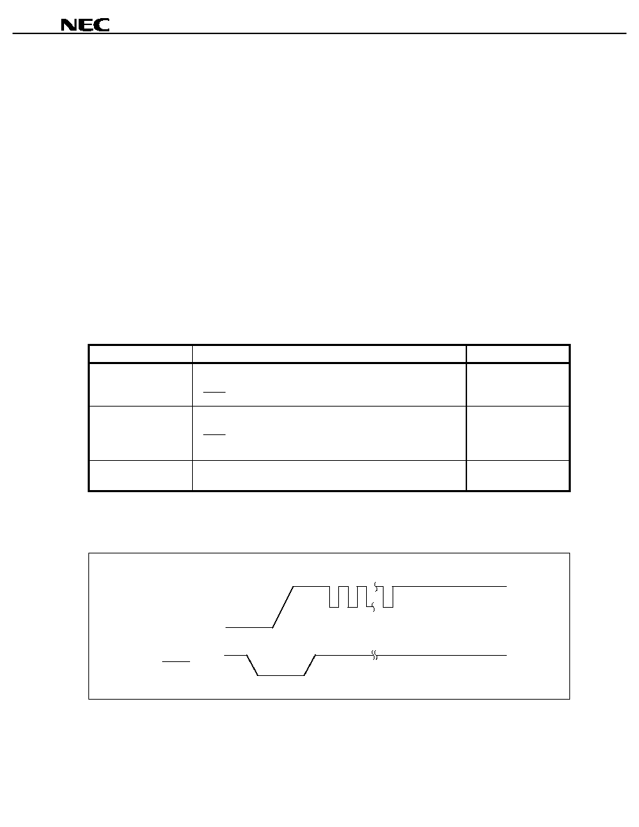
Figure 2-1. Pin Input/Output Circuits (1/2)
Type 2
Schmitt-triggered input with hysteresis characteristics
Push-pull output that can be set for high-impedance output
(both P-ch and N-ch off)
IN
Data
Output
disable
P-ch
OUT
V
DD
N-ch
Data
Output
disable
P-ch
IN/OUT
V
DD
N-ch
Input
enable
Data
Output
disable
P-ch
IN/OUT
V
DD
N-ch
Input
enable
P-ch
V
DD
Pullup
enable
Data
Output
disable
P-ch
IN/OUT
V
DD
N-ch
P-ch
V
DD
Pullup
enable
IN
Comparator
+
≠
V
REF
(threshold voltage)
P-ch
N-ch
Input enable
Type 4
Type 5
Type 9
Type 8-A
Type 5-A
Caution
V
DD
in the circuit diagrams can be read as EV
DD
, BV
DD
, or AV
DD
, as appropriate.

Data Sheet U14780EJ1V0DS00
18
µ
µ
µ
µ
PD703034A, 703034AY, 703035A, 703035AY, 70F3035A, 70F3035AY
Figure 2-1. Pin Input/Output Circuits (2/2)
Data
Output disable
P-ch
IN/OUT
V
DD
N-ch
P-ch
V
DD
Pullup
enable
Open drain
P-ch
Feedback cut-off
XT1
XT2
Data
Output
disable
Open drain
P-ch
IN/OUT
V
DD
N-ch
P-ch
V
DD
Pullup
enable
Type 10-A
Type 26
Type 16
Caution
V
DD
in the circuit diagrams can be read as EV
DD
, BV
DD
, or AV
DD
, as appropriate.
Data Sheet U14780EJ1V0DS00
19
µ
µ
µ
µ
PD703034A, 703034AY, 703035A, 703035AY, 70F3035A, 70F3035AY
3. PROGRAMMING FLASH MEMORY (
µ
µ
µ
µ
PD70F3035A, 70F3035AY ONLY)
There are the following two methods for writing a program to the flash memory.
(1) On-board programming
Write a program to the flash memory using a dedicated flash programmer after the
µ
PD70F3035A and
70F3035AY have been mounted on the target board. Also mount a connector, etc. on the target board to
communicate with the dedicated flash programmer.
(2) Off-board programming
Write a program using a dedicated adapter before the
µ
PD70F3035A and 70F3035AY have been mounted on
the target board.
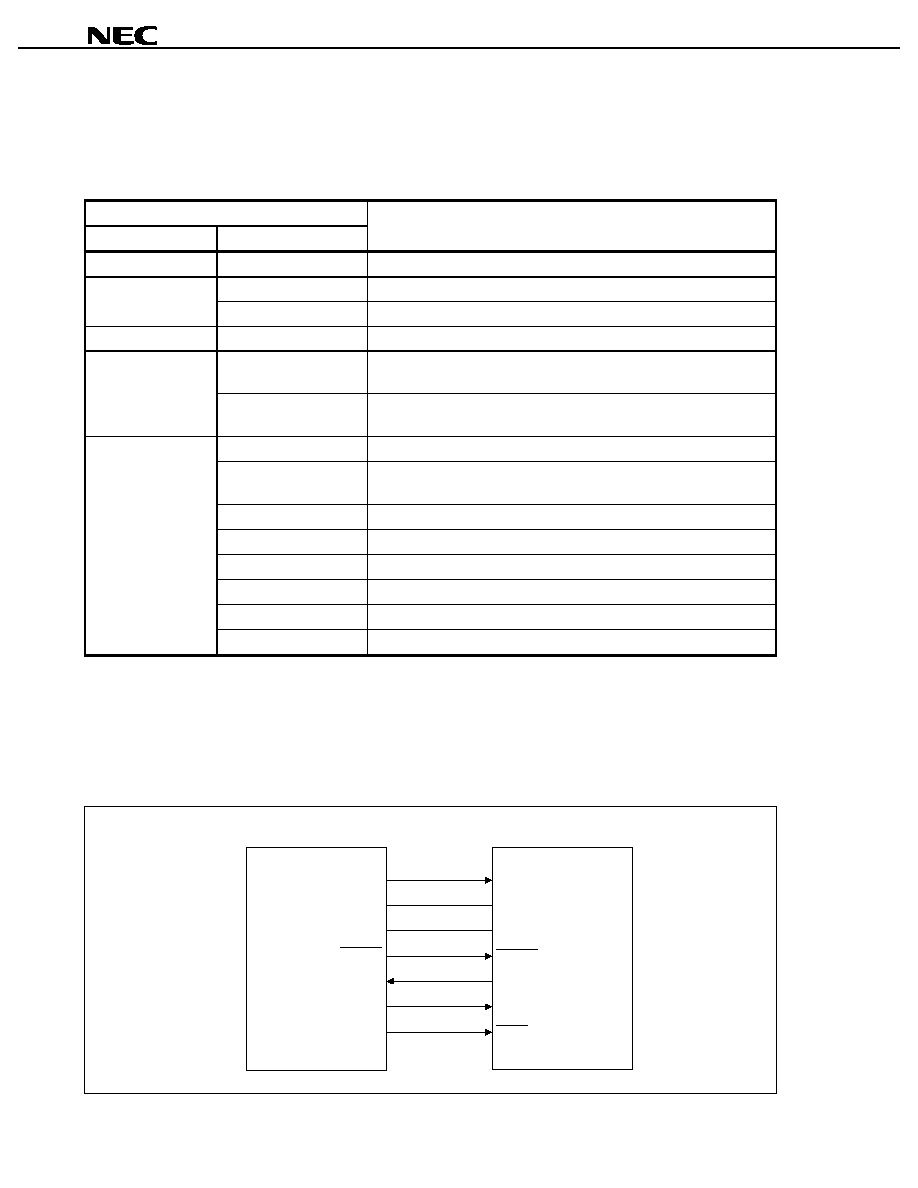
3.1 Selecting Communication Mode
To write the flash memory, use a dedicated flash programmer and serial communication. Select a serial
communication mode from those listed in Table 3-1 in the format shown in Figure 3-1. Each communication mode is
selected by the number of V
PP
pulses shown in Table 3-1.
Table 3-1. Communication Modes
Communication Mode
Pins Used
Number of V
PP
Pulses
CSI0
SO0 (serial data output)
SI0 (serial data input)
SCK0 (serial clock input)
0
CSI0
+
HS
SO0 (serial data output)
SI0 (serial data input)
SCK0 (serial clock input)
P15 (3-wire + handshake signal output of handshake communication)
3
UART0
TXD0 (serial data output)
RXD0 (serial data input)
8
Figure 3-1. Communication Mode Selecting Format
7.8 V
V
SS
V
PP
RESET
EV
DD
V
SS
3.0 V
Data Sheet U14780EJ1V0DS00
20
µ
µ
µ
µ
PD703034A, 703034AY, 703035A, 703035AY, 70F3035A, 70F3035AY
3.2 Function of Flash Memory Programming
Operations such as writing to flash memory are performed by various command/data transmission and reception
operations according to the selected communication mode. The major functions are shown below.
Table 3-2. Major Functions of Flash Memory Programming
Function
Category
Command
Description
Verify
Batch verify
Compares the contents of the entire memory and the input data.
Batch erase
Erases the contents of the entire memory.
Erase
Write back
Writes back the contents which is overerased.
Blank check
Batch blank check
Checks the erase state of the entire memory.
High-speed write
Writes data by the specification of the write start address and the
number of bytes to be written, and executes verify check.
Data write
Continuous write
Writes data from the address following the high-speed write command
executed immediately before, and executes verify check.
Status read out
Reads out the status of operations.
Oscillation frequency
setting
Sets the oscillation frequency.
Erase time setting
Sets the erase time of batch erase.
Write time setting
Sets the write time of data write.
Write back time setting
Sets the write back time.
Baud rate setting
Sets the baud rate when using UART0.
Silicon signature
Reads out the silicon signature information.
System
setting/control
Reset
Restarts the system of flash programmer.
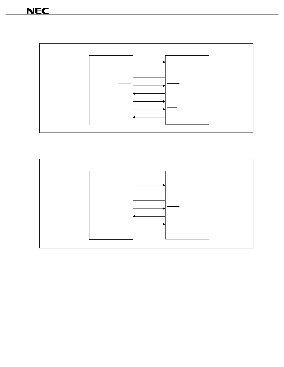
3.3 Connecting Dedicated Flash Programmer
The connection of the dedicated flash programmer and the
µ
PD70F3035A and 70F3035AY differs according to
the communication mode. The connections for each communication mode are shown below.
Figure 3-2. Connection of Dedicated Flash Programmer in CSI0 Mode
Dedicated flash programmer
PD70F3035A, 70F3035AY
V
DD
V
DD
V
SS
GND
SI
SO
SCK
V
PP
V
PP
RESET
RESET
SO0
SI0
SCK0
µ
Data Sheet U14780EJ1V0DS00
21
µ
µ
µ
µ
PD703034A, 703034AY, 703035A, 703035AY, 70F3035A, 70F3035AY
Figure 3-3. Connection of Dedicated Flash Programmer in CSI0 + HS Mode
Dedicated flash programmer
PD70F3035A, 70F3035AY
V
DD
V
DD
V
SS
GND
SI
SO
SCK
V
PP
V
PP
RESET
RESET
HS
SO0
SI0
SCK0
P15
µ
Figure 3-4. Connection of Dedicated Flash Programmer in UART0 Mode
Dedicated flash programmer
PD70F3035A, 70F3035AY
V
DD
V
DD
V
SS
GND
RxD
TxD
V
PP
V
PP
RESET
RESET
TXD0
RXD0
µ
Data Sheet U14780EJ1V0DS00
22
µ
µ
µ
µ
PD703034A, 703034AY, 703035A, 703035AY, 70F3035A, 70F3035AY
4. ELECTRICAL SPECIFICATIONS
Absolute Maximum Ratings (T
A
= 25∞C, V
SS
= 0 V)
Parameter
Symbol
Conditions
Ratings
Unit
V
DD
V
DD
pin
≠0.5 to +7.0
V
AV
DD
AV
DD
pin
≠0.5 to +7.0
V
BV
DD
BV
DD
pin
≠0.5 to +7.0
V
EV
DD
EV
DD
pin
≠0.5 to +7.0
V
AV
SS
AV
SS
pin
≠0.5 to +0.5
V
BV
SS
BV
SS
pin
≠0.5 to +0.5
V
Supply voltage
EV
SS
EV
SS
pin
≠0.5 to +0.5
V
V
I1
Note 1 (BV
DD
pin)
≠0.5 to BV
DD
+ 0.5
Note 4
V
V
I2
Note 2 (EV
DD
pin)
≠0.5 to EV
DD
+ 0.5
Note 4
V
Input voltage
V
I3
V
PP
pin (
µ
PD70F3035A, 70F3035AY only)
≠0.5 to
+
8.5
V
Analog input voltage
V
IAN
Note 3 (AV
DD
pin)
≠0.5 to AV
DD
+ 0.5
Note 4
V
Analog reference input voltage
AV
REF
AV
REF
pin
≠0.5 to AV
DD
+ 0.5
Note 4
V
Per pin
4.0
mA
Total for P00 to P07, P10 to P15, P20 to
P25
25
mA
Total for P26, P27, P30 to P37, P100 to
P107, P110 to P113
25
mA
Total for P40 to P47, P90 to P96, CLKOUT
25
mA
Output current, low
I
OL
Total for P50 to P57, P60 to P65
25
mA
Per pin
≠4.0
mA
Total for P00 to P07, P10 to P15, P20 to
P25
≠25
mA
Total for P26, P27, P30 to P37, P100 to
P107, P110 to P113
≠25
mA
Total for P40 to P47, P90 to P96, CLKOUT
≠25
mA
Output current, high
I
OH
Total for P50 to P57, P60 to P65
≠25
mA
V
O1
Note 1 (BV
DD
pin)
≠0.5 to BV
DD
+ 0.5
Note 4
V
Output voltage
V
O2
Note 2 (EV
DD
pin)
≠0.5 to EV
DD
+ 0.5
Note 4
V
Normal operation mode
≠40 to +85
∞
C
Operating ambient temperature
T
A
Flash memory programming mode
(
µ
PD70F3035A, 70F3035AY only)
10 to 85
∞
C
µ
PD703034A, 703034AY
µ
PD703035A, 703035AY
≠65 to +150
∞
C
Storage temperature
T
stg
µ
PD70F3035A, 70F3035AY
≠40 to
+
125
∞
C
Notes 1. Ports 4, 5, 6, 9, CLKOUT, and their alternate-function pins
2. Ports 0, 1, 2, 3, 10, 11, RESET, and their alternate-function pins
3. Ports 7, 8, and their alternate-function pins
4. Be sure not to exceed the absolute maximum ratings (MAX. value) of each supply voltage.

Data Sheet U14780EJ1V0DS00
23
µ
µ
µ
µ
PD703034A, 703034AY, 703035A, 703035AY, 70F3035A, 70F3035AY
Cautions
1. Do not directly connect the output (or I/O) pins of IC products to each other, or to V
DD
, V
CC
,
and GND. Open-drain pins or open-collector pins, however, can be directly connected to
each other. Direct connection of the output pins between an IC product and an external
circuit is possible, if the output pins can be set to the high-impedance state and the output
timing of the external circuit is designed to avoid output conflict.
2. Product quality may suffer if the absolute maximum rating is exceeded even momentarily for
any parameter. That is, the absolute maximum ratings are rated values at which the product
is on the verge of suffering physical damage, and therefore the product must be used under
conditions that ensure that the absolute maximum ratings are not exceeded.
The ratings and conditions indicated for DC characteristics and AC characteristics represent
the quality assurance range during normal operation.
Capacitance (T
A
= 25∞C)
Parameter
Symbol
Conditions
MIN.
TYP.
MAX.
Unit
Input capacitance
C
I
15
pF
I/O capacitance
C
IO
15
pF
Output capacitance
C
O
f
C
= 1 MHz
Unmeasured pins returned to 0 V
15
pF
Operating Conditions
(1) Operating frequency
Operating Frequency (f
XX
)
V
DD
AV
DD
BV
DD
EV
DD
Remark
2 to 13 MHz
4.0 to 5.5 V
4.5 to 5.5 V
3.0 to 5.5 V
3.0 to 5.5 V
Note 1
Other than IDLE mode
4.0 to 5.5 V
4.5 to 5.5 V
3.0 to 5.5 V
3.0 to 5.5 V
≠
32.768 kHz
IDLE mode
3.5 to 5.5 V
4.5 to 5.5 V
3.0 to 5.5 V
3.0 to 5.5 V
Note 2
Notes 1. During STOP mode (subsystem oscillator operating), V
DD
= 3.5 to 5.5 V. Shifting to STOP mode or
restoring from STOP mode must be performed at V
DD
= 4.0 V min.
2. Shifting to IDLE mode or restoring from IDLE mode must be performed at V
DD
= 4.0 V min.
(2) CPU operating frequency
Parameter
Symbol
Conditions
MIN.
TYP.
MAX.
Unit
Main system clock operation
0.25
13
MHz
CPU operating frequency
f
CPU
Subsystem clock operation
32.768
kHz
Data Sheet U14780EJ1V0DS00
24
µ
µ
µ
µ
PD703034A, 703034AY, 703035A, 703035AY, 70F3035A, 70F3035AY
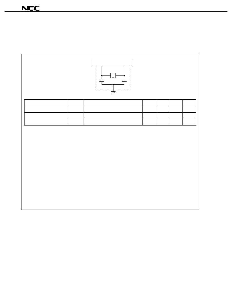
Recommended Oscillator
(1) Main system clock oscillator (T
A
= ≠40 to +85∞C)
(a) Connection of ceramic resonator or crystal resonator
X1
X2
Parameter
Symbol
Conditions
MIN.
TYP.
MAX.
Unit
Oscillation frequency
f
XX
2
13
MHz
≠
Upon reset release
2
19
/f
XX
s
Oscillation stabilization time
≠
Upon STOP mode release
Note
s
Note The TYP. value differs depending on the setting of the oscillation stabilization time select register (OSTS).
Cautions 1. Main system clock oscillator operates on the output voltage of the on-chip regulator.
External clock input is prohibited.
2. When using the main system clock oscillator, wire as follows in the area enclosed by the
broken lines in the above figure to avoid an adverse effect from wiring capacitance.
∑
∑
∑
∑
Keep the wiring length as short as possible.
∑
∑
∑
∑
Do not cross the wiring with the other signal lines.
∑
∑
∑
∑
Do not route the wiring near a signal line through which a high fluctuating current flows.
∑
∑
∑
∑
Always make the ground point of the oscillator capacitor the same potential as V
SS
.
∑
∑
∑
∑
Do not ground the capacitor to a ground pattern through which a high current flows.
∑
∑
∑
∑
Do not fetch signals from the oscillator.
3. Ensure that the duty of oscillation waveform is between 5.5 and 4.5.
4. Sufficiently evaluate the matching between the
µ
µ
µ
µ
PD703034A, 703034AY, 703035A, 703035AY,
70F3035A, 70F3035AY and the resonator.

Data Sheet U14780EJ1V0DS00
25
µ
µ
µ
µ
PD703034A, 703034AY, 703035A, 703035AY, 70F3035A, 70F3035AY
(2) Subsystem clock oscillator (T
A
= ≠40 to +85∞C)
(a) Connection of crystal resonator
XT1
XT2
Parameter
Symbol
Conditions
MIN.
TYP.
MAX.
Unit
Oscillation frequency
f
XT
32
32.768
35
kHz
Oscillation stabilization time
≠
10
s
Cautions 1. Subsystem clock oscillator operates on the output voltage of the on-chip regulator.
External clock input is prohibited.
2. When using the subsystem clock oscillator, wire as follows in the area enclosed by the
broken lines in the above figure to avoid an adverse effect from wiring capacitance.
∑
∑
∑
∑
Keep the wiring length as short as possible.
∑
∑
∑
∑
Do not cross the wiring with the other signal lines.
∑
∑
∑
∑
Do not route the wiring near a signal line through which a high fluctuating current flows.
∑
∑
∑
∑
Always make the ground point of the oscillator capacitor the same potential as V
SS
.
∑
∑
∑
∑
Do not ground the capacitor to a ground pattern through which a high current flows.
∑
∑
∑
∑
Do not fetch signals from the oscillator.
3. Sufficiently evaluate the matching between the
µ
µ
µ
µ
PD703034A, 703034AY, 703035A, 703035AY,
70F3035A, 70F3035AY and the resonator.
Data Sheet U14780EJ1V0DS00
26
µ
µ
µ
µ
PD703034A, 703034AY, 703035A, 703035AY, 70F3035A, 70F3035AY
DC Characteristics
(T
A
= ≠40 to +85∞C, V
DD
= 4.0 to 5.5 V, BV
DD
= EV
DD
= 3.0 to 5.5 V, AV
DD
= 4.5 to 5.5 V, V
SS
= AV
SS
= BV
SS
= EV
SS
= 0 V)
Parameter
Symbol
Conditions
MIN.
TYP.
MAX.
Unit
4.0 V
BV
DD
5.5 V
0.7BV
DD
BV
DD
V
V
IH1
Note 1
3.0 V
BV
DD
< 4.0 V
0.8BV
DD
BV
DD
V
4.0 V
EV
DD
5.5 V
0.7EV
DD
EV
DD
V
V
IH2
Note 2
3.0 V
EV
DD
< 4.0 V
0.8EV
DD
EV
DD
V
4.0 V
EV
DD
5.5 V
0.7EV
DD
EV
DD
V
V
IH3
Note 3
3.0 V
EV
DD
< 4.0 V
0.8EV
DD
EV
DD
V
Input voltage, high
V
IH4
Note 4
4.5 V
AV
DD
5.5 V
0.7AV
DD
AV
DD
V
V
IL1
Note 1
BV
SS
0.3BV
DD
V
V
IL2
Note 2
EV
SS
0.3EV
DD
V
V
IL3
Note 3
EV
SS
0.3EV
DD
V
Input voltage, low
V
IL4
Note 4
AV
SS
0.3AV
DD
V
3.0 V
BV
DD
5.5 V,
I
OH
= ≠100
µ
A
BV
DD
≠0.5
V
V
OH1
Note 1
4.0 V
BV
DD
5.5 V,
I
OH
= ≠3 mA
BV
DD
≠1.0
V
3.0 V
EV
DD
5.5 V,
I
OH
= ≠100
µ
A
EV
DD
≠0.5
V
Output voltage, high
V
OH2
Notes 2, 3
(except RESET)
4.0 V
EV
DD
5.5 V,
I
OH
= ≠3 mA
EV
DD
≠1.0
V
I
OL
= 3 mA,
3.0 V
BV
DD
, EV
DD
5.5 V
0.5
V
Output voltage, low
V
OL
I
OL
= 3 mA,
4.0 V
BV
DD
, EV
DD
5.5 V
0.4
V
Input leakage current, high
I
LIH
V
I
= V
DD
= BV
DD
= EV
DD
= AV
DD
5
µ
A
Input leakage current, low
I
LIL
V
I
= 0 V
≠5
µ
A
Output leakage current, high
I
LOH
5
µ
A
Output leakage current, low
I
LOL
≠5
µ
A
Notes 1. Ports 4, 5, 6, 9, CLKOUT, and their alternate-function pins
2. P11, P14, P21, P24, P34, P35, P110 to P113, and their alternate-function pins
3. P00 to P07, P10, P12, P13, P15, P20, P22, P23, P25 to P27, P30 to P33, P36, P37, P100 to P107,
RESET, and their alternate-function pins
4. Ports 7, 8, and their alternate-function pins
Data Sheet U14780EJ1V0DS00
27
µ
µ
µ
µ
PD703034A, 703034AY, 703035A, 703035AY, 70F3035A, 70F3035AY
DC Characteristics
(T
A
= ≠40 to +85∞C, V
DD
= 4.0 to 5.5 V, BV
DD
= EV
DD
= 3.0 to 5.5 V, AV
DD
= 4.5 to 5.5 V, V
SS
= AV
SS
= BV
SS
= EV
SS
= 0 V)
Parameter
Symbol
Conditions
MIN.
TYP.
MAX.
Unit
µ
PD703034A,
I
DD1
In normal operation mode
Note 1
15
25
mA
µ
PD703034AY,
I
DD2
In HALT mode
Note 1
6
13
mA
µ
PD703035A,
I
DD3
In IDLE
mode
Note 2
Watch timer operating
1
4
mA
Watch timer, subsystem
oscillator operating
13
70
µ
A
I
DD4
In STOP
mode
Subsystem oscillator
stopped, XT1 = V
SS
8
70
µ
A
I
DD5
In normal operation mode
(subsystem operation)
Note 3
50
150
µ
A
µ
PD703035AY
I
DD6
In IDLE mode (subsystem
operation)
Note 3
13
70
µ
A
µ
PD70F3035A,
I
DD1
In normal operation mode
Note 1
25
48
mA
I
DD2
In HALT mode
Note 1
7
15
mA
I
DD3
In IDLE
mode
Note 2
Watch timer operating
1
4
mA
Watch timer, subsystem
oscillator operating
13
100
µ
A
I
DD4
In STOP
mode
Subsystem oscillator
stopped, XT1 = V
SS
8
100
µ
A
I
DD5
In normal operation mode
(subsystem operation)
Note 3
200
600
µ
A
Supply current
µ
PD70F3035AY
I
DD6
In IDLE mode (subsystem
operation)
Note 3
90
180
µ
A
Pull-up resistance
R
L
V
IN
= 0 V
10
30
100
k
Notes 1. f
CPU
= f
XX
= 13 MHz, all peripheral functions operating, output buffer: OFF
2. f
XX
= 13 MHz
3. f
CPU
= f
XT
= 32.768 kHz, main system clock oscillator stopped
Remark
TYP. values are reference values for when T
A
= 25
∞
C, V
DD
= BV
DD
= EV
DD
= AV
DD
= 5.0 V. The current
consumed by the output buffer is not included.
Data Sheet U14780EJ1V0DS00
28
µ
µ
µ
µ
PD703034A, 703034AY, 703035A, 703035AY, 70F3035A, 70F3035AY
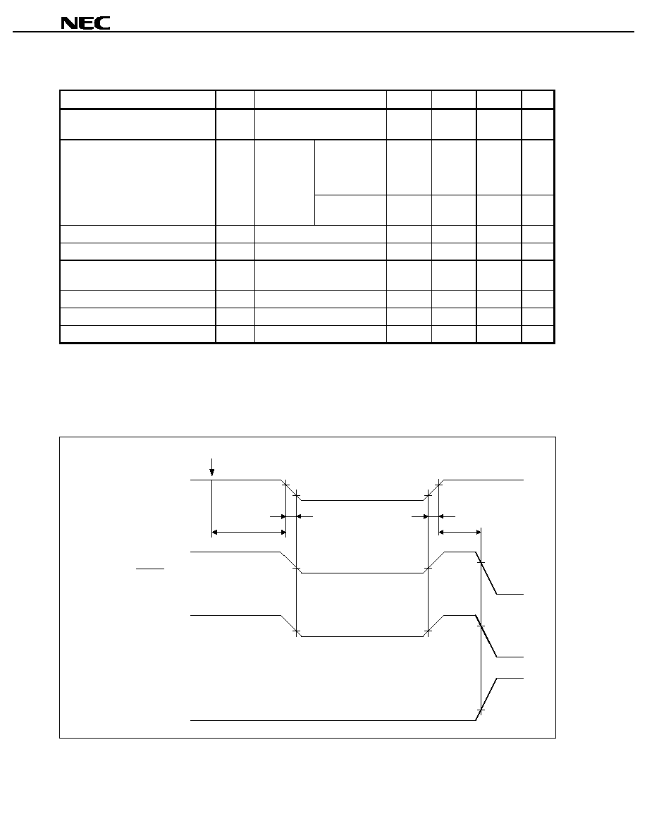
Data Retention Characteristics (T
A
= ≠40 to +85∞C)
Parameter
Symbol
Conditions
MIN.
TYP.
MAX.
Unit
Data retention voltage
V
DDDR
STOP mode (all functions not
operating)
3.0
Note
5.5
V
µ
PD703034A,
µ
PD703034AY,
µ
PD703035A,
µ
PD703035AY
8
70
µ
A
Data retention current
I
DDDR
V
DD
= V
DDDR
,
XT1 = V
SS
(subsystem
stopped)
µ
PD70F3035A,
µ
PD70F3035AY
8
100
µ
A
Supply voltage rise time
t
RVD
200
µ
s
Supply voltage fall time
t
FVD
200
µ
s
Supply voltage hold time
(from STOP mode setting)
t
HVD
0
ms
STOP release signal input time
t
DREL
0
ms
Data retention high-level input voltage
V
IHDR
All input ports
0.9V
DDDR
V
DDDR
V
Data retention low-level input voltage
V
ILDR
All input ports
0
0.1V
DDDR
V
Note
During STOP mode (subsystem oscillator operating), V
DD
= 3.5 to 5.5 V. Shifting to STOP mode or
restoring from STOP mode must be performed at V
DD
= 4.0 V min.
Remark
TYP. values are reference values for when T
A
= 25
∞
C.
t
HVD
V
DDDR
t
DREL
V
IHDR
V
IHDR
t
FVD
t
RVD
V
DD
NMI, INTPn (input)
(Released by falling edge)
Setting STOP mode
RESET (input)
NMI, INTPn (input)
(Released by rising edge)
V
ILDR
Data Sheet U14780EJ1V0DS00
29
µ
µ
µ
µ
PD703034A, 703034AY, 703035A, 703035AY, 70F3035A, 70F3035AY
AC Characteristics (T
A
= ≠40 to +85∞C, V
DD
= 4.0 to 5.5 V, BV
DD
= EV
DD
= 3.0 to 5.5 V, AV
DD
= 4.5 to 5.5 V, V
SS
=
AV
SS
= BV
SS
= EV
SS
= 0 V)
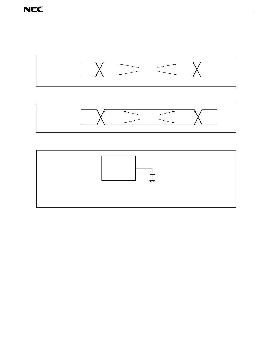
AC Test Input Waveform (V
DD
: EV
DD
, BV
DD
, AV
DD
)
V
DD
0 V
V
IH
V
IL
V
IH
V
IL
Test points
Input signal
AC Test Output Test Points (EV
DD
, BV
DD
)
V
OH
V
OL
V
OH
V
OL
Test points
Output signal
Load Conditions
DUT
(Device under test)
C
L
= 50 pF
Caution If the load capacitance exceeds 50 pF due to the circuit configuration, bring the load capacitance
of the device to 50 pF or less by inserting a buffer or by some other means.
Data Sheet U14780EJ1V0DS00
30
µ
µ
µ
µ
PD703034A, 703034AY, 703035A, 703035AY, 70F3035A, 70F3035AY
(1) Clock timing
(a) T
A
= ≠40 to +85∞C, V
DD
= BV
DD
= 4.0 to 5.5 V, V
SS
= BV
SS
= 0 V
Parameter
Symbol
Conditions
MIN.
MAX.
Unit
CLKOUT output cycle
<1>
t
CYK
76.9 ns
31.2
µ
s
CLKOUT high-level width
<2>
t
WKH
0.4t
CYK
≠ 12
ns
CLKOUT low-level width
<3>
t
WKL
0.4t
CYK
≠ 12
ns
CLKOUT rise time
<4>
t
KR
12
ns
CLKOUT fall time
<5>
t
KF
12
ns
(b) T
A
= ≠40 to +85∞C, V
DD
= 4.0 to 5.5 V, BV
DD
= 3.0 to 4.0 V, V
SS
= BV
SS
= 0 V
Parameter
Symbol
Conditions
MIN.
MAX.
Unit
CLKOUT output cycle
<1>
t
CYK
76.9 ns
31.2
µ
s
CLKOUT high-level width
<2>
t
WKH
0.4t
CYK
≠ 15
ns
CLKOUT low-level width
<3>
t
WKL
0.4t
CYK
≠ 15
ns
CLKOUT rise time
<4>
t
KR
15
ns
CLKOUT fall time
<5>
t
KF
15
ns
CLKOUT (output)
<2>
<4>
<5>
<3>
<1>
Data Sheet U14780EJ1V0DS00
31
µ
µ
µ
µ
PD703034A, 703034AY, 703035A, 703035AY, 70F3035A, 70F3035AY
(2) Output waveform (other than port 4, port 5, port 6, port 9, X1, and CLKOUT)
(T
A
= ≠40 to +85
∞
∞
∞
∞
C, V
DD
= 4.0 to 5.5 V, BV
DD
= EV
DD
= 3.0 to 5.5 V, V
SS
= BV
SS
= EV
SS
=
0 V)
Parameter
Symbol
Conditions
MIN.
MAX.
Unit
Output rise time
<6>
t
OR
20
ns
Output fall time
<7>
t
OF
20
ns
<7>
<6>
Output signal
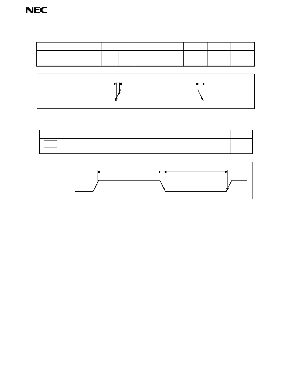
(3) Reset timing
Parameter
Symbol
Conditions
MIN.
MAX.
Unit
RESET pin high-level width
<8>
t
WRSH
500
ns
RESET pin low-level width
<9>
t
WRSL
500
ns
<8>
<9>
RESET (input)
Data Sheet U14780EJ1V0DS00
32
µ
µ
µ
µ
PD703034A, 703034AY, 703035A, 703035AY, 70F3035A, 70F3035AY
(4) Bus timing
(a) Clock asynchronous (T
A
= ≠40 to +85∞C, V
DD
= BV
DD
= 4.0 to 5.5 V, V
SS
= BV
SS
= 0 V)
Parameter
Symbol
Conditions
MIN.
MAX.
Unit
Address setup time (to ASTB
)
<10>
t
SAST
0.5T
≠ 16
ns
Address hold time (from ASTB
)
<11>
t
HSTA
0.5T
≠ 15
ns
Address float from DSTB
<12>
t
FDA
0
ns
Data input setup time from address
<13>
t
SAID
(2 + n)T ≠ 40
ns
Data input setup time from DSTB
<14>
t
SDID
(1 + n)T ≠ 40
ns
Delay time from ASTB
to DSTB
<15>
t
DSTD
0.5T
≠ 15
ns
Data input hold time (from DSTB
)
<16>
t
HDID
0
ns
Address output time from DSTB
<17>
t
DDA
(1 + i)T ≠ 15
ns
Delay time from DSTB
to ASTB
<18>
t
DDST1
0.5T ≠ 15
ns
Delay time from DSTB
to ASTB
<19>
t
DDST2
(1.5 + i)T ≠ 15
ns
DSTB low-level width
<20>
t
WDL
(1 + n)T ≠ 22
ns
ASTB high-level width
<21>
t
WSTH
T ≠ 15
ns
Data output time from DSTB
<22>
t
DDOD
10
ns
Data output setup time (to DSTB
)
<23>
t
SODD
(1 + n)T ≠ 25
ns
Data output hold time (from DSTB
)
<24>
t
HDOD
T ≠ 20
ns
<25>
t
SAWT1
n
1
1.5T ≠ 40
ns
WAIT setup time (to address)
<26>
t
SAWT2
n
1
(1.5 + n)T ≠ 40
ns
<27>
t
HAWT1
n
1
(0.5 + n)T
ns
WAIT hold time (from address)
<28>
t
HAWT2
n
1
(1.5 + n)T
ns
<29>
t
SSTWT1
n
1
T ≠ 32
ns
WAIT setup time (to ASTB
)
<30>
t
SSTWT2
n
1
(1 + n)T ≠ 32
ns
<31>
t
HSTWT1
n
1
nT
ns
WAIT hold time (from ASTB
)
<32>
t
HSTWT2
n
1
(1 + n)T
ns
HLDRQ high-level width
<33>
t
WHQH
T + 10
ns
HLDAK low-level width
<34>
t
WHAL
T ≠ 15
ns
Bus output delay time from HLDAK
<35>
t
DHAC
≠6
ns
Delay time from HLDRQ
to HLDAK
<36>
t
DHQHA1
(2n + 7.5)T + 25
ns
Delay time from HLDRQ
to HLDAK
<37>
t
DHQHA2
0.5T
1.5T + 25
ns
Remarks 1.
T = 1/f
CPU
(f
CPU
: CPU clock frequency)
2.
n: Number of wait clocks inserted in the bus cycle.
The sampling timing changes when a programmable wait is inserted.
3.
i: Number of idle cycles inserted in the bus cycle.
4.
The values in the above specifications are values for when clocks with a 5:5 duty ratio are input from
X1.
Data Sheet U14780EJ1V0DS00
33
µ
µ
µ
µ
PD703034A, 703034AY, 703035A, 703035AY, 70F3035A, 70F3035AY
(b) Clock asynchronous (T
A
= ≠40 to +85
∞
∞
∞
∞
C, V
DD
= 4.0 to 5.5 V, BV
DD
= 3.0 to 4.0 V, V
SS
= BV
SS
= 0 V)
Parameter
Symbol
Conditions
MIN.
MAX.
Unit
Address setup time (to ASTB
)
<10>
t
SAST
0.5T
≠ 20
ns
Address hold time (from ASTB
)
<11>
t
HSTA
0.5T
≠ 20
ns
Address float from DSTB
<12>
t
FDA
0
ns
Data input setup time from address
<13>
t
SAID
(2 + n)T ≠ 50
ns
Data input setup time from DSTB
<14>
t
SDID
(1 + n)T ≠ 50
ns
Delay time from ASTB
to DSTB
<15>
t
DSTD
0.5T
≠ 15
ns
Data input hold time (from DSTB
)
<16>
t
HDID
0
ns
Address output time from DSTB
<17>
t
DDA
(1 + i)T ≠ 15
ns
Delay time from DSTB
to ASTB
<18>
t
DDST1
0.5T ≠ 15
ns
Delay time from DSTB
to ASTB
<19>
t
DDST2
(1.5 + i)T ≠ 15
ns
DSTB low-level width
<20>
t
WDL
(1 + n)T ≠ 35
ns
ASTB high-level width
<21>
t
WSTH
T ≠ 15
ns
Data output time from DSTB
<22>
t
DDOD
10
ns
Data output setup time (to DSTB
)
<23>
t
SODD
(1 + n)T ≠ 35
ns
Data output hold time (from DSTB
)
<24>
t
HDOD
T ≠ 25
ns
<25>
t
SAWT1
n
1
1.5T ≠ 55
ns
WAIT setup time (to address)
<26>
t
SAWT2
n
1
(1.5 + n)T ≠ 55
ns
<27>
t
HAWT1
n
1
(0.5 + n)T
ns
WAIT hold time (from address)
<28>
t
HAWT2
n
1
(1.5 + n)T
ns
<29>
t
SSTWT1
n
1
T ≠ 45
ns
WAIT setup time (to ASTB
)
<30>
t
SSTWT2
n
1
(1 + n)T ≠ 45
ns
<31>
t
HSTWT1
n
1
nT
ns
WAIT hold time (from ASTB
)
<32>
t
HSTWT2
n
1
(1 + n)T
ns
HLDRQ high-level width
<33>
t
WHQH
T + 10
ns
HLDAK low-level width
<34>
t
WHAL
T ≠ 25
ns
Bus output delay time from HLDAK
<35>
t
DHAC
≠6
ns
Delay time from HLDRQ
to HLDAK
<36>
t
DHQHA1
(2n + 7.5)T + 25
ns
Delay time from HLDRQ
to HLDAK
<37>
t
DHQHA2
0.5T
1.5T + 25
ns
Remarks 1.
T = 1/f
CPU
(f
CPU
: CPU clock frequency)
2.
n: Number of wait clocks inserted in the bus cycle.
The sampling timing changes when a programmable wait is inserted.
3.
i: Number of idle cycles inserted in the bus cycle.
4.
The values in the above specifications are values for when clocks with a 5:5 duty ratio are input from
X1.
Data Sheet U14780EJ1V0DS00
34
µ
µ
µ
µ
PD703034A, 703034AY, 703035A, 703035AY, 70F3035A, 70F3035AY
(c) Clock synchronous (T
A
= ≠40 to +85∞C, V
DD
= BV
DD
= 4.0 to 5.5 V, V
SS
= BV
SS
= 0 V)
Parameter
Symbol
Conditions
MIN.
MAX.
Unit
Delay time from CLKOUT
to address
<38>
t
DKA
0
19
ns
Delay time from CLKOUT
to address
float
<39>
t
FKA
≠12
10
ns
Delay time from CLKOUT
to ASTB
<40>
t
DKST
0
19
ns
Delay time from CLKOUT
to DSTB
<41>
t
DKD
0
19
ns
Data input setup time (to CLKOUT
)
<42>
t
SIDK
20
ns
Data input hold time (from CLKOUT
)
<43>
t
HKID
5
ns
Data output delay time from CLKOUT
<44>
t
DKOD
19
ns
WAIT setup time (to CLKOUT
)
<45>
t
SWTK
20
ns
WAIT hold time (from CLKOUT
)
<46>
t
HKWT
5
ns
HLDRQ setup time (to CLKOUT
)
<47>
t
SHQK
20
ns
HLDRQ hold time (from CLKOUT
)
<48>
t
HKHQ
5
ns
Delay time from CLKOUT
to address
float (during bus hold)
<49>
t
DKF
19
ns
Delay time from CLKOUT
to HLDAK
<50>
t
DKHA
19
ns
Remark
The values in the above specifications are values for when clocks with a 5:5 duty ratio are input from X1.
(d) Clock synchronous (T
A
= ≠40 to +85∞C, V
DD
= 4.0 to 5.5 V, BV
DD
= 3.0 to 4.0 V, V
SS
= BV
SS
= 0 V)
Parameter
Symbol
Conditions
MIN.
MAX.
Unit
Delay time from CLKOUT
to address
<38>
t
DKA
0
22
ns
Delay time from CLKOUT
to address
float
<39>
t
FKA
≠16
10
ns
Delay time from CLKOUT
to ASTB
<40>
t
DKST
0
19
ns
Delay time from CLKOUT
to DSTB
<41>
t
DKD
0
22
ns
Data input setup time (to CLKOUT
)
<42>
t
SIDK
20
ns
Data input hold time (from CLKOUT
)
<43>
t
HKID
5
ns
Data output delay time from CLKOUT
<44>
t
DKOD
22
ns
WAIT setup time (to CLKOUT
)
<45>
t
SWTK
24
ns
WAIT hold time (from CLKOUT
)
<46>
t
HKWT
5
ns
HLDRQ setup time (to CLKOUT
)
<47>
t
SHQK
24
ns
HLDRQ hold time (from CLKOUT
)
<48>
t
HKHQ
5
ns
Delay time from CLKOUT
to address
float (during bus hold)
<49>
t
DKF
19
ns
Delay time from CLKOUT
to HLDAK
<50>
t
DKHA
19
ns
Remark
The values in the above specifications are values for when clocks with a 5:5 duty ratio are input from X1.
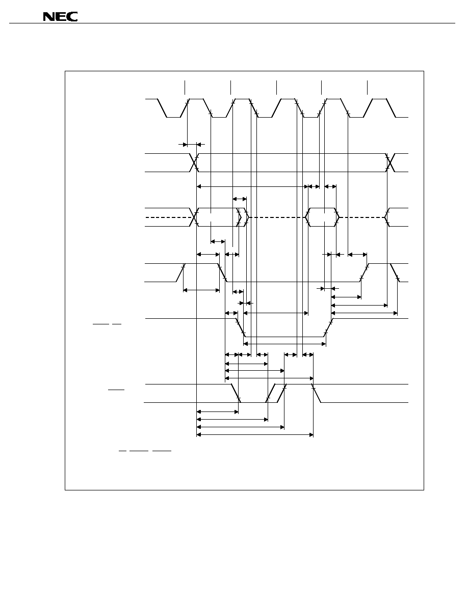
Data Sheet U14780EJ1V0DS00
35
µ
µ
µ
µ
PD703034A, 703034AY, 703035A, 703035AY, 70F3035A, 70F3035AY
(e) Read cycle (CLKOUT synchronous/asynchronous, 1 wait)
CLKOUT (output)
ASTB (output)
T1
T2
TW
<38>
<
15
>
<
20
>
<
45
>
DSTB, RD
(output)
WAIT
(input)
AD0 to AD15 (I/O)
<
39
>
<
10
>
<
43
>
<
40
>
T3
<
42
>
<
13
>
<
21
>
<
16
>
<
14
>
<
19
>
<
17
>
<
18
>
<
41
>
<
12
>
<
29
>
<
31
>
<
25
>
<
27
>
<
26
>
<
28
>
<
30
>
<
46
>
<
45
>
<
46
>
Data
Address
<
40
>
<
11
>
<
41
>
<
32
>
A1 to A15 (output)
A16 to A21 (output)
Note (output)
Note
R/W, UBEN, LBEN
Remark
The broken lines indicate high impedance.
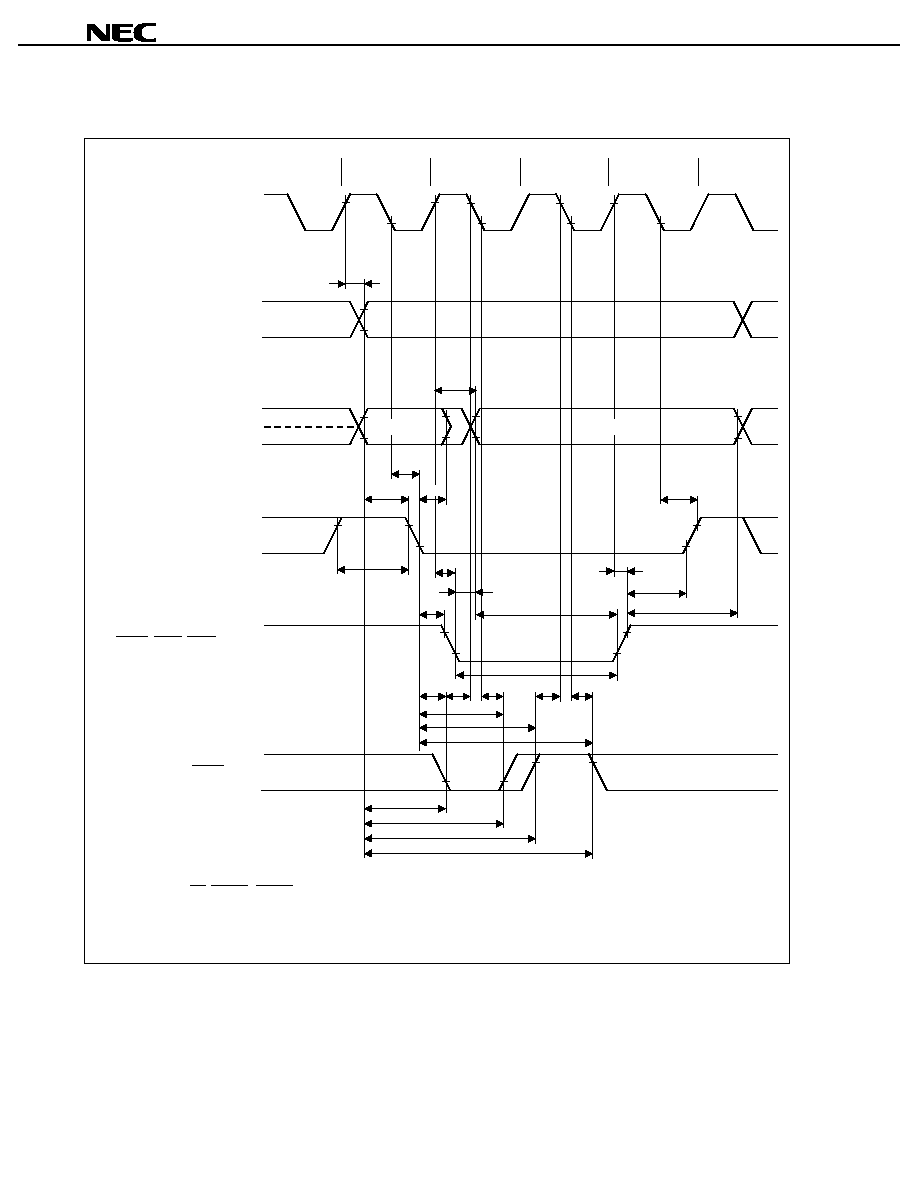
Data Sheet U14780EJ1V0DS00
36
µ
µ
µ
µ
PD703034A, 703034AY, 703035A, 703035AY, 70F3035A, 70F3035AY
(f) Write cycle (CLKOUT synchronous/asynchronous, 1 wait)
CLKOUT (output)
ASTB (output)
T1
T2
TW
<38>
<
15
>
<
20
>
<
45
>
A1 to A15 (output)
A16 to A21 (output)
Note (output)
DSTB, WRL, WRH
(output)
WAIT
(input)
AD0 to AD15 (I/O)
<
44
>
<
10
>
<
40
>
T3
<
21
>
<
23
>
<
24
>
<
18
>
<
41
>
<
22
>
<
29
>
<
31
>
<
25
>
<
27
>
<
26
>
<
28
>
<
30
>
<
46
>
<
45
>
<
46
>
Data
Address
<
40
>
<
11
>
<
41
>
<
32
>
Note
R/W, UBEN, LBEN
Remark
The broken lines indicate high impedance.
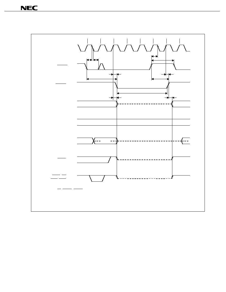
Data Sheet U14780EJ1V0DS00
37
µ
µ
µ
µ
PD703034A, 703034AY, 703035A, 703035AY, 70F3035A, 70F3035AY
(g) Bus hold timing
CLKOUT (output)
TH
A1 to A15 (output)
<
47
> <
48
>
TH
TH
TH
TI
<
47
>
<
36
>
<
50
>
<
50
>
<34>
<
37
>
<33>
<49>
<35>
A16 to A19 (output)
Note (output)
HLDRQ
(input)
HLDAK
(output)
ASTB
(output)
DSTB, RD
(output)
WRL, WRH
(output)
AD0 to AD15 (I/O)
Data
Note
R/W, UBEN, LBEN
Remark
The broken lines indicate high impedance.
Data Sheet U14780EJ1V0DS00
38
µ
µ
µ
µ
PD703034A, 703034AY, 703035A, 703035AY, 70F3035A, 70F3035AY
(5) Interrupt timing
(T
A
= ≠40 to +85∞C, V
DD
= 4.0 to 5.5 V, EV
DD
= 3.0 to 5.5 V, V
SS
= AV
SS
= BV
SS
= EV
SS
= 0 V)
Parameter
Symbol
Conditions
MIN.
MAX.
Unit
NMI high-level width
<51>
t
WNIH
500
ns
NMI low-level width
<52>
t
WNIL
500
ns
n = 0 to 3, analog noise
elimination
500
ns
n = 4, 5, digital noise
elimination
3T + 20
ns
INTPn high-level width
<53>
t
WITH
n = 6, digital noise
elimination
3Tsmp
+
20
ns
n = 0 to 3, analog noise
elimination
500
ns
n = 4, 5, digital noise
elimination
3T + 20
ns
INTPn low-level width
<54>
t
WITL
n = 6, digital noise
elimination
3Tsmp
+
20
ns
Remarks 1. T = 1/f
XX
2. Tsmp = Noise elimination sampling clock cycle
<51>
<52>
NMI (input)
<53>
<54>
INTPn (input)
Remark n = 0 to 6
Data Sheet U14780EJ1V0DS00
39
µ
µ
µ
µ
PD703034A, 703034AY, 703035A, 703035AY, 70F3035A, 70F3035AY
(6) RPU timing (T
A
= ≠40 to +85∞C, V
DD
= 4.0 to 5.5 V, EV
DD
= 3.0 to 5.5 V, V
SS
= AV
SS
= BV
SS
= EV
SS
= 0 V)
Parameter
Symbol
Conditions
MIN.
MAX.
Unit
TIn0, TIn1 high-level width
<55>
t
TIHn
n = 0, 1
2T
sam
+ 20
Note
ns
TIn0, TIn1 low-level width
<56>
t
TILn
n = 0, 1
2T
sam
+ 20
Note
ns
TIn high-level width
<57>
t
TIHn
n = 2 to 5
3T + 20
ns
TIn low-level width
<58>
t
TILn
n = 2 to 5
3T + 20
ns
Note T
sam
can select the following count clocks by setting the PRMn2 to PRMn0 bits of prescaler mode registers
n0, n1 (PRMn0, PRMn1).
When n = 0 (TM0), T
sam
= 2T, 4T, 16T, 64T, 256T, or 1/INTWTNI cycle
When n = 1 (TM1), T
sam
= 2T, 4T, 16T, 32T, 128T, or 256T
However, when the TIn0 valid edge is selected as the count clock, T
sam
= 4T.
Remark T = 1/f
XX
<55>
<56>
TIn0, TIn1 (input)
<57>
<58>
TIn (input)
Remark
n = 0 to 5
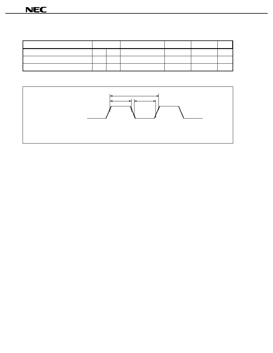
Data Sheet U14780EJ1V0DS00
40
µ
µ
µ
µ
PD703034A, 703034AY, 703035A, 703035AY, 70F3035A, 70F3035AY
(7) Asynchronous serial interface (UART0, UART1) timing
(T
A
= ≠40 to +85∞C, V
DD
= 4.0 to 5.5 V, EV
DD
= 3.0 to 5.5 V, V
SS
= EV
SS
= 0 V)
Parameter
Symbol
Conditions
MIN.
MAX.
Unit
ASCKn cycle time
<59>
t
KCY13
200
ns
ASCKn high-level width
<60>
t
KH13
80
ns
ASCKn low-level width
<61>
t
KSO13
80
ns
Remark n = 0, 1
<60>
<61>
<59>
ASCKn (input)
Remark n = 0, 1
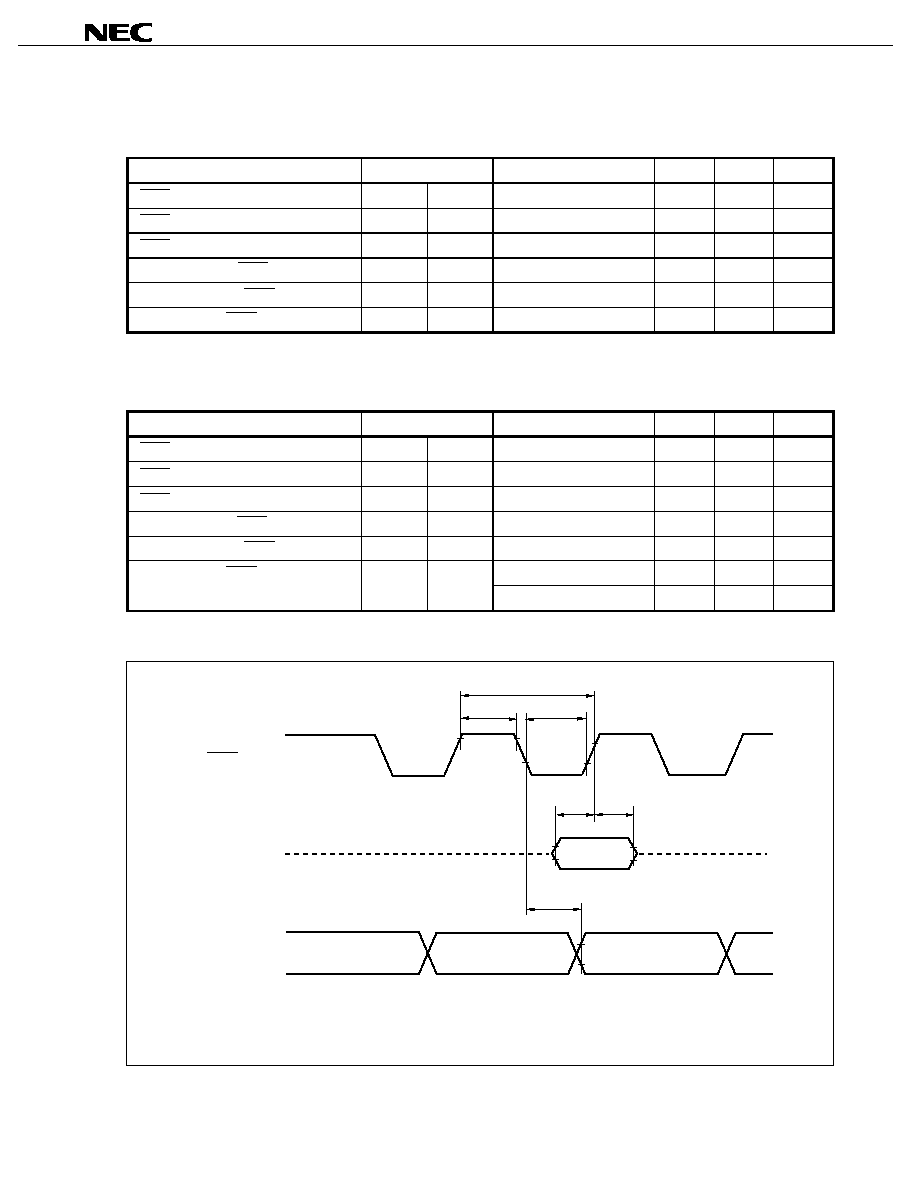
Data Sheet U14780EJ1V0DS00
41
µ
µ
µ
µ
PD703034A, 703034AY, 703035A, 703035AY, 70F3035A, 70F3035AY
(8) 3-wire serial interface (CSI0 to CSI3) timing
(a) Master mode (T
A
= ≠40 to +85∞C, V
DD
= 4.0 to 5.5 V, EV
DD
= 3.0 to 5.5 V, V
SS
= EV
SS
= 0 V)
Parameter
Symbol
Conditions
MIN.
MAX.
Unit
SCKn cycle
<62>
t
KCY1
400
ns
SCKn high-level width
<63>
t
KH1
140
ns
SCKn low-level width
<64>
t
KL1
140
ns
SIn setup time (to SCKn
)
<65>
t
SIK1
50
ns
SIn hold time (from SCKn
)
<66>
t
KSI1
50
ns
Delay time from SCKn
to SOn output
<67>
t
KSO1
60
ns
Remark n = 0 to 3
(b) Slave mode (T
A
= ≠40 to +85∞C, V
DD
= 4.0 to 5.5 V, EV
DD
= 3.0 to 5.5 V, V
SS
= EV
SS
= 0 V)
Parameter
Symbol
Conditions
MIN.
MAX.
Unit
SCKn cycle
<62>
t
KCY2
400
ns
SCKn high-level width
<63>
t
KH2
140
ns
SCKn low-level width
<64>
t
KL2
140
ns
SIn setup time (to SCKn
)
<65>
t
SIK2
50
ns
SIn hold time (from SCKn
)
<66>
t
KSI2
50
ns
4.0 V
EV
DD
5.5 V
60
ns
Delay time from SCKn
to SOn output
<67>
t
KSO2
3.0 V
EV
DD
< 4.0 V
100
ns
Remark n = 0 to 3
<66>
<67>
<65>
<62>
<63>
<64>
Remarks 1. The broken lines indicate high impedance.
2. n = 0 to 3
SCKn (I/O)
SIn (input)
SOn (output)
Input data
Output data

Data Sheet U14780EJ1V0DS00
42
µ
µ
µ
µ
PD703034A, 703034AY, 703035A, 703035AY, 70F3035A, 70F3035AY
(9) 3-wire variable length serial interface (CSI4) timing
(a) Master mode (T
A
= ≠40 to +85
∞
∞
∞
∞
C, V
DD
= 4.0 to 5.5 V, EV
DD
= 3.0 to 5.5 V, V
SS
= EV
SS
= 0 V)
Parameter
Symbol
Conditions
MIN.
MAX.
Unit
4.0 V
EV
DD
5.5 V
200
ns
SCK4 cycle
<68>
t
KCY1
3.0 V
EV
DD
< 4.0 V
400
ns
4.0 V
EV
DD
5.5 V
60
ns
SCK4 high-level width
<69>
t
KH1
3.0 V
EV
DD
< 4.0 V
140
ns
4.0 V
EV
DD
5.5 V
60
ns
SCK4 low-level width
<70>
t
KL1
3.0 V
EV
DD
< 4.0 V
140
ns
4.0 V
EV
DD
5.5 V
25
ns
SI4 setup time (to SCK4
)
<71>
t
SIK1
3.0 V
EV
DD
< 4.0 V
50
ns
SI4 hold time (from SCK4
)
<72>
t
KSI1
20
ns
Delay time from SCK4
to SO4
output
<73>
t
KSO1
55
ns
(b) Slave mode (T
A
= ≠40 to +85
∞
∞
∞
∞
C, V
DD
= 4.0 to 5.5 V, EV
DD
= 3.0 to 5.5 V, V
SS
= EV
SS
= 0 V)
Parameter
Symbol
Conditions
MIN.
MAX.
Unit
4.0 V
EV
DD
5.5 V
200
ns
SCK4 cycle
<68>
t
KCY2
3.0 V
EV
DD
< 4.0 V
400
ns
4.0 V
EV
DD
5.5 V
60
ns
SCK4 high-level width
<69>
t
KH2
3.0 V
EV
DD
< 4.0 V
140
ns
4.0 V
EV
DD
5.5 V
60
ns
SCK4 low-level width
<70>
t
KL2
3.0 V
EV
DD
< 4.0 V
140
ns
4.0 V
EV
DD
5.5 V
25
ns
SI4 setup time (to SCK4
)
<71>
t
SIK2
3.0 V
EV
DD
< 4.0 V
50
ns
SI4 hold time (from SCK4
)
<72>
t
KSI2
20
ns
4.0 V
EV
DD
5.5 V
55
ns
Delay time from SCK4
to SO4
output
<73>
t
KSO2
3.0 V
EV
DD
< 4.0 V
100
ns
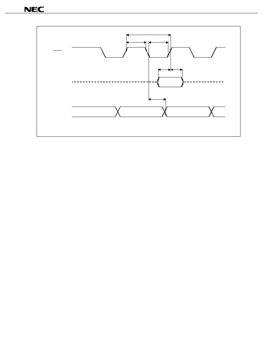
Data Sheet U14780EJ1V0DS00
43
µ
µ
µ
µ
PD703034A, 703034AY, 703035A, 703035AY, 70F3035A, 70F3035AY
<68>
<70>
<69>
<71>
<72>
<73>
SI4 (input)
SO4 (output)
SCK4
(I/O)
Output data
Input data
Remark
The broken lines indicate high impedance.
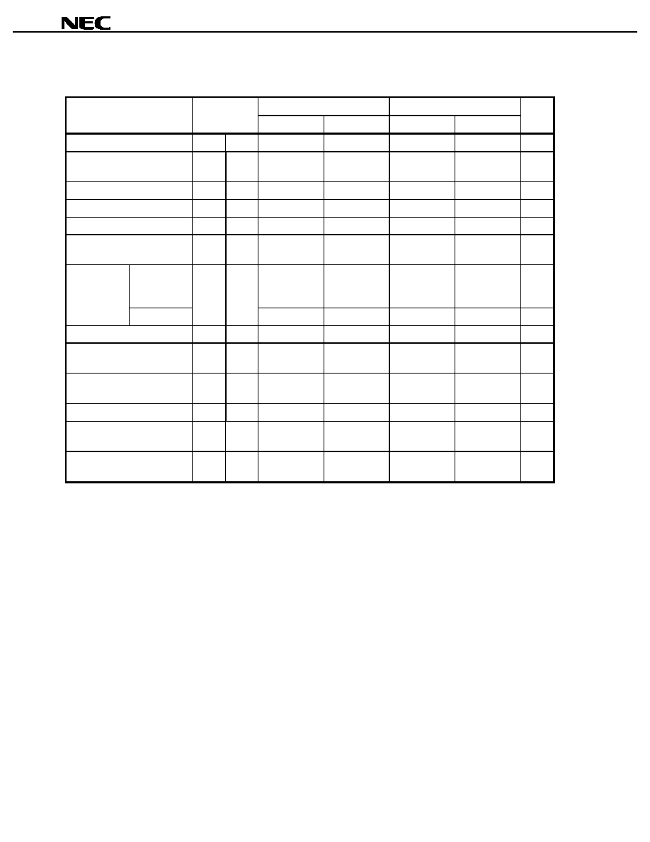
Data Sheet U14780EJ1V0DS00
44
µ
µ
µ
µ
PD703034A, 703034AY, 703035A, 703035AY, 70F3035A, 70F3035AY
(10) I
2
C bus mode (
µ
µ
µ
µ
PD703034AY, 703035AY, 70F3035AY only)
(T
A
= ≠40 to +85∞C, V
DD
= 4.0 to 5.5 V, EV
DD
= 3.0 to 5.5 V, V
SS
= EV
SS
= 0 V)
Normal Mode
High-Speed Mode
Parameter
Symbol
MIN.
MAX.
MIN.
MAX.
Unit
SCLn clock frequency
≠
f
CLK
0
100
0
400
kHz
Bus-free time (between
stop/start conditions)
<74>
t
BUF
4.7
≠
1.3
≠
µ
s
Hold time
Note 1
<75>
t
HD:STA
4.0
≠
0.6
≠
µ
s
SCLn clock low-level width
<76>
t
LOW
4.7
≠
1.3
≠
µ
s
SCLn clock high-level width
<77>
t
HIGH
4.0
≠
0.6
≠
µ
s
Setup time for start/restart
conditions
<78>
t
SU:STA
4.7
≠
0.6
≠
µ
s
CBUS
compatible
master
5.0
≠
≠
≠
µ
s
Data hold
time
I
2
C mode
<79>
t
HD:DAT
0
Note 2
≠
0
Note 2
0.9
Note 3
µ
s
Data setup time
<80>
t
SU:DAT
250
≠
100
Note 4
≠
ns
SDAn and SCLn signal rise
time
<81>
t
R
≠
1000
20 + 0.1Cb
Note 5
300
ns
SDAn and SCLn signal fall
time
<82>
t
F
≠
300
20 + 0.1Cb
Note 5
300
ns
Stop condition setup time
<83>
t
SU:STO
4.0
≠
0.6
≠
µ
s
Pulse width of spike
suppressed by input filter
<84>
t
SP
≠
≠
0
50
ns
Capacitance load of each
bus line
≠
Cb
≠
400
≠
400
pF
Notes 1. At the start condition, the first clock pulse is generated after the hold time.
2. The system requires a minimum of 300 ns hold time internally for the SDAn signal (at V
IHmin.
.
of SCLn
signal) in order to occupy the undefined area at the falling edge of SCLn.
3. If the system does not extend the SCLn signal low hold time (t
LOW
), only the maximum data hold time
(t
HD
:
DAT
) needs to be satisfied.
4. The high-speed mode I
2
C bus can be used in the normal-mode I
2
C bus system. In this case, set the
high-speed mode I
2
C bus so that it meets the following conditions.
∑
If the system does not extend the SCLn signal's low state hold time:
t
HD
:
DAT
250 ns
∑
If the system extends the SCLn signal's low state hold time:
Transmit the following data bit to the SDAn line prior to the SCLn line release (t
Rmax.
+ t
SU
:
DAT
= 1000
+ 250 = 1250 ns: Normal mode I
2
C bus specification).
5. Cb: Total capacitance of one bus line (unit: pF)
Remark n = 0, 1
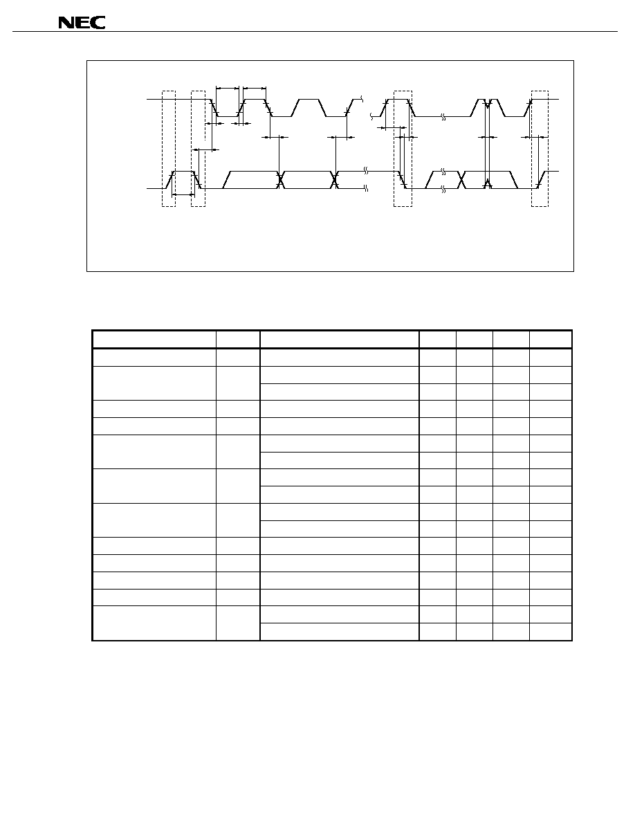
Data Sheet U14780EJ1V0DS00
45
µ
µ
µ
µ
PD703034A, 703034AY, 703035A, 703035AY, 70F3035A, 70F3035AY
Stop
condition
Start
condition
Restart
condition
Stop
condition
SCLn (I/O)
SDAn (I/O)
<75>
<74>
<76>
<77>
<81>
<82>
<79>
<80>
<78>
<75>
<84>
<83>
Remark
n = 0, 1
A/D Converter Characteristics (T
A
= ≠40 to +85∞C, V
DD
= AV
DD
= AV
REF
, V
SS
= AV
SS
= 0 V, Output pin load
capacitance: C
L
= 50 pF)
Parameter
Symbol
Conditions
MIN.
TYP.
MAX.
Unit
Resolution
≠
10
10
10
bit
ADM2 = 00H
±
0.6
%FSR
Overall error
Note 1
≠
ADM2 = 01H
±
1.0
%FSR
Conversion time
t
CONV
5
10
µ
s
Zero-scale error
Note 1
AINL
±
0.4
%FSR
ADM2 = 00H
±
0.4
%FSR
Full-scale error
Note 1
AINL
ADM2 = 01H
±
0.6
%FSR
ADM2 = 00H
±
4.0
LSB
Integral linearity error
Note 2
INL
ADM2 = 01H
±
6.0
LSB
ADM2 = 00H
±
4.0
LSB
Differential linearity error
Note 2
DNL
ADM2 = 01H
±
6.0
LSB
Analog reference voltage
AV
REF
AV
REF
=
AV
DD
4.5
5.5
V
Analog power supply voltage
AV
DD
4.5
5.5
V
Analog input voltage
V
IAN
AV
SS
AV
REF
V
AV
REF
input current
AI
REF
1
2
mA
ADM2 = 00H
3
6
mA
AV
DD
current
AI
DD
ADM2 = 01H
4
8
mA
Notes 1. Excluding quantization error (
±
0.05 %FSR)
2. Excluding quantization error (
±
0.5 LSB)
Remarks 1. LSB: Least Significant Bit
FSR: Full Scale Range
2. ADM2: A/D converter mode register 2
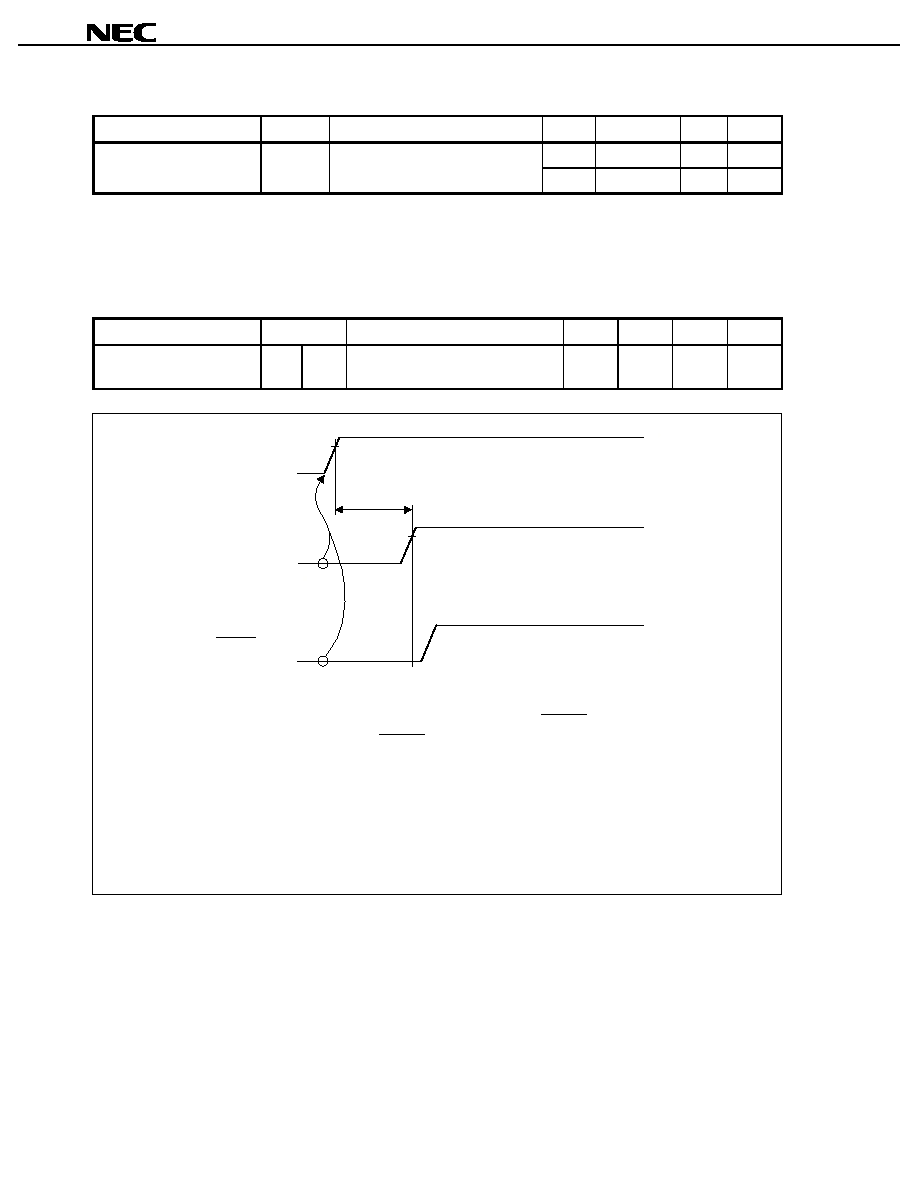
Data Sheet U14780EJ1V0DS00
46
µ
µ
µ
µ
PD703034A, 703034AY, 703035A, 703035AY, 70F3035A, 70F3035AY
IEBus Controller Characteristics (T
A
= ≠40 to +85
∞
∞
∞
∞
C, V
DD
= 4.0 to 5.5 V, EV
DD
= 3.0 to 5.5 V, V
SS
= EV
SS
= 0 V)
Parameter
Symbol
Conditions
MIN.
TYP.
MAX.
Unit
6.0
Note 1
MHz
IEBus system clock
frequency
f
S
Communication mode: fixed to
mode 1
6.29
Notes 1, 2
MHz
Notes 1. 6.0 MHz and 6.29 MHz can not be used together for the IEBus system clock frequency
2. Although the system clock specified in the IEBus specification is 6.0 MHz, operation is guaranteed at
6.29 MHz system clock in the V850/SB2.
Regulator (T
A
= ≠40 to +85
∞
∞
∞
∞
C, V
DD
= 4.0 to 5.5 V, V
SS
= 0 V)
Parameter
Symbol
Conditions
MIN.
TYP.
MAX.
Unit
Output stabilization time
<85>
t
REG
Stabilization capacitance C = 1
µ
F
(Connected to REGC pin)
1
ms
<85>
BV , EV
DD
DD
V
DD
RESET (input)
Cautions 1. Be sure to start inputting supply voltage (V
DD
) when RESET = V
SS
= EV
SS
= BV
SS
= 0 V
(the above state), and make RESET high level after the t
REG
period has elapsed.
2. If supply voltage (BV
DD
or EV
DD
) is input before the t
REG
period has elapsed following the
input of supply voltage (V
DD
), data may be driven from the pins until the t
REG
period has
elapsed because the I/O buffers' power supply was turned on while the circuit was in an
undefined state. To avoid this situation, it is recommended to input supply voltage
(BV
DD
or EV
DD
) after the t
REG
period has elapsed following the input of supply voltage
(V
DD
).
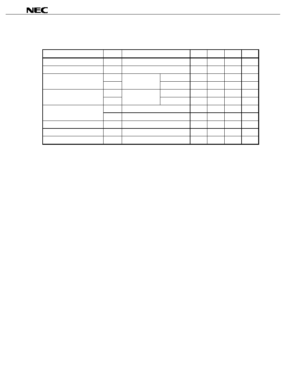
Data Sheet U14780EJ1V0DS00
47
µ
µ
µ
µ
PD703034A, 703034AY, 703035A, 703035AY, 70F3035A, 70F3035AY
4.1 Flash Memory Programming Mode (
µ
µ
µ
µ
PD70F3035A, 70F3035AY only)
Basic characteristics (T
A
= 10 to 85
∞
∞
∞
∞
C)
Parameter
Symbol
Conditions
MIN.
TYP.
MAX.
Unit
Operating frequency
f
X
2
13
MHz
Power supply voltage
V
DD
4.5
5.5
V
I
DDW
V
DD
pin
51
mA
Write current
I
PPW
When V
PP
= V
PP1
V
PP
pin
50
mA
I
DDE
V
DD
pin
51
mA
Erase current
I
PPE
When V
PP
= V
PP1
V
PP
pin
100
mA
V
PP0
During normal operation
0
0.54
V
V
PP
power supply voltage
V
PP1
During flash memory programming
7.5
7.8
8.1
V
Write count
Note
C
WRT
20
20
20
Times
Unit erase time
t
ER
0.2
0.2
0.2
s
Total erase time
t
ERT
20
s
Note Erase/write are regarded as 1 cycle.
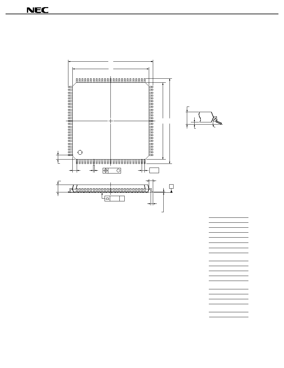
Data Sheet U14780EJ1V0DS00
48
µ
µ
µ
µ
PD703034A, 703034AY, 703035A, 703035AY, 70F3035A, 70F3035AY
5. PACKAGE DRAWINGS
100-PIN PLASTIC LQFP (FINE PITCH) (14x14)
NOTE
Each lead centerline is located within 0.08 mm of
its true position (T.P.) at maximum material condition.
ITEM
MILLIMETERS
A
B
D
G
16.00
±
0.20
14.00
±
0.20
0.50 (T.P.)
1.00
J
16.00
±
0.20
K
C
14.00
±
0.20
I
0.08
1.00
±
0.20
L
0.50
±
0.20
F
1.00
N
P
Q
0.08
1.40
±
0.05
0.10
±
0.05
S100GC-50-8EU-1
S
1.60 MAX.
H
0.22
+
0.05
-
0.04
M
0.17
+
0.03
-
0.07
R
3
∞+
7
∞
-
3
∞
1
25
26
50
100
76
75
51
S
S
N
J
detail of lead end
C
D
A
B
R
K
M
L
P
I
S
Q
G
F
M
H

Data Sheet U14780EJ1V0DS00
49
µ
µ
µ
µ
PD703034A, 703034AY, 703035A, 703035AY, 70F3035A, 70F3035AY
80
81
50
100
1
31
30
51
100-PIN PLASTIC QFP (14x20)
H
I
J
detail of lead end
M
Q
R
K
M
L
P
S
S
N
G
F
NOTE
Each lead centerline is located within 0.15 mm of
its true position (T.P.) at maximum material condition.
ITEM
MILLIMETERS
A
B
D
G
23.6
±
0.4
20.0
±
0.2
0.30
±
0.10
0.6
H
17.6
±
0.4
I
C
14.0
±
0.2
0.15
J
0.65 (T.P.)
K
1.8
±
0.2
L
0.8
±
0.2
F
0.8
P100GF-65-3BA1-4
N
P
Q
0.10
2.7
±
0.1
0.1
±
0.1
R
5
∞±
5
∞
S
3.0 MAX.
M
0.15
+
0.10
-
0.05
C D
A
B
S

Data Sheet U14780EJ1V0DS00
50
µ
µ
µ
µ
PD703034A, 703034AY, 703035A, 703035AY, 70F3035A, 70F3035AY
6. RECOMMENDED SOLDERING CONDITIONS
The
µ
PD703034A, 703034AY, 703035A, 703035AY, 70F3035A, and 70F3035AY should be soldered and mounted
under the following recommended conditions.
For the details of the recommended soldering conditions, refer to the document Semiconductor Device Mounting
Technology Manual (C10535E).
For soldering methods and conditions other than those recommended below, contact your NEC sales
representative.
Table 6-1. Surface Mounting Type Soldering Conditions (1/2)
(1)
µ
µ
µ
µ
PD703034AGC-
◊◊◊
◊◊◊
◊◊◊
◊◊◊
-8EU: 100-pin plastic LQFP (fine pitch) (14
◊
◊
◊
◊
14)
µ
µ
µ
µ
PD703034AYGC-
◊◊◊
◊◊◊
◊◊◊
◊◊◊
-8EU: 100-pin plastic LQFP (fine pitch) (14
◊
◊
◊
◊
14)
µ
µ
µ
µ
PD703035AGC-
◊◊◊
◊◊◊
◊◊◊
◊◊◊
-8EU: 100-pin plastic LQFP (fine pitch) (14
◊
◊
◊
◊
14)
µ
µ
µ
µ
PD703035AYGC-
◊◊◊
◊◊◊
◊◊◊
◊◊◊
-8EU: 100-pin plastic LQFP (fine pitch) (14
◊
◊
◊
◊
14)
Soldering Method
Soldering Conditions
Recommended
Condition
Symbol
Infrared reflow
Package peak temperature: 235∞C, Time: 30 seconds max. (at 210∞C or higher),
Count: Two times or less
Exposure limit: 7 days
Note
(after that, prebake at 125∞C for 10 hours)
IR35-107-2
VPS
Package peak temperature: 215∞C, Time: 40 seconds max. (at 200∞C or higher),
Count: Two times or less
Exposure limit: 7 days
Note
(after that, prebake at 125∞C for 10 hours)
VP15-107-2
Partial heating
Pin temperature: 300∞C max., Time: 3 seconds max. (per pin row)
≠
Note After opening the dry pack, store it at 25∞C or less and 65% RH or less for the allowable storage period.
Caution
Do not use different soldering methods together (except for partial heating).
(2)
µ
µ
µ
µ
PD70F3035AGC-8EU:
100-pin plastic LQFP (fine pitch) (14
◊
◊
◊
◊
14)
µ
µ
µ
µ
PD70F3035AYGC-8EU:
100-pin plastic LQFP (fine pitch) (14
◊
◊
◊
◊
14)
Soldering Method
Soldering Conditions
Recommended
Condition
Symbol
Infrared reflow
Package peak temperature: 235∞C, Time: 30 seconds max. (at 210∞C or higher),
Count: Two times or less
Exposure limit: 3 days
Note
(after that, prebake at 125∞C for 10 hours)
IR35-103-2
VPS
Package peak temperature: 215∞C, Time: 40 seconds max. (at 200∞C or higher),
Count: Two times or less
Exposure limit: 3 days
Note
(after that, prebake at 125∞C for 10 hours)
VP15-103-2
Partial heating
Pin temperature: 300∞C max., Time: 3 seconds max. (per pin row)
≠
Note After opening the dry pack, store it at 25∞C or less and 65% RH or less for the allowable storage period.
Caution
Do not use different soldering methods together (except for partial heating).

Data Sheet U14780EJ1V0DS00
51
µ
µ
µ
µ
PD703034A, 703034AY, 703035A, 703035AY, 70F3035A, 70F3035AY
Table 6-1. Surface Mounting Type Soldering Conditions (2/2)
(3)
µ
µ
µ
µ
PD703034AGF-
◊◊◊
◊◊◊
◊◊◊
◊◊◊
-3BA:
100-pin plastic QFP (14
◊
◊
◊
◊
20)
µ
µ
µ
µ
PD703034AYGF-
◊◊◊
◊◊◊
◊◊◊
◊◊◊
-3BA: 100-pin plastic QFP (14
◊
◊
◊
◊
20)
µ
µ
µ
µ
PD703035AGF-
◊◊◊
◊◊◊
◊◊◊
◊◊◊
-3BA:
100-pin plastic QFP (14
◊
◊
◊
◊
20)
µ
µ
µ
µ
PD703035AYGF-
◊◊◊
◊◊◊
◊◊◊
◊◊◊
-3BA: 100-pin plastic QFP (14
◊
◊
◊
◊
20)
µ
µ
µ
µ
PD70F3035AGF-3BA:
100-pin plastic QFP (14
◊
◊
◊
◊
20)
µ
µ
µ
µ
PD70F3035AYGF-3BA:
100-pin plastic QFP (14
◊
◊
◊
◊
20)
Soldering Method
Soldering Conditions
Recommended
Condition
Symbol
Infrared reflow
Package peak temperature: 235∞C, Time: 30 seconds max. (at 210∞C or higher),
Count: Two times or less
Exposure limit: 7 days
Note
(after that, prebake at 125∞C for 20 hours)
IR35-207-2
VPS
Package peak temperature: 215∞C, Time: 40 seconds max. (at 200∞C or higher),
Count: Two times or less
Exposure limit: 7 days
Note
(after that, prebake at 125∞C for 20 hours)
VP15-207-2
Wave soldering
Solder bath temperature: 260∞C max., Time: 10 seconds max., Count: Once
Preheating temperature: 120∞C max. (package surface temperature)
Exposure limit: 7 days
Note
(after that, prebake at 125∞C for 20 hours)
WS60-207-1
Partial heating
Pin temperature: 300∞C max., Time: 3 seconds max. (per pin row)
≠
Note After opening the dry pack, store it at 25∞C or less and 65% RH or less for the allowable storage period.
Caution
Do not use different soldering methods together (except for partial heating).

Data Sheet U14780EJ1V0DS00
52
µ
µ
µ
µ
PD703034A, 703034AY, 703035A, 703035AY, 70F3035A, 70F3035AY
[MEMO]

Data Sheet U14780EJ1V0DS00
53
µ
µ
µ
µ
PD703034A, 703034AY, 703035A, 703035AY, 70F3035A, 70F3035AY
[MEMO]
Data Sheet U14780EJ1V0DS00
54
µ
µ
µ
µ
PD703034A, 703034AY, 703035A, 703035AY, 70F3035A, 70F3035AY
NOTES FOR CMOS DEVICES
1
PRECAUTION AGAINST ESD FOR SEMICONDUCTORS
Note:
Strong electric field, when exposed to a MOS device, can cause destruction of the gate oxide and
ultimately degrade the device operation. Steps must be taken to stop generation of static electricity
as much as possible, and quickly dissipate it once, when it has occurred. Environmental control
must be adequate. When it is dry, humidifier should be used. It is recommended to avoid using
insulators that easily build static electricity. Semiconductor devices must be stored and transported
in an anti-static container, static shielding bag or conductive material. All test and measurement
tools including work bench and floor should be grounded. The operator should be grounded using
wrist strap. Semiconductor devices must not be touched with bare hands. Similar precautions need
to be taken for PW boards with semiconductor devices on it.
2
HANDLING OF UNUSED INPUT PINS FOR CMOS
Note:
No connection for CMOS device inputs can be cause of malfunction. If no connection is provided
to the input pins, it is possible that an internal input level may be generated due to noise, etc., hence
causing malfunction. CMOS devices behave differently than Bipolar or NMOS devices. Input levels
of CMOS devices must be fixed high or low by using a pull-up or pull-down circuitry. Each unused
pin should be connected to V
DD
or GND with a resistor, if it is considered to have a possibility of
being an output pin. All handling related to the unused pins must be judged device by device and
related specifications governing the devices.
3
STATUS BEFORE INITIALIZATION OF MOS DEVICES
Note:
Power-on does not necessarily define initial status of MOS device. Production process of MOS
does not define the initial operation status of the device. Immediately after the power source is
turned ON, the devices with reset function have not yet been initialized. Hence, power-on does
not guarantee out-pin levels, I/O settings or contents of registers. Device is not initialized until the
reset signal is received. Reset operation must be executed immediately after power-on for devices
having reset function.
Caution
Purchase of NEC I
2
C components conveys a license under the Philips I
2
C Patent Rights to use
these components in an I
2
C system, provided that the system conforms to the I
2
C Standard
Specification as defined by Philips.
Reference document
Electrical Characteristics for Microcomputer (IEI-601)
Note
Note
This document number is that of the Japanese version.
V850/SB1, V850/SB2, and V850 Family are trademarks of NEC Corporation.

Data Sheet U14780EJ1V0DS00
55
µ
µ
µ
µ
PD703034A, 703034AY, 703035A, 703035AY, 70F3035A, 70F3035AY
Regional Information
Some information contained in this document may vary from country to country. Before using any NEC
product in your application, pIease contact the NEC office in your country to obtain a list of authorized
representatives and distributors. They will verify:
∑
Device availability
∑
Ordering information
∑
Product release schedule
∑
Availability of related technical literature
∑
Development environment specifications (for example, specifications for third-party tools and
components, host computers, power plugs, AC supply voltages, and so forth)
∑
Network requirements
In addition, trademarks, registered trademarks, export restrictions, and other legal issues may also vary
from country to country.
NEC Electronics Inc. (U.S.)
Santa Clara, California
Tel: 408-588-6000
800-366-9782
Fax: 408-588-6130
800-729-9288
NEC Electronics (Germany) GmbH
Duesseldorf, Germany
Tel: 0211-65 03 02
Fax: 0211-65 03 490
NEC Electronics (UK) Ltd.
Milton Keynes, UK
Tel: 01908-691-133
Fax: 01908-670-290
NEC Electronics Italiana s.r.l.
Milano, Italy
Tel: 02-66 75 41
Fax: 02-66 75 42 99
NEC Electronics (Germany) GmbH
Benelux Office
Eindhoven, The Netherlands
Tel: 040-2445845
Fax: 040-2444580
NEC Electronics (France) S.A.
Velizy-Villacoublay, France
Tel: 01-30-67 58 00
Fax: 01-30-67 58 99
NEC Electronics (France) S.A.
Spain Office
Madrid, Spain
Tel: 91-504-2787
Fax: 91-504-2860
NEC Electronics (Germany) GmbH
Scandinavia Office
Taeby, Sweden
Tel: 08-63 80 820
Fax: 08-63 80 388
NEC Electronics Hong Kong Ltd.
Hong Kong
Tel: 2886-9318
Fax: 2886-9022/9044
NEC Electronics Hong Kong Ltd.
Seoul Branch
Seoul, Korea
Tel: 02-528-0303
Fax: 02-528-4411
NEC Electronics Singapore Pte. Ltd.
United Square, Singapore 1130
Tel: 65-253-8311
Fax: 65-250-3583
NEC Electronics Taiwan Ltd.
Taipei, Taiwan
Tel: 02-2719-2377
Fax: 02-2719-5951
NEC do Brasil S.A.
Electron Devices Division
Rodovia Presidente Dutra, Km 214
07210-902-Guarulhos-SP Brasil
Tel: 55-11-6465-6810
Fax: 55-11-6465-6829
J99.1

µ
µ
µ
µ
PD703034A, 703034AY, 703035A, 703035AY, 70F3035A, 70F3035AY
The export of these products from Japan is regulated by the Japanese government. The export of some or all of these
products may be prohibited without governmental license. To export or re-export some or all of these products from a
country other than Japan may also be prohibited without a license from that country. Please call an NEC sales
representative.
∑
The information in this document is subject to change without notice. Before using this document, please
confirm that this is the latest version.
∑
No part of this document may be copied or reproduced in any form or by any means without the prior written
consent of NEC Corporation. NEC Corporation assumes no responsibility for any errors which may appear in
this document.
∑
NEC Corporation does not assume any liability for infringement of patents, copyrights or other intellectual property
rights of third parties by or arising from use of a device described herein or any other liability arising from use
of such device. No license, either express, implied or otherwise, is granted under any patents, copyrights or other
intellectual property rights of NEC Corporation or others.
∑
Descriptions of circuits, software, and other related information in this document are provided for illustrative
purposes in semiconductor product operation and application examples. The incorporation of these circuits,
software, and information in the design of the customer's equipment shall be done under the full responsibility
of the customer. NEC Corporation assumes no responsibility for any losses incurred by the customer or third
parties arising from the use of these circuits, software, and information.
∑
While NEC Corporation has been making continuous effort to enhance the reliability of its semiconductor devices,
the possibility of defects cannot be eliminated entirely. To minimize risks of damage or injury to persons or
property arising from a defect in an NEC semiconductor device, customers must incorporate sufficient safety
measures in its design, such as redundancy, fire-containment, and anti-failure features.
∑
NEC devices are classified into the following three quality grades:
"Standard", "Special", and "Specific". The Specific quality grade applies only to devices developed based on a
customer designated "quality assurance program" for a specific application. The recommended applications of
a device depend on its quality grade, as indicated below. Customers must check the quality grade of each device
before using it in a particular application.
Standard: Computers, office equipment, communications equipment, test and measurement equipment,
audio and visual equipment, home electronic appliances, machine tools, personal electronic
equipment and industrial robots
Special: Transportation equipment (automobiles, trains, ships, etc.), traffic control systems, anti-disaster
systems, anti-crime systems, safety equipment and medical equipment (not specifically designed
for life support)
Specific: Aircraft, aerospace equipment, submersible repeaters, nuclear reactor control systems, life
support systems or medical equipment for life support, etc.
The quality grade of NEC devices is "Standard" unless otherwise specified in NEC's Data Sheets or Data Books.
If customers intend to use NEC devices for applications other than those specified for Standard quality grade,
they should contact an NEC sales representative in advance.
M7 98. 8