Document Outline
- COVER
- FEATURES
- APPLICATIONS
- ORDERING INFORMATION
- PIN CONFIGURATION (Top view)
- PIN NAMES
- INTERNAL BLOCK DIAGRAM
- 1. DIFFERENCES AMONG PRODUCTS
- 2. PIN FUNCTIONS
- 2.1 Port Pins
- 2.2 Non-port Pins
- 2.3 Pin I/O Circuits and Recommended Connection of Unused Pins
- 3. FUNCTION BLOCKS
- 3.1 Internal Units
- 3.1.1 CPU
- 3.1.2 Bus control unit (BCU)
- 3.1.3 ROM
- 3.1.4 RAM
- 3.1.5 Ports
- 3.1.6 Interrupt controller (INTC)
- 3.1.7 Clock generator (CG)
- 3.1.8 Real-time pulse unit (RPU)
- 3.1.9 Serial interface (SIO)
- 3.1.10 A/D converter (ADC)
- 4. CPU FUNCTIONS
- 5. BUS CONTROL FUNCTIONS
- 6. MEMORY ACCESS CONTROL FUNCTIONS
- 6.1 SRAM Connection
- 6.2 Page ROM Controller (ROMC)
- 6.2.1 Features
- 6.2.2 Page ROM connection
- 6.3 DRAM Controller
- 6.3.1 Features
- 6.3.2 DRAM Connections
- 7. DMA FUNCTIONS (DMA CONTROLLER)
- 8. INTERRUPT/EXCEPTION PROCESSING FUNCTIONS
- 9. CLOCK GENERATION FUNCTIONS
- 10. TIMER/COUNTER FUNCTIONS (REAL-TIME PULSE UNIT)
- 11. SERIAL INTERFACE FUNCTION
- 11.1 Asynchronous Serial Interfaces 0, 1 (UART0, UART1)
- 11.2 Clocked Serial Interfaces 0 to 3 (CSI0 to CSI3)
- 11.3 Dedicated Baud Rate Generators 0 to 2 (BRG0 to BRG2)
- 12. A/D CONVERTER
- 13. PORT FUNCTIONS
- 14. RESET FUNCTION
- 15. INSTRUCTION SET
- 16. ELECTRICAL SPECIFICATIONS (PRELIMINARY VALUES)
- 17. PACKAGE DRAWING
- 18. RECOMMENDED SOLDERING CONDITIONS

The information in this document is subject to change without notice.
MOS INTEGRATED CIRCUIT
µ
µ
µ
µ
PD703100-33, 703100-40, 703101-33, 703102-33
V850E/MS1
TM
32/16-BIT SINGLE-CHIP MICROCONTROLLERS
Document No. U13995EJ1V0DS00 (1st edition)
Date Published April 1999 N CP(K)
Printed in Japan
PRELIMINARY DATA SHEET
1999
©
The
µ
PD703101-33 and
µ
PD703102-33 are members of the V850 Family
TM
of 32-bit single-chip microcontrollers
designed for real-time control operations. These microcontrollers provide on-chip features, including a 32-bit CPU
core, ROM, RAM, interrupt controller, real-time pulse unit, serial interface, A/D converter, and DMA controller.
The
µ
PD703100-33 and
µ
PD703100-40 are ROM-less versions of the
µ
PD703101-33 and
µ
PD703102-33
products.
The
µ
PD703100-A33,
µ
PD703100-A40,
µ
PD703101-A33, and
µ
PD703102-A33 are also available as products
having a 3.3-V power supply for external pins.
Detailed function descriptions are provided in the following user's manuals. Be sure to read them before
designing.
V850E/MS1 User's Manual Hardware:
U12688E
V850E/MS1 User's Manual Architecture: U12197E
FEATURES
∑
Number of instructions: 81
∑
Minimum instruction execution time
25 ns (@ 40-MHz operation) ∑∑∑∑∑
µ
PD703100-40
30 ns (@ 33-MHz operation) ∑∑∑∑∑
µ
PD703100-33, 703101-33, 703102-33
∑
General registers 32 bits
◊
32
∑
Instruction set optimized for control applications
∑
Internal memory ROM : None (
µ
PD703100-33, 703100-40),
96 Kbytes (
µ
PD703101-33),
128 Kbytes (
µ
PD703102-33)
RAM : 4 Kbytes
∑
Advanced on-chip interrupt controller
∑
Real-time pulse unit suitable for control operations
∑
Powerful serial interface (on-chip dedicated baud rate generator)
∑
On-chip clock generator
∑
10-bit resolution A/D converter: 8 channels
∑
DMA controller: 4 channels
∑
Power saving functions
APPLICATIONS
∑
Office automation equipment: printers, facsimile machines, PPCs, etc.
∑
Multimedia equipment: digital still cameras, video printers, etc.
∑
Consumer equipment: single-lens reflex cameras, etc.
∑
Industrial equipment: motor controllers, NC machine tools, etc.

Preliminary Data Sheet U13995EJ1V0DS00
2
µ
µ
µ
µ
PD703100-33, 703100-40, 703101-33, 703102-33
ORDERING INFORMATION
Part Number
Package
Maximum Operating
Frequency (MHz)
Internal ROM
(bytes)
µ
PD703100GJ-33-8EU
144-pin plastic LQFP (fine pitch) (20
◊
20 mm)
33 MHz
None
µ
PD703100GJ-40-8EU
144-pin plastic LQFP (fine pitch) (20
◊
20 mm)
40 MHz
None
µ
PD703101GJ-33-xxx-8EU
144-pin plastic LQFP (fine pitch) (20
◊
20 mm)
33 MHz
96 Kbytes
µ
PD703102GJ-33-xxx-8EU
144-pin plastic LQFP (fine pitch) (20
◊
20 mm)
33 MHz
128 Kbytes
Remark xxx indicates ROM code suffix.
PIN CONFIGURATION (Top view)
144-pin plastic LQFP (fine pitch) (20
◊
◊
◊
◊
20 mm)
∑
µ
PD703100GJ-33-8EU
∑
µ
PD703101GJ-33-xxx-8EU
∑
µ
PD703100GJ-40-8EU
∑
µ
PD703102GJ-33-xxx-8EU
INTP103/DMARQ3/P07
INTP102/DMARQ2/P06
INTP101/DMARQ1/P05
INTP100/DMARQ0/P04
TI10/P03
TCLR10/P02
TO101/P01
TO100/P00
V
SS
INTP113/DMAAK3/P17
INTP112/DMAAK2/P16
INTP111/DMAAK1/P15
INTP110/DMAAK0/P14
TI11/P13
TCLR11/P12
TO111/P11
TO110/P10
INTP123/TC3/P107
INTP122/TC2/P106
INTP121/TC1/P105
INTP120/TC0/P104
TI12/P103
TCLR12/P102
TO121/P101
TO120/P100
ANI7/P77
ANI6/P76
ANI5/P75
ANI4/P74
ANI3/P73
ANI2/P72
ANI1/P71
ANI0/P70
AV
DD
AV
SS
AV
REF
1
2
3
4
5
6
7
8
9
10
11
12
13
14
15
16
17
18
19
20
21
22
23
24
25
26
27
28
29
30
31
32
33
34
35
36
A16/P60
A17/P61
A18/P62
A19/P63
A20/P64
A21/P65
A22/P66
A23/P67
HV
DD
CS0/RAS0/P80
CS1/RAS1/P81
CS2/RAS2/P82
CS3/RAS3/P83
CS4/RAS4/IOWR/P84
CS5/RAS5/IORD/P85
CS6/RAS6/P86
CS7/RAS7/P87
LCAS/LWR/P90
UCAS/UWR/P91
RD/P92
WE/P93
BCYST/P94
OE/P95
HLDAK/P96
HLDRQ/P97
V
SS
REFRO/PX5
WAIT/PX6
CLKOUT/PX7
TO150/P120
TO151/P121
TCLR15/P122
TI15/P123
INTP150/P124
INTP151/P125
INTP152/P126
108
107
106
105
104
103
102
101
100
99
98
97
96
95
94
93
92
91
90
89
88
87
86
85
84
83
82
81
80
79
78
77
76
75
74
73
NMI/P20
P21
TXD0/SO0/P22
RXD0/SI0/P23
SCK0/P24
TXD1/SO1/P25
RXD1/SI1/P26
SCK1/P27
V
DD
INTP133/SCK2/P37
INTP132/SI2/P36
INTP131/SO2/P35
INTP130/P34
TI13/P33
TCLR13/P32
TO131/P31
TO130/P30
INTP143/SCK3/P117
INTP142/SI3/P116
INTP141/SO3/P115
INTP140/P114
TI14/P113
TCLR14/P112
TO141/P111
TO140/P110
CV
DD
X2
X1
CV
SS
CKSEL
MODE0
MODE1
MODE2
MODE3
RESET
INTP153/ADTRG/P127
37
38
39
40
41
42
43
44
45
46
47
48
49
50
51
52
53
54
55
56
57
58
59
60
61
62
63
64
65
66
67
68
69
70
71
72
V
DD
D0/P40
D1/P41
D2/P42
D3/P43
D4/P44
D5/P45
D6/P46
D7/P47
V
SS
D8/P50
D9/P51
D10/P52
D11/P53
D12/P54
D13/P55
D14/P56
D15/P57
HV
DD
A0/PA0
A1/PA1
A2/PA2
A3/PA3
A4/PA4
A5/PA5
A6/PA6
A7/PA7
V
SS
A8/PB0
A9/PB1
A10/PB2
A11/PB3
A12/PB4
A13/PB5
A14/PB6
A15/PB7
144
142
142
141
140
139
138
137
136
135
134
133
132
131
130
129
128
127
126
125
124
123
122
121
120
119
118
117
116
115
114
113
112
111
110
109
Preliminary Data Sheet U13995EJ1V0DS00
3
µ
µ
µ
µ
PD703100-33, 703100-40, 703101-33, 703102-33
PIN NAMES
A0 to A23
: Address Bus
P50 to P57
: Port 5
ADTRG
: AD Trigger Input
P60 to P67
: Port 6
ANI0 to ANI7
: Analog Input
P70 to P77
: Port 7
AV
DD
: Analog Power Supply
P80 to P87
: Port 8
AV
REF
: Analog Reference Voltage
P90 to P97
: Port 9
AV
SS
: Analog Ground
P100 to P107
: Port 10
BCYST
: Bus Cycle Start Timing
P110 to P117
: Port 11
CKSEL
: Clock Generator Operating Mode Select
P120 to P127
: Port 12
CLKOUT
: Clock Output
PA0 to PA7
: Port A
CS0 to CS7
: Chip Select
PB0 to PB7
: Port B
CV
DD
: Clock Generator Power Supply
PX5 to PX7
: Port X
CV
SS
: Clock Generator Ground
RAS0 to RAS7
: Row Address Strobe
D0 to D15
: Data Bus
RD
: Read
DMAAK0 to DMAAK3 : DMA Acknowledge
REFRQ
: Refresh Request
DMARQ0 to DMARQ3 : DMA Request
RESET
: Reset
HLDAK
: Hold Acknowledge
RXD0, RXD1
: Receive Data
HLDRQ
: Hold Request
SCK0 to SCK3
: Serial Clock
HV
DD
: Power Supply for External Pins
SI0 to SI3
: Serial Input
INTP100 to INTP103, : Interrupt Request from Peripherals
SO0 to SO3
: Serial Output
INTP110 to INTP113,
TC0 to TC3
: Terminal Count Signal
INTP120 to INTP123,
TCLR10 to TCLR15 : Timer Clear
INTP130 to INTP133,
TI10 to TI15
: Timer Input
INTP140 to INTP143,
TO100, TO101,
: Timer Output
INTP150 to INTP153
TO110, TO111,
IORD
: I/O Read Strobe
TO120, TO121,
IOWR
: I/O Write Strobe
TO130, TO131,
LCAS
: Lower Column Address Strobe
TO140, TO141,
LWR
: Lower Write Strobe
TO150, TO151
MODE0 to MODE3
: Mode
TXD0, TXD1
: Transmit Data
NMI
: Non-Maskable Interrupt Request
UCAS
: Upper Column Address Strobe
OE
: Output Enable
UWR
: Upper Write Strobe
P00 to P07
: Port 0
V
DD
: Power Supply for Internal Unit
P10 to P17
: Port 1
V
SS
: Ground
P20 to P27
: Port 2
WAIT
: Wait
P30 to P37
: Port 3
WE
: Write Enable
P40 to P47
: Port 4
X1, X2
: Crystal

Preliminary Data Sheet U13995EJ1V0DS00
4
µ
µ
µ
µ
PD703100-33, 703100-40, 703101-33, 703102-33
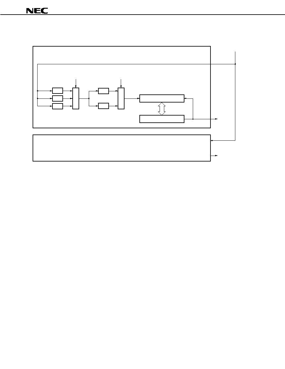
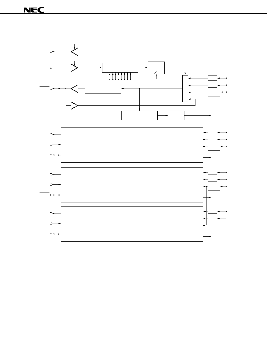
INTERNAL BLOCK DIAGRAM
TCLR10 to TCLR15
TI10 to TI15
TO100, TO101,
TO110, TO111,
TO120, TO121,
TO130, TO131,
TO140, TO141,
TO150, TO151
INTP100 to INTP103,
INTP110 to INTP113,
INTP120 to INTP123,
INTP130 to INTP133,
INTP140 to INTP143,
INTP150 to INTP153
NMI
INTC
RPU
UART0/CSI0
SIO
SCK0
SI0/RXD0
SO0/TXD0
BRG0
UART1/CSI1
SCK1
SI1/RXD1
SO1/TXD1
BRG1
CSI2
SCK2
SI2
SO2
BRG2
CSI3
SCK3
SI3
SO3
AV
REF
ADC
AV
SS
AV
DD
ADTRG
ANI0 to ANI7
Port
PX5 to PX7
PB0 to PB7
PA0 to PA7
P120 to P127
P110 to P117
P100 to P107
P90 to P97
P80 to P87
P70 to P77
P60 to P67
P50 to P57
P40 to P47
P30 to P37
P21 to P27
P20
P10 to P17
P00 to P07
HV
DD
Note
ROM
4 Kbytes
RAM
Instruction queue
PC
System registers
General registers
(32 bits
◊
32)
Multiplier
(32
◊
32
64)
Barrel
shifter
ALU
DRAMC
Page ROM
controller
DMAC
BCU
CPU
TC0 to TC3
LWR/LCAS
DMAAK0 to DMARQ3
DMARQ0 to DMARQ3
D0 to D15
A0 to A23
WAIT
CS0 to CS7/RAS0 to RAS7
UWR/UCAS
OE
RD
WE
BCYST
REFRQ
IORD
IOWR
HLDAK
HLDRQ
CG
CKSEL
CLKOUT
X1
X2
CV
DD
CV
SS
System
controller
RESET
V
DD
V
SS
MODE0 to MODE3
Note
µ
PD703100-33, 703100-40: None
µ
PD703101-33: 96 Kbytes (mask ROM)
µ
PD703102-33: 128 Kbytes (mask ROM)

Preliminary Data Sheet U13995EJ1V0DS00
5
µ
µ
µ
µ
PD703100-33, 703100-40, 703101-33, 703102-33
CONTENTS
1.
DIFFERENCES AMONG PRODUCTS...........................................................................................
7
2.
PIN FUNCTIONS .............................................................................................................................
8
2.1
Port Pins .................................................................................................................................
8
2.2
Non-port Pins .........................................................................................................................
11
2.3
Pin I/O Circuits and Recommended Connection of Unused Pins.....................................
15
3.
FUNCTION BLOCKS ......................................................................................................................
18
3.1
Internal Units ..........................................................................................................................
18
3.1.1
CPU ...........................................................................................................................................
18
3.1.2
Bus control unit (BCU) ...............................................................................................................
18
3.1.3
ROM ..........................................................................................................................................
18
3.1.4
RAM...........................................................................................................................................
19
3.1.5
Ports ..........................................................................................................................................
19
3.1.6
Interrupt controller (INTC) ..........................................................................................................
19
3.1.7
Clock generator (CG).................................................................................................................
19
3.1.8
Real-time pulse unit (RPU) ........................................................................................................
19
3.1.9
Serial interface (SIO) .................................................................................................................
19
3.1.10 A/D converter (ADC) ..................................................................................................................
19
4.
CPU FUNCTIONS............................................................................................................................
20
5.
BUS CONTROL FUNCTIONS........................................................................................................
20
6.
MEMORY ACCESS CONTROL FUNCTIONS ..............................................................................
21
6.1
SRAM Connection..................................................................................................................
21
6.2
Page ROM Controller (ROMC) ..............................................................................................
22
6.2.1
Features.....................................................................................................................................
22
6.2.2
Page ROM connection...............................................................................................................
22
6.3
DRAM Controller ....................................................................................................................
24
6.3.1
Features.....................................................................................................................................
24
6.3.2
DRAM Connections ...................................................................................................................
24
7.
DMA FUNCTIONS (DMA CONTROLLER) ...................................................................................
26
8.
INTERRUPT/EXCEPTION PROCESSING FUNCTIONS...............................................................
28
8.1
Features ..................................................................................................................................
28
9.
CLOCK GENERATION FUNCTIONS ............................................................................................
33
10. TIMER/COUNTER FUNCTIONS (REAL-TIME PULSE UNIT).....................................................
34

Preliminary Data Sheet U13995EJ1V0DS00
6
µ
µ
µ
µ
PD703100-33, 703100-40, 703101-33, 703102-33
11. SERIAL INTERFACE FUNCTION ..................................................................................................
37
11.1 Asynchronous Serial Interfaces 0, 1 (UART0, UART1).......................................................
37
11.2 Clocked Serial Interfaces 0 to 3 (CSI0 to CSI3) ...................................................................
38
11.3 Dedicated Baud Rate Generators 0 to 2 (BRG0 to BRG2)..................................................
40
12. A/D CONVERTER............................................................................................................................
41
13. PORT FUNCTIONS .........................................................................................................................
42
14. RESET FUNCTION ..........................................................................................................................
53
15. INSTRUCTION SET .........................................................................................................................
54
16. ELECTRICAL SPECIFICATIONS (PRELIMINARY VALUES)......................................................
64
17. PACKAGE DRAWING ..................................................................................................................... 120
18. RECOMMENDED SOLDERING CONDITIONS ............................................................................. 121

Preliminary Data Sheet U13995EJ1V0DS00
7
µ
µ
µ
µ
PD703100-33, 703100-40, 703101-33, 703102-33
1. DIFFERENCES AMONG PRODUCTS
Product Name
µ
PD703100
µ
PD703101
µ
PD703102
µ
PD70F3102
Item
≠33
≠40
≠A33
≠A40
≠33
≠A33
≠33
≠A33
≠33
≠A33
Internal ROM
None
96 Kbytes
(mask ROM)
128 Kbytes
(mask ROM)
128 Kbytes
(flash memory)
Maximum operating
frequency
33 MHz
40 MHz
33 MHz
40 MHz
33 MHz
HV
DD
4.5 to 5.5 V
3.0 to 3.6 V
4.5 to
5.5 V
3.0 to
3.6 V
4.5 to
5.5 V
3.0 to
3.6 V
4.5 to
5.5 V
3.0 to
3.6 V
Operation mode
Single-chip
mode 0, 1
None
Provided
Flash memory
programming
mode
None
Provided
Flash memory
programming pin
None
Provided (V
PP
)
Electrical
specifications
Power consumptions differ (refer to the data sheet of each product).
Package
144LQFP
144LQFP
157FBGA
144LQFP
144LQFP
157FBGA
144LQFP
144LQFP
157FBGA
144LQFP
144LQFP
157FBGA
Others
Noise tolerance and noise radiation will differ due to the differences in circuit scale and mask layout.
Remark 144LQFP: 144-pin plastic LQFP (fine pitch) (20
◊
20 mm)
157FBGA: 157-pin plastic FBGA (14
◊
14 mm)
Preliminary Data Sheet U13995EJ1V0DS00
8
µ
µ
µ
µ
PD703100-33, 703100-40, 703101-33, 703102-33
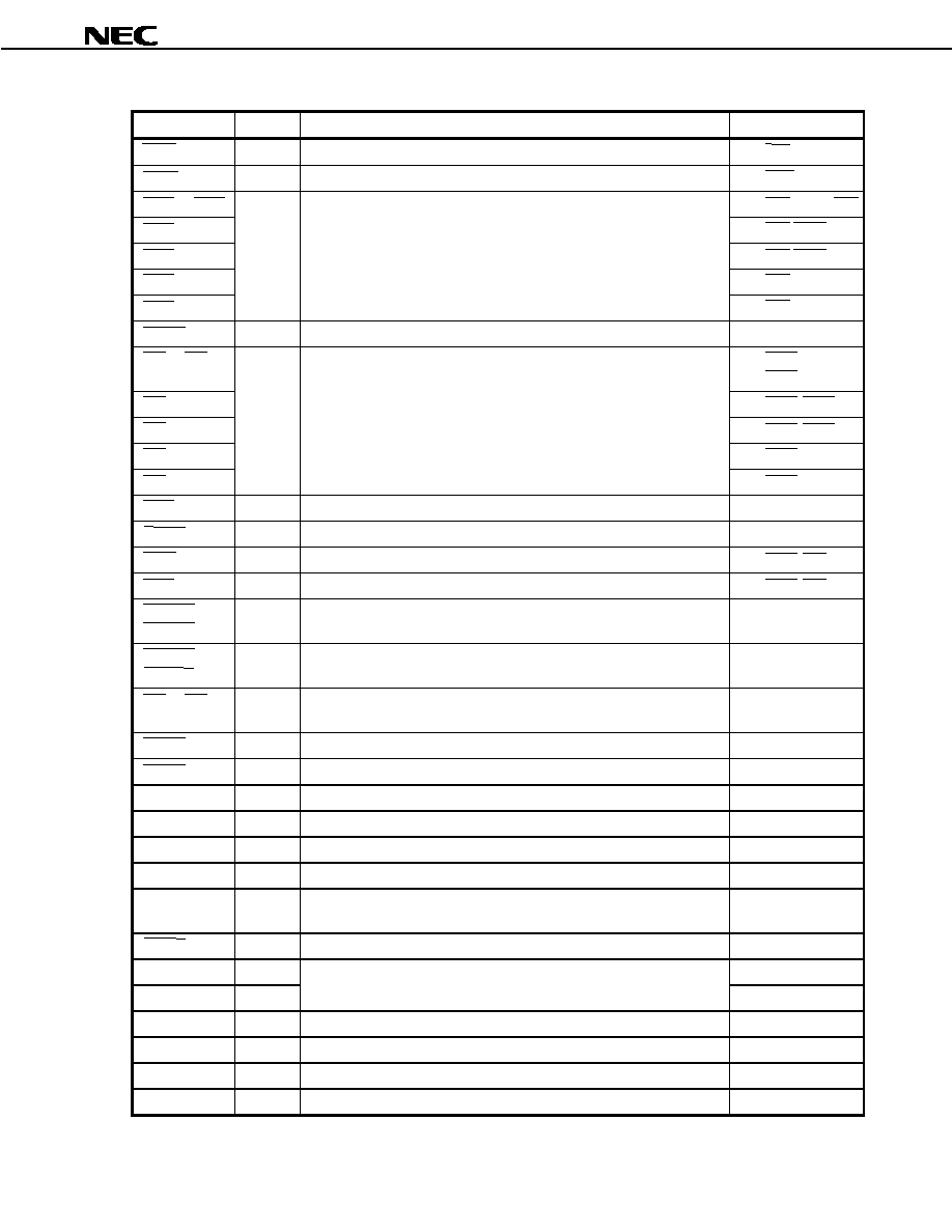
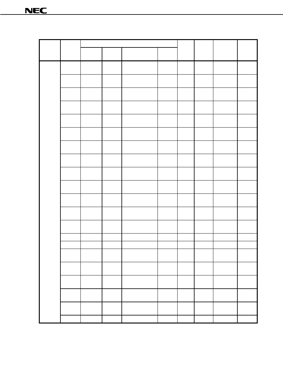
2. PIN FUNCTIONS
2.1 Port Pins
(1/3)
Pin Name
I/O
Function
Alternate Function
P00
TO100
P01
TO101
P02
TCLR10
P03
TI10
P04
INTP100/DMARQ0
P05
INTP101/DMARQ1
P06
INTP102/DMARQ2
P07
I/O
Port 0
8-bit I/O port
Input/output mode can be specified in 1-bit units
INTP103/DMARQ3
P10
TO110
P11
TO111
P12
TCLR11
P13
TI11
P14
INTP110/DMAAK0
P15
INTP111/DMAAK1
P16
INTP112/DMAAK2
P17
I/O
Port 1
8-bit I/O port
Input/output mode can be specified in 1-bit units
INTP113/DMAAK3
P20
I
NMI
P21
≠
P22
TXD0/SO0
P23
RXD0/SO0
P24
SCK0
P25
TXD1/SO1
P26
RXD1/SI1
P27
I/O
Port 2
P20 is an input only port.
When a valid edge is input, this pin operates as NMI input. Also, bit 0
of the P2 register indicates the NMI input status.
P21 to P27 are 7-bit I/O port.
Input/output mode can be specified in 1-bit units
SCK1
P30
TO130
P31
TO131
P32
TCLR13
P33
TI13
P34
INTP130
P35
INTP131/SO2
P36
INTP132/SI2
P37
I/O
Port 3
8-bit I/O port.
Input/output mode can be specified in 1-bit units
INTP133/SCK2
P40 to P47
I/O
Port 4
8-bit I/O port
Input/output mode can be specified in 1-bit units
D0 to D7

Preliminary Data Sheet U13995EJ1V0DS00
9
µ
µ
µ
µ
PD703100-33, 703100-40, 703101-33, 703102-33
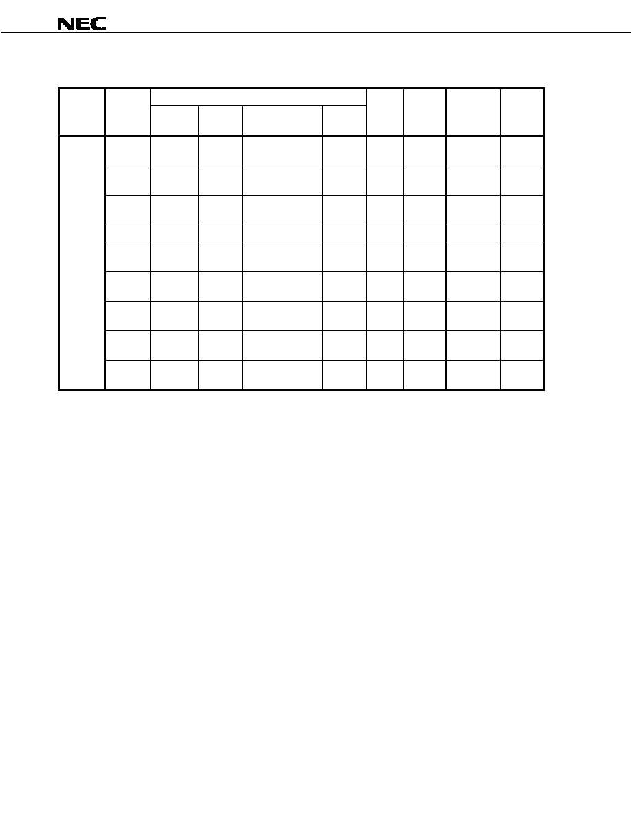
(2/3)
Pin Name
I/O
Function
Alternate Function
P50 to P57
I/O
Port 5
8-bit I/O port
Input/output mode can be specified in 1-bit units
D8 to D15
P60 to P67
I/O
Port 6
8-bit I/O port
Input/output mode can be specified in 1-bit units
A16 to A23
P70 to P77
I
Port 7
8-bit input only port
ANI0 to ANI7
P80
CS0/RAS0
P81
CS1/RAS1
P82
CS2/RAS2
P83
CS3/RAS3
P84
CS4/RAS4/IOWR
P85
CS5/RAS5/IORD
P86
CS6/RAS6
P87
I/O
Port 8
8-bit I/O port
Input/output mode can be specified in 1-bit units
CS7/RAS7
P90
LCAS/LWR
P91
UCAS/UWR
P92
RD
P93
WE
P94
BCYST
P95
OE
P96
HLDAK
P97
I/O
Port 9
8-bit I/O port
Input/output mode can be specified in 1-bit units
HLDRQ
P100
TO120
P101
TO121
P102
TCLR12
P103
TI12
P104
INTP120/TC0
P105
INTP121/TC1
P106
INTP122/TC2
P107
I/O
Port 10
8-bit I/O port
Input/output mode can be specified in 1-bit units
INTP123/TC3
P110
TO140
P111
TO141
P112
TCLR14
P113
TI14
P114
INTP140
P115
INTP141/SO3
P116
INTP142/SI3
P117
I/O
Port 11
8-bit I/O port
Input/output mode can be specified in 1-bit units
INTP143/SCK3
Preliminary Data Sheet U13995EJ1V0DS00
10
µ
µ
µ
µ
PD703100-33, 703100-40, 703101-33, 703102-33
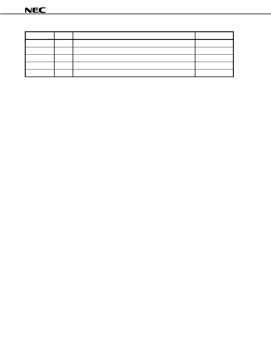
(3/3)
Pin Name
I/O
Function
Alternate Function
P120
TO150
P121
TO151
P122
TCLR15
P123
TI15
P124
INTP150
P125
INTP151
P126
INTP152
P127
I/O
Port 12
8-bit I/O port
Input/output mode can be specified in 1-bit units
INTP153/ADTRG
PA0
A0
PA1
A1
PA2
A2
PA3
A3
PA4
A4
PA5
A5
PA6
A6
PA7
I/O
Port A
8-bit I/O port
Input/output mode can be specified in 1-bit units
A7
PB0
A8
PB1
A9
PB2
A10
PB3
A11
PB4
A12
PB5
A13
PB6
A14
PB7
I/O
Port B
8-bit I/O port
Input/output mode can be specified in 1-bit units
A15
PX5
REFRQ
PX6
WAIT
PX7
I/O
Port X
3-bit I/O port
Input/output mode can be specified in 1-bit units
CLKOUT
Preliminary Data Sheet U13995EJ1V0DS00
11
µ
µ
µ
µ
PD703100-33, 703100-40, 703101-33, 703102-33
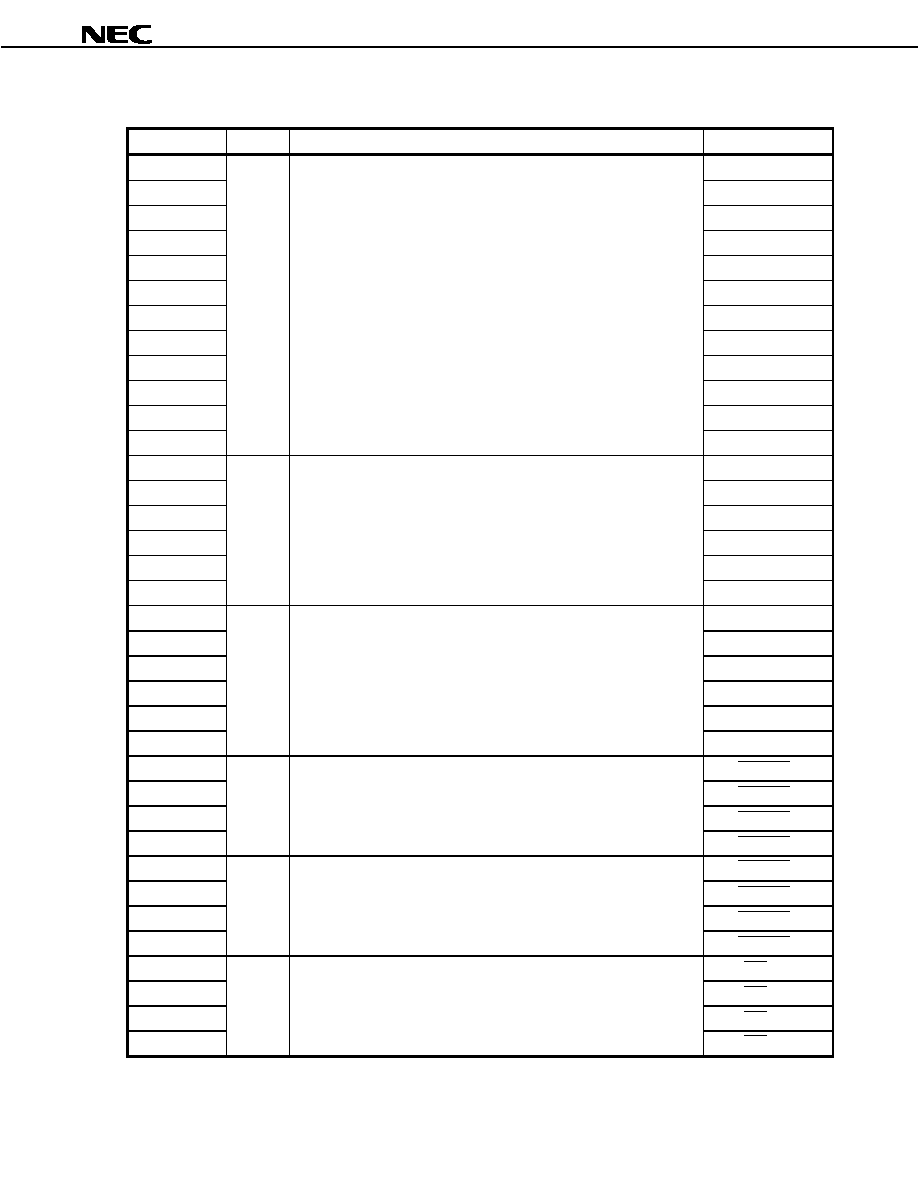
2.2 Non-port Pins
(1/4)
Pin Name
I/O
Function
Alternate Function
TO100
P00
TO101
P01
TO110
P10
TO111
P11
TO120
P100
TO121
P101
TO130
P30
TO131
P31
TO140
P110
TO141
P111
TO150
P120
TO151
O
Pulse signal output for timers 10 to 15
P121
TCLR10
P02
TCLR11
P12
TCLR12
P102
TCLR13
P32
TCLR14
P112
TCLR15
I
External clear signal input for timers 10 to 15
P122
TI10
P03
TI11
P13
TI12
P103
TI13
P33
TI14
P113
TI15
I
External count clock input for timers 10 to 15
P123
INTP100
P04/DMARQ0
INTP101
P05/DMARQ1
INTP102
P06/DMARQ2
INTP103
I
External maskable interrupt request input, shared as external capture
trigger input for timer 10
P07/DMARQ3
INTP110
P14/DMAAK0
INTP111
P15/DMAAK1
INTP112
P16/DMAAK2
INTP113
I
External maskable interrupt request input, shared as external capture
trigger input for timer 11
P17/DMAAK3
INTP120
P104/TC0
INTP121
P105/TC1
INTP122
P106/TC2
INTP123
I
External maskable interrupt request input, shared as external capture
trigger input for timer 12
P107/TC3

Preliminary Data Sheet U13995EJ1V0DS00
12
µ
µ
µ
µ
PD703100-33, 703100-40, 703101-33, 703102-33
(2/4)
Pin Name
I/O
Function
Alternate Function
INTP130
P34
INTP131
P35/SO2
INTP132
P36/SI2
INTP133
I
External maskable interrupt request input, shared as external capture
trigger input for timer 13
P37/SCK2
INTP140
P114
INTP141
P115/SO3
INTP142
P116/SI3
INTP143
I
External maskable interrupt request input, shared as external capture
trigger input for timer 14
P117/SCK3
INTP150
P124
INTP151
P125
INTP152
P126
INTP153
I
External maskable interrupt request input, shared as external capture
trigger input for timer 15
P127/ADTRG
SO0
P22/TXD0
SO1
P25/TXD1
SO2
P35/INTP131
SO3
O
Serial transmit data output (3-wire) for CSI0 to CSI3
P115/INTP141
SI0
P23/RXD0
SI1
P26/RXD1
SI2
P36/INTP132
SI3
I
Serial receive data input (3-wire) for CSI0 to CSI3
P116/INTP142
SCK0
P24
SCK1
P27
SCK2
P37/INTP133
SCK3
I/O
Serial clock I/O (3-wire) for CSI0 to CSI3
P117/INTP143
TXD0
P22/SO0
TXD1
O
Serial transmit data output for UART0 and UART1
P25/SO1
RXD0
P23/SI0
RXD1
I
Serial receive data input for UART0 and UART1
P26/SI1
D0 to D7
P40 to P47
D8 to D15
I/O
16-bit data bus for external memory
P50 to P57
A0 to A7
PA0 to PA7
A8 to A15
PB0 to PB7
A16 to A23
O
24-bit address bus for external memory
P60 to P67
LWR
O
Lower byte write-enable signal output for external data bus
P90/LCAS
UWR
O
Higher byte write-enable signal output for external data bus
P91/UCAS
RD
O
Read strobe signal output for external data bus
P92
WE
O
Write enable signal output for DRAM
P93
OE
O
Output enable signal output for DRAM
P95
Preliminary Data Sheet U13995EJ1V0DS00
13
µ
µ
µ
µ
PD703100-33, 703100-40, 703101-33, 703102-33
(3/4)
Pin Name
I/O
Function
Alternate Function
LCAS
O
Column address strobe signal output for DRAM's lower data
P90/LWR
UCAS
O
Column address strobe signal output for DRAM's higher data
P91/UWR
RAS0 to RAS3
P80/CS0 to P83/CS3
RAS4
P84/CS4/IOWR
RAS5
P85/CS5/IORD
RAS6
P86/CS6
RAS7
O
Low address strobe signal output for DRAM
P87/CS7
BCYST
O
Strobe signal output indicating start of bus cycle
P94
CS0 to CS3
P80/RAS0 to
P83/RAS3
CS4
P84/RAS4/IOWR
CS5
P85/RAS5/IORD
CS6
P86/RAS6
CS7
O
Chip select signal output
P87/RAS7
WAIT
I
Control signal input for inserting waits in bus cycle
PX6
REFRQ
O
Refresh request signal output for DRAM
PX5
IOWR
O
DMA write strobe signal output
P84/RAS4/CS4
IORD
O
DMA read strobe signal output
P85/RAS5/CS5
DMARQ0 to
DMARQ3
I
DMA request signal input
P04/INTP100 to
P07/INTP103
DMAAK0 to
DMAAK3
O
DMA acknowledge signal output
P14/INTP110 to
P17/INTP113
TC0 to TC3
O
DMA end (terminal count) signal output
P104/INTP120 to
P107/INTP123
HLDAK
O
Bus hold acknowledge output
P96
HLDRQ
I
Bus hold request input
P97
ANI0 to ANI7
I
Analog input to A/D converter
P70 to P77
NMI
I
Non-maskable interrupt request input
P20
CLKOUT
O
System clock output
PX7
CKSEL
I
Input for specifying clock generator's operation mode
≠
MODE0 to
MODE3
I
Specify operation modes
≠
RESET
I
System reset input
≠
X1
I
≠
X2
≠
Oscillator connection for system clock. Input is via X1 when using an
external clock.
≠
ADTRG
I
A/D converter external trigger input
P127/INTP153
AV
REF
I
Reference voltage input for A/D converter
≠
AV
DD
≠
Positive power supply for A/D converter
≠
AV
SS
≠
Ground potential for A/D converter
≠
Preliminary Data Sheet U13995EJ1V0DS00
14
µ
µ
µ
µ
PD703100-33, 703100-40, 703101-33, 703102-33
(4/4)
Pin Name
I/O
Function
Alternate Function
CV
DD
≠
Positive power supply for dedicated clock generator
≠
CV
SS
≠
Ground potential for dedicated clock generator
≠
V
DD
≠
Positive power supply (power supply for internal units)
≠
HV
DD
≠
Positive power supply (power supply for external pins)
≠
V
SS
≠
Ground potential
≠
Preliminary Data Sheet U13995EJ1V0DS00
15
µ
µ
µ
µ
PD703100-33, 703100-40, 703101-33, 703102-33
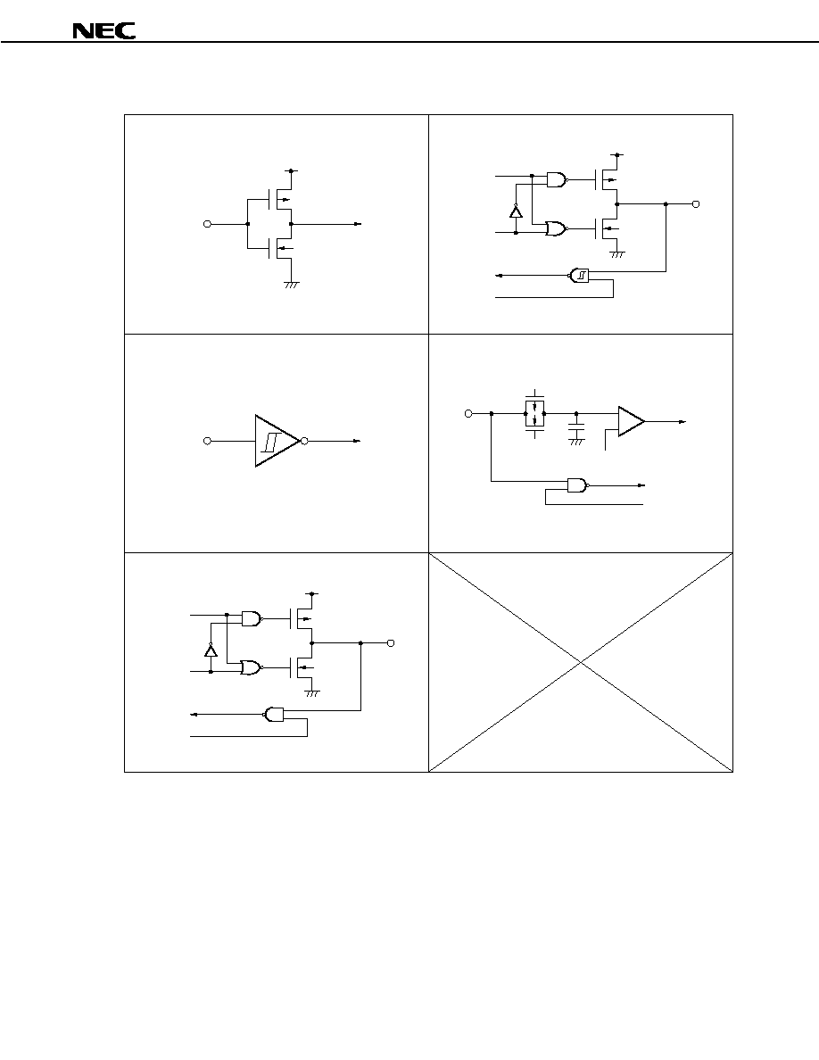
2.3 Pin I/O Circuits and Recommended Connection of Unused Pins
Table 2-1 shows the I/O circuit type of each pin and recommended connection of unused pins. Figure 2-1 shows
the various circuit types using partially abridged diagrams.
When connecting to V
DD
or V
SS
via a resistor, a resistance value in the range of 1 to 10 k
is recommended.
Table 2-1. I/O Circuit Type of Each Pin and Recommended Connection of Unused Pins (1/2)
Pin
I/O Circuit Type
Recommended Connection of Unused Pins
P00/TO100, P01/TO101
5
P02/TCLR10, P03/TI10
P04/INTP100/DMARQ0 to
P07/INTP103/DMARQ3
5-K
P10/TO110, P11/TO111
5
P12/TCLR11, P13/TI11
P14/INTP110/DMAAK0 to
P17/INTP113/DMAAK3
5-K
Input : Independently connect to HV
DD
or V
SS
via a resistor
Output: Leave open
P20/NMI
2
Connect directly to V
SS
P21
P22/TXD0/SO0
5
P23/RXD0/SI0
P24/SCK0
5-K
P25/TXD1/SO1
5
P26/RXD1/SI1
P27/SCK1
5-K
P30/TO130, P31/TO131
5
P32/TCLR13,P33/TI13
P34/INTP130
P35/INTP131/SO2
P36/INTP132/SI2
P37/INTP133/SCK2
5-K
P40/D0 to P47/D7
P50/D8 to P57/D15
P60/A16 to P67/A23
5
Input : Independently connect to HV
DD
or V
SS
via a resistor
Output: Leave open
P70/ANI0 to P77/ANI7
9
Connect directly to V
SS
P80/CS0/RAS0 to P83/CS3/RAS3
P84/CS4/RAS4/IOWR,
P85/CS5/RAS5/IORD
P86/CS6/RAS6, P87/CS7/RAS7
P90/LCAS/LWR
P91/UCAS/UWR
5
Input : Independently connect to HV
DD
or V
SS
via a resistor
Output: Leave open
Preliminary Data Sheet U13995EJ1V0DS00
16
µ
µ
µ
µ
PD703100-33, 703100-40, 703101-33, 703102-33
Table 2-1. I/O Circuit Type of Each Pin and Recommended Connection of Unused Pins (2/2)
Pin
I/O Circuit Type
Recommended Connection of Unused Pins
P92/RD
P93/WE
P94/BCYST
P95/OE
P96/HLDAK
P97/HLDRQ
P100/TO120, P101/TO121
5
P102/TCLR12, P103/TI12
P104/INTP120/TC0 to
P107/INTP123/TC3
5-K
P110/TO140, P111/TOI41
5
P112/TCLR14, P113/TI14
P114/INTP140
P115/INTP141/SO3
P116/INTP142/SI3
P117/INTP143/SCK3
5-K
P120/TO150, P121/TO151
5
P122/TCLR15, P123/TI15
P124/INTP150 to P126/INTP152
P127/INTP153/ADTRG
5-K
PA0/A0-PA7/A7
PB0/A8-PB7/A15
PX5/REFRQ
PX6/WAIT
PX7/CLKOUT
5
Input : Independently connect to HV
DD
or V
SS
via a resistor
Output: Leave open
CKSEL
1
Connect directly to HV
DD
RESET
MODE0 to MODE2
≠
MODE3
2
Connect to V
SS
via a resistor (R
VPP
)
AV
REF
, AV
SS
≠
Connect directly to V
SS
AV
DD
≠
Connect directly to HV
DD
Preliminary Data Sheet U13995EJ1V0DS00
17
µ
µ
µ
µ
PD703100-33, 703100-40, 703101-33, 703102-33
Figure 2-1. Pin I/O Circuits
IN
P-ch
V
DD
N-ch
IN
data
P-ch
V
DD
N-ch
IN/OUT
output
disable
input
enable
data
P-ch
V
DD
N-ch
IN/OUT
output
disable
input
enable
IN
+
≠
input enable
P-ch
N-ch
V
REF
(threshold voltage)
Type 1
Type 2
Type 5
Type 5-K
Type 9
Comparator
Schmitt trigger input with hysteresis characteristics
Caution Replace V
DD
by HV
DD
when referencing the circuit diagrams shown above.

Preliminary Data Sheet U13995EJ1V0DS00
18
µ
µ
µ
µ
PD703100-33, 703100-40, 703101-33, 703102-33
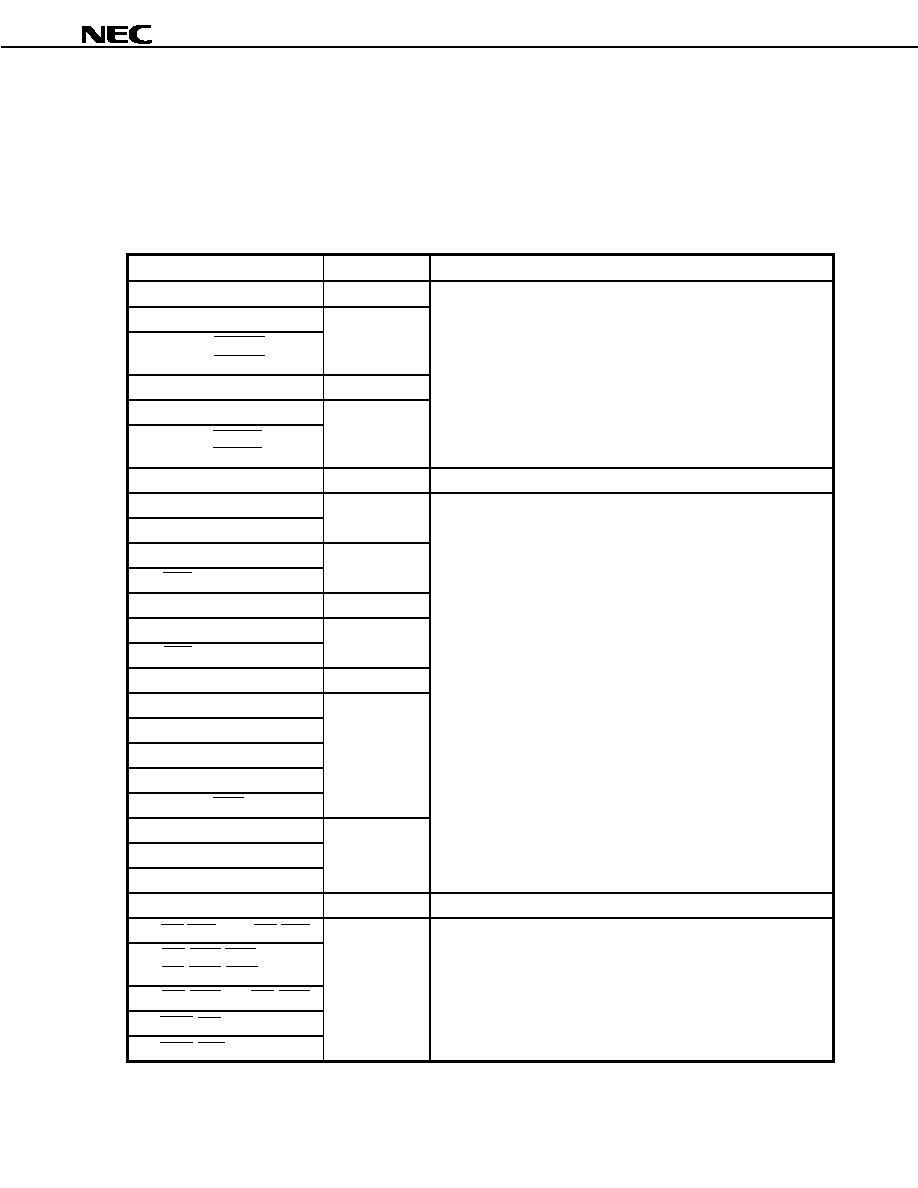
3. FUNCTION BLOCKS
3.1 Internal Units
3.1.1 CPU
The CPU uses five-stage pipeline control to enable single-clock execution of address calculations, arithmetic logic
operations, data transfers, and almost all other instruction processing.
Other dedicated on-chip hardware, such as the multiplier (16 bits
◊
16 bits
32 bits, or 32 bits
◊
32 bits
64
bits) and the barrel shifter (32 bits) help accelerate processing of complex instructions.
3.1.2 Bus control unit (BCU)
The BCU starts a required external bus cycle based on the physical address obtained by the CPU. When an
instruction is fetched from external memory area and the CPU does not send a bus cycle start request, the BCU
generates a prefetch address and prefetches the instruction code. The prefetched instruction code is stored in an
internal instruction queue of the CPU.
The BCU contains DRAM controller (DRAMC), page ROM controller, and DMA controller (DMAC).
(a) DRAM controller (DRAMC)
The DRAM controller generates the RAS, UCAS, and LCAS signals (2CAS control) and controls access to the
DRAM.
It supports high-speed page DRAM and EDO DRAM, and has two types of cycles for accessing DRAM.
These types of cycles are referred to as normal access (off-page) and page access (on-page).
The DRAM controller also has a refresh function that is associated with the CBR refresh cycle.
(b) Page ROM controller
The page ROM controller supports access to ROM that has the page access function.
It compares the address with that of the preceding bus cycle and controls the waits for normal access (off-
page) and page access (on-page). The page ROM controller can support page sizes of 8 to 64 bytes.
(c) DMA controller (DMAC)
The DMA controller transfers data between memory and an I/O device in place of the CPU.
The two address modes are flyby (one-cycle) transfer and two-cycle transfer. The three bus modes are single
transfer, single-step transfer, and block transfer.
3.1.3 ROM
The
µ
PD703101-33 contains 96-Kbytes mask ROM, and the
µ
PD703102-33 contains 128-Kbytes mask ROM.
The CPU can access ROM in one clock cycle when an instruction is fetched.
When single-chip mode 0 is set, ROM is mapped to the address space starting at 00000000H. When single-chip
mode 1 is set, ROM is mapped to the address space starting at 00100000H. When ROM-less mode 0 or 1 is set,
ROM cannot be accessed.
The
µ
PD703100-33 and
µ
PD703100-40 have no internal ROM.

Preliminary Data Sheet U13995EJ1V0DS00
19
µ
µ
µ
µ
PD703100-33, 703100-40, 703101-33, 703102-33
3.1.4 RAM
RAM is mapped to the 4-Kbyte address space starting at FFFFE000H. The CPU can access RAM in one clock
cycle when an instruction is fetched or data is accessed.
3.1.5 Ports
In addition to the 123 pins (ports 0 to 12, A, B, and X) comprising I/O ports (of which nine pins comprise an input-
only port), various port pin and control pin functions can be selected for these pins.
3.1.6 Interrupt controller (INTC)
This controller handles hardware interrupt requests (NMI, INTP100 to INTP103, INTP110 to INTP113, INTP120 to
INTP123, INTP130 to INTP133, INTP140 to INTP143, and INTP150 to INTP153) from on-chip peripheral I/O and
external hardware. Eight interrupt priority levels can be specified for these interrupt requests, and multiplexed
servicing control can be performed for interrupt sources.
3.1.7 Clock generator (CG)
A frequency of five times (using an on-chip PLL) or one-half times (not using an on-chip PLL) that of the input
clock (f
XX
) is supplied as the internal system clock (
). Either an external oscillator is connected to pins X1 and X2
(only when the on-chip PLL synthesizer is used) or an external clock is input from the X1 pin as the input clock.
3.1.8 Real-time pulse unit (RPU)
The RPU includes a six-channel 16-bit timer/event counter and a two-channel 16-bit interval timer, which enables
measurement of pulse intervals and frequency as well as programmable pulse output.
3.1.9 Serial interface (SIO)
Four channels are comprised of two kinds of serial interfaces: an asynchronous serial interface (UART) and a
clocked serial interface (CSI). Two of these four channels are switchable between the UART and CSI and the other
two channels are fixed as CSI.
For UART, data is transferred via the TXD and RXD pins. For CSI, data is transferred via the SO, SI, and SCK
pins.
The serial clock source can be selected from dedicated baud rate generator output or the internal system clock.
3.1.10 A/D converter (ADC)
This is a high-speed, high-resolution 10-bit A/D converter that includes eight analog input pins. It converts using
the successive approximation method.

Preliminary Data Sheet U13995EJ1V0DS00
20
µ
µ
µ
µ
PD703100-33, 703100-40, 703101-33, 703102-33
4. CPU FUNCTIONS
{
RISC-based architecture
{
Uses five-stage pipeline control to enable single-clock execution of almost all instructions
{
Minimum instruction execution time
25 ns (@ 40-MHz operation) ...
µ
PD703100-40
30 ns (@ 33-MHz operation) ...
µ
PD703100-33, 703101-33, 703102-33
{
Memory space
Program space : 64-Mbyte linear
Data space
: 4-Gbyte linear
{
General registers 32 bits
◊
32
{
Internal 32-bit architecture
{
5-stage pipeline control
{
Multiply/divide instructions
{
Saturated operation instructions
{
32-bit shift instruction: 1 clock
{
Long/short format
{
Four types of bit manipulation instructions
∑
Set
∑
Clear
∑
Not
∑
Test
5. BUS CONTROL FUNCTIONS
{
16-bit/8-bit data bus sizing function
{
8-space chip select output function
{
Wait functions
∑
Programmable wait function for up to seven states for each memory block
∑
External wait function using WAIT pin
{
Idle state insertion function
{
Bus mastering arbitration function
{
Bus hold function
{
Alternate function for port pins are connectable to external bus
Preliminary Data Sheet U13995EJ1V0DS00
21
µ
µ
µ
µ
PD703100-33, 703100-40, 703101-33, 703102-33
6. MEMORY ACCESS CONTROL FUNCTIONS
6.1 SRAM Connection
The following figure shows an SRAM connection example.
Figure 6-1. SRAM Connection Example
A0 to A16
I/O1 to I/O8
1-Mbit (128 K
◊
8) SRAM
CS
WE
OE
V
CC
A1 to A17
D0 to D7
D8 to D15
CSn
UWR
LWR
V850E/MS1
RD
5 V
5 V
5 V
HV
DD
A0 to A16
I/O1 to I/O8
1-Mbit (128 K
◊
8) SRAM
CS
WE
OE
V
CC
Remark n = 0 to 7
Preliminary Data Sheet U13995EJ1V0DS00
22
µ
µ
µ
µ
PD703100-33, 703100-40, 703101-33, 703102-33
6.2 Page ROM Controller (ROMC)
The page ROM controller (ROMC) supports access to ROM (page ROM) that has the page access function.
It compares the address with that of the preceding bus cycle and performs wait control for normal access (off-
page) and page access (on-page). The page ROM controller can support page widths of 8 to 64 bytes.
6.2.1 Features
{
Can be connected directly to 8-bit or 16-bit page ROM
{
For 16-bit bus width, it supports 4-, 8-, 16-, or 32-word page access
For 8-bit bus width, it supports 8-, 16-, 32-, or 64-word page access
{
Enables waits to be set (0 to 7 waits) independently for off-page and on-page access
6.2.2 Page ROM connection
The following figure shows page ROM connection examples.
Figure 6-2. Page ROM Connection Examples (1/2)
(a) 16-Mbit (1 M
◊
◊
◊
◊
16) page ROM
V
DD
A1 to A20
D0 to D15
RD
CSn
V850E/MS1
16-Mbit (1 M
◊
16) page ROM
A0 to A19
O1 to O16
WORD/BYTE
OE
CE
Remark n = 0 to 7

Preliminary Data Sheet U13995EJ1V0DS00
23
µ
µ
µ
µ
PD703100-33, 703100-40, 703101-33, 703102-33
Figure 6-2. Page ROM Connection Examples (2/2)
(b) 16-Mbit (2 M
◊
◊
◊
◊
8) page ROM
16-Mbit (2 M
◊
8) page ROM
A0 to A19
O0 to O7
WORD/BYTE
OE
CE
16-Mbit (2 M
◊
8) page ROM
A0 to A19
O0 to O7
WORD/BYTE
OE
CE
A1 to A20
D8 to D15
D0 to D7
RD
CSn
V850E/MS1
Remark n = 0 to 7
Preliminary Data Sheet U13995EJ1V0DS00
24
µ
µ
µ
µ
PD703100-33, 703100-40, 703101-33, 703102-33
6.3 DRAM Controller
6.3.1 Features
{
Generates the RAS, UCAS, and LCAS signals
{
Can be connected directly to high-speed page DRAM and EDO DRAM
{
Supports RAS hold mode
{
Can assign 4 types of DRAM to 8 memory block spaces
{
Supports 2CAS type DRAM
{
Can be switched between row and column address multiplex widths
{
Can insert waits (0 to 3 waits) at each of the following timings
∑
Row address pre-charge wait
∑
Row address hold wait
∑
Data access wait
∑
Column address pre-charge wait
{
Supports CBR refresh and CBR self refresh
6.3.2 DRAM Connections
The following figure shows DRAM connection examples.
Figure 6-3. DRAM Connection Examples (1/2)
(a) 16-Mbit (1 M
◊
◊
◊
◊
16) DRAM
16-Mbit (1 M
◊
16) DRAM
RASn
LCAS
UCAS
WE
OE
A0 to A9
I/O1 to I/O16
A1 to A10
D0 to D15
RASn
LCAS
V850E/MS1
UCAS
WE
OE
Remark n = 0 to 7
Preliminary Data Sheet U13995EJ1V0DS00
25
µ
µ
µ
µ
PD703100-33, 703100-40, 703101-33, 703102-33
Figure 6-3. DRAM Connection Examples (2/2)
(b) 4-Mbit (1 M
◊
◊
◊
◊
4) DRAM
4-Mbit (1 M
◊
4) DRAM
RAS
CAS
WE
OE
A0 to A9
A1 to A10
D8 to D15
I/O1 to I/O4
4-Mbit (1 M
◊
4) DRAM
RAS
CAS
WE
OE
A0 to A9
I/O1 to I/O4
4-Mbit (1 M
◊
4) DRAM
RAS
CAS
WE
OE
A0 to A9
I/O1 to I/O4
4-Mbit (1 M
◊
4) DRAM
RAS
CAS
WE
OE
A0 to A9
I/O1 to I/O4
D0 to D7
V850E/MS1
RASn
LCAS
UCAS
WE
OE
Remark n = 0 to 7

Preliminary Data Sheet U13995EJ1V0DS00
26
µ
µ
µ
µ
PD703100-33, 703100-40, 703101-33, 703102-33
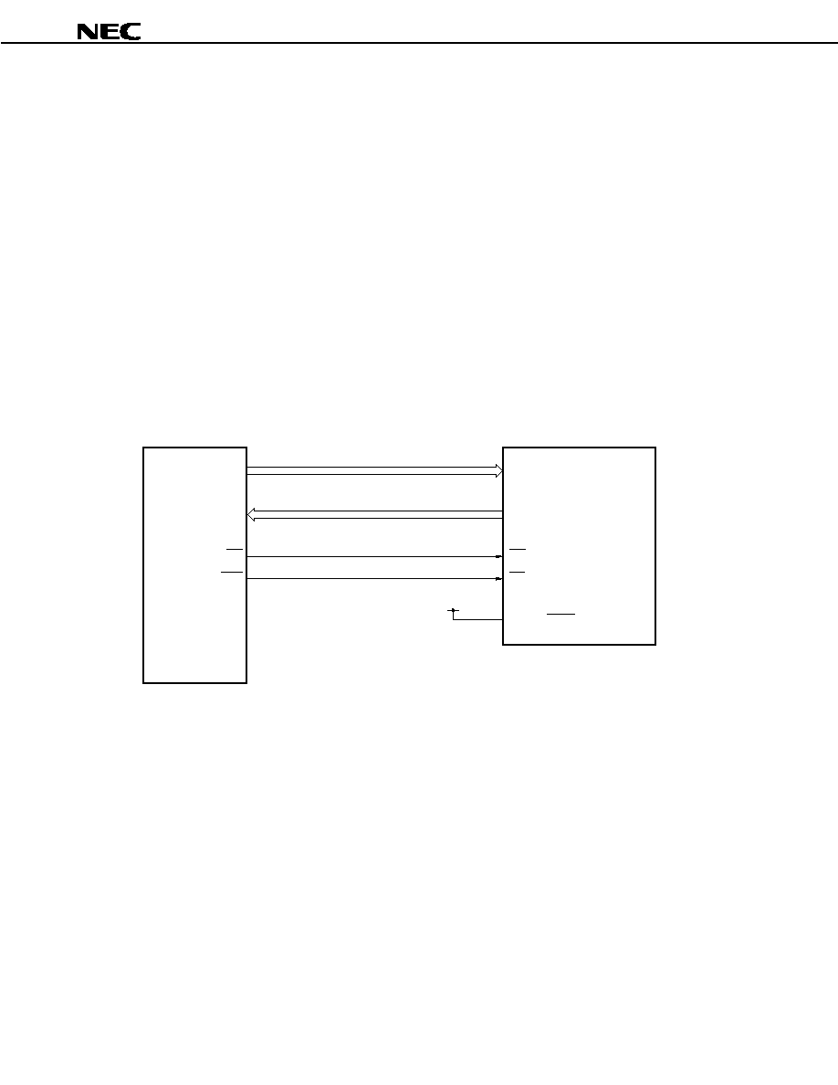
7. DMA FUNCTIONS (DMA CONTROLLER)
{
4 independent DMA channels
{
Transfer units: 8 or 16 bits
{
Maximum transfer count: 65536 (2
16
)
{
Two types of transfer
∑
Flyby (one-cycle) transfer
∑
Two-cycle transfer
{
Three transfer modes
∑
Single transfer mode
∑
Single-step transfer mode
∑
Block transfer mode
{
Transfer requests
∑
DMARQ0 to DMARQ3 pin (
◊
4)
∑
Requests from on-chip peripheral I/O (serial interface and real-time pulse unit)
∑
Requests by software
{
Transfer objects
∑
Memory to I/O and vice versa
∑
Memory to memory and vice versa
{
DMA transfer end output signal (TC0 to TC3)
Preliminary Data Sheet U13995EJ1V0DS00
27
µ
µ
µ
µ
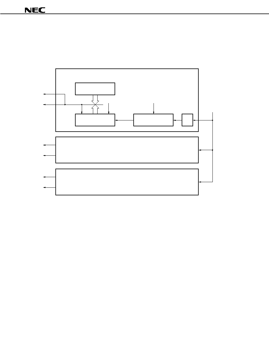
PD703100-33, 703100-40, 703101-33, 703102-33
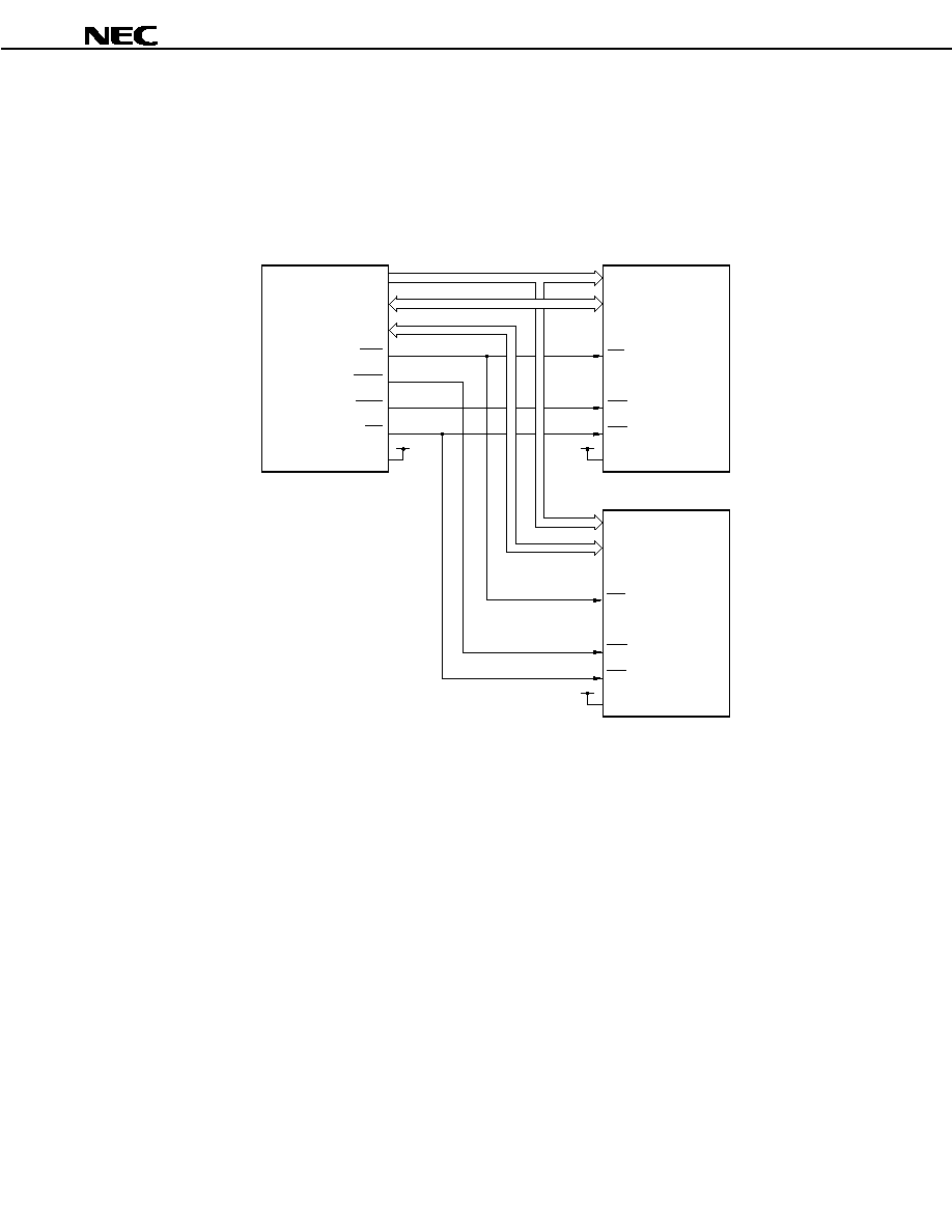
Figure 7-1. DMA Function Block Diagram
TCn
CPU
Internal RAM
Internal peripheral I/O
Internal peripheral I/O bus
Internal bus
Data control
Address control
DMAC
V850E/MS1
Bus interface
External bus
External ROM
External RAM
External I/O
DMA source address
register (DSAnH/DSAnL)
DMA byte count register
(DBCn)
DMA channel control
register (DCHCn)
DMA disable status
register (DDISn)
DMA restart register
(DRSTn)
DMA trigger source
register (DTFRn)
DMA addressing control
register (DADCn)
DMA destination address
register (DDAnH/DDAnL)
NMI
INTPmn
Request from on-chip
peripheral I/O
DMARQn
DMAAKn
Count control
Channel control
Remark m = 10 to 15, n=0 to 3

Preliminary Data Sheet U13995EJ1V0DS00
28
µ
µ
µ
µ
PD703100-33, 703100-40, 703101-33, 703102-33
8. INTERRUPT/EXCEPTION PROCESSING FUNCTIONS
8.1 Features
{
Interrupts
∑
Non-maskable interrupt: 1 source
∑
Maskable interrupt
: 47 sources
∑
8-level programmable priority control
∑
Multiple interrupt control based on priority levels
∑
Mask specification for each maskable interrupt request
∑
Noise elimination, edge detection, and valid edge specification for external interrupt requests
{
Exceptions
∑
Software exceptions: 32 sources
∑
Exception trap
: 1 source (invalid instruction code exception)
Preliminary Data Sheet U13995EJ1V0DS00
29
µ
µ
µ
µ
PD703100-33, 703100-40, 703101-33, 703102-33
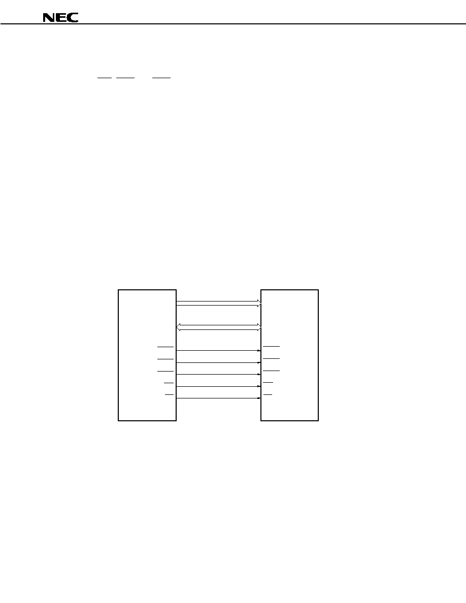
Figure 8-1. Interrupt Control Function Block Diagram
Internal bus
xxMKn (interrupt mask flag)
xxICn register
ISPR register
Handler
address
generator
CPU
PSW
ID
Interrupt request
Interrupt request
acknowledge
HALT mode
release signal
RPU
DMAC
A/D converter
SIO
CSI0
UART0
CSI1
UART1
CSI2
CSI3
INTM1
(edge detection)
INTM2
(edge detection)
Note
Note
Note
Note
Note
Note
INTM3
(edge detection)
INTM4
(edge detection)
INTM5
(edge detection)
INTM6
(edge detection)
INTP100
INTP101
INTP102
INTP103
INTP110
INTP111
INTP112
INTP113
INTP120
INTP121
INTP122
INTP123
INTP130
INTP131
INTP132
INTP133
INTP140
INTP141
INTP142
INTP143
INTP150
INTP151
INTP152
INTP153
3210
3210
Selector
32
10
3210
3210
Selector
32
10
3210
3210
Selector
32
10
3210
3210
Selector
32
10
3210
3210
Selector
32
10
3210
3210
Selector
xxPRn0 to xxPRn3 (interrupt priority order specification bit)
32
10
INTOV10
INTOV11
INTOV12
INTOV13
INTOV14
INTOV15
INTCM40
INTCM41
INTDMA0
INTDMA1
INTDMA2
INTDMA3
INTCSI0
INTSER0
INTSR0
INTST0
INTCSI1
INTSER1
INTSR1
INTST1
INTCSI2
INTCSI3
INTAD
INTP100/INTCC100
INTP101/INTCC101
INTP102/INTCC102
INTP103/INTCC103
INTP110/INTCC110
INTP111/INTCC111
INTP112/INTCC112
INTP113/INTCC113
INTP120/INTCC120
INTP121/INTCC121
INTP122/INTCC122
INTP123/INTCC123
INTP130/INTCC130
INTP131/INTCC131
INTP132/INTCC132
INTP133/INTCC133
INTP140/INTCC140
INTP141/INTCC141
INTP142/INTCC142
INTP143/INTCC143
INTP150/INTCC150
INTP151/INTCC151
INTP152/INTCC152
INTP153/INTCC153
OVIF10
OVIF11
OVIF12
OVIF13
OVIF14
OVIF15
P10IF0
P10IF1
P10IF2
P10IF3
P11IF0
P11IF1
P11IF2
P11IF3
P12IF0
P12IF1
P12IF2
P12IF3
P13IF0
P13IF1
P13IF2
P13IF3
P14IF0
P14IF1
P14IF2
P14IF3
P15IF0
P15IF1
P15IF2
P15IF3
CMIF40
CMIF41
DMAIF0
DMAIF1
DMAIF2
DMAIF3
CSIF0
SEIF0
SRIF0
STIF0
CSIF1
SEIF1
SRIF1
STIF1
CSIF2
CSIF3
ADIF
NMI
Note Noise elimination
Remark xx: OV, CM, P10 to P15, DMA, CS, SE, SR, ST, AD
n: None, or 10 to 15, 40, 41, 0 to 3
Preliminary Data Sheet U13995EJ1V0DS00
30
µ
µ
µ
µ
PD703100-33, 703100-40, 703101-33, 703102-33
Table 8-1. List of Interrupts (1/3)
Interrupt/Exception Source
Type
Category
Name
Control
Register
Generation Source
Generat-
ing Unit
Default
Priority
Excep-
tion
Code
Handler
Address
Restore
PC
Reset
Interrupt
RESSET
≠
RESET input
Pin
≠
0000H
00000000H
Unde-
fined
Non-
maskable
Interrupt
NMI
≠
NMI input
Pin
≠
0010H
00000010H
nextPC
Exception
TRAP0n
Note
≠
TRAP instruction
≠
≠
004n
Note
H
00000040H
nextPC
Software
exception
Exception
TRAP1n
Note
≠
TRAP instruction
≠
≠
005n
Note
H
00000050H
nextPC
Exception
trap
Exception
ILGOP
≠
Illegal instruction
code
≠
≠
0060H
00000060H
nextPC
Interrupt
INTOV10
OVIC10
Timer 10 overflow
RPU
0
0080H
00000080H
nextPC
Interrupt
INTOV11
OVIC11
Timer 11 overflow
RPU
1
0090H
00000090H
nextPC
Interrupt
INTOV12
OVIC12
Timer 12 overflow
RPU
2
00A0H
000000A0H
nextPC
Interrupt
INTOV13
OVIC13
Timer 13 overflow
RPU
3
00B0H
000000B0H
nextPC
Interrupt
INTOV14
OVIC14
Timer 14 overflow
RPU
4
00C0H
000000C0H
nextPC
Interrupt
INTOV15
OVIC15
Timer 15 overflow
RPU
5
00D0H
000000D0H
nextPC
Interrupt
INTP100/
INTCC100
P10IC0
Match between
INTP100 and CC100
Pin/RPU
6
0100H
00000100H
nextPC
Interrupt
INTP101/
INTCC101
P10IC1
Match between
INTP101 and CC101
Pin/RPU
7
0110H
00000110H
nextPC
Interrupt
INTP102/
INTCC102
P10IC2
Match between
INTP102 and CC102
Pin/RPU
8
0120H
00000120H
nextPC
Interrupt
INTP103/
INTCC103
P10IC3
Match between
INTP103 and CC103
Pin/RPU
9
0130H
00000130H
nextPC
Interrupt
INTP110/
INTCC110
P11IC0
Match between
INTP110 and CC110
Pin/RPU
10
0140H
00000140H
nextPC
Interrupt
INTP111/
INTCC111
P11IC1
Match between
INTP111 and CC111
Pin/RPU
11
0150H
00000150H
nextPC
Interrupt
INTP112/
INTCC112
P11IC2
Match between
INTP112 and CC112
Pin/RPU
12
0160H
00000160H
nextPC
Interrupt
INTP113/
INTCC113
P11IC3
Match between
INTP113 and CC113
Pin/RPU
13
0170H
00000170H
nextPC
Interrupt
INTP120/
INTCC120
P12IC0
Match between
INTP120 and CC120
Pin/RPU
14
0180H
00000180H
nextPC
Interrupt
INTP121/
INTCC121
P12IC1
Match between
INTP121 and CC121
Pin/RPU
15
0190H
00000190H
nextPC
Maskable
Interrupt
INTP122/
INTCC122
P12IC2
Match between
INTP122 and CC122
Pin/RPU
16
01A0H
000001A0H
nextPC
Note n = 0 to FH
Preliminary Data Sheet U13995EJ1V0DS00
31
µ
µ
µ
µ
PD703100-33, 703100-40, 703101-33, 703102-33
Table 8-1. List of Interrupts (2/3)
Interrupt/Exception Source
Type
Category
Name
Control
Register
Generation Source
Generat-
ing Unit
Default
Priority
Excep-
tion
Code
Handler
Address
Restore
PC
Interrupt
INTP123/
INTCC123
P12IC3
Match between
INTP123 and CC123
Pin/RPU
17
01B0H
000001B0H
nextPC
Interrupt
INTP130/
INTCC130
P13IC0
Match between
INTP130 and CC130
Pin/RPU
18
01C0H
000001C0H
nextPC
Interrupt
INTP131/
INTCC131
P13IC1
Match between
INTP131 and CC131
Pin/RPU
19
01D0H
000001D0H
nextPC
Interrupt
INTP132/
INTCC132
P13IC2
Match between
INTP132 and CC132
Pin/RPU
20
01E0H
000001E0H
nextPC
Interrupt
INTP133/
INTCC133
P13IC3
Match between
INTP133 and CC133
Pin/RPU
21
01F0H
000001F0H
nextPC
Interrupt
INTP140/
INTCC140
P14IC0
Match between
INTP140 and CC140
Pin/RPU
22
0200H
00000200H
nextPC
Interrupt
INTP141/
INTCC141
P14IC1
Match between
INTP141 and CC141
Pin/RPU
23
0210H
00000210H
nextPC
Interrupt
INTP142/
INTCC142
P14IC2
Match between
INTP142 and CC142
Pin/RPU
24
0220H
00000220H
nextPC
Interrupt
INTP143/
INTCC143
P14IC3
Match between
INTP143 and CC143
Pin/RPU
25
0230H
00000230H
nextPC
Interrupt
INTP150/
INTCC150
P15IC0
Match between
INTP150 and CC150
Pin/RPU
26
0240H
00000240H
nextPC
Interrupt
INTP151/
INTCC151
P15IC1
Match between
INTP151 and CC151
Pin/RPU
27
0250H
00000250H
nextPC
Interrupt
INTP152/
INTCC152
P15IC2
Match between
INTP152 and CC152
Pin/RPU
28
0260H
00000260H
nextPC
Interrupt
INTP153/
INTC153
P15IC3
Match between
INTP153 and CC153
Pin/RPU
29
0270H
00000270H
nextPC
Interrupt
INTCM40
CMIC40
CM40 match signal
RPU
30
0280H
00000280H
nextPC
Interrupt
INTCM41
CMIC41
CM41 match signal
RPU
31
0290H
00000290H
nextPC
Interrupt
INTDMA0
DMAIC0
DMA channel 0
transfer completion
DMAC
32
02A0H
000002A0H
nextPC
Interrupt
INTDMA1
DMAIC1
DMA channel 1
transfer completion
DMAC
33
02B0H
000002B0H
nextPC
Interrupt
INTDMA2
DMAIC2
DMA channel 2
transfer completion
DMAC
34
02C0H
000002C0H
nextPC
Interrupt
INTDMA3
DMAIC3
DMA channel 3
transfer completion
DMAC
35
02D0H
000002D0H
nextPC
Interrupt
INTCSI0
CSIC0
CSI0 send/receive
completion
SIO
36
0300H
000000300H
nextPC
Maskable
Interrupt
INTSER0
SEIC0
UART0 receive error
SIO
37
0310H
000000310H
nextPC
Note n = 0 to FH
Preliminary Data Sheet U13995EJ1V0DS00
32
µ
µ
µ
µ
PD703100-33, 703100-40, 703101-33, 703102-33
Table 8-1. List of Interrupts (3/3)
Interrupt/Exception Source
Type
Category
Name
Control
Register
Generation Source
Generat-
ing Unit
Default
Priority
Excep-
tion
Code
Handler
Address
Restore
PC
Interrupt
INTSR0
SRIC0
UART0 receive
completion
SIO
38
0320H
00000320H
nextPC
Interrupt
INTST0
STIC0
UART0 send
completion
SIO
39
0330H
00000330H
nextPC
Interrupt
INTCSI1
CSIC1
CSI1 send/receive
completion
SIO
40
0340H
00000340H
nextPC
Interrupt
INTSER1
SEIC1
UART1 receive error
SIO
41
0350H
00000350H
nextPC
Interrupt
INTSR1
SRIC1
UART1 receive
completion
SIO
42
0360H
00000360H
nextPC
Interrupt
INTST1
STIC1
UART1 send
completion
SIO
43
0370H
00000370H
nextPC
Interrupt
INTCSI2
CSIC2
CSI2 send/receive
completion
SIO
44
0380H
00000380H
nextPC
Interrupt
INTCSI3
CSIC3
CSI3 send/receive
completion
SIO
45
03C0H
000003C0H
nextPC
Maskable
Interrupt
INTAD
ADIC
A/D conversion
completion
ADC
46
0400H
00000400H
nextPC
Remarks 1. Default priority: Priority that takes precedence when two or more maskable interrupt requests having
the same priority level are generated at the same time. The highest priority is 0.
Restore PC: The PC value that is saved in EIPC or FEPC when the interrupt or exception
processing is started. However, the restore PC value that is saved when an interrupt is
acknowledged during the execution of a division instruction (DIV, DIVH, DIVU, or
DIVHU), is the PC value of the current instruction (DIV, DIVH, DIVU, or DIVHU).
2. The execution address of the illegal instruction when an illegal opcode exception occurs is obtained
according to the calculation "restore PC - 4."

Preliminary Data Sheet U13995EJ1V0DS00
33
µ
µ
µ
µ
PD703100-33, 703100-40, 703101-33, 703102-33
9. CLOCK GENERATION FUNCTIONS
{
Multiplier function using a PLL (Phase locked loop) synthesizer
{
Clock sources
∑
Oscillation by connecting an oscillator: f
XX
=
/5
∑
External clock: f
XX
= 2
◊
or
/5
{
Power saving modes
∑
HALT mode
∑
IDLE mode
∑
Software STOP mode
∑
Clock output inhibit mode
{
Internal system clock output function
Figure 9-1. Block Diagram of Clock Generation Function
X1
(f
XX
)
X2
CKSEL
Clock generator
(CG)
CPU, on-chip peripheral I/O
Time base counter (TBC)
CLKOUT
Remark
: internal system clock frequency
F
XX
: external oscillator or external clock frequency

Preliminary Data Sheet U13995EJ1V0DS00
34
µ
µ
µ
µ
PD703100-33, 703100-40, 703101-33, 703102-33
10. TIMER/COUNTER FUNCTIONS (REAL-TIME PULSE UNIT)
{
Measures the pulse interval and frequency, and outputs a programmable pulse
∑
16-bit measurements are possible
∑
Can generate a variety of pulse patterns (interval pulse, one-shot pulse)
{
Timer 1
∑
16-bit timer/event counter
∑
Count clock sources: 2 types (division of internal system clock, and external pulse input)
∑
Capture/compare common registers: 24
∑
Count clear pins: TCLR10 to TCLR15
∑
Interrupt sources: 30 types
∑
External pulse outputs: 12
{
Timer 4
∑
16-bit interval timer
∑
Count clock can select division for internal system clock
∑
Compare registers: 2
∑
Interrupt sources: 2

Preliminary Data Sheet U13995EJ1V0DS00
35
µ
µ
µ
µ
PD703100-33, 703100-40, 703101-33, 703102-33
Figure 10-1. Block Diagram of Timer 1 (16-bit Timer/Event Counter)
INTOV11
TO110
TO111
INTP110/INTCC110
INTP111/INTCC111
INTP112/INTCC112
INTP113/INTCC113
TO101
TO100
INTOV10
Internal system
clock ( )
INTP100/INTCC100
INTP101/INTCC101
INTP102/INTCC102
INTP103/INTCC103
INTOV15
TO150
TO151
INTP150/INTCC150
INTP151/INTCC151
INTP152/INTCC152
INTP153/INTCC153
TCLR10
TI10
INTP100
INTP101
INTP102
INTP103
TCLR11
TI11
INTP110
INTP111
INTP112
INTP113
TM11
Selector
Selector
Selector
Selector
S
Q
Q
R
Note 3
IMS100 IMS101 IMS102 IMS103
TM15
∑∑∑
TCLR15
TI15
INTP150
INTP151
INTP152
INTP153
Selector
Selector
Selector
Selector
Selector
S
CC100
TM10 (16 bits)
TM10
ETI10
1/4
1/2
1/8
1/16
Note 2
Note 1
PRS100,
PRS101
PRM
101
Edge detection
Edge detection
Clear and
count control
CC101
CC102
CC103
Q
ALV101
OVF10
Clear and
start
ALV100
Q
R
Note 3
1/4
Noise
elimination
Edge
detection
(INTM1)
m
Notes 1. Internal count clock
2. External count clock
3. Reset priority
Preliminary Data Sheet U13995EJ1V0DS00
36
µ
µ
µ
µ
PD703100-33, 703100-40, 703101-33, 703102-33
Figure 10-2. Block Diagram of Timer 4 (16-bit Interval Timer)
1/2
1/16
Internal count
clock
1/32
PRM400, PRM401
PRS400
TM40 (16 bits)
CM40
TM41
TM40
Clear and
start
INTCM40
INTCM41
m
1/4
1/8
Selector
Selector
Internal system
clock
( )

Preliminary Data Sheet U13995EJ1V0DS00
37
µ
µ
µ
µ
PD703100-33, 703100-40, 703101-33, 703102-33
11. SERIAL INTERFACE FUNCTION
The serial interface function provides two 6-channel serial interfaces.
Up to four channels can be used at the same time.
(1) Asynchronous serial interface (UART0 and UART1): 2 channels
(2) Clocked serial interface (CSI0 to CSI3): 4 channels
Caution UART0 and CSI0 share a pin, as do UART1 and CSI1. One or the other of each pair can be
selected via a register (ASIM00, ASIM10).
11.1 Asynchronous Serial Interfaces 0, 1 (UART0, UART1)
{
Transfer rate
150 bps to 76800 bps (using the dedicated baud rate generator when the internal system clock is
33 MHz)
Maximum 4.125 Mbps (using the
/2 clock when the internal system clock is 33 MHz)
{
Full duplex communications
On-chip receive buffer (RXBn)
{
2-pin configuration
TXDn : Transmit data output pin
RXDn: Receive data input pin
{
Receive error detection functions
∑
Parity error
∑
Framing error
∑
Overrun error
{
Interrupt sources: 3 types
∑
Receive error interrupt (INTSERn)
∑
Receive completion interrupt (INTSRn)
∑
Transmission completion interrupt (INTSTn)
{
The character length of transmission/reception data is specified by the ASIMn0 and ASIMn1 registers.
{
Character length
7, 8 bits
9 bits (when adding an expansion bit)
{
Parity function: odd, even, 0, none
{
Transmission stop bit: 1, 2 bits
{
On-chip dedicated baud rate generator
{
Serial clock (SCKn) output function
Remark n = 0, 1
Preliminary Data Sheet U13995EJ1V0DS00
38
µ
µ
µ
µ
PD703100-33, 703100-40, 703101-33, 703102-33
Figure 11-1. Block Diagram of Asynchronous Serial Interfaces 0, 1 (UART0, UART1)
UART1
UART0
RXD1
RXD0
RXE0
TXD1
TXD0
SCK1
SCK0
1/16
TXS0/TXS0L
RXB0/RXB0L
Transmit shift
register
Receive shift
register
Receive buffer
Receive
control
parity check
Transmit
control
parity addition
1/16
BRG0
BRG1
1/2
SCLS01, SCLS00
INTST0
INTSER0
INTSR0
INTST1
INTSER1
INTSR1
Selector
Internal system
clock ( )
11.2 Clocked Serial Interfaces 0 to 3 (CSI0 to CSI3)
{
High-speed transfer
Maximum 10 Mbps (when the internal system clock is operating at 40 MHz) ...
µ
PD703100-40
Maximum 8.25 Mbps (when the internal system clock is operating at 33 MHz) ...
µ
PD703100-33,
µ
PD703101-33,
µ
PD703102-33
{
Half-duplex communications
{
Character length: 8 bits
{
Can switch between MSB first or LSB first for data
{
Either external serial clock input or internal serial clock output can be selected
{
3-wire type
SOn:
Serial data output
SIn:
Serial data input
SCKn: Serial clock input/output
{
Interrupt source: 1 type
∑
Transmission/reception completion interrupt (INTCSIn)
Remark n = 0 to 3
Preliminary Data Sheet U13995EJ1V0DS00
39
µ
µ
µ
µ
PD703100-33, 703100-40, 703101-33, 703102-33
Figure 11-2. Block Diagram of Clocked Serial Interfaces 0 to 3 (CSI0 to CSI3)
SO0
CTXE0
CRXE0
CSI0
CLS00, CLS01
SO latch
1/2
1/4
BRG0
INTCSI0
1/2
1/4
BRG1
INTCSI1
D
Q
Serial I/O shift register
(SIO0)
Serial clock control
circuit
Serial clock counter
Interrupt
control circuit
SI0
SCK0
Selector
SO1
SI1
SCK1
1/2
1/4
INTCSI2
SO2
SI2
SCK2
1/2
1/4
INTCSI3
SO3
SI3
SCK3
CSI1
CSI2
CSI3
BRG2
Internal system
clock ( )
Preliminary Data Sheet U13995EJ1V0DS00
40
µ
µ
µ
µ
PD703100-33, 703100-40, 703101-33, 703102-33
11.3 Dedicated Baud Rate Generators 0 to 2 (BRG0 to BRG2)
{
Serial clock can be selected via either dedicated baud rate generator output or internal system clock (
)
{
Identical baud rates during transmission and reception
Figure 11-3. Block Diagram of Dedicated Baud Rate Generators 0 to 2 (BRG0 to BRG2)
CSI0
UART0
CSI1
UART1
Clear
Match
BRCE0
BRGC0
TMBRG0
Prescaler
1/2
BPR00 to BPR02
BRG0
BRG1
CSI2
CSI3
BRG2
Internal system
clock ( )
Preliminary Data Sheet U13995EJ1V0DS00
41
µ
µ
µ
µ
PD703100-33, 703100-40, 703101-33, 703102-33
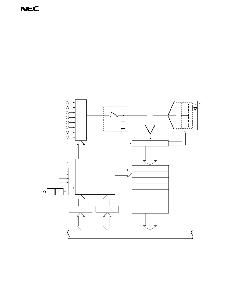
12. A/D CONVERTER
{
Analog input: 8 channels
{
On-chip 10-bit A/D converter
{
On-chip A/D conversion result registers (ADCR0 to ADCR7)
10 bits
◊
8
{
A/D conversion trigger modes
A/D trigger mode
Timer trigger mode
External trigger mode
{
Successive approximation method
Figure 12-1. A/D Converter Block Diagram
ANI0
ANI1
ANI2
ANI3
ANI4
ANI5
ANI6
ANI7
INTCC110
INTCC111
INTCC112
INTCC113
INTAD
Input circuit
ADM0 (8)
8
Voltage comparator
SAR (10)
ADCR0
ADCR1
ADCR2
ADCR3
ADCR4
ADCR5
ADCR6
ADCR7
10
10
10
9
0
9
0
Internal bus
Tap selector
AV
REF
R/2
R
R/2
AV
DD
Series resistor string
7
0
ADM1 (8)
7
0
AV
SS
8
Edge
detection
Noise
elimination
ADTRG
Controller
Sample & hold circuit

Preliminary Data Sheet U13995EJ1V0DS00
42
µ
µ
µ
µ
PD703100-33, 703100-40, 703101-33, 703102-33
13. PORT FUNCTIONS
{
Number of ports
Dedicated input ports: 9
Input/output ports
: 114
{
Shares pins with other peripheral function I/O
{
Input and output can be specified in 1-bit units
The block diagrams of the various ports are divided into 16 block types identified by A to P as shown in Table 13-
1. Figures 13-1 to 13-16 show the block diagrams of each type.
Table 13-1. List of Port Block Types
Port Name
Pin Name
Port Function
Function in Control Mode
Block Type
Port 0
P00 to P07
8-bit input/output
Input/output of real-time pulse unit (RPU), external
interrupt input, DMA controller (DMAC) input
A, B, M
Port 1
P10 to P17
8-bit input/output
Input/output of real-time pulse unit (RPU), external
interrupt input, DMA controller (DMAC) output
A, B, K
Port 2
P20 to P27
1-bit input,
7-bit input/output
NMI input, serial interface (UART0/CSI0, UART1/CSI1)
input/output
A, C, D, I, J
Port 3
P30 to P37
8-bit input/output
Input/output of real-time pulse unit (RPU), external
interrupt input, serial interface (CSI2) input/output
A, B, K, M,
N
Port 4
P40 to P47
8-bit input/output
External data bus (D0 to D7)
E
Port 5
P50 to P57
8-bit input/output
External data bus (D8 to D15)
E
Port 6
P60 to P67
8-bit input/output
External address bus (A16 to A23)
F
Port 7
P70 to P77
8-bit input/output
A/D converter (ADC) analog input
G
Port 8
P80 to P87
8-bit input/output
External bus interface control signal output
O, P
Port 9
P90 to P97
8-bit input/output
External bus interface control signal input/output
H, O
Port 10
P100 to
P107
8-bit input/output
Input/output of real-time pulse unit (RPU), external
interrupt input, DMA controller (DMAC) output
A, B, K
Port 11
P110 to
P117
8-bit input/output
Input/output of real-time pulse unit (RPU), external
interrupt input, serial interface (CSI3) input/output
A, B, K, M,
N
Port 12
P120 to
P127
8-bit input/output
Input/output of real-time pulse unit (RPU), external
interrupt input, A/D converter (ADC) external trigger input
A, B
Port A
PA0 to PA7
8-bit input/output
External address bus (A0 to A7)
F
Port B
PB0 to PB7
8-bit input/output
External address bus (A8 to A15)
F
Port X
PX5 to PX7
3-bit input/output
Refresh request signal output, wait insertion signal input,
internal system clock output
A, L
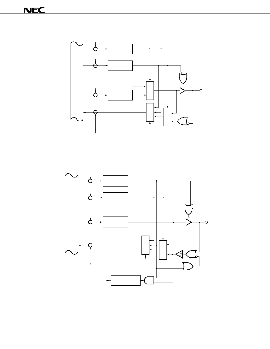
Preliminary Data Sheet U13995EJ1V0DS00
43
µ
µ
µ
µ
PD703100-33, 703100-40, 703101-33, 703102-33
Figure 13-1. Block Diagram of Type A
Internal bus
WR
PMC
WR
PM
WR
PORT
RD
IN
PMCmn
PMmn
Pmn
Output signal
in control mode
Selector
Selector
Selector
Pmn
Address
Remark m: port number
n : bit number
Figure 13-2. Block Diagram of Type B
Internal bus
WR
PMC
WR
PM
WR
PORT
RD
IN
PMCmn
PMmn
Pmn
Selector
Selector
Pmn
Address
Noise elimination
Edge detection
Input signal in
control mode
Remark m: port number
n : bit number
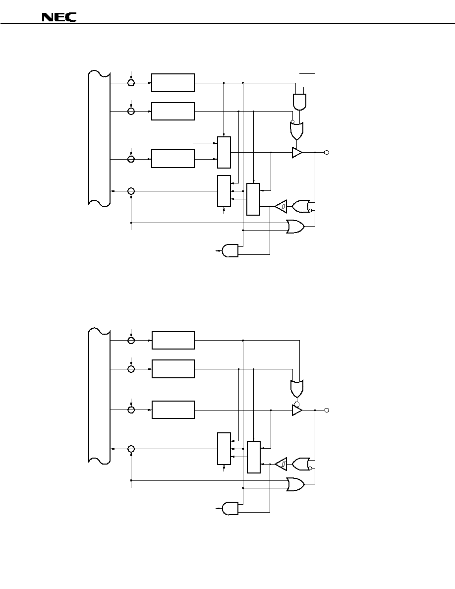
Preliminary Data Sheet U13995EJ1V0DS00
44
µ
µ
µ
µ
PD703100-33, 703100-40, 703101-33, 703102-33
Figure 13-3. Block Diagram of Type C
Internal bus
WR
PMC
WR
PM
WR
PORT
RD
IN
PMCmn
PMmn
Pmn
Selector
Selector
Selector
Pmn
Address
Input signal in
control mode
Output signal in
control mode
SCKx output
enable signal
Remark mn: 24, 27
x
: 0 (when mn = 24), 1 (when mn = 27)
Figure 13-4. Block Diagram of Type D
Internal bus
WR
PMC
WR
PM
WR
PORT
RD
IN
PMCmn
PMmn
Pmn
Selector
Selector
Pmn
Address
Input signal in
control mode
Remark m: port number
n : bit number
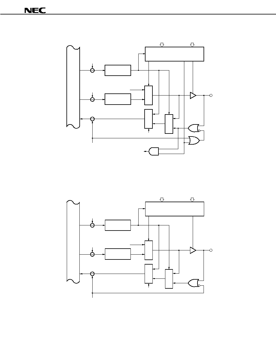
Preliminary Data Sheet U13995EJ1V0DS00
45
µ
µ
µ
µ
PD703100-33, 703100-40, 703101-33, 703102-33
Figure 13-5. Block Diagram of Type E
Internal bus
WR
PM
WR
PORT
RD
IN
PMmn
Pmn
Selector
Selector
Selector
Pmn
Address
Input signal in
control mode
Output signal in
control mode
MODE0 to MODE3
MM0 to MM3
I/O control circuit
Remark m: port number
n : bit number
Figure 13-6. Block Diagram of Type F
Internal bus
WR
PM
WR
PORT
RD
IN
PMmn
Pmn
Selector
Selector
Selector
Pmn
Address
Output signal in
control mode
MODE0 to MODE3
MM0 to MM3
I/O control circuit
Remark m: port number
n : bit number

Preliminary Data Sheet U13995EJ1V0DS00
46
µ
µ
µ
µ
PD703100-33, 703100-40, 703101-33, 703102-33
Figure 13-7. Block Diagram of Type G
Internal bus
RD
IN
P7n
Sample & hold circuit
ANIn
Input signal in
control mode
Remark n = 0 to 7
Figure 13-8. Block Diagram of Type H
Internal bus
WR
PM
WR
PORT
RD
IN
PMmn
Pmn
Selector
Selector
P97
Address
Input signal in
control mode
MODE0 to MODE3
MM0 to MM3
I/O control circuit

Preliminary Data Sheet U13995EJ1V0DS00
47
µ
µ
µ
µ
PD703100-33, 703100-40, 703101-33, 703102-33
Figure 13-9. Block Diagram of Type I
Internal bus
RD
IN
Selector
P20
Address
Noise elimination
Edge detection
1
NMI
Figure 13-10. Block Diagram of Type J
Internal bus
WR
PM
WR
PORT
RD
IN
PMmn
Pmn
Selector
Selector
Pmn
Address
Remark m: port number
n : bit number
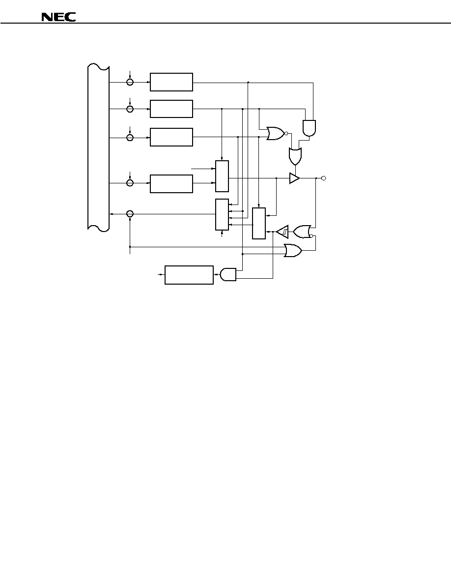
Preliminary Data Sheet U13995EJ1V0DS00
48
µ
µ
µ
µ
PD703100-33, 703100-40, 703101-33, 703102-33
Figure 13-11. Block Diagram of Type K
Internal bus
WR
PCS
WR
PMC
WR
PM
WR
PORT
RD
IN
PCSmn
PMCmn
PMmn
Pmn
Selector
Selector
Selector
Pmn
Address
Input signal in
control mode
Output signal in
control mode
Noise elimination
Edge detection
Remark m: port number
n : bit number
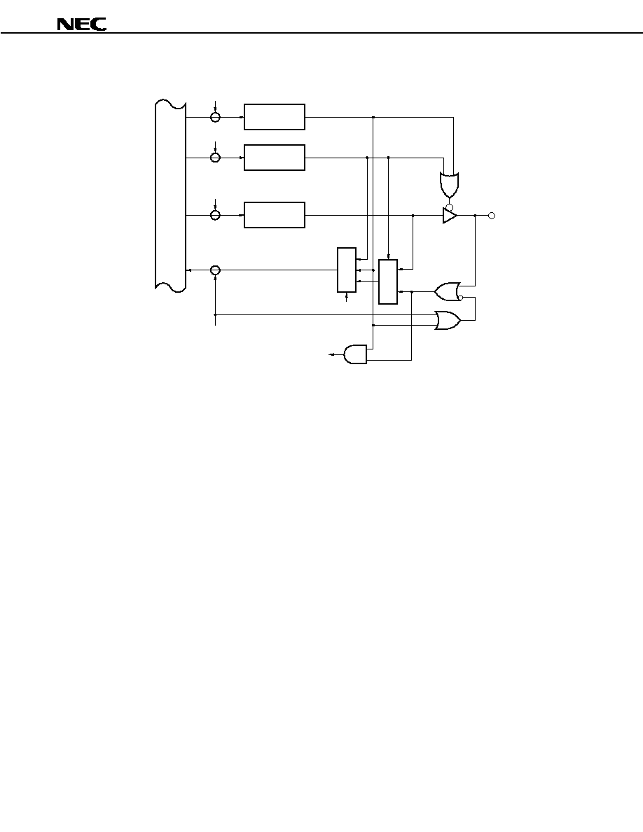
Preliminary Data Sheet U13995EJ1V0DS00
49
µ
µ
µ
µ
PD703100-33, 703100-40, 703101-33, 703102-33
Figure 13-12. Block Diagram of Type L
Internal bus
WR
PMC
WR
PM
WR
PORT
RD
IN
PMCmn
PMmn
Pmn
Selector
Selector
Pmn
Address
Input signal in
control mode
Remark m: port number
n : bit number
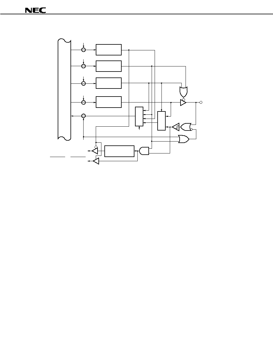
Preliminary Data Sheet U13995EJ1V0DS00
50
µ
µ
µ
µ
PD703100-33, 703100-40, 703101-33, 703102-33
Figure 13-13. Block Diagram of Type M
Internal bus
WR
PCS
WR
PMC
WR
PM
WR
PORT
RD
IN
PCSmn
Note
PMCmn
PMmn
Pmn
Selector
Selector
Pmn
Address
Noise elimination
Edge detection
INTP100 to INTP103,
INTP132, INTP142
DMARQ0 to DMARQ3,
SI2, SI3
Note When mn = 36:
PCS35
When mn = 116: PCS115
Remark mn: 04 to 07, 36, 116

Preliminary Data Sheet U13995EJ1V0DS00
51
µ
µ
µ
µ
PD703100-33, 703100-40, 703101-33, 703102-33
Figure 13-14. Block Diagram of Type N
Internal bus
WR
PCS
WR
PMC
WR
PM
WR
PORT
RD
IN
PCSm5
PMCmn
PMmn
Pmn
Selector
Selector
Selector
Pmn
Address
Output signal in
control mode
Noise elimination
Edge detection
INTP133, INTP143
SCK2, SCK3
SCKx output
enable signal
Remark mn: 37, 117
x: 2 (when mn = 37), 3 (when mn = 117)

Preliminary Data Sheet U13995EJ1V0DS00
52
µ
µ
µ
µ
PD703100-33, 703100-40, 703101-33, 703102-33
Figure 13-15. Block Diagram of Type O
Internal bus
WR
PM
WR
PORT
RD
IN
PMmn
WR
PMC
PMCmn
Pmn
Selector
Selector
Selector
Pmn
Address
Output signal in
control mode
MODE0 to MODE3
MM0 to MM3
I/O control circuit
Remark m: port number
n : bit number
Figure 13-16. Block Diagram of Type P
MODE0 to MODE3
MM0 to MM3
I/O control circuit
Internal bus
WR
PCS
WR
PMC
WR
PM
WR
PORT
RD
IN
PCSmn
PMCmn
PMmn
Pmn
Selector
Selector
Selector
Selector
Pmn
Address
Output signal in
control mode
Remark m: port number
n : bit number

Preliminary Data Sheet U13995EJ1V0DS00
53
µ
µ
µ
µ
PD703100-33, 703100-40, 703101-33, 703102-33
14. RESET FUNCTION
When low-level signal is input to the RESET pin, a system reset is performed and the various on-chip hardware
devices are initialized.
When the RESET input changes from low to high, the reset state is canceled and the CPU begins program
execution. (the contents of the various registers should be initialized within the program as necessary.)
An on-chip noise elimination circuit, which uses analog delay (
=
60 ns) to eliminate noise, is provided for the
RESET pin.
Preliminary Data Sheet U13995EJ1V0DS00
54
µ
µ
µ
µ
PD703100-33, 703100-40, 703101-33, 703102-33
15. INSTRUCTION SET
Table 15-1. Symbols Used to Describe Operands
Symbol
Description
reg1
General registers (r0 to r31): used as source registers
reg2
General registers (r0 to r31): used mainly as destination registers
reg3
General registers (r0 to r31): used mainly to store the remainders of division results and the higher 3 bits
of multiplication results
imm
◊
◊
-bit immediate
disp
◊
◊
-bit displacement
regID
System register number
bit#3
3-bit data for specifying the bit number
ep
Element pointer (r30)
cccc
4-bit data indicating the condition code
vector
5-bit data used for specifying the trap vector (00H to 1FH)
list
◊
List of
◊
registers
Table 15-2. Symbols Used to Describe Opcodes
Symbol
Description
R
1-bit data of code specifying reg1 or regID
r
1-bit data of code specifying reg2
w
1-bit data of code specifying reg3
d
1-bit displacement data
i
1-bit immediate data
cccc
4-bit data indicating condition code
bbb
3-bit data for specifying bit number
L
1-bit data specifying register list
Preliminary Data Sheet U13995EJ1V0DS00
55
µ
µ
µ
µ
PD703100-33, 703100-40, 703101-33, 703102-33
Table 15-3. Symbols Used in Operation
Symbol
Description
Input for
GR [ ]
General register
SR [ ]
System register
zero-extend (n)
Extend n with zeros until word length
sign-extend (n)
Extend n with signs until word length
load-memory (a, b)
Read data of size b from address a
store-memory (a, b, c)
Write data b of address a by size c
load-memory-bit (a, b)
Read bit b of address a
store-memory-bit (a, b, c)
Write c to bit b of address a
saturated (n)
Execute saturation processing of n (n is a two's complement)
If, as a result of the calculation,
n
7FFFFFFFH, let it be 7FFFFFFFH.
n
80000000H, let it be 80000000H
result
Reflect the result in a flag
Byte
Byte (8 bits)
Half-word
Half word (16 bits)
Word
Word (32 bits)
+
Add
-
Subtract
||
Bit concatenation
◊
Multiply
˜
Divide
%
Remainder of division result
AND
Logical AND
OR
Logical OR
XOR
Exclusive OR
NOT
Logical NOT
logically shift left by
Logical shift left
logically shift right by
Logical shift right
arithmetically shift right by
Arithmetic shift right
Table 15-4. Symbols Used for Execution Clock
Symbol
Description
i : issue
When executing another instruction immediately after executing an instruction
r : repeat
When repeating the same instruction immediately after executing the instruction
l : latency
When referring to instruction execution results in the next instruction

Preliminary Data Sheet U13995EJ1V0DS00
56
µ
µ
µ
µ
PD703100-33, 703100-40, 703101-33, 703102-33
Table 15-5. Symbols Used in Flag Operations
Identifier
Description
(Blank)
No change
0
Clear to 0
◊
Set or cleared according to the results
R
Previously saved values are restored
Table 15-6. Condition Codes
Condition
Name (cond)
Condition Code
(cccc)
Condition Formula
Description
V
0000
OV = 1
Overflow
NV
1000
OV = 0
No overflow
C/L
0001
CY = 1
Carry
Lower (Less than)
NC/NL
1001
CY = 0
No carry
Not lower (Greater than or equal)
Z/E
0010
Z = 1
Zero
Equal
NZ/NE
1010
Z = 0
Not zero
Not equal
NH
0011
(CY or Z) = 1
Not higher (Less than or equal)
H
1011
(CY or Z) = 0
Higher (Greater than)
N
0100
S = 1
Negative
P
1100
S = 0
Positive
T
0101
≠
Always (unconditional)
SA
1101
SAT = 1
Saturated
LT
0110
(S xor OV) = 1
Less than signed
GE
1110
(S xor OV) = 0
Greater than or equal signed
LE
0111
((S xor OV) or Z) = 1
Less than or equal signed
GT
1111
((S xor OV) or Z) = 0
Greater than signed

Preliminary Data Sheet U13995EJ1V0DS00
57
µ
µ
µ
µ
PD703100-33, 703100-40, 703101-33, 703102-33
Instruction Set
(1/7)
Execution
Clock
Flags
Mnemonic
Operand
Opcode
Operation
i
r
l
CY
OV
S
Z
SAT
reg1,reg2
r r r r r 0 0 1 1 1 0 R R R R R
GR[reg2]
GR[reg2]+GR[reg1]
1
1
1
◊
◊
◊
◊
ADD
imm5,reg2
r r r r r 0 1 0 0 1 0 i i i i i
GR[reg2]
GR[reg2]+sign-extend(imm5)
1
1
1
◊
◊
◊
◊
r r r r r 1 1 0 0 0 0 r r r r r
ADDI
imm16,reg1,reg2
i i i i i i i i i i i i i i i i
GR[reg2]
GR[reg1]+sign-extend(imm16)
1
1
1
◊
◊
◊
◊
AND
reg1,reg2
r r r r r 0 0 1 0 1 0 R R R R R
GR[reg2]
GR[reg2]AND GR[reg1]
1
1
1
0
◊
◊
r r r r r 1 1 0 1 1 0 R R R R R
ANDI
imm16,reg1,reg2
i i i i i i i i i i i i i i i i
GR[reg2]
GR[reg1]AND zero-
extend(imm16)
1
1
1
0
0
◊
d d d d d 1 0 1 1 d d d c c c c
When
conditions are
satisfied
2
Note 2
2
Note 2
2
Note 2
Bcond
disp9
Note 1
if conditions are satisfied
then PC
PC+sign-
extend(disp9)
When
conditions are
not satisfied
1
1
1
r r r r r 1 1 1 1 1 1 0 0 0 0 0
BSH
reg2,reg3
w w w w w 0 1 1 0 1 0 0 0 0 1 0
GR[reg3]
GR[reg2] (23 : 16) II GR[reg2]
(31 : 24) II GR[reg2] (7 : 0) II GR[reg2] (15 : 8)
1
1
1
◊
0
◊
◊
r r r r r 1 1 1 1 1 1 0 0 0 0 0
BSW
reg2,reg3
w w w w w 0 1 1 0 1 0 0 0 0 0 0
GR[reg3]
GR[reg2] (7 : 0) II GR[reg2] (15 : 8) II
GR[reg2] (23 : 16) II GR[reg2] (31 : 24)
1
1
1
◊
0
◊
◊
CALLT
imm6
0 0 0 0 0 0 1 0 0 0 i i i i i i
CTPC
PC+2(return PC)
CTPSW
PSW
adr
CTBP+zero-extend(imm6 logically
shift left by 1)
PC
CTBP+zero-extend(Load-
memory(adr, Half-word))
4
4
4
1 0 b b b 1 1 1 1 1 0 R R R R R
bit#3,
disp 16[reg1]
d d d d d d d d d d d d d d d d
adr
GR[reg1]+sign-extend(disp16)
Z flags
Not(Load-memory-bit(adr,bit#3))
Store-memory-bit (adr,bit#3,0)
3
Note 3
3
Note 3
3
Note 3
◊
r r r r r 1 1 1 1 1 1 R R R R R
CLR1
reg2,[reg1]
0 0 0 0 0 0 0 0 1 1 1 0 0 1 0 0
adr
GR[reg1]
Z flags
Not(Load-memory-bit(adr,reg2))
Store-memory-bit (adr,reg2,0)
3
Note 3
3
Note 3
3
Note 3
◊
r r r r r 1 1 1 1 1 1 i i i i i
cccc,imm5,reg2,
reg3
w w w w w 0 1 1 0 0 0 c c c c 0
if condition are satisfied then
GR[reg3]
sign-extended(imm5)
else GR[reg3]
GR[reg2]
1
1
1
r r r r r 1 1 1 1 1 1 R R R R R
CMOV
cccc,reg1,reg2,
reg3
w w w w w 0 1 1 0 0 1 c c c c 0
if conditions are satisfied
then GR[reg3]
GR[reg1]
else GR[reg3]
GR[reg2]
1
1
1
reg1,reg2
r r r r r 0 0 1 1 1 1 R R R R R
result
GR[reg2]
-
GR[reg1]
1
1
1
◊
◊
◊
◊
CMP
imm5,reg2
r r r r r 0 1 0 0 1 1 i i i i i
result
GR[reg2]
-
sign-extend(imm5)
1
1
1
◊
◊
◊
◊
0 0 0 0 0 1 1 1 1 1 1 0 0 0 0 0
CTRET
0 0 0 0 0 0 0 1 0 1 0 0 0 1 0 0
PC
CTPC
PSW
CTPSW
3
3
3
R
R
R
R
R
0 0 0 0 0 1 1 1 1 1 1 0 0 0 0 0
DI
0 0 0 0 0 0 0 1 0 1 1 0 0 0 0 0
PSW.ID
1
1
1
1

Preliminary Data Sheet U13995EJ1V0DS00
58
µ
µ
µ
µ
PD703100-33, 703100-40, 703101-33, 703102-33
(2/7)
Execution
Clock
Flags
Mnemonic
Operand
Opcode
Operation
i
r
l
CY
OV
S
Z
SAT
0 0 0 0 0 1 1 0 0 1 i i i i i L
imm5,list12
L L L L L L L L L L L 0 0 0 0 0
sp
sp+zero-extend(imm5 logically shift left
by 2)
GR[reg in list12]
Load-memory(sp,Word)
sp
sp+4
repeat 2 steps above untill all regs in list12
is loaded
N+1
Note 4
N+1
Note 4
N+1
Note 4
0 0 0 0 0 1 1 0 0 1 i i i i i L
L L L L L L L L L L L R R R R R
Note 5
DISPOSE
imm5,list12,[reg1]
sp
sp+zero-extend(imm5 logically shif left
by 2)
GR[reg in list12]
Load-memory(sp,Word)
sp
sp+4
repeat 2 steps above until all regs in list 12
is loaded
PC
GR[reg1]
N+3
Note 4
N+3
Note 4
N+3
Note 4
r r r r r 1 1 1 1 1 1 R R R R R
DIV
reg1,reg2,reg3
w w w w w 0 1 0 1 1 0 0 0 0 0 0
GR[reg2]
GR[reg2]
˜
GR[reg1]
GR[reg3]
GR[reg2]%GR[reg1]
35
35
35
reg1,reg2
r r r r r 0 0 0 0 1 0 R R R R R
GR[reg2]
GR[reg2]
˜
GR[reg1]
Note 6
35
35
35
◊
◊
◊
r r r r r 1 1 1 1 1 1 R R R R R
DIVH
reg1,reg2,reg3
w w w w w 0 1 0 1 0 0 0 0 0 0 0
GR[reg2]
GR[reg2]
˜
GR[reg1]
Note 6
GR[reg3]
GR[reg2]%GR[reg1]
35
35
35
◊
◊
◊
r r r r r 1 1 1 1 1 1 R R R R R
DIVHU
reg1,reg2,reg3
w w w w w 0 1 0 1 0 0 0 0 0 1 0
GR[reg2]
GR[reg2]
˜
GR[reg1]
Note 6
GR[reg3]
GR[reg2]%GR[reg1]
34
34
34
◊
◊
◊
r r r r r 1 1 1 1 1 1 R R R R R
DIVU
reg1,reg2,reg3
w w w w w 0 1 0 1 1 0 0 0 0 1 0
GR[reg2]
GR[reg2]
˜
GR[reg1]
GR[reg3]
GR[reg2]%GR[reg1]
34
34
34
◊
◊
◊
1 0 0 0 0 1 1 1 1 1 1 0 0 0 0 0
EI
0 0 0 0 0 0 0 1 0 1 1 0 0 0 0 0
PSW.ID
0
1
1
1
0 0 0 0 0 1 1 1 1 1 1 0 0 0 0 0
HALT
0 0 0 0 0 0 0 1 0 0 1 0 0 0 0 0
Stop
1
1
1
r r r r r 1 1 1 1 1 1 0 0 0 0 0
HSW
reg2,reg3
w w w w w 0 1 1 0 1 0 0 0 1 0 0
GR[reg3]
GR[reg2] (15 : 0) II GR[reg2]
(31: 6)
1
1
1
◊
0
◊
◊
r r r r r 1 1 1 1 0 d d d d d d
d d d d d d d d d d d d d d d 0
JARL
disp22,reg2
Note 7
GR[reg2]
PC+4
PC
PC+sign≠extend(disp22)
2
2
2
JMP
[reg1]
0 0 0 0 0 0 0 0 0 1 1 R R R R R
PC
GR[reg1]
3
3
3
0 0 0 0 0 1 1 1 1 0 d d d d d d
d d d d d d d d d d d d d d d 0
JR
disp22
Note 7
PC
PC+sign-extend(disp22)
2
2
2
r r r r r 1 1 1 0 0 0 R R R R R
LD.B
disp16[reg1],reg2
d d d d d d d d d d d d d d d d
adr
GR[reg1]+signe-extend(disp16)
GR[reg2]
sign-extend(Load-memory
(adr,Byte))
1
1
n
Note 9
Preliminary Data Sheet U13995EJ1V0DS00
59
µ
µ
µ
µ
PD703100-33, 703100-40, 703101-33, 703102-33
(3/7)
Execution
Clock
Flags
Mnemonic
Operand
Opcode
Operation
i
r
l
CY
OV
S
Z
SAT
r r r r r 1 1 1 1 0 b R R R R R
d d d d d d d d d d d d d d d 1
LD.BU
disp16[reg1],reg2
Notes 8, 10
adr
GR[reg1]+sign-extend(disp16)
GR[reg2]
zero-extend(Load-memory
(adr,Byte))
1
1
n
Note 11
r r r r r 1 1 1 0 0 1 R R R R R
d d d d d d d d d d d d d d d 0
LD.H
disp16[reg1],reg2
Note 8
adr
GR[reg1]+sign-extend(disp16)
GR[reg2]
sign-extend(Load-memory
(adr,Half-word))
1
1
n
Note 9
r r r r r 1 1 1 1 1 1 R R R R R
d d d d d d d d d d d d d d d 1
LD.HU
disp16[reg1],reg2
Note 8
adr
GR[reg1]+sign-extend(disp16)
GR[reg2]
zero-extend(Load-memory
(adr,Half-word))
1
1
n
Note 11
r r r r r 1 1 1 0 0 1 R R R R R
LD.W
disp16[reg1],reg2
d d d d d d d d d d d d d d d 1
adr
GR[reg1]+signe-extend(disp16)
GR[reg2]
Load-memory(adr,Word)
1
1
n
Note 9
r r r r r 1 1 1 1 1 1 R R R R R
0 0 0 0 0 0 0 0 0 0 1 0 0 0 0 0
Other than
regID=PSW
LDSR
reg2,regID
Note 12
SR[regID]
GR[reg2]
regID=PSW
1
1
1
◊
◊
◊
◊
◊
reg1,reg2
r r r r r 0 0 0 0 0 0 R R R R R
GR[reg2]
GR[reg1]
1
1
1
imm5,reg2
r r r r r 0 1 0 0 0 0 i i i i i
GR[reg2]
sign-extend(imm5)
1
1
1
0 0 0 0 0 1 1 0 0 0 1 R R R R R
i i i i i i i i i i i i i i i i
MOV
imm32,reg1
i i i i i i i i i i i i i i i i
GR[reg1]
imm32
2
2
2
r r r r r 1 1 0 0 0 1 R R R R R
MOVEA
imm16,reg1,reg2
i i i i i i i i i i i i i i i i
GR[reg2]
GR[reg1]+ sign-extend(imm16)
1
1
1
r r r r r 1 1 0 0 1 0 R R R R R
MOVHI
imm16,reg1,reg2
i i i i i i i i i i i i i i i i
GR[reg2]
GR[reg1]+(imm16 II 0
16
)
1
1
1
r r r r r 1 1 1 1 1 1 R R R R R
reg1,reg2,reg3
w w w w w 0 1 0 0 0 1 0 0 0 0 0
GR[reg3] II GR[reg2]
GR[reg2]
◊
GR[reg1]
1
2
Note 14
2
r r r r r 1 1 1 1 1 1 i i i i i
MUL
imm9,reg2,reg3
w w w w w 0 1 0 0 1 1 1 1 1 0 0
GR[reg3] II GR[reg2]
GR[reg2]
◊
sign-
extend(imm9)
Note 13
1
2
Note 14
2
reg1,reg2
r r r r r 0 0 0 1 1 1 R R R R R
GR[reg2]
GR[reg2]
Note 6
◊
GR[reg1]
Note 6
1
1
2
MULH
imm5,reg2
r r r r r 0 1 0 1 1 1 i i i i i
GR[reg2]
GR[reg2]
Note 6
◊
sign-extend (imm5)
1
1
2
r r r r r 1 1 0 1 1 R R R R R R
MULHI
imm16,reg1,reg2
i i i i i i i i i i i i i i i i
GR[reg2]
GR[reg1]
Note 6
◊
imm16
1
1
2
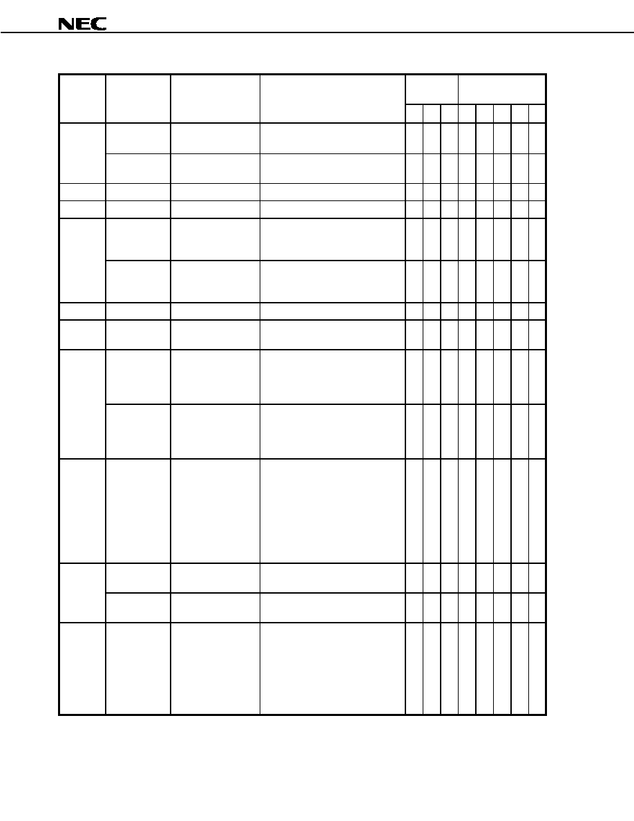
Preliminary Data Sheet U13995EJ1V0DS00
60
µ
µ
µ
µ
PD703100-33, 703100-40, 703101-33, 703102-33
(4/7)
Execution
Clock
Flags
Mnemonic
Operand
Opcode
Operation
i
r
l
CY
OV
S
Z
SAT
r r r r r 1 1 1 1 1 1 R R R R R
reg1,reg2,reg3
w w w w w 0 1 0 0 0 1 0 0 0 1 0
GR[reg3] II GR[reg2]
GR[reg2]
◊
GR[reg1]
1
2
Note 14
2
r r r r r 1 1 1 1 1 1 i i i i i
MULU
imm9,reg2,reg3
w w w w w 0 1 0 0 1 1 1 1 1 1 0
GR[reg3] II GR[reg2]
GR[reg2]
◊
zero-
extend(imm9)
1
2
Note 14
2
NOP
0 0 0 0 0 0 0 0 0 0 0 0 0 0 0 0
Pass at least one clock cycle doing nothing
1
1
1
NOT
reg1,reg2
r r r r r 0 0 0 0 0 1 R R R R R
GR[reg2]
NOT(GR[reg1])
1
1
1
0
◊
◊
0 1 b b b 1 1 1 1 1 0 R R R R R
bit#3,disp16[reg1]
d d d d d d d d d d d d d d d d
adr
GR[reg1]+sign-extend(disp16)
Z flag
Not(Load-memory-bit(adr,bit#3))
Store-memory-bit(adr,bit#3,Z flag)
3
Note 3
3
Note 3
3
Note 3
◊
r r r r r 1 1 1 1 1 1 R R R R R
NOT1
reg2,[reg1]
0 0 0 0 0 0 0 0 1 1 1 0 0 0 1 0
adr
GR[reg1]
Z flag
Not(Load-memory-bit(adr,reg2))
Store-memory-bit(adr,reg2,Z flag)
3
Note 3
3
Note 3
3
Note 3
◊
OR
reg1,reg2
r r r r r 0 0 1 0 0 0 R R R R R
GR[reg2]
GR[reg2] OR GR[reg1]
1
1
1
0
◊
◊
r r r r r 1 1 0 1 0 0 R R R R R
ORI
imm16,reg1,reg2
i i i i i i i i i i i i i i i i
GR[reg2]
GR[reg1] OR zero-
extend(imm16)
1
1
1
0
◊
◊
0 0 0 0 0 1 1 1 1 0 i i i i i L
list12,imm5
L L L L L L L L L L L 0 0 0 0 1
Store-memory(sp-4,GR[reg in list12],Word)
sp
sp-4
repeat 1 step above until all regs in list12 is
stored sp
sp-zero-extend(imm5)
N+1
Note 4
N+1
Note 4
N+1
Note 4
0 0 0 0 0 1 1 1 1 0 i i i i i L
L L L L L L L L L L L f f 0 1 1
PREPARE
list12,imm5,
sp/imm
Note 15
imm16/imm32
Note 16
Store-memory(sp-4,GR[reg in list12],Word)
sp
sp-4
repeat 1 step above until all regs in list12 is
stored sp
sp-zero-extend(imm5)
N+2
Note 4
Note 17
N+2
Note 4
Note 17
N+2
Note 4
Note 17
0 0 0 0 0 1 1 1 1 1 1 0 0 0 0 0
RETI
0 0 0 0 0 0 0 1 0 1 0 0 0 0 0 0
if PSW.EP=1
then PC
EIPC
PSW
EIPSW
else if PSW.NP = 1
then PC
FEPC
PSW
FEPSW
else
PC
EIPC
PSW
EIPSW
3
3
3
R
R
R
R
R
r r r r r 1 1 1 1 1 1 R R R R R
reg1,reg2
0 0 0 0 0 0 0 0 1 0 1 0 0 0 0 0
GR[reg2]
GR[reg2]arithmetically shift right
by GR[reg1]
1
1
1
◊
0
◊
◊
SAR
imm5,reg2
r r r r r 0 1 0 1 0 1 i i i i i
GR[reg2]
GR[reg2]arithmetically shift right
by zero-extend(imm5)
1
1
1
◊
0
◊
◊
r r r r r 1 1 1 1 1 0 c c c c c
SASF
cccc,reg2
0 0 0 0 0 0 1 0 0 0 0 0 0 0 0 0
if conditions are satisfied
then GR[reg2]
(GR[reg2] Logically shift
left by 1)
OR 00000001H
else GR[reg2]
(GR[reg2] Logically shift
left by 1)
OR 00000000H
1
1
1

Preliminary Data Sheet U13995EJ1V0DS00
61
µ
µ
µ
µ
PD703100-33, 703100-40, 703101-33, 703102-33
(5/7)
Execution
Clock
Flags
Mnemonic
Operand
Opcode
Operation
i
r
l
CY
OV
S
Z
SAT
SATADD
reg1,reg2
r r r r r 0 0 0 1 1 0 R R R R R
GR[reg2]
saturated(GR[reg2]+GR[reg1])
1
1
1
◊
◊
◊
◊
◊
imm5,reg2
r r r r r 0 1 0 0 0 1 i i i i i
GR[reg2]
saturated(GR[reg2]+sign-
extend(imm5)
1
1
1
◊
◊
◊
◊
◊
SATSUB
reg1,reg2
r r r r r 0 0 0 1 0 1 R R R R R
GR[reg2]
saturated(GR[reg2]
-
GR[reg1])
1
1
1
◊
◊
◊
◊
◊
r r r r r 1 1 0 0 1 1 R R R R R
SATSUBI
imm16,reg1,reg2
i i i i i i i i i i i i i i i i
GR[reg2]
saturated(GR[reg1]
-
sign-
extend(imm16)
1
1
1
◊
◊
◊
◊
◊
SATSUBR
reg1,reg2
r r r r r 0 0 0 1 0 0 R R R R R
GR[reg2]
saturated(GR[reg1]
-
GR[reg2])
1
1
1
◊
◊
◊
◊
◊
r r r r r 1 1 1 1 1 1 0 c c c c
SETF
cccc,reg2
0 0 0 0 0 0 0 0 0 0 0 0 0 0 0 0
If conditions are satisfied
then GR[reg2]
00000001H
else GR[reg2]
00000000H
1
1
1
0 0 b b b 1 1 1 1 1 0 R R R R R
bit#3,disp16[reg1]
d d d d d d d d d d d d d d d d
adr
GR[reg1]+sign-extend(disp16)
Z flag
Not(Load-memory-bit(adr,bit#3))
Store-memory-bit(adr,bit#3,1)
3
Note 3
3
Note 3
3
Note 3
◊
r r r r r 1 1 1 1 1 1 R R R R R
SET1
reg2,[reg1]
0 0 0 0 0 0 0 0 1 1 1 0 0 0 0 0
adr
GR[reg1]
Z flag
Not(Load-memory-bit(adr,reg2))
Store-memory-bit(adr,reg2,1)
3
Note 3
3
Note 3
3
Note 3
◊
r r r r r 1 1 1 1 1 1 R R R R R
SHL
reg1,reg2
0 0 0 0 0 0 0 0 1 1 0 0 0 0 0 0
GR[reg2]
GR[reg2] logically shift left by
GR[reg1]
1
1
1
◊
0
◊
◊
imm5,reg2
r r r r r 0 1 0 1 1 0 i i i i i
GR[reg2]
GR[reg2] logically shift left by
zero-extend(imm5)
1
1
1
◊
0
◊
◊
r r r r r 1 1 1 1 1 1 R R R R R
SHR
reg1,reg2
0 0 0 0 0 0 0 0 1 0 0 0 0 0 0 0
GR[reg2]
GR[reg2] logically shift right by
GR[reg1]
1
1
1
◊
0
◊
◊
imm5,reg2
r r r r r 0 1 0 1 0 0 i i i i i
GR[reg2]
GR[reg2] logically shift right by
zero-extend(imm5)
1
1
1
◊
0
◊
◊
SLD.B
disp7[ep],reg2
r r r r r 0 1 1 0 d d d d d d d
adr
ep+zero-extend(disp7)
GR[reg2]
sign-extend(Load-
memory(adr,Byte))
1
1
n
Note 9
SLD.BU
disp4[ep],reg2
Note 18
r r r r r 0 0 0 0 1 1 0 d d d d
adr
ep+zero-extend(disp4)
GR[reg2]
zero-extend(Load-
memory(adr,Byte))
1
1
n
Note 9
r r r r r 1 0 0 0 d d d d d d d
SLD.H
disp8[ep],reg2
Note 19
adr
ep+zero-extend(disp8)
GR[reg2]
sign-extend(Load-
memory(adr,Half-word))
1
1
n
Note 9
SLD.HU
disp5[ep],reg2
Notes 18, 20
r r r r r 0 0 0 0 1 1 1 d d d d
adr
ep+zero-extend(disp5)
GR[reg2]
zero-extend(Load-
memory(adr,Half-word))
1
1
n
Note 9
r r r r r 1 0 1 0 d d d d d d 0
SLD.W
disp8[ep],reg2
Note 21
adr
ep+zero-extend(disp8)
GR[reg2]
Load-memory(adr,Word))
1
1
n
Note 9
SST.B
reg2,disp7[ep]
r r r r r 0 1 1 1 d d d d d d d
adr
ep+zero-extend(disp7)
Store-memory(adr,GR[reg2],Byte)
1
1
1

Preliminary Data Sheet U13995EJ1V0DS00
62
µ
µ
µ
µ
PD703100-33, 703100-40, 703101-33, 703102-33
(6/7)
Execution
Clock
Flags
Mnemonic
Operand
Opcode
Operation
i
r
l
CY
OV
S
Z
SAT
r r r r r 1 0 0 1 d d d d d d d
SST.H
reg2,disp8[ep]
Note 19
adr
ep+zero-extend(disp8)
Store-memory(adr,GR[reg2],Half-word)
1
1
1
r r r r r 1 0 1 0 d d d d d d 1
SST.W
reg2,disp8[ep]
Note 21
adr
ep+zero-extend(disp8)
Store-memory(adr,GR[reg2],Word)
1
1
1
r r r r r 1 1 1 0 1 0 R R R R R
ST.B
reg2,disp16[reg1]
d d d d d d d d d d d d d d d d
adr
GR[reg1]+sign-extend(disp16)
Store-memory(adr,GR[reg2],Byte)
1
1
1
r r r r r 1 1 1 0 1 1 R R R R R
d d d d d d d d d d d d d d d 0
ST.H
reg2,disp16[reg1]
Note 8
adr
GR[reg1]+sign-extend(disp16)
Store-memory(adr,GR[reg2],Half-word)
1
1
1
r r r r r 1 1 1 0 1 1 R R R R R
d d d d d d d d d d d d d d d 1
ST.W
reg2,disp16[reg1]
Note 8
adr
GR[reg1]+sign-extend(disp16)
Store-memory(adr,GR[reg2],Word)
1
1
1
r r r r r 1 1 1 1 1 1 R R R R R
STSR
regID,reg2
0 0 0 0 0 0 0 0 0 1 0 0 0 0 0 0
GR[reg2]
SR[regID]
1
1
1
SUB
reg1,reg2
r r r r r 0 0 1 1 0 1 R R R R R
GR[reg2]
GR[reg2]
-
GR[reg1]
1
1
1
◊
◊
◊
◊
SUBR
reg1,reg2
r r r r r 0 0 1 1 0 0 R R R R R
GR[reg2]
GR[reg1]
-
GR[reg2]
1
1
1
◊
◊
◊
◊
SWITCH
reg1
0 0 0 0 0 0 0 0 0 1 0 R R R R R
adr
(PC+2)+(GR[reg1] logically shift left
by 1)
PC
(PC+2)+sign-extend((Load-
memory(adr,Hafl-word))
logically shift left by 1)
5
5
5
SXB
reg1
0 0 0 0 0 0 0 0 1 0 1 R R R R R
GR[reg1]
sign-extend
(GR[reg1] (7 : 0)
1
1
1
SXH
reg1
0 0 0 0 0 0 0 0 1 1 1 R R R R R
GR[reg1]
sign-extend
(GR[reg1] (15 : 0))
1
1
1
0 0 0 0 0 1 1 1 1 1 1 i i i i i
TRAP
vector
0 0 0 0 0 0 0 1 0 0 0 0 0 0 0 0
EIPC
PC+4 (restore PC)
EIPSW
PSW
ECR.EICC
Interrupt code
PSW.EP
1
PSW.ID
1
PC
00000040H (when vector
is 00H to 0FH)
00000050H (when vector
is 10H to 1FH)
3
3
3
TST
reg1,reg2
r r r r r 0 0 1 0 1 1 R R R R R
result
GR[reg2] AND GR[reg1]
1
1
1
0
◊
◊
1 1 b b b 1 1 1 1 1 0 R R R R R
bit#3,disp16[reg1]
d d d d d d d d d d d d d d d d
adr
GR[reg1]+sign-extend(disp16)
Z flag
Not(Load-memory-bit(adr,bit#3))
3
Note 3
3
Note 3
3
Note 3
◊
r r r r r 1 1 1 1 1 1 R R R R R
TST1
reg2,[reg1]
0 0 0 0 0 0 0 0 1 1 1 0 0 1 1 0
adr
GR[reg1]
Z flag
Not(Load-memory-bit(adr,reg2))
3
Note 3
3
Note 3
3
Note 3
◊
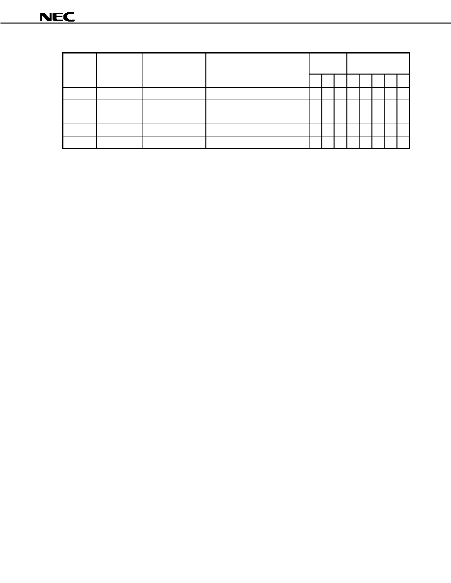
Preliminary Data Sheet U13995EJ1V0DS00
63
µ
µ
µ
µ
PD703100-33, 703100-40, 703101-33, 703102-33
(7/7)
Execution
Clock
Flags
Mnemonic
Operand
Opcode
Operation
i
r
l
CY
OV
S
Z
SAT
XOR
reg1,reg2
r r r r r 0 0 1 0 0 1 R R R R R
GR[reg2]
GR[reg2] XOR GR[reg1]
1
1
1
0
◊
◊
r r r r r 1 1 0 1 0 1 R R R R R
1
1
1
0
◊
◊
XORI
imm16,reg1,reg2
i i i i i i i i i i i i i i i i
GR[reg2]
GR[reg1] XOR zero-extend
(imm16)
ZXB
reg1
0 0 0 0 0 0 0 0 1 0 0 R R R R R
GR[reg1]
zero-extend(GR[reg1] (7 : 0))
1
1
1
ZXH
reg1
0 0 0 0 0 0 0 0 1 1 0 R R R R R
GR[reg1]
zero-extend(GR[reg1] (15 : 0))
1
1
1
Notes 1. dddddddd: Higher 8 bits of disp9.
2. 3 clocks if the final instruction includes PSW write access.
3. If there is no wait state (3 + the number of read access wait states).
4. N is the total number of list 12 read registers. (according to the number of wait states. Also, if there are
no wait states, N is the number of list 12 registers.)
5. RRRRR other than 00000.
6. Only the lower half word data are valid.
7. ddddddddddddddddddddd: Higher 21 bits of disp22.
8. ddddddddddddddd: Higher 15 bits of disp16.
9. According to the number of wait states (1 if there are no wait states).
10. b: bit 0 of disp16.
11. According to the number of wait states (2 if there are no wait states).
12. In this instruction, for convenience of mnemonic description, the source register is made reg2, but the
reg1 field is used in the op code. Therefore, the meaning of the register specification in the mnemonic
description and in the opcode differs from other instructions.
rrrrr
: regID specification
RRRRR: reg2 specification
13. 11111: Lower 5 bits of imm9.
1111 : Lower 4 bits of imm9.
14. 1 when r = w (the lower 32 bits of the results are not written in the register) or w = r0 (the higher 32 bits
of the results are not written in the register).
15. sp/imm: specified by bits 19 and 20 of the sub opcode.
16. ff = 00: load sp in ep.
01: load sign expanded 16-bit immediate data (bits 47 to 32) in ep.
10: load 16-bit logically left shifted 16-bit immediate data (bits 47 to 32) in ep.
11: load 32-bit immediate data (bits 63 to 32) in ep.
17. If imm=imm32, N + 3 clocks.
18. rrrrr other than 00000.
19. ddddddd: Higher 7 bits of disp8.
20. dddd: Higher 4 bits of disp5.
21. dddddd: Higher 6 bits of disp8.
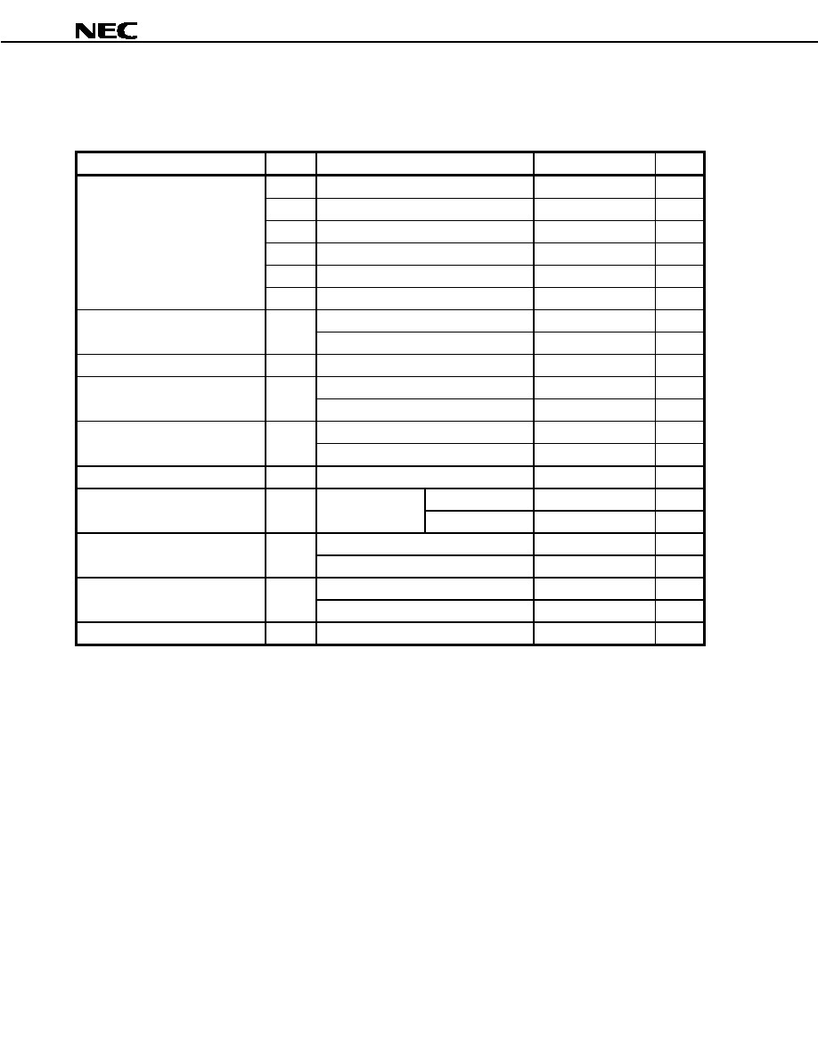
Preliminary Data Sheet U13995EJ1V0DS00
64
µ
µ
µ
µ
PD703100-33, 703100-40, 703101-33, 703102-33
16. ELECTRICAL SPECIFICATIONS (PRELIMINARY VALUES)
Absolute Maximum Ratings (T
A
= 25
∞
∞
∞
∞
C)
Parameter
Symbol
Condition
Rating
Unit
V
DD
V
DD
pin
-
0.5 to +4.6
V
HV
DD
HV
DD
pin, HV
DD
V
DD
-
0.5 to +7.0
V
CV
DD
CV
DD
pin
-
0.5 to +4.6
V
CV
SS
CV
SS
pin
-
0.5 to +0.5
V
AV
DD
AV
DD
pin
-
0.5 to HV
DD
+ 0.5
V
Power supply voltage
AV
SS
AV
SS
pin
-
0.5 to +0.5
V
X1 pin, except MODE3 pin
-
0.5 to HV
DD
+ 0.5
V
Input voltage
V
I
MODE3 pin
-
0.5 to V
DD
+ 0.5
V
Clock input voltage
V
K
X1, V
DD
= 3.0 to 3.6 V
-
0.5 to V
DD
+ 1.0
V
1 pin
4.0
mA
Low-level output current
I
OL
Total of all pins
100
mA
1 pin
-
4.0
mA
High-level output current
L
OH
Total of all pins
-
100
mA
Output voltage
V
O
HV
DD
= 5.0 V
±
10 %
-
0.5 to HV
DD
+ 0.5
V
AV
DD
> HV
DD
-
0.5 to HV
DD
+ 0.5
V
Analog input voltage
V
IAN
P70/ANI0 to
P77/ANI7 pins
HV
DD
AV
DD
-
0.5 to AV
DD
+ 0.5
V
AV
DD
> HV
DD
-
0.5 to HV
DD
+ 0.5
V
A/D converter reference input
voltage
AV
REF
HV
DD
AV
DD
-
0.5 to AV
DD
+ 0.5
V
Operating ambient temperature
T
A
µ
PD703100-40
-
40 to +70
∞
C
µ
PD703100-33, 703101-33, 703102-33
-
40 to +85
∞
C
Storage temperature
T
stg
-
60 to +150
∞
C
Caution
1. Do not make direct connections of the output (or input/output) pins of the IC product with
each other, and also avoid direct connections to V
DD
, V
CC
, or GND. However, the open drain
pins or the open collector pins can be directly connected with each other. A direct
connection can also be made for an external circuit designed with timing specifications that
prevent conflicting output from pins subject to high-impedance state.
2. Product quality may suffer if the absolute maximum rating is exceeded even momentarily
for any parameter. That is, the absolute maximum ratings are rated values at which the
product is on the verge of suffering physical damage, and therefore the product must be
used under conditions that ensure that the absolute maximum ratings are not exceeded.
The ratings and conditions shown below for DC characteristics and AC characteristics are
within the range for normal operation and quality assurance.

Preliminary Data Sheet U13995EJ1V0DS00
65
µ
µ
µ
µ
PD703100-33, 703100-40, 703101-33, 703102-33
Capacitance (T
A
= 25
∞
∞
∞
∞
C, V
DD
= HV
DD
= CV
DD
= V
SS
= 0 V)
Parameter
Symbol
Condition
MIN.
TYP.
MAX.
Unit
Input capacitance
C
I
15
pF
Input/output capacitance
C
IO
15
pF
Output capacitance
C
O
fc = 1 MHz
Unmeasured pins returned to 0 V.
15
pF
Operating Conditions
Operation
Mode
Internal Operating Clock Frequency (
)
Operating Ambient
Temperature (T
A
)
Power Supply Voltage
(V
DD
, HV
DD
)
µ
PD703100-40
2 to 40 MHz
-
40 to +70
∞
C
Direct mode
µ
PD703100-33, 703101-33, 703102-33
2 to 33 MHz
-
40 to +85
∞
C
µ
PD703100-40
20 to 40 MHz
-
40 to +70
∞
C
PLL mode
µ
PD703100-33, 703101-33, 703102-33
20 to 33 MHz
-
40 to +85
∞
C
V
DD
= 3.0 to 3.6 V,
HV
DD
= 5.0 V
±
10%
Recommended Oscillation Circuits
(a) Ceramic resonator or crystal resonator connection (T
A
= ≠40 to +70
∞
∞
∞
∞
C ...
µ
µ
µ
µ
PD703100-40,
T
A
= ≠40 to +85
∞
∞
∞
∞
C ...
µ
µ
µ
µ
PD703100-33,
µ
µ
µ
µ
PD703101-33,
µ
µ
µ
µ
PD703102-33)
X1
C1
X2
C2
Cautions
1. Connect the oscillation circuit as closely to the X1 and X2 pins as possible.
2. Do not wire any other signal lines in the area indicated by the broken line.
3. Throughly evaluate the matching between the
µ
µ
µ
µ
PD703100-33,
µ
µ
µ
µ
PD703100-40,
µ
µ
µ
µ
PD703101-33,
and
µ
µ
µ
µ
PD703102-33 and the oscillators.
(b) External clock input (T
A
= ≠40 to +70
∞
∞
∞
∞
C ...
µ
µ
µ
µ
PD703100-40, T
A
= ≠40 to +85
∞
∞
∞
∞
C ...
µ
µ
µ
µ
PD703100-33,
µ
µ
µ
µ
PD703101-
33,
µ
µ
µ
µ
PD703102-33)
X1
X2
Open
External clock
Caution Input CMOS-level voltage to the X1 pin.

Preliminary Data Sheet U13995EJ1V0DS00
66
µ
µ
µ
µ
PD703100-33, 703100-40, 703101-33, 703102-33
DC Characteristics (T
A
= ≠40 to +70
∞
∞
∞
∞
C ...
µ
µ
µ
µ
PD703100-40,T
A
= ≠40 to +85
∞
∞
∞
∞
C ...
µ
µ
µ
µ
PD703100-33,
µ
µ
µ
µ
PD703101-33,
µ
µ
µ
µ
PD703102-33, V
DD
= CV
DD
= 3.0 to 3.6 V, HV
DD
= 5.0
±
±
±
±
10%, V
SS
=0 V)
Parameter
Symbol
Condition
MIN.
TYP.
MAX.
Unit
Except Note 1
2.2
HV
DD
+ 0.3
V
High-level input voltage
V
IH
Note 1
0.8HV
DD
HV
DD
+ 0.3
V
Except Note 1 and Note 2
-
0.5
+0.8
V
Low-level input voltage
V
IL
Note 1
-
0.5
0.2HV
DD
V
X1 pin
Direct mode
0.8V
DD
V
DD
+ 0.3
V
High-level clock input voltage
V
XH
PLL mode
0.8V
DD
V
DD
+ 0.3
V
X1 pin
Direct mode
-
0.3
0.15V
DD
V
Low-level clock input voltage
V
XL
PLL mode
-
0.3
0.15V
DD
V
HV
T
+
Note 1, rising edge
3.0
V
Schmitt-triggered input
threshold voltage
HV
T
-
Note 1, falling edge
2.0
V
Schmitt-triggered input
hysteresis width
HV
T
+
≠HV
T
-
Note 1
0.5
V
I
OH
=
-
2.5 mA
0.7HV
DD
V
High-level output voltage
V
OH
I
OH
=
-
100
µ
A
HV
DD
-
0.4
V
Low-level output voltage
V
OL
I
OL
= 2.5 mA
0.45
V
High-level input leakage
current
I
LIH
Except V
I
= H
VDD
or Note 2
10
µ
A
Low-level input leakage
current
I
LIL
Except V
I
= 0 V or Note 2
-
10
µ
A
High-level output leakage
current
I
LOH
V
O
= H
VDD
10
µ
A
Low-level output leakage
current
I
LOL
V
O
= 0 V
-
10
µ
A
Analog pin input leakage
current
I
LIAN
Note 2
T.B.D.
µ
A
otes
1. P04/INTP100/DMARQ0 to P07/INTP103/DMARQ3, P14/INTP110/DMAAK0 to P17/INTP113/DMAAK3,
P34/INTP130, P35/INTP131/SO2, P36/INTP132/S12, P37/INTP133/SCK2, P104/INTP120/TC0 to
P107/INTP123/TC3, Pl14/INTP140, P115/INTP141/SO3, P116/INTP142/SI3, P117/INTP143/SCK3,
P124/INTP150 to P126/INTP152, P127/INTP153/ADTRG, P02/TCLR10, P12/TCLR11, P32/TCLR13,
P102/TCLR12, P112/TCLR14, P122/TCLR15, P03/TI10, P13/TI11, P33/TI13, P103/TI12, P113/TI14,
P123/TI15, P20/NMI, P23/RXD0/SI0, P24/SCK0, P26/RXD1/SI1, P27/SCK1, MODE0 to MODE2,
RESET
2. When the P70/ANI0 to P77/ANI7 pins are used as analog input.
Remark TYP. values are reference values for when T
A
= 25
∞
C, V
DD
= CV
DD
= 3.3 V, and HV
DD
= 5.0 V.

Preliminary Data Sheet U13995EJ1V0DS00
67
µ
µ
µ
µ
PD703100-33, 703100-40, 703101-33, 703102-33
DC Characteristics (T
A
= ≠40 to +70
∞
∞
∞
∞
C ...
µ
µ
µ
µ
PD703100-40,T
A
= ≠40 to +85
∞
∞
∞
∞
C ...
µ
µ
µ
µ
PD703100-33,
µ
µ
µ
µ
PD703101-33,
µ
µ
µ
µ
PD703102-33, V
DD
= CV
DD
= 3.0 to 3.6 V, HV
DD
= 5.0
±
±
±
±
10%, V
SS
= 0 V)
Parameter
Symbol
Condition
MIN.
TYP.
MAX.
Unit
V
DD
+ CV
DD
2.0
◊
fx
3.6
◊
fx
mA
Direct mode
HV
DD
1.8
◊
fx
3.0
◊
fx
mA
V
DD
+ CV
DD
2.7
◊
fx
-
17.0
3.6
◊
fx
mA
During
normal
operation
I
DD1
PLL mode
HV
DD
1.3
◊
fx
-
3.6
3.0
◊
fx
mA
V
DD
+ CV
DD
1.4
◊
fx
2.5
◊
fx
mA
Direct mode
HV
DD
0.8
◊
fx
1.6
◊
fx
mA
V
DD
+ CV
DD
1.8
◊
fx
-
10.0
2.5
◊
fx
mA
HALT mode
I
DD2
PLL mode
HV
DD
0.8
◊
fx
-
1.0
1.6
◊
fx
mA
V
DD
+ CV
DD
1.5
3.0
mA
Direct mode
HV
DD
10
50
µ
A
PLL mode
V
DD
+ CV
DD
1.8
3.0
mA
IDLE mode
I
DD3
HV
DD
10
50
µ
A
V
DD
+ CV
DD
20
100
µ
A
Power supply
current
STOP
mode
I
DD4
HV
DD
10
50
µ
A
Remarks 1. TYP. values are reference values for when T
A
= 25∞C, V
DD
= CV
DD
= 3.3 V, and HV
DD
= 5.0 V.
2. Direct mode:
f
X
= 2 to 40 MHz (
µ
PD703100-40)
f
X
= 2 to 33 MHz (
µ
PD703100-33,
µ
PD703101-33,
µ
PD703102-33)
PLL mode:
f
X
= 20 to 40 MHz (
µ
PD703100-40)
f
X
= 20 to 33 MHz (
µ
PD703100-33,
µ
PD703101-33,
µ
PD703102-33)
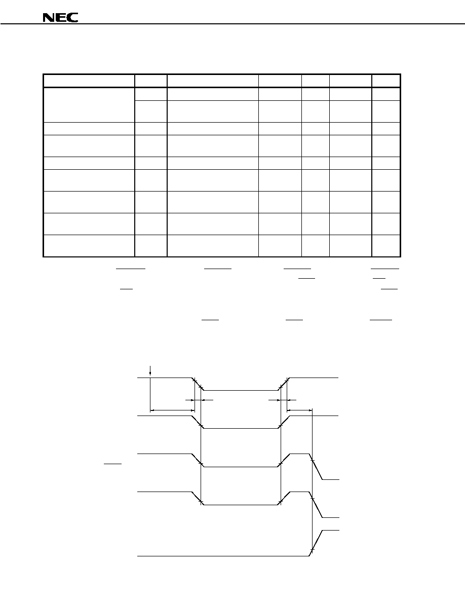
Preliminary Data Sheet U13995EJ1V0DS00
68
µ
µ
µ
µ
PD703100-33, 703100-40, 703101-33, 703102-33
Data Hold Characteristics(T
A
= ≠40 to +70
∞
∞
∞
∞
C ...
µ
µ
µ
µ
PD703100-40, T
A
= ≠40 to +85
∞
∞
∞
∞
C ...
µ
µ
µ
µ
PD703100-33,
µ
µ
µ
µ
PD703101-
33,
µ
µ
µ
µ
PD703102-33)
Parameter
Symbol
Condition
MIN.
TYP.
MAX.
Unit
V
DDDR
STOP mode, V
DD
= V
DDDR
1.5
3.6
V
Data hold voltage
HV
DDDR
STOP mode,
HV
DD
= HV
DDDR
V
DDDR
5.5
V
Data hold current
I
DDDR
V
DD
= V
DDDR
T.B.D.
T.B.D.
µ
A
Power supply voltage rise
time
t
RVD
200
µ
s
Power supply voltage fall time
t
FVD
200
µ
s
Power supply voltage hold
time (to STOP mode setting)
t
HVD
0
ms
STOP mode release signal
input time
t
DREL
0
ns
Data hold high-level input
voltage
V
IHDR
Note
0.8 HV
DDDR
HV
DDDR
V
Data hold low-level input
voltage
V
ILDR
Note
0
0.2 HV
DDDR
V
Note P04/INTP100/DMARQ0 to P07/INTP103/DMARQ3, P14/INTP110/DMAAK0 to P17/INTP113/DMAAK3,
P34/INTP130, P35/INTP131/SO2, P36/INTP132/SI2, P37/INTP133/SCK2, P104/INTP120/TC0 to
P107/INTP123/TC3, P114/INTP140, P115/INTP141/SO3, Pl16/INTP142/SI3, P117/INTP143/SCK3,
P124/INTP150 to P126/INTP152, P127/INTP153/ADTRG, P02/TCLR10, P12/TCLR11, P32/TCLR13,
P102/TCLR12, P112/TCLR14, P122/TCLR15, P03/TI10, P13/TI11, P33/TI13, P103/TI12,P113/TI14,
P123/TI15, P20/NMI, P23/RXD0/SI0 ,P24/SCK0, P26/RXD1/SI1, P27/SCK1, MODE0 to MODE2, RESET
Remark TYP. values are reference values for when T
A
= 25
∞
C.
HV
DD
RESET (input)
V
IHDR
V
IHDR
V
ILDR
V
DD
t
HVD
t
FVD
V
DDDR
t
RVD
t
DREL
STOP mode setting
NMI (input)
(Released by falling edge)
NMI (input)
(Released by rising edge)

Preliminary Data Sheet U13995EJ1V0DS00
69
µ
µ
µ
µ
PD703100-33, 703100-40, 703101-33, 703102-33
AC Characteristics (T
A
= ≠40 to +70
∞
∞
∞
∞
C ...
µ
µ
µ
µ
PD703100-40, T
A
= ≠40 to +85
∞
∞
∞
∞
C ...
µ
µ
µ
µ
PD703100-33,
µ
µ
µ
µ
PD703101-33,
µ
µ
µ
µ
PD703102-33, V
DD
= CV
DD
= 3.0 to 3.6 V, HV
DD
= 5.0
±
±
±
±
10%, V
SS
= 0 V, output pin load
capacitance: C
L
= 50 pF)
AC Test Input Waveform
(a) P04/INTP100/DMARQ0 to P07/INTP103/DMARQ3, P14/INTP110/DMAAK0 to P17/INTP113/DMAAK3, P34/
INTP130, P35/INTP131/SO2, P36/INTP132/SI2, P37/INTP133/SCK2, P104/INTP120/TC0 to P107/INTP123/
TC3, P114/INTP140, P115/INTP141/SO3, P116/INTP142/SI3, P117/INTP143/SCK3, P124/INTP150 to P126/
INTP152, P127/INTP153/ADTRG, P02/TCLR10, P12/TCLR11, P32/TCLR13, P102/TCLR12, P112/TCLR14,
P122/TCLR15, P03/TI10, P13/TI11, P33/TI13, P103/TI12, P113/TI14, P123/TI15, P20/NMI, P23/RXD0/SI0, P24/
SCK0, P26/RXD1/SI1, P27/SCK1, MODE0 to MODE2, RESET
HV
DD
0 V
0.8HV
DD
0.2HV
DD
0.8HV
DD
0.2HV
DD
Test
points
Input signal
(b) Pins other than those listed in (a) above
2.4 V
0.4 V
2.2 V
0.8 V
2.2 V
0.8 V
Test
points
Input signal
AC Test Output Test Points
2.4 V
0.8 V
2.4 V
0.8 V
Test
points
Output Signal

Preliminary Data Sheet U13995EJ1V0DS00
70
µ
µ
µ
µ
PD703100-33, 703100-40, 703101-33, 703102-33
Load Condition
C
L
= 50 pF
DUT
(Measured Device)
Caution In cases where the load capacitance is greater than 50 pF due to the circuit configuration, insert
a buffer or other element to reduce the devide's load capacitance 50 pF.
(1) Clock timing
Parameter
Symbol
Condition
MIN.
MAX.
Unit
µ
PD703100-40
12.5
250
ns
Direct
mode
µ
PD703100-33,
703101-33,
703102-33
15
250
ns
µ
PD703100-40
125
250
ns
X1 input cycle
<1>
t
CYX
PLL mode
µ
PD703100-33,
703101-33,
703102-33
150
250
ns
Direct mode
5
ns
X1 input high-level width
<2>
t
WXH
PLL mode
50
ns
Direct mode
5
ns
X1 input low-level width
<3>
t
WXL
PLL mode
50
ns
Direct mode
4
ns
X1 input rise time
<4>
t
XR
PLL mode
10
ns
X1 input fall time
<5>
t
XF
Direct mode
4
ns
PLL mode
10
ns
µ
PD703100-40
2
40
MHz
CPU operating frequency
≠
µ
PD703100-33, 703101-33,
703102-33
2
33
MHz
CLKOUT output cycle
<6>
t
CYK
30
500
ns
CLKOUT input high-level width
<7>
t
WKH
0.5T ≠ 7
ns
CLKOUT input low-level width
<8>
t
WKL
0.5T ≠ 4
ns
CLKOUT input rise time
<9>
t
KR
5
ns
CLKOUT input fall time
<10>
t
KF
5
ns
CLKOUT output delay time from X1
<11>
t
DXK
Direct mode
T.B.D.
T.B.D.
ns
Remark T = t
CYK
Parameter
Symbol
Condition
TYP.
Unit
Free-running oscillation frequency
≠
P
PLL mode
T.B.D.
MHz
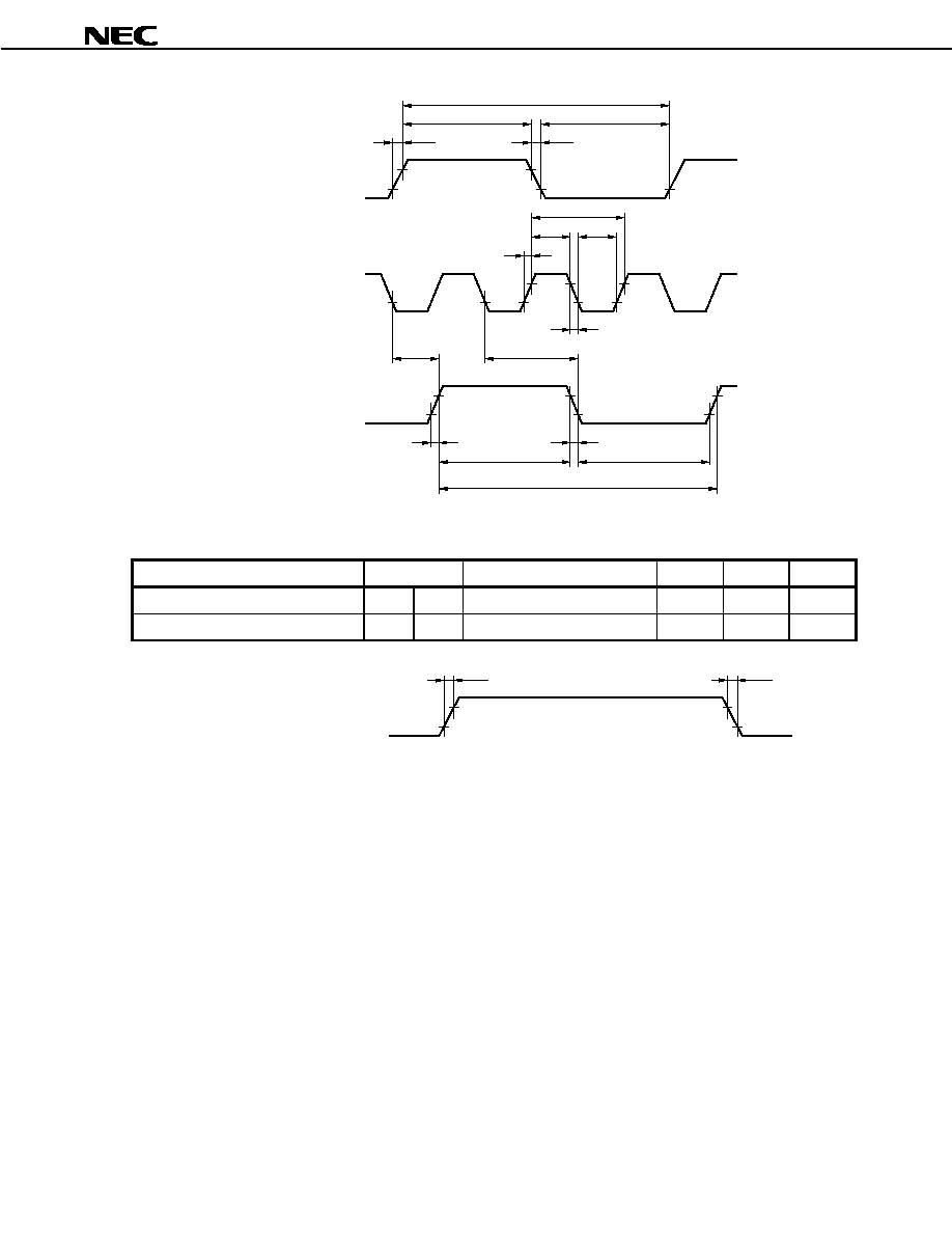
Preliminary Data Sheet U13995EJ1V0DS00
71
µ
µ
µ
µ
PD703100-33, 703100-40, 703101-33, 703102-33
<4>
<5>
<2>
<3>
<1>
X1
(PLL mode)
<1>
<2>
<3>
<4>
<5>
<11>
<11>
<9>
<10>
<7>
<8>
<6>
X1
(Direct mode)
CLKOUT (output)
(2) Output waveform (other than X1, CLKOUT)
Parameter
Symbol
Condition
MIN.
MAX.
Unit
Output rise time
<12>
t
OR
10
ns
Output fall time
<13>
t
OF
10
ns
<13>
Signals other than X1, CLKOUT
<12>

Preliminary Data Sheet U13995EJ1V0DS00
72
µ
µ
µ
µ
PD703100-33, 703100-40, 703101-33, 703102-33
(3) Reset timing
Parameter
Symbol
Condition
MIN.
MAX.
Unit
RESET high-level width
<14>
t
WRSH
500
ns
When power supply is on, and
STOP mode has been released
500 + T
OS
ns
RESET low-level width
<15>
t
WRSL
Other than when power supply is
on, and STOP mode has been
released
500
ns
Remark T
OS
: Oscillation stabilization time
<14>
<15>
RESET (input)

Preliminary Data Sheet U13995EJ1V0DS00
73
µ
µ
µ
µ
PD703100-33, 703100-40, 703101-33, 703102-33
[MEMO]
Preliminary Data Sheet U13995EJ1V0DS00
74
µ
µ
µ
µ
PD703100-33, 703100-40, 703101-33, 703102-33
(4) SRAM, external ROM, or external I/O access timing
(a) Access timing (SRAM, external ROM, or external I/O) (1/2)
Parameter
Symbol
Condition
MIN.
MAX.
Unit
Address, CSn output delay time (from
CLKOUT
)
<16>
t
DKA
2
10
ns
Address, CSn output hold time (from
CLKOUT
)
<17>
t
HKA
2
10
ns
RD, IORD
delay time
(from CLKOUT
)
<18>
t
DKRDL
2
14
ns
RD, IORD
delay time
(from CLKOUT
)
<19>
t
HKRDH
2
14
ns
UWR, LWR, IOWR
delay time (from
CLKOUT
)
<20>
t
DKWRL
2
10
ns
UWR, LWR, IOWR
delay time (from
CLKOUT
)
<21>
t
HKWRH
2
10
ns
BCYST
delay time (from CLKOUT
)
<22>
t
DKBSL
2
10
ns
BCYST
delay time (from CLKOUT
)
<23>
t
HKBSH
2
10
ns
WAIT setup time (to CLKOUT
)
<24>
t
SWK
15
ns
WAIT hold time (from CLKOUT
)
<25>
t
HKW
2
ns
Data input setup time
(to CLKOUT
)
<26>
t
SKID
18
ns
Data input hold time
(from CLKOUT
)
<27>
t
HKID
2
ns
Data output delay time
(from CLKOUT
)
<28>
t
DKOD
2
10
ns
Data output hold time
(from CLKOUT
)
<29>
t
HKOD
2
10
ns
Remarks 1. Maintain at least one of the data input hold times t
HKID
and t
HRDID
.
2. n = 0 to 7

Preliminary Data Sheet U13995EJ1V0DS00
75
µ
µ
µ
µ
PD703100-33, 703100-40, 703101-33, 703102-33
(a) Access timing (SRAM, external ROM, or external I/O) (2/2)
CLKOUT (Output)
A0 to A23 (Output)
CSn (Output)
BCYCT (Output)
RD, IORD (Output)
[Read time]
UWR, LWR, IOWR (Output)
[Write time]
D0 to 15 (I/O)
[Read time]
D0 to 15 (I/O)
[Write time]
WAIT (Input)
<16>
<17>
<22>
<23>
<18>
<19>
<20>
<21>
<26>
<27>
<28>
<29>
<24>
<25>
<24>
<25>
T1
TW
T2
Remarks 1. This is the timing when the number of waits due to the DWC1 and DWC2 registers is zero.
2. The broken lines indicate high impedance.
3. n = 0 to 7

Preliminary Data Sheet U13995EJ1V0DS00
76
µ
µ
µ
µ
PD703100-33, 703100-40, 703101-33, 703102-33
(b) Read timing (SRAM, external ROM, or external I/O) (1/2)
Parameter
Symbol
Condition
MIN.
MAX.
Unit
Data input setup time (to address)
<30>
t
SAID
(1.5 + w
D
+ w) T ≠ 28
ns
Data input setup time (to RD)
<31>
t
SRDID
(1 + w
D
+ w) T ≠ 32
ns
RD, IORD low-level width
<32>
t
WRDL
(1 + w
D
+ w) T ≠ 10
ns
RD, IORD high-level width
<33>
t
WRDH
T ≠ 10
ns
RD, IORD
delay time from address,
CSn
<34>
t
DARD
0.5T ≠ 10
ns
Address delay time from RD, IORD
<35>
t
DRDA
(0.5 + i) T ≠ 10
ns
Data input hold time (from RD, IORD
)
<36>
t
HRDID
0
ns
Data output delay time from RD, IORD
<37>
t
DRDOD
(0.5 + i) T ≠ 10
ns
WAIT setup time (to address)
<38>
t
SAW
Note
T ≠ 25
ns
WAIT setup time (to BCYST
)
<39>
t
SBSW
Note
T ≠ 25
ns
WAIT hold time (to BCYST
)
<40>
t
HBSW
Note
0
ns
Note For first WAIT sampling when the number of waits due to the DWC1 and DWC2 registers is zero.
Remarks 1. T = t
CYK
2. w: the number of waits due to WAIT.
3. w
D
: the number of waits due to the DWC1 and DWC2 registers.
4. i: the number of idle states that are inserted when a write cycle follows a read cycle.
5. Maintain at least one of the data input hold times t
HKID
and t
HRDID
.
6. n = 0 to 7

Preliminary Data Sheet U13995EJ1V0DS00
77
µ
µ
µ
µ
PD703100-33, 703100-40, 703101-33, 703102-33
(b) Read timing (SRAM, external ROM, or external I/O) (2/2)
UWR, LWR, IOWR (Output)
RD, IORD (Output)
D0 to 15 (I/O)
T1
TW
T2
CLKOUT (Output)
<33>
<32>
<35>
<38>
<34>
<31>
<30>
<36>
<37>
<39>
<40>
A0 to A23 (Output)
CSn (Output)
WAIT (Input)
BCYST (Output)
Remarks 1. This is the timing when the number of waits due to the DWC1 and DWC2 registers is zero.
2. The broken lines indicate high impedance.
3. n = 0 to 7

Preliminary Data Sheet U13995EJ1V0DS00
78
µ
µ
µ
µ
PD703100-33, 703100-40, 703101-33, 703102-33
(c) Write timing (SRAM, external ROM, or external I/O) (1/2)
Parameter
Symbol
Condition
MIN.
MAX.
Unit
WAIT setup time (to address)
<38>
t
SAW
Note
T ≠ 25
ns
WAIT setup time (to BCYST
)
<39>
t
SBSW
Note
T ≠ 25
ns
WAIT hold time (from BCYST
)
<40>
t
HBSW
Note
0
ns
UWR, LWR, IOWR
delay time from
address, CSn
<41>
t
DAWR
0.5T ≠ 10
ns
Address setup time (to UWR, LWR,
IOWR
)
<42>
t
SAWR
(1.5 + w
D
+ w) T ≠ 10
ns
Address delay time from UWR, LWR,
IOWR
<43>
t
DWRA
0.5T ≠ 10
ns
UWR, LWR, IOWR high-level width
<44>
t
WWRH
T ≠ 10
ns
UWR, LWR, IOWR low-level width
<45>
t
WWRL
(1 + w
D
+ w) T ≠ 10
ns
Data output setup time
(to UWR, LWR, IOWR
)
<46>
t
SODWR
(1.5 + w
D
+ w) T ≠ 10
ns
Data output hold time
(from UWR, LWR, IOWR
)
<47>
t
HWROD
0.5T ≠ 10
ns
Note For first WAIT sampling when the number of waits due to the DWC1 and DWC2 registers is zero.
Remarks 1. T = t
CYK
2. w: the number of waits due to WAIT.
3. w
D
: the number of waits due to the DWC1 and DWC2 registers.
4. n = 0 to 7

Preliminary Data Sheet U13995EJ1V0DS00
79
µ
µ
µ
µ
PD703100-33, 703100-40, 703101-33, 703102-33
(c) Write timing (SRAM, external ROM, or external I/O) (2/2)
T1
TW
T2
CLKOUT (Output)
<44>
<45>
<43>
<38>
<46>
<47>
<39>
<40>
<41>
<42>
A0 to A23 (Output)
CSn (Output)
RD, IORD (Output)
UWR, LWR, IOWR (Output)
D0 to 15 (I/O)
WAIT (Input)
BCYST (Output)
Remarks 1. This is the timing when the number of waits due to the DWC1 and DWC2 registers is zero.
2. The broken lines indicate high impedance.
3. n = 0 to 7

Preliminary Data Sheet U13995EJ1V0DS00
80
µ
µ
µ
µ
PD703100-33, 703100-40, 703101-33, 703102-33
(d) DMA flyby transfer timing (SRAM
external I/O transfer) (1/2)
Parameter
Symbol
Condition
MIN.
MAX.
Unit
WAIT setup time (to CLKOUT
)
<24>
t
SWK
15
ns
WAIT hold time (from CLKOUT
)
<25>
t
HKW
2
ns
RD low-level width
<32>
t
WRDL
(1 + w
D
+ w
F
+ w)
T ≠ 10
ns
RD high-level width
<33>
t
WRDH
T ≠ 10
ns
RD
delay time from address, CSn
<34>
t
DARD
0.5T ≠ 10
ns
Address delay time from RD
<35>
t
DRDA
(0.5 + i) T ≠ 10
ns
Data output delay time from RD
<37>
t
DRDOD
(0.5 + i) T ≠ 10
ns
WAIT setup time (to address)
<38>
t
SAW
Note
T ≠ 25
ns
WAIT setup time (to BCYST
)
<39>
t
SBSW
Note
T ≠ 25
ns
WAIT hold time (from BCYST
)
<40>
t
HBSW
Note
0
ns
IOWR
delay time from address
<41>
t
DAWR
0.5T ≠ 10
ns
Address setup time (to IOWR
)
<42>
t
SAWR
(1.5 + w
D
+ w) T ≠ 10
ns
Address delay time from UWR, LWR,
IOWR
<43>
t
DWRA
0.5T ≠ 10
ns
IOWR high-level width
<44>
t
WWRH
T ≠ 10
ns
IOWR low-level width
<45>
t
WWRL
(1 + w
D
+ w) T ≠ 10
ns
w
F
= 0
0
ns
RD
delay time from IOWR
<48>
t
DWRRD
w
F
= 1
T ≠ 10
ns
IOWR
delay time from DMAAKm
<49>
t
DDAWR
0.5T ≠ 10
ns
DMAAKm
delay time from IOWR
<50>
t
DWRDA
(0.5 + w
F
) T ≠ 10
ns
Note For first WAIT sampling when the number of waits due to the DWC1 and DWC2 registers is zero.
Remarks 1. T = t
CYK
2. w: the number of waits due to WAIT.
3. w
D
: the number of waits due to the DWC1 and DWC2 registers.
4. w
F
: the number of waits that are inserted for a source-side access during a DMA flyby transfer.
5. i: the number of idle states that are inserted when a write cycle follows a read cycle.
6. n = 0 to 7, m = 0 to 3

Preliminary Data Sheet U13995EJ1V0DS00
81
µ
µ
µ
µ
PD703100-33, 703100-40, 703101-33, 703102-33
(d) DMA flyby transfer timing (SRAM
external I/O transfer) (2/2)
CLKOUT (Output)
T1
TW
T2
<33>
<32>
<35>
<34>
<48>
<50>
<49>
<43>
<42>
<41>
<44>
<45>
<37>
<38>
<24>
<24>
<25>
<25>
<40>
<39>
A0 to A23 (Output)
CSn (Output)
RD (Output)
DMAAKm (Output)
IORD (Output)
IOWR (Output)
UWR, LWR (Output)
D0 to 15 (I/O)
WAIT (Input)
BCYST (Output)
Remarks 1. This is the timing when the number of waits due to the DWC1 and DWC2 registers is zero and w
F
= 0.
2. The broken lines indicate high impedance.
3. n = 0 to 7, m = 0 to 3
Preliminary Data Sheet U13995EJ1V0DS00
82
µ
µ
µ
µ
PD703100-33, 703100-40, 703101-33, 703102-33
(e) DMA flyby transfer timing (external I/O
SRAM transfer) (1/2)
Parameter
Symbol
Condition
MIN.
MAX.
Unit
WAIT setup time (to CLKOUT
)
<24>
t
SWK
15
ns
WAIT hold time (from CLKOUT
)
<25>
t
HKW
2
ns
IORD low-level width
<32>
t
WRDL
(1 + w
D
+ w
F
+ w)
T ≠ 10
ns
IORD high-level width
<33>
t
WRDH
T ≠ 10
ns
IORD
delay time from address, CSn
<34>
t
DARD
0.5T ≠ 10
ns
Address delay time from IORD
<35>
t
DRDA
(0.5 + i) T ≠ 10
ns
Data output delay time from IORD
<37>
t
DRDOD
(0.5 + i) T ≠ 10
ns
WAIT setup time (to address)
<38>
t
SAW
Note
T ≠ 25
ns
WAIT setup time (to BCYST
)
<39>
t
SBSW
Note
T ≠ 25
ns
WAIT hold time (from BCYST
)
<40>
t
HBSW
Note
0
ns
UWR, LWR
delay time from address
<41>
t
DAWR
0.5T ≠ 10
ns
Address setup time (to UWR, LWR
)
<42>
t
SAWR
(1.5 + w
D
+ w) T ≠ 10
ns
Address delay time from UWR, LWR,
IOWR
<43>
t
DWRA
0.5T ≠ 10
ns
UWR, LWR high-level width
<44>
t
WWRH
T ≠ 10
ns
UWR, LWR low-level width
<45>
t
WWRL
(1 + w
D
+ w) T ≠ 10
ns
w
F
= 0
0
ns
IORD
delay time from UWR, LWR
<48>
t
DWRRD
w
F
= 1
T ≠ 10
ns
IORD
delay time from DMAAKm
<51>
t
DDARD
0.5T ≠ 10
ns
DMAAKm
delay time from IORD
<52>
t
DRDDA
0.5T ≠ 10
ns
Note For first WAIT sampling when the number of waits due to the DWC1 and DWC2 registers is zero.
Remarks 1. T = t
CYK
2. w: the number of waits due to WAIT.
3. w
D
: the number of waits due to the DWC1 and DWC2 registers.
4. w
F
: the number of waits that are inserted for a source-side access during a DMA flyby transfer.
5. i: the number of idle states that are inserted when a write cycle follows a read cycle.
6. n = 0 to 7, m = 0 to 3

Preliminary Data Sheet U13995EJ1V0DS00
83
µ
µ
µ
µ
PD703100-33, 703100-40, 703101-33, 703102-33
(e) DMA flyby transfer timing (external I/O
SRAM transfer) (2/2)
CLKOUT (Output)
T1
TW
T2
<44>
<45>
<35>
<48>
<52>
<33>
<37>
<38>
<24>
<24>
<25>
<25>
<40>
<39>
<42>
<41>
<43>
<51>
<32>
<35>
<34>
A0 to A23 (Output)
CSn (Output)
UWR, LWR (Output)
RD (Output)
DMAAKm (Output)
IOWR (Output)
IORD (Output)
D0 to 15 (I/O)
WAIT (Input)
BCYST (Output)
Remarks 1. This is the timing when the number of waits due to the DWC1 and DWC2 registers is zero and w
F
= 0.
2. The broken lines indicate high impedance.
3. n = 0 to 7, m = 0 to 3

Preliminary Data Sheet U13995EJ1V0DS00
84
µ
µ
µ
µ
PD703100-33, 703100-40, 703101-33, 703102-33
(5) Page ROM access timing (1/2)
Parameter
Symbol
Condition
MIN.
MAX.
Unit
WAIT setup time (to CLKOUT
)
<24>
t
SWK
15
ns
WAIT hold time (from CLKOUT
)
<25>
t
HKW
2
ns
Data input setup time
(to CLKOUT
)
<26>
t
SKID
18
ns
Data input hold time
(from CLKOUT
)
<27>
t
HKID
2
ns
Off-page data input setup time (to
address)
<30>
t
SAID
(1.5 + w
D
+ w) T ≠ 28
ns
Off-page data input setup time (to RD)
<31>
t
SRDID
(1 + w
D
+ w) T ≠ 32
ns
Off-page RD low-level width
<32>
t
WRDL
(1 + w
D
+ w) T ≠ 10
ns
RD high-level width
<33>
t
WRDH
0.5T ≠ 10
ns
Data input hold time (from RD)
<36>
t
HRDID
0
ns
Data output delay time from RD
<37>
t
DRDOD
(0.5 + i) T ≠ 10
ns
On-page RD low-level width
<53>
t
WORDL
(1.5 + w
PR
+ w)
T ≠ 10
ns
On-page data input setup time
(to address)
<54>
t
SOAID
(1.5 + w
PR
+ w) T ≠ 28
ns
On-page data input setup time (to RD)
<55>
t
SORDID
(1.5 + w
PR
+ w) T ≠ 32
ns
Remarks 1. T = t
CYK
2. w: the number of waits due to WAIT.
3. w
D
: the number of waits due to the DWC1 and DWC2 registers.
4. w
PR
: the number of waits due to the PRC register.
5. i: the number of idle states that are inserted when a write cycle follows a read cycle.
6. Maintain at least one of the data input hold times t
HKID
and t
HRDID
.
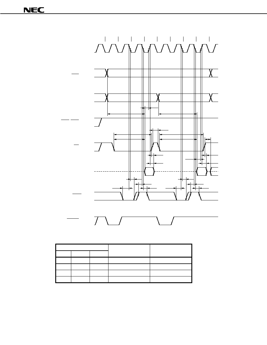
Preliminary Data Sheet U13995EJ1V0DS00
85
µ
µ
µ
µ
PD703100-33, 703100-40, 703101-33, 703102-33
(5) Page ROM access timing (2/2)
CLKOUT (Output)
On-page address
Note
T1
TDW
TW
T2
TO1
TPRW
TW
TO2
<24>
<25>
<24>
<25>
<24>
<25>
<24>
<25>
<26>
<27>
<36>
<32>
<31>
<53>
<55>
<27>
<26>
<36>
<37>
<33>
<30>
<54>
Off-page address
Note
CSn (Output)
UWR, LWR (Output)
RD (Output)
D0 to 15 (I/O)
WAIT (Input)
BCYST (Output)
Note On-page and off-page addresses are as follows.
PRC register
MA5
MA4
MA3
On-page Addresses
Off-page Addresses
0
0
0
A0, A1
A2 to A23
0
0
1
A0 to A2
A3 to A23
0
1
1
A0 to A3
A4 to A23
1
1
1
A0 to A4
A5 to A23
Remarks 1. This is the timing for the following case.
Number of waits due to the DWC1 and DWC2 registers (TDW) : 1
Number of waits due to the PRC register (TPRW)
: 1
2. The broken lines indicate high impedance.
3. n = 0 to 7
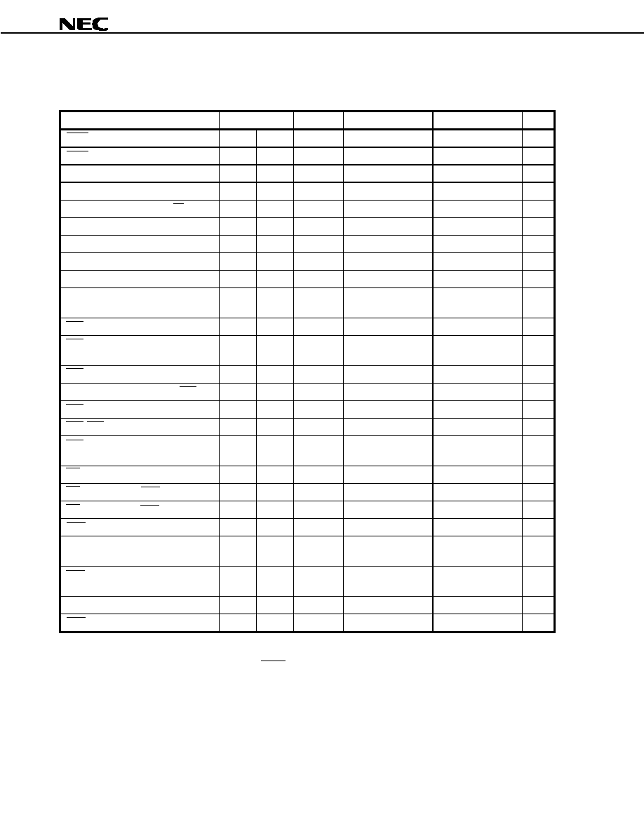
Preliminary Data Sheet U13995EJ1V0DS00
86
µ
µ
µ
µ
PD703100-33, 703100-40, 703101-33, 703102-33
(6) DRAM access timing
(a) Read timing (high-speed page DRAM access, normal access: off-page) (1/3)
Parameter
Symbol
Condition
MIN.
MAX.
Unit
WAIT setup time (to CLKOUT
)
<24>
t
SWK
15
ns
WAIT hold time (from CLKOUT
)
<25>
t
HKW
2
ns
Data input setup time (to CLKOUT
)
<26>
t
SKID
18
ns
Data input hold time (from CLKOUT
)
<27>
t
HKID
2
ns
Data output delay time from OE
<37>
t
DRDOD
(0.5 + i) T ≠ 10
ns
Row address setup time
<56>
t
ASR
(0.5 + w
RP
) T ≠ 10
ns
Row address hold time
<57>
t
RAH
(0.5 + w
RH
) T ≠ 10
ns
Column address setup time
<58>
t
ASC
0.5T ≠ 10
ns
Column address hold time
<59>
t
CAH
(1.5 + w
DA
+ w) T ≠ 10
ns
Read/write cycle time
<60>
t
RC
(3 + w
RP
+ w
RH
+ w
DA
+ w)
T ≠ 10
ns
RAS precharge time
<61>
t
RP
(0.5 + w
RP
) T ≠ 10
ns
RAS pulse time
<62>
t
RAS
(2.5 + w
RH
+ w
DA
+ w)
T ≠ 10
ns
RAS hold time
<63>
t
RSH
(1.5 + w
DA
+ w) T ≠ 10
ns
Column address read time for RAS
<64>
t
RAL
(2 + w
DA
+ w) T ≠ 10
ns
CAS pulse width
<65>
t
CAS
(1 + w
DA
+ w) T ≠ 10
ns
CAS-RAS precharge time
<66>
t
CRP
(1 + w
RP
) T ≠ 10
ns
CAS hold time
<67>
t
CSH
(2 + w
RH
+ w
DA
+ w)
T ≠ 10
ns
WE setup time
<68>
t
RCS
(2 + w
RP
+ w
RH
) T ≠ 10
ns
WE hold time (from RAS
)
<69>
t
RRH
0.5T ≠ 10
ns
WE hold time (from CAS
)
<70>
t
RCH
T ≠ 10
ns
CAS precharge time
<71>
t
CPN
(2 + w
RP
+ w
RH
) T ≠ 10
ns
Output enable access time
<72>
t
OEA
(2 + w
RP
+ w
RH
+ w
DA
+ w)
T ≠ 28
ns
RAS access time
<73>
t
RAC
(2 + w
RH
+ w
DA
+ w)
T ≠ 28
ns
Access time from column address
<74>
t
AA
(1.5 + w
DA
+ w) T ≠ 28
ns
CAS access time
<75>
t
CAC
(1 + w
DA
+ w) T ≠ 28
ns
Remarks 1. T = t
CYK
2. w: the number of waits due to WAIT.
3. w
RP
: the number of waits due to the RPCxx bit of the DRCn register (n = 0 to 3, xx = 00 to 03, 10 to
13).
4. w
RH
: the number of waits due to the RHCxx bit of the DRCn register (n = 0 to 3, xx = 00 to 03, 10 to
13).
5. w
DA
: the number of waits due to the DACxx bit of the DRCn register (n = 0 to 3, xx = 00 to 03, 10 to
13).
6. i: the number of idle states that are inserted when a write cycle follows a read cycle.

Preliminary Data Sheet U13995EJ1V0DS00
87
µ
µ
µ
µ
PD703100-33, 703100-40, 703101-33, 703102-33
(a) Read timing (high-speed page DRAM access, normal access: off-page) (2/3)
Parameter
Symbol
Condition
MIN.
MAX.
Unit
RAS column address delay time
<76>
t
RAD
(0.5 + w
RH
) T ≠ 10
ns
RAS-CAS delay time
<77>
t
RCD
(1 + w
RH
) T ≠ 10
ns
Output buffer turn-off delay time (from
OE
)
<78>
t
OEZ
0
ns
Output buffer turn-off delay time (from
CAS
)
<79>
t
OFF
0
Remarks 1. T = t
CYK
2. w
RH
: the number of waits due to the RHCxx bit of the DRCn register (n = 0 to 3, xx = 00 to 03, 10 to
13).
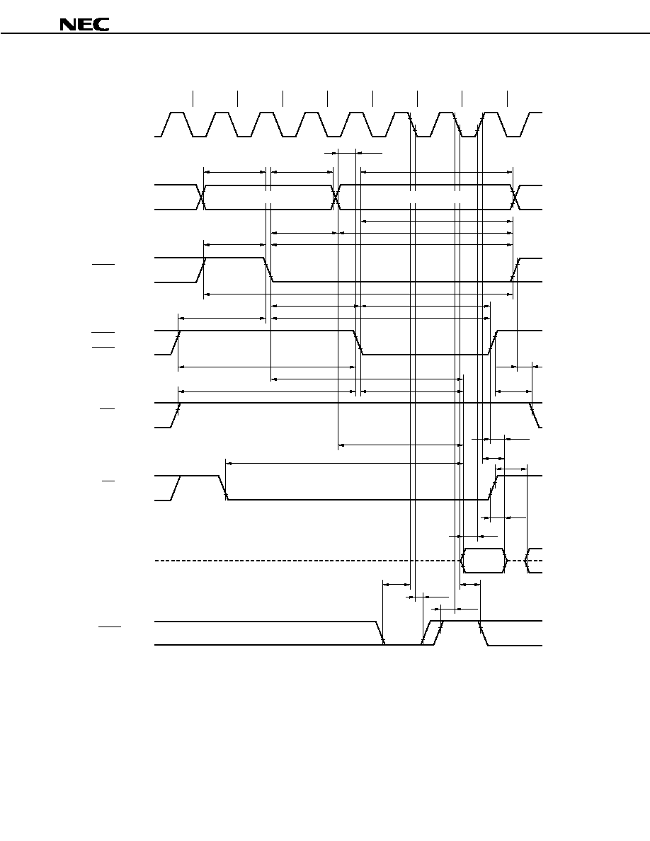
Preliminary Data Sheet U13995EJ1V0DS00
88
µ
µ
µ
µ
PD703100-33, 703100-40, 703101-33, 703102-33
(a) Read timing (high-speed page DRAM access, normal access: off-page) (3/3)
TRPW
TRHW
T2
T1
TDAW
TW
T3
<56>
<61>
<57>
<58>
<59>
<62>
<76>
<63>
<64>
<60>
<77>
<65>
<67>
<66>
<71>
<73>
<68>
<75>
<74>
<72>
<70>
<69>
<79>
<37>
<27>
<25>
<26>
<25>
<24>
<78>
<24>
CLKOUT (Output)
A0 to A23 (Output)
RASn (Output)
WE (Output)
OE (Output)
WAIT (Input)
D0 to D15 (I/O)
UCAS (Output)
LCAS (Output)
Row address
Column address
Remarks 1. This is the timing for the following case (n = 0 to 3, xx = 00 to 03, 10 to 13).
Number of waits due to the RPCxx bit of the DRCn register (TRPW): 1
Number of waits due to the RHCxx bit of the DRCn register (TRHW): 1
Number of waits due to the DACxx bit of the DRCn register (TDAW): 1
2. The broken lines indicate high impedance.
3. n = 0 to 7

Preliminary Data Sheet U13995EJ1V0DS00
89
µ
µ
µ
µ
PD703100-33, 703100-40, 703101-33, 703102-33
[MEMO]
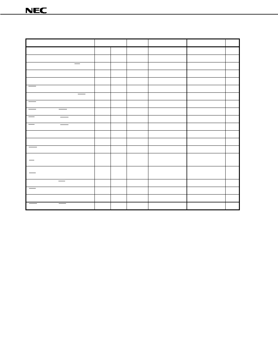
Preliminary Data Sheet U13995EJ1V0DS00
90
µ
µ
µ
µ
PD703100-33, 703100-40, 703101-33, 703102-33
(b) Read timing (high-speed page DRAM access: on-page) (1/2)
Parameter
Symbol
Condition
MIN.
MAX.
Unit
Data input setup time (to CLKOUT
)
<26>
t
SKID
18
ns
Data input hold time (from CLKOUT
)
<27>
t
HKID
2
ns
Data output delay time from OE
<37>
t
DRDOD
(0.5 + i) T ≠ 10
ns
Column address setup time
<58>
t
ASC
(0.5 + w
CP
) T ≠ 10
ns
Column address hold time
<59>
t
CAH
(1.5 + w
DA
) T ≠ 10
ns
RAS hold time
<63>
t
RSH
(1.5 + w
DA
) T ≠ 10
ns
Column address read time for RAS
<64>
t
RAL
(2 + w
CP
+ w
DA
) T ≠ 10
ns
CAS pulse width
<65>
t
CAS
(1 + w
DA
) T ≠ 10
ns
WE setup time (to CAS
)
<68>
t
RCS
(1 + w
CP
) T ≠ 10
ns
WE hold time (from RAS
)
<69>
t
RRH
0.5T ≠ 10
ns
WE hold time (from CAS
)
<70>
t
RCH
T ≠ 10
ns
Output enable access time
<72>
t
OEA
(1 + w
CP
+ w
DA
) T ≠ 28
ns
Access time from column address
<74>
t
AA
(1.5 + w
CP
+ w
DA
) T ≠ 28
ns
CAS access time
<75>
t
CAC
(1 + w
DA
) T ≠ 28
ns
Output buffer turn-off delay time (from
OE
)
<78>
t
OEZ
0
ns
Output buffer turn-off delay time (from
CAS
)
<79>
t
OFF
0
ns
Access time from CAS precharge
<80>
t
ACP
(2 + w
CP
+ w
DA
) T ≠ 28
ns
CAS precharge time
<81>
t
CP
(1 + w
CP
) T ≠ 10
ns
High-speed page mode cycle time
<82>
t
PC
(2 + w
CP
+ w
DA
) T ≠ 10
ns
RAS hold time for CAS precharge
<83>
t
RHCP
(2.5 + w
CP
+ w
DA
) T ≠ 10
ns
Remarks 1. T = t
CYK
2. w
CP
: the number of waits due to the CPCxx bit of the DRCn register (n = 0 to 3, xx = 00 to 03, 10 to
13).
3. w
DA
: the number of waits due to the DACxx bit of the DRCn register (n = 0 to 3, xx = 00 to 03, 10 to
13).
4. i: the number of idle states that are inserted when a write cycle follows a read cycle.
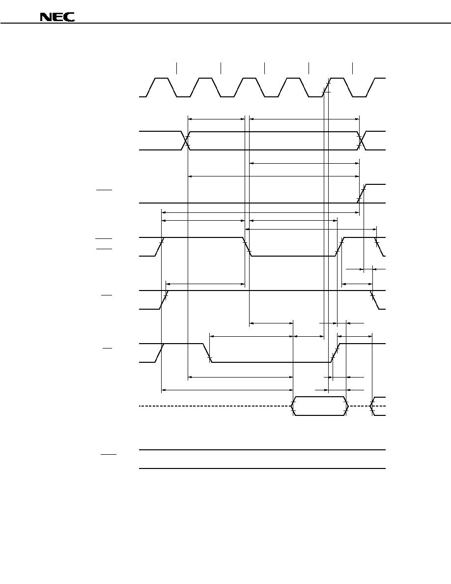
Preliminary Data Sheet U13995EJ1V0DS00
91
µ
µ
µ
µ
PD703100-33, 703100-40, 703101-33, 703102-33
(b) Read timing (high-speed page DRAM access: on-page) (2/2)
TCPW
TO1
TDAW
TO2
<58>
<59>
<63>
<64>
<83>
<65>
<81>
<82>
<68>
<75>
<72>
<26>
<79>
<37>
<74>
<80>
<27>
<78>
<70>
<69>
CLKOUT (Output)
A0 to A23 (Output)
RASn (Output)
UCAS (Output)
LCAS (Output)
WE (Output)
OE (Output)
D0 to D15 (I/O)
WAIT (Input)
Column address
Remarks 1. This is the timing for the following case (n = 0 to 3, xx = 00 to 03, 10 to 13).
Number of waits due to the CPCxx bit of the DRCn register (TCPW): 1
Number of waits due to the DACxx bit of the DRCn register (TDAW): 1
2. The broken lines indicate high impedance.
3. n = 0 to 7

Preliminary Data Sheet U13995EJ1V0DS00
92
µ
µ
µ
µ
PD703100-33, 703100-40, 703101-33, 703102-33
(c) Write timing (high-speed page DRAM access, normal access: off-page) (1/2)
Parameter
Symbol
Condition
MIN.
MAX.
Unit
WAIT setup time (to CLKOUT
)
<24>
t
SWK
15
ns
WAIT hold time (from CLKOUT
)
<25>
t
HKW
2
ns
Row address setup time
<56>
t
ASR
(0.5 + w
RP
) T ≠ 10
ns
Row address hold time
<57>
t
RAH
(0.5 + w
RH
) T ≠ 10
ns
Column address setup time
<58>
t
ASC
0.5T ≠ 10
ns
Column address hold time
<59>
t
CAH
(1.5 + w
DA
+ w) T ≠ 10
ns
Read/write cycle time
<60>
t
RC
(3 + w
RP
+ w
RH
+ w
DA
+ w)
T ≠ 10
ns
RAS precharge time
<61>
t
RP
(0.5 + w
RP
) T ≠ 10
ns
RAS pulse time
<62>
t
RAS
(2.5 + w
RH
+ w
DA
+ w)
T ≠ 10
ns
RAS hold time
<63>
t
RSH
(1.5 + w
DA
+ w) T ≠ 10
ns
Column address read time (from RAS
)
<64>
t
RAL
(2 + w
DA
+ w) T ≠ 10
ns
CAS pulse width
<65>
t
CAS
(1 + w
DA
+ w) T ≠ 10
ns
CAS-RAS precharge time
<66>
t
CRP
(1 + w
RH
) T ≠ 10
ns
CAS hold time
<67>
t
CSH
(2 + w
RH
+ w
DA
+ w)
T ≠ 10
ns
CAS precharge time
<71>
t
CPN
(2 + w
RP
+ w
RH
) T ≠ 10
ns
RAS column address delay time
<76>
t
RAD
(0.5 + w
RH
) T ≠ 10
ns
RAS-CAS delay time
<77>
t
RCD
(1 + w
RH
) T ≠ 10
ns
WE setup time (to CAS
)
<84>
t
WCS
(1 + w
RP
+ w
RH
)
T ≠ 10
ns
WE hold time (from CAS
)
<85>
t
WCH
(1 + w
DA
+ w) T ≠ 10
ns
Data setup time (to CAS
)
<86>
t
DS
(1.5 + w
RP
+ w
RH
) T ≠ 10
ns
Data hold time (from CAS
)
<87>
t
DH
(1.5 + w
DA
+ w) T ≠ 10
ns
Remarks 1. T = t
CYK
2. w: the number of waits due to WAIT.
3. w
RP
: the number of waits due to the RPCxx bit of the DRCn register (n = 0 to 3, xx = 00 to 03, 10 to
13).
4. w
RH
: the number of waits due to the RHCxx bit of the DRCn register (n = 0 to 3, xx = 00 to 03, 10 to
13).
5. w
DA
: the number of waits due to the DACxx bit of the DRCn register (n = 0 to 3, xx = 00 to 03, 10 to
13).
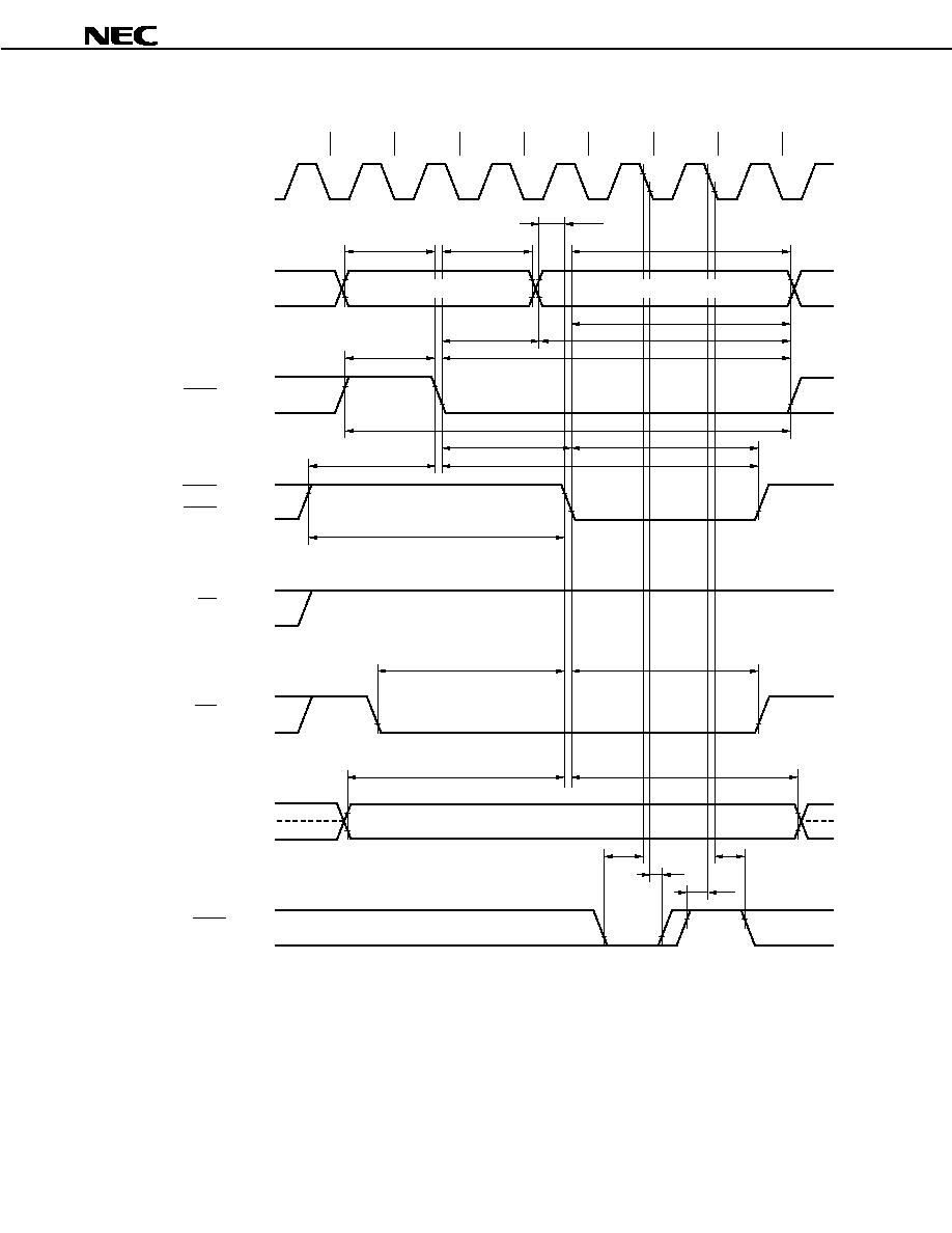
Preliminary Data Sheet U13995EJ1V0DS00
93
µ
µ
µ
µ
PD703100-33, 703100-40, 703101-33, 703102-33
(c) Write timing (high-speed page DRAM access, normal access: off-page) (2/2)
TRPW
TRHW
T2
T1
TDAW
TW
T3
<56>
<61>
<57>
<58>
<59>
<62>
<76>
<63>
<64>
<60>
<77>
<65>
<67>
<66>
<71>
<84>
<25>
<25>
<24>
<24>
<85>
<86>
<87>
CLKOUT (Output)
A0 to A23 (Output)
RASn (Output)
UCAS (Output)
LCAS (Output)
WE (Output)
OE (Output)
D0 to D15 (I/O)
WAIT (Input)
Row address
Column address
Remarks 1. This is the timing for the following case (n = 0 to 3, xx = 00 to 03, 10 to 13).
Number of waits due to the RPCxx bit of the DRCn register (TRPW): 1
Number of waits due to the RHCxx bit of the DRCn register (TRHW): 1
Number of waits due to the DACxx bit of the DRCn register (TDAW): 1
2. The broken lines indicate high impedance.
3. n = 0 to 7
Preliminary Data Sheet U13995EJ1V0DS00
94
µ
µ
µ
µ
PD703100-33, 703100-40, 703101-33, 703102-33
(d) Write timing (high-speed page DRAM access: on-page) (1/2)
Parameter
Symbol
Condition
MIN.
MAX.
Unit
Column address setup time
<58>
t
ASC
(0.5 + w
CP
) T ≠ 10
ns
Column address hold time
<59>
t
CAH
(1.5 + w
DA
) T ≠ 10
ns
RAS hold time
<63>
t
RSH
(1.5 + w
DA
) T ≠ 10
ns
Column address read time (from RAS
)
<64>
t
RAL
(2 + w
CP
+ w
DA
) T ≠ 10
ns
CAS pulse width
<65>
t
CAS
(1 + w
DA
) T ≠ 10
ns
CAS precharge time
<81>
t
CP
(1 + w
CP
) T ≠ 10
ns
RAS hold time for CAS precharge
<83>
t
RHCP
(2.5 + w
CP
+ w
DA
)
T ≠ 10
ns
WE setup time (to CAS
)
<84>
t
WCS
w
CP
1
w
CP
T ≠ 10
ns
WE hold time (from CAS
)
<85>
t
WCH
(1 + w
DA
) T ≠ 10
ns
Data setup time (to CAS
)
<86>
t
DS
(0.5 + w
CP
) T ≠ 10
ns
Data hold time (from CAS
)
<87>
t
DH
(1.5 + w
DA
) T ≠ 10
ns
WE read time (from RAS
)
<88>
t
RWL
w
CP
= 0
(1.5 + w
DA
) T ≠ 10
ns
WE read time (from CAS
)
<89>
t
CWL
w
CP
= 0
(1 + w
DA
) T ≠ 10
ns
Data setup time (to WE
)
<90>
t
DSWE
w
CP
= 0
0.5T ≠ 10
ns
Data hold time (from WE
)
<91>
t
DHWE
w
CP
= 0
(1.5 + w
DA
) T ≠ 10
ns
WE pulse width
<92>
t
WP
w
CP
= 0
(1 + w
DA
) T ≠ 10
ns
Remarks 1. T = t
CYK
2. w
CP
: the number of waits due to the CPCxx bit of the DRCn register (n = 0 to 3, xx = 00 to 03, 10 to
13).
3. w
DA
: the number of waits due to the DACxx bit of the DRCn register (n = 0 to 3, xx = 00 to 03, 10 to
13).
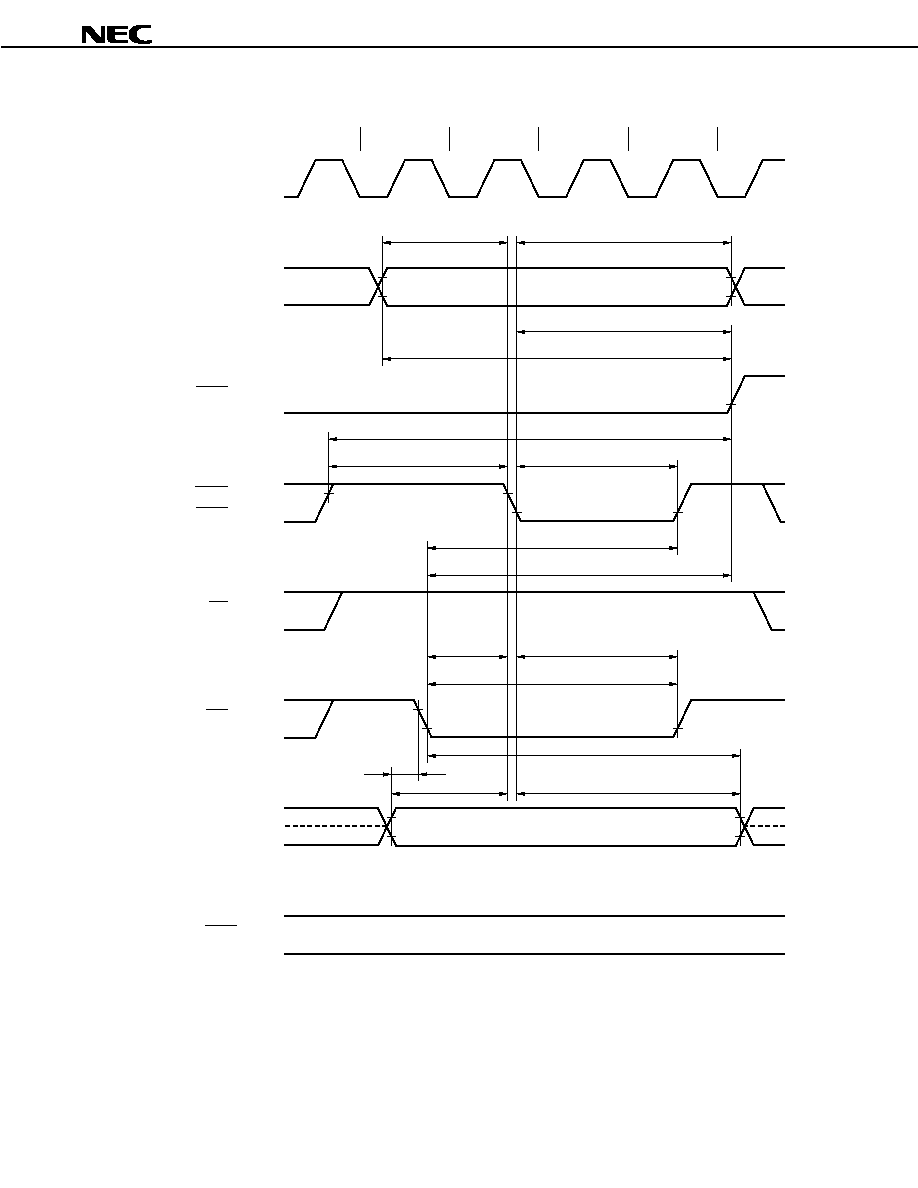
Preliminary Data Sheet U13995EJ1V0DS00
95
µ
µ
µ
µ
PD703100-33, 703100-40, 703101-33, 703102-33
(d) Write timing (high-speed page DRAM access: on-page) (2/2)
TCPW
TO1
TDAW
TO2
<58>
<59>
<63>
<64>
<83>
<81>
<65>
<89>
<88>
<84>
<85>
<92>
<91>
<86>
<87>
<90>
CLKOUT (Output)
A0 to A23 (Output)
RASn (Output)
UCAS (Output)
LCAS (Output)
OE (Output)
WE (Output)
D0 to D15 (I/O)
WAIT (Input)
Column address
Remarks 1. This is the timing for the following case (n = 0 to 3, xx = 00 to 03, 10 to 13).
Number of waits due to the CPCxx bit of the DRCn register (TCPW ): 1
Number of waits due to the DACxx bit of the DRCn register (TDAW): 1
2. The broken lines indicate high impedance.
3. n = 0 to 7

Preliminary Data Sheet U13995EJ1V0DS00
96
µ
µ
µ
µ
PD703100-33, 703100-40, 703101-33, 703102-33
(e) Read timing (EDO DRAM) (1/3)
Parameter
Symbol
Condition
MIN.
MAX.
Unit
Data input setup time (to CLKOUT
)
<26>
t
SKID
18
ns
Data input hold time (from CLKOUT
)
<27>
t
HKID
2
ns
Data output delay time from OE
<37>
t
DRDOD
(0.5 + i) T ≠ 10
ns
Row address setup time
<56>
t
ASR
(0.5 + w
RP
) T ≠ 10
ns
Row address hold time
<57>
t
RAH
(0.5 + w
RH
) T ≠ 10
ns
Column address setup time
<58>
t
ASC
0.5T ≠ 10
ns
Column address hold time
<59>
t
CAH
(0.5 + w
DA
) T ≠ 10
ns
RAS precharge time
<61>
t
RP
(0.5 + w
RP
) T ≠ 10
ns
Column address read time (from RAS
)
<64>
t
RAL
(2 + w
CP
+ w
DA
) T ≠ 10
ns
CAS-RAS precharge time
<66>
t
CRP
(1 + w
RP
) T ≠ 10
ns
CAS hold time
<67>
t
CSH
(1.5 + w
RH
+ w
DA
) T ≠ 10
ns
WE setup time (to CAS
)
<68>
t
RCS
(2 + w
RP
+ w
RH
) T ≠ 10
ns
WE hold time (from RAS
)
<69>
t
RRH
0.5T ≠ 10
ns
WE hold time (from CAS
)
<70>
t
RCH
1.5T ≠ 10
ns
RAS access time
<73>
t
RAC
(2 + w
RH
+ w
DA
) T ≠ 28
ns
Access time from column address
<74>
t
AA
(1.5 + w
DA
) T ≠ 28
ns
CAS access time
<75>
t
CAC
(1 + w
DA
) T ≠ 28
ns
Column address delay time from RAS
<76>
t
RAD
(0.5 + w
RH
) T ≠ 10
ns
RAS-CAS delay time
<77>
t
RCD
(1 + w
RH
) T ≠ 10
ns
Output buffer turn-off delay time (from
OE)
<78>
t
OEZ
0
ns
Access time from CAS precharge
<80>
t
ACP
(1.5 + w
CP
+ w
DA
) T ≠ 28
ns
CAS precharge time
<81>
t
CP
(0.5 + w
CP
) T ≠ 10
ns
RAS hold time for CAS precharge
<83>
t
RHCP
(2 + w
CP
+ w
DA
) T ≠ 10
ns
Read cycle time
<93>
t
HPC
(1 + w
DA
+ w
CP
) T ≠ 10
ns
RAS pulse width
<94>
t
RASP
(2.5 + w
RH
+ w
DA
) T ≠ 10
ns
CAS pulse width
<95>
t
HCAS
(0.5 + w
DA
) T ≠ 10
ns
Off-page
<96>
t
OCH1
(2 + w
RH
+ w
DA
) T ≠ 10
ns
CAS hold time from OE
On-page
<97>
t
OCH2
(0.5 + w
DA
) T ≠ 10
ns
Data input hold time (from CAS
)
<98>
t
DHC
0
ns
Remarks 1. T = t
CYK
2. w
RP
: the number of waits due to the RPCxx bit of the DRCn register (n = 0 to 3, xx = 00 to 03, 10 to
13).
3. w
RH
: the number of waits due to the RHCxx bit of the DRCn register (n = 0 to 3, xx = 00 to 03, 10 to
13).
4. w
DA
: the number of waits due to the DACxx bit of the DRCn register (n = 0 to 3, xx = 00 to 03, 10 to
13).
5. w
CP
: the number of waits due to the CPCxx bit of the DRCn register (n = 0 to 3, xx = 00 to 03, 10 to
13).
6. i: the number of idle states that are inserted when a write cycle follows a read cycle.

Preliminary Data Sheet U13995EJ1V0DS00
97
µ
µ
µ
µ
PD703100-33, 703100-40, 703101-33, 703102-33
(e) Read timing (EDO DRAM) (2/3)
Parameter
Symbol
Condition
MIN.
MAX.
Unit
Off-page
<99>
t
OEA1
(2 + w
PR
+ w
RH
+ w
DA
)
T ≠ 28
ns
Output enable access
time
On-page
<100>
t
OEA2
(1 + w
CP
+ w
DA
) T ≠ 28
ns
Remarks 1. T = t
CYK
2. w
RP
: the number of waits due to the RPCxx bit of the DRCn register (n = 0 to 3, xx = 00 to 03, 10 to
13).
3. w
RH
: the number of waits due to the RHCxx bit of the DRCn register (n = 0 to 3, xx = 00 to 03, 10 to
13).
4. w
DA
: the number of waits due to the DACxx bit of the DRCn register (n = 0 to 3, xx = 00 to 03, 10 to
13).
5. w
CP
: the number of waits due to the CPCxx bit of the DRCn register (n = 0 to 3, xx = 00 to 03, 10 to
13).

Preliminary Data Sheet U13995EJ1V0DS00
98
µ
µ
µ
µ
PD703100-33, 703100-40, 703101-33, 703102-33
(e) Read timing (EDO DRAM) (3/3)
TRPW
T1
TRHW
T2
TDAW TCPW
TB
TDAW
TE
<56>
<57>
<59>
<58>
<76>
<64>
<94>
<61>
<67>
<83>
<77>
<95>
<81>
<75>
<66>
<93>
<95>
<80>
<97>
<74>
<27>
<78>
Data
<74>
Data
<70>
<69>
<68>
<96>
<100>
<26>
<37>
<27>
<98>
<26>
<75>
<73>
<99>
CLKOUT (Output)
A0 to A23 (Output)
RASn (Output)
UCAS (Output)
LCAS (Output)
WE (Output)
OE (Output)
D0 to D15 (I/O)
BCYST (Output)
WAIT (Input)
Row address
Column address
Column address
Note For on-page access from another cycle during the RASn low level signal.
Remarks 1. This is the timing for the following case (n = 0 to 3, xx = 00 to 03, 10 to 13).
Number of waits due to the RPCxx bit of the DRCn register (TRPW): 1
Number of waits due to the RHCxx bit of the DRCn register (TRHW): 1
Number of waits due to the DACxx bit of the DRCn register (TDAW): 1
Number of waits due to the CPCxx bit of the DRCn register (TCPW): 1
2. The broken lines indicate high impedance.
3. n = 0 to 7

Preliminary Data Sheet U13995EJ1V0DS00
99
µ
µ
µ
µ
PD703100-33, 703100-40, 703101-33, 703102-33
[MEMO]

Preliminary Data Sheet U13995EJ1V0DS00
100
µ
µ
µ
µ
PD703100-33, 703100-40, 703101-33, 703102-33
(f) Write timing (EDO DRAM) (1/2)
Parameter
Symbol
Condition
MIN.
MAX.
Unit
Row address setup time
<56>
t
ASR
(0.5 + w
RP
) T ≠ 10
ns
Row address hold time
<57>
t
RAH
(0.5 + w
RH
) T ≠ 10
ns
Column address setup time
<58>
t
ASC
0.5T ≠ 10
ns
Column address hold time
<59>
t
CAH
(0.5 + w
DA
) T ≠ 10
ns
RAS precharge time
<61>
t
RP
(0.5 + w
RP
) T ≠ 10
ns
RAS hold time
<63>
t
RSH
(1.5 + w
DA
) T ≠ 10
ns
Column address read time
(from RAS
)
<64>
t
RAL
(2 + w
CP
+ w
DA
) T ≠ 10
ns
CAS-RAS precharge time
<66>
t
CRP
(1 + w
RP
) T ≠ 10
ns
CAS hold time
<67>
t
CSH
(1.5 + w
RH
+ w
DA
) T ≠ 10
ns
Column address delay time from RAS
<76>
t
RAD
(0.5 + w
RH
) T ≠ 10
ns
RAS-CAS delay time
<77>
t
RCD
(1 + w
RH
) T ≠ 10
ns
CAS precharge time
<81>
t
CP
(0.5 + w
CP
) T ≠ 10
ns
RAS hold time for CAS precharge
<83>
t
RHCP
(2 + w
CP
+ w
DA
) T ≠ 10
ns
WE hold time (from CAS
)
<85>
t
WCH
(1 + w
DA
) T ≠ 10
ns
Data hold time (from CAS
)
<87>
t
DH
(0.5 + w
DA
) T ≠ 10
ns
WE read time
(from RAS
)
On-page
<88>
t
RWL
w
CP
= 0
(1.5 + w
DA
) T ≠ 10
ns
WE read time
(from CAS
)
On-page
<89>
t
CWL
w
CP
= 0
(0.5 + w
DA
) T ≠ 10
ns
WE pulse width
On-page
<92>
t
WP
w
CP
= 0
(1 + w
DA
) T ≠ 10
ns
Write cycle time
<93>
t
HPC
(1 + w
DA
+ w
CP
) T ≠ 10
ns
RAS pulse width
<94>
t
RASP
(2.5 + w
RH
+ w
DA
) T ≠ 10
ns
CAS pulse width
<95>
t
HCAS
(0.5 + w
DA
) T ≠ 10
ns
Off-page
<101>
t
WCS1
(1 + w
RP
+ w
RH
) T ≠ 10
ns
WE setup time
(to CAS
)
On-page
<102>
t
WCS2
w
CP
1
w
CP
T ≠ 10
ns
Off-page
<103>
t
DS1
(1.5 + w
RP
+ w
RH
) T ≠ 10
ns
Data setup time
(to CAS
)
On-page
<104>
t
DS2
(0.5 + w
CP
) T ≠ 10
ns
Remarks 1. T = t
CYK
2. w
RP
: the number of waits due to the RPCxx bit of the DRCn register (n = 0 to 3, xx = 00 to 03, 10 to
13).
3. w
RH
: the number of waits due to the RHCxx bit of the DRCn register (n = 0 to 3, xx = 00 to 03, 10 to
13).
4. w
DA
: the number of waits due to the DACxx bit of the DRCn register (n = 0 to 3, xx = 00 to 03, 10 to
13).
5. w
CP
: the number of waits due to the CPCxx bit of the DRCn register (n = 0 to 3, xx = 00 to 03, 10 to
13).
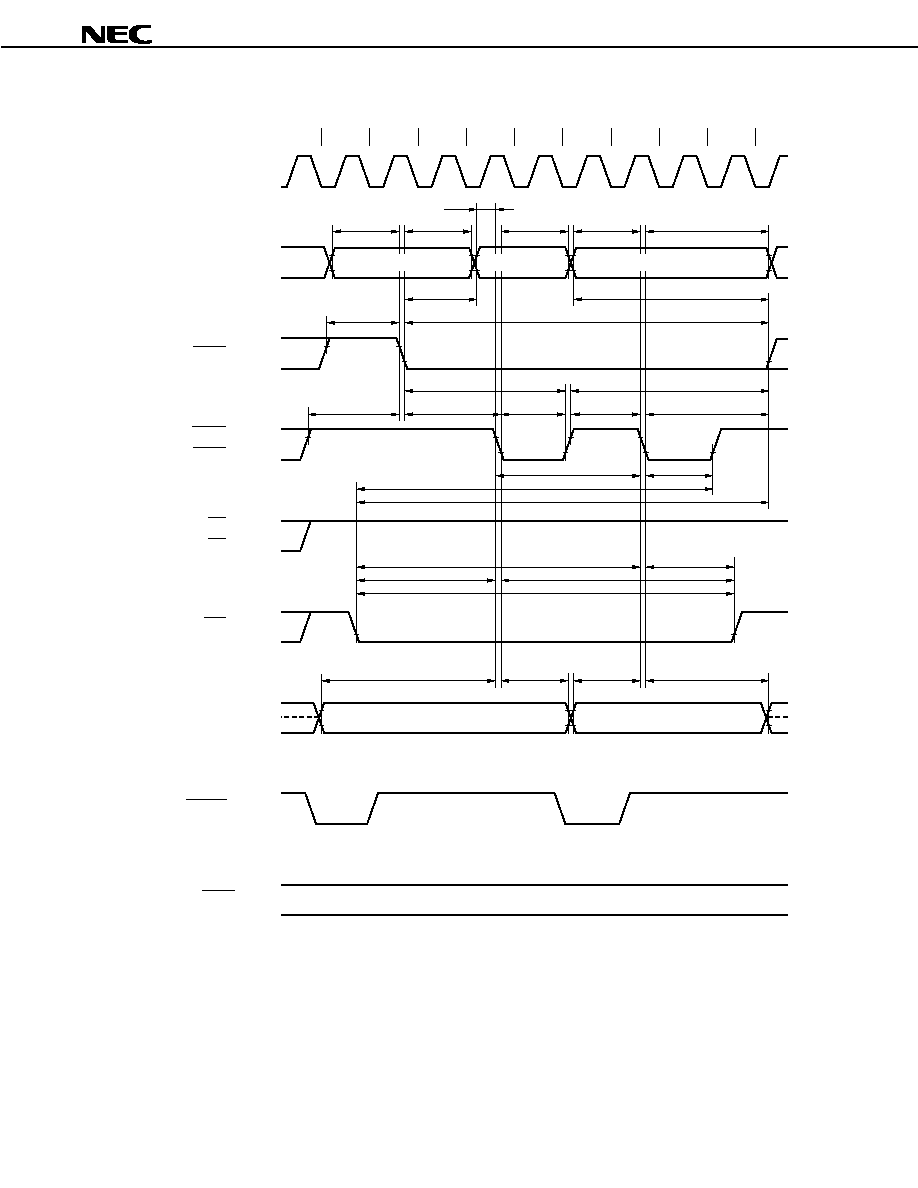
Preliminary Data Sheet U13995EJ1V0DS00
101
µ
µ
µ
µ
PD703100-33, 703100-40, 703101-33, 703102-33
(f) Write timing (EDO DRAM) (2/2)
TRPW
T1
TRHW
T2
TDAW
TCPW
TB
TDAW
TE
<56>
<57>
<59>
<58>
<58>
<59>
<76>
<64>
<94>
<61>
<67>
<83>
<77>
<95>
<81>
<63>
<66>
<93>
<95>
<89>
<88>
<102>
<101>
<92>
<85>
<85>
<103>
<87>
<104>
<87>
Data
Data
CLKOUT (Output)
A0 to A23 (Output)
RASn (Output)
UCAS (Output)
LCAS (Output)
RD (Output)
OE (Output)
WE (Output)
D0 to D15 (I/O)
BCYST (Output)
WAIT (Input)
Row address
Column address
Column address
Remarks 1. This is the timing for the following case (n = 0 to 3, xx = 00 to 03, 10 to 13).
Number of waits due to the RPCxx bit of the DRCn register (TRPW): 1
Number of waits due to the RHCxx bit of the DRCn register (TRHW): 1
Number of waits due to the DACxx bit of the DRCn register (TDAW): 1
Number of waits due to the CPCxx bit of the DRCn register (TCPW): 1
2. The broken lines indicate high impedance.
3. n = 0 to 7
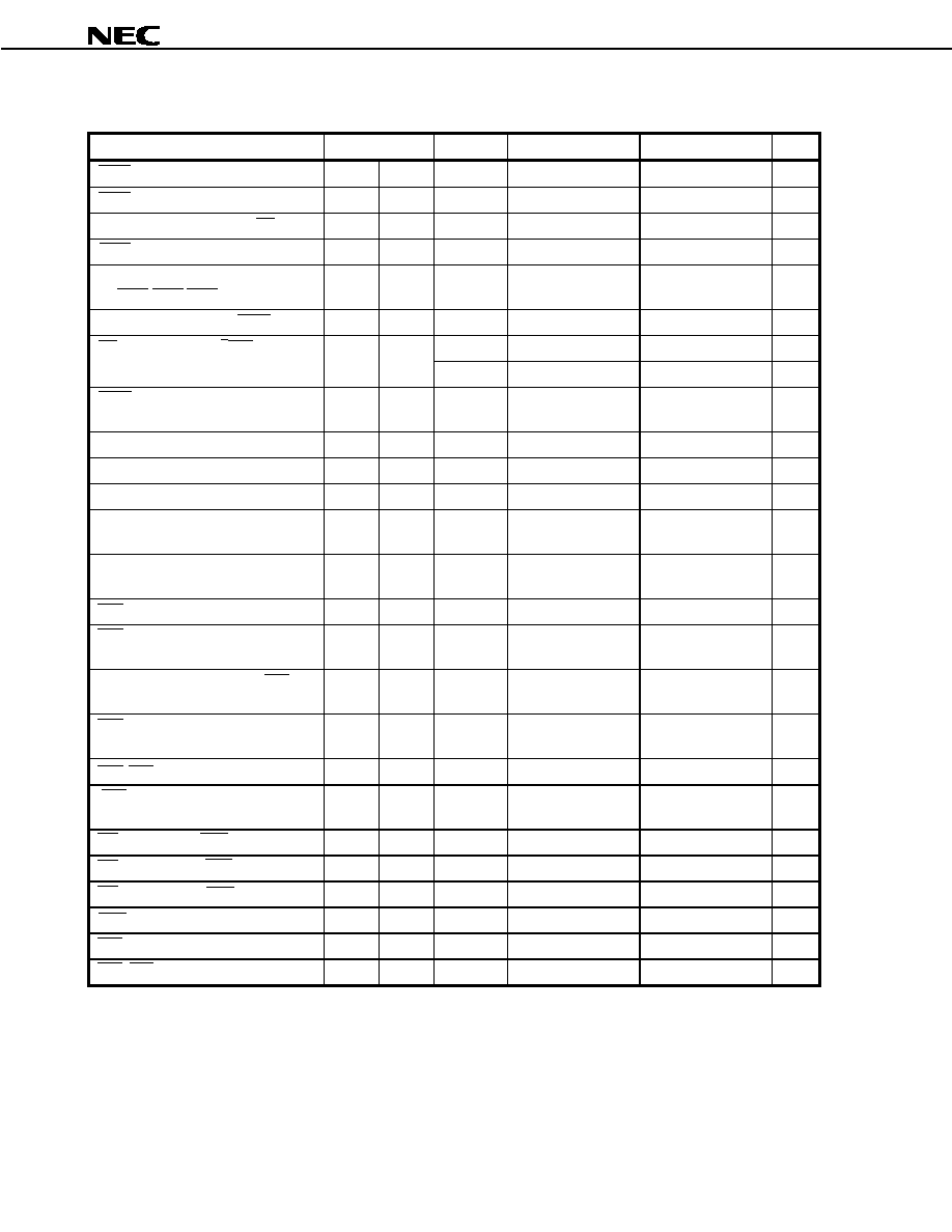
Preliminary Data Sheet U13995EJ1V0DS00
102
µ
µ
µ
µ
PD703100-33, 703100-40, 703101-33, 703102-33
(g) DMA flyby transfer timing (DRAM (EDO, high-speed page)
external I/O transfer) (1/3)
Parameter
Symbol
Condition
MIN.
MAX.
Unit
WAIT setup time (to CLKOUT
)
<24>
t
SWK
15
ns
WAIT hold time (from CLKOUT
)
<25>
t
HKW
2
ns
Data output delay time from OE
<37>
t
DRDOD
(0.5 + i) T ≠ 10
ns
IOWR
delay time from address
<41>
t
DAWR
(0.5 + w
RP
) T ≠ 10
ns
Address setup time
(to UWR, LWR IOWR
)
<42>
t
SAWR
(2 + w
RP
+ w
RH
+ w
DA
)
T ≠ 10
ns
Address delay time from IOWR
<43>
t
DWRA
0.5T ≠ 10
ns
w
F
= 0
0
ns
RD
delay time from IOWR
<48>
t
DWRRD
w
F
= 1
T ≠ 10
ns
IOWR low-level width
<50>
t
WWRL
(2 + w
RH
+ w
DA
+ w)
T ≠ 10
ns
Row address setup time
<56>
t
ASR
(0.5 + w
RP
) T ≠ 10
ns
Row address hold time
<57>
t
RAH
(0.5 + w
RH
) T ≠ 10
ns
Column address setup time
<58>
t
ASC
0.5T ≠ 10
ns
Column address hold time
<59>
t
CAH
(1.5 + w
DA
+ w
F
+ w)
T ≠ 10
ns
Read/write cycle time
<60>
t
RC
(3 + w
RP
+ w
RH
+ w
DA
+
w
F
+w) T ≠ 10
ns
RAS precharge time
<61>
t
RP
(0.5 + w
RP
) T ≠ 10
ns
RAS hold time
<63>
t
RSH
(1.5 + w
DA
+ w
F
+ w)
T ≠ 10
ns
Column address read time for RAS
<64>
t
RAL
(2 + w
CP
+ w
DA
+ w
F
+ w)
T ≠ 10
ns
CAS pulse width
<65>
t
CAS
(1 + w
DA
+ w
F
+ w)
T ≠ 10
ns
CAS-RAS precharge time
<66>
t
CRP
(1 + w
RP
) T ≠ 10
ns
CAS hold time
<67>
t
CSH
(2 + w
RH
+ w
DA
+ w
F
+w)
T ≠ 10
ns
WE setup time (to CAS
)
<68>
t
RCS
(2 + w
RP
+ w
RH
) T ≠ 10
ns
WE hold time (from RAS
)
<69>
t
RRH
0.5T ≠ 10
ns
WE hold time (from CAS
)
<70>
t
RCH
1.5T ≠ 10
ns
CAS precharge time
<71>
t
CPN
(2 + w
RP
+ w
RH
) T ≠ 10
ns
RAS column address delay time
<76>
t
RAD
(0.5 + w
RH
) T ≠ 10
ns
RAS-CAS delay time
<77>
t
RCD
(1 + w
RH
) T ≠ 10
ns

Preliminary Data Sheet U13995EJ1V0DS00
103
µ
µ
µ
µ
PD703100-33, 703100-40, 703101-33, 703102-33
Remarks 1. T = t
CYK
2. w: the number of waits due to WAIT.
3. w
RP
: the number of waits due to the RPCxx bit of the DRCn register (n = 0 to 3, xx = 00 to 03, 10 to
13).
4. w
RH
: the number of waits due to the RHCxx bit of the DRCn register (n = 0 to 3, xx = 00 to 03, 10 to
13).
5. w
DA
: the number of waits due to the DACxx bit of the DRCn register (n = 0 to 3, xx = 00 to 03, 10 to
13).
6. w
CP
: the number of waits due to the CPCxx bit of the DRCn register (n = 0 to 3, xx = 00 to 03, 10 to
13).
7. w
F
: the number of waits that are inserted for a source-side access during a DMA flyby transfer.
8. i: the number of idle states that are inserted when a write cycle follows a read cycle.
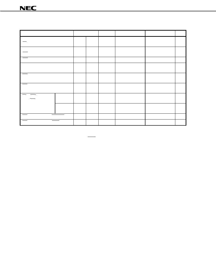
Preliminary Data Sheet U13995EJ1V0DS00
104
µ
µ
µ
µ
PD703100-33, 703100-40, 703101-33, 703102-33
(g) DMA flyby transfer timing (DRAM (EDO, high-speed page) R external I/O transfer) (2/3)
Parameter
Symbol
Condition
MIN.
MAX.
Unit
Output buffer turn-off delay time (from
OE
)
<78>
t
OEZ
0
ns
Output buffer turn-off delay time (from
CAS
)
<79>
t
OFF
0
ns
CAS precharge time
<81>
t
CP
(0.5 + w
CP
) T ≠ 10
ns
High-speed page mode cycle time
<82>
t
PC
(2 + w
CP
+ w
DA
+ w
F
+ w)
T ≠ 10
ns
RAS hold time for CAS precharge
<83>
t
RHCP
(2.5 + w
CP
+ w
DA
+ w
F
+ w)
T ≠ 10
ns
RAS pulse width
<94>
t
RASP
(2.5 + w
RH
+ w
DA
+ w
F
+ w)
T ≠ 10
ns
Off-page
<96>
t
OCH1
(2.5 + w
RP
+ w
RH
+ w
DA
+ w
F
+ w) T ≠ 10
ns
OE
CAS hold time
(from CAS
)
On-page
<97>
t
OCH2
(1.5 + w
CP
+ w
DA
+ w
F
+ w)
T ≠ 10
ns
CAS
delay time from DMAAKm
<105>
t
DDACS
(1.5 + w
RH
) T ≠ 10
ns
CAS
delay time from IOWR
<106>
t
DRDCS
(1 + w
RH
) T ≠ 10
ns
Remarks 1. T=t
CYK
2. w: the number of waits due to WAIT.
3. w
CP
: the number of waits due to the CPCxx bit of the DRCn register (n = 0 to 3, xx = 00 to 03, 10 to
13).
4. w
DA
: the number of waits due to the DACxx bit of the DRCn register (n = 0 to 3, xx = 00 to 03, 10 to
13).
5. w
RH
: the number of waits due to the RHCxx bit of the DRCn register (n = 0 to 3, xx = 00 to 03, 10 to
13).
6. w
RP
: the number of waits due to the RPCxx bit of the DRCn register (n = 0 to 3, xx = 00 to 03, 10 to
13).
7. w
F
: the number of waits that are inserted for a source-side access during a DMA flyby transfer.
8. m = 0 to 3
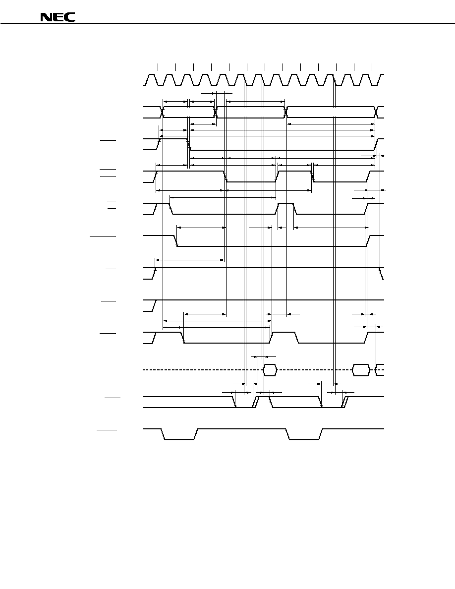
Preliminary Data Sheet U13995EJ1V0DS00
105
µ
µ
µ
µ
PD703100-33, 703100-40, 703101-33, 703102-33
(g) DMA flyby transfer timing (DRAM (EDO, high-speed page)
external I/O transfer) (3/3)
TRPW
T1
TRHW
T2
TDAW
TW
T3
TCPW
TO1
TO2
TW
TDAW
<56>
<57>
<58>
<59>
<76>
<61>
<60>
<94>
<64>
<77>
<65>
<83>
<63>
<81>
<67>
<66>
<71>
<82>
<96>
<105>
<68>
<69>
<70>
<79>
<48>
<97>
<106>
<42>
<41>
<50>
<43>
<78>
<37>
<24>
<25>
<24>
<25>
<25>
<24>
Data
Data
CLKOUT (Output)
A0 to A23 (Output)
RASn (Output)
UCAS (Output)
LCAS (Output)
RD (Output)
OE (Output)
DMAAKm (Output)
WE (Output)
IORD (Output)
IOWR (Output)
D0 to D15 (I/O)
WAIT (Input)
BCYST (Output)
Row address
Column address
Column address
Remarks 1. This is the timing for the following case (n = 0 to 3, xx = 00 to 03, 10 to 13).
Number of waits due to the RPCxx bit of the DRCn register (TRPW): 1
Number of waits due to the RHCxx bit of the DRCn register (TRHW): 1
Number of waits due to the DACxx bit of the DRCn register (TDAW): 1
Number of waits due to the CPCxx bit of the DRCn register (TCPW): 1
Number of waits that are inserted for a source-side access during a DMA flyby transfer: 0
2. The broken lines indicate high impedance.
3. n = 0 to 7, m = 0 to 3

Preliminary Data Sheet U13995EJ1V0DS00
106
µ
µ
µ
µ
PD703100-33, 703100-40, 703101-33, 703102-33
(h) DMA flyby transfer timing (external I/O
DRAM (EDO, high-speed page) transfer) (1/3)
Parameter
Symbol
Condition
MIN.
MAX.
Unit
WAIT setup time (to CLKOUT
)
<24>
t
SWK
15
ns
WAIT hold time (from CLKOUT
)
<25>
t
HKW
2
ns
IORD low-level width
<32>
t
WRDL
(2 + w
RH
+ w
DA
+ w
F
+ w) T ≠ 10
ns
IORD high-level width
<33>
t
WRDH
T ≠ 10
ns
IORD
delay time from address, CSn
<34>
t
DARD
0.5T ≠ 10
ns
Address delay time from IORD
<35>
t
DRDA
(0.5 + i) T ≠ 10
ns
Row address setup time
<56>
t
ASR
(0.5 + w
RP
) T ≠ 10
ns
Row address hold time
<57>
t
RAH
(0.5 + w
RH
) T ≠ 10
ns
Column address setup time
<58>
t
ASC
0.5T ≠ 10
ns
Column address hold time
<59>
t
CAH
(1.5 + w
DA
+ w
F
) T ≠ 10
ns
Read/write cycle time
<60>
t
RC
(3 + w
RP
+ w
RH
+ w
DA
+ w
F
+ w)
T ≠ 10
ns
RAS precharge time
<61>
t
RP
(0.5 + w
RP
) T ≠ 10
ns
RAS hold time
<63>
t
RSH
(1.5 + w
DA
+ w
F
) T ≠ 10
ns
Column address read time for RAS
<64>
t
RAL
(2 + w
CP
+ w
DA
+ w
F
+ w) T ≠ 10
ns
CAS pulse width
<65>
t
CAS
(1 + w
DA
+ w
F
) T ≠ 10
ns
CAS-RAS precharge time
<66>
t
CRP
(1 + w
RP
) T ≠ 10
ns
CAS hold time
<67>
t
CSH
(2 + w
RH
+ w
DA
+ w
F
+ w) T ≠ 10
ns
CAS precharge time
<71>
t
CPN
(2 + w
RP
+ w
RH
+ w) T ≠ 10
ns
RAS column address delay time
<76>
t
RAD
(0.5 + w
RH
) T ≠ 10
ns
RAS-CAS delay time
<77>
t
RCD
(1 + w
RH
+ w) T ≠ 10
ns
CAS precharge time
<81>
t
CP
(0.5 + w
CP
+ w) T ≠ 10
ns
High-speed page mode cycle time
<82>
t
PC
(2 + w
CP
+ w
DA
+ w
F
+ w) T ≠ 10
ns
RAS hold time for CAS precharge
<83>
t
RHCP
(2.5 + w
CP
+ w
DA
+ w) T ≠ 10
ns
WE hold time (from CAS
)
<85>
t
WCH
(1 + w
DA
) T ≠ 10
ns
WE read time (from RAS
)
<88>
t
RWL
w
CP
= 0
(1.5 + w
DA
+ w) T ≠ 10
ns
WE read time (from CAS
)
<89>
t
CWL
w
CP
= 0
(1 + w
DA
+ w) T ≠ 10
ns
WE pulse width
<92>
t
WP
w
CP
= 0
(1 + w
DA
+ w) T ≠ 10
ns
RAS pulse width
<94>
t
RASP
(2.5 + w
RH
+ w
DA
+ w
F
+ w) T ≠ 10
ns
Off-page
<101>
t
WCS1
w
CP
= 0
(1 + w
RH
+ w
RP
+ w) T ≠ 10
ns
WE setup time
(to CAS
)
On-page
<102>
t
WCS2
w
CP
1
w
CP
T ≠ 10
ns

Preliminary Data Sheet U13995EJ1V0DS00
107
µ
µ
µ
µ
PD703100-33, 703100-40, 703101-33, 703102-33
Remarks 1. T = t
CYK
2. w: the number of waits due to WAIT.
3. w
RH
: the number of waits due to the RHCxx bit of the DRCn register (n = 0 to 3, xx = 00 to 03, 10 to
13).
4. w
DA
: the number of waits due to the DACxx bit of the DRCn register (n = 0 to 3, xx = 00 to 03, 10 to
13).
5. w
RP
: the number of waits due to the RPCxx bit of the DRCn register (n = 0 to 3, xx = 00 to 03, 10 to
13).
6. w
CP
: the number of waits due to the CPCxx bit of the DRCn register (n = 0 to 3, xx = 00 to 03, 10 to
13).
7. w
F
: the number of waits that are inserted for a source-side access during a DMA flyby transfer.
8. i: the number of idle states that are inserted when a write cycle follows a read cycle.
9. n = 0 to 7
Preliminary Data Sheet U13995EJ1V0DS00
108
µ
µ
µ
µ
PD703100-33, 703100-40, 703101-33, 703102-33
(h) DMA flyby transfer timing (external I/O
DRAM (EDO, high-speed page) transfer) (2/3)
Parameter
Symbol
Condition
MIN.
MAX.
Unit
CAS
delay time from DMAAKm
<105>
t
DDACS
(1.5 + w
RH
+ w) T ≠ 10
ns
CAS
delay time from IORD
<106>
t
DRDCS
(1 + w
RH
+ w) T ≠ 10
ns
IORD
delay time from WE
<107>
t
DWERD
w
F
= 0
0
ns
w
F
= 1
T ≠ 10
ns
Remarks 1. T = t
CYK
2. w: the number of waits due to WAIT.
3. w
RH
: the number of waits due to the RHCxx bit of the DRCn register (n = 0 to 3, xx = 00 to 03, 10 to
13).
4. w
F
: the number of waits that are inserted for a source-side access during a DMA flyby transfer.
5. m = 0 to 3
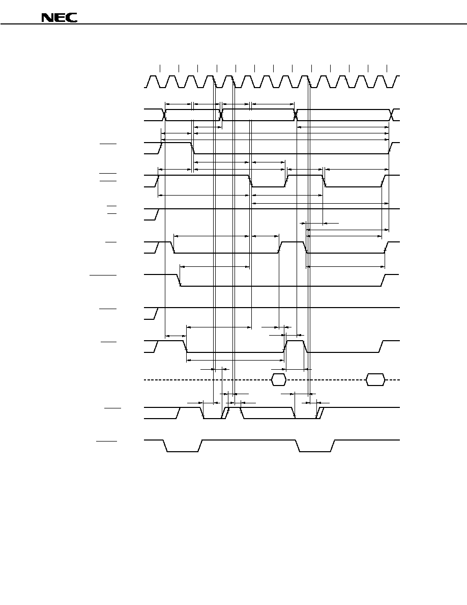
Preliminary Data Sheet U13995EJ1V0DS00
109
µ
µ
µ
µ
PD703100-33, 703100-40, 703101-33, 703102-33
(h) DMA flyby transfer timing (external I/O
DRAM (EDO, high-speed page) transfer) (3/3)
TRPW
T1
TRHW
TW
T2
TDAW
T3
TCPW
TW
TO2
TDAW
TO1
<56>
<57>
<58>
<76>
<61>
<60>
<94>
<64>
<77>
<65>
<63>
<81>
<67>
<66>
<71>
<82>
<101>
<105>
<83>
<85>
<89>
<106>
<34>
<107>
<33>
<24>
<25>
<24>
<25>
<24>
Data
Data
<59>
<88>
<102>
<92>
<35>
<32>
<25>
CLKOUT (Output)
A0 to A23 (Output)
RASn (Output)
UCAS (Output)
LCAS (Output)
RD (Output)
OE (Output)
DMAAKm (Output)
WE (Output)
IOWR (Output)
IORD (Output)
D0 to D15 (I/O)
WAIT (Input)
BCYST (Output)
Row address
Column address
Column address
Remarks 1. This is the timing for the following case (n = 0 to 3, xx = 00 to 03, 10 to 13).
Number of waits due to the RPCxx bit of the DRCn register (TRPW): 1
Number of waits due to the RHCxx bit of the DRCn register (TRHW): 1
Number of waits due to the DACxx bit of the DRCn register (TDAW): 1
Number of waits due to the CPCxx bit of the DRCn register (TCPW): 1
Number of waits that are inserted for a source-side access during a DMA flyby transfer: 0
2. The broken lines indicate high impedance.
3. n = 0 to 7, m = 0 to 3
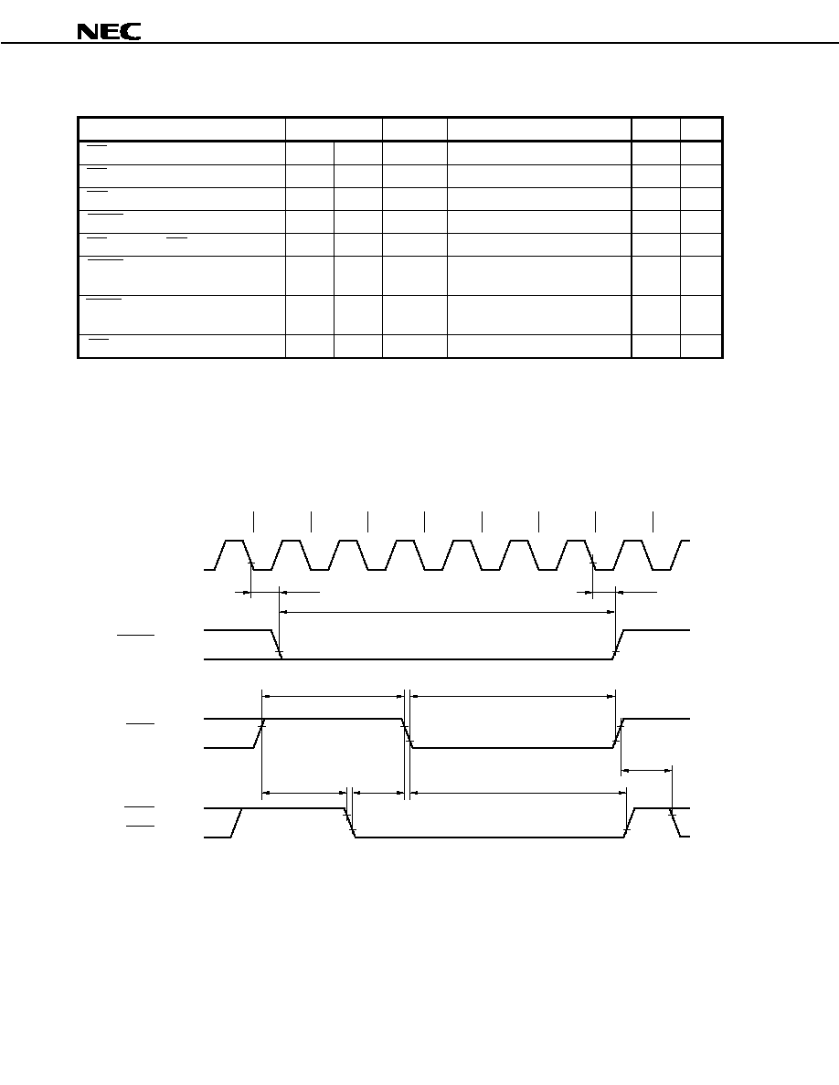
Preliminary Data Sheet U13995EJ1V0DS00
110
µ
µ
µ
µ
PD703100-33, 703100-40, 703101-33, 703102-33
(i) CBR refresh timing
Parameter
Symbol
Condition
MIN.
MAX.
Unit
RAS precharge time
<61>
t
RP
(1.5 + w
RRW
) T ≠ 10
ns
RAS pulse width
<62>
t
RAS
(1.5 + w
RCW
Note
) T ≠ 10
ns
CAS hold time
<108>
t
CHR
(1.5 + w
RCW
Note
) T ≠ 10
ns
REFRQ pulse width
<109>
t
WRFL
(3 + w
RRW
+ w
RCW
Note
) T ≠ 10
ns
RAS precharge CAS hold time
<110>
t
RPC
(0.5 + w
RRW
) T ≠ 10
ns
REFRQ active delay time
(from CLKOUT
)
<111>
t
DKRF
2
10
ns
REFRQ inactive delay time
(from CLKOUT
)
<112>
t
HKRF
2
10
ns
CAS setup time
<113>
t
CSR
T ≠ 10
ns
Note At least one clock cycle is inserted by default for w
RCW
regardless of the settings of the RCW0 to RCW2 bits
of the RWC register.
Remarks 1. T = t
CYK
2. w
RRW
: the number of waits due to the RRW0 and RRW1 bits of the RWC register.
3. w
RCW
: the number of waits due to the RCW0 to RCW2 bits of the RWC register.
TI
REFRQ (Output)
T3
TRCW
TRCW
Note
T2
T1
TRRW
<109>
<111>
<112>
RASn (Output)
<62>
UCAS (Output)
<108>
<110>
<61>
<113>
<110>
LCAS (Output)
CLKOUT (Output)
Note This TRCW is always inserted regardless of the settings of the RCW0 to RCW2 bits of the RWC register.
Remarks 1. This is the timing for the following case.
Number of waits due to the RRW0 and RRW1 bits of the RWC register (TRRW): 1
Number of waits due to the RCW0 to RCW2 bits of the RWC register (TRCW): 2
2. n = 0 to 7
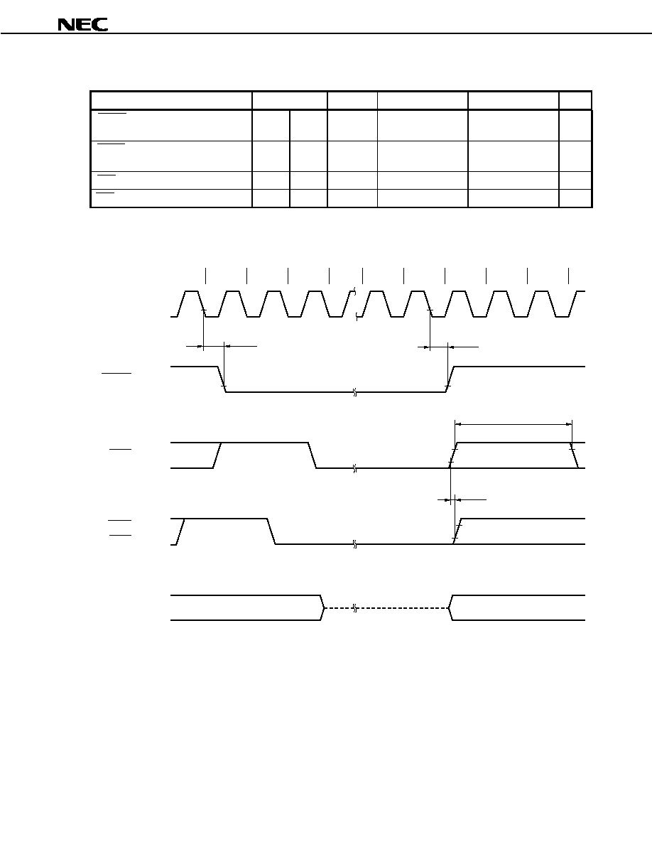
Preliminary Data Sheet U13995EJ1V0DS00
111
µ
µ
µ
µ
PD703100-33, 703100-40, 703101-33, 703102-33
(j) CBR self-refresh timing
Parameter
Symbol
Condition
MIN.
MAX.
Unit
REFRQ active delay time
(from CLKOUT
)
<111>
t
DKRF
2
10
ns
REFRQ inactive delay time
(from CLKOUT
)
<112>
t
HKRF
2
10
ns
CAS hold time
<114>
t
CHS
-
5
ns
RAS precharge time
<115>
t
RPS
(1 + 2w
SRW
) T ≠ 10
ns
Remarks 1. T = t
CYK
2. w
SRW
: the number of waits due to the SRW0 to SRW2 bits of the RWC register.
<111>
TH
TH
TH
TRRW
TSRW
TI
TH
TRCW
TSRW
Output signals
other than above
<115>
<112>
<114>
CLKOUT (Output)
REFRQ (Output)
RASn (Output)
UCAS (Output)
LCAS (Output)
Remarks 1. This is the timing for the following case.
Number of waits due to the RRW0 and RRW1 bits of the RWC register (TRRW): 1
Number of waits due to the RCW0 to RCW2 bits of the RWC register (TRCW): 1
Number of waits due to the SRW0 to SRW2 bits of the RWC register (TSRW): 2
2. The broken lines indicate high impedance.
3. n = 0 to 7
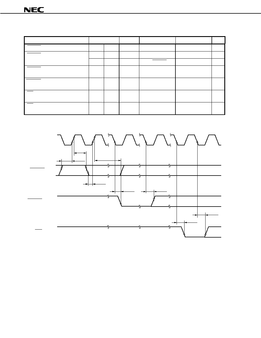
Preliminary Data Sheet U13995EJ1V0DS00
112
µ
µ
µ
µ
PD703100-33, 703100-40, 703101-33, 703102-33
(7) DMAC timing
Parameter
Symbol
Condition
MIN.
MAX.
Unit
DMARQn setup time (to CLKOUT
)
<116>
t
SDRK
15
ns
<117>
t
HKDR1
2
ns
DMARQn hold time (from CLKOUT
)
<118>
t
HKDR2
Until DMAAKn
ns
DMAAKn output delay time
(from CLKOUT
)
<119>
t
DKDA
2
10
ns
DMAAKn output hold time
(from CLKOUT
)
<120>
t
HKDA
2
10
ns
TCn output delay time
(from CLKOUT
)
<121>
t
DKTC
2
10
ns
TCn output hold time
(from CLKOUT
)
<122>
t
HKTC
2
10
ns
Remark n = 0 to 3
<121>
DMARQn (Input)
DMAAKn (Output)
TCn (Output)
<122>
<120>
<119>
<118>
<117>
<116>
<116>
CLKOUT (Output)
Remark n = 0 to 3

Preliminary Data Sheet U13995EJ1V0DS00
113
µ
µ
µ
µ
PD703100-33, 703100-40, 703101-33, 703102-33
[MEMO]
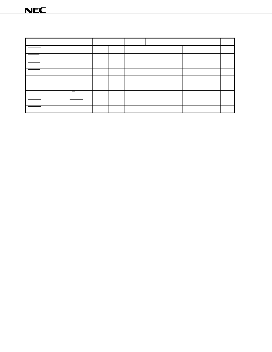
Preliminary Data Sheet U13995EJ1V0DS00
114
µ
µ
µ
µ
PD703100-33, 703100-40, 703101-33, 703102-33
(8) Bus hold timing (1/2)
Parameter
Symbol
Condition
MIN.
MAX.
Unit
HLDRQ setup time (to CLKOUT
)
<123>
t
SHRK
15
ns
HLDRQ hold time (from CLKOUT
)
<124>
t
HKHR
2
ns
HLDAK delay time from CLKOUT
<125>
t
DKHA
2
10
ns
HLDRQ high-level width
<126>
t
WHQH
T + 17
ns
HLDAK low-level width
<127>
t
WHAL
T ≠ 8
ns
Bus float delay time from CLKOUT
<128>
t
DKCF
10
ns
Bus output delay time from HLDAK
<129>
t
DHAC
0
ns
HLDAK
delay time from HLDRQ
<130>
t
DHQHA1
2.5T
ns
HLDAK
delay time from HLDRQ
<131>
t
DHQHA2
0.5T
1.5T
ns
Remark T = t
CYK
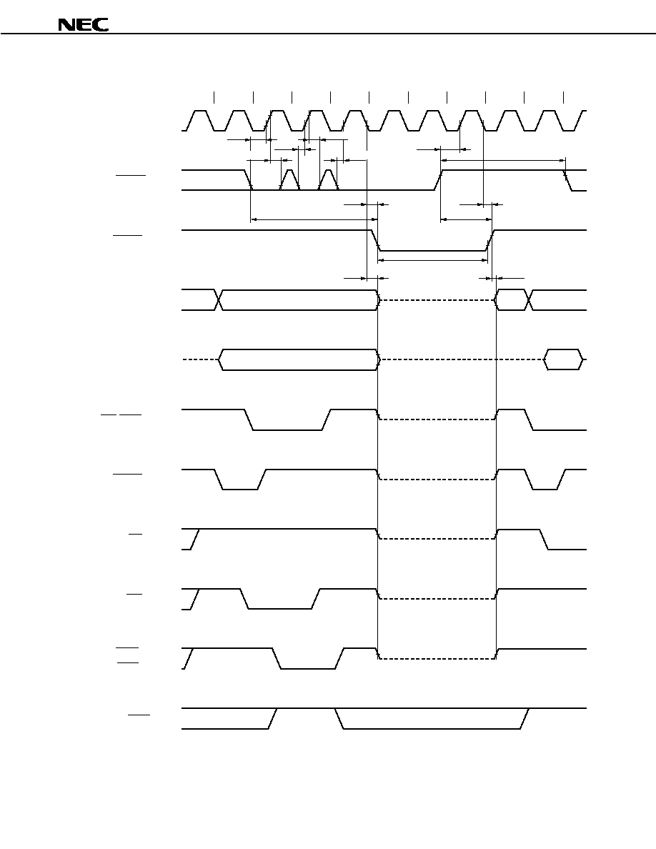
Preliminary Data Sheet U13995EJ1V0DS00
115
µ
µ
µ
µ
PD703100-33, 703100-40, 703101-33, 703102-33
(8) Bus hold timing (2/2)
T1
T2
T3
TI
TH
TH
TH
TI
T1
A0 to A23 (Output)
D0 to D15 (I/O)
<123>
<124>
<124>
<123>
<123>
<123>
<126>
<130>
<125>
<127>
<125>
<128>
<129>
<131>
Address
Undefined
Data
CLKOUT (Output)
HLDRQ (Intput)
HLDAK (Output)
CSn/RASn (Output)
BCYST (Output)
RD (Output)
WE (Output)
WAIT (Input)
UCAS (Output)
LCAS (Output)
Remarks 1. The broken lines indicate high impedance.
2. n = 0 to 7
Preliminary Data Sheet U13995EJ1V0DS00
116
µ
µ
µ
µ
PD703100-33, 703100-40, 703101-33, 703102-33
(9) Interrupt timing
Parameter
Symbol
Condition
MIN.
MAX.
Unit
NMI high-level width
<132>
t
WNIH
500
ns
NMI low-level width
<133>
t
WNIL
500
ns
INTPn high-level width
<134>
t
WITH
4T + 10
ns
INTPn low-level width
<135>
t
WITL
4T + 10
ns
Remarks 1. n = 100 to 103, 110 to 113, 120 to 123, 130 to 133, 140 to 143, or 150 to 153
2. T = t
CYK
NMI (Input)
<132>
<133>
INTPn (Input)
<134>
<135>
Remark n = 100 to 103, 110 to 113, 120 to 123, 130 to 133, 140 to 143, or 150 to 153
(10) RPU timing
Parameter
Symbol
Condition
MIN.
MAX.
Unit
TI1n high-level width
<136>
t
WTIH
3T + 18
ns
TI1n low-level width
<137>
t
WTIL
3T + 18
ns
TCLR1n high-level width
<138>
t
WTCH
3T + 18
ns
TCLR1n low-level width
<139>
t
WTCL
3T + 18
ns
Remarks 1. n = 0 to 5
2. T = t
CYK
TI1n (Input)
<136>
<137>
TCLR1n (Input)
<138>
<139>
Remark n = 0 to 5
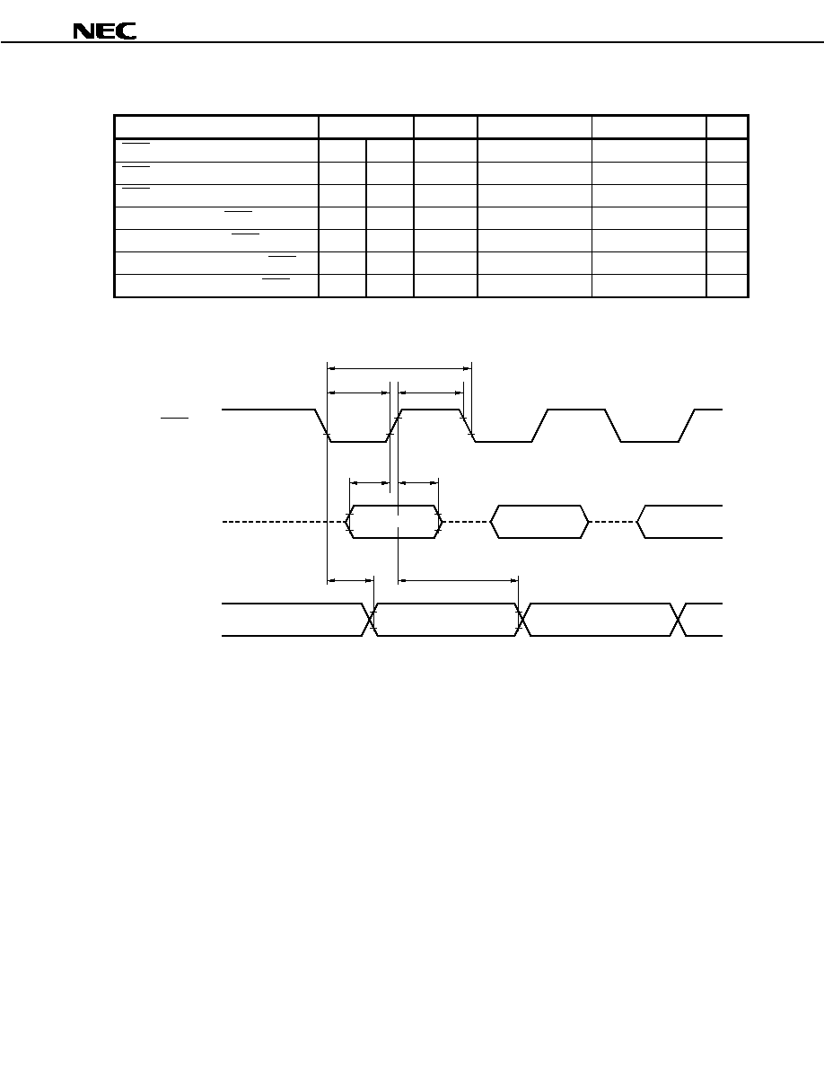
Preliminary Data Sheet U13995EJ1V0DS00
117
µ
µ
µ
µ
PD703100-33, 703100-40, 703101-33, 703102-33
(11) UART0, UART1 timing (clock-synchronized or master mode only)
Parameter
Symbol
Condition
MIN.
MAX.
Unit
SCKn cycle
<140>
t
CYSK0
Output
250
ns
SCKn high-level width
<141>
t
WSK0H
Output
0.5t
CYSK0
≠ 20
ns
SCKn low-level width
<142>
t
WSK0L
Output
0.5t
CYSK0
≠ 20
ns
RXDn setup time (to SCKn
)
<143>
t
SRXSK
30
ns
RXDn hold time (from SCKn
)
<144>
t
HSKRX
0
ns
TXDn output delay time (from SCKn
)
<145>
t
DSKTX
20
ns
TXDn output hold time (from SCKn
)
<146>
t
HSKTX
0.5t
CYSK0
≠ 5
ns
Remark n = 0, 1
SCKn (I/O)
<142>
<140>
<141>
RXDn (Input)
<143>
<144>
Input data
TXDn (Output)
<145>
Output data
<146>
Remarks 1. The broken lines indicate high impedance.
2. n = 0, 1
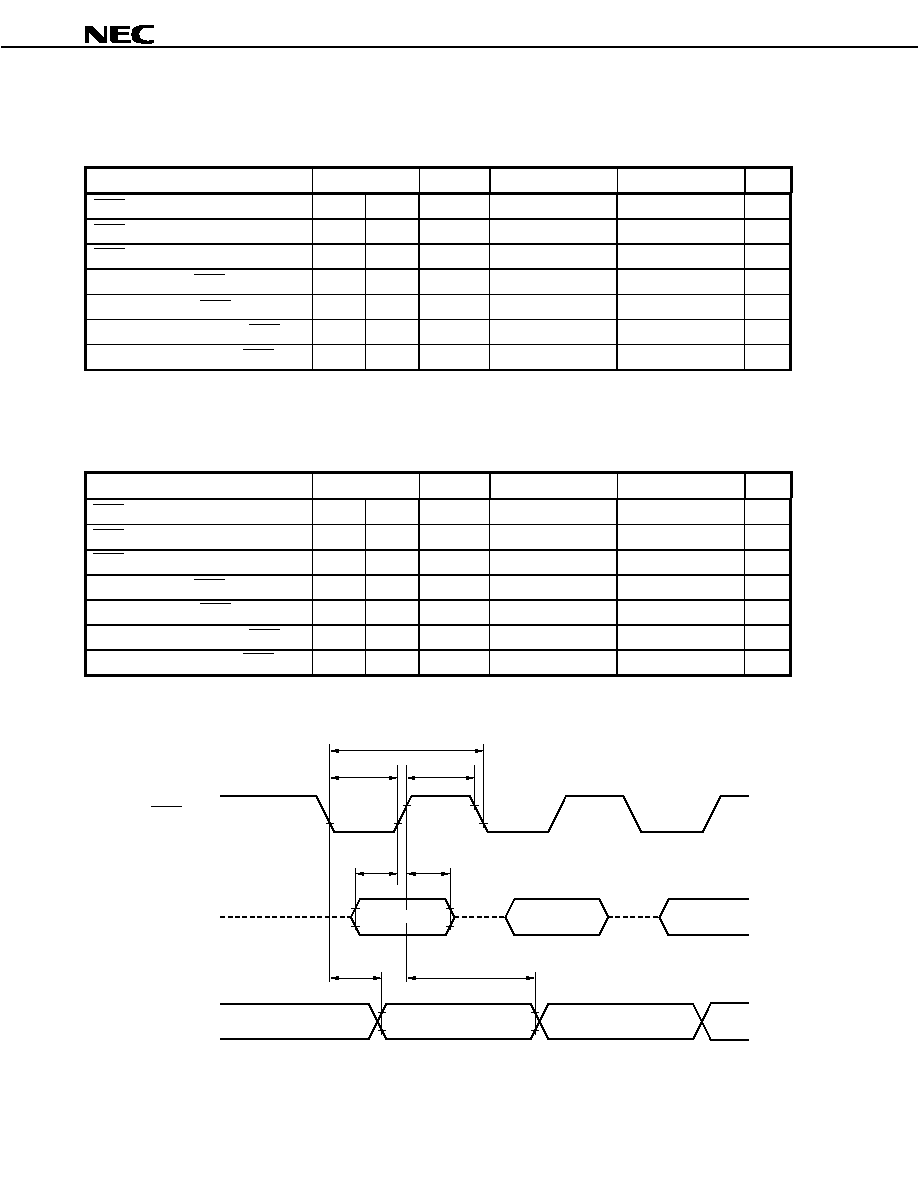
Preliminary Data Sheet U13995EJ1V0DS00
118
µ
µ
µ
µ
PD703100-33, 703100-40, 703101-33, 703102-33
(12) CSI0 to CSI3 timing
(a) Master mode
Parameter
Symbol
Condition
MIN.
MAX.
Unit
SCKn cycle
<147>
t
CYSK1
Output
100
ns
SCKn high-level width
<148>
t
WSK1H
Output
0.5t
CYSK1
≠ 20
ns
SCKn low-level width
<149>
t
WSK1L
Output
0.5t
CYSK1
≠ 20
ns
SIn setup time (to SCKn
)
<150>
t
SSISK
30
ns
SIn hold time (from SCKn
)
<151>
t
HSKSI
0
ns
SOn output delay time (from SCKn
)
<152>
t
DSKSO
20
ns
SOn output hold time (from SCKn
)
<153>
t
HSKSO
0.5t
CYSK1
≠ 5
ns
Remark n = 0 to 3
(b) Slave mode
Parameter
Symbol
Condition
MIN.
MAX.
Unit
SCKn cycle
<147>
t
CYSK1
Input
100
ns
SCKn high-level width
<148>
t
WSK1H
Input
30
ns
SCKn low-level width
<149>
t
WSK1L
Input
30
ns
SIn setup time (to SCKn
)
<150>
t
SSISK
10
ns
SIn hold time (from SCKn
)
<151>
t
HSKSI
10
ns
SOn output delay time (from SCKn
)
<152>
t
DSKSO
30
ns
SOn output hold time (from SCKn
)
<153>
t
HSKSO
t
WSK1H
ns
Remark n = 0 to 3
SCKn (I/O)
<149>
<147>
<148>
Sln (Input)
<150>
<151>
Input data
SOn (Output)
<152>
Output data
<153>
Remarks 1. The broken lines indicate high impedance.
2. n = 0 to 3
Preliminary Data Sheet U13995EJ1V0DS00
119
µ
µ
µ
µ
PD703100-33, 703100-40, 703101-33, 703102-33
A/D Converter Characteristics (T
A
= ≠40 to +70
∞
∞
∞
∞
C ...
µ
µ
µ
µ
PD703100-40, T
A
= ≠40 to +85
∞
∞
∞
∞
C ...
µ
µ
µ
µ
PD703100-33,
µ
µ
µ
µ
PD703101-33,
µ
µ
µ
µ
PD703102-33, V
DD
= CV
DD
= 3.0 to 3.6 V, HV
DD
= 5.0 V
±
±
±
±
10%,
V
SS
= 0 V, HV
DD
≠ 0.5 V < AV
DD
< HV
DD
, output pin load capacitance: C
L
= 50
pF)
Parameter
Symbol
Condition
MIN.
TYP.
MAX.
Unit
Resolution
≠
10
bit
Total error
≠
±
4
LSB
Quantization error
≠
±
1/2
LSB
Conversion time
t
CONV
5
µ
s
Sampling time
t
SAMP
833
ns
Zero scale error
≠
±
2
LSB
Full scale error
≠
±
2
LSB
Nonlinearity error
≠
±
1
LSB
Analog input voltage
V
IAN
-
0.3
AV
REF
+ 0.3
V
Analog input resistance
R
AN
2
M
AV
REF
input voltage
AV
REF
AV
REF
= AV
DD
4.5
5.5
V
AV
REF
input current
AI
REF
1.6
mA
AV
DD
current
AI
DD
6
mA
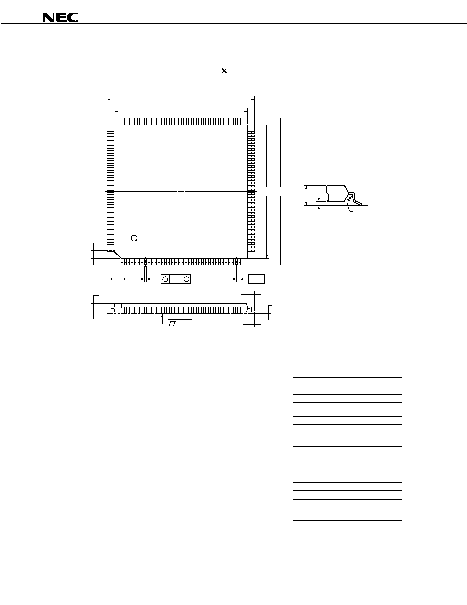
Preliminary Data Sheet U13995EJ1V0DS00
120
µ
µ
µ
µ
PD703100-33, 703100-40, 703101-33, 703102-33
17. PACKAGE DRAWING
144 PIN PLASTIC LQFP (FINE PITCH) (20 20)
ITEM
MILLIMETERS
INCHES
NOTE
Each lead centerline is located within 0.10 mm (0.004 inch) of
its true position (T.P.) at maximum material condition.
A
22.0
±
0.2
0.866
±
0.008
B
20.0
±
0.2
0.787+0.009
≠0.008
C
20.0
±
0.2
0.787+0.009
≠0.008
D
F
1.25
22.0
±
0.2
0.866
±
0.008
0.049
S144GJ-50-8EU-2
S
1.7 MAX.
0.067 MAX.
K
1.0
±
0.2
0.039+0.009
≠0.008
L
0.5
±
0.2
0.020+0.008
≠0.009
R
3
∞
3
∞
+7
∞
≠3
∞
+7
∞
≠3
∞
G
1.25
0.049
H
0.22
0.009
±
0.002
I
0.10
0.004
J
0.5 (T.P.)
0.020 (T.P.)
M
0.145
0.006
±
0.002
N
0.10
0.004
P
1.4
±
0.1
0.055
±
0.004
Q
0.125
±
0.075
0.005
±
0.003
+0.05
≠0.04
+0.055
≠0.045
M
108
73
1
36
109
144
72
37
detail of lead end
I
J
F
G
H
Q
R
P
K
M
L
N
C
D
S
A
B
Preliminary Data Sheet U13995EJ1V0DS00
121
µ
µ
µ
µ
PD703100-33, 703100-40, 703101-33, 703102-33
18. RECOMMENDED SOLDERING CONDITIONS
This product should be soldered and mounted under the following recommended conditions.
For the details of the recommended soldering conditions, refer to the document Semiconductor Device Mounting
Technology Manual (C10535E).
For soldering methods and conditions other than those recommended below, contact your NEC sales
representative.
Table 18-1. Surface Mounting Type Soldering Conditions
µ
µ
µ
µ
PD703100GJ-40-8EU
: 144-pin plastic LQFP (fine pitch) (20
◊
◊
◊
◊
20 mm)
µ
µ
µ
µ
PD703100GJ-33-8EU
: 144-pin plastic LQFP (fine pitch) (20
◊
◊
◊
◊
20 mm)
µ
µ
µ
µ
PD703101GJ-33-xxx-8EU : 144-pin plastic LQFP (fine pitch) (20
◊
◊
◊
◊
20 mm)
µ
µ
µ
µ
PD703102GJ-33-xxx-8EU : 144-pin plastic LQFP (fine pitch) (20
◊
◊
◊
◊
20 mm)
Soldering Method
Soldering Conditions
Recommended
Condition
Symbol
Infrared reflow
Package peak temperature: 235
∞
C, Time: 30 sec. Max. (at 210
∞
C or higher), Count:
two times or less, Exposure limit: 3 days
Note
(after that, prebake at 125
∞
C for 10 hours)
IR35-103-2
Partial heating
Pin temperature: 300
∞
C Max., Time: 3 sec. Max. (per pin row)
≠
Note After opening the dry pack, store it at 25
∞
C or less and 65% RH or less for the allowable storage period.

Preliminary Data Sheet U13995EJ1V0DS00
122
µ
µ
µ
µ
PD703100-33, 703100-40, 703101-33, 703102-33
[MEMO]

Preliminary Data Sheet U13995EJ1V0DS00
123
µ
µ
µ
µ
PD703100-33, 703100-40, 703101-33, 703102-33
NOTES FOR CMOS DEVICES
1
PRECAUTION AGAINST ESD FOR SEMICONDUCTORS
Note:
Strong electric field, when exposed to a MOS device, can cause destruction of the gate oxide and
ultimately degrade the device operation. Steps must be taken to stop generation of static electricity
as much as possible, and quickly dissipate it once, when it has occurred. Environmental control
must be adequate. When it is dry, humidifier should be used. It is recommended to avoid using
insulators that easily build static electricity. Semiconductor devices must be stored and transported
in an anti-static container, static shielding bag or conductive material. All test and measurement
tools including work bench and floor should be grounded. The operator should be grounded using
wrist strap. Semiconductor devices must not be touched with bare hands. Similar precautions need
to be taken for PW boards with semiconductor devices on it.
2
HANDLING OF UNUSED INPUT PINS FOR CMOS
Note:
No connection for CMOS device inputs can be cause of malfunction. If no connection is provided
to the input pins, it is possible that an internal input level may be generated due to noise, etc., hence
causing malfunction. CMOS devices behave differently than Bipolar or NMOS devices. Input levels
of CMOS devices must be fixed high or low by using a pull-up or pull-down circuitry. Each unused
pin should be connected to V
DD
or GND with a resistor, if it is considered to have a possibility of
being an output pin. All handling related to the unused pins must be judged device by device and
related specifications governing the devices.
3
STATUS BEFORE INITIALIZATION OF MOS DEVICES
Note:
Power-on does not necessarily define initial status of MOS device. Production process of MOS
does not define the initial operation status of the device. Immediately after the power source is
turned ON, the devices with reset function have not yet been initialized. Hence, power-on does
not guarantee out-pin levels, I/O settings or contents of registers. Device is not initialized until the
reset signal is received. Reset operation must be executed immediately after power-on for devices
having reset function.
Related Documents
µ
PD70F3102-33 Data Sheet (U13844E)
µ
PD703100-A33,
µ
PD703100-A40,
µ
PD703101-A33,
µ
PD703102-A33 Data Sheet (To be
prepared)
µ
PD70F3102-A33 Data Sheet (U13845E)
V850 Family Application Note Flash Memory Self-Programming Library (U13261E)
Reference Materials: Electrical Characteristics for Microcomputer (IEI-601
Note
)
Note This document number is that of Japanese version.
The related documents indicated in this publication may include preliminary versions. However, preliminary
versions are not marked as such.
V850E/MS1 Family and V850 are trademarks of NEC Corporation.

Preliminary Data Sheet U13995EJ1V0DS00
124
µ
µ
µ
µ
PD703100-33, 703100-40, 703101-33, 703102-33
[MEMO]

Preliminary Data Sheet U13995EJ1V0DS00
125
µ
µ
µ
µ
PD703100-33, 703100-40, 703101-33, 703102-33
Regional Information
Some information contained in this document may vary from country to country. Before using any NEC
product in your application, pIease contact the NEC office in your country to obtain a list of authorized
representatives and distributors. They will verify:
∑
Device availability
∑
Ordering information
∑
Product release schedule
∑
Availability of related technical literature
∑
Development environment specifications (for example, specifications for third-party tools and
components, host computers, power plugs, AC supply voltages, and so forth)
∑
Network requirements
In addition, trademarks, registered trademarks, export restrictions, and other legal issues may also vary
from country to country.
NEC Electronics Inc. (U.S.)
Santa Clara, California
Tel: 408-588-6000
800-366-9782
Fax: 408-588-6130
800-729-9288
NEC Electronics (Germany) GmbH
Duesseldorf, Germany
Tel: 0211-65 03 02
Fax: 0211-65 03 490
NEC Electronics (UK) Ltd.
Milton Keynes, UK
Tel: 01908-691-133
Fax: 01908-670-290
NEC Electronics Italiana s.r.l.
Milano, Italy
Tel: 02-66 75 41
Fax: 02-66 75 42 99
NEC Electronics (Germany) GmbH
Benelux Office
Eindhoven, The Netherlands
Tel: 040-2445845
Fax: 040-2444580
NEC Electronics (France) S.A.
Velizy-Villacoublay, France
Tel: 01-30-67 58 00
Fax: 01-30-67 58 99
NEC Electronics (France) S.A.
Spain Office
Madrid, Spain
Tel: 91-504-2787
Fax: 91-504-2860
NEC Electronics (Germany) GmbH
Scandinavia Office
Taeby, Sweden
Tel: 08-63 80 820
Fax: 08-63 80 388
NEC Electronics Hong Kong Ltd.
Hong Kong
Tel: 2886-9318
Fax: 2886-9022/9044
NEC Electronics Hong Kong Ltd.
Seoul Branch
Seoul, Korea
Tel: 02-528-0303
Fax: 02-528-4411
NEC Electronics Singapore Pte. Ltd.
United Square, Singapore 1130
Tel: 65-253-8311
Fax: 65-250-3583
NEC Electronics Taiwan Ltd.
Taipei, Taiwan
Tel: 02-2719-2377
Fax: 02-2719-5951
NEC do Brasil S.A.
Electron Devices Division
Rodovia Presidente Dutra, Km 214
07210-902-Guarulhos-SP Brasil
Tel: 55-11-6465-6810
Fax: 55-11-6465-6829
J99.1

µ
µ
µ
µ
PD703100-33, 703100-40, 703101-33,
The export of these products from Japan is regulated by the Japanese government. The export of some or all of these
products may be prohibited without governmental license. To export or re-export some or all of these products from a
country other than Japan may also be prohibited without a license from that country. Please call an NEC sales
representative.
Lisence not needed
:
µ
PD703100-33, 703100-40
The customer must judge the need for lisence :
µ
PD703101-33, 703102-33
No part of this document may be copied or reproduced in any form or by any means without the prior written
consent of NEC Corporation. NEC Corporation assumes no responsibility for any errors which may appear in this
document.
NEC Corporation does not assume any liability for infringement of patents, copyrights or other intellectual
property rights of third parties by or arising from use of a device described herein or any other liability arising
from use of such device. No license, either express, implied or otherwise, is granted under any patents,
copyrights or other intellectual property rights of NEC Corporation or others.
While NEC Corporation has been making continuous effort to enhance the reliability of its semiconductor devices,
the possibility of defects cannot be eliminated entirely. To minimize risks of damage or injury to persons or
property arising from a defect in an NEC semiconductor device, customers must incorporate sufficient safety
measures in its design, such as redundancy, fire-containment, and anti-failure features.
NEC devices are classified into the following three quality grades:
"Standard", "Special", and "Specific". The Specific quality grade applies only to devices developed based on
a customer designated "quality assurance program" for a specific application. The recommended applications
of a device depend on its quality grade, as indicated below. Customers must check the quality grade of each
device before using it in a particular application.
Standard: Computers, office equipment, communications equipment, test and measurement equipment,
audio and visual equipment, home electronic appliances, machine tools, personal electronic
equipment and industrial robots
Special: Transportation equipment (automobiles, trains, ships, etc.), traffic control systems, anti-disaster
systems, anti-crime systems, safety equipment and medical equipment (not specifically designed
for life support)
Specific: Aircrafts, aerospace equipment, submersible repeaters, nuclear reactor control systems, life
support systems or medical equipment for life support, etc.
The quality grade of NEC devices is "Standard" unless otherwise specified in NEC's Data Sheets or Data Books.
If customers intend to use NEC devices for applications other than those specified for Standard quality grade,
they should contact an NEC sales representative in advance.
Anti-radioactive design is not implemented in this product.
M4 96. 5