Document Outline
- COVER
- INTRODUCTION
- CHAPTER 1 OVERVIEW OF EACH PRODUCT
- 1.1 Outline
- 1.2 Features
- 1.3 Ordering Information
- 1.4 Pin Configuration
- 1.5 Internal Block Diagram
- CHAPTER 2 OVERVIEW OF PCI HOST BRIDGE MACRO
- CHAPTER 3 SPECIFICATIONS OF PCI HOST BRIDGE MACRO
- 3.1 Internal Blocks of PCI Host Bridge Macro
- 3.2 Relationship Between Internal Blocks and Signals
- 3.3 Pin Functions
- 3.3.1 External bus slave interface pins
- 3.3.2 SDRAM bus interface pins
- 3.3.3 PCI bus interface pins
- 3.4 Registers
- 3.4.1 PCI_CONFIG_DATA register
- 3.4.2 PCI_CONFIG_ADD register
- 3.4.3 PCI_CONTROL register
- 3.4.4 PCI_IO_BASE register
- 3.4.5 PCI_MEM_BASE register
- 3.4.6 PCI_INT_CTL register
- 3.4.7 PCI_ERR_ADD register
- 3.4.8 SYSTEM_MEM_BASE register
- 3.4.9 SYSTEM_MEM_RANGE register
- 3.4.10 SDRAM_CTL register
- 3.5 Address Map
- 3.6 Initializing PCI Host Bridge Macro
- 3.7 Bus Width of External Bus Interface
- 3.8 Timing
- 3.8.1 External bus interface timing
- 3.8.2 PCI bus interface timing
- CHAPTER 4 CONFIGURATION EXAMPLES OF FPGA INTEGRATION
- 4.1 Conditions for Configuration Examples of FPGA Integration
- 4.2 Points to Remember When Creating Top Layer of FPGA
- 4.3 Reference Diagram for FPGA Top Connection
- 4.4 FPGA Top Pin Functions
- 4.4.1 CPU bus slave interface pins
- 4.4.2 SDRAM bus interface pins
- 4.4.3 PCI bus interface pins
- 4.5 FPGA Top Pin Configuration
- 4.5.1 Internal connection diagram of external bus interface
- 4.5.2 Internal connection diagram of PCI bus interface
- 4.5.3 External connection diagram of external bus interface (example of connection with V850E/ME2)
- 4.5.4 External connection diagram of PCI bus interface
- 4.6 Cautions on Designing FPGA
- 4.6.1 FPGA fitting design
- 4.6.2 PCI bus interface timing parameters (as constraint of PCI CLK = 33 MHz)
- 4.6.3 SDRAM interface timing
- CHAPTER 5 APPLICATION EXAMPLES
- 5.1 Block Diagram of Evaluation Board
- 5.2 Specifications of Evaluation Board
- 5.3 Example of Evaluation Board Connection Circuit
- 5.4 Evaluation Board Memory Space
- 5.5 Sample Program Examples
- 5.5.1 Development tools
- 5.5.2 Program configuration
- 5.5.3 V850E/ME2 PCI host bridge macro initialization sample program list
- 5.5.4 PCI configuration space access sample program list
- 5.5.5 IDE HDD access sample program list

Application Note
V850E/MA1, V850E/MA2, V850E/MA3, V850E/ME2
32-Bit Single-Chip Microcontrollers
PCI Host Bridge Macro
Document No. U17121EJ1V1AN00 (1st edition)
Date Published September 2004 N CP(K)
Printed in Japan
2004
V850E/MA1: V850E/MA2: V850E/MA3: V850E/ME2:
�
PD703103A
�
PD703108
�
PD703131A
�
PD703111A
�
PD703105A
�
PD703131AY
�
PD703106A
�
PD703132A
�
PD703106A(A)
�
PD703132AY
�
PD703107A
�
PD703133A
�
PD703107A(A)
�
PD703133AY
�
PD70F3107A
�
PD703134A
�
PD70F3107A(A)
�
PD703134AY
�
PD70F3134A
�
PD70F3134AY

Application Note U17121EJ1V1AN
2
[MEMO]
Application Note U17121EJ1V1AN
3
1
2
3
4
VOLTAGE APPLICATION WAVEFORM AT INPUT PIN
Waveform distortion due to input noise or a reflected wave may cause malfunction. If the input of the
CMOS device stays in the area between V
IL
(MAX) and V
IH
(MIN) due to noise, etc., the device may
malfunction. Take care to prevent chattering noise from entering the device when the input level is fixed,
and also in the transition period when the input level passes through the area between V
IL
(MAX) and
V
IH
(MIN).
HANDLING OF UNUSED INPUT PINS
Unconnected CMOS device inputs can be cause of malfunction. If an input pin is unconnected, it is
possible that an internal input level may be generated due to noise, etc., causing malfunction. CMOS
devices behave differently than Bipolar or NMOS devices. Input levels of CMOS devices must be fixed
high or low by using pull-up or pull-down circuitry. Each unused pin should be connected to V
DD
or GND
via a resistor if there is a possibility that it will be an output pin. All handling related to unused pins must
be judged separately for each device and according to related specifications governing the device.
PRECAUTION AGAINST ESD
A strong electric field, when exposed to a MOS device, can cause destruction of the gate oxide and
ultimately degrade the device operation. Steps must be taken to stop generation of static electricity as
much as possible, and quickly dissipate it when it has occurred. Environmental control must be
adequate. When it is dry, a humidifier should be used. It is recommended to avoid using insulators that
easily build up static electricity. Semiconductor devices must be stored and transported in an anti-static
container, static shielding bag or conductive material. All test and measurement tools including work
benches and floors should be grounded. The operator should be grounded using a wrist strap.
Semiconductor devices must not be touched with bare hands. Similar precautions need to be taken for
PW boards with mounted semiconductor devices.
STATUS BEFORE INITIALIZATION
Power-on does not necessarily define the initial status of a MOS device. Immediately after the power
source is turned ON, devices with reset functions have not yet been initialized. Hence, power-on does
not guarantee output pin levels, I/O settings or contents of registers. A device is not initialized until the
reset signal is received. A reset operation must be executed immediately after power-on for devices
with reset functions.
POWER ON/OFF SEQUENCE
In the case of a device that uses different power supplies for the internal operation and external
interface, as a rule, switch on the external power supply after switching on the internal power supply.
When switching the power supply off, as a rule, switch off the external power supply and then the
internal power supply. Use of the reverse power on/off sequences may result in the application of an
overvoltage to the internal elements of the device, causing malfunction and degradation of internal
elements due to the passage of an abnormal current.
The correct power on/off sequence must be judged separately for each device and according to related
specifications governing the device.
INPUT OF SIGNAL DURING POWER OFF STATE
Do not input signals or an I/O pull-up power supply while the device is not powered. The current
injection that results from input of such a signal or I/O pull-up power supply may cause malfunction and
the abnormal current that passes in the device at this time may cause degradation of internal elements.
Input of signals during the power off state must be judged separately for each device and according to
related specifications governing the device.
NOTES FOR CMOS DEVICES
5
6

Application Note U17121EJ1V1AN
4
The copyright of the PCI host bridge macro described in this document is held by the System Interface Module
Development Department, Device Solutions Division, NEC Engineering, Ltd.
Green Hills Software and MULTI are trademarks of Green Hills Software, Inc.
These commodities, technology or software, must be exported in accordance
with the export administration regulations of the exporting country.
Diversion contrary to the law of that country is prohibited.
The information in this document is current as of March, 2004. The information is subject to change
without notice. For actual design-in, refer to the latest publications of NEC Electronics data sheets or
data books, etc., for the most up-to-date specifications of NEC Electronics products. Not all
products and/or types are available in every country. Please check with an NEC Electronics sales
representative for availability and additional information.
No part of this document may be copied or reproduced in any form or by any means without the prior
written consent of NEC Electronics. NEC Electronics assumes no responsibility for any errors that may
appear in this document.
NEC Electronics does not assume any liability for infringement of patents, copyrights or other intellectual
property rights of third parties by or arising from the use of NEC Electronics products listed in this document
or any other liability arising from the use of such products. No license, express, implied or otherwise, is
granted under any patents, copyrights or other intellectual property rights of NEC Electronics or others.
Descriptions of circuits, software and other related information in this document are provided for illustrative
purposes in semiconductor product operation and application examples. The incorporation of these
circuits, software and information in the design of a customer's equipment shall be done under the full
responsibility of the customer. NEC Electronics assumes no responsibility for any losses incurred by
customers or third parties arising from the use of these circuits, software and information.
While NEC Electronics endeavors to enhance the quality, reliability and safety of NEC Electronics products,
customers agree and acknowledge that the possibility of defects thereof cannot be eliminated entirely. To
minimize risks of damage to property or injury (including death) to persons arising from defects in NEC
Electronics products, customers must incorporate sufficient safety measures in their design, such as
redundancy, fire-containment and anti-failure features.
NEC Electronics products are classified into the following three quality grades: "Standard", "Special" and
"Specific".
The "Specific" quality grade applies only to NEC Electronics products developed based on a customer-
designated "quality assurance program" for a specific application. The recommended applications of an NEC
Electronics product depend on its quality grade, as indicated below. Customers must check the quality grade of
each NEC Electronics product before using it in a particular application.
"Standard": Computers, office equipment, communications equipment, test and measurement equipment, audio
and visual equipment, home electronic appliances, machine tools, personal electronic equipment
and industrial robots.
"Special":
Transportation equipment (automobiles, trains, ships, etc.), traffic control systems, anti-disaster
systems, anti-crime systems, safety equipment and medical equipment (not specifically designed
for life support).
"Specific": Aircraft, aerospace equipment, submersible repeaters, nuclear reactor control systems, life
support systems and medical equipment for life support, etc.
The quality grade of NEC Electronics products is "Standard" unless otherwise expressly specified in NEC
Electronics data sheets or data books, etc. If customers wish to use NEC Electronics products in applications
not intended by NEC Electronics, they must contact an NEC Electronics sales representative in advance to
determine NEC Electronics' willingness to support a given application.
(Note)
(1) "NEC Electronics" as used in this statement means NEC Electronics Corporation and also includes its
majority-owned subsidiaries.
(2) "NEC Electronics products" means any product developed or manufactured by or for NEC Electronics
(as defined above).
�
�
�
�
�
�
M8E 02. 11-1

Application Note U17121EJ1V1AN
5
Regional Information
�
Device availability
�
Ordering information
�
Product release schedule
�
Availability of related technical literature
�
Development environment specifications (for example, specifications for third-party tools and
components, host computers, power plugs, AC supply voltages, and so forth)
�
Network requirements
In addition, trademarks, registered trademarks, export restrictions, and other legal issues may also vary
from country to country.
[GLOBAL SUPPORT]
http://www.necel.com/en/support/support.html
NEC Electronics America, Inc. (U.S.)
Santa Clara, California
Tel: 408-588-6000
800-366-9782
NEC Electronics Hong Kong Ltd.
Hong Kong
Tel: 2886-9318
NEC Electronics Hong Kong Ltd.
Seoul Branch
Seoul, Korea
Tel: 02-558-3737
NEC Electronics Shanghai Ltd.
Shanghai, P.R. China
Tel: 021-5888-5400
NEC Electronics Taiwan Ltd.
Taipei, Taiwan
Tel: 02-2719-2377
NEC Electronics Singapore Pte. Ltd.
Novena Square, Singapore
Tel: 6253-8311
J04.1
NEC Electronics (Europe) GmbH
Duesseldorf, Germany
Tel: 0211-65030
�
Sucursal en Espa�a
Madrid, Spain
Tel: 091-504 27 87
V�lizy-Villacoublay, France
Tel: 01-30-67 58 00
�
Succursale Fran�aise
�
Filiale Italiana
Milano, Italy
Tel: 02-66 75 41
�
Branch The Netherlands
Eindhoven, The Netherlands
Tel: 040-244 58 45
�
Tyskland Filial
Taeby, Sweden
Tel: 08-63 80 820
�
United Kingdom Branch
Milton Keynes, UK
Tel: 01908-691-133
Some information contained in this document may vary from country to country. Before using any NEC
Electronics product in your application, pIease contact the NEC Electronics office in your country to
obtain a list of authorized representatives and distributors. They will verify:

Application Note U17121EJ1V1AN
6
INTRODUCTION
Readers
This application note is intended for users who wish to understand the functions of the
V850E/MA1, V850E/MA2, V850E/MA3, V850E/ME2, and PCI bus to design application
systems using these products.
Purpose
The purpose of this application note is to help the user understand the PCI host bridge
macro and its composition using the V850E/MA1, V850E/MA2, V850E/MA3,
V850E/ME2, and PCI host bridge macro as a system example.
Organization
This application note is broadly divided into the following sections.
�
Overview of each product
�
Overview of PCI host bridge macro
�
Specifications of PCI host bridge macro
�
Configuration examples of FPGA integration
�
Application examples
How to Read This Manual It is assumed that the readers of this application note have general knowledge in the
fields of electrical engineering, logic circuits, and microcontrollers.
For details of the hardware functions and electrical specifications of the V850E/MA1,
V850E/MA2, V850E/MA3, and V850E/ME2
Refer to the Hardware User's Manual of each product.
For details of the instruction functions of the V850E/MA1, V850E/MA2, V850E/MA3, and
V850E/ME2
Refer to the V850E1 Architecture User's Manual.
Conventions
Data significance:
Higher digits on the left and lower digits on the right
Active low representation: xxx (overscore over pin or signal name) or /xxx ("/" before
signal
name)
Memory map address:
Higher addresses on the top and lower addresses on the
bottom
Note:
Footnote for item marked with Note in the text
Caution:
Information requiring particular attention
Remark: Supplementary
information
Numeric representation:
Binary ... xxxx or xxxxB
Decimal ... xxxx
Hexadecimal ... xxxxH
Prefix indicating power of 2 (address space, memory capacity):
K (kilo) ... 2
10
= 1,024
M (mega) ... 2
20
= 1,024
2
G (giga) ... 2
30
= 1,024
3
Application Note U17121EJ1V1AN
7
Related Documents
The related documents indicated in this publication may include preliminary versions.
However, preliminary versions are not marked as such.
Documents related to V850E/MA1, V850E/MA2, V850E/MA3, and V850E/ME2
Document Name
Document No.
V850E1 Architecture User's Manual
U14559E
V850E/MA1 Hardware User's Manual
U14359E
V850E/MA1 Hardware Application Note
U15179E
V850E/MA2 Hardware User's Manual
U14980E
V850E/MA3 Hardware User's Manual
U16397E
V850E/ME2 Hardware User's Manual
U16031E
V850E/ME2 Hardware Application Note
U16794E
V850E/ME2 USB Function Driver Application Note
U17069E
V850E/MA1, V850E/MA2, V850E/MA3, V850E/ME2 PCI Host Bridge Macro Application Note
This manual
Documents related to development tools (user's manuals)
Document Name
Document No.
IE-V850E-MC, IE-V850E-MC-A In-Circuit Emulator
U14487E
IE-703107-MC-EM1 In-Circuit Emulator Option Board
U14481E
IE-V850E1-CD-NW PCMCIA Card Type On-Chip Debug Emulator
U16647E
Operation U16053E
C Language
U16054E
CA850 Ver.2.50 C Compiler Package
Assembly Language
U16042E
PM plus Ver.5.20
U16934E
ID850 Ver.2.50 Integrated Debugger
Operation
U16217E
ID850NW Ver.2.51 Integrated Debugger
Operation
U16454E
SM850 Ver.2.40 System Simulator
Operation
U15182E
SM850 Ver.2.00 or Later System Simulator
External Part User Open Interface Specifications U14873E
Basics U13430E
Installation U13410E
RX850 Ver.3.13 or Later Real-Time OS
Technical U13431E
Basics U13773E
Installation U13774E
RX850 Pro Ver.3.15 Real-Time OS
Technical U13772E
RD850 Ver.3.01 Task Debugger
U13737E
RD850 Pro Ver.3.01 Task Debugger
U13916E
AZ850 Ver.3.10 System Performance Analyzer
U14410E
PG-FP4 Flash Memory Programmer
U15260E

Application Note U17121EJ1V1AN
8
CONTENTS
CHAPTER 1 OVERVIEW OF EACH PRODUCT..................................................................................10
1.1 Outline ...........................................................................................................................................10
1.2 Features.........................................................................................................................................11
1.3 Ordering Information....................................................................................................................12
1.4 Pin Configuration..........................................................................................................................14
1.5 Internal Block Diagram ................................................................................................................25
CHAPTER 2 OVERVIEW OF PCI HOST BRIDGE MACRO ..............................................................29
2.1 Outline ...........................................................................................................................................29
2.2 Features.........................................................................................................................................30
CHAPTER 3 SPECIFICATIONS OF PCI HOST BRIDGE MACRO ...................................................31
3.1 Internal Blocks of PCI Host Bridge Macro .................................................................................31
3.2 Relationship Between Internal Blocks and Signals ..................................................................32
3.3 Pin Functions ................................................................................................................................33
3.3.1 External bus slave interface pins .......................................................................................................33
3.3.2 SDRAM
bus
interface pins .................................................................................................................33
3.3.3 PCI bus interface pins ........................................................................................................................34
3.4 Registers .......................................................................................................................................35
3.4.1 PCI_CONFIG_DATA register.............................................................................................................35
3.4.2 PCI_CONFIG_ADD register...............................................................................................................36
3.4.3 PCI_CONTROL register.....................................................................................................................37
3.4.4 PCI_IO_BASE register.......................................................................................................................38
3.4.5 PCI_MEM_BASE register ..................................................................................................................38
3.4.6 PCI_INT_CTL register........................................................................................................................39
3.4.7 PCI_ERR_ADD register .....................................................................................................................40
3.4.8 SYSTEM_MEM_BASE register .........................................................................................................41
3.4.9 SYSTEM_MEM_RANGE register ......................................................................................................41
3.4.10 SDRAM_CTL register ........................................................................................................................42
3.5 Address Map .................................................................................................................................44
3.6 Initializing PCI Host Bridge Macro ..............................................................................................45
3.7 Bus Width of External Bus Interface ..........................................................................................46
3.8 Timing ............................................................................................................................................47
3.8.1 External
bus
interface timing..............................................................................................................47
3.8.2 PCI bus interface timing .....................................................................................................................50
CHAPTER 4 CONFIGURATION EXAMPLES OF FPGA INTEGRATION..........................................57
4.1 Conditions for Configuration Examples of FPGA Integration .................................................57
4.2 Points to Remember When Creating Top Layer of FPGA ........................................................57
4.3 Reference Diagram for FPGA Top Connection .........................................................................58
4.4 FPGA Top Pin Functions .............................................................................................................59
4.4.1 CPU bus slave interface pins .............................................................................................................59
4.4.2 SDRAM
bus
interface pins .................................................................................................................59
4.4.3 PCI bus interface pins ........................................................................................................................60
4.5 FPGA Top Pin Configuration.......................................................................................................61

Application Note U17121EJ1V1AN
9
4.5.1 Internal
connection diagram of external bus interface ....................................................................... 61
4.5.2 Internal
connection diagram of PCI bus interface .............................................................................. 62
4.5.3 External
connection
diagram of external bus interface (example of connection with V850E/ME2).... 63
4.5.4 External
connection diagram of PCI bus interface ............................................................................. 64
4.6 Cautions on Designing FPGA .....................................................................................................65
4.6.1 FPGA
fitting design............................................................................................................................ 65
4.6.2 PCI bus interface timing parameters (as constraint of PCI CLK = 33 MHz)....................................... 65
4.6.3 SDRAM
interface timing .................................................................................................................... 66
CHAPTER 5 APPLICATION EXAMPLES..............................................................................................67
5.1 Block Diagram of Evaluation Board ...........................................................................................67
5.2 Specifications of Evaluation Board............................................................................................68
5.3 Example of Evaluation Board Connection Circuit ....................................................................69
5.4 Evaluation Board Memory Space ...............................................................................................70
5.5 Sample Program Examples .........................................................................................................72
5.5.1 Development tools ............................................................................................................................. 72
5.5.2 Program
configuration ....................................................................................................................... 72
5.5.3 V850E/ME2 PCI host bridge macro initialization sample program list ............................................... 73
5.5.4 PCI
configuration space access sample program list ........................................................................ 76
5.5.5 IDE HDD access sample program list................................................................................................ 79

Application Note U17121EJ1V1AN
10
CHAPTER 1 OVERVIEW OF EACH PRODUCT
The V850E/MA1, V850E/MA2, V850E/MA3, and V850E/ME2 are products in NEC Electronics' V850 Series of
single-chip microcontrollers. This chapter gives a simple outline of each product.
1.1 Outline
The V850E/MA1, V850E/MA2, V850E/MA3, and V850E/ME2 are 32-bit single-chip microcontrollers that integrate
the V850E1 CPU, which is a 32-bit RISC-type CPU core for ASIC, newly developed as the CPU core central to
system LSI in the current age of system-on-chip. These devices incorporate memory and various peripheral functions
such as memory controllers, a DMA controller, timer/counters, serial interfaces, and an A/D converter for realizing
high-capacity data processing and sophisticated real-time control.

CHAPTER 1 OVERVIEW OF EACH PRODUCT
Application Note U17121EJ1V1AN
11
1.2 Features
Commercial Name
V850E/MA1
V850E/MA2
V850E/MA3
V850E/ME2
Maximum operating
frequency
50 MHz
40 MHz
80 MHz
150 MHz
Mask ROM
-
128 256
-
-
256 512
-
-
Flash memory
-
256
-
-
512
-
Internal
memory
(KB)
RAM 4
10 4
16
32
16
32
Instruction
RAM:
128
Data RAM: 16
Cache (KB)
-
Instruction cache: 8
Bus type
Separate
Separate
Separate/multiplexed
Separate
Address bus
26 bits
25 bits
26 bits
26 bits
Data bus
8/16 bits
8/16 bits
8/16 bits
16/32 bits
External
bus
Chip select signals 8
4
8
8
Memory controller
SDRAM, EDO DRAM,
SRAM, etc.
SDRAM, SRAM, etc.
External
Note 1
17 (17)
4 (4)
26 (26)
40 (31)
Interrupts
Internal 41
27
49
59
32
�
32
64
20 to 40 ns (50 MHz)
25 to 50 ns (40 MHz)
12.5 to 25 ns (80 MHz) 6.7 to 13.3 ns (150 MHz)
DSP
function
32
�
32 + 32
32 60 ns (50 MHz)
75 ns (40 MHz)
37.5 ns (80 MHz)
20 ns (150 MHz)
TMC
4 ch
2 ch
-
6 ch
TMP
-
-
3 ch
-
TMQ
-
-
1 ch
-
Interval timer
4 ch
4 ch
4 ch
4 ch
16-bit
timer
Up/down counter
-
-
1 ch
2 ch
Watchdog timer
-
-
1 ch
-
CSI 1
ch
-
-
1 ch
UART 1
ch
-
-
1 ch
CSI/UART
2 ch
2 ch
3 ch
1 ch
Serial
interface
UART/I
2
C
-
-
1 ch
Note 2
-
10-bit A/D converter
8 ch
4 ch
8 ch
8 ch
8-bit D/A converter
-
-
2 ch
-
DMA controller
4 ch
4 ch
4 ch
4 ch
CMOS input
9
5
11
7
Ports
CMOS I/O
106
74
101
77
Debug functions
-
-
Provided (RUN, break)
Provided (RUN, break,
trace)
Other peripheral functions
PWM
�
2 ch
-
ROM correction function USB function, SSCG,
PWM
�
2 ch
Power supply voltage
3.0 to 3.6 V
2.3 to 2.7 V (internal)
3.0 to 3.6 V (external)
1.5 V (internal)
3.3 V (external)
Power consumption
(mask version TYP.)
528 mW
416 mW
575 mW
200 mW
Package
144-pin LQFP (20
�
20)
161-pin FBGA (13
�
13)
100-pin LQFP (14
�
14) 144-pin LQFP (20
�
20)
161-pin FBGA (13
�
13)
176-pin LQFP (20
�
20)
240-pin FBGA (16
�
16)
Operating ambient
temperature
T
A
=
-
40 to +85
�
C T
A
=
-
40 to +85
�
C
(@133 MHz)
T
A
=
-
40 to +70
�
C
(@150 MHz)
Notes 1. The figure in parentheses indicates the number of external interrupts that can release STOP mode.
2. Available only in on-chip I
2
C products (Y products).

CHAPTER 1 OVERVIEW OF EACH PRODUCT
Application Note U17121EJ1V1AN
12
1.3 Ordering Information
(1) V850E/MA1
Part Number
Package
Internal ROM
�
PD703103AGJ-UEN
144-pin plastic LQFP (fine pitch) (20
�
20)
ROMless
�
PD703105AGJ-xxx-UEN
144-pin plastic LQFP (fine pitch) (20
�
20)
Mask ROM (128 KB)
�
PD703106AGJ-xxx-UEN
144-pin plastic LQFP (fine pitch) (20
�
20)
Mask ROM (128 KB)
�
PD703106AGJ(A)-xxx-UEN
144-pin plastic LQFP (fine pitch) (20
�
20)
Mask ROM (128 KB)
�
PD703106AF1-xxx-EN4
161-pin plastic FBGA (13
�
13)
Mask ROM (128 KB)
�
PD703107AGJ-xxx-UEN
144-pin plastic LQFP (fine pitch) (20
�
20)
Mask ROM (256 KB)
�
PD703107AGJ(A)-xxx-UEN
144-pin plastic LQFP (fine pitch) (20
�
20)
Mask ROM (256 KB)
�
PD703107AF1-xxx-EN4
161-pin plastic FBGA (13
�
13)
Mask ROM (256 KB)
�
PD70F3107AGJ-UEN
144-pin plastic LQFP (fine pitch) (20
�
20)
Flash memory (512 KB)
�
PD70F3107AGJ(A)-UEN
144-pin plastic LQFP (fine pitch) (20
�
20)
Flash memory (512 KB)
�
PD70F3107AF1-EN4
161-pin plastic FBGA (13
�
13)
Flash memory (512 KB)
(2) V850E/MA2
Part Number
Package
Internal ROM
�
PD703108GC-8EU
100-pin plastic LQFP (fine pitch) (14
�
14)
ROMless

CHAPTER 1 OVERVIEW OF EACH PRODUCT
Application Note U17121EJ1V1AN
13
(3) V850E/MA3
Part Number
Package
Internal ROM
�
PD703131AGJ-xxx-UEN
144-pin plastic LQFP (fine pitch) (20
�
20)
Mask ROM (256 KB)
�
PD703131AF1-xxx-EN4
161-pin plastic FBGA (13
�
13)
Mask ROM (256 KB)
�
PD703131AYGJ-xxx-UEN
144-pin plastic LQFP (fine pitch) (20
�
20)
Mask ROM (256 KB)
�
PD703131AYF1-xxx-EN4
161-pin plastic FBGA (13
�
13)
Mask ROM (256 KB)
�
PD703132AGJ-xxx-UEN
144-pin plastic LQFP (fine pitch) (20
�
20)
Mask ROM (256 KB)
�
PD703132AF1-xxx-EN4
161-pin plastic FBGA (13
�
13)
Mask ROM (256 KB)
�
PD703132AYGJ-xxx-UEN
144-pin plastic LQFP (fine pitch) (20
�
20)
Mask ROM (256 KB)
�
PD703132AYF1-xxx-EN4
161-pin plastic FBGA (13
�
13)
Mask ROM (256 KB)
�
PD703133AGJ-xxx-UEN
144-pin plastic LQFP (fine pitch) (20
�
20)
Mask ROM (512 KB)
�
PD703133AF1-xxx-EN4
161-pin plastic FBGA (13
�
13)
Mask ROM (512 KB)
�
PD703133AYGJ-xxx-UEN
144-pin plastic LQFP (fine pitch) (20
�
20)
Mask ROM (512 KB)
�
PD703133AYF1-xxx-EN4
161-pin plastic FBGA (13
�
13)
Mask ROM (512 KB)
�
PD703134AGJ-xxx-UEN
144-pin plastic LQFP (fine pitch) (20
�
20)
Mask ROM (512 KB)
�
PD703134AF1-xxx-EN4
161-pin plastic FBGA (13
�
13)
Mask ROM (512 KB)
�
PD703134AYGJ-xxx-UEN
144-pin plastic LQFP (fine pitch) (20
�
20)
Mask ROM (512 KB)
�
PD703134AYF1-xxx-EN4
161-pin plastic FBGA (13
�
13)
Mask ROM (512 KB)
�
PD70F3134AGJ-UEN
144-pin plastic LQFP (fine pitch) (20
�
20)
Flash memory (512 KB)
�
PD70F3134AF1-EN4
161-pin plastic FBGA (13
�
13)
Flash memory (512 KB)
�
PD70F3134AYGJ-UEN 144-pin
plastic LQFP (fine pitch) (20
�
20)
Flash memory (512 KB)
�
PD70F3134AYF1-EN4
161-pin plastic FBGA (13
�
13)
Flash memory (512 KB)
(4) V850E/ME2
Part Number
Package
Maximum Operating
Frequency
�
PD703111AGM-10-UEU
176-pin plastic LQFP (fine pitch) (24
�
24)
100 MHz
�
PD703111AGM-13-UEU
176-pin plastic LQFP (fine pitch) (24
�
24)
133 MHz
�
PD703111AGM-15-UEU
176-pin plastic LQFP (fine pitch) (24
�
24)
150 MHz
�
PD703111AF1-10-GA3
240-pin plastic FBGA (16
�
16)
100 MHz
�
PD703111AF1-13-GA3
240-pin plastic FBGA (16
�
16)
133 MHz
�
PD703111AF1-15-GA3
240-pin plastic FBGA (16
�
16)
150 MHz
CHAPTER 1 OVERVIEW OF EACH PRODUCT
Application Note U17121EJ1V1AN
14
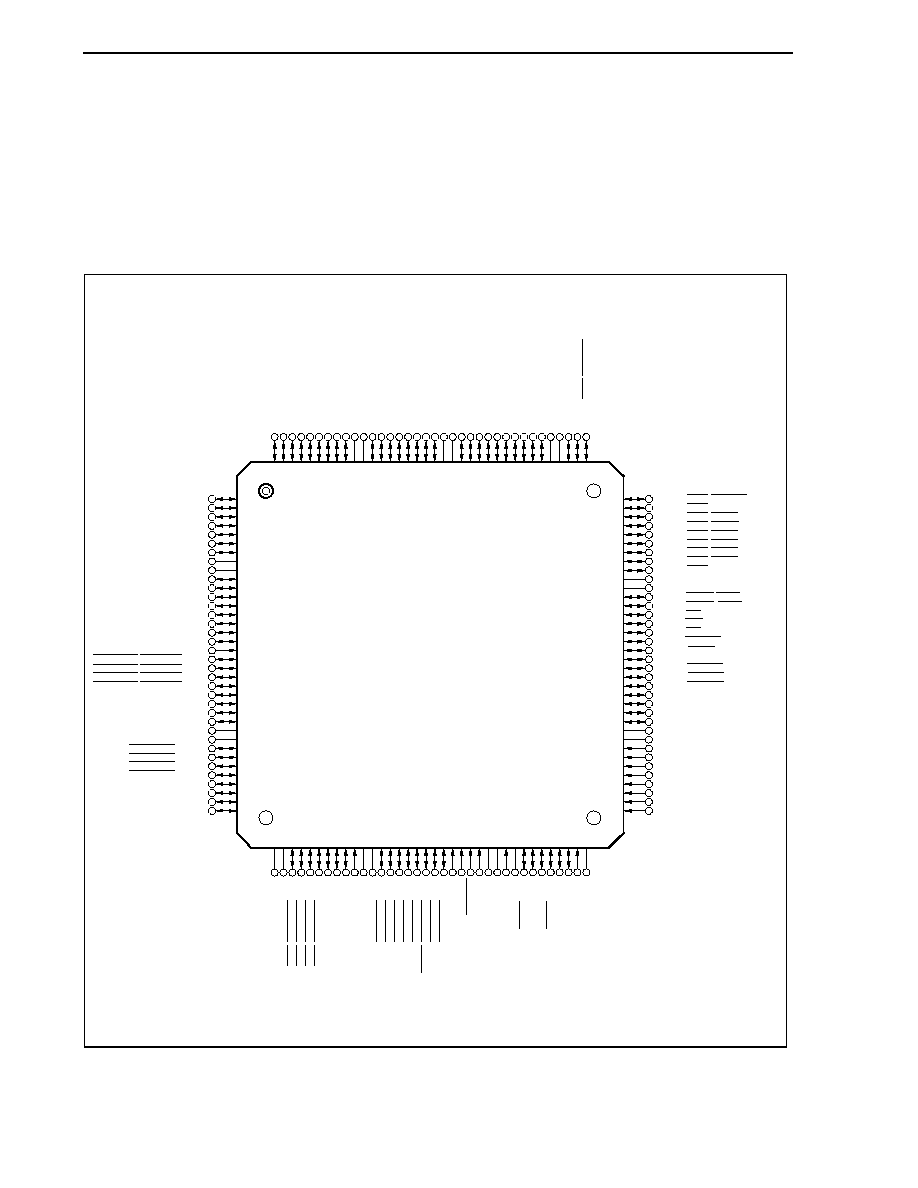
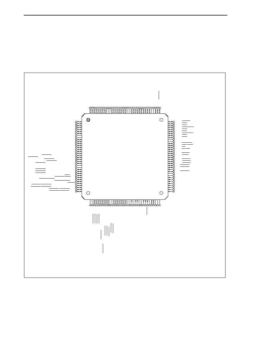
1.4 Pin Configuration
(1) V850E/MA1
�
144-pin plastic LQFP (fine pitch) (20
�
20)
�
PD703103AGJ-UEN
�
PD703106AGJ(A)-xxx-UEN
�
PD70F3107AGJ-UEN
�
PD703105AGJ-xxx-UEN
�
PD703107AGJ-xxx-UEN
�
PD70F3107AGJ(A)-UEN
�
PD703106AGJ-xxx-UEN
�
PD703107AGJ(A)-xxx-UEN
Top View
D14/PDL14
D13/PDL13
D12/PDL12
D11/PDL11
D10/PDL10
D9/PDL9
D8/PDL8
V
DD
V
SS
D7/PDL7
D6/PDL6
D5/PDL5
D4/PDL4
D3/PDL3
D2/PDL2
D1/PDL1
D0/PDL0
MODE2 (V
PP
/MODE2)
DMARQ3/INTP103/P07
DMARQ2/INTP102/P06
DMARQ1/INTP101/P05
DMARQ0/INTP100/P04
TO00/P03
INTP001/P02
TI000/INTP000/P01
PWM0/P00
V
DD
V
SS
DMAAK3/PBD3
DMAAK2/PBD2
DMAAK1/PBD1
DMAAK0/PBD0
TO01/P13
INTP011/P12
TI010/INTP010/P11
PWM1/P10
PCD3/UBE/SDRAS
PCS0/CS0
PCS1/CS1/RAS1
PCS2/CS2/IOWR
PCS3/CS3/RAS3
PCS4/CS4/RAS4
PCS5/CS5/IORD
PCS6/CS6/RAS6
PCS7/CS7
V
SS
V
DD
PCT0/LCAS/LWR/LDQM
PCT1/UCAS/UWR/UDQM
PCT4/RD
PCT5/WE
PCT6/OE
PCT7/BCYST
PCM0/WAIT
PCM1/CLKOUT/BUSCLK
PCM2/HLDAK
PCM3/HLDRQ
PCM4/REFRQ
PCM5/SELFREF
P50/INTP030/TI030
P51/INTP031
P52/TO03
V
SS
V
DD
P70/ANI0
P71/ANI1
P72/ANI2
P73/ANI3
P74/ANI4
P75/ANI5
P76/ANI6
P77/ANI7
V
DD
V
SS
TC3/INTP113/P27 TC2/INTP112/P26 TC1/INTP111/P25 TC0/INTP110/P24
TO02/P23
INTP021/P22
TI020/INTP020/P21
NMI/P20
V
DD
V
SS
ADTRG/INTP123/P37
INTP122/P36 INTP121/P35
RXD2/INTP120/P34 TXD2/INTP133/P33 SCK2/INTP132/P32
SI2/INTP131/P31
SO2/INTP130/P30
MODE1 MODE0 RESET CKSEL
CV
DD
X2 X1
CV
SS
SCK1/P45
RXD1/SI1/P44 TXD1/SO1/P43
SCK0/P42
RXD0/SI0/P41 TXD0/SO0/P40
AV
DD
/AV
REF
AV
SS
PDL15/D15 PAL0/A0 PAL1/A1 PAL2/A2 PAL3/A3 PAL4/A4 PAL5/A5 PAL6/A6 PAL7/A7 V
SS
V
DD
PAL8/A8 PAL9/A9 PAL10/A10 PAL11/A11 PAL12/A12 PAL13/A13 PAL14/A14 PAL15/A15 V
SS
V
DD
PAH0/A16 PAH1/A17 PAH2/A18 PAH3/A19 PAH4/A20 PAH5/A21 PAH6/A22 PAH7/A23 PAH8/A24 PAH9/A25 V
SS
V
DD
PCD0/SDCKE PCD1/SDCLK PCD2/LBE/SDCAS
1
2
3
4
5
6
7
8
9
10
11
12
13
14
15
16
17
18
19
20
21
22
23
24
25
26
27
28
29
30
31
32
33
34
35
36
144 143 142 141 140 139 138 137 136 135 134 133 132 131 130 129 128 127 126 125 124 123 122 121 120 119 118 117 116 115 114 113 112 111 110 109
37 38 39 40 41 42 43 44 45 46 47 48 49 50 51 52 53 54 55 56 57 58 59 60 61 62 63 64 65 66 67 68 69 70 71 72
108
107
106
105
104
103
102
101
100
99
98
97
96
95
94
93
92
91
90
89
88
87
86
85
84
83
82
81
80
79
78
77
76
75
74
73
Remark Items in parentheses are pin names in the
�
PD70F3107A.
CHAPTER 1 OVERVIEW OF EACH PRODUCT
Application Note U17121EJ1V1AN
15
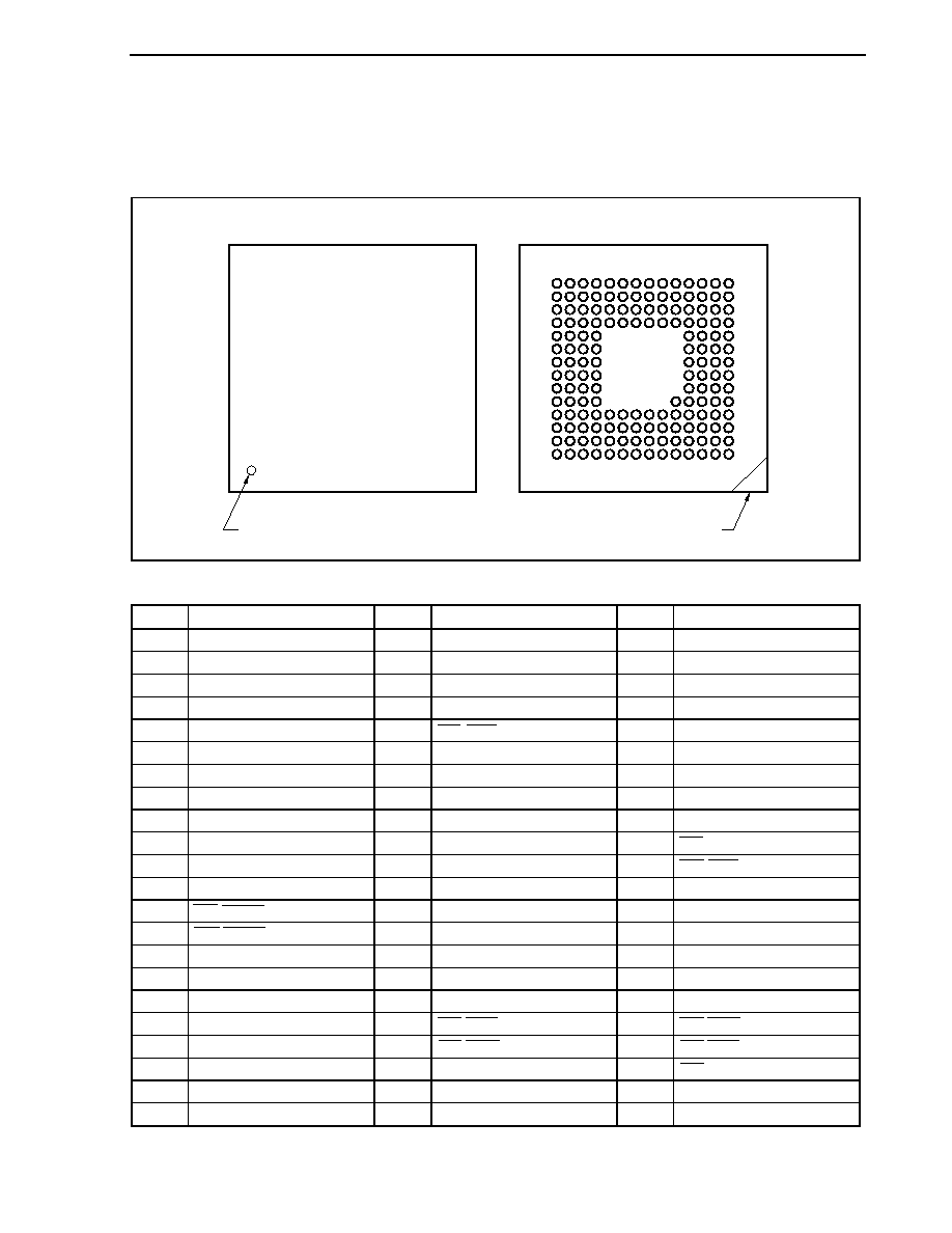
�
161-pin plastic FBGA (13
�
13)
�
PD703106AF1-xxx-EN4
�
PD703107AF1-xxx-EN4
�
PD70F3107AF1-EN4
14
13
12
11
10
9
8
7
6
5
4
3
2
1
Top View
Bottom View
P N M L K J H G F E D C B A
A B C D E F G H J K L M N P
Index mark
Index mark
(1/2)
Pin No.
Name
Pin No.
Name
Pin No.
Name
A1
-
B9 A18/PAH2
D3 D14/PDL14
A2 D15/PDL15
B10 A21/PAH5
D4 A3/PAL3
A3 A2/PAL2
B11 A25/PAH9
D5 A6/PAL6
A4 A5/PAL5
B12 SDCLK/PCD1
D6 A10/PAL10
A5
-
B13 CS1/RAS1/PCS1
D7 A14/PAL14
A6 A9/PAL9
B14
-
D8 A16/PAH0
A7 A12/PAL12
C1
-
D9 A20/PAH4
A8 A15/PAL15
C2 D9/PDL9
D10 A23/PAH7
A9 A17/PAH1
C3 D13/PDL13
D11 SDCKE/PCD0
A10
-
C4 A1/PAL1
D12 CS0/PCS0
A11 A24/PAH8
C5 A7/PAL7
D13 CS5/IORD/PCS5
A12 V
DD
C6
V
DD
D14
-
A13 LBE/SDCAS/PCD2
C7 A11/PAL11
E1 D5/PDL5
A14 UBE/SDRAS/PCD3
C8 V
DD
E2
D7/PDL7
B1
-
C9 A19/PAH3
E3 D8/PDL8
B2 D12/PDL12
C10 A22/PAH6
E4 D11/PDL11
B3 A0/PAL0
C11 V
SS
E5
-
B4 A4/PAL4
C12 CS3/RAS3/PCS3
E11 CS6/RAS6/PCS6
B5 V
SS
C13
CS2/IOWR/PCS2
E12
CS4/RAS4/PCS4
B6 A8/PAL8
C14
-
E13 CS7/PCS7
B7 A13/PAL13
D1 V
SS
E14
V
SS
B8 V
SS
D2
D10/PDL10
F1
D2/PDL2

CHAPTER 1 OVERVIEW OF EACH PRODUCT
Application Note U17121EJ1V1AN
16
(2/2)
Pin No.
Name
Pin No.
Name
Pin No.
Name
F2 D3/PDL3
K2 V
SS
M12
ANI6/P76
F3 D4/PDL4
K3 DMAAK1/PBD1
M13 ANI5/P75
F4 V
DD
K4
DMAAK3/PBD3
M14
-
F11 RD/PCT4
K11 ANI1/P71
N1
-
F12 V
DD
K12
ANI0/P70
N2
PWM1/P10
F13 LCAS/LWR/LDQM/PCT0
K13 V
SS
N3
TC3/INTP113/P27
F14 UCAS/UWR/UDQM/PCT1
K14 V
DD
N4
TC0/INTP110/P24
G1 MODE2
(MODE2/V
PP
) L1
-
N5 NMI/P20
G2 DMARQ3/INTP103/P07
L2 DMAAK2/PBD2
N6 ADTRG/INTP123/P37
G3 D0/PDL0
L3 TI010/INTP010/P11
N7 TXD2/INTP133/P33
G4 D6/PDL6
L4 DMAAK0/PBD0
N8 SO2/INTP130/P30
G11 WAIT/PCM0
L5 TO02/P23
N9 X2
G12 WE/PCT5
L6 V
DD
N10
CV
SS
G13 BCYST/PCT7
L7 INTP122/P36
N11 SCK0/P42
G14 OE/PCT6
L8 SI2/INTP131/P31
N12 AV
DD
/AV
REF
H1 DMARQ2/INTP102/P06
L9 RESET
N13 AV
SS
H2 DMARQ1/INTP101/P05
L10 TXD1/SO1/P43
N14
-
H3 DMARQ0/INTP100/P04
L11 ANI7/P77
P1 V
DD
H4 D1/PDL1
L12 ANI4/P74
P2 V
SS
H11 REFRQ/PCM4
L13 ANI3/P73
P3 TC1/INTP111/P25
H12 HLDRQ/PCM3
L14 ANI2/P72
P4 INTP021/P22
H13 HLDAK/PCM2
M1
-
P5
-
H14 CLKOUT/BUSCLK/PCM1
M2 INTP011/P12
P6 INTP121/P35
J1 TO00/P03
M3 TO01/P13
P7 SCK2/INTP132/P32
J2 TI000/INTP000/P01
M4 TC2/INTP112/P26
P8 MODE1
J3 V
DD
M5
TI020/INTP020/P21
P9
CV
DD
J4 INTP001/P02
M6 V
SS
P10
X1
J11 TO03/P52
M7 RXD2/INTP120/P34
P11
-
J12 TI030/INTP030/P50
M8 MODE0
P12 RXD1/SI1/P44
J13 SELFREF/PCM5
M9 CKSEL
P13 RXD0/SI0/P41
J14 INTP031/P51
M10 SCK1/P45
P14
-
K1 PWM0/P00
M11 TXD0/SO0/P40
Remarks 1. Leave the A1, A5, A10, B1, B14, C1, C14, D14, E5, L1, M1, M14, N1, N14, P5, P11, and P14 pins
open.
2. Items in parentheses are pin names in the
�
PD70F3107A.

CHAPTER 1 OVERVIEW OF EACH PRODUCT
Application Note U17121EJ1V1AN
17
(2) V850E/MA2
�
100-pin plastic LQFP (fine pitch) (14
�
14)
�
PD703108GC-8EU
Top View
1
2
3
4
5
6
7
8
9
10
11
12
13
14
15
16
17
18
19
20
21
22
23
24
25
A1/PAL1
A0/PAL0
D15/PDL15
D14/PDL14
D13/PDL13
D12/PDL12
D11/PDL11
D10/PDL10
D9/PDL9
D8/PDL8
V
DD
V
SS
D7/PDL7
D6/PDL6
D5/PDL5
D4/PDL4
D3/PDL3
D2/PDL2
D1/PDL1
D0/PDL0
MODE2
DMARQ1/INTP101/P05
DMARQ0/INTP100/P04
TO00/P03
INTP001/P02
75
74
73
72
71
70
69
68
67
66
65
64
63
62
61
60
59
58
57
56
55
54
53
52
51
PAH7/A23
PAH8/A24
PCD0/SDCKE
PCD1/SDCLK
PCD2/LBE/SDCAS
PCD3/UBE/SDRAS
PCS0/CS0
PCS3/CS3
PCS4/CS4
PCS7/CS7
PCT0/LWR/LDQM
PCT1/UWR/UDQM
PCT4/RD
PCT5/WE
PCM0/WAIT
PCM1/CLKOUT
PCM2/HLDAK
PCM3/HLDRQ
PCM4/REFRQ
V
SS
V
DD
P70/ANI0
P71/ANI1
P72/ANI2
P73/ANI3
100
99
98
97
96
95
94
93
92
91
90
89
88
87
86
85
84
83
82
81
80
79
78
77
76
PAL2/A2
PAL3/A3
PAL4/A4
PAL5/A5
PAL6/A6
PAL7/A7
V
SS
V
DD
PAL8/A8
PAL9/A9
PAL10/A10
PAL11/A11
PAL12/A12
PAL13/A13
PAL14/A14
PAL15/A15
V
SS
V
DD
PAH0/A16
PAH1/A17
PAH2/A18
PAH3/A19
PAH4/A20
PAH5/A21
PAH6/A22
26
27
28
29
30
31
32
33
34
35
36
37
38
39
40
41
42
43
44
45
46
47
48
49
50
TI000/INTP000/P01
DMAAK1/PBD1
DMAAK0/PBD0
INTP011/P12
TI010/INTP010/P11
TC0/INTP110/P24
NMI/P20
V
DD
V
SS
MODE1
MODE0
RESET
CKSEL
CV
DD
X2
X1
CV
SS
SCK1/P45
RXD1/SI1/P44
TXD1/SO1/P43
SCK0/P42
RXD0/SI0/P41
TXD0/SO0/P40
AV
DD
/A
REF
AV
SS
CHAPTER 1 OVERVIEW OF EACH PRODUCT
Application Note U17121EJ1V1AN
18
(3) V850E/MA3
�
144-pin plastic LQFP (fine pitch) (20
�
20)
�
PD703131AGJ-xxx-UEN
�
PD703133AGJ-xxx-UEN
�
PD70F3134AGJ-UEN
�
PD703131AYGJ-xxx-UEN
�
PD703133AYGJ-xxx-UEN
�
PD70F3134AYGJ-UEN
�
PD703132AGJ-xxx-UEN
�
PD703134AGJ-xxx-UEN
�
PD703132AYGJ-xxx-UEN
�
PD703134AYGJ-xxx-UEN
Top View
AD14/PDL14
AD13/PDL13
AD12/PDL12
AD11/PDL11
AD10/PDL10
AD9/PDL9
AD8/PDL8
EV
DD
EV
SS
AD7/PDL7
AD6/PDL6
AD5/PDL5
AD4/PDL4
AD3/PDL3
AD2/PDL2
AD1/PDL1
AD0/PDL0
INTP001/TOP01/INTPP01/P01
INTP000/TOP00/EVTP0/TIP0/INTPP00/P00
INTP115/TOQB3/EVTQ/P15
INTP114/TOQB2/TIQ/P14
INTP013/TOQT3/INTPQ3/TOQ3/P13
V
DD
V
SS
INTP012/TOQT2/INTPQ2/TOQ2/P12
INTP011/TOQT1/INTPQ1/TOQ1/P11
INTP010/TOQB1/INTPQ0/TOQ0/P10
TDO/TC3/P27
TDI/INTP126/TC2/P26
INTP125/TC1/TIUD10/TO10/P25
INTP124/TC0/P24
TRST
INTP004/DMARQ0/TCLR10/INTP11/P04
INTP005/DMARQ1/TCUD10/INTP10/P05
TMS/INTP106/DMARQ2/P06
TCK/INTP107/DMARQ3/P07
PCD3/SDRAS
PCS0/CS0
PCS1/CS1
PCS2/CS2/IOWR
PCS3/CS3
PCS4/CS4
PCS5/CS5/IORD
PCS6/CS6
PCS7/CS7
EV
SS
EV
DD
PCT0/LBE/LWR/LDQM
PCT1/UBE/UWR/UDQM
PCT4/RD
PCT5/WR/WE
PCT6/ASTB
PCT7/BCYST
PCM0/WAIT
PCM1/BUSCLK
PCM2/HLDAK
PCM3/HLDRQ
PCM4/REFRQ
P50/INTP050/INTPP20/TOP20/EVTP2/TIP2
P51/INTP051/INTPP21/TOP21
P20/NMI
P37/INTP137/ADTRG
V
SS
V
DD
P70/ANI0
P71/ANI1
P72/ANI2
P73/ANI3
P74/ANI4
P75/ANI5
P76/ANI6
P77/ANI7
EV
DD
EV
SS
DMAAK3/PBD3 DMAAK2/PBD2 DMAAK1/PBD1 DMAAK0/PBD0
INTP022/TOP11/INTPP11/P22
INTP021/TOP10/EVTP1/TIP1/INTPP10/P21
INTP134/RXD3/SCL
Note
/P34
INTP133/TXD3/SDA
Note
/P33
INTP132/ASCK2/SCK2/P32
INTP131/RXD2/SI2/P31 INTP130/TXD2/SO2/P30
ASCK1/SCK1/P45
RXD1/SI1/P44 TXD1/SO1/P43
ASCK0/SCK0/P42
RXD0/SI0/P41 TXD0/SO0/P40
CV
DD
X2 X1
CV
SS
CKSEL
PSEL
V
DD
V
SS
MODE0 MODE1 RESET
AV
DD1
ANO1/P81 ANO0/P80
AV
SS1
AV
SS0
AV
DD0
PDL15/AD15 PAL0/A0 PAL1/A1 PAL2/A2 PAL3/A3 PAL4/A4 PAL5/A5 PAL6/A6 PAL7/A7 EV
SS
EV
DD
PAL8/A8 PAL9/A9 PAL10/A10 PAL11/A11 PAL12/A12 PAL13/A13 PAL14/A14 PAL15/A15 V
SS
V
DD
PAH0/A16 PAH1/A17 PAH2/A18 PAH3/A19 PAH4/A20 PAH5/A21 PAH6/A22 PAH7/A23 PAH8/A24 PAH9/A25 EV
SS
EV
DD
PCD0/SDCKE PCD1/SDCLK PCD2/SDCAS
1
2
3
4
5
6
7
8
9
10
11
12
13
14
15
16
17
18
19
20
21
22
23
24
25
26
27
28
29
30
31
32
33
34
35
36
144 143 142 141 140 139 138 137 136 135 134 133 132 131 130 129 128 127 126 125 124 123 122 121 120 119 118 117 116 115 114 113 112 111 110 109
37 38 39 40 41 42 43 44 45 46 47 48 49 50 51 52 53 54 55 56 57 58 59 60 61 62 63 64 65 66 67 68 69 70 71 72
108
107
106
105
104
103
102
101
100
99
98
97
96
95
94
93
92
91
90
89
88
87
86
85
84
83
82
81
80
79
78
77
76
75
74
73
Note SCL and SDA are available only in the
�
PD703131Y, 703132Y, 703133Y, 703134Y, 703137Y, and
70F3134Y.

CHAPTER 1 OVERVIEW OF EACH PRODUCT
Application Note U17121EJ1V1AN
19
�
161-pin plastic FBGA (13
�
13)
�
PD703131AF1-EN4
�
PD703133AF1-xxx-EN4
�
PD70F3134AF1-EN4
�
PD703131AYF1-xxx-EN4
�
PD703133AYF1-xxx-EN4
�
PD70F3134AYF1-EN4
�
PD703132AF1-xxx-EN4
�
PD703134AF1-xxx-EN4
�
PD703132AYF1-xxx-EN4
�
PD703134AYF1-xxx-EN4
14
13
12
11
10
9
8
7
6
5
4
3
2
1
Top View
Bottom View
P N M L K J H G F E D C B A
A B C D E F G H J K L M N P
Index mark
Index mark
(1/2)
Pin No.
Name
Pin No.
Name
Pin No.
Name
A1 EV
SS
B8
V
SS
D1
EV
SS
A2 AD15/PDL15
B9 A18/PAH2
D2 AD10/PDL10
A3 A2/PAL2
B10 A21/PAH5
D3 AD14/PDL14
A4 A5/PAL5
B11 A25/PAH9
D4 A3/PAL3
A5 EV
SS
B12
SDCLK/PCD1
D5
A6/PAL6
A6 A9/PAL9
B13 CS1/PCS1
D6 A10/PAL10
A7 A12/PAL12
B14 EV
SS
D7
A14/PAL14
A8 A15/PAL15
C1 EV
SS
D8
A16/PAH0
A9 A17/PAH1
C2 AD9/PDL9
D9 A20/PAH4
A10
-
C3 AD13/PDL13
D10 A23/PAH7
A11 A24/PAH8
C4 A1/PAL1
D11 SDCKE/PCD0
A12 EV
DD
C5
A7/PAL7
D12
CS0/PCS0
A13 SDCAS/PCD2
C6 EV
DD
D13
CS5/IORD/PCS5
A14 SDRAS/PCD3
C7 A11/PAL11
D14 EV
SS
B1 EV
SS
C8
V
DD
E1
AD5/PDL5
B2 AD12/PDL12
C9 A19/PAH3
E2 AD7/PDL7
B3 A0/PAL0
C10 A22/PAH6
E3 AD8/PDL8
B4 A4/PAL4
C11 EV
SS
E4
AD11/PDL11
B5 EV
SS
C12
CS3/PCS3
E5
-
B6 A8/PAL8
C13 CS2/IOWR/PCS2
E11 CS6/PCS6
B7 A13/PAL13
C14 EV
SS
E12
CS4/PCS4

CHAPTER 1 OVERVIEW OF EACH PRODUCT
Application Note U17121EJ1V1AN
20
(2/2)
Pin No.
Name
Pin No.
Name
Pin No.
Name
E13 CS7/PCS7
J14 NMI/P20
M11 AV
SS0
E14 EV
SS
K1
TOQT1/INTP011/INTPQ1/TOQ1/P11
M12 ANI6/P76
F1 AD2/PDL2
K2 TC3/TDO/P27
M13 ANI5/P75
F2 AD3/PDL3
K3 TC0/INTP124/P24
M14
-
F3 AD4/PDL4
K4 TC2/TDI/INTP126/P26
N1 EV
SS
F4 EV
DD
K11
ANI1/P71
N2
DMARQ3/TCK/INTP107/P07
F11 RD/PCT4
K12 ANI0/P70
N3 DMAAK3/PBD3
F12 EV
DD
K13
V
SS
N4
DMAAK0/PBD0
F13 LBE/LWR/LDQM/PCT0
K14 V
DD
N5
TXD3/SDA
Note
/INTP133/P33
F14 UBE/UWR/UDQM/PCT1
L1 EV
SS
N6
TXD2/SO2/INTP130/P30
G1 TOP01/INTP001/INTPP01/P01 L2 TC1/TIUD10/TO10/INTP125/P25
N7 ASCK0/SCK0/P42
G2
TOP00/INTP000/EVTP0/TIP0/
INTPP00/P00
L3 DMARQ2/TMS/INTP106/P06
N8 V
SS
G3 AD0/PDL0
L4 TRST
N9 X2
G4 AD6/PDL6
L5 TOP11/INTPP11/INTP022/P22 N10 CV
SS
G11 WAIT/PCM0
L6 ASCK2/SCK2/INTP132/P32
N11 ANO1/P81
G12 WR/WE/PCT5
L7 ASCK1/SCK1/P45
N12 AV
SS1
G13 BCYST/PCT7
L8 TXD0/SO0/P40
N13 AV
DD1
G14 ASTB/PCT6
L9 MODE0
N14
-
H1 TOQB3/INTP115/EVTQ/P15
L10 AV
DD0
P1
EV
DD
H2 TOQB2/INTP114/TIQ/P14
L11 ANI7/P77
P2 EV
SS
H3
TOQT3/INTP013/INTPQ3/TOQ3/P13
L12 ANI4/P74
P3 DMAAK1/PBD1
H4 AD1/PDL1
L13 ANI3/P73
P4 TOP10/INTPP10/EVTP1/TIP1/
INTP021/P21
H11 REFRQ/PCM4
L14 ANI2/P72
P5 EV
SS
H12 HLDRQ/PCM3
M1 EV
SS
P6
RXD1/SI1/P44
H13 HLDAK/PCM2
M2 DMARQ1/TCUD10/INTP10/
INTP005/P05
P7 RXD0/SI0/P41
H14 BUSCLK/PCM1
M3 DMARQ0/INTP11/TCLR10/
INTP004/P04
P8 PSEL
J1 V
DD
M4
DMAAK2/PBD2
P9
CV
DD
J2
TOQT2/INTP012/INTPQ2/TOQ2/P12
M5 RXD3/SCL
Note
/INTP134/P34 P10
X1
J3
TOQB1/INTP010/INTPQ0/TOQ0/P10
M6 RXD2/SI2/INTP131/P31
P11
-
J4 V
SS
M7
TXD1/SO1/P43
P12
RESET
J11 ADTRG/INTP137/P37
M8 V
DD
P13
ANO0/P80
J12 TOP21/INTPP21/INTP051/P51 M9 CKSEL
P14
-
J13
TOP20/INTPP20/EVTP2/TIP2/
INTP050/P50
M10 MODE1
Note SCL and SDA are available only in the
�
PD703131AY, 703132AY, 703133AY, 703134AY, and 70F3134AY.
Remark Leave the A10, E5, M14, N14, P11, and P14 pins open.
CHAPTER 1 OVERVIEW OF EACH PRODUCT
Application Note U17121EJ1V1AN
21
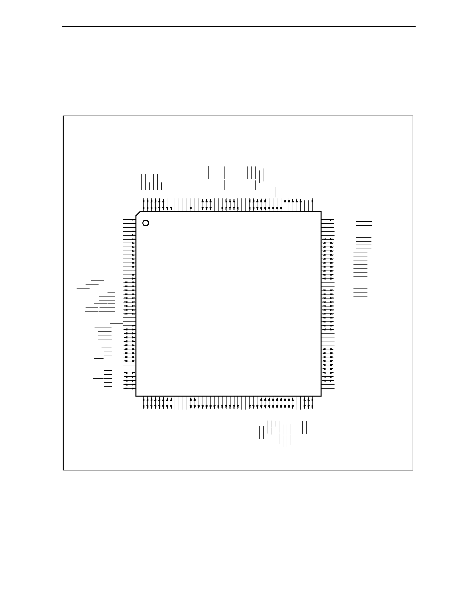
(4) V850E/ME2
�
176-pin plastic LQFP (fine pitch) (24
�
24)
�
PD703111AGM-10-UEU
�
PD703111AGM-13-UEU
�
PD703111AGM-15-UEU
Top View
132
131
130
129
128
127
126
125
124
123
122
121
120
119
118
117
116
115
114
113
112
111
110
109
108
107
106
105
104
103
102
101
100
99
98
97
96
95
94
93
92
91
90
89
TRCDATA3
PDH15/D31/INTPD15/PWM1
PDH14/D30/INTPD14/PWM0
EV
SS
EV
DD
PDH13/D29/INTPD13/TIUD11
PDH12/D28/INTPD12/TO11
PDH11/D27/INTPD11/INTP111/TCLR11
PDH10/D26/INTPD10/INTP110/TCUD11
PDH9/D25/INTPD9/TIUD10
PDH8/D24/INTPD8/TO10
PDH7/D23/INTPD7/INTP101/TCLR10
PDH6/D22/INTPD6/INTP100/TCUD10
PDH5/D21/INTPD5/TOC5
PDH4/D20/INTPD4
PDH3/D19/INTPD3
EV
SS
EV
DD
PDH2/D18/INTPD2/TOC4
PDH1/D17/INTPD1
PDH0/D16/INTPD0
D15
D14
D13
D12
D11
D10
D9
D8
IV
SS
IV
DD
EV
SS
EV
DD
D7
D6
D5
D4
D3
D2
D1
D0
SDCKE/PCD0
EV
SS
EV
DD
176
175
174
173
172
171
170
169
168
167
166
165
164
163
162
161
160
159
158
157
156
155
154
153
152
151
150
149
148
147
146
145
144
143
142
141
140
139
138
137
136
135
134
133
P72/DMARQ2/INTPC20/TIC2
P73/DMAAK2/INTPC21
P74/TC2/TOC2
P75/DMARQ3/INTPC30/TIC3
P76/DMAAK3/INTPC31
P77/TC3/TOC3
SSEL0
SSEL1
PLLV
SS
PLLV
DD
OSCV
SS
X2
X1
OSCV
DD
UV
DD
UDM
UDP
P10/UCLK/INTP10
IV
SS
IV
DD
PLLSEL
P11/SCK0/INTP11
P12/RXD0/SI0
P13/TXD0/SO0
P20/NMI
EV
SS
EV
DD
P21/RXD1/INTP21
P22/TXD1/INTP22
P23/SCK1/INTP23
P24/SI1/INTP24
P25/SO1/INTP25
DCK
DMS
DRST
DDI
DDO
TRCCLK
TRCEND
TRCDATA0
TRCDATA1
IV
SS
IV
DD
TRCDATA2
45
46
47
48
49
50
51
52
53
54
55
56
57
58
59
60
61
62
63
64
65
66
67
68
69
70
71
72
73
74
75
76
77
78
79
80
81
82
83
84
85
86
87
88
A25/PAH9
A24/PAH8
A23/PAH7
A22/PAH6
A21/PAH5
A20/PAH4
A19/PAH3
A18/PAH2
EV
DD
EV
SS
IV
DD
IV
SS
A17/PAH1
A16/PAH0
A15
A14
A13
A12
A11
A10
A9
A8
A7
A6
A5
EV
DD
EV
SS
A4
A3
A2
INTPL1/A1/PAL1
INTPL0/A0/PAL0
BCYST/PCT7
WE/WR/PCT5
RD/PCT4
UUDQM/UUBE/UUWR/PCT3
PCT2/ULWR/ULBE/ULDQM
PCT1/LUWR/LUBE/LUDQM
PCT0/LLWR/LLBE/LLDQM
IV
DD
IV
SS
SDRAS/PCD3
SDCAS/PCD2
BUSCLK/PCD1
JIT1
JIT0
AV
DD
AV
REFP
ANI0
ANI1
ANI2
ANI3
ANI4
ANI5
ANI6
ANI7
AV
REFM
AV
SS
MODE1
MODE0
INTP67/TOC1/P67
INTP66/INTPC11/P66
INTP65/TIC1/INTPC10/P65
TOC0/TC1/P55
INTPC01/DMAAK1/P54
INTPC00/TIC0/DMARQ1/P53
INTP52/TC0/P52
INTP51/DMAAK0/P51
INTP50/DMARQ0/P50
IV
DD
IV
SS
RESET
ADTRG/SELFREF/PCM5
REFRQ/PCM4
HLDRQ/PCM3
HLDAK/PCM2
PCM1
WAIT/PCM0
CS7/PCS7
CS6/PCS6
IORD/CS5/PCS5
EV
DD
EV
SS
CS4/PCS4
CS3/PCS3
IOWR/CS2/PCS2
CS1/PCS1
CS0/PCS0
1
2
3
4
5
6
7
8
9
10
11
12
13
14
15
16
17
18
19
20
21
22
23
24
25
26
27
28
29
30
31
32
33
34
35
36
37
38
39
40
41
42
43
44
CHAPTER 1 OVERVIEW OF EACH PRODUCT
Application Note U17121EJ1V1AN
22
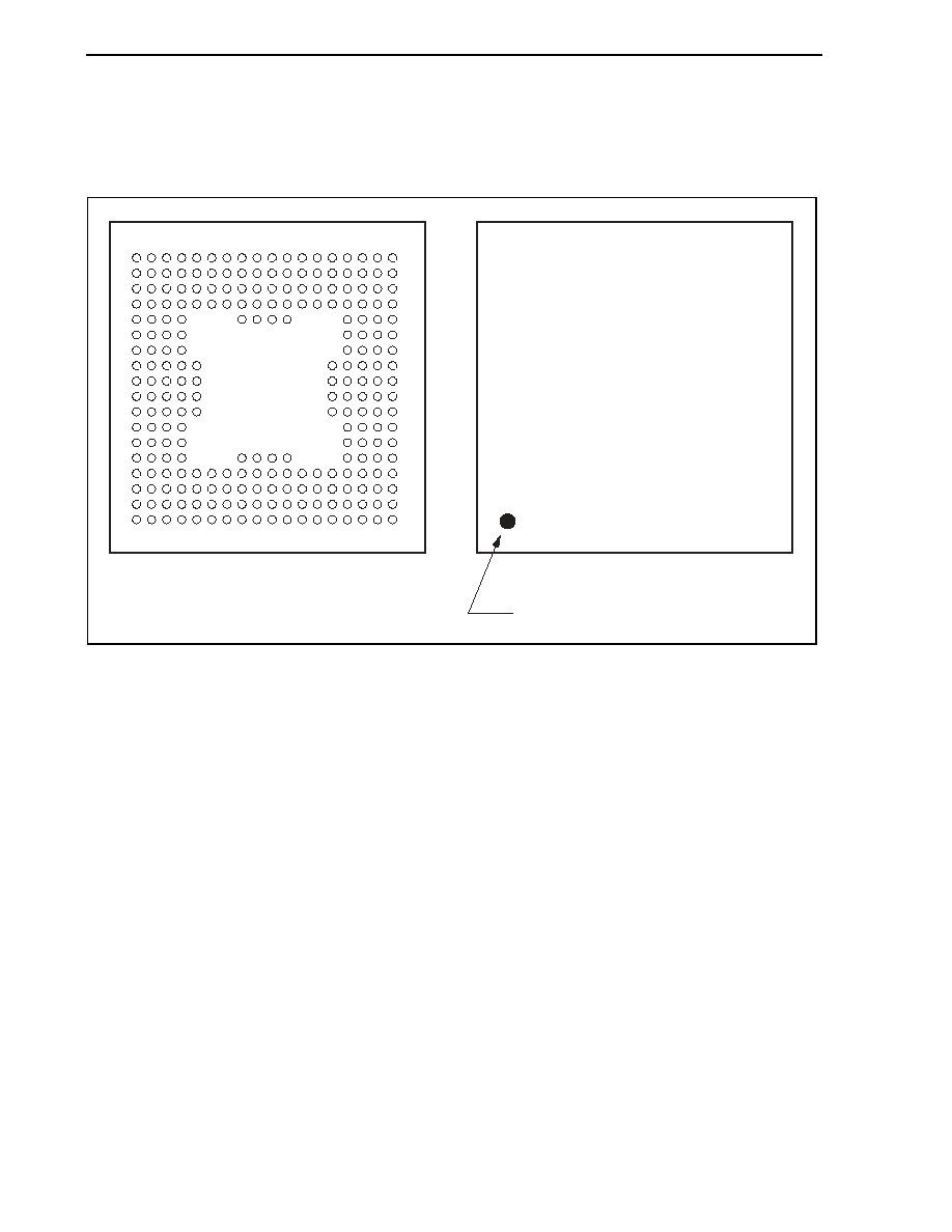
�
240-pin plastic FBGA (16
�
16)
�
PD703111AF1-10-GA3
�
PD703111AF1-13-GA3
�
PD703111AF1-15-GA3
Bottom View
Top View
18
17
16
15
14
13
12
11
10
9
8
7
6
5
4
3
2
1
Index mark
E F G H J K L M N P R T U V
A B C D
P N M L K J H G F E D C B A
V U T R

CHAPTER 1 OVERVIEW OF EACH PRODUCT
Application Note U17121EJ1V1AN
23
(1/2)
Pin No.
Name
Pin No.
Name
Pin No.
Name
A1
-
C12 IV
DD
G3
EV
SS
A2 IV
SS
C13
PAH2/A18
G4
D7
A3 PCT0/LLWR/LLBE/LLDQM
C14 PAH4/A20
G15 PCM1
A4
-
C15 PAH6/A22
G16 PCM3/HLDRQ
A5 PCT4/RD
C16
-
G17 PCM4/REFRQ
A6
-
C17 PCS0/CS0
G18 PCM5/ADTRG/SELFREF
A7
-
C18
-
H1
-
A8 EV
DD
D1
D0 H2
D8
A9 A9
D2 EV
SS
H3
D9
A10
-
D3 PCD0/SDCKE
H4 D10
A11 A14
D4 EV
DD
H5
IV
SS
A12 IV
SS
D5
PCT1/LUWR/LUBE/LUDQM
H14
-
A13 EV
DD
D6
-
H15 RESET
A14
-
D7 PAL0/INTPL0/A0
H16 IV
SS
A15 PAH5/A21
D8 A4
H17
-
A16 PAH7/A23
D9 A6
H18 IV
DD
A17 PAH9/A25
D10
-
J1
-
A18
-
D11 A13
J2 D11
B1
-
D12 EV
SS
J3
D12
B2 PCD1/BUSCLK
D13 PAH3/A19
J4
-
B3 PCD2/SDCAS
D14
-
J5 D13
B4
-
D15
-
J14
-
B5 PCT3/UUWR/UUBE/UUDQM D16 PCS2/CS2/IOWR
J15 P50/INTP50/DMARQ0
B6 PCT7/BCYST
D17 PCS3/CS3
J16 P51/INTP51/DMAAK0
B7 A2
D18 EV
DD
J17
P52/INTP52/TC0
B8
-
E1 D3
J18 P53/INTPC00/TIC0/DMARQ1
B9 A8
E2 D2
K1 D14
B10 A12
E3 D1
K2 D15
B11 PAH0/A16
E4
-
K3 PDH0/D16/INTPD0
B12
-
E8 A3
K4 PDH1/D17/INTPD1
B13
-
E9 A5
K5 PDH2/D18/INTPD2/TOC4
B14
-
E10 A10
K14 P55/TOC0/TC1
B15
-
E11 PAH1/A17
K15 P54/INTPC01/DMAAK1
B16 PAH8/A24
E15 PCS4/CS4
K16 P65/INTP65/INTPC10/TIC1
B17
-
E16 EV
SS
K17
P66/INTP66/INTPC11
B18 PCS1/CS1
E17 PCS5/CS5/IORD
K18
-
C1
-
E18 PCS6/CS6
L1 EV
DD
C2
-
F1 D6
L2
-
C3 PCD3/SDRAS
F2 D5
L3 EV
SS
C4 IV
DD
F3 D4
L4 PDH3/D19/INTPD3
C5 PCT2/ULWR/ULBE/ULDQM
F4
-
L5 PDH4/D20/INTPD4
C6 PCT5/WE/WR
F15
-
L14 MODE1
C7 PAL1/INTPL1/A1
F16 PCS7/CS7
L15
-
C8 EV
SS
F17 PCM0/WAIT
L16 MODE0
C9 A7
F18 PCM2/HLDAK
L17
-
C10 A11
G1 IV
DD
L18
P67/INTP67/TOC1
C11 A15
G2 EV
DD
M1
-

CHAPTER 1 OVERVIEW OF EACH PRODUCT
Application Note U17121EJ1V1AN
24
(2/2)
Pin No.
Name
Pin No.
Name
Pin No.
Name
M2 PDH5/D21/INTPD5/TOC5
R7 DCK
U4
-
M3
PDH6/D22/INTPD6/INTP100/
TCUD10
R8 EV
DD
U5
TRCCLK
M4
-
R9 P11/INTP11/SCK0
U6 DRST
M15 ANI6
R10 IV
SS
U7
P25/INTP25/SO1
M16 AV
REFM
R11
UDM
U8
P22/INTP22/TXD1
M17 ANI7
R12 X2
U9 EV
SS
M18 AV
SS
R13
PLLV
DD
U10
IV
DD
N1
PDH7/D23/INTPD7/INTP101/
TCLR10
R14 SSEL0
U11
-
N2 PDH8/D24/INTPD8/TO10
R15
-
U12 OSCV
DD
N3 PDH9/D25/INTPD9/TIUD10
R16 AV
REFP
U13
-
N4
PDH10/D26/INTPD10/
INTP110/TCUD11
R17 AV
DD
U14
-
N15 ANI2
R18
-
U15 P76/INTPC31/DMAAK3
N16 ANI3
T1 EV
DD
U16
P73/INTPC21/DMAAK2
N17 ANI4
T2 TRCDATA3
U17 P72/INTPC20/TIC2/DMARQ2
N18 ANI5
T3
-
U18
-
P1
-
T4 TRCDATA1
V1
-
P2
PDH11/D27/INTPD11/
INTP111/TCLR11
T5 TRCEND
V2 TRCDATA2
P3 PDH13/D29/INTPD13/TIUD11 T6 DDI
V3 IV
SS
P4
-
T7
-
V4 TRCDATA0
P8 P23/INTP23/SCK1
T8 P21/INTP21/RXD1
V5
-
P9 P12/SI0/RXD0
T9 P20/NMI
V6 DMS
P10
-
T10
-
V7 P24/INTP24/SI1
P11 UV
DD
T11
UDP V8
-
P15
-
T12 X1
V9 P13/SO0/TXD0
P16 ANI0
T13 OSCV
SS
V10
PLLSEL
P17 ANI1
T14 SSEL1
V11 P10/INTP10/UCLK
P18
-
T15 P75/INTPC30/TIC3/DMARQ3 V12
-
R1 PDH12/D28/INTPD12/TO11
T16
-
V13
-
R2 EV
SS
T17
JIT1 V14
-
R3 PDH14/D30/INTPD14/PWM0 T18 JIT0
V15 PLLV
SS
R4 IV
DD
U1
PDH15/D31/INTPD15/PWM1
V16
P77/TOC3/TC3
R5
-
U2
-
V17 P74/TOC2/TC2
R6 DDO
U3
-
V18
-
Remark Leave the A1, A4, A6, A7, A10, A14, A18, B1, B4, B8, B12 to B15, B17, C1, C2, C16, C18, D6, D10, D14,
D15, E4, F4, F15, H1, H14, H17, J1, J4, J14, K18, L2, L15, L17, M1, M4, P1, P4, P10, P15, P18, R5, R15,
R18, T3, T7, T10, T16, U2 to U4, U11, U13, U14, U18, V1, V5, V8, V12 to V14, and V18 pins open.

CHAPTER 1 OVERVIEW OF EACH PRODUCT
Application Note U17121EJ1V1AN
25
1.5 Internal Block Diagram
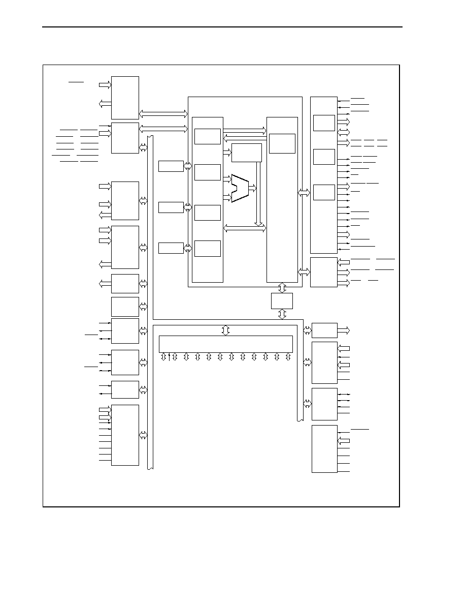
(1) V850E/MA1
NMI
INTP000, INTP001,
INTP010, INTP011,
INTP020, INTP021,
INTP030, INTP031
INTP100 to INTP103,
INTP110 to INTP113,
INTP120 to INTP123,
INTP130 to INTP133
TO00 to TO03
TI000, TI010,
TI020, TI030
INTC
RPU
SIO
ROM
Note 1
RAM
Note 2
CPU
32-bit
barrel shifter
PC
System
registers
General-
purpose
registers
(32 bits
�
32)
ALU
Multiplier
(32
�
32
64)
Ports
PDL0 to PDL15
PAL0 to PAL15
PAH0 to PAH9
PCS0 to PCS7
PCT0, PCT1, PCT4 to PCT7
PCM0 to PCM5
PCD0 to PCD3
PBD0 to PBD3
P70 to P77
P50 to P52
P40 to P45
P30 to P37
P21 to P27
P20
P10 to P13
P00 to P07
CG
System
controller
BCU
CLKOUT
CKSEL
X1
X2
CV
DD
CV
SS
MODE0, MODE1
MODE2/V
PP
Note 3
RESET
V
DD
V
SS
UART0/CSI0
UART1/CSI1
UART2
CSI2
ADC
SO0/TXD0
SI0/RXD0
SCK0
SO1/TXD1
SI1/RXD1
SCK1
TXD2
RXD2
PWM0
SO2
SI2
SCK2
ANI0 to ANI7
AV
REF
/AV
DD
AV
SS
ADTRG
Instruction
queue
MEMC
HLDRQ
HLDAK
CS0, CS7
CS1/RAS1, CS3/RAS3
CS4/RAS4, CS6/RAS6
CS2/IORD
CS5/IOWR
SELFREF
REFRQ
BCYST
LBE/SDCAS
UBE/SDRAS
SDCLK
SDCKE
WE
RD
OE
UWR/UCAS/UDQM
LWR/LCAS/LDQM
WAIT
A0 to A25
D0 to D15
BUSCLK
DRAMC
DMAC
ROMC
PWM0
PWM1
PWM1
DMARQ0 to DMARQ3
DMAAK0 to DMAAK3
TC0 to TC3
Notes 1.
�
PD703103A: ROMless
�
PD703105A, 703106A:
128 KB (mask ROM)
�
PD703107A:
256 KB (mask ROM)
�
PD70F3107A:
256 KB (flash memory)
2.
�
PD703103A, 703105A:
4 KB
�
PD703106A, 703107A, 70F3107A: 10 KB
3. Available only in the
�
PD70F3107A.
CHAPTER 1 OVERVIEW OF EACH PRODUCT
Application Note U17121EJ1V1AN
26
(2) V850E/MA2
NMI
INTP000, INTP001,
INTP010, INTP011
INTP100, INTP101,
INTP110
TO00
TI000, TI010
INTC
RPU
SIO
RAM
4 KB
CPU
32-bit
barrel shifter
PC
System
registers
General-
purpose
registers
(32 bits
�
32)
ALU
Multiplier
(32
�
32
64)
Ports
PDL0 to PDL15
PAL0 to PAL15
PAH0 to PAH8
PCS0, PCS3, PCS4, PCS7
PCT0, PCT1, PCT4, PCT5
PCM0 to PCM4
PCD0 to PCD3
PBD0, PBD1
P70 to P73
P40 to P45
P24
P20
P11, P12
P01 to P05
CG
System
controller
BCU
CLKOUT
CKSEL
X1
X2
CV
DD
CV
SS
MODE0 to MODE2
RESET
V
DD
V
SS
UART0/CSI0
UART1/CSI1
ADC
TXD0/SO0
RXD0/SI0
SCK0
TXD1/SO1
RXD1/SI1
SCK1
ANI0 to ANI3
AV
REF
/AV
DD
AV
SS
Instruction
queue
MEMC
HLDRQ
HLDAK
CS0, CS3, CS4, CS7
REFRQ
LBE/SDCAS
UBE/SDRAS
SDCLK
SDCKE
WE
RD
UWR/UDQM
LWR/LDQM
WAIT
A0 to A24
D0 to D15
SDRAMC
DMAC
ROMC
Prescaler
DMARQ0, DMARQ1
DMAAK0, DMAAK1
TC0

CHAPTER 1 OVERVIEW OF EACH PRODUCT
Application Note U17121EJ1V1AN
27
(3) V850E/MA3
NMI
TOQ0 to TOQ3,
TOQT1 to TOQT3,
TOQB1 to TOQB3
ANI0 to ANI7
ANO0, ANO1
TCLR10, TIUD10, TCUD10
INTP10, INTP11
TO10
INTP000, INTP001, INTP004, INTP005
INTP010 to INTP013, INTP114, INTP115
INTP021, INTP022, INTP124 to INTP126
INTP130 to INTP134, INTP137, INTP050,
INTP051, INTP106, INTP107
INTC
TMENC
�
1 ch
TMD
�
4 ch
TMQ0
�
1 ch
TMP
�
3 ch
UARTA0/CSIB0
UARTA1/CSIB1
ADC
�
8 ch
DAC
�
2 ch
ROM
RAM
Note 2
CPU
32-bit
barrel shifter
PC
System
registers
General-
purpose
registers
(32 bits
�
32)
ALU
Multiplier
(32
�
32
64)
Ports
CG
DCU
System
controller
BCU
PSEL
CKSEL
X1
X2
CV
DD
CV
SS
RESET
MODE0, MODE1
V
DD
V
SS
EV
DD
EV
SS
TCK
TMS
TRST
TDO
TDI
TIQ, EVTQ, INTPQ0 to INTPQ3
EVTP0 to EVTP2, TIP0 to TIP2, INTPP00, INTPP01
INTPP10, INTPP11, INTPP20, INTPP21
TOP00, TOP01, TOP10,
TOP11, TOP20, TOP21
TXD2/SO2
RXD2/SI2
ASCK2/SCK2
UARTA2/CSIB2
ADTRG
TXD0/SO0
RXD0/SI0
ASCK0/SCK0
TXD1/SO1
RXD1/SI1
ASCK1/SCK1
AV
DD0
AV
SS
0
AV
DD1
AV
SS
1
Instruction
queue
MEMC
WAIT
HLDRQ
HLDAK
BUSCLK
A0 to A25
AD0 to AD15
CS0 to CS7
BCYST
RD
UWR, LWR/UBE, LBE
WR
ASTB
IORD
IOWR
SDCLK
SDCKE
SDRAS
SDCAS
WE
LDQM, UDQM
REFRQ
SRAM
ROM
DMAC
SDRAM
WDT
UARTA3/I
2
C
Note 3
TXD3/SDA
Note 3
RXD3/SCL
Note 3
DMARQ0 to DMARQ3
DMAAK0 to DMAAK3
TC0 to TC3
P00, P01, P04 to P07
P10 to P15
P20
P21, P22, P24 to P27
P30 to P34, P37
P40 to P45
P50, P51
P70 to P77
P80, P81
PAL0 to PAL15
PAH0 to PAH9
PDL0 to PDL15
PCS0 to PCS7
PCT0 to PCT7
PCM0 to PCM4
PCD0 to PCD3
PBD0 to PBD3
ROM
correction
Note 1
PLL
Notes 1.
�
PD703131A, 703131AY, 703132A, 703132AY: 256 KB (mask ROM)
�
PD703133A, 703133AY, 703134A, 703134AY: 512 KB (mask ROM)
�
PD70F3134A, 70F3134AY:
512 KB (flash memory)
2.
�
PD703131A, 703131AY, 703133A, 703133AY: 16 KB
�
PD703132A, 703132AY, 703134A, 703134AY,
70F3134A, 70F3134AY:
32 KB
3. Available only in the
�
PD703131AY, 703132AY, 703133AY, 703134AY, 703137AY, and 70F3134AY.
CHAPTER 1 OVERVIEW OF EACH PRODUCT
Application Note U17121EJ1V1AN
28
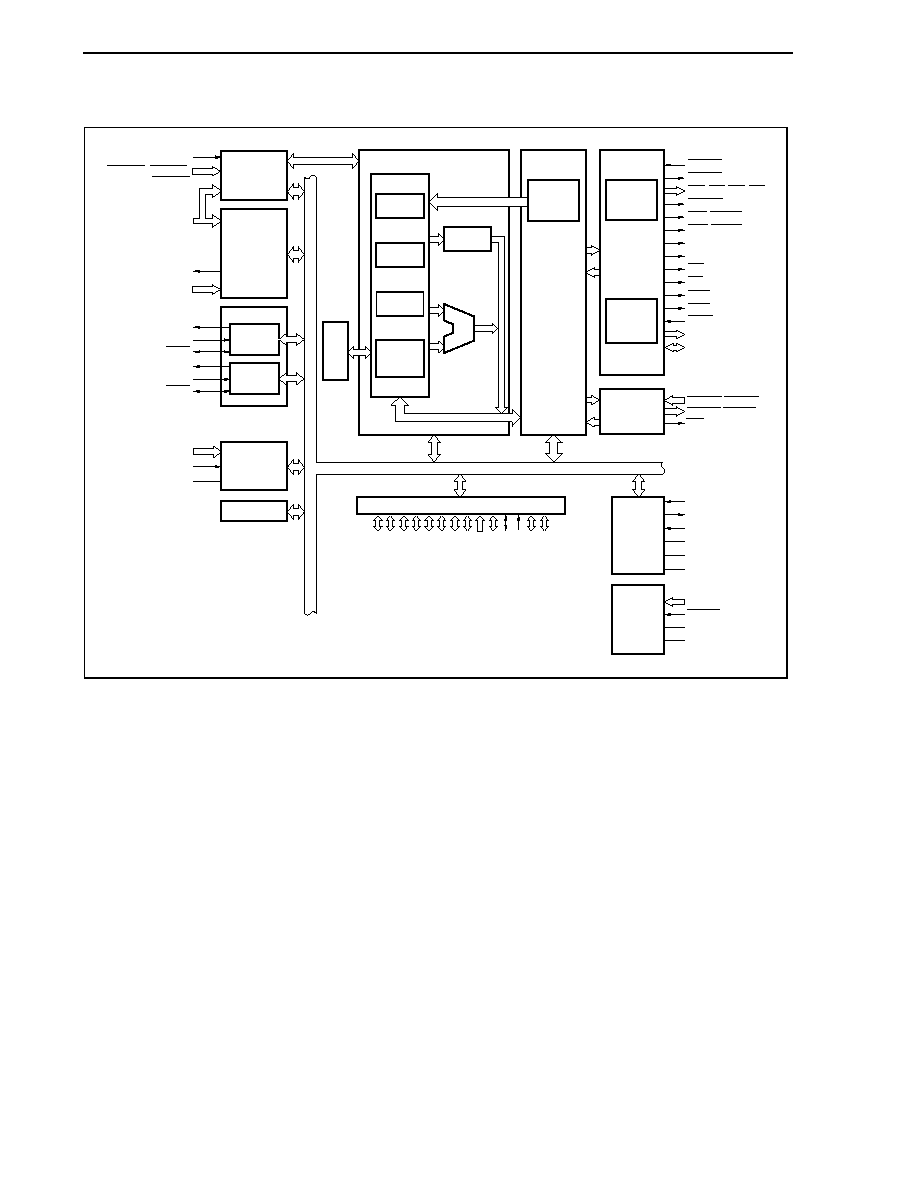
(4) V850E/ME2
CPU
32-bit
barrel shifter
PC
System
registers
General-
purpose
registers
(32 bits
�
32)
ALU
Multiplier
(32
�
32
64)
Ports
P10 to P13
P20
P21 to P25
P50 to P55
P65 to P67
P72 to P77
PAL0, PAL1
PAH0 to PAH9
PCD0 to PCD3
PCM0 to PCM5
PCS0 to PCS7
PCT0 to PCT5, PCT7
PDH0 to PDH15
ADC
USBF
PWM
System
controller
BCU
Instruction
queue
MEMC
SRAM
ROM
SDRAM
DMA
SI0/RXD0
SO0/TXD0
SCK0
TOC4, TOC5
TOC0 to TOC3
TIC0 to TIC3
TO10, TO11
NMI
DRST, DCK,
DMS, DDI,
WAIT
HLDRQ
HLDAK
A0 to A25
D0 to D31
DMARQ0 to DMARQ3
DMAAK0 to DMAAK3
TC0 to TC3
CS0, CS1, CS3,
CS4, CS6, CS7
CS2/IOWR
CS5/IORD
BCYST
RD
ANI0 to ANI7
ADTRG
AV
REFP
, AV
REFM
AV
DD
AV
SS
RESET
MODE0, MODE1
IV
DD
IV
SS
EV
DD
EV
SS
PWM0, PWM1
UDP
UDM
UCLK
UV
DD
xxWR/xxBE
WR
BUSCLK
SDCKE
SDRAS
SDCAS
WE
xxDQM
REFRQ
SELFREF
DDO, TRCCLK,
TRCDATA0 to TRCDATA3,
TRCEND
INTP100, INTP110
INTP101, INTP111
INTP10, INTP11
INTP21 to INTP25
INTP50 to INTP52
INTP65 to INTP67
INTPD0 to INTPD15
INTPL0, INTPL1
TCLR10, TCLR11
TIUD10, TIUD11
TCUD10, TCUD11
INTPC00, INTPC01,
INTPC10, INTPC11,
INTPC20, INTPC21,
INTPC30, INTPC31
SI1
SO1
SCK1
RXD1
TXD1
SSEL0, SSEL1
JIT0, JIT1
PLLSEL
X1
X2
OSCV
DD
OSCV
SS
PLLV
DD
PLLV
SS
TMC
TMC
TMENC1
INTC
DCU
TMD
CSI30/UARTB0
CSI31
UARTB1
CG
8 KB
Instruction cache
128 KB
Instruction RAM
16 KB
Data RAM
BBR
Remark xx: LL, LU, UL, UU

Application Note U17121EJ1V1AN
29
CHAPTER 2 OVERVIEW OF PCI HOST BRIDGE MACRO
The PCI host bridge macro enables connection of V850E/MA1, V850E/MA2, V850E/MA3, V850E/ME2 external
bus interfaces to the PCI bus interface. This chapter gives an outline of the PCI host bridge macro.
2.1 Outline
The PCI host bridge macro is a bridge control macro that connects V850E/MA1, V850E/MA2, V850E/MA3,
V850E/ME2 external bus interfaces (memory controller (MEMC)) to the PCI bus interface.
The main memory (SDRAM) can be directly controlled when SDRAM is accessed from a PCI device.

CHAPTER 2 OVERVIEW OF PCI HOST BRIDGE MACRO
Application Note U17121EJ1V1AN
30
2.2 Features
The features of the PCI host bridge macro are as follows.
�
PCI bus master cycle control
PCI configuration register read/write single cycle
PCI I/O register read/write single cycle
PCI memory read/write single cycle
�
PCI bus slave cycle control
PCI memory read/write cycle (burst transfer up to 8 doublewords (32 bits
�
8 bursts))
�
PCI bus arbiter control
Up to 8 masters can be controlled (one of them is occupied by the PCI host bridge macro)
Bus parking master: Limited to PCI host bridge macro/selectable from the last accessed master
�
PCI bus error processing
An error interrupt is generated for master abort/target abort/PERR# reception/SERR# reception
The address immediately before an error occurs is retained
�
PCI bus address conversion control
PCI I/O address and PCI memory address registers are supported to convert the physical addresses from
the CPU to addresses for the PCI bus
�
CPU interface control
External bus interface (MEMC)
Data bus width: 32 bits/16 bits
Cycle control by hardware wait control
�
SDRAM
control
SDRAM is controlled in response to main memory (SDRAM) access from the PCI device
Data bus width: 16 bits/32 bits are supported
�
PCI
clock
33 MHz supported
SDRAM control and PCI control clocks are designed to be asynchronous

Application Note U17121EJ1V1AN
31
CHAPTER 3 SPECIFICATIONS OF PCI HOST BRIDGE MACRO
This chapter describes the block diagram, signals, register specifications, and operation specifications of the PCI
host bridge macro.
3.1 Internal Blocks of PCI Host Bridge Macro
The PCI host bridge macro consists of the four blocks shown in Figure 3-1 General Block Diagram of PCI Host
Bridge Macro. The functions of each block are described below.
(1) LM_BRIDGE: External bus interface master controller
This controller is connected to the external bus interface, responds to accesses from the CPU, and issues an
access request to the PH_FLIP_BRIDGE block of the PCI bus controller. A bus width of 16 bits or 32 bits can
be accessed from the CPU.
(2) LS_BRIDGE: External bus interface slave controller
This controller responds to accesses from the PH_FLIP_BRIDGE block of the PCI bus controller in response
to a memory data transfer request from the PCI device and issues an access request to SDRAMC.
(3) SDRAMC: External bus interface SDRAM controller
This controller is connected to the SDRAM bus. A memory request from the PCI device via the LS_BRIDGE
block is transferred by activating the SDRAM bus.
When the bus width of SDRAM is 16 bits, memory cycles of up to 8 bursts are started. When the bus width is
32 bits, memory cycles of up to 4 bursts are started.
(4) PH_FLIP_BRIDGE:
External
bus interface host controller
This controller is connected to the PCI bus and operates as the PCI host device.
A PCI configuration register read/write cycle, PCI IO register read/write cycle, and PCI memory read/write
cycle are started in response to a request from the LM_BRIDGE block.
Moreover, a request is issued to the LS_BRIDGE block in response to a memory data transfer request from
the PCI device connected to the PCI bus.
Figure 3-1. General Block Diagram of PCI Host Bridge Macro
PCI bus
interface
PCI host bridge macro
LM_BRIDGE
PH_FLIP_BRIDGE
LS_BRIDGE
SDRAMC
External bus
interface
SDRAM bus
interface
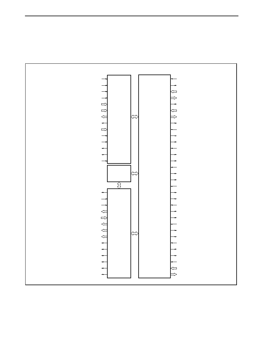
CHAPTER 3 SPECIFICATIONS OF PCI HOST BRIDGE MACRO
Application Note U17121EJ1V1AN
32
3.2 Relationship Between Internal Blocks and Signals
The I/O signals for each block of the PCI host bridge macro are as follows.
Figure 3-2. Blocks and Pin Signals of PCI Host Bridge Macro
LM_BRIDGE
LS_BRIDGE
SDRAMC
PH_FLIP_BRIDGE
I_PCLK
O_PCIRST_B
I_AD0 to I_AD31
O_AD0 to O_AD31
EN_AD
I_CBE0 to I_CBE3
O_CBE0 to O_CBE3
EN_CBE
I_FRAME_B
O_FRAME_B
EN_FRAME
I_IRDY_B
O_IRDY_B
EN_IRDY
I_DEVSEL_B
O_DEVSEL_B
EN_DEVSEL
I_TRDY_B
O_TRDY_B
EN_TRDY
I_STOP_B
O_STOP_B
EN_STOP
I_PAR
O_PAR
EN_PAR
I_PERR_B
O_PERR_B
EN_PERR
I_SERR_B
I_REQ_B1 to I_REQ_B7
O_GNT_B1 to O_GNT_B7
I_SRST_B
I_CPU_CS0_B
I_CPU_CS1_B
I_CPU_CS2_B
I_CPU_ADR0 to I_CPU_ADR19
I_CPU_DATA0 to I_CPU_DATA31
O_CPU_DATA0 to O_CPU_DATA31
EN_CPU_DATA
I_CPU_BE_B0 to I_CPU_BE_B3
I_CPU_WE_B
I_CPU_OE_B
O_CPU_WAIT_B
O_PCIHOST_INT
I_MODE16
O_HOLDREQ_B
I_HOLDACK_B
I_SDCLK
O_SD_DATA0 to O_SD_DATA31
I_SD_DATA0 to I_SD_DATA31
EN_SD_DATA0, EN_SD_DATA1
O_SD_DQM_B0 to O_SD_DQM_B3
O_SD_ADR1 to O_SD_ADR25
O_SD_CKE
O_SD_CS_B
O_SD_RAS_B
O_SD_CAS_B
O_SD_WR_B
EN_SD_CTL
External bus interface
PCI bus interface
SDRAM bus interface

CHAPTER 3 SPECIFICATIONS OF PCI HOST BRIDGE MACRO
Application Note U17121EJ1V1AN
33
3.3 Pin Functions
The pin functions of each interface are described below.
3.3.1 External bus slave interface pins
Pin Name
I/O
Function
Active
I_SRST_B
Input
System reset input
Low
I_CPU_CS0_B
Input
PCI host bridge register chip select input
Low
I_CPU_CS1_B
Input
PCI I/O area chip select input
Low
I_CPU_CS2_B
Input
PCI memory area chip select input
Low
I_CPU_ADR0 to I_CPU_ADR19
Input
CPU address input
-
I_CPU_DATA0 to I_CPU_DATA31
Input
CPU data input
-
O_CPU_DATA0 to O_CPU_DATA31
Output
CPU data output
-
EN_CPU_DATA
Output
CPU data output enable output
High
I_CPU_BE_B0 to I_CPU_BE_B3
Input
CPU data byte enable input
-
I_CPU_WE_B
Input
CPU write data enable input
Low
I_CPU_OE_B
Input
CPU read data output enable input
Low
O_CPU_WAIT_B
Output
CPU data wait output
Low
O_PCIHOST_INT
Output
PCI host bridge interrupt output
Low
I_MODE16
Input
CPU data bus width select input
Low: 32-bit width
High: 16-bit width
3.3.2 SDRAM bus interface pins
Pin Name
I/O
Function
Active
O_HOLDREQ_B
Output
SDRAM bus hold request output
Low
I_HOLDACK_B
Input
SDRAM bus hold acknowledge input
Low
I_SDCLK
Input
SDRAM clock input
-
O_SD_DATA0 to O_SD_DATA31
Output
SDRAM data output
-
I_SD_DATA0 to I_SD_DATA31
Input
SDRAM data input
-
EN_SD_DATA0, EN_SD_DATA1
Output
SDRAM data enable output
Low: Lower 16 bits (O_SD_DATA0 to O_SD_DATA15)
High: Higher 16 bits (O_SD_DATA16 to O_SD_DATA31)
O_SD_DQM_B0 to O_SD_DQM_B3
Output
SDRAM data mask output
Low
O_SD_ADR1 to O_SD_ADR25
Output
SDRAM address output
-
O_SD_CKE
Output
SDRAM clock enable output
High
O_SD_CS_B
Output
SDRAM chip select output
Low
O_SD_RAS_B
Output
SDRAM row address strobe output
Low
O_SD_CAS_B
Output
SDRAM column address strobe output
Low
O_SD_WR_B
Output
SDRAM read/write output
Low
EN_SD_CTL Output
SDRAM control signal output enable output
(Output buffer enable of O_SD_ADR1 to O_SD_ADR25,
O_SD_CKE, O_SD_CS_B, O_SD_RAS_B,
O_SD_CAS_B, and O_SD_WR_B pins)
High

CHAPTER 3 SPECIFICATIONS OF PCI HOST BRIDGE MACRO
Application Note U17121EJ1V1AN
34
3.3.3 PCI bus interface pins
Pin Name
I/O
Function
Active
I_PCLK
Input
PCI clock input
-
O_PCIRST_B
Output
PCI reset output
Low
I_AD0 to I_AD31
Input
PCI address/data input
-
O_AD0 to O_AD31
Output
PCI address/data output
-
EN_AD Output
PCI address/data output enable output
(Output buffer enable of O_AD0 to O_AD31)
High
I_CBE0 to I_CBE3
Input
PCI command/byte enable input
Low
O_CBE0 to O_CBE3
Output
PCI command/byte enable output
Low
EN_CBE Output
PCI command/byte enable output enable output
(Output buffer enable of O_CBE0 to O_CBE3)
High
I_FRAME_B
Input
PCI frame input
Low
O_FRAME_B
Output
PCI frame output
Low
EN_FRAME Output
PCI frame output enable output
(Output buffer enable of O_FRAME_B)
High
I_IRDY_B
Input
PCI initiator ready input
Low
O_IRDY_B
Output
PCI initiator ready output
Low
EN_IRDY Output
PCI initiator ready output enable output
(Output buffer enable of O_IRDY_B)
High
I_DEVSEL_B
Input
PCI device select input
Low
O_DEVSEL_B
Output
PCI device select output
Low
EN_DEVSEL Output
PCI device select output enable output
(Output buffer enable of O_DEVSEL_B)
High
I_TRDY_B
Input
PCI target ready input
Low
O_TRDY_B
Output
PCI target ready output
Low
EN_TRDY Output
PCI target ready output enable output
(Output buffer enable of O_TRDY_B)
High
I_STOP_B
Input
PCI stop input
Low
O_STOP_B
Output
PCI stop output
Low
EN_STOP Output
PCI stop output enable output
(Output buffer enable of O_STOP_B)
High
I_PAR
Input
PCI parity input
-
O_PAR
Output
PCI parity output
-
EN_PAR Output
PCI parity output enable output
(Output buffer enable of O_PAR)
High
I_PERR_B
Input
PCI parity error input
Low
O_PERR_B
Output
PCI parity error output
Low
EN_PERR Output
PCI parity error output enable output
(Output buffer enable of O_PERR_B)
High
I_SERR_B
Input
PCI system error input
Low
I_REQ_B1 to I_REQ_B7
Input
PCI request input
Low
O_GNT_B1 to O_GNT_B7
Output
PCI grant output
Low
CHAPTER 3 SPECIFICATIONS OF PCI HOST BRIDGE MACRO
Application Note U17121EJ1V1AN
35
3.4 Registers
The registers of the PCI host bridge macro are listed below. The bit width of all registers is 32 bits.
The offset address of each register is the offset value from the base address in the area in which the
I_CPU_CS0_B pin becomes active.
Offset Address
Register Name
R/W
Function
00H
PCI_CONFIG_DATA
R/W
PCI configuration register access data setting
04H
PCI_CONFIG_ADD
R/W
PCI configuration register access address setting
08H PCI_CONTROL
R/W
PCI
bus
control
0CH Reserved
10H PCI_IO_BASE
R/W
Sets base address of PCI bus I/O space accessed from PCI I/O
area on CPU memory map
14H PCI_MEM_BASE
R/W
Sets base address of PCI bus memory space accessed from PCI
memory area on CPU memory map
18H
PCI_INT_CTL
R/W
PCI error interrupt control
1CH
PCI_ERR_ADD
R
PCI error generation address retention
20H to 3FH
Reserved
40H SYSTEM_MEM_BASE
R/W
Sets base address of system memory area mapped to PCI bus
memory space
44H SYSTEM_MEM_RANGE
R/W
Sets range of system memory area mapped to PCI bus memory
space
48H SDRAM_CTL
R/W
SDRAM
access
control
4CH to FFH
Reserved
3.4.1 PCI_CONFIG_DATA register
After reset: Undefined R/W Offset address: 00H
31
0
CDATA
Bit Name
R/W
Function
CDATA R/W
PCI configuration register write access is executed by writing data to this field, and the data written
to this field is written to the access target register.
PCI configuration register read access is executed by reading this field, and the data of the access
target register is read.

CHAPTER 3 SPECIFICATIONS OF PCI HOST BRIDGE MACRO
Application Note U17121EJ1V1AN
36
3.4.2 PCI_CONFIG_ADD register
After reset: 00000000H R/W Offset address: 04H
31
0
CADD
Bit Name
R/W
Function
CADD
R/W
Sets PCI configuration register address of access target.
(1) How to set PCI_CONFIG_ADD register
(a) Type 0 (PCI device)
31
11 10
8
7 2
1
0
0
0
IDSEL specification
Function
number
Register number
IDSEL
specification: Selects the IDSEL signal corresponding to the access target PCI device.
Because this PCI host bridge macro uses the AD31 to AD11 signals as the IDSEL
signal for each PCI device, the AD signal connected to the IDSEL pin of each PCI
device is specified in this field. For example, if the AD31 signal is connected to the
IDSEL pin of a PCI device, access is enabled by setting bit 31 of CADD to 1.
Function number:
Specifies the function number for a multifunction device.
Register number:
Specifies the number of the access target PCI configuration register.
(b) Type 1 (PCI-PCI bridge)
31
24
23
16 15
11 10
8
7 2
1
0
0
1
Bus number
Device number
Function
number
Register number
Bus number:
Specifies the number of the PCI bus connected to the access target PCI device.
Device number:
Specifies the device number of the access target PCI device.
Function number:
Specifies the function number for a multifunction device.
Register number:
Specifies the number of the access target PCI configuration register.
CHAPTER 3 SPECIFICATIONS OF PCI HOST BRIDGE MACRO
Application Note U17121EJ1V1AN
37
(2) How to access PCI configuration register
�
Write
access
Set the access target register address to the PCI_CONFIG_ADD register
Write the access target register setting value to the PCI_CONFIG_DATA register
�
Read
access
Set the access target register address to the PCI_CONFIG_ADD register
Read the PCI_CONFIG_DATA register
3.4.3 PCI_CONTROL register
After reset: 07000100H R/W Offset address: 08H
31
24
23
17 16 15
8
7 5
4
3
2
1
0
PCI_PARKCNT
0 0 0 0 0 0 0
PCI_BPMO
D
E
PCI_REQ
0 0 0
PCI_RESET
0
TARGE
T
_EN
MEM_EN
IO_EN
Bit Name
R/W
Function
PCI_PARKCNT R/W
Sets the time for shifting to bus parking.
At the default value, bus parking is performed seven clocks after the bus status becomes IDLE.
The counter is started when FRAME# = High and IRDY# = High.
PCI_BPMODE R/W
Sets the bus parking master.
0: Limited to this macro
1: Master accessed last
PCI_REQ R/W
Enables/disables the REQ# signal (I_REQ_B1 to I_REQ_B7 pins) from the bus master.
Bit 0 of this field (bit 8 of the PCI_CONTROL register) is assigned to the PCI host bridge macro,
and is always 1.
0:
Disabled
1:
Enabled
PCI_RESET R/W
Sets the reset status of the PCI bus.
0: Reset status
1: Reset released
TARGET_EN R/W
Sets the operation of the PCI bus target of the PCI host bridge macro.
0: Do not respond to main memory (SDRAM) access from the PCI device
1: Respond to main memory (SDRAM) access from the PCI device
MEM_EN R/W
Enables/disables access from the CPU to the PCI memory area.
0: Access disabled
1: Access enabled
IO_EN R/W
Enables/disables access from the CPU to the PCI I/O area.
0: Access disabled
1: Access enabled
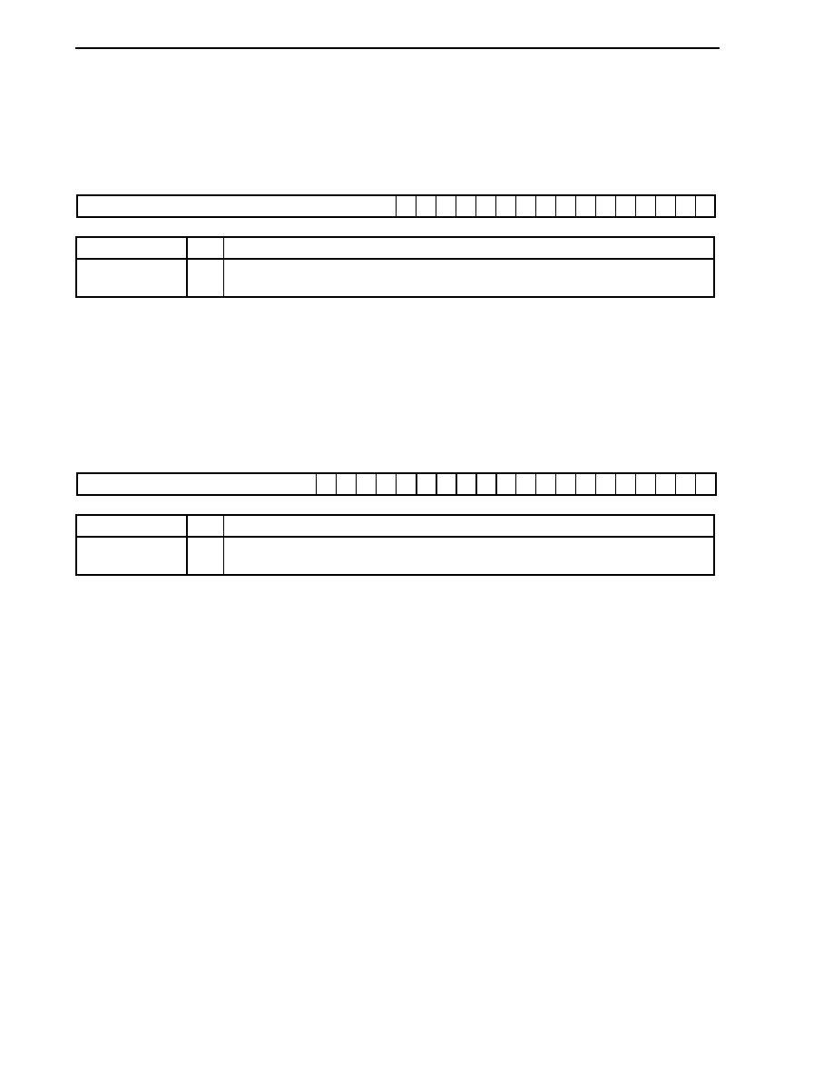
CHAPTER 3 SPECIFICATIONS OF PCI HOST BRIDGE MACRO
Application Note U17121EJ1V1AN
38
3.4.4 PCI_IO_BASE register
When I/O accessing the PCI bus I/O space via the PCI I/O area (area in which the I_CPU_CS1_B pin becomes
active: 64 KB), any area of the 4 GB PCI bus I/O space can be accessed by setting this register.
After reset: 00000000H R/W Offset address: 10H
31
16 15
0
IO_BASE
0 0 0 0 0 0 0 0 0 0 0 0 0 0 0 0
Bit Name
R/W
Function
IO_BASE R/W
Sets the higher 16 bits (bits 16 to 31) of the PCI bus I/O space base address when accessing the
PCI I/O area (area in which the I_CPU_CS1_B pin becomes active) from the CPU.
3.4.5 PCI_MEM_BASE register
When memory accessing the PCI bus memory space via the PCI memory area (area in which the I_CPU_CS2_B
pin becomes active: 1 MB), any area of the 4 GB PCI bus memory space can be accessed by setting this register.
However, because the main memory (SDRAM) is mapped on the PCI bus memory space, do not overlap the area
set by the SYSTEM_MEM_BASE register and SYSTEM_MEM_RANGE register described later.
After reset: 80000000H R/W Offset address: 14H
31
20 19
0
M_BASE
0 0 0 0 0 0 0 0 0 0 0 0 0 0 0 0 0 0 0 0
Bit Name
R/W
Function
M_BASE R/W
Sets the higher 12 bits (bits 20 to 31) of the PCI bus memory space base address when accessing
the PCI memory area (area in which the I_CPU_CS2_B pin becomes active) from the CPU.
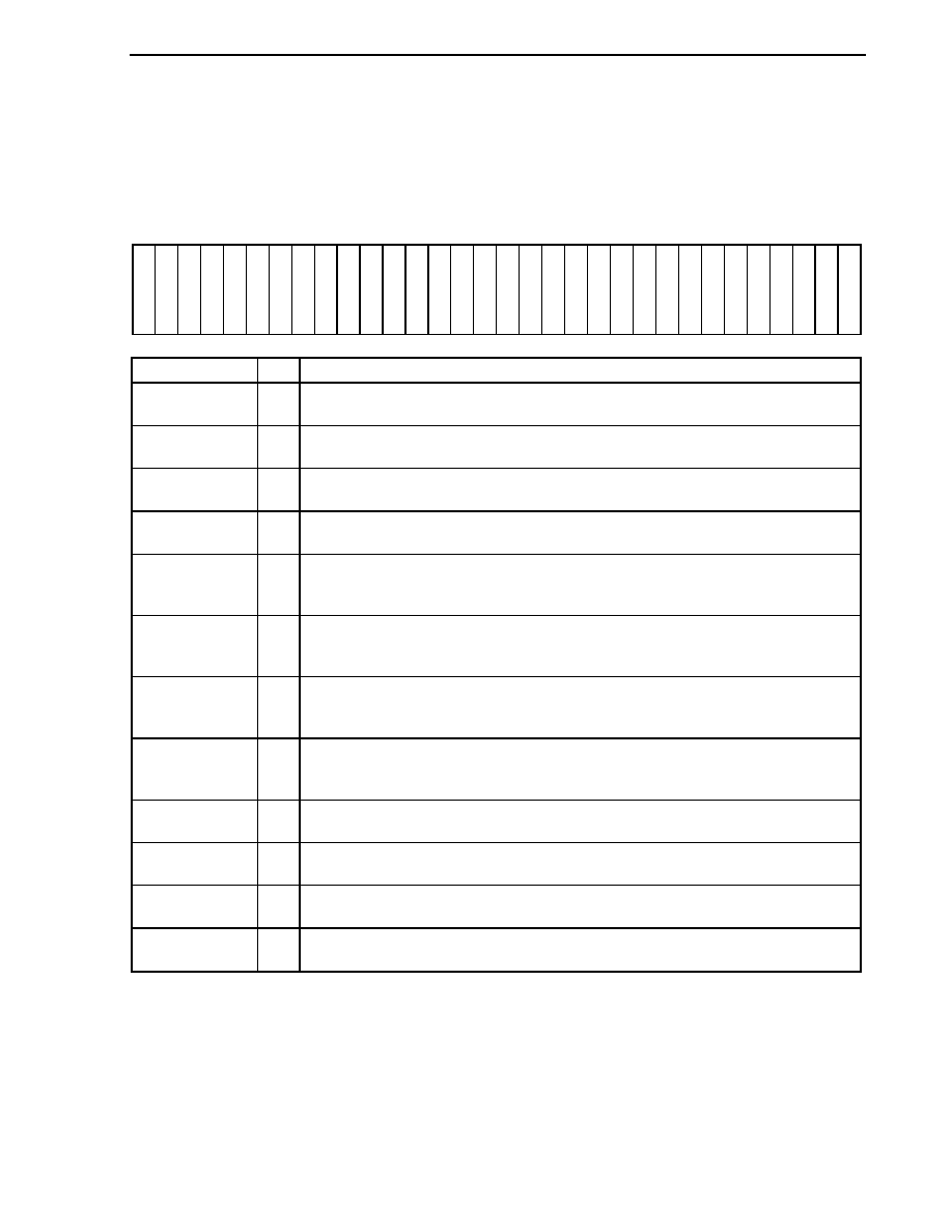
CHAPTER 3 SPECIFICATIONS OF PCI HOST BRIDGE MACRO
Application Note U17121EJ1V1AN
39
3.4.6 PCI_INT_CTL register
The PCI_INT_CTL register shows the interrupt sources of the PCI bus error interrupt (O_PCIHOST_INT) and
controls masking and clearing of these interrupts.
This function is used only for debugging and is not used in normal operation.
After reset: 000x0F00H R/W Offset address: 18H
31
20 19 18 17 16 15
12 11 10
9
8
7 4
3
2
1
0
0 0 0 0 0 0 0 0 0 0 0 0
CLR_SERR
CLR_PERR
CLR_MAB
CLR_TAB
0 0 0 0
MSK_SERR
MSK_PERR
MSK_MAB
MSK_TAB
0 0 0 0
SERR
PERR
MABO
RT
TABO
R
T
Bit Name
R/W
Function
CLR_SERR W
Clears the PCI bus system error (SERR# reception) interrupt.
1:
Cleared
CLR_PERR W
Clears the PCI bus parity error (PERR# reception) interrupt.
1:
Cleared
CLR_MAB W
Clears the PCI bus master abort interrupt.
1:
Cleared
CLR_TAB W
Clears the PCI bus target abort interrupt.
1:
Cleared
MSK_SERR R/W
Sets the mask status of the PCI bus system error (SERR# reception) interrupt.
0: Not masked
1:
Masked
MSK_PERR R/W
Sets the mask status of the PCI bus parity error (PERR# reception) interrupt.
0: Not masked
1:
Masked
MSK_MAB R/W
Sets the mask status of the PCI bus master abort interrupt.
0: Not masked
1:
Masked
MSK_TAB R/W
Sets the mask status of the PCI bus target abort interrupt.
0: Not masked
1:
Masked
SERR R
Detects the occurrence status of a PCI bus system error (SERR# reception).
1: System error occurred
PERR R
Detects the occurrence status of the PCI bus parity error (PERR# reception).
1: Parity error occurred
MABORT R
Detects the occurrence status of the PCI bus master abort.
1: Master abort occurred
TABORT R
Detects the occurrence status of the PCI bus target abort.
1: Target abort occurred

CHAPTER 3 SPECIFICATIONS OF PCI HOST BRIDGE MACRO
Application Note U17121EJ1V1AN
40
3.4.7 PCI_ERR_ADD register
The PCI_ERR_ADD register retains the PCI bus address when the following errors occur.
�
System error (SERR# reception)
�
Parity error (PERR# reception)
�
Master
abort
�
Target
abort
When the PCI_ERR_ADD register is read, all the bits are cleared. Once an error occurs and a value is set to the
PCI_ERR_ADD register, the first value is retained until read access is performed or a new error occurs and the value
is updated.
This function is used only for debugging and is not used in normal operation.
After reset: 00000000H R Offset address: 1CH
31
0
ERR_ADR
Bit Name
R/W
Function
ERR_ADR
R
Retains the address when a PCI bus error occurs.
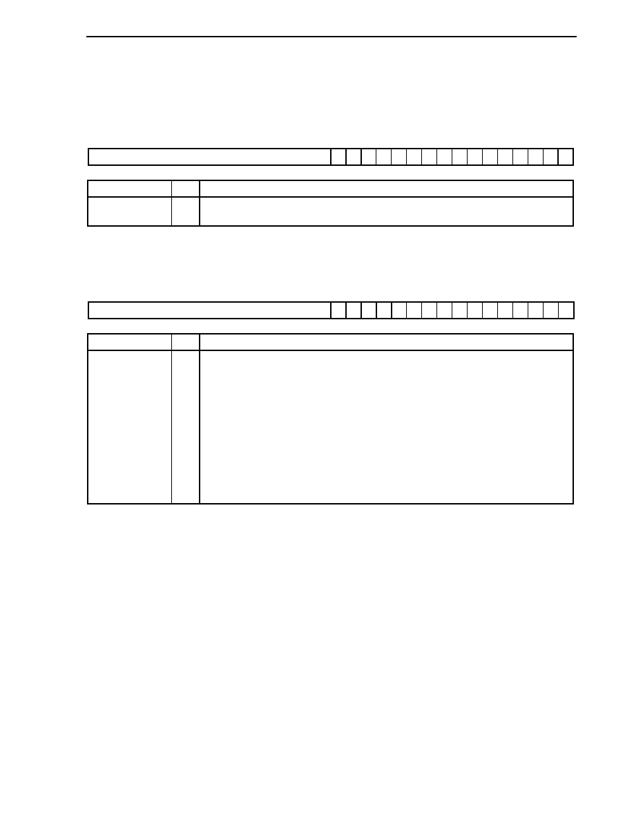
CHAPTER 3 SPECIFICATIONS OF PCI HOST BRIDGE MACRO
Application Note U17121EJ1V1AN
41
3.4.8 SYSTEM_MEM_BASE register
When the main memory is accessed from the PCI device by setting the SYSTEM_MEM_BASE register and
SYSTEM_MEM_RANGE register, the register responds to an access of a matching address.
After reset: 00000000H R/W Offset address: 40H
31
16 15
0
S_BASE
0 0 0 0 0 0 0 0 0 0 0 0 0 0 0 0
Bit Name
R/W
Function
S_BASE R/W
Sets the higher 16 bits (bits 16 to 31) of the base address on the PCI bus memory space in which
the main memory (SDRAM) is mapped.
3.4.9 SYSTEM_MEM_RANGE register
After reset: 0000FFFFH R/W Offset address: 44H
31
16 15
0
S_RANGE
1 1 1 1 1 1 1 1 1 1 1 1 1 1 1 1
Bit Name
R/W
Function
S_RANGE R/W
Sets the range of the PCI bus memory space in which the main memory (SDRAM) is mapped.
It can be set in 64 KB units.
0000H: 64 KB
0001H: 128 KB
:
000FH: 1 MB
:
00FFH: 16 MB
:
0FFFH: 256 MB
:
FFFFH:
4
GB

CHAPTER 3 SPECIFICATIONS OF PCI HOST BRIDGE MACRO
Application Note U17121EJ1V1AN
42
3.4.10 SDRAM_CTL register
After reset: 00070230H R/W Offset address: 48H
31 24
23 16 15
13 12 11 10
9 8 7 6 5 4 3 2 1 0
0 0 0 0 0 0 0 0
CYCLE_LATENCY
0 0 0
BUS_SIZE
0 0
CAS_LATENCY
0 0
W
A
IT_STATE
0 0
COLUM
N
_SIZE
Bit Name
R/W
Function
CYCLE_LATENCY R/W Sets the latency for successive main memory (SDRAM) accesses from the PCI device.
A latency of up to 7,650 ns can be set.
00H: No latency
01H: 1 PCI clock (30 ns)
:
FFH: 255 PCI clocks (7,650 ns)
BUS_SIZE R/W
Sets the bit width of the data bus.
0: 16-bit width
1: 32-bit width
CAS_LATENCY R/W
Sets the CAS latency.
00: Setting prohibited
01:
1
10:
2
11:
3
WAIT_STATE R/W
Sets the wait interval of ACT
CMD, PRE
ACT, and CMD
ACT.
00: Setting prohibited
01: 1 clock
10: 2 clocks
11: 3 clocks
COLUMN_SIZE R/W
Sets the bit width of the column address.
00: 8-bit width
01: 9-bit width
10: 10-bit width
11: 11-bit width
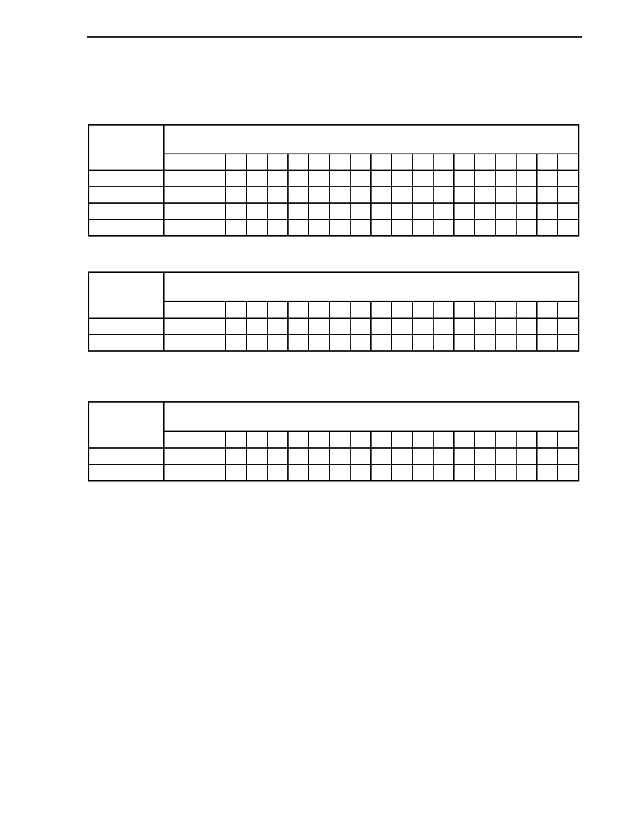
CHAPTER 3 SPECIFICATIONS OF PCI HOST BRIDGE MACRO
Application Note U17121EJ1V1AN
43
The correspondence between the output address signals when the main memory (SDRAM) is accessed and the
PCI bus address signals is shown below.
Table 3-1. Row Address Output
Correspondence Between PCI Bus Address Signal and Main Memory (SDRAM) Address Pins
(O_SD_ADR1 to O_SD_ADR25)
COLUMN_SIZE
Field Setting Value
25
to
18
17 16 15 14 13 12 11 10 9 8 7 6 5 4 3 2 1
00
(8
bits)
25
to
18
25 24 23 22 21 20 19 18 17 16 15 14 13 12 11 10 9
01
(9
bits)
25
to
18
17 25 24 23 22 21 20 19 18 17 16 15 14 13 12 11 10
10
(10
bits)
25
to
18
17 16 25 24 23 22 21 20 19 18 17 16 15 14 13 12 11
11
(11
bits)
25
to
18
17 16 15 25 24 23 22 21 20 19 18 17 16 15 14 13 12
Table 3-2. Column Address Output (Precharge Command)
Correspondence Between PCI Bus Address Signal and Main Memory (SDRAM) Address Pins
(O_SD_ADR1 to O_SD_ADR25)
BUS_SIZE
Bit Setting Value
25
to
18
17 16 15 14 13 12 11 10 9 8 7 6 5 4 3 2 1
0 (16 bits)
25 to 18
17
16
15
14
12
11
H
10
9
8
7
6
5
4
3
2
1
1 (32 bits)
25 to 18
17
16
15
14
12
H
11
10
9
8
7
6
5
4
3
2
1
Remark H: High level
Table 3-3. Column Address Output (Read/Write Command)
Correspondence Between PCI Bus Address Signal and Main Memory (SDRAM) Address Pins
(O_SD_ADR1 to O_SD_ADR25)
BUS_SIZE
Bit Setting Value
25
to
18
17 16 15 14 13 12 11 10 9 8 7 6 5 4 3 2 1
0 (16 bits)
25 to 18
17
16
15
14
12
11
L
10
9
8
7
6
5
4
3
2
1
1 (32 bits)
25 to 18
17
16
15
14
12
L
11
10
9
8
7
6
5
4
3
2
1
Remark L: Low level
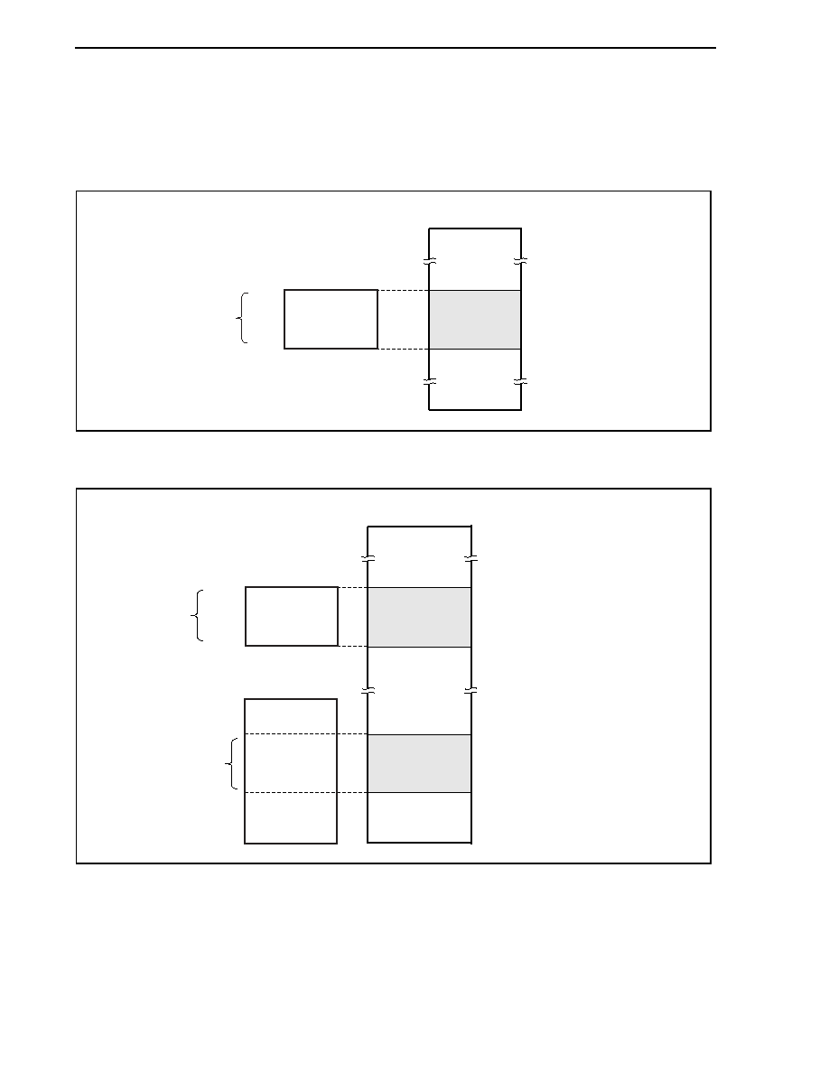
CHAPTER 3 SPECIFICATIONS OF PCI HOST BRIDGE MACRO
Application Note U17121EJ1V1AN
44
3.5 Address Map
The address maps of the CPU memory space and PCI bus I/O or memory space are shown below.
Figure 3-3. CPU Memory Space/PCI Bus I/O Space Address Map
PCI bus I/O space
CPU memory space
I_CPU_CS1_B area
PCI I/O area
FFFFH
0000H
FFFF FFFFH
IO_BASE[31:16] + FFFFH
IO_BASE[31:16] + 0000H
0000 0000H
64 KB
PCI bus I/O space
64 KB
Figure 3-4. CPU Memory Space/PCI Bus Memory Space Address Map
PCI bus memory space
CPU memory space
I_CPU_CS2_B area
Main memory
(SDRAM) area
Main memory space
PCI memory area
FFFFFH
00000H
FFFF FFFFH
M_BASE[31:16] + FFFFFH
M_BASE[31:16] + 00000H
S_BASE[31:16] + S_RANGE[31:16] + FFFFH
S_BASE[31:16] + S_RANGE[31:16] + 0000H
0000 0000H
1 MB
PCI memory space
1 MB
O_SD_CS_B output
when accessing from
PCI host bridge

CHAPTER 3 SPECIFICATIONS OF PCI HOST BRIDGE MACRO
Application Note U17121EJ1V1AN
45
3.6 Initializing PCI Host Bridge Macro
The PCI host bridge macro must be initialized according to the following procedure to acknowledge memory
access and I/O access to the PCI bus and main memory (SDRAM) access from the PCI device.
Figure 3-5. Initializing PCI Host Bridge Macro
Internal PCI bus
reset released
PCI_CONTROL register
Set PCI_RESET bit to 1
Main memory (SDRAM)
area setting
PCI bus control setting
PCI I/O area setting
PCI memory area setting
PCI_MEM_BASE register
Set any address to M_BASE field
PCI_I/O_BASE register
Set any address to I/O_BASE field
PCI_CONTROL register
Set MEM_EN and IO_EN bits to 11
SDRAM_CTL register
Set bit width of column address to COLUMN_SIZE field
Set number of wait clocks to WAIT_STATE field
Set CAS latency to CAS_LATENCY field
Set BUS_SIZE bit to bit width of data bus
Set latency between successive accesses to CYCLE_LATENCY field
SYSTEM_MEM_BASE register
Set any address to S_BASE field
SYSTEM_MEM_RANGE register
Set any value to S_RANGE field
PCI_CONTROL register
Set TARGET_EN bit to 1
Set required bit of PCI_REQ field to 1
SDRAM control setting
CHAPTER 3 SPECIFICATIONS OF PCI HOST BRIDGE MACRO
Application Note U17121EJ1V1AN
46
3.7 Bus Width of External Bus Interface
The operation mode of the data bus with respect to the external bus interface can be changed via the I_MODE16
pin status.
Cautions 1. Do not change the status of the I_MODE16 pin during operation.
2. The I_MODE16 pin can only be used to change the operation mode of the data bus with
respect to the external bus slave interface.
To change the data bus width of the SDRAM bus interface, use the BUS_SIZE bit in 3.4.10
SDRAM_CTL register.
3. The setting of the I_MODE16 pin should correspond with the external bus interface operation
mode of the CPU.
4. When 16-bit mode is set, the access cycle is divided for 32-bit access on the external bus
interface. Accordingly, access is divided similarly on the PCI bus interface. Therefore, when
16-bit mode is set, because a 32-bit access cycle is not generated on the PCI bus interface, a
PCI device whose registers are only valid for 32-bit access cannot be accessed.
Table 3-4. I_MODE16 Pin Status and Operation Mode of Data Bus
I_MODE16 Pin
Data Bus Operation Mode
Remark
Low level
32-bit mode
32-bit data bus
High level
16-bit mode
16-bit data bus
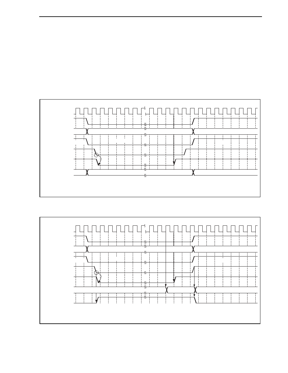
CHAPTER 3 SPECIFICATIONS OF PCI HOST BRIDGE MACRO
Application Note U17121EJ1V1AN
47
3.8 Timing
The timing for each interface of the PCI host bridge macro is shown below.
3.8.1 External bus interface timing
CPU write/CPU read access is performed from the CPU using the bus interface (Figures 3-6 and 3-7).
When accessing SDRAM from the PCI host bridge macro, bus hold is performed and the main memory is
write/read accessed (Figures 3-8 to 3-10).
Figure 3-6. CPU Write Access
I_CPU_CSx_B
I_CPU_WE_B
I_CPU_WAIT_B
I_CPU_ADR0 to
I_CPU_ADR19
I_CPU_DATA0 to
I_CPU_DATA31
I_CPU_BE_B0 to
I_CPU_BE_B3
I_PCLK
Valid
Valid
1111
1111
0000
Remark x = 0 to 2
Figure 3-7. CPU Read Access
I_PCLK
I_CPU_CSx_B
I_CPU_OE_B
I_CPU_WAIT_B
I_CPU_ADR0 to
I_CPU_ADR19
I_CPU_DATA0 to
I_CPU_DATA31
EN_CPU_DATA
I_CPU_BE_B0 to
I_CPU_BE_B3
1111
1111
0000
Valid
Valid
Remark x = 0 to 2
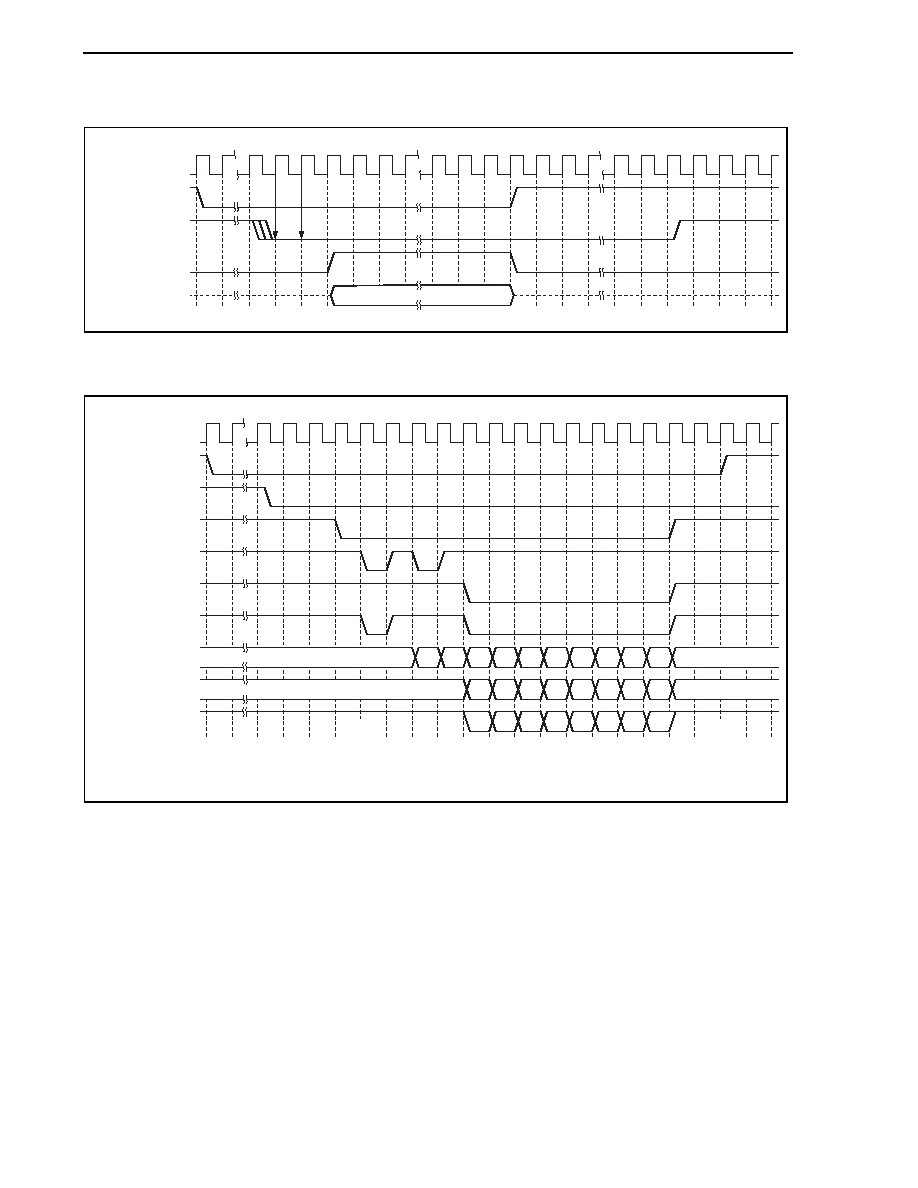
CHAPTER 3 SPECIFICATIONS OF PCI HOST BRIDGE MACRO
Application Note U17121EJ1V1AN
48
Figure 3-8. Hold Request/Hold Acknowledge
I_SDCLK
O_HOLDREQ_B
I_HOLDACK_B
EN_SD_CTL
SDRAM control
signal output
Figure 3-9. Main Memory (SDRAM) Write Access (8-Burst)
I_SDCLK
O_HOLDREQ_B
I_HOLDACK_B
O_SD_CS_B
O_SD_RAS_B
O_SD_CAS_B
O_SD_WR_B
O_SD_DQM_B0 to
O_SD_DQM_B3
O_SD_DATA0 to
O_SD_DATA31
O_SD_ADR1 to
O_SD_ADR25
1111
1111
RA
WD0 WD1
CA1
CA0
CA2 CA3 CA4 CA5 CA6 CA7
WD2 WD3 WD4 WD5 WD6 WD7
Remark SDRAM_CTL register WAIT_STATE field = 10, CAS_LATENCY field = 10

CHAPTER 3 SPECIFICATIONS OF PCI HOST BRIDGE MACRO
Application Note U17121EJ1V1AN
49
Figure 3-10. Main Memory (SDRAM) Read Access (8-Burst)
I_SDCLK
O_HOLDREQ_B
I_HOLDACK_B
O_SD_CS_B
O_SD_RAS_B
O_SD_CAS_B
O_SD_WR_B
O_SD_DQM_B0 to
O_SD_DQM_B3
I_SD_DATA0 to
I_SD_DATA31
O_SD_ADR1 to
O_SD_ADR25
1111
1111
RA
RD0 RD1
CA1
CA0
CA2 CA3 CA4 CA5 CA6 CA7
RD2 RD3 RD4 RD5 RD6 RD7
0000
Remark SDRAM_CTL register WAIT_STATE field = 10, CAS_LATENCY field = 10
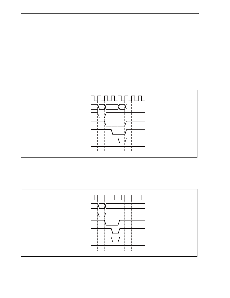
CHAPTER 3 SPECIFICATIONS OF PCI HOST BRIDGE MACRO
Application Note U17121EJ1V1AN
50
3.8.2 PCI bus interface timing
The PCI host bridge macro supports the following PCI bus interface timing.
(1) PCI bus master cycle timing
The timing of access from the CPU to the PCI device is shown below.
(a) Configuration read/write cycle, I/O read/write cycle, and memory read/write cycle
(i) Read
cycle
Timing type: Configuration register read, internal I/O register read, memory read
Figure 3-11. Read Cycle
AD
H
DEVSEL#
TRDY#
FRAME#
STOP#
IRDY#
PCICLK
(ii) Write
cycle
Timing type: Configuration register write, internal I/O register write, memory write
Figure 3-12. Write Cycle
AD
H
DEVSEL#
TRDY#
FRAME#
STOP#
IRDY#
PCICLK
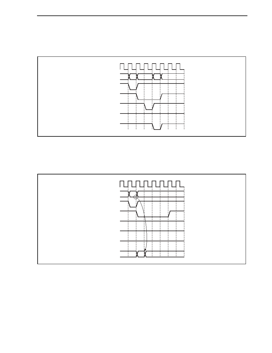
CHAPTER 3 SPECIFICATIONS OF PCI HOST BRIDGE MACRO
Application Note U17121EJ1V1AN
51
(b) Target abort cycle
Timing type: Target abort
Figure 3-13. Target Abort Cycle
AD
H
DEVSEL#
TRDY#
FRAME#
STOP#
IRDY#
PCICLK
(c) Master
abort
cycle
Timing type: Master abort cycle
Figure 3-14. Master Abort Cycle
AD
H
H
H
DEVSEL#
TRDY#
PAR
FRAME#
STOP#
IRDY#
PCICLK
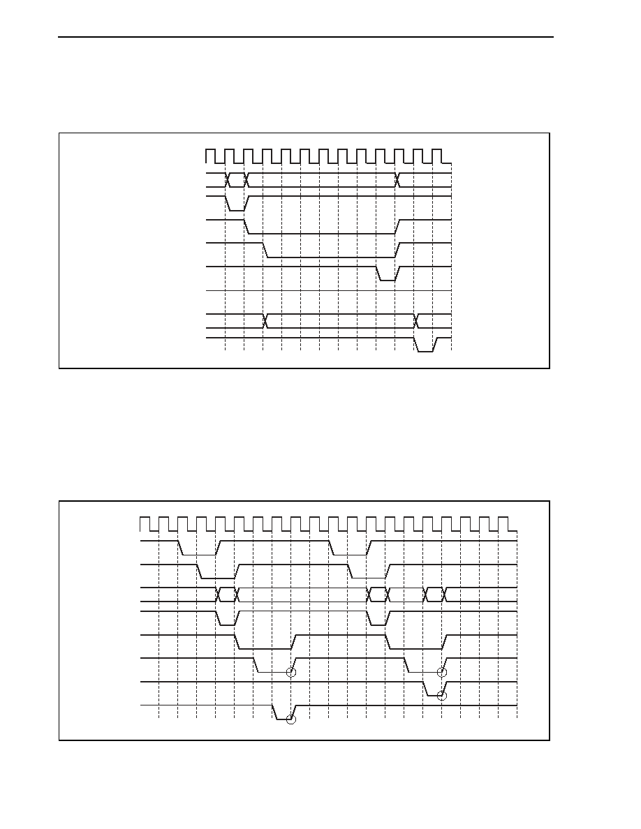
CHAPTER 3 SPECIFICATIONS OF PCI HOST BRIDGE MACRO
Application Note U17121EJ1V1AN
52
(d) Data parity error
Timing type: Single read & write cycle data parity error
Figure 3-15. Data Parity Error
AD
DEVSEL#
TRDY#
PAR
FRAME#
STOP#
IRDY#
PCICLK
PERR#
H
(2) PCI bus slave cycle timing
The timing of access from the PCI device to SDRAM is shown below.
(a) Memory single read cycle
Timing type: Memory single read cycle
Figure 3-16. Single Read Cycle
AD
DEVSEL#
TRDY#
REQ#
FRAME#
STOP#
IRDY#
PCICLK
GNT#
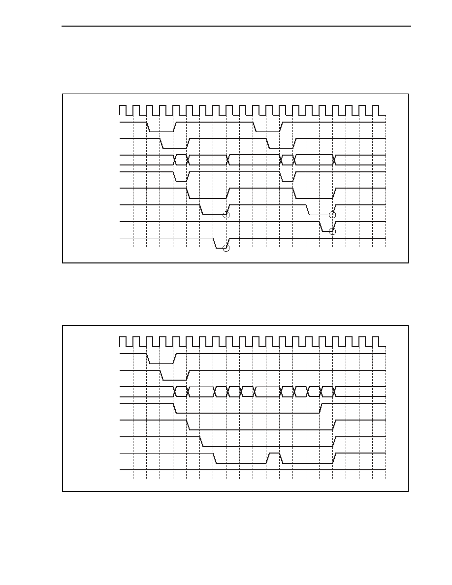
CHAPTER 3 SPECIFICATIONS OF PCI HOST BRIDGE MACRO
Application Note U17121EJ1V1AN
53
(b) Memory single write cycle
Timing type: Memory single write cycle
Figure 3-17. Single Write Cycle
AD
DEVSEL#
TRDY#
REQ#
FRAME#
STOP#
IRDY#
PCICLK
GNT#
(c) Burst read cycle
Timing type: Memory burst read cycle
-
Not disconnect
Figure 3-18. Burst Read Cycle
AD
0
1
2
3
4
5
6
7
DEVSEL#
TRDY#
REQ#
FRAME#
STOP#
IRDY#
PCICLK
GNT#
H

CHAPTER 3 SPECIFICATIONS OF PCI HOST BRIDGE MACRO
Application Note U17121EJ1V1AN
54
(d) Burst write cycle
Timing type: Memory burst write cycle
-
Not disconnect
Figure 3-19. Burst Write Cycle
AD
0
1
2
3
4
5
6
7
DEVSEL#
TRDY#
REQ#
FRAME#
STOP#
IRDY#
PCICLK
GNT#
H
(e) Abort
cycle
Timing type: Target abort cycle & master abort cycle
Figure 3-20. Abort Cycle
AD
DEVSEL#
TRDY#
REQ#
FRAME#
STOP#
IRDY#
PCICLK
GNT#
SERR#
H

CHAPTER 3 SPECIFICATIONS OF PCI HOST BRIDGE MACRO
Application Note U17121EJ1V1AN
55
(f) Data parity error
(i) Read data parity error 1
Timing type: Single read cycle data parity error
Figure 3-21. Read Data Parity Error
AD
DEVSEL#
TRDY#
PAR
FRAME#
STOP#
IRDY#
PCICLK
PERR#
H
(ii) Read data parity error 2
Timing type: Burst read cycle data parity error
Figure 3-22. Read Data Parity Error 2
AD
DEVSEL#
TRDY#
PAR
FRAME#
STOP#
IRDY#
PCICLK
PERR#
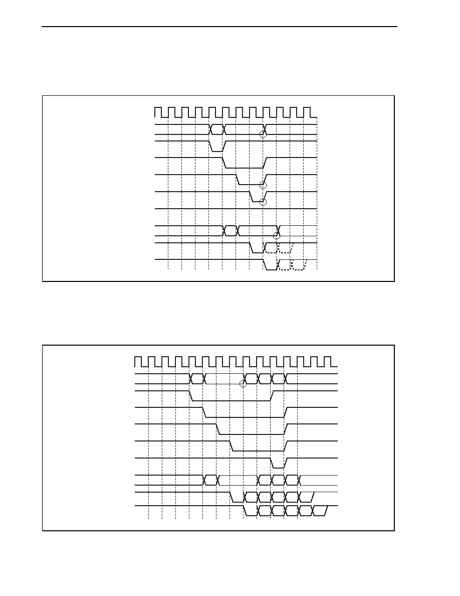
CHAPTER 3 SPECIFICATIONS OF PCI HOST BRIDGE MACRO
Application Note U17121EJ1V1AN
56
(iii) Write data parity error 1
Timing type: Single write cycle data parity error
Figure 3-23. Write Data Parity Error 1
AD
DEVSEL#
TRDY#
PAR
FRAME#
STOP#
IRDY#
PCICLK
PERR#
H
SERR#
(iv) Write data parity error 2
Timing type: Burst write cycle data parity error
Figure 3-24. Write Data Parity Error 2
AD
DEVSEL#
TRDY#
PAR
FRAME#
STOP#
IRDY#
PCICLK
PERR#
SERR#

Application Note U17121EJ1V1AN
57
CHAPTER 4 CONFIGURATION EXAMPLES OF FPGA INTEGRATION
This chapter describes configuration examples in which the PCI host bridge macro is integrated in an FPGA
(Altera's EP20K200EQC240-1X).
4.1 Conditions for Configuration Examples of FPGA Integration
The conditions in the configuration examples are as follows.
(1) CPU:
V850E/ME2
(2) Bus width of external bus interface: 32 bits
(3) CS space of PCI host bridge:
CSZ6
(4) CS space of SDRAM:
CSZ3
(5) SDRAM:
Connecting two 16 M
�
16 SDRAMs (4 M
�
16
�
4 banks)
(6) PCI connection:
2 devices
4.2 Points to Remember When Creating Top Layer of FPGA
Points to remember when integrating the PCI host bridge macro with an FPGA are indicated below.
(1) First decode the chip select from the address before creation.
�
I_CPU_CS0_B: PCI host bridge register chip select
(Offset address in 3.4 Registers)
�
I_CPU_CS1_B: PCI I/O area chip select
(See
Figure 3-3 CPU Memory Space/PCI Bus I/O Space Address Map)
�
I_CPU_CS2_B: PCI memory area chip select
(See
Figure 3-4 CPU Memory Space/PCI Bus Memory Space Address Map)
(2) Because the buffers of the address bus and data bus for the expansion bus interface are output when the PCI
host bridge controls SDRAM, they become bidirectional pins via the selector.
The following pins that control SDRAM become 3-state output.
�
DQM0 to DQM3, SDCKE, SDCS, SDRAS, SDCAS, SDWEZ
(3) The following PCI bus interface pins become bidirectional pins.
�
AD, CBE, FRAME, IRDY, DEVSEL, TRDY, STOP, PAR, PERR
(4) There are three interrupt request output signals: one is output from the PCI host bridge; the remaining two are
INTA and INTB signals from the external PCI slot and are directly connected to the CPU.
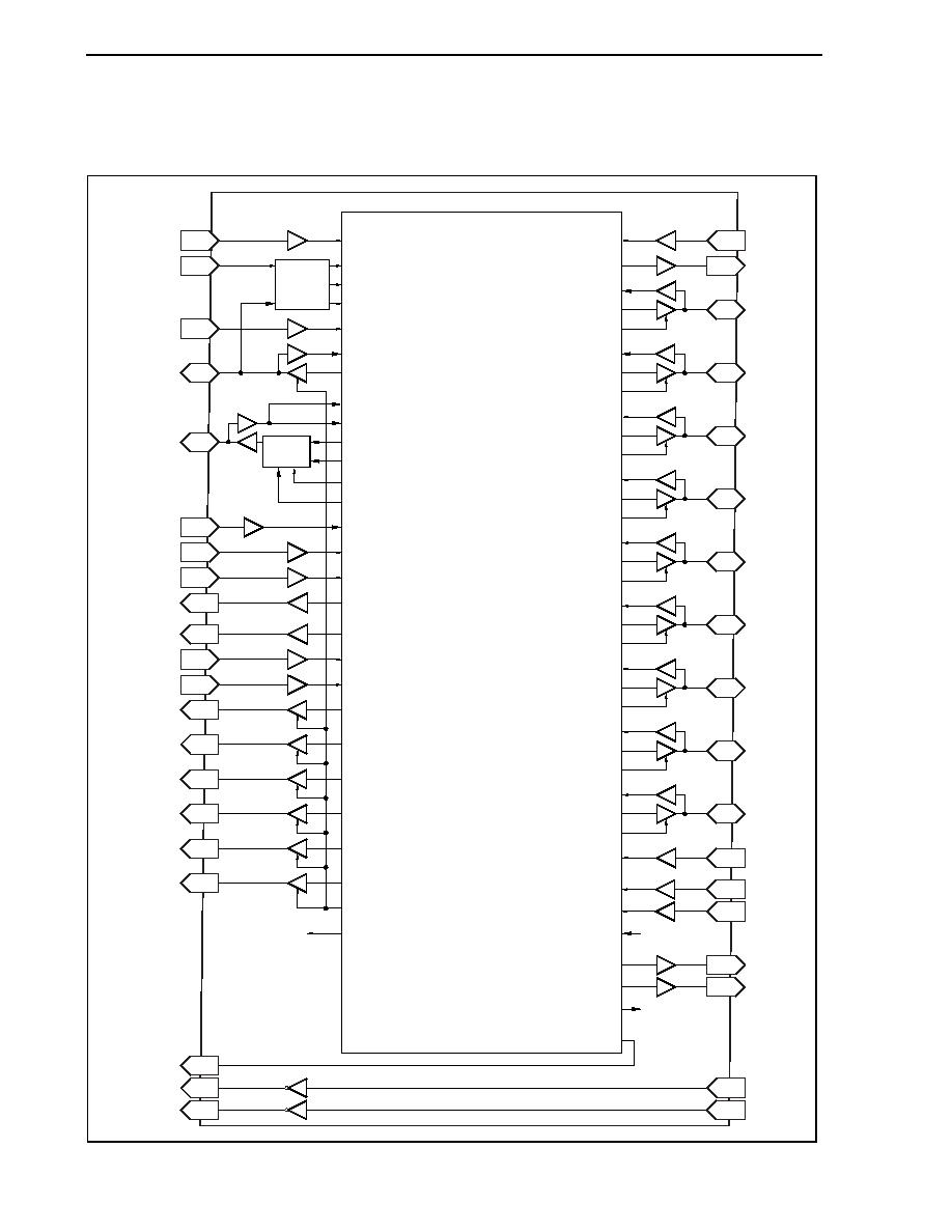
CHAPTER 4 CONFIGURATION EXAMPLES OF FPGA INTEGRATION
Application Note U17121EJ1V1AN
58
4.3 Reference Diagram for FPGA Top Connection
The reference diagram for connecting the PCI host bridge macro with the FPGA top layer is shown below.
Internal H
fixed input
FPGA top
I_PCLK
I_CPU_WE_B
PCLK
O_PCIRST_B
PCIRST
EN_AD
I_CPU_CS0_B
I_CPU_CS1_B
I_CPU_CS2_B
RA21 to
RA25
I_CPU_OE_B
O_CPU_WAIT_B
I_HOLDACK_B
I_SDCLK
EN_SDCLK
I_CPU_ADR0
O_GNT_B2
O_PCIHOST_IN
O_GNT_B1
GNT2
INTB
INT2
INTA
GNT1
O_HOLDREQ_B
I_AD0 to I_AD31
O_AD0 to O_AD31
AD0 to
AD31
EN_CBE
I_CBE0 to I_CBE3
O_CBE0 to O_CBE3
I_CPU_ADR1 to I_CPU_ADR19
O_SD_ADR1 to O_SD_ADR25
CBE0 to
CBE3
O_SD_DQM_B0 to O_SD_DQM_B3
O_SD_CKE
O_SD_CS_B
O_SD_RAS_B
O_SD_CAS_B
O_SD_WR_B
EN_SD_CTL
I_SD_DATA0 to I_SD_DATA31
O_CPU_DATA0 to O_CPU_DATA31
O_SD_DATA0 to O_SD_DATA31
EN_CPU_DATA
I_CPU_BE_B0 to I_CPU_BE_B3
I_CPU_DATA0 to I_CPU_DATA31
I_REQ_B1
REQ1
O_GNT_B3 to O_GNT_B7
EN_FRAME
I_FRAME_B
O_FRAME_B
FRAME
I_SERR_B
SERR
I_REQ_B2
REQ2
I_REQ_B3 to I_REQ_B7
EN_IRDY
I_IRDY_B
O_IRDY_B
IRDY
EN_DEVSEL
I_DEVSEL_B
O_DEVSEL_B
DEVSEL
EN_TRDY
I_TRDY_B
O_TRDY_B
TRDY
EN_STOP
I_STOP_B
O_STOP_B
STOP
EN_PAR
I_PAR
O_PAR
PAR
EN_PERR
I_PERR_B
O_PERR_B
PERR
Open
Open
PCI host bridge macro
Address
decoder
Selector
EN_SD_DATA0, EN_SD_DATA1
INT1
INT0
SDWEZ
SDCASZ
SDCS
SDCKE
HLDRQZ
WAITZ
DQM0 to
DQM3
SDCLK
HLDAKZ
RDZ
WRZ0
BENZ0 to
BENZ3
RA0
CSZ6
I_SRST_B
VBRESETZ
RD0 to RD31
RA1 to RA25
SDRASZ

CHAPTER 4 CONFIGURATION EXAMPLES OF FPGA INTEGRATION
Application Note U17121EJ1V1AN
59
4.4 FPGA Top Pin Functions
The pin information when integrating the PCI host bridge macro with an FPGA is shown below.
4.4.1 CPU bus slave interface pins
Pin Name
I/O
Function
VBRESETZ
Input
System reset input
CSZ6
Input
PCI host bridge chip select input
RA0 to RA25
I/O
CPU address I/O
RD0 to RD31
I/O
CPU data I/O
BENZ0 to BENZ3
Input
CPU data byte enable input
WRZ
Input
CPU data write enable input
RDZ
Input
CPU data read enable input
WAITZ
Output
CPU data wait output
INT0
Output
PCI host bridge interrupt output
4.4.2 SDRAM bus interface pins
Pin Name
I/O
Function
HLDREQZ
Output
SDRAM bus hold request output
HLDACKZ
Input
SDRAM bus hold acknowledge input
SDCLK
Input
SDRAM clock input
SDCKE
Output
SDRAM clock enable output
SDCS
Output
SDRAM chip select output
SDRASZ
Output
SDRAM row address strobe output
SDCASZ
Output
SDRAM column address strobe output
SDWEZ
Output
SDRAM read/write output
DQM0 to DQM3
Output
SDRAM output disable output

CHAPTER 4 CONFIGURATION EXAMPLES OF FPGA INTEGRATION
Application Note U17121EJ1V1AN
60
4.4.3 PCI bus interface pins
Pin Name
I/O
Function
PCLK
Input
PCI clock input
PCIRST
Output
PCI reset output
AD0 to AD31
I/O
PCI address/data I/O
CBE0 to CBE3
I/O
PCI command/byte enable I/O
FRAME
I/O
PCI frame I/O
IRDY
I/O
PCI initiator ready I/O
DEVSEL
I/O
PCI device select I/O
TRDY
I/O
PCI target ready I/O
STOP
I/O
PCI stop I/O
PAR
I/O
PCI parity I/O
PERR
I/O
PCI parity error I/O
SERR
Input
PCI system error input
REQ1, REQ2
Input
PCI request input
GNT1, GNT2
Output
PCI grant output
INT1, INT2
Output
PCI INTA, INTB output
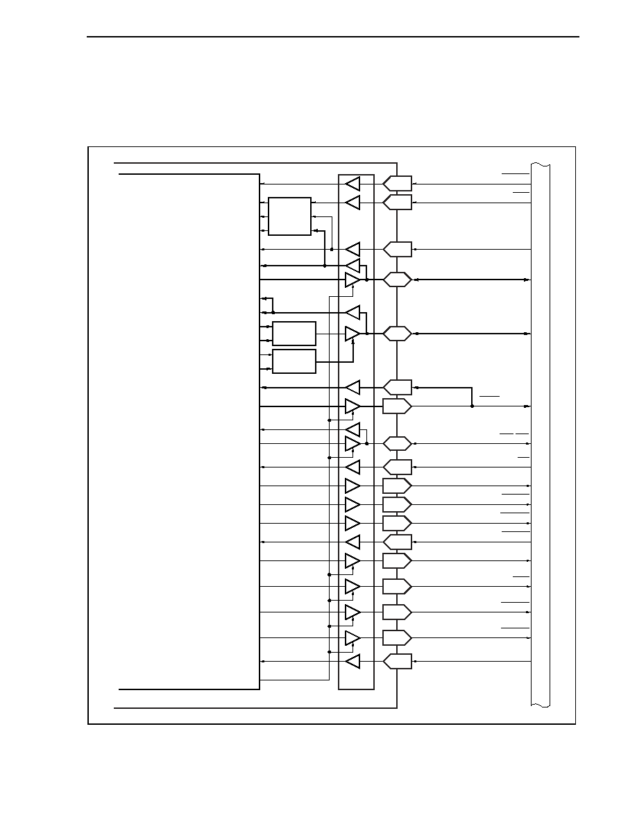
CHAPTER 4 CONFIGURATION EXAMPLES OF FPGA INTEGRATION
Application Note U17121EJ1V1AN
61
4.5 FPGA Top Pin Configuration
The connection diagram of the PCI host bridge macro pins in an FPGA is shown below.
4.5.1 Internal connection diagram of external bus interface
I_SRST_B
PCI host
bridge macro
FPGA top
I_CPU_CS0_B
I_CPU_CS1_B
I_CPU_CS2_B
I_CPU_WE_B
I_CPU_ADR1 to I_CPU_ADR19
I/O buffer
A1 to A25
RESET
CS6
VBRESETZ
CS6
RA0
RA1 to RA25
External bus interface
A0
Selector
Address
decoder
O_SD_ADR1 to O_SD_ADR25
I_CPU_DATA0 to I_CPU_DATA31
I_SD_DATA0 to I_SD_DATA31
O_CPU_DATA0 to O_CPU_DATA31
O_SD_DQM_B0 to O_SD_DQM_B3
I_CPU_BE_B0 to I_CPU_BE_B3
O_SD_DATA0 to O_SD_DATA31
I_CPU_OE_B
O_SD_WR_B
O_CPU_WAIT_B
I_HOLDACK_B
I_SDCLK
O_PCIHOST_INT
O_HOLDRQ_B
O_SD_CKE
O_SD_CS_B
O_SD_RAS_B
O_SD_CAS_B
EN_SD_CTL
Selector
EN_CPU_DATA
EN_SD_DATA0, EN_SD_DATA1
I_SRST_B
RDZ
RD
WRZ
D0 to D31
RD0 to RD31
DQM0 to DQM3
BENZ0 to BENZ3
xxBE/xxDQM
WE/WR
WAITZ
WAIT
INT0
INTP10
HLDRQZ
HLDRQ
HLDAKZ
HLDAK
SDCASZ
SDCAS
SDCLK
BUSCLK
SDCKE
SDCKE
SDCSZ
CS3
SDRASZ
SDRAS

CHAPTER 4 CONFIGURATION EXAMPLES OF FPGA INTEGRATION
Application Note U17121EJ1V1AN
62
4.5.2 Internal connection diagram of PCI bus interface
I/O buffer
H fixed
FPGA top
PCI bus
I_PCLK
O_PCIRST_B
EN_AD
O_GNT_B1, O_GNT_B2
I_AD0 to I_AD31
O_AD0 to O_AD31
EN_CBE
I_CBE0 to I_CBE3
O_CBE0 to O_CBE3
I_REQ_B1, I_REQ_B2
I_REQ_B3 to I_REQ_B7
O_GNT_B3 to O_GNT_B7
EN_FRAME
I_FRAME_B
O_FRAME_B
CLK
PCLK
I_SERR_B
SERR#
SERR
C/BE0# to C/BE3#
CBE0 to CBE3
PCIRST
RST#
AD0 to AD31
AD0 to AD31
FRAME
FRAME#
EN_IRDY
I_IRDY_B
O_IRDY_B
IRDY
IRDY#
EN_DEVSEL
I_DEVSEL_B
O_DEVSEL_B
DEVSEL
DEVSEL#
EN_TRDY
I_TRDY_B
O_TRDY_B
TRDY
TRDY#
EN_STOP
I_STOP_B
O_STOP_B
STOP
STOP#
EN_PAR
I_PAR
O_PAR
PAR
PAR
GNT1#, GNT2#
GNT1, GNT2
REQ1#, REQ2#
REQ1, REQ2
EN_PERR
I_PERR_B
O_PERR_B
PERR
PERR#
Open
PCI host
bridge macro
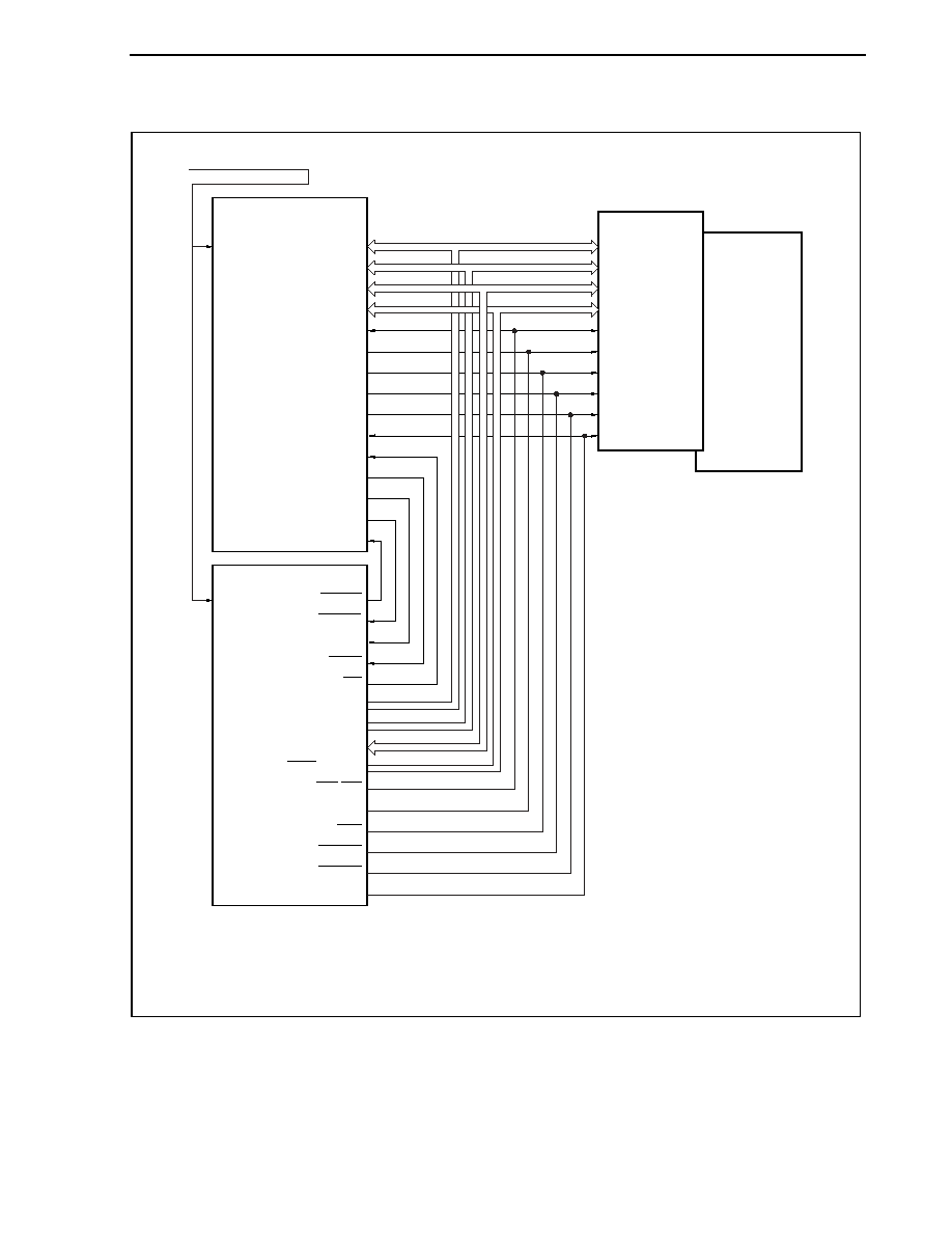
CHAPTER 4 CONFIGURATION EXAMPLES OF FPGA INTEGRATION
Application Note U17121EJ1V1AN
63
4.5.3 External connection diagram of external bus interface (example of connection with V850E/ME2)
VBRESETZ
System reset
FPGA
(PCI host bridge)
SDRAM1
SDRAM2
RA2 to RA14
RA24, RA25
RD0 to RD31
BENZ0 to BENZ3
WRZ
SDCKE
SDCS
SDRASZ
SDCASZ
SDCLK
RDZ
WAITZ
INT0
HLDRQZ
HLDAKZ
RESET
V850E/ME2
HLDAK
HLDRQ
INTPxxx
WAIT
RD
A0 to A22
A24, A25
D0 to D31
xxBE/xxDQM
WR/WE
SDCKE
CSx
SDRAS
SDCAS
BUSCLK
A0 to A12
BA0, BA1
DQ0 to DQ31
DQM0, DQM1
/WE
CKE
/CS
/RAS
/CAS
CLK
DQM2, DQM3
Remarks 1. This is an example using two SDRAMs of 4 M words
�
16 bits
�
4 banks (row address: 13 bits,
column address: 9 bits).
2. xx: LL, LU, UL, UU
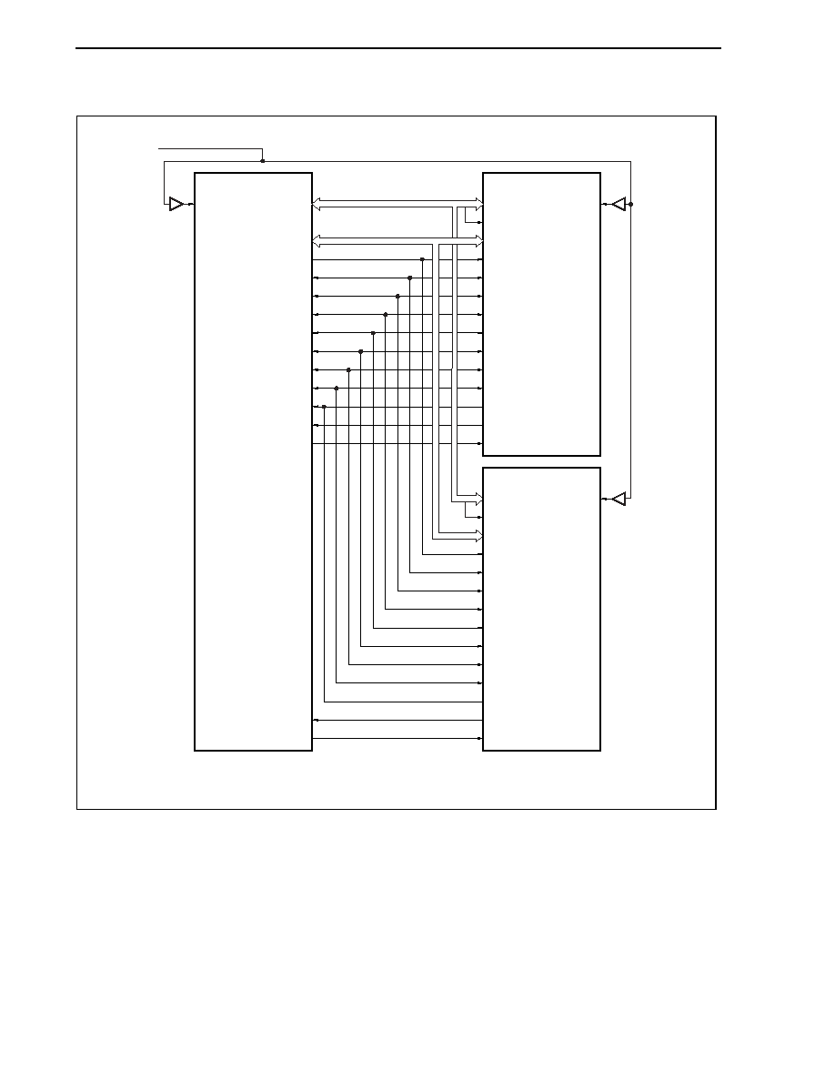
CHAPTER 4 CONFIGURATION EXAMPLES OF FPGA INTEGRATION
Application Note U17121EJ1V1AN
64
4.5.4 External connection diagram of PCI bus interface
PCI device
CLK
PCLK
PCI bus clock
PCI host bridge
PCI device 1
AD00 to AD31
CBE0 to CBE3
PCIRST
FRAME
IRDY
DEVSEL
TRDY
STOP
PAR
PERR
SERR
REQ1
GNT1
AD00 to AD31
IDSEL
Note
C/BE0# to C/BE3#
RST#
FRAME#
IRDY#
DEVSEL#
TRDY#
STOP#
PAR
PERR#
SERR#
REQ#
GNT#
CLK
AD00 to AD31
IDSEL
Note
C/BE0# to C/BE3#
RST#
FRAME#
IRDY#
DEVSEL#
TRDY#
STOP#
PAR
PERR#
SERR#
REQ#
GNT#
REQ2
GNT2
Note Connect one of the AD31 to AD11 signals to the IDSEL pin of each PCI device.

CHAPTER 4 CONFIGURATION EXAMPLES OF FPGA INTEGRATION
Application Note U17121EJ1V1AN
65
4.6 Cautions on Designing FPGA
Cautions when fitting an FPGA using Altera's "Quartusll Design Software" are shown below.
4.6.1 FPGA fitting design
(1) Set the "I/O Standard" buffer type to "3.3-V PCI" for the following PCI bus interface pins.
Pin Name/Usage
Dir
I/O Standard
INTA input 3.3-V
PCI
INTB input 3.3-V
PCI
FRAME bidir
3.3-V
PCI
DEVSEL bidir
3.3-V
PCI
REQ1 input 3.3-V
PCI
REQ2 input 3.3-V
PCI
GNT1 output 3.3-V
PCI
GNT2 output 3.3-V
PCI
IRDY bidir 3.3-V
PCI
TRDY bidir 3.3-V
PCI
STOP bidir 3.3-V
PCI
PCIRST output 3.3-V
PCI
AD0 to AD31
bidir
3.3-V PCI
CBE0 to CBE3
bidir
3.3-V PCI
PAR bidir 3.3-V
PCI
PERR bidir 3.3-V
PCI
SERR input 3.3-V
PCI
(2) Determine the pin assignment taking equal length wiring into consideration for the PCI bus interface pins.
(3) Specify the "PCLK" and "SDCLK" signals as Global CLK.
4.6.2 PCI bus interface timing parameters (as constraint of PCI CLK = 33 MHz)
Adjust the timing so that the following PCI specification values are satisfied.
(1) Input setup time to CLK point to point
Pin Setup Hold
REQ1, REQ2
10 ns
0 ns
Other PCI pins
7 ns
0 ns

CHAPTER 4 CONFIGURATION EXAMPLES OF FPGA INTEGRATION
Application Note U17121EJ1V1AN
66
(2) CLK to signal valid delay signals
Pin MIN.
MAX.
All PCI pins
2 ns
11 ns
The following specification values apply to the PCI bus timing (PCI CLK = 33 MHz).
Figure 4-1. Output Timing
CLK
T
VAL
Output delay
Figure 4-2. Input Timing
CLK
T
H
T
SU
Input
Inputs
valid
Table 4-1. 33 MHz Timing Parameters
Symbol
Parameter
MIN. (ns)
MAX. (ns)
T
VAL
CLK to signal valid delay bused signals
2
11
T
VAL
(ptp)
CLK to signal valid delay point to point signals
2
12
T
SU
Input setup time to CLK bused signals
7
T
SU
(ptp)
Input setup time to CLK point to point signals
10
T
H
Input hold time from CLK
0
4.6.3 SDRAM interface timing
The timing for interfacing with SDRAM depends on the external bus interface and the SDRAM to be connected.
Adjust the timing to suit the system.
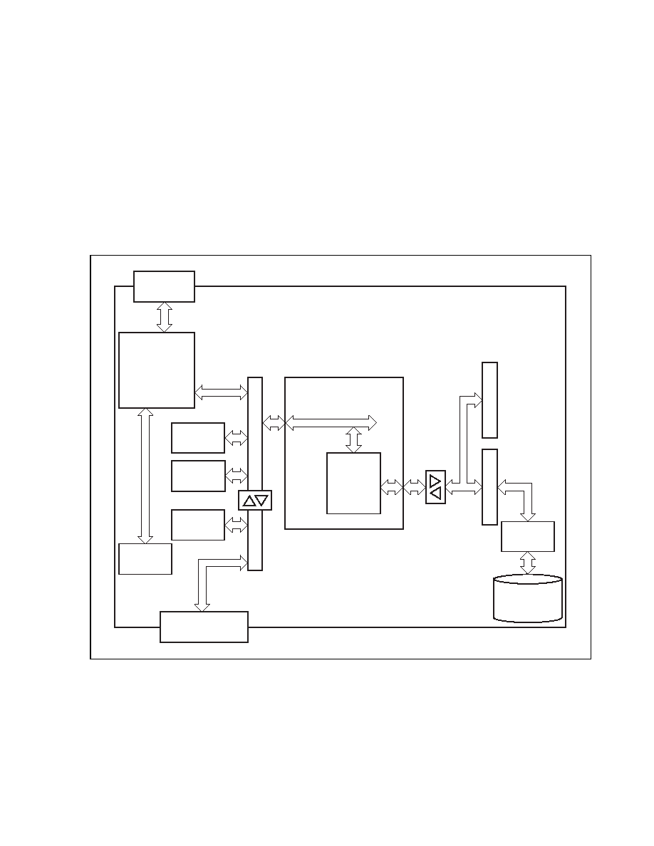
Application Note U17121EJ1V1AN
67
CHAPTER 5 APPLICATION EXAMPLES
This chapter introduces the configuration of an evaluation board that mounts the V850E/ME2, as well as program
examples.
This is an example of an application used to operate a HDD with an IDE controller mounted on the PCI connecter.
5.1 Block Diagram of Evaluation Board
A block diagram of the evaluation board is shown below.
Figure 5-1. Block Diagram of Evaluation Board
PCI host evaluation board
MEMC bus
MEMC b
u
s
PCI b
u
s
PCI bus
PCI host
bridge macro
PCI connector
Hard disk drive
PCI-IDE
controller
Flash
memory
7-segment/
SW
V850E/ME2
(176-pin LQFP)
SRAM
(1 MB)
SDRAM
(64 MB)
ROM socket
(for emulation)
N-Wire
connector
PCI connector

CHAPTER 5 APPLICATION EXAMPLES
Application Note U17121EJ1V1AN
68
5.2 Specifications of Evaluation Board
The specifications of the evaluation board are as follows.
Table 5-1. Specifications of Evaluation Board
Item Description
CPU V850E/ME2
CPU operating frequency
30 MHz
MEMC bus operating frequency
30 MHz
Evaluation board memory
Flash memory
CSZ0 area (32-bit width): 8 MB
SRAM
CSZ1 area (32-bit width): 1 MB
SDRAM
CSZ3 area (32-bit width): 64 MB
Evaluation board peripheral I/O
PCI host bridge
CSZ6 area (32-bit width): PCI Rev.2.1 compliant host interface (33 MHz)
Other
7-segment display
7-segment display
�
2 can be controlled by V850E/ME2 general-purpose port
The device numbers of the PCI bus are assigned as follows.
Table 5-2. IDSEL Connection
Slot Device
Number
Remark
PCI Slot 1 (J2)
AD31
Connect AD31 to IDSEL
PCI Slot 2 (J3)
AD30
Connect AD30 to IDSEL
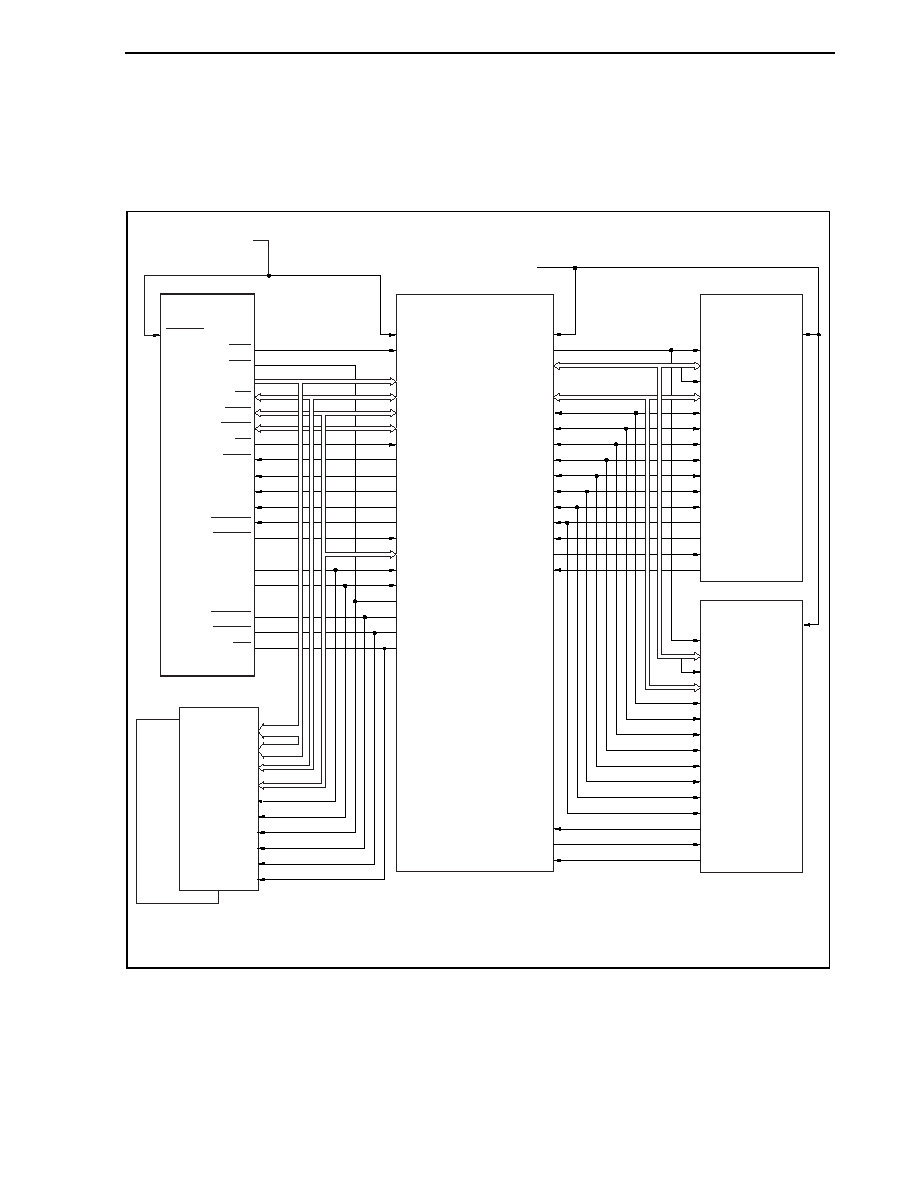
CHAPTER 5 APPLICATION EXAMPLES
Application Note U17121EJ1V1AN
69
5.3 Example of Evaluation Board Connection Circuit
A circuit example of connection of the V850E/ME2 with SDRAM, FPGA, and a PCI device (slot) is shown below.
Figure 5-2. Example of Evaluation Board Connection Circuit
RESET
System reset
PCI bus clock
CS6
CS3
RD
RD
WAIT
INT0
INT1
INT2
HLDRQ
HLDAK
BUSCLK
SDCKE
SDRAS
SDCAS
WE
xxBE
xxWR
A0 to A25
V850E/ME2
A0 to A12
BA0, BA12
D0 to D31
CLK
RAS
CAS
WE
CKE
CS
DQM0, DQM1
DQM2,
DQM3
SDRAM
SDRAM
CSZ6
VBESTZ
RA0 to RA25
RD0 to RD25
BENZ0 to BENZ3
WRZ0 to WRZ3
RDZ
WAITZ
INT0
INT1
INT2
HLDRQZ
HLDAKZ
DQM0 to DQM3
SDCLK
SDCKE
SDCS
SDRASZ
SDCASZ
SDWEZ
PCLK
PCIRST
IRDY
DEVSEL
TRDY
STOP
PAR
PERR
SERR
REQ1
GNT1
INTA
CBE0 to CBE3
FRAME
AD0 to AD31
FPGA
(PCI host bridge)
RST#
AD0 to AD31
IDSEL#
FRAME#
IRDY#
DEVSEL#
TRDY#
STOP#
PAR
SERR#
PERR#
REQ#
GNT#
INT#
C/BE#0 to C/BE#3
CLK
PCI device
RST#
AD0 to AD31
IDSEL#
FRAME#
IRDY#
DEVSEL#
TRDY#
STOP#
PAR
SERR#
PERR#
REQ#
GNT#
INT#
REQ2
GNT2
INTB
C/BE#0 to C/BE#3
CLK
PCI device
A24, A25
A2 to A14
Remark xx: LL, LU, UL, UU
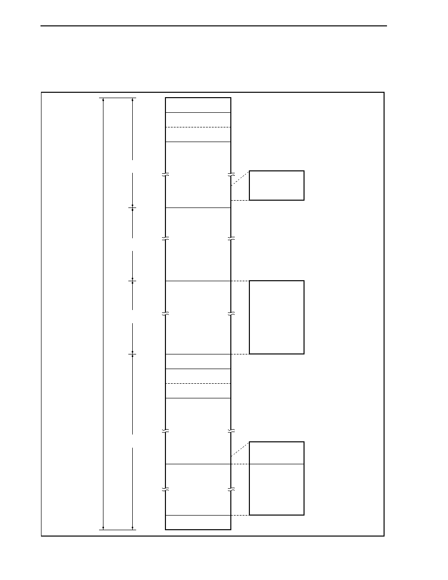
CHAPTER 5 APPLICATION EXAMPLES
Application Note U17121EJ1V1AN
70
5.4 Evaluation Board Memory Space
The evaluation board memory space is shown below.
Figure 5-3. Evaluation Board Memory Space
08F FFFFH
7FF FFFFH
CFF FFFFH
07F FFFFH
010 0000H
080 0000H
400 0000H
C80 0000H
07F FFFFH
000 0000H
080 0000H
400 0000H
3FF 8000H
00F FFFFH
3FF 7FFFH
3FF AFFFH
CSZ0
ROM area
(7 MB)
CSZ1
External SRAM area
(1 MB)
CSZ3
External
SRAM area
(64 MB)
CSZ6
PCI host
bridge area
(8 MB)
SRAM area
(56 MB)
Flash memory area
(7 MB)
Access-prohibited area
On-chip instruction
RAM area (1 MB)
3FF B000H
3FF EFFFH
On-chip peripheral
I/O mirror (4 KB)
SDRAM area
(area 1 = 64 MB)
Reserved area
(area 2 = 64 MB)
On-chip data RAM mirror
(16 KB)
3FF F000H
3FF FFFFH
FFF 8000H
FFF 7FFFH
FFF AFFFH
Access-prohibited area
FFF B000H
FFF EFFFH
On-chip peripheral
I/O area (4 KB)
On-chip data RAM area
(16 KB)
PCI host bridge
CS area
(63.9 MB)
FFF F000H
FFF FFFFH
800 0000H
7FF FFFFH
C00 0000H
BFF FFFFH
Area 0
(64 MB)
Area 1
(64 MB)
Area 2
(64 MB)
Area 3
(64 MB)
256 MB
CHAPTER 5 APPLICATION EXAMPLES
Application Note U17121EJ1V1AN
71
The PCI memory I/O space is assigned to the CSZ6 area.
The base address of the PCI memory space is set to CC0 0000H.
The base address of the PCI I/O space is set to C80 0000H.
Figure 5-4. Comparison Between CPU Memory Space and PCI Memory Space
PCI memory space
0000 0000H
FFFF FFFFH
SYSTEM_MEM_BASE
SYSTEM_MEM_BASE
CC0 0000H
CFF FFFFH
PCI_MEM_BASE[31:22] + 00 0000H
PCI_MEM_BASE[31:22] + 3F FFFFH
SYSTEM_MEM_BASE
SYSTEM_MEM_BASE
Main memory area
(SDRAM)
PCI memory area
CS6 area (4 MB)
CPU memory space
Main memory area
(SDRAM)
PCI memory area
Figure 5-5. Comparison Between CPU Memory Space and PCI I/O Space
PCI I/O space
0000 0000H
FFFF FFFFH
CA0 0000H
C80 0000H
CBF FFFFH
PCI_MEM_BASE[31:21] + 00 0000H
PCI_MEM_BASE[31:21] + 1F FFFFH
PCI I/O area
(2 MB)
CS6 area (4 MB)
CPU memory space
PCI I/O area
PCI bridge I/O area

CHAPTER 5 APPLICATION EXAMPLES
Application Note U17121EJ1V1AN
72
5.5 Sample Program Examples
This sample program is assumed to be used in an environment with the PCI-IDE board connected to the
V850E/ME2 evaluation board as the PCI device.
The PCI-IDE board is connected to the IDE HDD, and the sample program accesses the IDE HDD.
5.5.1 Development tools
(1) MULTI
TM
1.8.9
Integrated development environment made by Green Hills Software
TM
, Inc.
(2) PCI-IDE
board
IDE card of PCI interface connected to evaluation board.
Used by connecting IDE HDD in this application.
5.5.2 Program configuration
The sample program configuration is shown below.
(1) PCI host bridge macro initialization sample program list
First the PCI host bridge macro must be initialized for the CPU to access the PCI area.
The correspondence between the PCI memory space and CPU memory space, the interrupts from PCI, and
access control from the CPU to the PCI memory space are set by the PCI host bridge macro registers.
(2) PCI configuration space access sample program list
When initialization of the PCI host bridge macro ends, initialization of each PCI device connected to the PCI
bus is performed. Initialization is performed mainly by setting the configuration space registers existing in
each PCI device. The configuration space registers can be accessed only by executing a configuration cycle
using the PCI_CONFIG_ADD and PCI_CONFIG_DATA registers described in the register descriptions.
(3) IDE HDD access sample program list
When initialization of the PCI host bridge macro and PCI devices ends, the PCI device can actually be
operated. The PCI device is operated by setting the registers assigned to the configuration space and PCI I/O
area.
The IDE bus setting is performed and the IDE HDD is actually accessed by operating the PCI-IDE board
registers in this sample code.

CHAPTER 5 APPLICATION EXAMPLES
Application Note U17121EJ1V1AN
73
5.5.3 V850E/ME2 PCI host bridge macro initialization sample program list
/////////////////////////////////////////////////////////////////
// V850E/ME2 - PCI Host Bridge Macro initialization sample //
// Overview: Initializes PCI Host Bridge Macro by setting //
// PCI Bridge IO area register group. //
// Specific initialization is described in //
// function PCI_HBM_Init(). //
// //
// PCI_HBM_Init() is called after functions required for //
// accessing Host Bridge Macro, such as CPU and peripheral //
// I/O, are initialized. //
// //
/////////////////////////////////////////////////////////////////
/////////////////////////////////////////////////////////////////
// Defines base address of PCI area and SDRAM area. //
// Start address of PCI area is 0C80_0000H, and start address //
// of SDRAM area is 0400_0000H in this application. //
/////////////////////////////////////////////////////////////////
#define BASE_ADDRESS_ME2PCIIF
(0x0C800000)
#define BASE_ADDRESS_PCI_IO
(BASE_ADDRESS_ME2PCIIF)
#define BASE_ADDRESS_PCI_BRIDGE_IO
(BASE_ADDRESS_ME2PCIIF + 0x00200000)
#define BASE_ADDRESS_PCI_MEM
(BASE_ADDRESS_ME2PCIIF + 0x00400000)
#define
BASE_ADDRESS_SDRAM
(0x04000000)
#define RANGE_SDRAM
(0x03FFFFFF) // 64MB
////////////////////////////////////////////////////////
// PCI Host Bridge Macro register address definition //
////////////////////////////////////////////////////////
#define PHBMR_PCI_CONFIG_DATA
(BASE_ADDRESS_PCI_BRIDGE_IO+0x00)
#define PHBMR_PCI_CONFIG_ADD
(BASE_ADDRESS_PCI_BRIDGE_IO+0x04)
#define
PHBMR_PCI_CONTROL
(BASE_ADDRESS_PCI_BRIDGE_IO+0x08)
#define
PHBMR_PCI_IO_BASE
(BASE_ADDRESS_PCI_BRIDGE_IO+0x10)
#define
PHBMR_PCI_MEM_BASE
(BASE_ADDRESS_PCI_BRIDGE_IO+0x14)
#define
PHBMR_PCI_INT_CTL
(BASE_ADDRESS_PCI_BRIDGE_IO+0x18)
#define
PHBMR_PCI_ERR_ADD
(BASE_ADDRESS_PCI_BRIDGE_IO+0x1C)
#define PHBMR_SYSTEM_MEM_BASE
(BASE_ADDRESS_PCI_BRIDGE_IO+0x40)
#define PHBMR_SYSTEM_MEM_RANGE
(BASE_ADDRESS_PCI_BRIDGE_IO+0x44)
#define
PHBMR_SDRAM_CTL
(BASE_ADDRESS_PCI_BRIDGE_IO+0x48)
///////////////////////////////////////////
// Macro definition for register access //
///////////////////////////////////////////
#define V850EME2_REGW(x) *((volatile unsigned int *)((int)x))

CHAPTER 5 APPLICATION EXAMPLES
Application Note U17121EJ1V1AN
74
/////////////////////////////////////////////////////////////////////////
// Function name: PCI_HBM_Init //
// Function: Initializes PCI Host Bridge Macro. //
// Argument: None //
// Return value: None //
// Remark: Base addresses of this initialization sample are as follows.//
// - Base address of PCI I/O space: 0C80_0000H //
// - Base address of PCI memory space: 0CC0_0000H //
// - Base address on PCI bus memory space in which //
// main memory (SDRAM) is mapped: 0400_0000H //
// - Range of PCI bus memory space in which //
// main memory (SDRAM) is mapped: 03FF_FFFFH //
// Other settings are required according to system //
// requirements and mounting. //
/////////////////////////////////////////////////////////////////////////
void PCI_HBM_Init(void)
{
V850EME2_REGW(PHBMR_PCI_CONTROL) = 0x07000110;
// PCI_CONTROL register
// bit 31-24: PCI_PARKCNT = 1
// (Set time for shifting to bus parking to 7)
// bit 15-08: PCI_REQ = 1 (Enable I_REQ_B0)
// bit 4: PCI_RESET bit = 1 (Release PCI bus reset)
V850EME2_REGW(PHBMR_PCI_IO_BASE) = BASE_ADDRESS_PCI_IO;
// PCI_IO_BASE register
// Set PCI I/O space base address to C800000H.
V850EME2_REGW(PHBMR_PCI_MEM_BASE) = BASE_ADDRESS_PCI_MEM;
// PCI_MEM_BASE register
// Set PCI memory space base address to CC00000H.
V850EME2_REGW(PHBMR_PCI_CONTROL) = 0x07000113;
// PCI_CONTROL register
// bit 31-24: PCI_PARKCNT = 1
// (Set time for shifting to bus parking to 7)
// bit 15-08: PCI_REQ = 1 (Enable I_REQ_B0)
// bit 4: PCI_RESET bit = 1 (Release PCI bus reset)
// bit 1: PCI_MEM_EN bit = 1
// (Enable access from CPU to PCI memory area)
// bit 0: PCI_IO_EN bit = 1
// (Enable access from CPU to PCI I/O area)
V850EME2_REGW(PHBMR_SYSTEM_MEM_BASE) = BASE_ADDRESS_SDRAM;
// SYSTEM_MEM_BASE register
// Set base address on PCI bus memory space in which main
// memory (SDRAM) is mapped to 4000000H.

CHAPTER 5 APPLICATION EXAMPLES
Application Note U17121EJ1V1AN
75
V850EME2_REGW(PHBMR_SYSTEM_MEM_RANGE) = RANGE_SDRAM;
// SYSTEM_MEM_RANGE register
// Set range of PCI bus memory space in which main
// memory (SDRAM) is mapped to 3FFFFFFH (64 MB).
V850EME2_REGW(PHBMR_SDRAM_CTL) = 0x00071211;
// SDRAM_CTL register
// bit 23-16: CYCLE_LATENCY = 07H
// (Set latency for successive main memory
// (SDRAM) access from PCI device to 210 ns)
// bit 12: BUS_SIZE = 1B
// (Set bit width of data bus to 32 bits)
// bit 09-08: CAS_LATENCY = 10B (Set CAS latency to 2)
// bit 05-04: WAIT_STATE = 01B
// (Set wait interval of ACT CMD, PRE ACT,
// and CMD ACT to 1 clock)
// bit 01-00: COLUMN_SIZE = 01B
// (Set bit width of column address to 9 bits)
V850EME2_REGW(PHBMR_PCI_CONTROL) = 0x07000717;
// bit 31-24: PCI_PARKCNT = 1
// (Set time for shifting to bus parking to 7)
// bit 15-08: PCI_REQ = 1 (Enable I_REQ_B0)
// bit 4: PCI_RESET bit = 1 (Release PCI bus reset)
// bit 1: PCI_MEM_EN bit = 1
// (Enable access from CPU to PCI memory area)
// bit 0: PCI_IO_EN bit = 1
// (Enable access from CPU to PCI I/O area)
return;
}
/////////////////////////////////////////////////////////////////
// Function name: main //
// Function: Initializes PCI Host Bridge Macro. //
// Argument: None //
// Return value: 0: Normal end //
/////////////////////////////////////////////////////////////////
int main(void)
{
// Initializes PCI Host Bridge Macro.
PCI_HBM_Init();
return 0;
}

CHAPTER 5 APPLICATION EXAMPLES
Application Note U17121EJ1V1AN
76
5.5.4 PCI configuration space access sample program list
/////////////////////////////////////////////////////////////////////////
// PCI configuration space access sample //
// Overview: Configuration space is accessed using procedure //
// shown below. //
// 1) Write 32-bit value indicating PCI device, function //
// number, and register number to be accessed to //
// PCI_CONFIG_ADD register of PCI Host Bridge Macro. //
// 2) When reading configuration space register, read //
// (word access) 32-bit value in PCI_CONFIG_DATA //
// register of PCI Host Bridge Macro. //
// When writing to configuration space register, write //
// (word access) 32-bit value to PCI_CONFIG_DATA register //
// of PCI Host Bridge Macro. //
// //
// This procedure is combined in functions PCI_ConfigRead //
// and PCI_ConfigWrite shown below. //
// Function PCI_Config_BaseAddressInit uses function //
// PCI_ConfigWrite to set base address register in //
// configuration space. //
// //
/////////////////////////////////////////////////////////////////////////
//////////////////////
// Type declaration //
//////////////////////
typedef
char
BYTE;
typedef
short
int
HWORD;
typedef
int
WORD;
typedef unsigned char
UBYTE;
typedef unsigned short int
UHWORD;
typedef
unsigned
int UWORD;
typedef volatile unsigned char
VUBYTE;
typedef volatile unsigned short int
VUHWORD;
typedef volatile unsigned int
VUWORD;
/////////////////////////////////////////////////////////////////
// Function name: PCI_ConfigRead //
// Function: Reads 32-bit value in PCI configuration space. //
// Argument: ConfigAdd: Register address of configuration space//
// Return value: Read configuration space register data //
/////////////////////////////////////////////////////////////////
UWORD PCI_ConfigRead(UWORD ConfigAdd)
{
V850EME2_REGW(PHBMR_PCI_CONFIG_ADD) = ConfigAdd;
return
V850EME2_REGW(PHBMR_PCI_CONFIG_DATA);
}

CHAPTER 5 APPLICATION EXAMPLES
Application Note U17121EJ1V1AN
77
/////////////////////////////////////////////////////////////////
// Function name: PCI_ConfigWrite //
// Function: Writes 32-bit value to PCI configuration space. //
// Argument: ConfigAdd: Register address of configuration space//
// ConfigData: Register data of configuration space //
// Return value: None //
/////////////////////////////////////////////////////////////////
void PCI_ConfigWrite(UWORD ConfigAdd, UWORD ConfigData)
{
V850EME2_REGW(PHBMR_PCI_CONFIG_ADD) = ConfigAdd;
V850EME2_REGW(PHBMR_PCI_CONFIG_DATA) = ConfigData;
return;
}
/////////////////////////////////////////////////////////////////////////
// Function name: PCI_Config_BaseAddressInit //
// Function: Sets base address of configuration space. //
// Argument: None //
// Return value: None //
// Details: Sets base address register of offset 10H to 24H in //
// configuration space of PCI device connected to AD30 //
// signal by IDSEL as follows. //
// //
// ATA Command Register Base Address (10H) : 0C80_0000H //
// ATA Control Register Base Address (14H) : 0C80_0008H //
// Bus Master Control Register Base Address(18H) : 0C80_0010H //
// //
/////////////////////////////////////////////////////////////////////////
void PCI_Config_BaseAddressInit(void)
{
UWORD ConfigAddress;
UWORD ConfigData;
///////////////////////////////////////
// ATA Command Register Base Address //
///////////////////////////////////////
ConfigAddress = 0x40000010;
// bit 31-11 : IDSEL specification = 010000000000000000000b
// Select PCI device connected to AD30
// bit 10-08 : Function number = 00b
// bit 07-02 : Register number = 4 (000100b),
// -> ATA Command Register Base Address
// (In the case of PCI-IDE ASIC board used in this application)
// bit 01-00 : 00b (fixed)
PCI_ConfigWrite(ConfigAddress, 0x0C800000);

CHAPTER 5 APPLICATION EXAMPLES
Application Note U17121EJ1V1AN
78
///////////////////////////////////////
// ATA Control Register Base Address //
///////////////////////////////////////
ConfigAddress = 0x40000014;
// bit 31-11 : IDSEL specification = 010000000000000000000b
// Select PCI device connected to AD30
// bit 10-08 : Function number = 00b
// bit 07-02 : Register number = 5 (000101b),
// -> ATA Control Register Base Address
// (In the case of PCI-IDE ASIC board used in this application)
// bit 01-00 : 00b (fixed)
PCI_ConfigWrite(ConfigAddress, 0x0C800008);
//////////////////////////////////////////////
// Bus Master Control Register Base Address //
//////////////////////////////////////////////
ConfigAddress = 0x40000018;
// bit 31-11 : IDSEL specification = 010000000000000000000b
// Select PCI device connected to AD30
// bit 10-08 : Function number = 00b
// bit 07-02 : Register number = 6 (000110b)
// -> Bus Master Control Register Base Address
// (In the case of PCI-IDE ASIC board used in this application)
// bit 01-00 : 00b (fixed)
PCI_ConfigWrite(ConfigAddress, 0x0C800010);
return;
}
/////////////////////////////////////////////////////////////////
// Function name: main //
// Function: Sets base address of configuration space. //
// Argument: None //
// Return value: 0: Normal end //
/////////////////////////////////////////////////////////////////
int main(void)
{
// Initializes PCI Host Bridge Macro.
PCI_HBM_Init();
// Sets base address of configuration space.
PCI_Config_BaseAddressInit();
return 0;
}

CHAPTER 5 APPLICATION EXAMPLES
Application Note U17121EJ1V1AN
79
5.5.5 IDE HDD access sample program list
///////////////////////////////////////////////////////////////////////////////
// IDE HDD access sample //
// Overview: Issues ATA commands to HDD, which is ATA device, via PCI-IDE //
// ASIC board connected to PCI slot of evaluation board. //
// ATA commands to be issued are as follows. //
// //
// IDLE IMMEDIATE, IDENTIFY DEVICE, SET FEATURE, //
// READ SECTOR(S), WRITE SECTOR(S), READ DMA, WRITE DMA //
// //
// ATA command is executed by executing device selection //
// protocol to determine that command is issued to either //
// Master Device or Slave Device. ATA command is issued //
// and data is transferred using transfer protocol //
// corresponding to each ATA command. Four transfer //
// protocols, PIO datain transfer, PIO dataout transfer, //
// PIO nondata transfer, and DMA transfer, are available. //
// //
// This sample program is provided with device selection //
// protocol and four transfer protocols as functions. //
// Corresponding transfer protocol function is called //
// from function processing each ATA command. //
// //
///////////////////////////////////////////////////////////////////////////////
/////////////////////////////////////////////////////
// PCI-IDE ASIC board register address definition //
/////////////////////////////////////////////////////
//////////////////////
// IDE Command Area //
//////////////////////
#define IDEREG_DATA
((VUWORD*)(BASE_ADDRESS_PCI_IO + 0x00))
#define
IDEREG_ERROR ((VUBYTE*)(BASE_ADDRESS_PCI_IO
+
0x01))
#define IDEREG_ERROR_ERR_BIT
(0x01)
#define IDEREG_FEATURES
((VUBYTE*)(BASE_ADDRESS_PCI_IO + 0x01))
#define IDEREG_SECTOR_COUNT
((VUBYTE*)(BASE_ADDRESS_PCI_IO + 0x02))
#define IDEREG_SECTOR_NUMBER
((VUBYTE*)(BASE_ADDRESS_PCI_IO + 0x03))
#define IDEREG_CYLINDER_LOW
((VUBYTE*)(BASE_ADDRESS_PCI_IO + 0x04))
#define IDEREG_CYLINDER_HIGH
((VUBYTE*)(BASE_ADDRESS_PCI_IO + 0x05))
#define IDEREG_DEVICE_HEAD
((VUBYTE*)(BASE_ADDRESS_PCI_IO + 0x06))
#define IDEREG_STATUS
((VUBYTE*)(BASE_ADDRESS_PCI_IO + 0x07))
#define IDEREG_COMMAND
((VUBYTE*)(BASE_ADDRESS_PCI_IO + 0x07))
//////////////////////
// IDE Control Area //
//////////////////////

CHAPTER 5 APPLICATION EXAMPLES
Application Note U17121EJ1V1AN
80
#define IDEREG_ALTERNATE_STATUS
((VUBYTE*)(BASE_ADDRESS_PCI_IO + 0x0E))
#define IDEREG_DEVICE_CONTROL
((VUBYTE*)(BASE_ADDRESS_PCI_IO + 0x0E))
/////////////////////////
// Bus Master I/O Area //
/////////////////////////
#define IDEREG_BUSMASTER_START_STOP
((VUWORD*)(BASE_ADDRESS_PCI_IO + 0x10))
#define IDEREG_DSCTBL_START_ADDRESS
((VUWORD*)(BASE_ADDRESS_PCI_IO + 0x14))
#define IDEREG_INTERRUPT_CONTROL
((VUWORD*)(BASE_ADDRESS_PCI_IO + 0x18))
///////////////////////////
// Error code definition //
///////////////////////////
#define STATUS_SUCCESS 0
#define STATUS_TIMEOUT_BSY0_DRQ0 1
#define STATUS_TIMEOUT_DEVICE_SELECTION 1
#define STATUS_TIMEOUT_DRDY1 2
#define STATUS_TIMEOUT_BSY0 3
#define STATUS_TIMEOUT_INTRQ 4
#define STATUS_TIMEOUT_BMEND 5
#define STATUS_IDE_ERROR(IDE_ERROR_REG) (0x10000000 | (UWORD)(IDE_ERROR_REG))
///////////////////////////////////////////////////
// Transfer mode timing setting value definition //
///////////////////////////////////////////////////
// See IDE specifications for details of transfer mode timing setting values shown below.
// Setting value passed to SET_FEATURES command in Set_Transfer_mode()
#define PIO_MODE0 0x08
#define UDMA_MODE0 0x40
// Setting value of timing register (when IDE operation clock is 33 MHz)
#define IDE_PIO_TIMING_IDE33MHz_MODE0 (0x00020906)
#define IDE_UDMA_TIMING1_IDE33MHz_MODE0 (0x00000202)
#define IDE_UDMA_TIMING2_IDE33MHz_MODE0 (0x00000005)
////////////////////////////
// Structure declaration //
////////////////////////////
///////////////////////////////////////
// Structure for issuing ATA command //
///////////////////////////////////////
typedef struct{
UBYTE features;
// Features register
UBYTE sector_count;
// Sector Count register
UBYTE sector_number;
// Sector Number register

CHAPTER 5 APPLICATION EXAMPLES
Application Note U17121EJ1V1AN
81
UBYTE cylinder_low;
// Cylinder Low register
UBYTE cylinder_high;
// Cylinder High register
UBYTE device_head;
// Device/Head register
UBYTE command;
// Command register
} ATA_COMMAND;
////////////////////////////////////////////
// Descriptor table for UltraDMA transfer //
////////////////////////////////////////////
typedef struct{
UWORD transfer_address;
// Transfer address
UWORD transfer_byte;
// Number of transfer bytes
UWORD next_table_address;
// Next table address
} DISCRIPTOR_TABLE;
/////////////////////////////
// Initialization function //
/////////////////////////////
/////////////////////////////////////////////////////////////////
// Function name: PCI_Config_ModeInit //
// Function: Sets initialization of PCI-IDE ASIC board. //
// Argument: None //
// Return value: None //
// Details: Sets handling of interrupts and errors, coding and //
// then resets IDE bus. //
// //
/////////////////////////////////////////////////////////////////
void PCI_Config_ModeInit(void)
{
UWORD ConfigAddress;
UWORD ConfigData;
//////////////////////////////
// Setting of PCI functions //
//////////////////////////////
ConfigAddress = 0x40000004;
// bit 31-11 : IDSEL specification = 010000000000000000000b
// Select PCI device connected to AD30
// bit 10-08 : Function number = 00b
// bit 07-02 : Register number = 1 (000001b)
// -> Status / Command
// bit 01-00 : 00b (fixed)
ConfigData = 0x02000145;
// bit 26-25 : DEVSEL timing = 01b (medium fixed)
// bit 8 : SERR Enable = 1b : Output pci_serr.
// bit 6 : Parity Error Response = 1b : Output pci_serr

CHAPTER 5 APPLICATION EXAMPLES
Application Note U17121EJ1V1AN
82
// when Parity Error is detected.
// bit 2 : Bus Master = 1b : Enable PCI Bus Master transfer
// bit 0 : IO Space = 1b : Enable IO access to PCI-IDE ASIC board
PCI_ConfigWrite(ConfigAddress, ConfigData);
////////////////////////////
// Setting DES to disable //
////////////////////////////
ConfigAddress = 0x40000058;
// bit 31-11 : IDSEL specification = 010000000000000000000b
// Select PCI device connected to AD30
// bit 10-08 : Function number = 00b
// bit 07-02 : Register number = 22 (010110b),
// -> IDE Bus Master Control
// (In the case of PCI-IDE ASIC board used in this application)
// bit 01-00 : 00b (fixed)
// IDE Bus Master Control
// Disable DES (Set bit16 des_on to 0)
ConfigData = PCI_ConfigRead(ConfigAddress);
PCI_ConfigWrite(ConfigAddress, ConfigData & 0xFFFEFFFF);
///////////////////////////////////////////
// Setting of Interrupt Control register //
///////////////////////////////////////////
*IDEREG_INTERRUPT_CONTROL &= 0xFFFCFFFF;
// bit 17 : PCI Bus Master End Interrupt Mask = 0b (Interrupt enabled)
// bit 16 : PCI I/F Interrupt Mask = 0b (Interrupt enabled)
////////////////////////////////////////
// Setting of Device Command register //
////////////////////////////////////////
*IDEREG_DEVICE_CONTROL = 0x00;
// bit 2 : nIEN = 0b (Set INTRQ signal to enable)
///////////////////
// IDE Bus reset //
///////////////////
ConfigAddress = 0x40000044;
// bit 31-11 : IDSEL specification = 010000000000000000000b
// Select PCI device connected to AD30
// bit 10-08 : Function number = 00b
// bit 07-02 : Register number = 17 (010001b),
// -> IDE Reset Register
// (In the case of PCI-IDE ASIC board used in this application)
// bit 01-00 : 00b (fixed)

CHAPTER 5 APPLICATION EXAMPLES
Application Note U17121EJ1V1AN
83
ConfigData = 0x00000001;
// bit 0 : IDE I/F RESET Port = 1b :
// Output IDE RESETX signal output to IDE I/F.
PCI_ConfigWrite(ConfigAddress, ConfigData);
return;
}
////////////////////////////////////
// Transfer mode setting function //
////////////////////////////////////
/////////////////////////////////////////////////////////////////////////
// Function name: Set_Transfer_Mode //
// Function: Setting of transfer mode //
// Argument: dev_num : Device selection (0:Master/1:Slave) //
// mode : Transfer mode //
// Return value: //
// STATUS_SUCCESS : Normal end //
// STATUS_TIMEOUT_DEVICE_SELECTION : DEVICE SELECTION error end //
// STATUS_TIMEOUT_DRDY1 : DRDY=1 timeout error end //
// STATUS_TIMEOUT_INTRQ : INTRQ timeout error end //
// STATUS_IDE_ERROR : Error end after command execution //
// //
/////////////////////////////////////////////////////////////////////////
int Set_Transfer_Mode(int dev_num, UBYTE mode)
{
status = ATA_Set_Features(dev_num, 0x03, mode);
return status;
}
/////////////////////////////////////////////////////////////////
// Function name: Set_PIO_Timing //
// Function: Setting of PIO Timing register //
// Argument: pio_timing : Value set to PIO Timing register //
// Return value: None //
// //
/////////////////////////////////////////////////////////////////
void Set_PIO_Timing(UWORD pio_timing)
{
UWORD ConfigAddress;
UWORD ConfigData;
ConfigAddress = 0x40000048;
// bit 31-11 : IDSEL specification = 010000000000000000000b
// Select PCI device connected to AD30
// bit 10-08 : Function number = 00b

CHAPTER 5 APPLICATION EXAMPLES
Application Note U17121EJ1V1AN
84
// bit 07-02 : Register number = 18 (010010b)
// -> PIO Timing (In the case of PCI-IDE ASIC board used in this application)
// bit 01-00 : 00b (fixed)
PCI_ConfigWrite( ConfigAddress, pio_timing );
return;
}
/////////////////////////////////////////////////////////////////////////
// Function name: Set_UDMA_Timing //
// Function: Setting of UltraDMA Timing1, 2 registers //
// Argument: udma_timing1 : Value set to UltraDMA Timing1 register //
// udma_timing2 : Value set to UltraDMA Timing2 register //
// Return value: None //
// //
/////////////////////////////////////////////////////////////////////////
void Set_UDMA_Timing(UWORD udma_timing1, UWORD udma_timing2)
{
UWORD ConfigAddress;
UWORD ConfigData;
ConfigAddress = 0x4000004C;
// bit 31-11 : IDSEL specification = 010000000000000000000b
// Select PCI device connected to AD30
// bit 10-08 : Function number = 00b
// bit 07-02 : Register number = 19 (010011b)
// -> UltraDMA Timing1
// (In the case of PCI-IDE ASIC board used in this application)
// bit 01-00 : 00b (fixed)
PCI_ConfigWrite( ConfigAddress, udma_timing11 );
ConfigAddress = 0x40000050;
// bit 31-11 : IDSEL specification = 010000000000000000000b
// Select PCI device connected to AD30
// bit 10-08 : Function number = 00b
// bit 07-02 : Register number = 20 (010100b)
// -> UltraDMA Timing2
// (In the case of PCI-IDE ASIC board used in this application)
// bit 01-00 : 00b (fixed)
PCI_ConfigWrite( ConfigAddress, udma_timing2 );
return;
}
////////////////////////////////////

CHAPTER 5 APPLICATION EXAMPLES
Application Note U17121EJ1V1AN
85
// ATA command execution function //
////////////////////////////////////
/////////////////////////////////////////////////////////////////////////
// Function name: ATA_Set_Features //
// Function: Executes SET FEATURES command (Protocol:ND, Command:EFh). //
// Argument: dev_num : Device selection (0:Master/1:Slave) //
// Return value: //
// STATUS_SUCCESS : Normal end //
// STATUS_TIMEOUT_DEVICE_SELECTION : DEVICE SELECTION error end //
// STATUS_TIMEOUT_DRDY1 : DRDY=1 timeout error end //
// STATUS_TIMEOUT_INTRQ : INTRQ timeout error end //
// STATUS_IDE_ERROR : Error end after command execution //
// //
/////////////////////////////////////////////////////////////////////////
int ATA_Set_Features(int dev_num, int sub_cmd, int mode)
{
int status;
ATA_COMMAND ac;
ac.features = sub_cmd;
// Features register
ac.sector_count = mode;
// SectorCount register
ac.sector_number = 0x00;
// SectorNumber register
ac.cylinder_low = 0x00;
// CylinderLow register
ac.cylinder_high = 0x00;
// CylinderHigh register
ac.device_head = dev_num<<4;
// Device/Head register
ac.command = 0xEF;
// Command register
status = ATA_PIO_nondata(&ac);
return status;
}
//////////////////////////////////////////////////////////////////////////
// Function name: ATA_Idle_Immediate //
// Function: Executes IDLE IMMEDIATE command (Protocol:ND, Command:E1h).//
// Argument: dev_num : Device selection (0:Master/1:Slave) //
// Return value: //
// STATUS_SUCCESS : Normal end //
// STATUS_TIMEOUT_DEVICE_SELECTION : DEVICE SELECTION error end //
// STATUS_TIMEOUT_DRDY1 : DRDY=1 timeout error end //
// STATUS_TIMEOUT_INTRQ : INTRQ timeout error end //
// STATUS_IDE_ERROR : Error end after command execution //
// //
//////////////////////////////////////////////////////////////////////////
int ATA_Idle_Immediate(int dev_num)
{
ATA_COMMAND ac;

CHAPTER 5 APPLICATION EXAMPLES
Application Note U17121EJ1V1AN
86
ac.features
= 0x00;
// Features register
ac.sector_count
= 0x00;
// SectorCount register
ac.sector_number
= 0x00;
// SectorNumber register
ac.cylinder_low
= 0x00;
// CylinderLow register
ac.cylinder_high
= 0x00;
// CylinderHigh register
ac.device_head
= dev_num<<4;
// Device/Head register
ac.command
= 0xE1;
// Command register
status = ATA_PIO_nondata(&ac);
return status;
}
///////////////////////////////////////////////////////////////////////////
// Function name: ATA_Identify_Device //
// Function: Executes IDENTIFY DEVICE command (Protocol:PI, Command:ECh).//
// Argument: dev_num : Device selection (0:Master/1:Slave) //
// buff : Buffer pointer //
// Return value: //
// STATUS_SUCCESS : Normal end //
// STATUS_TIMEOUT_DEVICE_SELECTION : DEVICE SELECTION error end //
// STATUS_TIMEOUT_DRDY1 : DRDY=1 timeout error end //
// STATUS_TIMEOUT_INTRQ : INTRQ timeout error end //
// STATUS_IDE_ERROR : Error end after command execution //
// //
///////////////////////////////////////////////////////////////////////////
int ATA_Identify_Device(int dev_num, void *buff)
{
ATA_COMMAND ac;
int status;
ac.features
= 0x00;
// Features register
ac.sector_count
= 0x00;
// SectorCount register
ac.sector_number
= 0x00;
// SectorNumber register
ac.cyliner_low
= 0x00;
// CylinderLow register
ac.cylinder_high
= 0x00;
// CylinderHigh register
ac.dev_head
= dev_num << 4;
// Device/Head register
ac.command
= 0xEC;
// Command register
status = ATA_PIO_datain(&ac, 1, buff);
return status;
}
//////////////////////////////////////////////////////////////////////////
// Function name: ATA_Read_Sector //

CHAPTER 5 APPLICATION EXAMPLES
Application Note U17121EJ1V1AN
87
// Function: Executes READ SECTOR(S) command (Protocol:PI, Command:20h).//
// Argument: dev_num : Device selection (0:Master/1:Slave) //
// lba : LBA //
// sec_cnt : Number of sectors //
// buff : Buffer pointer //
// Return value: //
// STATUS_SUCCESS : Normal end //
// STATUS_TIMEOUT_DEVICE_SELECTION : DEVICE SELECTION error end //
// STATUS_TIMEOUT_DRDY1 : DRDY=1 timeout error end //
// STATUS_TIMEOUT_INTRQ : INTRQ timeout error end //
// STATUS_IDE_ERROR : Error end after command execution //
// //
//////////////////////////////////////////////////////////////////////////
int ATA_Read_Sector(int dev_num, UWORD lba, UHWORD sec_cnt, void *buff)
{
int status;
ATA_COMMAND ac;
ac.features = 0x00; // Features register
ac.sector_count = sector_count; // SectorCount register
ac.sector_number = (lba & 0xFF); // SectorNumber register
ac.cylinder_low = (lba>>8 & 0xFF); // CylinderLow register
ac.cylinder_high = (lba>>16 & 0xFF); // CylinderHigh register
ac.device_head = 0x40|(dev_num<<4)|(lba>>24 & 0x0F); // Device/Head register
ac.command = 0x20; // Command register
status = ATA_PIO_datain(&ac, sec_cnt, buff);
return status;
}
///////////////////////////////////////////////////////////////////////////
// Function name: ATA_Write_Sector //
// Function: Executes WRITE SECTOR(S) command (Protocol:PO, Command:30h).//
// Argument: dev_num : Device selection (0:Master/1:Slave) //
// lba : LBA //
// sec_cnt : Number of sectors //
// buff : Buffer pointer //
// Return value: //
// STATUS_SUCCESS : Normal end //
// STATUS_TIMEOUT_DEVICE_SELECTION : DEVICE SELECTION error end //
// STATUS_TIMEOUT_BSY0_DRQ0 : BSY=0,DRQ=0 timeout error end //
// STATUS_TIMEOUT_DRDY1 : DRDY=1 timeout error end //
// STATUS_TIMEOUT_INTRQ : INTRQ timeout error end //
// STATUS_IDE_ERROR : Error end after command execution //
// //
///////////////////////////////////////////////////////////////////////////
int ATA_Write_Sector(int dev_num, UWORD lba, UHWORD sec_cnt, void *buff)
{

CHAPTER 5 APPLICATION EXAMPLES
Application Note U17121EJ1V1AN
88
int status;
ATA_COMMAND ac;
ac.features = 0x00; // Features register
ac.sector_count = sector_count; // SectorCount register
ac.sector_number = (lba & 0xFF); // SectorNumber register
ac.cylinder_low = (lba>>8 & 0xFF); // CylinderLow register
ac.cylinder_high = (lba>>16 & 0xFF); // CylinderHigh register
ac.device_head = 0x40|(dev_num<<4)|(lba>>24 & 0x0F); // Device/Head register
ac.command = 0x30; // Command register
status = ATA_PIO_dataout(&ac, sec_cnt, buff);
return status;
}
/////////////////////////////////////////////////////////////////////////
// Function name: ATA_Read_DMA //
// Function: Executes READ DMA command (Protocol:DM, Command:C8h). //
// Argument: dev_num : Device selection (0:Master/1:Slave) //
// lba : LBA //
// sec_cnt : Number of sectors //
// Return value: //
// STATUS_SUCCESS : Normal end //
// STATUS_TIMEOUT_DEVICE_SELECTION : DEVICE SELECTION error end //
// STATUS_TIMEOUT_BSY0_DRQ0 : BSY=0,DRQ=0 timeout error end //
// STATUS_TIMEOUT_DRDY1 : DRDY=1 timeout error end //
// STATUS_TIMEOUT_INTRQ : INTRQ timeout error end //
// STATUS_TIMEOUT_BMEND : BM timeout error end //
// STATUS_IDE_ERROR : Error end after command execution //
// //
/////////////////////////////////////////////////////////////////////////
int ATA_Read_DMA(int dev_num, UWORD lba, UHWORD sec_cnt)
{
int status;
ATA_COMMAND ac;
ac.features = 0x00; // Features register
ac.sector_count = sector_count; // SectorCount register
ac.sector_number = (lba & 0xFF); // SectorNumber register
ac.cylinder_low = (lba>>8 & 0xFF); // CylinderLow register
ac.cylinder_high = (lba>>16 & 0xFF); // CylinderHigh register
ac.device_head = 0x40|(dev_num<<4)|(lba>>24 & 0x0F); // Device/Head register
ac.command = 0xC8; // Command register
status = ATA_DMA(&ac);
return status;
}

CHAPTER 5 APPLICATION EXAMPLES
Application Note U17121EJ1V1AN
89
/////////////////////////////////////////////////////////////////////////
// Function name: ATA_Write_DMA //
// Function: Executes WRITE DMA command (Protocol:DM, Command:CAh). //
// Argument: dev_num : Device selection (0:Master/1:Slave) //
// lba : LBA //
// sec_cnt : Number of sectors //
// Return value: //
// STATUS_SUCCESS : Normal end //
// STATUS_TIMEOUT_DEVICE_SELECTION : DEVICE SELECTION error end //
// STATUS_TIMEOUT_BSY0_DRQ0 : BSY=0,DRQ=0 timeout error end //
// STATUS_TIMEOUT_DRDY1 : DRDY=1 timeout error end //
// STATUS_TIMEOUT_INTRQ : INTRQ timeout error end //
// STATUS_TIMEOUT_BMEND : BM timeout error end //
// STATUS_IDE_ERROR : Error end after command execution //
// //
/////////////////////////////////////////////////////////////////////////
int ATA_Write_DMA(int dev_num, UWORD lba, UHWORD sec_cnt)
{
int status;
ATA_COMMAND ac;
ac.features = 0x00; // Features register
ac.sector_count = sector_count; // SectorCount register
ac.sector_number = (lba & 0xFF); // SectorNumber register
ac.cylinder_low = (lba>>8 & 0xFF); // CylinderLow register
ac.cylinder_high = (lba>>16 & 0xFF); // CylinderHigh register
ac.device_head = 0x40|(dev_num<<4)|(lba>>24 & 0x0F); // Device/Head register
ac.command = 0xCA; // Command register
status = ATA_DMA(&ac);
return status;
}
/////////////////////////////////
// Protocol execution function //
/////////////////////////////////
/////////////////////////////////////////////////////////////////////////
// Function name: ATA_Device_Selection //
// Function: Executes device selection protocol. //
// Argument: dev_num : (0:Master / 1:Slave) //
// Return value: //
// STATUS_SUCCESS : Normal end //
// STATUS_TIMEOUT_BSY0_DRQ0 : BSY=0,DRQ=0 timeout error end //
// //
/////////////////////////////////////////////////////////////////////////
int ATA_Device_Selection(int dev_num)
{

CHAPTER 5 APPLICATION EXAMPLES
Application Note U17121EJ1V1AN
90
int status;
status = Wait_IDE_BSY0_DRQ0();
// Wait until BSY=0, DRQ=0
if ( status != 0 ) {
return STATUS_TIMEOUT_BSY0_DRQ0;
// Timeout error end
}
*IDEREG_DEVICE_HEAD = dev_num << 4;
// Device selection
wait(TIMER400ns);
// Wait 400 ns
status = Wait_IDE_BSY0_DRQ0();
// Wait until BSY=0, DRQ=0
if ( status != 0 ) {
return STATUS_TIMEOUT_BSY0_DRQ0;
// Timeout error end
}
return STATUS_SUCCESS;
// Normal end
}
/////////////////////////////////////////////////////////////////////////
// Function name: ATA_PIO_datain //
// Function: Executes PIO data in command protocol. //
// Argument: atacom : ATA_COMMAND structure pointer //
// sector_count : Number of sectors //
// buff : Buffer pointer //
// Return value: //
// STATUS_SUCCESS : Normal end //
// STATUS_TIMEOUT_DEVICE_SELECTION : DEVICE SELECTION error end //
// STATUS_TIMEOUT_DRDY1 : DRDY=1 timeout error end //
// STATUS_TIMEOUT_INTRQ : INTRQ timeout error end //
// STATUS_IDE_ERROR : Error end after command execution //
// //
/////////////////////////////////////////////////////////////////////////
int ATA_PIO_datain(ATA_COMMAND *atacom, UHWORD sector_count, void *buff)
{
UBYTE dev, idestat;
UWORD *buffp;
int i, j, status;
buffp = (UWORD*)buff;
dev = ( atacom->device_head >> 4 ) & 1;
status = ATA_Device_Selection(dev); // DEVICE SELECTION
if ( status != 0 ) {
return STATUS_TIMEOUT_DEVICE_SELECTION; // DEVICE SELECTION timeout
}
*IDEREG_FEATURES = atacom->features; // Features register
*IDEREG_SECTOR_COUNT = atacom->sector_count; // SectorCount register

CHAPTER 5 APPLICATION EXAMPLES
Application Note U17121EJ1V1AN
91
*IDEREG_SECTOR_NUMBER = atacom->sector_number; // SectorNumber register
*IDEREG_CYLINDER_LOW = atacom->cylinder_low; // CylinderLow register
*IDEREG_CYLINDER_HIGH = atacom->cylinder_high; // CylinderHigh register
status = Wait_IDE_DRDY1(); // Loop until DRDY=1
if ( status != 0 ) {
return STATUS_TIMEOUT_DRDY1 // DRDY1 timeout
}
*IDEREG_COMMAND = atacom->command; // Command register
wait(TIMER400ns); // Wait 400 ns
for ( i=0; i<sector_count; i++ ) {
status = Wait_IDE_INTRQ(); // Wait for INTRQ assert
if ( status != 0 ) {
return STATUS_TIMEOUT_INTRQ; // INTRQ timeout error
}
idestat = *IDEREG_STATUS; // Status register read (INTRQ clear)
for ( j=0; j<128; j++ ) { // Data read
*buffp = *IDEREG_DATA;
buffp++;
}
}
idestat = *IDEREG_ALTERNATE_STATUS; // Alt Status register empty read
idestat = *IDEREG_STATUS; // Status register read
if ( idestat & IDEREG_ERROR_ERR_BIT ) {
return STATUS_IDE_ERROR(*IDEREG_ERROR); // Error end (after command execution)
}
return STATUS_SUCCESS; // Normal end
}
/////////////////////////////////////////////////////////////////////////
// Function name: ATA_PIO_dataout //
// Function: Executes PIO data out command protocol. //
// Argument: atacom : ATA_COMMAND structure pointer //
// sector_count : Number of sectors //
// buff : Buffer pointer //
// Return value: //
// STATUS_SUCCESS : Normal end //
// STATUS_TIMEOUT_DEVICE_SELECTION : DEVICE SELECTION error end //
// STATUS_TIMEOUT_BSY0_DRQ0 : BSY=0,DRQ=0 timeout error end //
// STATUS_TIMEOUT_DRDY1 : DRDY=1 timeout error end //
// STATUS_TIMEOUT_INTRQ : INTRQ timeout error end //
// STATUS_IDE_ERROR : Error end after command execution //

CHAPTER 5 APPLICATION EXAMPLES
Application Note U17121EJ1V1AN
92
// //
/////////////////////////////////////////////////////////////////////////
int ATA_PIO_dataout(ATA_COMMAND *atacom, UHWORD sector_count, void *buff)
{
UBYTE dev, idestat;
UWORD *buffp;
int i, j, status;
buffp = (UWORD*)buff;
dev = ( atacom->device_head >> 4 ) & 1;
status = ATA_Device_Selection(dev); // DEVICE SELECTION
if ( status != 0 ) {
return STATUS_TIMEOUT_DEVICE_SELECTION; // DEVICE SELECTION timeout
}
*IDEREG_FEATURES = atacom->features; // Features register
*IDEREG_SECTOR_COUNT = atacom->sector_count; // SectorCount register
*IDEREG_SECTOR_NUMBER = atacom->sector_number; // SectorNumber register
*IDEREG_CYLINDER_LOW = atacom->cylinder_low; // CylinderLow register
*IDEREG_CYLINDER_HIGH = atacom->cylinder_high; // CylinderHigh register
status = Wait_IDE_DRDY1(); // Loop until DRDY=1
if ( status != 0 ) {
return STATUS_TIMEOUT_DRDY1; // DRDY timeout
}
*IDEREG_COMMAND = atacom->command; // Command register
wait(TIMER400ns); // Wait 400 ns
status = Wait_IDE_BSY0_DRQ0(); // Wait until BSY=0, DRQ=0
if ( status != 0 ) {
return STATUS_TIMEOUT_BSY0_DRQ0; // BSY timeout error end
}
for ( i=0; i<sector_count; i++ ) {
for ( j=0; j<128; j++ ) { // Data write
*IDEREG_DATA
=
*buffp;
buffp++;
}
status = Wait_IDE_INTRQ(); // Wait for INTRQ assert
if ( status != 0 ) {
return STATUS_TIMEOUT_INTRQ; // INTRQ timeout error
}
idestat = *IDEREG_STATUS; // Status register read (INTRQ clear)
}
if ( idestat & IDEREG_ERROR_ERR_BIT ) {

CHAPTER 5 APPLICATION EXAMPLES
Application Note U17121EJ1V1AN
93
return STATUS_IDE_ERROR(*IDEREG_ERROR); // Error end (after command execution)
}
return STATUS_SUCCESS; // Normal end
}
/////////////////////////////////////////////////////////////////////////
// Function name: ATA_PIO_nondata //
// Function: Executes PIO non data command protocol. //
// Argument: atacom : ATA_COMMAND structure pointer //
// Return value: //
// STATUS_SUCCESS : Normal end //
// STATUS_TIMEOUT_DEVICE_SELECTION : DEVICE SELECTION error end //
// STATUS_TIMEOUT_DRDY1 : DRDY=1 timeout error end //
// STATUS_TIMEOUT_INTRQ : INTRQ timeout error end //
// STATUS_IDE_ERROR : Error end after command execution //
// //
/////////////////////////////////////////////////////////////////////////
int ATA_PIO_nondata(ATA_COMMAND *atacom)
{
int status;
UBYTE dev, idestat;
dev = ( atacom->device_head >> 4 ) & 1;
status = ATA_Device_Selection(dev); // DEVICE SELECTION
if ( status != 0 ) {
return STATUS_TIMEOUT_DEVICE_SELECTION; // DEVICE SELECTION timeout
}
*IDEREG_FEATURES = atacom->features; // Features register
*IDEREG_SECTOR_COUNT = atacom->sector_count; // SectorCount register
*IDEREG_SECTOR_NUMBER = atacom->sector_number; // SectorNumber register
*IDEREG_CYLINDER_LOW = atacom->cylinder_low; // CylinderLow register
*IDEREG_CYLINDER_HIGH = atacom->cylinder_high; // CylinderHigh register
status = Wait_IDE_DRDY1(); // Loop until DRDY=1
if ( status != 0 ) {
return STATUS_TIMEOUT_DRDY1; // DRDY timeout
}
*IDEREG_COMMAND = atacom->command; // Command register
wait(TIMER400ns); // Wait 400 ns
status = Wait_IDE_INTRQ(); // Wait for INTRQ assert
if ( status != 0 ) {
return STATUS_TIMEOUT_INTRQ; // INTRQ timeout error
}

CHAPTER 5 APPLICATION EXAMPLES
Application Note U17121EJ1V1AN
94
idestat = *IDEREG_ALT_STATUS; // Alt Status register empty read
idestat = *IDEREG_STATUS; // Status register read
if ( idestat & IDEREG_ERROR_ERR_BIT ) {
return STATUS_IDE_ERROR(*IDEREG_ERROR); // Error end (after command execution)
}
return STATUS_SUCCESS; // Normal end
}
/////////////////////////////////////////////////////////////////////////
// Function name: ATA_DMA //
// Function: Executes DMA command protocol. //
// Argument: atacom : ATA_COMMAND structure pointer //
// Return value: //
// STATUS_SUCCESS : Normal end //
// STATUS_TIMEOUT_DEVICE_SELECTION : DEVICE SELECTION error end //
// STATUS_TIMEOUT_BSY0_DRQ0 : BSY=0,DRQ=0 timeout error end //
// STATUS_TIMEOUT_DRDY1 : DRDY=1 timeout error end //
// STATUS_TIMEOUT_INTRQ : INTRQ timeout error end //
// STATUS_TIMEOUT_BMEND : BM timeout error end //
// STATUS_IDE_ERROR : Error end after command execution //
// //
/////////////////////////////////////////////////////////////////////////
int ATA_DMA(ATA_COMMAND *atacom)
{
int status;
UBYTE dev, idestat;
dev = ( atacom->device_head >> 4 ) & 1;
status = ATA_Device_Selection(dev); // DEVICE SELECTION
if ( status != 0 ) {
return STATUS_TIMEOUT_DEVICE_SELECTION; // DEVICE SELECTION timeout
}
*IDEREG_FEATURES = atacom->features; // Features register
*IDEREG_SECTOR_COUNT = atacom->sector_count; // SectorCount register
*IDEREG_SECTOR_NUMBER = atacom->sector_number; // SectorNumber register
*IDEREG_CYL_LOW = atacom->cylinder_low; // CylinderLow register
*IDEREG_CYL_HIGH = atacom->cylinder_high; // CylinderHigh register
status = Wait_IDE_DRDY1(); // Loop until DRDY=1
if ( status != 0 ) {
return STATUS_TIMEOUT_DRDY1; // DRDY timeout
}
*IDEREG_COMMAND = atacom->command; // Command register

CHAPTER 5 APPLICATION EXAMPLES
Application Note U17121EJ1V1AN
95
wait(TIMER400ns); // Wait 400 ns
idestat = *IDEREG_ALT_STATUS; // Alt Status register empty read
*IDEREG_BUSMASTER_START_STOP |= 0x01; // Bus Master Start
status = Wait_IDE_BMEND();
if ( status != 0 ) {
return STATUS_TIMEOUT_BMEND; // BMEND timeout error end
}
status = Wait_IDE_INTRQ(); // Wait for INTRQ assert
if ( status != 0 ) {
return STATUS_TIMEOUT_INTRQ; // INTRQ timeout error end
}
idestat = *IDEREG_ALT_STATUS; // Alt Status register empty read
idestat = *IDEREG_STATUS; // Status register read
if ( idestat & IDEREG_ERROR_ERR_BIT ) {
return STATUS_IDE_ERROR(*IDEREG_ERROR); // Error end (after command execution)
}
return STATUS_SUCCESS; // Normal end
}
/////////////////////////////////////////////////////////////////
// Function name: ATA_Soft_Reset //
// Function: Performs software reset. //
// Argument: None //
// Return value: //
// STATUS_SUCCESS : Normal end //
// STATUS_TIMEOUT_BSY0 : BSY=0 timeout error end //
// //
/////////////////////////////////////////////////////////////////
int ATA_soft_reset(void)
{
int status;
*IDEREG_DEVICE_CONTROL = 0x04;
// Reset execution
wait(TIMER5ms);
// Wait 5 ms
*IDEREG_DEVICE_CONTROL = 0x00;
// Reset release
wait(TIMER5ms);
// Wait 5 ms
status = Wait_IDE_BSY0();
// Wait until BSY=0
if ( status != 0 ) {
return STATUS_TIMEOUT_BSY0;
// Timeout error end
}
return STATUS_SUCCESS;
}

CHAPTER 5 APPLICATION EXAMPLES
Application Note U17121EJ1V1AN
96
/////////////////////////////////////////////////////////////////////////////////
// Function name: main //
// Function: Accesses IDE HDD via PCI bus and PCI-IDE ASIC board. //
// Argument: None //
// Return value: 0: Normal end //
// Overview: Issues IDLE IMMEDIATE, IDENTIFY DEVICE, SET FEATURE, READ //
// SECTOR(S), WRITE SECTOR(S), READ DMA, and WRITE DMA commands. //
// //
/////////////////////////////////////////////////////////////////////////////////
int main(void)
{
int status;
UBYTE wbuff[4096], rbuff[4096];
DISCRIPTOR_TABLE* dsc_tbl;
///////////////////////////
// System initialization //
///////////////////////////
// Initializes PCI Host Bridge Macro.
PCI_HBM_Init();
// Sets initialization of PCI-IDE ASIC board.
PCI_Config_BaseAddressInit();
PCI_Config_ModeInit();
ATA_soft_reset(void);
// Soft reset
//////////////////////////////////
// Issue ATA command to IDE HDD //
//////////////////////////////////
////////////////////
// IDLE IMMEDIATE //
////////////////////
ATA_Idle_Immediate(0);
// Issues IDLE IMMEDIATE command.
/////////////////////
// IDENTIFY DEVICE //
/////////////////////
ATA_Identify_Device(
// Issues IDENTIFY DEVICE command.
0,
// Master Device
buff
// Buffer storing results
);
//////////////////////////////
// PIO transfer preparation //
//////////////////////////////

CHAPTER 5 APPLICATION EXAMPLES
Application Note U17121EJ1V1AN
97
// Sets transfer mode to PIO transfer Mode0 using SET_FEATURE command.
Set_Transfer_Mode(0, PIO_MODE0);
// Sets PIO Timing register of configuration register of
// PCI-IDE ASIC board.
Set_PIO_Timing(IDE_PIO_TIMING_IDE33MHz_MODE0);
// Buffer initialization
InitBuffer(wbuff, 4096);
//////////////////
// PIO transfer //
//////////////////
ATA_Write_Sector( // Issues WRITE SECTOR command.
0, // Master Device
0, // LBA 0
1, // 1 Sector
wbuff // Buffer storing written contents
);
ATA_Read_Sector( // Issues READ SECTOR command.
0, // Master Device
0, // LBA 0
1, // 1 Sector
rbuff // Buffer storing read results
);
status = memcmp(wbuff, rbuff, 512);
if ( status != 0 ) {
printf("Verify Error!: WRITE SECTOR(S), READ SECTOR(S)\n");
}
///////////////////////////////////
// UltraDMA transfer preparation //
///////////////////////////////////
// Sets transfer mode to UltraDMA transfer Mode0 using SET_FEATURE command.
Set_Transfer_Mode(0, UDMA_MODE0);
// Sets UltraDMA Timing1 and UltraDMA Timing2 registers of configuration
// register of PCI-IDE ASIC board.
Set_UDMA_Timing(IDE_UDMA_TIMING1_IDE33MHz_MODE0, IDE_UDMA_TIMING2_IDE33MHz_MODE0);
////////////////////////////////
// PCI->IDE UltraDMA transfer //
////////////////////////////////
// Sets descriptor table referenced by PCI-IDE ASIC board during UltraDMA transfer.
dsc_tbl = (DISCRIPTOR_TABLE*)(BASE_ADDRESS_SDRAM + 0x02000000)

CHAPTER 5 APPLICATION EXAMPLES
Application Note U17121EJ1V1AN
98
dsc_tbl->transfer_address = BASE_ADDRESS_SDRAM;
dsc_tbl->transfer_byte = 0x1000;
// = 4096byte = 8Sector
dsc_tbl->next_table_address = 0x00000001;
// Last table
*IDEREG_DSCTBL_START_ADDRESS = dsc_tbl;
// Sets transfer direction of UltraDMA transfer.
*IDEREG_BUSMASTER_START_STOP &= 0xFFFFFEFF;
// Ultra DMA (PCI->IDE)
// Buffer initialization
InitBuffer((UBYTE*)dsc_tbl->transfer_address, 512*8);
// Issues command of UltraDMA transfer.
ATA_Write_DMA(
0,
// Master Device
0,
// LBA 0
8,
// 8 Sector
);
////////////////////////////////
// PCI<-IDE UltraDMA transfer //
////////////////////////////////
// Sets descriptor table referenced by device during UltraDMA transfer.
dsc_tbl->transfer_address = BASE_ADDRESS_SDRAM + 0x01000000;
dsc_tbl->transfer_byte = 0x1000;
// = 4096byte = 8Sector
dsc_tbl->next_table_address = 0x00000001;
// Last table
*IDEREG_DSCTBL_START_ADDRESS = dsc_tbl;
// Sets transfer direction of UltraDMA transfer.
*IDEREG_BUSMASTER_START_STOP |= 0x00000100;
// Ultra DMA (PCI<-IDE)
// Issues command of UltraDMA transfer.
ATA_Read_DMA(
0,
// Master Device
0,
// LBA 0
8,
// 8 Sector
);
status = memcmp(
(UBYTE*)(BASE_ADDRESS_SDRAM),
(UBYTE*)(BASE_ADDRESS_SDRAM+0x01000000),
512*8);
if ( status != 0 ) {
printf("Verify Error!: WRITE DMA, READ DMA\n");
}
return 0;
}
CHAPTER 5 APPLICATION EXAMPLES
Application Note U17121EJ1V1AN
99
Figure 5-6. IDE_Write_DMA Function
400 0000H
4096 bytes
Descriptor table
500 0000H
700 0000H
3FF FFFFH
4FF FFFFH
6FF FFFFH
600 0000H
5FF FFFFH
000 0000H
IDE HDD
Number of transfer bytes 0000 1000H
WRITE DMA (Data transfer from SDRAM to IDE HDD)
:
Transfer address 0400 0000H
Bus master transfer of 8 sectors (4096 bytes)
is performed from 400 0000H (SDRAM area)
to LBA0 of IDE HDD.
Figure 5-7. IDE_Read_DMA Function
400 0000H
4096 bytes
Descriptor table
500 0000H
600 0000H
3FF FFFFH
4FF FFFFH
5FF FFFFH
700 0000H
6FF FFFFH
000 0000H
IDE HDD
READ DMA (Data transfer from IDE HDD to SDRAM)
:
Bus master transfer of 8 sectors (4096 bytes)
is performed from LBA0 of IDE HDD to
500 0000H (SDRAM area).
Number of transfer bytes 0000 1000H
Transfer address 0500 0000H