Document Outline
- COVER
- INTRODUCTION
- CHAPTER 1 INTRODUCTION
- 1.1 Outline
- 1.2 Features
- 1.3 Applications
- 1.4 Ordering Information
- 1.5 Pin Configuration (Top View)
- 1.6 Configuration of Function Block
- 1.6.1 Internal block diagram
- 1.6.2 Internal units
- 1.7 Differences Between Products
- CHAPTER 2 PIN FUNCTIONS
- 2.1 List of Pin Functions
- 2.2 Pin Status
- 2.3 Description of Pin Functions
- 2.4 Types of Pin I/O Circuit and Connection of Unused Pins
- 2.5 Pin I/O Circuits
- CHAPTER 3 CPU FUNCTION
- 3.1 Features
- 3.2 CPU Register Set
- 3.2.1 Program register set
- 3.2.2 System register set
- 3.3 Operation Modes
- 3.3.1 Operation modes
- 3.3.2 Operation mode specification
- 3.4 Address Space
- 3.4.1 CPU address space
- 3.4.2 Image
- 3.4.3 Wrap-around of CPU address space
- 3.4.4 Memory map
- 3.4.5 Area
- 3.4.6 External memory expansion
- 3.4.7 Recommended use of address space
- 3.4.8 On-chip peripheral I/O registers
- 3.4.9 Programmable peripheral I/O registers
- 3.4.10 Specific registers
- 3.4.11 System wait control register (VSWC)
- 3.4.12 Cautions
- CHAPTER 4 BUS CONTROL FUNCTION
- 4.1 Features
- 4.2 Bus Control Pins
- 4.2.1 Pin status during internal ROM, internal RAM, and on-chip peripheral I/O access
- 4.3 Memory Block Function
- 4.3.1 Chip select control function
- 4.4 Bus Cycle Type Control Function
- 4.5 Bus Access
- 4.5.1 Number of access clocks
- 4.5.2 Bus sizing function
- 4.5.3 Word data processing format
- 4.5.4 Bus width
- 4.6 Wait Function
- 4.6.1 Programmable wait function
- 4.6.2 External wait function
- 4.6.3 Relationship between programmable wait and external wait
- 4.7 Idle State Insertion Function
- 4.8 Bus Hold Function
- 4.8.1 Function outline
- 4.8.2 Bus hold procedure
- 4.8.3 Operation in power save mode
- 4.8.4 Bus hold timing
- 4.9 Bus Priority Order
- 4.10 Boundary Operation Conditions
- 4.10.1 Program space
- 4.10.2 Data space
- CHAPTER 5 MEMORY ACCESS CONTROL FUNCTION
- 5.1 SRAM, External ROM, External I/O Interface
- 5.1.1 Features
- 5.1.2 SRAM, external ROM, external I/O access
- CHAPTER 6 DMA FUNCTIONS (DMA CONTROLLER)
- 6.1 Features
- 6.2 Configuration
- 6.3 Control Registers
- 6.3.1 DMA source address registers 0 to 3 (DSA0 to DSA3)
- 6.3.2 DMA destination address registers 0 to 3 (DDA0 to DDA3)
- 6.3.3 DMA transfer count registers 0 to 3 (DBC0 to DBC3)
- 6.3.4 DMA addressing control registers 0 to 3 (DADC0 to DADC3)
- 6.3.5 DMA channel control registers 0 to 3 (DCHC0 to DCHC3)
- 6.3.6 DMA disable status register (DDIS)
- 6.3.7 DMA restart register (DRST)
- 6.3.8 DMA trigger factor registers 0 to 3 (DTFR0 to DTFR3)
- 6.4 Transfer Mode
- 6.4.1 Single transfer mode
- 6.4.2 Single-step transfer mode
- 6.4.3 Block transfer mode
- 6.5 Transfer Types
- 6.6 Transfer Target
- 6.6.1 Transfer type and transfer target
- 6.6.2 External bus cycles during DMA transfer (two-cycle transfer)
- 6.7 DMA Channel Priorities
- 6.8 Next Address Setting Function
- 6.9 DMA Transfer Start Factors
- 6.10 Forcible Interruption
- 6.11 DMA Transfer End
- 6.12 Forcible Termination
- 6.12.1 Restriction related to DMA transfer forcible termination
- 6.13 Times Related to DMA Transfer
- 6.14 Precautions
- CHAPTER 7 INTERRUPT/EXCEPTION PROCESSING FUNCTION
- 7.1 Features
- 7.2 Non-Maskable Interrupt
- 7.2.1 Operation
- 7.2.2 Restore
- 7.2.3 Non-maskable interrupt status flag (NP)
- 7.2.4 Edge detection function
- 7.3 Maskable Interrupts
- 7.3.1 Operation
- 7.3.2 Restore
- 7.3.3 Priorities of maskable interrupts
- 7.3.4 Interrupt control register (xxICn)
- 7.3.5 Interrupt mask registers 0 to 3 (IMR0 to IMR3)
- 7.3.6 In-service priority register (ISPR)
- 7.3.7 Maskable interrupt status flag (ID)
- 7.3.8 Interrupt trigger mode selection
- 7.4 Software Exception
- 7.4.1 Operation
- 7.4.2 Restore
- 7.4.3 Exception status flag (EP)
- 7.5 Exception Trap
- 7.5.1 Illegal opcode definition
- 7.5.2 Debug trap
- 7.6 Multiple Interrupt Servicing Control
- 7.7 Interrupt Response Time
- 7.8 Periods in Which CPU Does Not Acknowledge Interrupts
- CHAPTER 8 CLOCK GENERATION FUNCTION
- 8.1 Features
- 8.2 Configuration
- 8.3 Input Clock Selection
- 8.3.1 Direct mode
- 8.3.2 PLL mode
- 8.3.3 Peripheral command register (PHCMD)
- 8.3.4 Clock control register (CKC)
- 8.3.5 Peripheral status register (PHS)
- 8.4 PLL Lockup
- 8.5 Power Save Control
- 8.5.1 Overview
- 8.5.2 Control registers
- 8.5.3 HALT mode
- 8.5.4 IDLE mode
- 8.5.5 Software STOP mode
- 8.6 Securing Oscillation Stabilization Time
- 8.6.1 Oscillation stabilization time security specification
- 8.6.2 Time base counter (TBC)
- CHAPTER 9 TIMER/COUNTER FUNCTION
- 9.1 Timer 0
- 9.1.1 Features (timer 0)
- 9.1.2 Function overview (timer 0)
- 9.1.3 Basic configuration
- 9.1.4 Control registers
- 9.1.5 Operation
- 9.1.6 Operation timing
- 9.2 Timer 1
- 9.2.1 Features (timer 1)
- 9.2.2 Function overview (timer 1)
- 9.2.3 Basic configuration
- 9.2.4 Control registers
- 9.2.5 Operation
- 9.2.6 Supplementary description of internal operation
- 9.3 Timer 2
- 9.3.1 Features (timer 2)
- 9.3.2 Function overview (timer 2)
- 9.3.3 Basic configuration
- 9.3.4 Control registers
- 9.3.5 Operation
- 9.3.6 PWM output operation when timer 2 operates in compare mode
- 9.4 Timer 3
- 9.4.1 Features (timer 3)
- 9.4.2 Function overview (timer 3)
- 9.4.3 Basic configuration
- 9.4.4 Control registers
- 9.4.5 Operation
- 9.4.6 Application examples
- 9.4.7 Precautions
- 9.5 Timer 4
- 9.5.1 Features (timer 4)
- 9.5.2 Function overview (timer 4)
- 9.5.3 Basic configuration
- 9.5.4 Control register
- 9.5.5 Operation
- 9.5.6 Application example
- 9.5.7 Precautions
- 9.6 Timer Connection Function
- 9.6.1 Overview
- 9.6.2 Control register
- CHAPTER 10 SERIAL INTERFACE FUNCTION
- 10.1 Features
- 10.2 Asynchronous Serial Interface 0 (UART0)
- 10.2.1 Features
- 10.2.2 Configuration
- 10.2.3 Control registers
- 10.2.4 Interrupt requests
- 10.2.5 Operation
- 10.2.6 Dedicated baud rate generator 0 (BRG0)
- 10.2.7 Precautions
- 10.3 Asynchronous Serial Interfaces 1, 2 (UART1, UART2)
- 10.3.1 Features
- 10.3.2 Configuration
- 10.3.3 Control registers
- 10.3.4 Interrupt requests
- 10.3.5 Operation
- 10.3.6 Synchronous mode
- 10.3.7 Dedicated baud rate generators 1, 2 (BRG1, BRG2)
- 10.4 Clocked Serial Interfaces 0, 1 (CSI0, CSI1)
- 10.4.1 Features
- 10.4.2 Configuration
- 10.4.3 Control registers
- 10.4.4 Operation
- 10.4.5 Output pins
- 10.4.6 Dedicated baud rate generator 3 (BRG3)
- CHAPTER 11 FCAN CONTROLLER
- 11.1 Function Overview
- 11.2 Configuration
- 11.3 Configuration of Messages and Buffers
- 11.4 Time Stamp Function
- 11.5 Message Processing
- 11.5.1 Message transmission
- 11.5.2 Message reception
- 11.6 Mask Function
- 11.7 Protocol
- 11.7.1 Protocol mode function
- 11.7.2 Message formats
- 11.8 Functions
- 11.8.1 Determination of bus priority
- 11.8.2 Bit stuffing
- 11.8.3 Multi-master
- 11.8.4 Multi-cast
- 11.8.5 CAN sleep mode/CAN stop mode function
- 11.8.6 Error control function
- 11.8.7 Baud rate control function
- 11.9 Cautions on Bit Set/Clear Function
- 11.10 Control Registers
- 11.11 Operations
- 11.11.1 Initialization processing
- 11.11.2 Transmit setting
- 11.11.3 Receive setting
- 11.11.4 CAN sleep mode
- 11.11.5 CAN stop mode
- 11.12 Rules for Correct Setting of Baud Rate
- 11.13 Ensuring Data Consistency
- 11.13.1 Sequential data read
- 11.13.2 Burst read mode
- 11.14 Interrupt Conditions
- 11.14.1 Interrupts that are generated for FCAN controller
- 11.14.2 Interrupts that are generated for global CAN interface
- 11.15 How to Shut Down FCAN Controller
- 11.16 Cautions on Use
- CHAPTER 12 NBD FUNCTION (uPD70F3116)
- 12.1 Overview
- 12.2 NBD Function Register Map
- 12.3 NBD Function Protocol
- 12.4 NBD Function
- 12.4.1 RAM monitoring, accessing NBD space
- 12.4.2 Event detection function
- 12.4.3 Chip ID registers (TID0 to TID2)
- 12.5 Control Registers
- 12.6 Restrictions on NBD
- 12.6.1 General restrictions
- 12.6.2 Restrictions related to read or write of RAM by NBD
- 12.6.3 Restrictions related to NBD event trigger function
- 12.6.4 How to detect termination of DMA initialization via NBD tool
- 12.7 Initialization Required for DMA (2 Channels)
- CHAPTER 13 A/D CONVERTER
- 13.1 Features
- 13.2 Configuration
- 13.3 Control Registers
- 13.4 Interrupt Requests
- 13.5 A/D Converter Operation
- 13.5.1 A/D converter basic operation
- 13.5.2 Operation modes and trigger modes
- 13.6 Operation in A/D Trigger Mode
- 13.6.1 Operation in select mode
- 13.6.2 Operation in scan mode
- 13.7 Operation in A/D Trigger Polling Mode
- 13.7.1 Operation in select mode
- 13.7.2 Operation in scan mode
- 13.8 Operation in Timer Trigger Mode
- 13.8.1 Operation in select mode
- 13.8.2 Operation in scan mode
- 13.9 Operation in External Trigger Mode
- 13.9.1 Operation in select mode
- 13.9.2 Operation in scan mode
- 13.10 Precautions on Operation
- 13.10.1 Stopping A/D conversion operation
- 13.10.2 Trigger input during A/D conversion operation
- 13.10.3 External or timer trigger interval
- 13.10.4 Operation in standby modes
- 13.10.5 Compare match interrupt in timer trigger mode
- 13.10.6 Timing that makes the A/D conversion result undefined
- 13.11 How to Read A/D Converter Characteristics Table
- CHAPTER 14 PORT FUNCTIONS
- 14.1 Features
- 14.2 Basic Configuration of Ports
- 14.3 Pin Functions of Each Port
- 14.3.1 Port 0
- 14.3.2 Port 1
- 14.3.3 Port 2
- 14.3.4 Port 3
- 14.3.5 Port 4
- 14.3.6 Port DH
- 14.3.7 Port DL
- 14.3.8 Port CS
- 14.3.9 Port CT
- 14.3.10 Port CM
- 14.4 Operation of Port Function
- 14.4.1 Writing to I/O port
- 14.4.2 Reading from I/O port
- 14.4.3 Output status of alternate function in control mode
- 14.5 Noise Eliminator
- 14.5.1 Interrupt pins
- 14.5.2 Timer 10, timer 11, timer 3 input pins
- 14.5.3 Timer 2 input pins
- CHAPTER 15 RESET FUNCTION
- 15.1 Features
- 15.2 Pin Functions
- 15.3 Initialization
- CHAPTER 16 FLASH MEMORY (uPD70F3116)
- 16.1 Features
- 16.2 Writing by Flash Programmer
- 16.3 Programming Environment
- 16.4 Communication Mode
- 16.5 Pin Connection
- 16.5.1 VPP pin
- 16.5.2 Serial interface pin
- 16.5.3 RESET# pin
- 16.5.4 NMI pin
- 16.5.5 MODE0 to MODE2 pins
- 16.5.6 Port pins
- 16.5.7 Other signal pins
- 16.5.8 Power supply
- 16.6 Programming Method
- 16.6.1 Flash memory control
- 16.6.2 Flash memory programming mode
- 16.6.3 Selection of communication mode
- 16.6.4 Communication commands
- 16.7 Flash Memory Programming by Self-Programming
- 16.7.1 Outline of self-programming
- 16.7.2 Self-programming function
- 16.7.3 Outline of self-programming interface
- 16.7.4 Hardware environment
- 16.7.5 Software environment
- 16.7.6 Self-programming function number
- 16.7.7 Calling parameters
- 16.7.8 Contents of RAM parameters
- 16.7.9 Errors during self-programming
- 16.7.10 Flash information
- 16.7.11 Area number
- 16.7.12 Flash programming mode control register (FLPMC)
- 16.7.13 Calling device internal processing
- 16.7.14 Erasing flash memory flow
- 16.7.15 Continuous writing flow
- 16.7.16 Internal verify flow
- 16.7.17 Acquiring flash information flow
- 16.7.18 Self-programming library
- 16.8 How to Distinguish Flash Memory and Mask ROM Versions
- CHAPTER 17 TURNING ON/OFF POWER
- CHAPTER 18 ELECTRICAL SPECIFICATIONS
- 18.1 Normal Operation Mode
- 18.2 Flash Memory Programming Mode (uPD70F3116 only)
- CHAPTER 19 PACKAGE DRAWING
- CHAPTER 20 RECOMMENDED SOLDERING CONDITIONS
- APPENDIX A NOTES ON TARGET SYSTEM DESIGN
- APPENDIX B REGISTER INDEX
- APPENDIX C INSTRUCTION SET LIST
- C.1 Functions
- C.2 Instruction Set (Alphabetical Order)
- APPENDIX D REVISION HISTORY
- D.1 Major Revisions in This Edition
- D.2 Revision History up to Previous Edition

Printed in Japan
Document No. U14492EJ5V0UD00 (5th edition)
Date Published August 2005 N CP(K)
V850E/IA1
32-Bit Single-Chip Microcontrollers
Hardware
User's Manual
µ
PD703116
µ
PD703116(A)
µ
PD703116(A1)
µ
PD70F3116
µ
PD70F3116(A)
µ
PD70F3116(A1)
1999, 2002

2
User's Manual U14492EJ5V0UD
[MEMO]

3
User's Manual U14492EJ5V0UD
1
2
3
4
VOLTAGE APPLICATION WAVEFORM AT INPUT PIN
Waveform distortion due to input noise or a reflected wave may cause malfunction. If the input of the
CMOS device stays in the area between V
IL
(MAX) and V
IH
(MIN) due to noise, etc., the device may
malfunction. Take care to prevent chattering noise from entering the device when the input level is fixed,
and also in the transition period when the input level passes through the area between V
IL
(MAX) and
V
IH
(MIN).
HANDLING OF UNUSED INPUT PINS
Unconnected CMOS device inputs can be cause of malfunction. If an input pin is unconnected, it is
possible that an internal input level may be generated due to noise, etc., causing malfunction. CMOS
devices behave differently than Bipolar or NMOS devices. Input levels of CMOS devices must be fixed
high or low by using pull-up or pull-down circuitry. Each unused pin should be connected to V
DD
or GND
via a resistor if there is a possibility that it will be an output pin. All handling related to unused pins must
be judged separately for each device and according to related specifications governing the device.
PRECAUTION AGAINST ESD
A strong electric field, when exposed to a MOS device, can cause destruction of the gate oxide and
ultimately degrade the device operation. Steps must be taken to stop generation of static electricity as
much as possible, and quickly dissipate it when it has occurred. Environmental control must be
adequate. When it is dry, a humidifier should be used. It is recommended to avoid using insulators that
easily build up static electricity. Semiconductor devices must be stored and transported in an anti-static
container, static shielding bag or conductive material. All test and measurement tools including work
benches and floors should be grounded. The operator should be grounded using a wrist strap.
Semiconductor devices must not be touched with bare hands. Similar precautions need to be taken for
PW boards with mounted semiconductor devices.
STATUS BEFORE INITIALIZATION
Power-on does not necessarily define the initial status of a MOS device. Immediately after the power
source is turned ON, devices with reset functions have not yet been initialized. Hence, power-on does
not guarantee output pin levels, I/O settings or contents of registers. A device is not initialized until the
reset signal is received. A reset operation must be executed immediately after power-on for devices
with reset functions.
POWER ON/OFF SEQUENCE
In the case of a device that uses different power supplies for the internal operation and external
interface, as a rule, switch on the external power supply after switching on the internal power supply.
When switching the power supply off, as a rule, switch off the external power supply and then the
internal power supply. Use of the reverse power on/off sequences may result in the application of an
overvoltage to the internal elements of the device, causing malfunction and degradation of internal
elements due to the passage of an abnormal current.
The correct power on/off sequence must be judged separately for each device and according to related
specifications governing the device.
INPUT OF SIGNAL DURING POWER OFF STATE
Do not input signals or an I/O pull-up power supply while the device is not powered. The current
injection that results from input of such a signal or I/O pull-up power supply may cause malfunction and
the abnormal current that passes in the device at this time may cause degradation of internal elements.
Input of signals during the power off state must be judged separately for each device and according to
related specifications governing the device.
NOTES FOR CMOS DEVICES
5
6

4
User's Manual U14492EJ5V0UD
These commodities, technology or software, must be exported in accordance
with the export administration regulations of the exporting country.
Diversion contrary to the law of that country is prohibited.
The information in this document is current as of March, 2005. The information is subject to change
without notice. For actual design-in, refer to the latest publications of NEC Electronics data sheets or
data books, etc., for the most up-to-date specifications of NEC Electronics products. Not all
products and/or types are available in every country. Please check with an NEC Electronics sales
representative for availability and additional information.
No part of this document may be copied or reproduced in any form or by any means without the prior
written consent of NEC Electronics. NEC Electronics assumes no responsibility for any errors that may
appear in this document.
NEC Electronics does not assume any liability for infringement of patents, copyrights or other intellectual
property rights of third parties by or arising from the use of NEC Electronics products listed in this document
or any other liability arising from the use of such products. No license, express, implied or otherwise, is
granted under any patents, copyrights or other intellectual property rights of NEC Electronics or others.
Descriptions of circuits, software and other related information in this document are provided for illustrative
purposes in semiconductor product operation and application examples. The incorporation of these
circuits, software and information in the design of a customer's equipment shall be done under the full
responsibility of the customer. NEC Electronics assumes no responsibility for any losses incurred by
customers or third parties arising from the use of these circuits, software and information.
While NEC Electronics endeavors to enhance the quality, reliability and safety of NEC Electronics products,
customers agree and acknowledge that the possibility of defects thereof cannot be eliminated entirely. To
minimize risks of damage to property or injury (including death) to persons arising from defects in NEC
Electronics products, customers must incorporate sufficient safety measures in their design, such as
redundancy, fire-containment and anti-failure features.
NEC Electronics products are classified into the following three quality grades: "Standard", "Special" and
"Specific".
The "Specific" quality grade applies only to NEC Electronics products developed based on a customer-
designated "quality assurance program" for a specific application. The recommended applications of an NEC
Electronics product depend on its quality grade, as indicated below. Customers must check the quality grade of
each NEC Electronics product before using it in a particular application.
The quality grade of NEC Electronics products is "Standard" unless otherwise expressly specified in NEC
Electronics data sheets or data books, etc. If customers wish to use NEC Electronics products in applications
not intended by NEC Electronics, they must contact an NEC Electronics sales representative in advance to
determine NEC Electronics' willingness to support a given application.
(Note)
∑
∑
∑
∑
∑
∑
M8E 02. 11-1
(1)
(2)
"NEC Electronics" as used in this statement means NEC Electronics Corporation and also includes its
majority-owned subsidiaries.
"NEC Electronics products" means any product developed or manufactured by or for NEC Electronics (as
defined above).
Computers, office equipment, communications equipment, test and measurement equipment, audio
and visual equipment, home electronic appliances, machine tools, personal electronic equipment
and industrial robots.
Transportation equipment (automobiles, trains, ships, etc.), traffic control systems, anti-disaster
systems, anti-crime systems, safety equipment and medical equipment (not specifically designed
for life support).
Aircraft, aerospace equipment, submersible repeaters, nuclear reactor control systems, life
support systems and medical equipment for life support, etc.
"Standard":
"Special":
"Specific":

5
User's Manual U14492EJ5V0UD
Regional Information
∑
Device availability
∑
Ordering information
∑
Product release schedule
∑
Availability of related technical literature
∑
Development environment specifications (for example, specifications for third-party tools and
components, host computers, power plugs, AC supply voltages, and so forth)
∑
Network requirements
In addition, trademarks, registered trademarks, export restrictions, and other legal issues may also vary
from country to country.
[GLOBAL SUPPORT]
http://www.necel.com/en/support/support.html
NEC Electronics America, Inc. (U.S.)
Santa Clara, California
Tel: 408-588-6000
800-366-9782
NEC Electronics Hong Kong Ltd.
Hong Kong
Tel: 2886-9318
NEC Electronics Hong Kong Ltd.
Seoul Branch
Seoul, Korea
Tel: 02-558-3737
NEC Electronics Shanghai Ltd.
Shanghai, P.R. China
Tel: 021-5888-5400
NEC Electronics Taiwan Ltd.
Taipei, Taiwan
Tel: 02-2719-2377
NEC Electronics Singapore Pte. Ltd.
Novena Square, Singapore
Tel: 6253-8311
J05.6
NEC Electronics (Europe) GmbH
Duesseldorf, Germany
Tel: 0211-65030
∑
Sucursal en EspaÒa
Madrid, Spain
Tel: 091-504 27 87
VÈlizy-Villacoublay, France
Tel: 01-30-67 58 00
∑
Succursale FranÁaise
∑
Filiale Italiana
Milano, Italy
Tel: 02-66 75 41
∑
Branch The Netherlands
Eindhoven, The Netherlands
Tel: 040-265 40 10
∑
Tyskland Filial
Taeby, Sweden
Tel: 08-63 87 200
∑
United Kingdom Branch
Milton Keynes, UK
Tel: 01908-691-133
Some information contained in this document may vary from country to country. Before using any NEC
Electronics product in your application, pIease contact the NEC Electronics office in your country to
obtain a list of authorized representatives and distributors. They will verify:

6
User's Manual U14492EJ5V0UD
INTRODUCTION
Readers
This manual is intended for users who wish to understand the functions of the
V850E/IA1 and design application systems using it.
The target products are as follows.
∑ Standard products:
µ
PD703116, 70F3116
∑ Special products:
µ
PD703116(A), 703116(A1), 70F3116(A), 70F3116(A1)
Purpose
This manual introduces the hardware functions of the V850E/IA1 shown below for
user's understanding.
Organization
This manual is divided into two parts: Hardware (this manual) and Architecture
(V850E1 Architecture User's Manual).
Hardware
Architecture
∑ Pin functions
∑ Data type
∑ CPU function
∑ Register set
∑ Internal peripheral functions
∑ Instruction format and instruction set
∑ Flash memory programming
∑ Interrupt and exception
∑ Electrical specifications
∑ Pipeline operation
How to Read This Manual
It is assumed that the readers of this manual have general knowledge in the fields of
electrical engineering, logic circuits, and microcontrollers.
Cautions 1. The application examples in this manual apply to "standard"
quality grade products for general electronic systems. When
using an example in this manual for an application that requires a
"special" quality grade product, thoroughly evaluate the
component and circuit to be actually used to see if they satisfy the
special quality grade.
2. When using this manual as a manual for a special grade product,
read the part numbers as follows.
µ
PD703116
703116(A), 703116(A1)
µ
PD70F3116
70F3116(A), 70F3116(A1)
∑ To find the details of a register where the name is known
Refer to APPENDIX B REGISTER INDEX.
∑ To understand the details of an instruction function
Refer to the V850E1 Architecture User's Manual.
∑ To know details of the electrical specifications of the V850E/IA1
Refer to CHAPTER 18 ELECTRICAL SPECIFICATIONS.

7
User's Manual U14492EJ5V0UD
∑ To understand the overall functions of the V850E/IA1
Read this manual according to the CONTENTS.
∑ How to read register formats
The name of a bit whose number is in angle brackets (<>) is defined as a
reserved word in the device file.
When the register format of each register describes 0 or 1, other values are
prohibited to be specified.
The mark
shows major revised points.
Conventions
Data significance:
Higher digits on the left and lower digits on the right
Active low representation:
xxx (overscore over pin or signal name)
Memory map address:
Higher address on the top and lower address on the
bottom
Note:
Footnote for item marked with Note in the text
Caution:
Information requiring particular attention
Remark: Supplementary
information
Numeric representation:
Binary ... xxxx or xxxxB
Decimal ... xxxx
Hexadecimal ... xxxxH
Prefix indicating power of 2
(address space, memory
capacity):
K (kilo): 2
10
= 1,024
M (mega): 2
20
= 1,024
2
G (giga): 2
30
= 1,024
3
Data type:
Word ... 32 bits
Halfword ... 16 bits
Byte ... 8 bits
Related Documents
The related documents indicated in this publication may include preliminary versions.
However, preliminary versions are not marked as such.
Documents related to V850E/IA1
Document Name
Document No.
V850E1 Architecture User's Manual
U14559E
V850E/IA1 Hardware User's Manual
This manual
V850E/IA1, V850E/IA2 AC Motor Inverter Control Using Vector
Operation Application Note
U14868E
Inverter Control by V850 Series 120∞ Excitation Method Control by Zero-
Cross Detection Application Note
U17209E
Inverter Control by V850 Series Vector Control by Encoder Application
Note
U17324E
Inverter Control by V850 Series Vector Control by Hole Sensor
Application Note
U17338E
V850 Series Flash Memory Self-Programming User's Manual
U15673E
8
User's Manual U14492EJ5V0UD
Documents related to development tools (User's Manuals)
Document Name
Document No.
IE-V850E-MC, IE-V850E-MC-A (In-circuit emulator)
U14487E
IE-703116-MC-EM1 (In-circuit emulator option board)
U14700E
Operation
U17293E
C Language
U17291E
Assembly Language
U17292E
CA850 (Ver. 3.00) (C compiler package)
Link Directives
U17294E
PM+ (Ver. 6.00) (Project manager)
U17178E
ID850 (Ver. 3.00) (Integrated debugger)
Operation
U17358E
TW850 (Ver. 2.00) (Performance analysis tuning tool)
U17241E
SM850 (Ver. 2.50) (System simulator)
Operation
U16218E
SM850 (Ver. 2.00 or later) (System
simulator)
External Part User Open
Interface Specification
U14873E
Operation U17246E
SM+ (System simulator)
User Open Interface
U17247E
Basics U13430E
Installation U13410E
RX850 (Ver. 3.13 or later) (Real-time OS)
Technical U13431E
Basics U13773E
Installation U13774E
RX850 Pro (Ver. 3.15) (Real-time OS)
Technical U13772E
RD850 (Ver. 3.01) (Task debugger)
U13737E
RD850 Pro (Ver. 3.01) (Task debugger)
U13916E
AZ850 (Ver. 3.10) (System performance analyzer)
U14410E
PG-FP4 Flash memory programmer
U15260E

9
User's Manual U14492EJ5V0UD
CONTENTS
CHAPTER 1 INTRODUCTION .................................................................................................................18
1.1
Outline........................................................................................................................................ 18
1.2
Features ..................................................................................................................................... 21
1.3
Applications............................................................................................................................... 23
1.4
Ordering Information ................................................................................................................ 23
1.5
Pin Configuration (Top View)................................................................................................... 24
1.6
Configuration of Function Block ............................................................................................. 26
1.6.1
Internal block diagram ..................................................................................................................26
1.6.2
Internal units.................................................................................................................................27
1.7
Differences Between Products ................................................................................................ 29
CHAPTER 2 PIN FUNCTIONS ................................................................................................................30
2.1
List of Pin Functions ................................................................................................................ 30
2.2
Pin Status................................................................................................................................... 36
2.3
Description of Pin Functions ................................................................................................... 37
2.4
Types of Pin I/O Circuit and Connection of Unused Pins..................................................... 45
2.5
Pin I/O Circuits .......................................................................................................................... 47
CHAPTER 3 CPU FUNCTION.................................................................................................................48
3.1
Features ..................................................................................................................................... 48
3.2
CPU Register Set ...................................................................................................................... 49
3.2.1
Program register set.....................................................................................................................50
3.2.2
System register set.......................................................................................................................51
3.3
Operation Modes....................................................................................................................... 57
3.3.1
Operation modes..........................................................................................................................57
3.3.2
Operation mode specification .......................................................................................................58
3.4
Address Space .......................................................................................................................... 59
3.4.1
CPU address space .....................................................................................................................59
3.4.2
Image ...........................................................................................................................................60
3.4.3
Wrap-around of CPU address space............................................................................................61
3.4.4
Memory map ................................................................................................................................62
3.4.5
Area..............................................................................................................................................63
3.4.6
External memory expansion .........................................................................................................67
3.4.7
Recommended use of address space ..........................................................................................68
3.4.8
On-chip peripheral I/O registers ...................................................................................................70
3.4.9
Programmable peripheral I/O registers ........................................................................................81
3.4.10
Specific registers ..........................................................................................................................98
3.4.11
System wait control register (VSWC) ...........................................................................................98
3.4.12
Cautions .......................................................................................................................................98
CHAPTER 4 BUS CONTROL FUNCTION...........................................................................................100
4.1
Features ................................................................................................................................... 100
4.2
Bus Control Pins ..................................................................................................................... 100
4.2.1
Pin status during internal ROM, internal RAM, and on-chip peripheral I/O access.....................100
4.3
Memory Block Function ......................................................................................................... 101

10
User's Manual U14492EJ5V0UD
4.3.1
Chip select control function ....................................................................................................... 102
4.4
Bus Cycle Type Control Function ......................................................................................... 105
4.5
Bus Access .............................................................................................................................. 106
4.5.1
Number of access clocks........................................................................................................... 106
4.5.2
Bus sizing function..................................................................................................................... 107
4.5.3
Word data processing format..................................................................................................... 107
4.5.4
Bus width ................................................................................................................................... 108
4.6
Wait Function........................................................................................................................... 114
4.6.1
Programmable wait function ...................................................................................................... 114
4.6.2
External wait function ................................................................................................................ 116
4.6.3
Relationship between programmable wait and external wait ..................................................... 116
4.7
Idle State Insertion Function.................................................................................................. 117
4.8
Bus Hold Function .................................................................................................................. 118
4.8.1
Function outline ......................................................................................................................... 118
4.8.2
Bus hold procedure ................................................................................................................... 118
4.8.3
Operation in power save mode.................................................................................................. 119
4.8.4
Bus hold timing .......................................................................................................................... 119
4.9
Bus Priority Order ................................................................................................................... 120
4.10
Boundary Operation Conditions............................................................................................ 120
4.10.1
Program space .......................................................................................................................... 120
4.10.2
Data space ................................................................................................................................ 120
CHAPTER 5 MEMORY ACCESS CONTROL FUNCTION .................................................................121
5.1
SRAM, External ROM, External I/O Interface........................................................................ 121
5.1.1
Features .................................................................................................................................... 121
5.1.2
SRAM, external ROM, external I/O access ............................................................................... 122
CHAPTER 6 DMA FUNCTIONS (DMA CONTROLLER) ....................................................................127
6.1
Features ................................................................................................................................... 127
6.2
Configuration........................................................................................................................... 128
6.3
Control Registers .................................................................................................................... 129
6.3.1
DMA source address registers 0 to 3 (DSA0 to DSA3) ............................................................. 129
6.3.2
DMA destination address registers 0 to 3 (DDA0 to DDA3) ...................................................... 131
6.3.3
DMA transfer count registers 0 to 3 (DBC0 to DBC3)................................................................ 133
6.3.4
DMA addressing control registers 0 to 3 (DADC0 to DADC3) ................................................... 134
6.3.5
DMA channel control registers 0 to 3 (DCHC0 to DCHC3)........................................................ 136
6.3.6
DMA disable status register (DDIS)........................................................................................... 138
6.3.7
DMA restart register (DRST) ..................................................................................................... 138
6.3.8
DMA trigger factor registers 0 to 3 (DTFR0 to DTFR3) ............................................................. 139
6.4
Transfer Mode.......................................................................................................................... 142
6.4.1
Single transfer mode ................................................................................................................. 142
6.4.2
Single-step transfer mode ......................................................................................................... 144
6.4.3
Block transfer mode................................................................................................................... 145
6.5
Transfer Types......................................................................................................................... 145
6.5.1
Two-cycle transfer ..................................................................................................................... 145
6.6
Transfer Target ........................................................................................................................ 146
6.6.1
Transfer type and transfer target ............................................................................................... 146
6.6.2
External bus cycles during DMA transfer (two-cycle transfer) ................................................... 147

11
User's Manual U14492EJ5V0UD
6.7
DMA Channel Priorities .......................................................................................................... 147
6.8
Next Address Setting Function ............................................................................................. 147
6.9
DMA Transfer Start Factors ................................................................................................... 149
6.10
Forcible Interruption............................................................................................................... 150
6.11
DMA Transfer End................................................................................................................... 150
6.12
Forcible Termination .............................................................................................................. 151
6.12.1
Restriction related to DMA transfer forcible termination .............................................................152
6.13
Times Related to DMA Transfer............................................................................................. 153
6.14
Precautions.............................................................................................................................. 154
6.14.1
Interrupt factors .........................................................................................................................155
CHAPTER 7 INTERRUPT/EXCEPTION PROCESSING FUNCTION..................................................156
7.1
Features ................................................................................................................................... 156
7.2
Non-Maskable Interrupt.......................................................................................................... 160
7.2.1
Operation ...................................................................................................................................161
7.2.2
Restore.......................................................................................................................................163
7.2.3
Non-maskable interrupt status flag (NP) ....................................................................................164
7.2.4
Edge detection function..............................................................................................................164
7.3
Maskable Interrupts ................................................................................................................ 165
7.3.1
Operation ...................................................................................................................................165
7.3.2
Restore.......................................................................................................................................167
7.3.3
Priorities of maskable interrupts .................................................................................................168
7.3.4
Interrupt control register (xxICn).................................................................................................172
7.3.5
Interrupt mask registers 0 to 3 (IMR0 to IMR3) ..........................................................................175
7.3.6
In-service priority register (ISPR) ...............................................................................................176
7.3.7
Maskable interrupt status flag (ID)..............................................................................................177
7.3.8
Interrupt trigger mode selection..................................................................................................177
7.4
Software Exception................................................................................................................. 186
7.4.1
Operation ...................................................................................................................................186
7.4.2
Restore.......................................................................................................................................187
7.4.3
Exception status flag (EP) ..........................................................................................................188
7.5
Exception Trap ........................................................................................................................ 189
7.5.1
Illegal opcode definition..............................................................................................................189
7.5.2
Debug trap .................................................................................................................................191
7.6
Multiple Interrupt Servicing Control ..................................................................................... 193
7.7
Interrupt Response Time........................................................................................................ 194
7.8
Periods in Which CPU Does Not Acknowledge Interrupts ................................................. 196
CHAPTER 8 CLOCK GENERATION FUNCTION ...............................................................................197
8.1 Features ................................................................................................................................... 197
8.2 Configuration .......................................................................................................................... 197
8.3
Input Clock Selection ............................................................................................................. 198
8.3.1 Direct mode ................................................................................................................................198
8.3.2 PLL mode ...................................................................................................................................198
8.3.3 Peripheral
command register (PHCMD).....................................................................................199
8.3.4 Clock
control
register (CKC).......................................................................................................200
8.3.5 Peripheral
status register (PHS).................................................................................................202
8.4 PLL
Lockup.............................................................................................................................. 203

12
User's Manual U14492EJ5V0UD
8.5 Power
Save
Control ................................................................................................................ 204
8.5.1 Overview ................................................................................................................................... 204
8.5.2 Control
registers ........................................................................................................................ 207
8.5.3 HALT mode ............................................................................................................................... 210
8.5.4 IDLE mode................................................................................................................................. 212
8.5.5 Software
STOP mode................................................................................................................ 214
8.6
Securing Oscillation Stabilization Time................................................................................ 216
8.6.1
Oscillation stabilization time security specification..................................................................... 216
8.6.2 Time
base
counter (TBC) .......................................................................................................... 217
CHAPTER 9 TIMER/COUNTER FUNCTION ........................................................................................218
9.1 Timer
0...................................................................................................................................... 218
9.1.1 Features (timer 0) ...................................................................................................................... 218
9.1.2 Function
overview (timer 0) ....................................................................................................... 219
9.1.3 Basic
configuration .................................................................................................................... 220
9.1.4 Control
registers ........................................................................................................................ 226
9.1.5 Operation................................................................................................................................... 250
9.1.6 Operation timing ........................................................................................................................ 284
9.2 Timer
1...................................................................................................................................... 293
9.2.1 Features (timer 1) ...................................................................................................................... 293
9.2.2 Function
overview (timer 1) ....................................................................................................... 293
9.2.3 Basic
configuration .................................................................................................................... 295
9.2.4 Control
registers ........................................................................................................................ 299
9.2.5 Operation................................................................................................................................... 313
9.2.6 Supplementary
description of internal operation........................................................................ 323
9.3
Timer 2...................................................................................................................................... 326
9.3.1 Features (timer 2) ...................................................................................................................... 326
9.3.2 Function
overview (timer 2) ....................................................................................................... 326
9.3.3 Basic
configuration .................................................................................................................... 328
9.3.4 Control
registers ........................................................................................................................ 335
9.3.5 Operation................................................................................................................................... 352
9.3.6
PWM output operation when timer 2 operates in compare mode .............................................. 370
9.4 Timer
3...................................................................................................................................... 373
9.4.1 Features (timer 3) ...................................................................................................................... 373
9.4.2 Function
overview (timer 3) ....................................................................................................... 373
9.4.3 Basic
configuration .................................................................................................................... 374
9.4.4 Control
registers ........................................................................................................................ 379
9.4.5 Operation................................................................................................................................... 385
9.4.6 Application examples................................................................................................................. 392
9.4.7 Precautions................................................................................................................................ 398
9.5 Timer
4...................................................................................................................................... 399
9.5.1 Features (timer 4) ...................................................................................................................... 399
9.5.2 Function
overview (timer 4) ....................................................................................................... 399
9.5.3 Basic
configuration .................................................................................................................... 400
9.5.4 Control register .......................................................................................................................... 404
9.5.5 Operation................................................................................................................................... 405
9.5.6 Application example .................................................................................................................. 407
9.5.7 Precautions................................................................................................................................ 407

13
User's Manual U14492EJ5V0UD
9.6
Timer Connection Function ................................................................................................... 408
9.6.1 Overview ....................................................................................................................................408
9.6.2 Control register...........................................................................................................................409
CHAPTER 10 SERIAL INTERFACE FUNCTION ................................................................................410
10.1 Features ................................................................................................................................... 410
10.2 Asynchronous Serial Interface 0 (UART0) ........................................................................... 411
10.2.1 Features .....................................................................................................................................411
10.2.2 Configuration ..............................................................................................................................412
10.2.3 Control
registers .........................................................................................................................414
10.2.4 Interrupt requests .......................................................................................................................421
10.2.5 Operation ...................................................................................................................................422
10.2.6
Dedicated baud rate generator 0 (BRG0)...................................................................................434
10.2.7 Precautions ................................................................................................................................441
10.3 Asynchronous Serial Interfaces 1, 2 (UART1, UART2) ....................................................... 442
10.3.1 Features .....................................................................................................................................442
10.3.2 Configuration ..............................................................................................................................443
10.3.3 Control
registers .........................................................................................................................445
10.3.4 Interrupt requests .......................................................................................................................454
10.3.5 Operation ...................................................................................................................................455
10.3.6 Synchronous mode ....................................................................................................................464
10.3.7
Dedicated baud rate generators 1, 2 (BRG1, BRG2) .................................................................469
10.4 Clocked Serial Interfaces 0, 1 (CSI0, CSI1)........................................................................... 477
10.4.1 Features .....................................................................................................................................477
10.4.2 Configuration ..............................................................................................................................477
10.4.3 Control
registers .........................................................................................................................479
10.4.4 Operation ...................................................................................................................................493
10.4.5 Output pins .................................................................................................................................508
10.4.6
Dedicated baud rate generator 3 (BRG3)...................................................................................509
CHAPTER 11 FCAN CONTROLLER ....................................................................................................513
11.1 Function
Overview.................................................................................................................. 513
11.2 Configuration .......................................................................................................................... 514
11.3 Configuration of Messages and Buffers............................................................................... 516
11.4 Time Stamp Function ............................................................................................................. 517
11.5 Message
Processing .............................................................................................................. 520
11.5.1 Message
transmission................................................................................................................520
11.5.2 Message
reception .....................................................................................................................522
11.6 Mask
Function ......................................................................................................................... 523
11.7 Protocol.................................................................................................................................... 525
11.7.1 Protocol
mode function...............................................................................................................525
11.7.2 Message formats........................................................................................................................526
11.8 Functions ................................................................................................................................. 535
11.8.1 Determination
of bus priority ......................................................................................................535
11.8.2 Bit
stuffing ..................................................................................................................................535
11.8.3 Multi-master ...............................................................................................................................535
11.8.4 Multi-cast ....................................................................................................................................535
11.8.5
CAN sleep mode/CAN stop mode function ................................................................................536

14
User's Manual U14492EJ5V0UD
11.8.6 Error
control function ................................................................................................................. 536
11.8.7
Baud rate control function.......................................................................................................... 539
11.9 Cautions on Bit Set/Clear Function....................................................................................... 542
11.10 Control Registers .................................................................................................................... 544
11.11 Operations ............................................................................................................................... 596
11.11.1 Initialization processing ............................................................................................................. 596
11.11.2 Transmit setting ......................................................................................................................... 609
11.11.3 Receive setting .......................................................................................................................... 610
11.11.4 CAN
sleep mode ....................................................................................................................... 612
11.11.5 CAN
stop mode ......................................................................................................................... 613
11.12 Rules for Correct Setting of Baud Rate ................................................................................ 615
11.13 Ensuring Data Consistency ................................................................................................... 619
11.13.1 Sequential data read ................................................................................................................. 619
11.13.2 Burst
read mode ........................................................................................................................ 620
11.14 Interrupt Conditions................................................................................................................ 621
11.14.1 Interrupts that are generated for FCAN controller...................................................................... 621
11.14.2 Interrupts that are generated for global CAN interface .............................................................. 621
11.15 How to Shut Down FCAN Controller ..................................................................................... 622
11.16 Cautions on Use ...................................................................................................................... 623
CHAPTER 12 NBD FUNCTION (
µPD70F3116)...................................................................................625
12.1 Overview .................................................................................................................................. 625
12.2 NBD Function Register Map................................................................................................... 626
12.3 NBD Function Protocol........................................................................................................... 627
12.4 NBD
Function .......................................................................................................................... 630
12.4.1
RAM monitoring, accessing NBD space .................................................................................... 630
12.4.2 Event
detection function ............................................................................................................ 632
12.4.3
Chip ID registers (TID0 to TID2) ................................................................................................ 633
12.5 Control
Registers .................................................................................................................... 634
12.6 Restrictions
on
NBD ............................................................................................................... 637
12.6.1 General
restrictions ................................................................................................................... 637
12.6.2
Restrictions related to read or write of RAM by NBD................................................................. 637
12.6.3
Restrictions related to NBD event trigger function ..................................................................... 637
12.6.4
How to detect termination of DMA initialization via NBD tool..................................................... 637
12.7 Initialization Required for DMA (2 Channels) ....................................................................... 638
CHAPTER 13 A/D CONVERTER ..........................................................................................................642
13.1 Features ................................................................................................................................... 642
13.2 Configuration........................................................................................................................... 642
13.3 Control
Registers .................................................................................................................... 646
13.4 Interrupt
Requests .................................................................................................................. 655
13.5 A/D
Converter
Operation ........................................................................................................ 656
13.5.1 A/D
converter
basic operation ................................................................................................... 656
13.5.2 Operation
modes and trigger modes ......................................................................................... 657
13.6 Operation in A/D Trigger Mode .............................................................................................. 660
13.6.1 Operation
in select mode........................................................................................................... 660
13.6.2 Operation
in scan mode ............................................................................................................ 661
13.7 Operation in A/D Trigger Polling Mode ................................................................................. 662

15
User's Manual U14492EJ5V0UD
13.7.1 Operation
in select mode ...........................................................................................................662
13.7.2 Operation
in scan mode .............................................................................................................663
13.8 Operation in Timer Trigger Mode .......................................................................................... 664
13.8.1 Operation
in select mode ...........................................................................................................664
13.8.2 Operation
in scan mode .............................................................................................................665
13.9 Operation in External Trigger Mode...................................................................................... 666
13.9.1 Operation
in select mode ...........................................................................................................666
13.9.2 Operation
in scan mode .............................................................................................................667
13.10 Precautions on Operation ...................................................................................................... 668
13.10.1 Stopping A/D conversion operation ............................................................................................668
13.10.2 Trigger input during A/D conversion operation ...........................................................................668
13.10.3 External or timer trigger interval .................................................................................................668
13.10.4 Operation
in standby modes ......................................................................................................668
13.10.5 Compare match interrupt in timer trigger mode ..........................................................................669
13.10.6 Timing that makes the A/D conversion result undefined ............................................................669
13.11 How to Read A/D Converter Characteristics Table ............................................................. 670
CHAPTER 14 PORT FUNCTIONS ........................................................................................................674
14.1 Features ................................................................................................................................... 674
14.2 Basic Configuration of Ports ................................................................................................. 674
14.3 Pin Functions of Each Port .................................................................................................... 689
14.3.1 Port
0..........................................................................................................................................689
14.3.2 Port
1..........................................................................................................................................690
14.3.3 Port
2..........................................................................................................................................693
14.3.4 Port
3..........................................................................................................................................696
14.3.5 Port
4..........................................................................................................................................698
14.3.6 Port DH ......................................................................................................................................700
14.3.7 Port DL .......................................................................................................................................702
14.3.8 Port CS.......................................................................................................................................704
14.3.9 Port CT.......................................................................................................................................706
14.3.10 Port CM ......................................................................................................................................708
14.4 Operation of Port Function .................................................................................................... 710
14.4.1 Writing
to I/O port .......................................................................................................................710
14.4.2 Reading
from I/O port.................................................................................................................710
14.4.3
Output status of alternate function in control mode ....................................................................710
14.5 Noise
Eliminator...................................................................................................................... 711
14.5.1 Interrupt pins ..............................................................................................................................711
14.5.2
Timer 10, timer 11, timer 3 input pins .........................................................................................712
14.5.3 Timer
2
input pins.......................................................................................................................716
CHAPTER 15 RESET FUNCTION ........................................................................................................719
15.1 Features ................................................................................................................................... 719
15.2 Pin
Functions .......................................................................................................................... 719
15.3 Initialization ............................................................................................................................. 721
CHAPTER 16 FLASH MEMORY (
µPD70F3116).................................................................................727
16.1
Features ................................................................................................................................... 727
16.2
Writing by Flash Programmer................................................................................................ 727

16
User's Manual U14492EJ5V0UD
16.3
Programming Environment.................................................................................................... 729
16.4
Communication Mode............................................................................................................. 729
16.5
Pin Connection ........................................................................................................................ 731
16.5.1 V
PP
pin ....................................................................................................................................... 731
16.5.2 Serial interface pin..................................................................................................................... 731
16.5.3 RESET pin................................................................................................................................. 733
16.5.4 NMI pin ...................................................................................................................................... 733
16.5.5 MODE0 to MODE2 pins ............................................................................................................ 733
16.5.6 Port pins .................................................................................................................................... 733
16.5.7 Other signal pins........................................................................................................................ 733
16.5.8 Power supply ............................................................................................................................. 734
16.6
Programming Method ............................................................................................................. 734
16.6.1 Flash memory control ................................................................................................................ 734
16.6.2 Flash memory programming mode............................................................................................ 735
16.6.3 Selection of communication mode............................................................................................. 735
16.6.4 Communication commands ....................................................................................................... 736
16.7
Flash Memory Programming by Self-Programming ............................................................ 737
16.7.1
Outline of self-programming ...................................................................................................... 737
16.7.2
Self-programming function ........................................................................................................ 738
16.7.3
Outline of self-programming interface........................................................................................ 738
16.7.4
Hardware environment .............................................................................................................. 739
16.7.5
Software environment................................................................................................................ 741
16.7.6
Self-programming function number ........................................................................................... 742
16.7.7
Calling parameters .................................................................................................................... 743
16.7.8
Contents of RAM parameters .................................................................................................... 744
16.7.9
Errors during self-programming ................................................................................................. 745
16.7.10
Flash information ....................................................................................................................... 745
16.7.11
Area number.............................................................................................................................. 746
16.7.12
Flash programming mode control register (FLPMC).................................................................. 747
16.7.13
Calling device internal processing ............................................................................................. 749
16.7.14
Erasing flash memory flow ........................................................................................................ 752
16.7.15
Continuous writing flow.............................................................................................................. 753
16.7.16
Internal verify flow...................................................................................................................... 754
16.7.17
Acquiring flash information flow ................................................................................................. 755
16.7.18
Self-programming library ........................................................................................................... 756
16.8
How to Distinguish Flash Memory and Mask ROM Versions ............................................. 758
CHAPTER 17 TURNING ON/OFF POWER .........................................................................................759
CHAPTER 18 ELECTRICAL SPECIFICATIONS ..................................................................................761
18.1
Normal Operation Mode ......................................................................................................... 761
18.2
Flash Memory Programming Mode (
µPD70F3116 only)...................................................... 787
CHAPTER 19 PACKAGE DRAWING....................................................................................................789
CHAPTER 20 RECOMMENDED SOLDERING CONDITIONS............................................................790
APPENDIX A NOTES ON TARGET SYSTEM DESIGN ....................................................................791

17
User's Manual U14492EJ5V0UD
APPENDIX B REGISTER INDEX ..........................................................................................................792
APPENDIX C INSTRUCTION SET LIST..............................................................................................803
C.1 Functions ................................................................................................................................. 803
C.2
Instruction Set (Alphabetical Order) ..................................................................................... 806
APPENDIX D REVISION HISTORY ......................................................................................................812
D.1
Major Revisions in This Edition ............................................................................................ 812
D.2
Revision History up to Previous Edition .............................................................................. 814

18
User's Manual U14492EJ5V0UD
CHAPTER 1 INTRODUCTION
The V850E/IA1 is a product in the V850 Series of NEC Electronics Corporation single-chip microcontrollers. This
chapter provides an overview of the V850E/IA1.
1.1 Outline
The V850E/IA1 is a 32-bit single-chip microcontroller that realizes high-precision inverter control of a motor due to
high-speed operation. It uses the V850E1 CPU of the V850 Series and has on-chip ROM, RAM, bus interface, DMA
controller, a variety of timers including a 3-phase sine wave PWM timer for a motor, various serial interfaces including
FCAN, and peripheral facilities such as A/D converters.
(1) Implementation of V850E1 CPU
The V850E1 CPU supports a RISC instruction set in which instruction execution speeds are increased greatly
through the use of basic instructions that execute one instruction per clock and optimized pipelines.
Moreover, it supports multiply instructions using a 32-bit hardware multiplier, saturated product-sum operation
instructions, and bit manipulation instructions as optimum instructions for digital servo control applications.
Object code efficiency is increased in the C compiler by using 2-byte length basic instructions and instructions
corresponding to high-level languages, which makes a program compact.
Furthermore, since interrupt response time including processing by the on-chip interrupt controller also is fast,
this CPU is suited to the realm of advanced real-time control.
(2) External bus interface function
As the external bus interface, there is a multiplex bus configuration that is an address bus (24 bits) and data
bus (select 8 bits or 16 bits) suitable for compact system design. SRAM and ROM memories can be
connected.
In the DMA controller, a transfer is started using software and transfers between external memories can be
made concurrent with internal CPU operations or data transfers. Real-time control such as motor control or
communication control also can be realized simultaneously due to high speed, high-performance CPU
instruction execution.
(3) On-chip flash memory (
µ
PD70F3116)
The on-chip flash memory version (
µ
PD70F3116), which has a quickly accessible flash memory on-chip, can
shorten system development time since it is possible to rewrite a program with the V850E/IA1 mounted in an
application system. Moreover, it can greatly improve maintainability after a system ships.
(4) Complete middleware, development environment products
The V850E/IA1 can execute JPEG, JBIG, MH/MR/MMR and other middleware fast. Moreover, since
middleware for realizing speech recognition, speech synthesis, and other processing also is provided,
multimedia systems can be realized easily by combining with this middleware.
A development environment that integrates an optimizing C compiler, debugger, in-circuit emulator, simulator,
and system performance analyzer also is provided.
CHAPTER 1 INTRODUCTION
19
User's Manual U14492EJ5V0UD
Table 1-1 lists the differences between the V850E/IA1 and V850E/IA2. Table 1-2 lists the differences
between the V850E/IA1 and V850E/IA2 register setting values.
Table 1-1. Differences Between V850E/IA1 and V850E/IA2
Item V850E/IA1
V850E/IA2
Maximum operating frequency
50 MHz
Note
40
MHz
Mask ROM
µ
PD703116: 256 KB
µ
PD703114: 128 KB
Internal ROM
Flash memory
µ
PD70F3116: 256 KB
µ
PD70F3114: 128 KB
Internal RAM
10 KB
6 KB
Timer 00, 01
Provided
Buffer register, compare register, and
compare match interrupt added
Timer 10, 11
Provided
Timer 10: Provided, Timer 11: Not
provided
Timer 20, 21
Provided
Provided
Timer 3
Provided
TO3 output buffer off function added by
INTP4 input
Timer
Timer 4
Provided
Provided
UART0 Provided
Provided
UART1
Provided
Provided (pins also used with CSI1)
UART2 Provided
Not
provided
CSI0 Provided
Provided
CSI1
Provided
Provided (pins also used with UART1)
Serial interface
FCAN Provided
Not
provided
Debug support
function
NBD Provided
Not
provided
Analog input
Total of two circuits: 16 ch
A/D converter 0: 8 ch
A/D converter 1: 8 ch
Total of two circuits: 14 ch
A/D converter 0: 6 ch
A/D converter 1: 8 ch
A/D converter
AV
DD
, AV
REF
pins
Independent pins
Alternate-function pins
Supply voltage
V
DD3
= 3.3 V
±0.3 V
V
DD5
= 5.0 V
±0.5 V
V
DD
= RV
DD
= 5.0 V
±0.5 V
Internal regulator
Package
144-pin plastic LQFP
100-pin plastic LQFP
100-pin plastic QFP
Note The maximum operating frequency of the in-circuit emulator is 40 MHz. A frequency of 50 MHz can be
supported by upgrading the in-circuit emulator, so contact an NEC Electronics sales representative or
distributor.
Remark For details, refer to the user's manual of each product.

CHAPTER 1 INTRODUCTION
20
User's Manual U14492EJ5V0UD
Table 1-2. Differences Between V850E/IA1 and V850E/IA2 Register Setting Values
Register Name
V850E/IA1
Note
V850E/IA2
System wait control register (VSWC)
12H
02H
Timer 1/timer 2 clock selection register
(PRM02)
00H or 01H
01H (initial value 00H)
Notes 1. Setting the TESnE1 and TESnE0 bits of timer 2 count clock/control edge select register 0 (CSE0) to
11B (both rising/falling edges) is prohibited when the PRM2 bit of the timer 1/timer 2 clock selection
register (PRM02) is 1B (f
CLK
= f
XX
/2)
2. Set the VSWC register to 15H when the PRM2 bit of the timer 1/timer 2 clock selection register
(PRM02) = 0B (f
CLK
= f
XX
/4).
Remark For details, refer to the user's manual of each product.
CHAPTER 1 INTRODUCTION
21
User's Manual U14492EJ5V0UD
1.2 Features
Number of instructions
80
Minimum instruction execution time
20 ns (@ internal 50 MHz operation)
General-purpose registers 32 bits
◊ 32 registers
Instruction set
V850E1 CPU
Signed multiplication (32 bits
◊ 32 bits 64 bits): 1 or 2 clocks
Saturated operation instructions (with overflow/underflow detection function)
32-bit shift instruction: 1 clock
Bit manipulation instructions
Long/short format load/store instructions
Signed load instructions
Memory space
256 MB linear address space (shared by program and data)
Chip select output function: 8 spaces
Memory block division function: 2, 4, or 8 MB/block
Programmable wait function
Idle state insertion function
External bus interface
16-bit data bus (address/data multiplex)
16-/8-bit bus sizing function
Bus hold function
External wait function
On-chip
memory
Product Name
Internal ROM
Internal RAM
µ
PD703116
256 KB (mask ROM)
10 KB
µ
PD70F3116
256 KB (flash memory)
10 KB
Interrupts/exceptions
External interrupts: 20 (including NMI)
Internal interrupts: 45 sources
Exceptions:
1
cause
8 levels of priority definable
Memory access control
SRAM controller

CHAPTER 1 INTRODUCTION
22
User's Manual U14492EJ5V0UD
DMA controller
4-channel configuration
Transfer unit:
8 bits/16 bits
Maximum transfer count: 65,536 (2
16
)
Transfer type:
2-cycle transfer
Transfer modes:
Single transfer, single-step transfer, block transfer
Transfer
subjects:
Memory
Memory, Memory I/O, I/O I/O
Transfer
requests:
On-chip peripheral I/O, software
Next address setting function
I/O lines
Input ports: 8
I/O
ports: 75
Timer/counter function
16-bit timer for 3-phase sine wave PWM inverter control: 2 channels
16-bit up/down counter/timer for 2-phase encoder input: 2 channels
General-purpose 16-bit timer/counter: 2 channels
General-purpose 16-bit timer/event counter: 1 channel
16-bit interval timer: 1 channel
Serial interface
Asynchronous serial interface (UART): 3 channels
Clocked serial interface (CSI): 2 channels
FCAN (Full Controller Area Network): 1 channel
NBD (Non Break Debug) function: 1 channel (
µ
PD70F3116 only)
RAM
monitoring
Event
detection
A/D converter
10-bit resolution A/D converter: 8 channels
◊ 2 units
Clock generator
Multiplication function (
◊1, ◊2.5, ◊5, ◊10) using PLL clock synthesizer
Divide-by-2 function using external clock input
Power-saving function
HALT, IDLE, and software STOP modes
Power supply voltage
Internal unit: 3.3 V, A/D converter: 5 V, external pin: 5 V
Package
144-pin plastic LQFP (fine pitch) (20
◊ 20)
CMOS technology
Full static circuits
CHAPTER 1 INTRODUCTION
23
User's Manual U14492EJ5V0UD
1.3 Applications
∑
µ
PD703116, 70F3116: Consumer equipment (inverter air conditioner)
Industrial equipment (motor control, general-purpose inverter)
∑
µ
PD703116(A), 703116(A1), 70F3116(A), 70F3116(A1): Automobile applications (electrical power steering,
electric car control)
1.4 Ordering
Information
Part No.
Package
Quality Grade
µ
PD703116GJ-xxx-UEN
144-pin plastic LQFP (fine pitch) (20
◊ 20)
Standard
µ
PD703116GJ-xxx-UEN-A
144-pin plastic LQFP (fine pitch) (20
◊ 20)
Standard
µ
PD70F3116GJ-UEN 144-pin
plastic LQFP (fine pitch) (20
◊ 20)
Standard
µ
PD70F3116GJ-UEN-A 144-pin
plastic LQFP (fine pitch) (20
◊ 20)
Standard
µ
PD703116GJ(A)-xxx-UEN
144-pin plastic LQFP (fine pitch) (20
◊ 20)
Special
µ
PD703116GJ(A)-xxx-UEN-A
144-pin plastic LQFP (fine pitch) (20
◊ 20)
Special
µ
PD703116GJ(A1)-xxx-UEN
144-pin plastic LQFP (fine pitch) (20
◊ 20)
Special
µ
PD703116GJ(A1)-xxx-UEN-A
144-pin plastic LQFP (fine pitch) (20
◊ 20)
Special
µ
PD70F3116GJ(A)-UEN 144-pin
plastic LQFP (fine pitch) (20
◊ 20)
Special
µ
PD70F3116GJ(A)-UEN-A 144-pin
plastic LQFP (fine pitch) (20
◊ 20)
Special
µ
PD70F3116GJ(A1)-UEN
144-pin plastic LQFP (fine pitch) (20
◊ 20)
Special
µ
PD70F3116GJ(A1)-UEN-A
144-pin plastic LQFP (fine pitch) (20
◊ 20)
Special
Remarks 1. xxx indicates the ROM code suffix.
2. Products with -A at the end of the part number are lead-free products.
P l e a s e r e f e r t o " Q u a l i t y G r a d e s o n N E C S e m i c o n d u c t o r D e v i c e s " ( D o c u m e n t N o . C 1 1 5 3 1 E ) p u b l i s h e d b y
N E C E l e c t r o n i c s C o r p o r a t i o n t o k n o w t h e s p e c i f i c a t i o n o f t h e q u a l i t y g r a d e o n t h e d e v i c e a n d i t s
recommended applications.
Differences between
µ
PD703116, 703116(A), 703116(A1), 70F3116, 70F3116(A), and 70F3116(A1)
Part No.
Item
µ
PD703116
µ
PD703116(A)
µ
PD703116(A1)
µ
PD70F3116
µ
PD70F3116(A)
µ
PD70F3116(A1)
Quality grade
Standard grade
Special grade
Standard grade
Special grade
Maximum operating
frequency (MHz)
50
Note
32
50
Note
32
Operating ambient
temperature (T
A
)
-40 to +85∞C
-40 to +110∞C
-40 to +85∞C
-40 to +110∞C
Note The maximum operating frequency of the in-circuit emulator is 40 MHz. A frequency of 50 MHz can be
supported by upgrading the in-circuit emulator, so contact an NEC Electronics sales representative or
distributor.
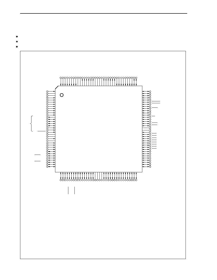
CHAPTER 1 INTRODUCTION
24
User's Manual U14492EJ5V0UD
1.5 Pin Configuration (Top View)
∑ 144-pin plastic LQFP (fine pitch) (20 ◊ 20)
µ
PD703116GJ-xxx-UEN, 703116GJ-xxx-UEN-A, 703116GJ(A)-xxx-UEN, 703116GJ(A)-xxx-UEN-A,
µ
PD703116GJ(A1)-xxx-UEN, 703116GJ(A1)-xxx-UEN-A, 70F3116GJ-UEN, 70F3116GJ-UEN-A,
µ
PD70F3116GJ(A)-UEN, 70F3116GJ(A)-UEN-A, 70F3116GJ(A1)-UEN, 70F3116GJ(A1)-UEN-A
ANI07
AV
DD
AV
SS
AV
REF1
ANI10
ANI11
ANI12
ANI13
ANI14
ANI15
ANI16
ANI17
TRIG_DBG
AD3_DBG
AD2_DBG
AD1_DBG
AD0_DBG
SYNC
CLK_DBG
RESET
CV
DD
CV
SS
X1
X2
CKSEL
MODE0
MODE1
MODE2
SI0/P40
SO0/P41
SCK0/P42
SI1/P43
SO1/P44
SCK1/P45
CRXD/P46
CTXD/P47
TIUD11/TO11/P13
TCLR10/INTP101/P12
TCUD10/INTP100/P11
TIUD10/TO10/P10
PCM4
HLDRQ/PCM3
HLDAK/PCM2
CLKOUT/PCM1
WAIT/PCM0
PCT7
ASTB/PCT6
PCT5
RD/PCT4
PCT3
PCT2
UWR/PCT1
LWR/PCT0
V
DD5
V
SS5
CS7/PCS7
CS6/PCS6
CS5/PCS5
CS4/PCS4
CS3/PCS3
CS2/PCS2
CS1/PCS1
CS0/PCS0
A23/PDH7
A22/PDH6
A21/PDH5
A20/PDH4
A19/PDH3
A18/PDH2
A17/PDH1
A16/PDH0
RXD0/P30 TXD0/P31 RXD1/P32 TXD1/P33
ASCK1/P34
RXD2/P35 TXD2/P36
ASCK2/P37
TI2/INTP20/P20
TO21/INTP21/P21 TO22/INTP22/P22 TO23/INTP23/P23 TO24/INTP24/P24
TCLR2/INTP25/P25
TI3/INTP30/TCLR3/P26
TO3/INTP31/P27
V
DD3
V
SS3
V
SS5
V
DD5
AD0/PDL0 AD1/PDL1 AD2/PDL2 AD3/PDL3 AD4/PDL4 AD5/PDL5 AD6/PDL6 AD7/PDL7 AD8/PDL8 AD9/PDL9
AD10/PDL10 AD11/PDL11 AD12/PDL12 AD13/PDL13 AD14/PDL14 AD15/PDL15
ANI06 ANI05 ANI04 ANI03 ANI02 ANI01 ANI00 AV
REF0
AV
SS
AV
DD
TO015 TO014 TO013 TO012 TO011 TO010 V
DD3
V
SS3
V
SS5
V
DD5
TO005 TO004 TO003 TO002 TO001 TO000 INTP6/P07 INTP5/P06 INTP4/P05 ADTRG1/INTP3/P04 ADTRG0/INTP2/P03 ESO1/INTP1/P02 ESO0/INTP0/P01 NMI/P00
Note 3
TCLR11/INTP111/P15 TCUD11/INTP110/P14
1
2
3
4
5
6
7
8
9
10
11
12
13
14
15
16
17
18
19
20
21
22
23
24
25
26
27
28
29
30
31
32
33
34
35
36
144 143 142 141 140 139 138 137 136 135 134 133 132 131 130 129 128 127 126 125 124 123 122 121 120 119 118 117 116 115 114 113 112 111 110 109
37 38 39 40 41 42 43 44 45 46 47 48 49 50 51 52 53 54 55 56 57 58 59 60 61 62 63 64 65 66 67 68 69 70 71 72
108
107
106
105
104
103
102
101
100
99
98
97
96
95
94
93
92
91
90
89
88
87
86
85
84
83
82
81
80
79
78
77
76
75
74
73
Note 1
Note 2
Notes 1.
µ
PD70F3116 only
As follows in
µ
PD703116.
TRIG_DBG: IC1, AD0_DBG to AD3_DBG: IC2, SYNC: IC3, CLK_DBG: IC4
2.
µ
PD703116: IC5
µ
PD70F3116: V
PP
3. The NMI/P00 pin always functions as the NMI pin. The NMI pin level can be read by reading the
P0.P00 bit.
Cautions 1. When using the
µ
PD70F3116 in normal mode, connect the V
PP
pin to V
SS5
.
2. When using the
µ
PD703116, the processing when the IC1 to IC5 pins are unused is as
follows.
IC1 to IC4 pins: Leave open.
IC5 pin: Independently connect to V
SS5
via a resistor.

CHAPTER 1 INTRODUCTION
25
User's Manual U14492EJ5V0UD
Pin Identification
A16 to A23:
AD0 to AD15:
AD0_DBG to AD3_DBG:
ADTRG0, ADTRG1:
ANI00 to ANI07,
ANI10 to ANI17:
ASCK1, ASCK2:
ASTB:
AV
DD
:
AV
REF0
, AV
REF1
:
AV
SS
:
CKSEL:
CLK_DBG:
CLKOUT:
CRXD:
CS0 to CS7:
CTXD:
CV
DD
:
CV
SS
:
ESO0, ESO1:
HLDAK:
HLDRQ:
IC1 to IC5:
INTP0 to INTP6,
INTP100, INTP101,
INTP110, INTP111,
INTP20 to INTP25,
INTP30, INTP31:
LWR:
MODE0 to MODE2:
NMI:
P00 to P07:
P10 to P15:
Address bus
Address/data bus
Debug address/data bus
A/D trigger input
Analog input
Asynchronous serial clock
Address strobe
Analog power supply
Analog reference voltage
Analog ground
Clock generator operating mode select
Debug clock
Clock output
Receive data for controller area network
Chip select
Transmit data for controller area network
Clock generator power supply
Clock generator ground
Emergency shut off
Hold acknowledge
Hold request
Internally connected
External interrupt input
Lower write strobe
Mode
Non-maskable interrupt request
Port 0
Port 1
P20 to P27:
P30 to P37:
P40 to P47:
PCM0 to PCM4:
PCS0 to PCS7:
PCT0 to PCT7:
PDH0 to PDH7:
PDL0 to PDL15:
RD:
RESET:
RXD0 to RXD2:
SCK0, SCK1:
SI0, SI1:
SO0, SO1:
SYNC:
TCLR10, TCLR11,
TCLR2, TCLR3:
TCUD10, TCUD11:
TI2, TI3:
TIUD10, TIUD11:
TO000 to TO005,
TO010 to TO015,
TO10, TO11,
TO21 to TO24, TO3:
TRIG_DBG:
TXD0 to TXD2:
UWR:
V
DD3
, V
DD5
:
V
PP
:
V
SS3
, V
SS5
:
WAIT:
X1, X2:
Port 2
Port 3
Port 4
Port CM
Port CS
Port CT
Port DH
Port DL
Read strobe
Reset
Receive data
Serial clock
Serial input
Serial output
Debug synchronization
Timer clear
Timer control pulse input
Timer input
Timer count pulse input
Timer output
Debug trigger
Transmit data
Upper write strobe
Power supply
Programming power supply
Ground
Wait
Crystal
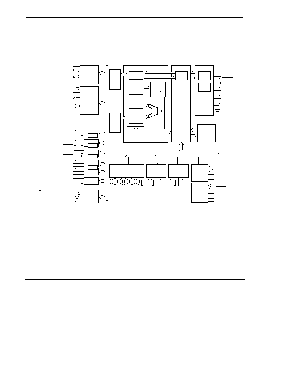
CHAPTER 1 INTRODUCTION
26
User's Manual U14492EJ5V0UD
1.6 Configuration of Function Block
1.6.1 Internal
block diagram
UART0
BRG0
UART1
BRG1
UART2
BRG2
CSI0
CSI1
FCAN
NBD
Note 3
TM0: 2 ch
TM1: 2 ch
TM2: 2 ch
TM3: 1 ch
TM4: 1 ch
INTC
NMI
INTP0 to INTP6
INTP20 to INTP25
INTP30, INTP31
INTP100, INTP101
INTP110, INTP111
ESO0, ESO1
TO000 to TO005,
TO010 to TO015
TIUD10/TO10,
TCUD10, TCLR10
TIUD11/TO11,
TCUD11, TCLR11
TI2, TCLR2, TO21 to TO24
TI3/TCLR3, TO3
TXD0
RXD0
TXD1
RXD1
ASCK1
TXD2
RXD2
ASCK2
SO0
SI0
SCK0
SO1
SI1
SCK1
CTXD
CRXD
CLK_DBG
SYNC
AD0_DBG to AD3_DBG
TRIG_DBG
Note 1
SRAMC
ROMC
DMAC
PC
32-bit
barrel
shifter
Multiplier
32
◊32 64
CPU
ROM
RAM
BCU
ALU
MEMC
HLDRQ
HLDAK
CS0 to CS7
CKSEL
CLKOUT
X1
X2
CV
DD
CV
SS
PDL0 to PDL15
PDH0 to PDH7
PCS0 to PCS7
PCT0 to PCT7
PCM0 to PCM4
P40 to P47
P30 to P37
P20 to P27
P10 to P15
P00 to P07
ADTRG0
ANI00 to ANI07
AV
SS
AV
REF0
AV
DD
ADTRG1
ANI10 to ANI17
AV
SS
AV
REF1
AV
DD
MODE0 to MODE2
RESET
V
DD5
V
SS5
V
DD3
V
SS3
V
PP
Note 4
UWR
LWR
WAIT
A16 to A23
AD0 to AD15
System
register
General-
purpose
registers
32bits
◊32
Ports
ADC0
ADC1
CG
System
controller
BRG3
10 KB
RD
ASTB
Note 2
Instruction
queue
Notes 1.
µ
PD703116: 256 KB (mask ROM)
µ
PD70F3116: 256 KB (flash memory)
2.
µ
PD70F3116 only
As follows in
µ
PD703116.
TRIG_DBG: IC1, AD0_DBG to AD3_DBG: IC2, SYNC: IC3, CLK_DBG: IC4
3.
µ
PD70F3116 only
4.
µ
PD70F3116 only
In
the
µ
PD703116, the V
PP
pin is assigned as the IC5 pin.

CHAPTER 1 INTRODUCTION
27
User's Manual U14492EJ5V0UD
1.6.2 Internal
units
(1) CPU
The CPU uses 5-stage pipeline control to execute address calculation, arithmetic and logical operation, data
transfer, and most other instruction processing in one clock.
A multiplier (16 bits
◊ 16 bits 32 bits or 32 bits ◊ 32 bits 64 bits), barrel shifter (32-bit), and other
dedicated hardware are on-chip to accelerate complex instruction processing.
(2) Bus control unit (BCU)
The BCU starts a required external bus cycle based on a physical address obtained from the CPU. If there is
no bus cycle start request from the CPU when fetching an instruction from an external memory area, the BCU
generates a prefetch address and prefetches the instruction code. The prefetched instruction code is fetched
into the internal instruction queue of the CPU.
(3) Memory controller (MEMC)
The MEMC controls SRAM, ROM, and various I/O for external memory expansion.
(4) DMA controller (DMAC)
The DMA transfers data between memory and I/O in place of the CPU.
The address mode is two-cycle transfer. The three bus modes are single transfer, single-step transfer, and
block transfer.
(5) ROM
There is on-chip flash memory (256 KB) in the
µ
PD70F3116, and mask ROM (256 KB) in the
µ
PD703116.
On an instruction fetch, the ROM can be accessed by the CPU in one clock.
When single-chip mode 0 or flash memory programming mode is set, ROM is mapped starting from address
00000000H.
When single-chip mode 1 is set, it is mapped starting from address 00100000H.
ROM cannot be accessed if ROMless mode 0 or 1 is set.
(6) RAM
RAM is mapped starting from address FFFFC000H.
It can be accessed by the CPU in one clock on an instruction fetch or data access.
(7) Interrupt controller (INTC)
The INTC services hardware interrupt requests from on-chip peripheral I/O and external sources (NMI, INTP0
to INTP6, INTP20 to INTP25, INTP30, INTP31, INTP100, INTP101, INTP110, INTP111). For these interrupt
requests, eight levels of interrupt priority can be defined and multiprocessing controls against the interrupt
sources can be performed.
(8) Clock generator (CG)
The CG provides a frequency that is 1, 2.5, 5, or 10 times (using the on-chip PLL) or 1/2 times (not using the
on-chip PLL) the input clock (f
X
) as the internal system clock (f
XX
). As the input clock, connect an external
resonator to pins X1 and X2 (only when using the on-chip PLL synthesizer) or input an external clock from the
X1 pin.
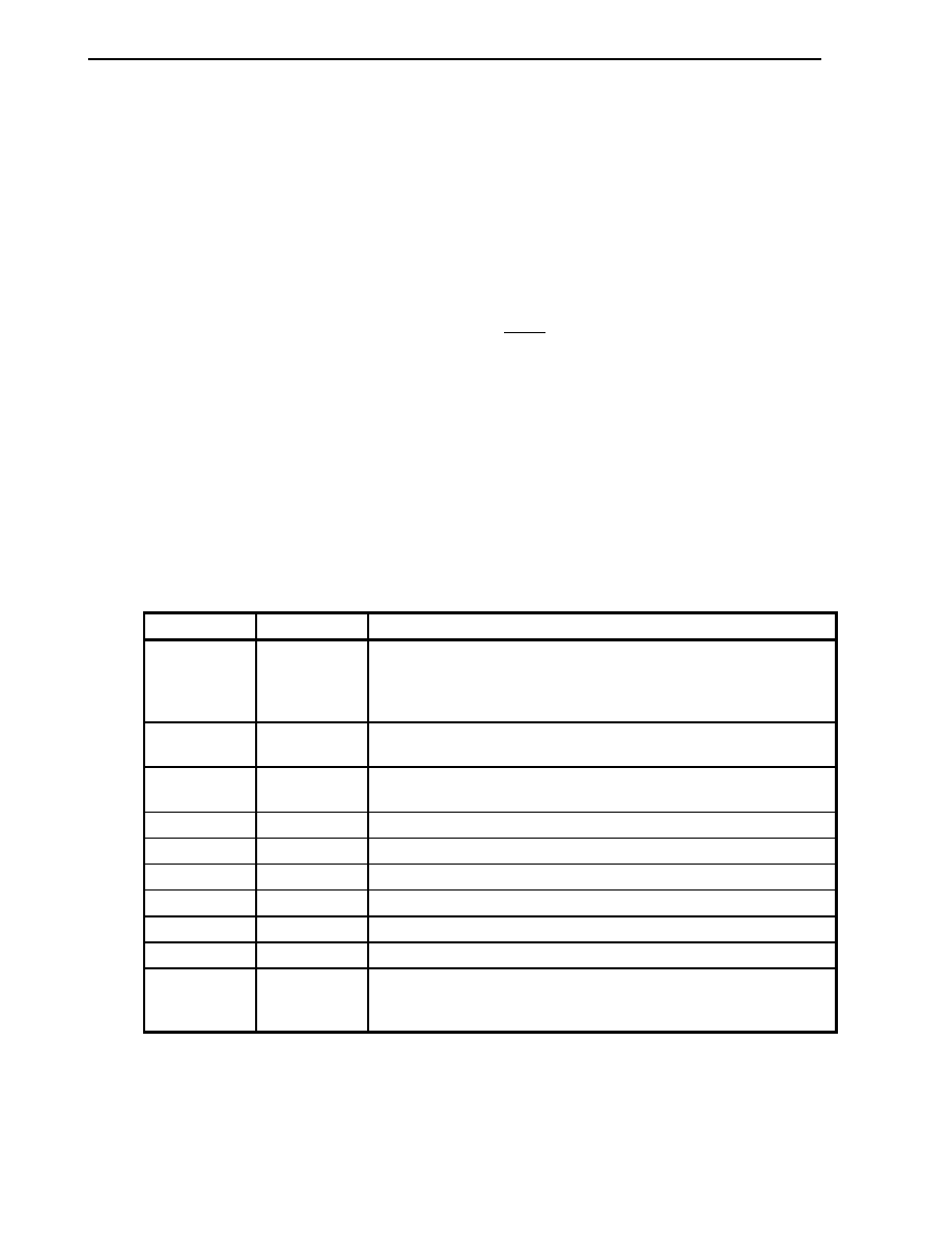
CHAPTER 1 INTRODUCTION
28
User's Manual U14492EJ5V0UD
(9) Timer/counter function
This unit incorporates a 2-channel 16-bit timer (TM0) for 3-phase sine wave PWM inverter control, a 2-
channel 16-bit up/down counter (TM1) that can be used for 2-phase encoder input or as a general-purpose
timer, a 2-channel 16-bit general-purpose timer unit (TM2), a 1-channel 16-bit timer/event counter (TM3), and
a 1-channel 16-bit interval timer (TM4) on-chip, and can measure the pulse interval or frequency and can
output a programmable pulse.
(10) Serial interface
A 3-channel asynchronous serial interface (UART), 2-channel clocked serial interface (CSI), and 1-channel
FCAN are provided as serial interfaces.
The UART performs data transfer using pins TXDn and RXDn (n = 0 to 2).
The CSI performs data transfer using pins SOm, SIm, and SCKm (m = 0, 1).
FCAN performs data transfer using pins CTXD and CRXD.
(11) NBD function
There is a 1-channel NBD on-chip as a debugging interface (
µ
PD70F3116 only).
(12) A/D converter (ADC)
Two units of a high-speed, high-resolution 10-bit A/D converter having eight analog input pins are
implemented. The ADC converts using a successive approximation method.
(13) Ports
As shown in the table below, ports function as general-purpose ports and as control pins.
Port I/O
Control
Functions
Port 0
8-bit input
NMI input
Timer/counter output stop signal input
External interrupt input
A/D converter external trigger input
Port 1
6-bit I/O
Timer/counter I/O
External interrupt input
Port 2
8-bit I/O
Timer/counter I/O
External interrupt input
Port 3
8-bit I/O
Serial interface I/O (UART0 to UART2)
Port 4
8-bit I/O
Serial interface I/O (CSI0, CSI1, FCAN)
Port DH
8-bit I/O
External address bus (A16 to A23)
Port DL
16-bit I/O
External address/data bus (AD0 to AD15)
Port CS
8-bit I/O
External bus interface control signal output
Port CT
8-bit I/O
External bus interface control signal output
Port CM
5-bit I/O
Wait insertion signal input
Internal system clock output
External bus interface control signal I/O
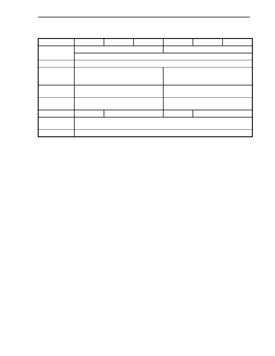
CHAPTER 1 INTRODUCTION
29
User's Manual U14492EJ5V0UD
1.7 Differences
Between
Products
Item
µ
PD703116
µ
PD703116(A)
µ
PD703116(A1)
µ
PD70F3116
µ
PD70F3116(A)
µ
PD70F3116(A1)
Mask ROM
Flash memory
Internal ROM
256 KB
Internal RAM
10 KB
NBD (Non Break
Debug) function
Not provided
(IC1 to IC4)
Provided
(TRIG_DBG, AD0_DBG to AD3_DBG, SYNC,
CLK_DBG)
Flash memory
programming pin
Not provided (IC5)
Provided (V
PP
)
Flash memory
programming mode
Not provided
Provided
(MODE0 = H/L, MODE1 = H, MODE2 = L, V
PP
= 7.8 V)
Quality grade
Standard grade
Special grade
Standard grade
Special grade
Electrical
specifications
The maximum operating frequency, operating ambient temperature, and power supply current differ (refer to
CHAPTER 18 ELECTRICAL SPECIFICATIONS).
Other
The noise immunity and noise radiation differ because the circuit scale and mask layout are different.

30
User's Manual U14492EJ5V0UD
CHAPTER 2 PIN FUNCTIONS
The names and functions of the V850E/IA1 pins are shown below. These pins can be divided by function into port
pins and non-port pins.
2.1 List of Pin Functions
(1) Port pins
(1/3)
Pin Name
I/O
Function
Alternate Function
P00
NMI
P01
ESO0/INTP0
P02
ESO1/INTP1
P03
ADTRG0/INTP2
P04
ADTRG1/INTP3
P05
INTP4
P06
INTP5
P07
I Port
0
8-bit input-only port
P00 is also used for indicating the NMI pin status. The NMI pin level can
be read by reading the P0.P00 bit. P00 functions as an NMI input when a
valid edge is input.
INTP6
P10
TIUD10/TO10
P11
TCUD10/INTP100
P12
TCLR10/INTP101
P13
TIUD11/TO11
P14
TCUD11/INTP110
P15
I/O Port
1
6-bit I/O port
Input/output can be specified in 1-bit units.
TCLR11/INTP111
P20
TI2/INTP20
P21
TO21/INTP21
P22
TO22/INTP22
P23
TO23/INTP23
P24
TO24/INTP24
P25
TCLR2/INTP25
P26
TI3/TCLR3/INTP30
P27
I/O Port
2
8-bit I/O port
Input/output can be specified in 1-bit units.
TO3/INTP31
P30
RXD0
P31
TXD0
P32
RXD1
P33
TXD1
P34
ASCK1
P35
RXD2
P36
TXD2
P37
I/O Port
3
8-bit I/O port
Input/output can be specified in 1-bit units.
ASCK2
CHAPTER 2 PIN FUNCTIONS
31
User's Manual U14492EJ5V0UD
(2/3)
Pin Name
I/O
Function
Alternate Function
P40
SI0
P41
SO0
P42
SCK0
P43
SI1
P44
SO1
P45
SCK1
P46
CRXD
P47
I/O Port
4
8-bit I/O port
Input/output can be specified in 1-bit units.
CTXD
PCM0
WAIT
PCM1
CLKOUT
PCM2
HLDAK
PCM3
HLDRQ
PCM4
I/O Port
CM
5-bit I/O port
Input/output can be specified in 1-bit units.
-
PCT0
LWR
PCT1
UWR
PCT2
-
PCT3
-
PCT4
RD
PCT5
-
PCT6
ASTB
PCT7
I/O Port
CT
8-bit I/O port
Input/output can be specified in 1-bit units.
-
PCS0
CS0
PCS1
CS1
PCS2
CS2
PCS3
CS3
PCS4
CS4
PCS5
CS5
PCS6
CS6
PCS7
I/O Port
CS
8-bit I/O port
Input/output can be specified in 1-bit units.
CS7
PDH0
A16
PDH1
A17
PDH2
A18
PDH3
A19
PDH4
A20
PDH5
A21
PDH6
A22
PDH7
I/O Port
DH
8-bit I/O port
Input/output can be specified in 1-bit units.
A23
CHAPTER 2 PIN FUNCTIONS
32
User's Manual U14492EJ5V0UD
(3/3)
Pin Name
I/O
Function
Alternate Function
PDL0
AD0
PDL1
AD1
PDL2
AD2
PDL3
AD3
PDL4
AD4
PDL5
AD5
PDL6
AD6
PDL7
AD7
PDL8
AD8
PDL9
AD9
PDL10
AD10
PDL11
AD11
PDL12
AD12
PDL13
AD13
PDL14
AD14
PDL15
I/O Port
DL
16-bit I/O port
Input/output can be specified in 1-bit units.
AD15
CHAPTER 2 PIN FUNCTIONS
33
User's Manual U14492EJ5V0UD
(2) Non-port pins
(1/3)
Pin Name
I/O
Function
Alternate Function
TO000
-
TO001
-
TO002
-
TO003
-
TO004
-
TO005
O
Timer 00 pulse signal output
-
TO010
-
TO011
-
TO012
-
TO013
-
TO014
-
TO015
O
Timer 01 pulse signal output
-
TO10
P10/TIUD10
TO11
O
Timer 10 or 11 pulse signal output
P13/TIUD11
TO21
P21/INTP21
TO22
P22/INTP22
TO23
P23/INTP23
TO24
O
Timer 2 pulse signal output
P24/INTP24
TO3
O
Timer 3 pulse signal output
P27/INTP31
ESO0
P01/INTP0
ESO1
I
Timer 00 or 01 output stop signal input
P02/INTP1
TIUD10
P10/TO10
TIUD11
I
External count clock input to up/down counter (timer 10 or 11)
P13/TO11
TCUD10
P11/INTP100
TCUD11
I
Count operation switching signal to up/down counter (timer 10 or 11)
P14/INTP110
TCLR10
P12/INTP101
TCLR11
I
Clear signal input to up/down counter (timer 10 or 11)
P15/INTP111
TI2
P20/INTP20
TI3
I
Timer 2 or 3 external count clock input
P26/INTP30/TCLR3
TCLR2
P25/INTP25
TCLR3
I
Timer 2 or 3 clear signal input
P26/INTP31/TI3
INTP0
P01/ESO0
INTP1
P02/ESO1
INTP2
P03/ADTRG0
INTP3
P04/ADTRG1
INTP4
P05
INTP5
P06
INTP6
I
External maskable interrupt request input
P07

CHAPTER 2 PIN FUNCTIONS
34
User's Manual U14492EJ5V0UD
(2/3)
Pin Name
I/O
Function
Alternate Function
INTP100
P11/TCUD10
INTP101
I
External maskable interrupt request input and timer 10 external capture
trigger input
P12/TCLR10
INTP110
P14/TCUD11
INTP111
I
External maskable interrupt request input and timer 11 external capture
trigger input
P15/TCLR11
INTP20
P20/TI2
INTP21
P21/TO21
INTP22
P22/TO22
INTP23
P23/TO23
INTP24
P24/TO24
INTP25
I
External maskable interrupt request input and timer 2 external capture
trigger input
P25/TCLR2
INTP30
P26/TI3/TCLR3
INTP31
I
External maskable interrupt request input and timer 3 external capture
trigger input
P27/TO3
SO0
P41
SO1
O
Serial transmit data output (3-wire) of CSI0 and CSI1
P44
SI0
P40
SI1
I
Serial receive data input (3-wire) of CSI0 and CSI1
P43
SCK0
P42
SCK1
I/O
Serial clock I/O (3-wire) of CSI0 and CSI1
P45
TXD0
P31
TXD1
P33
TXD2
O
Serial transmit data output of UART0 to UART2
P36
RXD0
P30
RXD1
P32
RXD2
I
Serial receive data input of UART0 to UART2
P35
ASCK1
P34
ASCK2
I/O
Serial clock I/O of UART1 and UART2
P37
CTXD
O
FCAN serial transmit data output
P47
CRXD
I
FCAN serial receive data input
P46
ANI00 to ANI07
-
ANI10 to ANI17
I
Analog input to A/D converter
-
ADTRG0
P03/INTP2
ADTRG1
I
External trigger input to A/D converter
P04/INTP3
NMI
I
Non-maskable interrupt request input
P00
MODE0
-
MODE1
-
MODE2
I
Specifies V850E/IA1 operation mode
-
V
PP
Note 1
-
Power application for flash memory write
-
IC1 to IC5
Note 2
-
Internal connection pins
-
Notes 1.
µ
PD70F3116 only
2.
µ
PD703116 only

CHAPTER 2 PIN FUNCTIONS
35
User's Manual U14492EJ5V0UD
(3/3)
Pin Name
I/O
Function
Alternate Function
WAIT
I
Control signal input to insert wait in bus cycle
PCM0
HLDAK
O
Bus hold acknowledge output
PCM2
HLDRQ
I
Bus hold request input
PCM3
LWR
O
External data lower byte write strobe signal output
PCT0
UWR
O
External data upper byte write strobe signal output
PCT1
RD
O
External data bus read strobe signal output
PCT4
ASTB
O
External data bus address strobe signal output
PCT6
CS0
PCS0
CS1
PCS1
CS2
PCS2
CS3
PCS3
CS4
PCS4
CS5
PCS5
CS6
PCS6
CS7
O
Chip select signal output
PCS7
AD0 to AD15
I/O
16-bit address/data bus for external memory
PDL0 to PDL15
A16 to A23
O
Upper 8-bit address bus for external memory
PDH0 to PDH7
RESET
I
System reset input
-
X1 I
-
X2
-
Crystal resonator connection pin for system clock generation
Input to X1 pin when providing clocks from outside.
-
CLKOUT
O
System clock output
PCM1
CKSEL
I
Input specifying clock generator operation mode
-
AV
REF0
I
Reference voltage input for A/D converter 0
-
AV
REF1
I
Reference voltage input for A/D converter 1
-
AV
DD
-
Positive power supply for A/D converter
-
AV
SS
-
Ground potential for A/D converter
-
CV
DD
-
Positive power supply for dedicated clock generator
-
CV
SS
-
Ground potential for dedicated clock generator
-
V
DD5
-
Positive power supply for peripheral interface
-
V
SS5
-
Ground potential for peripheral interface
-
V
DD3
-
3.3 V positive power supply pin for internal CPU
-
V
SS3
-
Ground potential for internal CPU
-
CLK_DBG
Note
I
Debugging interface clock input (3.3 V interface)
-
SYNC
Note
I
Debugging interface command synchronization input (3.3 V interface)
-
AD0_DBG
Note
-
AD1_DBG
Note
-
AD2_DBG
Note
-
AD3_DBG
Note
I/O
Command interface input for debugging (3.3 V interface)
-
TRIG_DBG
Note
O
Address match trigger signal output for debugging (3.3 V interface)
-
Note
µ
PD70F3116 only
CHAPTER 2 PIN FUNCTIONS
36
User's Manual U14492EJ5V0UD
2.2 Pin
Status
The following table shows the status of each pin after a reset, in power-saving mode (software STOP mode, IDLE,
HALT), on a DMA transfer, and on a bus hold.
Operating Status
Pin
Reset
(Single-Chip
Mode 0)
Reset
(Single-Chip
Mode 1, ROMless
Mode 0 or 1)
IDLE Mode/
Software STOP
Mode
HALT Mode/
During DMA
Transfer
Bus Hold
A16 to A23 (PDH0 to PDH7)
Hi-Z Hi-Z Hi-Z
Operating
Hi-Z
AD0 to AD15 (PDL0 to PDL15)
Hi-Z Hi-Z Hi-Z
Operating
Hi-Z
CS0 to CS7 (PCS0 to PCS7)
Hi-Z Hi-Z H
Operating
Hi-Z
LWR, UWR (PCT0, PCT1)
Hi-Z Hi-Z H
Operating
Hi-Z
RD (PCT4)
Hi-Z
Hi-Z
H
Operating
Hi-Z
ASTB (PCT6)
Hi-Z
Hi-Z
H
Operating
Hi-Z
WAIT (PCM0)
Hi-Z
Hi-Z
-
Operating
-
CLKOUT (PCM1)
Hi-Z
Operating L Operating
Operating
HLDAK (PCM2)
Hi-Z
Hi-Z
H
Operating
L
HLDRQ (PCM3)
Hi-Z
Hi-Z
-
Operating Operating
Caution When controlling the external bus using an ASIC or the like in standby mode, provide a separate
controller.
Remark Hi-Z:
High
impedance
H: High-level
output
L: Low-level
output
-:
No input sampling

CHAPTER 2 PIN FUNCTIONS
37
User's Manual U14492EJ5V0UD
2.3 Description
of
Pin
Functions
(1) P00 to P07 (Port 0) ... Input
Port 0 is an 8-bit input-only port in which all pins are fixed for input.
Besides functioning as an input port, in control mode, P00 to P07 operate as NMI input, timer/counter output
stop signal input, external interrupt request input, and A/D converter (ADC) external trigger input. Normally, if
function pins also serve as ports, one mode or the other is selected using a port mode control register.
However, there is no such register for P00 to P07. Therefore, the input port cannot be switched with the NMI
input pin, timer/counter output stop signal input pin, external interrupt request input pin, and A/D converter
(ADC) external trigger input pin. Read the status of each pin by reading the port.
(a) Port mode
P00 to P07 are input-only.
(b) Control mode
P00 to P07 also serve as NMI, ESO0, ESO1, ADTRG0, ADTRG1, and INTP0 to INTP6 pins, but they
cannot be switched.
(i) NMI (Non-maskable interrupt request) ... Input
This is non-maskable interrupt request input.
(ii) ESO0, ESO1 (Emergency shut off) ... Input
These pins input timer 00 and timer 01 output stop signals.
(iii) INTP0 to INTP6 (External interrupt input) ... Input
These are external interrupt request input pins.
(iv) ADTRG0, ADTRG1 (A/D trigger input) ... Input
These are A/D converter external trigger input pins.
(2) P10 to P15 (Port 1) ... I/O
Port 1 is a 6-bit I/O port in which input or output can be set in 1-bit units.
Besides functioning as an I/O port, in control mode, P10 to P15 operate as timer/counter I/O and external
interrupt request input.
An operation mode of port or control mode can be selected for each bit and specified by the port 1 mode
control register (PMC1).
(a) Port mode
P10 to P15 can be set to input or output in 1-bit units using the port 1 mode register (PM1).
(b) Control mode
P10 to P15 can be set to port or control mode in 1-bit units using PMC1.
(i) TO10, TO11 (Timer output) ... Output
These pins output timer 10 and timer 11 pulse signals.
(ii) TIUD10, TIUD11 (Timer count pulse input) ... Input
These are external count clock input pins to the up/down counter (timer 10, timer 11).

CHAPTER 2 PIN FUNCTIONS
38
User's Manual U14492EJ5V0UD
(iii) TCUD10, TCUD11 (Timer control pulse input) ... Input
These pins input count operation switching signals to the up/down counter (timer 10, timer 11).
(iv) TCLR10, TCLR11 (Timer clear) ... Input
These are clear signal input pins to the up/down counter (timer 10, timer 11).
(v) INTP100, INTP101 (External interrupt input) ... Input
These are external interrupt request input pins and timer 10 external capture trigger input pins.
(vi) INTP110, INTP111 (External interrupt input) ... Input
These are external interrupt request input pins and timer 11 external capture trigger input pins.
(3) P20 to P27 (Port 2) ... I/O
Port 2 is an 8-bit I/O port in which input or output can be set in 1-bit units.
Besides functioning as an I/O port, in control mode, P20 to P27 operate as timer/counter I/O and external
interrupt request input.
An operation mode of port or control mode can be selected for each bit and specified by the port 2 mode
control register (PMC2).
(a) Port mode
P20 to P27 can be set to input or output in 1-bit units using the port 2 mode register (PM2).
(b) Control mode
P20 to P27 can be set to port or control mode in 1-bit units using PMC2.
(i) TO21 to TO24 (Timer output) ... Output
These pins output a timer 2 pulse signal.
(ii) TO3 (Timer output) ... Output
This pin outputs a timer 3 pulse signal.
(iii) TI2, TI3 (Timer input) ... Input
These are timer 2 and timer 3 external count clock input pins.
(iv) TCLR2, TCLR3 (Timer clear) ... Input
These are timer 2 and timer 3 clear signal input pins.
(v) INTP20 to INTP25 (External interrupt input) ... Input
These are external interrupt request input pins and timer 2 external capture trigger input pins.
(vi) INTP30, INTP31 (External interrupt input) ... Input
These are external interrupt request input pins and timer 3 external capture trigger input pins.

CHAPTER 2 PIN FUNCTIONS
39
User's Manual U14492EJ5V0UD
(4) P30 to P37 (Port 3) ... I/O
Port 3 is an 8-bit I/O that can be set to input or output in 1-bit units.
Besides functioning as an I/O port, in control mode, P30 to P37 operate as serial interface (UART0 to
UART2) I/O.
An operation mode of port or control mode can be selected for each bit and specified by the port 3 mode
control register (PMC3).
(a) Port mode
P30 to P37 can be set to input or output in 1-bit units using the port 3 mode register (PM3).
(b) Control mode
P30 to P37 can be set to port or control mode in 1-bit units using PMC3.
(i) TXD0 to TXD2 (Transmit data) ... Output
These pins output serial transmit data of UART0 to UART2.
(ii) RXD0 to RXD2 (Receive data) ... Input
These pins input serial receive data of UART0 to UART2.
(iii) ASCK1, ASCK2 (Asynchronous serial clock) ... I/O
These are UART1 and UART2 serial clock I/O pins.
(5) P40 to P47 (Port 4) ... I/O
Port 4 is an 8-bit I/O port in which input or output can be set in 1-bit units.
Besides functioning as an I/O port, in control mode, P40 to P47 operate as serial interface (CSI0, CSI1,
FCAN) I/O.
An operation mode of port or control mode can be selected for each bit and specified by the port 4 mode
control register (PMC4).
(a) Port mode
P40 to P47 can be set to input or output in 1-bit units using the port 4 mode register (PM4).
(b) Control mode
P40 to P47 can be set to port or control mode in 1-bit units using PMC4.
(i) SO0, SO1 (Serial output) ... Output
These pins output CSI0 and CSI1 serial transmit data.
(ii) SI0, SI1 (Serial input) ... Input
These pins input CSI0 and CSI1 serial receive data.
(iii) SCK0, SCK1 (Serial clock) ... I/O
These are CSI0 and CSI1 serial clock I/O pins.
(iv) CTXD (Transmit data for controller area network) ... Output
This pin outputs FCAN serial transmit data.

CHAPTER 2 PIN FUNCTIONS
40
User's Manual U14492EJ5V0UD
(v) CRXD (Receive data for controller area network) ... Input
This pin inputs FCAN serial receive data.
(6) PCM0 to PCM4 (Port CM) ... I/O
Port CM is a 5-bit I/O port in which input or output can be set in 1-bit units.
Besides functioning as a port, in control mode, PCM0 to PCM4 operate as wait insertion signal input, internal
system clock output, and bus hold control signal output.
An operation mode of port or control mode can be selected for each bit and specified by the port CM mode
control register (PMCCM).
(a) Port mode
PCM0 to PCM4 can be set to input or output in 1-bit units using the port CM mode register (PMCM).
(b) Control mode
PCM0 to PCM4 can be set to port or control mode in 1-bit units using PMCCM.
(i) WAIT (Wait) ... Input
This control signal input pin, which inserts a data wait in a bus cycle, can input asynchronously with
respect to a CLKOUT signal. Sampling is done at the falling edge of a CLKOUT signal in a bus cycle
in a T2 or TW state. If the setup or hold time is not secured in the sampling timing, wait insertion
may not be performed.
(ii) CLKOUT (Clock output) ... Output
This is an internal system clock output pin. In single-chip mode 1 and ROMless mode 0 or 1, output
is not performed by the CLKOUT pin because it is in port mode during the reset period. To perform
CLKOUT output, set this pin to control mode using the port CM mode control register (PMCCM).
(iii) HLDAK (Hold acknowledge) ... Output
This is an acknowledge signal output pin that shows that the V850E/IA1 received a bus hold request
and that the external address/data bus and various strobe pins entered in a high-impedance state.
While this signal is active, the external address/data bus and various strobe pins become high-
impedance and transfer the bus mastership to the external bus master.
(iv) HLDRQ (Hold request) ... Input
This is the input pin by which an external device requests that the V850E/IA1 release the external
address/data bus and various strobe pins. The signal via this pin can be input asynchronously with
respect to the CLKOUT signal. When this pin becomes active, the V850E/IA1 makes the external
address/data bus and various strobe pins high-impedance after the executing bus cycle terminates
(or immediately if there is none) and releases the bus by making the HLDAK signal active.
To reliably set bus hold status, keep the HLDRQ signal active until a HLDAK signal is output.

CHAPTER 2 PIN FUNCTIONS
41
User's Manual U14492EJ5V0UD
(7) PCT0 to PCT7 (Port CT) ... I/O
Port CT is an 8-bit I/O port in which input or output can be set in 1-bit units.
Besides functioning as a port, in control mode, it operates as control signal output for when memory is
expanded externally.
An operation mode of port or control mode can be selected for each bit and specified by the port CT mode
control register (PMCCT).
(a) Port mode
PCT0 to PCT7 can be set to input or output in 1-bit units using the port CT mode register (PMCT).
(b) Control mode
PCT0 to PCT7 can be set to port or control mode in 1-bit units using PMCCT.
(i) LWR (Lower byte write strobe) ... Output
This is a strobe signal that shows that the executing bus cycle is a write cycle for SRAM, external
ROM, or an external peripheral I/O area.
In the data bus, the lower byte is in effect. If the bus cycle is a lower memory write, it becomes
active at the falling edge of a T1 state CLKOUT signal and becomes inactive at the falling edge of a
T2 state CLKOUT signal.
(ii) UWR (Upper byte write strobe) ... Output
This is a strobe signal that shows that the executing bus cycle is a write cycle for SRAM, external
ROM, or an external peripheral I/O area.
In the data bus, the upper byte is in effect. If the bus cycle is an upper memory write, it becomes
active at the falling edge of a T1 state CLKOUT signal and becomes inactive at the falling edge of a
T2 state CLKOUT signal.
(iii) RD (Read strobe) ... Output
This is a strobe signal that shows that the executing bus cycle is a read cycle for SRAM, external
ROM, or external peripheral I/O. It is inactive in an idle state (TI).
(iv) ASTB (Address strobe) ... Output
This is the external address bus latch strobe signal output pin.
Output becomes low level in synchronous with the falling edge of the clock in a T1 state bus cycle,
and high level in synchronous with the falling edge of the clock in a T3 state.
(8) PCS0 to PCS7 (Port CS) ... I/O
Port CS is an 8-bit I/O port in which input or output can be set in 1-bit units.
Besides functioning as a port, in control mode, these operate as chip select signal output for when memory is
expanded externally.
An operation mode of port or control can be selected for each bit and specified by the port CS mode control
register (PMCCS).
(a) Port mode
PCS0 to PCS7 can be set to input or output in 1-bit units using the port CS mode register (PMCS).

CHAPTER 2 PIN FUNCTIONS
42
User's Manual U14492EJ5V0UD
(b) Control mode
PCS0 to PCS7 can be set to port or control mode in 1-bit units using PMCCS.
(i) CS0 to CS7 (Chip select) ... Output
This is the chip select signal for external SRAM, external ROM, or external peripheral I/O.
The signal CSn is assigned to memory block n (n = 0 to 7).
This is active for the period during which a bus cycle that accesses the corresponding memory block
is activated.
It is inactive in an idle state (TI).
(9) PDH0 to PDH7 (Port DH) ... I/O
Port DH is an 8-bit I/O port in which input or output can be set in 1-bit units.
Besides functioning as a port, in control mode (external expansion mode), these operate as the address bus
(A16 to A23) for when memory is expanded externally.
An operation mode of port or control mode can be selected for each bit and specified by the port DH mode
control register (PMCDH).
(a) Port mode
PDH0 to PDH7 can be set to input or output in 1-bit units using the port DH mode register (PMDH).
(b) Control mode
PDH0 to PDH7 can be used as A16 to A23 by using PMCDH.
(i) A16 to A23 (Address) ... Output
This pin outputs the upper 8-bit address of the 24-bit address in the address bus on an external
access.
(10) PDL0 to PDL7 (Port DL) ... I/O
Port DL is a 16-bit I/O port in which input or output can be set in 1-bit units.
Besides functioning as a port, in control mode (external expansion mode), these operate as the address/data
bus (AD0 to AD15) for when memory is expanded externally.
An operation mode of port or control mode can be selected for each bit and specified by the port DL mode
control register (PMCDL).
(a) Port mode
PDL0 to PDL15 can be set to input or output in 1-bit units using the port DL mode register (PMDL).
(b) Control mode
PDL0 to PDL15 can be used as AD0 to AD15 by using PMCDL.
(i) AD0 to AD15 (Address/data bus) ... I/O
This is a multiplexed bus for an address or data on an external access. When used for an address
(T1 state) they are 24-bit address output pins A0 to A15, and when used for data (T2, TW, T3) they
are 16-bit data I/O bus pins.
(11) TO000 to TO005 (Timer output) ... Output
These pins output the pulse signal of timer 00.

CHAPTER 2 PIN FUNCTIONS
43
User's Manual U14492EJ5V0UD
(12) TO010 to TO015 (Timer output) ... Output
These pins output the pulse signal of timer 01.
(13) ANI00 to ANI07, ANI10 to ANI17 (Analog input) ... Input
These are analog input pins to the A/D converter.
(14) CKSEL (Clock generator operating mode select) ... Input
This is the input pin that specifies the operation mode of the clock generator. Fix it so that the input level
does not change during operation.
(15) MODE0 to MODE2 (Mode) ... Input
These are the input pins that specify the operation mode. Operation modes are broadly divided into normal
operation modes and flash memory programming mode. The normal operation modes are single-chip modes
0 and 1 and ROMless modes 0 and 1 (see 3.3 Operation Modes for details). The operation mode is
determined by sampling the status of each of pins MODE0 to MODE2 on a reset.
Fix these so that the input level does not change during operation.
(a)
µ
PD703116
MODE2 MODE1 MODE0
Operation
Mode
L L L
ROMless
mode
0
L L H
ROMless
mode
1
L
H
L
Single-chip mode 0
L H H
Normal operation mode
Single-chip mode 1
Other than above
Setting prohibited
(b)
µ
PD70F3116
V
PP
MODE2 MODE1 MODE0
Operation
Mode
0
V
L L L
ROMless
mode
0
0
V
L L H
ROMless
mode
1
0 V
L
H
L
Single-chip mode 0
0 V
L
H
H
Normal operation mode
Single-chip mode 1
7.8 V
L
H
◊
Flash memory programming mode
Other than above
Setting prohibited
Remark L: Low-level
input
H: High-level input
◊: don't care
(16) RESET (Reset) ... Input
RESET input is asynchronous input. When a signal having a certain low level width is input in asynchronous
with the operation clock, a system reset that takes precedence over all operations occurs.
Besides a normal initialize or start, this signal is also used to release a standby mode (HALT, IDLE, software
STOP).

CHAPTER 2 PIN FUNCTIONS
44
User's Manual U14492EJ5V0UD
(17) X1, X2 (Crystal)
These pins connect a resonator for system clock generation.
They also can input external clocks. For external clock input, connect to the X1 pin and leave the X2 pin
open.
(18) CV
DD
(Power supply for clock generator)
This is the positive power supply pin for the clock generator.
(19) CV
SS
(Ground for clock generator)
This is the ground pin for the clock generator.
(20) V
DD5
(Power supply)
This is the positive power supply pin for the peripheral interface.
(21) V
SS5
(Ground)
This is the ground pin for the peripheral interface.
(22) V
DD3
(Power supply)
This is the positive power supply pin for the internal CPU.
(23) V
SS3
(Ground)
This is the ground pin for the internal CPU.
(24) CLK_DBG (Debug clock) ... Input
This is the clock input pin for the debug interface (3.3 V interface).
(25) SYNC (Debug synchronization) ... Input
This is the command synchronization input pin for debugging (3.3 V interface).
(26) AD0_DBG to AD3_DBG (Debug address/data bus) ... I/O
These are command interface pins for debugging (3.3 V interface).
(27) TRIG_DBG (Debug trigger) ... Output
This is the address match trigger signal output pin for debugging (3.3 V interface).
(28) AV
DD
(Analog power supply)
This is the analog positive power supply pin for the A/D converter.
(29) AV
SS
(Analog ground)
This is the ground pin for the A/D converter.
(30) AV
REF0
, AV
REF1
(Analog reference voltage) ... Input
These are the reference voltage supply pins for the A/D converter.
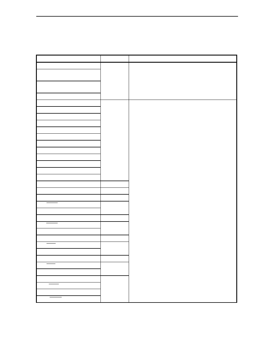
CHAPTER 2 PIN FUNCTIONS
45
User's Manual U14492EJ5V0UD
2.4 Types of Pin I/O Circuit and Connection of Unused Pins
Connection of a 1 to 10 k
resistor is recommended when connecting to V
DD5
, V
SS5
, CV
DD
, CV
SS
, or AV
SS
via a
resistor.
(1/2)
Pin
I/O Circuit Type
Recommended Connection
P00/NMI
P01/ESO0/INTP0
P02/ESO1/INTP1
P03/ADTRG0/INTP2
P04/ADTRG1/INTP3
P05/INTP4 to P07/INTP6
2
Connect directly to V
SS5
.
P10/TIUD10/TO10
P11/TCUD10/INTP100
P12/TCLR10/INTP101
P13/TIUD11/TO11
P14/TCUD11/INTP110
P15/TCLR11/INTP111
P20/TI2/INTP20
P21/TO21/INTP21 to P24/TO24/INTP24
P25/TCLR2/INTP25
P26/TI3/TCLR3/INTP30
P27/TO3/INTP31
P30/RXD0
5-AC
P31/TXD0 5
P32/RXD1 5-AC
P33/TXD1 5
P34/ASCK1
P35/RXD2
5-AC
P36/TXD2 5
P37/ASCK2
P40/SI0
5-AC
P41/SO0 5
P42/SCK0
P43/SI1
5-AC
P44/SO1 5
P45/SCK1
P46/CRXD
5-AC
P47/CTXD
PCM0/WAIT
PCM1/CLKOUT
PCM2/HLDAK
5
Input status: Independently connect to V
DD5
or V
SS5
via a resistor.
Output status: Leave open.
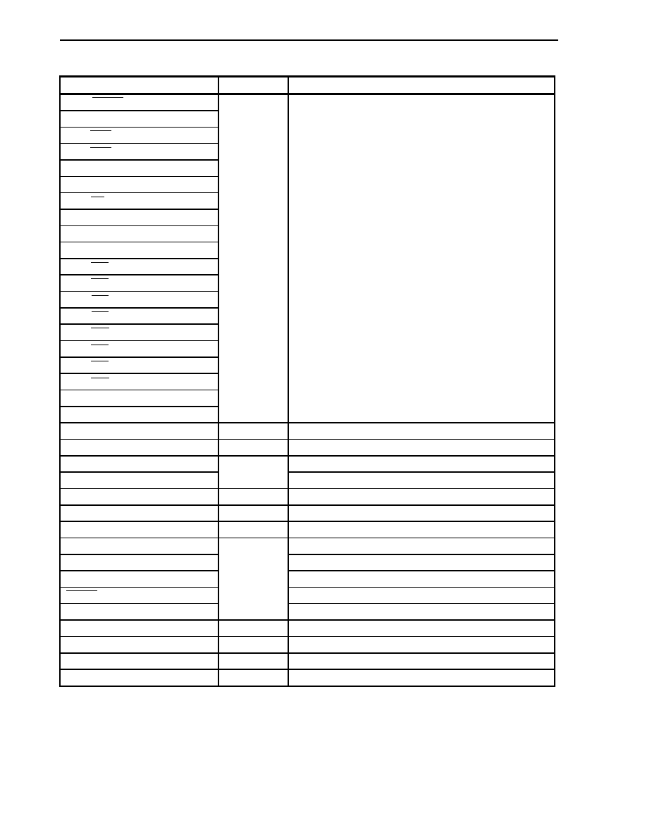
CHAPTER 2 PIN FUNCTIONS
46
User's Manual U14492EJ5V0UD
(2/2)
Pin
I/O Circuit Type
Recommended Connection
PCM3/HLDRQ
PCM4
PCT0/LWR
PCT1/UWR
PCT2
PCT3
PCT4/RD
PCT5
PCT6/ASTB
PCT7
PCS0/CS0
PCS1/CS1
PCS2/CS2
PCS3/CS3
PCS4/CS4
PCS5/CS5
PCS6/CS6
PCS7/CS7
PDH0/A16 to PDH7/A23
PDL0/AD0 to PDL15/AD15
5
Input status: Independently connect to V
DD5
or V
SS5
via a resistor.
Output status: Leave open.
AD0_DBG to AD3_DBG
Note 1
5-AC
Independently connect to CV
DD
or CV
SS
via a resistor.
TRIG_DBG
Note 1
3
Leave open (low-level output).
CLK_DBG
Note 1
Independently connect to CV
SS
via a resistor.
SYNC
Note 1
2
Independently connect to CV
DD
via a resistor.
IC1 to IC4
Note 2
-
Leave open.
ANI00 to ANI07, ANI10 to ANI17
7
Connect to AV
SS
.
TO000 to TO005, TO010 to TO015
4
Leave open.
MODE0 to MODE2
-
V
PP
Note 1
Connect to V
SS5
.
IC5
Note 2
Independently connect to V
SS5
via a resistor.
RESET
-
CKSEL
2
-
X2
-
Leave open.
AV
SS
-
Connect to V
SS5
.
AV
REF0
, AV
REF1
-
Connect to V
SS5
.
AV
DD
-
Connect to V
DD5
.
Notes 1.
µ
PD70F3116 only
2.
µ
PD703116 only
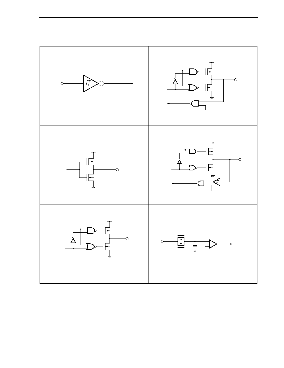
CHAPTER 2 PIN FUNCTIONS
47
User's Manual U14492EJ5V0UD
2.5 Pin I/O Circuits
Type 2
Schmitt-triggered input with hysteresis characteristics
IN
Type 3
P-ch
OUT
V
DD
N-ch
Type 4
Push-pull output with possible high-impedance output
(P-ch, N-ch both off)
Data
Output
disable
P-ch
OUT
V
DD
N-ch
Type 5
Data
Output
disable
P-ch
IN/OUT
V
DD
N-ch
Input
enable
Type 5-AC
Type 7
IN
Comparator
+
_
V
REF
(threshold voltage)
P-ch
N-ch
P-ch
N-ch
V
DD
IN/OUT
Data
Output
disable
Input
enable

48
User's Manual U14492EJ5V0UD
CHAPTER 3 CPU FUNCTION
The CPU of the V850E/IA1 is based on RISC architecture and executes almost all instructions in one clock cycle,
using 5-stage pipeline control.
3.1 Features
∑ Minimum instruction execution time: 20 ns (@ internal 50 MHz operation)
∑ Memory space
Program space: 64 MB linear
Data space:
4 GB linear
∑ Thirty-two 32-bit general-purpose registers
∑ Internal
32-bit
architecture
∑ Five-stage pipeline control
∑ Multiplication/division
instructions
∑ Saturated operation instructions
∑ One-clock 32-bit shift instruction
∑ Long/short format load/store instructions
∑ Four types of bit manipulation instructions
∑ SET1
∑ CLR1
∑ NOT1
∑ TST1
CHAPTER 3 CPU FUNCTION
49
User's Manual U14492EJ5V0UD
3.2 CPU Register Set
The registers of the V850E/IA1 can be classified into two categories: a general-purpose program register set and a
dedicated system register set. All the registers are 32-bit width.
For details, refer to V850E1 Architecture User's Manual.
(1) Program register set
(2) System register set
r0
r1
r2
r3
r4
r5
r6
r7
r8
r9
r10
r11
r12
r13
r14
r15
r16
r17
r18
r19
r20
r21
r22
r23
r24
r25
r26
r27
r28
r29
r30
r31
(Zero register)
(Assembler-reserved register)
(Stack pointer (SP))
(Global pointer (GP))
(Text pointer (TP))
(Element pointer (EP))
(Link pointer (LP))
PC
(Program counter)
PSW
(Program status word)
ECR
(Interrupt source register)
FEPC
FEPSW
(Status saving register during NMI)
(Status saving register during NMI)
EIPC
EIPSW
(Status saving register during interrupt)
(Status saving register during interrupt)
31
0
31
0
31
0
CTBP
(CALLT base pointer)
DBPC
DBPSW
(Status saving register during exception/debug trap)
(Status saving register during exception/debug trap)
CTPC
CTPSW
(Status saving register during CALLT execution)
(Status saving register during CALLT execution)
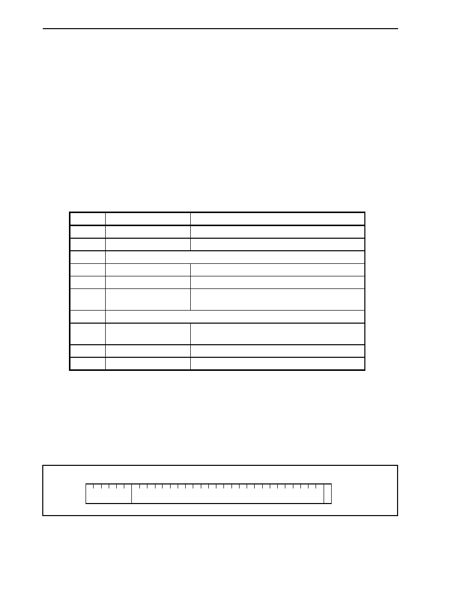
CHAPTER 3 CPU FUNCTION
50
User's Manual U14492EJ5V0UD
3.2.1
Program register set
The program register set includes general-purpose registers and a program counter.
(1) General-purpose registers
Thirty-two general-purpose registers, r0 to r31, are available. Any of these registers can be used as a data
variable or address variable.
However, r0 and r30 are implicitly used by instructions, and care must be exercised when using these
registers. r0 is a register that always holds 0, and is used for operations using 0 and offset 0 addressing. r30
is used, by means of the SLD and SST instructions, as a base pointer for when memory is accessed. Also,
r1, r3 to r5, and r31 are implicitly used by the assembler and C compiler. Therefore, before using these
registers, their contents must be saved so that they are not lost. The contents must be restored to these
registers after they have been used. r2 is sometimes used by a real-time OS. r2 can be used as a register
for variables when it is not being used by the real-time OS.
Table 3-1. Program Registers
Name Usage
Operation
r0
Zero register
Always holds 0
r1 Assembler-reserved
register
Working register for generating address
r2
Address/data variable register (when not being used by the real-time OS)
r3
Stack pointer
Used to generate stack frame when function is called
r4
Global pointer
Used to access global variable in data area
r5
Text pointer
Register to indicate the start of the text area (where program
code is located)
r6 to r29
Address/data variable registers
r30
Element pointer
Base pointer for generating address when memory is
accessed
r31
Link pointer
Used by compiler when calling function
PC
Program counter
Holds instruction address during program execution
Remark For detailed descriptions about r1, r3 to r5, and r31, which are used by the assembler and C compiler,
refer to CA850 (C Compiler Package) Assembly Language User's Manual.
(2) Program counter (PC)
This register holds the instruction address during program execution. The lower 26 bits of this register are
valid, and bits 31 to 26 are fixed to 0. If a carry occurs from bit 25 to 26, it is ignored.
Bit 0 is fixed to 0, and branching to an odd address cannot be performed.
31
26 25
1 0
PC
Fixed to 0
Instruction address during execution
0
Initial value
00000000H
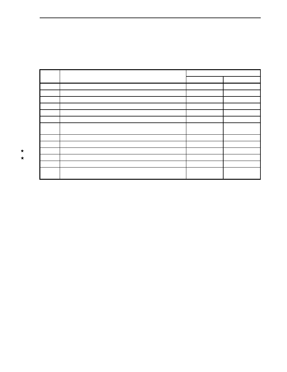
CHAPTER 3 CPU FUNCTION
51
User's Manual U14492EJ5V0UD
3.2.2
System register set
System registers control the status of the CPU and hold interrupt information.
To read/write these system registers, specify a system register number indicated below using the system register
load/store instruction (LDSR or STSR instruction).
Table 3-2. System Register Numbers
Operand Specification
No. System
Register
Name
LDSR Instruction
STSR Instruction
0
Status saving register during interrupt (EIPC)
Note 1
1
Status saving register during interrupt (EIPSW)
Note 1
2
Status saving register during NMI (FEPC)
3
Status saving register during NMI (FEPSW)
4
Interrupt source register (ECR)
◊
5
Program status word (PSW)
6 to 15
Reserved number for future function expansion (operations that access
these register numbers cannot be guaranteed).
◊
◊
16
Status saving register during CALLT execution (CTPC)
17
Status saving register during CALLT execution (CTPSW)
18
Status saving register during exception/debug trap (DBPC)
Note 2
Note 2
19
Status saving register during exception/debug trap (DBPSW)
Note 2
Note 2
20
CALLT base pointer (CTBP)
21 to 31
Reserved number for future function expansion (operations that access
these register numbers cannot be guaranteed).
◊
◊
Notes 1. Because this register has only one set, to allow multiple interrupts, it is necessary to save this register
by program.
2. These registers can be accessed only after DBTRAP instruction execution and before DBRETI
instruction execution.
Caution Even if bit 0 of EIPC, FEPC, or CTPC is set to 1 with the LDSR instruction, bit 0 will be ignored
when the program is returned by the RETI instruction after interrupt servicing (because bit 0 of
the PC is fixed to 0). When setting the value of EIPC, FEPC, or CTPC, use an even value (bit 0 =
0).
Remark
: Access allowed
◊: Access prohibited
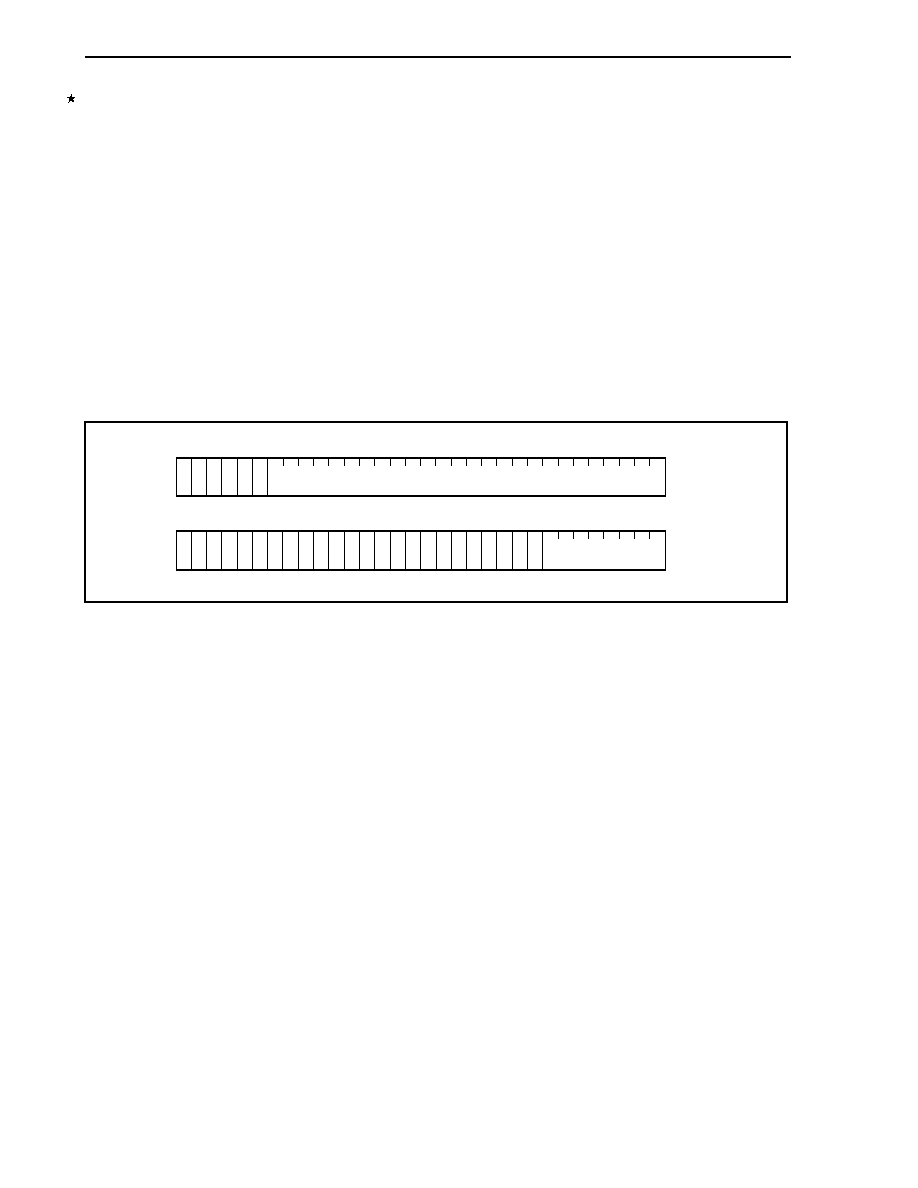
CHAPTER 3 CPU FUNCTION
52
User's Manual U14492EJ5V0UD
(1) Interrupt status saving registers (EIPC, EIPSW)
There are two interrupt status saving registers, EIPC and EIPSW.
Upon occurrence of a software exception or a maskable interrupt, the contents of the program counter (PC)
are saved to EIPC and the contents of the program status word (PSW) are saved to EIPSW (upon
occurrence of a non-maskable interrupt (NMI), the contents are saved to the NMI status saving registers
(FEPC, FEPSW)).
The address of the next instruction following the instruction executed when a software exception or maskable
interrupt occurs is saved to EIPC, except for some instructions (refer to 7.8 Periods in Which CPU Does Not
Acknowledge Interrupts).
The current PSW contents are saved to EIPSW.
Since there is only one set of interrupt status saving registers, the contents of these registers must be saved
by the program when multiple interrupt servicing is enabled.
Bits 31 to 26 of EIPC and bits 31 to 8 of EIPSW are reserved (fixed to 0) for future function expansion.
When the RETI instruction is executed, the values in EIPC and EIPSW are restored to the PC and PSW,
respectively.
31
0
EIPC
(PC contents saved)
0
0
After reset
0xxxxxxxH
(x: Undefined)
26 25
0 0 0 0
31
0
EIPSW
(PSW contents saved)
0
0
After reset
000000xxH
(x: Undefined)
8
0 0 0 0
0
0
0 0 0 0
0
0
0 0 0 0
0
0
0 0 0 0
7
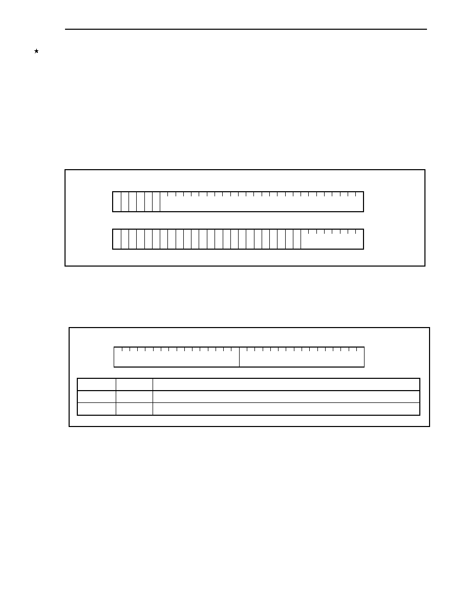
CHAPTER 3 CPU FUNCTION
53
User's Manual U14492EJ5V0UD
(2) NMI status saving registers (FEPC, FEPSW)
There are two NMI status saving registers, FEPC and FEPSW.
Upon occurrence of a non-maskable interrupt (NMI), the contents of the program counter (PC) are saved to
FEPC and the contents of the program status word (PSW) are saved to FEPSW.
The address of the next instruction following the instruction executed when a non-maskable interrupt occurs
is saved to FEPC, except for some instructions.
The current PSW contents are saved to FEPSW.
Bits 31 to 26 of FEPC and bits 31 to 8 of FEPSW are reserved (fixed to 0) for future function expansion.
When the RETI instruction has been executed, the values of FEPC and FEPSW are restored to the PC and
PSW, respectively.
31
0
FEPC
(PC contents saved)
0
0
After reset
0xxxxxxxH
(x: Undefined)
26 25
0 0 0 0
31
0
FEPSW
(PSW contents saved)
0
0
After reset
000000xxH
(x: Undefined)
8
0 0 0 0
0
0
0 0 0 0
0
0
0 0 0 0
0
0
0 0 0 0
7
(3) Interrupt source register (ECR)
Upon occurrence of an interrupt or an exception, the interrupt source register (ECR) holds the source of an
interrupt or an exception. The value held by ECR is the exception code coded for each interrupt source. This
register is a read-only register, and thus data cannot be written to it using the LDSR instruction.
31
0
ECR
FECC
EICC
After reset
00000000H
16 15
Bit position
Bit name
Description
31 to 16
FECC
Non-maskable interrupt (NMI) exception code
15 to 0
EICC
Exception, maskable interrupt exception code
CHAPTER 3 CPU FUNCTION
54
User's Manual U14492EJ5V0UD
(4) Program status word (PSW)
The program status word (PSW) is a collection of flags that indicate the program status (instruction execution
result) and the CPU status.
When the contents of this register are changed using the LDSR instruction, the new contents become valid
immediately following completion of LDSR instruction execution. Interrupt request acknowledgment is held
pending while a write to the PSW is being executed by the LDSR instruction.
Bits 31 to 8 are reserved (fixed to 0) for future function expansion.
(1/2)
31
0
PSW
RFU
After reset
00000020H
8 7
NP
6
EP
5
ID
4
SAT
3
CY
2
OV
1
S Z
Bit position Flag name
Description
31 to 8
RFU
Reserved field. Fixed to 0.
7 NP
Indicates that non-maskable interrupt (NMI) servicing is in progress. This flag is set to 1 when
an NMI request is acknowledged, and disables multiple interrupts.
0: NMI servicing not in progress
1: NMI servicing in progress
6 EP
Indicates that exception processing is in progress. This flag is set to 1 when an exception
occurs. Moreover, interrupt requests can be acknowledged even when this bit is set.
0: Exception processing not in progress
1: Exception processing in progress
5 ID Indicates whether maskable interrupt request acknowledgment is enabled.
0: Interrupt enabled (EI)
1: Interrupt disabled (DI)
4 SAT
Note
Indicates that the result of executing a saturated operation instruction has overflowed and that
the calculation result is saturated. Since this is a cumulative flag, it is set to 1 when the result of
a saturated operation instruction becomes saturated, and it is not cleared to 0 even if the
operation results of successive instructions do not become saturated. This flag is neither set nor
cleared when arithmetic operation instructions are executed.
0: Not saturated
1: Saturated
3 CY
Indicates whether carry or borrow occurred as the result of an operation.
0: No carry or borrow occurred
1: Carry or borrow occurred
2 OV
Note
Indicates whether overflow occurred during an operation.
0: No overflow occurred
1: Overflow occurred.
1 S
Note
Indicates whether the result of an operation is negative.
0: Operation result is positive or 0.
1: Operation result is negative.
0 Z Indicates whether operation result is 0.
0: Operation result is not 0.
1: Operation result is 0.
Remark Note is explained on the following page.

CHAPTER 3 CPU FUNCTION
55
User's Manual U14492EJ5V0UD
(2/2)
Note During saturated operation, the saturated operation results are determined by the contents of the OV
flag and S flag. The SAT flag is set (to 1) only when the OV flag is set (to 1) during saturated operation.
Flag status
Operation result status
SAT OV S
Saturated
operation result
Maximum positive value exceeded
1
1
0
7FFFFFFFH
Maximum negative value exceeded
1
1
1
80000000H
Positive (maximum value not exceeded)
0
Negative (maximum value not exceeded)
Holds value
before operation
0
1
Actual operation
result
(5) CALLT execution status saving registers (CTPC, CTPSW)
There are two CALLT execution status saving registers, CTPC and CTPSW.
When the CALLT instruction is executed, the contents of the program counter (PC) are saved to CTPC, and
the program status word (PSW) contents are saved to CTPSW.
The contents saved to CTPC consist of the address of the next instruction after the CALLT instruction.
The current PSW contents are saved to CTPSW.
Bits 31 to 26 of CTPC and bits 31 to 8 of CTPSW are reserved (fixed to 0) for future function expansion.
31
0
CTPC
(PC contents saved)
0
0
After reset
0xxxxxxxH
(x: Undefined)
26 25
0 0 0 0
31
0
CTPSW
(PSW contents saved)
0
0
After reset
000000xxH
(x: Undefined)
8
0 0 0 0
0
0
0 0 0 0
0
0
0 0 0 0
0
0
0 0 0 0
7

CHAPTER 3 CPU FUNCTION
56
User's Manual U14492EJ5V0UD
(6) Exception/debug trap status saving registers (DBPC, DBPSW)
There are two exception/debug trap status saving registers, DBPC and DBPSW.
Upon occurrence of an exception trap or debug trap, the contents of the program counter (PC) are saved to
DBPC, and the program status word (PSW) contents are saved to DBPSW.
The contents saved to DBPC consist of the address of the next instruction after the instruction executed when
an exception trap or debug trap occurs.
The current PSW contents are saved to DBPSW.
These registers can be read or written only in the period between DBTRAP instruction execution and DBRET
instruction execution.
Bits 31 to 26 of DBPC and bits 31 to 8 of DBPSW are reserved (fixed to 0) for future function expansion.
When the DBRET instruction has been executed, the values of DBPC and DBPSW are restored to the PC
and PSW, respectively.
31
0
DBPC
(PC contents saved)
0
0
After reset
0xxxxxxxH
(x: Undefined)
26 25
0 0 0 0
31
0
DBPSW
(PSW contents saved)
0
0
After reset
000000xxH
(x: Undefined)
8
0 0 0 0
0
0
0 0 0 0
0
0
0 0 0 0
0
0
0 0 0 0
7
(7) CALLT base pointer (CTBP)
The CALLT base pointer (CTBP) is used to specify table addresses and generate target addresses (bit 0 is
fixed to 0).
Bits 31 to 26 are reserved (fixed to 0) for future function expansion.
31
0
CTBP
(Base address)
0
0
After reset
0xxxxxxxH
(x: Undefined)
26 25
0 0 0 0
0

CHAPTER 3 CPU FUNCTION
57
User's Manual U14492EJ5V0UD
3.3 Operation
Modes
3.3.1
Operation modes
The V850E/IA1 has the following operation modes. Mode specification is carried out by the MODE0 to MODE2
pins.
(1) Normal operation mode
(a) Single-chip modes 0, 1
Access to the internal ROM is enabled.
In single-chip mode 0, after the system reset is cleared, each pin related to the bus interface enters the
port mode, program execution branches to the reset entry address of the internal ROM, and instruction
processing starts. By setting the PMCDH, PMCDL, PMCCS, PMCCT, and PMCCM registers to control
mode by instruction, an external device can be connected to the external memory area.
In single-chip mode 1, after the system reset is cleared, each pin related to the bus interface enters the
control mode, program execution branches to the external device's (memory) reset entry address, and
instruction processing starts. The internal ROM area is mapped from address 100000H.
(b) ROMless modes 0, 1
After the system reset is cleared, each pin related to the bus interface enters the control mode, program
execution branches to the external device's (memory) reset entry address, and instruction processing
starts. Fetching of instructions and data access for internal ROM becomes impossible.
In ROMless mode 0, the data bus is a 16-bit data bus and in ROMless mode 1, the data bus is an 8-bit
data bus.
(2) Flash memory programming mode (
µ
PD70F3116 only)
If this mode is specified, it becomes possible for the flash programmer to run a program to the internal flash
memory.
The initial values of the registers differ depending on the mode.
Operation Mode
PMCDH
PMCDL
PMCCS
PMCCT
PMCCM
BSC
ROMless mode 0
FFH FFFFH FFH 53H 0FH 5555H
ROMless mode 1
FFH FFFFH FFH 53H 0FH 0000H
Single-chip mode 0
00H 0000H 00H 00H 00H 5555H
Normal
operation
mode
Single-chip mode 1
FFH FFFFH FFH 53H 0FH 5555H
CHAPTER 3 CPU FUNCTION
58
User's Manual U14492EJ5V0UD
3.3.2
Operation mode specification
The operation mode is specified according to the status of pins MODE0 to MODE2. In an application system fix
the specification of these pins and do not change them during operation. Operation is not guaranteed if these pins
are changed during operation.
(a)
µ
PD703116
MODE2 MODE1 MODE0
Operation Mode
Remark
L
L
L
ROMless mode 0
16-bit data bus
L
L
H
ROMless mode 1
8-bit data bus
L
H
L
Single-chip mode 0
Internal ROM area is allocated
from address 000000H.
L H H
Normal operation mode
Single-chip mode 1
Internal ROM area is allocated
from address 100000H.
Other than above
Setting prohibited
(b)
µ
PD70F3116
V
PP
MODE2
MODE1
MODE0
Operation Mode
Remark
0 V
L
L
L
ROMless mode 0
16-bit data bus
0 V
L
L
H
ROMless mode 1
8-bit data bus
0 V
L
H
L
Single-chip mode 0
Internal ROM area is allocated
from address 000000H.
0 V
L
H
H
Normal operation mode
Single-chip mode 1
Internal ROM area is allocated
from address 100000H.
7.8 V
L
H
H/L
Flash memory programming mode
--
Other than above
Setting prohibited
Remark L:
Low-level
input
H:
High-level
input
CHAPTER 3 CPU FUNCTION
59
User's Manual U14492EJ5V0UD
3.4 Address
Space
3.4.1
CPU address space
The CPU of the V850E/IA1 is of 32-bit architecture and supports up to 4 GB of linear address space (data space)
during operand addressing (data access). Also, in instruction address addressing, a maximum of 64 MB of linear
address space (program space) is supported.
Figure 3-1 shows the CPU address space.
Figure 3-1. CPU Address Space
FFFFFFFFH
04000000H
03FFFFFFH
00000000H
Data area
(4 GB linear)
Program area
(64 MB linear)
CPU address space

CHAPTER 3 CPU FUNCTION
60
User's Manual U14492EJ5V0UD
3.4.2 Image
16 images, each containing a 256 MB physical address space, are seen in the 4 GB CPU address space. In
actuality, the same 256 MB physical address space is accessed regardless of the values of bits 31 to 28 of the CPU
address. Figure 3-2 shows the image of the virtual addressing space.
Physical address x0000000H can be seen as CPU address 00000000H, and in addition, can be seen as address
10000000H, address 20000000H, ... , address E0000000H, or address F0000000H.
Figure 3-2. Image on Address Space
FFFFFFFFH
F0000000H
EFFFFFFFH
00000000H
Internal ROM
Image
Image
Image
Internal RAM
On-chip peripheral I/O
External memory
Physical address space
FFFFFFFH
0000000H
Image
Image
E0000000H
DFFFFFFFH
20000000H
1FFFFFFFH
10000000H
0FFFFFFFH
CPU address space
CHAPTER 3 CPU FUNCTION
61
User's Manual U14492EJ5V0UD
3.4.3
Wrap-around of CPU address space
(1) Program space
Of the 32 bits of the PC (program counter), the higher 6 bits are fixed to 0, and only the lower 26 bits are
valid. Even if a carry or borrow occurs from bit 25 to 26 as a result of branch address calculation, the higher
6 bits ignore the carry or borrow.
Therefore, the upper-limit address of the program space, address 03FFFFFFH, and the lower-limit address
00000000H become contiguous addresses. Wrap-around refers to a situation like this whereby the lower-
limit address and upper-limit address become contiguous.
Caution The 4 KB area of 03FFF000H to 03FFFFFFH can be seen as an image of 0FFFF000H to
0FFFFFFFH. No instruction can be fetched from this area because this area is defined as
on-chip peripheral I/O area. Therefore, do not execute any branch address calculation in
which the result will reside in any part of this area.
00000001H
00000000H
03FFFFFFH
03FFFFFEH
Program space
Program space
(+) direction
( ) direction
(2) Data space
The result of an operand address calculation that exceeds 32 bits is ignored.
Therefore, the upper-limit address of the program space, address FFFFFFFFH, and the lower-limit address
00000000H are contiguous addresses, and the data space is wrapped around at the boundary of these
addresses.
00000001H
00000000H
FFFFFFFFH
FFFFFFFEH
Data space
Data space
(+) direction
( ) direction
CHAPTER 3 CPU FUNCTION
62
User's Manual U14492EJ5V0UD
3.4.4 Memory
map
The V850E/IA1 reserves areas as shown below. Each mode is specified by the MODE0 to MODE2 pins.
Figure 3-3. Memory Map
xFFFFFFFH
On-chip peripheral
I/O area
Internal RAM area
On-chip peripheral
I/O area
Internal RAM area
On-chip peripheral
I/O area
Internal RAM area
Access prohibited
Note
External memory
area
Internal ROM area
External memory
area
Internal ROM area
External memory
area
Single-chip mode 0
Single-chip mode 1
ROMless mode 0, 1
256 MB
1 MB
1 MB
4 KB
xFFFF000H
xFFFEFFFH
xFFFE800H
xFFFE7FFH
x0200000H
x01FFFFFH
x0100000H
x00FFFFFH
x0000000H
xFFFC000H
xFFFBFFFH
10 KB
Note By setting the PMCDH, PMCDL, PMCCS, PMCCT, and PMCCM registers to control mode, this area
can be used as external memory area.

CHAPTER 3 CPU FUNCTION
63
User's Manual U14492EJ5V0UD
3.4.5 Area
(1) Internal ROM/internal flash memory area
(a) Memory map
Up to 1 MB of internal ROM/internal flash memory area is reserved.
256 KB are provided in the following addresses as physical internal ROM (mask ROM/flash memory).
∑ In single-chip mode 0: Addresses 000000H to 03FFFFH
(addresses
040000H
to 0FFFFFH are undefined)
∑ In single-chip mode 1: Addresses 0100000H to 013FFFFH
(addresses 0140000H to 01FFFFFH are undefined)
Figure 3-4. Internal ROM/Internal Flash Memory Area
Undefined
Undefined
Internal ROM/
internal flash
memory area
Internal ROM/
internal flash
memory area
Single-chip mode 0
Single-chip mode 1
0FFFFFH
040000H
000000H
03FFFFH
1FFFFFH
140000H
100000H
13FFFFH
(b) Interrupt/exception table
The V850E/IA1 increases the interrupt response speed by assigning handler addresses corresponding to
interrupts/exceptions.
The collection of these handler addresses is called an interrupt/exception table, which is located in the
internal ROM area. When an interrupt/exception request is acknowledged, execution jumps to the
handler address, and the program written at that memory is executed. Table 3-3 shows the sources of
interrupts/exceptions, and the corresponding addresses.
Remark When in ROMless modes 0, 1, or in single-chip mode 1, in order to resume correct operation
after reset, provide a handler address to the reset routine in address 0 of the external memory.

CHAPTER 3 CPU FUNCTION
64
User's Manual U14492EJ5V0UD
Table 3-3. Interrupt/Exception Table
Start Address of
Interrupt/Exception Table
Interrupt/Exception
Source
Start Address of
Interrupt/Exception Table
Interrupt/Exception
Source
00000000H RESET
00000200H INTP21/INTCC21
00000010H NMI0
00000210H INTP22/INTCC22
00000040H
TRAP0n (n = 0 to F)
00000220H
INTP23/INTCC23
00000050H
TRAP1n (n = 0 to F)
00000230H
INTP24/INTCC24
00000060H ILGOP/DBG0
00000240H INTP25/INTCC25
00000080H INTP0
00000250H INTTM3
00000090H INTP1
00000260H INTP30/INTCC30
000000A0H INTP2
00000270H INTP31/INTCC31
000000B0H INTP3
00000280H INTCM4
000000C0H INTP4
00000290H INTDMA0
000000D0H INTP5
000002A0H INTDMA1
000000E0H INTP6
000002B0H INTDMA2
000000F0H INTDET0
000002C0H INTDMA3
00000100H INTDET1
000002D0H INTCREC
00000110H INTTM00
000002E0H INTCTRX
00000120H INTCM003 000002F0H INTCERR
00000130H INTTM01
00000300H INTCMAC
00000140H INTCM013 00000310H INTCSI0
00000150H INTP100/INTCC100
00000320H INTCSI1
00000160H INTP101/INTCC101
00000330H INTSR0
00000170H INTCM100 00000340H INTST0
00000180H INTCM101 00000350H INTSER0
00000190H INTP110/INTCC110
00000360H INTSR1
000001A0H INTP111/INTCC111
00000370H INTST1
000001B0H INTCM110 00000380H INTSR2
000001C0H INTCM111 00000390H INTST2
000001D0H INTTM20
000003A0H INTAD0
000001E0H INTTM21
000003B0H INTAD1
000001F0H INTP20/INTCC20

CHAPTER 3 CPU FUNCTION
65
User's Manual U14492EJ5V0UD
(c) Internal ROM area relocation function
If set in single-chip mode 1, the internal ROM area is located beginning from address 100000H, so
booting from external memory becomes possible.
Therefore, in order to resume correct operation after reset, provide a handler address to the reset routine
in address 0 of the external memory.
Figure 3-5. Internal ROM Area in Single-Chip Mode 1
Internal ROM area
External memory area
200000H
1FFFFFH
100000H
0FFFFFH
000000H
Block 0
Note
Note See
4.3 Memory Block Function.
(2) Internal RAM area
12 KB of memory, addresses FFFC000H to FFFEFFFH, is reserved for the internal RAM area.
The 12 KB area of 3FFC000H to 3FFEFFFH can be seen as an image of FFFC000H to FFFEFFFH.
In the V850E/IA1, 10 KB of memory, addresses FFFC000H to FFFE7FFH, is provided as physical internal
RAM.
Access to the area of addresses FFFE800H to FFFEFFFH is prohibited.
Internal RAM area (10 KB)
FFFEFFFH
FFFE800H
FFFE7FFH
FFFC000H
Access prohibited

CHAPTER 3 CPU FUNCTION
66
User's Manual U14492EJ5V0UD
(3) On-chip peripheral I/O area
4 KB of memory, addresses FFFF000H to FFFFFFFH, is provided as an on-chip peripheral I/O area.
An image of addresses FFFF000H to FFFFFFFH can be seen in the area between addresses 3FFF000H and
3FFFFFFH
Note
.
Note Access to the area of addresses 3FFF000H to 3FFFFFFH is prohibited. To access the on-chip
peripheral I/O, specify addresses FFFF000H to FFFFFFFH.
FFFFFFFH
FFFF000H
On-chip peripheral I/O area
(4 KB)
On-chip peripheral I/O registers associated with the operation mode specification and the state monitoring for
the on-chip peripherals I/O are all memory-mapped to the on-chip peripheral I/O area. Program fetches
cannot be executed from this area.
Cautions 1. The least significant bit of an address is not decoded. Therefore, if byte access is
executed in the register at an odd address (2n + 1), the register at the even address (2n)
will be accessed because of the hardware specification.
2. In the V850E/IA1, no registers exist that are capable of word access, but if a register is
word accessed, halfword access is performed twice in the order of lower address, then
higher address of the word area, ignoring the lower 2 bits of the address.
3. For registers in which byte access is possible, if halfword access is executed, the
higher 8 bits become undefined during the read operation, and the lower 8 bits of data
are written to the register during the write operation.
4.
Addresses that are not defined as registers are reserved for future expansion. If these
addresses are accessed, the operation is undefined and not guaranteed.
5.
Addresses 3FFF000H to 3FFFFFFH cannot be specified as the source/destination
address of DMA transfer. Be sure to use addresses FFFF000H to FFFFFFFH for the
source/destination address of DMA transfer.
In the on-chip peripheral I/O area, a 16 KB area of addresses from x0000H to x3FFFH is provided as a
programmable peripheral I/O area. Within this area, the area between x2000H and x2FFFH is used
exclusively for the FCAN controller (see 3.4.9 Programmable peripheral I/O registers).
Caution When emulating the FCAN controller using the in-circuit emulator (IE-V850E-MC or IE-
703116-MC-EM1), perform the following settings in the Configuration screen that appears
when the debugger is started.
∑ Set the start address of the programmable peripheral I/O area that is set using the BPC
register to the Programmable I/O Area field.
∑ Map the programmable peripheral I/O area as "Target" or "Emulation RAM" in the
Memory Mapping field.

CHAPTER 3 CPU FUNCTION
67
User's Manual U14492EJ5V0UD
(4) External memory area
256 MB are available for external memory area. The lower 64 MB can be used as program/data area and the
higher 192 MB as data area.
∑ When in single-chip mode 0: x0100000H
to
xFFFBFFFH
∑ When in single-chip mode 1:
x0000000H to x00FFFFFH, x0200000H to xFFFBFFFH
∑ When in ROMless modes 0 and 1: x0000000H to xFFFBFFFH
Access to the external memory area uses the chip-select signal assigned to each memory block (which is
carried out in the CS unit set by chip area selection control registers 0 and 1 (CSC0, CSC1)).
Note that, the internal ROM, internal RAM, on-chip peripheral I/O, and programmable peripheral I/O areas
cannot be accessed as external memory areas.
3.4.6
External memory expansion
By setting the port n mode control register (PMCn) to control mode, an external device can be connected to the
external memory space using each pin of ports DH, DL, CS, CT, and CM. Each register is set by selecting control
mode for each pin of these ports using PMCn (n = DH, DL, CS, CT, CM).
Note that the status after reset differs as shown below in accordance with the operating mode specification set by
pins MODE0 to MODE2 (refer to 3.3 Operation Modes for details of the operation modes).
(a) In the case of ROMless mode 0
Because each pin of ports DH, DL, CS, CT, and CM enters control mode following a reset, external
memory can be used without making changes to the port n mode control register (PMCn) (the external
data bus width is 16 bits).
(b) In the case of ROMless mode 1
Because each pin of ports DH, DL, CS, CT, and CM enters control mode following a reset, external
memory can be used without making changes to the port n mode control register (PMCn) (the external
data bus width is 8 bits).
(c) In the case of single-chip mode 0
Since the internal ROM area is accessed after a reset, each pin of ports DH, DL, CS, CT, and CM enters
the port mode, and external devices cannot be used.
To use external memory, set the port n mode control register (PMCn).
(d) In the case of single-chip mode 1
The internal ROM area is allocated from address 100000H. As a result, because each pin of ports DH,
DL, CS, CT, and CM enters control mode following a reset, external memory can be used without making
changes to the port n mode control register (PMCn) (the external data bus width is 16 bits).
Remark n = DH, DL, CS, CT, CM
CHAPTER 3 CPU FUNCTION
68
User's Manual U14492EJ5V0UD
3.4.7
Recommended use of address space
The architecture of the V850E/IA1 requires that a register that serves as a pointer be secured for address
generation when accessing operand data in the data space. Operand data access from instruction can be directly
executed at the address in this pointer register ±32 KB. However, because there is a limit to which general-purpose
registers are used as a pointer register, by minimizing the deterioration of address calculation performance when
changing the pointer value, the number of usable general-purpose registers for handling variables is maximized, and
the program size can be saved.
To enhance the efficiency of using the pointer in connection with the memory map of the V850E/IA1, the following
points are recommended:
(1) Program space
Of the 32 bits of the program counter (PC), the higher 6 bits are fixed to 0, and only the lower 26 bits are
valid. Therefore, a contiguous 64 MB space starting from address 00000000H corresponds to the memory
map of the program space.
(2) Data space
For the efficient use of resources that make use of the wrap-around feature of the data space, the continuous
16 MB address spaces 00000000H to 00FFFFFFH and FF000000H to FFFFFFFFH of the 4 GB CPU are
used as the data space. With the V850E/IA1, a 256 MB physical address space is seen as 16 images in the
4 GB CPU address space. The highest bit (bit 25) of this 26-bit address is assigned as address sign-
extended to 32 bits.
Example Application of wrap-around
00007FFFH
(R =) 00000000H
FFFFE7FFH
FFFF8000H
Internal ROM area
On-chip peripheral
I/O area
External memory
area
FFFFF000H
FFFFEFFFH
FFFFBFFFH
FFFFE800H
FFFFC000H
Internal RAM area
32 KB
4 KB
10 KB
16 KB
0003FFFFH
When R = r0 (zero register) is specified with the LD/ST disp16 [R] instruction, an addressing range of
00000000H ±32 KB can be referenced with the sign-extended disp16. By mapping the external memory in
the 16 KB area in the figure, all resources including internal hardware can be accessed with one pointer.
The zero register (r0) is a register set to 0 by the hardware, and eliminates the need for additional registers
for the pointer.
CHAPTER 3 CPU FUNCTION
69
User's Manual U14492EJ5V0UD
Figure 3-6. Recommended Memory Map
FFFFFFFFH
FFFFFA78H
FFFFFA77H
FFFFF000H
FFFFEFFFH
FFFFE800H
FFFFE7FFH
FFFFC000H
FFFFBFFFH
03FFE800H
03FFE7FFH
03FFF000H
03FFEFFFH
03FFC000H
03FFBFFFH
00100000H
000FFFFFH
00040000H
0003FFFFH
00000000H
03FFFFFFH
04000000H
xFFFFFFFH
xFFFF000H
xFFFEFFFH
xFFFC000H
xFFFBFFFH
xFFFE800H
xFFFE7FFH
x0100000H
x00FFFFFH
x0040000H
x003FFFFH
x0000000H
xFFFFA78H
xFFFFA77H
Data space
Program space
On-chip
peripheral I/O
On-chip
peripheral I/O
Internal RAM
Internal RAM
External
memory
Internal ROM
External
memory
External
memory
Internal RAM
On-chip
peripheral I/O
Note
Program space
64 MB
Internal ROM
Internal ROM
Note Access to this area is prohibited. To access the on-chip peripheral I/O, specify addresses FFFF000H
to FFFFFFFH.
Remarks 1. The arrows indicate the recommended area.
2. This is a recommended memory map when the V850E/IA1 is set to single-chip mode 0, and
used in external expansion mode.
CHAPTER 3 CPU FUNCTION
70
User's Manual U14492EJ5V0UD
3.4.8
On-chip peripheral I/O registers
(1/11)
Bit Units for Manipulation
Address Function
Register
Name
Symbol
R/W
1 Bit
8 Bits 16 Bits
Initial Value
FFFFF004H Port
DL
PDL
R/W
Undefined
FFFFF004H Port
DLL
PDLL
R/W
Undefined
FFFFF005H Port
DLH
PDLH
R/W
Undefined
FFFFF006H Port
DH
PDH
R/W
Undefined
FFFFF008H Port
CS
PCS
R/W
Undefined
FFFFF00AH Port
CT
PCT
R/W
Undefined
FFFFF00CH Port
CM
PCM
R/W
Undefined
FFFFF024H
Port DL mode register
PMDL
R/W
FFFFH
FFFFF024H Port DL mode register L
PMDLL
R/W
FFH
FFFFF025H Port DL mode register H
PMDLH
R/W
FFH
FFFFF026H
Port DH mode register
PMDH
R/W
FFH
FFFFF028H
Port CS mode register
PMCS
R/W
FFH
FFFFF02AH
Port CT mode register
PMCT
R/W
FFH
FFFFF02CH
Port CM mode register
PMCM
R/W
FFH
FFFFF044H
Port DL mode control register
PMCDL
R/W
0000H/FFFFH
FFFFF044H Port DL mode control register L
PMCDLL
R/W
00H/FFH
FFFFF045H Port DL mode control register H
PMCDLH
R/W
00H/FFH
FFFFF046H
Port DH mode control register
PMCDH
R/W
00H/FFH
FFFFF048H
Port CS mode control register
PMCCS
R/W
00H/FFH
FFFFF04AH
Port CT mode control register
PMCCT
R/W
00H/53H
FFFFF04CH
Port CM mode control register
PMCCM
R/W
00H/0FH
FFFFF060H
Chip area selection control register 0
CSC0
R/W
2C11H
FFFFF062H
Chip area selection control register 1
CSC1
R/W
2C11H
FFFFF064H
Peripheral area selection control register
BPC
R/W
0000H
FFFFF066H
Bus size configuration register
BSC
R/W
0000H/5555H
FFFFF06EH
System wait control register
VSWC
R/W
77H
FFFFF080H
DMA source address register 0L
DSA0L
R/W
Undefined
FFFFF082H
DMA source address register 0H
DSA0H
R/W
Undefined
FFFFF084H
DMA destination address register 0L
DDA0L
R/W
Undefined
FFFFF086H
DMA destination address register 0H
DDA0H
R/W
Undefined
FFFFF088H
DMA source address register 1L
DSA1L
R/W
Undefined
FFFFF08AH
DMA source address register 1H
DSA1H
R/W
Undefined
FFFFF08CH
DMA destination address register 1L
DDA1L
R/W
Undefined
FFFFF08EH
DMA destination address register 1H
DDA1H
R/W
Undefined
FFFFF090H
DMA source address register 2L
DSA2L
R/W
Undefined
FFFFF092H
DMA source address register 2H
DSA2H
R/W
Undefined

CHAPTER 3 CPU FUNCTION
71
User's Manual U14492EJ5V0UD
(2/11)
Bit Units for Manipulation
Address Function
Register
Name
Symbol
R/W
1 Bit
8 Bits 16 Bits
Initial Value
FFFFF094H
DMA destination address register 2L
DDA2L
R/W
Undefined
FFFFF096H
DMA destination address register 2H
DDA2H
R/W
Undefined
FFFFF098H
DMA source address register 3L
DSA3L
R/W
Undefined
FFFFF09AH
DMA source address register 3H
DSA3H
R/W
Undefined
FFFFF09CH
DMA destination address register 3L
DDA3L
R/W
Undefined
FFFFF09EH
DMA destination address register 3H
DDA3H
R/W
Undefined
FFFFF0C0H
DMA transfer count register 0
DBC0
R/W
Undefined
FFFFF0C2H
DMA transfer count register 1
DBC1
R/W
Undefined
FFFFF0C4H
DMA transfer count register 2
DBC2
R/W
Undefined
FFFFF0C6H
DMA transfer count register 3
DBC3
R/W
Undefined
FFFFF0D0H
DMA addressing control register 0
DADC0
R/W
0000H
FFFFF0D2H
DMA addressing control register 1
DADC1
R/W
0000H
FFFFF0D4H
DMA addressing control register 2
DADC2
R/W
0000H
FFFFF0D6H
DMA addressing control register 3
DADC3
R/W
0000H
FFFFF0E0H
DMA channel control register 0
DCHC0
R/W
00H
FFFFF0E2H
DMA channel control register 1
DCHC1
R/W
00H
FFFFF0E4H
DMA channel control register 2
DCHC2
R/W
00H
FFFFF0E6H
DMA channel control register 3
DCHC3
R/W
00H
FFFFF0F0H
DMA disable status register
DDIS
R
00H
FFFFF0F2H DMA
restart
register
DRST
R/W
00H
FFFFF100H
Interrupt mask register 0
IMR0
R/W
FFFFH
FFFFF100H Interrupt mask register 0L
IMR0L
R/W
FFH
FFFFF101H Interrupt mask register 0H
IMR0H
R/W
FFH
FFFFF102H
Interrupt mask register 1
IMR1
R/W
FFFFH
FFFFF102H Interrupt mask register 1L
IMR1L
R/W
FFH
FFFFF103H Interrupt mask register 1H
IMR1H
R/W
FFH
FFFFF104H
Interrupt mask register 2
IMR2
R/W
FFFFH
FFFFF104H Interrupt mask register 2L
IMR2L
R/W
FFH
FFFFF105H Interrupt mask register 2H
IMR2H
R/W
FFH
FFFFF106H
Interrupt mask register 3
IMR3
R/W
FFFFH
FFFFF106H Interrupt mask register 3L
IMR3L
R/W
FFH
FFFFF107H Interrupt mask register 3H
IMR3H
R/W
FFH
FFFFF110H
Interrupt control register
P0IC0
R/W
47H
FFFFF112H
Interrupt control register
P0IC1
R/W
47H
FFFFF114H
Interrupt control register
P0IC2
R/W
47H
FFFFF116H
Interrupt control register
P0IC3
R/W
47H
FFFFF118H
Interrupt control register
P0IC4
R/W
47H

CHAPTER 3 CPU FUNCTION
72
User's Manual U14492EJ5V0UD
(3/11)
Bit Units for Manipulation
Address Function
Register
Name
Symbol
R/W
1 Bit
8 Bits 16 Bits
Initial Value
FFFFF11AH
Interrupt control register
P0IC5
R/W
47H
FFFFF11CH
Interrupt control register
P0IC6
R/W
47H
FFFFF11EH
Interrupt control register
DETIC0
R/W
47H
FFFFF120H
Interrupt control register
DETIC1
R/W
47H
FFFFF122H
Interrupt control register
TM0IC0
R/W
47H
FFFFF124H
Interrupt control register
CM03IC0
R/W
47H
FFFFF126H
Interrupt control register
TM0IC1
R/W
47H
FFFFF128H
Interrupt control register
CM03IC1
R/W
47H
FFFFF12AH
Interrupt control register
CC10IC0
R/W
47H
FFFFF12CH
Interrupt control register
CC10IC1
R/W
47H
FFFFF12EH
Interrupt control register
CM10IC0
R/W
47H
FFFFF130H
Interrupt control register
CM10IC1
R/W
47H
FFFFF132H
Interrupt control register
CC11IC0
R/W
47H
FFFFF134H
Interrupt control register
CC11IC1
R/W
47H
FFFFF136H
Interrupt control register
CM11IC0
R/W
47H
FFFFF138H
Interrupt control register
CM11IC1
R/W
47H
FFFFF13AH
Interrupt control register
TM2IC0
R/W
47H
FFFFF13CH
Interrupt control register
TM2IC1
R/W
47H
FFFFF13EH
Interrupt control register
CC2IC0
R/W
47H
FFFFF140H
Interrupt control register
CC2IC1
R/W
47H
FFFFF142H
Interrupt control register
CC2IC2
R/W
47H
FFFFF144H
Interrupt control register
CC2IC3
R/W
47H
FFFFF146H
Interrupt control register
CC2IC4
R/W
47H
FFFFF148H
Interrupt control register
CC2IC5
R/W
47H
FFFFF14AH
Interrupt control register
TM3IC0
R/W
47H
FFFFF14CH
Interrupt control register
CC3IC0
R/W
47H
FFFFF14EH
Interrupt control register
CC3IC1
R/W
47H
FFFFF150H
Interrupt control register
CM4IC0
R/W
47H
FFFFF152H
Interrupt control register
DMAIC0
R/W
47H
FFFFF154H
Interrupt control register
DMAIC1
R/W
47H
FFFFF156H
Interrupt control register
DMAIC2
R/W
47H
FFFFF158H
Interrupt control register
DMAIC3
R/W
47H
FFFFF15AH
Interrupt control register
CANIC0
R/W
47H
FFFFF15CH
Interrupt control register
CANIC1
R/W
47H
FFFFF15EH
Interrupt control register
CANIC2
R/W
47H
FFFFF160H
Interrupt control register
CANIC3
R/W
47H
FFFFF162H
Interrupt control register
CSIIC0
R/W
47H
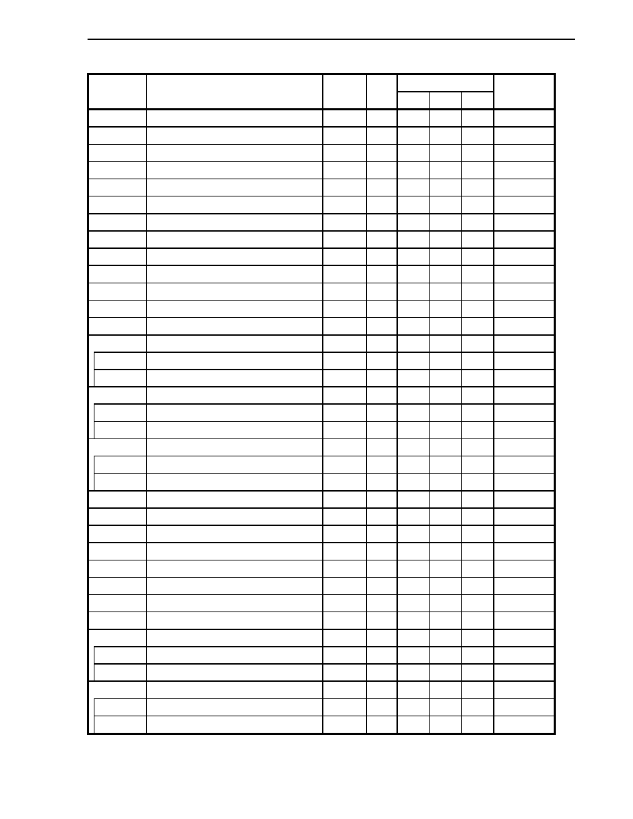
CHAPTER 3 CPU FUNCTION
73
User's Manual U14492EJ5V0UD
(4/11)
Bit Units for Manipulation
Address Function
Register
Name
Symbol
R/W
1 Bit
8 Bits 16 Bits
Initial Value
FFFFF164H
Interrupt control register
CSIIC1
R/W
47H
FFFFF166H
Interrupt control register
SRIC0
R/W
47H
FFFFF168H
Interrupt control register
STIC0
R/W
47H
FFFFF16AH
Interrupt control register
SEIC0
R/W
47H
FFFFF16CH
Interrupt control register
SRIC1
R/W
47H
FFFFF16EH
Interrupt control register
STIC1
R/W
47H
FFFFF170H
Interrupt control register
SRIC2
R/W
47H
FFFFF172H
Interrupt control register
STIC2
R/W
47H
FFFFF174H
Interrupt control register
ADIC0
R/W
47H
FFFFF176H
Interrupt control register
ADIC1
R/W
47H
FFFFF1FAH
In-service priority register
ISPR
R
00H
FFFFF1FCH Command
register
PRCMD
W
Undefined
FFFFF1FEH
Power save control register
PSC
R/W
00H
FFFFF200H
A/D scan mode register 00
ADSCM00
R/W
0000H
FFFFF200H A/D scan mode register 00L
ADSCM00L
R/W
00H
FFFFF201H A/D scan mode register 00H
ADSCM00H
R/W
00H
FFFFF202H
A/D scan mode register 01
ADSCM01
R/W
0000H
FFFFF202H A/D scan mode register 01L
ADSCM01L
R
00H
FFFFF203H A/D scan mode register 01H
ADSCM01H
R/W
00H
FFFFF204H
A/D voltage detection mode register 0
ADETM0
R/W
0000H
FFFFF204H A/D voltage detection mode register 0L
ADETM0L
R/W
00H
FFFFF205H A/D voltage detection mode register 0H
ADETM0H
R/W
00H
FFFFF210H
A/D conversion result register 00
ADCR00
R
0000H
FFFFF212H
A/D conversion result register 01
ADCR01
R
0000H
FFFFF214H
A/D conversion result register 02
ADCR02
R
0000H
FFFFF216H
A/D conversion result register 03
ADCR03
R
0000H
FFFFF218H
A/D conversion result register 04
ADCR04
R
0000H
FFFFF21AH
A/D conversion result register 05
ADCR05
R
0000H
FFFFF21CH
A/D conversion result register 06
ADCR06
R
0000H
FFFFF21EH
A/D conversion result register 07
ADCR07
R
0000H
FFFFF240H
A/D scan mode register 10
ADSCM10
R/W
0000H
FFFFF240H A/D scan mode register 10L
ADSCM10L
R/W
00H
FFFFF241H A/D scan mode register 10H
ADSCM10H
R/W
00H
FFFFF242H
A/D scan mode register 11
ADSCM11
R/W
0000H
FFFFF242H A/D scan mode register 11L
ADSCM11L
R
00H
FFFFF243H A/D scan mode register 11H
ADSCM11H
R/W
00H
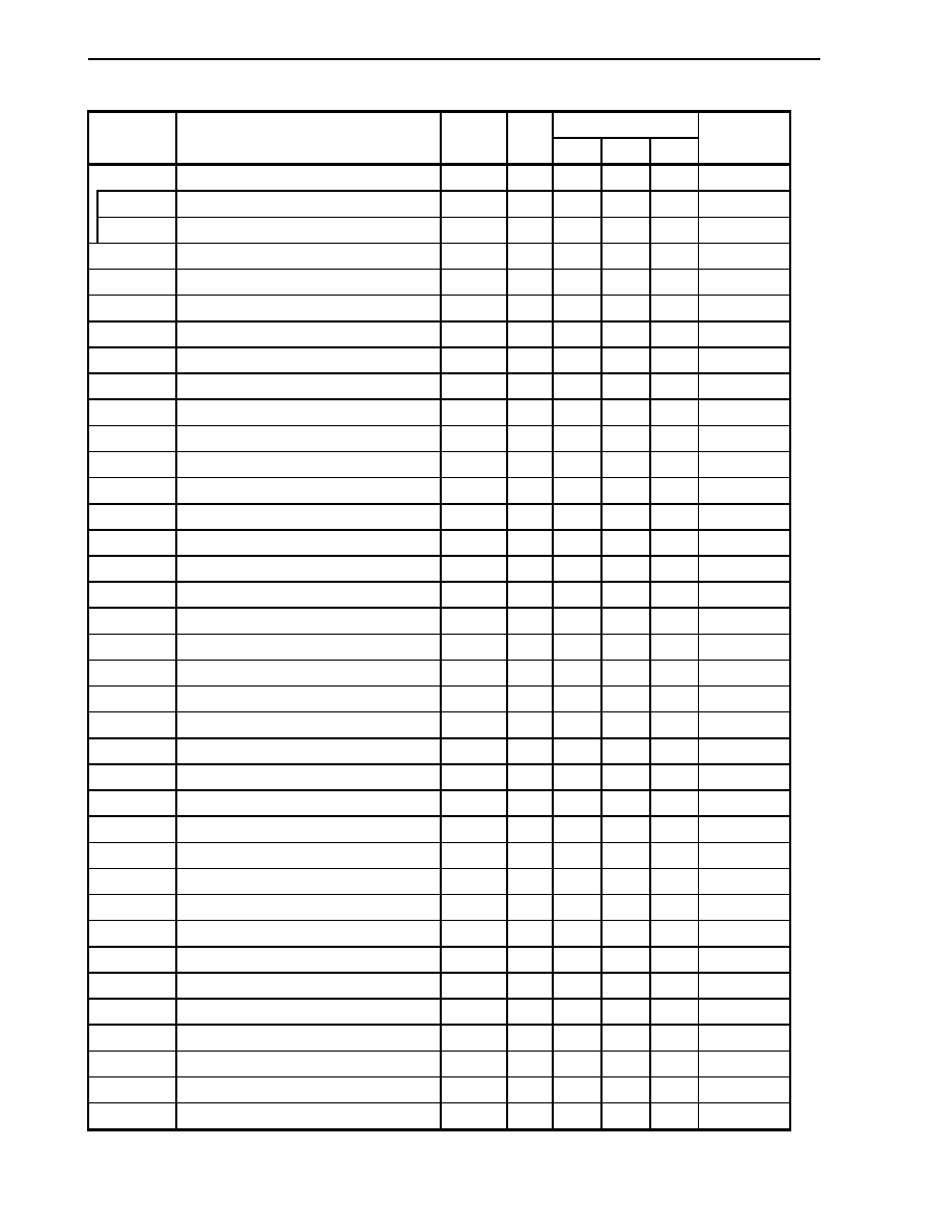
CHAPTER 3 CPU FUNCTION
74
User's Manual U14492EJ5V0UD
(5/11)
Bit Units for Manipulation
Address Function
Register
Name
Symbol
R/W
1 Bit
8 Bits 16 Bits
Initial Value
FFFFF244H
A/D voltage detection mode register 1
ADETM1
R/W
0000H
FFFFF244H A/D voltage detection mode register 1L
ADETM1L
R/W
00H
FFFFF245H A/D voltage detection mode register 1H
ADETM1H
R/W
00H
FFFFF250H
A/D conversion result register 10
ADCR10
R
0000H
FFFFF252H
A/D conversion result register 11
ADCR11
R
0000H
FFFFF254H
A/D conversion result register 12
ADCR12
R
0000H
FFFFF256H
A/D conversion result register 13
ADCR13
R
0000H
FFFFF258H
A/D conversion result register 14
ADCR14
R
0000H
FFFFF25AH
A/D conversion result register 15
ADCR15
R
0000H
FFFFF25CH
A/D conversion result register 16
ADCR16
R
0000H
FFFFF25EH
A/D conversion result register 17
ADCR17
R
0000H
FFFFF280H
A/D internal trigger selection register
ITRG0
R/W
00H
FFFFF400H Port
0
P0
R
Undefined
FFFFF402H Port
1
P1
R/W
Undefined
FFFFF404H Port
2
P2
R/W
Undefined
FFFFF406H Port
3
P3
R/W
Undefined
FFFFF408H Port
4
P4
R/W
Undefined
FFFFF422H
Port 1 mode register
PM1
R/W
FFH
FFFFF424H
Port 2 mode register
PM2
R/W
FFH
FFFFF426H
Port 3 mode register
PM3
R/W
FFH
FFFFF428H
Port 4 mode register
PM4
R/W
FFH
FFFFF442H
Port 1 mode control register
PMC1
R/W
00H
FFFFF444H
Port 2 mode control register
PMC2
R/W
00H
FFFFF446H
Port 3 mode control register
PMC3
R/W
00H
FFFFF448H
Port 4 mode control register
PMC4
R/W
00H
FFFFF462H
Port 1 function control register
PFC1
R/W
00H
FFFFF464H
Port 2 function control register
PFC2
R/W
00H
FFFFF480H
Bus cycle type configuration register 0
BCT0
R/W
CCCCH
FFFFF482H
Bus cycle type configuration register 1
BCT1
R/W
CCCCH
FFFFF484H
Data wait control register 0
DWC0
R/W
3333H
FFFFF486H
Data wait control register 1
DWC1
R/W
3333H
FFFFF488H
Address wait control register
AWC
R/W
0000H
FFFFF48AH
Bus cycle control register
BCC
R/W
AAAAH
FFFFF540H Timer
4
TM4
R
0000H
FFFFF542H Compare
register
4
CM4
R/W
0000H
FFFFF544H
Timer control register 4
TMC4
R/W
00H
FFFFF570H
Dead-time timer reload register 0
DTRR0
R/W
0FFFH
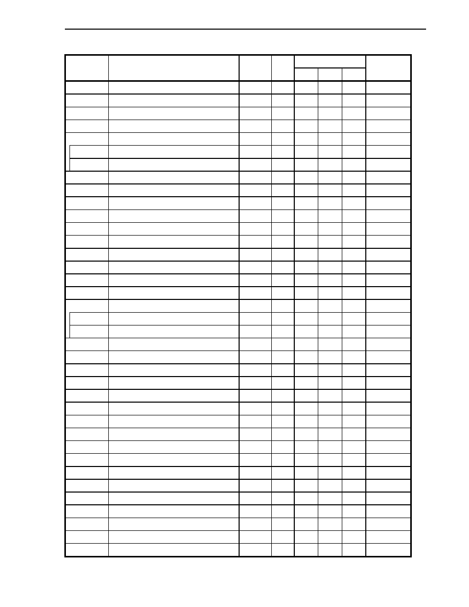
CHAPTER 3 CPU FUNCTION
75
User's Manual U14492EJ5V0UD
(6/11)
Bit Units for Manipulation
Address Function
Register
Name
Symbol
R/W
1 Bit
8 Bits 16 Bits
Initial Value
FFFFF572H Buffer
register
CM00
BFCM00 R/W
FFFFH
FFFFF574H Buffer
register
CM01
BFCM01 R/W
FFFFH
FFFFF576H Buffer
register
CM02
BFCM02 R/W
FFFFH
FFFFF578H Buffer
register
CM03
BFCM03 R/W
FFFFH
FFFFF57AH
Timer control register 00
TMC00
R/W
0508H
FFFFF57AH Timer control register 00L TMC00L
R/W
08H
FFFFF57BH Timer control register 00H
TMC00H
R/W
05H
FFFFF57CH
Timer unit control register 00
TUC00
R/W
01H
FFFFF57DH
Timer output mode register 0
TOMR0
R/W
00H
FFFFF57EH
PWM software timing output register 0
PSTO0
R/W
00H
FFFFF57FH
PWM output enable register 0
POER0
R/W
00H
FFFFF580H
TOMR write enable register 0
SPEC0
R/W
0000H
FFFFF5B0H
Dead-time timer reload register 1
DTRR1
R/W
0FFFH
FFFFF5B2H Buffer
register
CM10
BFCM10 R/W
FFFFH
FFFFF5B4H Buffer
register
CM11
BFCM11 R/W
FFFFH
FFFFF5B6H Buffer
register
CM12
BFCM12 R/W
FFFFH
FFFFF5B8H Buffer
register
CM13
BFCM13 R/W
FFFFH
FFFFF5BAH
Timer control register 01
TMC01
R/W
0508H
FFFFF5BAH Timer control register 01L TMC01L
R/W
08H
FFFFF5BBH Timer control register 01H
TMC01H
R/W
05H
FFFFF5BCH
Timer unit control register 01
TUC01
R/W
01H
FFFFF5BDH
Timer output mode register 1
TOMR1
R/W
00H
FFFFF5BEH
PWM software timing output register 1
PSTO1
R/W
00H
FFFFF5BFH
PWM output enable register 1
POER1
R/W
00H
FFFFF5C0H
TOMR write enable register 1
SPEC1
R/W
0000H
FFFFF5D0H
Timer 0 clock selection register
PRM01
R/W
00H
FFFFF5D8H
Timer 1/timer 2 clock selection register
PRM02
R/W
00H
FFFFF5E0H Timer
10
TM10
R/W
0000H
FFFFF5E2H Compare
register
100
CM100
R/W
0000H
FFFFF5E4H Compare
register
101
CM101
R/W
0000H
FFFFF5E6H
Capture/compare register 100
CC100
R/W
0000H
FFFFF5E8H
Capture/compare register 101
CC101
R/W
0000H
FFFFF5EAH
Capture/compare control register 0
CCR0
R/W
00H
FFFFF5EBH
Timer unit mode register 0
TUM0
R/W
00H
FFFFF5ECH
Timer control register 10
TMC10
R/W
00H
FFFFF5EDH
Signal edge selection register 10
SESA10
R/W
00H
FFFFF5EEH
Prescaler mode register 10
PRM10
R/W
07H

CHAPTER 3 CPU FUNCTION
76
User's Manual U14492EJ5V0UD
(7/11)
Bit Units for Manipulation
Address Function
Register
Name
Symbol
R/W
1 Bit
8 Bits 16 Bits
Initial Value
FFFFF5EFH
Status register 0
STATUS0
R
00H
FFFFF5F6H
CC101 capture input selection register
CSL10
R/W
00H
FFFFF5F8H
Timer 10 noise elimination time selection register NRC10
R/W
00H
FFFFF600H Timer
11
TM11
R/W
0000H
FFFFF602H Compare
register
110
CM110
R/W
0000H
FFFFF604H Compare
register
111
CM111
R/W
0000H
FFFFF606H
Capture/compare register 110
CC110
R/W
0000H
FFFFF608H
Capture/compare register 111
CC111
R/W
0000H
FFFFF60AH
Capture/compare control register 1
CCR1
R/W
00H
FFFFF60BH
Timer unit mode register 1
TUM1
R/W
00H
FFFFF60CH
Timer control register 11
TMC11
R/W
00H
FFFFF60DH
Signal edge selection register 11
SESA11
R/W
00H
FFFFF60EH
Prescaler mode register 11
PRM11
R/W
07H
FFFFF60FH
Status register 1
STATUS1
R
00H
FFFFF616H
CC111 capture input selection register
CSL11
R/W
00H
FFFFF618H
Timer 11 noise elimination time selection register NRC11
R/W
00H
FFFFF620H
Timer connection selection register 0
TMIC0
R/W
00H
FFFFF630H
Timer 2 input filter mode register 0
FEM0
R/W
00H
FFFFF631H
Timer 2 input filter mode register 1
FEM1
R/W
00H
FFFFF632H
Timer 2 input filter mode register 2
FEM2
R/W
00H
FFFFF633H
Timer 2 input filter mode register 3
FEM3
R/W
00H
FFFFF634H
Timer 2 input filter mode register 4
FEM4
R/W
00H
FFFFF635H
Timer 2 input filter mode register 5
FEM5
R/W
00H
FFFFF640H
Timer 2 clock stop register 0
STOPTE0
R/W
0000H
FFFFF640H Timer 2 clock stop register 0L
STOPTE0L
R
00H
FFFFF641H Timer 2 clock stop register 0H
STOPTE0H
R/W
00H
FFFFF642H
Timer 2 count clock/control edge selection
register 0
CSE0 R/W
0000H
FFFFF642H Timer 2 count clock/control edge selection
register 0L
CSE0L R/W
00H
FFFFF643H Timer 2 count clock/control edge selection
register 0H
CSE0H R/W
00H
FFFFF644H
Timer 2 sub-channel input event edge
selection register 0
SESE0 R/W
0000H
FFFFF644H Timer 2 sub-channel input event edge
selection register 0L
SESE0L R/W
00H
FFFFF645H Timer 2 sub-channel input event edge
selection register 0H
SESE0H R/W
00H
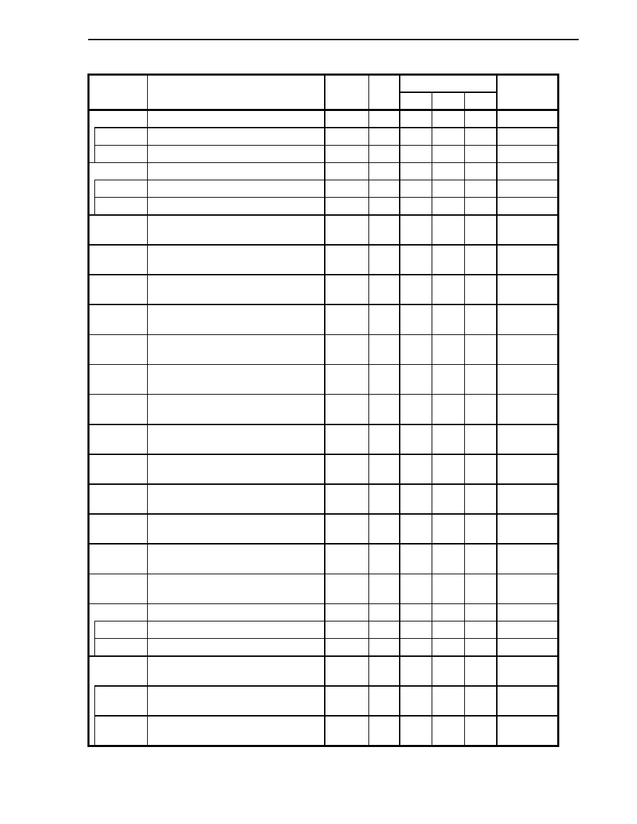
CHAPTER 3 CPU FUNCTION
77
User's Manual U14492EJ5V0UD
(8/11)
Bit Units for Manipulation
Address Function
Register
Name
Symbol
R/W
1 Bit
8 Bits 16 Bits
Initial Value
FFFFF646H
Timer 2 time base control register 0
TCRE0
R/W
0000H
FFFFF646H Timer 2 time base control register 0L
TCRE0L
R/W
00H
FFFFF647H Timer 2 time base control register 0H
TCRE0H
R/W
00H
FFFFF648H
Timer 2 output control register 0
OCTLE0
R/W
0000H
FFFFF648H Timer 2 output control register 0L
OCTLE0L
R/W
00H
FFFFF649H Timer 2 output control register 0H
OCTLE0H
R/W
00H
FFFFF64AH
Timer 2 sub-channel 0, 5 capture/compare
control register
CMSE050
R/W
0000H
FFFFF64CH
Timer 2 sub-channel 1, 2 capture/compare
control register
CMSE120
R/W
0000H
FFFFF64EH
Timer 2 sub-channel 3, 4 capture/compare
control register
CMSE340
R/W
0000H
FFFFF650H
Timer 2 sub-channel 1 sub capture/compare
register
CVSE10 R/W
0000H
FFFFF652H
Timer 2 sub-channel 1 main capture/compare
register
CVPE10 R
0000H
FFFFF654H
Timer 2 sub-channel 2 sub capture/compare
register
CVSE20 R/W
0000H
FFFFF656H
Timer 2 sub-channel 2 main capture/compare
register
CVPE20 R
0000H
FFFFF658H
Timer 2 sub-channel 3 sub capture/compare
register
CVSE30 R/W
0000H
FFFFF65AH
Timer 2 sub-channel 3 main capture/compare
register
CVPE30 R
0000H
FFFFF65CH
Timer 2 sub-channel 4 sub capture/compare
register
CVSE40 R/W
0000H
FFFFF65EH
Timer 2 sub-channel 4 main capture/compare
register
CVPE40 R
0000H
FFFFF660H
Timer 2 sub-channel 0 capture/compare
register
CVSE00 R/W
0000H
FFFFF662H
Timer 2 sub-channel 5 capture/compare
register
CVSE50 R/W
0000H
FFFFF664H
Timer 2 time base status register 0
TBSTATE0
R/W
0101H
FFFFF664H Timer 2 time base status register 0L
TBSTATE0L
R/W
01H
FFFFF665H Timer 2 time base status register 0H
TBSTATE0H
R/W
01H
FFFFF666H
Timer 2 capture/compare 1 to 4 status
register 0
CCSTATE0
R/W
0000H
FFFFF666H Timer 2 capture/compare 1 to 4 status
register 0L
CCSTATE0L
R/W
00H
FFFFF667H Timer 2 capture/compare 1 to 4 status
register 0H
CCSTATE0H
R/W
00H
CHAPTER 3 CPU FUNCTION
78
User's Manual U14492EJ5V0UD
(9/11)
Bit Units for Manipulation
Address Function
Register
Name
Symbol
R/W
1 Bit
8 Bits 16 Bits
Initial Value
FFFFF668H
Timer 2 output delay register 0
ODELE0
R/W
0000H
FFFFF668H Timer 2 output delay register 0L
ODELE0L
R/W
00H
FFFFF669H Timer 2 output delay register 0H
ODELE0H
R/W
00H
FFFFF66AH
Timer 2 software event capture register
CSCE0
R/W
0000H
FFFFF680H Timer
3
TM3
R
0000H
FFFFF682H
Capture/compare register 30
CC30
R/W
0000H
FFFFF684H
Capture/compare register 31
CC31
R/W
0000H
FFFFF686H
Timer control register 30
TMC30
R/W
00H
FFFFF688H
Timer control register 31
TMC31
R/W
20H
FFFFF689H
Valid edge selection register
SESC
R/W
00H
FFFFF690H
Timer 3 clock selection register
PRM03
R/W
00H
FFFFF698H
Timer 3 noise elimination time selection register
NRC3
R/W
00H
FFFFF800H
Peripheral command register
PHCMD
W
Undefined
FFFFF802H
Peripheral status register
PHS
R/W
00H
FFFFF810H
DMA trigger factor register 0
DTFR0
R/W
00H
FFFFF812H
DMA trigger factor register 1
DTFR1
R/W
00H
FFFFF814H
DMA trigger factor register 2
DTFR2
R/W
00H
FFFFF816H
DMA trigger factor register 3
DTFR3
R/W
00H
FFFFF820H
Power save mode register
PSMR
R/W
00H
FFFFF822H Clock
control
register
CKC
R/W
00H
FFFFF824H Lock
register
LOCKR
R
0000000xB
FFFFF880H
External interrupt mode register 0
INTM0
R/W
00H
FFFFF882H
External interrupt mode register 1
INTM1
R/W
00H
FFFFF884H
External interrupt mode register 2
INTM2
R/W
00H
FFFFF8D4H
Flash programming mode control register
FLPMC
R/W
08H/0CH/00H
Note
FFFFF900H
Clocked serial interface mode register 0
CSIM0
R/W
00H
FFFFF901H
Clocked serial interface clock selection register 0 CSIC0
R/W
00H
FFFFF902H
Clocked serial interface receive buffer register 0
SIRB0
R
0000H
FFFFF902H Clocked serial interface receive buffer
register L0
SIRBL0 R
00H
FFFFF904H
Clocked serial interface transmit buffer
register 0
SOTB0 R/W
0000H
FFFFF904H Clocked serial interface transmit buffer
register L0
SOTBL0 R/W
00H
Note
µ
PD703116: 00H
µ
PD70F3116: 08H or 0CH (For details, refer to 16.7.12 Flash programming mode control register
(FLPMC).)
CHAPTER 3 CPU FUNCTION
79
User's Manual U14492EJ5V0UD
(10/11)
Bit Units for Manipulation
Address Function
Register
Name
Symbol
R/W
1 Bit
8 Bits 16 Bits
Initial Value
FFFFF906H
Clocked serial interface read-only receive
buffer register 0
SIRBE0 R
0000H
FFFFF906H Clocked serial interface read-only receive
buffer register L0
SIRBEL0 R
00H
FFFFF908H
Clocked serial interface initial transmit buffer
register 0
SOTBF0 R/W
0000H
FFFFF908H Clocked serial interface initial transmit buffer
register L0
SOTBFL0
R/W
00H
FFFFF90AH
Serial I/O shift register 0
SIO0
R
0000H
FFFFF90AH Serial I/O shift register L0
SIOL0
R
00H
FFFFF910H
Clocked serial interface mode register 1
CSIM1
R/W
00H
FFFFF911H
Clocked serial interface clock selection
register 1
CSIC1 R/W
00H
FFFFF912H
Clocked serial interface receive buffer register 1
SIRB1
R
0000H
FFFFF912H Clocked serial interface receive buffer register
L1
SIRBL1 R
00H
FFFFF914H
Clocked serial interface transmit buffer register 1 SOTB1
R/W
0000H
FFFFF914H Clocked serial interface transmit buffer register
L1
SOTBL1 R/W
00H
FFFFF916H
Clocked serial interface read-only receive
buffer register 1
SIRBE1 R
0000H
FFFFF916H Clocked serial interface read-only receive
buffer register L1
SIRBEL1 R
00H
FFFFF918H
Clocked serial interface initial transmit buffer
register 1
SOTBF1 R/W
0000H
FFFFF918H Clocked serial interface initial transmit buffer
register L1
SOTBFL1
R/W
00H
FFFFF91AH
Serial I/O shift register 1
SIO1
R
0000H
FFFFF91AH Serial I/O shift register L1
SIOL1
R
00H
FFFFF920H
Prescaler mode register 3
PRSM3
R/W
00H
FFFFF922H
Prescaler compare register 3
PRSCM3
R/W
00H
FFFFF930H
FCAN clock selection register
PRM04
R/W
00H
FFFFFA00H
Asynchronous serial interface mode register 0 ASIM0
R/W
01H
FFFFFA02H
Receive buffer register 0
RXB0
R
FFH
FFFFFA03H
Asynchronous serial interface status register 0
ASIS0
R
00H
FFFFFA04H
Transmit buffer register 0
TXB0
R/W
FFH
FFFFFA05H
Asynchronous serial interface transmit status
register 0
ASIF0 R
00H
FFFFFA06H
Clock selection register 0
CKSR0
R/W
00H
CHAPTER 3 CPU FUNCTION
80
User's Manual U14492EJ5V0UD
(11/11)
Bit Units for Manipulation
Address Function
Register
Name
Symbol
R/W
1 Bit
8 Bits 16 Bits
Initial Value
FFFFFA07H
Baud rate generator control register 0
BRGC0
R/W
FFH
FFFFFA20H
2-frame continuous reception buffer register 1 RXB1
R
Undefined
FFFFFA22H
Receive buffer register L1
RXBL1
R
Undefined
FFFFFA24H
2-frame continuous transmission shift register 1 TXS1
W
Undefined
FFFFFA26H
Transmit shift register L1
TXSL1
W
Undefined
FFFFFA28H
Asynchronous serial interface mode register 10
ASIM10
R/W
81H
FFFFFA2AH
Asynchronous serial interface mode register 11
ASIM11
R/W
00H
FFFFFA2CH
Asynchronous serial interface status register 1
ASIS1
R
00H
FFFFFA2EH
Prescaler mode register 1
PRSM1
R/W
00H
FFFFFA30H
Prescaler compare register 1
PRSCM1
R/W
00H
FFFFFA40H
2-frame continuous reception buffer register 2 RXB2
R
Undefined
FFFFFA42H
Receive buffer register L2
RXBL2
R
Undefined
FFFFFA44H
2-frame continuous transmission shift register 2 TXS2
W
Undefined
FFFFFA46H
Transmit shift register L2
TXSL2
W
Undefined
FFFFFA48H
Asynchronous serial interface mode register 20
ASIM20
R/W
81H
FFFFFA4AH
Asynchronous serial interface mode register 21
ASIM21
R/W
00H
FFFFFA4CH
Asynchronous serial interface status register 2
ASIS2
R
00H
FFFFFA4EH
Prescaler mode register 2
PRSM2
R/W
00H
FFFFFA50H
Prescaler compare register 2
PRSCM2
R/W
00H
FFFFFA60H
RAM access data buffer register L
NBDL
R/W
0000H
FFFFFA60H RAM access data buffer register LL
NBDLL
R/W
00H
FFFFFA61H RAM access data buffer register LU
NBDLU
R/W
00H
FFFFFA62H
RAM access data buffer register H
NBDH
R/W
0000H
FFFFFA62H RAM access data buffer register HL
NBDHL
R/W
00H
FFFFFA63H RAM access data buffer register HU
NBDHU
R/W
00H
FFFFFA64H
DMA source address setting register SL
NBDMSL
R
Undefined
FFFFFA66H
DMA source address setting register SH
NBDMSH
R
Undefined
FFFFFA68H
DMA destination address setting register DL
NBDMDL
R
Undefined
FFFFFA6AH
DMA destination address setting register DH
NBDMDH
R
Undefined
CHAPTER 3 CPU FUNCTION
81
User's Manual U14492EJ5V0UD
3.4.9 Programmable
peripheral I/O registers
In the V850E/IA1, the 16 KB area of x0000H to x3FFFH is provided as a programmable peripheral I/O area. In this
area, the area between x2000H and x2FFFH is used exclusively for the FCAN controller.
The internal bus of the V850E/IA1 becomes active when the on-chip peripheral I/O register area (FFFF000H to
FFFFFFFH) or the programmable peripheral I/O register area (xxxxm000H to xxxxnFFFH) is accessed (m = xx00B, n
= xx11B). However, the on-chip peripheral I/O area is allocated to the last 4 KB of the programmable peripheral I/O
register area. Note that when data is written to this area, the written contents are reflected on the on-chip peripheral
I/O area. Therefore, access to this area is prohibited. To access the on-chip peripheral I/O area, be sure to specify
addresses FFFF000H to FFFFFFFH.
Figure 3-7. Programmable Peripheral I/O Register (Outline)
3FFFFFFH
3FFF000H
3FFEFFFH
xxxxNFFFH
xxxxM000H
x3FFFH
x3000H
x2FFFH
x2000H
x0000H
x1FFFH
0000000H
On-chip peripheral
I/O register
Programmable
peripheral
I/O register
Internal local bus
Dedicated area for
FCAN controller
On-chip peripheral
I/O area
Programmable
peripheral
I/O area
Caution The CAN message buffer register can allocate address xxxx freely as a programmable
peripheral I/O register. But once the address xxxx is set, it cannot be changed.
Remark M = xx00B
N = xx11B
The peripheral area selection control register (BPC) is used for programmable peripheral I/O register area
selection.
Caution When emulating the FCAN controller using the in-circuit emulator (IE-V850E-MC or IE-703116-
MC-EM1), perform the following settings in the Configuration screen that appears when the
debugger is started.
∑ Set the start address of the programmable peripheral I/O area that is set using the BPC
register to the Programmable I/O Area field.
∑ Map the programmable peripheral I/O area as "Target" or "Emulation RAM" in the Memory
Mapping field.
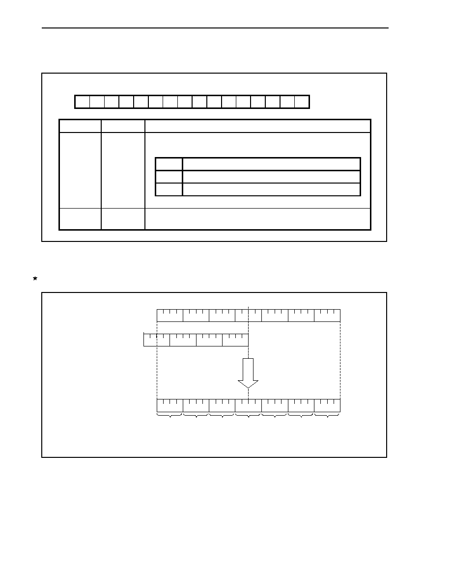
CHAPTER 3 CPU FUNCTION
82
User's Manual U14492EJ5V0UD
(1) Peripheral area selection control register (BPC)
This register can be read/written in 16-bit units.
15
14
13
12
11
10 9 8 7 6 5 4 3 2 1 0 Address
Initial
value
BPC
PA15
0
PA13 PA12
PA11 PA10
PA09 PA08 PA07 PA06 PA05 PA04 PA03 PA02 PA01 PA00
FFFFF064H 0000H
Bit position
Bit name
Function
Enables/disables usage of programmable peripheral I/O area
PA15
Usage of programmable peripheral I/O area
0
Disables usage of programmable peripheral I/O area
1
Enables usage of programmable peripheral I/O area
15 PA15
13 to 0
PA13 to PA00 Specifies an address in programmable peripheral I/O area (corresponds to A27 to
A14, respectively).
An example of setting for the programmable peripheral I/O register allocation address is shown below.
Figure 3-8. Example of Programmable Peripheral I/O Register Allocation Address Setting
M_DLC00 address
BPC register = x200H
Allocation address
0
4
8
12
16
20
24
0
0
1
0
0
0
0
0
0
0
0
1
0
1
x
x
x
x
x
x
x
x
x
x
x
x
x
x
0
4
8
12
16
20
24
0
4
H
0
8
2
0
8
0
0
1
0
0
0
0
0
0
0
0
1
0
1
0
0
0
0
0
0
0
0
0
1
0
0
0
0
0
0
0
0
0
0
0
0
0
1
0
0
0
0
0
x
When BPC register = x200H, the M_DLC00 register is allocated at address 0802804H.
A list of the programmable peripheral I/O registers is shown below.

CHAPTER 3 CPU FUNCTION
83
User's Manual U14492EJ5V0UD
(1/15)
Bit Units for Manipulation
Address Function
Register
Name Symbol
R/W
1 Bit
8 Bits 16 Bits
Initial Value
xxxxn804H
CAN message data length register 00
M_DLC00
R/W
Undefined
xxxxn805H
CAN message control register 00
M_CTRL00
R/W
Undefined
xxxxn806H
CAN message time stamp register 00
M_TIME00
R/W
Undefined
xxxxn808H
CAN message data register 000
M_DATA000
R/W
Undefined
xxxxn809H
CAN message data register 001
M_DATA001
R/W
Undefined
xxxxn80AH
CAN message data register 002
M_DATA002
R/W
Undefined
xxxxn80BH
CAN message data register 003
M_DATA003
R/W
Undefined
xxxxn80CH
CAN message data register 004
M_DATA004
R/W
Undefined
xxxxn80DH
CAN message data register 005
M_DATA005
R/W
Undefined
xxxxn80EH
CAN message data register 006
M_DATA006
R/W
Undefined
xxxxn80FH
CAN message data register 007
M_DATA007
R/W
Undefined
xxxxn810H
CAN message ID register L00
M_IDL00
R/W
Undefined
xxxxn812H
CAN message ID register H00
M_IDH00
R/W
Undefined
xxxxn814H CAN
message
configuration register 00
M_CONF00
R/W
Undefined
xxxxn815H CAN
message
status
register 00
M_STAT00
R
Undefined
xxxxn816H
CAN status set/clear register 00
SC_STAT00
W
0000H
xxxxn824H
CAN message data length register 01
M_DLC01
R/W
Undefined
xxxxn825H
CAN message control register 01
M_CTRL01
R/W
Undefined
xxxxn826H
CAN message time stamp register 01
M_TIME01
R/W
Undefined
xxxxn828H
CAN message data register 010
M_DATA010
R/W
Undefined
xxxxn829H
CAN message data register 011
M_DATA011
R/W
Undefined
xxxxn82AH
CAN message data register 012
M_DATA012
R/W
Undefined
xxxxn82BH
CAN message data register 013
M_DATA013
R/W
Undefined
xxxxn82CH
CAN message data register 014
M_DATA014
R/W
Undefined
xxxxn82DH
CAN message data register 015
M_DATA015
R/W
Undefined
xxxxn82EH
CAN message data register 016
M_DATA016
R/W
Undefined
xxxxn82FH
CAN message data register 017
M_DATA017
R/W
Undefined
xxxxn830H
CAN message ID register L01
M_IDL01
R/W
Undefined
xxxxn832H
CAN message ID register H01
M_IDH01
R/W
Undefined
xxxxn834H CAN
message
configuration register 01
M_CONF01
R/W
Undefined
xxxxn835H CAN
message
status
register 01
M_STAT01
R
Undefined
xxxxn836H
CAN status set/clear register 01
SC_STAT01
W
0000H
xxxxn844H
CAN message data length register 02
M_DLC02
R/W
Undefined
xxxxn845H
CAN message control register 02
M_CTRL02
R/W
Undefined
xxxxn846H
CAN message time stamp register 02
M_TIME02
R/W
Undefined
xxxxn848H
CAN message data register 020
M_DATA020
R/W
Undefined
Remark n = 2, 6, A, or E

CHAPTER 3 CPU FUNCTION
84
User's Manual U14492EJ5V0UD
(2/15)
Bit Units for Manipulation
Address Function
Register
Name Symbol
R/W
1 Bit
8 Bits 16 Bits
Initial Value
xxxxn849H
CAN message data register 021
M_DATA021
R/W
Undefined
xxxxn84AH
CAN message data register 022
M_DATA022
R/W
Undefined
xxxxn84BH
CAN message data register 023
M_DATA023
R/W
Undefined
xxxxn84CH
CAN message data register 024
M_DATA024
R/W
Undefined
xxxxn84DH
CAN message data register 025
M_DATA025
R/W
Undefined
xxxxn84EH
CAN message data register 026
M_DATA026
R/W
Undefined
xxxxn84FH
CAN message data register 027
M_DATA027
R/W
Undefined
xxxxn850H
CAN message ID register L02
M_IDL02
R/W
Undefined
xxxxn852H
CAN message ID register H02
M_IDH02
R/W
Undefined
xxxxn854H CAN
message
configuration register 02
M_CONF02
R/W
Undefined
xxxxn855H CAN
message
status
register 02
M_STAT02
R
Undefined
xxxxn856H
CAN status set/clear register 02
SC_STAT02
W
0000H
xxxxn864H
CAN message data length register 03
M_DLC03
R/W
Undefined
xxxxn865H
CAN message control register 03
M_CTRL03
R/W
Undefined
xxxxn866H
CAN message time stamp register 03
M_TIME03
R/W
Undefined
xxxxn868H
CAN message data register 030
M_DATA030
R/W
Undefined
xxxxn869H
CAN message data register 031
M_DATA031
R/W
Undefined
xxxxn86AH
CAN message data register 032
M_DATA032
R/W
Undefined
xxxxn86BH
CAN message data register 033
M_DATA033
R/W
Undefined
xxxxn86CH
CAN message data register 034
M_DATA034
R/W
Undefined
xxxxn86DH
CAN message data register 035
M_DATA035
R/W
Undefined
xxxxn86EH
CAN message data register 036
M_DATA036
R/W
Undefined
xxxxn86FH
CAN message data register 037
M_DATA037
R/W
Undefined
xxxxn870H
CAN message ID register L03
M_IDL03
R/W
Undefined
xxxxn872H
CAN message ID register H03
M_IDH03
R/W
Undefined
xxxxn874H CAN
message
configuration register 03
M_CONF03
R/W
Undefined
xxxxn875H CAN
message
status
register 03
M_STAT03
R
Undefined
xxxxn876H
CAN status set/clear register 03
SC_STAT03
W
0000H
xxxxn884H
CAN message data length register 04
M_DLC04
R/W
Undefined
xxxxn885H
CAN message control register 04
M_CTRL04
R/W
Undefined
xxxxn886H
CAN message time stamp register 04
M_TIME04
R/W
Undefined
xxxxn888H
CAN message data register 040
M_DATA040
R/W
Undefined
xxxxn889H
CAN message data register 041
M_DATA041
R/W
Undefined
xxxxn88AH
CAN message data register 042
M_DATA042
R/W
Undefined
xxxxn88BH
CAN message data register 043
M_DATA043
R/W
Undefined
xxxxn88CH
CAN message data register 044
M_DATA044
R/W
Undefined
Remark n = 2, 6, A, or E

CHAPTER 3 CPU FUNCTION
85
User's Manual U14492EJ5V0UD
(3/15)
Bit Units for Manipulation
Address Function
Register
Name Symbol
R/W
1 Bit
8 Bits 16 Bits
Initial Value
xxxxn88DH
CAN message data register 045
M_DATA045
R/W
Undefined
xxxxn88EH
CAN message data register 046
M_DATA046
R/W
Undefined
xxxxn88FH
CAN message data register 047
M_DATA047
R/W
Undefined
xxxxn890H
CAN message ID register L04
M_IDL04
R/W
Undefined
xxxxn882H
CAN message ID register H04
M_IDH04
R/W
Undefined
xxxxn894H CAN
message
configuration register 04
M_CONF04
R/W
Undefined
xxxxn895H CAN
message
status
register 04
M_STAT04
R
Undefined
xxxxn896H
CAN status set/clear register 04
SC_STAT04
W
0000H
xxxxn8A4H
CAN message data length register 05
M_DLC05
R/W
Undefined
xxxxn8A5H
CAN message control register 05
M_CTRL05
R/W
Undefined
xxxxn8A6H
CAN message time stamp register 05
M_TIME05
R/W
Undefined
xxxxn8A8H
CAN message data register 050
M_DATA050
R/W
Undefined
xxxxn8A9H
CAN message data register 051
M_DATA051
R/W
Undefined
xxxxn8AAH
CAN message data register 052
M_DATA052
R/W
Undefined
xxxxn8ABH
CAN message data register 053
M_DATA053
R/W
Undefined
xxxxn8ACH
CAN message data register 054
M_DATA054
R/W
Undefined
xxxxn8ADH
CAN message data register 055
M_DATA055
R/W
Undefined
xxxxn8AEH
CAN message data register 056
M_DATA056
R/W
Undefined
xxxxn8AFH
CAN message data register 057
M_DATA057
R/W
Undefined
xxxxn8B0H
CAN message ID register L05
M_IDL05
R/W
Undefined
xxxxn8B2H
CAN message ID register H05
M_IDH05
R/W
Undefined
xxxxn8B4H CAN
message
configuration register 05
M_CONF05
R/W
Undefined
xxxxn8B5H CAN
message
status register 05
M_STAT05
R
Undefined
xxxxn8B6H CAN
status
set/clear
register 05
SC_STAT05
W
0000H
xxxxn8C4H
CAN message data length register 06
M_DLC06
R/W
Undefined
xxxxn8C5H
CAN message control register 06
M_CTRL06
R/W
Undefined
xxxxn8C6H
CAN message time stamp register 06
M_TIME06
R/W
Undefined
xxxxn8C8H
CAN message data register 060
M_DATA060
R/W
Undefined
xxxxn8C9H
CAN message data register 061
M_DATA061
R/W
Undefined
xxxxn8CAH
CAN message data register 062
M_DATA062
R/W
Undefined
xxxxn8CBH
CAN message data register 063
M_DATA063
R/W
Undefined
xxxxn8CCH
CAN message data register 064
M_DATA064
R/W
Undefined
xxxxn8CDH
CAN message data register 065
M_DATA065
R/W
Undefined
xxxxn8CEH
CAN message data register 066
M_DATA066
R/W
Undefined
xxxxn8CFH
CAN message data register 067
M_DATA067
R/W
Undefined
xxxxn8D0H
CAN message ID register L06
M_IDL06
R/W
Undefined
Remark n = 2, 6, A, or E

CHAPTER 3 CPU FUNCTION
86
User's Manual U14492EJ5V0UD
(4/15)
Bit Units for Manipulation
Address Function
Register
Name Symbol
R/W
1 Bit
8 Bits 16 Bits
Initial Value
xxxxn8D2H
CAN message ID register H06
M_IDH06
R/W
Undefined
xxxxn8D4H CAN
message
configuration register 06
M_CONF06
R/W
Undefined
xxxxn8D5H CAN
message
status register 06
M_STAT06
R
Undefined
xxxxn8D6H
CAN status set/clear register 06
SC_STAT06
W
0000H
xxxxn8E4H
CAN message data length register 07
M_DLC07
R/W
Undefined
xxxxn8E5H
CAN message control register 07
M_CTRL07
R/W
Undefined
xxxxn8E6H
CAN message time stamp register 07
M_TIME07
R/W
Undefined
xxxxn8E8H
CAN message data register 070
M_DATA070
R/W
Undefined
xxxxn8E9H
CAN message data register 071
M_DATA071
R/W
Undefined
xxxxn8EAH
CAN message data register 072
M_DATA072
R/W
Undefined
xxxxn8EBH
CAN message data register 073
M_DATA073
R/W
Undefined
xxxxn8ECH
CAN message data register 074
M_DATA074
R/W
Undefined
xxxxn8EDH
CAN message data register 075
M_DATA075
R/W
Undefined
xxxxn8EEH
CAN message data register 076
M_DATA076
R/W
Undefined
xxxxn8EFH
CAN message data register 077
M_DATA077
R/W
Undefined
xxxxn8F0H
CAN message ID register L07
M_IDL07
R/W
Undefined
xxxxn8F2H
CAN message ID register H07
M_IDH07
R/W
Undefined
xxxxn8F4H CAN
message
configuration register 07
M_CONF07
R/W
Undefined
xxxxn8F5H CAN
message
status register 07
M_STAT07
R
Undefined
xxxxn8F6H
CAN status set/clear register 07
SC_STAT07
W
0000H
xxxxn904H
CAN message data length register 08
M_DLC08
R/W
Undefined
xxxxn905H
CAN message control register 08
M_CTRL08
R/W
Undefined
xxxxn906H
CAN message time stamp register 08
M_TIME08
R/W
Undefined
xxxxn908H
CAN message data register 080
M_DATA080
R/W
Undefined
xxxxn909H
CAN message data register 081
M_DATA081
R/W
Undefined
xxxxn90AH
CAN message data register 082
M_DATA082
R/W
Undefined
xxxxn90BH
CAN message data register 083
M_DATA083
R/W
Undefined
xxxxn90CH
CAN message data register 084
M_DATA084
R/W
Undefined
xxxxn90DH
CAN message data register 085
M_DATA085
R/W
Undefined
xxxxn90EH
CAN message data register 086
M_DATA086
R/W
Undefined
xxxxn90FH
CAN message data register 087
M_DATA087
R/W
Undefined
xxxxn910H
CAN message ID register L08
M_IDL08
R/W
Undefined
xxxxn912H
CAN message ID register H08
M_IDH08
R/W
Undefined
xxxxn914H CAN
message
configuration register 08
M_CONF08
R/W
Undefined
xxxxn915H CAN
message
status
register 08
M_STAT08
R
Undefined
xxxxn916H
CAN status set/clear register 08
SC_STAT08
W
0000H
Remark n = 2, 6, A, or E

CHAPTER 3 CPU FUNCTION
87
User's Manual U14492EJ5V0UD
(5/15)
Bit Units for Manipulation
Address Function
Register
Name Symbol
R/W
1 Bit
8 Bits 16 Bits
Initial Value
xxxxn924H
CAN message data length register 09
M_DLC09
R/W
Undefined
xxxxn925H
CAN message control register 09
M_CTRL09
R/W
Undefined
xxxxn926H
CAN message time stamp register 09
M_TIME09
R/W
Undefined
xxxxn928H
CAN message data register 090
M_DATA090
R/W
Undefined
xxxxn929H
CAN message data register 091
M_DATA091
R/W
Undefined
xxxxn92AH
CAN message data register 092
M_DATA092
R/W
Undefined
xxxxn92BH
CAN message data register 093
M_DATA093
R/W
Undefined
xxxxn92CH
CAN message data register 094
M_DATA094
R/W
Undefined
xxxxn92DH
CAN message data register 095
M_DATA095
R/W
Undefined
xxxxn92EH
CAN message data register 096
M_DATA096
R/W
Undefined
xxxxn92FH
CAN message data register 097
M_DATA097
R/W
Undefined
xxxxn930H
CAN message ID register L09
M_IDL09
R/W
Undefined
xxxxn932H
CAN message ID register H09
M_IDH09
R/W
Undefined
xxxxn934H CAN
message
configuration register 09
M_CONF09
R/W
Undefined
xxxxn935H CAN
message
status
register 09
M_STAT09
R
Undefined
xxxxn936H
CAN status set/clear register 09
SC_STAT09
W
0000H
xxxxn944H
CAN message data length register 10
M_DLC10
R/W
Undefined
xxxxn945H
CAN message control register 10
M_CTRL10
R/W
Undefined
xxxxn946H
CAN message time stamp register 10
M_TIME10
R/W
Undefined
xxxxn948H
CAN message data register 100
M_DATA100
R/W
Undefined
xxxxn949H
CAN message data register 101
M_DATA101
R/W
Undefined
xxxxn94AH
CAN message data register 102
M_DATA102
R/W
Undefined
xxxxn94BH
CAN message data register 103
M_DATA103
R/W
Undefined
xxxxn94CH
CAN message data register 104
M_DATA104
R/W
Undefined
xxxxn94DH
CAN message data register 105
M_DATA105
R/W
Undefined
xxxxn94EH
CAN message data register 106
M_DATA106
R/W
Undefined
xxxxn94FH
CAN message data register 107
M_DATA107
R/W
Undefined
xxxxn950H
CAN message ID register L10
M_IDL10
R/W
Undefined
xxxxn952H
CAN message ID register H10
M_IDH10
R/W
Undefined
xxxxn954H CAN
message
configuration register 10
M_CONF10
R/W
Undefined
xxxxn955H CAN
message
status
register 10
M_STAT10
R
Undefined
xxxxn956H
CAN status set/clear register 10
SC_STAT10
W
0000H
xxxxn964H
CAN message data length register 11
M_DLC11
R/W
Undefined
xxxxn965H
CAN message control register 11
M_CTRL11
R/W
Undefined
xxxxn966H
CAN message time stamp register 11
M_TIME11
R/W
Undefined
xxxxn968H
CAN message data register 110
M_DATA110
R/W
Undefined
Remark n = 2, 6, A, or E

CHAPTER 3 CPU FUNCTION
88
User's Manual U14492EJ5V0UD
(6/15)
Bit Units for Manipulation
Address Function
Register
Name Symbol
R/W
1 Bit
8 Bits 16 Bits
Initial Value
xxxxn969H
CAN message data register 111
M_DATA111
R/W
Undefined
xxxxn96AH
CAN message data register 112
M_DATA112
R/W
Undefined
xxxxn96BH
CAN message data register 113
M_DATA113
R/W
Undefined
xxxxn96CH
CAN message data register 114
M_DATA114
R/W
Undefined
xxxxn96DH
CAN message data register 115
M_DATA115
R/W
Undefined
xxxxn96EH
CAN message data register 116
M_DATA116
R/W
Undefined
xxxxn96FH
CAN message data register 117
M_DATA117
R/W
Undefined
xxxxn970H
CAN message ID register L11
M_IDL11
R/W
Undefined
xxxxn972H
CAN message ID register H11
M_IDH11
R/W
Undefined
xxxxn974H CAN
message
configuration register 11
M_CONF11
R/W
Undefined
xxxxn975H CAN
message
status
register 11
M_STAT11
R
Undefined
xxxxn976H
CAN status set/clear register 11
SC_STAT11
W
0000H
xxxxn984H
CAN message data length register 12
M_DLC12
R/W
Undefined
xxxxn985H
CAN message control register 12
M_CTRL12
R/W
Undefined
xxxxn986H
CAN message time stamp register 12
M_TIME12
R/W
Undefined
xxxxn988H
CAN message data register 120
M_DATA120
R/W
Undefined
xxxxn989H
CAN message data register 121
M_DATA121
R/W
Undefined
xxxxn98AH
CAN message data register 122
M_DATA122
R/W
Undefined
xxxxn98BH
CAN message data register 123
M_DATA123
R/W
Undefined
xxxxn98CH
CAN message data register 124
M_DATA124
R/W
Undefined
xxxxn98DH
CAN message data register 125
M_DATA125
R/W
Undefined
xxxxn98EH
CAN message data register 126
M_DATA126
R/W
Undefined
xxxxn98FH
CAN message data register 127
M_DATA127
R/W
Undefined
xxxxn990H
CAN message ID register L12
M_IDL12
R/W
Undefined
xxxxn992H
CAN message ID register H12
M_IDH12
R/W
Undefined
xxxxn994H CAN
message
configuration register 12
M_CONF12
R/W
Undefined
xxxxn995H CAN
message
status
register 12
M_STAT12
R
Undefined
xxxxn996H
CAN status set/clear register 12
SC_STAT12
W
0000H
xxxxn9A4H
CAN message data length register 13
M_DLC13
R/W
Undefined
xxxxn9A5H
CAN message control register 13
M_CTRL13
R/W
Undefined
xxxxn9A6H
CAN message time stamp register 13
M_TIME13
R/W
Undefined
xxxxn9A8H
CAN message data register 130
M_DATA130
R/W
Undefined
xxxxn9A9H
CAN message data register 131
M_DATA131
R/W
Undefined
xxxxn9AAH
CAN message data register 132
M_DATA132
R/W
Undefined
xxxxn9ABH
CAN message data register 133
M_DATA133
R/W
Undefined
xxxxn9ACH
CAN message data register 134
M_DATA134
R/W
Undefined
Remark n = 2, 6, A, or E

CHAPTER 3 CPU FUNCTION
89
User's Manual U14492EJ5V0UD
(7/15)
Bit Units for Manipulation
Address Function
Register
Name Symbol
R/W
1 Bit
8 Bits 16 Bits
Initial Value
xxxxn9ADH
CAN message data register 135
M_DATA135
R/W
Undefined
xxxxn9AEH
CAN message data register 136
M_DATA136
R/W
Undefined
xxxxn9AFH
CAN message data register 137
M_DATA137
R/W
Undefined
xxxxn9B0H
CAN message ID register L13
M_IDL13
R/W
Undefined
xxxxn9B2H
CAN message ID register H13
M_IDH13
R/W
Undefined
xxxxn9B4H CAN
message
configuration register 13
M_CONF13
R/W
Undefined
xxxxn9B5H CAN
message
status register 13
M_STAT13
R
Undefined
xxxxn9B6H CAN
status
set/clear
register 13
SC_STAT13
W
0000H
xxxxn9C4H
CAN message data length register 14
M_DLC14
R/W
Undefined
xxxxn9C5H
CAN message control register 14
M_CTRL14
R/W
Undefined
xxxxn9C6H
CAN message time stamp register 14
M_TIME14
R/W
Undefined
xxxxn9C8H
CAN message data register 140
M_DATA140
R/W
Undefined
xxxxn9C9H
CAN message data register 141
M_DATA141
R/W
Undefined
xxxxn9CAH
CAN message data register 142
M_DATA142
R/W
Undefined
xxxxn9CBH
CAN message data register 143
M_DATA143
R/W
Undefined
xxxxn9CCH
CAN message data register 144
M_DATA144
R/W
Undefined
xxxxn9CDH
CAN message data register 145
M_DATA145
R/W
Undefined
xxxxn9CEH
CAN message data register 146
M_DATA146
R/W
Undefined
xxxxn9CFH
CAN message data register 147
M_DATA147
R/W
Undefined
xxxxn9D0H
CAN message ID register L14
M_IDL14
R/W
Undefined
xxxxn9D2H
CAN message ID register H14
M_IDH14
R/W
Undefined
xxxxn9D4H CAN
message
configuration register 14
M_CONF14
R/W
Undefined
xxxxn9D5H CAN
message
status register 14
M_STAT14
R
Undefined
xxxxn9D6H
CAN status set/clear register 14
SC_STAT14
W
0000H
xxxxn9E4H
CAN message data length register 15
M_DLC15
R/W
Undefined
xxxxn9E5H
CAN message control register 15
M_CTRL15
R/W
Undefined
xxxxn9E6H
CAN message time stamp register 15
M_TIME15
R/W
Undefined
xxxxn9E8H
CAN message data register 150
M_DATA150
R/W
Undefined
xxxxn9E9H
CAN message data register 151
M_DATA151
R/W
Undefined
xxxxn9EAH
CAN message data register 152
M_DATA152
R/W
Undefined
xxxxn9EBH
CAN message data register 153
M_DATA153
R/W
Undefined
xxxxn9ECH
CAN message data register 154
M_DATA154
R/W
Undefined
xxxxn9EDH
CAN message data register 155
M_DATA155
R/W
Undefined
xxxxn9EEH
CAN message data register 156
M_DATA156
R/W
Undefined
xxxxn9EFH
CAN message data register 157
M_DATA157
R/W
Undefined
xxxxn9F0H
CAN message ID register L15
M_IDL15
R/W
Undefined
Remark n = 2, 6, A, or E

CHAPTER 3 CPU FUNCTION
90
User's Manual U14492EJ5V0UD
(8/15)
Bit Units for Manipulation
Address Function
Register
Name Symbol
R/W
1 Bit
8 Bits 16 Bits
Initial Value
xxxxn9F2H
CAN message ID register H15
M_IDH15
R/W
Undefined
xxxxn9F4H CAN
message
configuration register 15
M_CONF15
R/W
Undefined
xxxxn9F5H CAN
message
status register 15
M_STAT15
R
Undefined
xxxxn9F6H
CAN status set/clear register 15
SC_STAT15
W
0000H
xxxxnA04H
CAN message data length register 16
M_DLC16
R/W
Undefined
xxxxnA05H
CAN message control register 16
M_CTRL16
R/W
Undefined
xxxxnA06H
CAN message time stamp register 16
M_TIME16
R/W
Undefined
xxxxnA08H
CAN message data register 160
M_DATA160
R/W
Undefined
xxxxnA09H
CAN message data register 161
M_DATA161
R/W
Undefined
xxxxnA0AH
CAN message data register 162
M_DATA162
R/W
Undefined
xxxxnA0BH
CAN message data register 163
M_DATA163
R/W
Undefined
xxxxnA0CH
CAN message data register 164
M_DATA164
R/W
Undefined
xxxxnA0DH
CAN message data register 165
M_DATA165
R/W
Undefined
xxxxnA0EH
CAN message data register 166
M_DATA166
R/W
Undefined
xxxxnA0FH
CAN message data register 167
M_DATA167
R/W
Undefined
xxxxnA10H
CAN message ID register L16
M_IDL16
R/W
Undefined
xxxxnA12H
CAN message ID register H16
M_IDH16
R/W
Undefined
xxxxnA14H CAN
message
configuration register 16
M_CONF16
R/W
Undefined
xxxxnA15H CAN
message
status register 16
M_STAT16
R
Undefined
xxxxnA16H CAN
status
set/clear
register 16
SC_STAT16
W
0000H
xxxxnA24H
CAN message data length register 17
M_DLC17
R/W
Undefined
xxxxnA25H
CAN message control register 17
M_CTRL17
R/W
Undefined
xxxxnA26H
CAN message time stamp register 17
M_TIME17
R/W
Undefined
xxxxnA28H
CAN message data register 170
M_DATA170
R/W
Undefined
xxxxnA29H
CAN message data register 171
M_DATA171
R/W
Undefined
xxxxnA2AH
CAN message data register 172
M_DATA172
R/W
Undefined
xxxxnA2BH
CAN message data register 173
M_DATA173
R/W
Undefined
xxxxnA2CH
CAN message data register 174
M_DATA174
R/W
Undefined
xxxxnA2DH
CAN message data register 175
M_DATA175
R/W
Undefined
xxxxnA2EH
CAN message data register 176
M_DATA176
R/W
Undefined
xxxxnA2FH
CAN message data register 177
M_DATA177
R/W
Undefined
xxxxnA30H
CAN message ID register L17
M_IDL17
R/W
Undefined
xxxxnA32H
CAN message ID register H17
M_IDH17
R/W
Undefined
xxxxnA34H CAN
message
configuration register 17
M_CONF17
R/W
Undefined
xxxxnA35H CAN
message
status register 17
M_STAT17
R
Undefined
xxxxnA36H CAN
status
set/clear
register 17
SC_STAT17
W
0000H
Remark n = 2, 6, A, or E

CHAPTER 3 CPU FUNCTION
91
User's Manual U14492EJ5V0UD
(9/15)
Bit Units for Manipulation
Address Function
Register
Name Symbol
R/W
1 Bit
8 Bits 16 Bits
Initial Value
xxxxnA44H
CAN message data length register 18
M_DLC18
R/W
Undefined
xxxxnA45H
CAN message control register 18
M_CTRL18
R/W
Undefined
xxxxnA46H
CAN message time stamp register 18
M_TIME18
R/W
Undefined
xxxxnA48H
CAN message data register 180
M_DATA180
R/W
Undefined
xxxxnA49H
CAN message data register 181
M_DATA181
R/W
Undefined
xxxxnA4AH
CAN message data register 182
M_DATA182
R/W
Undefined
xxxxnA4BH
CAN message data register 183
M_DATA183
R/W
Undefined
xxxxnA4CH
CAN message data register 184
M_DATA184
R/W
Undefined
xxxxnA4DH
CAN message data register 185
M_DATA185
R/W
Undefined
xxxxnA4EH
CAN message data register 186
M_DATA186
R/W
Undefined
xxxxnA4FH
CAN message data register 187
M_DATA187
R/W
Undefined
xxxxnA50H
CAN message ID register L18
M_IDL18
R/W
Undefined
xxxxnA52H
CAN message ID register H18
M_IDH18
R/W
Undefined
xxxxnA54H CAN
message
configuration register 18
M_CONF18
R/W
Undefined
xxxxnA55H CAN
message
status register 18
M_STAT18
R
Undefined
xxxxnA56H CAN
status
set/clear
register 18
SC_STAT18
W
0000H
xxxxnA64H
CAN message data length register 19
M_DLC19
R/W
Undefined
xxxxnA65H
CAN message control register 19
M_CTRL19
R/W
Undefined
xxxxnA66H
CAN message time stamp register 19
M_TIME19
R/W
Undefined
xxxxnA68H
CAN message data register 190
M_DATA190
R/W
Undefined
xxxxnA69H
CAN message data register 191
M_DATA191
R/W
Undefined
xxxxnA6AH
CAN message data register 192
M_DATA192
R/W
Undefined
xxxxnA6BH
CAN message data register 193
M_DATA193
R/W
Undefined
xxxxnA6CH
CAN message data register 194
M_DATA194
R/W
Undefined
xxxxnA6DH
CAN message data register 195
M_DATA195
R/W
Undefined
xxxxnA6EH
CAN message data register 196
M_DATA196
R/W
Undefined
xxxxnA6FH
CAN message data register 197
M_DATA197
R/W
Undefined
xxxxnA70H
CAN message ID register L19
M_IDL19
R/W
Undefined
xxxxnA72H
CAN message ID register H19
M_IDH19
R/W
Undefined
xxxxnA74H CAN
message
configuration register 19
M_CONF19
R/W
Undefined
xxxxnA75H CAN
message
status register 19
M_STAT19
R
Undefined
xxxxnA76H CAN
status
set/clear
register 19
SC_STAT19
W
0000H
xxxxnA84H
CAN message data length register 20
M_DLC20
R/W
Undefined
xxxxnA85H
CAN message control register 20
M_CTRL20
R/W
Undefined
xxxxnA86H
CAN message time stamp register 20
M_TIME20
R/W
Undefined
xxxxnA88H
CAN message data register 200
M_DATA200
R/W
Undefined
Remark n = 2, 6, A, or E

CHAPTER 3 CPU FUNCTION
92
User's Manual U14492EJ5V0UD
(10/15)
Bit Units for Manipulation
Address Function
Register
Name Symbol
R/W
1 Bit
8 Bits 16 Bits
Initial Value
xxxxnA89H
CAN message data register 201
M_DATA201
R/W
Undefined
xxxxnA8AH
CAN message data register 202
M_DATA202
R/W
Undefined
xxxxnA8BH
CAN message data register 203
M_DATA203
R/W
Undefined
xxxxnA8CH
CAN message data register 204
M_DATA204
R/W
Undefined
xxxxnA8DH
CAN message data register 205
M_DATA205
R/W
Undefined
xxxxnA8EH
CAN message data register 206
M_DATA206
R/W
Undefined
xxxxnA8FH
CAN message data register 207
M_DATA207
R/W
Undefined
xxxxnA90H
CAN message ID register L20
M_IDL20
R/W
Undefined
xxxxnA92H
CAN message ID register H20
M_IDH20
R/W
Undefined
xxxxnA94H CAN
message
configuration register 20
M_CONF20
R/W
Undefined
xxxxnA95H CAN
message
status register 20
M_STAT20
R
Undefined
xxxxnA96H CAN
status
set/clear
register 20
SC_STAT20
W
0000H
xxxxnAA4H
CAN message data length register 21
M_DLC21
R/W
Undefined
xxxxnAA5H
CAN message control register 21
M_CTRL21
R/W
Undefined
xxxxnAA6H
CAN message time stamp register 21
M_TIME21
R/W
Undefined
xxxxnAA8H
CAN message data register 210
M_DATA210
R/W
Undefined
xxxxnAA9H
CAN message data register 211
M_DATA211
R/W
Undefined
xxxxnAAAH
CAN message data register 212
M_DATA212
R/W
Undefined
xxxxnAABH
CAN message data register 213
M_DATA213
R/W
Undefined
xxxxnAACH
CAN message data register 214
M_DATA214
R/W
Undefined
xxxxnAADH
CAN message data register 215
M_DATA215
R/W
Undefined
xxxxnAAEH
CAN message data register 216
M_DATA216
R/W
Undefined
xxxxnAAFH
CAN message data register 217
M_DATA217
R/W
Undefined
xxxxnAB0H
CAN message ID register L21
M_IDL21
R/W
Undefined
xxxxnAB2H
CAN message ID register H21
M_IDH21
R/W
Undefined
xxxxnAB4H CAN
message
configuration register 21
M_CONF21
R/W
Undefined
xxxxnAB5H CAN
message
status register 21
M_STAT21
R
Undefined
xxxxnAB6H CAN
status
set/clear
register 21
SC_STAT21
W
0000H
xxxxnAC4H
CAN message data length register 22
M_DLC22
R/W
Undefined
xxxxnAC5H
CAN message control register 22
M_CTRL22
R/W
Undefined
xxxxnAC6H
CAN message time stamp register 22
M_TIME22
R/W
Undefined
xxxxnAC8H
CAN message data register 220
M_DATA220
R/W
Undefined
xxxxnAC9H
CAN message data register 221
M_DATA221
R/W
Undefined
xxxxnACAH
CAN message data register 222
M_DATA222
R/W
Undefined
xxxxnACBH
CAN message data register 223
M_DATA223
R/W
Undefined
xxxxnACCH
CAN message data register 224
M_DATA224
R/W
Undefined
Remark n = 2, 6, A, or E

CHAPTER 3 CPU FUNCTION
93
User's Manual U14492EJ5V0UD
(11/15)
Bit Units for Manipulation
Address Function
Register
Name Symbol
R/W
1 Bit
8 Bits 16 Bits
Initial Value
xxxxnACDH
CAN message data register 225
M_DATA225
R/W
Undefined
xxxxnACEH
CAN message data register 226
M_DATA226
R/W
Undefined
xxxxnACFH
CAN message data register 227
M_DATA227
R/W
Undefined
xxxxnAD0H
CAN message ID register L22
M_IDL22
R/W
Undefined
xxxxnAD2H
CAN message ID register H22
M_IDH22
R/W
Undefined
xxxxnAD4H CAN
message
configuration register 22
M_CONF22
R/W
Undefined
xxxxnAD5H CAN
message
status register 22
M_STAT22
R
Undefined
xxxxnAD6H CAN
status
set/clear
register 22
SC_STAT22
W
0000H
xxxxnAE4H
CAN message data length register 23
M_DLC23
R/W
Undefined
xxxxnAE5H
CAN message control register 23
M_CTRL23
R/W
Undefined
xxxxnAE6H
CAN message time stamp register 23
M_TIME23
R/W
Undefined
xxxxnAE8H
CAN message data register 230
M_DATA230
R/W
Undefined
xxxxnAE9H
CAN message data register 231
M_DATA231
R/W
Undefined
xxxxnAEAH
CAN message data register 232
M_DATA232
R/W
Undefined
xxxxnAEBH
CAN message data register 233
M_DATA233
R/W
Undefined
xxxxnAECH
CAN message data register 234
M_DATA234
R/W
Undefined
xxxxnAEDH
CAN message data register 235
M_DATA235
R/W
Undefined
xxxxnAEEH
CAN message data register 236
M_DATA236
R/W
Undefined
xxxxnAEFH
CAN message data register 237
M_DATA237
R/W
Undefined
xxxxnAF0H
CAN message ID register L23
M_IDL23
R/W
Undefined
xxxxnAF2H
CAN message ID register H23
M_IDH23
R/W
Undefined
xxxxnAF4H CAN
message
configuration register 23
M_CONF23
R/W
Undefined
xxxxnAF5H
CAN message status register 23
M_STAT23
R
Undefined
xxxxnAF6H
CAN status set/clear register 23
SC_STAT23
W
0000H
xxxxnB04H
CAN message data length register 24
M_DLC24
R/W
Undefined
xxxxnB05H
CAN message control register 24
M_CTRL24
R/W
Undefined
xxxxnB06H
CAN message time stamp register 24
M_TIME24
R/W
Undefined
xxxxnB08H
CAN message data register 240
M_DATA240
R/W
Undefined
xxxxnB09H
CAN message data register 241
M_DATA241
R/W
Undefined
xxxxnB0AH
CAN message data register 242
M_DATA242
R/W
Undefined
xxxxnB0BH
CAN message data register 243
M_DATA243
R/W
Undefined
xxxxnB0CH
CAN message data register 244
M_DATA244
R/W
Undefined
xxxxnB0DH
CAN message data register 245
M_DATA245
R/W
Undefined
xxxxnB0EH
CAN message data register 246
M_DATA246
R/W
Undefined
xxxxnB0FH
CAN message data register 247
M_DATA247
R/W
Undefined
xxxxnB10H
CAN message ID register L24
M_IDL24
R/W
Undefined
Remark n = 2, 6, A, or E

CHAPTER 3 CPU FUNCTION
94
User's Manual U14492EJ5V0UD
(12/15)
Bit Units for Manipulation
Address Function
Register
Name Symbol
R/W
1 Bit
8 Bits 16 Bits
Initial Value
xxxxnB12H
CAN message ID register H24
M_IDH24
R/W
Undefined
xxxxnB14H CAN
message
configuration register 24
M_CONF24
R/W
Undefined
xxxxnB15H CAN
message
status register 24
M_STAT24
R
Undefined
xxxxnB16H CAN
status
set/clear
register 24
SC_STAT24
W
0000H
xxxxnB24H
CAN message data length register 25
M_DLC25
R/W
Undefined
xxxxnB25H
CAN message control register 25
M_CTRL25
R/W
Undefined
xxxxnB26H
CAN message time stamp register 25
M_TIME25
R/W
Undefined
xxxxnB28H
CAN message data register 250
M_DATA250
R/W
Undefined
xxxxnB29H
CAN message data register 251
M_DATA251
R/W
Undefined
xxxxnB2AH
CAN message data register 252
M_DATA252
R/W
Undefined
xxxxnB2BH
CAN message data register 253
M_DATA253
R/W
Undefined
xxxxnB2CH
CAN message data register 254
M_DATA254
R/W
Undefined
xxxxnB2DH
CAN message data register 255
M_DATA255
R/W
Undefined
xxxxnB2EH
CAN message data register 256
M_DATA256
R/W
Undefined
xxxxnB2FH
CAN message data register 257
M_DATA257
R/W
Undefined
xxxxnB30H
CAN message ID register L25
M_IDL25
R/W
Undefined
xxxxnB32H
CAN message ID register H25
M_IDH25
R/W
Undefined
xxxxnB34H CAN
message
configuration register 25
M_CONF25
R/W
Undefined
xxxxnB35H CAN
message
status register 25
M_STAT25
R
Undefined
xxxxnB36H CAN
status
set/clear
register 25
SC_STAT25
W
0000H
xxxxnB44H
CAN message data length register 26
M_DLC26
R/W
Undefined
xxxxnB45H
CAN message control register 26
M_CTRL26
R/W
Undefined
xxxxnB46H
CAN message time stamp register 26
M_TIME26
R/W
Undefined
xxxxnB48H
CAN message data register 260
M_DATA260
R/W
Undefined
xxxxnB49H
CAN message data register 261
M_DATA261
R/W
Undefined
xxxxnB4AH
CAN message data register 262
M_DATA262
R/W
Undefined
xxxxnB4BH
CAN message data register 263
M_DATA263
R/W
Undefined
xxxxnB4CH
CAN message data register 264
M_DATA264
R/W
Undefined
xxxxnB4DH
CAN message data register 265
M_DATA265
R/W
Undefined
xxxxnB4EH
CAN message data register 266
M_DATA266
R/W
Undefined
xxxxnB4FH
CAN message data register 267
M_DATA267
R/W
Undefined
xxxxnB50H
CAN message ID register L26
M_IDL26
R/W
Undefined
xxxxnB52H
CAN message ID register H26
M_IDH26
R/W
Undefined
xxxxnB54H CAN
message
configuration register 26
M_CONF26
R/W
Undefined
xxxxnB55H CAN
message
status register 26
M_STAT26
R
Undefined
xxxxnB56H CAN
status
set/clear
register 26
SC_STAT26
W
0000H
Remark n = 2, 6, A, or E

CHAPTER 3 CPU FUNCTION
95
User's Manual U14492EJ5V0UD
(13/15)
Bit Units for Manipulation
Address Function
Register
Name Symbol
R/W
1 Bit
8 Bits 16 Bits
Initial Value
xxxxnB64H
CAN message data length register 27
M_DLC27
R/W
Undefined
xxxxnB65H
CAN message control register 27
M_CTRL27
R/W
Undefined
xxxxnB66H
CAN message time stamp register 27
M_TIME27
R/W
Undefined
xxxxnB68H
CAN message data register 270
M_DATA270
R/W
Undefined
xxxxnB69H
CAN message data register 271
M_DATA271
R/W
Undefined
xxxxnB6AH
CAN message data register 272
M_DATA272
R/W
Undefined
xxxxnB6BH
CAN message data register 273
M_DATA273
R/W
Undefined
xxxxnB6CH
CAN message data register 274
M_DATA274
R/W
Undefined
xxxxnB6DH
CAN message data register 275
M_DATA275
R/W
Undefined
xxxxnB6EH
CAN message data register 276
M_DATA276
R/W
Undefined
xxxxnB6FH
CAN message data register 277
M_DATA277
R/W
Undefined
xxxxnB70H
CAN message ID register L27
M_IDL27
R/W
Undefined
xxxxnB72H
CAN message ID register H27
M_IDH27
R/W
Undefined
xxxxnB74H CAN
message
configuration register 27
M_CONF27
R/W
Undefined
xxxxnB75H CAN
message
status register 27
M_STAT27
R
Undefined
xxxxnB76H CAN
status
set/clear
register 27
SC_STAT27
W
0000H
xxxxnB84H
CAN message data length register 28
M_DLC28
R/W
Undefined
xxxxnB85H
CAN message control register 28
M_CTRL28
R/W
Undefined
xxxxnB86H
CAN message time stamp register 28
M_TIME28
R/W
Undefined
xxxxnB88H
CAN message data register 280
M_DATA280
R/W
Undefined
xxxxnB89H
CAN message data register 281
M_DATA281
R/W
Undefined
xxxxnB8AH
CAN message data register 282
M_DATA282
R/W
Undefined
xxxxnB8BH
CAN message data register 283
M_DATA283
R/W
Undefined
xxxxnB8CH
CAN message data register 284
M_DATA284
R/W
Undefined
xxxxnB8DH
CAN message data register 285
M_DATA285
R/W
Undefined
xxxxnB8EH
CAN message data register 286
M_DATA286
R/W
Undefined
xxxxnB8FH
CAN message data register 287
M_DATA287
R/W
Undefined
xxxxnB90H
CAN message ID register L28
M_IDL28
R/W
Undefined
xxxxnB92H
CAN message ID register H28
M_IDH28
R/W
Undefined
xxxxnB94H CAN
message
configuration register 28
M_CONF28
R/W
Undefined
xxxxnB95H CAN
message
status register 28
M_STAT28
R
Undefined
xxxxnB96H CAN
status
set/clear
register 28
SC_STAT28
W
0000H
xxxxnBA4H
CAN message data length register 29
M_DLC29
R/W
Undefined
xxxxnBA5H
CAN message control register 29
M_CTRL29
R/W
Undefined
xxxxnBA6H
CAN message time stamp register 29
M_TIME29
R/W
Undefined
xxxxnBA8H
CAN message data register 290
M_DATA290
R/W
Undefined
Remark n = 2, 6, A, or E

CHAPTER 3 CPU FUNCTION
96
User's Manual U14492EJ5V0UD
(14/15)
Bit Units for Manipulation
Address Function
Register
Name Symbol
R/W
1 Bit
8 Bits 16 Bits
Initial Value
xxxxnBA9H
CAN message data register 291
M_DATA291
R/W
Undefined
xxxxnBAAH
CAN message data register 292
M_DATA292
R/W
Undefined
xxxxnBABH
CAN message data register 293
M_DATA293
R/W
Undefined
xxxxnBACH
CAN message data register 294
M_DATA294
R/W
Undefined
xxxxnBADH
CAN message data register 295
M_DATA295
R/W
Undefined
xxxxnBAEH
CAN message data register 296
M_DATA296
R/W
Undefined
xxxxnBAFH
CAN message data register 297
M_DATA297
R/W
Undefined
xxxxnBB0H
CAN message ID register L29
M_IDL29
R/W
Undefined
xxxxnBB2H
CAN message ID register H29
M_IDH29
R/W
Undefined
xxxxnBB4H CAN
message
configuration register 29
M_CONF29
R/W
Undefined
xxxxnBB5H CAN
message
status register 29
M_STAT29
R
Undefined
xxxxnBB6H CAN
status
set/clear
register 29
SC_STAT29
W
0000H
xxxxnBC4H
CAN message data length register 30
M_DLC30
R/W
Undefined
xxxxnBC5H
CAN message control register 30
M_CTRL30
R/W
Undefined
xxxxnBC6H
CAN message time stamp register 30
M_TIME30
R/W
Undefined
xxxxnBC8H
CAN message data register 300
M_DATA300
R/W
Undefined
xxxxnBC9H
CAN message data register 301
M_DATA301
R/W
Undefined
xxxxnBCAH
CAN message data register 302
M_DATA302
R/W
Undefined
xxxxnBCBH
CAN message data register 303
M_DATA303
R/W
Undefined
xxxxnBCCH
CAN message data register 304
M_DATA304
R/W
Undefined
xxxxnBCDH
CAN message data register 305
M_DATA305
R/W
Undefined
xxxxnBCEH
CAN message data register 306
M_DATA306
R/W
Undefined
xxxxnBCFH
CAN message data register 307
M_DATA307
R/W
Undefined
xxxxnBD0H
CAN message ID register L30
M_IDL30
R/W
Undefined
xxxxnBD2H
CAN message ID register H30
M_IDH30
R/W
Undefined
xxxxnBD4H CAN
message
configuration register 30
M_CONF30
R/W
Undefined
xxxxnBD5H CAN
message
status register 30
M_STAT30
R
Undefined
xxxxnBD6H CAN
status
set/clear
register 30
SC_STAT30
W
0000H
xxxxnBE4H
CAN message data length register 31
M_DLC31
R/W
Undefined
xxxxnBE5H
CAN message control register 31
M_CTRL31
R/W
Undefined
xxxxnBE6H
CAN message time stamp register 31
M_TIME31
R/W
Undefined
xxxxnBE8H
CAN message data register 310
M_DATA310
R/W
Undefined
xxxxnBE9H
CAN message data register 311
M_DATA311
R/W
Undefined
xxxxnBEAH
CAN message data register 312
M_DATA312
R/W
Undefined
xxxxnBEBH
CAN message data register 313
M_DATA313
R/W
Undefined
xxxxnBECH
CAN message data register 314
M_DATA314
R/W
Undefined
Remark n = 2, 6, A, or E
CHAPTER 3 CPU FUNCTION
97
User's Manual U14492EJ5V0UD
(15/15)
Bit Units for Manipulation
Address Function
Register
Name Symbol
R/W
1 Bit
8 Bits 16 Bits
Initial Value
xxxxnBEDH
CAN message data register 315
M_DATA315
R/W
Undefined
xxxxnBEEH
CAN message data register 316
M_DATA316
R/W
Undefined
xxxxnBEFH
CAN message data register 317
M_DATA317
R/W
Undefined
xxxxnBF0H
CAN message ID register L31
M_IDL31
R/W
Undefined
xxxxnBF2H
CAN message ID register H31
M_IDH31
R/W
Undefined
xxxxnBF4H CAN
message
configuration register 31
M_CONF31
R/W
Undefined
xxxxnBF5H
CAN message status register 31
M_STAT31
R
Undefined
xxxxnBF6H
CAN status set/clear register 31
SC_STAT31
W
0000H
xxxxnC00H
CAN interrupt pending register
CCINTP
R
0000H
xxxxnC02H
CAN global interrupt pending register
CGINTP
R/W
00H
xxxxnC04H
CAN1 interrupt pending register
C1INTP
R/W
00H
xxxxnC0CH
CAN stop register
CSTOP
R/W
0000H
xxxxnC10H
CAN global status register
CGST
R/W
0100H
xxxxnC12H
CAN global interrupt enable register
CGIE
R/W
0A00H
xxxxnC14H
CAN main clock selection register
CGCS
R/W
7F05H
xxxxnC18H
CAN time stamp count register
CGTSC
R
0000H
CAN message search start register
CGMSS
W
0000H
xxxxnC1AH
CAN message search result register
CGMSR
R
0000H
xxxxnC40H
CAN1 address mask 0 register L
C1MASKL0
R/W
Undefined
xxxxnC42H
CAN1 address mask 0 register H
C1MASKH0
R/W
Undefined
xxxxnC44H
CAN1 address mask 1 register L
C1MASKL1
R/W
Undefined
xxxxnC46H
CAN1 address mask 1 register H
C1MASKH1
R/W
Undefined
xxxxnC48H
CAN1 address mask 2 register L
C1MASKL2
R/W
Undefined
xxxxnC4AH
CAN1 address mask 2 register H
C1MASKH2
R/W
Undefined
xxxxnC4CH
CAN1 address mask 3 register L
C1MASKL3
R/W
Undefined
xxxxnC4EH
CAN1 address mask 3 register H
C1MASKH3
R/W
Undefined
xxxxnC50H
CAN1 control register
C1CTRL
R/W
0101H
xxxxnC52H
CAN1 definition register
C1DEF
R/W
0000H
xxxxnC54H
CAN1 information register
C1LAST
R
00FFH
xxxxnC56H
CAN1 error count register
C1ERC
R
0000H
xxxxnC58H
CAN1 interrupt enable register
C1IE
R/W
0900H
xxxxnC5AH
CAN1 bus active register
C1BA
R
00FFH
CAN1 bit rate prescaler register
C1BRP
R/W
0000H
xxxxnC5CH
CAN1 bus diagnostic information register
C1DINF
R
0000H
xxxxnC5EH CAN1
synchronization
control register
C1SYNC
R/W
0218H
Remark n = 2, 6, A, or E
CHAPTER 3 CPU FUNCTION
98
User's Manual U14492EJ5V0UD
3.4.10 Specific registers
Specific registers are registers that are protected from being written with illegal data due to inadvertent program
loop (runaway), etc. The V850E/IA1 has three specific registers, the power save control register (PSC) (refer to 8.5.2
(13) Power save control register (PSC)), clock control register (CKC) (refer to 8.3.4 Clock control register (CKC)),
and flash programming mode control register (FLPMC) (refer to 16.7.12 Flash programming mode control register
(FLPMC)).
3.4.11 System wait control register (VSWC)
Set the value shown below to this register.
This register can be read/written in 8-bit units (address: FFFFF06EH, initial value: 77H).
Remark If the timing of changing the flag or count value conflicts with the timing of accessing a register when a
register including a status flag that indicates the status of an on-chip peripheral function (such as ASIF0)
or a register indicating the count value of a timer (such as TM0n) is accessed, a register access retry
operation is performed. As a result, a longer time may be required to access the on-chip peripheral I/O
register.
Register Name
VSWC Set Value
When PRM02 register = 01H
12H (3 clocks are set for the wait)
System wait control register
(VSWC)
When PRM02 register = 00H
15H (6 clocks are set for the wait)
3.4.12 Cautions
(1) Register to be set first
When using the V850E/IA1, the following registers must be set from the beginning.
∑ System wait control register (VSWC)
(See 3.4.11 System wait control register (VSWC))
∑ Clock control register (CKC)
(See 8.3.4 Clock control register (CKC))
After setting VSWC and CKC, set other registers as required.

CHAPTER 3 CPU FUNCTION
99
User's Manual U14492EJ5V0UD
(2) Restriction on conflict between sld instruction and interrupt request
(a) Description
If a conflict occurs between the decode operation of an instruction in <2> immediately before the sld
instruction following an instruction in <1> and an interrupt request before the instruction in <1> is
complete, the execution result of the instruction in <1> may not be stored in a register.
Instruction <1>
∑ ld instruction:
ld.b, ld.h, ld.w, ld.bu, ld.hu
∑ sld instruction:
sld.b, sld.h, sld.w, sld.bu, sld.hu
∑ Multiplication instruction: mul, mulh, mulhi, mulu
Instruction <2>
mov reg1, reg2
satadd reg1, reg2
and reg1, reg2
add reg1, reg2
mulh reg1, reg2
not reg1, reg2
satadd imm5, reg2
tst reg1, reg2
add imm5, reg2
shr imm5, reg2
satsubr reg1, reg2
or reg1, reg2
subr reg1, reg2
cmp reg1, reg2
sar imm5, reg2
satsub reg1, reg2
xor reg1, reg2
sub reg1, reg2
cmp imm5, reg2
shl imm5, reg2
<Example>
<i> ld.w [r11], r10
If the decode operation of the mov instruction <ii> immediately before the sld
instruction <iii> and an interrupt request conflict before execution of the ld
instruction <i> is complete, the execution result of instruction <i> may not be
stored in a register.
<ii> mov r10, r28
<iii> sld.w 0x28, r10
(b) Countermeasure
<1> When compiler (CA850) is used
Use CA850 Ver. 2.61 or later because generation of the corresponding instruction sequence can be
automatically suppressed.
<2> For
assembler
When executing the sld instruction immediately after instruction <ii>, avoid the above operation
using either of the following methods.
∑ Insert a nop instruction immediately before the sld instruction.
∑ Do not use the same register as the sld instruction destination register in the above instruction
<ii> executed immediately before the sld instruction.
∑
∑
∑
100
User's Manual U14492EJ5V0UD
CHAPTER 4 BUS CONTROL FUNCTION
The V850E/IA1 is provided with an external bus interface function by which external I/O and memories, such as
ROM and RAM, can be connected.
4.1 Features
∑ 16-bit/8-bit data bus sizing function
∑ 8-space chip select function
∑ Wait
function
∑ Programmable wait function, through which up to 7 wait states can be inserted for each memory block
∑ External wait function via WAIT pin
∑ Idle state insertion function
∑ Bus hold function
∑ External device connection enabled via bus control/port alternate function pins
4.2 Bus Control Pins
The following pins are used for connection to external devices.
Bus Control Pin (Function When in Control Mode)
Function When in Port Mode
Register for Port/Control
Mode Switching
Address/data bus (AD0 to AD15)
PDL0 to PDL15 (Port DL)
PMCDL
Address bus (A16 to A23)
PDH0 to PDH7 (Port DH)
PMCDH
Chip select (CS0 to CS7)
PCS0 to PCS7 (Port CS)
PMCCS
Read/write control (LWR/UWR, RD, ASTB)
PCT0, PCT1, PCT4, PCT6
(Port CT)
PMCCT
External wait control (WAIT)
PCM0 (Port CM)
Internal system clock (CLKOUT)
PCM1 (Port CM)
Bus hold control (HLDRQ, HLDAK)
PCM2, PCM3 (Port CM)
PMCCM
Remark In the case of single-chip mode 1 and ROMless modes 0 and 1, when the system is reset, each bus
control pin becomes unconditionally valid.
4.2.1 Pin status during internal ROM, internal RAM, and on-chip peripheral I/O access
When the internal ROM and RAM are accessed, both the address bus and address/data bus become undefined.
The external bus control signal becomes inactive.
When on-chip peripheral I/O are accessed, both the address bus and address/data bus output the addresses of the
on-chip peripheral I/O currently being accessed. No data is output. The external bus control signal becomes inactive.
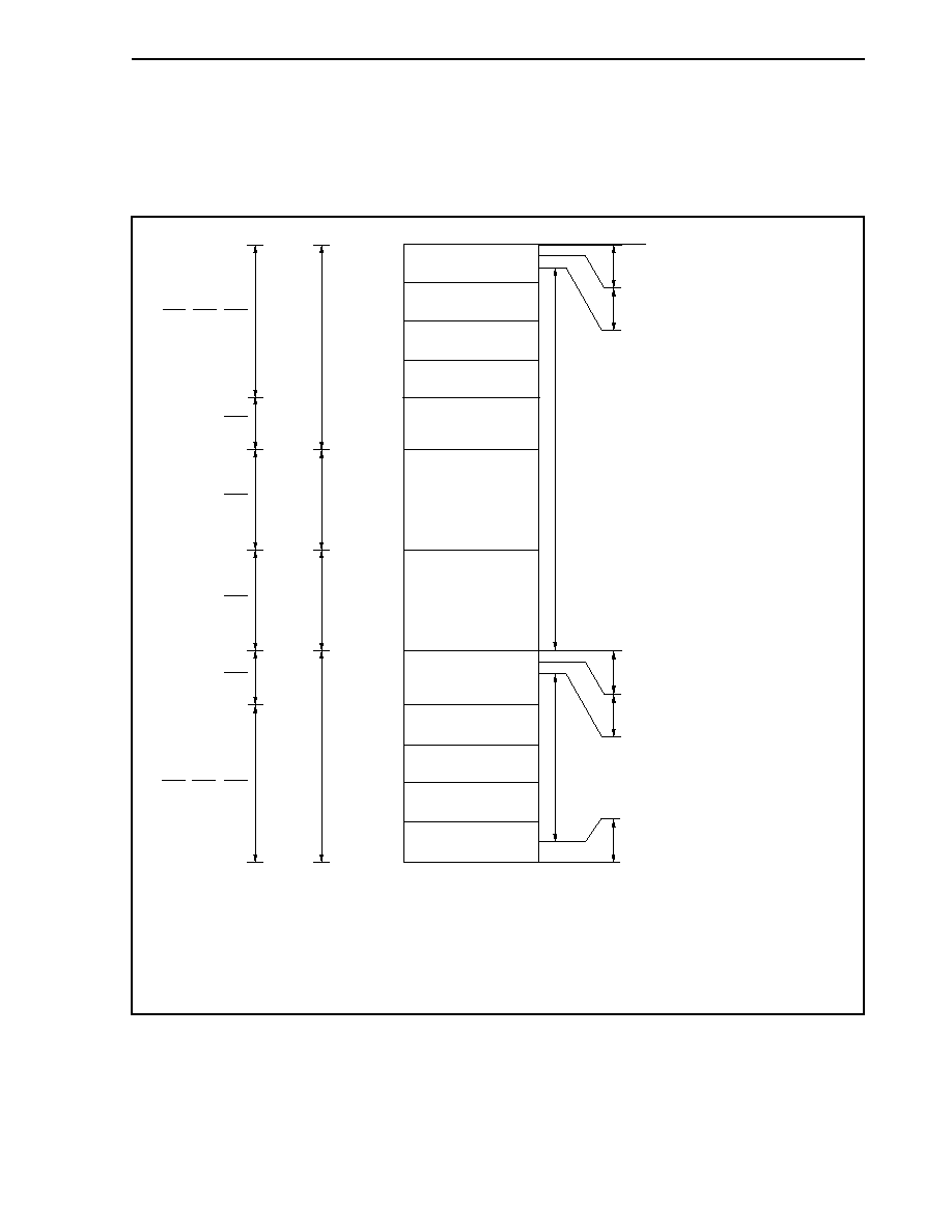
CHAPTER 4 BUS CONTROL FUNCTION
101
User's Manual U14492EJ5V0UD
4.3 Memory Block Function
The 256 MB memory space is divided into memory blocks of 2 MB and 64 MB units. The programmable wait
function and bus cycle operation mode can be independently controlled for each block.
The area that can be used as program area is the 64 MB space of addresses 0000000H to 3FFFFFFH.
FFFFFFFH
FFFFFFFH
On-chip peripheral I/O area (4 KB)
Internal RAM area (12 KB
Note 1
)
External memory area
External memory area
FFFC000H
FE00000H
FDFFFFFH
FFFF000H
FFFEFFFH
FC00000H
FBFFFFFH
FA00000H
F9FFFFFH
F800000H
F7FFFFFH
C000000H
BFFFFFFH
8000000H
7FFFFFFH
4000000H
3FFFFFFH
0800000H
07FFFFFH
0600000H
05FFFFFH
0400000H
03FFFFFH
0200000H
01FFFFFH
0000000H
Block 1
(2 MB)
Block 0
(2 MB)
Block 2
(2 MB)
Block 3
(2 MB)
64 MB
64 MB
Block 5
(2 MB)
Block 6
(2 MB)
Block 4
(2 MB)
Block 7
(2 MB)
3FFFFFFH
On-chip peripheral I/O area (4 KB)
Note 2
Internal RAM area (12 KB
Note 1
)
3FFC000H
3FFF000H
3FFEFFFH
00FFFFFH
Internal ROM area (1 MB)
Note 3
0000000H
CS7, CS6, CS5
Area 3
Area 2
Area 1
Area 0
CS6
CS4
CS1
CS3
CS2, CS1, CS0
Notes 1. Physical internal RAM: 10 KB
2. Access to this area is prohibited. To access the on-chip peripheral I/O in this area, specify
addresses FFFF000H to FFFFFFFH.
3. When in single-chip mode 1 and ROMless modes 0 and 1, this becomes an external memory area.
When in single-chip mode 1, addresses 0100000H to 01FFFFFH become an internal ROM area.

CHAPTER 4 BUS CONTROL FUNCTION
102
User's Manual U14492EJ5V0UD
4.3.1 Chip select control function
Of the 256 MB memory area, the lower 8 MB (0000000H to 07FFFFFH) and the higher 8 MB (F800000H to
FFFFFFFH) can be divided into 2 MB memory blocks by chip area selection control registers 0 and 1 (CSC0, CSC1)
to control the chip select signal.
The memory area can be effectively used by dividing it into memory blocks using the chip select control function.
The priority order is described below.
(1) Chip area selection control registers 0, 1 (CSC0, CSC1)
These registers can be read/written in 16-bit units and become valid by setting each bit to 1.
If different chip select signal outputs are set to the same block, the priority order is controlled as follows.
CSC0: CS0 > CS2 > CS1
CSC1: CS7 > CS5 > CS6
If both the CS0m and CS2m bits of the CSC0 register are set to 0, CS1 is output to the corresponding block
(m = 0 to 3).
Similarly, if both the CS5m and CS7m bits of the CSC1 register are set to 0, CS6 is output to the
corresponding block (m = 0 to 3).
Caution Write to the CSC0 and CSC1 registers after reset, and then do not change the set values.

CHAPTER 4 BUS CONTROL FUNCTION
103
User's Manual U14492EJ5V0UD
15
CS33
CSC0
Address
FFFFF060H
Initial value
2C11H
14
CS32
13
CS31
12
CS30
11
CS23
10
CS22
9
CS21
8
CS20
7
CS13
6
CS12
5
CS11
4
CS10
3
CS03
2
CS02
1
CS01
0
CS00
15
CS43
CSC1
Address
FFFFF062H
Initial value
2C11H
14
CS42
13
CS41
12
CS40
11
CS53
10
CS52
9
CS51
8
CS50
7
CS63
6
CS62
5
CS61
4
CS60
3
CS73
2
CS72
1
CS71
0
CS70
Bit position
Bit name
Function
Chip select enabled by setting CSnm bit to 1.
CSnm CS
operation
CS00
CS0 output during block 0 access
CS01
CS0 output during block 1 access
CS02
CS0 output during block 2 access
CS03
CS0 output during block 3 access
CS10 to CS13
Note 1
CS20
CS2 output during block 0 access
CS21
CS2 output during block 1 access
CS22
CS2 output during block 2 access
CS23
CS2 output during block 3 access
CS30 to CS33
Note 2
CS40 to CS43
Note 3
CS50
CS5 output during block 7 access
CS51
CS5 output during block 6 access
CS52
CS5 output during block 5 access
CS53
CS5 output during block 4 access
CS60 to CS63
Note 4
CS70
CS7 output during block 7 access
CS71
CS7 output during block 6 access
CS72
CS7 output during block 5 access
CS73
CS7 output during block 4 access
15 to 0
CSnm
(n = 0 to 7)
(m = 0 to 3)
Notes 1. If both the CS0m and CS2m bits have been set to 0, if area 0 is accessed, CS1 will be output
regardless of the setting of the CS1m bit.
2. When area 1 is accessed, CS3 will be output regardless of the setting of the CS3m bit.
3. When area 2 is accessed, CS4 will be output regardless of the setting of the CS4m bit.
4. If both the CS5m and CS7m bits have been set to 0, if area 3 is accessed, CS6 will be output
regardless of the setting of the CS6m bit.
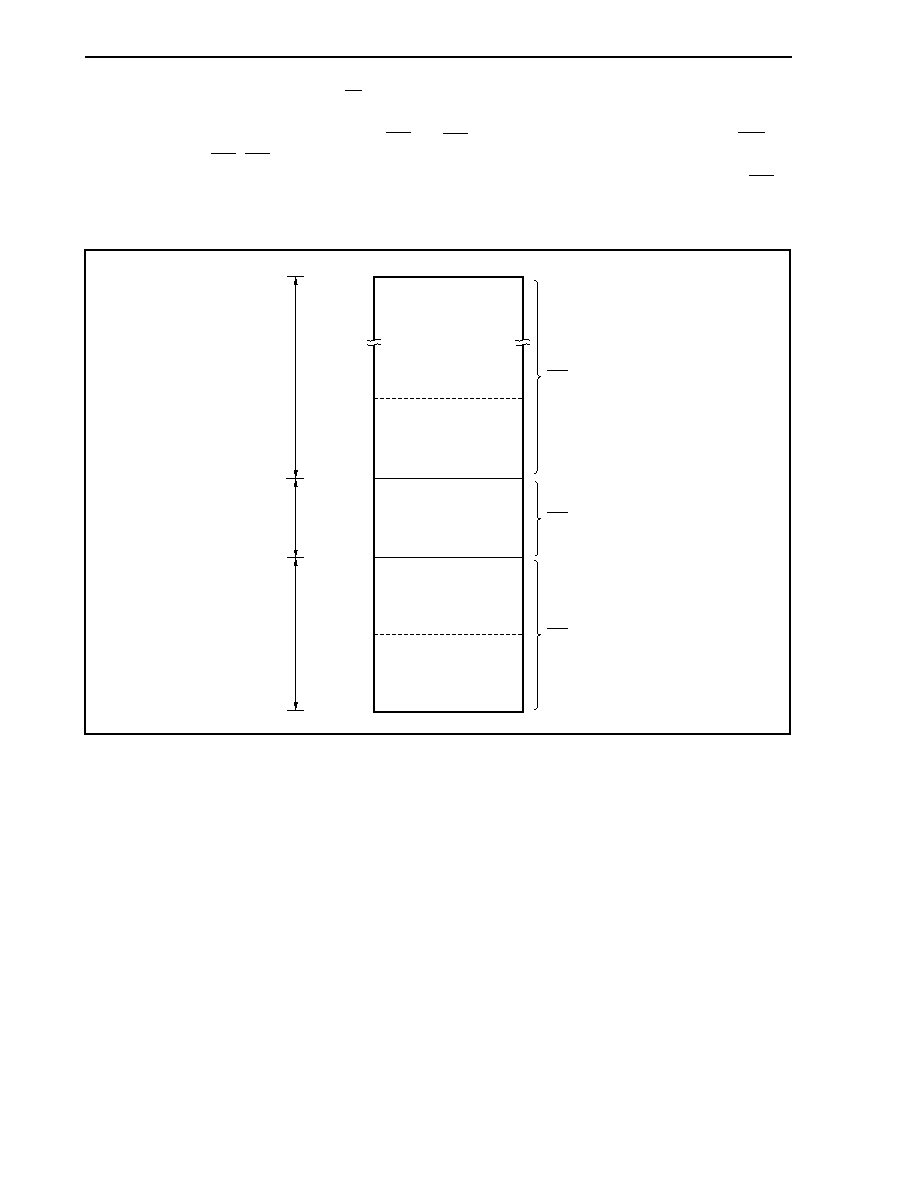
CHAPTER 4 BUS CONTROL FUNCTION
104
User's Manual U14492EJ5V0UD
The following diagram shows the CS signal, which is enabled for area 0 when the CSC0 register is set to
0703H.
When the CSC0 register is set to 0703H, CS0 and CS2 are output to block 0 and block 1, but since CS0 has
priority over CS2, CS0 is output if the addresses of block 0 and block 1 are accessed.
If the address of block 3 is accessed, both the CS03 and CS23 bits of the CSC0 register are 0, and CS1 is
output.
Figure 4-1. Example When CSC0 Register Is Set to 0703H
3FFFFFFH
0600000H
05FFFFFH
0800000H
07FFFFFH
0400000H
03FFFFFH
0200000H
01FFFFFH
0000000H
Block 2
(2 MB)
Block 3
(2 MB)
Block 1
(2 MB)
Block 0
(2 MB)
CS1 is output.
CS2 is output.
CS0 is output.
58 MB
2 MB
4 MB
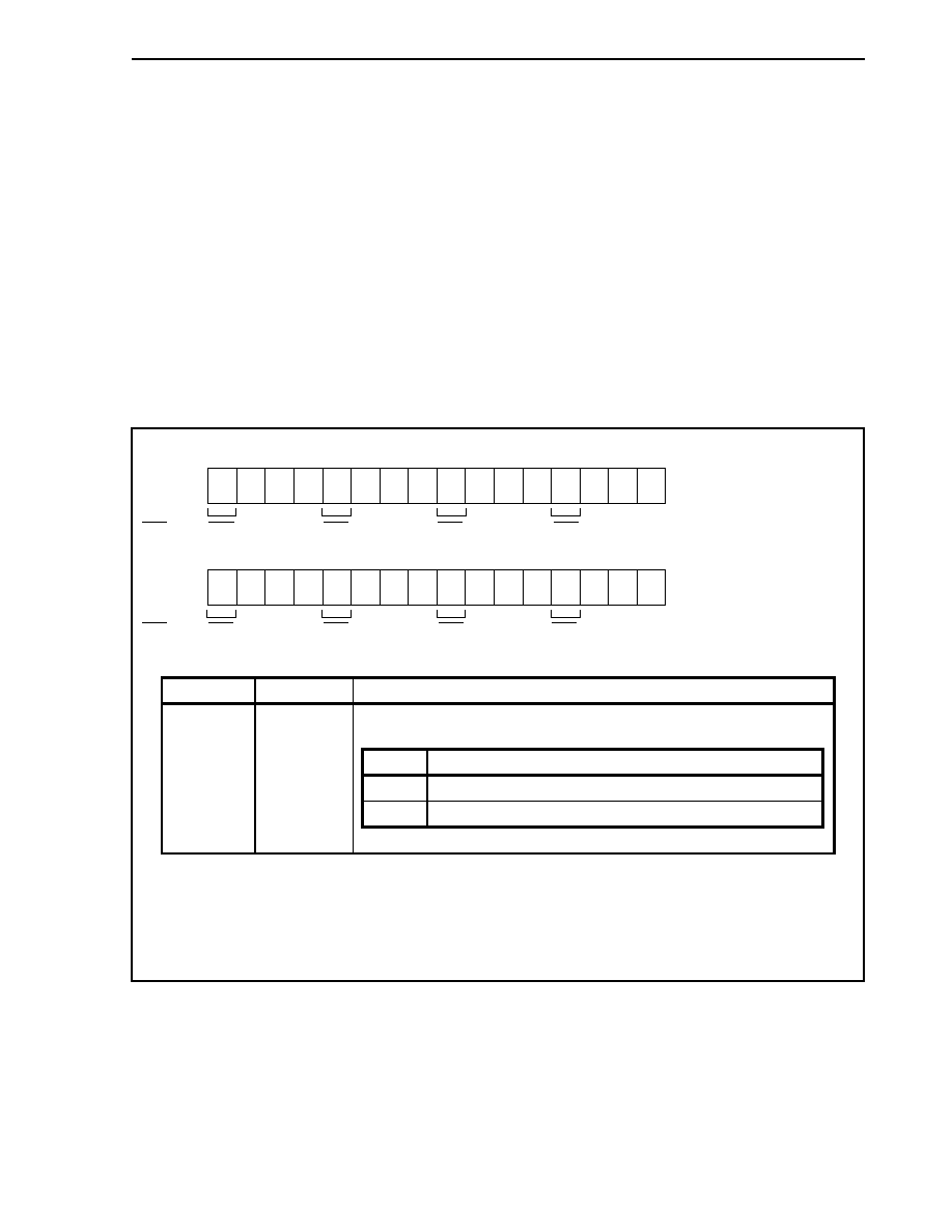
CHAPTER 4 BUS CONTROL FUNCTION
105
User's Manual U14492EJ5V0UD
4.4 Bus Cycle Type Control Function
In the V850E/IA1, the following external devices can be connected directly to each memory block.
∑ SRAM, external ROM, external I/O
Connected external devices are specified by bus cycle type configuration registers 0, 1 (BCT0, BCT1).
(1) Bus cycle type configuration registers 0, 1 (BCT0, BCT1)
These registers can be read/written in 16-bit units.
Caution Write to the BCT0 and BCT1 registers after reset, and then do not change the set values.
Also, do not access an external memory area other than the one for this initialization
routine until the initial setting of the BCT0 and BCT1 registers is complete. However, it is
possible to access external memory areas whose initial settings are complete.
15
ME3
BCT0
CSn signal
Address
FFFFF480H
Initial value
CCCCH
14
1
1
0
0
13
12
11
ME2
10
9
0
0
0
0
8
7
ME1
6
1
5
4
3
ME0
2
1
1
0
0
0
CS3
CS2
CS1
CS0
15
ME7
BCT1
CSn signal
Address
FFFFF482H
Initial value
CCCCH
14
1
13
0
0
0
0
12
11
ME6
10
1
9
8
7
ME5
6
1
5
0
0
0
0
4
3
ME4
2
1
1
0
CS6
CS5
CS4
CS7
Bit position
Bit name
Function
Sets memory controller operation enable for each chip select
Note
.
MEn
Memory controller operation enable
0
Operation disabled
1
Operation enabled
15, 11, 7, 3
(BCT0),
15, 11, 7, 3
(BCT1)
MEn
(n = 0 to 7)
Note Set the BCT1.ME6 and BCT1.ME5 bits to 11B (operation enable) when an external memory is
connected to the CS5 area or CS6 area.
Set the PMCCS register to x01xxxxxB when only CS5 is connected to the external memory and CS6
is used as a port (PCS6), and set the PMCCS register to x10xxxxxB when only CS6 is connected to
the external memory and CS5 is used as a port (PCS5).
CHAPTER 4 BUS CONTROL FUNCTION
106
User's Manual U14492EJ5V0UD
4.5 Bus
Access
4.5.1 Number
of access clocks
The number of base clocks required to access each resource is shown below.
Bus Cycle Status
Resource (Bus Width)
Instruction Fetch
Operand Data Access
Internal ROM (32 bits)
1
Note 1
5
Internal RAM (32 bits)
1
Note 2
1
On-chip peripheral I/O (16 bits)
-
5
Note 3
Programmable peripheral I/O
-
5
Note 3
External memory (16 bits)
3
Note 3
3
Note 3
Notes 1. This value is 2 in the case of instruction branch
2. This value is 2 if there is contention with data access.
3. MIN. value
Remark Unit: Clock/access
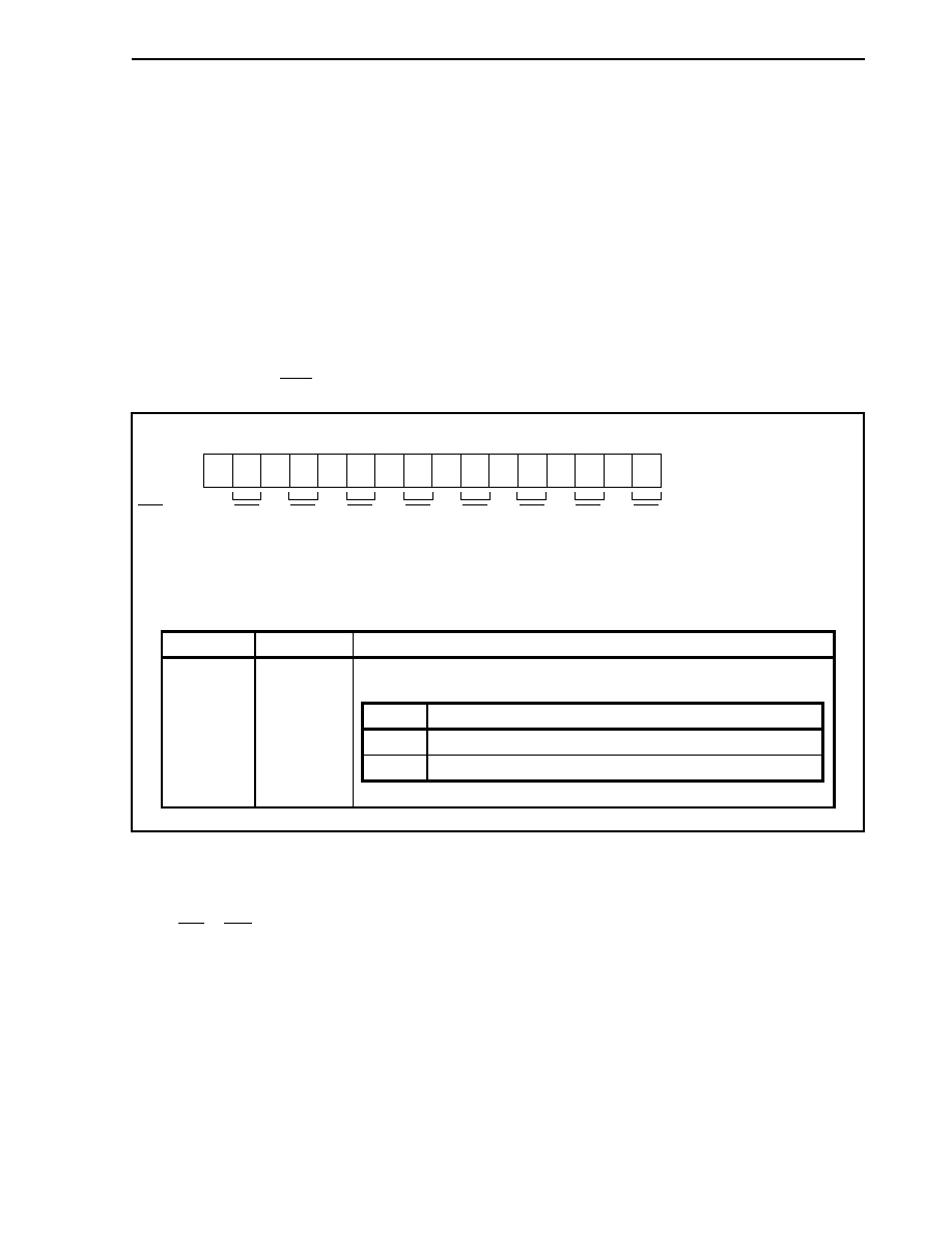
CHAPTER 4 BUS CONTROL FUNCTION
107
User's Manual U14492EJ5V0UD
4.5.2 Bus sizing function
The bus sizing function controls the data bus width for each CS space. The data bus width is specified by using
the bus size configuration register (BSC).
(1) Bus size configuration register (BSC)
This register can be read/written in 16-bit units.
Cautions 1. Write to the BSC register after reset, and then do not change the set values. Also, do
not access an external memory area other than the one for this initialization routine
until the initial setting of the BSC register is complete. However, it is possible to
access external memory areas whose initial settings are complete.
2.
When the data bus width is specified as 8 bits, only the signals shown below become
active.
LWR: When accessing SRAM, external ROM, or external I/O (write cycle)
15
0
BSC
CSn signal
Address
FFFFF066H
Initial value
Note
0000H/5555H
14
BS70
13
0
12
BS60
11
0
10
BS50
9
0
8
BS40
7
0
6
BS30
5
0
4
BS20
3
0
2
BS10
1
0
0
BS00
CS3
CS2
CS1
CS0
CS4
CS5
CS6
CS7
Note When in single-chip mode 0, 1: 5555H
When in ROMless mode 0:
5555H
When in ROMless mode 1:
0000H
Bit position
Bit name
Function
Sets the data bus width of CSn space.
BSn0
Data bus width of CSn space
0
8 bits
1
16 bits
14, 12, 10, 8,
6, 4, 2, 0
BSn0
(n = 0 to 7)
4.5.3 Word data processing format
The word data in memory can be processed using the little endian method for CS space selected with a chip select
signal (CS0 to CS7).
CHAPTER 4 BUS CONTROL FUNCTION
108
User's Manual U14492EJ5V0UD
4.5.4 Bus width
The V850E/IA1 accesses on-chip peripheral I/O and external memory in 8-bit, 16-bit, or 32-bit units. The following
shows the operation for each type of access. Access all data in order starting from the lower side.
(1) Byte access (8 bits)
(a) When the data bus width is 16 bits (little endian)
<1> Access to even address (2n)
<2> Access to odd address (2n + 1)
7
0
7
0
Byte data
15
8
External
data bus
2n
Address
7
0
7
0
Byte data
15
8
External
data bus
2n + 1
Address
(b) When the data bus width is 8 bits (little endian)
<1> Access to even address (2n)
<2> Access to odd address (2n + 1)
7
0
7
0
Byte data
External
data bus
2n
Address
7
0
7
0
Byte data
External
data bus
2n + 1
Address
CHAPTER 4 BUS CONTROL FUNCTION
109
User's Manual U14492EJ5V0UD
(2) Halfword access (16 bits)
(a) When the data bus width is 16 bits (little endian)
<1> Access to even address (2n)
<2> Access to odd address (2n + 1)
1st access
2nd access
7
0
7
0
Halfword
data
15
8
External
data bus
2n
Address
15
8
2n + 1
7
0
7
0
Halfword
data
15
8
15
8
External
data bus
2n + 1
Address
7
0
7
0
Halfword
data
15
8
15
8
External
data bus
2n + 2
Address
2n
(b) When the data bus width is 8 bits (little endian)
<1> Access to even address (2n)
<2> Access to odd address (2n + 1)
1st access
2nd access
1st access
2nd access
7
0
7
0
Halfword
data
15
8
External
data bus
Address
7
0
7
0
Halfword
data
15
8
External
data bus
2n + 1
Address
2n
7
0
7
0
Halfword
data
15
8
External
data bus
Address
7
0
7
0
Halfword
data
15
8
External
data bus
2n + 2
Address
2n + 1
CHAPTER 4 BUS CONTROL FUNCTION
110
User's Manual U14492EJ5V0UD
(3) Word access (32 bits)
(a) When the data bus width is 16 bits (little endian) (1/2)
<1> Access to address (4n)
1st access
2nd access
7
0
7
0
Word data
15
8
External
data bus
4n
Address
15
8
4n + 1
23
16
31
24
7
0
7
0
Word data
15
8
External
data bus
4n + 2
Address
15
8
4n + 3
23
16
31
24
<2> Access to address (4n + 1)
1st access
2nd access
3rd access
7
0
7
0
Word data
15
8
External
data bus
Address
15
8
4n + 1
23
16
31
24
7
0
7
0
Word data
15
8
External
data bus
4n + 2
Address
15
8
4n + 3
23
16
31
24
7
0
7
0
Word data
15
8
External
data bus
4n + 4
Address
15
8
23
16
31
24
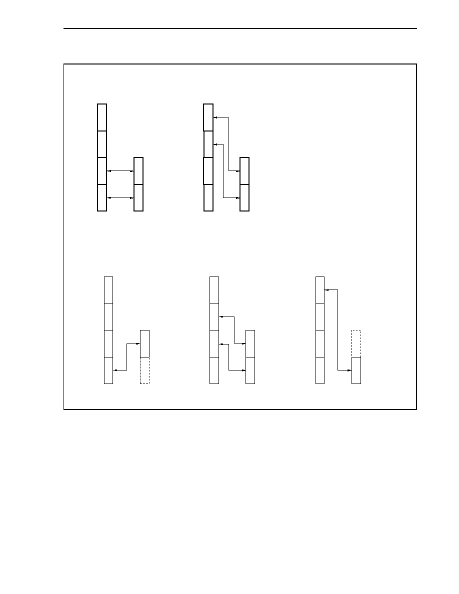
CHAPTER 4 BUS CONTROL FUNCTION
111
User's Manual U14492EJ5V0UD
(a) When the data bus width is 16 bits (little endian) (2/2)
<3> Access to address (4n + 2)
1st access
2nd access
7
0
7
0
Word data
15
8
External
data bus
4n + 2
Address
15
8
4n + 3
23
16
31
24
7
0
7
0
Word data
15
8
External
data bus
4n + 4
Address
15
8
4n + 5
23
16
31
24
<4> Access to address (4n + 3)
1st access
2nd access
3rd access
7
0
7
0
Word data
15
8
External
data bus
Address
15
8
4n + 3
23
16
31
24
7
0
7
0
Word data
15
8
External
data bus
4n + 4
Address
15
8
4n + 5
23
16
31
24
7
0
7
0
Word data
15
8
External
data bus
4n + 6
Address
15
8
23
16
31
24
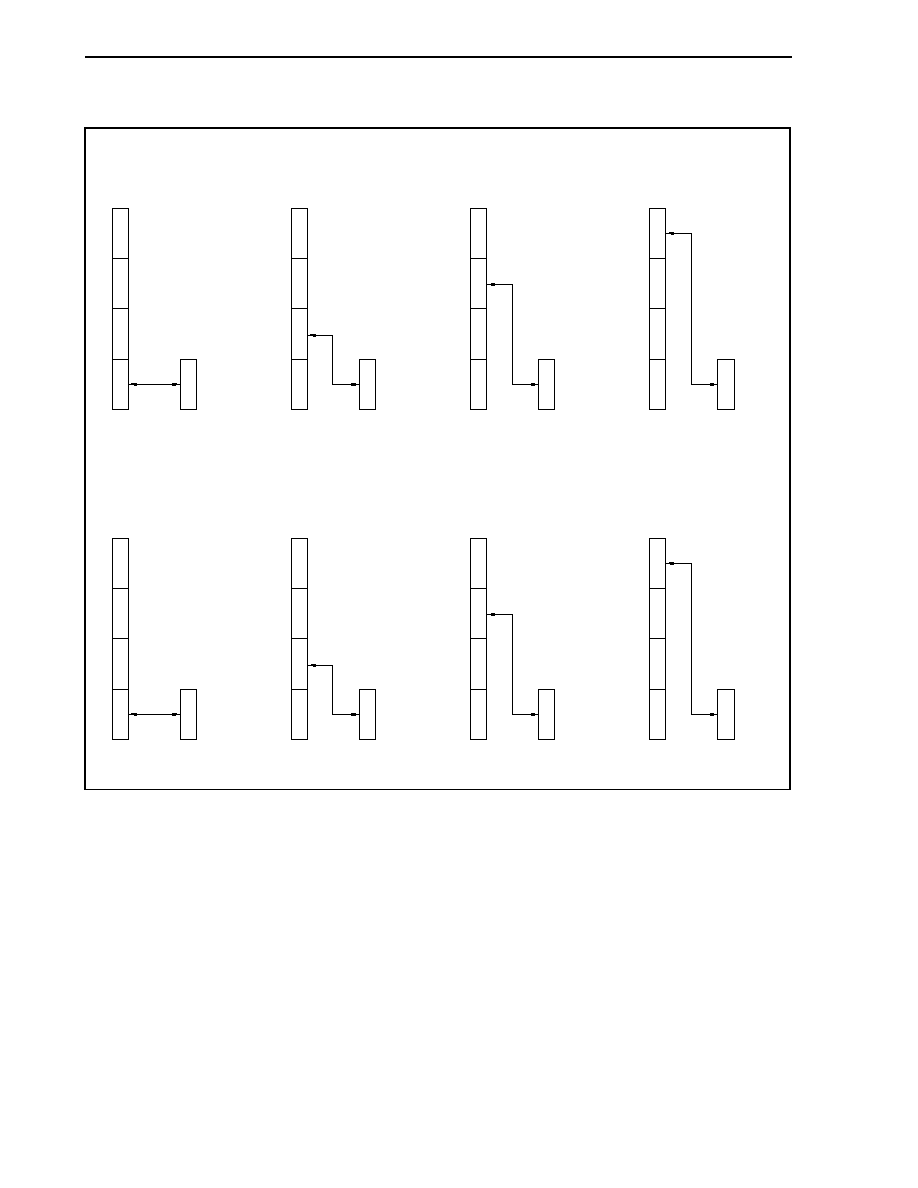
CHAPTER 4 BUS CONTROL FUNCTION
112
User's Manual U14492EJ5V0UD
(b) When the data bus width is 8 bits (little endian) (1/2)
<1> Access to address (4n)
1st access
2nd access
3rd access
4th access
7
0
7
0
Word data
External
data bus
Address
15
8
4n
23
16
31
24
7
0
7
0
Word data
External
data bus
4n + 1
Address
15
8
23
16
31
24
7
0
7
0
Word data
External
data bus
4n + 2
Address
15
8
23
16
31
24
7
0
7
0
Word data
External
data bus
4n + 3
Address
15
8
23
16
31
24
<2> Access to address (4n + 1)
1st access
2nd access
3rd access
4th access
7
0
7
0
Word data
External
data bus
Address
15
8
4n + 1
23
16
31
24
7
0
7
0
Word data
External
data bus
4n + 2
Address
15
8
23
16
31
24
7
0
7
0
Word data
External
data bus
4n + 3
Address
15
8
23
16
31
24
7
0
7
0
Word data
External
data bus
4n + 4
Address
15
8
23
16
31
24

CHAPTER 4 BUS CONTROL FUNCTION
113
User's Manual U14492EJ5V0UD
(b) When the data bus width is 8 bits (little endian) (2/2)
<3> Access to address (4n + 2)
1st access
2nd access
3rd access
4th access
7
0
7
0
Word data
External
data bus
Address
15
8
4n + 2
23
16
31
24
7
0
7
0
Word data
External
data bus
4n + 3
Address
15
8
23
16
31
24
7
0
7
0
Word data
External
data bus
4n + 4
Address
15
8
23
16
31
24
7
0
7
0
Word data
External
data bus
4n + 5
Address
15
8
23
16
31
24
<4> Access to address (4n + 3)
1st access
2nd access
3rd access
4th access
7
0
7
0
Word data
External
data bus
Address
15
8
4n + 3
23
16
31
24
7
0
7
0
Word data
External
data bus
4n + 4
Address
15
8
23
16
31
24
7
0
7
0
Word data
External
data bus
4n + 5
Address
15
8
23
16
31
24
7
0
7
0
Word data
External
data bus
4n + 6
Address
15
8
23
16
31
24
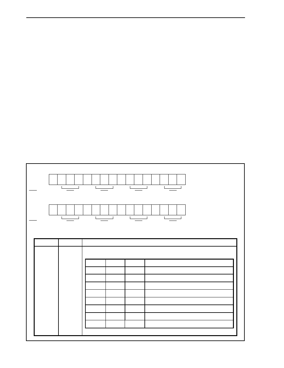
CHAPTER 4 BUS CONTROL FUNCTION
114
User's Manual U14492EJ5V0UD
4.6 Wait
Function
4.6.1 Programmable wait function
(1) Data wait control registers 0, 1 (DWC0, DWC1)
To facilitate interfacing with low-speed memory or with I/Os, it is possible to insert up to 7 data wait states in
the starting bus cycle for each CS space.
The number of wait states can be specified by program using data wait control registers 0 and 1 (DWC0,
DWC1). Just after system reset, all blocks have 3 data wait states inserted.
These registers can be read/written in 16-bit units.
Cautions 1. The internal ROM area and internal RAM area are not subject to programmable waits
and ordinarily no wait access is carried out. The on-chip peripheral I/O area is also
not subject to programmable wait states, with wait control performed by each
peripheral function only.
2. Write to the DWC0 and DWC1 registers after reset, and then do not change the set
values. Also, do not access an external memory area other than the one for this
initialization routine until the initial setting of the DWC0 and DWC1 registers is
complete. However, it is possible to access external memory areas whose initial
settings are complete.
15
DWC0
CSn signal
Address
FFFFF484H
Initial value
3333H
14
13
12
11
10
9
8
7
6
5
4
3
2
1
0
0
DW32 DW31 DW30
0
DW22 DW21 DW20
0
DW12 DW11 DW10
0
DW02 DW01 DW00
0
DW72 DW71 DW70
0
DW62 DW61 DW60
0
DW52 DW51 DW50
0
DW42 DW41 DW40
CS3
CS2
CS1
CS0
CS7
CS6
CS5
CS4
15
DWC1
CSn signal
Address
FFFFF486H
Initial value
3333H
14
13
12
11
10
9
8
7
6
5
4
3
2
1
0
Bit position
Bit name
Function
Specifies the number of wait states inserted in the CSn space.
DWn2
DWn1
DWn0
Number of wait states inserted in CSn space
0 0 0
Not
inserted
0 0 1
1
0 1 0
2
0 1 1
3
1 0 0
4
1 0 1
5
1 1 0
6
1 1 1
7
14 to 12,
10 to 8,
6 to 4,
2 to 0
DWn2 to
DWn0
(n = 0 to 7)

CHAPTER 4 BUS CONTROL FUNCTION
115
User's Manual U14492EJ5V0UD
(2) Address wait control register (AWC)
In the V850E/IA1, address setup wait and address hold wait states can be inserted before and after the T1
cycle, respectively.
These wait states can be set for each CS space via the AWC register.
This register can be read/written in 16-bit units.
Caution Write to the AWC register after reset, and then do not change the set values.
CS4
CS0
AWC
CSn signal
15
AHW7
14
ASW7
13
AHW6
12
ASW6
11
AHW5
10
ASW5
9
AHW4
8
ASW4
7
AHW3
6
ASW3
5
AHW2
4
ASW2
3
AHW1
2
ASW1
1
AHW0
0
ASW0
Address
FFFFF488H
Initial value
0000H
CS7
CS6
CS5
CS3
CS2
CS1
Bit position
Bit name
Function
15, 13, 11, 9,
7, 5, 3, 1
AHWn
(n = 0 to 7)
Sets the insertion of an address hold wait state in each CSn space after the T1 cycle.
0: Address hold wait state not inserted
1: Address hold wait state inserted
14, 12, 10, 8,
6, 4, 2, 0
ASWn
(n = 0 to 7)
Sets the insertion of an address setup wait state in each CSn space before the T1 cycle.
0: Address setup wait state not inserted
1: Address setup wait state inserted
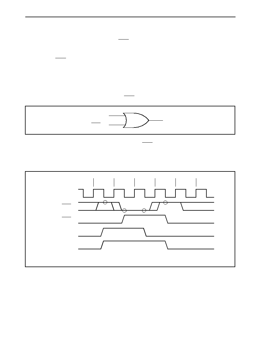
CHAPTER 4 BUS CONTROL FUNCTION
116
User's Manual U14492EJ5V0UD
4.6.2 External wait function
When an extremely slow device, I/O, or asynchronous system is connected, an arbitrary number of wait states can
be inserted in the bus cycle by the external wait pin (WAIT) for synchronization with the external device.
Just as with programmable waits, accessing internal ROM, internal RAM, and on-chip peripheral I/O areas cannot
be controlled by external waits.
The external WAIT signal can be input asynchronously to CLKOUT and is sampled at the falling edge of the
CLKOUT signal in the T2 and TW states of a bus cycle. If the setup/hold time in the sampling timing is not satisfied,
the wait state may or may not be inserted in the next state.
4.6.3 Relationship
between
programmable wait and external wait
A wait cycle is inserted as the result of an OR operation between the wait cycle specified by the set value of the
programmable wait and the wait cycle controlled by the WAIT pin.
Wait control
Programmable wait
Wait by WAIT pin
For example, if the timings of the programmable wait and the WAIT pin signal are as illustrated below, three wait
states will be inserted in the bus cycle.
Figure 4-2. Example of Wait Insertion
CLKOUT
WAIT pin
Wait by WAIT pin
Programmable wait
Wait control
T2
TW
TW
TW
T3
Remark The circles indicate the sampling timing.

CHAPTER 4 BUS CONTROL FUNCTION
117
User's Manual U14492EJ5V0UD
4.7 Idle State Insertion Function
To facilitate interfacing with low-speed memory devices, a set number of idle states (TI) can be inserted into the
starting bus cycle after the T3 state to secure the data output float delay time (t
DF
) of the memory when each CS
space is read accessed. The bus cycle following the T3 state starts after the inserted idle state(s).
Idle states are inserted at the following timing.
∑ After the read cycle for SRAM, external I/O, or external ROM.
The idle state insertion setting can be specified using the bus cycle control register (BCC). Idle state insertion is
automatically programmed for all memory blocks immediately after a system reset.
(1) Bus cycle control register (BCC)
This register can be read/written in 16-bit units.
Cautions 1. Idle states cannot be inserted in internal ROM, internal RAM, on-chip peripheral I/O, or
programmable peripheral I/O areas.
2. Write to the BCC register after reset, and then do not change the set values. Also, do
not access an external memory area other than the one for this initialization routine
until the initial setting for this register is complete. However, it is possible to access
external memory areas whose initial settings are complete.
CS4
CS0
BCC
CSn signal
15
BC71
14
0
0
0
0
0
0
0
0
13
BC61
12
11
BC51
10
9
BC41
8
7
BC31
6
5
BC21
4
3
BC11
2
1
BC01
0
Address
FFFFF48AH
Initial value
AAAAH
CS7
CS6
CS5
CS3
CS2
CS1
Bit position
Bit name
Function
15, 13, 11, 9,
7, 5, 3, 1
BCn1
(n = 0 to 7)
Specifies the insertion of idle states after the T3 state in each CSn space.
0: Idle state not inserted
1: Idle state inserted
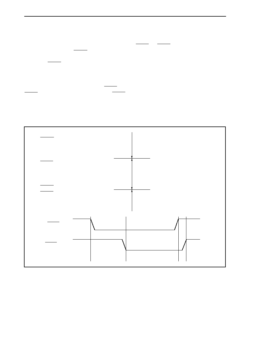
CHAPTER 4 BUS CONTROL FUNCTION
118
User's Manual U14492EJ5V0UD
4.8 Bus
Hold
Function
4.8.1 Function outline
If pins PCM2 and PCM3 are specified in the control mode, the HLDAK and HLDRQ functions become valid.
If it is determined that the HLDRQ pin has become active (low level) as a bus mastership request from another bus
master, the external address/data bus and each strobe pin are shifted to high impedance and then released (bus hold
state). If the HLDRQ pin becomes inactive (high level) and the bus mastership request is canceled, driving of these
pins begins again.
During the bus hold period, the internal operations of the V850E/IA1 continue until the external memory or on-chip
peripheral I/O register is accessed.
The bus hold state can be known by the HLDAK pin becoming active (low level). The period from when the
HLDRQ pin becomes active (low level) to when the HLDAK pin becomes active (low level) is at least 2 clocks.
In a multiprocessor configuration, etc., a system with multiple bus masters can be configured.
4.8.2 Bus hold procedure
The procedure of the bus hold function is illustrated below.
<1> HLDRQ = 0 accepted
<2> All bus cycle start requests held pending
<3> End of current bus cycle
<4> Transition to bus idle state
<5> HLDAK = 0
<6> HLDRQ = 1 accepted
<7> HLDAK = 1
<8> Releases pending bus cycle start request
<9> Start of bus cycle
Normal state
Bus hold state
Normal state
HLDAK (output)
HLDRQ (input)
<1> <2>
<3><4> <5>
<6> <7><8><9>
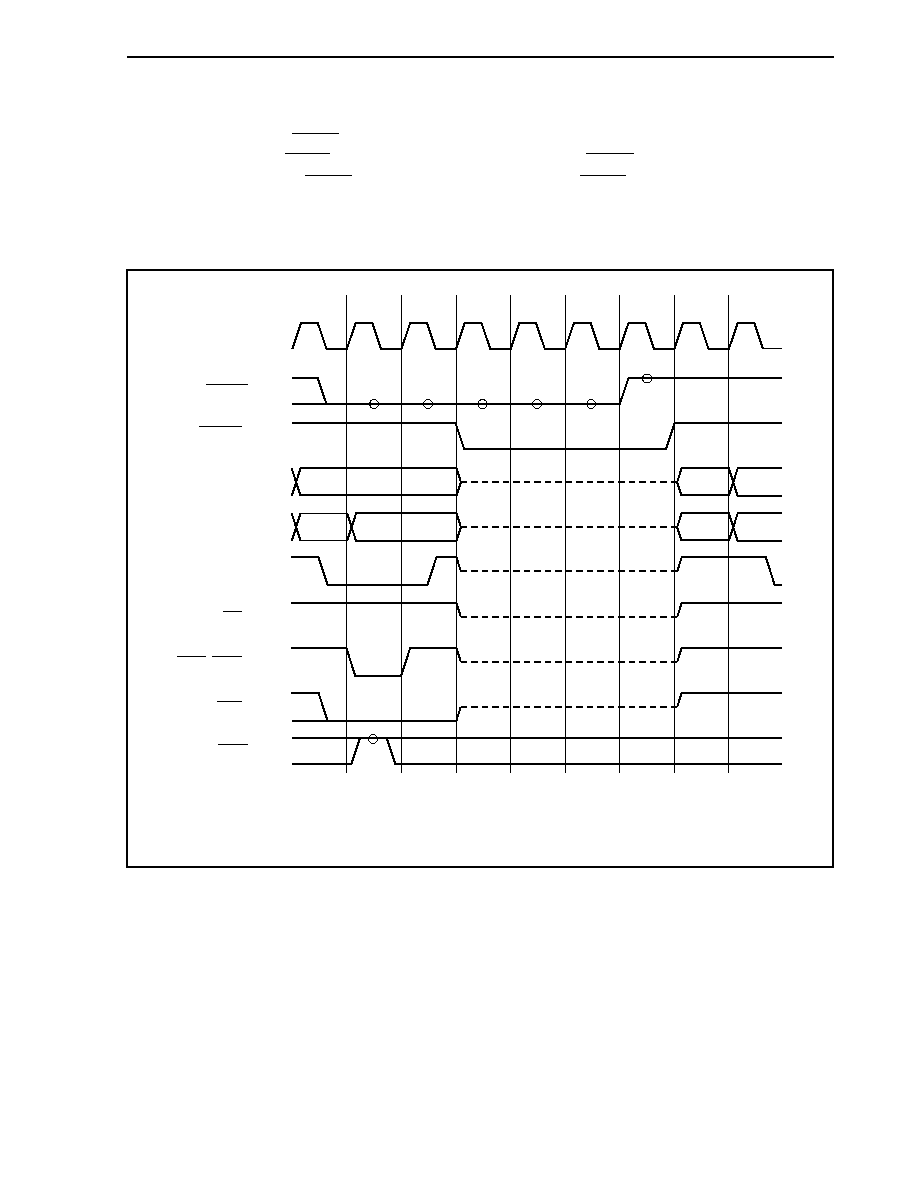
CHAPTER 4 BUS CONTROL FUNCTION
119
User's Manual U14492EJ5V0UD
4.8.3 Operation in power save mode
In the software STOP or IDLE mode, the internal system clock is stopped. Consequently, the bus hold state is not
accepted and set since the HLDRQ pin cannot be accepted even if it becomes active.
In the HALT mode, the HLDAK pin immediately becomes active when the HLDRQ pin becomes active, and the bus
hold state is set. When the HLDRQ pin becomes inactive after that, the HLDAK pin also becomes inactive. As a
result, the bus hold state is cleared and the HALT mode is set again.
4.8.4
Bus hold timing
T2
T3
TH
TH
TH
TH
TI
T1
CLKOUT (output)
HLDRQ (input)
HLDAK (output)
A16 to A23 (output)
AD0 to AD15 (I/O)
ASTB (output)
RD (output)
LWR, UWR (output)
CSn (output)
WAIT (input)
Address
Address
Undefined
Data
Address
Address
Undefined
Remarks 1. The circles indicate the sampling timing.
2. The broken lines indicate the high-impedance state.
3. n = 0 to 7
CHAPTER 4 BUS CONTROL FUNCTION
120
User's Manual U14492EJ5V0UD
4.9 Bus Priority Order
There are four external bus cycles: bus hold, DMA cycle, operand data access, and instruction fetch.
In order of priority, bus hold is the highest, followed by DMA cycle, operand data access, and instruction fetch, in
that order.
An instruction fetch may be inserted between a read access and write access during a read modify write access.
Also, an instruction fetch may be inserted between bus accesses when the CPU bus is locked.
Table 4-1. Bus Priority Order
Priority
Order
External Bus Cycle
Bus Master
High
Bus hold
External device
DMA cycle
DMA controller
Operand data access
CPU
Low Instruction
fetch
CPU
4.10 Boundary Operation Conditions
4.10.1 Program space
(1) Branching to the on-chip peripheral I/O area or successive fetches from the internal RAM area to the on-chip
peripheral I/O area are prohibited. If the above is performed (branching or successive fetch), a data to be
fetched is undefined and the operation is not guaranteed.
(2) If a branch instruction exists at the upper limit of the internal RAM area, a prefetch operation (invalid fetch)
that straddles over the on-chip peripheral I/O area does not occur.
4.10.2
Data space
The V850E/IA1 is provided with an address misalign function.
Through this function, regardless of the data format (word data or halfword data), data can be allocated to all
addresses. However, in the case of word data and halfword data, if the data is not subject to boundary alignment, the
bus cycle will be generated at least 2 times and bus efficiency will drop.
(1) In the case of halfword-length data access
When the address's LSB is 1, the byte-length bus cycle will be generated 2 times.
(2) In the case of word-length data access
(a) When the address's LSB is 1, bus cycles will be generated in the order of byte-length bus cycle,
halfword-length bus cycle, and byte-length bus cycle.
(b) When the address's lowest 2 bits are 10, the halfword-length bus cycle will be generated 2 times.

121
User's Manual U14492EJ5V0UD
CHAPTER 5 MEMORY ACCESS CONTROL FUNCTION
5.1 SRAM, External ROM, External I/O Interface
5.1.1 Features
∑ SRAM is accessed in a minimum of 2 states.
∑ A maximum of 7 programmable data wait states can be inserted according to DWC0 and DWC1 register
settings.
∑ Data waits can be controlled by WAIT pin input.
∑ An idle state (1 state) can be inserted after a read/write cycle by setting the BCC register.
∑ An address hold wait state or address setup wait state can be inserted by setting the AWC register.
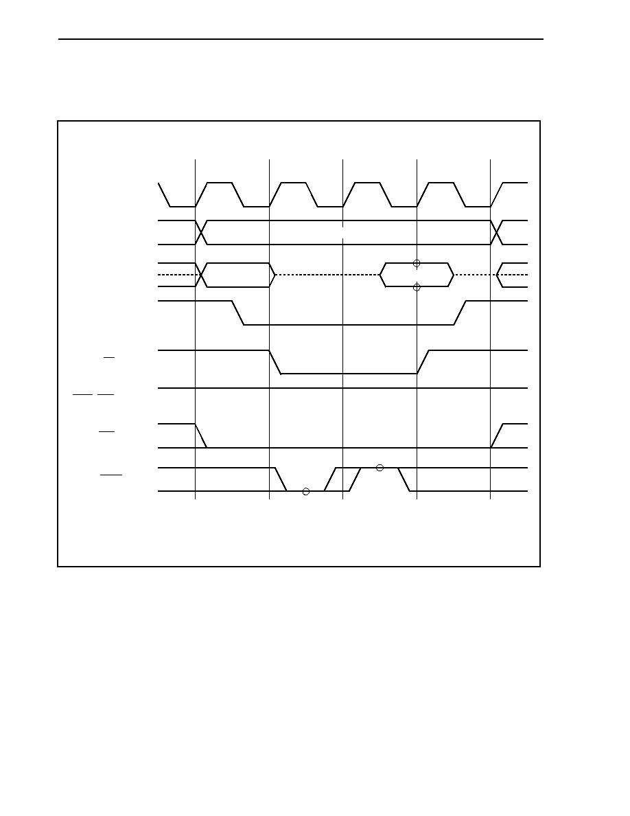
CHAPTER 5 MEMORY ACCESS CONTROL FUNCTION
122
User's Manual U14492EJ5V0UD
5.1.2
SRAM, external ROM, external I/O access
Figure 5-1. SRAM, External ROM, External I/O Access Timing (1/5)
(a) On a read (1 wait insertion)
T1
T2
TW
T3
Address
Data
H
CLKOUT (Output)
A16 to A23 (Output)
AD0 to AD15 (I/O)
ASTB (Output)
RD (Output)
UWR, LWR (Output)
CSn (Output)
WAIT (Input)
Address
Remarks 1. The circles indicate the sampling timing.
2. Broken lines indicate high impedance.
3. n = 0 to 7
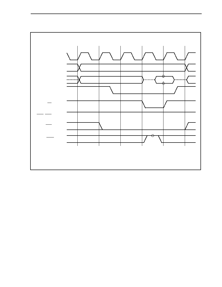
CHAPTER 5 MEMORY ACCESS CONTROL FUNCTION
123
User's Manual U14492EJ5V0UD
Figure 5-1. SRAM, External ROM, External I/O Access Timing (2/5)
(b) On a read (0 wait, address setup wait, address hold wait state insertion)
TASW
T1
TAHW
Address
Address
T2
T3
Data
H
CLKOUT (Output)
A16 to A23 (Output)
AD0 to AD15 (I/O)
ASTB (Output)
RD (Output)
UWR, LWR (Output)
CSn (Output)
WAIT (Input)
Remarks 1. The circles indicate the sampling timing.
2. Broken lines indicate high impedance.
3. n = 0 to 7
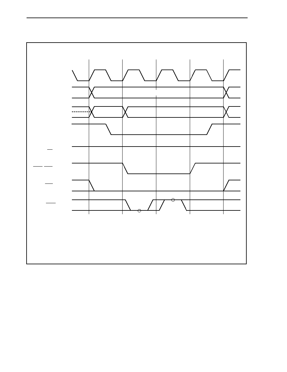
CHAPTER 5 MEMORY ACCESS CONTROL FUNCTION
124
User's Manual U14492EJ5V0UD
Figure 5-1. SRAM, External ROM, External I/O Access Timing (3/5)
(c) On a write (1 wait insertion)
T1
T2
TW
T3
Address
Data
Note
H
CLKOUT (Output)
A16 to A23 (Output)
AD0 to AD15 (I/O)
ASTB (Output)
RD (Output)
UWR, LWR (Output)
CSn (Output)
WAIT (Input)
Address
Note AD0 to AD7 output invalid data when accessed to odd-numbered address byte data.
AD8 to AD15 output invalid data when accessed to even-numbered address byte data.
Remarks 1. The circles indicate the sampling timing.
2. Broken lines indicate high impedance.
3. n = 0 to 7

CHAPTER 5 MEMORY ACCESS CONTROL FUNCTION
125
User's Manual U14492EJ5V0UD
Figure 5-1. SRAM, External ROM, External I/O Access Timing (4/5)
(d) On a write (0 wait insertion, for 8-bit data bus)
T1
T2
T3
Address
Address
Address
H
CLKOUT (Output)
A16 to A23 (Output)
AD8 to AD15 (I/O)
AD0 to AD7 (I/O)
ASTB (Output)
RD (Output)
UWR, LWR (Output)
CSn (Output)
WAIT (Input)
Data
Note
Note AD0 to AD7 output invalid data when accessed to odd-numbered address byte data.
Remarks 1. The circles indicate the sampling timing.
2. Broken lines indicate high impedance.
3. n = 0 to 7
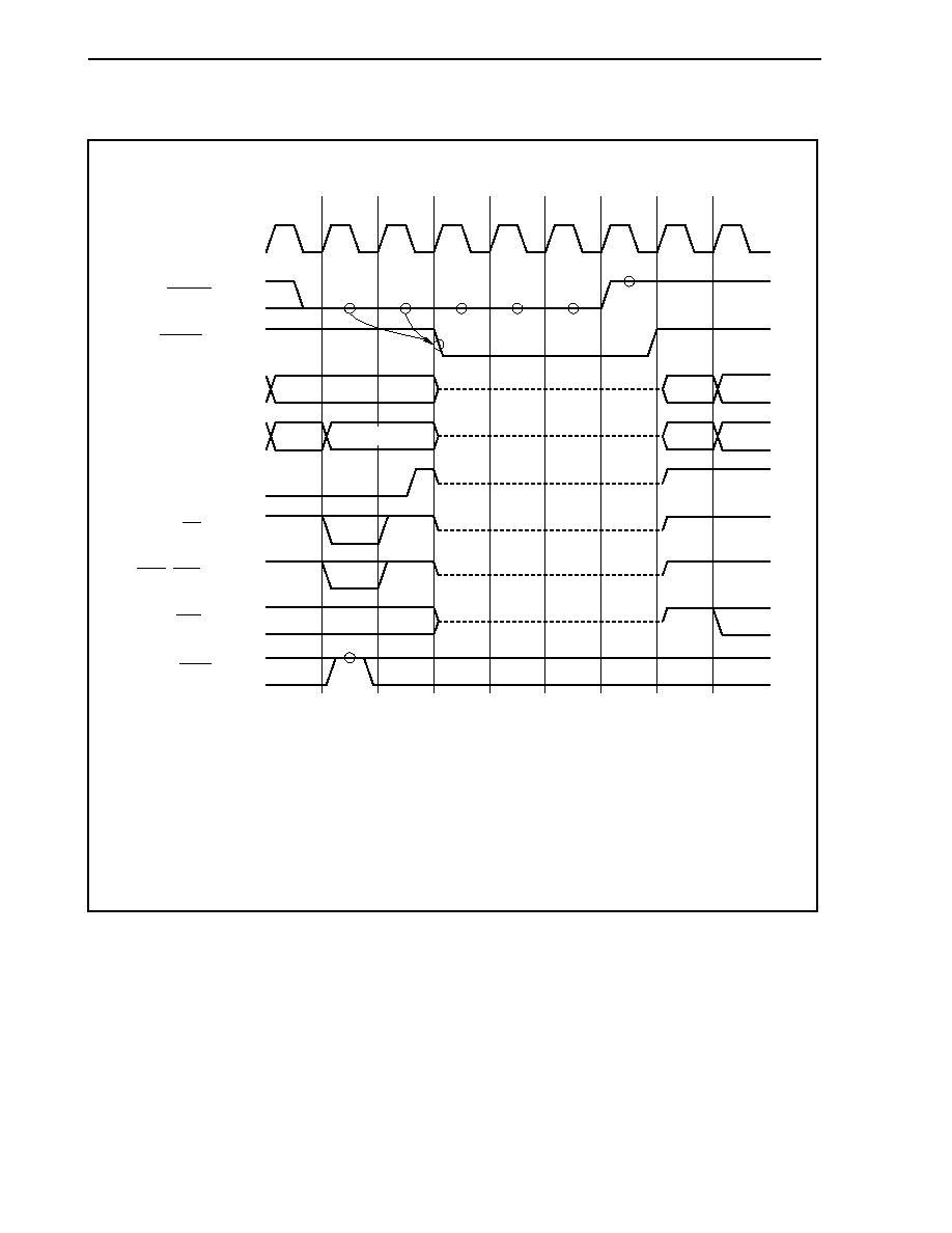
CHAPTER 5 MEMORY ACCESS CONTROL FUNCTION
126
User's Manual U14492EJ5V0UD
Figure 5-1. SRAM, External ROM, External I/O Access Timing (5/5)
(e) Bus hold timing
T2
Note 1
Address
Undefined
Note 2
Address
Undefined
T3
TH
TH
TH
TH
TI
T1
CLKOUT (Output)
A16 to A23 (Output)
AD0 to AD15 (I/O)
HLDAK (Output)
ASTB (Output)
RD (Output)
UWR, LWR (Output)
CSn (Output)
HLDRQ (Input)
WAIT (Input)
Undefined
Notes 1. On a read: Undefined
On a write: Address
2. On a read: Data
On a write: Undefined
Remarks 1. The circles indicate the sampling timing.
2. Broken lines indicate high impedance.
3.
n = 0 to 7

127
User's Manual U14492EJ5V0UD
CHAPTER 6 DMA FUNCTIONS (DMA CONTROLLER)
The V850E/IA1 includes a direct memory access (DMA) controller (DMAC) that executes and controls DMA
transfer.
The DMAC controls data transfer between memory and peripheral I/O, among memories or among peripheral I/Os,
based on DMA requests issued by the on-chip peripheral I/O (such as serial interface, timer/counter, and A/D
converter), or software triggers (memory refers to internal RAM or external memory).
6.1 Features
∑ 4 independent DMA channels
∑ Transfer units: 8/16 bits
∑ Maximum transfer count: 65,536 (2
16
)
∑ Transfer type: Two-cycle transfer
∑ Three transfer modes
∑ Single transfer mode
∑ Single-step transfer mode
∑ Block transfer mode
∑ Transfer
requests
∑ Request by interrupts from on-chip peripheral I/O (such as serial interface, timer/counter, A/D converter)
∑ Requests by software trigger
∑ Transfer targets
∑ Memory
peripheral I/O
∑ Memory
memory
∑ Peripheral
I/O
peripheral I/O
∑ Next address setting function
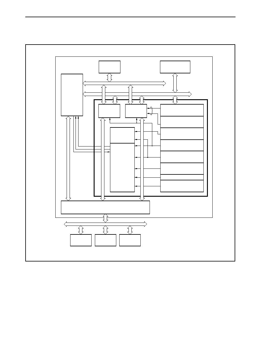
CHAPTER 6 DMA FUNCTIONS (DMA CONTROLLER)
128
User's Manual U14492EJ5V0UD
6.2 Configuration
CPU
Internal RAM
On-chip
peripheral I/O
On-chip peripheral I/O bus
Internal bus
Data
control
Address
control
Count
control
Channel
control
DMAC
V850E/IA1
Bus interface
External bus
External
RAM
External
ROM
External I/O
DMA source address
register (DSAnH/DSAnL)
DMA transfer count
register (DBCn)
DMA channel control
register (DCHCn)
DMA destination address
register (DDAnH/DDAnL)
DMA addressing control
register (DADCn)
DMA disable status
register (DDIS)
DMA trigger factor
register n (DTFRn)
DMA restart register (DRST)
Remark n = 0 to 3
CHAPTER 6 DMA FUNCTIONS (DMA CONTROLLER)
129
User's Manual U14492EJ5V0UD
6.3 Control Registers
6.3.1 DMA source address registers 0 to 3 (DSA0 to DSA3)
These registers are used to set the DMA source addresses (28 bits each) for DMA channel n (n = 0 to 3). They
are divided into two 16-bit registers, DSAnH and DSAnL.
Since these registers are 2-stage FIFO buffer registers, a new source address for DMA transfer can be specified
during DMA transfer (refer to 6.8 Next Address Setting Function). In this case, if a new DSAn register is set, the
value set will be transferred to the slave register and enabled only if DMA transfer ends normally, and the TCn bit of
DMA channel control register n (DCHCn) has been set to 1 or the INITn bit of the DCHCn register has been set to 1 (n
= 0 to 3).
(1) DMA source address registers 0H to 3H (DSA0H to DSA3H)
These registers can be read/written in 16-bit units.
Be sure to set bits 12 to 14 to 0. If they are set to 1, the operation is not guaranteed.
Cautions 1. When setting an address of an on-chip peripheral I/O register for the source address, be
sure to specify an address between FFFF000H and FFFFFFFH. An address of the on-
chip peripheral I/O register image (3FFF000H to 3FFFFFFH) must not be specified.
2. Do not set the DSAnH register when DMA transfer has been suspended.
15
IR
DSA0H
Address
FFFFF082H
Initial value
Undefined
14
0
13
0
12
0
11
SA27
10
SA26
9
SA25
8
SA24
7
SA23
6
SA22
5
SA21
4
SA20
3
SA19
2
SA18
1
SA17
0
SA16
IR
DSA1H
FFFFF08AH
Undefined
0
0
0
SA27 SA26 SA25 SA24 SA23 SA22 SA21 SA20 SA19 SA18 SA17 SA16
IR
DSA2H
FFFFF092H
Undefined
0
0
0
SA27 SA26 SA25 SA24 SA23 SA22 SA21 SA20 SA19 SA18 SA17 SA16
IR
DSA3H
FFFFF09AH
Undefined
0
0
0
SA27 SA26 SA25 SA24 SA23 SA22 SA21 SA20 SA19 SA18 SA17 SA16
Bit position
Bit name
Function
15
IR
Specifies the DMA source address.
0: External memory, on-chip peripheral I/O
1: Internal RAM
11 to 0
SA27 to
SA16
Sets the DMA source addresses (A27 to A16). During DMA transfer, it stores the next
DMA transfer source address.
CHAPTER 6 DMA FUNCTIONS (DMA CONTROLLER)
130
User's Manual U14492EJ5V0UD
(2) DMA source address registers 0L to 3L (DSA0L to DSA3L)
These registers can be read/written in 16-bit units.
15
SA15
DSA0L
Address
FFFFF080H
Initial value
Undefined
14
SA14
13
SA13
12
SA12
11
SA11
10
SA10
9
SA9
8
SA8
7
SA7
6
SA6
5
SA5
4
SA4
3
SA3
2
SA2
1
SA1
0
SA0
SA15
DSA1L
FFFFF088H
Undefined
SA14 SA13 SA12 SA11 SA10 SA9 SA8 SA7 SA6 SA5 SA4 SA3 SA2 SA1 SA0
SA15
DSA2L
FFFFF090H
Undefined
SA14 SA13 SA12 SA11 SA10 SA9 SA8 SA7 SA6 SA5 SA4 SA3 SA2 SA1 SA0
SA15
DSA3L
FFFFF098H
Undefined
SA14 SA13 SA12 SA11 SA10 SA9 SA8 SA7 SA6 SA5 SA4 SA3 SA2 SA1 SA0
Bit position
Bit name
Function
15 to 0
SA15 to SA0
Sets the DMA source addresses (A15 to A0). During DMA transfer, it stores the next
DMA transfer source address.
CHAPTER 6 DMA FUNCTIONS (DMA CONTROLLER)
131
User's Manual U14492EJ5V0UD
6.3.2 DMA destination address registers 0 to 3 (DDA0 to DDA3)
These registers are used to set the DMA destination address (28 bits each) for DMA channel n (n = 0 to 3). They
are divided into two 16-bit registers, DDAnH and DDAnL.
Since these registers are 2-stage FIFO buffer registers, a new destination address for DMA transfer can be
specified during DMA transfer (refer to 6.8 Next Address Setting Function). In this case, if a new DDAn register is
set, the value set will be transferred to the slave register and enabled only if DMA transfer ends normally, and the TCn
bit of DMA channel control register n (DCHCn) has been set to 1 or the INITn bit of the DCHCn register has been set
to 1 (n = 0 to 3).
(1) DMA destination address registers 0H to 3H (DDA0H to DDA3H)
These registers can be read/written in 16-bit units.
Be sure to set bits 12 to 14 to 0. If they are set to 1, the operation is not guaranteed.
Cautions 1. When setting an address of an on-chip peripheral I/O register for the destination
address, be sure to specify an address between FFFF000H and FFFFFFFH. An address
of the on-chip peripheral I/O register image (3FFF000H to 3FFFFFFH) must not be
specified.
2. Do not set the DDAnH register when DMA transfer has been suspended.
15
IR
DDA0H
Address
FFFFF086H
Initial value
Undefined
14
0
13
0
12
0
11
DA27
10
DA26
9
DA25
8
DA24
7
DA23
6
DA22
5
DA21
4
DA20
3
DA19
2
DA18
1
DA17
0
DA16
IR
DDA1H
FFFFF08EH
Undefined
0
0
0
DA27 DA26 DA25 DA24 DA23 DA22 DA21 DA20 DA19 DA18 DA17 DA16
IR
DDA2H
FFFFF096H
Undefined
0
0
0
DA27 DA26 DA25 DA24 DA23 DA22 DA21 DA20 DA19 DA18 DA17 DA16
IR
DDA3H
FFFFF09EH
Undefined
0
0
0
DA27 DA26 DA25 DA24 DA23 DA22 DA21 DA20 DA19 DA18 DA17 DA16
Bit position
Bit name
Function
15
IR
Specifies the DMA destination address.
0: External memory, on-chip peripheral I/O
1: Internal RAM
11 to 0
DA27 to
DA16
Sets the DMA destination addresses (A27 to A16). During DMA transfer, it stores the
next DMA transfer destination address.

CHAPTER 6 DMA FUNCTIONS (DMA CONTROLLER)
132
User's Manual U14492EJ5V0UD
(2) DMA destination address registers 0L to 3L (DDA0L to DDA3L)
These registers can be read/written in 16-bit units.
15
DA15
DDA0L
Address
FFFFF084H
Initial value
Undefined
14
DA14
13
DA13
12
DA12
11
DA11
10
DA10
9
DA9
8
DA8
7
DA7
6
DA6
5
DA5
4
DA4
3
DA3
2
DA2
1
DA1
0
DA0
DA15
DDA1L
FFFFF08CH
Undefined
DA14 DA13 DA12 DA11 DA10 DA9 DA8 DA7 DA6 DA5 DA4 DA3 DA2 DA1 DA0
DA15
DDA2L
FFFFF094H
Undefined
DA14 DA13 DA12 DA11 DA10 DA9 DA8 DA7 DA6 DA5 DA4 DA3 DA2 DA1 DA0
DA15
DDA3L
FFFFF09CH
Undefined
DA14 DA13 DA12 DA11 DA10 DA9 DA8 DA7 DA6 DA5 DA4 DA3 DA2 DA1 DA0
Bit position
Bit name
Function
15 to 0
DA15 to DA0
Sets the DMA destination addresses (A15 to A0). During DMA transfer, it stores the next
DMA transfer destination address.
CHAPTER 6 DMA FUNCTIONS (DMA CONTROLLER)
133
User's Manual U14492EJ5V0UD
6.3.3 DMA transfer count registers 0 to 3 (DBC0 to DBC3)
These 16-bit registers are used to set the byte transfer counts for DMA channel n (n = 0 to 3). They store the
remaining transfer counts during DMA transfer.
Since these registers are 2-stage FIFO buffer registers, a new DMA byte transfer count for DMA transfer can be
specified during DMA transfer (refer to 6.9 Next Address Setting Function). In this case, if a new DBCn register is
set, the value set will be transferred to the slave register and enabled only if DMA transfer ends normally, and the TCn
bit of DMA channel control register n (DCHCn) has been set to 1 or the INITn bit of the DCHCn register has been set
to 1 (n = 0 to 3).
These registers are decremented by 1 per transfer. Transfer is terminated if a borrow occurs.
These registers can be read/written in 16-bit units.
Cautions 1. When performing 2-cycle transfer from the internal RAM, do not set the transfer count to 2
(by setting the DBCn register to 0001H). If it is required to perform DMA transfer twice, be
sure to perform DMA transfer for which the transfer count is set to 1 (by setting the DBCn
register to 0000H) twice.
2. Do not set the DBCn register when DMA transfer has been suspended.
Remark If the DBCn register is read after a terminal count has occurred during DMA transfer without the value of
the DBCn register being rewritten, the value set immediately before DMA transfer is read (0000H is not
read even after completion of transfer).
15
BC15
DBC0
Address
FFFFF0C0H
Initial value
Undefined
14
BC14
13
BC13
12
BC12
11
BC11
10
BC10
9
BC9
8
BC8
7
BC7
6
BC6
5
BC5
4
BC4
3
BC3
2
BC2
1
BC1
0
BC0
BC15
DBC1
FFFFF0C2H
Undefined
BC14 BC13 BC12 BC11 BC10 BC9 BC8 BC7 BC6 BC5 BC4 BC3 BC2 BC1 BC0
BC15
DBC2
FFFFF0C4H
Undefined
BC14 BC13 BC12 BC11 BC10 BC9 BC8 BC7 BC6 BC5 BC4 BC3 BC2 BC1 BC0
BC15
DBC3
FFFFF0C6H
Undefined
BC14 BC13 BC12 BC11 BC10 BC9 BC8 BC7 BC6 BC5 BC4 BC3 BC2 BC1 BC0
Bit position
Bit name
Function
Sets the byte transfer count. It stores the remaining byte transfer count during DMA
transfer.
DBCn (n = 0 to 3)
States
0000H
Byte transfer count 1 or remaining byte transfer count
0001H
Byte transfer count 2 or remaining byte transfer count
:
:
FFFFH
Byte transfer count 65,536 (2
16
) or remaining byte transfer
count
15 to 0
BC15 to BC0

CHAPTER 6 DMA FUNCTIONS (DMA CONTROLLER)
134
User's Manual U14492EJ5V0UD
6.3.4 DMA addressing control registers 0 to 3 (DADC0 to DADC3)
These 16-bit registers are used to control the DMA transfer modes for DMA channel n (n = 0 to 3). These registers
cannot be accessed during DMA operation.
These registers can be read/written in 16-bit units.
Be sure to set bits 0, 1, and 8 to 13 to 0. If they are set to 1, the operation is not guaranteed.
Cautions 1. The DS1 and DS0 bits are used to set how many bits of data are transferred.
When 8-bit data (DS1, DS0 bits = 00) is set, the lower data bus (AD0 to AD7) is not necessarily
used.
When the transfer data size is set to 16 bits, the transfer must start from an address with bit 1
of the lower address aligned to "0". In this case, the transfer cannot start from an odd
address.
2. Set the DADCn register when the corresponding channel is in one of the following periods
(the operation is not guaranteed if set at another timing).
∑ Time from system reset to generation of the first DMA transfer request
∑ Time from DMA transfer end (after terminal count) to generation of the next DMA transfer
request
∑ Time from the forcible termination of DMA transfer (after the INITn bit of DMA channel
control register n (DCHCn) has been set to 1) to generation of the next DMA transfer
request
(1/2)
15
DS1
DADC0
Address
FFFFF0D0H
Initial value
0000H
14
DS0
13
0
12
0
11
0
10
0
9
0
8
0
7
SAD1
6
SAD0
5
DAD1
4
DAD0
3
TM1
2
TM0
1
0
0
0
DS1
DADC1
FFFFF0D2H
0000H
DS0
0
0
0
0
0
0
SAD1 SAD0 DAD1 DAD0 TM1 TM0
0
0
DS1
DADC2
FFFFF0D4H
0000H
DS0
0
0
0
0
0
0
SAD1 SAD0 DAD1 DAD0 TM1 TM0
0
0
DS1
DADC3
FFFFF0D6H
0000H
DS0
0
0
0
0
0
0
SAD1 SAD0 DAD1 DAD0 TM1 TM0
0
0
Bit position
Bit name
Function
Sets the transfer data size for DMA transfer.
DS1
DS0
Transfer data size
0 0
8
bits
0 1
16
bits
1 0
Setting
prohibited
1 1
Setting
prohibited
15, 14
DS1, DS0
For the on-chip peripheral I/O and programmable peripheral I/O registers, ensure the
transfer size matches the access size.

CHAPTER 6 DMA FUNCTIONS (DMA CONTROLLER)
135
User's Manual U14492EJ5V0UD
(2/2)
Bit position
Bit name
Function
Sets the count direction of the source address for DMA channel n (n = 0 to 3).
SAD1 SAD0
Count
direction
0 0
Increment
0 1
Decrement
1 0
Fixed
1 1
Setting
prohibited
7, 6
SAD1,
SAD0
Sets the count direction of the destination address for DMA channel n (n = 0 to 3).
DAD1 DAD0
Count
direction
0 0
Increment
0 1
Decrement
1 0
Fixed
1 1
Setting
prohibited
5, 4
DAD1,
DAD0
Sets the transfer mode during DMA transfer.
TM1 TM0
Transfer
mode
0
0
Single transfer mode
0
1
Single-step transfer mode
1 0
Setting
prohibited
1
1
Block transfer mode
3, 2
TM1, TM0

CHAPTER 6 DMA FUNCTIONS (DMA CONTROLLER)
136
User's Manual U14492EJ5V0UD
6.3.5 DMA channel control registers 0 to 3 (DCHC0 to DCHC3)
These 8-bit registers are used to control the DMA transfer operating mode for DMA channel n (n = 0 to 3).
These registers can be read/written in 8-bit or 1-bit units. (However, bit 7 is read only and bits 2 and 1 are write
only. If bits 2 and 1 are read, the read value is always 0.)
Be sure to set bits 4 to 6 to 0. If they are set to 1, the operation is not guaranteed.
Cautions 1. If transfer is completed with the MLEn bit set to 1, and the next transfer request is executed
with the DMA transfer (hardware DMA) started by an interrupt from the on-chip peripheral I/O,
the next transfer will be executed if the TCn bit is set to 1 (will not be automatically cleared to
0).
2. Set the MLEn bit when the corresponding channel is in one of the following periods (the
operation is not guaranteed if set at another timing).
∑ Time from system reset to generation of the first DMA transfer request
∑ Time from DMA transfer end (after terminal count) to generation of the next DMA transfer
request
∑ Time from the forcible termination of DMA transfer (after the INITn bit has been set to 1) to
generation of the next DMA transfer request
3. If DMA transfer is forcibly terminated in the last transfer cycle with the MLEn bit set to 1, the
same operations as transfer completion (setting of the TCn bit to 1) are performed (the Enn
bit will be cleared to 0 in forcible termination regardless of the value of the MLEn bit).
In this case, at the next DMA transfer request, the Enn bit must be set to 1 and the TCn bit
must be read (cleared to 0).
4. During DMA transfer completion (terminal count), each bit is updated in the order of clearing
the Enn bit to 0 and setting the TCn bit to 1. For this reason, if the TCn bit and Enn bit are in
the polling mode, the value indicating "transfer not completed, and transfer prohibited" (TCn
bit = 0, and Enn bit = 0) may be read in some cases if the DCHCn register is read while each
of the above bits is being updated (this is not an error).
5. Do not set the Enn and STGn bits when DMA transfer has been suspended; otherwise the
operation cannot be guaranteed.
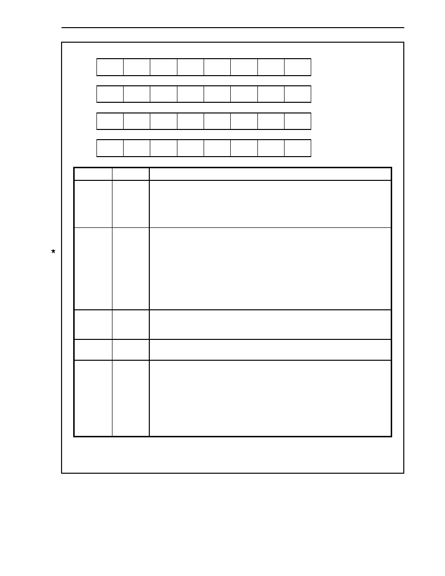
CHAPTER 6 DMA FUNCTIONS (DMA CONTROLLER)
137
User's Manual U14492EJ5V0UD
Address
FFFFF0E0H
<7>
TC0
DCHC0
6
0
5
0
4
0
<3>
MLE0
<2>
INIT0
<1>
STG0
<0>
E00
Initial value
00H
FFFFF0E2H
TC1
DCHC1
0
0
0
MLE1
INIT1
STG1
E11
00H
FFFFF0E4H
TC2
DCHC2
0
0
0
MLE2
INIT2
STG2
E22
00H
FFFFF0E6H
TC3
DCHC3
0
0
0
MLE3
INIT3
STG3
E33
00H
Bit position
Bit name
Function
7
TCn
This status bit indicates whether DMA transfer through DMA channel n has ended or not.
This bit is read-only. It is set to 1 when DMA transfer ends and cleared (to 0) when it is
read.
0: DMA transfer had not ended.
1: DMA transfer had ended.
3
MLEn
When this bit is set to 1 when DMA transfer ends (at terminal count output), the Enn bit is
not cleared to 0 and the DMA transfer enable state is retained. When the next DMA
transfer start trigger is an interrupt from the on-chip peripheral I/O (hardware DMA), the
DMA transfer request can be accepted even when the TCn bit is not read. When the next
DMA transfer start trigger is the setting of the STGn bit to 1 (software DMA), the DMA
transfer request can be accepted by reading and clearing the TCn bit to 0.
When this bit is cleared to 0 when DMA transfer ends (at terminal count output), the Enn
bit is cleared to 0 and the DMA transfer disable state is entered. At the next DMA transfer
request, the setting of the Enn bit to 1 and the reading of the TCn bit are required.
2
INITn
When this bit is set to 1 during DMA transfer or DMA transfer suspension, DMA transfer is
forcibly terminated (refer to 6.12.1 Restrictions related to DMA transfer forcible
termination).
1
STGn
If this bit is set to 1 in the DMA transfer enable state (TCn bit = 0, Enn bit = 1), DMA
transfer is started.
0
Enn
Specifies whether DMA transfer through DMA channel n is to be enabled or disabled. This
bit is cleared to 0 when DMA transfer ends. It is also cleared to 0 when DMA transfer is
forcibly suspended or terminated by means of setting the INITn bit to 1 or by NMI input.
0: DMA transfer disabled
1: DMA transfer enabled
Caution
After the Enn bit is set (1), do not set the Enn bit again until the number
of DMA transfers set by the DBCn register are complete or DMA transfer
is forcibly terminated using the INITn bit.
Remark n = 0 to 3
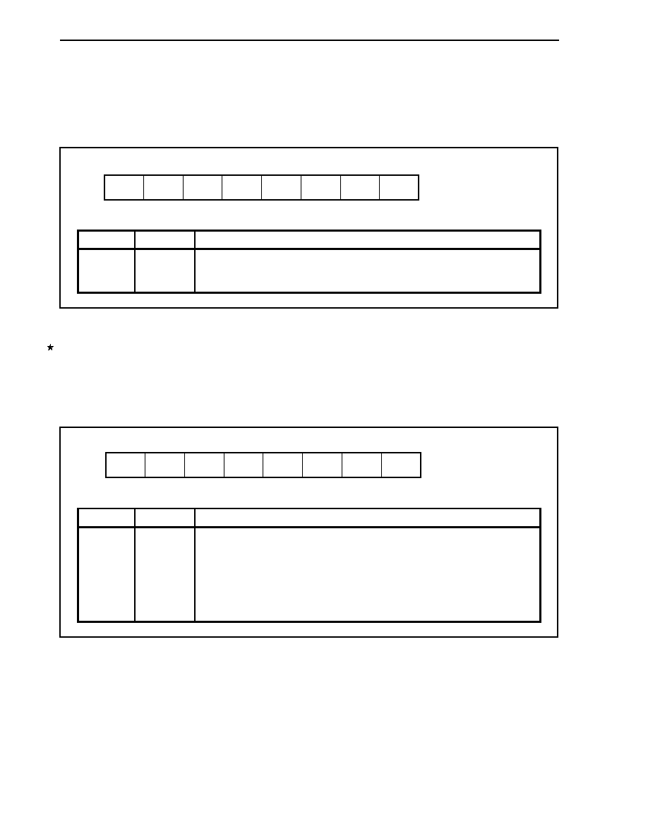
CHAPTER 6 DMA FUNCTIONS (DMA CONTROLLER)
138
User's Manual U14492EJ5V0UD
6.3.6 DMA disable status register (DDIS)
This register holds the contents of the Enn bit of the DCHCn register during forcible interruption by NMI input (n = 0
to 3).
This register is read-only, in 8-bit units.
Be sure to set bits 4 to 7 to 0. If they are set to 1, the operation is not guaranteed.
Address
FFFFF0F0H
7
0
DDIS
6
0
5
0
4
0
3
CH3
2
CH2
1
CH1
0
CH0
Initial value
00H
Bit position
Bit name
Function
3 to 0
CH3 to CH0
Reflects the contents of the Enn bit of the DCHCn register during forcible interruption by
NMI input. The contents of this register are held until the next forcible interruption by
NMI input or until the system is reset.
6.3.7 DMA restart register (DRST)
The ENn bit of the DRST register and the Enn bit of the DCHCn register are linked to each other, the Enn bit can
also be used to set the enabling or disabling of DMA transfer independently for four channels, and the DRST register
can be used to set the enabling or disabling of DMA transfer for four channels at the same time (n = 0 to 3).
This register can be read/written in 8-bit units.
Be sure to set bits 4 to 7 to 0. If they are set to 1, the operation is not guaranteed.
Address
FFFFF0F2H
7
0
DRST
6
0
5
0
4
0
3
EN3
2
EN2
1
EN1
0
EN0
Initial value
00H
Bit position
Bit name
Function
3 to 0
EN3 to EN0
Specifies whether DMA transfer through DMA channel n is to be enabled or disabled.
This bit is cleared to 0 when DMA transfer is completed in accordance with the terminal
count output (n = 0 to 3).
It is also cleared to 0 when DMA transfer is forcibly terminated by setting the INITn bit of
the DCHCn register to 1 or by NMI input.
0: DMA transfer disabled
1: DMA transfer enabled
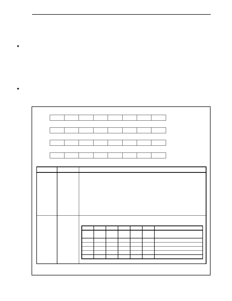
CHAPTER 6 DMA FUNCTIONS (DMA CONTROLLER)
139
User's Manual U14492EJ5V0UD
6.3.8 DMA trigger factor registers 0 to 3 (DTFR0 to DTFR3)
These 8-bit registers are used to control the DMA transfer start trigger through interrupt requests from on-chip
peripheral I/O.
The interrupt requests set with these registers serve as DMA transfer start factors.
These registers can be read/written in 8-bit units. Only bit 7 (DFn) can be read/written in 1-bit units, and bits 5 to 0
(IFCn5 to IFCn0) can be read/written in 8-bit units (n = 0 to 3).
Be sure to set bit 6 to 0. If it is set to 1, the operation is not guaranteed.
Cautions 1. Be sure to stop DMA operation before making changes to DTFRn register settings.
2. An interrupt request input in a standby mode (IDLE or software STOP mode) cannot be used
as a DMA transfer start factor except for INTP0 to INTP6 and INTP20 to INTP25 (when the
noise elimination by analog filter is selected).
3. If the start factor for DMA transfer is changed using the IFCn5 to IFCn0 bits, be sure to clear
(0) the DFn bit with the instruction immediately after the change.
(1/2)
<7>
DTFR0
6
5
4
3
2
1
0
DF0
0
IFC05
IFC04
IFC03
IFC02
IFC01
IFC00
Address
FFFFF810H
Initial value
00H
<7>
DTFR1
6
5
4
3
2
1
0
DF1
0
IFC15
IFC14
IFC13
IFC12
IFC11
IFC10
FFFFF812H
00H
<7>
DTFR2
6
5
4
3
2
1
0
DF2
0
IFC25
IFC24
IFC23
IFC22
IFC21
IFC20
FFFFF814H
00H
<7>
DTFR3
6
5
4
3
2
1
0
DF3
0
IFC35
IFC34
IFC33
IFC32
IFC31
IFC30
FFFFF816H
00H
Bit position
Bit name
Function
7
DFn
This is a DMA transfer request flag.
Only 0 can be written to this flag.
0: No DMA transfer request
1: DMA transfer request
If an interrupt that causes DMA transfer occurs while DMA transfer is disabled (including if
it has been suspended by an NMI or forcibly terminated by software), and if this DMA
transfer request must be cleared, stop the operation causing the interrupt (e.g., disable
reception if serial reception is in progress), and then clear the DFn bit. If it is clear in the
application that the interrupt will not occur again until DMA transfer is resumed next, it is
not necessary to stop the operation causing the interrupt.
Sets the interrupt source that serves as the DMA transfer start factor.
IFCn5 IFCn4 IFCn3 IFCn2 IFCn1 IFCn0
Interrupt
Source
0
0
0
0
0
0
DMA request from on-chip
peripheral I/O disabled
0 0 0 0 0 1
INTP0
0 0 0 0 1 0
INTP1
0 0 0 0 1 1
INTP2
0 0 0 1 0 0
INTP3
5 to 0
IFCn5 to
IFCn0
0 0 0 1 0 1
INTP4
Remark n = 0 to 3
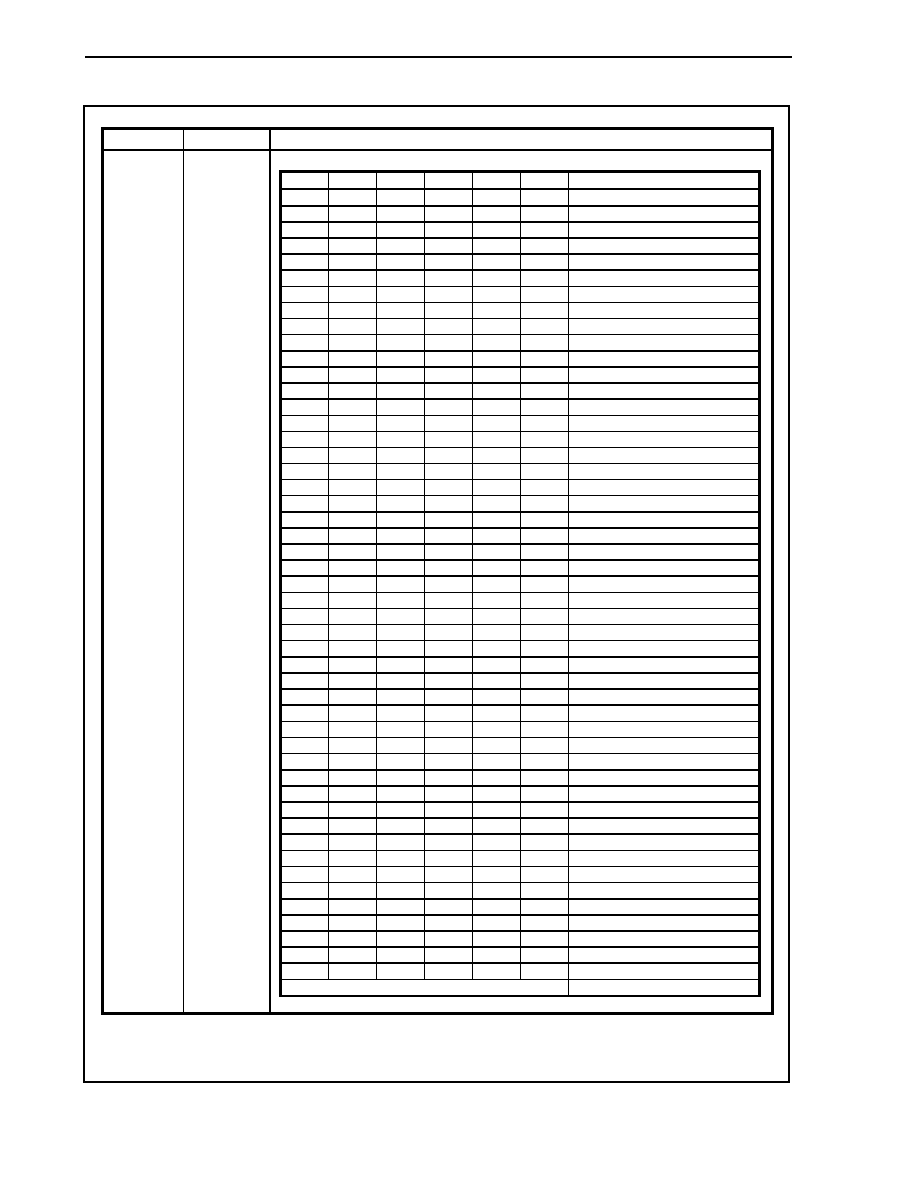
CHAPTER 6 DMA FUNCTIONS (DMA CONTROLLER)
140
User's Manual U14492EJ5V0UD
(2/2)
Bit position
Bit name
Function
IFCn5 IFCn4 IFCn3 IFCn2 IFCn1 IFCn0
Interrupt
source
0 0 0 1 1 0
INTP5
0 0 0 1 1 1
INTP6
0 0 1 0 0 0
INTDET0
0 0 1 0 0 1
INTDET1
0 0 1 0 1 0
INTTM00
0 0 1 0 1 1
INTCM003
0 0 1 1 0 0
INTTM01
0 0 1 1 0 1
INTCM013
0 0 1 1 1 0
INTP100/INTCC100
0 0 1 1 1 1
INTP101/INTCC101
0 1 0 0 0 0
INTCM100
0 1 0 0 0 1
INTCM101
0 1 0 0 1 0
INTP110/INTCC110
0 1 0 0 1 1
INTP111/INTCC111
0 1 0 1 0 0
INTCM110
0 1 0 1 0 1
INTCM111
0 1 0 1 1 0
INTTM20
0 1 0 1 1 1
INTTM21
0 1 1 0 0 0
INTP20/INTCC20
0 1 1 0 0 1
INTP21/INTCC21
0 1 1 0 1 0
INTP22/INTCC22
0 1 1 0 1 1
INTP23/INTCC23
0 1 1 1 0 0
INTP24/INTCC24
0 1 1 1 0 1
INTP25/INTCC25
0 1 1 1 1 0
INTTM3
0 1 1 1 1 1
INTP30/INTCC30
1 0 0 0 0 0
INTP31/INTCC31
1 0 0 0 0 1
INTCM4
1 0 0 0 1 0
INTDMA0
1 0 0 0 1 1
INTDMA1
1 0 0 1 0 0
INTDMA2
1 0 0 1 0 1
INTDMA3
1 0 0 1 1 0
INTCREC
1 0 0 1 1 1
INTCTRX
1 0 1 0 0 0
INTCERR
1 0 1 0 0 1
INTCMAC
1 0 1 0 1 0
INTCSI0
1 0 1 0 1 1
INTCSI1
1 0 1 1 0 0
INTSR0
1 0 1 1 0 1
INTST0
1 0 1 1 1 0
INTSER0
1 0 1 1 1 1
INTSR1
1 1 0 0 0 0
INTST1
1 1 0 0 0 1
INTSR2
1 1 0 0 1 0
INTST2
1 1 0 0 1 1
INTAD0
1 1 0 1 0 0
INTAD1
1 1 0 1 0 1
NBDAD
Note
1 1 0 1 1 0
NBDREW
Note
Other than above
Setting prohibited
5 to 0
IFCn5 to
IFCn0
Note
µ
PD70F3116 only
Remark n = 0 to 3

CHAPTER 6 DMA FUNCTIONS (DMA CONTROLLER)
141
User's Manual U14492EJ5V0UD
The relationship between the interrupt source and the DMA transfer trigger is as follows (n = 0 to 3).
IFCn0 to IFCn5
Internal DMA request signal
Interrupt source
Selector
Caution An interrupt request will be generated when DMA transfer starts. To prevent an interrupt from
being generated, mask the interrupt by setting the interrupt request control register. DMA
transfer starts even if an interrupt is masked.
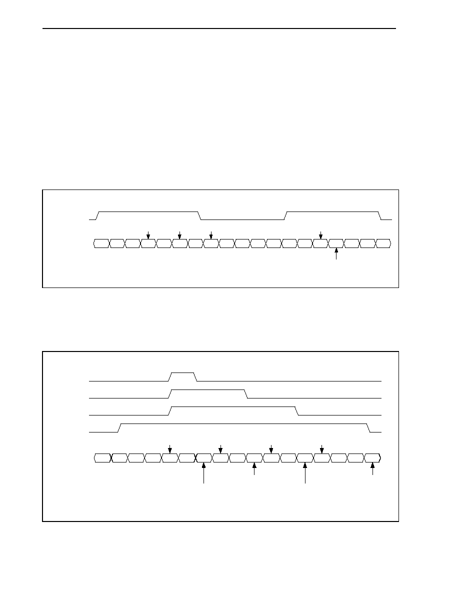
CHAPTER 6 DMA FUNCTIONS (DMA CONTROLLER)
142
User's Manual U14492EJ5V0UD
6.4 Transfer
Mode
6.4.1 Single transfer mode
In single transfer mode, the DMAC releases the bus at each byte/halfword transfer. If there is a subsequent DMA
transfer request, transfer is performed again once. This operation continues until a terminal count occurs.
When the DMAC has released the bus, if another higher priority DMA transfer request is issued, the higher priority
DMA request always takes precedence. However, if a lower priority DMA transfer request is generated within one
clock after the end of a single transfer, even if the previous higher priority DMA transfer request signal stays active,
this request is not prioritized, and the next DMA transfer after the bus is released for the CPU is a transfer based on
the newly generated, lower priority DMA transfer request.
Figures 6-1 to 6-4 show examples of single transfer.
Figure 6-1. Single Transfer Example 1
CPU
DMA3
CPU
CPU
DMA3
CPU
CPU
CPU
CPU
CPU
DMA3
CPU
DMA3
DMA3
CPU
CPU
CPU
DMARQ3
(Internal signal)
CPU
CPU
DMA channel 3 terminal count
Note
Note
Note
Note
Note The bus is always released.
Figure 6-2 shows a single transfer mode example in which a higher priority DMA transfer request is generated.
DMA channels 0 to 2 are used for a block transfer, and channel 3 is used for a single transfer.
Figure 6-2. Single Transfer Example 2
DMA1
DMA2
CPU
DMA2
CPU DMA3
CPU
CPU
CPU
DMA3
CPU
DMA0
DMA0
CPU
DMA1
DMARQ3
CPU DMA3
DMARQ2
DMARQ1
DMARQ0
Note
Note
Note
Note
DMA channel 0
terminal count
DMA channel 2
terminal count
DMA channel 3
terminal count
DMA channel 1
terminal count
(Internal signal)
(Internal signal)
(Internal signal)
(Internal signal)
Note The bus is always released.
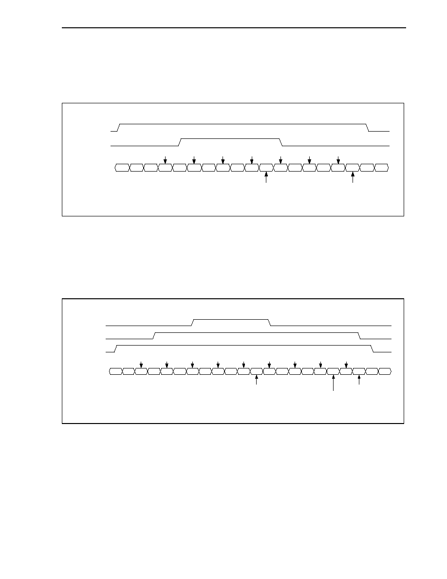
CHAPTER 6 DMA FUNCTIONS (DMA CONTROLLER)
143
User's Manual U14492EJ5V0UD
Figure 6-3 shows a single transfer mode example in which a lower priority DMA transfer request is generated
within one clock after the end of a single transfer. DMA channels 0 and 3 are used for a single transfer. When two
DMA transfer request signals are activated at the same time, the two DMA transfers are performed alternately.
Figure 6-3. Single Transfer Example 3
CPU
CPU
DMA3
DMA0
CPU
DMA0
CPU
CPU
CPU
CPU
DMA0
CPU
DMA0
DMA3
CPU
CPU
DMA0
DMARQ3
CPU
DMA0
DMA channel 0
terminal count
Note
Note
Note
Note
DMARQ0
DMA channel 3
terminal count
Note
Note
Note
(Internal signal)
(Internal signal)
Note The bus is always released.
Figure 6-4 shows a single transfer mode example in which two or more lower priority DMA transfer requests are
generated within one clock after the end of a single transfer. DMA channels 0, 2, and 3 are used for a single transfer.
When three or more DMA transfer request signals are activated at the same time, the two highest priority DMA
transfers are performed alternately.
Figure 6-4. Single Transfer Example 4
DMA2
CPU
DMA3
CPU
CPU
DMA3
CPU
CPU
DMA2
DMA0
CPU
DMARQ3
DMA0
Note
Note
Note
DMARQ2
Note
Note
DMARQ0
DMA2
CPU
DMA channel 0
terminal count
Note
DMA3
CPU
DMA2
CPU
CPU
DMA3
DMA channel 3
terminal count
Note
CPU
CPU
Note
DMA channel 2
terminal count
Note
(Internal signal)
(Internal signal)
(Internal signal)
Note The bus is always released.

CHAPTER 6 DMA FUNCTIONS (DMA CONTROLLER)
144
User's Manual U14492EJ5V0UD
6.4.2 Single-step transfer mode
In single-step transfer mode, the DMAC releases the bus at each byte/halfword transfer. Once a DMA transfer
request signal is received, transfer is performed again. This operation continues until a terminal count occurs.
When the DMAC has released the bus, if another higher priority DMA transfer request is issued, the higher priority
DMA request always takes precedence.
The following shows examples of single-step transfer. Figure 6-6 shows a single-step transfer mode example in
which a higher priority DMA transfer request is generated. DMA channels 0 and 1 are used for the single-step
transfer.
Figure 6-5. Single-Step Transfer Example 1
DMA1
CPU
CPU
CPU
CPU
CPU
CPU
CPU
CPU
DMA1
CPU
CPU
DMA1
DMA1
CPU
DMARQ1
CPU
CPU
DMA channel 1
terminal count
Note
Note
Note
(Internal signal)
Note The bus is always released.
Figure 6-6. Single-Step Transfer Example 2
DMA0
DMA0
CPU
CPU
DMA1 CPU
CPU
CPU
CPU
DMA1
CPU
CPU
DMA1
DMA0
CPU
DMARQ1
DMA1 CPU
DMARQ0
DMA channel 0
terminal count
DMA channel 1
terminal count
Note
Note
Note
Note
Note
Note
(Internal signal)
(Internal signal)
Note The bus is always released.
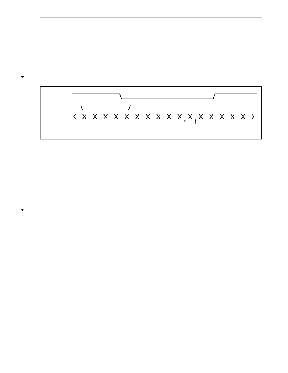
CHAPTER 6 DMA FUNCTIONS (DMA CONTROLLER)
145
User's Manual U14492EJ5V0UD
6.4.3 Block transfer mode
In the block transfer mode, once transfer starts, the DMAC continues the transfer operation without releasing the
bus until a terminal count occurs. No other DMA requests are acknowledged during block transfer.
After the block transfer ends and the DMAC releases the bus, another DMA transfer can be acknowledged.
The following shows an example of block transfer in which a higher priority DMA request is issued. DMA channels
2 and 3 are in the block transfer mode.
Figure 6-7. Block Transfer Example
CPU CPU CPU DMA3
DMA3
DMA3
DMA3
DMA3
DMA3
DMA3
DMA3 CPU DMA2
DMA2
DMA2
DMA2
DMA2
DMA channel 3 terminal count
The bus is always
released.
DMARQ3
(internal signal)
DMARQ2
(internal signal)
6.5 Transfer
Types
6.5.1 Two-cycle
transfer
In two-cycle transfer, data transfer is performed in two cycles, a read cycle (source to DMAC) and a write cycle
(DMAC to destination).
In the first cycle, the source address is output and reading is performed from the source to the DMAC. In the
second cycle, the destination address is output and writing is performed from the DMAC to the destination.
Caution An idle cycle of 1 to 2 clocks is always inserted between the read cycle and write cycle.
CHAPTER 6 DMA FUNCTIONS (DMA CONTROLLER)
146
User's Manual U14492EJ5V0UD
6.6 Transfer
Target
6.6.1 Transfer type and transfer target
Table 6-1 shows the relationship between the transfer type and transfer target (
: transfer enabled, ◊: transfer
disabled).
Table 6-1. Relationship Between Transfer Type and Transfer Target
Destination
Internal ROM
On-Chip
Peripheral I/O
Note
Internal RAM
External Memory,
External I/O
On-chip peripheral I/O
Note
◊
External I/O
◊
Internal RAM
◊
◊
External memory
◊
Source
Internal ROM
◊
◊
◊
◊
Note If the transfer target is the on-chip peripheral I/O, only the single transfer mode can be used.
Cautions 1. The operation is not guaranteed for combinations of transfer destination and source marked
with "
◊" in Table 6-1.
2.
Addresses between 3FFF000H and 3FFFFFFH cannot be specified for the source and
destination address of DMA transfer. Be sure to specify an address between FFFF000H and
FFFFFFFH.
Remark If the target of the DMA transfer is an on-chip peripheral I/O register (transfer source/transfer
destination), be sure to specify the same transfer size as the register size. For example, in the case of
DMA transfer to an 8-bit register, be sure to specify byte (8-bit) transfer.
<16-bit transfer>
∑ Transfer from a 16-bit bus to an 8-bit bus
A read cycle (16 bits) is generated and then a write cycle (8 bits) is generated twice successively.
∑ Transfer from an 8-bit bus to a 16-bit bus
A read cycle (8 bits) is generated twice successively and then a write cycle (16 bits) is generated.
Data is written to the transfer destination from the lowest byte in little-endian mode, and the highest
byte in big-endian mode.
<8-bit transfer>
∑ Transfer from a 16-bit bus to an 8-bit bus
A read cycle (the higher 8 bits go into a high-impedance state) is generated and then a write cycle (8
bits) is generated.
∑ Transfer from an 8-bit bus to a 16-bit bus
A read cycle (8 bits) is generated and then a write cycle (the higher 8 bits go into a high-impedance
state) is generated. Data is written to the transfer destination from the lowest byte in little-endian
mode, and the highest byte in big-endian mode.

CHAPTER 6 DMA FUNCTIONS (DMA CONTROLLER)
147
User's Manual U14492EJ5V0UD
6.6.2 External bus cycles during DMA transfer (two-cycle transfer)
The external bus cycles during DMA transfer (two-cycle transfer) are shown below.
Table 6-2. External Bus Cycles During DMA Transfer (Two-Cycle Transfer)
Transfer Target
External Bus Cycle
On-chip peripheral I/O, internal RAM
None
≠
External memory, external I/O
Yes
SRAM, external ROM, external I/O access cycle
6.7 DMA Channel Priorities
The DMA channel priorities are fixed as follows.
DMA channel 0 > DMA channel 1 > DMA channel 2 > DMA channel 3
In the block transfer mode, the channel used for transfer is never switched.
In the single-step transfer mode, if a higher priority DMA transfer request is issued while the bus is released, the
higher priority DMA transfer request is acknowledged.
Caution Do not start more than one DMA channel using the same start factor. If more than one DMA
channel is started, a lower priority DMA channel may be acknowledged prior to a higher priority
DMA channel.
6.8 Next Address Setting Function
The DMA source address registers (DSAnH, DSAnL), DMA destination address registers (DDAnH, DDAnL), and
DMA transfer count register (DBCn) are 2-stage FIFO buffer registers configured with a master register and slave
register (n = 0 to 3).
When the terminal count is issued, these registers are automatically rewritten with the value that was set
immediately before.
If new DMA transfer setting is made to these registers during DMA transfer, therefore, the values of the registers
are automatically updated to the new value after completion of transfer
Note
.
Note Before making another DMA transfer setting, confirm that DMA transfer has started. If new settings are
made before DMA transfer starts, the set values are overwritten to both the master and slave registers,
preventing the DMA transfer based on the set value immediately before from being correctly performed.

CHAPTER 6 DMA FUNCTIONS (DMA CONTROLLER)
148
User's Manual U14492EJ5V0UD
Figure 6-8 shows the configuration of the buffer register.
Figure 6-8. Buffer Register Configuration
The actual DMA transfer is performed based on the settings of the slave register.
The settings incorporated in the master and slave registers differ as follows according to the timing (time) at which
the settings were made.
(1) Time from system reset to generation of first DMA transfer request
The settings made are incorporated in both the master and slave registers.
(2) During DMA transfer (time from generation of DMA transfer request to end of DMA transfer)
The settings made are incorporated in only the master register, and not in the slave register (the slave
register maintains the value set for the next DMA transfer).
However, the contents of the master register are automatically overwritten in the slave register after DMA
transfer ends.
The value of the slave register is read if the value of each register is read during this period.
To check that DMA transfer has been started, confirm that the first transfer has been executed by reading the
DBCn register (n = 0 to 3).
(3) Time from DMA transfer end to start of next DMA transfer
The settings made are incorporated in both the master and slave registers.
Remark "DMA transfer end" means one of the following.
∑ Completion of DMA transfer (terminal count)
∑ Forcible termination of DMA transfer (the INITn bit of the DCHCn register is set to 1)
Data read
Data write
Master
register
Slave
register
Address/
count
controller
Internal bus

CHAPTER 6 DMA FUNCTIONS (DMA CONTROLLER)
149
User's Manual U14492EJ5V0UD
6.9 DMA Transfer Start Factors
There are two types of DMA transfer start factors, as shown below.
Cautions 1. Do not use two or more start factors ((1) and (2)) in combination for the same channel (if two
or more start factors are generated at the same time, only one of them is valid, but the valid
start factor cannot be identified). The operation is not guaranteed if two or more start factors
are used in combination.
2. If DMA transfer is started via software and if the software does not correctly detect whether
the expected DMA transfer operation has been completed through manipulation (setting to 1)
of the STGn bit of the DCHCn register, it cannot be guaranteed whether the next (second)
manipulation of the STGn bit corresponds to the start of "the next DMA transfer expected by
software" (n = 0 to 3).
For example, suppose single transfer is started by manipulating the STGn bit. Even if the
STGn bit is manipulated next (the second time) without checking by software whether the
single transfer has actually been executed, the next (second) DMA transfer is not always
executed. This is because the STGn bit may be manipulated the second time before the first
DMA transfer is started or completed because, for example, DMA transfer with a higher
priority had already been started when the STGn bit was manipulated for the first time. It is
therefore necessary to manipulate the STGn bit next time (the second time) after checking
whether DMA transfer started by the first manipulation of the STGn bit has been completed.
Completion of DMA transfer can be checked by checking the contents of the DBCn register.
(1) Request from software
If the STGn, Enn, and TCn bits of the DCHCn register are set as follows, DMA transfer starts (n = 0 to 3).
∑ STGn bit = 1
∑ Enn bit = 1
∑ TCn bit = 0
(2) Request from on-chip peripheral I/O
If, when the Enn and TCn bits of the DCHCn register are set as shown below, an interrupt request is issued
from the on-chip peripheral I/O that is set in the DTFRn register, DMA transfer starts (n = 0 to 3).
∑ Enn bit = 1
∑ TCn bit = 0

CHAPTER 6 DMA FUNCTIONS (DMA CONTROLLER)
150
User's Manual U14492EJ5V0UD
6.10 Forcible Interruption
DMA transfer can be forcibly interrupted by NMI input during DMA transfer.
At such a time, the DMAC clears the Enn bit of the DCHCn register of all channels to 0 and the DMA transfer
disabled state is entered. An NMI request can then be acknowledged after the DMA transfer executed during NMI
input is terminated (n = 0 to 3).
If DMA transfer has been forcibly interrupted, perform forcible termination of the DMA using the INITn bit of the
DCHCn register and then initialize.
6.11 DMA Transfer End
When DMA transfer ends and the TCn bit of the DCHCn register is set to 1, a DMA transfer end interrupt
(INTDMAn) is issued to the interrupt controller (INTC) (n = 0 to 3).

CHAPTER 6 DMA FUNCTIONS (DMA CONTROLLER)
151
User's Manual U14492EJ5V0UD
6.12 Forcible Termination
In addition to the forcible interruption operation by means of NMI input, DMA transfer can be forcibly terminated by
the INITn bit of the DCHCn register (n = 0 to 3).
An example of forcible termination by the INITn bit of the DCHCn register is illustrated below (n = 0 to 3).
Figure 6-9. Example of Forcible Termination of DMA Transfer
(a) Block transfer via DMA channel 3 is started during block transfer via DMA channel 2
CPU CPU CPU CPU DMA2 DMA2 DMA2 DMA2 DMA2 CPU DMA3 DMA3 DMA3 DMA3 CPU CPU CPU
DMARQ2
(internal signal)
DMARQ3
(internal signal)
DMA channel 3 transfer start
DMA channel 3 terminal count
Forcible termination of DMA channel 2 transfer, bus released
DSA2, DDA2, DBC2,
DADC2, DCHC2
Register set
DCHC2
(INIT2 bit = 1)
Register set
DSA3, DDA3, DBC3,
DADC3, DCHC3
Register set
E22 bit = 1
TC2 bit = 0
E22 bit
0
TC2 bit = 0
E33 bit = 1
TC3 bit = 0
E33 bit
0
TC3 bit
1
(b) When transfer is suspended during DMA channel 1 block transfer, and transfer under another
condition is executed
CPU CPU CPU CPU DMA1 DMA1 DMA1 DMA1 DMA1 DMA1 CPU CPU CPU CPU DMA1 DMA1 DMA1 CPU
DMARQ1
(internal signal)
Forcible termination of DMA channel
1 transfer, bus released
DMA channel 1
terminal count
DSA1, DDA1, DBC1,
DADC1, DCHC1
Register set
DADC1,
DCHC1
Register set
DCHC1
(INIT1 bit = 1)
Register set
DSA1, DDA1,
DBC1
Register set
E11 bit = 1
TC1 bit = 0
E11 bit
0
TC1 bit = 0
E11 bit
1
TC1 bit = 0
E11 bit
0
TC1 bit
1
Remark The values of the DSAn, DDAn, and DBCn registers (n = 0 to 3) are retained even when DMA
transfer is forcibly terminated, because these registers are FIFO-format buffer registers. The next
transfer condition can be set to these registers even while DMA transfer is in progress. On the
other hand, the setting of the DADCn and DCHCn registers is invalid during DMA transfer because
these registers are not buffer registers (see 6.8 Next Address Setting Function, 6.3.4 DMA
addressing control registers 0 to 3 (DADC0 to DADC3), and 6.3.5 DMA channel control
registers 0 to 3 (DCHC0 to DCHC3)).

CHAPTER 6 DMA FUNCTIONS (DMA CONTROLLER)
152
User's Manual U14492EJ5V0UD
6.12.1 Restriction related to DMA transfer forcible termination
When terminating a DMA transfer by setting the INITn bit of the DCHCn register, the transfer may not be
terminated, but just suspended, even though the INITn bit is set to 1. As a result, when the DMA transfer of a channel
that should have been terminated is resumed, the DMA transfer will terminate after an unexpected number of
transfers are completed and a DMA transfer completion interrupt may occur.
[Preventive measures]
This problem can be avoided by implementing any of the following workarounds.
(1) Stop all the transfers from DMA channels temporarily.
The following measure is effective if the program does not assume that the TCn bit of the DCHCn register is 1
except for the following workaround processing. (Since the TCn bit of the DCHCn register is cleared to 0
when it is read, execution of the following procedure (ii) under step <5> clears this bit.)
<1> Disable interrupts (DI state).
<2> Read the DMA restart register (DRST) and transfer the ENn bit of each channel to a general-purpose
register (value A).
<3> Write 00H to the DMA restart register (DRST) twice
Note
.
By executing twice, the DMA transfer is definitely stopped before proceeding to <4>.
<4> Set the INITn bit of the DCHCn register of the channel to be forcibly terminated to 1.
<5> Perform the following operations for value A read in step <2>. (Value B)
(i) Clear the bit of the channel to be forcibly terminated to 0
(ii) If the TCn of the DCHCn register and ENn bit of the DRST register of the channel that is not
terminated forcibly are 1 (AND makes 1), clear the bit of the channel to 0.
<6> Write value B in <5> to the DRST register.
<7> Enable interrupts (EI state).
Note Execute three times if the transfer target (transfer source or transfer destination) is the internal
RAM.
Caution Be sure to execute step <5> to prevent the ENn bit of the DRST register from being set
illegally for channels that are terminated normally during the period of steps <2> and
<3>.
Remark n = 0 to 3
CHAPTER 6 DMA FUNCTIONS (DMA CONTROLLER)
153
User's Manual U14492EJ5V0UD
(2) Repeat setting the INITn bit of the DCHCn register until forcible termination of DMA transfer is
completed normally
The procedure is shown below.
<1> Copy the initial transfer count of the channel to be forcibly terminated to a general-purpose register.
<2> Set the INITn bit of the DCHCn register of the channel to be forcibly terminated to 1.
<3> Read the value of DMA transfer count register n (DBCn) of the channel to be forcibly terminated, and
compare that value with the value copied in step <1>. If the two values do not match, repeat steps <2>
and <3>.
Cautions 1. If the DBCn register is read in step <3>, and if DMA transfer is stopped due to
trouble, the remaining number of transfers will be read. If DMA transfer has been
forcibly terminated correctly, the initial number of transfers will be read.
2. With this procedure, it may take some time for the channel in question to be
forcibly terminated in an application in which DMA transfer of a channel other than
that to be forcibly terminated is frequently executed.
Remark n = 0 to 3
6.13 Times Related to DMA Transfer
The overhead before and after DMA transfer and minimum execution clock for DMA transfer are shown below.
Table 6-3. Number of Minimum Execution Clocks in DMA Cycle
DMA Cycle
Number of Minimum Execution Clocks
<1> Time to respond to DMA request
4 clocks
Note 1
Internal RAM access
2 clocks
Note 2
<2> Memory access
On-chip peripheral I/O
register access
4 clocks + number of waits set by VSWC register
Notes 1. If an external interrupt (INTPn) is specified as a factor of starting DMA transfer, noise elimination time
is added (n = 0 to 6, 100, 101, 110, 111, 20 to 25, 30, or 31).
2.
Two clocks are required for the DMA cycle.
The minimum execution clock in the DMA cycle in each transfer mode is as follows.
Single transfer: DMA response time (<1>) + Transfer source memory access (<2>) + 1
Note
+ Transfer
destination memory access (<2>)
Block transfer:
DMA response time (<1>) + (Transfer source memory access (<2>) + 1
Note
+ Transfer
destination memory access (<2>))
◊ Number of transfers
Note One clock is always inserted between the read cycle and write cycle of DMA transfer.

CHAPTER 6 DMA FUNCTIONS (DMA CONTROLLER)
154
User's Manual U14492EJ5V0UD
6.14 Precautions
(1) Memory boundary
The transfer operation is not guaranteed if the source or the destination address exceeds the area of DMA
targets (external memory, internal RAM, or on-chip peripheral I/O) during DMA transfer.
(2) Transfer of misaligned data
DMA transfer of 16-bit bus width misaligned data is not supported.
If the source or the destination address is set to an odd address, the LSB of the address is forcibly handled
as "0".
(3) Bus arbitration for CPU
When an external device is targeted for DMA transfer, the CPU can access the internal ROM and internal
RAM (if they are not subject to DMA transfer).
When DMA transfer is executed between the on-chip peripheral I/O and internal RAM, the CPU can access
the internal ROM.
(4) DMA start factor
Do not start two or more DMA channels with the same factor. If two or more DMA channels are started with
the same factor, the DMA channel with a lower priority may be acknowledged before the DMA channel with a
higher priority. Operation is not guaranteed in this case.
(5) Program execution and DMA transfer with internal RAM
Do not execute DMA transfer to/from the internal RAM and an instruction in the internal RAM simultaneously.
(6) Restrictions related to automatic clearing of TCn bit of DCHCn register
The TCn bit of the DCHCn register is automatically cleared to 0 when it is read. When DMA transfer is
executed to transfer data to or from the internal RAM when two or more DMA transfer channels are
simultaneously used, the TCn bit may not be cleared even if it is read after completion of DMA transfer (n = 0
to 3).
Caution This restriction does not apply if one of the following conditions is satisfied.
∑ Only one channel of DMA transfer is used.
∑ DMA is not executed to transfer data to or from the internal RAM.
[Preventive measures]
To read the TCn bit of the DCHCn register of the DMA channel that is used to transfer data to or from the
internal RAM, be sure to read the TCn bit three times in a row. This can accurately clear the TCn bit to 0.

CHAPTER 6 DMA FUNCTIONS (DMA CONTROLLER)
155
User's Manual U14492EJ5V0UD
(7) Read values of DSAn and DDAn registers
If the values of the DSAn and DDAn registers are read during DMA transfer, the values in the middle of being
updated may be read (n = 0 to 3).
For example, if the DSAnH register and the DSAnL register are read in that order when the value of the DMA
transfer source address (DSAn register) is "0000FFFFH" and the counting direction is incremental (when the
SADn1 and SADn0 bits of the DADCn register = 00), the value of the DSAnL register differs as follows
depending on whether DMA transfer is executed immediately after the DSAnH register has been read.
(a) If DMA transfer does not occur while the DSAn register is being read
<1> Reading DSAnH register: DSAnH = 0000H
<2> Reading DSAnL register: DSAnL = FFFFH
(b) If DMA transfer occurs while the DSAn register is being read
<1> Reading DSAnH register: DSAnH = 0000H
<2> Occurrence of DMA transfer
<3> Incrementing DSAn register : DSAn = 00010000H
<4> Reading DSAnL register: DSAnL = 0000H
6.14.1 Interrupt factors
DMA transfer is interrupted if a bus hold is issued.
If the factor (bus hold) interrupting DMA transfer disappears, DMA transfer promptly restarts.

156
User's Manual U14492EJ5V0UD
CHAPTER 7 INTERRUPT/EXCEPTION PROCESSING FUNCTION
The V850E/IA1 is provided with an interrupt controller (INTC) that can process a total of 53 interrupt requests.
An interrupt is an event that occurs independently of program execution, and an exception is an event whose
occurrence is dependent on program execution.
The V850E/IA1 can process interrupt requests from the on-chip peripheral hardware and external sources.
Moreover, exception processing can be started by the TRAP instruction (software exception) or by generation of an
exception event (i.e. fetching of an illegal opcode) (exception trap).
Eight levels of software-programmable priorities can be specified for each interrupt request.
Interrupt servicing starts after no fewer than 4 system clocks (80 ns (@ 50 MHz)) following the generation of an
interrupt request.
7.1 Features
Interrupts
∑ Non-maskable interrupts: 1 source
Caution P00 alternately functions as NMI, and is fixed to input. P00 and NMI cannot be switched. If
the P00 bit of the P0 register is read, the level of the P00/NMI pin is read.
Set the valid edge of the NMI pin using the ESN0 bit of the INTM0 register (default value:
falling edge detection).
∑ Maskable interrupts: 52 sources
∑ 8 levels of programmable priorities (maskable interrupts)
∑ Multiple interrupt control according to priority
∑ Masks can be specified for each maskable interrupt request.
∑ Noise elimination
Note
, edge detection, and valid edge specification for external interrupt request signals.
Note For details of the noise eliminator, refer to 14.5 Noise Eliminator.
Exceptions
∑ Software exceptions: 32 sources
∑ Exception traps: 2 sources (illegal opcode exception and debug trap)
Interrupt/exception sources are listed in Table 7-1.
CHAPTER 7 INTERRUPT/EXCEPTION PROCESSING FUNCTION
157
User's Manual U14492EJ5V0UD
Table 7-1. Interrupt/Exception Source List (1/2)
Interrupt/Exception Source
Type Classification
Name Controlling
Register
Generating Source
Generating
Unit
Default
Priority
Exception
Code
Handler
Address
Restored PC
Reset Interrupt
RESET
- RESET
input
Pin
- 0000H 00000000H
Undefined
Non-maskable Interrupt
NMI0
- NMI
input
Pin
- 0010H 00000010H
nextPC
Exception
TRAP0n
Note
- TRAP
instruction
-
-
004nH
Note 1
00000040H nextPC
Software
exception
Exception
TRAP1n
Note
- TRAP
instruction
-
-
005nH
Note 1
00000050H nextPC
Exception trap Exception
ILGOP/
DBG0
- Illegal
opcode/
DBTRAP instruction
-
- 0060H 00000060H
nextPC
Interrupt INTP0
P0IC0 INTP0
pin
Pin
0
0080H
00000080H
nextPC
Interrupt INTP1
P0IC1 INTP1
pin
Pin
1
0090H
00000090H
nextPC
Interrupt INTP2
P0IC2 INTP2
pin
Pin
2
00A0H
000000A0H nextPC
Interrupt INTP3
P0IC3 INTP3
pin
Pin
3
00B0H
000000B0H nextPC
Interrupt INTP4
P0IC4 INTP4
pin Pin
4
00C0H
000000C0H nextPC
Interrupt INTP5
P0IC5 INTP5
pin Pin
5
00D0H
000000D0H nextPC
Interrupt INTP6
P0IC6 INTP6
pin
Pin
6
00E0H
000000E0H nextPC
Interrupt INTDET0 DETIC0
AD0
voltage
detection ADC0
7 00F0H 000000F0H nextPC
Interrupt INTDET1 DETIC1
AD1
voltage
detection ADC1
8 0100H 00000100H
nextPC
Interrupt INTTM00 TM0IC0
TM00
underflow TM00 9
0110H
00000110H
nextPC
Interrupt INTCM003
CM03IC0
CM003
match TM00
10
0120H
00000120H
nextPC
Interrupt INTTM01 TM0IC1
TM01
underflow TM01 11
0130H
00000130H
nextPC
Interrupt INTCM013
CM03IC1
CM013
match TM01
12
0140H
00000140H
nextPC
Interrupt INTP100/
INTCC100
CC10IC0 INTP100
pin/
CC100 match
Pin/TM10 13
0150H
00000150H
nextPC
Interrupt INTP101/
INTCC101
CC10IC1
INTP101/INTP100 pin
Note 2
/
CC101 match
Pin/TM10 14
0160H
00000160H
nextPC
Interrupt INTCM100
CM10IC0
CM100
match TM10
15
0170H
00000170H
nextPC
Interrupt INTCM101
CM10IC1
CM101
match TM10
16
0180H
00000180H
nextPC
Interrupt INTP110/
INTCC110
CC11IC0 INTP110
pin/
CC110 match
Pin/TM10 17
0190H
00000190H
nextPC
Interrupt INTP111/
INTCC111
CC11IC1
INTP111/INTP110 pin
Note 2
/
CC111 match
Pin/TM11 18
01A0H
000001A0H nextPC
Interrupt INTCM110
CM11IC0
CM110
match TM11
19
01B0H
000001B0H nextPC
Interrupt INTCM111
CM11IC1
CM111
match TM11
20
01C0H
000001C0H nextPC
Interrupt INTTM20 TM2IC0
TM20
overflow TM20
21
01D0H
000001D0H nextPC
Interrupt INTTM21 TM2IC1
TM21
overflow TM21
22
01E0H
000001E0H nextPC
Interrupt INTP20/
INTCC20
CC2IC0
INTP20 pin/CC20 match Pin/TM20 23
01F0H
000001F0H nextPC
Interrupt INTP21/
INTCC21
CC2IC1
INTP21 pin/CC21 match Pin/
TM20/TM21
24 0200H 00000200H
nextPC
Interrupt INTP22/
INTCC22
CC2IC2
INTP22 pin/CC22 match Pin/
TM20/TM21
25 0210H 00000210H
nextPC
Interrupt INTP23/
INTCC23
CC2IC3 INTP23
pin/
CC23 match
Pin/
TM20/TM21
26 0220H 00000220H
nextPC
Interrupt INTP24/
INTCC24
CC2IC4 INTP24
pin/
CC24 match
Pin/
TM20/TM21
27 0230H 00000230H
nextPC
Interrupt INTP25/
INTCC25
CC2IC5 INTP25
pin/
CC25 match
Pin/TM21 28
0240H
00000240H
nextPC
Maskable
Interrupt INTTM3 TM3IC0
TM3
overflow TM3
29
0250H
00000250H
nextPC
Notes 1. n = 0 to FH
2. Select using the CSL10 and CSL11 registers.

CHAPTER 7 INTERRUPT/EXCEPTION PROCESSING FUNCTION
158
User's Manual U14492EJ5V0UD
Table 7-1. Interrupt/Exception Source List (2/2)
Interrupt/Exception Source
Type Classification
Name Controlling
Register
Generating Source
Generating
Unit
Default
Priority
Exception
Code
Handler
Address
Restored PC
Interrupt INTP30/
INTCC30
CC3IC0
INTP30 pin/CC30 match Pin/TM3 30
0260H
00000260H
nextPC
Interrupt INTP31/
INTCC31
CC3IC1
INTP31 pin/CC31 match Pin/TM3 31
0270H
00000270H
nextPC
Interrupt INTCM4 CM4IC0
CM4
match signal
TM4
32
0280H
00000280H nextPC
Interrupt
INTDMA0
DMAIC0
End of DMA0 transfer
DMA
33
0290H
00000290H nextPC
Interrupt
INTDMA1
DMAIC1
End of DMA1 transfer
DMA
34
02A0H
000002A0H nextPC
Interrupt
INTDMA2
DMAIC2
End of DMA2 transfer
DMA
35
02B0H
000002B0H nextPC
Interrupt
INTDMA3
DMAIC3
End of DMA3 transfer
DMA
36
02C0H
000002C0H nextPC
Interrupt INTCREC
CANIC0
CAN1
reception complete FCAN
37
02D0H
000002D0H nextPC
Interrupt INTCTRX CANIC1
CAN1
transmission
complete
FCAN 38
02E0H
000002E0H
nextPC
Interrupt INTCERR
CANIC2
CAN1
communication
error
FCAN 39
02F0H
000002F0H
nextPC
Interrupt INTCMAC
CANIC3
CAN
illegal write
FCAN
40
0300H
00000300H nextPC
Interrupt INTCSI0 CSIIC0 CSI0
transmission/
reception complete
CSI0 41
0310H
00000310H
nextPC
Interrupt INTCSI1 CSIIC1 CSI1
transmission/
reception complete
CSI1 42
0320H
00000320H
nextPC
Interrupt INTSR0 SRIC0 UART0
reception
complete
UART0 43
0330H
00000330H
nextPC
Interrupt INTST0 STIC0 UART0
transmission
complete
UART0 44
0340H
00000340H
nextPC
Interrupt INTSER0 SEIC0 UART0
reception error
UART0
45
0350H
00000350H nextPC
Interrupt INTSR1 SRIC1 UART1
reception
complete
UART1 46
0360H
00000360H
nextPC
Interrupt INTST1 STIC1 UART1
transmission
complete
UART1 47
0370H
00000370H
nextPC
Interrupt INTSR2 SRIC2 UART2
reception
complete
UART2 48
0380H
00000380H
nextPC
Interrupt INTST2 STIC2 UART2
transmission
complete
UART2 49
0390H
00000390H
nextPC
Interrupt
INTAD0
ADIC0
End of AD0 conversion ADC0
50 03A0H 000003A0H
nextPC
Maskable
Interrupt
INTAD1
ADIC1
End of AD1 conversion ADC1
51 03B0H 000003B0H
nextPC

CHAPTER 7 INTERRUPT/EXCEPTION PROCESSING FUNCTION
159
User's Manual U14492EJ5V0UD
Remarks 1. Default priority: The priority order when two or more maskable interrupt requests are generated at
the same time. The highest priority is 0.
Restored PC: The value of the program counter (PC) saved to EIPC, FEPC, or DBPC of CPU
when interrupt servicing is started. Note, however, that the restored PC when a
non-maskable or maskable interrupt is acknowledged while one of the following
instructions is being executed does not become the nextPC. (If an interrupt is
acknowledged during instruction execution, execution stops, and then resumes
after the interrupt servicing has finished. In this case, the address of the aborted
instruction is the restore PC.)
∑ Load instructions (SLD.B, SLD.BU, SLD.H, SLD.HU, SLD.W)
∑ Division instructions (DIV, DIVH, DIVU, DIVHU)
∑ PREPARE, DISPOSE instructions (only if an interrupt is generated before the
stack pointer is updated)
nextPC:
The PC value that starts the processing following interrupt/exception processing.
2. The execution address of the illegal instruction when an illegal opcode exception occurs is
calculated by (Restored PC ≠ 4).

CHAPTER 7 INTERRUPT/EXCEPTION PROCESSING FUNCTION
160
User's Manual U14492EJ5V0UD
7.2 Non-Maskable
Interrupt
A non-maskable interrupt request is acknowledged unconditionally, even when interrupts are in the interrupt
disabled (DI) status. An NMI is not subject to priority control and takes precedence over all the other interrupts.
A non-maskable interrupt request is input from the NMI pin. When the valid edge specified by bit 0 (ESN0) of the
external interrupt mode register 0 (INTM0) is detected on the NMI pin, the interrupt occurs.
While the service program of the non-maskable interrupt is being executed, another non-maskable interrupt request
is held pending. The pending NMI is acknowledged after the original service program of the non-maskable interrupt
under execution has been terminated (by the RETI instruction). Note that if two or more NMI requests are input during
the execution of the service program for an NMI, the number of NMIs that will be acknowledged after the RETI
instruction is executed is only one.
CHAPTER 7 INTERRUPT/EXCEPTION PROCESSING FUNCTION
161
User's Manual U14492EJ5V0UD
7.2.1 Operation
If a non-maskable interrupt is generated by NMI input, the CPU performs the following processing, and transfers
control to the handler routine.
(1) Saves the restored PC to FEPC.
(2) Saves the current PSW to FEPSW.
(3) Writes exception code 0010H to the higher halfword (FECC) of ECR.
(4) Sets the NP and ID bits of the PSW and clears the EP bit.
(5) Sets the handler address (00000010H) corresponding to the non-maskable interrupt to the PC, and transfers
control.
The servicing configuration of a non-maskable interrupt is shown in Figure 7-1.
Figure 7-1. Servicing Configuration of Non-Maskable Interrupt
PSW.NP
FEPC
FEPSW
ECR.FECC
PSW.NP
PSW.EP
PSW.ID
PC
restored PC
PSW
0010H
1
0
1
00000010H
1
0
NMI input
Non-maskable interrupt request
Interrupt servicing
Interrupt request held pending
INTC
acknowledged
CPU processing

CHAPTER 7 INTERRUPT/EXCEPTION PROCESSING FUNCTION
162
User's Manual U14492EJ5V0UD
Figure 7-2. Acknowledging Non-Maskable Interrupt Request
(a) If a new NMI request is generated while an NMI service program is being executed
Main routine
NMI request
NMI request
(PSW.NP = 1)
NMI request held pending regardless
of the value of the NP bit of the PSW
Pending NMI request processed
(b) If a new NMI request is generated twice while an NMI service program is being executed
Main routine
NMI request
NMI request
Held pending because NMI service program is being processed
Only one NMI request is acknowledged even though
two NMI requests are generated
NMI request
Held pending because NMI service program is being processed

CHAPTER 7 INTERRUPT/EXCEPTION PROCESSING FUNCTION
163
User's Manual U14492EJ5V0UD
7.2.2 Restore
Execution is restored from the non-maskable interrupt servicing by the RETI instruction.
When the RETI instruction is executed, the CPU performs the following processing, and transfers control to the
address of the restored PC.
(1) Restores the values of the PC and the PSW from FEPC and FEPSW, respectively, because the EP bit of the
PSW is 0 and the NP bit of the PSW is 1.
(2) Transfers control back to the address of the restored PC and PSW.
Figure 7-3 illustrates how the RETI instruction is processed.
Figure 7-3. RETI Instruction Processing
PSW.EP
RETI instruction
PSW.NP
Original processing restored
1
1
0
0
PC
PSW
EIPC
EIPSW
PC
PSW
FEPC
FEPSW
Caution When the PSW.EP bit and PSW.NP bit are changed by the LDSR instruction during non-
maskable interrupt servicing, in order to restore the PC and PSW correctly during recovery
by the RETI instruction, it is necessary to set PSW.EP back to 0 and PSW.NP back to 1 using
the LDSR instruction immediately before the RETI instruction.
Remark The solid lines show the CPU processing flow.

CHAPTER 7 INTERRUPT/EXCEPTION PROCESSING FUNCTION
164
User's Manual U14492EJ5V0UD
7.2.3 Non-maskable interrupt status flag (NP)
The NP flag is a status flag that indicates that non-maskable interrupt (NMI) servicing is under execution.
This flag is set when an NMI interrupt has been acknowledged, and masks all interrupt requests and exceptions to
prohibit multiple interrupts from being acknowledged.
31
0
PSW
Initial value
00000020H
7
NP
6
EP
5
ID
4
SAT
3
CY
2
OV
1
S Z
8
0
0
0
0
0
0
0
0
0
0
0
0
0
0
0
0
0
0
0
0
0
0
0
0
Bit position
Bit name
Function
7 NP
Indicates whether NMI interrupt servicing is in progress.
0: No NMI interrupt servicing
1: NMI interrupt currently being serviced
7.2.4 Edge detection function
(1) External interrupt mode register 0 (INTM0)
External interrupt mode register 0 (INTM0) is a register that specifies the valid edge of a non-maskable
interrupt (NMI). The NMI valid edge can be specified to be either the rising edge or the falling edge by the
ESN0 bit.
This register can be read/written in 8-bit or 1-bit units.
Address
FFFFF880H
7
0
INTM0
6
0
5
0
4
0
3
0
2
0
1
0
<0>
ESN0
Initial value
00H
Bit position
Bit name
Function
0 ESN0
Specifies the NMI pin's valid edge.
0: Falling edge
1: Rising edge

CHAPTER 7 INTERRUPT/EXCEPTION PROCESSING FUNCTION
165
User's Manual U14492EJ5V0UD
7.3 Maskable
Interrupts
Maskable interrupt requests can be masked by interrupt control registers. The V850E/IA1 has 52 maskable
interrupt sources.
If two or more maskable interrupt requests are generated at the same time, they are acknowledged according to
the default priority. In addition to the default priority, eight levels of priorities can be specified by using the interrupt
control registers (programmable priority control).
When an interrupt request has been acknowledged, the acknowledgment of other maskable interrupt requests is
disabled and the interrupt disabled (DI) status is set.
When the EI instruction is executed in an interrupt servicing routine, the interrupt enabled (EI) status is set, which
enables servicing of interrupts having a higher priority than the interrupt request in progress (specified by the interrupt
control register). Note that only interrupts with a higher priority will have this capability; interrupts with the same
priority level cannot be nested.
However, if multiple interrupts are executed, the following processing is necessary.
<1> Save EIPC and EIPSW in memory or a general-purpose register before executing the EI instruction.
<2> Execute the DI instruction before executing the RETI instruction, then reset EIPC and EIPSW with the values
saved in <1>.
7.3.1 Operation
If a maskable interrupt occurs by INT input, the CPU performs the following processing, and transfers control to a
handler routine.
(1) Saves the restored PC to EIPC.
(2) Saves the current PSW to EIPSW.
(3) Writes an exception code to the lower halfword of ECR (EICC).
(4) Sets the ID bit of the PSW and clears the EP bit.
(5) Sets the handler address corresponding to each interrupt to the PC, and transfers control.
The servicing configuration of a maskable interrupt is shown in Figure 7-4.
CHAPTER 7 INTERRUPT/EXCEPTION PROCESSING FUNCTION
166
User's Manual U14492EJ5V0UD
Figure 7-4. Servicing Configuration of Maskable Interrupt
INT input
xxIF = 1
No
xxMK = 0
No
Is the interrupt
mask released?
Yes
Yes
No
No
No
Maskable interrupt request
Interrupt request held pending
PSW.NP
PSW.ID
1
1
Interrupt request held pending
0
0
Interrupt servicing
CPU processing
INTC acknowledged
Yes
Yes
Yes
Priority higher than
that of interrupt currently
being serviced?
Priority higher
than that of other interrupt
request?
Highest default
priority of interrupt requests
with the same priority?
EIPC
EIPSW
ECR.EICC
PSW.EP
PSW.ID
Corresponding
bit of ISPR
Note
PC
restored PC
PSW
exception code
0
1
1
handler address
Note For the ISPR register, see 7.3.6 In-service priority register (ISPR).
The INT input masked by the interrupt controllers and the INT input that occurs while another interrupt is being
serviced (when PSW.NP = 1 or PSW.ID = 1) are held pending internally by the interrupt controller. In such case, if the
interrupts are unmasked, or when PSW.NP = 0 and PSW.ID = 0 as set by the RETI and LDSR instructions, input of
the pending INT starts the new maskable interrupt servicing.
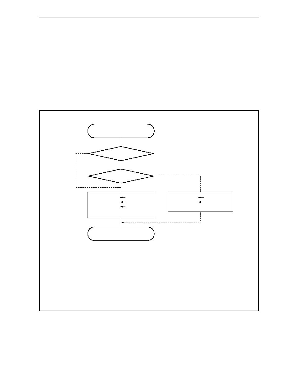
CHAPTER 7 INTERRUPT/EXCEPTION PROCESSING FUNCTION
167
User's Manual U14492EJ5V0UD
7.3.2 Restore
Recovery from maskable interrupt servicing is carried out by the RETI instruction.
When the RETI instruction is executed, the CPU performs the following processing, and transfers control to the
address of the restored PC.
(1) Restores the values of the PC and the PSW from EIPC and EIPSW because the EP bit of the PSW is 0 and
the NP bit of the PSW is 0.
(2) Transfers control to the address of the restored PC and PSW.
Figure 7-5 illustrates the processing of the RETI instruction.
Figure 7-5. RETI Instruction Processing
Note For the ISPR register, see 7.3.6 In-service priority register (ISPR).
Caution When the PSW.EP bit and the PSW.NP bit are changed by the LDSR instruction during
maskable interrupt servicing, in order to restore the PC and PSW correctly during recovery
by the RETI instruction, it is necessary to set PSW.EP back to 0 and PSW.NP back to 0 using
the LDSR instruction immediately before the RETI instruction.
Remark The solid lines show the CPU processing flow.
PSW.EP
RETI instruction
PSW.NP
Restores original processing
1
1
0
0
PC
PSW
Corresponding
bit of ISPR
Note
EIPC
EIPSW
0
PC
PSW
FEPC
FEPSW

CHAPTER 7 INTERRUPT/EXCEPTION PROCESSING FUNCTION
168
User's Manual U14492EJ5V0UD
7.3.3 Priorities of maskable interrupts
The V850E/IA1 provides multiple interrupt servicing in which an interrupt is acknowledged while another interrupt is
being serviced. Multiple interrupts can be controlled by priority levels.
There are two types of priority level control: control based on the default priority levels, and control based on the
programmable priority levels that are specified by the interrupt priority level specification bit (xxPRn) of the interrupt
control register (xxICn). When two or more interrupts having the same priority level specified by the xxPRn bit are
generated at the same time, interrupts are serviced in order depending on the priority level allocated to each interrupt
request type (default priority level) beforehand. For more information, refer to Table 7-1 Interrupt/Exception Source
List. The programmable priority control customizes interrupt requests into eight levels by setting the priority level
specification flag.
Note that when an interrupt request is acknowledged, the ID flag of PSW is automatically set to 1. Therefore, when
multiple interrupts are to be used, clear the ID flag to 0 beforehand (for example, by placing the EI instruction in the
interrupt service program) to set the interrupt enable mode.
Remark xx: Identification name of each peripheral unit (refer to Table 7-2)
n: Peripheral unit number (refer to Table 7-2)
CHAPTER 7 INTERRUPT/EXCEPTION PROCESSING FUNCTION
169
User's Manual U14492EJ5V0UD
Figure 7-6. Example of Servicing in Which Another Interrupt Request Is Issued While an
Interrupt Is Being Serviced (1/2)
Main routine
EI
EI
Interrupt request a
(level 3)
Servicing of a
Servicing of b
Servicing of c
Interrupt request c
(level 3)
Servicing of d
Servicing of e
EI
Interrupt request e
(level 2)
Servicing of f
EI
Servicing of g
Interrupt request g
(level 1)
Interrupt request h
(level 1)
Servicing of h
Interrupt request b is acknowledged because the
priority of b is higher than that of a and interrupts are
enabled.
Although the priority of interrupt request d is higher
than that of c, d is held pending because interrupts
are disabled.
Interrupt request f is held pending even if interrupts are
enabled because its priority is lower than that of e.
Interrupt request h is held pending even if interrupts are
enabled because its priority is the same as that of g.
Interrupt
request b
(level 2)
Interrupt request d
(level 2)
Interrupt request f
(level 3)
Caution The values of the EIPC and EIPSW registers must be saved before executing multiple
interrupts. When returning from multiple interrupt servicing, restore the values of EIPC and
EIPSW after executing the DI instruction.
Remarks 1. a to u in the figure are the temporary names of interrupt requests shown for the sake of
explanation.
2. The default priority in the figure indicates the relative priority between two interrupt requests.
CHAPTER 7 INTERRUPT/EXCEPTION PROCESSING FUNCTION
170
User's Manual U14492EJ5V0UD
Figure 7-6. Example of Servicing in Which Another Interrupt Request Is Issued While an
Interrupt Is Being Serviced (2/2)
Main routine
EI
Interrupt request i
(level 2)
Servicing of i
Servicing of k
Interrupt
request j
(level 3)
Servicing of j
Interrupt request l
(level 2)
EI
EI
EI
Interrupt request o
(level 3)
Interrupt request s
(level 1)
Interrupt request k
(level 1)
Servicing of l
Servicing of n
Servicing of m
Servicing of s
Servicing of u
Servicing of t
Interrupt
request m
(level 3)
Interrupt request n
(level 1)
Servicing of o
Interrupt
request p
(level 2)
Interrupt
request q
(level 1)
Interrupt
request r
(level 0)
Interrupt request u
(level 2)
Note 2
Interrupt
request t
(level 2)
Note 1
Servicing of p
Servicing of q
Servicing of r
EI
If levels 3 to 0 are acknowledged
Interrupt request j is held pending because its
priority is lower than that of i.
k that occurs after j is acknowledged because it
has the higher priority.
Interrupt requests m and n are held pending
because servicing of l is performed in the interrupt
disabled status.
Pending interrupt requests are acknowledged after
servicing of interrupt request l.
At this time, interrupt requests n is acknowledged
first even though m has occurred first because the
priority of n is higher than that of m.
Pending interrupt requests t and u are
acknowledged after servicing of s.
Because the priorities of t and u are the same, u is
acknowledged first because it has the higher
default priority, regardless of the order in which the
interrupt requests have been generated.
Caution The values of the EIPC and EIPSW registers must be saved before executing multiple
interrupts. When returning from multiple interrupt servicing, restore the values of EIPC
and EIPSW after executing the DI instruction.
Notes 1. Lower default priority
2. Higher default priority
CHAPTER 7 INTERRUPT/EXCEPTION PROCESSING FUNCTION
171
User's Manual U14492EJ5V0UD
Figure 7-7. Example of Servicing Interrupt Requests Generated Simultaneously
Default priority
a > b > c
Main routine
EI
Interrupt request a (level 2)
Interrupt request b (level 1)
Interrupt request c (level 1)
Servicing of interrupt request b
.
.
Servicing of interrupt request c
Servicing of interrupt request a
Interrupt requests b and c are
acknowledged first according to
their priorities.
Because the priorities of b and c are
the same, b is acknowledged first
according to the default priority.
Caution The values of the EIPC and EIPSW registers must be saved before executing multiple
interrupts. When returning from multiple interrupt servicing, restore the values of EIPC and
EIPSW after executing the DI instruction.
Remark a to c in the figure are the temporary names of interrupt requests shown for the sake of explanation.
CHAPTER 7 INTERRUPT/EXCEPTION PROCESSING FUNCTION
172
User's Manual U14492EJ5V0UD
7.3.4 Interrupt control register (xxICn)
An interrupt control register is assigned to each interrupt request (maskable interrupt) and sets the control
conditions for each maskable interrupt request.
This register can be read/written in 8-bit or 1-bit units.
Caution Read the xxIFn bit of the xxICn register in the interrupt disabled (DI) state. Otherwise if the
timing of interrupt acknowledgment and bit reading conflict, normal values may not be read.
Address
FFFFF110H to
FFFFF176H
<7>
xxIFn
xxICn
<6>
xxMKn
5
0
4
0
3
0
<2>
xxPRn2
<1>
xxPRn1
<0>
xxPRn0
Initial value
47H
Bit position
Bit name
Function
7
xxIFn
This is an interrupt request flag.
0: Interrupt request not issued
1: Interrupt request issued
The flag xxlFn is reset automatically by the hardware if an interrupt request is
acknowledged.
6
xxMKn
This is an interrupt mask flag.
0: Enables interrupt servicing
1: Disables interrupt servicing (pending)
8 levels of priority order are specified for each interrupt.
xxPRn2 xxPRn1 xxPRn0
Interrupt
priority specification bit
0
0
0
Specifies level 0 (highest).
0
0
1
Specifies level 1.
0
1
0
Specifies level 2.
0
1
1
Specifies level 3.
1
0
0
Specifies level 4.
1
0
1
Specifies level 5.
1
1
0
Specifies level 6.
1
1
1
Specifies level 7 (lowest).
2 to 0
xxPRn2 to
xxPRn0
Remark xx: Identification name of each peripheral unit (refer to Table 7-2)
n: Peripheral unit number (refer to Table 7-2)
The address and bit of each interrupt control register are as follows.

CHAPTER 7 INTERRUPT/EXCEPTION PROCESSING FUNCTION
173
User's Manual U14492EJ5V0UD
Table 7-2. Addresses and Bits of Interrupt Control Registers (1/2)
Bit
Address Register
<7>
<6>
5 4 3
<2>
<1>
<0>
FFFFF110H
P0IC0
P0IF0
P0MK0
0 0 0
P0PR02
P0PR01
P0PR00
FFFFF112H
P0IC1
P0IF1
P0MK1
0 0 0
P0PR12
P0PR11
P0PR10
FFFFF114H
P0IC2
P0IF2
P0MK2
0 0 0
P0PR22
P0PR21
P0PR20
FFFFF116H
P0IC3
P0IF3
P0MK3
0 0 0
P0PR32
P0PR31
P0PR30
FFFFF118H
P0IC4
P0IF4
P0MK4
0 0 0
P0PR42
P0PR41
P0PR40
FFFFF11AH
P0IC5
P0IF5
P0MK5
0 0 0
P0PR52
P0PR51
P0PR50
FFFFF11CH
P0IC6
P0IF6
P0MK6
0 0 0
P0PR62
P0PR61
P0PR60
FFFFF11EH DETIC0 DETIF0
DETMK0
0 0 0
DETPR02
DETPR01
DETPR00
FFFFF120H DETIC1 DETIF1
DETMK1
0 0 0
DETPR12
DETPR11
DETPR10
FFFFF122H
TM0IC0
TM0IF0
TM0MK0
0 0 0
TM0PR02
TM0PR01
TM0PR00
FFFFF124H
CM03IC0
CM03IF0
CM03MK0
0 0 0
CM03PR02 CM03PR01 CM03PR00
FFFFF126H
TM0IC1
TM0IF1
TM0MK1
0 0 0
TM0PR12
TM0PR11
TM0PR10
FFFFF128H CM03IC1 CM03IF1
CM03MK1
0 0 0
CM03PR12 CM03PR11 CM03PR10
FFFFF12AH
CC10IC0
CC10IF0
CC10MK0
0 0 0
CC10PR02 CC10PR01
CC10PR00
FFFFF12CH
CC10IC1
CC10IF1
CC10MK1
0 0 0
CC10PR12 CC10PR11
CC10PR10
FFFFF12EH CM10IC0 CM10IF0
CM10MK0
0 0 0
CM10PR02 CM10PR01 CM10PR00
FFFFF130H CM10IC1 CM10IF1
CM10MK1
0 0 0
CM10PR12 CM10PR11 CM10PR10
FFFFF132H
CC11IC0
CC11IF0
CC11MK0
0 0 0
CC11PR02 CC11PR01
CC11PR00
FFFFF134H
CC11IC1
CC11IF1
CC11MK1
0 0 0
CC11PR12 CC11PR11
CC11PR10
FFFFF136H CM11IC0 CM11IF0
CM11MK0
0 0 0
CM11PR02 CM11PR01 CM11PR00
FFFFF138H CM11IC1 CM11IF1
CM11MK1
0 0 0
CM11PR12 CM11PR11 CM11PR10
FFFFF13AH
TM2IC0
TM2IF0
TM2MK0
0 0 0
TM2PR02
TM2PR01
TM2PR00
FFFFF13CH
TM2IC1
TM2IF1
TM2MK1
0 0 0
TM2PR12
TM2PR11
TM2PR10
FFFFF13EH
CC2IC0
CC2IF0
CC2MK0
0 0 0
CC2PR02
CC2PR01
CC2PR00
FFFFF140H
CC2IC1
CC2IF1
CC2MK1
0 0 0
CC2PR12
CC2PR11
CC2PR10
FFFFF142H
CC2IC2
CC2IF2
CC2MK2
0 0 0
CC2PR22
CC2PR21
CC2PR20
FFFFF144H
CC2IC3
CC2IF3
CC2MK3
0 0 0
CC2PR32
CC2PR31
CC2PR30
FFFFF146H
CC2IC4
CC2IF4
CC2MK4
0 0 0
CC2PR42
CC2PR41
CC2PR40
FFFFF148H
CC2IC5
CC2IF5
CC2MK5
0 0 0
CC2PR52
CC2PR51
CC2PR50
FFFFF14AH
TM3IC0
TM3IF0
TM3MK0
0 0 0
TM3PR02
TM3PR01
TM3PR00
FFFFF14CH
CC3IC0
CC3IF0
CC3MK0
0 0 0
CC3PR02
CC3PR01
CC3PR00
FFFFF14EH
CC3IC1
CC3IF1
CC3MK1
0 0 0
CC3PR12
CC3PR11
CC3PR10
FFFFF150H
CM4IC0
CM4IF0
CANMK2
0 0 0
CM4PR02
CM4PR01
CM4PR00
FFFFF152H
DMAIC0
DMAIF0
DMAMK0
0 0 0
DMAPR02
DMAPR01
DMAPR00
FFFFF154H
DMAIC1
DMAIF1
DMAMK1
0 0 0
DMAPR12
DMAPR11
DMAPR10
FFFFF156H
DMAIC2
DMAIF2
DMAMK2
0 0 0
DMAPR22
DMAPR21
DMAPR20
FFFFF158H
DMAIC3
DMAIF3
DMAMK3
0 0 0
DMAPR32
DMAPR31
DMAPR30
FFFFF15AH CANIC0 CANIF0
CANMK0
0 0 0
CANPR02
CANPR01
CANPR00
FFFFF15CH
CANIC1
CANIF1
CANMK1
0 0 0
CANPR12
CANPR11
CANPR10
FFFFF15EH CANIC2 CANIF2
CANMK2
0 0 0
CANPR22
CANPR21
CANPR20
FFFFF160H
CANIC3
CANIF3
CANMK3
0 0 0
CANPR32
CANPR31
CANPR30
FFFFF162H
CSIIC0
CSIIF0
CSIMK0
0 0 0
CSIPR02
CSIPR01
CSIPR00

CHAPTER 7 INTERRUPT/EXCEPTION PROCESSING FUNCTION
174
User's Manual U14492EJ5V0UD
Table 7-2. Addresses and Bits of Interrupt Control Registers (2/2)
Bit
Address Register
<7>
<6>
5 4 3
<2>
<1>
<0>
FFFFF164H
CSIIC1
CSIIF1
CSIMK1
0 0 0
CSIPR12
CSIPR11
CSIPR10
FFFFF166H
SRIC0
SRIF0
SRMK0
0 0 0
SRPR02
SRPR01
SRPR00
FFFFF168H
STIC0
STIF0
STMK0
0 0 0
STPR02
STPR01
STPR00
FFFFF16AH
SEIC0
SEIF0
SEMK0
0 0 0
SEPR02
SEPR01
SEPR00
FFFFF16CH
SRIC1
SRIF1
SRMK1
0 0 0
SRPR12
SRPR11
SRPR10
FFFFF16EH
STIC1
STIF1
STMK1
0 0 0
STPR12
STPR11
STPR10
FFFFF170H
SRIC2
SRIF2
SRMK2
0 0 0
SRPR22
SRPR21
SRPR20
FFFFF172H
STIC2
STIF2
STMK2
0 0 0
STPR22
STPR21
STPR20
FFFFF174H
ADIC0
ADIF0
ADMK0
0 0 0
ADPR02
ADPR01
ADPR00
FFFFF176H
ADIC1
ADIF1
ADMK1
0 0 0
ADPR12
ADPR11
ADPR10
CHAPTER 7 INTERRUPT/EXCEPTION PROCESSING FUNCTION
175
User's Manual U14492EJ5V0UD
7.3.5 Interrupt mask registers 0 to 3 (IMR0 to IMR3)
These registers set the interrupt mask state for the maskable interrupts.
The xxMKn bit of the IMR0 to IMR3 registers is equivalent to the xxMKn bit of the xxICn register.
IMRm can be read/written in 16-bit units (m = 0 to 3).
When the IMRm register is divided into two registers: higher 8 bits (IMRmH register) and lower 8 bits (IMRmL
register), these registers can be read/written in 8-bit or 1-bit units.
Caution The device file defines the xxMKn bit of the xxICn register as a reserved word. If a bit is
manipulated with the name xxMKn, therefore, the xxICn register, rather than the IMRm register, is
rewritten (as a result, the IMRm register is also rewritten).
<15>
CM10MK0
<7>
DETMK0
IMR0
<14>
CC10MK1
<6>
P0MK6
<13>
CC10MK0
<5>
P0MK5
<12>
CM03MK1
<4>
P0MK4
<11>
TM0MK1
<3>
P0MK3
<10>
CM03MK0
<2>
P0MK2
<9>
TM0MK0
<1>
P0MK1
<8>
DETMK1
<0>
P0MK0
Address
FFFFF100H
Initial value
FFFFH
<15>
CC3MK1
<7>
CC2MK0
IMR1
<14>
CC3MK0
<6>
TM2MK1
<13>
TM3MK0
<5>
TM2MK0
<12>
CC2MK5
<4>
CM11MK1
<11>
CC2MK4
<3>
CM11MK0
<10>
CC2MK3
<2>
CC11MK1
<9>
CC2MK2
<1>
CC11MK0
<8>
CC2MK1
<0>
CM10MK1
Address
FFFFF102H
Initial value
FFFFH
<15>
STMK1
<7>
CANMK2
IMR2
<14>
SRMK1
<6>
CANMK1
<13>
SEMK0
<5>
CANMK0
<12>
STMK0
<4>
DMAMK3
<11>
SRMK0
<3>
DMAMK2
<10>
CSIMK1
<2>
DMAMK1
<9>
CSIMK0
<1>
DMAMK0
<8>
CANMK3
<0>
CM4MK0
Address
FFFFF104H
Initial value
FFFFH
15
1
7
1
IMR3
14
1
6
1
13
1
5
1
12
1
4
1
11
1
<3>
ADMK1
10
1
<2>
ADMK0
9
1
<1>
STMK2
8
1
<0>
SRMK2
Address
FFFFF106H
Initial value
FFFFH
Bit position
Bit name
Function
15 to 0
(IMR0 to 2),
0 to 3 (IMR3)
xxMKn
Interrupt mask flag
0: Interrupt servicing enabled
1: Interrupt servicing disabled (pending)
Remark xx: Identification name of each peripheral unit (refer to Table 7-2)
n: Peripheral unit number (refer to Table 7-2)
CHAPTER 7 INTERRUPT/EXCEPTION PROCESSING FUNCTION
176
User's Manual U14492EJ5V0UD
7.3.6 In-service
priority register (ISPR)
This register holds the priority level of the maskable interrupt currently acknowledged. When an interrupt request is
acknowledged, the bit of this register corresponding to the priority level of that interrupt request is set to 1 and remains
set while the interrupt is serviced.
When the RETI instruction is executed, the bit corresponding to the interrupt request having the highest priority is
automatically cleared to 0 by hardware. However, it is not cleared to 0 when execution is returned from non-maskable
interrupt servicing or exception processing.
This register is read-only, in 8-bit or 1-bit units.
Caution In the interrupt enabled (EI) state, if an interrupt is acknowledged during the reading of the ISPR
register, the value of the ISPR register may be read after the bit is set to 1 by this interrupt
acknowledgment. To read the value of the ISPR register properly before interrupt
acknowledgment, read it in the interrupt disabled (DI) state.
Address
FFFFF1FAH
<7>
ISPR7
ISPR
<6>
ISPR6
<5>
ISPR5
<4>
ISPR4
<3>
ISPR3
<2>
ISPR2
<1>
ISPR1
<0>
ISPR0
Initial value
00H
Bit position
Bit name
Function
7 to 0
ISPR7 to ISPR0
Indicates priority of interrupt currently acknowledged
0: Interrupt request with priority n not acknowledged
1: Interrupt request with priority n acknowledged
Remark n = 0 to 7 (priority level)
CHAPTER 7 INTERRUPT/EXCEPTION PROCESSING FUNCTION
177
User's Manual U14492EJ5V0UD
7.3.7 Maskable interrupt status flag (ID)
The ID flag is bit 5 of the PSW and this controls the maskable interrupt's operating state, and stores control
information regarding enabling or disabling of interrupt requests.
31
0
PSW
Initial value
00000020H
7
NP
6
EP
5
ID
4
SAT
3
CY
2
OV
1
S Z
8
0
0
0
0
0
0
0
0
0
0
0
0
0
0
0
0
0
0
0
0
0
0
0
0
Bit position
Bit name
Function
5 ID
Indicates whether maskable interrupt servicing is enabled or disabled.
0: Maskable interrupt request acknowledgment enabled
1: Maskable interrupt request acknowledgment disabled (pending)
This bit is set to 1 by the DI instruction and reset to 0 by the EI instruction. Its
value is also modified by the RETI instruction or LDSR instruction when
referencing the PSW.
Non-maskable interrupt requests and exceptions are acknowledged regardless
of this flag. When a maskable interrupt is acknowledged, the ID flag is
automatically set to 1 by hardware.
The interrupt request generated during the acknowledgment disabled period (ID
= 1) is acknowledged when the xxIFn bit of xxICn register is set to 1, and the ID
flag is reset to 0.
7.3.8 Interrupt trigger mode selection
The valid edge of the INTPn, ADTRG0, ADTRG1, TIUD10, TIUD11, TCUD10, TCUD11, TCLR10, TCLR11,
TCLR3, and TI3 pins can be selected by program. The edge that can be selected as the valid edge is one of the
following (n = 0 to 6, 20 to 25, 30, 31, 100, 101, 110, 111).
∑ Rising edge
∑ Falling edge
∑ Both the rising and falling edges
When the INTPn, ADTRG0, ADTRG1, TIUD10, TIUD11, TCUD10, TCUD11, TCLR10, TCLR11, TCLR3, and TI3
signals are edge-detected, they become an interrupt source or capture/trigger.
The valid edge is specified by external interrupt mode registers 1 and 2 (INTM1 and INTM2), signal edge selection
registers 10 and 11 (SESA10 and SESA11), the valid edge selection register (SESC), and TM2 input filter mode
registers 0 to 5 (FEM0 to FEM5).
CHAPTER 7 INTERRUPT/EXCEPTION PROCESSING FUNCTION
178
User's Manual U14492EJ5V0UD
(1) External interrupt mode registers 1, 2 (INTM1, INTM2)
These registers specify the valid edge for external interrupt requests (INTP0 to INTP6), input via external
pins. The correspondence between each register and the external interrupt requests that register controls is
shown below.
∑ INTM1: INTP0, INTP1, INTP2/ADTRG0, INTP3/ADTRG1
∑ INTM2: INTP4 to INTP6
INTP2 and INTP3 function alternately as ADTRG0 and ADTRG1 (A/D converter external trigger input).
Therefore, if the external trigger mode has been set by the TRG0 to TRG2 bits of A/D converter mode register
n0 (ADSCMn0), setting the ES20 and ES21, and ES30 and ES31 bits of INTM1 also specifies the valid edge
of the external trigger input (ADTRG0 and ADTRG1) (n = 0, 1).
The valid edge can be specified independently for each pin (rising edge, falling edge, or both rising and falling
edges).
These registers can be read/written in 8-bit or 1-bit units.
7
ES31
INTM1
6
ES30
5
ES21
4
ES20
3
ES11
2
ES10
1
ES01
0
ES00
Address
FFFFF882H
Initial value
00H
INTP3/ADTRG1
INTP2/ADTRG0
INTP1
INTP0
7
0
INTM2
6
0
5
ES61
4
ES60
3
ES51
2
ES50
1
ES41
0
ES40
Address
FFFFF884H
Initial value
00H
INTP6
INTP5
INTP4
Bit position
Bit name
Function
Specifies the valid edge of the INTPn, ADTRG0 and ADTRG1 pins.
ESn1 ESn0
Operation
0 0
Falling
edge
0 1
Rising
edge
1 0
Setting
prohibited
1
1
Both rising and falling edges
7 to 0
(INTM1),
5 to 0
(INTM2)
ESn1, ESn0
(n = 0 to 6)

CHAPTER 7 INTERRUPT/EXCEPTION PROCESSING FUNCTION
179
User's Manual U14492EJ5V0UD
(2) Signal edge selection registers 10, 11 (SESA10, SESA11)
These registers specify the valid edge of external interrupt requests (INTP100, INTP101, INTP110, INTP111,
TIUD10, TIUD11, TCUD10, TCUD11, TCLR10, and TCLR11), input via external pins. The correspondence
between each register and the external interrupt requests that register controls is shown below.
∑ SESA10: TIUD10, TCUD10, TCLR10, INTP100, INTP101
∑ SESA11: TIUD11, TCUD11, TCLR11, INTP110, INTP111
The valid edge can be specified independently for each pin (rising edge, falling edge, or both rising and falling
edges).
These registers can be read/written in 8-bit or 1-bit units.
Cautions 1. The bits of the SESA1n register cannot be changed during TM1n operation (TM1CEn bit
of timer control registers 10, 11 (TMC10, TMC11) = 1).
2. The TM1CEn bit must be set (1) before using the TCUD10/INTP100, TCLR10/INTP101,
TCUD11/INTP110, and TCLR11/INTP111 pins as INTP100, INTP101, INTP110, and
INTP111, even if not using timer 1.
3. Before setting the INTP100, INTP101, INTP110, INTP111, TIUD10, TIUD11, TCUD10,
TCUD11, TCLR10, and TCLR11 pins to the trigger mode, set the PMC1 register.
If the PMC1 register is set after the SESA10 and SESA11 registers have been set, an
illegal interrupt may occur as soon as the PMC1 register is set.
CHAPTER 7 INTERRUPT/EXCEPTION PROCESSING FUNCTION
180
User's Manual U14492EJ5V0UD
(1/2)
7
TESUD01
SESA10
6
TESUD00
5
CESUD01
4
CESUD00
3
IES1011
2
IES1010
1
IES1001
0
IES1000
Address
FFFFF5EDH
Initial value
00H
TIUD10, TCUD10
TCLR10
INTP101
INTP100
7
TESUD11
SESA11
6
TESUD10
5
CESUD11
4
CESUD10
3
IES1111
2
IES1110
1
IES1101
0
IES1100
Address
FFFFF60DH
Initial value
00H
TCLR11
TIUD11, TCUD11
INTP111
INTP110
Bit position
Bit name
Function
Specifies the valid edge of the TIUD10, TIUD11, TCUD10, and TCUD11 pins.
TESUDn1 TESUDn0
Valid
edge
0 0
Falling
edge
0 1
Rising
edge
1 0
Setting
prohibited
1
1
Both rising and falling edges
7, 6
TESUDn1,
TESUDn0
Cautions 1. The values set to the TESUDn1 and TESUDn0 bits are valid only in
UDC mode A
Note 1
and UDC mode B
Note 1
.
2. If TM1n operation has been specified in mode 4
Note 2
, the valid edge
specification (TESUDn1 and TESUDn0 bits) for the TIUD1n and
TCUD1n pins is invalid.
Specifies the valid edge of the TCLR10 and TCLR11 pins.
CESUDn1 CESUDn0
Valid
edge
0 0
Falling
edge
0 1
Rising
edge
1 0
Low
level
1 1
High
level
5, 4
CESUDn1,
CESUDn0
The setting values of the CESUDn1 and CESUDn0 bits and the operation of TM1n are
as follows.
00: TM1n cleared after detection of TCLR1n rising edge
01: TM1n cleared after detection of TCLR1n falling edge
10: TM1n holds cleared status while TCLR1n input is low level
11: TM1n holds cleared status while TCLR1n input is high level
Caution The values set to the CESUDn1 and CESUDn0 bits are valid only in
UDC mode A
Note 1
.
Remark n = 0, 1
Notes 1. See
9.2.4 (2) Timer unit mode registers 0, 1 (TUM0, TUM1)
2. See
9.2.4 (6) Prescaler mode registers 10, 11 (PRM10, PRM11)
CHAPTER 7 INTERRUPT/EXCEPTION PROCESSING FUNCTION
181
User's Manual U14492EJ5V0UD
(2/2)
Bit position
Bit name
Function
Specifies the valid edge of the pin selected using the CSLn bit of the CSL1n register
(INTP1n1, INTP1n0).
IES1n11 IES1n10
Valid
edge
0 0
Falling
edge
0 1
Rising
edge
1 0
Setting
prohibited
1
1
Both rising and falling edges
3, 2
IES1n11,
IES1n10
Specifies the valid edge of the INTP100 and INTP110 pins.
IES1n01 IES1n00
Valid
edge
0 0
Falling
edge
0 1
Rising
edge
1 0
Setting
prohibited
1, 0
IES1n01,
IES1n00
1
1
Both rising and falling edges
Remark n = 0, 1

CHAPTER 7 INTERRUPT/EXCEPTION PROCESSING FUNCTION
182
User's Manual U14492EJ5V0UD
(3) Valid edge selection register (SESC)
This register specifies the valid edge for external interrupt requests (INTP30, INTP31, TCLR3, and TI3), input
via external pins.
The valid edge can be specified independently for each pin (rising edge, falling edge, or both rising and falling
edges).
This register can be read/written in 8-bit or 1-bit units.
Cautions 1. The TM3CAE and TM3CE bits of timer control register 30 (TMC30) must be set (1) before
using the TI3/TCLR3/INTP30 and TO3/INTP31 pins as INTP30 and INTP31, even if not
using timer 3.
2. Before setting the INTP30, INTP31, TCLR3, and TI3 pins to the trigger mode, set the
PMC2 register.
If the PMC2 register is set after the SESC register has been set, an illegal interrupt may
occur as soon as the PMC2 register is set.
7
TES31
SESC
6
TES30
5
CES31
4
CES30
3
IES311
2
IES310
1
IES301
0
IES300
Address
FFFFF689H
Initial value
00H
TI3
TCLR3
INTP31
INTP30
Bit position
Bit name
Function
7, 6
TES31,
TES30
Specifies the valid edge of the INTP30, INTP31, TCLR3, and TI3 pins.
xESn1 xESn0
Operation
0 0
Falling
edge
5, 4
CES31,
CES30
0 1
Rising
edge
1 0
Setting
prohibited
1
1
Both rising and falling edges
3, 2
IES311,
IES310
1, 0
TES301,
TES300
Remark n = 3, 30, 31

CHAPTER 7 INTERRUPT/EXCEPTION PROCESSING FUNCTION
183
User's Manual U14492EJ5V0UD
(4) Timer 2 input filter mode registers 0 to 5 (FEM0 to FEM5)
These registers specify the valid edge for external interrupt requests input to timer 2 (INTP20 to INTP25).
The correspondence between each register and the external interrupt request that register controls is shown
below.
∑ FEM0: INTP20
∑ FEM1: INTP21
∑ FEM2: INTP22
∑ FEM3: INTP23
∑ FEM4: INTP24
∑ FEM5: INTP25
The valid edge can be specified independently for each pin (rising edge, falling edge, or both rising and falling
edges).
These registers can be read/written in 8-bit or 1-bit units.
Cautions 1. The STFTE bit of timer 2 clock stop register 0 (STOPTE0) must be cleared (0) before
using the TI2/INTP20, TO21/INTP21, TO22/INTP22, TO23/INTP23, TO24/INTP24, and
TCLR2/INTP25 pins as INTP20, INTP21, INTP22, INTP23, INTP24, and INTP25, even if not
using timer 2.
2. Before setting the INTP2n pin to the trigger mode, set the PMC2 register. If the PMC2
register is set after the FEMn register has been set, an illegal interrupt may occur as
soon as the PMC2 register is set (n = 0 to 5).
3. The noise elimination function starts operating by setting the CEEn bit of the TCRE0
register to 1 (enabling count operations).
CHAPTER 7 INTERRUPT/EXCEPTION PROCESSING FUNCTION
184
User's Manual U14492EJ5V0UD
(1/2)
7
DFEN00
FEM0
6
0
5
0
4
0
3
EDGE010
2
EDGE000
1
TMS010
0
TMS000
Address
FFFFF630H
Initial value
00H
INTP20
7
DFEN01
FEM1
6
0
5
0
4
0
3
EDGE011
2
EDGE001
1
TMS011
0
TMS001
Address
FFFFF631H
Initial value
00H
INTP21
7
DFEN02
FEM2
6
0
5
0
4
0
3
EDGE012
2
EDGE002
1
TMS012
0
TMS002
Address
FFFFF632H
Initial value
00H
INTP22
7
DFEN03
FEM3
6
0
5
0
4
0
3
EDGE013
2
EDGE003
1
TMS013
0
TMS003
Address
FFFFF633H
Initial value
00H
INTP23
7
DFEN04
FEM4
6
0
5
0
4
0
3
EDGE014
2
EDGE004
1
TMS014
0
TMS004
Address
FFFFF634H
Initial value
00H
INTP24
7
DFEN05
FEM5
6
0
5
0
4
0
3
EDGE015
2
EDGE005
1
TMS015
0
TMS005
Address
FFFFF635H
Initial value
00H
INTP25
Bit position
Bit name
Function
7
DFEN0n
Specifies the filter of the INTP2n pin.
0: Analog filter
1: Digital filter
Caution When the DFEN0n bit = 1, the sampling clock of the digital filter is f
XXTM2
(clock of TM20 and TM21 selected by PRM02 register).
Specifies the valid edge of the INTP2n pin.
EDGE01n EDGE00n
Operation
0
0
Interrupt by INTCC2n
Note
0 1
Rising
edge
1 0
Falling
edge
1
1
Both rising and falling edges
3, 2
EDGE01n,
EDGE00n
Note Set when INTCC2n is selected by a match between TM20, TM21 and the sub-
channel compare register (specified by the TMS01n, TMS00n bits) (n = 0 to 5).
Remark n = 0 to 5
CHAPTER 7 INTERRUPT/EXCEPTION PROCESSING FUNCTION
185
User's Manual U14492EJ5V0UD
(2/2)
Bit position
Bit name
Function
Selects the capture input
Note
.
TMS01n TMS00n
Operation
0
0
Used as a pin
0
1
Digital filter (noise eliminator specification)
1 0
Timer-based
capture to sub-channel 1
1 1
Timer-based
capture to sub-channel 2
1, 0
TMS01n,
TMS00n
Note Selection of capture input based on INTCM100 and INTCM101 is valid only for the FEM1 and FEM2
registers. Set the TMS01m and TMS00m bits of the FEMm register to 00B or 01B. All other settings
are prohibited (m = 1, 3 to 5).
Sub-channels 1 and 2 of timer 2 can be captured by INTP21, INTP22, and INTCM100, INTCM101.
An example is given below.
(a) When sub-channel 1 is captured by INTCM101
FEM1 register = xxxxxx10B
TMIC0 register = 00000010B
(b) When sub-channel 2 is captured by INTCM101
FEM2 register = xxxxxx11B
TMIC0 register = 00001000B
Remark n = 0 to 5
CHAPTER 7 INTERRUPT/EXCEPTION PROCESSING FUNCTION
186
User's Manual U14492EJ5V0UD
7.4 Software
Exception
A software exception is generated when the CPU executes the TRAP instruction, and can be always
acknowledged.
7.4.1 Operation
If a software exception occurs, the CPU performs the following processing, and transfers control to the handler
routine.
(1) Saves the restored PC to EIPC.
(2) Saves the current PSW to EIPSW.
(3) Writes an exception code to the lower 16 bits (EICC) of ECR (interrupt source).
(4) Sets the EP and ID bits of the PSW.
(5) Sets the handler address (00000040H or 00000050H) corresponding to the software exception to the PC, and
transfers control.
Figure 7-8 illustrates the processing of a software exception.
Figure 7-8. Software Exception Processing
TRAP instruction
EIPC
EIPSW
ECR.EICC
PSW.EP
PSW.ID
PC
restored PC
PSW
exception code
1
1
handler address
CPU processing
Exception processing
Note
Note TRAP instruction format: TRAP vector (the vector is a value from 00H to 1FH.)
The handler address is determined by the TRAP instruction's operand (vector). If the vector is 00H to 0FH, it
becomes 00000040H, and if the vector is 10H to 1FH, it becomes 00000050H.

CHAPTER 7 INTERRUPT/EXCEPTION PROCESSING FUNCTION
187
User's Manual U14492EJ5V0UD
7.4.2 Restore
Recovery from software exception processing is carried out by the RETI instruction.
By executing the RETI instruction, the CPU carries out the following processing and shifts control to the restored
PC's address.
(1) Loads the restored PC and PSW from EIPC and EIPSW because the EP bit of the PSW is 1.
(2) Transfers control to the address of the restored PC and PSW.
Figure 7-9 illustrates the processing of the RETI instruction.
Figure 7-9. RETI Instruction Processing
PSW.EP
RETI instruction
PC
PSW
EIPC
EIPSW
PSW.NP
Original processing restored
PC
PSW
FEPC
FEPSW
1
1
0
0
Caution When the PSW.EP bit and the PSW.NP bit are changed by the LDSR instruction during the
software exception processing, in order to restore the PC and PSW correctly during
recovery by the RETI instruction, it is necessary to set PSW.EP back to 1 using the LDSR
instruction immediately before the RETI instruction.
Remark The solid lines show the CPU processing flow.
CHAPTER 7 INTERRUPT/EXCEPTION PROCESSING FUNCTION
188
User's Manual U14492EJ5V0UD
7.4.3 Exception status flag (EP)
The EP flag is bit 6 of PSW, and is a status flag used to indicate that exception processing is in progress. It is set
when an exception occurs.
31
0
PSW
Initial value
00000020H
7
NP
6
EP
5
ID
4
SAT
3
CY
2
OV
1
S Z
8
0
0
0
0
0
0
0
0
0
0
0
0
0
0
0
0
0
0
0
0
0
0
0
0
Bit position
Bit name
Function
6 EP
Shows that exception processing is in progress.
0: Exception processing not in progress.
1: Exception processing in progress.

CHAPTER 7 INTERRUPT/EXCEPTION PROCESSING FUNCTION
189
User's Manual U14492EJ5V0UD
7.5 Exception
Trap
An exception trap is an interrupt that is requested when an illegal execution of an instruction takes place. In the
V850E/IA1, an illegal opcode exception (ILGOP: Illegal Opcode Trap) is considered as an exception trap.
7.5.1 Illegal opcode definition
The illegal instruction has an opcode (bits 10 to 5) of 111111B, a sub-opcode (bits 26 to 23) of 0111B to 1111B,
and a sub-opcode (bit 16) of 0B. An exception trap is generated when an instruction applicable to this illegal
instruction is executed.
15
16
23 22
◊ ◊ ◊ ◊ ◊ ◊
0
◊
◊
◊
◊
◊
◊
◊
◊
◊
◊
1
1
1
1
1
1
◊
◊
◊
◊
◊
27 26
31
0
4
5
10
11
1
1
1
1
1
1
0
1
to
◊: Arbitrary
Caution Since it is possible to assign this instruction to an illegal opcode in the future, it is
recommended that it not be used.
(1) Operation
If an exception trap occurs, the CPU performs the following processing, and transfers control to the handler
routine.
(1) Saves the restored PC to DBPC.
(2) Saves the current PSW to DBPSW.
(3) Sets the NP, EP, and ID bits of the PSW.
(4) Sets the handler address (00000060H) corresponding to the exception trap to the PC, and transfers
control.
Figure 7-10 illustrates the processing of the exception trap.

CHAPTER 7 INTERRUPT/EXCEPTION PROCESSING FUNCTION
190
User's Manual U14492EJ5V0UD
Figure 7-10. Exception Trap Processing
Exception trap (ILGOP) occurs
DBPC
DBPSW
PSW.NP
PSW.EP
PSW.ID
PC
restored PC
PSW
1
1
1
00000060H
Exception processing
CPU processing
(2) Restore
Recovery from an exception trap is carried out by the DBRET instruction. By executing the DBRET
instruction, the CPU carries out the following processing and controls the address of the restored PC.
(1) Loads the restored PC and PSW from DBPC and DBPSW.
(2) Transfers control to the address indicated by the restored PC and PSW.
Figure 7-11 illustrates the restore processing from an exception trap.
Figure 7-11. Restore Processing from Exception Trap
DBRET instruction
PC
PSW
DBPC
DBPSW
Jump to address of restored PC
CHAPTER 7 INTERRUPT/EXCEPTION PROCESSING FUNCTION
191
User's Manual U14492EJ5V0UD
7.5.2 Debug
trap
The debug trap is an exception that can be acknowledged every time and is generated by execution of the
DBTRAP instruction.
When the debug trap is generated, the CPU performs the following processing.
(1) Operation
(1) Saves the restored PC to DBPC.
(2) Saves the current PSW to DBPSW.
(3) Sets the NP, EP and ID bits of the PSW.
(4) Sets the handler address (00000060H) corresponding to the debug trap to the PC and transfers control.
Figure 7-12 illustrates the processing of the debug trap.
Figure 7-12. Debug Trap Processing
DBTRAP instruction
DBPC
DBPSW
PSW.NP
PSW.EP
PSW.ID
PC
restored PC
PSW
1
1
1
00000060H
Debug monitor routine processing
CPU processing
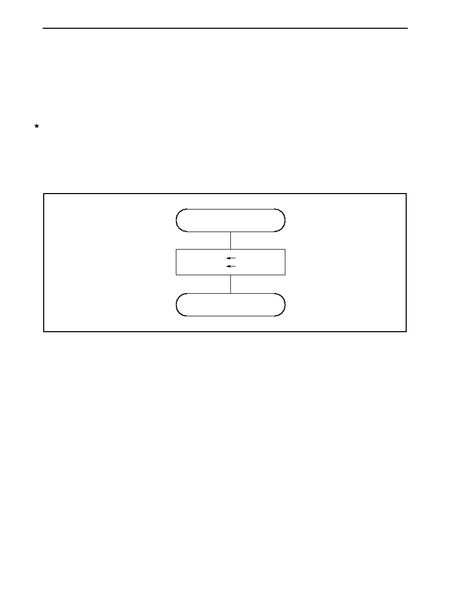
CHAPTER 7 INTERRUPT/EXCEPTION PROCESSING FUNCTION
192
User's Manual U14492EJ5V0UD
(2) Restore
Restoration from a debug trap is carried out by the DBRET instruction. By executing the DBRET instruction,
the CPU carries out the following processing and controls the address of the restored PC.
(1) Loads the restored PC and PSW from DBPC and DBPSW.
(2)
Transfers control to the address indicated by the restored PC and PSW.
Caution DBPC and DBPSW can be accessed during the period between when the DBTRAP is
executed and when the DBRET instruction is executed.
Figure 7-13 illustrates the processing for restoring from a debug trap.
Figure 7-13. Processing for Restoring from Debug Trap
DBRET instruction
PC
PSW
DBPC
DBPSW
Jump to address of restored PC

CHAPTER 7 INTERRUPT/EXCEPTION PROCESSING FUNCTION
193
User's Manual U14492EJ5V0UD
7.6 Multiple Interrupt Servicing Control
Multiple interrupt servicing control is a process by which an interrupt request that is currently being serviced can be
interrupted during servicing if there is an interrupt request with a higher priority level, and the higher priority interrupt
request is acknowledged and serviced first.
If there is an interrupt request with a lower priority level than the interrupt request currently being serviced, that
interrupt request is held pending.
Maskable interrupt multiple servicing control is executed when interrupts are enabled (ID = 0). Thus, if multiple
interrupts are executed, it is necessary for interrupts to be enabled (ID = 0) even during an interrupt servicing routine.
If a maskable interrupt or a software exception is generated in a maskable interrupt or software exception service
program, it is necessary to save EIPC and EIPSW.
This is accomplished by the following procedure.
(1) Acknowledgement of maskable interrupts in service program
Service program of maskable interrupt or exception
...
...
∑ EIPC saved to memory or register
∑ EIPSW saved to memory or register
∑ EI instruction (interrupt acknowledgment enabled)
...
...
Maskable interrupt acknowledgment
...
...
∑ DI instruction (interrupt acknowledgment disabled)
∑ Saved value restored to EIPSW
∑ Saved value restored to EIPC
∑ RETI instruction

CHAPTER 7 INTERRUPT/EXCEPTION PROCESSING FUNCTION
194
User's Manual U14492EJ5V0UD
(2) Generation of exception in service program
Service program of maskable interrupt or exception
...
...
∑ EIPC saved to memory or register
∑ EIPSW saved to memory or register
...
∑ TRAP instruction
Exception such as TRAP instruction acknowledged.
...
∑ Saved value restored to EIPSW
∑ Saved value restored to EIPC
∑ RETI instruction
The priority order for multiple interrupt servicing control has 8 levels, from 0 to 7 for each maskable interrupt
request (0 is the highest priority), but it can be set as desired via software. Setting of the priority order level is
done using the xxPRn0 to xxPRn2 bits of the interrupt request control register (xxlCn), which is provided for
each maskable interrupt request. After system reset, an interrupt request is masked by the xxMKn bit and the
priority order is set to level 7 by the xxPRn0 to xxPRn2 bits.
The priority order of maskable interrupts is as follows.
(High) Level 0 > Level 1 > Level 2 > Level 3 > Level 4 > Level 5 > Level 6 > Level 7 (Low)
Interrupt servicing that has been suspended as a result of multiple servicing control is resumed after the
servicing of the higher priority interrupt has been completed and the RETI instruction has been executed.
A pending interrupt request is acknowledged after the current interrupt servicing has been completed and the
RETI instruction has been executed.
Caution In a non-maskable interrupt servicing routine (time until the RETI instruction is executed),
maskable interrupts are suspended and not acknowledged.
7.7 Interrupt Response Time
The following table describes the V850E/IA1 interrupt response time (from interrupt generation to start of interrupt
servicing).
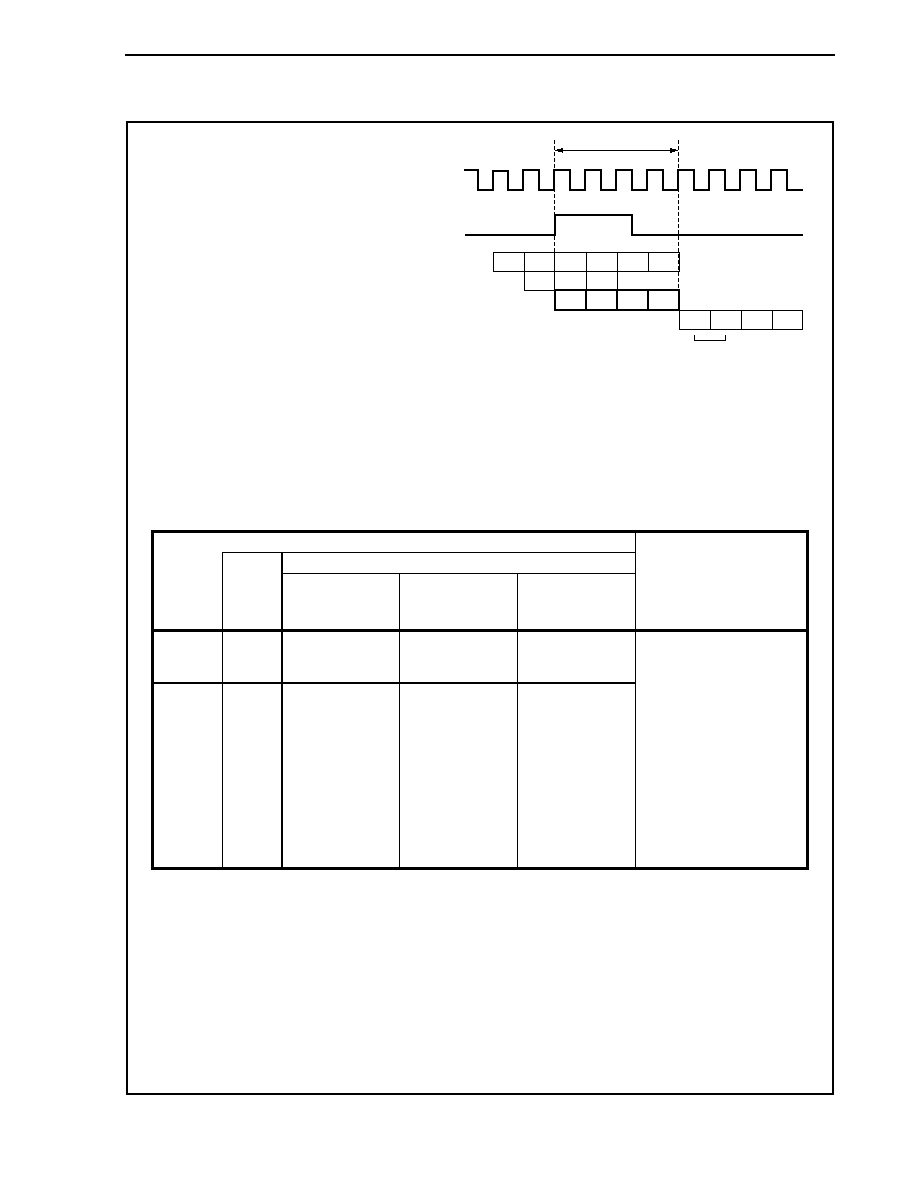
CHAPTER 7 INTERRUPT/EXCEPTION PROCESSING FUNCTION
195
User's Manual U14492EJ5V0UD
Figure 7-14. Pipeline Operation at Interrupt Request Acknowledgement (Outline)
Internal clock
Instruction 1
Instruction 2
Interrupt acknowledgment operation
Instruction (start instruction of interrupt servicing routine)
Interrupt request
IF
ID
EX
DF
WB
IFX
IDX
4 system clocks
IF
Interleave
access
Note
IF
ID
EX
INT1 INT2 INT3 INT4
IF
IFX
Note For details of interleave access, refer to 8.1.2 2-clock branch in V850E1 Architecture User's Manual
(U14559E).
Remark INT1 to INT4: Interrupt acknowledgment processing
IFX:
Invalid instruction fetch
IDX:
Invalid instruction decode
Interrupt response time (internal system clock (f
XX
))
External interrupt
Internal
interrupt
INTP0 to INTP6,
INTP20 to INTP25
INTP20 to INTP25
INTP100, INTP101,
INTP110, INTP111
INTP30, INTP31
Condition
Minimum 4
4
+
analog delay time
4 +
digital noise filter
4 + Note 1 +
digital noise filter
Maximum 7
Note 2
7
+
analog delay time
7 +
digital noise filter
7 + Note 1 +
digital noise filter
The following cases are
exceptions.
∑ In IDLE/software STOP
mode
∑ External bus access
∑ Two or more interrupt
request non-sampling
instructions are executed
in succession
∑ Access to on-chip
peripheral I/O register
∑ Access to programmable
peripheral I/O register
Notes 1. The number of internal system clocks are as follows.
∑ For timers 10, 11 (TM10, TM11) using INTP100, INTP101, INTP110, and INTP111 as external
interrupt inputs (see 9.2.4 (1) Timer 1/timer 2 clock selection register (PRM02)):
f
CLK
= f
XX
/2 (PRM2 bit = 1): 2
f
CLK
= f
XX
/4 (PRM2 bit = 0): 4
∑ For timer 3 (TM3) using INTP30 and INTP31 as external interrupt inputs (see 9.4.4 (1) Timer
3 clock selection register (PRM03)):
f
CLK
= f
XX
(PRM3 bit = 1): 2
f
CLK
= f
XX
/2 (PRM3 bit = 0): 4
2. When LD instruction is executed to internal ROM (during align access)

CHAPTER 7 INTERRUPT/EXCEPTION PROCESSING FUNCTION
196
User's Manual U14492EJ5V0UD
7.8 Periods in Which CPU Does Not Acknowledge Interrupts
The CPU acknowledges an interrupt while an instruction is being executed. However, no interrupt will be
acknowledged between an interrupt request non-sampling instruction and the next instruction (interrupt is held
pending).
The interrupt request non-sampling instructions are as follows.
∑ EI instruction
∑ DI instruction
∑ LDSR reg2, 0x5 instruction (for PSW)
∑ The store instruction for the command register (PRCMD)
∑ The store instructions or bit manipulation instructions of SET1, CLR1, and NOT1 instructions for the following
registers:
∑ Interrupt-related registers:
Interrupt control register (xxICn), interrupt mask registers 0 to 3 (IMR0 to IMR3)
∑ Power save control register (PSC)
∑ CSI-related registers:
Clocked serial interface mode registers 0, 1 (CSIM0, CSIM1)
Clocked serial interface clock selection registers 0, 1 (CSIC0, CSIC1)
Clocked serial interface receive buffer registers 0, 1 (SIRB0, SIRB1)
Clocked serial interface receive buffer registers L0, L1 (SIRBL0, SIRBL1)
Clocked serial interface transmit buffer registers 0, 1 (SOTB0, SOTB1)
Clocked serial interface transmit buffer registers L0, L1 (SOTBL0, SOTBL1)
Clocked serial interface read-only receive buffer registers 0, 1 (SIRBE0, SIRBE1)
Clocked serial interface read-only receive buffer registers L0, L1 (SIRBEL0, SIRBEL1)
Clocked serial interface initial transmit buffer registers 0, 1 (SOTBF0, SOTBF1)
Clocked serial interface initial transmit buffer registers L0, L1 (SOTBFL0, SOTBFL1)
Serial I/O shift registers 0, 1 (SIO0, SIO1)
Serial I/O shift registers L0, L1 (SIOL0, SIOL1)
Prescaler mode register (PRSM3)
Prescaler compare register (PRSCM3)
∑ FCAN clock selection register (PRM04)
Remark xx: Identification name of each peripheral unit (refer to Table 7-2)
n: Peripheral unit number (refer to Table 7-2)
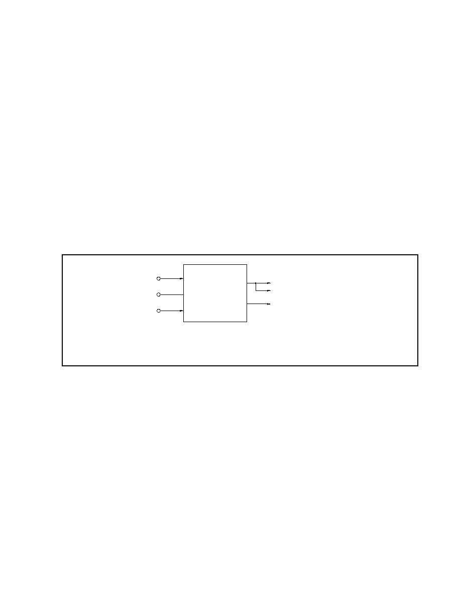
197
User's Manual U14492EJ5V0UD
CHAPTER 8 CLOCK GENERATION FUNCTION
The clock generator (CG) generates and controls the internal system clock (f
XX
) that is supplied to each internal
unit, such as the CPU.
8.1 Features
∑ Multiplier function using a phase locked loop (PLL) synthesizer
∑ Clock sources
∑ Oscillation by connecting a resonator
∑ External clock
∑ Power saving modes
∑ HALT mode
∑ IDLE mode
∑ Software STOP mode
∑ Internal system clock output function
8.2 Configuration
X1
X2
Clock
generator
(CG)
CKSEL
(f
X
)
CPU, on-chip peripheral I/O
Time base counter (TBC)
CLKOUT
f
XX
Remark f
X
: External resonator or external clock frequency
f
XX
: Internal system clock
CHAPTER 8 CLOCK GENERATION FUNCTION
198
User's Manual U14492EJ5V0UD
8.3 Input Clock Selection
The clock generator consists of an oscillator and a PLL synthesizer. For example, connecting a 5.0 MHz crystal
resonator or ceramic resonator to pins X1 and X2 enables a 50 MHz internal system clock (f
XX
) to be generated when
the multiplier is 10. Also, an external clock can be input directly to the oscillator. In this case, the clock signal should
be input only to pin X1 (pin X2 should be left open). Two basic operation modes are provided for the clock generator.
These are PLL mode and direct mode. The operation mode is selected by the CKSEL pin. The input to this pin is
latched on reset.
CKSEL
Operating Mode
0 PLL
mode
1 Direct
mode
Caution The input level for the CKSEL pin must be fixed. If it is switched during operation, a
malfunction may occur.
8.3.1 Direct mode
In direct mode, an external clock is divided by two and the divided clock is supplied as the internal system clock.
The maximum frequency that can be input in direct mode is 50 MHz. The V850E/IA1 is mainly used in application
systems in which operates at relatively low frequencies.
Caution In direct mode, an external clock must be input (an external resonator should not be
connected).
8.3.2 PLL mode
In PLL mode, an external resonator is connected or external clock is input and multiplied by the PLL synthesizer.
The multiplied PLL output is divided by the division ratio specified by the clock control register (CKC) to generate a
system clock that is 10, 5, 2.5, or 1 times the frequency (f
X
) of the external resonator or external clock.
After reset, an internal system clock (f
XX
) that is 1 time the frequency (1
◊
f
X
) of the input clock frequency (f
X
) is
generated.
When a frequency that is 10 times (10
◊ f
X
) the input clock frequency (f
X
) is generated, a system with low noise and
low power consumption can be realized because a frequency of up to 50 MHz is obtained based on a 5 MHz external
resonator or external clock.
In PLL mode, if the clock supply from an external resonator or external clock source stops, operation of the internal
system clock (f
XX
) based on the self-propelled frequency of the clock generator's internal voltage controlled oscillator
(VCO) continues. In this case, f
XX
is undefined. However, do not devise an application method expecting to use this
self-propelled frequency.
Example: Clocks when PLL mode (f
XX
= 10
◊ f
X
) is used
Internal System Clock Frequency (f
XX
)
External Resonator or External Clock Frequency (f
X
)
50.000 MHz
5.0000 MHz
40.000 MHz
4.0000 MHz
CHAPTER 8 CLOCK GENERATION FUNCTION
199
User's Manual U14492EJ5V0UD
Caution When using the PLL mode, only an f
X
(4 to 5 MHz) value for which 10
◊ f
X
does not exceed the
system clock maximum frequency (50 MHz) can be used for the oscillation frequency or
external clock frequency.
When
5
◊ f
X
, 2.5
◊ f
X
, or 1
◊ f
X
is used, a frequency of 4 to 6.4 MHz can be used.
Remark Note the following when PLL mode is selected (f
XX
= 5
◊ f
X
, f
XX
= 2.5
◊ f
X
, or f
XX
= 1
◊ f
X
)
If the V850E/IA1 need not be operated at high frequency, use f
XX
= 5
◊
f
X
, f
XX
= 2.5
◊ f
X
, or f
XX
= 1
◊ f
X
to reduce the power consumption by lowering the system clock frequency using software.
8.3.3 Peripheral command register (PHCMD)
This is an 8-bit register that is used to set protection for writing to registers that can significantly affect the system
so that the application system is not halted unexpectedly due to erroneous program execution. This register can be
written only in 8-bit units (when it is read, undefined data is read out).
Writing to the first specific register (CKC or FLPMC register) is only valid after first writing to the PHCMD register.
Because of this, the register value can be overwritten only with the specified sequence, preventing an illegal write
operation from being performed.
7 6 5 4 3 2 1 0
Address
Initial
value
PHCMD
REG7 REG6 REG5 REG4 REG3 REG2 REG1 REG0
FFFFF800H
Undefined
Bit position
Bit name
Function
7 to 0
REG7 to
REG0
Registration code (arbitrary 8-bit data)
The specific registers targeted are as follows.
∑ Clock control register (CKC)
∑ Flash programming mode control register (FLPMC)
The generation of an illegal store operation can be checked with the PRERR bit of the peripheral status register
(PHS).
CHAPTER 8 CLOCK GENERATION FUNCTION
200
User's Manual U14492EJ5V0UD
8.3.4 Clock control register (CKC)
The clock control register is an 8-bit register that controls the internal system clock (f
XX
) in PLL mode. It can be
written to only by a specific sequence combination so that it cannot easily be overwritten by mistake due to erroneous
program execution.
This register can be read/written in 8-bit units.
Caution Do not change bits CKDIV2 to CKDIV0 in direct mode.
7 6 5 4 3 2 1 0
Address
Initial
value
CKC 0 0 TBCS
CESEL
0
CKDIV2
CKDIV1
CKDIV0
FFFFF822H
00H
Bit position
Bit name
Function
5 TBCS Selects the time base counter clock.
0: f
X
/2
8
1: f
X
/2
9
For details, see 8.6.2 Time base counter (TBC).
4 CESEL Specifies the functions of the X1 and X2 pins.
0: A resonator is connected to the X1 and X2 pins
1: An external clock is connected to the X1 pin
When CESEL = 1, the oscillator feedback loop is disconnected to prevent current
leak in software STOP mode.
Sets the internal system clock frequency (f
XX
) when PLL mode is used.
CKDIV2 CKDIV1 CKDIV0
Internal system clock (f
XX
)
0 0 0
f
X
0 0 1
2.5
◊
f
X
0 1 1
5
◊
f
X
1 1 1
10
◊
f
X
Other than above
Setting prohibited
2 to 0
CKDIV2 to
CKDIV0
Caution When changing the internal system clock during operation,
be sure to set the clock to be changed after setting the
CKDIV2 to CKDIV0 bits to 000 (f
X
).
Example Clock generator settings
CKC Register
Operation
Mode
CKSEL Pin
CKDIV2 CKDIV1 CKDIV0
Input Clock (f
X
)
Internal System
Clock (f
XX
)
Direct mode
High-level input
0
0
0
16 MHz
8 MHz
0
0
0
5 MHz
5 MHz
0
0
1
5 MHz
12.5 MHz
0
1
1
5 MHz
25 MHz
PLL mode
Low-level input
1
1
1
5 MHz
50 MHz
Other than above
Setting prohibited Setting
prohibited

CHAPTER 8 CLOCK GENERATION FUNCTION
201
User's Manual U14492EJ5V0UD
Data is set in the clock control register (CKC) according to the following sequence.
<1> Disable interrupts (set the NP bit of PSW to 1).
<2> Prepare data in any one of the general-purpose registers to set in the specific register.
<3> Write arbitrary data to the peripheral command register (PHCMD).
<4> Set the clock control register (CKC) (with the following instructions).
∑ Store instruction (ST/SST instruction)
<5> Insert five or more NOP instructions (5 instructions (<5> to <9>))
<10> Release the interrupt disabled state (set the NP bit of PSW to 0).
[Sample coding] <1>
LDSR rX,
5
<2>
MOV 0x07,
r10
<3>
ST.B
r10, PHCMD [r0]
<4>
ST.B
r10, CKC [r0]
<5>
NOP
<6>
NOP
<7>
NOP
<8>
NOP
<9>
NOP
<10>
LDSR rY,
5
Remark rX: Value written to PSW
rY: Value returned to PSW
No special sequence is required to read the specific register.
Cautions 1. If an interrupt is acknowledged between the issuing of data to the PHCMD (<3>) and writing
to the specific register immediately after (<4>), the write operation to the specific register is
not performed and a protection error (the PRERR bit of the PHS register = 1) may occur.
Therefore, set the NP bit of the PSW to 1 (<1>) to disable interrupt acknowledgment. Also
disable interrupt acknowledgment as well when selecting a bit manipulation instruction for
the specific register setting.
2. Although the data written to the PHCMD register is dummy data however, use the same
register as the general-purpose register used in specific register setting (<4>) for writing to
the PHCMD register (<3>). The same method should be applied when using a general-
purpose register for addressing.
3. Before executing this processing, complete all DMA transfer operations.
CHAPTER 8 CLOCK GENERATION FUNCTION
202
User's Manual U14492EJ5V0UD
8.3.5 Peripheral status register (PHS)
If a write operation is not performed in the correct sequence including access to the command register for the
protection-targeted internal registers, writing is not performed and a protection error is generated, setting the status
flag (PRERR) to 1. This flag is a cumulative flag. After checking the PRERR flag, it is cleared to 0 by an instruction.
This register can be read/written in 8-bit or 1-bit units.
7 6 5 4 3 2 1
<0>
Address
Initial
value
PHS
0 0 0 0 0 0 0
PRERR
FFFFF802H
00H
Bit position
Bit name
Function
0 PRERR Protection error
0: Protection error does not occur
1: Protection error occurs
The operation conditions of the PRERR flag are as follows.
Set conditions:
<1> If the operation of the relevant store instruction for the on-chip peripheral I/O is not a write
operation for the PHCMD register, but the peripheral specific register is written to.
<2> If the first store instruction operation after the write operation to the PHCMD register is for
memory other than the specific registers and on-chip peripheral I/O.
Reset conditions: <1> If the PRERR flag of the PHS register is set to 0.
<2> If the system is reset
CHAPTER 8 CLOCK GENERATION FUNCTION
203
User's Manual U14492EJ5V0UD
8.4 PLL Lockup
The lockup time (frequency stabilization time) is the time from when the power is turned on or the software STOP
mode is released until the phase locks at the prescribed frequency. The state until this stabilization occurs is called a
lockup state, and the stabilized state is called a lock state.
(1) Lock register (LOCKR)
The lock register (LOCKR) has a LOCK flag that reflects the stabilized state of the PLL frequency.
This register is read-only, in 8-bit or 1-bit units.
Caution When the PLL is locked, the LOCK flag is 0. If the system then enters an unlocked state
due to a standby, the LOCK flag becomes 1. If anything other than a standby causes the
system to enter an unlocked state, the LOCK flag is not affected (LOCK = 0).
7 6 5 4 3 2 1
<0>
Address
Initial
value
LOCKR
0 0 0 0 0 0 0
LOCK
FFFFF824H
0000000xB
Bit position
Bit name
Function
0 LOCK This is a read-only flag that indicates the PLL state. This flag holds the value 0 as
long as a lockup state is maintained and is not initialized by a system reset.
0: Indicates that the PLL is locked.
1: Indicates that the PLL is not locked (UNLOCK state).
If the clock stops, the power fails, or some other factor operates to cause an unlock state to occur, for control
processing that depends on software execution speed, such as real-time processing, be sure to judge the LOCK flag
using software immediately after operation begins so that processing does not begin until after the clock stabilizes.
On the other hand, static processing such as the setting of internal hardware or the initialization of register data or
memory data can be executed without waiting for the LOCK flag to be reset.
The relationship between the oscillation stabilization time (the time from when the resonator starts to oscillate until
the input waveform stabilizes) when a resonator is used, and the PLL lockup time (the time until frequency stabilizes)
is shown below.
Oscillation stabilization time < PLL lockup time

CHAPTER 8 CLOCK GENERATION FUNCTION
204
User's Manual U14492EJ5V0UD
8.5 Power Save Control
8.5.1 Overview
The power save function has the following three modes.
(1) HALT mode
In this mode, the clock generator (oscillator and PLL synthesizer) continues to operate, but the CPU's
operation clock stops. Since the supply of clocks to on-chip peripheral functions other than the CPU
continues, operation continues. The power consumption of the overall system can be reduced by intermittent
operation that is achieved due to a combination of HALT mode and normal operation mode.
The system is switched to HALT mode by a specific instruction (the HALT instruction).
(2) IDLE mode
In this mode, the clock generator (oscillator and PLL synthesizer) continues to operate, but the supply of
internal system clocks is stopped, which causes the overall system to stop.
When the system is released from IDLE mode, it can be switched to normal operation mode quickly because
the oscillator's oscillation stabilization time need not be secured.
The system is switched to IDLE mode according to the PSMR register setting.
IDLE mode is located midway between software STOP mode and HALT mode in relation to the clock
stabilization time and current consumption. It is used for situations in which a low current consumption mode
is to be used and the clock stabilization time is to be eliminated after the mode is released.
(3) Software STOP mode
In this mode, the overall system is stopped by stopping the clock generator (oscillator and PLL synthesizer).
The system enters an ultra-low power consumption state in which only leak current is lost.
The system is switched to software STOP mode according to a PSMR register setting.
(a) PLL mode
The system is switched to software STOP mode by setting the register according to software. The PLL
synthesizer's clock output is stopped at the same time that the oscillator is stopped. After software
STOP mode is released, the oscillator's oscillation stabilization time must be secured until the system
clock stabilizes. Also, PLL lockup time may be required depending on the program. When a resonator
or external clock is connected, following the release of the software STOP mode, execution of the
program is started after the count time of the time base counter has elapsed.
(b) Direct mode
To stop the clock, set the X1 pin to low level. After the release of software STOP mode, execution of the
program is started after the count time of the time base counter has elapsed.
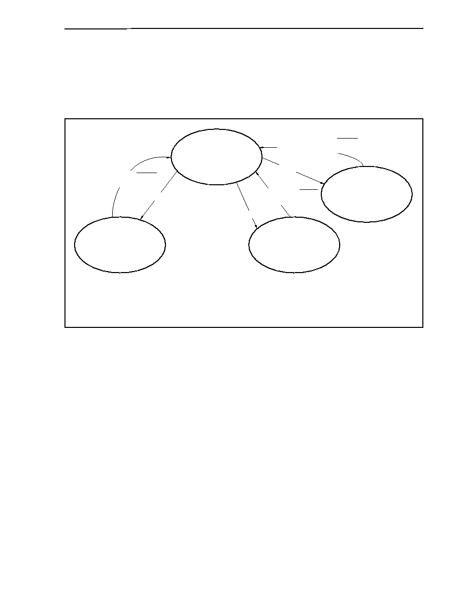
CHAPTER 8 CLOCK GENERATION FUNCTION
205
User's Manual U14492EJ5V0UD
Table 8-1 shows the operation of the clock generator in normal operation mode, HALT mode, IDLE mode, and
software STOP mode.
An effective low power consumption system can be realized by combining these modes and switching modes
according to the required use.
Figure 8-1. Power Save Mode State Transition Diagram
Note INTPn (n = 0 to 6, 20 to 25)
However, when a digital filter using clock sampling is selected as the noise eliminator for INTP20 to
INTP25, the software STOP or IDLE mode cannot be released.
Normal operation mode
Software STOP mode
Set STOP mode
IDLE mode
Set IDLE mode
Release according to RESET,
NMI, or maskable interrupt
Note
Set HALT mode
Release according to RESET,
NMI, or maskable interrupt
HALT mode
Release according to RESET,
NMI, or maskable interrupt
Note
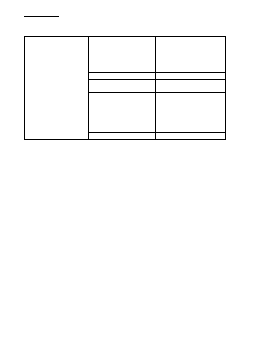
CHAPTER 8 CLOCK GENERATION FUNCTION
206
User's Manual U14492EJ5V0UD
Table 8-1. Clock Generator Operation Using Power Save Control
Clock Source
Power Save Mode
Oscillator
PLL
Synthesizer
Clock
Supply to
Peripheral
I/O
Clock
Supply
to CPU
Normal operation
HALT mode
-
IDLE mode
- -
Oscillation with
resonator
Software STOP mode
- - - -
Normal operation
-
HALT mode
-
-
IDLE mode
-
- -
PLL mode
External clock
Software STOP mode
- - - -
Normal operation
- -
HALT mode
- -
-
IDLE mode
- - - -
Direct mode
External clock
Software STOP mode
- - - -
Remark
: Operating
-: Stopped
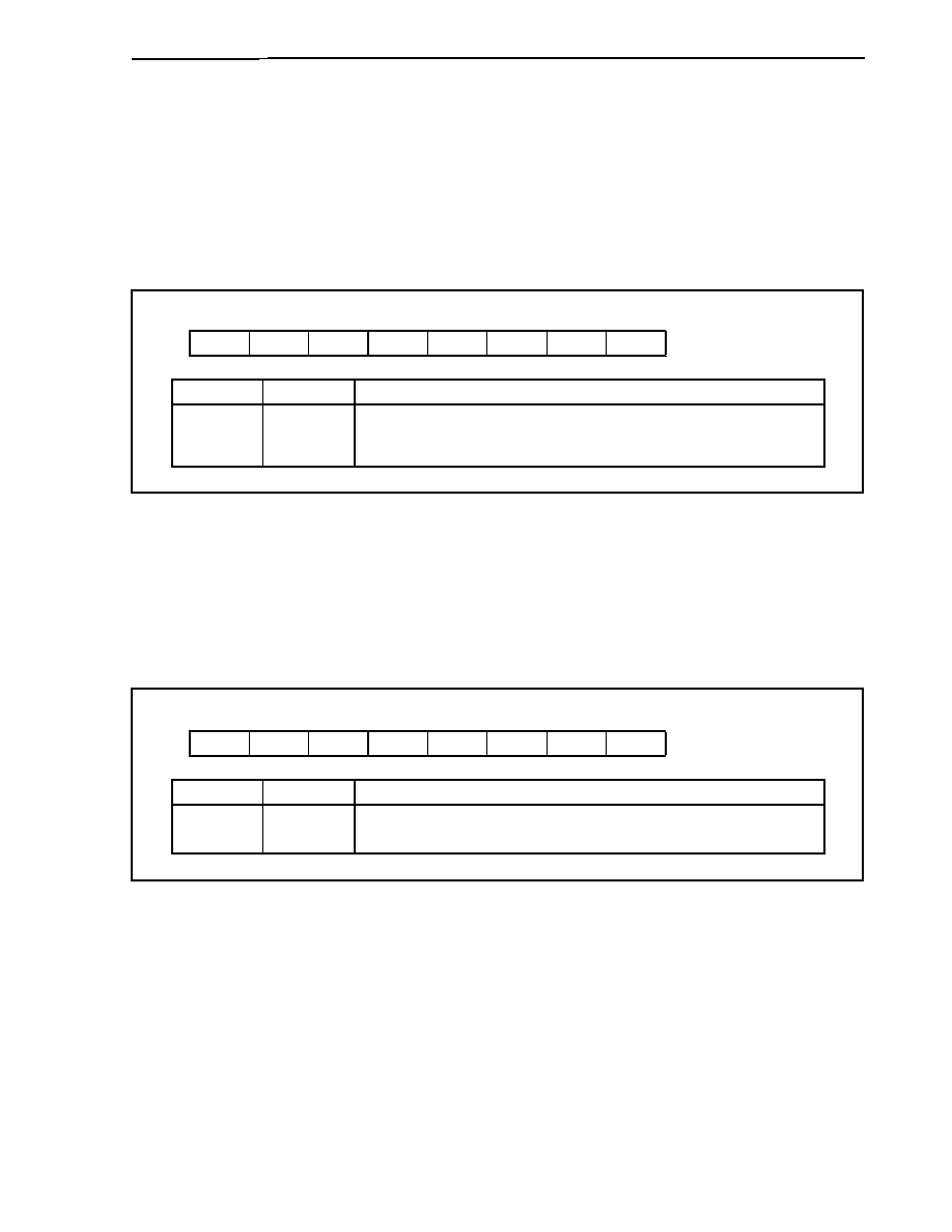
CHAPTER 8 CLOCK GENERATION FUNCTION
207
User's Manual U14492EJ5V0UD
8.5.2 Control registers
(1) Power save mode register (PSMR)
This is an 8-bit register that controls power save mode. It is effective only when the STB bit of the PSC
register is set to 1.
Writing to the PSMR register is executed by the store instruction (ST/SST instruction) and a bit manipulation
instruction (SET1/CLR1/NOT1 instruction).
This register can be read/written in 8-bit or 1-bit units.
7 6 5 4 3 2 1
<0>
Address
Initial
value
PSMR
0 0 0 0 0 0 0
PSM
FFFFF820H
00H
Bit position
Bit name
Function
0 PSM
Specifies IDLE mode or software STOP mode.
0: Switches the system to IDLE mode
1: Switches the system to software STOP mode
(2) Command register (PRCMD)
This is an 8-bit register that is used to set protection for write operations to registers that can significantly
affect the system so that the application system is not halted unexpectedly due to erroneous program
execution. Writing to the first specific register (power save control register (PSC)) is only valid after first
writing to the PRCMD register. Because of this, the register value can be overwritten only by the specified
sequence, preventing an illegal write operation from being performed.
This register can only be written in 8-bit units. The undefined data is read out if read.
7 6 5 4 3 2 1 0
Address
Initial
value
PRCMD
REG7 REG6 REG5 REG4 REG3 REG2 REG1 REG0
FFFFF1FCH
Undefined
Bit position
Bit name
Function
7 to 0
REG7 to
REG0
Registration code (arbitrary 8-bit data)
The specific register targeted is the power save control register (PSC).
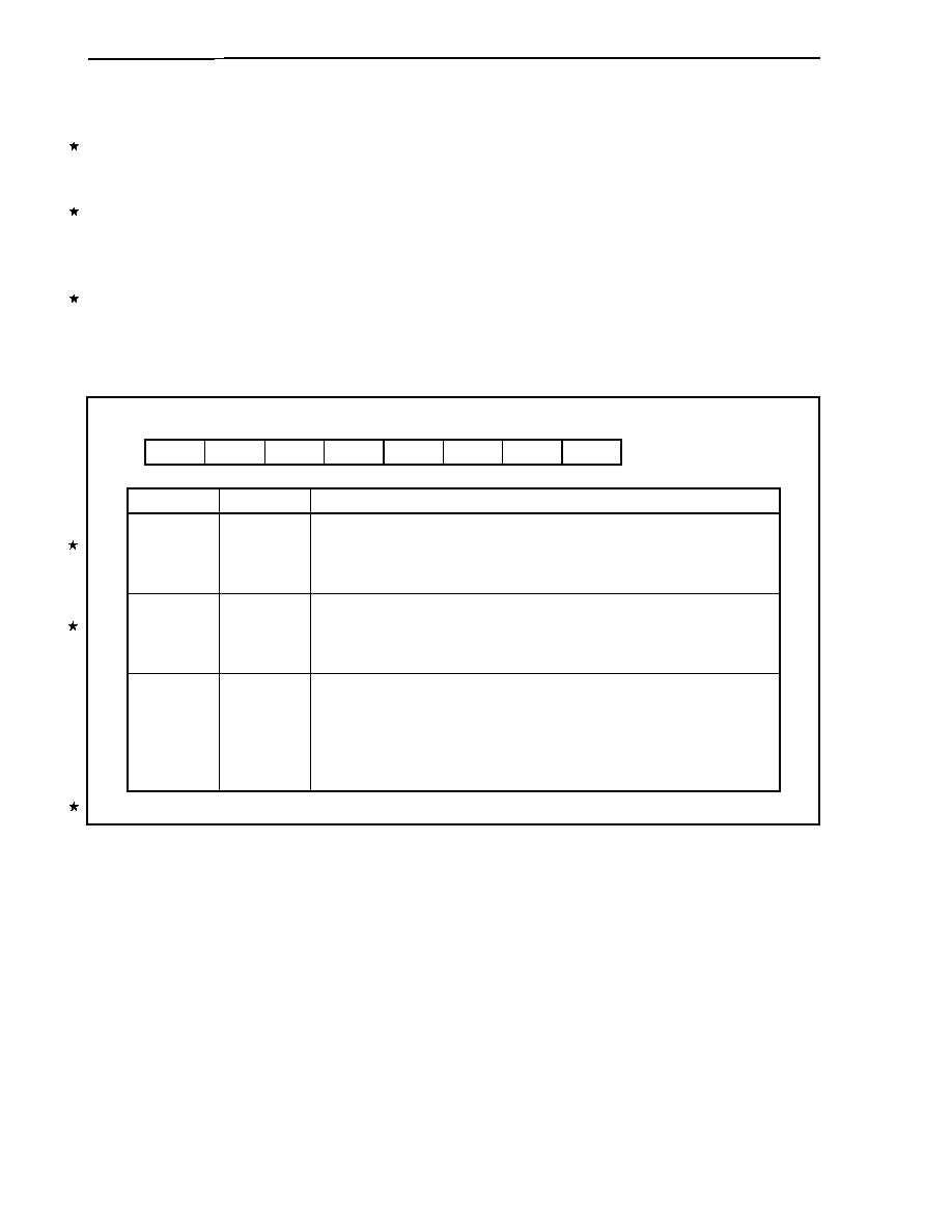
CHAPTER 8 CLOCK GENERATION FUNCTION
208
User's Manual U14492EJ5V0UD
(3) Power save control register (PSC)
This is an 8-bit register that controls the power save function.
If releasing of interrupts are enabled by the setting of the NMIM and INTM bits, the software STOP mode can
be released by an interrupt request (except when interrupt servicing is disabled by the interrupt mask
registers (IMR0 to IMR3)).
The software STOP mode is specified by the setting of the STB bit.
This register, which is one of the specific registers, is effective only when accessed by a specific sequence
during a write operation.
This register can be read/written in 8-bit or 1-bit units.
Be sure to clear bits 7 and 6 to 0. If they are set to 1, the operation is not guaranteed.
Caution It is impossible to set STB bit and NMIM or INTM bit at the same time. Be sure to set STB
bit after setting NMIM or INTM bit.
7 6 <5>
<4> 3 2 <1> 0 Address
Initial
value
PSC
0 0
NMIM
INTM
0 0
STB
0
FFFFF1FEH
00H
Bit position
Bit name
Function
5 NMIM This is the enable/disable setting bit for standby mode release using valid edge
input of NMI
Note
.
0: Enables NMI cancellation
1: Disables NMI cancellation
4 INTM
This is the enable/disable setting for standby mode release using an unmasked
maskable interrupt (INTPn) (n = 0 to 6, 20 to 25, 30, 31, 100, 101, 110, 111)
Note
.
0: Enables maskable interrupt cancellation
1: Disables maskable interrupt cancellation
1 STB
Indicates the standby mode status.
If 1 is written to this bit, the system enters IDLE or software STOP mode (set by
the PSM bit of the PSMR register). When standby mode is released, this bit is
automatically reset to 0.
0: Standby mode is released
1: Standby mode is in effect
Note Setting these bits is valid only in the IDLE/software STOP mode.
Data is set in the power save control register (PSC) according to the following sequence.
<1> Set the power save mode register (PSMR) (with the following instructions).
∑ Store instruction (ST/SST instruction)
∑ Bit manipulation instruction (SET1/CLR1/NOT1 instruction)
<2> Prepare data in any one of the general-purpose registers to set in the specific register.
<3> Write arbitrary data to the command register (PRCMD).
<4> Set the power save control register (PSC) (with the following instructions).
∑ Store instruction (ST/SST instruction)
∑ Bit manipulation instruction (SET1/CLR1/NOT1 instruction)
<5> Insert the NOP instructions (5 instructions (<5> to <9>).

CHAPTER 8 CLOCK GENERATION FUNCTION
209
User's Manual U14492EJ5V0UD
[Sample coding]
<1> ST.B r11, PSMR [r0]
; Set PSMR register
<2> MOV
0x07, r10
; Prepare data for setting specific register in
arbitrary general-purpose register
<3> ST.B r10, PRCMD [r0] ; Write PRCMD register
<4> ST.B r10, PSC [r0]
; Set PSC register
<5> NOP
; Dummy instruction
<6> NOP
; Dummy instruction
<7> NOP
; Dummy instruction
<8> NOP
; Dummy instruction
<9> NOP
; Dummy instruction
(next instruction)
; Execution routine after software STOP mode and IDLE
mode release
No special sequence is required to read the specific register.
Cautions 1. A store instruction for the command register does not acknowledge interrupts. This coding
is made on assumption that <3> and <4> above are executed by the program with
consecutive store instructions. If another instruction is set between <3> and <4>, the above
sequence may become in effective when the interrupt is acknowledged by that instruction,
and a malfunction of the program may result.
2. Although the data written to the PRCMD register is dummy data, use the same register as
the general-purpose register used in specific register setting (<4>) for writing to the PRCMD
register (<3>). The same method should be applied when using a general-purpose register
for addressing.
3. At least 5 NOP instructions must be inserted after executing a store instruction to the PSC
register to set software STOP or IDLE mode.
4. Before executing this processing, complete all DMA transfer operations.
CHAPTER 8 CLOCK GENERATION FUNCTION
210
User's Manual U14492EJ5V0UD
8.5.3 HALT mode
(1) Setting and operation status
In HALT mode, the clock generator (oscillator and PLL synthesizer) continues to operate, but the operation
clock of the CPU is stopped. Since the supply of clocks to on-chip peripheral I/O units other than the CPU
continues, operation continues. The power consumption of the overall system can be reduced by setting the
system to HALT mode while the CPU is idle.
The system is switched to HALT mode by the HALT instruction.
Although program execution stops in HALT mode, the contents of all registers, internal RAM, and ports are
maintained in the state they were in immediately before HALT mode began. Also, operation continues for all
on-chip peripheral I/O units (other than ports) that do not depend on CPU instruction processing. Table 8-2
shows the status of each hardware unit in HALT mode.
Table 8-2. Operation Status in HALT Mode
Function Operation
Status
Clock generator
Operating
Internal system clock
Operating
CPU Stopped
Ports Maintained
On-chip peripheral I/O (excluding ports)
Operating
Internal data
All internal data such as CPU registers, statuses, data,
and the contents of internal RAM are maintained in the
state they were in immediately before HALT mode
began.
AD0 to AD15
A16 to A23
RD, ASTB
UWR, LWR
CS0 to CS7
HLDRQ
HLDAK
WAIT
Operating
CLKOUT Clock
output
CHAPTER 8 CLOCK GENERATION FUNCTION
211
User's Manual U14492EJ5V0UD
(2) Release of HALT mode
HALT mode is released by a non-maskable interrupt request, an unmasked maskable interrupt request
(INTPn), or RESET pin input (n = 0 to 6, 20 to 25, 30, 31, 100, 101, 110, 111).
(a) Release by a non-maskable interrupt request or an unmasked maskable interrupt request
HALT mode is released by a non-maskable interrupt request or by an unmasked maskable interrupt
request regardless of the priority. However, if the system is set to HALT mode during an interrupt
servicing routine, operation will differ as follows.
(i) If an interrupt request is generated with a lower priority than that of the interrupt request that is
currently being serviced, HALT mode is released, but the newly generated interrupt request is not
acknowledged. The new interrupt request is held pending.
(ii) If an interrupt request (including non-maskable interrupt requests) is generated with a higher priority
than that of the interrupt request that is currently being serviced, HALT mode is released and the
newly generated interrupt request is acknowledged.
Table 8-3. Operation After HALT Mode Is Released by Interrupt Request
Release Source
Enable Interrupt (EI) Status
Disable Interrupt (DI) Status
Non-maskable interrupt request
Branch to handler address
Maskable interrupt request
Branch to handler address or
execute next instruction
Execute next instruction
(b) Release by RESET pin input
This is the same as a normal reset operation.

CHAPTER 8 CLOCK GENERATION FUNCTION
212
User's Manual U14492EJ5V0UD
8.5.4 IDLE mode
(1) Setting and operation status
In IDLE mode, the clock generator (oscillator and PLL synthesizer) continues to operate, but the supply of
internal system clocks is stopped which causes the overall system to stop.
When IDLE mode is released, the system can be switched to normal operation mode quickly because the
oscillator's oscillation stabilization time or the PLL lockup time need not be secured.
The system is switched to IDLE mode by setting the PSC or PSMR register using a store instruction (ST or
SST instruction) or a bit manipulation instruction (SET1, CLR1, or NOT1 instruction) (see 8.5.2 Control
registers).
In IDLE mode, program execution is stopped, and the contents of all registers, internal RAM, and ports are
maintained in the state they were in immediately before execution stopped. The operation of on-chip
peripheral I/O units (excluding ports) also is stopped.
Table 8-4 shows the status of each hardware unit in IDLE mode.
Table 8-4. Operation Status in IDLE Mode
Function Operation
Status
Clock generator
Operating
Internal system clock
Stopped
CPU Stopped
Ports Maintained
On-chip peripheral I/O (excluding ports)
Stopped (CSI0 and CSI1 are operable in slave mode)
Note
Internal data
All internal data such as CPU registers, statuses, data,
and the contents of internal RAM are maintained in the
state they were in immediately before IDLE mode began.
AD0 to AD15
A16 to A23
High impedance
RD
UWR, LWR
CS0 to CS7
High-level output
HLDAK High
impedance
HLDRQ
WAIT
Input (no sampling)
ASTB High-level
output
CLKOUT Low-level
output
Note NBD cannot be used in IDLE mode.
CHAPTER 8 CLOCK GENERATION FUNCTION
213
User's Manual U14492EJ5V0UD
(2) Release of IDLE mode
IDLE mode is released by a non-maskable interrupt request, an unmasked maskable interrupt request
(INTPn)
Note
, or RESET pin input (n = 0 to 6, 20 to 25).
Note When a digital filter using clock sampling is selected as the noise eliminator for INTP20 to INTP25, the
IDLE mode cannot be released.
(a) Release by a non-maskable interrupt request or an unmasked maskable interrupt request
The IDLE mode can be released by an interrupt request only when transition to IDLE mode is performed
with the INTM and NMIM bits of the PSC register set to 0.
IDLE mode is released by a non-maskable interrupt request or by an unmasked maskable interrupt
request (INTPn) regardless of the priority (n = 0 to 6, 20 to 25). The operation after release is as follows.
Caution When the NMIM and INTM bits of the PSC register = 1, the IDLE mode cannot be
released by the non-maskable interrupt request signal and unmasked maskable
interrupt request signal.
Table 8-5. Operation After IDLE Mode Is Released by Interrupt Request
Release Source
Enable Interrupt (EI) Status
Disable Interrupt (DI) Status
Non-maskable interrupt request
Branch to handler address
Maskable interrupt request
Branch to handler address or
execute next instruction
Execute next instruction
If the system is set to IDLE mode during a maskable interrupt servicing routine, operation will differ as
follows.
(i) If an interrupt request is generated with a lower priority than that of the interrupt request that is
currently being serviced, IDLE mode is released, but the newly generated interrupt request is not
acknowledged. The new interrupt request is held pending.
(ii) If an interrupt request (including non-maskable interrupt requests) is generated with a higher priority
than that of the interrupt request that is currently being serviced, IDLE mode is released and the
newly generated interrupt request is acknowledged.
If the system is set to IDLE mode during an NMI servicing routine, IDLE mode is released, but the
interrupt is not acknowledged (interrupt is held pending).
Interrupt servicing that is started when IDLE mode is released by NMI pin input is handled in the same
way as normal NMI interrupt servicing that occurs during an emergency (because the NMI interrupt
handler address is unique). Therefore, when a program must be able to distinguish between these two
situations, a software status must be prepared in advance and that status must be set before setting the
PSMR register using a store instruction or a bit manipulation instruction. By checking for this status
during NMI interrupt servicing, an ordinary NMI can be distinguished from the processing that is started
when IDLE mode is released by NMI pin input.
(b) Release by RESET pin input
This is the same as a normal reset operation.

CHAPTER 8 CLOCK GENERATION FUNCTION
214
User's Manual U14492EJ5V0UD
8.5.5 Software STOP mode
(1) Setting and operation status
In software STOP mode, the clock generator (oscillator and PLL synthesizer) is stopped. The overall system
is stopped, and ultra-low power consumption is achieved in which only leak current is lost.
The system is switched to software STOP mode by using a store instruction (ST or SST instruction) or bit
manipulation instruction (SET1, CLR1, or NOT1 instruction) to set the PSC and PSMR registers (see 8.5.2
Control registers).
When PLL mode and resonator connection mode (CESEL bit of CKC register = 0) are used, the oscillator's
oscillation stabilization time must be secured after software STOP mode is released.
In both PLL and direct modes, following the release of software STOP mode, execution of the program is
started after the count time of the time base counter has elapsed.
Although program execution stops in software STOP mode, the contents of all registers, internal RAM, and
ports are maintained in the state they were in immediately before software STOP mode began. The
operation of all on-chip peripheral I/O units (excluding ports) is also stopped.
Table 8-6 shows the status of each hardware unit in software STOP mode.
Table 8-6. Operation Status in Software STOP Mode
Function Operation
Status
Clock generator
Stopped
Internal system clock
Stopped
CPU Stopped
Ports Retained
Note 1
On-chip peripheral I/O (excluding ports)
Stopped (CSI0 and CSI1 are operable in slave mode)
Note 2
Internal data
All internal data such as CPU registers, statuses, data, and
the contents of internal RAM are retained in the state before
software STOP mode has been set
Note 1
.
AD0 to AD15
A16 to A23
High impedance
RD
UWR, LWR
CS0 to CS7
High-level output
HLDAK High
impedance
HLDRQ
WAIT
Input (no sampling)
ASTB High-level
output
CLKOUT Low-level
output
Notes 1. When the V
DD5
value is within the operable range. However, even if it drops below the minimum
operable voltage, as long as the data retention voltage V
DDDR
is maintained, the contents of only
the internal RAM will be retained.
2. NBD cannot be used in software STOP mode.

CHAPTER 8 CLOCK GENERATION FUNCTION
215
User's Manual U14492EJ5V0UD
(2) Release of software STOP mode
Software STOP mode is released by a non-maskable interrupt request, an unmasked maskable interrupt
request (INTPn)
Note
, or RESET pin input. Also, to release software STOP mode when PLL mode (CKSEL pin
= low level) and resonator connection mode (CESEL bit of CKC register = 0) are used, the oscillator's
oscillation stabilization time must be secured (n = 0 to 6, 20 to 25).
Moreover, PLL lockup time may be required depending on the program. See 8.4 PLL Lockup for details.
Note When a digital filter using clock sampling is selected as the noise eliminator for INTP20 to INTP25, the
software STOP mode cannot be released.
(a) Release by a non-maskable interrupt request or an unmasked maskable interrupt request
The software STOP mode can be released by an interrupt request only when transition to software STOP
mode is performed with the INTM and NMIM bits of the PSC register set to 0.
Software STOP mode is released by a non-maskable interrupt request or by an unmasked maskable
interrupt request (INTPn) regardless of the priority (n = 0 to 6, 20 to 25). The operation after release is as
follows.
Caution When the NMIM and INTM bits of the PSC register = 1, the software STOP mode cannot
be released by the non-maskable interrupt request signal and unmasked maskable
interrupt request signal.
Table 8-7. Operation After Software STOP Mode Is Released by Interrupt Request
Release Source
Enable Interrupt (EI) Status
Disable Interrupt (DI) Status
Non-maskable interrupt request
Branch to handler address
Maskable interrupt request
Branch to handler address or
execute next instruction
Execute next instruction
If the system is set to software STOP mode during a maskable interrupt servicing routine, operation will
differ as follows.
(i) If an interrupt request is generated with a lower priority than that of the interrupt request that is
currently being serviced, software STOP mode is released, but the newly generated interrupt request
is not acknowledged. The new interrupt request is held pending.
(ii) If an interrupt request (including non-maskable interrupt requests) is generated with a higher priority
than that of the interrupt request that is currently being serviced, software STOP mode is released
and the newly generated interrupt request is acknowledged.
If the system is set to software STOP mode during an NMI servicing routine, software STOP mode is
released, but the interrupt is not acknowledged (interrupt is held pending).
Interrupt servicing that is started when software STOP mode is released by NMI pin input is handled in
the same way as normal NMI interrupt servicing that occurs during an emergency (because the NMI
interrupt handler address is unique). Therefore, when a program must be able to distinguish between
these two situations, a software status must be prepared in advance and that status must be set before
setting the PSMR register using a store instruction or a bit manipulation instruction.
By checking for this status during NMI interrupt servicing, an ordinary NMI can be distinguished from the
servicing that is started when software STOP mode is released by NMI pin input.
(b) Release by RESET pin input
This is the same as a normal reset operation.
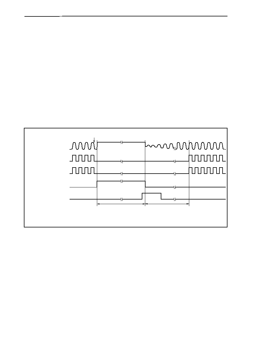
CHAPTER 8 CLOCK GENERATION FUNCTION
216
User's Manual U14492EJ5V0UD
8.6 Securing Oscillation Stabilization Time
8.6.1 Oscillation stabilization time security specification
Two specification methods can be used to secure the time from when software STOP mode is released until the
stopped oscillator stabilizes.
(1) Securing the time using an on-chip time base counter
Software STOP mode is released when a valid edge is input to the NMI pin or a maskable interrupt request is
input (INTPn). When a valid edge is input to the pin causing the start of oscillation, the time base counter
(TBC) starts counting, and the time until the clock output from the oscillator stabilizes is secured during that
counting time (n = 0 to 6, 20 to 25).
Oscillation stabilization time = TBC counting time
After a fixed time, internal system clock output begins, and processing branches to the NMI interrupt or
maskable interrupt (INTPn) handler address.
Oscillation waveform (X2)
Set software STOP mode
Oscillator is stopped
CLKOUT (output)
Internal main clock
STOP state
NMI (input)
Note
Time base counter's
counting time
Note Valid edge: When specified as the rising edge.
The NMI pin should usually be set to an inactive level (for example, high level when the valid edge is
specified as the falling edge) in advance.
Software STOP mode is immediately released if an operation is performed according to NMI valid edge input
or maskable interrupt request input (INTPn) timing in which software STOP mode is set until the CPU
acknowledges the interrupt.
If direct mode or external clock connection mode (CESEL bit of CKC register = 1) is used, program execution
begins after the count time of the time base counter has elapsed.
Also, even if PLL mode and resonator connection mode (CESEL bit of CKC register = 0) are used, program
execution begins after the oscillation stabilization time is secured according to the time base counter.
CHAPTER 8 CLOCK GENERATION FUNCTION
217
User's Manual U14492EJ5V0UD
(2) Securing the time according to the signal level width (RESET pin input)
Software STOP mode is released due to falling edge input to the RESET pin.
The time until the clock output from the oscillator stabilizes is secured according to the low level width of the
signal that is input to the pin.
The supply of internal system clocks begins after a rising edge is input to the RESET pin, and processing
branches to the handler address used for a system reset.
Oscillation waveform (X2)
Set software STOP mode
Oscillator is stopped
Internal main clock
STOP state
Internal system
reset signal
Oscillation stabilization
time secured by RESET
RESET (input)
Undefined
CLKOUT (output)
Undefined
8.6.2 Time base counter (TBC)
The time base counter (TBC) is used to secure the oscillator's oscillation stabilization time when software STOP
mode is released.
When an external clock is connected (CESEL bit of CKC register = 1) or a resonator is connected (PLL mode and
CESEL bit of CKC register = 0), the TBC counts the oscillation stabilization time after software STOP mode is
released, and program execution begins after the count is completed.
The TBC count clock is selected according to the TBCS bit of the CKC register, and the next counting time can be
set.
Table 8-8. Counting Time Examples (f
XX
= 10
◊ f
X
)
Counting Time
TBCS Bit
Count Clock
f
X
= 4.0000 MHz
f
X
= 5.0000 MHz
0 f
X
/2
8
16.4 ms
13.2 ms
1 f
X
/2
9
32.8 ms
26.3 ms
f
XX
: Internal system clock
f
X
:
External oscillation frequency

218
User's Manual U14492EJ5V0UD
CHAPTER 9 TIMER/COUNTER FUNCTION
9.1 Timer 0
9.1.1 Features (timer 0)
Timers 00, 01 (TM00, TM01) are 16-bit timer/counters that are ideal for controlling high-speed inverters such as
motors.
∑ 3-phase PWM output function
PWM mode 0 (symmetric triangular wave)
PWM mode 1 (asymmetric triangular wave)
PWM mode 2 (sawtooth wave)
∑ Interrupt culling function
Culling ratios (1/1, 1/2, 1/4, 1/8, 1/16)
∑ Forcible 3-phase PWM output stop function
3-phase PWM output can be forcibly stopped by inputting a signal from external signal input pin ESOn during
anomalies.
This function can also be used when the clock is stopped.
∑ Real-time output function
3-phase PWM output or rectangular wave output can be selected at the desired timing.
∑ Output of positive phase and negative phase or positive phase and in-phase of 3-phase PWM output

CHAPTER 9 TIMER/COUNTER FUNCTION
219
User's Manual U14492EJ5V0UD
9.1.2 Function overview (timer 0)
∑
16-bit timer (TM0n) for 3-phase PWM inverter control: 2 channels
∑
Compare registers: 4 registers
◊ 2 channels
∑
12-bit dead-time timers (DTMn0 to DTMn2): 3 timers
◊ 2 channels
∑
Count clock division selectable by prescaler (set the frequency of the count clock to 40 MHz or less)
∑
Base clock (f
CLK
): 2 types (set f
CLK
to 40 MHz or less)
f
XX
and f
XX
/2 can be selected
∑
Prescaler division ratio
The following division ratios can be selected according to the base clock (f
CLK
).
Base Clock (f
CLK
)
Division Ratio
f
XX
Selected
f
XX
/2 Selected
1/1 f
XX
f
XX
/2
1/2 f
XX
/2 f
XX
/4
1/4 f
XX
/4 f
XX
/8
1/8 f
XX
/8 f
XX
/16
1/16 f
XX
/16 f
XX
/32
1/32 f
XX
/32 f
XX
/64
∑
Interrupt request sources
∑ Compare-match interrupt request: 2 types
INTCM0n3 generated by CM0n3 match signal
∑ Underflow interrupt request: 2 types
INTTM0n generated by underflow
∑
External pulse output (TO0n0 to TO0n5): 6
◊ 2 channels
Remark f
XX
: Internal system clock
n = 0, 1

CHAPTER 9 TIMER/COUNTER FUNCTION
220
User's Manual U14492EJ5V0UD
9.1.3 Basic configuration
The basic configuration is shown below.
Figure 9-1. Block Diagram of Timer 0 (Mode 0: Symmetric Triangular Wave, Mode 1: Asymmetric
Triangular Wave)
f
XX
/2
BFCMn3
CM0n3
BFCMn0
CM0n0
BFCMn1
CM0n1
BFCMn2
CM0n2
TM0n
S/R
1/1
1/2
1/4
1/8
1/16
1/32
16
16
12
f
CLK
INTCM0n3
INTTM0n
R
S
R
S
R
S
DTMn2
DTMn1
DTMn0
DTRRn
6
TO0n0
(U phase)
TO0n1
(U phase)
TO0n2
(V phase)
TO0n3
(V phase)
TO0n4
(W phase)
TO0n5
(W phase)
Selector
Output control by
external input (ESOn),
TM0n timer operation
Underflow
Underflow
Underflow
ALVUB
ALVVB
ALVWB
R
S
R
S
R
S
R
S
R
S
R
S
ALVTO
f
XX
Remarks 1. TM0n:
Timer register
CM0n0 to CM0n3:
Compare registers
BFCMn0 to BFCMn3: Buffer registers
DTRRn:
Dead-time timer reload register
DTMn0 to DTMn2:
Dead-time timers
ALVTO:
Bit 7 of TOMRn register
ALVUB:
Bit 6 of TOMRn register
ALVVB:
Bit 5 of TOMRn register
ALVWB:
Bit 4 of TOMRn register
S/R:
Set/Reset
2. n = 0, 1
3. f
XX
: Internal system clock
4. f
CLK
: Base clock (40 MHz (MAX.))

CHAPTER 9 TIMER/COUNTER FUNCTION
221
User's Manual U14492EJ5V0UD
Figure 9-2. Block Diagram of Timer 0 (Mode 2: Sawtooth Wave)
BFCMn3
CM0n3
BFCMn0
CM0n0
BFCMn1
CM0n1
BFCMn2
CM0n2
TM0n
1/1
1/2
1/4
1/8
1/16
1/32
16
16
12
INTCM0n3
R
S
R
S
R
S
DTMn2
DTMn1
DTMn0
DTRRn
TO0n0
(U phase)
TO0n1
(U phase)
TO0n2
(V phase)
TO0n3
(V phase)
TO0n4
(W phase)
TO0n5
(W phase)
Underflow
Underflow
Underflow
f
XX
/2
Selector
Clear
Output control by
external input (ESOn),
TM0n timer operation
f
CLK
R
S
R
S
R
S
R
S
R
S
R
S
ALVUB
ALVVB
ALVWB
ALVTO
f
XX
Remarks 1. TM0n:
Timer register
CM0n0 to CM0n3:
Compare registers
BFCMn0 to BFCMn3: Buffer registers
DTRRn:
Dead-time timer reload register
DTMn0 to DTMn2:
Dead-time timers
ALVTO:
Bit 7 of TOMRn register
ALVUB:
Bit 6 of TOMRn register
ALVVB:
Bit 5 of TOMRn register
ALVWB:
Bit 4 of TOMRn register
2. n = 0, 1
3. f
XX
: Internal system clock
4. f
CLK
: Base clock (40 MHz (MAX.))

CHAPTER 9 TIMER/COUNTER FUNCTION
222
User's Manual U14492EJ5V0UD
(1) Timers 00, 01 (TM00, TM01)
TM0n operates as a 16-bit up/down timer or up timer. The cycle is controlled by compare register 0n3
(CM0n3) (n = 0, 1).
TM0n start/stop is controlled by the TM0CEn bit of timer control register 0n (TMC0n).
Division by the prescaler can be selected for the count clock from among f
CLK
, f
CLK
/2, f
CLK
/4, f
CLK
/8, f
CLK
/16,
f
CLK
/32 with the PRM02 to PRM00 bits of the TMC0n register (f
CLK
: base clock, see 9.1.4 (1) Timer 0 clock
selection register (PRM01)).
The conditions when TM0n becomes 0000H are as follows.
∑ Reset input
∑ TM0CEn bit = 0
∑ TM0n register and compare register 0n3 (CM0n3) match (PWM mode 2 (sawtooth wave) only)
∑ Immediately after overflow or underflow
The TM0n timer has 3 operation modes, shown in Table 9-1. The operation mode is selected with timer
control register 0n (TMC0n).
Table 9-1. Timer 0 Operation Modes
Operation Mode
Count Operation
Timer Clear
Source
Interrupt Source
BFCMn3
CM0n3
Transfer Timing
BFCMn0 to BFCMn2
CM0n0 to CM0n2
Transfer Timing
PWM mode 0
(symmetric
triangular wave)
Up/down
-
INTTM0n
INTCM0n3
INTTM0n INTTM0n
PWM mode 1
(asymmetric
triangular wave)
Up/down
-
INTTM0n
INTCM0n3
INTTM0n INTTM0n
INTCM0n3
PWM mode 2
(sawtooth wave)
Up INTCM0n3
INTCM0n3
INTCM0n3 INTCM0n3
Caution An interrupt does not occur and the operation of timer 0 is not affected even if TM0ICn,
CM03ICn, or the interrupt mask flag of the IMR0 register (TM0MKn or CM03MKn) is set
(interrupts disabled) as the interrupt source.
Remark n = 0, 1

CHAPTER 9 TIMER/COUNTER FUNCTION
223
User's Manual U14492EJ5V0UD
(2) Dead-time timers 00 to 02, 10 to 12 (DTM00 to DTM02, DTM10 to DTM12)
DTMn0 to DTMn2 are dedicated 12-bit down timers that generate dead time suitable for inverter control
application. DTMn0 to DTMn2 operate as one-shot timers.
Counting by a dead-time timer is enabled or disabled by the TM0CEDn bit of timer control register 0n
(TMC0n) and cannot be controlled by software. Dead-time timer count start and stop is controlled by
hardware.
A dead-time timer starts counting down when the value of the dead-time timer reload register n (DTRRn) is
transferred in synchronization with the compare match timing of CM0n0 to CM0n2.
When the value of a dead-time timer changes from 000H to FFFH, the dead-time timer generates an
underflow signal, and the timer stops at the value FFFH.
If the value of a dead-time timer matches the value of the corresponding compare register before underflow of
the dead-time timer takes place, the value of DTRRn is transferred to the dead-time timer again, and the
timer starts down counting.
The count clock of the dead-time timer is fixed to the base clock (f
CLK
), and the dead-time width is (set value
of DTRRn + 1)/base clock (f
CLK
).
If TM0n operates in PWM mode 0, PWM mode 1 with the dead-time timer count operation disabled, an
inverted signal without dead time is output to TO0n0 and TO0n1, TO0n2 and TO0n3, and TO0n4 and TO0n5.
(3) Dead-time timer reload registers 0, 1 (DTRR0, DTRR1)
DTRRn register is a 12-bit register used to set the values of the three dead-time timers (DTMn0 to DTMn2
registers) (n = 0, 1). However, a value is transferred from the DTRRn register to each dead-time register
independently.
DTRRn can be read/written in 16-bit units. All 0s are read for the higher 4 bits when 16-bit read access is
performed to the DTRRn register.
14
0
13
0
12
0
2
3
4
5
6
7
8
9
10
11
15
0
1
0
DTRR0
Address
FFFFF570H
Initial value
0FFFH
14
0
13
0
12
0
2
3
4
5
6
7
8
9
10
11
15
0
1
0
DTRR1
Address
FFFFF5B0H
Initial value
0FFFH
Cautions 1. Changing the value of the DTRRn register during TM0n operation (TM0CEn bit of TMC0n
register = 1) is prohibited.
2. Be sure to write 0 to the higher 4 bits.
(4) Compare registers 000 to 002, 010 to 012 (CM000 to CM002, CM010 to CM012)
CM0n0 to CM0n2 are 16-bit registers that always compare their own values with the value of TM0n. If the
value of a compare register matches the value of TM0n, the compare register outputs a trigger signal, and
changes the contents of the flip-flop (F/F) connected to the compare register. Each of CM0n0 to CM0n2 is
provided with a buffer register (BFCMn0 to BFCMn2), so that the contents of the buffer are transferred to
CM0n0 to CM0n2 at the next transfer timing. Transfer is enabled or disabled by the BFTEN bit of the TMC0n
register.

CHAPTER 9 TIMER/COUNTER FUNCTION
224
User's Manual U14492EJ5V0UD
(5) Compare registers 003, 013 (CM003, CM013)
CM0n3 is a 16-bit register that always compare its value with the value of TM0n. If the values match, CM0n3
outputs an interrupt signal (INTCM0n3). CM0n3 controls the maximum count value of TM0n, and if the values
match, it performs the following operations at the next timer count clock.
∑ In triangular wave setting mode (PWM modes 0, 1): Switches TM0n operation from up count to down
count
∑ Sawtooth wave setting mode (PWM mode 2):
Clears the count value of TM0n
CM0n3 also has a buffer register (BFCMn3) and transfers the buffer contents at the timing of the next transfer
to CM0n3. Transfer enable or disable is controlled by the BFTE3 bit of the TMC0n register.
(6) Buffer registers CM00 to CM02, CM10 to CM12 (BFCM00 to BFCM02, BFCM10 to BFCM12)
BFCMn0 to BFCMn2 are 16-bit registers that transfer data to the compare register (CM0n0 to CM0n2)
corresponding to each buffer register when an interrupt signal (INTCM0n3/INTTM0n) is generated.
BFCMn0 to BFCMn2 can be read/written in 16-bit units.
Caution The set values of the BFCMn0 to BFCMn2 registers are transferred to the CM0n0 to CM0n2
registers in the following timing (n = 0, 1).
∑ When TM0CEn bit of TMC0n register = 0: Transfer at next operation timing after writing to
BFCMn0 to BFCMn2 registers
∑ When TM0CEn bit of TMC0n register = 1: Value of BFCMn0 to BFCMn2 registers is
transferred to CM0n0 to CM0n2 registers upon occurrence of INTTM0n or INTCM0n3. At
this time, transfer enable or disable is controlled by the BFTEN bit of the timer control
register (TMC0n).
14
13
12
2
3
4
5
6
7
8
9
10
11
15
1
0
BFCM00
Address
FFFFF572H
Initial value
FFFFH
14
13
12
2
3
4
5
6
7
8
9
10
11
15
1
0
BFCM10
Address
FFFFF5B2H
Initial value
FFFFH
14
13
12
2
3
4
5
6
7
8
9
10
11
15
1
0
BFCM01
Address
FFFFF574H
Initial value
FFFFH
14
13
12
2
3
4
5
6
7
8
9
10
11
15
1
0
BFCM11
Address
FFFFF5B4H
Initial value
FFFFH
14
13
12
2
3
4
5
6
7
8
9
10
11
15
1
0
BFCM02
Address
FFFFF576H
Initial value
FFFFH
14
13
12
2
3
4
5
6
7
8
9
10
11
15
1
0
BFCM12
Address
FFFFF5B6H
Initial value
FFFFH
CHAPTER 9 TIMER/COUNTER FUNCTION
225
User's Manual U14492EJ5V0UD
(7) Buffer registers CM03, CM13 (BFCM03, BFCM13)
BFCMn3 is a 16-bit register that transfers data to the compare register at any timing. Transfer enable or
disable is controlled by the BFTE3 bit of the TMC0n register.
BFCMn3 can be read/written in 16-bit units.
Cautions 1. The set value of the BFCMn3 register is transferred to the CM0n3 register in the
following timing (n = 0, 1).
∑ When TM0CEn bit of TMC0n register = 0: Transfer at next operation timing after
writing to BFCMn3 register
∑ When TM0CEn bit of TMC0n register = 1: Value of BFCMn3 register is transferred to
CM0n3 register upon occurrence of INTTM0n. At this time, transfer enable or disable
is controlled by the BFTE3 bit of the timer control register (TMC0n).
2. Setting the BFCMn3 register to 0000H is prohibited.
14
13
12
2
3
4
5
6
7
8
9
10
11
15
1
0
BFCM03
Address
FFFFF578H
Initial value
FFFFH
14
13
12
2
3
4
5
6
7
8
9
10
11
15
1
0
BFCM13
Address
FFFFF5B8H
Initial value
FFFFH

CHAPTER 9 TIMER/COUNTER FUNCTION
226
User's Manual U14492EJ5V0UD
9.1.4 Control registers
(1) Timer 0 clock selection register (PRM01)
The PRM01 register is used to select the base clock (f
CLK
) of timer 0 (TM0n).
It can be read/written in 8-bit or 1-bit units.
Caution Always set this register before using the timer.
7
0
PRM01
6
0
5
0
4
0
3
0
2
0
1
0
0
PRM1
Address
FFFFF5D0H
Initial value
00H
Bit position
Bit name
Function
0
PRM1
Specifies the base clock (f
CLK
) of timer 0 (TM0n) (See Figure 9-3).
0: f
XX
/2 (When f
XX
> 40 MHz)
1: f
XX
(When f
XX
40 MHz)
Remark f
XX
: Internal system clock
Figure 9-3. Timer 00 and Timer 01 Clock
Timer 00
Timer 01
PRM1
f
CLK
f
XX
/2
Select
f
XX
Remarks 1. f
XX
: Internal system clock
2. f
CLK
: Base clock
CHAPTER 9 TIMER/COUNTER FUNCTION
227
User's Manual U14492EJ5V0UD
(2) Timer control registers 00, 01 (TMC00, TMC01)
TMC0n register is a 16-bit register that sets the operation of timer 0 (TM0n).
The TMC0n register can be read/written in 16-bit units.
If the higher 8 bits of the TMC0n register are used as the TMC0nH register and the lower 8 bits as the
TMC0nL register, the register can be read/written in 8-bit or 1-bit units.
Caution To operate timer 0, first set TM0CEn = 0 and then set TM0CEn = 1.
(1/4)
<14>
STINT0
13
CUL02
12
CUL01
2
MBFTE
3
BFTEN
4
BFTE3
<5>
TM0CED0
6
0
7
0
8
PRM00
9
PRM01
10
PRM02
11
CUL00
<15>
TM0CE0
1
MOD01
0
MOD00
TMC00
Address
FFFFF57AH
Initial value
0508H
<14>
STINT1
13
CUL02
12
CUL01
2
MBFTE
3
BFTEN
4
BFTE3
<5>
TM0CED1
6
0
7
0
8
PRM00
9
PRM01
10
PRM02
11
CUL00
<15>
TM0CE1
1
MOD01
0
MOD00
TMC01
Address
FFFFF5BAH
Initial value
0508H
Bit position
Bit name
Function
15
TM0CEn
Specifies the operation of TM0n.
0: Count disabled (stops after all count values are cleared)
1: Count enabled
Caution When TM0CEn = 0, TO0n0 to TO0n5 output becomes high impedance.
14
STINTn
Specifies interrupt during TM0n timer start.
0: Don't generate interrupt at operation start
1: Generate interrupt at operation start
When STINTn bit = 1, an interrupt is generated immediately after the rising edge of
the TM0CEn signal.
When the MOD01 bit = 0 (triangular wave mode), the INTTM0n interrupt (see Figure
9-4) is generated, and when the MOD01 bit = 1 (sawtooth wave mode), the
INTCM0n3 interrupt is generated.
Caution Changing the STINTn bit during TM0n operation (TM0CEn bit = 1) is
prohibited.
Specifies the interrupt culling ratio.
CUL02
CUL01
CUL00
Interrupt culling ratio
0 0 0
1/1
0 0 1
1/2
0 1 0
1/4
0 1 1
1/8
1 0 0
1/16
Other than above
Culling is not performed
13 to 11
CUL02 to CUL00
Remark n = 0, 1
CHAPTER 9 TIMER/COUNTER FUNCTION
228
User's Manual U14492EJ5V0UD
(2/4)
Bit position
Bit name
Function
13 to 11
CUL02 to CUL00
Cautions 1. INTTM0n and INTCM0n3 interrupts can be culled with the same
culling ratio (1/1, 1/2, 1/4, 1/8, 1/16).
2.
Even when BFTE3 bit = 1, BFTEN bit = 1 (settings to transfer data
from BFCMn0 to BFCMn3 registers to CM0n0 to CM0n3
registers), transfer is not performed with the generation timing of
culled INTTM0n and INTCM0n3 interrupts if the MBFTE bit = 0.
3. If the culling ratio is changed during count operation, the new
culling ratio is applied after an interrupt has occurred with the
culling ratio prior to the change (see Figure 9-5).
Specifies the count clock for TM0n.
PRM02 PRM01 PRM00
Count
clock
0 0 0
f
CLK
0 0 1
f
CLK
/2
0 1 0
f
CLK
/4
0 1 1
f
CLK
/8
1 0 0
f
CLK
/16
1 0 1
f
CLK
/32
Other than above
Setting prohibited
10 to 8
PRM02 to PRM00
Caution
The division ratio switch timing is from when the TM0n value has
become 0000H and an INTTM0n interrupt has occurred. Therefore,
in the timing that corresponds to interrupt culling, the division ratio
is not switched.
Remark For the base clock (f
CLK
), see 9.1.4 (1) Timer 0 clock selection register
(PRM01).
5
TM0CEDn
Specifies the operation of DTMn0 to DTMn2 timers.
0: DTMn0 to DTMn2 perform count operation
1: DTMn0 to DTMn2 stopped
Cautions 1. Changing the TM0CEDn bit during TM0n operation (TM0CEn = 1)
is prohibited.
2. If TM0n is operated when the TM0CEDn bit = 1, a signal without
dead time is output to the TO0n0 to TO0n5 pins.
Remark n = 0, 1
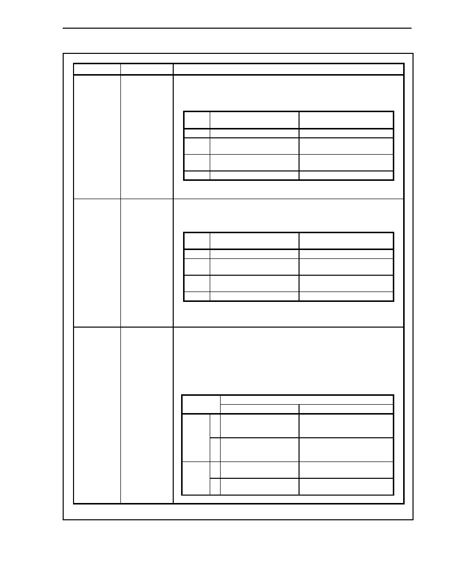
CHAPTER 9 TIMER/COUNTER FUNCTION
229
User's Manual U14492EJ5V0UD
(3/4)
Bit position
Bit name
Function
Specifies transfer of data from BFCMn3 register to CM0n3 register.
0: Transfer disabled
1: Transfer enabled
The transfer timing from the BFCMn3 register to the CM0n3 register is as follows.
BFTE3 TM0n
operation
mode
BFCMn3
CM0n3 transfer
timing
0
All modes
Don't transfer
1
PWM mode 0 (symmetric
triangular wave)
INTTM0n
1
PWM mode 1 (asymmetric
triangular wave)
INTTM0n
1
PWM mode 2 (sawtooth wave)
INTCM0n3
4 BFTE3
When the BFTE3 bit = 1, the value of the BFCMn3 register is transferred to the
CM0n3 register upon occurrence of an INTTM0n or INTCM0n3 interrupt.
Specifies transfer of data from BFCMn0 to BFCMn2 registers to CM0n0 to CM0n2
registers.
0: Transfer disabled
1: Transfer enabled
BFTEN
TM0n operation mode
BFCMn0 to BFCMn2
CM0n0 to
CM0n2 transfer timing
0
All modes
Don't transfer
1
PWM mode 0 (symmetric
triangular wave)
INTTM0n
1
PWM mode 1 (asymmetric
triangular wave)
INTTM0n, INTCM0n3
1
PWM mode 2 (sawtooth wave)
INTCM0n3
3
BFTEN
When the BFTEN bit = 1, the values of the BFCMn0 to BFCMn2 registers are
transferred to the CM0n0 to CM0n2 registers upon occurrence of an INTTM0n or
INTCM0n3 interrupt.
When culling of INTTM0n and INTCM0n3 interrupts is set with the CUL02 to CUL00
bits, specifies whether enable or disable the BFTE3 and BFTEN bit settings upon
occurrence of an interrupt for culling.
0: Disable the set values of BFTE3, BFTEN bits upon occurrence of a culling
interrupt
1: Enable the set values of BFTE3, BFTEN bits upon occurrence of a culling
interrupt
The various combinations are as follows.
Operation upon occurrence of interrupt for culling
MBFTE
0 1
0
BFCMn0 to BFCMn2
CM0n0 to CM0n2 transfer
disabled
BFCMn0 to BFCMn2
CM0n0
to CM0n2 transfer disabled
BFTEN
1
BFCMn0 to BFCMn2
CM0n0 to CM0n2 transfer
disabled
BFCMn0 to BFCMn2
CM0n0
to CM0n2 transfer enabled
0
BFCMn3
CM0n3
transfer disabled
BFCMn3
CM0n3 transfer
disabled
BFTE3
1
BFCMn3
CM0n3
transfer disabled
BFCMn3
CM0n3 transfer
enabled
2 MBFTE
.
Remark n = 0, 1

CHAPTER 9 TIMER/COUNTER FUNCTION
230
User's Manual U14492EJ5V0UD
(4/4)
Bit position
Bit name
Function
Specifies the operation mode of TM0n.
MOD
01
MOD
00
Operation mode
TM0n
operation
Timer clear
source
BFCMn3
CM0n3
timing
BFCMn0 to
BFCMn2
CM0n0 to
CM0n2
timing
0 0
PWM mode 0
(symmetric
triangular wave)
Up/down
-
INTTM0n INTTM0n
0 1
PWM mode 1
(asymmetric
triangular wave)
Up/down
-
INTTM0n
INTTM0n,
INTCM0n3
1 0
PWM mode 2
(sawtooth wave)
Up INTCM0n3
INTCM0n3
INTCM0n3
1 1
Setting
prohibited
1, 0
MOD01,
MOD00
Caution Changing the value of the MOD01, MOD00 bits during TM0n operation
(TM0CEn bit = 1) is prohibited.
Remark n = 0, 1
Figure 9-4. Specification of INTTM0n Interrupt During PWM Mode 0 (Symmetric Triangular Wave), PWM
Mode 1 (Asymmetric Triangular Wave) (MOD01, MOD00 Bits of TMC0n Register = 0n)
CM0n3
TM0n count value
0000H
TM0CEn
Specification from occurrence of
INTTM0n at first start after reset is
possible with STINTn bit
INTTM0n occurrence can be
specified with STINTn bit
INTTM0n
occurrence
INTTM0n
occurrence
Timer operation
stopped
Remark n = 0, 1
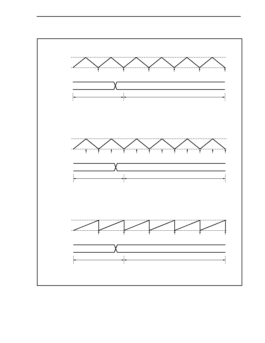
CHAPTER 9 TIMER/COUNTER FUNCTION
231
User's Manual U14492EJ5V0UD
Figure 9-5. Interrupt Culling Processing
(a) PWM mode 0 (symmetric triangular wave)
CM0n3
TM0n count value
0000H
CUL02 to CUL00
INTTM0n
occurrence
Interrupt request
Interrupt culling
1/1 cycle
Interrupt culling
1/2 cycle
INTTM0n
occurrence
INTTM0n
occurrence
INTTM0n
occurrence
000
001
Remark n = 0, 1
(b) PWM mode 1 (asymmetric triangular wave)
CM0n3
TM0n count value
0000H
CUL02 to CUL00
INTTM0n
occurrence
INTCM0n3
occurrence
Interrupt request
INTCM0n3
occurrence
INTCM0n3
occurrence
INTCM0n3
occurrence
INTTM0n
occurrence
Interrupt culling
1/1 cycle
Interrupt culling
1/2 cycle
INTTM0n
occurrence
INTTM0n
occurrence
000
001
Remark n = 0, 1
(c) PWM mode 2 (sawtooth wave)
CM0n3
TM0n count value
0000H
CUL02 to CUL00
INTCM0n3
occurrence
Interrupt request
INTCM0n3
occurrence
Interrupt culling
1/1 cycle
Interrupt culling
1/2 cycle
INTCM0n3
occurrence
INTCM0n3
occurrence
000
001
Remark n = 0, 1
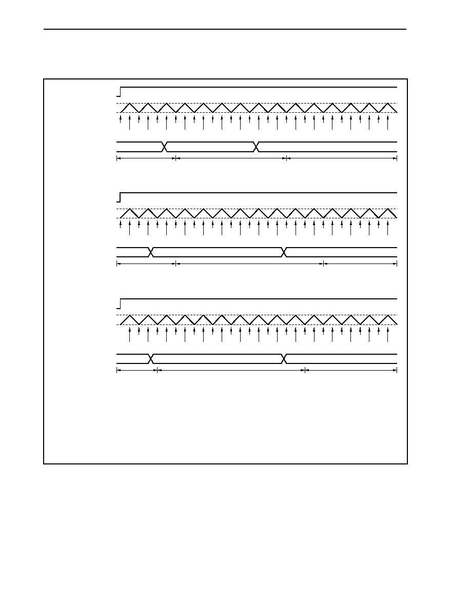
CHAPTER 9 TIMER/COUNTER FUNCTION
232
User's Manual U14492EJ5V0UD
Figure 9-6. Interrupt Culling Ratio Change Timing
(Relationship Between STINTn Bit Setting and CUL Bit Change): PWM Mode 1 (Asymmetric Triangular Wave)
INTTM0n INTTM0n INTTM0n INTTM0n
INTTM0n
INTTM0n
INTTM0n
INTTM0n
INTCM0n3 INTCM0n3 INTCM0n3 INTCM0n3
INTCM0n3
INTCM0n3
INTCM0n3
INTCM0n3
000
001
010
Interrupt culling
1/1 cycle
Interrupt culling
1/2 cycle
Interrupt culling
1/4 cycle
TM0CEn bit
TM0n count value
CUL02 to CUL00 bits
STINTn = 1
INTTM0n
INTTM0n
INTTM0n
INTTM0n
INTTM0n
INTCM0n3
INTCM0n3
INTCM0n3
INTCM0n3
INTTM0n
INTCM0n3
INTTM0n
INTCM0n3
INTCM0n3
001
010
000
Interrupt culling
1/2 cycle
Interrupt culling
1/4 cycle
Interrupt culling
1/1 cycle
TM0CEn bit
TM0n count value
CUL02 to CUL00 bits
STINTn = 1
INTTM0n
INTTM0n
INTTM0n
INTTM0n
INTCM0n3
INTCM0n3
INTCM0n3
INTCM0n3
INTTM0n
INTTM0n
INTCM0n3
INTTM0n
INTCM0n3
INTCM0n3
001
010
000
Interrupt culling
1/2 cycle
Interrupt culling
1/4 cycle
Interrupt culling
1/1 cycle
TM0CEn bit
TM0n count value
CM0n3
0000H
CM0n3
0000H
CM0n3
0000H
CUL02 to CUL00 bits
STINTn = 1
Caution If, in TM0n, to realize the INTTM0n and INTCM0n3 culling function, the culling ratio is set to a
value other than 1/1 with bits CUL02 to CUL00 and counting is started, the subsequent interrupt
output sequence will differ due to the set value of the STINTn bit at count start.
Remark n = 0, 1
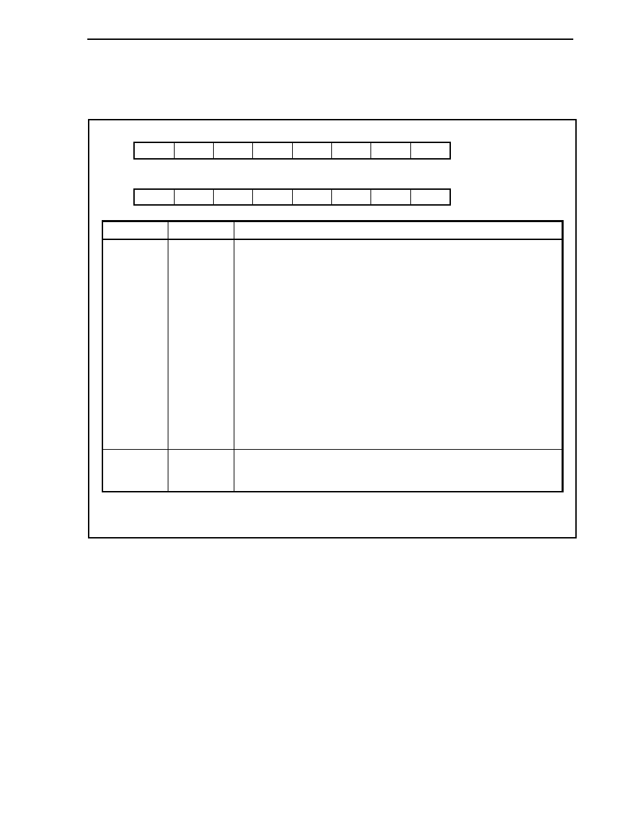
CHAPTER 9 TIMER/COUNTER FUNCTION
233
User's Manual U14492EJ5V0UD
(3) Timer unit control registers 00, 01 (TUC00, TUC01)
TUC0n register is an 8-bit register that controls TO0n0 to TO0n5 outputs.
TUC0n can be read/written in 8-bit or 1-bit units. However, bit 0 is read-only.
7
0
TUC00
6
0
5
0
4
0
3
0
2
0
<1>
TORS0
<0>
TOSTA0
Address
FFFFF57CH
Initial value
01H
7
0
TUC01
6
0
5
0
4
0
3
0
2
0
<1>
TORS1
<0>
TOSTA1
Address
FFFFF5BCH
Initial value
01H
Bit position
Bit name
Function
1
TORSn
Flag that restarts TO0n0 to TO0n5 pin output that was forcibly stopped by ESOn pin
input.
Causes output to resume by writing "1" to TORSn bit.
Cautions 1. If the level is set for the ESOn pin input level (TOMR register
TOEDG1 bit = 1, TOEDG0 bit = 0 or 1), the output disabled state is
not released (TOSTAn bit = 1) even if "1" is written to the TORSn
bit while the output is disabled (TOSTAn bit = 1). If the input level
is inactive, the output disabled state is released (TOSTAn bit = 0).
The value of the TORSn bit is held.
2. If the edge is set for the ESOn pin input (TOEDG1 bit = 0, TOEDG0
bit = 0 or 1), the output disabled state is released (TOSTAn bit = 0)
by writing "1" to the TORSn bit while the output is disabled
(TOSTAn bit = 1).
3. After reset, be sure to write "1" to the TORSn bit prior to starting
output of TO0n0 to TO0n5. "0" is read when the TORSn bit is read.
0
TOSTAn
TO0n0 to TO0n5 pin output status flag through ESOn pin input
0: Output enabled status
1: Output disabled status
Remark n = 0, 1

CHAPTER 9 TIMER/COUNTER FUNCTION
234
User's Manual U14492EJ5V0UD
(4) Timer output mode registers 0, 1 (TOMR0, TOMR1)
The TOMRn register controls timer output from the TO0n0 to TO0n5 pins.
To prevent abnormal output from pins TO0n0 to TO0n5 due to illegal access, data write to the TOMRn
register consists of the following two sequences.
(a) Write access to the TOMR write enable register (SPECn), followed by
(b) Write access to the TOMRn register
Write is not enabled hardware-wise unless these two sequences are implemented.
TOMRn can be read/written in 8-bit units.
Caution When interrupt requests are generated during write access to the TOMRn register (after
write access to the SPECn register and prior to write to the TOMRn register), write
processing to the TOMRn register may not be performed normally if access to other
addresses is performed using the internal bus during servicing of these interrupts. Add one
of the following processing items during the TOMRn register write routine.
∑ Prior to write access to the TOMRn register, disable acknowledge of all interrupts of
CPU.
∑ Following write access to the TOMRn register, check that write was performed normally.
(1/2)
7
ALVTO
TOMR0
6
ALVUB
5
ALVVB
4
ALVWB
3
TOSP
2
0
1
TOEDG1
0
TOEDG0
Address
FFFFF57DH
Initial value
00H
7
ALVTO
TOMR1
6
ALVUB
5
ALVVB
4
ALVWB
3
TOSP
2
0
1
TOEDG1
0
TOEDG0
Address
FFFFF5BDH
Initial value
00H
Bit position
Bit name
Function
7
ALVTO
Specifies the active level of TO0n0, TO0n2, and TO0n4 pins.
0: Active level is low level
1: Active level is high level
Caution
Changing the ALVTO bit during TM0n operation (TM0CEn = 1) is
prohibited.
6
ALVUB
Specifies the output level of the TO0n1 pin.
0: Inverted level of active level set by ALVTO bit
1: Active level set by ALVTO bit
When the ALVUB bit = 1, the output level of the TO0n1 output is the same as
TO0n0.
Caution
Changing the ALVUB bit during TM0n operation (TM0CEn = 1) is
prohibited.
Remark n = 0, 1
CHAPTER 9 TIMER/COUNTER FUNCTION
235
User's Manual U14492EJ5V0UD
(2/2)
Bit position
Bit name
Function
5
ALVVB
Specifies the output level of the TO0n3 pin.
0: Inverted level of active level set by ALVTO bit
1: Active level set by ALVTO bit
When the ALVVB bit = 1, the output level of the TO0n3 output is the same as
TO0n2.
Caution Changing the ALVVB bit during TM0n operation (TM0CEn = 1) is
prohibited.
4
ALVWB
Specifies the output level of the TO0n5 pin.
0: Inverted level of active level set by ALVTO bit
1: Active level set by ALVTO bit
When the ALVWB bit = 1, the output level of the TO0n5 output is the same as
TO0n4.
Caution Changing the ALVWB bit during TM0n operation (TM0CEn = 1) is
prohibited.
3
TOSP
Controls TO0n0 to TO0n5 pin output stop through ESOn pin input.
0: Enables ESOn pin input
1: Disables ESOn pin input
Cautions 1. The output stop status can be released by writing "1" to the
TORSn bit of the TUC0n register. The operation continues
even if output is prohibited for all timers and counters.
2. Before changing the ESOn pin input status from disable to enable
(changing TOSP bit from 1 to 0), write "1" to the TORSn bit of the
TUC0n register to reset the ESOn pin input status.
These bits select the valid edge or level when setting forcible stop of TO0n0 to
TO0n5 output through ESOn pin input with the TOSP bit.
TOEDG1 TOEDG0
Operation
0 0
Rising
edge
0 1
Falling
edge
1 0
Low
level
1 1
High
level
1, 0
TOEDG1,
TOEDG0
Cautions 1. Changing the TOEDG1, TOEDG0 bits during TM0n operation
(TM0CEn = 1) is prohibited.
2. Before changing the settings of bits TOEDG1 and TOEDG0,
write "1" to the TORSn bit of the TUC0n register to reset the ESOn
pin input status.
Remark n = 0, 1
CHAPTER 9 TIMER/COUNTER FUNCTION
236
User's Manual U14492EJ5V0UD
Examples of the output waveforms of TO000 and TO001 when the higher 4 bits (ALVTO, ALVUB, ALVVB,
and ALVWB) of the TOMRn register are set in PWM mode 0 (symmetric triangular waves) are shown below.
Figure 9-7. Output Waveforms of TO000 and TO001 in PWM Mode 0 (Symmetric Triangular Waves)
(Without Dead Time (TM0CED0 Bit = 1))
(a) TOMR0 register value = 80H
TM00 = CM000
TO000
TO001
TM00 = CM000
(b) TOMR0 register value = 00H
TM00 = CM000
TO000
TO001
TM00 = CM000
(c) TOMR0 register value = C0H
TM00 = CM000
TO000
TO001
TM00 = CM000
(d) TOMR0 register value = 40H
TM00 = CM000
TO000
TO001
TM00 = CM000
CHAPTER 9 TIMER/COUNTER FUNCTION
237
User's Manual U14492EJ5V0UD
Figure 9-8. Output Waveforms of TO000 and TO001 in PWM Mode 0 (Symmetric Triangular Waves)
(With Dead Time (TM0CED0 Bit = 0))
(a) TOMR0 register value = 80H
TM00 = CM000
TO000
TO001
TM00 = CM000
Dead time period
Dead time period
(b) TOMR0 register value = 00H
TM00 = CM000
TO000
TO001
TM00 = CM000
Dead time period
Dead time period
(c) TOMR0 register value = C0H
TM00 = CM000
TO000
TO001
TM00 = CM000
Dead time period
Dead time period
(d) TOMR0 register value = 40H
TM00 = CM000
TO000
TO001
TM00 = CM000
Dead time period
Dead time period

CHAPTER 9 TIMER/COUNTER FUNCTION
238
User's Manual U14492EJ5V0UD
Data setting to timer output mode registers 0, 1 (TOMR0, TOMR1) is done in the following sequence.
<1> Prepare the data to be set to timer output mode registers 0, 1 (TOMR0, TOMR1) in a general-purpose
register.
<2> Write data to the TOMR write enable registers 0, 1 (SEPC0, SPEC1).
<3> Set timer output mode registers 0, 1 (TOMR0, TOMR1) (performed with the following instructions).
∑ Store instruction (ST/SST instructions)
∑ Bit manipulation instruction (SET1/CLR1/NOT1 instructions)
[Description example] <1> MOV 0x04,
r10
<2>
ST.B
r10, SPECn [r0]
<3>
ST.B
r10, TOMRn [r0]
Remark n = 0, 1
To read the TOMRn register, no special sequence is required.
Cautions 1. Disable interrupts between SPECn issue (<2>) and TOMRn register write that immediately
follows (<3>).
2. The data written to the SPECn register is dummy data; use the same register as the general-
purpose register used to set the TOMRn register (<3> in the above example) for SPECn
register write (<2> in the above example). The same applies when using a general-purpose
register for addressing.
3. Do not write to the SPECn register or TOMRn register via DMA transfer.

CHAPTER 9 TIMER/COUNTER FUNCTION
239
User's Manual U14492EJ5V0UD
(5) PWM output enable registers 0, 1 (POER0, POER1)
The POERn register is used to make the external pulse output (TO0n0 to TO0n5) status inactive by software.
POERn can be read/written in 8-bit or 1-bit units.
7
0
POER0
6
0
<5>
OE210
<4>
OE200
<3>
OE110
<2>
OE100
<1>
OE010
<0>
OE000
Address
FFFFF57FH
Initial value
00H
7
0
POER1
6
0
<5>
OE211
<4>
OE201
<3>
OE111
<2>
OE101
<1>
OE011
<0>
OE001
Address
FFFFF5BFH
Initial value
00H
Bit position
Bit name
Function
5
OE21n
Specifies output status of TO0n5 pin.
0: TO0n5 output status is high impedance.
1: TO0n5 output status is controlled by TM0CEn bit of TMC0n register and
TORTOn bit of PSTOn register and ESOn pin.
4
OE20n
Specifies output status of TO0n4 pin.
0: TO0n4 output status is high impedance.
1: TO0n4 output status is controlled by TM0CEn bit of TMC0n register and
TORTOn bit of PSTOn register and ESOn pin.
3
OE11n
Specifies output status of TO0n3 pin.
0: TO0n3 output status is high impedance.
1: TO0n3 output status is controlled by TM0CEn bit of TMC0n register and
TORTOn bit of PSTOn register and ESOn pin.
2
OE10n
Specifies output status of TO0n2 pin.
0: TO0n2 output status is high impedance.
1: TO0n2 output status is controlled by TM0CEn bit of TMC0n register and
TORTOn bit of PSTOn register and ESOn pin.
1
OE01n
Specifies output status of TO0n1 pin.
0: TO0n1 output status is high impedance.
1: TO0n1 output status is controlled by TM0CEn bit of TMC0n register and
TORTOn bit of PSTOn register and ESOn pin.
0
OE00n
Specifies output status of TO0n0 pin.
0: TO0n0 output status is high impedance.
1: TO0n0 output status is controlled by TM0CEn bit of TMC0n register and
TORTOn bit of PSTOn register and ESOn pin.
Remark n = 0, 1

CHAPTER 9 TIMER/COUNTER FUNCTION
240
User's Manual U14492EJ5V0UD
(6) PWM software timing output registers 0, 1 (PSTO0, PSTO1)
The PSTOn register is used to perform settings to output the desired waveforms to the external pulse output
pins (TO0n0 to TO0n5) by software.
PSTOn can be read/written in 8-bit or 1-bit units.
Cautions 1. When the value of the TORTOn bit has been changed from 0 to 1 during timer output
(setting changed to software output), the timing is delayed by the dead-time portion
when the output level differs from the timer output signal during output due to the
settings of the UPORTn, VPORTn, and WPORTn bits.
When the output level is the same as the timer output signal during output due to the
settings of the UPORTn, VPORTn, and WPORTn bits, output is performed maintaining
the same output level.
2. If software output is enabled (TORTOn bit = 1), the INTTM0n and INTCM0n3 interrupts
and TO0n0 to TO0n5 output statuses are as follows during TM0n operation (TM0CEn bit
= 1).
INTTM0n and INTCM0n3 interrupts: Continue occurring at each timing in accordance
with timer and compare operations.
TO0n0 to TO0n5 outputs:
Software output has priority.
3. If the TORTOn bit is changed from 1 to 0 during TM0n operation (TM0CEn bit = 1), the
software output state is retained for the TO0n0 to TO0n5 outputs until one of the
set/reset condition of the flip-flop for the TO0n0 to TO0n5 outputs shown in (a) below is
generated.
(a) Set/reset conditions of flip-flop for TO0n0 to TO0n5 outputs
Output Status
Operation Mode
Conditions
Triangular wave mode
(PWM mode 0, 1)
Compare match while TM0n is counting up
Timer output
Sawtooth wave mode
(PWM mode 2)
Match between TM0n and CM0n3 registers
Set
Software output
-
Set (to 1) UPORTn, VPORTn, and WPORTn bits
Triangular wave mode
(PWM mode 0, 1)
Compare match while TM0n is counting down
Timer output
Sawtooth wave mode
(PWM mode 2)
Compare match with TM0n
Reset
Software output
-
Clear (to 0) UPORTn, VPORTn, and WPORTn bits
Remark n = 0, 1
4. If the same value is written to the UPORTn (VPORTn, WPORTn) bit when TORTOn = 1,
the TO0n0 and TO0n1 outputs (TO0n2 and TO0n3, TO0n4 and TO0n5) are not changed.
CHAPTER 9 TIMER/COUNTER FUNCTION
241
User's Manual U14492EJ5V0UD
(1/2)
<7>
TORTO0
PSTO0
6
0
5
0
4
0
3
0
<2>
UPORT0
<1>
VPORT0
<0>
WPORT0
Address
FFFFF57EH
Initial value
00H
<7>
TORTO1
PSTO1
6
0
5
0
4
0
3
0
<2>
UPORT1
<1>
VPORT1
<0>
WPORT1
Address
FFFFF5BEH
Initial value
00H
Bit position
Bit name
Function
7
TORTOn
Specifies TO0n0 to TO0n5 output control.
0: Timer
output
1: Software
output
The change of the TO0n0 to TO0n5 signals during software output occurs when the
TORTOn bit is set (to 1) and a value is written to the UPORTn, VPORTn, and
WPORTn bits. A dead-time timer can also be used.
2
UPORTn
Specifies the TO0n0 (U phase)/TO0n1 (U phase) pin output value.
Caution If the UPORTn bit setting value is changed when TORTOn = 1, the
dead-time setting becomes valid for the TO0n0/TO0n1 output signal
in the same way as during normal timer operation.
1
VPORTn
Specifies the TO0n2 (V phase)/TO0n3 (V phase) pin output value.
Caution If the VPORTn bit setting value is changed when TORTOn = 1, the
dead-time setting becomes valid for the TO0n2/TO0n3 output signal
in the same way as during normal timer operation.
Remark n = 0, 1
ALVTO bit: Bit 7 of the TOMRn register
ALVUB bit: Bit 6 of the TOMRn register
ALVVB bit: Bit 5 of the TOMRn register
UPORTn Operation
TO0n0
Inverted level of ALVTO bit setting
When ALVUB = 0
Level of ALVTO bit setting
0
TO0n1
When ALVUB = 1
Inverted level of ALVTO bit setting
TO0n0
Level of ALVTO bit setting
When ALVUB = 0
Inverted level of ALVTO bit setting
1
TO0n1
When ALVUB = 1
Level of ALVTO bit setting
VPORTn Operation
TO0n2
Inverted level of ALVTO bit setting
When ALVVB = 0
Level of ALVTO bit setting
0
TO0n3
When ALVVB = 1
Inverted level of ALVTO bit setting
TO0n2
Level of ALVTO bit setting
When ALVVB = 0
Inverted level of ALVTO bit setting
1
TO0n3
When ALVVB = 1
Level of ALVTO bit setting
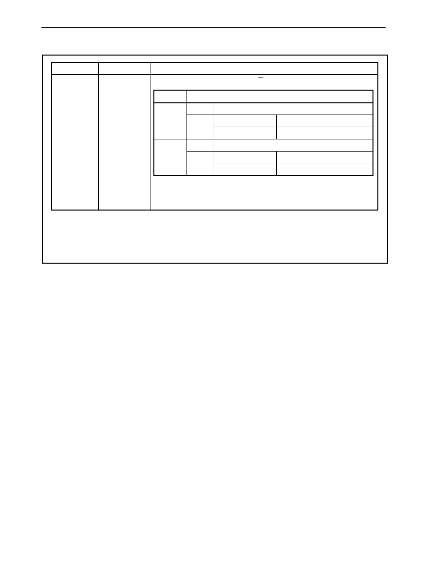
CHAPTER 9 TIMER/COUNTER FUNCTION
242
User's Manual U14492EJ5V0UD
(2/2)
Bit position
Bit name
Function
0
WPORTn
Specifies the TO0n4 (W phase)/TO0n5 (W phase) pin output value.
Caution If the WPORTn bit setting value is changed when TORTOn = 1, the
dead-time setting becomes valid for the TO0n4/TO0n5 output signal
in the same way as during normal timer operation.
Remark n = 0, 1
ALVTO bit: Bit 7 of the TOMRn register
ALVWB bit: Bit 4 of the TOMRn register
The TO0n0 to TO0n5 pins can be set to timer output by a match between TM0n and the compare register or to
software output using the PSTOn register (TORTOn bit = 1). Software output has the priority over timer output.
Consequently, when the setting changes from TM0CEn = 1 (timer operation enabled), TORTOn = 1 (software
output enabled) to TM0CEn = 1 (timer operation enabled), TORTOn = 0 (software output disabled), the TO0n0 to
TO0n5 pins continue to perform software output until the occurrence of the first F/F set/reset due to a match between
TM0n and the compare register after the TORTOn bit setting changes.
The relationship between the settings of the TORTOn and TM0CEn bits when ALVTO = 1 and the output of TO0n0
(positive phase side) is shown on the following pages (the negative phase side (TO0n1, TO0n3, and TO0n5) is
dependent on the ALVUB, ALVVB, and ALVWB bits, so refer to the explanations of each of these bits).
WPORTn Operation
TO0n4
Inverted level of ALVTO bit setting
When ALVWB = 0
Level of ALVTO bit setting
0
TO0n5
When ALVWB = 1
Inverted level of ALVTO bit setting
TO0n4
Level of ALVTO bit setting
When ALVWB = 0
Inverted level of ALVTO bit setting
1
TO0n5
When ALVWB = 1
Level of ALVTO bit setting
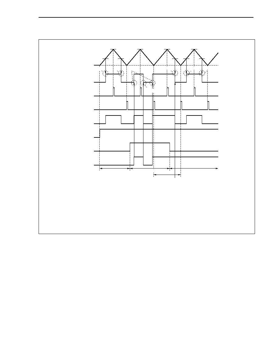
CHAPTER 9 TIMER/COUNTER FUNCTION
243
User's Manual U14492EJ5V0UD
Figure 9-9. When UPORTn = 1 Is Set Immediately Before TORTOn = 0 (Switched by Active Value)
CM0n3
0000H
TM0n
Count value
F/F
INTCM0n3
INTTM0n
TO0n0
TM0CEn
TORTOn
UPORTn
Timer output
Note 1
Note 2
Note 3
Software output
Timer output
P1
T1
CM0n3
CM0n3
CM0n3
Note 2
Note 2
Note 1
Note 4
Notes 1. F/F set by compare match during up count
2. F/F reset by compare match during down count
3. F/F set by writing UPORTn bit
4. F/F reset by writing UPORTn bit
Remark n = 0, 1
If the setting of the TORTOn bit changes from 1 to 0 while the UPORTn bit is set to 1 in the P1 period in Figure 9-9
above, the F/F continues to hold the TORTOn bit setting of "1" until the T1 timing.
However, because the F/F is reset at the T1 timing (by a compare match of TM0n during down counting), the
TO0n0 output changes from 1 to 0.

CHAPTER 9 TIMER/COUNTER FUNCTION
244
User's Manual U14492EJ5V0UD
Figure 9-10. When UPORTn = 0 Is Set Immediately Before TORTOn = 0 (Switched by Inactive Value)
CM0n3
0000H
TM0n
Count value
F/F
INTCM0n3
INTTM0n
TO0n0
TM0CEn
TORTOn
UPORTn
Timer output
Note 1
Note 3
Software output
Timer output
P1
T2
CM0n3
CM0n3
CM0n3
Note 2
Note 1
Note 2
Note 4
Notes 1. F/F set by compare match during up count
2. F/F reset by compare match during down count
3. F/F set by writing UPORTn bit
4. F/F reset by writing UPORTn bit
Remark n = 0, 1
If the setting of the TORTOn bit changes from 1 to 0 while the UPORTn bit is set to 0 in the P1 period in Figure 9-
10 above, the F/F continues to hold the TORTOn bit setting of "0" until the T2 timing.
However, because the F/F is set at the T2 timing (by a compare match of TM0n during up counting), the TO0n0
output changes from 1 to 0.
Note that TO0n0 to TO0n5 output will stop if the TORTOn bit setting is changed from 1 to 0 while the TM0CEn bit
is 0.
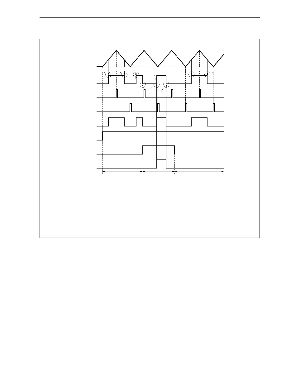
CHAPTER 9 TIMER/COUNTER FUNCTION
245
User's Manual U14492EJ5V0UD
Figure 9-11. When UPORTn = 0 Is Set Immediately Before TORTOn = 1
CM0n3
0000H
TM0n
Count value
F/F
INTCM0n3
INTTM0n
TO0n0
TM0CEn
TORTOn
UPORTn
Timer output
Software output
Timer output
T3
CM0n3
CM0n3
CM0n3
Note 2
Note 1
Note 1
Note 2
Note 1
Note 4
Note 3
Notes 1. F/F set by compare match during up count
2. F/F reset by compare match during down count
3. F/F set by writing UPORTn bit
4. F/F reset by writing UPORTn bit
Remark n = 0, 1
If the setting of the TORTOn bit changes from 0 to 1 while the UPORTn bit is set to 0 during TM0n operation
(TM0CEn = 1), the TO0n0 output changes from 1 to 0 because the F/F is reset at the T3 timing.
Examples of the software output waveforms of TO000 and TO001 based on the settings of the TORTOn, UPORTn,
VPORTn, and WPORTn bits are shown on the following pages.
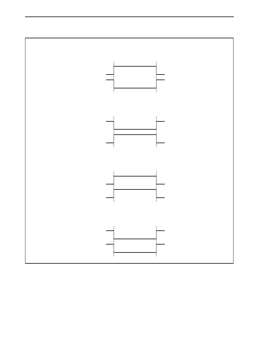
CHAPTER 9 TIMER/COUNTER FUNCTION
246
User's Manual U14492EJ5V0UD
Figure 9-12. Software Output Waveforms of TO000 and TO001 (Without Dead Time (TM0CED0 = 1))
(a) TOMR0 register value = 80H
UPORT0
1
TO000
TO001
UPORT0
0
(b) TOMR0 register value = 00H
UPORT0
1
TO000
TO001
UPORT0
0
(c) TOMR0 register value = C0H
UPORT0
1
TO000
TO001
UPORT0
0
(d) TOMR0 register value = 40H
UPORT0
1
TO000
TO001
UPORT0
0

CHAPTER 9 TIMER/COUNTER FUNCTION
247
User's Manual U14492EJ5V0UD
Figure 9-13. Software Output Waveforms of TO000 and TO001 (With Dead Time (TM0CED0 = 0))
(a) TOMR0 register value = 80H
UPORT0
1
TO000
TO001
UPORT0
0
Dead-time period
Dead-time period
(b) TOMR0 register value = 00H
UPORT0
1
TO000
TO001
UPORT0
0
Dead-time period
Dead-time period
(c) TOMR0 register value = C0H
UPORT0
1
TO000
TO001
UPORT0
0
Dead-time period
Dead-time period
(d) TOMR0 register value = 40H
UPORT0
1
TO000
TO001
UPORT0
0
Dead-time period
Dead-time period
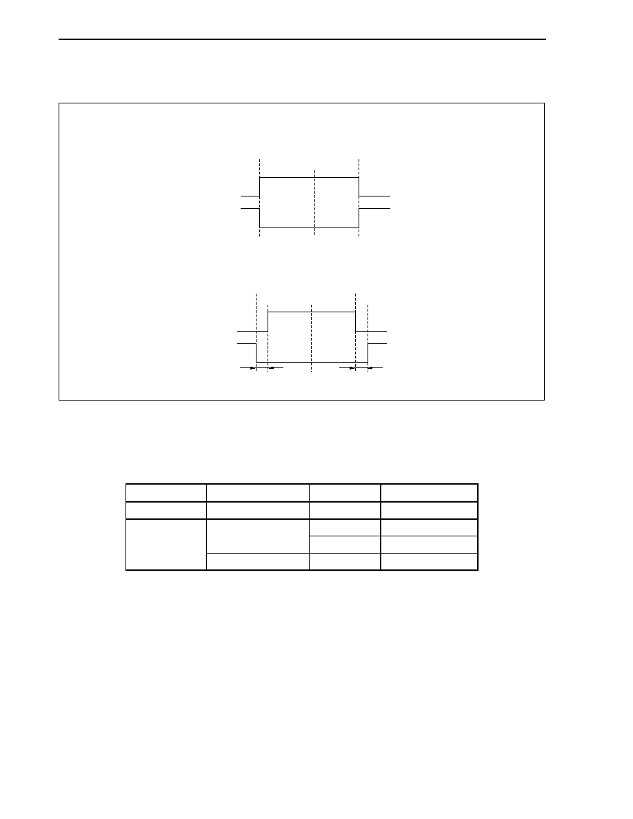
CHAPTER 9 TIMER/COUNTER FUNCTION
248
User's Manual U14492EJ5V0UD
Figure 9-14. Software Output Waveforms of TO000 and TO001 When "1" Is Written to UPORT0 Bit
While TORTO0 = 1 (When TOMR0 Register Value = 80H)
(a) Without dead time (TM0CED0 = 1)
UPORT0
1
UPORT0
0
UPORT0
1
TO000
TO001
(b) With dead time (TM0CED0 = 0)
UPORT0
1
UPORT0
0
UPORT0
1
TO000
TO001
Dead-time period
Dead-time period
The following table shows the output status of external pulse output (in the case of TO0n0).
Table 9-2. Output Status of External Pulse Output (In Case of TO0n0)
OE00n Bit
TORTOn, UPORTn Bits
TM0CEn Bit
TO0n0
0 0/1
0/1
High
impedance
0 High
impedance
0
1 Timer
output
1
1
0/1
Output by UPORTn bit
Remarks 1. OE00n bit: Bit 0 of POERn register
TORTOn bit: Bit 7 of PSTOn register
UPORTn bit: Bit 2 of PSTOn register
TM0CEn bit: Bit 15 of TMC0n register
2. n = 0, 1

CHAPTER 9 TIMER/COUNTER FUNCTION
249
User's Manual U14492EJ5V0UD
(7) TOMR write enable registers 0, 1 (SPEC0, SPEC1)
The SPECn register enables write to the TOMRn register. Unless write to the TOMRn register is performed
following immediately after write to the SPECn register (any data can be written), write processing to the
TOMRn register is not performed normally. Normally, 0000H is read.
The SPECn register can be read/written in 16-bit units.
Remark n = 0, 1
14
0
13
0
12
0
2
0
3
0
4
0
5
0
6
0
7
0
8
0
9
0
10
0
11
0
15
0
1
0
0
0
SPEC0
Address
FFFFF580H
Initial value
0000H
14
0
13
0
12
0
2
0
3
0
4
0
5
0
6
0
7
0
8
0
9
0
10
0
11
0
15
0
1
0
0
0
SPEC1
Address
FFFFF5C0H
Initial value
0000H

CHAPTER 9 TIMER/COUNTER FUNCTION
250
User's Manual U14492EJ5V0UD
9.1.5 Operation
Remarks 1. In the description of the operation in 9.1.5, it is assumed that each bit that affects the output of
TO0n0 to TO0n5 is set as follows.
ALVTO = 1, ALVUB = 0, ALVVB = 0, ALVWB = 0, TORTOn = 0
2. F/F mentioned in 9.1.5 is a flip-flop that controls output of the TO0n0 to TO0n5 pins.
(1) Basic operation
Timer 0 (TM0n) is a 16-bit interval timer that operates as an up/down timer or as an up timer. The cycle is
controlled by compare register 0n3 (CM0n3) (n = 0, 1).
All TM0n bits are cleared (0) by RESET input and count operation is stopped.
Count operation enable/disable is controlled by the TM0CEn bit of timer control register 0n (TMC0n). The
count operation is started by setting the TM0CEn bit to 1 by software. Resetting the TM0CEn bit to 0 clears
TM0n and stops the count operation.
When the value of compare register 0n3 (CM0n3) set beforehand and the value of the TM0n counter match,
a match interrupt (INTCM0n3) is generated.
The count clock to TM0n can be selected from among 6 internal clocks with the TMC0n register. If the TM0n
has been set as an up/down timer, an underflow interrupt (INTTM0n) is generated when TM0n becomes
0000H during down counting.
The TM0n has the following three operation modes, which are selected with timer control register 0n
(TMC0n).
∑ PWM mode 0: Triangular wave modulation (Right-left symmetric waveform control)
∑ PWM mode 1: Triangular wave modulation (Right-left asymmetric waveform control)
∑ PWM mode 2: Sawtooth wave modulation control
Table 9-3. Timer 0 (TM0n) Operation Modes
TMC0n Register
MOD01 MOD00
Operation Mode
TM0n
Operation
Timer Clear
Source
Interrupt
Source
BFCMn3
CM0n3
Timing
BFCMn0 to
BFCMn2
CM0n0 to
CM0n2 Timing
0
0
PWM mode 0
(symmetric
triangular wave)
Up/down
-
INTTM0n
INTCM0n3
INTTM0n INTTM0n
0
1
PWM mode 1
(asymmetric
triangular wave)
Up/down
-
INTTM0n
INTCM0n3
INTTM0n INTTM0n
INTCM0n3
1
0
PWM mode 2
(sawtooth wave)
Up INTCM0n3
INTCM0n3
INTCM0n3
INTCM0n3
1 1
Setting
prohibited
Caution Changing bits MOD01, MOD00 during TM0n operation (TM0CEn = 1) is prohibited.
Remark n = 0, 1
The various operation modes are described below.

CHAPTER 9 TIMER/COUNTER FUNCTION
251
User's Manual U14492EJ5V0UD
(2) PWM mode 0: Triangular wave modulation (right-left symmetric waveform control)
[Setting procedure]
(a) Set PWM mode 0 (symmetric triangular wave) with bits MOD01 and MOD00 of the TMC0n register. Also
set the active level of pins TO0n0 to TO0n5 with the ALVTO bit of the TOMRn register (n = 0, 1).
(b) Set the count clock of TM0n with bits PRM02 to PRM00 of the TMC0n register. The transfer operation
from BFCMn3 to CM0n3 is set with bit BFTE3, and the transfer operation from BFCMn0 to BFCMn2 to
CM0n0 to CM0n2 is set with bit BFTEN.
(c) Set the initial values.
(i)
Specify the interrupt culling ratio with bits CUL02 to CUL00 of the TMC0n register.
(ii) Set the half-cycle width of the PWM cycle in BFCMn3.
∑ PWM cycle = BFCMn3 value ◊ 2 ◊ TM0n count clock
(The TM0n count clock is set with the TMC0n register.)
(iii) Set the dead-time width in DTRRn.
∑ Dead-time width = (DTRRn + 1)/f
CLK
f
CLK
: Base clock
(iv) Set the set/reset timing of the F/F used in the PWM cycle in BFCMn0 to BFCMn2.
(d) Clear (0) the TM0CEDn bit of the TMC0n register to enable dead-time timer operation. Set TM0CEDn = 1
when not using dead time.
(e) Setting (1) the TM0CEn bit of the TMC0n register starts TM0n counting, and a 6-channel PWM signal is
output from pins TO0n0 to TO0n5.
Cautions 1. Setting CM0n3 to 0000H is prohibited.
2. Setting BFCMnx > BFCMn3 is prohibited when the TM0CEn bit of the TMC0n register = 0
because output of the TO0n0 to TO0n5 pins is inverted from the setting (x = 0 to 2). In
addition, setting BFCMnx > BFCMn3 is also prohibited when the TM0CEn bit of the
TMC0n register = 1 and the CM0nx register = 0.
Remark The TM0CEn bit of the TMC0n register indicates transfer operation under the following conditions.
∑ When TM0CEn bit of TMC0n register is 0
Transfer to the CM0n0 to CM0n2 registers is performed at the next base clock (f
CLK
) after writing
to registers BFCMn0 to BFCMn2.
∑ When TM0CEn bit of TMC0n register is 1
The value of the BFCMn0 to BFCMn2 registers is transferred to the CM0n0 to CM0n2 registers
upon occurrence of the INTTM0n interrupt. Transfer enable/disable at this time is controlled by
bit BFTEN of the TMC0n register.

CHAPTER 9 TIMER/COUNTER FUNCTION
252
User's Manual U14492EJ5V0UD
[Operation]
In PWM mode 0, TM0n performs up/down count operation. When TM0n = 0000H during down counting, an
underflow interrupt (INTTM0n) is generated, and when TM0n = CM0n3 during up counting, a match interrupt
(INTCM0n3) is generated (n = 0, 1).
Switching from up counting to down counting is performed when TM0n and CM0n3 match (INTCM0n3), and
switching from down counting to up counting is performed when TM0n underflow occurs after TM0n becomes
0000H.
The PWM cycle in this mode is (BFCMn3 value
◊ 2 ◊ TM0n count clock). Concerning setting of data to
BFCMn3, the next PWM cycle width is set to BFCMn3.
The data of BFCMn3 is automatically transferred by hardware to CM0n3 upon generation of the INTTM0n
interrupt. Furthermore, calculation is performed by software processing started by INTTM0n, and the data for
the next cycle is set to BFCMn3.
Data setting to CM0n0 to CM0n2, which control the PWM duty, is explained next.
Setting of data to CM0n0 to CM0n2 consists in setting the duty output from BFCMn0 to BFCMn2.
The values of BFCMn0 to BFCMn2 are automatically transferred by hardware to CM0n0 to CM0n2 upon
generation of the INTTM0n interrupt. Furthermore, software processing is started up and calculation
performed, and set/reset timing of the F/F for the next cycle is set to BFCMn0 to BFCMn2.
The PWM cycle and the PWM duty are set in the above procedure.
The F/F set/reset conditions upon match of CM0n0 to CM0n2 are as follows.
∑ Set: CM0n0 to CM0n2 match detection during TM0n up-count operation
∑ Reset: CM0n0 to CM0n2 match detection during TM0n down-count operation
In this mode, the F/F set/reset timing is performed in the same timing (right-left symmetric control). The
values of DTRRn are transferred to the corresponding dead-time timers (DTMn0 to DTMn2) in
synchronization with the set/reset timing of the F/F, and down counting is started. DTMn0 to DTMn2 count
down to 000H, and stop when they count down further to FFFH.
DTMn0 to DTMn2 can automatically generate a width (dead time) at which the active levels of the positive
phase (TO0n0, TO0n2, TO0n4) and negative phase (TO0n1, TO0n3, TO0n5) do not overlap.
In this way, software processing is started by an interrupt (INTTM0n) that occurs once during every PWM
cycle after initial setting has been performed, and by setting the PWM cycle and PWM duty to be used in the
next cycle, it is possible to automatically output a PWM waveform to TO0n0 to TO0n5 pins taking into
consideration the dead-time width (in case of interrupt culling ratio of 1/1).

CHAPTER 9 TIMER/COUNTER FUNCTION
253
User's Manual U14492EJ5V0UD
[Output waveform width in respect to set value]
∑ PWM cycle = BFCMn3 ◊ 2 ◊ T
TM0n
∑ Dead-time width T
Dnm
= (DTRRn + 1)/f
CLK
∑ Active width of positive phase (TO0n0, TO0n2, TO0n4 pins)
= { (CM0n3
- CM0nX
up
) + (CM0n3
- CM0nX
down
) }
◊ T
TM0n
- T
Dnm
∑ Active width of negative phase (TO0n1, TO0n3, TO0n5 pins)
=
(CM0nX
down
+ CM0nX
up
)
◊ T
TM0n
- T
Dnm
∑ In this mode, CM0nX
up
= CM0nX
down
(However, within the same PWM cycle).
Since CM0nX
up
and CM0nX
down
in the negative phase formula are prepared in a separate PWM cycle,
CM0nX
up
CM0nX
down
.
f
CLK
:
Base clock
T
TM0n
:
TM0n count clock
CM0nX
up
: Set value of CM0n0 to CM0n2 while TM0n is counting up
CM0nX
down
: Set value of CM0n0 to CM0n2 while TM0n is counting down
The pin level when the TO0n0 to TO0n5 pins are reset is the high impedance state. When the control mode is
selected thereafter, the following levels are output until the TM0n is started.
∑ TO0n0, TO0n2, TO0n4... When low active High level
When high active
Low level
∑ TO0n1, TO0n3, TO0n5... When low active Low level
When high active
High level
The active level is set with the ALVTO bit of the TOMRn register. The default is low active.
Caution If a value such that the positive phase or negative phase active width is "0" or a negative
value in the above formula, the TO0n0 to TO0n5 pins output a waveform fixed to the
inactive level waveform with active width "0".
Remark m = 0 to 2
n = 0, 1

CHAPTER 9 TIMER/COUNTER FUNCTION
254
User's Manual U14492EJ5V0UD
Figure 9-15. Operation Timing in PWM Mode 0 (Symmetric Triangular Wave)
t
t
t
t
CM0n3 (d)
CM0n3 (e)
a
a
b
b
CM0nx
match
CM0nx
match
CM0nx
match
CM0nx
match
b
c
e
a
d
f
b
a
e
f
d
INTCM0n3
INTTM0n
INTCM0n3
INTTM0n
c
TM0n count value
Positive phase
(TO0n0, TO0n2, TO0n4)
Negative phase
(TO0n1, TO0n3, TO0n5)
BFCMnx
BFCMn3
CM0n3
DTMnx
F/F
CM0nx
Interrupt request
0000H
Remarks 1. The above figure shows the timing chart when BFTE3 and BFTEN of the TMC0n register are 1,
and transfer from BFCMn3 to CM0n3, or from BFCMnx to CM0nx is enabled. Transfer is not
performed when BFTE3 = 0 or BFTEN = 0.
2. n = 0, 1
3. x = 0 to 2
4. t: Dead time = (DTRRn + 1)/f
CLK
(f
CLK
: Base clock)
5. To not use dead time, set the TM0CEDn bit of the TMC0n register to 1.
6. The above figure shows an active high case.
Figure 9-16 shows the overall operation image.

CHAPTER 9 TIMER/COUNTER FUNCTION
255
User's Manual U14492EJ5V0UD
Figure 9-16. Overall Operation Image of PWM Mode 0 (Symmetric Triangular Wave)
CM0n3
TM0n
count value
TO0n0 output
TO0n1 output
TO0n2 output
TO0n3 output
TO0n4 output
TO0n5 output
TO0n0 output
TO0n1 output
TO0n2 output
TO0n3 output
TO0n4 output
TO0n5 output
0000H
CM0n2
CM0n2
CM0n1
CM0n1
CM0n0
CM0n0
CM0n3
CM0n2
CM0n2
CM0n1
CM0n1
CM0n0
CM0n0
Without
dead time
With
dead time
Remark n = 0, 1
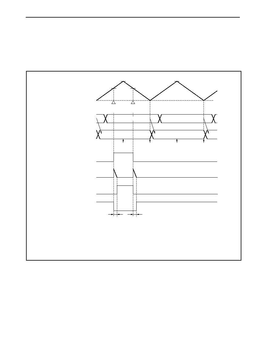
CHAPTER 9 TIMER/COUNTER FUNCTION
256
User's Manual U14492EJ5V0UD
Next, an example of the operation timing, which depends on the values set to CM0n0 to CM0n2 (BFCMn0 to
BFCMn2) is shown.
(a) When CM0nx (BFCMnx)
CM0n3 is set
Figure 9-17. Operation Timing in PWM Mode 0 (Symmetric Triangular Wave, BFCMnx
CM0n3)
t
t
CM0n3
CM0n3
a
a
CM0nx
match
CM0nx
match
BFCMnx
CM0n3
BFCMnx
CM0n3
a
BFCMnx
CM0n3
a
INTTM0n
INTCM0n3
INTCM0n3
INTTM0n
TM0n
count value
Positive phase
(TO0n0, TO0n2, TO0n4)
Negative phase
(TO0n1, TO0n3, TO0n5)
BFCMnx
DTMnx
F/F
Interrupt request
CM0nx
0000H
Remarks 1. n = 0, 1
2. x = 0 to 2
3. t: Dead time = (DTRRn + 1)/f
CLK
(f
CLK
: Base clock)
4. The above figure shows an active high case.
When a value greater than CM0n3 is set to BFCMnx, the positive phase side (TO0n0, TO0n2, TO0n4
pins) outputs a low level, and the negative phase side (TO0n1, TO0n3, TO0n5 pins) continues to output
a high level. This feature is effective for outputting a low-level or high-level width exceeding the PWM
cycle in an application such as inverter control. Furthermore, if CM0nx = CM0n3 is set, matching of TM0n
and CM0nx is detected during down counting by TM0n, so that the F/F remains reset as is, and does not
get set.
The above explanation applies to an active high case. In an active low case, the levels of positive and
negative phases are merely inverted and other operations remain the same.
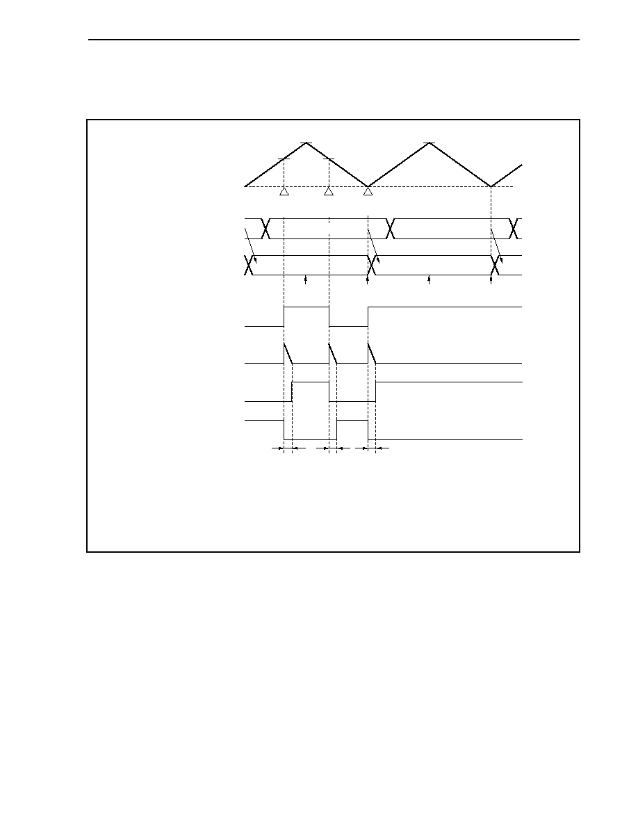
CHAPTER 9 TIMER/COUNTER FUNCTION
257
User's Manual U14492EJ5V0UD
(b) When CM0nx (BFCMnx) = 0000H is set
Figure 9-18. Operation Timing in PWM Mode 0 (Symmetric Triangular Wave, BFCMnx = 0000H)
t
t
t
CM0n3
CM0n3
a
a
CM0nx
match
CM0nx
match
CM0nx
match
0000H
0000H
a
0000H
a
INTTM0n
INTCM0n3
INTCM0n3
INTTM0n
TM0n
count value
Positive phase
(TO0n0, TO0n2, TO0n4)
Negative phase
(TO0n1, TO0n3, TO0n5)
BFCMnx
DTMnx
F/F
Interrupt request
CM0nx
0000H
Remarks 1. n = 0, 1
2. x = 0 to 2
3. t: Dead time = (DTRRn + 1)/f
CLK
(f
CLK
: Base clock)
4. The above figure shows an active high case.
Since TM0n = CM0nx = 0000H match is detected during up counting by TM0n, the F/F is just set and
does not get reset. Even when the setting value is 0000H, F/F is changed in the cycle during which
transfer is performed from BFCMnx to CM0nx similarly to when the setting value is other than 0000H.
Figure 9-19 shows the change timing from the 100% duty state.
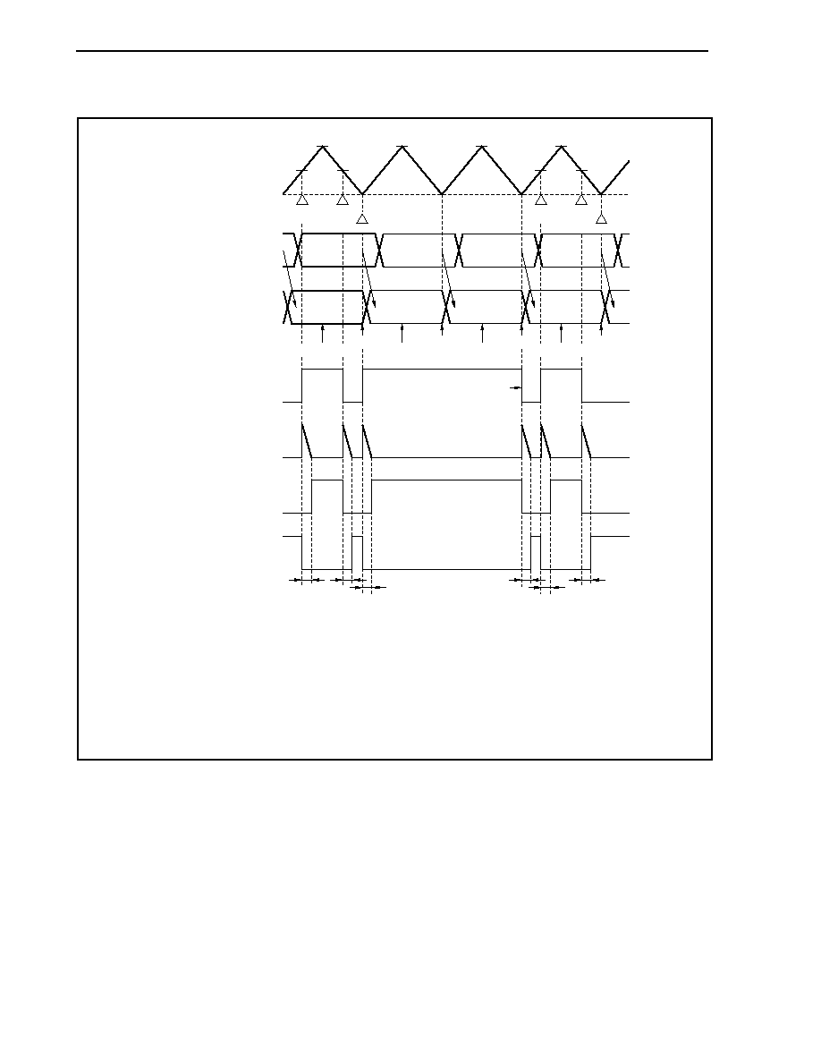
CHAPTER 9 TIMER/COUNTER FUNCTION
258
User's Manual U14492EJ5V0UD
Figure 9-19. Change Timing from 100% Duty State (PWM Mode 0)
CM0n3
TM0n
count value
BFCM0nx
CM0nx
DTMnx
F/F
Interrupt request
Positive phase
(TO0n0, TO0n2, TO0n4)
Negative phase
(TO0n1, TO0n3, TO0n5)
0000H
0000H
b
c
a
0000H
0000H
Note
b
CM0n3
CM0n3
a
a
CM0nx
match
CM0nx
match
CM0nx match
CM0n3
b
b
t
t
t
t
t
t
INTTM0n
INTTM0n
INTTM0n
INTTM0n
CM0nx
match
CM0nx
match
CM0nx match
a
INTCM0n3
INTCM0n3
INTCM0n3
INTCM0n3
Note F/F is reset upon INTTM0n occurrence.
Remarks 1. n = 0, 1
2. x = 0 to 2
3. t: Dead time = (DTRRn + 1)/f
CLK
(f
CLK
: Base clock)
4. The above figure shows an active high case.

CHAPTER 9 TIMER/COUNTER FUNCTION
259
User's Manual U14492EJ5V0UD
(3) PWM mode 1: Triangular wave modulation (right-left asymmetric waveform control)
[Setting procedure]
(a) Set PWM mode 1 (asymmetric triangular wave) with bits MOD01 and MOD00 of the TMC0n register.
Also set the active level of pins TO0n0 to TO0n5 with the ALVTO bit of the TOMRn register (n = 0, 1).
(b) Set the count clock of TM0n with bits PRM02 to PRM00 of the TMC0n register. The transfer operation
from BFCMn3 to CM0n3 is set with bit BFTE3, and the transfer operation from BFCMn0 to BFCMn2 to
CM0n0 to CM0n2 is set with bit BFTEN.
(c) Set the initial values.
(i) Specify the interrupt culling ratio with bits CUL02 to CUL00 of the TMC0n register.
(ii) Set the half-cycle width of the PWM cycle in BFCMn3.
∑ PWM cycle = BFCMn3 value ◊ 2 ◊ TM0n count clock
(The TM0n count clock is set with the TMC0n register.)
(iii) Set the dead-time width in DTRRn.
∑ Dead-time width = (DTRRn + 1)/f
CLK
f
CLK
: Base clock
(iv) Set the set timing of the F/F used in the PWM cycle in BFCMn0 to BFCMn2.
(d) Clear (0) the TM0CEDn bit of the TMC0n register to enable dead-time timer operation. Set TM0CEDn = 1
when not using dead time.
(e) Setting (1) the TM0CEn bit of the TMC0n register starts TM0n counting, and a 6-channel PWM signal is
output from pins TO0n0 to TO0n5.
Caution Setting CM0n3 to 0000H is prohibited.
Remark The TM0CEn bit of the TMC0n register indicates transfer operation under the following conditions.
∑ When TM0CEn bit of TMC0n register is 0
Transfer to the CM0n0 to CM0n2 registers is performed at the next base clock (f
CLK
) after writing
to registers BFCMn0 to BFCMn2.
∑ When TM0CEn bit of TMC0n register is 1
The value of the BFCMn0 to BFCMn2 registers is transferred to the CM0n0 to CM0n2 registers
upon occurrence of the INTTM0n or INTCM0n3 interrupt. Transfer enable/disable at this time is
controlled by bit BFTEN of the TMC0n register.

CHAPTER 9 TIMER/COUNTER FUNCTION
260
User's Manual U14492EJ5V0UD
[Operation]
In PWM mode 1, TM0n performs up/down count operation. When TM0n = 0000H during down counting, an
underflow interrupt (INTTM0n) is generated, and when TM0n = CM0n3 during up counting, a match interrupt
(INTCM0n3) is generated (n = 0, 1).
Switching from up counting to down counting is performed when TM0n and CM0n3 match (INTCM0n3), and
switching from down counting to up counting is performed by INTTM0n.
The PWM cycle in this mode is (BFCMn3 value
◊ 2 ◊ TM0n count clock). Concerning setting of data to
BFCMn3, the next PWM cycle width is set to BFCMn3.
The data of BFCMn3 is automatically transferred by hardware to CM0n3 upon generation of the INTTM0n
interrupt. Furthermore, calculation is performed by software processing started by INTTM0n, and the data for
the next cycle is set to BFCMn3.
Data setting to CM0n0 to CM0n2, which control the PWM duty, is explained next.
Setting of data to CM0n0 to CM0n2 consists in setting the duty output from BFCMn0 to BFCMn2.
The values of BFCMn0 to BFCMn2 are automatically transferred by hardware to CM0n0 to CM0n2 upon
generation of the INTTM0n and INTCM0n3 (TM0n and CM0n3 match interrupts). Furthermore, software
processing is started up and calculation performed, and the set/reset timing of the F/F after a half cycle is set
in BFCMn0 to BFCMn2.
The PWM cycle and the PWM duty are set in the above procedure.
The F/F set/reset conditions upon match of CM0n0 to CM0n2 are as follows.
∑ Set: CM0n0 to CM0n2 match detection during TM0n up-count operation
∑ Reset: CM0n0 to CM0n2 match detection during TM0n down-count operation
The values of DTRRn are transferred to the corresponding dead-time timers (DTMn0 to DTMn2) in
synchronization with the set/reset timing of the F/F, and down counting is started. DTMn0 to DTMn2 count
down to 000H, and stop when they count down further to FFFH.
DTMn0 to DTMn2 can automatically generate a width (dead time) at which the active levels of the positive
phase (TO0n0, TO0n2, TO0n4) and negative phase (TO0n1, TO0n3, TO0n5) do not overlap.
In this way, software processing is started by two interrupts (INTTM0n and INTCM0n3) that occur during
every PWM cycle after initial setting has been performed, and by setting the PWM cycle and PWM duty to be
used after a half cycle, it is possible to automatically output a PWM waveform to TO0n0 to TO0n5 pins taking
into consideration the dead-time width (in case of interrupt culling ratio of 1/1).
The difference between right-left symmetric waveform control and control in this mode (right-left asymmetric
waveform control) is that BFCMn0 to BFCMn2 are transferred to CM0n0 to CM0n2, and that the interrupt
signals that start software processing consist just of INTTM0n (generated once per PWM cycle) in the case of
right-left symmetric waveform control, and INTTM0n and INTCM0n3 (generated twice per PWM cycle, or
once per half cycle) in the case of right-left asymmetric waveform control.

CHAPTER 9 TIMER/COUNTER FUNCTION
261
User's Manual U14492EJ5V0UD
[Output waveform width in respect to set value]
∑ PWM cycle = BFCMn3 ◊ 2 ◊ T
TM0n
∑ Dead-time width T
Dnm
= (DTRRn + 1)/f
CLK
∑ Active width of positive phase (TO0n0, TO0n2, TO0n4 pins)
= { (CM0n3
- CM0nX
up
) + (CM0n3
- CM0nX
down
) }
◊ T
TM0n
- T
Dnm
∑ Active width of negative phase (TO0n1, TO0n3, TO0n5 pins)
=
(CM0nX
down
+ CM0nX
up
)
◊ T
TM0n
- T
Dnm
f
CLK
:
Base clock
T
TM0n
:
TM0n count clock
CM0nX
up
: Set value of CM0n0 to CM0n2 while TM0n is counting up
CM0nX
down
: Set value of CM0n0 to CM0n2 while TM0n is counting down
The pin level when the TO0n0 to TO0n5 pins are reset is the high impedance state. When the control mode is
selected thereafter, the following levels are output until the TM0n is started.
∑ TO0n0, TO0n2, TO0n4... When low active High level
When high active
Low level
∑ TO0n1, TO0n3, TO0n5... When low active Low level
When high active
High level
The active level is set with the ALVTO bit of the TOMRn register. The default is low active.
Caution If a value such that the positive phase or negative phase active width is "0" or a negative
value in the above formula, the TO0n0 to TO0n5 pins output a waveform fixed to the
inactive level waveform with active width "0".
Remark m = 0 to 2
n = 0, 1
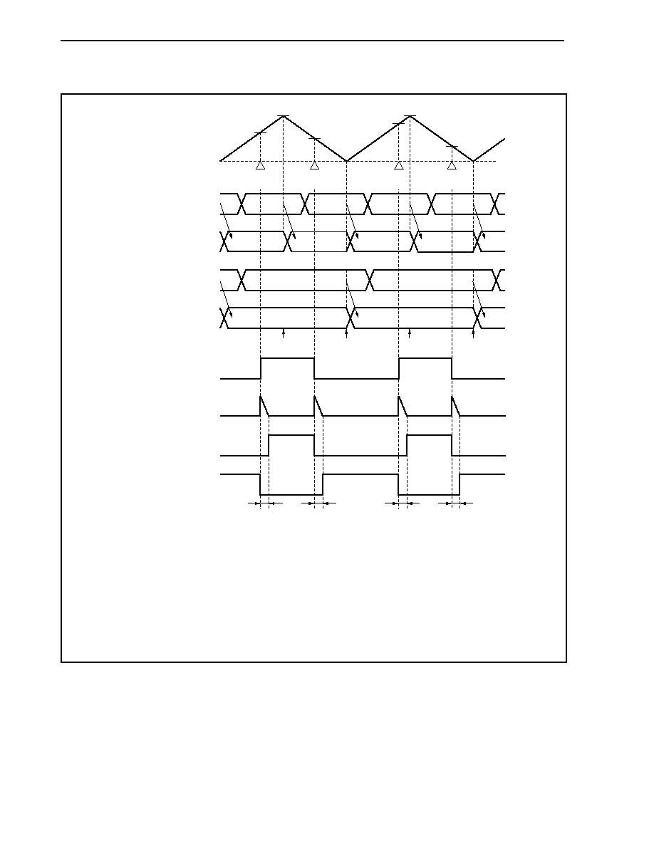
CHAPTER 9 TIMER/COUNTER FUNCTION
262
User's Manual U14492EJ5V0UD
Figure 9-20. Operation Timing in PWM Mode 1 (Asymmetric Triangular Wave)
t
t
t
t
CM0n3 (f)
CM0n3 (g)
a
b
c
d
CM0nx
match
CM0nx
match
CM0nx
match
CM0nx
match
b
c
d
e
g
a
f
h
b
a
g
h
f
INTCM0n3
INTTM0n
INTCM0n3
INTTM0n
c
d
e
TM0n
count value
Positive phase
(TO0n0, TO0n2, TO0n4)
Negative phase
(TO0n1, TO0n3, TO0n5)
Interrupt request
BFCMnx
BFCMn3
CM0n3
DTMnx
F/F
CM0nx
0000H
Remarks 1. The above figure shows the timing chart when BFTE3 and BFTEN of the TMC0n register are 1,
and transfer from BFCMn3 to CM0n3, or from BFCMnx to CM0nx is enabled. Transfer is not
performed when BFTE3 = 0 or BFTEN = 0.
2. n = 0, 1
3. x = 0 to 2
4. t: Dead time = (DTRRn + 1)/f
CLK
(f
CLK
: Base clock)
5. To not use dead time, set the TM0CEDn bit of the TMC0n register to 1.
6. The above figure shows an active high case.
Figure 9-21 shows the overall operation image.
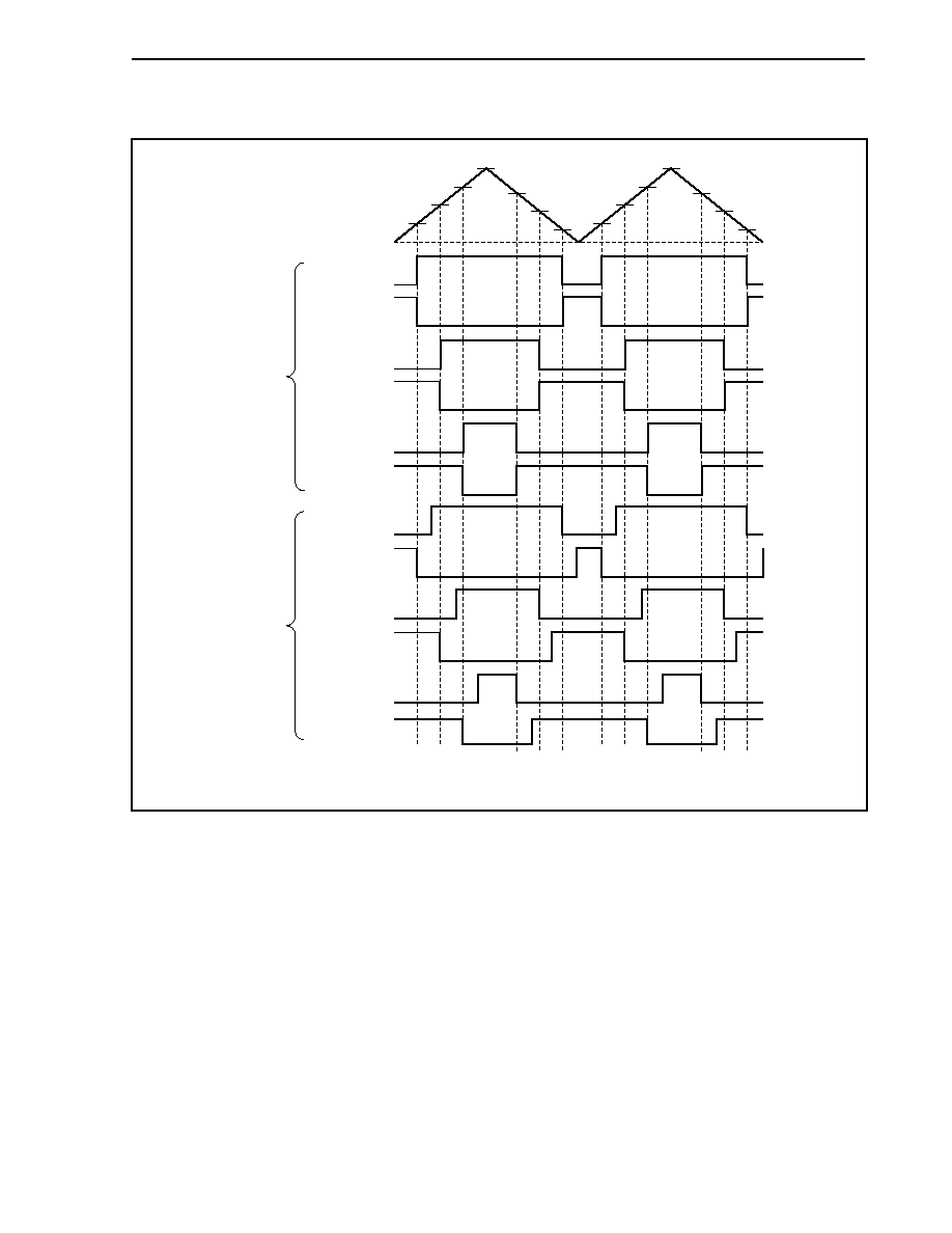
CHAPTER 9 TIMER/COUNTER FUNCTION
263
User's Manual U14492EJ5V0UD
Figure 9-21. Overall Operation Image of PWM Mode 1 (Asymmetric Triangular Wave)
CM0n3
TM0n
count value
TO0n0 output
TO0n1 output
TO0n2 output
TO0n3 output
TO0n4 output
TO0n5 output
TO0n0 output
TO0n1 output
TO0n2 output
TO0n3 output
TO0n4 output
TO0n5 output
0000H
CM0n2
CM0n2
CM0n1
CM0n1
CM0n0
CM0n0
CM0n3
CM0n2
CM0n2
CM0n1
CM0n1
CM0n0
CM0n0
Without
dead time
With
dead time
Remark n = 0, 1
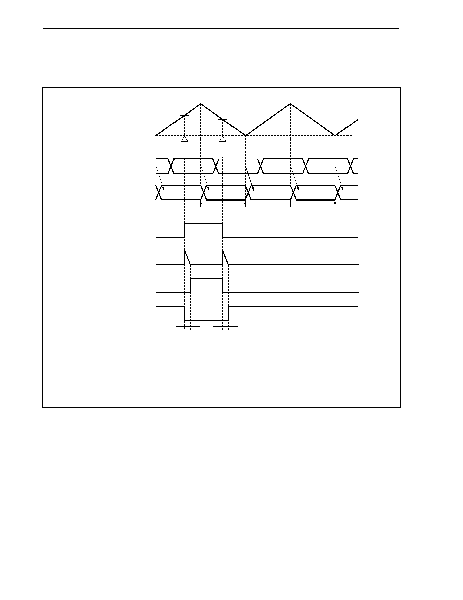
CHAPTER 9 TIMER/COUNTER FUNCTION
264
User's Manual U14492EJ5V0UD
(a) When BFCMnx
CM0n3 is set in software processing started by INTCM0n3
Figure 9-22. Operation Timing in PWM Mode 1 (Asymmetric Triangular Wave, BFCMnx
CM0n3)
t
t
CM0n3
CM0n3
a
b
CM0nx
match
CM0nx
match
INTTM0n
INTTM0n
TM0n
count value
Positive phase
(TO0n0, TO0n2, TO0n4)
Negative phase
(TO0n1, TO0n3, TO0n5)
BFCMnx
DTMnx
F/F
Interrupt request
CM0nx
0000H
b
c
c
c
a
b
a
c
c
c
INTCM0n3
INTCM0n3
Remarks 1. n = 0, 1
2. x = 0 to 2
3. c
CM0n3
4. t: Dead time = (DTRRn + 1)/f
CLK
(f
CLK
: Base clock)
5. The above figure shows an active high case.
When a value greater than CM0n3 is set to BFCMnx, the positive phase side (TO0n0, TO0n2, TO0n4
pins) outputs a low level, and the negative phase side (TO0n1, TO0n3, TO0n5 pins) continues to output
a high level. This feature is effective for outputting a low-level or high-level width exceeding the PWM
cycle in an application such as inverter control. Furthermore, if CM0nx = CM0n3 is set, matching of TM0n
and CM0nx is detected during down counting by TM0n, so that the F/F remains reset as is, and does not
get set.
The above explanation applies to an active high case. In an active low case, the levels of positive and
negative phases are merely inverted and other operations remain the same.
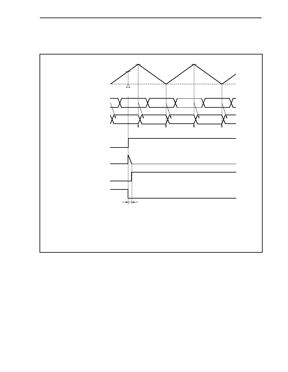
CHAPTER 9 TIMER/COUNTER FUNCTION
265
User's Manual U14492EJ5V0UD
(b) When BFCMnx > CM0n3 is set in software processing started by INTTM0n
Figure 9-23. Operation Timing in PWM Mode 1 (Asymmetric Triangular Wave, BFCMnx > CM0n3)
t
CM0n3
CM0n3
a
CM0nx
match
INTTM0n
INTTM0n
TM0n
count value
Positive phase
(TO0n0, TO0n2, TO0n4)
Negative phase
(TO0n1, TO0n3, TO0n5)
BFCMnx
DTMnx
F/F
Interrupt request
CM0nx
0000H
b
b
b
b
a
b
a
b
b
b
INTCM0n3
INTCM0n3
Remarks 1. n = 0, 1
2. x = 0 to 2
3. b > CM0n3
4. t: Dead time = (DTRRn + 1)/f
CLK
(f
CLK
: Base clock)
5. The above figure shows an active high case.
When a value greater than CM0n3 is set to BFCMnx, the positive phase side (TO0n0, TO0n2, TO0n4
pins) outputs a high level, and the negative phase side (TO0n1, TO0n3, TO0n5 pins) continues to output
a low level. This feature is effective for outputting a low-level or high-level width exceeding the PWM
cycle in an application such as inverter control.
The above explanation applies to an active high case. In an active low case, the levels of positive and
negative phases are merely inverted and other operations remain the same.
Figure 9-24 shows the change timing from the 100% duty state.

CHAPTER 9 TIMER/COUNTER FUNCTION
266
User's Manual U14492EJ5V0UD
Figure 9-24. Change Timing from 100% Duty State (PWM Mode 1)
CM0n3
TM0n
count value
BFCM0nx
0000H
CM0nx
DTMnx
F/F
Interrupt request
Positive phase
(TO0n0, TO0n2, TO0n4)
Negative phase
(TO0n1, TO0n3, TO0n5)
b
b
b
b
b
c
d
e
Note
CM0n3
CM0n3
a
CM0nx
match
CM0n3
c
d
CM0nx
match
CM0nx
match
a
b
b
b
b
b
c
d
e
t
t
t
t
INTTM0n
INTCM0n3
INTCM0n3
INTCM0n3
INTCM0n3
INTTM0n
INTTM0n
INTTM0n
Note F/F is reset upon INTTM0n occurrence.
Remarks 1. n = 0, 1
2. x = 0 to 2
3. b > CM0n3
4. t: Dead time = (DTRRn + 1)/f
CLK
(f
CLK
: Base clock)
5. The above figure shows an active high case.
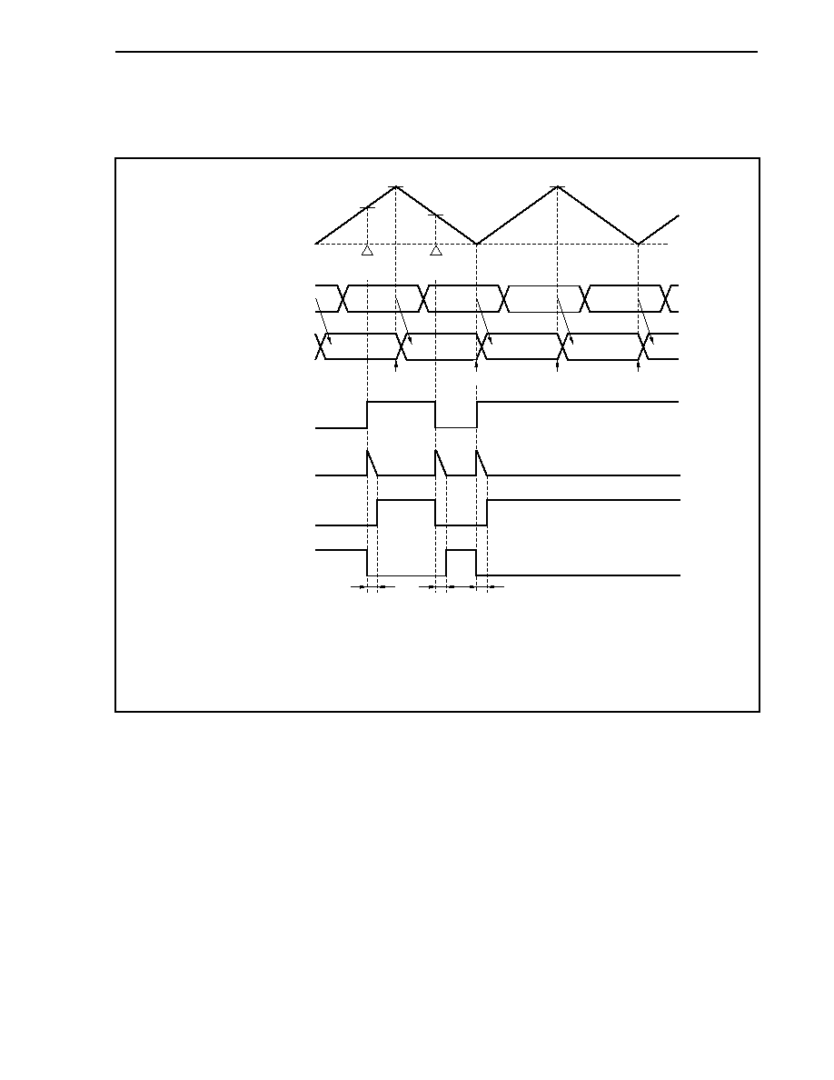
CHAPTER 9 TIMER/COUNTER FUNCTION
267
User's Manual U14492EJ5V0UD
(c) When BFCMnx = 0000H is set in software processing started by INTCM0n3
Figure 9-25. Operation Timing in PWM Mode 1 (Asymmetric Triangular Wave, BFCMnx = 0000H) (1)
t
t
t
CM0n3
CM0n3
a
b
CM0nx
match
CM0nx
match
INTTM0n
TM0n
count value
Positive phase
(TO0n0, TO0n2, TO0n4)
Negative phase
(TO0n1, TO0n3, TO0n5)
BFCMnx
DTMnx
F/F
Interrupt request
CM0nx
0000H
b
0000H
0000H
0000H
a
b
a
0000H
0000H
0000H
INTCM0n3
INTCM0n3
INTTM0n
Remarks 1. n = 0, 1
2. x = 0 to 2
3. t: Dead time = (DTRRn + 1)/f
CLK
(f
CLK
: Base clock)
4. The above figure shows an active high case.
Since TM0n = CM0nx = 0000H match is detected during up counting by TM0n, the F/F is just set and
does not get reset. Moreover, the F/F gets set upon match detection in the cycle when 0000H is
transferred to CM0nx by INTTM0n interrupt.
Figure 9-26 shows the change timing from the 100% duty state.

CHAPTER 9 TIMER/COUNTER FUNCTION
268
User's Manual U14492EJ5V0UD
Figure 9-26. Change Timing from 100% Duty State (1) (PWM Mode 1)
CM0n3
TM0n
count value
BFCM0nx
0000H
CM0nx
DTMnx
F/F
Interrupt request
Positive phase
(TO0n0, TO0n2, TO0n4)
Negative phase
(TO0n1, TO0n3, TO0n5)
b
c
d
e
Note
CM0n3
CM0n3
a
c
CM0nx
match
CM0n3
d
b
CM0nx
match
CM0nx
match
0000H 0000H 0000H 0000H
d
e
t
t
t
t
t
t
INTTM0n INTCM0n3
INTCM0n3 INTTM0n
INTTM0n
INTTM0n
CM0nx
match
CM0nx
match
0000H 0000H 0000H 0000H
b
c
a
INTCM0n3
INTCM0n3
Note F/F is reset upon INTTM0n occurrence.
Remarks 1. n = 0, 1
2. x = 0 to 2
3. t: Dead time = (DTRRn + 1)/f
CLK
(f
CLK
: Base clock)
4. The above figure shows an active high case.

CHAPTER 9 TIMER/COUNTER FUNCTION
269
User's Manual U14492EJ5V0UD
(d) When BFCMnx = 0000H is set in software processing started by INTTM0n
Figure 9-27. Operation Timing in PWM Mode 1 (Asymmetric Triangular Wave, BFCMnx = 0000H) (2)
t
CM0n3
CM0n3
a
CM0nx
match
INTTM0n
INTTM0n
TM0n
count value
Positive phase
(TO0n0, TO0n2, TO0n4)
Negative phase
(TO0n1, TO0n3, TO0n5)
BFCMnx
DTMnx
F/F
Interrupt request
CM0nx
0000H
0000H
0000H
0000H
0000H
a
0000H
a
0000H
0000H
0000H
INTCM0n3
INTCM0n3
Remarks 1. n = 0, 1
2. x = 0 to 2
3. t: Dead time = (DTRRn + 1)/f
CLK
(f
CLK
: Base clock)
4. The above figure shows an active high case.
Since TM0n = CM0nx = 0000H match is detected during up counting by TM0n, the F/F is just set and
does not get reset. Therefore, the positive phase side (TO0n0, TO0n2, TO0n4 pins) outputs a high level,
and the negative phase side (TO0n1, TO0n3, TO0n5 pins) continues to output a low level.
The above explanation applies to an active high case. In an active low case, the levels of positive and
negative phases are merely inverted and other operations remain the same.
Figure 9-28 shows the change timing from the 100% duty state.
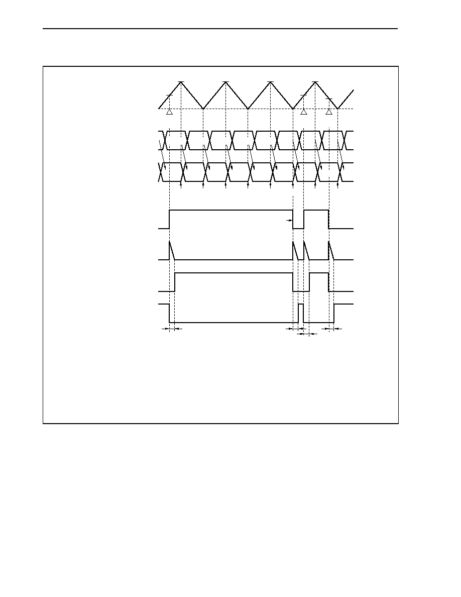
CHAPTER 9 TIMER/COUNTER FUNCTION
270
User's Manual U14492EJ5V0UD
Figure 9-28. Change Timing from 100% Duty State (2) (PWM Mode 1)
CM0n3
TM0n
count value
BFCM0nx
0000H
CM0nx
DTMnx
F/F
Interrupt request
Positive phase
(TO0n0, TO0n2, TO0n4)
Negative phase
(TO0n1, TO0n3, TO0n5)
b
c
d
Note
CM0n3
CM0n3
a
CM0nx
match
CM0n3
b
c
CM0nx
match
CM0nx
match
a
0000H 0000H 0000H 0000H 0000H
b
d
t
t
t
t
INTTM0n
INTCM0n3
I
NTCM0n3
INTCM0n3
INTCM0n3
INTTM0n
INTTM0n
INTTM0n
0000H 0000H 0000H 0000H 0000H
c
Note F/F is reset upon INTTM0n occurrence.
Remarks 1. n = 0, 1
2. x = 0 to 2
3. t: Dead time = (DTRRn + 1)/f
CLK
(f
CLK
: Base clock)
4. The above figure shows an active high case.
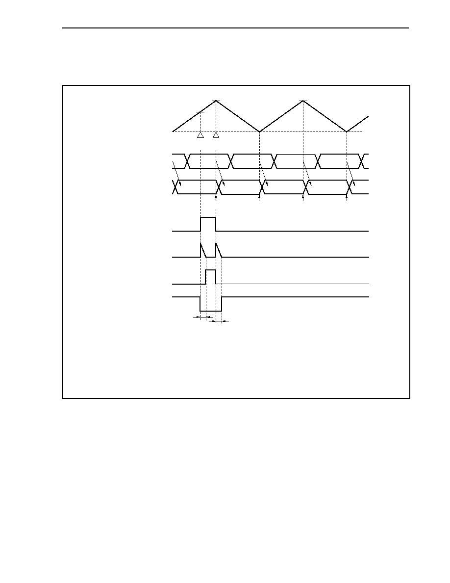
CHAPTER 9 TIMER/COUNTER FUNCTION
271
User's Manual U14492EJ5V0UD
(e) When BFCMnx = CM0n3 is set in software processing started by INTTM0n
Figure 9-29. Operation Timing in PWM Mode 1 (Asymmetric Triangular Wave, BFCMnx = CM0n3)
t
t
CM0n3
CM0n3
a
CM0nx
match
CM0nx
match
INTTM0n
INTTM0n
TM0
count value
Positive phase
(TO0n0, TO0n2, TO0n4)
Negative phase
(TO0n1, TO0n3, TO0n5)
BFCMnx
DTMnx
F/F
Interrupt request
CM0nx
0000H
b
b
b
b
a
b
a
b
b
b
INTCM0n3
INTCM0n3
Remarks 1. n = 0, 1
2. x = 0 to 2
3. b = CM0n3
4. t: Dead time = (DTRRn + 1)/f
CLK
(f
CLK
: Base clock)
5. The above figure shows an active high case.
Since TM0n and CM0nx match is detected during count down of TM0n when BFCMnx = CM0n3 has
been set, the F/F remains reset as is and does not get set. Therefore, the positive phase side (TO0n0,
TO0n2, TO0n4 pins) outputs a low level, and the negative phase side (TO0n1, TO0n3, TO0n5 pins)
continues to output a high level. Moreover, the timing of matching with TM0n with CM0nx = CM0n3 is the
cycle when transfer is performed from BFCMnx to CM0nx by INTCM0n3.
The above explanation applies to an active high case. In an active low case, the levels of positive and
negative phases are merely inverted and other operations remain the same.

CHAPTER 9 TIMER/COUNTER FUNCTION
272
User's Manual U14492EJ5V0UD
(4) PWM mode 2: Sawtooth wave modulation
[Setting procedure]
(a) Set PWM mode 2 (sawtooth wave) with bits MOD01 and MOD00 of the TMC0n register. Also set the
active level of pins TO0n0 to TO0n5 with the ALVTO bit of the TOMRn register.
(b) Set the count clock of TM0n with bits PRM02 to PRM00 of the TMC0n register. The transfer operation
from BFCMn3 to CM0n3 is set with bit BFTE3, and the transfer operation from BFCMn0 to BFCMn2 to
CM0n0 to CM0n2 is set with bit BFTEN.
(c) Set the initial values.
(i) Specify the interrupt culling ratio with bits CUL02 to CUL00 of the TMC0n register.
(ii) Set the cycle width of the PWM cycle in BFCMn3.
∑ PWM cycle = (BFCMn3 value + 1) ◊ TM0n count clock
(The TM0n count clock is set with the TMC0n register.)
(iii) Set the dead-time width in DTRRn.
∑ Dead-time width = (DTRRn + 1)/f
CLK
f
CLK
: Base clock
(iv) Set the set/reset timing of the F/F used in the PWM cycle in BFCM0n0 to BFCM0n2.
(d) Clear (0) the TM0CEDn bit of the TMC0n register to enable dead-time timer operation. Set TM0CEDn = 1
when not using dead time.
(e) Setting (1) the TM0CEn bit of the TMC0n register starts TM0n counting, and a 6-channel PWM signal is
output from pins TO0n0 to TO0n5.
Caution Setting CM0n3 to 0000H is prohibited.

CHAPTER 9 TIMER/COUNTER FUNCTION
273
User's Manual U14492EJ5V0UD
[Operation]
In PWM mode 2, TM0n performs up-count operation, and when it matches the value of CM0n3, match
interrupt INTCM0n3 is generated and TM0n is cleared (n = 0, 1).
The PWM cycle in this mode is ((BFCMn3 value + 1)
◊ TM0n count clock). Concerning setting of data to
CM0n3, the next PWM cycle width is set to BFCMn3.
The data of BFCMn3 is automatically transferred by hardware to CM0n3 upon generation of the INTCM0n3
interrupt. Furthermore, calculation is performed by software processing started by INTCM0n3, and the data
for the next cycle is set to BFCMn3.
Data setting to CM0n0 to CM0n2, which control the PWM duty, is explained next.
Setting of data to CM0n0 to CM0n2 consists in setting the duty output from BFCMn0 to BFCMn2.
The values of BFCMn0 to BFCMn2 are automatically transferred by hardware to CM0n0 to CM0n2 upon
generation of the INTCM0n3 interrupt. Furthermore, software processing is started up and calculation
performed, and reset timing of the F/F for the next cycle is set to BFCMn0 to BFCMn2.
The PWM cycle and the PWM duty are set in the above procedure.
The F/F set/reset conditions upon match of CM0n0 to CM0n2 are as follows.
∑ Set: TM0n and CM0n3 match detection and rising edge of TM0CEn bit of TMC0n register
∑ Reset: TM0n and CM0n0 to CM0n2 match detection
The values of DTRRn are transferred to the corresponding dead-time timers (DTMn0 to DTMn2) in
synchronization with the set/reset timing of the F/F, and down counting is started. DTMn0 to DTMn2 count
down to 000H, and stop when they count down further to FFFH.
DTMn0 to DTMn2 can automatically generate a width (dead time) at which the active levels of the positive
phase (TO0n0, TO0n2, TO0n4) and negative phase (TO0n1, TO0n3, TO0n5) do not overlap.
In this way, software processing is started by an interrupt (INTCM0n3) that occurs once during every PWM
cycle after initial setting has been performed, and by setting the PWM cycle and PWM duty to be used in the
next cycle, it is possible to automatically output a PWM waveform to TO0n0 to TO0n5 pins taking into
consideration the dead-time width (in case of interrupt culling ratio of 1/1).

CHAPTER 9 TIMER/COUNTER FUNCTION
274
User's Manual U14492EJ5V0UD
[Output waveform width in respect to set value]
∑ PWM cycle = (BFCMn3 + 1) ◊ T
TM0n
∑ Dead-time width T
Dnm
= (DTRRn + 1)/f
CLK
∑ Active width of positive phase (TO0n0, TO0n2, TO0n4 pins)
= (CM0nX + 1)
◊ T
TM0n
- T
Dnm
∑ Active width of negative phase (TO0n1, TO0n3, TO0n5 pins)
=
(CM0n3
- CM0nX) ◊ T
TM0n
- T
Dnm
f
CLK
:
Base clock
T
TM0n
:
TM0n count clock
CM0nX: Set value of CM0n0 to CM0n2
The pin level when the TO0n0 to TO0n5 pins are reset is the high impedance state. When the control mode is
selected thereafter, the following levels are output until the TM0n is started.
∑ TO0n0, TO0n2, TO0n4... When low active High level
When high active
Low level
∑ TO0n1, TO0n3, TO0n5... When low active Low level
When high active
High level
The active level is set with the ALVTO bit of the TOMRn register. The default is low active.
Caution If a value such that the positive phase or negative phase active width is "0" or a negative
value in the above formula, the TO0n0 to TO0n5 pins output a waveform fixed to the
inactive level waveform with active width "0".
Remark m = 0 to 2
n = 0, 1
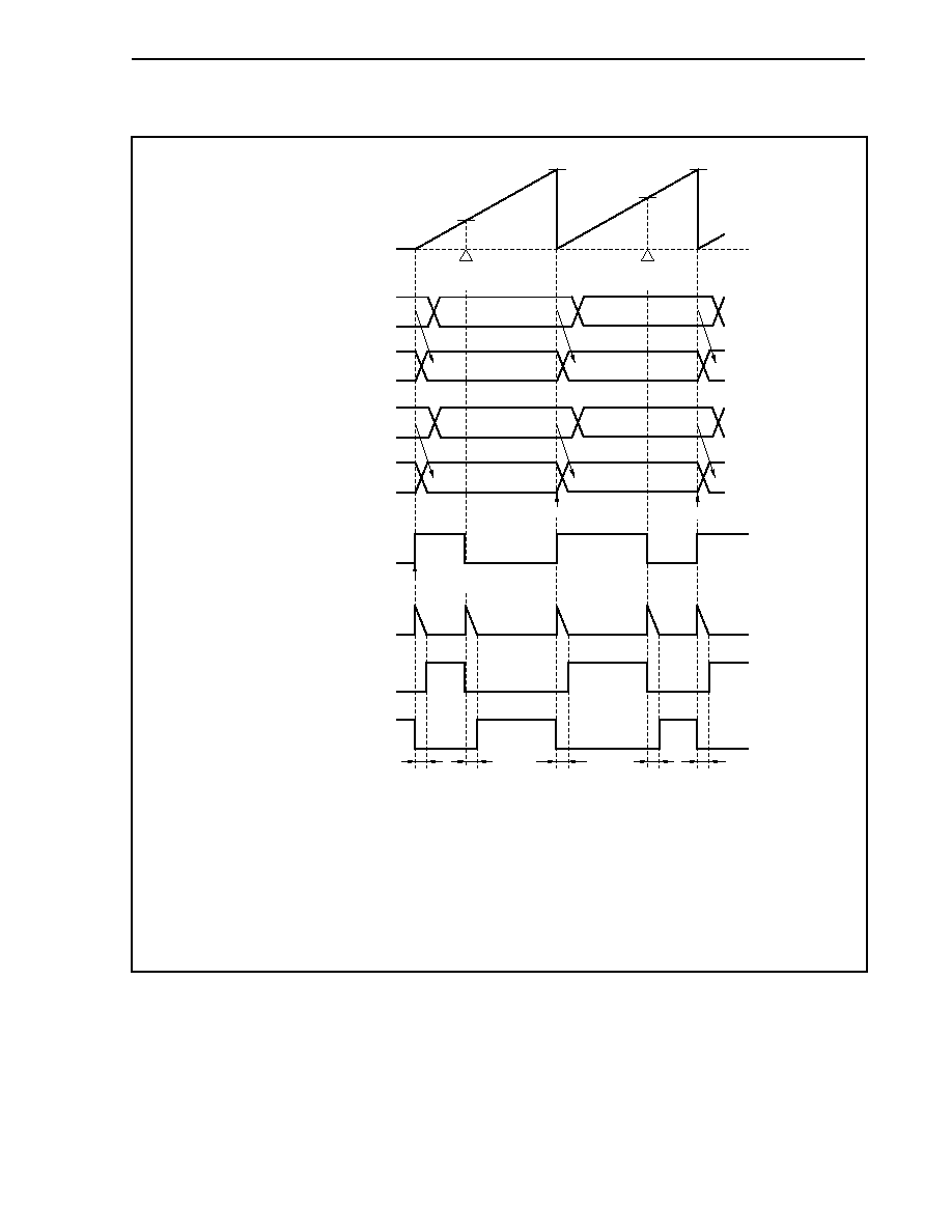
CHAPTER 9 TIMER/COUNTER FUNCTION
275
User's Manual U14492EJ5V0UD
Figure 9-30. Operation Timing in PWM Mode 2 (Sawtooth Wave)
t
t
t
t
t
CM0n3 (d)
CM0n3 (e)
a
b
CM0nx
match
CM0nx
match
b
c
e
f
b
c
a
e
f
d
TM0n
count value
Positive phase
(TO0n0, TO0n2, TO0n4)
Negative phase
(TO0n1, TO0n3, TO0n5)
Interrupt request
BFCMnx
BFCMn3
CM0n3
DTMnx
F/F
CM0nx
0000H
INTCM0n3
INTCM0n3
Set by rising edge of
TM0CEn bit
Remarks 1. The above figure shows the timing chart when BFTE3 and BFTEN of the TMC0n register are 1,
and transfer from BFCMn3 to CM0n3, or from BFCMnx to CM0nx is enabled. Transfer is not
performed when BFTE3 = 0 or BFTEN = 0.
2. n = 0, 1
3. x = 0 to 2
4. t: Dead time = (DTRRn + 1)/f
CLK
(f
CLK
: Base clock)
5. The above figure shows an active high case.
Figure 9-31 shows the overall operation image.
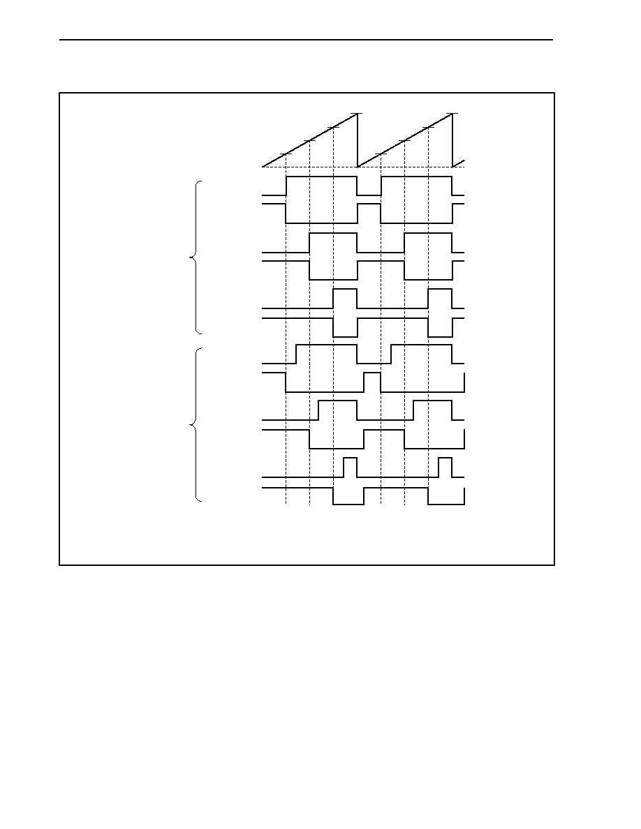
CHAPTER 9 TIMER/COUNTER FUNCTION
276
User's Manual U14492EJ5V0UD
Figure 9-31. Overall Operation Image of PWM Mode 2 (Sawtooth Wave)
CM0n3
TM0n
count value
TO0n0 output
TO0n1 output
TO0n2 output
TO0n3 output
TO0n4 output
TO0n5 output
TO0n0 output
TO0n1 output
TO0n2 output
TO0n3 output
TO0n4 output
TO0n5 output
0000H
CM0n2
CM0n1
CM0n0
CM0n3
CM0n2
CM0n1
CM0n0
Without
dead time
With
dead time
Remarks 1. n = 0, 1
2. The above figure shows an active low case.
Since the F/F is set at the rising edge of the TM0CEn bit of the TMC0n register in the first cycle, the
PWM signal can be output.

CHAPTER 9 TIMER/COUNTER FUNCTION
277
User's Manual U14492EJ5V0UD
(a) When BFCMnx > CM0n3 is set
Figure 9-32. Operation Timing in PWM Mode 2 (Sawtooth Wave, BFCMnx > CM0n3)
t
t
t
CM0n3
CM0n3
CM0n3
a
CM0nx
match
b
b
b
b
b
a
TM0n
count value
Positive phase
(TO0n0, TO0n2, TO0n4)
Negative phase
(TO0n1, TO0n3, TO0n5)
Interrupt request
BFCMnx
DTMnx
F/F
CM0nx
0000H
INTCM0n3
INTCM0n3
INTCM0n3
Set by rising edge of
TM0CEn bit
Remarks 1. n = 0, 1
2. x = 0 to 2
3. b > CM0n3
4. t: Dead time = (DTRRn + 1)/f
CLK
(f
CLK
: Base clock)
5. The above figure shows an active high case.
When a value greater than CM0n3 is set to BFCMnx, the positive phase side (TO0n0, TO0n2, TO0n4
pins) outputs a high level, and the negative phase side (TO0n1, TO0n3, TO0n5 pins) continues to output
a low level. Since TM0n and CM0nx match does not occur, the F/F does not get reset. This feature is
effective for outputting a low-level or high-level width exceeding the PWM cycle in an application such as
inverter control.
The above explanation applies to an active high case. In an active low case, the levels of positive and
negative phases are merely inverted and other operations remain the same.
Figure 9-33 shows the change timing from the 100% duty state.
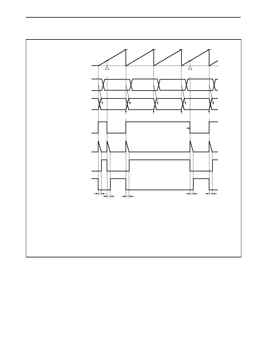
CHAPTER 9 TIMER/COUNTER FUNCTION
278
User's Manual U14492EJ5V0UD
Figure 9-33. Change Timing from 100% Duty State (PWM Mode 2)
CM0n3
TM0n
count value
BFCM0nx
0000H
CM0nx
DTMnx
F/F
Interrupt request
Positive phase
(TO0n0, TO0n2, TO0n4)
Negative phase
(TO0n1, TO0n3, TO0n5)
a
b
b
c
d
a
b
b
c
Note
CM0n3
CM0n3
a
c
CM0nx
match
CM0nx
match
CM0n3
t
t
t
t
t
INTCM0n3
INTCM0n3
INTCM0n3
INTCM0n3
Note F/F is reset upon occurrence of match with CM0nx.
Remarks 1. n = 0, 1
2. x = 0 to 2
3. b > CM0n3
4. t: Dead time = (DTRRn + 1)/f
CLK
(f
CLK
: Base clock)
5. The above figure shows an active high case.
The timing at which the F/F is reset is upon occurrence of match with CM0nx as normal.
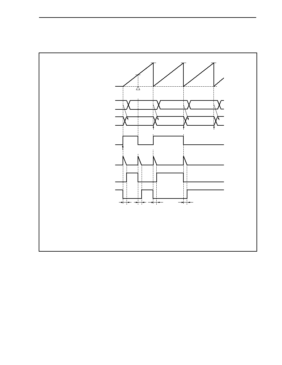
CHAPTER 9 TIMER/COUNTER FUNCTION
279
User's Manual U14492EJ5V0UD
(b) When BFCMnx = CM0n3 is set
Figure 9-34. Operation Timing in PWM Mode 2 (Sawtooth Wave, BFCMnx = CM0n3)
t
t
t
t
CM0n3
CM0n3
CM0n3
a
CM0nx
match
b
b
b
b
b
a
TM0n
count value
Positive phase
(TO0n0, TO0n2, TO0n4)
Negative phase
(TO0n1, TO0n3, TO0n5)
Interrupt request
BFCMnx
DTMnx
F/F
CM0nx
0000H
INTCM0n3
INTCM0n3
INTCM0n3
Set by rising edge of
TM0CEn bit
a
Remarks 1. n = 0, 1
2. x = 0 to 2
3. b = CM0n3
4. t: Dead time = (DTRRn + 1)/f
CLK
(f
CLK
: Base clock)
5. The above figure shows an active high case.
If match signal INTCM0n3 for TM0n and CM0n3 and the match signal for TM0n and CM0nx conflict,
reset of the F/F takes precedence, so that the F/F does not get set following match of CM0nx (= CM0n3)
with TM0n.
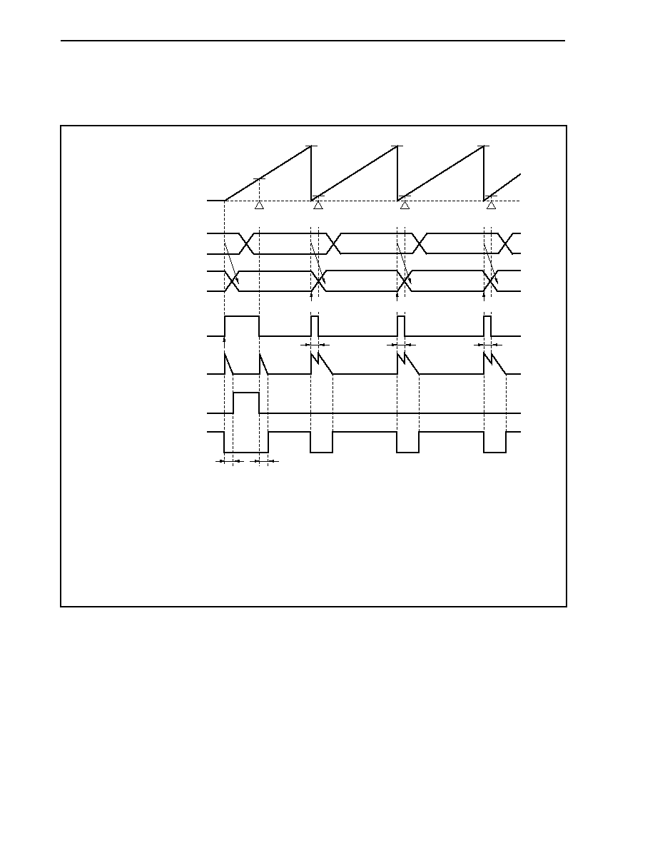
CHAPTER 9 TIMER/COUNTER FUNCTION
280
User's Manual U14492EJ5V0UD
(c) When BFCMnx = 0000H is set
Figure 9-35. Operation Timing in PWM Mode 2 (Sawtooth Wave, BFCMnx = 0000H)
t
t
W
W
W
CM0n3
CM0n3
CM0n3
a
CM0nx
match
CM0nx
match
CM0nx
match
CM0nx
match
b
b
b
b
b
a
TM0n
count value
Positive phase
(TO0n0, TO0n2, TO0n4)
Negative phase
(TO0n1, TO0n3, TO0n5)
Interrupt request
BFCMnx
DTMnx
F/F
CM0nx
0000H
Note
INTCM0n3
INTCM0n3
INTCM0n3
a
Note Set by rising edge of TM0CEn bit
Remarks 1. n = 0, 1
2. x = 0 to 2
3. t: Dead time = (DTRRn + 1)/f
CLK
(f
CLK
: Base clock)
4. The above figure shows an active high case.
5. W: Width between CM0n3 match and CM0nx match (timer count clock)
If CM0nx = 0000H has been set, the output waveform resulting from the TM0n count clock rate and the
DTRRn set value differ.

CHAPTER 9 TIMER/COUNTER FUNCTION
281
User's Manual U14492EJ5V0UD
(d) When BFCMnx = 0000H is set while DTMnx = 000H or TM0CEDn bit = 1
A pulse equivalent to one count clock of the timer is output.
Figure 9-36. Operation Timing in PWM Mode 2 (Sawtooth Wave, BFCMnx = 0000H
While DTMnx = 000H or TM0CEDn Bit = 1)
W
L
W
W
CM0n3
CM0n3
CM0n3
a
CM0nx
match
CM0nx
match
CM0nx
match
CM0nx
match
b
a
b
b
b
b
a
TM0n
count value
Positive phase
(TO0n0, TO0n2, TO0n4)
Negative phase
(TO0n1, TO0n3, TO0n5)
Interrupt request
BFCMnx
DTMnx
F/F
CM0nx
0000H
Note
INTCM0n3
INTCM0n3
INTCM0n3
Note Set at the rising edge of the TM0CEn bit.
Remarks 1. n = 0, 1
2. x = 0 to 2
3. The above figure shows an active-high case.
4. W: Width of a pulse equivalent to one count clock of the timer from CM0n3 match

CHAPTER 9 TIMER/COUNTER FUNCTION
282
User's Manual U14492EJ5V0UD
(e) When BFCMnx = CM0n3 = a is set
Figure 9-37. Operation Timing in PWM Mode 2 (Sawtooth Wave, BFCMnx = CM0n3 = a)
(When DTRRn = 0000H, TM0CEDn Bit of TMC0n Register = 1, ALVTO Bit of TOMRn
Register = 1 (PWM Driving, Active Level = High) Are Set)
L
CM0n3
CM0n3
CM0n3
CM0nx
match
CM0nx
match
CM0nx
match
a
a
a
a
a
a
TM0n
count value
Positive phase
(TO0n0, TO0n2, TO0n4)
Negative phase
(TO0n1, TO0n3, TO0n5)
BFCMnx
DTMnx
F/F
CM0nx
Interrupt request
0000H
INTCM0n3
INTCM0n3
INTCM0n3
Remarks 1. n = 0, 1
2. x = 0 to 2
3. The above figure shows an active-high case.
4. For the timing including the dead time, refer to Figure 9-35.
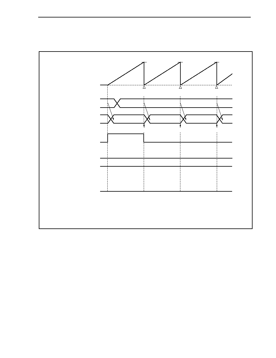
CHAPTER 9 TIMER/COUNTER FUNCTION
283
User's Manual U14492EJ5V0UD
Figure 9-38. Operation Timing in PWM Mode 2 (Sawtooth Wave, BFCMnx = CM0n3 = a)
(When DTRRn = 0000H, TM0CEDn Bit of TMC0n Register = 1, ALVTO Bit of TOMRn
Register = 0 (PWM Driving, Active Level = Low) Are Set)
L
L
H
CM0n3
CM0n3
CM0n3
CM0nx
match
CM0nx
match
CM0nx
match
a
a
a
a
a
a
TM0n
count value
Positive phase
(TO0n0, TO0n2, TO0n4)
Negative phase
(TO0n1, TO0n3, TO0n5)
BFCMnx
DTMnx
F/F
CM0nx
0000H
INTCM0n3
INTCM0n3
INTCM0n3
Interrupt request
Remarks 1. n = 0, 1
2. x = 0 to 2
3. The above figure shows an active-low case.
4. For the timing including the dead time, refer to Figure 9-35.
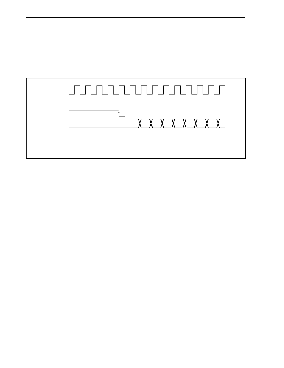
CHAPTER 9 TIMER/COUNTER FUNCTION
284
User's Manual U14492EJ5V0UD
9.1.6 Operation timing
(1) TM0CEn bit write and TM0n timer operation timing
Figure 9-39 shows the timing from write of the TM0CEn bit of the TMC0n register until the TM0n timer starts
operating.
Figure 9-39. TM0CEn Bit Write and TM0n Timer Operation Timing
Register write timing
0000H
0001H 0002H 0003H 0004H 0005H 0006H 0007H
f
CLK
TM0CEn bit
write timing
TM0n
Caution The operation of TM0n starts 2f
CLK
after the register write timing.
Remark f
CLK
: Base clock
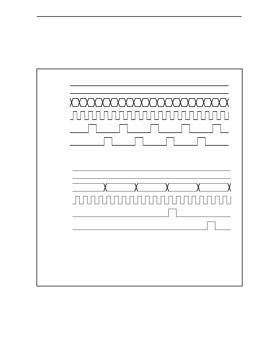
CHAPTER 9 TIMER/COUNTER FUNCTION
285
User's Manual U14492EJ5V0UD
(2) Interrupt generation timing
The interrupt generation timing with the count clock setting (PRM02 to PRM00 bits of the TMC0n register) to
TM0n in the various modes is described below.
Figure 9-40. Interrupt Generation Timing in PWM Mode 0 (Symmetric Triangular Wave), PWM Mode 1
(Asymmetric Triangular Wave)
(a) When count clock = f
CLK
0002H
0001H 0002H 0001H 0000H 0001H 0002H 0001H 0000H 0001H 0002H 0001H 0000H 0001H 0002H 0001H 0000H 0001H 0002H 0001H 0000H
CM0n3
TM0n
INTCM0n3
INTTM0n
f
CLK
(b) When count clock = f
CLK
/4
0002H
0000H
0001H
0002H
0001H
0000H
CM0n3
TM0n
INTCM0n3
INTTM0n
f
CLK
Cautions 1. INTCM0n3 is generated at the next f
CLK
after detection of TM0n and CM0n3 match.
2. INTTM0n is generated at the next f
CLK
after detection of TM0n and 0000H match.
3. INTTM0n is generated at the next f
CLK
after detection of TM0n and 0000H match, even if
the count clock is 1/2, 1/8, 1/16, or 1/32.
Remarks 1. n = 0, 1
2. f
CLK
: Base clock

CHAPTER 9 TIMER/COUNTER FUNCTION
286
User's Manual U14492EJ5V0UD
Figure 9-41. Interrupt Generation Timing in PWM Mode 2 (Sawtooth Wave)
(a) When count clock = f
CLK
0002H
0001H 0002H 0000H 0001H 0002H 0000H 0001H 0002H 0000H 0001H 0002H 0000H 0001H 0002H 0000H 0001H 0002H 0000H 0001H 0002H
CM0n3
TM0n
INTCM0n3
f
CLK
(b) When count clock = f
CLK
/4
0002H
0000H
0001H
0002H
0000H
0001H
CM0n3
TM0n
INTCM0n3
f
CLK
Cautions 1. INTCM0n3 is generated at the next f
CLK
after detection of TM0n and CM0n3 match.
2. INTCM0n3 is generated at the next f
CLK
after detection of TM0n and CM0n3 match even if the
count clock is 1/2, 1/8, 1/16, or 1/32.
Remarks 1. n = 0, 1
2. f
CLK
: Base clock
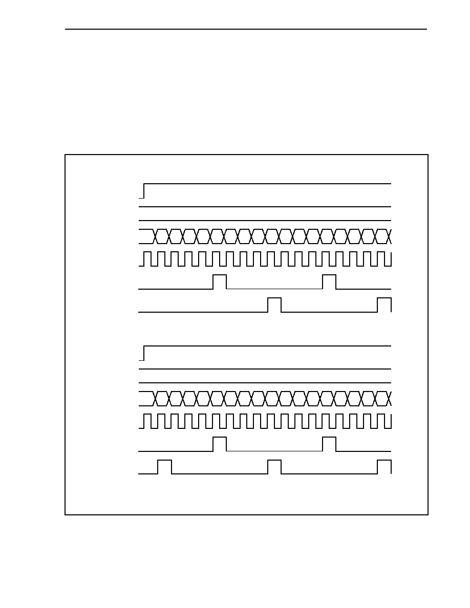
CHAPTER 9 TIMER/COUNTER FUNCTION
287
User's Manual U14492EJ5V0UD
(3) Relationship between interrupt generation and STINTn bit of TMC0n register
The interrupt generation timing for the setting of the STINTn bit of the TMC0n register and the interrupt culling
ratio setting (bits CUL02 to CUL00) in the various modes is described below.
If, to realize the INTTM0n and INTCM0n3 interrupt culling function for TM0n, bits CUL02 to CUL00 of the
TMC0n register are set for a culling ratio other than 1/1, and count operation is started, the interrupt output
order differs according to the setting of the STINTn bit when counting starts.
Figure 9-42. Interrupt Generation Timing in PWM Mode 0 (Symmetric Triangular Wave), PWM Mode 1
(Asymmetric Triangular Wave): In Case of Interrupt Culling Ratio of 1/1
(a) When STINTn bit = 0
0004H
0000H 0001H 0002H 0003H 0004H 0003H 0002H 0001H 0000H 0001H 0002H 0003H 0004H 0003H 0002H 0001H 0000H 0001H
CM0n3
TM0CEn bit
TM0n
INTCM0n3
INTTM0n
f
CLK
(b) When STINTn bit = 1
0004H
0000H 0001H 0002H 0003H 0004H 0003H 0002H 0001H 0000H 0001H 0002H 0003H 0004H 0003H 0002H 0001H 0000H 0001H
CM0n3
TM0CEn bit
TM0n
INTCM0n3
INTTM0n
f
CLK
Remarks 1. n = 0, 1
2. f
CLK
: Base clock
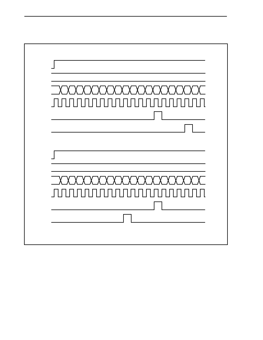
CHAPTER 9 TIMER/COUNTER FUNCTION
288
User's Manual U14492EJ5V0UD
Figure 9-43. Interrupt Generation Timing in PWM Mode 0 (Symmetric Triangular Wave), PWM Mode 1
(Asymmetric Triangular Wave): In Case of Interrupt Culling Ratio of 1/2
(a) When STINTn bit = 0
0004H
0000H 0001H 0002H 0003H 0004H 0003H 0002H 0001H 0000H 0001H 0002H 0003H 0004H 0003H 0002H 0001H 0000H 0001H 0002H 0003H
CM0n3
TM0CEn bit
TM0n
INTCM0n3
INTTM0n
f
CLK
(b) When STINTn bit = 1
0004H
0000H 0001H 0002H 0003H 0004H 0003H 0002H 0001H 0000H 0001H 0002H 0003H 0004H 0003H 0002H 0001H 0000H 0001H 0002H 0003H
CM0n3
TM0CEn bit
TM0n
INTCM0n3
INTTM0n
f
CLK
Remarks 1. n = 0, 1
2. f
CLK
: Base clock
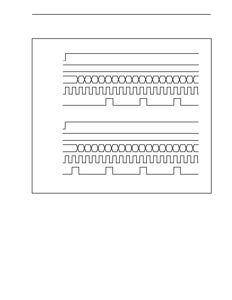
CHAPTER 9 TIMER/COUNTER FUNCTION
289
User's Manual U14492EJ5V0UD
Figure 9-44. Interrupt Generation Timing in PWM Mode 2 (Sawtooth Wave):
In Case of Interrupt Culling Ratio of 1/1
(a) When STINTn bit = 0
0004H
0000H
0001H 0002H 0003H 0004H 0000H 0001H 0002H 0003H 0004H 0000H 0001H 0002H 0003H 0004H 0000H 0001H 0002H 0003H
CM0n3
TM0CEn bit
TM0n
INTCM0n3
f
CLK
(b) When STINTn bit = 1
0004H
0000H
0001H 0002H 0003H 0004H 0000H 0001H 0002H 0003H 0004H 0000H 0001H 0002H 0003H 0004H 0000H 0001H 0002H 0003H
CM0n3
TM0CEn bit
TM0n
INTCM0n3
f
CLK
Remarks 1. n = 0, 1
2. f
CLK
: Base clock
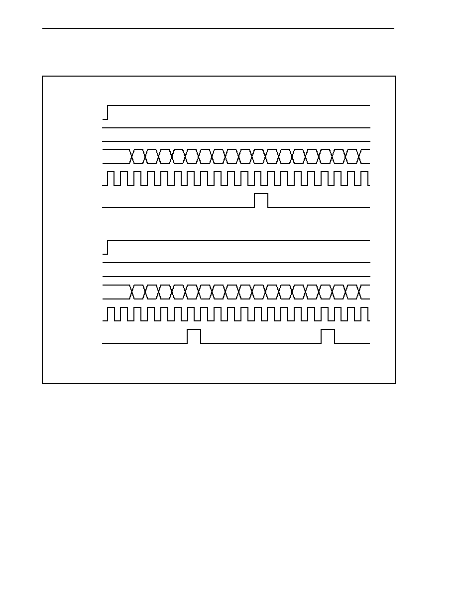
CHAPTER 9 TIMER/COUNTER FUNCTION
290
User's Manual U14492EJ5V0UD
Figure 9-45. Interrupt Generation Timing in PWM Mode 2 (Sawtooth Wave): In Case of Interrupt Culling
Ratio of 1/2
(a) When STINTn bit = 0
0004H
0000H
0001H 0002H 0003H 0004H 0000H 0001H 0002H 0003H 0004H 0000H 0001H 0002H 0003H 0004H 0000H 0001H 0002H 0003H
CM0n3
TM0CEn bit
TM0n
INTCM0n3
f
CLK
(b) When STINTn bit = 1
0004H
0000H
0001H 0002H 0003H 0004H 0000H 0001H 0002H 0003H 0004H 0000H 0001H 0002H 0003H 0004H 0000H 0001H 0002H 0003H
CM0n3
TM0CEn bit
TM0n
INTCM0n3
f
CLK
Remarks 1. n = 0, 1
2. f
CLK
: Base clock
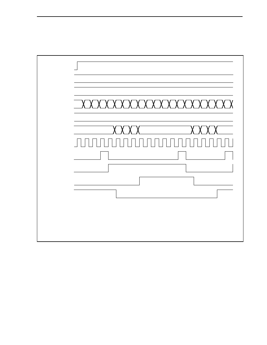
CHAPTER 9 TIMER/COUNTER FUNCTION
291
User's Manual U14492EJ5V0UD
(4) TO0n0 to TO0n5 output timing
Figure 9-46. TO0n0 to TO0n5 Output Timing in PWM Mode 0 (Symmetric Triangular Wave), PWM Mode 1
(Asymmetric Triangular Wave)
0003H
0002H
0008H
0000H 0001H 0002H 0003H 0004H 0005H 0006H 0007H
0002H
FFFFH
FFFFH
FFFFH
0001H 0000H
0002H 0001H 0000H
0008H 0007H 0006H 0005H 0004H 0003H 0002H 0001H 0000H 0001H 0002H 0003H
CM0nx
TM0n
DTMnx
Match signal
F/F
TO0n0, TO0n2,
TO0n4
TO0n1, TO0n3,
TO0n5
DTRRn
f
CLK
CM0n3
TM0CEn bit
Remarks 1. The above figure shows the timing until the compare register and the TM0n timer match and the
TO0n0 to TO0n5 outputs change.
2. x = 0 to 2
3. n = 0, 1
4. f
CLK
: Base clock
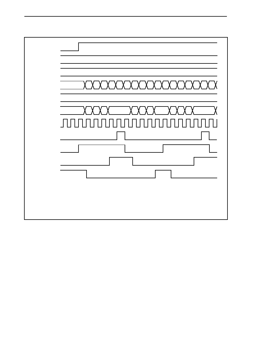
CHAPTER 9 TIMER/COUNTER FUNCTION
292
User's Manual U14492EJ5V0UD
Figure 9-47. TO0n0 to TO0n5 Output Timing in PWM Mode 2 (Sawtooth Wave)
0005H
0002H
000AH
0001H 0002H 0003H 0004H 0005H
0002H
FFFFH
0000H
FFFFH
FFFFH
0001H 0000H
0002H 0001H 0000H
0002H
FFFFH
0001H 0000H
0006H 0007H 0008H 0009H 000AH 0000H 0001H 0002H 0003H 0004H 0005H 0006H
CM0nx
TM0n
DTMnx
Match signal
F/F
TO0n0, TO0n2,
TO0n4
TO0n1, TO0n3,
TO0n5
DTRRn
f
CLK
CM0n3
TM0CEn bit
Remarks 1. The above figure shows the timing until the compare register and the TM0n timer match and the
TO0n0 to TO0n5 outputs change.
2. x = 0 to 2
3. n = 0, 1
4. f
CLK
: Base clock

CHAPTER 9 TIMER/COUNTER FUNCTION
293
User's Manual U14492EJ5V0UD
9.2 Timer 1
9.2.1 Features (timer 1)
Timers 10, 11 (TM10, TM11) are 16-bit up/down counters that perform the following operations.
∑ General-purpose timer mode (See 9.2.5 (1) Operation in general-purpose timer mode.)
Free-running timer
PWM output
∑ Up/down counter mode (See 9.2.5 (2) Operation in UDC mode.)
UDC mode A (mode 1, mode 2, mode 3, mode 4)
UDC mode B (mode 1, mode 2, mode 3, mode 4)
9.2.2 Function overview (timer 1)
∑
16-bit 2-phase encoder input up/down counter & general-purpose timer (TM1n): 2 channels
∑
Compare register: 2
◊ 2 channels
∑
Capture/compare register: 2
◊ 2 channels
∑
Interrupt request source
∑ Capture/compare match interrupt: 2 types ◊ 2 channels
∑ Compare match interrupt request: 2 types ◊ 2 channels
∑
Capture request signal: 2 types
◊ 2 channels
∑ The TM1n value can be latched using the valid edge of the INTP1n0, INTP1n1 pins corresponding to the
capture/compare register as the capture trigger.
∑
Count clocks selectable through division by prescaler (set the frequency of the count clock to 8 MHz or less)
∑
Base clock (f
CLK
): 2 types (set f
CLK
to 16 MHz or less)
f
XX
/2 and f
XX
/4 can be selected
∑
Prescaler division ratio
The following division ratios can be selected according to the base clock (f
CLK
).
Base Clock (f
CLK
)
Division Ratio
f
XX
/2 Selected
f
XX
/4 Selected
1/2 f
XX
/4 f
XX
/8
1/4 f
XX
/8 f
XX
/16
1/8 f
XX
/16 f
XX
/32
1/16 f
XX
/32 f
XX
/64
1/32 f
XX
/64 f
XX
/128
1/64 f
XX
/128
f
XX
/256
1/128 f
XX
/256 f
XX
/512

CHAPTER 9 TIMER/COUNTER FUNCTION
294
User's Manual U14492EJ5V0UD
∑
PWM output function
In the general-purpose timer mode, 16-bit resolution PWM output can be output from the TO1n pin.
∑
Timer clear
The following timer clear operations are performed according to the mode that is used.
(a) General-purpose timer mode: Timer clear operation is possible upon occurrence of match with CM1n0 set
value.
(b) Up/down counter mode: The timer clear operation can be selected from among the following four
conditions.
(i) Timer clear performed upon occurrence of match with CM1n0 set value during TM1n up-count
operation, and timer clear performed upon occurrence of match with CM1n1 set value during TM1n
down-count operation.
(ii) Timer clear performed only by external input.
(iii) Timer clear performed upon occurrence of match between TM1n count value and CM1n0 set value.
(iv) Timer clear performed upon occurrence of external input and match between TM1n count value and
CM1n0 set value.
∑
External pulse output (TO1n): 1
◊ 2 channels
Remark f
XX
: Internal system clock
n = 0, 1

CHAPTER 9 TIMER/COUNTER FUNCTION
295
User's Manual U14492EJ5V0UD
9.2.3 Basic configuration
The basic configuration is shown below.
Table 9-4. Timer 1 Configuration List
Count Clock
Timer
Note 1
Note 2
Register Read/Write Generated
Interrupt Signal
Capture Trigger
TM10 Read/write
-
-
CM100 Read/write
INTCM100
-
CM101 Read/write
INTCM101
-
CC100 Read/write
INTCC100 INTP100
CC101 Read/write
INTCC101 INTP100
or
INTP101
TM11 Read/write
-
-
CM110 Read/write
INTCM110
-
CM111 Read/write
INTCM111
-
CC110 Read/write
INTCC110 INTP110
Timer 1
f
XX
/4,
f
XX
/8,
f
XX
/16,
f
XX
/32,
f
XX
/64,
f
XX
/128,
f
XX
/256
f
XX
/8,
f
XX
/16,
f
XX
/32,
f
XX
/64,
f
XX
/128,
f
XX
/256,
f
XX
/512
CC111 Read/write
INTCC111 INTP110
or
INTP111
Notes 1. When f
XX
/2 is selected as the base clock to TM1n.
2. When
f
XX
/4 is selected as the base clock to TM1n.
Remark f
XX
: Internal system clock
Figure 9-48 shows the block diagram of timer 1.
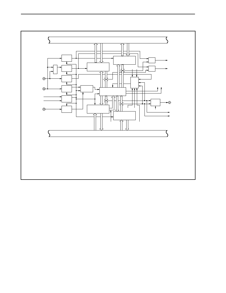
CHAPTER 9 TIMER/COUNTER FUNCTION
296
User's Manual U14492EJ5V0UD
Figure 9-48. Block Diagram of Timer 1
1/2, 1/4, 1/8, 1/16,
1/32, 1/64, 1/128
Edge
detector
Output
control
Selector
Selector
Edge
detector
Clock
control
Edge
detector
Edge
detector
Edge
detector
CLR1, CLR0
CM1n1
CM1n0
TM1n
TM10 clear
controller
CC1n1
CC1n0
MSEL
CMD
TM1UBDn
ENMD
ALVT10
RLEN
TM1UDFn
TM1OVFn
Clear
TCLR
SELCLK
f
CLK
Internal bus
Internal bus
TCLR1n/
INTP1n1
TCUD1n/
INTP1n0
TIUD1n
f
XX
/4
f
XX
/2
INTP1n0/
INTCC1n0
INTP1n1
Note
/
INTCC1n1
TO1n
INTCM1n0
INTCM1n1
Selector
Note The INTP1n1 interrupt is the signal of the capture trigger signal from the INTP1n1 pin or the capture
trigger signal from the INTP1n0 pin, selected by the CSLn bit of the CSL1n register.
Remarks 1. n = 0, 1
2. f
XX
: Internal system clock
3. f
CLK
: Base clock (16 MHz (MAX.))
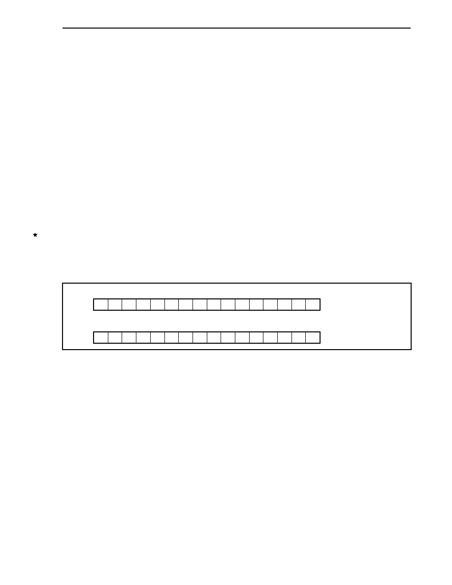
CHAPTER 9 TIMER/COUNTER FUNCTION
297
User's Manual U14492EJ5V0UD
(1) Timers 10, 11 (TM10, TM11)
TM1n is a general-purpose timer (in general-purpose mode) and 2-phase encoder input up/down counter (in
UDC mode).
This timer counts up in the general-purpose timer mode and counts up/down in the UDC mode.
TM1n can be read/written in 16-bit units.
Cautions 1. Write to TM1n is enabled only when the TM1CEn bit of the TMC1n register is "0" (count
operation disabled).
2. Continuous reading of TM1n is prohibited. If TM1n is continuously read, the second
read value may differ from the actual value. If TM1n must be read twice, be sure to read
another register between the first and the second read operation.
Correct usage example
Incorrect usage example
TM10
read
TM10
read
TM11
read
TM10
read
TM10
read
TM11
read
TM11
read
TM11
read
3. Writing the same value to the TM1n, CC1n0, and CC1n1 registers, and the STATUSn
register is prohibited. Writing the same value to the CCRn, TUMn, TMC1n, SESA1n, and
PRM1n registers, and CM1n0 and CM1n1 registers is permitted (writing the same value
is guaranteed even during a count operation).
14
13
12
2
3
4
5
6
7
8
9
10
11
15
1
0
TM10
Address
FFFFF5E0H
Initial value
0000H
14
13
12
2
3
4
5
6
7
8
9
10
11
15
1
0
TM11
Address
FFFFF600H
Initial value
0000H
TM1n start and stop is controlled by the TM1CEn bit of timer control register 1n (TMC1n).
The TM1n operation consists of the following two modes.
(a) General-purpose timer mode
In the general-purpose timer mode, TM1n operates as a 16-bit interval timer, free-running timer, or for
PWM output.
Counting is performed based on the clock selected by software.
Division by the prescaler can be selected for the count clock from among f
CLK
/2, f
CLK
/4, f
CLK
/8, f
CLK
/16,
f
CLK
/32, f
CLK
/64, or f
CLK
/128 with bits PRM12 to PRM10 of prescaler mode register 1n (PRM1n). (f
CLK
:
base clock, refer to 9.2.4 (1) Timer 1/timer 2 clock selection register (PRM02)).
CHAPTER 9 TIMER/COUNTER FUNCTION
298
User's Manual U14492EJ5V0UD
(b) Up/down counter mode (UDC mode)
In the UDC mode, TM1n functions as a 16-bit up/down counter, counting based on the TCUD1n and
TIUD1n input signals.
This mode is divided into the UDC mode A and UDC mode B, depending on the condition of clearing
TM1n.
The conditions for clearing the TM1n are classified as follows depending on the operation mode.
Table 9-5. Timer 1 (TM1n) Clear Conditions
TUMn Register
TMC1n Register
Operation Mode
CMD
Bit
MSEL
Bit
ENMD
Bit
CLR1
Bit
CLR0
Bit
TM1n Clear
0
◊
◊
Clearing not performed (free-running timer)
General-purpose
timer mode
0 0
1
◊
◊
Cleared upon match with CM1n0 set value
◊
0
0
Cleared only by TCLR1n input
◊
0
1
Cleared upon match with CM1n0 set value during up-
count operation
◊
1
0
Cleared by TCLR1n input or upon match with CM1n0 set
value during up-count operation
UDC mode A
1
0
◊
1
1
Clearing not performed
UDC mode B
1
1
◊
◊
◊
Cleared upon match with CM1n0 set value during up-
count operation or upon match with CM1n1 set value
during down-count operation
Settings other than the above
Setting prohibited
Remarks 1. n = 0, 1
2.
◊: Indicates that the set value of that bit is ignored.

CHAPTER 9 TIMER/COUNTER FUNCTION
299
User's Manual U14492EJ5V0UD
9.2.4 Control registers
(1) Timer 1/timer 2 clock selection register (PRM02)
The PRM02 register is used to select the base clock (f
CLK
) of timer 1 (TM1n) and timer 2 (TM2n).
This register can be read/written in 8-bit or 1-bit units.
Caution Always set this register before using the timers 1 and 2.
7
0
PRM02
6
0
5
0
4
0
3
0
2
0
1
0
0
PRM2
Address
FFFFF5D8H
Initial value
00H
Bit position
Bit name
Function
0
PRM2
Specifies the base clock (f
CLK
) of timer 1 (TM1n) and timer 2 (TM2n)
Note
.
0: f
CLK
= f
XX
/4
1: f
CLK
= f
XX
/2
Note Set the VSWC register to 15H when the PRM2 bit of the timer 1/timer 2 clock selection register (PRM02)
= 0B (f
CLK
= f
XX
/4), and set the VSWC register to 12H when the PRM2 bit = 1B (f
CLK
= f
XX
/2).
Remark f
XX
: Internal system clock
n = 0, 1

CHAPTER 9 TIMER/COUNTER FUNCTION
300
User's Manual U14492EJ5V0UD
(2) Timer unit mode registers 0, 1 (TUM0, TUM1)
The TUMn register is an 8-bit register used to specify the TM1n operation mode or to control the operation of
the PWM output pin.
TUMn can be read/written in 8-bit or 1-bit units.
Cautions 1. Changing the value of the TUMn register during TM1n operation (TM1CEn bit of TMCn
register = 1) is prohibited.
2. When the CMD bit = 0 (general-purpose timer mode), setting MSEL bit = 1 (UDC mode B)
is prohibited.
7
CMD
TUM0
6
0
5
0
4
0
3
TOE10
2
ALVT10
1
0
0
MSEL
Address
FFFFF5EBH
Initial value
00H
7
CMD
TUM1
6
0
5
0
4
0
3
TOE10
2
ALVT10
1
0
0
MSEL
Address
FFFFF60BH
Initial value
00H
Bit position
Bit name
Function
7
CMD
Specifies TM1n operation mode.
0: General-purpose timer mode (up count)
1: UDC mode (up/down count)
3
TOE10
Specifies timer output (TO1n) enable.
0: Timer output disabled
1: Timer output enabled
Caution
When CMD bit = 1 (UDC mode), timer output is not performed
regardless of the setting of the TOE10 bit. At this time, timer output
consists of the negative phase level of the level set by the ALVT10
bit.
2
ALVT10
Specifies active level of timer output (TO1n).
0: Active level is high level
1: Active level is low level
Caution
When CMD bit = 1 (UDC mode), timer output is not performed
regardless of the setting of the TOE10 bit. At this time, timer output
consists of the negative phase level of the level set by the ALVT10
bit.
0
MSEL
Specifies operation in UDC mode (up/down count).
0: UDC mode A
TM1n can be cleared by setting the CLR1, CLR0 bits of the TMC1n register.
1: UDC mode B
TM1n is cleared in the following cases.
∑ Upon match with CM1n0 during TM1n up-count operation
∑ Upon match with CM1n1 during TM1n down-count operation
When UDC mode B is set, the ENMD, CLR1, and CLR0 bits of the TMC1n
register becomes invalid.
Remark n = 0, 1

CHAPTER 9 TIMER/COUNTER FUNCTION
301
User's Manual U14492EJ5V0UD
(3) Timer control registers 10, 11 (TMC10, TMC11)
The TMC1n register is used to enable/disable TM1n operation and to set transfer and timer clear operations.
TMC1n can be read/written in 8-bit or 1-bit units.
Caution Changing the value of bits of the TMC1n register other than the TM1CEn bit during TM1n
operation (TM1CEn bit = 1) is prohibited.
(1/2)
7
0
TMC10
<6>
TM1CE0
5
0
4
0
3
RLEN
2
ENMD
1
CLR1
0
CLR0
Address
FFFFF5ECH
Initial value
00H
7
0
TMC11
<6>
TM1CE1
5
0
4
0
3
RLEN
2
ENMD
1
CLR1
0
CLR0
Address
FFFFF60CH
Initial value
00H
Bit position
Bit name
Function
6
TM1CEn
Enables/disables TM1n operation.
0: Disable TM1n count operation
1: Enable TM1n count operation
3
RLEN
Enables/disables transfer from CM1n0 to TM1n.
0: Disable transfer
1: Enable transfer
Cautions 1. When RLEN = 1, the value set to CM1n0 is transferred to TM1n
upon occurrence of TM1n underflow.
2. The RLEN bit is valid only in UDC mode A (CMD bit of TUMn
register = 1 and MSEL bit = 0). In the general-purpose timer mode
(CMD bit = 0) and UDC mode B (CMD bit = 1, MSEL bit = 1), a
transfer operation is not executed even if the RLEN bit is set to 1.
2
ENMD
Enables/disables clearing of TM1n in general-purpose timer mode (CMD bit of TUMn
register = 0).
0: Disable clear (free-running mode)
Clearing is not performed even when TM1n and CM1n0 values match.
1: Enable clear
Clearing is performed when TM1n and CM1n0 values match.
Caution
The ENMD bit setting becomes invalid in UDC mode (CMD bit of
TUMn register = 1).
Remark n = 0, 1

CHAPTER 9 TIMER/COUNTER FUNCTION
302
User's Manual U14492EJ5V0UD
(2/2)
Bit position
Bit name
Function
Controls TM1n clear operation in UDC mode A.
CLR1
CLR0
Specify TM1n clear source
0
0
Clear only by external input (TCLR1n)
0
1
Clear upon match of TM1n count value and CM1n0 set
value
1
0
Clear by TCLR1n input or upon match of TM1n count
value and CM1n0 set value
1 1
Don't
clear
1, 0
CLR1, CLR0
Cautions 1. Clearing by match of the TM1n count value and CM1n0 set value
is valid only during TM1n up-count operation (TM1n is not
cleared during TM1n down-count operation).
2. The CLR1 and CLR0 bit settings are invalid in general-purpose
timer mode (CMD bit of TUMn register = 0).
3. The CLR1 and CLR0 bit settings are invalid in UDC mode B
(MSEL bit of TUMn register = 1).
4. When clearing by TCLR1n has been enabled with bits CLR1 and
CLR0, clearing is performed whether the value of the TM1CEn bit
is 1 or 0.
Remark n = 0, 1
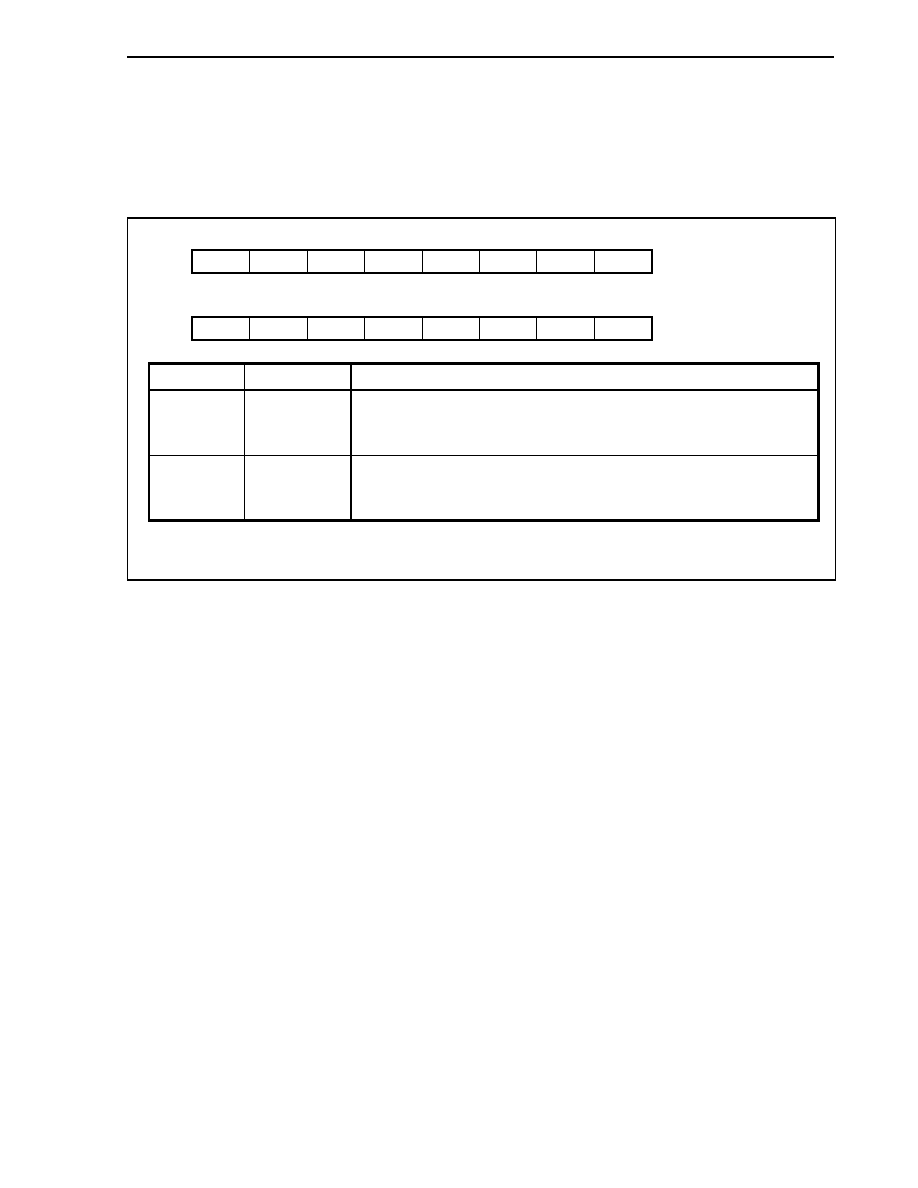
CHAPTER 9 TIMER/COUNTER FUNCTION
303
User's Manual U14492EJ5V0UD
(4) Capture/compare control registers 0, 1 (CCR0, CCR1)
The CCRn register specifies the operation mode of the capture/compare registers (CC1n0, CC1n1).
CCRn can be read/written in 8-bit or 1-bit units.
Caution Overwriting the CCRn register during TM1n operation (TM1CEn bit = 1) is prohibited.
7
0
CCR0
6
0
5
0
4
0
3
0
2
0
1
CMS1
0
CMS0
Address
FFFFF5EAH
Initial value
00H
7
0
CCR1
6
0
5
0
4
0
3
0
2
0
1
CMS1
0
CMS0
Address
FFFFF60AH
Initial value
00H
Bit position
Bit name
Function
1
CMS1
Specifies operation mode of CC1n1.
0: Capture register
1: Compare register
0
CMS0
Specifies operation mode of CC1n0.
0: Capture register
1: Compare register
Remark n = 0, 1
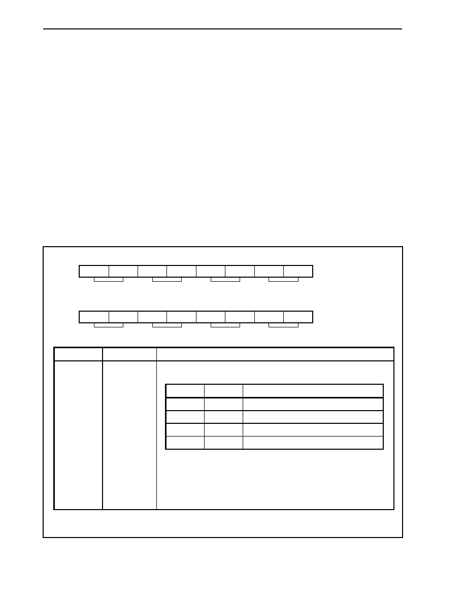
CHAPTER 9 TIMER/COUNTER FUNCTION
304
User's Manual U14492EJ5V0UD
(5) Signal edge selection registers 10, 11 (SESA10, SESA11)
The SESA1n register is used to specify the valid edge of external interrupt requests from external pins
(INTP100, INTP101, INTP110, INTP111, TIUD10, TIUD11, TCUD10, TCUD11, TCLR10, TCLR11). The
correspondences between each register and the external interrupt requests it controls are as follows.
∑ SESA10: TIUD10, TCUD10, TCLR10, INTP100, INTP101
∑ SESA11: TIUD11, TCUD11, TCLR11, INTP110, INTP111
The valid edge (rising edge, falling edge, or both edges) can be specified independently for each pin.
SESA1n can be read/written in 8-bit or 1-bit units.
Cautions 1. Changing the values of the SESA1n register bits during TM1n operation (TM1CEn bit =
1) is prohibited.
2. Be sure to set (to 1) the TM1CEn bit of timer control registers 10, 11 (TMC10, TMC11)
even when timer 1 is not used and the TCUD10/INTP100, TCLR10/INTP101,
TCUD11/INTP110, and TCLR11/INTP111 pins are used as INTP100, INTP101, INTP110,
and INTP111.
(1/2)
7
TESUD01
SESA10
6
TESUD00
5
CESUD01
4
CESUD00
3
IES1011
2
IES1010
1
IES1001
0
IES1000
Address
FFFFF5EDH
Initial value
00H
TIUD10, TCUD10
TCLR10
INTP101
INTP100
7
TESUD11
SESA11
6
TESUD10
5
CESUD11
4
CESUD10
3
IES1111
2
IES1110
1
IES1101
0
IES1100
Address
FFFFF60DH
Initial value
00H
TCLR11
TIUD11, TCUD11
INTP111
INTP110
Bit position
Bit name
Function
Specifies valid edge of pins TIUD10, TIUD11, TCUD10, TCUD11.
TESUDn1 TESUDn0
Valid
edge
0 0
Falling
edge
0 1
Rising
edge
1 0
Setting
prohibited
1
1
Both rising and falling edges
7, 6
TESUDn1,
TESUDn0
Cautions 1. The set values of the TESUDn1 and TESUDn0 bits are only valid
in UDC mode A and UDC mode B.
2. If mode 4 is specified as the operation mode of TM1n (specified
with PRM12 to PRM10 bits of PRM1n register), the valid edge
specifications for pins TIUD1n and TCUD1n (bits TESUDn1 and
TESUDn0) are not valid.
Remark n = 0, 1
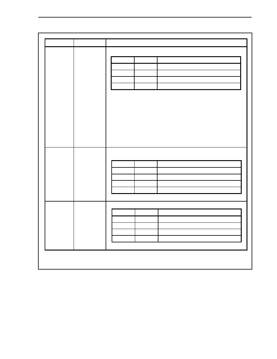
CHAPTER 9 TIMER/COUNTER FUNCTION
305
User's Manual U14492EJ5V0UD
(2/2)
Bit position
Bit name
Function
Specifies valid edge of pins TCLR10, TCLR11.
CESUDn1 CESUDn0
Valid
edge
0 0
Falling
edge
0 1
Rising
edge
1 0
Low
level
1 1
High
level
5, 4
CESUDn1,
CESUDn0
The set values of bits CESUDn1 and CESUDn0 and the TM1n operation are related
as follows.
00: TM1n cleared after detection of falling edge of TCLR1n
01: TM1n cleared after detection of rising edge of TCLR1n
10: TM1n cleared status held while TCLR1n input is low level
11: TM1n cleared status held while TCLR1n input is high level
Caution
The set values of the CESUDn1 and CESUDn0 bits are valid only in
UDC mode A.
Specifies valid edge of the pin (INTP1n1/INTP1n0) selected by the CSLn bit of the
CSL1n register.
IES1n11 IES1n10
Valid
edge
0 0
Falling
edge
0 1
Rising
edge
1 0
Setting
prohibited
1
1
Both rising and falling edges
3, 2
IES1n11,
IES1n10
Specifies valid edge of pins INTP100, INTP110.
IES1n01 IES1n00
Valid
edge
0 0
Falling
edge
0 1
Rising
edge
1 0
Setting
prohibited
1
1
Both rising and falling edges
1, 0
IES1n01,
IES1n00
Remark n = 0, 1
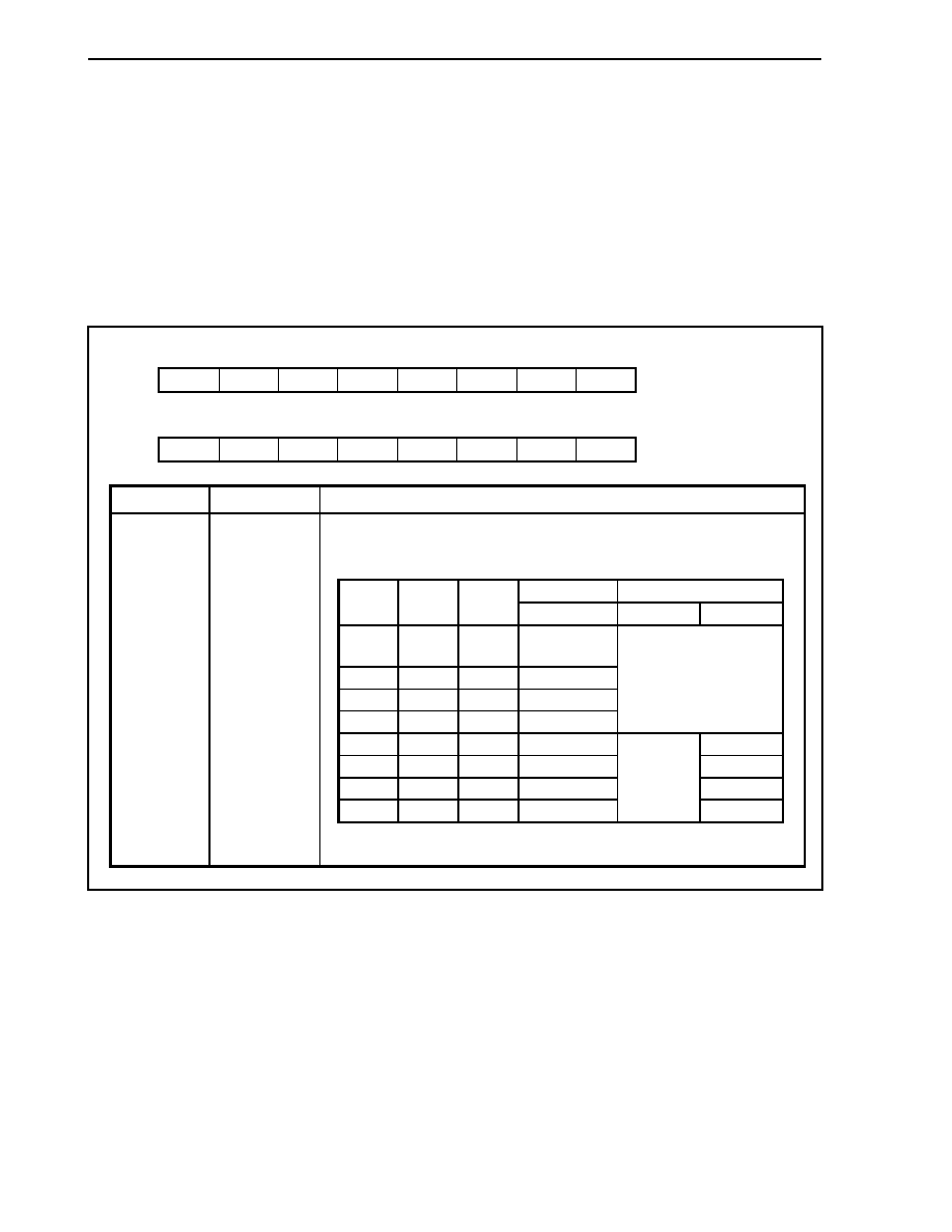
CHAPTER 9 TIMER/COUNTER FUNCTION
306
User's Manual U14492EJ5V0UD
(6) Prescaler mode registers 10, 11 (PRM10, PRM11)
The PRM1n register is used to perform the following selections.
∑ Selection of count clock in the general-purpose timer mode (CMD bit of TUMn register = 0)
∑ Selection of count operation mode in the UDC mode (CMD bit = 1)
PRM1n can be read/written in 8-bit or 1-bit units.
Cautions 1. Overwriting the PRM1n register during TM1n operation (TM1CEn bit = 1) is prohibited.
2. Clearing the PRM12 bit to 0 is prohibited in UDC mode (CMD bit of TUMn register = 1).
3. When TM1n is in mode 4, specification of the valid edge for the TIUD1n and TCUD1n
pins is invalid.
7
0
PRM10
6
0
5
0
4
0
3
0
2
PRM12
1
PRM11
0
PRM10
Address
FFFFF5EEH
Initial value
07H
7
0
PRM11
6
0
5
0
4
0
3
0
2
PRM12
1
PRM11
0
PRM10
Address
FFFFF60EH
Initial value
07H
Bit position
Bit name
Function
Specifies the up/down count operation mode during input of the clock rate when the
internal clock of the TM1n is used, or during external clock (TIUD1n) input.
CMD = 0
CMD = 1
PRM12 PRM11 PRM10
Count clock
Count clock
UDC mode
0 0 0
Setting
prohibited
0 0 1
f
CLK
/2
0 1 0
f
CLK
/4
0 1 1
f
CLK
/8
Setting prohibited
1 0 0
f
CLK
/16 Mode
1
1 0 1
f
CLK
/32 Mode
2
1 1 0
f
CLK
/64 Mode
3
1 1 1
f
CLK
/128
TIUD1n
Mode 4
2 to 0
PRM12 to
PRM10
Remarks 1. f
CLK
: Base clock
2. n = 0, 1
CHAPTER 9 TIMER/COUNTER FUNCTION
307
User's Manual U14492EJ5V0UD
(a) In general-purpose timer mode (CMD bit of TUMn register = 0)
The count clock is specified with the PRM12 to PRM10 bits.
(b) UDC mode (CMD bit of TUMn register = 1)
The TM1n count sources in the UDC mode are as follows.
Operation Mode
TM1n Operation
Mode 1
Down count when TCUD1n = high level
Up count when TCUD1n = low level
Mode 2
Up count upon detection of valid edge of TIUD1n input
Down count upon detection of valid edge of TCUD1n input
Mode 3
Up count upon detection of valid edge of TIUD1n input when TCUD1n = high level
Down count upon detection of valid edge of TIUD1n input when TCUD1n = low level
Mode 4
Automatic judgment upon detection of both edges of TIUD1n input and both edges of TCUD1n input

CHAPTER 9 TIMER/COUNTER FUNCTION
308
User's Manual U14492EJ5V0UD
(7) Status registers 0, 1 (STATUS0, STATUS1)
The STATUSn register indicates the operating status of TM1n.
STATUSn is read-only, in 8-bit or 1-bit units.
7
0
STATUS0
6
0
5
0
4
0
3
0
<2>
TM1UDF0
<1>
TM1OVF0
<0>
TM1UBD0
Address
FFFFF5EFH
Initial value
00H
7
0
STATUS1
6
0
5
0
4
0
3
0
<2>
TM1UDF1
<1>
TM1OVF1
<0>
TM1UBD1
Address
FFFFF60FH
Initial value
00H
Bit position
Bit name
Function
2 TM1UDFn TM1n
underflow
flag
0: No TM1n count underflow
1: TM1n count underflow
Caution
The TM1UDFn bit is cleared (to "0") upon completion of read access
to the STATUSn register from the CPU.
1
TM1OVFn
TM1n overflow flag
0: No TM1n count overflow
1: TM1n count overflow
Caution
The TM1OVFn bit is cleared (to "0") upon completion of read access
to the STATUSn register from the CPU.
0
TM1UBDn
Indicates the operating status of TM1n up/down count.
0: TM1n up count in progress
1: TM1n down count in progress
Caution The state of the TM1UBDn bit differs according to the mode as
follows.
∑ The TM1UBDn bit is fixed to 0 in general-purpose timer mode
(CMD bit of TUMn register = 0).
∑ The TM1UBDn bit indicates the TM1n up-/down-count status in
UDC mode (CMD bit of TUMn register = 1).
Remark n = 0, 1
CHAPTER 9 TIMER/COUNTER FUNCTION
309
User's Manual U14492EJ5V0UD
(8) CC101 capture input selection register (CSL10)
The CSL10 register is used to select the INTP101 or INTP100 pin to input a capture signal when the CC101
register is used as a capture register.
CSL10 can be read/written in 8-bit or 1-bit units.
7
0
CSL10
6
0
5
0
4
0
3
0
2
0
1
0
0
CSL0
Address
FFFFF5F6H
Initial value
00H
Bit position
Bit name
Function
0
CSL0
Specifies capture input to CC101.
0: INTP101
1: INTP100
(9) CC111 capture input selection register (CSL11)
The CSL11 register is used to select the INTP111 or INTP110 pin to input a capture signal when the CC111
register is used as a capture register.
CSL11 can be read/written in 8-bit or 1-bit units.
7
0
CSL11
6
0
5
0
4
0
3
0
2
0
1
0
0
CSL1
Address
FFFFF616H
Initial value
00H
Bit position
Bit name
Function
0
CSL1
Specifies capture input to CC111.
0: INTP111
1: INTP110

CHAPTER 9 TIMER/COUNTER FUNCTION
310
User's Manual U14492EJ5V0UD
(10) Compare registers 100, 110 (CM100, CM110)
CM1n0 is a 16-bit register that always compares its value with the value of TM1n. When the value of a
compare register matches the value of TM1n, an interrupt signal is generated. The interrupt generation timing
in the various modes is described below.
∑ In the general-purpose timer mode (CMD bit of TUMn register = 0) and UDC mode A (MSEL bit of TUMn
register = 0), an interrupt signal (INTCM1n0) is generated upon occurrence of a match.
∑ In UDC mode B (MSEL bit of TUMn register = 1), an interrupt signal (INTCM1n0) is generated only upon
occurrence of a match during up-count operation.
CM1n0 can be read/written in 16-bit units.
Caution When the TM1CEn bit of the TMC1n register is "1", it is prohibited to overwrite the value of
the CM1n0 register.
14
13
12
2
3
4
5
6
7
8
9
10
11
15
1
0
CM100
Address
FFFFF5E2H
Initial value
0000H
14
13
12
2
3
4
5
6
7
8
9
10
11
15
1
0
CM110
Address
FFFFF602H
Initial value
0000H
(11) Compare registers 101, 111 (CM101, CM111)
CM1n1 is a 16-bit register that always compares its value with the value of TM1n. When the value of a
compare register matches the value of TM1n, an interrupt signal is generated. The interrupt generation timing
in the various modes is described below.
∑ In the general-purpose timer mode (CMD bit of TUMn register = 0) and UDC mode A (MSEL bit of TUMn
register = 0), an interrupt signal (INTCM1n1) is generated upon occurrence of a match.
∑ In UDC mode B (MSEL bit of TUMn register = 1), an interrupt signal (INTCM1n1) is generated only upon
occurrence of a match during down count operation.
CM1n1 can be read/written in 16-bit units.
Caution When the TM1CEn bit of the TMC1n register is "1", it is prohibited to overwrite the value of
the CM1n1 register.
14
13
12
2
3
4
5
6
7
8
9
10
11
15
1
0
CM101
Address
FFFFF5E4H
Initial value
0000H
14
13
12
2
3
4
5
6
7
8
9
10
11
15
1
0
CM111
Address
FFFFF604H
Initial value
0000H

CHAPTER 9 TIMER/COUNTER FUNCTION
311
User's Manual U14492EJ5V0UD
(12) Capture/compare registers 100, 110 (CC100, CC110)
CC1n0 is a 16-bit register. It can be used as a capture register or as a compare register through specification
with capture/compare control register n (CCRn). CC1n0 can be read/written in 16-bit units.
Cautions 1. When used as a capture register (CMS0 bit of CCRn register = 0), write access is
prohibited.
2. When used as a compare register (CMS0 bit of CCRn register = 1) during TM1n
operation (TM1CEn bit of TMC1n register = 1), overwriting the CC1n0 register values is
prohibited.
3. When TM1n has been stopped (TM1CEn bit of TMC1n register = 0), the capture trigger is
disabled.
4. When the operation mode is changed from capture register to compare register, newly
set a compare value.
5. Continuous reading of CC1n0 is prohibited. If CC1n0 is continuously read, the second
read value may differ from the actual value. If CC1n0 must be read twice, be sure to read
another register between the first and the second read operation.
Correct usage example
Incorrect usage example
CC100 read
CC100 read
CC110 read
CC100 read
CC100 read
CC110 read
CC110 read
CC110 read
Remark n = 0, 1
14
13
12
2
3
4
5
6
7
8
9
10
11
15
1
0
CC100
Address
FFFFF5E6H
Initial value
0000H
14
13
12
2
3
4
5
6
7
8
9
10
11
15
1
0
CC110
Address
FFFFF606H
Initial value
0000H
(a) When set as a capture register
When CC1n0 is set as a capture register, the valid edge of the corresponding external interrupt signal
(INTP1n0) is detected as the capture trigger. TM1n latches the count value in synchronization with the
capture trigger (capture operation). The latched value is held in the capture register until the next capture
operation.
The valid edge of external interrupts (rising edge, falling edge, both rising and falling edges) is selected
with signal edge selection register 1n (SESA1n).
When the CC1n0 register is specified as a capture register, interrupts are generated upon detection of
the valid edge of the INTP1n0 signal.
(b) When set as a compare register
When CC1n0 is set as a compare register, it always compares its own value with the value of TM1n. If
the value of CC1n0 matches the value of the TM1n, CC1n0 generates an interrupt signal (INTCC1n0).
CHAPTER 9 TIMER/COUNTER FUNCTION
312
User's Manual U14492EJ5V0UD
(13) Capture/compare registers 101, 111 (CC101, CC111)
CC1n1 is a 16-bit register. It can be used as a capture register or as a compare register through specification
with capture/compare control register n (CCRn). CC1n1 can be read/written in 16-bit units.
Cautions 1. When used as a capture register (CMS1 bit of CCRn register = 0), write access is
prohibited.
2. When used as a compare register (CMS1 bit of CCRn register = 1) during TM1n
operation (TM1CEn bit of TMC1n register = 1), overwriting the CC1n1 register values is
prohibited.
3. When TM1n has been stopped (TM1CEn bit of TMC1n register = 0), the capture trigger is
disabled.
4. When the operation mode is changed from capture register to compare register, newly
set a compare value.
5. Continuous reading of CC1n1 is prohibited. If CC1n1 is continuously read, the second
read value may differ from the actual value. If CC1n1 must be read twice, be sure to read
another register between the first and the second read operation.
Correct usage example
Incorrect usage example
CC101 read
CC101 read
CC111 read
CC101 read
CC101 read
CC111 read
CC111 read
CC111 read
Remark n = 0, 1
14
13
12
2
3
4
5
6
7
8
9
10
11
15
1
0
CC101
Address
FFFFF5E8H
Initial value
0000H
14
13
12
2
3
4
5
6
7
8
9
10
11
15
1
0
CC111
Address
FFFFF608H
Initial value
0000H
(a) When set as a capture register
When CC1n1 is set as a capture register, the valid edge of either corresponding external interrupt signal
(INTP1n0 or INTP1n1) is selected with the selector, and the valid edge of the selected external interrupt
signal is detected as the capture trigger. TM1n latches the count value in synchronization with the
capture trigger (capture operation). The latched value is held in the capture register until the next capture
operation.
The valid edge of external interrupts (rising edge, falling edge, both rising and falling edges) is selected
with signal edge selection register 1n (SESA1n).
When the CC1n1 register is specified as a capture register, interrupts are generated upon detection of
the valid edge of either the INTP1n0 or INTP1n1 signal.
(b) When set as a compare register
When CC1n1 is set as a compare register, it always compares its own value with the value of TM1n. If
the value of CC1n1 matches the value of the TM1n, CC1n1 generates an interrupt signal (INTCC1n1).

CHAPTER 9 TIMER/COUNTER FUNCTION
313
User's Manual U14492EJ5V0UD
9.2.5 Operation
(1) Operation in general-purpose timer mode
TM1n can perform the following operations in the general-purpose timer mode.
(a) Interval operation (when ENMD bit of TMC1n register = 1)
TM1n and CM1n0 always compare their values and the INTCM1n0 interrupt is generated upon
occurrence of a match. TM1n is cleared (0000H) at the count clock following the match. Furthermore,
when one more count clock is input, TM1n counts up to 0001H.
The interval time can be calculated with the following formula.
Interval time = (CM1n0 value + 1)
◊ TM1n count clock rate
(b) Free-running operation (when ENMD bit of TMC1n register = 0)
TM1n performs full count operation from 0000H to FFFFH, and after the TM1OVFn bit of the STATUSn
register is set (to "1"), TM1n is cleared to 0000H at the next count clock and resumes counting.
The free-running cycle can be calculated with the following formula.
Free-running cycle = 65536
◊ TM1n count clock rate
(c) Compare function
TM1n connects two compare register (CM1n0, CM1n1) channels and two capture/compare register
(CC1n0, CC1n1) channels.
When the TM1n count value and the set value of one of the compare registers match, a match interrupt
(INTCM1n0, INTCM1n1, INTCC1n0
Note
, INTCC1n1
Note
) is output. Particularly in the case of interval
operation, TM1n is cleared upon generation of the INTCM1n0 interrupt.
Note This match interrupt is generated when CC1n0 and CC1n1 are set to the compare register mode.
(d) Capture function
TM1n connects two capture/compare register (CC1n0, CC1n1) channels.
When CC1n0 and CC1n1 are set to the capture register mode, the value of TM1n is captured in
synchronization with the corresponding capture trigger signal.
Furthermore, an interrupt request signal (INTCC1n0, INTCC1n1) is generated by the valid edge of the
INTP1n0, INTP1n1 input signals specified as the capture trigger signals.
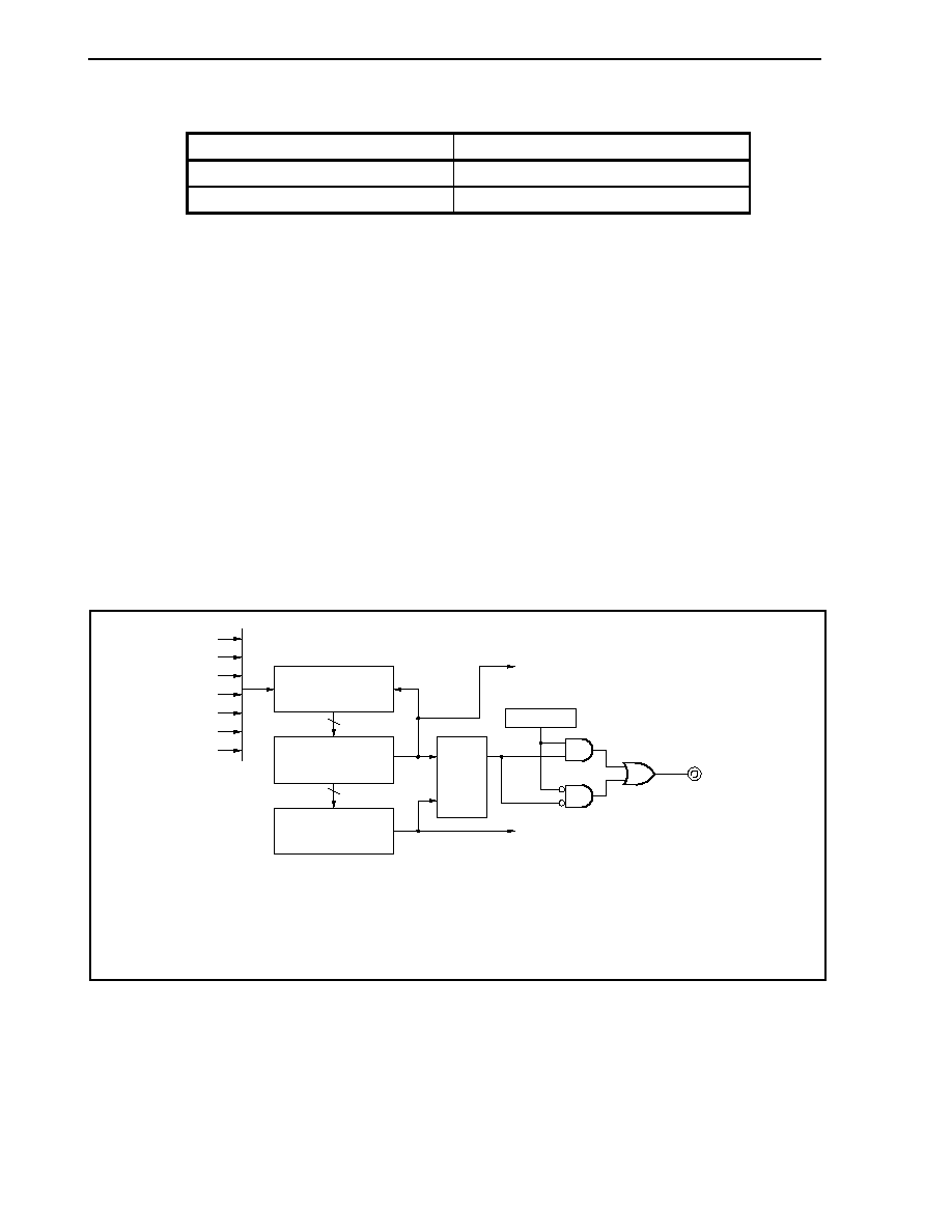
CHAPTER 9 TIMER/COUNTER FUNCTION
314
User's Manual U14492EJ5V0UD
Table 9-6. Capture Trigger Signal (TM1n) to 16-Bit Capture Register
Capture Register
Capture Trigger Signal
CC1n0 INTP1n0
CC1n1
INTP1n0 or INTP1n1
Remarks 1. CC1n0 and CC1n1 are capture/compare registers. Which of these registers is used is
specified with capture/compare control register n (CCRn).
2. n = 0, 1
The valid edge of the capture trigger is specified by signal edge selection register 1n (SESA1n). If both
the rising edge and the falling edge are selected as the capture triggers, it is possible to measure the
input pulse width from external. If a single edge is selected as the capture trigger, the input pulse cycle
can be measured.
(e) PWM output operation
PWM output operation is performed from the TO1n pin by setting TM1n to the general-purpose timer
mode (CMD bit = 0) using timer unit mode register n (TUMn).
The resolution is 16 bits, and the count clock can be selected from among seven internal clocks (f
CLK
/2,
f
CLK
/4, f
CLK
/8, f
CLK
/16, f
CLK
/32, f
CLK
/64, f
CLK
/128).
Figure 9-49. TM1n Block Diagram (During PWM Output Operation)
TM1n (16 bits)
Compare register
(CM1n0)
Compare register
(CM1n1)
S
INTCM1n0
INTCM1n1
ALVT10
TUMn register
Clear
16
16
TO1n
Q
R
f
CLK
/2
f
CLK
/4
f
CLK
/8
f
CLK
/16
f
CLK
/32
f
CLK
/64
f
CLK
/128
Caution Be sure to set the count clock of TM1n to 8 MHz or lower.
Remarks 1. f
CLK
: Base clock
2. n = 0, 1
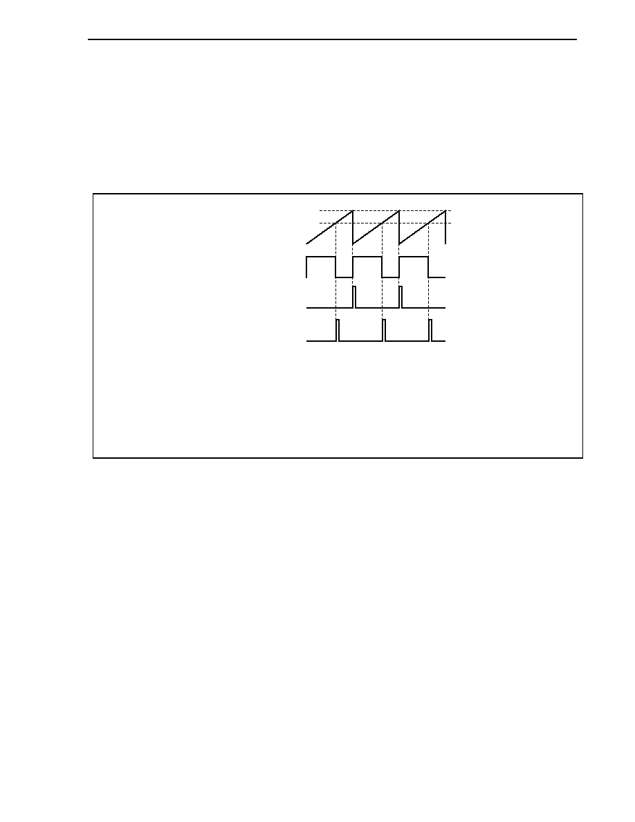
CHAPTER 9 TIMER/COUNTER FUNCTION
315
User's Manual U14492EJ5V0UD
(i) Description of operation
The CM1n0 register is a compare register used to set the PWM output cycle. When the value of this
register matches the value of TM1n, the INTCM1n0 interrupt is generated. Compare match is saved
by hardware, and TM1n is cleared at the next count clock after the match.
The CM1n1 register is a compare register used to set the PWM output duty. Set the duty required for
the PWM cycle.
Figure 9-50. PWM Signal Output Example (When ALVT10 Bit = 0 Is Set)
CM1n0 set value
CM1n1 set value
TM1n
TO1n
INTCM1n0
INTCM1n1
Cautions 1. Changing the values of the CM1n0 and CM1n1 registers is prohibited during TM1n operation
(TM1CEn bit of TMC1n register = 1).
2. Changing the value of the ALVT10 bit of the TUMn register is prohibited during TM1n
operation.
3. PWM signal output is performed from the second PWM cycle after the TM1CEn bit is set (to
"1").
CHAPTER 9 TIMER/COUNTER FUNCTION
316
User's Manual U14492EJ5V0UD
(2) Operation in UDC mode
(a) Overview of operation in UDC mode
The count clock input to TM1n in the UDC mode (CMD bit of TUMn register = 1) can only be external
input from the TIUD1n and TCUD1n pins. Up/down count judgment in the UDC mode is determined
based on the phase difference of the TIUD1n and TCUD1n pin inputs according to the PRM1n register
setting (there is a total of four choices).
Table 9-7. List of Count Operations in UDC Mode
PRM1n Register
PRM12 PRM11 PRM10
Operation
Mode
TM1n Operation
1
0
0
Mode 1
Down count when TCUD1n = high level
Up count when TCUD1n = low level
1
0
1
Mode 2
Up count upon detection of valid edge of TIUD1n input
Down count upon detection of valid edge of TCUD1n input
1
1
0
Mode 3
Up count upon detection of valid edge of TIUD1n input when
TCUD1n = high level
Down count upon detection of valid edge of TIUD1n input
when TCUD1n = low level
1
1
1
Mode 4
Automatic judgment upon detection of both edges of TIUD1n
input and both edges of TCUD1n input
The UDC mode is further divided into two modes according to the TM1n clear conditions (count operation
is performed only with TIUD1n, TCUD1n input in both modes).
∑ UDC mode A (TUMn register's CMD bit = 1, MSEL bit = 0)
The TM1n clear source can be selected as only external clear input (TCLR1n), a match signal
between the TM1n count value and the CM1n0 set value during up-count operation, or logical sum
(OR) of the two signals, using bits CLR1 and CLR0 of the TMC1n register.
TM1n can transfer the value of CM1n0 upon occurrence of TM1n underflow.
∑ UDC mode B (TUMn register's CMD bit = 1, MSEL bit = 1)
The status of TM1n after match of the TM1n count value and CM1n0 set value is as follows.
<1> In the case of up-count operation, TM1n is cleared (0000H), and the INTCM1n0 interrupt is
generated.
<2> In the case of down-count operation, the TM1n count value is decremented (
-1).
The status of TM1n after match of the TM1n count value and CM1n1 set value is as follows.
<1> In the case of up-count operation, the TM1n count value is incremented (+1).
<2> In the case of down-count operation, TM1n is cleared (0000H), and the INTCM1n1 interrupt is
generated.
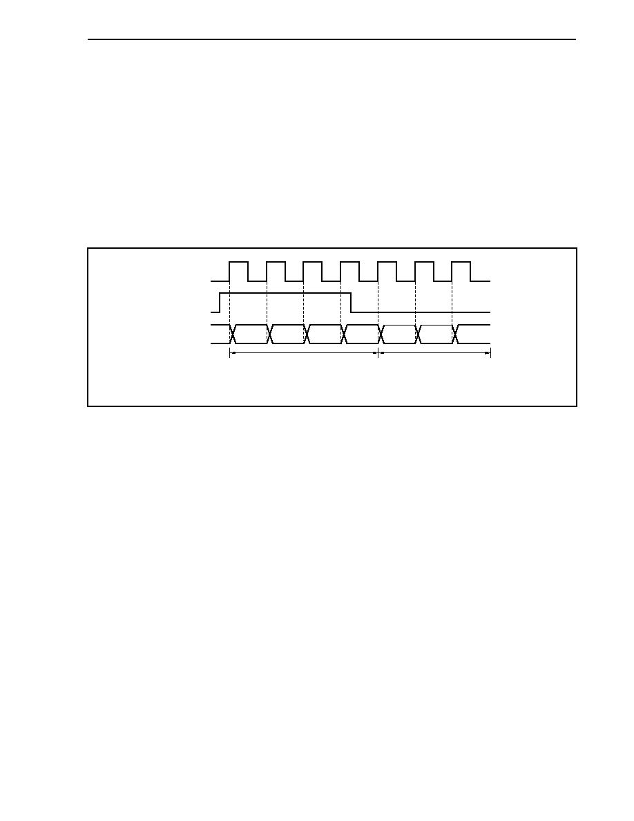
CHAPTER 9 TIMER/COUNTER FUNCTION
317
User's Manual U14492EJ5V0UD
(b) Up/down count operation in UDC mode
TM1n up/down count judgment in the UDC mode is determined based on the phase difference of the
TIUD1n and TCUD1n pin inputs according to the PRM1n register setting.
(i) Mode 1 (PRM1n register's PRM12 bit = 1, PRM11 bit = 0, PRM10 bit = 0)
In mode 1, the following count operations are performed based on the level of the TCUD1n pin upon
detection of the valid edge of the TIUD1n pin.
∑ TM1n down-count operation when TCUD1n pin = high level
∑ TM1n up-count operation when TCUD1n pin = low level
Figure 9-51. Mode 1 (When Rising Edge Is Specified as Valid Edge of TIUD1n Pin)
TIUD1n
TCUD1n
TM1n
0006H
0007H
Down count
Up count
0005H
0004H
0005H
0006H
0007H
Remark n = 0, 1

CHAPTER 9 TIMER/COUNTER FUNCTION
318
User's Manual U14492EJ5V0UD
Figure 9-52. Mode 1 (When Rising Edge Is Specified as Valid Edge of TIUD1n Pin):
In Case of Simultaneous TIUD1n, TCUD1n Pin Edge Timing
0007H
TIUD1n
TCUD1n
TM1n
0006H
Down count
Up count
0005H
0004H
0005H
0006H
0007H
Remark n = 0, 1
(ii) Mode 2 (PRM1n register's PRM12 bit = 1, PRM11 bit = 0, PRM10 bit = 1)
The count conditions in mode 2 are as follows.
∑ TM1n up-count upon detection of valid edge of TIUD1n pin
∑ TM1n down-count upon detection of valid edge of TCUD1n pin
Caution If the count clock is simultaneously input to the TIUD1n pin and the TCUD1n pin,
count operation is not performed and the immediately preceding value is held.
Figure 9-53. Mode 2 (When Rising Edge Is Specified as Valid Edge of TIUD1n, TCUD1n Pins)
0006H
TIUD1n
TCUD1n
TM1n
0007H
0008H
Up count
Hold value
Down count
0007H
0006H
0005H
Remark n = 0, 1

CHAPTER 9 TIMER/COUNTER FUNCTION
319
User's Manual U14492EJ5V0UD
(iii) Mode 3 (PRM1n register's PRM12 = 1, PRM11 = 1, PRM10 = 0)
In mode 3, when two signals 90 degrees out of phase are input to the TIUD1n and TCUD1n pins, the
level of the TCUD1n pin is sampled at the input of the valid edge of the TIUD1n pin (refer to Figure
9-54).
If the TCUD1n pin level sampled at the valid edge input to the TIUD1n pin is low, TM1n counts down
when the valid edge is input to the TIUD1n pin.
If the TCUD1n pin level sampled at the valid edge input to the TIUD1n pin is high, TM1n counts up
when the valid edge is input to the TIUD1n pin.
Figure 9-54. Mode 3 (When Rising Edge Is Specified as Valid Edge of TIUD1n Pin)
0007H
TIUD1n
TCUD1n
TM1n
0008H
Up count
Down count
0009H
000AH
0009H
0008H
0007H
Remark n = 0, 1
Figure 9-55. Mode 3 (When Rising Edge Is Specified as Valid Edge of TIUD1n Pin):
In Case of Simultaneous TIUD1n, TCUD1n Pin Edge Timing
0007H
TIUD1n
TCUD1n
TM1n
0008H
Up count
Down count
0009H
000AH
0009H
0008H
0007H
Remark n = 0, 1
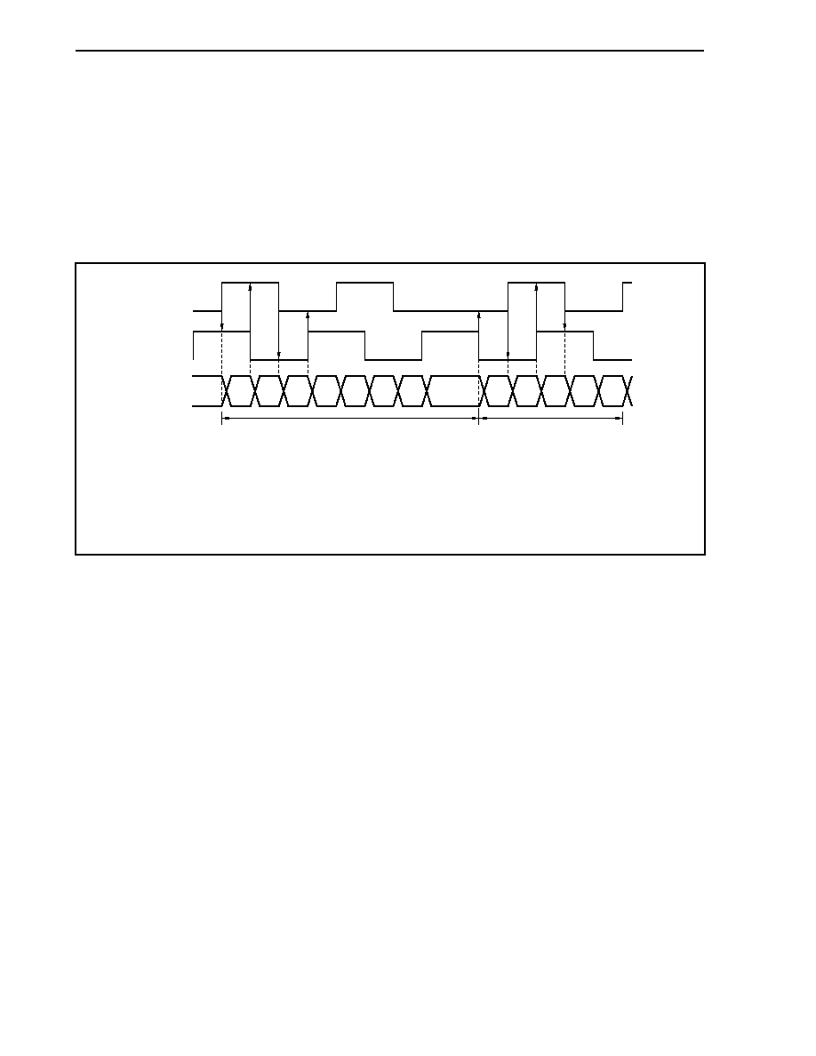
CHAPTER 9 TIMER/COUNTER FUNCTION
320
User's Manual U14492EJ5V0UD
(iv) Mode 4 (PRM1n register's PRM12 = 1, PRM11 = 1, PRM10 = 1)
In mode 4, when two signals out of phase are input to the TIUD1n and TCUD1n pins, up/down
operation is automatically judged and counting is performed according to the timing shown in Figure
9-56.
In mode 4, counting is executed at both the rising and falling edges of the two signals input to the
TIUD1n and TCUD1n pins. Therefore, TM1n counts four times per cycle of an input signal (
◊ 4
count).
Figure 9-56. Mode 4
TIUD1n
TCUD1n
TM1n
0004H
0003H
0006H
0005H
0008H
0007H
000AH
0009H
0008H
0009H
0006H
0007H
0005H
Up count
Down count
Cautions 1. When mode 4 is specified as the operation mode of TM1n, the valid edge specifications for
pins TIUD1n and TCUD1n are not valid.
2. If the TIUD1n pin edge and TCUD1n pin edge are input simultaneously in mode 4, TM1n
continues the same count operation (up or down) it was performing immediately before the
input.

CHAPTER 9 TIMER/COUNTER FUNCTION
321
User's Manual U14492EJ5V0UD
(c) Operation in UDC mode A
(i) Interval operation
The operations at the count clock following match of the TM1n count value and the CM1n0 set value
are as follows.
∑ In case of up-count operation: TM1n is cleared (0000H) and the INTCM1n0 interrupt is generated.
∑ In case of down-count operation: The TM1n count value is decremented (-1) and the INTCM1n0
interrupt is generated.
Remark The interval operation can be combined with the transfer operation.
(ii) Transfer operation
If TM1n becomes 0000H during down counting when the RLEN bit of the TMC1n register is 1, the
CM1n0 register set value is transferred to TM1n at the next count clock.
Remarks 1. Transfer enable/disable can be set with the RLEN bit of the TMC1n register.
2. The transfer operation can be combined with the interval operation.
Figure 9-57. Example of TM1n Operation When Interval Operation and Transfer Operation Are Combined
TM1n and CM1n0 match
& timer clear
TM1n underflow
& CM1n0 data transfer
TM1n count value
CM1n0 set value
Up count
Down count
0000H
Remark n = 0, 1
(iii) Compare function
TM1n connects two compare register (CM1n0, CM1n1) channels and two capture/compare register
(CC1n0, CC1n1) channels.
When the TM1n count value and the set value of one of the compare registers match, a match
interrupt (INTCM1n0, INTCM1n1, INTCC1n0
Note
, INTCC1n1
Note
) is output.
Note This match interrupt is generated when CC1n0 and CC1n1 are set to the compare register
mode.
(iv) Capture function
TM1n connects two capture/compare register (CC1n0, CC1n1) channels.
When CC1n0 and CC1n1 are set to the capture register mode, the value of TM1n is captured in
synchronization with the corresponding capture trigger signal. A capture interrupt (INTCC1n0,
INTCC1n1) is generated upon detection of the valid edge.
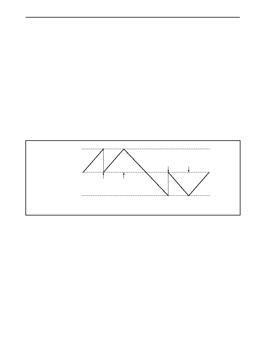
CHAPTER 9 TIMER/COUNTER FUNCTION
322
User's Manual U14492EJ5V0UD
(d) Operation in UDC mode B
(i) Basic operation
The operations at the next count clock after the count value of TM1n and the CM1n0 set value match
when TM1n is in UDC mode B are as follows.
∑ In case of up-count operation: TM1n is cleared (0000H) and the INTCM1n0 interrupt is generated.
∑ In case of down-count operation: The TM1n count value is decremented (-1).
The operations at the next count clock after the count value of TM1n and the CM1n1 set value match
when TM1n is in UDC mode B are as follows.
∑ In case of up-count operation: The TM1n count value is incremented (+1).
∑ In case of down-count operation: TM1n is cleared (0000H) and the INTCM1n1 interrupt is
generated.
Figure 9-58. Example of TM1n Operation in UDC Mode
CM1n0 set value
CM1n1 set value
TM1n count value
Clear
TM1n not
cleared if count clock
counts down following match
Clear
TM1n not
cleared if count clock
counts up following match
Remark n = 0, 1
(ii) Compare function
TM1n connects two compare register (CM1n0, CM1n1) channels and two capture/compare register
(CC1n0, CC1n1) channels.
When the TM1n count value and the set value of one of the compare registers match, a match
interrupt (INTCM1n0 (only during up-count operation), INTCM1n1 (only during down-count
operation), INTCC1n0
Note
, INTCC1n1
Note
) is output.
Note This match interrupt is generated when CC1n0 and CC1n1 are set to the compare register
mode.
(iii) Capture function
TM1n connects two capture/compare register (CC1n0, CC1n1) channels.
When CC1n0 and CC1n1 are set to the capture register mode, the value of TM1n is captured in
synchronization with the corresponding capture trigger signal. A capture interrupt (INTCC1n0,
INTCC1n1) is generated upon detection of the valid edge.

CHAPTER 9 TIMER/COUNTER FUNCTION
323
User's Manual U14492EJ5V0UD
9.2.6 Supplementary description of internal operation
(1) Clearing of count value in UDC mode B
When TM1n is in UDC mode B, the conditions to clear the count value are as follows.
∑ In case of TM1n up-count operation: TM1n count value is cleared upon match with the CM1n0 register
∑ In case of TM1n down-count operation: TM1n count value is cleared upon match with the CM1n1 register
Figure 9-59. Clear Operation After Match of CM1n0 Register Set Value and TM1n Count Value
(a) Up count
Up count
Count clock
(Rising edge set as valid edge)
CM1n0 register
FFFEH
TM1n cleared
TM1n
FFFFH
0000H
0001H
FFFFH
Up count
Up count
(b) Up count
Down count
Count clock
(Rising edge set as valid edge)
CM1n0 register
FFFEH
TM1n not cleared
TM1n
FFFFH
FFFEH
FFFDH
FFFFH
Up count
Down count
Remark n = 0, 1
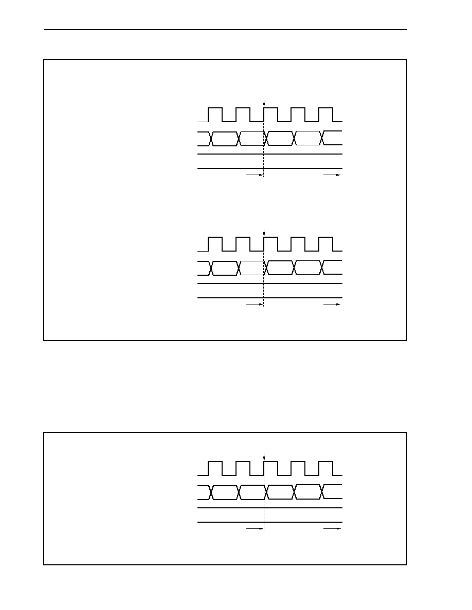
CHAPTER 9 TIMER/COUNTER FUNCTION
324
User's Manual U14492EJ5V0UD
Figure 9-60. Clear Operation After Match of CM1n1 Register Set Value and TM1n Count Value
(a) Down count
Down count
Count clock
(Rising edge set as valid edge)
CM1n1 register
00FFH
TM1n cleared
TM1n
00FEH
0000H
FFFFH
00FEH
Down count
Down count
(b) Down
Up count
Count clock
(Rising edge set as valid edge)
CM1n1 register
00FFH
TM1n not cleared
TM1n
00FEH
00FFH
0100H
00FEH
Down count
Up count
Remark n = 0, 1
(2) Transfer operation
If TM1n becomes 0000H during down counting when the RLEN bit of the TMC1n register is 1 in UDC mode
A, the set value of the CM1n0 register is transferred to TM1n at the next count clock. The transfer operation
is not performed during up counting.
Figure 9-61. Internal Operation During Transfer Operation
Count clock
(Rising edge set as valid edge)
CM1n0 register
0001H
Transfer operation performed.
TM1n
0000H
CM1n0
set value
CM1n0
set value
- 1
FFFFH
Down count
Down count
Remark n = 0, 1
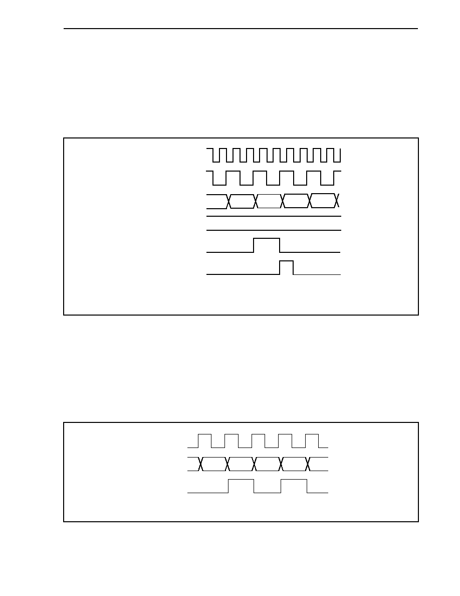
CHAPTER 9 TIMER/COUNTER FUNCTION
325
User's Manual U14492EJ5V0UD
(3) Interrupt signal output upon compare match
An interrupt signal is output when the count value of TM1n matches the set value of the CM1n0, CM1n1,
CC1n0
Note
, or CC1n1
Note
register. The interrupt generation timing is as follows.
Note When CC1n0 and CC1n1 are set to the compare register mode.
Figure 9-62. Interrupt Output upon Compare Match
(CM1n1 with Operation Mode Set to General-Purpose Timer Mode and Count Clock Set to f
CLK
/2)
Count clock
f
CLK
CM1n1
0007H
TM1n
Internal match signal
INTCM1n1
0008H
000BH
0009H
0009H
000AH
Remarks 1. n = 0, 1
2. f
CLK
: Base clock
An interrupt signal such as illustrated in Figure 9-62 is output at the next count clock following a match of the
TM1n count value and the set value of a corresponding compare register.
(4) TM1UBDn flag (bit 0 of STATUSn register) operation
In the UDC mode (CMD bit of TUMn register = 1), the TM1UBDn flag changes as follows during TM1n
up/down count operation at every internal operation clock.
Figure 9-63. TM1UBDn Flag Operation
Count clock
TM1UBDn
0001H
0000H
TM1n
0000H
0001H
0001H
0000H
Remark n = 0, 1
CHAPTER 9 TIMER/COUNTER FUNCTION
326
User's Manual U14492EJ5V0UD
9.3 Timer 2
9.3.1 Features (timer 2)
Timers 20, 21 (TM20, TM21) are 16-bit general-purpose timer units that perform the following operations.
∑ Pulse interval or frequency measurement and programmable pulse output
∑ Interval timer
∑ PWM output timer
∑ 32-bit capture timer when 2 timer/counter channels are connected in cascade
(In this case, four 32-bit capture register channels can be used.)
9.3.2 Function overview (timer 2)
∑
16-bit timer/counter (TM20, TM21): 2 channels
∑
Bit length
Timer 2 registers (TM20, TM21): 16 bits
During cascade operation: 32 bits (higher 16 bits: TM21, lower 16 bits: TM20)
∑
Capture/compare register
In 16-bit mode: 6
In 32-bit mode: 4 (capture mode only)
∑
Count clock division selectable by prescaler (set the frequency of the count clock to 8 MHz or less)
∑
Base clock (f
CLK
): 2 types (set f
CLK
to 16 MHz or less)
f
XX
/2 and f
XX
/4 can be selected
∑
Prescaler division ratio
The following division ratios can be selected according to the base clock (f
CLK
).
Base Clock (f
CLK
)
Division Ratio
f
XX
/2 Selected
f
XX
/4 Selected
1/2 f
XX
/4 f
XX
/8
1/4 f
XX
/8 f
XX
/16
1/8 f
XX
/16 f
XX
/32
1/16 f
XX
/32 f
XX
/64
1/32 f
XX
/64 f
XX
/128
1/64 f
XX
/128
f
XX
/256
1/128 f
XX
/256 f
XX
/512

CHAPTER 9 TIMER/COUNTER FUNCTION
327
User's Manual U14492EJ5V0UD
∑
Interrupt request sources
∑ Compare-match interrupt request: 6 types
Perform comparison with sub-channel n capture/compare register and generate the INTCC2n interrupt upon
compare match.
∑ Timer/counter overflow interrupt request: 2 types
The INTTM20 (INTTM21) interrupt is generated when the count value of TM20 (TM21) becomes FFFFH.
∑
Capture request
The count values of TM20, TM21 can be latched using external pin (INTP2n)
Notes 1, 2
, TM10, TM11 interrupt
signals (INTCM100, INTCM101) and interrupt requests by software as capture triggers.
∑
PWM output function
Control of the outputs of pins TO21 to TO24 in the compare mode and PWM output can be performed using
the compare match timing of sub-channels 1 to 4 and the zero count signal of the timer/counter.
∑
Timer count operation with external clock input
Note 2
Timer count operation can be performed with the pin TI2 clock input signal.
∑
Timer count enable operation
Note 3
with external pin input
Note 2
Timer count enable operation can be performed with the TCLR2 pin input signal.
∑
Timer/counter clear operation
Notes 3, 4
with external pin input
Note 2
Timer/counter clear operation can be performed with the TCLR2 pin input signal.
∑
Up/down count control
Notes 3, 5
with external pin input
Note 2
Up/down count operation in the compare mode can be controlled with the TCLR2 pin input signal.
∑
Output delay operation
A clock-synchronized output delay can be added to the output signal of pins TO21 to TO24.
This is effective as an EMI countermeasure.
∑
Input filter
An input filter can be inserted at the input stage of external pins (TI2, INTP20 to INTP25, TCLR2) and the
TM10, TM11 interrupt signals (refer to 14.5.3 (1) Timer 2 input filter mode registers 0 to 5 (FEM0 to FEM5)).
Notes 1. For the registers used to specify the valid edge for external interrupt requests (INTP20 to INTP25) to
timer 2, refer to 7.3.8 (4) Timer 2 input filter mode registers 0 to 5 (FEM0 to FEM5).
2. The pairs TI2 and INTP20, TO21 and INTP21, TO22 and INTP22, TO23 and INTP23, TO24 and
INTP24, TCLR2 and INTP25 are each alternate function pins.
3. The count enable operation for the timer/counter through external pin input, timer/counter clear
operation, and up/down count control cannot be performed combined all at the same time.
4. In the case of 32-bit cascade connection, clear operation by external pin input (TCLR2) cannot be
performed.
5. Up/down count control using 32-bit cascade connection cannot be performed.
Remark f
XX
: Internal system clock
n = 0 to 5

CHAPTER 9 TIMER/COUNTER FUNCTION
328
User's Manual U14492EJ5V0UD
9.3.3 Basic configuration
The basic configuration is shown below.
Table 9-8. Timer 2 Configuration List
Count Clock
Timer
Note 1
Note 2
Register Read/Write
Generated
Interrupt Signal
Capture Trigger
Other Functions
TM20
-
INTTM20
-
Note 3
TM21
-
INTTM21
-
Note 3
CVSE00 Read/write
INTCC20 INTP20/INTP25
-
CVSE10 Read/write
INTCC21 INTP21/INTP24
Buffer/Note 4
CVSE20 Read/write
INTCC22 INTP22/INTP23
Buffer/Note 4
CVSE30 Read/write
INTCC23 INTP23/INTP22
Buffer/Note 4
CVSE40 Read/write
INTCC24 INTP24/INTP21
Buffer/Note 4
CVSE50 Read/write
INTCC25 INTP25/INTP20
-
CVPE40 Read
INTCC24 INTP24/INTP21
Note 4
CVPE30 Read
INTCC23 INTP23/INTP22
Note 4
CVPE20 Read
INTCC22 INTP22/INTP23
Note 4
Timer 2
f
XX
/4,
f
XX
/8,
f
XX
/16,
f
XX
/32,
f
XX
/64,
f
XX
/128,
f
XX
/256
f
XX
/8,
f
XX
/16,
f
XX
/32,
f
XX
/64,
f
XX
/128,
f
XX
/256,
f
XX
/512
CVPE10 Read
INTCC21 INTP21/INTP24
Note 4
Notes 1. When
f
XX
/2 is selected as the base clock input to TM2n
2. When
f
XX
/4 is selected as the base clock input to TM2n
3. Cascade operation with TM20 and TM21 is enabled.
4. Cascade operation using the CVSEn0 register and CVPEn0 register is enabled (n = 1 to 4).
Remark f
XX
: Internal system clock

CHAPTER 9 TIMER/COUNTER FUNCTION
329
User's Manual U14492EJ5V0UD
The following shows the capture/compare operation sources.
Table 9-9. Capture/Compare Operation Sources
Register Sub-channel
No.
Timer to Be Captured
Timer to Be Compared
Timer Captured in 32-Bit
Cascade Connection
CVSE00 0
TM20
TM20
-
CVPEn0
n
TM21 when BFEEy bit of
CMSEm0 register = 0
TM20 when TB1Ey, TB0Ey
bits of CMSEm0 register = 01
TM21
CVSEn0
n
TM20 when BFEEy bit of
CMSEm0 register = 0
Used as buffer
TM20
CVSE50 5
TM21
TM21
-
Remark n = 1 to 4
m: m = 12 when n = 1, 2, m = 34 when n = 3, 4
y: y = 1, 2 when m = 12, y = 3, 4 when m = 34
The following shows the output level sources during timer output.
Table 9-10. Output Level Sources During Timer Output
TO2n
Toggle Mode 0
(OTMEn1, OTMEn0 = 00)
Toggle Mode 1
(OTMEn1, OTMEn0 = 01)
Toggle Mode 2
(OTMEn1, OTMEn0 = 10)
Toggle Mode 3
(OTMEn1, OTMEn0 = 11)
Trigger
Compare match of sub-
channel n
Compare
match of sub-
channel n
TM20 = 0
Compare
match of sub-
channel n
TM21 = 0
Compare
match of sub-
channel n
Compare
match of sub-
channel n + 1
Output level Active output Inactive
output
Active output Inactive
output
Active output Inactive
output
Active output Inactive
output
Remarks 1. n = 1 to 4
2. OTMEn1, OTMEn0: Bits 13, 12, 9, 8, 5, 4, 1, and 0 of timer 2 output control register 0 (OCTLE0)
Figure 9-64 shows the block diagram of timer 2.
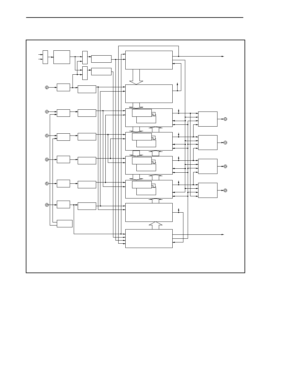
CHAPTER 9 TIMER/COUNTER FUNCTION
330
User's Manual U14492EJ5V0UD
Figure 9-64. Block Diagram of Timer 2
ED1
ECLR
CNT = MAX.
CNT = 0
R
CNT = MAX.
CNT = 0
R
CT
ED2
S/T
RA
RB
RN
Output
circuit 1
S/T
RA
RB
RN
Output
circuit 2
S/T
RA
RB
RN
Output
circuit 3
ED1
RELOAD2A
RELOAD2B
ED2
ED1
ECLR
CT
CTC
CASC
ED2
Sub-channel 4
CVSE40
(16-bit)
CVPE40
(16-bit)
ED1
RELOAD2A
RELOAD2B
ED2
Sub-channel 1
CVSE10
(16-bit)
CVPE10
(16-bit)
ED1
RELOAD2A
RELOAD2B
ED2
Sub-channel 2
CVSE20
(16-bit)
CVPE20
(16-bit)
ED1
RELOAD2A
RELOAD2B
ED2
Sub-channel 3
CVSE30
(16-bit)
CVPE30
(16-bit)
S/T
RA
RB
RN
Output
circuit 4
CVSE00
(16-bit)
TM20
(16-bit)
INTCC20
INTCC21
INTCC22
INTCC23
INTCC24
INTCC25
INTTM20
TO21
TO22
TO23
TO24
INTTM21
CVSE50
(16-bit)
TM21
(16-bit)
TINE5
edge selection
TINE4
edge selection
TINE3
edge selection
TINE2
edge selection
TINE1
edge selection
TINE0
edge selection
Input filter
Input filter
Input filter
Input filter
Input filter
Input filter
Timer
connection
selector
TCOUNTE1
edge selection
TCOUNTE0
f
CLK
edge selection
TCLR2/
INTP25
TI2/
INTP20
f
XX
/2
f
XX
/4
INTP24
INTP23
INTP22
INTP21
1/2, 1/4, 1/8,
1/16, 1/32,
1/64, 1/128
Sub-channel 5
Sub-channel 0
Selector
Selector
Selector
Remark f
XX
: Internal system clock
f
CLK
: Base clock (16 MHz (MAX.))

CHAPTER 9 TIMER/COUNTER FUNCTION
331
User's Manual U14492EJ5V0UD
Table 9-11. Meaning of Signals in Block Diagram
Signal Name
Meaning
CASC
Note 1
TM21 count signal input in 32-bit mode
CNT
Count value of timer 2 (CNT = MAX.: Maximum value count signal output of timer 2 (generated
when TM2n = FFFFH), CNT = 0: Zero count signal output of timer 2 (generated when TM2n =
0000H))
CT
TM2n count signal input in 16-bit mode
CTC
TM21 count signal input in 32-bit mode
ECLR
External control signal input from TCLR2 input
ED1, ED2
Capture event signal input from edge selector
R
Note 2
Compare
match
signal
input (sub-channel 0/5)
RA
TM20 zero count signal input (reset signal of output circuit)
RB
TM21 zero count signal input (reset signal of output circuit)
RELOAD2A
TM20 zero count signal input (generated when TM20 = 0000H)
RELOAD2B
TM21 zero count signal input (generated when TM21 = 0000H)
RN
Sub-channel x interrupt signal input (reset signal of output circuit)
S/T
Sub-channel x interrupt signal input (set signal of output circuit)
TCOUNTE0, TCOUNTE1
Timer 2 count enable signal input
TINEm
Timer 2 sub-channel m capture event signal input
Notes 1. TM21 performs count operation when CASC (CNT = MAX. for TM20) is generated and the rising
edge of CTC is detected in the 32-bit mode.
2. TM20/TM21 clear by sub-channel 0/5 compare match or count direction can be controlled.
Remark m = 0 to 5
n = 0, 1
x = 1 to 4
CHAPTER 9 TIMER/COUNTER FUNCTION
332
User's Manual U14492EJ5V0UD
(1) Timers 20, 21 (TM20, TM21)
The features of TM2n are listed below.
∑ Free-running counter that enables counter clearing by compare match of sub-channel 0 and sub-channel 5
∑ Can be used as a 32-bit capture timer when TM20 and TM21 are connected in cascade.
∑ Up/down control, counter clear, and count operation enable/disable can be controlled with external pin
(TCLR2).
∑ Counter up/down and clear operation control method can be set by software.
∑ Stop upon occurrence of count value 0 and count operation start/stop can be controlled by software.
(2) Timer 2 sub-channel 0 capture/compare register (CVSE00)
The CVSE00 register is a 16-bit capture/compare register of sub-channel 0.
In the capture register mode, it captures the TM20 count value.
In the compare register mode, it detects match with TM20.
This register can be read/written in 16-bit units.
14
13
12
2
3
4
5
6
7
8
9
10
11
15
1
0
CVSE00
Address
FFFFF660H
Initial value
0000H
CHAPTER 9 TIMER/COUNTER FUNCTION
333
User's Manual U14492EJ5V0UD
(3) Timer 2 sub-channel n main capture/compare register (CVPEn0) (n = 1 to 4)
The CVPEn0 register is a sub-channel n 16-bit main capture/compare register.
In the capture register mode, this register captures the value of TM21 when the BFEEn bit of the CMSEm0
register = 0 (m = 12, 34). When the BFEEn bit = 1, this register holds the value of TM20 or TM21.
In the compare register mode, a match between this register and TM2x is detected (TM2x = timer/counter
selected by TB1En and TB0En bits).
If the capture register mode is selected in the 32-bit mode (value of TB1En, TB0En bits of CMSEm0 register
= 11B), this register captures the contents of TM21 (higher 16 bits).
This register is read-only, in 16-bit units.
Caution When the BFEEn bit = 1, a compare match occurs on starting the timer in the compare
register mode because the values of both the TM2x and CVPEn0 registers are 0 after reset
(TM2x = timer/counter selected by TB1En and TB0En bits, n = 1 to 4). After that, the value
of the sub register (CVSEn0) is written to the main register (CVPEn0).
14
13
12
2
3
4
5
6
7
8
9
10
11
15
1
0
CVPE10
Address
FFFFF652H
Initial value
0000H
14
13
12
2
3
4
5
6
7
8
9
10
11
15
1
0
CVPE20
Address
FFFFF656H
Initial value
0000H
14
13
12
2
3
4
5
6
7
8
9
10
11
15
1
0
CVPE30
Address
FFFFF65AH
Initial value
0000H
14
13
12
2
3
4
5
6
7
8
9
10
11
15
1
0
CVPE40
Address
FFFFF65EH
Initial value
0000H
CHAPTER 9 TIMER/COUNTER FUNCTION
334
User's Manual U14492EJ5V0UD
(4) Timer 2 sub-channel n sub capture/compare register (CVSEn0) (n = 1 to 4)
The CVSEn0 register is a sub-channel n 16-bit sub capture/compare register.
In the compare register mode, this register can be used as a buffer. In the capture register mode, this register
captures the value of TM20 when the BFEEn bit of the CMSEm0 register = 0 (m = 12, 34).
If the capture register mode is selected in the 32-bit mode (value of TB1En and TB0En bits of CMSEm0
register = 11B), this register captures the contents of TM20 (lower 16 bits).
The CVSEn0 register can be written only in the compare register mode. If this register is written in the
capture register mode, the contents written to CVSEn0 register will be lost.
This register can be read/written in 16-bit units.
Caution When the BFEEn bit = 1, a compare match occurs on starting the timer in the compare
register mode because the values of both the TM2x and CVPEn0 registers are 0 after reset
(TM2x = timer/counter selected by TB1En and TB0En bits, n = 1 to 4). After that, the value
of the sub register (CVSEn0) is written to the main register (CVPEn0).
14
13
12
2
3
4
5
6
7
8
9
10
11
15
1
0
CVSE10
Address
FFFFF650H
Initial value
0000H
14
13
12
2
3
4
5
6
7
8
9
10
11
15
1
0
CVSE20
Address
FFFFF654H
Initial value
0000H
14
13
12
2
3
4
5
6
7
8
9
10
11
15
1
0
CVSE30
Address
FFFFF658H
Initial value
0000H
14
13
12
2
3
4
5
6
7
8
9
10
11
15
1
0
CVSE40
Address
FFFFF65CH
Initial value
0000H
(5) Timer 2 sub-channel 5 capture/compare register (CVSE50)
The CVSE50 register is a sub-channel 5 16-bit capture/compare register.
In the capture register mode, it captures the count value of TM21.
In the compare register mode, it detects match with TM21.
This register can be read/written in 16-bit units.
14
13
12
2
3
4
5
6
7
8
9
10
11
15
1
0
CVSE50
Address
FFFFF662H
Initial value
0000H
CHAPTER 9 TIMER/COUNTER FUNCTION
335
User's Manual U14492EJ5V0UD
9.3.4 Control registers
(1) Timer 1/timer 2 clock selection register (PRM02)
The PRM02 register is used to select the base clock (f
CLK
) of timer 1 and timer 2.
This register can be read/written in 8-bit or 1-bit units.
Caution Always set this register before using timer 1 and timer 2.
7
0
PRM02
6
0
5
0
4
0
3
0
2
0
1
0
0
PRM2
Address
FFFFF5D8H
Initial value
00H
Bit position
Bit name
Function
0
PRM2
Specifies the base clock (f
CLK
) of timer 1 and timer 2
Note
.
0: f
CLK
= f
XX
/4
1: f
CLK
= f
XX
/2
Note Set the VSWC register to 15H when the PRM2 bit of the timer 1/timer 2 clock selection register (PRM02) =
0B (f
CLK
= f
XX
/4) and set the VSWC register to 12H when the PRM2 bit = 1B (f
CLK
= f
XX
/2).
Remark f
XX
: Internal system clock
n = 0, 1
(2) Timer 2 clock stop register 0 (STOPTE0)
The STOPTE0 register is used to stop the operation clock input to timer 2.
This register can be read/written in 16-bit units.
When the higher 8 bits of the STOPTE0 register are used as the STOPTE0H register, and the lower 8 bits
are used as the STOPTE0L register, the STOPTE0H register can be read/written in 8-bit or 1-bit units, and
the STOPTE0L register is read-only, in 8-bit units.
Cautions 1. Initialize timer 2 when the STFTE bit = 0. Timer 2 cannot be initialized when the STFTE
bit = 1.
2. If, following initialization, the value of the STFTE bit is made "1", the initialized state is
maintained.
14
0
13
0
12
0
2
0
3
0
4
0
5
0
6
0
7
0
8
0
9
0
10
0
11
0
<15>
STFTE
1
0
0
0
STOPTE0
Address
FFFFF640H
Initial value
0000H
Bit position
Bit name
Function
15
STFTE
Stops the operation clock to timer 2.
0: Normal operation
1: Stop operation clock to timer 2
CHAPTER 9 TIMER/COUNTER FUNCTION
336
User's Manual U14492EJ5V0UD
(3) Timer 2 count clock/control edge selection register 0 (CSE0)
The CSE0 register is used to specify the TM2n count clock and the control valid edge (n = 0, 1).
This register can be read/written in 16-bit units.
When the higher 8 bits of the CSE0 register are used as the CSE0H register, and the lower 8 bits are used as
the CSE0L register, they can be read/written in 8-bit or 1-bit units.
(1/2)
14
0
13
0
12
0
2
CSE02
3
CSE10
4
CSE11
5
CSE12
6
CESE0
7
CESE1
8
TES0E0
9
TES0E1
10
TES1E0
11
TES1E1
15
0
1
CSE01
0
CSE00
CSE0
Address
FFFFF642H
Initial value
0000H
Bit position
Bit name
Function
Specifies the valid edge of the TM2n internal count clock (TCOUNTEn) signal.
TESnE1 TESnE0
Valid
edge
0 0
Falling
edge
0 1
Rising
edge
1 0
Setting
prohibited
1
1
Both rising and falling edges
Note
11, 10, 9, 8
TESnE1,
TESnE0
Specifies the valid edge of the TM2n external clear input (TCLR2).
CESE1 CESE0
Valid
edge
0 0
Falling
edge
0 1
Rising
edge
1
0
Through input (no clear operation)
1
1
Both rising and falling edges
7, 6
CESE1,
CESE0
Selects internal count clock (TCOUNTEn) of TM2n.
CSEn2 CSEn1 CSEn0
Count
clock
0 0 0
f
CLK
/2
Note 1
0 0 1
f
CLK
/4
0 1 0
f
CLK
/8
0 1 1
f
CLK
/16
1 0 0
f
CLK
/32
1 0 1
f
CLK
/64
1 1 0
f
CLK
/128
1 1 1
Selects
input
signal from external clock
input pin (TI2) as clock.
5 to 3, 2 to 0
CSEn2,
CSEn1,
CSEn0

CHAPTER 9 TIMER/COUNTER FUNCTION
337
User's Manual U14492EJ5V0UD
(2/2)
Note Setting the TESnE1 and TESnE0 bits to 11B and the CSEn2 to CSEn0 bits to 000B for timer 2 count
clock/control edge select register 0 (CSE0) is prohibited.
Caution Set the VSWC register to 15H when the PRM2 bit of the timer 1/timer 2 clock selection register
(PRM02) = 0B (f
CLK
= f
XX
/4) and set the VSWC register to 12H when the PRM2 bit = 1B (f
CLK
=
f
XX
/2).
Remark n = 0, 1
f
CLK
: Base clock
(4) Timer 2 sub-channel input event edge selection register 0 (SESE0)
The SESE0 register specifies the valid edge of the external capture signal input (TINEn) for the sub-channel
n capture/compare register performing capture (n = 0 to 5).
This register can be read/written in 16-bit units.
When the higher 8 bits of the SESE0 register are used as the SESE0H register, and the lower 8 bits are used
as the SESE0L register, they can be read/written in 8-bit or 1-bit units.
14
0
13
0
12
0
2
IESE10
3
IESE11
4
IESE20
5
IESE21
6
IESE30
7
IESE31
8
IESE40
9
IESE41
10
IESE50
11
IESE51
15
0
1
IESE01
0
IESE00
SESE0
Address
FFFFF644H
Initial value
0000H
Bit position
Bit name
Function
Specifies the valid edge of external capture signal input (TINEn) for sub-channel n
capture/compare register performing capture.
IESEn1 IESEn0
Valid
edge
0 0
Falling
edge
0 1
Rising
edge
1 0
Setting
prohibited
1
1
Both rising and falling edges
11 to 0
IESEn1,
IESEn0
Remark n = 0 to 5

CHAPTER 9 TIMER/COUNTER FUNCTION
338
User's Manual U14492EJ5V0UD
(5) Timer 2 time base control register 0 (TCRE0)
The TCRE0 register controls the operation of TM2n (n = 0, 1).
This register can be read/written in 16-bit units.
When the higher 8 bits of the TCRE0 register are used as the TCRE0H register, and the lower 8 bits are used
as the TCRE0L register, they can be read/written in 8-bit or 1-bit units.
Cautions 1. If ECREn = 1 and ECEEn = 1 have been set, it is not possible to input an external clear
signal (TCLR2) for TM2n. In this case, first set CLREn = 1, and then clear TM2n by
software (n = 0, 1).
2. When clearing is performed using the ECLR signal, the TM2n counter is cleared with a
delay of (1 internal count clock set with bits CSEn2 to CSEn0 of the CSE0 register) + 2
base clocks. Therefore, if external clock input is selected as the internal count clock,
the counter is not cleared until the external clock (TI2) is input.
3. The ECREn bit and the ECEEn bit cannot be set to 1.
4. If the ECEEn bit is set to 1 and the ECREn bit is set to 0, a down count operation cannot
be performed.
5. When UDSEn1, UDSEn0 = 01 and OSTEn = 1, the counter does not count up when the
counter value is 0. Therefore, when the counter value is 0, set OSTEn = 0, and after the
value of the counter ceases to be 0, set OSTEn = 1. Also, on the application, change the
value of OSTEn from 0 to 1 using the sub-channels 0 and 5 interrupt signals.
6. When the TM2n count value is cleared (0) by setting CLREn to 1, the CLREn = 1 setting
must be held for at least one of the internal count clocks set by the CSEn2 to CSEn0
bits of the CSE0 register.
Example
When timer 20 (TM20) is cleared (0)
<1> Select f
CLK
/2 as TM20 internal count clock
14
0
13
0
12
0
2
0
3
◊
4
◊
5
◊
6
◊
7
◊
8
◊
9
◊
10
◊
11
◊
15
0
1
0
0
0
CSE0
<2> Clear (0) the TM20 count value
6
1
5
0
4
0
0
◊
1
◊
2
◊
3
0
7
0
TCRE0L
<3> Set the conditions required for the TM20 count clock
14
◊
13
◊
12
◊
2
◊
3
◊
4
◊
5
◊
6
◊
7
◊
8
◊
9
◊
10
◊
11
◊
15
◊
1
◊
0
◊
CSE0
<4> Start the TM20 count operation
6
0
5
1
4
0
0
◊
1
◊
2
◊
3
0
7
0
TCRE0L

CHAPTER 9 TIMER/COUNTER FUNCTION
339
User's Manual U14492EJ5V0UD
(1/2)
<14>
CLRE1
<13>
CEE1
12
ECRE1
2
OSTE0
3
ECEE0
4
ECRE0
<5>
CEE0
<6>
CLRE0
7
0
8
UDSE10
9
UDSE11
10
OSTE1
11
ECEE1
15
CASE1
1
UDSE01
0
UDSE00
TCRE0
Address
FFFFF646H
Initial value
0000H
Bit position
Bit name
Function
15
CASE1
Specifies 32-bit cascade operation mode for TM21 (TM21 counts upon overflow of
TM20 (carry count)).
0: Not connected in cascade
Note 1
1: 32-bit cascade operation mode
Notes 2, 3
Notes 1. TM21 counts at CT signal input in the count enabled state.
2. TM21 counts at CTC and CASC signal inputs in the count enabled state.
3. Only the capture register mode can be used for the capture/compare
register.
Cautions 1. When CASE1 = 1, set the TByE1 and TByE0 bits of the CMSEx0
register to 11 (x = 12, 34, y: When x = 12, y = 1, 2, and when x =
34, y = 3, 4).
2. When CASE1 = 0, TCOUNTE1 is selected as the count of TM21.
When CASE1 = 1, TCOUNTE0 and the TM20 overflow signal are
selected as the count of TM21.
14, 6
CLREn
Specifies software clear for TM2n.
0: TM2n operation continued
1: TM2n count value cleared (0)
Caution Do not perform the software clear and hardware clear operations
simultaneously.
13, 5
CEEn
Specifies TM2n count operation enable/disable.
0: Count operation stopped
1: Count operation enabled
12, 4
ECREn
Specifies TM2n external clear (TCLR2) operation enable/disable via ECLR signal
input.
0: TM2n external clear (TCLR2) operation not enabled
1: TM2n external clear (TCLR2) operation enabled
Cautions 1. In the 32-bit cascade operation mode (CASE1 = 1), the TM2n
external clear operation is not performed.
2. When the count value is cleared by inputting the ECLR signal
while ECREn = 1, the ECREn = 1 setting must be held for at least
one of the internal count clocks set by the CSEn2 to CSEn0 bits
of the CSE0 register.
3. In the 32-bit cascade operation mode (CASE1 = 1), only TM21 is
affected by the ECREn bit setting.
Remark n = 0, 1
CHAPTER 9 TIMER/COUNTER FUNCTION
340
User's Manual U14492EJ5V0UD
(2/2)
Bit position
Bit name
Function
11, 3
ECEEn
Specifies TM2n count operation enable/disable through ECLR signal input.
0: TM2n count operation not enabled
1: TM2n count operation enabled
Cautions 1. In the 32-bit cascade operation mode (CASE1 = 1), the TM2n
count operation using ECLR signal input is not performed.
2. When the ECEEn bit = 1, always set the CESE1 and CESE0 bits of
the CSE0 register to 10 (through input).
3. In the 32-bit cascade operation mode (CASE1 = 1), only TM21 is
affected by the ECEEn bit setting.
10, 2
OSTEn
Specifies stop mode.
0: TM2n count stopped when count value is 0.
1: TM2n count not stopped when count value is 0.
Caution When the TM2n count stop is cancelled when the OSTE1n bit = 1
(TM2n count is stopped when the count value is 0), TM2n counts up
except when the UDSEn1, UDSEn0 bits = 10. The count direction
when the UDSEn1 and UDSEn0 bits = 10 is determined by the value
of ECLR
.
Specifies TM2n up/down count.
UDSEn1
UDSEn0 Count
0
0
Perform only up count.
Clear TM2n with compare match signal.
0
1
Count up after TM2n has become 0, and count down
after a compare match occurs for sub-channels 0, 5
(triangular wave up/down count).
1
0
Selects up/down count according to the ECLR signal
input.
Up count when ECLR = 1
Down count when ECLR = 0
1 1
Setting
prohibited
9, 8, 1, 0
UDSEn1,
UDSEn0
Cautions 1. In the 32-bit cascade operation mode (CASE1 bit = 1), set the
UDSEn1 and UDSEn0 bits to 00.
2. When the UDSEn1 and UDSEn0 bits = 10, be sure to set the
CESE1 and CESE0 bits of the CSE0 register to 10 (through input).
3. When the UDSEn1 and UDSEn0 bits = 10, compare match
between TM2n and CVSEx0 has no effect on the TM2n count
operation (x: 0 when n = 0, 5 when n = 1).
Remark n = 0, 1

CHAPTER 9 TIMER/COUNTER FUNCTION
341
User's Manual U14492EJ5V0UD
(6) Timer 2 output control register 0 (OCTLE0)
The OCTLE0 register controls timer output from the TO2n pin (n = 1 to 4).
This register can be read/written in 16-bit units.
When the higher 8 bits of the OCTLE0 register are used as the OCTLE0H register, and the lower 8 bits are
used as the OCTLE0L register, they can be read/written in 8-bit or 1-bit units.
14
ALVE
4
13
OTME
41
12
OTME
40
2
ALVE
1
3
SWFE
1
4
OTME
20
5
OTME
21
6
ALVE
2
7
SWFE
2
8
OTME
30
9
OTME
31
10
ALVE
3
11
SWFE
3
15
SWFE
4
1
OTME
11
0
OTME
10
OCTLE0
Address
FFFFF648H
Initial value
0000H
Bit position
Bit name
Function
15, 11, 7, 3
SWFEn
Fixes the TO2n pin output level according to the setting of ALVEn bit.
0: Don't fix output level.
1: When ALVEn = 0, fix output level to low level.
When ALVEn = 1, fix output level to high level.
14, 10, 6, 2
ALVEn
Specifies the active level of the TO2n pin output.
0: Active level is high level
1: Active level is low level
Specifies toggle mode.
OTMEn1
OTMEn0 Toggle
mode
0
0
Toggle mode 0:
Reverse output level of TO2n output every time a sub-
channel n compare match occurs.
0
1
Toggle mode 1:
Upon sub-channel n compare match, set TO2n output
to active level, and when TM20 is "0", set TO2n output
to inactive level.
1
0
Toggle mode 2:
Upon sub-channel n compare match, set TO2n output
to active level, and when TM21 is "0", set TO2n output
to inactive level.
1
1
Toggle mode 3:
Upon sub-channel n compare match, set TO2n output
to active level, and upon sub-channel n + 1 compare
match, set TO2n output to inactive level (when n = "4",
n + 1 becomes "1").
13, 12, 9, 8,
5, 4, 1, 0
OTMEn1,
OTMEn0
Cautions 1. When the OTMEn1, OTMEn0 bits = 11 (toggle mode 3), if the
same output delay operation settings are made when setting bits
ODLEn2 to ODLEn0 of the ODELE0 register, two outputs change
simultaneously upon 1 sub-channel n compare match.
2.
If two or more signals are input simultaneously to the same
output circuit, S/T signal input has a higher priority than RA, RB,
and RN signal inputs.
Remark n = 1 to 4

CHAPTER 9 TIMER/COUNTER FUNCTION
342
User's Manual U14492EJ5V0UD
(a) Caution for PWM output change timing
If the SWFEn bit is changed from 1 to 0 when the timer is operating while the internal PWM output
operation is being performed, then the output level becomes active. After that, PWM output from the
TO2n pin is performed upon a compare match at subchannel n. However, the first PWM output change
timing varies as follows, depending on the internal output level and the SWFEn bit clear timing.
Figure 9-65. PWM Output Change Timing
(i) Example 1
TO2n output
(ALVEn bit = 1)
PWM output change timing
SWFEn bit
Internal output level
(ii) Example 2
TO2n output
(ALVEn bit = 1)
PWM output change timing
SWFEn bit
Internal output level
Remark n = 1 to 4

CHAPTER 9 TIMER/COUNTER FUNCTION
343
User's Manual U14492EJ5V0UD
(7) Timer 2 sub-channel 0, 5 capture/compare control register (CMSE050)
The CMSE050 register controls timer 2 sub-channel 0 capture/compare register (CVSE00) and timer 2 sub-
channel 5 capture/compare register (CVSE50).
This register can be read/written in 16-bit units.
14
0
13
EEVE5
12
0
2
CCSE0
3
LNKE0
4
0
5
EEVE0
6
0
7
0
8
0
9
0
10
CCSE5
11
LNKE5
15
0
1
0
0
0
CMSE050
Address
FFFFF64AH
Initial value
0000H
Bit position
Bit name
Function
13, 5
EEVEn
Enables/disables event detection by sub-channel n capture/compare register.
0: ED1 and ED2 signal inputs ignored (nothing is done even if these signals are
input).
1: Operation caused by ED1 and ED2 signal inputs enabled.
11, 3
LNKEn
Specifies capture event signal input from edge selection to ED1 or ED2.
0: In capture register mode, select ED1 signal input.
In compare register mode, LNKEn bit has no influence.
1: In capture register mode, select ED2 signal input.
In compare register mode, LNKEn bit has no influence.
10, 2
CCSEn
Selects capture/compare register operation mode.
0: Operate in capture register mode. The TM20 and TM21 count statuses can be
read with sub-channel 0 and sub-channel 5, respectively.
1: Operate in compare register mode. TM2m is cleared upon detection of match
between sub-channel n and TM2m.
Remark m = 0, 1
n = 0, 5

CHAPTER 9 TIMER/COUNTER FUNCTION
344
User's Manual U14492EJ5V0UD
(8) Timer 2 sub-channel 1, 2 capture/compare control register (CMSE120)
The CMSE120 register controls the timer 2 sub-channel n sub capture/compare register (CVSEn0) and the
timer 2 sub-channel n main capture/compare register (CVPEn0) (n = 1, 2).
This register can be read/written in 16-bit units.
(1/2)
14
0
13
EEVE2
12
BFEE2
2
CCSE1
3
LNKE1
4
BFEE1
5
EEVE1
6
0
7
0
8
TB0E2
9
TB1E2
10
CCSE2
11
LNKE2
15
0
1
TB1E1
0
TB0E1
CMSE120
Address
FFFFF64CH
Initial value
0000H
Bit position
Bit name
Function
13, 5
EEVEn
Enables/disables event detection for CMSE120 register.
0: ED1 and ED2 signal inputs ignored (nothing is done even if these signals are
input).
1: Operation caused by ED1 and ED2 signal inputs enabled.
12, 4
BFEEn
Specifies the buffer operation of sub-channel n sub capture/compare register
(CVSEn0).
0: Don't use sub-channel n sub capture/compare register (CVSEn0) as buffer.
1: Use sub-channel n sub capture/compare register (CVSEn0) as buffer.
Caution When the BFEEn bit = 1, a compare match occurs on starting the
timer in the compare register mode because the values of both the
TM2x and CVPEn0 registers are 0 after reset (TM2x = timer/counter
selected by TB1En and TB0En bits, n = 1 to 4). After that, the value
of the sub register (CVSEn0) is written to the main register (CVPEn0).
Remarks 1. The operations in the capture register mode and compare register
mode when the sub-channel n sub capture/compare register (CVSEn0)
is not used as a buffer are shown below.
∑ In capture register mode: The CPU can read both the master register
(CVPEn0) and slave register (CVSEn0). The next event is ignored
until the CPU finishes reading the master register.
TM20 capture is performed by the slave register, and TM21 capture
is performed by the master register.
∑ In compare register mode: The CPU writes to the slave register
(CVSEn0), and immediately after, the same contents as those of the
slave register are written to the master register (CVPEn0).
2. The operations in the capture register mode and compare register
mode when the sub-channel n sub capture/compare register (CVSEn0)
is used as a buffer are shown below.
∑ In capture register mode: When the CPU reads the master register
(CVPEn0), the master register updates the value held by the slave
register (CVSEn0) immediately before the CPU read operation.
When a capture event occurs, the timer/counter value at that time is
always saved in the slave register.
∑ In compare register mode: The CPU writes to the slave register
(CVSEn0) and these contents are transferred to the master register
(CVPEn0) set with the LNKEn bits.
Remark n = 1, 2

CHAPTER 9 TIMER/COUNTER FUNCTION
345
User's Manual U14492EJ5V0UD
(2/2)
Bit position
Bit name
Function
11, 3
LNKEn
Selects capture event signal input from edge selection and specifies transfer
operation in compare register mode.
0: Select ED1 signal input in capture register mode.
In the compare register mode, the data of the CVSEn0 register is transferred to
the CVPEn0 register upon occurrence of TM2x compare match (TM2x = timer/
counter selected with bits TB1En, TB0En).
1: Select ED2 signal input in capture register mode.
In the compare register mode, the data of the CVSEn0 register is transferred to
the CVPEn0 register when the TM2x count value becomes "0" (TM2x = timer/
counter selected with bits TB1En, TB0En).
10, 2
CCSEn
Selects capture/compare register operation mode.
0: Capture register mode
1: Compare register mode
Sets sub-channel n timer/counter.
TB1En
TB0En
Sub-channel n timer/counter
0
0
Don't use sub-channel n.
0
1
Set TM20 to sub-channel n.
1
0
Set TM21 to sub-channel n.
1 1
32-bit
mode
Note
(select both TM20 and TM21.)
9, 8, 1, 0
TB1En, TB0En
Note In the 32-bit mode, influence of the BFEEn bit is ignored. Also, the CVSEn0
register cannot be used as a buffer in this mode.
Caution When the TB1En, TB0En bits are set to "11", set the CASE1 bit of
the TCRE0 register to "1".
Remark n = 1, 2

CHAPTER 9 TIMER/COUNTER FUNCTION
346
User's Manual U14492EJ5V0UD
(9) Timer 2 sub-channel 3, 4 capture/compare control register (CMSE340)
The CMSE340 register controls the timer 2 sub-channel n sub capture/compare register (CVSEn0) and the
timer 2 sub-channel n main capture/compare register (CVPEn0) (n = 3, 4).
This register can be read/written in 16-bit units.
(1/2)
14
0
13
EEVE4
12
BFEE4
2
CCSE3
3
LNKE3
4
BFEE3
5
EEVE3
6
0
7
0
8
TB0E4
9
TB1E4
10
CCSE4
11
LNKE4
15
0
1
TB1E3
0
TB0E3
CMSE340
Address
FFFFF64EH
Initial value
0000H
Bit position
Bit name
Function
13, 5
EEVEn
Enables/disables event detection by CMSE340 register.
0: ED1 and ED2 signal inputs ignored (nothing is done even if these signals are
input).
1: Operation caused by ED1 and ED2 signal inputs enabled.
12, 4
BFEEn
Specifies the sub-channel n sub capture/compare register (CVSEn0) buffer
operation.
0: Don't use sub-channel n sub capture/compare register (CVSEn0) as buffer.
1: Use sub-channel n sub capture/compare register (CVSEn0) as buffer.
Caution When the BFEEn bit = 1, a compare match occurs on starting the
timer in the compare register mode because the values of both the
TM2x and CVPEn0 registers are 0 after reset (TM2x = timer/counter
selected by TB1En and TB0En bits, n = 1 to 4). After that, the value
of the sub register (CVSEn0) is written to the main register (CVPEn0).
Remarks 1. The operations in the capture register mode and compare register
mode when the sub-channel n sub capture/compare register (CVSEn0)
is not used as a buffer are shown below.
∑ In capture register mode: The CPU can read both the master register
(CVPEn0) and slave register (CVSEn0). The next event is ignored
until the CPU finishes reading the master register.
TM20 capture is performed by the slave register, and TM21 capture
is performed by the master register.
∑ In compare register mode: The CPU writes to the slave register
(CVSEn0), and immediately after, the same contents as those of the
slave register are written to the master register (CVPEn0).
2. The operations in the capture register mode and compare register
mode when the sub-channel n sub capture/compare register (CVSEn0)
is used as a buffer are shown below.
∑ In capture register mode: When the CPU reads the master register
(CVPEn0), the master register updates the value held by the slave
register (CVSEn0) immediately before the CPU read operation.
When a capture event occurs, the timer/counter value at that time is
always saved in the slave register.
∑ In compare register mode: The CPU writes to the slave register
(CVSEn0) and these contents are transferred to the master register
(CVPEn0) set with the LNKEn bits.
Remark n = 3, 4
CHAPTER 9 TIMER/COUNTER FUNCTION
347
User's Manual U14492EJ5V0UD
(2/2)
Bit position
Bit name
Function
11, 3
LNKEn
Selects capture event signal input from edge selection and specifies transfer
operation in compare register mode.
0: Select ED1 signal input in capture register mode.
In the compare register mode, the data of the CVSEn0 register is transferred to
the CVPEn0 register upon occurrence of TM2x compare match (TM2x = timer/
counter selected with bits TB1En, TB0En).
1: Select ED2 signal input in capture register mode.
In the compare register mode, the data of the CVSEn0 register is transferred to
the CVPEn0 register when the TM2x count value becomes "0" (TM2x = timer/
counter selected with bits TB1En, TB0En).
10, 2
CCSEn
Selects capture/compare register operation mode.
0: Capture register mode
1: Compare register mode
Sets sub-channel n timer/counter.
TB1En
TB0En
Sub-channel n timer/counter
0
0
Don't use sub-channel n.
0
1
Set TM20 to sub-channel n.
1
0
Set TM21 to sub-channel n.
1 1
32-bit
mode
Note
(select both TM20 and TM21.)
9, 8, 1, 0
TB1En,
TB0En
Note In the 32-bit mode, influence of the BFEEn bit is ignored. Also, the CVSEn0
register cannot be used as a buffer in this mode.
Caution When the TB1En, TB0En bits are set to "11", set the CASE1 bit of
the TCRE0 register to "1".
Remark n = 3, 4

CHAPTER 9 TIMER/COUNTER FUNCTION
348
User's Manual U14492EJ5V0UD
(10) Timer 2 time base status register 0 (TBSTATE0)
The TBSTATE0 register indicates the status of TM2n (n = 0, 1).
This register can be read/written in 16-bit units.
When the higher 8 bits of the TBSTATE0 register are used as the TBSTATE0H register, and the lower 8 bits
are used as the TBSTATE0L register, they can be read/written in 8-bit or 1-bit units.
Caution The ECFEn, RSFEn, and UDFEn bits are read-only bits.
14
0
13
0
12
0
<2>
ECFE0
<3>
OVFE0
4
0
5
0
6
0
7
0
<8>
UDFE1
<9>
RSFE1
<10>
ECFE1
<11>
OVFE1
15
0
<1>
RSFE0
<0>
UDFE0
TBSTATE0
Address
FFFFF664H
Initial value
0101H
Bit position
Bit name
Function
11, 3
OVFEn
Indicates TM2n overflow status.
0: No overflow
1: Overflow
Caution
If write access to the TBSTATE0 register is performed while
overflow is not detected, the OVFEn bit is cleared (0).
10, 2
ECFEn
Indicates the ECLR signal input status.
0: Low level
1: High level
9, 1
RSFEn
Indicates the TM2n count status.
0: TM2n is not counting.
1: TM2n is counting (either up or down)
8, 0
UDFEn
Indicates the TM2n up/down count status.
0: TM2n is in the down-count mode.
1: TM2n is in the up-count mode.
Remark n = 0, 1
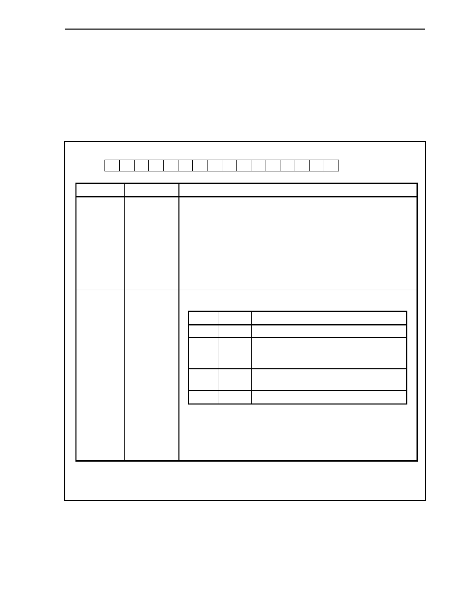
CHAPTER 9 TIMER/COUNTER FUNCTION
349
User's Manual U14492EJ5V0UD
(11) Timer 2 capture/compare 1 to 4 status register 0 (CCSTATE0)
The CCSTATE0 register indicates the status of the timer 2 sub-channel sub capture/compare register
(CVSEn0) and the timer 2 sub-channel main capture/compare register (CVPEn0) (n = 1 to 4).
This register can be read/written in 16-bit units.
When the higher 8 bits of the CCSTATE0 register are used as the CCSTATE0H register, and the lower 8 bits
are used as the CCSTATE0L register, they can be read/written in 8-bit or 1-bit units.
Caution The BFFEn1 and BFFEn0 bits are read-only bits.
<14>
CEFE4
13
BFFE41
12
BFFE40
<2>
CEFE1
3
0
4
BFFE20
5
BFFE21
<6>
CEFE2
7
0
8
BFFE30
9
BFFE31
<10>
CEFE3
11
0
15
0
1
BFFE11
0
BFFE10
CCSTATE0
Address
FFFFF666H
Initial value
0000H
Bit position
Bit name
Function
14, 10, 6, 2
CEFEn
Indicates the capture/compare event occurrence status.
0: In capture register mode: No capture operation has occurred.
In compare register mode: No compare match has occurred.
1: In capture register mode: At least one capture operation has occurred.
In compare register mode: At least one compare match has occurred.
Caution
The CEFEn bit can be cleared (0) by performing write access to the
CCSTATE0 register while no capture operation or compare match
occurs. When bit manipulation is performed for the CEFE1 (CEFE3)
bit and the CEFE2 (CEFE4) bit, both bits are cleared.
Indicates the capture buffer status.
BFFEn1 BFFEn0
Capture
buffer
status
0
0
No value in buffer
0
1
Sub-channel n master register (CVPEn0) contains a
capture value. Slave register (CVSEn0) does not
contain a value.
1
0
Both sub-channel n master register (CVPEn0) and
slave register (CVSEn0) contain a capture value.
1 1
Unused
13, 12, 9, 8,
5, 4, 1, 0
BFFEn1,
BFFEn0
Caution
The BFFEn1 and BFFEn0 bits return a value only when sub-channel
n sub capture/compare register (CVSEn0) buffer operation (bit
BFEEn of CMSEm0 register = 1) is selected or when capture register
mode (bit CCSEn of CMSEm0 register = 0) is selected. "0" is read
when the compare register mode (CCSEn bit = 1) is selected.
Remark m = 12, 34
n = 1 to 4
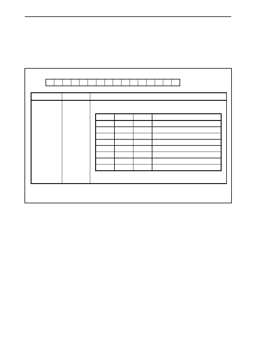
CHAPTER 9 TIMER/COUNTER FUNCTION
350
User's Manual U14492EJ5V0UD
(12) Timer 2 output delay register 0 (ODELE0)
The ODELE0 register sets the output delay operation synchronized with the clock to the TO2n pin's output
delay circuit (n = 1 to 4).
This register can be read/written in 16-bit units.
When the higher 8 bits of the ODELE0 register are used as the ODELE0H register, and the lower 8 bits are
used as the ODELE0L register, they can be read/written in 8-bit or 1-bit units.
14
ODLE42
13
ODLE41
12
ODLE40
2
ODLE12
3
0
4
ODLE20
5
ODLE21
6
ODLE22
7
0
8
ODLE30
9
ODLE31
10
ODLE32
11
0
15
0
1
ODLE11
0
ODLE10
ODELE0
Address
FFFFF668H
Initial value
0000H
Bit position
Bit name
Function
Specifies output delay operation.
ODLEn2 ODLEn1 ODLEn0
Set
output
delay
operation
0
0
0
Don't perform output delay operation.
0
0
1
Set output delay of 1 system clock.
0
1
0
Set output delay of 2 system clocks.
0
1
1
Set output delay of 3 system clocks.
1
0
0
Set output delay of 4 system clocks.
1
0
1
Set output delay of 5 system clocks.
1
1
0
Set output delay of 6 system clocks.
1
1
1
Set output delay of 7 system clocks.
14 to 12, 10 to 8,
6 to 4, 2 to 0
ODLEn2,
ODLEn1,
ODLEn0
Remark The ODLEn2, ODLEn1, and ODLEn0 bits are used for EMI
countermeasures.
Remark n = 1 to 4
CHAPTER 9 TIMER/COUNTER FUNCTION
351
User's Manual U14492EJ5V0UD
(13) Timer 2 software event capture register (CSCE0)
The CSCE0 register sets capture operation by software in the capture register mode.
This register can be read/written in 16-bit units.
14
0
13
0
12
0
2
SEVE2
3
SEVE3
4
SEVE4
5
SEVE5
6
0
7
0
8
0
9
0
10
0
11
0
15
0
1
SEVE1
0
SEVE0
CSCE0
Address
FFFFF66AH
Initial value
0000H
Bit position
Bit name
Function
5 to 0
SEVEn
Specifies capture operation by software in capture register mode.
0: Continue normal operation.
1: Perform capture operation.
Cautions 1. The SEVEn bit ignores the settings of the EEVEn and the LNKEn
bits of the CMSEm0 register.
2. The SEVEn bit is automatically cleared (0) at the end of an event.
3. The SEVEn bit ignores all the internal limitation statuses of the
timer 2 unit.
Remark m = 12, 34, 05
n = 0 to 5
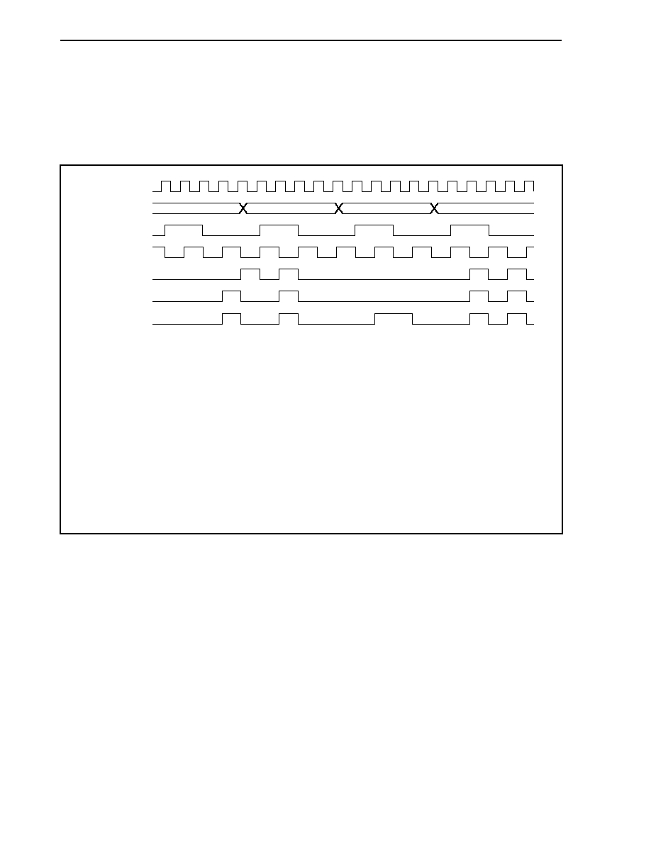
CHAPTER 9 TIMER/COUNTER FUNCTION
352
User's Manual U14492EJ5V0UD
9.3.5 Operation
(1) Edge detection
The edge detection timing is shown below.
Figure 9-66. Edge Detection Timing
f
CLK
00B
01B
10B
11B
MUXTB0
CT
ED1, ED2
ECLR
Note
TINEx, TCLR2,
TCOUNTEn
Note Set values of TESnE1, TESnE0 bits and CESE1, CESE0 bits of CSE0 register, and IESEx1, IESEx0 bits
of SESE0 register.
Remarks 1. f
CLK
: Base clock
2. CT: TM2n count signal input in the 16-bit mode
ECLR: External control signal input from TCLR2 input
ED1, ED2: Capture event signal input from edge selector
MUXTB0: TM20 multiplex signal
TCOUNTEn: Timer 2 count enable signal input
TINEx: Timer 2 sub-channel x capture event signal input
3. n = 0, 1
x = 0 to 5
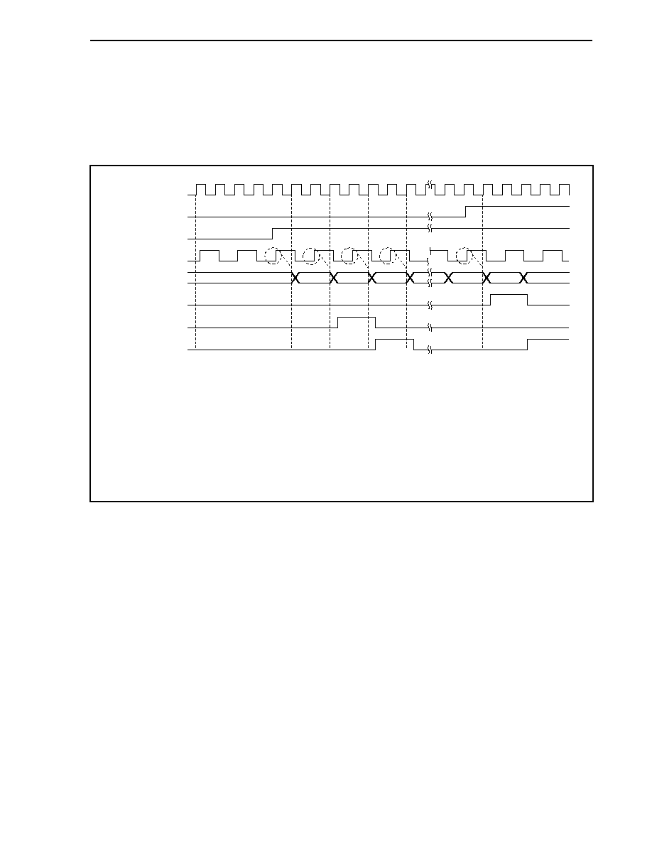
CHAPTER 9 TIMER/COUNTER FUNCTION
353
User's Manual U14492EJ5V0UD
(2) Basic operation of timer 2
Figures 9-67 to 9-70 show the basic operation of timer 2.
Figure 9-67. Timer 2 Up-Count Timing
(When TCRE0 Register's UDSEn1, UDSEn0 Bits = 00B,
ECEEn Bit = 0, ECREn Bit = 0, CLREn Bit = 0, CASE1 Bit = 0)
f
CLK
FFFDH (Stop)
FFFEH
FFFFH
0000H
1234H
1235H
0000H (Stop)
CT
CNT
R
Note 2
INTTM2n (output)
CNT = 0
OSTEn bit
Note 1
CEEn bit
Note 1
Notes 1. Bits OSTE, CEE of TCRE0 register
2. Can control TM20/TM21 clear by sub-channel 0/5 compare match or count direction.
Remarks 1. f
CLK
: Base clock
2. CNT: Count value of timer 2
CT: TM2n count signal input in 16-bit mode
R: Compare match signal input (sub-channel 0/5)
3. n = 0, 1
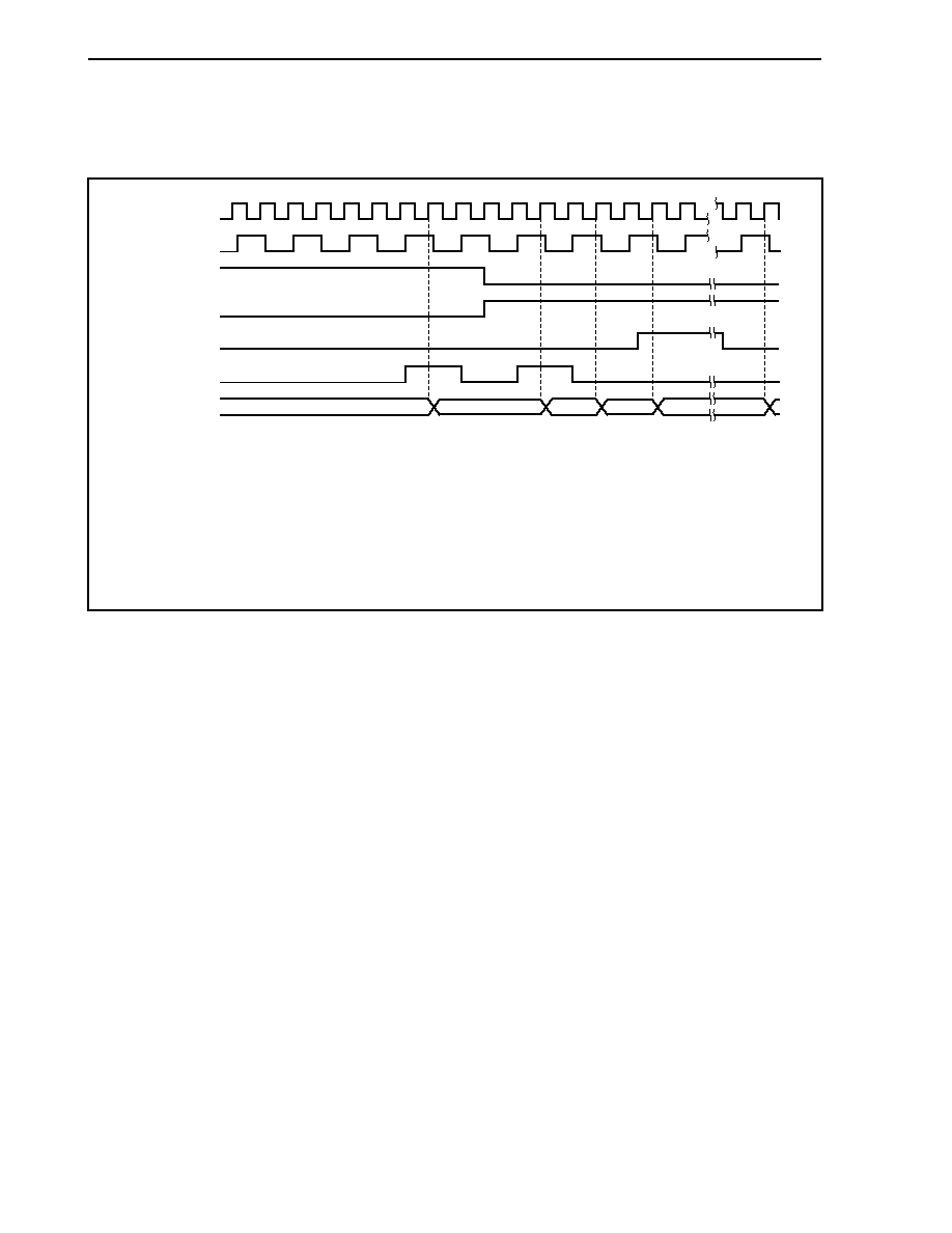
CHAPTER 9 TIMER/COUNTER FUNCTION
354
User's Manual U14492EJ5V0UD
Figure 9-68. External Control Timing of Timer 2
(When TCRE0 Register's UDSEn1, UDSEn0 Bits = 00B,
OSTEn Bit = 0, CEEn Bit = 1, CASE1 Bit = 0)
f
CLK
ECREn bit
Note
CLREn bit
Note
ECLR
CNT
CT
ECEEn bit
Note
1234H
1235H
0000H
0001H
0000H
Note Bits ECEEn, ECREn, CLREn of TCRE0 register
Remarks 1. f
CLK
: Base clock
2. CNT: Count value of timer 2
CT: TM2n count signal input in 16-bit mode
ECLR: External control signal input from TCLR2 pin input
3. n = 0, 1

CHAPTER 9 TIMER/COUNTER FUNCTION
355
User's Manual U14492EJ5V0UD
Figure 9-69. Operation in Timer 2 Up-/Down-Count Mode
(When TCRE0 Register's ECEEn Bit = 0, ECREn Bit = 0, CLREn Bit = 0,
OSTEn Bit = 0, CEEn Bit = 1, CASE1 Bit = 0)
f
CLK
ECLR
R
Note 2
CNT
INTTM2n (output)
CNT = 0
CT
UDSEn1, UDSEn0 bits
Note 1
FFFFH
0000H
0001H
don't care
01B
10B
0002H
0001H
0000H
0001H
0002H
0003H
0002H
FFFEH
Notes 1. UDSEn1, UDSEn0 bits of TCRE0 register
2. Can control TM20/TM21 clear by sub-channel 0/5 compare match or count direction.
Remarks 1. f
CLK
: Base clock
2. CNT: Count value of timer 2
CT: TM2n count signal input in 16-bit mode
ECLR: External control signal input from TCLR2 pin input
R: Compare match signal input (sub-channel 0/5)
3. n = 0, 1
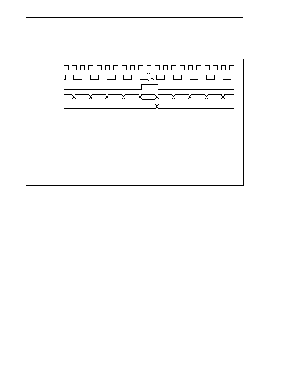
CHAPTER 9 TIMER/COUNTER FUNCTION
356
User's Manual U14492EJ5V0UD
Figure 9-70. Timing in 32-Bit Cascade Operation Mode
(When TCRE0 Register's UDSEn1, UDSEn0 Bits = 00B, ECEEn Bit =
0, ECREn Bit = 0, CLREn Bit = 0, OSTEn Bit = 0, CEEn Bit = 1,
CASE1 Bit = 1)
f
CLK
CNT[TB0]
CNT[TB1]
CTC
CASC
Note
[TB1]
FFFBH
FFFCH
FFFDH
FFFEH
FFFFH
0000H
0001H
0002H
0003H
0004H
1234H
1235H
Note If, in the 32-bit mode, CASC (CNT = MAX. for TM20) is input to TM21 and the CTC rising edge is
detected, TM21 performs count operation.
Remarks 1. f
CLK
: Base clock
2. CASC: TM21 count signal input in 32-bit mode
CNT: Count value of timer 2
CTC: TM21 count signal input in 32-bit mode
TB0: Count value of TM20
TB1: Count value of TM21
3. n = 0, 1
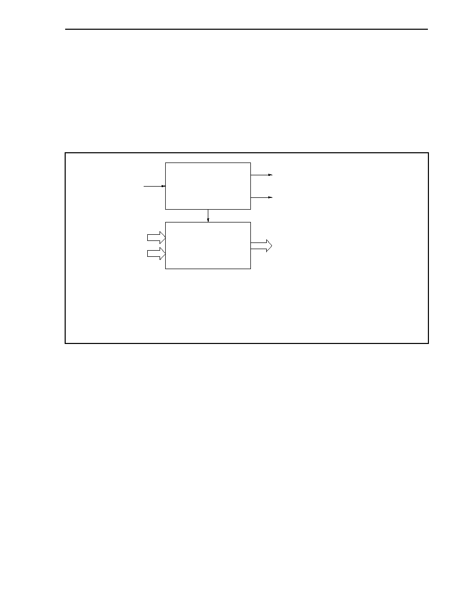
CHAPTER 9 TIMER/COUNTER FUNCTION
357
User's Manual U14492EJ5V0UD
(3) Operation of capture/compare register (sub-channels 1 to 4)
Sub-channels 1 to 4 receive the count value of the timer 2 multiplex count generator.
The multiplex count generator is an internal unit of TM2n that supplies the multiplex count value MUXCNT to
sub-channels 1 to 4. The count value of TM20 is output to sub-channels 1 to 4 at the rising edge of MUXTB0,
and the count value of TM21 is output to sub-channels 1 to 4 at the rising edge of MUXTB1.
Figure 9-71 shows the block diagram of the timer 2 multiplex count generator, and Figure 9-72 shows the
multiplex count timing.
Figure 9-71. Block Diagram of Timer 2 Multiplex Count Generator
MUXTB0
(to sub-channel m capture/compare register)
MUXTB1
(to sub-channel m capture/compare register)
MUXCNT
(to sub-channel m capture/compare register)
f
CLK
CNT (from TM20)
CNT (from TM21)
Multiplex control
Timer 2 multiplex
count generator
Remarks 1. f
CLK
: Base clock
2. CNT: Count value of timer 2
MUXTB0, MUXTB1: Multiplex signal of TM20, TM21
MUXCNT: Count value to sub-channel m
3. m = 1 to 4
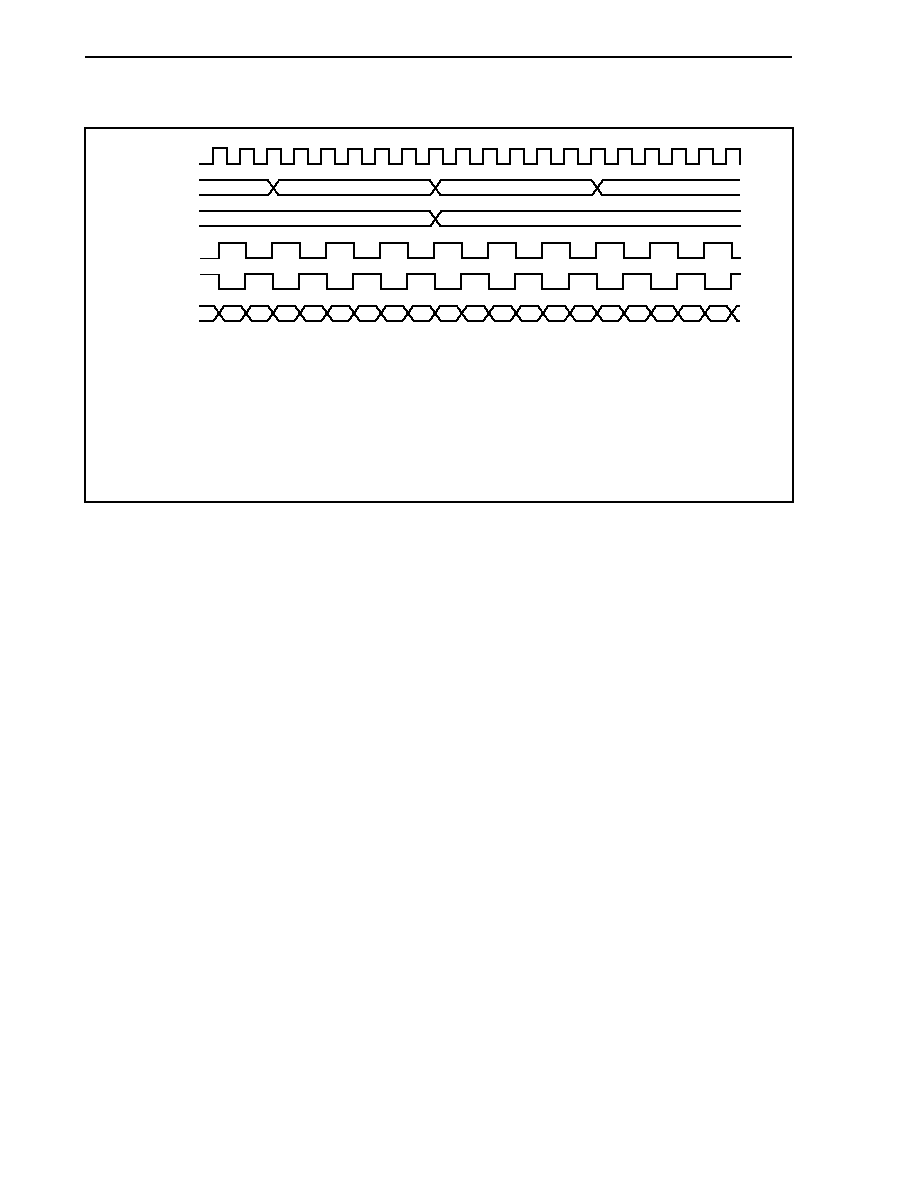
CHAPTER 9 TIMER/COUNTER FUNCTION
358
User's Manual U14492EJ5V0UD
Figure 9-72. Multiplex Count Timing
f
CLK
MUXTB0
MUXTB1
MUXCNT
CNT (0)
CNT (1)
FFFEH
FFFFH
0000H
1235H
1234H
TB0
TB1
TB0
TB1
TB0
TB1
TB0
TB1
TB0
TB1
TB0
TB1
TB0
TB1
TB0
TB1
TB0
TB1
TB0
TB1
0001H
FFFEH 1234H FFFFH
FFFFH
FFFFH
1234H
1234H
0000H
1234H
1235H
0000H 1235H
0000H
0001H
0001H
0001H
1235H
1235H
1235H
Remarks 1. f
CLK
: Base clock
2. CNT: Count value of timer 2
MUXTB0, MUXTB1: Multiplex signal of TM20, TM21
MUXCNT: Count value to sub-channel m (m = 1 to 4)
TB0: Count value of TM20
TB1: Count value of TM21
Figures 9-73 to 9-78 show the operation of the capture/compare register (sub-channels 1 to 4).
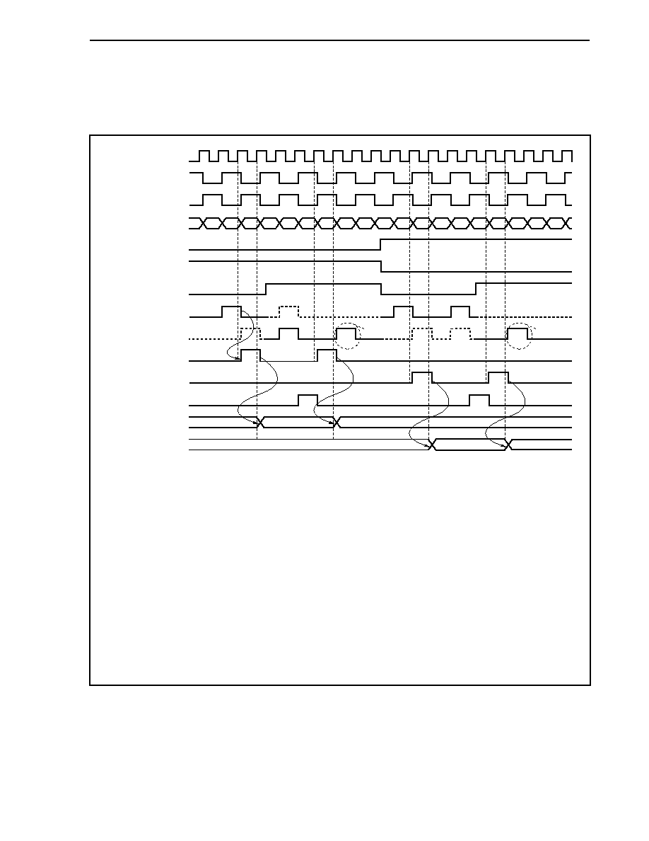
CHAPTER 9 TIMER/COUNTER FUNCTION
359
User's Manual U14492EJ5V0UD
Figure 9-73. Capture Operation: 16-Bit Buffer-Less Mode
(When Operation Is Delayed Through Setting of LNKEy Bit of CMSEx0
Register, and CMSEx0 Register's CCSEy Bit = 0, BFEEy Bit = 0,
EEVEy Bit = 1, and CSCE0 Register's SEVEy Bit = 0)
CVPEm0 register
f
CLK
MUXTB0
MUXTB1
ED1
ED2
CAPTURE_P
CAPTURE_S
READ_ENABLE_P
CVSEm0 register
MUXCNT
TB0Ey bit
Note 1
TB1Ey bit
Note 1
LNKEy bit
Note 1
TB1
TB0
TB1
TB0
TB1
TB0
TB1
TB0
TB1
TB0
TB1
TB0
TB1
TB0
TB1
TB0
TB1
TB0
TB1
TB0
1
5
6
2
3
4
7
8
5
9
10
6
11
7
8
9
10
12
13
14
Note 2
Note 2
Undefined
Undefined
2
4
13
11
Notes 1. Bits TB0Ey, TB1Ey of CMSEx register
2. If an event occurs in this timing, it is ignored.
Remarks 1. f
CLK
: Base clock
2. CAPTURE_P: Capture trigger signal of main capture register
CAPTURE_S: Capture trigger signal of sub capture register
ED1, ED2: Capture event signal input from edge selector
MUXCNT: Count value to sub-channel m
MUXTB0, MUXTB1: Multiplex signal of TM20, TM21
READ_ENABLE_P: Read timing for CVPEm0 register
TB0: Count value of TM20
TB1: Count value of TM21
3. m = 1 to 4, x = 12, 34
y: When x = 12, y = 1, 2, and when x = 34, y = 3, 4
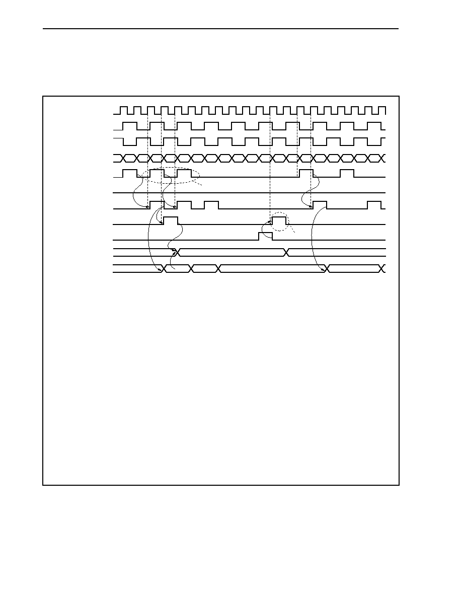
CHAPTER 9 TIMER/COUNTER FUNCTION
360
User's Manual U14492EJ5V0UD
Figure 9-74. Capture Operation: Mode with 16-Bit Buffer
Note 1
(When CMSEx0 Register's TByE1 Bit = 0, TByE0 Bit = 1, CCSEy Bit = 0,
LNKEy Bit = 0, BFEEy Bit = 1, EEVEy Bit = 1, and CSCE0 Register's
SEVEy Bit = 0)
f
CLK
MUXTB0
MUXTB1
BUFFER
READ_ENABLE_P
CVPEm0 register
CVSEm0 register
MUXCNT
ED1
CAPTURE_P
CAPTURE_S
TB0
TB1
TB0
TB1
TB0
TB1
TB0
TB1
TB0
TB1
TB0
TB1
TB0
TB1
TB0
TB1
TB0
TB1
TB0
TB1
1
5
6
2
3
4
7
8
5
9
10
6
11
7
8
9
10
12
13
New event
14
Note 2
Note 3
Undefined
Undefined
2
4
Capture
2
3
4
8
Shift
L
Event
Notes 1. To operate TM2n in the mode with 16-bit buffer, perform capture at least twice at the start of operation
and read the CVPEm0 register. Also, read the CVPEm0 register after performing capture at least
once.
2. Write operation to the CVPEn0 register is not performed at these signal inputs because the CVSEm0
register operates as a buffer.
3. After this timing, write operation from the CVSEm0 register to the CVPEm0 register is enabled.
Remarks 1. f
CLK
: Base clock
2. BUFFER: Timing of write operation from CVSEm0 register to CVPEm0 register
CAPTURE_P: Capture trigger signal of main capture register
CAPTURE_S: Capture trigger signal of sub capture register
ED1: Capture event signal input from edge selector
MUXCNT: Count value to sub-channel m
MUXTB0, MUXTB1: Multiplex signal of TM20, TM21
READ_ENABLE_P: Read timing of CVPEm0 register
TB0: Count value of TM20; TB1: Count value of TM21
3. m = 1 to 4, x = 12, 34
y: When x = 12, y = 1, 2, and when x = 34, y = 3, 4
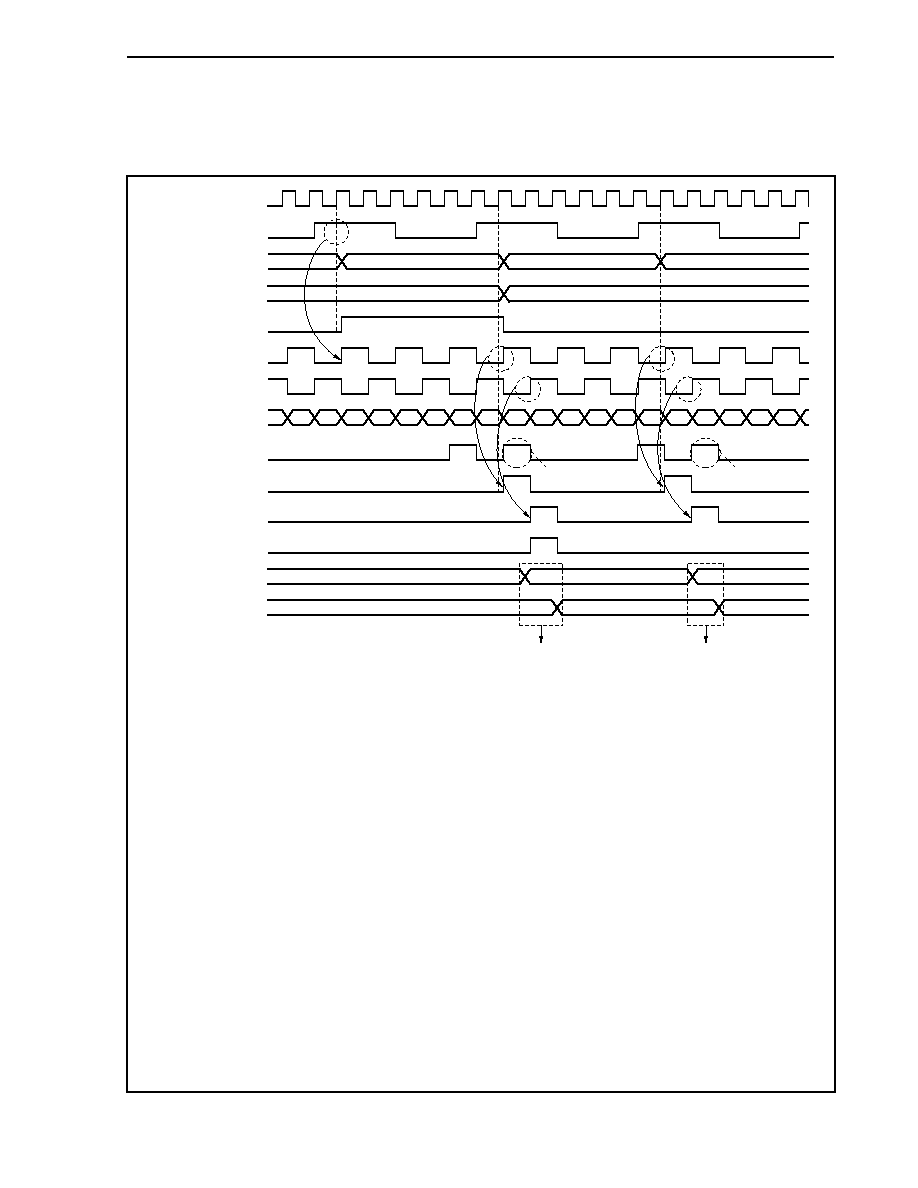
CHAPTER 9 TIMER/COUNTER FUNCTION
361
User's Manual U14492EJ5V0UD
Figure 9-75. Capture Operation: 32-Bit Cascade Operation Mode
(When CMSEx Register's TByE1 Bit = 1, TByE0 Bit = 1, CCSEy Bit = 0,
LNKEy Bit = 0, BFEEy Bit = Arbitrary, EEVEy Bit = 1, and CSCE0
Register's SEVEy Bit = 0)
f
CLK
CASC
Note 1
MUXTB0
MUXTB1
MUXCNT
ED1
CAPTURE_S
CAPTURE_P
READ_ENABLE_P
CVSEm0 register
CVPEm0 register
TCOUNTE0 =
TCOUNTE1
CNT (0)
CNT (1)
FFFEH
FFFFH
0000H
1235H
1234H
TB0
TB1
TB0
TB1
TB0
Undefined
Undefined
0000H
1235H
0001H
1235H
TB1
TB0
TB1
TB0
TB1
TB0
TB1
Note 2
Note 3
TB0
TB1
Enable the next capture
TB0
TB1
TB0
TB1
TB0
TB1
0001H
FFFEH 1234H FFFFH
FFFFH
FFFFH
1234H
1234H
0000H
1234H
1235H
0000H 1235H
0000H
0001H
0001H
0001H
1235H
1235H
1235H
Note 2
Note 3
Notes 1. TM21 performs count operation when, in the 32-bit mode, CASC (CNT = MAX. for TM20) is input to
TM21 and the rising edge of CTC is detected.
2. If an event occurs during this timing, it is ignored.
3. CPU read access is not performed in this timing (wait status).
Remarks 1. f
CLK
: Base clock
2. CAPTURE_P: Capture trigger signal of main capture register
CAPTURE_S: Capture trigger signal of sub capture register
CASC: TM21 count signal in 32-bit mode
CNT: Count value of timer 2
ED1: Capture event signal input from edge selector
MUXCNT: Count value to sub-channel m
MUXTB0, MUXTB1: Multiplex signal of TM20, TM21
READ_ENABLE_P: Read timing of CVPEm0 register
TB0: Count value of TM20
TB1: Count value of TM21
TCOUNTE0, TCOUNTE1: Count enable signal input of timer 2
3. m = 1 to 4, x = 12, 34
y: When x = 12, y = 1, 2, and when x = 34, y = 3, 4

CHAPTER 9 TIMER/COUNTER FUNCTION
362
User's Manual U14492EJ5V0UD
Figure 9-76. Capture Operation: Capture Control by Software and Trigger Timing
(When CMSEx0 Register's TByE1 Bit = 0, TByE0 Bit = 1, CCSEy Bit = 0, LNKEy Bit
= 0, BFEEy Bit = 1)
f
CLK
EEVEy bit
Note 1
SEVEy bit
Note 2
MUXTB0
MUXTB1
MUXCNT
ED1
CAPTURE_P
CAPTURE_S
BUFFER
CVSEm0 register
CVPEm0 register
Undefined
Undefined
4
4
9
TB0
TB1
TB0
TB1
TB0
TB1
TB0
TB1
TB0
TB1
TB0
TB1
TB0
TB1
TB0
TB1
TB0
TB1
TB0
TB1
5
1
6
2
3
4
7
8
5
9
10
6
11
7
8
9
10
12
13
14
Cleared by
timer
Set by software
Event detection by
EEVEy bit prohibited
L
Notes 1. EEVEy bit of CMSEx0 register
2. SEVEy bit of CSCE0 register
Remarks 1. f
CLK
: Base clock
2. BUFFER: Timing of write operation from CVSEm0 register to CVPEm0 register
CAPTURE_P: Capture trigger signal of main capture register
CAPTURE_S: Capture trigger signal of sub capture register
ED1: Capture event signal input from edge selector
MUXCNT: Count value to sub-channel m
MUXTB0, MUXTB1: Multiplex signal of TM20, TM21
TB0: Count value of TM20
TB1: Count value of TM21
3. m = 1 to 4, x = 12, 34
y: When x = 12, y = 1, 2, and when x = 34, y = 3, 4
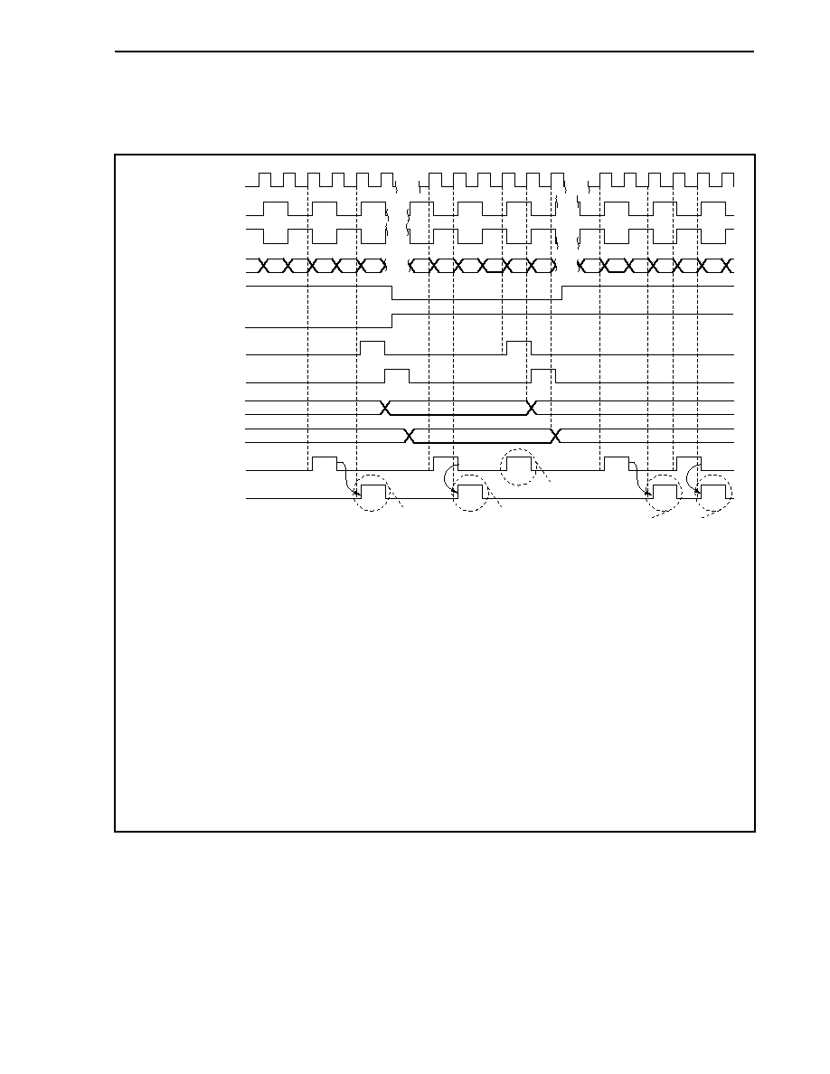
CHAPTER 9 TIMER/COUNTER FUNCTION
363
User's Manual U14492EJ5V0UD
Figure 9-77. Compare Operation: Buffer-Less Mode
(When CMSEx0 Register's CCSEy Bit = 1, LNKEy Bit = Arbitrary,
BFEEy Bit = 0)
f
CLK
TB0Ey bit
Note 1
TB1Ey bit
Note 1
MUXTB0
MUXTB1
MUXCNT
WRITE_ENABLE_S
RELOAD_PRIMARY
CVSEm0 register
CVPEm0 register
RELOAD1
INTCCm
TB0
TB1
TB0
TB1
TB0
TB1
TB0
TB0
TB1
TB0
TB1
TB1
TB0
TB1
TB0
TB1
TB0
TB1
5
1
6
2
3
7
7
8
9
10
9
11
8
9
10
6
7
8
2
2
9
9
8
8
Note 3
Note 3
Note 3
Note 3
Note 2
Notes 1. TB1Ey, TB0Ey bits of CMSEx0 register
2. No interrupt is generated due to compare match with counter differing from TB1Ey, TB0Ey bit
settings.
3. INTCC2m is generated to match the cycle from rising edge to falling edge of MUXTB0.
Remarks 1. f
CLK
: Base clock
2. MUXCNT: Count value to sub-channel m
MUXTB0, MUXTB1: Multiplex signal of TM20, TM21
RELOAD1: Compare match signal
RELOAD_PRIMARY: Timing of write operation from CVSEm0 register to CVPEm0 register
WRITE_ENABLE_S: Timing of CVSEm0 register write operation
TB0: Count value of TM20
TB1: Count value of TM21
3. m = 1 to 4, x = 12, 34
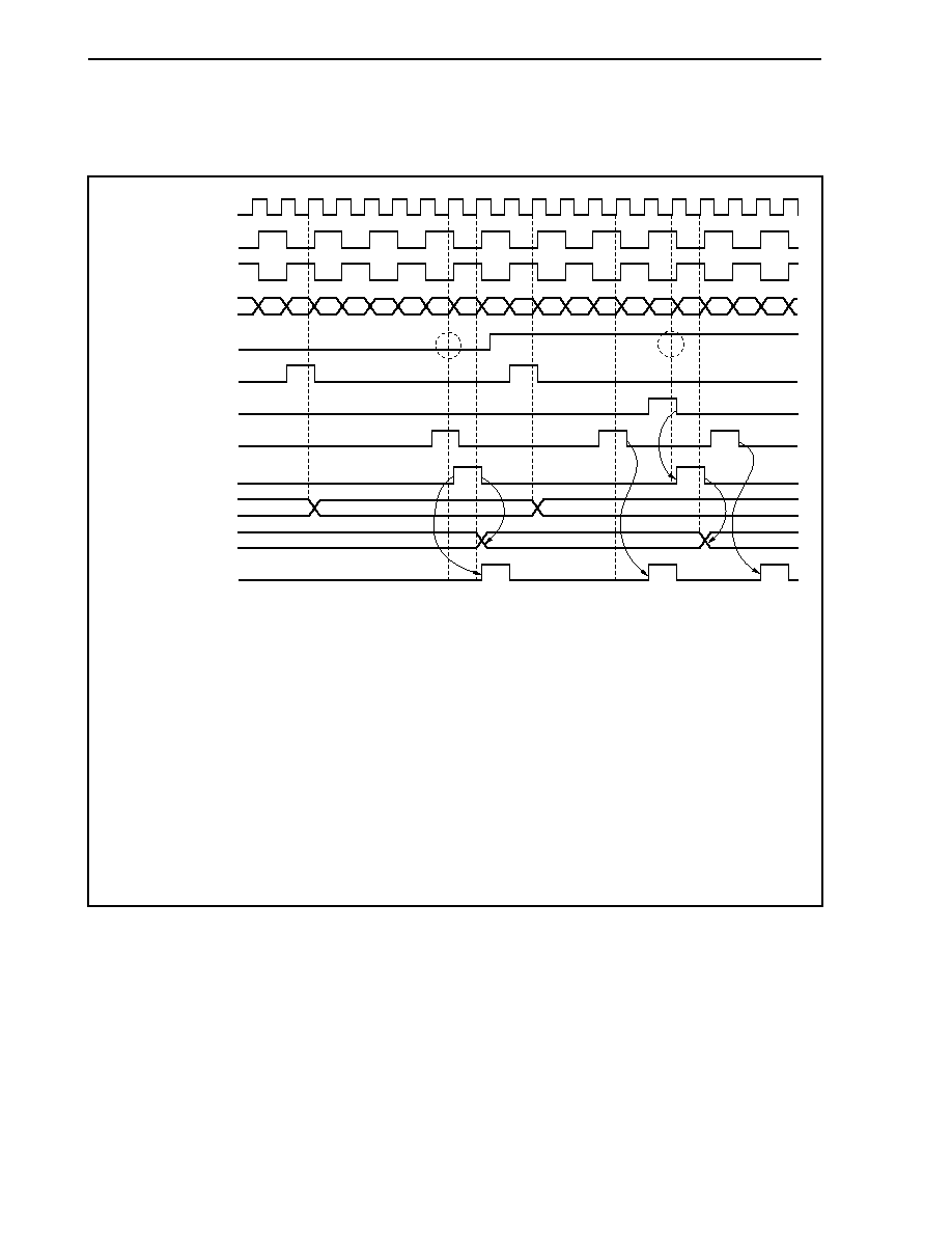
CHAPTER 9 TIMER/COUNTER FUNCTION
364
User's Manual U14492EJ5V0UD
Figure 9-78. Compare Operation: Mode with Buffer
(When Operation Is Delayed Through Setting of LNKEy Bit of CMSEx0
Register, CMSEx0 Register's CCSEy Bit = 1, BFEEy Bit = 1)
f
CLK
LNKEy bit
Note
WRITE_ENABLE_S
MUXTB0
MUXTB1
MUXCNT
RELOAD2A
RELOAD1
RELOAD_PRIMARY
CVSEm0 register
CVPEm0 register
INTCC2m (output)
TB0
TB1
TB0
TB1
TB0
TB1
TB0
TB1
TB0
TB1
TB0
TB1
TB0
TB1
TB0
TB1
TB0
TB1
TB0
TB1
5
1
6
2
3
4
7
8
5
9
10
6
11
7
0
1
2
12
13
14
4
4
7
1
7
1
Note LNKEy bit of CMSEx0 register
Remarks 1. f
CLK
: Base clock
2. MUXCNT: Count value to sub-channel m
MUXTB0, MUXTB1: Multiplex signal of TM20, TM21
RELOAD1: Compare match signal
RELOAD2A: Zero count signal input of TM20 (occurs when TM20 = 0000H)
RELOAD_PRIMARY: Timing of write operation from CVSEm0 register to CVPEm0 register
WRITE_ENABLE_S: Timing of CVSEm0 register write operation
TB0: Count value of TM20 (In this figure, the maximum count value is 7.)
TB1: Count value of TM21
3. m = 1 to 4, x = 12, 34
y: When x = 12, y = 1, 2, and when x = 34, y = 3, 4
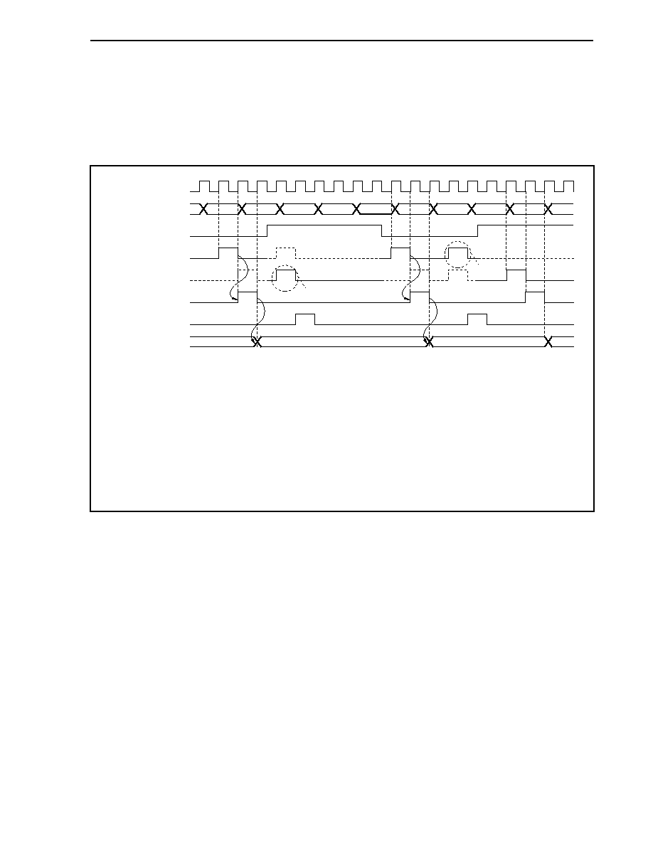
CHAPTER 9 TIMER/COUNTER FUNCTION
365
User's Manual U14492EJ5V0UD
(4) Operation of capture/compare register (sub-channels 0, 5)
Figures 9-79 and 9-80 show the operation of the capture/compare register (sub-channels 0, 5).
Figure 9-79. Capture Operation: Timer 2 Count Value Read Timing
(When CMSE050 Register's CCSEy Bit = 0, EEVEy Bit = 1, and CSCE0
Register's SEVEy Bit = 0)
f
CLK
ED1
ED2
CAPTURE_S
READ_ENABLE_S
CVSEy0 register
CNT
LNKEy
Note 1
1
2
3
4
5
6
7
8
9
10
0
Note 2
Note 2
Undefined
2
6
9
Notes 1. LNKEy bit of CMSE050 register
2. If an event occurs in this timing, it is ignored.
Remarks 1. f
CLK
: Base clock
2. CNT: Count value of timer 2
CAPTURE_S: Capture trigger signal of sub capture register
ED1, ED2: Capture event signal inputs from edge selector
READ_ENABLE_S: Read timing for CVSEy0 register
3. y = 0, 5
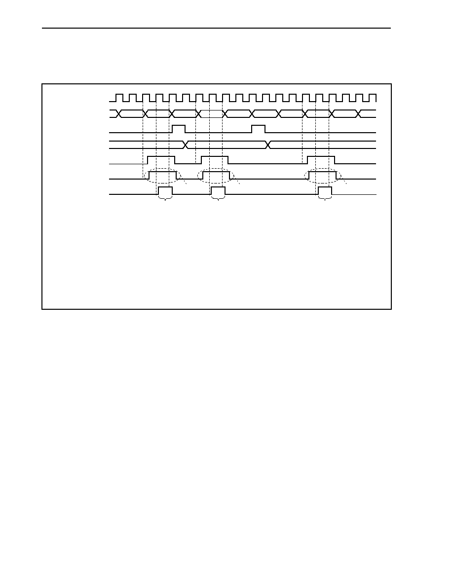
CHAPTER 9 TIMER/COUNTER FUNCTION
366
User's Manual U14492EJ5V0UD
Figure 9-80. Compare Operation: Timing of Compare Match and Write Operation to Register
(When CMSE050 Register's CCSEy Bit = 1, EEVEy Bit = Arbitrary, and CSCE0
Register's SEVEy Bit = Arbitrary)
f
CLK
CVSEy0 register
MATCH
R
Note 1
INTCC20, INTCC25
(output)
CNT
CPU write C/C
1
2
2
3
4
4
5
6
7
8
8
9
10
0
Note 2
Note 3
Note 2
Note 2
Note 3
Note 3
Notes 1. Can control TM20/TM21 clear by sub-channel 0/5 compare match or count direction.
2. When MATCH signal occurs, the same waveform as the MATCH signal is generated.
3. The pulse width is always 1 clock.
Remarks 1. f
CLK
: Base clock
2. CNT: Count value of timer 2
MATCH: CVSEy0 register compare match timing
R: Compare match input (sub-channel 0/5)
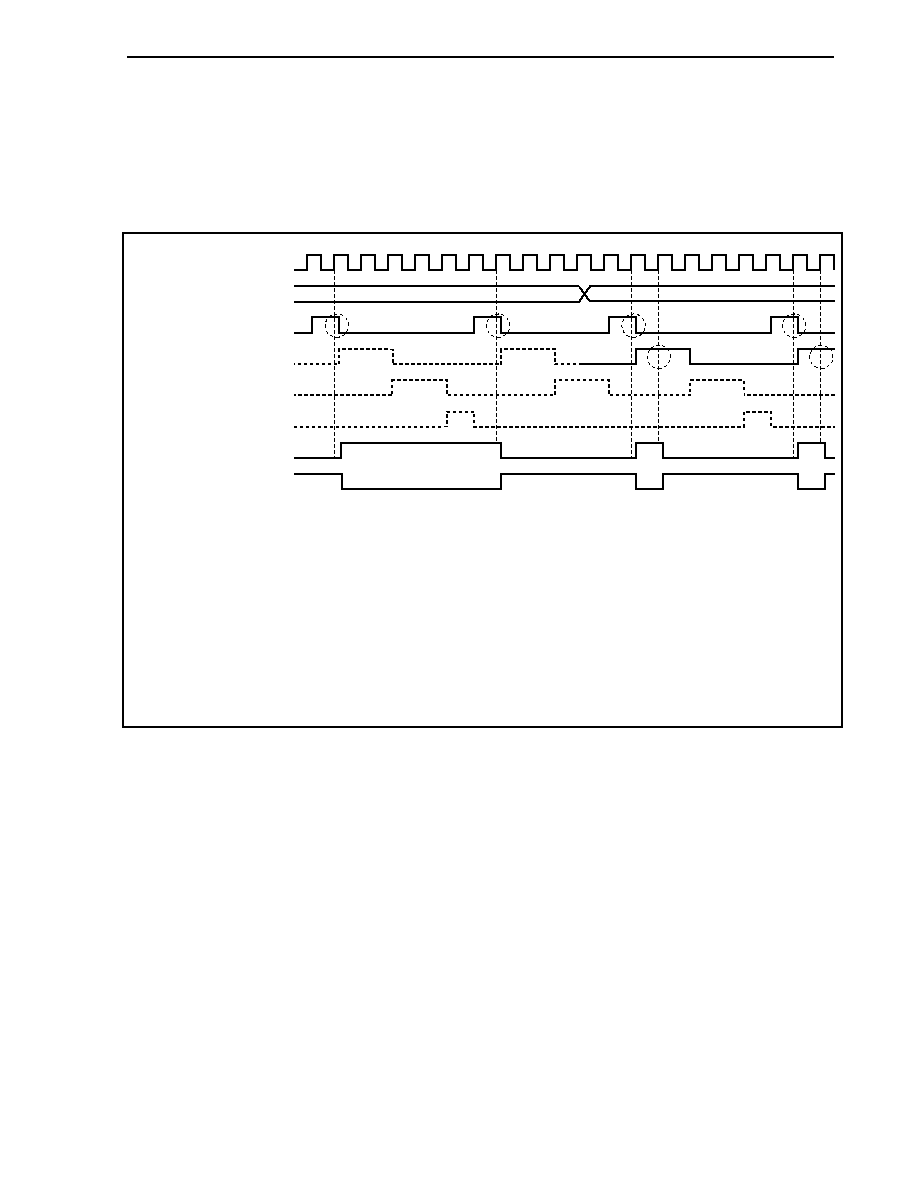
CHAPTER 9 TIMER/COUNTER FUNCTION
367
User's Manual U14492EJ5V0UD
(5) Operation of output circuit
Figures 9-81 to 9-84 show the output circuit operation.
Figure 9-81. Signal Output Operation: Toggle Mode 0 and Toggle Mode 1
(When OCTLE0 Register's SWFEn Bit = 0, and ODELE0 Register's ODLEn2
to ODLEn0 Bits = 0)
f
CLK
RA
RB
RN
TO2n timer output
(ALVEn bit = 0
Note 2
)
TO2n timer output
(ALVEn bit = 1
Note 2
)
OTMEn1, OTMEn0 bits
Note 1
S/T
00B
01B
Notes 1. OTMEn1, OTMEn0 bits of OCTLE0 register
2. ALVEn bit of OCTLE0 register
Remarks 1. f
CLK
: Base clock
2. RA: Zero count signal input of TM20 (output circuit reset signal)
RB: Zero count signal input of TM21 (output circuit reset signal)
RN: Interrupt signal input of sub-channel n (output circuit reset signal)
S/T: Interrupt signal input of sub-channel n (output circuit set signal)
3. n = 1 to 4

CHAPTER 9 TIMER/COUNTER FUNCTION
368
User's Manual U14492EJ5V0UD
Figure 9-82. Signal Output Operation: Toggle Mode 2 and Toggle Mode 3
(When OCTLE0 Register's SWFEn Bit = 0, and ODELE0 Register's ODLEn2
to ODLEn0 Bits = 0)
f
CLK
RA
RB
RN
TO2n timer output
(ALVEn bit = 0
Note 2
)
TO2n timer output
(ALVEn bit = 1
Note 2
)
OTMEn1, OTMEn0 bits
Note 1
S/T
10B
11B
Notes 1. OTMEn1, OTMEn0 bits of OCTLE0 register
2. ALVEn bit of OCTLE0 register
Remarks 1. f
CLK
: Base clock
2. RA: Zero count signal input of TM20 (output circuit reset signal)
RB: Zero count signal input of TM21 (output circuit reset signal)
RN: Interrupt signal input of sub-channel n (output circuit reset signal)
S/T: Interrupt signal input of sub-channel n (output circuit set signal)
3. n = 1 to 4
Figure 9-83. Signal Output Operation: During Software Control
(When OCTLE0 Register's OTMEn1, OTMEn0 Bits = Arbitrary, SWFEn Bit
= 1, and ODELE0 Register's ODLEn2 to ODLEn0 Bits = 0)
f
CLK
ALVEn bit
Note
TO2n timer output
Note ALVEn bit of OCTLE0 register
Remarks 1. f
CLK
: Base clock
2. n = 1 to 4
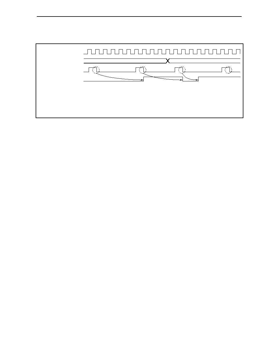
CHAPTER 9 TIMER/COUNTER FUNCTION
369
User's Manual U14492EJ5V0UD
Figure 9-84. Signal Output Operation: During Delay Output Operation
(When OCTLE0 Register's OTMEn1, OTMEn0 Bits = 0, ALVEn = 0, SWFEn Bit = 0)
f
CLK
TO2n timer output
ODELEn2 to ODELEn0 bits
Note
S/T
5
2
Note ODELEn2 to ODELEn0 bits of OCTLE0 register
Remarks 1. f
CLK
: Base clock
2. n = 1 to 4
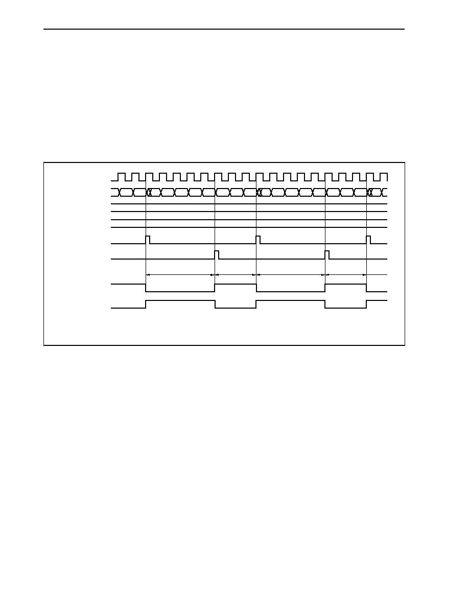
CHAPTER 9 TIMER/COUNTER FUNCTION
370
User's Manual U14492EJ5V0UD
9.3.6 PWM output operation when timer 2 operates in compare mode
(1) Operation when TO2n pin performs PWM output operation in toggle mode 1
In toggle mode 1, the TO2n output (internal) becomes inactive triggered by a signal when TM20 = 0, and
becomes active triggered by a sub-channel 1 (CVPEn0 register) compare match signal. In accordance with
the state of this TO2n (internal), the TO2n pin outputs a high or low level depending on the OCTLE0.ALVEn
bit setting.
Figure 9-85. Normal Output Operation
(When OCTLE0 Register's OTMEn1, OTMEn0 Bits = 01, ODELE0 Register's ODLEn2 to ODLEn0 Bits = 000)
f
CLK
CVSEn0 register
match signal
TO2n (internal)
TO2n output
(ALVEn
bit
= 0)
TO2n output
(ALVEn
bit
= 1)
TM20
CVSE00 register
CVSEn0 register
TM20 = 0
06
05
07
00
02
Inactive state
Inactive state
Active state
Active state
04
01
03
06
0008H
0005H
05
07
00 01
02
04
06
00 01
03
05
07
Remark n = 1 to 4
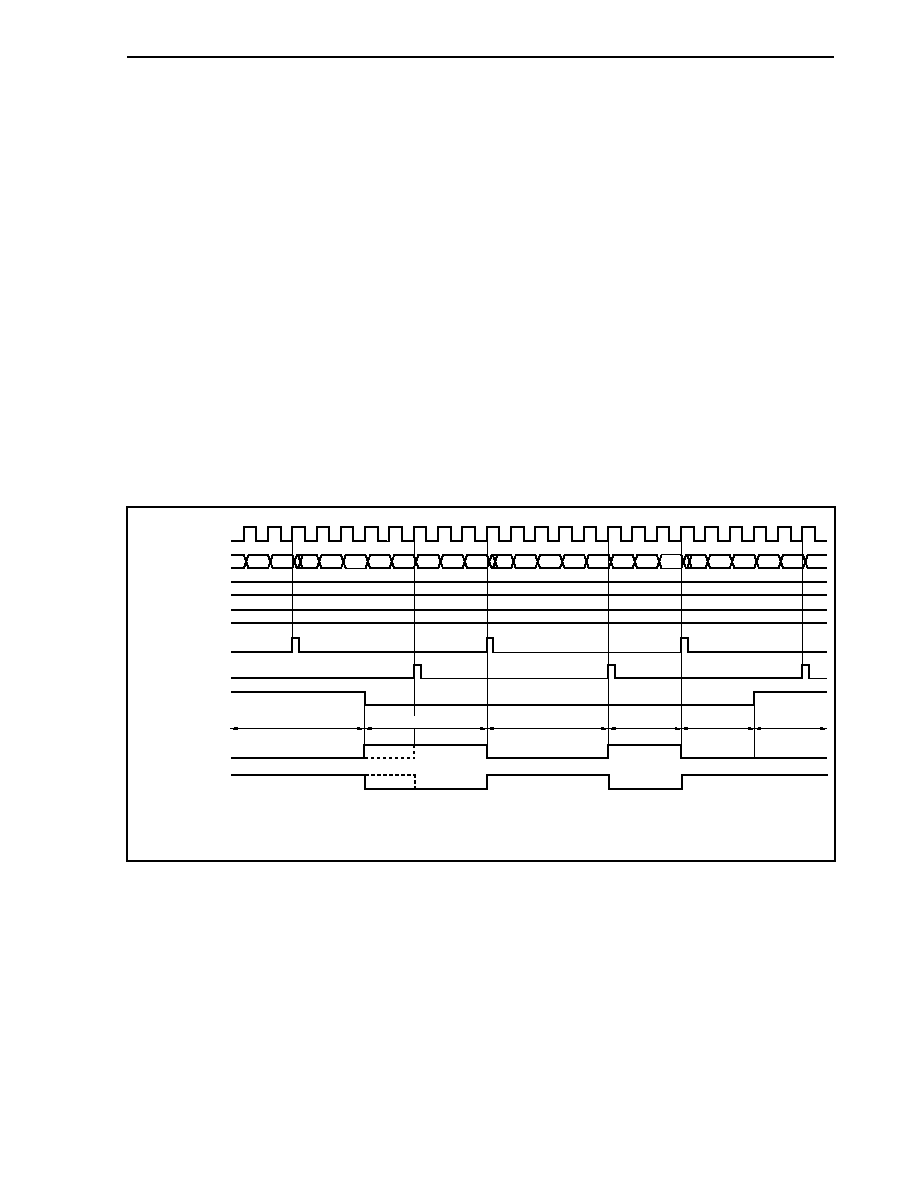
CHAPTER 9 TIMER/COUNTER FUNCTION
371
User's Manual U14492EJ5V0UD
(2) Operation when TO2n pin output is controlled by manipulating OCTLE0.SWFEn bit in toggle mode 1
(a) When a sub-channel n compare match signal is output immediately after the SWFEn bit is cleared
to 0
Figures 9-86 and 9-87 show the waveforms when output from the TO2n output pin is started or ended by
manipulating the SWFEn bit in toggle mode 1.
In the V850E/IA1, timer 2 outputs a level according to the ALVEn bit setting (low level when ALVEn bit =
0, and high level when ALVEn bit = 1) by fixing the TO2n output to the inactive state when the SWFEn bit
is 1. When the SWFEn bit is 0, TO2n (internal) synchronizes with a trigger signal and an active or
inactive level is output from the TO2n output pin.
However, TO2n output is forcibly fixed to the active state when the SWFEn bit is cleared to 0, and
inactive state when the SWFEn bit is set to 1.
Therefore, if the sub-channel n compare match signal is output immediately after the SWFEn bit is
cleared to 0, the active period from when the SWFEn bit is cleared to 0 to when the compare match
signal is output will be added to the ordinary TO2n output active period, so the first active period
becomes long (refer to Figure 9-86).
Figure 9-86. When Output Operation Is Started/Ended Normally
(When OCTLE0 Register's OTMEn1, OTMEn0 Bits = 01, ODELD0 Register's ODLEn2 to ODLEn0 Bits = 000)
f
CLK
CVSEn0
register
match signal
TO2n
(internal)
TO2n
output
(ALVEn bit = 0)
TO2n
output
(ALVEn bit = 1)
TM20
CVSE00
register
CVSEn0
register
TM20 = 0
06
05
07
00
02
Inactive state (fixed)
Inactive state
Active state Inactive state
Inactive state
(fixed)
04
01
03
06
0008H
0005H
05
07
00 01
02
04
06
03
05
07
SWFEn
bit
00 01
02
04
03
05
Active state
Remark n = 1 to 4
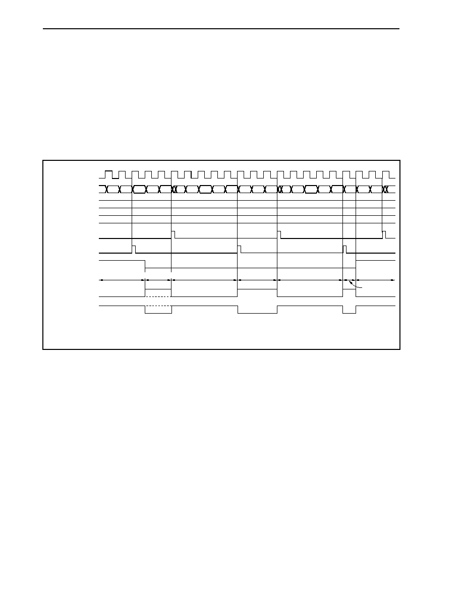
CHAPTER 9 TIMER/COUNTER FUNCTION
372
User's Manual U14492EJ5V0UD
(b) When the trigger signal of TM20 = 0 is output immediately after the SWFEn bit is cleared to 0
When the trigger signal of TM20 = 0 is output immediately after the SWFEn bit is cleared to 0, from when
the SWFEn bit is cleared to 0 to when the trigger signal of TM20 = 0 is output is the first active period, so
a pulse shorter than the active period of the ordinary TO2n output is output.
In addition, since TO2n output is forcibly fixed to the inactive level when the SWFEn bit is set to 1, the
active level output period also becomes shorter if the SWFEn bit is set to 1 while an active level is being
output (refer to Figure 9-87).
Figure 9-87. When Output Operation Is Started/Ended Normally
(When OCTLE0 Register's OTMEn1, OTMEn0 Bits = 01, ODELD0 Register's ODLEn2 to ODLEn0 Bits = 000)
f
CLK
CVSEn0
register
match signal
TO2n
(internal)
TO2n
output
(ALVEn bit = 0)
TO2n
output
(ALVEn bit = 1)
TM20
CVSE00
register
CVSEn0
register
TM20 = 0
02
Inactive state
(fixed)
Inactive state
Active state
Active state
Inactive state
Inactive state
(fixed)
04
03
06
0008H
0005H
05
07
00 01
02
04
06
03
05
07
SWFEn bit
00 01
02
04
03
05
06
07
00
Active state
Remark n = 1 to 4

CHAPTER 9 TIMER/COUNTER FUNCTION
373
User's Manual U14492EJ5V0UD
9.4 Timer 3
9.4.1 Features (timer 3)
Timer 3 (TM3) is a 16-bit timer/counter that can perform the following operations.
∑ Interval timer function
∑ PWM output
∑ External signal cycle measurement
9.4.2 Function overview (timer 3)
∑
16-bit timer/counter (TM3): 1 channel
∑
Capture/compare registers: 2
∑
Count clock division selectable by prescaler (set the frequency of the count clock to 16 MHz or less)
∑
Base clock (f
CLK
): 2 types (set f
CLK
to 32 MHz or less)
f
XX
and f
XX
/2 can be selected
∑
Prescaler division ratio
The following division ratios can be selected according to the base clock (f
CLK
).
Base Clock (f
CLK
)
Division Ratio
f
XX
Selected
f
XX
/2 Selected
1/2 f
XX
/2 f
XX
/4
1/4 f
XX
/4 f
XX
/8
1/8 f
XX
/8 f
XX
/16
1/16 f
XX
/16 f
XX
/32
1/32 f
XX
/32 f
XX
/64
1/64 f
XX
/64
f
XX
/128
1/128 f
XX
/128 f
XX
/256
1/256 f
XX
/256 f
XX
/512
∑
Interrupt request sources
∑ Capture/compare match interrupt requests: 2 sources
In case of capture register: INTCC3n generated by INTP3n input
In case of compare register: INTCC3n generated by CC3n match signal
∑ Overflow interrupt request: 1 source
INTTM3 generated upon overflow of TM3 register
∑
Timer/counter count clock sources: 2 types
(Selection of external pulse input, internal system clock cycle)
∑
One of two operation modes when the timer/counter overflows can be selected: free-running mode or overflow
stop mode
∑
The timer/counter can be cleared by match of timer/counter and compare register
∑
External pulse output (TO3): 1
Remarks 1. f
XX
: Internal system clock
2. n = 0, 1

CHAPTER 9 TIMER/COUNTER FUNCTION
374
User's Manual U14492EJ5V0UD
9.4.3 Basic configuration
Table 9-12. Timer 3 Configuration List
Count Clock
Timer
Note 1
Note 2
Register Read/Write Generated
Interrupt
Signal
Capture
Trigger
Timer Output
S/R
TM3 Read
INTTM3
-
-
CC30 Read/write INTCC30 INTP30
TO3
(S)
Timer 3
f
XX
/2,
f
XX
/4,
f
XX
/8,
f
XX
/16,
f
XX
/32,
f
XX
/64,
f
XX
/128,
f
XX
/256
f
XX
/4,
f
XX
/8,
f
XX
/16,
f
XX
/32,
f
XX
/64,
f
XX
/128,
f
XX
/256,
f
XX
/512
CC31 Read/write INTC31
INTP31
TO3
(R)
Notes 1. When f
XX
is selected as the base clock (f
CLK
) of TM3
2. When
f
XX
/2 is selected as the base clock (f
CLK
) of TM3
Remark f
XX
: Internal system clock
S/R: Set/Reset
Figure 9-88 shows the block diagram of timer 3.
Figure 9-88. Block Diagram of Timer 3
R
Note
Q
S
Q
TM3 (16-bit)
CC30
CC31
INTTM3
INTCC30
INTP31
1/2
1/4
1/8
1/16
1/32
1/64
1/128
1/256
f
XX
/2
TI3/TCLR3/INTP30
INTCC31
TO3
f
CLK
Selector
Selector
Selector
Clear & start
Clear & start
f
XX
Note Reset priority
Remarks 1. TI3 input and TCLR3 input connected to port immediately before edge detection
2. f
CLK
: Base clock (32 MHz (MAX.))
f
XX
: Internal system clock

CHAPTER 9 TIMER/COUNTER FUNCTION
375
User's Manual U14492EJ5V0UD
(1) Timer 3 (TM3)
TM3 functions as a 16-bit free-running timer or as an event counter for an external signal. Besides being
mainly used for cycle measurement, TM3 can be used as pulse output.
TM3 is read-only, in 16-bit units.
Cautions 1. The TM3 register can only be read. If writing is performed to the TM3 register, the
subsequent operation is undefined.
2. If the TM3CAE bit of the TMC30 register is cleared (0), a reset is performed
asynchronously.
3. Continuous reading of TM3 is prohibited. If TM3 is continuously read, the second read
value may differ from the actual value.
Figure 9-89. Timer 3 (TM3)
15
14
13
12
11
10
9
8
7
6
5
4
3
2
1
TM3
FFFFF680H
0000H
Address
Initial value
0
TM3 performs the count-up operations of an internal count clock or external count clock. Timer starting and
stopping are controlled by the TM3CE bit of timer control register 30 (TMC30).
The internal or external count clock is selected by the ETI bit of timer control register 31 (TMC31).
(a) Selection of the external count clock
TM3 operates as an event counter.
When the ETI bit of timer control register 31 (TMC31) is set (1), TM3 counts the valid edges of the
external clock input (TI3), synchronized with the internal count clock. The valid edge is specified by valid
edge selection register (SESC).
Caution If the INTP30, TI3, and TCLR3 pins are used as the TI3 and TCLR3, either mask the
INTP30 interrupt or set CC3n in compare mode (n = 0, 1).

CHAPTER 9 TIMER/COUNTER FUNCTION
376
User's Manual U14492EJ5V0UD
(b) Selection of the internal count clock
TM3 operates as a free-running timer.
When an internal clock is specified as a count clock by timer control register 31 (TMC31), TM3 is counted
up for each input clock cycle specified by the CS2 to CS0 bits of the TMC30 register.
A division by the prescaler can be selected for the count clock from among f
CLK
/2, f
CLK
/4, f
CLK
/8, f
CLK
/16,
f
CLK
/32, f
CLK
/64, f
CLK
/128 and f
CLK
/256 by the TMC30 register (f
CLK
: base clock).
An overflow interrupt can be generated if the timer overflows. Also, the timer can be stopped following
an overflow by setting the OST bit of the TMC31 register to 1.
Caution The count clock cannot be changed while the timer is operating.
The conditions when the TM3 register becomes 0000H are shown below.
(i) Asynchronous
reset
∑ TM3CAE bit of TMC30 register = 0
∑ Reset
input
(ii) Synchronous reset
∑ TM3CE bit of TMC30 register = 0
∑ The CC30 register is used as a compare register, and the TM3 and CC30 registers match when
clearing the TM3 register is enabled (CCLR bit of the TMC31 register = 1)
CHAPTER 9 TIMER/COUNTER FUNCTION
377
User's Manual U14492EJ5V0UD
(2) Capture/compare registers 30 and 31 (CC30 and CC31)
These capture/compare registers 30 and 31 are 16-bit registers.
They can be used as capture registers or compare registers according to the CMS1 and CMS0 bit
specifications of timer control register 31 (TMC31).
These registers can be read/written in 16-bit units (however, write operations can only be performed in
compare mode).
Caution Continuous reading of CC3n is prohibited. If CC3n is continuously read, the second read
value may differ from the actual value. If CC3n must be read twice, be sure to read another
register between the first and the second read operation.
Correct usage example
Incorrect usage example
CC30
read
CC30
read
CC31
read
CC30
read
CC30
read
CC31
read
CC31 read
CC31 read
CC31
15
14
13
12
11
10
9
8
7
6
5
4
3
2
1
CC30
FFFFF682H
FFFFF684H
0000H
0000H
Address
Initial value
0
15
14
13
12
11
10
9
8
7
6
5
4
3
2
1
Address
Initial value
0
(a) Setting these registers to capture registers (CMS1 and CMS0 of TMC31 = 0)
When these registers are set to capture registers, the valid edges of the corresponding external interrupt
signals INTP30 and INTP31 are detected as capture triggers. The timer TM3 is synchronized with the
capture trigger, and the value of TM3 is latched in the CC30 and CC31 registers (capture operation).
The valid edge of the INTP30 pin is specified (rising, falling, or both edges) according to the IES301 and
IES300 bits of the SESC register, and the valid edge of the INTP31 pin is specified according to the
IES311 and IES310 bits of the SESC register.
The capture operation is performed asynchronously relative to the count clock. The latched value is held
in the capture register until the next capture operation is performed.
When the TM3CAE bit of timer control register 30 (TMC30) is 0, 0000H is read.
If these registers are specified as capture registers, an interrupt is generated by detecting the valid edge
of signals INTP30 and INTP31.
Caution If the capture operation and the TM3 register count prohibit setting (TM3CE bit of
TMC30 register = 0) timings conflict, the captured data becomes undefined, and no
INTCC3n interrupt is generated (n = 0, 1).

CHAPTER 9 TIMER/COUNTER FUNCTION
378
User's Manual U14492EJ5V0UD
(b) Setting these registers to compare registers (CMS1 and CMS0 of TMC31 = 1)
When these registers are set to compare registers, the TM3 and register values are compared for each
count clock, and an interrupt is generated by a match. If the CCLR bit of timer control register 31
(TMC31) is set (1), the TM3 value is cleared (0) at the same time as a match with the CC30 register (it is
not cleared (0) by a match with the CC31 register).
A compare register is equipped with a set/reset output function. The corresponding timer output (TO3) is
set or reset, synchronized with the generation of a match signal.
The interrupt selection source differs according to the function of the selected register.
Cautions 1. To write to capture/compare registers 30 and 31 (CC30, CC31), always set the TM3CAE
bit to 1 first. When the TM3CAE bit is 0, even if writing to registers CC30 and CC31, the
data that is written will be invalid because the reset is asynchronous.
2. Perform a write operation to capture/compare registers 30 and 31 after setting them to
compare registers according to the TMC30, TMC31 register setting. If they are set to
capture registers (CMS1 and CMS0 bits of TMC31 register = 0), no data is written even if
a write operation is performed to CC30 and CC31.
3. When these registers are set to compare registers, INTP30 and INTP31 cannot be used
as external interrupt input pins.
CHAPTER 9 TIMER/COUNTER FUNCTION
379
User's Manual U14492EJ5V0UD
9.4.4 Control registers
(1) Timer 3 clock selection register (PRM03)
The PRM03 register is used to select the base clock (f
CLK
) of timer 3 (TM3).
This register can be read/written in 8-bit or 1-bit units.
Cautions 1. Always set this register before using the timer.
2.
Set
f
CLK
to 32 MHz or less.
7
0
PRM03
6
0
5
0
4
0
3
0
2
0
1
0
0
PRM3
Address
FFFFF690H
Initial value
00H
Bit position
Bit name
Function
0
PRM3
Specifies the base clock (f
CLK
) of timer 3 (TM3).
0: f
XX
/2 (when f
XX
> 32 MHz)
1: f
XX
(when f
XX
32 MHz)
Remark f
XX
: Internal system clock

CHAPTER 9 TIMER/COUNTER FUNCTION
380
User's Manual U14492EJ5V0UD
(2) Timer control register 30 (TMC30)
The TMC30 register controls the operation of TM3.
This register can be read/written in 8-bit or 1-bit units.
Cautions 1. The TM3CAE bit and other bits cannot be set at the same time. Be sure to set the
TM3CAE bit and then set the other bits and the other registers of TM3. To use an
external pin related to the timer function when using timer 3, be sure to set (1) the
TM3CAE bit after setting the external pin to the control mode.
2. If occurrence of an overflow conflicts with writing to the TMC30 register, the value of the
TM3OVF bit is the value written to the TMC30 register.
(1/2)
<7>
TM3OVF
TMC30
6
CS2
5
CS1
4
CS0
3
0
2
0
<1>
TM3CE
<0>
TM3CAE
Address
FFFFF686H
Initial value
00H
Bit position
Bit name
Function
7
TM3OVF
Flag that indicates TM3 overflow.
0: No overflow
1: Overflow
The TM3OVF bit becomes "1" when TM3 changes from FFFFH to 0000H. An overflow
interrupt request (INTTM3) is generated at the same time. However, if CC30 is set to
the compare mode (CMS0 bit of the TMC31 register = 1) and match clear during
comparison of TM3 and CC30 is enabled (CCLR bit of TMC31 register = 1), and TM3
is cleared to 0000H following match at FFFFH, TM3 is considered to have been
cleared and the TM3OVF bit does not become "1", nor is the INTTM3 interrupt
generated.
The TM3OVF bit holds a "1" until "0" is written to it or an asynchronous reset is applied
while the TM3CAE bit = 0. Interrupts by overflow and the TM3OVF bit are independent,
and even if the TM3OVF bit is manipulated, this does not affect the interrupt request
flag for INTTM3 (TM3IF0). If an overflow occurs while the TM3OVF bit is being read,
the value of the flag changes and the value is returned at the next read.
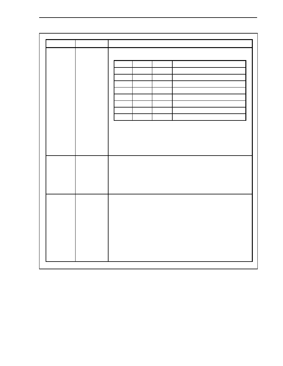
CHAPTER 9 TIMER/COUNTER FUNCTION
381
User's Manual U14492EJ5V0UD
(2/2)
Bit position
Bit name
Function
Selects the internal count clock for TM3.
CS2 CS1 CS0
Count
clock
0 0 0
f
CLK
/2
0 0 1
f
CLK
/4
0 1 0
f
CLK
/8
0 1 1
f
CLK
/16
1 0 0
f
CLK
/32
1 0 1
f
CLK
/64
1 1 0
f
CLK
/128
1 1 1
f
CLK
/256
6 to 4
CS2 to CS0
Caution Do not change the CS2 to CS0 bits during timer operation. If they
are to be changed, they must be changed after setting the TM3CE bit
to "0". If the CS2 to CS0 bits are overwritten during timer operation,
the operation is not guaranteed.
Remark f
CLK
: Base clock
1
TM3CE
Controls the operation of TM3.
0: Disable count (timer stopped at 0000H and does not operate)
1: Perform count operation.
Caution
If TM3CE = 0, the external pulse output (TO3) becomes inactive level
(the active level of TO3 output is set with the ALV bit of the TMC31
register).
0
TM3CAE
Controls the internal count clock.
0: Asynchronously reset entire TM3 unit. Stop base clock supply to TM3 unit.
1: Supply base clock (f
CLK
) to TM3 unit.
Cautions 1. When TM3CAE = 0 is set, the TM3 unit can be reset
asynchronously.
2. When TM3CAE = 0, the TM3 unit is in a reset state. To operate
TM3, first set TM3CAE = 1.
3. When the TM3CAE bit is changed from "1" to "0", all the
registers of the TM3 unit are initialized. When again setting
TM3CAE = 1, be sure to then again set all the registers of the TM3
unit.

CHAPTER 9 TIMER/COUNTER FUNCTION
382
User's Manual U14492EJ5V0UD
(3) Timer control register 31 (TMC31)
The TMC31 register controls the operation of TM3.
This register can be read/written in 8-bit or 1-bit units.
Cautions 1. Do not change the bits of the TMC31 register during timer operation. If they are to be
changed, they must be changed after setting the TM3CE bit of the TMC30 register to
"0". If the TMC31 register is overwritten during timer operation, the operation is not
guaranteed.
2. If the ENT1 bit and the ALV bit are changed simultaneously, a glitch (spike-shaped
noise) may be generated in the TO3 pin output. Either design the circuit that will not
malfunction even if a glitch is generated, or make sure that the ENT1 bit and the ALV bit
do not change at the same time.
3. TO3 output remains unchanged by external interrupt signals (INTP30, INTP31). When
using the TO3 signal, set the capture/compare register to the compare register (CMS1,
CMS0 bits of TMC31 register = 1).
Remark A reset takes precedence for the flip-flop of the TO3 output.

CHAPTER 9 TIMER/COUNTER FUNCTION
383
User's Manual U14492EJ5V0UD
7
OST
TMC31
6
ENT1
5
ALV
4
ETI
3
CCLR
2
ECLR
1
CMS1
0
CMS0
Address
FFFFF688H
Initial value
20H
Bit position
Bit name
Function
7
OST
Sets the operation when TM3 overflows.
0: Continue count operation after overflow (free-running mode)
1: After overflow, timer holds 0000H and stops count operation (overflow stop
mode). At this time, the TM3CE bit of TMC30 remains "1". The count operation
is resumed by again writing "1" to the TM3CE bit.
6
ENT1
Enables/disables output of external pulse output (TO3).
0: Disable external pulse output. Output of inactive level of ALV bit to TO3 pin is
fixed. TO3 pin level remains unchanged even if match signal from
corresponding compare register is generated.
1: Enable external pulse output. Compare register match causes TO3 output to
change. However, in capture mode, TO3 output does not change. An ALV bit
inactive level is output from the time when timer output is enabled until a match
signal is generated.
Caution
If either CC30 or CC31 is specified as a capture register, the ENT1
bit must be set to "0".
5
ALV
Specifies active level of external pulse output (TO3).
0: Active level is low level.
1: Active level is high level.
Caution
The initial value of the ALV bit is "1".
4
ETI
Switches count clock between external clock and internal clock.
0: Specifies input clock (internal). The count clock can be selected with bits CS2
to CS0 of TMC30.
1: Specifies external clock (TI3). Valid edge can be selected with bits TES31,
TES30 of SESC.
3
CCLR
Enables/disables TM3 clearing during compare operation.
0: Disable clearing.
1: Enable clearing (TM3 is cleared when CC30 and TM3 match during compare
operation).
2
ECLR
Enables TM3 clearing by external clear input (TCLR3).
0: Disable clearing by TCLR3.
1: Enable clearing by TCLR3 (counting resumes after clearing).
1
CMS1
Selects operation mode of capture/compare register (CC31).
0: Register operates as capture register.
1: Register operates as compare register.
0
CMS0
Selects operation mode of capture/compare register (CC30).
0: Register operates as capture register.
1: Register operates as compare register.
CHAPTER 9 TIMER/COUNTER FUNCTION
384
User's Manual U14492EJ5V0UD
(4) Valid edge selection register (SESC)
This register specifies the valid edge of external interrupt requests (TI3, TCLR3, INTP30, INTP31) from an
external pin.
The rising edge, the falling edge, or both rising and falling edges can be specified as the valid edge
independently for each pin.
This register can be read/written in 8-bit or 1-bit units.
Caution Do not change the bits of SESC register during timer operation. If they are to be changed,
they must be changed after setting the TM3CE bit of the TMC30 register to "0". If the SESC
register is overwritten during timer operation, the operation is not guaranteed.
7
TES31
SESC
6
TES30
5
CES31
4
CES30
3
IES311
2
IES310
1
IES301
0
IES300
Address
FFFFF689H
Initial value
00H
TI3
TCLR3
INTP31
INTP30
Bit position
Bit name
Function
7, 6
TES31, TES30
Specifies the valid edge of INTP30, INTP31 pins, TCLR3, and TI3 pins.
xESn1 xESn0
Operation
5, 4
CES31, CES30
0 0
Falling
edge
0 1
Rising
edge
3, 2
IES311, IES310
1 0
Setting
prohibited
1
1
Both rising and falling edges
1, 0
IES301, IES300
Remark n = 3, 30, 31
CHAPTER 9 TIMER/COUNTER FUNCTION
385
User's Manual U14492EJ5V0UD
9.4.5 Operation
(1) Count operation
Timer 3 can function as a 16-bit free-running timer or as an external signal event counter. The setting for the
type of operation is specified by timer control register 3n (TMC3n) (n = 0, 1).
When it operates as a free-running timer, if the CC30 or CC31 register and the TM3 count value match, an
interrupt signal is generated and the timer output signal (TO3) can be set or reset. Also, a capture operation
that holds the TM3 count value in the CC30 or CC31 register is performed, synchronized with the valid edge
that was detected from the external interrupt request input pin as an external trigger. The capture value is
held until the next capture trigger is generated.
Caution If the INTP30/TI3/TCLR3 pin is used as TI3 or TCLR3, either mask the INTP30 interrupt or set
the CC3n register to compare mode (n = 0, 1).
Figure 9-90. Basic Operation of Timer 3
0001H
0000H
0002H 0003H
FBFEH FBFFH
0001H 0002H
0000H
TM3
Count clock
Count disabled
TM3CE
0
Count start
TM3CE
1
Count start
TM3CE
1
CHAPTER 9 TIMER/COUNTER FUNCTION
386
User's Manual U14492EJ5V0UD
(2) Overflow
When the TM3 register has counted the count clock from FFFFH to 0000H, the TM3OVF bit of the TMC30
register is set (1), and an overflow interrupt (INTTM3) is generated at the same time. However, if the CC30
register is set to compare mode (CMS0 bit = 1) and to the value FFFFH when match clearing is enabled
(CCLR bit = 1), then the TM3 register is considered to be cleared and the TM3OVF bit is not set (1) when the
TM3 register changes from FFFFH to 0000H. Also, the overflow interrupt (INTTM3) is not generated.
When the TM3 register is changed from FFFFH to 0000H because the TM3CE bit changes from 1 to 0, the
TM3 register is considered to be cleared, but the TM3OVF bit is not set (1) and no INTTM3 interrupt is
generated.
Also, timer operation can be stopped after an overflow by setting the OST bit of the TMC31 register to 1.
When the timer is stopped due to an overflow, the count operation is not restarted until the TM3CE bit of the
TMC30 register is set (1).
Operation is not affected even if the TM3CE bit is set (1) during a count operation.
Figure 9-91. Operation After Overflow (When OST = 1)
Overflow
Count
start
Overflow
FFFFH
FFFFH
TM3
0
INTTM3
OST
1
TM3CE
1
TM3CE
1
CHAPTER 9 TIMER/COUNTER FUNCTION
387
User's Manual U14492EJ5V0UD
(3) Capture operation
The TM3 register has two capture/compare registers. These are the CC30 register and the CC31 register. A
capture operation or a compare operation is performed according to the settings of both the CMS1 and CMS0
bits of the TMC31 register. If the CMS1 and CMS0 bits of the TMC31 register are set to 0, the register
operates as a capture register.
A capture operation that captures and holds the TM3 count value asynchronously relative to the count clock
is performed synchronized with an external trigger. The valid edge that is detected from an external interrupt
request input pin (INTP30 or INTP31) is used as an external trigger (capture trigger). The TM3 count value
during counting is captured and held in the capture register, synchronized with that capture trigger signal.
The capture register value is held until the next capture trigger is generated.
Also, an interrupt request (INTCC30 or INTCC31) is generated by INTP30 or INTP31 signal input.
The valid edge of the capture trigger is set by valid edge selection register (SESC).
If both the rising and falling edges are set as capture triggers, the input pulse width from an external source
can be measured. Also, if only one of the edges is set as the capture trigger, the input pulse cycle can be
measured.
Figure 9-92. Capture Operation Example
TM3
0
TM3CE
INTP31
CC31
(Capture register)
n
n
(Capture trigger)
(Capture trigger)
Remarks 1. When the TM3CE bit is 0, no capture operation is performed even if INTP31 is input.
2. Valid edge of INTP31: Rising edge
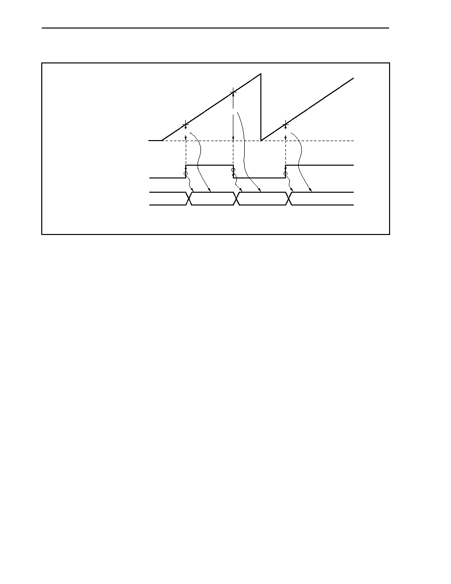
CHAPTER 9 TIMER/COUNTER FUNCTION
388
User's Manual U14492EJ5V0UD
Figure 9-93. TM3 Capture Operation Example (When Both Edges Are Specified)
TM3
Count start
TM3CE
1
Overflow
TM3OVF
1
D0
D1
D2
D0
D1
D2
Interrupt request (INTP31)
(TM3 count values)
Capture register (CC31)
Remark D0 to D2: TM3 count values
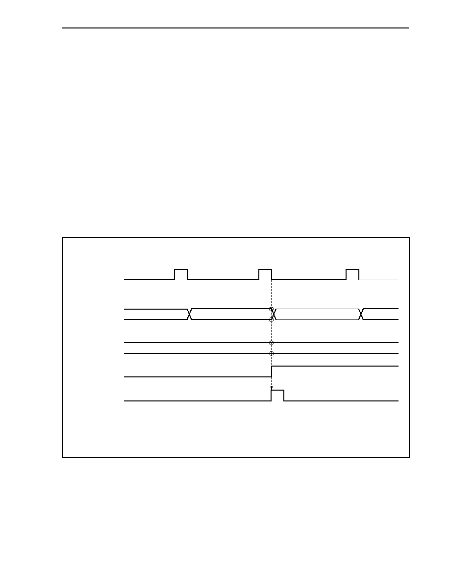
CHAPTER 9 TIMER/COUNTER FUNCTION
389
User's Manual U14492EJ5V0UD
(4) Compare operation
The TM3 register has two capture/compare registers. These are the CC30 register and the CC31 register. A
capture operation or a compare operation is performed according to the settings of both the CMS1 and CMS0
bits of the TMC31 register. If 1 is set in the CMS1 and CMS0 bits of the TMC31 register, the register
operates as a compare register.
A compare operation that compares the value that was set in the compare register and the TM3 count value
is performed.
If the TM3 count value matches the value of the compare register, which had been set in advance, a match
signal is sent to the output controller. The match signal causes the timer output pin (TO3) to change and an
interrupt request signal (INTCC30, INTCC31) to be generated at the same time.
If the CC30 or CC31 register is set to 0000H, the 0000H after the TM3 register counts up from FFFFH to
0000H is judged as a match. In this case, the value of the TM3 register is cleared to 0 at the next count
timing, but 0000H is not judged as a match at that time. 0000H when the TM3 register begins counting is not
judged as a match either.
If match clearing is enabled (CCLR bit = 1) for the CC30 register, the TM3 register is cleared when a match
with the TM3 register occurs during a compare operation.
Figure 9-94. Compare Operation Example (1/2)
(a) If CCLR bit = 1 and CC30 is value other than 0000H
0001H
TM3
Count up
0000H
n
n
n
-1
Compare register
(CC30)
Match detection
(INTCC30)
TO3
(output)
Remarks 1. The match is detected immediately after the count up, and the match detection signal is
generated.
2. n
0000H
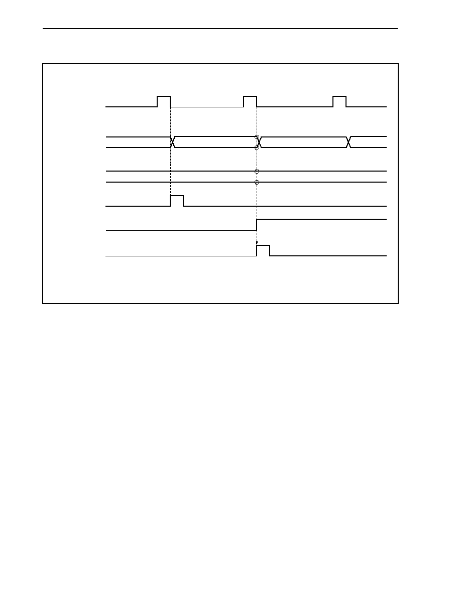
CHAPTER 9 TIMER/COUNTER FUNCTION
390
User's Manual U14492EJ5V0UD
Figure 9-94. Compare Operation Example (2/2)
(b) If CCLR bit = 1 and CC30 is 0000H
0001H
TM3
Count up
0000H
0000H
0000H
FFFFH
Compare register
(CC30)
INTTM3
Match detection
(INTCC30)
TO3
(output)
Remark The match is detected immediately after the count up, and the match detection signal is
generated.
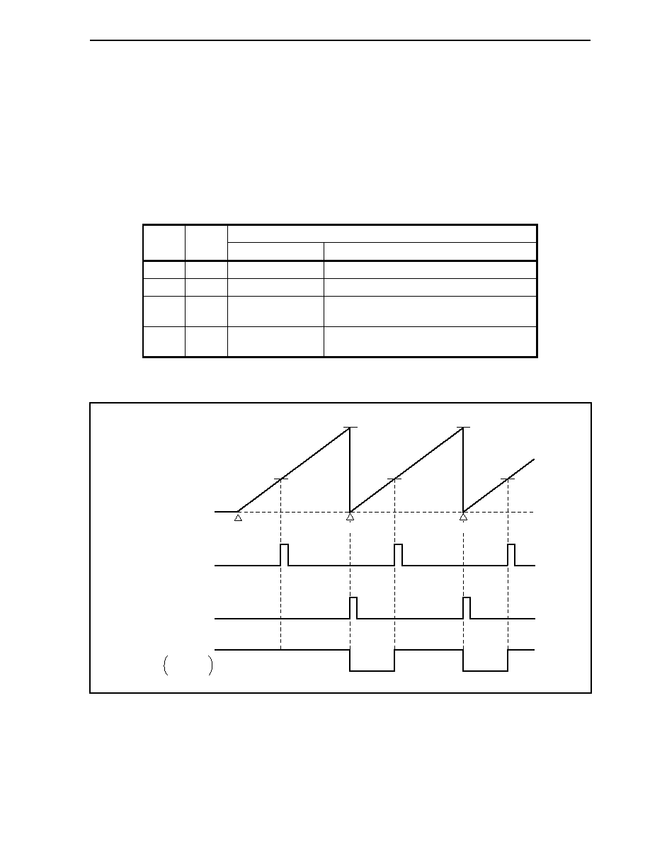
CHAPTER 9 TIMER/COUNTER FUNCTION
391
User's Manual U14492EJ5V0UD
(5) External pulse output
Timer 3 has one timer output pin (TO3).
An external pulse output (TO3) is generated when a match of the two compare registers (CC30 and CC31)
and the TM3 register is detected.
If a match is detected when the TM3 count value and the CC30 value are compared, the output level of the
TO3 pin is set. Also, if a match is detected when the TM3 count value and the CC31 value are compared,
the output level of the TO3 pin is reset.
The output level of the TO3 pin can be specified by the TMC31 register.
Table 9-13. TO3 Output Control
TO3 Output
ENT1 ALV
External Pulse Output
Output Level
0 0
Disable
High
level
0 1
Disable
Low
level
1
0
Enable
When the CC30 register is matched: Low level
When the CC31 register is matched: High level
1
1
Enable
When the CC30 register is matched: High level
When the CC31 register is matched: Low level
Figure 9-95. TM3 Compare Operation Example (Set/Reset Output Mode)
TM3 count value
0
Count start
TM3CE1
1
Clear & start
Clear & start
CC30
CC30
CC31
CC31
CC31
Interrupt request
(INTCC30)
Interrupt request
(INTCC31)
TO3 pin
ENT1
1
ALV
0
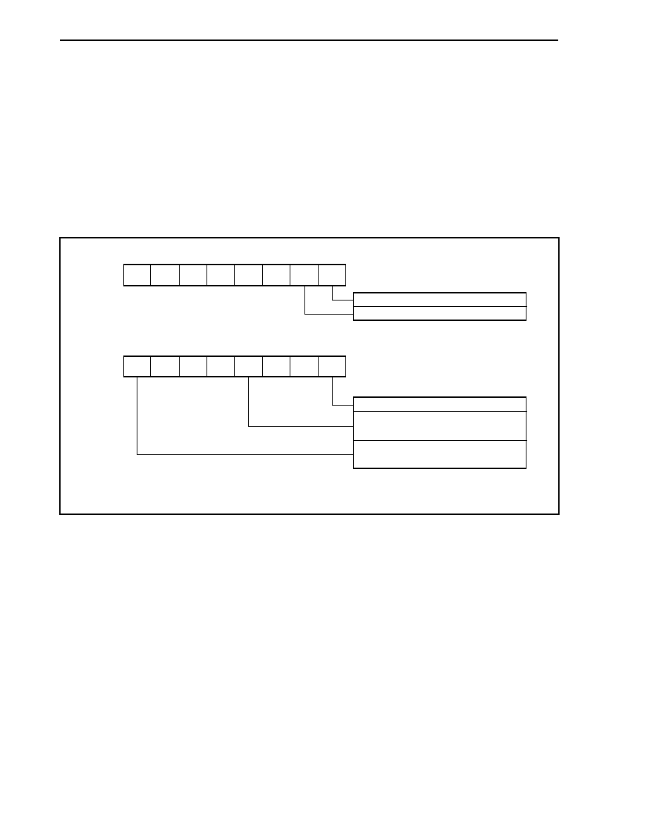
CHAPTER 9 TIMER/COUNTER FUNCTION
392
User's Manual U14492EJ5V0UD
9.4.6 Application examples
(1) Interval timer
By setting the TMC30 and TMC31 registers as shown in Figure 9-96, timer 3 operates as an interval timer
that repeatedly generates interrupt requests with the value that was set in advance in the CC30 register as
the interval.
When the counter value of the TM3 register matches the setting value of the CC30 register, the TM3 register
is cleared (0000H) and an interrupt request signal (INTCC30) is generated at the same time that the count
operation resumes.
Figure 9-96. Contents of Register Settings When Timer 3 Is Used as Interval Timer
Supply input clocks to internal units
Enable count operation
0
0/1
0/1
0/1
1
0/1
0/1
1
OST
ENT1
ALV
ETI
CCLR
CMS1 CMS0
0/1
0/1
0/1
0/1
0
0
1
1
TM3OVF
TMC30
TMC31
CS2
CS1
CS0
TM3CETM3CAE
Use CC30 register as compare register
Clear TM3 register due to match with
CC30 register
Continue counting after TM3 register
overflows
ECLR
Remark 0/1: Set to 0 or 1 as necessary
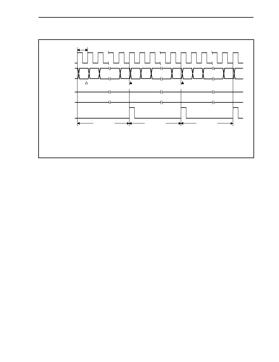
CHAPTER 9 TIMER/COUNTER FUNCTION
393
User's Manual U14492EJ5V0UD
Figure 9-97. Interval Timer Operation Timing Example
Count start
0001H
0000H 0001H
0000H 0001H
p
p
p
p
p
p
p
0000H
Interval time
Interval time
Interval time
Count clock
t
TM3 register
CC30 register
INTCC30
interrupt
Clear
Clear
Remark p: Setting value of CC30 register (0000H to FFFFH)
t: Count clock cycle
Interval time = (p + 1)
◊ t
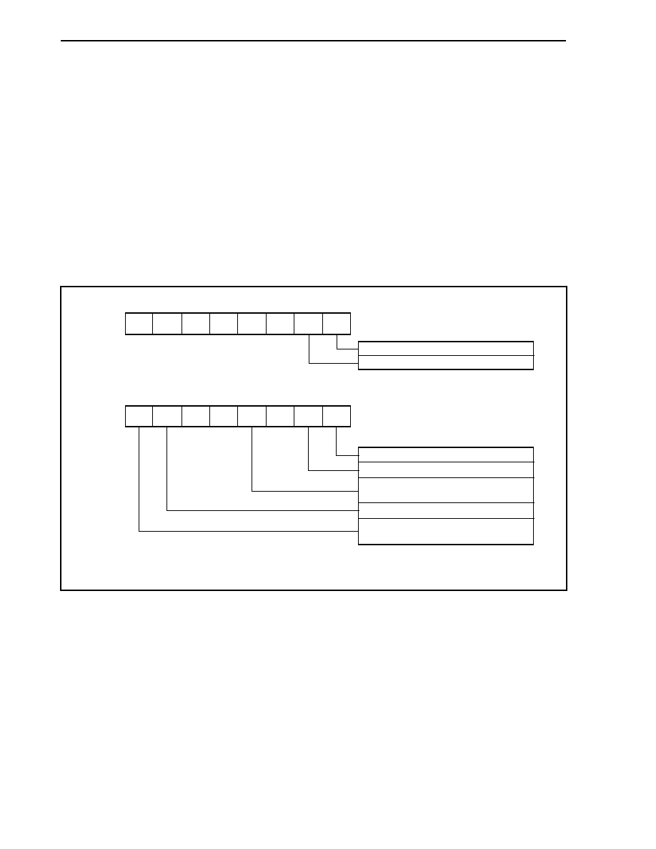
CHAPTER 9 TIMER/COUNTER FUNCTION
394
User's Manual U14492EJ5V0UD
(2) PWM output
By setting the TMC30 and TMC31 registers as shown in Figure 9-98, timer 3 can output a PWM of the
frequency determined by the setting of the CS2 to CS0 bits of the TMC30 register with the values that were
set in advance in the CC30 and CC31 registers as the intervals.
When the counter value of the TM3 register matches the setting value of the CC30 register, the TO3 output
becomes active. Then, when the count value of the TM3 register matches the setting value of the CC31
register, the TO3 output becomes inactive. The TM3 register continues counting, and when an overflow
occurs, clears the count value to 0000H and continues counting. This enables a PWM of the frequency
determined by the setting of the CS2 to CS0 bits of the TMC30 register to be output. When the setting value
of the CC30 register and the setting value of the CC31 register are the same, the TO3 output remains
inactive and does not change.
The active level of TO3 output can be set by the ALV bit of the TMC31 register.
Figure 9-98. Contents of Register Settings When Timer 3 Is Used for PWM Output
Supply input clocks to internal units
Enable count operation
0
1
0/1
0/1
0
0/1
1
1
OST
ENT1
ALV
ETI
CCLR
CMS1 CMS0
0/1
0/1
0/1
0/1
0
0
1
1
TM3OVF
TMC30
TMC31
CS2
CS1
CS0
TM3CETM3CAE
Use CC30 register as compare register
Use CC31 register as compare register
Disable clearing of TM3 register due to
match with CC30 register
Enable external pulse output (TO3)
Continue counting after TM3 register
overflows
ECLR
Remark 0/1: Set to 0 or 1 as necessary

CHAPTER 9 TIMER/COUNTER FUNCTION
395
User's Manual U14492EJ5V0UD
Figure 9-99. PWM Output Operation Timing Example
Count start
Clear
0001H
0000H
0001H
0000H
FFFFH
p
p
p
p
p
p
q
q
q
q
q
q
q
p
Count
clock
TM3
register
CC30
register
CC31
register
INTCC30
interrupt
INTCC31
interrupt
TO3
(output)
t
Remarks 1. p: Setting value of CC30 register (0000H to FFFFH)
q: Setting value of CC31 register (0000H to FFFFH)
p
q
t: Count clock cycle
PWM cycle = 65536
◊ t
q
- p
65536
2. In this example, the active level of TO3 output is set to high level.
Duty =

CHAPTER 9 TIMER/COUNTER FUNCTION
396
User's Manual U14492EJ5V0UD
(3) Cycle measurement
By setting the TMC30 and TMC31 registers as shown in Figure 9-100, timer 3 can measure the cycle of
signals input to the INTP30 pin or INTP31 pin.
The valid edge of the INTP30 pin is selected according to the IES301 and IES300 bits of the SESC register,
and the valid edge of the INTP31 pin is selected according to the IES311 and IES310 bits of the SESC
register. Either the rising edge, the falling edge, or both edges can be selected as the valid edges of both
pins.
If the CC30 register is set to a capture register and TM3 is started, the valid edge input of the INTP30 pin is
set as the trigger for capturing the TM3 register value in the CC30 register. When this value is captured, an
INTCC30 interrupt is generated.
Similarly, if the CC31 register is set to a capture register and TM3 is started, the valid edge input of the
INTP31 pin is set as the trigger for capturing the TM3 register value in the CC31 register. When this value is
captured, an INTCC31 interrupt is generated.
The cycle of signals input to the INTP30 pin is calculated by obtaining the difference between the TM3
register's count value (Dx) that was captured in the CC30 register according to the x-th valid edge input of the
INTP30 pin and the TM3 register's count value (D(x+1)) that was captured in the CC30 register according to
the (x+1)-th valid edge input of the INTP30 pin and multiplying the value of this difference by the cycle of the
clock control signal.
The cycle of signals input to the INTP31 pin is calculated by obtaining the difference between the TM3
register's count value (Dx) that was captured in the CC31 register according to the x-th valid edge input of the
INTP31 pin and the TM3 register's count value (D(x+1)) that was captured in the CC31 register according to
the (x+1)-th valid edge input of the INTP31 pin and multiplying the value of this difference by the cycle of the
clock control signal.
Figure 9-100. Contents of Register Settings When Timer 3 Is Used for Cycle Measurement
Supply input clocks to internal units
Enable count operation
0
0/1
0/1
0/1
0/1
0/1
0
0
OST
ENT1
ALV
ETI
CCLR
CMS1 CMS0
0/1
0/1
0/1
0/1
0
0
1
1
TM3OVF
TMC30
TMC31
CS2
CS1
CS0
TM3CETM3CAE
Use CC30 register as capture register
(when measuring the cycle of INTP30 input)
Use CC31 register as capture register
(when measuring the cycle of INTP31 input)
Continue counting after TM3 register
overflows
ECLR
Remark 0/1: Set to 0 or 1 as necessary
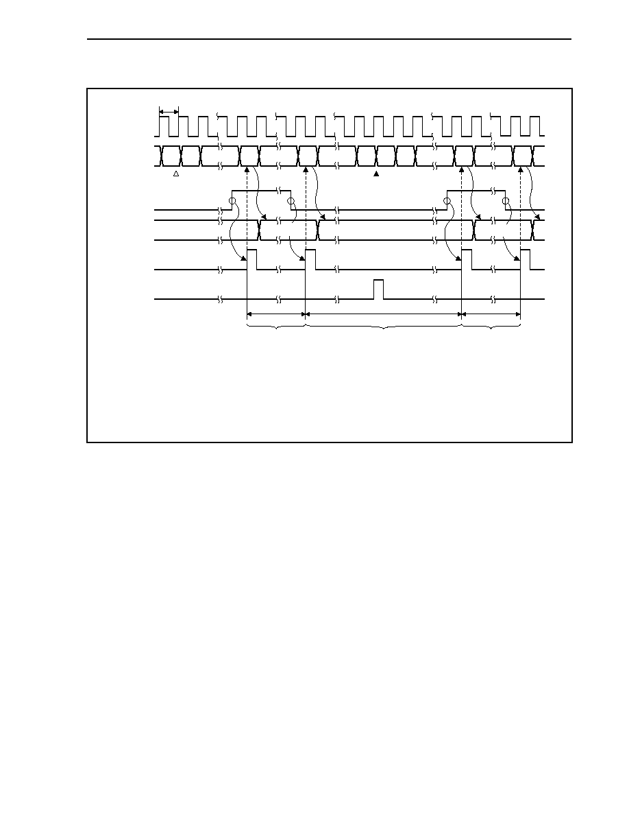
CHAPTER 9 TIMER/COUNTER FUNCTION
397
User's Manual U14492EJ5V0UD
Figure 9-101. Cycle Measurement Operation Timing Example
t
0001H
0000H
0001H
0000H
FFFFH
D0
D1
D2
D3
D3
D2
D1
D0
(D1 ≠ D0)
◊ t
(D3 ≠ D2)
◊ t
{(10000H ≠ D1) + D2}
◊ t
Note
Count
clock
TM3
register
INTP30
(input)
CC30
register
INTCC30
interrupt
INTTM3
interrupt
No overflow
Overflow occurs
No overflow
Clear
Count start
Note When an overflow occurs once
Remarks 1. D0 to D3: TM3 register count values
t: Count clock cycle
2. In this example, the valid edge of INTP30 input has been set to both edges (rising and falling).

CHAPTER 9 TIMER/COUNTER FUNCTION
398
User's Manual U14492EJ5V0UD
9.4.7 Precautions
Various precautions concerning timer 3 are shown below.
(1) If a conflict occurs between the reading of the CC30 register and a capture operation when the CC30 register
is used in capture mode, an external trigger (INTP30) valid edge is detected and an external interrupt request
signal (INTCC30) is generated however, the timer value is not stored in the CC30 register.
(2) If a conflict occurs between the reading of the CC31 register and a capture operation when the CC31 register
is used in capture mode, an external trigger (INTP31) valid edge is detected and an external interrupt request
signal (INTCC31) is generated however, the timer value is not stored in the CC31 register.
(3) The following bits and registers must not be rewritten during operation (TMC30 register TM3CE = 1).
∑ CS2 to CS0 bits of TMC30 register
∑ TMC31 register
∑ SESC register
(4) The TM3CAE bit of the TMC30 register is a TM3 reset signal. To use TM3, first set (1) the TM3CAE bit.
(5) The analog noise elimination time + two count clocks are required to detect a valid edge of the external
interrupt input (INTP30 or INTP31) and external clock input (TI3). Therefore, edge detection will not be
performed normally for changes that are less than the analog noise elimination time + two count clocks. For
the analog noise elimination, refer to 14.5 Noise Eliminator.
(6) The operation of an external interrupt output (INTCC30 or INTCC31) is automatically determined according to
the operating state of the capture/compare registers 30, 31 (CC30, CC31). When the capture/compare
register is used for a capture mode, the external trigger (INTP30, INTP31) is used for valid edge detection.
When the capture/compare register is used for a compare mode, the external interrupt output is used for a
match interrupt indicating a match with the TM3 register.
(7) If the ENT1 and ALV bits of the TMC31 register are changed at the same time, a glitch (spike shaped noise)
may be generated in the TO3 pin output. Either create a circuit configuration that will not malfunction even if
a glitch is generated or make sure that the ENT1 and ALV bits do not change at the same time.

CHAPTER 9 TIMER/COUNTER FUNCTION
399
User's Manual U14492EJ5V0UD
9.5 Timer 4
9.5.1 Features (timer 4)
Timer 4 (TM4) functions as a 16-bit interval timer.
9.5.2 Function overview (timer 4)
∑
16-bit interval timer: 1 channel
∑
Compare register: 1
∑
Count clock selected from divisions of internal system clock (set the frequency of the count clock to 16 MHz or
less)
∑
Base clock (f
CLK
): 1 type (set f
CLK
to 32 MHz or less)
f
XX
/2
∑
Prescaler division ratio
The following division ratios can be selected according to the base clock (f
CLK
).
Division Ratio
Base Clock (f
CLK
)
1/2 f
XX
/4
1/4 f
XX
/8
1/8 f
XX
/16
1/16 f
XX
/32
1/32 f
XX
/64
1/64 f
XX
/128
1/128 f
XX
/256
1/256 f
XX
/512
∑
Interrupt request source: 1
∑ Compare match interrupt
INTCM4 generated with CM4 match signal
∑
Timer clear
TM4 register can be cleared by CM4 register match.
Remark f
XX
: Internal system clock

CHAPTER 9 TIMER/COUNTER FUNCTION
400
User's Manual U14492EJ5V0UD
9.5.3 Basic configuration
Table 9-14. Timer 4 Configuration List
Timer Count
Clock
Register
Read/Write
Generated
Interrupt
Signal
Capture
Trigger
Timer Output
S/R
Other
Functions
TM4 Read
-
-
-
-
Timer 4
f
XX
/4, f
XX
/8, f
XX
/16, f
XX
/32,
f
XX
/64, f
XX
/128, f
XX
/256,
f
XX
/512
CM4 Read/write
INTCM4
-
-
-
Remark f
XX
: Internal system clock
S/R: Set/Reset
Figure 9-102 shows the block diagram of timer 4.
Figure 9-102. Block Diagram of Timer 4
TM4 (16-bit)
CM4
INTCM4
1/2
1/4
1/8
1/16
1/32
1/64
1/128
1/256
f
XX
/2
Clear & start
f
CLK
Remark f
CLK
: Base clock (32 MHz (MAX.))
f
XX
: Internal system clock
CHAPTER 9 TIMER/COUNTER FUNCTION
401
User's Manual U14492EJ5V0UD
(1) Timer 4 (TM4)
TM4 is a 16-bit timer. It is mainly used as an interval timer for software.
Starting and stopping TM4 is controlled by the TM4CE0 bit of the timer control register 4 (TMC4).
A division by the prescaler can be selected for the count clock from among f
XX
/4, f
XX
/8, f
XX
/16, f
XX
/32, f
XX
/64,
f
XX
/128, f
XX
/256, and f
XX
/512 by the CS2 to CS0 bits of the TMC4 register (f
XX
: Internal system clock).
TM4 is read-only, in 16-bit units.
15
14
13
12
11
10
9
8
7
6
5
4
3
2
1
TM4
FFFFF540H
0000H
Address
Initial value
0
The conditions for which the TM4 register becomes 0000H are shown below.
∑
Reset input
∑
TM4CAE0 bit = 0
∑
TM4CE0 bit = 0
∑
Match of TM4 register and CM4 register
∑
Overflow
Cautions 1. If the TM4CAE0 bit of the TMC4 register is cleared (0), a reset is performed
asynchronously.
2. If the TM4CE0 bit of the TMC4 register is cleared (0), a reset is performed, synchronized
with the internal clock. Similarly, a synchronized reset is performed after a match with
the CM4 register and after an overflow.
3. The count clock must not be changed during a timer operation. If it is to be overwritten,
it should be overwritten after the TM4CE0 bit is cleared (0).
4. Up to 4 internal system clocks are required after a value is set in the TM4CE0 bit until
the set value is transferred to internal units. When a count operation begins, the count
cycle from 0000H to 0001H differs from subsequent count cycles.
5. After a compare match is generated, the timer is cleared at the next count clock.
Therefore, if the division ratio is large, the timer value may not be zero even if the timer
value is read immediately after a match interrupt is generated.
CHAPTER 9 TIMER/COUNTER FUNCTION
402
User's Manual U14492EJ5V0UD
(2) Compare register 4 (CM4)
CM4 and the TM4 register count value are compared, and an interrupt request signal (INTCM4) is generated
when a match occurs. TM4 is cleared, synchronized with this match. If the TM4CAE0 bit of the TMC4
register is set to 0, a reset is performed asynchronously, and the registers are initialized.
The CM4 register is configured with a master/slave configuration. When a write operation to a CM4 register
is performed, data is first written to the master register and then the master register data is transferred to the
slave register. In a compare operation, the slave register value is compared with the count value of the TM4
register. When a read operation to a CM4 register is performed, data in the master side is read out.
CM4 can be read/written in 16-bit units.
Cautions 1. A write operation to a CM4 register requires 4 internal system clocks until the value that
was set in the CM4 register is transferred to internal units. When writing continuously
to the CM4 register, be sure to reserve a time interval of at least 4 internal system
clocks.
2. The CM4 register can be overwritten only once in a single TM4 register cycle (from
0000H until an INTCM4 interrupt is generated due to a match of the TM4 register and
CM4 register). If this cannot be secured by the application, make sure that the CM4
register is not overwritten during timer operation.
3. Note that an INTCM4 interrupt will be generated after an overflow if a value less than the
counter value is written in the CM4 register during TM4 register operation (Figure 9-103).
15
14
13
12
11
10
9
8
7
6
5
4
3
2
1
CM4
FFFFF542H
0000H
Address
Initial value
0
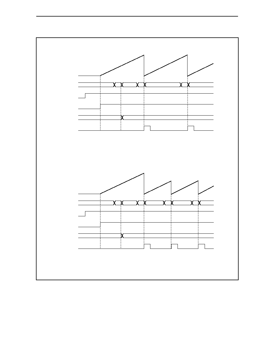
CHAPTER 9 TIMER/COUNTER FUNCTION
403
User's Manual U14492EJ5V0UD
Figure 9-103. Example of Timing During TM4 Operation
(a)
When TM4
< CM4
TM4
TM4CAE0
TM4CE0
CM4
INTCM4
M
N
N
N
Remark M = TM4 value when overwritten
N = CM4 value when overwritten
M < N
(b) When TM4
> CM4
TM4
TM4CAE0
TM4CE0
CM4
INTCM4
M
FFFFH
N
N
N
Remark M = TM4 value when overwritten
N = CM4 value when overwritten
M > N
CHAPTER 9 TIMER/COUNTER FUNCTION
404
User's Manual U14492EJ5V0UD
9.5.4 Control register
(1) Timer control register 4 (TMC4)
The TMC4 register controls the operation of timer 4.
This register can be read/written in 8-bit or 1-bit units.
Caution The TM4CAE0 bit and other bits cannot be set at the same time. Be sure to set the
TM4CAE0 bit and then set the other bits and the other registers of TM4.
7 6 5 4 3 2
<1>
<0>
Address
Initial
value
TMC4 0 CS2
CS1
CS0 0 0
TM4CE0 TM4CAE0 FFFFF544H
00H
Bit position
Bit name
Function
Selects the TM4 count clock.
CS2 CS1 CS0
Count
clock
0 0 0
f
XX
/4
0 0 1
f
XX
/8
0 1 0
f
XX
/16
0 1 1
f
XX
/32
1 0 0
f
XX
/64
1 0 1
f
XX
/128
1 1 0
f
XX
/256
1 1 1
f
XX
/512
6 to 4
CS2 to CS0
Caution Do not change the CS2 to CS0 bits during timer operation. If they
are to be changed, they must be changed after setting the TM4CE0
bit to 0. If the CS2 to CS0 bits are overwritten during timer
operation, the operation is not guaranteed.
1 TM4CE0
Controls the operation of TM4.
0: Disable count (timer stopped at 0000H and does not operate)
1: Perform count operation
Caution TM4CE0 bit is not cleared even if a match is detected by the
compare operation. To stop the count operation, clear the TM4CE0
bit.
0 TM4CAE0
Controls the internal count clock.
0: Asynchronously reset entire TM4 unit. Stop base clock (f
CLK
) supply to TM4
unit.
1: Supply base clock (f
CLK
) to TM4 unit.
Cautions 1. When TM4CAE0 = 0 is set, the TM4 unit can be reset
asynchronously.
2. When TM4CAE0 = 0, the TM4 unit is in a reset state. To operate
TM4, first set TM4CAE0 = 1.
3. When the TM4CAE0 bit is changed from 1 to 0, all the registers
of the TM4 unit are initialized. When again setting TM4CAE0 = 1,
be sure to then again set all the registers of the TM4 unit.
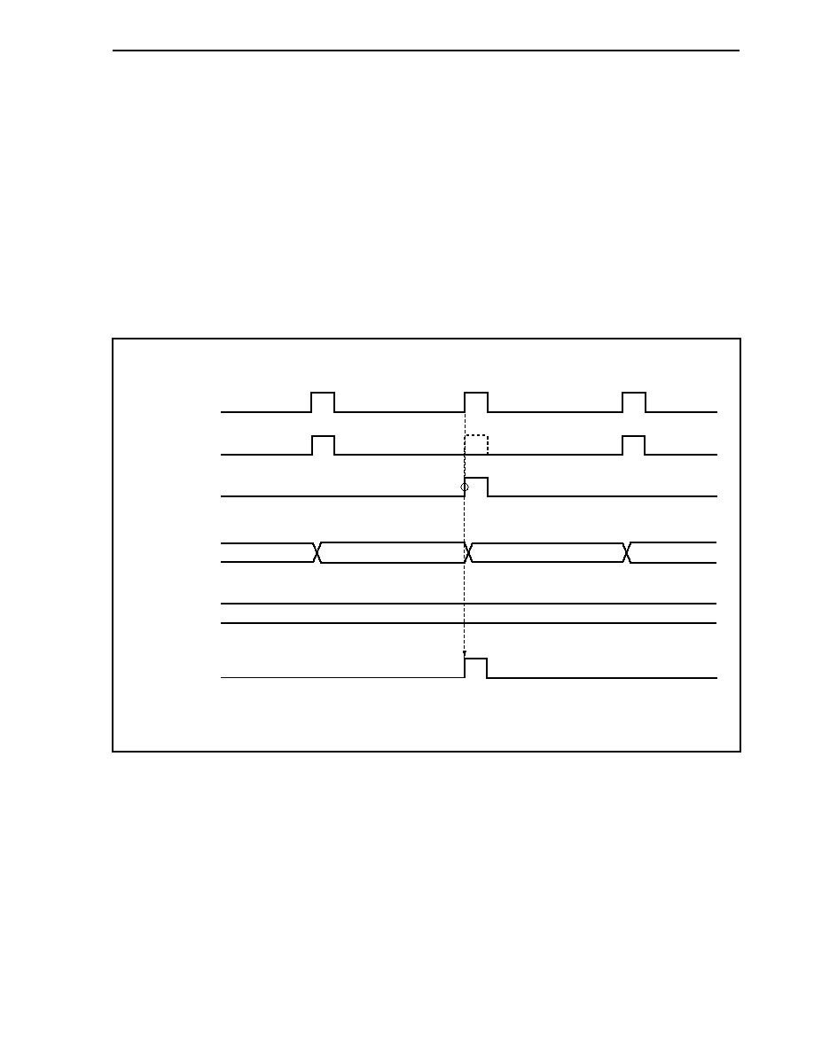
CHAPTER 9 TIMER/COUNTER FUNCTION
405
User's Manual U14492EJ5V0UD
9.5.5 Operation
(1) Compare operation
TM4 can be used for a compare operation in which the value that was set in a compare register (CM4) is
compared with the TM4 count value.
If a match is detected by the compare operation, an interrupt (INTCM4) is generated. The generation of the
interrupt causes TM4 to be cleared (0) at the next count timing. This function enables timer 4 to be used as
an interval timer.
CM4 can also be set to 0. In this case, when an overflow occurs and TM4 becomes 0, a match is detected
and INTCM4 is generated. Although the TM4 value is cleared (0) at the next count timing, INTCM4 is not
generated according to this match.
Figure 9-104. TM4 Compare Operation Example (1/2)
(a) When CM4 is set to n (non-zero)
1
TM4
Count clock
0
n
CM4
n
TM4 clear
Match detection
(INTCM4)
Count up
Clear
Remark Interval time = (n + 1)
◊ Count clock cycle
n = 1 to 65536 (FFFFH)

CHAPTER 9 TIMER/COUNTER FUNCTION
406
User's Manual U14492EJ5V0UD
Figure 9-104. TM4 Compare Operation Example (2/2)
(b) When CM4 is set to 0
1
0
0
0
FFFFH
Overflow
TM4
Count clock
CM4
TM4 clear
Match detection
(INTCM4)
Count up
Clear
Remark Interval time = (FFFFH + 2)
◊ Count clock cycle

CHAPTER 9 TIMER/COUNTER FUNCTION
407
User's Manual U14492EJ5V0UD
9.5.6 Application example
(1) Interval timer
This section explains an example in which timer 4 is used as an interval timer with 16-bit precision.
Interrupt requests (INTCM4) are output at equal intervals (refer to Figure 9-104 TM4 Compare Operation
Example). The setup procedure is shown below.
<1> Set (1) the TM4CAE0 bit.
<2> Set each register.
∑ Select the count clock using the CS2 to CS0 bits of the TMC4 register.
∑ Set the compare value in the CM4 register.
<3> Start counting by setting (1) the TM4CE0 bit.
<4> If the TM4 register and CM4 register values match, an INTCM4 interrupt is generated.
<5> INTCM4 interrupts are generated thereafter at equal intervals.
9.5.7 Precautions
Various precautions concerning timer 4 are shown below.
(1) To operate TM4, first set (1) the TM4CAE0 bit of the TMC4 register.
(2) Up to 4 internal system clocks are required after a value is set in the TM4CE0 bit of the TMC4 register until
the set value is transferred to internal units. When a count operation begins, the count cycle from 0000H to
0001H differs from subsequent count cycles.
(3) To initialize the TM4 register status and start counting again, clear (0) the TM4CE0 bit and then set (1) the
TM4CE0 bit after an interval of 4 internal system clocks has elapsed.
(4) Up to 4 internal system clocks are required until the value that was set in the CM4 register is transferred to
internal units. When writing continuously to the CM4 register, be sure to secure a time interval of at least 4
internal system clocks.
(5) The CM4 register can be overwritten only once during a timer/counter operation (from 0000H until an
INTCM4 interrupt is generated due to a match of the TM4 register and CM4 register). If this cannot be
secured by the application, make sure that the CM4 register is not overwritten during a timer/counter
operation.
(6) The count clock must not be changed during a timer operation. If it is to be overwritten, it should be
overwritten after the TM4CE0 bit is cleared (0). If the count clock is overwritten during a timer operation,
operation cannot be guaranteed.
(7) An INTCM4 interrupt will be generated after an overflow if a value less than the counter value is written in the
CM4 register during TM4 register operation.
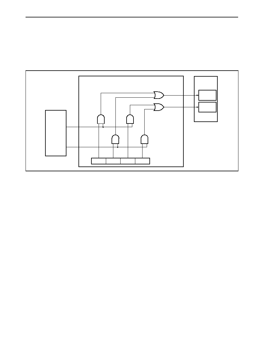
CHAPTER 9 TIMER/COUNTER FUNCTION
408
User's Manual U14492EJ5V0UD
9.6 Timer Connection Function
9.6.1 Overview
The V850E/IA1 provides a function to connect timer 1 and timer 2.
Figure 9-105. Block Diagram of Timer Connection Function
Timer 2
Timer 1
CVSE10/
CVPE10
CVSE20/
CVPE20
Capture 0
Capture 1
TMIC0
TMIC1
TMIC2
TMIC3
TMIC0 register
INTCM1
INTCM0
INTCM101
INTCM100
Timer connection selector

CHAPTER 9 TIMER/COUNTER FUNCTION
409
User's Manual U14492EJ5V0UD
9.6.2 Control register
(1) Timer connection selection register 0 (TMIC0)
The TMIC0 register enables/disables input of the INTCM100, INTCM101 signals to the CVSEn0/CVPEn0
registers (n = 1, 2).
This register can be read/written in 8-bit or 1-bit units.
7
0
TMIC0
6
0
5
0
4
0
3
TMIC3
2
TMIC2
1
TMIC1
0
TMIC0
Address
FFFFF620H
Initial value
00H
Bit position
Bit name
Function
3
TMIC3
Enables/disables input of INTCM101 signal to CVSE20/CVPE20 registers.
0: Don't input INTCM101 signal to CVSE20/CVPE20 registers.
1: Input INTCM101 signal to CVSE20/CVPE20 registers.
2
TMIC2
Enables/disables input of INTCM100 signal to CVSE20/CVPE20 registers.
0: Don't input INTCM100 signal to CVSE20/CVPE20 registers.
1: Input INTCM100 signal to CVSE20/CVPE20 registers.
1
TMIC1
Enables/disables input of INTCM101 signal to CVSE10/CVPE10 registers.
0: Don't input INTCM101 signal to CVSE10/CVPE10 registers.
1: Input INTCM101 signal to CVSE10/CVPE10 registers.
0
TMIC0
Enables/disables input of INTCM100 signal to CVSE10/CVPE10 registers.
0: Don't input INTCM100 signal to CVSE10/CVPE10 registers.
1: Input INTCM100 signal to CVSE10/CVPE10 registers.

User's Manual U14492EJ5V0UD
410
CHAPTER 10 SERIAL INTERFACE FUNCTION
10.1 Features
The serial interface function provides three types of serial interfaces combining a total of six transmit/receive
channels. All six channels can be used simultaneously.
The three interface formats are as follows.
(1) Asynchronous serial interfaces (UART0 to UART2): 3 channels
(2) Clocked serial interfaces (CSI0, CSI1): 2 channels
(3) FCAN controller: 1 channel
Remark For details about the FCAN controller, refer to CHAPTER 11 FCAN CONTROLLER.
UART0 to UART2, whereby one byte of serial data is transmitted/received following a start bit, support full-duplex
communication. In the UART1 and UART2 interfaces, one higher bit is added to 8 bits of transmit/receive data,
enabling communication using 9-bit data.
CSI0 and CSI1 perform data transfer according to three types of signals, namely serial clocks (SCK0, SCK1), serial
inputs (SI0, SI1), and serial outputs (SO0, SO1) (3-wire serial I/O).
FCAN conforms to CAN specification Ver. 2.0 PartB active, and provides a 32-message buffer.

CHAPTER 10 SERIAL INTERFACE FUNCTION
User's Manual U14492EJ5V0UD
411
10.2 Asynchronous Serial Interface 0 (UART0)
10.2.1 Features
∑ Transfer rate: 300 bps to 1562.5 Kbps (using a dedicated baud rate generator and an internal system clock of
50 MHz)
∑ Full-duplex communications
On-chip receive buffer register 0 (RXB0)
On-chip transmit buffer register 0 (TXB0)
∑ Two-pin configuration
Note
TXD0: Transmit data output pin
RXD0: Receive data input pin
∑ Reception error detection functions
∑ Parity error
∑ Framing error
∑ Overrun error
∑ Interrupt sources: 3 types
∑ Reception error interrupt (INTSER0):
Interrupt is generated according to the logical OR of the
three types of reception errors
∑ Reception completion interrupt (INTSR0):
Interrupt is generated when receive data is transferred from
the receive shift register to receive buffer register 0 after
serial transfer is completed during a reception enabled state
∑ Transmission completion interrupt (INTST0): Interrupt is generated when the serial transmission of
transmit data (8 or 7 bits) from the transmit shift register is
completed
∑ The character length of transmit/receive data is specified according to the ASIM0 register
∑ Character length: 7 or 8 bits
∑ Parity functions: Odd, even, 0, or none
∑ Transmission stop bits: 1 or 2 bits
∑ On-chip dedicated baud rate generator
Note The SCK and CTS pins are not available for UART0.

CHAPTER 10 SERIAL INTERFACE FUNCTION
User's Manual U14492EJ5V0UD
412
10.2.2 Configuration
UART0 is controlled by asynchronous serial interface mode register 0 (ASIM0), asynchronous serial interface
status register 0 (ASIS0), and asynchronous serial interface transmit status register 0 (ASIF0). Receive data is
maintained in receive buffer register 0 (RXB0), and transmit data is written to transmit buffer register 0 (TXB0).
Figure 10-1 shows the configuration of asynchronous serial interface 0 (UART0).
(1) Asynchronous serial interface mode register 0 (ASIM0)
The ASIM0 register is an 8-bit register for specifying the operation of the asynchronous serial interface.
(2) Asynchronous serial interface status register 0 (ASIS0)
The ASIS0 register consists of a set of flags that indicate the error contents when a reception error occurs.
The various reception error flags are set (1) when a reception error occurs and are reset (0) when the ASIS0
register is read.
(3) Asynchronous serial interface transmit status register 0 (ASIF0)
The ASIF0 register is an 8-bit register that indicates the status when a transmit operation is performed.
This register consists of a transmit buffer data flag, which indicates the hold status of TXB0 data, and the
transmit shift register data flag, which indicates whether transmission is in progress.
(4) Reception control parity check
The receive operation is controlled according to the contents set in the ASIM0 register. A check for parity
errors is also performed during a receive operation, and if an error is detected, a value corresponding to the
error contents is set in the ASIS0 register.
(5) Receive shift register
This is a shift register that converts the serial data that was input to the RXD0 pin to parallel data. One byte
of data is received, and if a stop bit is detected, the receive data is transferred to receive buffer register 0
(RXB0).
This register cannot be directly manipulated.
(6) Receive buffer register 0 (RXB0)
This is an 8-bit buffer register for holding receive data. When 7 characters are received, 0 is stored in the
MSB.
During a reception enabled state, receive data is transferred from the receive shift register to the RXB0
register, synchronized with the end of the shift-in processing of one frame.
Also, the reception completion interrupt request (INTSR0) is generated by the transfer of data to the RXB0
register.
(7) Transmit shift register
This is a shift register that converts the parallel data that was transferred from transmit buffer register 0
(TXB0) to serial data.
When one byte of data is transferred from the TXB0 register, the shift register data is output from the TXD0
pin.
The transmission completion interrupt request (INTST0) is generated synchronized with the completion of
transmission of one frame.
This register cannot be directly manipulated.
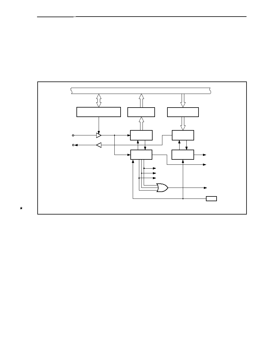
CHAPTER 10 SERIAL INTERFACE FUNCTION
User's Manual U14492EJ5V0UD
413
(8) Transmit buffer register 0 (TXB0)
This is an 8-bit buffer for transmit data. A transmit operation is started by writing transmit data to TXB0.
(9) Addition of transmission control parity
A transmit operation is controlled by adding a start bit, parity bit, or stop bit to the data that is written to the
TXB0 register, according to the contents that were set in the ASIM0 register.
Figure 10-1. Asynchronous Serial Interface 0 Block Diagram
Parity
Framing
Overrun
Internal bus
Asynchronous serial interface
mode register 0 (ASIM0)
Receive buffer
register 0 (RXB0)
Receive
shift register
Reception control
parity check
Transmit buffer
register 0 (TXB0)
Transmit
shift register
Addition of transmission
control parity
BRG0
INTSER0
INTSR0
INTST0
RXD0
TXD0
Remark For the configuration of baud rate generator 0, see Figure 10-12.

CHAPTER 10 SERIAL INTERFACE FUNCTION
User's Manual U14492EJ5V0UD
414
10.2.3 Control registers
(1) Asynchronous serial interface mode register 0 (ASIM0)
The ASIM0 register is an 8-bit register that controls the UART0 transfer operation.
This register can be read/written in 8-bit or 1-bit units.
Cautions 1. When using UART0, be sure to set the external pins related to the UART0 function to the
control mode before setting clock selection register 0 (CKSR0) and baud rate generator
control register 0 (BRGC0), and then set the UARTCAE0 bit to 1. Then set the other bits.
2. Set the UARTCAE0 and RXE0 bits to 1 while a high level is input to the RXD0 pin. If
these bits are set to 1 while a low high level is input to the RXD0 pin, reception will be
started.
(1/3)
<7>
UARTCAE0
ASIM0
<6>
TXE0
<5>
RXE0
4
PS1
3
PS0
2
CL
1
SL
0
ISRM
Address
FFFFFA00H
Initial value
01H
Bit position
Bit name
Function
7 UARTCAE0
Controls the operating clock.
0: Stops clock supply to UART0.
1: Supplies clock to UART0.
Cautions 1. When UARTCAE0 = 0 is set, UART0 is asynchronously reset
Note
.
2. When UARTCAE0 = 0, UART0 is in a reset state. To operate
UART0, first set UARTCAE0 = 1.
3. When the UARTCAE0 bit is cleared from 1 to 0, all the registers
of UART0 are initialized. When setting UARTCAE0 = 1 again, be
sure to re-set the registers of UART0.
The output of the TXD0 pin goes high when transmission is disabled, regardless of
the setting of the UARTCAE0 bit.
6 TXE0 Enables/disables transmission.
0: Disable transmission
1: Enable transmission
Cautions 1. Set the TXE0 bit to 1 after setting the UARTCAE0 bit to 1 at
startup. Set the UARTCAE0 bit to 0 after setting the TXE0 bit to
0 to stop.
2. To initialize the transmission unit, clear (0) the TXE0 bit, and
after letting 2 cycles of the base clock elapse, set (1) the TXE0
bit again. If the TXE0 bit is not set again, initialization may not
be successful (for details about the base clock, refer to 10.2.6
(1) (a) Base clock).
Note Only the ASIS0, ASIF0, and RXB0 registers are reset.

CHAPTER 10 SERIAL INTERFACE FUNCTION
User's Manual U14492EJ5V0UD
415
(2/3)
Bit position
Bit name
Function
5 RXE0 Enables/disables reception.
0: Disable reception
Note
1: Enable reception
Cautions 1. Set the RXE0 bit to 1 after setting the UARTCAE0 bit to 1 at
startup. Set the UARTCAE0 bit to 0 after setting the RXE0 bit to
0 to stop.
2. To initialize the reception unit status, clear (0) the RXE0 bit, and
after letting 2 cycles of the base clock elapse, set (1) the RXE0
bit again. If the RXE0 bit is not set again, initialization may not
be successful (for details about the base clock, refer to 10.2.6
(1) (a) Base clock).
Controls parity bit.
PS1
PS0
Transmit operation
Receive operation
0
0
Don't output parity bit
Receive with no parity
0
1
Output 0 parity
Receive as 0 parity
1
0
Output odd parity
Judge as odd parity
1
1
Output even parity
Judge as even parity
Cautions 1. To overwrite the PS1 and PS0 bits, first clear (0) the TXE0 and
RXE0 bits.
2. If "0 parity" is selected for reception, no parity judgment is
performed. Therefore, no error interrupt is generated because
the PE bit of the ASIS0 register is not set.
4, 3
PS1, PS0
∑ Even
parity
If the transmit data contains an odd number of bits with the value "1", the parity
bit is set (1). If it contains an even number of bits with the value "1", the parity
bit is cleared (0). This controls the number of bits with the value "1" contained
in the transmit data and the parity bit so that it is an even number.
During reception, the number of bits with the value "1" contained in the receive
data and the parity bit is counted, and if the number is odd, a parity error is
generated.
∑ Odd
parity
In contrast to even parity, odd parity controls the number of bits with the value
"1" contained in the transmit data and the parity bit so that it is an odd number.
During reception, the number of bits with the value "1" contained in the receive
data and the parity bit is counted, and if the number is even, a parity error is
generated.
Note When reception is disabled, the receive shift register does not detect a start bit. No shift-in processing
or transfer processing to receive buffer register 0 (RXB0) is performed, and the contents of the RXB0
register are retained.
When reception is enabled, the reception shift operation starts, synchronized with the detection of the
start bit, and when the reception of one frame is completed, the contents of the receive shift register
are transferred to the RXB0 register. A reception completion interrupt (INTSR0) is also generated in
synchronization with the transfer to the RXB0 register.

CHAPTER 10 SERIAL INTERFACE FUNCTION
User's Manual U14492EJ5V0UD
416
(3/3)
Bit position
Bit name
Function
4, 3
PS1, PS0
∑ 0
parity
During transmission, the parity bit is cleared (0) regardless of the transmit data.
During reception, no parity error is generated because no parity bit is checked.
∑ No
parity
No parity bit is added to transmit data.
During reception, the receive data is considered to have no parity bit. No parity
error is generated because there is no parity bit.
2 CL
Specifies character length of 1 frame of transmit/receive data.
0: 7 bits
1: 8 bits
Caution To overwrite the CL bit, first clear (0) the TXE0 and RXE0 bits.
1 SL
Specifies stop bit length of transmit data.
0: 1 bit
1: 2 bits
Cautions 1. To overwrite the SL bit, first clear (0) the TXE0 bit.
2. Since reception is always done with a stop bit length of 1, the
SL bit setting does not affect receive operations.
0 ISRM Enables/disables generation of reception completion interrupt requests when an
error occurs.
0: Generate a reception error interrupt request (INTSER0) as an interrupt when
an error occurs.
In this case, no reception completion interrupt request (INTSR0) is
generated.
1: Generate a reception completion interrupt request (INTSR0) as an interrupt
when an error occurs.
In this case, no reception error interrupt request (INTSER0) is generated.
Caution To overwrite the ISRM bit, first clear (0) the RXE0 bit.

CHAPTER 10 SERIAL INTERFACE FUNCTION
User's Manual U14492EJ5V0UD
417
(2) Asynchronous serial interface status register 0 (ASIS0)
The ASIS0 register, which consists of 3-bit error flags (PE, FE, and OVE), indicates the error status when
UART0 reception is completed.
The ASIS0 register is cleared to 00H by a read operation. When a reception error occurs, receive buffer
register 0 (RXB0) should be read and the error flag should be cleared after the ASIS0 register is read.
This register is read-only, in 8-bit units.
Cautions 1. When the UARTCAE0 bit or RXE0 bit of the ASIM0 register is set to 0, or when the ASIS0
register is read, the PE, FE, and OVE bits of the ASIS0 register are cleared (0).
2. Manipulation using a bit manipulation instruction is prohibited.
7 6 5 4 3 2 1 0
Address
Initial
value
ASIS0
0 0 0 0 0 PE
FE
OVE
FFFFFA03H
00H
Bit position
Bit name
Function
2 PE
This is a status flag that indicates a parity error.
0: When the ASIM0 register's UARTCAE0 and RXE0 bits are both set to 0, or
after the ASIS0 register is read
1: When reception was completed, the receive data parity did not match
the parity bit
Caution The operation of the PE bit differs according to the settings of the
PS1 and PS0 bits of the ASIM0 register.
1 FE
This is a status flag that indicates a framing error.
0: When the ASIM0 register's UARTCAE0 and RXE0 bits are both set to 0, or
after the ASIS0 register is read
1: When reception was completed, no stop bit was detected
Caution For receive data stop bits, only the first bit is checked regardless
of the stop bit length.
0 OVE
This is a status flag that indicates an overrun error.
0: When the ASIM0 register's UARTCAE0 and RXE0 bits are both set to 0, or
after the ASIS0 register is read.
1: UART0 completed the next receive operation before reading the RXB0
register receive data.
Caution When an overrun error occurs, the next receive data value is not
written to the RXB0 register and the data is discarded.

CHAPTER 10 SERIAL INTERFACE FUNCTION
User's Manual U14492EJ5V0UD
418
(3) Asynchronous serial interface transmit status register 0 (ASIF0)
The ASIF0 register, which consists of 2-bit status flags, indicates the status during transmission.
By writing the next data to the TXB0 register after data is transferred from the TXB0 register to the transmit
shift register, transmit operations can be performed continuously without suspension even during an interrupt
interval. When transmission is performed continuously, data should be written after referencing the TXBF0
bit of the ASIF0 register to prevent writing to the TXB0 register by mistake.
This register is read-only, in 8-bit or 1-bit units.
7 6 5 4 3 2
<1>
<0>
Address
Initial
value
ASIF0
0 0 0 0 0 0
TXBF0
TXSF0
FFFFFA05H
00H
Bit position
Bit name
Function
1 TXBF0 This is a transmit buffer data flag.
0: Data to be transferred next to TXB0 register does not exist (When the ASIM0
register's UARTCAE0 or TXE0 bit is 0, or when data has been transferred to
the transmit shift register)
1: Data to be transferred next exists in TXB0 register (Data exists in TXB0
register when the TXB0 register has been written to)
Caution When transmission is performed continuously, data should be
written to the TXB0 register after confirming that this flag is 0. If
writing to TXB0 register is performed when this flag is 1, transmit
data cannot be guaranteed.
0 TXSF0
This is a transmit shift register data flag. It indicates the transmission status of
UART0.
0: Initial status or a waiting transmission (When the ASIM0 register's UARTCAE0
or TXE0 bit is set to 0, or when following transmission completion, the next
data transfer from the TXB0 register is not performed)
1: Transmission in progress (When data has been transferred from the TXB0
register)
Caution When the transmission unit is initialized, initialization should be
executed after confirming that this flag is 0 following the
occurrence of a transmission completion interrupt (INTST0). If
initialization is performed when this flag is 1, transmit data cannot
be guaranteed.
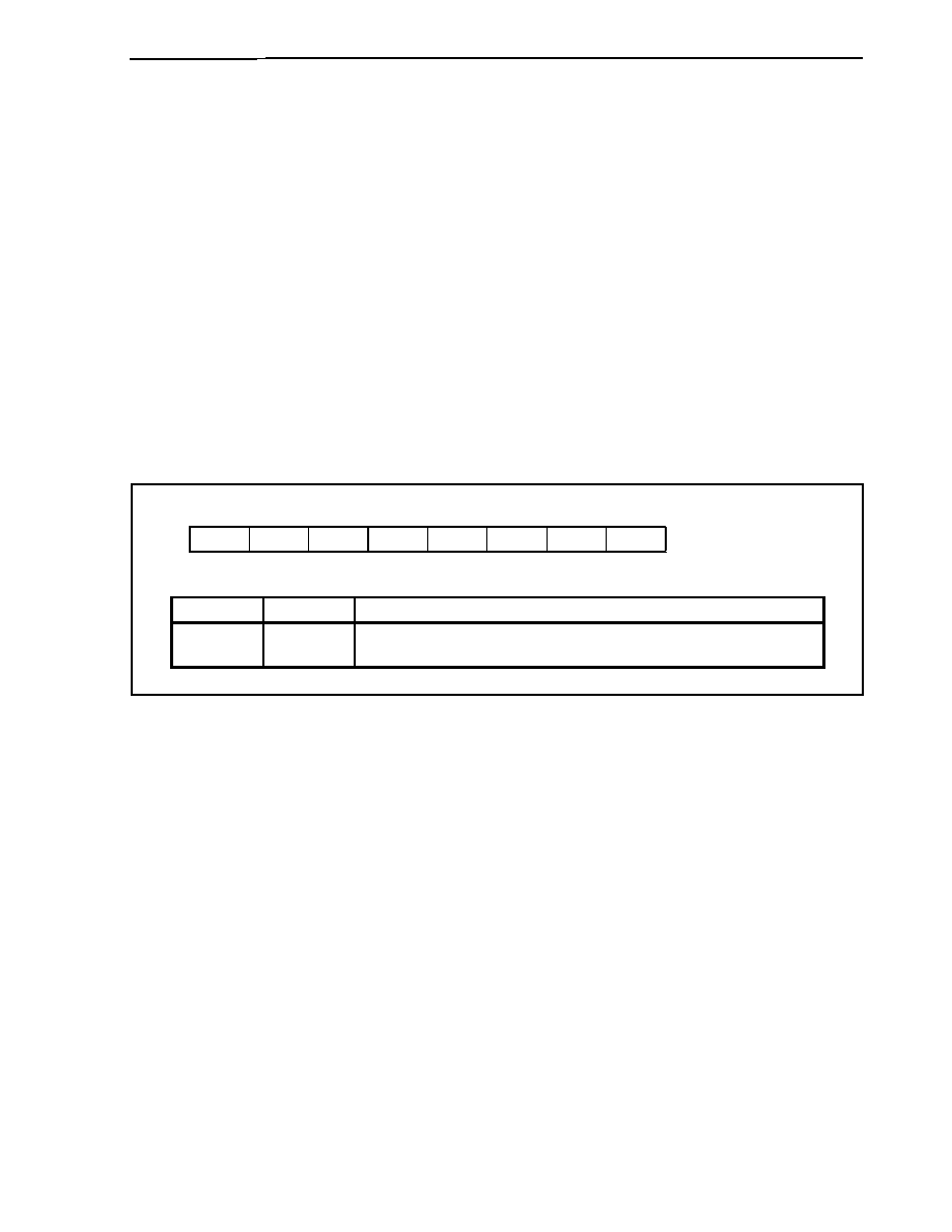
CHAPTER 10 SERIAL INTERFACE FUNCTION
User's Manual U14492EJ5V0UD
419
(4) Receive buffer register 0 (RXB0)
The RXB0 register is an 8-bit buffer register for storing parallel data that had been converted by the receive
shift register.
When reception is enabled (RXE0 bit = 1 in the ASIM0 register), receive data is transferred from the receive
shift register to the RXB0 register, synchronized with the completion of the shift-in processing of one frame.
Also, a reception completion interrupt request (INTSR0) is generated by the transfer to the RXB0 register.
For information about the timing for generating this interrupt request, refer to 10.2.5 (4) Reception
operation.
If reception is disabled (RXE0 bit = 0 in the ASIM0 register), the contents of the RXB0 register are retained,
and no processing is performed for transferring data to the RXB0 register even when the shift-in processing
of one frame is completed. Also, no INTSR0 signal is generated.
When 7 bits is specified for the data length, bits 6 to 0 of the RXB0 register are transferred for the receive
data and the MSB (bit 7) is always 0. However, if an overrun error (OVE bit of ASIS0 register = 1) occurs, the
receive data at that time is not transferred to the RXB0 register.
Except when a reset is input, the RXB0 register becomes FFH even when UARTCAE0 bit = 0 in the ASIM0
register.
This register is read-only, in 8-bit units.
7 6 5 4 3 2 1 0
Address
Initial
value
RXB0 RXB7 RXB6 RXB5 RXB4 RXB3 RXB2 RXB1 RXB0
FFFFFA02H FFH
Bit position
Bit name
Function
7 to 0
RXB7 to
RXB0
Stores receive data.
0 can be read for RXB7 when 7-bit or character data is received.

CHAPTER 10 SERIAL INTERFACE FUNCTION
User's Manual U14492EJ5V0UD
420
(5) Transmit buffer register 0 (TXB0)
The TXB0 register is an 8-bit buffer register for setting transmit data.
When transmission is enabled (TXE0 bit = 1 in the ASIM0 register), the transmit operation is started by
writing data to TXB0 register.
When transmission is disabled (TXE0 bit = 0 in the ASIM0 register), even if data is written to TXB0 register,
the value is ignored.
The TXB0 register data is transferred to the transmit shift register, and a transmission completion interrupt
request (INTST0) is generated, synchronized with the completion of the transmission of one frame from the
transmit shift register. For information about the timing for generating this interrupt request, refer to 10.2.5 (2)
Transmission operation.
When TXBF0 bit = 1 in the ASIF0 register, writing must not be performed to TXB0 register.
This register can be read/written in 8-bit units.
7 6 5 4 3 2 1 0
Address
Initial
value
TXB0 TXB7 TXB6 TXB5 TXB4 TXB3 TXB2 TXB1 TXB0
FFFFFA04H FFH
Bit position
Bit name
Function
7 to 0
TXB7 to
TXB0
Writes transmit data.
CHAPTER 10 SERIAL INTERFACE FUNCTION
User's Manual U14492EJ5V0UD
421
10.2.4 Interrupt requests
The following three types of interrupt requests are generated from UART0.
∑ Reception completion interrupt (INTSR0)
∑ Transmission completion interrupt (INTST0)
∑ Reception error interrupt (INTSER0)
The default priorities among these three types of interrupt requests is, from high to low, reception completion
interrupt, transmission completion interrupt, and reception error interrupt.
Table 10-1. Generated Interrupts and Default Priorities
Interrupt Priority
Reception completion
1
Transmission completion
2
Reception error
3
(1) Reception completion interrupt (INTSR0)
When reception is enabled, an INTSR0 signal is generated when data is shifted in to the receive shift register
and transferred to receive buffer register 0 (RXB0).
An INTSR0 signal can be generated in place of a reception error interrupt (INTSER0) according to the ISRM
bit of the ASIM0 register even when a reception error has occurred.
When reception is disabled, no INTSR0 signal is generated.
(2) Transmission completion interrupt (INTST0)
An INTST0 signal is generated when one frame of transmit data containing 7-bit or 8-bit characters is shifted
out from the transmit shift register.
(3) Reception error interrupt (INTSER0)
When reception is enabled, an INTSER0 signal is generated according to the logical OR of the three types of
reception errors explained for the ASIS0 register. Whether an INTSER0 signal or INTSR0 signal is generated
when an error occurs can be specified using the ISRM bit of the ASIM0 register.
When reception is disabled, no INTSER0 signal is generated.
CHAPTER 10 SERIAL INTERFACE FUNCTION
User's Manual U14492EJ5V0UD
422
10.2.5 Operation
(1) Data format
Full-duplex serial data transmission and reception can be performed.
The transmit/receive data format consists of one data frame containing a start bit, character bits, a parity bit,
and stop bits as shown in Figure 10-2.
The character bit length within one data frame, the type of parity, and the stop bit length are specified
according to the asynchronous serial interface mode register 0 (ASIM0).
Also, data is transferred with LSB first.
Figure 10-2. Asynchronous Serial Interface Transmit/Receive Data Format
1 data frame
Start
bit
D0
D1
D2
D3
D4
D5
D6
D7
Parity
bit
Stop bits
Character bits
∑ Start bit ∑∑∑ 1 bit
∑ Character bits ∑∑∑ 7 bits or 8 bits
∑ Parity bit ∑∑∑ Even parity, odd parity, 0 parity, or no parity
∑ Stop bits ∑∑∑ 1 bit or 2 bits

CHAPTER 10 SERIAL INTERFACE FUNCTION
User's Manual U14492EJ5V0UD
423
(2) Transmission operation
When UARTCAE0 bit is set to 1 in the ASIM0 register, a high level is output from the TXD0 pin.
Then, when TXE0 bit is set to 1 in the ASIM0 register, transmission is enabled, and the transmit operation is
started by writing transmit data to transmit buffer register 0 (TXB0).
(a) Transmission enabled state
This state is set by the TXE0 bit in the ASIM0 register.
∑ TXE0 = 1: Transmission enabled state
∑ TXE0 = 0: Transmission disabled state
Since UART0 does not have a CTS (transmission enabled signal) input pin, a port should be used to
confirm whether the destination is in a reception enabled state.
(b) Transmission operation start
In transmission enabled state, a transmission operation is started by writing transmit data to transmit
buffer register 0 (TXB0). When a transmit operation is started, the data in the TXB0 register is
transferred to the transmit shift register. Then, the transmit shift register outputs data to the TXD0 pin
(the transmit data is transferred sequentially starting with the start bit). The start bit, parity bit, and stop
bits are added automatically.
(c) Transmission interrupt request
When the transmit shift register becomes empty, a transmission completion interrupt request (INTST0) is
generated. The timing for generating the INTST0 signal differs according to the specification of the stop
bit length. The INTST0 signal is generated at the same time that the last stop bit is output.
If the data to be transmitted next has not been written to the TXB0 register, the transmit operation is
suspended.
Caution Normally, when the transmit shift register becomes empty, a transmission completion
interrupt (INTST0) is generated. However, no INTST0 signal is generated if the transmit
shift register becomes empty due to the input of a RESET.
CHAPTER 10 SERIAL INTERFACE FUNCTION
User's Manual U14492EJ5V0UD
424
Figure 10-3. Asynchronous Serial Interface Transmission Completion Interrupt Timing
Start
Stop
D0
D1
D2
D6
D7
Parity
Parity
TXD0 (output)
INTST0 (output)
Start
D0
D1
D2
D6
D7
TXD0 (output)
INTST0 (output)
(a) Stop bit length: 1
(b) Stop bit length: 2
Stop
CHAPTER 10 SERIAL INTERFACE FUNCTION
User's Manual U14492EJ5V0UD
425
(3) Continuous transmission operation
UART0 can write the next transmit data to the TXB0 register at the timing that the transmit shift register starts
the shift operation. This enables an efficient transmission rate to be realized by continuously transmitting
data even during the servicing of the transmission completion interrupt (INTST0) after the transmission of one
data frame. In addition, reading the TXSF0 bit of the ASIF0 register after the generation of an INTST0 signal
enables the TXB0 register to be efficiently written twice (2 bytes) without waiting for the transmission of 1 data
frame.
When continuous transmission is performed, data should be written after referencing the ASIF0 register to
confirm the transmission status and whether or not data can be written to the TXB0 register.
Caution The values of the TXBF0 and TXSF0 bits of the ASIF0 register change from 10
11 01 in
continuous transmission.
Therefore, do not confirm the status based on the combination of the TXBF0 and TXSF0
bits.
Read only the TXBF0 bit during continuous transmission.
TXBF0
Whether or Not Writing to TXB0 Register Is Enabled
0
Writing is enabled
1
Writing is not enabled
Caution When transmission is performed continuously, write the first transmit data (first byte) to the
TXB0 register and confirm that the TXBF0 bit is 0, and then write the next transmit data
(second byte) to TXB0 register. If writing to the TXB0 register is performed when the TXBF0
bit is 1, transmit data cannot be guaranteed.
The communication status can be confirmed with the TXSF0 bit.
TXSF0 Transmission
Status
0 Transmission
is
completed
1 Under
transmission
Cautions 1. When initializing the transmission unit when continuous transmission is completed,
confirm that the TXSF0 bit is 0 after the occurrence of the transmission completion
interrupt, and then execute initialization. If initialization is performed when the TXSF0
bit is 1, transmit data cannot be guaranteed.
2. While transmission is being performed continuously, an overrun error may occur if the
next transmission is completed before the INTST0 interrupt servicing following the
transmission of 1 data frame is executed. An overrun error can be detected by
embedding a program that can count the number of transmit data and referencing
TXSF0 bit.

CHAPTER 10 SERIAL INTERFACE FUNCTION
User's Manual U14492EJ5V0UD
426
Figure 10-4. Continuous Transmission Processing Flow
Set registers
Interrupt occurrence
Wait for interrupt
Required
number of transfers
performed?
Write transmit data to
TXB0 register
Write transmit data to
TXB0 register
When reading
ASIF0 register,
TXBF0 = 0?
When reading
ASIF0 register,
TXSF0 = 1?
When reading
ASIF0 register,
TXSF0 = 0?
No
No
No
No
Yes
Yes
Yes
Yes
End of transmission
processing
Write 2nd byte of the
transmit data to TXB0
register
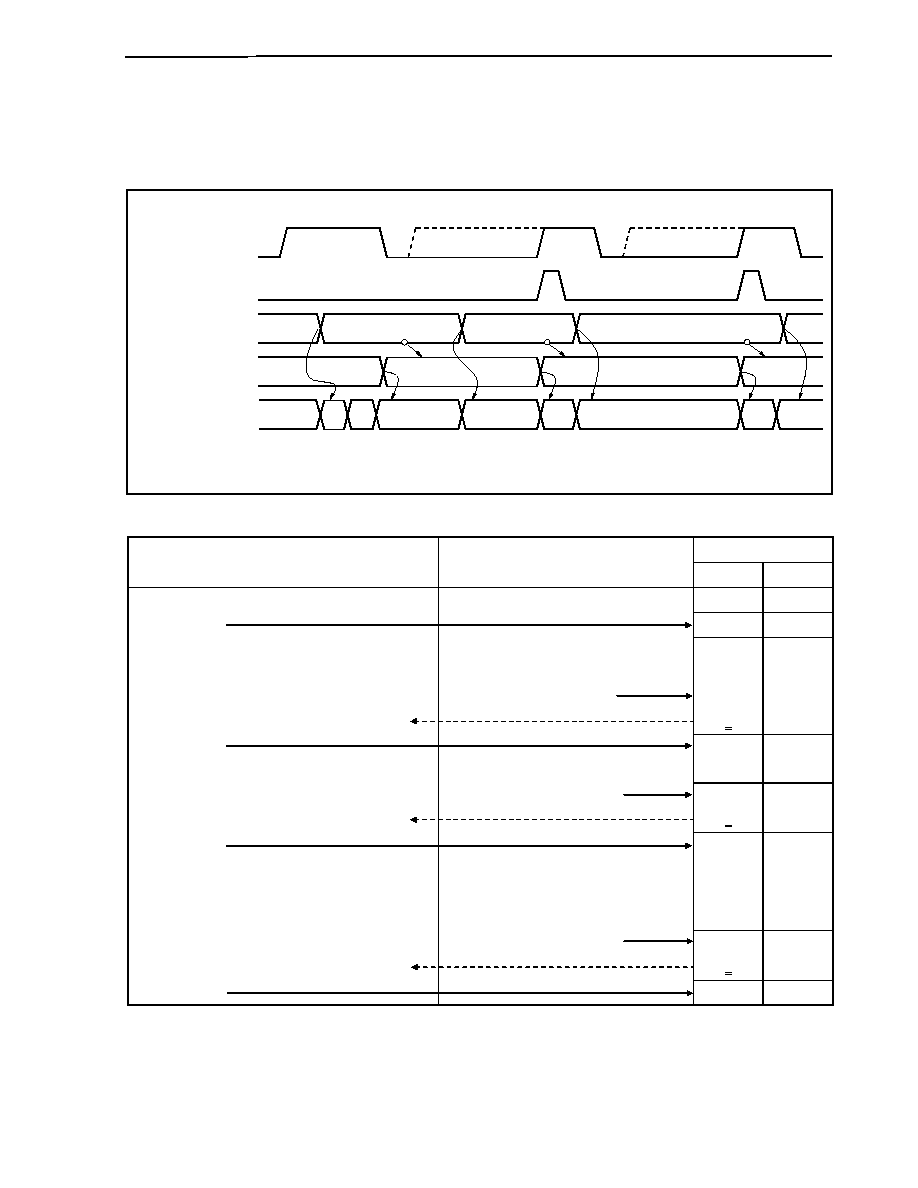
CHAPTER 10 SERIAL INTERFACE FUNCTION
User's Manual U14492EJ5V0UD
427
(a) Starting procedure
The procedure to start continuous transmission is shown below.
Figure 10-5. Continuous Transmission Starting Procedure
TXD0 (output)
Data (1)
Data (2)
<5>
<1>
<2>
<4>
INTST0 (output)
TXB0 register
FFH
FFH
Data (1)
Data (2)
Data (3)
Data (1)
Data (2)
Data (3)
<3>
ASIF0 register
(TXBF0, TXSF0 bits)
00
11
Note
11
01
01
11
01
11
TXS0 register
Start
bit
Stop
bit
Stop
bit
Start
bit
10
Note Refer
to
10.2.7 Precautions (2).
ASIF0 Register
Transmission Starting Procedure
Internal Operation
TXBF0 TXSF0
∑ Set transmission mode
<1> Start transmission unit
0
0
∑ Write data (1)
1
0
<2> Generate start bit
∑ Read ASIF0 register (confirm that TXBF0 bit = 0)
Start data (1) transmission
1
0
0
0
1
Note
1
Note
1
1
∑ Write data (2)
<<Transmission in progress>>
1 1
<3> INTST0 interrupt occurs
∑ Read ASIF0 register (confirm that TXBF0 bit = 0)
0
0
1
1
∑ Write data (3)
<4> Generate start bit
Start data (2) transmission
<<Transmission in progress>>
1 1
<5> INTST0 interrupt occurs
∑ Read ASIF0 register (confirm that TXBF0 bit = 0)
0
0
1
1
∑ Write data (4)
1
1
Note Refer
to
10.2.7 Precautions (2).
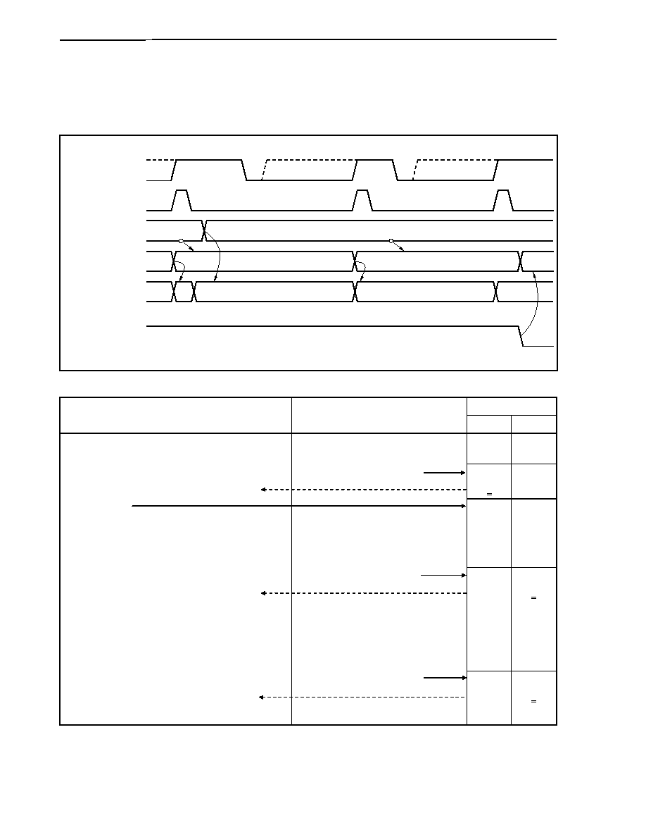
CHAPTER 10 SERIAL INTERFACE FUNCTION
User's Manual U14492EJ5V0UD
428
(b) Ending procedure
The procedure for ending continuous transmission is shown below.
Figure 10-6. Continuous Transmission End Procedure
TXD0 (output)
Data (m
- 1)
Data (m)
<11>
<7>
<6>
<8>
<10>
INTST0 (output)
TXB0 register
Data (m
- 1)
Data (m
- 1)
Data (m)
FFH
Data (m)
<9>
ASIF0 register
(TXBF0, TXSF0 bits)
UARTCAE0 bit
or
TXE0 bit
11
01
11
01
00
Transmit shift
register
Start
bit
Start
bit
Stop
bit
Stop
bit
ASIF0 Register
Transmission End Procedure
Internal Operation
TXBF0 TXSF0
<6> Transmission of data (m
- 2) is in
progress
1 1
<7> INTST0 interrupt occurs
∑ Read ASIF0 register (confirm that TXBF0 bit = 0)
0
0
1
1
∑ Write data (m)
<8> Generate start bit
Start data (m
- 1) transmission
<<Transmission in progress>>
1 1
<9> INTST0 interrupt occurs
∑ Read ASIF0 register (confirm that TXSF0 bit = 1)
There is no write data
<10> Generate start bit
Start data (m) transmission
<<Transmission in progress>>
0
0
1
1
<11> Generate INTST0 interrupt
∑ Read ASIF0 register (confirm that TXSF0 bit = 0)
∑ Clear (0) the UARTCAE0 bit or TXE0 bit
Initialize internal circuits
0
0
0
0

CHAPTER 10 SERIAL INTERFACE FUNCTION
User's Manual U14492EJ5V0UD
429
(4) Reception operation
An awaiting reception state is set by setting UARTCAE0 bit to 1 in the ASIM0 register and then setting RXE0
bit to 1 in the ASIM0 register. To start the receive operation, start sampling at the falling edge when the
falling of the RXD0 pin is detected. If the RXD0 pin is low level at a start bit sampling point, the start bit is
recognized. When the receive operation begins, serial data is stored sequentially in the receive shift register
according to the baud rate that was set. A reception completion interrupt (INTSR0) is generated each time
the reception of one frame of data is completed. Normally, the receive data is transferred from receive buffer
register 0 (RXB0) to memory by this interrupt servicing.
(a) Reception enabled state
The receive operation is set to reception enabled state by setting the RXE0 bit in the ASIM0 register to 1.
∑ RXE0 bit = 1: Reception enabled state
∑ RXE0 bit = 0: Reception disabled state
In reception disabled state, the reception hardware stands by in the initial state. At this time, the contents
of receive buffer register 0 (RXB0) are retained, and no reception completion interrupt or reception error
interrupt is generated.
(b) Start of reception operation
A reception operation is started by the detection of a start bit.
The RXD0 pin is sampled according to the serial clock from the baud rate generator 0 (BRG0).
(c) Reception completion interrupt
When RXE0 = 1 in the ASIM0 register and the reception of one frame of data is completed (the stop bit is
detected), a reception completion interrupt (INTSR0) is generated and the receive data in the receive
shift register is transferred to the RXB0 register at the same time.
Also, if an overrun error (OVE bit of ASIS0 register = 1) occurs, the receive data at that time is not
transferred to receive buffer register 0 (RXB0), and either an INTSR0 signal or a reception error interrupt
(INTSER0) is generated according to the ISRM bit setting in the ASIM0 register.
Even if a parity error (PE bit of ASIS0 register = 1) or framing error (FE bit of ASIS0 register = 1) occurs
during a receive operation, the receive operation continues until stop bit is received, and after reception is
completed, either an INTSR0 signal or an INTSER0 signal is generated according to the ISRM bit setting
in the ASIM0 register (the receive data in the receive shift register is transferred to the RXB0 register).
If the RXE0 bit is cleared (0) during a receive operation, the receive operation is immediately stopped.
The contents of receive buffer register 0 (RXB0) and of the asynchronous serial interface status register
(ASIS0) at this time do not change, and no INTSR0 or INTSER0 signal is generated.
No INTSR0 or INTSER0 signal is generated when RXE0 = 0 (reception is disabled).

CHAPTER 10 SERIAL INTERFACE FUNCTION
User's Manual U14492EJ5V0UD
430
Figure 10-7. Asynchronous Serial Interface Reception Completion Interrupt Timing
Start
D0
D1
D2
D6
D7
RXD0 (input)
INTSR0 (output)
RXB0 register
Parity
Stop
Cautions 1. Even if a reception error occurs, be sure to read receive buffer register 0 (RXB0). If the
RXB0 register is not read, an overrun error will occur at the next data reception, and the
reception error state will continue indefinitely.
2. Reception is always performed with the stop bit length set to 1.
A second stop bit is ignored.
(5) Reception error
The three types of error that can occur during a receive operation are a parity error, framing error, or overrun
error. The data reception result is that the various flags of the ASIS0 register are set (1), and a reception
error interrupt (INTSER0) or a reception completion interrupt (INTSR0) is generated at the same time. The
ISRM bit of the ASIM0 register specifies whether an INTSER0 or INTSR0 signal is generated.
The type of error that occurred during reception can be detected by reading the contents of the ASIS0
register during the INTSER0 or INTSR0 interrupt servicing.
The contents of the ASIS0 register are cleared (0) by reading the ASIS0 register.
Table 10-2. Reception Error Causes
Error Flag
Reception Error
Cause
PE
Parity error
The parity specification during transmission did not match
the parity of the reception data
FE
Framing error
No stop bit was detected
OVE
Overrun error
The reception of the next data was completed before data
was read from receive buffer register 0 (RXB0)

CHAPTER 10 SERIAL INTERFACE FUNCTION
User's Manual U14492EJ5V0UD
431
(a) Separation of reception error interrupt
A reception error interrupt can be separated from the INTSR0 signal and generated as an INTSER0
signal by clearing the ISRM bit of the ASIM0 register to 0.
Figure 10-8. When Reception Error Interrupt Is Separated from INTSR0 Interrupt (ISRM Bit = 0)
(a) No error occurs during reception (b) An error occurs during reception
INTSR0 signal (output)
(Reception completion
interrupt)
INTSER0 signal (output)
(Reception error
interrupt)
INTSR0 signal (output)
(Reception completion
interrupt)
INTSER0 signal (output)
(Reception error
interrupt)
INTSR0 signal
does not occur
Figure 10-9. When Reception Error Interrupt Is Included in INTSR0 Interrupt (ISRM Bit = 1)
(a) No error occurs during reception (b) An error occurs during reception
INTSR0 signal (output)
(Reception completion
interrupt)
INTSER0 signal (output)
(Reception error
interrupt)
INTSR0 signal (output)
(Reception completion
interrupt)
INTSER0 signal (output)
(Reception error
interrupt)
INTSER0 signal
does not occur

CHAPTER 10 SERIAL INTERFACE FUNCTION
User's Manual U14492EJ5V0UD
432
(6) Parity types and corresponding operation
A parity bit is used to detect a bit error in communication data. Normally, the same type of parity bit is used at
the transmission and reception sides.
(a) Even parity
(i) During
transmission
The parity bit is controlled so that the number of bits with the value "1" within the transmit data
including the parity bit is even. The parity bit value is as follows.
∑ If the number of bits with the value "1" within the transmit data is odd: 1
∑ If the number of bits with the value "1" within the transmit data is even: 0
(ii) During reception
The number of bits with the value "1" within the receive data including the parity bit is counted, and a
parity error is generated if this number is odd.
(b) Odd parity
(i) During
transmission
In contrast to even parity, the parity bit is controlled so that the number of bits with the value "1"
within the transmit data including the parity bit is odd. The parity bit value is as follows.
∑ If the number of bits with the value "1" within the transmit data is odd: 0
∑ If the number of bits with the value "1" within the transmit data is even: 1
(ii) During reception
The number of bits with the value "1" within the receive data including the parity bit is counted, and a
parity error is generated if this number is even.
(c) 0 parity
During transmission the parity bit is set to "0" regardless of the transmit data.
During reception, no parity bit check is performed. Therefore, no parity error is generated regardless of
whether the parity bit is "0" or "1".
(d) No parity
No parity bit is added to the transmit data.
During reception, the receive operation is performed as if there were no parity bit. Since there is no
parity bit, no parity error is generated.
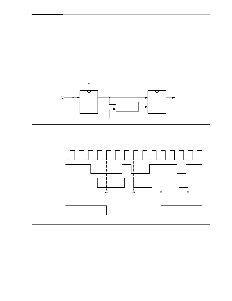
CHAPTER 10 SERIAL INTERFACE FUNCTION
User's Manual U14492EJ5V0UD
433
(7) Receive data noise filter
The RXD0 signal is sampled at the rising edge of the prescaler output base clock (f
CLK
). If the same sampling
value is obtained twice, the match detector output changes, and this output is sampled as input data.
Therefore, data not exceeding one clock width is judged to be noise and is not delivered to the internal circuit
(see Figure 10-11). Refer to 10.2.6 (1) (a) Base clock regarding the base clock.
Also, since the circuit is configured as shown in Figure 10-10, internal processing during a receive operation
is delayed by up to 2 clocks according to the external signal status.
Figure 10-10. Noise Filter Circuit
RXD0
f
CLK
Q
Base clock
In
LD_EN
Q
In
Internal signal A
Internal signal B
Match detector
Figure 10-11. Timing of RXD0 Signal Judged as Noise
Internal signal A
Base clock
RXD0 (input)
Internal signal B
Match
Mismatch
(judged as noise)
Mismatch
(judged as noise)
Match

CHAPTER 10 SERIAL INTERFACE FUNCTION
User's Manual U14492EJ5V0UD
434
10.2.6 Dedicated baud rate generator 0 (BRG0)
A dedicated baud rate generator, which consists of a source clock selector and an 8-bit programmable counter,
generates serial clocks during transmission/reception at UART0. The dedicated baud rate generator output can be
selected as the serial clock for each channel.
Separate 8-bit counters exist for transmission and for reception.
(1) Baud rate generator 0 (BRG0) configuration
Figure 10-12. Baud Rate Generator 0 (BRG0) Configuration
f
XX
/2
f
XX
/4
f
XX
/8
f
XX
/16
f
XX
/32
f
XX
/64
f
XX
/128
f
XX
/256
f
XX
/512
f
XX
/1024
f
XX
/2048
Base clock
(f
CLK
)
Selector
UARTCAE0
8-bit counter
Match detector
Baud rate
BRGC0: MDL7 to MDL0
1/2
UARTCAE0 and TXE0 (or RXE0)
CKSR0: TPS3 to TPS0
f
XX
Remark f
XX
: Internal system clock
(a) Base clock
When UARTCAE0 bit = 1 in the ASIM0 register, the clock selected according to the TPS3 to TPS0 bits of
the CKSR0 register is supplied to the transmission/reception unit. This clock is called the base clock
(f
CLK
). When UARTCAE0 bit = 0, f
CLK
is fixed at low level.
CHAPTER 10 SERIAL INTERFACE FUNCTION
User's Manual U14492EJ5V0UD
435
(2) Serial clock generation
A serial clock can be generated according to the settings of the CKSR0 and BRGC0 registers.
The base clock to the 8-bit counter is selected according to the TPS3 to TPS0 bits of the CKSR0 register.
The 8-bit counter divisor value can be set according to the MDL7 to MDL0 bits of the BRGC0 register.
(a) Clock selection register 0 (CKSR0)
The CKSR0 register is an 8-bit register for selecting the base clock (f
CLK
) according to the TPS3 to TPS0
bits. The clock selected by the TPS3 to TPS0 bits becomes f
CLK
of the transmission/reception module.
This register can be read/written in 8-bit units.
Cautions 1. The maximum allowable frequency of the base clock (f
CLK
) is 25 MHz. Therefore,
when the system clock's frequency is 50 MHz, bits TPS3 to TPS0 cannot be set to
0000B.
To use 50 MHz, set the TPS3 to TPS0 bits to a value other than 0000B, and set the
UARTCAE0 bit of the ASIM0 register to 1.
2. If the TPS3 to TPS0 bits are to be overwritten, the UARTCAE0 bit of the ASIM0
register should be set to 0 first.
7 6 5 4 3 2 1 0
Address
Initial
value
CKSR0
0 0 0 0
TPS3
TPS2
TPS1
TPS0
FFFFFA06H
00H
Bit position
Bit name
Function
Specifies the base clock (f
CLK
).
TPS3 TPS2 TPS1 TPS0
Base
clock
(f
CLK
)
0 0 0 0
f
XX
0 0 0 1
f
XX
/2
0 0 1 0
f
XX
/4
0 0 1 1
f
XX
/8
0 1 0 0
f
XX
/16
0 1 0 1
f
XX
/32
0 1 1 0
f
XX
/64
0 1 1 1
f
XX
/128
1 0 0 0
f
XX
/256
1 0 0 1
f
XX
/512
1 0 1 0
f
XX
/1024
1 0 1 1
f
XX
/2048
1 1
Arbitrary Arbitrary Setting
prohibited
3 to 0
TPS3 to
TPS0
Remark f
XX
: Internal system clock
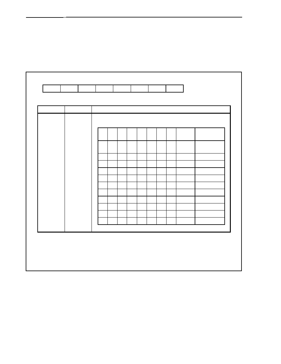
CHAPTER 10 SERIAL INTERFACE FUNCTION
User's Manual U14492EJ5V0UD
436
(b) Baud rate generator control register 0 (BRGC0)
The BRGC0 register is an 8-bit register that controls the baud rate (serial transfer speed) of UART0.
This register can be read/written in 8-bit units.
Caution If the MDL7 to MDL0 bits are to be overwritten, the TXE0 bit and RXE0 bit of the ASIM0
register should be set to 0 first.
7 6 5 4 3 2 1 0
Address
Initial
value
BRGC0 MDL7 MDL6 MDL5 MDL4 MDL3 MDL2 MDL1 MDL0
FFFFFA07H FFH
Bit position
Bit name
Function
Specifies the 8-bit counter's division value.
MDL7 MDL6 MDL5 MDL4 MDL3 MDL2 MDL1 MDL0
Set value
(k)
Serial clock
0 0 0 0 0 x x x
≠
Setting
prohibited
0 0 0 0 1 0 0 0
8
f
CLK
/8
0 0 0 0 1 0 0 1
9
f
CLK
/9
0 0 0 0 1 0 1 0
10
f
CLK
/10
1 1 1 1 1 0 1 0
250
f
CLK
/250
1 1 1 1 1 0 1 1
251
f
CLK
/251
1 1 1 1 1 1 0 0
252
f
CLK
/252
1 1 1 1 1 1 0 1
253
f
CLK
/253
1 1 1 1 1 1 1 0
254
f
CLK
/254
1 1 1 1 1 1 1 1
255
f
CLK
/255
7 to 0
MDL7 to
MDL0
Remarks 1. f
CLK
: Frequency [Hz] of base clock selected according to TPS3 to TPS0 bits of CKSR0 register
2.
k: Value set according to MDL7 to MDL0 bits (k = 8, 9, 10, ..., 255)
3.
The baud rate is the output clock for the 8-bit counter divided by 2
4.
x: don't care
...
...
...
...
...
...
...
...
...
...

CHAPTER 10 SERIAL INTERFACE FUNCTION
User's Manual U14492EJ5V0UD
437
(c) Baud rate
The baud rate is the value obtained according to the following formula.
Baud rate = [bps]
f
CLK
= Frequency [Hz] of base clock selected according to TPS3 to TPS0 bits of CKSR0 register
k = Value set according to MDL7 to MDL0 bits of BRGC0 register (k = 8, 9, 10, ..., 255)
(d) Baud rate error
The baud rate error is obtained according to the following formula.
Error (%) =
-1 ◊ 100 [%]
Cautions 1. Make sure that the baud rate error during transmission does not exceed the allowable
error of the reception destination.
2. Make sure that the baud rate error during reception is within the allowable baud rate
range during reception, which is described in (4) Allowable baud rate range during
reception.
Example: Base clock frequency (f
CLK
) = 20 MHz = 20,000,000 Hz
Settings of MDL7 to MDL0 bits in BRGC0 register = 01000001B (k = 65)
Target baud rate = 153,600 bps
Baud rate = 20M/(2
◊ 65)
=
20000000/(2
◊ 65) = 153,846 [bps]
Error = (153846/153600
- 1) ◊ 100
=
0.160
[%]
f
CLK
2
◊ k
Actual baud rate (baud rate with error)
Target baud rate (normal baud rate)

CHAPTER 10 SERIAL INTERFACE FUNCTION
User's Manual U14492EJ5V0UD
438
(3) Baud rate setting example
Table 10-3. Baud Rate Generator Setting Data
f
XX
= 50 MHz
f
XX
= 40 MHz
f
XX
= 33 MHz
f
XX
= 10 MHz
Baud Rate
(bps)
f
CLK
k ERR
f
CLK
k ERR
f
CLK
k ERR
f
CLK
k ERR
300 f
XX
/2
9
163 0.15 f
XX
/2
10
65 0.16 f
XX
/2
8
215 ≠0.07 f
XX
/2
7
130 0.16
600 f
XX
/2
8
163 0.15 f
XX
/2
9
65 0.16 f
XX
/2
7
215 ≠0.07 f
XX
/2
6
130 0.16
1200 f
XX
/2
7
163 0.15 f
XX
/2
8
65 0.16 f
XX
/2
6
215 ≠0.07 f
XX
/2
5
130 0.16
2400 f
XX
/2
6
163 0.15 f
XX
/2
7
65 0.16 f
XX
/2
5
215 ≠0.07 f
XX
/2
4
130 0.16
4800 f
XX
/2
5
163 0.15 f
XX
/2
6
65 0.16 f
XX
/2
4
215 ≠0.07 f
XX
/2
3
130 0.16
9600 f
XX
/2
4
163 0.15 f
XX
/2
5
65 0.16 f
XX
/2
3
215 ≠0.07 f
XX
/2
2
130 0.16
19200 f
XX
/2
3
163 0.15 f
XX
/2
4
65 0.16 f
XX
/2
2
215 ≠0.07 f
XX
/2
1
130 0.16
31250 f
XX
/2
3
100 0 f
XX
/2
3
80 0 f
XX
/2
2
132 0 f
XX
/2
1
80 0
38400 f
XX
/2
2
163 0.15 f
XX
/2
3
65 0.16 f
XX
/2
1
215 ≠0.07 f
XX
/2
0
130 0.16
76800 f
XX
/2
1
163 0.15 f
XX
/2
2
65 0.16 f
XX
/2
1
107 0.39 f
XX
/2
0
65 0.16
153600 f
XX
/2
1
81 0.47 f
XX
/2
1
65 0.16 f
XX
/2
1
54 ≠0.54
f
XX
/2
0
33 ≠1.36
312500 f
XX
/2
1
40 0 f
XX
/2
1
32 0 f
XX
/2
1
26 1.54 f
XX
/2
0
16 0
625000 f
XX
/2
1
20 0 f
XX
/2
1
16 0 f
XX
/2
1
13 1.54 f
XX
/2
0
8 0
1250000 f
XX
/2
1
10 0 f
XX
/2
1
8 0 f
XX
/2
1
8
-17.5
-
-
-
1562500 f
XX
/2
1
8 0 f
XX
/2
1
8
-18.6
-
-
-
-
-
-
Caution The maximum allowable frequency of the base clock (f
CLK
) is 25 MHz.
Remark f
XX
:
Internal system clock frequency
f
CLK
:
Base clock frequency
k:
Setting values of MDL7 to MDL0 bits in BRGC0 register
ERR:
Baud rate error [%]
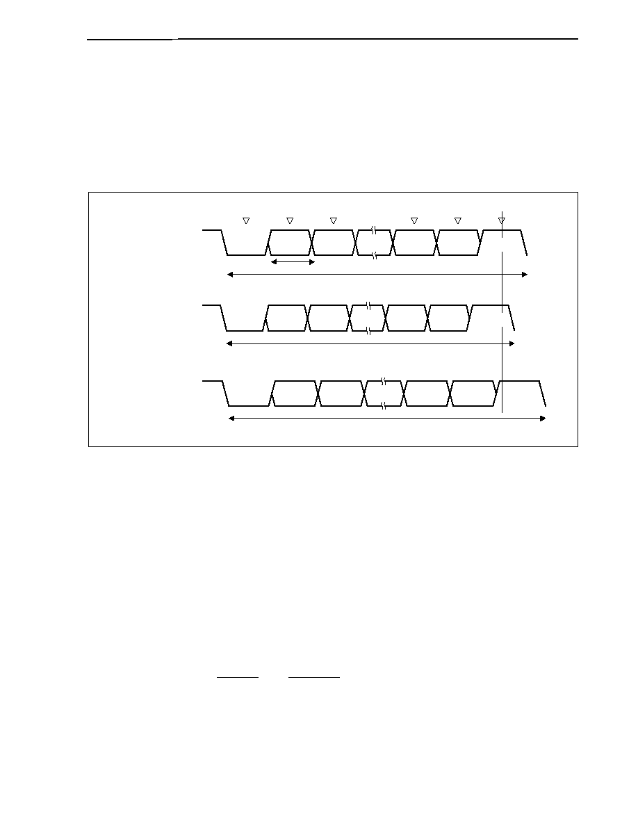
CHAPTER 10 SERIAL INTERFACE FUNCTION
User's Manual U14492EJ5V0UD
439
(4) Allowable baud rate range during reception
The degree to which a discrepancy from the transmission destination's baud rate is allowed during reception
is shown below.
Caution The equations described below should be used to set the baud rate error during reception
so that it always is within the allowable error range.
Figure 10-13. Allowable Baud Rate Range During Reception
FL
1 data frame (11
◊ FL)
FLmin
FLmax
UART0
transfer rate
Latch timing
Start bit
Bit 0
Bit 1
Bit 7
Parity bit
Minimum allowable
transfer rate
Maximum allowable
transfer rate
Stop bit
Start bit
Bit 0
Bit 1
Bit 7
Parity bit
Stop bit
Start bit
Bit 0
Bit 1
Bit 7
Parity bit
Stop bit
As shown in Figure 10-13, after the start bit is detected, the receive data latch timing is determined according
to the counter that was set by the BRGC0 register. If all data up to the final data (stop bit) is in time for this
latch timing, the data can be received normally.
Applying this to 11-bit reception is, theoretically, as follows.
FL = (Brate)
≠1
Brate: UART0 baud rate
k:
BRGC0 register setting value
FL:
1-bit data length
When the latch timing margin is made 2 base clocks, the minimum allowable transfer rate (FLmin) is
as follows.
FL
k
2
2
k
21
FL
k
2
2
k
FL
11
min
FL
+
=
◊
-
-
◊
=
CHAPTER 10 SERIAL INTERFACE FUNCTION
User's Manual U14492EJ5V0UD
440
Therefore, the transfer destination's maximum baud rate (BRmax) that can be received is as follows.
BRmax = (FLmin/11)
-
1
= Brate
Similarly, the maximum allowable transfer rate (FLmax) can be obtained as follows.
FL
k
2
2
k
21
FL
k
2
2
k
FL
11
max
FL
11
10
◊
-
=
◊
◊
+
-
◊
=
◊
11
FL
k
20
2
k
21
max
FL
◊
-
=
Therefore, the transfer destination's minimum baud rate (BRmin) that can be received is as follows.
BRmin = (FLmax/11)
-
1
= Brate
The allowable baud rate error of UART0 and the transfer destination can be obtained as follows from the
expressions described above for computing the minimum and maximum baud rate values.
Table 10-4. Maximum and Minimum Allowable Baud Rate Error
Division Ratio (k)
Maximum Allowable
Baud Rate Error
Minimum Allowable
Baud Rate Error
8 +3.53%
≠3.61%
20 +4.26%
≠4.31%
50 +4.56%
≠4.58%
100 +4.66%
≠4.67%
255 +4.72%
≠4.73%
Remarks 1. The reception precision depends on the number of bits in one frame, the base clock frequency,
and the division ratio (k). The higher the base clock frequency and the larger the division ratio
(k), the higher the precision.
2. k: BRGC0 register setting value
22k
21k + 2
20k
21k
- 2
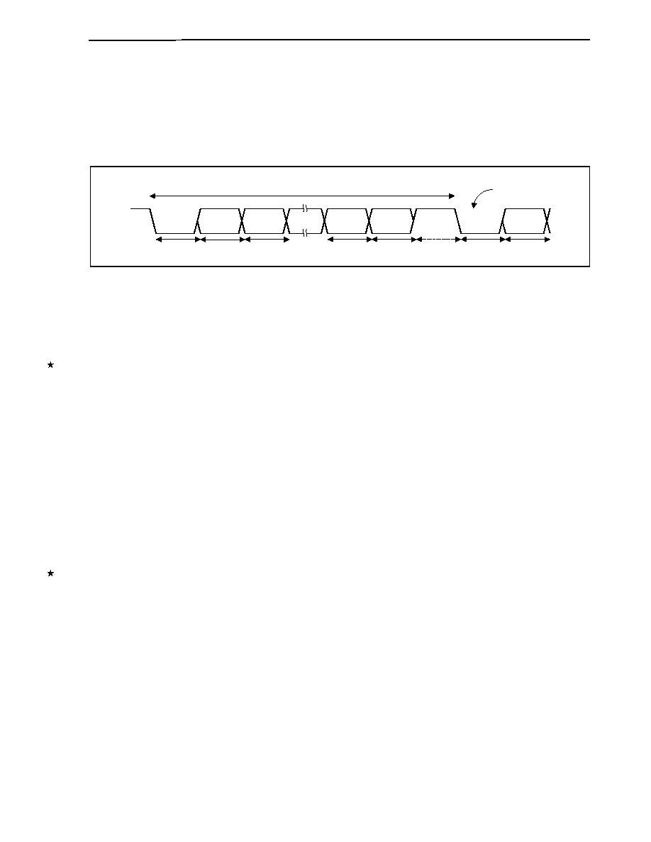
CHAPTER 10 SERIAL INTERFACE FUNCTION
User's Manual U14492EJ5V0UD
441
(5) Transfer rate during continuous transmission
During continuous transmission, the transfer rate from a stop bit to the next start bit is extended two clocks of
base clock longer than normal. However, on the reception side, the transfer result is not affected since the
timing is initialized by the detection of the start bit.
Figure 10-14. Transfer Rate During Continuous Transmission
Start bit
Bit 0
Bit 1
Bit 7
Parity bit
Stop bit
FL
1 data frame
Bit 0
FL
FL
FL
FL
FL
FL
FLstp
Start bit of
second byte
Start bit
Representing the 1-bit data length by FL, the stop bit length by FLstp, and the base clock frequency by f
CLK
yields the following equation.
FLstp = FL + 2/f
CLK
Therefore, the transfer rate during continuous transmission is as follows (when stop bit length = 1).
Transfer rate = 11
◊ FL + (2/f
CLK
)
10.2.7 Precautions
Precautions to be observed when using UART0 are shown below.
(1) When the supply of clocks to UART0 is stopped (for example, IDLE or software STOP mode), operation stops
with each register retaining the value it had immediately before the supply of clocks was stopped. The TXD0
pin output also holds and outputs the value it had immediately before the supply of clocks was stopped.
However, operation is not guaranteed after the supply of clocks is restarted. Therefore, after the supply of
clocks is restarted, the circuits should be initialized by setting UARTCAE0 bit = 0, RXE0 bit = 0, and TXE0 bit =
0 in the ASIM0 register.
(2) UART0 has a 2-stage buffer configuration consisting of transmit buffer register 0 (TXB0) and the transmit shift
register, and has status flags (TXBF0 and TXSF0 bits of ASIF0 register) that indicate the status of each buffer.
If the TXBF0 and TXSF0 bits are read in continuous transmission simultaneously, the values change from 10
11 01. Thus, judge the timing for writing the next data to the TXB0 register by reading only the TXBF0 bit
during continuous transmission.

CHAPTER 10 SERIAL INTERFACE FUNCTION
User's Manual U14492EJ5V0UD
442
10.3 Asynchronous Serial Interfaces 1, 2 (UART1, UART2)
10.3.1 Features
∑
Clocked (synchronous) mode/asynchronous mode can be selected
∑
Operation clock
Synchronous mode: Baud rate generator/external clock selectable
Asynchronous mode: Baud rate generator
∑
Transfer rate
600 bps to 153,600 bps (in asynchronous mode, f
XX
= 50 MHz)
4,800 bps to 1,000,000 bps (in synchronous mode)
∑
Full-duplex communications (LSB first)
On-chip receive buffer register n (RXBn)
∑
Three-pin configuration
TXDn: Transmit data output pin
RXDn: Receive data input pin
ASCKn: Synchronous serial clock I/O
∑
Reception error detection function
∑ Parity error
∑ Framing error
∑ Overrun error
∑
Interrupt sources: 2 types
∑ Reception completion interrupt (INTSRn): Interrupt is generated when receive data is transferred from the
shift register to receive buffer register n (RXBn) after serial
transfer is completed during a reception enabled state.
∑ Transmission completion interrupt (INTSTn): Interrupt is generated when the serial transmission of trans-
mit data (8/7 bits) from the shift register is completed.
∑
The character length of transmit/receive data is specified with the ASIMn0 register (extension bits are specified
with the ASIMn1 register)
∑
Character length: 7 or 8 bits
9 bits (when extension bit is added)
∑
Parity functions: Odd, even, 0, or no parity
∑
Transmission stop bits: 1 or 2 bits
∑
Communication mode: 1-frame transfer or 2-frame continuous transfer enabled
∑
On-chip dedicated baud rate generator
Remarks 1. n = 1, 2
2. f
XX
: Internal system clock

CHAPTER 10 SERIAL INTERFACE FUNCTION
User's Manual U14492EJ5V0UD
443
10.3.2 Configuration
UART1 and UART2 are controlled by asynchronous serial interface mode registers 10, 11, 20, and 21 (ASIM10,
ASIM11, ASIM20, ASIM21) and asynchronous serial interface status registers 1 and 2 (ASIS1, ASIS2). Receive data
is held in the receive buffer registers (RXB1, RXBL1, RXB2, RXBL2), and transmit data is held in the transmit shift
registers (TXS1, TXSL1, TXS2, TXSL2).
Figure 10-15 shows the configuration of asynchronous serial interfaces 1 and 2 (UART1, UART2).
(1) Asynchronous serial interface mode registers 10, 11, 20, 21 (ASIM10, ASIM11, ASIM20, ASIM21)
The ASIMn0 and ASIMn1 registers are 8-bit registers that specify the operation of the asynchronous serial
interface (n = 1, 2).
(2) Asynchronous serial interface status registers 1, 2 (ASIS1, ASIS2)
The ASIS1 and ASIS2 registers consist of a transmission status flag (SOTn), reception status flag (SIRn), a
bit (RB8) that indicates the 9th bit when extension bit addition is enabled, and 3-bit error flags (PEn, FEn,
OVEn) that indicate the error status at reception end (n = 1, 2).
(3) Reception control parity check
The receive operation is controlled according to the contents set in the ASIMn0 and ASIMn1 registers. A
check for parity errors is also performed during receive operation, and if an error is detected, a value
corresponding to the error contents is set in the ASIS1 and ASIS2 registers.
(4) 2-frame continuous reception buffer registers (RXB1, RXB2)/receive buffer registers (RXBL1, RXBL2)
RXBn is a 16-bit (during 2-frame continuous reception, 9-bit extension data reception) buffer register that
holds receive data. During 7, 8 bit/character reception, 0 is stored in the MSB.
For 16-bit access to this register, specify RXB1, RXB2, and for access to the lower 8 bits, specify RXBL1,
RXBL2.
In the reception enabled state, receive data is transferred from the receive shift register to the receive buffer
in synchronization with the completion of shift-in processing of one frame.
A reception completion interrupt request (INTSRn) is generated upon transfer to the receive buffer (when 2-
frame continuous reception is specified, receive buffer transfer of the second frame).
(5) 2-frame continuous transmission shift registers (TXS1, TXS2)/transmit shift registers (TXSL1, TXSL2)
TXSn is a 9-bit/2-frame continuous transmission processing shift register. Transmission is started by writing
data to this register.
A transmission completion interrupt request (INTSTn) is generated in synchronization with the end of
transmission of 1 frame or 2 frames including the TXSn data.
For 16-bit access to this register, specify TXS1, TXS2, and for access to the lower 8 bits, specify TXSL1,
TXSL2.
(6) Addition of transmission control parity
A transmission operation is controlled by adding a start bit, parity bit, or stop bit to the data that is written to
the TXSn or TXSLn register, according to the contents set in the ASIMn0, ASIMn1 registers.
(7) Selector
The selector selects the serial clock source.
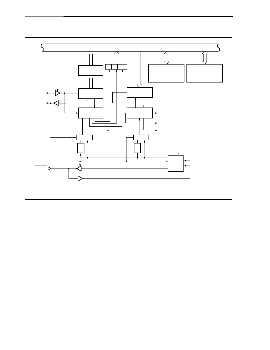
CHAPTER 10 SERIAL INTERFACE FUNCTION
User's Manual U14492EJ5V0UD
444
Figure 10-15. Block Diagram of Asynchronous Serial Interfaces 1, 2
Transmit
shift registers
(TXSn, TXSLn)
Asynchronous
serial interface mode
registers n0, n1
(ASIMn0, ASIMn1)
Asynchronous
serial interface status
register n
(ASISn)
Transmission control
parity addition
Receive buffers n, Ln
(RXBn, RXBLn)
PEn FEn OVEn
Receive
shift register
RXDn
TXDn
MOD bit
ASCKn
Reception control
parity check
Selector
Selector
Selector
INTSTn
INTSRn
SOTn flag
BRGn
SIRn flag
Internal bus
1
16
1
16
Remark n = 1, 2

CHAPTER 10 SERIAL INTERFACE FUNCTION
User's Manual U14492EJ5V0UD
445
10.3.3 Control registers
(1) Asynchronous serial interface mode registers 10, 20 (ASIM10, ASIM20)
The ASIMn0 register is an 8-bit register that controls the UART1, UART2 transfer operation (n = 1, 2).
This register can be read/written in 8-bit or 1-bit units.
Cautions 1. If a bit other than the RXEn bit of the ASIMn0 register is changed during UARTn
transmission or reception, the UARTn operation cannot be guaranteed (n = 1, 2).
2. Set a bit other than the RXEn bit of the ASIMn0 register when the UARTn operation is
stopped (when RXEn bit = 0 and transmission is completed). Change the port 3 mode
control register (PMC3) after setting the communication mode for bits other than the
RXEn bit of the ASIMn0 register.
3. In the case of serial clock output in the clocked (synchronous) mode, ensure that nodes
do not output to one another causing conflicts.
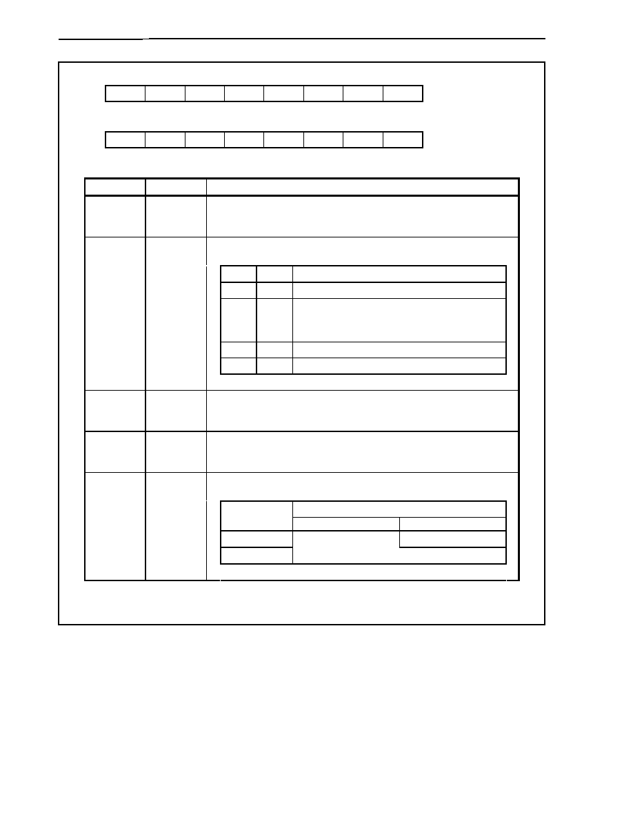
CHAPTER 10 SERIAL INTERFACE FUNCTION
User's Manual U14492EJ5V0UD
446
7
1
ASIM10
<6>
RXE1
5
PS1
4
PS0
3
CL
2
SL
1
0
0
SCLS
Address
FFFFFA28H
Initial value
81H
7
1
ASIM20
<6>
RXE2
5
PS1
4
PS0
3
CL
2
SL
1
0
0
SCLS
Address
FFFFFA48H
Initial value
81H
Bit position
Bit name
Function
6 RXEn Enables/disables reception.
0: Disable reception
1: Enable reception
Specifies parity bit length.
PS1 PS0
Operation
0 0
No parity, extension bit operation
0 1
0 parity
Transmit side
Transmission with parity bit = 0
Receive side
No parity error generated during
reception
1 0
Odd parity
5, 4
PS1, PS0
1 1
Even parity
3 CL
Specifies character length of transmit/receive data (1 frame).
0: 7 bits
1: 8 bits
2 SL
Specifies stop bit length of transmit data.
0: 1 bit
1: 2 bits
Specifies serial clock source.
Operation
SCLS
In asynchronous mode
In synchronous mode
0
External clock input
1
Internal baud rate
generator
0 SCLS
Remark n = 1, 2

CHAPTER 10 SERIAL INTERFACE FUNCTION
User's Manual U14492EJ5V0UD
447
(2) Asynchronous serial interface mode registers 11, 21 (ASIM11, ASIM21)
The ASIMn1 register is an 8-bit register that controls the UART1 and UART2 transfer modes.
This register can be read/written in 8-bit or 1-bit units.
7
0
ASIM11
6
0
5
0
4
0
3
MOD
2
UMST
1
UMSR
0
EBS
Address
FFFFFA2AH
Initial value
00H
7
0
ASIM21
6
0
5
0
4
0
3
MOD
2
UMST
1
UMSR
0
EBS
Address
FFFFFA4AH
Initial value
00H
Bit position
Bit name
Function
3 MOD
Specifies operation mode (asynchronous/synchronous mode).
0: Asynchronous mode
1: Synchronous mode
2 UMST Specifies number of continuous frame transmissions.
0: 1-frame data transmission
1: 2-frame continuous data transmission
1 UMSR Specifies number of continuous frame receptions.
0: 1-frame data reception
1: 2-frame continuous data reception
0 EBS
Specifies extension bit operation for transmit/receive data when no parity is
specified (PS0 = PS1 = 0).
0: Disable extension bit addition
1: Enable extension bit addition
When the extension bit is specified, 1 data bit is added on top of the 8 bits of
transmit/receive data, enabling 9-bit data communication.
Extension bit specification is valid only when no parity (ASIMn0 register's PS0 bit =
PS1 bit = 0) and 1-frame data transmission (UMST bit = 0) are specified. When 0
parity, odd parity, or even parity are specified, or when 2-frame continuous data
transmission (UMST bit = 1) is specified, the EBS bit setting becomes invalid and
extension bit addition is not performed.
Extension bit addition (EBS bit = 1) and 2-frame continuous data reception (UMSR
bit = 1) cannot be set simultaneously.

CHAPTER 10 SERIAL INTERFACE FUNCTION
User's Manual U14492EJ5V0UD
448
(3) Asynchronous serial interface status registers 1, 2 (ASIS1, ASIS2)
The ASISn register is a register that is configured of a UARTn transmission status flag (SOTn), reception
status flag (SIRn), a bit (RB8) indicating the 9th bit when extension bit addition is enabled, and 3-bit error
flags (PEn, FEn, OVEn) that indicate the error status at reception end (n = 1, 2).
The status flag that indicates reception errors always indicates the most recent error status. In other words, if
the same error occurs several times before receive data is read, this flag holds only the status of the error
that occurred last.
Each time the ASISn register is read after a receive completion interrupt (INTSRn), read the receive buffer
(RXBn or RXBLn). The error flag is cleared when the receive buffer (RXBn or RXBLn) is read.
Also, clear the error flag by reading the receive buffer (RXBn or RXBLn) when a reception error occurs.
This register is read-only, in 8-bit or 1-bit units.
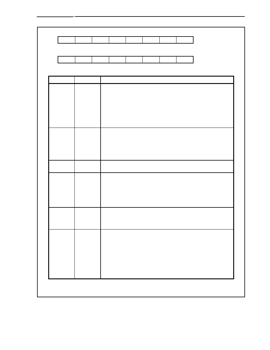
CHAPTER 10 SERIAL INTERFACE FUNCTION
User's Manual U14492EJ5V0UD
449
<7>
SOT1
ASIS1
<6>
SIR1
5
0
4
RB8
3
0
<2>
PE1
<1>
FE1
<0>
OVE1
Address
FFFFFA2CH
Initial value
00H
<7>
SOT2
ASIS2
<6>
SIR2
5
0
4
RB8
3
0
<2>
PE2
<1>
FE2
<0>
OVE2
Address
FFFFFA4CH
Initial value
00H
Bit position
Bit name
Function
7 SOTn
Status flag indicating transmission status
0: Transmission end timing (when INTSTn is generated)
1: Indicates transmission status
Note
Note
The transmission status is the status until the specified number of stop
bits has been transmitted following write operation to the transmit register.
During 2-frame continuous transmission, this status is until the stop bit of
the 2nd frame has been transmitted.
6 SIRn
Status flag indicating reception status
0: Reception end timing (when INTSRn is generated)
1: Indicates reception status
Note
Note
The reception status is the status until stop bit detection from the start bit
detection timing.
4 RB8
Indicates contents of receive data extension bit (1 bit) when 9-bit extended format
is specified (EBS bit of ASIMn1 register = 1).
2 PEn
Status flag indicating parity error
0: Processing to read data from receive buffer
1: When transmit parity and receive parity don't match
Caution No parity error is generated if no parity is specified or 0 parity is
specified with the PS1, PS0 bits of the ASIMn0 register.
1 FEn
Status flag indicating framing error
0: Processing to read data from receive buffer
1: When stop bit is not detected
0 OVEn Status flag indicating overrun error
0: Processing to read data from receive buffer
1: When UARTn has completed next reception processing prior to loading
receive data from receive buffer
Since the contents of the receive shift register are transferred to the receive buffer
(RXBn, RXBLn) every time 1 frame is received, the following receive data is
overwritten to the receive buffer (RXBn, RXBLn) and the previous receive data is
discarded.
Remark n = 1, 2

CHAPTER 10 SERIAL INTERFACE FUNCTION
User's Manual U14492EJ5V0UD
450
(4) 2-frame continuous reception buffer registers 1, 2 (RXB1, RXB2)/receive buffer registers L1, L2
(RXBL1, RXBL2)
The RXBn register is a 16-bit buffer register that holds receive data (during 2-frame continuous reception
(UMSR bit of ASIMn1 register = 1), during 9-bit extended data reception (EBS bit of ASIMn1 register = 1)) (n
= 1, 2). During 7 or 8 bit/character reception, 0 is stored in the MSB.
For 16-bit access to this register, specify RXBn, and for access to the lower 8 bits, specify RXBLn.
In the receive enabled status, receive data is transferred from the receive shift register to the receive buffer in
synchronization with the end of shift-in processing for 1 frame of data.
The reception completion interrupt request (INTSRn) is generated upon transfer of data to the receive buffer
(when 2-frame continuous reception is specified, receive buffer transfer of the second frame).
In the reception disabled status, transfer processing to the receive buffer is not performed even if shift-in
processing for 1 frame of data has been completed, and the contents of the receive buffer are held.
Neither is a reception completion interrupt request generated.
The RXBn register is read-only, in 16-bit units, and the RXBLn register is read-only, in 8-bit units.
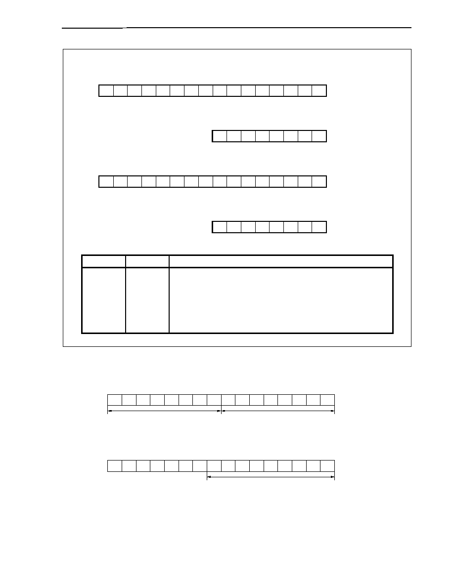
CHAPTER 10 SERIAL INTERFACE FUNCTION
User's Manual U14492EJ5V0UD
451
14
RXB14
13
RXB13
12
RXB12
2
RXB2
3
RXB3
4
RXB4
5
RXB5
6
RXB6
7
RXB7
8
RXB8
9
RXB9
10
RXB10
11
RXB11
15
RXB15
1
RXB1
0
RXB0
RXB1
[2-frame continuous reception buffer register 1]
Address
FFFFFA20H
Initial value
Undefined
2
RXB2
3
RXB3
4
RXB4
5
RXB5
6
RXB6
7
RXB7
1
RXB1
0
RXB0
RXBL1
[Receive buffer register L1]
Address
FFFFFA22H
Initial value
Undefined
14
RXB14
13
RXB13
12
RXB12
2
RXB2
3
RXB3
4
RXB4
5
RXB5
6
RXB6
7
RXB7
8
RXB8
9
RXB9
10
RXB10
11
RXB11
15
RXB15
1
RXB1
0
RXB0
RXB2
[2-frame continuous reception buffer register 2]
Address
FFFFFA40H
Initial value
Undefined
2
RXB2
3
RXB3
4
RXB4
5
RXB5
6
RXB6
7
RXB7
1
RXB1
0
RXB0
RXBL2
[Receive buffer register L2]
Address
FFFFFA42H
Initial value
Undefined
Bit position
Bit name
Function
15 to 0
RXB15 to
RXB0
Stores receive data.
0 can be read for the RXBn register when 7, 8 bit/character data is received.
When an extension bit is set during 9 bit/character data reception, the extension bit
(RXB8) is stored in RB8 of the ASISn register simultaneously with saving to the
receive buffer.
0 can be read for the RXB7 bit of the RXBLn register during 7 bit/character data
reception.
(a) When 2-frame continuous reception is set
14
RXB14
13
RXB13
12
RXB12
2
RXB2
3
RXB3
4
RXB4
5
RXB5
6
RXB6
7
RXB7
8
RXB8
9
RXB9
10
RXB10
11
RXB11
15
RXB15
1
RXB1
0
RXB0
RXBn
7-/8-bit data of 1st frame
7-/8-bit data of 2nd frame
(b) When 9-bit extension reception is set
14
RXB14
13
RXB13
12
RXB12
2
RXB2
3
RXB3
4
RXB4
5
RXB5
6
RXB6
7
RXB7
8
RXB8
9
RXB9
10
RXB10
11
RXB11
15
RXB15
1
RXB1
0
RXB0
RXBn
9-bit extended data
When 9-bit extension is set, the extension bit (RXB8) is stored in the RB8 bit of the ASISn register
simultaneously with saving to the receive buffer.

CHAPTER 10 SERIAL INTERFACE FUNCTION
User's Manual U14492EJ5V0UD
452
(c) Cautions
<1> Operation upon occurrence of overrun error during 2-frame continuous reception
∑ During normal reception
Reception completion interrupt (INTSRn) generated upon end of reception of 2nd frame, no error
RXDn
Frame 1
Frame 2
∑ Reception of 3rd frame started before performing reception processing
Reception completion interrupt (INTSRn) generated upon end of reception of 2nd frame, no error
RXDn
Frame 1
Frame 2
Reception completion interrupt not generated upon end of reception of 3rd frame, occurrence of error
RXDn
Frame 3
Frame 3
Value of OVEn bit of ASISn register becomes 1.
∑ Start of reception of 3rd frame and 4th frame before performing reception processing
Reception completion interrupt (INTSRn) generated upon end of reception of 2nd frame, no error
RXDn
Frame 1
Frame 2
Reception completion interrupt not generated upon end of reception of 3rd frame, occurrence of error
RXDn
Frame 3
Frame 3
Value of OVEn bit of ASISn register becomes 1.
Reception completion interrupt (INTSRn) generated upon end of reception of 4th frame, no error
RXDn
Frame 3
Frame 4
Value of OVEn bit of ASISn register remains 1.
∑ Start of reception of 3rd frame before performing reception processing, start of reception of
4th frame after performing reception processing
Reception completion interrupt (INTSRn) generated upon end of reception of 2nd frame, no error
RXDn
Frame 1
Frame 2
Reception completion interrupt not generated upon end of reception of 3rd frame, occurrence of error
RXDn
Frame 3
Frame 3
Value of OVEn bit of ASISn register becomes 1.
Value of OVEn flag becomes 0 during reception processing.
Reception completion interrupt (INTSRn) generated upon end of reception of 4th frame, no error
RXDn
Frame 3
Frame 4
No occurrence of error
CHAPTER 10 SERIAL INTERFACE FUNCTION
User's Manual U14492EJ5V0UD
453
(5) 2-frame continuous transmission shift registers 1, 2 (TXS1, TXS2)/transmit shift registers L1, L2
(TXSL1, TXSL2)
The TXSn register is a 9-bit/2-frame continuous transmission processing shift register (n = 1, 2).
Transmission is started by writing data to this register.
A transmission completion interrupt request (INTSTn) is generated in synchronization with the end of
transmission of 1 frame or 2 frames including the TXSn data.
For 16-bit access to this register, specify TXSn, and for access to the lower 8 bits, specify TXSLn.
The TXSn register is write-only, in 16-bit units, and the TXSLn register is write-only, in 8-bit units.
Caution TXSn, TXSLn can be read, but since shifting is done in synchronization with the shift clock,
the data that is read cannot be guaranteed.
14
TXS14
13
TXS13
12
TXS12
2
TXS2
3
TXS3
4
TXS4
5
TXS5
6
TXS6
7
TXS7
8
TXS8
9
TXS9
10
TXS10
11
TXS11
15
TXS15
1
TXS1
0
TXS0
TXS1
[2-frame continuous transmission shift register 1]
Address
FFFFFA24H
Initial value
Undefined
2
TXS2
3
TXS3
4
TXS4
5
TXS5
6
TXS6
7
TXS7
1
TXS1
0
TXS0
TXSL1
[Transmit shift register L1]
Address
FFFFFA26H
Initial value
Undefined
14
TXS14
13
TXS13
12
TXS12
2
TXS2
3
TXS3
4
TXS4
5
TXS5
6
TXS6
7
TXS7
8
TXS8
9
TXS9
10
TXS10
11
TXS11
15
TXS15
1
TXS1
0
TXS0
TXS2
[2-frame continuous transmission shift register 2]
Address
FFFFFA44H
Initial value
Undefined
2
TXS2
3
TXS3
4
TXS4
5
TXS5
6
TXS6
7
TXS7
1
TXS1
0
TXS0
TXSL2
[Transmit shift register L2]
Address
FFFFFA46H
Initial value
Undefined
Bit position
Bit name
Function
15 to 0
TXB15 to
TXB0
Writes transmit data.
CHAPTER 10 SERIAL INTERFACE FUNCTION
User's Manual U14492EJ5V0UD
454
10.3.4 Interrupt requests
The following two types of interrupt request are generated from UARTn (n = 1, 2).
∑ Reception completion interrupt (INTSRn)
∑ Transmission completion interrupt (INTSTn)
The reception completion interrupt has higher default priority than the transmission completion interrupt.
Table 10-5. Default Priority of Generated Interrupts
Interrupt Priority
Reception completion
1
Transmission completion
2
(1) Reception completion interrupt (INTSRn)
In the reception enabled state, the reception completion interrupt (INTSRn) is generated when data in the
receive shift register undergoes shift-in processing and is transferred to the receive buffer.
The reception completion interrupt request (INTSRn) is generated following stop bit sampling. The reception
completion interrupt (INTSRn) is generated upon occurrence of an error.
In the reception disabled state, no reception completion interrupt is generated.
Caution A reception completion interrupt (INTSRn) is generated when the last bit of receive data
(stop bit) is sampled.
(2) Transmission completion interrupt (INTSTn)
Since UARTn does not have a transmit buffer, a transmission completion interrupt request (INTSTn) is
generated when one frame of data containing 7-bit or 8-bit characters or two frames of data containing 9-bit
characters are shifted out from the transmit shift register (TXSn, TXSLn).
CHAPTER 10 SERIAL INTERFACE FUNCTION
User's Manual U14492EJ5V0UD
455
10.3.5 Operation
(1) Data format
Full-duplex serial data is transmitted and received.
Figure 10-16 shows the format of transmit/receive data. One data frame consists of a start bit, character bits,
a parity bit, and a stop bit(s). When 2 data frame transfer is set, both frames have the above-described
format.
Specification of the character bit length in one data frame, parity selection, and specification of the stop bit
length is done using asynchronous serial interface mode registers 10, 20 (ASIM10, ASIM20). Specification of
the number of frames and specification of the extension bit is done with asynchronous serial interface mode
registers 11, 21 (ASIM11, ASIM21). Data is transmitted LSB first.
Figure 10-16. Asynchronous Serial Interface Transmit/Receive Data Format
(a) 1-frame format
1 frame
Data
Stop bit
Start
bit
Parity/
extension
bit
D0
D1
D2
D3
D4
D5
D6
D7
(b) 2-frame format
Higher frame
Lower frame
Data
D8 D9 D10 D11 D12 D13 D14 D15
D0 D1 D2 D3 D4 D5 D6 D7
Start
bit
Parity
bit
Stop
bit
Parity
bit
Stop
bit
Start
bit
Start bit: 1 bit
Character bits: 7 or 8 bits
Parity bit: Even parity, odd parity, 0 parity, or no parity
Stop bit: 1 or 2 bits
Caution The extension bit is invalid in the 2-frame continuous mode or when a parity bit is added.

CHAPTER 10 SERIAL INTERFACE FUNCTION
User's Manual U14492EJ5V0UD
456
Table 10-6. ASIMn0, ASIMn1 Register Settings and Data Format
ASIMn0, ASIMn1 Register Settings
Data Format
CL Bit
PS1 Bit
PS0 Bit
SL Bit
EBS Bit
D0 to D6
D7
D8
D9
D10
0 0
0
DATA
Stop
bit
0
Other than PS1 = PS0 = 0
DATA
Parity bit
Stop bit
1 0
0
DATA
DATA
Stop
bit
1
Other than PS1 = PS0 = 0
0 0
DATA
DATA
Parity bit
Stop bit
0
0
0
DATA
Stop bit
Stop bit
0
Other than PS1 = PS0 = 0
DATA
Parity bit
Stop bit
Stop bit
1
0
0
DATA
DATA
Stop bit
Stop bit
1
Other than PS1 = PS0 = 0
1 0
DATA
DATA
Parity bit
Stop bit
Stop bit
0 0
0
DATA
Stop
bit
0
Other than PS1 = PS0 = 0
DATA
Parity bit
Stop bit
1
0
0
DATA DATA DATA Stop
bit
1
Other than PS1 = PS0 = 0
0 1
DATA
DATA
Parity bit
Stop bit
0
0
0
DATA
Stop bit
Stop bit
0
Other than PS1 = PS0 = 0
DATA
Parity bit
Stop bit
Stop bit
1
0
0
DATA DATA DATA Stop
bit
Stop
bit
1
Other than PS1 = PS0 = 0
1 1
DATA
DATA
Parity bit
Stop bit
Stop bit

CHAPTER 10 SERIAL INTERFACE FUNCTION
User's Manual U14492EJ5V0UD
457
(2) Transmission operation
The transmission operation is started by writing data to 2-frame continuous transmission shift registers 1, 2
(TXS1, TXS2)/transmit shift registers L1, L2 (TXSL1, TXSL2).
Following data write, the start bit is transmitted from the next shift timing.
Since the UARTn does not have a CTS (transmission enable signal) input pin, use a port when the other
party confirms the reception enabled status (n = 1, 2).
(a) Transmission operation start
The transmission operation is started by writing transmit data to 2-frame continuous transmission shift
registers 1, 2 (TXS1, TXS2)/transmit shift registers L1, L2 (TXSL1, TXSL2). Then data is output in
sequence from LSB to the TXDn pin (transmission in sequence from the start bit). A start bit, parity bit,
and stop bit(s) are automatically added.
(b) Transmission interrupt request
When the transmit shift register becomes empty upon completion of the transmission of 1 or 2 frames of
data, a transmission completion interrupt request (INTSTn) is generated. The INTSTn interrupt
generation timing differs depending on the specified stop bit length. The INTSTn interrupt is generated at
the same time that the last stop bit is output.
The transmission operation remains stopped until the data to be transmitted next has been written to the
TXSn/TXSLn registers.
Figure 10-17 shows the INTSTn interrupt generation timing.
Cautions 1. Normally, the transmission completion interrupt (INTSTn) is generated when the
transmit shift register becomes empty. However, if the transmit shift register has
become empty due to input of RESET, no transmission completion interrupt (INTSTn) is
generated.
2. No data can be written to the TXSn or TXSLn registers during transmission operation
until INTSTn is generated. Even if data is written, this does not affect the transmission
operation.
CHAPTER 10 SERIAL INTERFACE FUNCTION
User's Manual U14492EJ5V0UD
458
Figure 10-17. Asynchronous Serial Interface Transmission Completion Interrupt Timing
(a) When stop bit length = 1 bit
Start
Parity
Stop
D0
TXDn (output)
INTSTn interrupt
Flag in transmission
(SOTn)
D1
D2
D6
D7
(b) When stop bit length = 2 bits
Start
Parity Stop
D0
TXDn (output)
INTSTn interrupt
Flag in transmission
(SOTn)
D1
D2
D6
D7
(c) In 2-frame continuous transmission mode
Start
Start
Stop
Parity
Stop
D0
TXDn (output)
INTSTn interrupt
Flag in
transmission
(SOTn)
D1
1st frame
2nd frame
D1
D5
D6
D7
Parity

CHAPTER 10 SERIAL INTERFACE FUNCTION
User's Manual U14492EJ5V0UD
459
(3) Continuous transmission of 3 or more frames
In addition to the 1-frame/2-frame transmission function, UARTn also enables continuous transmission of 3 or
more frames, using the method shown below (n = 1, 2).
(a) How to continuously transmit 3 or more frames (when the stop bit is 1 bit (SL bit = 0))
Three frames can be continuously transmitted by writing transmit data to the TXSn/TXSLn register in the
period between the generation of the transmission completion interrupt request (INTSTn) and 4
◊ 2/f
XX
before the output of the last stop bit.
The INTSTn interrupt becomes high level 2/f
XX
after being output and returns to low level 2/f
XX
later.
TXSn/TXSLn can only be written after the INTSTn interrupt level has fallen. The time from INTSTn
interrupt generation to the completion of transmit data writing (t) is therefore indicated by the following
expression.
t = (Time of one stop bit) ≠ (2
◊ 2/f
XX
+ 4
◊ 2/f
XX
)
f
XX
= Internal system clock
Caution 4
◊ 2/f
XX
has a margin of double the clock that can actually be used for operation.
Example Count clock frequency = 32 MHz = 32,000,000 Hz
Target baud rate in synchronous mode = 9,600 bps
t = (1/9615.385)
- ((4 + 8)/32,000,000)
= 104.000
- 0.375
= 103.625 [
µ
s]
Therefore, be sure to write transmit data to TXSn/TXSLn within 103
µ
s of the generation of the INTSTn
interrupt.
Note, however, that because writing to TXSn/TXSLn may be delayed depending on the priority order of
the INTSTn interrupt or the interrupt servicing time, be sure to allow sufficient time for writing transmit
data after the INTSTn interrupt has been generated. If there is not enough time for continuous
transmission due to a delay in writing to TXSn/TXSLn, a 1-bit high level is transmitted.
Note also that if the stop bit length is 2 bits (SL bit = 1), the INTSTn interrupt will be generated when the
second stop bit is output.
Figure 10-18. Continuous Transmission of 3 or More Frames (When SL Bit = 0)
2/f
XX
2/f
XX
2/f
XX
4
◊ 2/f
XX
TXSn/TXSLn write period for 3-frame
continuous transmission
Stop bit
INTSTn interrupt

CHAPTER 10 SERIAL INTERFACE FUNCTION
User's Manual U14492EJ5V0UD
460
(4) Reception operation
The reception wait status is entered by setting the RXEn bit of the ASIMn0 register to 1 (n = 1, 2). To start
the reception operation, first perform start bit detection. Start bit detection is done by performing sampling of
the RXDn pin. When the reception operation is started, serial data is stored to the receive shift register in
sequence at the set baud rate. Each time reception of 2 frames or 1 frame of RXBn or RXBLn data has been
completed, a reception completion interrupt (INTSRn) is generated. Receive data is transmitted from the
receive buffer (RXBn/RXBLn) to memory when this interrupt is serviced.
(a) Reception enabled status
The reception operation is enabled by setting (1) the RXEn bit of the ASIMn0 register.
∑ RXEn = 1: Reception enabled status
∑ RXEn = 0: Reception disabled status
In the reception disabled status, the reception hardware is in standby in an initialized state. At this time,
no reception completion interrupt is generated, and the contents of the receive buffer are held.
(b) Start of reception operation
The reception operation is started through detection of the start bit.
∑ In asynchronous mode (MOD bit of ASIMn1 register = 0)
The RXDn pin is sampled using the serial clock from the baud rate generator. After 8 serial clocks
have been output following detection of the falling edge of the RXDn pin, the RXDn pin is again
sampled. If a low level is detected at this time, the falling edge of the RXDn pin is interpreted as a
start bit, the operation shifts to reception processing, and the RXDn pin input is sampled from this
point on in units of 16 serial clock output.
If the high level is detected during sampling after 8 serial clocks from detection of the falling edge of
the RXDn pin, this falling edge is not recognized as a start bit. The serial clock counter that generates
the sample timing is initialized and stops, and input of the next falling edge is waited for.
∑ In synchronous mode (MOD bit of ASIMn1 register = 1)
The RXDn pin is sampled using the serial clock from the baud rate generator or at the rising edge of
serial clock I/O. If the RXDn pin is low level at this time, this is interpreted as a start bit and reception
processing starts.
If reception data is interrupted at the fixed low level during reception, reception of this receive data
(including error detection) is completed and reception completion interrupt is generated. However, even
if the RXD line is fixed at low level, the next reception operation is not started (start bit detection is not
performed).
Be sure to set the high level when restarting the reception operation. If the high level is not set, the start
bit detection position becomes undefined, and correct reception operation cannot be performed.

CHAPTER 10 SERIAL INTERFACE FUNCTION
User's Manual U14492EJ5V0UD
461
(c) Reception completion interrupt request
When reception of one frame of data has been completed (stop bit detection) when the RXEn bit of the
ASIMn0 register = 1, the receive data in the shift register is transferred to RXBn/RXBLn and a reception
completion interrupt request (INTSRn) is generated after 1 frame or 2 frames of data have been
transferred to RXBn/RXBLn.
A reception completion interrupt is also generated upon detection of an error.
When the RXEn bit = 0 (reception disabled), no reception completion interrupt is generated.
Figure 10-19. Asynchronous Serial Interface Reception Completion Interrupt Timing
(a) When stop bit length = 1 bit
D0
D1
D2
D6
D7
Parity
8 serial clocks
8 serial clocks
Start
Stop
RXDn (input)
INTSRn interrupt
Flag in reception
(SIRn)
(b) When stop bit length = 2 bits
D0
D1
D2
D6
D7
Start
Parity
Stop
RXDn (input)
INTSRn interrupt
Flag in reception
(SIRn)
8 serial clocks
8 serial clocks
(c) In 2-frame continuous transmission mode
D0
D1
D1
D5
D6
D7
Start
Start
Parity Stop
Parity
Stop
RXDn (input)
INTSRn interrupt
Flag in reception
(SIRn)
1st frame
2nd frame
8 serial clocks
8 serial clocks
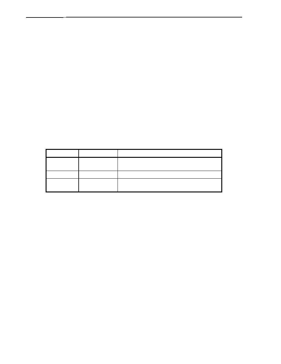
CHAPTER 10 SERIAL INTERFACE FUNCTION
User's Manual U14492EJ5V0UD
462
Cautions 1. Even if a reception error occurs, be sure to read 2-frame continuous reception buffer
register n (RXBn)/receive buffer register n (RXBLn). If the RXBn or RXBLn register is not
read, an overrun error will occur at the next data reception, and the reception error state will
continue indefinitely.
2. Reception is always performed with the stop bit length set to 1 bit. A second stop bit is
ignored.
(5) Reception errors
The three types of error flags of parity errors, framing errors, and overrun errors are affected in
synchronization with reception operation. As a result of data reception, the PEn, FEn, and OVEn flags of the
ASISn register are set (1) and a reception completion interrupt request (INTSRn) is generated at the same
time.
The contents of error that occurred during reception can be detected by reading the contents of the PEn,
FEn, and OVEn flags of the ASISn register during the INTSRn interrupt servicing.
The contents of the ASISn register are reset (0) by reading the ASISn register (if the next receive data
contains an error, the corresponding error flag is set (1)).
Table 10-7. Reception Error Causes
Error Flag
Reception Error
Causes
PEn Parity
error
The
parity
specification during transmission did not match
the parity of the reception data
FEn
Framing error
No stop bit was detected
OVEn
Overrun error
The reception of the next data was completed before data
was read from the receive buffer
(6) Parity types and corresponding operation
A parity bit is used to detect a bit error in communication data. Normally, the same type of parity bit is used at
the transmission and reception sides.
(a) Even parity
<1> During
transmission
The parity bit is controlled so that number of bits with the value "1" within the transmit data including
the parity bit is even. The parity bit value is as follows.
∑ If the number of bits with the value "1" within the transmit data is odd: 1
∑ If the number of bits with the value "1" within the transmit data is even: 0
<2> During reception
The number of bits with the value "1" within the receive data including the parity bit is counted, and a
parity error is generated if this number is odd.

CHAPTER 10 SERIAL INTERFACE FUNCTION
User's Manual U14492EJ5V0UD
463
(b) Odd parity
<1> During transmission
In contrast to even parity, the parity bit is controlled so that the number of bits with the value "1" within
the transmit data including the parity bit is odd. The parity bit value is as follows.
∑ If the number of bits with the value "1" within the transmit data is odd: 0
∑ If the number of bits with the value "1" within the transmit data is even: 1
<2> During reception
The number of bits with the value "1" within the receive data including the parity bit is counted, and a
parity error is generated if this number is even.
(c) 0 parity
During transmission, the parity bit is set to "0" regardless of the transmit data.
During reception, no parity bit check is performed. Therefore, no parity error is generated regardless of
whether the parity bit is "0" or "1".
(d) No parity
No parity bit is added to the transmit data.
During reception, the receive operation is performed as if there were no parity bit. Since there is no
parity bit, no parity error is generated.

CHAPTER 10 SERIAL INTERFACE FUNCTION
User's Manual U14492EJ5V0UD
464
10.3.6 Synchronous mode
The synchronous mode can be set with the ASCKn pin, which is the serial clock I/O pin (n = 1, 2).
The synchronous mode is set with the MOD bit of the ASIMn1 register, and the serial clock to be used for
synchronization is selected with the SCLS bit of the ASIMn0 register.
In the synchronous mode, external clock input is selected when the value of the SCLS bit is 0 (default), and the
serial clock output is selected in the case of all other settings. Therefore, when performing settings, make sure that
outputs between connection nodes do not conflict.
In the synchronous mode, the falling edge of the serial clock is used as the transmission timing, and the rising edge
as the reception timing, but transmit data is output with a delay of 1 system clock (serial clock) (in the external clock
synchronous mode, the maximum delay is 2.5 system clocks).
Figure 10-20. Transmission/Reception Timing in Synchronous Mode
D0
D1
D2
D3
D4
D5
D6
D7
Parity
Start
Stop
D0
D1
D2
D3
D4
D5
D6
D7
Parity
Start
Stop
ASCKn
Output data
(TXDn)
Input data
(RXDn)
On the data output side, the data changes at the falling edge of the serial clock output.
On the data input side, the data is latched at the rising edge of the serial clock output.
Serial clock output continues as long as the setting is not canceled.
Remark n = 1, 2
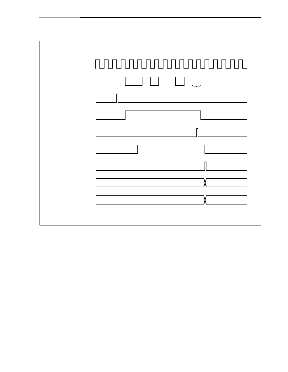
CHAPTER 10 SERIAL INTERFACE FUNCTION
User's Manual U14492EJ5V0UD
465
Figure 10-21. Transmission/Reception Timing Chart for Synchronous Mode (1/3)
(a) In 1-frame transmission/reception mode
Serial clock
Transmission register
write signal
Flag in transmission
(SOTn)
Transmission
completion interrupt
(INTSTn)
Reception completion
interrupt
(INTSRn)
Reception buffer
(RXBn)
Reception buffer
(RXBLn)
Flag in reception
(SIRn)
Transmit data
Stop bit
Undefined (hold previous value)
Undefined (hold previous value)
005AH
5AH
Remark n = 1, 2
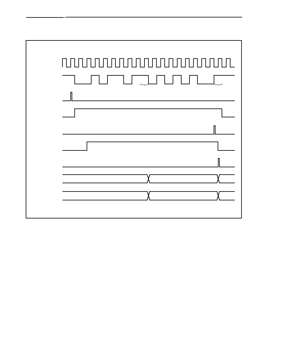
CHAPTER 10 SERIAL INTERFACE FUNCTION
User's Manual U14492EJ5V0UD
466
Figure 10-21. Transmission/Reception Timing Chart for Synchronous Mode (2/3)
(b) In 2-frame continuous transmission/reception mode
Serial clock
Transmission
register
write signal
Flag in transmission
(SOTn)
Transmission
completion
interrupt
(INTSTn)
Reception
completion
interrupt
(INTSRn)
Reception buffer
(RXBn)
Reception buffer
(RXBLn)
Flag in reception
(SIRn)
Transmit data
Stop bit
Stop bit
Undefined (hold previous value)
Undefined (hold previous value)
5A5AH
5AH
5A15H
15H
Remark n = 1, 2
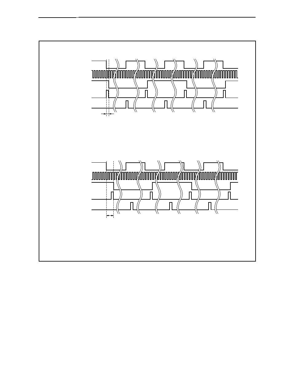
CHAPTER 10 SERIAL INTERFACE FUNCTION
User's Manual U14492EJ5V0UD
467
Figure 10-21. Transmission/Reception Timing Chart for Synchronous Mode (3/3)
(c) Transmission/reception timing and transmit data timing during serial clock output
Note
Serial clock (output)
System clock
Transmit data
Transmission timing
Reception timing
Note The transmit data is delayed by 1 system clock in relation to the serial clock.
(d) Transmission/reception timing and transmit data timing using external serial clock
Note
External serial clock
System clock
Transmit data
Transmission timing
Reception timing
Note Since, during external serial clock synchronization, synchronization is done with the internal system
clock when feeding the external serial clock to the internal circuit, a delay ranging from 1 system clock to
a maximum of 2.5 system clocks results.
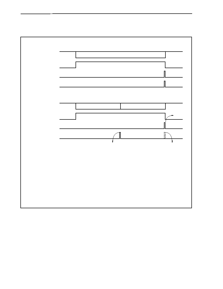
CHAPTER 10 SERIAL INTERFACE FUNCTION
User's Manual U14492EJ5V0UD
468
Figure 10-22. Reception Completion Interrupt and Error Interrupt Generation Timing During
Synchronous
Mode
Reception
(a) During normal operation (in 1-frame reception mode)
START
Receive data
Flag in reception
(SIRn)
Reception completion
interrupt
(INTSRn)
Error interrupt
STOP
(b) In 2-frame continuous reception mode
START
START
Receive data
Flag in reception
(SIRn)
Reception completion
interrupt
(INTSRn)
Error interrupt
STOP
STOP
(1)
(2)
(3)
<Explanation>
(1) If the start bit of the second frame is not detected, no reception completion interrupt is generated.
(2) If an error occurs in the first frame, an error interrupt is generated following detection of the stop bit
of the first frame (at the calculated position).
(3) If an error occurs in the second frame, an error interrupt is generated simultaneously with a
reception completion interrupt.
If an error occurs in the first frame, no error interrupt is generated even if an error occurs in the
second frame.
Remark n = 1, 2

CHAPTER 10 SERIAL INTERFACE FUNCTION
User's Manual U14492EJ5V0UD
469
10.3.7 Dedicated baud rate generators 1, 2 (BRG1, BRG2)
(1) Configuration of baud rate generators 1, 2 (BRG1, BRG2)
For UART1 and UART2, the serial clock can be selected from the dedicated baud rate generator output or
internal system clock (f
XX
) for each channel.
The serial clock source is specified with registers ASIM10 and ASIM20.
If dedicated baud rate generator output is specified, BRG1 and BRG2 are selected as the clock sources.
Since the same serial clock can be shared for transmission and reception for one channel, baud rate is the
same for the transmission/reception.
Figure 10-23. Block Diagram of Baud Rate Generators 1, 2 (BRG1, BRG2)
BGCS1, BGCS0
PRSCMn
Match detector
1/2
UARTn
8-bit timer counter
f
XX
/2
f
XX
/4
f
XX
/8
f
XX
/16
Selector
Remark f
XX
: Internal system clock
n = 1, 2
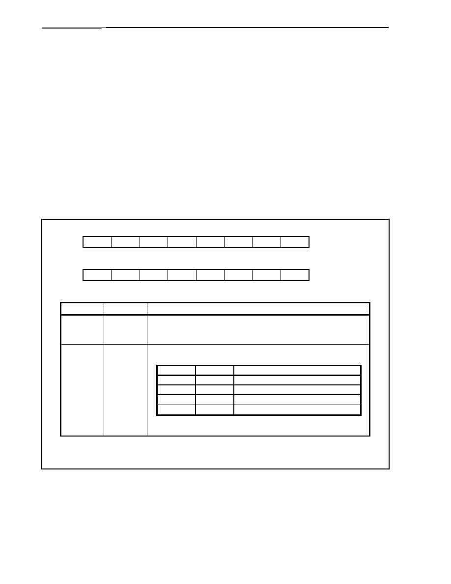
CHAPTER 10 SERIAL INTERFACE FUNCTION
User's Manual U14492EJ5V0UD
470
(2) Dedicated baud rate generators 1, 2 (BRG1, BRG2)
BRGn is configured of an 8-bit timer counter for baud rate signal generation, a prescaler mode register that
controls the generation of the baud rate signal (PRSMn), a prescaler compare register that sets the value of
the 8-bit timer counter (PRSCMn), and a prescaler (n = 1, 2).
(a) Input clock
The internal system clock (f
XX
) is input to BRGn.
(b) Prescaler mode registers 1, 2 (PRSM1, PRSM2)
The PRSMn register controls generation of the UARTn baud rate signal (n = 1, 2).
These registers can be read/written in 8-bit or 1-bit units.
Cautions 1. Do not change the values of the BGCS1 and BGCS0 bits during transmission/
reception operations.
2. Set PRSMn register other than the UARTCEn bit prior to setting the UARTCEn bit to
1 (n = 1, 2).
<7>
UARTCE1
PRSM1
6
0
5
0
4
0
3
0
2
0
1
BGCS1
0
BGCS0
Address
FFFFFA2EH
Initial value
00H
<7>
UARTCE2
PRSM2
6
0
5
0
4
0
3
0
2
0
1
BGCS1
0
BGCS0
Address
FFFFFA4EH
Initial value
00H
Bit position
Bit name
Function
7 UARTCEn
Enables baud rate counter operation.
0: Stop baud rate counter operation and fix baud rate output signal to "0".
1: Enable baud rate counter operation and start baud rate output operation.
Selects count clock to baud rate counter.
BGCS1
BGCS0
Count clock selection
0 0
f
XX
/2
0 1
f
XX
/4
1 0
f
XX
/8
1 1
f
XX
/16
1, 0
BGCS1,
BGCS0
Remark f
XX
: Internal system clock
Remark n = 1, 2
CHAPTER 10 SERIAL INTERFACE FUNCTION
User's Manual U14492EJ5V0UD
471
(c) Prescaler compare registers 1, 2 (PRSCM1, PRSCM2)
PRSCMn is an 8-bit compare register that sets the value of the 8-bit timer counter (n = 1, 2).
These registers can be read/written in 8-bit units.
Cautions 1. The internal timer counter is cleared by writing to the PRSCMn register. Therefore,
do not overwrite the PRSCMn register during transmission operation.
2. Perform PRSCMn register settings prior to setting the UARTCEn bit to 1. If the
contents of the PRSCMn register are overwritten when the value of the UARTCEn bit
is 1, the cycle of the baud rate signal is not guaranteed.
3. Set the baud rate to 153,600 bps or lower in asynchronous mode, and 1,000,000 bps
or lower in synchronous mode.
7
PRSCM7
PRSCM1
6
PRSCM6
5
PRSCM5
4
PRSCM4
3
PRSCM3
2
PRSCM2
1
PRSCM1
0
PRSCM0
Address
FFFFFA30H
Initial value
00H
7
PRSCM7
PRSCM2
6
PRSCM6
5
PRSCM5
4
PRSCM4
3
PRSCM3
2
PRSCM2
1
PRSCM1
0
PRSCM0
Address
FFFFFA50H
Initial value
00H
(d) Baud rate generation
First, when the UARTCEn bit of the PRSMn register is overwritten with 1, the 8-bit timer counter for baud
rate signal generation starts counting up with the clock selected with bits BGCS1 and BGCS0 of the
PRSMn register. The count value of the 8-bit timer counter is compared with the value of the PRSCMn
register, and if these values match, a timer count clock pulse of 1 cycle is output to the output controller
for the baud rate.
The output controller for the baud rate reverses the baud rate signal in synchronization with the rising
edge of the timer count clock when this pulse is "1".
(e) Cycle of baud rate signal
The cycle of the baud rate signal is calculated as follows.
∑ When setting value of PRSCMn register is 00H
(Cycle of signal selected with bits BGCS1, BGCS0 of PRSMn register)
◊ 256 ◊ 2
∑ In cases other than above
(Cycle of signal selected with bits BGCS1, BGCS0 of PRSMn register)
◊ (setting value of PRSCMn
register)
◊ 2

CHAPTER 10 SERIAL INTERFACE FUNCTION
User's Manual U14492EJ5V0UD
472
(f) Baud rate setting value
The formulas for calculating the baud rate in the asynchronous mode and the synchronous mode and the
formula for calculating the error are as follows.
<1> Formula for calculating baud rate in asynchronous mode
Baud rate = [bps]
f
XX
= Internal system clock frequency [Hz]
= CPU clock/2 [Hz]
m: Setting value of PRSCMn register (1
m 256
Note
)
k: Value set with bits BGCS1, BGCS0 of PRSMn register (k = 0, 1, 2, 3)
Note The setting of m = 256 is performed by writing 00H to the PRSCMn register.
<2> Formula for calculating the baud rate in synchronous mode
Baud rate = [bps]
f
XX
= Internal system clock frequency [Hz]
= CPU clock/2 [Hz]
m: Setting value of PRSCMn register (1
m 256
Note
)
k: Value set with bits BGCS1, BGCS0 of PRSMn register (k = 0, 1, 2, 3)
Note The setting of m = 256 is performed by writing 00H to the PRSCMn register.
<3> Formula for calculating error
Error [%] =
◊ 100
Example (9520
- 9600)/9600 ◊ 100 = -0.833 [%]
Remark Actual baud rate: Baud rate with error
Target baud rate: Normal baud rate
f
XX
2
◊ m ◊ 2
k
◊ 16
f
XX
2
◊ m ◊ 2
k
Actual baud rate
- Target baud rate
Target baud rate

CHAPTER 10 SERIAL INTERFACE FUNCTION
User's Manual U14492EJ5V0UD
473
<4> Baud rate setting example
In an actual system, the output of a prescaler module, etc. is connected to input clock. Table 10-8
shows the baud rate generator setting data at this time.
Table 10-8. Baud Rate Generator Setting Data (BRG = f
XX
/2) (1/2)
(a) When f
XX
= 32 MHz
Target Baud Rate
Actual Baud Rate
Synchronous
Mode
Asynchronous
Mode
Synchronous
Mode
Asynchronous
Mode
BGCSm Bit
(m = 0, 1)
PRSCMn
Register Setting
Value (n = 1, 2)
Error
4800 300
4807.692
300.4808
3 208
0.16
9600 600
9615.385
600.9615
3 104
0.16
19200 1200
19230.77
1201.923 3
52 0.16
38400 2400
38461.54
2403.846 3
26 0.16
76800 4800
76923.08
4807.692 3
13 0.16
153600 9600 153846.2
9615.385 2
13 0.16
166400 10400 166666.7
10416.67 1
24 0.16
307200 19200 307692.3
19230.77 1
13 0.16
614400 38400 615384.6
38461.54 0
13 0.16
Setting prohibited
76800
-
71428.57 0
7
-6.99
Setting prohibited
153600
-
166666.7 0
3 8.51
(b) When f
XX
= 40 MHz
Target Baud Rate
Actual Baud Rate
Synchronous
Mode
Asynchronous
Mode
Synchronous
Mode
Asynchronous
Mode
BGCSm Bit
(m = 0, 1)
PRSCMn
Register Setting
Value (n = 1, 2)
Error
4800 300
4882.813
305.1758
3 256
1.73
9600 600
9615.385
600.9615
3 130
0.16
19200 1200
19230.77
1201.923 3
65 0.16
38400 2400
38461.54
2403.846 2
65 0.16
76800 4800
76923.08
4807.692 1
65 0.16
153600 9600 153846.2
9615.385 0
65 0.16
166400 10400 166666.7
10416.67 0
60 0.16
307200 19200 303030.3
18939.39 0
33
-1.36
614400 38400 625000 39062.5 0
16 1.73
Setting prohibited
76800
-
78125 0 8 1.73
Setting prohibited
153600
-
156250 0
4 1.73
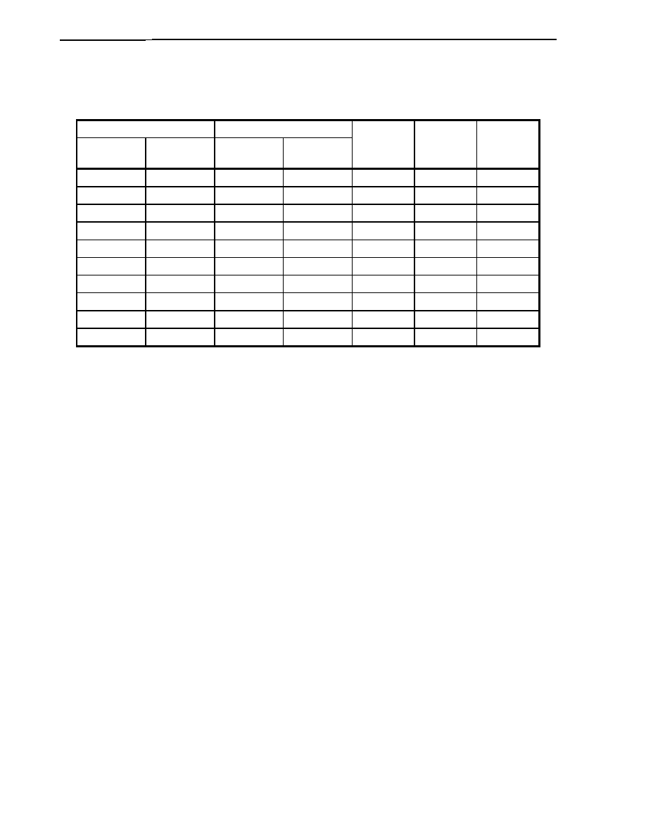
CHAPTER 10 SERIAL INTERFACE FUNCTION
User's Manual U14492EJ5V0UD
474
Table 10-8. Baud Rate Generator Setting Data (BRG = f
XX
/2) (2/2)
(c) When f
XX
= 50 MHz
Target Baud Rate
Actual Baud Rate
Synchronous
Mode
Asynchronous
Mode
Synchronous
Mode
Asynchronous
Mode
BGCSm Bit
(m = 0, 1)
PRSCMn
Register Setting
Value (n = 1, 2)
Error
9600 600
9585.89
599.1181
3 163
-0.15
19200 1200
19171.78
1198.236 2 163
-0.15
38400 2400
38343.56
2396.472 1 163
-0.15
76800 4800
76687.12
4792.945 0 163
-0.15
153600 9600 154321
9645.062 0
81 0.47
166400 10400 166666.7
10416.67 0
75 0.16
307200 19200 312500
19531.25 0
40 1.73
614400 38400 625000 39062.5 0
20 1.73
Setting prohibited
76800
-
78125 0 10 1.73
Setting prohibited
153600
-
156250 0
5 1.73
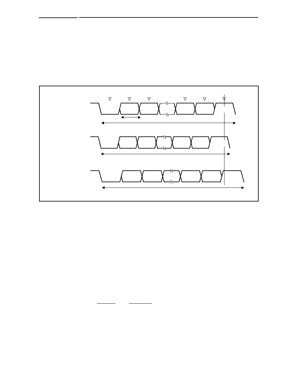
CHAPTER 10 SERIAL INTERFACE FUNCTION
User's Manual U14492EJ5V0UD
475
(3) Allowable baud rate range during reception
The degree to which a discrepancy from the transmission destination's baud rate is allowed during reception
is shown below.
Caution The equations described below should be used to set the baud rate error during reception
so that it always is within the allowable error range.
Figure 10-24. Allowable Baud Rate Range During Reception
FL
1 data frame (11
◊ FL)
FLmin
FLmax
UARTn
transfer rate
Latch timing
Start bit
Bit 0
Bit 1
Bit 7
Parity bit
Minimum allowable
transfer rate
Maximum allowable
transfer rate
Stop bit
Start bit
Bit 0
Bit 1
Bit 7
Parity bit
Stop bit
Start bit
Bit 0
Bit 1
Bit 7
Parity bit
Stop bit
As shown in Figure 10-24, after the start bit is detected, the receive data latch timing is determined according
to the counter that was set by the PRSCMn register. If all data up to the final data (stop bit) is in time for this
latch timing, the data can be received normally.
If this is applied to 11-bit reception, the following is theoretically true.
FL = (Brate)
≠1
Brate: UARTn baud rate
k:
PRSCMn register setting value
FL:
1-bit data length
When the latch timing margin is 2 clocks of f
XX
/2, the minimum allowable transfer rate (FLmin) is as
follows (f
XX
: Internal system clock).
FL
k
2
2
k
21
FL
k
2
2
k
FL
11
min
FL
+
=
◊
-
-
◊
=

CHAPTER 10 SERIAL INTERFACE FUNCTION
User's Manual U14492EJ5V0UD
476
Therefore, the transfer destination's maximum receivable baud rate (BRmax) is as follows.
BRmax = (FLmin/11)
-
1
= Brate
Similarly, the maximum allowable transfer rate (FLmax) can be obtained as follows.
FL
k
2
2
k
21
FL
k
2
2
k
FL
11
max
FL
11
10
◊
-
=
◊
◊
+
-
◊
=
◊
11
FL
k
20
2
k
21
max
FL
◊
-
=
Therefore, the transfer destination's minimum receivable baud rate (BRmin) is as follows.
BRmin = (FLmax/11)
-
1
= Brate
(4) Transfer rate in 2-frame continuous reception
In 2-frame continuous reception, the timing is initialized by detecting the start bit of the second frame, so the
transfer results are not affected.
22k
21k + 2
20k
21k
- 2

CHAPTER 10 SERIAL INTERFACE FUNCTION
User's Manual U14492EJ5V0UD
477
10.4 Clocked Serial Interfaces 0, 1 (CSI0, CSI1)
10.4.1 Features
∑
High-speed transfer: Maximum 5 Mbps
∑
Half-duplex communications
∑
Master mode or slave mode can be selected
∑
Transmission data length: 8 bits or 16 bits can be set
∑
Transfer data direction can be switched between MSB first and LSB first
∑
Eight clock signals can be selected (7 master clocks and 1 slave clock)
∑
3-wire type SOn:
Serial transmit data output
SIn:
Serial receive data input
SCKn: Serial clock I/O
∑
Interrupt sources: 1 type
∑
Transmission/reception completion interrupt (INTCSIn)
∑
Transmission/reception mode and reception-only mode can be specified
∑
Two transmission buffers (SOTBFn/SOTBFLn, SOTBn/SOTBLn) and two reception buffers (SIRBn/SIRBLn,
SIRBEn/SIRBELn) are provided on chip
∑
Single transfer mode and repeat transfer mode can be specified
Remark n = 0, 1
10.4.2 Configuration
CSIn is controlled via the clocked serial interface mode register (CSIMn) (n = 0, 1). Transmission/reception of data
is performed by writing/reading the SIOn register (n = 0, 1).
(1) Clocked serial interface mode registers 0, 1 (CSIM0, CSIM1)
The CSIMn register is an 8-bit register that specifies the operation of CSIn.
(2) Clocked serial interface clock selection registers 0, 1 (CSIC0, CSIC1)
The CSICn register is an 8-bit register that controls the CSIn serial transfer operation.
(3) Serial I/O shift registers 0, 1 (SIO0, SIO1)
The SIOn register is a 16-bit shift register that converts parallel data into serial data.
The SIOn register is used for both transmission and reception.
Data is shifted in (reception) and shifted out (transmission) from the MSB or LSB side.
The actual transmission/reception operations are started up by accessing the buffer register.
(4) Serial I/O shift registers L0, L1 (SIOL0, SIOL1)
The SIOLn register is an 8-bit shift register that converts parallel data into serial data.
The SIOLn register is used for both transmission and reception.
Data is shifted in (reception) and shifted out (transmission) from the MSB or LSB side.
The actual transmission/reception operations are started up by accessing the buffer register.

CHAPTER 10 SERIAL INTERFACE FUNCTION
User's Manual U14492EJ5V0UD
478
(5) Clocked serial interface receive buffer registers 0, 1 (SIRB0, SIRB1)
The SIRBn register is a 16-bit buffer register that stores receive data.
(6) Clocked serial interface receive buffer registers L0, L1 (SIRBL0, SIRBL1)
The SIRBLn register is an 8-bit buffer register that stores receive data.
(7) Clocked serial interface read-only receive buffer registers 0, 1 (SIRBE0, SIRBE1)
The SIRBEn register is a 16-bit buffer register that stores receive data.
The SIRBEn register is the same as the SIRBn register. It is used to read the contents of the SIRBn register.
(8) Clocked serial interface read-only receive buffer registers L0, L1 (SIRBEL0, SIRBEL1)
The SIRBELn register is an 8-bit buffer register that stores receive data.
The SIRBELn register is the same as the SIRBLn register. It is used to read the contents of the SIRBLn
register.
(9) Clocked serial interface transmit buffer registers 0, 1 (SOTB0, SOTB1)
The SOTBn register is a 16-bit buffer register that stores transmit data.
(10) Clocked serial interface transmit buffer registers L0, L1 (SOTBL0, SOTBL1)
The SOTBLn register is an 8-bit buffer register that stores transmit data.
(11) Clocked serial interface initial transmit buffer registers (SOTBF0, SOTBF1)
The SOTBFn register is a 16-bit buffer register that stores the initial transmit data in the repeat transfer mode.
(12) Clocked serial interface initial transmit buffer register L (SOTBFL0, SOTBFL1)
The SOTBFLn register is an 8-bit buffer register that stores initial transmit data in the repeat transfer mode.
(13) Selector
The selector selects the serial clock to be used.
(14) Serial clock controller
Controls the serial clock supply to the shift register. Also controls the clock output to the SCKn pin when the
internal clock is used.
(15) Serial clock counter
Counts the serial clock output or input during transmission/reception operation, and checks whether 8-bit or
16-bit data transmission/reception has been performed.
(16) Interrupt controller
Controls the interrupt request timing.

CHAPTER 10 SERIAL INTERFACE FUNCTION
User's Manual U14492EJ5V0UD
479
Figure 10-25. Block Diagram of Clocked Serial Interface
Selector
Transmission control
SO selection
SO latch
Transmit
buffer register
(SOTBn/SOTBLn)
Receive buffer register
(SIRBn/SIRBLn)
Shift register
(SIOn/SIOLn)
Initial transmit
buffer register
(SOTBFn/SOTBFLn)
Interrupt
controller
Clock start/stop control
&
clock phase control
Serial clock controller
SCKn
INTCSIn
SOn
SIn
Control signal
Transmission data control
f
XX
/2
7
f
XX
/2
6
f
XX
/2
5
f
XX
/2
4
f
XX
/2
3
f
XX
/2
2
BRG3
SCKn
Remarks 1. n = 0, 1
2. f
XX
: Internal system clock
10.4.3 Control registers
(1) Clocked serial interface mode registers 0, 1 (CSIM0, CSIM1)
The CSIMn register controls the CSIn operation (n = 0, 1).
These registers can be read/written in 8-bit or 1-bit units (however, bit 0 is read-only).
Caution Overwriting the TRMDn, CCL, DIRn, CSIT, and AUTO bits of the CSIMn register can be done
only when the CSOTn bit = 0. If these bits are overwritten at any other time, the operation
cannot be guaranteed.
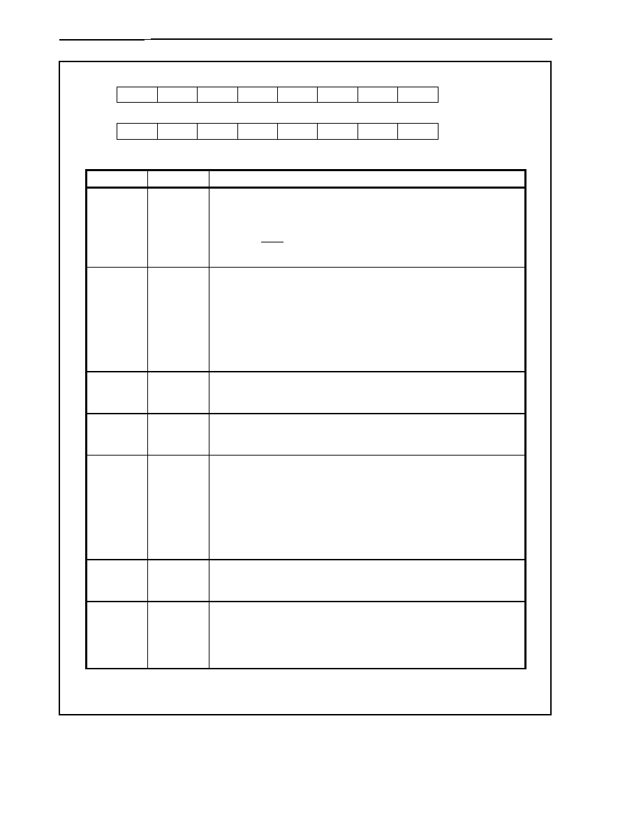
CHAPTER 10 SERIAL INTERFACE FUNCTION
User's Manual U14492EJ5V0UD
480
<7>
CSICAE0
CSIM0
<6>
TRMD0
5
CCL
<4>
DIR0
3
CSIT
2
AUTO
1
0
<0>
CSOT0
<7>
CSICAE1
<6>
TRMD1
5
CCL
<4>
DIR1
3
CSIT
2
AUTO
1
0
<0>
CSOT1
Address
FFFFF900H
Initial value
00H
CSIM1
Address
FFFFF910H
Initial value
00H
Bit position
Bit name
Function
7 CSICAEn
Enables/disables CSIn operation.
0: Disable CSIn operation.
1: Enable CSIn operation.
The internal CSIn circuit can be reset asynchronously by setting the CSICAEn bit
to 0. For the SCKn and SOn pin output status when the CSICAEn bit = 0, refer to
10.4.5 Output pins.
6 TRMDn Specifies transmission/reception mode.
0: Receive-only mode
1: Transmission/reception mode
When the TRMDn bit = 0, receive-only transfer is performed and the SOn pin
output is fixed to low level. Data reception is started by reading the SIRBn
register.
When the TRMDn bit = 1, transmission/reception is started by writing data to the
SOTBn register.
5 CCL
Specifies data length.
0: 8 bits
1: 16 bits
4 DIRn
Specifies transfer direction mode (MSB/LSB).
0: First bit of transfer data is MSB
1: First bit of transfer data is LSB
3 CSIT
Controls delay of interrupt request signal.
0: No delay
1: Delay mode (interrupt request signal is delayed 1/2 cycle).
Caution The delay mode (CSIT bit = 1) is valid only in the master mode
(CKS2 to CSK0 bits of the CSICn register are not 111B). In the
slave mode (CKS2 to CKS0 bits are 111B), do not set the delay
mode.
2 AUTO Specifies single transfer mode or repeat transfer mode.
0: Single transfer mode
1: Repeat transfer mode
0 CSOTn Flag indicating transfer status.
0: Idle status
1: Transfer execution status
Caution The CSOTn bit is cleared (0) by writing 0 to the CSICAEn bit.
Remark n = 0, 1

CHAPTER 10 SERIAL INTERFACE FUNCTION
User's Manual U14492EJ5V0UD
481
(2) Clocked serial interface clock selection registers 0, 1 (CSIC0, CSIC1)
The CSICn register is an 8-bit register that controls the CSIn transfer operation (n = 0, 1).
These registers can be read/written in 8-bit or 1-bit units.
Caution The CSICn register can be overwritten only when the CSICAEn bit of the CSIMn register = 0.
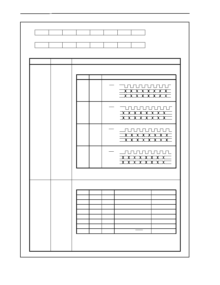
CHAPTER 10 SERIAL INTERFACE FUNCTION
User's Manual U14492EJ5V0UD
482
7
0
CSIC0
6
0
5
0
4
CKP
3
DAP
2
CKS2
1
CKS1
0
CKS0
7
0
6
0
5
0
4
CKP
3
DAP
2
CKS2
1
CKS1
0
CKS0
Address
FFFFF901H
Initial value
00H
CSIC1
Address
FFFFF911H
Initial value
00H
Bit position
Bit name
Function
Specifies operation mode.
CKP DAP
Operation
mode
0 0
0 1
1 0
1 1
4, 3
CKP, DAP
Remark n = 0, 1
Specifies serial clock.
CKS2 CKS1 CKS0
Serial
clock
Mode
0 0 0
f
XX
/2
7
Master
mode
0 0 1
f
XX
/2
6
Master
mode
0 1 0
f
XX
/2
5
Master
mode
0 1 1
f
XX
/2
4
Master
mode
1 0 0
f
XX
/2
3
Master
mode
1 0 1
f
XX
/2
2
Master
mode
1 1 0
Clock
generated
by
BRG3
Master
mode
1 1 1
External
clock
(SCKn) Slave
mode
2 to 0
CKS2 to
CKS0
Remark f
XX
: Internal system clock frequency
n = 0, 1
DO7 DO6 DO5 DO4 DO3 DO2 DO1 DO0
DI7
SOn (output)
SCKn (I/O)
SIn (input)
DI6
DI5
DI4
DI3
DI2
DI1
DI0
DO7 DO6 DO5 DO4 DO3 DO2 DO1 DO0
DI7
DI6
DI5
DI4
DI3
DI2
DI1
DI0
SOn (output)
SCKn (I/O)
SIn (input)
DO7 DO6 DO5 DO4 DO3 DO2 DO1 DO0
DI7
DI6
DI5
DI4
DI3
DI2
DI1
DI0
SOn (output)
SCKn (I/O)
SIn (input)
DO7 DO6 DO5 DO4 DO3 DO2 DO1 DO0
DI7
DI6
DI5
DI4
DI3
DI2
DI1
DI0
SOn (output)
SCKn (I/O)
SIn (input)
CHAPTER 10 SERIAL INTERFACE FUNCTION
User's Manual U14492EJ5V0UD
483
(3) Clocked serial interface receive buffer registers 0, 1 (SIRB0, SIRB1)
The SIRBn register is a 16-bit buffer register that stores receive data (n = 0, 1).
When the receive-only mode is set (TRMDn bit of CSIMn register = 0), the reception operation is started by
reading data from the SIRBn register.
These registers are read-only, in 16-bit units.
In addition to reset input, these registers can also be initialized by clearing (0) the CSICAEn bit of the CSIMn
register.
Cautions 1. Read the SIRBn register only when the 16-bit data length has been set (CCL bit of
CSIMn register = 1).
2. When the single transfer mode has been set (AUTO bit of CSIMn register = 0), perform
read operation only in the idle state (CSOTn bit of CSIMn register = 0). If the SIRBn
register is read during data transfer, the data cannot be guaranteed.
14
SIRB
14
13
SIRB
13
12
SIRB
12
2
SIRB
2
3
SIRB
3
4
SIRB
4
5
SIRB
5
6
SIRB
6
7
SIRB
7
8
SIRB
8
9
SIRB
9
10
SIRB
10
11
SIRB
11
15
SIRB
15
1
SIRB
1
0
SIRB
0
SIRB0
Address
FFFFF902H
Initial value
0000H
14
SIRB
14
13
SIRB
13
12
SIRB
12
2
SIRB
2
3
SIRB
3
4
SIRB
4
5
SIRB
5
6
SIRB
6
7
SIRB
7
8
SIRB
8
9
SIRB
9
10
SIRB
10
11
SIRB
11
15
SIRB
15
1
SIRB
1
0
SIRB
0
SIRB1
Address
FFFFF912H
Initial value
0000H
Bit position
Bit name
Function
15 to 0
SIRB15 to
SIRB0
Stores receive data.

CHAPTER 10 SERIAL INTERFACE FUNCTION
User's Manual U14492EJ5V0UD
484
(4) Clocked serial interface receive buffer registers L0, L1 (SIRBL0, SIRBL1)
The SIRBLn register is an 8-bit buffer register that stores receive data (n = 0, 1).
When the receive-only mode is set (TRMDn bit of CSIMn register = 0), the reception operation is started by
reading data from the SIRBLn register.
These registers are read-only, in 8-bit or 1-bit units.
In addition to reset input, these registers can also be initialized by clearing (0) the CSICAEn bit of the CSIMn
register.
The SIRBLn register is the same as the lower bytes of the SIRBn register.
Cautions 1. Read the SIRBLn register only when the 8-bit data length has been set (CCL bit of
CSIMn register = 0).
2. When the single transfer mode is set (AUTO bit of CSIMn register = 0), perform read
operation only in the idle state (CSOTn bit of CSIMn register = 0). If the SIRBLn register
is read during data transfer, the data cannot be guaranteed.
7
SIRB7
SIRBL0
6
SIRB6
5
SIRB5
4
SIRB4
3
SIRB3
2
SIRB2
1
SIRB1
0
SIRB0
Address
FFFFF902H
Initial value
00H
7
SIRB7
SIRBL1
6
SIRB6
5
SIRB5
4
SIRB4
3
SIRB3
2
SIRB2
1
SIRB1
0
SIRB0
Address
FFFFF912H
Initial value
00H
Bit position
Bit name
Function
7 to 0
SIRB7 to
SIRB0
Stores receive data.
CHAPTER 10 SERIAL INTERFACE FUNCTION
User's Manual U14492EJ5V0UD
485
(5) Clocked serial interface read-only receive buffer registers 0, 1 (SIRBE0, SIRBE1)
The SIRBEn register is a 16-bit buffer register that stores receive data (n = 0, 1).
These registers are read-only, in 16-bit units.
In addition to reset input, this register can also be initialized by clearing (0) the CSICAEn bit of the CSIMn
register.
The SIRBEn register is the same as the SIRBn register. It is used to read the contents of the SIRBn register.
Cautions 1. The receive operation is not started even if data is read from the SIRBEn register.
2. The SIRBEn register can be read only if the 16-bit data length is set (CCL bit of CSIMn
register = 1).
14
SIRBE
14
13
SIRBE
13
12
SIRBE
12
2
SIRBE
2
3
SIRBE
3
4
SIRBE
4
5
SIRBE
5
6
SIRBE
6
7
SIRBE
7
8
SIRBE
8
9
SIRBE
9
10
SIRBE
10
11
SIRBE
11
15
SIRBE
15
1
SIRBE
1
0
SIRBE
0
14
SIRBE
14
13
SIRBE
13
12
SIRBE
12
2
SIRBE
2
3
SIRBE
3
4
SIRBE
4
5
SIRBE
5
6
SIRBE
6
7
SIRBE
7
8
SIRBE
8
9
SIRBE
9
10
SIRBE
10
11
SIRBE
11
15
SIRBE
15
1
SIRBE
1
0
SIRBE
0
SIRBE0
Address
FFFFF906H
Initial value
0000H
SIRBE1
Address
FFFFF916H
Initial value
0000H
Bit position
Bit name
Function
15 to 0
SIRBE15 to
SIRBE0
Stores receive data.
CHAPTER 10 SERIAL INTERFACE FUNCTION
User's Manual U14492EJ5V0UD
486
(6) Clocked serial interface read-only receive buffer registers L0, L1 (SIRBEL0, SIRBEL1)
The SIRBELn register is an 8-bit buffer register that stores receive data (n = 0, 1).
These registers are read-only, in 8-bit or 1-bit units.
In addition to reset input, this register can also be initialized by clearing (0) the CSICAEn bit of the CSIMn
register.
The SIRBELn register is the same as the SIRBLn register. It is used to read the contents of the SIRBLn
register.
Cautions 1. The receive operation is not started even if data is read from the SIRBELn register.
2. The SIRBELn register can be read only if the 8-bit data length has been set (CCL bit of
CSIMn register = 0).
7
SIRBE7
SIRBEL0
6
SIRBE6
5
SIRBE5
4
SIRBE4
3
SIRBE3
2
SIRBE2
1
SIRBE1
0
SIRBE0
Address
FFFFF906H
Initial value
00H
7
SIRBE7
SIRBEL1
6
SIRBE6
5
SIRBE5
4
SIRBE4
3
SIRBE3
2
SIRBE2
1
SIRBE1
0
SIRBE0
Address
FFFFF916H
Initial value
00H
Bit position
Bit name
Function
7 to 0
SIRBE7 to
SIRBE0
Stores receive data.
CHAPTER 10 SERIAL INTERFACE FUNCTION
User's Manual U14492EJ5V0UD
487
(7) Clocked serial interface transmit buffer registers 0, 1 (SOTB0, SOTB1)
The SOTBn register is a 16-bit buffer register that stores transmit data (n = 0, 1).
When the transmission/reception mode is set (TRMDn bit of CSIMn register = 1), the transmission operation
is started by writing data to the SOTBn register.
These registers can be read/written in 16-bit units.
Cautions 1. Access the SOTBn register only when the 16-bit data length is set (CCL bit of CSIMn
register = 1).
2. When the single transfer mode is set (AUTO bit of CSIMn register = 0), perform access
only in the idle state (CSOTn bit of CSIMn register = 0). If the SOTBn register is
accessed during data transfer, the data cannot be guaranteed.
14
SOTB
14
13
SOTB
13
12
SOTB
12
2
SOTB
2
3
SOTB
3
4
SOTB
4
5
SOTB
5
6
SOTB
6
7
SOTB
7
8
SOTB
8
9
SOTB
9
10
SOTB
10
11
SOTB
11
15
SOTB
15
1
SOTB
1
0
SOTB
0
SOTB0
Address
FFFFF904H
Initial value
0000H
14
SOTB
14
13
SOTB
13
12
SOTB
12
2
SOTB
2
3
SOTB
3
4
SOTB
4
5
SOTB
5
6
SOTB
6
7
SOTB
7
8
SOTB
8
9
SOTB
9
10
SOTB
10
11
SOTB
11
15
SOTB
15
1
SOTB
1
0
SOTB
0
SOTB1
Address
FFFFF914H
Initial value
0000H
Bit position
Bit name
Function
15 to 0
SOTB15 to
SOTB0
Stores transmit data.

CHAPTER 10 SERIAL INTERFACE FUNCTION
User's Manual U14492EJ5V0UD
488
(8) Clocked serial interface transmit buffer registers L0, L1 (SOTBL0, SOTBL1)
The SOTBLn register is an 8-bit buffer register that stores transmit data (n = 0, 1).
When the transmission/reception mode is set (TRMDn bit of CSIMn register = 1), the transmission operation
is started by writing data to the SOTBLn register.
These registers can be read/written in 8-bit or 1-bit units.
The SOTBLn register is the same as the lower bytes of the SOTBn register.
Cautions 1. Access the SOTBLn register only when the 8-bit data length has been set (CCL bit of
CSIMn register = 0).
2. When the single transfer mode is set (AUTO bit of CSIMn register = 0), perform access
only in the idle state (CSOTn bit of CSIMn register = 0). If the SOTBLn register is
accessed during data transfer, the data cannot be guaranteed.
7
SOTB7
SOTBL0
6
SOTB6
5
SOTB5
4
SOTB4
3
SOTB3
2
SOTB2
1
SOTB1
0
SOTB0
Address
FFFFF904H
Initial value
00H
7
SOTB7
SOTBL1
6
SOTB6
5
SOTB5
4
SOTB4
3
SOTB3
2
SOTB2
1
SOTB1
0
SOTB0
Address
FFFFF914H
Initial value
00H
Bit position
Bit name
Function
7 to 0
SOTB7 to
SOTB0
Stores transmit data.
CHAPTER 10 SERIAL INTERFACE FUNCTION
User's Manual U14492EJ5V0UD
489
(9) Clocked serial interface initial transmit buffer registers 0, 1 (SOTBF0, SOTBF1)
The SOTBFn register is a 16-bit buffer register that stores initial transmission data in the repeat transfer
mode (n = 0, 1).
The transmission operation is not started even if data is written to the SOTBFn register.
These registers can be read/written in 16-bit units.
Caution Access the SOTBFn register only when the 16-bit data length has been set (CCL bit of
CSIMn register = 1), and only in the idle state (CSOTn bit of CSIMn register = 0). If the
SOTBFn register is accessed during data transfer, the data cannot be guaranteed.
14
SOTBF
14
13
SOTBF
13
12
SOTBF
12
2
SOTBF
2
3
SOTBF
3
4
SOTBF
4
5
SOTBF
5
6
SOTBF
6
7
SOTBF
7
8
SOTBF
8
9
SOTBF
9
10
SOTBF
10
11
SOTBF
11
15
SOTBF
15
1
SOTBF
1
0
SOTBF
0
14
SOTBF
14
13
SOTBF
13
12
SOTBF
12
2
SOTBF
2
3
SOTBF
3
4
SOTBF
4
5
SOTBF
5
6
SOTBF
6
7
SOTBF
7
8
SOTBF
8
9
SOTBF
9
10
SOTBF
10
11
SOTBF
11
15
SOTBF
15
1
SOTBF
1
0
SOTBF
0
SOTBF0
Address
FFFFF908H
Initial value
0000H
SOTBF1
Address
FFFFF918H
Initial value
0000H
Bit position
Bit name
Function
15 to 0
SOTBF15 to
SOTBF0
Stores initial transmission data in repeat transfer mode.
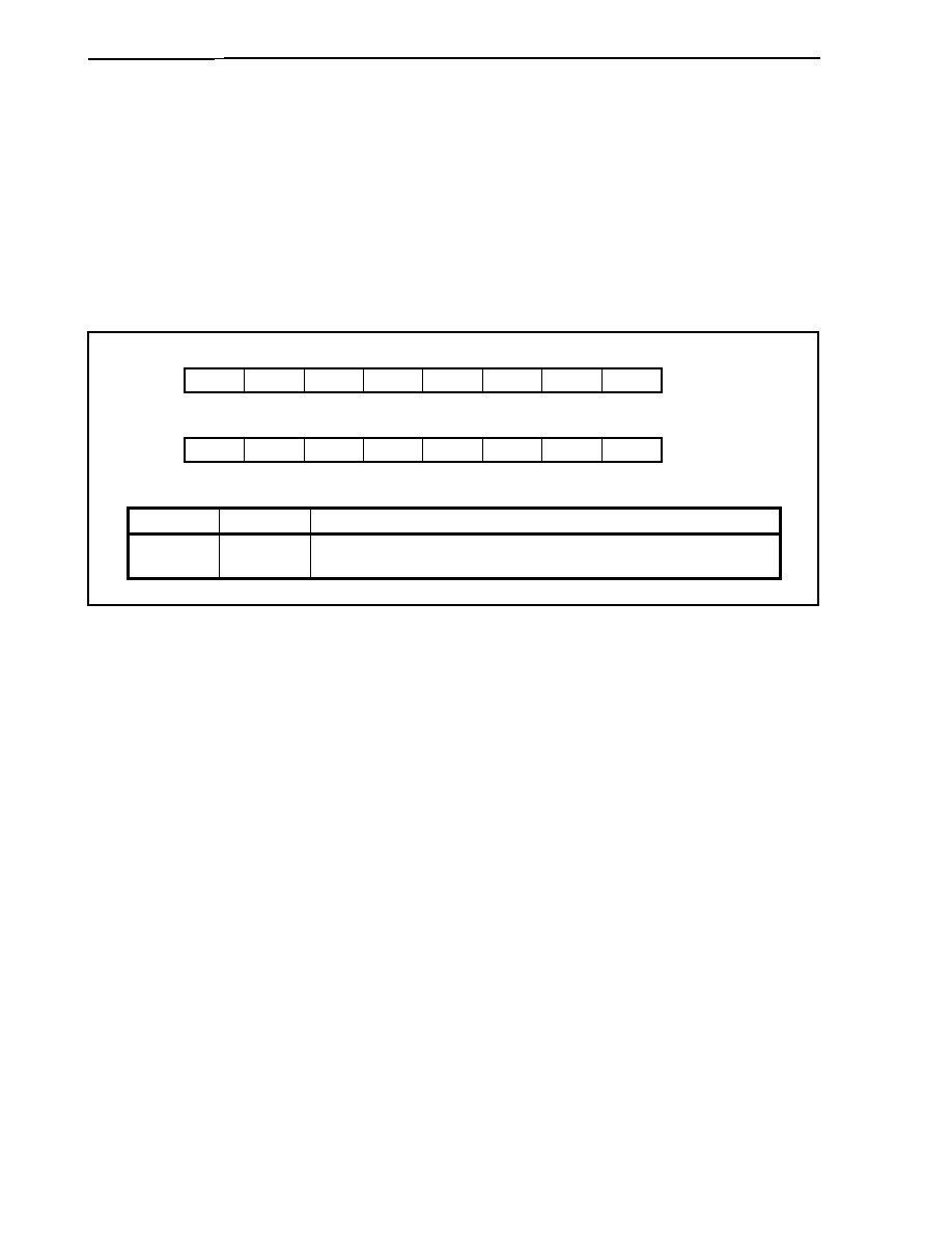
CHAPTER 10 SERIAL INTERFACE FUNCTION
User's Manual U14492EJ5V0UD
490
(10) Clocked serial interface initial transmit buffer registers L0, L1 (SOTBFL0, SOTBFL1)
The SOTBFLn register is an 8-bit buffer register that stores initial transmission data in the repeat transfer
mode (n = 0, 1).
The transmission operation is not started even if data is written to the SOTBFLn register.
These registers can be read/written in 8-bit or 1-bit units.
The SOTBFLn register is the same as the lower bytes of the SOTBFn register.
Caution Access the SOTBFLn register only when the 8-bit data length has been set (CCL bit of
CSIMn register = 0), and only in the idle state (CSOTn bit of CSIMn register = 0). If the
SOTBFLn register is accessed during data transfer, the data cannot be guaranteed.
7
SOTBF7
SOTBFL0
6
SOTBF6
5
SOTBF5
4
SOTBF4
3
SOTBF3
2
SOTBF2
1
SOTBF1
0
SOTBF0
Address
FFFFF908H
Initial value
00H
7
SOTBF7
SOTBFL1
6
SOTBF6
5
SOTBF5
4
SOTBF4
3
SOTBF3
2
SOTBF2
1
SOTBF1
0
SOTBF0
Address
FFFFF918H
Initial value
00H
Bit position
Bit name
Function
7 to 0
SOTBF7 to
SOTBF0
Stores initial transmission data in repeat transfer mode.
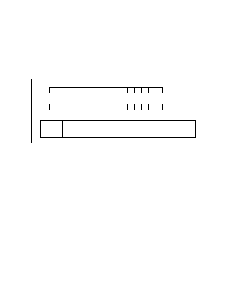
CHAPTER 10 SERIAL INTERFACE FUNCTION
User's Manual U14492EJ5V0UD
491
(11) Serial I/O shift registers 0, 1 (SIO0, SIO1)
The SIOn register is a 16-bit shift register that converts parallel data into serial data (n = 0, 1).
The transfer operation is not started even if the SIOn register is read.
These registers are read-only, in 16-bit units.
In addition to reset input, this register can also be initialized by clearing (0) the CSICAEn bit of the CSIMn
register.
Caution Read the SIOn register only when the 16-bit data length has been set (CCL bit of CSIMn
register = 1), and only in the idle state (CSOTn bit of CSIMn register = 0). If the SIOn
register is read during data transfer, the data cannot be guaranteed.
14
SIO14
13
SIO13
12
SIO12
2
SIO2
3
SIO3
4
SIO4
5
SIO5
6
SIO6
7
SIO7
8
SIO8
9
SIO9
10
SIO10
11
SIO11
15
SIO15
1
SIO1
0
SIO0
SIO0
Address
FFFFF90AH
Initial value
0000H
14
SIO14
13
SIO13
12
SIO12
2
SIO2
3
SIO3
4
SIO4
5
SIO5
6
SIO6
7
SIO7
8
SIO8
9
SIO9
10
SIO10
11
SIO11
15
SIO15
1
SIO1
0
SIO0
SIO1
Address
FFFFF91AH
Initial value
0000H
Bit position
Bit name
Function
15 to 0
SIO15 to
SIO0
Data is shifted in (reception) or shifted out (transmission) from the MSB or LSB
side.

CHAPTER 10 SERIAL INTERFACE FUNCTION
User's Manual U14492EJ5V0UD
492
(12) Serial I/O shift registers L0, L1 (SIOL0, SIOL1)
The SIOLn register is an 8-bit shift register that converts parallel data into serial data (n = 0, 1).
The transfer operation is not started even if the SIOLn register is read.
These registers are read-only, in 8-bit or 1-bit units.
In addition to reset input, this register can also be initialized by clearing (0) the CSICAEn bit of the CSIMn
register.
The SIOLn register is the same as the lower bytes of the SIOn register.
Caution Read the SIOLn register only when the 8-bit data length has been set (CCL bit of CSIMn
register = 0), and only in the idle state (CSOTn bit of CSIMn register = 0). If the SIOLn
register is read during data transfer, the data cannot be guaranteed.
7
SIO7
SIOL0
6
SIO6
5
SIO5
4
SIO4
3
SIO3
2
SIO2
1
SIO1
0
SIO0
7
SIO7
6
SIO6
5
SIO5
4
SIO4
3
SIO3
2
SIO2
1
SIO1
0
SIO0
Address
FFFFF90AH
Initial value
00H
SIOL1
Address
FFFFF91AH
Initial value
00H
Bit position
Bit name
Function
7 to 0
SIO7 to SIO0
Data is shifted in (reception) or shifted out (transmission) from the MSB or LSB
side.

CHAPTER 10 SERIAL INTERFACE FUNCTION
User's Manual U14492EJ5V0UD
493
10.4.4 Operation
(1) Single transfer mode
(a) Usage
In the receive-only mode (TRMDn bit of CSIMn register = 0), transfer is started by reading
Note
1
the receive
data buffer register (SIRBn/SIRBLn) (n = 0, 1).
In the transmission/reception mode (TRMDn bit of CSIMn register = 1), transfer is started by writing
Note
2
to the transmit data buffer register (SOTBn/SOTBLn).
In the slave mode, the operation must be enabled beforehand (CSICAEn bit of CSIMn register = 1).
When transfer is started, the value of the CSOTn bit of the CSIMn register becomes 1 (transmission
execution status).
Upon transfer completion, the transmission/reception completion interrupt (INTCSIn) is set (1), and the
CSOTn bit is cleared (0). The next data transfer request is then waited for.
Notes 1. When the 16-bit data length (CCL bit of CSIMn register = 1) has been set, read the SIRBn
register. When the 8-bit data length (CCL bit of CSIMn register = 0) has been set, read the
SIRBLn register.
2. When the 16-bit data length (CCL bit of CSIMn register = 1) has been set, write to the SOTBn
register. When the 8-bit data length (CCL bit of CSIMn register = 0) has been set, write to the
SOTBLn register.
Caution When the CSOTn bit of the CSIMn register = 1, do not manipulate the CSIn register.
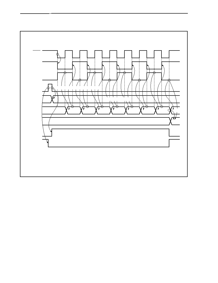
CHAPTER 10 SERIAL INTERFACE FUNCTION
User's Manual U14492EJ5V0UD
494
Figure 10-26. Timing Chart in Single Transfer Mode (1/2)
(a) In transmission/reception mode, data length: 8 bits, transfer direction: MSB first, no interrupt delay,
single transfer mode, operation mode: CKP bit = 0, DAP bit = 0
0
1
0
1
0
1
0
1
1
0
1
0
1
0
1
0
(55H)
(AAH)
AAH
AAH
ABH
56H
ADH
5AH
B5H
6AH
D5H
SCKn
(I/O)
SOn
(output)
SIn
(input)
Reg_R/W
SOTBLn
register
SIOLn
register
SIRBLn
register
CSOTn
bit
INTCSIn
interrupt
55H (transmit data)
Write 55H to SOTBLn register
Remarks 1. n = 0, 1
2.
Reg_R/W: Internal signal. This signal indicates that receive data buffer register (SIRBn/
SIRBLn) read or transmit data buffer register (SOTBn/SOTBLn) write was
performed.
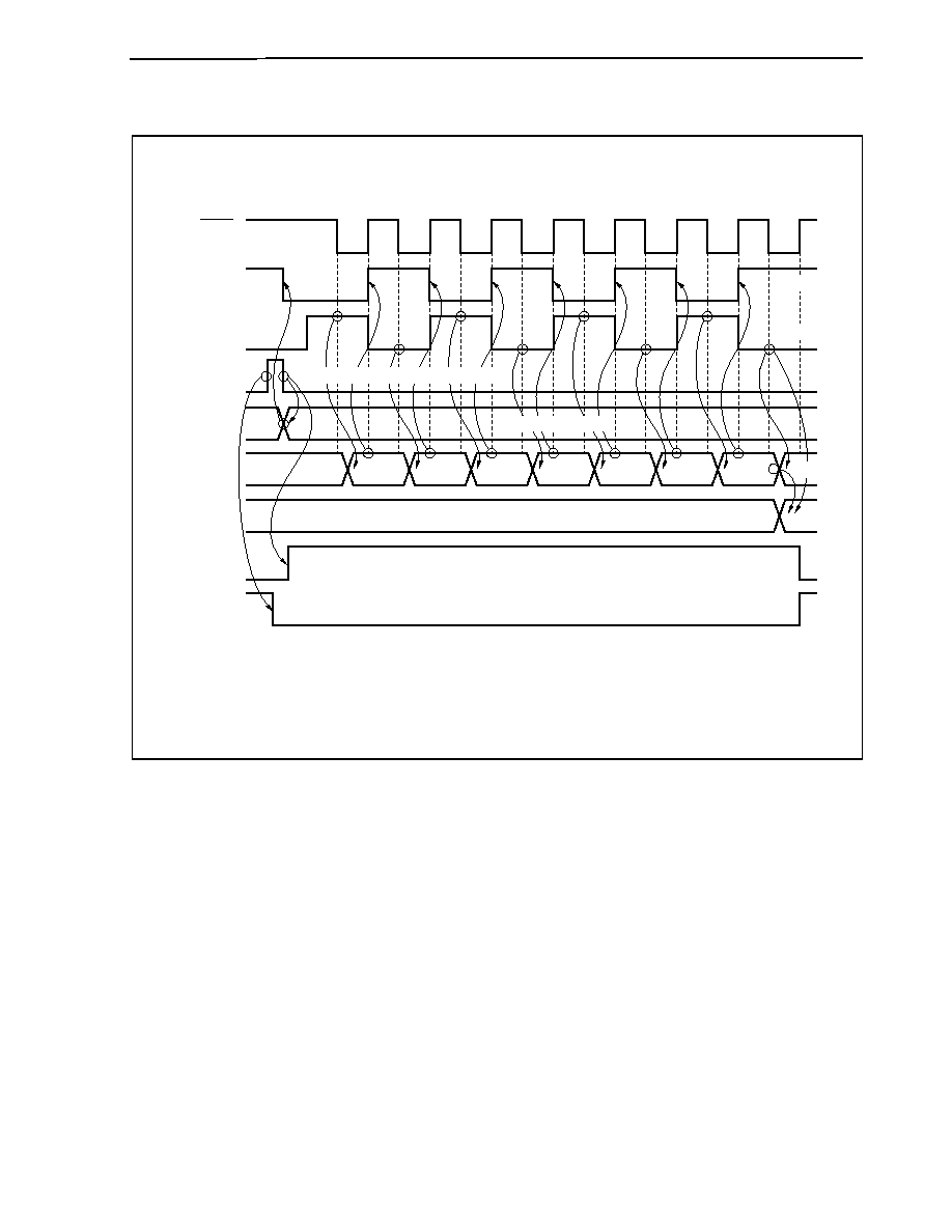
CHAPTER 10 SERIAL INTERFACE FUNCTION
User's Manual U14492EJ5V0UD
495
Figure 10-26. Timing Chart in Single Transfer Mode (2/2)
(b) In transmission/reception mode, data length: 8 bits, transfer direction: MSB first, no interrupt delay,
single transfer mode, operation mode: CKP bit = 0, DAP bit = 1
0
1
0
1
0
1
0
1
1
0
1
0
1
0
1
0
AAH
AAH
ABH
56H
ADH
5AH
B5H
6AH
D5H
SCKn
(I/O)
SOn
(output)
SIn
(input)
Reg_R/W
SOTBLn
register
SIOLn
register
SIRBLn
register
CSOTn
bit
INTCSIn
interrupt
(55H)
(AAH)
55H (transmit data)
Write 55H to SOTBLn register
Remarks 1. n = 0, 1
2.
Reg_R/W: Internal signal. This signal indicates that receive data buffer register (SIRBn/
SIRBLn) read or transmit data buffer register (SOTBn/SOTBLn) write was
performed.

CHAPTER 10 SERIAL INTERFACE FUNCTION
User's Manual U14492EJ5V0UD
496
(b) Clock phase selection
The following shows the timing when changing the conditions for clock phase selection (CKP bit of
CSICn register) and data phase selection (DAP bit of CSICn register) under the following conditions.
∑ Data length = 8 bits (CCL bit of CSIMn register = 0)
∑ First bit of transfer data = MSB (DIRn bit of CSIMn register = 0)
∑ No interrupt request signal delay control (CSIT bit of CSIMn register = 0)
Figure 10-27. Timing Chart According to Clock Phase Selection (1/2)
(a) When CKP bit = 0, DAP bit = 0
DI7
DI6
DI5
DI4
DI3
DI2
DI1
DO7
DO6
DO5
DO4
DO3
DO2
DO1
SCKn (I/O)
SIn (input)
SOn (output)
Reg_R/W
INTCSIn interrupt
CSOTn bit
DI0
DO0
(b)
When CKP bit = 1, DAP bit = 0
DI7
DI6
DI5
DI4
DI3
DI2
DI1
DO7
DO6
DO5
DO4
DO3
DO2
DO1
SCKn (I/O)
SIn (input)
SOn (output)
Reg_R/W
INTCSIn interrupt
CSOTn bit
DI0
DO0
Remarks 1. n = 0, 1
2.
Reg_R/W: Internal signal. This signal indicates that receive data buffer register (SIRBn/
SIRBLn) read or transmit data buffer register (SOTBn/SOTBLn) write was
performed.

CHAPTER 10 SERIAL INTERFACE FUNCTION
User's Manual U14492EJ5V0UD
497
Figure 10-27. Timing Chart According to Clock Phase Selection (2/2)
(c) When CKP bit = 0, DAP bit = 1
DI7
DI6
DI5
DI4
DI3
DI2
DI1
DO7
DO6
DO5
DO4
DO3
DO2
DO1
SCKn (I/O)
SIn (input)
SOn (output)
Reg_R/W
INTCSIn interrupt
CSOTn bit
DI0
DO0
(d) When CKP bit = 1, DAP bit = 1
DI7
DI6
DI5
DI4
DI3
DI2
DI1
DO7
DO6
DO5
DO4
DO3
DO2
DO1
SCKn (I/O)
SIn (input)
SOn (output)
Reg_R/W
INTCSIn interrupt
CSOTn bit
DI0
DO0
Remarks 1. n = 0, 1
2.
Reg_R/W: Internal signal. This signal indicates that receive data buffer register (SIRBn/
SIRBLn) read or transmit data buffer register (SOTBn/SOTBLn) write was
performed.
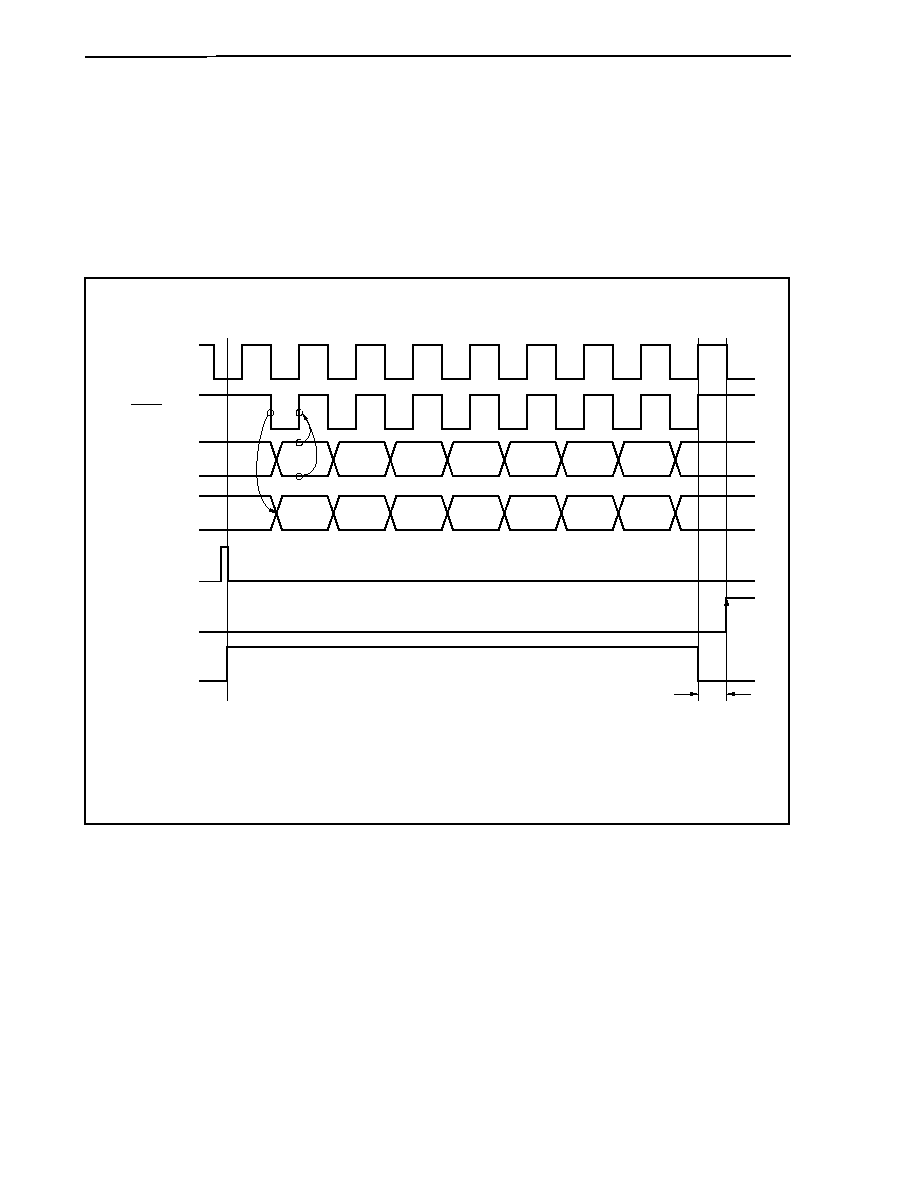
CHAPTER 10 SERIAL INTERFACE FUNCTION
User's Manual U14492EJ5V0UD
498
(c) Transmission/reception completion interrupt request signals (INTCSI0, INTCSI1)
INTCSIn is set (1) upon completion of data transmission/reception.
Caution The delay mode (CSIT bit = 1) is valid only in the master mode (bits CKS2 to CKS0 of the
CSICn register are not 111B). The delay mode cannot be set when the slave mode is set
(bits CKS2 to CKS0 = 111B).
Figure 10-28. Timing Chart of Interrupt Request Signal Output in Delay Mode (1/2)
(a) When CKP bit = 0, DAP bit = 0
DI7
DI6
DI5
DI4
DI3
DI2
DI1
DI0
DO7
DO6
DO5
DO4
DO3
DO2
DO1
DO0
Input clock
SCKn (I/O)
SIn (input)
SOn (output)
Reg_R/W
INTCSIn
interrupt
CSOTn bit
Delay
Remarks 1. n = 0, 1
2.
Reg_R/W: Internal signal. This signal indicates that receive data buffer register (SIRBn/
SIRBLn) read or transmit data buffer register (SOTBn/SOTBLn) write was
performed.

CHAPTER 10 SERIAL INTERFACE FUNCTION
User's Manual U14492EJ5V0UD
499
Figure 10-28. Timing Chart of Interrupt Request Signal Output in Delay Mode (2/2)
(b) When CKP bit = 1, DAP bit = 1
DI7
DI6
DI5
DI4
DI3
DI2
DI1
DI0
DO7
DO6
DO5
DO4
DO3
DO2
DO1
DO0
Input clock
SCKn (I/O)
SIn (input)
SOn (output)
Reg_R/W
INTCSIn
interrupt
CSOTn bit
Delay
Remarks 1. n = 0, 1
2.
Reg_R/W: Internal signal. This signal indicates that receive data buffer register (SIRBn/
SIRBLn) read or transmit data buffer register (SOTBn/SOTBLn) write was
performed.

CHAPTER 10 SERIAL INTERFACE FUNCTION
User's Manual U14492EJ5V0UD
500
(2) Repeat transfer mode
(a)
Usage (receive-only)
<1> Set the repeat transfer mode (AUTO bit of CSIMn register = 1) and the receive-only mode (TRMDn bit
of CSIMn register = 0).
<2> Read SIRBn register (start transfer with dummy read).
<3> Wait for transmission/reception completion interrupt request (INTCSIn).
<4> When the transmission/reception completion interrupt request (INTCSIn) has been set (1), read the
SIRBn register
Note
(reserve next transfer).
<5> Repeat steps <3> and <4> (N
- 2) times (N: Number of transfer data).
<6> Following output of the last transmission/reception completion interrupt request (INTCSIn), read the
SIRBEn register and the SIOn register
Note
.
Note When transferring N number of data, receive data is loaded by reading the SIRBn register from the
first data to the (N
- 2)th data. The (N - 1)th data is loaded by reading the SIRBEn register, and the
Nth (last) data is loaded by reading the SIOn register.
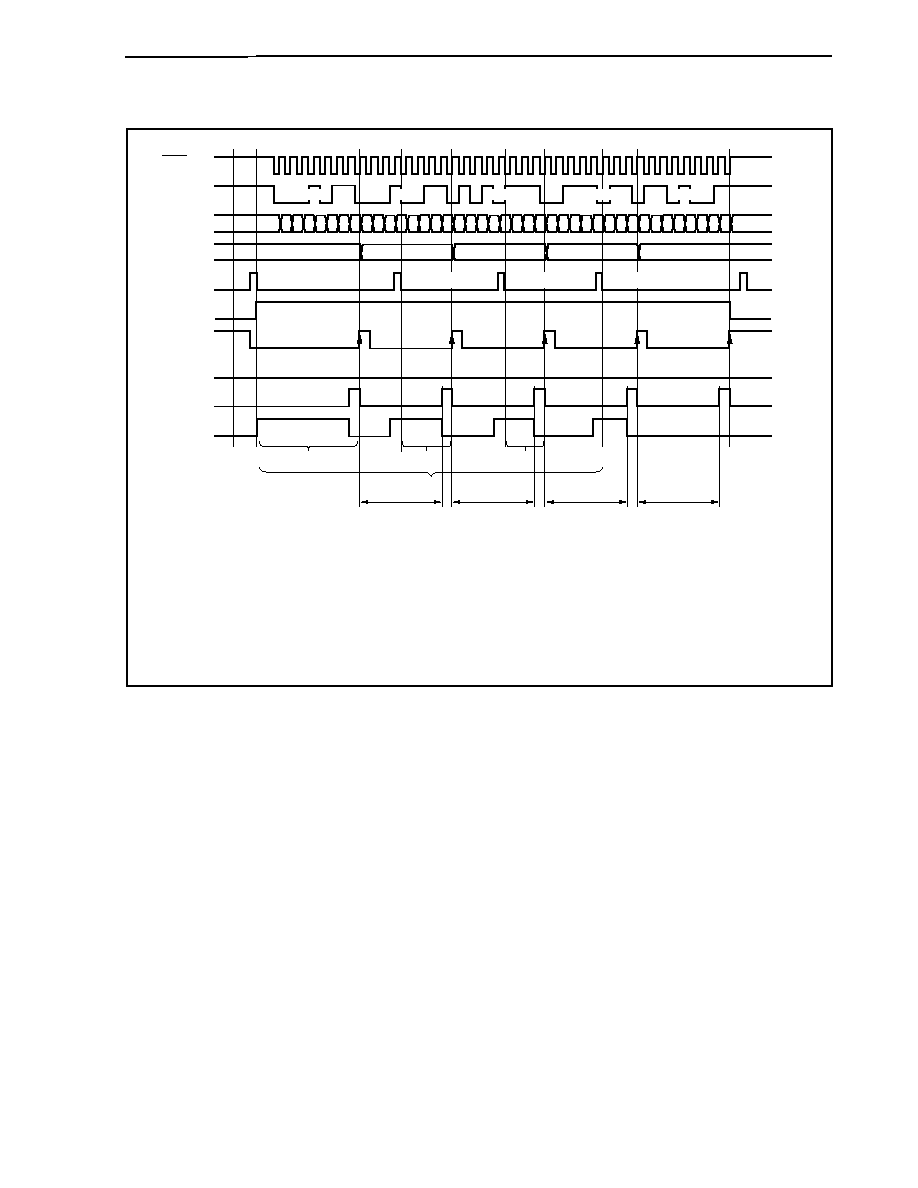
CHAPTER 10 SERIAL INTERFACE FUNCTION
User's Manual U14492EJ5V0UD
501
Figure 10-29. Repeat Transfer (Receive-Only) Timing Chart
din-1
SCKn (I/O)
SIn (input)
SOn (output)
L
SIOLn
register
SIRBLn
register
Reg_RD
CSOTn bit
INTCSIn
interrupt
rq_clr
trans_rq
din-2
din-1
SIRBn (dummy)
SIRBn (d1)
SIRBn (d2)
SIRBn (d3)
SIRBEn (d4)
SIOn (d5)
<4>
<6>
<4> <3>
<3>
<4>
<5>
Period during
which next transfer
can be reserved
<3>
<2>
<1>
din-2
din-3
din-4
din-5
din-5
din-3
din-4
Remarks 1. n = 0, 1
2.
Reg_RD: Internal signal. This signal indicates that the receive data buffer register (SIRBn/
SIRBLn) has been read.
rq_clr: Internal signal. Transfer request clear signal.
trans_rq: Internal signal. Transfer request signal.
In the case of the repeat transfer mode, two transfer requests are set at the start of the first transfer.
Following the transmission/reception completion interrupt request (INTCSIn), transfer is continued if the
SIRBn register can be read within the next transfer reservation period. If the SIRBn register cannot be
read, transfer ends and the SIRBn register does not receive the new value of the SIOn register.
The last data can be obtained by reading the SIOn register following completion of the transfer.

CHAPTER 10 SERIAL INTERFACE FUNCTION
User's Manual U14492EJ5V0UD
502
(b) Usage (transmission/reception)
<1> Set the repeat transfer mode (AUTO bit of CSIMn register = 1) and the transmission/reception mode
(TRMDn bit of CSIMn register = 1).
<2> Write the first data to the SOTBFn register.
<3> Write the 2nd data to the SOTBn register (start transfer).
<4> Wait for a transmission/reception completion interrupt request (INTCSIn).
<5> When the transmission/reception completion interrupt request (INTCSIn) has been set (1), write the
next data to the SOTBn register (reserve next transfer), and read the SIRBn register to load the
receive data.
<6> Repeat steps <4> and <5> as long as data to be sent remains.
<7> Wait for the INTCSIn interrupt. When the interrupt request signal is set (1), read the SIRBn register to
load the (N
- 1)th receive data (N: Number of transfer data).
<8> Following the last transmission/reception completion interrupt request (INTCSIn), read the SIOn
register to load the Nth (last) receive data.
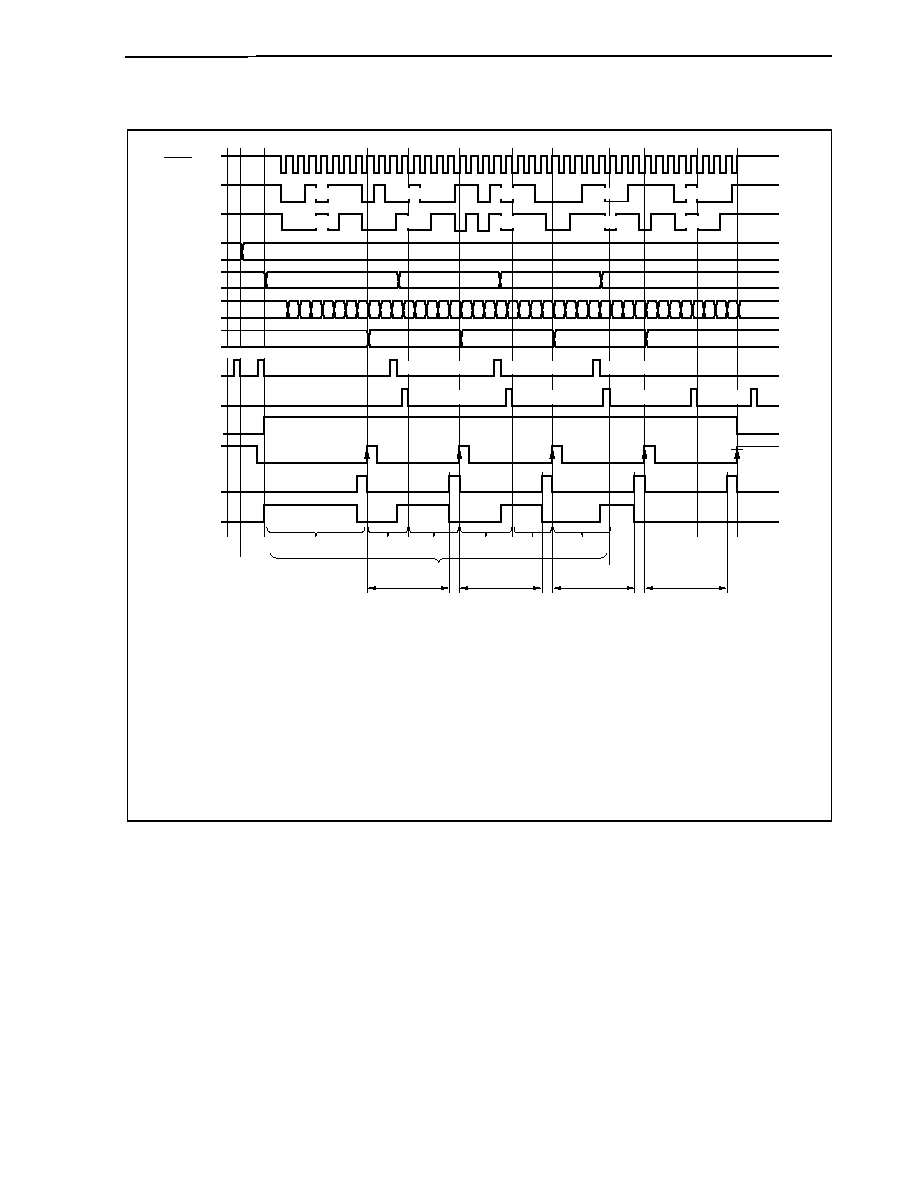
CHAPTER 10 SERIAL INTERFACE FUNCTION
User's Manual U14492EJ5V0UD
503
Figure 10-30. Repeat Transfer (Transmission/Reception) Timing Chart
dout-1
dout-1
SCKn (I/O)
SOn (output)
SIn (input)
SOTBFLn
register
SOTBLn
register
SIOLn
register
SIRBLn
register
Reg_WR
Reg_RD
CSOTn bit
INTCSIn
interrupt
rq_clr
trans_rq
dout-2
dout-3
dout-4
dout-5
dout-2
dout-3
dout-4
dout-5
din-1
din-1
SOTBFn (d1)
SOTBn (d2)
SOTBn (d3)
SOTBn (d4)
SOTBn (d5)
SIRBn (d1)
SIRBn (d2)
<5>
<7>
<8>
<4>
<5>
<4>
<6>
Period during which
next transfer can be
reserved
<5>
<4>
<3>
<2>
<1>
SIRBn (d3)
SIRBn (d4)
SIOn (d5)
din-2
din-3
din-4
din-5
din-2
din-3
din-4
din-5
Remarks 1. n = 0, 1
2.
Reg_WR: Internal signal. This signal indicates that the transmit data buffer register (SOTBn/
SOTBLn) has been written.
Reg_RD: Internal signal. This signal indicates that the receive data buffer register (SIRBn/
SIRBLn) has been read.
rq_clr: Internal signal. Transfer request clear signal.
trans_rq: Internal signal. Transfer request signal.
In the case of the repeat transfer mode, two transfer requests are set at the start of the first transfer.
Following the transmission/reception completion interrupt request (INTCSIn), transfer is continued if the
SOTBn register can be written within the next transfer reservation period. If the SOTBn register cannot
be written, transfer ends and the SIRBn register does not receive the new value of the SIOn register.
The last receive data can be obtained by reading the SIOn register following completion of the transfer.
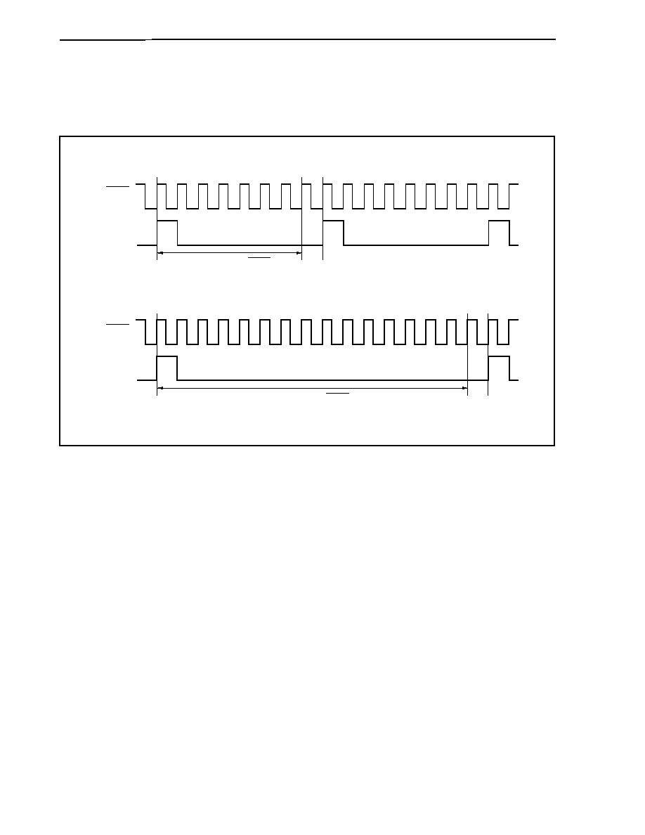
CHAPTER 10 SERIAL INTERFACE FUNCTION
User's Manual U14492EJ5V0UD
504
(c) Next transfer reservation period
In the repeat transfer mode, the next transfer must be prepared with the period shown in Figure 10-31.
Figure 10-31. Timing Chart of Next Transfer Reservation Period (1/2)
(a)
When data length: 8 bits, operation mode: CKP bit = 0, DAP bit = 0
SCKn
(I/O)
INTCSIn
interrupt
Reservation period: 7 SCKn cycles
(b) When data length: 16 bits, operation mode: CKP bit = 0, DAP bit = 0
SCKn
(I/O)
INTCSIn
interrupt
Reservation period: 15 SCKn cycles
Remark n = 0, 1

CHAPTER 10 SERIAL INTERFACE FUNCTION
User's Manual U14492EJ5V0UD
505
Figure 10-31. Timing Chart of Next Transfer Reservation Period (2/2)
(c) When data length: 8 bits, operation mode: CKP bit = 0, DAP bit = 1
SCKn
(I/O)
INTCSIn
interrupt
Reservation period: 6.5 SCKn cycles
(d) When data length: 16 bits, operation mode: CKP bit = 0, DAP bit = 1
SCKn
(I/O)
INTCSIn
interrupt
Reservation period: 14.5 SCKn cycles
Remark n = 0, 1
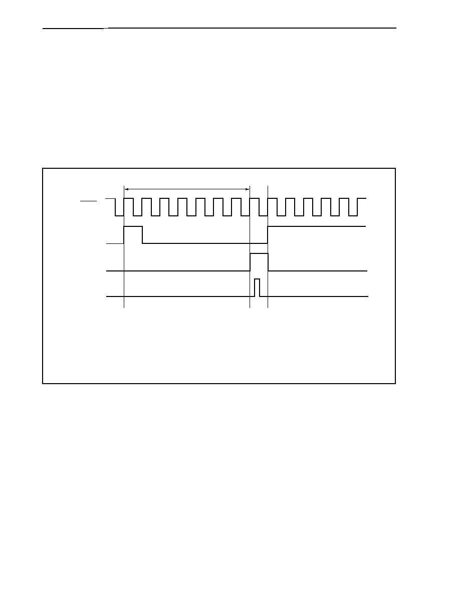
CHAPTER 10 SERIAL INTERFACE FUNCTION
User's Manual U14492EJ5V0UD
506
(d) Cautions
To continue repeat transfers, it is necessary to either read the SIRBn register or write to the SOTBn
register during the transfer reservation period.
If access is performed to the SIRBn register or the SOTBn register when the transfer reservation period
is over, the following occurs.
(i) In case of contention between transfer request clear and register access
Since request cancellation has higher priority, the next transfer request is ignored. Therefore,
transfer is interrupted, and normal data transfer cannot be performed.
Figure 10-32. Transfer Request Clear and Register Access Contention
SCKn
(I/O)
INTCSIn
interrupt
rq_clr
Reg_R/W
Transfer reservation period
Remarks 1. n = 0, 1
2.
rq_clr: Internal signal. Transfer request clear signal.
Reg_R/W: Internal signal. This signal indicates that the receive data buffer register (SIRBn/
SIRBLn) read or transmit data buffer register (SOTBn/SOTBLn) write was
performed.
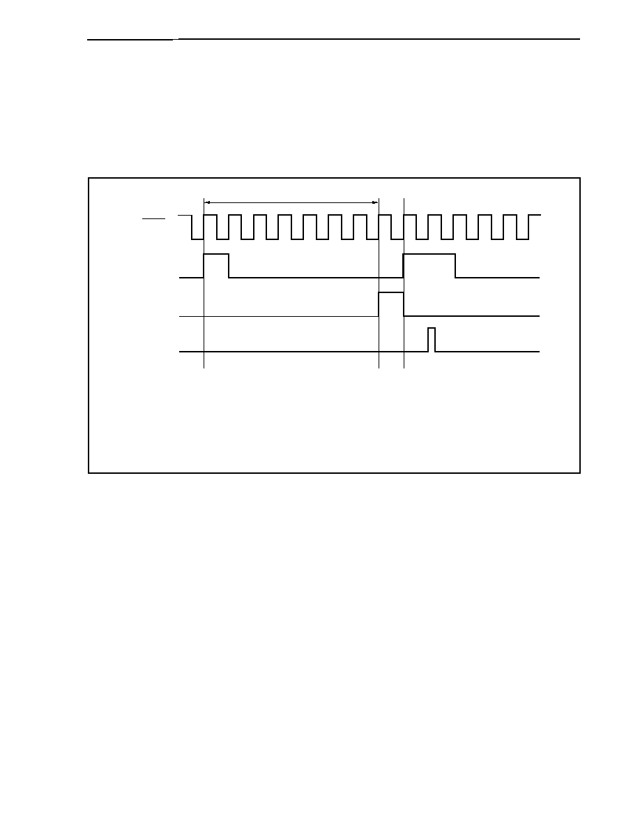
CHAPTER 10 SERIAL INTERFACE FUNCTION
User's Manual U14492EJ5V0UD
507
(ii) In case of contention between interrupt request and register access
Since continuous transfer has stopped once, executed as a new repeat transfer.
In the slave mode, a bit phase error transfer error results (refer to Figure 10-33).
In the transmission/reception mode, the value of the SOTBFn register is retransmitted, and illegal
data is sent.
Figure 10-33. Interrupt Request and Register Access Contention
SCKn
(I/O)
INTCSIn
interrupt
rq_clr
Reg_R/W
Transfer reservation period
0
1
2
3
4
Remarks 1. n = 0, 1
2.
rq_clr: Internal signal. Transfer request clear signal.
Reg_R/W: Internal signal. This signal indicates that receive data buffer register (SIRBn/
SIRBLn) read or transmit data buffer register (SOTBn/SOTBLn) write was
performed.
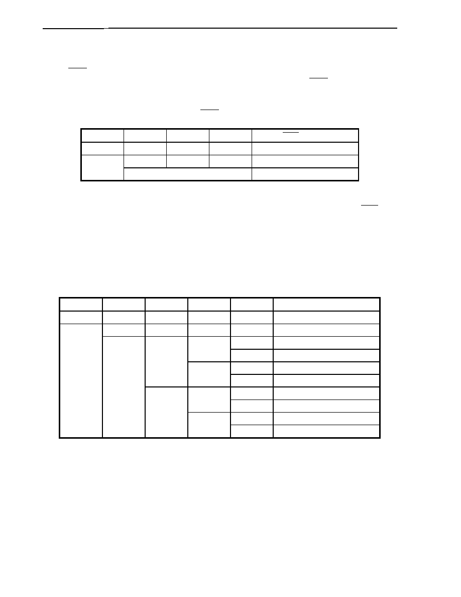
CHAPTER 10 SERIAL INTERFACE FUNCTION
User's Manual U14492EJ5V0UD
508
10.4.5 Output pins
(1) SCKn pin
When the CSIn operation is disabled (CSICAEn bit of CSIMn register = 0), the SCKn pin output status is as
follows (n = 0, 1).
Table 10-9. SCKn Pin Output Status
CKP CKS2 CKS1 CKS0
SCKn
Pin
Output
0
Don't care
Don't care
Don't care
Fixed to high level
1 1 1 Fixed
to
high
level
1
Other than above
Fixed to low level
Remarks 1. n = 0, 1
2.
When any of bits CKP and CKS2 to CKS0 of the CSICn register is overwritten, the SCKn pin
output changes.
(2) SOn pin
When the CSIn operation is disabled (CSICAEn bit of CSIMn register = 0), the SOn pin output status is as
follows (n = 0, 1).
Table 10-10. SOn Pin Output Status
TRMDn
DAP
AUTO
CCL
DIRn
SOn Pin Output
0
Don't care
Don't care
Don't care
Don't care
Fixed to low level
0
Don't care
Don't care
Don't care
SO latch value (low level)
0 SOTB7
value
0
1 SOTB0
value
0 SOTB15
value
0
1
1 SOTB0
value
0 SOTBF7
value
0
1 SOTBF0
value
0 SOTBF15
value
1
1
1
1
1 SOTBF0
value
Remarks 1. n = 0, 1
2.
When any of bits TRMDn, CCL, DIRn, and AUTO of the CSIMn register or DAP bit of the
CSICn register is overwritten, the SOn pin output changes.
3.
SOTBm: Bit m of SOTBn register (m = 0, 7, 15)
4.
SOTBFm: Bit m of SOTBFn register (m = 0, 7, 15)
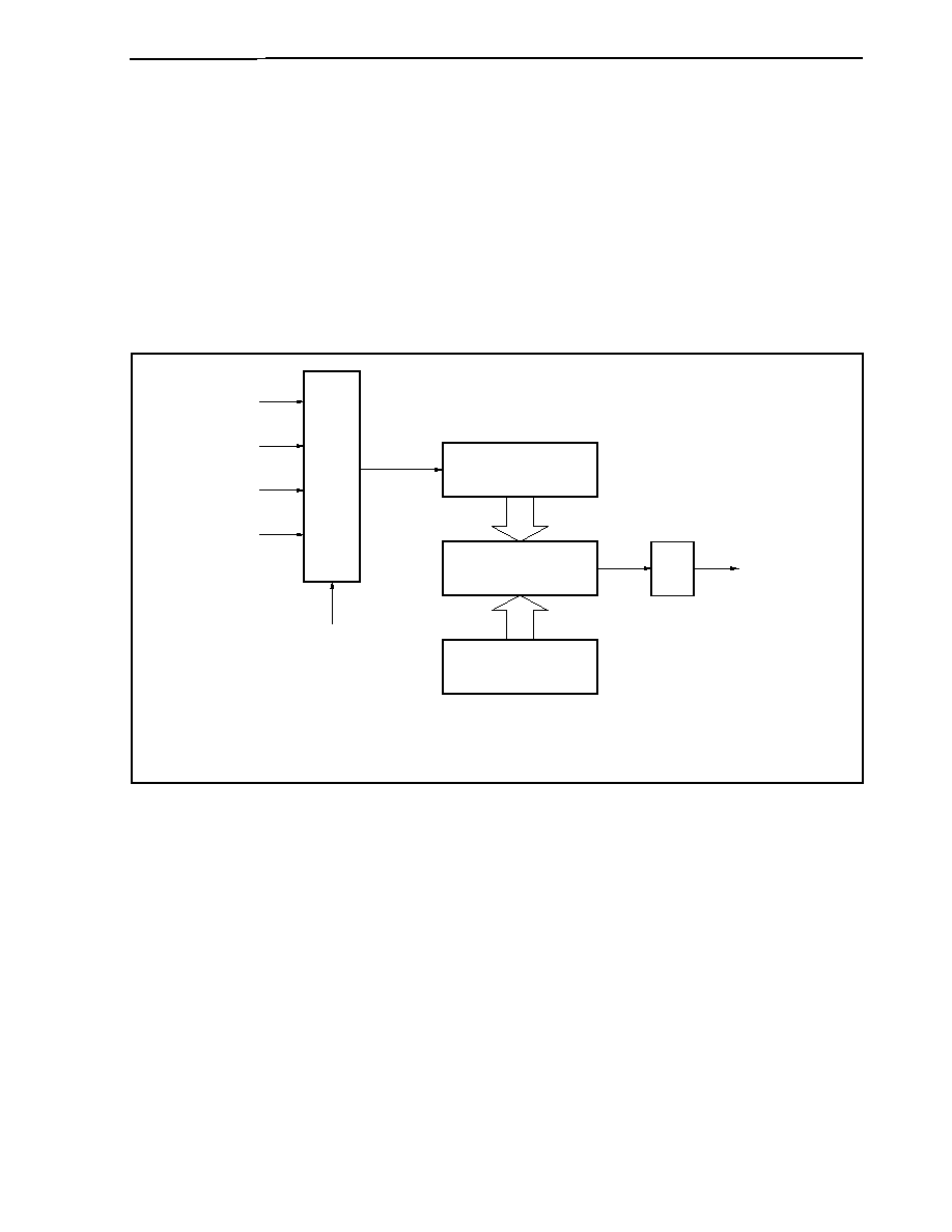
CHAPTER 10 SERIAL INTERFACE FUNCTION
User's Manual U14492EJ5V0UD
509
10.4.6 Dedicated baud rate generator 3 (BRG3)
(1) Configuration of baud rate generator 3 (BRG3)
The CSI0 and CSI1 serial clocks can be selected from the dedicated baud rate generator output or internal
system clock (f
XX
).
The serial clock source is specified with registers CSIC0 and CSIC1.
If dedicated baud rate generator output is specified, BRG3 is selected as the clock source.
Since the same serial clock can be shared for transmission and reception, baud rate is the same for the
transmission/reception.
Figure 10-34. Block Diagram of Baud Rate Generator 3 (BRG3)
BGCS1, BGCS0
PRSCM3
Match detector
1/2
CSIn
8-bit timer counter
f
XX
/4
f
XX
/8
f
XX
/16
f
XX
/32
Selector
Remark f
XX
: Internal system clock
n = 0, 1

CHAPTER 10 SERIAL INTERFACE FUNCTION
User's Manual U14492EJ5V0UD
510
(2) Dedicated baud rate generator 3 (BRG3)
BRG3 is configured of an 8-bit timer counter that generates the baud rate signal, a prescaler mode register 3
(PRSM3) that controls baud rate signal generation, a prescaler compare register 3 (PRSCM3) that sets the
value of the 8-bit timer counter, and a prescaler.
(a) Input clock
The internal system clock (f
XX
) is input to BRG3.
(b) Prescaler mode register 3 (PRSM3)
The PRSM3 register controls generation of the CSI0 and CSI1 baud rate signals.
This register can be read/written in 8-bit or 1-bit units.
Cautions 1. Do not change the values of the BGCS1 and BGCS0 bits during transmission/
reception operation.
2. Set the PRSM3 register prior to setting the CSICAEn bit of the CSIMn register to 1
(n = 0, 1).
7
0
PRSM3
6
0
5
0
4
CE
3
0
2
0
1
BGCS1
0
BGCS0
Address
FFFFF920H
Initial value
00H
Bit position
Bit name
Function
4 CE
Enables baud rate counter operation.
0: Stop baud rate counter operation and fix baud rate output signal to 0.
1: Enable baud rate counter operation and start baud rate output operation.
Selects count clock for baud rate counter.
BGCS1
BGCS0
Count clock selection
0 0
f
XX
/4
0 1
f
XX
/8
1 0
f
XX
/16
1, 0
BGCS1,
BGCS0
1 1
f
XX
/32
Remark f
XX
: Internal system clock

CHAPTER 10 SERIAL INTERFACE FUNCTION
User's Manual U14492EJ5V0UD
511
(c) Prescaler compare register 3 (PRSCM3)
PRSCM3 is an 8-bit compare register that sets the value of the 8-bit timer counter.
This register can be read/written in 8-bit units.
Cautions 1. The internal timer counter is cleared by writing to the PRSM3 register. Therefore,
do not write to the PRSCM3 register during transmission.
2. Set the PRSCM3 register prior to setting the CSICAEn bit of the CSIMn register to 1.
If the contents of the PRSCM3 register are overwritten when the value of the
CSICAEn bit is 1, the cycle of the baud rate signal is not guaranteed.
7
PRSCM7
PRSCM3
6
PRSCM6
5
PRSCM5
4
PRSCM4
3
PRSCM3
2
PRSCM2
1
PRSCM1
0
PRSCM0
Address
FFFFF922H
Initial value
00H
(d) Baud rate signal cycle
The baud rate signal cycle is calculated as follows.
∑ When setting value of PRSCM3 register is 00H
(Cycle of signal selected with bits BGCS1, BGCS0 of PRSM3 register)
◊ 256 ◊ 2
∑ In cases other than above
(Cycle of signal selected with bits BGCS1, BGCS0 of PRSM3 register)
◊ (setting value of PRSCM3
register)
◊ 2

CHAPTER 10 SERIAL INTERFACE FUNCTION
User's Manual U14492EJ5V0UD
512
(e) Baud rate setting value
Table 10-11. Baud Rate Generator Setting Data
(a) When f
XX
= 32 MHz
BGCS1
BGCS0
PRSCM Register Value
Clock (Hz)
0 0
1
4000000
0 0
2
2000000
0 0
4
1000000
0 0
8
500000
0 0
16
250000
0 0
40
100000
0 0
80
50000
0 0
160
25000
0 1
200
10000
1 0
200
5000
(b) When f
XX
= 40 MHz
BGCS1
BGCS0
PRSCM Register Value
Clock (Hz)
0 0
2
2500000
0 0
5
1000000
0 0
10
500000
0 0
20
250000
0 0
50
100000
0 0
100
50000
0 0
200
25000
0 1
250
10000
1 0
250
5000
(c) When f
XX
= 50 MHz
BGCS1
BGCS0
PRSCM Register Value
Clock (Hz)
0 0
2
3125000
0 0
4
1562500
0 0
5
1250000
0 0
10
625000
0 0
25
250000
0 0
50
125000
0 0
125
50000
0 0
250
25000
0 1
250
12500
1 0
250
6250
Caution Set the transfer clock so that it does not fall below the minimum value of 200 ns of the SCKn
cycle (t
CYSK1
) prescribed in the electrical specifications.

513
User's Manual U14492EJ5V0UD
CHAPTER 11 FCAN CONTROLLER
The V850E/IA1 features a 1 channel on-chip FCAN (Full Controller Area Network) controller that complies with the
CAN specification Ver. 2.0, PartB active.
11.1 Function Overview
Table 11-1 presents an overview of V850E/IA1 functions.
Table 11-1. Overview of Functions
Function Description
Protocol
CAN Protocol Ver. 2.0, PartB active (standard and extended frame transmission/reception)
Baud rate
Maximum 1 Mbps (during 16 MHz clock input)
Data storage
∑ Allocated to common access-enabled RAM area
∑ RAM that is mapped to an unused message byte can be used for CPU processing or other
processing
Mask functions
∑ Four
∑ Global masks and local masks can be used without distinction
Message configuration
Can be declared as transmit or receive messages
No. of messages
32
Message storage
method
∑ Storage to receive buffer corresponding to ID
∑ Storage to buffer specified by receive mask function
Remote reception
∑ Remote frames can be received in either the receive message buffer or the transmit message
buffer
∑ If a remote frame is received by a transmit message buffer, there is a choice between having the
remote request processed by the CPU or starting the auto transmit function.
Remote transmission
The remote frame can be sent either by setting the transmit message's RTR bit (M_CTRLn register)
or by setting the receive message's send request.
Time stamp function
A time stamp function can be set for receive messages and transmit messages.
Diagnostic functions
∑ Read-enabled error counter is provided.
∑ "Valid protocol operation flag" is provided for verification of bus connections.
∑ Receive-only mode (with auto baud rate detection) is provided.
∑ Diagnostic processing mode is provided.
Low-power mode
∑ CAN sleep mode (wake up function using CAN bus is enabled)
∑ CAN stop mode (wake up function using CAN bus is disabled)
Remark n = 00 to 31

CHAPTER 11 FCAN CONTROLLER
514
User's Manual U14492EJ5V0UD
11.2 Configuration
FCAN is composed of the following four blocks.
(1) NPB interface
This functional block provides an NPB (NEC peripheral I/O bus) interface as a means of transmitting and
receiving signals.
(2) MAC (Memory Access Controller)
This functional block controls access to the CAN module and to the CAN RAM within the FCAN.
(3) CAN module
This functional block is involved in the operation of the CAN protocol layer and its related settings.
(4) CAN RAM
This is the CAN memory functional block, which is used to store message IDs, message data, etc.
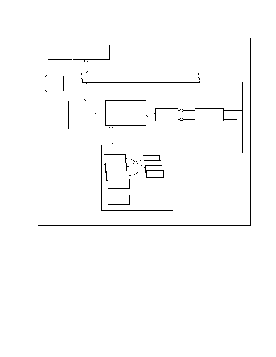
CHAPTER 11 FCAN CONTROLLER
515
User's Manual U14492EJ5V0UD
Figure 11-1. Block Diagram of FCAN
CPU
FCAN controller
CAN RAM
NPB
(NEC peripheral I/O bus)
MAC
(Memory Access Controller)
NPB
interface
CAN
module
Interrupt request
INTCREC
INTCTRX
INTCERR
INTCMAC
Message
buffer 0
Message
buffer 1
Message
buffer 2
Message
buffer 3
Message
buffer 31
CMASK0
CMASK1
CMASK2
CMASK3
...
CTXD
CRXD
CAN_H
CAN_L
CAN
transceiver
CAN bus

CHAPTER 11 FCAN CONTROLLER
516
User's Manual U14492EJ5V0UD
11.3 Configuration of Messages and Buffers
Table 11-2. Configuration of Messages and Buffers
Address
Note
(m = 2, 6, A, E)
Register Name
Address
Note
(m = 2, 6, A, E)
Register Name
xxxxm800H to xxxxm81FH
Message buffer 0 field
xxxxmA00H to xxxxmA1FH
Message buffer 16 field
xxxxm820H to xxxxm83FH
Message buffer 1 field
xxxxmA20H to xxxxmA3FH
Message buffer 17 field
xxxxm840H to xxxxm85FH
Message buffer 2 field
xxxxmA40H to xxxxmA5FH
Message buffer 18 field
xxxxm860H to xxxxm87FH
Message buffer 3 field
xxxxmA60H to xxxxmA7FH
Message buffer 19 field
xxxxm880H to xxxxm89FH
Message buffer 4 field
xxxxmA80H to xxxxmA9FH
Message buffer 20 field
xxxxm8A0H to xxxxm8BFH
Message buffer 5 field
xxxxmAA0H to xxxxmABFH
Message buffer 21 field
xxxxm8C0H to xxxxm8DFH
Message buffer 6 field
xxxxmAC0H to xxxxmADFH
Message buffer 22 field
xxxxm8E0H to xxxxm8FFH
Message buffer 7 field
xxxxmAE0H to xxxxmAFFH
Message buffer 23 field
xxxxm900H to xxxxm91FH
Message buffer 8 field
xxxxmB00H to xxxxmB1FH
Message buffer 24 field
xxxxm920H to xxxxm93FH
Message buffer 9 field
xxxxmB20H to xxxxmB3FH
Message buffer 25 field
xxxxm940H to xxxxm95FH
Message buffer 10 field
xxxxmB40H to xxxxmB5FH
Message buffer 26 field
xxxxm960H to xxxxm97FH
Message buffer 11 field
xxxxmB60H to xxxxmB7FH
Message buffer 27 field
xxxxm980H to xxxxm99FH
Message buffer 12 field
xxxxmB80H to xxxxmB9FH
Message buffer 28 field
xxxxm9A0H to xxxxm9BFH
Message buffer 13 field
xxxxmBA0H to xxxxmBBFH
Message buffer 29 field
xxxxm9C0H to xxxxm9DFH
Message buffer 14 field
xxxxmBC0H to xxxxmBDFH
Message buffer 30 field
xxxxm9E0H to xxxxm9FFH
Message buffer 15 field
xxxxmBE0H to xxxxmBFFH
Message buffer 31 field
Note CAN message buffer registers can be allocated to the xxxx addresses as programmable peripheral I/O
registers. Note, however, that the xxxx addresses cannot be changed after being set.
Caution When emulating the FCAN controller using the in-circuit emulator (IE-V850E-MC or IE-703116-MC-
EM1), perform the following settings in the Configuration screen that appears when the debugger is
started.
∑ Set the start address of the programmable peripheral I/O area that is set using the BPC register to
the Programmable I/O Area field.
∑ Map the programmable peripheral I/O area as "Target" or "Emulation RAM" in the Memory
Mapping field.
Remark For details of message buffers, see 3.4.9 Programmable peripheral I/O registers.

CHAPTER 11 FCAN CONTROLLER
517
User's Manual U14492EJ5V0UD
11.4 Time Stamp Function
The FCAN controller supports a time stamp function. This function is needed to build a global time system.
The time stamp function is implemented using a 16-bit free-running time stamp counter.
Two types of time stamp function can be selected for message reception in the FCAN controller. Use bit 3 (TMR)
of the CAN1 control register (C1CTRL) to set the desired time stamp function. When the TMR bit is 0, the time stamp
counter value is captured after the SOF is detected on the CAN bus (see Figure 11-2) and when the TMR bit is 1, the
time stamp counter value is captured after the EOF is detected on the CAN bus (a valid message is confirmed) (see
Figure 11-3).
Figure 11-2. Time Stamp Function Setting for Message Reception (When C1CTRL Register's TMR Bit = 0)
Message
ACK field
EOF
SOF
<2>
<1>
Time stamp
counter
Temporary
buffer
M_TIMEn
CAN message buffer n
<Explanation>
<1> The time stamp counter value is captured to the temporary buffer when the SOF is detected on the CAN
bus.
<2> A message is stored in CAN message buffer n and the value in the temporary buffer is copied to the
M_TIMEn register in CAN message buffer n when the EOF is detected on the CAN bus.
Remark n = 00 to 31
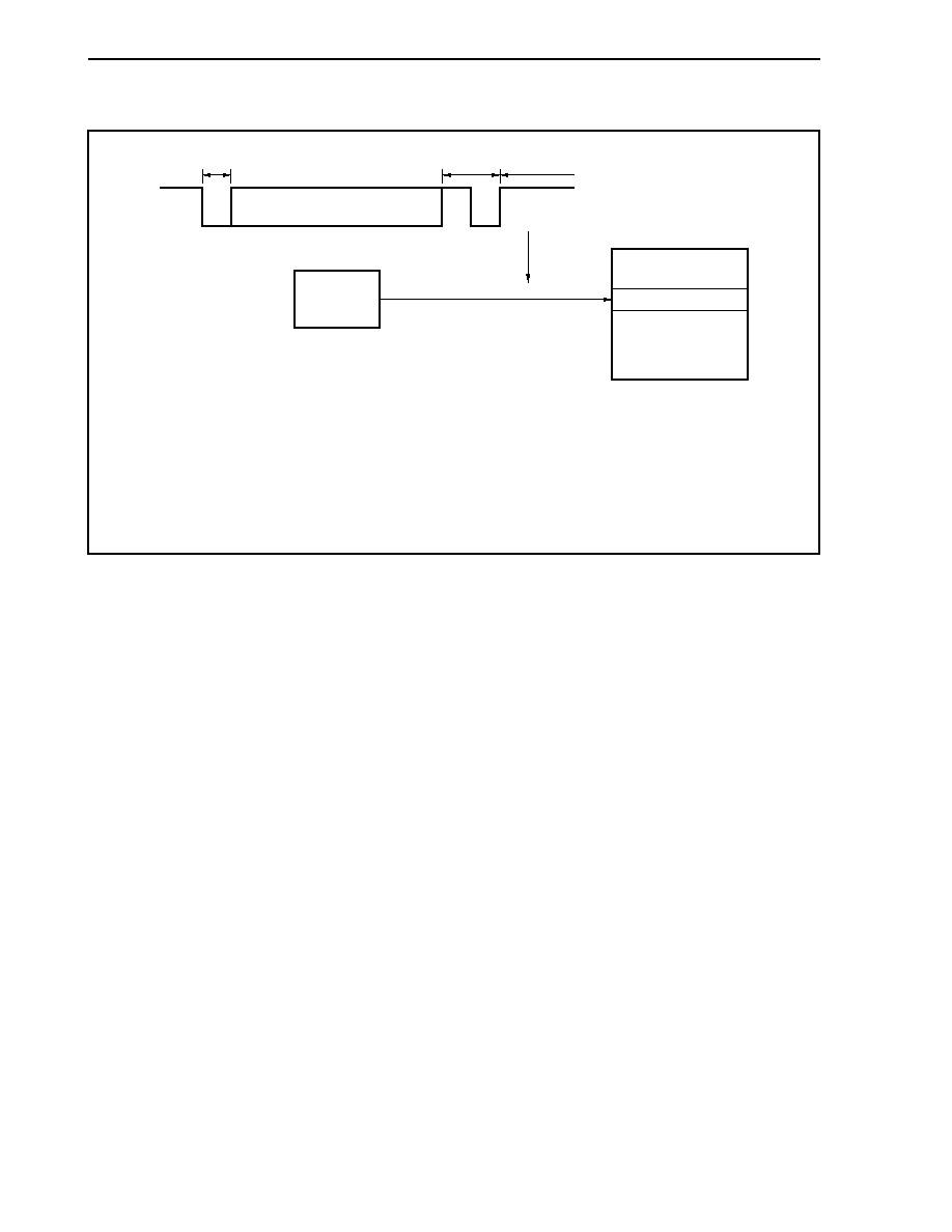
CHAPTER 11 FCAN CONTROLLER
518
User's Manual U14492EJ5V0UD
Figure 11-3. Time Stamp Function Setting for Message Reception (When C1CTRL Register's TMR Bit = 1)
Message
ACK field
EOF
SOF
<1>
Time stamp
counter
M_TIMEn
CAN message buffer n
<Explanation>
<1> When the EOF is detected on the CAN bus (a valid message is acknowledged), the captured time stamp
counter value is copied to the M_TIMEn register in CAN message buffer n when a message is stored in
CAN message buffer n.
Remark n = 00 to 31
In a global time system, the timer value must be captured using the SOF.
In addition, the ability to capture the time stamp counter value when message is stored in CAN message buffer n is
useful for evaluating the FCAN controller's performance.
The captured time stamp counter value is stored in CAN message buffer n, so CAN message buffer n has its own
time stamp function (n = 00 to 31).
When the SOF is detected on the CAN bus while transmitting a message, there is an option to replace the last two
bytes of the message with the captured time stamp counter value by setting bit 5 (ATS) of CAN message control
register n (M_CTRLn). This function can be selected for CAN message buffer n on a buffer by buffer basis. Figure
11-4 shows the time stamp setting when the ATS bit = 1.
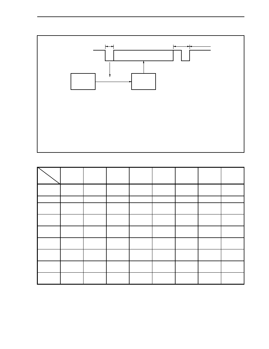
CHAPTER 11 FCAN CONTROLLER
519
User's Manual U14492EJ5V0UD
Figure 11-4. Time Stamp Function Setting for Message Transmission (When M_CTRL Register's ATS Bit = 1)
Message
ACK field
EOF
SOF
<2>
<1>
Time stamp
counter
Temporary
buffer
<Explanation>
<1> The time stamp counter value is captured to the temporary buffer when the SOF is detected on the CAN bus.
<2> The value of the temporary buffer is added to the last 2 bytes of the data length code
Note
specified by bits DLC3
to DLC0 of the M_DLCn register.
Note The ATS bit of the M_CTRLn register must be 1 and the data length must be more than 2 bytes to add
the time stamp counter value to the transmit message.
Remark n = 00 to 31
Table 11-3. Example When Adding Captured Time Stamp Counter Value to Last 2 Bytes of Transmit Message
Data Field
DLC
Bit Value
Note 1
Data 1
Data 2
Data 3
Data 4
Data 5
Data 6
Data 7
Data 8
1
M_DATAn0
register value
-
-
-
-
-
-
-
2
Note 2
Note 3
-
-
-
-
-
-
3
M_DATAn0
register value
Note 2
Note 3
-
-
-
-
-
4
M_DATAn0
register value
M_DATAn1
register value
Note 2
Note 3
-
-
-
-
5
M_DATAn0
register value
M_DATAn1
register value
M_DATAn2
register value
Note 2
Note 3
-
-
-
6
M_DATAn0
register value
M_DATAn1
register value
M_DATAn2
register value
M_DATAn3
register value
Note 2
Note 3
-
-
7
M_DATAn0
register value
M_DATAn1
register value
M_DATAn2
register value
M_DATAn3
register value
M_DATAn4
register value
Note 2
Note 3
-
8
M_DATAn0
register value
M_DATAn1
register value
M_DATAn2
register value
M_DATAn3
register value
M_DATAn4
register value
M_DATAn5
register value
Note 2
Note 3
9 to 15
M_DATAn0
register value
M_DATAn1
register value
M_DATAn2
register value
M_DATAn3
register value
M_DATAn4
register value
M_DATAn5
register value
Note 2
Note 3
Notes 1. See
11.10 (2) CAN message data length registers 00 to 31 (M_DLC00 to M_DLC31).
2. The lower 8 bits of the time stamp counter value when the SOF is detected on the CAN bus
3. The higher 8 bits of the time stamp counter value when the SOF is detected on the CAN bus
Remark n = 00 to 31

CHAPTER 11 FCAN CONTROLLER
520
User's Manual U14492EJ5V0UD
11.5 Message Processing
A modular system is used for the FCAN controller. Consequently, messages can be placed at any location within
the message area.
The messages can be linked to mask functions that are in turn linked to CAN modules.
11.5.1 Message transmission
The FCAN system is a multiplexed communication system. The priority of message transmission within this
system is determined based on message identifiers (IDs).
To facilitate communication processing by application software when there are several messages awaiting
transmission, the CAN module uses hardware to check the message IDs and automatically determine whether or not
linked messages are prioritized.
This eliminates the need for software-based priority control.
In addition, the priority at transmission can be controlled by setting the PBB bit of the C1DEF register.
∑ When the PBB bit is set to 0 (see Figure 11-5)
Transmission priority is controlled by the identifier (ID).
The number
Note
of messages waiting to be transmitted in the message buffer that can be set simultaneously by
application software is up to five messages per CAN module.
Note The number of message buffers when the TRQ bit of the M_STAT00 to M_STAT31 registers = 1.
∑ When the PBB bit is set to 1 (see Figure 11-6)
Transmission priority is controlled by the message numbers.
The number of messages waiting to be transmitted in the message buffer is not limited by the application
software.
CHAPTER 11 FCAN CONTROLLER
521
User's Manual U14492EJ5V0UD
Figure 11-5. Message Processing Example (When PBB Bit = 0)
Message No.
CAN module transmits messages in the following sequence.
Message waiting to be transmitted
ID = 120H
ID = 229H
ID = 223H
ID = 023H
ID = 123H
0
1
2
3
4
5
6
7
8
9
1. Message 6
2. Message 1
3. Message 8
4. Message 5
5. Message 2
Figure 11-6. Message Processing Example (When PBB Bit = 1)
Message No.
CAN module transmits messages in the following sequence.
Message waiting to be transmitted
ID = 120H
ID = 229H
ID = 223H
ID = 023H
ID = 123H
0
1
2
3
4
5
6
7
8
9
1. Message 1
2. Message 2
3. Message 5
4. Message 6
5. Message 8
CHAPTER 11 FCAN CONTROLLER
522
User's Manual U14492EJ5V0UD
11.5.2 Message reception
When two or more message buffers of the CAN module receive a message, the storage priority of the received
messages is as follows (the storage priority differs between data frames and remote frames).
Table 11-4. Storage Priority for Data Frame Reception
Priority Conditions
2 (High)
Unmasked message buffer
3
Message buffer linked to mask 0
4
Message buffer linked to mask 1
5
Message buffer linked to mask 2
6 (Low)
Message buffer linked to mask 3
Table 11-5. Storage Priority for Remote Frame Reception
Priority Conditions
1 (High)
Transmit message buffer
2
Unmasked message buffer
3
Message buffer linked to mask 0
4
Message buffer linked to mask 1
5
Message buffer linked to mask 2
6 (Low)
Message buffer linked to mask 3
A message (data frame or remote frame) is always stored in a receive message buffer with a higher priority, not in
a receive buffer with a lower priority. For example, when the unmasked receive message buffer and the message
buffer linked to mask 0 have the same ID, a message is always stored in the unmasked receive message buffer even
if the unmasked receive message buffer has already received a message.
When two or more message buffers with the same priority exist in the same CAN module, the priority is as follows.
Table 11-6. Priority of Same Priority Level
Priority Condition
1 (High)
DN bit of M_STAT register is not set (1)
2 (Low)
DN bit of M_STAT register is set (1)
When two or more message buffers with the same priority exist, the message buffer with the smaller message
number takes precedence.
Also, when two or more message buffers with the same ID exist, the message buffer with the smaller message
number takes precedence.
CHAPTER 11 FCAN CONTROLLER
523
User's Manual U14492EJ5V0UD
11.6 Mask Function
A mask linkage function can be defined for each received message.
This means that there is no need to distinguish between local masks and global masks.
When the mask function is used, the received message's identifier is compared with the message buffer's identifier
and the message can be stored in the defined message buffer regardless of whether the mask sets "0" or "1" as a
result of the comparison.
When the mask function is operating, a bit whose value is defined as "1" by masking is not subject to the
abovementioned comparison between the received message's identifier and the message buffer's identifier.
However, this comparison is performed for any bit whose value is defined as "0" by masking.
For example, let us assume that all messages that have a standard-format ID in which bits ID27 to ID25 = 0 and
bits ID24 and ID22 = 1 are to be stored in message buffer 14 (which is linked by mask 1 as explained in 11.10 (7)).
The procedure for this example is shown below.
<1> Identifier bits to be stored in message buffer
ID28 ID27 ID26 ID25 ID24 ID23 ID22 ID21 ID20 ID19 ID18
x 0 0 0 1 x 1 x x x x
Remark x = don't care
Messages with an ID in which bits ID27 to ID25 = 0 and bits ID24 and ID22 = 1 are registered (initialized) in
message buffer 14 (see 11.10 (6)).
<2> Identifier bits set to message buffer 14 (example)
(Using CAN message ID registers L14 and H14 (M_IDL14 and M_IDH14))
ID28 ID27 ID26 ID25 ID24 ID23 ID22 ID21 ID20 ID19 ID18
0 0 0 0 1 0 1 0 0 0 0
ID17 ID16 ID15 ID14 ID13 ID12 ID11 ID10 ID9 ID8 ID7
0 0 0 0 0 0 0 0 0 0 0
ID6 ID5 ID4 ID3 ID2 ID1 ID0
0 0 0 0 0 0 0
Message buffer 14 is set as a standard-format identifier linked to mask 1 (see 11.10 (7)).

CHAPTER 11 FCAN CONTROLLER
524
User's Manual U14492EJ5V0UD
<3> Mask setting for mask 1 (example)
(Using CAN1 address mask 1 registers L and H (C1MASKL1 and C1MASKH1))
CMID28 CMID27 CMID26 CMID25 CMID24
CMID23
CMID22 CMID21
CMID20
CMID19 CMID18
1 0 0 0 0 1 0 1 1 1 1
CMID17 CMID16 CMID15 CMID14 CMID13
CMID12
CMID11 CMID10
CMID9 CMID8 CMID7
1 1 1 1 1 1 1 1 1 1 1
CMID6 CMID5 CMID4 CMID3 CMID2 CMID1 CMID0
1 1 1 1 1 1 1
Remark 1: Do not compare (mask)
0: Compare
Values are written to mask 1 (see 11.10 (19)), bits CMID27 to CMID24 and CMID22 are set to 0 and bits
CMID28, CMID23, and CMID21 to CMID0 are set to 1.
CHAPTER 11 FCAN CONTROLLER
525
User's Manual U14492EJ5V0UD
11.7 Protocol
FCAN is a high-speed multiplex communication protocol designed to enable real-time communications in
automotive applications. The CAN specification is generally divided into two layers (physical layer and data link
layer). The data link layer is further divided into logical link control and medium access control. The composition of
these layers is illustrated below.
Figure 11-7. Composition of Layers
Application layer
Physical layer
Data link
layer
∑
Logical link control (LLC)
∑
Medium access control (MAC)
Not applicable
Message and status handling rules
Protocol rules
Signal level and bit expression rules
Higher
Lower
11.7.1 Protocol mode function
(1) Standard format mode
2048 different identifiers can be set in this mode.
The standard format mode uses 11-bit identifiers, which means that it can handle up to 2032 messages.
(2) Extended format mode
This mode is used to extend the number of identifiers that can be set.
∑ While the standard format mode uses 11-bit identifiers, the extended format mode uses 29-bit (11 bits + 18
bits) identifiers which expands the amount of messages that can be handled to 2048
◊ 2
18
messages.
∑ Extended format mode is set when "recessive (R): recessive in wired OR" is set for both the SRR and IDE
bits in the arbitration field.
∑ When an extended format mode message and a standard format mode remote frame are transmitted at
the same time, the node that transmitted the extended format mode message is set to receive mode.
CHAPTER 11 FCAN CONTROLLER
526
User's Manual U14492EJ5V0UD
11.7.2 Message formats
Four types of frames are used in CAN protocol messages. The output conditions for each type of frame are as
follows.
∑ Data frame:
Frame used for transmit data
∑ Remote frame:
Frame used for transmit requests from receiving side
∑ Error frame:
Frame that is output when an error has been detected
∑ Overload frame: Frame that is output when receiving side is not ready
Remark Dominant
(D): Dominant in wired OR
Recessive (R): Recessive in wired OR
In the figure shown below, (D) = 0 and (R) = 1.
(1) Data frame and remote frame
<1> Data
frame
A data frame is the frame used for transmit data.
This frame is composed of seven fields.
Figure 11-8. Data Frame
R
D
Interframe space
End of frame (EOF)
ACK field
CRC field
Data field
Control field
Arbitration field
Start of frame (SOF)
Data frame
<1>
<2>
<3>
<4>
<5>
<6> <7>
<8>
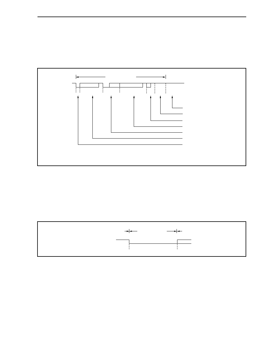
CHAPTER 11 FCAN CONTROLLER
527
User's Manual U14492EJ5V0UD
<2> Remote
frame
A remote frame is transmitted when the receiving node issues a transmit request.
A remote frame is similar to a data frame, except that the "data field" is deleted and the RTR bit of the
"arbitration field" is recessive.
Figure 11-9. Remote Frame
R
D
Interframe space
End of frame (EOF)
ACK field
CRC field
Control field
Arbitration field
Start of frame (SOF)
Remote frame
<1>
<2>
<3>
<5>
<6>
<7>
<8>
Remark The data field is not transferred even if the control field's data length code is not "0000B".
(2) Description of fields
<1> Start of frame (SOF)
The start of frame field is a 1-bit dominant (D) field that is located at the start of a data frame or remote
frame.
Figure 11-10. Start of Frame (SOF)
R
D
1 bit
Start of frame
(Interframe space or bus idle)
(Arbitration field)
∑ The start of frame field starts when the bus line level changes.
∑ When "dominant (D)" is detected at the sample point, reception continues.
∑ When "recessive (R)" is detected at the sample point, bus idle mode is set.
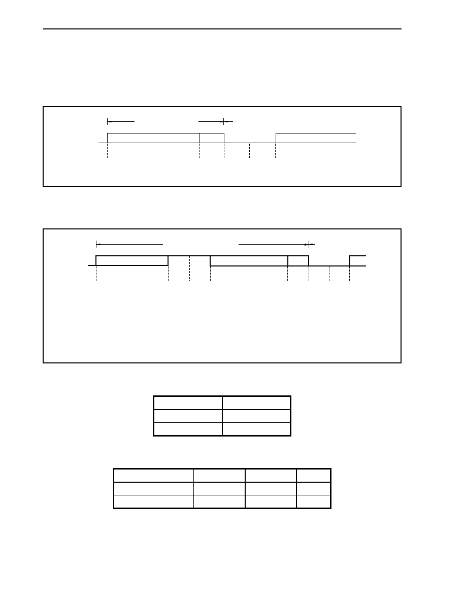
CHAPTER 11 FCAN CONTROLLER
528
User's Manual U14492EJ5V0UD
<2> Arbitration
field
The arbitration field is used to set the priority, data frame or remote frame, and protocol mode.
This field includes an identifier, frame setting (RTR bit), and protocol mode setting bit.
Figure 11-11. Arbitration Field (In Standard Format Mode)
R
D
IDE
(r1)
r0
RTR
Identifier
Arbitration field
(Control field)
(11 bits)
ID28 ∑ ∑ ∑ ∑ ∑ ∑ ∑ ∑ ∑ ∑ ∑ ∑ ∑ ∑ ∑ ∑ ∑ ∑ ∑ ∑ ID18
(1 bit)
(1 bit)
Figure 11-12. Arbitration Field (In Extended Format Mode)
R
D
r1
r0
RTR
IDE
SRR
Identifier
Note
Identifier
Arbitration field
(Control field)
(11 bits)
(18 bits)
ID28 ∑ ∑ ∑ ∑ ∑ ∑ ∑ ∑ ∑ ∑ ∑ ∑ ∑ ∑ ID18
ID17 ∑ ∑ ∑ ∑ ∑ ∑ ∑ ∑ ∑ ∑ ∑ ∑ ∑ ∑ ∑ ∑ ∑ ID0
(1 bit) (1 bit)
(1 bit)
Note Setting the higher 7 bits of the identifier as 1111111B is prohibited.
Cautions 1. ID28 to ID0 are identifier bits.
2. Identifier bits are transferred in MSB-first order.
Table 11-7. RTR Bit Settings
Frame Type
RTR Bit
Data frame
Dominant
Remote frame
Recessive
Table 11-8. Protocol Mode Setting and Number of Identifier (ID) Bits
Protocol Mode
SRR Bit
IDE Bit
No. of Bits
Standard format mode
None
Dominant (D)
11 bits
Extended format mode
Recessive (R) Recessive
(R) 29
bits
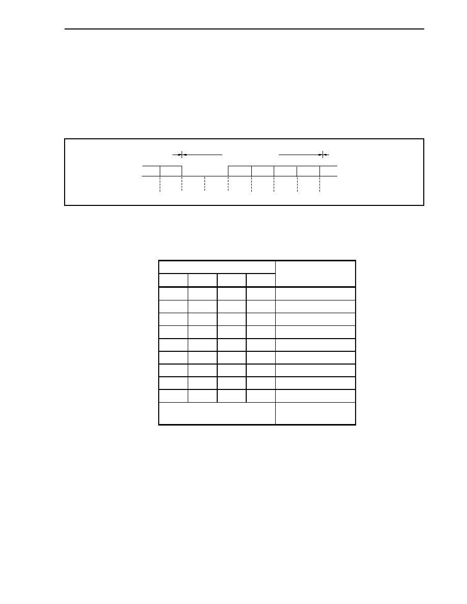
CHAPTER 11 FCAN CONTROLLER
529
User's Manual U14492EJ5V0UD
<3> Control
field
The control field sets "N" as the number of data bytes in the data field (N = 0 to 8).
r1 and r0 are fixed as dominant (D). The data length code bits (DLC3 to DLC0) set the byte count.
Remark DLC3 to DLC0: Bits 3 to 0 in CAN message data length registers 00 to 31 (M_DLC00 to
M_DLC31) (see 11.10 (2))
Figure 11-13. Control Field
R
D
r1
(IDE)
r0
RTR
DLC2
DLC3
DLC1
DLC0
Control field
(Data field)
(Arbitration field)
In standard format mode, the arbitration field's IDE bit is the same bit as the r1 bit.
Table 11-9. Data Length Code Settings
Data Length Code
DLC3 DLC2 DLC1 DLC0
Data Byte Count
0 0 0 0
0
bytes
0 0 0 1
1
byte
0 0 1 0
2
bytes
0 0 1 1
3
bytes
0 1 0 0
4
bytes
0 1 0 1
5
bytes
0 1 1 0
6
bytes
0 1 1 1
7
bytes
1 0 0 0
8
bytes
Other than above
8 bytes regardless of the
values of DLC3 to DLC0
Caution In the remote frame, there is no data field even if the data length code is
not 0000B.

CHAPTER 11 FCAN CONTROLLER
530
User's Manual U14492EJ5V0UD
<4> Data
field
The data field contains the amount of data set by the control field. Up to 8 units of data can be set.
Remark Data units in the data field are each 8 bits long and are ordered MSB first.
Figure 11-14. Data Field
R
D
Data
(8 bits)
Data
(8 bits)
Data field
(CRC field)
(Control field)
<5> CRC
field
The CRC field is a 16-bit field that is used to check for errors in transmit data. It includes a 15-bit CRC
sequence and a 1-bit CRC delimiter.
Figure 11-15. CRC Field
R
D
CRC sequence
CRC delimiter
(1 bit)
(15 bits)
CRC field
(ACK field)
(Data field, control field)
∑ The polynomial P(X) used to generate the 15-bit CRC sequence is expressed as: X
15
+ X
14
+ X
10
+
X
8
+ X
7
+ X
4
+ X
3
+ 1
∑ Transmitting node: No bit stuffing in start of frame, arbitration field, control field, or data field: The
transferred CRC sequence is calculated entirely from basic data bits.
∑ Receiving node:
The CRC sequence calculated using data bits that exclude the stuffing bits in
the receive data is compared with the CRC sequence in the CRC field. If the
two CRC sequences do not match, the node is passed to an error frame.
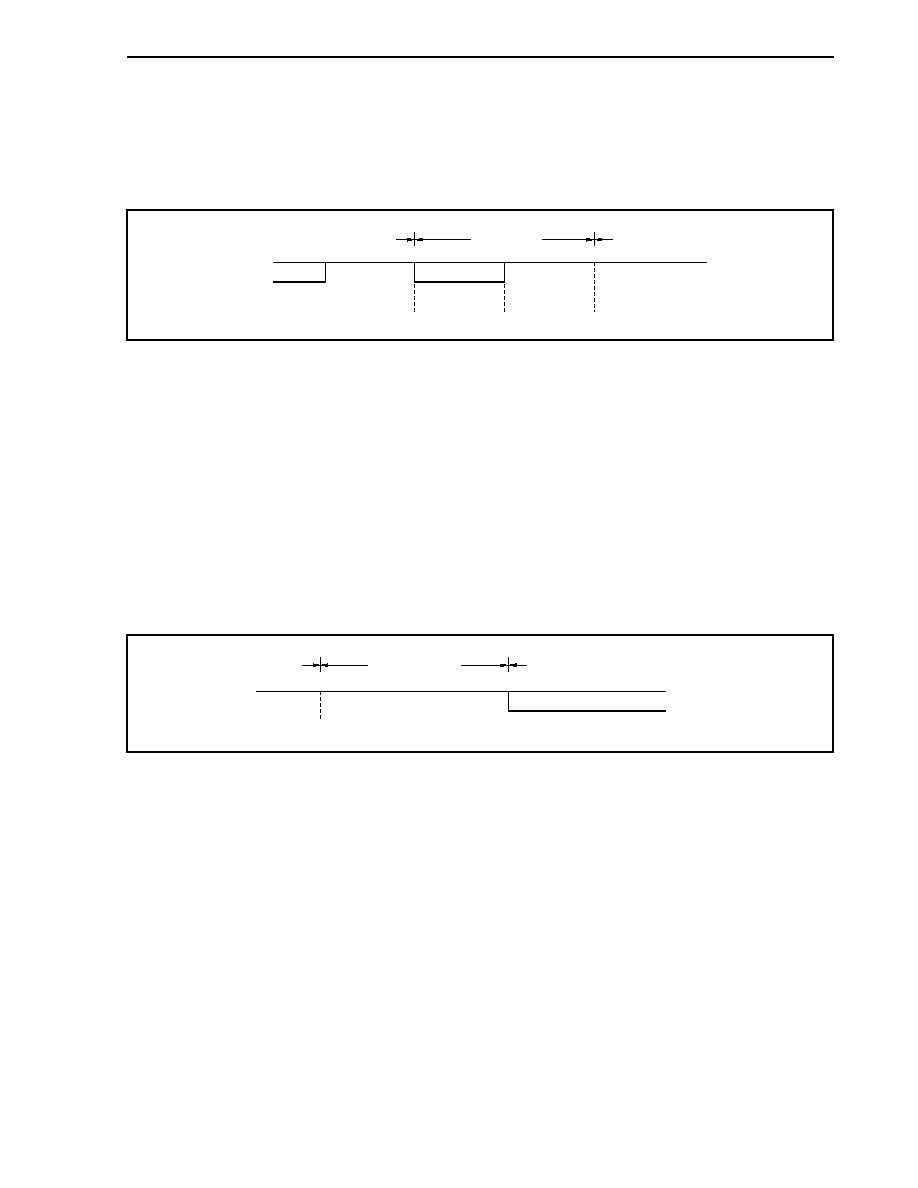
CHAPTER 11 FCAN CONTROLLER
531
User's Manual U14492EJ5V0UD
<6> ACK
field
The ACK field is used to confirm normal reception.
It includes a 1-bit ACK slot and a 1-bit ACK delimiter.
Figure 11-16. ACK Field
R
D
ACK slot
(1 bit)
ACK delimiter
(1 bit)
ACK field
(End of frame)
(CRC field)
∑ The receiving node outputs the following depending on whether or not an error is detected between
the start of frame field and the CRC field.
If an error is detected: ACK slot = Recessive (R)
If no error is detected: ACK slot = Dominant (D)
∑ The transmitting node outputs two "recessive (R)" bits and confirms the receiving node's receive
status.
<7> End of frame (EOF)
The end of frame field indicates the end of transmission or reception.
It includes 7 "recessive (R)" bits.
Figure 11-17. End of Frame (EOF)
R
D
End of frame
(7 bits)
(Interframe space or overload frame)
(ACK field)
CHAPTER 11 FCAN CONTROLLER
532
User's Manual U14492EJ5V0UD
<8> Interframe
space
The interframe space is inserted after the data frame, remote frame, error frame, and overload frame
to separate one frame from the next one.
∑
Error active node
When the bus is idle, transmit enable mode is set for each node. Transmission then starts from a
node that has received a transmit request.
If the node is an error active node, the interframe space is composed of a 3- or 2-bit intermission
field and bus idle field.
∑ Error
passive
node
After an 8-bit bus idle field, transmit enable mode is set. Receive mode is set if a transmission
starts from a different node in bus idle mode.
The error passive node is composed of an intermission field, suspend transmission field, and bus
idle field.
Figure 11-18. Interframe Space
(a) Error active
R
D
Interframe space
Intermission
(3 or 2 bits)
Bus idle
(0 or more bits)
(Frame)
(Frame)
(b) Error passive
R
D
Interframe space
Intermission
(3 or 2 bits)
Suspend transmission
(8 bits)
Bus idle
(0 or more bits)
(Frame)
(Frame)
∑ Bit length of intermission
When transmission is pending, transmission is resumed after a 3-bit intermission.
When receiving, the receive operation starts after only two bits.
∑ Bus idle
This mode is set when no nodes are using any buses.
∑ Suspend transmission
This is an 8-bit recessive (R) field that is transmitted from a node that is in error passive mode.
CHAPTER 11 FCAN CONTROLLER
533
User's Manual U14492EJ5V0UD
Table 11-10. Operation When Third Bit of Intermission Is "Dominant (D)"
Transmit Status
Operation
No pending transmissions
Receive operation is performed when start of frame output
by other node is detected.
Pending transmission exists
Identifier is transmitted when start of frame output by local
node is detected.
<9> Error
frame
An error frame is used to output from a node in which an error has been detected.
When a passive error flag is being output, if there is "dominant (D)" output from another node, the
passive error flag does not end until 6 consecutive bits are detected on the same level. If the bit
following the 6 consecutive "recessive (R)" bits is "dominant (D)", the error frame ends when the next
"recessive (R)" bit is detected.
Figure 11-19. Error Frame
<1>
R
D
<2>
<3>
6 bits
0 to 6 bits
8 bits
(<4>)
(<5>)
Interframe space or overload frame
Error delimiter
Error flag
Error flag
Error bit
Error frame
No Name Bit
count
Definition
Error active node
Consecutive output of 6
"dominant (D)" bits
<1> Error
flag
6
Error passive node
Consecutive output of 6
"recessive (R)" bits
<2>
Error flag
0 to 6
A node that receives an error flag is a node in which bit
stuffing errors are detected, after which an error flag is
output.
<3>
Error delimiter
8
8 consecutive "recessive (R)" bits are output.
If a "dominant (D)" bit is detected as the eighth bit, an
overload frame is sent starting at the next bit.
<4>
Error bit
≠
This bit is output following the bit where an error occurred.
If the error is a CRC error, it is output following an ACK
delimiter.
<5>
Interframe space or
overload frame
3/10
20 MAX.
An interframe space or overload frame starts from here.
CHAPTER 11 FCAN CONTROLLER
534
User's Manual U14492EJ5V0UD
<10> Overload frame
An overload frame is output starting from the first bit in an intermission in cases where the receiving
node is not yet ready to receive.
If a bit error is detected in intermission mode, it is output starting from the bit following the bit where
the bit error was detected.
Figure 11-20. Overload Frame
<1>
R
D
<2>
<3>
6 bits
0 to 6 bits
8 bits
(<4>)
(<5>)
Interframe space or overload frame
Overload delimiter
Overload flag (node n)
Overload flag (node m)
Frame
Overload frame
No Name Bit
count
Definition
<1>
Overload flag starting from
node m
6
Consecutive output of 6 "dominant (D)" bits.
Output when node m is not ready to receive.
<2>
Overload flag starting from
node n
0 to 6
Node n, which has received an overload flag in the
interframe space, outputs an overload flag.
<3>
Overload delimiter
8
8 consecutive "recessive (R)" bits are output.
If a "dominant (D)" bit is detected as the eighth bit, an
overload frame is sent starting at the next bit.
<4>
Frame
≠
Output following an end of frame, error delimiter, or
overload delimiter.
<5>
Interframe space or
overload frame
3/10
20 MAX.
An interframe space or overload frame starts from here.
Remark n
m

CHAPTER 11 FCAN CONTROLLER
535
User's Manual U14492EJ5V0UD
11.8 Functions
11.8.1 Determination of bus priority
(1) When one node has started transmitting
∑ In bus idle mode, the node that outputs data first starts transmission.
(2) When several nodes have started transmitting
∑ The node that has the longest string of consecutive "dominant (D)" bits starting from the first bit in the
arbitration field has top priority for bus access ("dominant (D)" bits take precedence due to wired OR bus
arbitration).
∑ The transmitting node compares the arbitration field which it has output and the bus data level.
Table 11-11. Determination of Bus Priority
Matched levels
Transmission continues
Mismatched
levels
When a mismatch is detected, data output stops at the next bit, and the
operation switches to receiving.
(3) Priority between data frame and remote frame
∑ If a bus conflict occurs between a data frame and a remote frame, the data frame takes priority because its
last bit (RTR) is "dominant (D)".
11.8.2 Bit stuffing
Bit stuffing is when one bit of inverted data is added for resynchronization to prevent burst errors when the same
level is maintained for five consecutive bits.
Table 11-12. Bit Stuffing
Transmit
When transmitting data frames and remote frames, if the same level is maintained for five bits
between the start of frame and CRC fields, one bit of data whose level is inverted from the
previous level is inserted before the next bit.
Receive
When receiving data frames and remote frames, if the same level is maintained for five bits
between the start of frame and CRC fields, the next bit of data is deleted before receiving is
resumed.
11.8.3 Multi-master
Since bus priority is determined based on the identifier, any node can be used as the bus master.
11.8.4 Multi-cast
Even when there is only one transmitting node, the same identifier can be set for several nodes, so that the same
data can be received by several nodes at the same time.
CHAPTER 11 FCAN CONTROLLER
536
User's Manual U14492EJ5V0UD
11.8.5 CAN sleep mode/CAN stop mode function
The CAN sleep mode/CAN stop mode function is able to set the FCAN controller to sleep (standby) mode to
reduce power consumption.
The CAN sleep mode is set via the procedure stipulated in the CAN specification. The CAN sleep mode can be set
to wake up by the bus operation, however the CAN stop mode cannot be set to wake up by the bus operation (this is
controlled via CPU access).
11.8.6 Error control function
(1) Types of errors
Table 11-13. Types of Errors
Description of Error
Detected Status
Error Type
Detection Method
Detection Condition
Transmit/
Receive
Field/Frame
Bit error
Comparison of output
level and bus level
(excludes stuff bits)
Mismatch between
levels
Transmitting/
receiving
nodes
Bits outputting data on bus in
start of frame to end of frame,
error frame, or overload frame
Stuff error
Use stuff bits to check
receive data
Six consecutive bits
of same-level data
Transmitting/
receiving
nodes
Start of frame to CRC
sequence
CRC error
Comparison of CRC
generated from
receive data and
received CRC
sequence
CRC mismatch
Receiving
node
Start of frame to data field
Form error
Check fixed-format
field/frame
Detection of inverted
fixed format
Receiving
node
∑ CRC delimiter
∑ ACK field
∑ End of frame
∑ Error frame
∑ Overload frame
ACK error
Use transmitting node
to check ACK slot
Use ACK slot to
detect recessive
Transmitting
node
ACK slot
(2) Error frame output timing
Table 11-14. Error Frame Output Timing
Error Type
Output Timing
Bit error, stuff error, form error,
ACK error
Error frame is output at the next bit following the bit where error was detected
CRC error
Error frame is output at the next bit following the ACK delimiter
(3) Handling of errors
The transmitting node retransmits the data frame or remote frame after the error frame has been transmitted.

CHAPTER 11 FCAN CONTROLLER
537
User's Manual U14492EJ5V0UD
(4) Error statuses
(a) Types of error statuses
The three types of error statuses are listed below.
Error active
Error passive
Bus off
∑ Error status is controlled by the transmit error counter and receive error counter (see 11.10 (23) CAN1
error count register (C1ERC)).
∑ The various error statuses are categorized according to their error counter values.
∑ The error flags used to output error statuses differ between transmit and receive operations.
∑ When the error counter value reaches 96 or more, the bus status must be tested since the bus may
become seriously damaged.
∑ During startup, if only one node is active, the error frame and data are repeatedly resent because no
ACK is returned even data has been transmitted.
In such cases, bus off mode cannot be set. Even if the node that is sending the transmit message
repeatedly experiences an error status, bus off mode cannot be set.
Table 11-15. Types of Error Statuses
Error Status Type
Operation
Error Counter Value
Type of Output Error Flag
Error active
Transmit/
receive
0 to 127
Active error flag (6 consecutive "dominant
(D)" bits)
Transmit
128 to 255
Error passive
Receive
128 or more
Passive error flag (6 consecutive "recessive
(R)" bits)
Bus off
Transmit
256 or more
Transfer is not possible.
When a string of at least 11 consecutive
"recessive (R)" bits occurs 128 times, the
error counter is zero-cleared and the error
active status can be resumed.

CHAPTER 11 FCAN CONTROLLER
538
User's Manual U14492EJ5V0UD
(b) Error counter
The error counter value is incremented each time an error occurs and is decremented when a transmit or
receive operation ends normally. The count-up/count-down timing occurs at the first bit of the error
delimiter.
Table 11-16. Error Counter
Status Transmit
Error
Counter
(TEC7 to TEC0)
Receive Error Counter
(REC7 to REC0)
Receiving node has detected an error (except for bit errors
that occur in an active error flag or overload flag)
No change
+1
"Dominant (D)" is detected following error frame's error flag
output by the receiving node
No change
+8
Transmitting node has sent an error flag
[When error counter = ±0]
<1> When an ACK error was detected during error passive
status and a "dominant (D)" was not detected during
passive error flag output
<2> When a stuff error occurs in the arbitration field
+8 No
change
Detection of bit error during output of active error flag or
overload flag (transmitting node with error active status)
+8 No
change
Detection of bit error during output of active error flag or
overload flag (receiving node with error active status)
No change
+8
14 consecutive "dominant (D)" bits were detected from the
start of each node's active error flag or overload flag,
followed by detection of eight consecutive dominant bits.
Each node has detected eight consecutive dominant bits
after a passive error flag.
+8 +8
The transmitting node has completed a transmit operation
without any errors (±0 if error counter value is 0).
≠1 No
change
The receiving node has completed a receive operation
without any errors.
No change
∑ -1
(1
REC7 to REC0 127)
∑ ±0
(REC7 to REC0 = 0)
∑ 127 is set
(REC7 to REC0 > 127)
(c) Occurrence of bit error during intermission
In this case, an overload frame occurs.
Caution When an error occurs, error control is performed according to the contents of the
transmitting and receiving error counters as they existed prior to the error's occurrence.
The error counter value is incremented only after an error flag has been output.
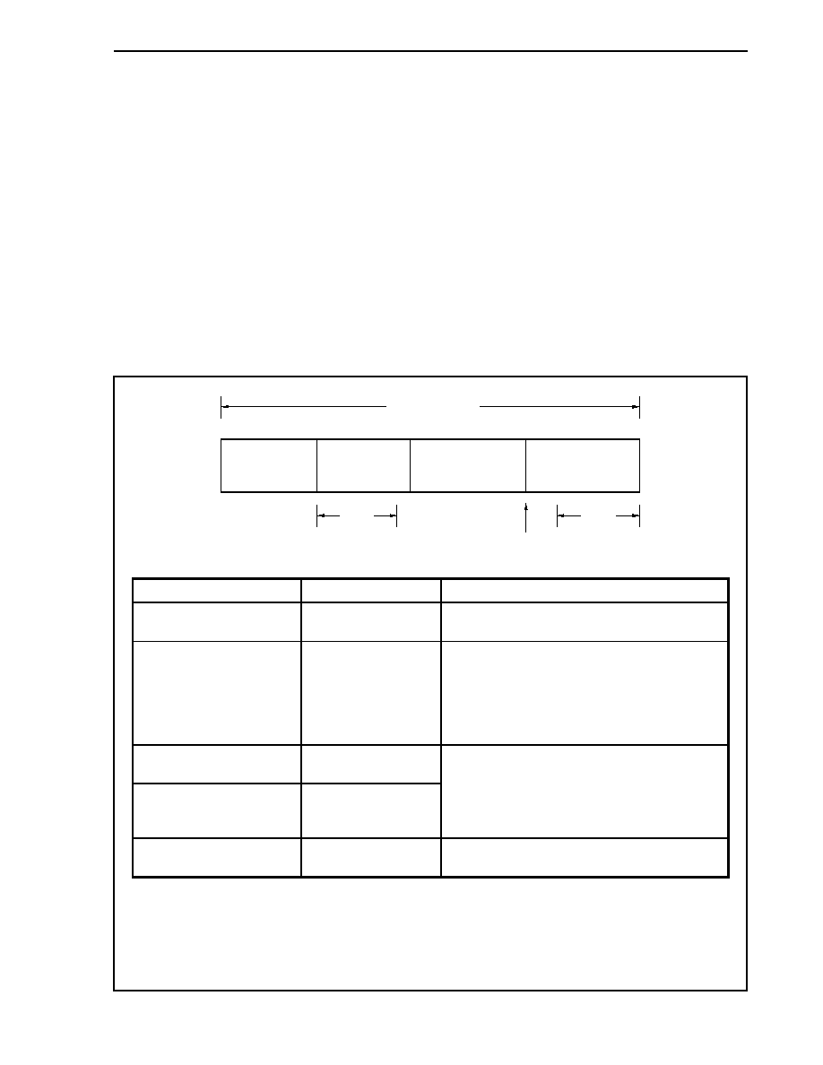
CHAPTER 11 FCAN CONTROLLER
539
User's Manual U14492EJ5V0UD
11.8.7 Baud rate control function
(1) Prescaler
The FCAN controller of the V850E/IA1 includes a prescaler for dividing the clock supplied to the CAN (f
MEM1
).
This prescaler generates a clock (f
BTL
) that is based on a division ratio ranging from 2 to 128 applied to the
CAN base clock (f
MEM
) when the C1BRP register's TLM bit = 0 and based on a division ratio ranging from 2 to
256 applied to the CAN base clock (f
MEM
) when the TLM bit = 1 (refer to 11.10 (26) CAN1 bit rate prescaler
register (C1BRP)).
(2) Nominal bit time (8 to 25 time quantum)
A definition of 1 data bit time is shown below.
Remark 1 time quantum = 1/f
BTL
Figure 11-21. Nominal Bit Time
Nominal bit time
SJW
SJW
Phase segment 2
Phase segment 1
Sample point
Prop segment
Sync segment
Segment name
Segment length
Description
Sync segment
(Synchronization Segment)
1
This segment begins when resynchronization occurs.
Prop segment
(Propagation Segment)
1 to 8 (programmable)
This segment is used to absorb the delays caused by
the output buffer, CAN bus, and input buffer.
It is set to return an ACK signal until phase segment 1
begins.
Prop segment time
(output buffer delay) + (CAN bus
delay) + (input buffer delay)
Phase segment 1
(Phase Buffer Segment 1)
1 to 8 (programmable)
Phase segment 2
(Phase Buffer Segment 2)
Maximum value from
phase segment 1 or
IPT
Note
(IPT = 0 to 2)
This segment is used to compensate for errors in the
data bit time. It accommodates a wide margin or error
but slows down communication speed.
SJW
(reSynchronization Jump Width)
1 to 4 (programmable)
This sets the range for bit synchronization.
Note IPT: Information Processing Time
IPT is a period in which the current bit level is referenced and judgment for the next processing is
performed. IPT is indicated by the expression below using the clock supplied to CAN (f
MEM1
).
IPT = 1/f
MEM1
◊ 3
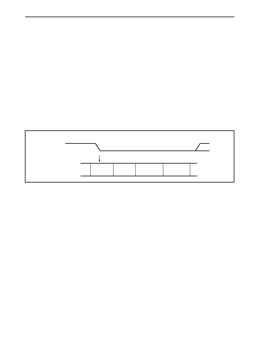
CHAPTER 11 FCAN CONTROLLER
540
User's Manual U14492EJ5V0UD
(3) Data bit synchronization
∑ Since the receiving node has no synchronization signal, synchronization is performed using level changes
that occur on the bus.
∑ As for the transmitting node, data is transmitted in sync with the transmitting node's bit timing.
(a) Hardware synchronization
This is bit synchronization that is performed when the receiving node has detected a start of frame in bus
idle mode.
∑ When a falling edge is detected on the bus, the current bit is assigned to the sync segment and the
next bit is assigned to the prop segment. In such cases, synchronization is performed regardless of
the SJW.
∑ Since bit synchronization must be established after a reset or after a wake-up, hardware
synchronization is performed only at the first level change that occurs on the bus (for the second and
subsequent level changes, bit synchronization is performed as shown below).
Figure 11-22. Coordination of Data Bit Synchronization
Phase
segment 2
Phase
segment 1
Prop
segment
Sync
segment
Start of frame
Bus idle
CAN bus
Bit timing
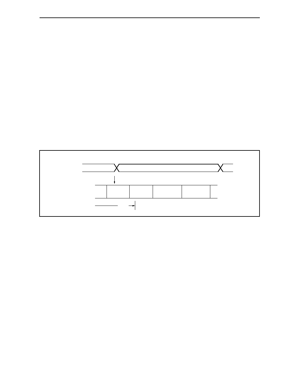
CHAPTER 11 FCAN CONTROLLER
541
User's Manual U14492EJ5V0UD
(b) Resynchronization
Resynchronization is performed when a level change is detected on the bus (only when the previous
sampling is at the recessive level) during a receive operation.
∑ The edge's phase error is produced by the relative positions of the detected edge and sync segment.
<Phase error symbols>
0:
When edge is within sync segment
Positive: Edge is before sample point (phase error)
Negative: Edge is after sample point (phase error)
∑ When the edge is detected as within the bit timing specified by the SJW, synchronization is performed
in the same way as hardware synchronization.
∑ When the edge is detected as extending beyond the bit timing specified by the SJW, synchronization
is performed on the following basis.
When phase error is positive: Phase segment 1 is lengthened to equal the SJW
When phase error is negative: Phase segment 2 is shortened to equal the SJW
∑ A "shifting" of the baud rate for the transmitting and receiving nodes moves the relative position of the
sample point for data on the receiving node.
Figure 11-23. Resynchronization
Phase
segment 2
Phase
segment 1
Prop
segment
Sync
segment
SOF
Next bit
Previous bit
CAN bus
Bit timing
SJW
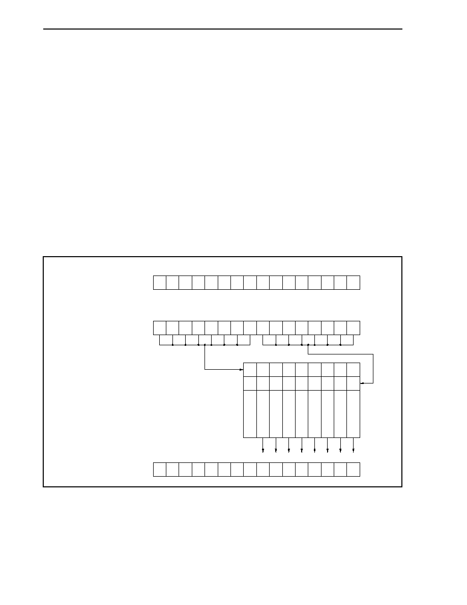
CHAPTER 11 FCAN CONTROLLER
542
User's Manual U14492EJ5V0UD
11.9 Cautions on Bit Set/Clear Function
The FCAN control registers include registers whose bits can be set or cleared via the CPU and via the CAN
interface. An operation error occurs if the following registers are written to directly, so do not directly write (via bit
manipulation, read/modify/write, or direct writing of target values) values to them.
∑ CAN global status register (CGST)
∑ CAN global interrupt enable register (CGIE)
∑ CAN1 control register (C1CTRL)
∑ CAN1 definition register (C1DEF)
∑ CAN1 interrupt enable register (C1IE)
All 16 bits in the above registers can be read via the usual method. Use the procedure described in Figure 11-24
below to set or clear the lower 8 bits in these registers.
Setting or clearing of lower 8 bits in the above registers is performed in combination with the higher 8 bits (see
Figure 11-25). Figure 11-24 shows how the values of set bits or clear bits relate to set/clear/no change operations in
the corresponding register.
Figure 11-24. Example of Bit Setting/Clearing Operations
0
0
0
0
0
0
0
0
1
1
0
1
0
0
0
1
15
14
13
12
11
10
9
8
7
6
5
4
3
2
1
0
15
14
13
12
11
10
9
8
7
6
5
4
3
2
1
0
15
14
13
12
11
10
9
8
7
6
5
4
3
2
1
0
0
0
0
0
1
0
1
1
1
1
0
1
1
0
0
0
set
0
0
0
0
1
0
1
1
0
0
0
0
0
0
0
0
0
0
0
0
0
0
1
1
clear
1
1
0
1
1
0
0
0
Set
Set
No change
No change
Clear
No change
Clear
Clear
Bit status
Register's current values
Write values
Register's value after
write operations
CHAPTER 11 FCAN CONTROLLER
543
User's Manual U14492EJ5V0UD
Figure 11-25. 16-Bit Data During Write Operation
15
14
13
12
11
10 9 8 7 6 5 4 3 2 1 0
set 7
set 6
set 5
set 4
set 3
set 2
set 1
set 0 clear 7 clear 6 clear 5 clear 4 clear 3 clear 2 clear 1 clear 0
set n
clear n
Bit n status after bit set/clear operation
0 0
No
change
0 1
0
1 0
1
1 1
No
change
Remark n = 0 to 7

CHAPTER 11 FCAN CONTROLLER
544
User's Manual U14492EJ5V0UD
11.10 Control Registers
(1) FCAN clock selection register (PRM04)
The PRM04 register is used to select the clock (f
MEM1
) supplied to CAN1.
The clock is selected according to the clock frequency.
This register can be read/written in 8-bit or 1-bit units.
Caution Set this register before using FCAN.
7
0
PRM04
6
0
5
0
4
0
3
0
2
0
1
PRM5
0
PRM4
Address
FFFFF930H
Initial value
00H
Bit position
Bit name
Function
Specifies FCAN clock (f
MEM1
) supplied to CAN1.
PRM5 PRM4
Input
clock
specification
0 0
f
XX
/4 (when f
XX
> 48 MHz)
0 1
f
XX
/2 (when 16 MHz < f
XX
32 MHz)
1 0
f
XX
/3 (when 32 MHz < f
XX
48 MHz)
1 1
f
XX
(when f
XX
16 MHz)
1, 0
PRM5,
PRM4
Remark f
XX
: Internal system clock
CHAPTER 11 FCAN CONTROLLER
545
User's Manual U14492EJ5V0UD
(2) CAN message data length registers 00 to 31 (M_DLC00 to M_DLC31)
The M_DLCn register sets the byte count in the data field of CAN message buffer n (n = 00 to 31). When
receiving, the receive data field's byte count is set (to 1).
These registers can be read/written in 8-bit units.
Caution When receiving a remote frame with an extended ID and storing it in the receive message
buffer, the values of DLC3 to DLC0 in the message buffer are cleared to 0 regardless of the
values of DLC3 to DLC0 on the CAN bus.
7
RFU
Note
M_DLCn
(n = 00 to 31)
6
RFU
Note
5
RFU
Note
4
RFU
Note
3
DLC3
2
DLC2
1
DLC1
0
DLC0
Address
See Table 11-17
Initial value
Undefined
Bit position
Bit name
Function
Control field data for setting the number of bytes in the data field
DLC3
DLC2
DLC1
DLC0
Data Length Code of Transmit/Receive
Message
0 0 0 0
0
bytes
0 0 0 1
1
byte
0 0 1 0
2
bytes
0 0 1 1
3
bytes
0 1 0 0
4
bytes
0 1 0 1
5
bytes
0 1 1 0
6
bytes
0 1 1 1
7
bytes
1 0 0 0
8
bytes
Other than above
8 bytes regardless of the values of
DLC3 to DLC0
3 to 0
DLC3 to
DLC0
Note RFU (Reserved for Future Use) indicates a reserved bit. Be sure to clear this bit to 0 when writing the
M_DLCn register.

CHAPTER 11 FCAN CONTROLLER
546
User's Manual U14492EJ5V0UD
Table 11-17. Addresses of M_DLCn (n = 00 to 31)
Register Name
Address
Note
(m = 2, 6, A, E)
Register Name
Address
Note
(m = 2, 6, A, E)
M_DLC00 xxxxm804H M_DLC16 xxxxmA04H
M_DLC01 xxxxm824H M_DLC17 xxxxmA24H
M_DLC02 xxxxm844H M_DLC18 xxxxmA44H
M_DLC03 xxxxm864H M_DLC19 xxxxmA64H
M_DLC04 xxxxm884H M_DLC20 xxxxmA84H
M_DLC05 xxxxm8A4H M_DLC21 xxxxmAA4H
M_DLC06 xxxxm8C4H M_DLC22 xxxxmAC4H
M_DLC07 xxxxm8E4H M_DLC23 xxxxmAE4H
M_DLC08 xxxxm904H M_DLC24 xxxxmB04H
M_DLC09 xxxxm924H M_DLC25 xxxxmB24H
M_DLC10 xxxxm944H M_DLC26 xxxxmB44H
M_DLC11 xxxxm964H M_DLC27 xxxxmB64H
M_DLC12 xxxxm984H M_DLC28 xxxxmB84H
M_DLC13 xxxxm9A4H M_DLC29 xxxxmBA4H
M_DLC14 xxxxm9C4H M_DLC30 xxxxmBC4H
M_DLC15 xxxxm9E4H M_DLC31 xxxxmBE4H
Note CAN message buffer registers can be allocated to the xxxx addresses as programmable peripheral I/O
registers. Note, however, that the xxxx addresses cannot be changed after being set.

CHAPTER 11 FCAN CONTROLLER
547
User's Manual U14492EJ5V0UD
(3) CAN message control registers 00 to 31 (M_CTRL00 to M_CTRL31)
The M_CTRLn register is used to set the frame format of the data field in messages stored in CAN message
buffer n (n = 00 to 31).
These registers can be read/written in 8-bit units.
(1/2)
7
RMDE1
M_CTRLn
(n = 00 to 31)
6
RMDE0
5
ATS
4
IE
3
MOVR
2
RFU
Notes 1, 2
1
RFU
Notes 1, 3
0
RTR
Address
See Table 11-18
Initial value
Undefined
Bit position
Bit name
Function
Specifies operation of the DN flag when a remote frame is received on a transmit message
buffer.
0: DN flag not set when remote frame is received
1: DN flag set when remote frame is received
7 RMDE1
Cautions 1. When the RMDE1 bit is set, the setting of the RMDE0 bit is irrelevant.
2. If a remote frame arrives at the transmit message buffer when the
RMDE1 bit has not been set, the CPU is not notified, nor are other
operations performed.
Specifies setting/clearing status of remote frame auto acknowledge function.
0: Remote frame auto acknowledge function cleared
1: Remote frame auto acknowledge function set
6 RMDE0
Cautions 1. The RMDE0 bit's setting is used only for transmit messages.
2. When the RTR bit has been set (to 1) (when the receive message or
transmit message has a remote frame), the RMDE0 bit is processed as
RMDE0 = 0. This prevents a worst-case scenario (in which
transmission of a remote frame draws a 100% bus load due to
reception of the same remote frame).
Notes 1. RFU (Reserved for Future Use) indicates a reserved bit. Be sure to clear this bit to 0 when writing
the M_DLCn register.
2. The value of the r1 bit on the CAN bus is set during reception.
3. The value of the r0 bit on the CAN bus is set during reception.
Remark DN: Bit 2 of M_STATn register (see 11.10 (8) CAN message status registers 00 to 31
(M_STAT00 to M_STAT31))

CHAPTER 11 FCAN CONTROLLER
548
User's Manual U14492EJ5V0UD
(2/2)
Bit position
Bit name
Function
Specifies whether or not to add a time stamp when transmitting.
0: Time stamp not added when transmitting
1: Time stamp added when transmitting
5 ATS
Cautions 1. The ATS bit is used only for transmit messages.
2. When the ATS bit has been set (to 1) and the data length code specifies
at least two bytes, the last two bytes are replaced by a time stamp (see
Table 11-3). The added time stamp counter value is sent over the bus
via the SOF of the message. When this occurs, the last two bytes
(which are defined as a data field) are ignored.
Specifies the enable/disable setting for interrupt requests.
0: Interrupt requests disabled
1: Interrupt requests enabled
4 IE
Cautions 1. An interrupt request is generated when interrupts are enabled under
the following conditions.
∑ When a message is transmitted from the transmit message buffer
∑ When a message is received by the receive message buffer
∑ When a remote frame is transmitted from the receive message
buffer
∑ When a remote frame is received by the transmit message buffer
when the auto acknowledge function has not been set (RMDE0 bit = 0)
2. An interrupt request is not generated when interrupts are enabled
under the following conditions.
∑ When a remote frame is received by the transmit message buffer
when the auto acknowledge function has been set (RMDE0 bit = 1)
3. An interrupt request is generated under the following conditions even if
interrupts are disabled.
∑ When a remote frame is received by the receive message buffer when
the auto acknowledge function has not been set (RMDE0 bit = 0)
This is the flag that indicates a message buffer overwrite.
0: Overwrite does not occur after DN bit is cleared
1: Overwrite occurs at least once after DN bit is cleared
3 MOVR
Caution An overwrite of the message buffer occurs when the CAN module writes
new data to the message buffer or when the DN bit has already been set
(to 1). The MOVR bit is updated each time new data is stored in the
message buffer.
Specifies frame type.
0: Data frame transmit/receive
1: Remote frame transmit/receive
0 RTR
Caution When the RTR bit has been set (to 1) for a transmit message, a remote
frame is transmitted instead of a data frame.
Remark DN: Bit 2 of M_STATn register (see 11.10 (8) CAN message status registers 00 to 31
(M_STAT00 to M_STAT31))

CHAPTER 11 FCAN CONTROLLER
549
User's Manual U14492EJ5V0UD
Table 11-18. Addresses of M_CTRLn (n = 00 to 31)
Register Name
Address
Note
(m = 2, 6, A, E)
Register Name
Address
Note
(m = 2, 6, A, E)
M_CTRL00 xxxxm805H M_CTRL16 xxxxmA05H
M_CTRL01 xxxxm825H M_CTRL17 xxxxmA25H
M_CTRL02 xxxxm845H M_CTRL18 xxxxmA45H
M_CTRL03 xxxxm865H M_CTRL19 xxxxmA65H
M_CTRL04 xxxxm885H M_CTRL20 xxxxmA85H
M_CTRL05 xxxxm8A5H M_CTRL21 xxxxmAA5H
M_CTRL06 xxxxm8C5H M_CTRL22 xxxxmAC5H
M_CTRL07 xxxxm8E5H M_CTRL23 xxxxmAE5H
M_CTRL08 xxxxm905H M_CTRL24 xxxxmB05H
M_CTRL09 xxxxm925H M_CTRL25 xxxxmB25H
M_CTRL10 xxxxm945H M_CTRL26 xxxxmB45H
M_CTRL11 xxxxm965H M_CTRL27 xxxxmB65H
M_CTRL12 xxxxm985H M_CTRL28 xxxxmB85H
M_CTRL13 xxxxm9A5H M_CTRL29 xxxxmBA5H
M_CTRL14 xxxxm9C5H M_CTRL30 xxxxmBC5H
M_CTRL15 xxxxm9E5H M_CTRL31 xxxxmBE5H
Note CAN message buffer registers can be allocated to the xxxx addresses as programmable peripheral I/O
registers. Note, however, that the xxxx addresses cannot be changed after being set.
CHAPTER 11 FCAN CONTROLLER
550
User's Manual U14492EJ5V0UD
(4) CAN message time stamp registers 00 to 31 (M_TIME00 to M_TIME31)
The M_TIMEn register is the register where the time stamp counter value is written upon completion of data
reception (n = 00 to 31).
These registers can be read/written in 16-bit units.
14
TS
14
13
TS
13
12
TS
12
2
TS
2
3
TS
3
4
TS
4
5
TS
5
6
TS
6
7
TS
7
8
TS
8
9
TS
9
10
TS
10
11
TS
11
15
TS
15
1
TS
1
0
TS
0
M_TIMEn
(n = 00 to 31)
Address
See Table 11-19
Initial value
Undefined
Bit position
Bit name
Function
Indicates the time stamp counter value.
15 to 0
TS15 to
TS0
Caution When a data frame or remote frame is received in the receive message
buffer, if the new data is stored in the message buffer, a 16-bit time tag
(time stamp counter value) is stored in the M_TIMEn register only when
the MT2 to MT0 bits of the M_CONFn register are set to value other than
"000" or "110" (receive message). This time tag is set according to the
FCAN's time stamp setting, which is either the time stamp counter value
that was captured when the SOF was sent via the bus or the value
captured when the CAN module writes data to the message buffer.
Table 11-19. Addresses of M_TIMEn (n = 00 to 31)
Register Name
Address
Note
(m = 2, 6, A, E)
Register Name
Address
Note
(m = 2, 6, A, E)
M_TIME00 xxxxm806H M_TIME16 xxxxmA06H
M_TIME01 xxxxm826H M_TIME17 xxxxmA26H
M_TIME02 xxxxm846H M_TIME18 xxxxmA46H
M_TIME03 xxxxm866H M_TIME19 xxxxmA66H
M_TIME04 xxxxm886H M_TIME20 xxxxmA86H
M_TIME05 xxxxm8A6H M_TIME21 xxxxmAA6H
M_TIME06 xxxxm8C6H M_TIME22 xxxxmAC6H
M_TIME07 xxxxm8E6H M_TIME23 xxxxmAE6H
M_TIME08 xxxxm906H M_TIME24 xxxxmB06H
M_TIME09 xxxxm926H M_TIME25 xxxxmB26H
M_TIME10 xxxxm946H M_TIME26 xxxxmB46H
M_TIME11 xxxxm966H M_TIME27 xxxxmB66H
M_TIME12 xxxxm986H M_TIME28 xxxxmB86H
M_TIME13 xxxxm9A6H M_TIME29 xxxxmBA6H
M_TIME14 xxxxm9C6H M_TIME30 xxxxmBC6H
M_TIME15 xxxxm9E6H M_TIME31 xxxxmBE6H
Note CAN message buffer registers can be allocated to the xxxx addresses as programmable peripheral I/O
registers. Note, however, that the xxxx addresses cannot be changed after being set.
CHAPTER 11 FCAN CONTROLLER
551
User's Manual U14492EJ5V0UD
(5) CAN message data registers n0 to n7 (M_DATAn0 to M_DATAn7) (n = 00 to 31)
The M_DATAnx registers are areas where up to 8 bytes of transmit or receive data is stored (n = 00 to 31, x
= 0 to 7).
These registers can be read/written in 8-bit units.
7
D0_7
M_DATAn0
(n = 00 to 31)
6
D0_6
5
D0_5
4
D0_4
3
D0_3
2
D0_2
1
D0_1
0
D0_0
Address
See Table 11-20
Initial value
Undefined
7
D1_7
M_DATAn1
(n = 00 to 31)
6
D1_6
5
D1_5
4
D1_4
3
D1_3
2
D1_2
1
D1_1
0
D1_0
Address
See Table 11-20
Initial value
Undefined
7
D2_7
M_DATAn2
(n = 00 to 31)
6
D2_6
5
D2_5
4
D2_4
3
D2_3
2
D2_2
1
D2_1
0
D2_0
Address
See Table 11-20
Initial value
Undefined
7
D3_7
M_DATAn3
(n = 00 to 31)
6
D3_6
5
D3_5
4
D3_4
3
D3_3
2
D3_2
1
D3_1
0
D3_0
Address
See Table 11-20
Initial value
Undefined
7
D4_7
M_DATAn4
(n = 00 to 31)
6
D4_6
5
D4_5
4
D4_4
3
D4_3
2
D4_2
1
D4_1
0
D4_0
Address
See Table 11-20
Initial value
Undefined
7
D5_7
M_DATAn5
(n = 00 to 31)
6
D5_6
5
D5_5
4
D5_4
3
D5_3
2
D5_2
1
D5_1
0
D5_0
Address
See Table 11-20
Initial value
Undefined
7
D6_7
M_DATAn6
(n = 00 to 31)
6
D6_6
5
D6_5
4
D6_4
3
D6_3
2
D6_2
1
D6_1
0
D6_0
Address
See Table 11-20
Initial value
Undefined
7
D7_7
M_DATAn7
(n = 00 to 31)
6
D7_6
5
D7_5
4
D7_4
3
D7_3
2
D7_2
1
D7_1
0
D7_0
Address
See Table 11-20
Initial value
Undefined
Bit position
Bit name
Function
Indicates the contents of the message data.
7 to 0
D7_7 to
D0_0
Cautions 1. The M_DATAn0 to M_DATAn7 registers are fields used to hold receive
data and transmit data. When data is transmitted, the number of
messages defined by the DLC3 to DLC0 bits in the M_DLCn register are
transmitted via the CAN bus.
2. When the M_CTRLn register's ATS bit has been set (to 1) and the value
of the DLC3 to DLC0 bits in the M_DLCn register is at least two bytes,
the last two bytes that are sent normally via the CAN bus are ignored
and the time stamp value is sent.
3. When a new message is received, all data fields are updated, even
when the value of the DLC3 to DLC0 bits in the M_DLCn register is less
than 8 bytes. The values of data bytes that have not been received may
be updated, but they are ignored.
Remark n = 00 to 31

CHAPTER 11 FCAN CONTROLLER
552
User's Manual U14492EJ5V0UD
Table 11-20. Addresses of M_DATAnx (n = 00 to 31, x = 0 to 7)
Register
Name
M_DATAn0
Note
(m = 2, 6, A, E)
M_DATAn1
Note
(m = 2, 6, A, E)
M_DATAn2
Note
(m = 2, 6, A, E)
M_DATAn3
Note
(m = 2, 6, A, E)
M_DATAn4
Note
(m = 2, 6, A, E)
M_DATAn5
Note
(m = 2, 6, A, E)
M_DATAn6
Note
(m = 2, 6, A, E)
M_DATAn7
Note
(m = 2, 6, A, E)
00 xxxxm808H
xxxxm809H
xxxxm80AH
xxxxm80BH
xxxxm80CH
xxxxm80DH
xxxxm80EH
xxxxm80FH
01 xxxxm828H
xxxxm829H
xxxxm82AH
xxxxm82BH
xxxxm82CH
xxxxm82DH
xxxxm82EH
xxxxm82FH
02 xxxxm848H
xxxxm849H
xxxxm84AH
xxxxm84BH
xxxxm84CH
xxxxm84DH
xxxxm84EH
xxxxm84FH
03 xxxxm868H
xxxxm869H
xxxxm86AH
xxxxm86BH
xxxxm86CH
xxxxm86DH
xxxxm86EH
xxxxm86FH
04 xxxxm888H
xxxxm889H
xxxxm88AH
xxxxm88BH
xxxxm88CH
xxxxm88DH
xxxxm88EH
xxxxm88FH
05 xxxxm8A8H
xxxxm8A9H
xxxxm8AAH
xxxxm8ABH
xxxxm8ACH xxxxm8ADH xxxxm8AEH xxxxm8AFH
06 xxxxm8C8H
xxxxm8C9H
xxxxm8CAH
xxxxm8CBH xxxxm8CCH xxxxm8CDH xxxxm8CEH xxxxm8CFH
07 xxxxm8E8H
xxxxm8E9H
xxxxm8EAH
xxxxm8EBH
xxxxm8ECH xxxxm8EDH xxxxm8EEH xxxxm8EFH
08 xxxxm908H
xxxxm909H
xxxxm90AH
xxxxm90BH
xxxxm90CH
xxxxm90DH
xxxxm90EH
xxxxm90FH
09 xxxxm928H
xxxxm929H
xxxxm92AH
xxxxm92BH
xxxxm92CH
xxxxm92DH
xxxxm92EH
xxxxm92FH
10 xxxxm948H
xxxxm949H
xxxxm94AH
xxxxm94BH
xxxxm94CH
xxxxm94DH
xxxxm94EH
xxxxm94FH
11 xxxxm968H
xxxxm969H
xxxxm96AH
xxxxm96BH
xxxxm96CH
xxxxm96DH
xxxxm96EH
xxxxm96FH
12 xxxxm988H
xxxxm989H
xxxxm98AH
xxxxm98BH
xxxxm98CH
xxxxm98DH
xxxxm98EH
xxxxm98FH
13 xxxxm9A8H
xxxxm9A9H
xxxxm9AAH
xxxxm9ABH
xxxxm9ACH xxxxm9ADH xxxxm9AEH xxxxm9AFH
14 xxxxm9C8H
xxxxm9C9H
xxxxm9CAH
xxxxm9CBH xxxxm9CCH xxxxm9CDH xxxxm9CEH xxxxm9CFH
15 xxxxm9E8H
xxxxm9E9H
xxxxm9EAH
xxxxm9EBH
xxxxm9ECH xxxxm9EDH xxxxm9EEH xxxxm9EFH
16 xxxxmA08H
xxxxmA09H
xxxxmA0AH
xxxxmA0BH
xxxxmA0CH xxxxmA0DH xxxxmA0EH xxxxmA0FH
17 xxxxmA28H
xxxxmA29H
xxxxmA2AH
xxxxmA2BH
xxxxmA2CH xxxxmA2DH xxxxmA2EH xxxxmA2FH
18 xxxxmA48H
xxxxmA49H
xxxxmA4AH
xxxxmA4BH
xxxxmA4CH xxxxmA4DH xxxxmA4EH xxxxmA4FH
19 xxxxmA68H
xxxxmA69H
xxxxmA6AH
xxxxmA6BH
xxxxmA6CH xxxxmA6DH xxxxmA6EH xxxxmA6FH
20 xxxxmA88H
xxxxmA89H
xxxxmA8AH
xxxxmA8BH
xxxxmA8CH xxxxmA8DH xxxxmA8EH xxxxmA8FH
21 xxxxmAA8H
xxxxmAA9H
xxxxmAAAH
xxxxmAABH
xxxxmAACH
xxxxmAADH
xxxxmAAEH
xxxxmAAFH
22 xxxxmAC8H
xxxxmAC9H
xxxxmACAH xxxxmACBH xxxxmACCH xxxxmACDH xxxxmACEH xxxxmACFH
23 xxxxmAE8H
xxxxmAE9H
xxxxmAEAH
xxxxmAEBH
xxxxmAECH
xxxxmAEDH
xxxxmAEEH
xxxxmAEFH
24 xxxxmB08H
xxxxmB09H
xxxxmB0AH
xxxxmB0BH
xxxxmB0CH xxxxmB0DH xxxxmB0EH xxxxmB0FH
25 xxxxmB28H
xxxxmB29H
xxxxmB2AH
xxxxmB2BH
xxxxmB2CH xxxxmB2DH xxxxmB2EH xxxxmB2FH
26 xxxxmB48H
xxxxmB49H
xxxxmB4AH
xxxxmB4BH
xxxxmB4CH xxxxmB4DH xxxxmB4EH xxxxmB4FH
27 xxxxmB68H
xxxxmB69H
xxxxmB6AH
xxxxmB6BH
xxxxmB6CH xxxxmB6DH xxxxmB6EH xxxxmB6FH
28 xxxxmB88H
xxxxmB89H
xxxxmB8AH
xxxxmB8BH
xxxxmB8CH xxxxmB8DH xxxxmB8EH xxxxmB8FH
29 xxxxmBA8H
xxxxmBA9H
xxxxmBAAH
xxxxmBABH
xxxxmBACH
xxxxmBADH
xxxxmBAEH
xxxxmBAFH
30 xxxxmBC8H
xxxxmBC9H
xxxxmBCAH xxxxmBCBH xxxxmBCCH xxxxmBCDH xxxxmBCEH xxxxmBCFH
31 xxxxmBE8H
xxxxmBE9H
xxxxmBEAH
xxxxmBEBH
xxxxmBECH
xxxxmBEDH
xxxxmBEEH
xxxxmBEFH
Note CAN message buffer registers can be allocated to the xxxx addresses as programmable peripheral I/O
registers. Note, however, that the xxxx addresses cannot be changed after being set.
n
CHAPTER 11 FCAN CONTROLLER
553
User's Manual U14492EJ5V0UD
(6) CAN message ID registers L00 to L31 and H00 to H31
(M_IDL00 to M_IDL31 and M_IDH00 to M_IDH31)
The M_IDLn and M_IDHn registers are areas used to set identifiers (n = 00 to 31).
These registers can be read/written in 16-bit units.
When in standard format mode, any data can be stored in the following areas.
Bits ID17 to ID10: First byte of receive data
Note
is stored.
Bits ID9 to ID2:
Second byte of receive data
Note
is stored.
Bits ID1, ID0:
Third byte (higher two bits) of receive data
Note
is stored.
Note See
11.10 (5) CAN message data registers n0 to n7 (M_DATAn0 to M_DATAn7) (n = 00 to 31).
14
0
13
0
12
ID28
2
ID18
3
ID19
4
ID20
5
ID21
6
ID22
7
ID23
8
ID24
9
ID25
10
ID26
11
ID27
15
IDE
1
ID17
0
ID16
M_IDHn
(n = 00 to 31)
Address
See Table 11-22
Initial value
Undefined
14
ID14
13
ID13
12
ID12
2
ID2
3
ID3
4
ID4
5
ID5
6
ID6
7
ID7
8
ID8
9
ID9
10
ID10
11
ID11
15
ID15
1
ID1
0
ID0
M_IDLn
(n = 00 to 31)
Address
See Table 11-21
Initial value
Undefined
Bit position
Bit name
Function
15
(M_IDHn)
IDE
(M_IDHn)
Specifies format setting mode.
0: Standard format mode (ID28 to ID18: 11 bits)
1: Extended format mode (ID28 to ID0: 29 bits)
Remark n = 00 to 31
CHAPTER 11 FCAN CONTROLLER
554
User's Manual U14492EJ5V0UD
Table 11-21. Addresses of M_IDLn (n = 00 to 31)
Register Name
Address
Note
(m = 2, 6, A, E)
Register Name
Address
Note
(m = 2, 6, A, E)
M_IDL00 xxxxm810H M_IDL16 xxxxmA10H
M_IDL01 xxxxm830H M_IDL17 xxxxmA30H
M_IDL02 xxxxm850H M_IDL18 xxxxmA50H
M_IDL03 xxxxm870H M_IDL19 xxxxmA70H
M_IDL04 xxxxm890H M_IDL20 xxxxmA90H
M_IDL05 xxxxm8B0H M_IDL21 xxxxmAB0H
M_IDL06 xxxxm8D0H M_IDL22 xxxxmAD0H
M_IDL07 xxxxm8F0H M_IDL23 xxxxmAF0H
M_IDL08 xxxxm910H M_IDL24 xxxxmB10H
M_IDL09 xxxxm930H M_IDL25 xxxxmB30H
M_IDL10 xxxxm950H M_IDL26 xxxxmB50H
M_IDL11 xxxxm970H M_IDL27 xxxxmB70H
M_IDL12 xxxxm990H M_IDL28 xxxxmB90H
M_IDL13 xxxxm9B0H M_IDL29 xxxxmBB0H
M_IDL14 xxxxm9D0H M_IDL30 xxxxmBD0H
M_IDL15 xxxxm9F0H M_IDL31 xxxxmBF0H
Note CAN message buffer registers can be allocated to the addresses xxxx as programmable peripheral I/O
registers. Note, however, that the xxxx addresses cannot be changed after being set.
Table 11-22. Addresses of M_IDHn (n = 00 to 31)
Register Name
Address
Note
(m = 2, 6, A, E)
Register Name
Address
Note
(m = 2, 6, A, E)
M_IDH00 xxxxm812H M_IDH16 xxxxmA12H
M_IDH01 xxxxm832H M_IDH17 xxxxmA32H
M_IDH02 xxxxm852H M_IDH18 xxxxmA52H
M_IDH03 xxxxm872H M_IDH19 xxxxmA72H
M_IDH04 xxxxm892H M_IDH20 xxxxmA92H
M_IDH05 xxxxm8B2H M_IDH21 xxxxmAB2H
M_IDH06 xxxxm8D2H M_IDH22 xxxxmAD2H
M_IDH07 xxxxm8F2H M_IDH23 xxxxmAF2H
M_IDH08 xxxxm912H M_IDH24 xxxxmB12H
M_IDH09 xxxxm932H M_IDH25 xxxxmB32H
M_IDH10 xxxxm952H M_IDH26 xxxxmB52H
M_IDH11 xxxxm972H M_IDH27 xxxxmB72H
M_IDH12 xxxxm992H M_IDH28 xxxxmB92H
M_IDH13 xxxxm9B2H M_IDH29 xxxxmBB2H
M_IDH14 xxxxm9D2H M_IDH30 xxxxmBD2H
M_IDH15 xxxxm9F2H M_IDH31 xxxxmBF2H
Note CAN message buffer registers can be allocated to the addresses xxxx as programmable peripheral I/O
registers. Note, however, that the xxxx addresses cannot be changed after being set.
CHAPTER 11 FCAN CONTROLLER
555
User's Manual U14492EJ5V0UD
(7) CAN message configuration registers 00 to 31 (M_CONF00 to M_CONF31)
The M_CONFn register is used to set the message buffer type and mask (n = 00 to 31).
These registers can be read/written in 8-bit units.
7
0
M_CONFn
(n = 00 to 31)
6
0
5
MT2
4
MT1
3
MT0
2
0
1
0
0
MA
Address
See Table 11-23
Initial value
Undefined
Bit position
Bit name
Function
Specifies message type and mask setting.
MT2 MT1 MT0
Operation
0 0 0
Transmit
message
0
0
1
Receive message (no mask setting)
0
1
0
Receive message (mask 0 is set)
0
1
1
Receive message (mask 1 is set)
1
0
0
Receive message (mask 2 is set)
1
0
1
Receive message (mask 3 is set)
1 1 0
Setting
prohibited
1
1
1
Receive message (used in diagnostic processing
mode)
5 to 3
MT2 to
MT0
When bits MT2 to MT0 have been set as "111", processing can be performed only when
the FCAN has been set to diagnostic processing mode. In such cases, all messages
received are stored regardless of the following conditions.
∑ Storage to other message buffer
∑ Identifier type (standard frame or extended frame)
∑ Data frame or remote frame
Specifies message buffer's address.
MA Operation
0
Message buffer is not used
1
Used as message buffer
0 MA
Caution When the MA bit has been set to 0, message buffer area is used for
application RAM or for event processing as a temporary buffer.

CHAPTER 11 FCAN CONTROLLER
556
User's Manual U14492EJ5V0UD
Table 11-23. Addresses of M_CONFn (n = 00 to 31)
Register Name
Address
Note
(m = 2, 6, A, E)
Register Name
Address
Note
(m = 2, 6, A, E)
M_CONF00 xxxxm814H M_CONF16 xxxxmA14H
M_CONF01 xxxxm834H M_CONF17 xxxxmA34H
M_CONF02 xxxxm854H M_CONF18 xxxxmA54H
M_CONF03 xxxxm874H M_CONF19 xxxxmA74H
M_CONF04 xxxxm894H M_CONF20 xxxxmA94H
M_CONF05 xxxxm8B4H M_CONF21 xxxxmAB4H
M_CONF06 xxxxm8D4H M_CONF22 xxxxmAD4H
M_CONF07 xxxxm8F4H M_CONF23 xxxxmAF4H
M_CONF08 xxxxm914H M_CONF24 xxxxmB14H
M_CONF09 xxxxm934H M_CONF25 xxxxmB34H
M_CONF10 xxxxm954H M_CONF26 xxxxmB54H
M_CONF11 xxxxm974H M_CONF27 xxxxmB74H
M_CONF12 xxxxm994H M_CONF28 xxxxmB94H
M_CONF13 xxxxm9B4H M_CONF29 xxxxmBB4H
M_CONF14 xxxxm9D4H M_CONF30 xxxxmBD4H
M_CONF15 xxxxm9F4H M_CONF31 xxxxmBF4H
Note CAN message buffer registers can be allocated to the xxxx addresses as programmable peripheral I/O
registers. Note, however, that the xxxx addresses cannot be changed after being set.

CHAPTER 11 FCAN CONTROLLER
557
User's Manual U14492EJ5V0UD
(8) CAN message status registers 00 to 31 (M_STAT00 to M_STAT31)
The M_STATn register indicates the transmit/receive status information of each message buffer (n = 00 to
31).
These registers are read-only, in 8-bit units.
Cautions 1. Writing directly to M_STATn register cannot be performed. Writing must be performed
using CAN status set/clear register n (SC_STATn).
2.
Messages
are
transmitted
only when the M_STATn register's TRQ and RDY bits have
been set (to 1).
7
0
M_STATn
(n = 00 to 31)
6
0
5
0
4
0
3
RFU
Note 1
2
DN
1
TRQ
0
RDY
Note 2
Address
See Table 11-24
Initial value
Undefined
Bit position
Bit name
Function
2
DN
This is the message update flag.
0: No message was received after DN bit was cleared.
1: At least one message was received after DN bit was cleared.
∑ When the DN bit has been set (to 1) by the transmit message buffer, it indicates that the
message buffer has received a remote frame.
When this message is sent, the DN bit is automatically cleared (to 0).
∑ When a frame is again received in the receive message buffer for which the DN bit has
been set (to 1), an overwrite condition occurs and the M_CTRLn register's MOVR bit is
set (to 1) (n = 00 to 31).
1
TRQ
This is the transmit request flag.
0: Message transmission disabled
1: Message transmission enabled
∑ A transmit request is processed as a CAN module only when the RDY bit is set to 1.
∑ A remote frame is transmitted for the receive message buffer in which the TRQ bit is set to 1.
0
RDY
This is the transmit message ready flag.
0: Message is not ready.
1: Message is ready.
∑ A receive operation is performed only for a message buffer in which the RDY bit is set to
1 during reception.
∑ A transmit operation is performed only for a message buffer in which the RDY bit is set to
1 and the TRQ bit is set to 1 during transmission.
Notes 1. RFU (Reserved for Future Use) indicates a reserved bit. 0 or 1 is read from this bit regardless of
the message buffer setting.
2. The FCAN controller incorporated in the V850E/IA1 can perform reception even if the RDY bit is
not set. However, in products other than the V850E/IA1, the RDY bit must be set for reception. In
order to maintain software compatibility, be sure to set the RDY bit even for the FCAN controller of
the V850E/IA1 prior to reception.

CHAPTER 11 FCAN CONTROLLER
558
User's Manual U14492EJ5V0UD
Table 11-24. Addresses of M_STATn (n = 00 to 31)
Register Name
Address
Note
(m = 2, 6, A, E)
Register Name
Address
Note
(m = 2, 6, A, E)
M_STAT00 xxxxm815H M_STAT16 xxxxmA15H
M_STAT01 xxxxm835H M_STAT17 xxxxmA35H
M_STAT02 xxxxm855H M_STAT18 xxxxmA55H
M_STAT03 xxxxm875H M_STAT19 xxxxmA75H
M_STAT04 xxxxm895H M_STAT20 xxxxmA95H
M_STAT05 xxxxm8B5H M_STAT21 xxxxmAB5H
M_STAT06 xxxxm8D5H M_STAT22 xxxxmAD5H
M_STAT07 xxxxm8F5H M_STAT23 xxxxmAF5H
M_STAT08 xxxxm915H M_STAT24 xxxxmB15H
M_STAT09 xxxxm935H M_STAT25 xxxxmB35H
M_STAT10 xxxxm955H M_STAT26 xxxxmB55H
M_STAT11 xxxxm975H M_STAT27 xxxxmB75H
M_STAT12 xxxxm995H M_STAT28 xxxxmB95H
M_STAT13 xxxxm9B5H M_STAT29 xxxxmBB5H
M_STAT14 xxxxm9D5H M_STAT30 xxxxmBD5H
M_STAT15 xxxxm9F5H M_STAT31 xxxxmBF5H
Note CAN message buffer registers can be allocated to the xxxx addresses as programmable peripheral I/O
registers. Note, however, that the xxxx addresses cannot be changed after being set.
CHAPTER 11 FCAN CONTROLLER
559
User's Manual U14492EJ5V0UD
(9) CAN status set/clear registers 00 to 31 (SC_STAT00 to SC_STAT31)
The SC_STATn register is used to set/clear the transmit/receive status information (n = 00 to 31).
These registers are write-only, in 16-bit units.
14
0
13
0
12
0
2
clear
DN
3
0
4
0
5
0
6
0
7
0
8
set
RDY
9
set
TRQ
10
set
DN
11
0
15
0
1
clear
TRQ
0
clear
RDY
SC_STATn
(n = 00 to 31)
Address
See Table 11-25
Initial value
0000H
Bit position
Bit name
Function
Specifies setting/clearing of the message update flag.
set DN
clear DN
Operation
0
1
Cleared (DN bit cleared)
1
0
Set (DN bit set)
Other than above
No change in DN bit value
10, 2
set DN,
clear DN
Specifies setting/clearing of the transmit request flag.
set TRQ
clear TRQ
Operation
0
1
Cleared (TRQ bit cleared)
1
0
Set (TRQ bit set)
Other than above
No change in TRQ bit value
9, 1
set TRQ,
clear TRQ
Specifies setting of the message ready flag.
set RDY
clear RDY
Operation
0
1
Cleared (RDY bit cleared)
1
0
Set (RDY bit set)
Other than above
No change in RDY bit value
8, 0
set RDY,
clear RDY
Remark DN: Bit 2 of CAN message status register n (M_STATn)
TRQ: Bit 1 of CAN message status register n (M_STATn)
RDY: Bit 0 of CAN message status register n (M_STATn)

CHAPTER 11 FCAN CONTROLLER
560
User's Manual U14492EJ5V0UD
Table 11-25. Addresses of SC_STATn (n = 00 to 31)
Register Name
Address
Note
(m = 2, 6, A, E)
Register Name
Address
Note
(m = 2, 6, A, E)
SC_STAT00 xxxxm816H SC_STAT16 xxxxmA16H
SC_STAT01 xxxxm836H SC_STAT17 xxxxmA36H
SC_STAT02 xxxxm856H SC_STAT18 xxxxmA56H
SC_STAT03 xxxxm876H SC_STAT19 xxxxmA76H
SC_STAT04 xxxxm896H SC_STAT20 xxxxmA96H
SC_STAT05 xxxxm8B6H SC_STAT21 xxxxmAB6H
SC_STAT06 xxxxm8D6H SC_STAT22 xxxxmAD6H
SC_STAT07 xxxxm8F6H SC_STAT23 xxxxmAF6H
SC_STAT08 xxxxm916H SC_STAT24 xxxxmB16H
SC_STAT09 xxxxm936H SC_STAT25 xxxxmB36H
SC_STAT10 xxxxm956H SC_STAT26 xxxxmB56H
SC_STAT11 xxxxm976H SC_STAT27 xxxxmB76H
SC_STAT12 xxxxm996H SC_STAT28 xxxxmB96H
SC_STAT13 xxxxm9B6H SC_STAT29 xxxxmBB6H
SC_STAT14 xxxxm9D6H SC_STAT30 xxxxmBD6H
SC_STAT15 xxxxm9F6H SC_STAT31 xxxxmBF6H
Note CAN message buffer registers can be allocated to the xxxx addresses as programmable peripheral I/O
registers. Note, however, that the xxxx addresses cannot be changed after being set.
CHAPTER 11 FCAN CONTROLLER
561
User's Manual U14492EJ5V0UD
(10) CAN interrupt pending register (CCINTP)
The CCINTP register is used to confirm the pending status of various interrupts.
This register is read-only, in 16-bit units.
14
INTMAC
13
0
12
0
2
CAN1
ERR
3
0
4
0
5
0
6
0
7
0
8
0
9
0
10
0
11
0
15
0
1
CAN1
REC
0
CAN1
TRX
CCINTP
Address
xxxxmC00H
Note 1
Initial value
0000H
Bit position
Bit name
Function
14
INTMAC
Indicates an MAC error
Note 2
interrupt (GINT2, GINT1) is pending.
0: Not pending
1:
Pending
2
CAN1ERR
Indicates a CAN access error interrupt (C1INT6 to C1INT2) is pending.
0: Not pending
1:
Pending
1
CAN1REC
Indicates a CAN receive completion interrupt (C1INT1) is pending.
0: Not pending
1:
Pending
0
CAN1TRX
Indicates a CAN transmit completion interrupt (C1INT0) is pending.
0: Not pending
1:
Pending
Notes 1. xxxx: CAN message buffer registers can be allocated to the xxxx addresses as programmable
peripheral I/O registers. Note, however, that the xxxx addresses cannot be changed after
being set.
m = 2, 6, A, E
2. MAC (Memory Access Control) errors are errors that are set only when an interrupt source has
occurred for the CAN global interrupt pending register (CGINTP).
Remark GINT3 to GINT1:
Bits 3 to 1 of the CAN global interrupt pending register (CGINTP)
C1INT6 to C1INT0: Bits 6 to 0 of the CAN1 interrupt pending register (C1INTP)

CHAPTER 11 FCAN CONTROLLER
562
User's Manual U14492EJ5V0UD
(11) CAN global interrupt pending register (CGINTP)
The CGINTP register is used to confirm the pending status of MAC error interrupts.
This register can be read/written in 8-bit units.
Cautions 1. When "1" is written to a bit in the CGINTP register, that bit is cleared (to 0). When "0"
is written to it, the bit's value does not change.
2. An interrupt is generated when the corresponding interrupt request is enabled and
when no interrupt pending bit has been set (to 1) for a new interrupt.
The correct or incorrect timing of setting the interrupt pending bit (to 1) is controlled
by an interrupt service routine. The earlier that the interrupt service routine clears the
interrupt pending bit (to 0), the more quickly the interrupt is generated without losing
any new interrupts of the same type.
The interrupt pending bit can be set (to 1) only when the interrupt enable bit has been
set (to 1). However, the interrupt pending bit is not automatically cleared (to 0) just
because the interrupt enable bit has been cleared (to 0).
Use software processing to clear the interrupt pending bit (to 0).
Remark For details of invalid write access error interrupts and unavailable memory address access error
interrupts, see 11.14.2 Interrupts that are generated for global CAN interface.
7
0
CGINTP
6
0
5
0
4
0
3
GINT3
2
GINT2
1
GINT1
0
0
Address
xxxxmC02H
Note
Initial value
00H
Bit position
Bit name
Function
3
GINT3
Indicates that a wake-up interrupt from CAN sleep mode with stopped clock supply to
FCAN is pending.
0: Not pending
1:
Pending
2
GINT2
Indicates that an invalid write access error interrupt is pending.
0: Not pending
1:
Pending
1
GINT1
Indicates that an unavailable memory address access error interrupt is pending.
0: Not pending
1:
Pending
Note xxxx: CAN message buffer registers can be allocated to the xxxx addresses as programmable
peripheral I/O registers. Note, however, that the xxxx addresses cannot be changed after being
set.
m = 2, 6, A, E
CHAPTER 11 FCAN CONTROLLER
563
User's Manual U14492EJ5V0UD
(12) CAN1 interrupt pending register (C1INTP)
The C1INTP register is used to confirm the pending status of interrupts issued to FCAN.
This register can be read/written in 8-bit units.
Cautions 1. When "1" is written to a bit in the C1INTP register, that bit is cleared (to 0). When "0" is
written to it, the bit's value does not change.
2. An interrupt is generated when the corresponding interrupt request is enabled and
when no interrupt pending bit has been set (to 1) for a new interrupt.
The correct or incorrect timing of setting the interrupt pending bit (to 1) is controlled
by an interrupt service routine. The earlier that the interrupt service routine clears the
interrupt pending bit (to 0), the more quickly the interrupt is generated without losing
any new interrupts of the same type.
The interrupt pending bit can be set (to 1) only when the interrupt enable bit has been
set (to 1). However, the interrupt pending bit is not automatically cleared (to 0) just
because the interrupt enable bit has been cleared (to 0). Use software processing to
clear the interrupt pending bit (to 0).
7
0
C1INTP
6
C1INT6
5
C1INT5
4
C1INT4
3
C1INT3
2
C1INT2
1
C1INT1
0
C1INT0
Address
xxxxmC04H
Note
Initial value
00H
Bit position
Bit name
Function
6
C1INT6
Indicates pending status of the CAN error interrupt.
0: Not pending
1:
Pending
5
C1INT5
Indicates pending status of the CAN bus error interrupt.
0: Not pending
1:
Pending
4
C1INT4
Indicates pending status of the wake-up interrupt from CAN sleep mode.
0: Not pending
1:
Pending
3
C1INT3
Indicates pending status of the CAN receive error passive status interrupt.
0: Not pending
1:
Pending
2
C1INT2
Indicates pending status of the CAN transmit error passive or bus-off status interrupt.
0: Not pending
1:
Pending
1
C1INT1
Indicates pending status of the CAN receive completion interrupt.
0: Not pending
1:
Pending
0
C1INT0
Indicates pending status of the CAN transmit completion interrupt.
0: Not pending
1:
Pending
Note xxxx: CAN message buffer registers can be allocated to the xxxx addresses as programmable
peripheral I/O registers. Note, however, that the xxxx addresses cannot be changed after being
set.
m = 2, 6, A, E
CHAPTER 11 FCAN CONTROLLER
564
User's Manual U14492EJ5V0UD
(13) CAN stop register (CSTOP)
The CSTOP register controls clock supply to the entire CAN system.
This register can be read/written in 16-bit units.
Cautions 1. Be sure to set the CSTP bit (to 1) if the FCAN function will not be used.
2. When the CSTP bit has been set (to 1), access to FCAN registers other than the CSTOP
register is prohibited. Access to FCAN (other than the CSTOP register) is possible only
when the CSTP bit has not been set (to 1).
3. When a change occurs on the CAN bus via a CSTP bit setting while the clock supply to
the CPU or peripheral functions is stopped, CPU can be woken up.
4. If the CAN main clock (f
MEM1
) is stopped in other than CAN sleep mode, first set the CAN
module to initial mode (INIT bit of C1CTRL register = 1), clear (0) the GOM bit of the
CGST register, and then set (1) the CSTP bit.
14
0
13
0
12
0
2
0
3
0
4
0
5
0
6
0
7
0
8
0
9
0
10
0
11
0
15
CSTP
1
0
0
0
CSTOP
Address
xxxxmC0CH
Note
Initial value
0000H
Bit position
Bit name
Function
15
CSTP
Controls clock supply to FCAN.
0: FCAN is operating (supplies clock to FCAN)
1: FCAN is stopped (access to FCAN is disabled)
Note xxxx: CAN message buffer registers can be allocated to the xxxx addresses as programmable
peripheral I/O registers. Note, however, that the xxxx addresses cannot be changed after being
set.
m = 2, 6, A, E
CHAPTER 11 FCAN CONTROLLER
565
User's Manual U14492EJ5V0UD
(14) CAN global status register (CGST)
The CGST register indicates global status information.
This register can be read/written in 16-bit units.
Cautions 1. Both bitwise writing and direct writing to the CGST register are prohibited. Attempts to
write directly to this register may result in operation faults, so be sure to follow the
sequence described in 11.9 Cautions on Bit Set/Clear Function.
2. When writing to the CGST register, set or clear bits according to the register
configuration shown in part (b) Write.
(1/3)
Address
xxxxmC10H
Note
Initial value
0100H
14
0
13
0
12
0
2
TSM
3
EFSD
4
0
5
0
6
0
7
MERR
8
1
9
0
10
0
11
0
15
0
1
0
0
GOM
CGST
(Read)
14
0
13
0
12
0
2
clear
TSM
3
clear
EFSD
4
0
5
0
6
0
7
clear
MERR
8
set
GOM
9
0
10
set
TSM
11
set
EFSD
15
0
1
0
0
clear
GOM
CGST
(Write)
(a) Read (1/2)
Bit position
Bit name
Function
7
MERR
This is the status flag that indicates an MAC error.
0: Error has not occurred after the MERR bit has been cleared.
1: Error occurred at least once after the MERR bit was cleared.
Caution MAC errors occur under the following conditions.
∑ When invalid address is accessed
∑ When access prohibited by MAC is performed
∑ When the GOM bit is cleared (0) before the INIT bit of the C1CTRL register
is set (1)
3
EFSD
Indicates shutdown request.
0: Shutdown disabled
1: Shutdown enabled
Caution Be sure to set the EFSD bit (to 1) before clearing the GOM bit (to 0) (needs
to be accessed twice). The EFSD bit will be cleared (to 0) automatically
when the CGST register is accessed again.
Note xxxx: CAN message buffer registers can be allocated to the xxxx addresses as programmable
peripheral I/O registers. Note, however, that the xxxx addresses cannot be changed after being
set.
m = 2, 6, A, E

CHAPTER 11 FCAN CONTROLLER
566
User's Manual U14492EJ5V0UD
(2/3)
(a) Read (2/2)
Bit position
Bit name
Function
2 TSM Indicates the operation status of the time stamp counter
Note
.
0: Time stamp counter is stopped
1: Time stamp counter is operating
Note See 11.10 (17) CAN time stamp count register (CGTSC)
0 GOM Indicates the status of the global operation mode.
0: Access to CAN module register
Note 1
is prohibited
1: Access to CAN module register
Note 1
is enabled
Cautions 1. The GOM bit controls the method the memory is accessed by the MAC
and CAN module operation state.
∑ When GOM bit = 0
∑ All the CAN modules are reset.
∑ Access to the CAN module register is prohibited (if accessed, a
MAC error interrupt occurs)
Note 2
.
∑ Read/write access to the temporary buffer is enabled.
∑ Access to the message buffer area is enabled.
∑ When GOM bit = 1
∑ Access to the CAN module register is enabled
Note 3
.
∑ Access to the temporary buffer is prohibited (if access is attempted,
a MAC error interrupt occurs).
∑ Access to the message buffer area is enabled.
2. The GOM bit is cleared to 0 only when all the CAN modules are in the
initial status (when the ISTAT bit of the C1CTRL register = 1). If one of
the CAN modules is not in the initial status, the GOM bit remains set (1)
even if it is cleared to 0.
3. To clear (0) the GOM bit, first set (1) the INIT bit of the C1CTRL register,
and then set (1) the EFSD bit. Do not manipulate the GOM bit and EFSD
bit simultaneously.
Notes 1. Register with a name starting with "C1"
2. The CGCS register can be accessed.
Write accessing the CGMSS register is prohibited. If the CGMSS register is write accessed, the
wrong search result is reflected in the CGMSR register.
3. Write-accessing the CGCS register is prohibited. Write-accessing the CGMSS register is possible.
CHAPTER 11 FCAN CONTROLLER
567
User's Manual U14492EJ5V0UD
(3/3)
(b) Write
Bit position
Bit name
Function
Sets/clears the EFSD bit.
set EFSD clear EFSD
Operation
0
1
EFSD bit cleared (to 0)
1
0
EFSD bit set (to 1)
Other than above
No change in EFSD bit value
11, 3
set EFSD,
clear EFSD
Sets/clears the TSM bit.
set TSM
clear TSM
Operation
0
1
TSM bit cleared (to 0)
1
0
TSM bit set (to 1)
Other than above
No change in TSM bit value
10, 2
set TSM,
clear TSM
Sets/clears the GOM bit.
set GOM clear GOM
Operation
0
1
GOM bit cleared (to 0)
1
0
GOM bit set (to 1)
Other than above
No change in GOM bit value
8, 0
set GOM,
clear GOM
7
clear
MERR
Clears the MERR bit.
0: No change in the MERR bit
1: MERR bit cleared (to 0)
CHAPTER 11 FCAN CONTROLLER
568
User's Manual U14492EJ5V0UD
(15) CAN global interrupt enable register (CGIE)
The CGIE register is used to issue interrupt requests for global interrupts.
This register can be read/written in 16-bit units.
Cautions 1. Both bitwise writing and direct writing to the CGIE register are prohibited. Attempts to
write directly to this register may result in operation faults, so be sure to follow the
sequence described in 11.9 Cautions on Bit Set/Clear Function.
2. When writing to the CGIE register, set or clear bits according to the register
configuration during a write operation.
Address
xxxxmC12H
Note
Initial value
0A00H
CGIE
(Read)
14
0
13
0
12
0
2
clear
G_IE2
3
0
4
0
5
0
6
0
7
0
8
0
9
set
G_IE1
10
set
G_IE2
11
0
15
0
1
clear
G_IE1
0
0
CGIE
(Write)
14
0
13
0
12
0
2
G_IE2
3
0
4
0
5
0
6
0
7
0
8
0
9
1
10
0
11
1
15
0
1
G_IE1
0
0
(a) Read
Bit position
Bit name
Function
2
G_IE2
This is the invalid write access (to temporary buffer, etc.) interrupt enable flag.
0: Interrupt disabled
1: Interrupt enabled
1
G_IE1
This is the unavailable memory address access interrupt enable flag.
0: Interrupt disabled
1: Interrupt enabled
(b) Write
Bit position
Bit name
Function
Sets/clears the G_IEn bit.
set G_IEn
clear G_IEn
Setting of G_IEn Bit
0
1
G_IEn bit cleared
1 0
G_IEn
bit
set
Other than above
No change in G_IEn bit value
10, 9, 2, 1
set G_IEn,
clear
G_IEn
Note xxxx: CAN message buffer registers can be allocated to the xxxx addresses as programmable
peripheral I/O registers. Note, however, that the xxxx addresses cannot be changed after being
set.
m = 2, 6, A, E
Remark n = 1, 2
CHAPTER 11 FCAN CONTROLLER
569
User's Manual U14492EJ5V0UD
(16) CAN main clock selection register (CGCS)
The CGCS register is used to select the main clock.
This register can be read/written in 16-bit units.
Caution When the GOM bit of the CGST register is 1, write accessing the CGCS register is
prohibited.
(1/2)
14
CGTS
6
13
CGTS
5
12
CGTS
4
2
MCP2
3
MCP3
4
0
Note 1
5
0
6
GTCS
0
7
GTCS
1
8
CGTS
0
9
CGTS
1
10
CGTS
2
11
CGTS
3
15
CGTS
7
1
MCP1
0
MCP0
CGCS
Address
xxxxmC14H
Note 3
Initial value
7F05H
Bit position
Bit name
Function
Indicates global timer system clock (f
GTS
) (see Figure 11-26).
n CGTS
7
CGTS
6
CGTS
5
CGTS
4
CGTS
3
CGTS
2
CGTS
1
CGTS
0
System timer prescaler
selection
f
GTS
= f
GTS1
/(n + 1)
0 0 0 0 0 0 0 0 0
f
GTS
= f
GTS1
/1
1 0 0 0 0 0 0 0 1
f
GTS
= f
GTS1
/2
: f
GTS
= f
GTS1
/(n + 1)
127
0 1 1 1 1 1 1 1
f
GTS
= f
GTS1
/128 (after reset)
: f
GTS
= f
GTS1
/(n + 1)
254
1 1 1 1 1 1 1 0
f
GTS
= f
GTS1
/255
255
1 1 1 1 1 1 1 1
f
GTS
= f
GTS1
/256
The global timer system clock (f
GTS
) is the source clock for the time stamp counter
Note 3
that
is used for the time stamp function.
15 to 8
CGTS7 to
CGTS0
Specifies the global timer clock (f
GTS1
) (see Figure 11-26).
GTCS1 GTCS0
Global
timer clock selection (f
GTS1
)
0 0
f
MEM
/2
0 1
f
MEM
/4
1 0
f
MEM
/8
1 1
f
MEM
/16
7, 6
GTCS1,
GTCS0
Notes 1. When writing to this bit, always set it to 0.
2. xxxx: CAN message buffer registers can be allocated to the xxxx addresses as programmable
peripheral I/O registers. Note, however, that the xxxx addresses cannot be changed after
being set.
m = 2, 6, A, E
3. Refer
to
11.10 (17) CAN time stamp count register (CGTSC).
CHAPTER 11 FCAN CONTROLLER
570
User's Manual U14492EJ5V0UD
(2/2)
Bit position
Bit name
Function
Specifies the clock to memory access controller (f
MEM
) (see Figure 11-26).
n
MCP3 MCP2 MCP1 MCP0
Selection of clock to memory access controller (f
MEM
)
0 0 0 0 0
f
MEM1
1 0 0 0 1
f
MEM1
/2
2 0 0 1 0
f
MEM1
/3
:
14 1 1 1 0
f
MEM1
/15
15 1 1 1 1
f
MEM1
/16
3 to 0
MCP3 to
MCP0
Once the values of the MCP3 to MCP0 bits are set after reset is released, do not change
these values.
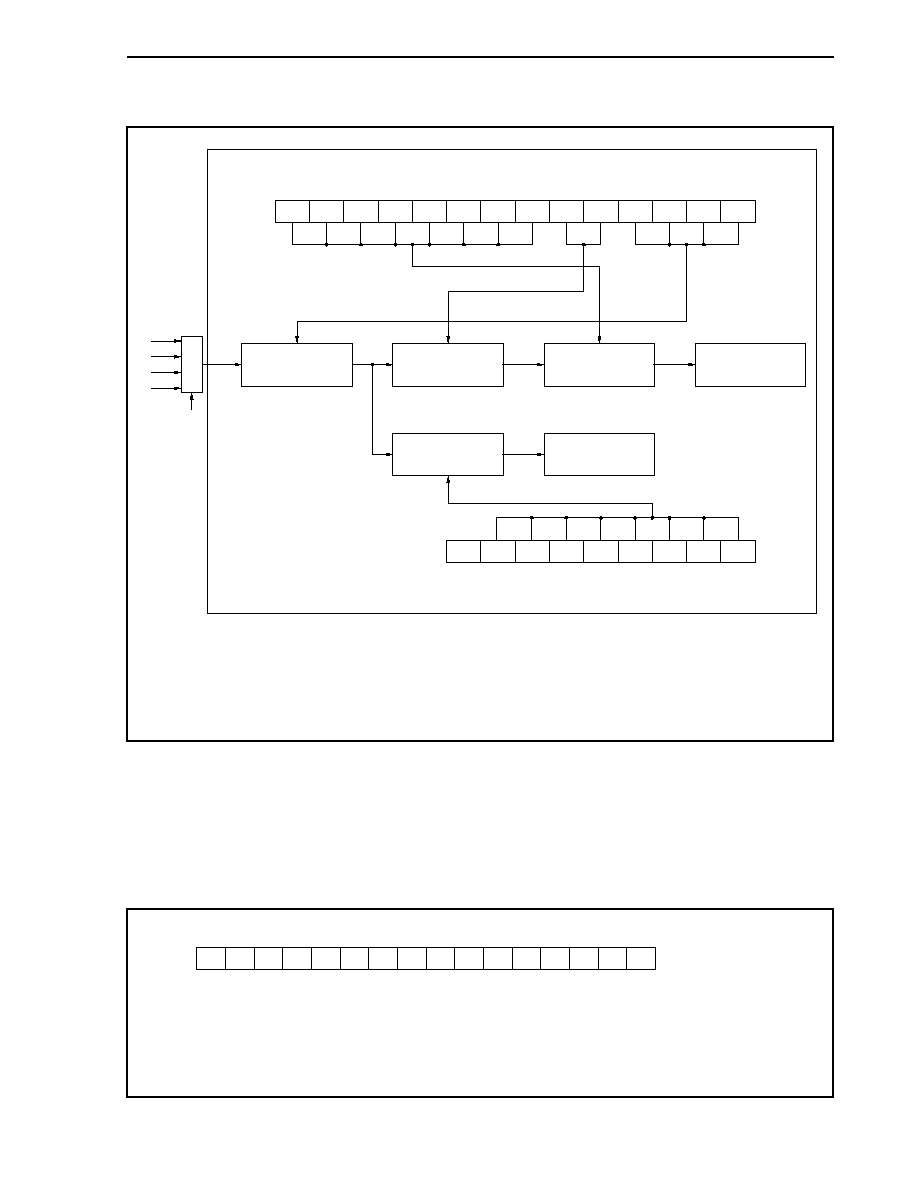
CHAPTER 11 FCAN CONTROLLER
571
User's Manual U14492EJ5V0UD
Figure 11-26. FCAN Clocks
CGTS7 CGTS6 CGTS5 CGTS4 CGTS3 CGTS2 CGTS1 CGTS0 GTCS1 GTCS0 MCP3 MCP2
Prescaler
Data bit time
CAN1 bit rate prescaler register
(C1BRP)
CAN main clock selection register (CGCS)
Global timer
clock prescaler
Baud rate generator
Global timer
system clock
CAN1 synchronization
control register
(C1SYNC)
Time stamp counter
MCP1 MCP0
BRP0
BRP1
BRP2
BRP3
BRP4
BRP5
BTYPE
f
MEM1
PRM04
f
XX
f
XX
/2
f
XX
/3
f
XX
/4
f
MEM
f
GTS1
f
BTL
f
GTS
FCAN
Selector
BRP7
Note
BRP6
Note
Note Only when the TLM bit of the CAN1 bit rate prescaler register (C1BRP) is 1
Caution When using a 1 Mbps transfer rate for the CPU, input f
MEM1
as a 16 MHz clock signal. If input at
another frequency, subsequent operation is not guaranteed.
(17) CAN time stamp count register (CGTSC)
The CGTSC register indicates the contents of the time stamp counter.
This register can be read at any time.
This register can be written to only when clearing bits. The clear function writes 0 to all bits in the CGTSC
register.
This register is read-only, in 16-bit units.
14
TSC14
13
TSC13
12
TSC12
2
TSC2
3
TSC3
4
TSC4
5
TSC5
6
TSC6
7
TSC7
8
TSC8
9
TSC9
10
TSC10
11
TSC11
15
TSC15
1
TSC1
0
TSC0
CGTSC
Address
xxxxmC18H
Note
Initial value
0000H
Note xxxx: CAN message buffer registers can be allocated to the xxxx addresses as programmable
peripheral I/O registers. Note, however, that the xxxx addresses cannot be changed after being
set.
m = 2, 6, A, E
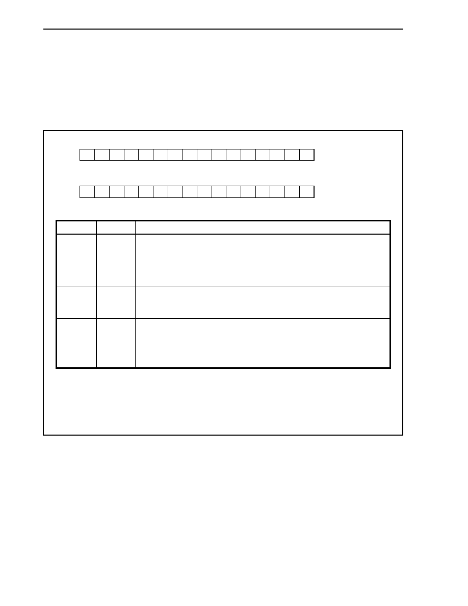
CHAPTER 11 FCAN CONTROLLER
572
User's Manual U14492EJ5V0UD
(18) CAN message search start/result register (CGMSS (during write)/CGMSR (during read))
The CGMSS/CGMSR register indicates the message search start/result status. Messages in the message
buffer that match the specified search criteria can be searched quickly.
These registers can be read/written in 16-bit units.
Caution Execute a search by writing the CGMSS register only once.
(1/2)
14
0
13
0
12
0
2
MFND2
3
MFND3
4
MFND4
5
0
6
0
7
0
8
AM
9
MM
10
0
11
0
15
0
1
MFND1
0
MFND0
CGMSR
(Read)
Address
xxxxmC1AH
Note
Initial value
0000H
14
0
13
CTRQ
12
CMSK
2
STRT2
3
STRT3
4
STRT4
5
0
6
0
7
0
8
SMNO
9
0
10
0
11
CDN
15
CIDE
1
STRT1
0
STRT0
CGMSS
(Write)
(a) Read
Bit position
Bit name
Function
9
MM
Confirms multiple hits from message search.
0: No messages or only one message meets the search criteria
1: Several messages meet the search criteria
If several message buffers that meet search criteria are detected, the MM bit is set (to 1).
8
AM
Confirms hits from message search.
0: No messages meet the search criteria
1: At least one message meets the search criteria
4 to 0
MFND4 to
MFND0
Indicates searched message number (0 to 31).
When multiple message buffer numbers match as a result of a search (MM = 1), the return
value of the MFND4 to MFND0 bits is the lowest message buffer number.
When no message buffer numbers match as a result of a search (AM = 0), the return
value of the MFND4 to MFND0 bits is the number of message buffers
- 1.
Note xxxx: CAN message buffer registers can be allocated to the xxxx addresses as programmable
peripheral I/O registers. Note, however, that the xxxx addresses cannot be changed after being
set.
m = 2, 6, A, E

CHAPTER 11 FCAN CONTROLLER
573
User's Manual U14492EJ5V0UD
(2/2)
(b) Write
Bit position
Bit name
Function
15
CIDE
Checks message identifier (ID) format flag.
0: Message identifier format flag not checked
1: Only message with standard format identifier checked
13
CTRQ
Checks transmit request and message ready flag.
0: Transmit request and message ready flag not checked
1: Transmit request and message ready flag checked
12 CMSK Checks
masked
messages.
0: Masked messages not checked
1: Only masked messages checked
11
CDN
Checks status of the DN flag of M_STATn register (n = 00 to 31).
0: Status of the DN flag of M_STATn register not checked
1: Status of the DN flag of M_STATn register checked
8 SMNO Sets
search
module.
0: No search module setting
1: CAN module set as search target
4 to 0
STRT4 to
STRT0
Indicates message search start position.
0 to 31: Message search start position (message number)
Search starts from the message number defined by bits STRT4 to STRT0. Search
continues until it reaches the message buffer having the highest number among the
usable message buffers. If the search results include several message buffer numbers
among the matching messages, the message buffer with the lowest message buffer
number is selected. To fetch the next message buffer number without changing the
search criteria, "(MFND4 to MFND0) + 1" must be set as the values of bits STRT4 to
STRT0.
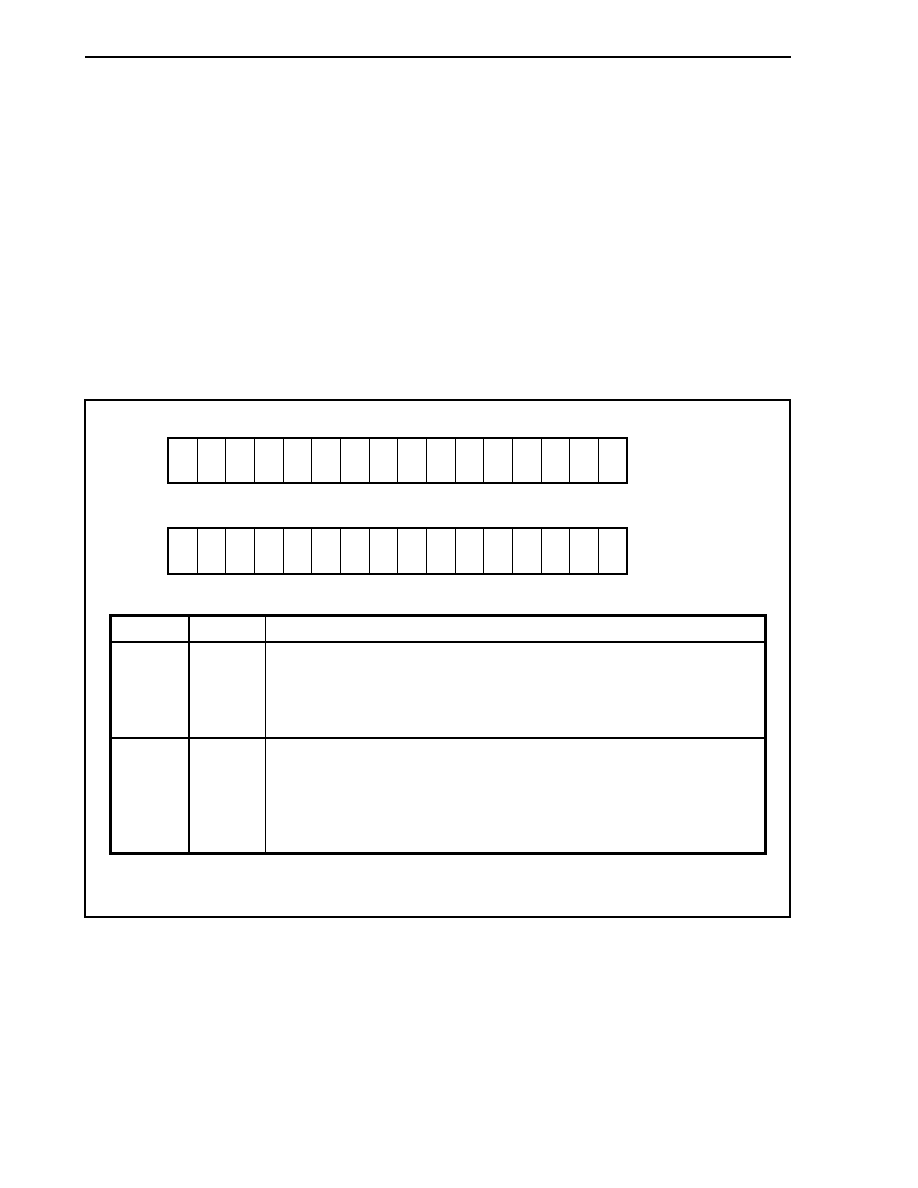
CHAPTER 11 FCAN CONTROLLER
574
User's Manual U14492EJ5V0UD
(19) CAN1 address mask a registers L and H (C1MASKLa and C1MASKHa)
The C1MASKLa and C1MASKHa registers are used to extend the number of receivable messages by
masking part of the message's identifier (ID) and then ignoring the masked parts (a = 0 to 3).
These registers can be read/written in 16-bit units.
Cautions 1. When the receive message buffer is linked to the C1MASKLa and C1MASKHa registers,
regardless of whether the ID in the receive message buffer is a standard ID (11 bits) or
extended ID (29 bits), set all the 32-bit values of the C1MASKLa and C1MASKHa
registers (a = 0 to 3).
2. When the C1MASKLa and C1MASKHa registers are linked to a message buffer for
standard ID, the lower 18 bits of the data field in the data frame are also automatically
compared. Therefore, if it is not necessary to compare the lower 18 bits (i.e., to mask
the lower 18 bits), set the CMID17 to CMID0 bits to 1 (a = 0 to 3). The standard ID and
extended ID can use the same mask.
Address
See Table 11-26
Initial value
Undefined
14
0
13
0
12
CMID
28
2
CMID
18
3
CMID
19
4
CMID
20
5
CMID
21
6
CMID
22
7
CMID
23
8
CMID
24
9
CMID
25
10
CMID
26
11
CMID
27
15
CMIDE
1
CMID
17
0
CMID
16
C1MASKHa
(a = 0 to 3)
Address
See Table 11-26
Initial value
Undefined
14
CMID
14
13
CMID
13
12
CMID
12
2
CMID
2
3
CMID
3
4
CMID
4
5
CMID
5
6
CMID
6
7
CMID
7
8
CMID
8
9
CMID
9
10
CMID
10
11
CMID
11
15
CMID
15
1
CMID
1
0
CMID
0
C1MASKLa
(a = 0 to 3)
Bit position
Bit name
Function
15
(C1MASKHa)
CMIDE
Sets mask for identifier (ID) format.
0: ID format (standard or extended) checked
1: ID format (standard or extended) not checked
When the CMIDE bit is set (1), the higher 11 bits of the ID are compared. The receive
message and the ID format stored in a message buffer are not compared.
12 to 0
(C1MASKHa)
15 to 0
(C1MASKLa)
CMID28 to
CMID16
(C1MASKHa)
CMID15 to
CMID0
(C1MASKLa)
Sets mask for identifier (ID) bit.
0: ID bit in message buffer linked to bits CMID28 to CMID0 compared with received ID
bit
1: ID bit in message buffer linked to bits CMID28 to CMID0 not compared (ID bit
masked) with received ID bit
Remark n = 0 to 3
CHAPTER 11 FCAN CONTROLLER
575
User's Manual U14492EJ5V0UD
Table 11-26. Addresses of C1MASKLa and C1MASKHa (a = 0 to 3)
Register Name
Address
Note
(m = 2, 6, A, E)
C1MASKL0 xxxxmC40H
C1MASKH0 xxxxmC42H
C1MASKL1 xxxxmC44H
C1MASKH1 xxxxmC46H
C1MASKL2 xxxxmC48H
C1MASKH2 xxxxmC4AH
C1MASKL3 xxxxmC4CH
C1MASKH3 xxxxmC4EH
Note CAN message buffer registers can be allocated to the xxxx addresses as
programmable peripheral I/O registers. Note, however, that the xxxx addresses
cannot be changed after being set.
CHAPTER 11 FCAN CONTROLLER
576
User's Manual U14492EJ5V0UD
(20) CAN1 control register (C1CTRL)
The C1CTRL register is used to control the operation of the CAN module.
This register can be read/written in 16-bit units.
Cautions 1. Both bitwise writing and direct writing to the C1CTRL register are prohibited. Attempts
to write directly to this register may result in operation faults, so be sure to follow the
sequence described in 11.9 Cautions on Bit Set/Clear Function.
2. When writing to the C1CTRL register, set or clear bits according to the register
configuration during a write operation.
3. When canceling CAN stop mode, CAN sleep mode must be canceled at the same time.
(1/4)
Address
xxxxmC50H
Note
Initial value
0101H
C1CTRL
(Read)
14
set
DLEVR
13
set
DLEVT
12
set
OVM
2
clear
STOP
3
clear
TMR
4
clear
OVM
5
clear
DLEVT
6
clear
DLEVR
7
0
8
set
INIT
9
set
SLEEP
10
set
STOP
11
set
TMR
15
0
1
clear
SLEEP
0
clear
INIT
C1CTRL
(Write)
14
TECS0
13
RECS1
12
RECS0
2
STOP
3
TMR
4
OVM
5
DLEVT
6
DLEVR
7
0
8
ISTAT
9
RSTAT
10
TSTAT
11
BOFF
15
TECS1
1
SLEEP
0
INIT
(a) Read (1/3)
Bit position
Bit name
Function
This is the transmit error counter status flag.
TECS1
TECS0
Status of transmit error counter
0
0
Transmit error counter value < 96
0
1
Transmit error counter value = 96 to 127 (warning level)
1 0
Not
used
1
1
Transmit error counter value
128 (error passive)
15, 14
TECS1,
TECS0
This is the receive error counter status flag.
RECS1
RECS0
Status of receive error counter
0
0
Receive error counter value < 96
0
1
Receive error counter value = 96 to 127 (warning level)
1 0
Not
used
1
1
Receive error counter value
128 (error passive)
13, 12
RECS1,
RECS0
Note xxxx: CAN message buffer registers can be allocated to the xxxx addresses as programmable
peripheral I/O registers. Note, however, that the xxxx addresses cannot be changed after being
set.
m = 2, 6, A, E

CHAPTER 11 FCAN CONTROLLER
577
User's Manual U14492EJ5V0UD
(2/4)
(a) Read (2/3)
Bit position
Bit name
Function
11
BOFF
This is the bus off status flag.
0: Transmit error counter < 256 (not bus off status)
1: Transmit error counter
256 (bus off status)
10
TSTAT
This is the transmit status flag.
0: Transmission stopped status
1: Transmitting status
9
RSTAT
This is the receive status flag.
0: Reception stopped status
1: Receiving status
8
ISTAT
This is the initialization status flag.
0: Normal operating status
1: FCAN is stopped and initialized
Cautions 1. The ISTAT bit is set (to 1) when the CAN protocol layer acknowledges
the settings of the INIT and STOP bits. Also, this bit is automatically
cleared (to 0) when the INIT and STOP bits are cleared (to 0).
2. In the initialization status, "recessive" is output to the CTXD pin.
3. The C1SYNC and C1BRP registers can be written only in initialization
mode.
4. In the initialization status, the error counter (see 11.10 (23) CAN1 error
count register (C1ERC)) is cleared (to 0) and the error status (bits
TECS1, TECS0, RECS0, and RECS1) is reset.
6
DLEVR
This is the dominant level control bit for receive pins.
0: A low level to a receive pin is acknowledged as dominant
1: A high level to a receive pin is acknowledged as dominant
5
DLEVT
This is the dominant level control bit for transmit pins.
0: A low level is transmitted from a transmit pin as dominant
1: A high level is transmitted from a transmit pin as dominant
4
OVM
This is the overwrite mode control bit.
0: New messages stored in message buffer in which DN bit of M_STATn register (n = 00
to 31) is set
1: New messages in message buffer in which DN bit is set are discarded.
When the OVM bit = 1, the receive completion interrupt (INTCREC) is not generated even if
new messages are received in the message buffer in which the DN bit is set.
3
TMR
This is the time stamp control bit for reception.
0: Captures time stamp counter value when SOF is detected on CAN bus
1: Captures time stamp counter value when EOF is detected on CAN bus (a valid
message is confirmed)
2
STOP
This is the CAN stop mode control bit.
0: No CAN stop mode setting
1: CAN stop mode
The CAN stop mode can be selected only when the CAN module is set to CAN sleep mode
(the SLEEP bit is set (to 1)). CAN stop mode can be canceled only by the CPU (STOP bit
cleared (to 0)).
CHAPTER 11 FCAN CONTROLLER
578
User's Manual U14492EJ5V0UD
(3/4)
(a) Read (3/3)
Bit position
Bit name
Function
1
SLEEP
This is the CAN sleep mode control bit.
0: Normal operation mode
1: Switch to CAN sleep mode. Change in CAN bus performs wake-up.
Cautions 1. CAN sleep mode can be set only when the CAN bus is in the idle state.
2. CAN sleep mode is canceled under the following conditions.
∑ When the CPU has cleared the SLEEP bit (to 0)
∑ When the CAN bus changes (only when CAN stop mode has not been
set)
3. The WAKE bit (see 11.10 (21) CAN1 definition register (C1DEF)) can be
set (to 1) only when CAN sleep mode is canceled by the change of the
CAN bus, and an error interrupt occurs.
0
INIT
This is the initialization request bit used to initialize the CAN module.
0: Normal operation mode
1: Initialization mode
Cautions 1. Be sure to confirm that the CAN module has entered the initialization
mode using the ISTAT bit (ISTAT bit = 1) after setting the INIT bit (to 1).
When the ISTAT bit = 0, set the INIT bit (to 1) again.
2. If the INIT bit is set (to 1) when the CAN module is in the bus off status
(BOFF bit = 1), the CAN module enters initialization mode (ISTAT bit =
1) after returning from the bus off status (BOFF bit = 0).
(b) Write (1/2)
Bit position
Bit name
Function
Sets/clears the DLEVR bit.
set
DLEVR
clear
DLEVR
Operation
0
1
DLEVR bit cleared (to 0)
1
0
DLEVR bit set (to 1)
Other than above
DLEVR bit not changed
14, 6
Set
DLEVR,
clear
DLEVR
Sets/clears the DLEVT bit.
set
DLEVT
clear
DLEVT
Operation
0
1
DLEVT bit cleared (to 0)
1
0
DLEVT bit set (to 1)
Other than above
DLEVT bit not changed
13, 5
Set
DLEVT,
clear
DLEVT

CHAPTER 11 FCAN CONTROLLER
579
User's Manual U14492EJ5V0UD
(4/4)
(b) Write (2/2)
Bit position
Bit name
Function
Sets/clears the OVM bit.
set
OVM
clear
OVM
Operation
0
1
OVM bit cleared (to 0)
1
0
OVM bit set (to 1)
Other than above
OVM bit not changed
12, 4
set OVM,
clear OVM
Sets/clears the TMR bit.
set
TMR
clear
TMR
Operation
0
1
TMR bit cleared (to 0)
1
0
TMR bit set (to 1)
Other than above
TMR bit not changed
11, 3
set TMR,
clear TMR
Sets/clears the STOP bit.
set
STOP
clear
STOP
Operation
0
1
STOP bit cleared (to 0)
1
0
STOP bit set (to 1)
Other than above
STOP bit not changed
10, 2
set STOP,
clear
STOP
Sets/clears the SLEEP bit.
set
SLEEP
clear
SLEEP
Operation
0
1
SLEEP bit cleared (to 0)
1
0
SLEEP bit set (to 1)
Other than above
SLEEP bit not changed
9, 1
set
SLEEP,
clear
SLEEP
Sets/clears the INIT bit.
set
INIT
clear
INIT
Operation
0
1
INIT bit cleared (to 0)
1
0
INIT bit set (to 1)
Other than above
INIT bit not changed
8, 0
set INIT,
clear INIT
CHAPTER 11 FCAN CONTROLLER
580
User's Manual U14492EJ5V0UD
(21) CAN1 definition register (C1DEF)
The C1DEF register is used to define the operation of the CAN module.
This register can be read/written in 16-bit units.
Cautions 1. Both bitwise writing and direct writing to the C1DEF register are prohibited. Attempts to
write directly to this register may result in operation faults, so be sure to follow the
sequence described in 11.9 Cautions on Bit Set/Clear Function.
2. When writing to the C1DEF register, set or clear bits according to the register
configuration during a write operation.
(1/4)
Address
xxxxmC52H
Note
Initial value
0000H
C1DEF
(Read)
14
set
MOM
13
set
SSHT
12
set
PBB
2
clear
VALID
3
clear
BERR
4
clear
PBB
5
clear
SSHT
6
clear
MOM
7
clear
DGM
8
0
9
0
10
0
11
0
15
set
DGM
1
clear
WAKE
0
clear
OVR
C1DEF
(Write)
14
0
13
0
12
0
2
VALID
3
BERR
4
PBB
5
SSHT
6
MOM
7
DGM
8
0
9
0
10
0
11
0
15
0
1
WAKE
0
OVR
(a) Read (1/3)
Bit position
Bit name
Function
7
DGM
Specifies diagnostic processing mode.
0: Only when receiving, valid messages received using message buffer used for
diagnostic processing mode (Bits MT2 to MT0 of M_CONF register = 111)
1: Only when receiving, valid messages received using normal operation mode.
The diagnostic processing mode (MOM bit = 1) is used for CAN baud rate detection and for
diagnostic purposes. When this mode has been set, the following operations are
performed.
∑ When the VALID bit = 1, it indicates that the current receive operation is valid.
∑ Setting the DGM bit confirms whether or not valid data has been stored in the message
buffer used for diagnostic processing mode, the same as for normal operation mode.
Note xxxx: CAN message buffer registers can be allocated to the xxxx addresses as programmable
peripheral I/O registers. Note, however, that the xxxx addresses cannot be changed after being
set.
m = 2, 6, A, E

CHAPTER 11 FCAN CONTROLLER
581
User's Manual U14492EJ5V0UD
(2/4)
(a) Read (2/3)
Bit position
Bit name
Function
6
MOM
Specifies the CAN module operation mode.
0: Normal operating mode
1: Diagnostic processing mode
Cautions 1. When in diagnostic processing mode (MOM bit = 1), the C1BRP register
can be accessed only when the CAN module has been set to
initialization mode (i.e., when the C1CTRL register's ISTAT bit = INIT bit
= 1).
When the CAN module is operating (i.e., when the C1CTRL register's
ISTAT bit = 0), the C1BRP register cannot be used, and the CAN1 bus
diagnostic information register (refer to 11. 10 (27) CAN1 bus
diagnostic information register (C1DINF)) can be used instead.
2. The CAN protocol layer does not send ACK, error frame, or transmit
messages, nor does it operate an error counter.
The internal transmit output is fed back to the internal input due to auto
baud rate detection.
5
SSHT
Specifies single shot mode.
0: Normal operating mode
1: Single shot mode
In single shot mode, the CAN module can transmit a message only one time. The
M_STATn register's TRQ bit is then cleared (to 0) regardless of whether or not there are
any pending normal transmit operations (n = 00 to 31).
Also, if a bus error has occurred due to a transmission, it is handled as an incomplete
transmission.
Cautions 1. In single shot mode, even if the CAN lost in arbitration, it is handled as
a completed message transmission.
When in this mode, the BERR bit is set (to 1) but the error counter
value (refer to 11.10 (23) CAN1 error count register (C1ERC)) does not
change since there are no CAN bus errors.
2. In single shot mode, even when transmission is stopped due to error
detection or a loss in the arbitration phase, the transmission
completion interrupt occurs.
3. During the time when the CAN module is active, the CPU switches
between normal operation mode and single shot mode without causing
any errors to occur on the CAN bus.
4
PBB
Specifies priority control for transmission.
0: Identifier (ID) based priority control
1: Message number based priority control
Ordinarily, priority for transmission is defined based on message IDs, but when the PBB bit
has been set (to 1) priority becomes based instead on the position of messages, so that
messages with lower message numbers have higher priority.
3 BERR Indicates CAN bus error status.
0: CAN bus error was not detected
1: CAN bus error was detected at least once after bit was cleared
2 VALID Indicates valid message detection status.
0: Valid message was not detected
1: Valid message was detected at least once after bit was cleared

CHAPTER 11 FCAN CONTROLLER
582
User's Manual U14492EJ5V0UD
(3/4)
(a) Read (3/3)
Bit position
Bit name
Function
1
WAKE
Indicates CAN sleep mode cancellation status.
0: Normal operation
1: CAN sleep mode canceled
Cautions 1. The WAKE bit is set (1) only when the CAN sleep mode is released due
to a change in the CAN bus and an error interrupt occurs.
2. While the WAKE bit is set (1), the error interrupt signal holds the active
status. Therefore, always clear (0) the WAKE bit after recognition that
the WAKE bit is set.
0
OVR
Indicates overrun error status.
0: Normal operation
1: Overrun occurred during RAM access
Caution When an overrun error has occurred, the OVR bit is set (to 1) and an error
interrupt occurs at the same time.
The source of the overrun error may be that the RAM access clock is
slower than the selected CAN baud rate.

CHAPTER 11 FCAN CONTROLLER
583
User's Manual U14492EJ5V0UD
(4/4)
(b) Write
Bit position
Bit name
Function
Sets/clears the DGM bit.
set DGM clear DGM
Operation
0
1
DGM bit cleared (to 0)
1
0
DGM bit set (to 1)
Other than above
DGM bit not changed
15, 7
set DGM,
clear DGM
Sets/clears the MOM bit.
set MOM clear MOM
Operation
0
1
MOM bit cleared (to 0)
1
0
MOM bit set (to 1)
Other than above
MOM bit not changed
14, 6
set MOM,
clear
MOM
Sets/clears the SSHT bit.
set SSHT clear SSHT
Operation
0
1
SSHT bit cleared (to 0)
1
0
SSHT bit set (to 1)
Other than above
SSHT bit not changed
13, 5
set SSHT,
clear
SSHT
Sets/clears the PBB bit.
set PBB
clear PBB
Operation
0
1
PBB bit cleared (to 0)
1
0
PBB bit set (to 1)
Other than above
PBB bit not changed
12, 4
set PBB,
clear PBB
3 clear
BERR
Clears the BERR bit.
0: No change in BERR bit
1: BERR bit cleared (to 0)
2 clear
VALID
Clears the VALID bit.
0: No change in VALID bit
1: VALID bit cleared (to 0)
1 clear
WAKE
Clears the WAKE bit.
0: No change in WAKE bit
1: WAKE bit cleared (to 0)
0
clear OVR
Clears the OVR bit.
0: No change in OVR bit
1: OVR bit cleared (to 0)

CHAPTER 11 FCAN CONTROLLER
584
User's Manual U14492EJ5V0UD
(22) CAN1 information register (C1LAST)
The C1LAST register indicates the CAN module's error information and the number of the message buffer
received last.
This register is read-only, in 16-bit units.
14
0
13
0
12
0
2
LREC2
3
LREC3
4
LREC4
5
LREC5
6
LREC6
7
LREC7
8
LERR0
9
LERR1
10
LERR2
11
LERR3
15
0
1
LREC1
0
LREC0
C1LAST
Address
xxxxmC54H
Note
Initial value
00FFH
Bit position
Bit name
Function
Indicates the last error information.
LERR3 LERR2 LERR1 LERR0
Last
error
information
0 0 0 0
Error
not
detected
0 0 0 1
Bit
error
0 0 1 0
Stuff
error
0 0 1 1
CRC
error
0 1 0 0
Form
error
0 1 0 1
ACK
error
0
1
1
0
Arbitration lost (only in single shot
mode (C1DEF register's SSHT bit = 1))
0 1 1 1
CAN
overrun
error
1
0
0
0
Wake-up from CAN bus
Other than above
Undefined
11 to 8
LERR3 to
LERR0
Caution Since the LERR3 to LERR0 bits cannot be cleared, the current status is
retained until the next error occurs.
7 to 0
LREC7 to
LREC0
Indicates the last received message number.
0 to 31: The number of the message buffer last received
32 to 255: Not used
Note xxxx: CAN message buffer registers can be allocated to the xxxx addresses as programmable
peripheral I/O registers. Note, however, that the xxxx addresses cannot be changed after being
set.
m = 2, 6, A, E

CHAPTER 11 FCAN CONTROLLER
585
User's Manual U14492EJ5V0UD
(23) CAN1 error count register (C1ERC)
The C1ERC register indicates the count values of the transmission/reception error counters.
This register is read-only, in 16-bit units.
14
REC6
13
REC5
12
REC4
2
TEC2
3
TEC3
4
TEC4
5
TEC5
6
TEC6
7
TEC7
8
REC0
9
REC1
10
REC2
11
REC3
15
REC7
1
TEC1
0
TEC0
C1ERC
Address
xxxxmC56H
Note
Initial value
0000H
Bit position
Bit name
Function
15 to 8
REC7 to
REC0
Indicates the reception error count.
0 to 255: The number of reception errors
This reflects the current status of the reception error counter.
The number of counts is defined by the CAN protocol.
7 to 0
TEC7 to
TEC0
Indicates the transmission error count.
0 to 255: The number of transmission errors
This reflects the current status of the transmission error counter.
The number of counts is defined by the CAN protocol.
Note xxxx: CAN message buffer registers can be allocated to the xxxx addresses as programmable
peripheral I/O registers. Note, however, that the xxxx addresses cannot be changed after being
set.
m = 2, 6, A, E

CHAPTER 11 FCAN CONTROLLER
586
User's Manual U14492EJ5V0UD
(24) CAN1 interrupt enable register (C1IE)
The C1IE register is used to enable/disable the CAN module's interrupts.
This register can be read/written in 16-bit units.
Cautions 1. Both bitwise writing and direct writing to the C1IE register are prohibited. Attempts to
write directly to this register may result in operation faults, so be sure to follow the
sequence described in 11.9 Cautions on Bit Set/Clear Function.
2. When writing to the C1IE register, set or clear bits according to the register
configuration during a write operation.
(1/3)
Address
xxxxmC58H
Note
Initial value
0900H
C1IE
(Read)
14
set
E_INT6
13
set
E_INT5
12
set
E_INT4
2
clear
E_INT2
3
clear
E_INT3
4
clear
E_INT4
5
clear
E_INT5
6
clear
E_INT6
7
0
8
set
E_INT0
9
set
E_INT1
10
set
E_INT2
11
set
E_INT3
15
0
1
clear
E_INT1
0
clear
E_INT0
C1IE
(Write)
14
0
13
0
12
0
2
E_INT2
3
E_INT3
4
E_INT4
5
E_INT5
6
E_INT6
7
0
8
1
9
0
10
0
11
1
15
0
1
E_INT1
0
E_INT0
(a) Read (1/2)
Bit position
Bit name
Function
6
E_INT6
This is the CAN module error interrupt enable flag.
0: Interrupt disabled
1: Interrupt enabled
5 E_INT5
This is the CAN bus error interrupt enable flag.
0: Interrupt disabled
1: Interrupt enabled
4 E_INT4
This is the wake up from CAN sleep mode interrupt enable flag.
0: Interrupt disabled
1: Interrupt enabled
3 E_INT3
This is the receive error passive interrupt enable flag.
0: Interrupt disabled
1: Interrupt enabled
2 E_INT2
This is the transmit error passive or bus off interrupt enable flag.
0: Interrupt disabled
1: Interrupt enabled
Note xxxx: CAN message buffer registers can be allocated to the xxxx addresses as programmable
peripheral I/O registers. Note, however, that the xxxx addresses cannot be changed after being
set.
m = 2, 6, A, E
CHAPTER 11 FCAN CONTROLLER
587
User's Manual U14492EJ5V0UD
(2/3)
(a) Read (2/2)
Bit position
Bit name
Function
1 E_INT1
This is the receive completion interrupt enable flag.
0: Interrupt disabled
1: Interrupt enabled
∑ When IE bit of the M_CTRLn register is 1, a reception completion interrupt occurs
regardless of the setting of the E_INT1 bit if the transmit message buffer receives a
remote frame while the auto response function is not set (RMDE0 bit of the M_CTRLn
register = 0) (n = 00 to 31).
0 E_INT0
This is the transmit completion interrupt enable flag.
0: Interrupt disabled
1: Interrupt enabled
(b) Write (1/2)
Bit position
Bit name
Function
Sets/clears the E_INT6 bit.
set E_INT6 clear E_INT6
Operation
0 1
E_INT6 interrupt cleared (to 0)
1 0
E_INT6 interrupt set (to 1)
Other than above
E_INT6 interrupt not changed
14, 6
set
E_INT6,
clear
E_INT6
Sets/clears the E_INT5 bit.
set E_INT5 clear E_INT5
Operation
0
1
E_INT5 interrupt cleared (to 0)
1
0
E_INT5 interrupt set (to 1)
Other than above
E_INT5 interrupt not changed
13, 5
set
E_INT5,
clear
E_INT5
Sets/clears the E_INT4 bit.
set E_INT4 clear E_INT4
Operation
0
1
E_INT4 interrupt cleared (to 0)
1
0
E_INT4 interrupt set (to 1)
Other than above
E_INT4 interrupt not changed
12, 4
set
E_INT4,
clear
E_INT4
Sets/clears the E_INT3 bit.
set E_INT3 clear E_INT3
Operation
0
1
E_INT3 interrupt cleared (to 0)
1
0
E_INT3 interrupt set (to 1)
Other than above
E_INT3 interrupt not changed
11, 3
set
E_INT3,
clear
E_INT3

CHAPTER 11 FCAN CONTROLLER
588
User's Manual U14492EJ5V0UD
(3/3)
(b) Write (2/2)
Bit position
Bit name
Function
Sets/clears the E_INT2 bit.
set E_INT2 clear E_INT2
Operation
0
1
E_INT2 interrupt cleared (to 0)
1
0
E_INT2 interrupt set (to 1)
Other than above
E_INT2 interrupt not changed
10, 2
set
E_INT2,
clear
E_INT2
Sets/clears the E_INT1 bit.
set E_INT1 clear E_INT1
Operation
0
1
E_INT1 interrupt cleared (to 0)
1
0
E_INT1 interrupt set (to 1)
Other than above
E_INT1 interrupt not changed
9, 1
set
E_INT1,
clear
E_INT1
Sets/clears the E_INT0 bit.
set E_INT0 clear E_INT0
Operation
0
1
E_INT0 interrupt cleared (to 0)
1
0
E_INT0 interrupt set (to 1)
Other than above
E_INT0 interrupt not changed
8, 0
set
E_INT0,
clear
E_INT0
CHAPTER 11 FCAN CONTROLLER
589
User's Manual U14492EJ5V0UD
(25) CAN1 bus active register (C1BA)
The C1BA register indicates frame information output via the CAN bus.
This register is read-only, in 16-bit units.
14
0
13
0
12
CACT4
2
TMNO2
3
TMNO3
4
TMNO4
5
TMNO5
6
TMNO6
7
TMNO7
8
CACT0
9
CACT1
10
CACT2
11
CACT3
15
0
1
TMNO1
0
TMNO0
C1BA
Address
xxxxmC5AH
Note
Initial value
00FFH
Bit position
Bit name
Function
Indicates CAN module status.
CACT4 CACT3 CACT2 CACT1 CACT0
CAN
module
status
0 0 0 0 0
Reset
state
0 0 0 0 1
Bus
idle
wait
0 0 0 1 0
Bus
idle
state
0 0 0 1 1
Start
of
frame
0 0 1 0 0
Standard
identifier
area
0 0 1 0 1
Data
length
code
area
0 0 1 1 0
Data
field
area
0 0 1 1 1
CRC
field
area
0 1 0 0 0
CRC
delimiter
0 1 0 0 1
ACK
slot
0 1 0 1 0
ACK
delimiter
0
1
0
1
1
End of frame area
0 1 1 0 0
Intermission
state
0 1 1 0 1
Suspend
transmission
0 1 1 1 0
Error
frame
0 1 1 1 1
Error
delimiter
wait
1 0 0 0 0
Error
delimiter
1 0 0 1 0
Extended
identifier
area
12 to 8
CACT4 to
CACT0
7 to 0
TMNO7 to
TMNO0
Specifies transmit message counter.
0 to 31: Message number of message awaiting transmission or being transmitted
32 to 254: Not used
255: No messages awaiting transmission or being transmitted
Note xxxx: CAN message buffer registers can be allocated to the xxxx addresses as programmable
peripheral I/O registers. Note, however, that the xxxx addresses cannot be changed after being
set.
m = 2, 6, A, E

CHAPTER 11 FCAN CONTROLLER
590
User's Manual U14492EJ5V0UD
(26) CAN1 bit rate prescaler register (C1BRP)
The C1BRP register is used to set the transmission baud rate for the CAN module.
Use the C1BRP register to select the CAN protocol layer base system clock (f
BTL
). The baud rate is
determined by the value set to the C1SYNC register.
While in normal operation mode (C1DEF register's MOM bit = 0), the C1BRP register can only be accessed
when the initialization mode has been set (C1CTRL register's INIT bit = 1).
This register can be read/written in 16-bit units.
Caution While in diagnostic processing mode (C1DEF register's MOM bit = 1), the C1BRP register
can only be accessed when the initialization mode has been set (C1CTRL register's INIT bit
= 1) (refer to 11.10 (21) CAN1 definition register (C1DEF)).
CHAPTER 11 FCAN CONTROLLER
591
User's Manual U14492EJ5V0UD
(1/2)
14
0
13
0
12
0
2
BRP2
3
BRP3
4
BRP4
5
BRP5
6
BTYPE
7
0
8
0
9
0
10
0
11
0
15
TLM
1
BRP1
0
BRP0
C1BRP
(TLM = 0)
Address
xxxxmC5CH
Note
Initial value
0000H
14
0
13
0
12
0
2
BRP2
3
BRP3
4
BRP4
5
BRP5
6
BRP6
7
BRP7
8
BTYPE
9
0
10
0
11
0
15
TLM
1
BRP1
0
BRP0
C1BRP
(TLM = 1)
(a) When TLM = 0
Bit position
Bit name
Function
15
TLM
Specifies transfer layer mode.
0: 6-bit prescaler mode
6
BTYPE
Specifies CAN bus type.
0: Low speed (
125 kbps)
1: High speed (> 125 kbps)
Specifies CAN protocol layer base system clock (f
BTL
) for CAN module.
n BRP5 BRP4 BRP3 BRP2 BRP1 BRP0 CAN
protocol
layer
base system clock
(f
BTL
)
0 0 0 0 0 0 0
f
MEM
/2
1 0 0 0 0 0 1
f
MEM
/4
2 0 0 0 0 1 0
f
MEM
/6
3 0 0 0 0 1 1
f
MEM
/8
∑
∑
∑
f
MEM
/(n + 1)
◊ 2
60
1 1 1 1 0 0
f
MEM
/122
61
1 1 1 1 0 1
f
MEM
/124
62
1 1 1 1 1 0
f
MEM
/126
63
1 1 1 1 1 1
f
MEM
/128
5 to 0
BRP5 to
BRP0
Remark f
BTL
= f
MEM
/{(n + 1)
◊ 2}: CAN protocol layer base system clock
n = 0 to 63 (set by bits BRP5 to BRP0)
f
MEM
= CAN base clock
Note xxxx: CAN message buffer registers can be allocated to the xxxx addresses as programmable
peripheral I/O registers. Note, however, that the xxxx addresses cannot be changed after being
set.
m = 2, 6, A, E

CHAPTER 11 FCAN CONTROLLER
592
User's Manual U14492EJ5V0UD
(2/2)
(b) When TLM = 1
Bit position
Bit name
Function
15
TLM
Specifies transfer layer mode.
1: 8-bit prescaler mode
8
BTYPE
Specifies CAN bus type.
0: Low speed (
125 kbps)
1: High speed (> 125 kbps)
Specifies CAN protocol layer base system clock (f
BTL
) for CAN module.
n
BRP7 BRP6 BRP5 BRP4 BRP3 BRP2 BRP1 BRP0
CAN protocol layer
base system clock
(f
BTL
)
0 0 0 0 0 0 0 0 0
Setting
prohibited
1 0 0 0 0 0 0 0 1
f
MEM
/2
2 0 0 0 0 0 0 1 0
f
MEM
/3
3 0 0 0 0 0 0 1 1
f
MEM
/4
∑
∑
∑
f
MEM
/(n + 1)
252
1 1 1 1 1 1 0 0
f
MEM
/253
253
1 1 1 1 1 1 0 1
f
MEM
/254
254
1 1 1 1 1 1 1 0
f
MEM
/255
255
1 1 1 1 1 1 1 1
f
MEM
/256
7 to 0
BRP7 to
BRP0
Remark f
BTL
= f
MEM
/(n + 1): CAN protocol layer base system clock
n = 0 to 255 (set by bits BRP7 to BRP0)
f
MEM
= CAN base clock
CHAPTER 11 FCAN CONTROLLER
593
User's Manual U14492EJ5V0UD
(27) CAN1 bus diagnostic information register (C1DINF)
The C1DINF register indicates all CAN bus bits, including stuff bits, delimiters, etc. This information is used
only for diagnostic purposes.
Because the number of bits starting from SOF is added at each frame, the actual number of bits is the value
obtained by subtracting the previous data.
This register is read-only, in 16-bit units.
Cautions 1. While in diagnostic processing mode (C1DEF register's MOM bit = 1) and in normal
operation mode (C1CTRL register's INIT bit = 0), the C1DINF register can only be
accessed. In normal operation mode (C1DEF register's MOM bit = 0), this register
cannot be accessed.
2. Storage of the last 8 bits is automatically stopped if an error or a valid message (ACK
delimiter) is detected on the CAN bus. Reset is automatically performed each time when
the SOF is detected on the CAN bus.
14
DINF14
13
DINF13
12
DINF12
2
DINF2
3
DINF3
4
DINF4
5
DINF5
6
DINF6
7
DINF7
8
DINF8
9
DINF9
10
DINF10
11
DINF11
15
DINF15
1
DINF1
0
DINF0
C1DINF
Address
xxxxmC5CH
Note
Initial value
0000H
Bit position
Bit name
Function
Indicates CAN bus diagnostic information.
Bit name
CAN Bus Diagnostic Information
DINF15 to DINF8
Number of bits starting from SOF
DINF7 to DINF0
Information from last 8 bits
15 to 0
DINF15 to
DINF0
Note xxxx: CAN message buffer registers can be allocated to the xxxx addresses as programmable
peripheral I/O registers. Note, however, that the xxxx addresses cannot be changed after being
set.
m = 2, 6, A, E

CHAPTER 11 FCAN CONTROLLER
594
User's Manual U14492EJ5V0UD
(28) CAN1 synchronization control register (C1SYNC)
The C1SYNC register controls the data bit time for transmission speed.
This register can be read/written in 16-bit units.
Cautions 1. The CPU is able to read the C1SYNC register at any time.
2. Writing to the C1SYNC register is enabled when in initialization mode (when C1CTRL
register's INIT bit = 1).
3. The limit values of the CAN protocol when setting the SPTn bit and DBTn bit are as
follows.
5
◊ BTL SPT (sampling point) 17 ◊ BTL [4 SPT4 to SPT0 set values 16]
8
◊ BTL DBT (data bit time) 25 ◊ BTL [7 DBT4 to DBT0 set values 24]
SJW (synchronization jump width)
DBT - SPT
2
(DBT - SPT) 8
Remark BTL = 1/f
BTL
(f
BTL
: CAN protocol layer base system clock)
(1/3)
14
0
13
0
12
SAMP
2
DBT2
3
DBT3
4
DBT4
5
SPT0
6
SPT1
7
SPT2
8
SPT3
9
SPT4
10
SJW0
11
SJW1
15
0
1
DBT1
0
DBT0
C1SYNC
Address
xxxxmC5EH
Note
Initial value
0218H
Bit position
Bit name
Function
12
SAMP
Specifies bit sampling.
0: Receive data sampled once at the sampling point.
1: Receive data sampled three times and the majority value used as the sampled value.
Specifies synchronization jump width stipulated in the CAN protocol specification, Ver. 2.0,
PartB active.
SJW1 SJW0
Synchronization jump width
Note
0 0
BTL
0 1
BTL
◊ 2
1 0
BTL
◊ 3
1 1
BTL
◊ 4
11, 10
SJW1,
SJW0
Note Stipulated in CAN protocol specification Ver. 2.0, PartB active
Remark BTL = 1/f
BTL
(f
BTL
: CAN protocol layer base system clock)
Note xxxx: CAN message buffer registers can be allocated to the xxxx addresses as programmable
peripheral I/O registers. Note, however, that the xxxx addresses cannot be changed after being
set.
m = 2, 6, A, E
CHAPTER 11 FCAN CONTROLLER
595
User's Manual U14492EJ5V0UD
(2/3)
Bit position
Bit name
Function
Specifies position of sampling points.
SPT4
SPT3
SPT2
SPT1
SPT0
Position of sampling point
0 0 0 1 0
BTL
◊ 3
Note
0 0 0 1 1
BTL
◊ 4
Note
0 0 1 0 0
BTL
◊ 5
0 0 1 0 1
BTL
◊ 6
0 0 1 1 0
BTL
◊ 7
0 0 1 1 1
BTL
◊ 8
0 1 0 0 0
BTL
◊ 9
0 1 0 0 1
BTL
◊ 10
0 1 0 1 0
BTL
◊ 11
0 1 0 1 1
BTL
◊ 12
0 1 1 0 0
BTL
◊ 13
0 1 1 0 1
BTL
◊ 14
0 1 1 1 0
BTL
◊ 15
0 1 1 1 1
BTL
◊ 16
1 0 0 0 0
BTL
◊ 17
9 to 5
SPT4 to
SPT0
Other than above
Setting prohibited
Note This setting is reserved for setting sample point extension and is not compliant with
the CAN protocol specifications.
Remark Sampling point within bit timing is selected.
CHAPTER 11 FCAN CONTROLLER
596
User's Manual U14492EJ5V0UD
(3/3)
Bit position
Bit name
Function
Sets data bit time.
DBT4 DBT3 DBT2 DBT1 DBT0
Data
bit
time
0 0 1 1 1
BTL
◊ 8
0 1 0 0 0
BTL
◊ 9
0 1 0 0 1
BTL
◊ 10
0 1 0 1 0
BTL
◊ 11
0 1 0 1 1
BTL
◊ 12
0 1 1 0 0
BTL
◊ 13
0 1 1 0 1
BTL
◊ 14
0 1 1 1 0
BTL
◊ 15
0 1 1 1 1
BTL
◊ 16
1 0 0 0 0
BTL
◊ 17
1 0 0 0 1
BTL
◊ 18
1 0 0 1 0
BTL
◊ 19
1 0 0 1 1
BTL
◊ 20
1 0 1 0 0
BTL
◊ 21
1 0 1 0 1
BTL
◊ 22
1 0 1 1 0
BTL
◊ 23
1 0 1 1 1
BTL
◊ 24
1 1 0 0 0
BTL
◊ 25
4 to 0
DBT4 to
DBT0
Other than above
Setting prohibited
Remark 1-bit data length is set for CAN bus.
Remark BTL = 1/f
BTL
(f
BTL
: CAN protocol layer base system clock)
11.11 Operations
11.11.1 Initialization processing
Figure 11-27 shows a flowchart of initialization processing. The register setting flow is shown in Figures 11-28 to
11-40.
CHAPTER 11 FCAN CONTROLLER
597
User's Manual U14492EJ5V0UD
Figure 11-27. Initialization Processing
START
Set CAN main clock selection register
(CGCS)
: See Figure 11-28 CAN Main Clock Selection Register (CGCS) Settings
: See Figure 11-29 CAN Global Interrupt Enable Register (CGIE) Settings
: See Figure 11-30 CAN Global Status Register (CGST) Settings
: See Figure 11-31 CAN1 Bit Rate Prescaler Register (C1BRP) Settings
: See Figure 11-32 CAN1 Synchronization Control Register (C1SYNC) Settings
: See Figure 11-33 CAN1 Interrupt Enable Register (C1IE) Settings
: See Figure 11-34 CAN1 Definition Register (C1DEF) Settings
: See Figure 11-35 CAN1 Control Register (C1CTRL) Settings
: See Figure 11-36 CAN1 Address Mask a Registers L and H
(C1MASKLa and C1MASKHa) (a = 0 to 3) Settings
: See Figure 11-37 Message Buffer Settings
Set CAN global interrupt enable register
(CGIE)
Set CAN global status register
(CGST)
Set CAN1 bit rate prescaler
(C1BRP)
set INIT = 1 (C1CTRL)
Set CAN1 synchronization control register (C1SYNC)
Set CAN1 interrupt enable register
(C1IE)
Set CAN1 definition register (C1DEF)
Set CAN1 control register (C1CTRL)
Mask required for
message ID?
Set message buffer (repeat
as many times as number of messages)
clear INIT = 1 (C1CTRL)
ISTAT = 0?
(C1CTRL)
END
Yes
Yes
Yes
No
No
No
ISTAT = 1?
(C1CTRL)
Set mask (C1MASKa)
CSTP = 1?
(CSTOP)
No
Yes
CSTP = 0 (CSTOP)
CHAPTER 11 FCAN CONTROLLER
598
User's Manual U14492EJ5V0UD
Figure 11-28. CAN Main Clock Selection Register (CGCS) Settings
START
f
MEM
f
GTS1
f
GTS
Select clock for memory access controller
(MCP0 to MCP3)
f
MEM
= f
MEM1
/(n + 1)
n = 0 to 15 (set using bits MCP0 to MCP3)
f
GTS
= f
GTS1
/(n + 1)
n = 0 to 255 (set using bits CGTS0 to CGTS7)
GTCS1, GTCS0 = 00: f
GTS1
= f
MEM
/2
GTCS1, GTCS0 = 01: f
GTS1
= f
MEM
/4
GTCS1, GTCS0 = 10: f
GTS1
= f
MEM
/8
GTCS1, GTCS0 = 11: f
GTS1
= f
MEM
/16
Select global timer clock
(GTCS0, GTCS1)
Select system timer prescaler
(CGTS0 to CGTS7)
Remark f
MEM
= CAN base clock
f
MEM1
= Clock supplied to CAN
f
GTS1
= Global timer clock
f
GTS
= System timer prescaler
Figure 11-29. CAN Global Interrupt Enable Register (CGIE) Settings
START
No
Enable interrupt
for G_IE1 bit
Yes
set G_IE1 = 1
clear G_IE1 = 0
No
Enable interrupt
for G_IE2 bit
∑ An interrupt occurs if a memory address
in the undefined area is accessed.
∑ An interrupt occurs if the GOM bit is not
cleared (0) under the following conditions.
∑ When shutdown is disabled (EFSD bit = 0)
∑ When a CAN module not in the initialization
status (ISTAT bit = 0) exists
∑ An interrupt occurs if an illegal write
access is made to the TEMP buffer when
the GOM bit = 1.
∑ An interrupt occurs if the CAN module
register (register starting with "C1") is accessed
when the GOM bit = 0.
Yes
set G_IE2 = 1
clear G_IE2 = 0
Remark GOM: Bit of CAN global status register (CGST)
EFSD: Bit of CAN global status register (CGST)
ISTAT: Bit of CAN1 control register (C1CTRL)
CHAPTER 11 FCAN CONTROLLER
599
User's Manual U14492EJ5V0UD
Figure 11-30. CAN Global Status Register (CGST) Settings
START
No
Use time stamp
function?
Yes
set TSM = 1
clear TSM = 0
Start FCAN operation
set GOM = 1
clear GOM = 0
Figure 11-31. CAN1 Bit Rate Prescaler Register (C1BRP) Settings
START
No
Transfer speed is
125 kbps or less
Yes
BTYPE = 0
(low speed)
f
BTL
setting
When TLM = 0
BRP5 to BRP0
When TLM = 1
BRP7 to BRP0
When TLM = 0
When TLM = 1
f
BTL
= f
MEM
/{(n + 1)
◊ 2}
n = 0 to 63 (set using bits BRP5 to BRP0)
f
BTL
= f
MEM
/(n + 1)
n = 0 to 255 (set using bits BRP7 to BRP0)
f
BTL
BTYPE = 1
(high speed)
Remark f
BTL
= CAN protocol layer base system clock
f
MEM
= CAN base clock

CHAPTER 11 FCAN CONTROLLER
600
User's Manual U14492EJ5V0UD
Figure 11-32. CAN1 Synchronization Control Register (C1SYNC) Settings
START
No
SAMP = 0
Set data bit time
(DBT4 to DBT0)
1 bit time = BTL
◊ (m + 1)
m = 7 to 24 (set using bits DBT4 to DBT0)
Sampling point = BTL
◊ (m + 1)
m = 2 to 16 (set using bits SPT4 to SPT0)
Note
Set sampling point
(SPT4 to SPT0)
Set SJW
(SJW1, SJW0)
SAMP = 1
Yes
Set once-only
(single shot) sampling
Set sampling for
one location only
Set sampling for
three locations
SJW = BTL
◊ (m + 1)
m = 0 to 3 (set using bits SJW1 and SJW0)
Note The setting of m = 2, 3 is reserved for setting sample point extension, and is not compliant with the
CAN protocol specifications.
Remark BTL = 1/f
BTL
(f
BTL
: CAN protocol layer base system clock)
CHAPTER 11 FCAN CONTROLLER
601
User's Manual U14492EJ5V0UD
Figure 11-33. CAN1 Interrupt Enable Register (C1IE) Settings
set E_INT0 = 1
clear E_INT0 = 0
START
No
Yes
Yes
Yes
Yes
Yes
Yes
Yes
clear E_INT0 = 1
set E_INT0 = 0
Enable interrupt
for E_INT0?
Interrupt enable flag
for end of transmission
set E_INT1 = 1
clear E_INT1 = 0
No
clear E_INT1 = 1
set E_INT1 = 0
Enable interrupt
for E_INT1?
Interrupt enable flag
for end of reception
set E_INT2 = 1
clear E_INT2 = 0
No
clear E_INT2 = 1
set E_INT2 = 0
Enable interrupt
for E_INT2?
Interrupt enable flag for error
passive or bus off by TEC
set E_INT3 = 1
clear E_INT3 = 0
No
clear E_INT3 = 1
set E_INT3 = 0
Enable interrupt
for E_INT3?
Interrupt enable flag for error
passive by REC
set E_INT4 = 1
clear E_INT4 = 0
No
clear E_INT4 = 1
set E_INT4 = 0
Enable interrupt
for E_INT4?
Interrupt enable flag for wake-up
from CAN sleep mode
set E_INT5 = 1
clear E_INT5 = 0
No
clear E_INT5 = 1
set E_INT5 = 0
Enable interrupt
for E_INT5?
Interrupt enable flag for
CAN bus error
set E_INT6 = 1
clear E_INT6 = 0
No
clear E_INT6 = 1
set E_INT6 = 0
Enable interrupt
for E_INT6?
Interrupt enable flag for
CAN error
CHAPTER 11 FCAN CONTROLLER
602
User's Manual U14492EJ5V0UD
Figure 11-34. CAN1 Definition Register (C1DEF) Settings
set MOM = 1
clear MOM = 0
START
No
Yes
Yes
Yes
Yes
clear MOM = 1
set MOM = 0
Set to diagnostic
processing mode?
Normal operation mode
Normal operation mode
Transmit priority is
determined based
on message numbers
Diagnostic processing mode
Transmit priority is determined
based on identifiers
Single shot mode:
Transmit only once.
Do not retransmit.
clear DGM = 1
set DGM = 0
No
set DGM = 1
clear DGM = 0
Store to buffer
Note
used for
diagnostic processing mode?
clear PBB = 1
set PBB = 0
No
set PBB = 1
clear PBB = 0
Determine transmit priority
based on identifiers?
set SSHT = 1
clear SSHT = 0
No
clear SSHT = 1
set SSHT = 0
Set single shot
mode?
Note Bits 5 to 3 (MT2 to MT0) in CAN message configuration register n (M_CONFn) (n = 00 to 31) are
set as "111"
CHAPTER 11 FCAN CONTROLLER
603
User's Manual U14492EJ5V0UD
Figure 11-35. CAN1 Control Register (C1CTRL) Settings
START
Yes
clear TMR = 1
set TMR = 0
Store timer value
when SOF occurs?
Set time stamp for
receiving
Set overwrite for
receive message
buffer
Set dominant level for
transmit pins
Set dominant level for
receive pins
Store timer value when
EOF occurs
Do not overwrite message in
DN flag (delete new message)
Set dominant level
to high level
Set dominant level
to high level
set OVM = 1
clear OVM = 0
Yes
clear OVM = 1
set OVM = 0
Store message
of DN flag?
set DLEVT = 1
clear DLEVT = 0
Yes
clear DLEVT = 1
set DLEVT = 0
Set dominant level
to low level?
set DLEVR = 1
clear DLEVR = 0
Yes
No
No
No
No
clear DLEVR = 1
set DLEVR = 0
Set dominant level
to low level?
set TMR = 1
clear TMR = 0
CHAPTER 11 FCAN CONTROLLER
604
User's Manual U14492EJ5V0UD
Figure 11-36. CAN1 Address Mask a Registers L and H
(C1MASKLa and C1MASKHa) (a = 0 to 3) Settings
START
Standard frame
Mask setting for standard frame
(x = 18 to 28)
Mask setting for extended frame
(x = 0 to 28)
Mask setting for message
ID format
No
CMIDx = 0
CMIDx = 1
Mask ID bit?
Yes
Yes
No
Yes
CMIDE = 0
CMIDE = 1
Check ID type?
No
No
CMIDx = 0
CMIDx = 1
Mask ID bit?
Yes
CMIDy = 1
(y = 0 to 17)
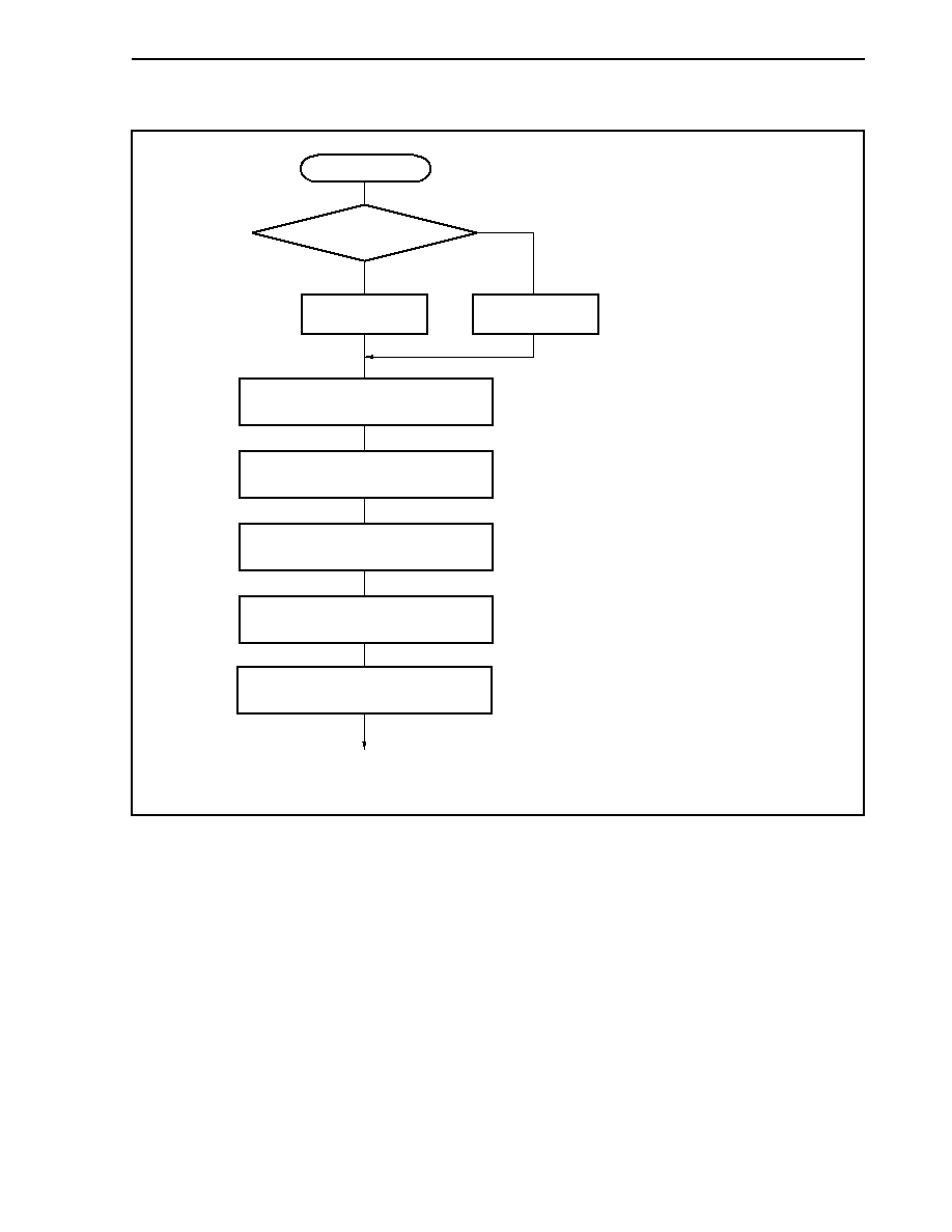
CHAPTER 11 FCAN CONTROLLER
605
User's Manual U14492EJ5V0UD
Figure 11-37. Message Buffer Settings
START
No
Standard frame?
Set message
ID type
Yes
IIDE = 0 (standard)
(M_IDHn)
Set message configuration
See Figure 11-38 CAN Message Configuration
Registers 00 to 31 (M_CONF00 to M_CONF31)
Settings
See Figure 11-39 CAN Message Control
Registers 00 to 31 (M_CTRL00 to M_CTRL31)
Settings
IDE = 1 (extended)
(M_IDHn)
Set identifier
(standard, extended)
Set message control byte
Set message length
See Figure 11-40 CAN Message Status
Registers 00 to 31 (M_STAT00 to M_STAT31) Settings
Set message status
Remark n = 00 to 31
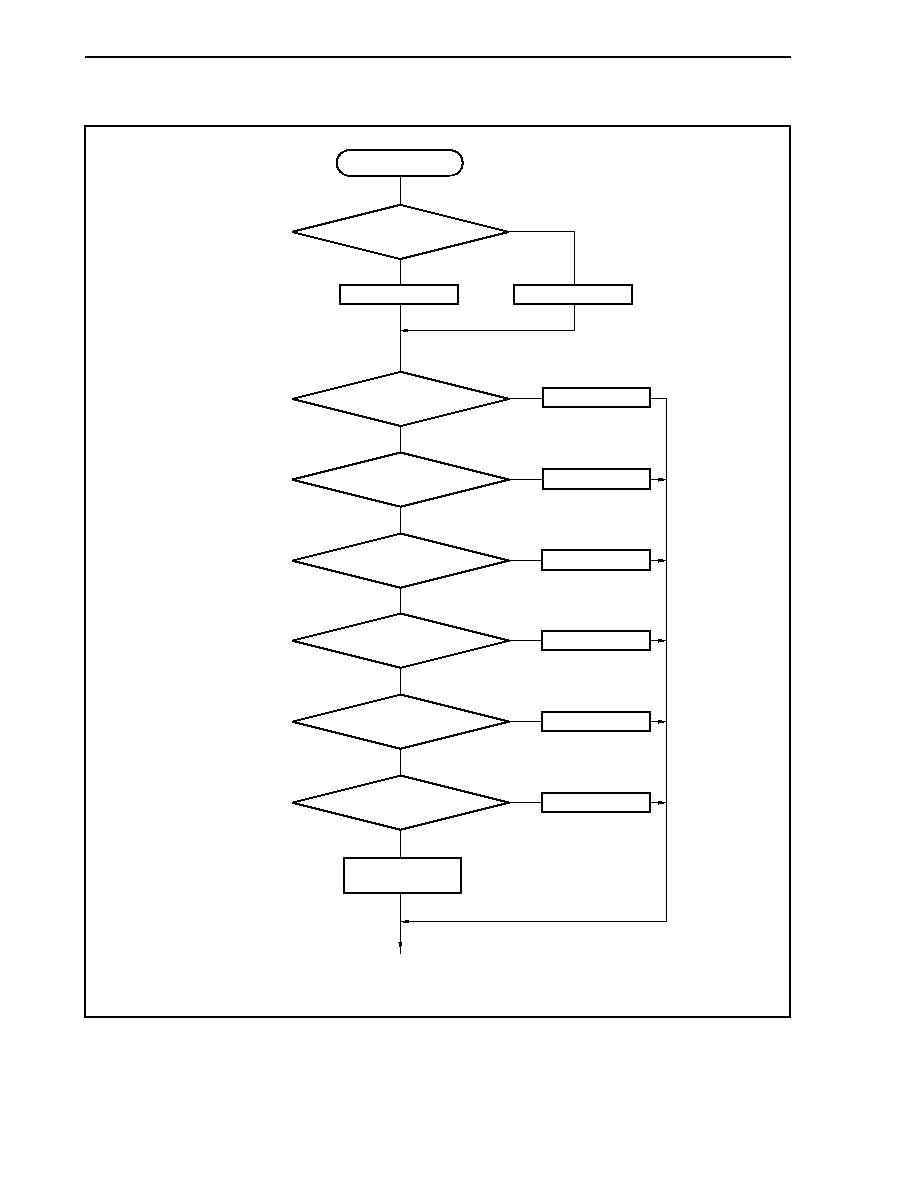
CHAPTER 11 FCAN CONTROLLER
606
User's Manual U14492EJ5V0UD
Figure 11-38. CAN Message Configuration Registers 00 to 31 (M_CONF00 to M_CONF31) Settings
START
Use message buffer?
Release CAN
message buffer
Yes
Yes
MA = 0
MA = 1
Yes
No
No
No
No
No
No
No
MT2 to MT0 = 111
(used in diagnostic
processing mode)
MT2 to MT0 = 000
MT2 to MT0 = 001
MT2 to MT0 = 010
MT2 to MT0 = 011
MT2 to MT0 = 100
MT2 to MT0 = 101
Yes
Yes
Yes
Yes
Transmit message
Receive message
(no mask setting)
Receive message
(set mask 0)
Receive message
(set mask 1)
Receive message
(set mask 2)
Receive message
(set mask 3)
Remark n = 00 to 31

CHAPTER 11 FCAN CONTROLLER
607
User's Manual U14492EJ5V0UD
Figure 11-39. CAN Message Control Registers 00 to 31 (M_CTRL00 to M_CTRL31) Settings
START
Yes
No
No
RTR = 0
RTR = 1
Transmit/receive remote frame
Transmit/receive
data frame?
Set remote frame auto
acknowledge function
Yes
No
IE = 0
IE = 1
Enable interrupt
Disable interrupt?
Yes
No
RMDE0 = 1
RMDE0 = 0
Remote frame auto
acknowledge?
Yes
No
RMDE1 = 1
RMDE1 = 0
ATS = 1
ATS = 0
Set DN flag?
Yes
Apply time stamp?
Set DN flag when remote
frame is received
CHAPTER 11 FCAN CONTROLLER
608
User's Manual U14492EJ5V0UD
Figure 11-40. CAN Message Status Registers 00 to 31 (M_STAT00 to M_STAT31) Settings
START
Clear DN flag
clear DN = 1, set DN = 0
(SC_STATm)
Clear TRQ flag
clear TRQ = 1, set TRQ = 0
(SC_STATm)
Clear RDY flag
clear RDY = 1, set RDY = 0
(SC_STATm)
Remark m = 00 to 31
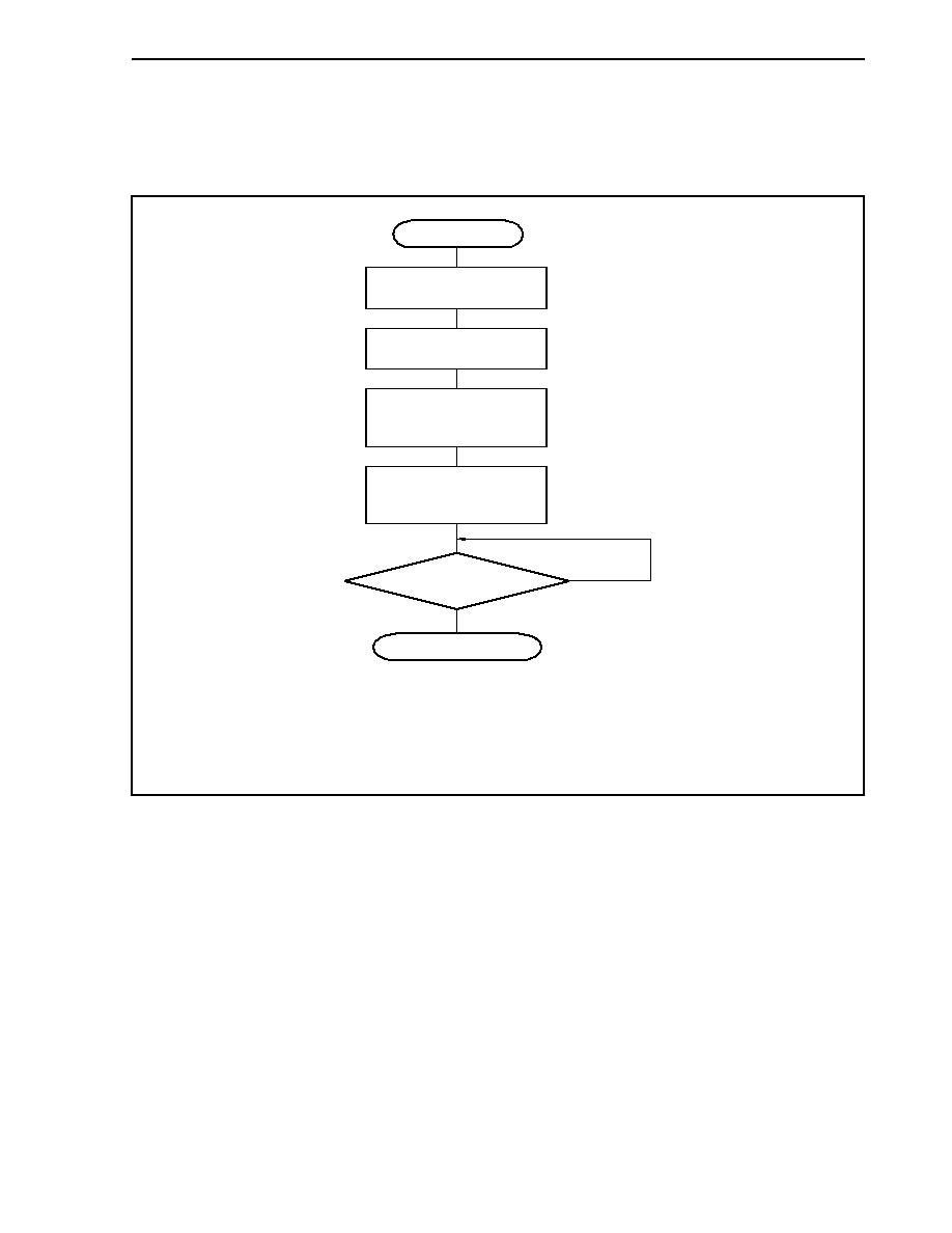
CHAPTER 11 FCAN CONTROLLER
609
User's Manual U14492EJ5V0UD
11.11.2 Transmit setting
Transmit messages are output from the target message buffer.
Figure 11-41. Transmit Setting
START
End of transmit operation
Note
Set RDY flag
set RDY = 1, clear RDY = 0
(SC_STATn)
Set data
(M_DATAnm)
Select transmit
message buffer
Set transmit request flag
set TRQ = 1, clear TRQ = 0
(SC_STATn)
No
Yes
TRQ = 0?
(M_STATn)
Note The RDY flag is not automatically cleared, so clear it by clearing the set RDY bit to 0 and set the
clear RDY bit to 1.
Remark n = 00 to 31, m = 0 to 7
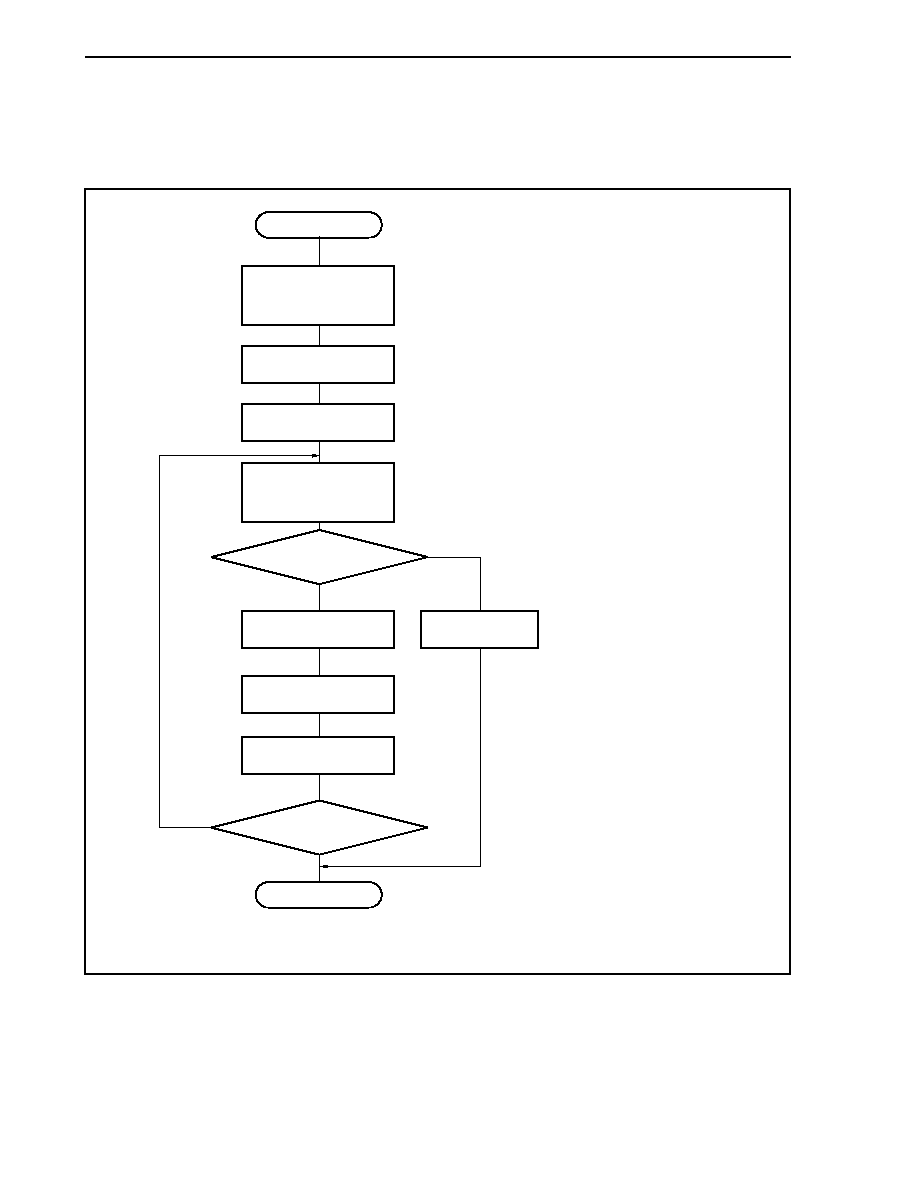
CHAPTER 11 FCAN CONTROLLER
610
User's Manual U14492EJ5V0UD
11.11.3 Receive setting
Receive messages are retrieved from the target message buffer.
Figure 11-42. Setting of Receive Completion Interrupt and Reception Operation Using Reception Polling
START
Receive completion
interrupt occurs
Set RDY flag
set RDY = 1,
clear RDY = 0
(SC_STATn)
End of receive operation
Yes
Receive data frame
No
Yes
Receive data frame?
Receive remote frame
: Detection methods
<1> Detect using CAN1 information register (C1LAST)
<2> Detect using CAN message search start/result
register (CGMSS/CGMSR)
(see Figure 11-43 CAN Message Search
Start/Result Register (CGMSS/CGMSR) Settings)
No
DN = 0 (M_STATn)
Detect target message
buffer
Clear DN flag
clear DN = 1, set DN = 0
(SC_STATn)
Get data length
Transmit operation
Get time stamp
Get data
Remark n = 00 to 31
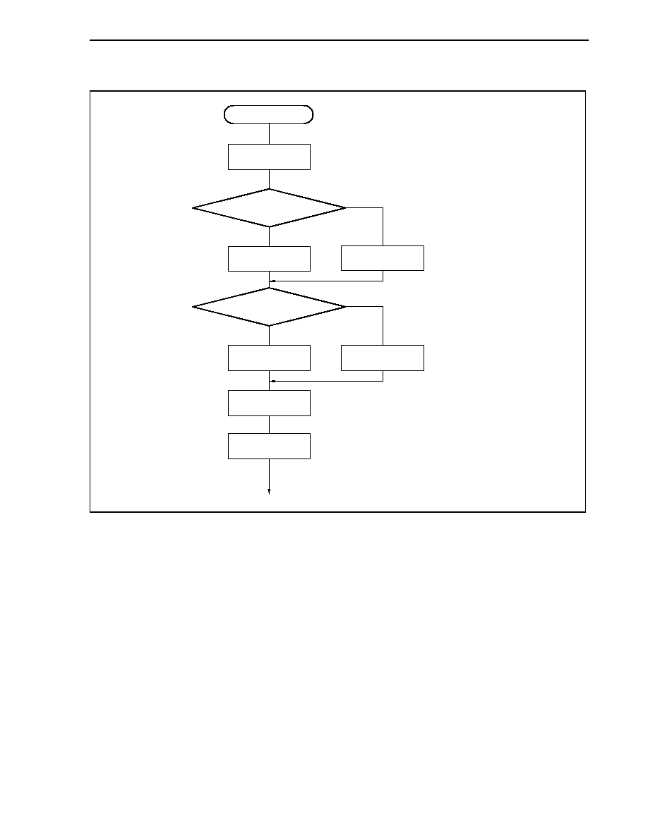
CHAPTER 11 FCAN CONTROLLER
611
User's Manual U14492EJ5V0UD
Figure 11-43. CAN Message Search Start/Result Register (CGMSS/CGMSR) Settings
START
Yes
Yes
Search non mask-
linked messages only
Search all messages
(regardless of mask setting)
Do not check message
ID format
Search standard
ID only
Check message ID?
No
No
CIDE = 1
(CGMSS)
CIDE = 0
(CGMSS)
CMSK = 0
(CGMSS)
Get search results
Check DN flag
(CDN = 1)
Check masked
messages?
CMSK = 1
(CGMSS)
Set start position
and start search
CHAPTER 11 FCAN CONTROLLER
612
User's Manual U14492EJ5V0UD
11.11.4 CAN sleep mode
In CAN sleep mode, the FCAN controller can be set to standby mode. A wake-up occurs when there is a bus
operation.
Figure 11-44. CAN Sleep Mode Settings
START
End of CAN sleep mode settings
No
Yes
SLEEP = 1
(C1CTRL)
set SLEEP = 1
clear SLEEP = 0
(C1CTRL)
Figure 11-45. Clearing of CAN Sleep Mode by CAN Bus Active Status
START
CAN bus active
SLEEP = 0 (C1CTRL)
WAKE = 1 (C1DEF)
Wake-up interrupt occurs
End of CAN sleep mode clearing operation

CHAPTER 11 FCAN CONTROLLER
613
User's Manual U14492EJ5V0UD
Figure 11-46. Clearing of CAN Sleep Mode by CPU
clear SLEEP = 1
set SLEEP = 0
(C1CTRL)
SLEEP = 0
(C1CTRL)
START
End of CAN sleep mode clearing operation
11.11.5 CAN stop mode
In CAN stop mode, the FCAN controller can be set to standby mode. No wake-up occurs when there is a bus
operation (stop mode is controlled by CPU access only).
Figure 11-47. CAN Stop Mode Settings
START
End of CAN stop mode settings
Yes
SLEEP = 1
(C1CTRL)
No
set STOP = 1
clear STOP = 0
(C1CTRL)
Set CAN sleep mode
(see Figure 11-44)
Yes
STOP = 1
(C1CTRL)
No
CHAPTER 11 FCAN CONTROLLER
614
User's Manual U14492EJ5V0UD
Figure 11-48. Clearing of CAN Stop Mode
START
End of CAN stop mode clearing operation
clear STOP = 1
set STOP = 0
clear SLEEP = 1
set SLEEP = 0
(C1CTRL)
STOP = 0
SLEEP = 0
(C1CTRL)

CHAPTER 11 FCAN CONTROLLER
615
User's Manual U14492EJ5V0UD
11.12 Rules for Correct Setting of Baud Rate
The CAN protocol limit values for ensuring correct operation of FCAN are described below. If these limit values are
exceeded, a CAN protocol violation may occur, which can result in operation faults. Always make sure that settings
are within the range of limit values.
(a) 5
◊ BTL SPT (sampling point) 17 ◊ BTL [4 SPT4 to SPT0 set values 16]
(b) 8
◊ BTL DBT (data bit time) 25 ◊ BTL [7 DBT4 to DBT0 set values 24]
(c) SJW (synchronization jump width)
DBT - SPT
(d) 2
◊ (DBT - SPT) 8
Remark BTL = 1/f
BTL
(f
BTL
: CAN protocol layer base system clock)
SPT4 to SPT0 (Bits 9 to 5 of CAN1 synchronization control register (C1SYNC))
DBT4 to DBT0 (Bits 4 to 0 of CAN1 synchronization control register (C1SYNC))
(1) Example of FCAN baud rate setting (when C1BRP register's TLM bit = 0)
The following is an example of how correct settings for the C1BRP register and C1SYNC register can be
calculated.
Conditions from CAN bus:
<1> CAN base clock frequency (f
MEM
): 16 MHz
<2> CAN bus baud rate: 83 kbps
<3> Sampling point: 80% or more
<4> Synchronization jump width: 3 BTL
First, calculate the ratio between the CAN base clock frequency and the CAN bus baud rate frequency as
shown below.
f
MEM
/CAN bus baud rate = 16 MHz/83 kHz
192.77 2
6
◊ 3
Set an even number between 2 and 128 to the C1BRP register's bits BRP5 to BRP0 as the setting for the
prescaler (CAN protocol layer base system clock: f
BTL
), then set a value between 8 and 25 to the C1SYNC
register's bits DBT4 to DBT0 as the data bit time.
Since it is assumed that the SJW (synchronization jump width) value is 3, the maximum setting for SPT
(sampling point) is 3 less than the data bit time setting and is 17.
(SPT
DBT ≠ 3 and SPT = 17)
CHAPTER 11 FCAN CONTROLLER
616
User's Manual U14492EJ5V0UD
Given the above limit values, the following four settings are possible.
Prescaler
DBT
SPT (MAX.)
Calculated SPT
24
8
5
5/8 = 62.5%
16
12
9
9/12 = 75%
12
16
13
13/16 = 81%
8
24
17
17/24 = 71%
16 MHz/83 kbps
192 = 64 ◊ 3
<1>
= 48
◊ 4
<2>
= 32
◊ 6
<3>
= 24
◊ 8
<4>
= 16
◊ 12
<5>
= 12
◊ 16
<6>
= 8
◊ 24
<7>
= 6
◊ 32
<8>
= 4
◊ 48
<9>
= 3
◊ 64
<10>
The settings that can actually be made for the V850E/IA1 are in the range from <4> to <7> above (the section
enclosed in broken lines).
Among these options in the range from <4> to <7> above, option <6> is the ideal setting for the specifications
when actually setting the register.
(i) Prescaler (CAN protocol layer base system clock: f
BTL
) setting
f
BTL
is calculated as below.
∑ f
BTL
= f
MEM
/{(a + 1)
◊ 2} : [0 a 63]
Value a is set using bits 5 to 0 (BRP5 to BRP0) of the C1BRP register.
f
BTL
= 16 MHz/12
= 16 MHz/{(5 + 1)
◊ 2}
thus a = 5
Therefore, C1BRP register = 0005H

CHAPTER 11 FCAN CONTROLLER
617
User's Manual U14492EJ5V0UD
(ii) DBT (data bit time) setting
DBT is calculated as below.
∑ DBT = BTL ◊ (a + 1) : [7 a 24]
Value a is set using bits 4 to 0 (DBT4 to DBT0) of the C1SYNC register.
DBT = BTL
◊ 16
= BTL
◊ (a + 1)
thus a = 15
Therefore, C1SYNC register's bits DBT4 to DBT0 = 01111B
Note that 1/DBT = f
BTL
/16
1333 kHz/16
83 kbps (nearly equal to the CAN bus baud rate)
(iii) SPT (sampling point) setting
Given SJW = 3:
SJW
DBT ≠ SPT
3
16 ≠ SPT
SPT
13
Therefore, SPT is set as 13 (max.)
SPT is calculated as below.
∑ SPT = BTL ◊ (a + 1) : [4 a 16]
Value a is set using bits 9 to 5 (SPT4 to SPT0) of the C1SYNC register.
SPT = BTL
◊ 13
= BTL
◊ (12 + 1)
thus a = 12
Therefore, the SPT4 to SPT0 bits of the C1SYNC register = 01100B
(iv) SJW (synchronization jump width) setting
SJW is calculated as below.
∑ SJW = BTL ◊ (a + 1) : [0 a 3]
Value a is set using bits11 and 10 (SJW1, SJW0) of the C1SYNC register.
C1SYNC register's bits SJW1 and SJW0 = BTL
◊ 3
=
BTL
◊ (2 + 1)
thus a = 2
Therefore, the SJW1 and SJW0 bits of the C1SYNC register = 10B.
The C1SYNC register settings based on these results are shown in Figure 11-49 below.
CHAPTER 11 FCAN CONTROLLER
618
User's Manual U14492EJ5V0UD
Figure 11-49. C1SYNC Register Settings
15 14 13 12 11 10 9 8
C1SYNC
0 0 0
SAMP
SJW1
SJW0
SPT4
SPT3
Setting
0 0 0 0 1 0 0 1
7 6 5 4 3 2 1 0
SPT2 SPT1 SPT0 DBT4 DBT3 DBT2 DBT1 DBT0
Setting
1 0 0 0 1 1 1 1
CHAPTER 11 FCAN CONTROLLER
619
User's Manual U14492EJ5V0UD
11.13 Ensuring Data Consistency
When the CPU reads data from CAN message buffers, it is essential for the read data to be consistent.
Two methods are used to ensure data consistency: sequential data read and burst read mode.
11.13.1 Sequential data read
When the CPU performs sequential access of a CAN message buffer, data is read from the buffer in the order
shown in Figure 11-50 below.
Only the FCAN internal operation can set the M_STATn register's DN bit (to 1) and only the CPU can clear it (to 0),
so during the read operation the CPU must be able to check whether or not any new data has been stored in the
message buffer.
Figure 11-50. Sequential Data Read
Read CPU
End of CPU's read operation
Yes
DN = 0
(M_STATn)
No
Clear DN flag
clear DN = 1, set DN = 0
(SC_STATn)
Read data from
message buffer
Remark n = 00 to 31

CHAPTER 11 FCAN CONTROLLER
620
User's Manual U14492EJ5V0UD
11.13.2 Burst read mode
Burst read mode is implemented in the FCAN to enable faster access to complete messages and secure the
synchrony of data.
Burst read mode starts up automatically each time the CPU reads the M_DLCn register and data is then copied
from the message buffer area to a temporary read buffer.
Data continues to be read from the temporary buffer as long as the CPU keeps directly incrementing (+1) the read
address (when data is read in the following order: M_DLCn register
M_CTRLn register M_TIMEn register
M_DATAn0 to M_DATAn7 registers
M_IDLn, M_IDHn register).
If these linear address rules are not followed or if access is attempted to an address that is lower than the M_IDHn
register's address (such as the M_CONFn register or M_STATn register), burst read mode becomes invalid.
Cautions 1. 16-bit read access is required for the memory buffer area when using the burst read mode.
If 8-bit access (byte read operation) is attempted, burst read mode does not start up even if
the address is linearly incremented (+1) as described above.
2. Be sure to read out the value of FCAN control registers other than the M_DLCn register
before starting the burst read mode.
Remark n = 00 to 31

CHAPTER 11 FCAN CONTROLLER
621
User's Manual U14492EJ5V0UD
11.14 Interrupt Conditions
11.14.1 Interrupts that are generated for FCAN controller
When interrupts are enabled (condition <1>: M_CTRLn register's IE bit = 1, conditions other than <1>: C1IE
register's interrupt enable flag = 1), interrupts will be generated under the following conditions (n = 00 to 31).
<1> Message-related operation has succeeded
∑ When a message has been received in the receive message buffer
∑ When a remote frame has been received in the transmit message buffer
(when auto acknowledge mode has not been set, i.e., when the M_CTRLn register's RMDE0 bit = 0)
∑ When a message has been transmitted from the transmit message buffer
<2> When a CAN bus error has been detected
∑ Bit
error
∑ Bit stuff error
∑ Form
error
∑ CRC
error
∑ ACK
error
<3> When the CAN bus mode has been changed
∑ Error passive status elapsed while FCAN was transmitting
∑ Bus off status was set while FCAN was transmitting
∑ Error passive status elapsed while FCAN was receiving
<4> Internal
error
∑ Overrun
error
11.14.2 Interrupts that are generated for global CAN interface
Interrupts are generated for the global CAN interface under the following conditions.
∑ An undefined area is accessed
∑ If the GOM bit is cleared to 0 when one of the CAN modules is not in the initialization status (ISTAT bit of
C1CTRL register = 0) with the EFSD bit of the CGST register = 0
∑ A CAN module register (register starting with "C1") is accessed when the GOM bit of the CGST register = 0
∑ A temporary buffer (in the area following the address of the C1SYNC register) is accessed when the GOM bit of
the CGST register = 1

CHAPTER 11 FCAN CONTROLLER
622
User's Manual U14492EJ5V0UD
11.15 How to Shut Down FCAN Controller
The following procedure should be used to stop CAN bus operations in order to stop the clock supply to the CAN
interface (to set low power mode).
<1> FCAN controller's initialization mode setting
∑ Set initialization mode (INIT bit = 1 in C1CTRL register (set INIT bit = 1, clear INIT bit = 0))
<2> Stop time stamp counter
∑ Set TSM bit = 0 in CGST register (set TSM bit = 0, clear TSM bit = 1)
<3> Stop CAN interface
∑ Set GOM bit = 0 in CGST register (set GOM bit = 0, clear GOM bit = 1)
∑ Stop CAN clock
Caution If the above procedure is not performed correctly, the CAN interface (in active status) can
cause operation faults.

CHAPTER 11 FCAN CONTROLLER
623
User's Manual U14492EJ5V0UD
11.16 Cautions on Use
<1> Bit manipulation is prohibited for all FCAN controller registers.
<2> Be sure to properly clear (0) all interrupt request flags
Note
in the interrupt routine. If these flags are not
cleared (0), subsequent interrupt requests may not be generated. Note also that if an interrupt is generated
at the same time as a CPU clear operation, that interrupt request flag will not be cleared (0). It is therefore
important to confirm that interrupt request flags have been properly cleared (0).
Note See 11.10 (10) CAN interrupt pending register (CCINTP), 11.10 (11) CAN global interrupt
pending register (CGINTP), and 11.10 (12) CAN1 interrupt pending register (C1INTP).
<3> When a change occurs on the CAN bus via a setting of the CSTP bit in the CSTOP register while the clock
supply to the CPU or peripheral functions is stopped, the CPU can be woken up.
<4> Do not read the same register of the FCAN controller twice or more in a row. If the same register is read
twice or more in a row, and even if the value of the register is changed while it is being read the second or
subsequent time, the new value is not reflected, and the same value as the one read the first time is always
read.
Example
Reading the C1CTRL and C1BA registers
(i) Correct usage: New value is reflected when C1CTRL is read the second time.
C1CTRL
read
C1BA
read
C1CTRL
read
(ii) Incorrect usage: The second read value of C1CTRL is the same as the first read value of
C1CTRL.
C1CTRL
read
C1CTRL
read
C1BA
read
<5> When receiving a remote frame with an extended ID and storing it in the receive message buffer, the values
of DLC3 to DLC0 in the message buffer are cleared to 0 regardless of the values of DLC3 to DLC0 on the
CAN bus.

CHAPTER 11 FCAN CONTROLLER
624
User's Manual U14492EJ5V0UD
<6> If the OS (OSEK/COM) is not used, be sure to execute the following processing.
[When CAN communication is performed using an interrupt routine]
∑ Clear (0) the following interrupt pending bits at the start of the corresponding interrupt routine.
∑ C1INTm bit of C1INTP register (m = 0 to 6)
∑ GINT1 bit of CGINTP register (m = 1 to 3)
∑ Clear (0) the following enable bits during the corresponding interrupt routine.
∑ E_INTm bit of C1IE register (m = 0 to 6)
∑ G_IEn bit of CGIE register (n = 1, 2)
[When CAN communication is performed by polling of bits, not using interrupt routines]
∑ The following interrupt mask flags and interrupt enable bits are used when set (1) (do not clear (0)
them).
∑ CANMKn bit of CANICn register (n = 0 to 3)
∑ E_INTm bit of C1IE register (m = 0 to 6)
∑ G_IEn bit of CGIE register (n = 1, 2)
∑ IE bit of M_CTRLn register (n = 00 to 31)
∑ Clear (0) the following interrupt pending bits in accordance with procedures (i) to (iii) below.
∑ C1INTm bit of C1INTP register (m = 0 to 6)
∑ GINTn bit of CGINTP register (n = 1 to 3)
(i) Poll the corresponding interrupt request flag.
(ii) If the value of the bit in procedure (i) is 1, clear (0) the corresponding interrupt pending bit.
(iii) After executing procedure (ii), clear (0) the interrupt request flag.
Example CAN reception
(i) Poll until the CANIF0 bit of the CANIC0 register becomes 1.
(ii) Clear (0) the C1INT1 bit of the C1INTP register.
(iii) Clear (0) the CANIF0 bit of the CANIC0 register.
<7> When emulating the FCAN controller using the in-circuit emulator (IE-V850E-MC or IE-703116-MC-EM1),
perform the following settings in the Configuration screen that appears when the debugger is started.
∑ Set the start address of the programmable peripheral I/O area that is set using the BPC register to the
Programmable I/O Area field.
∑ Maps the programmable peripheral I/O area as "Target" or "Emulation RAM" in the Memory Mapping
field.
625
User's Manual U14492EJ5V0UD
CHAPTER 12 NBD FUNCTION (
µPD70F3116)
The V850E/IA1 provides the Non Break Debug (NBD) function for on-chip data tuning.
12.1 Overview
The NBD function encompasses the following functions.
(1) RAM monitoring function
This function makes an arbitrary RAM area readable or writable using an NBD tool via DMA.
[Corresponding RAM area]
XFFFC000H to XFFFE7FFH
If executed using an address outside the above, the function instantly returns "ready".
Output is undefined on a read, and the write operation is not performed on a write.
(2) Event detection function
By having a comparator (24-bit address setting) for match detection on-chip, this function outputs a match
trigger (falling edge) to the NBD tool when the address match detection shown below is performed. The
lower 2 bits are masked.
∑ Execution PC address match detection
∑ Internal RAM area address write timing match detection
[Detection range]
ROM: X0000000H to X003FFFFH
RAM: XFFFC000H to XFFFE7FFH
Table 12-1. NBD Block Dedicated Pin Summary
Pin Name
I/O
Function Summary
CLK_DBG Input
Serial
clock input for debugging interface
SYNC
Input
Synchronization signal for debugging
AD0_DBG to AD3_DBG
I/O
Command data and RAM data I/O (4 bits)
TRIG_DBG
Output
Outputs trigger (falling edge) synchronized to timing of write to arbitrary specified RAM
address or to timing of execution of instruction at specified address.
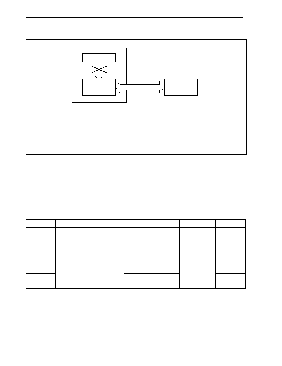
CHAPTER 12 NBD FUNCTION (
µ
PD70F3116)
626
User's Manual U14492EJ5V0UD
Figure 12-1. Image of NBD Space
V850E/IA1
Not
possible
CPU
NBD : Non Break Debug
NBD
unit
NBD dedicated
interface (7 ways)
NBD
tool
Caution The debug function does not operate under the following conditions.
∑ During reset period
∑ Until DMA initialization termination after reset
∑ Software STOP mode/IDLE mode
∑ Oscillation stabilization time (during TBC count)
12.2 NBD Function Register Map
Table 12-2 shows a map of the control registers of the NBD function. The NBD space does not exist in the internal
space of the CPU but exists independently as NBD space. Because of this, the NBD space is space that cannot be
read or written from the CPU but can only be read or written via the NBD dedicated interface (refer to Figure 12-1).
Table 12-2. NBD Space Map
Address Register
Name
Symbol
R/W
After
Reset
000H
Chip ID register 0
TID0
4EH
001H
Chip ID register 1
TID1
01H
002H
Chip ID register 2
TID2
R
01H
800H
EVTU_A0 to EVTU_A7
Undefined
801H
EVTU_A8 to EVTU_A15
Undefined
802H
EVTU_A16 to EVTU_A23
Undefined
803H
User event address setting register
EVTU_A24 to EVTU_A27
Undefined
820H
User event condition setting register
EVTU_C0
R/W
Undefined
Caution Since the V850E/IA1 NBD uses the DMA controller that is incorporated in the V850E1 CPU core,
settings for the DMA controller are initialized after reset.
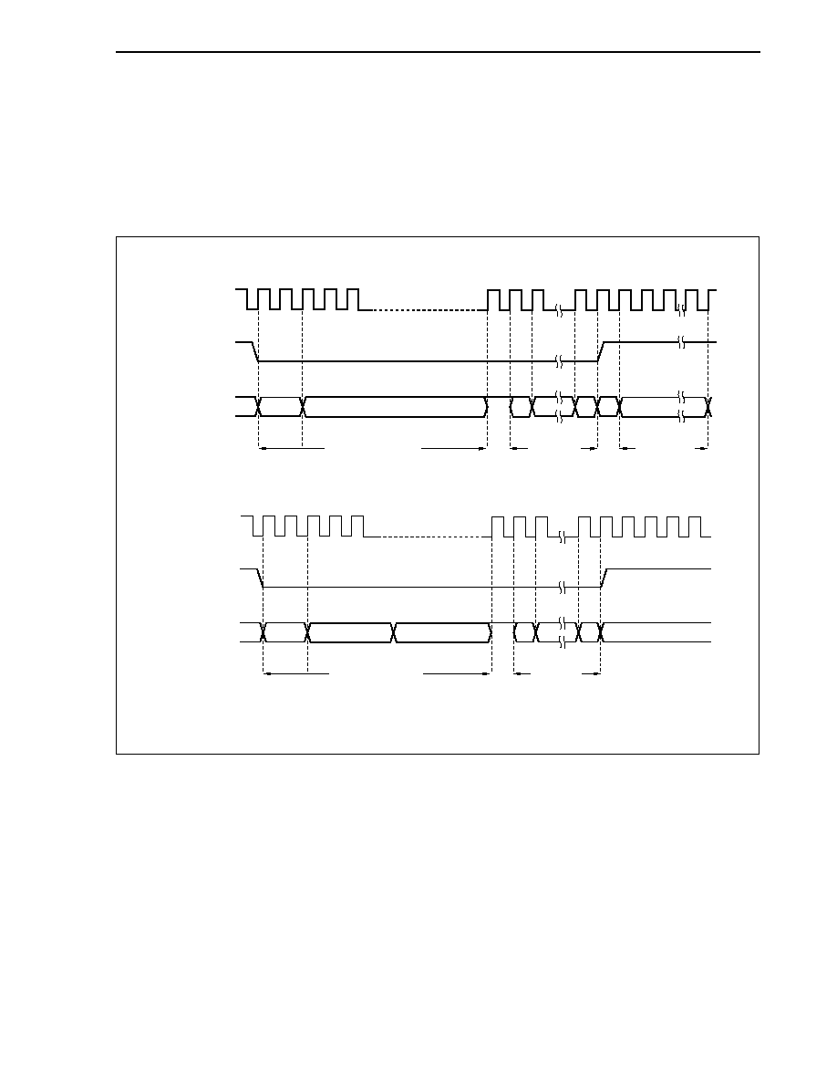
CHAPTER 12 NBD FUNCTION (
µ
PD70F3116)
627
User's Manual U14492EJ5V0UD
12.3 NBD Function Protocol
The basic protocol of the NBD function is shown below.
(1) Basic protocol
Figure 12-2. Basic Protocol
(1) On a read
CLK_DBG
SYNC
AD0_DBG to
AD3_DBG
N
Address section
Command packet
Flag sense
Control
section
N
R
Data packet
(2) On a write
CLK_DBG
SYNC
AD0_DBG to
AD3_DBG
N
N
R
Address section
Data section
Command packet
Flag sense
Control
section
Remark N: Not ready
R: Ready
CHAPTER 12 NBD FUNCTION (
µ
PD70F3116)
628
User's Manual U14492EJ5V0UD
(2) Command packet
NBD
Bus
Line
AD3_DBG AD2_DBG AD1_DBG AD0_DBG
1st
aux3 aux2 aux1 aux0
2nd SIZ1
SIZ0
R/W
I/T
3rd
A3 A2 A1 A0
4th
A7 A6 A5 A4
5th A11
A10
A9
A8
6th
A15 A14 A13 A12
7th
A19 A18 A17 A16
8th
A23 A22 A21 A20
9th
D3 D2 D1 D0
10th
D7 D6 D5 D4
11th D11
D10
D9
D8
12th
D15 D14 D13 D12
13th
D19 D18 D17 D16
14th
D23 D22 D21 D20
15th
D27 D26 D25 D24
16th
D31 D30 D29 D28
Caution Values are for command packet maximum setup.
∑ Access to NBD space
Address: 12 bits (A0 to A11) [Fixed]
Data: 8 bits (D0 to D7)
∑ Access to target space
Address: 24 bits (A0 to A23) [Fixed]
Data: 32 bits (D0 to D31)
(a) aux0 to aux3: Expansion bits
aux0 aux1 aux2 aux3
Remarks
0 0 0 0
Fixed
Other than 0000
For future expansion
(b) I/T: Access address space mode specification
I/T Remarks
0
Specifies access to NBD space
1
Specifies access to target space
(c) R/W: Access mode specification from NBD tool
R/W Remarks
0
Read mode from NBD tool
1
Write mode from NBD tool
CHAPTER 12 NBD FUNCTION (
µ
PD70F3116)
629
User's Manual U14492EJ5V0UD
(d) SIZ0, SIZ1: Access data size specification
SIZ1
SIZ0
Target Space Access
NBD Space Access
0 0
8-bit
length
Note 1
8-bit
length
0 1
16-bit
length
Note 1
1 0
32-bit
length
1 1
Setting
prohibited
Note 2
Setting prohibited
Note 2
Notes 1. Can be set only on a read.
If set on a write, RAM data will be lost.
2. A write is invalid and read data is undefined in cases where "Setting prohibited" is
specified.
(3) Flag sense packet
NBD Bus Line
AD3_DBG
AD2_DBG
AD1_DBG
AD0_DBG
1st 0
0
0
RFLG
RFLG
0:
Not
Ready
1:
Ready
(4) Data packet
The data packet data size is the data size specified by SIZ1 and SIZ0 in a command packet (8, 16, or 32
bits).
NBD Bus Line
AD3_DBG
AD2_DBG
AD1_DBG
AD0_DBG
1st D3
D2
D1
D0
2nd D7
D6
D5
D4
3rd D11
D10
D9
D8
4th D15
D14
D13
D12
5th D19
D18
D17
D16
6th D23
D22
D21
D20
7th D27
D26
D25
D24
8th D31
D30
D29
D28
CHAPTER 12 NBD FUNCTION (
µ
PD70F3116)
630
User's Manual U14492EJ5V0UD
12.4 NBD Function
12.4.1 RAM monitoring, accessing NBD space
The NBD function performs reading and writing of internal RAM data for addresses in internal RAM via the DMA
(direct memory access) controller. It also performs reading or writing to the NBD space.
(1) RAM monitoring
The following are the commands for reading and writing to internal RAM areas from the NBD tool.
(a) Write command
The target address (real address of target: lower 24 bits) at which a write to internal RAM is to be
performed and the data sent from the NBD tool are received as a command packet. After receiving the
command packet shown below from the NBD tool, a Ready command is output following write
completion.
Command packets can be received once more from the NBD tool (after Ready command SYNC inactive
confirmation).
Table 12-3. Command Packet (Write Access)
ADn_DBG AD3_DBG AD2_DBG AD1_DBG AD0_DBG
1st 0
0
0
0
2nd SIZ1
SIZ0
1
1
3rd to 8th
Target space write address specification (24 bits)
9th to 16th
Write data (data specified by SIZ0 and SIZ1)
(b) Read command
The target address (real address of target: lower 24 bits), at which read of internal RAM is to be
performed, which is sent from the NBD tool, is received as a command packet. After receiving the
command packet from the NBD tool, a Ready command is output, SYNC is made inactive, and the data
at the address specified by the command packet is transmitted to the NBD tool. The address (A27 to
A24) during read is "1111".
Table 12-4. Command Packet (Read Access)
ADn_DBG AD3_DBG AD2_DBG AD1_DBG AD0_DBG
1st 0
0
0
0
2nd SIZ1
SIZ0
0
1
3rd to 8th
Target space read address specification (24 bits)
Caution In read mode, the output data section from the NBD tool is deleted.
Table 12-5. Data Packet (Read Access)
ADn_DBG AD3_DBG AD2_DBG AD1_DBG AD0_DBG
1st to 8th
Target space read data
CHAPTER 12 NBD FUNCTION (
µ
PD70F3116)
631
User's Manual U14492EJ5V0UD
(2) Access to NBD space
The following are the commands for reading or writing to the NBD space from the NBD tool. For the NBD
space, the access address length is fixed to 12 bits and the access data length is fixed to 8 bits.
(a) Write command
The address (NBD space address: 12 bits) at which write to the NBD space is to be performed and the
data sent from the NBD tool are received as a command packet. After receiving the command packet
shown in Table 12-6 from the NBD tool, a Ready command is output following write completion.
Command packets can be received once more from the NBD tool (after Ready command SYNC inactive
confirmation).
Table 12-6. Command Packet (Write Access to NBD Space)
ADn_DBG AD3_DBG AD2_DBG AD1_DBG AD0_DBG
1st
0 0 0 0
2nd
0 0 1 0
3rd
A3 A2 A1 A0
4th
A7 A6 A5 A4
5th A11
A10
A9
A8
6th
D3 D2 D1 D0
7th
D7 D6 D5 D4
Caution The length of an NBD space write address is fixed to 12 bits.
The length of the write data is fixed to 8 bits.
(b) Read command
The target address (real address of target: 12 bits), at which read of internal RAM is to be performed,
which is sent from the NBD tool, is received as a command packet. After receiving the command packet
from the NBD tool, a Ready command is output, SYNC is made inactive, and the data at the address
specified by the command packet is transmitted to the NBD tool.
Table 12-7. Command Packet (Read Access to NBD Space)
ADn_DBG AD3_DBG AD2_DBG AD1_DBG AD0_DBG
1st
0 0 0 0
2nd
0 0 0 0
3rd
A3 A2 A1 A0
4th
A7 A6 A5 A4
5th A11
A10
A9
A8
Caution The length of an NBD space read address is fixed to 12 bits.
In read mode, the output data section from the NBD tool is deleted.
CHAPTER 12 NBD FUNCTION (
µ
PD70F3116)
632
User's Manual U14492EJ5V0UD
Table 12-8. Data Packet
ADn_DBG AD3_DBG AD2_DBG AD1_DBG AD0_DBG
1st D3
D2
D1
D0
2nd D7
D6
D5
D4
Caution The length of the read data is fixed to 8 bits.
12.4.2 Event detection function
By having a comparator (24-bit address setting) for match detection on-chip, this function detects match of the
address setting registers shown below and outputs a match trigger (falling edge) to the NBD tool. Event trigger output
is low active and during the active period it is output synchronous with the system clock of the target CPU. The active
width is one cycle of the internal system clock of the CPU.
(1) Event detection conditions
∑ Execution PC address match
Match detection range for timing of a write to a set address in the internal RAM area
XFFFC000H to XFFFE7FFH
(2) Event detection function control register
(a) NBD event condition setting register (EVTU_C)
7
0
EVTU_C7 to
EVTU_C0
6
0
5
0
4
0
3
0
2
0
1
0
0
PCU/DTU
NBD space address
820H
Initial value
Undefined
Bit position
Bit name
Function
0 PCU/DTU
Selects an execution PC event or RAM access event.
0: Internal RAM access event is invalid
Note
1: Execution PC event is invalid
Note
If the EVTU_C register is set to a location other than the internal RAM area,
an event also is output when writing to other than the RAM.
CHAPTER 12 NBD FUNCTION (
µ
PD70F3116)
633
User's Manual U14492EJ5V0UD
(b) NBD event address register (EVTU_A)
The EVTU_A register sets the value of the address that is the subject of the event.
7
EVAU7
EVTU_A7 to
EVTU_A0
6
EVAU6
5
EVAU5
4
EVAU4
3
EVAU3
2
EVAU2
1
EVAU1
0
EVAU0
NBD space address
800H
Initial value
Undefined
15
EVAU15
EVTU_A15 to
EVTU_A8
14
EVAU14
13
EVAU13
12
EVAU12
11
EVAU11
10
EVAU10
9
EVAU9
8
EVAU8
NBD space address
801H
Initial value
Undefined
23
EVAU23
EVTU_A23 to
EVTU_A16
22
EVAU22
21
EVAU21
20
EVAU20
19
EVAU19
18
EVAU18
17
EVAU17
16
EVAU16
NBD space address
802H
Initial value
Undefined
31
Undefined
EVTU_A27 to
EVTU_A24
30
Undefined
29
Undefined
28
Undefined
27
EVAU27
Note
26
EVAU26
Note
25
EVAU25
Note
24
EVAU24
Note
NBD space address
803H
Initial value
Undefined
Note Set bit 27 to bit 24 to 0.
Cautions 1. ROM address match functions are valid only for internal ROM.
2. This cannot be used in single-chip mode 1.
3. The lower 2 bits (EVAU1, EVAU0) are masked.
12.4.3 Chip ID registers (TID0 to TID2)
The chip ID registers are stored in NBD space 000H to 002H. By reading the ID codes in the chip ID registers from
the NBD tool in NBD mode, the semiconductor manufacturer, CPU code, and specific product type can be identified.
The chip ID registers have fixed values for each product.
The chip ID registers (TID0 to TID2) are read-only registers.
7
MC7
TID0
6
MC6
∑ MC7 to MC0: Semiconductor manufacturer classification code
NEC Electronics: 4EH
5
MC5
4
MC4
3
MC3
2
MC2
1
MC1
0
MC0
NBD space address
000H
7
FC7
TID1
6
FC6
5
FC5
4
FC4
3
FC3
2
FC2
1
FC1
0
FC0
NBD space address
001H
∑ FC7 to FC0: CPU classification code
V850E1 CPU: 01H
∑ SC7 to SC0: Specific product classification code
V850E/IA1: 01H
7
SC7
TID2
6
SC6
5
SC5
4
SC4
3
SC3
2
SC2
1
SC1
0
SC0
NBD space address
002H

CHAPTER 12 NBD FUNCTION (
µ
PD70F3116)
634
User's Manual U14492EJ5V0UD
12.5 Control Registers
(1) RAM access data buffer register L (NBDL)
The NBDL register operates as the buffer between the DMA controller and the NBD tool when reading or
writing RAM from the NBD tool via the DMA controller.
This register can be read/written in 16-bit units.
When the higher 8 bits of the NBDL register are used as the NBDLU register, and the lower 8 bits are used
as the NBDLL register, they can be read/written in 8-bit units.
14
D14
13
D13
12
D12
2
D2
3
D3
4
D4
5
D5
6
D6
7
D7
8
D8
9
D9
10
D10
11
D11
15
D15
1
D1
0
D0
NBDL
Address
FFFFFA60H
Initial value
0000H
Cautions 1. Although the NBDL, NBDLU, and NBDLL registers can be used for reading or writing,
physically separate registers are used when reading and when writing, so written values
cannot be read.
2. Use both the NBDL and NBDH registers (refer to 12.5 (2)) for 32-bit access of RAM.
Remark Register values written from the NBD tool can be read by DMA (CPU) and values written by DMA
(CPU) can be read by the NBD tool.
(2) RAM access data buffer register H (NBDH)
The NBDH register operates as the buffer between the DMA controller and the NBD tool when reading or
writing RAM from the NBD tool via the DMA controller.
This register can be read/written in 16-bit units.
When the higher 8 bits of the NBDH register are used as the NBDHU register, and the lower 8 bits are used
as the NBDHL register, they can be read/written in 8-bit units.
14
D30
13
D29
12
D28
2
D18
3
D19
4
D20
5
D21
6
D22
7
D23
8
D24
9
D25
10
D26
11
D27
15
D31
1
D17
0
D16
NBDH
Address
FFFFFA62H
Initial value
0000H
Cautions 1. Although the NBDH, NBDHU, and NBDHL registers can be used for reading or writing,
physically separate registers are used when reading and when writing, so written values
cannot be read.
2. Use both the NBDL and NBDH registers (refer to 12.5 (1)) for 32-bit access of RAM.
Remark Register values written from the NBD tool can be read by DMA (CPU) and values written by DMA
(CPU) can be read by the NBD tool.
CHAPTER 12 NBD FUNCTION (
µ
PD70F3116)
635
User's Manual U14492EJ5V0UD
(3) DMA source address setting register SL (NBDMSL)
The NBDMSL register specifies a DMA source address.
This register can be written from the NBD tool and read by the DMA controller (CPU).
This register is read-only, in 16-bit units.
14
AD14
13
AD13
12
AD12
2
AD2
3
AD3
4
AD4
5
AD5
6
AD6
7
AD7
8
AD8
9
AD9
10
AD10
11
AD11
15
AD15
1
AD1
0
AD0
NBDMSL
Address
FFFFFA64H
Initial value
Undefined
Remarks 1. When reading RAM using the NBD tool, an address signal sent from the NBD tool can be read
via the NBDMSL register using the DMA controller (CPU).
2. When writing to RAM using the NBD tool, the NBDL register value can be read via the NBDMSL
register using the DMA controller (CPU).
(4) DMA source address setting register SH (NBDMSH)
The NBDMSH register specifies a DMA source address.
This register can be written from the NBD tool and read by the DMA controller (CPU).
This register is read-only, in 16-bit units.
14
0
13
0
12
0
2
AD18
3
AD19
4
AD20
5
AD21
6
AD22
7
AD23
8
AD24
9
AD25
10
AD26
11
AD27
15
IR
1
AD17
0
AD16
NBDMSH
Address
FFFFFA66H
Initial value
Undefined
Bit position
Bit name
Function
15 IR
Shows read or write status when NBD accesses internal RAM of the V850E/IA1.
0: NBD is write accessing RAM
1: NBD is read accessing RAM
Remarks 1. When reading RAM using the NBD tool, an address signal sent from the NBD tool can be read
via the NBDMSH register using the DMA controller (CPU).
2. When writing to RAM using the NBD tool, the NBDL register value can be read via the NBDMSH
register using the DMA controller (CPU).

CHAPTER 12 NBD FUNCTION (
µ
PD70F3116)
636
User's Manual U14492EJ5V0UD
(5) DMA destination address setting register DL (NBDMDL)
The NBDMDL register specifies a DMA destination address.
This register can be written from the NBD tool and read by the DMA controller (CPU).
This register is read-only, in 16-bit units.
14
AD14
13
AD13
12
AD12
2
AD2
3
AD3
4
AD4
5
AD5
6
AD6
7
AD7
8
AD8
9
AD9
10
AD10
11
AD11
15
AD15
1
AD1
0
AD0
NBDMDL
Address
FFFFFA68H
Initial value
Undefined
Remarks 1. When writing to RAM using the NBD tool, an address signal sent from the NBD tool can be read
via the NBDMDL register using the DMA controller (CPU).
2. When reading RAM using the NBD tool, the NBDL register value can be read via the NBDMDL
register using the DMA controller (CPU).
(6) DMA destination address setting register DH (NBDMDH)
The NBDMDH register specifies a DMA destination address.
This register can be written from the NBD tool and read by the DMA controller (CPU).
This register is read-only, in 16-bit units.
14
0
13
0
12
0
2
AD18
3
AD19
4
AD20
5
AD21
6
AD22
7
AD23
8
AD24
9
AD25
10
AD26
11
AD27
15
IR
1
AD17
0
AD16
NBDMDH
Address
FFFFFA6AH
Initial value
Undefined
Bit position
Bit name
Function
15 IR
Shows read or write status when NBD accesses internal RAM of the V850E/IA1.
0: NBD is read accessing RAM
1: NBD is write accessing RAM
Remarks 1. When writing to RAM using the NBD tool, an address signal sent from the NBD tool can be read
via the NBDMDH register using the DMA controller (CPU).
2. When reading RAM using the NBD tool, the NBDL register value can be read via the NBDMDH
register using the DMA controller (CPU).

CHAPTER 12 NBD FUNCTION (
µ
PD70F3116)
637
User's Manual U14492EJ5V0UD
12.6 Restrictions on NBD
12.6.1 General restrictions
(1) CLK_DBG operates at less than half the speed of the internal system clock (f
XX
) and is 12.5 MHz maximum.
(2) If a command packet is sent during a reset period, "ready" is not returned afterwards. Reset again.
12.6.2 Restrictions related to read or write of RAM by NBD
(1) Initialize the DMA controller in user software.
(2) On a write, RAM can only be accessed in 32-bit units.
On a read-only, RAM can be accessed in 32-, 16-, or 8-bit units.
On a read/write, RAM can be accessed in 32-bit units.
(3) NBD does not function from the start of reset until completion of DMA controller initialization after the reset.
If a read or write of RAM is performed in this interval, NBD does not return "ready" afterwards. Reset again.
12.6.3 Restrictions related to NBD event trigger function
(1) If a ROM execution address event trigger is set to the address after a branch instruction, an event is
generated due to pipeline processing even if it is not executed. The trigger must be set to an address at least
32 bits
◊ 3 words after a branch instruction.
(2) Since an event trigger is cleared by a reset, it must be set again after a reset.
(3) Unless there is a ROM fetch, a trigger occurs even on a read.
(4) ROM address match functions only for internal ROM. The lower 2 bits are masked.
RAM address match functions only for internal RAM. The lower 2 bits are masked.
Caution ROM and RAM address match cannot be used in the in-circuit emulator.
12.6.4 How to detect termination of DMA initialization via NBD tool
Set an event trigger using a RAM write and send a write command from NBD to the relevant address. If an event
trigger occurs at this time, DMA initialization has terminated.

CHAPTER 12 NBD FUNCTION (
µ
PD70F3116)
638
User's Manual U14492EJ5V0UD
12.7 Initialization Required for DMA (2 Channels)
(1) The DMA initialization in a setting change request must be performed by user software.
(2) Assign DMA two channels in NBD.
At this time, assign an NBDAD interrupt to a higher priority channel than an NBDREW interrupt.
(3) Initialize registers of the channel to which the NBDAD interrupt is assigned.
Set contents so that the contents of NBDMSL/NDBMSH and NBDMDL/NBDMDH (read-only SFR) transfer to
DMA source address registers nL and nH (DSAnL, DSAnH)
Note
and DMA destination address registers nL and
nH (DDAnL, DDAnH)
Note
of the DMA channel assigned to the NBDREW interrupt in 16 bits
◊ 4 blocks (n = 0 to
3).
Note DMA registers are 16-bit access only.
(4) Set DMA addressing control register n (DADCn) of the DMA channel assigned to the NBDREW interrupt for
32-bit transfer (bit transfer settings of 8 bits
◊ 4, 16 bits ◊ 2, and 32 bits ◊ 1
Note
) (n = 0 to 3). In addition, set
the counter direction of the DMA transfer source address and DMA transfer destination address to increment
mode (SADm bit of DADCn register = 0, DADm bit = 0 (m = 0,1)) (since DMA judges data transfer terminated
on reading or writing the uppermost 8 bits).
Note Bits that can be manipulated on 8 bits
◊ 4, 16 bits ◊ 2, and 32 bits ◊ 1 bit transfer are shown below.
8 bits
◊ 4: 32-, 16-, or 8-bit read is possible.
16 bits
◊ 2: 16- or 8-bit read is possible.
32 bits
◊ 1: 32-bit read is possible. This is the highest read speed.
Settings other than the above are prohibited. Moreover, make the setting 32 bits
◊ 1 when reading
or writing RAM.
Caution In DMA initialization, set the DMA request selection last.

CHAPTER 12 NBD FUNCTION (
µ
PD70F3116)
639
User's Manual U14492EJ5V0UD
Examples of DMA initialization on 32-bit transfer, 16-bit transfer, and 8-bit transfer are shown below.
(a) Example of 32-bit transfer DMA initialization
-- DMA INITIAL -≠
mov
0x0000FA64 ,
r24 -- DMACH0 Source
Address ≠-
st.h
r24 , DSAL0[r0]
mov
0x00000FFF ,
r24 ≠- DMACH0 Source
Address ≠-
st.h
r24 , DSAH0[r0]
mov
0x0000F088 ,
r24 ≠- DMACH0 Destination Address ≠-
st.h
r24 , DDAL0[r0]
mov
0x00000FFF ,
r24 ≠- DMACH0 Destination Address ≠-
st.h
r24 , DDAH0[r0]
mov
0x0000400c ,
r24 -≠ DMACH0 Block MODE 16Bit MODE ≠-
st.h
r24 , DADC0[r0]
mov
0x0000800c ,
r24 -≠ DMACH1 Block MODE 32Bit MODE ≠-
st.h
r24 , DADC1[r0]
mov
0x00000003 ,
r24 -≠ DMACH0 Block MODE 16Bit
4 --
st.h
r24 , DBC0[r0]
mov
0x00000000 ,
r24 -≠ DMACH1 Block MODE 32Bit
1 --
st.h
r24 , DBC1[r0]
mov
0x00000009 ,
r24 -≠ DMACH0&1 DMA ready --
st.b
r24 , DCHC0[r0]
st.b
r24 , DCHC1[r0]
mov
0x00000035 ,
r24 -≠ DMACH0 Trigger ≠-
st.b
r24 , DTFR0[r0]
mov
0x00000036 ,
r24 -≠ DMACH1 Trigger ≠-
st.b
r24 , DTFR1[r0]

CHAPTER 12 NBD FUNCTION (
µ
PD70F3116)
640
User's Manual U14492EJ5V0UD
(b) Example of 16-bit transfer DMA initialization
-- DMA INITIAL -≠
mov
0x0000FA64 ,
r24 -- DMACH0 Source
Address ≠-
st.h
r24 , DSAL0[r0]
mov
0x00000FFF ,
r24 ≠- DMACH0 Source
Address ≠-
st.h
r24 , DSAH0[r0]
mov
0x0000F088 ,
r24 ≠- DMACH0 Destination Address ≠-
st.h
r24 , DDAL0[r0]
mov
0x00000FFF ,
r24 ≠- DMACH0 Destination Address ≠-
st.h
r24 , DDAH0[r0]
mov
0x0000400c ,
r24 -≠ DMACH0 Block MODE 16Bit MODE ≠-
st.h
r24 , DADC0[r0]
mov
0x0000400c ,
r24 -≠ DMACH1 Block MODE 16Bit MODE ≠
st.h
r24 , DADC1[r0]
mov
0x00000003 ,
r24 -≠ DMACH0 Block MODE 16Bit
4 --
st.h
r24 , DBC0[r0]
mov
0x00000001 ,
r24 -≠ DMACH1 Block MODE 16Bit
2 --
st.h
r24 , DBC1[r0]
mov
0x00000009 ,
r24 -≠ DMACH0&1 DMA ready --
st.b
r24 , DCHC0[r0]
st.b
r24 , DCHC1[r0]
mov
0x00000035 ,
r24 -≠ DMACH0 Trigger ≠-
st.b
r24 , DTFR0[r0]
mov
0x00000036 ,
r24 -≠ DMACH1 Trigger ≠-
st.b
r24 , DTFR1[r0]

CHAPTER 12 NBD FUNCTION (
µ
PD70F3116)
641
User's Manual U14492EJ5V0UD
(c) Example of 8-bit transfer DMA initialization
-- DMA INITIAL -≠
mov
0x0000FA64 ,
r24 -- DMACH0 Source
Address ≠-
st.h
r24 , DSAL0[r0]
mov
0x00000FFF ,
r24 ≠- DMACH0 Source
Address ≠-
st.h
r24 , DSAH0[r0]
mov
0x0000F088 ,
r24 ≠- DMACH0 Destination Address ≠-
st.h
r24 , DDAL0[r0]
mov
0x00000FFF ,
r24 ≠- DMACH0 Destination Address ≠-
st.h
r24 , DDAH0[r0]
mov
0x0000400c ,
r24 -≠ DMACH0 Block MODE 16Bit MODE ≠-
st.h
r24 , DADC0[r0]
mov
0x0000000c ,
r24 -≠ DMACH1 Block MODE 8Bit MODE ≠
st.h
r24 , DADC1[r0]
mov
0x00000003 ,
r24 -≠ DMACH0 Block MODE 16Bit
4 --
st.h
r24 , DBC0[r0]
mov
0x00000003 ,
r24 -≠ DMACH1 Block MODE 8Bit
4 --
st.h
r24 , DBC1[r0]
mov
0x00000009 ,
r24 -≠ DMACH0&1 DMA ready --
st.b
r24 , DCHC0[r0]
st.b
r24 , DCHC1[r0]
mov
0x00000035 ,
r24 -≠ DMACH0 Trigger ≠-
st.b
r24 , DTFR0[r0]
mov
0x00000036 ,
r24 -≠ DMACH1 Trigger ≠-
st.b
r24 , DTFR1[r0]

642
User's Manual U14492EJ5V0UD
CHAPTER 13 A/D CONVERTER
13.1 Features
∑ Two 10-bit resolution on-chip A/D converters (A/D converter 0 and 1)
Simultaneous sampling by two circuits is possible.
∑ Analog input: 8 channels per circuit
∑ On-chip A/D conversion result registers 0n, 1n (ADCR0n, ADCR1n)
10 bits
◊ 8 registers ◊ 2
∑ A/D conversion trigger mode
A/D trigger mode
A/D trigger polling mode
Timer trigger mode
External trigger mode
∑ Successive approximation technique
∑ Voltage detection mode
Remark n = 0 to 7
13.2 Configuration
A/D converters 0 and 1, which employ a successive approximation technique, perform A/D conversion operation
using A/D scan mode registers 00, 01, 10, and 11 (ADSCM00, ADSCM01, ADSCM10, and ADSCM11) and registers
ADCR0n and ADCR1n (n = 0 to 7).
(1) Input circuit
The input circuit selects an analog input (ANI0n or ANI1n) according to the mode set in the ADSCM00 or
ADSCM10 register and sends it to the sample and hold circuit (n = 0 to 7).
(2) Sample and hold circuit
The sample and hold circuit individually samples analog inputs sent sequentially from the input circuit and
sends them to the comparator. It holds sampled analog inputs during A/D conversion.
(3) Voltage comparator
The voltage comparator compares the analog input voltage that was input with the output voltage of the D/A
converter.
(4) D/A converter
The D/A converter is used to generate a voltage that matches an analog input.
The output voltage of the D/A converter is controlled by the successive approximation register (SAR).
(5) Successive approximation register (SAR)
The SAR is a 10-bit register that controls the output value of the D/A converter for comparing with an analog
input voltage value. When an A/D conversion terminates, the current contents of the SAR (conversion result)
are stored in an A/D conversion result register (ADCR0n, ADCR1n) (n = 0 to 7). When all specified A/D
conversions terminate, there also is an A/D conversion termination interrupt (INTAD0, INTAD1).

CHAPTER 13 A/D CONVERTER
643
User's Manual U14492EJ5V0UD
(6) A/D conversion result registers 0n, 1n (ADCR0n, ADCR1n)
ADCR0n and ADCR1n are 10-bit registers that hold A/D conversion results (n = 0 to 7). Whenever an A/D
conversion terminates, the conversion result from the successive approximation register (SAR) is loaded.
RESET input sets these registers to 0000H.
(7) Controller
The controller selects an analog input, generates sample and hold circuit operation timing, controls
conversion triggers, and specifies the conversion operation time according to the mode set in the ADSCMn0
or ADSCMn1 register (n = 0, 1).
(8) ANI0n, ANI1n pins (n = 0 to 7)
The ANI0n and ANI1n pins are the 8-channel (total of 16 channels for two circuits) analog input pins to A/D
converters 0 and 1. They input analog signals to be A/D converted.
Caution Use input voltages to ANI0n and ANI1n that are within the range of the ratings. In
particular, if a voltage (including noise) higher than AV
DD
or lower than AV
SS
(even one
within the range of absolute maximum ratings) is input, the conversion value of that
channel is invalid, and the conversion values of other channels also may be affected.
(9) AV
REF0
, AV
REF1
pins
The AV
REF0
and AV
REF1
pins are used to input reference voltages to A/D converters 0 and 1. A signal input to
the ANI0n or ANI1n pin is converted to a digital signal based on the voltage applied between AV
REF0
and
AV
SS
or between AV
REF1
and AV
SS
(n = 0 to 7).
Caution If not using the AV
REF0
or AV
REF1
pin, connect it to V
SS5
.
(10) AV
SS
pin
The AV
SS
pin is the ground voltage pin of A/D converters 0 and 1. Even if not using A/D converters 0 and 1,
always make this pin have the same potential as the V
SS5
pin.
(11) AV
DD
pin
The AV
DD
pin is the analog power supply pin of A/D converters 0 and 1. Even if not using A/D converters 0
and 1, always make this pin have the same potential as the V
DD5
pin.
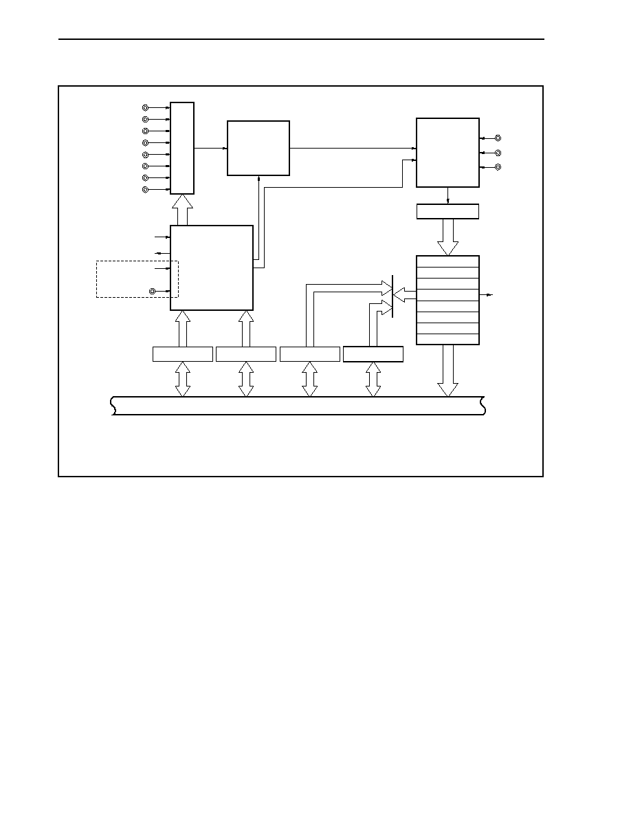
CHAPTER 13 A/D CONVERTER
644
User's Manual U14492EJ5V0UD
Figure 13-1. Block Diagram of A/D Converter 0 or 1
ADSCMn0 (16)
15
0
ADTRGn
INTADn
Sample and
hold circuit
ANIn0
ANIn1
ANIn2
ANIn3
ANIn4
ANIn5
ANIn6
ANIn7
ITRG0
16
16
16
16
ADSCMn1 (16)
15
0
ADETM0 (16)
15
0
ADETM1 (16)
15
0
9
0
Trigger source switching
circuit in timer trigger mode
(Figure 13-2)
Controller
10
10
SAR (10)
Comparator
and D/A
converter
AV
DD
AV
REFn
AV
SS
INTDETn
ADCRn0
ADCRn1
ADCRn2
ADCRn3
ADCRn4
ADCRn5
ADCRn6
ADCRn7
Internal bus
Input circuit
f
XX
/2
Remark n = 0, 1
f
XX
: Internal system clock
Cautions 1. Noise at an analog input pin (ANI0n, ANI1n) or reference voltage input pin (AV
REF0
, AV
REF1
) may
give rise to an invalid conversion result.
Software processing is needed in order to prevent this invalid conversion result from
adversely affecting the system.
The following are examples of software processing.
∑ Use the average value of the results of multiple A/D conversions as the A/D conversion
result.
∑ Perform A/D conversion multiple consecutive times and use conversion results with the
exception of any abnormal conversion results that are obtained.
∑ If an A/D conversion result from which it is judged that an abnormality occurred in the
system is obtained, do not perform abnormality processing at once but perform it upon
reconfirming the occurrence of an abnormality.
2. Be sure that voltages outside the range [AV
SS
to AV
REF0
, AV
SS
to AV
REF1
] are not applied to pins
being used as A/D converter 0 and 1 input pins.
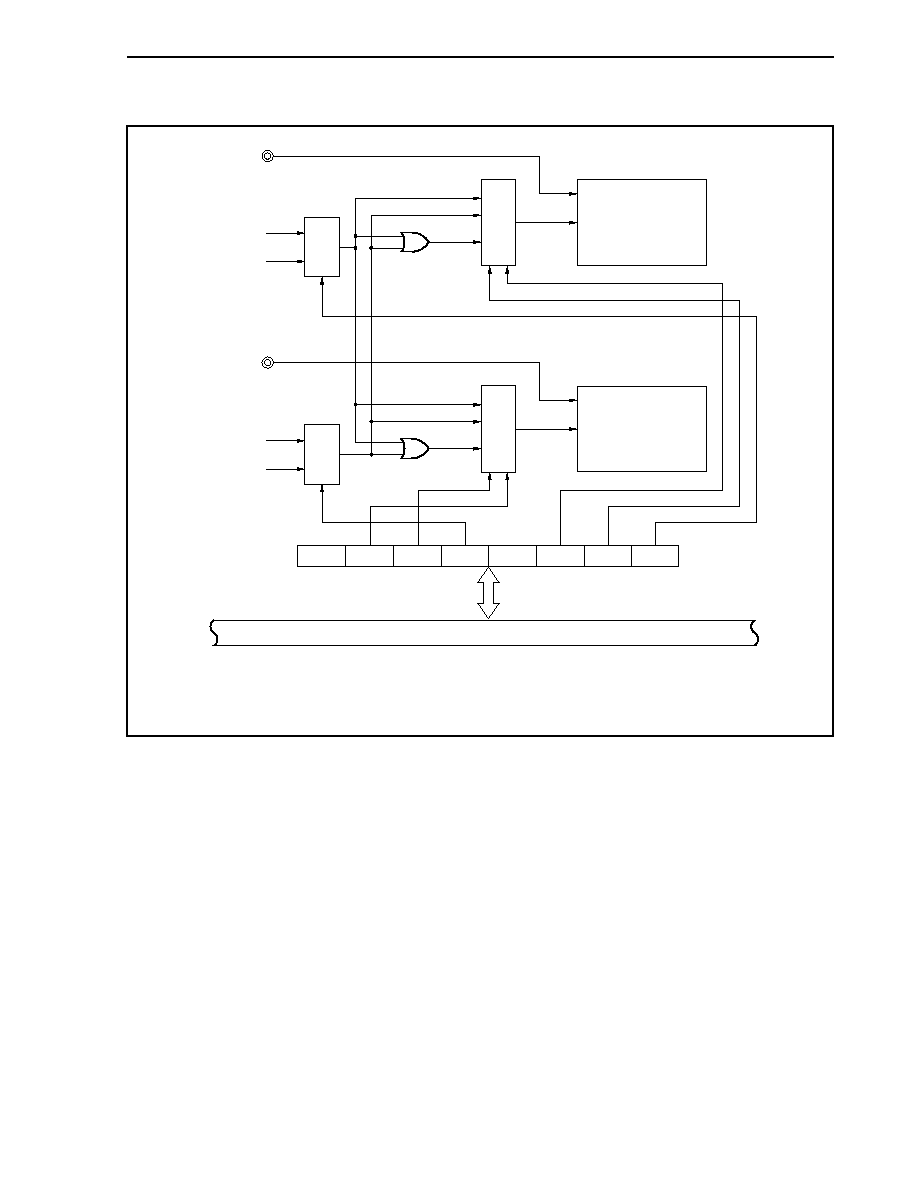
CHAPTER 13 A/D CONVERTER
645
User's Manual U14492EJ5V0UD
Figure 13-2. Block Diagram of Trigger Source Switching Circuit in Timer Trigger Mode
ITRG0
A/D converter 0
ADTRG0
INTCM003
INTCM013
ITRG0
A/D converter 1
ADTRG1
INTTM00
INTTM01
0
ITRG0
ITRG22 ITRG21 ITRG20
0
ITRG12 ITRG11 ITRG10
Internal bus
Selector
Selector
Selector
Selector
Caution For the selection of the trigger source in timer trigger mode, refer to 13.3 (5) A/D internal
trigger selection register (ITRG0).

CHAPTER 13 A/D CONVERTER
646
User's Manual U14492EJ5V0UD
13.3 Control Registers
(1) A/D scan mode registers 00 and 10 (ADSCM00, ADSCM10)
The ADSCMn0 registers are 16-bit registers that select analog input pins, specify operation modes, and
control conversion operation.
The ADSCMn0 register can be read/written in 16-bit units.
When the higher 8 bits of the ADSCMn0 register are used as the ADSCMn0H register, and the lower 8 bits
are used as the ADSCMn0L register, they can be read/written in 8-bit or 1-bit units.
However, writing to an ADSCMn0 register during A/D conversion operation initializes conversion operation
and starts the conversion over from the beginning. At this time, overwrite the ADSCMn0 register with the
same value. If writing a different value, be sure to clear the ADCEn bit to 0 first before overwriting.
Caution Before changing the trigger mode by using the ADPLMn and TRG2 to TRG0 bits, clear the
ADCEn bit to 0 (n = 0 or 1). The operation is not guaranteed if the trigger mode is changed
and the ADCEn bit is cleared at the same time (by the same instruction). Be sure to access
the register twice.
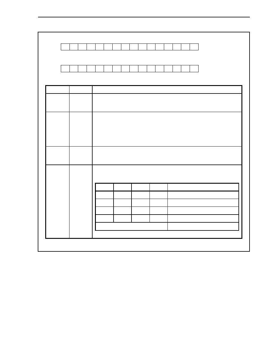
CHAPTER 13 A/D CONVERTER
647
User's Manual U14492EJ5V0UD
(1/2)
<14>
ADCS0
13
0
<12>
ADMS0
2
ANIS2
3
ANIS3
4
SANI0
5
SANI1
6
SANI2
7
SANI3
8
TRG0
9
TRG1
10
TRG2
<11>
ADPLM0
<15>
ADCE0
1
ANIS1
0
ANIS0
<14>
ADCS1
13
0
<12>
ADMS1
2
ANIS2
3
ANIS3
4
SANI0
5
SANI1
6
SANI2
7
SANI3
8
TRG0
9
TRG1
10
TRG2
<11>
ADPLM1
<15>
ADCE1
1
ANIS1
0
ANIS0
ADSCM00
Address
FFFFF200H
Initial value
0000H
ADSCM10
Address
FFFFF240H
Initial value
0000H
Bit position
Bit name
Function
15
ADCEn
Specifies enabling or disabling A/D conversion.
0:
Disable
1:
Enable
14
ADCSn
Shows status of A/D converter 0 or 1. This bit is read-only.
0:
Stopped
1:
Operating
The ADCSn bit is "0" for the duration of 6
◊ f
XX
/2 immediately after the start of A/D
conversion, and is then set to "1". In the scan mode, this operation is performed each time
the analog input pin to be A/D converted is switched.
12
ADMSn
Specifies operation mode of A/D converter 0 or 1.
0: Scan mode
1: Select mode
ADPLMn: Specifies polling mode.
TRG2 to TRG0: Specifies trigger mode.
ADPLMn
TRG2 TRG1 TRG0
Trigger
mode
0
0
0
0
A/D trigger mode
0
0
0
1
Timer trigger mode
0 1 1 1
External
trigger
mode
1
0
0
0
A/D trigger polling mode
Other than above
Setting prohibited
11 to 8
ADPLMn,
TRG2 to
TRG0
Remark n = 0, 1

CHAPTER 13 A/D CONVERTER
648
User's Manual U14492EJ5V0UD
(2/2)
Bit position
Bit name
Function
Specifies conversion start analog input pin in scan mode.
These bits are ignored in select mode.
SANI3
SANI2
SANI1
SANI0
Scan start analog input pin
0 0 0 0
ANIn0
0 0 0 1
ANIn1
0 0 1 0
ANIn2
0 0 1 1
ANIn3
0 1 0 0
ANIn4
0 1 0 1
ANIn5
0 1 1 0
ANIn6
0 1 1 1
ANIn7
Other than above
Setting prohibited
Caution Always set the conversion start analog input pin number that
is set by bits SANI3 to SANI0 to a smaller pin number than the
conversion termination analog input pin number that is set by
bits ANIS3 to ANIS0.
7 to 4
SANI3 to
SANI0
Specifies analog input pin in select mode.
In scan mode, specifies conversion termination analog input pin.
ANIS3
ANIS2
ANIS1
ANIS0
In select mode
In scan mode
0 0 0 0
ANIn0
ANIn0
0 0 0 1
ANIn1
SANI
ANIn1
0 0 1 0
ANIn2
SANI
ANIn2
0 0 1 1
ANIn3
SANI
ANIn3
0 1 0 0
ANIn4
SANI
ANIn4
0 1 0 1
ANIn5
SANI
ANIn5
0 1 1 0
ANIn6
SANI
ANIn6
0 1 1 1
ANIn7
SANI
ANIn7
Other than above
Setting prohibited
Remark SANI < ANInm
m = 1 to 7
3 to 0
ANIS3 to
ANIS0
Remark n = 0, 1
CHAPTER 13 A/D CONVERTER
649
User's Manual U14492EJ5V0UD
(2) A/D scan mode registers 01 and 11 (ADSCM01, ADSCM11)
The ADSCMn1 registers are 16-bit registers that set the conversion time of the A/D converter.
The ADSCMn1 register can be read/written in 16-bit units.
When the higher 8 bits of the ADSCMn1 register are used as the ADSCMn1H register, and the lower 8 bits
are used as the ADSCMn1L register, the ADSCMn1H register can be read/written in 8-bit or 1-bit units, and
the ADSCMn1L register is read-only, in 8-bit units.
Caution Do not write to the ADSCMn1 registers during A/D conversion operation. If a write is
performed, conversion operation is suspended and subsequently terminates.
14
0
13
0
12
0
2
0
3
0
4
0
5
0
6
0
7
0
8
FR0
9
FR1
10
FR2
11
0
15
0
1
0
0
0
14
0
13
0
12
0
2
0
3
0
4
0
5
0
6
0
7
0
8
FR0
9
FR1
10
FR2
11
0
15
0
1
0
0
0
ADSCM01
Address
FFFFF202H
Initial value
0000H
ADSCM11
Address
FFFFF242H
Initial value
0000H
Bit position
Bit name
Function
Specifies conversion time.
Conversion
time
(
µ
s)
Note
FR2 FR1 FR0 Conversion
Clocks
f
XX
= 50 MHz
f
XX
= 40 MHz f
XX
= 33 MHz
0 0 0
344
6.88
8.60
-
0 0 1
248
-
6.20 7.51
0 1 0
176
-
-
5.33
0 1 1
128
-
-
-
1 0 0
104
-
-
-
1 0 1
80
-
-
-
1 1 0
56
-
-
-
1 1 1
Setting
prohibited
-
-
-
10 to 8
FR2 to
FR0
Note This is the time from sampling until conversion termination.
Sampling time = (Conversion clocks
- 8)/6 ◊ f
XX
Caution Be sure to secure the conversion time within a range of 5 to 10
µ
s.
Conversion time = f
XX
◊ Conversion clocks
Remark f
XX
: Internal system clock
CHAPTER 13 A/D CONVERTER
650
User's Manual U14492EJ5V0UD
(3) A/D voltage detection mode registers 0 and 1 (ADETM0, ADETM1)
The ADETMn registers are 16-bit registers that set voltage detection mode. In voltage detection mode, the
analog input pin for which voltage detection is being performed and a reference voltage value are compared
and an interrupt is set in response to the comparison result.
The ADETMn register can be read/written in 16-bit units.
When the higher 8 bits of the ADETMn register are used as the ADETMnH register, and the lower 8 bits are
used as the ADETMnL register, they can be read/written in 8-bit or 1-bit units.
Caution Do not write to an ADETMn register during A/D conversion operation. If a write is
performed, conversion is suspended and it subsequently terminates.
Address
FFFFF204H
Initial value
0000H
<14>
ADET
LH0
13
DET
ANI3
12
DET
ANI2
2
DET
CMP2
3
DET
CMP3
4
DET
CMP4
5
DET
CMP5
6
DET
CMP6
7
DET
CMP7
8
DET
CMP8
9
DET
CMP9
10
DET
ANI0
11
DET
ANI1
<15>
ADET
EN0
1
DET
CMP1
0
DET
CMP0
ADETM0
Address
FFFFF244H
Initial value
0000H
<14>
ADET
LH1
13
DET
ANI3
12
DET
ANI2
2
DET
CMP2
3
DET
CMP3
4
DET
CMP4
5
DET
CMP5
6
DET
CMP6
7
DET
CMP7
8
DET
CMP8
9
DET
CMP9
10
DET
ANI0
11
DET
ANI1
<15>
ADET
EN1
1
DET
CMP1
0
DET
CMP0
ADETM1
Bit position
Bit name
Function
15
ADETENn
Specifies voltage detection mode.
0: Operate in normal mode
1: Operate in voltage detection mode
14
ADETLHn
Sets voltage comparison detection.
0: Generate INTDETn interrupt if reference voltage value > analog input pin voltage.
1: Generate INTDETn interrupt if reference voltage value
analog input pin voltage.
Selects analog input pin to compare to reference voltage value set by DETCMP9 to
DETCMP0 when in voltage detection mode.
DETANI3 DETANI2
DETANI1
DETANI0
Voltage detection analog input pin
0 0 0 0
ANIn0
0 0 0 1
ANIn1
0 0 1 0
ANIn2
0 0 1 1
ANIn3
0 1 0 0
ANIn4
0 1 0 1
ANIn5
0 1 1 0
ANIn6
0 1 1 1
ANIn7
1
◊
◊
◊
Setting prohibited
13 to 10
DETANI3
to
DETANI0
Remark
◊: Arbitrary
9 to 0
DETCMP9
to
DETCMP0
Sets reference voltage value to compare with analog input pin selected in DETANI3 to
DETANI0.
Remark n = 0, 1
CHAPTER 13 A/D CONVERTER
651
User's Manual U14492EJ5V0UD
(4) A/D conversion result registers 00 to 07 and 10 to 17 (ADCR00 to ADCR07, ADCR10 to ADCR17)
The ADCR0n and ADCR1n registers are 10-bit registers that hold the results of A/D conversions (n = 0 to 7).
One A/D converter is equipped with eight 10-bit registers for 8 channels, and A/D converters 0 and 1 together
have sixteen 10-bit registers.
These registers are read-only, in 16-bit units.
When reading 10 bits of data of an A/D conversion result from an ADCR0n or ADCR1n register, only the
lower 10 bits are valid and the higher 6 bits are always read as 0.
14
0
13
0
12
0
2
ADCRn2
3
ADCRn3
4
ADCRn4
5
ADCRn5
6
ADCRn6
7
ADCRn7
8
ADCRn8
9
ADCRn9
10
0
11
0
15
0
1
ADCRn1
0
ADCRn0
ADCR0n
Address
See Table 13-1
Initial value
0000H
ADCR1n
Address
See Table 13-2
Initial value
0000H
14
0
13
0
12
0
2
ADCRn2
3
ADCRn3
4
ADCRn4
5
ADCRn5
6
ADCRn6
7
ADCRn7
8
ADCRn8
9
ADCRn9
10
0
11
0
15
0
1
ADCRn1
0
ADCRn0
Table 13-1. Correspondence Between ADCR0n (n = 0 to 7) Register Names and Addresses
Register Name
Address
ADCR00 FFFFF210H
ADCR01 FFFFF212H
ADCR02 FFFFF214H
ADCR03 FFFFF216H
ADCR04 FFFFF218H
ADCR05 FFFFF21AH
ADCR06 FFFFF21CH
ADCR07 FFFFF21EH
Table 13-2. Correspondence Between ADCR1n (n = 0 to 7) Register Names and Addresses
Register Name
Address
ADCR10 FFFFF250H
ADCR11 FFFFF252H
ADCR12 FFFFF254H
ADCR13 FFFFF256H
ADCR14 FFFFF258H
ADCR15 FFFFF25AH
ADCR16 FFFFF25CH
ADCR17 FFFFF25EH

CHAPTER 13 A/D CONVERTER
652
User's Manual U14492EJ5V0UD
The correspondence between each analog input pin and the ADCR0n and ADCR1n registers is shown below.
Table 13-3. Correspondence Between Each Analog Input Pin and ADCR0n and ADCR1n Registers
A/D Converter
Analog Input Pin
A/D Conversion Result Register
ANI00 ADCR00
ANI01 ADCR01
ANI02 ADCR02
ANI03 ADCR03
ANI04 ADCR04
ANI05 ADCR05
ANI06 ADCR06
A/D converter 0
ANI07 ADCR07
ANI10 ADCR10
ANI11 ADCR11
ANI12 ADCR12
ANI13 ADCR13
ANI14 ADCR14
ANI15 ADCR15
ANI16 ADCR16
A/D converter 1
ANI17 ADCR17
CHAPTER 13 A/D CONVERTER
653
User's Manual U14492EJ5V0UD
The relationship between the analog voltage input to an analog input pin (ANI0n or ANI1n) and the value of the A/D
conversion result register (ADCR0n or ADCR1n) is as follows (n = 0 to 7):
V
IN
ADCR = INT ( ◊ 1,024 + 0.5)
AV
REF
Or,
AV
REF
AV
REF
(ADCR
- 0.5) ◊ V
IN
< (ADCR + 0.5) ◊
1,024
1,024
INT ( ): Function that returns integer of value in ( )
V
IN
:
Analog input voltage
AV
REF
: AV
REF0
or AV
REF1
pin voltage
ADCR: Value of A/D conversion result register (ADCR0n or ADCR1n)
Figure 13-3 illustrates the relationship between the analog input voltages and A/D conversion results.
Figure 13-3. Relationship Between Analog Input Voltages and A/D Conversion Results
1023
1022
1021
3
2
1
0
Input voltage/AV
REFm
1
2048
1
1024
3
2048
2
1024
5
2048
3
1024
2043
2048
1022
1024
2045
2048
1023
1024
2047
2048
1
A/D conversion result
(ADCRn)
Remark m = 0, 1
n = 00 to 07, 10 to 17

CHAPTER 13 A/D CONVERTER
654
User's Manual U14492EJ5V0UD
(5) A/D internal trigger selection register (ITRG0)
The ITRG0 register is the register that switches the trigger source in timer trigger mode. The timer trigger
source of A/D converters 0 and 1 can be set using the ITRG0 register.
This register can be read/written in 8-bit or 1-bit units.
7
0
ITRG0
6
ITRG22
5
ITRG21
4
ITRG20
3
0
2
ITRG12
1
ITRG11
0
ITRG10
Address
FFFFF280H
Initial value
00H
Bit position
Bit name
Function
Sets timer trigger source of A/D converter 1.
ITRG22 ITRG21 ITRG20 ITRG10
Trigger
Source
0 0
◊
0 Select
INTCM003
0 0
◊
1 Select
INTCM013
0 1 0
◊
Select INTTM00
0 1 1
◊
Select INTTM01
1
◊
0
0
Select INTCM003 and INTTM00
1
◊
0
1
Select INTCM013 and INTTM00
1
◊
1
0
Select INTCM003 and INTTM01
1
◊
1
1
Select INTCM013 and INTTM01
6 to 4
ITRG22 to
ITRG20
Remark
◊: Arbitrary
Specifies timer trigger source of A/D converter 0.
ITRG12 ITRG11 ITRG20 ITRG10
Trigger
Source
0 0
◊
0 Select
INTCM003
0 0
◊
1 Select
INTCM013
0 1 0
◊
Select INTTM00
0 1 1
◊
Select INTTM01
1
◊
0
0
Select INTCM003 and INTTM00
1
◊
0
1
Select INTCM013 and INTTM00
1
◊
1
0
Select INTCM003 and INTTM01
1
◊
1
1
Select INTCM013 and INTTM01
2 to 0
ITRG12 to
ITRG10
Remark
◊: Arbitrary
CHAPTER 13 A/D CONVERTER
655
User's Manual U14492EJ5V0UD
13.4 Interrupt Requests
A/D converters 0 and 1 generate two kinds of interrupts.
∑ A/D conversion termination interrupts (INTAD0, INTAD1)
∑ Voltage detection interrupts (INTDET0, INTDET1)
(1) A/D conversion termination interrupts (INTAD0, INTAD1)
In A/D conversion enabled status, an A/D conversion termination interrupt is generated when a specified
number of A/D conversions have terminated.
A/D Converter
A/D Conversion Termination Interrupt Signal
0 Generate
INTAD0
1 Generate
INTAD1
(2) Voltage detection interrupts (INTDET0, INTDET1)
In voltage detection mode (ADETEN0 or ADETEN1 bit of ADETM0 or ADETM1 = 1), the value of the
ADCR0n or ADCR1n register of the relevant analog input pin is compared to the reference voltage set in the
DETCMP9 to DETCMP0 bits of the ADETM0 or ADETM1 register and a voltage detection interrupt is
generated in response to the value of the ADETLH0 or ADETLH1 bit of the ADETM0 or ADETM1 register (n
= 0 to 7).
A/D Converter
Voltage Detection Interrupt Signal
0 Generate
INTDET0
1 Generate
INTDET1

CHAPTER 13 A/D CONVERTER
656
User's Manual U14492EJ5V0UD
13.5 A/D Converter Operation
13.5.1 A/D converter basic operation
A/D conversion is performed using the following procedure.
(1) Set the analog input selection and the operation mode and trigger mode specifications using the ADSCM00
or ADSCM10 register
Note 1
. Setting (1) the ADCE0 or ADCE1 bit of the ADSCM00 or ADSCM10 register when
in A/D trigger mode or A/D trigger polling mode starts A/D conversion. In timer trigger mode or external
trigger mode, the status becomes trigger standby
Note 2
.
(2) When A/D conversion starts, compare the analog input to the voltage generated by the D/A converter.
(3) When 10-bit comparison terminates, store the conversion result in the ADCR0n or ADCR1n register. When
the specified number of A/D conversions have terminated, generate an A/D conversion termination interrupt
(INTAD0, INTAD1) (n = 0 to 7).
Notes 1. If the ADSCM00 or ADSCM10 register is overwritten with the same value during A/D conversion, the
A/D conversion operation preceding the overwrite stops and the conversion result is not stored in the
ADCR0n or ADCR1n register. The conversion operation is initialized and conversion starts from the
beginning.
2. In timer trigger mode or external trigger mode, there is a transition to trigger standby status when the
ADCE0 or ADCE1 bit of the ADSCM00 or ADSCM10 register is set to 1. A/D conversion operation is
activated by a trigger signal and there is a return to trigger standby status when A/D conversion
operation terminates.
The timer trigger is selected by the ITRG0 register.

CHAPTER 13 A/D CONVERTER
657
User's Manual U14492EJ5V0UD
13.5.2 Operation modes and trigger modes
Diverse conversion operations can be specified for A/D converters 0 and 1 by specifying operation modes and
trigger modes. Operation modes and trigger modes are set using the ADSCM00 or ADSCM10 register.
The relationship between operation modes and trigger modes is shown below.
Setting
Trigger Mode
Operation Mode
ADSCM00 ADSCM10
Select XX010000XXXXXXXXB
XX010000XXXXXXXXB
AD trigger
Scan XX000000XXXXXXXXB
XX000000XXXXXXXXB
Select XX011000XXXXXXXXB
XX011000XXXXXXXXB
AD trigger polling
Scan XX001000XXXXXXXXB
XX001000XXXXXXXXB
Select XX010001XXXXXXXXB
XX010001XXXXXXXXB
Timer trigger
Scan XX000001XXXXXXXXB
XX000001XXXXXXXXB
Select XX010111XXXXXXXXB
XX010111XXXXXXXXB
External trigger
Scan XX000111XXXXXXXXB
XX000111XXXXXXXXB
(1) Trigger modes
The four trigger modes that serve as the start timing of A/D conversion processing are available: A/D trigger
mode, A/D trigger polling mode, timer trigger mode, and external trigger mode.
These trigger modes are set using the ADSCM00 and ADSCM10 registers.
(a) A/D trigger mode
A/D trigger mode, which starts the conversion timing of the analog input set for the ANI0n or ANI1n pin (n
= 0 to 7), is a mode that starts A/D conversion by setting the ADCE0 or ADCE1 bit of the ADSCM00 or
ADSCM10 register to 1. In this mode, it is necessary to set the ADCE0 or ADCE1 bit to 1 as an A/D
conversion restart operation after an INTAD0 or INTAD1 interrupt (ADCS0 or ADCS1 = 0).
(b) A/D trigger polling mode
A/D trigger polling mode, which starts the conversion timing of the analog input set for the ANI0n or
ANI1n pin (n = 0 to 7), is a mode that starts A/D conversion by setting the ADCE0 or ADCE1 bit of the
ADSCM00 or ADSCM10 register to 1. In this mode, it is not necessary to set the ADCE0 or ADCE1 bit to
1 as an A/D conversion restart operation after an INTAD0 or INTAD1 interrupt (ADCS0 or ADCS1 = 1).
The specified analog input is converted serially until the ADCE0 or ADCE1 bit is set to 0. An INTAD0 or
INTAD1 interrupt occurs each time a conversion terminates.
(c) Timer trigger mode
Timer trigger mode, which starts the conversion timing of the analog input set for the ANI0n or ANI1n pin
(n = 0 to 7), is a mode governed by a trigger specified in the A/D internal trigger selection register 0
(ITRG0).
(d) External trigger mode
External trigger mode, which starts the conversion timing of the analog input set for the ANI0n or ANI1n
pin, is a mode specified using the ADTRG0 or ADTRG1 pin.

CHAPTER 13 A/D CONVERTER
658
User's Manual U14492EJ5V0UD
(2) Operation modes
The two operation modes, which are the modes that set the ANI00 to ANI07 and ANI10 to ANI17 pins, are
select mode and scan mode. These modes are set using the ADSCM00 and ADSCM10 registers.
(a) Select mode
Select mode A/D converts one analog input specified in the ADSCM00 or ADSCM10 register. It stores
the conversion result in the ADCR0n or ADCR1n register corresponding to the analog input (ANI1n or
ANI0n) (n = 0 to 7).
Figure 13-4. Example of Select Mode Operation Timing (ANI01): For A/D Converter 0
ANI01 (input)
A/D conversion
Data 1
(ANI01)
Data 2
(ANI01)
Data 3
(ANI01)
Data 4
(ANI01)
Data 5
(ANI01)
Data 6
(ANI01)
Data 7
(ANI01)
Data 1
Data 2
Data 3
Data 4
Data 5
Data 6
Data 7
Data 1
(ANI01)
Data 2
(ANI01)
Data 3
(ANI01)
Data 4
(ANI01)
Data 6
(ANI01)
ADCR01 register
INTAD0 interrupt
Conversion start
(ADSCM0
register setting)
ADCE0
bit set
ADCE0
bit set
ADCE0
bit set
ADCE0
bit set
ADCE0
bit set
Conversion start
(ADSCM0
register setting)
ANI00
ANI01
ANI02
ANI03
ANI04
ANI05
ANI06
ANI07
ADCR00
ADCR01
ADCR02
ADCR03
ADCR04
ADCR05
ADCR06
ADCR07
AD converter 0
ADCR0n register
Analog input
CHAPTER 13 A/D CONVERTER
659
User's Manual U14492EJ5V0UD
(b) Scan mode
Scan mode sequentially selects and A/D converts pins from the A/D conversion start analog input pin
through the A/D conversion termination analog input pin specified in the ADSCM00 or ADSCM10
register. It stores the A/D conversion result in the ADCR0n or ADCR1n register corresponding to the
analog input (n = 0 to 7). When the specified analog input conversion terminates, there is an A/D
conversion termination interrupt (INTAD0 or INTAD1).
Figure 13-5. Example of Scan Mode Operation Timing: For A/D Converter 0
(4-Channel Scan (ANI00 to ANI03))
ANI00 (input)
ANI01 (input)
ANI02 (input)
ANI03 (input)
A/D conversion
Data 1
(ANI00)
Data 2
(ANI01)
Data 3
(ANI02)
Data 4
(ANI03)
Data 5
(ANI00)
Data 6
(ANI01)
Data 1
Data 2
Data 3
Data 4
Data 5
Data 6
Data 1
(ANI00)
ADCR00
Data 2
(ANI01)
ADCR01
Data 3
(ANI02)
ADCR02
Data 4
(ANI03)
ADCR03
Data 5
(ANI00)
ADCR00
ADCR0n register
INTAD0 interrupt
Conversion start
(ADSCM00 register setting)
Conversion start
(ADSCM00 register setting)
ANI00
ANI01
ANI02
ANI03
ANI04
ANI05
ANI06
ANI07
ADCR00
ADCR01
ADCR02
ADCR03
ADCR04
ADCR05
ADCR06
ADCR07
A/D converter 0
ADCR0n register
Analog input
CHAPTER 13 A/D CONVERTER
660
User's Manual U14492EJ5V0UD
13.6 Operation in A/D Trigger Mode
Setting the ADCE0 or ADCE1 bit of the ADSCM00 or ADSCM10 register to 1 starts A/D conversion.
13.6.1 Operation in select mode
One analog input specified in the ADSCM00 or ADSCM10 register is A/D converted at a time and the result is
stored in an ADCR0n or ADCR1n register. Analog inputs correspond one-to-one with ADCR0n or ADCR1n registers
(n = 0 to 7).
An A/D conversion termination interrupt (INTAD0, INTAD1) is generated for each A/D conversion termination,
which terminates A/D conversion (ADCS0 or ADCS1 bit = 0).
Analog Input
A/D Conversion Result Register
ANIx ADCRx
Remark x = 00 to 07, 10 to 17
To restart A/D conversion, write 1 in the ADCE0 or ADCE1 bit of the ADSCM00 or ADSCM10 register.
This is optimal for an application that reads a result for each A/D conversion.
Figure 13-6. Example of Select Mode (A/D Trigger Select) Operation (ANI02): For A/D Converter 0
ANI00
ANI01
ANI02
ANI03
ANI04
ANI05
ANI06
ANI07
ADCR00
ADCR01
ADCR02
ADCR03
ADCR04
ADCR05
ADCR06
ADCR07
A/D converter 0
ADSCM00
(1) ADCE0 bit of ADSCM00 = 1 (Enabled)
(2) A/D conversion of ANI02
(3) Store conversion result in ADCR02
(4) Generate INTAD0 interrupt
CHAPTER 13 A/D CONVERTER
661
User's Manual U14492EJ5V0UD
13.6.2 Operation in scan mode
Pins from the conversion start analog input pin through the conversion termination analog input pin specified in the
ADSCM00 or ADSCM10 register are sequentially selected and A/D converted. An A/D conversion result is stored in
the ADCR0n or ADCR1n register corresponding to the analog input (n = 0 to 7). When conversion terminates for all
analog inputs through the conversion termination analog input pin, an A/D conversion termination interrupt (INTAD0,
INTAD1) is generated, which terminates A/D conversion (ADCS0 or ADCS1 bit of ADSCM0 or ADSCM1 register = 0).
Analog Input
A/D Conversion Result Register
ANIx
Note 1
ADCRx
|
|
ANIx
Note 2
ADCRx
Notes 1. Set using SANI3 to SANI0 bits of ADSCM00 or ADSCM10 register.
Be sure to set a pin number that is smaller than the conversion termination analog input pin number
set according to Note 2.
2. Set using ANIS3 to ANIS0 bits of ADSCM00 or ADSCM10 register.
Remark x = 00 to 07, 10 to 17
To restart A/D conversion, write 1 in the ADCE0 or ADCE1 bit of the ADSCM00 or ADSCM10 register. This is
optimal for an application that regularly monitors multiple analog inputs.
Figure 13-7. Example of Scan Mode (A/D Trigger Scan) Operation (ANI02 to ANI05): For A/D Converter 0
ANI00
ANI01
ANI02
ANI03
ANI04
ANI05
ANI06
ANI07
ADCR00
ADCR01
ADCR02
ADCR03
ADCR04
ADCR05
ADCR06
ADCR07
A/D converter 0
ADSCM00
(1) ADCE0 bit of ADSCM00 = 1 (Enabled)
(2) A/D conversion of ANI02
(3) Store conversion result in ADCR02
(4) A/D conversion of ANI03
(5) Store conversion result in ADCR03
(6) A/D conversion of ANI04
(7) Store conversion result in ADCR04
(8) A/D conversion of ANI05
(9) Store conversion result in ADCR05
(10) Generate INTAD0 interrupt
CHAPTER 13 A/D CONVERTER
662
User's Manual U14492EJ5V0UD
13.7 Operation in A/D Trigger Polling Mode
Setting the ADCE0 or ADCE1 bit of the ADSCM00 or ADSCM10 register to 1 starts A/D conversion.
Both select mode and scan mode are available in A/D trigger polling mode. Since the ADCS0 or ADCS1 bit of the
ADSCM00 or ADSCM10 register remains 1 after an INTAD0 or INTAD1 interrupt in this mode, it is not necessary to
write 1 in the ADCE0 or ADCE1 bit as an A/D conversion restart operation.
13.7.1 Operation in select mode
The analog input specified in the ADSCM00 or ADSCM10 register is A/D converted. The conversion result is
stored in the ADCR0n or ADCR1n register (n = 0 to 7).
One analog input is A/D converted at a time and the result is stored in one ADCR0n or ADCR1n register. Analog
inputs correspond one-to-one with ADCR0n or ADCR1n register.
An A/D conversion termination interrupt (INTAD0 or INTAD1) is generated for each A/D conversion termination.
A/D conversion operation is repeated until the ADCE0 or ADCE1 bit = 0 (ADCS0 or ADCS1 bit = 1).
Analog Input
A/D Conversion Result Register
ANIx ADCRx
Remark x = 00 to 07, 10 to 17
In A/D trigger polling mode, it is not necessary to write 1 in the ADCE0 or ADCE1 bit of the ADSCM00 or
ADSCM10 register as an A/D conversion restart operation
Note
.
This is optimal for applications that regularly read A/D conversion values.
Note In A/D trigger polling mode, the fact that the ADCE0 or ADCE1 bit of the ADSCM00 or ADSCM10 register
is 0 means that A/D conversion operation does not stop as long as the ADCS0 or ADCS1 bit is not 0.
Therefore, if the ADCR0n or ADCR1n register is not read before the next A/D conversion, it is overwritten.
Figure 13-8. Example of Select Mode (A/D Trigger Polling Select) Operation (ANI02): For A/D Converter 0
ANI00
ANI01
ANI02
ANI03
ANI04
ANI05
ANI06
ANI07
ADCR00
ADCR01
ADCR02
ADCR03
ADCR04
ADCR05
ADCR06
ADCR07
A/D converter 0
ADSCM00
(1) ADCE0 bit of ADSCM00 = 1 (Enabled)
(2) A/D conversion of ANI02
(3) Store conversion result in ADCR02
(4) Generate INTAD0 interrupt
(5) Return to (2)

CHAPTER 13 A/D CONVERTER
663
User's Manual U14492EJ5V0UD
13.7.2 Operation in scan mode
Pins from the conversion start analog input pin through the conversion termination analog input pin specified in the
ADSCM00 or ADSCM10 register are sequentially selected and A/D converted. An A/D conversion result is stored in
the ADCR0n or ADCR1n register corresponding to the analog input (n = 0 to 7). When conversion terminates for all
analog inputs through the conversion termination analog input pin, an A/D conversion termination interrupt (INTAD0,
INTAD1) is generated. A/D conversion operation repeats until the ADCE0 or ADCE1 bit = 0 (ADCS0 or ADCS1 bit =
1).
Analog Input
A/D Conversion Result Register
ANIx
Note 1
ADCRx
|
|
ANIx
Note 2
ADCRx
Notes 1. Set using SANI3 to SANI0 bits of ADSCM00 or ADSCM10 register.
Be sure to set a pin number that is smaller than the conversion termination analog input pin number
set according to Note 2.
2. Set using ANIS3 to ANIS0 bits of ADSCM00 or ADSCM10 register.
Remark x = 00 to 07, 10 to 17
It is not necessary to write 1 in the ADCE0 or ADCE1 bit of the ADSCM00 or ADSCM10 register as an A/D
conversion restart operation in A/D trigger polling mode
Note
.
This is optimal for applications that regularly read A/D conversion values.
Note In A/D trigger polling mode, the fact that the ADCE0 or ADCE1 bit of the ADSCM00 or ADSCM10 register
is 0 means that A/D conversion operation does not stop as long as the ADCS0 or ADCS1 bit is not 0.
Therefore, if the ADCR0n or ADCR1n register is not read before the next A/D conversion, it is overwritten.
Figure 13-9. Example of Scan Mode (A/D Trigger Polling Scan) Operation (ANI02 to ANI05)
: For A/D Converter 0
ANI00
ANI01
ANI02
ANI03
ANI04
ANI05
ANI06
ANI07
ADCR00
ADCR01
ADCR02
ADCR03
ADCR04
ADCR05
ADCR06
ADCR07
A/D converter 0
ADSCM00
(1) ADCE0 bit of ADSCM00 = 1 (Enabled)
(2) A/D conversion of ANI02
(3) Store conversion result in ADCR02
(4) A/D conversion of ANI03
(5) Store conversion result in ADCR03
(6) A/D conversion of ANI04
(7) Store conversion result in ADCR04
(8) A/D conversion of ANI05
(9) Store conversion result in ADCR05
(10) Generate INTAD0 interrupt
(11) Return to (2)
CHAPTER 13 A/D CONVERTER
664
User's Manual U14492EJ5V0UD
13.8 Operation in Timer Trigger Mode
The A/D converter can set an interrupt signal specified by the A/D internal trigger selection register 0 (ITRG0) as a
conversion trigger for up to 8 channels (a total of 16 channels in 2 circuits) of analog input (ANI00 to ANI07, ANI10 to
ANI17).
The four interrupt signals that can be selected as triggers are the TM0n timer 0 register underflow interrupt signals
(INTTM00 and INTTM01) and the CM003 and CM013 match interrupt signals (INTCM003 and INTCM013) (n = 0, 1).
13.8.1 Operation in select mode
Taking the interrupt signal specified by the A/D internal trigger selection register 0 (ITRG0) as a trigger, one analog
input (ANI00 to ANI07, ANI10 to ANI17) specified by the ADSCM00 or ADSCM10 register is A/D converted once. The
conversion result is stored in the ADCR0n or ADCR1n register corresponding to the analog input (n = 0 to 7). An A/D
conversion termination interrupt (INTAD0 or INTAD1) is generated for each A/D conversion, which terminates A/D
conversion (ADCS0 or ADCS1 = 0).
This is optimal for applications that read A/D conversion values synchronized to a timer trigger.
Trigger
Analog Input
A/D Conversion Result Register
Interrupt specified by ITRG0 register
ANIx
ADCRx
Remark x = 00 to 07, 10 to 17
After A/D conversion termination, A/D converter 0 or 1 changes to trigger wait status (ADCE0 or ADCE1 = 1). It
performs A/D conversion operation again when the interrupt signal specified in the ITRG0 register occurs.
Figure 13-10. Example of Timer Trigger Select Mode Operation (ANI04): For A/D Converter 0
(a) When selecting INTTM00 by ITRG0 register
ANI00
ANI01
ANI02
ANI03
ANI04
ANI05
ANI06
ANI07
ADCR00
ADCR01
ADCR02
ADCR03
ADCR04
ADCR05
ADCR06
ADCR07
A/D converter 0
INTTM00
(1) ADCE0 bit of ADSCM00 = 1 (Enabled)
(2) INTTM00 interrupt generation
(3) A/D conversion of ANI04
(4) Store conversion result in ADCR04
(5) INTAD0 interrupt generation
CHAPTER 13 A/D CONVERTER
665
User's Manual U14492EJ5V0UD
13.8.2 Operation in scan mode
Using the interrupt signal specified by the A/D internal trigger selection register 0 (ITRG0) as a trigger, the
conversion start analog input pin through the conversion termination analog input pin specified by the ADSCM00 or
ADSCM10 register are sequentially selected and A/D converted. Conversion results are stored in the ADCR0n or
ADCR1n registers corresponding to the analog inputs. When all of the specified A/D conversions terminate, an A/D
conversion termination interrupt (INTAD0 or INTAD1) is generated, which terminates A/D conversion (ADCS0 or
ADCS1 = 0).
This is optimal for applications that regularly monitor multiple analog inputs in synchronization with a timer trigger.
Trigger
Analog Input
A/D Conversion Result Register
ANIn0 ADCRn0
ANIn1 ADCRn1
ANIn2 ADCRn2
ANIn3 ADCRn3
ANIn4 ADCRn4
ANIn5 ADCRn5
ANIn6 ADCRn6
Interrupt specified by ITRG0 register
ANIn7 ADCRn7
Remark n = 0, 1
After all of the specified A/D conversions terminate, the A/D converter changes to trigger wait status (ADCE0 or
ADCE1 = 1). It performs A/D conversion operation again when the interrupt signal specified in the ITRG0 register
occurs.
Figure 13-11. Example of Timer Trigger Scan Mode Operation (For A/D Converter 0)
: INTTM00 Selected by ITRG0 Register
(a) Set to scan ANI01 to ANI04
ANI00
ANI01
ANI02
ANI03
ANI04
ANI05
ANI06
ANI07
ADCR00
ADCR01
ADCR02
ADCR03
ADCR04
ADCR05
ADCR06
ADCR07
A/D converter 0
INTM00
(1) ADCE0 bit of ADSCM00 = 1 (Enabled)
(2) INTTM00 interrupt generation
(3) A/D conversion of ANI01
(4) Store conversion result in ADCR01
(5) A/D conversion of ANI02
(6) Store conversion result in ADCR02
(7) A/D conversion of ANI03
(8) Store conversion result in ADCR03
(9) A/D conversion of ANI04
(10) Store conversion result in ADCR04
(11) INTAD0 interrupt generation

CHAPTER 13 A/D CONVERTER
666
User's Manual U14492EJ5V0UD
13.9 Operation in External Trigger Mode
In external trigger mode, analog input (ANI00 to ANI07, ANI10 to ANI17) is A/D converted on ADTRG0 or ADTRG1
pin input timing.
The valid edge of an external input signal in external trigger mode can be specified as a rising edge, a falling edge,
or a rising or falling edge in the ES21 or ES20 bit of the INTM1 register for A/D converter 0 and in the ES31 or ES30
bit of the INTM1 register for A/D converter 1.
13.9.1 Operation in select mode
One analog input (ANI00 to ANI07, ANI10 to ANI17) specified by the ADSCM00 or ADSCM10 register is A/D
converted. The conversion result is stored in the ADCR0n or ADCR1n register (n = 0 to 7).
Using an ADTRG0 or ADTRG1 signal as a trigger, one analog input at a time is A/D converted and the result is
stored in one ADCR0n or ADCR1n register. Analog inputs correspond one-to-one with A/D conversion result
registers. For each A/D conversion, an A/D conversion termination interrupt (INTAD0 or INTAD1) is generated, which
terminates A/D conversion (ADCS0 or ADCS1 bit = 0).
Trigger
Analog Input
A/D Conversion Result Register
ADTRGm signal
ANImn
ADCRmn
Remark m = 0, 1
n = 0 to 7
To restart A/D conversion, a trigger must be input again from the ADTRGn pin (n = 0, 1).
This is optimal for applications that read results each time there is an A/D conversion in synchronization with an
external trigger.
Figure 13-12. Example of Select Mode (External Trigger Select) Operation (ANI02): For A/D Converter 0
ANI00
ANI01
ANI02
ANI03
ANI04
ANI05
ANI06
ANI07
ADCR00
ADCR01
ADCR02
ADCR03
ADCR04
ADCR05
ADCR06
ADCR07
A/D converter 0
ADTRG0
(1) ADCE0 bit of ADSCM00 = 1 (Enabled)
(2) External trigger generation
(3) A/D conversion of ANI02
(4) Store conversion result in ADCR02
(5) INTAD0 interrupt generation
CHAPTER 13 A/D CONVERTER
667
User's Manual U14492EJ5V0UD
13.9.2 Operation in scan mode
Using an ADTRG0 or ADTRG1 signal as a trigger, pins from the conversion start analog input pin through the
conversion termination analog input pin specified by the ADSCM00 or ADSCM10 register are sequentially selected
and A/D converted. A/D conversion results are stored in the ADCR0n or ADCRN1n registers corresponding to the
analog inputs (n = 0 to 7). When conversion terminates for all of the specified analog inputs, an INTAD0 or INTAD1
interrupt is generated, which terminates A/D conversion (ADCS0 or ADCS1 = 0).
Trigger
Analog Input
A/D Conversion Result Register
ANIn0 ADCRn0
ANIn1 ADCRn1
ANIn2 ADCRn2
ANIn3 ADCRn3
ANIn4 ADCRn4
ANIn5 ADCRn5
ANIn6 ADCRn6
ADTRGn signal
ANIn7 ADCRn7
Remark n = 0, 1
After all specified A/D conversions terminate, A/D conversion is restarted when an external trigger signal occurs.
This is optimal for applications that regularly monitor multiple analog inputs in synchronization with an external
trigger.
Figure 13-13. Example of Scan Mode (External Trigger Scan) Operation: For A/D Converter 0
(a) When setting to scan ANI01 to ANI04
ANI00
ANI01
ANI02
ANI03
ANI04
ANI05
ANI06
ANI07
ADCR00
ADCR01
ADCR02
ADCR03
ADCR04
ADCR05
ADCR06
ADCR07
A/D converter 0
ADTRG0
(1) ADCE0 bit of ADSCM00 = 1 (Enabled)
(2) External trigger generation
(3) A/D conversion of ANI01
(4) Store conversion result in ADCR01
(5) A/D conversion of ANI02
(6) Store conversion result in ADCR02
(7) A/D conversion of ANI03
(8) Store conversion result in ADCR03
(9) A/D conversion of ANI04
(10) Store conversion result in ADCR04
(11) INTAD0 interrupt generation

CHAPTER 13 A/D CONVERTER
668
User's Manual U14492EJ5V0UD
13.10 Precautions on Operation
13.10.1 Stopping A/D conversion operation
If 0 is written in the ADCE0 or ADCE1 bit of the ADSCM00 or ADSCM10 register during A/D conversion operation,
it stops A/D conversion operation and an A/D conversion result is not stored in the ADCR0n or ADCR1n register (n =
0 to 7).
13.10.2 Trigger input during A/D conversion operation
If a trigger is input during A/D conversion operation, that trigger input is ignored.
13.10.3 External or timer trigger interval
Make the trigger interval (input time interval) in external or timer trigger mode longer than the conversion time
specified by the FR2 to FR0 bits of the ADSCM01 or ADSCM11 register.
(1) When interval = 0
If multiple triggers are input simultaneously, they are processed as one trigger signal.
(2) When 0 < interval < conversion time
If an external or timer trigger is input during A/D conversion operation, that trigger input is ignored.
(3) When interval = conversion time
If an external or timer trigger is input at the same time as A/D conversion termination (comparison termination
signal and trigger contention), interrupt generation and ADCR0n or ADCR1n register storage of the value with
which conversion terminated are performed correctly (n = 0 to 7).
13.10.4 Operation in standby modes
(1) HALT mode
A/D conversion operation is suspended. If released by NMI or maskable interrupt input, the ADSCM00,
ADSCM10, ADSCM01, or ADSCM11 register and ADCR0n or ADCR1n register maintain their values (n = 0
to 7).
If released by RESET input, the ADCR0n or ADCR1n register is initialized.
(2) IDLE mode, software STOP mode
Since clock supply to A/D converter 0 or 1 stops, A/D conversion operation is not performed.
If released by NMI or maskable interrupt input, the ADSCM00, ADSCM10, ADSCM01, or ADSCM11 register
and ADCR0n or ADCR1n register maintain their values (n = 0 to 7). However, if IDLE mode or software
STOP mode is set during A/D conversion operation, A/D conversion operation stops.
If released by RESET input, the ADCR0n or ADCR1n register is initialized.
CHAPTER 13 A/D CONVERTER
669
User's Manual U14492EJ5V0UD
13.10.5 Compare match interrupt in timer trigger mode
A TM0n timer 0 register underflow interrupt (INTTM00 or INTTM01) and CM003 or CM013 interrupt (INTCM003 or
INTCM013) is an A/D conversion start trigger that starts conversion operation (n = 0, 1). At this time, the CM003 or
CM013 match interrupt (INTCM003 or INTCM013) also functions as a compare register match interrupt for the CPU.
In order not to generate these match interrupts for the CPU, disable interrupts using the mask bits (TM0MK0,
TM0MK1, CM03MK0, CM03MK1) of the interrupt control registers (TM0IC0, TM0IC1, CM03IC0, CM03IC1).
13.10.6 Timing that makes the A/D conversion result undefined
If the timing of the end of A/D conversion and the timing of the stop of operation of the A/D converter conflict, the
A/D conversion value may be undefined. Because of this, be sure to read the A/D conversion result while the A/D
converter is in operation. Furthermore, when reading an A/D conversion result after the A/D converter operation has
stopped, be sure to have done so by the time the next conversion result is complete.
The conversion result read timing is shown in Figures 13-14 and 13-15 below.
Figure 13-14. Conversion Result Read Timing (When Conversion Result Is Undefined)
A/D conversion end
A/D conversion end
ADCRnm
INTADn
ADCEn
Normal conversion
result read
Normal conversion result
Undefined value
A/D operation
stopped
Undefined
value read
Remark n = 0, 1, m = 0 to 7
Figure 13-15. Conversion Result Read Timing (When Conversion Result Is Normal)
A/D conversion end
ADCRnm
INTADn
ADCEn
A/D operation stopped
Normal conversion
result read
Normal conversion result
Remark n = 0, 1, m = 0 to 7
CHAPTER 13 A/D CONVERTER
670
User's Manual U14492EJ5V0UD
13.11 How to Read A/D Converter Characteristics Table
Here, special terms unique to the A/D converter are explained.
(1) Resolution
This is the minimum analog input voltage that can be identified. That is, the percentage of the analog input
voltage per bit of digital output is called 1LSB (Least Significant Bit). The percentage of 1LSB with respect to
the full scale is expressed by %FSR (Full Scale Range). %FSR indicates the ratio of analog input voltage that
can be converted as a percentage, and is always represented by the following formula regardless of the
resolution.
1%FSR = (Max. value of analog input voltage that can be converted
- Min. value of analog input voltage that
can be converted)/100
=
(AV
REFn
≠ 0)/100
=
AV
REFn
/100
Remark n = 0, 1
1LSB is as follows when the resolution is 10 bits.
1LSB = 1/2
10
= 1/1024
= 0.098 %FSR
Accuracy has no relation to resolution, but is determined by overall error.
(2) Overall error
This shows the maximum error value between the actual measured value and the theoretical value.
It is a total of zero-scale error, full-scale error, linearity error, and a combination of these errors.
Note that the quantization error is not included in the overall error in the characteristics table.
Figure 13-16. Overall Error
Ideal line
0......0
1......1
Digital output
Overall
error
Analog input
AV
REFn
(n = 0, 1)
0
CHAPTER 13 A/D CONVERTER
671
User's Manual U14492EJ5V0UD
(3) Quantization error
When analog values are converted to digital values, a ±1/2LSB error naturally occurs. In an A/D converter, an
analog input voltage in a range of ±1/2LSB is converted to the same digital code, so a quantization error
cannot be avoided.
Note that the quantization error is not included in the overall error, zero-scale error, full-scale error, integral
linearity error, and differential linearity error in the characteristics table.
Figure 13-17. Quantization Error
0......0
1......1
Digital output
Quantization error
1/2LSB
1/2LSB
Analog input
0
AV
REFn
(n = 0, 1)
(4) Zero-scale error
This shows the difference between the actual measurement value of the analog input voltage and the
theoretical value (1/2LSB) when the digital output changes from 0......000 to 0......001.
Figure 13-18. Zero-Scale Error
111
011
010
001
Zero-scale error
Ideal line
000
0
1
2
3
AV
REFn
(n = 0, 1)
Digital output (Lo
w
er 3 bits)
Analog input (LSB)
≠1
100
CHAPTER 13 A/D CONVERTER
672
User's Manual U14492EJ5V0UD
(5) Full-scale error
This shows the difference between the actual measurement value of the analog input voltage and the
theoretical value (full scale
- 3/2LSB) when the digital output changes from 1......110 to 1......111.
Figure 13-19. Full-Scale Error
100
011
010
000
≠0
AV
REFn
AV
REFn
≠1
AV
REFn
≠2
AV
REFn
≠3
Digital output (Lo
w
er 3 bits)
Analog input (LSB)
Full-scale error
111
(n = 0, 1)
(6) Differential linearity error
While the ideal width of code output is 1LSB, this indicates the difference between the actual measurement
value and the ideal value.
Figure 13-20. Differential Linearity Error
0
AV
REFn
(n = 0, 1)
Digital output
Analog input
Differential
linearity error
1......1
0......0
Ideal 1LSB width
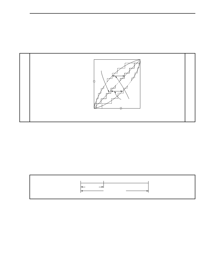
CHAPTER 13 A/D CONVERTER
673
User's Manual U14492EJ5V0UD
(7) Integral linearity error
This shows the degree to which the conversion characteristics deviate from the ideal linear relationship. It
expresses the maximum value of the difference between the actual measurement value and the ideal straight
line when the zero-scale error and full-scale error are 0.
Figure 13-21. Integral Linearity Error
0
AV
REFn
(n = 0, 1)
Digital output
Analog input
Integral linearity
error
Ideal line
1......1
0......0
(8) Conversion time
This expresses the time from when a trigger was generated to the time when the digital output was obtained.
The sampling time is included in the conversion time in the characteristics table.
(9) Sampling time
This is the time the analog switch is turned on for the analog voltage to be sampled by the sample & hold
circuit.
Figure 13-22. Sampling Time
Sampling
time
Conversion time
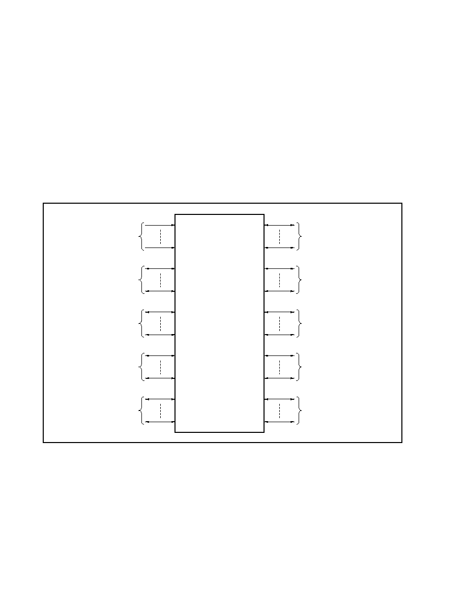
674
User's Manual U14492EJ5V0UD
CHAPTER 14 PORT FUNCTIONS
14.1 Features
∑ Input dedicated ports : 8
I/O ports: 75
∑ Ports alternate as I/O pins of other peripheral functions
∑ Input or output can be specified in bit units
14.2 Basic Configuration of Ports
The V850E/IA1 has a total of 83 on-chip input/output ports (ports 0 to 4, DH, DL, CS, CT, CM), of which 8 are
input-only ports. The port configuration is shown below.
Port DH
P00
P07
P10
P15
P20
P27
P30
P37
P40
P47
PDH0
PDH7
PDL0
PDL15
PCS0
PCS7
PCT0
PCT7
PCM0
PCM4
Port DL
Port CS
Port CT
Port CM
Port 0
Port 1
Port 2
Port 3
Port 4
(1) Functions of each port
The V850E/IA1 has the ports shown below.
Any port can operate in 8-bit or 1-bit units and can provide a variety of controls.
Moreover, besides its function as a port, each has functions as the I/O pins of on-chip peripheral I/O in control
mode.
Refer to (3) Port block diagrams for a block diagram of the block type of each port.
CHAPTER 14 PORT FUNCTIONS
675
User's Manual U14492EJ5V0UD
Port Name
Pin Name
Port Function
Function in Control Mode
Block Type
Port 0
P00 to P07
8-bit input
NMI input, timer/counter output stop signal input,
external interrupt input, A/D converter (ADC)
external trigger input
F
Port 1
P10 to P15
6-bit I/O
Timer/counter I/O
External interrupt input
B, N
Port 2
P20 to P27
8-bit I/O
Timer/counter I/O
External interrupt input
B, N
Port 3
P30 to P37
8-bit I/O
Serial interface I/O (UART0 to UART2)
A, C, G, H, M
Port 4
P40 to P47
8-bit I/O
Serial interface I/O (CSI0, CSI1, FCAN)
A, C, M
Port DH
PDH0 to PDH7
8-bit I/O
External address bus (A16 to A23)
P
Port DL
PDL0 to PDL15
16-bit I/O
External address/data bus (AD0 to AD15)
O
Port CS
PCS0 to PCS7
8-bit I/O
External bus interface control signal output
J
Port CT
PCT0 to PCT7
8-bit I/O
External bus interface control signal output
E, J
Port CM
PCM0 to PCM4
5-bit I/O
Wait insertion signal input, internal system clock
output, external bus interface control signal I/O
D, E, J
Cautions 1. When switching to the control mode, be sure to set ports that operate as output pins or I/O
pins in the control mode using the following procedure.
<1> Set the inactive level for the signal output in the control mode in the corresponding bits
of port n (n = 0 to 4, CM, CS, CT, DH, and DL).
<2> Switch to the control mode using the port n mode control register (PMCn).
If <1> above is not performed, the contents of port n may be output for a moment when
switching from the port mode to the control mode.
2. When port manipulation is performed by a bit manipulation instruction (SET1, CLR1, or
NOT1), perform byte data read for the port and process the data of only the bits to be
manipulated, and write the byte data after conversion back to the port.
For example, in ports in which input and output are mixed, because the contents of the
output latch are overwritten to bits other than the bits for manipulation, the output latch of
the input pin becomes undefined (in the input mode, however, the pin status does not
change because the output buffer is off).
Therefore, when switching the port from input to output, set the output expected value to the
corresponding bit, and then switch to the output port. This is the same as when the control
mode and output port are mixed.
3. The state of the port pin can be read by setting the port n mode register (PMn) to the input
mode regardless of the settings of the PMCn register. When the PMn register is set to the
output mode, the value of the port n register (Pn) can be read in the port mode while the
output state of the alternate function can be read in the control mode.
CHAPTER 14 PORT FUNCTIONS
676
User's Manual U14492EJ5V0UD
(2) Functions of each port pin after reset and registers that set port or control mode
Pin Function After Reset
Port Name
Pin Name
Single-Chip
Mode 0
Single-Chip
Mode 1
ROMless
Mode 0
ROMless
Mode 1
Mode-Setting
Register
P00/NMI
P00 (Input mode)
P01/ESO0/INTP0
P01 (Input mode)
P02/ESO1/INTP1
P02 (Input mode)
P03/ADTRG0/INTP2
P03 (Input mode)
P04/ADTRG1/INTP3
P04 (Input mode)
P05/INTP4
P05 (Input mode)
P06/INTP5
P06 (Input mode)
Port 0
P07/INTP6
P07 (Input mode)
-
P10/TIUD10/TO10
P10 (Input mode)
PMC1, PFC1
P11/TCUD10/INTP100
P11 (Input mode)
P12/TCLR10/INTP101
P12 (Input mode)
PMC1
P13/TIUD11/TO11
P13 (Input mode)
PMC1, PFC1
P14/TCUD11/INTP110
P14 (Input mode)
Port 1
P15/TCLR11/INTP111
P15 (Input mode)
PMC1
P20/TI2/INTP20
P20 (Input mode)
PMC2
P21/TO21/INTP21
P21 (Input mode)
P22/TO22/INTP22
P22 (Input mode)
P23/TO23/INTP23
P23 (Input mode)
P24/TO24/INTP24
P24 (Input mode)
PMC2, PFC2
P25/TCLR2/INTP25
P25 (Input mode)
P26/TI3/TCLR3/INTP30
P26 (Input mode)
PMC2
Port 2
P27/TO3/INTP31
P27 (Input mode)
PMC2, PFC2
P30/RXD0
P30 (Input mode)
P31/TXD0
P31 (Input mode)
P32/RXD1
P32 (Input mode)
P33/TXD1
P33 (Input mode)
P34/ASCK1
P34 (Input mode)
P35/RXD2
P35 (Input mode)
P36/TXD2
P36 (Input mode)
Port 3
P37/ASCK2
P37 (Input mode)
PMC3

CHAPTER 14 PORT FUNCTIONS
677
User's Manual U14492EJ5V0UD
Pin Function After Reset
Port Name
Pin Name
Single-Chip
Mode 0
Single-Chip
Mode 1
ROMless
Mode 0
ROMless
Mode 1
Mode-Setting
Register
P40/SI0
P40 (Input mode)
P41/SO0
P41 (Input mode)
P42/SCK0
P42 (Input mode)
P43/SI1
P43 (Input mode)
P44/SO1
P44 (Input mode)
P45/SCK1
P45 (Input mode)
P46/CRXD
P46 (Input mode)
Port 4
P47/CTXD
P47 (Input mode)
PMC4
PCM0/WAIT PCM0
(Input
mode)
WAIT
PCM1/CLKOUT
PCM1 (Input
mode)
CLKOUT
PCM2/HLDAK PCM2
(Input
mode)
HLDAK
PCM3/HLDRQ PCM3
(Input
mode)
HLDRQ
PMCCM
Port CM
PCM4
PCM4 (Input mode)
-
PCT0/LWR PCT0
(Input
mode)
LWR
PCT1/UWR PCT1
(Input
mode)
UWR
PMCCT
PCT2
PCT2 (Input mode)
PCT3
PCT3 (Input mode)
-
PCT4/RD PCT4
(Input
mode)
RD PMCCT
PCT5
PCT5 (Input mode)
-
PCT6/ASTB PCT6
(Input
mode)
ASTB PMCCT
Port CT
PCT7
PCT7 (Input mode)
-
Port CS
PCS0/CS0 to PCS7/CS7
PCS0 to
PCS7 (Input
mode)
CS0 to CS7
PMCCS
Port DH
PDH0/A16 to PDH7/A23
PDH0 to
PDH7 (Input
mode)
A16 to A23
PMCDH
Port DL
PDL0/AD0 to PDL15/AD15
PDL0 to
PDL15 (Input
mode)
AD0 to AD15
PMCDL
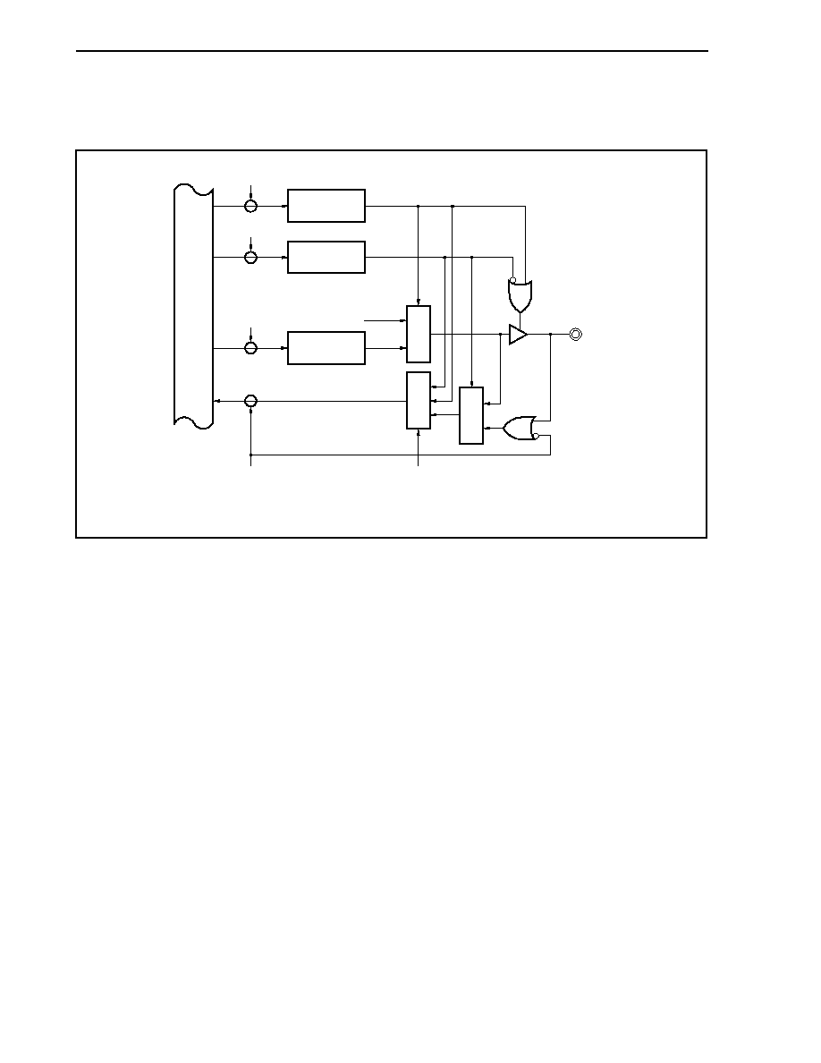
CHAPTER 14 PORT FUNCTIONS
678
User's Manual U14492EJ5V0UD
(3) Port block diagrams
Figure 14-1. Type A Block Diagram
WR
PMC
WR
PM
WR
PORT
RD
IN
PMCmn
PMmn
Pmn
Output signal in
control mode
Pmn
Address
Internal bus
Selector
Selector
Selector
Remark m: Port
number
n:
Bit
number
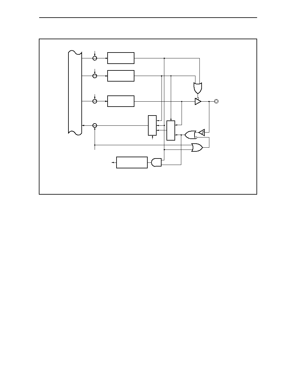
CHAPTER 14 PORT FUNCTIONS
679
User's Manual U14492EJ5V0UD
Figure 14-2. Type B Block Diagram
WR
PMC
WR
PM
WR
PORT
RD
IN
PMCmn
PMmn
Pmn
Pmn
Address
Noise elimination
Edge detection
Input signal in
control mode
Internal bus
Selector
Selector
Remark m: Port
number
n:
Bit
number
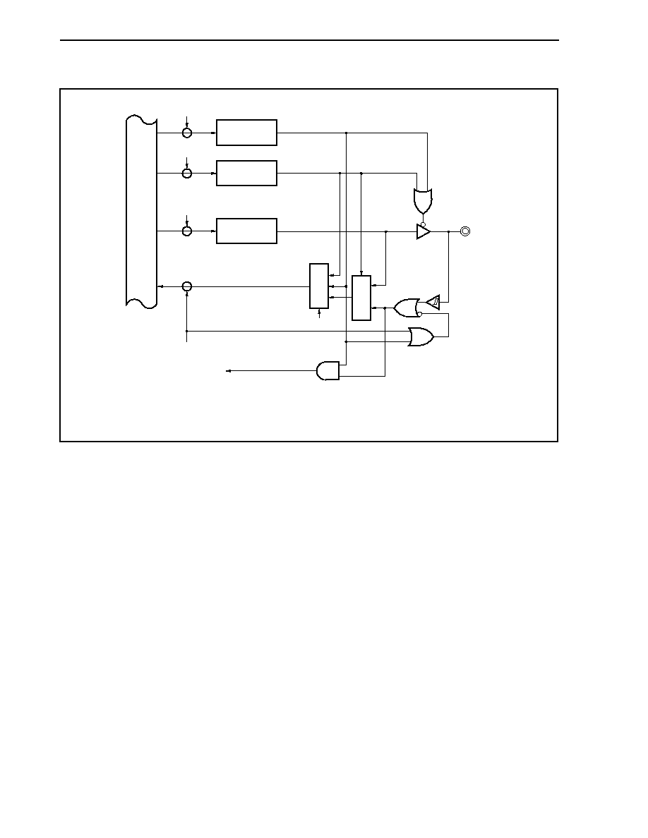
CHAPTER 14 PORT FUNCTIONS
680
User's Manual U14492EJ5V0UD
Figure 14-3. Type C Block Diagram
WR
PMC
WR
PM
WR
PORT
RD
IN
PMCmn
PMmn
Pmn
Pmn
Address
Input signal in
control mode
Internal bus
Selector
Selector
Remark m: Port
number
n:
Bit
number
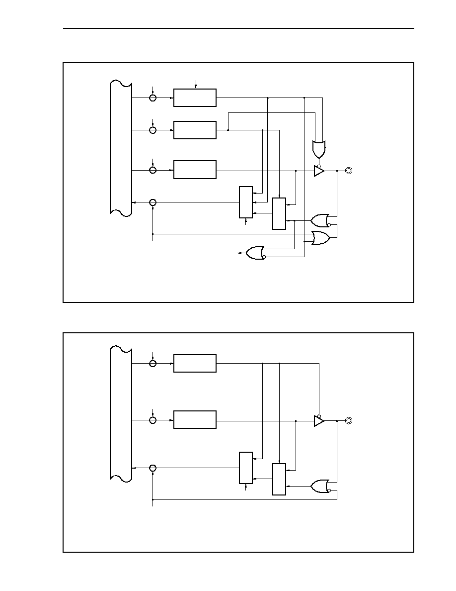
CHAPTER 14 PORT FUNCTIONS
681
User's Manual U14492EJ5V0UD
Figure 14-4. Type D Block Diagram
WR
PM
WR
PORT
RD
IN
PMmn
WR
PMC
PMCmn
Pmn
Pmn
MODE0 to MODE2
Address
Input signal in
control mode
Selector
Selector
Internal bus
Remark m: Port
number
n:
Bit
number
Figure 14-5. Type E Block Diagram
WR
PORT
RD
IN
WR
PM
Pmn
Pmn
PMmn
Address
Selector
Selector
Internal bus
Remark m: Port
number
n:
Bit
number
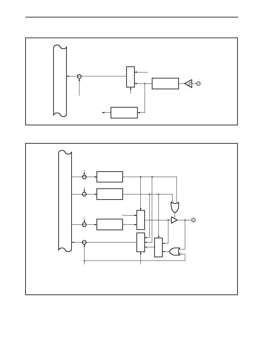
CHAPTER 14 PORT FUNCTIONS
682
User's Manual U14492EJ5V0UD
Figure 14-6. Type F Block Diagram
RD
IN
Pmn
Address
Noise elimination
Edge detection
1
Input signal in
control mode
Internal bus
Selector
Figure 14-7. Type G Block Diagram
WR
PMC
WR
PM
WR
PORT
RD
IN
PMCmn
PMmn
Pmn
Output signal in
control mode
Pmn
Address
Internal bus
Selector
Selector
Selector
Remark m: Port
number
n:
Bit
number

CHAPTER 14 PORT FUNCTIONS
683
User's Manual U14492EJ5V0UD
Figure 14-8. Type H Block Diagram
Internal bus
Selector
Selector
WR
PMC
WR
PM
WR
PORT
RD
IN
PMCmn
PMmn
Pmn
Pmn
Address
Input signal in
control mode
Remark m: Port
number
n:
Bit
number
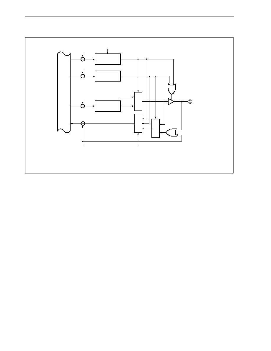
CHAPTER 14 PORT FUNCTIONS
684
User's Manual U14492EJ5V0UD
Figure 14-9. Type J Block Diagram
WR
PMC
WR
PM
WR
PORT
RD
IN
PMCmn
PMmn
Pmn
Output signal in
control mode
Pmn
Address
Internal bus
Selector
Selector
Selector
MODE0 to MODE2
Remark m: Port
number
n:
Bit
number
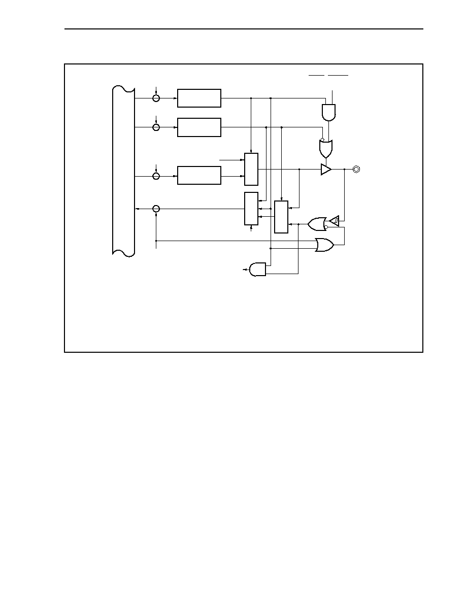
CHAPTER 14 PORT FUNCTIONS
685
User's Manual U14492EJ5V0UD
Figure 14-10. Type M Block Diagram
WR
PMC
WR
PM
WR
PORT
RD
IN
PMCmn
PMmn
Pmn
Pmn
Address
Input signal in
control mode
Output signal in
control mode
SCKx, ASCKy
output enable signal
Internal bus
Selector
Selector
Selector
Remark mn: 34, 37, 42, 45
x:
0 (When mn = 42)
1 (When mn = 45)
y:
1 (When mn = 34)
2 (When mn = 37)
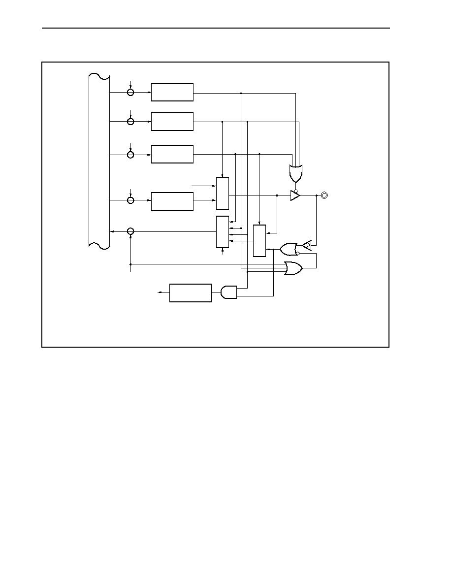
CHAPTER 14 PORT FUNCTIONS
686
User's Manual U14492EJ5V0UD
Figure 14-11. Type N Block Diagram
WR
PFC
WR
PMC
WR
PM
WR
PORT
RD
IN
PFCmn
PMCmn
PMmn
Pmn
Pmn
Address
Input signal in
control mode
Output signal in
control mode
Noise elimination
Edge detection
Internal bus
Selector
Selector
Selector
Remark m: Port
number
n:
Bit
number
CHAPTER 14 PORT FUNCTIONS
687
User's Manual U14492EJ5V0UD
Figure 14-12. Type O Block Diagram
WR
PM
WR
PORT
RD
IN
PMmn
WR
PMC
PMCmn
Pmn
Pmn
Output signal in
control mode
MODE0 to MODE2
I/O control
I/O control
Address
Input signal in
control mode
Selector
Selector
Internal bus
Selector
Remark m: Port
number
n:
Bit
number

CHAPTER 14 PORT FUNCTIONS
688
User's Manual U14492EJ5V0UD
Figure 14-13. Type P Block Diagram
WR
PM
WR
PORT
RD
IN
PMmn
WR
PMC
PMCmn
Pmn
Pmn
MODE0 to MODE2
Output signal in
control mode
I/O control
Address
Selector
Selector
Internal bus
Selector
Remark m: Port
number
n:
Bit
number

CHAPTER 14 PORT FUNCTIONS
689
User's Manual U14492EJ5V0UD
14.3 Pin Functions of Each Port
14.3.1 Port 0
Port 0 is an 8-bit input dedicated port in which all pins are fixed for input.
7
P07
P0
6
P06
5
P05
4
P04
3
P03
2
P02
1
P01
0
P00
Address
FFFFF400H
Initial value
Undefined
Besides functioning as an input port, in control mode, it also can operate as the timer/counter output stop signal
input, external interrupt request input, and A/D converter (ADC) external trigger input.
Although this port also serves as NMI, ESO0/INTP0, ESO1/INTP1, ADTRG0/INTP2, ADTRG1/INTP3, and INTP4
to INTP6, NMI, ESO0/INTP0, ESO1/INTP1, ADTRG0/INTP2, ADTRG1/INTP3, and INTP4 to INTP6 cannot be
switched with input port. The status of each pin is read by reading the port.
(1) Operation in control mode
Port
Alternate Pin Name
Remarks
Block Type
P00
NMI
Non-maskable interrupt request input
P01 ESO0/INTP0
P02 ESO1/INTP1
Timer/counter output stop signal input or external
interrupt request input
P03 ADTRG0/INTP2
P04 ADTRG1/INTP3
A/D converter (ADC) external trigger input or external
interrupt request input
Port 0
P05 to P07
INTP4 to INTP6
External interrupt request input
F
CHAPTER 14 PORT FUNCTIONS
690
User's Manual U14492EJ5V0UD
14.3.2 Port 1
Port 1 is a 6-bit I/O port in which input or output can be specified in 1-bit units.
7
≠
P1
6
≠
5
P15
4
P14
3
P13
2
P12
1
P11
0
P10
Address
FFFFF402H
Initial value
Undefined
Bit position
Bit name
Function
5 to 0
P1n
(n = 5 to 0)
I/O port
Besides functioning as a port, in control mode, it also can operate as the timer/counter I/O and external interrupt
request input.
(1) Operation in control mode
Port
Alternate Pin Name
Remarks
Block Type
P10 TIUD10/TO10
Timer/counter
I/O
N
P11 TCUD10/INTP100
P12 TCLR10/INTP101
Timer/counter input or external interrupt request input
B
P13 TIUD11/TO11
Timer/counter
I/O
N
P14 TCUD11/INTP110
Port 1
P15 TCLR11/INTP111
Timer/counter input or external interrupt request input
B
(2) Setting in I/O mode and control mode
Port 1 is set in I/O mode using the port 1 mode register (PM1). In control mode, it is set using the port 1
mode control register (PMC1) and port 1 function control register (PFC1).
(a) Port 1 mode register (PM1)
This register can be read/written in 8-bit or 1-bit units. Write 1 in bits 6 and 7.
7
1
PM1
6
1
5
PM15
4
PM14
3
PM13
2
PM12
1
PM11
0
PM10
Address
FFFFF422H
Initial value
FFH
Bit position
Bit name
Function
5 to 0
PM1n
(n = 5 to 0)
Specifies input/output mode of P1n pin.
0: Output mode (output buffer on)
1: Input mode (output buffer off)

CHAPTER 14 PORT FUNCTIONS
691
User's Manual U14492EJ5V0UD
(b) Port 1 mode control register (PMC1)
This register can be read/written in 8-bit or 1-bit units. Write 0 in bits 6 and 7.
Caution The PMC11, PMC12, PMC14, and PMC15 bits also serve as external interrupts (INTP100,
INTP101, INTP110, and INTP111). When not using them as external interrupts, mask
interrupt requests (refer to 7.3.4 Interrupt control register (xxICn)).
7
0
PMC1
6
0
5
PMC15
4
PMC14
3
PMC13
2
PMC12
1
PMC11
0
PMC10
Address
FFFFF442H
Initial value
00H
Bit position
Bit name
Function
5
PMC15
Specifies operation mode of P15 pin.
0: I/O port mode
1: TCLR11 input mode or external interrupt request (INTP111) input mode
4
PMC14
Specifies operation mode of P14 pin.
0: I/O port mode
1: TCUD11 input mode or external interrupt request (INTP110) input mode
3
PMC13
Specifies operation mode of P13 pin.
0: I/O port mode
1: TIUD11 input mode or TO11 output mode
2
PMC12
Specifies operation mode of P12 pin.
0: I/O port mode
1: TCLR10 input mode or external interrupt request (INTP101) input mode
1
PMC11
Specifies operation mode of P11 pin.
0: I/O port mode
1: TCUD10 input mode or external interrupt request (INTP100) input mode
0
PMC10
Specifies operation mode of P10 pin.
0: I/O port mode
1: TIUD10 input mode or TO10 output mode
CHAPTER 14 PORT FUNCTIONS
692
User's Manual U14492EJ5V0UD
(c) Port 1 function control register (PFC1)
This register can be read/written in 8-bit or 1-bit units. Write 0 in bits other than 0 and 3.
Caution When port mode is specified by the port 1 mode control register (PMC1), the setting of
this register is invalid.
7
0
PFC1
6
0
5
0
4
0
3
PFC13
2
0
1
0
0
PFC10
Address
FFFFF462H
Initial value
00H
Bit position
Bit name
Function
3
PFC13
Specifies operation mode of P13 pin in control mode.
0: TIUD11 input mode
1: TO11 output mode
0
PFC10
Specifies operation mode of P10 pin in control mode.
0: TIUD10 input mode
1: TO10 output mode
CHAPTER 14 PORT FUNCTIONS
693
User's Manual U14492EJ5V0UD
14.3.3 Port 2
Port 2 is an 8-bit I/O port in which input or output can be specified in 1-bit units.
7
P27
P2
6
P26
5
P25
4
P24
3
P23
2
P22
1
P21
0
P20
Address
FFFFF404H
Initial value
Undefined
Bit position
Bit name
Function
7 to 0
P2n
(n = 7 to 0)
I/O port
Besides functioning as a port, in control mode, it also can operate as the timer/counter I/O and external interrupt
request input.
(1) Operation in control mode
Port
Alternate Pin Name
Remarks
Block Type
P20
TI2/INTP20
Timer/counter input or external interrupt request input
B
P21 to P24
TO21/INTP21 to
TO24/INTP24
Timer/counter output or external interrupt request
input
N
P25 TCLR2/INTP25
P26 TI3/TCLR3/INTP30
Timer/counter input or external interrupt request input
B
Port 2
P27 TO3/INTP31 Timer/counter
output or external interrupt request
input
N
(2) Setting in I/O mode and control mode
Port 2 is set in I/O mode using the port 2 mode register (PM2). In control mode, it is set using the port 2
mode control register (PMC2) and port 2 function control register (PFC2).
(a) Port 2 mode register (PM2)
This register can be read/written in 8-bit or 1-bit units.
7
PM27
PM2
6
PM26
5
PM25
4
PM24
3
PM23
2
PM22
1
PM21
0
PM20
Address
FFFFF424H
Initial value
FFH
Bit position
Bit name
Function
7 to 0
PM2n
(n = 7 to 0)
Specifies input/output mode of P2n pin.
0: Output mode (output buffer on)
1: Input mode (output buffer off)

CHAPTER 14 PORT FUNCTIONS
694
User's Manual U14492EJ5V0UD
(b) Port 2 mode control register (PMC2)
This register can be read/written in 8-bit or 1-bit units.
Caution The PMC20, PMC25, and PMC26 bits also serve as external interrupts (INTP20, INTP25,
and INTP30). When not using them as external interrupts, mask interrupt requests
(refer to 7.3.4 Interrupt control register (xxICn)).
7
PMC27
PMC2
6
PMC26
5
PMC25
4
PMC24
3
PMC23
2
PMC22
1
PMC21
0
PMC20
Address
FFFFF444H
Initial value
00H
Bit position
Bit name
Function
7
PMC27
Specifies operation mode of P27 pin.
0: I/O port mode
1: TO3 output mode or external interrupt request (INTP31) input mode
6
PMC26
Specifies operation mode of P26 pin.
0: I/O port mode
1: TI3, TCLR3 input mode or external interrupt request (INTP30) input mode
5
PMC25
Specifies operation mode of P25 pin.
0: I/O port mode
1: TCLR2 input mode or external interrupt request (INTP25) input mode
4 to 1
PMC24 to
PMC21
Specify operation mode of P24 to P21 pins.
0: I/O port mode
1: TO24 to TO21 output mode or external interrupt request (INTP24 to INTP21)
input mode
0
PMC20
Specifies operation mode of P20 pin.
0: I/O port mode
1: TI2 input mode or external interrupt request (INTP20) input mode

CHAPTER 14 PORT FUNCTIONS
695
User's Manual U14492EJ5V0UD
(c) Port 2 function control register (PFC2)
This register can be read/written in 8-bit or 1-bit units. Write 0 in bits 0, 5, and 6.
Caution When port mode is specified by the port 2 mode control register (PMC2), the setting of
this register is invalid.
7
PFC27
PFC2
6
0
5
0
4
PFC24
3
PFC23
2
PFC22
1
PFC21
0
0
Address
FFFFF464H
Initial value
00H
Bit position
Bit name
Function
7
PFC27
Specifies operation mode of P27 pin in control mode.
0: External interrupt request (INTP31) input mode
1: TO3 output mode
4 to 1
PFC24 to
PFC21
Specify operation mode of P24 to P21 pins in control mode.
0: External interrupt request (INTP24 to INTP21) input mode
1: TO24 to TO21 output mode

CHAPTER 14 PORT FUNCTIONS
696
User's Manual U14492EJ5V0UD
14.3.4 Port 3
Port 3 is an 8-bit I/O port in which input or output can be specified in 1-bit units.
7
P37
P3
6
P36
5
P35
4
P34
3
P33
2
P32
1
P31
0
P30
Address
FFFFF406H
Initial value
Undefined
Bit position
Bit name
Function
7 to 0
P3n
(n = 7 to 0)
I/O port
Besides functioning as a port, in control mode, it also can operate as the serial interface (UART0 to UART2) I/O.
(1) Operation in control mode
Port
Alternate Pin Name
Remarks
Block Type
P30 RXD0
H
P31 TXD0
G
P32 RXD1
C
P33 TXD1
A
P34 ASCK1
M
P35 RXD2
C
P36 TXD2
A
Port 3
P37 ASCK2
Serial interface (UART0 to UART2) I/O
M
(2) Setting in I/O mode and control mode
Port 3 is set in I/O mode using the port 3 mode register (PM3). In control mode, it is set using the port 3
mode control register (PMC3).
(a) Port 3 mode register (PM3)
This register can be read/written in 8-bit or 1-bit units.
7
PM37
PM3
6
PM36
5
PM35
4
PM34
3
PM33
2
PM32
1
PM31
0
PM30
Address
FFFFF426H
Initial value
FFH
Bit position
Bit name
Function
7 to 0
PM3n
(n = 7 to 0)
Specifies input/output mode of P3n pin.
0: Output mode (output buffer on)
1: Input mode (output buffer off)
CHAPTER 14 PORT FUNCTIONS
697
User's Manual U14492EJ5V0UD
(b) Port 3 mode control register (PMC3)
This register can be read/written in 8-bit or 1-bit units.
7
PMC37
PMC3
6
PMC36
5
PMC35
4
PMC34
3
PMC33
2
PMC32
1
PMC31
0
PMC30
Address
FFFFF446H
Initial value
00H
Bit position
Bit name
Function
7
PMC37
Specifies operation mode of P37 pin.
0: I/O port mode
1: ASCK2 I/O mode
6
PMC36
Specifies operation mode of P36 pin.
0: I/O port mode
1: TXD2 output mode
5
PMC35
Specifies operation mode of P35 pin.
0: I/O port mode
1: RXD2 input mode
4
PMC34
Specifies operation mode of P34 pin.
0: I/O port mode
1: ASCK1 I/O mode
3
PMC33
Specifies operation mode of P33 pin.
0: I/O port mode
1: TXD1 output mode
2
PMC32
Specifies operation mode of P32 pin.
0: I/O port mode
1: RXD1 input mode
1
PMC31
Specifies operation mode of P31 pin.
0: I/O port mode
1: TXD0 output mode
0
PMC30
Specifies operation mode of P30 pin.
0: I/O port mode
1: RXD0 input mode
CHAPTER 14 PORT FUNCTIONS
698
User's Manual U14492EJ5V0UD
14.3.5 Port 4
Port 4 is an 8-bit I/O port in which input or output can be specified in 1-bit units.
7
P47
P4
6
P46
5
P45
4
P44
3
P43
2
P42
1
P41
0
P40
Address
FFFFF408H
Initial value
Undefined
Bit position
Bit name
Function
7 to 0
P4n
(n = 7 to 0)
I/O port
Besides functioning as a port, in control mode, it also can operate as the serial interface (CSI0, CSI1, FCAN) I/O.
(1) Operation in control mode
Port
Alternate Pin Name
Remarks
Block Type
P40 SI0
C
P41 SO0
A
P42 SCK0
M
P43 SI1
C
P44 SO1
A
P45 SCK1
M
P46 CRXD
C
Port 4
P47 CTXD
Serial interface (CSI0, CSI1, FCAN) I/O
A
(2) Setting in I/O mode and control mode
Port 4 is set in I/O mode using the port 4 mode register (PM4). In control mode, it is set using the port 4
mode control register (PMC4).
(a) Port 4 mode register (PM4)
This register can be read/written in 8-bit or 1-bit units.
7
PM47
PM4
6
PM46
5
PM45
4
PM44
3
PM43
2
PM42
1
PM41
0
PM40
Address
FFFFF428H
Initial value
FFH
Bit position
Bit name
Function
7 to 0
PM4n
(n = 7 to 0)
Specifies input/output mode of P4n pin.
0: Output mode (output buffer on)
1: Input mode (output buffer off)
CHAPTER 14 PORT FUNCTIONS
699
User's Manual U14492EJ5V0UD
(b) Port 4 mode control register (PMC4)
This register can be read/written in 8-bit or 1-bit units.
7
PMC47
PMC4
6
PMC46
5
PMC45
4
PMC44
3
PMC43
2
PMC42
1
PMC41
0
PMC40
Address
FFFFF448H
Initial value
00H
Bit position
Bit name
Function
7
PMC47
Specifies operation mode of P47 pin.
0: I/O port mode
1: CTXD output mode
6
PMC46
Specifies operation mode of P46 pin.
0: I/O port mode
1: CRXD input mode
5
PMC45
Specifies operation mode of P45 pin.
0: I/O port mode
1: SCK1 I/O mode
4
PMC44
Specifies operation mode of P44 pin.
0: I/O port mode
1: SO1 output mode
3
PMC43
Specifies operation mode of P43 pin.
0: I/O port mode
1: SI1 input mode
2
PMC42
Specifies operation mode of P42 pin.
0: I/O port mode
1: SCK0 I/O mode
1
PMC41
Specifies operation mode of P41 pin.
0: I/O port mode
1: SO0 output mode
0
PMC40
Specifies operation mode of P40 pin.
0: I/O port mode
1: SI0 input mode
CHAPTER 14 PORT FUNCTIONS
700
User's Manual U14492EJ5V0UD
14.3.6 Port DH
Port DH is an 8-bit I/O port in which input or output can be specified in 1-bit units.
7
PDH7
PDH
6
PDH6
5
PDH5
4
PDH4
3
PDH3
2
PDH2
1
PDH1
0
PDH0
Address
FFFFF006H
Initial value
Undefined
Bit position
Bit name
Function
7 to 0
PDHn
(n = 7 to 0)
I/O port
Besides functioning as a port, in control mode, this can operate as an address bus when memory is expanded
externally.
(1) Operation in control mode
Port
Alternate Pin Name
Remarks
Block Type
Port DH
PDH7 to
PDH0
A23 to A16
Memory expansion address bus
P
(2) Setting in I/O mode and control mode
Port DH is set in I/O mode using the port DH mode register (PMDH). In control mode, it is set using the port
DH mode control register (PMCDH).
(a) Port DH mode register (PMDH)
This register can be read/written in 8-bit or 1-bit units.
7
PMDH7
PMDH
6
PMDH6
5
PMDH5
4
PMDH4
3
PMDH3
2
PMDH2
1
PMDH1
0
PMDH0
Address
FFFFF026H
Initial value
FFH
Bit position
Bit name
Function
7 to 0
PMDHn
(n = 7 to 0)
Specifies input/output mode of PDHn pin.
0: Output mode (output buffer on)
1: Input mode (output buffer off)

CHAPTER 14 PORT FUNCTIONS
701
User's Manual U14492EJ5V0UD
(b) Port DH mode control register (PMCDH)
This register can be read/written in 8-bit or 1-bit units.
7
PMCDH7
PMCDH
6
PMCDH6
5
PMCDH5
4
PMCDH4
3
PMCDH3
2
PMCDH2
1
PMCDH1
0
PMCDH0
Address
FFFFF046H
Initial value
Note
00H/FFH
Note 00H: Single-chip mode 0
FFH: Single-chip mode 1, ROMless mode 0 or 1
Bit position
Bit name
Function
7 to 0
PMCDHn
(n = 7 to 0)
Specifies operation mode of PDHn pin.
0: I/O port mode
1: A23 to A16 output mode
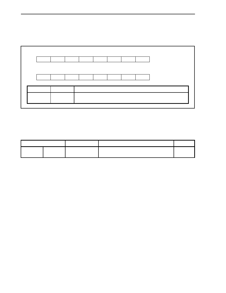
CHAPTER 14 PORT FUNCTIONS
702
User's Manual U14492EJ5V0UD
14.3.7 Port DL
Port DL is a 16-bit or 8-bit I/O port in which input or output can be specified in 1-bit units.
When using the higher 8 bits of PDL as PDLH and the lower 8 bits as PDLL, it can be used as an 8-bit I/O port that
can specify input or output in 1-bit units.
15
PDL15
PDL
14
PDL14
13
PDL13
12
PDL12
11
PDL11
10
PDL10
9
PDL9
8
PDL8
7
PDL7
6
PDL6
5
PDL5
4
PDL4
3
PDL3
2
PDL2
1
PDL1
0
PDL0
Address
FFFFF005H
Initial value
Undefined
Address
FFFFF004H
Bit position
Bit name
Function
15 to 0
PDLn
(n = 15 to 0)
I/O port
Besides functioning as a port, in control mode, this can operate as an address/data bus when memory is expanded
externally.
(1) Operation in control mode
Port
Alternate Pin Name
Remarks
Block Type
Port DL
PDL15 to
PDL0
AD15 to AD0
Memory expansion address/data bus
O
(2) Setting in I/O mode and control mode
Port DL is set in I/O mode using the port DL mode register (PMDL). In control mode, it is set using the port
DL mode control register (PMCDL).
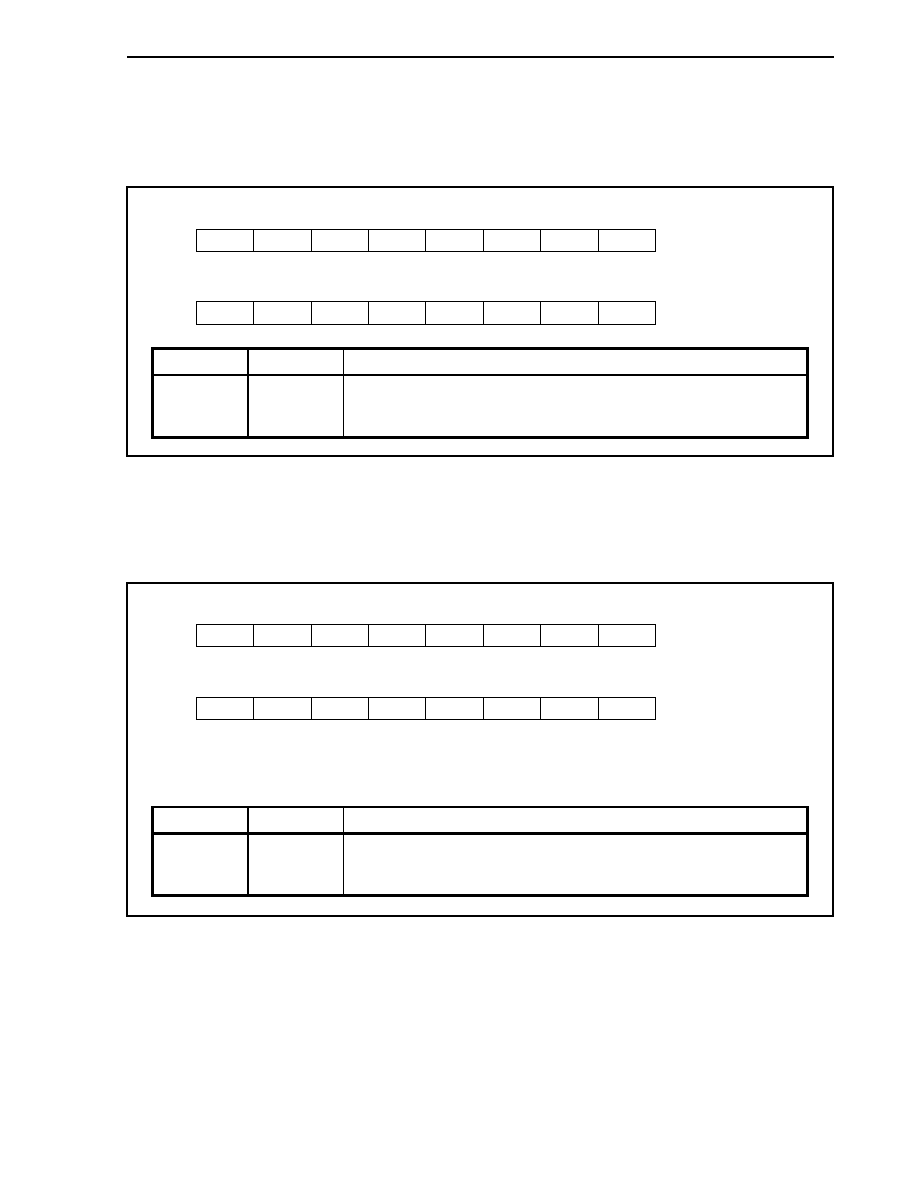
CHAPTER 14 PORT FUNCTIONS
703
User's Manual U14492EJ5V0UD
(a) Port DL mode register (PMDL)
The PMDL register can be read/written in 16-bit units.
When using the higher 8 bits of the PMDL register as the PMDLH register and the lower 8 bits as the
PMDLL register, it can be read/written in 8-bit or 1-bit units.
15
PMDL15
PMDL
14
PMDL14
13
PMDL13
12
PMDL12
11
PMDL11
10
PMDL10
9
PMDL9
8
PMDL8
7
PMDL7
6
PMDL6
5
PMDL5
4
PMDL4
3
PMDL3
2
PMDL2
1
PMDL1
0
PMDL0
Address
FFFFF025H
Initial value
FFFFH
Address
FFFFF024H
Bit position
Bit name
Function
15 to 0
PMDLn
(n = 15 to 0)
Specifies input/output mode of PDLn pin.
0: Output mode (output buffer on)
1: Input mode (output buffer off)
(b) Port DL mode control register (PMCDL)
The PMCDL register can be read/written in 16-bit units.
When using the higher 8 bits of the PMCDL register as the PMCDLH register and the lower 8 bits as the
PMCDLL register, it can be read/written in 8-bit or 1-bit units.
15
PMCDL15
PMCDL
14
PMCDL14
13
PMCDL13
12
PMCDL12
11
PMCDL11
10
PMCDL10
9
PMCDL9
8
PMCDL8
7
PMCDL7
6
PMCDL6
5
PMCDL5
4
PMCDL4
3
PMCDL3
2
PMCDL2
1
PMCDL1
0
PMCDL0
Address
FFFFF045H
Initial value
Note
0000H/FFFFH
Address
FFFFF044H
Note 0000H : Single-chip mode 0
FFFFH : Single-chip mode 1, ROMless mode 0 or 1
Bit position
Bit name
Function
15 to 0
PMCDLn
(n = 15 to 0)
Specifies operation mode of PDLn pin.
0: I/O port mode
1: AD15 to AD0 I/O mode
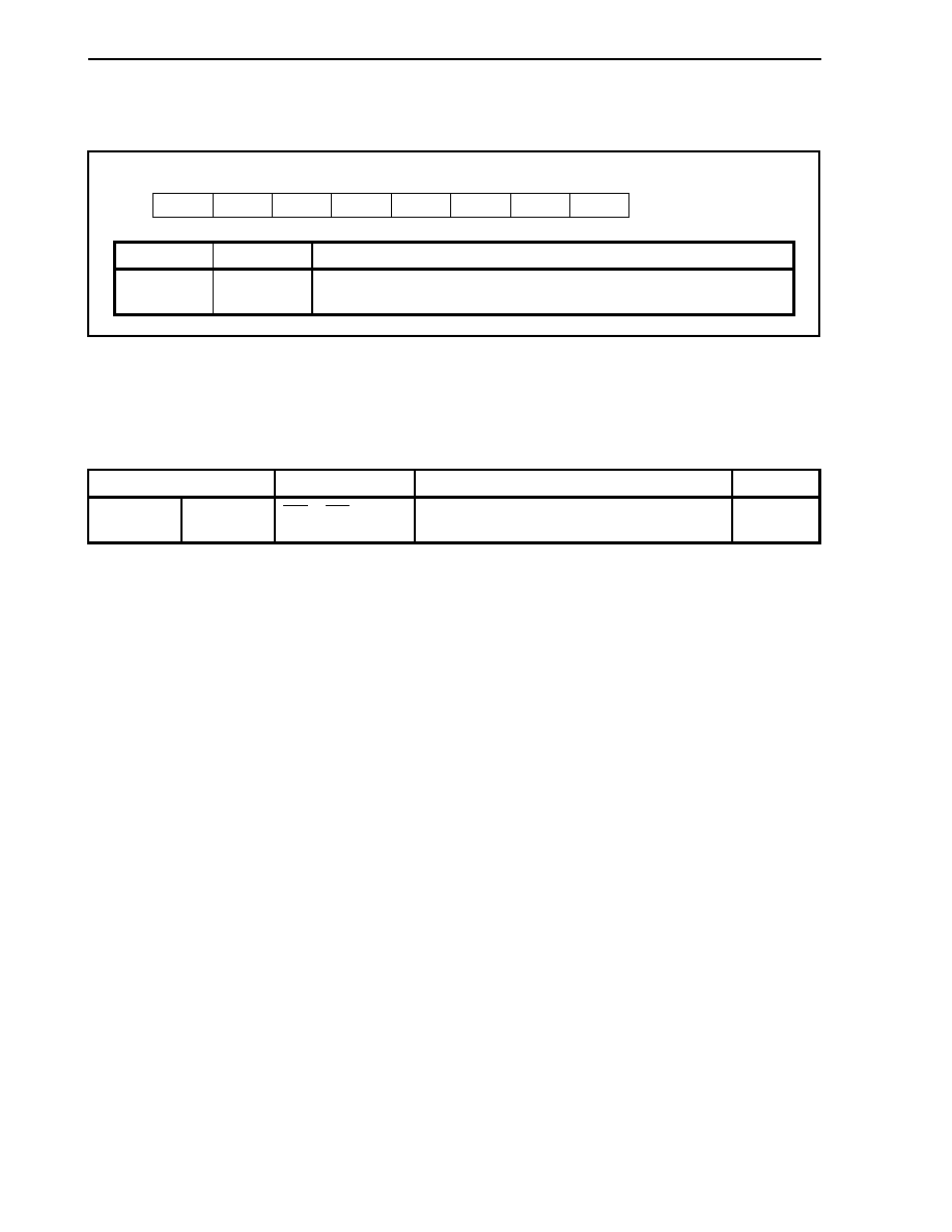
CHAPTER 14 PORT FUNCTIONS
704
User's Manual U14492EJ5V0UD
14.3.8 Port CS
Port CS is an 8-bit I/O port in which input or output can be specified in 1-bit units.
7
PCS7
PCS
6
PCS6
5
PCS5
4
PCS4
3
PCS3
2
PCS2
1
PCS1
0
PCS0
Address
FFFFF008H
Initial value
Undefined
Bit position
Bit name
Function
7 to 0
PCSn
(n = 7 to 0)
I/O port
Besides functioning as a port, in control mode, this can operate as the chip select signal output when memory is
expanded externally.
(1) Operation in control mode
Port
Alternate Pin Name
Remarks
Block Type
Port CS
PCS7 to
PCS0
CS0 to CS7
Chip select signal output
J
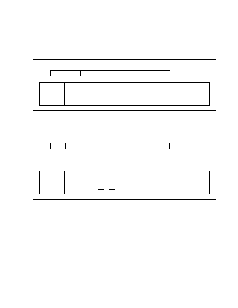
CHAPTER 14 PORT FUNCTIONS
705
User's Manual U14492EJ5V0UD
(2) Setting in I/O mode and control mode
Port CS is set in I/O mode using the port CS mode register (PMCS). In control mode, it is set using the port
CS mode control register (PMCCS).
(a) Port CS mode register (PMCS)
This register can be read/written in 8-bit or 1-bit units.
7
PMCS7
PMCS
6
PMCS6
5
PMCS5
4
PMCS4
3
PMCS3
2
PMCS2
1
PMCS1
0
PMCS0
Address
FFFFF028H
Initial value
FFH
Bit position
Bit name
Function
7 to 0
PMCSn
(n = 7 to 0)
Specifies input/output mode of PCSn pin.
0: Output mode (output buffer on)
1: Input mode (output buffer off)
(b) Port CS mode control register (PMCCS)
This register can be read/written in 8-bit or 1-bit units.
7
PMCCS7
PMCCS
6
PMCCS6
5
PMCCS5
4
PMCCS4
3
PMCCS3
2
PMCCS2
1
PMCCS1
0
PMCCS0
Address
FFFFF048H
Initial value
Note
00H/FFH
Note 00H: Single-chip mode 0
FFH: Single-chip mode 1, ROMless mode 0 or 1
Bit position
Bit name
Function
7 to 0
PMCCSn
(n = 7 to 0)
Specifies operation mode of PCSn pin.
0: I/O port mode
1: CS7 to CS0 output mode
CHAPTER 14 PORT FUNCTIONS
706
User's Manual U14492EJ5V0UD
14.3.9 Port CT
Port CT is an 8-bit I/O port in which input or output can be specified in 1-bit units.
7
PCT7
PCT
6
PCT6
5
PCT5
4
PCT4
3
PCT3
2
PCT2
1
PCT1
0
PCT0
Address
FFFFF00AH
Initial value
Undefined
Bit position
Bit name
Function
7 to 0
PCTn
(n = 7 to 0)
I/O port
Besides functioning as a port, in control mode, this can operate as control signal outputs when memory is
expanded externally.
(1) Operation in control mode
Port
Alternate Pin Name
Remarks
Block type
PCT0 LWR
PCT1 UWR
Write strobe signal output
J
PCT2
PCT3
-
Fixed in port mode
E
PCT4
RD
Read strobe signal output
J
PCT5
-
Fixed in port mode
E
PCT6
ASTB
Address strobe signal output
J
Port CT
PCT7
-
Fixed in port mode
E
(2) Setting in I/O mode and control mode
Port CT is set in I/O mode using the port CT mode register (PMCT). In control mode, it is set using the port
CT mode control register (PMCCT).
(a) Port CT mode register (PMCT)
This register can be read/written in 8-bit or 1-bit units.
7
PMCT7
PMCT
6
PMCT6
5
PMCT5
4
PMCT4
3
PMCT3
2
PMCT2
1
PMCT1
0
PMCT0
Address
FFFFF02AH
Initial value
FFH
Bit position
Bit name
Function
7 to 0
PMCTn
(n = 7 to 0)
Specifies input/output mode of PCTn pin.
0: Output mode (output buffer on)
1: Input mode (output buffer off)
CHAPTER 14 PORT FUNCTIONS
707
User's Manual U14492EJ5V0UD
(b) Port CT mode control register (PMCCT)
This register can be read/written in 8-bit or 1-bit units.
7
0
PMCCT
6
PMCCT6
5
0
4
PMCCT4
3
0
2
0
1
PMCCT1
0
PMCCT0
Address
FFFFF04AH
Initial value
Note
00H/53H
Note 00H: Single-chip mode 0
53H: Single-chip mode 1, ROMless mode 0 or 1
Bit position
Bit name
Function
6
PMCCT6
Specifies operation mode of PCT6 pin.
0: I/O port mode
1: ASTB output mode
4
PMCCT4
Specifies operation mode of PCT4 pin.
0: I/O port mode
1: RD output mode
1
PMCCT1
Specifies operation mode of PCT1 pin.
0: I/O port mode
1: UWR output mode
0
PMCCT0
Specifies operation mode of PCT0 pin.
0: I/O port mode
1: LWR output mode

CHAPTER 14 PORT FUNCTIONS
708
User's Manual U14492EJ5V0UD
14.3.10 Port CM
Port CM is a 5-bit I/O port in which input or output can be specified in 1-bit units.
7
≠
PCM
6
≠
5
≠
4
PCM4
3
PCM3
2
PCM2
1
PCM1
0
PCM0
Address
FFFFF00CH
Initial value
Undefined
Bit position
Bit name
Function
4 to 0
PCMn
(n = 4 to 0)
I/O port
Besides functioning as a port, in control mode, this can operate as the wait insertion signal input, internal system
clock output, and bus hold control signal output.
(1) Operation in control mode
Port
Alternate Pin Name
Remarks
Block Type
PCM0 WAIT
Note
Wait insertion signal input
D
PCM1
CLKOUT
Internal system clock output
J
PCM2
HLDAK
Bus hold acknowledge signal output
J
PCM3 HLDRQ
Note
Bus hold request signal input
D
Port CM
PCM4
-
Fixed in port mode
E
Note The WAIT and HLDRQ signals are set to control mode by default in ROMless mode 0, 1 or single-chip
mode 1. Be sure to fix these pins to the inactive level when not used. These pins function in control mode
until port mode is set using the port CM mode control register (PMCCM), so be sure to set these pins to
the inactive level before setting PMCCM.
(2) Setting in I/O mode and control mode
Port CM is set in I/O mode using the port CM mode register (PMCM). In control mode, it is set using the port
CM mode control register (PMCCM).
(a) Port CM mode register (PMCM)
This register can be read/written in 8-bit or 1-bit units.
7
1
PMCM
6
1
5
1
4
PMCM4
3
PMCM3
2
PMCM2
1
PMCM1
0
PMCM0
Address
FFFFF02CH
Initial value
FFH
Bit position
Bit name
Function
4 to 0
PMCMn
(n = 4 to 0)
Specifies input/output mode of PCMn pin.
0: Output mode (output buffer on)
1: Input mode (output buffer off)
CHAPTER 14 PORT FUNCTIONS
709
User's Manual U14492EJ5V0UD
(b) Port CM mode control register (PMCCM)
This register can be read/written in 8-bit or 1-bit units.
7
0
PMCCM
6
0
5
0
4
0
3
PMCCM3
2
PMCCM2
1
PMCCM1
0
PMCCM0
Address
FFFFF04CH
Initial value
Note
00H/0FH
Note 00H: Single-chip mode 0
0FH: Single-chip mode 1, ROMless mode 0 or 1
Bit position
Bit name
Function
3
PMCCM3
Specifies operation mode of PCM3 pin.
0: I/O port mode
1: HLDRQ input mode
2
PMCCM2
Specifies operation mode of PCM2 pin.
0: I/O port mode
1: HLDAK output mode
1
PMCCM1
Specifies operation mode of PCM1 pin.
0: I/O port mode
1: CLKOUT output mode
0
PMCCM0
Specifies operation mode of PCM0 pin.
0: I/O port mode
1: WAIT input mode

CHAPTER 14 PORT FUNCTIONS
710
User's Manual U14492EJ5V0UD
14.4 Operation of Port Function
The operation of a port differs depending on whether it is set in the input or output mode, as follows.
14.4.1 Writing to I/O port
(1) In output mode
A value can be written to the output latch (Pn) by writing it to the port n register (Pn). The contents of the
output latch are output from the pin.
Once data is written to the output latch, it is held until new data is written to the output latch.
(2) In input mode
A value can be written to the output latch (Pn) by writing it to the port n register (Pn). However, the status of
the pin does not change because the output buffer is off.
Once data is written to the output latch, it is held until new data is written to the output latch.
Caution A bit manipulation instruction (CLR1, SET1, NOT1) manipulates 1 bit but accesses a port in
8-bit units. If this instruction is executed to manipulate a port with a mixture of input and
output bits, the contents of the output latch of a pin set in the input mode, in addition to the
bit to be manipulated, are overwritten to the current input pin status and become undefined.
14.4.2 Reading from I/O port
(1) In output mode
The contents of the output latch (Pn) can be read by reading the port n register (Pn). The contents of the
output latch do not change.
(2) In input mode
The status of the pin can be read by reading the port n register (Pn). The contents of the output latch (Pn) do
not change.
14.4.3 Output status of alternate function in control mode
The status of a port pin is not dependent upon the setting of the PMCn register and can be read by setting the port
n mode register (PMn) to the input mode. If the PMn register is set to the output mode, the value of the port n register
(Pn) can be read in the port mode, and the output status of the alternate function can be read in the control mode.

CHAPTER 14 PORT FUNCTIONS
711
User's Manual U14492EJ5V0UD
14.5 Noise Eliminator
14.5.1 Interrupt pins
A timing controller to guarantee the noise elimination times shown below is added to the pins that operate as NMI
and valid edge inputs in port control mode. Signal input that changes in less than these elimination times is not
accepted internally.
Pin
Noise Elimination Time
P00/NMI
P01/ESO0/INTP0, P02/ESO1/INTP1
P03/ADTRG0/INTP2,
P04/ADTRG1/INTP3
P05/INTP4 to P07/INTP6
Analog delay (Approx. 10 ns)
Cautions 1. The above non-maskable/maskable interrupt pins are
used to release standby mode. A clock control timing
circuit is not used since the internal system clock is
stopped in standby mode.
2. The noise eliminator is valid only in control mode.

CHAPTER 14 PORT FUNCTIONS
712
User's Manual U14492EJ5V0UD
14.5.2 Timer 10, timer 11, timer 3 input pins
Noise filtering using the clock sampling shown below is added to the pins that operate as valid edge inputs to timer
10, timer 11, and timer 3. A signal input that changes in less than these elimination times is not accepted internally.
Pin
Noise Elimination Time
Sampling Clock
Timer 10
P10/TIUD10/TO10
P11/TCUD10/INTP100
P12/TCLR10/INTP101
Timer 11
P13/TIUD11/TO11
P14/TCUD11/INTP110
P15/TCLR11/INTP111
Select from f
XXTM10,11
f
XXTM10,11
/2
f
XXTM10,11
/4
f
XXTM10,11
/8
P26/TI3/INTP30/TCLR3 Select
from
f
XXTM3
/2
f
XXTM3
/4
f
XXTM3
/8
f
XXTM3
/16
Timer 3
P27/TO3/INTP31
4 to 5 clocks
Select from f
XXTM3
/32
f
XXTM3
/64
f
XXTM3
/128
f
XXTM3
/256
Cautions 1. Since the above pin noise filtering uses clock sampling, input signals are not received when
the CPU clock is stopped.
2. The noise eliminator is valid only in control mode.
Remark f
XXTM10,11
: Clock of TM10 and TM11 selected by PRM02 register
f
XXTM3
:
Clock of TM3 selected by PRM03 register

CHAPTER 14 PORT FUNCTIONS
713
User's Manual U14492EJ5V0UD
Figure 14-14. Example of Noise Elimination Timing
Noise elimination clock
Input signal
Internal signal
Timers 1 to 3 rising
edge detection
Timers 1 to 3 falling
edge detection
2 clocks 2 clocks
5 clocks
5 clocks
4 clocks
4 clocks
3 clocks
3 clocks
Caution If there are three or less noise elimination clocks while the timers 1 to 3 input signals
are high level (or low level), the input pulse is eliminated as noise. If it is sampled at
least four times, the edge is detected as valid input.
CHAPTER 14 PORT FUNCTIONS
714
User's Manual U14492EJ5V0UD
(1) Timer 10 noise elimination time selection register (NRC10)
The NRC10 register is used to set the clock source of timer 10 input pin noise elimination times.
This register can be read/written in 8-bit or 1-bit units.
Caution The noise elimination function starts operating by setting the TM1CE0 bit of the TMC10
register to 1 (enabling count operations).
7
0
NRC10
6
0
5
0
4
0
3
0
2
0
1
NRC101
0
NRC100
Address
FFFFF5F8H
Initial value
00H
Bit position
Bit name
Function
Selects the TIUD10/TO10, TCUD10/INTP100, and TCLR10/INTP101 pin noise elimination
clocks.
NRC101
NRC100
Noise elimination clock
0 0
f
XXTM10
/8
0 1
f
XXTM10
/4
1 0
f
XXTM10
/2
1 1
f
XXTM10
1, 0
NRC101,
NRC100
Remark f
XXTM10
: Clock of TM10 selected by PRM02 register
(2) Timer 11 noise elimination time selection register (NRC11)
The NRC11 register is used to set the clock source of timer 11 input pin noise elimination times.
This register can be read/written in 8-bit or 1-bit units.
Caution The noise elimination function starts operating by setting the TM1CE1 bit of the TMC11
register to 1 (enabling count operations).
7
0
NRC11
6
0
5
0
4
0
3
0
2
0
1
NRC111
0
NRC110
Address
FFFFF618H
Initial value
00H
Bit position
Bit name
Function
Selects the TIUD11/TO11, TCUD11/INTP110, and TCLR11/INTP111 pin noise elimination
clocks.
NRC111
NRC110
Noise elimination clock
0 0
f
XXTM11
/8
0 1
f
XXTM11
/4
1 0
f
XXTM11
/2
1 1
f
XXTM11
1, 0
NRC111,
NRC110
Remark f
XXTM11
: Clock of TM11 selected by PRM02 register
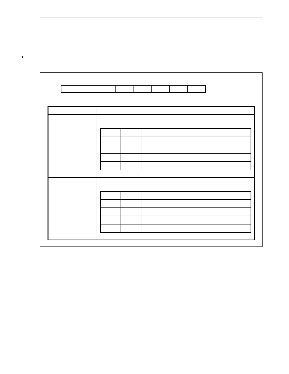
CHAPTER 14 PORT FUNCTIONS
715
User's Manual U14492EJ5V0UD
(3) Timer 3 noise elimination time selection register (NRC3)
The NRC3 register is used to set the clock source of timer 3 input pin noise elimination times.
This register can be read/written in 8-bit or 1-bit units.
Caution The noise elimination function starts operating by setting the TM3CE bit of the TMC30
register to 1 (enabling count operations).
7
0
NRC3
6
0
5
0
4
0
3
NRC33
2
NRC32
1
NRC31
0
NRC30
Address
FFFFF698H
Initial value
00H
Bit position
Bit name
Function
Selects the TO3/INTP31 pin noise elimination clock.
NRC33
NRC32
Noise elimination clock
0 0
f
XXTM3
/256
0 1
f
XXTM3
/128
1 0
f
XXTM3
/64
1 1
f
XXTM3
/32
3, 2
NRC33,
NRC32
Remark f
XXTM3
: Clock selected by PRM03 register
Selects the TI3/INTP30/TCLR3 pin noise elimination clock.
NRC31
NRC30
Noise elimination clock
0 0
f
XXTM3
/16
0 1
f
XXTM3
/8
1 0
f
XXTM3
/4
1 1
f
XXTM3
/2
1, 0
NRC31,
NRC30
Remark f
XXTM3
: Clock selected by PRM03 register
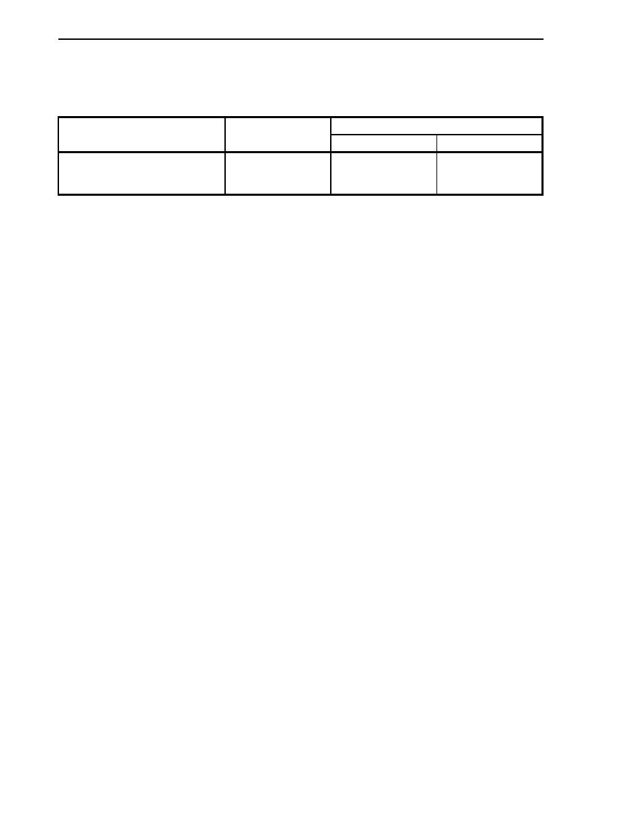
CHAPTER 14 PORT FUNCTIONS
716
User's Manual U14492EJ5V0UD
14.5.3 Timer 2 input pins
A noise eliminator using analog filtering and digital filtering using clock sampling are added to the timer 2 input
pins. A signal input that changes in less than these elimination times is not accepted internally.
Digital Filter
Pin
Analog Filter Noise
Elimination Time
Noise Elimination Time
Sampling Clock
P20/TI2/INTP20
P21/TO21/INTP21 to P24/TO24/INTP24
P25/TCLR2/INTP25
10 to 100 ns
4 to 5 clocks
f
XXTM2
Cautions 1. Since digital filtering uses clock sampling, if it is selected, input signals are not received
when the CPU clock is stopped.
2. The noise eliminator is valid only in control mode.
3. Refer to Figure 14-14 for an example of a noise eliminator.
Remark f
XXTM2
: Clock of TM20 and TM21 selected by PRM02 register
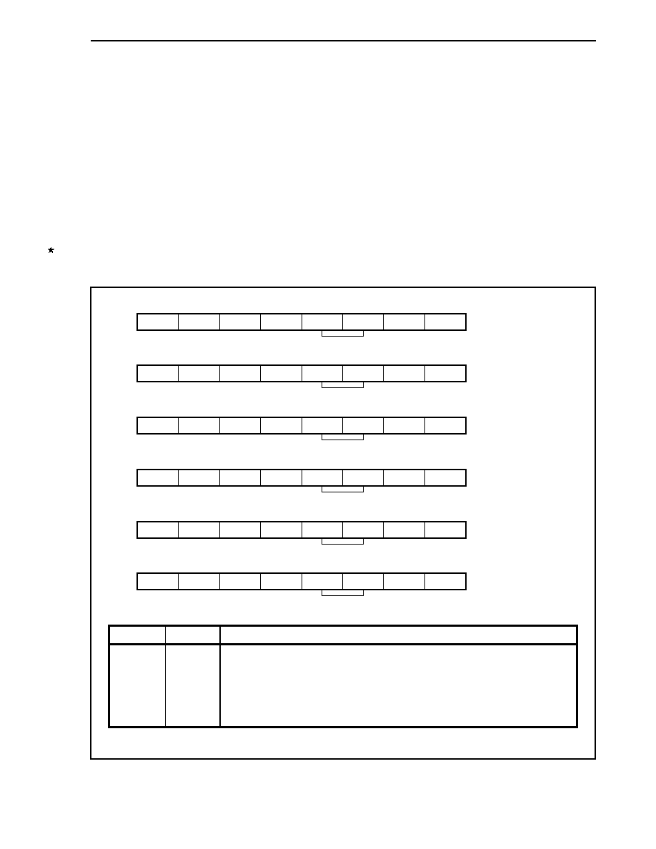
CHAPTER 14 PORT FUNCTIONS
717
User's Manual U14492EJ5V0UD
(1) Timer 2 input filter mode registers 0 to 5 (FEM0 to FEM5)
The FEMn registers are used to specify timer 2 input pin filtering and to set the clock source of noise
elimination times and the input valid edge.
These registers can be read/written in 8-bit or 1-bit units.
Cautions
1. Even when using the TI2/INTP20, TO21/INTP21, TO22/INTP22, TO23/INTP23,
TO24/INTP24, and TCLR2/INTP25 pins as INTP20, INTP21, INTP22, INTP23, INTP24, and
INTP25 without using timer 2, be sure to clear the STFTE bit of timer 2 clock stop
register 0 (STOPTE0) to 0.
2. Before setting the INTP2n pin to the trigger mode, set the PMC2 register. If the PMC2
register is set after the FEMn register has been set, an illegal interrupt may occur as
soon as the PMC2 register is set (n = 0 to 5).
3. The noise elimination function starts operating by setting the CEEn bit of the TCRE0
register to 1 (enabling count operations).
(1/2)
7
DFEN00
FEM0
6
0
5
0
4
0
3
EDGE010
2
EDGE000
1
TMS010
0
TMS000
Address
FFFFF630H
Initial value
00H
Address
FFFFF631H
Initial value
00H
Address
FFFFF632H
Initial value
00H
Address
FFFFF633H
Initial value
00H
Address
FFFFF634H
Initial value
00H
Address
FFFFF635H
Initial value
00H
INTP20
7
DFEN01
6
0
5
0
4
0
3
EDGE011
2
EDGE001
1
TMS011
0
TMS001
INTP21
7
DFEN02
6
0
5
0
4
0
3
EDGE012
2
EDGE002
1
TMS012
0
TMS002
INTP22
7
DFEN03
6
0
5
0
4
0
3
EDGE013
2
EDGE003
1
TMS013
0
TMS003
INTP23
7
DFEN04
6
0
5
0
4
0
3
EDGE014
2
EDGE004
1
TMS014
0
TMS004
INTP24
7
DFEN05
6
0
5
0
4
0
3
EDGE015
2
EDGE005
1
TMS015
0
TMS005
INTP25
FEM1
FEM2
FEM3
FEM4
FEM5
Bit position
Bit name
Function
7
DFEN0n
Specifies the INTP2n pin filter.
0: Analog filter
1: Digital filter
Caution When the DFEN0n bit = 1, the sampling clock of the digital filter is f
XXTM2
(clock of TM20 and TM21 selected by PRM02 register).
Remark n = 0 to 5
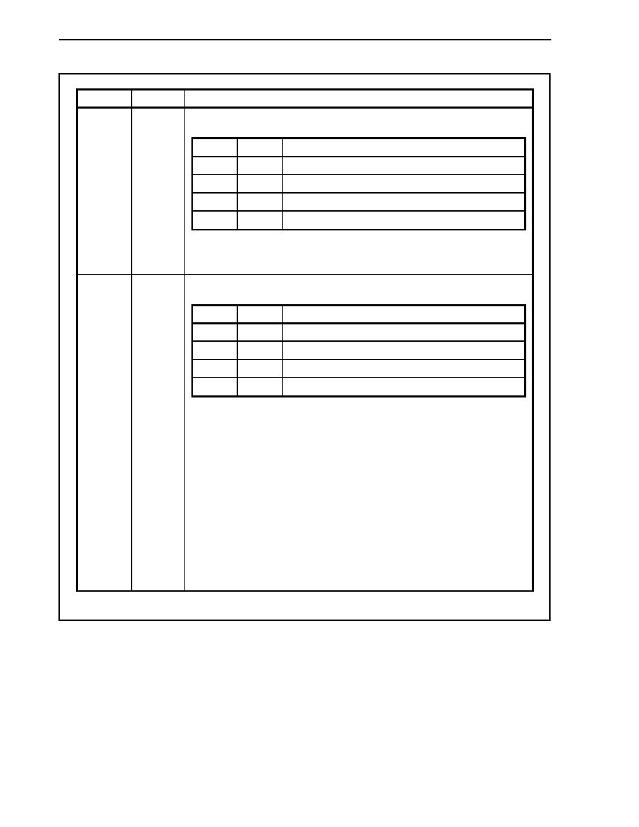
CHAPTER 14 PORT FUNCTIONS
718
User's Manual U14492EJ5V0UD
(2/2)
Bit position
Bit name
Function
Specifies the INTP2n pin valid edge.
EDGE01n EDGE00n
Operation
0
0
Interrupt due to INTCC2n
Note
0 1
Rising
edge
1 0
Falling
edge
1
1
Both rising and falling edges
3, 2
EDGE01n,
EDGE00n
Note Specify when selecting INTCC2n according to match of TM20, TM21
and sub-channel compare registers (TMS01n, TMS00n bit settings)
(n = 0 to 5).
Selects capture input
Note
.
TMS01n TMS00n
Operation
0
0
Use as pin
0
1
Digital filter (noise eliminator specification)
1
0
Capture to sub-channel 1 according to timer
1
1
Capture to sub-channel 2 according to timer
1, 0
TMS01n,
TMS00n
Note Capture input according to INTCM100 and INTCM101 can be
selected only for the FEM1 and FEM2 registers. Set the values of
the TMS01m and TMS00m bits in the FEMm register to 00B or 01B.
Settings other than these are prohibited (m = 1, 3 to 5).
Capture according to INTP21, INTP22 and INTCM100, INTCM101 is
possible for sub-channel 1 and sub-channel 2 of timer 2.
Examples are shown below.
(a) Capture sub-channel 1 on INTCM101
FEM1 register = xxxxxx10B
TMIC0 register = 00000010B
(b) Capture sub-channel 2 on INTCM101
FEM2 register = xxxxxx11B
TMIC0 register = 00001000B
Remark n = 0 to 5

719
User's Manual U14492EJ5V0UD
CHAPTER 15 RESET FUNCTION
When a low level is input to the RESET pin, there is a system reset and each hardware item of the V850E/IA1 is
initialized to its initial status.
When the RESET pin changes from low level to high level, reset status is released and the CPU starts program
execution. Initialize the contents of various registers as needed within the program.
15.1 Features
∑ Noise elimination using analog delay (approx. 60 ns) in reset pin (RESET)
15.2 Pin Functions
During a system reset period, most pin output is high impedance (all pins except CLKOUT
Note
, RESET, X2, V
DD5
,
V
SS5
, V
DD3
, V
SS3
, CV
DD
, CV
SS
, AV
DD
, AV
REF0
, AV
REF1
, and AV
SS
pins).
Thus, if for example memory is extended externally, a pull-up (or pull-down) resistor must be attached to each pin
of ports DH, DL, CS, CT, and CM. If there are no resistors, the external memory that is connected may be destroyed
when these pins become high impedance.
Similarly, perform pin processing so that on-chip peripheral I/O function signal output and output ports are not
affected.
Note In ROMless mode 0 or 1 and single-chip mode 1, CLKOUT signals also are output during a reset period.
In single-chip mode 0, CLKOUT signals are not output until the PMCCM register is set.
Table 15-1 shows the operation status of each pin during a reset period.
Table 15-1. Operation Status of Each Pin During Reset Period
Pin Status
Pin Name
In Single-Chip
Mode 0
In Single-Chip
Mode 1
In ROMless
Mode 0
In ROMless
Mode 1
A16 to A23, AD0 to AD15, CS0 to CS7,
LWR, UWR, RD, ASTB, WAIT, HLDAK,
HLDRQ
(Port mode)
High impedance
CLKOUT (Port
mode)
Operation
Ports 0 to 4
(Input)
Port pins
Ports CM, CS, CT, DH, DL
(Input)
(Control mode)
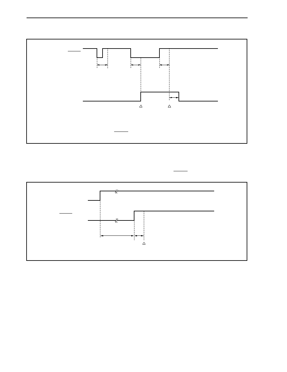
CHAPTER 15 RESET FUNCTION
720
User's Manual U14492EJ5V0UD
(1) Reset signal acknowledgment
RESET
Internal system
reset signal
Elimination as noise
Reset acknowledgment
Reset release
Analog
delay
Analog
delay
Analog
delay
Note
Note The internal system reset signal continues in active status for a period of at least 4 system clocks after
the timing of a reset release by the RESET pin.
(2) Reset at power-on
A reset operation at power-on (power supply application) must guarantee oscillation stabilization time from
power-on until reset acknowledgment due to the low level width of the RESET signal.
RESET (input)
V
DD3
, V
DD5
Reset release
Analog delay
Oscillation
stabilization time

CHAPTER 15 RESET FUNCTION
721
User's Manual U14492EJ5V0UD
15.3 Initialization
Initialize the contents of each register as needed within a program.
Table 15-2 shows the initial values of the CPU, internal RAM, and on-chip peripheral I/O after reset.
Table 15-2. Initial Values of CPU, Internal RAM, and On-Chip Peripheral I/O After Reset (1/6)
On-Chip Hardware
Register Name
Initial Value After Reset
General-purpose register (r0)
00000000H
General-purpose registers (r1 to r31)
Undefined
Program registers
Program counter (PC)
00000000H
Status saving register during interrupt (EIPC, EIPSW)
Undefined
Status saving register during NMI (FEPC, FEPSW)
Undefined
Interrupt source register (ECR)
00000000H
Program status word (PSW)
00000020H
Status saving register during CALLT execution (CTPC, CTPSW)
Undefined
Status saving register during exception/debug trap (DBPC, DBPSW)
Undefined
CPU
System registers
CALLT base pointer (CTBP)
Undefined
Internal RAM
-
Undefined
Chip area selection control register n (CSCn) (n = 0, 1)
2C11H
Peripheral area selection control register (BPC)
0000H
Bus size configuration register (BSC)
0000H/5555H
Bus control
function
System wait control register (VSWC)
77H
Bus cycle type configuration register n (BCTn) (n = 0, 1)
CCCCH
Data wait control register n (DWCn) (n = 0, 1)
3333H
Address wait control register (AWC)
0000H
Memory control
function
Bus cycle control register (BCC)
AAAAH
DMA source address register nL (DSAnL) (n = 0 to 3)
Undefined
DMA source address register nH (DSAnH) (n = 0 to 3)
Undefined
DMA destination address register nL (DDAnL) (n = 0 to 3)
Undefined
DMA destination address register nH (DDAnH) (n = 0 to 3)
Undefined
DMA transfer count register n (DBCn) (n = 0 to 3)
Undefined
DMA addressing control register n (DADCn) (n = 0 to 3)
0000H
DMA channel control register n (DCHCn) (n = 0 to 3)
00H
DMA disable status register (DDIS)
00H
DMA restart register (DRST)
00H
DMA function
DMA trigger factor register n (DTFRn) (n = 0 to 3)
00H
In-service priority register (ISPR)
00H
External interrupt mode register n (INTMn) (n = 0 to 2)
00H
Interrupt mask register n (IMRn) (n = 0 to 3)
FFFFH
Interrupt mask register nL (IMRnL) (n = 0 to 3)
FFH
On-chip
peripheral
I/O
Interrupt/exception
control function
Interrupt mask register nH (IMRnH) (n = 0 to 3)
FFH
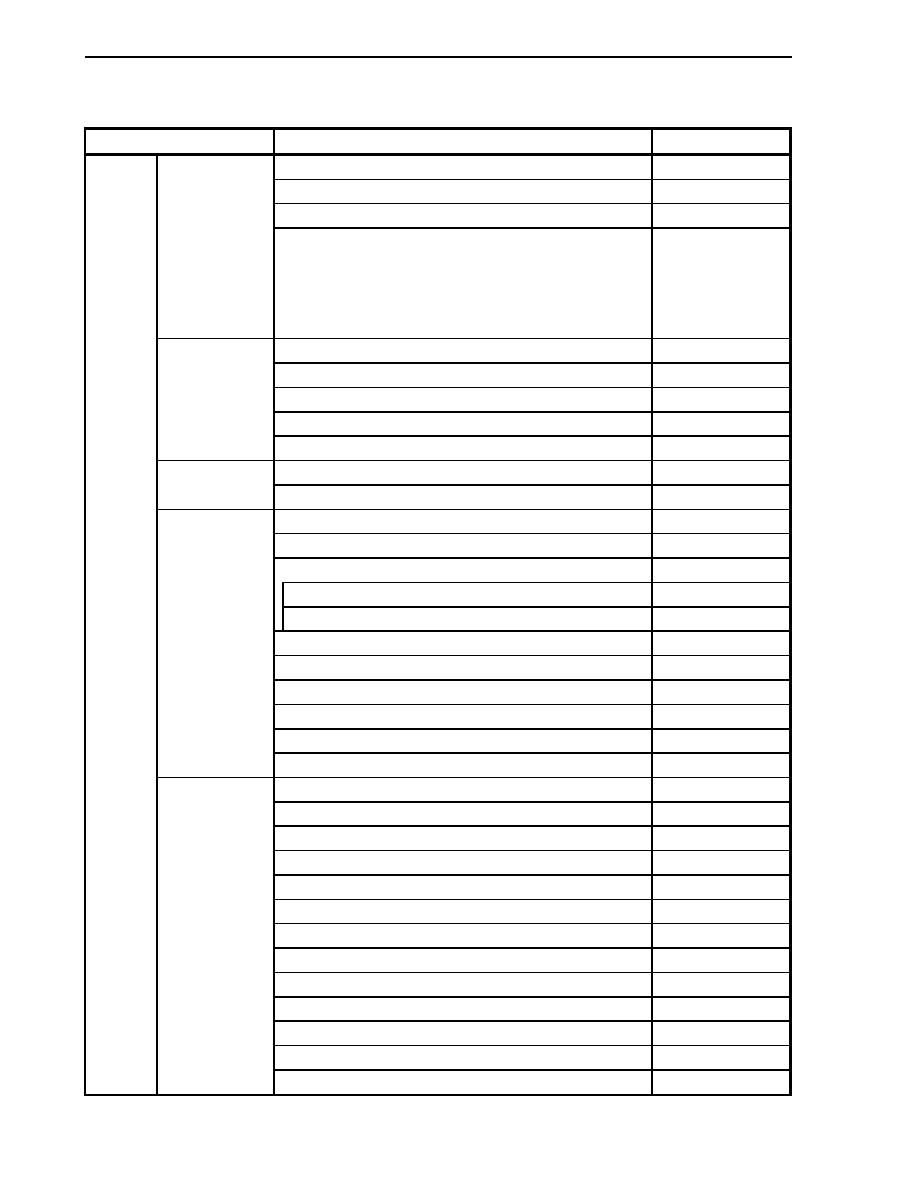
CHAPTER 15 RESET FUNCTION
722
User's Manual U14492EJ5V0UD
Table 15-2. Initial Values of CPU, Internal RAM, and On-Chip Peripheral I/O After Reset (2/6)
On-Chip Hardware
Register Name
Initial Value After Reset
Signal edge selection register n (SESA1n) (n = 10, 11)
00H
Valid edge selection register (SESC)
00H
Timer 2 input filter mode register n (FEMn) (n = 0 to 5)
00H
Interrupt/exception
control function
Interrupt control registers (P0IC0 to P0IC6, DETIC0, DETIC1,
TM0IC0, CM03IC0, TM0IC1, CM03IC1, CC10IC0, CC10IC1,
CM10IC0, CM10IC1, CC11IC0, CC11IC1, CM11IC0, CM11IC1,
TM2IC0, TM2IC1, CC2IC0 to CC2IC5, TM3IC0, CC3IC0, CC3IC1,
CM4IC0, DMAIC0 to DMAIC3, CANIC0 to CANIC3, CSIIC0, CSIIC1,
SRIC0 to SRIC2, STIC0 to STIC2, SEIC0, ADIC0, ADIC1)
47H
Command register (PRCMD)
Undefined
Power save control register (PSC)
00H
Clock control register (CKC)
00H
Power save mode register (PSMR)
00H
Power save
control function
Lock register (LOCKR)
0000000xB
Peripheral command register (PHCMD)
Undefined
System control
Peripheral status register (PHS)
00H
Dead-time timer reload register n (DTRRn) (n = 0, 1)
0FFFH
Buffer registers CM0n, CM1n (BFCM0n, BFCM1n) (n = 0 to 3)
FFFFH
Timer control register 0n (TMC0n) (n = 0, 1)
0508H
Timer control register 0nL (TMC0nL) (n = 0, 1)
08H
Timer control register 0nH (TMC0nH) (n = 0, 1)
05H
Timer unit control register 0n (TUC0n) (n = 0, 1)
01H
Timer output mode register n (TOMRn) (n = 0, 1)
00H
PWM software timing output register n (PSTOn) (n = 0, 1)
00H
PWM output enable register n (POERn) (n = 0, 1)
00H
TOMR write enable register n (SPECn) (n = 0, 1)
0000H
Timer 0
Timer 0 clock selection register (PRM01)
00H
Timer 1n (TM1n) (n = 0, 1)
0000H
Compare register 1n (CM1n) (n = 00, 01, 10, 11)
0000H
Capture/compare register 1n (CC1n) (n = 00, 01, 10, 11)
0000H
Capture/compare control register n (CCRn) (n = 0, 1)
00H
Timer unit mode register n (TUMn) (n = 0, 1)
00H
Timer control register 1n (TMC1n) (n = 0, 1)
00H
Signal edge selection register 1n (SESA1n) (n = 0, 1)
00H
Prescaler mode register 1n (PRM1n) (n = 0, 1)
07H
Status register n (STATUSn) (n = 0, 1)
00H
Timer connection selection register 0 (TMIC0)
00H
Timer 1/timer 2 clock selection register (PRM02)
00H
CC1n1 capture input selection register (CSL1n) (n = 0, 1)
00H
On-chip
peripheral
I/O
Timer 1
Timer 1n noise elimination time selection register (NRC1n) (n = 0, 1) 00H

CHAPTER 15 RESET FUNCTION
723
User's Manual U14492EJ5V0UD
Table 15-2. Initial Values of CPU, Internal RAM, and On-Chip Peripheral I/O After Reset (3/6)
On-Chip Hardware
Register Name
Initial Value After Reset
Timer 2 clock stop register 0 (STOPTE0)
0000H
Timer 2 clock stop register 0L (STOPTE0L)
00H
Timer 2 clock stop register 0H (STOPTE0H)
00H
Timer 2 count clock/control edge selection register 0 (CSE0)
0000H
Timer 2 count clock/control edge selection register 0L (CSE0L)
00H
Timer 2 count clock/control edge selection register 0H (CSE0H)
00H
Timer 2 sub-channel input event edge selection register 0 (SESE0)
0000H
Timer 2 sub-channel input event edge selection register 0L (SESE0L) 00H
Timer 2 sub-channel input event edge selection register 0H (SESE0H)
00H
Timer 2 time base control register 0 (TCRE0)
0000H
Timer 2 time base control register 0L (TCRE0L)
00H
Timer 2 time base control register 0H (TCRE0H)
00H
Timer 2 output control register 0 (OCTLE0)
0000H
Timer 2 output control register 0L (OCTLE0L)
00H
Timer 2 output control register 0H (OCTLE0H)
00H
Timer 2 sub-channel 0, 5 capture/compare control register
(CMSE050)
0000H
Timer 2 sub-channel 1, 2 capture/compare control register
(CMSE120)
0000H
Timer 2 sub-channel 3, 4 capture/compare control register
(CMSE340)
0000H
Timer 2 sub-channel n sub capture/compare register (CVSEn0) (n =
1 to 4)
0000H
Timer 2 sub-channel n main capture/compare register (CVPEn0) (n
= 1 to 4)
0000H
Timer 2 sub-channel n capture/compare register (CVSEn0) (n = 0, 5)
0000H
Timer 2 time base status register 0 (TBSTATE0)
0101H
Timer 2 time base status register 0L (TBSTATE0L)
01H
Timer 2 time base status register 0H (TBSTATE0H)
01H
Timer 2 capture/compare 1 to 4 status register 0 (CCSTATE0)
0000H
Timer 2 capture/compare 1 to 4 status register 0L (CCSTATE0L)
00H
Timer 2 capture/compare 1 to 4 status register 0H (CCSTATE0H)
00H
Timer 2 output delay register 0 (ODELE0)
0000H
Timer 2 output delay register 0L (ODELE0L)
00H
Timer 2 output delay register 0H (ODELE0H)
00H
Timer 2
Timer 2 software event capture register (OSCE0)
0000H
Timer 3 (TM3)
0000H
Capture/compare register 3n (CC3n) (n = 0, 1)
0000H
Timer control register 30 (TMC30)
00H
On-chip
peripheral
I/O
Timer 3
Timer control register 31 (TMC31)
20H
CHAPTER 15 RESET FUNCTION
724
User's Manual U14492EJ5V0UD
Table 15-2. Initial Values of CPU, Internal RAM, and On-Chip Peripheral I/O After Reset (4/6)
On-Chip Hardware
Register Name
Initial Value After Reset
Valid edge selection register (SESC)
00H
Timer 3 clock selection register (PRM03)
00H
Timer 3
Timer 3 noise elimination time selection register (NRC3)
00H
Timer 4 (TM4)
0000H
Compare register 4 (CM4)
0000H
Timer 4
Timer control register 4 (TMC4)
00H
Clocked serial interface mode register n (CSIMn) (n = 0, 1)
00H
Clocked serial interface clock selection register n (CSICn) (n = 0, 1)
00H
Clocked serial interface receive buffer register n (SIRBn) (n = 0, 1)
0000H
Clocked serial interface receive buffer register Ln (SIRBLn) (n = 0, 1)
00H
Clocked serial interface transmit buffer register n (SOTBn) (n = 0, 1) 0000H
Clocked serial interface transmit buffer register Ln (SOTBLn) (n =
0, 1)
00H
Clocked serial interface read-only receive buffer register n (SIRBEn)
(n = 0, 1)
0000H
Clocked serial interface read-only receive buffer register Ln
(SIRBELn) (n = 0, 1)
00H
Clocked serial interface initial transmit buffer register n (SOTBFn)
(n = 0, 1)
0000H
Clocked serial interface initial transmit buffer register Ln
(SOTBFLn) (n = 0, 1)
00H
Serial I/O shift register n (SIOn) (n = 0, 1)
0000H
Serial I/O shift register Ln (SIOLn) (n = 0, 1)
00H
Prescaler mode register (PRSM3)
00H
Serial interface
function (CSI0,
CSI1)
Prescaler compare register (PRSCM3)
00H
Asynchronous serial interface mode register 0 (ASIM0)
01H
Receive buffer register 0 (RXB0)
FFH
Asynchronous serial interface status register 0 (ASIS0)
00H
Transmit buffer register 0 (TXB0)
FFH
Asynchronous serial interface transmit status register 0 (ASIF0)
00H
Baud rate generator control register 0 (BRGC0)
FFH
Serial interface
function (UART0)
Clock selection register 0 (CKSR0)
00H
Asynchronous serial interface mode register n0 (ASIMn0) (n = 1, 2)
81H
Asynchronous serial interface mode register n1 (ASIMn1) (n = 1, 2)
00H
Asynchronous serial interface status register n (ASISn) (n = 1, 2)
00H
2-frame continuous reception buffer register n (RXBn) (n = 1, 2)
Undefined
Receive buffer register Ln (RXBLn) (n = 1, 2)
Undefined
On-chip
peripheral
I/O
Serial interface
function (UART1,
UART2)
2-frame continuous transmission shift register n (TXSn) (n = 1, 2)
Undefined

CHAPTER 15 RESET FUNCTION
725
User's Manual U14492EJ5V0UD
Table 15-2. Initial Values of CPU, Internal RAM, and On-Chip Peripheral I/O After Reset (5/6)
On-Chip Hardware
Register Name
Initial Value After Reset
Transmit shift register Ln (TXSLn) (n = 1, 2)
Undefined
Prescaler mode register n (PRSMn) (n = 1, 2)
00H
Serial interface
function (UART1,
UART2)
Prescaler compare register n (PRSCMn) (n = 1, 2)
00H
CAN message data length register n (M_DLCn) (n = 00 to 31)
Undefined
CAN message control register n (M_CTRLn) (n = 00 to 31)
Undefined
CAN message time stamp register n (M_TIMEn) (n = 00 to 31)
Undefined
CAN message data register nm (M_DATAnm) (n = 00 to 31, m = 0
to 7)
Undefined
CAN message ID register Ln, Hn (M_IDLn, M_IDHn) (n = 00 to 31)
Undefined
CAN message configuration register n (M_CONFn) (n = 00 to 31)
Undefined
CAN message status register n (M_STATn) (n = 00 to 31)
Undefined
CAN status set/clear register n (SC_STATn) (n = 00 to 31)
0000H
CAN interrupt pending register (CCINTP)
0000H
CAN global interrupt pending register (CGINTP)
00H
CAN1 interrupt pending register (C1INTP)
00H
CAN stop register (CSTOP)
0000H
CAN global status register (CGST)
0100H
CAN global interrupt enable register (CGIE)
0A00H
CAN main clock selection register (CGCS)
7F05H
CAN time stamp count register (CGTSC)
0000H
CAN message search start/result register (CGMSS on write;
CGMSR on read)
0000H
CAN1 address mask n register L, H (C1MASKLn, C1MASKHn)
(n = 0 to 3)
Undefined
CAN1 control register (C1CTRL)
0101H
CAN1 definition register (C1DEF)
0000H
CAN1 information register (C1LAST)
00FFH
CAN1 error count register (C1ERC)
0000H
CAN1 interrupt enable register (C1IE)
0900H
CAN1 bus active register (C1BA)
00FFH
CAN1 bit rate prescaler register (C1BRP)
0000H
CAN1 bus diagnostic information register (C1DINF)
0000H
CAN1 synchronization control register (C1SYNC)
0218H
Serial interface
function (FCAN)
FCAN clock selection register (PRM04)
00H
A/D scan mode register n0 (ADSCMn0) (n = 0, 1)
0000H
A/D scan mode register n0L (ADSCMn0L) (n = 0, 1)
00H
A/D scan mode register n0H (ADSCMn0H) (n = 0, 1)
00H
A/D scan mode register n1 (ADSCMn1) (n = 0, 1)
0000H
A/D scan mode register n1L (ADSCMn1L) (n = 0, 1)
00H
On-chip
peripheral
I/O
A/D converter
A/D scan mode register n1H (ADSCMn1H) (n = 0, 1)
00H
CHAPTER 15 RESET FUNCTION
726
User's Manual U14492EJ5V0UD
Table 15-2. Initial Values of CPU, Internal RAM, and On-Chip Peripheral I/O After Reset (6/6)
On-Chip Hardware
Register Name
Initial Value After Reset
A/D voltage detection mode register n (ADETMn) (n = 0, 1)
0000H
A/D voltage detection mode register nL (ADETMnL) (n = 0, 1)
00H
A/D voltage detection mode register nH (ADETMnH) (n = 0, 1)
00H
A/D conversion result register 0n (ADCR0n) (n = 0 to 7)
0000H
A/D conversion result register 1n (ADCR1n) (n = 0 to 7)
0000H
A/D converter
A/D internal trigger selection register (ITRG0)
00H
Ports (P0 to P4, PDH, PCS, PCT, PCM)
Undefined
Port (PDL)
Undefined
Port (PDLL)
Undefined
Port (PDLH)
Undefined
Mode registers (PM1 to PM4, PMDH, PMCS, PMCT, PMCM)
FFH
Mode register (PMDL)
FFFFH
Mode register (PMDLL)
FFH
Mode register (PMDLH)
FFH
Mode control registers (PMC1 to PMC4)
00H
Mode control registers (PMCDH, PMCCS)
00H/FFH
Mode control register (PMCDL)
0000H/FFFFH
Mode control register (PMCDLL)
00H/FFH
Mode control register (PMCDLH)
00H/FFH
Mode control register (PMCCT)
00H/53H
Mode control register (PMCCM)
00H/0FH
Port function
Function control registers (PFC1, PFC2)
00H
RAM access data buffer register L (NBDL)
0000H
RAM access data buffer register LL (NBDLL)
00H
RAM access data buffer register LU (NBDLU)
00H
RAM access data buffer register H (NBDH)
0000H
RAM access data buffer register HL (NBDHL)
00H
RAM access data buffer register HU (NBDHU)
00H
DMA source address setting register SL (NBDMSL)
Undefined
DMA source address setting register SH (NBDMSH)
Undefined
DMA destination address setting register DL (NBDMDL)
Undefined
NBD function
DMA destination address setting register DH (NBDMDH)
Undefined
On-chip
peripheral
I/O
Flash memory
Flash programming mode control register (FLPMC)
08H/0CH/00H
Note
Note
µ
PD703116: 00H
µ
PD70F3116: 08H or 0CH (For details, refer to 16.7.12 Flash programming mode control register
(FLPMC).)
Caution In the table above, "Undefined" means either undefined at the time of a power-on reset or
undefined due to data destruction when RESET
input and data write timing are synchronized.
On a RESET
other than this, data is maintained in its previous status.

727
User's Manual U14492EJ5V0UD
CHAPTER 16 FLASH MEMORY (
µPD70F3116)
The
µ
PD70F3116 is the flash memory version of the V850E/IA1 and it has an on-chip 256 KB flash memory
configured as two 128 KB areas.
Caution There are differences in noise immunity and noise radiation between the flash memory and mask
ROM versions. When pre-producing an application set with the flash memory version and then
mass producing it with the mask ROM version, be sure to conduct sufficient evaluations on the
commercial samples (CS) (not engineering samples (ES)) of the mask ROM versions.
Writing to a flash memory can be performed with memory mounted on the target system (on board). The
dedicated flash programmer is connected to the target system to perform writing.
The following can be considered as the development environment and the applications using a flash memory.
∑ Software can be changed after the V850E/IA1 is solder mounted on the target system.
∑ Small scale production of various models is made easier by differentiating software.
∑ Data adjustment in starting mass production is made easier.
16.1 Features
∑ All area batch erase, or erase in area units (128 KB)
∑ Communication through serial interface from the dedicated flash programmer
∑ Erase/write voltage: V
PP
= 7.8 V
∑ On-board
programming
∑ Flash memory programming is possible by the self-programming in area units (128 KB)
16.2 Writing by Flash Programmer
Writing can be performed either on-board or off-board by the dedicated flash programmer.
Caution When writing data with the flash programmer, the operation is always performed at the
frequency multiplied by 5 in the PLL mode.
(1) On-board programming
The contents of the flash memory is rewritten after the V850E/IA1 is mounted on the target system. Mount
connectors, etc., on the target system to connect the dedicated flash programmer.
(2) Off-board programming
Writing to a flash memory is performed by the dedicated program adapter (FA Series), etc., before mounting
the V850E/IA1 on the target system.
Remark The FA Series is a product of Naito Densei Machida Mfg. Co., Ltd.
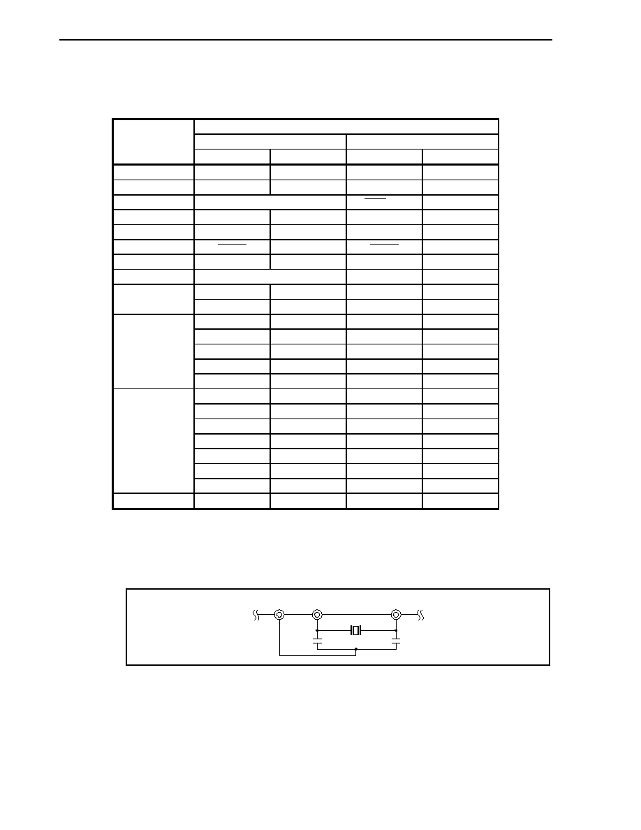
CHAPTER 16 FLASH MEMORY (
µ
PD70F3116)
728
User's Manual U14492EJ5V0UD
When the flash programming adapter (FA-144GJ-8EU) is used for writing, connect the pins as follows.
Table 16-1. Connection of V850E/IA1 Flash Programming Adapter (FA-144GJ-8EU)
V850E/IA1
UART0 CSI0
FA-144GJ-8EU
Silk Name
Pin Name
Pin No.
Pin Name
Pin No.
SI TXD0/P31
38
SO0/P41
30
SO RXD0/P30
37
SI0/P40
29
SCK
-
SCK0/P42 31
X1 X1
23
Note 1
X1 23
Note 1
X2 X2
24
Note 1
X2 24
Note 1
/RESET RESET 20 RESET 20
V
PP
V
PP
/IC5 89 V
PP
/IC5 89
RESERVE/HS
-
A16/PDH0
Note 2
73
V
DD3
53,
128 V
DD3
53,
128
LVDD
Note 3
CV
DD
21 CV
DD
21
V
DD5
56, 91, 125
V
DD5
56, 91, 125
AV
REF0
137 AV
REF0
137
AV
REF1
4 AV
REF1
4
MODE1 27 MODE1 27
VDD
AV
DD
2,
135 AV
DD
2,
135
V
SS3
54,
127 V
SS3
54,
127
V
SS5
55, 90, 126
V
SS5
55, 90, 126
AV
SS
3,
136 AV
SS
3,
136
CV
SS
22 CV
SS
22
MODE0 26 MODE0 26
MODE2 28 MODE2 28
GND
NMI/P00 111 NMI/P00 111
Note 4
CKSEL 25 CKSEL 25
Notes 1. Configure the oscillator on the FA-144GJ-8EU board using a resonator and a capacitor. The following
figure shows an example of the oscillator.
Example
CV
SS
X1
X2
2. Connection is not required for this pin when not using handshakes.
3. The option of dual-power-supply adapter (FA-TVC) for generating 3.3 V is available.
4. In PLL mode:
GND
In direct mode:
V
DD5
Remark
-: Leave open
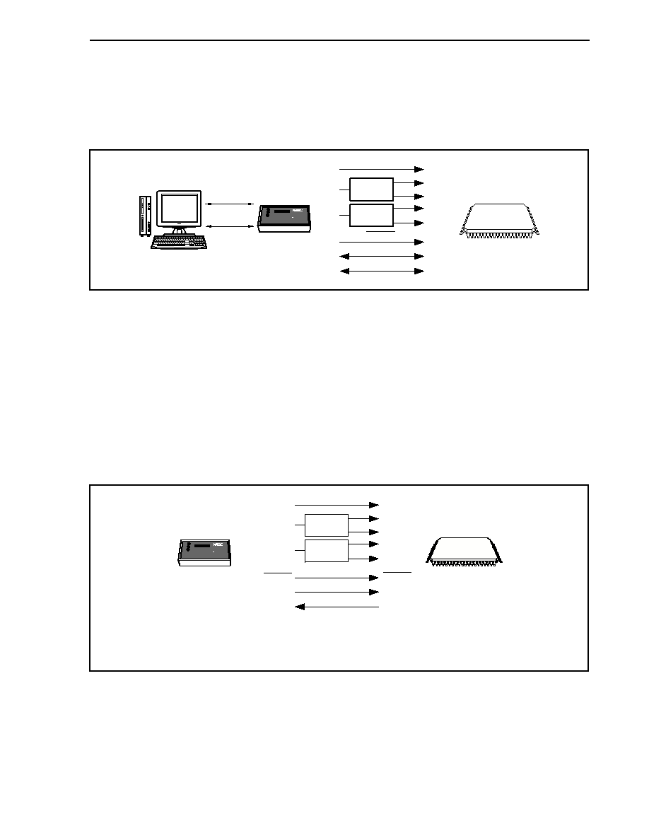
CHAPTER 16 FLASH MEMORY (
µ
PD70F3116)
729
User's Manual U14492EJ5V0UD
16.3 Programming Environment
The following shows the environment required for writing programs to the flash memory of the V850E/IA1.
Figure 16-1. Environment for Writing Program to Flash Memory
V850E/IA1
Dedicated flash
programmer
RS-232C
Host machine
V
PP1
V
DD
V
PP
V
DD3
V
DD5
V
SS5
V
SS3
GND
Regulator
Regulator
UART0
CSI0
RESET
PG-FP4
(Flash Pro4)
Cxxxxxx
Bxxxxx
Axxxx
XXX YYY
X
X
X
X
X
X
X
X
X
X
X
X
X
X
X
XXXX YYYY
STATVE
USB
A host machine is required for controlling the dedicated flash programmer.
UART0 or CSI0 is used for the interface between the dedicated flash programmer and the V850E/IA1 to perform
writing, erasing, etc. A dedicated program adapter (FA Series) is required for off-board writing. Supply the operating
clock of the V850E/IA1 via the oscillator configured on the V850E/IA1 board using a resonator and a capacitor.
16.4 Communication Mode
(1)
UART0
Transfer rate: 4,800 bps to 76,800 bps (LSB first)
Figure 16-2. Communication with Dedicated Flash Programmer (UART0)
V850E/IA1
V
PP1
V
DD
V
PP
V
DD3
V
DD5
V
SS5
V
SS3
GND
RESET
Regulator
Regulator
SO
SI
Dedicated flash
programmer
TXD0
RXD0
RESET
PG-FP4
(Flash Pro4)
Cxxxxxx
Bxxxxx
Axxxx
X
X
X
YY
Y
X
X
X
X
X
X
X
X
X
X
X
X
X
X
X
X
X
X
X Y
Y
Y
Y
STATVE
Caution Supply the operating clock of the V850E/IA1 via the oscillator configured on the
V850E/IA1 board using a resonator and a capacitor.

CHAPTER 16 FLASH MEMORY (
µ
PD70F3116)
730
User's Manual U14492EJ5V0UD
(2) CSI0
Transfer rate: up to 2 MHz (MSB first)
Figure 16-3. Communication with Dedicated Flash Programmer (CSI0)
V850E/IA1
RESET
SO
SI
SCK
Dedicated flash
programmer
SCK0
SO0
SI0
RESET
V
PP1
V
DD
V
PP
V
DD3
V
DD5
V
SS5
V
SS3
GND
Regulator
Regulator
PG-FP4
(Flash Pro4)
Cxxxxxx
Bxxxxx
Axxxx
X
X
X
YY
Y
X
X
X
X
X
X
X
X
X
X
X
X
X
X
X
X
X
X
X
Y
Y
Y
Y
STATVE
Caution Supply the operating clock of the V850E/IA1 via the oscillator configured on the
V850E/IA1 board using a resonator and a capacitor.
The dedicated flash programmer outputs transfer clocks and the V850E/IA1 operates as a slave.
(3) Handshake-supported CSI communication
Transfer rate: up to 2 MHz (MSB first)
Figure 16-4. Communication with Dedicated Flash Programmer (Handshake-Supported CSI Communication)
V850E/IA1
Dedicated flash
programmer
RESET
RESET
SO
SI
SO0
SI0
PDH0
SCK
SCK0
HS
V
PP1
V
DD
V
PP
V
DD3
V
DD5
V
SS5
V
SS3
GND
Regulator
Regulator
PG-FP4
(Flash Pro4)
Cxxxxxx
Bxxxxx
Axxxx
X
X
X
Y
Y
Y
X
X
X
X
X
X
X
X
X
X
X
X
X
X
X
X
X
X
X Y
Y
Y
Y
STATVE
Caution Supply the operating clock of the V850E/IA1 via the oscillator configured on the
V850E/IA1 board using a resonator and a capacitor.
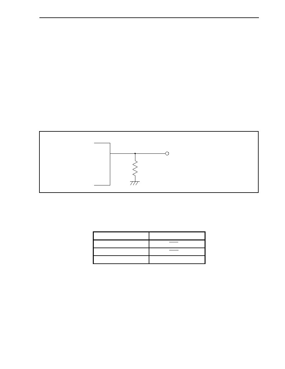
CHAPTER 16 FLASH MEMORY (
µ
PD70F3116)
731
User's Manual U14492EJ5V0UD
16.5 Pin Connection
When performing on-board writing, install a connector on the target system to connect to the dedicated flash
programmer. Also, install a function on-board to switch from the normal operation mode (single-chip modes 0, 1 or
ROMless modes 0, 1) to the flash memory programming mode.
In the flash memory programming mode, all the pins not used for flash memory programming become the same
status as they were immediately after reset in single-chip mode 0. Therefore, all the ports enter the output high-
impedance status, so that pin handling is required when the external device does not acknowledge the output high-
impedance status.
16.5.1 V
PP
pin
In the normal operation mode, 0 V is input to the V
PP
pin. In the flash memory programming mode, 7.8 V writing
voltage is supplied to the V
PP
pin. The following shows an example of the connection of the V
PP
pin.
Figure 16-5. Connection Example of V
PP
Pin
V850E/IA1
V
PP
Pull-down resistor (R
VPP
= 4.7 to 47 k
)
Dedicated flash programmer connection pin
16.5.2 Serial interface pin
The following shows the pins used by each serial interface.
Table 16-2. Pins Used by Each Serial Interface
Serial Interface
Pins Used
CSI0
SO0, SI0, SCK0
CSI0 + HS
SO0, SI0, SCK0, PDH0
UART0 TXD0,
RXD0
When connecting a dedicated flash programmer to a serial interface pin that is connected to other devices on-
board, care should be taken to avoid the conflict of signals and the malfunction of other devices, etc.
(1) Conflict of signals
When connecting a dedicated flash programmer (output) to a serial interface pin (input) which is connected to
another device (output), a conflict of signals occurs. To avoid the conflict of signals, isolate the connection to
the other device or set the other device to the output high-impedance status.
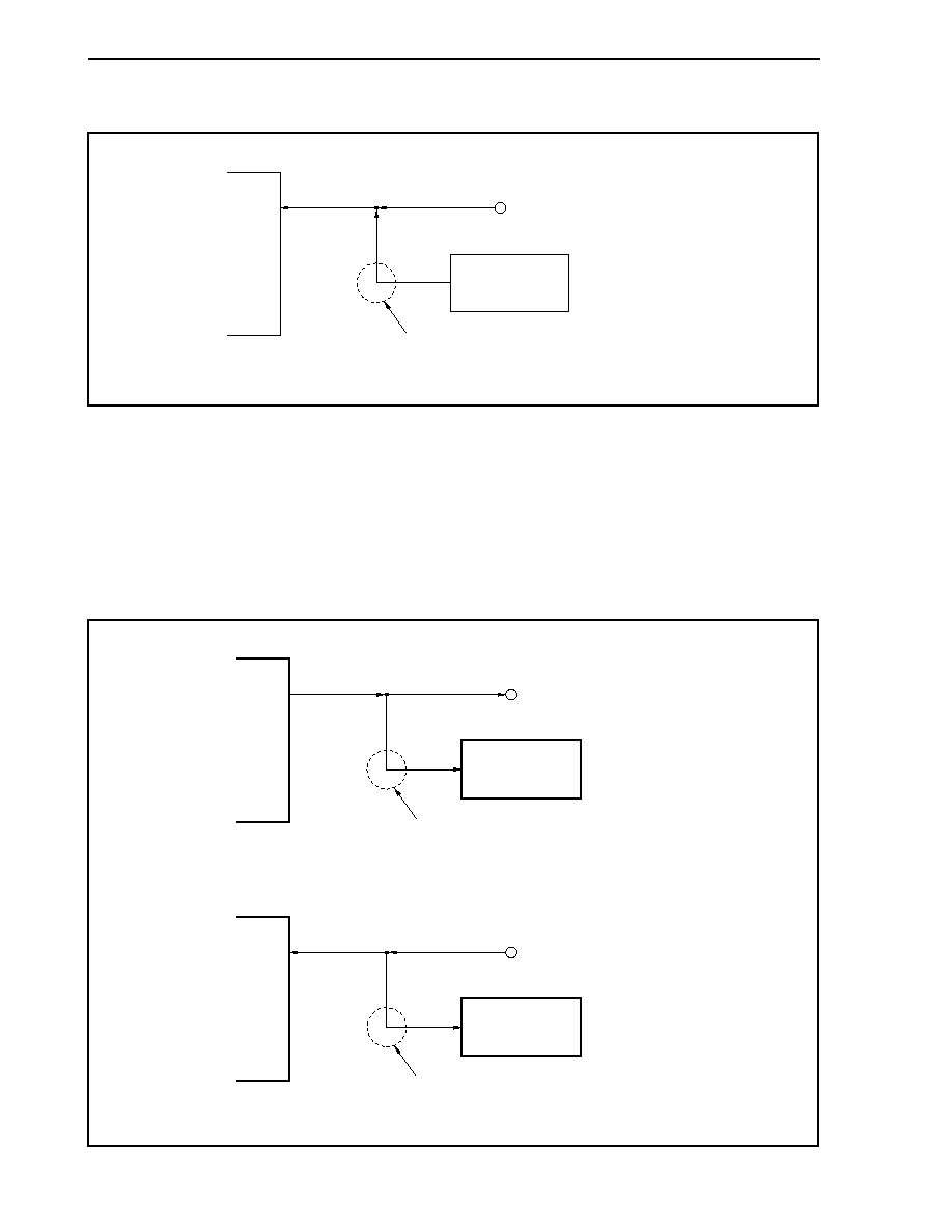
CHAPTER 16 FLASH MEMORY (
µ
PD70F3116)
732
User's Manual U14492EJ5V0UD
Figure 16-6. Conflict of Signals (Serial Interface Input Pin)
V850E/IA1
Input pin
Output pin
Other device
Dedicated flash programmer connection pin
Conflict of signals
In the flash memory programming mode, the signal that the
dedicated flash programmer sends out conflicts with signals the
other device outputs. Therefore, isolate the signals on the other
device side.
(2) Malfunction of the other device
When connecting a dedicated flash programmer (output or input) to a serial interface pin (input or output)
connected to another device (input), the signal output to the other device may cause the device to
malfunction. To avoid this, isolate the connection to the other device or make the setting so that the input
signal to the other device is ignored.
Figure 16-7. Malfunction of Other Device
V850E/IA1
Pin
Input pin
Other device
Dedicated flash programmer connection pin
In the flash memory programming mode, if the signal the
V850E/IA1 outputs affects the other device, isolate the
signal on the other device side.
V850E/IA1
Pin
Input pin
Other device
Dedicated flash programmer connection pin
In the flash memory programming mode, if the signal the
dedicated flash programmer outputs affects the other
device, isolate the signal on the other device side.
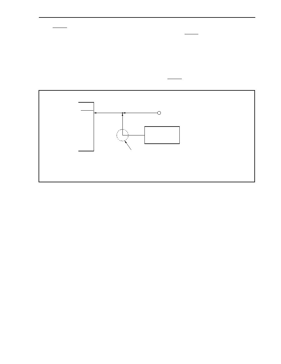
CHAPTER 16 FLASH MEMORY (
µ
PD70F3116)
733
User's Manual U14492EJ5V0UD
16.5.3 RESET pin
When connecting the reset signals of the dedicated flash programmer to the RESET pin, which is connected, to the
reset signal generator on-board, a conflict of signals occurs. To avoid the conflict of signals, isolate the connection to
the reset signal generator.
When the reset signal is input from the user system in flash memory programming mode, the programming
operation will not be performed correctly. Therefore, do not input signals other than the reset signals from the
dedicated flash programmer.
Figure 16-8. Conflict of Signals (RESET Pin)
V850E/IA1
RESET
Output pin
Reset signal generator
Dedicated flash programmer connection pin
Conflict of signals
In the flash memory programming mode, the signal
the reset signal generator outputs conflicts with the
signal the dedicated flash programmer outputs.
Therefore, isolate the signals on the reset signal
generator side.
16.5.4 NMI pin
Do not change the input signal to the NMI pin in flash memory programming mode. If it is changed in flash memory
programming mode, programming may not be performed correctly.
16.5.5 MODE0 to MODE2 pins
To shift to the flash memory programming mode, set MODE0 to high-level or low-level input, MODE1 to high-level
input, and MODE2 to low-level input, apply the writing voltage (7.8 V) to the V
PP
pin, and release reset.
16.5.6 Port pins
When the flash memory programming mode is set, all the port pins except the pins which communicate with the
dedicated flash programmer become output high-impedance status. Nothing need be done to these port pins. If
problems such as disabling output high-impedance status should occur to the external devices connected to the ports,
connect them to V
DD5
or V
SS5
via resistors.
16.5.7 Other signal pins
Connect X1 and X2 to the same status as in the normal operation mode.
The amplitude is 3.3 V.

CHAPTER 16 FLASH MEMORY (
µ
PD70F3116)
734
User's Manual U14492EJ5V0UD
16.5.8 Power supply
Supply the power supply (V
DD3
, V
SS3
, V
DD5
, V
SS5
, AV
DD
, AV
REF0
, AV
REF1
, AV
SS
, CV
DD
, and CV
SS
) the same as in
normal operation mode. Connect V
DD
Note
and GND of the dedicated flash programmer to V
DD3
, V
SS3
, V
DD5
, and V
SS5
(V
DD
of the dedicated flash programmer is provided with a power supply monitoring function).
Note Connect
V
DD
after converting the power supply to 3.3 V using a regulator.
16.6 Programming Method
16.6.1 Flash memory control
The following shows the procedure for manipulating the flash memory.
Figure 16-9. Flash Memory Manipulating Procedure
Start
Switch to flash memory programming mode
Supply RESET pulse
Select communication mode
Manipulate flash memory
End?
End
No
Yes
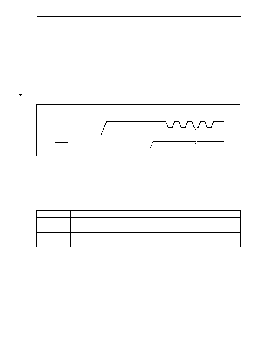
CHAPTER 16 FLASH MEMORY (
µ
PD70F3116)
735
User's Manual U14492EJ5V0UD
16.6.2 Flash memory programming mode
When rewriting the contents of flash memory using the dedicated flash programmer, set the V850E/IA1 in the flash
memory programming mode. To switch to this mode, set the MODE0, MODE1, MODE2, and V
PP
pins before
canceling reset.
When performing on-board writing, change modes using a jumper, etc.
∑ MODE0: High-level or low-level input
∑ MODE1: High-level input
∑ MODE2: Low-level input
∑ V
PP
: 7.8
V
Figure 16-10. Flash Memory Programming Mode
...
n
1
Flash memory programming mode
7.8 V
V
PP
3.3 V
0 V
RESET
2
16.6.3 Selection of communication mode
In the V850E/IA1, a communication mode is selected by inputting pulses (16 pulses max.) to V
PP
pin after switching
to the flash memory programming mode. The V
PP
pulse is generated by the dedicated flash programmer.
The following shows the relationship between the number of pulses and the communication mode.
Table 16-3. List of Communication Mode
V
PP
Pulse
Communication Mode
Remarks
0 CSI0
3 Handshake-supported
CSI
V850E/IA1 performs slave operation, MSB first
8
UART0
Communication rate: 9600 bps (after reset), LSB first
Others
RFU (reserved)
Setting prohibited

CHAPTER 16 FLASH MEMORY (
µ
PD70F3116)
736
User's Manual U14492EJ5V0UD
16.6.4 Communication commands
The V850E/IA1 communicates with the dedicated flash programmer by means of commands. A command sent
from the dedicated flash programmer to the V850E/IA1 is called a "command". The response signal sent from the
V850E/IA1 to the dedicated flash programmer is called the "response command".
Figure 16-11. Communication Commands
V850E/IA1
Dedicated flash programmer
Command
Response
command
PG-FP4
(Flash Pro4)
Cxxxxxx
Bxxxxx
Axxxx
X
X
X
Y
Y
Y
X
X
X
X
X
X
X
X
X
X
X
X
X
X
X
X
X
X
X
Y
Y
Y
Y
STATVE
The following shows the commands for controlling flash memory of the V850E/IA1. All of these commands are
issued from the dedicated flash programmer, and the V850E/IA1 performs the various processing corresponding to
the commands.
Table 16-4. Commands for Controlling Flash Memory
Category Command
Name
Function
Batch verify command
Compares the contents of the entire memory and
the input data.
Verify
Area verify command
Compares the contents of the specified area and
the input data.
Batch erase command
Erases the contents of the entire memory.
Area erase command
Erases the contents of the specified area.
Erase
Write back command
Writes back the contents which were erased.
Batch blank check command
Checks the erase state of the entire memory.
Blank check
Area blank check command
Checks the erase state of the specified area.
High-speed write command
Writes data by the specification of the write
address and the number of bytes to be written,
and executes verify check.
Data write
Continuous write command
Writes data from the address following the high-
speed write command executed immediately
before, and executes verify check.
Status read out command
Acquires the status of operations.
Oscillation frequency setting command
Sets the oscillation frequency.
Erasing time setting command
Sets the erasing time of batch erase.
Writing time setting command
Sets the writing time of data write.
Write back time setting command
Sets the write back time.
Silicon signature command
Reads outs the silicon signature information.
System setting and control
Reset command
Escapes from each state.

CHAPTER 16 FLASH MEMORY (
µ
PD70F3116)
737
User's Manual U14492EJ5V0UD
The V850E/IA1 sends back response commands for the commands issued from the dedicated flash programmer.
The following shows the response commands the V850E/IA1 sends out.
Table 16-5. Response Commands
Response Command Name
Function
ACK (acknowledge)
Acknowledges command/data, etc.
NAK (not acknowledge)
Acknowledges illegal command/data, etc.
16.7 Flash Memory Programming by Self-Programming
The
µ
PD70F3116 supports a self-programming function to rewrite the flash memory using a user program. By
using this function, the flash memory can be rewritten with a user application. This self-programming function can be
also used to upgrade the program in the field.
16.7.1 Outline of self-programming
Self-programming implements erasure and writing of the flash memory by calling the self-programming function
(device's internal processing) on the program placed in the block 0 space (000000H to 1FFFFFH) and areas other
than internal ROM area. To place the program in the block 0 space and internal ROM area, copy the program to
areas other than 000000H to 1FFFFFH (e.g. internal RAM area) and execute the program to call the self-
programming function.
To call the self-programming function, change the operating mode from normal operation mode to self-
programming mode using the flash programming mode control register (FLPMC).
Figure 16-12. Outline of Self-Programming
256 KB
Flash memory
00000H
3FFFFH
Erase area
Note
(128 KB)
Erase area
Note
(128 KB)
Flash memory
Normal operation mode
Self-programming mode
00000H
3FFFFH
FLPMC
02H
FLPMC
00H
Self-programming
function
(erase/write routine
incorporated)
Note Data is erased in area units (128 KB).
CHAPTER 16 FLASH MEMORY (
µ
PD70F3116)
738
User's Manual U14492EJ5V0UD
16.7.2 Self-programming
function
The
µ
PD70F3116 provides self-programming functions, as shown in Table 16-6. By combining these functions,
erasing/writing flash memory becomes possible.
Table 16-6. Function List
Type Function
Name
Function
Erase
Area erase
Erases the specified area.
Continuous write in word units
Continuously writes the specified memory contents from
the specified flash memory address, for the number of
words specified in 4-byte units.
Write
Pre-write
Writes 0 to flash memory before erasure.
Erase verify
Checks whether an over erase occurred after erasure.
Erase byte verify
Checks whether erasure is complete.
Check
Internal verify
Checks whether the signal level of the post-write data in
flash memory is appropriate.
Write back
Area write back
Writes back the flash memory area in which an over
erase occurred.
Acquire information
Flash memory information read
Reads out information about flash memory.
16.7.3 Outline of self-programming interface
To execute self-programming using the self-programming interface, the environmental conditions of the hardware
and software for manipulating the flash memory must be satisfied.
It is assumed that the self-programming interface is used in an assembly language.
(1) Entry program
This program is to call the internal processing of the device.
It is a part of the application program, and must be executed in memory other than the block 0 space and
internal ROM area (flash memory).
(2) Device internal processing
This is manipulation of the flash memory executed inside the device.
This processing manipulates the flash memory after it has been called by the entry program.
(3) RAM parameter
This is a RAM area to which the parameters necessary for self-programming, such as write time and erase
time, are written. It is set by the application program and referenced by the device internal processing.
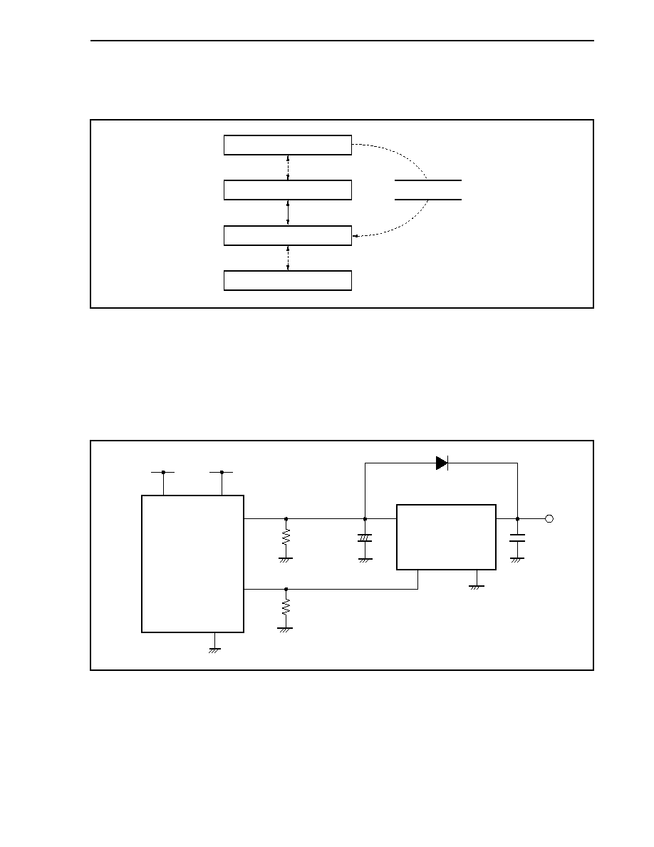
CHAPTER 16 FLASH MEMORY (
µ
PD70F3116)
739
User's Manual U14492EJ5V0UD
The self-programming interface is outlined below.
Figure 16-13. Outline of Self-Programming Interface
Application program
Entry program
RAM parameter
Device internal processing
Flash memory
Self-programming
interface
Flash-memory manipulation
16.7.4 Hardware
environment
To write or erase the flash memory, a high voltage must be applied to the V
PP
pin. To execute self-programming, a
circuit that can generate a write voltage (V
PP
) and that can be controlled by software is necessary on the application
system. An example of a circuit that can select a voltage to be applied to the V
PP
pin by manipulating a port is shown
below.
Figure 16-14. Example of Self-Programming Circuit Configuration
V
DD
= 3.3 V
±0.3 V
PD70F3116
V
DD5
, AV
DD
V
SS3
, V
SS5
, CV
SS
, AV
SS
V
PP
Output port
IC for power supply
OUTPUT
INPUT
ON/OFF
V
SS
10 k
10 k
V
IN
µ
V
PP
= 7.8 V
±0.3 V
V
DD3
, CV
DD
V
DD
= 5.0 V
±0.5 V
CHAPTER 16 FLASH MEMORY (
µ
PD70F3116)
740
User's Manual U14492EJ5V0UD
The voltage applied to the V
PP
pin must satisfy the following conditions:
∑ Hold the voltage applied to the V
PP
pin at 0 V in the normal operation mode and hold the V
PP
voltage only while
the flash memory is being manipulated.
∑ The V
PP
voltage must be stable from before manipulation of the flash memory starts until manipulation is
complete.
Cautions 1. Apply 0 V to the V
PP
pin when reset is released.
2. Implement self-programming in single-chip mode 0 or 1.
3. Apply the voltage to the V
PP
pin in the entry program.
4. If both writing and erasing are executed by using the self-programming function and flash
memory programmer on the target board, be sure to communicate with the programmer
using CSI0 (do not use the handshake-supported CSI).
Figure 16-15. Timing to Apply Voltage to V
PP
Pin
Flash memory
manipulation
RESET signal
V
PP
signal
V
PP
0 V
V
DD3
or V
DD5
0 V

CHAPTER 16 FLASH MEMORY (
µ
PD70F3116)
741
User's Manual U14492EJ5V0UD
16.7.5 Software
environment
The following conditions must be satisfied before using the entry program to call the device internal processing.
Table 16-7. Software Environmental Conditions
Item Description
Location of entry
program
Execute the entry program in memory other than the block 0 space and flash memory area.
The device internal processing cannot be directly called by the program that is executed on the flash
memory.
Execution status of
program
The device internal processing cannot be called while an interrupt is being serviced (NP bit of PSW =
0, ID bit of PSW = 1).
Masking interrupts
Mask all the maskable interrupts used. Mask each interrupt by using the corresponding interrupt
control register.
To mask a maskable interrupt, be sure to specify masking by using the corresponding interrupt
control register. Mask the maskable interrupt even when the ID bit of the PSW = 1 (interrupts are
disabled).
Manipulation of V
PP
voltage
Stabilize the voltage applied to the V
PP
pin (V
PP
voltage) before starting manipulation of the flash
memory. After completion of the manipulation, return the voltage of the V
PP
pin to 0 V.
Initialization of internal
timer
Do not use the internal timer while the flash memory is being manipulated.
Because the internal timer is initialized after the flash memory has been used, initialize the timer with
the application program to use the timer again.
Stopping reset signal
input
Do not input the reset signal while the flash memory is being manipulated.
If the reset signal is input while the flash memory is being manipulated, the contents of the flash
memory under manipulation become undefined.
Stopping NMI signal
input
Do not input the NMI signal while the flash memory is being manipulated.
If the NMI signal is input while the flash memory is being manipulated, the flash memory may not be
correctly manipulated by the device internal processing.
If an NMI occurs while the device internal processing is in progress, the occurrence of the NMI is
reflected in the NMI flag of the RAM parameter. If manipulation of the flash memory is affected by
the occurrence of the NMI, the function of each self-programming function is reflected in the return
value.
Reserving stack area
The device internal processing takes over the stack used by the user program. It is necessary that
an area of 300 bytes be reserved for the stack size of the user program when the device internal
processing is called. r3 is used as the stack pointer.
Saving general-purpose
registers
The device internal processing rewrites the contents of r6 to r14, r20, and r31 (lp).
Save and restore these register contents as necessary.

CHAPTER 16 FLASH MEMORY (
µ
PD70F3116)
742
User's Manual U14492EJ5V0UD
16.7.6 Self-programming function number
To identify a self-programming function, the following numbers are assigned to the respective functions. These
function numbers are used as parameters when the device internal processing is called.
Table 16-8. Self-Programming Function Number
Function No.
Function Name
0
Acquiring flash information
1 Erasing
area
2 to 4
RFU
5
Area write back
6 to 8
RFU
9 Erase
byte
verify
10 Erase
verify
11 to 15
RFU
16
Continuous write in word units
17 to 19
RFU
20 Pre-write
21 Internal
verify
Other Prohibited
Remark RFU: Reserved for Future Use

CHAPTER 16 FLASH MEMORY (
µ
PD70F3116)
743
User's Manual U14492EJ5V0UD
16.7.7 Calling
parameters
The arguments used to call the self-programming function are shown in the table below. In addition to these
arguments, parameters such as the write time and erase time are set to the RAM parameters indicated by ep (r30).
Table 16-9. Calling Parameters
Function Name
First Argument (r6)
Function No.
Second Argument
(r7)
Third Argument (r8)
Fourth Argument
(r9)
Return Value (r10)
Acquiring flash
information
0 Option
number
Note 1
-
-
Note 1
Erasing area
1
Area erase start
address
-
-
0: Normal completion
Other than 0: Error
Area write back
5
None (acts on erase
manipulation area
immediately before)
-
-
None
Erase byte verify 9
Verify start address
Number of bytes to
be verified
-
0: Normal completion
Other than 0: Error
Erase verify
10
None (acts on erase
manipulation area
immediately before)
-
-
0: Normal completion
Other than 0: Error
Continuous write
in word units
Note 2
16 Write
start
address
Note 3
Start address of
write source data
Note 3
Number of words
to be written (word
units)
0: Normal completion
Other than 0: Error
Pre-write
20
Write start address
Number of bytes to
be written
-
0: Normal completion
Other than 0: Error
Internal verify
21
Verify start address
Number of bytes to
be verified
-
0: Normal completion
Other than 0: Error
Notes 1. See
16.7.10 Flash information for details.
2. Prepare write source data in memory other than the flash memory when data is written continuously in
word units.
3. This address must be at a 4-byte boundary.
Caution For all the functions, ep (r30) must indicate the first address of the RAM parameter.

CHAPTER 16 FLASH MEMORY (
µ
PD70F3116)
744
User's Manual U14492EJ5V0UD
16.7.8 Contents of RAM parameters
Reserve the following 48-byte area in the internal RAM or external RAM for the RAM parameters, and set the
parameters to be input. Set the base addresses of these parameters to ep (r30).
Table 16-10. Description of RAM Parameter
Address Size
I/O
Description
ep+0 4
bytes
-
For internal operations
ep+4:Bit 5
Note 1
1 bit
Input
Operation flag (Be sure to set this flag to 1 before calling the device internal processing.)
0: Normal operation in progress
1: Self-programming in progress
ep+4:Bit 7
Notes 2, 3
1 bit
Output
NMI flag
0: NMI not detected
1: NMI
detected
ep+8
4 bytes
Input
Erase time (unsigned 4 bytes)
Expressed as 1 count value in units of the internal operation unit time (100
µ
s).
Set value = Erase time (
µ
s)/internal operation unit time (
µ
s)
Example: If erase time is 0.4 s
0.4 ◊ 1,000,000/100 = 4,000 (integer operation)
ep+0xc
4 bytes
Input
Write back time (unsigned 4 bytes)
Expressed as 1 count value in units of the internal operation unit time (100
µ
s).
Set value = Write back time (
µ
s)/internal operation unit time (
µ
s)
Example: If write back time is 1 ms
1 ◊ 1,000/100 = 10 (integer operation)
ep+0x10
2 bytes
Input
Timer set value for creating internal operation unit time (unsigned 2 bytes)
Write a set value that makes the value of timer 4 the internal operation unit time (100
µ
s).
Set value = Operating frequency (Hz)/1,000,000
◊ Internal operation unit time (
µ
s)/
Timer division ratio (4) + 1
Note 4
Example: If the operating frequency is 50 MHz
50,000,000/1,000,000 ◊ 100/4 + 1 = 1,251 (integer operation)
ep+0x12
2 bytes
Input
Timer set value for creating write time (unsigned 2 bytes)
Write a set value that makes the value of timer 4 the write time.
Set value = Operating frequency (Hz)/Write time (
µ
s)/Timer division ratio (4) + 1
Note 4
Example: If the operating frequency is 50 MHz and the write time is 20
µ
s
50,000,000/1,000,000 ◊ 20/4 + 1 = 251 (integer operation)
ep+0x14 28
bytes
-
For internal operations
Notes 1. Fifth bit of address of ep+4 (least significant bit is bit 0.)
2. Seventh bit of address of ep+4 (least significant bit is bit 0.)
3. Clear the NMI flag by the user program because it is not cleared by the device internal processing.
4. The device internal processing sets this value minus 1 to the timer. Because the fraction is rounded up,
add 1 as indicated by the expression of the set value.
Caution Be sure to reserve the RAM parameter area at a 4-byte boundary.

CHAPTER 16 FLASH MEMORY (
µ
PD70F3116)
745
User's Manual U14492EJ5V0UD
16.7.9 Errors
during
self-programming
The following errors related to manipulation of the flash memory may occur during self-programming. An error
occurs if the return value (r10) of each function is not 0.
Table 16-11. Errors During Self-Programming
Error Function
Description
Overerase error
Erase verify
Excessive erasure occurs.
Undererase error
(blank check error)
Erase byte verify
Erasure is insufficient. Additional erase operation is
needed.
Verify error
Continuous write in word units
The written data cannot be correctly read. Either an
attempt has been made to write to flash memory that
has not been erased, or writing is not sufficient.
Internal verify error
Internal verify
The written data is not at the correct signal level.
Caution The overerase error and undererase error may simultaneously occur in the entire flash memory.
16.7.10 Flash
information
For the flash information acquisition function (function No. 0), the option number (r7) to be specified and the
contents of the return value (r10) are as follows. To acquire all flash information, call the function as many times as
required in accordance with the format shown below.
Table 16-12. Flash Information
Option No. (r7)
Return Value (r10)
0 Specification
prohibited
1 Specification
prohibited
2
Bit representation of return value (MSB: bit 31) FFFFFFFFFFFFFFFFAAAAAAAAFFFFFFFF (LSB: bit 0)
Bits 31 to 16: FFFFFFFFFFFFFFFF (reserved for future use)
Mask bits 31 to 16 because they are not normally 0.
Bits 15 to 8: AAAAAAAA (number of areas) (unsigned 8 bits)
Bits 7 to 0:
FFFFFFFF (reserved for future use)
Mask bits 7 to 0 because they are not normally 0.
3+0
End address of area 0
3+1
End address of area 1
Cautions 1. The start address of area 0 is 0. The "end address + 1" of the preceding area is the start
address of the next area.
2. The flash information acquisition function does not check values such as the maximum
number of areas specified by the argument of an option. If an illegal value is specified, an
undefined value is returned.

CHAPTER 16 FLASH MEMORY (
µ
PD70F3116)
746
User's Manual U14492EJ5V0UD
16.7.11 Area
number
The area numbers and memory map of the
µ
PD70F3116 are shown below.
Figure 16-16. Area Configuration
Area 1
(128 KB)
Area 0
(128 KB)
0 x 3 F F F F (End address of area 1)
0 x 0 0 0 0 0 (Start address of area 0)
0 x 2 0 0 0 0 (Start address of area 1)
0 x 1 F F F F (End address of area 0)

CHAPTER 16 FLASH MEMORY (
µ
PD70F3116)
747
User's Manual U14492EJ5V0UD
16.7.12 Flash programming mode control register (FLPMC)
The flash programming mode control register (FLPMC) is a register used to enable/disable writing to flash memory
and to specify the self-programming mode.
This register can be read/written in 8-bit or 1-bit units (the VPP bit (bit 2) is read-only).
Cautions 1. Be sure to transfer control to the internal RAM or external memory beforehand to
manipulate the FLSPM bit. However, in on-board programming mode set by the flash
programmer, the specification of FLSPM bit is ignored.
2. Do not change the initial value of bits 0 and 4 to 7.
FLPMC
Address
FFFFF8D4H
Initial value
Note
08H/0CH/00H
7
6
5
4
<3>
<2>
<1>
0
0
FLSPM
VPP
VPPDIS
0
0
0
0
Note 08H: When writing voltage is not applied to the V
PP
pin
0CH: When writing voltage is applied to the V
PP
pin
00H: Product not provided with flash memory (
µ
PD703116)
Bit position
Bit name
Function
3 VPPDIS Enables/disables writing/erasing on-chip flash memory. When this bit is 1,
writing/erasing on-chip flash memory is disabled even if a high voltage is applied to
the V
PP
pin.
0: Enables writing/erasing flash memory
1: Disables writing/erasing flash memory
2 VPP
Indicates the voltage applied to the V
PP
pin reaches the writing-enabled level (read-
only). This bit is used to check whether writing is possible or not in the self-
programming mode.
0: Indicates high-voltage application to V
PP
pin is not detected (the voltage has
not reached the writing voltage enable level)
1: Indicates high-voltage application to V
PP
pin is detected (the voltage has
reached the writing voltage enable level)
1 FLSPM Controls switching between internal ROM and the self-programming interface. This
bit can switch the mode between the normal mode set by the mode pin on the
application system and the self-programming mode. The setting of this bit is valid
only if the voltage applied to the V
PP
pin reaches the writing voltage enable level.
0: Normal mode (for all addresses, instruction fetch is performed from on-chip
flash memory)
1: Self-programming mode (device internal processing is started)

CHAPTER 16 FLASH MEMORY (
µ
PD70F3116)
748
User's Manual U14492EJ5V0UD
Setting data to the flash programming mode control register (FLPMC) is performed in the following sequence.
<1> Disable interrupts (set the NP bit and ID bit of the PSW to 1).
<2> Prepare the data to be set in the specific register in a general-purpose register.
<3> Write data to the peripheral command register (PHCMD).
<4> Set the flash programming mode control register (FLPMC) by executing the following instructions.
∑ Store instruction (ST/SST instructions)
∑ Bit manipulation instruction (SET1/CLR1/NOT1 instructions)
<5> Insert NOP instructions (5 instructions (<5> to <9>)).
<10> Cancel the interrupt disabled state (reset the NP bit of the PSW to 0).
[Description example] <1>
LDSR rX, 5
<2>
MOV 0x02, r10
<3>
ST.B r10, PHCMD[r0]
<4>
ST.B r10, FLPMC[r0]
<5>
NOP
<6>
NOP
<7>
NOP
<8>
NOP
<9>
NOP
<10>
LDSR rY, 5
Remark rX: Value written to the PSW
rY: Value returned to the PSW
No special sequence is required for reading a specific register.
Cautions 1. If an interrupt is acknowledged between when PHCMD is issued (<3>) and writing to a
specific register (<4>) immediately after issuing PHCMD, writing to the specific register may
not be performed and a protection error may occur (the PRERR bit of the PHS register = 1).
Therefore, set the NP bit of the PSW to 1 (<1>) to disable interrupt acknowledgment.
Similarly, disable acknowledgment of interrupts when a bit manipulation instruction is used
to set a specific register.
2. Use the same general-purpose register used to set a specific register (<3>) for writing to the
PHCMD register (<4>) even though the data written to the PHCMD register is dummy data.
This is the same as when a general-purpose register is used for addressing.
3. Before executing this processing, complete all DMA transfer operations.

CHAPTER 16 FLASH MEMORY (
µ
PD70F3116)
749
User's Manual U14492EJ5V0UD
16.7.13 Calling device internal processing
This section explains the procedure to call the device internal processing from the entry program.
Before calling the device internal processing, make sure that all the conditions of the hardware and software
environments are satisfied and that the necessary arguments and RAM parameters have been set. Call the device
internal processing by setting the FLSPM bit of the flash programming mode control register (FLPMC) to 1 and then
executing the trap 0x1f instruction. The processing is always called using the same procedure. It is assumed that the
program of this interface is described in an assembly language.
<1> Set the FLPMC register as follows:
∑ VPPDIS bit = 0 (to enable writing/erasing flash memory)
∑ FLSPM bit = 1 (to select self-programming mode)
<2> Clear the NP bit of the PSW to 0 (to enable NMIs (only when NMIs are used on the application)).
<3> Execute trap 0x1f to transfer the control to the device's internal processing.
<4> Set the NP bit and ID bit of the PSW to 1 (to disable all interrupts).
<5> Set the value to the peripheral command register (PHCMD) that is to be set to the FLPMC register.
<6> Set the FLPMC register as follows:
∑ VPPDIS bit = 1 (to disable writing/erasing flash memory)
∑ FLSPM bit = 0 (to select normal operation mode)
<7> Wait for the internal manipulation setup time (see 16.7.13 (5) Internal manipulation setup parameter).
(1) Parameter
r6: First argument (sets a self-programming function number)
r7: Second argument
r8: Third argument
r9: Fourth argument
ep: First address of RAM parameter
(2) Return value
r10:
Return value (return value from device internal processing of 4 bytes)
ep+4:Bit 7: NMI flag (flag indicating whether an NMI occurred while the device internal processing was being
executed)
0: NMI did not occur while device internal processing was being executed.
1: NMI occurred while device internal processing was being executed.
If an NMI occurs while control is being transferred to the device internal processing, the NMI
request may never be reflected. Because the NMI flag is not internally reset, this bit must be
cleared before calling the device internal processing. After the control returns from the device
internal processing, NMI dummy processing can be executed by checking the status of this flag
using software.
(3) Description
Transfer control to the device internal processing specified by a function number using the trap instruction.
To do this, the hardware and software environmental conditions must be satisfied. Even if trap 0x1f is used in
the user application program, trap 0x1f is treated as another operation after the FLPMC register has been set.
Therefore, use of the trap instruction is not restricted on the application.

CHAPTER 16 FLASH MEMORY (
µ
PD70F3116)
750
User's Manual U14492EJ5V0UD
(4) Program example
An example of a program in which the entry program is executed as a subroutine is shown below. In this
example, the return address is saved to the stack and then the device internal processing is called. This
program must be located in memory other than the block 0 space and flash memory area.
ISETUP 130
--
Internal manipulation setup parameter
EntryProgram:
add
-4, sp
-- Prepare
st.w
lp, 0[sp]
-- Save return address
movea
lo(0x00a0), r0, r10
--
ldsr
r10, 5
-- PSW = NP, ID
mov lo(0x0002),
r10
--
st.b
r10, PHCMD[r0]
-- PHCMD = 2
st.b
r10, FLPMC[r0]
-- VPPDIS = 0, FLSPM = 1
nop
nop
nop
nop
nop
movea
lo(0x0020), r0, r10
--
ldsr
r10, 5
-- PSW = ID
trap
0x1f
-- Device Internal Process
movea
lo(0x00a0), r0, r6
--
ldsr
r6, 5
-- PSW = NP, ID
mov lo(0x08),
r6
st.b
r6, PHCMD[r0]
-- PHCMD = 8
st.b
r6, FLPMC[r0]
-- VPPDIS = 1, FLSPM = 0
nop
nop
nop
nop
nop
mov
ISETUP, lp
-- loop time = 130
loop:
divh
r6, r6
-- To kill time
add
-1, lp
-- Decrement counter
jne loop
--
ld.w
0[sp], lp
-- Reload lp
add
4, sp
-- Dispose
jmp
[lp]
-- Return to caller

CHAPTER 16 FLASH MEMORY (
µ
PD70F3116)
751
User's Manual U14492EJ5V0UD
(5) Internal manipulation setup parameter
If the self-programming mode is switched to the normal operation mode, the
µ
PD70F3116 must wait for 100
µ
s before it accesses the flash memory. In the program example in (4) above, the elapse of this wait time is
ensured by setting ISETUP to "130" (@ 50 MHz operation). The total number of execution clocks in this
example is 39 clocks (divh instruction (35 clocks) + add instruction (1 clock) + jne instruction (3 clocks)).
Ensure that a wait time of 100
µ
s elapses by using the following expression.
39 clocks (total number of execution clocks)
◊ 20 ns (@ 50 MHz operation) ◊ 130 (ISETUP) = 101.4
µ
s
(wait time)

CHAPTER 16 FLASH MEMORY (
µ
PD70F3116)
752
User's Manual U14492EJ5V0UD
16.7.14 Erasing flash memory flow
The procedure to erase the flash memory is illustrated below. The processing of each function number must be
executed in accordance with the specified calling procedure.
Figure 16-17. Erasing Flash Memory Flow
... Function No. 20
... Function No. 1
... Function No. 9
... Function No. 10
... Function No. 5
... Function No. 10
... Function No. 9
Erase
Write error
Undererase error
Set RAM parameter.
Mask interrupts.
Pre-write
Erase area
Erase byte verify
Erase verify
Area write back
Erase verify
Clear number of times
write-back is repeated.
Erase byte verify
Write error?
Undererase?
Maximum
number of times
of repeating erasure is
exceeded?
Maximum
number of times
of repeating write-back is
exceeded?
Overerase?
Overerase?
Undererase?
Set V
PP
voltage.
Clear V
PP
voltage.
Unmask interrupts.
Clear V
PP
voltage.
Unmask interrupts.
Normal completion
Clear V
PP
voltage.
Unmask interrupts.
Overerase error
Clear V
PP
voltage.
Unmask interrupts.
Normal completion
Clear V
PP
voltage.
Unmask interrupts.
Yes
Yes
Yes
Yes
No
No
No
Yes
No
No
No
Yes
No
Yes
CHAPTER 16 FLASH MEMORY (
µ
PD70F3116)
753
User's Manual U14492EJ5V0UD
16.7.15 Continuous writing flow
The procedure to write data all at once to the flash memory by using the function to continuously write data in word
units is illustrated below. The processing of each function number must be executed in accordance with the specified
calling procedure.
Figure 16-18. Continuous Writing Flow
... Function No. 16
Yes
No
Continuous writing
Mask interrupts.
Set V
PP
voltage.
Continuous writing
Error?
Clear V
PP
voltage.
Unmask interrupts.
Write error
Clear V
PP
voltage.
Unmask interrupts.
Normal completion
Set RAM parameter.
CHAPTER 16 FLASH MEMORY (
µ
PD70F3116)
754
User's Manual U14492EJ5V0UD
16.7.16 Internal verify flow
The procedure of internal verification is illustrated below. The processing of each function number must be
executed in accordance with the specified calling procedure.
Figure 16-19. Internal Verify Flow
... Function No. 21
Yes
No
Internal verify
Mask interrupts.
Set V
PP
voltage.
Internal verify
Error?
Clear V
PP
voltage.
Unmask interrupts.
Internal verify error
Clear V
PP
voltage.
Unmask interrupts.
Normal completion
Set RAM parameter.
CHAPTER 16 FLASH MEMORY (
µ
PD70F3116)
755
User's Manual U14492EJ5V0UD
16.7.17 Acquiring flash information flow
The procedure to acquire the flash information is illustrated below. The processing of each function number must
be executed in accordance with the specified calling procedure.
Figure 16-20. Acquiring Flash Information Flow
... Function No. 0
Acquiring flash
information
Mask interrupts.
Set V
PP
voltage.
Acquiring flash
information
Clear V
PP
voltage.
Unmask interrupts.
End
Set RAM parameter.
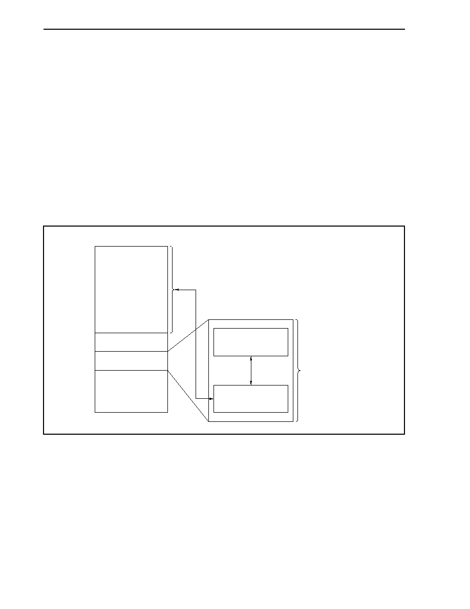
CHAPTER 16 FLASH MEMORY (
µ
PD70F3116)
756
User's Manual U14492EJ5V0UD
16.7.18 Self-programming
library
V850 Series Flash Memory Self-Programming User's Manual is available for reference when executing self-
programming.
In this manual, the library uses the self-programming interface of the V850 Series and can be used in C as a utility
and as part of the application program. To use the library, thoroughly evaluate it on the application system.
(1) Functional outline
Figure 16-21 outlines the function of the self-programming library. In this figure, a rewriting module is located
in area 0 and the data in area 1 is rewritten or erased.
The rewriting module is a user program to rewrite the flash memory. The other areas can be also rewritten by
using the flash functions included in this self-programming library. The flash functions expand the entry
program in the external memory or internal RAM and call the device internal processing.
When using the self-programming library, make sure that the hardware conditions, such as the write voltage,
and the software conditions, such as interrupts, are satisfied.
Figure 16-21. Functional Outline of Self-Programming Library
Rewriting module
Flash rewriting program
Self-programming
library
Flash function
Flash environment
Erase/write
Flash memory
Rewriting module
Area 1
Area 0

CHAPTER 16 FLASH MEMORY (
µ
PD70F3116)
757
User's Manual U14492EJ5V0UD
The configuration of the self-programming library is outlined below.
Figure 16-22. Outline of Self-Programming Library Configuration
Application program
Entry program
RAM parameter
Device internal processing
Flash memory
Self-programming interface
Self-programming library
Flash memory manipulation
C interface

CHAPTER 16 FLASH MEMORY (
µ
PD70F3116)
758
User's Manual U14492EJ5V0UD
16.8 How to Distinguish Flash Memory and Mask ROM Versions
It is possible to distinguish a flash memory version (
µ
PD70F3116) and a mask ROM version (
µ
PD703116) by
means of software, using the methods shown below.
<1> Disable interrupts (set the NP bit of PSW to 1).
<2> Write data to the peripheral command register (PHCMD).
<3> Set the VPPDIS bit of the flash programming mode control register (FLPMC) to 1.
<4> Insert NOP instructions (5 instructions (<4> to <8>)).
<9> Cancel the interrupt disabled state (reset the NP bit of the PSW to 0).
<10> Read the VPPDIS bit of the flash programming mode control register (FLPMC).
∑ If the value read is 0: Mask ROM version (
µ
PD703116)
∑ If the value read is 1: Flash memory version (
µ
PD70F3116)
[Description example] <1>
LDSR rX, 5
<2>
ST.B r10, PHCMD[r0]
<3>
SET1 3, FLPMC[r0]
<4>
NOP
<5>
NOP
<6>
NOP
<7>
NOP
<8>
NOP
<9>
LDSR rY, 5
<10>
TST1 3, FLPMC[r0]
BNZ
<Start address of self-programming routine>
BR
<Routine when writing is not performed>
Remark rX: Value written to the PSW
rY: Value returned to the PSW
Cautions 1. If an interrupt is acknowledged between when PHCMD is issued (<2>) and writing to a
specific register (<3>) immediately after issuing PHCMD, writing to a specific register may
not be performed and a protection error may occur (the PRERR bit of the PHS register = 1).
Therefore, set the NP bit of the PSW to 1 (<1>) to disable interrupt acknowledgment.
Similarly, disable acknowledgment of interrupts when a bit manipulation instruction is used
to set a specific register.
2. When a store instruction is used for setting a specific register, be sure to use the same
general-purpose register used to set the specific register for writing to the PHCMD register
even though the data written to the PHCMD register is dummy data. This is the same as
when a general-purpose register is used for addressing.
3. Before executing this processing, complete all DMA transfer operations.
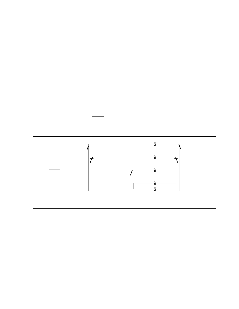
759
User's Manual U14492EJ5V0UD
CHAPTER 17 TURNING ON/OFF POWER
The V850E/IA1 has three types of power supply pins: 3.3 V power supply pins for internal units (V
DD3
and CV
DD
), 5
V power supply pins for external pins (V
DD5
and AV
DD
), and a flash programming power supply pin (V
PP
)
Note
.
This chapter explains the I/O pin status when power is turned ON/OFF.
Note
µ
PD70F3116 only
[Recommended timing of turning ON/OFF power]
∑ To turn ON
Keep the voltage on the V
DD5
and AV
DD
pins at 0 V until the voltage on the V
DD3
pin rises to the level at which
the operation is guaranteed (3.0 to 3.6 V).
∑ To turn OFF
Keep the voltage on the V
DD3
pin at the level at which the operation is guaranteed (3.0 to 3.6 V), until the voltage
on the V
DD5
and AV
DD
pins has dropped to 0 V.
∑ When releasing reset status by RESET pin
Release the reset status by the RESET pin after both the 3.3 V power supply and 5 V power supply have risen.
Figure 17-1. Recommended Timing of Turning ON/OFF Power
Depends on program setting
I/O pin
V
DD3
V
DD5
, AV
DD
0 V
3.0 V
4.5 V
3.0 V
4.5 V
0 V
0 V
0 V
RESET (input)
Remark The broken line indicates a high-impedance state.
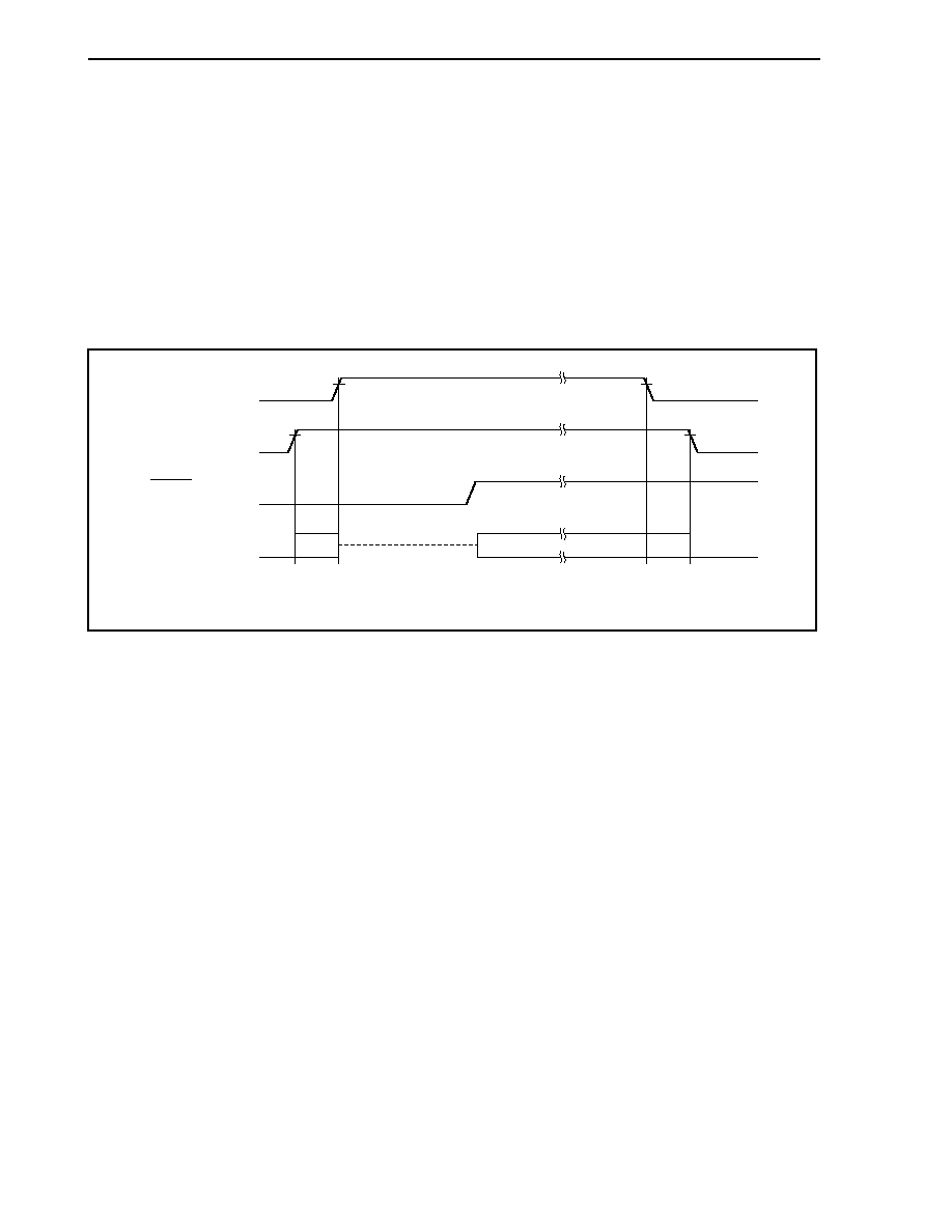
CHAPTER 17 TURNING ON/OFF POWER
760
User's Manual U14492EJ5V0UD
[Other timing]
∑ If power is supplied to the V
DD5
and AV
DD
pins before the voltage on the V
DD3
pins rises to the level at which the
operation is guaranteed (3.0 to 3.6 V), the status of the I/O pin is undefined
Note
until the voltage on the V
DD3
pin
reaches 3.0 V.
∑ If the voltage on the V
DD3
pin drops below the level at which the operation is guaranteed (3.0 to 3.6 V) before the
voltage on the V
DD5
and AV
DD
pins drops to 0 V, the status of the I/O pin is undefined
Note
.
Note This means that the input or output mode of an I/O pin, or the output level of an output pin is not
determined.
Figure 17-2. Other Timing
Depends on program setting
Undefined
I/O pin
V
DD3
V
DD5
, AV
DD
0 V
0 V
0 V
0 V
RESET (input)
Undefined
3.0 V
4.5 V
3.0 V
4.5 V
Remark The broken line indicates a high-impedance state.
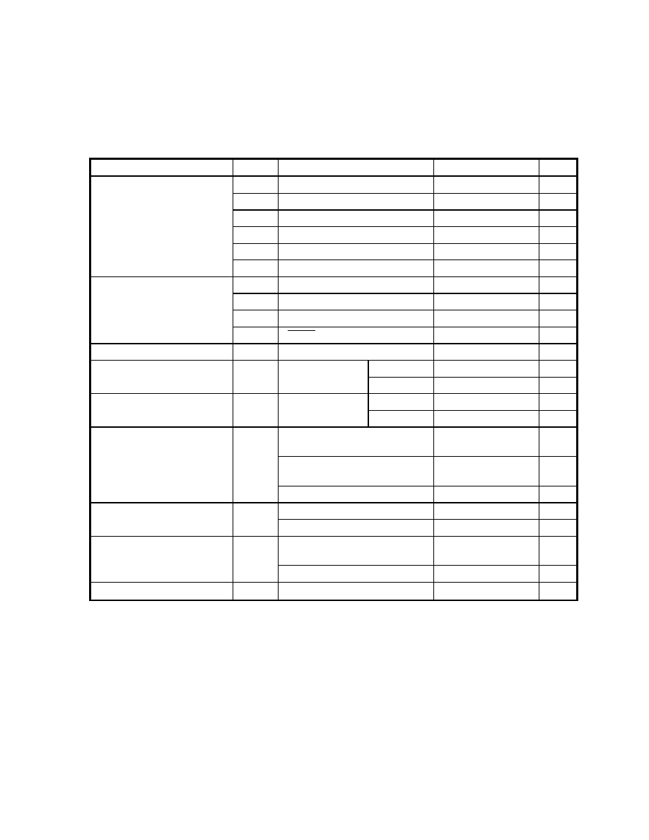
761
User's Manual U14492EJ5V0UD
CHAPTER 18 ELECTRICAL SPECIFICATIONS
18.1 Normal Operation Mode
Absolute Maximum Ratings (T
A
= 25
∞C)
Parameter
Symbol
Conditions
Ratings
Unit
V
DD3
V
DD3
pin
-0.5 to +4.6
V
V
DD5
V
DD5
pin
-0.5 to +7.0
V
CV
DD
CV
DD
pin
-0.5 to +4.6
V
CV
SS
CV
SS
pin
-0.5 to +0.5
V
AV
DD
AV
DD
pin
-0.5 to V
DD5
+ 0.5
Note 1
V
Power supply voltage
AV
SS
AV
SS
pin
-0.5 to +0.5
V
V
I1
Other than X1 pin and pins for NBD
Note 2
-0.5 to V
DD5
+ 0.5
Note 1
V
V
I2
V
PP
pin,
µ
PD70F3116
Note 3
-0.5 to +8.5
V
V
I3
Pins for NBD
Note 2
-0.5 to V
DD3
+ 0.5
Note 1
V
Input voltage
V
I4
RESET pin (when V
DD3
is supplied)
-0.5 to +6.0
V
Clock input voltage
V
K
X1 pin
-0.5 to V
DD3
+ 1.0
Note 1
V
AV
DD
> V
DD5
-0.5 to V
DD5
+ 0.5
Note 1
V
Analog input voltage
V
IAN
ANI00 to ANI07 pins,
ANI10 to ANI17 pins
V
DD5
AV
DD
-0.5 to AV
DD
+ 0.5
Note 1
V
AV
DD
> V
DD5
-0.5 to V
DD5
+ 0.5
Note 1
V
Analog reference input voltage
AV
REF
AV
REF0
pin,
AV
REF1
pin
V
DD5
AV
DD
-0.5 to AV
DD
+ 0.5
Note 1
V
Per pin for TO000 to TO005 and
TO010 to TO015 pins
15 mA
Per pin other than for TO000 to
TO005 and TO010 to TO015 pins
4.0 mA
Output current, low
I
OL
Total for all pins
210
mA
Per pin
-4.0 mA
Output current, high
I
OH
Total for all pins
-100 mA
µ
PD703116, 703116(A),
µ
PD70F3116, 70F3116(A)
-40 to +85
∞C
Operating ambient temperature
T
A
µ
PD703116(A1), 70F3116(A1)
-40 to +110
∞C
Storage temperature
T
stg
-65 to +150
∞C
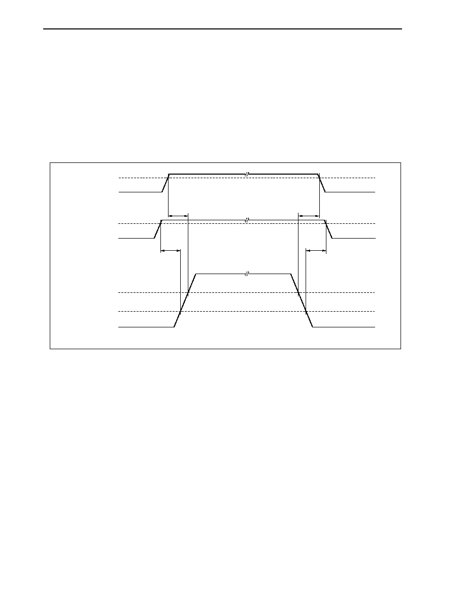
CHAPTER 18 ELECTRICAL SPECIFICATIONS
762
User's Manual U14492EJ5V0UD
Notes 1. Be sure not to exceed the absolute maximum ratings (MAX. value) of each power supply voltage.
2. CLK_DBG, SYNC, AD0_DBG to AD3_DBG pins (
µ
PD70F3116 only)
3. Make sure that the following conditions of the V
PP
voltage application timing are satisfied when the
flash memory is written.
∑ When power supply voltage rises
V
PP
must exceed V
DD3
and V
DD5
10
µ
s or more after V
DD3
and V
DD5
have reached the lower-limit
value (V
DD3
: 3.0 V, V
DD5
: 4.5 V) of the operating voltage range (see a in the figure below).
∑ When power supply voltage drops
V
DD3
and V
DD5
must be lowered 10
µ
s or more after V
PP
falls below the lower-limit value (V
DD3
: 3.0 V,
V
DD5
: 4.5 V) of the operating voltage range of V
DD3
and V
DD5
(see b in the figure below).
0 V
0 V
4.5 V
4.5 V
V
PP
V
DD3
V
DD5
V
PP
0 V
3.0 V
3.0 V
a
a
b
b
Cautions 1. Do not directly connect output (or I/O) pins of IC products to each other, or to V
DD
, V
CC
, and
GND. Open drain pins or open collector pins, however, can be directly connected to each
other. Direct connection of the output pins between an IC product and an external circuit is
possible, if the output pins can be set to the high-impedance state and the output timing of
the external circuit is designed to avoid output conflict.
2. Product quality may suffer if the absolute maximum rating is exceeded even momentarily for
any parameter. That is, the absolute maximum ratings are rated values at which the product
is on the verge of suffering physical damage, and therefore the product must be used under
conditions that ensure that the absolute maximum ratings are not exceeded.
The ratings and conditions shown below for DC characteristics and AC characteristics are
within the range for normal operation and quality assurance.

CHAPTER 18 ELECTRICAL SPECIFICATIONS
763
User's Manual U14492EJ5V0UD
Capacitance (T
A
= 25
∞C, V
DD3
= V
DD5
= V
SS3
= V
SS5
= 0 V)
Parameter Symbol Conditions MIN.
TYP.
MAX.
Unit
Input capacitance
C
I
15
pF
I/O capacitance
C
IO
15
pF
Output capacitance
C
O
f
C
= 1 MHz
Unmeasured pins returned to 0 V.
15
pF
Operating Conditions
Power Supply Voltage
Operation Mode
Internal System Clock Frequency (f
XX
)
Operating Ambient
Temperature (T
A
)
V
DD3
V
DD5
µ
PD703116, 703116(A),
70F3116, 70F3116(A)
4 to 25 MHz
-40 to +85∞C 3.3
V
±0.3 V
5.0 V
±0.5 V
Direct mode
µ
PD703116(A1), 70F3116(A1)
4 to 16 MHz
-40 to +110∞C 3.3
V
±0.3 V
5.0 V
±0.5 V
µ
PD703116, 703116(A),
70F3116, 70F3116(A)
4 to 50 MHz
-40 to +85∞C 3.3
V
±0.3 V
5.0 V
±0.5 V
PLL mode
µ
PD703116(A1), 70F3116(A1)
4 to 32 MHz
-40 to +110∞C 3.3
V
±0.3 V
5.0 V
±0.5 V
Caution When interfacing to the external devices using the CLKOUT signal, make the internal system
clock frequency (f
XX
) 32 MHz or lower.
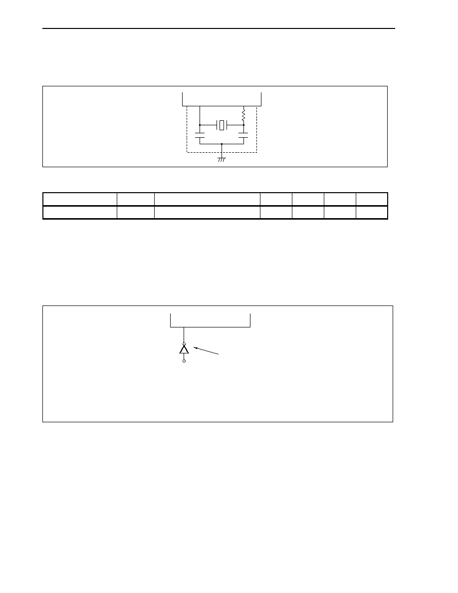
CHAPTER 18 ELECTRICAL SPECIFICATIONS
764
User's Manual U14492EJ5V0UD
Clock Oscillator Characteristics (T
A
=
-40 to +85∞C:
µ
PD703116, 703116(A), 70F3116, 70F3116(A),
T
A
=
-40 to +110∞C:
µ
PD703116(A1), 70F3116(A1))
(a)
Ceramic resonator or crystal resonator connection
Parameter Symbol
Conditions
MIN.
TYP.
MAX.
Unit
Oscillation frequency
f
X
4
6.4
MHz
Remarks 1. Connect the oscillator as close to the X1 and X2 pins as possible.
2. Do not wire any other signal lines in the area indicated by the broken lines.
3. For the resonator selection and oscillator constant, customers are required to either evaluate the
oscillation themselves or apply to the resonator manufacturer for evaluation.
(b) External clock input
Cautions 1. Connect the high-speed CMOS inverter as closely to the X1 pin as possible.
2. Thoroughly evaluate the matching between the V850E/IA1 and the high-speed CMOS
inverter.
Open
External clock
High-speed CMOS inverter
X2
X1
X2
X1
C1
C2
R
d
CHAPTER 18 ELECTRICAL SPECIFICATIONS
765
User's Manual U14492EJ5V0UD
Recommended Oscillator Constant
(a) Ceramic resonator
(i) Murata Mfg. Co., Ltd (T
A
=
-40 to +85∞C:
µ
PD703116, 703116(A), 70F3116, 70F3116(A),
T
A
=
-40 to +110∞C:
µ
PD703116(A1), 70F3116(A1))
Oscillation
Frequency
Recommended Circuit Constant
Recommended Voltage
Range
Type Product
Name
f
X
(MHz)
C1 (pF)
C2 (pF)
R
d
(
)
MIN. (V)
MAX. (V)
CSTCR4M00G55-R0 4.0 On-chip
On-chip
0
3.0
3.6
Surface mount
CSTCR6M00G55-R0 6.0 On-chip
On-chip
0
3.0
3.6
Caution This oscillator constant is a reference value based on evaluation under a specific environment
by the resonator manufacturer.
If optimization of oscillator characteristics is necessary in the actual application, apply to the
resonator manufacturer for evaluation on the implementation circuit.
The oscillation voltage and oscillation frequency indicate only oscillator characteristics. Use the
V850E/IA1 so that the internal operating conditions are within the specifications of the DC and
AC characteristics.
CHAPTER 18 ELECTRICAL SPECIFICATIONS
766
User's Manual U14492EJ5V0UD
DC Characteristics (T
A
= ≠40 to +85∞C:
µ
PD703116, 703116(A), 70F3116, 70F3116(A),
T
A
= ≠40 to +110∞C:
µ
PD703116(A1), 70F3116(A1),
V
DD3
= CV
DD
= 3.0 to 3.6 V, V
DD5
= 5 V ±0.5 V, V
SS3
= V
SS5
= CV
SS
=
0 V) (1/2)
Parameter Symbol
Conditions
MIN.
TYP.
MAX.
Unit
V
IH1
Pins for bus control
Note 1
2.2
V
DD5
V
V
IH2
Pins for NBD
Note 2
0.8V
DD3
V
DD3
V
V
IH3
Port
pins
Note 3
0.7V
DD5
V
DD5
V
V
IH4
Port pins other than Notes 1, 2, 3 0.8V
DD5
V
DD5
V
V
IH5
X1
pin
0.8V
DD3
V
DD3
+0.3
V
Input voltage, high
V
IH6
RESET
pin
0.8V
DD3
5.5 V
V
IL1
Pins for bus control
Note 1
0
0.8
V
V
IL2
Pins for NBD
Note 2
0
0.2V
DD3
V
V
IL3
Port
pins
Note 3
0
0.3V
DD5
V
V
IL4
Port pins other than Notes 1, 2, 3 0
0.2V
DD5
V
V
IL5
X1
pin
≠0.5 0.15V
DD3
V
Input voltage, low
V
IL6
RESET
pin
0
0.2V
DD3
V
V
OH1
Pins other than
Note 4
I
OH
= ≠2.5 mA
V
DD5
≠1.0
V
Output voltage, high
V
OH2
Pins for NBD
Note 4
I
OH
= ≠2.5 mA
V
DD3
≠1.0
V
I
OL
= 15 mA
2.0
V
V
OL1
PWM
output
Note 5
I
OL
= 2.5 mA
0.4
V
V
OL2
Pins other than
Notes 4, 5
I
OL
= 2.5 mA
0.4
V
Output voltage, low
V
OL3
Pins for NBD
Note 4
I
OL
= 2.5 mA
0.4
V
Input leakage current, high
I
LIH
V
I
= V
DD5
10
µ
A
Input leakage current, low
I
LIL
V
I
= 0 V
≠10
µ
A
Output leakage current, high
I
LOH
V
O
= V
DD5
10
µ
A
Output leakage current, low
I
LOL
V
O
= 0 V
≠10
µ
A
Analog pin input leakage
current
I
LIAN
ANI00 to ANI07, ANI10 to ANI17 pins
±10
µ
A
Notes
1.
AD0/PDL0 to AD15/PDL15, A16/PDH0 to A23/PDH7, LWR/PCT0, UWR/PCT1, PCT2, PCT3,
RD/PCT4, PCT5, ASTB/PCT6, PCT7, WAIT/PCM0, CLKOUT/PCM1, HLDAK/PCM2, HLDRQ/PCM3,
PCM4, CS0/PCS0 to CS7/PCS7 pins
2. CLK_DBG, SYNC, AD0_DBG to AD3_DBG pins (
µ
PD70F3116 only)
3. P31/TXD0, P33/TXD1, P36/TXD2, P41/SO0, P44/SO1, P47/CTXD pins
4. AD0_DBG to AD3_DBG, TRIG_DBG pins (
µ
PD70F3116 only)
5. TO000 to TO005, TO010 to TO015 pins

CHAPTER 18 ELECTRICAL SPECIFICATIONS
767
User's Manual U14492EJ5V0UD
DC Characteristics (T
A
= ≠40 to +85∞C:
µ
PD703116, 703116(A), 70F3116, 70F3116(A),
T
A
= ≠40 to +110∞C:
µ
PD703116(A1), 70F3116(A1),
V
DD3
= CV
DD
= 3.0 to 3.6 V, V
DD5
= 5 V ±0.5 V, V
SS3
= V
SS5
= CV
SS
=
0 V) (2/2)
Parameter Symbol
Conditions
MIN.
TYP.
MAX.
Unit
V
DD3
+ CV
DD
Note 2
1.9f
XX
+ 2.8
2.5f
XX
+ 5.0
mA
µ
PD703116
V
DD5
Note 3
0.8f
XX
+ 0.8
1.0f
XX
mA
V
DD3
+ CV
DD
Note 2
2.4f
XX
+ 12
3.6f
XX
+ 18
mA
In
normal
mode
I
DD1
µ
PD70F3116
V
DD5
Note 3
30 50
mA
V
DD3
+ CV
DD
Note 2
0.9f
XX
+ 6.8
1.8f
XX
+ 4.0
mA
µ
PD703116
V
DD5
Note 3
20 40
mA
V
DD3
+ CV
DD
Note 2
1.2f
XX
2.3f
XX
mA
In HALT
mode
I
DD2
µ
PD70F3116
V
DD5
Note 3
20 40
mA
V
DD3
+ CV
DD
3.0
10
mA
In IDLE
mode
I
DD3
V
DD5
Note 3
0.5
2.0
mA
-40∞C T
A
+85∞C 20
1200
µ
A
V
DD3
+ CV
DD
-40∞C T
A
+110∞C 20 3500
µ
A
Power supply
current
Note 1
In STOP
mode
I
DD4
V
DD5
Note 3
10
120
µ
A
Notes 1. Value in the PLL mode
2. Determine the value by calculating f
XX
from the operating conditions.
3. The current of the TO000 to TO005 and TO010 to TO015 pins is not included.
Remarks 1. f
XX
: Internal system clock frequency (MHz)
2. An example of calculating the power supply current is shown below.
∑ Power supply current (TYP.) of the V850E/IA1 in normal mode when f
XX
= 32 MHz
V
DD3
+ CV
DD
: I
DD1
= 2.4f
XX
+ 12 = 2.4
◊ 32 + 12 = 88.8 mA
V
DD5
: I
DD1
= 30 mA
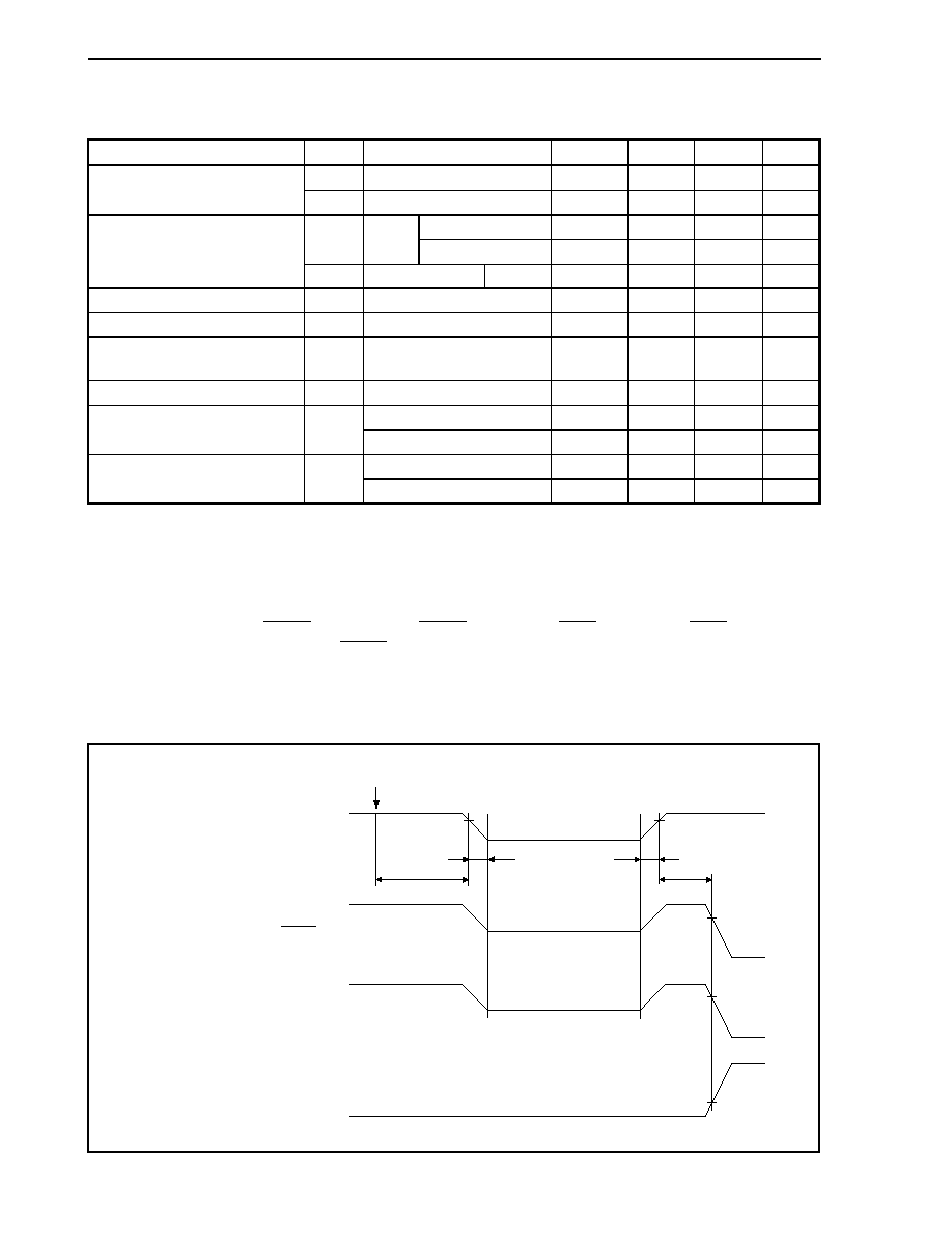
CHAPTER 18 ELECTRICAL SPECIFICATIONS
768
User's Manual U14492EJ5V0UD
Data Retention Characteristics (T
A
= ≠40 to
+85∞C:
µ
PD703116, 703116(A), 70F3116, 70F3116(A),
T
A
= ≠40 to
+110∞C:
µ
PD703116(A1), 70F3116(A1))
Parameter
Symbol
Conditions
MIN.
TYP.
MAX.
Unit
V
DDDR
STOP mode, V
DD3
= V
DDDR
1.5
3.6
V
Data retention voltage
HV
DDDR
STOP mode, V
DD5
= HV
DDDR
3.6
5.5
V
≠40
∞C T
A
+85∞C 20
1200
µ
A
I
DDDR
V
DD3
=
V
DDDR
≠40
∞C T
A
+110∞C
20 3500
µ
A
Data retention current
HI
DDDR
V
DD5
= HV
DDDR
Note 1
10
120
µ
A
Power supply voltage rise time
t
RVD
200
µ
s
Power supply voltage fall time
t
FVD
200
µ
s
Power supply voltage retention
time (from STOP mode setting)
t
HVD
0
ms
STOP release signal input time
t
DREL
0
ns
Note 2
0.8HV
DDDR
HV
DDDR
V
Data retention input voltage, high
V
IHDR
Note 3
0.8V
DDDR
V
DDDR
V
Note 2
0
0.2HV
DDDR
V
Data retention input voltage, low
V
ILDR
Note 3
0
0.2V
DDDR
V
Notes 1. The current of the TO000 to TO005 and TO010 to TO015 pins is not included.
2.
P00/NMI, P01/ESO0/INTP0, P02/ESO1/INTP1, P03/ADTRG0/INTP2, P04/ADTRG1/INTP3, P05/INTP4 to
P07/INTP6, P10/TIUD10/TO10, P11/TCUD10/INTP100, P12/TCLR10/INTP101, P13/TIUD11/TO11,
P14/TCUD11/INTP110,
P15/TCLR11/INTP111, P20/TI2/INTP20, P21/TO21/INTP21 to
P24/TO24/INTP24, P25/TCLR2/INTP25, P26/TI3/TCLR3/INTP30, P27/TO3/INTP31, P30/RXD0,
P32/RXD1, P34/ASCK1, P35/RXD2, P37/ASCK2, P40/SI0, P42/SCK0, P43/SI1, P45/SCK1, P46/CRXD,
MODE0 to MODE2, CKSEL, RESET pins
3. CLK_DBG, SYNC, AD0_DBG to AD3_DBG pins (
µ
PD70F3116 only)
Remark The TYP. value is a reference value for when T
A
= 25
∞C.
t
HVD
V
DDDR
, HV
DDDR
t
DREL
V
IHDR
V
IHDR
t
FVD
t
RVD
V
DD3
, V
DD5
RESET (input)
STOP mode release interrupt (NMI, etc.)
(released by falling edge)
STOP mode release interrupt (NMI, etc.)
(released by rising edge)
V
ILDR
STOP mode setting
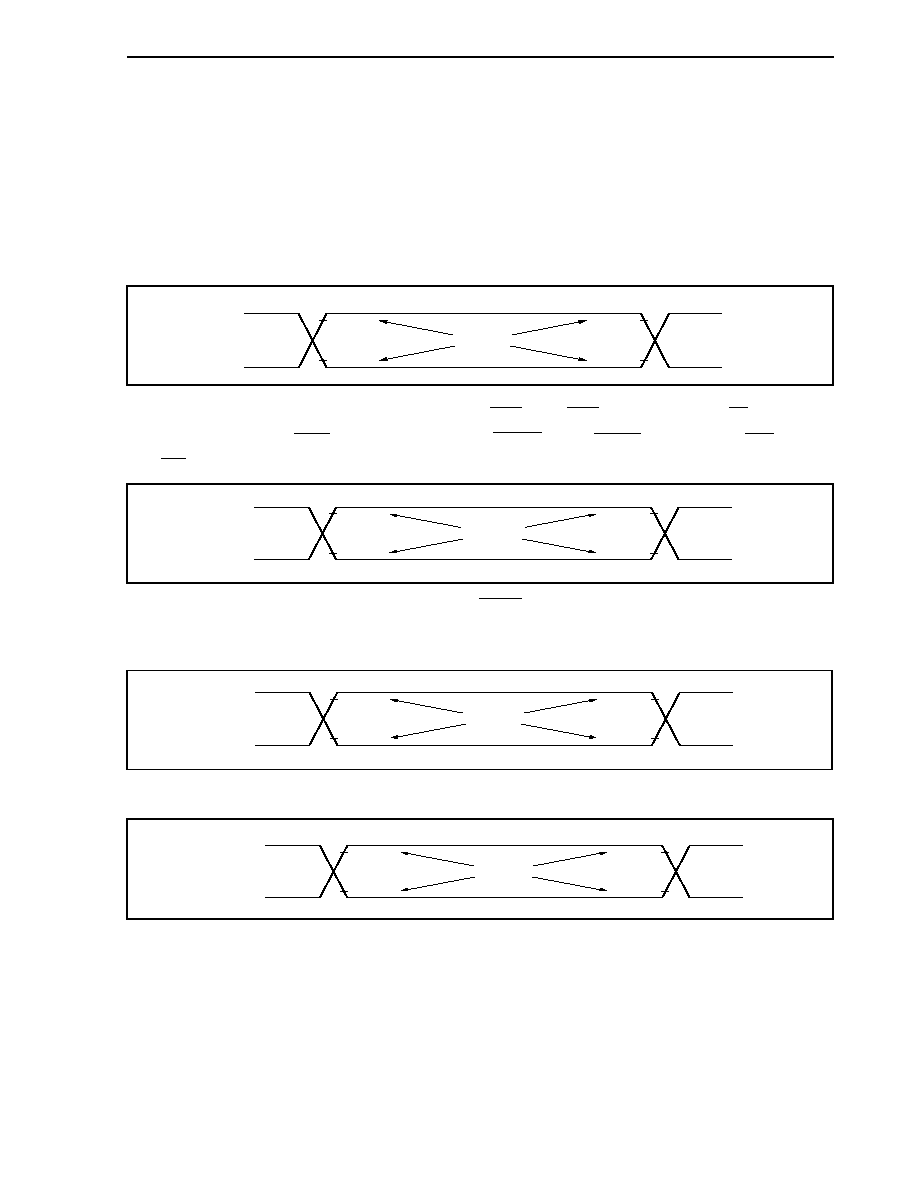
CHAPTER 18 ELECTRICAL SPECIFICATIONS
769
User's Manual U14492EJ5V0UD
AC Characteristics (T
A
= ≠40 to
+85∞C:
µ
PD703116, 703116(A), 70F3116, 70F3116(A),
T
A
= ≠40 to
+110∞C:
µ
PD703116(A1), 70F3116(A1),
V
DD3
= CV
DD
= 3.0 to 3.6 V, V
DD5
= 5 V
±0.5 V, V
SS3
= V
SS5
= CV
SS
= 0 V,
output pin load capacitance: C
L
= 50 pF)
AC test input test points
(a) Other than (b) to (d) below
(b) AD0/PDL0 to AD15/PDL15, A16/PDH0 to A23/PDH7, LWR/PCT0, UWR/PCT1, PCT2, PCT3, RD/PCT4, PCT5,
ASTB/PCT6, PCT7, WAIT/PCM0, CLKOUT/PCM1, HLDAK/PCM2, HLDRQ/PCM3, PCM4, CS0/PCS0 to
CS7/PCS7 pins
(c) CLK_DBG
Note
, SYNC
Note
, AD0_DBG to AD3_DBG
Note
, RESET pins
Note
µ
PD70F3116 only
(d) X1
pin
V
DD5
0 V
0.8V
DD5
0.2V
DD5
0.8V
DD5
0.2V
DD5
Test points
V
DD3
0 V
0.8V
DD3
0.2V
DD3
0.8V
DD3
0.2V
DD3
Test points
V
DD3
0 V
0.8V
DD3
0.15V
DD3
0.8V
DD3
0.15V
DD3
Test points
V
DD5
0 V
2.2 V
0.8 V
2.2 V
0.8 V
Test points

CHAPTER 18 ELECTRICAL SPECIFICATIONS
770
User's Manual U14492EJ5V0UD
AC test output test points
(a) Pins other than (b) below
(b) AD0_DBG to AD3_DBG, TRIG_DBG pins (
µ
PD70F3116 only)
Load conditions
Caution In cases where the load capacitance is greater than 50 pF due to the circuit configuration,
insert a buffer or other element to reduce the device's load capacitance to 50 pF or lower.
V
DD5
0 V
0.8V
DD5
0.2V
DD5
0.8V
DD5
0.2V
DD5
Test points
V
DD3
0 V
0.8V
DD3
0.2V
DD3
0.8V
DD3
0.2V
DD3
Test points
DUT
(Device under test)
C
L
= 50 pF
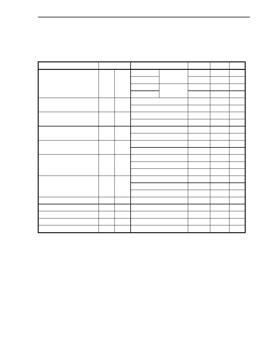
CHAPTER 18 ELECTRICAL SPECIFICATIONS
771
User's Manual U14492EJ5V0UD
(1)
Clock timing (1/2)
(T
A
= ≠40 to
+85∞C:
µ
PD703116, 703116(A), 70F3116, 70F3116(A),
T
A
= ≠40 to
+110∞C:
µ
PD703116(A1), 70F3116(A1),
V
DD3
= CV
DD
= 3.0 to 3.6 V, V
DD5
= 5 V
±0.5 V, V
SS3
= V
SS5
= CV
SS
= 0 V,
output pin load capacitance: C
L
= 50 pF)
Parameter
Symbol
Conditions
MIN.
MAX.
Unit
Direct mode
31.25
125
ns
PLL mode
Note 1
156 250
ns
Direct mode
20
125
ns
X1 input cycle
<1>
t
CYX
PLL mode
Note 2
156 250
ns
Direct mode
6
ns
X1 input high-level width
<2>
t
WXH
PLL mode
50
ns
Direct mode
6
ns
X1 input low-level width
<3>
t
WXL
PLL mode
50
ns
Direct mode
4
ns
X1 input rise time
<4>
t
XR
PLL mode
10
ns
Direct mode
4
ns
X1 input fall time
<5>
t
XF
PLL mode
10
ns
Note 2 4
50
MHz
Note 1 4
32
MHz
CPU operation frequency
-
f
XX
CLKOUT signal used
Note 3
4
32
MHz
Note 2 20
250
ns
Note 1 31.25
250
ns
CLKOUT output cycle
<6>
t
CYK
CLKOUT signal used
Note 3
31.25
250
ns
CLKOUT high-level width
<7>
t
WKH
0.5T ≠ 9
ns
CLKOUT low-level width
<8>
t
WKL
0.5T ≠ 11
ns
CLKOUT rise time
<9>
t
KR
11 ns
CLKOUT fall time
<10>
t
KF
9 ns
Delay time from X1
to CLKOUT
<11>
t
DXK
Direct mode
40
ns
Notes 1. ≠40∞C
T
A
+110∞C
2. ≠40∞C
T
A
+85∞C
3. When interfacing to the external devices using the CLKOUT signal, make the internal system clock
frequency
(f
XX
) 32 MHz or lower.
Remark T
=
t
CYK
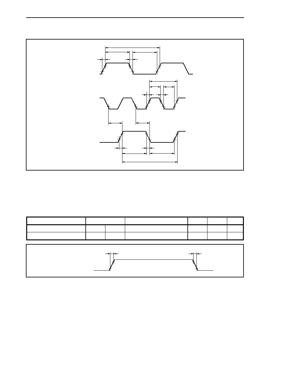
CHAPTER 18 ELECTRICAL SPECIFICATIONS
772
User's Manual U14492EJ5V0UD
(1) Clock timing (2/2)
(2)
Output waveform (except for CLKOUT)
(T
A
= ≠40 to
+85∞C:
µ
PD703116, 703116(A), 70F3116, 70F3116(A),
T
A
= ≠40 to
+110∞C:
µ
PD703116(A1), 70F3116(A1),
V
DD3
= CV
DD
= 3.0 to 3.6 V, V
DD5
= 5 V
±0.5 V, V
SS3
= V
SS5
= CV
SS
= 0 V,
output pin load capacitance: C
L
= 50 pF)
Parameter
Symbol
Conditions
MIN.
MAX.
Unit
Output rise time
<12>
t
OR
15
ns
Output fall time
<13>
t
OF
15
ns
X1
<3>
<1>
<2>
<4>
<5>
X1
(direct mode)
(PLL mode)
<5>
<1>
<2>
<3>
<4>
<11>
<11>
CLKOUT (output)
<8>
<9>
<7>
<10>
<6>
<13>
<12>
Signals other than
CLKOUT
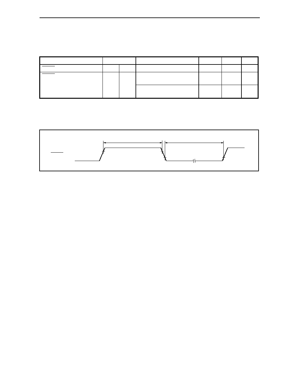
CHAPTER 18 ELECTRICAL SPECIFICATIONS
773
User's Manual U14492EJ5V0UD
(3)
Reset timing
(T
A
= ≠40 to
+85∞C:
µ
PD703116, 703116(A), 70F3116, 70F3116(A),
T
A
= ≠40 to
+110∞C:
µ
PD703116(A1), 70F3116(A1),
V
DD3
= CV
DD
= 3.0 to 3.6 V, V
DD5
= 5 V
±0.5 V, V
SS3
= V
SS5
= CV
SS
= 0 V, C
L
= 50 pF)
Parameter
Symbol
Conditions
MIN.
MAX.
Unit
RESET pin high-level width
<14>
t
WRSH
500
ns
At power-on and at STOP mode
release
500
+ T
OST
ns
RESET pin low-level width
<15>
t
WRSL
Other than at power-on and at
STOP mode release
500
ns
Caution Thoroughly evaluate the oscillation stabilization time.
Remark T
OST
: Oscillation stabilization time
RESET (input)
<14>
<15>
CHAPTER 18 ELECTRICAL SPECIFICATIONS
774
User's Manual U14492EJ5V0UD
(4)
Multiplex bus timing
(a)
CLKOUT asynchronous (T
A
= ≠40 to
+85∞C:
µ
PD703116, 703116(A), 70F3116, 70F3116(A),
T
A
= ≠40 to
+110∞C:
µ
PD703116(A1), 70F3116(A1),
V
DD3
= CV
DD
= 3.0 to 3.6 V, V
DD5
= 5 V
±0.5 V, V
SS3
= V
SS5
= CV
SS
= 0 V,
output pin load capacitance: C
L
= 50 pF)
Parameter Symbol
Conditions
MIN.
MAX.
Unit
Address setup time (to ASTB
) <16>
t
SAST
(0.5 + w
AS
)T
≠ 16
ns
Address hold time (from ASTB
) <17>
t
HSTA
(0.5 + w
AH
)T
≠ 15
ns
Address float delay time from RD
<18>
t
FRDA
11
ns
Data input setup time from address
<19>
t
SAID
(2 + w + w
AS
+
w
AH
)T
≠ 40
ns
Data input setup time from RD
<20>
t
SRDID
(1 + w)T ≠ 40
ns
Delay time from ASTB
to RD, LWR, UWR <21>
t
DSTRDWR
(0.5 + w
AH
)T
≠ 15
ns
Data input hold time (from RD
) <22>
t
HRDID
0
ns
Address output time from RD
<23>
t
DRDA
(1 + i)T ≠ 15
ns
Delay time from RD, LWR, UWR
to ASTB <24>
t
DRDWRST
0.5T ≠ 15
ns
Delay time from RD
to ASTB <25>
t
DRDST
(1.5 + i + w
AS
)T
≠ 15
ns
RD, LWR, UWR low-level width
<26>
t
WRDWRL
(1 + w)T ≠ 22
ns
ASTB high-level width
<27>
t
WSTH
(1 + w
AS
)T ≠ 15
ns
Data output time from LWR, UWR
<28>
t
DWROD
10
ns
Data output setup time (to LWR, UWR
) <29>
t
SODWR
(1 + w)T ≠ 25
ns
Data output hold time (from LWR, UWR
) <30>
t
HWROD
T ≠ 20
ns
<31> t
SAWT1
w
1
(1.5 + w
AS
+
w
AH
)T
≠ 40
ns
WAIT setup time (to address)
<32> t
SAWT2
(1.5 + w + w
AS
+
w
AH
)T
≠ 40
ns
<33> t
HAWT1
w
1
(0.5 + w + w
AS
+
w
AH
)T
ns
WAIT hold time (from address)
<34> t
HAWT2
(1.5 + w + w
AS
+
w
AH
)T
ns
<35> t
SSTWT1
w
1
(1 +
w
AH
)T ≠ 32
ns
WAIT setup time (to ASTB
)
<36> t
SSTWT2
(1 + w +
w
AH
)T
≠ 32
ns
<37> t
HSTWT1
w
1
(w +
w
AH
)T
ns
WAIT hold time (from ASTB
)
<38> t
HSTWT2
(1 + w +
w
AH
)T ns
HLDRQ high-level width
<39>
t
WHQH
T + 10
ns
HLDAK low-level width
<40>
t
WHAL
T ≠ 15
ns
Delay time from address float to HLDAK
<41>
t
DFHA
≠12
ns
Delay time from HLDAK
to bus output
<42>
t
DHAC
≠7
ns
Delay time from HLDRQ
to HLDAK <43>
t
DHQHA1
2T
ns
Delay time from HLDRQ
to HLDAK <44>
t
DHQHA2
0.5T
1.5T + 30
ns
CHAPTER 18 ELECTRICAL SPECIFICATIONS
775
User's Manual U14492EJ5V0UD
Remarks 1. T
=
t
CYK
2. w: Number of wait clocks inserted in the bus cycle
The sampling timing changes when a programmable wait is inserted.
3. i: Number of idle states inserted after the read cycle (0 or 1)
4. w
AS
: Number of address setup wait states (0 or 1)
5. w
AH
: Number of address hold wait states (0 or 1)
6. Observe at least either of the data input hold time t
HKID
or
t
HRDID
.
7. For the number of wait clocks to be inserted, refer to 4.6.3 Relationship between programmable
wait and external wait.
(b)
CLKOUT synchronous (T
A
= ≠40 to
+85∞C:
µ
PD703116, 703116(A), 70F3116, 70F3116(A),
T
A
= ≠40 to
+110∞C:
µ
PD703116(A1), 70F3116(A1),
V
DD3
= CV
DD
= 3.0 to 3.6 V, V
DD5
= 5 V
±0.5 V, V
SS3
= V
SS5
= CV
SS
= 0 V,
output pin load capacitance: C
L
= 50 pF)
Parameter Symbol
Conditions
MIN.
MAX.
Unit
Delay time from CLKOUT
to address
<45>
t
DKA
≠7
19
ns
Delay time from CLKOUT
to address float
<46>
t
FKA
≠12
15
ns
Delay time from CLKOUT
to ASTB
<47>
t
DKST
≠3 + w
AH
T
19 + w
AH
T ns
Delay time from CLKOUT
to RD, LWR, UWR
<48>
t
DKRDWR
≠5
19
ns
Data input setup time (to CLKOUT
) <49>
t
SIDK
21
ns
Data input hold time (from CLKOUT
) <50>
t
HKID
5
ns
Delay time from CLKOUT
to data output
<51>
t
DKOD
19
ns
WAIT setup time (to CLKOUT
) <52>
t
SWTK
21
ns
WAIT hold time (from CLKOUT
) <53>
t
HKWT
5
ns
HLDRQ setup time (to CLKOUT
) <54>
t
SHQK
21
ns
HLDRQ hold time (from CLKOUT
) <55>
t
HKHQ
5
ns
Delay time from CLKOUT
to HLDAK
<56>
t
DKHA
19
ns
Delay time from CLKOUT
to address float
<57>
t
DKF
19
ns
Remarks 1. T = t
CYK
2.
w
AH
: Number of address hold wait states (0 or 1)
3. Observe at least either of the data input hold time t
HKID
or
t
HRDID
.
CHAPTER 18 ELECTRICAL SPECIFICATIONS
776
User's Manual U14492EJ5V0UD
(c) Read cycle (CLKOUT synchronous/asynchronous, 1 wait)
<21>
CLKOUT (output)
A16 to A23 (output)
CS0 to CS7 (output)
RD (output)
AD0 to AD15 (I/O)
ASTB (output)
WAIT (input)
T1
T2
TW
T3
Data
Address
Hi-Z
<45>
<19>
<46>
<47>
<16>
<27>
<48>
<35>
<37>
<36>
<38>
<31>
<33>
<32>
<34>
<52>
<52>
<53>
<20>
<26>
<18>
<17>
<49>
<50>
<47>
<22>
<48>
<23>
<25>
<24>
<53>
Caution When interfacing with the external device using the CLKOUT signal, set the internal system
clock frequency (f
XX
) to 32 MHz or lower.
Remark LWR and UWR are high level.
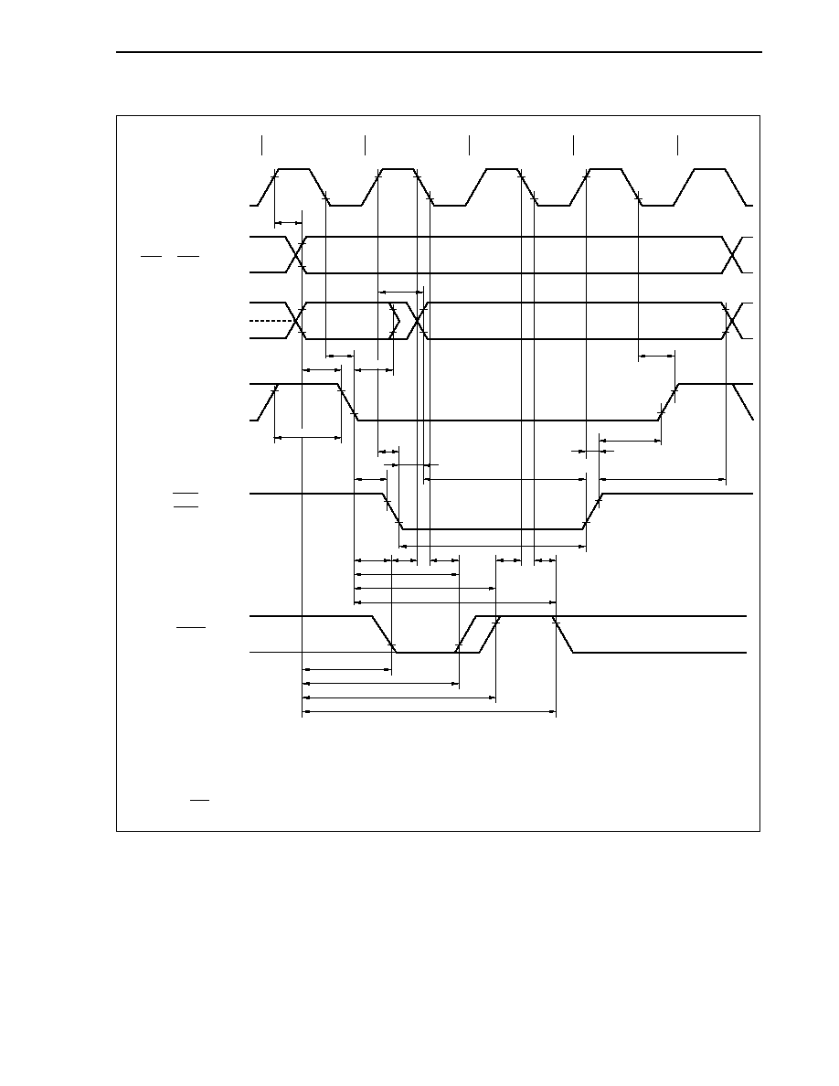
CHAPTER 18 ELECTRICAL SPECIFICATIONS
777
User's Manual U14492EJ5V0UD
(d) Write cycle (CLKOUT synchronous/asynchronous, 1 wait)
CLKOUT (output)
AD0 to AD15 (I/O)
ASTB (output)
LWR (output)
UWR (output)
A16 to A23 (output)
CS0 to CS7 (output)
WAIT (input)
T1
T2
TW
T3
Data
Address
<45>
<51>
<47>
<16>
<17>
<27>
<47>
<48>
<21>
<35> <52>
<37>
<36>
<38>
<31>
<33>
<32>
<34>
<53>
<52>
<53>
<28>
<29>
<26>
<48>
<24>
<30>
Caution When interfacing with the external device using the CLKOUT signal, set the internal system
clock frequency (f
XX
) to 32 MHz or lower.
Remark RD is high level.
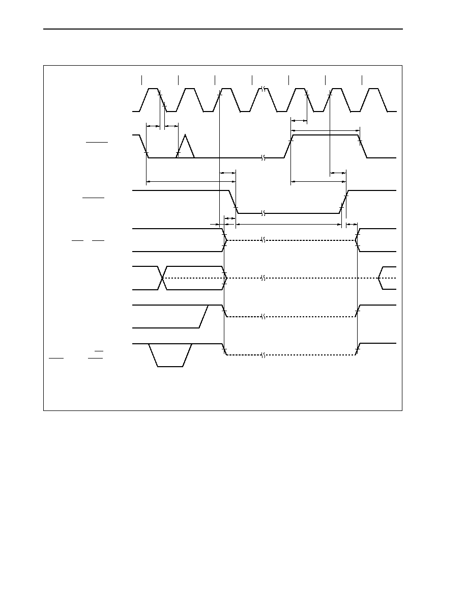
CHAPTER 18 ELECTRICAL SPECIFICATIONS
778
User's Manual U14492EJ5V0UD
(e) Bus hold
CLKOUT (output)
HLDRQ (input)
HLDAK (output)
A16 to A23 (output)
CS0 to CS7 (output)
AD0 to AD15 (I/O)
ASTB (output)
RD (output)
LWR (output), UWR (output)
TH
TH
TH
TI
Hi-Z
Hi-Z
Hi-Z
Data
Hi-Z
<54> <55>
<43>
<56>
<41>
<57>
<56>
<44>
<40>
<42>
<54>
<39>
Caution When interfacing with the external device using the CLKOUT signal, set the internal system
clock frequency (f
XX
) to 32 MHz or lower.
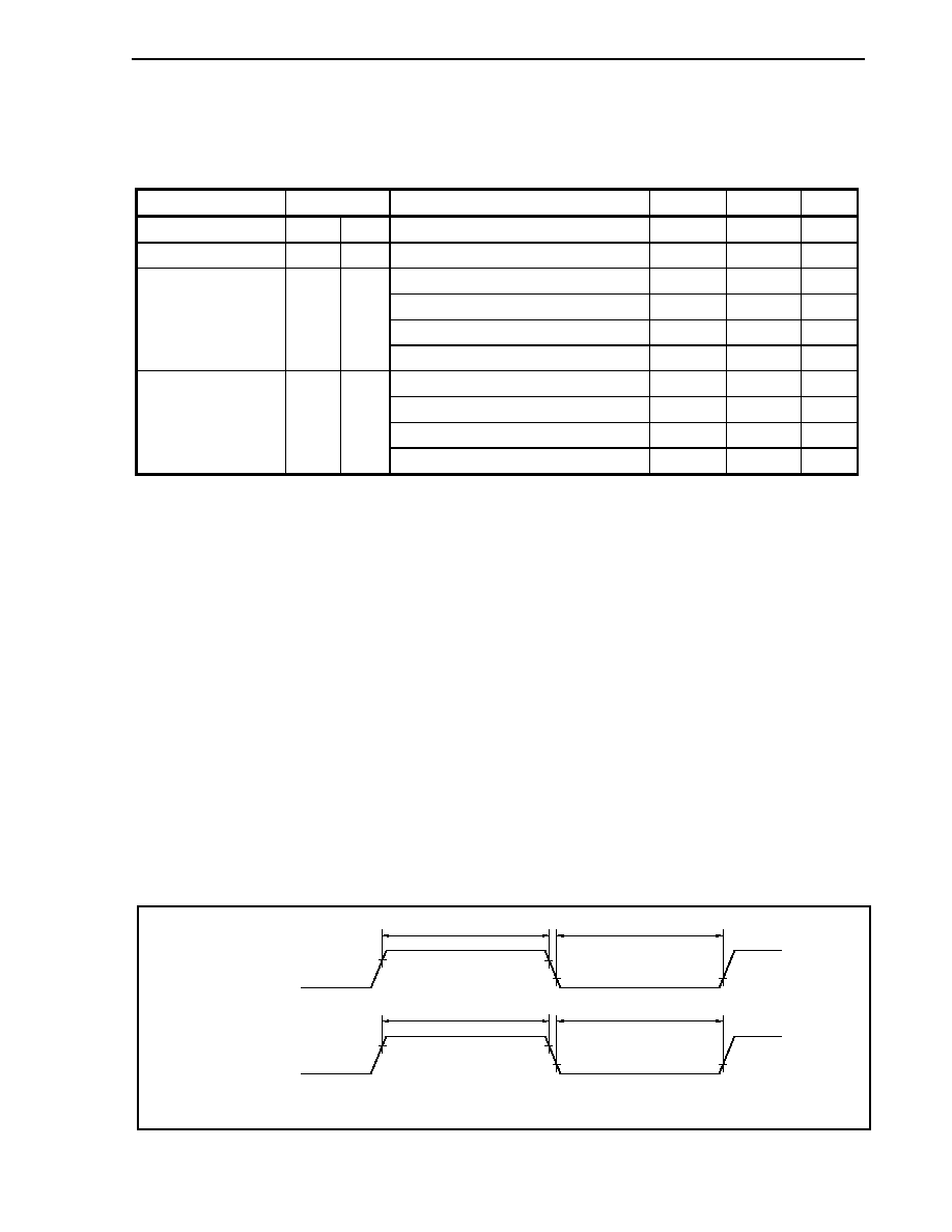
CHAPTER 18 ELECTRICAL SPECIFICATIONS
779
User's Manual U14492EJ5V0UD
(5)
Interrupt timing
(T
A
= ≠40 to
+85∞C:
µ
PD703116, 703116(A), 70F3116, 70F3116(A),
T
A
= ≠40 to
+110∞C:
µ
PD703116(A1), 70F3116(A1),
V
DD3
= CV
DD
= 3.0 to 3.6 V, V
DD5
= 5 V
±0.5 V, V
SS3
= V
SS5
= CV
SS
= 0 V, C
L
= 50 pF)
Parameter Symbol
Conditions
MIN.
MAX.
Unit
NMI high-level width
<58>
t
WNIH
500
ns
NMI low-level width
<59>
t
WNIL
500
ns
n = 0 to 6
500
ns
n = 100, 101, 110, 111, 30, 31
5T
+ 10
ns
n = 20 to 25 (when analog filter specified)
500
ns
INTPn high-level width
<60>
t
WITH
n = 20 to 25 (when digital filter specified)
5T + 10
ns
n = 0 to 6
500
ns
n = 100, 101, 110, 111, 30, 31
5T
+ 10
ns
n = 20 to 25 (when analog filter specified)
500
ns
INTPn low-level width
<61>
t
WITL
n = 20 to 25 (when digital filter specified)
5T + 10
ns
Remark T: Digital filter sampling clock
T can be selected by setting the following registers.
∑ INTP100, INTP101:
Can be selected from f
XX
TM10
, f
XX
TM10
/2, f
XX
TM10
/4, and
f
XX
TM10
/8
by setting the NRC101 and NRC100
bits of the timer 10 noise elimination time selection register (NRC10) (f
XX
TM10
: clock selected with the
timer 1/timer 2 clock selection register (PRM02)).
∑ INTP110, INTP111:
Can be selected from f
XX
TM11
, f
XX
TM11
/2, f
XX
TM11
/4, and
f
XX
TM11
/8
by setting the NRC111 and NRC110
bits of the timer 11 noise elimination time selection register (NRC11) (f
XX
TM11
: clock selected with the
PRM02 register).
∑ INTP30:
Can be selected from f
XX
TM3
/2, f
XX
TM3
/4, f
XX
TM3
/8, and
f
XX
TM3
/16
by setting the NRC31 and NRC30 bits
of the timer 3 noise elimination time selection register (NRC3) (f
XX
TM3
: clock selected with the timer 3
clock selection register (PRM03)).
∑ INTP31:
Can be selected from f
XX
TM3
/32, f
XX
TM3
/64, f
XX
TM3
/128, and
f
XX
TM3
/256
by setting the NRC33 and
NRC32 bits of the timer 3 noise elimination time selection register (NRC3) (f
XX
TM3
: clock selected with
the PRM03 register).
Remark n = 0 to 6, 100, 101, 110, 111, 20 to 25, 30, 31
NMI (input)
INTPn (input)
<58>
<59>
<60>
<61>
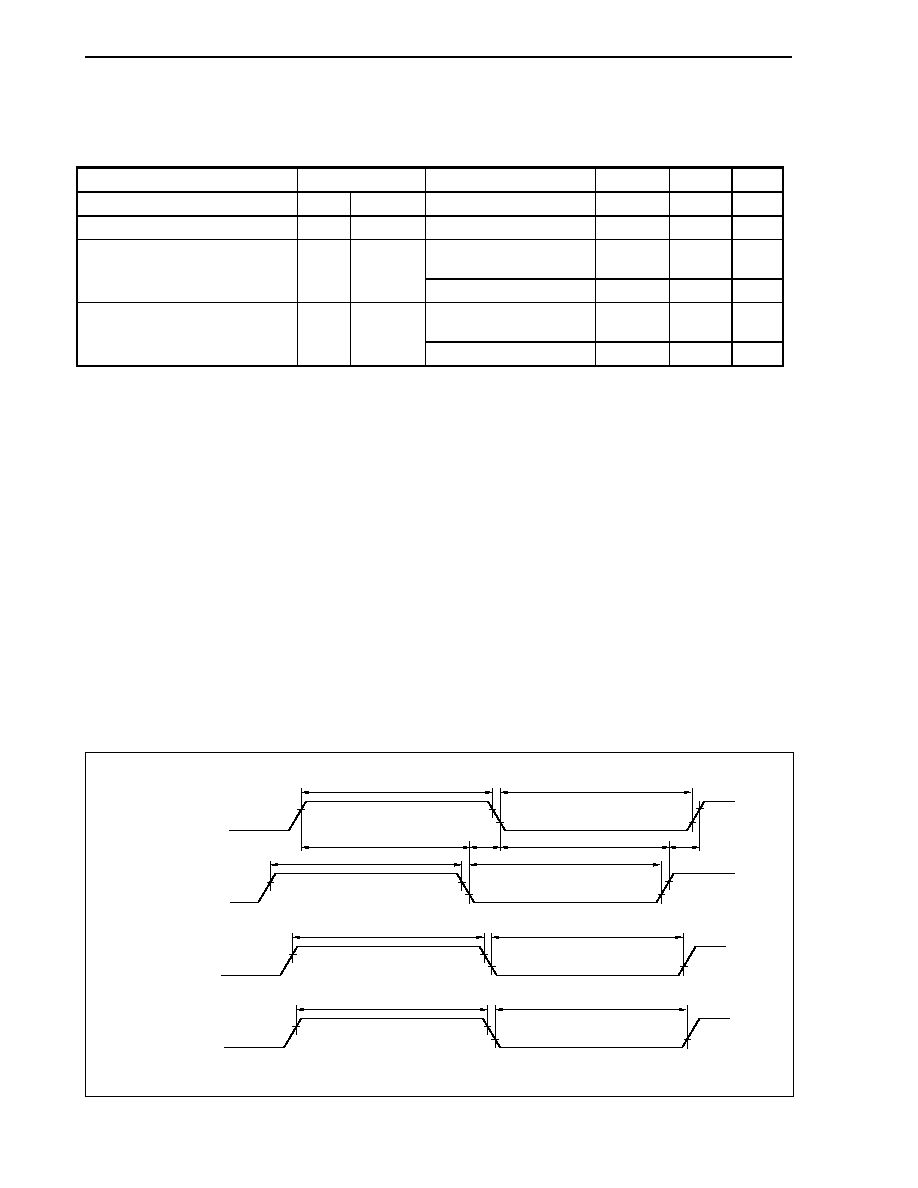
CHAPTER 18 ELECTRICAL SPECIFICATIONS
780
User's Manual U14492EJ5V0UD
(6) Timer input timing
(T
A
= ≠40 to
+85∞C:
µ
PD703116, 703116(A), 70F3116, 70F3116(A),
T
A
= ≠40 to
+110∞C:
µ
PD703116(A1), 70F3116(A1),
V
DD3
= CV
DD
= 3.0 to 3.6 V, V
DD5
= 5 V
±0.5 V, V
SS3
= V
SS5
= CV
SS
= 0 V, C
L
= 50 pF)
Parameter Symbol
Conditions
MIN.
MAX.
Unit
TIUDn, TCUDn high-/low-level width
<62>
t
WUDH,
t
WUDL
n = 10, 11
5T + 10
ns
TIUDn, TCUDn input time difference
<63>
t
PHUD
n = 10, 11
2T + 10
ns
n = 10, 11, 2 (other than for
through input), 3
5T + 10
ns
TCLRn high-/low-level width
<64>
t
WTCH,
t
WTCL
n = 2 (for through input
Note
)
2T + 10
ns
n = 2 (other than for through
input), 3
5T + 10
ns
TIn high-/low-level width
<65>
t
WTIH,
t
WTIL
n = 2 (for through input
Note
)
2T + 10
ns
Note When setting the timer 2 count clock/control edge selection register 0 (CSE0)'s CESE1 bit to 1 and CESE0 bit
to 0.
Remarks 1. T: Digital filter sampling clock
T can be selected by setting the following registers.
∑ When using TIUDn, TCUDn, and TCLRn (n = 10, 11), the following cycles can be selected by
setting the NRCn1 and NRCn0 bits of timer n noise elimination time selection register (NRCn).
When f
XX
/2 is selected for the timer n base clock: f
XX
/2, f
XX
/4, f
XX
/8, f
XX
/16
When f
XX
/4 is selected for the timer n base clock: f
XX
/4, f
XX
/8, f
XX
/16, f
XX
/32
∑ When using TCLR2 and TI2, the following cycles can be selected by setting the PRM2 bit of the
timer 1/timer 2 clock selection register (PRM02).
When f
XX
/2 is selected for the timer 2 base clock: f
XX
/2
When f
XX
/4 is selected for the timer 2 base clock: f
XX
/4
∑ When using TCLR3 and TI3, the following cycles can be selected by setting the NRC31 and
NRC30 bits of timer 3 noise elimination time selection register (NRC3).
When f
XX
is selected for the timer 3 base clock: f
XX
/2, f
XX
/4, f
XX
/8, f
XX
/16
When f
XX
/2 is selected for the timer 3 base clock: f
XX
/4, f
XX
/8, f
XX
/16, f
XX
/32
2.
f
XX
: Internal system clock frequency
Remark m = 10, 11 n = 10, 11, 2, 3 x = 2, 3
<62>
TIUDm (input)
TCUDm (input)
TCLRn (input)
TIx (input)
<62>
<62>
<62>
<63>
<63>
<63>
<63>
<64>
<64>
<65>
<65>
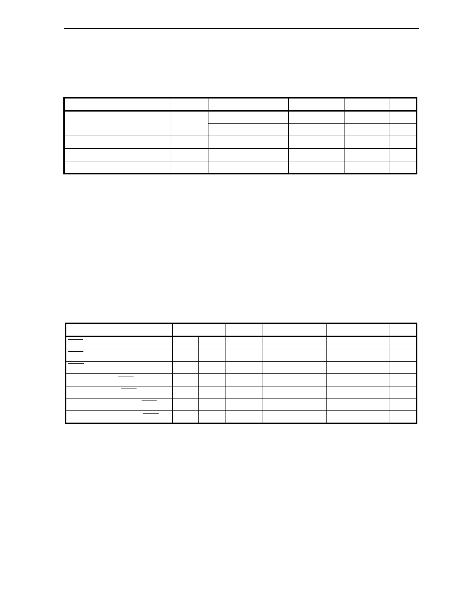
CHAPTER 18 ELECTRICAL SPECIFICATIONS
781
User's Manual U14492EJ5V0UD
(7) Timer operating frequency
(T
A
= ≠40 to
+85∞C:
µ
PD703116, 703116(A), 70F3116, 70F3116(A),
T
A
= ≠40 to
+110∞C:
µ
PD703116(A1), 70F3116(A1),
V
DD3
= CV
DD
= 3.0 to 3.6 V, V
DD5
= 5 V
±0.5 V, V
SS3
= V
SS5
= CV
SS
= 0 V,
output pin load capacitance: C
L
= 50 pF)
Parameter Symbol
Conditions MIN.
MAX.
Unit
≠40
∞C T
A
+85∞C 40
MHz
Timer 00, 01 operating frequency
T
0
≠40
∞C T
A
+110∞C 32
MHz
Timer 10, 11 operating frequency
T
1
16
MHz
Timer 20, 21 operating frequency
Note
T
2
16
MHz
Timer 3 operating frequency
T
3
32
MHz
Notes 1. Setting the TESnE1 and TESnE0 bits of timer 2 count clock/control edge select register 0 (CSE0) to
11B (both rising/falling edges) is prohibited when the PRM2 bit of the timer 1/timer 2 clock selection
register (PRM02) is 1B (f
CLK
= f
XX
/2)
2. Set the VSWC register to 15H when the PRM2 bit of the timer 1/timer 2 clock selection register
(PRM02) = 0B (f
CLK
= f
XX
/4).
(8) CSI timing (1/2)
(a)
Master mode
(T
A
= ≠40 to
+85∞C:
µ
PD703116, 703116(A), 70F3116, 70F3116(A),
T
A
= ≠40 to
+110∞C:
µ
PD703116(A1), 70F3116(A1),
V
DD3
= CV
DD
= 3.0 to 3.6 V, V
DD5
= 5 V
±0.5 V, V
SS3
= V
SS5
= CV
SS
= 0 V,
output pin load capacitance: C
L
= 50 pF)
Parameter Symbol
Conditions
MIN.
MAX.
Unit
SCKn cycle
<66>
t
CYSK1
Output
200
ns
SCKn high-level width
<67>
t
WSK1H
Output
0.5t
CYSK1
- 25
ns
SCKn low-level width
<68>
t
WSK1L
Output
0.5t
CYSK1
- 25
ns
SIn setup time (to SCKn
) <69>
t
SSISK
35
ns
SIn hold time (from SCKn
) <70>
t
HSKSI
30
ns
SOn output delay time (from SCKn
) <71>
t
DSKSO
30
ns
SOn output hold time (from SCKn
) <72>
t
HSKSO
0.5t
CYSK1
- 20
ns
Remark n = 0, 1
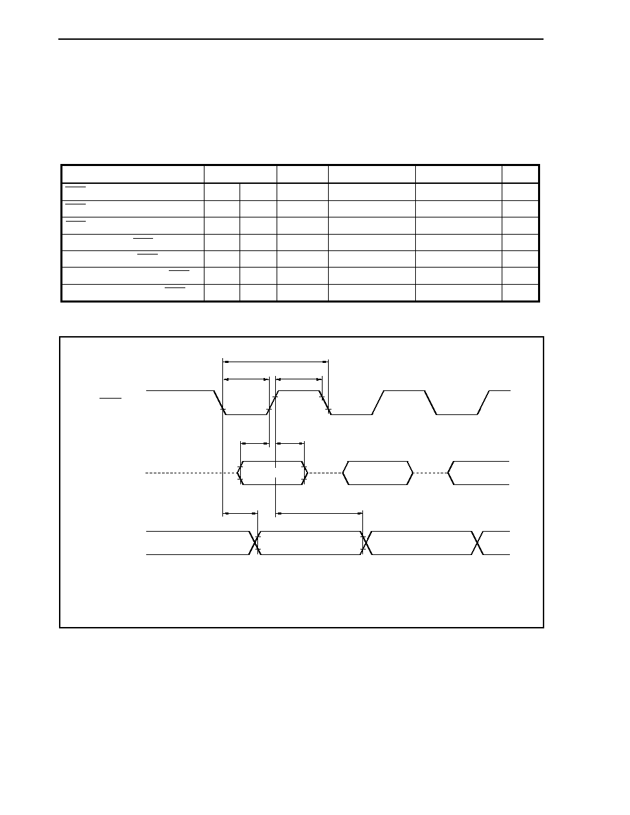
CHAPTER 18 ELECTRICAL SPECIFICATIONS
782
User's Manual U14492EJ5V0UD
(8) CSI timing (2/2)
(b)
Slave mode
(T
A
= ≠40 to
+85∞C:
µ
PD703116, 703116(A), 70F3116, 70F3116(A),
T
A
= ≠40 to
+110∞C:
µ
PD703116(A1), 70F3116(A1),
V
DD3
= CV
DD
= 3.0 to 3.6 V, V
DD5
= 5 V
±0.5 V, V
SS3
= V
SS5
= CV
SS
= 0 V,
output pin load capacitance: C
L
= 50 pF)
Parameter Symbol
Conditions
MIN.
MAX.
Unit
SCKn cycle
<66>
t
CYSK1
Input
200
ns
SCKn high-level width
<67>
t
WSK1H
Input
90
ns
SCKn low-level width
<68>
t
WSK1L
Input
90
ns
SIn setup time (to SCKn
) <69>
t
SSISK
50
ns
SIn hold time (from SCKn
) <70>
t
HSKSI
50
ns
SOn output delay time (from SCKn
) <71> t
DSKSO
55
ns
SOn output hold time (from SCKn
) <72>
t
HSKSO
t
WSK1H
ns
Remark n = 0, 1
Remarks 1. The broken lines indicate high impedance.
2. n = 0, 1
<66>
<68>
<67>
<69>
<70>
<71>
<72>
SIn (input)
SOn (output)
SCKn (I/O)
Output data
Input data
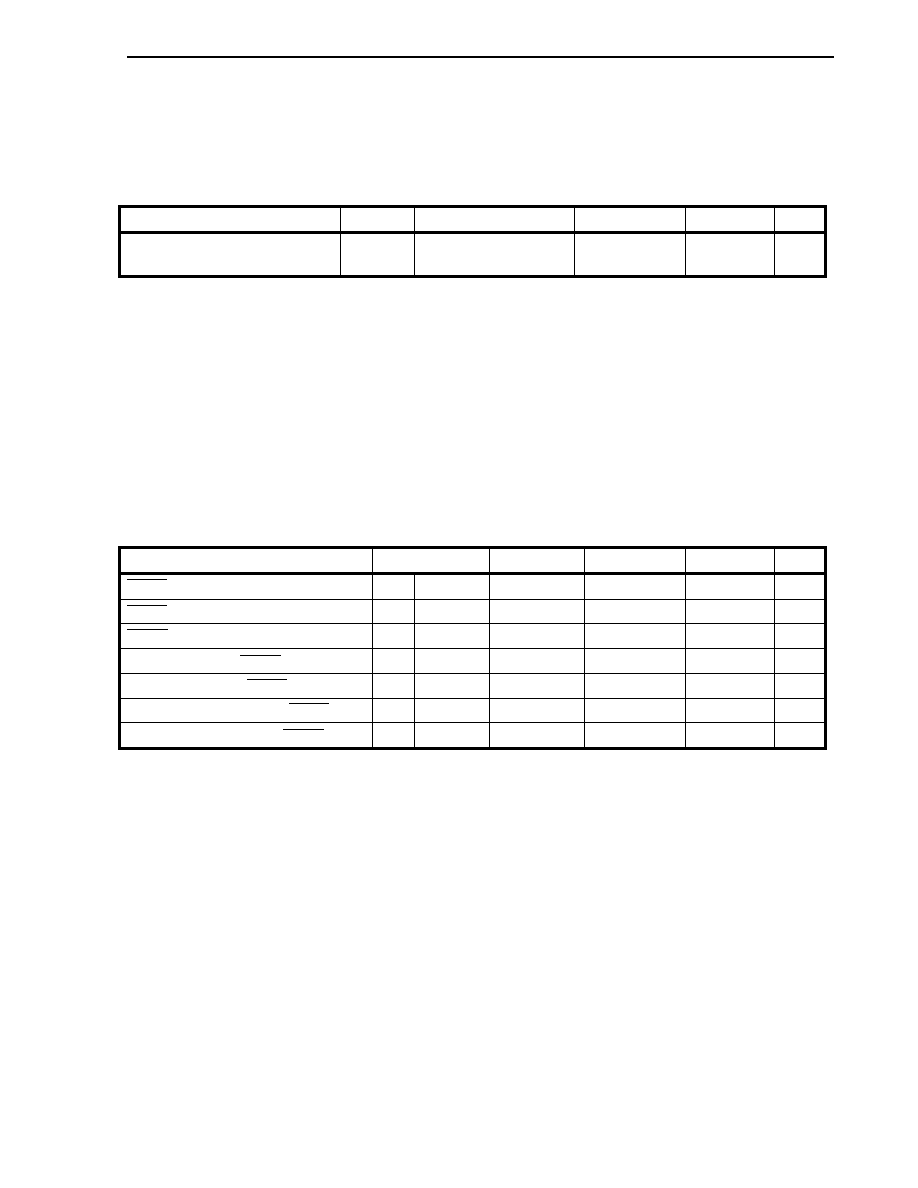
CHAPTER 18 ELECTRICAL SPECIFICATIONS
783
User's Manual U14492EJ5V0UD
(9) UART0 timing
(T
A
= ≠40 to
+85∞C:
µ
PD703116, 703116(A), 70F3116, 70F3116(A),
T
A
= ≠40 to
+110∞C:
µ
PD703116(A1), 70F3116(A1),
V
DD3
= CV
DD
= 3.0 to 3.6 V, V
DD5
= 5 V
±0.5 V, V
SS3
= V
SS5
= CV
SS
= 0 V,
output pin load capacitance: C
L
= 50 pF)
Parameter Symbol
Conditions MIN.
MAX.
Unit
UART0 baud rate generator input
frequency
f
BRG
25
MHz
Remark f
BRG
(UART0 baud rate generator input frequency) can be selected from f
XX
, f
XX
/2, f
XX
/4, f
XX
/8, f
XX
/16,
f
XX
/32, f
XX
/64, f
XX
/128, f
XX
/256, f
XX
/512, f
XX
/1024, and f
XX
/2048 by setting the TPS3 to TPS0 bits of clock
selection register 0 (CKSR0) (f
XX
: Internal system clock frequency).
(10) UART1, UART2 timing (1/2)
(a) Clocked master mode
(T
A
= ≠40 to
+85∞C:
µ
PD703116, 703116(A), 70F3116, 70F3116(A),
T
A
= ≠40 to
+110∞C:
µ
PD703116(A1), 70F3116(A1),
V
DD3
= CV
DD
= 3.0 to 3.6 V, V
DD5
= 5 V
±0.5 V, V
SS3
= V
SS5
= CV
SS
= 0 V,
output pin load capacitance: C
L
= 50 pF)
Parameter Symbol
Conditions
MIN.
MAX.
Unit
ASCKn cycle
<73> t
CYSK0
Output
1000
ns
ASCKn high-level width
<74> t
WSK0H
Output
k T ≠ 20
ns
ASCKn low-level width
<75> t
WSK0L
Output
k T ≠ 20
ns
RXDn setup time (to ASCKn
) <76>
t
SRXSK
1.5 T + 35
ns
RXDn hold time (from ASCKn
) <77>
t
HSKRX
0
ns
TXDn output delay time (from ASCKn
) <78>
t
DSKTX
T + 10
ns
TXDn output hold time (from ASCKn
) <79>
t
HSKTX
(k + 1)T ≠ 20
ns
Remarks 1. T = 2t
CYK
2. k: Setting value of prescaler compare register n (PRSCMn) of UARTn
3. n = 1, 2
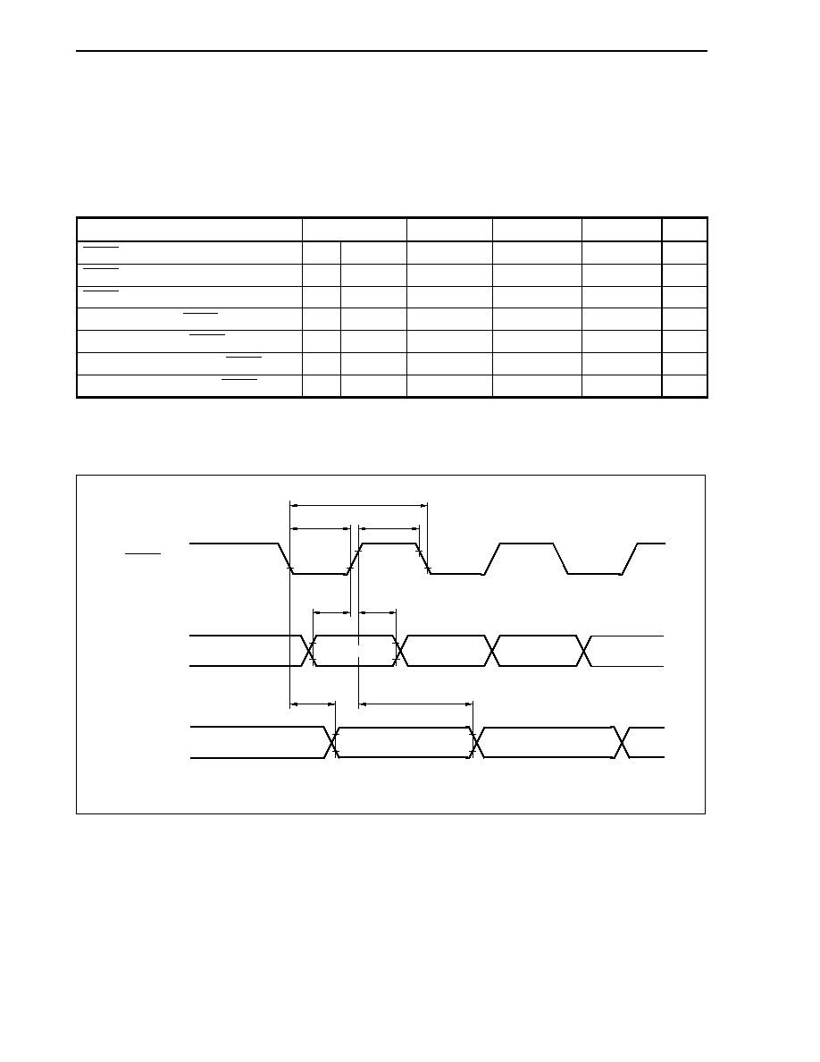
CHAPTER 18 ELECTRICAL SPECIFICATIONS
784
User's Manual U14492EJ5V0UD
(10) UART1, UART2 timing (2/2)
(b) Clocked slave mode
(T
A
= ≠40 to
+85∞C:
µ
PD703116, 703116(A), 70F3116, 70F3116(A),
T
A
= ≠40 to
+110∞C:
µ
PD703116(A1), 70F3116(A1),
V
DD3
= CV
DD
= 3.0 to 3.6 V, V
DD5
= 5 V
±0.5 V, V
SS3
= V
SS5
= CV
SS
= 0 V,
output pin load capacitance: C
L
= 50 pF)
Parameter Symbol
Conditions
MIN.
MAX.
Unit
ASCKn cycle
<73> t
CYSK0
Input
1000
ns
ASCKn high-level width
<74> t
WSK0H
Input
4 T + 80
ns
ASCKn low-level width
<75> t
WSK0L
Input
4 T + 80
ns
RXDn setup time (to ASCKn
) <76>
t
SRXSK
T + 10
ns
RXDn hold time (from ASCKn
) <77>
t
HSKRX
T + 10
ns
TXDn output delay time (from ASCKn
) <78>
t
DSKTX
2.5 T + 45
ns
TXDn output hold time (from ASCKn
) <79>
t
HSKTX
k T + 1.5 T
ns
Remarks 1. T = 2t
CYK
2. k: Setting value of PRSCMn register of UARTn
3. n = 1, 2
<73>
<75>
<74>
<76>
<77>
<78>
<79>
RXDn
(input)
TXDn
(output)
ASCKn
(I/O)
Output data
Input data
Remark n = 1, 2
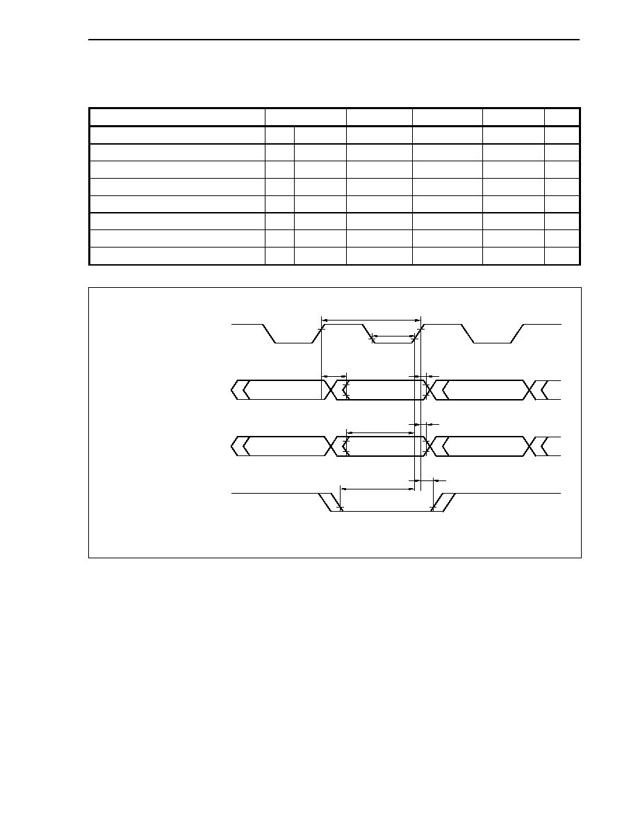
CHAPTER 18 ELECTRICAL SPECIFICATIONS
785
User's Manual U14492EJ5V0UD
(11) NBD timing (
µ
PD70F3116 only)
(T
A
= 0 to +40∞C, V
DD3
= CV
DD
= 3.0 to 3.6 V, V
DD5
= 5 V ±0.5 V, V
SS3
= V
SS5
= CV
SS
= 0 V,
output pin load capacitance: C
L
= 100 pF)
Parameter Symbol
Conditions
MIN.
MAX.
Unit
NBD cycle
<80> t
NDCYC
80
ns
NBD cycle low-level width
<81> t
NDL
35
ns
NBD data output delay time
<82> t
NDD
5 t
NDCYC
≠ 20
ns
NBD data output hold time
<83> t
NDHD
2
ns
NBD data input setup time
<84> t
NDS
20
ns
NBD data input hold time
<85> t
NDH
5
ns
SYNC input setup time
<86> t
NDSYS
20
ns
SYNC input hold time
<87> t
NDSYH
5
ns
CLK_DBG
(input)
AD0_DBG to AD3_DBG (output)
AD0_DBG to AD3_DBG (input)
SYNC
(input)
<80>
<81>
<84>
<82>
<83>
<85>
<86>
<87>

CHAPTER 18 ELECTRICAL SPECIFICATIONS
786
User's Manual U14492EJ5V0UD
A/D Converter Characteristics
(T
A
= ≠40 to
+85∞C:
µ
PD703116, 703116(A), 70F3116, 70F3116(A),
T
A
=
-40 to +110∞C:
µ
PD703116(A1), 70F3116(A1),
V
DD3
= CV
DD
= 3.0 to 3.6 V, AV
DD
= V
DD5
= 5 V
±0.5 V, AV
SS
= V
SS3
= V
SS5
= CV
SS
= 0 V, C
L
= 50 pF)
Parameter Symbol
Conditions
MIN.
TYP.
MAX.
Unit
Resolution
-
10
bit
Overall error
Note 1
-
±5 LSB
Quantization error
-
±1/2 LSB
Conversion time
t
CONV
5
10
µ
s
Sampling time
t
SAMP
833
ns
Zero-scale error
Note 1
-
±3 LSB
Full-scale error
Note 1
-
±3 LSB
Differential linearity error
Note 1
-
±3 LSB
Integral linearity error
Note 1
-
±5 LSB
Analog input voltage
V
IAN
-0.3
AV
REFn
+ 0.3
V
Analog reference voltage
AV
REF
AV
REFn
= AV
DD
4.5 5.5
V
AV
REFn
input current
Note 2
AI
REF
1
2
mA
AV
DD
power supply current
Note 2
AI
DD
3
6
mA
Notes 1. The quantization error (
±0.5 LSB) is not included.
2.
The V850E/IA1 incorporates two A/D converters. This is the rated value for one converter.
Remarks 1. LSB: Least Significant Bit
2.
n = 0, 1
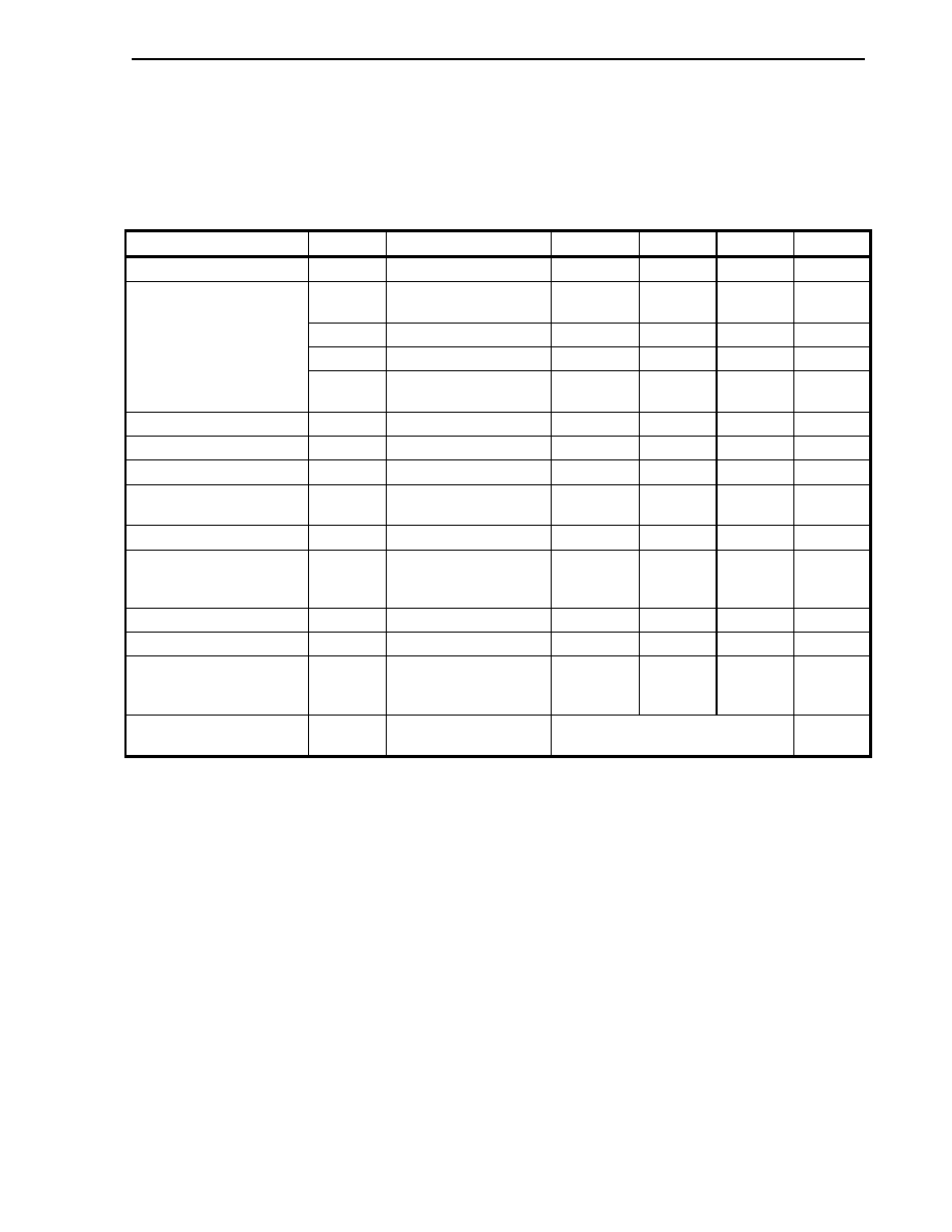
CHAPTER 18 ELECTRICAL SPECIFICATIONS
787
User's Manual U14492EJ5V0UD
18.2
Flash Memory Programming Mode (
µPD70F3116 only)
Basic Characteristics (T
A
= 0 to 70
∞C (during rewrite),
T
A
=
-40 to +85∞C (except during rewrite):
µ
PD70F3116, 70F3116(A),
T
A
=
-40 to +110∞C (except during rewrite):
µ
PD70F3116(A1),
V
DD3
= CV
DD
= 3.0 to 3.6 V, V
DD5
= 5 V
±0.5 V, V
SS3
= V
SS5
= CV
SS
= 0 V)
Parameter Symbol
Conditions MIN.
TYP.
MAX.
Unit
Operating frequency
f
X
4 50
MHz
V
PP1
During flash memory
programming
7.5 7.8
8.1 V
V
PPL
V
PP
low-level detection
-0.3
0.2V
DD3
V
V
PPM
V
PP
, V
DD3
level detection
0.65V
DD3
V
DD3
+ 0.3
V
V
PP
supply voltage
V
PPH
V
PP
high-voltage level
detection
7.5 7.8
8.1 V
V
DD3
supply current
I
DD1
V
PP
= V
PP1
4.5fx
mA
V
PP
supply current
I
PP
V
PP
= 7.8 V
100
mA
Step erase time
t
ER
Note 1
0.398 0.4
0.402 s
Overall erase time per area
t
ERA
When the step erase time =
0.4 s, Note 2
40
s/area
Write-back time
t
WB
Note 3
0.99 1
1.01
ms
Number of write-backs per
write-back command
C
WB
When the write-back time =
1 ms, Note 4
300
Count/write-
back
command
Number of erase/write-backs
C
ERWB
16 Count
Step writing time
t
WT
Note 5
18 20
22
µ
s
Overall writing time per word
t
WTW
When the step writing time
= 20
µ
s (1 word = 4 bytes),
Note 6
20
200
µ
s/word
Number of rewrites per area
C
ERWR
1 erase + 1 write after
erase = 1 rewrite, Note 7
100 Count/area
Notes 1. The recommended setting value of the step erase time is 0.4 s.
2.
The prewrite time prior to erasure and the erase verify time (write-back time) are not included.
3.
The recommended setting value of the write-back time is 1 ms.
4.
Write-back is executed once by the issuance of the write-back command. Therefore, the retry count
must be the maximum value minus the number of commands issued.
5.
The recommended setting value of the step writing time is 20
µ
s.
6.
20
µ
s is added to the actual writing time per word. The internal verify time during and after the writing
is not included.
7.
When writing initially to shipped products, it is counted as one rewrite for both "erase to write" and
"write only".
Example (P: Write, E: Erase)
Shipped product
P E P E P: 3 rewrites
Shipped product
E P E P E P: 3 rewrites
Remarks 1. When the PG-FP4 is used, a time parameter required for writing/erasing by downloading
parameter files is automatically set. Do not change the settings unless otherwise specified.
2. Area 0 = 00000H to 1FFFFH, area 1 = 20000H to 3FFFFH
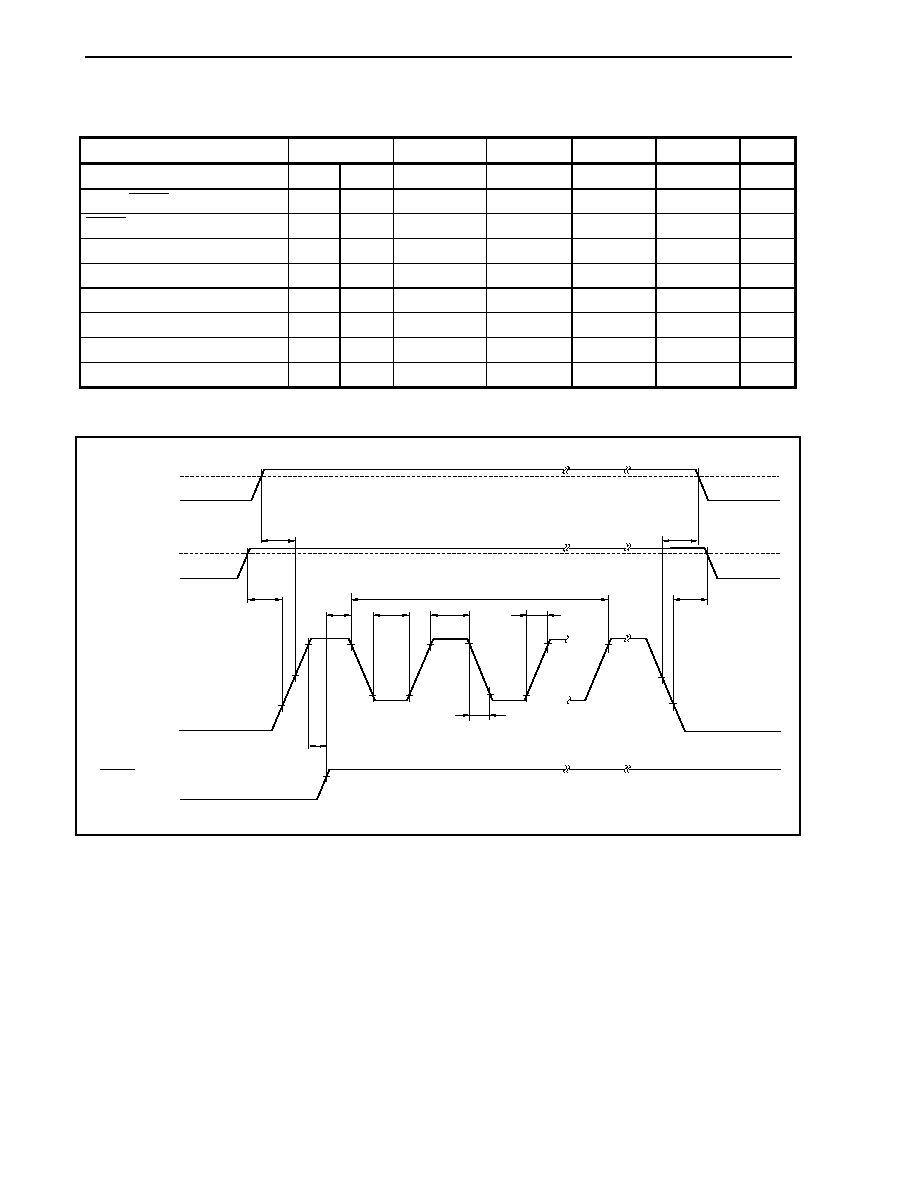
CHAPTER 18 ELECTRICAL SPECIFICATIONS
788
User's Manual U14492EJ5V0UD
Serial Write Operation Characteristics (T
A
= 0 to 70
∞C, V
DD3
= CV
DD
= 3.0 to 3.6 V,
V
DD5
= 5 V
±0.5 V, V
SS3
= V
SS5
= CV
SS
= 0 V)
Parameter Symbol
Conditions
MIN.
TYP.
MAX.
Unit
V
DD3
, V
DD5
to V
PP
set time
<88>
t
DRPSR
10
µ
s
V
PP
to RESET set time
<89>
t
PSRRF
1
µ
s
RESET
to V
PP
count start time
<90>
t
RFOF
V
PP
= 7.8 V
10T + 1500
ns
Count execution time
<91>
t
COUNT
15
ms
V
PP
counter high-level width
<92>
t
CH
1
µ
s
V
PP
counter low-level width
<93>
t
CL
1
µ
s
V
PP
counter rise time
<94>
t
R
1
µ
s
V
PP
counter fall time
<95>
t
F
1
µ
s
V
PP
to V
DD3
, V
DD5
reset time
<96>
t
PFDR
10
µ
s
Remark T
=
t
CYK
<88>
<90>
<93>
<92>
<91>
<95>
<94>
0 V
0 V
RESET
(input)
<89>
<96>
0 V
4.5 V
V
DD3
V
DD5
V
DD5
V
PP
V
DD3
V
DD5
V
PP
0 V
3.0 V
<96>
<88>

789
User's Manual U14492EJ5V0UD
CHAPTER 19 PACKAGE DRAWING
108
73
1
36
109
144
72
37
144-PIN PLASTIC LQFP (FINE PITCH) (20x20)
ITEM
MILLIMETERS
NOTE
A
22.0
±0.2
B
20.0
±0.2
C
20.0
±0.2
D
F
1.25
22.0
±0.2
S144GJ-50-UEN
S
1.5
±0.1
K
1.0
±0.2
L
0.5
±0.2
R
3
∞+4∞
-3∞
G
1.25
H
0.22
±0.05
I
0.08
J
0.5 (T.P.)
M
0.17
N
0.08
P
1.4
Q
0.10
±0.05
+0.03
-0.07
Each lead centerline is located within 0.08 mm of
its true position (T.P.) at maximum material condition.
S
S
M
detail of lead end
I
J
F
G
H
Q
R
P
K
M
L
N
C
D
S
A
B

790
User's Manual U14492EJ5V0UD
CHAPTER 20 RECOMMENDED SOLDERING CONDITIONS
V850E/IA1 should be soldered and mounted under the following recommended conditions.
For technical information, see the following website.
Semiconductor Device Mount Manual (http://www.necel.com/pkg/en/mount/index.html)
Table 20-1. Surface Mounting Type Soldering Conditions
(1)
µ
PD703116GJ-xxx-UEN:
144-pin plastic LQFP (fine pitch) (20
◊ 20)
µ
PD703116GJ(A)-xxx-UEN:
144-pin plastic LQFP (fine pitch) (20
◊ 20)
µ
PD703116GJ(A1)-xxx-UEN:
144-pin plastic LQFP (fine pitch) (20
◊ 20)
µ
PD70F3116GJ-UEN:
144-pin plastic LQFP (fine pitch) (20
◊ 20)
µ
PD70F3116GJ(A)-UEN:
144-pin plastic LQFP (fine pitch) (20
◊ 20)
µ
PD70F3116GJ(A1)-UEN:
144-pin plastic LQFP (fine pitch) (20
◊ 20)
Soldering Method
Soldering Conditions
Recommended
Condition
Symbol
Infrared reflow
Package peak temperature: 230∞C, Time: 30 seconds max. (at 210∞C or higher),
Count: Two times or less, Exposure limit: 3 days
Note
(after that, prebake at 125∞C for
10 to 72 hours)
IR30-103-2
VPS
Package peak temperature: 215∞C, Time: 25 to 40 seconds (at 200∞C or higher),
Count: Two times or less, Exposure limit: 3 days
Note
(after that, prebake at 125∞C for
10 to 72 hours)
VP15-103-2
Partial heating
Pin temperature: 350∞C max., Time: 3 seconds max. (per pin row)
≠
(2)
µ
PD70F3116GJ-UEN-A:
144-pin plastic LQFP (fine pitch) (20
◊ 20)
µ
PD70F3116GJ(A1)-UEN-A:
144-pin plastic LQFP (fine pitch) (20
◊ 20)
Soldering Method
Soldering Conditions
Recommended
Condition
Symbol
Infrared reflow
Package peak temperature: 260∞C, Time: 60 seconds max. (at 220∞C or higher),
Count: Three times or less, Exposure limit: 3 days
Note
(after that, prebake at 125∞C
for 20 to 72 hours)
IR60-203-3
Wave soldering
For details, consult an NEC Electronics sales representative.
≠
Partial heating
Pin temperature: 350∞C max., Time: 3 seconds max. (per pin row)
≠
Note After opening the dry pack, store it at 25∞C or less and 65% RH or less for the allowable storage period.
Caution Do not use different soldering methods together (except for partial heating).
Remarks 1. Products with -A at the end of the part number are lead-free products.
2. For soldering methods and conditions other than those recommended above, consult an NEC
Electronics sales representative.
3. For soldering conditions for the
µ
PD703116GJ-xxx-UEN-A, 703116GJ(A)-xxx-UEN-A,
703116GJ(A1)-xxx-UEN-A, and 70F3116GJ(A)-UEN-A, consult an NEC Electronics sales
representative.
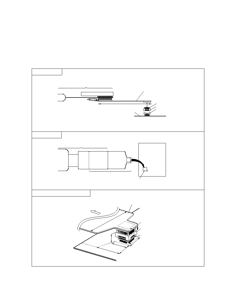
791
User's Manual U14492EJ5V0UD
APPENDIX A NOTES ON TARGET SYSTEM DESIGN
The following shows a diagram of the connection conditions between the in-circuit emulator option board and
conversion connector. Design your system making allowances for conditions such as the form of parts mounted on
the target system based on this configuration.
Figure A-1. 144-Pin Plastic LQFP (Fine Pitch) (20
◊ 20)
Side view
Target system
NQPACK144SD
YQPACK144SD
206.26 mm
Note
In-circuit emulator
option board
Conversion connector
IE-703116-MC-EM1
In-circuit emulator
IE-V850E-MC
YQGUIDE
Note YQSOCKET144SDN (sold separately) can be inserted here to adjust the height (height: 3.2 mm).
Top view
Target system
YQPACK144SD, NQPACK144SD,
YQGUIDE
IE-703116-MC-EM1
IE-V850E-MC
Connection condition diagram
13.3 mm
27.205 mm
21.58 mm
17.99 mm
75 mm
31.84 mm
Target system
NQPACK144SD
YQPACK144SD
IE-703116-MC-EM1
Connect to IE-V850E-MC
YQGUIDE

792
User's Manual U14492EJ5V0UD
APPENDIX B REGISTER INDEX
(1/11)
Symbol Register
Name
Unit
Page
ADCR00
A/D conversion result register 00
ADC
651
ADCR01
A/D conversion result register 01
ADC
651
ADCR02
A/D conversion result register 02
ADC
651
ADCR03
A/D conversion result register 03
ADC
651
ADCR04
A/D conversion result register 04
ADC
651
ADCR05
A/D conversion result register 05
ADC
651
ADCR06
A/D conversion result register 06
ADC
651
ADCR07
A/D conversion result register 07
ADC
651
ADCR10
A/D conversion result register 10
ADC
651
ADCR11
A/D conversion result register 11
ADC
651
ADCR12
A/D conversion result register 12
ADC
651
ADCR13
A/D conversion result register 13
ADC
651
ADCR14
A/D conversion result register 14
ADC
651
ADCR15
A/D conversion result register 15
ADC
651
ADCR16
A/D conversion result register 16
ADC
651
ADCR17
A/D conversion result register 17
ADC
651
ADETM0
A/D voltage detection mode register 0
ADC
650
ADETM0H
A/D voltage detection mode register 0H
ADC
650
ADETM0L
A/D voltage detection mode register 0L
ADC
650
ADETM1
A/D voltage detection mode register 1
ADC
650
ADETM1H
A/D voltage detection mode register 1H
ADC
650
ADETM1L
A/D voltage detection mode register 1L
ADC
650
ADIC0
Interrupt control register
INTC
172
ADIC1
Interrupt control register
INTC
172
ADSCM00
A/D scan mode register 00
ADC
646
ADSCM00H
A/D scan mode register 00H
ADC
646
ADSCM00L
A/D scan mode register 00L
ADC
646
ADSCM01
A/D scan mode register 01
ADC
649
ADSCM01H
A/D scan mode register 01H
ADC
649
ADSCM01L
A/D scan mode register 01L
ADC
649
ADSCM10
A/D scan mode register 10
ADC
646
ADSCM10H
A/D scan mode register 10H
ADC
646
ADSCM10L
A/D scan mode register 10L
ADC
646
ADSCM11
A/D scan mode register 11
ADC
649
ADSCM11H
A/D scan mode register 11H
ADC
649
ADSCM11L
A/D scan mode register 11L
ADC
649
ASIF0
Asynchronous serial interface transmit status register 0
UART0
418
ASIM0
Asynchronous serial interface mode register 0
UART0
414

APPENDIX B REGISTER INDEX
793
User's Manual U14492EJ5V0UD
(2/11)
Symbol Register
Name
Unit
Page
ASIM10
Asynchronous serial interface mode register 10
UART1
445
ASIM11
Asynchronous serial interface mode register 11
UART1
447
ASIM20
Asynchronous serial interface mode register 20
UART2
445
ASIM21
Asynchronous serial interface mode register 21
UART2
447
ASIS0
Asynchronous serial interface status register 0
UART0
417
ASIS1
Asynchronous serial interface status register 1
UART1
448
ASIS2
Asynchronous serial interface status register 2
UART2
448
AWC
Address wait control register
BCU
115
BCC
Bus cycle control register
BCU
117
BCT0
Bus cycle type configuration register 0
BCU
105
BCT1
Bus cycle type configuration register 1
BCU
105
BFCM00 Buffer
register
CM00
TM00 224
BFCM01 Buffer
register
CM01
TM00 224
BFCM02 Buffer
register
CM02
TM00 224
BFCM03 Buffer
register
CM03
TM00 225
BFCM10 Buffer
register
CM10
TM01 224
BFCM11 Buffer
register
CM11
TM01 224
BFCM12 Buffer
register
CM12
TM01 224
BFCM13 Buffer
register
CM13
TM01 225
BPC
Peripheral area selection control register
CPU
82
BRGC0
Baud rate generator control register 0
UART0
436
BSC
Bus size configuration register
BCU
107
C1BA
CAN1 bus active register
FCAN
589
C1BRP
CAN1 bit rate prescaler register
FCAN
590
C1CTRL
CAN1 control register
FCAN
576
C1DEF
CAN1 definition register
FCAN
580
C1DINF
CAN1 bus diagnostic information register
FCAN
593
C1ERC
CAN1 error count register
FCAN
585
C1IE
CAN1 interrupt enable register
FCAN
586
C1INTP
CAN1 interrupt pending register
FCAN
563
C1LAST
CAN1 information register
FCAN
584
C1MASKH0
CAN1 address mask 0 register H
FCAN
574
C1MASKH1
CAN1 address mask 1 register H
FCAN
574
C1MASKH2
CAN1 address mask 2 register H
FCAN
574
C1MASKH3
CAN1 address mask 3 register H
FCAN
574
C1MASKL0
CAN1 address mask 0 register L
FCAN
574
C1MASKL1
CAN1 address mask 1 register L
FCAN
574
C1MASKL2
CAN1 address mask 2 register L
FCAN
574
C1MASKL3
CAN1 address mask 3 register L
FCAN
574
C1SYNC
CAN1 synchronization control register
FCAN
594
CANIC0
Interrupt control register
INTC
172

APPENDIX B REGISTER INDEX
794
User's Manual U14492EJ5V0UD
(3/11)
Symbol Register
Name
Unit
Page
CANIC1
Interrupt control register
INTC
172
CANIC2
Interrupt control register
INTC
172
CANIC3
Interrupt control register
INTC
172
CC100
Capture/compare register 100
TM10
311
CC101
Capture/compare register 101
TM10
312
CC10IC0
Interrupt control register
INTC
172
CC10IC1
Interrupt control register
INTC
172
CC110
Capture/compare register 110
TM11
311
CC111
Capture/compare register 111
TM11
312
CC11IC0
Interrupt control register
INTC
172
CC11IC1
Interrupt control register
INTC
172
CC2IC0
Interrupt control register
INTC
172
CC2IC1
Interrupt control register
INTC
172
CC2IC2
Interrupt control register
INTC
172
CC2IC3
Interrupt control register
INTC
172
CC2IC4
Interrupt control register
INTC
172
CC2IC5
Interrupt control register
INTC
172
CC30
Capture/compare register 30
TM3
377
CC31
Capture/compare register 31
TM3
377
CC3IC0
Interrupt control register
INTC
172
CC3IC1
Interrupt control register
INTC
172
CCINTP
CAN interrupt pending register
FCAN
561
CCR0
Capture/compare control register 0
TM10
303
CCR1
Capture/compare control register 1
TM11
303
CCSTATE0
Timer 2 capture/compare 1 to 4 status register 0
TM2
349
CCSTATE0H
Timer 2 capture/compare 1 to 4 status register 0H
TM2
349
CCSTATE0L
Timer 2 capture/compare 1 to 4 status register 0L
TM2
349
CGCS
CAN main clock selection register
FCAN
569
CGIE
CAN global interrupt enable register
FCAN
568
CGINTP
CAN global interrupt pending register
FCAN
562
CGMSR
CAN message search result register
FCAN
572
CGMSS
CAN message search start register
FCAN
572
CGST
CAN global status register
FCAN
565
CGTSC
CAN time stamp count register
FCAN
571
CKC Clock
control
register
CG 200
CKSR0
Clock selection register 0
UART0
435
CM000 Compare
register
000
TM00 223
CM001 Compare
register
001
TM00 223
CM002 Compare
register
002
TM00 223
CM003 Compare
register
003
TM00 224
CM010 Compare
register
010
TM01 223

APPENDIX B REGISTER INDEX
795
User's Manual U14492EJ5V0UD
(4/11)
Symbol Register
Name
Unit
Page
CM011 Compare
register
011
TM01 223
CM012 Compare
register
012
TM01 223
CM013 Compare
register
013
TM01 224
CM03IC0
Interrupt control register
INTC
172
CM03IC1
Interrupt control register
INTC
172
CM100 Compare
register
100
TM10 310
CM101 Compare
register
101
TM10 310
CM10IC0
Interrupt control register
INTC
172
CM10IC1
Interrupt control register
INTC
172
CM110 Compare
register
110
TM11 310
CM111 Compare
register
111
TM11 310
CM11IC0
Interrupt control register
INTC
172
CM11IC1
Interrupt control register
INTC
172
CM4 Compare
register
4
TM4
402
CM4IC0
Interrupt control register
INTC
172
CMSE050
Timer 2 subchannel 0, 5 capture/compare control register
TM2
343
CMSE120
Timer 2 subchannel 1, 2 capture/compare control register
TM2
344
CMSE340
Timer 2 subchannel 3, 4 capture/compare control register
TM2
346
CSC0
Chip area selection control register 0
BCU
102
CSC1
Chip area selection control register 1
BCU
102
CSCE0
Timer 2 software event capture register
TM2
351
CSE0
Timer 2 count clock/control edge selection register 0
TM2
336
CSE0H
Timer 2 count clock/control edge selection register 0H
TM2
336
CSE0L
Timer 2 count clock/control edge selection register 0L
TM2
336
CSIC0
Clocked serial interface clock selection register 0
CSI0
481
CSIC1
Clocked serial interface clock selection register 1
CSI1
481
CSIIC0
Interrupt control register
INTC
172
CSIIC1
Interrupt control register
INTC
172
CSIM0
Clocked serial interface mode register 0
CSI0
479
CSIM1
Clocked serial interface mode register 1
CSI1
479
CSL10
CC101 capture input selection register
TM10
309
CSL11
CC111 capture input selection register
TM11
309
CSTOP
CAN stop register
FCAN
564
CVPE10
Timer 2 subchannel 1 main capture/compare register
TM2
333
CVPE20
Timer 2 subchannel 2 main capture/compare register
TM2
333
CVPE30
Timer 2 subchannel 3 main capture/compare register
TM2
333
CVPE40
Timer 2 subchannel 4 main capture/compare register
TM2
333
CVSE00
Timer 2 subchannel 0 capture/compare register
TM2
332
CVSE10
Timer 2 subchannel 1 sub capture/compare register
TM2
334
CVSE20
Timer 2 subchannel 2 sub capture/compare register
TM2
334
CVSE30
Timer 2 subchannel 3 sub capture/compare register
TM2
334

APPENDIX B REGISTER INDEX
796
User's Manual U14492EJ5V0UD
(5/11)
Symbol Register
Name
Unit
Page
CVSE40
Timer 2 subchannel 4 sub capture/compare register
TM2
334
CVSE50
Timer 2 subchannel 5 capture/compare register
TM2
334
DADC0
DMA addressing control register 0
DMAC
134
DADC1
DMA addressing control register 1
DMAC
134
DADC2
DMA addressing control register 2
DMAC
134
DADC3
DMA addressing control register 3
DMAC
134
DBC0
DMA transfer count register 0
DMAC
133
DBC1
DMA transfer count register 1
DMAC
133
DBC2
DMA transfer count register 2
DMAC
133
DBC3
DMA transfer count register 3
DMAC
133
DCHC0
DMA channel control register 0
DMAC
136
DCHC1
DMA channel control register 1
DMAC
136
DCHC2
DMA channel control register 2
DMAC
136
DCHC3
DMA channel control register 3
DMAC
136
DDA0H
DMA destination address register 0H
DMAC
131
DDA0L
DMA destination address register 0L
DMAC
132
DDA1H
DMA destination address register 1H
DMAC
131
DDA1L
DMA destination address register 1L
DMAC
132
DDA2H
DMA destination address register 2H
DMAC
131
DDA2L
DMA destination address register 2L
DMAC
132
DDA3H
DMA destination address register 3H
DMAC
131
DDA3L
DMA destination address register 3L
DMAC
132
DDIS
DMA disable status register
DMAC
138
DETIC0
Interrupt control register
INTC
172
DETIC1
Interrupt control register
INTC
172
DMAIC0
Interrupt control register
INTC
172
DMAIC1
Interrupt control register
INTC
172
DMAIC2
Interrupt control register
INTC
172
DMAIC3
Interrupt control register
INTC
172
DRST DMA
restart
register
DMAC
138
DSA0H
DMA source address register 0H
DMAC
129
DSA0L
DMA source address register 0L
DMAC
130
DSA1H
DMA source address register 1H
DMAC
129
DSA1L
DMA source address register 1L
DMAC
130
DSA2H
DMA source address register 2H
DMAC
129
DSA2L
DMA source address register 2L
DMAC
130
DSA3H
DMA source address register 3H
DMAC
129
DSA3L
DMA source address register 3L
DMAC
130
DTFR0
DMA trigger factor register 0
DMAC
139
DTFR1
DMA trigger factor register 1
DMAC
139
DTFR2
DMA trigger factor register 2
DMAC
139

APPENDIX B REGISTER INDEX
797
User's Manual U14492EJ5V0UD
(6/11)
Symbol Register
Name
Unit
Page
DTFR3
DMA trigger factor register 3
DMAC
139
DTM00 Dead-time
timer
00
TM00 223
DTM01 Dead-time
timer
01
TM00 223
DTM02 Dead-time
timer
02
TM00 223
DTM10 Dead-time
timer
10
TM01 223
DTM11 Dead-time
timer
11
TM01 223
DTM12 Dead-time
timer
12
TM01 223
DTRR0
Dead-time timer reload register 0
TM00
223
DTRR1
Dead-time timer reload register 1
TM01
223
DWC0
Data wait control register 0
TM2
114
DWC1
Data wait control register 1
TM2
114
FEM0
Timer 2 input filter mode register 0
TM2
183, 717
FEM1
Timer 2 input filter mode register 1
TM2
183, 717
FEM2
Timer 2 input filter mode register 2
TM2
183, 717
FEM3
Timer 2 input filter mode register 3
TM2
183, 717
FEM4
Timer 2 input filter mode register 4
TM2
183, 717
FEM5
Timer 2 input filter mode register 5
TM2
183, 717
FLPMC
Flash programming mode control register
CPU
747
IMR0
Interrupt mask register 0
INTC
175
IMR0H
Interrupt mask register 0H
INTC
175
IMR0L
Interrupt mask register 0L
INTC
175
IMR1
Interrupt mask register 1
INTC
175
IMR1H
Interrupt mask register 1H
INTC
175
IMR1L
Interrupt mask register 1L
INTC
175
IMR2
Interrupt mask register 2
INTC
175
IMR2H
Interrupt mask register 2H
INTC
175
IMR2L
Interrupt mask register 2L
INTC
175
IMR3
Interrupt mask register 3
INTC
175
IMR3H
Interrupt mask register 3H
INTC
175
IMR3L
Interrupt mask register 3L
INTC
175
INTM0
External interrupt mode register 0
INTC
164
INTM1
External interrupt mode register 1
INTC
178
INTM2
External interrupt mode register 2
INTC
178
ISPR
In-service priority register
INTC
176
ITRG0
A/D internal trigger selection register
ADC
654
LOCKR Lock
register
CPU 203
M_CONF00 to
M_CONF31
CAN message configuration registers 00 to 31
FCAN
555
M_CTRL00 to
M_CTRL31
CAN message control registers 00 to 31
FCAN
547

APPENDIX B REGISTER INDEX
798
User's Manual U14492EJ5V0UD
(7/11)
Symbol Register
Name
Unit
Page
M_DATAn0 to
M_DATAn7
CAN message data registers n0 to n7 (n = 00 to 31)
FCAN
551
M_DLC00 to
M_DLC31
CAN message data length registers 00 to 31
FCAN
545
M_IDH00 to
M_IDH31
CAN message ID registers H00 to H31
FCAN
553
M_IDL00 to
M_IDL31
CAN message ID registers L00 to L31
FCAN
553
M_STAT00 to
M_STAT31
CAN message status registers 00 to 31
FCAN
557
M_TIME00 to
M_TIME31
CAN message time stamp registers 00 to 31
FCAN
550
NBDH
RAM access data buffer register H
NBD
634
NBDHL
RAM access data buffer register HL
NBD
634
NBDHU
RAM access data buffer register HU
NBD
634
NBDL
RAM access data buffer register L
NBD
634
NBDLL
RAM access data buffer register LL
NBD
634
NBDLU
RAM access data buffer register LU
NBD
634
NBDMDH DMA
destination
address
setting register DH
NBD
636
NBDMDL DMA
destination
address
setting register DL
NBD
636
NBDMSH
DMA source address setting register SH
NBD
635
NBDMSL
DMA source address setting register SL
NBD
635
NRC10
Timer 10 noise elimination time selection register
TM10
714
NRC11
Timer 11 noise elimination time selection register
TM11
714
NRC3
Timer 3 noise elimination time selection register
TM3
715
OCTLE0
Timer 2 output control register 0
TM2
341
OCTLE0H
Timer 2 output control register 0H
TM2
341
OCTLE0L
Timer 2 output control register 0L
TM2
341
ODELE0
Timer 2 output delay register 0
TM2
350
ODELE0H
Timer 2 output delay register 0H
TM2
350
ODELE0L
Timer 2 output delay register 0L
TM2
350
P0 Port
0
Port 689
P0IC0
Interrupt control register
INTC
172
P0IC1
Interrupt control register
INTC
172
P0IC2
Interrupt control register
INTC
172
P0IC3
Interrupt control register
INTC
172
P0IC4
Interrupt control register
INTC
172
P0IC5
Interrupt control register
INTC
172
P0IC6
Interrupt control register
INTC
172
P1 Port
1
Port 690
P2 Port
2
Port 693
P3 Port
3
Port 696

APPENDIX B REGISTER INDEX
799
User's Manual U14492EJ5V0UD
(8/11)
Symbol Register
Name
Unit
Page
P4 Port
4
Port 698
PCM Port
CM
Port 708
PCS Port
CS
Port 704
PCT Port
CT
Port 706
PDH Port
DH
Port 700
PDL Port
DL
Port 702
PDLH Port
DLH
Port 702
PDLL Port
DLL
Port 702
PFC1
Port 1 function control register
Port
692
PFC2
Port 2 function control register
Port
695
PHCMD
Peripheral command register
CPU
199
PHS
Peripheral status register
CPU
202
PM1
Port 1 mode register
Port
690
PM2
Port 2 mode register
Port
693
PM3
Port 3 mode register
Port
696
PM4
Port 4 mode register
Port
698
PMC1
Port 1 mode control register
Port
691
PMC2
Port 2 mode control register
Port
694
PMC3
Port 3 mode control register
Port
697
PMC4
Port 4 mode control register
Port
699
PMCCM
Port CM mode control register
Port
709
PMCCS
Port CS mode control register
Port
705
PMCCT
Port CT mode control register
Port
707
PMCDH
Port DH mode control register
Port
701
PMCDL
Port DL mode control register
Port
703
PMCDLH
Port DL mode control register H
Port
703
PMCDLL
Port DL mode control register L
Port
703
PMCM
Port CM mode register
Port
708
PMCS
Port CS mode register
Port
705
PMCT
Port CT mode register
Port
706
PMDH
Port DH mode register
Port
700
PMDL
Port DL mode register
Port
703
PMDLH
Port DL mode register H
Port
703
PMDLL
Port DL mode register L
Port
703
POER0
PWM output enable register 0
TM00
239
POER1
PWM output enable register 1
TM01
239
PRCMD Command
register
CPU 207
PRM01
Timer 0 clock selection register
TM0
226
PRM02
Timer 1/timer 2 clock selection register
TM1/TM2
299, 335
PRM03
Timer 3 clock selection register
TM3
379
PRM04
FCAN clock selection register
FCAN
544

APPENDIX B REGISTER INDEX
800
User's Manual U14492EJ5V0UD
(9/11)
Symbol Register
Name
Unit
Page
PRM10
Prescaler mode register 10
TM10
306
PRM11
Prescaler mode register 11
TM11
306
PRSCM1
Prescaler compare register 1
UART1
471
PRSCM2
Prescaler compare register 2
UART2
471
PRSCM3
Prescaler compare register 3
CSI0, CSI1
511
PRSM1
Prescaler mode register 1
UART1
470
PRSM2
Prescaler mode register 2
UART2
470
PRSM3
Prescaler mode register 3
CSI0, CSI1
511
PSC
Power save control register
CPU
208
PSMR
Power save mode register
CPU
207
PSTO0
PWM software timing output register 0
TM00
240
PSTO1
PWM software timing output register 1
TM01
240
RXB0
Receive buffer register 0
UART0
419
RXB1 2-frame
continuous
reception buffer register 1
UART1
450
RXB2 2-frame
continuous
reception buffer register 2
UART2
450
RXBL1
Receive buffer register L1
UART1
450
RXBL2
Receive buffer register L2
UART2
450
SC_STAT00 to
SC_STAT31
CAN status set/clear registers 00 to 31
FCAN
559
SEIC0
Interrupt control register
INTC
172
SESA10
Signal edge selection register 10
INTC, TM10
179, 304
SESA11
Signal edge selection register 11
INTC, TM11
179, 304
SESC
Valid edge selection register
INTC, TM3
182, 384
SESE0
Timer 2 sub-channel input event edge selection register 0
TM2
337
SESE0H
Timer 2 sub-channel input event edge selection register 0H
TM2
337
SESE0L
Timer 2 sub-channel input event edge selection register 0L
TM2
337
SIO0
Serial I/O shift register 0
CSI0
491
SIO1
Serial I/O shift register 1
CSI1
491
SIOL0
Serial I/O shift register L0
CSI0
492
SIOL1
Serial I/O shift register L1
CSI1
492
SIRB0
Clocked serial interface receive buffer register 0
CSI0
483
SIRB1
Clocked serial interface receive buffer register 1
CSI1
483
SIRBE0
Clocked serial interface read-only receive buffer register 0
CSI0
485
SIRBE1
Clocked serial interface read-only receive buffer register 1
CSI1
485
SIRBEL0
Clocked serial interface read-only receive buffer register L0
CSI0
486
SIRBEL1
Clocked serial interface read-only receive buffer register L1
CSI1
486
SIRBL0
Clocked serial interface receive buffer register L0
CSI0
484
SIRBL1
Clocked serial interface receive buffer register L1
CSI1
484
SOTB0
Clocked serial interface transmit buffer register 0
CSI0
487
SOTB1
Clocked serial interface transmit buffer register 1
CSI1
487
SOTBF0
Clocked serial interface initial transmit buffer register 0
CSI0
489

APPENDIX B REGISTER INDEX
801
User's Manual U14492EJ5V0UD
(10/11)
Symbol Register
Name
Unit
Page
SOTBF1
Clocked serial interface initial transmit buffer register 1
CSI1
489
SOTBFL0
Clocked serial interface initial transmit buffer register L0
CSI0
490
SOTBFL1
Clocked serial interface initial transmit buffer register L1
CSI1
490
SOTBL0
Clocked serial interface transmit buffer register L0
CSI0
488
SOTBL1
Clocked serial interface transmit buffer register L1
CSI1
488
SPEC0
TOMR write enable register 0
TM00
249
SPEC1
TOMR write enable register 1
TM01
249
SRIC0
Interrupt control register
INTC
172
SRIC1
Interrupt control register
INTC
172
SRIC2
Interrupt control register
INTC
172
STATUS0
Status register 0
TM10
308
STATUS1
Status register 1
TM11
308
STIC0
Interrupt control register
INTC
172
STIC1
Interrupt control register
INTC
172
STIC2
Interrupt control register
INTC
172
STOPTE0
Timer 2 clock stop register 0
TM2
335
STOPTE0H
Timer 2 clock stop register 0H
TM2
335
STOPTE0L
Timer 2 clock stop register 0L
TM2
335
TBSTATE0
Timer 2 time base status register 0
TM2
348
TBSTATE0H
Timer 2 time base status register 0H
TM2
348
TBSTATE0L
Timer 2 time base status register 0L
TM2
348
TCRE0
Timer 2 time base control register 0
TM2
338
TCRE0H
Timer 2 time base control register 0H
TM2
338
TCRE0L
Timer 2 time base control register 0L
TM2
338
TM00 Timer
00
TM00 222
TM01 Timer
01
TM01 222
TM0IC0
Interrupt control register
INTC
172
TM0IC1
Interrupt control register
INTC
172
TM10 Timer
10
TM10 297
TM11 Timer
11
TM11 297
TM20 Timer
20
TM2 332
TM21 Timer
21
TM2 332
TM2IC0
Interrupt control register
INTC
172
TM2IC1
Interrupt control register
INTC
172
TM3 Timer
3
TM3 375
TM3IC0
Interrupt control register
INTC
172
TM4 Timer
4
TM4 401
TMC00
Timer control register 00
TM00
227
TMC00H
Timer control register 00H
TM00
227
TMC00L
Timer control register 00L
TM00
227
TMC01
Timer control register 01
TM01
227

APPENDIX B REGISTER INDEX
802
User's Manual U14492EJ5V0UD
(11/11)
Symbol Register
Name
Unit
Page
TMC01H
Timer control register 01H
TM01
227
TMC01L
Timer control register 01L
TM01
227
TMC10
Timer control register 10
TM10
301
TMC11
Timer control register 11
TM11
301
TMC30
Timer control register 30
TM3
380
TMC31
Timer control register 31
TM3
382
TMC4
Timer control register 4
TM4
404
TMIC0
Timer connection selection register 0
TM1/TM2
409
TOMR0
Timer output mode register 0
TM00
234
TOMR1
Timer output mode register 1
TM01
234
TUC00
Timer unit control register 00
TM00
233
TUC01
Timer unit control register 01
TM01
233
TUM0
Timer unit mode register 0
TM10
300
TUM1
Timer unit mode register 1
TM11
300
TXB0
Transmit buffer register 0
UART0
420
TXS1 2-frame
continuous
transmission shift register 1
UART1
453
TXS2 2-frame
continuous
transmission shift register 2
UART2
453
TXSL1
Transmit shift register L1
UART1
453
TXSL2
Transmit shift register L2
UART2
453
VSWC
System wait control register
BCU
98

803
User's Manual U14492EJ5V0UD
APPENDIX C INSTRUCTION SET LIST
C.1 Functions
(1) Symbols used in operand descriptions
Symbol Explanation
reg1 General-purpose
register
(Used as source register)
reg2
General-purpose register (Usually used as destination register. Used as source register in some
instructions.)
reg3
General-purpose register (Usually stores remainder of division result or higher 32 bits of
multiplication result.)
bit#3
3-bit data for bit number specification
immX
X-bit immediate data
dispX
X-bit displacement data
regID System
register
number
vector
5-bit data that specifies a trap vector (00H to 1FH)
cccc
4-bit data that shows a condition code
sp Stack
pointer
(r3)
ep
Element pointer (r30)
list
◊
X-item register list
(2) Symbols used in operands
Symbol Explanation
R
1 bit of data of code that specifies reg1 or regID
r
1 bit of data of code that specifies reg2
w
1 bit of data of code that specifies reg3
d
1 bit of data of a displacement
I
1 bit of immediate data (Shows higher bit of immediate data)
i
1 bit of immediate data
cccc
4-bit data that shows a condition code
CCCC
4-bit data that shows condition code of Bcond instruction
bbb
3-bit data for bit number specification
L
1 bit of data that specifies a program register in a register list
S
1 bit of data that specifies a system register in a register list

APPENDIX C INSTRUCTION SET LIST
804
User's Manual U14492EJ5V0UD
(3) Symbols used in operations
Symbol Explanation
Assignment
GR [ ]
General-purpose register
SR [ ]
System register
zero-extend (n)
Zero-extend n to word length.
sign-extend (n)
Sign-extend n to word length.
load-memory (a, b)
Read data of size "b" from address "a".
store-memory (a, b, c)
Write data "b" of size "c" to address "a".
load-memory-bit (a, b)
Read bit "b" of address "a".
store-memory-bit (a, b, c)
Write "c" in bit "b" of address "a".
saturated (n)
Perform saturation processing of n (n is 2's complement).
If n is a computation result and n
7FFFFFFFH, make n = 7FFFFFFFH.
If n is a computation result and n
80000000H, make n = 80000000H.
result
Reflect result in flag.
Byte Byte
(8
bits)
Half-word
Halfword (16 bits)
Word
Word (32 bits)
+ Addition
-
Subtraction
|| Bit
concatenation
◊
Multiplication
˜
Division
%
Remainder of division result
AND Logical
product
OR Logical
sum
XOR Exclusive
logical
sum
NOT Logical
negation
logically shift left by
Logical shift left
logically shift right by
Logical shift right
arithmetically shift right by Arithmetic
shift
right
(4) Symbols used in execution clock
Symbol Explanation
i
When executing another instruction immediately after instruction execution (issue)
r
When repeating same instruction immediately after instruction execution (repeat)
|
When using instruction execution result in instruction immediately after instruction execution
(latency)

APPENDIX C INSTRUCTION SET LIST
805
User's Manual U14492EJ5V0UD
(5) Symbols used in flag operations
Symbol Explanation
(Blank) No
change
0
Clear to 0.
◊
Set or cleared according to result.
R
Previously saved value is restored.
(6) Condition codes
Condition Name
(cond)
Condition Code
(cccc)
Condition Expression
Explanation
V
0000
OV = 1
Overflow
NV
1000
OV = 0
No overflow
C/L
0001
CY = 1
Carry
Lower (Less than)
NC/NL
1001
CY = 0
No carry
No lower (Greater than or
equal)
Z/E
0010
Z = 1
Zero
Equal
NZ/NE
1010
Z = 0
Not zero
Not equal
NH
0011
(CY or Z) = 1
Not higher (Less than or equal)
H
1011
(CY or Z) = 0
Higher (Greater than)
N
0100
S = 1
Negative
P
1100
S = 0
Positive
T 0101
-
Always (Unconditional)
SA
1101
SAT = 1
Saturated
LT
0110
(S xor OV) = 1
Less than signed
GE
1110
(S xor OV) = 0
Greater than or equal signed
LE
0111
((S xor OV) or Z) = 1
Less than or equal signed
GT
1111
((S xor OV) or Z) = 0
Greater than signed

APPENDIX C INSTRUCTION SET LIST
806
User's Manual U14492EJ5V0UD
C.2 Instruction Set (Alphabetical Order)
(1/5)
Execution Clock
Flags
Mnemonic Operands
Opcode
Operation
i r I
CY
OV
S Z
SAT
reg1, reg2
r r r r r 0 0 1 1 1 0 R R R R R
GR[reg2]
GR[reg2] + GR[reg1]
1
1
1
◊
◊
◊
◊
ADD
imm5, reg2
r r r r r 0 1 0 0 1 0 i i i i i
GR[reg2]
GR[reg2] + sign-extend (imm5)
1
1
1
◊
◊
◊
◊
ADDI imm16,
r r r r r 1 1 0 0 0 0 R R R R R GR[reg2]
GR[reg1] + sign-extend (imm16)
1
1
1
◊
◊
◊
◊
reg1,
reg2
i i i i i i i i i i i i i i i i
AND reg1,
reg2
r r r r r 0 0 1 0 1 0 R R R R R
GR[reg2]
GR[reg2] AND GR[reg1]
1
1
1
0
◊
◊
r r r r r 1 1 0 1 1 0 R R R R R
1 1 1 0 0
◊
ANDI imm16,
reg1,
reg2
i i i i i i i i i i i i i i i i
GR[reg2]
GR[reg1] AND zero-extend (imm16)
d d d d d 1 0 1 1 d d d c c c c
Conditions satisfied
3
Note 2
3
Note 2
3
Note 2
Bcond disp9
if conditions are satisfied
then PC
PC + sign-extend
(disp9)
Conditions not
satisfied
1 1 1
r r r r r 1 1 1 1 1 1 0 0 0 0 0
1 1 1
◊
0
◊
◊
BSH reg2,
reg3
w w w w w 0 1 1 0 1 0 0 0 0 1 0
GR[reg3]
GR[reg2] (23:16) || GR[reg2] (31:24) ||
GR[reg2] (7:0) || GR[reg2] (15:8)
r r r r r 1 1 1 1 1 1 0 0 0 0 0
1 1 1
◊
0
◊
◊
BSW reg2,
reg3
w w w w w 0 1 1 0 1 0 0 0 0 0 0
GR[reg3]
GR[reg2] (7:0) || GR[reg2] (15:8) || GR
[reg2] (23:16) || GR[reg2] (31:24)
CALLT imm6
0 0 0 0 0 0 1 0 0 0 i i i i i i
CTPC
PC + 2 (return PC)
CTPSW
PSW
adr
CTBP + zero-extend (imm6 logically shift left by 1)
PC
CTBP + zero-extend (Load-memory (adr,
Halfword)
5 5 5
1 0 b b b 1 1 1 1 1 0 R R R R R
bit#3,
disp16[reg1]
d d d d d d d d d d d d d d d d
adr
GR[reg1] + sign-extend (disp16)
Z flag
Not (Load-memory-bit (adr, bit#3))
Store-memory-bit (adr, bit#3, 0)
3
Note 3
3
Note 3
3
Note 3
◊
1 0 b b b 1 1 1 1 1 0 R R R R R
CLR1
reg2, [reg1]
d d d d d d d d d d d d d d d d
adr
GR[reg1]
Z flag
Not (Load-memory-bit (adr, reg2))
Store-memory-bit (adr, reg2, 0)
3
Note 3
3
Note 3
3
Note 3
◊
r r r r r 1 1 1 1 1 1 i i i i i
cccc, imm5,
reg2, reg3
w w w w w 0 1 1 0 0 0 c c c c 0
if conditions are satisfied
then GR[reg3]
sign-extend (imm5)
else GR[reg3]
GR[reg2]
1 1 1
r r r r r 1 1 1 1 1 1 R R R R R
CMOV
cccc, reg1,
reg2, reg3
w w w w w 0 1 1 0 0 1 c c c c 0
if conditions are satisfied
then GR[reg3]
GR[reg1]
else GR[reg3]
GR[reg2]
1 1 1
reg1, reg2
r r r r r 0 0 1 1 1 1 R R R R R
result
GR[reg2] - GR[reg1]
1
1
1
◊
◊
◊
◊
CMP
imm5, reg2
r r r r r 0 1 0 0 1 1 i i i i i
result
GR[reg2] - sign-extend (imm5)
1
1
1
◊
◊
◊
◊
0 0 0 0 0 1 1 1 1 1 1 0 0 0 0 0
CTRET
0 0 0 0 0 0 0 1 0 1 0 0 0 1 0 0
PC
CTPC
PSW
CTPSW
4 4 4 R R R R R
0 0 0 0 0 1 1 1 1 1 1 0 0 0 0 0
DBRET
0 0 0 0 0 0 0 1 0 1 0 0 0 1 1 0
PC
DBPC
PSW
DBPSW
4 4 4 R R R R R
DBTRAP
1 1 1 1 1 0 0 0 0 1 0 0 0 0 0 0
DBPC
PC + 2 (return PC)
DBPSW
PSW
PSW.NP
1
PSW.EP
1
PSW.ID
1
PC
00000060H
4 4 4
0 0 0 0 0 1 1 1 1 1 1 0 0 0 0 0
DI
0 0 0 0 0 0 0 1 0 1 1 0 0 0 0 0
PSW.ID
1
1
1
1
Note 1
APPENDIX C INSTRUCTION SET LIST
807
User's Manual U14492EJ5V0UD
(2/5)
Execution Clock
Flags
Mnemonic Operands
Opcode
Operation
i r I
CY
OV
S Z
SAT
0 0 0 0 0 1 1 0 0 1 i i i i i L
imm5, list12
L L L L L L L L L L L 0 0 0 0 0
sp
sp + zero-extend (imm5 logically shift left by 2)
GR[reg in list12]
Load-memory (sp, Word)
sp
sp + 4
repeat 2 steps above until regs in list12 is loaded
n+1
Note 4
n+1
Note 4
n+1
Note 4
0 0 0 0 0 1 1 0 0 1 i i i i i L
DISPOSE
imm5,
list12[reg1]
L L L L L L L L L L L R R R R R
sp
sp + zero-extend (imm5 logically shift left by 2)
GR[reg in list12]
Load-memory (sp, Word)
sp
sp + 4
repeat 2 steps above until regs in list12 is loaded
PC
GR[reg1]
n+3
Note 4
n+3
Note 4
n+3
Note 4
r r r r r 1 1 1 1 1 1 R R R R R
DIV reg1,
reg2,
reg3
w w w w w 0 1 0 1 1 0 0 0 0 0 0
GR[reg2]
GR[reg2] ˜ GR[reg1]
GR[reg3]
GR[reg2]%GR[reg1]
35 35 35
◊
◊
◊
reg1, reg2
r r r r r 0 0 0 0 1 0 R R R R R
GR[reg2]
GR[reg2] ˜ GR[reg1]
Note 6
35 35 35
◊
◊
◊
r r r r r 1 1 1 1 1 1 R R R R R
DIVH
reg1, reg2,
reg3
w w w w w 0 1 0 1 0 0 0 0 0 0 0
GR[reg2]
GR[reg2] ˜ GR[reg1]
Note 6
GR[reg3]
GR[reg2]%GR[reg1]
35 35 35
◊
◊
◊
r r r r r 1 1 1 1 1 1 R R R R R
DIVHU reg1,
reg2,
reg3
w w w w w 0 1 0 1 0 0 0 0 0 1 0
GR[reg2]
GR[reg2] ˜ GR[reg1]
Note 6
GR[reg3]
GR[reg2]%GR[reg1]
34 34 34
◊
◊
◊
r r r r r 1 1 1 1 1 1 R R R R R
DIVU reg1,
reg2,
reg3
w w w w w 0 1 0 1 1 0 0 0 0 1 0
GR[reg2]
GR[reg2] ˜ GR[reg1]
GR[reg3]
GR[reg2]%GR[reg1]
34 34 34
◊
◊
◊
1 0 0 0 0 1 1 1 1 1 1 0 0 0 0 0
EI
0 0 0 0 0 0 0 1 0 1 1 0 0 0 0 0
PSW.ID
0
1
1
1
0 0 0 0 0 1 1 1 1 1 1 0 0 0 0 0
HALT
0 0 0 0 0 0 0 1 0 0 1 0 0 0 0 0
Stop
1
1
1
r r r r r 1 1 1 1 1 1 0 0 0 0 0
HSW reg2,
reg3
w w w w w 0 1 1 0 1 0 0 0 1 0 0
GR[reg3]
GR[reg2] (15:0) || GR[reg2] (31:16)
1 1 1
◊
0
◊
◊
r r r r r 1 1 1 1 0 d d d d d d
JARL disp22,
reg2
d d d d d d d d d d d d d d d 0
GR[reg2]
PC + 4
PC
PC + sign-extend (disp22)
3
3
3
JMP [reg1] 0 0 0 0 0 0 0 0 0 1 1 R R R R R PC
GR[reg1]
4
4
4
0 0 0 0 0 1 1 1 1 0 d d d d d d
JR disp22
d d d d d d d d d d d d d d d 0
PC
PC + sign-extend (disp22)
3
3
3
r r r r r 1 1 1 0 0 0 R R R R R
LD.B disp16[reg1],
reg2
d d d d d d d d d d d d d d d d
adr
GR[reg1] + sign-extend (disp16)
GR[reg2]
sign-extend (Load-memory (adr, Byte))
1 1
Note 11
r r r r r 1 1 1 1 0 b R R R R R
LD.BU disp16[reg1],
reg2
d d d d d d d d d d d d d d d 1
adr
GR[reg1] + sign-extend (disp16)
GR[reg2]
zero-extend (Load-memory (adr, Byte))
1 1
Note 11
r r r r r 1 1 1 0 0 1 R R R R R
LD.H disp16[reg1],
reg2
d d d d d d d d d d d d d d d 0
adr
GR[reg1] + sign-extend (disp16)
GR[reg2]
sign-extend (Load-memory (adr,
Halfword))
1 1
Note 11
Other than regID = PSW
1
1
1
LDSR reg2,
regID
r
0
r
0
r
0
r
0
r
0
1
0
1
0
1
0
1
0
1
0
1
1
R
0
R
0
R
0
R
0
R
0
SR[regID]
GR[reg2]
regID = PSW
1 1 1
◊
◊
◊
◊
◊
r r r r r 1 1 1 0 0 1 R R R R R
LD.HU disp16[reg1],
reg2
d d d d d d d d d d d d d d d 1
adr
GR[reg1] + sign-extend (disp16)
GR[reg2]
zero-extend (Load-memory (adr,
Halfword))
1 1
Note 11
Note 7
Notes 8, 10
Note 8
Note 12
Note 8
Note 5
Note 7

APPENDIX C INSTRUCTION SET LIST
808
User's Manual U14492EJ5V0UD
(3/5)
Execution Clock
Flags
Mnemonic Operands
Opcode
Operation
i r I
CY
OV
S Z
SAT
r r r r r 1 1 1 0 0 1 R R R R R
LD.W disp16[reg1],
reg2
d d d d d d d d d d d d d d d 1
adr
GR[reg1] + sign-extend (disp16)
GR[reg2]
Load-memory (adr, Word)
1 1
Note 11
reg1, reg2
r r r r r 0 0 0 0 0 0 R R R R R
GR[reg2]
GR[reg1]
1
1
1
imm5, reg2
r r r r r 0 1 0 0 0 0 i i i i i
GR[reg2]
sign-extend (imm5)
1
1
1
0 0 0 0 0 1 1 0 0 0 1 R R R R R
GR[reg1]
imm32
2
2
2
i i i i i i i i i i i i i i i i
MOV
imm32, reg1
I I I I I I I I I I I I I I I I
r r r r r 1 1 0 0 0 1 R R R R R
MOVEA imm16,
reg1,
reg2
i i i i i i i i i i i i i i i i
GR[reg2]
GR[reg1] + sign-extend (imm16)
1
1
1
r r r r r 1 1 0 0 1 0 R R R R R
MOVHI imm16,
reg1,
reg2
i i i i i i i i i i i i i i i i
GR[reg2]
GR[reg1] + (imm16 || 0
16
) 1
1
1
r r r r r 1 1 1 1 1 1 R R R R R
reg1, reg2,
reg3
w w w w w 0 1 0 0 0 1 0 0 0 0 0
GR[reg3] || GR[reg2]
GR[reg2]
◊
GR[reg1]
reg1
reg2 reg3, reg3 r0
1 2
Note 14
2
r r r r r 1 1 1 1 1 1 i i i i i
MUL
Note 22
imm9, reg2,
reg3
w w w w w 0 1 0 0 1 I I I I 0 0
GR[reg3] || GR[reg2]
GR[reg2]
◊
sign-extend
(imm9)
1 2
Note 14
2
reg1, reg2
r r r r r 0 0 0 1 1 1 R R R R R
GR[reg2]
GR[reg2]
Note 6
◊
GR[reg1]
Note 6
1 1 2
MULH
imm5, reg2
r r r r r 0 1 0 1 1 1 i i i i i
GR[reg2]
GR[reg2]
Note 6
◊
sign-extend (imm5)
1 1 2
r r r r r 1 1 0 1 1 1 R R R R R
MULHI imm16,
reg1,
reg2
i i i i i i i i i i i i i i i i
GR[reg2]
GR[reg1]
Note 6
◊
imm16
1 1 2
r r r r r 1 1 1 1 1 1 R R R R R
reg1, reg2,
reg3
w w w w w 0 1 0 0 0 1 0 0 0 1 0
GR[reg3] || GR[reg2]
GR[reg2]
◊
GR[reg1]
reg1
reg2 reg3, reg3 r0
1 2
Note 14
2
r r r r r 1 1 1 1 1 1 i i i i i
MULU
Note 22
imm9, reg2,
reg3
w w w w w 0 1 0 0 1 I I I I 1 0
GR[reg3] || GR[reg2]
GR[reg2]
◊
zero-extend
(imm9)
1 2
Note 14
2
NOP
0 0 0 0 0 0 0 0 0 0 0 0 0 0 0 0
Passes at least 1 cycle doing nothing.
1
1
1
NOT reg1,
reg2
r r r r r 0 0 0 0 0 1 R R R R R
GR[reg2]
NOT (GR[reg1])
1
1
1
0
◊
◊
0 1 b b b 1 1 1 1 1 0 R R R R R
bit#3,
disp16[reg1]
d d d d d d d d d d d d d d d d
adr
GR[reg1] + sign-extend (disp16)
Z flag
Not (Load-memory-bit (adr, bit#3))
Store-memory-bit (adr, bit#3, Z flag)
3
Note 3
3
Note 3
3
Note 3
◊
r r r r r 1 1 1 1 1 1 R R R R R
NOT1
reg2, [reg1]
0 0 0 0 0 0 0 0 1 1 1 0 0 0 1 0
adr
GR[reg1]
Z flag
Not (Load-memory-bit (adr, reg2))
Store-memory-bit (adr, reg2, Z flag)
3
Note 3
3
Note 3
3
Note 3
◊
OR reg1,
reg2
r r r r r 0 0 1 0 0 0 R R R R R
GR[reg2]
GR[reg2] OR GR[reg1]
1 1 1 0
◊
◊
r r r r r 1 1 0 1 0 0 R R R R R
ORI imm16,
reg1,
reg2
i i i i i i i i i i i i i i i i
GR[reg2]
GR[reg1] OR zero-extend (imm16)
1
1
1
0
◊
◊
0 0 0 0 0 1 1 1 1 0 i i i i i L
list12, imm5
L L L L L L L L L L L 0 0 0 0 1
Store-memory (sp
-4, GR[reg in list12], Word)
sp
sp-4
repeat 1 steps above until regs in list12 is stored
sp
sp-zero-extend (imm5)
n+1
Note 4
n+1
Note 4
n+1
Note 4
0 0 0 0 0 1 1 1 1 0 i i i i i L
PREPARE
list12, imm5,
sp/imm
Note 15
L L L L L L L L L L L f f 0 1 1
Store-memory (sp
-4, GR[reg in list12], Word)
GR[reg in list12]
Load-memory (sp, Word)
sp
sp + 4
repeat 2 steps above until regs in list12 is loaded
PC
GR[reg1]
n+2
Note 4
Note 17
n+2
Note 4
Note 17
n+2
Note 4
Note 17
Note 8
Note 13
Note 13
Note 16
imm16/imm32
APPENDIX C INSTRUCTION SET LIST
809
User's Manual U14492EJ5V0UD
(4/5)
Execution Clock
Flags
Mnemonic Operands
Opcode
Operation
i r I
CY
OV
S Z
SAT
0 0 0 0 0 1 1 1 1 1 1 0 0 0 0 0
RETI
0 0 0 0 0 0 0 1 0 1 0 0 0 0 0 0
if PSW.EP = 1
then PC
EIPC
PSW
EIPSW
else if PSW.NP = 1
then PC
FEPC
PSW
FEPSW
else
PC
EIPC
PSW
EIPSW
4 4 4 R R R R R
r r r r r 1 1 1 1 1 1 R R R R R
reg1, reg2
0 0 0 0 0 0 0 0 1 0 1 0 0 0 0 0
GR[reg2]
GR[reg2] arithmetically shift right by
GR[reg1]
1 1 1
◊
0
◊
◊
SAR
imm5, reg2
r r r r r 0 1 0 1 0 1 i i i i i
GR[reg2]
GR[reg2] arithmetically shift right by zero-
extend (imm5)
1 1 1
◊
0
◊
◊
r r r r r 1 1 1 1 1 1 0 c c c c
SASF cccc,
reg2
0 0 0 0 0 0 1 0 0 0 0 0 0 0 0 0
if conditions are satisfied
then GR[reg2]
(GR[reg2] Logically shift left by 1)
OR 00000001H
else GR[reg2]
(GR[reg2] Logically shift left by 1)
OR 00000000H
1
1
1
reg1, reg2
r r r r r 0 0 0 1 1 0 R R R R R
GR[reg2]
saturated (GR[reg2] + GR[reg1])
1
1
1
◊
◊
◊
◊
◊
SATADD
imm5, reg2
r r r r r 0 1 0 0 0 1 i i i i i
GR[reg2]
saturated (GR[reg2] + sign-extend (imm5))
1
1
1
◊
◊
◊
◊
◊
SATSUB reg1,
reg2 r r r r r 0 0 0 1 0 1 R R R R R GR[reg2]
saturated (GR[reg2] - GR[reg1])
1
1
1
◊
◊
◊
◊
◊
r r r r r 1 1 0 0 1 1 R R R R R
SATSUBI imm16,
reg1,
reg2
i i i i i i i i i i i i i i i i
GR[reg2]
saturated (GR[reg1] - sign-extend
(imm16))
1 1 1
◊
◊
◊
◊
◊
SATSUBR reg1,
reg2
r r r r r 0 0 0 1 0 0 R R R R R
GR[reg2]
saturated (GR[reg1] - GR[reg2])
1
1
1
◊
◊
◊
◊
◊
r r r r r 1 1 1 1 1 1 0 c c c c
SETF cccc,
reg2
0 0 0 0 0 0 0 0 0 0 0 0 0 0 0 0
if conditions are satisfied
then GR[reg2]
00000001H
else GR[reg2]
00000000H
1
1
1
0 0 b b b 1 1 1 1 1 0 R R R R R
bit#3, disp16
[reg1]
d d d d d d d d d d d d d d d d
adr
GR[reg1] + sign-extend (disp16)
Z flag
Not (Load-memory-bit (adr, bit#3))
Store-memory-bit (adr, bit#3, 1)
3
Note 3
3
Note 3
3
Note 3
◊
r r r r r 1 1 1 1 1 1 R R R R R
SET1
reg2, [reg1]
0 0 0 0 0 0 0 0 1 1 1 0 0 0 0 0
adr
GR[reg1]
Z flag
Not (Load-memory-bit (adr, reg2))
Store-memory-bit (adr, reg2, 1)
3
Note 3
3
Note 3
3
Note 3
◊
r r r r r 1 1 1 1 1 1 R R R R R
reg1, reg2
0 0 0 0 0 0 0 0 1 1 0 0 0 0 0 0
GR[reg2]
GR[reg2] logically shift left by GR[reg1]
1
1
1
◊
0
◊
◊
r r r r r 0 1 0 1 1 0 i i i i i
SHL
imm5, reg2
GR[reg2]
GR[reg2] logically shift left
by zero-extend (imm5)
1 1 1
◊
0
◊
◊
r r r r r 1 1 1 1 1 1 R R R R R
reg1, reg2
0 0 0 0 0 0 0 0 1 0 0 0 0 0 0 0
GR[reg2]
GR[reg2] logically shift right by GR[reg1]
1
1
1
◊
0
◊
◊
SHR
imm5, reg2
r r r r r 0 1 0 1 0 0 i i i i i
GR[reg2]
GR[reg2] logically shift right
by zero-extend (imm5)
1 1 1
◊
0
◊
◊
SLD.B
disp7[ep],
reg2
r r r r r 0 1 1 0 d d d d d d d
adr
ep + zero-extend (disp7)
GR[reg2]
sign-extend (Load-memory (adr, Byte))
1
1
Note 9
SLD.BU
disp4[ep],
reg2
r r r r r 0 0 0 0 1 1 0 d d d d
adr
ep + zero-extend (disp4)
GR[reg2]
zero-extend (Load-memory (adr, Byte))
1
1
Note 9
SLD.H
disp8[ep],
reg2
r r r r r 1 0 0 0 d d d d d d d
adr
ep + zero-extend (disp8)
GR[reg2]
sign-extend (Load-memory (adr,
Halfword))
1
1
Note 9
Note 18
Note 19

APPENDIX C INSTRUCTION SET LIST
810
User's Manual U14492EJ5V0UD
(5/5)
Execution Clock
Flags
Mnemonic Operands
Opcode
Operation
i r I
CY
OV
S Z
SAT
SLD.HU disp5[ep],
reg2
r r r r r 0 0 0 0 1 1 1 d d d d
adr
ep + zero-extend (disp5)
GR[reg2]
zero-extend (Load-memory (adr,
Halfword))
1
1
Note 9
SLD.W disp8[ep],
reg2
r r r r r 1 0 1 0 d d d d d d 0
adr
ep + zero-extend (disp8)
GR[reg2]
Load-memory (adr, Word)
1
1
Note 9
SST.B reg2,
disp7[ep]
r r r r r 0 1 1 1 d d d d d d d
adr
ep + zero-extend (disp7)
Store-memory (adr, GR[reg2], Byte)
1 1 1
SST.H reg2,
disp8[ep]
r r r r r 1 0 0 1 d d d d d d d
adr
ep + zero-extend (disp8)
Store-memory (adr, GR[reg2], Halfword)
1 1 1
SST.W reg2,
disp8[ep]
r r r r r 1 0 1 0 d d d d d d 1
adr
ep + zero-extend (disp8)
Store-memory (adr, GR[reg2], Word)
1 1 1
r r r r r 1 1 1 0 1 0 R R R R R
ST.B reg2,
disp16
[reg1]
d d d d d d d d d d d d d d d d
adr
GR[reg1] + sign-extend (disp16)
Store-memory (adr, GR[reg2], Byte)
1 1 1
r r r r r 1 1 1 0 1 1 R R R R R
ST.H reg2,
disp16
[reg1]
d d d d d d d d d d d d d d d 0
adr
GR[reg1] + sign-extend (disp16)
Store-memory (adr, GR[reg2], Halfword)
1 1 1
r r r r r 1 1 1 0 1 1 R R R R R
ST.W reg2,
disp16
[reg1]
d d d d d d d d d d d d d d d 1
adr
GR[reg1] + sign-extend (disp16)
Store-memory (adr, GR[reg2], Word)
1 1 1
r r r r r 1 1 1 1 1 1 R R R R R
STSR regID,
reg2
0 0 0 0 0 0 0 0 0 1 0 0 0 0 0 0
GR[reg2]
SR[regID]
1
1
1
SUB reg1,
reg2
r r r r r 0 0 1 1 0 1 R R R R R
GR[reg2]
GR[reg2] - GR[reg1]
1
1
1
◊
◊
◊
◊
SUBR reg1,
reg2
r r r r r 0 0 1 1 0 0 R R R R R
GR[reg2]
GR[reg1] - GR[reg2]
1
1
1
◊
◊
◊
◊
SWITCH reg1
0 0 0 0 0 0 0 0 0 1 0 R R R R R
adr
(PC + 2) + (GR[reg1] logically shift left by 1)
PC
(PC + 2) + (sign-extend
(Load-memory (adr, Halfword))) logically shift left by 1
5 5 5
SXB reg1
0 0 0 0 0 0 0 0 1 0 1 R R R R R
GR[reg1]
sign-extend (GR[reg1] (7:0))
1
1
1
SXH reg1
0 0 0 0 0 0 0 0 1 1 1 R R R R R
GR[reg1]
sign-extend (GR[reg1] (15:0))
1
1
1
0 0 0 0 0 1 1 1 1 1 1 i i i i i
TRAP vector
0 0 0 0 0 0 0 1 0 0 0 0 0 0 0 0
EIPC
PC + 4 (return PC)
EIPSW
PSW
ECR.EICC
exception code
(40H to 4FH, 50H to 5FH)
PSW.EP
1
PSW.ID
1
PC
00000040H (when vector is 00H to 0FH
(exception code: 40H to 4FH))
00000050H (when vector is 10H to 1FH
(exception code: 50H to 5FH))
4 4 4
TST reg1,
reg2
r r r r r 0 0 1 0 1 1 R R R R R
result
GR[reg2] AND GR[reg1]
1
1
1
0
◊
◊
1 1 b b b 1 1 1 1 1 0 R R R R R
bit#3, disp16
[reg1]
d d d d d d d d d d d d d d d d
adr
GR[reg1] + sign-extend (disp16)
Z flag
Not (Load-memory-bit (adr, bit#3))
3
Note 3
3
Note 3
3
Note 3
◊
r r r r r 1 1 1 1 1 1 R R R R R
TST1
reg2, [reg1]
0 0 0 0 0 0 0 0 1 1 1 0 0 1 1 0
adr
GR[reg1]
Z flag
Not (Load-memory-bit (adr, reg2))
3
Note 3
3
Note 3
3
Note 3
◊
XOR reg1,
reg2
r r r r r 0 0 1 0 0 1 R R R R R
GR[reg2]
GR[reg2] XOR GR[reg1]
1
1
1
0
◊
◊
r r r r r 1 1 0 1 0 1 R R R R R
XORI imm16,
reg1,
reg2
i i i i i i i i i i i i i i i i
GR[reg2]
GR[reg1] XOR zero-extend (imm16)
1
1
1
0
◊
◊
ZXB reg1
0 0 0 0 0 0 0 0 1 0 0 R R R R R
GR[reg1]
zero-extend (GR[reg1] (7:0))
1
1
1
ZXH reg1
0 0 0 0 0 0 0 0 1 1 0 R R R R R
GR[reg1]
zero-extend (GR[reg1] (15:0))
1
1
1
Notes 18, 20
Note 21
Note 19
Note 21
Note 8
Note 8

APPENDIX C INSTRUCTION SET LIST
811
User's Manual U14492EJ5V0UD
Notes 1. dddddddd is the higher 8 bits of disp9.
2.
4 if there is an instruction to overwrite the contents of the PSW immediately before
3.
If there is no wait state (3 + number of read access wait states)
4.
n is the total number of load registers in list12. (According to the number of wait states. If there are no
wait states, n is the number of registers in list12. When n = 0, the operation is the same as n = 1.)
5.
RRRRR
: Other than 00000
6.
Only the lower halfword of data is valid.
7.
ddddddddddddddddddddd
is the higher 21 bits of disp22.
8.
ddddddddddddddd
is the higher 15 bits of disp16.
9.
According to the number of wait states (1 if there are no wait states)
10. b: Bit 0 of disp16
11. According to the number of wait states (2 if there are no wait states)
12. In this instruction, although the source register is regarded as reg2 for convenience of the mnemonic
description, the reg1 field is used in the opcode. Therefore, the meanings of register specifications
assigned in the mnemonic description and in the opcode differ from those in other instructions.
rrrrr
= regID specification
RRRRR
= reg2 specification
13.
iiiii
: Lower 5 bits of imm9
IIII
: Higher 4 bits of imm9
14.
Shortened by 1 clock if reg2 = reg3 (lower 32 bits of result are not written to register) or reg3 = r0
(higher 32 bits of result are not written to register).
15.
sp/imm: Specify in bits 19 and 20 of sub-opcode.
16.
ff
= 00: Load sp in ep.
01: Load sign-extended 16-bit immediate data (bits 47 to 32) in ep.
10: Load 16-bit immediate data (bits 47 to 32) logically shifted 16 bits to the left in ep.
11: Load 32-bit immediate data (bits 63 to 32) in ep.
17.
n + 3 clocks when imm = imm32
18.
rrrrr
: Other than 00000
19.
ddddddd
is the higher 7 bits of disp8.
20.
dddd
is the higher 4 bits of disp5.
21.
dddddd
is the higher 6 bits of disp8.
22. Do not make a combination that satisfies all the following conditions when using the "MUL reg1, reg2,
reg3" instruction and "MULU reg1, reg2, reg3" instruction. Operation is not guaranteed when an
instruction that satisfies the following conditions is executed.
∑ Reg1 = reg3
∑ Reg1 reg2
∑ Reg1 r0
∑ Reg3 r0

User's Manual U14492EJ5V0UD
812
APPENDIX D REVISION HISTORY
D.1 Major Revisions in This Edition
(1/2)
Page Description
Throughout
∑ Addition of the following lead-free products
µ
PD703116GJ-xxx-UEN-A, 70F3116GJ-UEN-A, 703116GJ(A)-xxx-UEN-A,
70F3116GJ(A)-UEN-A,
703116GJ(A1)-xxx-UEN-A, 70F3116GJ(A1)-UEN-A
p. 21
Change of number of instructions in 1.2 Features
p. 51
Addition of Note to Table 3-2 System Register Numbers
pp. 52, 53, 55, 56
Addition of 3.2.2 (1) Interrupt status saving registers (EIPC, EIPSW), (2) NMI status saving registers
(FEPC, FEPSW), (5) CALLT execution status saving registers (CTPC, CTPSW), (6) Exception/debug
trap status saving registers (DBPC, DBPSW), and (7) CALLT base pointer (CTBP)
p. 82
Addition of Figure 3-8 Example of Programmable Peripheral I/O Register Allocation Address Setting
p. 97
Change of bit units for manipulation and initial values in 3.4.9 Programmable peripheral I/O registers
p. 98
Modification of descriptions in table in 3.4.11 System wait control register (VSWC)
p. 99
Addition of 3.4.12 (2) Restriction on conflict between sld instruction and interrupt request
pp. 136, 137
Modification of description in 6.3.5 DMA channel control registers 0 to 3 (DCHC0 to DCHC3)
p. 138
Modification of description in 6.3.7 DMA restart register (DRST)
pp. 139, 141
Modification of description and addition of Caution to 6.3.8 DMA trigger factor registers 0 to 3 (DTFR0 to
DTFR3)
p. 145
Addition of Figure 6-7 Block Transfer Example
p. 145
Modification of description of Caution in 6.5.1 Two-cycle transfer
p. 146
Addition of Note to Table 6-1 Relationship Between Transfer Type and Transfer Target
p. 147
Deletion of a part of description in 6.7 DMA Channel Priorities
pp. 147, 148
Modification of description in 6.8 Next Address Setting Function
p. 151
Addition of Figure 6-9 Example of Forcible Termination of DMA Transfer
p. 154
Modification of descriptions in 6.14 (2) Transfer of misaligned data and (4) DMA start factor
p. 154
Addition of 6.14 (5) Program execution and DMA transfer with internal RAM
p. 156
Addition of Caution to 7.1 Features
pp. 157, 159
Addition of Note and Remark to Table 7-1 Interrupt/Exception Source List
p. 183
Addition of Caution to 7.3.8 (4) Timer 2 input filter mode registers 0 to 5 (FEM0 to FEM5)
p. 192
Addition of Caution to 7.5.2 (2) Restore
p. 196
Modification of description in 7.8 Periods in Which CPU Does Not Acknowledge Interrupts
p. 208
Modification of descriptions in 8.5.2 (3) Power save control register (PSC)
p. 212
Addition of description to Table 8-4 Operation Status in IDLE Mode
p. 213
Addition of Caution to 8.5.4 (2) (a) Release by a non-maskable interrupt request or an unmasked
maskable interrupt request
p. 214
Addition of description to Table 8-6 Operation Status in Software STOP Mode
p. 215
Addition of Caution to 8.5.5 (2) (a) Release by a non-maskable interrupt request or an unmasked
maskable interrupt request

APPENDIX D REVISION HISTORY
User's Manual U14492EJ5V0UD
813
(2/2)
Page Description
p. 281
Addition of 9.1.5 (4) [Output waveform width in respect to set value] (d) When BFCMnx = 0000H is set
while DTMnx = 000H or TM0CEDn bit = 1
p. 282
Addition of 9.1.5 (4) [Output waveform width in respect to set value] (e) When BFCMnx = CM0n3 = a is
set
p. 297
Addition of Caution to 9.2.3 (1) Timers 10, 11 (TM10, TM11)
p. 299
Deletion of Note and modification of description in 9.2.4 (1) Timer 1/timer 2 clock selection register
(PRM02)
p. 307
Modification of description in table in 9.2.4 (6) (b) UDC mode (CMD bit of TUMn register = 1)
p. 316
Modification of description in Table 9-7 List of Count Operations in UDC Mode
p. 335
Deletion of Note and modification of description in 9.3.4 (1) Timer 1/timer 2 clock selection register
(PRM02)
p. 337
Modification of description in 9.3.4 (3) Timer 2 count clock/control edge selection register 0 (CSE0)
p. 342
Addition of 9.3.4 (6) (a) Caution for PWM output change timing
p. 413
Addition of Remark to Figure 10-1 Asynchronous Serial Interface 0 Block Diagram
p. 417
Deletion of a part of description and addition of Caution to 10.2.3 (2) Asynchronous serial interface status
register 0 (ASIS0)
p. 441
Addition of description to 10.2.6 (5) Transfer rate during continuous transmission
p. 441
Addition of description to 10.2.7 Precautions (2)
p. 461
Modification of Figure 10-19 Asynchronous Serial Interface Reception Completion Interrupt Timing
p. 562
Modification of description in 11.10 (11) CAN global interrupt pending register (CGINTP)
p. 563
Modification of description in 11.10 (12) CAN1 interrupt pending register (C1INTP)
p. 714
Addition of Caution to 14.5.2 (1) Timer 10 noise elimination time selection register (NRC10)
p. 714
Addition of Caution to 14.5.2 (2) Timer 11 noise elimination time selection register (NRC11)
p. 715
Addition of Caution to 14.5.2 (3) Timer 3 noise elimination time selection register (NRC3)
p. 717
Addition of Caution to 14.5.3 (1) Timer 2 input filter mode registers 0 to 5 (FEM0 to FEM5)
p. 790
Addition of (2) to Table 20-1 Surface Mounting Type Soldering Conditions
p. 784 in previous
edition
Deletion of APPENDIX A NOTES
APPENDIX D REVISION HISTORY
User's Manual U14492EJ5V0UD
814
D.2 Revision History up to Previous Edition
The following table shows the revision history up to the previous editions. The "Applied to:" column indicates the
chapters of each edition in which the revision was applied.
(1/13)
Edition
Major Revision from Previous Edition
Applied to:
∑ Deletion of the following product
µ
PD703117GJ-xxx-UEN
∑ Addition of the following products
µ
PD703116GJ-xxx-UEN, 703116GJ(A)-xxx-UEN, 703116GJ(A1)-xxx-UEN,
70F3116GJ(A)-UEN, 70F3116GJ(A1)-UEN
∑ Change of status of the following product from "under development" to "developed"
µ
PD70F3116GJ-UEN
∑ Clarification of bits defined as reserved words in the device file (names of bits whose
numbers are in angle brackets)
Throughout
Addition of Table 1-1 Differences Between V850E/IA1 and V850E/IA2
Addition of Table 1-2 Differences Between V850E/IA1 and V850E/IA2 Register Setting
Values
Modification of description in 1.3 Applications
Modification of description in 1.4 Ordering Information
Modification of Caution in 1.5 Pin Configuration
Addition of 1.7 Differences Between Products
CHAPTER 1
INTRODUCTION
Modification of pin status of ASTB (PCT6) and HLDRQ (PCM3) pins in 2.2 Pin Status
Modification of description in 2.4 Types of Pin I/O Circuit and Connection of Unused
Pins
Modification of I/O circuit type from 5-K to 5-AC in 2.5 Pin I/O Circuits
CHAPTER 2 PIN
FUNCTIONS
Modification of description in 3.4.5 (1) (a) Memory map
Modification of description in 3.4.5 (2) Internal RAM area
Addition of Note and modification of Caution in 3.4.5 (3) On-chip peripheral I/O area
Deletion of part of description in 3.4.7 (1) Program space
Modification of part of description in example of wrap-around application in 3.4.7 (2) Data
space
Modification of Figure 3-6 Recommended Memory Map
Modification of description in 3.4.8 Peripheral I/O registers
Modification of description in 3.4.9 Programmable peripheral I/O registers
Modification of bit name in 3.4.9 (1) Peripheral area selection control register (BPC)
Modification of description of programmable peripheral I/O register area in 3.4.9
Programmable peripheral I/O registers
Modification of description on bits that can be manipulated, modification of description in
table, and addition of Remark in 3.4.11 System wait control register (VSWC)
CHAPTER 3 CPU
FUNCTION
Modification and addition of description in 4.2.1 Pin status during internal ROM, internal
RAM, and peripheral I/O access
2nd
edition
Addition of Note in 4.3 Memory Block Function
CHAPTER 4 BUS
CONTROL
FUNCTION

APPENDIX D REVISION HISTORY
User's Manual U14492EJ5V0UD
815
(2/13)
Edition
Major Revision from Previous Edition
Applied to:
Addition of Caution in 4.3.1 (1) Chip area selection control registers 0, 1 (CSC0, CSC1)
Modification of description in table in 4.5.1 Number of access clocks
Addition of Caution in 4.6.1 (2) Address wait control register (AWC)
Modification of timing chart in Figure 4-2 Example of Wait Insertion
Addition of description in 4.8.1 Function outline
Modification of description in 4.9 Bus Priority Order
Modification of description (1) in 4.10.1 Program space
CHAPTER 4
BUS CONTROL
FUNCTION
Modification of timing chart in Figure 5-1 SRAM, External ROM, External I/O Access
Timing
CHAPTER 5
MEMORY ACCESS
CONTROL
FUNCTION
Addition of description in 6.3.3 DMA transfer count registers 0 to 3 (DBC0 to DBC3)
Addition of Caution and modification of bit settings in 6.3.4 DMA addressing control
registers 0 to 3 (DADC0 to DADC3)
Modification of description and Caution in 6.3.5 DMA channel control registers 0 to 3
(DCHC0 to DCHC3)
Modification of description on bits that can be manipulated in 6.3.6 DMA disable status
register (DDIS)
Modification of description on bits that can be manipulated in 6.3.7 DMA restart register
(DRST)
Modification of description and addition of bit names and bit description in 6.3.8 DMA
trigger factor registers 0 to 3 (DTFR0 to DTFR3)
Addition of description in 6.5.1 Single transfer mode
Addition of description in 6.5.2 Single-step transfer mode
Addition of Caution in 6.6.1 Two-cycle transfer
Modification of description in 6.7.1 Transfer type and transfer target
Modification of description in Table 6-1 Relationship Between Transfer Type and
Transfer Target
Addition and deletion of description in Table 6-2 External Bus Cycles During DMA
Transfer (Two-Cycle Transfer)
Addition of Caution in 6.8 DMA Channel Priorities
Addition of part of description in Remark in 6.13 Forcible Termination
Modification of description in 6.14 (3) Times related to DMA transfer
Addition of 6.14 (5) DMA start factor
CHAPTER 6 DMA
FUNCTIONS (DMA
CONTROLLER)
Modification of description in CHAPTER 7 INTERRUPT/EXCEPTION PROCESSING
FUNCTION
Modification of description in Table 7-1 Interrupt/Exception Source List
Modification of description in Figure 7-2 Acknowledging Non-Maskable Interrupt
Request
Addition of Caution in 7.3.5 Interrupt mask registers 0 to 3 (IMR0 to IMR3)
2nd
edition
Addition of Caution and modification of bit description in 7.3.8 (2) Signal edge selection
registers 10, 11 (SESA10, SESA11)
CHAPTER 7
INTERRUPT/
EXCEPTION
PROCESSING
FUNCTION
APPENDIX D REVISION HISTORY
User's Manual U14492EJ5V0UD
816
(3/13)
Edition
Major Revision from Previous Edition
Applied to:
Addition of Caution in 7.3.8 (3) Valid edge selection register (SESC)
Addition of Caution and addition of Caution in bit description in 7.3.8 (4) Timer 2 input
filter mode registers 0 to 5 (FEM0 to FEM5)
Modification of description in Figure 7-14 Pipeline Operation at Interrupt Request
Acknowledgement (Outline)
Addition and modification of description in 7.8 Periods in Which Interrupts Are Not
Acknowledged
CHAPTER 7
INTERRUPT/
EXCEPTION
PROCESSING
FUNCTION
Modification of description in 8.3.1 Direct mode
Addition of description on Caution in 8.3.2 PLL mode
Modification of description on bit that can be manipulated and data setting sequence to
CKC, and modification of Caution in 8.3.4 Clock control register (CKC)
Modification of register symbol and initial value in 8.4 PLL Lockup
Modification of Note in Figure 8-1 Power Save Mode State Transition Diagram
Modification of data setting sequence to PSC and Caution in 8.5.2 (3) Power save
control register (PSC)
Modification of description in Table 8-4 Operation Status in IDLE Mode
Addition of Note and addition and modification of description in 8.5.4 (2) Release of IDLE
mode
Modification of description in Table 8-6 Operation Status in Software STOP Mode
Addition of Note and addition and modification of description in 8.5.5 (2) Release of
software STOP mode
Addition and modification of description and modification of timing chart in 8.6.1 (1)
Securing the time using an on-chip time base counter
Modification of timing chart in 8.6.1 (2) Securing the time according to the signal level
width (RESET pin input)
Modification of description in Table 8-8 Counting Time Examples (f
XX
= 10
◊ f
X
)
CHAPTER 8
CLOCK
GENERATION
FUNCTION
Modification of Figure 9-1 Block Diagram of Timer 0 (Mode 0: Symmetric Triangular
Wave, Mode 1: Asymmetric Triangular Wave)
Modification of Figure 9-2 Block Diagram of Timer 0 (Mode 2: Sawtooth Wave)
Addition of Caution in Table 9-1 Timer 0 Operation Modes
Addition of Caution in 9.1.3 (3) Dead-time timer reload registers 0, 1 (DTRR0, DTRR1)
Modification of bit names in 9.1.4 (2) Timer control registers 00, 01 (TMC00, TMC01)
Addition of description, modification of bit names, and addition of Caution in bit description
in 9.1.4 (3) Timer unit control registers 00, 01 (TUC00, TUC01)
Addition of bit names and bit descriptions in 9.1.4 (4) Timer output mode registers 0, 1
(TOMR0, TOMR1)
Addition of Figure 9-7 Output Waveforms of TO000 and TO001 in PWM Mode 0
(Symmetric Triangular Waves) (Without Dead Time (TM0CED0 Bit = 1))
Addition of Figure 9-8 Output Waveforms of TO000 and TO001 in PWM Mode 0
(Symmetric Triangular Waves) (With Dead Time (TM0CED0 Bit = 0))
2nd
edition
Modification of bit names in 9.1.4 (5) PWM output enable registers 0, 1 (POER0,
POER1)
CHAPTER 9
TIMER/COUNTER
FUNCTION (REAL-
TIME PULSE UNIT)

APPENDIX D REVISION HISTORY
User's Manual U14492EJ5V0UD
817
(4/13)
Edition
Major Revision from Previous Edition
Applied to:
Addition of Caution, modification of bit names and bit descriptions, and addition of Figures
9-9 to 9-14 in 9.1.4 (6) PWM software timing output registers 0, 1 (PSTO0, PSTO1)
Addition of Remark in 9.1.5 Operation
Addition of Remark in Figure 9-30 Operation Timing in PWM Mode 2 (Sawtooth Wave)
Modification of Figure 9-45 Block Diagram of Timer 1
Modification of bit names and addition of Caution in bit description in 9.2.4 (3) Timer
control registers 10, 11 (TMC10, TMC11)
Modification of bit description in 9.2.4 (5) Signal edge selection registers 10, 11
(SESA10, SESA11)
Modification of bit names in 9.2.4 (7) Status registers 0, 1 (STATUS0, STATUS1)
Modification of description in Table 9-8 Timer 2 Configuration List
Addition of Table 9-9 Capture/Compare Operation Sources
Addition of Table 9-10 Output Level Sources During Timer Output
Modification of Figure 9-62 Block Diagram of Timer 2
Addition of Caution in 9.3.3 (3) Timer 2 sub-channel n main capture/compare register
(CVPEn0) (n = 1 to 4)
Addition of Caution in 9.3.3 (4) Timer 2 sub-channel n sub capture/compare register
(CVSEn0) (n = 1 to 4)
Modification of description on bits that can be manipulated in 9.3.4 (2) Timer 2 clock stop
register 0 (STOPTE0)
Modification of description on bits that can be manipulated in 9.3.4 (3) Timer 2 count
clock/control edge selection register 0 (CSE0)
Modification of description on bits that can be manipulated in 9.3.4 (4) Timer 2 sub-
channel input event edge selection register 0 (SESE0)
Modification of description on bits that can be manipulated, addition of Caution, and
addition of Caution in bit description in 9.3.4 (5) Timer 2 time base control register 0
(TCRE0)
Modification of description on bits that can be manipulated in 9.3.4 (6) Timer 2 output
control register 0 (OCTLE0)
Addition of Caution in bit description in 9.3.4 (8) Timer 2 sub-channel 1, 2
capture/compare control register (CMSE120)
Addition of Caution in bit description in 9.3.4 (9) Timer 2 sub-channel 3, 4
capture/compare control register (CMSE340)
Modification of description on bits that can be manipulated and modification of initial value
in 9.3.4 (10) Timer 2 time base status register 0 (TBSTATE0)
Modification of description on bits that can be manipulated in 9.3.4 (11) Timer 2
capture/compare 1 to 4 status register 0 (CCSTATE0)
Modification of description on bits that can be manipulated in 9.3.4 (12) Timer 2 output
delay register 0 (ODELE0)
Modification of Caution in 9.4.3 (1) (a) Selection of the external count clock
Addition of Caution and modification of bit names in 9.4.4 (2) Timer control register 30
(TMC30)
2nd
edition
Addition of Caution in 9.4.5 (1) Count operation
CHAPTER 9
TIMER/COUNTER
FUNCTION (REAL-
TIME PULSE UNIT)

APPENDIX D REVISION HISTORY
User's Manual U14492EJ5V0UD
818
(5/13)
Edition
Major Revision from Previous Edition
Applied to:
Modification of Figure 9-88 Compare Operation Example
Addition of Note and deletion of Caution in Figure 9-95 Cycle Measurement Operation
Timing Example
Modification of Figure 9-97 Example of Timing During TM4 Operation
Modification of bit names in 9.5.4 (1) Timer control register 4 (TMC4)
Modification of Figure 9-98 TM4 Compare Operation Example
CHAPTER 9
TIMER/COUNTER
FUNCTION (REAL-
TIME PULSE UNIT)
Addition of Caution and modification of bit names and bit descriptions in 10.2.3 (1)
Asynchronous serial interface mode register 0 (ASIM0)
Modification of description on bits that can be manipulated in 10.2.3 (2) Asynchronous
serial interface status register 0 (ASIS0)
Modification of bit names and addition of Caution in bit description in 10.2.3 (3)
Asynchronous serial interface transmission status register 0 (ASIF0)
Modification of description on bits that can be manipulated in 10.2.3 (4) Reception buffer
register 0 (RXB0)
Modification of description on bits that can be manipulated in 10.2.3 (5) Transmission
buffer register 0 (TXB0)
Addition and modification of description in 10.2.5 (3) Continuous transmission
operation
Addition of Figure 10-4 Continuous Transmission Processing Flow
Addition of Note and modification of description in table in Figure 10-5 Continuous
Transmission Starting Procedure
Modification of description in table in Figure 10-6 Continuous Transmission End
Procedure
Addition of Caution in Figure 10-7 Asynchronous Serial Interface Reception
Completion Interrupt Timing
Modification of description on bits that can be manipulated and addition of Caution in
10.2.6 (2) (a) Clock selection register 0 (CKSR0)
Modification of description on bits that can be manipulated in 10.2.6 (2) (b) Baud rate
generator control register 0 (BRGC0)
Addition of baud rate item in Table 10-3 Baud Rate Generator Setting Data
Addition of (2) in 10.2.7 Precautions
Modification of bit names in 10.3.3 (1) Asynchronous serial interface mode registers
10, 20 (ASIM10, ASIM20)
Modification of bit names in 10.3.3 (3) Asynchronous serial interface status registers
1, 2 (ASIS1, ASIS2)
Modification of description on bits that can be manipulated in 10.3.3 (4) 2-frame
continuous reception buffer registers 1, 2 (RXB1, RXB2)/reception buffer registers
L1, L2 (RXBL1, RXBL2)
Addition of Caution in 10.3.4 (1) Reception completion interrupt (INTSRn)
Addition of 10.3.5 (3) Continuous transmission of 3 or more frames
2nd
edition
Modification of bit names in 10.3.7 (2) (b) Prescaler mode registers 1, 2 (PRSM1,
PRSM2)
CHAPTER 10
SERIAL
INTERFACE
FUNCTION

APPENDIX D REVISION HISTORY
User's Manual U14492EJ5V0UD
819
(6/13)
Edition
Major Revision from Previous Edition
Applied to:
Modification of description on bits that can be manipulated in 10.3.7 (2) (c) Prescaler
compare registers 1, 2 (PRSCM1, PRSCM2)
Addition of 10.3.7 (3) Allowable baud rate range during reception
Addition of 10.3.7 (4) Transfer rate in 2-frame continuous reception
Modification of bit names in 10.4.3 (1) Clocked serial interface mode registers 0, 1
(CSIM0, CSIM1)
Modification of description on bits that can be manipulated in 10.4.3 (4) Clocked serial
interface reception buffer registers L0, L1 (SIRBL0, SIRBL1)
Modification of description on bits that can be manipulated in 10.4.3 (6) Clocked serial
interface read-only reception buffer registers L0, L1 (SIRBEL0, SIRBEL1)
Modification of description on bits that can be manipulated in 10.4.3 (8) Clocked serial
interface transmission buffer registers L0, L1 (SOTBL0, SOTBL1)
Modification of description on bits that can be manipulated in 10.4.3 (10) Clocked serial
interface initial transmission buffer registers L0, L1 (SOTBFL0, SOTBFL1)
Modification of description on bits that can be manipulated in 10.4.3 (12) Serial I/O shift
registers L0, L1 (SIOL0, SIOL1)
Modification of description on bits that can be manipulated in 10.4.6 (2) (c) Prescaler
compare register 3 (PRSCM3)
CHAPTER 10
SERIAL
INTERFACE
FUNCTION
Modification of Figure 11-1 Block Diagram of FCAN
Addition of description in 11.5 Message Processing
Modification of description in Table 11-6 Data Length Code Settings
Modification of description in 11.8.7 (1) Prescaler
Modification of description in 11.8.7 (2) Nominal bit time (8 to 25 time quantum)
Addition of Caution and modification of bit description in 11.10 (2) CAN message data
length registers 00 to 31 (M_DLC00 to M_DLC31)
Deletion of one of Notes for bits, addition of Caution and modification of bit description in
11.10 (3) CAN message control registers 00 to 31 (M_CTRL00 to M_CTRL31)
Addition of Caution in bit description in 11.10 (4) CAN message time stamp registers 00
to 31 (M_TIME00 to M_TIME31)
Modification of description in 11.10 (6) CAN message ID registers L00 to L31 and H00
to H31 (M_IDL00 to M_IDL31 and M_IDH00 to M_IDH31)
Deletion of part of bit description in 11.10 (7) CAN message configuration registers 00
to 31 (M_CONF00 to M_CONF31)
Addition of bit description in 11.10 (8) CAN message status registers 00 to 31
(M_STAT00 to M_STAT31)
Modification of description on bits that can be manipulated, modification of Caution in bit
description, and addition of Note in 11.10 (14) CAN global status register (CGST)
Modification of description on bits that can be manipulated in 11.10 (15) CAN global
interrupt enable register (CGIE)
Modification of Figure 11-25 FCAN Clocks
2nd
edition
Modification of bit description in 11.10 (18) CAN message search start/result register
(CGMSS (during write)/CGMSR (during read))
CHAPTER 11
FCAN
CONTROLLER
APPENDIX D REVISION HISTORY
User's Manual U14492EJ5V0UD
820
(7/13)
Edition
Major Revision from Previous Edition
Applied to:
Addition of Caution and deletion of part of bit description in 11.10 (19) CAN1 address
mask a registers L and H (C1MASKLa and C1MASKHa)
Addition of Caution and addition of bit description in 11.10 (20) CAN1 control register
(C1CTRL)
Modification of description on bits that can be manipulated, addition and deletion of bit
description, and deletion of Caution and modification of bit description in 11.10 (21) CAN1
definition register (C1DEF)
Modification of description on bits that can be manipulated in 11.10 (24) CAN1 interrupt
enable register (C1IE)
Modification of bit settings in 11.10 (25) CAN1 bus active register (C1BA)
Modification of Caution and bit settings in 11.10 (28) CAN1 synchronization control
register (C1SYNC)
Modification of Figure 11-28 CAN Global Interrupt Enable Register (CGIE) Settings
Modification of Figure 11-35 CAN1 Address Mask a Registers L and H (C1MASKLa
and C1MASKHa) (a = 0 to 3) Settings
Modification of 11.11.3 Receive setting
Modification of Figure 11-44 CAN Stop Mode Settings
Modification of Figure 11-45 Clearing of CAN Stop Mode
Modification of description in 11.12 Rules for Correct Setting of Baud Rate
Modification of description in 11.14.2 Burst read mode
Addition of description in 11.15.1 Interrupts that are generated for FCAN controller
Modification of description in 11.15.2 Interrupts that are generated for global CAN
interface
Addition of <2> and <3> in 11.17 Cautions on Use
CHAPTER 11
FCAN
CONTROLLER
Addition of description in 12.1 (2) Event detection function
Modification of Figure 12-1 Image of NBD Space
Addition of description in 12.4.1 (1) (b) Read command
Addition of Caution in 12.4.2 (2) (b) NBD event address register (EVTU_A)
Addition of description for NBDLL, modification of description on bits that can be
manipulated, and deletion of part of Remark in 12.5 (1) RAM access data buffer register
L (NBDL)
Addition of description for NBDHL, modification of description on bits that can be
manipulated, and deletion of part of Remark in 12.5 (2) RAM access data buffer register
H (NBDH)
Addition of description to (1) in 12.6.1 General restrictions
Addition of description and Caution to (4) in 12.6.3 Restrictions related to NBD event
trigger function
CHAPTER 12
NBD FUNCTION
(
µ
PD70F3116)
Modification of description on bits that can be manipulated, modification of bit names, and
addition of bit descriptions in 13.3 (1) A/D scan mode registers 00 and 10 (ADSCM00,
ADSCM10)
2nd
edition
Modification of description on bits that can be manipulated and modification of bit
description in 13.3 (2) A/D scan mode registers 01 and 11 (ADSCM01, ADSCM11)
CHAPTER 13 A/D
CONVERTER

APPENDIX D REVISION HISTORY
User's Manual U14492EJ5V0UD
821
(8/13)
Edition
Major Revision from Previous Edition
Applied to:
Modification of description on bits that can be manipulated and modification of bit names in
13.3 (3) A/D voltage detection mode registers 0 and 1 (ADETM0, ADETM1)
Addition of description in 13.10.4 (1) HALT mode
Modification of description in 13.10.4 (2) IDLE mode, software STOP mode
Addition of 13.10.6 Timing that makes the A/D conversion result undefined
Addition of 13.11 How to Read A/D Converter Characteristics Table
CHAPTER 13 A/D
CONVERTER
Modification of block type and addition of Caution in 14.2 (1) Functions of each port
Modification of Figure 14-2 Type B Block Diagram
Modification of Figure 14-3 Type C Block Diagram
Modification of Figure 14-4 Type D Block Diagram
Addition of Figure 14-5 Type E Block Diagram
Modification of Figure 14-8 Type H Block Diagram
Modification of Figure 14-9 Type J Block Diagram
Modification of Figure 14-10 Type M Block Diagram
Modification of Figure 14-11 Type N Block Diagram
Modification of Figure 14-12 Type O Block Diagram
Addition of Figure 14-13 Type P Block Diagram
Modification of block type in 14.3.2 (1) Operation in control mode
Modification of block type in 14.3.6 (1) Operation in control mode
Modification of block type in 14.3.9 (1) Operation in control mode
Modification of block type in 14.3.10 (1) Operation in control mode
Addition of Caution and addition of Caution in bit description in 14.4.3 (1) Timer 2 input
filter mode registers 0 to 5 (FEM0 to FEM5)
CHAPTER 14
PORT FUNCTIONS
Addition and modification of description in Table 15-2 Initial Values of CPU, Internal
RAM, and On-Chip Peripheral I/O After Reset
CHAPTER 15
RESET FUNCTION
Addition of Caution in 16.2 Writing by Flash Programmer
Addition of Note in Table 16-1 Connection of V850E/IA1 Flash Programming Adapter
(FA-144GJ-8EU)
Addition of batch erase command in erase item in Table 16-4 Commands for
Controlling Flash Memory
Addition of 16.7.3 Outline of self-programming interface
Addition of 16.7.5 Software environment
Addition of 16.7.6 Self-programming function number
Addition of 16.7.7 Calling parameters
Addition of 16.7.8 Contents of RAM parameters
Addition of 16.7.9 Errors during self-programming
Addition of 16.7.10 Flash information
2nd
edition
Addition of 16.7.11 Area number
CHAPTER 16
FLASH MEMORY
(
µ
PD70F3116)
APPENDIX D REVISION HISTORY
User's Manual U14492EJ5V0UD
822
(9/13)
Edition
Major Revision from Previous Edition
Applied to:
Addition of initial value 00H and modification of Caution in 16.7.12 Flash programming
mode control register (FLPMC)
Addition of 16.7.13 Calling device internal processing
Addition of 16.7.14 Erasing flash memory flow
Addition of 16.7.15 Continuous writing flow
Addition of 16.7.16 Internal verify flow
Addition of 16.7.17 Acquiring flash information flow
Addition of 16.7.18 Self-programming library
Modification of Caution in 16.8 How to Distinguish Flash Memory and Mask ROM
Versions
CHAPTER 16
FLASH MEMORY
(
µ
PD70F3116)
Addition of CHAPTER 17 TURNING ON/OFF POWER
CHAPTER 17
TURNING ON/OFF
POWER
2nd
edition
Modification of description in B.2 Instruction Set (Alphabetical Order)
APPENDIX B
INSTRUCTION
SET LIST
Modification of description in 4.2.1 Pin status during internal ROM, internal RAM, and
on-chip peripheral I/O access
CHAPTER 4 BUS
CONTROL
FUNCTION
Addition of description to 6.3.1 DMA source address registers 0 to 3 (DSA0 to DSA3)
Addition of description to 6.3.1 (1) DMA source address registers 0H to 3H (DSA0H to
DSA3H)
Addition of description to 6.3.2 DMA destination address registers 0 to 3 (DDA0 to
DDA3)
Addition of description to 6.3.2 (1) DMA destination address registers 0H to 3H
(DDA0H to DDA3H)
Addition of description to 6.3.3 DMA transfer count registers 0 to 3 (DBC0 to DBC3)
Addition of description to 6.3.4 DMA addressing control registers 0 to 3 (DADC0 to
DADC3)
Addition of description to 6.3.5 DMA channel control registers 0 to 3 (DCHC0 to
DCHC3)
Addition and modification of description in 6.3.6 DMA disable status register (DDIS)
Addition of description to 6.3.7 DMA restart register (DRST)
Addition of description to 6.3.8 DMA trigger factor registers 0 to 3 (DTFR0 to DTFR3)
Modification of description in Table 6-1 Relationship Between Transfer Type and
Transfer Target
Modification of description in Remark in 6.7.1 Transfer type and transfer target
Modification and addition of description in 6.9 Next Address Setting Function
Modification of description in 6.11 Forcible Interruption
Modification of description in 6.14 (4) Bus arbitration for CPU
3rd
edition
Addition of 6.14 (6) Execution of program and DMA transfer in internal RAM
CHAPTER 6 DMA
FUNCTIONS (DMA
CONTROLLER)

APPENDIX D REVISION HISTORY
User's Manual U14492EJ5V0UD
823
(10/13)
Edition
Major Revision from Previous Edition
Applied to:
Addition of Caution to 7.3.4 Interrupt control register (xxICn)
Addition of Caution to 7.3.6 In-service priority register (ISPR)
CHAPTER 7
INTERRUPT/
EXCEPTION
PROCESSING
FUNCTION
Modification of description in Remark in 9.1.5 (2) PWM mode 0: Triangular wave
modulation (right-left symmetric waveform control)
CHAPTER 9
TIMER/COUNTER
FUNCTION (REAL-
TIME PULSE UNIT)
Addition of Caution to 14.2 (1) Functions of each port
Modification of description in Figure 14-14 Example of Noise Elimination Timing
CHAPTER 14
PORT FUNCTIONS
Addition of CHAPTER 18 ELECTRICAL SPECIFICATIONS
CHAPTER 18
ELECTRICAL
SPECIFICATIONS
Addition of CHAPTER 19 PACKAGE DRAWING
CHAPTER 19
PACKAGE
DRAWING
Addition of CHAPTER 20 RECOMMENDED SOLDERING CONDITIONS
CHAPTER 20
RECOMMENDED
SOLDERING
CONDITIONS
Addition of APPENDIX A NOTES ON TARGET SYSTEM DESIGN
APPENDIX A
NOTES ON
TARGET SYSTEM
DESIGN
3rd
edition
Addition of APPENDIX E REVISION HISTORY
APPENDIX E
REVISION
HISTORY
Addition of Note to Table 1-1 Differences Between V850E/IA1 and V850E/IA2
Addition of Notes 1 and 2 to Table 1-2 Differences Between V850E/IA1 and V850E/IA2
Register Setting Values
Addition of Note to 1.4 Ordering Information
Addition of Note 3 to 1.5 Pin Configuration (Top View)
CHAPTER 1
INTRODUCTION
Addition of Caution to 3.4.5 (3) On-chip peripheral I/O area
Addition of Caution to 3.4.9 Programmable peripheral I/O registers and modification of
bit units for manipulation and initial values
Modification of description in 3.4.11 System wait control register (VSWC)
CHAPTER 3 CPU
FUNCTION
4th
edition
Addition of Note to 4.4 (1) Bus cycle type configuration registers 0, 1 (BCT0, BCT1)
CHAPTER 4 BUS
CONTROL
FUNCTION
APPENDIX D REVISION HISTORY
User's Manual U14492EJ5V0UD
824
(11/13)
Edition
Major Revision from Previous Edition
Applied to:
Addition of Caution 2 to 6.3.1 (1) DMA source address registers 0H to 3H (DSA0H to
DSA3H)
Addition of Caution 2 to 6.3.2 (1) DMA destination address registers 0H to 3H (DDA0H
to DDA3H)
Addition of Cautions 1 and 2 to 6.3.3 DMA transfer count registers 0 to 3 (DBC0 to
DBC3)
Modification and addition of description to Caution in 6.3.5 DMA channel control
registers 0 to 3 (DCHC0 to DCHC3)
Deletion of Note from Table 6-2 External Bus Cycles During DMA Transfer (Two-Cycle
Transfer)
Modification of description in 6.9 Next Address Setting Function and addition of Note
Addition of Cautions 1 and 2 to 6.10 DMA Transfer Start Factors
Addition of 6.13.1 Restrictions related to DMA transfer forcible termination
Modification of description in 6.14 Times Related to DMA Transfer
Addition of 6.15 (5) Restrictions related to automatic clearing of TCn bit of DCHCn
register and (6) Read values of DSAn and DDAn registers
CHAPTER 6 DMA
FUNCTIONS (DMA
CONTROLLER)
Modification of description in CHAPTER 7 INTERRUPT/EXCEPTION PROCESSING
FUNCTION
CHAPTER 7
INTERRUPT/
EXCEPTION
PROCESSING
FUNCTION
Addition of Caution 2 to 9.1.5 (2) PWM mode 0: Triangular wave modulation (right-left
symmetric waveform control)
Addition of Notes 1 and 2 to 9.2.4 (1) Timer 1/timer 2 clock selection register (PRM02)
Addition of Notes 1 and 2 to 9.3.4 (1) Timer 1/timer 2 clock selection register (PRM02)
Addition of Notes 1 and 2 to 9.3.4 (3) Timer 2 count clock/control edge selection
register 0 (CSE0)
Addition of 9.3.6 PWM output operation when timer 2 operates in compare mode
Modification of description in Figure 9-92 TM3 Compare Operation Example (Set/Reset
Output Mode)
CHAPTER 9
TIMER/COUNTER
FUNCTION (REAL-
TIME PULSE UNIT)
Addition of Caution 2 to 10.2.3 (1) Asynchronous serial interface mode register
(ASIM0)
Addition of Caution to 10.2.5 (3) Continuous transmission operation
Addition of description of transfer rate to 10.3.1 Features
Modification of description in Cautions 1 and 2 in 10.3.3 (1) Asynchronous serial
interface mode registers 10, 20 (ASIM10, ASIM20)
Addition of Caution 3 to 10.3.7 (2) (c) Prescaler compare registers 1, 2 (PRSCM1,
PRSCM2)
4th
edition
Modification of description in Table 10-8 Baud Rate Generator Setting Data (BRG =
f
XX
/2)
CHAPTER 10
SERIAL
INTERFACE
FUNCTION

APPENDIX D REVISION HISTORY
User's Manual U14492EJ5V0UD
825
(12/13)
Edition
Major Revision from Previous Edition
Applied to:
Addition of Caution to Table 11-2 Configuration of Messages and Buffers
Addition of description to 11.5 Message Processing
Addition of description to Note in Figure 11-21 Nominal Bit Time
Modification of description in 11.10 (2) CAN message data length registers 00 to 31
(M_DLC00 to M_DLC31) and addition of Note
Modification of description in 11.10 (3) CAN message control registers 00 to 31
(M_CTRL00 to M_CTRL31) and addition of Note
Modification of description in 11.10 (8) CAN message status registers 00 to 31
(M_STAT00 to M_STAT31)
Modification of description in 11.10 (11) CAN global interrupt pending register
(CGINTP)
Modification of description in 11.10 (12) CAN1 interrupt pending register (C1INTP)
Addition of Caution to 11.10 (13) CAN stop register (CSTOP)
Modification of description in 11.10 (14) CAN global status register (CGST) and addition
of description to Note and Caution
Modification of description in 11.10 (16) CAN main clock selection register (CGCS) and
addition of description to Note and Caution
Addition of Caution to 11.10 (18) CAN message search start/result register (CGMSS
(during write)/CGMSR (during read))
Addition of description to 11.10 (19) CAN1 address mask a registers L and H
(C1MASKLa and C1MASKHa)
Addition of description to Caution in 11.10 (20) CAN1 control register (C1CTRL)
Addition of description to Caution in 11.10 (21) CAN1 definition register (C1DEF)
Addition of description to 11.10 (24) CAN1 interrupt enable register (C1IE)
Addition of description to 11.10 (28) CAN1 synchronization control register (C1SYNC)
and addition of Note
Addition of description to Figure 11-27 Initialization Processing
Addition of Note to Figure 11-32 CAN1 Synchronization Control Register (C1SYNC)
Settings
Addition of description to Figure 11-37 Message Buffer Settings
Addition of Figure 11-40 CAN Message Status Registers 00 to 31 (M_STAT00 to
M_STAT31) Settings
Modification of description in Figure 11-42 Setting of Receive Completion Interrupt and
Reception Operation Using Reception Polling
Addition of Figure 11-43 CAN Message Search Start/Result Register
(CGMSS/CGMSR) Settings
Addition of description to Figure 11-47 CAN Stop Mode Settings
Addition of description to Figure 11-48 Clearing of CAN Stop Mode
Modification of description in 11.12 Rules for Correct Setting of Baud Rate
Modification of description in Figure 11-50 Sequential Data Read
4th
edition
Addition of description to Caution in 11.13.2 Burst read mode
CHAPTER 11
FCAN
CONTROLLER
APPENDIX D REVISION HISTORY
User's Manual U14492EJ5V0UD
826
(13/13)
Edition
Major Revision from Previous Edition
Applied to:
Addition of description to 11.16 Cautions on Use
CHAPTER 11
FCAN
CONTROLLER
Addition of 14.4 Operation of Port Function
CHAPTER 14
PORT FUNCTIONS
Addition of Caution to 18.1 (4) (c) Read cycle (CLKOUT synchronous/asynchronous, 1
wait)
Addition of Caution to 18.1 (4) (d) Write cycle (CLKOUT synchronous/asynchronous, 1
wait)
Addition of Caution to 18.1 (4) (e) Bus hold
Addition of Notes 1 and 2 to 18.1 (7) Timer operating frequency
Modification of description of V
PP
supply voltage (V
PPL
) in Basic Characteristics in 18.2
Flash Memory Programming Mode (
µ
PD70F3116 only)
CHAPTER 18
ELECTRICAL
SPECIFICATIONS
Addition of APPENDIX A NOTES
APPENDIX A NOTES
Addition of Note 22 to MUL, MULU in APPENDIX D D.2 Instruction Set (Alphabetical
Order)
APPENDIX D
INSTRUCTION SET
LIST
4th
edition
Modification of description in APPENDIX E REVISION HISTORY
APPENDIX E
REVISION HISTORY