Document Outline
- COVER
- DESCRIPTION
- FEATURES
- APPLICATIONS
- ORDERING INFORMATION
- PIN CONFIGURATION (TOP VIEW)
- INTERNAL BLOCK DIAGRAM
- 1. PIN FUNCTIONS
- 1.1 LIST OF PIN FUNCTIONS
- 1.1.1 Port Pins
- 1.1.2 Non-Port Pins
- 2. BLOCK CONFIGURATION
- 2.1 BUS CONTROL UNIT (BCU)
- 2.2 EXECUTION UNIT (EXU)
- 2.3 INTERRUPT CONTROLLER (INTC)
- 2.4 DMA CONTROLLER (DMAC)
- 2.5 UART/CLOCKED SERIAL INTERFACE (UART/CSI)
- 2.6 PARALLEL INTERFACE UNIT (PIU)
- 2.7 A/D CONVERTER UNIT (8-BIT A/D)
- 2.8 TIMER/COUNTER UNIT (TCU)
- 2.9 PWM (PULSE WIDTH MODULATION) UNIT (PWM)
- 2.10 WATCHDOG TIMER (WDT)
- 2.11 PORTS (PORT)
- 2.12 REAL-TIME OUTPUT PORT (RTOP)
- 2.13 CLOCK GENERATOR (CG)
- 2.14 SOFTWARE INTERVAL TIMER (SIT)
- 3. CPU FUNCTIONS
- 3.1 FEATURES
- 3.2 REGISTERS
- 3.2.1 Register Banks
- 3.2.2 General Registers (AW, BW, CW, DW)
- 3.2.3 Pointers (SP, BP) and Index Registers (IX, IY)
- 3.2.4 Segment Registers (PS, SS, DS0, DS1)
- 3.2.5 Extended Segment Registers (DS2, DS3)
- 3.2.6 Special Function Registers (SFR)
- 3.3 PROGRAM COUNTER (PC)
- 3.4 PROGRAM STATUS WORDS (PSW)
- 3.5 MEMORY SPACE
- 3.5.1 Basic Memory Space
- 3.5.2 Extended Memory Space
- 3.5.3 Special Function Register Area
- 3.5.4 Vector Table Area
- 3.6 REGISTER FILE SPACE
- 3.7 I/O SPACE
- 4. BUS CONTROL FUNCTIONS
- 4.1 WAIT FUNCTION
- 4.2 REFRESH FUNCTION
- 4.2.1 Refresh Mode Register (RFM)
- 4.2.2 Wait Control in Refresh Cycle
- 4.2.3 Refresh Address
- 5. INTERRUPT FUNCTIONS
- 5.1 FEATURES
- 5.2 INTERRUPT RESPONSE METHODS
- 5.2.1 Vectored Interrupts
- 5.2.2 Register Bank Switching Function
- 5.2.3 Macro Service Function
- 6. DMA FUNCTION (DMA CONTROLLER)
- 7. SERIAL INTERFACE FUNCTIONS
- 7.1 FEATURES
- 7.2 PROTOCOLS
- 7.3 UART
- 7.4 CLOCKED SERIAL INTERFACE (CSI)
- 8. PARALLEL INTERFACE FUNCTIONS
- 9. TIMER FUNCTION
- 9.1 FEATURES
- 9.2 TIMER UNIT CONFIGURATION
- 9.3 REAL-TIME OUTPUT PORT FUNCTION
- 9.3.1 Real-Time Output Port Configuration
- 9.3.2 Real-Time Output Port Operation
- 10. PWM UNIT
- 10.1 FEATURES
- 10.2 PWM UNIT CONFIGURATION
- 11. WATCHDOG TIMER FUNCTION
- 11.1 FEATURES
- 11.2 WATCHDOG TIMER CONFIGURATION AND OPERATION
- 12. A/D CONVERTER FUNCTION
- 13. STANDBY FUNCTIONS
- 13.1 HALT MODE
- 13.2 STOP MODE
- 14. CLOCK GENERATOR
- 14.1 CLOCK GENERATOR CONFIGURATION AND OPERATION
- 15. SOFTWARE INTERVAL TIMER FUNCTION
- 15.1 SOFTWARE INTERVAL TIMER CONFIGURATION
- 16. CODEC INSTRUCTIONS
- 16.1 FEATURES
- 16.2 MEMORY MAP
- 16.3 PROCESSING FLOW
- 17. INSTRUCTION SET
- 17.1 INSTRUCTIONS NEWLY ADDED TO V20/V30 AND V25/V35
- 17.2 INSTRUCTION SET OPERATIONS
- 17.3 INSTRUCTION SET TABLE
- 18. ELECTRICAL SPECIFICATIONS
- 19. CHARACTERISTIC CURVES (FOR REFERENCE ONLY)
- 20. PACKAGE DRAWINGS
- 21. RECOMMENDED SOLDERING CONDITIONS
The
µ
PD70433 (V55PI) is a microprocessor in which a 16-bit CPU, RAM, serial interface, parallel interface, A/D
converter, timers, DMA controller, interrupt controller, etc., are integrated in a single chip.
The V55PI is software-compatible with the
µ
PD70320 and 70330 (V25
TM
and V35
TM
) single-chip microcontrollers. The
V55PI provides a migration path from the V25. It offers higher-level functions and higher performance, and is particularly
suitable for control of data processing systems associated with mechanical control, including printer and facsimile.
Detailed functions are described in the following user's manuals, which should be read when carrying out
design work.
∑ V55PI User's Manual Hardware
: U10514E
∑ V55PI User's Manual Instruction
: U10231E
FEATURES
∑
Internal 16-bit architecture, selectable external data bus width (16/8 bits)
∑
Software compatible with V20
TM
and V30
TM
(native mode) and V25 and V35 (includes additional instructions)
∑
Minimum instruction cycle: 160 ns/12.5 MHz (external 25 MHz)
125 ns/16 MHz (external 32 MHz)
∑
Address space: 16M bytes:
1-Mbyte basic memory space
16-Mbyte extended memory space
∑
Register file space (in on-chip RAM) : 512 bytes/16 register banks
∑
I/O space : 64K bytes
∑
Automatic wait control with memory space divided in variable sizes (max. 6 blocks)
∑
I/O line (input ports: 11 bits, input/output ports: 42 bits)
∑
DMA controller (DMAC): Max. 4-channel configuration possible
∑ Four DMA transfer modes (single transfer, demand release, single step, burst)
∑ Intelligent DMA modes 1 and 2
∑
Serial interface: 2 channels
∑ Asynchronous mode (UART) or clocked mode (CSI) selectable
∑
Parallel interface: 8 bits
∑ Centronics data input/output and general-purpose data input/output
∑
A/D converter (8 bits): 4 channels
∑
Real-time output port: 4 bits
◊
2 channels or 8 bits
◊
1 channel
∑
PMW (Pulse Width Modulation) output function : 8 bits
DESCRIPTION
MOS INTEGRATED CIRCUIT
µ
PD70433
V55PI
TM
16-BIT MICROPROCESSOR
Document No. U11775EJ4V0DS00 (4th edition)
Previous No. IC-8257
Date Published November 1996 P
Printed in Japan
©
1995
DATA SHEET
The information in this document is subject to change without notice.
The mark shows major revised points.

2
µ
PD70433
ORDERING INFORMATION
Part Number
Package
µ
PD70433GD-12-5BB
120-pin plastic QFP (28
◊
28 mm)
12.5
µ
PD70433GD-16-5BB
120-pin plastic QFP (28
◊
28 mm)
16
µ
PD70433R-12
132-pin ceramic PGA
12.5
µ
PD70433R-16
132-pin ceramic PGA
16
µ
PD70433GJ-12-3EB
120-pin plastic QFP (fine pitch) (20
◊
20 mm)
12.5
µ
PD70433GJ-16-3EB
120-pin plastic QFP (fine pitch) (20
◊
20 mm)
16
∑
Interrupt controller
∑ Programmable priority (4 levels)
∑ Three interrupt servicing methods
Vectored interrupt function, register bank switching function, macro service function
∑
16-bit timer: 4 channels
∑
Watchdog timer function
∑
Software interval timer (16 bits)
∑
Address field wait insertion function and RAS/CAS switchover timing generation function
∑
DRAM and pseudo-SRAM refresh functions
∑
Standby functions (STOP mode, HALT mode)
∑
On-chip clock generator
APPLICATIONS
∑
Control of data processing systems using serial or parallel communication
(Data processing terminals, printer, G3 facsimile, etc.)
Maximum Operating
Frequency (MHz)
3
µ
PD70433
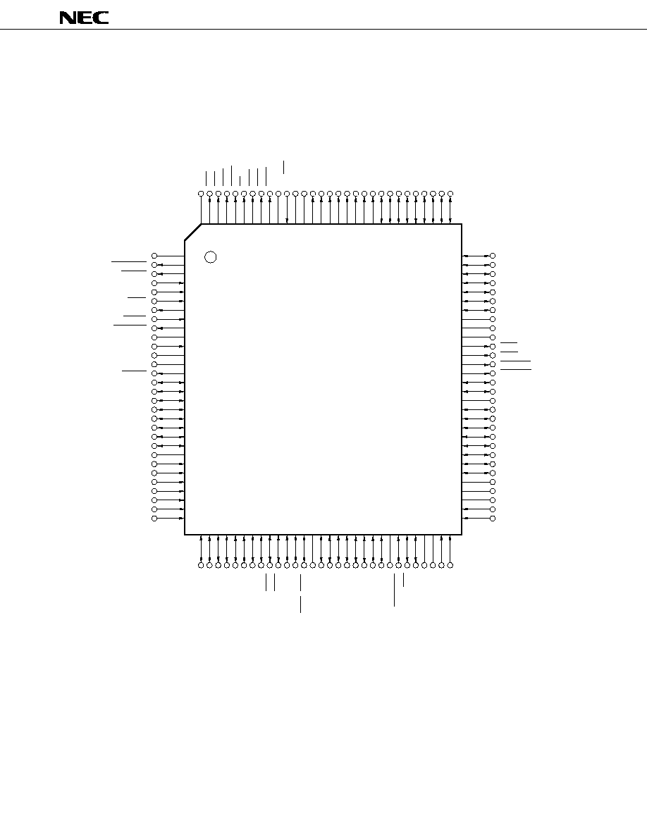
PIN CONFIGURATION (TOP VIEW)
(1)
120-Pin Plastic QFP (28
◊
28 mm), 120-pin plastic QFP (fine pitch) (20
◊
20 mm)
µ
PD70433GD-xx-5BB
µ
PD70433GJ-xx-3EB
Remark
IC: Internally Connected
Notes
1. The IC (H) pin should be connected to V
DD
with an external resistor (1 to 10 k
).
2. The IC (L) pin should be connected to GND with an external resistor (1 to 10 k
).
3. No connection should be made to the OPEN pin.
120
119
118
117
116
115
114
113
112
111
110
109
108
107
106
105
104
103
102
101
100
99
98
97
96
95
94
93
92
OPEN
DEX
RAS
IORD
IOWR
RD
WRL
WRH
ASTB
IC (L)
D8/D16
GND
V
DD
A23
A22
A21
A20
A19
A18
A17
A16
AD15
AD14
AD13
AD12
AD11
AD10
AD9
AD8
AD7
91
313233343536373839404142434445464748495051525354555657585960
P20/PWM
P21/TO00
P22/TO01
P23/TO20
P24/TO21
P25/TO30
P30/T
X
D0/SB0/SO0
P31/R
X
D0/SB1/SI0
P32/T
X
C/SCK0
P33/CTS0
P34/T
X
D1/SO1
P35/R
X
D1/SI1
P36/SCK1/CTS1
V
DD
P40/PD0
P41/PD1
P42/PD2
P43/PD3
P44/PD4
P45/PD5
P46/PD6
P47/PD7
GND
P50/DATASTB
P51/ACK
P52/BUSY
AV
SS
V
DD
P60/ANI0
P61/ANI1
AD6
AD5
AD4
AD3
AD2
AD1
AD0
IC (H)
GND
V
DD
TCE1
TCE0
DMAAK1
DMAAK0
P81/DMARQ1
P80/DMARQ0
V
DD
P77/RTPT7
P76/RTPT6
P75/RTPT5
P74/RTPT4
P73/RTPT3
P72/RTPT2
P71/RTPT1
P70/RTPT0
GND
AV
DD
AV
REF
P63/ANI3
P62/ANI2
72
90
89
88
87
86
85
84
83
82
81
80
79
78
77
76
75
74
73
71
70
69
68
67
66
65
64
63
62
61
1
2
3
4
5
6
7
8
9
10
11
12
13
14
15
16
17
18
19
20
21
22
23
24
25
26
27
28
29
30
V
DD
BUSLOCK
HLDAK
HLDRQ
READY
POLL
CLKOUT
RESET
WDTOUT
V
DD
X1
X2
GND
REFRQ
P00
P01
P02
P03
P04
P05
P06
P07
GND
P10/NMI
P11/INTP0
P12/INTP1
P13/INTP2
P14/INTP3/TI
P15/INTP4
P16/INTP5

4
µ
PD70433
(2)
132-Pin Ceramic PGA
µ
PD70433R-xx
Remark
The locator pin is not included in the pin count.
No.
Signal Nane
Port
No.
Signal Name
Port
No.
Signal Name
Port
A1
ANI1
P61
B5
PD7
P47
C9
CTS0
P33
A2
AV
SS
≠≠
B6
PD5
P45
C10
TO30
P25
A3
ACK
P51
B7
PD2
P42
C11
TO00
P21
A4
DATASTB
P50
B8
PD0
P40
C12
NC
≠≠
A5
PD6
P46
B9
R
X
D1/SI1
P35
C13
INTP4
P15
A6
PD4
P44
B10
R
X
D0/SB1/SI0
P31
C14
INTP0
P11
A7
PD1
P41
B11
TO21
P24
D1
RTPT2
P72
A8
NC
≠≠
B12
TO01
P22
D2
GND
≠≠
A9
SCK1/CTS1
P36
B13
NC
≠≠
D3
ANI3
P63
A10
T
X
D1/SO1
P34
B14
INTP3/TI
P14
D12
INTP5
P16
A11
T
X
C/SCK0
P32
C1
RTPT1
P71
D13
INTP2
P13
A12
T
X
D0/SB0/SO0
P30
C2
AV
REF
≠≠
D14
NMI
P10
A13
TO20
P23
C3
NC
≠≠
E1
RTPT5
P75
A14
PWM
P20
C4
NC
≠≠
E2
RTPT3
P73
B1
AV
DD
≠≠
C5
V
DD
≠≠
E3
RTPT0
P70
B2
ANI2
P62
C6
GND
≠≠
E12
INTP1
P12
B3
ANI0
P60
C7
PD3
P43
E13
GND
≠≠
B4
BUSY
P52
C8
V
DD
≠≠
E14
≠≠
P06
Locator Pin
A
B
C
D
E
F
G
H
J
K
L
M
N
P
1
2
3
4
5
6
7
8
9
10
11
12
13
14
Bottom View
P
N
M
L
K
J
H
G
F
E
D
C
B
A
Top View
Index Mark
5
µ
PD70433
Remark
IC: Internally Connected
NC: Non-Connection
Notes
1. The IC (H) pin should be connected to V
DD
with an external resistor (1 to 10 k
).
2. The IC (L) pin should be connected to GND with an external resistor (1 to 10 k
).
3. No connection should be made to the OPEN pin.
No.
Signal Nane
Port
No.
Signal Name
Port
No.
Signal Name
Port
F1
RTPT7
P77
K3
AD2
≠≠≠
N3
AD9
≠≠≠
F2
RTPT6
P76
K12
POLL
≠≠≠
N4
AD11
≠≠≠
F3
RTPT4
P74
K13
WDTOUT
≠≠≠
N5
AD14
≠≠≠
F12
≠≠≠
P07
K14
X1
≠≠≠
N6
A18
≠≠≠
F13
≠≠≠
P05
L1
AD0
≠≠≠
N7
A21
≠≠≠
F14
≠≠≠
P04
L2
AD3
≠≠≠
N8
A23
≠≠≠
G1
NC
≠≠≠
L3
AD6
≠≠≠
N9
D8/D16
≠≠≠
G2
DMARQ0
P80
L12
BUSLOCK
≠≠≠
N10
ASTB
≠≠≠
G3
V
DD
≠≠≠
L13
READY
≠≠≠
N11
IOWR
≠≠≠
G12
≠≠≠
P03
L14
RESET
≠≠≠
N12
DEX
≠≠≠
G13
≠≠≠
P02
M1
AD1
≠≠≠
N13
V
DD
≠≠≠
G14
≠≠≠
P01
M2
AD5
≠≠≠
N14
HLDRQ
≠≠≠
H1
DMARQ1
P81
M3
NC
≠≠≠
P1
AD7
≠≠≠
H2
DMAAK0
≠≠≠
M4
AD8
≠≠≠
P2
AD10
≠≠≠
H3
DMAAK1
≠≠≠
M5
AD12
≠≠≠
P3
AD13
≠≠≠
H12
REFRQ
≠≠≠
M6
A16
≠≠≠
P4
AD15
≠≠≠
H13
≠≠≠
P00
M7
A20
≠≠≠
P5
A17
≠≠≠
H14
NC
≠≠≠
M8
V
DD
≠≠≠
P6
A19
≠≠≠
J1
TCE0
≠≠≠
M9
WRH
≠≠≠
P7
NC
≠≠≠
J2
TCE1
≠≠≠
M10
IORD
≠≠≠
P8
A22
≠≠≠
J3
GND
≠≠≠
M11
NC
≠≠≠
P9
GND
≠≠≠
J12
V
DD
≠≠≠
M12
NC
≠≠≠
P10
IC (L)
≠≠≠
J13
X2
≠≠≠
M13
HLDAK
≠≠≠
P11
WRL
≠≠≠
J14
GND
≠≠≠
M14
CLKOUT
≠≠≠
P12
RD
≠≠≠
K1
V
DD
≠≠≠
N1
AD4
≠≠≠
P13
RAS
≠≠≠
K2
IC (H)
≠≠≠
N2
NC
≠≠≠
P14
OPEN
≠≠≠
6
µ
PD70433
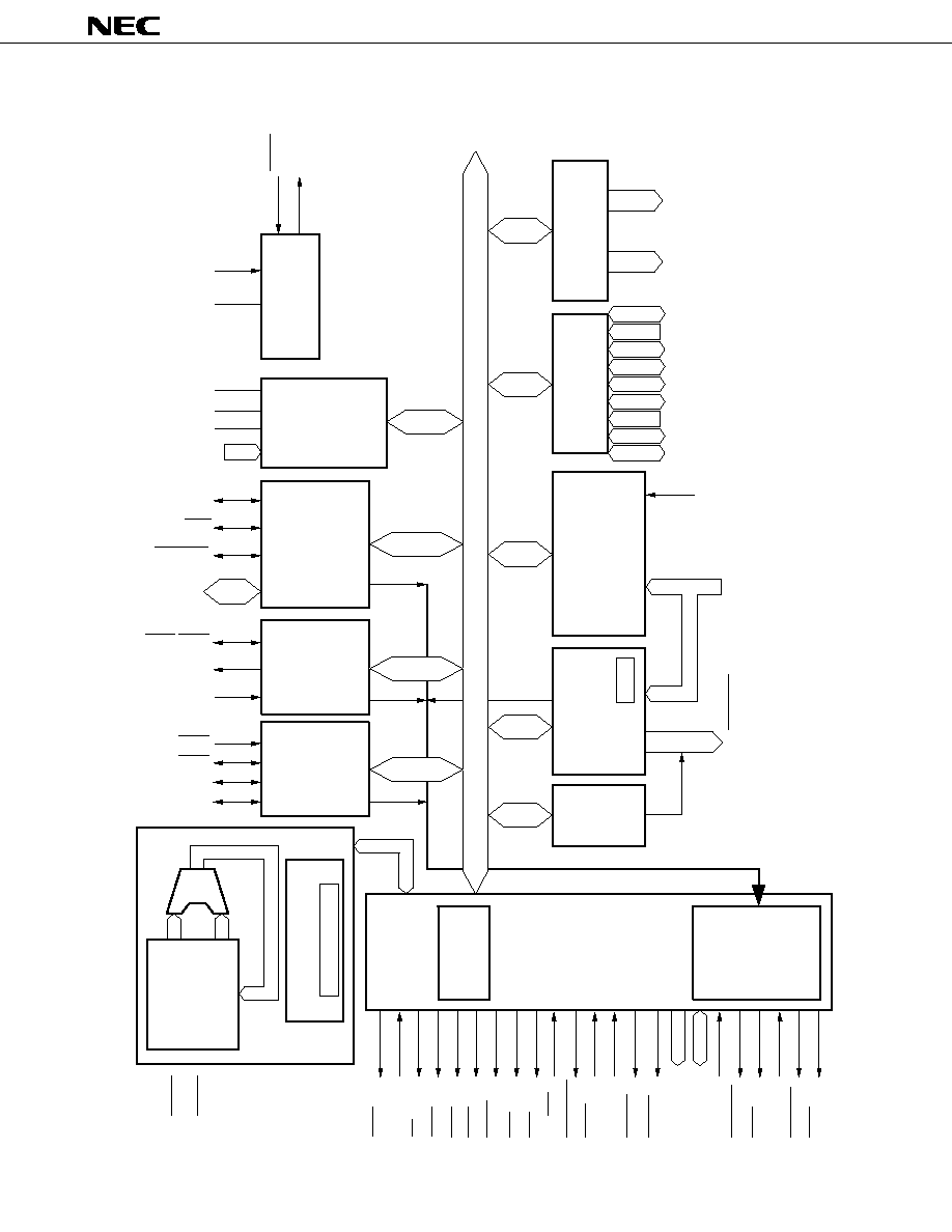
INTERNAL BLOCK DIAGRAM
X1
X2
AV
REF
AV
SS
AV
DD
ANI0≠ANI3
BUSY
ACK
DATASTB
4
8
CTS1/SCK1
PD0≠PD7
T
X
D1/SO1
R
X
D1/SI1
CTS0
T
X
C/SCK0
T
X
D0/SB0/SO0
R
X
D0/SB1/SI0
SYSTEM
CONTROL
8-BIT
A/D
PIU
UART/CSI
UART/CSI
DMA
request
GENERAL
REGISTERS
&
DATA MEMORY
512 BYTES
ALU
MICRO ROM
MICRO SEQUENCE
CONTROL
EXU
BCU
PREFETCH
QUEUE
6 BYTES
BUS
CONTROL
&
PREFETCH
CONTROL
DMAC
PWM
UNIT
TIMER/
COUNTER
UNIT
WDT
PROGRAMMABLE
INTERRUPT
CONTROLLER
PORT
RTOP
4
4
8
7
6
7
8
3
4
8
2
6
4
∑ PWM
∑ TO00
∑ TO20
∑ TO03
∑ WDTOUT
∑ TO01
∑ TO21
∑ INTP0
∑ INTP1
∑ INTP2
∑ INTP3/TI
∑ INTP4
∑ INTP5
RTP0≠RTP3
RTP4≠RTP7
PORT0
PORT1
PORT2
PORT3
PORT4
PORT5
PORT6
PORT7
PORT8
NMI
RESET
CLKOUT
V
DD
GND
ASTB
READY
RD
WRH
WRL
IORD
IOWR
RAS
DEX
D8/D16
BUSLOCK
POLL
HLDRQ
HLDAK
A16≠A23
AD0≠AD15
DMARQ0
DMAAK0
TCE0
DMARQ1
DMAAK1
TCE1
REFRQ

7
µ
PD70433
CONTENTS
1.
PIN FUNCTIONS ....................................................................................................................................... 10
1.1
LIST OF PIN FUNCTION .................................................................................................................................... 10
1.1.1
Port Pins ................................................................................................................................................ 10
1.1.2
Non-Port Pins ........................................................................................................................................ 11
2.
BLOCK CONFIGURATION ....................................................................................................................... 14
2.1
BUS CONTROL UNIT (BCU) ............................................................................................................................. 14
2.2
EXECUTION UNIT (EXU) ................................................................................................................................... 14
2.3
INTERRUPT CONTROLLER (INTC) ................................................................................................................. 14
2.4
DMA CONTROLLER (DMAC) ........................................................................................................................... 14
2.5
UART/CLOCKED SERIAL INTERFACE (UART/CSI) ...................................................................................... 14
2.6
PARALLEL INTERFACE UNIT (PIU) ................................................................................................................ 14
2.7
A/D CONVERTER UNIT (8-BIT A/D) ................................................................................................................ 14
2.8
TIMER/COUNTER UNIT (TCU) ......................................................................................................................... 14
2.9
PWM (PULSE WIDTH MODULATION) UNIT (PWM) ....................................................................................... 14
2.10
WATCHDOG TIMER (WDT) .............................................................................................................................. 14
2.11
PORTS (PORT) ................................................................................................................................................... 14
2.12
REAL-TIME OUTPUT PORT (RTOP) ................................................................................................................ 14
2.13
CLOCK GENERATOR (CG) .............................................................................................................................. 15
2.14
SOFTWARE INTERVAL TIMER (SIT) .............................................................................................................. 15
3.
CPU FUNCTIONS ....................................................................................................................................... 16
3.1
FEATURES .......................................................................................................................................................... 16
3.2
REGISTERS ......................................................................................................................................................... 17
3.2.1
Register Banks ...................................................................................................................................... 17
3.2.2
General Registers (AW, BW, CW, DW) .............................................................................................. 19
3.2.3
Pointers (SP, BP) and Index Registers (IX, IY) ................................................................................. 20
3.2.4
Segment Registers (PS, SS, DS0, DS1) ............................................................................................. 20
3.2.5
Extended Segment Registers (DS2, DS3) ......................................................................................... 21
3.2.6
Special Function Registers (SFR) ...................................................................................................... 22
3.3
PROGRAM COUNTER (PC) .............................................................................................................................. 23
3.4
PROGRAM STATUS WORDS (PSW) ............................................................................................................... 23
3.5
MEMORY SPACE ............................................................................................................................................... 24
3.5.1
Basic Memory Space ........................................................................................................................... 24
3.5.2
Extended Memory Space ..................................................................................................................... 25
3.5.3
Special Function Register Area .......................................................................................................... 26
3.5.4
Vector Table Area ................................................................................................................................. 34
3.6
REGISTER FILE SPACE ..................................................................................................................................... 36
3.7
I/O SPACE .......................................................................................................................................................... 38
4.
BUS CONTROL FUNCTIONS .................................................................................................................... 39
4.1
WAIT FUNCTION ............................................................................................................................................... 39
4.2
REFRESH FUNCTION ........................................................................................................................................ 41
4.2.1
Refresh Mode Register (RFM) ............................................................................................................. 41
4.2.2
Wait Control in Refresh Cycle ............................................................................................................ 41
4.2.3
Refresh Address ................................................................................................................................... 41

8
µ
PD70433
5.
INTERRUPT FUNCTIONS ......................................................................................................................... 42
5.1
FEATURES ......................................................................................................................................................... 42
5.2
INTERRUPT RESPONSE METHODS ............................................................................................................... 45
5.2.1
Vectored Interrupts .............................................................................................................................. 45
5.2.2
Register Bank Switching Function .................................................................................................... 46
5.2.3
Macro Service Function ....................................................................................................................... 47
6.
DMA FUNCTION (DMA CONTROLLER) ..................................................................................................48
6.1
FEATURES .......................................................................................................................................................... 48
7.
SERIAL INTERFACE FUNCTIONS ........................................................................................................... 50
7.1
FEATURES .......................................................................................................................................................... 50
7.2
PROTOCOLS ....................................................................................................................................................... 50
7.3
UART ................................................................................................................................................................... 51
7.3.1
Features ................................................................................................................................................. 51
7.4
CLOCKED SERIAL INTERFACE (CSI) ............................................................................................................... 52
7.4.1
Features ................................................................................................................................................. 52
8.
PARALLEL INTERFACE FUNCTIONS .....................................................................................................53
8.1
FEATURES .......................................................................................................................................................... 53
9.
TIMER FUNCTION ..................................................................................................................................... 55
9.1
FEATURES .......................................................................................................................................................... 55
9.2
TIMER UNIT CONFIGURATION ....................................................................................................................... 55
9.3
REAL-TIME OUTPUT PORT FUNCTION .......................................................................................................... 57
9.3.1
Real-Time Output Port Configuration ................................................................................................ 57
9.3.2
Real-Time Output Port Operation ...................................................................................................... 59
10. PWM UNIT .................................................................................................................................................. 61
10.1
FEATURES .......................................................................................................................................................... 61
10.2
PWM UNIT CONFIGURATION ......................................................................................................................... 61
11. WATCHDOG TIMER FUNCTION .............................................................................................................. 63
11.1
FEATURES .......................................................................................................................................................... 63
11.2
WATCHDOG TIMER CONFIGURATION AND OPERATION .......................................................................... 63
12. A/D CONVERTER FUNCTION .................................................................................................................. 64
12.1
FEATURES .......................................................................................................................................................... 64
13. STANDBY FUNCTION ............................................................................................................................... 66
13.1
HALT MODE ....................................................................................................................................................... 66
13.2
STOP MODE ....................................................................................................................................................... 67
14. CLOCK GENERATOR ............................................................................................................................... 68
14.1
CLOCK GENERATOR CONFIGURATION AND OPERATION ......................................................................... 68

9
µ
PD70433
15. SOFTWARE INTERVAL TIMER FUNCTION ........................................................................................... 70
15.1
SOFTWARE INTERVAL TIMER CONFIGURATION ........................................................................................ 70
16. CODEC INSTRUCTION .............................................................................................................................. 71
16.1
FEATURES .......................................................................................................................................................... 71
16.2
MEMORY MAP ................................................................................................................................................... 74
16.3
PROCESSING FLOW ......................................................................................................................................... 76
17. INSTRUCTION SET .................................................................................................................................... 78
17.1
INSTRUCTIONS NEWLY ADDED TO V20/V30 AND V25/V35 ..................................................................... 78
17.2
INSTRUCTION SET OPERATIONS ................................................................................................................... 80
17.3
INSTRUCTION SET TABLE ............................................................................................................................. 105
18. ELECTRICAL SPECIFICATIONS ............................................................................................................ 128
19. CHARACTERISTIC CURVES (FOR REFERENCE ONLY) ................................................................... 158
20. PACKAGE DRAWINGS ........................................................................................................................... 159
21. RECOMMENDED SOLDERING CONDITIONS ...................................................................................... 162
10
µ
PD70433
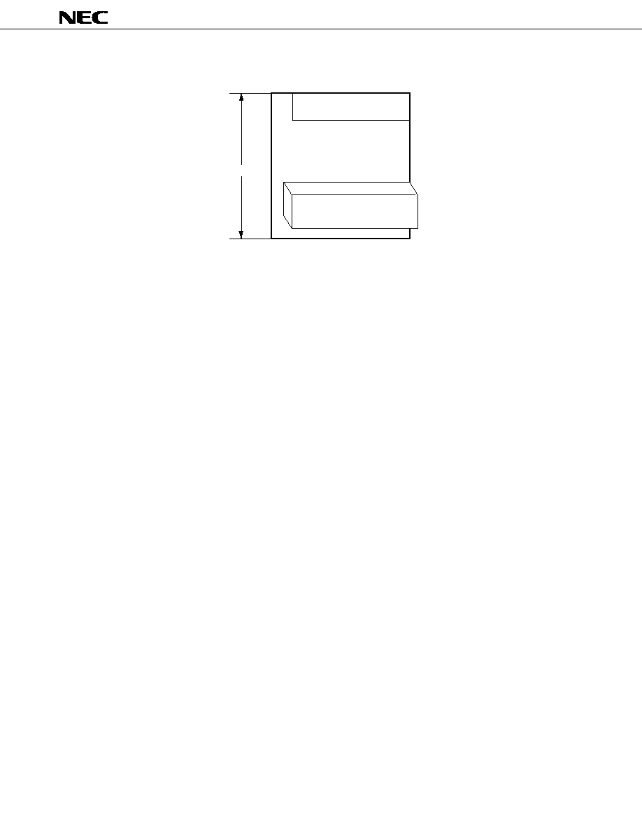
Port 6
Input/output specifiable bit-wise
4-bit input/output port
Port 0
Input/output specifiable bit-wise
8-bit input/output port
1.
PIN FUNCTIONS
1.1
LIST OF PIN FUNCTIONS
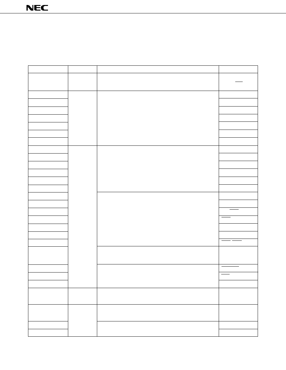
1.1.1
Port Pins
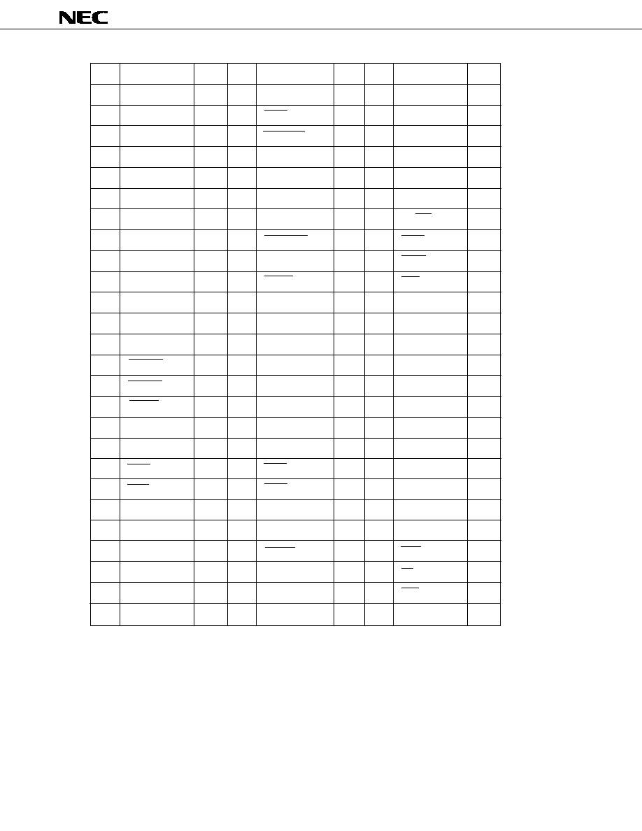
Pin Name
Input/Output
Function
Alternate Function
P00 to P07
Input/output
P10*
NMI
P11
INTP0
P12
INTP1
P13
INTP2
P14
INTP3/TI
P15
INTP4
P16
INTP5
P20
PWM
P21
TO00
P22
TO01
P23
TO20
P24
TO21
P25
TO30
P30
TxD0/SB0/SO0
P31
RxD0/SB1/SI0
P32
TxC/SCK0
P33
CTS0
P34
TxD1/SO1
P35
RxD1/SI1
P36
CTS1/SCK1
P40 to P47
PD0 to PD7
P50
DATASTB
P51
ACK
P52
BUSY
P60 to P63
ANI0 to ANI3
P70 to P77
RTP0 to RTP7
P80
DMARQ0
P81
DMARQ1
Port 1
7-bit input port
Port 2
Input/output specifiable bit-wise
6-bit input/output port
Port 3
Input/output specifiable bit-wise
7-bit input/output port
Port 4
Input/output specifiable bit-wise
8-bit input/output port
*
Unusable as general-purpose port (non-maskable interrupt)
Port 5
Input/output specifiable bit-wise
3-bit input/output port
Port 7
Input/output specifiable bit-wise
8-bit input/output port
Port 8
Input/output specifiable bit-wise
2-bit input/output port
Input/output
Input/output
Input
Input
11
µ
PD70433
Pin Name
Function
AD0 to AD15
A16 to A23
External bus cycle address signal output in external bus
RD
Output
WRL
WRH
≠≠≠
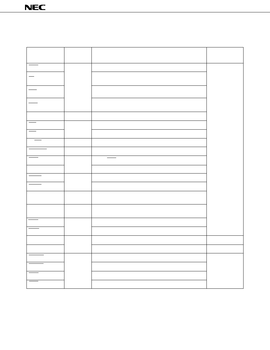
1.1.2
Non-Port Pins
(1)
Bus control pins
Input/
Alternate
Output
Function
ASTB
External bus cycle address strobe signal output in external bus
External memory cycle data read strobe signal output in
external bus
External memory cycle lower byte data write strobe signal
output in external bus
External memory cycle upper byte data write strobe signal
output in external bus
READY
Input
External bus cycle ready signal input in external bus
DEX
External bus cycle upper byte data enable signal output
Output
RAS
DRAM low address latch timing signal output
D8/D16
Input
External bus data bus width selection signal input
BUSLOCK
Output
External bus bus lock signal output
POLL
Input of POLL signal (sampled in POLL instruction execution)
Input
HLDRQ
External bus hold request signal input
HLDAK
External bus hold acknowledge signal output
Output
REFRQ
Refresh pulse signal output
3≠state
External bus cycle address/data multiplex signal input/output
input/output
in external bus
3≠state
output
IORD
External I/O cycle data read strobe signal output
Output
IOWR
External I/O cycle data write strobe signal output
DMARQ0
DMA request signal input (channel 0)
P80
Input
DMARQ1
DMA request signal input (channel 1)
P81
DMAAK0
DMA acknowledge signal output (channel 0)
DMAAK1
DMA acknowledge signal output (channel 1)
Output
≠≠≠
TCE0
DMA termination signal output (channel 0)
TCE1
DMA termination signal output (channel 1)

12
µ
PD70433
(2)
Other pins
Input/
Alternate
Output
Function
GND
GND potential
V
DD
Positive power supply
≠≠≠
AV
SS
A/D converter GND potential
AV
DD
A/D converter analog power supply
AV
REF
A/D converter reference voltage input
≠≠≠
RESET
Input
System reset signal input
X1
Connection pins of crystal resonator/ceramic resonator for
system clock generation. In case of external clock supply, input
X2
≠≠≠
to X1 and leave X2 open.
CLKOUT
Internal system clock ¯ output
Output
WDTOUT
Watchdog timer overflow signal output
NMI
Non-maskable interrupt request input *1
P10
INTP0
P11
INTP1
P12
INTP2
P13
Input
External interrupt request input *2
INTP3
P14/TI
INTP4
P15
INTP5
P16
TI
External event clock input
P14/INTP3
PWM
PWM output
P20
TO00, TO01, TO20,
TO21, TO30
T
X
D0
UART transmission data output
P30/SB0/SO0
R
X
D0
Input
UART reception data input
P31/SB1/SI0
T
X
C
Output
UART transmission clock output
P32/SCK0
CTS0
P33
Input
UART transmission enable signal input
CTS1
P36/SCK1
SB0
P30/T
X
D0/SO0
Input/output
SBI transmission/reception data input/output
SB1
P31/R
X
D0/SI0
Pin Name
Function
Output
Timer unit output
P21 to P25
*
1.
Because NMI interrupt is unmaskable, NMI interrupt is always initiated by detecting a valid edge (when reading from
port 1, the pin level is read).
2.
By masking or disabling (IE = 0) these interrupts, these pins can be used as general≠purpose input/output ports,
respectively.
13
µ
PD70433
Input/
Alternate
Output
Function
SO0
P30/T
X
D0/SB0
Output
CSI transmission data output
SO1
P34/T
X
D1
SI0
P31/R
X
D0/SB1
Input
CSI reception data input
SI1
P35/R
X
D1
SCK0
P32/T
X
C
CSI serial clock input/output
SCK1
P36/CTS1
PD0 to PD7
Parallel interface -- Data input/output
P40 to P47
Input/output
DATASTB
Parallel interface -- Data strobe signal
P50
ACK
Parallel interface -- Acknowledge signal
P51
BUSY
Parallel interface -- Busy signal
P52
ANI0 to ANI3
Input
Analog input signal to A/D converter
P60 to P63
RTP0 to RTP7
Output
Real-time output port
P70 to P77
Pin Name
Function

14
µ
PD70433
2.
BLOCK CONFIGURATION
2.1
BUS CONTROL UNIT (BCU)
The BCU performs control of the main bus. The BCU starts the necessary internal/external bus cycle on the basis of
the physical address obtained from the execution unit (EXU).
2.2
EXECUTION UNIT (EXU)
The EXU controls address calculation, arithmetic and logical operations, data transfer, etc., by means of a microprogram
(firmware for controlling the microsequencer on the basis of decoded op code). The EXU contains 512 bytes of RAM
(corresponding to the register file space).
2.3
INTERRUPT CONTROLLER (INTC)
The INTC services hardware interrupt requests generated by on-chip peripheral hardware and interrupt requests
generated externally with vectored interrupts, bank switching, or macro service. It can also control the programmable 4-
level interrupt priority order, and can also perform multiprocessing control for interrupt.
2.4
DMA CONTROLLER (DMAC)
The DMAC is a general-purpose DMA controller, capable of handling the 16M-byte memory space in a linear fashion.
Operating modes comprise memory-to-memory transfer mode, intelligent DMA (ring buffer method and counter control
method) mode, next address specification mode, and 2-channel operation.
2.5
UART/CLOCKED SERIAL INTERFACE (UART/CSI)
This block supports the asynchronous interface (UART) in which data synchronization is achieved by means of start/
stop bits, and the clocked serial interface (CSI), allowing either to be used.
For the clocked serial interface there is a further choice of serial bus interface mode (SBI) or 3-wire serial I/O mode.
2.6
PARALLEL INTERFACE UNIT (PIU)
This performs input/output using strobe signal synchronization in 8-bit units, and supports the Centronics interface and
general-purpose parallel data communication functions.
2.7
A/D CONVERTER UNIT (8-BIT A/D)
This is an A/D converter with 4 analog inputs, and provided with 4 A/D conversion result registers.
2.8
TIMER/COUNTER UNIT (TCU)
The timer/counter unit incorporates a 16-bit timer/counter, and can be used as an interval timer, free-running counter,
or event counter.
2.9
PWM (PULSE WIDTH MODULATION) UNIT (PWM)
An 8-bit precision PWM (pulse width modulation) signal output function.
2.10 WATCHDOG TIMER (WDT)
The WDT incorporates an 8-bit watchdog timer for detection of inadvertent program looping, system errors, etc. The
WDTOUT pin is provided to give external notification of the generation of watchdog timer interrupts.
2.11 PORTS (PORT)
53 port pins are provided, allowing port pin and control pin functions to be selected.
2.12 REAL-TIME OUTPUT PORT (RTOP)
This is a real-time output port which uses an interrupt from timer 0 as a trigger. It can output the contents of the 8-bit
buffer register at programmable intervals in 4-bit or 8-bit units.

15
µ
PD70433
2.13 CLOCK GENERATOR (CG)
The CG generates a clock at a frequency of 1/2, 1/4, 1/8 or 1/16 that of the crystal and oscillator connected to the X1
and X2 pins and supplies it as the CPU operating clock.
2.14 SOFTWARE INTERVAL TIMER (SIT)
The SIT incorporates a 16-bit software interval timer as a software timer function and watch function timer. Interval
interrupts can be set by input clock (count clock) selection and software timer/counter compare register setting.
16
µ
PD70433
3.
CPU FUNCTIONS
The CPU of the V55PI is software upword compatible with the V20 and V30 (native mode), and the V25 and V35.
3.1
FEATURES
∑
Software upward compatible with V20 & V30 (native mode) and V25 & V35 (includes additional instructions)
∑
Minimum instruction cycle: 160 ns/12.5 MHz (external 25 MHz clock)
125 ns/16 MHz (external 32 MHz clock)
∑
Address space: 16M bytes
1M-byte basic memory (program) space
16M-byte extended memory (data) space
∑
Register file space (in on-chip RAM): 512 bytes/16 register banks
∑
I/O space: 64K bytes
∑
Register configuration (compared with V20/V30 and V25/V35)
∑
Internal 16-bit architecture, switchable external data bus width (16/8 bits)
∑
Automatic wait control with memory divided in variable sizes (max. 6 blocks)
∑ Programmable wait function
∑ Wait function using READY pin
∑
Refresh function
∑ Automatic generation of refresh cycle (RAS only)
∑
RAS pin functions
RAS pin
DRAM RAS timing
RD, WRH, WRL pins
DRAM CAS timing
ASTB pin
DRAM row/column address switching timing
PSW
None
IBRK
IBRK
Item
V20, V30
V25, V35
V55PI
Extended segment register
None
None
DS2, DS3
Register bank
None
8 banks (in memory space)
16 banks (in register file space)
Mode flag
MD
None
None
Register bank flags
None
RB0 to RB2
RB0 to RB3
Input/output instruction
trap flag
User flag
None
F0, F1
None
240 bytes
496 bytes
Special function register area
None
(memory mapping onto
(memory mapping onto
FFF00H to FFFEFH)
FFE00H to FFFEFH)

17
µ
PD70433
3.2
REGISTERS
The V55PI CPU has general register sets compatible with the V20 and V30 (native mode), and the V25 and V35. The
general register sets are mapped onto the register file space. These general register sets are also used as on-chip RAM,
and there can be a maximum of 16 register sets in bank form.
In addition, the V55PI has various special function registers for controlling on-chip peripheral hardware. These special
function registers are mapped onto memory space addresses 0FFE00H to 0FFFEFH.
3.2.1
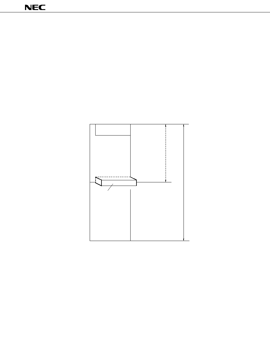
Register Banks
The general register sets are mapped onto the register file space (in on-chip RAM). The general register sets are used
in a bank arrangement; each bank consists of 32 bytes and up to 16 banks can be set.
The CPU normally uses register bank 15 for program execution, and it is possible to switch to another bank automatically
by means of maskable hardware interrupt or software interrupt (BRKCS instruction). It is possible to return from the switched-
to register bank to the original register bank by means of the instruction for returning from an interrupt (RETRBI).
The register bank configuration is shown in Figure 3-1. The general register sets are mapped onto the area with an offset
of (+08H) to (+1FH) from the start address of each register bank. The word address from the start in a register bank is the
extended segment register (DS2) area. The vector PC/DS3 area is used to set the value to be loaded into the PC when
the register bank is switched, that is, the offset value of the start address of the interrupt service routine. This area is also
used as the extended segment register (DS3) area. The PSW save area is used to save the PSW when the register bank
is switched, and the PC save area is used to save the PC when the register bank is switched.
After a reset, register bank 15 is selected automatically. Also, segment register initialization after a reset is performed
for register bank 15 only.
The register file space onto which these general register sets are mapped can also be accessed as data memory by
addition of a special prefix instruction (IRAM:) to a memory manipulation instruction.
Of the 16 set register banks, banks 0 and 1 have macro service channels (parameter and work area for macro service)
allocated in duplicate.

18
µ
PD70433
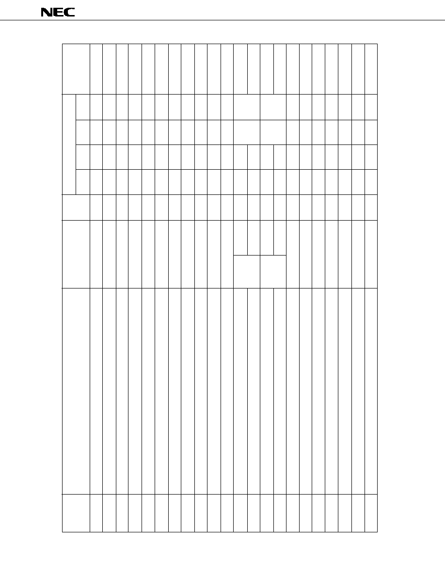
Figure 3-1. Register Bank Configuration
Register File Space (512 bytes)
Register Bank 0
1
2
3
4
5
6
7
8
9
10
11
12
13
14
15
(Offset from the starting address of each register bank)
DS2
BW
BH
+ 0 2 H
DH
CH
AH
BL
DL
CL
AL
DW
CW
AW
000H
020H
040H
060H
080H
0A0H
0C0H
0E0H
100H
120H
140H
160H
180H
1A0H
1C0H
1E0H
1FFH
Vector PC/DS3
PSW Save
PC Save
+ 0 4 H
+ 0 6 H
+ 0 8 H
+ 0 A H
+ 0 C H
+ 0 E H
+ 1 0 H
+ 1 2 H
+ 1 4 H
+ 1 6 H
+ 1 8 H
+ 1 A H
+ 1 C H
+ 1 E H
DS0
SS
PS
DS1
IY
IX
BP
SP
+ 0 0 H
1 5
8 7
0
19
µ
PD70433
3.2.2
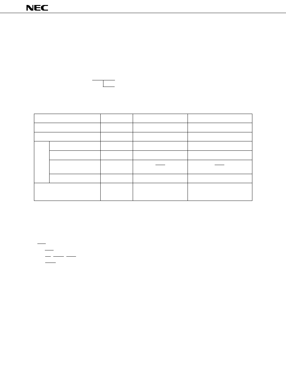
General Registers (AW, BW, CW, DW)
There are four 16-bit general registers. In addition to being accessed as 16-bit registers, these registers can also be
accessed as 8-bit registers by dividing each register into upper and lower 8-bit halves (AH, AL, BH, BL, CH, CL, DH, DL).
These registers are used as 8-bit or 16-bit registers with a wide range of instructions including transfer, arithmetic and
logical operation instructions.
Each register is also used as the default register for specific instruction processing, as shown below.
AW : Word multiplication/division, word input/output, data conversion
AL : Byte multiplication/division, byte input/output, BCD rotation, data conversion
AH : Byte multiplication/division
BW : Data conversion
CW : Loop control branch, repeat prefix
CL : Shift instructions, rotate instructions, BCD operations
DW : Word multiplication/division, indirect addressing input/output
These registers are mapped onto the register file space (in on-chip RAM). The address is the value obtained by adding
the offset for each register to (register bank number
◊
32).
Register
Offset
Register
Offset
AL
1EH
AW
1EH
AH
1FH
BL
18H
BW
18H
BH
19H
CL
1CH
CW
1CH
CH
1DH
DL
1AH
DW
1AH
DH
1BH
Table 3-1. General Register Offsets
20
µ
PD70433
3.2.3
Pointers (SP, BP) and Index Registers (IX, IY)
These are 16-bit registers used as base pointers or index registers in memory accesses using based addressing (BP),
indexed addressing (IX, IY), based indexed addressing (BP, IX, IY), etc. The SP is also used as the pointer in stack
operations. As with general registers, these are used with transfer instructions, arithmetic operation instructions, etc., but
in this case they cannot be used as 8-bit registers. Each register is also used as the fixed address pointer for specific
instruction processing, as shown below.
SP : Stack manipulation
IX : Block transfers, BCD operation source side address specification
IY : Block transfers, BCD operation destination side address specification
These registers are mapped onto the register file space (in on-chip RAM). The address is the value obtained by adding
the offset for each register to (register bank number
◊
32).
Table 3-2. Pointer and Index Register Offsets
Register
Offset
SP
16H
BP
14H
IX
12H
IY
10H
3.2.4
Segment Registers (PS, SS, DS0, DS1)
The CPU manages the 1M-byte basic memory space by dividing it into 64K-byte units. The CPU specifies the start
address of each segment with a segment register, and uses another register or effective address for the specification of
phyiscal address, with the relative address from the start address as the offset.
The physical address is created as shown below.
Segment Register 4-Bit Fixed
x
x
x
x
0
H
0
x
x
x
x
H
x
x
x
x
x
H
+
There are four segment registers: PS (Program Segment), SS (Stack Segment), DS0 (Data Segment 0), and DS1 (Data
Segment 1). The respective segments are used in the following cases.
PS : Program fetch
SS : Stack manipulation instructions, addressing using BP as base register
DS0 : General variable accesses, source block data accesses such as block transfer instructions, etc.
DS1 : Destination block data accesses such as block transfer instructions, etc.
....
Segment Start Address
....
Offset Value
.....
Physical Address (20 Bits)

21
µ
PD70433
However, using a segment override prefix instruction makes it possible for access of general variables to change from
DS0 to another segment register. Also, in addressing which uses BP as the base register, another segment register can
be used instead of SS.
Example
MOV
AW, 1000H
MOV
DS1 : AW
MOV
BL, DS1, BYTE PTR [IX]; DSI : Byte data read from IX
When a reset is performed, PS of register bank 15 is initialized to FFFFH, and SS, DS0 and DS1 are initialized to 0000H.
These registers are mapped onto the register file space (in on-chip RAM). The address is the value obtained by adding
the offset for each register to (register bank number
◊
32).
Table 3-3. Segment Register Offsets
Register
Offset
DS0
08H
DS1
0EH
SS
0AH
PS
0CH
3.2.5
Extended Segment Registers (DS2, DS3)
In addition to the segment registers for accessing the 1M-byte basic memory space, the V55PI is provided with extended
segment registers which specify the start address of each 64K-byte segment of the 16M-byte extended memory space.
There are two extended segment registers, DS2 (Data Segment 2) and DS3 (Data Segment 3), which are used as shown
below.
DS2: Extended memory space general variable accesses (by segment override prefix instructions), source block
data accesses in extended memory space block transfer instructions, etc.
DS3: Extended memory space general variable accesses (by segment override prefix instructions), destination
block data accesses in extended memory space block transfer instructions, etc.
The data access using an extended semgnet register is performed by using the segment override prefix. Especially, in
the block transfer instruction, DS2 and DS3 can be specified simultaneously by segment override prefix. (In this case, the
order for DS2 and DS3 is optional.)
Example
REP
DS2:
DS3: MOVBKW ; Word memory block transfer from DS2 : IX to DS3 : IY.
The CPU specifies the start address of each segment with an extended segment register, and performs an access by
using another register or effective address for the specification of physical address, with the relative address from the start
address as the offset value.
The physical address is created as shown in the next page.
22
µ
PD70433
Extended Segment Register 8-Bit Fixed
...
Segment Start Address
...
Offset Value
...
Physical Address (24 Bits)
When a reset is performed, DS2 and DS3 of register bank 15 are initialized to 0000H.
These registers are mapped onto the register file space (in on-chip RAM). The address is the value obtained by adding the
offset for each register to (register bank number
◊
32).
Table 3-4. Extended Segment Register Offsets
Register
Offset
DS2
00H
DS3
02H (Also used as vectored PC)
3.2.6
Special Function Registers (SFR)
The V55PI has a group of registers with the function of controlling on-chip peripheral hardware.
A number of registers are provided according to the type of cotrol for each peripheral hardware unit, and the actual
operation can be set using the individual bits in the registers. These registers are mapped onto the memory space, and
are read and written to using the same method as for ordinary memory (see 3.5.3 "Special Function Register Area").
Example
MOV
AW, 0FFE0H
MOV
DS1, AW
MOV
BL, DS1 : BYTE PTR [1EFH]; 0FFE0H : 1EFH (PRC register) Read
There are also two instructions, BTCLR and BTCLRL, which are only valid for special function registers. Of these,
BTCLRL is an instruction newly provided in the V25 or V35.
The BTCLR instruction is valid for registers in the upper 240 bytes (0FFF00H to 0FFFEFH) of the special function register
area, and the BTCLRL instruction is valid for registers in the lower 256 bytes (0FFE00H to 0FFEFFH).
x
x
x
x
0
0
H
0
0
x
x
x
x
H
x
x
x
x
x
x
H
+

23
µ
PD70433
3.3
PROGRAM COUNTER (PC)
This is a 16-bit binary counter which holds the offset value of the program memory address on which the CPU is to perform
execution.
The PC is incremented each time an instruction code is fetched from the instruction queue, and is also loaded with the
new location address value when a branch, call, return or break instruction is executed.
When a reset is performed, 0000H is loaded into the PC. Because the PS register is initialized to FFFFH in a reset, after
a reset the CPU begins execution at physical address 0FFFF0H.
3.4
PROGRAM STATUS WORDS (PSW)
The PSW consists of 6 status flags and 5 control flags.
∑ Status flags
∑ V (Overflow)
...Overflow detection flag
∑ S (Sign)
...Sign bit detection flag
∑ Z (Zero)
...All zero detection flag
∑ AC (Auxiliary Carry)
...4-bit carry/borrow detection flag
∑ P (Parity)
...Parity detection flag
∑ CY (Carry)
...Carry/borrow detection flag
∑ Control flags
∑ RB0 to RB3 (Register Banks 0 to 3) ...Register bankspecification flags
∑ DIR (Direction)
...Block transfer/input/output instruction direction control flag
∑ IE (Interrupt Enable)
...Interrupt enabled state control flag
∑ BRK (Break)
...Single-step interrupt control flag
∑ IBRK (I/O Break)
...Input/output instruction trap control flag
The status flags are set (1) or reset (0) automatically according to the result (data value) of execution of various kinds
of instructions. The CY flag can be directly set, reset or inverted by an instruction.
The control flags are set or reset by instructions, and control the operation of the CPU. The IE and BRK flags are always
reset when interrupt servicing is initiated.
The contents of the PSW can be saved to and restored from the stack by the PUSH and POP instructions. However,
when the contents are restored by the POP PSW instruction, bits 12 to 15 (RB0 to RB3) are not returned to the PSW.
The low-order 8 bits of the PSW can also be saved to or restored from the AH register by an MOV instruction.
The PSW bit configuration is shown below.
RB3
RB2
RB1
RB0
Y
DIR
IE
BRK
S
Z
0
AC
0
P
IBRK
CY
15
14
13
12
11
10
9
8
7
6
5
4
3
2
1
0
24
µ
PD70433
3.5
MEMORY SPACE
The V55PI has a 16M-byte memory space. Of this, using lowest 1M bytes (000000H to 0FFFFFH) as the basic memory
space, the 16M bytes including the basic memory space (000000H to FFFFFFH) can be accessed as the extended memory
space. The basic memory space can be accessed using the segment registers (PS, SS, DS0, DS1) in the same way as
in the V25 and V35. The extended memory space can be accessed using the extended segment registers (DS2, DS3), and
has the basic memory space mapped onto the lowest 1M bytes. See 3.2.4 "Segment Registers (PS, SS, DS0, DS1)" and
3.2.5 "Extended Segment Registers (DS2, DS3)" for the physical addresses.
The 496-byte space 0FFE00H to 0FFFEFH has mapped onto it a group of registers to which specific functions are
allocated such as on-chip peripheral hardware registers, control registers, etc., and these are manipulated by memory
accesses.
In addition, independent of these, there is a 512-byte register file space (in on-chip RAM). In addition to being accessed
by using register manipulation instructions as in the V25 and V35, the register file space can also be accessed as data
memory by adding a special prefix instruction (IRAM:) to a memory manipulation in.
Figure 3-2. Memory Space
3.5.1
Basic Memory Space
The memory space comprises a 1M-byte basic memory space and 16M-byte extended memory space. The basic memory
space is mapped onto the lowest 1M bytes (000000H to 0FFFFFH) of the extended memory space.
The 1M-byte basic memory space is shown in Figure 3-3.
Conditions for accessing the basic memory space by software are the same as for the V20/V30 and V25/V35.
A basic memory space physical address is specified by the segment start address indicated by the segment register (PS,
SS, DS0, DS1) and the offset value from the segment start position indicated by another register or immediate data.
The basic memory space has the vectored interrupt vector area and special function register area mapped onto it. For
an area in which special function registers are mapped, data accesses cannot be made to external memory (program fetches
are possible.)
0 0 0 0 0 0 H
0 F F F F F H
1 0 0 0 0 0 H
F F F F F F H
0 0 3 F F H
F F E 0 0 H
F F F E F H
Basic Memory
Space
(1M Bytes)
Vector Area
Extended Memory
Space (16M Bytes)
Special Function
Register Area
(On-Chip Area)
25
µ
PD70433
Figure 3-3. Basic Memory Space
0FFF0H to 0FFFFFH is a program area used for the system boot, and PS and PC become 0FFFH and 0H, respectively,
therefore the program execution starts from 0FFFF0H.
3.5.2
Extended Memory Space
The 16M-byte extended memory space is shown in Figure 3-4.
The only accesses that can be performed on the extended memory space are data accesses.
The basic memory space is mapped onto the lowest 1M bytes (000000H to 0FFFFFH) of the extended memory space,
and can be accessed using the segment registers PS, SS, DS0 and DS1.
Data accesses can be performed in the extended memory space using the extended segment registers DS2 and DS3.
With DS2 and DS3 it is possible to use a specification as a segment override prefix instruction added to a memory
manipulation instruction.
An extended memory space physical address is specified by the segment start address indicated by the extended
segment register and the offset value from the segment start position indicated by another register or immediate data. If
the generated address indicates the lowest 1M-byte area (000000H to 0FFFFFH), the basic memory space is accessed.
Vector Area
Spaecial Function Register Area
(Internal Area)
0 0 0 0 0 0 H
0 F F F F F H
0 0 0 0 0 H
0 0 3 F F H
F F E 0 0 H
F F F E F H
1M Bytes
26
µ
PD70433
Figure 3-4. Extended Memory Space
Vector Area
Spaecial Function
Register Area
(Internal Area)
0 F F F F F H
0 0 0 0 0 H
0 0 3 F F H
F F E 0 0 H
F F F E F H
1 0 0 0 0 0 H
0 0 0 0 0 0 H
F F F F F F H
1M Bytes
16M Bytes
3.5.3
Special Function Register Area
The 496-byte space 0FFE00H to 0FFFEFH has mapped onto it a group of registers to which functions such as
on-chip peripheral hardware operation specification, status monitoring, etc., are assigned.
Program fetches cannot be performed from these areas.
Special function register manipulation is performed by accesses by means of memory manipulation instructions.
If the special function register area is accessed, RD, WRH, WRL, IORD, IOWR and other control signals do not become
active.
A list of special function registers is given in Table 3-5. The meaning of the items in the table is explained below.
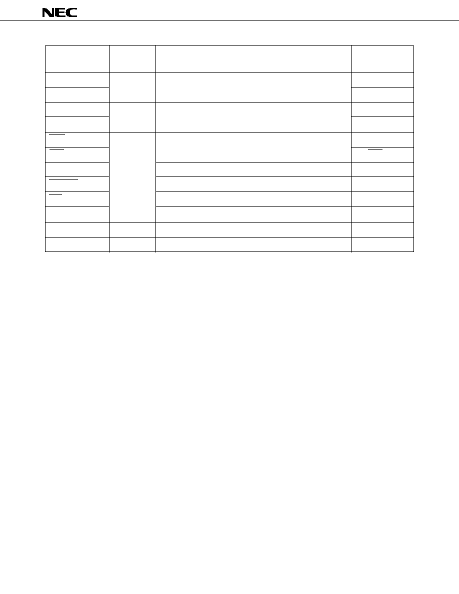
∑ Symbol ............................ The symbol used to indicate the special function register name. Corresponds to the
operand description format (symbol name) in a memory manipulation instruction.
∑ R/W ................................. Indicates whether this special function register is read/write enabled.
R/W :
Read/write enabled
R
:
Read only
W
:
Write only
∑ Manipulation Method ..... Indicates which of the following can be used on the register: bit manipulation,
8-bit manipulation, 16-bit manipulation, 32-bit manipulation.
∑ RESET ............................ Indicates the status of the register after RESET input.
Note
Addresses which are not listed are the reserved area, therefore, they should not be accessed by the user
program.
27
µ
PD70433
MK0
MK1
* 1.
Varies according to input/output mode.
2.
Some bits R, others R/W (possible).
Address
Special Function Register Name
Symbol
R/W
After Reset
Table 3-5. Special Function Registers (1/7)
Manipulable Bit Units
1 Bit
8 Bits 16 Bits 32 Bits
0FFE00H
A/D conversion result register 0
ADCR0
R
∑
Undefined
0FFE02H
A/D conversion result register 1
ADCR1
R
∑
Undefined
0FFE04H
A/D conversion result register 2
ADCR2
R
∑
Undefined
0FFE06H
A/D conversion result register 3
ADCR3
R
∑
Undefined
0FFE10H
Parallel interface buffer
PAD
R/W *1
∑
Undefined
0FFE18H
Parallel interface control register 0
PAC0
R/W
∑
∑
90H
0FFE19H
Parallel interface control register 1
PAC1
R/W
∑
∑
03H
0FFE1AH
Parallel interface status register
PAS
R/W *2
∑
40H
0FFE1CH
Parallel interface acknowledge interval register 1
PAI1
W
∑
Undefined
0FFE1DH
Parallel interface acknowledge interval register 2
PAI2
W
∑
Undefined
0FFE20H
A/D converter mode register
ADM
R/W
∑
∑
00H
0FFEC0H
Interrupt mask flag register 0 (low)
MK0L
R/W
∑
∑
∑
FFH
0FFEC1H
Interrupt mask flag register 0 (high)
MK0H
R/W
∑
∑
FFH
0FFEC2H
Interrupt mask flag register 1 (low)
MK1L
R/W
∑
∑
∑
FFH
0FFEC3H
Interrupt mask flag register 1 (high)
MK1H
R/W
∑
∑
FFH
0FFEC4H
In-service priority register
ISPR
R
∑
∑
00H
0FFEC5H
Interrupt mode control register
IMC
R/W
∑
80H
0FFEC9H
Interrupt request control register 09
IC09
R/W
∑
∑
43H
0FFECAH
Interrupt request control register 10
IC10
R/W
∑
∑
43H
0FFECBH
Interrupt request control register 11
IC11
R/W
∑
∑
43H
0FFECCH
Interrupt request control register 12
IC12
R/W
∑
∑
43H
0FFECDH
Interrupt request control register 13
IC13
R/W
∑
∑
43H

28
µ
PD70433
Address
Special Function Register Name
Symbol
R/W
After Reset
Table 3-5. Special Function Registers (2/7)
Manipulable Bit Units
1 Bit
8 Bits 16 Bits
32 Bits
0FFECEH
Interrupt request control register 14
IC14
R/W
∑
∑
43H
0FFED0H
Interrupt request control register 16
IC16
R/W
∑
∑
43H
0FFED1H
Interrupt request control register 17
IC17
R/W
∑
∑
43H
0FFED2H
Interrupt request control register 18
IC18
R/W
∑
∑
43H
0FFED3H
Interrupt request control register 19
IC19
R/W
∑
∑
43H
0FFED4H
Interrupt request control register 20
IC20
R/W
∑
∑
43H
0FFED5H
Interrupt request control register 21
IC21
R/W
∑
∑
43H
0FFED6H
Interrupt request control register 22
IC22
R/W
∑
∑
43H
0FFED7H
Interrupt request control register 23
IC23
R/W
∑
∑
43H
0FFED8H
Interrupt request control register 24
IC24
R/W
∑
∑
43H
0FFED9H
Interrupt request control register 25
IC25
R/W
∑
∑
43H
0FFEDAH
Interrupt request control register 26
IC26
R/W
∑
∑
43H
0FFEDBH
Interrupt request control register 27
IC27
R/W
∑
∑
43H
0FFEDCH
Interrupt request control register 28
IC28
R/W
∑
∑
43H
0FFEDDH
Interrupt request control register 29
IC29
R/W
∑
∑
43H
0FFEDEH
Interrupt request control register 30
IC30
R/W
∑
∑
43H
0FFEDFH
Interrupt request control register 31
IC31
R/W
∑
∑
43H
0FFEE0H
Interrupt request control register 32
IC32
R/W
∑
∑
43H
0FFEE4H
Interrupt request control register 36
IC36
R/W
∑
∑
43H
0FFEE5H
Interrupt request control register 37
IC37
R/W
∑
∑
43H
0FFF00H
Port 0
P0
R/W
∑
∑
Undefined
0FFF01H
Port 1
P1
R
∑
∑
Undefined
0FFF02H
Port 2
P2
R/W
∑
∑
Undefined
0FFF03H
Port 3
P3
R/W
∑
∑
Undefined

29
µ
PD70433
Address
Special Function Register Name
Symbol
R/W
After Reset
Table 3≠5. Special Function Registers (3/7)
Manipulable Bit Units
1 Bit
8 Bits 16 Bits
32 Bits
0FFF04H
Port 4
P4
R/W
∑
∑
Undefined
0FFF05H
Port 5
P5
R/W
∑
∑
Undefined
0FFF06H
Port 6
P6
R
∑
∑
Undefined
0FFF07H
Port 7
P7
R/W
∑
∑
Undefined
0FFF08H
Port 8
P8
R/W
∑
∑
Undefined
0FFF0CH
Port read control register
PRDC
R/W
∑
∑
00H
0FFF0EH
Real≠time output port
RTP
R/W
∑
∑
Undefined
0FFF10H
Port 0 mode register
PM0
R/W
∑
∑
FFH
0FFF12H
Port 2 mode register
PM2
R/W
∑
∑
FFH
0FFF13H
Port 3 mode register
PM3
R/W
∑
∑
FFH
0FFF14H
Port 4 mode register
PM4
R/W
∑
∑
FFH
0FFF15H
Port 5 mode register
PM5
R/W
∑
∑
FFH
0FFF17H
Port 7 mode register
PM7
R/W
∑
∑
FFH
0FFF18H
Port 8 mode register
PM8
R/W
∑
∑
FFH
0FFF22H
Port 2 mode conrol register
PMC2
R/W
∑
∑
00H
0FFF23H
Port 3 mode control register
PMC3
R/W
∑
∑
00H
0FFF24H
Port 4 mode control register
PMC4
R/W
∑
∑
00H
0FFF25H
Port 5 mode control register
PMC5
R/W
∑
∑
00H
0FFF27H
Port 7 mode control register
PMC7
R/W
∑
∑
00H
0FFF28H
Port 8 mode control register
PMC8
R/W
∑
∑
00H
0FFF2CH
Real≠time output port control register
RTPC
R/W
∑
∑
40H
0FFF2DH
Real≠time output port delay specification register
RTPD
R/W
∑
∑
Undefined
0FFF2EH
Port 7 buffer (low)
P7L
R/W
∑
∑
Undefined
0FFF2FH
Port 7 buffer (high)
P7H
R/W
∑
∑
Undefined
30
µ
PD70433
Table 3-5. Special Function Registers (4/7)
Manipulable Bit Units
1 Bit
8 Bits 16 Bits
32 Bits
0FFF30H
Timer control register 0
TMC0
R/W
∑
∑
∑
00H
0FFF31H
Timer control register 1
TMC1
R/W
∑
∑
00H
0FFF32H
Timer output control register 0
TOC0
R/W
∑
∑
∑
00H
0FFF33H
Timer output control register 1
TOC1
R/W
∑
∑
00H
0FFF34H
External interrupt mode register 0
INTM0
R/W
∑
∑
∑
00H
0FFF35H
External interrupt mode register 1
INTM1
R/W
∑
∑
00H
0FFF40H
Timer register 0
TM0
R/W
∑
00H
0FFF42H
Timer register 1
TM1
R/W
∑
00H
0FFF44H
Timer register 2
TM2
R/W
∑
00H
0FFF46H
Timer register 3
TM3
R/W
∑
00H
0FFF48H
Timer capture register 00
CT00
R/W
∑
Undefined
0FFF4AH
Timer capture register 01
CT01
R/W
∑
Undefined
0FFF4CH
Timer compare register 00
CM00
R/W
∑
Undefined
0FFF4EH
Timer compare register 01
CM01
R/W
∑
Undefined
0FFF50H
Timer capture register 10
CT10
R/W
∑
Undefined
0FFF52H
Timer compare register 10
CM10
R/W
∑
Undefined
0FFF54H
Timer compare register 11
CM11
R/W
∑
Undefined
0FFF58H
Timer compare register 20
CM20
R/W
∑
Undefined
0FFF5AH
Timer compare register 21
CM21
R/W
∑
Undefined
0FFF5CH
Timer compare register 22
CM22
R/W
∑
Undefined
0FFF5EH
Timer compare register 23
CM23
R/W
∑
Undefined
0FFF60H
Watchdog timer mode register
WDM
R/W*
∑
∑
00H
0FFF64H
Timer compare register 30
CM30
R/W
∑
Undefined
Address
Special Function Register Name
Symbol
R/W
After Reset
INTM
*
WDT can only be written to by the RSTWDT instruction (8-bit unit only).

31
µ
PD70433
Address
Special Function Register Name
Symbol
R/W
After Reset
TC0
* 1.
Some bits R, others R/W.
2.
R or W in bit units.
Remark
(
): Depends on the mode.
Table 3-5. Special Function Registers (5/7)
Manipulable Bit Units
1 Bits
8 Bits 16 Bits 32 Bits
0FFF66H
Timer compare register 31
CM31
R/W
∑
Undefined
0FFF6CH
PWM register
PWM
R/W
∑
∑
00H
0FFF6DH
PWM control register
PWMC
R/W
∑
∑
00H
0FFF70H
Transmit baud rate generator register 0
T
X
BRG0
R/W
∑
∑
Undefined
0FFF71H
Receive baud rate generator register 0
R
X
BRG0
R/W
∑
∑
Undefined
0FFF72H
Prescaler register 0
PRS0
R/W
∑
∑
00H
0FFF73H
UART mode register 0 / clocked serial interface mode register 0
UARTM0/CSIM0
R/W
(
∑
)
∑
00H
0FFF74H
UART status register 0 / SBI control register 0
UARTS0/SBIC0
*1/*2
(
∑
)
∑
00H
0FFF75H
UART transmit buffer 0 / clocked serial I/O shift register 0
T
X
B0/SIO0
W
∑
Undefined
0FFF76H
Receive buffer 0
R
X
B0
R
∑
Undefined
0FFF78H
Transmit baud rate generator register 1
T
X
BRG1
R/W
∑
∑
Undefined
0FFF79H
Receive baud rate generator register 1
R
X
BRG1
R/W
∑
∑
Undefined
0FFF7AH
Prescaler register 1
PRS1
R/W
∑
∑
00H
0FFF7BH
UART mode register 1 / clocked serial interface mode register 1
UARTM1/CSIM1
R/W
(
∑
)
∑
00H
0FFF7CH
UART status register 1
UARTS1
*1/*2
(
∑
)
∑
00H
0FFF7DH
UART transmit buffer 1 / clocked serial I/O shift register 1
T
X
B1/SIO1
W
∑
Undefined
0FFF7EH
Receive buffer 1
R
X
B1
R
∑
Undefined
0FFF7FH
Protocol selection register
ASP
R/W
∑
∑
00H
0FFF80H
Terminal counter 0 (low)
TC0L
R/W
∑
∑
Undefined
0FFF82H
Terminal counter 0 (high)
TC0H
R/W
∑
∑
Undefined
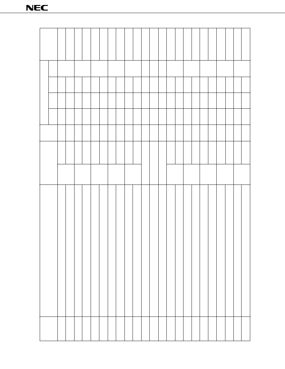
32
µ
PD70433
Address
Special Function Register Name
Symbol
R/W
After Reset
TC1
TCM1
UDC1
DCM1
MAR1
TCM0
UDC0
DCM0
MAR0
DPTC0
*
Bit clear operation possible.
Table 3-5. Special Function Registers (6/7)
Manipulable Bit Units
1 Bit
8 Bits 16 Bits 32 Bits
0FFF84H
Terminal counter modulo register 0 (low)
TCM0L
R/W
∑
∑
Undefined
0FFF86H
Terminal counter modulo register 0 (high)
TCM0H
R/W
∑
∑
Undefined
0FFF88H
DMA up/down counter 0 (low)
UDC0L
R/W
∑
∑
Undefined
0FFF8AH
DMA up/down counter 0 (high)
UDC0H
R/W
∑
∑
Undefined
0FFF8CH
DMA compare register 0 (low)
DCM0L
R/W
∑
∑
Undefined
0FFF8EH
DMA compare register 0 (high)
DCM0H
R/W
∑
∑
Undefined
0FFF90H
DMA memory address register 0 (low)
MAR0L
R/W
∑
∑
Undefined
0FFF92H
DMA memory address register 0 (high)
MAR0H
R/W
∑
∑
Undefined
0FFF94H
DMA read/write pointer 0 (low)
DPTC0L
R/W
∑
∑
Undefined
0FFF96H
DMA read/write pointer 0 (high)
DPTC0H
R/W
∑
∑
Undefined
0FFF9CH
DMA mode register 0
DMAM0
R/W
∑
∑
E0H
0FFF9DH
DMA control register 0
DMAC0
R/W
∑
∑
00H
0FFF9EH
DMA status register
DMAS
R/W
∑
*
∑
00H
0FFFA0H
Terminal counter 1 (low)
TC1L
R/W
∑
∑
Undefined
0FFFA2H
Terminal counter 1 (high)
TC1H
R/W
∑
∑
Undefined
0FFFA4H
Terminal counter modulo register 1 (low)
TCM1L
R/W
∑
∑
Undefined
0FFFA6H
Terminal counter modulo register 1 (high)
TCM1H
R/W
∑
∑
Undefined
0FFFA8H
DMA up/down counter 1 (low)
UDC1L
R/W
∑
∑
Undefined
0FFFAAH
DMA up/down counter 1 (high)
UDC1H
R/W
∑
∑
Undefined
0FFFACH
DMA compare register 1 (low)
DCM1L
R/W
∑
∑
Undefined
0FFFAEH
DMA compare register 1 (high)
DCM1H
R/W
∑
∑
Undefined
0FFFB0H
DMA memory address register 1 (low)
MAR1L
R/W
∑
∑
Undefined
0FFFB2H
DMA memory address register 1 (high)
MAR1H
R/W
∑
∑
Undefined

33
µ
PD70433
Address
Special Function Register Name
Symbol
R/W
After Reset
DPTC1
*1 The SFB bit of the standby control register can be set (1) by instruction, but cannot be cleared (0). (Only '1' can be written.)
*2 After power-on reset: 00H, otherwise: no change
Table 3-5. Special Function Registers (7/7)
Manipulable Bit Units
1 Bit
8 Bits 16 Bits 32 Bits
0FFFB4H
DMA read/write pointer 1 (low)
DPTC1L
R/W
∑
∑
Undefined
0FFFB6H
DMA read/write pointer 1 (high)
DPTC1H
R/W
∑
∑
Undefined
0FFFBCH
DMA mode register 1
DMAM1
R/W
∑
∑
E0H
0FFFBDH
DMA control register 1
DMAC1
R/W
∑
∑
00H
0FFFE0H
Software timer/counter
STC
R
∑
Undefined
0FFFE2H
Software timer/counter compare register
STMC
R/W
∑
FFFFH
0FFFE8H
Programmable wait control register 0
PWC0
R/W
∑
∑
EAH
0FFFE9H
Programmable wait control register 1
PWC1
R/W
∑
∑
AAH
0FFFEAH
Memory block control register
MBC
R/W
∑
∑
FCH
0FFFECH
Refresh mode register
RFM
R/W
∑
∑
77H
0FFFEEH
Standby control register
STBC
R/W *1
∑
∑
Undefined *2
0FFFEFH
Processor control register
PRC
R/W
∑
∑
EEH

34
µ
PD70433
3.5.4
Vector Table Area
The 1K≠byte area 00000H to 003FFH in the memory space holds 256 vectors (4 bytes used per vector) for the start
addresses of interrupt routines initiated by interrupt requests, break instructions, etc.
In the initial state, vectors 0 to 47 are reserved as V55PI family dedicated on-chip peripheral and software interrupt
vectors. For vectors 8 to 47, the vector address of hardware interrupts except NMI can be changed by means of bits V0
and V1 of the interrupt mode control register (IMC).
Vector 0
(00000H)
: Divide error
Vector 1
(00004H)
: Single step
Vector 2
(00008H)
: NMI instruction
Vector 3
(0000CH)
: BRK 3 instruction
Vector 4
(00010H)
: BRKV instruction
Vector 5
(00014H)
: CHKIND instruction
Vector 6
(00018H)
: Input/output instruction
Vector 7
(0001CH)
: FPO instruction/exception trap
When V1 = V0 = 0 :
Vector 8
(00020H)
: INTWDT
Vector 9
(00024H)
: INTP0
Vector 10
(00028H)
: INTP1
Vector 11
(0002CH)
: INTP2
Vector 12
(00030H)
: INTP3
Vector 13
(00034H)
: INTP4
Vector 14
(00038H)
: INTP5
Vector 15
(0003CH)
: System reserved
Vector 16
(00040H)
: INTCM00
Vector 17
(00044H)
: INTCM01
Vector 18
(00048H)
: INTCM10
Vector 19
(0004CH)
: INTCM11
Vector 20
(00050H)
: INTCM21
Vector 21
(00054H)
: INTCM31
Vector 22
(00058H)
: INTD0 DMA#0_MAIN
Vector 23
(0005CH)
: INTD0S DMA#0_SUB
Vector 24
(00060H)
: INTD1 DMA#1_MAIN
Vector 25
(00064H)
: INTD1S DMA#1_SUB
Vector 26
(00068H)
: INTSER0
Vector 27
(0006CH)
: INTSER1
Vector 28
(00070H)
: INTSR0/INTCSI0
Vector 29
(00074H)
: INTSR1/INTCSI1
Vector 30
(00078H)
: INTST0
Vector 31
(0007CH)
: INTST1
Vector 32
(00080H)
: INTSIT
Vector 33
(00084H)
: System reserved
Vector 34
(00088H)
: System reserved
Vector 35
(0008CH)
: System reserved
Vector 36
(00090H)
: INTPAI
Vector 37
(00094H)
: INTAD
Vector 38
(00098H)
: System reserved
Vector 39
(0009CH)
: System reserved

35
µ
PD70433
Vector 40
(000A0H)
: System reserved
Vector 41
(000A4H)
: System reserved
Vector 42
(000A8H)
: System reserved
Vector 43
(000ACH)
: System reserved
Vector 44
(000B0H)
: System reserved
Vector 45
(000B4H)
: System reserved
Vector 46
(000B8H)
: System reserved
Vector 47
(000BCH)
: System reserved
When V1 = 0, V0 = 1 :
Vector 72
(00120H)
: INTWDT
Vector 73
(00124H)
: INTP0
∑
∑
∑
∑
∑
∑
∑
∑
∑
Vector 110
(001B8H)
: System reserved
Vector 111
(001BCH)
: System reserved
When V1 = 1, V0 = 0 :
Vector 136
(00220H)
: INTWDT
Vector 137
(00224H)
: INTP0
∑
∑
∑
∑
∑
∑
∑
∑
∑
Vector 174
(002B8H)
: System reserved
Vector 175
(002BCH)
: System reserved
When V1 = 1, V0 = 1 :
Vector 200
(00320H)
: INTWDT
Vector 201
(00324H)
: INTP0
∑
∑
∑
∑
∑
∑
∑
∑
∑
Vector 238
(003B8H)
: System reserved
Vector 239
(003BCH)
: System reserved

36
µ
PD70433
3.6
REGISTER FILE SPACE
The register file space is shown in Figure 3-5.
The size of the register file space is 512 bytes, and a maximum 16-bank register set can be set.
The register file space is separate from the memory space, and in addition to accesses using a register manipulation
instruction as with the V25 and V35, the register file space can be accessed as data memory by adding a special prefix
instruction (IRAM:) to a memory manipulation instruction. (Access is performed asynchronously independently of the
external bus cycle.
When the IRAM: prefix instruction is added to a memory manipulation instruction, the CPU performs a data access with
the low≠order 9 bits of the memory address offset value as the register file address. In this case, segment register and
physical address addition is not performed, and an external bus cycle is not initiated.
Example
Label1: MOV
IRAM : [0024H], AW ..... <1>
MOV
[0056H], BW
..... <2>
<1> This shows the case where data is transferred to the register file space using an "IRAM:" prefix
instruction. The AW register value is stored in address 24H of the register file.
<2> This shows the case where an instruction for data transfer to the memory space is used.
If the IRAM prefix instruction is added to the primitive block transfer instruction and BCD operation instruction, which
specify the source block and destination block, it becomes effective for the destination block.
Also, the macro service conrol word area (008H to 03FH), the macro service work area (000H to 007H), and the area
used by the macro service channel (008H to 0FFH) are allocated in overlapping fashion in the file space. If a specific macro
service which requires work area (RTOPTRN) is not used, these work areas can be used as data space.
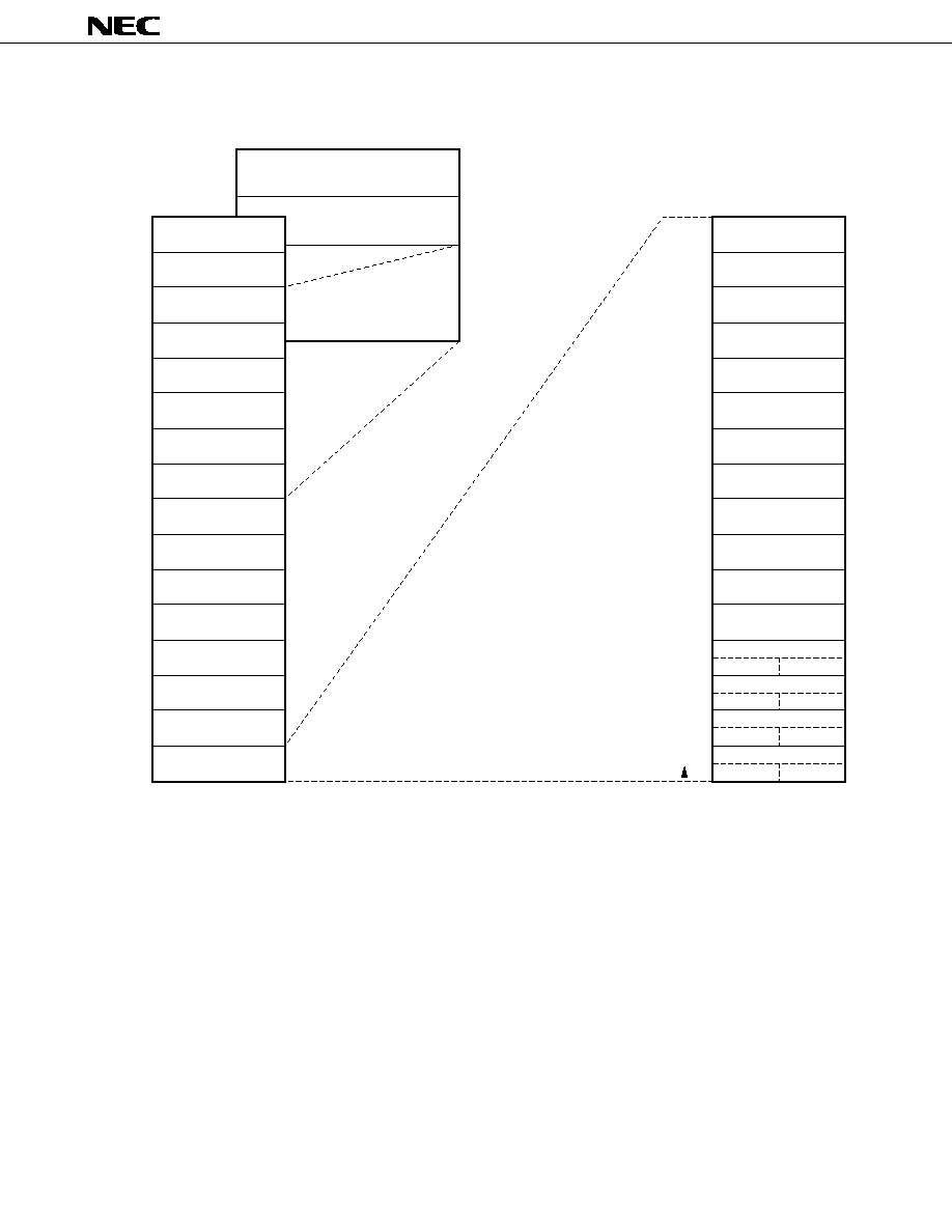
37
µ
PD70433
Figure 3-5. Register File Space
Register Bank 0
1
2
3
4
5
6
7
8
9
10
11
12
13
14
15
15 87 0
DS2
Vector PC/DS3
PSW Save
PC Save
DS0
SS
PS
DS1
IY
IX
BP
SP
BW
DW
CW
AW
BH
DH
CH
AH
BL
DL
CL
AL
+ 0 2 H
+ 0 4 H
+ 0 6 H
+ 0 8 H
+ 0 A H
+ 0 C H
+ 0 E H
+ 1 0 H
+ 1 2 H
+ 1 4 H
+ 1 6 H
+ 1 8 H
+ 1 A H
+ 1 C H
+ 1 E H
0 H
0 H
0 H
0 H
0 H
0 H
0 H
0 H
0 H
0 H
0 H
0 H
0 H
0 H
0 H
0 H
1 F F H
(Offset from the starting address of each register bank)
0
2
4
6
8
A
C
E
0
2
4
6
8
A
C
E
0
0
0
0
0
0
0
0
1
1
1
1
1
1
1
1
Macro Service Work Area
Macro Service Control
Word Area
Macro Service
Channel Area
000H
008H
03FH
0FFH
+ 0 0 H

38
µ
PD70433
3.7
I/O SPACE
The V55PI has a 64K-byte I/O space.
The I/O space map is shown in Figure 3-6.
The I/O space is accessed using address bus/data bus and control signals (IORD, IOWR, etc).
0 is output from the unused high-order 8 bits of the address bus.
Wait cycles can be inserted in an I/O cycle by software and the READY pin.
The area FF80H to FFFFH of the I/O space is a reserved area, in which two V55PI on-chip peripheral DMA input/output
read/write pointers (IOP) are allocated. The address of IOP0 is FF94H, and the address of IOP1 is FFB4H.
When the CPU executes an input/output instruction with an IOP address as an operand, the DMA controller performs
a read/write of data in the DMA controller transfer buffer, with the IOP contents as the address value, and increments (or
decrements) the IOP value automatically in accordance with the contents of the DMA control register. Therefore, data written
by the DMA controller can be referenced by an input/output instruction, and conversely, data written by an input/output
instruction can be transferred by the DMA controller.
Figure 3-6. I/O Map (64K Bytes)
Remark
IOPn corresponds to the DMA read/write pointer (DPTCn).
0 0 0 0 H
F F 8 0 H
F F 9 4 H
F F B 4 H
F F F F H
Reserved Area
IOP 0
IOP 1
:
:

39
µ
PD70433
4.
BUS CONTROL FUNCTIONS
With the V55PI pin, refer to 1.1.2 (1) "Pin function for bus control".
As regards pins which have an alternate function as port pins, when that function is used, the corresponding function
must be selected by means of the port mode control register (PMCn).
4.1
WAIT FUNCTION
The V55PI divides the basic memory space (000000H to 0FFFFFH) into a maximum of 4 blocks with a variable memory
size, divides the uppermost extended memory space area (100000H to FFFFFFH) into two areas with a variable memory
size, and performs wait control for each block. The memory size of each block in the basic memory space is specified by
the memory block control register (MBC).
Figure 4-1 shows the memory block configuration when A9H has been set for the MBC register value.
Figure 4-1. Partitioned Memory Control
MB31
00
00
11
00
01
11
00
01
10
11
Main Memory Space
MBC
Block 0
Block 1
Block 2
Block 3
Block 4
128K Bytes
256K Bytes
512K Bytes
640K Bytes
768K Bytes
896K Bytes
1M Bytes
2M Bytes
4M Bytes
6M Bytes
8M Bytes
10
01
10
01
10
11
Block 5
16M Bytes
1
MB30
0
MB21
1
MB20
0
MB11
1
MB10
1
MB01
0
MB00
1
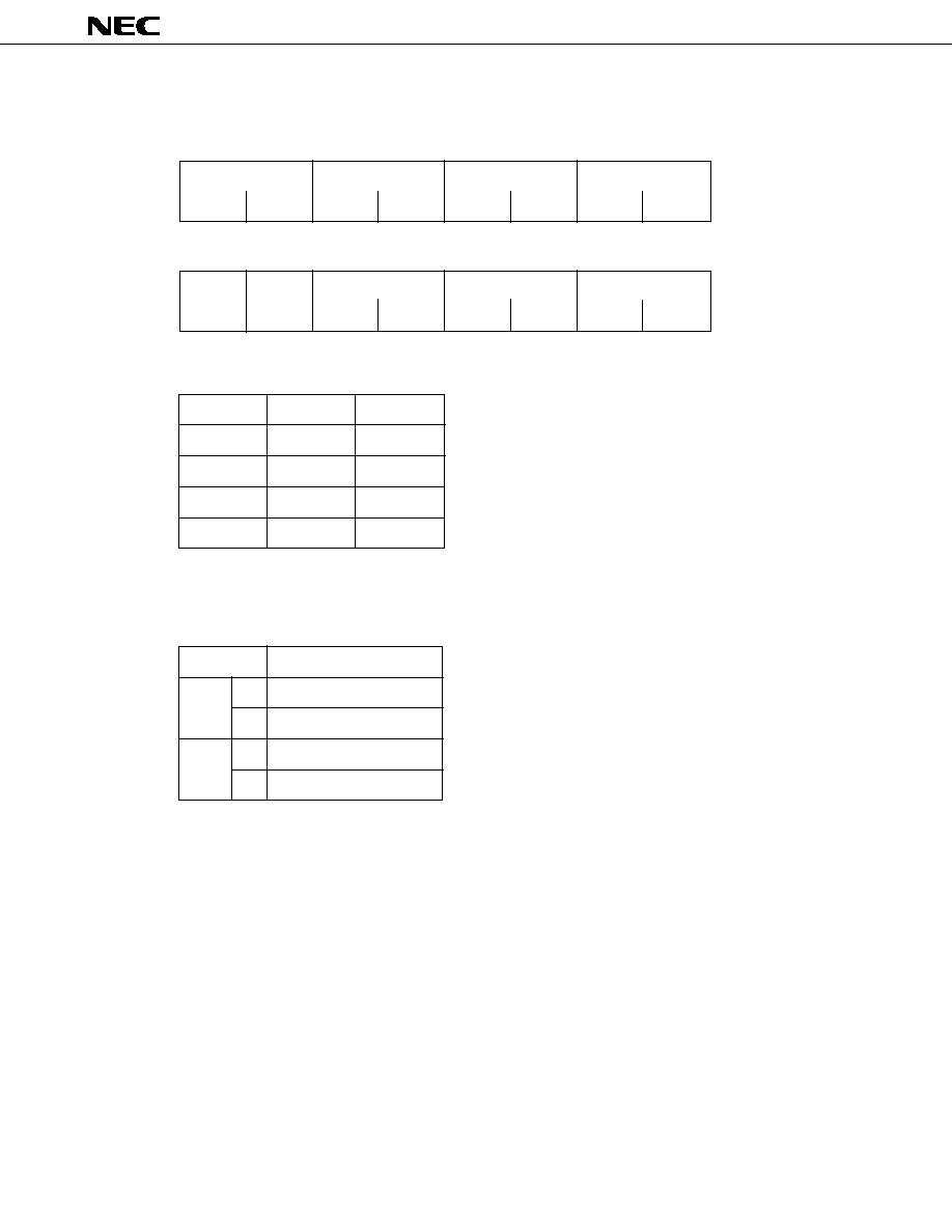
40
µ
PD70433
Figure 4-2. Memory Wait Control
7
6
5
4
3
2
1
0
(BLOCK3)
(BLOCK2)
(BLOCK1)
(BLOCK0)
PWC1
DW31
DW30
DW21
DW20
DW11
DW10
DW01
DW00
7
6
5
4
3
2
1
0
(BLOCK4) (BLOCK1)
(I/O Space)
(BLOCK5)
(BLOCK4)
PWC0
AW1
AW0
IOW1
IOW0
DW51
DW50
DW41
DW40
Data Wait (DW, IOW)
DWn1/IOW1
DWn0/IOW0
Wait State
0
0
0 *1
0
1
1 *2
1
0
2 *2
1
1
3 *2
* 1.
READY signal is ignored.
2.
Additional control by means of READY signal is also possible.
Address Wait (AW)
AWn
Wait State
0
Not inserted (block 1)
AW0
1
Inserted (block 1)
0
Not inserted (block 4)
AW1
1
Inserted (block 4)

41
µ
PD70433
4.2
REFRESH FUNCTION
The following functions are provided to refresh DRAM and pseudo-SRAM.
∑ Function to insert periodically a refresh cycle in a series of bus cycles
∑ Refresh address output function to refresh DRAM and pseudo-SRAM
∑ Function to generate a refresh cycle in hold mode and HALT mode.
∑ Function to insert a wait state in a refresh cycle
4.2.1
Refresh Mode Register (RFM)
The RFM register is an 8-bit register to control refresh operation.
A refresh cycle can be selected from the time base counter output tap.
While a refresh request is held by another bus cycle if the next refresh request is generated, only the latter is valid.
The RFM register value after a reset is 77H.
4.2.2
Wait Control in Refresh Cycle
A wait state can be inserted in a refresh cycle. The specified number of wait states is inserted for memory block 4 by
the programmable wait control register (PWC0) or READY pin.
4.2.3
Refresh Address
Bus pins AD0 to AD15 and A16 to A19 are activated in a refresh cycle.
For each refresh cycle, the count is performed in one-address increments from x00000 to x1FFFFF in the case of the
external 8-bit bus width, and in two-address increments from x00001H to xFFFFF in the case of the external 16-bit bus width
(the minimum address is returned to after the maximum address).
After initialization by a reset, count-up is started from x00000H in the case of the external 8-bit bus width and x00001H
in the case of the external 16-bit bus width.
In the case of the external 16-bit bus width, the refresh address minimum address bit (A0) is fixed at "1" and the DEX
pin output is also fixed at "1".
A20 to A23 are undefined in a refresh cycle.

42
µ
PD70433
5.
INTERRUPT FUNCTIONS
The V55PI incorporates a powerful interrupt controller (INTC) which controls multiple-interrupt servicing for a total of 25
maskable hardware interrupt requests: 19 internal and 6 external. The interrupt controller controls multiple-interrupt
servicing based on programmable priority.
The following functions are provided as interrupt servicing modes: vectored interrupt function, macro service function,
register bank switching function.
5.1
FEATURES
V55PI interrupt functions offer the following features:
∑
Comprehensive servicing states for interrupt requests
∑ Vectored interrupt function
: Branch to interrupt service routine specified by vector table
∑ Register bank switching function
: High-speed interrupt response by automatic register bank switching
∑ Macro service function
: High-speed interrupt servicing by microprogram (firmware)
∑
4-level programmable priority order control
∑
Interrupt multiprocessing control according to the priority
∑
Rich variety of macro service functions (following 7 modes) closely tied to V55PI on-chip peripheral hardware
EVTCNT
: Event count processing
BLKTRS
: Data transfer between special function register and external memory buffer
BLKTRS-C
: Data transfer between special function register and external memory buffer (with transfer data
detection function)
DTACMP
: Special function register status detection
DTADIF
: Time measurement by timer capture function
RTOPTRN
: Automatic control of real-time output port
DTACMP-M : Data transfer between external I/O and memory
∑
7 external interrupt request inputs (NMI, INTP0 to INTP5)
∑
Maskable interrupt requests are individually maskable.
A list of interrupt sources is given in Table 5-1.

43
µ
PD70433
Interrupt
Register
Macro Service
Request
Bank
Control Word
Signal
Switching
Address
Interrupt Request
Control Register
Table 5-1. Interrupt Sources (1/2)
Interrupt Source
Default
Interrupt
Default
Vector
Vectored
Macro
Classification
Priority
Generating
Generating
Table
Address
Service
Source
Unit
Number
1
NMI
NMI pin input
≠≠≠
2
00008H
No
No
Nonmaskable
≠≠
≠≠
2
WDT
Watchdog timer overflow
WDT
8
00
◊
20H
No
No
3
INTP0
IC9
INTP0 pin input
9
00
◊
24H
Yes
Yes
012H
4
INTP1
IC10
INTP1 pin input
10
00
◊
28H
Yes
Yes
014H
5
INTP2
IC11
INTP2 pin input
11
00
◊
2CH
Yes
Yes
016H
External
6
INTP3
IC12
INTP3 pin input
12
00
◊
30H
Yes
Yes
018H
7
INTP4
IC13
INTP4 pininput
13
00
◊
34H
Yes
Yes
01AH
8
INTP5
IC14
INTP5 pin input
14
00
◊
38H
Yes
Yes
01CH
9
INTCM00
IC16
CM00 match detection
16
00
◊
40H
Yes
Yes
020H
10
INTCM01
IC17
CM01 match detection
17
00
◊
44H
Yes
Yes
022H
Maskable
11
INTCM10
IC18
CM10 match detection
18
00
◊
48H
Yes
Yes
024H
Timer
12
INTCM11
IC19
CM11 match detection
19
00
◊
4CH
Yes
Yes
026H
13
INTCM21
IC20
CM21 match detection
20
00
◊
50H
Yes
Yes
028H
14
INTCM31
IC21
CM31 match detection
21
00
◊
54H
Yes
Yes
02AH
15
INTD0
IC22
DMA channel 0_main
22
00
◊
58H
Yes
Yes
02CH
16
INTD0S
IC23
DMA channel 0_sub
23
00
◊
5CH
Yes
Yes
02EH
DMA
17
INTD1
IC24
DMA channel 1_main
24
00
◊
60H
Yes
Yes
030H
18
INTD1S
IC25
DMA channel 1_sub
25
00
◊
64H
Yes
Yes
032H

44
µ
PD70433
*
Indicates that the value is variable in the range 0 to 255 (0 to FFH).
Remarks
"
◊
" indicates that the value is determined by the V0 and V1 bits of the IMC register.
Interrupt
Register
Macro Service
Request
Bank
Control Word
Signal
Switching
Address
Interrupt Request
Control Register
Table 5-1. Interrupt Sources (2/2)
Interrupt Sourse
Default
Interrupt
Default
Vector
Vectored
Macro
Classification
Priority
Generating
Generating
Table
Address
Service
Source
Unit
Number
19
INTSER0
IC26
UART reception error (ch0)
26
00
◊
68H
No
Yes
034H
20
INTSER1
IC27
UART reception error (ch1)
27
00
◊
6CH
No
Yes
036H
INTSR0/
UART reception (ch0)/
Yes
Yes
21
IC28
28
00
◊
70H
038H
INTCSI0
Serial transmission/reception (ch0)
Yes
Yes
Serial I/F
INTSR1/
UART reception (ch1)/
Yes
Yes
22
IC29
29
00
◊
74H
03AH
Maskable
INTCSI1
LDMA channel 5
Yes
Yes
23
INTST0
IC30
UART transmission (ch0)
30
00
◊
78H
Yes
Yes
03CH
24
INTST1
IC31
UART transmission (ch1)
31
00
◊
7CH
Yes
Yes
03EH
25
INTSIT
IC32
STM match detection
SIT
32
00
◊
80H
No
Yes
≠≠
26
INTPAI
IC36
Parallel I/F
Parallel I/F
36
00
◊
90H
Yes
Yes
≠≠
27
INTAD
IC37
A/D converter
A/D converter
37
00
◊
94H
Yes
Yes
008H
Divide error
0
00000H
No
No
BRK flag (single-step)
1
00004H
No
No
BRK3 instruction
3
0000CH
No
No
BRKV instruction
4
00010H
No
No
Software
CHKIND instruction
5
00014H
No
No
≠≠
≠≠
≠≠
≠≠
≠≠
Input/output instruction (IBRK flag)
6
00018H
No
No
BRK imm8
*
00
◊
*H
No
No
BRKCS instruction
≠≠
≠≠
No
Yes
FP0 instruction/
Exception
7
0001CH
No
No
trap
Exception trap
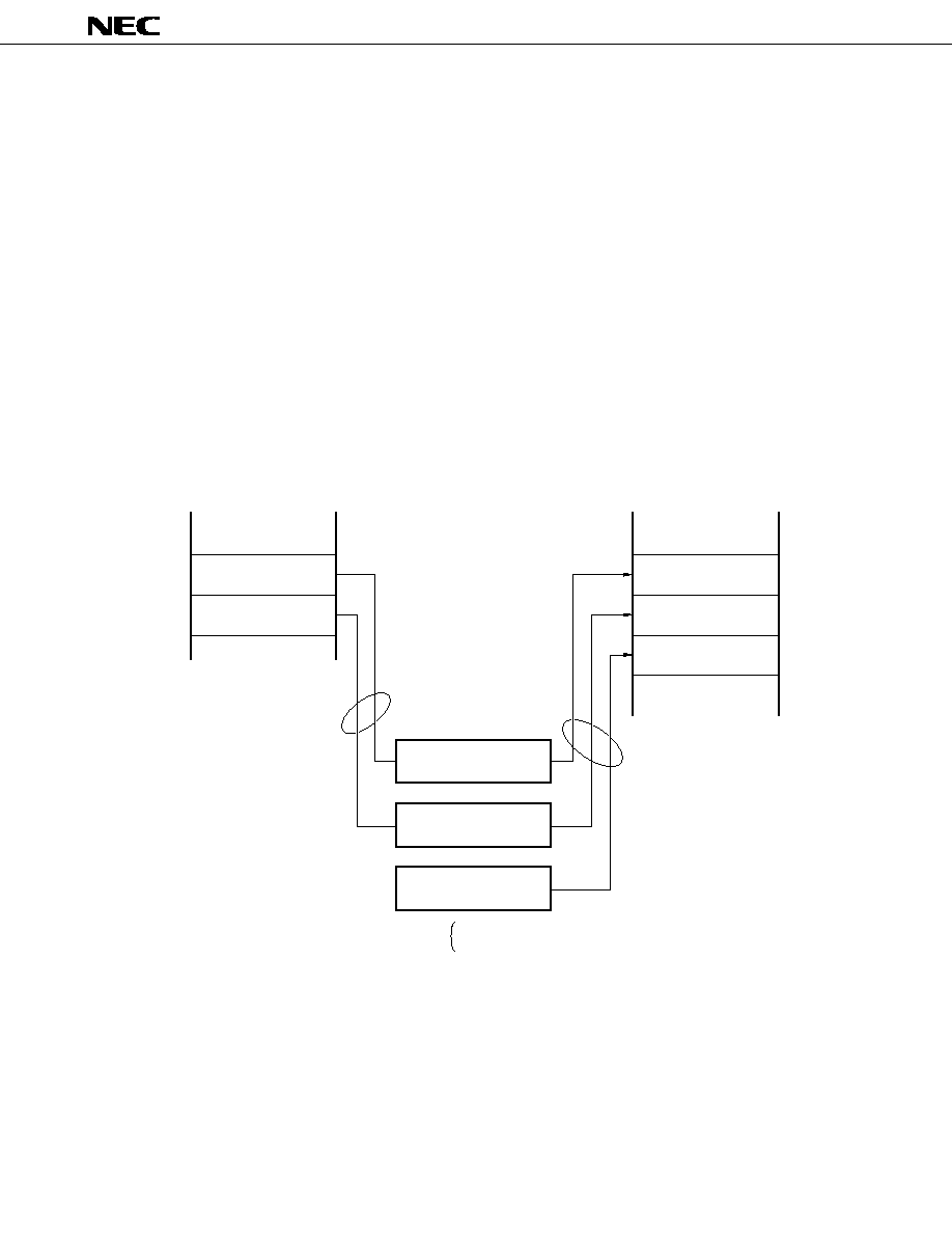
45
µ
PD70433
5.2
INTERRUPT RESPONSE METHODS
The V55PI has three interrupt response methods: a vectored interrupt function, register bank switching function, and
macro service function. In the case of a maskable interrupt request, one of these functions can be selected by means of
the interrupt request control register (IC
◊◊
) for each interrupt source according to the purpose of the interrupt. The on-chip
interrupt controller handles interrupt requests according to the set response method.
5.2.1
Vectored Interrupts
A vectored interrupt can only be acknowledged in the interrupt enabled state (EI state). When a vectored interrupt is
acknowledged, the CPU enters the interrupt disabled state (DI state), and the current PSW contents and PC and PS contents
are saved to the stack. Then the corresponding vector is selected from the vector table, and the interrupt service routine
is started at the address indicated by that vector. Vector numbers are fixed for each interrupt source. In the DI state, interrupts
are held pending, and are acknowledged when the EI state is set again.
The return from the interrupt is performed by an RETI instruction. In the case of a hardware interrupt other than a non-
maskable interrupt, an FINT instruction must be executed before the return instruction. When a return is made from an
interrupt, the PC, PS and PSW are restored from the stack.
Figure 5-1. Interrupt Acknowledge Operation (Performed in Sequence <1>
<4>)
PSW
PS
PC
Vector Table
Stack
SP ≠ 6
SP ≠ 4
SP ≠ 2
n: Vector Number
n
◊
4
n
◊
4 + 2
<4>
<2>
SP
SP ≠ 6
<1>
<3>
IE = 0
BRK = 0
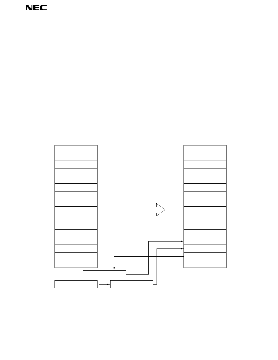
46
µ
PD70433
5.2.2
Register Bank Switching Function
In the V55PI, general register sets are mapped onto on-chip RAM, and register sets can be held in up to 16 banks. Interrupt
servicing is performed by automatically switching the register bank when a BRKCS or TSKSW instruction is executed or
when an interrupt is responded to. Because saving of registers to the stack previously performed by software is not required,
high-speed switching of the program execution environment is possible.
The register bank switching sequence is performed as follows (See Figure 5-2).
<1> The contents of PSW is saved to temporary register.
<2> The register bank is switched.
<3> IE and BRK are set to 0.
<4> The contents of PSW which is saved to the PC and the temporary register are saved to the saving area, respectively.
<5> The interrupt service routine start address offset value is loaded from the vector PC area in the register bank to
PC.
Figure 5-2. Register Bank Switching Sequence
(In Case of Register Bank Switching by Interrupt)
Old Register Bank
AW
CW
DW
BW
SP
BP
IX
IY
DS1
PS
SS
DS0
PC Save
PSW Save
Vector PC/DS3
DS2
New Register Bank
for Interrupt Servicing
AW
CW
DW
BW
SP
BP
IX
IY
DS1
PS
SS
DS0
PC Save
PSW Save
Vector PC/DS3
DS2
PSW
PC
Temporary Register
<2>
Register Bank Switching
<3>
IE = 0, BRK = 0
<1>
<5>
<4>
<4>

47
µ
PD70433
5.2.3
Macro Service Function
The macro service function performs processing of simple data transfers, etc., by means of a microprogram (CPU internal
dedicated firmware) started by generation of an interrupt request. The simple, standardized interrupt servicing which was
coded and executed by a user program is performed automatically.
Macro service processing is caused by an interrupt request and is performed. Macro service is designed to minimize
as far as possible the frequency of generation of interrupts consisting mainly of software processing, hold down the software
overhead due to a series of processes used in an interrupt (register saving, initialization, register restoration, return from
the interrupt routine), and improve the CPU efficiency.
Processing performed by the macro service is transparent in terms of software, and it is possible to process as a single
mass of data what was previously processed by software byte by byte, allowing more efficient programming.
The V55PI macro service supports not only the simple data transfers used in the V25 and V35, but also various operating
modes closely linked to the on-chip V55PI peripheral hardware, as shown below.
(a) EVTCNT (EVENT COUNTER)
The counter is updated each time the macro service are generated, and when the counter reaches 0 the macro service
for the corresponding interrupt source is terminated and a vectored interrupt or a register bank switching is generated.
(b) DTACMP (DATA COMPARE)
The interrupt source specific SFR and preset byte data are compared, and if they match, the macro service for the
corresponding interrupt source is terminated and a vectored interrupt or register bank switching is generated.
(c) DTADIF (DATA DIFFERENCE)
The difference in using the timer/counter unit capture register is calculated. This is initiated by a timer interrupt: the
value of the capture register latched last time is subtracted from the value of the capture register latched this time, and
the result is stored in the previously specified memory buffer.
When processing has been performed the previously set number of times, the corresponding interrupt source macro
service is terminated, and a vectored interrupt or register bank switching is generated.
(d) BLKTRS (BLOCK TRANSFER)
A data transfer is performed between the previously specified memory buffer and SFR.
When the previously set number of data transfers have been performed, the corresponding interrupt source macro
service is terminated, and a vectored interrupt or register bank switching is generated.
(e) BLKTRS≠C (BLOCK TRANSFER WITH CHARACTER SEARCH)
A data transfer is performed between the previously specified memory buffer and SFR. When the previously set
number of data transfers have been completed, or when the transfer data matches the previously set character data,
the corresponding interrupt source macro service is terminated, and a vectored interrupt or register bank switching is
generated.
(f) RTOPRTN (RTOP TRANSFER)
Data to be output to the real-time output port is transferred to the port 7 buffer (P7H, P7L), and data which specifies
interval for output to the real-time output port is transferred to the timer compare register (CM00, CM01).
(g) DTACMP-M (DATA COMPARE WITH CHARACTER MASK)
The logical product of the status data read from the external I/O and the previously set mask data is performed. The
previously set byte data is compared with the result. If it matches, a data transfer is performed between the external I/
O and memory. If it does not match, or if the previously set number of data transfers have been performed, the
corresponding interrupt source macro service is terminated, and a vectored interrupt or register bank switching is
generated.

48
µ
PD70433
6.
DMA FUNCTION (DMA CONTROLLER)
The V55PI incorporates a 2-channel DMA controller which controls execution of memory-to-I/O or memory-to-memory
DMA transfers on the basis of DMA requests generated by an on-chip peripheral hardware (serial interface, parallel interface,
or timer), the external DMARQ pin or a software trigger.
Each channel of the DMA controller further comprises a main channel and a sub-channel: the operating mode determines
whether the main channel and sub-channel are used as a single channel or as separate channels. When used as separate
channels, function for a maximum of 4 channels can be constructed.
6.1
FEATURES
∑
Two independent DMA channels (max. 4-channel configuration possible)
∑
Four transfer modes
∑ Single transfer mode
... One DMA transfer cycle is executed in response to one DMA request.
∑ Demand release mode ... Consecutive DMA transfer cycles are executed while DMA request is active.
∑ Single-step mode
... DMA transfer cycles and CPU bus cycles are executed alternately after DMA
request generation.
∑ Burst mode
... For each DMA request, the specified number of DMA transfer cycles are executed
consecutively.
∑
Five operating modes
∑ Intelligent DMA mode≠1 (ring buffer system)
... DMA transfers to ring buffer are controlled.
∑ Intelligent DMA mode≠2 (counter control system) ... Transfer data is transferred consecutively, divided into
an arbitrary number of bytes.
∑ Next address specification mode
... Consecutive transfers are possible between different
transfer buffers.
∑ 2-channel operating mode
... Main channel and subchannel are used as independent
channels.
∑ Memory-to-memory transfer mode
... Two bus cycles are started for one DMA transfer cycle,
and memory-to-memory transfer is executed.
∑
3 clocks/1 bus cycle (no wait case)
∑
Transfer objects
∑ External I/O
memory
... 1 DMA transfer cycle/1 bus cycle
∑ SFR (internal I/O)
memory
... 1 DMA transfer cycle/1 bus cycle
∑ Memory
memory (memory includes SFR) ... 1 DMA transfer cycle/2 bus cycles
∑
Byte transfer/word transfer selectable
∑
Transfer address increment/decrement/non-update selectable
∑
DMA transfer end signal (TCE0, TCE1) output
∑
24-bit DMA memory address registers (MAR0, MAR1)
∑
21-bit terminal counters (TC0, TC1)
∑
External DMA request signal input pins (DMARQ0, DMARQ1: alternate function as port P80 and P81 pins)
∑
External DMA acknowledge signal output pins (DMAAK0, DMAAK1)
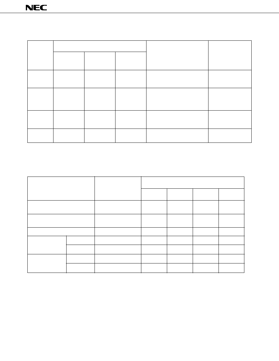
49
µ
PD70433
Table 6-1. Transfer Modes
DMA Start Source
Transfer
Mode
On≠Chip
Software
Peripheral
Trigger
Single
transfer
Available
Available
Available
mode
Stops when the DMARQ pin is
Not acknowledged
driven low during the transfer.
during transfer.
Reset of EDMA bit of DMAMn
Acknowledged at
register
other times.
Single
step
Available*
Available
Available
mode
Burst
None (stop disabled during the
mode
transfer)
*
The DMA start source is an on-chip timer interrupt, and transfer is possible only when the transfer I/O specification is
external.
Table 6-2. Correspondence Between Operating Modes and Transfer Modes
Possible Transfer Modes*
Operating Mode
Transfer Type
<1>
<2>
<3>
<4>
Intelligent DMA mode≠1
I/O (SFR)
Memory
Yes
Yes
No
No
(ring buffer method)
Intelligent DMA mode≠2
Memory
I/O (SFR)
No
No
Yes
Yes
(counter control method)
Next address specification mode
I/O (SFR)
Memory
Yes
Yes
No
No
(Stop at end)
I/O
Memory
Yes
Yes
Yes
Yes
(Repetition)
I/O
Memory
Yes
Yes
Yes
No
(Stop at end)
Memory
Memory
Yes
No
Yes
Yes
(Repetition)
Memory
Memory
Yes
No
Yes
No
*
Transfer modes
<1> Single transfer mode
<2> Demand release mode
<3> Single step mode
<4> Burst mode
Not Available
Not Available
Available
Available*
Available
Available
2≠channel
operating mode
Memory≠memory
transfer mode
Demand
release
mode
Reset of EDMA bit of DMAMn
register
Reset of EDMA bit of DMAMn
Acknowledged
register
Not acknowledged
Acknowledged
STOP Method
Interrupt
DMARQ Pin

50
µ
PD70433
7.
SERIAL INTERFACE FUNCTIONS
The V55PI is equipped with a 2-channel serial interface unit (ch0, ch1).
The two communication protocols supported by the V55PI are as follows:
(1)
Asynchronous
UART
(2)
Clocked
CSI
SBI:
2-wire serial bus interface
IOE:
I/O expansion 3-wire serial interface
7.1
FEATURES
∑
Two communication protocols supported
∑
Two serial channels
∑
Wake-up function
∑
On-chip dedicated baud rate generator
∑
DMA request generated by completion of transmission/reception (transmit/receive data DMA transfer is
capable)
7.2
PROTOCOLS
The UART is an asynchronous serial interface which achieves data synchronization by means of start/stop bits, and is
functionally enhanced UART functions compared with previous single-chip microcontroller.
The CSI (clocked serial interface) is a clocked serial interface which achieves synchronization by transmission/reception
of a clock. The CSI is a subset of the standard serial bus interface specification for NEC single-chip microcontrollers, and
I
2
C functions are not supported. The wake-up release function is implemented by using macro service.
Table 7-1. Supported Protocols
Supported Protocols
Serial Interface Unit
Clocked (CSI)
Asynchronous
SBI
IOE
(UART)
Channel 0
Yes
Yes
Yes
Channel 1
No
Yes
Yes
The UART function or CSI function can be programmably selected for each channel. Protocol selection is performed by
means of the protocol selection register (ASP).
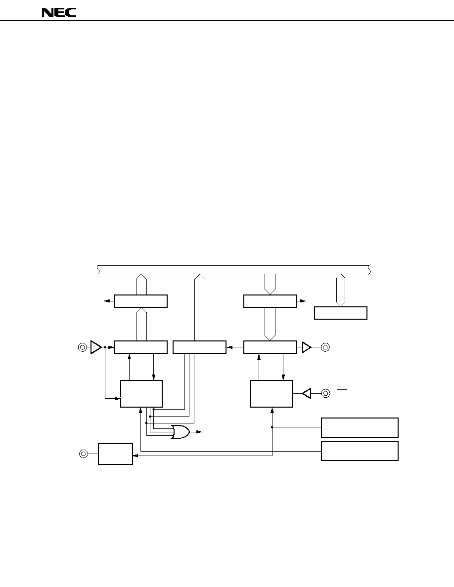
51
µ
PD70433
INTSR
n
R
◊
B
INTST
n
UARTM
R
◊
D
n
Shift Register
UARTS
Shift Register
T
◊
D
n
CTS
Transmission
Control Parity
Addition
Reception
Control Parity
Check
External
Clock
Control
INTSER
n
ERP
ERF
ERO
AS
T
◊
C*
T
◊
B
Transmit Serial Clock
Receive Serial Clock
7.3
UART
7.3.1
Features
∑
Transfer rate:
95 to 390 Kbps (with 12.5 MHz system clock
)
123 to 500 Kbps (with 16 MHz system clock
)
∑
Full-duplex operation capability
∑
On-chip dedicated (transmission and reception) baud rate generators
∑
Wake-up function
∑
Zero parity function
∑
Parity error detection
∑
Framing error detection
∑
Overrun error detection
∑
Three dedicated UART interrupt sources
∑ UART receive error interrupts (INTSER0, INTSER1)
∑ UART reception interrupts (INTSR0, INTSR1)
∑ UART transmisstion interrupts (INTST0, INTST1)
∑
Macro service function
∑ UART reception interrupts (INTSR0, INTSR1)
∑ UART transmission interrupts (INTST0, INTST1)
Figure 7≠1. UART Block Diagram
*
Channel 0 only

52
µ
PD70433
7.4
CLOCKED SERIAL INTERFACE (CSI)
7.4.1
Features
∑
Transfer speed:
Max. 3.125 Mbps (with 12.5 MHz system clock
)
Max. 4.0 Mbps (with 16 MHz system clock
)
∑
Half-duplex communication
∑
Data length: 8-bit unit
∑
External/internal clock selection function
∑
Data MSB-first/LSB-first selection function
∑
SBI mode (2-wire NEC type serial bus) ... ch0 only
∑ Address/command/data identification function
∑ Function for chip selection by address
∑ Wake-up function
∑ Acknowledge signal (ACK) control function
∑ Busy signal (BUSY) control function
The V55PI clocked serial interface has the following two operating modes.
(1) 3≠wire serial I/O mode (IOE mode)
In this mode, 8-bit data transfer is performed using three lines: the serial clock (SCK), and serial data input and output
(SI, SO). This mode is useful when connecting an I/O device, display controller, etc., which incorporates a conventional
clocked serial interface.
The functions of the V25 and V25+
TM
have been enhanced, and data MSB-first/LSB-first selection is possible.
(2)
Serial bus interface mode (SBI mode)
In the SBI mode, communication is performed with multiple devices by means of two lines: the serial clock (SCK)
and the serial bus interface (SB0 or SB1).
This mode conforms to the NEC serial bus format.
In the SBI mode, the sender can output to the serial data bus an address to select the target device for serial
communication, a command which gives a directive to the target device, and actual data. Thus there is no need for
the line for handshaking required when multiple devices are connected with a conventional clocked serial interface,
allowing input/output ports to be used efficiently.
In addition, wake-up release is performed using macro service.

53
µ
PD70433
8.
PARALLEL INTERFACE FUNCTIONS
The V55PI incorporates a parallel interface unit for data input on a Centronics specification interface, and general data
input/output.
8.1
FEATURES
The following features are provided as parallel interface functions:
∑
Centronics specification interface compatibility
∑
Input/output mode switchable by software
∑
BUSY signal manipulable by software
∑
BUSY signal and ACK signal output timing settable
∑
Initialization by external interrupt
∑
Dedicated parallel interface interrupt source
∑ Parallel interface interrupt (INTPAI)
∑
DMA request signal generation in parallel transmission/reception
∑ INTPAI functions as a DMA start trigger.
∑
Signal pin input/output characteristic is TTL level (Centronics specification interface)

54
µ
PD70433
Internal Bus
Internal Bus
Input
Data
Latch
ACK
Control
Circuit
DMA
Request
ACK
Timing
Control
BUSY
Control
Circuit
PAI Timer
Counter
IBSY
S
R
DATA
RD
RESET
IBF
S
R
Q
MB0, 1
OE
PD0≠PD7
DATASTB
BUSY
ACK
INTP5
Output
Data
Latch
PAI Timer
Counter
PD0≠PD7
DATASTB
BUSY
ACK
WR
DATA
WR
DMA
Request
INTPAI Request
INT/
DMA
Request
Control
Figure 8-1. Parallel Interface Block Diagram
(a)
Input mode
(b)
Output mode
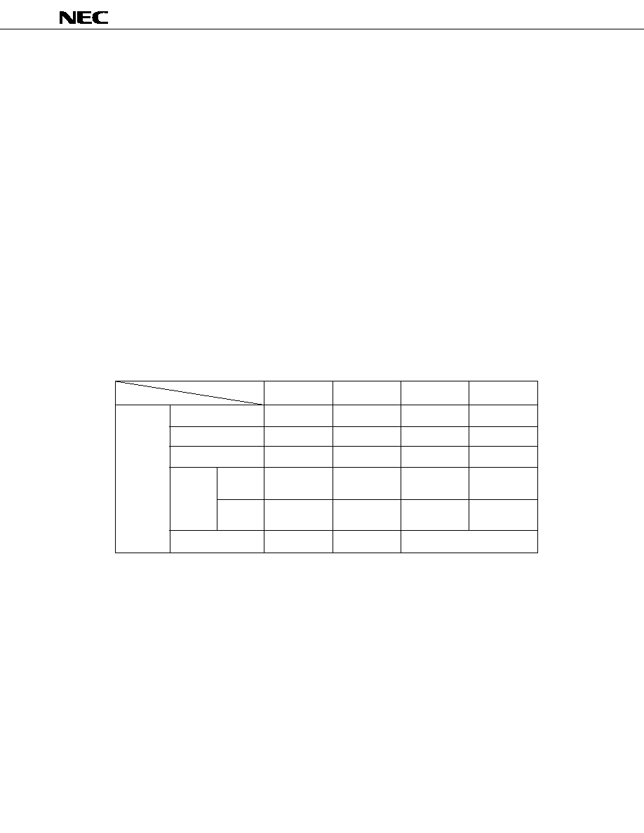
55
µ
PD70433
9.
TIMER FUNCTION
The V55PI timer unit can be used as an interval timer, free-running timer and event counter. It is also possible to
manipulate P7 as a real-time output port, synchronized with interrupt requests generated by the timer. The normal timer
function and real-time output port function are described here.
9.1
FEATURES
The timer function offers the following features.
∑
16-bit timer
◊
4
∑
Two count clock sources are selectable
∑ System clock scaled output selectable (
/8,
/32: system clock
)
∑ External input pulses from TI pin
∑
External count output signal (TOn output)
∑
Three 16-bit capture registers on chip (external interrupt input signals INTP0 to INTP2 as triggers)
∑
Six dedicated timer unit interrupt source (INTCM00, INTCM01, INTCM10, INTCM11, INTCM21, INTCM31)
∑
Real-time output port function synchronized with timer interrupts
9.2
TIMER UNIT CONFIGURATION
The timer unit configuration is shown in Figure 9-1, and the function of each timer in Table 9-1.
Table 9-1. Timer Functions
Timer 0
Timer 1
Timer 2
Timer 3
Count function
Available
Available
Available
Available
Capture function
Available
Available
Not Available
Not Available
Compare function
Available
Available
Available
Available
Function
Toggle
Available
Not Available
Available
Not Available
Timer
output
output
function
Set/reset
Not Available
Not Available
Available
Available
output
Cascading
Not Available
Not Available
Available
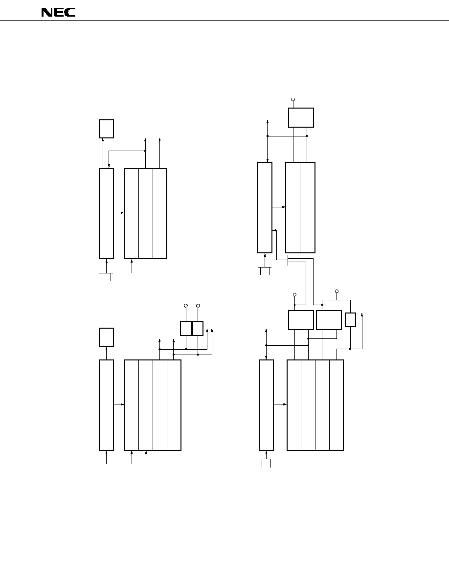
56
µ
PD70433
Figure 9-1. Timer Unit Block Diagram
Timer 0
16≠Bit Free Running Timer (TM0)
Capture Register (CT00)
Capture Register (CT01)
Compare Register (CM00)
Compare Register (CM01)
INTP0
INTP1
/8
OVF
T
T
INTCM00
INTCM01
TO00
TO01
To Real≠Time
Output Port
Timer 2
16≠Bit Timer Register 2 (TM2)
Compare Register (CM20)
Compare Register (CM21)
Compare Register (CM22)
Compare Register (CM23)
/8
/32
Clear
S
R
Q
S
R
Q
T
INTCM21
To DMA
Controller
TO20
TO21
Timer 1
16≠Bit Timer Register/Event Counter 1
(TM1)
Capture Register (CT10)
Compare Register (CM10)
Compare Register (CM11)
/8
OVF
TI
INTP2
Clear
INTCM10
INTCM11
Timer 3
16≠Bit Timer Register 3 (TM3)
Compare Register (CM30)
Compare Register (CM31)
/8
/32
S
R
Q
TO30
INTCM31
Clear, Count Enable
Clear

57
µ
PD70433
9.3
REAL-TIME OUTPUT PORT FUNCTION
Port 7 of the V55PI incorporates a real-time output port function, and can output the contents of the port 7 buffer (P7H,
P7L) at programmable intervals from timer 0 bit-wise.
9.3.1
Real-Time Output Port Configuration
The real-time output port configuration is shown in Figure 9-2. It comprises the following buffer registers, output and
control registers.
(1)
Port 7 buffer (P7H, P7L)
The buffer registers hold the data to be output next when port 7 is set to the real-time output port mode.
The port 7 buffer contents are not affected by reset input.
(2)
Real-time output port (RTP)
Real-time output port output data is held in this port after being taken from the port 7 buffer, and output from the
pins.
RTP can be read or written to by an 8-bit or single-bit manipulation instruction (unlike the port 7 output port).
(3)
Real-time output port delay specification regiser (RTPD) and delay counter
This register is set and used when using the mode in which a delay time is inserted in the timing for output from
the real-time output port (RTP) to the output pins.
If the P7L bit is set to "0", "0" is output to the corresponding output pin bit after the elapse of the delay time equivalent
to the count clock cycle time set in the real-time output port delay specification register after the time at which the transfer
trigger is generated. The delay time in this case is counted by the delay counter.
(4)
Real-time output port control register (RTPC)
RTPC specifies the operating mode of the real-time output port. It is possible to specify whether or not a delay is
to be inserted when data is output, the timing for transferring data to the port 7 buffer, the transfer timing trigger, and
so on.

58
µ
PD70433
Figure 9≠2. Real≠Time Output Port Operation
Real≠Time Output
Port Control Register
RTPC
TRG, BYTE
DLY
8
Internal Bus
P7H
Port 7 Buffer
P7L
Port 7 Buffer
Output
Latch
RTP Bit 3
Output Latches
RTP7 to RTP4
P77
P76
P75
P74
P73
P72
P71
P70
Control Output Signals
To Port 7
R
S
Q
No Delay
Delay
Bor-
row
Preset
Delay Counter
Delay Specification
Register
Selector
INTCM00
(Timer 0)
INTCM01
(Timer 1)
/2
RTPD
59
µ
PD70433
9.3.2
Real-Time Output Port Operation
Real-time output port specification is performed bit-wise by the port 7 mode control register (PCM7).
Port 7 (P7), the port 7 buffer (P7H, P7L) and the real-time output port can be accessed as real-time output ports.
Data output is performed as described below.
When output data is written in the port 7 buffer (P7H, P7L), the port 7 buffer contents are transferred to the real-time
output port (RTP) and output to the pins in synchronization with the timing of an interrupt request from timer 0 (INTCM00,
INTCM01), or a write to the TRG bit in the control register (RTPC).
An example of the direct control of the output pattern for a real-time output port and the output interval is shown in Figure
9-3.
Update data is transferred from the two data storage areas set beforehand in the external memory space to the real-
time output function buffer registers (P7H, P7L) and compare registers (CM00, CM01).
Figure 9-3. Real-Time Output Port Stepping Motor Control
Output Data Area
Output Timing Data Area
External Memory Space
D1
D2
D3
D4
T1
T2
T3
T4
Register File Space
Output Data Pointer
Buffer Register Address
Compare Register Address
Output Timing Data Pointer
RC Initial Value
Real≠Time Output Counter (RC)
Macro Service Counter
Mode Register
Channel Pointer
Macro Service
Control Word
+1
≠1
≠1
Internal Bus
Real-Time Output Port
Transfer
Transfer or Addition
Compare Register
CM00 or CM01
Timer 0
Free Running Timer
TM0
Match
Interrupt
Request
f
CLK
/8
Real-Time Output Trigger/
Macro Service Activation
INTCM00
or
INTCM01
Macro Service
Processing
Buffer Register
P7H, P7L
RTP
Stepping Motor
Output Latch

60
µ
PD70433
In particular, it is possible to insert a delay time in the timing for output by setting the real-time output port delay
specification register (RTPD) pins. If the P7L bit is changed from "1" to "0", it is possible to perform output after inserting
a delay time of 2
◊
the system clock set in the RTPD from the timing at which the transfer trigger is generated. In this case,
"0" is output from the corresponding output pin. This delay is counted by the delay counter.

61
µ
PD70433
10. PWM UNIT
The V55PI is provided with an 8-bit precision PWM (pulse width modulation) signal output function.
PWM output can be used as a digital-to-analog conversion output by connecting a low-pass filter, etc., externally. This
is ideal for the actuator control signal for motors, etc.
10.1 FEATURES
The PWM unit offers the following features:
∑
PWM output pulse active level selectable
∑
Frequency: 25 MHz (with 12.5 MHz system clock
)
PWM cycle: 40.96
µ
s
: 32 MHz (with 16 MHz system clock
)
PWM cycle: 32.00
µ
s
∑
Output pulse width (duty): 0, 1/256, ....., 255/256
Resolution: 160 ns (with 12.5 MHz system clock
)
125 ns (with 16 MHz system clock
)
10.2 PWM UNIT CONFIGURATION
The configuration of the PWM unit is shown in Figure 10-1.
The PWM unit consists of the PWM register (PWM) and PWM control register (PWMC), and an 8-bit counter.
The PWM register controls the pulse width (duty) in the PWM output mode. The 8≠bit counter is set to 00H by reset input.
The PWM register is not affected by reset input.
62
µ
PD70433
8-Bit Counter
Comparator
PWM Slave Latch
PWM Register
Internal Bus
Preset
Match Detection
Signal
Overflow
S
R
Active
Level
Control
Q
Q
PWM Control
Register
PWM
Output
0
0
0
0
0
0
CE
ALV
Figure 10-1. PWM Unit Block Diagram
63
µ
PD70433
*1
/2
/2
/2
9
11
13
Frequency
Divider
Watchdog
Timer
(8 bits)
Clear
WDTCLR
RESET
STOP
*2
Overflow
WDTOUT
Active Timer
(5 bits)
INTWDT
Oscillation
Stabilizing
Time Control
Circuit
OVF
WDTOUT
S
Q
R
11. WATCHDOG TIMER FUNCTION
The watchdog timer is a function for preventing inadvertent program looping and deadlocks.
11.1 FEATURES
∑
Three overflow times settable (8.1, 32.7, 131.0 [ms]: system clock
= 16 MHz) (10.4, 41.9, 167.7 [ms]: system
clock
= 12.5 MHz)
∑
Output pin provided (WDTOUT pin) which can be directly connected to the RESET pin
11.2 WATCHDOG TIMER CONFIGURATION AND OPERATION
Non-generation of a watchdog timer interrupt enables normal operation of the program or system to be confirmed. To
use the watchdog function, an instruction (RSTWDT) to clear the watchdog timer (start the count) must be included in at
fixed intervals in the program execution time, at the start of a subroutine, etc.
If the instruction which clears the watchdog timer is not executed within the set time and the watchdog timer overflows,
a watchdog timer interrupt (INTWDT) is generated and the low-level signal is output to the WDTOUT pin to report a program
error.
The watchdog timer configuration is shown in Figure 11-1.
Figure 11-1. Watchdog Timer Configuration Diagram
* 1.
: System clock
2.
WDTCLR: Watchdog timer clearance by instruction

64
µ
PD70433
12. A/D CONVERTER FUNCTION
The V55PI incorporates a high-speed, high-precision 8-bit analog/digital (A/D) converter with four analog inputs (ANI0
to ANI3). The A/D converter uses the successive approximation method, and is provided with four A/D conversion result
registers (ADCR0 to ADCR3) which hold the conversion results.
12.1 FEATURES
The A/D converter offers the following features:
∑
Incorporates four 8-bit A/D conversion result registers.
∑
Four analog input pins (ANI0 to ANI3)
∑
Two A/D converter conversion operating modes
∑ Scan mode
: Performs conversion by selecting multiple analog inputs in sequence.
∑ Select mode : Performs continuous conversion with only one pin used as the analog input.
∑
Two conversion start methods
∑ Hardware start : Started by trigger input (INTP4)
∑ Software start
: Started by A/D converter mode register (ADM) bit setting
∑
Generation of conversion end interrupt request (INTAD)
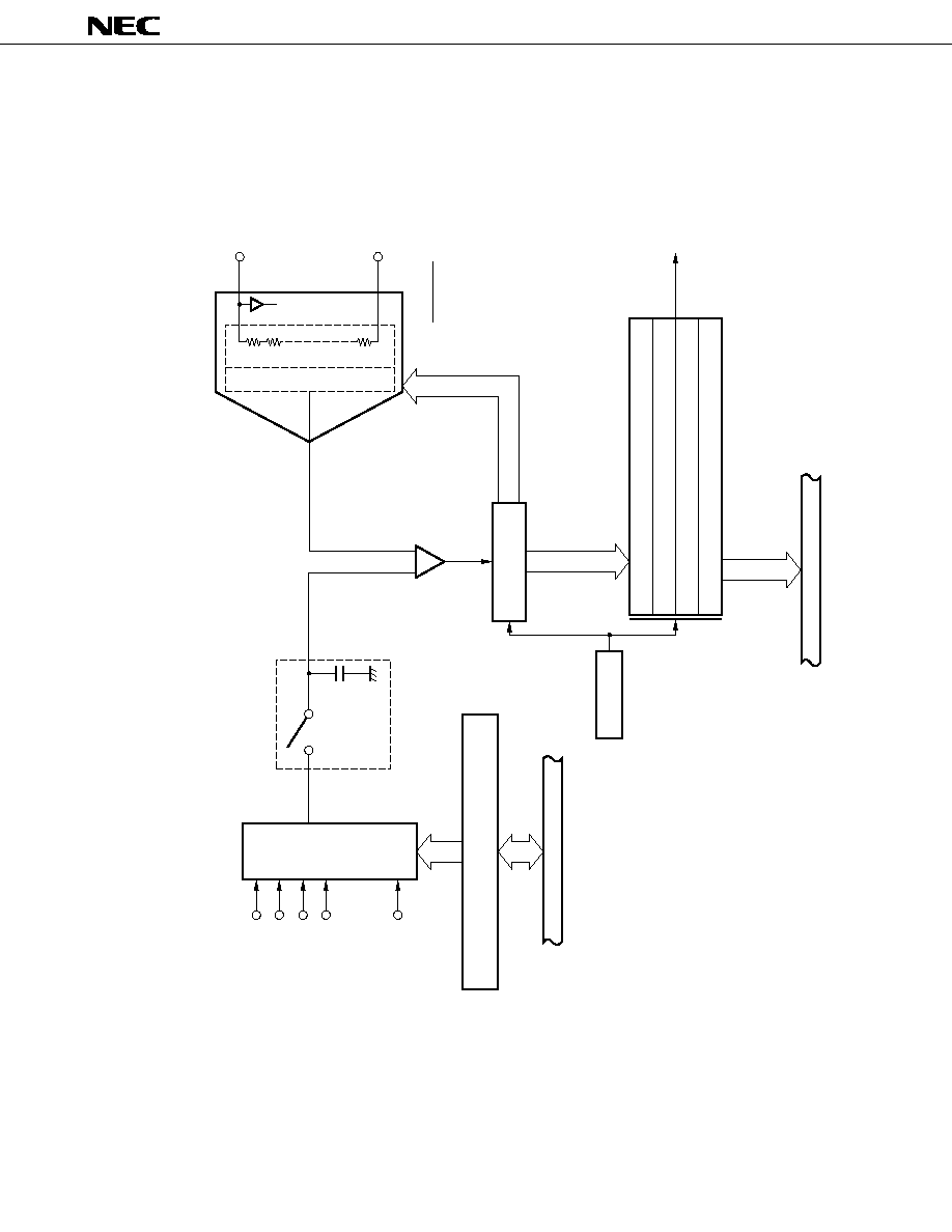
65
µ
PD70433
Input
Circuit
ANI0
ANI1
ANI2
ANI3
P15/INTP4
External Trigger
A/D Converter Mode Register (ADM)
Sample & Hold Circuit
8
Internal Bus
Control
Internal Bus
8
8
Successive Approxi-
mation Register (SAR)
A/D Conversion Result Register 0 (ADCR0)
Comparator
A/D Conversion Result Register 1 (ADCR1)
A/D Conversion Result Register 2 (ADCR2)
A/D Conversion Result Register 3 (ADCR3)
INTAD
AV
DD
AV
SS
AV
REF
Series Resistance String
R/2
R
R/2
Tap Decoder
Figure 12-1. A/D Converter Block Diagram

66
µ
PD70433
Change accordng to DMAC operating
status
Data retention
Release method
13. STANDBY FUNCTIONS
The V55PI has two methods for controlling the operating clock as standby functions designed to reduce power dissipation.
Transition to either of these standby modes is possible by means of a dedicated instruction.
Table 13-1. HALT/STOP Mode Operating Status
Parameter
HALT Mode
STOP Mode
Clock generator
Operating
Internal system clock
Stopped
16≠bit timer
Watchdog timer
Hold circuit
Stopped
Serial interface
Operating
Parallel interface
A/D Converter
Interrupt request controller
DMA controller
IORD, IOWR
High level
High level
AD0 to AD15
Bus lines
Retained
A16 to A23
R/W output
High level
High level
Refresh operation
Operating
Stopped
All internal data retained (CPU status,
All internal data retained (CPU status,
RAM contents, etc.)
RAM contents, etc.)
∑ NMI
∑ INTWDT
∑ NMI
∑ Maskable interrupt request
∑ RESET input
∑ RESET input
13.1 HALT MODE
In this mode, the CPU operating clock is halted.
Setting the CPU idle time to the HALT mode enables overall system power dissipation to be reduced. The HALT mode
is entered by executing the HALT instruction.
In the HALT mode the CPU clock and program execution are stopped, and all register and on-chip RAM contents
immediately prior to the stoppage are retained. The status of each hardware unit is shown in Table 13-1.
When the HALT instruction is executed during a DMA transfer, transition to the HALT mode is deferred until the transfer
bus cycle for one DMA request is completed.

67
µ
PD70433
13.2 STOP MODE
In this mode, clock oscillation is stopped.
This is effective when the entire application system is stopped, and offers extremely low power dissipation. The STOP
mode is entered by executing the STOP instruction. In this mode all clocks are stopped. Program execution is stopped, and
all register and on-chip RAM contents immediately prior to the stoppage are retained. The status of each hardware unit is
shown in Table 13-1.
When the STOP instruction is executed during a DMA transfer, transition to the STOP mode is deferred until the transfer
bus cycle for one DMA request is completed. If there is contention between a refresh cycle and STOP instruction execution,
transition to the STOP mode is deferred until the refresh cycle is completed.
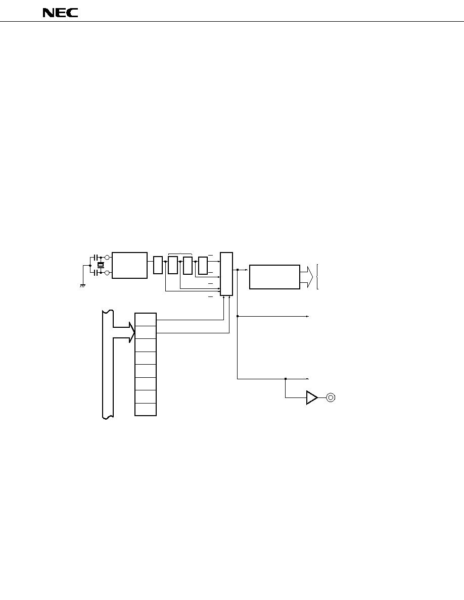
68
µ
PD70433
14. CLOCK GENERATOR
The clock generator supplies various clocks to the CPU and peripheral hardware, and controls the CPU operating mode.
14.1 CLOCK GENERATOR CONFIGURATION AND OPERATION
The clock generator is configured as shown in Figure 14-1.
The clock generator clock is generated by a crystal resonator or ceramic resonator connected to the X1 and X2 pins.
The clock generator output is subjected to waveform shaping (dividing frequency by 2) and selection of the scaling factor
by means of the processor control register (PRC), and is then used as the system clock
.
The system clock
scaling factor is specified by the PCK1 and PCK0 bits of the PRC register, and can be selected as
1/2, 1/4, 1/8 or 1/16 the oscillator frequency (f
XX
).
Selecting a low-speed system clock
reduces the current consumption of internal circuit, allowing extended operation
of a battery-driven system even when the voltage drops.
An external clock can be input. In this case, the clock signal should be input to the X1 pin, and leave the X2 pin open.
Figure 14-1. Clock Generator
Clock
Oscillator
X1
X2
1/2
1/2
1/2
1/2
f
XX
Waveform
Shaping
1
8
f
XX
1
4
f
XX
1
2
f
XX
(=f
X
)
Time Base
Counter
Baud Rate Generator
Watchdog Timer
System Clock
CLKOUT
Selector
Internal Bus
8
PRC
PCK0
PCK1
TB0
TB1
0
ENCLK
1
1
Frequency
Dividers
1
16
f
XX
Software Interval Timer
Refresh Cycle Generator
PWM
f
XX
: Oscillator frequency
: System clock
PRC : Processor control register
69
µ
PD70433
In the V55PI, the frequency divider (time base counter: TBC) which divides the internal system clock
is shared by each
timer unit.
The TBC cannot be read or written to by an instruction.
The TBC tap output (divide-by-2
n
clock) is supplied to the units shown below as a count clock.
(1)
Refresh cycle generator
(2)
Software interval timer
(3)
PWM unit
(4)
Baud rate generator
The TBC is cleared to 00H only by reset input, after which it is constantly incremented. TBC operation is stopped in the
STOP mode. The configuration of the TBC is shown in Figure 14-2.
Figure 14-2. Frequency Divider (Time Base Counter, TBC) Configuration
TBC
Baud Rate
Generator
Refresh Cycle
Generator
Software Interval
Timer
PWM
/2
to
/2
9
/2
to
/2
8
3
/2
to
/2
9
2
/2
and
/2
7

70
µ
PD70433
15. SOFTWARE INTERVAL TIMER FUNCTION
The V55PI incorporates a 16-bit software interval timer as a timer for software timer functions and watch functions.
15.1 SOFTWARE INTERVAL TIMER CONFIGURATION
The configuration of the software interval timer is shown in Figure 15-1.
Figure 15-1. Software Interval Timer Configuration
/4
/128
Software Timer Counter (STC)
Software Timer Counter Compare Register (STMC)
Clear
INTSIT
Match Detection

71
µ
PD70433
16. CODEC INSTRUCTIONS
The V55PI has 9 codec instructions.
Using these special instructions on the V55PI enables not only image information MH encoding but also MR encoding
which previously required the use of a special device such as an ACEE (advanced compression/expansion engine) to be
implemented by means of a small-scale, high-speed codec.
16.1 FEATURES
The V55PI has the following 9 codec instructions (4 for compression, 5 for expansion):
∑
Compression instructions
(1)
Change point table creation instruction: COLTRP
(2)
Data transmission instruction (transmission of EOL *1, FILL, RTC *2, etc.): ALBIT
(3)
MH encoding instruction: MHENC
(4)
MR encoding instruction: MRENC
∑
Expansion instructions
(5)
EOL detection instruction: SCHEOL
(6)
1-bit (tag) detection instruction: GETBIT
(7)
MH decoding change point table creation instruction: MHDEC
(8)
MR decoding change point table creation instruction: MRDEC
(9)
Pixel data creation instruction: CNVTRP
MH/MR encoding and MH/MR decoding using these instructions are performed as shown in Figures 16-1 and
16-2.
* 1.
EOL: End Of Line
2.
RTC: Return To Control
Note
When compression/expansion processing is performed using the V55PI codec instructions, the following
should be specified as preconditions.
∑ Compression/expansion is to be performed line by line.
∑ Consideration must be given to task switching and interrupt generation during compression processing.
∑ The number of bits processed per line must not be changed during processing of one page.
∑ The segment value must be changed for data over 64 Kbytes that straddles segments during processing.
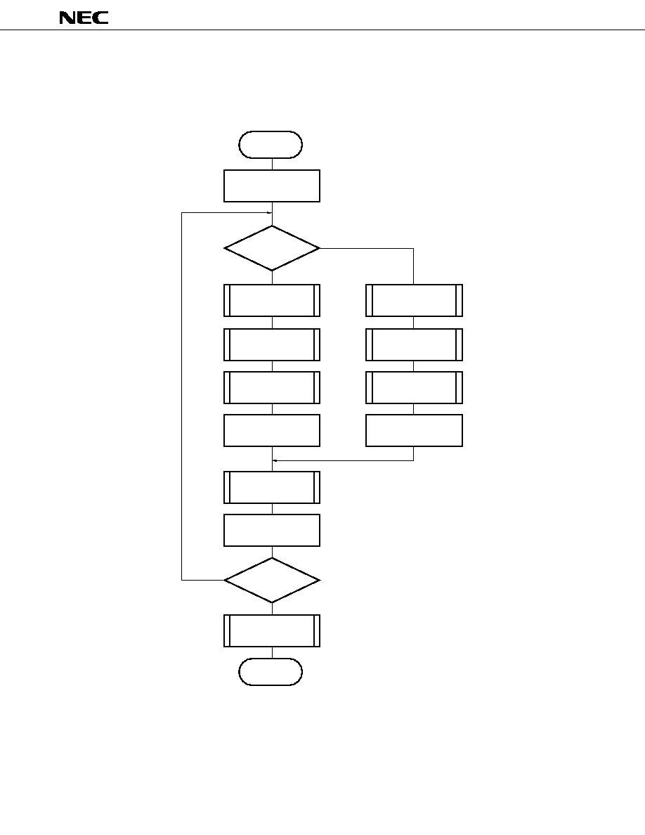
72
µ
PD70433
Figure 16-1. MH/MR Encoding Processing Flow
Start
K = 0
K = 0
L = Number of lines
No
Yes
Data transmission
instruction (EOL + tag
bit "1" transmission)
Data transmission
instruction (EOL + tag
bit "0" transmission)
Change point table
creation instruction
Change point table
creation instruction
MH encoding
instruction
MR encoding
instruction
K = K factor ≠ 1
K = K ≠ 1
Data transmission
instruction
(FILL transmission)
L = L ≠ 1
L = 0
No
Yes
Data transmission
instruction
(RTC transmission)
End
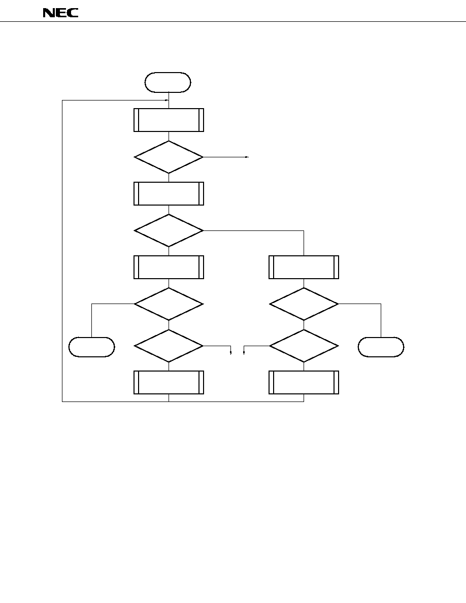
73
µ
PD70433
*
RTC is detected by two EOLs.
Figure 16-2. MH and MR Decoding Processing Flow
Start
EOL detection
instruction
Error detection
To Error Processing
Yes
No
1≠bit detection
instruction (tag
bit detection)
Tag = 1
No
Yes
MH decoding
instruction
MR decoding
instruction
EOL detection
at start
EOL detection
at start
Error detection
Yes
No
Yes
No
End
Error detection
End
No
Yes
Pixel data creation
instruction
Pixel data creation
instruction
No
Yes
To Error Processing
*
74
µ
PD70433
16.2 MEMORY MAP
The data memory areas required by the V55PI's codec instructions are shown below.
(1) Register file space
This is the register bank for parameter setting.
(2) User RAM
Encoding line change point table : Storage area for change point information required for performing encoding
In the case of n bit/lines, a maximum area of 2n + 4 bytes is required.
Reference line table
: Reference line change point information storage area
Image data buffer
: Storage area for pixel data read from scanner in encoding, or encoding data
received from modem in decoding
Transmit/receive buffer
: Buffer for transferring encoded data to modem/scanner
Print buffer
: Buffer for transferring decoded pixel data to recording system
(3) User ROM
Encoding conversion table :
Conversion table for MH/MR encoding
Decoding conversion table :
Conversion table for MH/MR decoding
(4) Access to Expanded Memory Space
The 16-Mbyte expanded memory space can be accessed by using the expanded segment override prefix
instruction (DS2: or DS3:).
However, the segment registers DS2 and DS3 that are used during instruction execution are DS2 and DS3
in the parameter setting register banks of each instruction.
Table 16-1. Instructions to which Expanded Segment Override Prefix Can Be Attached
DS2:
DS3:
CODEC Instruction
Yes
Yes
COLTRP
Yes
No
MHENC
Yes
Yes
MHDEC
Yes
No
MRENC
Yes
Yes
MRDEC
Yes
No
SCHEOL
Yes
No
GETBIT
Yes
Yes
CNVTRP
Example
DS2 : DS3 : COLTRP
DS2 : SCHEOL
The relationship between encoding instructions and data in memory is shown in Figure 16-3, and the relationship between
decoding instruction and data in memory is shown in Figure 16-4.
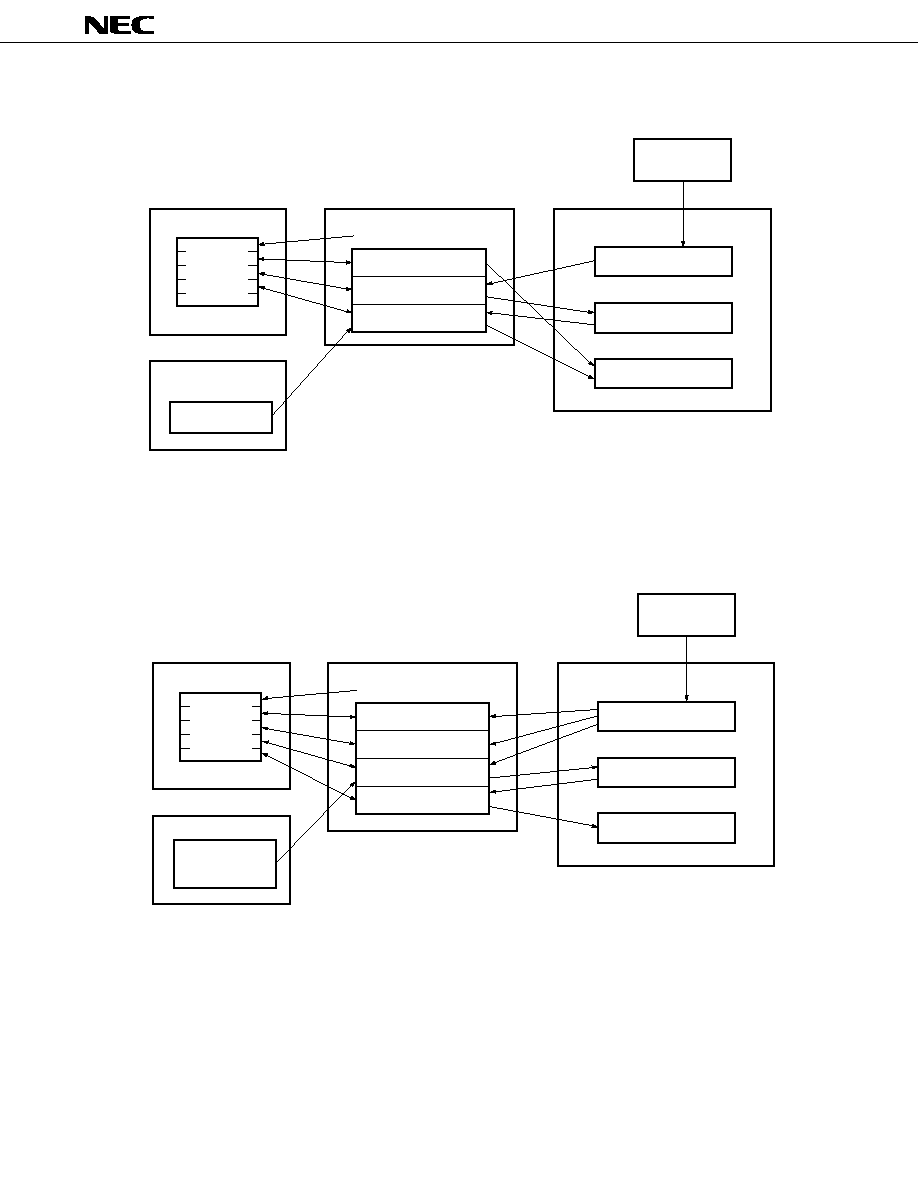
75
µ
PD70433
Figure 16-3. Encoding Instructions and Data in Memory
*
In case of MH/MR decoding instructions
*
In case of MH/MR encoding instructions
Figure 16-4. Decoding Instruction and Data in Memory
DMA
Image Data (1 Line)
Register File
Parameter
Frame
Encoding Conversion
Table (512 Bytes) *
User ROM
Software
User RAM
Data Output Instruction
Change Point Table
Creation Instruction
MH/MR Encoding
Instruction
Work (Change Points)
Coding Data (1 Line)
DMA
Coding Data
Register File
Parameter
Frame
Decoding Conversion
Table (2304 Bytes)*
User ROM
Software
User RAM
EOL Detection Instruction
MH/MR Decoding
Instruction
Work (Change Points)
Image Data (1 Line)
1≠Bit Detection Instruction
Image Data Creation
Instruction
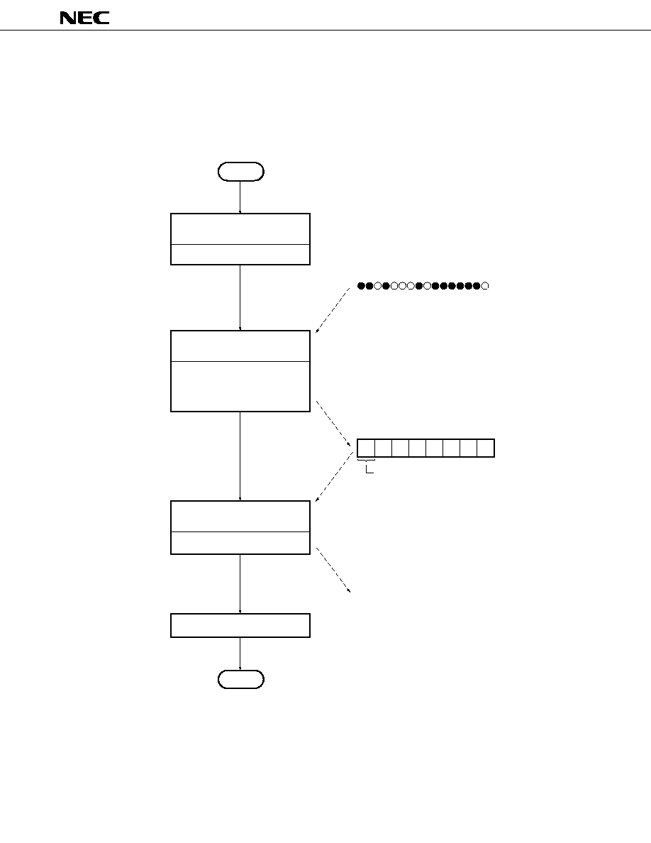
76
µ
PD70433
16.3 PROCESSING FLOW
The instructions shown in 16.1 "Features" are used in the order shown in Figures 16-5 and 16-6 in encoding/decoding
procesing.
Figure 16-5. Processing Flow for Encoding of One Line
.....
.....
Start
Data transmission instruction
(ALBIT)
Transmission of EOL and tag
Change point table
creation instruction
(COLTRP)
Change point information for
1 line created, and stored in
prescribed storage area
(change point table)
MH/MR encoding instruction
(MHENC/MRENC)
MH/MR encoding for 1 line
Fill transmission
End
(Pixel Data)
(Change Point Table)
Input
Output
Input
1 Word
0
2
1
1
3
1
1
6
White
Black
White
Black
White
Black
White
Black
Encoded Data
Transmision Buffer
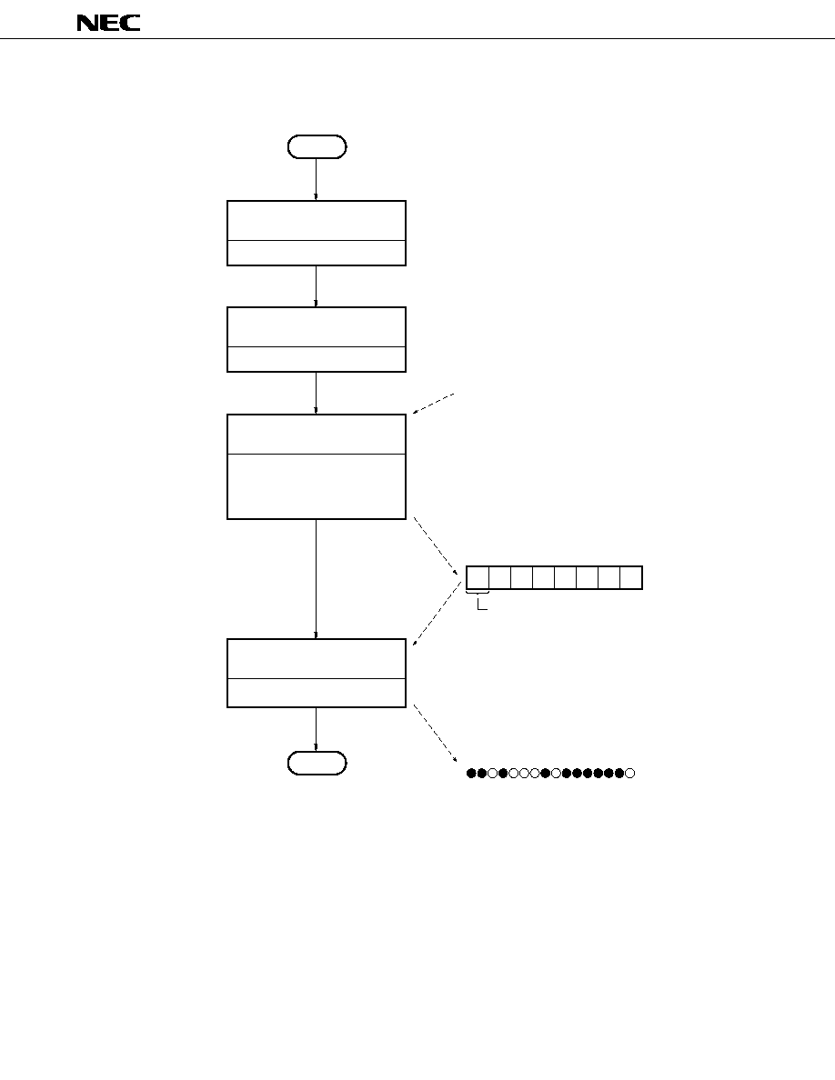
77
µ
PD70433
Figure 16-6. Processing Flow for Decoding of One Line
.....
.....
(Change Point Table)
Input
1 Word
0
2
1
1
3
1
1
6
White
Black
White
Black
White
Black
White
Black
Encoded Data
Printer Buffer
Output
(Pixel Data)
Input
Output
Start
EOL detection instruction
(SCHEOL)
EOL (000000000001) is detected
Tag (1 bit) is detected
1 bit detection instruction
(GETBIT)
MH/MR decoding instruction
(MHDEC/MRDEC)
Pixel data creation instruction
(CNVTRP)
Pixel data for 1 line is created
End
MH/MR decoding change point
information for 1 line is generated
and stored in specified area
(change point table)
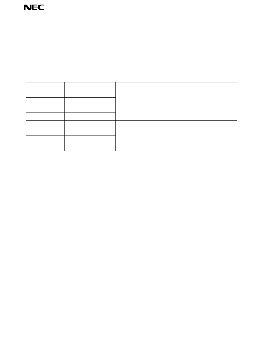
78
µ
PD70433
17. INSTRUCTION SET
The V55PI instruction set is upward compatible with the V20/V30 (native mode) and V25/V35 instruction sets.
17.1 INSTRUCTIONS NEWLY ADDED TO V20/V30 AND V25/V35
Instructions which have been added to the V20/V30 and V25/V35 instruction sets, and instructions whose application
range has been extended, are shown below.
(1)
Instructions added to V20/V30.
Mnemonic
Operand
Instruction Group
BRKCS
reg 16
TSKSW
reg 16
MOVSPA
None
MOVSPB
reg 16
BTCLR
sfr, imm3, short-label
Conditional branch instruction
RETRBI
None
FINT
None
STOP
None
CPU control instruction
Register bank switching instruction
Data transfer instruction
Interrupt instruction
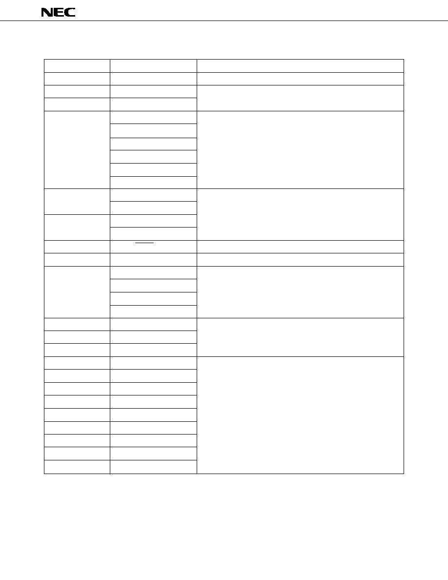
79
µ
PD70433
Stack manipulation instruction
(2)
Instructions added to V25/V35.
Mnemonic
Operand
Instruction Group
IRAM
None
Register file space access override prefix instrution
DS2
None
DS3
None
DS2, reg16, mem32
DS3, reg16, mem32
xsreg, reg16
xsreg, mem16
reg16, xsreg
mem16, xsreg
DS2
DS3/VPC
DS2
DS3/VPC
RSTWDT
imm8, imm8'
Watchdog timer manipulation instruction
BTCLRL
sfrl, imm3, short-label
Conditional branch instruction
reg8
mem8
reg16
mem16
QHOUT
imm16
QOUT
imm16
Queue manipulation instruction
QTIN
imm16
ALBIT
None
COLTRP
None
MHENC
None
MRENC
None
SCHEOL
None
Dedicated FAX instruction
GETBIT
None
MHDEC
None
MRDEC
None
CNVTRP
None
Bit manipulation instruction
Extended segment override prefix instruction
Data transfer instruction
Remark
VPC: Vector PC
MOV
PUSH
BSCH
POP

80
µ
PD70433
17.2 INSTRUCTION SET OPERATIONS
Table 17-1. Operand Type Legend
Identifier
Description
reg,
8/16-bit general register
(Destination register in an instruction using two 8/16-bit general registers)
reg'
Source register in an instruction using two 8/16-bit general registers
reg8,
8-bit general register
(Destination register in an instruction using two 8-bit general registers)
reg8'
Source register in an instruction using two 8-bit general registers
reg16,
16-bit general register
(Destination register in an instruction using two 16-bit general registers)
reg16'
Source register in an instruction using two 16-bit general registers
mem
8/16-bit memory address
mem8
8-bit memory address
mem16
16-bit memory address
mem32
32-bit memory address
sfr
Special function register location: FFF00H to FFFEFH
sfrl
Special function register location: FFE00H to FFEFFH
dmem
16-bit direct memory address
imm
8/16-bit immediate data
imm3
3-bit immediate data
imm4
4-bit immediate data
imm8
8-bit immediate data
imm8'
8-bit immediate date (1's compliment of imm8)
imm16
16-bit immediate data
acc
Accumulator AW or AL
sreg
Segment register
xsreg
Extended segment register
src-table
Name of 256-byte conversion table
src-block
Name of source block addressed by register IX
dst-block
Name of destination block addressed by register IY
src-string
Name of source string addressed by register IX
dst-string
Name of destination string addressed by register IY
near-proc
Procedure start address in current program segment
far-proc
Procedure start address in a different program segment
near-label
Absolute address in current program segment
short-label
Relative address of memory in range ≠128 to +127 bytes from end of instruction
far-label
Absolute address in a different program segment
regptr16
16-bit general register holding call address offset in current program segment
memptr16
16-bit memory address holding call address offset in current program segment
memptr32
32-bit memory address holding call address offset and segment data in a different program segment
pop-value
Number of bytes removed from stack (0 to 64K, normally an even number)
fp-op
Immediate value which identifies external floating point operation coprocessor operation code
repeat
Repeat prefix instruction
IRAM :
Register file space access override prefix instruction
R
Register set (AW, BW, CW, DW, SP, BP, IX, IY)
( )
Omissible
or, /
Or

81
µ
PD70433
Table 17-2. Operation Code Legend
Identifier
Description
W
Word/byte specification bit (1: word, 0: byte). However, when s = 1, sign extension byte data is
specified as 16-bit operand even if W = 1.
reg, reg'
8/16-bit general register specification bits (000 to 111)
mod, mem
Memory addressing specification bits (mod: 00 to 10, mem: 000 to 111)
(disp-low)
Optional 16-bit displacement low byte
(disp-high)
Optional 16-bit displacement high byte
disp-low
16-bit displacement low byte for PC relative addition
disp-high
16-bit displacement high byte for PC relative addition
imm3
3-bit immediate data
imm4
4-bit immediate data
imm8
8-bit immediate data
imm8'
8-bit immediate data (1's complement of imm8)
imm16-low
16-bit immediate data low byte
imm16-high
16-bit immediate data high byte
addr-low
16-bit direct address low byte
addr-high
16-bit direct address high byte
sreg
Segment register specification bits (00 to 11)
xsreg
Extended segment register specification bits (10 to 11)
s
Sign extension specification bit (1: sign extension, 0: no sign extension)
offset-low
Low byte of 16-bit offset data to be loaded in PC
offset-high
High byte of 16-bit offset data to be loaded in PC
seg-low
Low byte of 16-bit segment data to be loaded in PS
seg-high
High byte of 16-bit segment data to be loaded in PS
pop-value-low
Low byte of 16-bit data which specifies number of bytes to be removed from stack
pop-value-high
High byte of 16-bit data which specifies number of bytes to be removed from stack
disp8
8-bit displacement for relative addition to PC
X
XXX
YYY
ZZZ
Operation code of an external floating point operation coprocessor

82
µ
PD70433
Table 17-3. Operation Description Legend
Identifier
Description
AW
Accumulator (16 bits)
AH
Accumulator (high byte)
AL
Accumulator (low byte)
BW
Register BW (16 bits)
CW
Register CW (16 bits)
CL
Register CL (low byte)
DW
Register DW
SP
Stack pointer (16 bits)
BP
Base Pointer (16 bits)
PC
Program counter (16 bits)
PSW
Program status word (16 bits)
IX
Index register (source) (16 bits)
IY
Index register (destination) (16 bits)
PS
Program segment register (16 bits)
DS3
Extended data segment 3 register (16 bits)
DS2
Extended data segment 2 register (16 bits)
DS1
Data segment 1 register (16 bits)
DS0
Data segment 0 register (16 bits)
SS
Stack segment register (16 bits)
AC
Auxiliary carry flag
CY
Carry flag
P
Parity flag
S
Sign flag
Z
Direction flag
IE
Interrupt enable flag
V
Overflow flag
IBRK
I/O break flag
BRK
Break flag
RB0
Register bank 0 flag
RB1
Register bank 1 flag
RB2
Register bank 2 flag
RB3
Register bank 3 flag
VPC
Vector PC
(...)
Contents of memory indicated by contents of in parenthesis
disp
Displacement (8/16-bit)
temp
Temporary register (8/16/32 bits)
ext≠disp8
16 bits with 8-bit displacement sign-extended
seg
Immediate segment data (16 bits)
offset
Immediate offset data (16 bits)
Transfer direction
+
Addition
-
Subtraction
◊
Multiplication
˜
Division
%
Modulo
Logical product (AND)
Logical sum (OR)
V
Exclusive logical sum (exclusive OR)
◊◊
H
2-digit hexadecimal number
◊◊◊◊
H
4-digit hexadecimal number
/
Alternate function, or
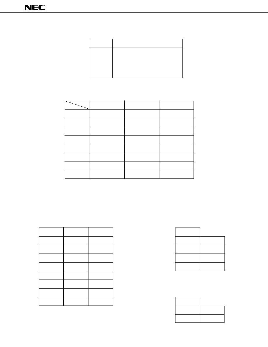
83
µ
PD70433
Table 17-4. Flag Operation Legend
Identifier
Description
(Blank)
No change
0
Cleared to 0
1
Set to 1
◊
Set or cleared depending on result
U
Undefined
R
Previously saved value is restored
Table 17-5. Memory Addressing
mem
mod
00
01
10
000
BW + IX
BW + IX + disp8
BW + IX + disp16
001
BW + IY
BW + IY + disp8
BW + IY + disp16
010
BP + IX
BP + IX + disp8
BP + IX + disp16
011
BP + IY
BP + IY + disp8
BP + IY + disp16
100
IX
IX + disp8
IX + disp16
101
IY
IY + disp8
IY + disp16
110
Direct address
BP + disp8
BP + disp16
111
BW
BW + disp8
BW + disp16
Note
When BP is used in memory addressing other than in a primitive instruction, the default segment register
is SS. When BP is not used, the default segment register is DS0.
In primitive instruction memory addressing, the destination block default segment register is DS1. In
memory addressing, the source block default segment register is DS0.
Table 17-6. 8/16-Bit General Register Selection
Table 17-7. Segment Register Selection
reg
W = 0
W = 1
sreg
000
AL
AW
00
DS1
001
CL
CW
01
PS
010
DL
DW
10
SS
011
BL
BW
11
DS0
100
AH
SP
101
CH
BP
110
DH
IX
111
BH
IY
xsreg
10
DS3/VPC
11
DS2
Table 17-8. Extended Segment Register Selection
84
µ
PD70433
Number of Clock Cycles
In the case of a memory operand the number of clock cycles depends on the addressing mode. The following numbers
should be used for "EA" in Table 17-9 "Number of Clock Cycles".
mod
00
Clock
01
Clock
10
Clock
mem
Cycles
Cycles
Cycles
000
BW + IX
3
BW + IX + disp8
3
BW + IX + disp16
3
001
BW + IY
3
BW + IY + disp8
3
BW + IY + disp16
3
010
BP + IX
3
BP + IX + disp8
3
BP + IX + disp16
3
011
BP + IY
3
BP + IY + disp8
3
BP + IY + disp16
3
100
IX
2
IX + disp8
2
IX + disp16
2
101
IY
2
IY + disp8
2
IY + disp16
2
110
Direct address
2
BP + disp8
2
BP + disp16
2
111
BW
2
BW + disp8
2
BW + disp16
2
"T" indicates the number of wait states. Any number of wait states from "0" (no wait) up can be used.
85
µ
PD70433
Table 17-9. Number of Clock Cycles (1/20)
Byte Processing
Word Processing
On-Chip
Other
On-Chip
Other
RAM Access
Access
RAM Access
Access
reg, reg'
≠≠
2
2
2
2
mem, reg
≠≠
EA + 2
EA + 3
EA + 2
EA + 3
8
EA + 8 + 2T
reg, mem
EA + 2
EA + 5 + T
EA + 2
16
EA + 5 + T
mem, imm
≠≠
EA + 2
EA + 3
EA + 2
EA + 3
reg, imm
≠≠
2
2
2
2
8
10 + 2T
acc, dmem
4
7 + T
4
16
7 + T
dmem, acc
≠≠
4
5
4
5
sreg, reg16
≠≠
≠≠
≠≠
2
2
8
≠≠
≠≠
2
2
16
8
EA + 8 + 2T
MOV
sreg, mem16
≠≠
≠≠
EA + 2
16
EA + 5 + T
8
EA + 8 + 2T
≠≠
≠≠
EA + 2
16
EA + 5 + T
reg16, sreg
≠≠
≠≠
≠≠
2
2
8
≠≠
≠≠
2
2
16
mem16, sreg
≠≠
≠≠
≠≠
EA + 2
EA + 3
8
≠≠
≠≠
EA + 2
EA + 3
16
8
EA + 17 + 4T
≠≠
≠≠
EA + 5
16
EA + 11 + 2T
8
EA + 17 + 4T
≠≠
≠≠
EA + 5
16
EA + 11 + 2T
8
EA + 17 + 4T
≠≠
≠≠
EA + 5
16
EA + 11 + 2T
8
EA + 17 + 4T
≠≠
≠≠
EA + 5
16
EA + 11 + 2T
Mnemonic
Operands
xsreg, reg16
VPC, reg16
xsreg,mem16/
VPC, mem16
reg16, xsreg/
reg16, VPC
mem16, xsreg/
mem16, VPC
DS0,
reg16, mem32
DS2,
reg16, mem32
DS1,
reg16, mem32
DS3,
reg16, mem32
Data transfer instructions
Instruction
Group
Bus Width
*
*
8 : 8-bit width 16 : 16-bit width ≠≠ : Both 8-bit and 16-bit bus width

86
µ
PD70433
Table 17-9. Number of Clock Cycles (2/20)
Byte Processing
Word Processing
On-Chip
Other
On-Chip
Other
RAM Access
Access
RAM Access
Access
AH, PSW
≠≠
2
2
≠≠
≠≠
MOV
8
3
3
PSW, AH
≠≠
≠≠
16
2
2
LDEA
reg16, mem16
≠≠
≠≠
≠≠
EA + 2
EA + 2
src-table
≠≠
6
9 + T
≠≠
≠≠
reg, reg'
≠≠
4
4
4
4
EA + 10 + 2T
EA + 4
EA + 7 + T
EA + 4
EA + 7 + T
≠≠
≠≠
≠≠
4
4
MOVSPA
≠≠
≠≠
≠≠
8
8
MOVSPB
reg16
≠≠
≠≠
≠≠
9
9
REPC
≠≠
0 to 1
0 to 1
0 to 1
0 to 1
REPNC
≠≠
0 to 1
0 to 1
0 to 1
0 to 1
REP/
REPE/
≠≠
0 to 1
0 to 1
0 to 1
0 to 1
REPZ
≠≠
0 to 1
0 to 1
0 to 1
0 to 1
21 + 2T
22 + 2T
18 + T
19 + T
8
9 + (14 + 2T)n
9 + (18 + 4T)n
5
5
9 + (11 + T)n
9 + (12 + 2T)n
18 + T
19 + T
16
9 + (11 + T)n
9 + (12 + 2T)n
5
5
23 + 2T
28 + 4T
20 + T
22 + 2T
8
9 + (16 + 2T)n
9 + (21 + 4T)n
5
5
9 + (13 + T)n
9 + (15 + 2T)n
20 + T
22 + 2T
16
9 + (13 + T)n
9 + (15 + 2T)n
5
5
TRANS/
TRANSB
REPNE/
REPNZ
AW, reg16/
reg16, AW
mem, reg/
reg, mem
Mnemonic
Operands
Data transfer instructions
(rep CW = 0)
5
5
(rep CW = 0)
5
5
(rep)
MOVBK
dst-block,
src-block
(rep)
CMPBK
Primitive block transfer instructions
Repeat prefixes
Instruction
Group
src-block,
dst-block
Bus Width
*
*
8
: 8-bit width
16 : 16-bit width
≠≠ : Both 8-bit and 16-bit bus width
Remark
n: Number of repetitions
XCH
MOVBKB/
MOVBKW
CMPBKB/
CMPBKW
87
µ
PD70433
Table 17-9. Number of Clock Cycles (3/20)
Byte Processing
Word Processing
On-Chip
Other
On-Chip
Other
RAM Access
Access
RAM Access
Access
CMPM
dst-block
20 + T
15
17 + T
15
8
10 + (12 + 2T)n
5
10 + 7n
10 + (9 + T)n
10 + 7n
17 + T
16
10 + (9 + T)n
5
LDM
src-block
16 + T
10
13 + T
10
8
9 + (9 + 2T)n
5
9 + 3n
9 + (6 + T)n
9 + 3n
13 + T
16
9 + (6 + T)n
5
STM
dst-block
13
12
13
12
8
9 + (9 + 2T)n
5
9 + 5n
9 + (6 + T)n
9 + 5n
13
16
9 + (6 + T)n
5
8
31 to 72
reg8, reg8'
≠≠
≠≠
22 to 63
16
23 to 64
8
31 to 72
reg8, imm4
≠≠
≠≠
22 to 63
16
23 to 64
8
19 + 2T to 48 + 4T
reg8, reg8'
≠≠
≠≠
19 to 41
16
19 to 42 + 2T
8
19 + 2T to 48 + 4T
reg8, imm4
≠≠
≠≠
19 to 41
16
19 to 42 + 2T
Mnemonic
Operands
(rep CW = 0)
5
5
5
(rep)
Primitive block transfer instructions
(rep CW = 0)
5
5
5
(rep)
(rep CW = 0)
5
5
5
(rep)
Bit field manipulation instructions
Instruction
Group
Bus Width
*
*
8
: 8-bit width
16 : 16-bit width
≠≠ : Both 8-bit and 16-bit bus width
Remark
n: Number of repetitions
CMPMB/
CMPMW
LDMB/
LDMW
STMB/
STMW
INS
EXT
88
µ
PD70433
Table 17-9. Number of Clock Cycles (4/20)
Byte Processing
Word Processing
On-Chip
Other
On-Chip
Other
RAM Access
Access
RAM Access
Access
acc8, imm8
8
10 + 2T
≠≠
7 + T
≠≠
16
7 + T
8
10 + 2T
≠≠
7 + T
≠≠
16
7 + T
8
≠≠
5
≠≠
5
16
8
≠≠
5
≠≠
5
16
20 + 2T
21 + 2T
17 + T
18 + T
8
9 + (13 + 2T)n
9 + (17 + 4T)n
5
5
9 + (10 + T)n
9 + (11 + 2T)n
17 + T
18 + T
16
9 + (10 + T)n
9 + (11 + 2T)n
5
5
17 + 2T
23 + 4T
14 + T
17 + 2T
8
9 + (10 + 2T)n
9 + (16 + 4T)n
5
5
9 + (7 + T)n
9 + (10 + 2T)n
14 + T
17 + 2T
16
9 + (7 + T)n
9 + (10 + 2T)n
5
5
Mnemonic
Operands
Bus Width
*1
(rep)
(rep)
Instruction
Group
(rep CW = 0)
5
5
* 1.
8
: 8-bit width
16 : 16-bit width
2.
When IBRK = 1. As shown in the next page when IBRK = 0.
Remark
n: Number of repetitions
(rep CW = 0)
5
5
Primitive input/output instructions
Input/output instructions
acc, DW
imm8, acc
DW, acc
dst-block, DW
DW, src-block
OUTM*2
INM*2
OUT*2
IN*2

89
µ
PD70433
Table 17-9. Number of Clock Cycles (5/20)
Bus Width
*
Byte Processing
Word Processing
On-Chip
Other
On-Chip
Other
RAM Access
Access
RAM Access
Access
8
60 + 10T
60 + 10T
≠≠
≠≠
16
40 + 5T
40 + 5T
8
60 + 10T
60 + 10T
≠≠
≠≠
16
40 + 5T
40 + 5T
8
60 + 10T
60 + 10T
≠≠
≠≠
16
40 + 5T
40 + 5T
8
60 + 10T
60 + 10T
≠≠
≠≠
16
40 + 5T
40 + 5T
8
60 + 10T
60 + 10T
≠≠
≠≠
16
40 + 5T
40 + 5T
8
60 + 10T
60 + 10T
≠≠
≠≠
16
40 + 5T
40 + 5T
Mnemonic
Operands
Primitive input/
output instructions
*
8
: 8-bit width
16 : 16-bit width
Instruction
Group
Input/output instructions
IN
acc8, imm8
OUT
imm8, acc
dst-block, DW
INM
DW, src-block
OUTM
DW, acc
acc, DW
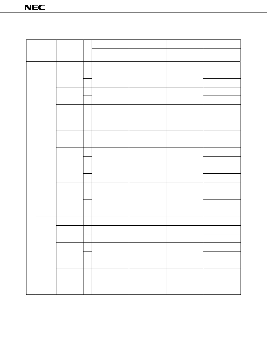
90
µ
PD70433
Table 17-9. Number of Clock Cycles (6/20)
Byte Processing
Word Processing
On-Chip
Other
On-Chip
Other
RAM Access
Access
RAM Access
Access
reg, reg'
≠≠
3
3
3
3
8
EA + 10 + 2T
mem, reg
EA + 4
EA + 7 + T
EA + 4
16
EA + 7 + T
8
EA + 9 + 2T
reg, mem
EA + 2
EA + 6 + T
EA + 2
16
EA + 6 + T
reg, imm
≠≠
2
2
2
2
8
EA + 10 + 2T
mem, imm
EA + 4
EA + 7 + T
EA + 4
16
EA + 7 + T
acc, imm
≠≠
2
2
2
2
reg, reg'
≠≠
3
3
3
3
8
EA + 10 + 2T
mem, reg
EA + 4
EA + 7 + T
EA + 4
16
EA + 7 + T
8
EA + 9 + 2T
reg, mem
EA + 2
EA + 6 + T
EA + 2
16
EA + 6 + T
reg, imm
≠≠
2
2
2
2
8
EA + 10 + 2T
mem, imm
EA + 4
EA + 7 + T
EA + 4
16
EA + 7 + T
acc, imm
≠≠
2
2
2
2
reg, reg'
≠≠
3
3
3
3
8
EA + 10 + 2T
mem, reg
EA + 4
EA + 7 + T
EA + 4
16
EA + 7 + T
8
EA + 9 + 2T
reg, mem
EA + 2
EA + 6 + T
EA + 2
16
EA + 6 + T
reg, imm
≠≠
2
2
2
2
8
EA + 10 + 2T
mem, imm
EA + 4
EA + 7 + T
EA + 4
16
EA + 7 + T
acc, imm
≠≠
2
2
2
2
Mnemonic
Operands
*
8
: 8-bit width
16 : 16-bit width
≠≠ : Both 8-bit and 16-bit bus width
Addition/subtraction instructions
Instruction
Group
Bus Width
*
ADD
ADDC
SUB
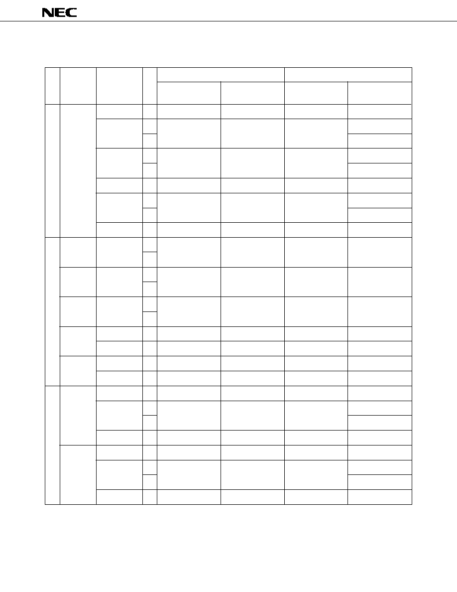
91
µ
PD70433
Table 17-9. Number of Clock Cycles (7/20)
Byte Processing
Word Processing
On-Chip
Other
On-Chip
Other
RAM Access
Access
RAM Access
Access
reg, reg'
≠≠
3
3
3
3
8
EA + 10 + 2T
mem, reg
EA + 4
EA + 7 + T
EA + 4
16
EA + 7 + T
8
EA + 9 + 2T
reg, mem
EA + 2
EA + 6 + T
EA + 2
16
EA + 6 + T
reg, imm
≠≠
2
2
2
2
8
EA + 10 + 2T
mem, imm
EA + 4
EA + 7 + T
EA + 4
16
EA + 7 + T
acc, imm
≠≠
2
2
2
2
8
6 + (15 + T)n
6 + (19 + 3T)n
≠≠
≠≠
16
8
6 + (16 + T)n
6 + (20 + 3T)n
≠≠
≠≠
16
8
6 + (15 + T)n
6 + (18 + 2T)n
≠≠
≠≠
16
reg8
8
5
5
≠≠
≠≠
mem8
16
EA + 5
EA + 8 + T
≠≠
≠≠
reg8
8
5
5
≠≠
≠≠
mem8
16
EA + 5
EA + 8 + T
≠≠
≠≠
reg8
≠≠
2
2
≠≠
≠≠
8
EA + 10 + 2T
mem
EA + 3
EA + 7 + T
EA + 3
16
EA + 7 + T
reg16
≠≠
≠≠
≠≠
2
2
reg8
≠≠
2
2
≠≠
≠≠
8
EA + 10 + 2T
mem
EA + 3
EA + 7 + T
EA + 3
16
EA + 7 + T
reg16
≠≠
≠≠
≠≠
2
2
Mnemonic
Operands
*
8
: 8-bit width
16 : 16-bit width
≠≠ : Both 8-bit and 16-bit bus width
Remark
n: Half of number of BCD digits
dst-string,
src-string
dst-string,
src-string
dst-string,
src-string
Instruction
Group
Increment/decrement instructions
BCD operation instructions
Addition/subtraction instructions
Bus Width
*
SUBC
ADD4S
SUB4S
CMP4S
ROL4
ROR4
INC
DEC

92
µ
PD70433
Table 17-9. Number of Clock Cycles (8/20)
Byte Processing
Word Processing
On-Chip
Other
On-Chip
Other
RAM Access
Access
RAM Access
Access
reg8
≠≠
11
11
15
15
8
EA + 21 + 2T
mem8
EA + 12
EA + 14 + T
EA + 16
16
EA + 18 + T
reg16
≠≠
11
11
15
15
8
EA + 21 + 2T
mem16
EA + 12
EA + 14 + T
EA + 16
16
EA + 18 + T
reg8
≠≠
10
10
14
14
8
EA + 20 + 2T
mem8
EA + 11
EA + 13 + T
EA + 15
16
EA + 17 + T
reg16
≠≠
10
10
14
14
8
EA + 20 + 2T
mem16
EA + 11
EA + 13 + T
EA + 15
16
EA + 17 + T
reg16, reg16',
imm8/reg16,
≠≠
≠≠
≠≠
14
14
imm8
reg16,
8
EA + 20 + 2T
mem16,
≠≠
≠≠
EA + 15
imm8
16
EA + 17 + T
reg16, reg16',
imm16/reg16,
≠≠
≠≠
≠≠
14
14
imm16
reg16,
8
EA + 20 + 2T
mem16,
≠≠
≠≠
EA + 15
imm1616
EA + 17 + T
Mnemonic
Operands
Multiplication instructions
*
8
: 8-bit width
16 : 16-bit width
≠≠ : Both 8-bit and 16-bit bus width
Bus Width
*
Instruction
Group
MULU
MUL

93
µ
PD70433
Table 17-9. Number of Clock Cycles (9/20)
Byte Processing
Word Processing
On-Chip
Other
On-Chip
Other
RAM Access
Access
RAM Access
Access
8
15/62 + 10T
15/62 + 10T
23/57 + 10T
23/57 + 10T
reg8
16
15/42 + 5T
15/42 + 5T
23/42 + 5T
23/42 + 5T
8
EA + 16/63 + 10T
EA + 18 + T/63 + 10T
EA + 24/58 + 10T
EA + 30 + 2T/58 + 10T
mem8
16
EA + 16/43 + 5T
EA + 18 + T/63 + 5T
EA + 24/43 + 5T
EA + 26 + T/43 + 5T
8
15/62 + 10T
15/62 + 10T
23/57 + 10T
23/57 + 10T
reg16
16
15/42 + 5T
15/42 + 5T
23/42 + 5T
23/42 + 5T
8
EA + 16/63 + 10T
EA + 18 + T/63 + 10T
EA + 24/58 + 10T
EA + 30 + 2T/58 + 10T
mem16
16
EA + 16/43 + 5T
EA + 18 + T/43 + 5T
EA + 24/43 + 5T
EA + 26 + T/43 + 5T
8
17/64 + 10T
17/64 + 10T
25/59 + 10T
25/59 + 10T
reg8
16
17/44 + 5T
17/44 + 5T
25/44 + 5T
25/44 + 5T
8
EA + 18/65 + 10T
EA + 20 + T/65 + 10T
EA + 26/60 + 10T
EA + 31 + 2T/60 + 10T
mem8
16
EA + 18/45 + 5T
EA + 20 + T/45 + 5T
EA + 26/45 + 5T
EA + 28 + T/45 + 5T
8
17/64 + 10T
17/64 + 10T
25/59 + 10T
25/59 + 10T
reg16
16
17/44 + 5T
17/44 + 5T
25/44 + 5T
25/44 + 5T
8
EA + 18/65 + 10T
EA + 20 + T/65 + 10T
EA + 26/60 + 10T
EA + 31 + 2T/60 + 10T
mem16
16
EA + 18/45 + 5T
EA + 20 + T/45 + 5T
EA + 26/45 + 5T
EA + 28 + T/45 + 5T
8
6
9
≠≠
≠≠
16
9
ADJ4A
≠≠
3
3
≠≠
≠≠
8
6
6
≠≠
≠≠
16
9
9
ADJ4S
≠≠
3
3
≠≠
≠≠
CVTBD
≠≠
18
18
≠≠
≠≠
CVTDB
≠≠
8
8
≠≠
≠≠
CVTBW
≠≠
3
3
≠≠
≠≠
CVTWL
≠≠
≠≠
≠≠
3
3
Mnemonic
Operands
Bus Width
*
Division instructions
*
8
: 8-bit width
16 : 16-bit width
≠≠ : Both 8-bit and 16-bit bus width
Remark
Figures on right of / (slash) apply in case of a divide error.
BCD adjustment instructions
Instruction
Group
Data conversion
instructions
DIVU
DIV
ADJBA
ADJBS

94
µ
PD70433
mem, reg/
reg, mem
Table 17-9. Number of Clock Cycles (10/20)
Byte Processing
Word Processing
On-Chip
Other
On-Chip
Other
RAM Access
Access
RAM Access
Access
reg, reg'
≠≠
3
3
3
3
8
EA + 9 + 2T
mem, reg
EA + 4
EA + 6 + T
EA + 4
16
EA + 6 + T
8
EA + 9 + 2T
reg, mem
EA + 2
EA + 6 + T
EA + 2
16
EA + 6 + T
reg, imm
≠≠
2
2
2
2
8
EA + 9 + 2T
mem, imm
EA + 4
EA + 6 + T
EA + 4
16
EA + 6 + T
acc, imm
≠≠
2
2
2
2
reg
≠≠
2
2
2
2
8
EA + 10 + 2T
mem
EA + 3
EA + 7 + T
EA + 3
16
EA + 7 + T
reg
≠≠
2
2
2
2
8
EA + 10 + 2T
mem
EA + 3
EA + 7 + T
EA + 3
16
EA + 7 + T
reg, reg'
≠≠
3
3
3
3
8
EA + 9 + 2T
EA + 4
EA + 6 + T
EA + 4
16
EA + 6 + T
reg, imm
≠≠
2
2
2
2
8
EA + 9 + 2T
mem, imm
EA + 4
EA + 6 + T
EA + 4
16
EA + 6 + T
acc, imm
≠≠
2
2
2
2
reg, reg'
≠≠
3
3
3
3
8
EA + 10 + 2T
mem, reg
EA + 4
EA + 7 + T
EA + 4
16
EA + 7 + T
8
EA + 9 + 2T
reg, mem
EA + 2
EA + 6 + T
EA + 2
16
EA + 6 + T
reg, imm
≠≠
2
2
2
2
8
EA + 10 + 2T
mem, imm
EA + 4
EA + 7 + T
EA + 4
16
EA + 7 + T
acc, imm
≠≠
2
2
2
2
Mnemonic
Operands
Complement operation
instructions
Instruction
Group
Comparison instructions
Logical operation instructions
Bus Width
*
CMP
NOT
NEG
TEST
AND
*
8 : 8-bit width 16 : 16-bit width ≠≠ : Both 8-bit and 16-bit bus width

95
µ
PD70433
Byte Processing
Word Processing
On-Chip
Other
On-Chip
Other
RAM Access
Access
RAM Access
Access
reg, reg'
≠≠
3
3
3
3
8
EA + 10 + 2T
mem, reg
EA + 4
EA + 7 + T
EA + 4
16
EA + 7 + T
8
EA + 9 + 2T
reg, mem
EA + 2
EA + 6 + T
EA + 2
OR
16
EA + 6 + T
reg, imm
≠≠
2
2
2
2
8
EA + 10 + 2T
mem, imm
EA + 4
EA + 7 + T
EA + 4
16
EA + 7 + T
acc, imm
≠≠
2
2
2
2
reg, reg'
≠≠
3
3
3
3
8
EA + 10 + 2T
mem, reg
EA + 4
EA + 7 + T
EA + 4
16
EA + 7 + T
8
EA + 9 + 2T
reg, mem
EA + 2
EA + 6 + T
EA + 2
XOR
16
EA + 6 + T
reg, imm
≠≠
2
2
2
2
8
EA + 10 + 2T
mem, imm
EA + 4
EA + 7 + T
EA + 4
16
EA + 7 + T
acc, imm
≠≠
2
2
2
2
reg8, CL
≠≠
3
3
3
3
8
EA + 9 + 2T
mem8, CL
EA + 4
EA + 6 + T
EA + 4
16
EA + 6 + T
reg16, CL
≠≠
3
3
3
3
8
EA + 9 + 2T
mem16, CL
EA + 4
EA + 6 + T
EA + 4
16
EA + 6 + T
TEST1
reg8, imm3
≠≠
2
2
2
2
8
EA + 9 + 2T
mem8, imm3
EA + 4
EA + 6 + T
EA + 4
16
EA + 6 + T
reg16, imm4
≠≠
2
2
2
2
8
EA + 9 + 2T
mem16, imm4
EA + 4
EA + 6 + T
EA + 4
16
EA + 6 + T
Mnemonic
Operands
Logical operation instructions
Bit manipulation instructions
Bus Width
*
Instruction
Group
Table 17-9. Number of Clock Cycles (11/20)
*
8 : 8-bit width 16 : 16-bit width ≠≠ : Both 8-bit and 16-bit bus width
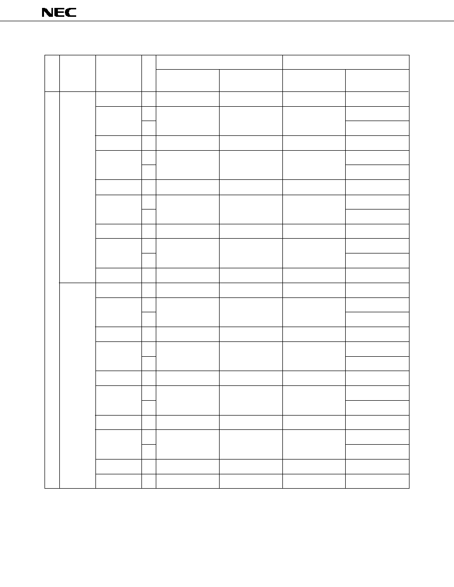
96
µ
PD70433
Byte Processing
Word Processing
On-Chip
Other
On-Chip
Other
RAM Access
Access
RAM Access
Access
reg8, CL
≠≠
3
3
3
3
8
EA + 10 + 2T
mem8, CL
EA + 4
EA + 7 + T
EA + 4
16
EA + 7 + T
reg16, CL
≠≠
3
3
3
3
8
EA + 10 + 2T
mem16, CL
EA + 4
EA + 7 + T
EA + 4
16
EA + 7 + T
NOT1
reg8, imm3
≠≠
2
2
2
2
8
EA + 10 + 2T
mem8, imm3
EA + 4
EA + 7 + T
EA + 4
16
EA + 7 + T
reg16, imm4
≠≠
2
2
2
2
8
EA + 10 + 2T
mem16, imm4
EA + 4
EA + 7 + T
EA + 4
16
EA + 7 + T
CY
≠≠
2
2
2
2
reg8, CL
≠≠
3
3
3
3
8
EA + 10 + 2T
mem8, CL
EA + 4
EA + 7 + T
EA + 4
16
EA + 7 + T
reg16, CL
≠≠
3
3
3
3
8
EA + 10 + 2T
mem16, CL
EA + 4
EA + 7 + T
EA + 4
16
EA + 7 + T
CLR1
reg8, imm3
≠≠
2
2
2
2
8
EA + 10 + 2T
mem8, imm3
EA + 4
EA + 7 + T
EA + 4
16
EA + 7 + T
reg16, imm4
≠≠
2
2
2
2
8
EA + 10 + 2T
mem16, imm4
EA + 4
EA + 7 + T
EA + 4
16
EA + 7 + T
CY
≠≠
2
2
2
2
DIR
≠≠
2
2
2
2
Mnemonic
Operands
*
8
: 8-bit width
16 : 16-bit width
≠≠ : Both 8-bit and 16-bit bus width
Bit manipulation instructions
Bus Width
*
Instruction
Group
Table 17-9. Number of Clock Cycles (12/20)

97
µ
PD70433
Byte Processing
Word Processing
On-Chip
Other
On-Chip
Other
RAM Access
Access
RAM Access
Access
reg8, CL
≠≠
3
3
3
3
8
EA + 10 + 2T
mem8, CL
EA + 4
EA + 7 + T
EA + 4
16
EA + 7 + T
reg16, CL
≠≠
3
3
3
3
8
EA + 10 + 2T
mem16, CL
EA + 4
EA + 7 + T
EA + 4
16
EA + 7 + T
reg8, imm3
≠≠
2
2
2
2
SET1
8
EA + 10 + 2T
mem8, imm3
EA + 4
EA + 7 + T
EA + 4
16
EA + 7 + T
reg16, imm4
≠≠
2
2
2
2
8
EA + 10 + 2T
mem16, imm4
EA + 4
EA + 7 + T
EA + 4
16
EA + 7 + T
CY
≠≠
2
2
2
2
DIR
≠≠
2
2
2
2
8
EA + 8 + 3n + T
EA + 8 + 3n + T
EA + 11 + 3n + 2T
EA + 11 + 3n + 2T
mem
BSCH
16
EA + 8 + 3n + T
EA + 8 + 3n + T
EA + 8 + 3n + T
EA + 8 + 3n + T
reg
≠≠
4 + 3n
4 + 3n
4 + 3n
4 + 3n
reg, 1
≠≠
3
3
3
3
8
EA + 10 + 2T
mem, 1
EA + 3
EA + 7 + T
EA + 3
16
EA + 7 + T
reg, CL
≠≠
5 + n
5 + n
5 + n
5 + n
SHL
8
EA + 11 + 2T + n
mem, CL
EA + 5 + n
EA + 8 + T + n
EA + 6 + n
16
EA + 8 + T + n
reg, imm8
≠≠
5 + n
5 + n
5 + n
5 + n
8
EA + 11 + 2T + n
mem, imm8
EA + 6 + n
EA + 8 + T + n
EA + 6 + n
16
EA + 8 + T + n
Mnemonic
Operands
Bit manipulation instructions
Shift instructions
*
8
: 8-bit width
16 : 16-bit width
≠≠ : Both 8-bit and 16-bit bus width
Remark
Number of shifts (n in a bit manipulation instruction indicates the bit number searched for)
Bus Width
*
Instruction
Group
Table 17-9. Number of Clock Cycles (13/20)
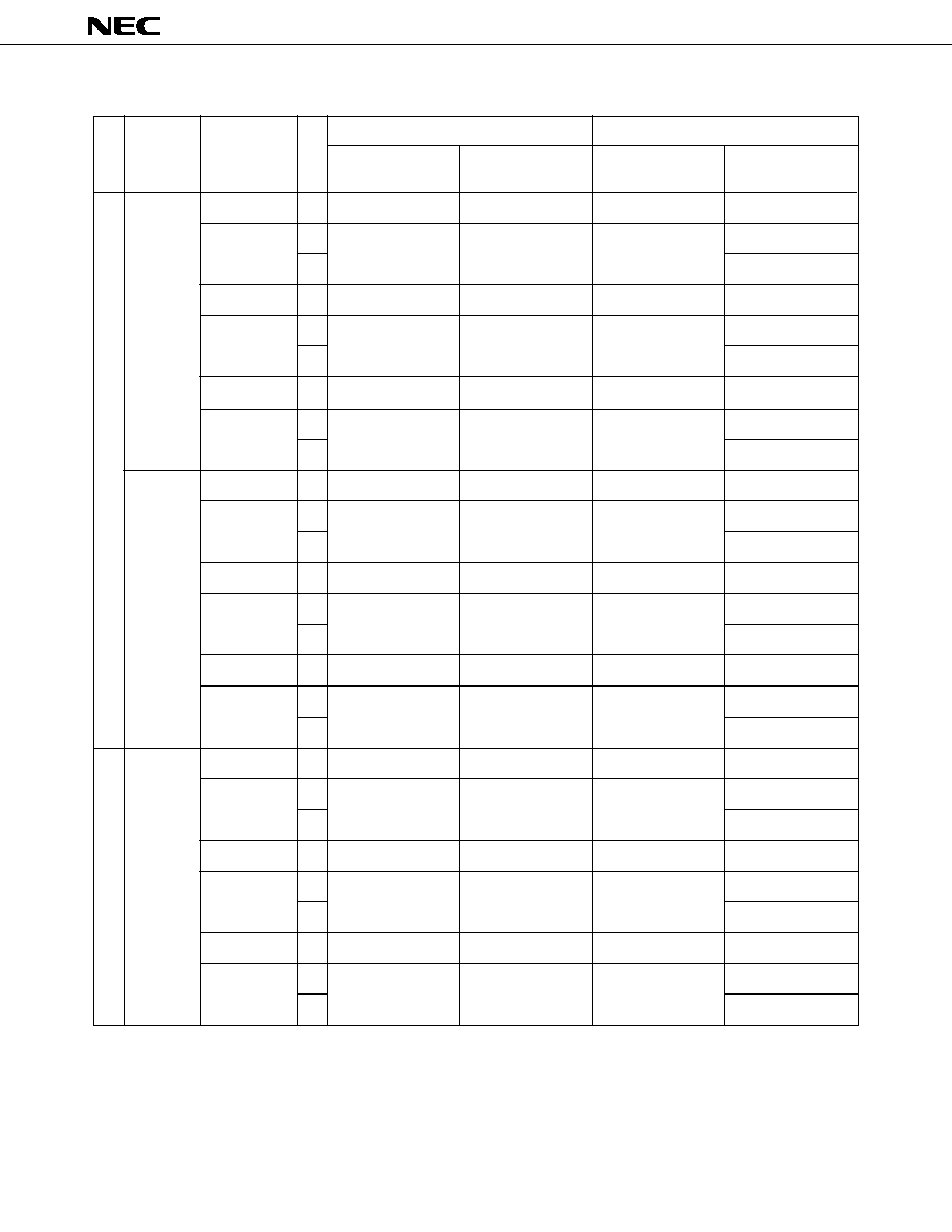
98
µ
PD70433
*
8
: 8-bit width
16 : 16-bit width
≠≠ : Both 8-bit and 16-bit bus width
Remark
Number of shifts (n in a bit manipulation instruction indicates the bit number searched for)
Byte Processing
Word Processing
On-Chip
Other
On-Chip
Other
RAM Access
Access
RAM Access
Access
reg, 1
≠≠
3
3
3
3
8
EA + 10 + 2T
mem, 1
EA + 3
EA + 7 + T
EA + 3
16
EA + 7 + T
reg, CL
≠≠
5 + n
5 + n
5 + n
5 + n
SHR
8
EA + 11 + 2T + n
mem, CL
EA + 5 + n
EA + 8 + T + n
EA + 6 + n
16
EA + 8 + T + n
reg, imm8
≠≠
5 + n
5 + n
5 + n
5 + n
8
EA + 11 + 2T + n
mem, imm8
EA + 6 + n
EA + 8 + T + n
EA + 6 + n
16
EA + 8 + T + n
reg, 1
≠≠
3
3
3
3
8
EA + 10 + 2T
mem, 1
EA + 3
EA + 7 + T
EA + 3
16
EA + 7 + T
reg, CL
≠≠
5 + n
5 + n
5 + n
5 + n
SHRA
8
EA + 11 + 2T + n
mem, CL
EA + 5 + n
EA + 8 + T + n
EA + 6 + n
16
EA + 8 + T + n
reg, imm8
≠≠
5 + n
5 + n
5 + n
5 + n
8
EA + 11 + 2T + n
mem, imm8
EA + 6 + n
EA + 8 + T + n
EA + 6 + n
16
EA + 8 + T + n
reg, 1
≠≠
3
3
3
3
8
EA + 10 + 2T
mem, 1
EA + 3
EA + 7 + T
EA + 3
16
EA + 7 + T
reg, CL
≠≠
5 + n
5 + n
5 + n
5 + n
ROL
8
EA + 11 + 2T + n
mem, CL
EA + 5 + n
EA + 8 + T + n
EA + 6 + n
16
EA + 8 + T + n
reg, imm8
≠≠
5 + n
5 + n
5 + n
5 + n
8
EA + 11 + 2T + n
mem, imm8
EA + 6 + n
EA + 8 + T + n
EA + 6 + n
16
EA + 8 + T + n
Mnemonic
Operands
Shift instructions
Rotate instructions
Bus Width
*
Instruction
Group
Table 17-9. Number of Clock Cycles (14/20)

99
µ
PD70433
*
8
: 8-bit width
16 : 16-bit width
≠≠ : Both 8-bit and 16-bit bus width
Remark
Number of shifts
Byte Processing
Word Processing
On-Chip
Other
On-Chip
Other
RAM Access
Access
RAM Access
Access
reg, 1
≠≠
3
3
3
3
8
EA + 10 + 2T
mem, 1
EA + 3
EA + 7 + T
EA + 3
16
EA + 7 + T
reg, CL
≠≠
5 + n
5 + n
5 + n
5 + n
ROR
8
EA + 11 + 2T + n
mem, CL
EA + 5 + n
EA + 8 + T + n
EA + 6 + n
16
EA + 8 + T + n
reg, imm8
≠≠
5 + n
5 + n
5 + n
5 + n
8
EA + 11 + 2T + n
mem, imm8
EA + 6 + n
EA + 8 + T + n
EA + 6 + n
16
EA + 8 + T + n
reg, 1
≠≠
3
3
3
3
8
EA + 10 + 2T
mem, 1
EA + 3
EA + 7 + T
EA + 3
16
EA + 7 + T
reg, CL
≠≠
5 + n
5 + n
5 + n
5 + n
ROLC
8
EA + 11 + 2T + n
mem, CL
EA + 5 + n
EA + 8 + T + n
EA + 6 + n
16
EA + 8 + T + n
reg, imm8
≠≠
5 + n
5 + n
5 + n
5 + n
8
EA + 11 + 2T + n
mem, imm8
EA + 6 + n
EA + 8 + T + n
EA + 6 + n
16
EA + 8 + T + n
reg, 1
≠≠
3
3
3
3
8
EA + 10 + 2T
mem, 1
EA + 3
EA + 7 + T
EA + 3
16
EA + 7 + T
reg, CL
≠≠
5 + n
5 + n
5 + n
5 + n
RORC
8
EA + 11 + 2T + n
mem, CL
EA + 5 + n
EA + 8 + T + n
EA + 6 + n
16
EA + 8 + T + n
reg, imm8
≠≠
5 + n
5 + n
5 + n
5 + n
8
EA + 11 + 2T + n
mem, imm8
EA + 6 + n
EA + 8 + T + n
EA + 6 + n
16
EA + 8 + T + n
Mnemonic
Operands
Rotate instructions
Bus Width
*
Instruction
Group
Table 17-9. Number of Clock Cycles (15/20)
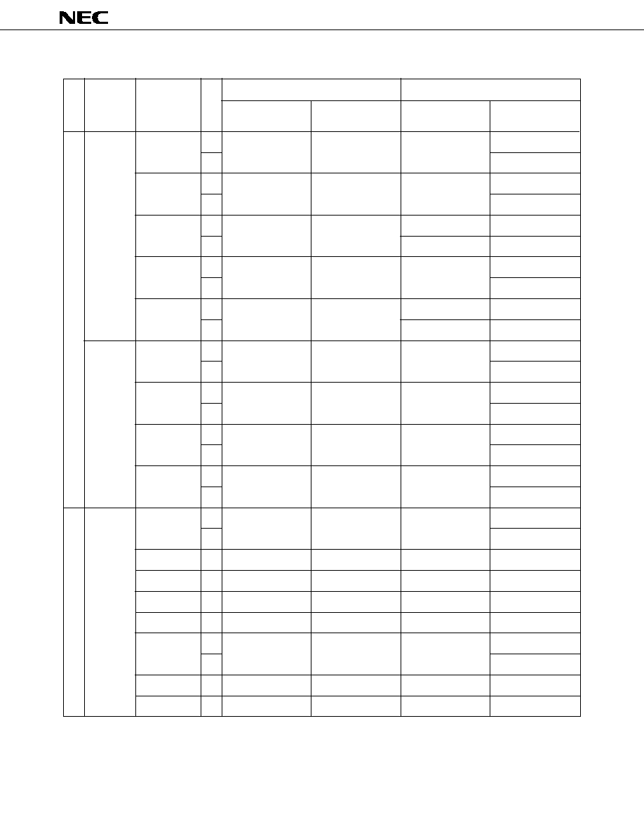
100
µ
PD70433
Byte Processing
Word Processing
On-Chip
Other
On-Chip
Other
RAM Access
Access
RAM Access
Access
8
19 + 2T
near-proc
≠≠
≠≠
≠≠
16
16 + T
8
18 + 2T
regptr16
≠≠
≠≠
≠≠
16
15 + T
8
EA + 19 + 2T
EA + 24 + 4T
CALL
memptr16
≠≠
≠≠
16
EA + 16 + T
EA + 18 + 2T
8
29 + 4T
far-proc
≠≠
≠≠
≠≠
16
23 + 2T
8
EA + 32 + 4T
EA + 44 + 8T
memptr32
≠≠
≠≠
16
EA + 26 + 2T
EA + 32 + 4T
8
18 + 2T
≠≠
≠≠
≠≠
16
15 + T
8
19 + 2T
pop-value
≠≠
≠≠
≠≠
16
16 + T
RET
8
26 + 4T
*2
≠≠
≠≠
≠≠
16
20 + 2T
8
27 + 4T
pop-value*2
≠≠
≠≠
≠≠
16
21 + 2T
8
EA + 13 + 2T
mem16
≠≠
≠≠
EA + 7
16
EA + 10 + T
reg16
≠≠
≠≠
≠≠
≠≠
7
sreg
≠≠
≠≠
≠≠
≠≠
7
xsreg/VPC
≠≠
≠≠
≠≠
≠≠
7
PUSH
PSW
≠≠
≠≠
≠≠
≠≠
6
8
57 + 14T
R
≠≠
≠≠
≠≠
16
36 + 7T
imm8
≠≠
≠≠
≠≠
≠≠
6
imm16
≠≠
≠≠
≠≠
≠≠
6
Mnemonic
Operands
* 1.
8
: 8-bit width
16 : 16-bit width
≠≠ : Both 8-bit and 16-bit bus width
2.
Segment-external
Remark
n: Number of shifts
Subroutine control instructions
Stack manipulation instructions
Instruction
Group
Bus Width
*1
Table 17-9. Number of Clock Cycles (16/20)
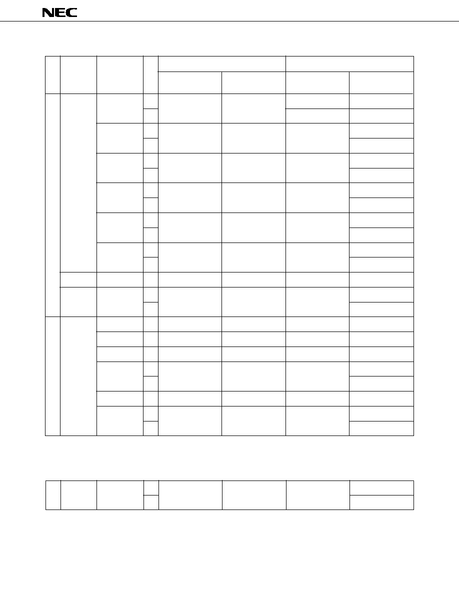
101
µ
PD70433
Table 17-9. Number of Clock Cycles (17/20)
Byte Processing
Word Processing
On-Chip
Other
On-Chip
Other
RAM Access
Access
RAM Access
Access
8
EA + 13 + 2T
EA + 14 + 2T
mem16
≠≠
≠≠
16
EA + 10 + T
EA + 11 + T
8
10 + 2T
reg16
≠≠
≠≠
≠≠
16
7 + T
8
10 + 2T
sreg
≠≠
≠≠
≠≠
16
7 + T
POP
8
10 + 2T
xsreg/VPC
≠≠
≠≠
≠≠
16
7 + T
8
11 + 2T
PSW
≠≠
≠≠
≠≠
16
8 + T
8
76 + 16T
R
≠≠
≠≠
≠≠
16
52 + 8T
PREPARE*2 imm16, imm8
≠≠
≠-
≠≠
≠≠
9
8
10 + 2T
DISPOSE
≠≠
≠≠
≠≠
16
7 + T
near-label
≠≠
≠≠
≠≠
≠≠
9
short-label
≠≠
≠≠
≠≠
≠≠
9
regptr16
≠≠
≠≠
≠≠
≠≠
8
8
EA + 14 + 2T
BR
memptr16
≠≠
≠≠
EA + 9
16
EA + 11 + T
far-label
≠≠
≠≠
≠≠
≠≠
9
8
EA + 24 + 4T
memptr32
≠≠
≠≠
EA + 12
16
EA + 18 + 2T
8
15+2T+(16+4T)n
PREPARE
imm16, imm8
≠≠
≠≠
≠≠
16
14 + (12 + T)n
Mnemonic
Operands
* 1.
8
: 8-bit width
16 : 16-bit width
≠≠ : Both 8-bit and 16-bit bus width
2.
When imm8 = 0. As shown below when imm8
1.
Stack manipulation instructions
Branch instructions
Instruction
Group
n : imm8
Bus Width
*1

102
µ
PD70433
Byte Processing
Word Processing
On-Chip
Other
On-Chip
Other
RAM Access
Access
RAM Access
Access
BV
short-label
≠≠
≠≠
≠≠
9/3
9/3
BNV
short-label
≠≠
≠≠
≠≠
9/3
9/3
BC/BL
short-label
≠≠
≠≠
≠≠
9/3
9/3
BNC/BNL
short-label
≠≠
≠≠
≠≠
9/3
9/3
BE/BZ
short-label
≠≠
≠≠
≠≠
9/3
9/3
BNE/BNZ
short-label
≠≠
≠≠
≠≠
9/3
9/3
BNH
short-label
≠≠
≠≠
≠≠
9/3
9/3
BH
short-label
≠≠
≠≠
≠≠
9/3
9/3
BN
short-label
≠≠
≠≠
≠≠
9/3
9/3
BP
short-label
≠≠
≠≠
≠≠
9/3
9/3
BPE
short-label
≠≠
≠≠
≠≠
9/3
9/3
BPO
short-label
≠≠
≠≠
≠≠
9/3
9/3
BLT
short-label
≠≠
≠≠
≠≠
9/3
9/3
BGE
short-label
≠≠
≠≠
≠≠
9/3
9/3
BLE
short-label
≠≠
≠≠
≠≠
9/3
9/3
BGT
short-label
≠≠
≠≠
≠≠
9/3
9/3
DBNZNE
short-label
≠≠
≠≠
≠≠
10/5
10/5
DBNZE
short-label
≠≠
≠≠
≠≠
10/5
10/5
DBNZ
short-label
≠≠
≠≠
≠≠
10/5
10/5
BCWZ
short-label
≠≠
≠≠
≠≠
10/5
10/5
8
BTCLR
≠≠
21/14
≠≠
≠≠
16
8
BTCLRL
≠≠
20/13
≠≠
≠≠
16
Table 17-9. Number of Clock Cycles (18/20)
Mnemonic
Operands
sfr, imm3
short-label
sfrl, imm3
short-label
*
8 : 8-bit width
16 : 16-bit width
≠≠ : Both 8-bit and 16-bit bus width
Conditional branch instructions
Instruction
Group
Bus Width
*
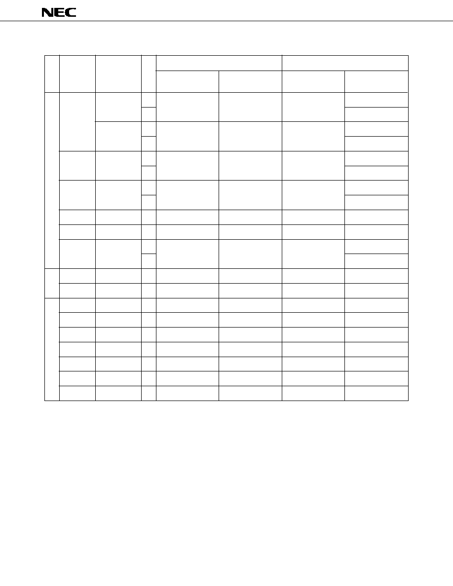
103
µ
PD70433
Table 17-9. Number of Clock Cycles (19/20)
Byte Processing
Word Processing
On-Chip
Other
On-Chip
Other
RAM Access
Access
RAM Access
Access
8
50 + 10T
3
≠≠
≠≠
≠≠
16
36 + 4T + t
BRK*2
8
52 + 10T
imm8 (
3)
≠≠
≠≠
≠-
16
38 + 4T + t
8
51 + 10 T
BRKV*2
≠≠
≠≠
≠≠
16
37 + 4T + t
8
28 + 4T
RETI
≠≠
≠≠
≠≠
16
22 + 2T
RETRBI
≠≠
≠≠
≠≠
≠≠
9
FINT
--
3
3
3
3
8
EA + 21 + 4T
CHKIND*3
≠≠
≠≠
EA + 11
16
EA + 15 + 2T
BRKCS
reg16
≠≠
≠≠
≠≠
12
12
*4
TSKSW
reg16
≠≠
≠≠
≠≠
13
13
HALT
≠≠
≠≠
≠≠
≠≠
≠≠
STOP
≠≠
≠≠
≠≠
≠≠
≠≠
IDLE
≠≠
≠≠
≠≠
≠≠
≠≠
POLL
≠≠
≠≠
≠≠
≠≠
≠≠
DI
≠≠
3
3
3
3
EI
≠≠
3
3
3
3
BUSLOCK
≠≠
0 to 1
0 to 1
0 to 1
0 to 1
Mnemonic
Operands
Interrupt instructions
CPU control instructions
* 1.
8
: 8-bit width
16 : 16-bit width
≠≠ : Both 8-bit and 16-bit bus width
2.
When BRK = 1, add 50 + 10T in case of 8-bit bus width, and 34 + 4T in case of 16-bit bus.
3.
When (mem32) > reg16 or (mem32 + 2) < reg16, add 50 + 10T in case of 8-bit bus width, and 34 +
4T + t in case of 16-bit bus width.
4.
Register bank switching instructions
Remarks
When T
2, t = T ≠ 1
Instruction
Group
Bus Width
*1

104
µ
PD70433
Table 17-9. Number of Clock Cycles (20/20)
Byte Processing
Word Processing
On-Chip
Other
On-Chip
Other
RAM Access
Access
RAM Access
Access
8
50 + 10T
fp-op
--
≠≠
≠≠
16
36 + 4T + t
FPO1
8
EA + 50 + 10 T
fp-op, mem
≠≠
≠≠
≠≠
16
EA + 36 + 4T + t
8
50 + 10T
fp-op
--
≠≠
≠≠
16
36 + 4T + t
FPO2
8
EA + 50 + 10 T
fp-op, mem
≠≠
≠≠
≠≠
16
EA + 36 + 4T + t
NOP
≠≠
4
4
4
4
8
9/54 + 10T*3
*2
RSTWDT
imm8, imm8'
≠≠
≠≠
≠≠
16
9/40 + 4T + t*3
*4
≠≠
0 to 1
0 to 1
0 to 1
0 to 1
QHOUT
imm16
≠≠
--
≠≠
≠≠
≠≠
QOUT
imm16
≠≠
--
≠≠
≠≠
≠≠
QTIN
imm16
≠≠
≠≠
≠≠
≠≠
≠≠
ALBIT
≠≠
≠≠
≠≠
≠≠
≠≠
COLTRP
≠≠
≠≠
≠≠
≠≠
≠≠
MHENC
≠≠
≠≠
≠≠
≠≠
≠≠
MRENC
≠≠
≠≠
≠≠
≠≠
≠≠
SCHEOL
≠≠
≠≠
≠≠
≠≠
≠≠
GETBIT
≠≠
≠≠
≠≠
≠≠
≠≠
MHDEC
≠≠
≠≠
≠≠
≠≠
≠≠
MRDEC
≠≠
≠≠
≠≠
≠≠
≠≠
CNVTRP
≠≠
≠≠
≠≠
≠≠
≠≠
Mnemonic
Operands
CPU control instructions
Instruction
Group
Bus Width
*1
* 1.
8
: 8-bit width
16 : 16-bit width
≠≠ : Both 8-bit and 16-bit bus width
2.
Watchdog timer manipulation instruction
3.
Figure after / (slash) applies when word processing is performed during data error.
When T
2, t = T ≠ 1
4.
Segment override prefix instructions (DS0:, DS1:, PS:, SS:)
Extended segment override prefix instructions (DS2: DS3:)
Register file space access override prefix instruction (IRAM)
Dedicated fax instructions
Queue manipula-
tion instructions

µ
PD70433
105
Operation Code
Flags
Mnemonic
Operand(s)
Bytes
Operation
7 6 5 4 3 2 1 0
7 6 5 4 3 2 1 0
AC CY V
P
S
Z
reg, reg'
1 0 0 0 1 0 1 W
1 1
reg
reg'
2
reg
reg'
mem, reg
1 0 0 0 1 0 0 W
mod reg
mem
2 to 4
(mem)
reg
reg, mem
1 0 0 0 1 0 1 W
mod reg
mem
2 to 4
reg
(mem)
mem, imm
1 1 0 0 0 1 1 W
mod0 0 0 mem
3 to 6
(mem)
imm
reg, imm
1 0 1 1 W
reg
2 to 3
reg
imm
If W = 0, AL
(dmem)
If W = 1, AH
(dmem + 1), AL
(dmem)
If W = 0, (dmem)
AL
If W = 1, (dmem + 1)
AH, (dmem)
AL
sreg, reg16
1 0 0 0 1 1 1 0
1 1 0 sreg
reg
2
sreg
reg16
sreg : SS, DS0, DS1
xsreg, reg16*
1 0 0 0 1 1 1 0
1 1 1 xsreg
reg
2
xsreg
reg16
xsreg : DS2, DS3
sreg, mem16
1 0 0 0 1 1 1 0
mod 0 sreg
mem
2 to 4
sreg
(mem16)
sreg : SS, DS0, DS1
MOV
xsreg, mem16*
1 0 0 0 1 1 1 0
mod 1 xsreg mem
2 to 4
xsreg
(mem16)
reg16, sreg
1 0 0 0 1 1 0 0
1 1 0 sreg
reg
2
reg16
sreg
reg16, xsreg*
1 0 0 0 1 1 0 0
1 1 1 xsreg
reg
2
reg16
xsreg
mem16, sreg
1 0 0 0 1 1 0 0
mod 0 sreg
mem
2 to 4
(mem16)
sreg
mem16, xsreg*
1 0 0 0 1 1 0 0
mod 1 xsreg
mem
2 to 4
(mem16)
xsreg
1 1 0 0 0 1 0 1
mod
reg
mem
2 to 4
1 1 0 0 0 1 0 0
mod
reg
mem
2 to 4
0 0 0 0 1 1 1 1
0 0 1 1 1 1 1 0
3 to 5
mod reg
mem
0 0 0 0 1 1 1 1
0 0 1 1 0 1 1 0
3 to 5
mod reg
mem
17.3
INSTRUCTION SET TABLE
acc, dmem
1 0 1 0 0 0 0 W
3
DS1, reg16,
reg16
(mem32)
mem32
DS1
(mem32 + 2)
DS2, reg16*,
reg16
(mem32)
mem32
DS2
(mem32 + 2)
DS3, reg16*,
reg16
(mem32)
mem32
DS3
(mem32 + 2)
*
This instruction is newly added to the V25 or V35.
Data transfer instructions
Instruction
Group
DS0, reg16,
reg16
(mem32)
mem32
DS0
(mem32 + 2)
dmem, acc
1 0 1 0 0 0 1 W
3

µ
PD70433
106
Operation Code
Flags
Mnemonic
Operand(s)
Bytes
Operation
7 6 5 4 3 2 1 0
7 6 5 4 3 2 1 0
AC CY V
P
S
Z
AH, PSW
1 0 0 1 1 1 1 1
1
AH
S, Z, F1, AC, F0, P, IBRK, CY
MOV
PSW, AH
1 0 0 1 1 1 1 0
1
S, Z, F1, AC, F0, P, IBRK, CY
AH
◊ ◊
◊ ◊ ◊
LDEA
reg16, mem16
1 0 0 0 1 1 0 1
mod reg
mem
2 to 4
reg16
mem16
src-table
1 1 0 1 0 1 1 1
1
AL
(BW + AL)
reg, reg'
1 0 0 0 0 1 1 W
1 1
reg
reg'
2
reg
reg'
XCH
1 0 0 0 0 1 1 W
mod reg
mem
2 to 4
(mem)
reg
1 0 0 1 0
reg
1
AW
reg16
MOVSPA*2
0 0 0 0 1 1 1 1
0 0 1 0 0 1 0 1
2
New register bank SS, SP
Old register bank SS, SP
0 0 0 0 1 1 1 1
1 0 0 1 0 1 0 1
MOVSPB*2
reg16
3
1 1 1 1 1
reg
While CW
0, the following byte primitive block
transfer instruction is executed and CW is decremented
REPC
0 1 1 0 0 1 0 1
1
(≠1).
If there is a pending interrupt, it is serviced.
If CY
1, the loop is exited.
Same as above.
If CY
0, the loop is exited.
While CW
0, the following byte primitive block
transfer instruction is executed and CW is decremented
(≠1).
If there is a pending interupt, it is serviced.
If the primitive block transfer instruction is CMPBK or
CMPM, and Z
1, the loop is exited.
REPNE
Same as above.
REPNZ
If Z
0, the loop is exited.
REP
REPE
1 1 1 1 0 0 1 1
1
REPZ
* 1.
The operand can be omitted in the case of the TRANS instruction. The TRANSB instruction has no operand.
2.
This instruction is newly added to the V20 or V30.
REPNC
0 1 1 0 0 1 0 0
1
1 1 1 1 0 0 1 0
1
TRANS
TRANSB*1
AW, reg16
reg16, AW
Repeat prefixes
Data transfer instructions
Instruction
Group
mem, reg
reg, mem
SS, SP of register bank indicated by reg16
current register bank SS, SP
µ
PD70433
107
dst-block,
src-block
src-block,
dst-block
Primitive block transfer instructions
Instruction
Group
Operation Code
Flags
Mnemonic
Operand(s)
Bytes
Operation
7 6 5 4 3 2 1 0
7 6 5 4 3 2 1 0
AC CY V
P
S
Z
If W = 0, (IY)
(IX)
DIR = 0: IX
IX + 1, IY
IY + 1
MOVBK
DIR = 1: IX
IX ≠ 1, IY
IY ≠ 1
MOVBKB
1 0 1 0 0 1 0 W
1
MOVBKW
If W = 1, (IY + 1, IY)
(IX + 1, IX)
DIR = 0: IX
IX + 2, IY
IY + 2
DIR = 1: IX
IX ≠ 2, IY
IY ≠ 2
If W = 0, (IX) ≠ (IY)
DIR = 0: IX
IX + 1, IY
IY + 1
CMPBK
DIR = 1: IX
IX ≠ 1, IY
IY ≠ 1
CMPBKB
1 0 1 0 0 1 1 W
1
◊ ◊ ◊ ◊ ◊ ◊
CMPBKW
If W = 1, (IX + 1, IX) ≠ (IY + 1, IY)
DIR = 0: IX
IX + 2, IY
IY + 2
DIR = 1: IX
IX ≠ 2, IY
IY ≠ 2
If W = 0, AL ≠ (IY)
CMPM
DIR = 0: IY
IY + 1 ; DIR = 1: IY
IY ≠ 1
CMPMB
dst-block
1 0 1 0 1 1 1 W
1
◊ ◊ ◊ ◊ ◊ ◊
CMPMW
If W = 1, AW ≠ (IY + 1, IY)
DIR = 0: IY
IY + 2 ; DIR = 1: IY
IY ≠ 2
If W = 0, AL
(IX)
LDM
DIR = 0: IX
IX + 1 ; DIR = 1: IX
IX ≠ 1
LDMB
src-block
1 0 1 0 1 1 0 W
1
LDMW
If W = 1, AW + (IX + 1, IX)
DIR = 0: IX + 2 ; DIR = 1: IX
IX ≠ 2
If W = 0, (IY)
AL
STM
DIR = 0: IY
IY + 1 ; DIR = 1: IY
IY ≠ 1
STMB
dst-block
1 0 1 0 1 0 1 W
1
STMW
If W = 1, AW ≠ (IY + 1, IY)
AW
DIR = 0: IY
IY + 2 ; DIR = 1: IY
IY ≠ 2
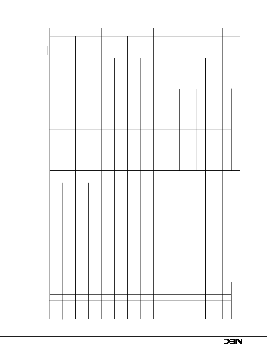
µ
PD70433
108
DW,
src-block
*
When IBRK = 0, a software interrupt is generated automatically and the instruction is not executed.
acc, DW
1 1 1 0 1 1 0 W
1
DW, acc
1 1 1 0 1 1 1 W
1
imm8, acc
1 1 1 0 0 1 1 W
2
Instruction
Group
Operation Code
Flags
Mnemonic
Operand(s)
Bytes
Operation
7 6 5 4 3 2 1 0
7 6 5 4 3 2 1 0
AC CY V
P
S
Z
0 0 0 0 1 1 1 1
0 0 1 1 0 0 0 1
reg8, reg8'
3
16-bit field
AW
1 1
reg'
reg
INS
0 0 0 0 1 1 1 1
0 0 1 1 1 0 0 1
reg8, imm4
4
16-bit field
AW
1 1 0 0 0
reg
0 0 0 0 1 1 1 1
0 0 1 1 0 0 1 1
reg8, reg8'
3
AW
16-bit field
1 1
reg'
reg
EXT
0 0 0 0 1 1 1 1
0 0 1 1 1 0 1 1
reg8, imm4
4
AW
16-bit field
1 1 0 0 0
reg
If W = 0, AL
(imm8)
If W = 1, AH
(imm8 + 1), AL
(imm8)
IN*
If W = 0, AL
(DW)
If W = 1, AH
(DW + 1), AL
(DW)
If W = 0, (imm8)
AL
If W = 1, (imm8 + 1)
AH, (imm8)
AL
OUT*
If W = 0, (DW)
AL
If W = 1, (DW + 1)
AH, (DW)
AL
If W = 0, (IY)
(DW)
DIR = 0: IY
IY + 1 ; DIR = 1: IY
IY ≠ 1
INM*
0 1 1 0 1 1 0 W
1
If W = 1, (IY + 1, IY)
(DW + 1, DW)
DIR = 0: IY
IY + 2 ; DIR = 1: IY
IY ≠ 2
If W = 0, (DW)
(IX)
DIR = 0: IX
IX + 1 ; DIR = 1: IX
IX ≠ 1
OUTM*
0 1 1 0 1 1 1 W
1
If W = 1, (DW + 1, DW)
(IX + 1, IX)
DIR = 0: IX
IX + 2 ; DIR = 1: IX
IX ≠ 2
Primitive input
Input/output
Bit field manipulation
/output instructions
instructions
instructions
acc, imm8
1 1 1 0 0 1 0 W
2
dst-block,
DW
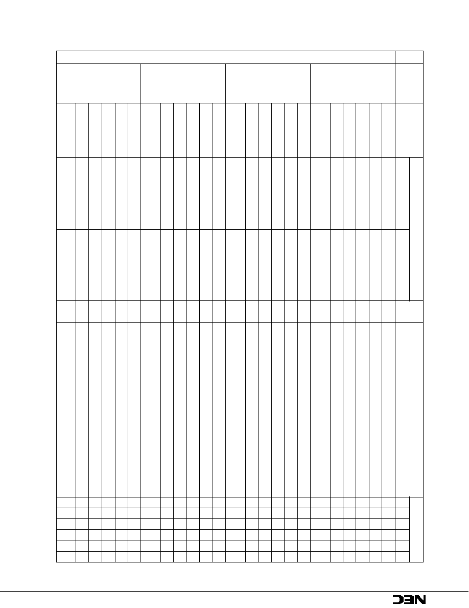
µ
PD70433
109
acc, imm
0 0 0 1 1 1 0 W
2 to 3
◊ ◊ ◊ ◊ ◊ ◊
acc, imm
0 0 0 0 0 1 0 W
2 to 3
◊ ◊ ◊ ◊ ◊ ◊
Operation Code
Flags
Mnemonic
Operand(s)
Bytes
Operation
7 6 5 4 3 2 1 0
7 6 5 4 3 2 1 0
AC CY V
P
S
Z
reg, reg'
0 0 0 0 0 0 1 W
1 1
reg
reg'
2
reg
reg + reg'
◊ ◊ ◊ ◊ ◊ ◊
mem, reg
0 0 0 0 0 0 0 W
mod reg
mem
2 to 4
(mem)
(mem) + reg
◊ ◊ ◊ ◊ ◊ ◊
reg, mem
0 0 0 0 0 0 1 W
mod reg
mem
2 to 4
reg
reg + (mem)
◊ ◊ ◊ ◊ ◊ ◊
ADD
reg, imm
1 0 0 0 0 0 s W
1 1 0 0 0
reg
3 to 4
reg
reg + imm
◊ ◊ ◊ ◊ ◊ ◊
mem, imm
1 0 0 0 0 0 s W
mod 0 0 0 mem
3 to 6
(mem)
(mem) + imm
◊ ◊ ◊ ◊ ◊ ◊
If W = 0, AL
AL + imm
If W = 1, AW
AW + imm
reg, reg'
0 0 0 1 0 0 1 W
1 1
reg
reg'
2
reg
reg + reg' + CY
◊ ◊ ◊ ◊ ◊ ◊
mem, reg
0 0 0 1 0 0 0 W
mod reg
mem
2 to 4
(mem)
(mem) + reg + CY
◊ ◊ ◊ ◊ ◊ ◊
reg, mem
0 0 0 1 0 0 1 W
mod reg
mem
2 to 4
reg
reg + (mem) + CY
◊ ◊ ◊ ◊ ◊ ◊
ADDC
reg, imm
1 0 0 0 0 0 s W
1 1 0 1 0
reg
3 to 4
reg
reg + imm + CY
◊ ◊ ◊ ◊ ◊ ◊
mem, imm
1 0 0 0 0 0 s W
mod 0 1 0 mem
3 to 6
(mem)
(mem) + imm + CY
◊ ◊ ◊ ◊ ◊ ◊
If W = 0, AL
AL + imm + CY
If W = 1, AW
AW + imm + CY
reg, reg'
0 0 1 0 1 0 1 W
1 1
reg
reg'
2
reg
reg ≠ reg'
◊ ◊ ◊ ◊ ◊ ◊
mem, reg
0 0 1 0 1 0 0 W
mod reg
mem
2 to 4
(mem)
(mem) ≠ reg
◊ ◊ ◊ ◊ ◊ ◊
reg, mem
0 0 1 0 1 0 1 W
mod reg
mem
2 to 4
reg
reg ≠ (mem)
◊ ◊ ◊ ◊ ◊ ◊
SUB
reg, imm
1 0 0 0 0 0 s W
1 1 1 0 1
reg
3 to 4
reg
reg ≠ imm
◊ ◊ ◊ ◊ ◊ ◊
mem, imm
1 0 0 0 0 0 s W
mod 1 0 1 mem
3 to 6
(mem)
(mem) ≠ imm
◊ ◊ ◊ ◊ ◊ ◊
If W = 0, AL
AL ≠ imm
If W = 1, AW
AW ≠ imm
reg, reg'
0 0 0 1 1 0 1 W
1 1
reg
reg'
2
reg
reg ≠ reg' ≠ CY
◊ ◊ ◊ ◊ ◊ ◊
mem, reg
0 0 0 1 1 0 0 W
mod reg
mem
2 to 4
(mem)
(mem) ≠ reg ≠ CY
◊ ◊ ◊ ◊ ◊ ◊
reg, mem
0 0 0 1 1 0 1 W
mod reg
mem
2 to 4
reg
reg ≠ (mem) ≠ CY
◊ ◊ ◊ ◊ ◊ ◊
SUBC
reg, imm
1 0 0 0 0 0 s W
1 1 0 1 1
reg
3 to 4
reg
reg ≠ imm ≠ CY
◊ ◊ ◊ ◊ ◊ ◊
mem, imm
1 0 0 0 0 0 s W
mod 0 1 1 mem
3 to 6
(mem)
(mem) ≠ imm ≠ CY
◊ ◊ ◊ ◊ ◊ ◊
If W = 0, AL
AL ≠ imm ≠ CY
If W = 1, AW
AW ≠ imm ≠ CY
acc, imm
0 0 1 0 1 1 0 W
2 to 3
◊ ◊ ◊ ◊ ◊ ◊
acc, imm
0 0 0 1 0 1 0 W
2 to 3
◊ ◊ ◊ ◊ ◊ ◊
Addition/subtraction instructions
Instruction
Group

µ
PD70433
110
Operation Code
Flags
Mnemonic
Operand(s)
Bytes
Operation
7 6 5 4 3 2 1 0
7 6 5 4 3 2 1 0
AC CY V
P
S
Z
(dst-string,
src-string)
(dst-string,
src-string)
(dst-string,
src-string)
reg8
0 0 0 0 1 1 1 1
0 0 1 0 1 0 0 0
3
1 1 0 0 0
reg
ROL4
mem8
0 0 0 0 1 1 1 1
0 0 1 0 1 0 0 0
3 to 5
mod 0 0 0 mem
reg8
0 0 0 0 1 1 1 1
0 0 1 0 1 0 1 0
3
1 1 0 0 0
reg
ROR4
mem8
0 0 0 0 1 1 1 1
0 0 1 0 1 0 1 0
3 to 5
mod 0 0 0 mem
reg8
1 1 1 1 1 1 1 0
1 1 0 0 0
reg
2
reg8
reg8 + 1
◊
◊ ◊ ◊ ◊
INC
mem
1 1 1 1 1 1 1 W
mod 0 0 0 mem
2 to 4
(mem)
(mem) + 1
◊
◊ ◊ ◊ ◊
reg16
0 1 0 0 0
reg
1
reg16
reg16 + 1
◊
◊ ◊ ◊ ◊
reg8
1 1 1 1 1 1 1 0
1 1 0 0 1
reg
2
reg8
reg8 ≠ 1
◊
◊ ◊ ◊ ◊
DEC
mem
1 1 1 1 1 1 1 W
mod 0 0 1 mem
2 to 4
(mem)
(mem) ≠ 1
◊
◊ ◊ ◊ ◊
reg16
0 1 0 0 1
reg
1
reg16
reg16 ≠ 1
◊
◊ ◊ ◊ ◊
ADD4S*1
0 0 0 0 1 1 1 1
0 0 1 0 0 0 0 0
2
dst BCD string
dst BCD string + src BCD string*2
U
◊
U
U
U
◊
SUB4S*1
0 0 0 0 1 1 1 1
0 0 1 0 0 0 1 0
2
dst BCD string
dst BCD string ≠ src BCD string*2
U
◊
U
U
U
◊
CMP4S*1
0 0 0 0 1 1 1 1
0 0 1 0 0 1 1 0
2
dst BCD string ≠ src BCD string*2
U
◊
U
U
U
◊
* 1.
The operand can be omitted.
2.
The number of BCD digits is given by the CL register: a value between 1 and 254 can be set.
Increment/decrement
BCD operation instructions
instructions
Instruction
Group
AL
L
AL
L
AL
L
AL
L
reg
mem
reg
mem
High-
order
Low-
order
High-
order
Low-
order
High-
order
Low-
order
High-
order
Low-
order

µ
PD70433
111
Operation Code
Flags
Mnemonic
Operand(s)
Bytes
Operation
7 6 5 4 3 2 1 0
7 6 5 4 3 2 1 0
AC CY V
P
S
Z
AW
AL
◊
reg8
reg8
1 1 1 1 0 1 1 0
1 1 1 0 0
reg
2
AH = 0: CY
0, V
0
U
◊ ◊
U
U
U
AH
0: CY
1, V
1
AW
AL
◊
(mem8)
mem8
1 1 1 1 0 1 1 0
mod 1 0 0 mem
2 to 4
AH = 0: CY
0, V
0
U
◊ ◊
U
U
U
AH
0: CY
1, V
1
MULU
DW, AW
AW
◊
reg16
reg16
1 1 1 1 0 1 1 1
1 1 1 0 0
reg
2
DW = 0: CY
0, V
0
U
◊ ◊
U
U
U
DW
0: CY
1, V
1
DW, AW
AW
◊
(mem16)
mem16
1 1 1 1 0 1 1 1
mod 1 0 0 mem
2 to 4
DW = 0: CY
0, V
0
U
◊ ◊
U
U
U
DW
0: CY
1, V
1
AW
AL
◊
reg8
reg8
1 1 1 1 0 1 1 0
1 1 1 0 1
reg
2
AH = AL sign extension: CY
0, V
0
U
◊ ◊
U
U
U
AH
AL sign extension: CY
1, V
1
AW
AL
◊
(mem8)
mem8
1 1 1 1 0 1 1 0
mod 1 0 1 mem
2 to 4
AH = AL sign extension: CY
0, V
0
U
◊ ◊
U
U
U
AH
AL sign extension: CY
1, V
1
DW, AW
AW
◊
reg16
reg16
1 1 1 1 0 1 1 1
1 1 1 0 1
reg
2
DW = AW sign extension: CY
0, V
0
U
◊ ◊
U
U
U
DW
AW sign extension: CY
1, V
1
DW, AW
AW
◊
(mem16)
mem16
1 1 1 1 0 1 1 1
mod 1 0 1 mem
2 to 4
DW = AW sign extension: CY
0, V
0
U
◊ ◊
U
U
U
DW
AW sign extension: CY
1, V
1
MUL
reg16,
reg16
reg16'
◊
imm8
(reg16',)*
0 1 1 0 1 0 1 1
1 1
reg
reg'
3
Product
16 bits: CY
0, V
0
U
◊ ◊
U
U
U
imm8
Product > 16 bits: CY
1, V
1
reg16,
reg16
(mem16)
◊
imm8
mem16,
0 1 1 0 1 0 1 1
mod reg
mem
3 to 5
Product
16 bits: CY
0, V
0
U
◊ ◊
U
U
U
imm8
Product > 16 bits: CY
1, V
1
reg16,
reg16
reg16'
◊
imm16
(reg16',)*
0 1 1 0 1 0 0 1
1 1
reg
reg'
4
Product
16 bits: CY
0, V
0
U
◊ ◊
U
U
U
imm16
Product > 16 bits: CY
1, V
1
reg16,
reg16
(mem16)
◊
imm16
mem16,
0 1 1 0 1 0 0 1
mod reg
mem
4 to 6
Product
16 bits: CY
0, V
0
U
◊ ◊
U
U
U
imm16
Product > 16 bits: CY
1, V
1
Multiplication instructions
*
The 2nd operand can be omitted, in which case the same register as the 1st operand is taken as being specified.
Instruction
Group
µ
PD70433
112
Operation Code
Flags
Mnemonic
Operand(s)
Bytes
Operation
7 6 5 4 3 2 1 0
7 6 5 4 3 2 1 0
AC CY V
P
S
Z
temp
AW
If temp
˜
reg8
FFH
AH
temp%reg8, AL
temp
˜
reg8
reg8
1 1 1 1 0 1 1 0
1 1 1 1 0
reg
2
If temp
˜
reg8 > FFH
U
U
U
U
U
U
(SP ≠ 1, SP ≠ 2)
PSW, (SP ≠ 3, SP ≠ 4)
PS
(SP ≠ 5, SP ≠ 6)
PC, SP
SP ≠ 6
IE
0, BRK
0, PS
(3, 2), PC
(1, 0)
temp
AW
If temp
˜
(mem8)
FFH
AH
temp%(mem8), AL
temp
˜
(mem8)
mem8
1 1 1 1 0 1 1 0
mod 1 1 0 mem
2 to 4
If temp
˜
(mem8) > FFH
U
U
U
U
U
U
(SP ≠ 1, SP ≠ 2)
PSW, (SP ≠ 3, SP ≠ 4)
PS
(SP ≠ 5, SP ≠ 6)
PC, SP
SP ≠ 6
IE
0, BRK
0, PS
(3, 2), PC
(1, 0)
DIVU
temp
DW, AW
If temp
˜
reg16
FFFFH
DW
temp%reg16, AW
temp
˜
reg16
reg16
1 1 1 1 0 1 1 1
1 1 1 1 0
reg
2
If temp
˜
reg16 > FFFFH
U
U
U
U
U
U
(SP ≠ 1, SP ≠ 2)
PSW, (SP ≠ 3, SP ≠ 4)
PS
(SP ≠ 5, SP ≠ 6)
PC, SP
SP ≠ 6
IE
0, BRK
0, PS
(3, 2), PC
(1, 0)
temp
DW, AW
If temp
˜
(mem16)
FFFFH
DW
temp%(mem16), AW
temp
˜
(mem16)
mem16
1 1 1 1 0 1 1 1
mod 1 1 0 mem
2 to 4
If temp
˜
(mem16) > FFFFH
U
U
U
U
U
U
(SP ≠ 1, SP ≠ 2)
PSW, (SP ≠ 3, SP ≠ 4)
PS
(SP ≠ 5, SP ≠ 6)
PC, SP
SP ≠ 6
IE
0, BRK
0, PS
(3, 2), PC
(1, 0)
Unsigned division instructions
Instruction
Group
µ
PD70433
113
Signed division instructions
Instruction
Group
Operation Code
Flags
Mnemonic
Operand(s)
Bytes
Operation
7 6 5 4 3 2 1 0
7 6 5 4 3 2 1 0
AC CY V
P
S
Z
temp
AW
If temp
˜
reg8 > 0 and temp
˜
reg8
7FH; or
if temp
˜
reg8 < 0 and temp
˜
reg8 > 0 ≠ 7FH ≠ 1
AH
temp%reg8, AL
temp
˜
reg8
reg8
1 1 1 1 0 1 1 0
1 1 1 1 1
reg
2
If temp
˜
reg8 > 0 and temp
˜
reg8 > 7FH; or
U
U
U
U
U
U
if temp
˜
reg8 < 0 and temp
˜
reg8
0 ≠ 7FH ≠ 1
(SP ≠ 1, SP ≠ 2)
PSW, (SP ≠ 3, SP ≠ 4)
PS
(SP ≠ 5, SP ≠ 6)
PC, SP
SP ≠ 6
IE
0, BRK
0, PS
(3, 2), PC
(1, 0)
temp
AW
If temp
˜
(mem8) > 0 and temp
˜
(mem8)
7FH; or
if temp
˜
(mem8) < 0 and temp
˜
(mem8) > 0 ≠ 7FH ≠ 1
AH
temp%(mem8), AL
temp
˜
(mem8)
mem8
1 1 1 1 0 1 1 0
mod 1 1 1 mem
2 to 4
If temp
˜
(mem8) > 0 and temp
˜
(mem8) > 7FH; or
U
U
U
U
U
U
if temp
˜
(mem8) < 0 and temp
˜
(mem8)
0 ≠ 7FH ≠ 1
(SP ≠ 1, SP ≠ 2)
PSW, (SP ≠ 3, SP ≠ 4)
PS
(SP ≠ 5, SP ≠ 6)
PC, SP
SP ≠ 6
IE
0, BRK
0, PS
(3, 2), PC
(1, 0)
DIV
temp
DW, AW
If temp
˜
reg16 > 0 and temp
˜
reg16
7FFFH; or
if temp
˜
reg16 < 0 and temp
˜
reg16 > 0 ≠ 7FFFH ≠ 1
DW
temp%reg16, AW
temp
˜
reg16
reg16
1 1 1 1 0 1 1 1
1 1 1 1 1
reg
2
If temp
˜
reg16 > 0 and temp
˜
reg16 > 7FFFH; or
U
U
U
U
U
U
if temp
˜
reg16 < 0 and temp
˜
reg16
0 ≠ 7FFFH ≠ 1
(SP ≠ 1, SP ≠ 2)
PSW, (SP ≠ 3, SP ≠ 4)
PS
(SP ≠ 5, SP ≠ 6)
PC, SP
SP ≠ 6
IE
0, BRK
0, PS
(3, 2), PC
(1, 0)
temp
DW, AW
If temp
˜
(mem16) > 0 and temp
˜
(mem16)
7FFFH; or
if temp
˜
(mem16) < 0 and temp
˜
(mem16) > 0 ≠ 7FFFH ≠ 1
AH
temp%(mem16), AW
temp
˜
(mem16)
mem16
1 1 1 1 0 1 1 1
mod 1 1 1 mem
2 to 4
If temp
˜
(mem16) > 0 and temp
˜
(mem16) > 7FFFH; or
U
U
U
U
U
U
if temp
˜
(mem16) < 0 and temp
˜
(mem16)
0 ≠ 7FFFH ≠ 1
(SP ≠ 1, SP ≠ 2)
PSW, (SP ≠ 3, SP ≠ 4)
PS
(SP ≠ 5, SP ≠ 6)
PC, SP
SP ≠ 6
IE
0, BRK
0, PS
(3, 2), PC
(1, 0)

µ
PD70433
114
Operation Code
Flags
Mnemonic
Operand(s)
Bytes
Operation
7 6 5 4 3 2 1 0
7 6 5 4 3 2 1 0
AC CY V
P
S
Z
ADJBA
0 0 1 1 0 1 1 1
1
If AL
0FH > 9 or AC = 1: AL
AL + 6
◊ ◊
U
U
U
U
AH
AH + 1, AC
1, CY
AC, AL
AL
0FH
If AL
0FH > 9 or AC = 1:
ADJ4A
0 0 1 0 0 1 1 1
1
AL
AL + 6, AC
1
◊ ◊
U
◊ ◊ ◊
If AL > 9FH or CY = 1:
AL
AL + 60H, CY
1
If AL
0FH > 9 or AC = 1:
ADJBS
0 0 1 1 1 1 1 1
1
AL
AL ≠ 6, AC
1
◊ ◊
U
U
U
U
CY
AC, AL
AL
0FH
If AL
0FH > 9 or AC = 1:
ADJ4S
0 0 1 0 1 1 1 1
1
AL
AL ≠ 6, CY
CY
AC, AC
1
◊ ◊
U
◊ ◊ ◊
If AL > 9FH or CY = 1:
AL
AL ≠ 60H, CY
1
CVTBD
1 1 0 1 0 1 0 0
0 0 0 0 1 0 1 0
2
AH
AH
˜
0AH, AL
AL%0AH
U
U
U
◊ ◊ ◊
CVTDB
1 1 0 1 0 1 0 1
0 0 0 0 1 0 1 0
2
AL
AH
◊
0AH + AL, AH
0
U
U
U
◊ ◊ ◊
CVTBW
1 0 0 1 1 0 0 0
1
If AL < 80H: AH
0, otherwise: AH
FFH
CVTWL
1 0 0 1 1 0 0 1
1
If AW < 8000H: DW
0, otherwise: DW
FFFFH
reg, reg'
0 0 1 1 1 0 1 W
1 1
reg
reg'
2
reg ≠ reg'
◊ ◊ ◊ ◊ ◊ ◊
mem, reg
0 0 1 1 1 0 0 W
mod
reg
mem
2 to 4
(mem)≠ reg
◊ ◊ ◊ ◊ ◊ ◊
reg, mem
0 0 1 1 1 0 1 W
mod
reg
mem
2 to 4
reg ≠ (mem)
◊ ◊ ◊ ◊ ◊ ◊
CMP
reg, imm
1 0 0 0 0 0 s W
1 1 1 1 1
reg
3 to 4
reg ≠ imm
◊ ◊ ◊ ◊ ◊ ◊
mem, imm
1 0 0 0 0 0 s W
mod 1 1 1 mem
3 to 6
(mem) ≠ imm
◊ ◊ ◊ ◊ ◊ ◊
acc, imm
0 0 1 1 1 1 0 W
2 to 3
If W = 0, AL ≠ imm
◊ ◊ ◊ ◊ ◊ ◊
If W = 1, AW ≠ imm
reg
1 1 1 1 0 1 1 W
1 1 0 1 0
reg
2
reg
reg
NOT
mem
1 1 1 1 0 1 1 W
mod 0 1 0 mem
2 to 4
(mem) ≠ (mem)
*
reg
1 1 1 1 0 1 1 W
1 1 0 1 1
reg
2
reg
reg + 1
◊ ◊ ◊ ◊ ◊ ◊
NEG
mem
1 1 1 1 0 1 1 W
mod0 1 1mem
2 to 4
(mem)
(mem) + 1
◊ ◊ ◊ ◊ ◊ ◊
* Complement operation instructions
Instruction
Group
Data conversion
instructions
Comparison
BCD adjustment instructions
instruction
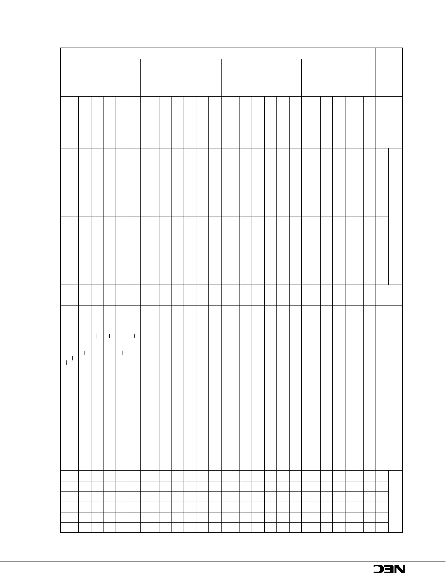
µ
PD70433
115
Logical operation instructions
Instruction
Group
Operation Code
Flags
Mnemonic
Operand(s)
Bytes
Operation
7 6 5 4 3 2 1 0
7 6 5 4 3 2 1 0
AC CY V
P
S
Z
reg, reg'
1 0 0 0 0 1 0 W
1 1
reg'
reg
2
reg
reg'
U
0
0
◊ ◊ ◊
mem, reg
1 0 0 0 0 1 0 W
mod reg
mem
2 to 4
(mem)
reg
U
0
0
◊ ◊ ◊
reg, mem
TEST
reg, imm
1 1 1 1 0 1 1 W
1 1 0 0 0
reg
3 to 4
reg
imm
U
0
0
◊ ◊ ◊
mem, imm
1 1 1 1 0 1 1 W
mod 0 0 0 mem
3 to 6
(mem)
imm
U
0
0
◊ ◊ ◊
acc, imm
1 0 1 0 1 0 0 W
2 to 3
If W = 0, AL
imm8
U
0
0
◊ ◊ ◊
If W = 1, AW
imm16
reg, reg'
0 0 1 0 0 0 1 W
1 1
reg
reg'
2
reg
reg
reg'
U
0
0
◊ ◊ ◊
mem, reg
0 0 1 0 0 0 0 W
mod reg
mem
2 to 4
(mem)
(mem)
reg
U
0
0
◊ ◊ ◊
reg, mem
0 0 1 0 0 0 1 W
mod reg
mem
2 to 4
reg
reg
(mem)
U
0
0
◊ ◊ ◊
AND
reg, imm
1 0 0 0 0 0 0 W
1 1 1 0 0
reg
3 to 4
reg
reg
imm
U
0
0
◊ ◊ ◊
mem, imm
1 0 0 0 0 0 0 W
mod 1 0 0 mem
3 to 6
(mem)
(mem)
imm
U
0
0
◊ ◊ ◊
acc, imm
0 1 0 0 1 0 W
2 to 3
If W = 0, AL
AL
imm8
U
0
0
◊ ◊ ◊
If W = 1, AW
AW
imm16
reg, reg'
0 0 0 0 1 0 1 W
1 1
reg
reg'
2
reg
reg
reg'
U
0
0
◊ ◊ ◊
mem, reg
0 0 0 0 1 0 0 W
mod reg
mem
2 to 4
(mem)
(mem)
reg
U
0
0
◊ ◊ ◊
reg, mem
0 0 0 0 1 0 1 W
mod reg
mem
2 to 4
reg
reg
(mem)
U
0
0
◊ ◊ ◊
OR
reg, imm
1 0 0 0 0 0 0 W
1 1 0 0 1
reg
3 to 4
reg
reg
imm
U
0
0
◊ ◊ ◊
mem, imm
1 0 0 0 0 0 0 W
mod 0 0 1 mem
3 to 6
(mem)
(mem)
imm
U
0
0
◊ ◊ ◊
acc, imm
0 0 0 0 1 1 0 W
2 to 3
If W = 0, AL
AL
imm8
U
0
0
◊ ◊ ◊
If W = 1, AW
AW
imm16
reg, reg'
0 0 1 1 0 0 1 W
1 1
reg
reg'
2
reg
reg v reg'
U
0
0
◊ ◊ ◊
mem, reg
0 0 1 1 0 0 0 W
mod reg
mem
2 to 4
(mem)
(mem) v reg'
U
0
0
◊ ◊ ◊
reg, mem
0 0 1 1 0 0 1 W
mod reg
mem
2 to 4
reg
reg v (mem)
U
0
0
◊ ◊ ◊
XOR
reg, imm
1 0 0 0 0 0 0 W
1 1 1 1 0
reg
3 to 4
reg
reg v imm
U
0
0
◊ ◊ ◊
mem, imm
1 0 0 0 0 0 0 W
mod 1 1 0 mem
3 to 6
(mem)
(mem) v imm
U
0
0
◊ ◊ ◊
acc, imm
0 0 1 1 0 1 0 W
2 to 3
If W = 0, AL
AL v imm8
U
0
0
◊ ◊ ◊
If W = 1, AW
AW v imm16
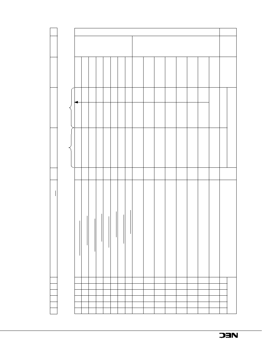
µ
PD70433
116
Operation Code
Flags
Mnemonic
Operand(s)
Bytes
Operation
7 6 5 4 3 2 1 0
7 6 5 4 3 2 1 0
AC CY V
P
S
Z
reg8, CL
0 0 0 1 0 0 0 0
1 1 0 0 0
reg
3
reg8 bit NO.CL = 0 : Z
1
U
0
0
U
U
◊
reg8 bit NO.CL = 1 : Z
0
mem8, CL
0 0 0 0
mod 0 0 0 mem
3 to 5
(mem)8 bit NO.CL = 0 : Z
1
U
0
0
U
U
◊
(mem)8 bit NO.CL = 1 : Z
0
reg16, CL
0 0 0 1
1 1 0 0 0
reg
3
reg16 bit NO.CL = 0 : Z
1
U
0
0
U
U
◊
reg16 bit NO.CL = 1 : Z
0
mem16, CL
0 0 0 1
mod 0 0 0 mem
3 to 5
(mem16) bit NO.CL = 0 : Z
1
U
0
0
U
U
◊
(mem16) bit NO.CL = 1 : Z
0
TEST1
reg8, imm3
1 0 0 0
1 1 0 0 0
reg
4
reg8 bit NO.imm3 = 0 : Z
1
U
0
0
U
U
◊
reg8 bit NO.imm3 = 1 : Z
0
mem8, imm3
1 0 0 0
mod 0 0 0 mem
4 to 6
(mem8) bit NO.imm3 = 0 : Z
1
U
0
0
U
U
◊
(mem8) bit NO.imm3 = 1 : Z
0
reg16, imm4
1 0 0 1
1 1 0 0 0
reg
4
reg16 bit NO.imm4 = 0 : Z
1
U
0
0
U
U
◊
reg16 bit NO.imm4 = 1 : Z
0
mem16, imm4
1 0 0 0
mod 0 0 0 mem
4 to 6
(mem16) bit NO.imm4 = 0 : Z
1
U
0
0
U
U
◊
(mem16) bit NO.imm4 = 1 : Z
0
reg8, CL
0 1 1 0
1 1 0 0 0
reg
3
reg8 bit NO.CL
reg8 bit NO.CL
mem8, CL
0 1 1 0
mod 0 0 0 mem
3 to 5
(mem8) bit NO.CL
(mem8) bit NO.CL
reg16, CL
0 1 1 1
1 1 0 0 0
reg
3
reg16 bit NO.CL
reg16 bit NO.CL
mem16, CL
0 1 1 1
mod 0 0 0 mem
3 to 5
(mem16) bit NO.CL
(mem16) bit NO.CL
NOT1
reg8, imm3
1 1 1 0
1 1 0 0 0
reg
4
reg8 bit NO.imm3
reg8 bit NO.imm3
mem8, imm3
1 1 1 0
mod 0 0 0 mem
4 to 6
(mem8) bit NO.imm3
(mem8) bit NO.imm3
reg16, imm4
1 1 1 1
1 1 0 0 0
reg
4
reg16 bit NO.imm4
reg16 bit NO.imm4
mem16, imm4
1 1 1 1
mod 0 0 0 mem
4 to 6
(mem16) bit NO.imm4
(mem16) bit NO.imm4
Bit manipulation instructions
2nd byte *
3rd byte *
*
1st byte = 0FH
NOT1
CY
1 1 1 1 0 1 0 1
1
CY
CY
◊
Instruction
Group
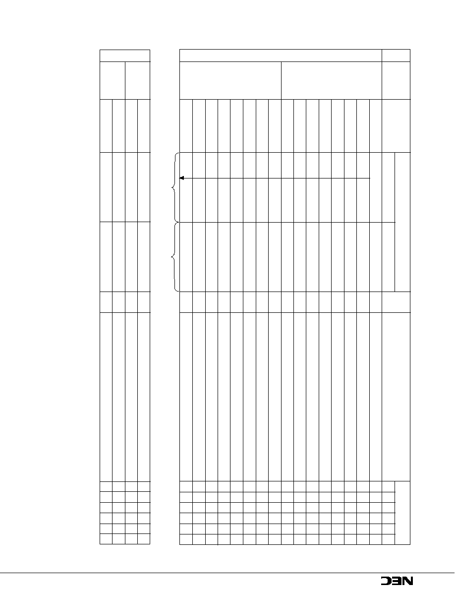
µ
PD70433
117
CY
1 1 1 1 1 0 0 0
1
CY
0
0
CLR1
DIR
1 1 1 1 1 1 0 0
1
DIR
0
CY
1 1 1 1 1 0 0 1
1
CY
1
1
SET1
DIR
1 1 1 1 1 1 0 1
1
DIR
0
Operation Code
Flags
Mnemonic
Operand(s)
Bytes
Operation
7 6 5 4 3 2 1 0
7 6 5 4 3 2 1 0
AC CY V
P
S
Z
reg8, CL
0 0 0 1 0 0 1 0
1 1 0 0 0
reg
3
reg8 bit NO.CL
0
mem8, CL
0 0 1 0
mod 0 0 0 mem
3 to 5
(mem8) bit NO.CL
0
reg16, CL
0 0 1 1
1 1 0 0 0
reg
3
reg16 bit NO.CL
0
mem16, CL
0 0 1 1
mod 0 0 0 mem
3 to 5
(mem16) bit NO.CL
0
CLR1
reg8, imm3
1 0 1 0
1 1 0 0 0
reg
4
reg8 bit NO.imm3
0
mem8, imm3
1 0 1 0
mod 0 0 0 mem
4 to 6
(mem8) bit NO.imm3
0
reg16, imm4
1 0 1 1
1 1 0 0 0
reg
4
reg16 bi NO.imm4
0
mem16, imm4
1 0 1 1
mod 0 0 0 mem
4 to 6
(mem16) bit NO.imm4
0
reg8, CL
0 1 0 0
1 1 0 0 0
reg
3
reg8 bit NO.CL
1
mem8, CL
0 1 0 0
mod 0 0 0 mem
3 to 5
(mem8) bit NO.CL
1
reg16, CL
0 1 0 1
1 1 0 0 0
reg
3
reg16 bit NO.CL
1
mem16, CL
0 1 0 1
mod 0 0 0 mem
3 to 5
(mem16) bit NO.CL
1
SET1
reg8, imm3
1 1 0 0
1 1 0 0 0
reg
4
reg8 bit NO.imm3
1
mem8, imm3
1 1 0 0
mod 0 0 0 mem
4 to 6
(mem8) bit NO.imm3
1
reg16, imm4
1 1 0 1
1 1 0 0 0
reg
4
reg16 bi NO.imm4
1
mem16, imm4
1 1 0 1
mod 0 0 0 mem
4 to 6
(mem16) bit NO.imm4
1
Instruction
Group
2nd byte *
3rd byte *
*
1st byte = 0FH
Bit manipulation instructions
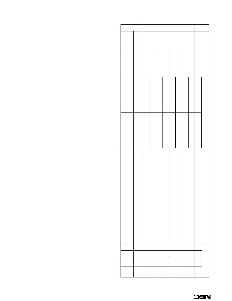
µ
PD70433
118
Operation Code
Flags
Mnemonic
Operand(s)
Bytes
Operation
7 6 5 4 3 2 1 0
7 6 5 4 3 2 1 0
AC CY V
P
S
Z
0 0 0 0 1 1 1 1
0 0 1 1 1 1 0 0
reg8
3
U
U
U
U
U
◊
1 1 0 0 0
reg
0 0 0 0 1 1 1 1
0 0 1 1 1 1 0 0
mem8
3 to 5
U
U
U
U
U
◊
mod 0 0 0 mem
BSCH*
0 0 0 0 1 1 1 1
0 0 1 1 1 1 0 1
reg16
3
U
U
U
U
U
◊
1 1 0 0 0
reg
0 0 0 0 1 1 1 1
0 0 1 1 1 1 0 1
mem16
3 to 5
U
U
U
U
U
◊
mod 0 0 0 mem
QHOUT
*
imm16
0 0 0 0 1 1 1 1
0 1 1 1 0 0 0 0
4
Removes block queued at head of queue and stores its
U
U
U
U
U
◊
segment address in P2.
QOUT*
imm16
0 0 0 0 1 1 1 1
0 1 1 1 0 0 0 1
4
Removes queue block indicated by P2.
U
U
U
U
U
◊
QTIN*
imm16
0 0 0 0 1 1 1 1
0 1 1 1 0 0 1 0
4
Queues block indicated by P2 at end of queue.
Bit manipulation
instruction
Queue manipu-
lation instructions
Instruction
Group
*
This instruction is newly added to the V25 or V35.
Remarks
P2: Parameter table (in register file)
<1> CL
0
<2> [When reg8 bit No.CL=0]
if CL<7, re-executed from CL
CL+1, <2>
if CL=7 Z
1
[When reg8 bit No.CL=1]
Z
0
<1> CL
0
<2> [When mem8 bit No.CL=0] if CL<7, re-executed from CL
CL+1, <2>
if CL=7 Z
1
[When mem8 bit No.CL=1] Z
0
<1> CL
0
<2> [When reg16 bit No.CL=0]
if CL<15, re-executed from CL
CL+1, <2>
if CL=15 Z
1
[When reg16 bit No.CL=1]
Z
0
<1> CL
0
<2> [When mem16 bit No.CL=0]
if CL<15, re-executed from CL
CL+1, <2>
if CL=15 Z
1
[When mem16 bit No.CL=1]
Z
0
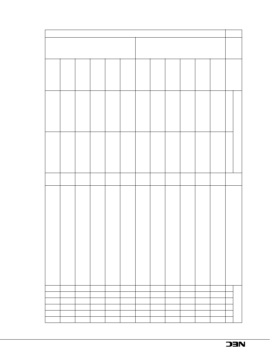
µ
PD70433
119
Operation Code
Flags
Mnemonic
Operand(s)
Bytes
Operation
7 6 5 4 3 2 1 0
7 6 5 4 3 2 1 0
AC CY V
P
S
Z
CY
reg MSB, reg
reg
◊
2
reg, 1
1 1 0 1 0 0 0 W
1 1 1 0 0
reg
2
If reg MSB
CY, V
1
U
◊ ◊ ◊ ◊ ◊
If reg MSB = CY, V
0
CY
(mem) MSB, (mem)
(mem)
◊
2
mem, 1
1 1 0 1 0 0 0 W
mod 1 0 0 mem
2 to 4
If (mem) MSB
CY, V
1
U
◊ ◊ ◊ ◊ ◊
If (mem) MSB = CY, V
0
temp
CL, while temp
0, the following operations are
reg, CL
1 1 0 1 0 0 1 W
1 1 1 0 0
reg
2
repeated: CY
reg MSB, reg
reg
◊
2
U
◊
U
◊ ◊ ◊
temp
temp ≠ 1
SHL
temp
CL, while temp
0, the following operations are
mem, CL
1 1 0 1 0 0 1 W
mod 1 0 0 mem
2 to 4
repeated: CY
(mem) MSB, (mem)
(mem)
◊
2
U
◊
U
◊ ◊ ◊
temp
temp ≠ 1
temp
imm8, while temp
0, the following operations are
reg, imm8
1 1 0 0 0 0 0 W
1 1 1 0 0
reg
3
repeated: CY
reg MSB, reg
reg
◊
2
U
◊
U
◊ ◊ ◊
temp
temp ≠ 1
temp
imm8, while temp
0, the following operations are
mem, imm8
1 1 0 0 0 0 0 W
mod 1 0 0 mem
3 to 5
repeated: CY
(mem) MSB, (mem)
(mem)
◊
2
U
◊
U
◊ ◊ ◊
temp
temp ≠ 1
CY
reg LSB, reg
reg
˜
2
reg, 1
1 1 0 1 0 0 0 W
1 1 1 0 1
reg
2
If reg MSB
bit after reg MSB: V
1
U
◊ ◊ ◊ ◊ ◊
If reg MSB = bit after reg MSB: V
0
CY
(mem) LSB, (mem)
(mem)
˜
2
mem, 1
1 1 0 1 0 0 0 W
mod 1 0 1 mem
2 to 4
If (mem) MSB
bit after (mem) MSB: V
1
U
◊ ◊ ◊ ◊ ◊
If (mem) MSB = bit after (mem) MSB: V
0
temp
CL, while temp
0, the following operations are
reg, CL
1 1 0 1 0 0 1 W
1 1 1 0 1
reg
2
repeated: CY
reg LSB, reg
reg
˜
2
U
◊
U
◊ ◊ ◊
temp
temp ≠ 1
SHR
temp
CL, while temp
0, the following operations are
mem, CL
1 1 0 1 0 0 1 W
mod 1 0 1 mem
2 to 4
repeated: CY
(mem) LSB, (mem)
(mem)
˜
2
U
◊
U
◊ ◊ ◊
temp
temp ≠ 1
temp
imm8, while temp
0, the following operations are
reg, imm8
1 1 0 0 0 0 0 W
1 1 1 0 1
reg
3
repeated: CY
reg LSB, reg
reg
˜
2
U
◊
U
◊ ◊ ◊
temp
temp ≠ 1
temp
imm8, while temp
0, the following operations are
mem, imm8
1 1 0 0 0 0 0 W
mod 1 0 1 mem
3 to 5
repeated: CY
(mem) LSB, (mem)
(mem)
˜
2
U
◊
U
◊ ◊ ◊
temp
temp ≠ 1
Instruction
Group
Shift instructions

µ
PD70433
120
Instruction
Group
Operation Code
Flags
Mnemonic
Operand(s)
Bytes
Operation
7 6 5 4 3 2 1 0
7 6 5 4 3 2 1 0
AC CY V
P
S
Z
CY
reg LSB, reg
reg
˜
2, V
0
reg, 1
1 1 0 1 0 0 0 W
1 1 1 1 1
reg
2
MSB of operand is unchanged.
U
◊
0
◊ ◊ ◊
CY
(mem) LSB, (mem)
(mem)
˜
2, V
0
mem, 1
1 1 0 1 0 0 0 W
mod 1 1 1 mem
2 to 4
MSB of operand is unchanged.
U
◊
0
◊ ◊ ◊
temp
CL, while temp
0, the following operations are
reg, CL
1 1 0 1 0 0 1 W
1 1 1 1 1
reg
2
repeated: CY
reg LSB, reg
reg
˜
2
U
◊
U
◊ ◊ ◊
temp
temp ≠ 1, MSB of operand is unchanged.
SHRA
temp
CL, while temp
0, the following operations are
mem, CL
1 1 0 1 0 0 1 W
mod 1 1 1 mem
2 to 4
repeated: CY
(mem) LSB, (mem)
(mem)
˜
2
U
◊
U
◊ ◊ ◊
temp
temp ≠ 1, MSB of operand is unchanged.
temp
imm8, while temp
0, the following operations are
reg, imm8
1 1 0 0 0 0 0 W
1 1 1 1 1
reg
3
repeated: CY
reg LSB, reg
reg
˜
2
U
◊
U
◊ ◊ ◊
temp
temp ≠ 1, MSB of operand is unchanged.
temp
imm8, while temp
0, the following operations are
mem, imm8
1 1 0 0 0 0 0 W
mod 1 1 1 mem
3 to 5
repeated: CY
(mem) LSB, (mem)
(mem)
˜
2
U
◊
U
◊ ◊ ◊
temp
temp ≠ 1, MSB of operand is unchanged.
CY
reg MSB, reg
reg
◊
2 + CY
reg, 1
1 1 0 1 0 0 0 W
1 1 0 0 0
reg
2
reg MSB
CY: V
1
◊ ◊
reg MSB = CY: V
0
CY
(mem) MSB, (mem)
(mem)
◊
2 + CY
mem, 1
1 1 0 1 0 0 0 W
mod 0 0 0 mem
2 to 4
(mem) MSB
CY: V
1
◊ ◊
(mem) MSB = CY: V
0
temp
CL, while temp
0, the following instructions are
reg, CL
1 1 0 1 0 0 1 W
1 1 0 0 0
reg
2
repeated: CY
reg MSB, reg
reg
◊
2 + CY
◊
U
temp
temp ≠ 1
ROL
temp
CL, while temp
0, the following instructions are
mem, CL
1 1 0 1 0 0 1 W
mod 0 0 0 mem
2 to 4
repeated: CY
(mem) MSB, (mem)
(mem)
◊
2 + CY
◊
U
temp
temp ≠ 1
temp
imm8, while temp
0, the following instructions are
reg, imm8
1 1 0 0 0 0 0 W
1 1 0 0 0
reg
3
repeated: CY
reg MSB, reg
reg
◊
2 + CY
◊
U
temp
temp ≠ 1
temp
imm8, while temp
0, the following instructions are
mem, imm8
1 1 0 0 0 0 0 W
mod 0 0 0 mem
3 to 5
repeated: CY
(mem) MSB, (mem)
(mem)
◊
2 + CY
◊
U
temp
temp ≠ 1
Rotate instruction
Shift instruction

µ
PD70433
121
Operation Code
Flags
Mnemonic
Operand(s)
Bytes
Operation
7 6 5 4 3 2 1 0
7 6 5 4 3 2 1 0
AC CY V
P
S
Z
CY
reg LSB, reg
reg
˜
2
reg, 1
1 1 0 1 0 0 0 W
1 1 0 0 1
reg
2
reg MSB
CY
◊ ◊
reg MSB
bit after reg MSB: V
1
reg MSB = bit after reg MSB: V
0
CY
(mem) LSB, (mem)
(mem)
˜
2
mem, 1
1 1 0 1 0 0 0 W
mod 0 0 1 mem
2 to 4
(mem) MSB
CY
◊ ◊
(mem) MSB
bit after (mem) MSB: V
1
(mem) MSB = bit after (mem) MSB: V
0
temp
CL, while temp
0, the following operations are
reg, CL
1 1 0 1 0 0 1 W
1 1 0 0 1
reg
2
repeated: CY
reg LSB, reg
reg
˜
2
◊
U
reg MSB
CY
temp
temp ≠ 1
ROR
temp
CL, while temp
0, the following operations are
mem, CL
1 1 0 1 0 0 1 W
mod 0 0 1 mem
2 to 4
repeated: CY
(mem) LSB, (mem)
(mem)
˜
2
◊
U
(mem) MSB
CY
temp
temp ≠ 1
temp
imm8, while temp
0, the following operations are
reg, imm8
1 1 0 0 0 0 0 W
1 1 0 0 1
reg
3
repeated: CY
reg LSB, reg
reg
˜
2
◊
U
reg MSB
CY
temp
temp ≠ 1
temp
imm8, while temp
0, the following operations are
mem, imm8
1 1 0 0 0 0 0 W
mod 0 0 1 mem
3 to 5
repeated: CY
(mem) LSB, (mem)
(mem)
˜
2
◊
U
(mem) MSB
CY
temp
temp ≠ 1
tmpcy
CY, CY
reg MSB
reg, 1
1 1 0 1 0 0 0 W
1 1 0 1 0
reg
2
reg
reg
◊
2 + tmpcy
◊ ◊
reg MSB
CY: V
1
reg MSB = CY: V
0
tmpcy
CY, CY
(mem) MSB
mem, 1
1 1 0 1 0 0 0 W
mod 0 1 0 mem
2 to 4
(mem)
(mem)
◊
2 + tmpcy
◊ ◊
(mem) MSB
CY: V
1
(mem) MSB = CY: V
0
ROLC
temp
CL, while temp
0, the following operations are
reg, CL
1 1 0 1 0 0 1 W
1 1 0 1 0
reg
2
repeated: tmpcy
CY, CY
reg MSB
◊
U
reg
reg
◊
2 + tmpcy
temp
temp ≠ 1
temp
CL, while temp
0, the following operations are
mem, CL
1 1 0 1 0 0 1 W
mod 0 1 0 mem
2 to 4
repeated: tmpcy
CY, CY
(mem) MSB
◊
U
(mem)
(mem)
◊
2 + tmpcy
temp
temp ≠ 1
Rotate instructions
Instruction
Group

µ
PD70433
122
Operation Code
Flags
Mnemonic
Operand(s)
Bytes
Operation
7 6 5 4 3 2 1 0
7 6 5 4 3 2 1 0
AC CY V
P
S
Z
temp
imm8, while temp
0, the following instructions
reg, imm8
1 1 0 0 0 0 0 W
1 1 0 1 0
reg
3
are repeated: tmpcy
CY, CY
reg MSB
◊
U
reg
reg
◊
2 + tmpcy
temp
temp ≠ 1
ROLC
temp
imm8, while temp
0, the following instructions
mem, imm8
1 1 0 0 0 0 0 W
mod 0 1 0 mem
3 to 5
are repeated: tmpcy
CY, CY
(mem) MSB
◊
U
(mem)
(mem)
◊
2 + tmpcy
temp
temp ≠ 1
tmpcy
CY, CY
reg LSB
reg
reg
˜
2
reg, 1
1 1 0 1 0 0 0 W
1 1 0 1 1
reg
2
reg MSB
tmpcy
◊ ◊
reg MSB
bit after reg MSB: V
1
reg MSB = bit after reg MSB: V
0
tmpcy
CY, CY
(mem) LSB
(mem)
(mem)
˜
2
mem, 1
1 1 0 1 0 0 0 W
mod 0 1 1 mem
2 to 4
(mem) MSB
tmpcy
◊ ◊
(mem) MSB
bit after (mem) MSB: V
1
(mem) MSB = bit after (mem) MSB: V
0
temp
CL, while temp
0, the following operations are
repeated: tmpcy
CY, CY
reg LSB
reg, CL
1 1 0 1 0 0 1 W
1 1 0 1 1
reg
2
reg
reg
˜
2
◊
U
reg MSB
tmpcy
temp
temp ≠ 1
RORC
temp
CL, while temp
0, the following operations are
repeated: tmpcy
CY, CY
(mem) LSB
mem, CL
1 1 0 1 0 0 1 W
mod 0 1 1 mem
2 to 4
(mem)
(mem)
˜
2
◊
U
(mem) MSB
tmpcy
temp
temp ≠ 1
temp
imm8, while temp
0, the following operations are
repeated: tmpcy
CY, CY
reg LSB
reg, imm8
1 1 0 0 0 0 0 W
1 1 0 1 1
reg
3
reg
reg
˜
2
◊
U
reg MSB
tmpcy
temp
temp ≠ 1
temp
imm8, while temp
0, the following operations are
repeated: tmpcy
CY, CY
(mem) LSB
mem, imm8
1 1 0 0 0 0 0 W
mod 0 1 1 mem
3 to 5
(mem)
(mem)
˜
2
◊
U
(mem) MSB
tmpcy
temp
temp ≠ 1
Rotate instructions
Instruction
Group
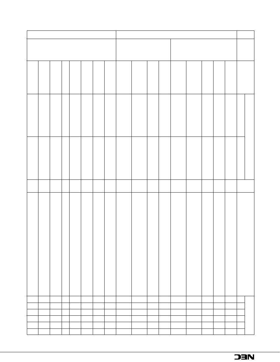
µ
PD70433
123
Operation Code
Flags
Mnemonic
Operand(s)
Bytes
Operation
7 6 5 4 3 2 1 0
7 6 5 4 3 2 1 0
AC CY V
P
S
Z
near-proc
1 1 1 0 1 0 0 0
3
(SP ≠ 1, SP ≠ 2)
PC, SP
SP ≠ 2
PC
PC + disp
regptr16
1 1 1 1 1 1 1 1
1 1 0 1 0
reg
2
(SP ≠ 1, SP ≠ 2)
PC, SP
regptr16
SP
SP ≠ 2
CALL
memptr16
1 1 1 1 1 1 1 1
mod 0 1 0 mem
2 to 4
(SP ≠ 1, SP ≠ 2)
PC, SP
SP ≠ 2
PC
(memptr16)
(SP ≠ 1, SP ≠ 2)
PS, (SP ≠ 3, SP ≠ 4)
PC
far-proc
1 0 0 1 1 0 1 0
5
SP
SP ≠ 4
PC
seg, PC
offset
(SP ≠ 1, SP ≠ 2)
PS, (SP ≠ 3, SP ≠ 4)
PC
memptr32
1 1 1 1 1 1 1 1
mod 0 1 1 mem
2 to 4
SP
SP ≠ 4
PC
(memptr32 + 2), PC
(memptr32)
1 1 0 0 0 0 1 1
1
PC
(SP + 1, SP)
SP
SP + 2
pop-value
1 1 0 0 0 0 1 0
3
PC
(SP + 1, SP)
SP
SP + 2, SP
SP + pop-value
RET
PC
(SP + 1, SP)
1 1 0 0 1 0 1 1
1
PS
(SP + 3, SP + 2)
SP
SP + 4
PC
(SP + 1, SP)
pop-value
1 1 0 0 1 0 1 0
3
PS
(SP + 3, SP + 2)
SP
SP + 4, SP
SP + pop-value
mem16
1 1 1 1 1 1 1 1
mod 1 1 0 mem
2 to 4
(SP ≠ 1, SP ≠ 2)
(mem16)
SP
SP ≠ 2
reg16
0 1 0 1 0
reg
1
(SP ≠ 1, SP ≠ 2)
reg16
SP
SP ≠ 2
sreg
0 0 0 sreg 1 1 0
1
(SP ≠ 1, SP ≠ 2)
sreg
SP
SP ≠ 2
PSW
1 0 0 1 1 1 0 0
1
(SP ≠ 1, SP ≠ 2)
PSW
PUSH
SP
SP ≠ 2
R
0 1 1 0 0 0 0 0
1
Push registers on the stack
imm8
0 1 1 0 1 0 1 0
2
(SP ≠ 1, SP ≠ 2)
imm8 sign extension
SP
SP ≠ 2
imm16
0 1 1 0 1 0 0 0
3
(SP ≠ 1, SP ≠ 2)
imm16
SP
SP ≠ 2
DS2
*
0 0 0 0 1 1 1 1
0 0 1 1 1 1 1 0
2
(SP ≠ 1, SP ≠ 2)
DS2
SP
SP ≠ 2
Instruction
Group
Stack manipulation instruction
Subroutine control instructions
*
This instruction is newly added to the V25 or V35.

µ
PD70433
124
Operation Code
Flags
Mnemonic
Operand(s)
Bytes
Operation
7 6 5 4 3 2 1 0
7 6 5 4 3 2 1 0
AC CY V
P
S
Z
PUSH
DS3/VPC
*
0 0 0 0 1 1 1 1
0 0 1 1 0 1 1 0
2
(SP ≠ 1, SP ≠ 2)
DS3/VPC
SP
SP ≠ 2
mem16
1 0 0 0 1 1 1 1
mod 0 0 0 mem
2 to 4
SP
SP + 2
(mem16)
(SP ≠ 1, SP ≠ 2)
reg16
0 1 0 1 1
reg
1
SP
SP + 2
reg16
(SP ≠ 1, SP ≠ 2)
sreg
0 0 0 sreg 1 1 1
1
SP
SP + 2
sreg : SS, DS0, DS1
sreg16
(SP ≠ 1, SP ≠ 2)
POP
PSW
1 0 0 1 1 1 0 1
1
SP
SP + 2
R
R
R
R
R
R
PSW
(SP ≠ 1, SP ≠ 2)
R
0 1 1 0 0 0 0 1
1
Pop registers from the stack
DS2
*
0 0 0 0 1 1 1 1
0 0 1 1 1 1 1 1
2
SP
SP + 2
DS2
(SP ≠ 1, SP ≠ 2)
DS3/VPC
*
0 0 0 0 1 1 1 1
0 0 1 1 0 1 1 1
2
SP
SP + 2
DS3/VPC
(SP ≠ 1, SP ≠ 2)
PREPARE
imm16, imm8
1 1 0 0 1 0 0 0
4
Prepare New Stack Frame
DISPOSE
1 1 0 0 1 0 0 1
1
Dispose of Stack Frame
near-label
1 1 1 0 1 0 0 1
3
PC
PC + disp
short-label
1 1 1 0 1 0 1 1
2
PC
PC + ext-disp8
regptr16
1 1 1 1 1 1 1 1
1 1 1 0 0
reg
2
PC
regptr16
BR
memptr16
1 1 1 1 1 1 1 1
mod 1 0 0 mem
2 to 4
PC
(memptr16)
far-label
1 1 1 0 1 0 1 0
5
PS
seg
PC
offset
memptr32
1 1 1 1 1 1 1 1
mod 1 0 1 mem
2 to 4
PS
(memptr32 + 2)
PC
(memptr32)
Instruction
Group
Branch instruction
Stack manipulation instructions
*
This instruction is newly added to the V25 or V35.
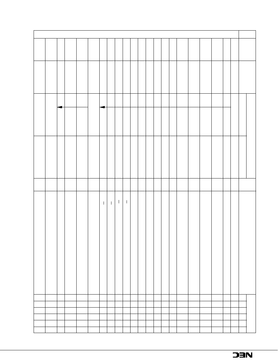
µ
PD70433
125
Instruction
Group
Conditional branch instructions
* 1.
This instruction is newly added to the V20 or V30.
2.
This instruction is newly added to the V25 or V35.
Operation Code
Flags
Mnemonic
Operand(s)
Bytes
Operation
7 6 5 4 3 2 1 0
7 6 5 4 3 2 1 0
AC CY V
P
S
Z
BV
short-label
0 1 1 1 0 0 0 0
2
if V = 1
PC
PC + ext-disp8
BNV
short-label
0 0 0 1
2
if V = 0
PC
PC + ext-disp8
BC
short-label
0 0 1 0
2
if CY = 1
PC
PC + ext-disp8
BL
BNC
short-label
0 0 1 1
2
if CY = 0
PC
PC + ext-disp8
BNL
BE
short-label
0 1 0 0
2
if Z = 1
PC
PC + ext-disp8
BZ
BNE
short-label
0 1 0 1
2
if Z = 0
PC
PC + ext-disp8
BNZ
BNH
short-label
0 1 1 0
2
if CY
Z = 1
PC
PC + ext-disp8
BH
short-label
0 1 1 1
2
if CY
Z = 0
PC
PC + ext-disp8
BN
short-label
1 0 0 0
2
if S = 1
PC
PC + ext-disp8
BP
short-label
1 0 0 1
2
if S = 0
PC
PC + ext-disp8
BPE
short-label
1 0 1 0
2
if P = 1
PC
PC + ext-disp8
BPO
short-label
1 0 1 1
2
if P = 0
PC
PC + ext-disp8
BLT
short-label
1 1 0 0
2
if S
V = 1
PC
PC + ext-disp8
BGE
short-label
1 1 0 1
2
if S
V = 0
PC
PC + ext-disp8
BLE
short-label
1 1 1 0
2
if (S
Z)
Z = 1
PC
PC + ext-disp8
BGT
short-label
1 1 1 1
2
if (S
V)
Z = 0
PC
PC + ext-disp8
DBNZNE
short-label
1 1 1 0 0 0 0 0
2
CW = CW ≠ 1
PC
PC + ext-disp8
if Z = 0 and CW
0
DBNZE
short-label
0 0 0 1
2
CW = CW ≠ 1
PC
PC + ext-disp8
if Z = 1 and CW
0
DBNZ
short-label
0 0 1 0
2
CW = CW ≠ 1
PC
PC + ext-disp8
if CW
0
BCWZ
short-label
0 0 1 1
2
if CW = 0
PC
PC + ext-disp8
BTCLR
*1
sfr, imm3,
0 0 0 0 1 1 1 1
1 0 0 1 1 1 0 0
5
If (sfr) bit No. imm3 = 1:
short-label
PC
PC + ext-disp8, (sfr) bit No.imm3
0
BTCLRL
*2
sfrl, imm3,
0 0 0 0 1 1 1 1
1 0 0 1 1 1 0 1
5
If (sfrl) bit No. imm3 = 1:
short-label
PC
PC + ext-disp8, (sfrl) bit No.imm3
0
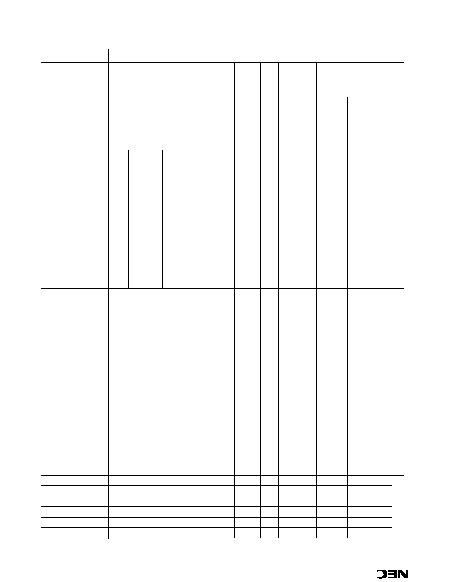
µ
PD70433
126
Operation Code
Flags
Mnemonic
Operand(s)
Bytes
Operation
7 6 5 4 3 2 1 0
7 6 5 4 3 2 1 0
AC CY V
P
S
Z
(SP ≠ 1, SP ≠ 2)
PSW, (SP ≠ 3, SP ≠ 4)
PS
3
1 1 0 0 1 1 0 0
1
(SP ≠ 5, SP ≠ 6)
PC, SP
SP ≠ 6
IE
0, BRK
0
PS
(15, 14), PC
(13, 12)
BRK
(SP ≠ 1, SP ≠ 2)
PSW, (SP ≠ 3, SP ≠ 4)
PS
imm8
1 1 0 0 1 1 0 1
2
(SP ≠ 5, SP ≠ 6)
PC, SP
SP ≠ 6
(
3)
IE
0, BRK
0
PS
(n
◊
4 + 3, n
◊
4 + 2), PC
(n
◊
4 + 1, n
◊
4) n = imm8
If V = 1:
(SP ≠ 1, SP ≠ 2)
PSW, (SP ≠ 3, SP ≠ 4)
PS
BRKV
1 1 0 0 1 1 1 0
1
(SP ≠ 5, SP ≠ 6)
PC, SP
SP ≠ 6
IE
0, BRK
0
PS
(19, 18), PC
(17, 16)
RETI
1 1 0 0 1 1 1 1
1
PC
(SP + 1, SP), PS
(SP + 3, SP + 2)
R
R
R
R
R
R
PSW
(SP + 5, SP + 4), SP
SP + 6
RETRBI*
0 0 0 0 1 1 1 1
1 0 0 1 0 0 0 1
2
PC
Value of PC save area in currently selected bank
R
R
R
R
R
R
register, PSW
Value of PSW save area in currently
selected bank register
FINT
*
0 0 0 0 1 1 1 1
1 0 0 1 0 0 1 0
2
Indicates to interrupt controller incorporated in CPU
that interrupt servicing has ended.
If (mem32) > reg16 or (mem32 + 2) < reg16
(SP ≠ 1, SP ≠ 2)
PSW, (SP ≠ 3, SP ≠ 4)
PS
CHKIND
reg, mem32
0 1 1 0 0 0 1 0
mod reg mem
2 to 4
(SP ≠ 5, SP ≠ 6)
PC, SP
SP ≠ 6
IE
0, BRK
0
PS
(23, 22), PC
(21, 20)
0 0 0 0 1 1 1 1
0 0 1 0 1 1 0 1
BRKCS*
reg16
3
1 1 0 0 0
reg
0 0 0 0 1 1 1 1
1 0 0 1 0 1 0 0
PSW save area in currently selected register bank
PSW
PC save area in currently selected register bank
PC
TSKSW*
reg16
3
RB3-0
reg16 low-order 4 bits
◊ ◊ ◊ ◊ ◊ ◊
1 1 1 1 1
reg
PSW
Value of PSW save area in newly selected register bank
PC
Value of PC save area in newly selected register bank
If CH + CL
16: BW, DW
DS1:IY output to transmit
ALBIT
0 0 0 0 1 1 1 1
1 0 0 1 1 0 1 0
2
buffer If CH + CL < 16: CH + CL
CH, BW, DW
BW
U
◊
U
U
U
◊
Part exceeding 16 bits: CH+CL≠16
CH, BW, DW
BW
Stores 1 line pixel data change point information in
COLTRP
0 0 0 0 1 1 1 1
1 0 0 1 1 0 1 1
2
change point table (start white run length).
MHENC
0 0 0 0 1 1 1 1
1 0 0 1 0 0 1 1
2
Generates MH code from change point table.
U
◊
U
U
U
◊
MRENC
0 0 0 0 1 1 1 1
1 0 0 1 0 1 1 1
2
Generates MR code from change point table.
U
◊
U
U
U
◊
Instruction
Group
Interrupt instructions
temp
PSW
RB3 to 0
reg16 low≠order 4 bits, IE
0, BRK
0
PSW save area in newly selected register bank
temp
PC save area in newly selected register bank
PC
*
This instruction is newly added to the V20 or V30.
Dedicated fax
instructions
Register bank
switching instructions

µ
PD70433
127
Operation Code
Flags
Mnemonic
Operand(s)
Bytes
Operation
7 6 5 4 3 2 1 0
7 6 5 4 3 2 1 0
AC CY V
P
S
Z
SCHEOL
0 0 0 0 1 1 1 1
0 1 1 1 1 0 0 0
2
"EOL" detection in MH/MR code
U
◊
U
U
U
◊
GETBIT
0 0 0 0 1 1 1 1
0 1 1 1 1 0 0 1
2
Fetches pixel data start bit and sets it to CY flag.
U
◊
U
U
U
◊
MHDEC
0 0 0 0 1 1 1 1
0 1 1 1 1 1 0 0
2
Generates change point table from MH code.
U
◊
U
U
U
◊
MRDEC
0 0 0 0 1 1 1 1
0 1 1 1 1 1 0 1
2
Generates change point table from MR code.
U
◊
U
U
U
◊
Converts 1 line change point information in change
CNVTRP
0 0 0 0 1 1 1 1
0 1 1 1 1 0 1 0
2
point table to pixel data.
HALT
1 1 1 1 0 1 0 0
1
CPU Halt
STOP*1
0 0 0 0 1 1 1 1
1 0 0 1 1 1 1 0
2
CPU Stop
POLL
1 0 0 1 1 0 1 1
1
Poll and wait
DI
1 1 1 1 1 0 1 0
1
IE
0
EI
1 1 1 1 1 0 1 1
1
IE
1
BUSLOCK
1 1 1 1 0 0 0 0
1
Bus Lock Prefix
fp-op
1 1 0 1 1 X X X
1 1 Y Y Y Z Z Z
2
(SP ≠ 1, SP ≠ 2)
PSW, (SP ≠ 3, SP ≠ 4)
PS
FPO1
fp-op, mem
1 1 0 1 1 X X X
mod Y Y Y mem
2 to 4
(SP ≠ 5, SP ≠ 6)
PC ≠ x*6, SP
SP ≠ 6
fp-op
0 1 1 0 0 1 1 X
1 1 Y Y Y Z Z Z
2
IE
0, BRK
0
FPO2
fp-op, mem
0 1 1 0 0 1 1 X
mod Y Y Y mem
2 to 4
PC
(01DH; 01CH), PS
(01FH, 01EH)
NOP
1 0 0 1 0 0 0 0
1
No Operation
0 0 0 0 1 1 1 1
1 0 0 1 0 1 1 0
RSTWDT*2 imm8, imm8
4
imm8
imm8
*4
0 0 1 sreg 1 1 0
1
Segment override prefix
DS2: *2
0 1 1 0 0 0 1 1
1
Extended segment override prefix
DS3: *2
1 1 0 1 0 1 1 0
1
Extended segment override prefix
IRAM: *2
1 1 1 1 0 0 0 1
1
Register file override prefix
Instruction
Group
Dedicated fax instruc
tions
*3
*5
* 1.
This instruction is newly added to the V20 or V30.
2.
This instruction is newly added to the V25 or V35.
3.
Watchdog timer manipulation instruction
4.
Four kinds: DS0:, DS1:, PS:, SS:
5.
Register file space access override prefix instruction
6.
x: Number of instruction bytes + number of prefixes
When imm8 = imm8'
WDM register
imm8
When imm8
imm8'
(SP ≠ 1, SP ≠ 2)
PSW, (SP ≠ 3, SP ≠ 4)
PS
(SP ≠ 5, SP ≠ 6)
PC ≠ x
*6
, SP
SP ≠ 6
IE
0, BRK
0
PC
(20H, 21H), PS
(22H, 23H)
CPU control instructions
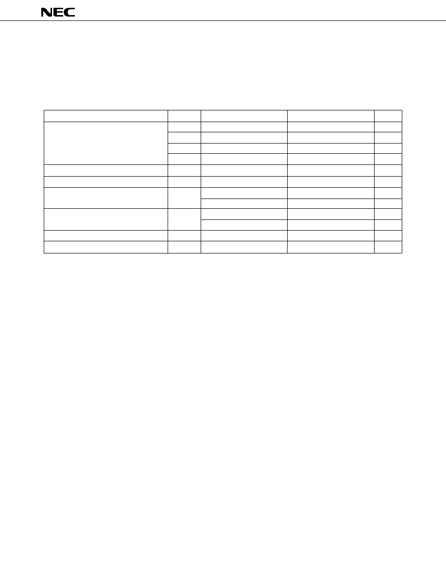
128
µ
PD70433
18. ELECTRICAL SPECIFICATIONS
This section shows the electrical specifications of the V55PI
TM
using the three categories below.
µ
PD70433GD/R/GJ-12:
µ
PD70433-12
µ
PD70433GD/R/GJ-16:
µ
PD70433-16
ABSOLUTE MAXIMUM RATINGS (T
A
= 25
∞
C)
PARAMETER
SYMBOL
TEST CONDITIONS
RATINGS
UNIT
V
DD
≠0.5 to +7.0
V
AV
DD
≠0.5 to V
DD
+ 0.5
V
Supply voltage
AV
SS
≠0.5 to +0.5
V
AV
REF
≠0.5 to AV
DD
+ 0.3
V
Input voltage
V
I
≠0.5 to V
DD
+ 0.5
V
Output voltage
V
O
≠0.5 to V
DD
+ 0.5
V
One pin
4.0
mA
Output current low
I
OL
Total of all pins
100
mA
One pin
≠1.0
mA
Output current high
I
OH
Total of all pins
≠20
mA
Operating ambient temperature
T
A
≠40 to +85
∞
C
Storage temperature
T
stg
≠65 to +150
∞
C
Notes 1. The IC product output (or input/output) pins should not be directly connected between V
DD
, V
CC
or GND.
However, direct connection between the open-drain pins or betwen the open collector pins is possible.
Direct connection is also possible for an external circuit via timing design that avoids collision of output
at pins which become high impedance.
2. Exceeding the absolute maximum ratings even in one of the parameters even for an instant may affect
the product quality.
That is, the absolute maximum ratings are rated values at which the product is on the verge of suffering
physical damage, and therefore avoid using the product close to the rated values. The specifications
and conditions shown in the DC characteristics and AC characteristics comprise the normal operation
and guaranteed quality range.
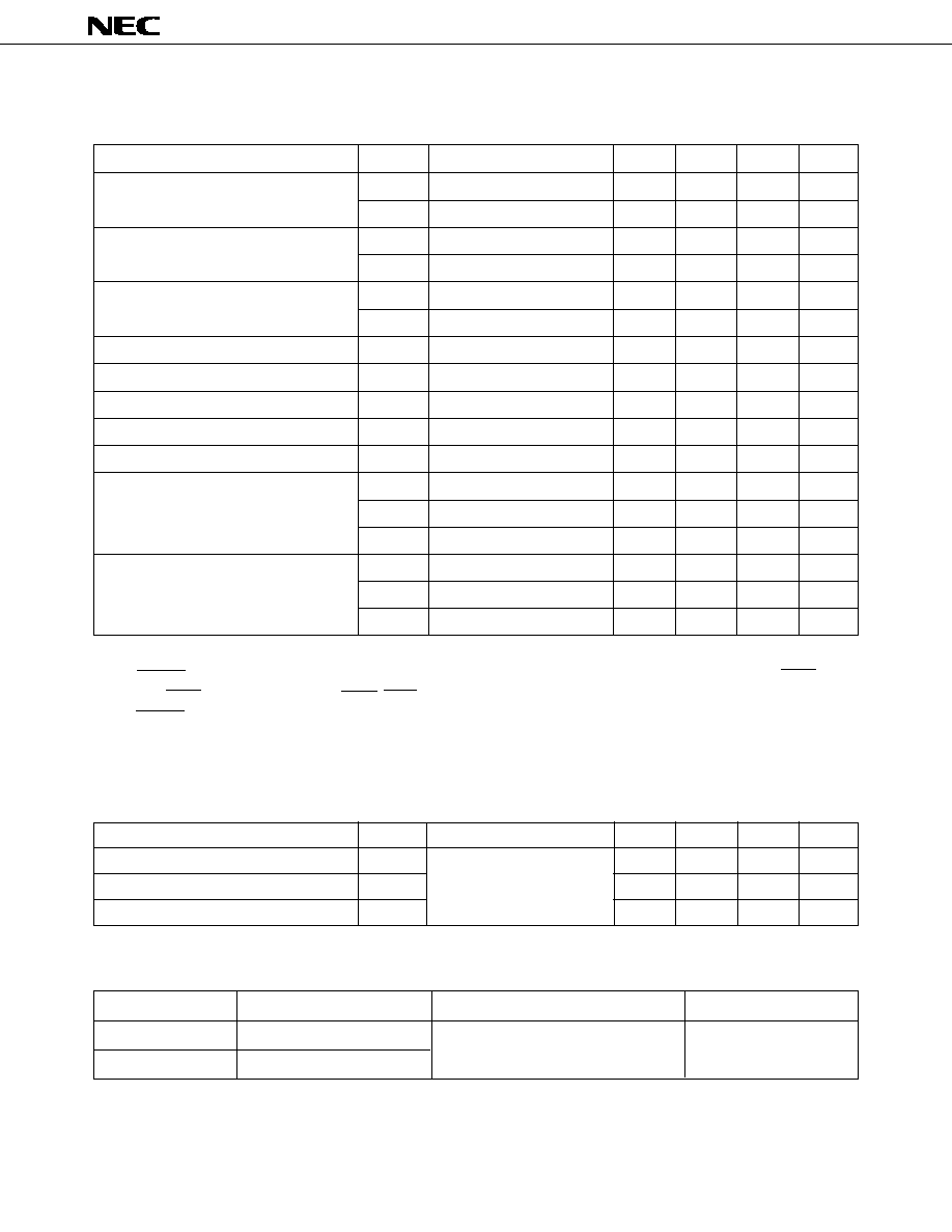
129
µ
PD70433
DC Characteristics (T
A
= ≠40 to +85
∞
C, V
DD
= +5.0 V
±
10 %)
PARAMETER
SYMBOL
TEST CONDITIONS
MIN.
TYP.
MAX.
UNIT
Input voltage low
V
IL1
*1
0
0.8
V
V
IL2
*2
0
0.2V
DD
V
Input voltage high
V
IH1
*1
2.2
V
DD
V
V
IH2
*2
0.8V
DD
V
DD
V
Schmitt-triggered input threshold voltage
V
T
+
*3, rise
3.3
V
V
T
≠
*3, fall
1.6
V
Schmitt-triggered input hysteresis width
V
T
+
≠ V
T
≠
*3
0.5
V
Output voltage low
V
OL
I
OL
= 2.0 mA
0.45
V
Output voltage high
V
OH
I
OH
= ≠0.4 mA
V
DD
≠1.0
V
Input leakage current
I
LI
0 V
V
I
V
DD
±
10
µ
A
Output leakage current
I
LO
0 V
V
O
V
DD
±
10
µ
A
V
DD
supply current*4
I
DD1
Operating mode
5.4f
X
+ 30 5.4f
X
+ 50
mA
I
DD2
HALT mode
3.7 f
X
3.7f
X
+ 20
mA
I
DD3
STOP mode
10
50
µ
A
AV
DD
supply current
AI
DD1
Operating mode
1.5
2.5
mA
AI
DD2
HALT mode
0.6
1
mA
AI
DD3
STOP mode
10
50
µ
A
* 1.
Other than *2
2.
RESET, P10/NMI, X1, P11/INTP0 to P16/INTP5, P30/TxD0/SO0/SB0, P31/RxD0/SB1/SI0, P32/TxC/SCK0,
P33/CTS0, P35/RxD1/SI1, P36/SCK1/CTS1
3.
RESET, P10/NMI, P11/INTP0 to P16/INTP5
4. The unit for the constants 5.4 and 3.7 is mA/MHz.
CAPACITANCE (T
A
= 25
∞
C, V
DD
= 0 V)
PARAMETER
SYMBOL
TEST CONDITIONS
MIN.
TYP.
MAX.
UNIT
Input capacitance
C
I
f
C
= 1 MHz
10
pF
Unmeasured pins are
Output capacitance
C
O
returned to 0 V.
20
pF
I/O capacitance
C
IO
20
pF
OPERATING CONDITIONS
PART NUMBER
INT. CLOCK FREQUENCY
OPERATING TEMPERATURE (T
A
)
SUPPLY VOLTAGE (V
DD
)
µ
PD70433-12
0.25 MHz
f
X
12.5 MHz
≠40 to +85
∞
C
+5.0 V
±
10 %
µ
PD70433-16
0.25 MHz
f
X
12.5 MHz

130
µ
PD70433
RECOMMENDED OSCILLATION CIRCUIT
The circuit shown below is recommended for a clock input.
(1) Ceramic resonator connection (T
A
= ≠40 to +85 ∞C
±
10 %, V
DD
= 5 V
±
10 %)
OSCILLATOR
RECOMMENDED CONSTANTS
MANUFACTURER
FREQUENCY
PRODUCT NAME
f
XX
[MHz]
C1 [pF]
C2 [pF]
Murata Mfg. Co., Ltd.
25
CSA25.00MXZ040
5
5
32
CSA32.00MXZ040
3
3
Notes 1. The oscillator should be located as close to the X1 and X2 pins as possible.
2. Other signal lines should not cross the dotted area.
3. When matching the
µ
PD70433 with a resonator, careful evaluation is required.
(2) Crystal resonator connection
(a) Basic-wave recommended condition (T
A
= ≠10 to +70 ∞C, V
DD
= 5 V
±
10 %)
OSCILLATOR
RECOMMENDED CONSTANTS
MANUFACTURER
FREQUENCY
PRODUCT NAME
f
XX
[MHz]
C1 [pF]
C2 [pF]
R [
]
Kinseki
25
HC≠49/U≠S
5
5
200
10
10
≠
Notes 1. The oscillator should be located as close to the X1 and X2 pins as possible.
2. Other signal lines should not cross the dotted area.
3. When matching the
µ
PD70433 with a resonator, careful evaluation is required.
X2
X1
C2
C1
X2
X1
C2
C1
R
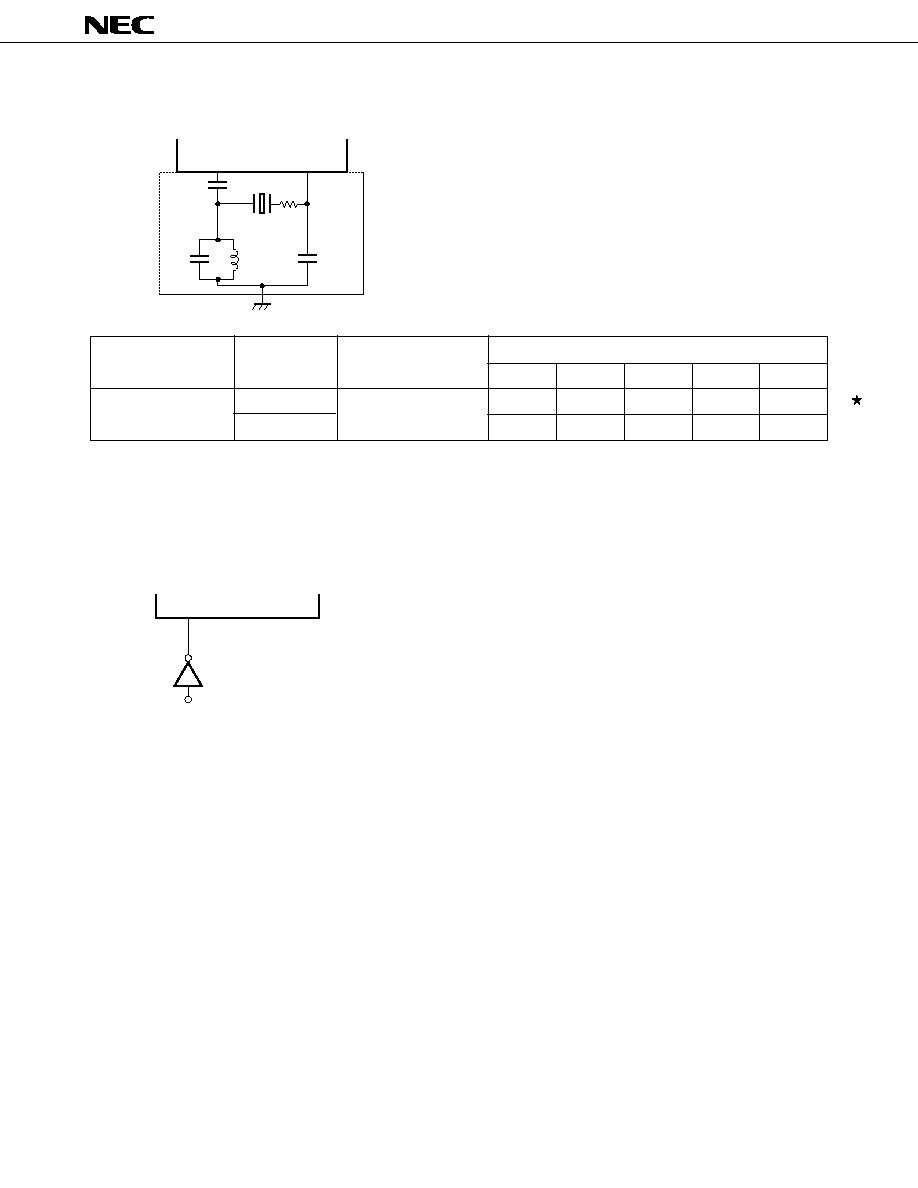
131
µ
PD70433
(b) 3rd-overtone recommended condition (T
A
= ≠20 to +70 ∞C, V
DD
= 5 V
±
10 %)
OSCILLATOR
RECOMMENDED CONSTANTS
MANUFACTURER
FREQUENCY
PRODUCT NAME
f
XX
[MHz]
C1 [pF]
C2 [pF]
C3 [pF]
L [
µ
H]
R [
]
Kinseki
25
HC≠49/U
15
15
1000
3.3
100
32
10
5
1000
3.3
100
Notes 1. The oscillator should be located as close to the X1 and X2 pins as possible.
2. Other signal lines should not cross the dotted area.
3. When matching the
µ
PD70433 with a resonator, careful evaluation is required.
(3) External clock input
X2
X1
C1
C2
L
C3
R
X1
X2
Open
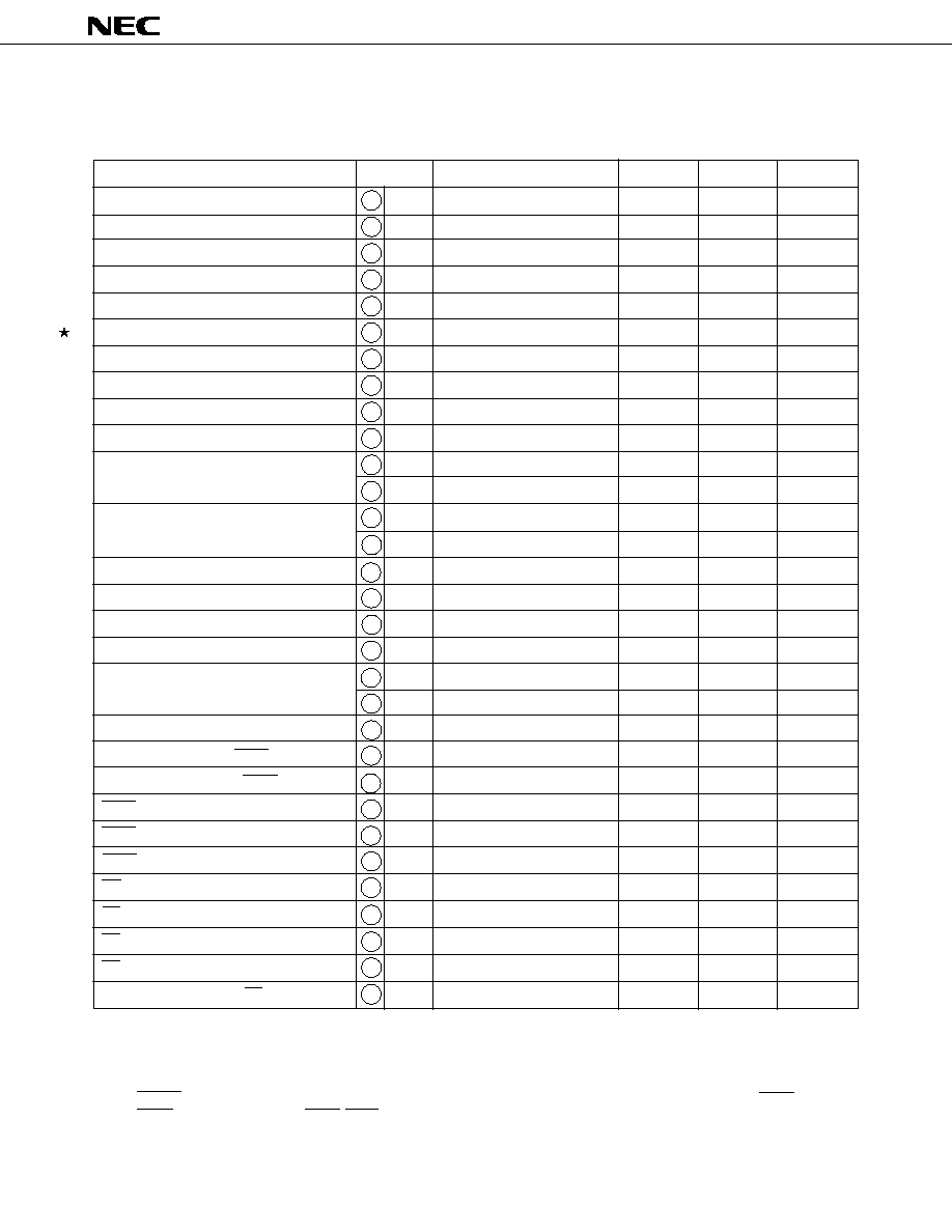
132
µ
PD70433
AC CHARACTERISTICS (T
A
= ≠40 to +85
∞
C, V
DD
= +5.0 V
±
10 %)
(1)
µ
PD70433-12
PARAMETER
SYMBOL
TEST CONDITIONS
MIN.
MAX.
UNIT
X1 input cycle time
1
t
CYX
40
250
ns
X1 input high-level width
2
t
WXH
15
ns
X1 input low-level width
3
t
WXL
15
ns
X1 input rise time
4
t
XR
10
ns
X1 input fall time
5
t
XF
10
ns
CLKOUT output cycle time
6
t
CYK
80
4000
ns
CLKOUT output high-level width
7
t
WKH
0.5T ≠ 5
ns
CLKOUT output low-level width
8
t
WKL
0.5T ≠ 5
ns
CLKOUT output rise time
9
t
KR
7
ns
CLKOUT output fall time
10
t
KF
7
ns
11
t
IR1
*1
10
ns
Input rise time
12
t
IR2
*2
20
ns
13
t
IF1
*1
10
ns
Input fall time
14
t
IF2
*2
20
ns
Output rise time
15
t
OR
10
ns
Output fall time
16
t
OF
10
ns
CLKOUT delay time from X1
118
t
DXK
X2: open
18
ns
Address delay time from CLKOUT
17
t
DKA
5
27
ns
18
t
HKA1
0
ns
Address hold time (from CLKOUT
)
19
t
HKA2
0
ns
Address float delay time from CLKOUT
20
t
FKA
t
HKA1
36
ns
Address setup time (to ASTB
)
21
t
SAST
(n + 0.5)T ≠ 25
ns
Address hold time (from ASTB
)
22
t
HSTA
0.5T ≠ 15
ns
ASTB
delay time from CLKOUT
23
t
DKSTL
0
22
ns
ASTB
delay time from CLKOUT
24
t
DKSTH
0
22
ns
ASTB high-level width
25
t
WSTH
(n + 1)T ≠ 15
ns
RD
delay time from CLKOUT
26
t
DKRL
0
22
ns
RD
delay time from CLKOUT
27
t
DKRH
0
22
ns
RD low-level width
28
t
WRL
(N + 1.5)T ≠ 15
ns
RD
delay time from address float
29
t
FARL
0
ns
Address delay time from RD
30
t
DRA
0.5T
ns
n :
Number of address wait states
N :
Number of data wait states
T :
t
CYK
* 1.
Other than *2
2.
RESET, P10 NMI, X1, P11/INTP0 to P16/INTP5, P30/TxD0/SO0/SB0, P31/R
X
D0/SB1/SI0, P32/T
X
C/SCK0, P33/
CTS0, P35/R
X
D1/SI1, P36/SCK1/CTS1
Remark
Numbers in the Symbol column correspond to numbers in the timing charts.
133
µ
PD70433
PARAMETER
SYMBOL
TEST CONDITIONS
MIN.
MAX.
UNIT
ASTB
delay time from RD
, IORD
119
t
DRSTH
0
ns
RD
, IORD
delay time from WRL
, WRH
, IOWR
120
t
DWRH
0
ns
DEX delay time from CLKOUT
31
t
DKDX
0
27
ns
DEX hold time (from CLKOUT
)
32
t
HKDX
0
ns
Data input setup time (to CLKOUT
)
33
t
SDK
11
ns
Data input hold time (from CLKOUT
)
34
t
HKDR
0
ns
WR
delay time from CLKOUT
35
t
DKWL
0
22
ns
WR
delay time from CLKOUT
36
t
DKWH
0
22
ns
WR low-level width
37
t
WWL
(N + 1)T ≠ 12
ns
Data output delay time from CLKOUT
38
t
DKD
3
27
ns
Data output hold time (from CLKOUT
)
39
t
HKDW
0
ns
ASTB
delay time from WR
40
t
DWSTH
0
ns
RAS
delay time from CLKOUT
41
t
DKRAL
nT
nT + 22
ns
RAS
delay time from CLKOUT
42
t
DKRAH
0
22
ns
RAS high-level width
43
t
WRAH
(n + 1)T ≠ 15
ns
RAS
delay time from WRH
, WRL
121
t
DWRAH
(N + 0.5)T ≠ 10
ns
Address setup time (to RAS
)
122
t
SARAL
nT ≠ 12
ns
READY setup time (to CLKOUT
)
44
t
SRYHK
18
ns
READY hold time (from CLKOUT
)
45
t
HKRYL
12
ns
READY setup time (to CLKOUT
)
46
t
SRYLK
18
ns
READY hold time (from CLKOUT
)
47
t
HKRYH
12
ns
48
t
WRSL1
STOP release/power-on reset
30
ms
RESET low-level width
49
t
WRSL2
System reset
1000 + 2T
ns
NMI high-level width
50
t
WNIH
5
µ
s
NMI low-level width
51
t
WNIL
5
µ
s
INTPm setup time (to CLKOUT
)
52
t
SIQK
m = 0 to 5
25
ns
INTPm high-level width
53
t
WIQH
m = 0 to 5
10T
ns
INTPm low-level width
54
t
WIQL
m = 0 to 5
10T
ns
POLL setup time (to CLKOUT
)
55
t
SPLK
25
ns
HLDRQ setup time (to CLKOUT
)
56
t
SHQK
25
ns
HLDAK
delay time from CLKOUT
57
t
DKHA
0
27
ns
HLDAK
delay time from bus float
58
t
FCHA
0
ns
Bus output delay time from HLDAK
59
t
DHAC
T ≠ 22.5
ns
n :
Number of address wait states
N :
Number of data wait states
T :
t
CYK
Remark
Numbers in the Symbol column correspond to numbers in the timing charts.

134
µ
PD70433
PARAMETER
SYMBOL
TEST CONDITIONS
MIN.
MAX.
UNIT
HLDAK
delay time from HLDRQ
60
t
DHQHA
0.5T ≠ 15
3.5T + 35
ns
Bus output delay time from HLDRQ
61
t
DHQC
0.5T + 45
ns
HLDRQ low-level width
62
t
WHQL
2T
ns
HLDAK low-level width
63
t
WHAL
3T ≠ 10
ns
BUSLOCK delay time from CLKOUT
64
t
DKBL
0
27
ns
DMARQm setup time (to CLKOUT
)
65
t
SDQK
Except demand release
25
ns
mode; m = 0, 1
DMARQm high-level width
66
t
WDQH
Except demand release
2T
ns
mode; m = 0, 1
DMARQm low-level width
67
t
WDQL
Except demand release
2T
ns
mode; m = 0, 1
DMARQm setup time (to CLKOUT
)
68
t
SKDQ
Demand release mode;
5
ns
m = 0 or 1
DMARQm low-level hold time
69
t
HKDQ
Demand release mode;
12
ns
(from CLKOUT
)
m = 0 or 1
DMAAKm
delay time from CLKOUT
70
t
DKDA
m = 0 or 1
0
27
ns
DMAAKm low-level width
71
t
WDAL
m = 0 or 1
(3 + n + N)T ≠ 10
ns
TCEm
delay time from CLKOUT
72
t
DKTE
m = 0 or 1
0
27
ns
TCEm low-level width
73
t
WTCL
m = 0 or 1
T ≠ 10
ns
TOUT high-level width
74
t
WTOH
8T ≠ 10
ns
TOUT low-level width
75
t
WTOL
8T ≠ 10
ns
WDTOUT low-level width
76
t
WWTL
32T ≠ 10
ns
Input
8T
ns
SCK cycle time
77
t
CYSK
Output
8T ≠ 10
ns
Input
4T ≠ 10
ns
SCK high-level width
78
t
WSKH
Output
4T ≠ 10
ns
Input
4T ≠ 10
ns
SCK low-level width
79
t
WSKL
Output
4T ≠ 10
ns
SI, SB setup time (to SCK
)
80
t
SSSK
50
ns
SI, SB hold time (from SCK
)
81
t
HSKS
150
ns
82
t
DSKSB1
IOE mode (CMOS push-pull
0
90
ns
output)
SO, SB delay time from SCK
83
t
DSKSB2
SBI mode (open-drain
0
190
ns
output, RL = 1 k
)
SB high-level hold time (from SCK
)
84
t
HSKSB
4T
ns
SBI mode
SB low-level setup time (to SCK
)
85
t
SSBSK
4T
ns
SB high-level width
86
t
WSBH
4T
ns
SB low-level width
87
t
WSBL
4T
ns
n :
Number of address wait states
N :
Number of data wait states
T :
t
CYK
Remark
Numbers in the Symbol column correspond to numbers in the timing charts.
135
µ
PD70433
PARAMETER
SYMBOL
TEST CONDITIONS
MIN.
MAX.
UNIT
CTS high-level width
88
t
WCTH
2T
ns
CTS low-level width
89
t
WCTL
2T
ns
Transmit/receive data cycle
90
t
CYD
UART
32T
ns
T
X
C output clock cycle
91
t
CYC
32T
ns
T
X
C output clock high-level width
92
t
WCH
16T ≠ 10
ns
T
X
C output clock low-level width
93
t
WCL
UART
16T ≠ 10
ns
T
X
D delay time from T
X
C
94
t
DTCTD
0
90
ns
T
X
D delay time from CTS
95
t
DCTTD
2t
CYC
ns
DATASTB setup time
96
t
SDSK
Input mode
25
ns
97
t
WDSL1
Input mode
2T
ns
DATASTB low-level width
98
t
WDSL2
Output mode
2T ≠ 10
512T
ns
PD setup time (to DATASTB
)
99
t
SPDDS1
Input mode
45
ns
(DATASTB
latch mode)
PD hold time (from DATASTB
)
100
t
HDSPD1
4T
ns
BUSY delay time from DATASTB
101
t
DDSBY1
4T
ns
PD setup time (to DATASTB
)
102
t
SPDDS2
Input mode
45
ns
(DATASTB
latch mode)
PD hold time (from DATASTB
)
103
t
HDSPD2
4T
ns
BUSY delay time from DATASTB
104
t
DDSBY2
4T
ns
DATASTB
delay time from PD
105
t
DPDDSL
2T ≠ 30
512T
ns
DATASTB setup time (to ACK
)
106
t
SDSAK
0
ns
ACK input low-level width
107
t
WAKL
Output mode
2T
ns
DATASTB setup time (to BUSY
)
108
t
SDSBY
0
ns
BUSY input high-level width
109
t
WBYH
2T
ns
Port output delay time (from CLKOUT
)
123
t
DKP
8
50
ns
Port input setup time (to CLKOUT
)
124
t
SPK
25
ns
Port input hold time (from CLKOUT
)
125
t
HKP
16
ns
DMARQm high-level hold time
126
t
HSTDQ
Demand release
0
ns
(from ASTB
)
mode; m = 0 or 1
REFRQ
delay time from CLKOUT
127
t
DKREL
0
25
ns
REFRQ
delay time from CLKOUT
128
t
DKREH
0
25
ns
RAS delay time from REFRQ
129
t
DRERA
nT ≠ 5
ns
RD
delay time from ASTB
130
t
DSTLRL
0.5T ≠ 5
ns
n :
Number of address wait states
N :
Number of data wait states
T :
t
CYK
Remark
Numbers in the Symbol column correspond to numbers in the timing charts.
136
µ
PD70433
(2)
µ
PD70433-16
PARAMETER
SYMBOL
TEST CONDITIONS
MIN.
MAX.
UNIT
X1 input cycle time
1
t
CYX
31.25
250
ns
X1 input high-level width
2
t
WXH
12
ns
X1 input low-level width
3
t
WXL
12
ns
X1 input rise time
4
t
XR
5
ns
X1 input fall time
5
t
XF
5
ns
CLKOUT output cycle time
6
t
CYK
62.5
4000
ns
CLKOUT output high-level width
7
t
WKH
0.5T ≠ 5
ns
CLKOUT output low-level width
8
t
WKL
0.5T ≠ 5
ns
CLKOUT output rise time
9
t
KR
5
ns
CLKOUT output fall time
10
t
KF
5
ns
11
t
IR1
*1
10
ns
Input rise time
12
t
IR2
*2
20
ns
13
t
IF1
*1
10
ns
Input fall time
14
t
IF2
*2
20
ns
Output rise time
15
t
OR
10
ns
Output fall time
16
t
OF
10
ns
CLKOUT delay time from X1
118
t
DXK
X2: open
18
ns
Address delay time from CLKOUT
17
t
DKA
5
27
ns
18
t
HKA1
0
ns
Address hold time (from CLKOUT
)
19
t
HKA2
0
ns
Address float delay time from CLKOUT
20
t
FKA
t
HKA1
36
ns
Address setup time (to ASTB
)
21
t
SAST
(n + 0.5)T ≠ 25
ns
Address hold time (from ASTB
)
22
t
HSTA
0.5T ≠ 15
ns
ASTB
delay time from CLKOUT
23
t
DKSTL
0
22
ns
ASTB
delay time from CLKOUT
24
t
DKSTH
0
22
ns
ASTB high-level width
25
t
WSTH
(n + 1)T ≠ 15
ns
RD
delay time from CLKOUT
26
t
DKRL
0
22
ns
RD
delay time from CLKOUT
27
t
DKRH
0
22
ns
RD low-level width
28
t
WRL
(N + 1.5)T ≠ 15
ns
RD
delay time from address float
29
t
FARL
0
ns
Address delay time from RD
30
t
DRA
0.5T
ns
n :
Number of address wait states
N :
Number of data wait states
T :
t
CYK
* 1.
Other than *2
2.
RESET, P10 NMI, X1, P11/INTP0 to P16/INTP5, P30/TxD0/SO0/SB0, P31/R
X
D0/SB1/SI0, P32/T
X
C/SKC0, P33/
CTS0, P35/R
X
D1/SI1, P36/SCK1/CTS1
Remark
Numbers in the Symbol column correspond to numbers in the timing charts.

137
µ
PD70433
PARAMETER
SYMBOL
TEST CONDITIONS
MIN.
MAX.
UNIT
ASTB
delay time from RD
, IORD
119
t
DRSTH
0
ns
RD
, IORD
delay time from WRL
, WRH
, IOWR
120
t
DWRH
0
ns
DEX delay time from CLKOUT
31
t
DKDX
0
27
ns
DEX hold time (from CLKOUT
)
32
t
HKDX
0
ns
Data input setup time (to CLKOUT
)
33
t
SDK
11
ns
Data input hold time (from CLKOUT
)
34
t
HKDR
0
ns
WR
delay time from CLKOUT
35
t
DKWL
0
22
ns
WR
delay time from CLKOUT
36
t
DKWH
0
22
ns
WR low-level width
37
t
WWL
(N + 1)T ≠ 12
ns
Data output delay time from CLKOUT
38
t
DKD
3
27
ns
Data output hold time (from CLKOUT
)
39
t
HKDW
0
ns
ASTB
delay time from WR
40
t
DWSTH
0
ns
RAS
delay time from CLKOUT
41
t
DKRAL
nT
nT + 22
ns
RAS
delay time from CLKOUT
42
t
DKRAH
0
22
ns
RAS high-level width
43
t
WRAH
(n + 1)T ≠ 15
ns
RAS
delay time from WRH
, WRL
121
t
DWRAH
(N + 0.5)T ≠ 10
ns
Address setup time (to RAS
)
122
t
SARAL
nT ≠ 12
ns
READY setup time (to CLKOUT
)
44
t
SRYHK
18
ns
READY hold time (from CLKOUT
)
45
t
HKRYL
12
ns
READY setup time (to CLKOUT
)
46
t
SRYLK
18
ns
READY hold time (from CLKOUT
)
47
t
HKRYH
12
ns
48
t
WRSL1
STOP release/power-on reset
30
ms
RESET low-level width
49
t
WRSL2
System reset
1000 + 2T
ns
NMI high-level width
50
t
WNIH
5
µ
s
NMI low-level width
51
t
WNIL
5
µ
s
INTPm setup time (to CLKOUT
)
52
t
SIQK
m = 0 to 5
25
ns
INTPm high-level width
53
t
WIQH
m = 0 to 5
10T
ns
INTPm low-level width
54
t
WIQL
m = 0 to 5
10T
ns
POLL setup time (to CLKOUT
)
55
t
SPLK
25
ns
HLDRQ setup time (to CLKOUT
)
56
t
SHQK
25
ns
HLDAK
delay time from CLKOUT
57
t
DKHA
0
27
ns
HLDAK
delay time from bus float
58
t
FCHA
0
ns
Bus output delay time from HLDAK
59
t
DHAC
T ≠ 22.5
ns
n :
Number of address wait states
N :
Number of data wait states
T :
t
CYK
Remark
Numbers in the Symbol column correspond to numbers in the timing charts.
138
µ
PD70433
PARAMETER
SYMBOL
TEST CONDITIONS
MIN.
MAX.
UNIT
HLDAK
delay time from HLDRQ
60
t
DHQHA
0.5T ≠ 15
3.5T + 35
ns
Bus output delay time from HLDRQ
61
t
DHQC
0.5T + 45
ns
HLDRQ low-level width
62
t
WHQL
2T
ns
HLDAK low-level width
63
t
WHAL
3T ≠ 10
ns
BUSLOCK delay time from CLKOUT
64
t
DKBL
0
27
ns
DMARQm setup time (to CLKOUT
)
65
t
SDQK
Except demand release
25
ns
mode; m = 0 or 1
DMARQm high-level width
66
t
WDQH
Except demand release
2T
ns
mode; m = 0 or 1
DMARQm low-level width
67
t
WDQL
Except demand release
2T
ns
mode; m = 0 or 1
DMARQm setup time (to CLKOUT
)
68
t
SKDQ
Demand release mode;
5
ns
m = 0 or 1
DMARQm low-level hold time
69
t
HKDQ
Demand release mode;
12
ns
(from CLKOUT
)
m = 0 or 1
DMAAKm
delay time from CLKOUT
70
t
DKDA
m = 0 or 1
0
27
ns
DMAAKm low-level width
71
t
WDAL
m = 0 or 1
(3 + n + N)T ≠ 10
ns
TCEm
delay time from CLKOUT
72
t
DKTE
m = 0 or 1
0
27
ns
TCEm low-level width
73
t
WTCL
m = 0 or 1
T ≠ 10
ns
TOUT high-level width
74
t
WTOH
8T ≠ 10
ns
TOUT low-level width
75
t
WTOL
8T ≠ 10
ns
WDTOUT low-level width
76
t
WWTL
32T ≠ 10
ns
Input
8T
ns
SCK cycle time
77
t
CYSK
Output
8T ≠ 10
ns
Input
4T ≠ 10
ns
SCK high-level width
78
t
WSKH
Output
4T ≠ 10
ns
Input
4T ≠ 10
ns
SCK low-level width
79
t
WSKL
Output
4T ≠ 10
ns
SI, SB setup time (to SCK
)
80
t
SSSK
50
ns
SI, SB hold time (from SCK
)
81
t
HSKS
150
ns
82
t
DSKSB1
IOE mode (CMOS push-pull
0
90
ns
output)
SO, SB delay time from SCK
83
t
DSKSB2
SBI mode (open-drain
0
190
ns
output, RL = 1 k
)
SB high-level hold time (from SCK
)
84
t
HSKSB
4T
ns
SBI mode
SB low-level setup time (to SCK
)
85
t
SSBSK
4T
ns
SB high-level width
86
t
WSBH
4T
ns
SB low-level width
87
t
WSBL
4T
ns
n :
Number of address wait states
N :
Number of data wait states
T :
t
CYK
Remark
Numbers in the Symbol column correspond to numbers in the timing charts.
139
µ
PD70433
PARAMETER
SYMBOL
TEST CONDITIONS
MIN.
MAX.
UNIT
CTS high-level width
88
t
WCTH
2T
ns
CTS low-level width
89
t
WCTL
2T
ns
Transmit/receive data cycle
90
t
CYD
UART
32T
ns
T
X
C output clock cycle
91
t
CYC
32T
ns
T
X
C output clock high-level width
92
t
WCH
16T ≠ 10
ns
T
X
C output clock low-level width
93
t
WCL
UART
16T ≠ 10
ns
T
X
D delay time from T
X
C
94
t
DTCTD
0
90
ns
T
X
D delay time from CTS
95
t
DCTTD
2t
CYC
ns
DATASTB setup time
96
t
SDSK
Input mode
25
ns
97
t
WDSL1
Input mode
2T
ns
DATASTB low-level width
98
t
WDSL2
Output mode
2T ≠ 10
512T
ns
PD setup time (to DATASTB
)
99
t
SPDDS1
Input mode
45
ns
(DATASTB
latch mode)
PD hold time (from DATASTB
)
100
t
HDSPD1
4T
ns
BUSY delay time from DATASTB
101
t
DDSBY1
4T
ns
PD setup time (to DATASTB
)
102
t
SPDDS2
Input mode
45
ns
(DATASTB
latch mode)
PD hold time (from DATASTB
)
103
t
HDSPD2
4T
ns
BUSY delay time from DATASTB
104
t
DDSBY2
4T
ns
DATASTB
delay time from PD
105
t
DPDDSL
2T ≠ 30
512T
ns
DATASTB setup time (to ACK
)
106
t
SDSAK
0
ns
ACK input low-level width
107
t
WAKL
Output mode
2T
ns
DATASTB setup time (to BUSY
)
108
t
SDSBY
0
ns
BUSY input high-level width
109
t
WBYH
2T
ns
Port output delay time (from CLKOUT
)
123
t
DKP
8
50
ns
Port input setup time (to CLKOUT
)
124
t
SPK
25
ns
Port input hold time (from CLKOUT
)
125
t
HKP
16
ns
DMARQm high-level hold time
126
t
HSTDQ
Demand release
0
ns
(from ASTB
)
mode; m = 0 or 1
REFRQ
delay time from CLKOUT
127
t
DKREL
0
25
ns
REFRQ
delay time from CLKOUT
128
t
DKREH
0
25
ns
RAS delay time from REFRQ
129
t
DRERA
nT ≠ 5
ns
RD
delay time from ASTB
130
t
DSTLRL
0.5T ≠ 5
ns
TI high-level width
131
t
WTIH
4T
ns
TI low-level width
132
t
WTIL
4T
ns
TOm setup time (to CLKOUT
)
133
t
DKT
m = 00, 01, 20, 21, 30
5
30
ns
n :
Number of address wait states
N :
Number of data wait states
T :
t
CYK
Remark
Numbers in the Symbol column correspond to numbers in the timing charts.

140
µ
PD70433
A/D CONVERTER CHARACTERISTICS (T
A
= ≠40 to +85
∞
C, V
DD
= +5.0 V
±
10 %, AV
SS
= 0 V, V
DD
≠ 0.5 V
AV
DD
V
DD
)
PARAMETER
SYMBOL
TEST CONDITIONS
MIN.
TYP.
MAX.
UNIT
Resolution
8
Bit
Total error *1
3.4 V
AV
REF
AV
DD
0.8
%
4.5 V
AV
REF
AV
DD
0.6
%
Quantization error
±
1/2
LSB
Conversion time
80 ns
T
125 ns (for
µ
PD70433, 70433-12)
160T
ns
t
CONV
65 ns
T
125 ns (for
µ
PD70433-16)
125 ns
T
250 ns
120T
ns
Sampling time
80 ns
T
125 ns (for
µ
PD70433, 70433-12)
32T
ns
t
SAMP
65 ns
T
125 ns (for
µ
PD70433-16)
125 ns
T
250 ns
24T
ns
Analog input voltage
V
IAN
≠0.3
AV
REF
+ 0.3
V
Analog input impedance
R
AN
Non-sampling
1000
M
Sampling
*2
Reference voltage
AV
REF
3.4
AV
DD
V
AV
REF
current
AI
REF
T = 80 ns
1.5
5.0
mA
T: t
CYK
* 1.
Excluding quantization error
2.
Analog input impedance is identical with the equivalent circuit shown below. (The values in the figure are not
guaranteed, but are TYP. values)
DATA MEMORY STOP MODE LOW SUPPLY VOLTAGE DATA RETENTION CHARACTERISTICS (T
A
= ≠40 to +85
∞
C)
PARAMETER
SYMBOL
TEST CONDITIONS
MIN.
MAX.
UNIT
Data retention supply voltage
115
V
DDDR
2.5
5.5
V
Supply voltage rise time
116
t
RVD
200
µ
s
Supply voltage fall time
117
t
FVD
200
µ
s
Remark
Numbers in the Symbol column correspond to number in the timing chart.
Analog Input Pin
30 pF
(Input
Capacitance
Included)
5 pF
20 k
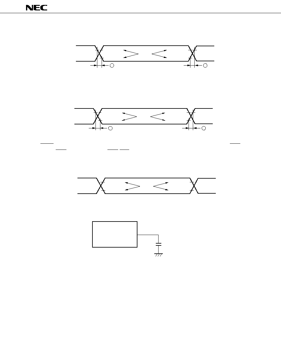
141
µ
PD70433
0.8V
DD
0.8 V
0.8V
DD
0.8 V
Test
Points
V
DD
0.4 V
14
12
AC Test Input Waveform *1
2.2 V
0.8 V
2.2 V
0.8 V
Test
Points
2.4 V
0.4 V
13
11
* 1.
Except *2
AC Test Input Waveform *2
* 2.
RESET, P10/NMI, X1, P11/INTP0 to P16/INTP5, P30/TxD0/SO0/SB0, P31/RxD0/SB1/SI0, P32/TxC/SCK0,
P33/CTS0, P35/R
X
D1/SI1, P36/SCK1/CTS1
AC Test Output Test Points
Note
If the load capacitance exceeds 100 pF due to the configuration of the circuit, the load capacitance of this
device should be reduced to 100 pF or less by insertion of a buffer, etc.
Remark
DUT: Measured device
2.2 V
0.8 V
2.2 V
0.8 V
Test
Points
Load Conditions
DUT
C
L
= 100 pF
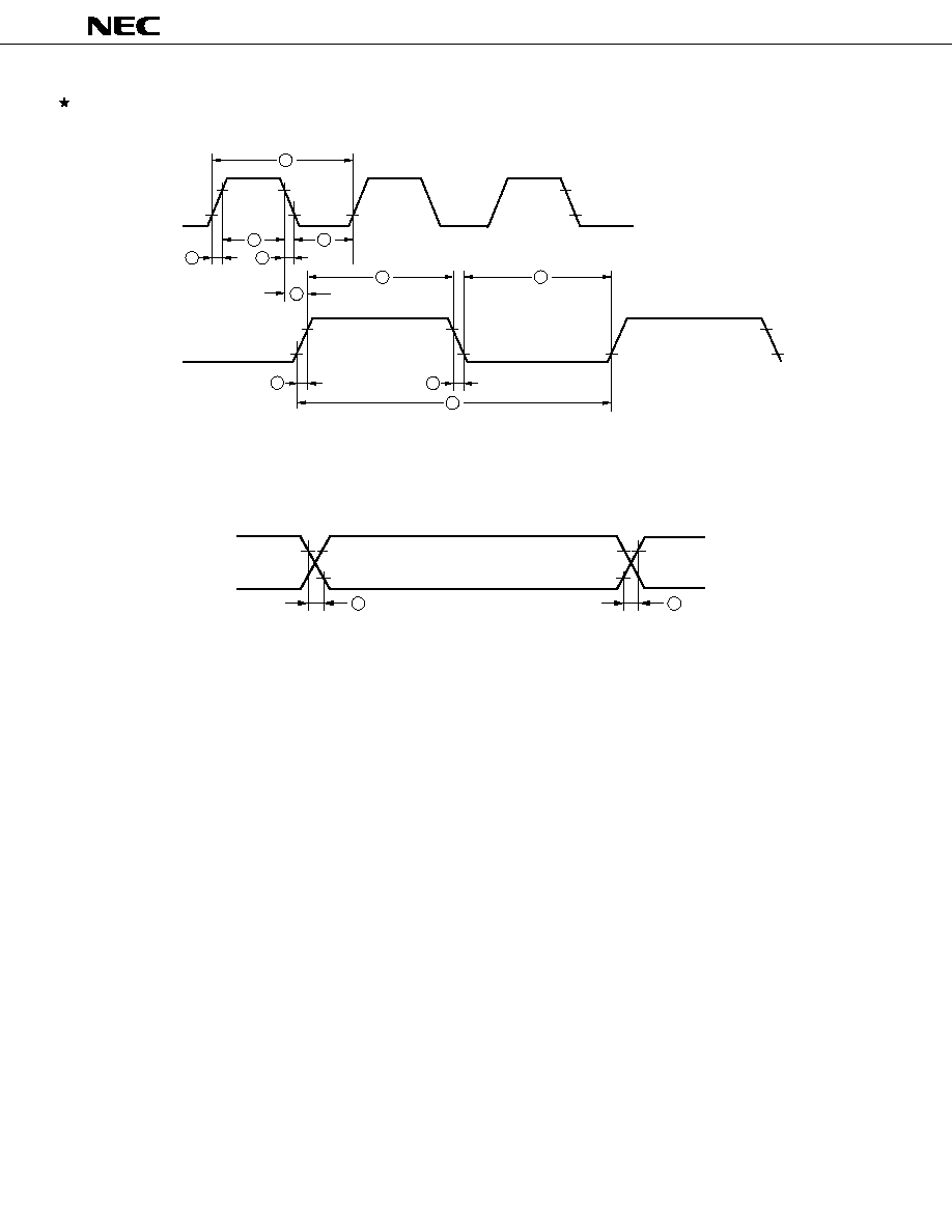
142
µ
PD70433
Clock Input/Output Timing
Output Waveform (Except CLKOUT)
2.2 V
0.8 V
2.2 V
0.8 V
16
15
1
2
3
4
5
9
118
10
7
8
6
X1
CLKOUT
0.8 V
DD
0.8 V
2.2 V
0.8 V
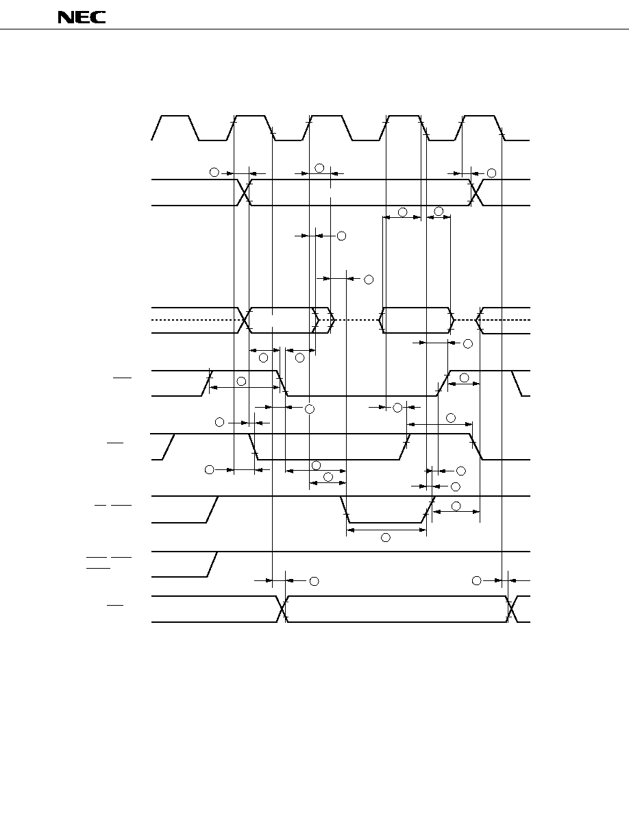
143
µ
PD70433
Read Timing
* 1.
Only activated when memory block 1 or 4 (set by the MBS register) is accessed.
2.
Only valid when the external bus width is 16 bits.
Remark
The dotted line indicates high-impedance.
CLKOUT
A16-A23,
AD8-AD15
(With 8-Bit
External Bus)
AD0-AD7,
AD8-AD15
(With 16-Bit
External Bus)
ASTB
RAS*1
RD, IORD
WRL, WRH,
IOWR
DEX*2
T1
T2
T3
Address
Address
Data
17
20
19
18
29
33
34
21
22
24
25
30
23
42
43
122
130
41
26
119
27
28
31
30
32

144
µ
PD70433
Write Timing
* 1.
Only activated when memory block 1 or 4 (set by the MBC register) is accessed.
2.
Only valid when the external bus width is 16 bits.
Remark
The dotted line indicates high-impedance.
CLKOUT
A16-A23,
AD8-AD15
(With 8-Bit
External Bus)
AD0-AD7,
AD8-AD15
(With 16-Bit
External Bus)
ASTB
RAS*1
RD, IORD
WRL, WRH,
IOWR
DEX*2
T1
T2
T3
17
19
18
38
39
21
22
24
122
23
42
43
121
41
35
40
36
37
32
31
Data
25
Address
Address
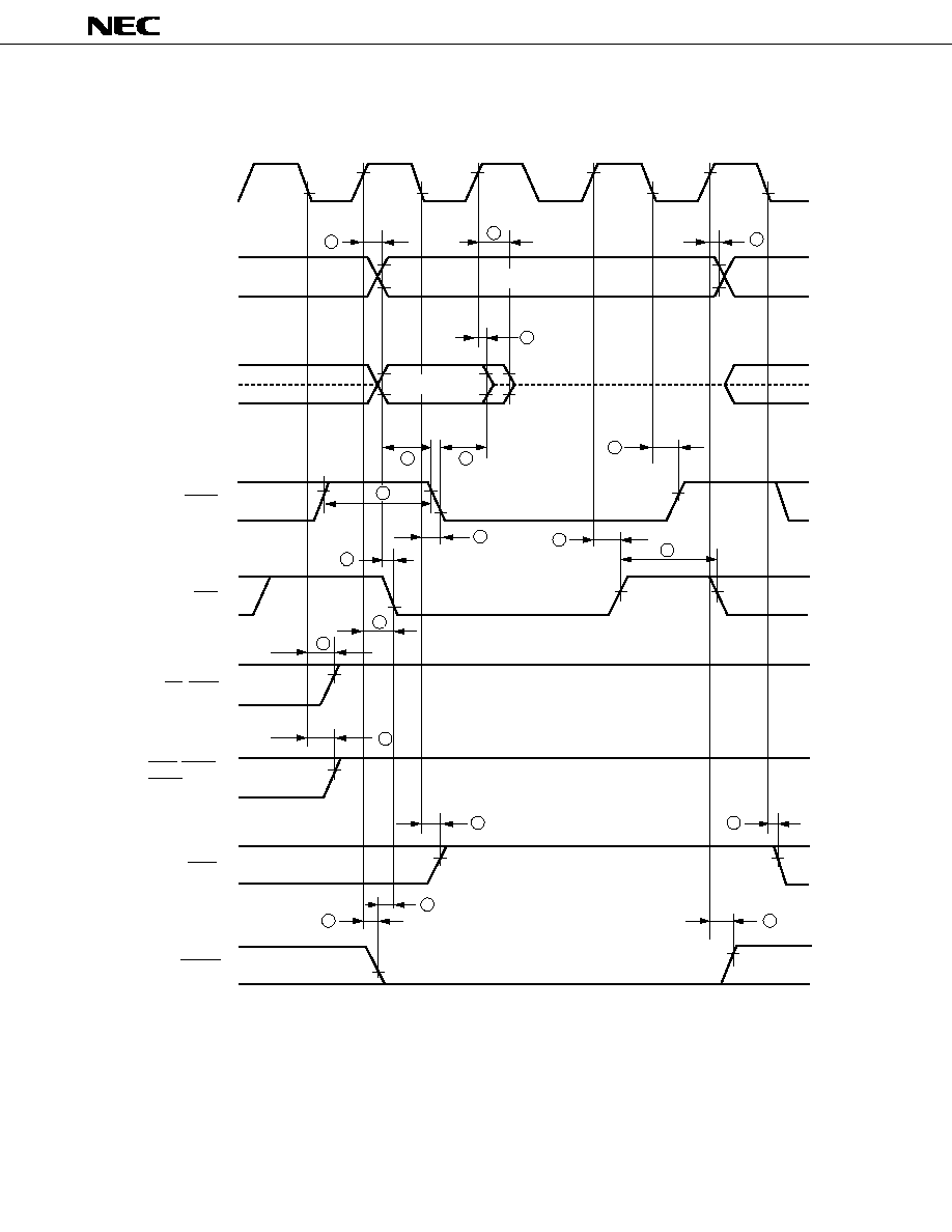
145
µ
PD70433
Refresh Timing
*
Only valid when the external bus width is 16 bits.
Remark
The dotted line indicates high-impedance.
CLKOUT
A16-A23,
AD8-AD15
(With 8-Bit
External Bus)
AD0-AD7,
AD8-AD15
(With 16-Bit
External Bus)
ASTB
RAS
RD, IORD
WRL, WRH,
IOWR
T1
T2
T3
17
19
18
21
22
122
23
42
43
41
36
Address
Address
20
27
31
DEX*
32
25
129
127
128
REFRQ
24

146
µ
PD70433
Ready Input Timing
(1)
1 data wait inserted
44
45
T1
T2
TW
1
T3
CLKOUT
READY
(2)
2 data waits inserted
47
46
44
45
T1
T2
TW
1
TW
2
T3
CLKOUT
READY
(3)
n data waits inserted (n
3)
Remark
The READY input becomes valid when the corresponding field of the PWCn register (n = 0 or 1) is other than
"00" (binary).
47
46
44
45
T1
T2
TW
n≠1
TW
n
T3
CLKOUT
READY
TW
n≠2
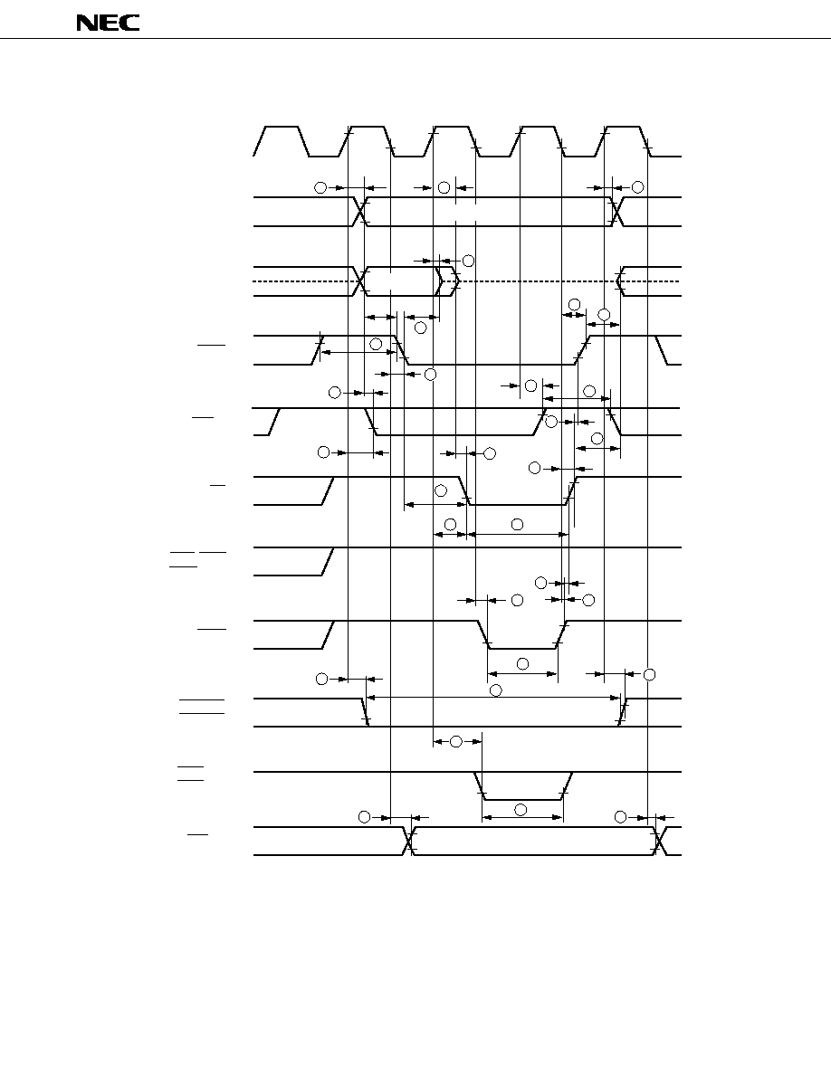
147
µ
PD70433
DMA Timing (External Memory
External I/O)
* 1.
Only activated when a DMA transfer is performed on memory block 1 or 4 (set by the MBC register).
2.
The bus is activated at the last transfer in intelligent DMA mode-2, 2-channel operating mode (stop in termina-
tion), or memory-to-memory transfer mode (stop in termination).
3.
Only valid when the external bus width is 16 bits.
Remark
The dotted line indicates high-impedance.
T1
T2
T3
19
17
20
18
22
24
30
25
23
42
43
119
30
29
41
26
28
35
120
36
70
37
70
71
72
73
32
31
CLKOUT
A16-A23,
AD8-AD15
(With 8-Bit
External Bus)
AD0-AD7,
AD8-AD15
(With 16-Bit
External Bus)
ASTB
RAS *1
RD
WRL, WRH,
IORD
IOWR
DMAAK0,
DMAAK1
TCE0, *2
TCE1
DEX *3
Address
Address
27
122
130
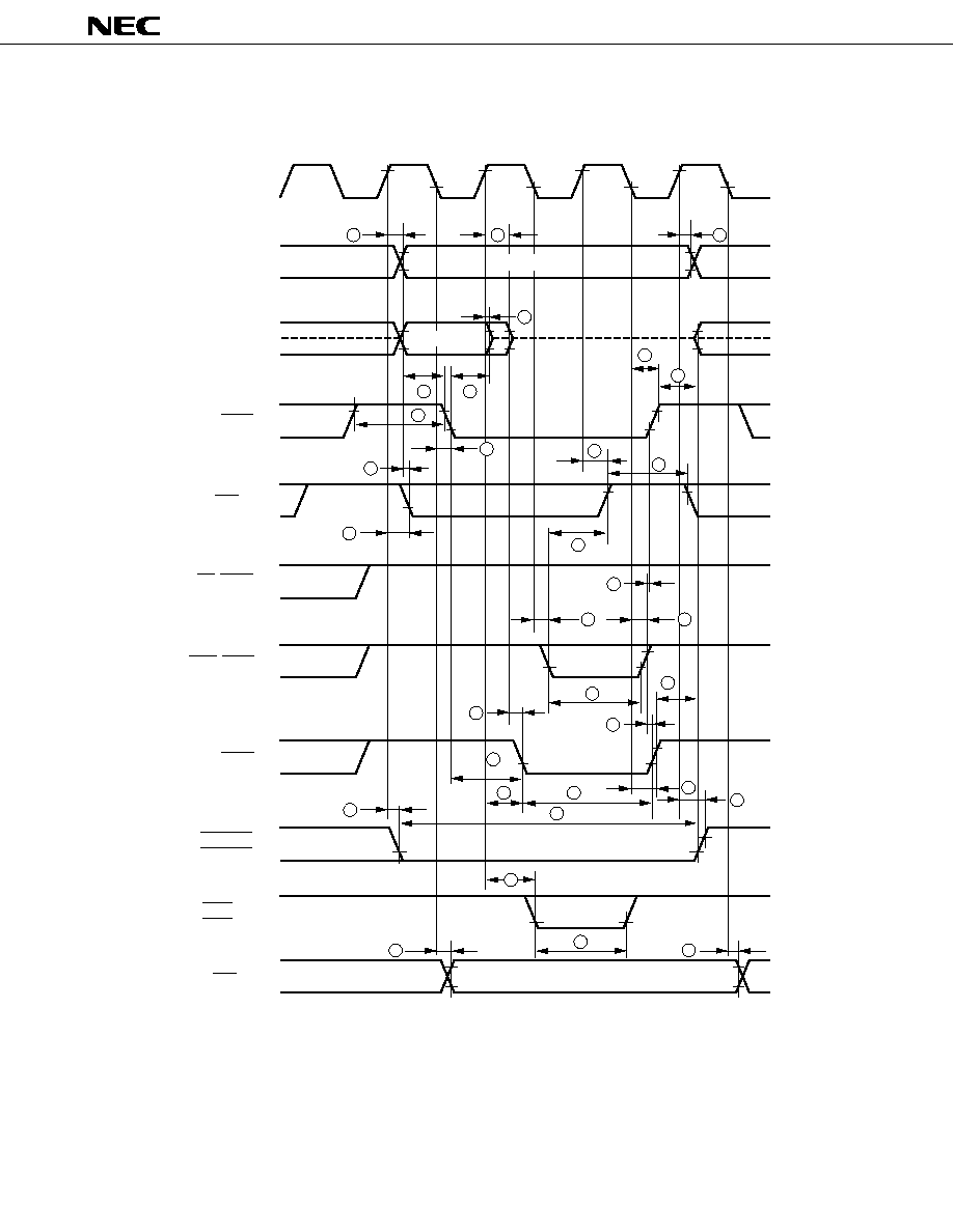
148
µ
PD70433
DMA Timing (External I/O
External Memory)
T1
T2
T3
17
122
130
CLKOUT
A16-A23,
AD8-AD15
(With 8-Bit
External Bus)
AD0-AD7,
AD8-AD15
(With 16-Bit
External Bus)
ASTB
RAS *1
RD, IOWR
WRL, WRH
IORD
DMAAK0,
DMAAK1
TCE0, *2
TCE1
DEX *3
20
19
Address
Address
18
21
22
24
30
43
42
23
25
41
121
40
36
35
37
30
120
27
70
71
28
26
70
72
31
73
32
29
* 1.
Only activated when a DMA transfer is performed on memory block 1 or 4 (set by the MBC register).
2.
The bus is activated at the last transfer in intelligent DMA mode≠2, 2≠channel operating mode (stop in termina-
tion), or memory-to-memory transfer mode (stop in termination).
3.
Only valid when the external bus width is 16 bits.
Remark
The dotted line indicates high-impedance.
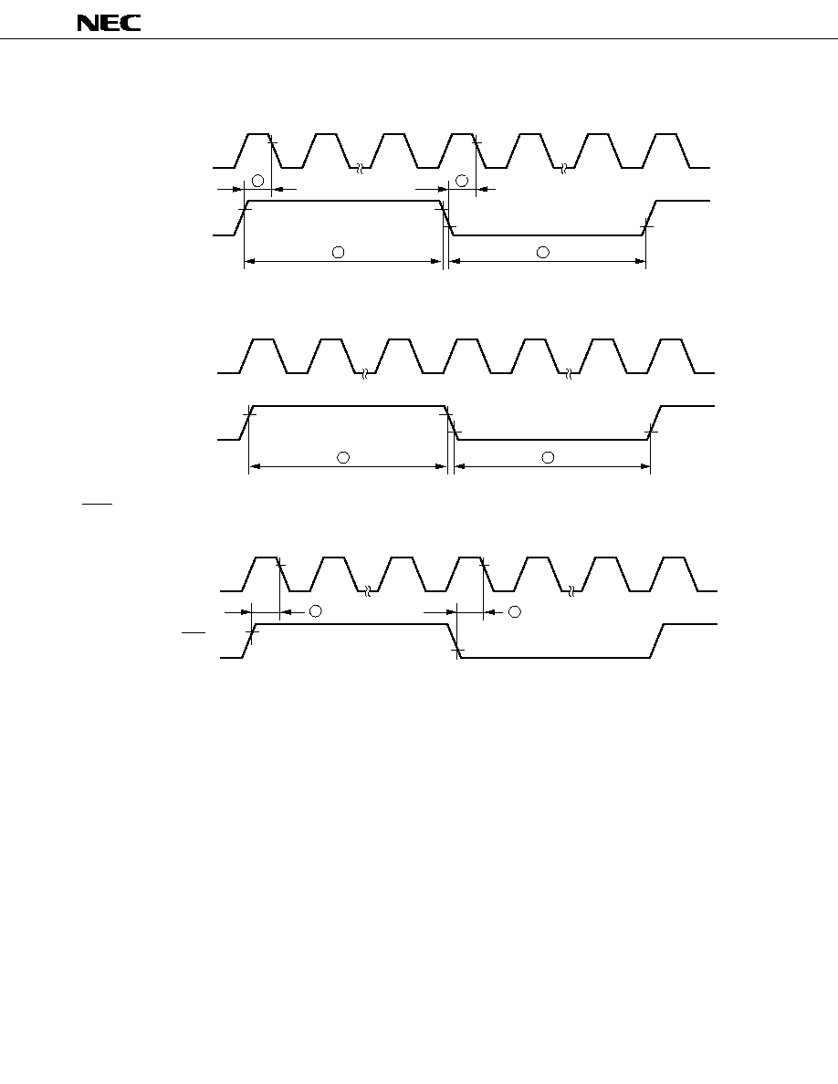
149
µ
PD70433
INRPm Input Timing (m = 0 to 5)
NMI Input Timing
POLL Input Timing
52
CLKOUT
53
54
52
INTP0-INTP5
CLKOUT
50
51
NMI
55
CLKOUT
55
POLL
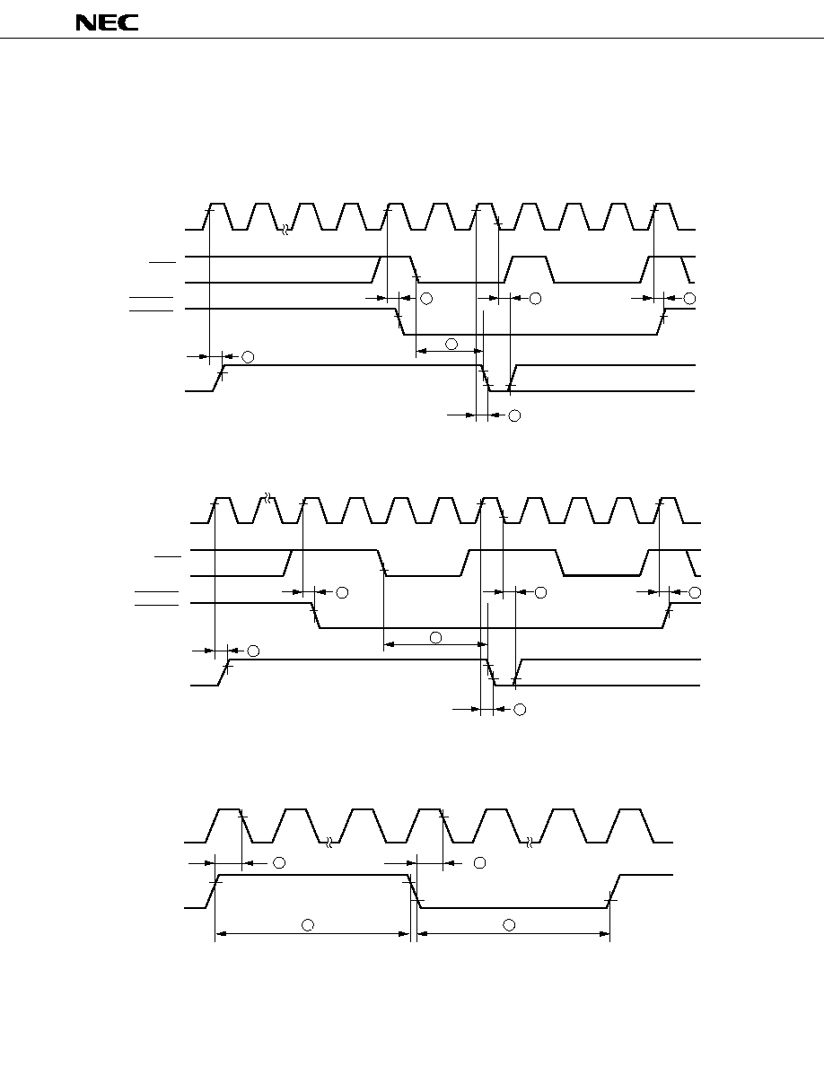
150
µ
PD70433
DMARQm Input Timing (m = 0 or 1)
(1)
In demand release mode (I/O-to-memory transfer)
(a)
Address wait not inserted
(b)
Address wait inserted
(2)
In the mode other than demand release mode
CLKOUT
DMAAK0,
DMAAK1
70
70
69
68
68
ASTB
DMARQ0,
DMARQ1
T1
T2
T3
T1
T2
T3
126
CLKOUT
DMAAK0,
DMAAK1
70
70
69
68
68
ASTB
DMARQ0,
DMARQ1
TAW
T2
T3
126
T1
TAW
T2
T3
T1
65
CLKOUT
66
67
65
DMARQ0,
DMARQ1

151
µ
PD70433
Timer Output Timing
WDTOUT Output Timing
BUSLOCK Output Timing
Data Retention Timing (STOP Mode)
WDTOUT
76
V
DD
115
117
116
CLKOUT
BUSLOCK
64
64
131
CLKOUT
TO00, TO01, TO20
TO21, TO30
TI1
132
133
133
75
74

152
µ
PD70433
Hold Request/Acknowledge Timing
(1)
In normal mode
*
ASTB, RD, WRH, WRL, DEX, RAS, BUSLOCK, IORD, IOWR, AD0 to AD15, A16 to A23
(2)
Release of hold mode for refresh cycle insertion
*
ASTB, RD, WRH, WRL, DEX, RAS, BUSLOCK, IORD, IOWR, AD0 to AD15, A16 to A23
CLKOUT
HLDRQ
Bus Control
Signal*
HLDAK
56
56
57
62
Hi-Z
60
59
58
63
CLKOUT
56
62
61
57
HLDRQ
Bus Control
Signal*
HLDAK
Hi-Z
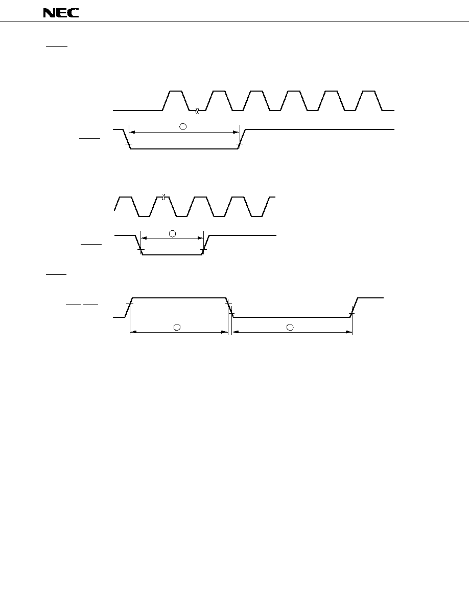
153
µ
PD70433
RESET Input Timing
(1)
STOP mode release/power-on reset
(2)
System reset
CTSm Input Timing (m = 0 or 1)
CLKOUT
RESET
48
CLKOUT
RESET
49
CTS0, CTS1
88
89

154
µ
PD70433
Serial Interface Timing
(1)
3-wire serial I/O mode
(2)
SBI mode
Bus release signal transfer timing
Command signal transfer timing
84
SCK0
SB0, SB1
87
86
85
84
SCK0
SB0, SB1
85
77
83
80
81
79
78
Input/Output Data
79
78
77
82
80
81
SCK0, SCK1
SI0, SI1
SO0, SO1
Output Data
Input Data
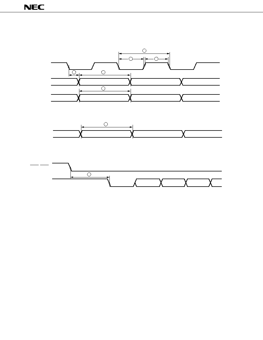
155
µ
PD70433
(3)
UART mode
Transmit timing
Receive timing
Transmission enale timing
90
T
◊
C
T
◊
D0
T
◊
D1
Output Data
Output Data
90
94
91
92
93
90
R
◊
D0, R
◊
D1
Input Data
95
CTS0, CTS1
T
◊
D0, T
◊
D1
Start Bit
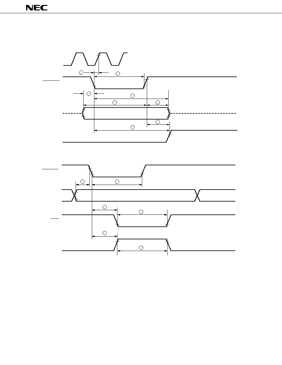
156
µ
PD70433
Parallel Interface Timing
(1)
Input mode
(2)
Output mode
96
CLKOUT
DATASTB
PD0≠PD7
BUSY
Input Data
97
99
100
103
102
101
104
105
DATASTB
PD0≠PD7
ACK
BUSY
Output Data
98
106
107
108
109

157
µ
PD70433
Port Input/Output Timing
124
125
123
T2/TI
T3
T1/TI
CLKOUT
Input Port
Output Port
158
µ
PD70433
(T
A
= 25 ∞C, V
DD
= 5.0 V)
≠3.0
≠2.0
≠1.0
0
0
0.2
0.4
0.6
High-Level Output Current I
OH
[mA]
Supply Voltage ≠ High-Level Output Voltage V
DD
≠ V
OH
[V]
(T
A
= 25 ∞C, V
DD
= 5.0 V)
6.0
4.0
2.0
0
0
0.2
0.4
0.6
Low-Level Output Current I
OL
[mA]
Low-Level Output Voltage V
OL
[V]
19. CHARACTERISTIC CURVES (FOR REFERENCE ONLY)
I
OH
vs (V
DD
≠ V
OH
)
I
OL
vs V
OL

159
µ
PD70433
20. PACKAGE DRAWINGS
N
A
M
F
B
K
L
120 PIN PLASTIC QFP ( 28)
120
1
31
D
C
P
30
91
60
90
61
detail of lead end
S
Q
5∞±5∞
M
I
H
J
G
P120GD-80-5BB-3
ITEM
MILLIMETERS
INCHES
A
B
C
D
F
G
H
I
J
K
L
32.0±0.4
28.0±0.2
2.4
0.35±0.10
0.15
28.0±0.2
1.260±0.016
0.094
0.094
0.006
0.031 (T.P.)
1.102
NOTE
M
N
0.10
0.15
2.0±0.2
0.8 (T.P.)
0.004
0.006
+0.004
≠0.003
Each lead centerline is located within 0.15
mm (0.006 inch) of its true position (T.P.) at
maximum material condition.
0.079
0.014
1.102
0.8±0.2
0.031
P
3.7
0.146
1.260±0.016
32.0±0.4
2.4
+0.009
≠0.008
Q
0.1±0.1
0.004±0.004
S
4.0 MAX.
0.157 MAX.
+0.10
≠0.05
+0.009
≠0.008
+0.004
≠0.005
+0.009
≠0.008
+0.009
≠0.008
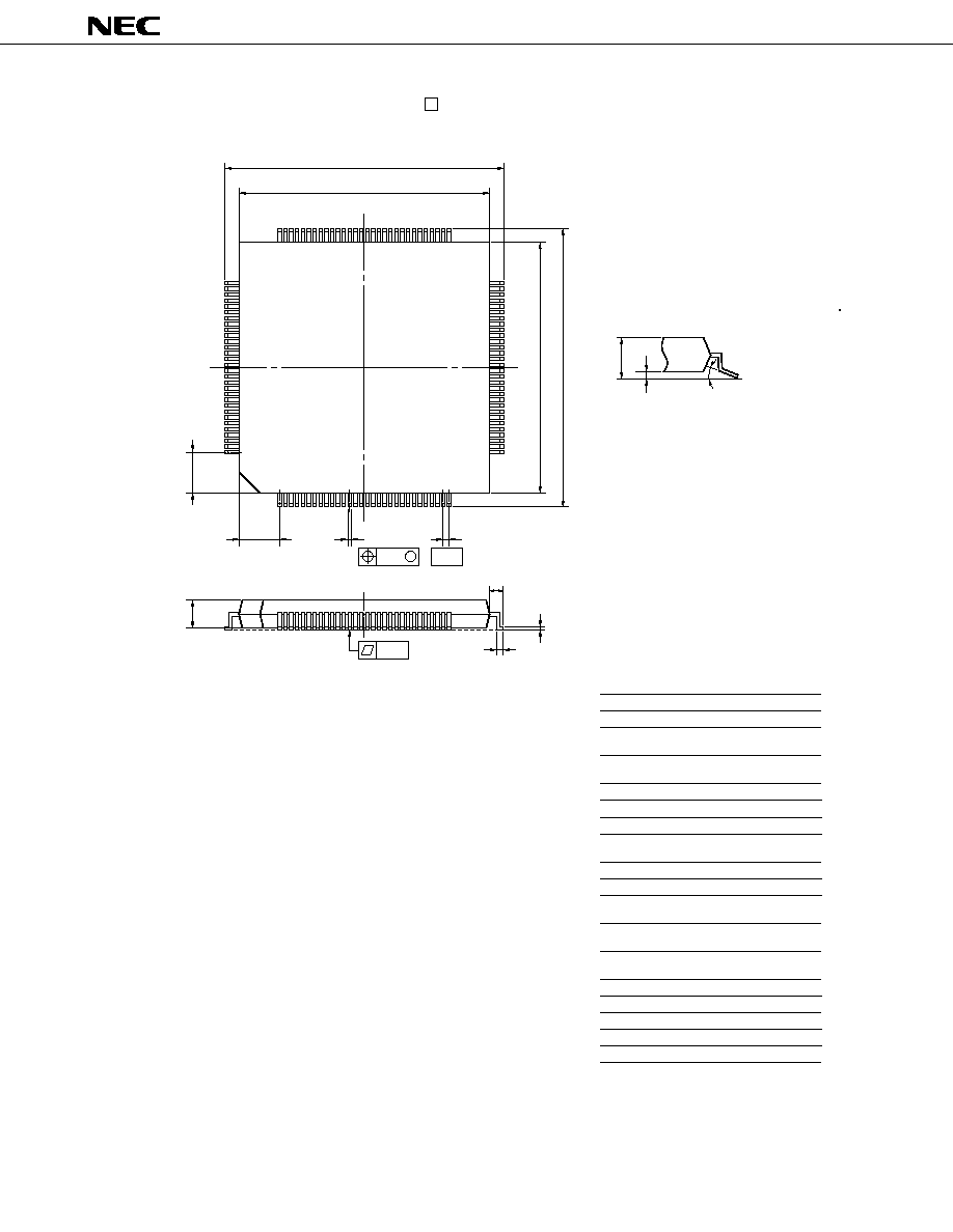
160
µ
PD70433
120 PIN PLASTIC QFP (FINE PITCH) ( 20)
ITEM
MILLIMETERS
INCHES
A
NOTE
Each lead centerline is located within 0.10 mm (0.004 inch) of
its true position (T.P.) at maximum material condition.
S
A
22.0±0.2
0.866±0.008
B
20.0±0.2
0.787+0.009
≠0.008
C
20.0±0.2
0.787+0.009
≠0.008
S120GJ-50-3EB-2
S
3.0 MAX.
0.119 MAX.
K
1.0±0.2
0.039+0.009
≠0.008
L
0.5±0.2
0.020+0.008
≠0.009
M
0.17
0.007
N
0.10
0.004
P
2.7
0.106
Q
0.125±0.075
0.005±0.003
+0.03
≠0.07
B
C
D
J
H
I
G
F
P
N
L
K
M
Q
R
R
5∞±5∞
5∞±5∞
detail of lead end
D
F
2.75
22.0±0.2
0.866±0.008
0.108
G
2.75
0.108
H
0.22
0.009±0.002
I
J
0.5 (T.P.)
0.10
0.004
0.020 (T.P.)
+0.05
≠0.04
+0.001
≠0.003
M
1
30
90
61
31
60
120
91
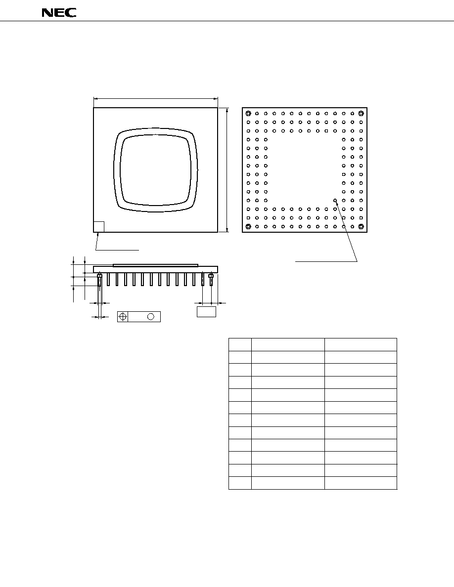
161
µ
PD70433
A
D
Index mark
Orientation pin
E
M
F
M
K
L
I
H
G
J
P N M L K J H G F E D C B A
14
13
12
11
10
9
8
7
6
5
4
3
2
1
X132R-100A-1
ITEM
MILLIMETERS
INCHES
NOTE
Each lead centerline is located within 0.5
mm ( 0.020 inch) of its true position (T.P.) at
maximum material condition.
A
D
E
F
G
H
I
J
K
L
M
35.56±0.3
35.56±0.3
1.27
2.54 (T.P.)
2.8±0.3
0.9 MIN.
2.95
4.57 MAX.
1.2±0.2
0.46±0.05
0.254
1.400±0.012
1.400±0.012
0.050
0.100 (T.P.)
0.110±0.012
0.035 MIN.
0.116
0.180 MAX.
0.047
0.018±0.002
0.010
132 PIN CERAMIC PGA
(Bottom View)
+0.009
≠0.008
162
µ
PD70433
*
For the storage period after dry-pack decompression, storage conditions are max. 25
∞
C, 65 % RH.
Note
Use of more than one soldering method should be avoided (except in the case of partial heating method).
(2)
µ
PD70433GJ-xx-3EB : 120-Pin Plastic QFP (Fine Pitch) (20
◊
20 mm)
21. RECOMMENDED SOLDERING CONDITIONS
This product should be soldered and mounted under the conditions recommended in the table below.
For details of recommended soldering conditions, refer to the information document "Semiconductor Device Mounting
Technology Manual" (C10535E).
For soldering methods and conditions other than those recommended, contact our sales personnel.
Table 21-1. Surface Mount Type Soldering Conditions
(1)
µ
PD70433GD-xx-5BB : 120-Pin Plastic QFP (28
◊
28 mm)
Soldering Method
Soldering Conditions
Recommended
Condition Symbol
Package peak temperature: 235
∞
C, Duration: 30 sec. max. (at 210
∞
C
Infrared reflow
or above), Number of times: Within twice, Time limit: 7 days*
IR35-367-2
(thereafter 36 hours 125
∞
C prebanking required)
Package peak temperature: 215
∞
C, Duration: 40 sec. max. (at 200
∞
C
VPS
or above), Number of times: Within twice, Time limit: 7 days*
VP15-367-2
(thereafter 36 hours 125
∞
C prebanking required)
Solder bath temperature: 260
∞
C or less, Time: 10 sec. max.,
Wave soldering
Number of times: Once, Time limit: 7 days* (thereafter 35 hours
WS60-367-1
125
∞
C prebanking required), Preheating temperature: 120
∞
C max.
(Package surface temperature)
Partial heating
Pin temperature: 300
∞
C or below, Duration: 3 sec. max. (per pin row)
≠≠≠
Soldering Method
Soldering Conditions
Recommended
Condition Symbol
Infrared reflow
Package peak temperature: 235
∞
C, Duration: 30 sec. max. (at 210
∞
C
IR35-00-2
or above), Number of times: Within twice
VPS
Package peak temperature: 215
∞
C, Duration: 40 sec. max. (at 200
∞
C
VP15-00-2
or above), Number of times: Within twice
Partial heating
Pin temperature: 300
∞
C or below, Duration: 3 sec. max. (per pin row)
≠≠≠
Note
Use of more than one soldering method should be avoided (except in the case of partial heating method).
Soldering Method
Soldering Conditions
Wave soldering
Solder temperature: 260
∞
C or less, Duration: 10 sec. max.
(lead part only)
Partial heating
Pin temperature: 300
∞
C or less, Duration: 3 sec. max. (per pin row)
Table 21-2. Insertion Type Soldering Conditions
µ
PD70433R-xx : 132-Pin Ceramic PGA
Note
Wave soldering is used on the lead part only, and care must be taken to prevent solder from coming into
direct contact with the body.

163
µ
PD70433
NEC Electronics Inc. (U.S.)
Santa Clara, California
Tel: 800-366-9782
Fax: 800-729-9288
NEC Electronics (Germany) GmbH
Duesseldorf, Germany
Tel: 0211-65 03 02
Fax: 0211-65 03 490
NEC Electronics (UK) Ltd.
Milton Keynes, UK
Tel: 01908-691-133
Fax: 01908-670-290
NEC Electronics Italiana s.r.1.
Milano, Italy
Tel: 02-66 75 41
Fax: 02-66 75 42 99
NEC Electronics Hong Kong Ltd.
Hong Kong
Tel: 2886-9318
Fax: 2886-9022/9044
NEC Electronics Hong Kong Ltd.
Seoul Branch
Seoul, Korea
Tel: 02-528-0303
Fax: 02-528-4411
NEC Electronics Singapore Pte. Ltd.
United Square, Singapore 1130
Tel: 253-8311
Fax: 250-3583
NEC Electronics Taiwan Ltd.
Taipei, Taiwan
Tel: 02-719-2377
Fax: 02-719-5951
NEC do Brasil S.A.
Sao Paulo-SP, Brasil
Tel: 011-889-1680
Fax: 011-889-1689
NEC Electronics (Germany) GmbH
Benelux Office
Eindhoven, The Netherlands
Tel: 040-2445845
Fax: 040-2444580
NEC Electronics (France) S.A.
Velizy-Villacoublay, France
Tel: 01-30-67 58 00
Fax: 01-30-67 58 99
NEC Electronics (France) S.A.
Spain Office
Madrid, Spain
Tel: 01-504-2787
Fax: 01-504-2860
NEC Electronics (Germany) GmbH
Scandinavia Office
Taeby, Sweden
Tel: 08-63 80 820
Fax: 08-63 80 388
Regional Information
Some information contained in this document may vary from country to country. Before using any NEC
product in your application, please contact the NEC office in your country to obtain a list of authorized
representatives and distributors. They will verify:
∑ Device availability
∑ Ordering information
∑ Product release schedule
∑ Availability of related technical literature
∑ Development environment specifications (for example, specifications for third-party tools and
components, host computers, power plugs, AC supply voltages, and so forth)
∑ Network requirements
In addition, trademarks, registered trademarks, export restrictions, and other legal issues may also vary
from country to country.
J96. 8

164
µ
PD70433
[MEMO]
165
µ
PD70433
NOTES FOR CMOS DEVICES
1
PRECAUTION AGAINST ESD FOR SEMICONDUCTORS
Note: Strong electric field, when exposed to a MOS device, can cause destruction
of the gate oxide and ultimately degrade the device operation. Steps must
be taken to stop generation of static electricity as much as possible, and
quickly dissipate it once, when it has occurred. Environmental control must
be adequate. When it is dry, humidifier should be used. It is recommended
to avoid using insulators that easily build static electricity. Semiconductor
devices must be stored and transported in an anti-static container, static
shielding bag or conductive material. All test and measurement tools
including work bench and floor should be grounded. The operator should
be grounded using wrist strap. Semiconductor devices must not be touched
with bare hands. Similar precautions need to be taken for PW boards with
semiconductor devices on it.
2
HANDLING OF UNUSED INPUT PINS FOR CMOS
Note: No connection for CMOS device inputs can be cause of malfunction. If no
connection is provided to the input pins, it is possible that an internal input
level may be generated due to noise, etc., hence causing malfunction. CMOS
devices behave differently than Bipolar or NMOS devices. Input levels of
CMOS devices must be fixed high or low by using a pull-up or pull-down
circuitry. Each unused pin should be connected to V
DD
or GND with a
resistor, if it is considered to have a possibility of being an output pin. All
handling related to the unused pins must be judged device by device and
related specifications governing the devices.
3
STATUS BEFORE INITIALIZATION OF MOS DEVICES
Note: Power-on does not necessarily define initial status of MOS device. Production
process of MOS does not define the initial operation status of the device.
Immediately after the power source is turned ON, the devices with reset
function have not yet been initialized. Hence, power-on does not guarantee
out-pin levels, I/O settings or contents of registers. Device is not initialized
until the reset signal is received. Reset operation must be executed imme-
diately after power-on for devices having reset function.

µ
PD70433
[MEMO]
No part of this document may be copied or reproduced in any form or by any means without the prior written
consent of NEC Corporation. NEC Corporation assumes no responsibility for any errors which may appear in
this document.
NEC Corporation does not assume any liability for infringement of patents, copyrights or other intellectual property
rights of third parties by or arising from use of a device described herein or any other liability arising from use
of such device. No license, either express, implied or otherwise, is granted under any patents, copyrights or other
intellectual property rights of NEC Corporation or others.
While NEC Corporation has been making continuous effort to enhance the reliability of its semiconductor devices,
the possibility of defects cannot be eliminated entirely. To minimize risks of damage or injury to persons or
property arising from a defect in an NEC semiconductor device, customers must incorporate sufficient safety
measures in its design, such as redundancy, fire-containment, and anti-failure features.
NEC devices are classified into the following three quality grades:
"Standard", "Special", and "Specific". The Specific quality grade applies only to devices developed based on a
customer designated "quality assurance program" for a specific application. The recommended applications of
a device depend on its quality grade, as indicated below. Customers must check the quality grade of each device
before using it in a particular application.
Standard: Computers, office equipment, communications equipment, test and measurement equipment,
audio and visual equipment, home electronic appliances, machine tools, personal electronic
equipment and industrial robots
Special:
Transportation equipment (automobiles, trains, ships, etc.), traffic control systems, anti-disaster
systems, anti-crime systems, safety equipment and medical equipment (not specifically designed
for life support)
Specific:
Aircrafts, aerospace equipment, submersible repeaters, nuclear reactor control systems, life
support systems or medical equipment for life support, etc.
The quality grade of NEC devices is "Standard" unless otherwise specified in NEC's Data Sheets or Data Books.
If customers intend to use NEC devices for applications other than those specified for Standard quality grade,
they should contact an NEC sales representative in advance.
Anti-radioactive design is not implemented in this product.
M4 96.5
V20, V30, V25, V35, V25+, V55PI are trademarks of NEC Corporation.
The documents referred to in this publication may include preliminary versions. However, preliminary versions are
not marked as such.