 | –≠–ª–µ–∫—Ç—Ä–æ–Ω–Ω—ã–π –∫–æ–º–ø–æ–Ω–µ–Ω—Ç: UPD705101 | –°–∫–∞—á–∞—Ç—å:  PDF PDF  ZIP ZIP |
Document Outline
- COVER
- DESCRIPTION
- FEATURES
- ORDERING INFORMATION
- PIN CONFIGURATION (TOP VIEW)
- PIN NAMES
- BLOCK DIAGRAM
- 1. PIN FUNCTIONS LIST
- 2. INTERNAL UNITS
- 3. CPU FUNCTION
- 4. INTERRUPT/EXCEPTION PROCESSING FUNCTION
- 5. BUS CONTROL FUNCTION
- 6. WAIT CONTROL FUNCTION
- 7. MEMORY ACCESS CONTROL FUNCTION
- 7.1 DRAM Control Function
- 7.2 Page-ROM Control Function
- 8. DMA FUNCTION
- 9. SERIAL INTERFACE FUNCTION
- 9.1 Asynchronous Serial Interface (UART)
- 9.2 Clocked Serial Interface (CSI)
- 9.3 Baud Rate Generator (BRG)
- 9.3.1 Configuration and function
- 10. TIMER/COUNTER FUNCTION
- 11. PORT FUNCTION
- 12. CLOCK GENERATION FUNCTION
- 13. STANDBY FUNCTION
- 14. RESET/NMI CONTROL FUNCTION
- 15. INSTRUCTIONS
- 15.1 Instruction Format
- 15.2 Instructions (Listed Alphabetically)
- 16. ELECTRICAL SPECIFICATIONS
- 17. PACKAGE DRAWINGS
- 18. RECOMMENDED SOLDERING CONDITIONS

V831
TM
32-BIT MICROPROCESSOR
MOS INTEGRATED CIRCUIT
µ
PD705101
DESCRIPTION
The
µ
PD70501 (V831) is a 32-bit RISC microprocessor for embedded control applications, with a high-performance
32-bit V830
TM
processor core and many peripheral functions such as a DRAM/ROM controller, 4-channel DMA
controller, real-time pulse unit, serial interface, and interrupt controller.
In addition to high interrupt response speed and optimized pipeline structure, the V831 offers sum-of-products
operation instructions, concatenated shift instructions, and high-speed branch instructions to realize multimedia
functions, and therefore, can provide high performance in multimedia systems such as internet/intra-net systems, car
navigation systems, high-performance televisions, and color FAXes.
Detailed explanations of the functions, etc. are given in the following user's manuals. Be sure to read the
manuals before designing your systems.
V831 User's Manual -Handware
: U12273E
V830 Family
TM
User's Manual -Architecture : U12496E
Document No. U12979EJ1V0DS00 (1st edition)
Date Published January 1998 N
Printed in Japan
FEATURES
∑
CPU function
∑ V830-compatible instructions
∑ Instruction cache
: 4 KB
∑ Instruction RAM
: 4 KB
∑ Data cache
: 4 KB
∑ Data RAM
: 4 KB
∑ Minimum number of instruction
execution cycles
: 1 cycle
∑ Number of general purpose
registers
: 32 bits
◊
32
∑ Memory space and I/O space
: 4 GB each
∑ Interrupt/exception function
∑ Non-maskable : External input : 1
∑ Maskable
: External input : 8 (of which 4 are
multiplexed with internal sources)
Internal source: 11 types
∑
Bus control function
∑
Wait control function
∑
Memory access control function
∑
DMA controller
: 4 channel
∑
Serial interface function
∑ Asynchronous serial interface (UART): 1 channel
∑ Clocked serial interface (CSI)
: 1 channel
∑ Dedicated baud rate generator (BRG) : 1 channel
∑
Timer/counter function
∑ 16-bit timer/event counter : 1 channel
∑ 16-bit interval timer
: 1 channel
∑
Port function
: 3 I/O ports
∑
Clock generation function : PLL clock synthesizer
∑
Standby function
: HALT and STOP modes
∑
Debug function
∑ Debug-dedicated synchronous serial
interface
: 1 channel
∑ Trace-dedicated interface
: 1 channel
The information in this document is subject to change without notice.
©
1998
DATA SHEET

µ
PD705101
2
ORDERING INFORMATION
Part Number
Package
µ
PD705101GM-100-8ED
160-pin plastic LQFP (fine pitch) (24
◊
24 mm)
PIN CONFIGURATION (TOP VIEW)
∑ 160-pin plastic LQFP (fine pitch) (24
◊
24 mm)
µ
PD705101GM-100-8ED
1
2
3
4
5
6
7
8
9
10
11
12
13
14
15
16
17
18
19
20
21
22
23
24
25
26
27
28
29
30
31
32
33
34
35
36
37
38
39
40
GND
D2
D3
D4
D5
D6
D7
D8
V
DD
GND
D9
D10
D11
V
DD
GND
D12
D13
D14
D15
D16
D17
D18
D19
D20
D21
V
DD
GND
D22
D23
D24
V
DD
GND
D25
D26
D27
D28
D29
D30
D31
V
DD
120
119
118
117
116
115
114
113
112
111
110
109
108
107
106
105
104
103
102
101
100
99
98
97
96
95
94
93
92
91
90
89
88
87
86
85
84
83
82
81
V
DD
CLKOUT
TRCDATA0
TRCDATA1
TRCDATA2
TRCDATA3
DDI
DCK
DMS
DDO
A22
A23
GND
V
DD
IOWR
IORD
BCYST
READY
HLDRQ
HLDAK
CS1
CS2
GND
V
DD
CS3
CS4
CS5
GND
V
DD
CS6
CS7
INTP10/TO10
INTP12/TO11
INTP11
INTP13
TI
TCLR
INTP00
INTP01
GND
160
159
158
157
156
155
154
153
152
151
150
149
148
147
146
145
144
143
142
141
140
139
138
137
136
135
134
133
132
131
130
129
128
127
126
125
124
123
122
121
V
DD
D1
D0
LLCAS
LUCAS
ULCAS
UUCAS
RAS
OE
WE
A1
GND
V
DD
GND
V
DD
A2
A3
A4
A5
A6
A7
A8
A9
GND
V
DD
A10
A11
GND
V
DD
A12
A13
A14
A15
A16
A17
A18
A19
A20
A21
GND
41
42
43
44
45
46
47
48
49
50
51
52
53
54
55
56
57
58
59
60
61
62
63
64
65
66
67
68
69
70
71
72
73
74
75
76
77
78
79
80
GND
LLMWR
LUMWR
ULMWR
UUMWR
MRD
TXD
RXD
GND
V
DD
PORT2/SI
PORT1/SO
PORT0/SCLK
V
DD
_PLL
X1
X2
GND_PLL
GND
V
DD
GND
V
DD
RESET
DRST
NMI
BT16B
GND
V
DD
GND
DMAAK0
DMAAK1
DMAAK2
DMAAK3
DMARQ0
DMARQ1
DMARQ2
DMARQ3
TC/REFRQ
INTP03
INTP02
V
DD

µ
PD705101
3
PIN NAMES
A1-A23
: Address Bus
BCYST
: Bus Cycle Start
BT16B
: Boot Bus Size 16 bit
CLKOUT
: Clock Out
CS1-CS7
: Chip Select
D0-D31
: Data Bus
DCK
: Debug Clock
DDI
: Debug Data Input
DDO
: Debug Data Output
DMAAK0-DMAAK3 : DMA Acknowledge
DMARQ0-DMARQ3: DMA Request
DMS
: Debug Mode Select
DRST
: Debug Reset
GND
: Ground
GND_PLL
: PLL Ground
HLDAK
: Hold Acknowledge
HLDRQ
: Hold Request
INTP00-INTP03, INTP10-INTP13
: Interrupt Request
From Peripheral
IORD
: I/O Read
IOWR
: I/O Write
LLCAS
: Lower Lower Column Address Strobe
LLMWR
: Lower Lower Memory Write
LUCAS
: Lower Upper Column Address Strobe
LUMWR
: Lower Upper Memory Write
MRD
: Memory Read
NMI
: Non-Maskable Interrupt Request
OE
: Output Enable
PORT0-PORT2
: Port
RAS
: Row Address Strobe
READY
: Ready
REFRQ
: Refresh Request
RESET
: Reset
RXD
: Receive Data
SCLK
: Serial Clock
SI
: Serial Input
SO
: Serial Output
TC
: Terminal Count
TCLR
: Timer Clear
TI
: Timer Input
TO10, TO11
: Timer Output
TRCDATA0-TRCDATA3
: Trace Data
TXD
: Transmit Data
ULCAS
: Upper Lower Column Address Strobe
ULMWR
: Upper Lower Memory Write
UUCAS
: Upper Upper Column Address Strobe
UUMWR
: Upper Upper Memory Write
V
DD
: Power Supply
V
DD
_PLL
: PLL Power Supply
WE
: Write Enable
X1, X2
: Crystal Oscillator

µ
PD705101
4
BLOCK DIAGRAM
DCU
DCK
DMS
DDI
DDO
TRCDATA0 - TRCDATA3
DRST
CG
X1
X2
CLKOUT
RESET
NMI
SYU
RPU
TI, TCLR
INTP10/TO10,
INTP12/TO11
ICU
INTP00 - INTP03
INTP11, INTP13
P10
CSI
PORT1/SO
PORT2/SI
TXD
RXD
BRG
UART
DMAC
V830 core
BCU
DMAAK0 - DMAAK3
PORT0/SCLK
DMARQ0 - DMARQ3
IOWR
IORD
UUMWR, ULMWR, LUMWR, LLMWR
MRD
READY
BT16B
BCYST
CS1-CS7
A1-A23
D0-D31
HLDAK
HLDRQ
RAS
UUCAS, ULCAS, LUCAS, LLCAS
WE
OE
REFRQ/TC

µ
PD705101
5
CONTENTS
1. PIN FUNCTIONS LIST ......................................................................................................................... 6
2. INTERNAL UNITS ................................................................................................................................ 8
3. CPU FUNCTION ................................................................................................................................. 10
4. INTERRUPT/EXCEPTION PROCESSING FUNCTION ..................................................................... 11
5. BUS CONTROL FUNCTION .............................................................................................................. 13
6. WAIT CONTROL FUNCTION ............................................................................................................. 13
7. MEMORY ACCESS CONTROL FUNCTION ...................................................................................... 14
7.1 DRAM Control Function ............................................................................................................................ 14
7.2 Page-ROM Control Function ..................................................................................................................... 15
8. DMA FUNCTION ................................................................................................................................ 16
9. SERIAL INTERFACE FUNCTION ...................................................................................................... 18
9.1 Asynchronous Serial Interface (UART) ................................................................................................... 18
9.2 Clocked Serial Interface (CSI) ................................................................................................................... 20
9.3 Baud Rate Generator (BRG) ...................................................................................................................... 21
9.3.1
Configuration and function ................................................................................................................ 21
10. TIMER/COUNTER FUNCTION .......................................................................................................... 22
11. PORT FUNCTION .............................................................................................................................. 25
12. CLOCK GENERATION FUNCTION ................................................................................................... 27
13. STANDBY FUNCTION ........................................................................................................................ 28
14. RESET/NMI CONTROL FUNCTION .................................................................................................. 30
15. INSTRUCTIONS ................................................................................................................................. 31
15.1 Instruction Format ..................................................................................................................................... 31
15.2 Instructions (Listed Alphabetically) ......................................................................................................... 33
16. ELECTRICAL SPECIFICATIONS ...................................................................................................... 43
17. PACKAGE DRAWINGS ...................................................................................................................... 65
18. RECOMMENDED SOLDERING CONDITIONS ................................................................................. 66

µ
PD705101
6
1. PIN FUNCTIONS LIST
(1/2)
Pin Name
I/O
Function
Multiplexed Pin
D0-D31
3-state I/O
Data bus
≠
A1-A23
3-state output
Address bus
≠
UUCAS
Column address strobe (most significant byte)
≠
ULCAS
Column address strobe (most significant byte)
≠
LUCAS
Column address strobe (third byte)
≠
LLCAS
Column address strobe (least significant byte)
≠
RAS
Row address strobe/chip select
≠
UUMWR
Memory write strobe (most significant byte)
≠
ULMWR
Memory write strobe (second byte)
≠
LUMWR
Memory write strobe (third byte)
≠
LLMWR
Memory write strobe (least significant byte)
≠
MRD
Memory read strobe
≠
WE
DRAM write strobe
≠
OE
DRAM read strobe
≠
IORD
I/O read strobe
≠
IOWR
I/O write strobe
≠
REFRQ
DRAM refresh request
TC
CS1, CS2, CS7
Memory chip select
≠
CS3-CS6
Memory chip select / I/O chip select
≠
BCYST
Bus cycle start
≠
BT16B
Input
Specifies bus size on boot
≠
READY
Enables end of bus cycle
≠
DMARQ0-DMARQ3
DMA request (CH0 through CH3)
≠
DMAAK0-DMAAK3
Output
DMA enable (CH0 through CH3)
≠
TC
DMA transfer end
REFRQ
RXD
Input
UART data input
≠
TXD
Output
UART data output
≠
SI
Input
CSI data input
PORT2
SO
Output
CSI data output
PORT1
SCLK
I/O
CSI clock I/O
PORT0
TI
Input
Timer 1 count clock input
≠
TCLR
Timer 1 clear, start
≠
TO10
Output
RPU pulse output
INTP10
TO11
INTP12

µ
PD705101
7
(2/2)
Pin Name
I/O
Function
Multiplexed Pin
INTP10
Input
Interrupt request
TO10
INTP11
≠
INTP12
TO11
INTP13
≠
INTP00-INTP03
≠
HLDRQ
Bus request
≠
HLDAK
Output
Bus enable
≠
NMI
Input
Non-maskable interrupt request
≠
RESET
System reset
≠
PORT0
I/O
Port
SCLK
PORT1
SO
PORT2
SI
X1
≠
Connects crystal resonator. (Opened when external clock is
≠
input.)
X2
Input
Connects crystal resonator or inputs external clock.
≠
CLKOUT
Output
Bus clock output
≠
DCK
Input
Debug clock input
≠
DDI
Debug data input
≠
DDO
3-state output
Debug data output
≠
DMS
Input
Debug mode select
≠
DRST
Reset input (debug module)
≠
TRCDATA0-
Output
Trace data output
≠
TRCDATA3
V
DD
≠
Positive power supply
≠
GND
Ground potential
≠
V
DD
_PLL
Positive power supply for PLL (internal clock generator)
≠
GND_PLL
Ground potential for PLL (internal clock generator)
≠

µ
PD705101
8
2. INTERNAL UNITS
(1) Bus control unit (BCU)
Controls the address bus, data bus, and control bus pins. The major functions of BCU are as follows:
(a) Bus arbitration
Arbitrates the bus mastership among bus masters (CPU, DRAMC, DMAC, and external bus masters). The
bus mastership can be changed after completion of the bus cycle under execution, and in an idle state.
(b) Wait control
Controls eight areas in the 16M-byte space corresponding to RAS and seven chip select signals (CS1 through
CS7). Generates chip select signals, controls wait states, and selects the type of bus cycle.
(c) DMA controller
Generates RAS and four CAS signals, and controls access to DRAM. The hyper page mode of DRAM is
supported and DRAM can be accessed in two types of cycle: normal access (off-page) and hyper page (on-
page).
(d) ROM controller
Accessing ROM with page access function is supported. The bus cycle immediately before and addresses
are compared, and wait states are controlled in the normal access (off-page) and page access (on-page)
modes. A page width of 8 bytes to 16 bytes can be supported.
(2) Interrupt controller (ICU)
Services maskable interrupt requests (INTP00 through INTP03, and INTP10 through INTP13) from internal
peripheral hardware and external sources. The priorities of these interrupt requests can be specified in units of
four groups, and edge-triggered or level-triggered interrupts can be nested.
(3) DMA controller (DMAC)
Transfers data between memory and I/O in the place of the CPU. The transfer type is 2-cycle transfer. Two transfer
modes, single transfer and demand transfer, are available.
(4) Serial interface (UART/CSI/BRG)
One asynchronous serial interface (UART) channel and one clocked serial interface (CSI) channel is provided.
As the serial clock source, the output of the baud rate generator (BRG) and the bus clock can be selected.
(5) Real-time pulse unit (RPU)
Provides timer/counter functions. The on-chip 16-bit time/event counter and 16-bit interval timer can be used
to calculate pulse intervals and frequencies, and to output programmable pulses.
(6) Clock generator (CG)
A frequency three times higher than that of an oscillator connected to the X1 and X2 pins is supplied as the
operating clock of the CPU. In addition, a bus clock (with the same cycle as the input clock) is also supplied as
the operating clock of the peripheral units. An external clock can be also input instead of connecting an oscillator.
(7) Port (PIO)
Provides port functions. Three I/O ports are available. The pins of these ports can be used as port pins or serial
control pins.

µ
PD705101
9
(8) System control unit (SYU)
A circuit that rejects noise on the RESET signal (input)/NMI signal (input) is provided.
(9) Debug control unit (DCU)
A circuit to realize mapping and trace functions is provided to implement basic debugging functions.

µ
PD705101
10
3. CPU FUNCTION
The features of the CPU function are as follows:
∑
High-performance 32-bit architecture for embedded control applications
∑ Cache memory
Instruction cache : 4K bytes
Data cache
: 4K bytes
∑ Internal RAM
Instruction RAM : 4K bytes
Data RAM
: 4K bytes
∑ 1-clock pitch pipeline structure
∑ 16-/32-bit length instruction format
∑ Address/data separated type bus
∑ 4GB linear address
∑ Thirty-two 32-bit general register
∑ Register/flag hazard interlock is handled by hardware
∑ 16 levels of interrupt response
∑
16-bit bus fixed function
∑ 16-bit bus system can be constructed
∑
Ideal instructions for any application field:
∑ Sum-of-products operation
∑ Saturation operation
∑ Branch prediction
∑ Concatenation shift
∑ Block transfer instruction

µ
PD705101
11
4. INTERRUPT/EXCEPTION PROCESSING FUNCTION
The features of the interrupt/exception processing function are as follows:
∑
Interrupt
∑ Non-maskable interrupt : 1 source
∑ Maskable interrupt
: 15 sources
∑ Priority of the programmable interrupt can be specified in four levels
∑ Nesting interrupt can be controlled according to the priority
∑ Mask can be specified for each maskable interrupt request
∑ Valid edge of an external interrupt request can be specified
∑ Noise rejection circuit provided for the non-maskable interrupt pin (NMI)
∑
Exception
∑ Software exception : 32 sources
∑ Exception trap
: 4 sources
The interrupt/exception sources are shown in Tables 4-1 and 4-2.
Table 4-1. Reset/Non-maskable Interrupt/Exception Source List
Type
Classification
Source of Interrupt/Exception
Exception Code
Handler
Restore
Name
Note 1
Cause
(ECR)
Address
PC
Note 2
Reset
Interrupt
RESET
Reset input
FFF0H
FFFFFFF0H
Undefined
Non-maskable
Interrupt
NMI
NMI input
FFD0H
FFFFFFD0H
next PC
Note 3
Software exception
Exception
TRAP 1nH
TRAP instruction
FFBnH
FFFFFFB0H
next PC
TRAP 0nH
TRAP instruction
FFAnH
FFFFFFA0H
Exception trap
Exception
NMI
Dual exception
Note 4
FFFFFFD0H
current PC
FAULT
Fatal exception
Not affected
FFFFFFE0H
I-OPC
Illegal instruction
FF90H
FFFFFF90H
code
DIV0
Zero division
FF80H
FFFFFF80H
Notes 1. Handler names used in development tools or software.
2. The PC value saved to EIPC/FEPC/DPC when interrupt/exception processing is started.
3. Execution of all instructions cannot be stopped by an interrupt.
4. The exception code of an exception causing a dual exception.
Remark n = 0H to FH

µ
PD705101
12
Table 4-2. Maskable Interrupt List
Classifi-
In-
Source of Interrupt
Exception
Handler Address
Note 3
Restore
Type
cation
Group Group
Name
Cause
Unit
Code
HCCW.IHA=0
HCCW.IHA=1
PC
Note 1
Priority
Mask- Interrupt GR3
3
RESERVED Reserved
≠
FEF0H
FFFFFEF0H FE0000F0H next
able
2
INTOV1
Timer 1 overflow
RPU
FEE0H
FFFFFEE0H FE0000E0H PC
Note 2
1
INTSER
UART receive error
UART
FED0H FFFFFED0H FE0000D0H
0
INTP03
INTP03 pin input
External
FEC0H
FFFFFEC0H FE0000C0H
GR2
3
INTSR
UART receive end
UART
FEB0H
FFFFFEB0H FE0000B0H
2
INTST
UART transmit end
UART
FEA0H
FFFFFEA0H FE0000A0H
1
INTCSI
CSI transmit/receive end CSI
FE90H
FFFFFE90H FE000090H
0
INTP02
INTP02 pin input
External
FE80H
FFFFFE80H FE000080H
GR1
3
INTDMA
DMA transfer end
DMAC
FE70H
FFFFFE70H FE000070H
2
INTP10/
INTP10 pin input/
External/
FE60H
FFFFFE60H FE000060H
INTCC10
coincidence of CC10
RPU
1
INTP11/
INTP11 pin input/
External/ FE50H
FFFFFE50H FE000050H
INTCC11
coincidence of CC11
RPU
0
INTP01
INTP01 pin input
External
FE40H
FFFFFE40H FE000040H
GR0
3
INTCM4
Coincidence of CM4
RPU
FE30H
FFFFFE30H FE000030H
2
INTP12/
INTP12 pin input/
External/ FE20H
FFFFFE20H FE000020H
INTCC12
coincidence of CC11
RPU
1
INTP13/
INTP13 pin input/
External/ FE10H
FFFFFE10H FE000010H
INTCC13
coincidence of CC13
RPU
0
INTP00
INTP00 pin input
External
FE00H
FFFFFE00H FE000000H
Notes 1. The PC value saved to EIPC when interrupt processing is started.
2. Execution of all instructions cannot be stopped by an interrupt.
3. FFFFFEn0H can be selected as a handler address when HCCW.IHA = 0, and FE0000n0H can be selected
when HCCW.IHA = 1 (N = 0H to FH).
Caution The exception codes and handler addresses of the maskable interrupts shown above are the
values if the default priority is used.

µ
PD705101
13
5. BUS CONTROL FUNCTION
The features of the bus control function are as follows:
∑
Directly connects to EDO DRAM, Page-ROM, SRAM (ROM), or I/O
∑
CAS access with 1 bus clock minimum
∑
DRAM byte access control with four CAS signals
∑
Wait control by READY signal
∑
32-/16-bit bus width can be set every CS space
∑ When the 16-bit memory or I/O are accessed by data bus, the external data bus width can be set by the data
bus width control register (DBC).
6. WAIT CONTROL FUNCTION
The features of the wait control function are as follows:
∑
Controls 8 blocks in accordance with I/O and memory spaces
∑
Linear address space of each block: 16M bytes
∑
Bus cycle select function
Block 0
: EDO DRAM
Blocks 1 and 2
: SRAM (ROM)
Blocks 3 through 6
: I/O or SRAM (ROM) selectable
Block 7
: Page-ROM or SRAM (ROM) selectable
∑
Data bus width select function
Data bus width selectable between 32 bits and 16 bits for each block
∑
Wait control function
Block 0
: Can control EDO DRAM access timing
Blocks 1 through 4 and 7 : 0 to 7 wait states
Blocks 5 and 6
: 0 to 15 wait states
∑
Idle state insertion function
0 to 3 states for each block (bus clock)

µ
PD705101
14
7. MEMORY ACCESS CONTROL FUNCTION
The features of the memory access control function are as follows:
∑
DRAM control function
∑ Generates RAS, LLCAS, LUCAS, ULCAS, UUCAS, REFRQ, OE, and WE signals
∑ Address multiplex: 8, 9, or 10 bits
∑ Timing control of DRAM access
CAS access period
: 1 or 2 bus clocks selectable
RAS-CAS delay period : 1.5 or 2.5 bus clocks selectable
RAS precharge period : 2 or 3 bus clocks selectable
∑ CBR refresh and CBR self-refresh functions
∑
Page-ROM control function
∑ Page size
: 8 or 16 bytes
∑ Wait control during page access: 0 or 1 wait states
7.1 DRAM Control Function
The BCU generates RAS, LLCAS, LUCAS, ULCAS, UUCAS, REFRQ, OE, and WE signals and controls access
to the DRAM. Addresses are output to the DRAM from the address pins by multiplexing row and column addresses.
The connected DRAM must be of x8 bits or more and have a hyper page mode (EDO).
The refresh mode is a CAS-before-RAS (CBR) mode, and the refresh cycle can be arbitrarily set.
CBR self refresh is performed in the STOP mode.
(1) Address multiplex function
An address is multiplexed as shown in Figure 7-1 when a row and column addresses are output in the DMA cycle,
depending on the value of the DAW bit of the DRAM configuration register (DRC). In this figure, a1 through a23
indicate the address output by the CPU, and A1 through A23 indicate the address pins of the V831.

µ
PD705101
15
Figure 7-1. Output of Row Address and Column Address
(2) Decision of on-page/off-page
If the RAS signal is active when page access is enabled because the HPAE bit of the DRAM configuration register
(DRC) is 1, whether the DRAM access to be started is in the same page as the previous DRAM access is decided.
Table 7-1 shows the relation between an address to be compared and address shift.
Table 7-1. Address Compared by on-page/off-page Decision
Address Shift
Data Bus Width
16 bits
32 bits
8
a23-a9
a23-a10
9
a23-a10
a23-a11
10
a23-a11
a23-a12
(3) Refresh function
The BCU can automatically generate the distributed CBR refresh cycle necessary for refreshing the external
DRAM. Whether refreshing is enabled or disabled and the refresh interval are set by the refresh control register
(RFC).
The BCU has a refresh request queue that can store refresh requests up to seven times.
7.2 Page-ROM Control Function
The BCU controls page access to the Page-ROM. Page access to the Page-ROM is valid during burst access.
The page size (8 bytes/16 bytes) and the number of wait states (0 wait/1 wait) during page access can be set by using
the Page-ROM configuration register (PRC).
Address pins
A23
A15 A14 A13 A12 A11 A10
A9
A8
A7
A6
A5
A4
A3
A2
A1
DAW = 10
a23
a15 a14
a23
a22
a21
a20
a19
a18
a17
a16
a15
a14
a13
a12
a11
DAW = 01
a23
a15 a23
a22
a21
a20
a19
a18
a17
a16
a15
a14
a13
a12
a11
a10
DAW = 00
a23
a15 a22
a21
a20
a19
a18
a17
a16
a15
a14
a13
a12
a11
a10
a9
Column address
a23
a1

µ
PD705101
16
8. DMA FUNCTION
The features of the DMA function are as follows:
∑
Four independent DMA channels
∑
Transfer unit: Bytes, half words (2 bytes), words (4 bytes)
∑
Maximum number of transfers: 16,777,216 (2
24
) times
∑
Transfer type: 2-cycle transfer
∑
Two transfer modes
∑ Single transfer mode
∑ Demand transfer mode
∑
Transfer request
∑ External DMARQ pin (
◊
4)
∑ Request from internal peripheral hardware (serial interface (
◊
3 channels) and timer)
∑ Request from software
∑
Transfer source and destination
∑ Between memory and I/O
∑ Between memory and memory
∑
Programmable wait function
∑
DMA transfer end output signal (TC)

µ
PD705101
17
The configuration of the DMA controller (DMAC) is shown below.
Figure 8-1. DMAC Block Diagram
Internal I/O
ROM
RAM
I/O
I/O
External bus
Internal peripheral I/O bus
Bus interface
BCU
Address control block
DMA source address
register (DSA)
DMA destination address
register (DDA)
DMA transfer count
register (DBC)
DMA control register
(DCHC, DC)
Counter control block
Channel control block
INTCM4
INTSR
INTST
INTCSI
TC
DMARQ0 - 3
DMAAK0 - 3
INTDMA
DMAC

µ
PD705101
18
9. SERIAL INTERFACE FUNCTION
The following channels are provided for the serial interface function.
∑
Asynchronous serial interface (UART) : 1 channel
∑
Clocked serial interface (CSI)
: 1 channel
∑
Baud rate generator (BRG)
: 1 channel
9.1 Asynchronous Serial Interface (UART)
The features of the asynchronous serial interface (UART) are as follows:
∑
Full duplex communication. Receive buffer (RXB) is provided (transmit buffer (TXB) is not provided).
∑
Two-pin configuration (The UART of the V831 does not have the SCLK and CTS pins.)
∑ TXD: Transmit data output pin
∑ RXD: Receive data input pin
∑
Transfer rate: 150 bps to 76800 bps (bus clock: 33 MHz, with BRG)
∑
Baud rate generator
Serial clock source can be selected from band rate generator output or bus clock (
)
∑
Receive error detection function
∑ Parity error
∑ Framing error
∑ Overrun error
∑
Three interrupt sources
∑ Receive error interrupt (INTSER)
The interrupt is generated by ORing three types of receive errors.
∑ Receive end interrupt (INTSR)
The receive end interrupt request is generated after completion of receive data transfer from the shift register
to the receive buffer in the reception enabled status.
∑ Transmit end interrupt (INTST)
The transmit end interrupt is generated after completion of serial transfer of transmit data (9, 8, or 7 bits) from
the shift register. The character length of the transmit/receive data is specified by the ASIM00 and ASIM01
registers.
∑
Character length : 7 or 8 bits
: 9 bits (with extension bit appended)
∑
Parity function
: Odd, even, 0, or none
∑
Transmit stop bit : 1 or 2 bits

µ
PD705101
19
The configuration of the asynchronous serial interface (UART) is shown below.
Figure 9-1. Block Diagram of UART
Receive buffer
RXB0
RXB0L
Receive shift
register
16/8
RXD
Receive
control parity
check
TXD
1/16
Status register
8
ASIS0
Transmit shift
register
TXS0
TXS0L
Transmit control
parity append
1/16
1/2
Mode register
ASIM00
ASIM01
SEL
INTSER
INTST
INTSR
Baud rate generator
Internal peripheral I/O bus
8
16/8
Remark
= bus clock (33 M to 16.7 MHz)

µ
PD705101
20
9.2 Clocked Serial Interface (CSI)
The features of the clocked serial interface (CSI) are as follows:
∑
High-speed transfer: 8.25 Mbps MAX. (bus clock: 33 MHz)
∑
Half duplex communication for transmission/reception (buffer is not provided)
∑
Character length: 8 bits
∑
External or internal clock selectable
The configuration of the clocked serial interface (CSI) is shown below.
Figure 9-2. Block Diagram of CSI
Remark
= bus clock (33 M to 16.7 MHz)
INTCSI
Internal peripheral I/O bus
Shift register
Mode register
CSIM0
SI
SO
SCLK
Serial clock control circuit
SEL
1/2
SEL
D
Q
Serial clock counter
Interrupt control
circuit
Baud rate generator
1/2, 1/4, 1/8,
1/16, 1/32
prescaler
8
8
SIO0
SO latch

µ
PD705101
21
9.3 Baud Rate Generator (BRG)
9.3.1 Configuration and function
The serial interface can use the serial clock output by the baud rate generator or the divided value of
(bus clock)
as a baud rate.
The serial clock source is specified by the following registers.
∑
In the case of UART : Specified by the SCLS0 bit of the ASIM00 register.
∑
In the case of CSI
: Specified by the CLS02 through CLS00 bits of the CSIM0 register.
∑
The baud rate generator is shared by the UART and CSI.
The configuration of the baud rate generator (BRG) is shown below.
Figure 9-3. Block Configuration of Baud Rate Generator (BRG)
Remark
= bus clock (33 M to 16.7 MHz)
Compare
register
Internal peripheral I/O bus
BRG0
Internal timer
TMBRG0
Serial interface
(UART/CSI)
BPR00 - 02
BRCE0
BPRM0
Prescaler
1/2

µ
PD705101
22
10. TIMER/COUNTER FUNCTION
The features of the timer/counter function are as follows:
∑
Measures pulse interval and frequency and outputs programmable pulse
∑ 16-bit measurement
∑ Can generate pulses of various shapes (interval pulse, one-shot pulse)
∑
Timer 1
∑ 16-bit timer/event counter
∑ Source of count clock
: 2 types (selected by dividing system clock, external pulse input)
∑ Capture/compare register :
◊
4
∑ Count clear pin
: TCLR
∑ Interrupt source
: 5 types
∑ External pulse output
: 2 pins
∑
Timer 4
∑ 16-bit interval timer
∑ Count clock selected by dividing system clock
∑ Compare register:
◊
1
∑ Interrupt source : 1 type

µ
PD705101
23
The configurations of timer 1 and timer 4 are shown below.
Figure 10-1. Block Configuration of Timer 1
Notes 1. Internal count clock
2. External count clock (TI: 4.125 MHz MAX.)
3. Reset priority
Remarks 1.
= bus clock (33 M to 16.7 MHz)
2.
m = intermediate clock
TM1 (16 bits)
Clear & start
TCLR1
Edge
detection
/2
/4
m
m/4
m/16
m
Note 1
Edge detection
TI
Note 2
INTOV1
Edge detection
INTP10
Edge detection
INTP11
Edge detection
INTP12
Edge detection
INTP13
CC10
CC11
CC12
CC13
S
R
Q
Q
TO10
INTCC10
INTCC11
S
R
Q
Q
TO11
INTCC12
INTCC13
Note 3
Note 3

µ
PD705101
24
Figure 10-2. Block Configuration of Timer 4
Note
Internal count clock
Remarks 1.
= bus clock (33 M to 16.7 MHz)
2.
m = intermediate clock
TM4 (16 bits)
m/16
m/32
Note
/2
/8
CM4
INTCM4
Clear & start
m

µ
PD705101
25
11. PORT FUNCTION
The features of the port function are as follows:
∑
3-bit input/output port which can be specified in 1-bit units
∑
In addition to the port function, the port can operate as the I/O of the serial interface (CSI) in the control mode
∑ Port 0 (control mode): operates as SCLK
∑ Port 1 (control mode): operates as SO
∑ Port 2 (control mode): operates as SI
The configurations of port 0 through 2 are shown below.
Figure 11-1. Block Diagram of Port 0
Internal peripheral I/O bus
Control mode
register (PC)
Mode register
(PM)
Port register
(PORT)
Selector
PORT0
SCLK output
Selector
SCLK input

µ
PD705101
26
Figure 11-2. Block Diagram of Port 1
Figure 11-3. Block Diagram of Port 2
Internal peripheral I/O bus
Control mode
register (PC)
Mode register
(PM)
Port register
(PORT)
Selector
PORT1
SO
Selector
Internal peripheral I/O bus
Control mode
register (PC)
Mode register
(PM)
Port register
(PORT)
PORT2
Selector
SI

µ
PD705101
27
12. CLOCK GENERATION FUNCTION
The features of the clock generation function are as follows:
∑
Generation and control of CPU clock and bus clock supplied to each hardware unit
∑ Bus clock (
) : 16.7-33 MHz (f
B
)
∑ CPU clock
: 50-100 MHz (3
◊
f
B
)
The configuration of the clock generation function is shown below.
Figure 12-1. Block Diagram of Clock Generation Function
f
B
: Oscillation frequency or external clock frequency
: Bus clock
OSC : Oscillator
PFD : Phase Frequency Detector
VCO : Voltage Controlled Oscillator
OSC
X2
X1
f
B
PDF
VCO
200 MHz
Phase
comparator
1/6
Bus clock
1/2
CPU clock
100 MHz
33 MHz
PLL synthesizer

µ
PD705101
28
13. STANDBY FUNCTION
The following two standby modes can be used.
(1) HALT mode
In this mode, the clock generator (oscillation circuit and PLL synthesizer) operates, but the operating clock of the
CPU is stopped. The other internal peripheral functions are supplied with the clock and continue operation. By
using this mode in combination with the normal mode, the power consumption of the entire system can be reduced.
(2) STOP mode
In this mode, the clock generator (PLL synthesizer) is stopped and the entire system is stopped. Because the
PLL synthesizer and internal peripheral functions are stopped, the power consumption can be reduced more than
in the HALT mode.
Because the clock output of the PLL synthesizer is stopped, make sure that sufficient time elapses after the STOP
mode is released until the oscillation circuit, CPU clock, and bus clock are stabilized. The PLL circuit may require
lock up time depending on the program.
Table 13-1 shows the operations of the clock generator in the HALT and STOP modes. By selecting each mode
as the application requires, the power consumption of the system can be efficiently reduced.
Table 13-1. Operation of Clock Generator in Standby Mode
Standby Mode
Oscillation Circuit
PLL Synthesizer
Clock Supply to
Clock Supply to
(OSC)
Peripheral I/O
CPU
Normal mode
HALT mode
◊
STOP mode
◊
◊
◊
Remark
: Operates
◊
: Stopped

µ
PD705101
29
Table 13-2. Operating Status in HALT/STOP Mode
Function
Operating Status
Note 1
STOP Mode
Oscillation circuit
Operates
PLL synthesizer
Operates
Stops
Bus clock
Operates
Stops
CPU
Stops
Port output
Retained
Peripheral function
Operates
Stops
Internal data
Internal data such as registers of CPU retain status before HALT mode is set.
A1-A23
Undefined
High impedance when
Undefined
HLDAK = 0
D0-D31
High impedance
BCYST
1
High impedance when
1
CS1-CS7
IORD, IOWR
MRD, WE, OE, LLMWR, LUMWR,
ULMWR, UUMWR
REFRQ, LLCAS, LUCAS, ULCAS,
1
Note 2
CBR self refresh
Note 4
UUCAS
RAS
Note 3
HLDRQ
Operates
Not accept
CLKOUT
Clock output (when clock output is not
0
disabled)
Notes 1. Each pin is in the operating status during DMA transfer.
2. Other than CBR refresh
3. The previous status is retained before CBR refresh is executed. This pin is set to "1" after CBR refresh.
4. CBR self refresh is not executed when it is disabled. In this case, the status of this pin before the STOP
mode is set is retained.
HLDAK = 0
--------
-----------------------------------

µ
PD705101
30
14. RESET/NMI CONTROL FUNCTION
The features of the reset/NMI control function are as follows:
∑
RESET and NMI pins have noise rejection circuit that samples clock.
∑
Performs forced reset, reset mask, and NMI mask processing from debug control unit
Table 14-1 shows the status of the output pins during the system reset period and immediately after reset. This
status is retained during the reset period.
Table 14-1. Status of Output Pin Immediately after Reset
Function
Operating Status
A1-A23
Undefined
D0-D31
High impedance
CS1-CS7
1
BCYST
1
IORD, IOWR
1
WE, OE
1
LLMWR, LUMWR, ULMWR, UUMWR
1
LLCAS, LUCAS, ULCAS, UUCAS
1
RAS
1
CLKOUT
Clock output
HLDAK
1
DMAAK0-DMAAK3
1
PORT2/SI
High impedance
PORT1/SO
High impedance
PORT0/SCLK
High impedance
TXD
1
DDO
Undefined
TRCDATA0-TRCDATA3
Undefined
TC/REFRQ
1
TO10/INTP10, TO11/INTP12
High impedance

µ
PD705101
31
15. INSTRUCTIONS
15.1 Instruction Format
The V831 uses two instruction formats: 16-bit and 32-bit. The 16-bit instructions include binary operation, control,
and conditional branch instructions, while the 32-bit instructions include load/store and I/O operation instructions,
instructions for handling 16 bits of immediate data, and jump-and-link instructions.
Some instructions contain unused fields, which must be fixed to 0, which are provided for future use. When an
instruction is actually loaded into memory, its configuration is as follows:
∑ Low-order part of each instruction format (including bit 0)
Low-order address
∑ High-order part of each instruction format (including bit 15 or 31)
High-order address
(1) reg-reg instruction format [FORMAT I]
This instruction format has a six-bit operation code field and two general-purpose register designation fields for
operand specification, giving a total length of 16 bits.
reg 1
0
4
5
9
10
15
opcode
reg 2
(2) imm-reg instruction format [FORMAT II]
This instruction format has a six-bit operation code field, a five-bit immediate data field, and a general-purpose
register designation field, giving a total length of 16 bits.
15
10 9
5 4
0
imm 5
reg 2
opcode
(3) Conditional branch instruction format [FORMAT III]
This instruction format has a three-bit operation code field, a four-bit condition code field, a nine-bit branch
displacement field (bit 0 is handled as 0 and need not be specified), and a one-bit sub-operation code, giving a
total length of 16 bits.
15
13 12
9 8
1 0
s = 0 : Bcond
s = 1 : ABcond
s : sub-opcode
opcode
cond
disp 9
s

µ
PD705101
32
(4) Medium-distance jump instruction format [FORMAT IV]
This instruction format has a six-bit operation code field and a 26-bit displacement field (the lowest-order bit must
be 0), giving a total length of 32 bits.
15
disp 26
16
0
10 9
0 31
opcode
(5) Three-operand instruction format [FORMAT V]
This instruction format has a six-bit operation code field, two general-purpose register designation fields, and a
16-bit immediate data field, giving a total length of 32 bits.
15
imm 16
16
10 9
0 31
opcode
5 4
reg 2
reg 1
(6) Load/store instruction format [FORMAT VI]
This instruction format has a six-bit operation code field, two general-purpose register designation fields, and a
16-bit displacement field, giving a total length of 32 bits.
15
disp 16
16
10 9
0 31
opcode
5 4
reg 2
reg 1
(7) Extended instruction format [FORMAT VII]
This instruction format has a six-bit operation code field, two general-purpose register designation fields, and a
six-bit sub-operation code field, giving a total length of 32 bits.
15
RFU
16
10 9
0 31
opcode
5 4
reg 2
reg 1
sub-opcode
26 25
(8) Three-register operand instruction format [FORMAT VIII]
This instruction format has a six-bit operation code field, three general-purpose register designation fields, and
a six-bit sub-operation code field, giving a total length of 32 bits.
15
RFU
16
10 9
0 31
opcode
5 4
reg 2
reg 1
sub-opcode
26 25
reg 3
21 20
(9) No-operand instruction format [FORMAT IX]
This instruction format has a six-bit operation code field and a one-bit sub-operation code field, giving a total length
of 16 bits.
15
RFU
s : sub-opcode
s
10 9
1 0
opcode

µ
PD705101
33
15.2 Instructions (Listed Alphabetically)
The instructions are listed below in alphabetic order of their mnemonics.
General-purpose register (used as a source register)
General-purpose register (used mainly as a destination register,
but in some instructions, used as a source register)
General-purpose register (used mainly as a destination register,
but in some instructions, used as a source register)
◊
bits of immediate data
◊
-bit displacement
System register number
Trap handler address corresponding to trap vector
Explanation of list format
Instruction
Operand(s)
Function
Instruction
mnemonic
Instruction
format
(See Section 15.1.)
Indicates how each flag changes.
: Does not change.
: Changes.
: Becomes 0.
: Becomes 1.
Abbreviations of operands
Format CY OV
S
Z
*
*
*
*
-
*
0
1
I
reg1, reg2
ADD
Abbreviation
Meaning
reg1
reg2
reg3
imm
◊
disp
◊
regID
vector adr

µ
PD705101
34
Instruction
Operand(s)
Format
CY
OV
S
Z
Function
ABC
disp9
III
≠
≠
≠
≠
High-speed conditional branch (if Carry) relative
to PC.
ABE
disp9
III
≠
≠
≠
≠
High-speed conditional branch (if Equal) relative
to PC.
ABGE
disp9
III
≠
≠
≠
≠
High-speed conditional branch (if Greater than
or Equal) relative to PC.
ABGT
disp9
III
≠
≠
≠
≠
High-speed conditional branch (if Greater than)
relative to PC.
ABH
disp9
III
≠
≠
≠
≠
High-speed conditional branch (if Higher) relative
to PC.
ABL
disp9
III
≠
≠
≠
≠
High-speed conditional branch (if Lower) relative
to PC.
ABLE
disp9
III
≠
≠
≠
≠
High-speed conditional branch (if Less than
or Equal) relative to PC.
ABLT
disp9
III
≠
≠
≠
≠
High-speed conditional branch (if Less than)
relative to PC.
ABN
disp9
III
≠
≠
≠
≠
High-speed conditional branch (if Negative)
relative to PC.
ABNC
disp9
III
≠
≠
≠
≠
High-speed conditional branch (if Not Carry)
relative to PC.
ABNE
disp9
III
≠
≠
≠
≠
High-speed conditional branch (if Not Equal)
relative to PC.
ABNH
disp9
III
≠
≠
≠
≠
High-speed conditional branch (if Not Higher)
relative to PC.
ABNL
disp9
III
≠
≠
≠
≠
High-speed conditional branch (if Not Lower)
relative to PC.
ABNV
disp9
III
≠
≠
≠
≠
High-speed conditional branch (if Not Overflow)
relative to PC.
ABNZ
disp9
III
≠
≠
≠
≠
High-speed conditional branch (if Not Zero)
relative to PC.
ABP
disp9
III
≠
≠
≠
≠
High-speed conditional branch (if Positive)
relative to PC.
ABR
disp9
III
≠
≠
≠
≠
High-speed unconditional branch (Always)
relative to PC.
ABV
disp9
III
≠
≠
≠
≠
High-speed conditional branch (if Overflow)
relative to PC.
ABZ
disp9
III
≠
≠
≠
≠
High-speed conditional branch (if Zero) relative
to PC.
ADD
reg1, reg2
I
Addition. reg1 is added to reg2 and the sum is
written into reg2.
imm5, reg2
II
Addition. imm5, sign-extended to a word, is
added to reg2 and the sum is written into reg2.
ADDI
imm16,
V
Addition. imm16, sign-extended to a word, is
reg1, reg2
added to reg1, and the sum is written into reg2.

µ
PD705101
35
Instruction
Operand(s)
Format
CY
OV
S
Z
Function
AND
reg1, reg2
I
≠
0
AND. reg2 and reg1 are ANDed and the result
is written into reg2.
ANDI
imm16,
V
≠
0
0
AND. reg1 is ANDed with imm16,
reg1, reg2
zero-extended to a word, and result is written
into reg2.
BC
disp9
III
≠
≠
≠
≠
Conditional branch (if Carry) relative to PC.
BDLD
[reg1], [reg2]
VII
≠
≠
≠
≠
Block transfer. 4 words of data are transferred
from external memory to built-in data RAM.
BDST
[reg2], [reg1]
VII
≠
≠
≠
≠
Block transfer. 4 words of data are transferred
from built-in data RAM to external memory.
BE
disp9
III
≠
≠
≠
≠
Conditional branch (if Equal) relative to PC.
BGE
disp9
III
≠
≠
≠
≠
Conditional branch (if Greater than or Equal)
relative to PC.
BGT
disp9
III
≠
≠
≠
≠
Conditional branch (if Greater than) relative to
PC.
BH
disp9
III
≠
≠
≠
≠
Conditional branch (if Higher) relative to PC.
BILD
[reg1], [reg2]
VII
≠
≠
≠
≠
Block transfer. 4 words of data are transferred
from external memory to built-in instruction RAM.
BIST
[reg2], [reg1]
VII
≠
≠
≠
≠
Block transfer. 4 words of data are transferred
from built-in instruction RAM to external memory.
BL
disp9
III
≠
≠
≠
≠
Conditional branch (if Lower) relative to PC.
BLE
disp9
III
≠
≠
≠
≠
Conditional branch (if Less than or Equal)
relative to PC.
BLT
disp9
III
≠
≠
≠
≠
Conditional branch (if Less than) relative to PC.
BN
disp9
III
≠
≠
≠
≠
Conditional branch (if Negative) relative to PC.
BNC
disp9
III
≠
≠
≠
≠
Conditional branch (if Not Carry) relative to PC.
BNE
disp9
III
≠
≠
≠
≠
Conditional branch (if Not Equal) relative to PC.
BNH
disp9
III
≠
≠
≠
≠
Conditional branch (if Not Higher) relative to PC.
BNL
disp9
III
≠
≠
≠
≠
Conditional branch (if Not Lower) relative to PC.
BNV
disp9
III
≠
≠
≠
≠
Conditional branch (if Not Overflow) relative to
PC.
BNZ
disp9
III
≠
≠
≠
≠
Conditional branch (if Not Zero) relative to PC.
BP
disp9
III
≠
≠
≠
≠
Conditional branch (if Positive) relative to PC.
BR
disp9
III
≠
≠
≠
≠
Unconditional branch (Always) relative to PC.
BRKRET
IX
≠
≠
≠
≠
Return from fatal exception handling.
BV
disp9
III
≠
≠
≠
≠
Conditional branch (if Overflow) relative to PC.
BZ
disp9
III
≠
≠
≠
≠
Conditional branch (if Zero) relative to PC.
CAXI
disp16[reg1],
VI
Inter-processor synchronization in multi-
reg2
processor system.

µ
PD705101
36
Instruction
Operand(s)
Format
CY
OV
S
Z
Function
CMP
reg1, reg2
I
Comparison. reg2 is compared with reg1
sign-extended to a word and the condition flag
is set according to the result.
The comparison involves subtracting reg1 from
reg2.
imm5, rag2
II
Comparison. reg2 is compared with imm5
sign-extended to a word and the condition flag
is set according to the result.
The comparison involves subtracting imm5,
sign-extended to a word, from reg2.
DI
II
≠
≠
≠
≠
Disable interrupt. Maskable interrupts are
disabled. DI instruction cannot disable
nonmaskable interrupts.
DIV
reg1, reg2
I
≠
Division of signed operands. reg2 is divided by
reg1 (signed operands).
The quotient is stored in reg2 and the remainder
in r30. The division is performed so that the
sign of the remainder will match that of the
dividend.
DIVU
reg1, reg2
I
≠
0
Division of unsigned operands. reg2 is divided
by reg1 (unsigned operands). The quotient is
stored in reg2 and the remainder in r30. The
division is performed so that the sign of the
remainder will match that of the dividend.
EI
II
≠
≠
≠
≠
Enable interrupt. Maskable interrupts are
enabled. The EI instruction cannot enable
nonmaskable interrupts.
HALT
IX
≠
≠
≠
≠
Processor halt. The processor is placed in
sleep mode.
IN.B
disp16[reg1],
VI
≠
≠
≠
≠
Port input. disp16, sign-extended to a word,
reg2
is added to reg1 to produce an unsigned 32-bit
port address. A byte of data is read from the
resulting port address, zero-extended to a word,
then stored in reg2.
IN.H
disp16[reg1],
VI
≠
≠
≠
≠
Port input. disp16, sign-extended to a word,
reg2
is added to reg1 to produce an unsigned 32-bit
port address. A halfword of data is read from
the produced port address, zero-extended to a
word, and stored in reg2. Bit 0 of the unsigned
32-bit port address is masked to 0.
IN.W
disp16[reg1],
VI
≠
≠
≠
≠
Port input. disp16, sign-extended to a word,
reg2
is added to reg1 to produce an unsigned 32-bit
port address. A word of data is read from the
resulting port address, then written into reg2.
Bits 0 and 1 of the unsigned 32-bit port address
are masked to 0.

µ
PD705101
37
Instruction
Operand(s)
Format
CY
OV
S
Z
Function
JAL
disp26
IV
≠
≠
≠
≠
Jump and link. The sum of the current PC
and 4 is written into r31. disp26, sign-extended
to a word, is added to the PC and the sum is
set to the PC for control transfer. Bit 0 of
disp26 is masked.
JMP
[reg1]
I
≠
≠
≠
≠
Indirect unconditional branch via register.
Control is passed to the address designated by
reg1. Bit 0 of the address is masked to 0.
JR
disp26
IV
≠
≠
≠
≠
Unconditional branch. disp26, sign-extended to
a word, is added to the current PC and control
is passed to the address specified by that sum.
Bit 0 of disp26 is masked to 0.
LD.B
disp16[reg1],
VI
≠
≠
≠
≠
Byte load. disp16, sign-extended to a word,
reg2
is added to reg1 to produce an unsigned 32-bit
address. A byte of data is read from the
produced address, sign-extended to a word,
then written into reg2.
LD.H
disp16[reg1],
VI
≠
≠
≠
≠
Halfword load. disp16, sign-extended to a word,
reg2
is added to reg1 to produce an unsigned 32-bit
address. A halfword of data is read from the
produced address, sign-extended to a word,
then written into reg2. Bit 0 of the unsigned
32-bit address is masked to 0.
LD.W
disp16[reg1],
VI
≠
≠
≠
≠
Word load. disp16, sign-extended to a word,
reg2
is added to reg1 to produce an unsigned 32-bit
address. A word of data is read from the
produced address, then written into reg2. Bits 0
and 1 of the unsigned 32-bit address are
masked to 0.
LDSR
reg2, regID
II
Load into system register. The contents of
reg2 are set in the system register identified by
the system register number (regID).
MAC3
reg1, reg2,
VIII
≠
≠
≠
≠
Saturatable operation on signed 32-bit operands.
reg3
reg1 and reg2 are multiplied together as signed
integers and the product is added to reg3.
[If no overflow has occurred:]
The result is stored in reg3.
[If an overflow has occurred:]
The SAT bit is set. If the result is positive,
the positive maximum is written into reg3; if
the result is negative, the negative maximum
is written into reg3.

µ
PD705101
38
Instruction
Operand(s)
Format
CY
OV
S
Z
Function
MACI
imm16,
V
≠
≠
≠
≠
Sum-of-products operation on signed 32-bit
reg1, reg2
operands. reg1 and imm16, sign-extended to
32 bits, are multiplied together as signed
integers and the product is added to reg2 as a
signed integer.
[If no overflow has occurred:]
The result is written into reg2.
[If an overflow has occurred:]
The SAT bit is set. If the result is positive,
the positive maximum is written into reg2; if
the result is negative, the negative maximum
is written into reg2.
MACT3
reg1, reg2,
VIII
≠
≠
≠
≠
Saturatable operation on signed 32-bit
reg3
operands. reg1 and reg2 are multiplied together
as signed integers and the high-order 32 bits of
the product are added to reg3 as signed integers.
[If no overflow has occurred:]
The result is written into reg3.
[If an overflow has occurred:]
The SAT bit is set. If the result is positive,
the positive maximum is written into reg3; if
the result is negative, the negative maximum
is written into reg3.
MAX3
reg1, reg2,
VIII
≠
≠
≠
≠
Maximum. reg2 and reg1 are compared as
reg3
signed integers. The larger value is written
into reg3.
MIN3
reg1, reg2,
VIII
≠
≠
≠
≠
Minimum. reg2 and reg1 are compared as
reg3
signed integers. The smaller value is written
into reg3.
MOV
reg1, reg2,
I
≠
≠
≠
≠
Data transfer. reg1 is copied to reg2 for
data transfer.
imm5, reg2
II
≠
≠
≠
≠
Data transfer. imm5, sign-extended to a word,
is copied into reg2 for data transfer.
MOVEA
imm16,
V
≠
≠
≠
≠
Addition. The high-order 16 bits (imm16),
reg1, reg2
sign-extended to a word, are added to reg1 and
the sum is written into reg2.
MOVHI
imm16,
V
≠
≠
≠
≠
Addition. A word consisting of the high-order
reg1, reg2
16 bits (imm16) and low-order 16 bits (0) is
added to reg1 and the sum is written into reg2.
MUL
reg1, reg2
I
≠
Multiplication of signed operands. reg2 and reg1
are multiplied together as signed values. The
high-order 32 bits of the product (double word)
are written into r30 and low-order 32 bits are
written into reg2.
MUL3
reg1, reg2,
VIII
≠
≠
≠
≠
Multiplication of signed 32-bit operands.
reg3
reg2 and reg1 are multiplied together as signed
integers. The high-order 32 bits of the product
are written into reg3.

µ
PD705101
39
Instruction
Operand(s)
Format
CY
OV
S
Z
Function
MULI
imm16,
V
≠
≠
≠
≠
Saturatable multiplication of signed 32-bit
reg1, reg2
operands. reg1 and imm16, sign-extended to
32 bits, are multiplied together as signed
integers.
[If no overflow has occurred:]
The result is written into reg2.
[If an overflow has occurred:]
The SAT bit is set. If the result is positive,
the positive maximum is written into reg2; if
the result is negative, the negative maximum
is written into reg2.
MULT3
reg1, reg2,
VIII
≠
≠
≠
≠
Saturatable multiplication of signed 32-bit
reg3
operands. reg1 and reg2 are multiplied
together as signed integers. The high-order
32 bits of the product are written into reg3.
MULU
reg1, reg2
I
≠
Multiplication of unsigned operands. reg1 and
reg2 are multiplied together as unsigned values.
The high-order 32 bits of the product (double
word) are written into r30 and the low-order
32 bits are written into reg2.
NOP
III
≠
≠
≠
≠
No operation.
NOT
reg1, reg2
I
≠
0
NOT. The NOT (ones complement) of reg1 is
taken and written into reg2.
OR
reg1, reg2
I
≠
0
OR. The OR of reg2 and reg1 is taken and
written into reg2.
ORI
imm16,
V
≠
0
OR. The OR of reg1 and imm16, zero-
reg1, reg2
extended to a word, is taken and written into
reg2.
OUT.B
reg2,
VI
≠
≠
≠
≠
Port output. disp16, sign-extended to a word,
disp16[reg1]
is added to reg1 to produce an unsigned 32-bit
port address. The low-order one byte of the
data in reg2 is output to the resulting port
address.
OUT.H
reg2,
VI
≠
≠
≠
≠
Port output. disp16, sign-extended to a word,
disp16[reg1]
is added to reg1 to produce an unsigned 32-bit
port address. The low-order two bytes of the
data in reg2 are output to the resulting port
address. Bit 0 of the unsigned 32-bit port
address is masked to 0.
OUT.W
reg2,
VI
≠
≠
≠
≠
Port output. disp16, sign-extended to a word,
disp16[reg1]
is added to reg1 to produce an unsigned 32-bit
port address. The word of data in reg2 is output
to the produced port address. Bits 0 and 1 of the
unsigned 32-bit port address are masked to 0.
RETI
IX
Return from trap/interrupt handling routine.
The return PC and PSW are read from the
system registers so that program execution will
return from the trap or interrupt handling routine.

µ
PD705101
40
Instruction
Operand(s)
Format
CY
OV
S
Z
Function
SAR
reg1 ,reg2
I
0
Arithmetic right shift. reg2 is arithmetically
shifted to the right by the displacement
specified by the low-order five bits of reg1
(MSB value is copied to the MSB in sequence).
The result is written into reg2.
imm5, reg2
II
0
Arithmetic right shift. reg2 is arithmetically
shifted to the right by the displacement specified
by imm5, zero-extended to a word. The result is
written into reg2.
SATADD3
reg1, reg2,
VIII
Saturatable addition. reg1 and reg2 are added
reg3
together as signed integers.
[If no overflow has occurred:]
The result is written into reg3.
[If an overflow has occurred:]
The SAT bit is set. If the result is positive,
the positive maximum is written into reg3; if
the result is negative, the negative maximum
is written into reg3.
SATSUB3
reg1, reg2,
VIII
Saturatable subtraction. reg1 is subtracted from
reg3
reg2 as signed integers.
[If no overflow has occurred:]
The result is written into reg3.
[If an overflow has occurred:]
The SAT bit is set. If the result is positive,
the positive maximum is written into reg3; if
the result is negative, the negative maximum
is written into reg3.
SETF
imm5, reg2
II
≠
≠
≠
≠
Set flag condition. reg2 is set to 1 if the
condition specified by the low-order four bits of
imm5 matches the condition flag; otherwise it is
set to 0.
SHL
reg1, reg2
I
0
Logical left shift. reg2 is logically shifted to the
left (0 is put on the LSB) by the displacement
specified by the low-order five bits of reg1. The
result is written into reg2.
imm5, reg2
II
0
Logical left shift. reg2 is logically shifted to the
left by the displacement specified by imm5,
zero-extended to a word. The result is written
into reg2.
SHLD3
reg1, reg2,
VIII
≠
≠
≠
≠
Left shift of concatenation. The 64 bits
reg3
consisting of reg3 (high order) and reg2
(low order) are logically shifted to the left by the
displacement specified by the low-order five bits
of reg1. The high-order 32 bits of the result are
written into reg3.

µ
PD705101
41
Instruction
Operand(s)
Format
CY
OV
S
Z
Function
SHR
reg1, reg2
I
0
Logical right shift. reg2 is logically shifted to
the right by the displacement specified by the
low-order five bits of reg1 (0 is put on the MSB).
The result is written into reg2.
imm5, reg2
II
0
Logical right shift. reg2 is logically shifted to
the right by the displacement specified by imm5,
zero-extended to a word. The result is written
into reg2.
SHRD3
reg1, reg2,
VIII
≠
≠
≠
≠
Right shift of concatenation. The 64 bits
reg3
consisting of reg3 (high order) and reg2
(low order) are logically shifted to the right by
the displacement specified by the low-order five
bits of reg1. The low-order 32 bits of the result
are written into reg3.
ST.B
reg2,
VI
≠
≠
≠
≠
Byte store. disp16, sign-extended to a word,
disp16[reg1]
is added to reg1 to produce an unsigned 32-bit
address. The low-order one byte of data in reg2
is stored at the resulting address.
ST.H
reg2,
VI
≠
≠
≠
≠
Halfword store. disp16, sign-extended to a
disp16[reg1]
word, is added to reg1 to produce an unsigned
32-bit address. The low-order two bytes of the
data in reg2 are stored at the resulting address.
Bit 0 of the unsigned 32-bit address is masked
to 0.
ST.W
reg2,
VI
≠
≠
≠
≠
Word store. disp16, sign-extended to a word,
disp16[reg1]
is added to reg1 to produce an unsigned 32-bit
address. The word of data in reg2 is stored at
the resulting address. Bits 0 and 1 of the
unsigned 32-bit address are masked to 0.
STBY
IX
≠
≠
≠
≠
Processor stop. The processor is placed in
stop mode.
STSR
regID,reg2
II
≠
≠
≠
≠
System register store. The contents of the
system register identified by the system
register number (regID) are set in reg2.
SUB
reg1,reg2
I
Subtraction. reg1 is subtracted from reg2.
The difference is written into reg2.
TRAP
vector
II
≠
≠
≠
≠
Software trap. The return PC and PSW are
saved in the system registers:
PSW.EP = 1
Save in FEPC, FEPSW
PSW.EP = 0
Save in EIPC, EIPSW
The exception code is set in the ECR:
PSW.EP = 1
Set in FECC
PSW.EP = 0
Set in EICC
PSW flags are set:
PSW.EP = 1
Set NP and ID
PSW.EP = 0
Set EP and ID
Program execution jumps to the trap handler
address corresponding to the trap vector (0-31)
specified by vector and begins exception
handling.

µ
PD705101
42
Instruction
Operand(s)
Format
CY
OV
S
Z
Function
XOR
reg1,reg2
I
≠
0
Exclusive OR. The exclusive OR of reg2 and
reg1 is taken and written into reg2.
XORI
imm16,
V
≠
0
Exclusive OR. The exclusive OR of reg1 and
reg1,reg2
imm16, zero-extended to a word, is taken and
written into reg2.

µ
PD705101
43
16. ELECTRICAL SPECIFICATIONS
ABSOLUTE MAXIMUM RATINGS (T
A
= 25∞C)
Parameter
Symbol
Conditions
Rating
Unit
Power supply voltage
V
DD
≠0.5 to +4.5
V
Input voltage
V
I
≠0.5 to V
DD
+ 0.3
V
Clock input voltage
V
K
≠0.5 to V
DD
+ 0.3
V
Operating ambient temperature
V
A
≠40 to +85
∞C
Storage temperature
T
stg
≠65 to +150
∞C
Cautions 1. Do not connect an output (or input/output) pin of an IC device directly to any other output (or
input/output) pin of the same device. Do not connect the V
DD
or V
CC
pin of an IC device directly
to its GND pin or a ground. Note, however, that these restrictions do not apply to the high-
impedance pins of an external circuit, whose timing has been specifically designed to avoid
output collision.
2. Absolute maximum ratings are rated values, beyond which physical damage may be caused
to the product; if the rated value of any of the parameters in the above table is exceeded even
momentarily, the quality of the product may deteriorate. Always use the product within its rated
values, therefore. For IC products, normal operation and quality are guaranteed only when
the ratings and conditions described under the DC and AC characteristics are satisfied.
DC CHARACTERISTICS (T
A
= ≠40 to +85∞C, V
DD
= 3.0 to 3.6 V)
Parameter
Symbol
Conditions
MIN.
TYP.
MAX.
Unit
Low-level clock input voltage
V
KL
Note 1
≠0.5
+0.2 V
DD
V
High-level clock input voltage
V
KH
Note 1
0.8 V
DD
V
DD
+ 0.3
V
Low-level input voltage
V
IL
≠0.5
+0.6
V
High-level input voltage
V
IH
2.0
V
DD
+ 0.3
V
Low-level shmitt input voltage
V
SL
Note 2
≠0.5
+0.2 V
DD
V
High-level shmitt input voltage
V
SH
Note 2
0.8 V
DD
V
DD
+ 0.3
V
Low-level output voltage
V
OL
I
OL
= 3.2 mA
0.4
V
High-level output voltage
V
OH
I
OH
= ≠400
µ
A
0.85 V
DD
V
Low-level input leakage current
I
LIL
V
I
= 0 V
≠10
µ
A
High-level input leakage current
I
LIH
V
IN
= V
DD
10
µ
A
Low-level output leakage current
I
LOL
V
O
= 0 V
≠10
µ
A
High-level output leakage current
I
LOH
V
O
= V
DD
10
µ
A
Supply current
Note 3
I
DD
When operating
167
230
mA
At HALT mode
45
60
mA
At STOP mode
Note 4
36
180
µ
A
Notes 1. X2 pin and SCLK pin at external clock input
2. PORT0/SCLK, PORT2/SI, RXD
3. Supply current at f = 33 MHz, when output pins are open.
4. External clock mode when clock input is stopped.

µ
PD705101
44
CAPACITANCE (T
A
= ≠40 to +85∞C, V
DD
= 3.0 to 3.6 V)
Parameter
Symbol
Conditions
MIN.
MAX.
Unit
Input capacitance
C
I
f
C
= 1 MHz
15
pF
I/O capacitance
C
IO
15
pF
Remark These parameters are sample values, not the value actually measured.
AC CHARACTERISTICS (T
A
= ≠40 to +85∞C, V
DD
= 3.0 to 3.6 V)
AC test input waveform
AC test output waveform
Test load
V
DD
0 V
0.5 V
DD
Test point
2.0 V
0.6 V
4 ns
0.5 V
DD
Test points
0.85 V
DD
0.4 V
V831 output pin
C
L
= 50 pF

µ
PD705101
45
(1) Clock input (X2) timing (when external clock used)
Parameter
Symbol
Conditions
MIN.
MAX.
Unit
External clock cycle
<1>
t
CYX
Stability of input clock is 0.1%
30
60
ns
or less t
CYX
External clock high-level time
<2>
t
XXH
10
ns
External clock low-level time
<3>
t
XXL
10
ns
External clock rise time
<4>
t
XR
5
ns
External clock fall time
<5>
t
XF
5
ns
(2) Clock output timing (CLKOUT)
Parameter
Symbol
Conditions
MIN.
MAX.
Unit
External clock cycle
<6>
t
CYK
30
60
ns
External clock high-level time
<7>
t
KKH
t
CYK
/2 ≠ 4
ns
External clock low-level time
<8>
t
KKL
t
CYK
2 ≠ 4
ns
External clock rise time
<9>
t
KR
4
ns
External clock fall time
<10> t
KF
4
ns
<4>
<5>
<1>
<2>
X2 (input)
0.8 V
DD
0.5 V
DD
0.2 V
DD
<3>
<6>
<10>
<9>
<7>
CLKOUT (output)
0.8 V
DD
0.5 V
DD
0.2 V
DD
<8>

µ
PD705101
46
(3) Reset timing
Parameter
Symbol
Conditions
MIN.
MAX.
Unit
RESET hold time (vs. V
DD
VALID) <11>
t
HVR
2
µ
s
RESET setup time (vs. BCLK
)
<12>
t
SRK
7
ns
RESET hold time (vs. BCLK
)
<13>
T
HKR
7
ns
RESET pulse low-level width
<14>
t
WRL
Note 1
20
ms
Note 2
10
ms
Note 3
25
t
CYK
Notes 1. At power application or when returned from STOP mode, and the internal clock is generated.
2. At power application or when returned from STOP mode, and the internal clock is generated, after clock
has stabilized.
3. When clock has stabilized under conditions other than Notes 1 and 2.
Remark It is not necessary to satisfy t
SRK
and t
HKR
if reset during the period of t
HVR
. In such a case, however,
the reset acknowledge timing may be shifted.
<12>
<13>
<11>
<12>
<14>
0.9 V
DD
V
DD
CLKOUT (output)
RESET (input)

µ
PD705101
47
(4) DRAM access timing
Parameter
Symbol
Conditions
MIN.
MAX.
Unit
BCYST delay time (vs. CLKOUT
)
<15>
t
DKBC
2
10
ns
Address delay time (vs. CLKOUT
)
<16>
t
DKA
2
9
ns
RAS delay time (vs. CLKOUT
)
<17>
t
DKRAS
1
6
ns
CAS delay time (vs. CLKOUT
)
<18>
t
DKCAS
1
6
ns
CAS signal interval
<19>
t
CYC
26
ns
CAS high-level time
<20>
t
CCH
11
ns
CAS low-level time
<21>
t
CCL
11
ns
CAS rise time
<22>
t
CR
4
ns
CAS fall time
<23>
t
CF
4
ns
WE delay time (vs. CLKOUT
)
<24>
t
DKWE
2
10
ns
OE delay time (vs. CLKOUT
)
<25>
t
DKOE
2
10
ns
REFRQ delay time (vs. CLKOUT
)
<26>
t
DKREF
2
10
ns
Data input setup time (DRAM read) (vs. CLKOUT
)
<27>
t
SDRMK
0
ns
Data input hold time (DRAM read) (vs. CLKOUT
)
<28>
t
HKDRM
5
ns
Data output delay time (from active, vs. CLKOUT
) <29>
t
DKDT
2
10
ns
Data output delay time (from float, vs. CLKOUT
)
<30>
t
LZKDT
2
10
ns
Data float delay time (vs. CLKOUT
)
<31>
t
HZKDT
3
20
ns
(a) xxCAS signal
<23>
<22>
<21>
<20>
<19>
xxCAS (output)
0.8 V
DD
0.5 V
DD
0.2 V
DD
Remark
xxCAS : UUCAS, ULCAS, LUCAS, LLCAS

µ
PD705101
48
(b) CBR refresh, CBR self refresh timing
<18>
<18>
<26>
<26>
<17>
<17>
<17>
CLKOUT (output)
RAS (output)
xxCAS (output)
REFRQ (output)

µ
PD705101
49
(c) DRAM single 1-clock CAS off-page cycle (32-bit data bus)
Remark The dotted lines indicate high impedance.
<16>
<17>
<17>
<17>
<18>
<24>
<24>
<25>
<25>
<28>
<27>
<31>
<30>
<15>
<15>
<15>
<16>
<16>
<16>
CLKOUT (output)
EDO off-page
Trm
Trp
Trc
Tc
Tce
BCYST (output)
A1-A23 (output)
RA
CA
RAS (output)
xxCAS (output)
WE (output)
OE (output)
D0-D31 (input)
D0-D31 (output)

µ
PD705101
50
(d) DRAM single 1-clock CAS on-page cycle (32-bit data bus)
Remark The dotted lines indicate high impedance.
<17>
<18>
<24>
<24>
<25>
<25>
<28>
<27>
<31>
<29>
<15>
<15>
<15>
<16>
<16>
CLKOUT (output)
EDO on-page
Tc
Tce
CA
BCYST (output)
A1-A23 (output)
RAS (output)
xxCAS (output)
WE (output)
OE (output)
D0-D31 (input)
D0-D31 (output)
D0-D31 (output)
<31>
<30>

µ
PD705101
51
(e) DRAM single 2-clock CAS off-page cycle (32-bit data bus)
Remark The dotted lines indicate high impedance.
<16>
<16>
<17>
<17>
<17>
<18>
<18>
<24>
<24>
<25>
<25>
<28>
<27>
<31>
<30>
<15>
<15>
<16>
CLKOUT (output)
EDO off-page
Trp
Trc
Tca
Tcn
Tce
BCYST (output)
A1-A23 (output)
RA
CA
RAS (output)
xxCAS (output)
WE (output)
OE (output)
D0-D31 (input)
D0-D31 (output)
Trm
<16>
<15>
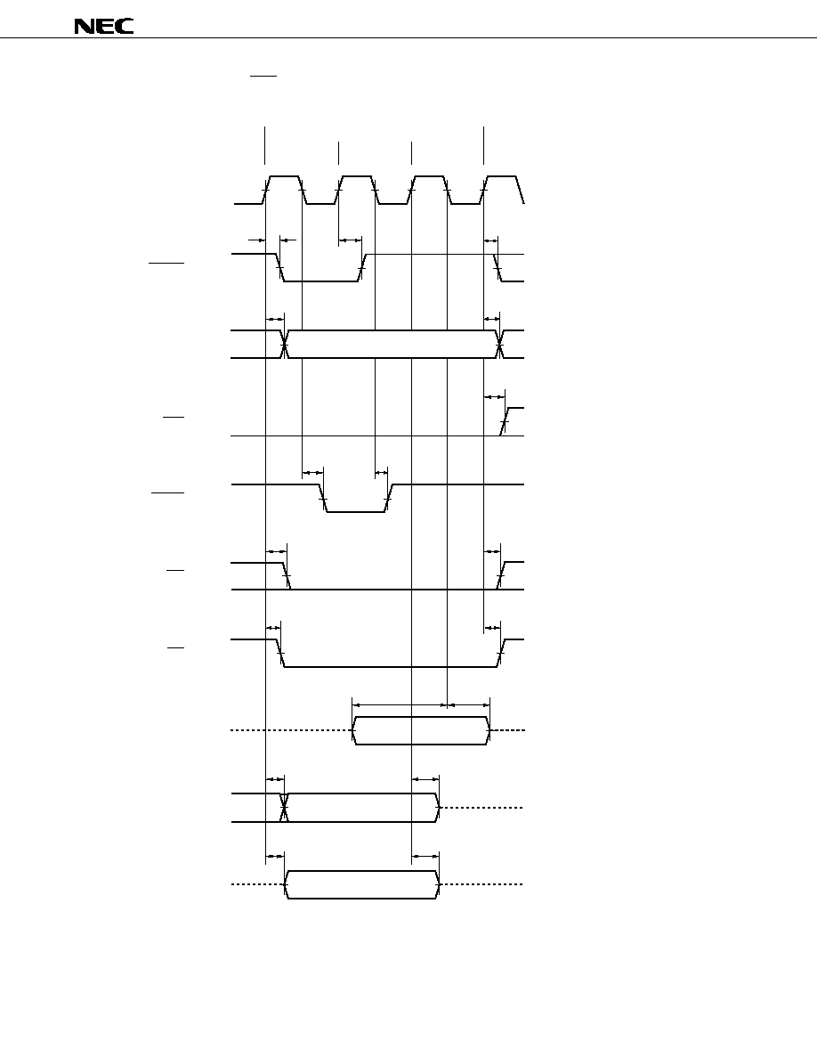
µ
PD705101
52
(f)
DRAM single 2-clock CAS on-page cycle (32-bit data bus)
Remark The dotted lines indicate high impedance.
<17>
<18>
<18>
<24>
<25>
<28>
<27>
<31>
<29>
<15>
<15>
<16>
CLKOUT (output)
EDO on-page
Tca
Tcn
CA
Tce
BCYST (output)
A1-A23 (output)
RAS (output)
xxCAS (output)
WE (output)
OE (output)
D0-D31 (input)
D0-D31 (output)
D0-D31 (output)
<16>
<15>
<24>
<25>
<31>
<30>

µ
PD705101
53
(g) DRAM burst 1-clock CAS off-page cycle (32-bit data bus)
Remark The dotted lines indicate high impedance.
<15>
<15>
<15>
<16>
<16>
<16>
<16>
<16>
<16>
<16>
<17>
<17>
<17>
<16>
<18>
<18>
<18>
<24>
<25>
<24>
<25>
<28>
<27>
<28>
<27>
<28>
<27>
<28>
<30>
<29>
<29>
<29>
<31>
<27>
1
2
3
4
1
RA
CA1
CA2
CA3
CA4
2
3
4
CLKOUT (output)
BCYST (output)
A1-A23 (output)
RAS (output)
xxCAS (output)
WE (output)
OE (output)
D0-D31 (input)
D0-D31 (output)
Trm
Trp
Trc
Tc
Tc2
EDO off-page
Tc3
Tc4
Tce

µ
PD705101
54
(h) DRAM burst 2-clock CAS off-page cycle (32-bit data bus)
Remark The dotted lines indicate high impedance.
1
RA
CA1
CA2
CA3
CA4
2
3
4
1
2
3
4
<30>
<29>
<29>
<29>
<31>
<28>
<27>
<28>
<27>
<28>
<27>
<28>
<27>
<25>
<24>
<25>
<24>
<18>
<18>
<18>
<18>
<18>
<18>
<18>
<18>
<17>
<17>
<17>
<15>
<15>
<15>
<15>
<15>
<15>
<15>
<15>
<15>
<16>
<16>
<16>
<16>
<16>
<16>
<16>
CLKOUT (output)
Trm
Trp
Trc
Tca2
Tcn1
Tca3
Tcn2
Tca4
Tcn3
Tcn4
Tca
Tce
BCYST (output)
A1-A23 (output)
RAS (output)
xxCAS (output)
WE (output)
OE (output)
D0-D31 (input)
D0-D31 (output)

µ
PD705101
55
(5) SRAM (ROM), Page-ROM, I/O access timing
Parameter
Symbol
Conditions
MIN.
MAX.
Unit
BCYST delay time (vs. CLKOUT
)
<15>
t
DKBC
2
10
ns
Address delay time (vs. CLKOUT
)
<16>
t
DKA
2
9
ns
Data output delay time (from active, vs. CLKOUT
) <29>
t
DKDT
2
10
ns
Data output delay time (from float, vs. CLKOUT
)
<30>
t
LZKDT
2
10
ns
Data float delay time (vs. CLKOUT
)
<31>
t
HZKDT
3
20
ns
CS delay time (vs. CLKOUT
)
<32>
t
DKCS
2
10
ns
IORD output delay time (vs. CLKOUT
)
<33>
t
DKRD
2
10
ns
IOWR output delay time (vs. CLKOUT
)
<34>
t
DKWR
2
10
ns
MRD output delay time (vs. CLKOUT
)
<35>
t
DKMRD
2
10
ns
xxMWR delay time (vs. CLKOUT
)
<36>
t
DKMWR
2
10
ns
Data input setup time (vs. CLKOUT
)
<37>
t
SDTK
4
ns
Data input hold time (vs. CLKOUT
)
<38>
t
HKDT
1
ns
READY setup time (vs. CLKOUT
)
<39>
t
SRYK
7
ns
READY hold time (vs. CLKOUT
)
<40>
t
HKRY
3
ns

µ
PD705101
56
(a) I/O access timing
Remark The dotted lines indicate high impedance.
<15>
<15>
<15>
<16>
<16>
<32>
<33>
<33>
<37>
<38>
<34>
<34>
<29>
<30>
<39>
<39>
<40>
<40>
<31>
<29>
<32>
Ta
Ts
Ts
CLKOUT (output)
BCYST (output)
A1-A23 (output)
CS (output)
IORD (output)
D0-D31 (input)
IOWR (output)
D0-D31 (output)
D0-D31 (output)
READY (input)

µ
PD705101
57
(b) SRAM (ROM)/Page-ROM single cycle
Remark The dotted lines indicate high impedance.
<15>
<15>
<15>
<16>
<16>
<32>
<35>
<35>
<37>
<38>
<36>
<36>
<29>
<30>
<39>
<39>
<40>
<40>
<31>
<29>
<32>
Ta
Ts
Ts
CLKOUT (output)
BCYST (output)
A1-A23 (output)
CS (output)
MRD (output)
D0-D31 (input)
xxMWR (output)
D0-D31 (output)
D0-D31 (output)
READY (input)

µ
PD705101
58
(c) Page-ROM burst cycle (32-bit data bus)
Remark The dotted lines indicate high impedance.
Ta
Tb1
Tb1
Tb2
Ta2
Ta3
Ta4
Tb3
Ts
<15>
<15>
<15>
<15>
<15>
<15>
<15>
<15>
<16>
<16>
<16>
<16>
<32>
<33>
<32>
<33>
<38>
<37>
<38>
<37>
<38>
<37>
<38>
<37>
<39> <40> <39> <40>
<39> <40>
<39> <40>
<39> <40>
CLKOUT (output)
BCYST (output)
A1-A23 (output)
CS1-CS7 (output)
MRD (output)
D0-D31 (input)
READY (input)

µ
PD705101
59
(6) Interrupt timing
Parameter
Symbol
Conditions
MIN.
MAX.
Unit
NMI setup time (vs. CLKOUT
)
<41> t
SNK
5
ns
NMI hold time (vs. CLKOUT
)
<42> t
HKN
7
ns
INTPxx setup time (vs. CLKOUT
)
<43> t
SIK
7
ns
INTPxx hold time (vs. CLKOUT
)
<44> t
HKI
3
ns
NMI clock high-level time
<45> t
NMH
5T+12
ns
NMI clock low-level time
<46> t
NML
5T+12
ns
Remark T = t
CYK
(external clock cycle)
<41>
<42>
<42> <41>
<45>
<46>
<43>
<44>
CLKOUT (output)
NMI (input)
2.0 V
0.6 V
0.5 V
DD
INTP00-INTP03,
INTP10-INTP13 (input)

µ
PD705101
60
(7) Bus hold timing
Parameter
Symbol
Conditions
MIN.
MAX.
Unit
Data active delay time (vs. CLKOUT
)
<30>
t
LZKDT
2
10
ns
Data float delay time (vs. CLKOUT
)
<31>
t
HZKDT
3
20
ns
HLDRQ input setup time (vs. CLKOUT
)
<47>
t
SHQK
7
ns
HLDRQ hold time (vs. CLKOUT
)
<48>
t
HKHQ
3
ns
HLDAK output delay time
<49>
t
DKHA
2
10
ns
Address float delay time (vs. CLKOUT
)
<50>
t
HZKA
3
20
ns
Address active delay time (vs. CLKOUT
)
<51>
t
LZKA
2
10
ns
<47>
<48>
<49>
<49>
<47>
<50>
<51>
<31>
<30>
CLKOUT (output)
HLDRQ (input)
HLDAK (output)
Note (output)
D0-D31 (output)
Ti
Th
Th
Th
Th
Ti
Note
BCYST, WE, OE, A1-A23, CS1-CS7, RAS, xxCAS, MRD, IORD, xxMWR, IOWR
Remark The dotted lines indicate high impedance.

µ
PD705101
61
(8) DMA timing
Parameter
Symbol
Conditions
MIN.
MAX.
Unit
DMARQ input setup time (vs. CLKOUT
)
<52>
t
SDQK
7
ns
DMARQ hold time (vs. CLKOUT
)
<53>
t
HKDQ
3
ns
DMAAK output delay time
<54>
t
DKDAK
2
10
ns
<52>
<53><52>
<54>
<54>
CLKOUT (output)
DMARQ0-DMARQ3 (input)
DMAAK0-DMAAK3 (output)

µ
PD705101
62
(9) CSI timing
(a) SCLK input mode
Parameter
Symbol
Conditions
MIN.
MAX.
Unit
SCLK cycle
<55>
t
CYSI
120
ns
SCLK high-level time
<56>
t
SIH
50
ns
SCLK low-level time
<57>
t
SIL
50
ns
SCLK rise time
<58>
t
SIR
10
ns
SCLK fall time
<59>
t
SIF
10
ns
SI input setup time (vs. SCLK
)
<60>
t
SDTS
30
ns
SI input hold time (vs. SCLK
)
<61>
t
HSDT
30
ns
SO output delay time (vs. SCLK
)
<62>
t
DSDT
2
30
ns
<55>
<56>
<57>
<58>
<61>
<60>
<62>
<59>
SCLK (input)
SI (input)
0.8 V
DD
0.5 V
DD
0.2 V
DD
SO (output)
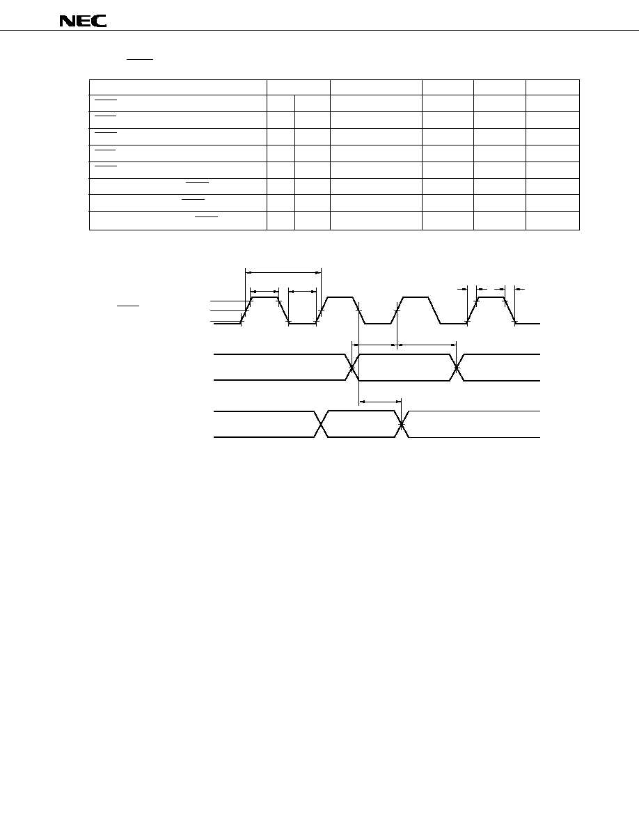
µ
PD705101
63
(b) SCLK output mode
Parameter
Symbol
Conditions
MIN.
MAX.
Unit
SCLK cycle
<63>
t
CYSO
120
ns
SCLK high-level time
<64>
t
SOH
50
ns
SCLK low-level time
<65>
t
SOL
50
ns
SCLK rise time
<66>
t
SOR
10
ns
SCLK fall time
<67>
t
SOF
10
ns
SI input setup time (vs. SCLK
)
<68>
t
SDTS
30
ns
SI input hold time (vs. SCLK
)
<69>
t
HSDT
30
ns
SO output delay time (vs. SCLK
)
<70>
t
DSDT
2
30
ns
<63>
<64>
<65>
<66>
<69>
<68>
<70>
<67>
SCLK (output)
SI (input)
0.8 V
DD
0.5 V
DD
0.2 V
DD
SO (output)

µ
PD705101
64
(10) Timer timing
Parameter
Symbol
Conditions
MIN.
MAX.
Unit
TI clock cycle
<71>
t
CYT
243
ns
TI clock high-level time
<72>
t
TIH
4T + 10
ns
TI clock low-level time
<73>
t
TIL
4T + 10
ns
TI clock rise time
<74>
t
TR
10
ns
TI clock fall time
<75>
t
TF
10
ns
TCLR clock high-level time
<76>
t
CLH
4T + 10
ns
TCLR clock low-level time
<77>
t
CLL
4T + 10
ns
Remark T = t
CYK
(external clock cycle)
<71>
<72>
<73>
<77>
<76>
<74>
<75>
TI (input)
2.0 V
0.5 V
DD
0.6 V
2.0 V
0.6 V
TCLR (input)

µ
PD705101
65
17. PACKAGE DRAWINGS
160 PIN PLASTIC LQFP (FINE PITCH) ( 24)
NOTE
Each lead centerline is located within 0.10 mm (0.004 inch) of
its true position (T.P.) at maximum material condition.
ITEM
MILLIMETERS
INCHES
F
G
2.25
2.25
0.089
0.089
A
26.0±0.2
1.024+0.008
≠0.009
B
C
24.0±0.2
24.0±0.2
0.945±0.008
0.945±0.008
D
26.0±0.2
1.024
H
0.22
0.009±0.002
I
0.10
0.004
S
1.7 MAX.
0.067 MAX.
K
1.0±0.2
0.039+0.009
≠0.008
L
0.5±0.2
0.020+0.008
≠0.009
M
0.145
0.006±0.002
N
0.10
0.004
P
1.4±0.1
0.055±0.004
Q
0.125±0.075
0.005±0.003
+0.05
≠0.04
+0.008
≠0.009
J
0.5 (T.P.)
0.020 (T.P.)
S160GM-50-8ED-2
+0.055
≠0.045
+7∞
≠3∞
R
3∞
3∞ +7∞
≠3∞
120
121
160
1
40
41
80
81
A
B
M
C
D
detail of lead end
S
Q
R
F
G
H
I
J
K
M
N
P
L

µ
PD705101
66
18. RECOMMENDED SOLDERING CONDITIONS
The conditions listed below shall be met when soldering the
µ
PD705101.
For details of the recommended soldering conditions, refer to our document Semiconductor Device Mounting
Technology Manual (C10535E).
Please consult with our sales offices in case any other soldering process is used, or in case soldering is done under
different conditions.
Table 18-1. Soldering Conditions for Surface-Mount Devices
Note
Maximum number of days during which the product can be stored at a temperature of 25
∞
C and a relative
humidity of 65 % or less after dry-pack package is opened.
Caution Do not apply two or more different soldering methods to one chip (except for partial heating
method for terminal sections).
Soldering Process
Infrared ray reflow
VPS
Partial heating method
Symbol
IR35-103-2
VP15-103-2
≠
Soldering Conditions
Peak package's surface temperature: 235
∞
C
Reflow time: 30 seconds or less (210
∞
C or more)
Maximum allowable number of reflow processes: 2
Exposure limit: 3 days
Note
(10 hours of pre-baking is required at 125
∞
C
afterward)
<Caution>
Non-heat-resistant trays, such as magazine and taping trays, cannot be
baked before unpacking.
Peak package's surface temperature: 215
∞
C
Reflow time: 40 seconds or less (200
∞
C or more)
Maximum allowable number of reflow processes: 2
Exposure limit: 3 days
Note
(10 hours of pre-baking is required at 125
∞
C
afterward)
<Caution>
Non-heat-resistant trays, such as magazine and taping trays, cannot be
baked before unpacking.
Terminal temperature: 300
∞
C or less
Heat time: 3 seconds or less (for one side of a device)

µ
PD705101
67
[MEMO]

µ
PD705101
68
[MEMO]

µ
PD705101
69
[MEMO]

µ
PD705101
70
NOTES FOR CMOS DEVICES
1
PRECAUTION AGAINST ESD FOR SEMICONDUCTORS
Note: Strong electric field, when exposed to a MOS device, can cause destruction
of the gate oxide and ultimately degrade the device operation. Steps must
be taken to stop generation of static electricity as much as possible, and
quickly dissipate it once, when it has occurred. Environmental control must
be adequate. When it is dry, humidifier should be used. It is recommended
to avoid using insulators that easily build static electricity. Semiconductor
devices must be stored and transported in an anti-static container, static
shielding bag or conductive material. All test and measurement tools
including work bench and floor should be grounded. The operator should
be grounded using wrist strap. Semiconductor devices must not be touched
with bare hands. Similar precautions need to be taken for PW boards with
semiconductor devices on it.
2
HANDLING OF UNUSED INPUT PINS FOR CMOS
Note: No connection for CMOS device inputs can be cause of malfunction. If no
connection is provided to the input pins, it is possible that an internal input
level may be generated due to noise, etc., hence causing malfunction. CMOS
device behave differently than Bipolar or NMOS devices. Input levels of
CMOS devices must be fixed high or low by using a pull-up or pull-down
circuitry. Each unused pin should be connected to V
DD
or GND with a
resistor, if it is considered to have a possibility of being an output pin. All
handling related to the unused pins must be judged device by device and
related specifications governing the devices.
3
STATUS BEFORE INITIALIZATION OF MOS DEVICES
Note: Power-on does not necessarily define initial status of MOS device. Produc-
tion process of MOS does not define the initial operation status of the device.
Immediately after the power source is turned ON, the devices with reset
function have not yet been initialized. Hence, power-on does not guarantee
out-pin levels, I/O settings or contents of registers. Device is not initialized
until the reset signal is received. Reset operation must be executed imme-
diately after power-on for devices having reset function.

µ
PD705101
71
NEC Electronics Inc. (U.S.)
Santa Clara, California
Tel: 408-588-6000
800-366-9782
Fax: 408-588-6130
800-729-9288
NEC Electronics (Germany) GmbH
Duesseldorf, Germany
Tel: 0211-65 03 02
Fax: 0211-65 03 490
NEC Electronics (UK) Ltd.
Milton Keynes, UK
Tel: 01908-691-133
Fax: 01908-670-290
NEC Electronics Italiana s.r.1.
Milano, Italy
Tel: 02-66 75 41
Fax: 02-66 75 42 99
NEC Electronics Hong Kong Ltd.
Hong Kong
Tel: 2886-9318
Fax: 2886-9022/9044
NEC Electronics Hong Kong Ltd.
Seoul Branch
Seoul, Korea
Tel: 02-528-0303
Fax: 02-528-4411
NEC Electronics Singapore Pte. Ltd.
United Square, Singapore 1130
Tel: 253-8311
Fax: 250-3583
NEC Electronics Taiwan Ltd.
Taipei, Taiwan
Tel: 02-719-2377
Fax: 02-719-5951
NEC do Brasil S.A.
Cumbica-Guarulhos-SP, Brasil
Tel: 011-6465-6810
Fax: 011-6465-6829
NEC Electronics (Germany) GmbH
Benelux Office
Eindhoven, The Netherlands
Tel: 040-2445845
Fax: 040-2444580
NEC Electronics (France) S.A.
Velizy-Villacoublay, France
Tel: 01-30-67 58 00
Fax: 01-30-67 58 99
NEC Electronics (France) S.A.
Spain Office
Madrid, Spain
Tel: 01-504-2787
Fax: 01-504-2860
NEC Electronics (Germany) GmbH
Scandinavia Office
Taeby, Sweden
Tel: 08-63 80 820
Fax: 08-63 80 388
Regional Information
Some information contained in this document may vary from country to country. Before using any NEC
product in your application, please contact the NEC office in your country to obtain a list of authorized
representatives and distributors. They will verify:
∑ Device availability
∑ Ordering information
∑ Product release schedule
∑ Availability of related technical literature
∑ Development environment specifications (for example, specifications for third-party tools and
components, host computers, power plugs, AC supply voltages, and so forth)
∑ Network requirements
In addition, trademarks, registered trademarks, export restrictions, and other legal issues may also vary
from country to country.
J97. 8

µ
PD705101
72
The related documents referred to in this publication may include preliminary versions. However, preliminary
versions are not marked as such.
V830, V831, and V830 Family are trademarks of NEC Corporation.
No part of this document may be copied or reproduced in any form or by any means without the prior written
consent of NEC Corporation. NEC Corporation assumes no responsibility for any errors which may appear in
this document.
NEC Corporation does not assume any liability for infringement of patents, copyrights or other intellectual property
rights of third parties by or arising from use of a device described herein or any other liability arising from use
of such device. No license, either express, implied or otherwise, is granted under any patents, copyrights or other
intellectual property rights of NEC Corporation or others.
While NEC Corporation has been making continuous effort to enhance the reliability of its semiconductor devices,
the possibility of defects cannot be eliminated entirely. To minimize risks of damage or injury to persons or
property arising from a defect in an NEC semiconductor device, customers must incorporate sufficient safety
measures in its design, such as redundancy, fire-containment, and anti-failure features.
NEC devices are classified into the following three quality grades:
"Standard", "Special", and "Specific". The Specific quality grade applies only to devices developed based on a
customer designated "quality assurance program" for a specific application. The recommended applications of
a device depend on its quality grade, as indicated below. Customers must check the quality grade of each device
before using it in a particular application.
Standard: Computers, office equipment, communications equipment, test and measurement equipment,
audio and visual equipment, home electronic appliances, machine tools, personal electronic
equipment and industrial robots
Special:
Transportation equipment (automobiles, trains, ships, etc.), traffic control systems, anti-disaster
systems, anti-crime systems, safety equipment and medical equipment (not specifically designed
for life support)
Specific:
Aircrafts, aerospace equipment, submersible repeaters, nuclear reactor control systems, life
support systems or medical equipment for life support, etc.
The quality grade of NEC devices is "Standard" unless otherwise specified in NEC's Data Sheets or Data Books.
If customers intend to use NEC devices for applications other than those specified for Standard quality grade,
they should contact an NEC sales representative in advance.
Anti-radioactive design is not implemented in this product.
M4 96.5