Document Outline
- Cover
- FEATURES
- ORDERING INFORMATION
- PIN CONFIGURATION (Top View)
- PIN IDENTIFICATION
- INTERNAL BLOCK DIAGRAM
- 1. DIFFERENCES AMONG PRODUCTS
- 1.1 Differences Between uPD70F3102-33 and uPD703102-33
- 1.2 Differences Between uPD70F3102-33 and uPD70F3102A-33
- 2. PIN FUNCTIONS
- 2.1 Port Pins
- 2.2 Non-Port Pins
- 2.3 Pin I/O Circuit Types and Recommended Connection of Unused Pins
- 3. FLASH MEMORY PROGRAMMING
- 3.1 Selection of Communication System
- 3.2 Flash Memory Programming Functions
- 3.3 Connecting the Dedicated Flash Programmer
- 4. ELECTRICAL SPECIFICATIONS
- 4.1 Normal Operation Mode
- 4.2 Flash Memory Programming Mode
- 5. PACKAGE DRAWINGS
- 6. RECOMMENDED SOLDERING CONDITIONS

The information contained in this document is being issued in advance of the production cycle for the
device. The parameters for the device may change before final production or NEC Corporation, at its own
discretion, may withdraw the device prior to its production.
Not all devices/types available in every country. Please check with local NEC representative for
availability and additional information.
MOS INTEGRATED CIRCUITS
µ
µ
µ
µ
PD70F3102-33
V850E/MS1
TM
32-/16-BIT SINGLE-CHIP MICROCONTROLLER
©
1999
Document No. U13844EJ2V0DS00 (2nd edition)
Date Published July 2000 N CP(K)
Printed in Japan
PRELIMINARY DATA SHEET
The
µ
PD70F3102-33 is a product that substitutes the internal mask ROM of the
µ
PD703102-33 with flash
memory. This enables users to perform on-board program writing and erasure, enabling effective evaluation during
system development, small-lot production of multiple devices, and rapid production start, and quick development and
time-to-market.
A version using a 3.3 V power supply for external pins, the
µ
PD70F3102-A33, is also available.
For additional information, refer to the following user's manuals. Be sure to read them before starting
design.
V850E/MS1 User's Manual Hardware:
U12688E
V850E/MS1 User's Manual Architecture: U12197E
FEATURES
∑
µ
PD703102-33 compatible
Can be replaced by the
µ
PD703102-33 with internal mask ROM for mass production
∑
Internal flash memory: 128 KB
ORDERING INFORMATION
Part Number
Package
µ
PD70F3102GJ-33-8EU
144-pin plastic LQFP (fine pitch) (20
◊
20)
µ
PD70F3102GJ-33-UEN
144-pin plastic LQFP (fine pitch) (20
◊
20)
The mark shows major revised points.

Preliminary Data Sheet U13844EJ2V0DS00
2
µ
µ
µ
µ
PD70F3102-33
PIN CONFIGURATION (Top View)
144-pin plastic LQFP (fine pitch) (20
◊
◊
◊
◊
20)
∑
µ
µ
µ
µ
PD70F3102GJ-33-8EU
∑
µ
µ
µ
µ
PD70F3102GJ-33-UEN
INTP103/DMARQ3/P07
INTP102/DMARQ2/P06
INTP101/DMARQ1/P05
INTP100/DMARQ0/P04
TI10/P03
TCLR10/P02
TO101/P01
TO100/P00
V
SS
INTP113/DMAAK3/P17
INTP112/DMAAK2/P16
INTP111/DMAAK1/P15
INTP110/DMAAK0/P14
TI11/P13
TCLR11/P12
TO111/P11
TO110/P10
INTP123/TC3/P107
INTP122/TC2/P106
INTP121/TC1/P105
INTP120/TC0/P104
TI12/P103
TCLR12/P102
TO121/P101
TO120/P100
ANI7/P77
ANI6/P76
ANI5/P75
ANI4/P74
ANI3/P73
ANI2/P72
ANI1/P71
ANI0/P70
AV
DD
AV
SS
AV
REF
1
2
3
4
5
6
7
8
9
10
11
12
13
14
15
16
17
18
19
20
21
22
23
24
25
26
27
28
29
30
31
32
33
34
35
36
A16/P60
A17/P61
A18/P62
A19/P63
A20/P64
A21/P65
A22/P66
A23/P67
HV
DD
CS0/RAS0/P80
CS1/RAS1/P81
CS2/RAS2/P82
CS3/RAS3/P83
CS4/RAS4/IOWR/P84
CS5/RAS5/IORD/P85
CS6/RAS6/P86
CS7/RAS7/P87
LCAS/LWR/P90
UCAS/UWR/P91
RD/P92
WE/P93
BCYST/P94
OE/P95
HLDAK/P96
HLDRQ/P97
V
SS
REFRQ/PX5
WAIT/PX6
CLKOUT/PX7
TO150/P120
TO151/P121
TCLR15/P122
TI15/P123
INTP150/P124
INTP151/P125
INTP152/P126
108
107
106
105
104
103
102
101
100
99
98
97
96
95
94
93
92
91
90
89
88
87
86
85
84
83
82
81
80
79
78
77
76
75
74
73
NMI/P20
P21
TXD0/SO0/P22
RXD0/SI0/P23
SCK0/P24
TXD1/SO1/P25
RXD1/SI1/P26
SCK1/P27
V
DD
INTP133/SCK2/P37
INTP132/SI2/P36
INTP131/SO2/P35
INTP130/P34
TI13/P33
TCLR13/P32
TO131/P31
TO130/P30
INTP143/SCK3/P117
INTP142/SI3/P116
INTP141/SO3/P115
INTP140/P114
TI14/P113
TCLR14/P112
TO141/P111
TO140/P110
CV
DD
X2
X1
CV
SS
CKSEL
MODE0
MODE1
MODE2
MODE3/V
PP
RESET
INTP153/ADTRG/P127
37
38
39
40
41
42
43
44
45
46
47
48
49
50
51
52
53
54
55
56
57
58
59
60
61
62
63
64
65
66
67
68
69
70
71
72
V
DD
D0/P40
D1/P41
D2/P42
D3/P43
D4/P44
D5/P45
D6/P46
D7/P47
V
SS
D8/P50
D9/P51
D10/P52
D11/P53
D12/P54
D13/P55
D14/P56
D15/P57
HV
DD
A0/PA0
A1/PA1
A2/PA2
A3/PA3
A4/PA4
A5/PA5
A6/PA6
A7/PA7
V
SS
A8/PB0
A9/PB1
A10/PB2
A11/PB3
A12/PB4
A13/PB5
A14/PB6
A15/PB7
144
143
142
141
140
139
138
137
136
135
134
133
132
131
130
129
128
127
126
125
124
123
122
121
120
119
118
117
116
115
114
113
112
111
110
109

Preliminary Data Sheet U13844EJ2V0DS00
3
µ
µ
µ
µ
PD70F3102-33
PIN IDENTIFICATION
A0 to A23:
Address Bus
P50 to P57:
Port 5
ADTRG:
AD Trigger Input
P60 to P67:
Port 6
ANI0 to ANI7:
Analog Input
P70 to P77:
Port 7
AV
DD:
Analog Power Supply
P80 to P87:
Port 8
AV
REF
:
Analog Reference Voltage
P90 to P97:
Port 9
AV
SS
:
Analog Ground
P100 to P107:
Port 10
BCYST:
Bus Cycle Start Timing
P110 to P117:
Port 11
CKSEL:
Clock Generator Operating Mode
P120 to P127:
Port 12
Select
PA0 to PA7:
Port A
CLKOUT:
Clock Output
PB0 to PB7:
Port B
CS0 to CS7:
Chip Select
PX5 to PX7:
Port X
CV
DD
:
Clock Generator Power Supply
RAS0 to RAS7:
Row Address Strobe
CV
SS
:
Clock Generator
RD:
Read
D0 to D15:
Data Bus
REFRQ:
Refresh Request
DMAAK0 to DMAAK3: DMA Acknowledge
RESET:
Reset
DMARQ0 to DMARQ3: DMA Request
RXD0, RXD1:
Receive Data
HLDAK:
Hold Acknowledge
SCK0 to SCK3:
Serial Clock
HLDRQ:
Hold Request
SI0 to SI3:
Serial Input
HV
DD
:
Power Supply for External Pins
SO0 to SO3:
Serial Output
INTP100 to INTP103,
TC0 to TC3:
Terminal Count Signal
INTP110 to INTP113,
TCLR10 to TCLR15: Timer Clear
INTP120 to INTP123,
TI10 to TI15:
Timer Input
INTP130 to INTP133,
TO100, TO101,
INTP140 to INTP143,
TO110, TO111,
INTP150 to INTP153:
Interrupt Request from Peripherals TO120, TO121,
IORD:
I/O Read Strobe
TO130, TO131,
IOWR:
I/O Write Strobe
TO140, TO141,
LCAS:
Lower Column Address Strobe
TO150, TO151:
Timer Output
LWR:
Lower Write Strobe
TXD0, TXD1:
Transmit Data
MODE0 to MODE3:
Mode
UCAS:
Upper Column Address Strobe
NMI:
Non-Maskable Interrupt Request UWR:
Upper Write Strobe
OE:
Output Enable
V
DD
:
Power Supply for Internal Unit
P00 to P07:
Port 0
V
PP
:
Programming Power Supply
P10 to P17:
Port 1
V
SS
:
Ground
P20 to P27:
Port 2
WAIT:
Wait
P30 to P37:
Port 3
WE:
Write Enable
P40 to P47:
Port 4
X1, X2:
Crystal

Preliminary Data Sheet U13844EJ2V0DS00
4
µ
µ
µ
µ
PD70F3102-33
INTERNAL BLOCK DIAGRAM
TCLR10 to TCLR15
TI10 to TI15
TO100, TO101,
TO110, TO111,
TO120, TO121,
TO130, TO131,
TO140, TO141,
TO150, TO151
INTP100 to INTP103,
INTP110 to INTP113,
INTP120 to INTP123,
INTP130 to INTP133,
INTP140 to INTP143,
INTP150 to INTP153
NMI
INTC
RPU
UART0/CSI0
SIO
SCK0
SI0/RXD0
SO0/TXD0
BRG0
UART1/CSI1
SCK1
SI1/RXD1
SO1/TXD1
BRG1
CSI2
SCK2
SI2
SO2
BRG2
CSI3
SCK3
SI3
SO3
AV
REF
ADC
AV
SS
AV
DD
ADTRG
ANI0 to ANI7
Port
PX5 to PX7
PB0 to PB7
PA0 to PA7
P120 to P127
P110 to P117
P100 to P107
P90 to P97
P80 to P87
P70 to P77
P60 to P67
P50 to P57
P40 to P47
P30 to P37
P21 to P27
P20
P10 to P17
P00 to P07
HV
DD
128 KB
Flash memory
4 KB
RAM
Instruction queue
PC
System registers
General-purpose
registers
(32 bits
◊
32)
Multiplier
(32
◊
32
64)
Barrel
shifter
ALU
DRAMC
Page ROM
controller
DMAC
BCU
CPU
TC0 to TC3
LWR/LCAS
DMAAK0 to DMAAK3
DMARQ0 to DMARQ3
D0 to D15
A0 to A23
WAIT
CS0 to CS7/RAS0 to RAS7
UWR/UCAS
OE
RD
WE
BCYST
REFRQ
IORD
IOWR
HLDAK
HLDRQ
CG
CKSEL
CLKOUT
X1
X2
CV
DD
CV
SS
System
controller
RESET
V
PP
V
DD
V
SS
MODE0 to MODE3

Preliminary Data Sheet U13844EJ2V0DS00
5
µ
µ
µ
µ
PD70F3102-33
CONTENTS
1. DIFFERENCES AMONG PRODUCTS ..............................................................................................
6
1.1 Differences Between
µ
µ
µ
µ
PD70F3102-33 and
µ
µ
µ
µ
PD703102-33 ......................................................
6
1.2 Differences Between
µ
µ
µ
µ
PD70F3102-33 and
µ
µ
µ
µ
PD70F3102A-33..................................................
6
2. PIN FUNCTIONS.................................................................................................................................
7
2.1 Port Pins ......................................................................................................................................
7
2.2 Non-Port Pins .............................................................................................................................. 10
2.3 Pin I/O Circuit Types and Recommended Connection of Unused Pins ................................ 14
3. FLASH MEMORY PROGRAMMING ................................................................................................. 17
3.1 Selection of Communication System........................................................................................ 17
3.2 Flash Memory Programming Functions ................................................................................... 18
3.3 Connecting the Dedicated Flash Programmer......................................................................... 18
4. ELECTRICAL SPECIFICATIONS....................................................................................................... 19
4.1 Normal Operation Mode ............................................................................................................. 19
4.2 Flash Memory Programming Mode ........................................................................................... 74
5. PACKAGE DRAWINGS...................................................................................................................... 76
6. RECOMMENDED SOLDERING CONDITIONS................................................................................. 78

Preliminary Data Sheet U13844EJ2V0DS00
6
µ
µ
µ
µ
PD70F3102-33
1. DIFFERENCES AMONG PRODUCTS
1.1
Differences Between
µ
µ
µ
µ
PD70F3102-33 and
µ
µ
µ
µ
PD703102-33
Product
Item
µ
PD70F3102-33
µ
PD703102-33
Internal ROM
Flash memory
Mask ROM
Flash memory programming pin
Provided (V
PP
)
None
Flash memory programming mode
Provided (MODE0 = L, MODE1 = H,
MODE2 = L, MODE3/V
PP
= 7.8 V)
None
Electrical specifications
Consumption current etc. differ (see individual data sheets).
Others
Circuit scale and master layout differ, thus noise immunity, noise radiation, etc. differ.
Cautions
1. There are differences in noise immunity and noise radiation between the flash memory
version and mask ROM version. When pre-producing an application set with the flash
memory version and then mass-producing it with the mask ROM version, be sure to conduct
sufficient evaluation for commercial samples (not engineering samples) of the mask ROM
version.
2. When switching from the flash memory version to the mask ROM version, write the same
code to the free area of the internal ROM.
1.2
Differences Between
µ
µ
µ
µ
PD70F3102-33 and
µ
µ
µ
µ
PD70F3102A-33
Product
Item
µ
PD70F3102-33
µ
PD70F3102A-33
HV
DD
4.5 to 5.5 V
3.0 to 3.6 V
Electrical specifications
See individual data sheets.
Package
∑ 144-pin plastic LQFP (fine pitch) (20
◊
20)
∑ 157-pin plastic FBGA (14
◊
14)
∑ 144-pin plastic LQFP (fine pitch) (20
◊
20)

Preliminary Data Sheet U13844EJ2V0DS00
7
µ
µ
µ
µ
PD70F3102-33
2. PIN FUNCTIONS
2.1
Port Pins
(1/3)
Pin Name
I/O
Function
Alternate Function
P00
TO100
P01
TO101
P02
TCLR10
P03
TI10
P04
INTP100/DMARQ0
P05
INTP101/DMARQ1
P06
INTP102/DMARQ2
P07
I/O
Port 0
8-bit I/O port
Input/output can be specified in 1-bit units.
INTP103/DMARQ3
P10
TO110
P11
TO111
P12
TCLR11
P13
TI11
P14
INTP110/DMAAK0
P15
INTP111/DMAAK1
P16
INTP112/DMAAK2
P17
I/O
Port 1
8-bit I/O port
Input/output can be specified in 1-bit units.
INTP113/DMAAK3
P20
Input
NMI
P21
≠
P22
TXD0/SO0
P23
RXD0/SI0
P24
SCK0
P25
TXD1/SO1
P26
RXD1/SI1
P27
I/O
Port 2
P20 is an input-only port.
When a valid edge is input, it operates as an NMI input. The status of
the NMI input is shown by bit 0 of register P2.
P21 to P27 is a 7-bit I/O port.
Input/output can be specified in 1-bit units.
SCK1
P30
TO130
P31
TO131
P32
TCLR13
P33
TI13
P34
INTP130
P35
INTP131/SO2
P36
INTP132/SI2
P37
I/O
Port 3
8-bit I/O port
Input/output can be specified in 1-bit units.
INTP133/SCK2
P40 to P47
I/O
Port 4
8-bit I/O port
Input/output can be specified in 1-bit units.
D0 to D7

Preliminary Data Sheet U13844EJ2V0DS00
8
µ
µ
µ
µ
PD70F3102-33
(2/3)
Pin Name
I/O
Function
Alternate Function
P50 to P57
I/O
Port 5
8-bit I/O port
Input/output can be specified in 1-bit units.
D8 to D15
P60 to P67
I/O
Port 6
8-bit I/O port
Input/output can be specified in 1-bit units.
A16 to A23
P70 to P77
Input
Port 7
8-bit input-only port
ANI0 to ANI7
P80
CS0/RAS0
P81
CS1/RAS1
P82
CS2/RAS2
P83
CS3/RAS3
P84
CS4/RAS4/IOWR
P85
CS5/RAS5/IORD
P86
CS6/RAS6
P87
I/O
Port 8
8-bit I/O port
Input/output can be specified in 1-bit units.
CS7/RAS7
P90
LCAS/LWR
P91
UCAS/UWR
P92
RD
P93
WE
P94
BCYST
P95
OE
P96
HLDAK
P97
I/O
Port 9
8-bit I/O port
Input/output can be specified in 1-bit units
HLDRQ
P100
TO120
P101
TO121
P102
TCLR12
P103
TI12
P104
INTP120/TC0
P105
INTP121/TC1
P106
INTP122/TC2
P107
I/O
Port 10
8-bit I/O port
Input/output can be specified in 1-bit units.
INTP123/TC3

Preliminary Data Sheet U13844EJ2V0DS00
9
µ
µ
µ
µ
PD70F3102-33
(3/3)
Pin Name
I/O
Function
Alternate Function
P110
TO140
P111
TO141
P112
TCLR14
P113
TI14
P114
INTP140
P115
INTP141/SO3
P116
INTP142/SI3
P117
I/O
Port 11
8-bit I/O port
Input/output can be specified in 1-bit units.
INTP143/SCK3
P120
TO150
P121
TO151
P122
TCLR15
P123
TI15
P124
INTP150
P125
INTP151
P126
INTP152
P127
I/O
Port 12
8-bit I/O port
Input/output can be specified in 1-bit units.
INTP153/ADTRG
PA0
A0
PA1
A1
PA2
A2
PA3
A3
PA4
A4
PA5
A5
PA6
A6
PA7
I/O
Port A
8-bit I/O port
Input/output can be specified in 1-bit units.
A7
PB0
A8
PB1
A9
PB2
A10
PB3
A11
PB4
A12
PB5
A13
PB6
A14
PB7
I/O
Port B
8-bit I/O port
Input/output can be specified in 1-bit units.
A15
PX5
REFRQ
PX6
WAIT
PX7
I/O
Port X
3-bit I/O port
Input/output can be specified in 1-bit units.
CLKOUT

Preliminary Data Sheet U13844EJ2V0DS00
10
µ
µ
µ
µ
PD70F3102-33
2.2
Non-Port Pins
(1/4)
Pin Name
I/O
Function
Alternate Function
TO100
P00
TO101
P01
TO110
P10
TO111
P11
TO120
P100
TO121
P101
TO130
P30
TO131
P31
TO140
P110
TO141
P111
TO150
P120
TO151
Output
Pulse signal output of timers 10 to 15
P121
TCLR10
P02
TCLR11
P12
TCLR12
P102
TCLR13
P32
TCLR14
P112
TCLR15
Input
External clear signal input of timers 10 to 15
P122
TI10
P03
TI11
P13
TI12
P103
TI13
P33
TI14
P113
TI15
Input
External count clock input of timers 10 to 15
P123
INTP100
P04/DMARQ0
INTP101
P05/DMARQ1
INTP102
P06/DMARQ2
INTP103
Input
External maskable interrupt request input, or timer 10 external capture
trigger input
P07/DMARQ3
INTP110
P14/DMAAK0
INTP111
P15/DMAAK1
INTP112
P16/DMAAK2
INTP113
Input
External maskable interrupt request input, or timer 11 external capture
trigger input
P17/DMAAK3
INTP120
P104/TC0
INTP121
P105/TC1
INTP122
P106/TC2
INTP123
Input
External maskable interrupt request input, or timer 12 external capture
trigger input
P107/TC3

Preliminary Data Sheet U13844EJ2V0DS00
11
µ
µ
µ
µ
PD70F3102-33
(2/4)
Pin Name
I/O
Function
Alternate Function
INTP130
P34
INTP131
P35/SO2
INTP132
P36/SI2
INTP133
Input
External maskable interrupt request input, or timer 13 external capture
trigger input
P37/SCK2
INTP140
P114
INTP141
P115/SO3
INTP142
P116/SI3
INTP143
Input
External maskable interrupt request input, or timer 14 external capture
trigger input
P117/SCK3
INTP150
P124
INTP151
P125
INTP152
P126
INTP153
Input
External maskable interrupt request input, or timer 15 external capture
trigger input
P127/ADTRG
SO0
P22/TXD0
SO1
P25/TXD1
SO2
P35/INTP131
SO3
Output
CSI0 to CSI3 serial transmission data output (3-wire)
P115/INTP141
SI0
P23/RXD0
SI1
P26/RXD1
SI2
P36/INTP132
SI3
Input
CSI0 to CSI3 serial reception data input (3-wire)
P116/INTP142
SCK0
P24
SCK1
P27
SCK2
P37/INTP133
SCK3
I/O
CSI0 to CSI3 serial clock input/output (3-wire)
P117/INTP143
TXD0
P22/SO0
TXD1
Output
UART0 and UART1 serial transmission data output
P25/SO1
RXD0
P23/SI0
RXD1
Input
UART0 and UART1 serial reception data input
P26/SI1
D0 to D7
P40 to P47
D8 to D15
I/O
16-bit data bus for external memory
P50 to P57
A0 to A7
PA0 to PA7
A8 to A15
PB0 to PB7
A16 to A23
Output
24-bit address bus for external memory
P60 to P67
LWR
Output
External data bus lower byte write enable signal output
P90/LCAS
UWR
Output
External data bus upper byte write enable signal output
P91/UCAS
RD
Output
External data bus read strobe signal output
P92
WE
Output
Write enable signal output for DRAM
P93
OE
Output
Output enable signal output for DRAM
P95

Preliminary Data Sheet U13844EJ2V0DS00
12
µ
µ
µ
µ
PD70F3102-33
(3/4)
Pin Name
I/O
Function
Alternate Function
LCAS
Output
Column address strobe signal output for lower data of DRAM
P90/LWR
UCAS
Output
Column address strobe signal output for higher data of DRAM
P91/UWR
RAS0 to RAS3
P80/CS0 to P83/CS3
RAS4
P84/CS4/IOWR
RAS5
P85/CS5/IORD
RAS6
P86/CS6
RAS7
Output
Row address strobe signal output for DRAM
P87/CS7
BCYST
Output
Strobe signal output indicating start of bus cycle
P94
CS0 to CS3
P80/RAS0 to
P83/RAS3
CS4
P84/RAS4/IOWR
CS5
P85/RAS5/IORD
CS6
P86/RAS6
CS7
Output
Chip select signal output
P87/RAS7
WAIT
Input
Control signal input that inserts a wait in the bus cycle
PX6
REFRQ
Output
Refresh request signal output for DRAM
PX5
IOWR
Output
DMA write strobe signal output
P84/RAS4/CS4
IORD
Output
DMA read strobe signal output
P85/RAS5/CS5
DMARQ0 to
DMARQ3
Input
DMA request signal input
P04/INTP100 to
P07/INTP103
DMAAK0 to
DMAAK3
Output
DMA acknowledge signal output
P14/INTP110 to
P17/INTP113
TC0 to TC3
Output
DMA termination (terminal count) signal output
P104/INTP120 to
P107/INTP123
HLDAK
Output
Bus hold acknowledge output
P96
HLDRQ
Input
Bus hold request input
P97
ANI0 to ANI7
Input
Analog input to A/D converter
P70 to P77
NMI
Input
Non-maskable interrupt request input
P20
CLKOUT
Output
System clock output
PX7
CKSEL
Input
Input that specifies the clock generator's operation mode
≠
MODE0 to
MODE2
≠
MODE3
Input
Operation mode specification
V
PP
RESET
Input
System reset input
≠
X1
Input
≠
X2
≠
Connecting system clock resonator. In the case of an external clock, it is
input to X1.
≠
ADTRG
Input
A/D converter external trigger input
P127/INTP153
AV
REF
Input
Reference voltage applied to A/D converter
≠
AV
DD
≠
Positive power supply for A/D converter
≠

Preliminary Data Sheet U13844EJ2V0DS00
13
µ
µ
µ
µ
PD70F3102-33
(4/4)
Pin Name
I/O
Function
Alternate Function
AV
SS
≠
Ground potential for A/D converter
≠
CV
DD
≠
Positive power supply for the dedicated clock generator
≠
CV
SS
≠
Ground potential for dedicated clock generator
≠
V
DD
≠
Positive power supply (internal unit power supply)
≠
HV
DD
≠
Positive power supply (external pin power supply)
≠
V
SS
≠
Ground potential
≠
V
PP
≠
High-voltage application pin during program write/verify
MODE3

Preliminary Data Sheet U13844EJ2V0DS00
14
µ
µ
µ
µ
PD70F3102-33
2.3
Pin I/O Circuit Types and Recommended Connection of Unused Pins
Table 2-1 shows the I/O circuit type of each pin and the recommended connection of unused pins, and Figure 2-1
shows the schematic circuit diagram for each I/O circuit type.
In the case of connection to V
DD
or V
SS
via a resistor, connection of a resistor of 1 to 10 k
is recommended.
Table 2-1. Pin I/O Circuit Types and Recommended Connection of Unused Pins (1/2)
Pin
I/O Circuit
Type
Recommended Connection of Unused Pins
P00/TO100, P01/TO101
5
P02/TCLR10, P03/TI10
P04/INTP100/DMARQ0 to
P07/INTP103/DMARQ3
5-K
P10/TO110, P11/TO111
5
P12/TCLR11, P13/TI11
P14/INTP110/DMAAK0 to
P17/INTP113/DMAAK3
5-K
Input:
Independently connect to HV
DD
or V
SS
via a resistor.
Output: Leave open.
P20/NMI
2
Connect directly to V
SS
.
P21
P22/TXD0/SO0
5
P23/RXD0/SI0
P24/SCK0
5-K
P25/TXD1/SO1
5
P26/RXD1/SI1
P27/SCK1
5-K
P30/TO130, P31/TO131
5
P32/TCLR13, P33/TI13
P34/INTP130
P35/INTP131/SO2
P36/INTP132/SI2
P37/INTP133/SCK2
5 - K
P40/D0 to P47/D7
P50/D8 to P57/D15
P60/A16 to P67/A23
5
Input:
Independently connect to HV
DD
or V
SS
via a resistor.
Output: Leave open.
P70/ANI0 to P77/ANI7
9
Connect directly to V
SS
.

Preliminary Data Sheet U13844EJ2V0DS00
15
µ
µ
µ
µ
PD70F3102-33
Table 2-1. Pin I/O Circuit Types and Recommended Connection of Unused Pins (2/2)
Pin
I/O Circuit
Type
Recommended Connection of Unused Pins
P80/CS0/RAS0 to P83/CS3/RAS3
P84/CS4/RAS4/IOWR,
P85/CS5/RAS5/IORD
P86/CS6/RAS6, P87/CS7/RAS7
P90/LCAS/LWR
P91/UCAS/UWR
P92/RD
P93/WE
P94/BCYST
P95/OE
P96/HLDAK
P97/HLDRQ
5
Input:
Independently connect to HV
DD
or V
SS
via a resistor.
Output: Leave open.
P100/TO120, P101/TO121
5
P102/TCLR12, P103/TI12
P104/INTP120/TC0 to
P107/INTP123/TC3
5-K
P110/TO140, P111/TO141
5
P112/TCLR14, P113/TI14
P114/INTP140
P115/INTP141/SO3
P116/INTP142/SI3
P117/INTP143/SCK3
5-K
P120/TO150, P121/TO151
5
P122/TCLR15, P123/TI15
P124/INTP150 to P126/INTP152
P127/INTP153/ADTRG
5-K
PA0/A0 to PA7/A7
PB0/A8 to PB7/A15
PX5/REFRQ
PX6/WAIT
PX7/CLKOUT
5
Input:
Independently connect to HV
DD
or V
SS
via a resistor.
Output: Leave open.
CKSEL
1
Connect directly to HV
DD
.
RESET
MODE0 to MODE2
≠
MODE3/V
PP
2
Connect to V
SS
via a resistor (R
VPP
).
AV
REF
, AV
SS
≠
Connect directly to V
SS
.
AV
DD
≠
Connect directly to HV
DD
.

Preliminary Data Sheet U13844EJ2V0DS00
16
µ
µ
µ
µ
PD70F3102-33
Figure 2-1. Pin Input/Output Circuits
IN
P-ch
V
DD
N-ch
IN
Data
P-ch
V
DD
N-ch
IN/OUT
Output
disable
Input
enable
Data
P-ch
V
DD
N-ch
IN/OUT
Output
disable
Input
enable
IN
+
≠
Input enable
P-ch
N-ch
V
REF
(threshold voltage)
Type 1
Type 2
Type 5
Type 5-K
Type 9
Comparator
Schmitt-triggered input with hysteresis characteristics
Caution Replace V
DD
in the circuit diagrams with HV
DD
.

Preliminary Data Sheet U13844EJ2V0DS00
17
µ
µ
µ
µ
PD70F3102-33
3. FLASH MEMORY PROGRAMMING
The following two flash memory programming methods are available.
(1) On-board programming
The program is written to the flash memory using a dedicated flash programmer after the
µ
PD70F3102-33 is
mounted on the target board. Install the connectors, etc., required for communication with the dedicated flash
programmer, on the target board.
(2) Off-board programming
The program is written to the flash memory using a dedicated adapter before the
µ
PD70F3102-33 is mounted on
the target board.
3.1
Selection of Communication System
Writing to the flash memory is done via serial communication using the dedicated flash programmer. Select one
of the communication modes listed in Table 3-1. Base your selection of the communication mode on the selection
format shown in Table 3-1. Refer to the number of V
PP
pulses shown in Table 3-1 when selecting the communication
mode.
Table 3-1. Communication Modes
Communication Mode
Pins Used
Number of V
PP
Pulses
CSI0
SO0 (serial data output)
SI0 (serial data input)
SCK0 (serial clock input)
0
UART0
TXD0 (serial data output)
RXD0 (serial data input)
8
Figure 3-1. Communication Mode Selection Format
7.8 V
V
DD
V
SS
V
DD
V
SS
V
PP
RESET

Preliminary Data Sheet U13844EJ2V0DS00
18
µ
µ
µ
µ
PD70F3102-33
3.2
Flash Memory Programming Functions
Flash memory programming is performed by sending and receiving commands and data according to the selected
communication mode. Table 3-2 shows the main flash memory programming functions.
Table 3-2. Main Flash Memory Programming Functions
Function
Description
Batch erasure
Erases the contents of the entire memory.
Batch blank check
Checks whether the entire memory has been erased.
Data write
Writes data to flash memory based on the write start address and the number of bytes to be written.
Batch verify
Compares the contents of the entire memory with the input data.
3.3
Connecting the Dedicated Flash Programmer
The connection of the dedicated flash programmer to the
µ
PD70F3102-33 differs depending on the
communication mode. Figures 3-2 and 3-3 show the various connection types.
Figure 3-2. Connection of Dedicated Flash Programmer for CSI0 Mode
Dedicated flash programmer
PD70F3102-33
µ
CLK
V
PP
V
DD
RESET
SCK
SO
SI
V
SS
CLK
V
PP
V
DD
RESET
SCK0
SI0
SO0
V
SS
Figure 3-3. Connection of Dedicated Flash Programmer for UART0 Mode
Dedicated flash programmer
PD70F3102-33
µ
CLK
V
PP
V
DD
RESET
TxD
RxD
V
SS
CLK
V
PP
V
DD
RESET
RXD0
TXD0
V
SS

Preliminary Data Sheet U13844EJ2V0DS00
19
µ
µ
µ
µ
PD70F3102-33
4. ELECTRICAL SPECIFICATIONS
4.1
Normal Operation Mode
Absolute Maximum Ratings (T
A
= 25∞C)
Parameter
Symbol
Conditions
Ratings
Unit
V
DD
V
DD
pin
≠0.5 to +4.6
V
HV
DD
HV
DD
pin, HV
DD
V
DD
≠0.5 to +7.0
V
CV
DD
CV
DD
pin
≠0.5 to +4.6
V
CV
SS
CV
SS
pin
≠0.5 to +0.5
V
AV
DD
AV
DD
pin
≠0.5 to HV
DD
+ 0.5
V
Supply voltage
AV
SS
AV
SS
pin
≠0.5 to +0.5
V
Except X1 pin, MODE3/V
PP
pin
≠0.5 to HV
DD
+ 0.5
V
MODE3/V
PP
pin
≠0.5 to V
DD
+ 0.5
V
Input voltage
V
I
MODE3/V
PP
pin in flash memory
programming mode
≠0.5 to +11.0
V
Clock input voltage
V
K
X1, V
DD
= 3.0 to 3.6 V
≠0.5 to V
DD
+ 1.0
V
1 pin
4.0
mA
Output current, low
I
OL
Total of all pins
100
mA
1 pin
≠4.0
mA
Output current, high
I
OH
Total of all pins
≠100
mA
Output voltage
V
O
HV
DD
= 5.0 V
±
10%
≠0.5 to HV
DD
+ 0.5
V
AV
DD
> HV
DD
≠0.5 to HV
DD
+ 0.5
V
Analog input voltage
V
IAN
P70/ANI0 to
P77/ANI7 pins
HV
DD
AV
DD
≠0.5 to AV
DD
+ 0.5
V
AV
DD
> HV
DD
≠0.5 to HV
DD
+ 0.5
V
A/D converter reference input
voltage
AV
REF
HV
DD
AV
DD
≠0.5 to AV
DD
+ 0.5
V
Operating ambient temperature
T
A
≠40 to +85
∞C
Storage temperature
T
stg
≠65 to +125
∞C
Cautions
1. Do not directly connect output pins (or I/O pins) of IC products, and do not connect them
directly to V
DD
, V
CC
, or GND. However, open-drain pins and open-collector pins can be
directly connected to each other. Moreover, external circuits that implement a timing that
avoids conflict with the output of pins that go into high-impedance can be directly
connected.
2. Product quality may suffer if the absolute maximum rating is exceeded even momentarily
for any parameter. That is, the absolute maximum ratings are rated values at which the
product is on the verge of suffering physical damage, and therefore the product must be
used under conditions that ensure that the absolute maximum ratings are not exceeded.
The ratings and conditions indicated for DC characteristics and AC characteristics
represent the quality assurance range during normal operation.

Preliminary Data Sheet U13844EJ2V0DS00
20
µ
µ
µ
µ
PD70F3102-33
Capacitance (T
A
= 25∞C, V
DD
= HV
DD
= CV
DD
= V
SS
= 0 V)
Parameter
Symbol
Conditions
MIN.
TYP.
MAX.
Unit
Input capacitance
C
I
15
pF
I/O capacitance
C
IO
15
pF
Output capacitance
C
O
f
C
= 1 MHz
Unmeasured pins returned to 0 V
15
pF
Operating Conditions
Operation
Mode
Internal Operation Clock Frequency
(
)
Operating Ambient Temperature
(T
A
)
Supply Voltage (V
DD
, HV
DD
)
Direct mode
10 to 33 MHz
≠40 to +85∞C
V
DD
= 3.0 to 3.6 V,
HV
DD
= 5.0 V
±
10%
PLL mode
20 to 33 MHz
Note
≠40 to +85∞C
V
DD
= 3.0 to 3.6 V,
HV
DD
= 5.0 V
±
10%
Note Set the input clock frequency used in PLL mode to 4.0 to 6.6 MHz.

Preliminary Data Sheet U13844EJ2V0DS00
21
µ
µ
µ
µ
PD70F3102-33
Recommended Oscillator
(a) Connection of ceramic resonator (T
A
= ≠40 to +85∞C)
(i) Murata Mfg. Co., Ltd. (T
A
= ≠40 to +85∞C)
X1
C1
X2
C2
R
d
Recommended Circuit
Constant
Oscillation Voltage
Range
Type
Product Name
Oscillation
Frequency
f
XX
(MHz)
C1 (pF)
C2 (pF)
R
d
(k
)
MIN. (V)
MAX. (V)
Oscillation
Stabilization Time
(MAX.)
T
OST
(ms)
CSAC4.00MGC040
4.0
100
100
0
3.0
3.6
0.5
CSTCC4.00MG0H6
4.0
On-chip
On-chip
0
3.0
3.6
0.3
CSAC5.00MGC040
5.0
100
100
0
3.0
3.6
0.4
CSTCC5.00MG0H6
5.0
On-chip
On-chip
0
3.0
3.6
0.2
CSAC6.60MT
6.6
30
30
0
3.0
3.6
0.2
CSTCC6.60MG0H6
6.6
On-chip
On-chip
0
3.0
3.6
0.1
CSAC8.00MT
8.0
30
30
0
3.0
3.6
0.2
Surface
mount
CSTCC8.00MG0H6
8.0
On-chip
On-chip
0
3.0
3.6
0.3
CSA4.00MG040
4.0
100
100
0
3.0
3.6
0.5
CST4.00MGW040
4.0
On-chip
On-chip
0
3.0
3.6
0.5
CSA5.00MG040
5.0
100
100
0
3.0
3.6
0.5
CST5.00MGW040
5.0
On-chip
On-chip
0
3.0
3.6
0.5
CSA6.60MTZ
6.6
30
30
0
3.0
3.6
0.1
CST6.60MTW
6.6
On-chip
On-chip
0
3.0
3.6
0.1
CSA8.00MTZ
8.0
30
30
0
3.0
3.6
0.1
Lead
CST8.00MTW
8.0
On-chip
On-chip
0
3.0
3.6
0.1
Cautions
1. Connect the oscillator as closely to the X1 and X2 pins as possible.
2. Do not wire any other signal lines in the area indicated by the broken lines.
3. Thoroughly evaluate the matching between the
µ
µ
µ
µ
PD70F3102-33 and the resonator.

Preliminary Data Sheet U13844EJ2V0DS00
22
µ
µ
µ
µ
PD70F3102-33
(ii) TDK Corporation (T
A
= ≠40 to +85∞C)
X1
C1
X2
C2
R
d
Recommended Circuit
Constant
Oscillation Voltage
Range
Manufacturer
Product Name
Oscillation
Frequency
f
XX
(MHz)
C1 (pF)
C2 (pF)
R
d
(k
)
MIN. (V)
MAX. (V)
Oscillation
Stabilization Time
(MAX.)
T
OST
(ms)
CCR4.0MC3
4.0
On-chip
On-chip
0
3.0
3.6
0.17
CCR5.0MC3
5.0
On-chip
On-chip
0
3.0
3.6
0.15
TDK
CCR8.0MC5
8.0
On-chip
On-chip
0
3.0
3.6
0.11
Cautions 1. Connect the oscillator as closely to the X1 and X2 pins as possible.
2. Do not wire any other signal lines in the area indicated by the broken lines.
3. Thoroughly evaluate the matching between the
µ
µ
µ
µ
PD70F3102-33 and the resonator.
(iii) Kyocera Corporation (T
A
= ≠20 to +80∞C)
X1
C1
X2
C2
R
d
Recommended Circuit
Constant
Oscillation Voltage
Range
Manufacturer
Product Name
Oscillation
Frequency
f
XX
(MHz)
C1 (pF)
C2 (pF)
R
d
(k
)
MIN. (V)
MAX. (V)
Oscillation
Stabilization Time
(MAX.)
T
OST
(ms)
PBRC5.00BR-A
5.0
On-chip
On-chip
0
3.0
3.6
0.06
PBRC6.00BR-A
6.0
On-chip
On-chip
0
3.0
3.6
0.06
Kyocera
PBRC6.60BR-A
6.6
On-chip
On-chip
0
3.0
3.6
0.06
Cautions 1. Connect the oscillator as closely to the X1 and X2 pins as possible.
2. Do not wire any other signal lines in the area indicated by the broken lines.
3. Thoroughly evaluate the matching between the
µ
µ
µ
µ
PD70F3102-33 and the resonator.

Preliminary Data Sheet U13844EJ2V0DS00
23
µ
µ
µ
µ
PD70F3102-33
(b) External clock input (T
A
= ≠40 to +85∞C)
X1
X2
Open
External clock
Caution Input a CMOS level voltage to the X1 pin.
Cautions when turning on/off the power
The
µ
PD70F3102-33 is configured with power supply pins for the internal unit (V
DD
) and for the external pins
(HV
DD
).
The operation guaranteed range is V
DD
= CV
DD
= 3.0 to 3.6 V, HV
DD
= 5.0 V
±
10%. The input and output state of
ports may be undefined when the voltage exceeds this range.

Preliminary Data Sheet U13844EJ2V0DS00
24
µ
µ
µ
µ
PD70F3102-33
DC Characteristics (T
A
= ≠40 to 85∞C, V
DD
= CV
DD
= 3.0 to 3.6 V, HV
DD
= 5.0 V
±
±
±
±
10%, V
SS
= 0 V)
Parameter
Symbol
Conditions
MIN.
TYP.
MAX.
Unit
Except Note 1
2.2
HV
DD
+ 0.3
V
Input voltage, high
V
IH
Note 1
0.8HV
DD
HV
DD
+ 0.3
V
Except Notes 1 and 2
≠0.5
+0.8
V
Input voltage, low
V
IL
Note 1
≠0.5
0.2HV
DD
V
Direct mode
0.8V
DD
V
DD
+ 0.3
V
Clock input voltage, high
V
XH
X1 pin
PLL mode
0.8V
DD
V
DD
+ 0.3
V
Direct mode
≠0.3
0.15V
DD
V
Clock input voltage, low
V
XL
X1 pin
PLL mode
≠0.3
0.15V
DD
V
HV
T
+
Note 1, rising edge
3.0
V
Schmitt-triggered input
threshold voltage
HV
T
≠
Note 1, falling edge
2.0
V
Schmitt-triggered input
hysteresis width
HV
T
+
≠HV
T
≠
Note 1
0.5
V
I
OH
= ≠2.5 mA
0.7HV
DD
V
Output voltage, high
V
OH
I
OH
= ≠100
µ
A
HV
DD
≠ 0.4
V
Output voltage, low,
V
OL
I
OL
= 2.5 mA
0.45
V
Input leakage current, high
I
LIH
V
I
= HV
DD
, except Note 2
10
µ
A
Input leakage current, low
I
LIL
V
I
= 0 V, except Note 2
≠10
µ
A
Output leakage current, high
I
LOH
V
O
= HV
DD
10
µ
A
Output leakage current, low
I
LOL
V
O
= 0 V
≠10
µ
A
Notes 1. P04/INTP100/DMARQ0 to P07/INTP103/DMARQ3, P14/INTP110/DMAAK0 to P17/INTP113/DMAAK3,
P34/INTP130, P35/INTP131/SO2, P36/INTP132/SI2, P37/INTP133/SCK2,
P104/INTP120/TC0 to P107/INTP123/TC3, P114/INTP140, P115/INTP141/SO3, P116/INTP142/SI3,
P117/INTP143/SCK3, P124/INTP150 to P126/INTP152, P127/INTP153/ADTRG, P02/TCLR10,
P12/TCLR11, P32/TCLR13, P102/TCLR12, P112/TCLR14, P122/TCLR15, P03/TI10, P13/TI11,
P33/TI13, P103/TI12, P113/TI14, P123/TI15, P20/NMI, P23/RXD0/SI0, P24/SCK0, P26/RXD1/SI1,
P27/SCK1, MODE0 to MODE2, RESET
2. When using the P70/AN10 to P77/ANI7 pins as analog inputs.
Remark TYP. values are reference values for when T
A
= 25∞C, V
DD
= CV
DD
= 3.3 V, HV
DD
= 5.0 V.

Preliminary Data Sheet U13844EJ2V0DS00
25
µ
µ
µ
µ
PD70F3102-33
DC Characteristics (T
A
= ≠40 to 85∞C, V
DD
= CV
DD
= 3.0 to 3.6 V, HV
DD
= 5.0 V
±
±
±
±
10%, V
SS
= 0 V)
Parameter
Symbol
Conditions
MIN.
TYP.
MAX.
Unit
V
DD
+ CV
DD
2.0
◊
f
X
4.5
◊
f
X
mA
Direct mode
HV
DD
1.8
◊
f
X
3.0
◊
f
X
mA
V
DD
+ CV
DD
2.7
◊
f
X
≠ 17.0
4.5
◊
f
X
mA
During normal
I
DD1
PLL mode
HV
DD
1.3
◊
f
X
≠ 3.6
3.0
◊
f
X
mA
V
DD
+ CV
DD
1.4
◊
f
X
3.0
◊
f
X
mA
Direct mode
HV
DD
0.8
◊
f
X
1.5
◊
f
X
mA
V
DD
+ CV
DD
1.8
◊
f
X
≠ 10.0
3.0
◊
f
X
mA
During HALT
I
DD2
PLL mode
HV
DD
0.8
◊
f
X
≠ 1.0
1.5
◊
f
X
mA
V
DD
+ CV
DD
3.0
10
mA
Direct mode
HV
DD
0.5
1.0
mA
V
DD
+ CV
DD
3.0
10
mA
During IDLE
I
DD3
PLL mode
HV
DD
0.5
1.0
mA
≠40∞C
T
A
+
40∞C
20
50
µ
A
V
DD
+ CV
DD
+
40∞C
<
T
A
+
85∞C
20
600
µ
A
Supply
current
During STOP
I
DD4
HV
DD
10
20
µ
A
Remarks 1. TYP. values are reference values for when T
A
= 25∞C, V
DD
= CV
DD
= 3.3 V, HV
DD
= 5.0 V.
2. Direct mode: f
X
= 10 to 33 MHz
PLL mode:
f
X
= 20 to 33 MHz
3. The f
X
unit is MHz.

Preliminary Data Sheet U13844EJ2V0DS00
26
µ
µ
µ
µ
PD70F3102-33
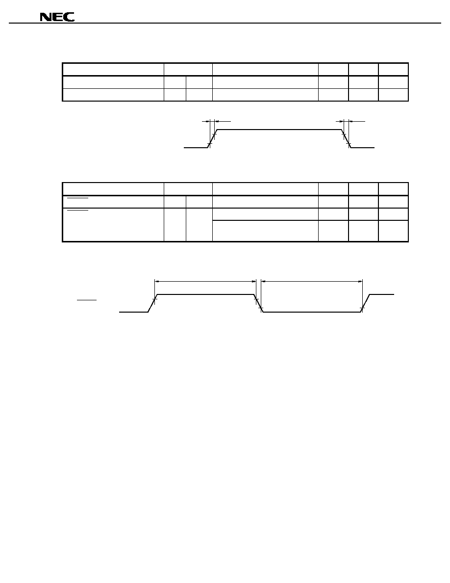
Data Retention Characteristics (T
A
= ≠40 to +85∞C)
Parameter
Symbol
Conditions
MIN.
TYP.
MAX.
Unit
V
DDDR
STOP mode, V
DD
= V
DDDR
1.5
3.6
V
Data retention voltage
HV
DDDR
STOP mode, HV
DD
= HV
DDDR
V
DDDR
5.5
V
≠40∞C
TA
+
40∞C
50
µ
A
Data retention current
I
DDDR
V
DD
=
V
DDDR
+
40∞C
<
TA
+
85∞C
600
µ
A
Supply voltage rise time
t
RVD
200
µ
s
Supply voltage fall time
t
FVD
200
µ
s
Supply voltage hold time
(from STOP mode setting)
t
HVD
0
ms
STOP release signal input time
t
DREL
0
ns
Data retention high-level input
voltage
V
IHDR
Note
0.8HV
DDDR
HV
DDDR
V
Data retention low-level input
voltage
V
ILDR
Note
0
0.2HV
DDDR
V
Note P04/INTP100/DMARQ0 to P07/INTP103/DMARQ3, P14/INTP110/DMAAK0 to P17/INTP113/DMAAK3,
P34/INTP130, P35/INTP131/SO2, P36/INTP132/SI2, P37/INTP133/SCK2,
P104/INTP120/TC0 to P107/INTP123/TC3, P114/INTP140, P115/INTP141/SO3, P116/INTP142/SI3,
P117/INTP143/SCK3, P124/INTP150 to P126/INTP152, P127/INTP153/ADTRG, P02/TCLR10,
P12/TCLR11, P32/TCLR13, P102/TCLR12, P112/TCLR14, P122/TCLR15, P03/TI10, P13/TI11, P33/TI13,
P103/TI12, P113/TI14, P123/TI15, P20/NMI, P23/RXD0/SI0, P24/SCK0, P26/RXD1/SI1, P27/SCK1,
MODE0 to MODE2, RESET
Remark TYP. values are reference values for when T
A
= 25∞C.
V
DD
HV
DD
RESET (input)
t
HVD
t
FVD
V
DDDR
t
RVD
t
DREL
V
IHDR
V
IHDR
V
ILDR
STOP mode setting
NMI (input)
(released by falling edge)
NMI (input)
(released by rising edge)

Preliminary Data Sheet U13844EJ2V0DS00
27
µ
µ
µ
µ
PD70F3102-33
AC Characteristics (T
A
= ≠40 to +85∞C, V
DD
= CV
DD
= 3.0 to 3.6 V, HV
DD
= 5.0 V
±
±
±
±
10%, V
SS
= 0 V, Output Pin
Load Capacitance: C
L
= 50 pF)
AC Test Input Waveforms
(a) P04/INTP100/DMARQ0 to P07/INTP103/DMARQ3, P14/INTP110/DMAAK0 to P17/INTP113/DMAAK3,
P34/INTP130, P35/INTP131/SO2, P36/INTP132/SI2, P37/INTP133/SCK2, P104/INTP120/TC0 to
P107/INTP123/TC3, P114/INTP140, P115/INTP141/SO3, P116/INTP142/SI3, P117/INTP143/SCK3,
P124/INTP150 to P126/INTP152, P127/INTP153/ADTRG, P02/TCLR10, P12/TCLR11, P32/TCLR13,
P102/TCLR12, P112/TCLR14, P122/TCLR15, P03/TI10, P13/TI11, P33/TI13, P103/TI12, P113/TI14,
P123/TI15, P20/NMI, P23/RXD0/SI0, P24/SCK0, P26/RXD1/SI1, P27/SCK1, MODE0 to MODE2, RESET
HV
DD
0 V
0.8HV
DD
0.2HV
DD
0.8HV
DD
0.2HV
DD
Measurement
points
Input signal
(b) Other than (a)
2.4 V
0.4 V
2.2 V
0.8 V
2.2 V
0.8 V
Measurement
points
Input signal
AC Test Output Measurement Points
2.4 V
0.8 V
2.4 V
0.8 V
Measurement
points
Output signal
Load Conditions
C
L
= 50 pF
DUT
(Device under test)
Caution If the load capacitance exceeds 50 pF due to the circuit configuration, reduce the load
capacitance of the device to 50 pF or less by inserting a buffer or by some other means.

Preliminary Data Sheet U13844EJ2V0DS00
28
µ
µ
µ
µ
PD70F3102-33
(1) Clock timing
Parameter
Symbol
Conditions
MIN.
MAX.
Unit
In direct mode
15
250
ns
X1 input cycle
<1>
t
CYX
In PLL mode
150
250
ns
In direct mode
5
ns
X1 input high-level width
<2>
t
WXH
In PLL mode
50
ns
In direct mode
5
ns
X1 input low-level width
<3>
t
WXL
In PLL mode
50
ns
In direct mode
4
ns
X1 input rise time
<4>
t
XR
In PLL mode
10
ns
In direct mode
4
ns
X1 input fall time
<5>
t
XF
In PLL mode
10
ns
CPU operating frequency
≠
10
33
MHz
CLKOUT output cycle
<6>
t
CYK
30
100
ns
CLKOUT high-level width
<7>
t
WKH
0.5T ≠ 7
ns
CLKOUT low-level width
<8>
t
WKL
0.5T ≠ 4
ns
CLKOUT rise time
<9>
t
KR
5
ns
CLKOUT fall time
<10>
t
KF
5
ns
Remark T = t
CYK
<4>
<5>
<2>
<3>
<1>
X1
(PLL mode)
<1>
<2>
<3>
<4>
<5>
<9>
<10>
<7>
<8>
<6>
X1
(Direct mode)
CLKOUT (output)
Preliminary Data Sheet U13844EJ2V0DS00
29
µ
µ
µ
µ
PD70F3102-33
(2) Output waveform (other than X1, CLKOUT)
Parameter
Symbol
Conditions
MIN.
MAX.
Unit
Output rise time
<12>
t
OR
10
ns
Output fall time
<13>
t
OF
10
ns
<13>
Signals other than X1, CLKOUT
<12>
(3) Reset timing
Parameter
Symbol
Conditions
MIN.
MAX.
Unit
RESET pin high-level width
<14>
t
WRSH
500
ns
At power ON, STOP mode release
500 + T
OS
ns
RESET pin low-level width
<15>
t
WRSL
Except at power ON, STOP mode
release
500
ns
Remark T
OS
: Oscillation stabilization time
<14>
<15>
RESET (input)

Preliminary Data Sheet U13844EJ2V0DS00
30
µ
µ
µ
µ
PD70F3102-33
(4) SRAM, external ROM, external I/O access timing
(a) Access timing (SRAM, external ROM, external I/O) (1/2)
Parameter
Symbol
Conditions
MIN.
MAX.
Unit
Address, CSn output delay time
(from CLKOUT
)
<16>
t
DKA
2
10
ns
Address, CSn output hold time
(from CLKOUT
)
<17>
t
HKA
2
10
ns
RD, IORD
delay time
(from CLKOUT
)
<18>
t
DKRDL
2
14
ns
RD, IORD
delay time
(from CLKOUT
)
<19>
t
HKRDH
2
14
ns
UWR, LWR, IOWR
delay time
(from CLKOUT
)
<20>
t
DKWRL
2
10
ns
UWR, LWR, IOWR
delay time
(from CLKOUT
)
<21>
t
HKWRH
2
10
ns
BCYST
delay time
(from CLKOUT
)
<22>
t
DKBSL
2
10
ns
BCYST
delay time
(from CLKOUT
)
<23>
t
HKBSH
2
10
ns
WAIT setup time (to CLKOUT
)
<24>
t
SWK
15
ns
WAIT hold time (from CLKOUT
)
<25>
t
HKW
2
ns
Data input setup time
(to CLKOUT
)
<26>
t
SKID
18
ns
Data input hold time
(from CLKOUT
)
<27>
t
HKID
2
ns
Data output delay time
(from CLKOUT
)
<28>
t
DKOD
2
10
ns
Data output hold time
(from CLKOUT
)
<29>
t
HKOD
2
10
ns
Remarks 1. Observe at least one of the data input hold times, t
HKID
or t
HRDID
.
2. n = 0 to 7

Preliminary Data Sheet U13844EJ2V0DS00
31
µ
µ
µ
µ
PD70F3102-33
(a) Access timing (SRAM, external ROM, external I/O) (2/2)
CLKOUT (Output)
A0 to A23 (Output)
CSn (Output)
BCYST (Output)
RD, IORD (Output)
[Read time]
UWR, LWR, IOWR (Output)
[Write time]
D0 to 15 (I/O)
[Read time]
D0 to 15 (I/O)
[Write time]
WAIT (Input)
<16>
<17>
<22>
<23>
<18>
<19>
<20>
<21>
<26>
<27>
<28>
<29>
<24>
<25>
<24>
<25>
T1
TW
T2
Remarks 1. Timing when number of waits specified by registers DWC1 and DWC2 is 0.
2. Broken lines indicate high impedance.
3. n = 0 to 7

Preliminary Data Sheet U13844EJ2V0DS00
32
µ
µ
µ
µ
PD70F3102-33
(b) Read timing (SRAM, external ROM, external I/O) (1/2)
Parameter
Symbol
Conditions
MIN.
MAX.
Unit
Data input setup time (to address)
<30>
t
SAID
(1.5 + w
D
+ w) T ≠ 28
ns
Data input setup time (to RD)
<31>
t
SRDID
(1 + w
D
+w) T ≠ 32
ns
RD, IORD low-level width
<32>
t
WRDL
(1 + w
D
+ w) T ≠ 10
ns
RD, IORD high-level width
<33>
t
WRDH
T ≠ 10
ns
Delay time from address, CSn to
RD, IORD
<34>
t
DARD
0.5T ≠ 10
ns
Delay time from RD, IORD
to
address
<35>
t
DRDA
(0.5 + i) T ≠ 10
ns
Data input hold time
(from RD, IORD
)
<36>
t
HRDID
0
ns
Delay time from RD, IORD
to
data output
<37>
t
DRDOD
(0.5 + i) T ≠ 10
ns
WAIT setup time (to address)
<38>
t
SAW
Note
T ≠ 25
ns
WAIT setup time (to BCYST
)
<39>
t
SBSW
Note
T ≠ 25
ns
WAIT hold time (from BCYST
)
<40>
t
HBSW
Note
0
ns
Note During the first WAIT sampling, when the number of waits specified by registers DWC1 and DWC2 is 0.
Remarks 1. T = t
CYK
2. w: Number of waits due to WAIT
3. w
D
: Number of waits specified by registers DWC1, DWC2
4. i: Number of idle states inserted when a write cycle follows the read cycle.
5. Observe at least one of the data input hold times, t
HKID
or t
HRDID
.
6. n = 0 to 7

Preliminary Data Sheet U13844EJ2V0DS00
33
µ
µ
µ
µ
PD70F3102-33
(b) Read timing (SRAM, external ROM, external I/O) (2/2)
UWR, LWR, IOWR (Output)
RD, IORD (Output)
D0 to D15 (I/O)
T1
TW
T2
CLKOUT (Output)
<33>
<32>
<35>
<38>
<34>
<31>
<30>
<36>
<37>
<39>
<40>
A0 to A23 (Output)
CSn (Output)
WAIT (Input)
BCYST (Output)
Remarks 1. Timing when the number of waits specified by registers DWC1 and DWC2 is 0.
2. Broken lines indicate high impedance.
3. n = 0 to 7

Preliminary Data Sheet U13844EJ2V0DS00
34
µ
µ
µ
µ
PD70F3102-33
(c) Write timing (SRAM, external ROM, external I/O) (1/2)
Parameter
Symbol
Conditions
MIN.
MAX.
Unit
WAIT setup time (to address)
<38>
t
SAW
Note
T ≠ 25
ns
WAIT setup time (to BCYST
)
<39>
t
SBSW
Note
T ≠ 25
ns
WAIT hold time (from BCYST
)
<40>
t
HBSW
Note
0
ns
Delay time from address, CSn to
UWR, LWR, IOWR
<41>
t
DAWR
0.5T ≠ 10
ns
Address setup time
(to UWR, LWR, IOWR
)
<42>
t
SAWR
(1.5 + w
D
+ w) T ≠ 10
ns
Delay time from UWR, LWR,
IOWR
to address
<43>
t
DWRA
0.5T ≠ 10
ns
UWR, LWR, IOWR high-level
width
<44>
t
WWRH
T ≠ 10
ns
UWR, LWR, IOWR low-level width
<45>
t
WWRL
(1 + w
D
+ w) T ≠ 10
ns
Data output setup time (to UWR,
LWR, IOWR
)
<46>
t
SODWR
(1.5 + w
D
+ w) T ≠ 10
ns
Data output hold time (from UWR,
LWR, IOWR
)
<47>
t
HWROD
0.5T ≠ 10
ns
Note During the first WAIT sampling, when the number of waits specified by registers DWC1 and DWC2 is 0.
Remarks 1. T = t
CYK
2. w: Number of waits due to WAIT
3. w
D
: Number of waits specified by registers DWC1 and DWC2
4. n = 0 to 7

Preliminary Data Sheet U13844EJ2V0DS00
35
µ
µ
µ
µ
PD70F3102-33
(c) Write timing (SRAM, external ROM, external I/O) (2/2)
T1
TW
T2
CLKOUT (Output)
<44>
<45>
<43>
<38>
<46>
<47>
<39>
<40>
<41>
<42>
A0 to A23 (Output)
CSn (Output)
RD, IORD (Output)
UWR, LWR, IOWR (Output)
D0 to D15 (I/O)
WAIT (Input)
BCYST (Output)
Remarks 1. Timing when the number of waits specified by registers DWC1 and DWC2 is 0.
2. Broken lines indicate high impedance.
3. n = 0 to 7

Preliminary Data Sheet U13844EJ2V0DS00
36
µ
µ
µ
µ
PD70F3102-33
(d) DMA flyby transfer timing (SRAM
external I/O transfer) (1/2)
Parameter
Symbol
Conditions
MIN.
MAX.
Unit
WAIT setup time (to CLKOUT
)
<24>
t
SWK
15
ns
WAIT hold time (from CLKOUT
)
<25>
t
HKW
2
ns
RD low-level width
<32>
t
WRDL
(1 + w
D
+ w
F
+ w) T ≠ 10
ns
RD high-level width
<33>
t
WRDH
T ≠ 10
ns
Delay time from address, CSn to
RD
<34>
t
DARD
0.5T ≠ 10
ns
Delay time from RD
to address
<35>
t
DRDA
(0.5 + i) T ≠ 10
ns
Delay time from RD
to data
output
<37>
t
DRDOD
(0.5 + i) T ≠ 10
ns
WAIT setup time (to address)
<38>
t
SAW
Note
T ≠ 25
ns
WAIT setup time (to BCYST
)
<39>
t
SBSW
Note
T ≠ 25
ns
WAIT hold time (from BCYST
)
<40>
t
HBSW
Note
0
ns
Delay time from address to
IOWR
<41>
t
DAWR
0.5T ≠ 10
ns
Address setup time (to IOWR
)
<42>
t
SAWR
(1.5 + w
D
+ w) T ≠ 10
ns
Delay time from IOWR
to
address
<43>
t
DWRA
0.5T ≠ 10
ns
IOWR high-level width
<44>
t
WWRH
T ≠ 10
ns
IOWR low-level width
<45>
t
WWRL
(1 + w
D
+ w) T ≠ 10
ns
w
F
= 0
0
ns
Delay time from IOWR
to RD
<48>
t
DWRRD
w
F
= 1
T ≠ 10
ns
Delay time from DMAAKm
to
IOWR
<49>
t
DDAWR
0.5T ≠ 10
ns
Delay time from IOWR
to
DMAAKm
<50>
t
DWRDA
(0.5 + w
F
) T ≠ 10
ns
Note During the first WAIT sampling, when number of waits specified by registers DWC1 and DWC2 is 0.
Remarks 1. T = t
CYK
2. w: Number of waits due to WAIT
3. w
D
: Number of waits specified by registers DWC1, DWC2
4. w
F
: Number of waits inserted to source-side access during DMA flyby transfer
5. i: Number of idle states inserted when a write cycle follows the read cycle
6. n = 0 to 7, m = 0 to 3

Preliminary Data Sheet U13844EJ2V0DS00
37
µ
µ
µ
µ
PD70F3102-33
(d) DMA flyby transfer timing (SRAM
external I/O transfer) (2/2)
CLKOUT (Output)
T1
TW
T2
<33>
<32>
<35>
<34>
<48>
<50>
<49>
<43>
<42>
<41>
<44>
<45>
<37>
<38>
<24>
<24>
<25>
<25>
<40>
<39>
A0 to A23 (Output)
CSn (Output)
RD (Output)
DMAAKm (Output)
IORD (Output)
IOWR (Output)
UWR, LWR (Output)
D0 to D15 (I/O)
WAIT (Input)
BCYST (Output)
Remarks 1. Timing when the number of waits specified by registers DWC1 and DWC2 is 0.
2. Broken lines indicate high impedance.
3. n = 0 to 7, m = 0 to 3

Preliminary Data Sheet U13844EJ2V0DS00
38
µ
µ
µ
µ
PD70F3102-33
(e) DMA flyby transfer timing (external I/O
SRAM transfer) (1/2)
Parameter
Symbol
Conditions
MIN.
MAX.
Unit
WAIT setup time (to CLKOUT
)
<24>
t
SWK
15
ns
WAIT hold time (from CLKOUT
)
<25>
t
HKW
2
ns
IORD low-level width
<32>
t
WRDL
(1 + w
D
+ w
F
+ w) T ≠ 10
ns
IORD high-level width
<33>
t
WRDH
T ≠ 10
ns
Delay time from address, CSn to
IORD
<34>
t
DARD
0.5T ≠ 10
ns
Delay time from IORD
to address
<35>
t
DRDA
(0.5 + i) T ≠ 10
ns
Delay time from IORD
to data
output
<37>
t
DRDOD
(0.5 + i) T ≠ 10
ns
WAIT setup time (to address)
<38>
t
SAW
Note
T ≠ 25
ns
WAIT setup time (to BCYST
)
<39>
t
SBSW
Note
T ≠ 25
ns
WAIT hold time (from BCYST
)
<40>
t
HBSW
Note
0
ns
Delay time from address to UWR,
LWR
<41>
t
DAWR
0.5T ≠ 10
ns
Address setup time (to UWR,
LWR
)
<42>
t
SAWR
(1.5 + w
D
+ w) T ≠ 10
ns
Delay time from UWR, LWR to
address
<43>
t
DWRA
0.5T ≠ 10
ns
UWR, LWR high-level width
<44>
t
WWRH
T ≠ 10
ns
UWR, LWR low-level width
<45>
t
WWRL
(1 + w
D
+ w) T ≠ 10
ns
w
F
= 0
0
ns
Delay time from UWR, LWR
to
IORD
<48>
t
DWRRD
w
F
= 1
T ≠ 10
ns
Delay time from DMAAKm
to
IORD
<51>
t
DDARD
0.5T ≠ 10
ns
Delay time from IORD
to
DMAAKm
<52>
t
DRDDA
0.5T ≠ 10
ns
Note During the first WAIT sampling, when the number of waits specified by registers DWC1 and DWC2 is 0.
Remarks 1. T = t
CYK
2. w: Number of waits due to WAIT
3. w
D
: Number of waits specified by registers DWC1 and DWC2.
4. w
F
: Number of waits inserted to source-side access during DMA flyby transfer.
5. i: Number of idle states inserted when a write cycle follows the read cycle.
6. n = 0 to 7, m = 0 to 3

Preliminary Data Sheet U13844EJ2V0DS00
39
µ
µ
µ
µ
PD70F3102-33
(e) DMA flyby transfer timing (external I/O
SRAM transfer) (2/2)
CLKOUT (Output)
T1
TW
T2
<44>
<45>
<48>
<52>
<33>
<37>
<38>
<24>
<24>
<25>
<25>
<40>
<39>
<42>
<41>
<43>
<51>
<32>
<35>
<34>
A0 to A23 (Output)
CSn (Output)
UWR, LWR (Output)
RD (Output)
DMAAKm (Output)
IOWR (Output)
IORD (Output)
D0 to D15 (I/O)
WAIT (Input)
BCYST (Output)
Remarks 1. Timing when the number of waits specified by registers DWC1 and DWC2 is 0 and w
F
= 0.
2. Broken lines indicate high impedance.
3. n = 0 to 7, m = 0 to 3

Preliminary Data Sheet U13844EJ2V0DS00
40
µ
µ
µ
µ
PD70F3102-33
(5) Page ROM access timing (1/2)
Parameter
Symbol
Conditions
MIN.
MAX.
Unit
WAIT setup time (to CLKOUT
)
<24>
t
SWK
15
ns
WAIT hold time (from CLKOUT
)
<25>
t
HKW
2
ns
Data input setup time
(to CLKOUT
)
<26>
t
SKID
18
ns
Data input hold time
(from CLKOUT
)
<27>
t
HKID
2
ns
Off-page data input setup time
(to address)
<30>
t
SAID
(1.5 + w
D
+w) T ≠ 28
ns
Off-page data input setup time
(to RD)
<31>
t
SRDID
(1 + w
D
+ w) T ≠ 32
ns
Off-page RD low-level width
<32>
t
WRDL
(1 + w
D
+ w) T ≠ 10
ns
RD high-level width
<33>
t
WRDH
0.5T ≠ 10
ns
Data input hold time (from RD)
<36>
t
HRDID
0
ns
Delay time from RD
to data
output
<37>
t
DRDOD
(0.5 + i) T ≠ 10
ns
On-page RD low-level width
<53>
t
WORDL
(1.5 + w
PR
+ w) T ≠ 10
ns
On-page data input setup time
(to address)
<54>
t
SOAID
(1.5 + w
PR
+ w) T ≠ 28
ns
On-page data input setup time
(to RD)
<55>
t
SORDID
(1.5 + w
PR
+ w) T ≠ 32
ns
Remarks 1. T = t
CYK
2. w: Number of waits due to WAIT
3. w
D
: Number of waits specified by registers DWC1 and DWC2.
4. w
PR
: Number of waits specified by register PRC.
5. i: Number of idle states inserted when a write cycle follows the read cycle.
6. Observe at least one of the data input hold times, t
HKID
or t
HRDID
.

Preliminary Data Sheet U13844EJ2V0DS00
41
µ
µ
µ
µ
PD70F3102-33
(5) Page ROM access timing (2/2)
CLKOUT (Output)
On-page address
Note
T1
TDW
TW
T2
TO1
TPRW
TW
TO2
<24>
<25>
<24>
<25>
<24>
<25>
<24>
<25>
<26>
<27>
<36>
<32>
<31>
<53>
<55>
<27>
<26>
<36>
<37>
<33>
<30>
<54>
Off-page address
Note
CSn (Output)
UWR, LWR (Output)
RD (Output)
D0 to D15 (I/O)
WAIT (Input)
BCYST (Output)
Note On-page addresses and off-page addresses are as follows.
PRC Register
MA5
MA4
MA3
On-Page Addresses
Off-Page Addresses
0
0
0
A0, A1
A2 to A23
0
0
1
A0 to A2
A3 to A23
0
1
1
A0 to A3
A4 to A23
1
1
1
A0 to A4
A5 to A23
Remarks 1. These timings are for the following cases:
Number of waits (TDW) specified by registers DWC1 and DWC2: 1
Number of waits (TPRW) specified by register PRC: 1
2. Broken lines indicate high impedance.
3. n = 0 to 7

Preliminary Data Sheet U13844EJ2V0DS00
42
µ
µ
µ
µ
PD70F3102-33
(6) DRAM access timing
(a) Read timing (high-speed page DRAM access, normal access: off-page) (1/3)
Parameter
Symbol
Conditions
MIN.
MAX.
Unit
WAIT setup time (to CLKOUT
)
<24>
t
SWK
15
ns
WAIT hold time (from CLKOUT
)
<25>
t
HKW
2
ns
Data input setup time (to CLKOUT
)
<26>
t
SKID
18
ns
Data input hold time (from CLKOUT
)
<27>
t
HKID
2
ns
Delay time from OE
to data output
<37>
t
DRDOD
(0.5 + i) T ≠ 10
ns
Row address setup time
<56>
t
ASR
(0.5 + w
RP
) T ≠ 10
ns
Row address hold time
<57>
t
RAH
(0.5 + w
RH
) T ≠ 10
ns
Column address setup time
<58>
t
ASC
0.5T ≠ 10
ns
Column address hold time
<59>
t
CAH
(1.5 + w
DA
+ w) T ≠ 10
ns
Read/write cycle time
<60>
t
RC
(3 + w
RP
+ w
RH
+ w
DA
+ w)
T ≠ 10
ns
RAS recharge time
<61>
t
RP
(0.5 + w
RP
) T ≠ 10
ns
RAS pulse time
<62>
t
RAS
(2.5 + w
RH
+ w
DA
+ w)
T ≠ 10
ns
RAS hold time
<63>
t
RSH
(1.5 + w
DA
+ w) T ≠ 10
ns
Column address read time for RAS
<64>
t
RAL
(2 + w
DA
+ w) T ≠ 10
ns
CAS pulse width
<65>
t
CAS
(1 + w
DA
+ w) T ≠ 10
ns
CAS to RAS precharge time
<66>
t
CRP
(1 + w
RP
) T ≠ 10
ns
CAS hold time
<67>
t
CSH
(2 + w
RH
+ w
DA
+ w) T ≠ 10
ns
WE setup time
<68>
t
RCS
(2 + w
RP
+ w
RH
) T ≠ 10
ns
WE hold time (from RAS
)
<69>
t
RRH
0.5T ≠ 10
ns
WE hold time (from CAS
)
<70>
t
RCH
T ≠ 10
ns
CAS precharge time
<71>
t
CPN
(2 + w
RP
+ w
RH
) T ≠ 10
ns
Output enable access time
<72>
t
OEA
(2 + w
RP
+ w
RH
+ w
DA
+ w)
T ≠ 28
ns
RAS access time
<73>
t
RAC
(2 + w
RH
+ w
DA
+ w) T ≠ 28
ns
Access time from column address
<74>
t
AA
(1.5 + w
DA
+ w) T ≠ 28
ns
CAS access time
<75>
t
CAC
(1 + w
DA
+ w) T ≠ 28
ns
Remarks 1. T = t
CYK
2. w: Number of waits due to WAIT
3. w
RP
: Number of waits specified by RPCxx bit of register DRCn (n = 0 to 3, xx = 00 to 03, 10 to 13)
4. w
RH
: Number of waits specified by RHCxx bit of register DRCn (n = 0 to 3, xx = 00 to 03, 10 to 13)
5. w
DA
: Number of waits specified by DACxx bit of register DRCn (n = 0 to 3, xx = 00 to 03, 10 to 13)
6. i: Number of idle states inserted when a write cycle follows the read cycle.

Preliminary Data Sheet U13844EJ2V0DS00
43
µ
µ
µ
µ
PD70F3102-33
(a) Read timing (high-speed page DRAM access, normal access: off-page) (2/3)
Parameter
Symbol
Conditions
MIN.
MAX.
Unit
RAS column address delay time
<76>
t
RAD
(0.5 + w
RH
) T ≠ 10
ns
RAS to CAS delay time
<77>
t
RCD
(1 + w
RH
) T ≠ 10
ns
Output buffer turn off delay time
(from OE
)
<78>
t
OEZ
0
ns
Output buffer turn off delay time
(from CAS
)
<79>
t
OFF
0
ns
Remarks 1. T = t
CYK
2. w
RH
: Number of waits specified by RHCxx bit of register DRCn (n = 0 to 3, xx = 00 to 03, 10 to 13)

Preliminary Data Sheet U13844EJ2V0DS00
44
µ
µ
µ
µ
PD70F3102-33
(a) Read timing (high-speed page DRAM access, normal access: off-page) (3/3)
TRPW
TRHW
T2
T1
TDAW
TW
T3
<56>
<61>
<57>
<58>
<59>
<62>
<76>
<63>
<64>
<60>
<77>
<65>
<67>
<66>
<71>
<73>
<68>
<75>
<74>
<72>
<70>
<69>
<79>
<37>
<27>
<25>
<26>
<25>
<24>
<78>
<24>
CLKOUT (Output)
A0 to A23 (Output)
RASn (Output)
WE (Output)
OE (Output)
WAIT (Input)
D0 to D15 (I/O)
UCAS (Output)
LCAS (Output)
Row address
Column address
Remarks 1. These timings are for the following cases (n = 0 to 3, xx = 00 to 03, 10 to 13):
Number of waits (TRPW) specified by RPCxx bit of register DRCn: 1
Number of waits (TRHW) specified by RHCxx bit of register DRCn: 1
Number of waits (TDAW) specified by DACxx bit of register DRCn: 1
2. Broken lines indicate high impedance.
3. n = 0 to 7

Preliminary Data Sheet U13844EJ2V0DS00
45
µ
µ
µ
µ
PD70F3102-33
[MEMO]

Preliminary Data Sheet U13844EJ2V0DS00
46
µ
µ
µ
µ
PD70F3102-33
(b) Read timing (high-speed DRAM access: on-page) (1/2)
Parameter
Symbol
Conditions
MIN.
MAX.
Unit
Data input setup time (to CLKOUT
)
<26>
t
SKID
18
ns
Data input hold time (from CLKOUT
)
<27>
t
HKID
2
ns
Delay time from OE
to data output
<37>
t
DRDOD
(0.5 + i) T ≠ 10
ns
Column address setup time
<58>
t
ASC
(0.5 + w
CP
) T ≠ 10
ns
Column address hold time
<59>
t
CAH
(1.5 + w
DA
) T ≠ 10
ns
RAS hold time
<63>
t
RSH
(1.5 + w
DA
) T ≠ 10
ns
Column address read time for RAS
<64>
t
RAL
(2 + w
CP
+ w
DA
) T ≠ 10
ns
CAS pulse width
<65>
t
CAS
(1 + w
DA
) T ≠ 10
ns
WE setup time (to CAS
)
<68>
t
RCS
(1 + w
CP
) T ≠ 10
ns
WE hold time (from RAS
)
<69>
t
RRH
0.5 T ≠ 10
ns
WE hold time (from CAS
)
<70>
t
RCH
T ≠ 10
ns
Output enable access time
<72>
t
OEA
(1 +
w
CP
+ w
DA
) T ≠ 28
ns
Access time from column address
<74>
t
AA
(1.5 + w
CP
+ w
DA
) T ≠ 28
ns
CAS access time
<75>
t
CAC
(1 + w
DA
) T ≠ 28
ns
Output buffer turn-off delay time
(from OE
)
<78>
t
OEZ
0
ns
Output buffer turn-off delay time
(from CAS
)
<79>
t
OFF
0
ns
Access time from CAS precharge
<80>
t
ACP
(2 + w
CP
+ w
DA
) T ≠ 28
ns
CAS precharge time
<81>
t
CP
(1 + w
CP
) T ≠ 10
ns
High-speed page mode cycle time
<82>
t
PC
(2 + w
CP
+ w
DA
) T ≠ 10
ns
RAS hold time from CAS precharge
<83>
t
RHCP
(2.5 + w
CP
+ w
DA
) T ≠ 10
ns
Remarks 1. T = t
CYK
2. w
CP
: Number of waits specified by CPCxx bit of register DRCn (n = 0 to 3, xx = 00 to 03, 10 to 13)
3. w
DA
: Number of waits specified by DACxx bit of register DRCn (n = 0 to 3, xx = 00 to 03, 10 to 13)
4. i: Number of idle states inserted when a write cycle follows the read cycle.

Preliminary Data Sheet U13844EJ2V0DS00
47
µ
µ
µ
µ
PD70F3102-33
(b) Read timing (high-speed DRAM access: on-page) (2/2)
TCPW
TO1
TDAW
TO2
<58>
<59>
<63>
<64>
<83>
<65>
<81>
<82>
<68>
<75>
<72>
<26>
<79>
<37>
<74>
<80>
<27>
<78>
<70>
<69>
CLKOUT (Output)
A0 to A23 (Output)
RASn (Output)
UCAS (Output)
LCAS (Output)
WE (Output)
OE (Output)
D0 to D15 (I/O)
WAIT (Input)
Column address
Remarks 1. These timings are for the following cases (n = 0 to 3, xx = 00 to 03, 10 to 13):
Number of waits (TCPW) specified by CPCxx bit of register DRCn: 1
Number of waits (TDAW) specified by DACxx bit of register DRCn: 1
2. Broken lines indicate high impedance.
3. n = 0 to 7

Preliminary Data Sheet U13844EJ2V0DS00
48
µ
µ
µ
µ
PD70F3102-33
(c) Write timing (high-speed page DRAM access, normal access: off-page) (1/2)
Parameter
Symbol
Conditions
MIN.
MAX.
Unit
WAIT setup time (to CLKOUT
)
<24>
t
SWK
15
ns
WAIT hold time (from CLKOUT
)
<25>
t
HKW
2
ns
Row address setup time
<56>
t
ASR
(0.5 + w
RP
) T ≠ 10
ns
Row address hold time
<57>
t
RAH
(0.5 + w
RH
) T ≠ 10
ns
Column address setup time
<58>
t
ASC
0.5T ≠ 10
ns
Column address hold time
<59>
t
CAH
(1.5 + w
DA
+ w) T ≠ 10
ns
Read/write cycle time
<60>
t
RC
(3 + w
RP
+ w
RH
+ w
DA
+ w)
T ≠ 10
ns
RAS precharge time
<61>
t
RP
(0.5 +
w
RP
) T ≠ 10
ns
RAS pulse time
<62>
t
RAS
(2.5 + w
RH
+ w
DA
+ w)
T ≠ 10
ns
RAS hold time
<63>
t
RSH
(1.5 + w
DA
+ w) T ≠ 10
ns
Column address read time (from
RAS
)
<64>
t
RAL
(2 + w
DA
+ w) T ≠ 10
ns
CAS pulse width
<65>
t
CAS
(1 + w
DA
+ w) T ≠ 10
ns
CAS to RAS precharge time
<66>
t
CRP
(1 + w
RH
) T ≠ 10
ns
CAS hold time
<67>
t
CSH
(2 + w
RH
+ w
DA
+ w) T ≠ 10
ns
CAS precharge time
<71>
t
CPN
(2 + w
RP
+ w
RH
) T ≠ 10
ns
RAS column address delay time
<76>
t
RAD
(0.5+ w
RH
) T ≠ 10
ns
RAS to CAS delay time
<77>
t
RCD
(1 + w
RH
) T ≠ 10
ns
WE setup time (to CAS
)
<84>
t
WCS
(1 + w
RP
+ w
RH
) T ≠ 10
ns
WE hold time (from CAS
)
<85>
t
WCH
(1 + w
DA
+ w) T ≠ 10
ns
Data setup time (to CAS
)
<86>
t
DS
(1.5 + w
RP
+ w
RH
) T ≠ 10
ns
Data hold time (from CAS
)
<87>
t
DH
(1.5 + w
DA
+ w) T ≠ 10
ns
Remarks 1. T = t
CYK
2. w: Number of waits due to WAIT
3. w
RP
: Number of waits specified by RPCxx bit of register DRCn (n = 0 to 3, xx = 00 to 03, 10 to 13)
4. w
RH
: Number of waits specified by RHCxx bit of register DRCn (n = 0 to 3, xx = 00 to 03, 10 to 13)
5. w
DA
: Number of waits specified by DACxx bit of register DRCn (n = 0 to 3, xx = 00 to 03, 10 to 13)

Preliminary Data Sheet U13844EJ2V0DS00
49
µ
µ
µ
µ
PD70F3102-33
(c) Write timing (high-speed page DRAM access, normal access: off-page) (2/2)
TRPW
TRHW
T2
T1
TDAW
TW
T3
<56>
<61>
<57>
<58>
<59>
<62>
<76>
<63>
<64>
<60>
<77>
<65>
<67>
<66>
<71>
<84>
<25>
<25>
<24>
<24>
<85>
<86>
<87>
CLKOUT (Output)
A0 to A23 (Output)
RASn (Output)
UCAS (Output)
LCAS (Output)
WE (Output)
OE (Output)
D0 to D15 (I/O)
WAIT (Input)
Row address
Column address
Remarks 1. These timings are for the following cases (n = 0 to 3, xx = 00 to 03, 10 to 13):
Number of waits (TRPW) specified by RPCxx bit of register DRCn: 1
Number of waits (TRHW) specified by RHCxx bit of register DRCn: 1
Number of waits (TDAW) specified by DACxx bit of register DRCn: 1
2. Broken lines indicate high impedance.
3. n = 0 to 7

Preliminary Data Sheet U13844EJ2V0DS00
50
µ
µ
µ
µ
PD70F3102-33
(d) Write timing (high-speed page DRAM access: on-page) (1/2)
Parameter
Symbol
Conditions
MIN.
MAX.
Unit
Column address setup time
<58>
t
ASC
(0.5 + w
CP
) T ≠ 10
ns
Column address hold time
<59>
t
CAH
(1.5 + w
DA
) T ≠ 10
ns
RAS hold time
<63>
t
RSH
(1.5 + w
DA
) T ≠ 10
ns
Column address read time (from
RAS
)
<64>
t
RAL
(2 + w
CP
+ w
DA
) T ≠ 10
ns
CAS pulse width
<65>
t
CAS
(1 + w
DA
) T ≠ 10
ns
CAS precharge time
<81>
t
CP
(1 + w
CP
) T ≠ 10
ns
RAS hold time for CAS precharge
<83>
t
RHCP
(2.5 + w
CP
+ w
DA
) T ≠ 10
ns
WE setup time (to CAS
)
<84>
t
WCS
w
CP
1
w
CP
T ≠ 10
ns
WE hold time (from CAS
)
<85>
t
WCH
(1 + w
DA
) T ≠ 10
ns
Data setup time (to CAS
)
<86>
t
DS
(0.5 + w
CP
) T ≠ 10
ns
Data hold time (from CAS
)
<87>
t
DH
(1.5 + w
DA
) T ≠ 10
ns
WE read time (from RAS
)
<88>
t
RWL
w
CP
= 0
(1.5 + w
DA
) T ≠ 10
ns
WE read time (from CAS
)
<89>
t
CWL
w
CP
= 0
(1 + w
DA
) T ≠ 10
ns
Data setup time (to WE
)
<90>
t
DSWE
w
CP
= 0
0.5T ≠ 10
ns
Data hold time (from WE
)
<91>
t
DHWE
w
CP
= 0
(1.5 + w
DA
) T ≠ 10
ns
WE pulse width
<92>
t
WP
w
CP
= 0
(1 + w
DA
) T ≠ 10
ns
Remarks 1. T = t
CYK
2. w
CP
: Number of waits specified by CPCxx bit of register DRCn (n = 0 to 3, xx = 00 to 03, 10 to 13)
3. w
DA
: Number of waits specified by DACxx bit of register DRCn (n = 0 to 3, xx = 00 to 03, 10 to 13)

Preliminary Data Sheet U13844EJ2V0DS00
51
µ
µ
µ
µ
PD70F3102-33
(d) Write timing (high-speed page DRAM access: on-page) (2/2)
TCPW
TO1
TDAW
TO2
<58>
<59>
<63>
<64>
<83>
<81>
<65>
<89>
<88>
<84>
<85>
<92>
<91>
<86>
<87>
<90>
CLKOUT (Output)
A0 to A23 (Output)
RASn (Output)
UCAS (Output)
LCAS (Output)
OE (Output)
WE (Output)
D0 to D15 (I/O)
WAIT (Input)
Column address
Remarks 1. These timings are for the following cases (n = 0 to 3, xx = 00 to 03, 10 to 13):
Number of waits (TCPW) specified by CPCxx bit of register DRCn: 1
Number of waits (TDAW) specified by DACxx bit of register DRCn: 1
2. Broken lines indicate high impedance.
3. n = 0 to 7

Preliminary Data Sheet U13844EJ2V0DS00
52
µ
µ
µ
µ
PD70F3102-33
(e) Read timing (EDO DRAM) (1/3)
Parameter
Symbol
Conditions
MIN.
MAX.
Unit
Data input setup time (to
CLKOUT
)
<26>
t
SKID
18
ns
Data input hold time (from
CLKOUT
)
<27>
t
HKID
2
ns
Delay time from OE
to data output
<37>
t
DRDOD
(0.5 + i) T ≠ 10
ns
Row address setup time
<56>
t
ASR
(0.5 + w
RP
) T ≠ 10
ns
Row address hold time
<57>
t
RAH
(0.5 + w
RH
) T ≠ 10
ns
Column address setup time
<58>
t
ASC
0.5T ≠ 10
ns
Column address hold time
<59>
t
CAH
(0.5 + w
DA
) T ≠ 10
ns
RAS precharge time
<61>
t
RP
(0.5 + w
RP
) T ≠ 10
ns
Column address read time (to RAS
)
<64>
t
RAL
(2 + w
CP
+ w
DA
) T ≠ 10
ns
CAS to RAS precharge time
<66>
t
CRP
(1 + w
RP
) T ≠ 10
ns
CAS hold time
<67>
t
CSH
(1.5 + w
RH
+ w
DA
) T ≠ 10
ns
WE setup time (to CAS
)
<68>
t
RCS
(2 + w
RP
+w
RH
) T ≠ 10
ns
WE hold time (from RAS
)
<69>
t
RRH
0.5T ≠ 10
ns
WE hold time (from CAS
)
<70>
t
RCH
1.5T ≠ 10
ns
RAS access time
<73>
t
RAC
(2 + w
RH
+ w
DA
) T ≠ 28
ns
Access time from column address
<74>
t
AA
(1.5 + w
DA
) T ≠ 28
ns
CAS access time
<75>
t
CAC
(1 + w
DA
) T ≠ 28
ns
Delay time from RAS to column
address
<76>
t
RAD
(0.5 + w
RH
) T ≠ 10
ns
RAS to CAS delay time
<77>
t
RCD
(1 + w
RH
) T ≠ 10
ns
Output buffer turn-off delay time
(from OE)
<78>
t
OEZ
0
ns
Access time from CAS precharge
<80>
t
ACP
(1.5 + w
CP
+ w
DA
) T ≠ 28
ns
CAS precharge time
<81>
t
CP
(0.5 + w
CP
) T ≠ 10
ns
RAS hold time for CAS precharge
<83>
t
RHCP
(2 + w
CP
+ w
DA
) T ≠ 10
ns
Read cycle time
<93>
t
HPC
(1 + w
DA
+ w
CP
) T ≠ 10
ns
RAS pulse width
<94>
t
RASP
(2.5 + w
RH
+ w
DA
) T ≠ 10
ns
CAS pulse width
<95>
t
HCAS
(0.5 + w
DA
) T ≠ 10
ns
Off-page
<96>
t
OCH1
(2 + w
RH
+ w
DA
) T ≠ 10
ns
Hold time from
OE to CAS
On-page
<97>
t
OCH2
(0.5 + w
DA
) T ≠ 10
ns
Data input hold time (from CAS
)
<98>
t
DHC
0
ns
Remarks 1. T = t
CYK
2. w
RP
: Number of waits specified by RPCxx bit of register DRCn (n = 0 to 3, xx = 00 to 03, 10 to 13)
3. w
RH
: Number of waits specified by RHCxx bit of register DRCn (n = 0 to 3, xx = 00 to 03, 10 to 13)
4. w
DA
: Number of waits specified by DACxx bit of register DRCn (n = 0 to 3, xx = 00 to 03, 10 to 13)
5. w
CP
: Number of waits specified by CPCxx bit of register DRCn (n = 0 to 3, xx = 00 to 03, 10 to 13)
6. i: Number of idle states inserted when a write cycle follows the read cycle.

Preliminary Data Sheet U13844EJ2V0DS00
53
µ
µ
µ
µ
PD70F3102-33
(e) Read timing (EDO DRAM) (2/3)
Parameter
Symbol
Conditions
MIN.
MAX.
Unit
Off-page
<99>
t
OEA1
(2 + w
RP
+ w
RH
+ w
DA
)
T ≠ 28
ns
Output enable
access time
On-page
<100>
t
OEA2
(1 + w
CP
+ w
DA
) T ≠ 28
ns
Remarks 1. T = t
CYK
2. w
RP
: Number of waits specified by RPCxx bit of register DRCn (n = 0 to 3, xx = 00 to 03, 10 to 13)
3. w
RH
: Number of waits specified by RHCxx bit of register DRCn (n = 0 to 3, xx = 00 to 03, 10 to 13)
4. w
DA
: Number of waits specified by DACxx bit of register DRCn (n = 0 to 3, xx = 00 to 03, 10 to 13)
5. w
CP
: Number of waits specified by CPCxx bit of register DRCn (n = 0 to 3, xx = 00 to 03, 10 to 13)

Preliminary Data Sheet U13844EJ2V0DS00
54
µ
µ
µ
µ
PD70F3102-33
(e) Read timing (EDO DRAM) (3/3)
TRPW
T1
TRHW
T2
TDAW TCPW
TB
TDAW
TE
<56>
<57>
<59>
<58>
<76>
<64>
<94>
<61>
<67>
<83>
<77>
<95>
<81>
<75>
<66>
<93>
<95>
<80>
<97>
<74>
<27>
<78>
Data
<74>
Data
<70>
<69>
<68>
<96>
<100>
<26>
<37>
<27>
<98>
<26>
<75>
Note
<73>
<99>
CLKOUT (Output)
A0 to A23 (Output)
RASn (Output)
UCAS (Output)
LCAS (Output)
WE (Output)
OE (Output)
D0 to D15 (I/O)
BCYST (Output)
WAIT (Input)
Row address
Column address
Column address
Note In case of on-page access from another cycle, while RASn is low level.
Remarks 1. These timings are for the following cases (n = 0 to 3, xx = 00 to 03, 10 to 13):
Number of waits (TRPW) specified by RPCxx bit of register DRCn: 1
Number of waits (TRHW) specified by RHCxx bit of register DRCn: 1
Number of waits (TDAW) specified by DACxx bit of register DRCn: 1
Number of waits (TCPW) specified by CPCxx bit of register DRCn: 1
2. Broken lines indicate high impedance.
3. n = 0 to 7

Preliminary Data Sheet U13844EJ2V0DS00
55
µ
µ
µ
µ
PD70F3102-33
[MEMO]

Preliminary Data Sheet U13844EJ2V0DS00
56
µ
µ
µ
µ
PD70F3102-33
(f) Write timing (EDO DRAM) (1/2)
Parameter
Symbol
Conditions
MIN.
MAX.
Unit
Row address setup time
<56>
t
ASR
(0.5 + w
RP
) T ≠ 10
ns
Row address hold time
<57>
t
RAH
(0.5 + w
RH
) T ≠10
ns
Column address setup time
<58>
t
ASC
0.5T ≠ 10
ns
Column address hold time
<59>
t
CAH
(0.5 + w
DA
) T ≠ 10
ns
RAS precharge time
<61>
t
RP
(0.5 + w
RP
) T ≠ 10
ns
RAS hold time
<63>
t
RSH
(1.5 + w
DA
) T ≠ 10
ns
Column address read time
(to RAS
)
<64>
t
RAL
(2 + w
CP
+ w
DA
) T ≠ 10
ns
CAS to RAS precharge time
<66>
t
CRP
(1 + w
RP
) T ≠ 10
ns
CAS hold time
<67>
t
CSH
(1.5 + w
RH
+ w
DA
) T ≠ 10
ns
Delay time from RAS to column
address
<76>
t
RAD
(0.5 + w
RH
) T ≠ 10
ns
RAS to CAS delay time
<77>
t
RCD
(1 + w
RH
) T ≠ 10
ns
CAS precharge time
<81>
t
CP
(0.5 + w
CP
) T ≠ 10
ns
RAS hold time for CAS precharge
<83>
t
RHCP
(2 + w
CP
+ w
DA
) T ≠ 10
ns
WE hold time (from CAS
)
<85>
t
WCH
(1 + w
DA
) T ≠ 10
ns
Data hold time (from CAS
)
<87>
t
DH
(0.5 + w
DA
) T ≠ 10
ns
WE read time (to
RAS
)
On-page
<88>
t
RWL
w
CP
= 0
(1.5 + tw
DA
) T ≠ 10
ns
WE read time (to
CAS
)
On-page
<89>
t
CWL
w
CP
= 0
(0.5 + w
DA
) T ≠ 10
ns
WE pulse width
On-page
<92>
t
WP
w
CP
= 0
(1 + w
DA
) T ≠ 10
ns
Write cycle time
<93>
t
HPC
(1 + w
DA
+ w
CP
) T ≠ 10
ns
RAS pulse width
<94>
t
RASP
(2.5 + w
RH
+ w
DA
) T ≠ 10
ns
CAS pulse width
<95>
t
HCAS
(0.5 + w
DA
) T ≠ 10
ns
Off-page
<101>
t
WCS1
(1 + w
RP
+ w
RH
) T ≠ 10
ns
WE setup time
(to CAS
)
On-page
<102>
t
WCS2
w
CP
1
w
CP
T ≠ 10
ns
Off-page
<103>
t
DS1
(1.5 + w
RP
+ w
RH
) T ≠ 10
ns
Data setup time
(to CAS
)
On-page
<104>
t
DS2
(0.5 + w
CP
) T ≠ 10
ns
Remarks 1. T = t
CYK
2. w
RP
: Number of waits specified by RPCxx bit of register DRCn (n = 0 to 3, xx = 00 to 03, 10 to 13)
3. w
RH
: Number of waits specified by RHCxx bit of register DRCn (n = 0 to 3, xx = 00 to 03, 10 to 13)
4. w
DA
: Number of waits specified by DACxx bit of register DRCn (n = 0 to 3, xx = 00 to 03, 10 to 13)
5. w
CP
: Number of waits specified by CPCxx bit of register DRCn (n = 0 to 3, xx = 00 to 03, 10 to 13)

Preliminary Data Sheet U13844EJ2V0DS00
57
µ
µ
µ
µ
PD70F3102-33
(f) Write timing (EDO DRAM) (2/2)
TRPW
T1
TRHW
T2
TDAW
TCPW
TB
TDAW
TE
<56>
<57>
<59>
<58>
<58>
<59>
<76>
<64>
<94>
<61>
<67>
<83>
<77>
<95>
<81>
<63>
<66>
<93>
<95>
<89>
<88>
<102>
<101>
<92>
<85>
<85>
<103>
<87>
<104>
<87>
Data
Data
CLKOUT (Output)
A0 to A23 (Output)
RASn (Output)
UCAS (Output)
LCAS (Output)
RD (Output)
OE (Output)
WE (Output)
D0 to D15 (I/O)
BCYST (Output)
WAIT (Input)
Row address
Column address
Column address
Remarks 1. These timings are for the following cases (n = 0 to 3, xx = 00 to 03, 10 to 13):
Number of waits (TRPW) specified by RPCxx bit of register DRCn: 1
Number of waits (TRHW) specified by RHCxx bit of register DRCn: 1
Number of waits (TDAW) specified by DACxx bit of register DRCn: 1
Number of waits (TCPW) specified by CPCxx bit of register DRCn: 1
2. Broken lines indicate high impedance.
3. n = 0 to 7

Preliminary Data Sheet U13844EJ2V0DS00
58
µ
µ
µ
µ
PD70F3102-33
(g) DMA flyby transfer timing (DRAM (EDO, high-speed page)
external I/O transfer) (1/3)
Parameter
Symbol
Conditions
MIN.
MAX.
Unit
WAIT setup time (to CLKOUT
)
<24>
t
SWK
15
ns
WAIT hold time (from CLKOUT
)
<25>
t
HKW
2
ns
Delay time from OE
to data output
<37>
t
DRDOD
(0.5 + i) T ≠ 10
ns
Delay time from address to IOWR
<41>
t
DAWR
(0.5 + w
RP
) T ≠ 10
ns
Address setup time (to IOWR
)
<42>
t
SAWR
(2 + w
RP
+ w
RH
+ w
DA
+ w) T ≠10
ns
Delay time from IOWR
to address
<43>
t
DWRA
0.5T ≠ 10
ns
w
F
= 0
0
ns
Delay time from IOWR
to RD
<48>
t
DWRRD
w
F
= 1
T ≠ 10
ns
IOWR low-level width
<50>
t
WWRL
(2 + w
RH
+ w
DA
+ w) T ≠ 10
ns
Row address setup time
<56>
t
ASR
(0.5 + w
RP
) T ≠ 10
ns
Row address hold time
<57>
t
RAH
(0.5 + w
RH
) T ≠ 10
ns
Column address setup time
<58>
t
ASC
0.5T ≠ 10
ns
Column address hold time
<59>
t
CAH
(1.5 + w
DA
+ w
F
+ w) T ≠ 10
ns
Read/write cycle time
<60>
t
RC
(3 + w
RP
+ w
RH
+ w
DA
+ w
F
+
w) T ≠ 10
ns
RAS precharge time
<61>
t
RP
(0.5 + w
RP
) T ≠ 10
ns
RAS hold time
<63>
t
RSH
(1.5 + w
DA
+ w
F
+ w) T ≠ 10
ns
Column address read time for RAS
<64>
t
RAL
(2 + w
CP
+ w
DA
+ w
F
+ w) T ≠ 10
ns
CAS pulse width
<65>
t
CAS
(1 + w
DA
+ w
F
+ w) T ≠ 10
ns
CAS to RAS precharge time
<66>
t
CRP
(1 + w
RP
) T ≠10
ns
CAS hold time
<67>
t
CSH
(2 + w
RH
+ w
DA
+ w
F
+ w) T ≠ 10
ns
WE setup time (to CAS
)
<68>
t
RCS
(2 + w
RP
+ w
RH
) T ≠ 10
ns
WE hold time (from RAS
)
<69>
t
RRH
0.5T ≠ 10
ns
WE hold time (from CAS
)
<70>
t
RCH
1.5T ≠ 10
ns
CAS precharge time
<71>
t
CPN
(2 + w
RP
+ w
RH
) T ≠ 10
ns
RAS column address delay time
<76>
t
RAD
(0.5 + w
RH
) T ≠ 10
ns
RAS to CAS delay time
<77>
t
RCD
(1 + w
RH
) T ≠ 10
ns
Remarks 1. T = t
CYK
2. w: Number of waits due to WAIT
3. w
RP
: Number of waits specified by RPCxx bit of register DRCn (n = 0 to 3, xx = 00 to 03, 10 to 13)
4. w
RH
: Number of waits specified by RHCxx bit of register DRCn (n = 0 to 3, xx = 00 to 03, 10 to 13)
5. w
DA
: Number of waits specified by DACxx bit of register DRCn (n = 0 to 3, xx = 00 to 03, 10 to 13)
6. w
CP
: Number of waits specified by CPCxx bit of register DRCn (n = 0 to 3, xx = 00 to 03, 10 to 13)
7. w
F
: Number of waits inserted to source-side access during DMA flyby transfer
8. i: Number of idle states inserted when a write cycle follows the read cycle.

Preliminary Data Sheet U13844EJ2V0DS00
59
µ
µ
µ
µ
PD70F3102-33
(g) DMA flyby transfer timing (DRAM (EDO, high-speed page)
external I/O transfer) (2/3)
Parameter
Symbol
Conditions
MIN.
MAX.
Unit
Output buffer turn-off delay time
(from OE
)
<78>
t
OEZ
0
ns
Output buffer turn-off delay time
(from CAS
)
<79>
t
OFF
0
ns
CAS precharge time
<81>
t
CP
(0.5 + w
CP
) T ≠ 10
ns
High-speed mode cycle time
<82>
t
PC
(2 + w
CP
+ w
DA
+ w
F
+ w)
T ≠ 10
ns
RAS hold time for CAS precharge
<83>
t
RHCP
(2.5 + w
CP
+ w
DA
+ w
F
+
w) T ≠ 10
ns
RAS pulse width
<94>
t
RASP
(2.5 + w
RH
+ w
DA
+ w
F
+
w) T ≠ 10
ns
Off-page
<96>
t
OCH1
(2.5 + w
RP
+ w
RH
+
w
DA
+ w
F
+ w) T ≠ 10
ns
Hold time from
OE to CAS
(from CAS
)
On-page
<97>
t
OCH2
(1.5 + w
CP
+ w
DA
+ w
F
+
w) T ≠ 10
ns
Delay time from DMAAKm
to
CAS
<105>
t
DDACS
(1.5 + w
RH
) T ≠ 10
ns
Delay time from IOWR
to CAS
<106>
t
DRDCS
(1 + w
RH
) T ≠ 10
ns
Remarks 1. T = t
CYK
2. w: Number of waits due to WAIT
3. w
CP
: Number of waits specified by CPCxx bit of register DRCn (n = 0 to 3, xx = 00 to 03, 10 to 13)
4. w
DA
: Number of waits specified by DACxx bit of register DRCn (n = 0 to 3, xx = 00 to 03, 10 to 13)
5. w
RH
: Number of waits specified by RHCxx bit of register DRCn (n = 0 to 3, xx = 00 to 03, 10 to 13)
6. w
RP
: Number of waits specified by RPCxx bit of register DRCn (n = 0 to 3, xx = 00 to 03, 10 to 13)
7. w
F
: Number of waits inserted to source-side access during DMA flyby transfer
8. m = 0 to 3

Preliminary Data Sheet U13844EJ2V0DS00
60
µ
µ
µ
µ
PD70F3102-33
(g) DMA flyby transfer timing (DRAM (EDO, high-speed page)
external I/O transfer) (3/3)
TRPW
T1
TRHW
T2
TDAW
TW
T3
TCPW
TO1
TO2
TW
TDAW
<56>
<57>
<58>
<59>
<76>
<61>
<60>
<94>
<64>
<77>
<65>
<83>
<63>
<81>
<67>
<66>
<71>
<82>
<96>
<105>
<68>
<69>
<70>
<79>
<48>
<97>
<106>
<42>
<41>
<50>
<43>
<78>
<37>
<24>
<25>
<24>
<25>
<25>
<24>
Data
Data
CLKOUT (Output)
A0 to A23 (Output)
RASn (Output)
UCAS (Output)
LCAS (Output)
RD (Output)
OE (Output)
DMAAKm (Output)
WE (Output)
IORD (Output)
IOWR (Output)
D0 to D15 (I/O)
WAIT (Input)
BCYST (Output)
Row address
Column address
Column address
Remarks 1. These timings are for the following cases (n = 0 to 3, xx = 00 to 03, 10 to 13):
Number of waits (TRPW) specified by RPCxx bit of register DRCn: 1
Number of waits (TRHW) specified by RHCxx bit of register DRCn: 1
Number of waits (TDAW) specified by DACxx bit of register DRCn: 1
Number of waits (TCPW) specified by CPCxx bit of register DRCn: 1
Number of waits inserted to source-side access during DMA flyby transfer: 0
2. Broken lines indicate high impedance.
3. n = 0 to 7, m = 0 to 3

Preliminary Data Sheet U13844EJ2V0DS00
61
µ
µ
µ
µ
PD70F3102-33
(h) DMA flyby transfer timing (external I/O
DRAM (EDO, high-speed page) transfer) (1/3)
Parameter
Symbol
Conditions
MIN.
MAX.
Unit
WAIT setup time (to CLKOUT
)
<24>
t
SWK
15
ns
WAIT hold time (from CLKOUT
)
<25>
t
HKW
2
ns
IORD low-level width
<32>
t
WRDL
(2 + w
RH
+ w
DA
+ w
F
+ w) T ≠ 10
ns
IORD high-level width
<33>
t
WRDH
T ≠ 10
ns
Delay time from address to IORD
<34>
t
DARD
0.5T ≠ 10
ns
Delay time from IORD
to address
<35>
t
DRDA
(0.5 + i) T ≠ 10
ns
Row address setup time
<56>
t
ASR
(0.5 + w
RP
) T ≠ 10
ns
Row address hold time
<57>
t
RAH
(0.5 + w
RH
) T ≠ 10
ns
Column address setup time
<58>
t
ASC
0.5T ≠ 10
ns
Column address hold time
<59>
t
CAH
(1.5 + w
DA
+ w
F
) T ≠ 10
ns
Read/write cycle time
<60>
t
RC
(3 + w
RP
+ w
RH
+ w
DA
+ w
F
+ w) T ≠ 10
ns
RAS precharge time
<61>
t
RP
(0.5 + w
RP
) T ≠ 10
ns
RAS hold time
<63>
t
RSH
(1.5 + w
DA
+ w
F
) T ≠ 10
ns
Column address read time for RAS
<64>
t
RAL
(2 + w
CP
+ w
DA
+ w
F
+ w) T ≠ 10
ns
CAS pulse width
<65>
t
CAS
(1 + w
DA
+ w
F
) T ≠ 10
ns
CAS to RAS precharge time
<66>
t
CRP
(1 + w
RP
) T ≠ 10
ns
CAS hold time
<67>
t
CSH
(2 + w
RH
+ w
DA
+ w
F
+ w) T ≠ 10
ns
CAS precharge time
<71>
t
CPN
(2 + w
RP
+ w
RH
+ w) T ≠ 10
ns
RAS column address delay time
<76>
t
RAD
(0.5 + w
RH
) T ≠ 10
ns
RAS to CAS delay time
<77>
t
RCD
(1 + w
RH
+ w) T ≠ 10
ns
CAS precharge time
<81>
t
CP
(0.5 + w
CP
+ w) T ≠ 10
ns
High-speed page mode cycle time
<82>
t
PC
(2 + w
CP
+ w
DA
+ w
F
+ w) T ≠ 10
ns
RAS hold time for CAS precharge
<83>
t
RHCP
(2.5 + w
CP
+ w
DA
+ w) T ≠ 10
ns
WE hold time (from CAS
)
<85>
t
WCH
(1 + w
DA
) T ≠ 10
ns
WE read time (to RAS
)
<88>
t
RWL
w
CP
= 0
(1.5 + w
DA
+ w) T ≠ 10
ns
WE read time (to CAS
)
<89>
t
CWL
w
CP
= 0
(1 + w
DA
+ w) T ≠ 10
ns
WE pulse width
<92>
t
WP
w
CP
= 0
(1 + w
DA
+ w) T ≠ 10
ns
RAS pulse width
<94>
t
RASP
(2.5 + w
RH
+ w
DA
+ w
F
+ w) T ≠ 10
ns
Remarks 1. T = t
CYK
2. w: Number of waits due to WAIT
3. w
RH
: Number of waits specified by RHCxx bit of register DRCn (n = 0 to 3, xx = 00 to 03, 10 to 13)
4. w
DA
: Number of waits specified by DACxx bit of register DRCn (n = 0 to 3, xx = 00 to 03, 10 to 13)
5. w
RP
: Number of waits specified by RPCxx bit of register DRCn (n = 0 to 3, xx = 00 to 03, 10 to 13)
6. w
CP
: Number of waits specified by CPCxx bit of register DRCn (n = 0 to 3, xx = 00 to 03, 10 to 13)
7. w
F
: Number of waits inserted to source-side access during DMA flyby transfer.
8. i: Number of idle states inserted when a write cycle follows the read cycle.
9. n = 0 to 7

Preliminary Data Sheet U13844EJ2V0DS00
62
µ
µ
µ
µ
PD70F3102-33
(h) DMA flyby transfer timing (external I/O
DRAM (EDO, high-speed page) transfer) (2/3)
Parameter
Symbol
Conditions
MIN.
MAX.
Unit
Off-page
<101>
t
WCS1
w
CP
= 0
(1 + w
RH
+ w
RP
+ w) T ≠ 10
ns
WE setup time
(to CAS
)
On-page
<102>
t
WCS2
w
CP
1
w
CP
T ≠ 10
ns
Delay time from DMAAKm
to
CAS
<105>
t
DDACS
(1.5 + w
RH
+ w) T ≠ 10
ns
Delay time from IORD
to CAS
<106>
t
DRDCS
(1 + w
RH
+ w) T ≠ 10
ns
w
F
= 0
0
ns
Delay time from WE
to IORD
<107>
t
DWERD
w
F
= 1
T ≠ 10
ns
Remarks 1. T = t
CYK
2. w: Number of waits due to WAIT
3. w
RH
: Number of waits specified by RHCxx bit of register DRCn (n = 0 to 3, xx = 00 to 03, 10 to 13)
4. w
RP
: Number of waits specified by RPCxx bit of register DRCn (n = 0 to 3, xx = 00 to 03, 10 to 13)
5. w
CP
: Number of waits specified by CPCxx bit of register DRCn (n = 0 to 3, xx = 00 to 03, 10 to 13)
6. w
F
: Number of waits inserted to source-side access during DMA flyby transfer
7. m = 0 to 3

Preliminary Data Sheet U13844EJ2V0DS00
63
µ
µ
µ
µ
PD70F3102-33
(h) DMA flyby transfer timing (external I/O
DRAM (EDO, high-speed page) transfer) (3/3)
TRPW
T1
TRHW
TW
T2
TDAW
T3
TCPW
TW
TO2
TDAW
TO1
<56>
<57>
<58>
<76>
<61>
<60>
<94>
<64>
<77>
<65>
<63>
<81>
<67>
<66>
<71>
<82>
<101>
<105>
<83>
<85>
<89>
<106>
<34>
<107>
<33>
<24>
<25>
<24>
<25>
<24>
Data
Data
<59>
<88>
<102>
<92>
<35>
<32>
<25>
CLKOUT (Output)
A0 to A23 (Output)
RASn (Output)
UCAS (Output)
LCAS (Output)
RD (Output)
OE (Output)
DMAAKm (Output)
WE (Output)
IOWR (Output)
IORD (Output)
D0 to D15 (I/O)
WAIT (Input)
BCYST (Output)
Row address
Column address
Column address
Remarks 1. These timings are for the following cases (n = 0 to 3, xx = 00 to 03, 10 to 13):
Number of waits (TRPW) specified by RPCxx bit of register DRCn: 1
Number of waits (TRHW) specified by RHCxx bit of register DRCn: 1
Number of waits (TDAW) specified by DACxx bit of register DRCn: 1
Number of waits (TCPW) specified by CPCxx bit of register DRCn: 1
Number of waits inserted to source-side access during DMA flyby transfer: 0
2. Broken lines indicate high impedance.
3. n = 0 to 7, m = 0 to 3

Preliminary Data Sheet U13844EJ2V0DS00
64
µ
µ
µ
µ
PD70F3102-33
(i)
CBR refresh timing
Parameter
Symbol
Conditions
MIN.
MAX.
Unit
RAS precharge time
<61>
t
RP
(1.5 + w
RRW
) T ≠ 10
ns
RAS pulse width
<62>
t
RAS
(1.5 + w
RCW
Note
) T ≠ 10
ns
CAS hold time
<108>
t
CHR
(1.5 + w
RCW
Note
) T ≠ 10
ns
REFRQ pulse width
<109>
t
WRFL
(3 +w
RRW
+ w
RCW
Note
)
T ≠ 10
ns
RAS precharge CAS hold time
<110>
t
RPC
(0.5 + w
RRW
) T ≠ 10
ns
REFRQ active delay time
(from CLKOUT
)
<111>
t
DKRF
2
10
ns
REFRQ inactive delay time
(from CLKOUT
)
<112>
t
HKRF
2
10
ns
CAS setup time
<113>
t
CSR
T ≠ 10
ns
Note w
RCW
is inserted for at least 1 clock, regardless of the setting of bits RCW0 to RCW2 of register RWC.
Remarks 1. T = t
CYK
2. w
RRW
: Number of waits specified by bits RRW0 and RRW1 of register RWC
3. w
RCW
: Number of waits specified by bits RCW0 to RCW2 of register RWC.
TI
REFRQ (Output)
T3
TRCW
TRCW
Note
T2
T1
TRRW
<109>
<111>
<112>
RASn (Output)
<62>
UCAS (Output)
<108>
<110>
<61>
<113>
<110>
LCAS (Output)
CLKOUT (Output)
Note This TRCW is always inserted, regardless of the setting of bits RCW0 to RCW2 of register RWC.
Remarks 1. These timings are for the following cases:
Number of waits (TRRW) specified by bits RRW0 and RRW1 of register RWC: 1
Number of waits (TRCW) specified by bits RCW0 to RCW2 of register RWC: 2
2. n = 0 to 7

Preliminary Data Sheet U13844EJ2V0DS00
65
µ
µ
µ
µ
PD70F3102-33
(j)
CBR self refresh timing
Parameter
Symbol
Conditions
MIN.
MAX.
Unit
REFRQ active delay time
(from CLKOUT
)
<111>
t
DKRF
2
10
ns
REFRQ inactive delay time
(from CLKOUT
)
<112>
t
HKRF
2
10
ns
CAS hold time
<114>
t
CHS
≠5
ns
RAS precharge time
<115>
t
RPS
(1 + 2w
SRW
) T ≠ 10
ns
Remarks 1. T = t
CYK
2. w
SRW
: Number of waits specified by bits SRW0 to SRW2 of register RWC.
<111>
TH
TH
TH
TRRW
TSRW
TI
TH
TRCW
TSRW
Output signals
other than above
<115>
<112>
<114>
CLKOUT (Output)
REFRQ (Output)
RASn (Output)
UCAS (Output)
LCAS (Output)
Remarks 1. These timings are for the following cases:
Number of waits (TRRW) specified by bits RRW0 and RRW1 of register RWC: 1
Number of waits (TRCW) specified by bits RCW0 to RCW2 of register RWC: 1
Number of waits (TSRW) specified by bits SRW0 to SRW2 of register RWC: 2
2. Broken lines indicate high impedance.
3. n = 0 to 7

Preliminary Data Sheet U13844EJ2V0DS00
66
µ
µ
µ
µ
PD70F3102-33
(7) DMAC timing
Parameter
Symbol
Conditions
MIN.
MAX.
Unit
DMARQn setup time
(to CLKOUT
)
<116>
t
SDRK
15
ns
<117>
t
HKDR1
2
ns
DMARQn hold time
(from CLKOUT
)
<118>
t
HKDR2
Until DMAAKn
ns
DMAAKn output delay time
(from CLKOUT
)
<119>
t
DKDA
2
10
ns
DMAAKn output hold time
(from CLKOUT
)
<120>
t
HKDA
2
10
ns
TCn output delay time
(from CLKOUT
)
<121>
t
DKTC
2
10
ns
TCn output hold time
(from CLKOUT
)
<122>
t
HKTC
2
10
ns
Remark n = 0 to 3
<121>
DMARQn (Input)
DMAAKn (Output)
TCn (Output)
<122>
<120>
<119>
<118>
<117>
<116>
<116>
CLKOUT (Output)
Remark n = 0 to 3

Preliminary Data Sheet U13844EJ2V0DS00
67
µ
µ
µ
µ
PD70F3102-33
[MEMO]

Preliminary Data Sheet U13844EJ2V0DS00
68
µ
µ
µ
µ
PD70F3102-33
(8) Bus hold timing (1/2)
Parameter
Symbol
Conditions
MIN.
MAX.
Unit
HLDRQ setup time (to CLKOUT
)
<123>
t
SHRK
15
ns
HLDRQ hold time
(from CLKOUT
)
<124>
t
HKHR
2
ns
Delay time from CLKOUT
to
HLDAK
<125>
t
DKHA
2
10
ns
HLDRQ high-level width
<126>
t
WHQH
T + 17
ns
HLDAK low-level width
<127>
t
WHAL
T ≠ 8
ns
Delay time from CLKOUT
to bus
float
<128>
t
DKCF
10
ns
Delay time from HLDAK
to bus
output
<129>
t
DHAC
0
ns
Delay time from HLDRQ
to
HLDAK
<130>
t
DHQHA1
2.5T
ns
Delay time from HLDRQ
to
HLDAK
<131>
t
DHQHA2
0.5T
1.5T
ns
Remark T = t
CYK

Preliminary Data Sheet U13844EJ2V0DS00
69
µ
µ
µ
µ
PD70F3102-33
(8) Bus hold timing (2/2)
T1
T2
T3
TI
TH
TH
TH
TI
T1
A0 to A23 (Output)
D0 to D15 (I/O)
<123>
<124>
<124>
<123>
<123>
<123>
<126>
<130>
<125>
<127>
<125>
<128>
<129>
<131>
Address
Undefined
Data
CLKOUT (Output)
HLDRQ (Intput)
HLDAK (Output)
CSn/RASn (Output)
BCYST (Output)
RD (Output)
WE (Output)
UCAS (Output)
LCAS (Output)
Remarks 1. Broken lines indicate high impedance.
2. n = 0 to 7

Preliminary Data Sheet U13844EJ2V0DS00
70
µ
µ
µ
µ
PD70F3102-33
(9) Interrupt timing
Parameter
Symbol
Conditions
MIN.
MAX.
Unit
NMI high-level width
<132>
t
WNIH
500
ns
NMI low-level width
<133>
t
WNIL
500
ns
INTPn high-level width
<134>
t
WITH
4T + 10
ns
INTPn low-level width
<135>
t
WITL
4T + 10
ns
Remarks 1. n = 100 to 103, 110 to 113, 120 to 123, 130 to 133, 140 to 143, and 150 to 153
2. T = t
CYK
NMI (Input)
<132>
<133>
INTPn (Input)
<134>
<135>
Remark n = 100 to 103, 110 to 113, 120 to 123, 130 to 133, 140 to 143, and 150 to 153
(10) RPU timing
Parameter
Symbol
Conditions
MIN.
MAX.
Unit
TI1n high-level width
<136>
t
WTIH
3T + 18
ns
TI1n low-level width
<137>
t
WTIL
3T + 18
ns
TCLR1n high-level width
<138>
t
WTCH
3T + 18
ns
TCLR1n low-level width
<139>
t
WTCL
3T + 18
ns
Remarks 1. n = 0 to 5
2. T = t
CYK
TI1n (Input)
<136>
<137>
TCLR1n (Input)
<138>
<139>
Remark n = 0 to 5

Preliminary Data Sheet U13844EJ2V0DS00
71
µ
µ
µ
µ
PD70F3102-33
(11) UART0, UART1 timing (synchronized with clock, master mode only)
Parameter
Symbol
Conditions
MIN.
MAX.
Unit
SCKn cycle
<140>
t
CYSK0
Output
250
ns
SCKn high-level width
<141>
t
WSK0H
Output
0.5t
CYSK0
≠ 20
ns
SCKn low-level width
<142>
t
WSK0L
Output
0.5t
CYSK0
≠ 20
ns
RXDn setup time (to SCKn
)
<143>
t
SRXSK
30
ns
RXDn hold time (from SCKn
)
<144>
t
HSKRX
0
ns
TXDn output delay time
(from SCKn
)
<145>
t
DSKTX
20
ns
TXDn output hold time
(from SCKn
)
<146>
t
HSKTX
0.5t
CYSK0
≠ 5
ns
Remark n = 0, 1
SCKn (I/O)
<142>
<140>
<141>
RXDn (Input)
<143>
<144>
Input data
TXDn (Output)
<145>
Output data
<146>
Remarks 1. Broken lines indicate high impedance.
2. n = 0, 1

Preliminary Data Sheet U13844EJ2V0DS00
72
µ
µ
µ
µ
PD70F3102-33
(12) CSI0 to CSI3 timing
(a) Master mode
Parameter
Symbol
Conditions
MIN.
MAX.
Unit
SCKn cycle
<147>
t
CYSK1
Output
100
ns
SCKn high-level width
<148>
t
WSK1H
Output
0.5t
CYSK1
≠ 20
ns
SCKn low-level width
<149>
t
WSK1L
Output
0.5t
CYSK1
≠ 20
ns
SIn setup time (to SCKn
)
<150>
t
SSISK
30
ns
SIn hold time (from SCKn
)
<151>
t
HSKSI
0
ns
SOn output delay time (from SCKn
)
<152>
t
DSKSO
20
ns
SOn output hold time (from SCKn
)
<153>
t
HSKSO
0.5t
CYSK1
≠ 5
ns
Remark n = 0 to 3
(b) Slave mode
Parameter
Symbol
Conditions
MIN.
MAX.
Unit
SCKn cycle
<147>
t
CYSK1
Input
100
ns
SCKn high-level width
<148>
t
WSK1H
Input
30
ns
SCKn low-level width
<149>
t
WSK1L
Input
30
ns
SIn setup time (to SCKn
)
<150>
t
SSISK
10
ns
SIn hold time (from SCKn
)
<151>
t
HSKSI
10
ns
SOn output delay time (from SCKn
)
<152>
t
DSKSO
30
ns
SOn output hold time (from SCKn
)
<153>
t
HSKSO
t
WSK1H
ns
Remark n = 0 to 3
SCKn (I/O)
<149>
<147>
<148>
Sln (Input)
<150>
<151>
Input data
SOn (Output)
<152>
Output data
<153>
Remarks 1. Broken lines indicate high impedance.
2. n = 0 to 3

Preliminary Data Sheet U13844EJ2V0DS00
73
µ
µ
µ
µ
PD70F3102-33
A/D Converter Characteristics (T
A
= ≠40 to +85
∞
∞
∞
∞
C, V
DD
= CV
DD
= 3.0 to 3.6 V, HV
DD
= 5.0 V
±
±
±
±
10%,
V
SS
= 0 V, HV
DD
≠ 0.5 V
AV
DD
HV
DD
, Output Pin Load Capacitance: C
L
= 50 pF)
Parameter
Symbol
Conditions
MIN.
TYP.
MAX.
Unit
Resolution
≠
10
bit
Overall error
≠
±
4
LSB
Quantization error
≠
±
1/2
LSB
Conversion time
t
CONV
5
10
µ
s
Sampling time
t
SAMP
833
ns
Zero scale error
≠
±
2
LSB
Scale error
≠
±
2
LSB
Linearity error
≠
±
1
LSB
Analog input voltage
V
IAN
≠0.3
AV
REF
+ 0.3
V
Analog input resistance
R
AN
2
M
AV
REF
input voltage
AV
REF
AV
REF
= AV
DD
4.5
5.5
V
AV
REF
input current
AI
REF
1.6
mA
AV
DD
current
AI
DD
6
mA

Preliminary Data Sheet U13844EJ2V0DS00
74
µ
µ
µ
µ
PD70F3102-33
4.2
Flash Memory Programming Mode
Basic Characteristics (T
A
= 10 to 40
∞
∞
∞
∞
C (When Rewriting), T
A
= ≠40 to +85
∞
∞
∞
∞
C (Other Than When Rewriting))
Parameter
Symbol
Conditions
MIN.
TYP.
MAX.
Unit
Operating frequency
f
X
20
33
MHz
V
DD
3.6
V
HV
DD
5.5
V
V
PP
V
DD
high-level detection
0.8V
DD
V
DD
1.2V
DD
V
Power supply voltage
V
PPH
V
PP
high-voltage
detection
7.5
7.8
8.1
V
HV
DD
supply current
I
DD
50
mA
V
PP
supply current
I
PP
V
PP
= 8.1 V
150
mA
K category
Note
5
Times
P category
Note
10
Times
Number of writes
C
WRT
Other than K, P
category
Note
20
Times
Write time
t
WRT
Per 1 byte
20
200
µ
s
K, P category
Note
(Recommendation:
Step erase = 5 s)
60
s
Erase time
t
ERASE
Other than K, P
category
Note
(Recommendation:
Step erase = 0.2 s)
20
s
K, P category
Note
10
40
∞
C
Temperature during write
T
PRG
Other than K, P
category
Note
10
85
∞
C
Note The category is indicated by the fifth letter from the left of the lot number.
Caution The I category is applied to engineering samples only. The number of rewrites is not guaranteed
for the I category products.

Preliminary Data Sheet U13844EJ2V0DS00
75
µ
µ
µ
µ
PD70F3102-33
Serial Write Operation Characteristics
Parameter
Symbol
Conditions
MIN.
TYP.
MAX.
Unit
V
DD
to V
PP
set time
<201>
t
DRPSR
200
ns
V
PP
to RESET
set time
<202>
t
PSRRF
1
µ
s
RESET
to V
PP
count start time
<203>
t
RFOF
V
PP
= 7.8 V
5T + 500
µ
s
Count execution time
<204>
t
COUNT
10
ms
V
PP
counter high-level width
<205>
t
CH
1
µ
s
V
PP
counter low-level width
<206>
t
CL
1
µ
s
V
PP
counter rise time
<207>
t
R
3
µ
s
V
PP
counter fall time
<208>
t
F
3
µ
s
V
DD
, HV
DD
V
PP
RESET (Input)
HV
DD
0 V
0 V
0 V
V
DD
, HV
DD
<205>
<203>
<201>
<207>
<208>
<206>
<204>
HV
DD
V
PPH
<202>

Preliminary Data Sheet U13844EJ2V0DS00
76
µ
µ
µ
µ
PD70F3102-33
5. PACKAGE DRAWINGS
144-PIN PLASTIC LQFP (FINE PITCH) (20x20)
NOTE
Each lead centerline is located within 0.10 mm of
its true position (T.P.) at maximum material condition.
ITEM
MILLIMETERS
A
B
D
G
22.0
±
0.2
20.0
±
0.2
0.5 (T.P.)
1.25
J
22.0
±
0.2
K
C
20.0
±
0.2
I
0.10
1.0
±
0.2
L
0.5
±
0.2
F
1.25
N
P
Q
0.10
1.4
±
0.1
0.125
±
0.075
S144GJ-50-8EU-3
S
1.7 MAX.
H
0.22
+
0.05
-
0.04
R
3
∞+
7
∞
-
3
∞
M
0.145
+
0.055
-
0.045
108
73
1
36
109
144
72
37
S
S
N
J
detail of lead end
C
D
A
B
R
K
M
L
P
I
S
Q
G
F
M
H

Preliminary Data Sheet U13844EJ2V0DS00
77
µ
µ
µ
µ
PD70F3102-33
108
73
1
36
109
144
72
37
144-PIN PLASTIC LQFP (FINE PITCH) (20x20)
ITEM
MILLIMETERS
NOTE
A
22.0
±
0.2
B
20.0
±
0.2
C
20.0
±
0.2
D
F
1.25
22.0
±
0.2
S144GJ-50-UEN
S
1.5
±
0.1
K
1.0
±
0.2
L
0.5
±
0.2
R
3
∞+
4
∞
-
3
∞
G
1.25
H
0.22
±
0.05
I
0.08
J
0.5 (T.P.)
M
0.17
N
0.08
P
1.4
Q
0.10
±
0.05
+
0.03
-
0.07
Each lead centerline is located within 0.08 mm of
its true position (T.P.) at maximum material condition.
S
S
M
detail of lead end
I
J
F
G
H
Q
R
P
K
M
L
N
C
D
S
A
B

Preliminary Data Sheet U13844EJ2V0DS00
78
µ
µ
µ
µ
PD70F3102-33
6. RECOMMENDED SOLDERING CONDITIONS
These products should be soldered and mounted under the following recommended conditions.
For the details of the recommended soldering conditions, refer to the document "Semiconductor Device
Mounting Technology Manual (C10535E)".
For soldering methods and conditions other than those recommended below, contact your NEC sales
representative.
Table 6-1. Surface Mounting Type Soldering Conditions
µ
µ
µ
µ
PD70F3102GJ-33-8EU: 144-pin plastic LQFP (Fine Pitch) (20
◊
◊
◊
◊
20)
Soldering Method
Soldering Conditions
Recommended Condition Symbol
Infrared reflow
Package peak temperature: 235∞C, Time: 30 seconds max. (at
210∞C or higher), Count: Twice or less, Exposure limit: 3 days
Note
(after that, prebake at 125∞C for 10 hours)
IR35-103-2
Partial heating
Pin temperature: 300∞C max., Time: 3 seconds max. (per pin row)
≠
Note After opening the dry pack, store it at 25∞C or less and 65% RH or less for the allowable storage period.
Caution The recommended soldering conditions of the
µ
µ
µ
µ
PD70F3102GJ-33-UEN are yet to be determined.

Preliminary Data Sheet U13844EJ2V0DS00
79
µ
µ
µ
µ
PD70F3102-33
[MEMO]

Preliminary Data Sheet U13844EJ2V0DS00
80
µ
µ
µ
µ
PD70F3102-33
NOTES FOR CMOS DEVICES
1
PRECAUTION AGAINST ESD FOR SEMICONDUCTORS
Note:
Strong electric field, when exposed to a MOS device, can cause destruction of the gate oxide and
ultimately degrade the device operation. Steps must be taken to stop generation of static electricity
as much as possible, and quickly dissipate it once, when it has occurred. Environmental control
must be adequate. When it is dry, humidifier should be used. It is recommended to avoid using
insulators that easily build static electricity. Semiconductor devices must be stored and transported
in an anti-static container, static shielding bag or conductive material. All test and measurement
tools including work bench and floor should be grounded. The operator should be grounded using
wrist strap. Semiconductor devices must not be touched with bare hands. Similar precautions need
to be taken for PW boards with semiconductor devices on it.
2
HANDLING OF UNUSED INPUT PINS FOR CMOS
Note:
No connection for CMOS device inputs can be cause of malfunction. If no connection is provided
to the input pins, it is possible that an internal input level may be generated due to noise, etc., hence
causing malfunction. CMOS devices behave differently than Bipolar or NMOS devices. Input levels
of CMOS devices must be fixed high or low by using a pull-up or pull-down circuitry. Each unused
pin should be connected to V
DD
or GND with a resistor, if it is considered to have a possibility of
being an output pin. All handling related to the unused pins must be judged device by device and
related specifications governing the devices.
3
STATUS BEFORE INITIALIZATION OF MOS DEVICES
Note:
Power-on does not necessarily define initial status of MOS device. Production process of MOS
does not define the initial operation status of the device. Immediately after the power source is
turned ON, the devices with reset function have not yet been initialized. Hence, power-on does
not guarantee out-pin levels, I/O settings or contents of registers. Device is not initialized until the
reset signal is received. Reset operation must be executed immediately after power-on for devices
having reset function.

Preliminary Data Sheet U13844EJ2V0DS00
81
µ
µ
µ
µ
PD70F3102-33
Regional Information
Some information contained in this document may vary from country to country. Before using any NEC
product in your application, pIease contact the NEC office in your country to obtain a list of authorized
representatives and distributors. They will verify:
∑
Device availability
∑
Ordering information
∑
Product release schedule
∑
Availability of related technical literature
∑
Development environment specifications (for example, specifications for third-party tools and
components, host computers, power plugs, AC supply voltages, and so forth)
∑
Network requirements
In addition, trademarks, registered trademarks, export restrictions, and other legal issues may also vary
from country to country.
NEC Electronics Inc. (U.S.)
Santa Clara, California
Tel: 408-588-6000
800-366-9782
Fax: 408-588-6130
800-729-9288
NEC Electronics (Germany) GmbH
Duesseldorf, Germany
Tel: 0211-65 03 02
Fax: 0211-65 03 490
NEC Electronics (UK) Ltd.
Milton Keynes, UK
Tel: 01908-691-133
Fax: 01908-670-290
NEC Electronics Italiana s.r.l.
Milano, Italy
Tel: 02-66 75 41
Fax: 02-66 75 42 99
NEC Electronics (Germany) GmbH
Benelux Office
Eindhoven, The Netherlands
Tel: 040-2445845
Fax: 040-2444580
NEC Electronics (France) S.A.
Velizy-Villacoublay, France
Tel: 01-30-67 58 00
Fax: 01-30-67 58 99
NEC Electronics (France) S.A.
Spain Office
Madrid, Spain
Tel: 91-504-2787
Fax: 91-504-2860
NEC Electronics (Germany) GmbH
Scandinavia Office
Taeby, Sweden
Tel: 08-63 80 820
Fax: 08-63 80 388
NEC Electronics Hong Kong Ltd.
Hong Kong
Tel: 2886-9318
Fax: 2886-9022/9044
NEC Electronics Hong Kong Ltd.
Seoul Branch
Seoul, Korea
Tel: 02-528-0303
Fax: 02-528-4411
NEC Electronics Singapore Pte. Ltd.
United Square, Singapore 1130
Tel: 65-253-8311
Fax: 65-250-3583
NEC Electronics Taiwan Ltd.
Taipei, Taiwan
Tel: 02-2719-2377
Fax: 02-2719-5951
NEC do Brasil S.A.
Electron Devices Division
Rodovia Presidente Dutra, Km 214
07210-902-Guarulhos-SP Brasil
Tel: 55-11-6465-6810
Fax: 55-11-6465-6829
J99.1

µ
µ
µ
µ
PD70F3102-33
Related Documents
µ
PD70F3102A-33 Data Sheet (U13845E)
µ
PD703100-33, 703100-40, 703101-33, 703102-33 Data Sheet (U13995E)
µ
PD703100A-33, 703100A-40, 703101A-33, 703102A-33 Data Sheet (U14168E)
Reference Materials Electrical Characteristics for Microcomputer (IEI-601)
Note
Note This document number is that of Japanese version.
The related documents in this publication may include preliminary versions. However, preliminary versions
are not marked as such.
The V850E/MS1 is a trademark of NEC Corporation.
∑
The information contained in this document is being issued in advance of the production cycle for the
device. The parameters for the device may change before final production or NEC Corporation, at its own
discretion, may withdraw the device prior to its production.
∑
No part of this document may be copied or reproduced in any form or by any means without the prior written
consent of NEC Corporation. NEC Corporation assumes no responsibility for any errors which may appear in
this document.
∑
NEC Corporation does not assume any liability for infringement of patents, copyrights or other intellectual property
rights of third parties by or arising from use of a device described herein or any other liability arising from use
of such device. No license, either express, implied or otherwise, is granted under any patents, copyrights or other
intellectual property rights of NEC Corporation or others.
∑
Descriptions of circuits, software, and other related information in this document are provided for illustrative
purposes in semiconductor product operation and application examples. The incorporation of these circuits,
software, and information in the design of the customer's equipment shall be done under the full responsibility
of the customer. NEC Corporation assumes no responsibility for any losses incurred by the customer or third
parties arising from the use of these circuits, software, and information.
∑
While NEC Corporation has been making continuous effort to enhance the reliability of its semiconductor devices,
the possibility of defects cannot be eliminated entirely. To minimize risks of damage or injury to persons or
property arising from a defect in an NEC semiconductor device, customers must incorporate sufficient safety
measures in its design, such as redundancy, fire-containment, and anti-failure features.
∑
NEC devices are classified into the following three quality grades:
"Standard", "Special", and "Specific". The Specific quality grade applies only to devices developed based on a
customer designated "quality assurance program" for a specific application. The recommended applications of
a device depend on its quality grade, as indicated below. Customers must check the quality grade of each device
before using it in a particular application.
Standard: Computers, office equipment, communications equipment, test and measurement equipment,
audio and visual equipment, home electronic appliances, machine tools, personal electronic
equipment and industrial robots
Special: Transportation equipment (automobiles, trains, ships, etc.), traffic control systems, anti-disaster
systems, anti-crime systems, safety equipment and medical equipment (not specifically designed
for life support)
Specific: Aircraft, aerospace equipment, submersible repeaters, nuclear reactor control systems, life
support systems or medical equipment for life support, etc.
The quality grade of NEC devices is "Standard" unless otherwise specified in NEC's Data Sheets or Data Books.
If customers intend to use NEC devices for applications other than those specified for Standard quality grade,
they should contact an NEC sales representative in advance.
M5 98. 8