Document Outline
- COVER
- DESCRIPTION
- FEATURES
- APPLICATIONS
- ORDERING INFORMATION
- PIN CONFIGURATION
- PIN IDENTIFICATION
- INTERNAL BLOCK DIAGRAM
- 1. PIN FUNCTIONS
- 1.1 Port Pins
- 1.2 Non-Port Pins
- 1.3 Pin I/O Circuits and Recommended Connection of Unused Pins
- 2. FUNCTION BLOCKS
- 3. CPU FUNCTIONS
- 4. MEMORY MAP
- 5. EXTERNAL BUS INTERFACE FUNCTION
- 6. INTERRUPT SERVICING/EXCEPTION PROCESSING FUNCTION
- 7. CLOCK GENERATION FUNCTION CLKOUT
- 8. POWER SAVE FUNCTION
- 9. TIMER/COUNTER FUNCTION
- 10. REAL-TIME COUNTER FUNCTION
- 11. WATCHDOG TIMER FUNCTION
- 12. SERIAL INTERFACE FUNCTION
- 12.1 3-Wire Serial I/O (CSIn)
- 12.2 Asynchronous Serial Interface (UART0 and UART1)
- 12.3 I2C Bus (I2C) ( µPD703201Y, 703204Y, 70F3201Y, 70F3204Y)
- 13. A/D CONVERTER
- 14. D/A CONVERTER
- 15. DMA FUNCTION
- 16. ROM CORRECTION FUNCTION
- 17. RESET FUNCTION
- 18. FLASH MEMORY ( µPD70F3201, 70F3201Y, 70F3204, 70F3204Y)
- 19. INSTRUCTION SET LIST
- 19.1 Conventions
- 19.2 Instruction Set (In Alphabetical Order)
- 20. ELECTRICAL SPECIFICATIONS (TARGET VALUES)
- 21. PACKAGE DRAWINGS
- APPENDIX DEVELOPMENT TOOLS

MOS INTEGRATED CIRCUIT
µ
µ
µ
µ
PD703201, 703201Y, 703204, 703204Y,
70F3201, 70F3201Y, 70F3204, 70F3204Y
V850ES/SA2
TM
,
V850ES/SA3
TM
32-BIT SINGLE-CHIP MICROCONTROLLERS
Document No. U15436EJ1V0PM00 (1st edition)
Date Published June 2001 N CP(K)
Printed in Japan
PRELIMINARY PRODUCT INFORMATION
The information contained in this document is being issued in advance of the production cycle for the
device. The parameters for the device may change before final production or NEC Corporation, at its own
discretion, may withdraw the device prior to its production.
Not all devices/types available in every country. Please check with local NEC representative for
availability and additional information.
©
2001
DESCRIPTION
The
µPD703201, 703201Y, 70F3201, and 70F3201Y (V850ES/SA2), µPD703204, 703204Y, 70F3204, and
70F3204Y (V850ES/SA3) are products in the V850 Family
TM
of 32-bit single-chip microcontrollers, and include
peripheral functions such as ROM/RAM, timer/counters, serial interfaces, an A/D converter, a D/A converter, and a
DMA controller.
In addition to their high real-time responsiveness and one-clock-pitch execution of instructions, the V850ES/SA2
and V850ES/SA3 include instructions suited to digital servo control applications such as multiplication instructions
executed via a hardware multiplier, saturation instructions, and bit manipulation instructions. As a real-time control
system, this device provides a high-level cost performance ideal for ultra-low-power DVC and portable audio
applications.
Detailed function descriptions are provided in the following user's manuals. Be sure to read them before
designing.
V850ES/SA2, V850ES/SA3 User's Manual Hardware:
To be prepared
V850ES User's Manual Architecture:
To be prepared
FEATURES
Number of instructions: 83
Minimum instruction execution time:
59 ns (@ 17 MHz operation with main system clock (f
XX
))
74 ns (@ 13.5 MHz operation with main system clock (f
XX
))
General-purpose registers: 32 bits
◊ 32 registers
Instruction set:
Signed multiplication, saturation operations, 32-bit
shift instructions, bit manipulation instructions,
load/store instructions
Memory space:
64 MB linear address space
Memory block division function:
2 MB, 2 MB, 4 MB, 8 MB = Total four blocks
External bus interface: 16-bit data bus
Address bus: Separate output enabled
Internal memory
Mask ROM:
256 KB (
µPD703201, 703201Y,
703204, 703204Y)
Flash memory: 256 KB (
µPD70F3201, 70F3201Y,
70F3204, 70F3204Y)
RAM: 16 KB
Interrupts and exceptions
Non-maskable interrupts: 2 sources
Maskable interrupts:
38 sources (
µPD703201, 70F3201)
39 sources (
µPD703201Y, 70F3201Y)
39 sources (
µPD703204, 70F3204)
40 sources (
µPD703204Y, 70F3204Y)
Software exceptions: 32 sources
Exception trap: 1 source
I/O lines Total: 82 (V850ES/SA2)
102 (V850ES/SA3)
Timer/counters
16-bit timer: 2 channels
8-bit timer: 4 channels
Real-time counter (for watch): 1 channel
Watchdog timer: 1 channel

Preliminary Product Information U15436EJ1V0PM
2
µ
µ
µ
µPD703201, 703201Y, 703204, 703204Y, 70F3201, 70F3201Y, 70F3204, 70F3204Y
Serial interface (SIO)
Asynchronous serial interface (UART): 2 channels
Clocked serial interface (CSI):
4 channels (V850ES/SA2),
5 channels (V850ES/SA3)
I
2
C bus interface: 1 channel
(
µPD703201Y, 703204Y, 70F3201Y, 70F3204Y)
A/D converter:
10-bit resolution
◊ 12 channels (V850ES/SA2)
10-bit resolution
◊ 16 channels (V850ES/SA3)
D/A converter: 8-bit resolution
◊ 2 channels
DMA controller: 4 channels
Power save functions: HALT/IDLE/STOP/Backup
modes
ROM correction: Four points can be corrected
Packages: 100-pin plastic LQFP (14
◊ 14)
(V850ES/SA2)
121-pin plastic FBGA (12
◊ 12)
(V850ES/SA3)
APPLICATIONS
Low-power portable devices
DVCs, portable audios
ORDERING INFORMATION
Part Number
Package
Internal ROM
µPD703201GC-◊◊◊-8EU
µPD703201YGC-◊◊◊-8EU
µPD703204F1-◊◊◊-EA6
µPD703204YF1-◊◊◊-EA6
µPD70F3201GC-8EU
µPD70F3201YGC-8EU
µPD70F3204F1-EA6
µPD70F3204YF1-EA6
100-pin plastic LQFP (fine pitch) (14
◊ 14)
100-pin plastic LQFP (fine pitch) (14
◊ 14)
121-pin plastic FBGA (12
◊ 12)
121-pin plastic FBGA (12
◊ 12)
100-pin plastic LQFP (fine pitch) (14
◊ 14)
100-pin plastic LQFP (fine pitch) (14
◊ 14)
121-pin plastic FBGA (12
◊ 12)
121-pin plastic FBGA (12
◊ 12)
256 KB (mask ROM)
256 KB (mask ROM)
256 KB (mask ROM)
256 KB (mask ROM)
256 KB (flash memory)
256 KB (flash memory)
256 KB (flash memory)
256 KB (flash memory)
Remark
◊◊◊ indicates ROM code suffix.
Preliminary Product Information U15436EJ1V0PM
3
µ
µ
µ
µPD703201, 703201Y, 703204, 703204Y, 70F3201, 70F3201Y, 70F3204, 70F3204Y
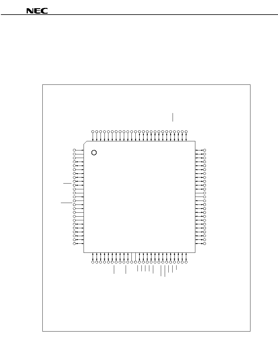
PIN CONFIGURATION
∑
∑
∑
∑ V850ES/SA2
100-pin plastic LQFP (fine-pitch) (14
◊
◊
◊
◊ 14)
µPD703201GC-◊◊◊-8EU
µPD703201YGC-◊◊◊-8EU
µPD70F3201GC-8EU
µPD70F3201YGC-8EU
1
2
3
4
5
6
7
8
9
10
11
12
13
14
15
16
17
18
19
20
21
22
23
24
25
26
27
28
29
30
31
32
33
34
35
36
37
38
39
40
41
42
43
44
45
46
47
48
49
50
P70/ANI0
P71/ANI1
P72/ANI2
P73/ANI3
P74/ANI4
P75/ANI5
P76/ANI6
P77/ANI7
P78/ANI8
P79/ANI9
P710/ANI10
P711/ANI11
P05/INTP4
P04/INTP3/TI5
P03/INTP2/TI4
P02/INTP1/TI3
P01/INTP0/TI2
P46/INTP11/TO1
P45/INTP10/TI1/TCLR1
P44/INTP01/TO0
P43/INTP00/TI0/TCLR0
P42/SCK0/SCL
Note 1
P41/SO0/SDA
Note 1
P40/SI0
PDH5/A21
100
99
98
97
96
95
94
93
92
91
90
89
88
87
86
85
84
83
82
81
80
79
78
77
76
P96/A6/TO4
P97/A7/TO5
P98/A8/RXD1
P99/A9/TXD1
P910/A10/SI2
P911/A11/SO2
P912/A12/SCK2
P913/A13/SI3
P914/A14/SO3
P915/A15/SCK3
EV
SS
EV
DD
PCS0/CS0
PCS1/CS1
PCS2/CS2
PCS3/CS3
PCM0/WAIT
PCM1/CLKOUT
PCM2/HLDAK
PCM3/HLDRQ
PCT0/WR0
PCT1/WR1
PCT4/RD
PCT5
PCT6/ASTB
75
74
73
72
71
70
69
68
67
66
65
64
63
62
61
60
59
58
57
56
55
54
53
52
51
AV
REF0
AV
DD
AV
SS
P80/ANO0
P81/ANO1
AV
REF1
P00/NMI
P30/SI1/RXD0
P31/SO1/TXD0
P32/SCK1
V
DD
V
SS
X1
X2
RESET
XT1
XT2
V
SS
BU
V
DD
BU
P90/A0
P91/A1
P92/A2/INTP5
P93/A3/INTP6
P94/A4/TO2
P95/A5/TO3
PDH4/A20
PDH3/A19
PDH2/A18
PDH1/A17
PDH0/A16
PDL15/AD15
PDL14/AD14
PDL13/AD13
PDL12/AD12
PDL11/AD11
PDL10/AD10
EV
DD
EV
SS
IC/FLMD0
Notes 2, 3
PDL9/AD9
PDL8/AD8
PDL7/AD7
PDL6/AD6
PDL5/AD5/FLMD1
Note 2
PDL4/AD4
PDL3/AD3
PDL2/AD2
PDL1/AD1
PDL0/AD0
PCT7
Notes 1. SCL and SDA are valid only for the
µPD703201Y and 70F3201Y.
2. FLMD0 and FLMD1 are valid only for the
µPD70F3201 and 70F3201Y.
3. IC:
Connect directly to V
SS
(
µPD703201, 703201Y).
FLMD0: Connect to V
SS
in normal mode (
µPD70F3201, 70F3201Y).

Preliminary Product Information U15436EJ1V0PM
4
µ
µ
µ
µPD703201, 703201Y, 703204, 703204Y, 70F3201, 70F3201Y, 70F3204, 70F3204Y
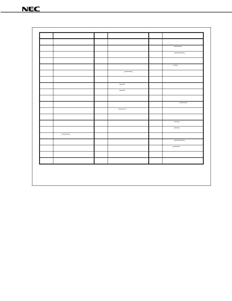
∑
∑
∑
∑ V850ES/SA3
121-pin plastic FBGA (12
◊
◊
◊
◊ 12)
µPD703204F1-◊◊◊-EA6
µPD70F3204F1-EA6
µPD703204YF1-◊◊◊-EA6
µPD70F3204YF1-EA6
(1/2)
Top View
Bottom View
N M L K J H G F E D C B A
A B C D E F G H J K L M N
13
12
11
10
9
8
7
6
5
4
3
2
1
Pin No.
Pin Name
Pin No.
Pin Name
Pin No.
Pin Name
A1
P70/ANI0
B8
PCD3
D2
AV
REF1
A2
P71/ANI1
B9
P02/INTP1/TI3
D3
P00/NMI
A3
P73/ANI3
B10
P46/INTP11/TO1
D11
PDH0/A16
A4
P713/ANI13
B11
P42/SCK0/SCL
Note
D12
PDH2/A18
A5
P76/ANI6
B12
P40/SI0
D13
PDH1/A17
A6
P78/ANI8
B13
PDH4/A20
E1
P30/SI1/RXD0
A7
P711/ANI11
C1
P80/ANO0
E2
P31/SO1/TXD0
A8
P04/INTP3/TI5
C2
AV
SS
E3
P32/SCK1
A9
PCD2
C3
P74/ANI4
E11
PDL14/AD14
A10
P45/INTP10/TI1/TCLR1
C4
P714/ANI14
E12
PDH6/A22
A11
P43/INTP00/TI0/TCLR0
C5
P715/ANI15
E13
PDL15/AD15
A12
P41/SO0/SDA
Note
C6
P79/ANI9
F1
V
SS
A13
PDH5/A21
C7
P05/INTP4
F2
X1
B1
AV
DD
C8
P03/INTP2/TI4
F3
V
DD
B2
AV
REF0
C9
PCD1
F11
PDL11/AD11
B3
P72/ANI2
C10
P01/INTP0/TI2
F12
PDL13/AD13
B4
P712/ANI12
C11
P44/INTP01/TO0
F13
PDL12/AD12
B5
P75/ANI5
C12
PDH3/A19
G1
RESET
B6
P77/ANI7
C13
PDH7/A23
G2
XT1
B7
P710/ANI10
D1
P81/ANO1
G3
X2
Note
SCL and SDA are valid only for
µPD703204Y and 70F3204Y.
Remark
Connect the D4 pin directly to V
SS
.
Preliminary Product Information U15436EJ1V0PM
5
µ
µ
µ
µPD703201, 703201Y, 703204, 703204Y, 70F3201, 70F3201Y, 70F3204, 70F3204Y
(2/2)
Pin No.
Pin Name
Pin No.
Pin Name
Pin No.
Pin Name
G11
EV
SS
K13
PDL3/AD3
M7
PCS4
G12
PDL10/AD10
L1
P93/A3/INTP6
M8
PCM0/WAIT
G13
EV
DD
L2
P94/A4/TO2
M9
PCM2/HLDAK
H1
V
SS
BU
L3
P911/A11/SO2
M10
PCT3
H2
V
DD
BU
L4
P914/A14/SO3
M11
PCT4/RD
H3
XT2
L5
P915/A15/SCK3
M12
PCT7
H11
PDL8/AD8
L6
EV
DD
M13
PDL0/AD0
H12
IC/FLMD0
Notes 1, 2
L7
PCS0/CS0
N1
P96/A6/TO4
H13
PDL9/AD9
L8
PCS2/CS2
N2
P98/A8/RXD1
J1
P20/SI4
L9
PCM4
N3
P910/A10/SI2
J2
P91/A1
L10
PCT2
N4
P912/A12/SCK2
J3
P90/A0
L11
PCT0/WR0
N5
PCS7
J11
PDL5/AD5/FLMD1
Note 1
L12
PDL1/AD1
N6
PCS6
J12
PDL7/AD7
L13
PDL2/AD2
N7
PCS1/CS1
J13
PDL6/AD6
M1
P95/A5/TO3
N8
PCS3/CS3
K1
P22/SCK4
M2
P97/A7/TO5
N9
PCM5
K2
P92/A2/INTP5
M3
P99/A9/TXD1
N10
PCM3/HLDRQ
K3
P21/SO4
M4
P913/A13/SI3
N11
PCT1/WR1
K11
PCM1/CLKOUT
M5
EV
SS
N12
PCT5
K12
PDL4/AD4
M6
PCS5
N13
PCT6/ASTB
Notes 1. FLMD0 and FLMD1 are valid only for
µPD70F3204Y and 70F3204Y.
2. IC: Connect directly to V
SS
(
µPD703204, 703204Y).
FLMD0: Connect to V
SS
in normal mode (
µPD70F3204, 70F3204Y).

Preliminary Product Information U15436EJ1V0PM
6
µ
µ
µ
µPD703201, 703201Y, 703204, 703204Y, 70F3201, 70F3201Y, 70F3204, 70F3204Y
PIN IDENTIFICATION
A0 to A23:
AD0 to AD15:
ADTRG:
ANI0 to ANI15:
ANO0, ANO1:
ASTB:
AV
DD
:
AV
REF0
, AV
REF1
:
AV
SS
:
CLKOUT:
CS0 to CS3:
EV
DD
:
EV
SS
:
FLMD0, FLMD1:
HLDAK:
HLDRQ:
IC:
INTP0 to INTP6:
INTP00, INTP01,:
INTP10, INTP11
NMI:
P00 to P05:
P20 to P22:
P30 to P32:
P40 to P46:
P70 to P715:
P80, P81:
P90 to P915:
Address bus
Address/data bus
AD trigger input
Analog input
Analog output
Address strobe
Analog V
DD
Analog reference voltage
Analog V
SS
Clock output
Chip select
Power supply for port
Ground for port
Flash programming mode
Hold acknowledge
Hold request
Internally connected
Interrupt request from peripherals
Interrupt request to timer
Non-maskable interrupt request
Port 0
Port 2
Port 3
Port 4
Port 7
Port 8
Port 9
PCD1 to PCD3:
PCM0 to PCM5:
PCS0 to PCS7:
PCT0 to PCT7:
PDH0 to PDH7:
PDL0 to PDL15:
RD:
RESET:
RXD0, RXD1:
SCK0 to SCK4:
SCL:
SDA:
SI0 to SI4:
SO0 to SO4:
TCLR0, TCLR1:
TI0 to TI5:
TO0 to TO5:
TXD0, TXD1:
V
DD
:
V
DD
BU:
V
SS
:
V
SS
BU:
WAIT:
WR0:
WR1:
X1, X2:
XT1, XT2:
Port CD
Port CM
Port CS
Port CT
Port DH
Port DL
Read
Reset
Receive data
Serial clock
Serial clock
Serial data
Serial input
Serial output
Timer clear input
Timer input
Timer output
Transmit data
Power supply
Power supply for backup
Ground
Ground for backup
Wait
Write strobe low level data
Write strobe high level data
Crystal for main clock
Crystal for subclock
Preliminary Product Information U15436EJ1V0PM
7
µ
µ
µ
µPD703201, 703201Y, 703204, 703204Y, 70F3201, 70F3201Y, 70F3204, 70F3204Y
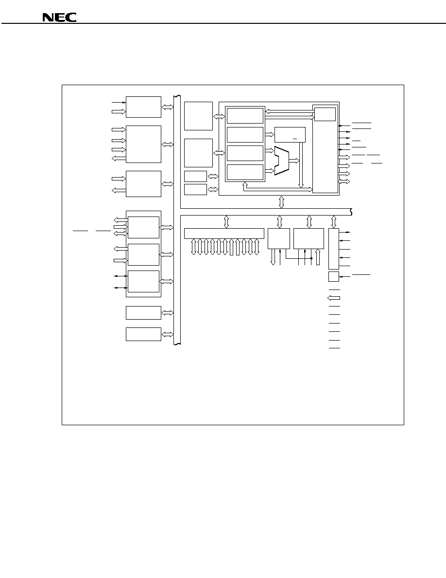
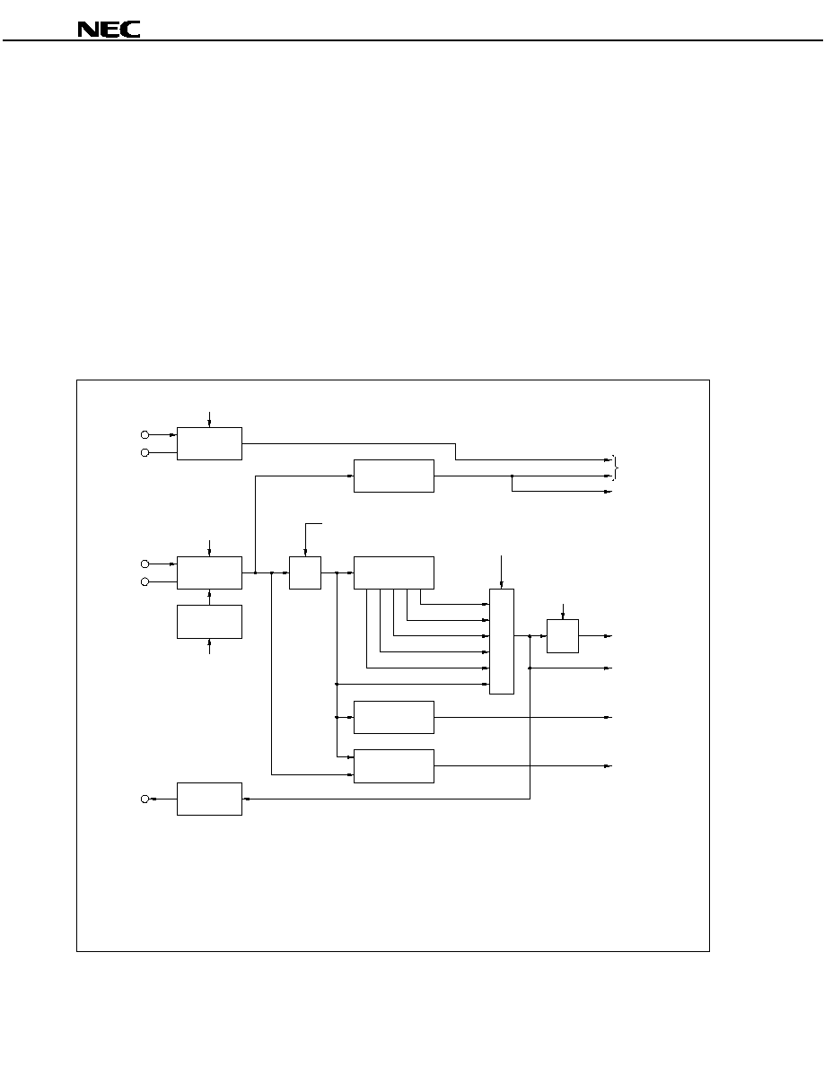
INTERNAL BLOCK DIAGRAM
∑
∑
∑
∑ V850ES/SA2
NMI
INTP00, INTP01,
INTP10, INTP11
TO0, TO1
SIO
TI0, TI1
TCLR0, TCLR1
SO0 to SO3
SI0 to SI3
SCK0 to SCK3
INTP0 to INTP6
INTC
Timer/counter
16-bit timer:
2 ch
TO2 to TO5
TI2 to TI5
Timer/counter
8-bit timer:
4 ch
TXD0, TXD1
RXD0, RXD1
UART: 2 ch
SDA
Note 2
SCL
Note 2
I
2
C
Note 2
: 1 ch
DMAC
Watchdog
timer
Real-time
counter
Note 1
RAM
ROM
16 KB
PC
General-purpose
registers 32-bits
◊
32
Multiplier
16
◊ 16 32
ALU
System
registers
32-bit barrel
shifter
CPU
HLDRQ
HLDAK
ASTB
RD
WAIT
WR0, WR1
CS0 to CS3
A0 to A21
AD0 to AD15
IC
Note 3
FLMD0
Note 4
, FLMD1
Note 4
Ports
CG
RG
A/D
converter
D/A
converter
PCS0 to PCS3
PCM0 to PCM3
PCT0, PCT1, PCT4 to PCT7
PDH0 to PDH5
PDL0 to PDL15
P90 to P915
P80, P81
P70 to P711
P40 to P46
P30 to P32
P00 to P05
ANO0, ANO1
AV
REF1
AV
DD
AV
REF0
AV
SS
ANI0 to ANI11
CLKOUT
X1
X2
XT1
XT2
RESET
V
DD
V
SS
V
DD
BU
V
SS
BU
EV
DD
EV
SS
Instruction
queue
BCU
CSI: 4 ch
ROM
correction
Notes 1.
µPD703201, 703201Y:
256 KB (mask ROM)
µPD70F3201, 70F3201Y: 256 KB (flash memory)
2. Applies to the
µPD703201Y and 70F3201Y only.
3. Applies to the
µPD703201 and 703201Y only.
4. Applies to the
µPD70F3201 and 70F3201Y only.
Preliminary Product Information U15436EJ1V0PM
8
µ
µ
µ
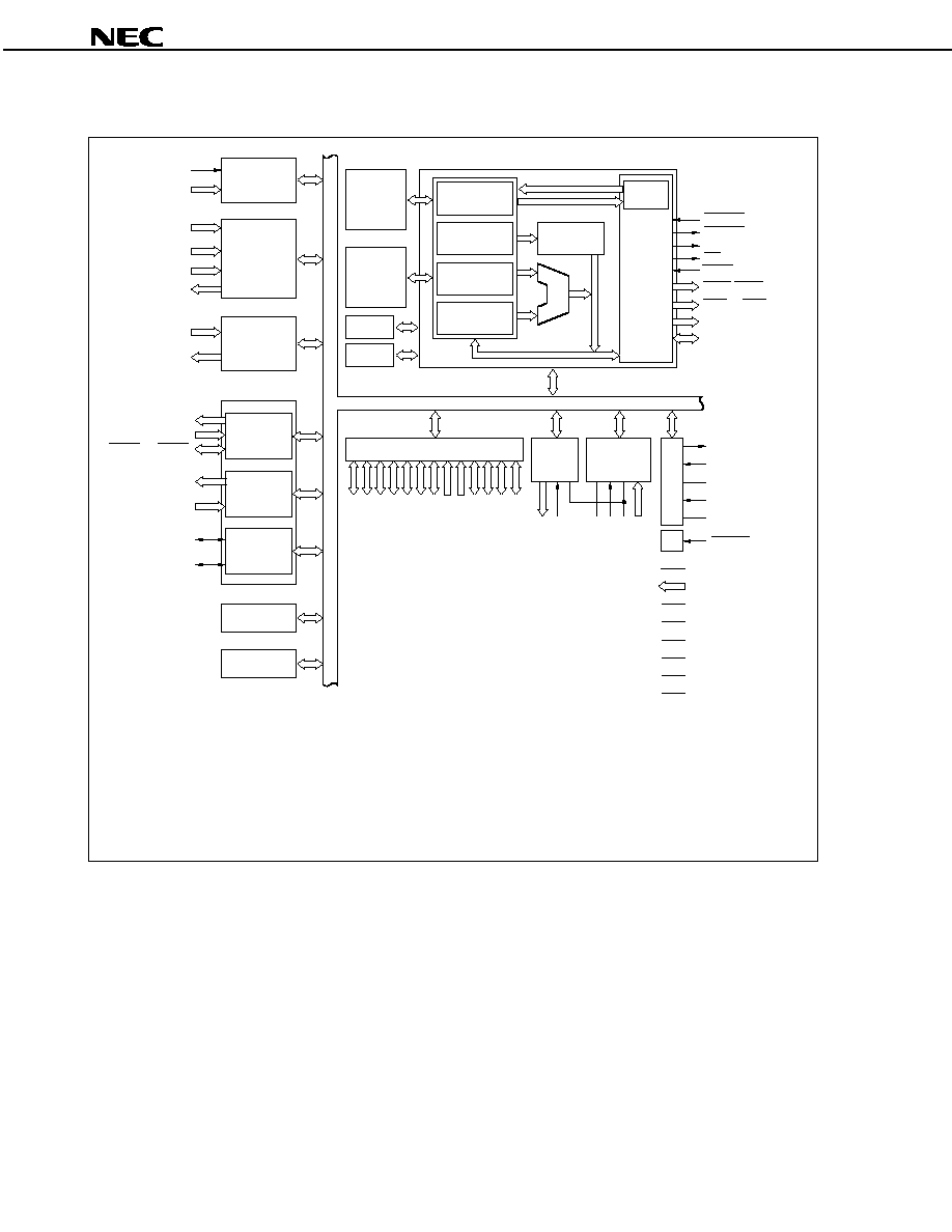
µPD703201, 703201Y, 703204, 703204Y, 70F3201, 70F3201Y, 70F3204, 70F3204Y
∑
∑
∑
∑ V850ES/SA3
NMI
INTP00, INTP01,
INTP10, INTP11
TO0, TO1
SIO
TI0, TI1
TCLR0, TCLR1
SO0 to SO4
SI0 to SI4
SCK0 to SCK4
INTP0 to INTP6
INTC
Timer/counter
16-bit timer:
2 ch
TO2 to TO5
TI2 to TI5
Timer/counter
8-bit timer:
4 ch
TXD0, TXD1
RXD0, RXD1
UART: 2 ch
SDA
Note 2
SCL
Note 2
I
2
C
Note 2
:1 ch
DMAC
Watchdog
timer
Real-time
counter
Note 1
RAM
ROM
16 KB
PC
General-purpose
registers 32-bits
◊
32
Multiplier
16
◊ 16 32
ALU
System
registers
32-bit barrel
shifter
CPU
HLDRQ
HLDAK
ASTB
RD
WAIT
WR0, WR1
CS0 to CS3
A0 to A23
AD0 to AD15
IC
Note 3
FLMD0
Note 4
, FLMD1
Note 4
Ports
CG
RG
A/D
converter
D/A
converter
PCS0 to PCS7
PCM0 to PCM5
PCT0 to PCT7
PDH0 to PDH7
PDL0 to PDL15
PCD1 to PCD3
P90 to P915
P80, P81
P70 to P715
P40 to P46
P30 to P32
P20 to P22
P00 to P05
ANO0, ANO1
AV
REF1
AV
DD
AV
REF0
AV
SS
ANI0 to ANI15
CLKOUT
X1
X2
XT1
XT2
RESET
V
DD
V
SS
V
DD
BU
V
SS
BU
EV
DD
EV
SS
Instruction
queue
BCU
CSI: 5 ch
ROM
correction
Notes 1.
µPD703204, 703204Y:
256 KB (mask ROM)
µPD70F3204, 70F3204Y: 256 KB (flash memory)
2. Applies to the
µPD703204Y and 70F3204Y only.
3. Applies to the
µPD703204 and 703204Y only.
4. Applies to the
µPD70F3204 and 70F3204Y only.

Preliminary Product Information U15436EJ1V0PM
9
µ
µ
µ
µPD703201, 703201Y, 703204, 703204Y, 70F3201, 70F3201Y, 70F3204, 70F3204Y
CONTENTS
1.
PIN FUNCTIONS ................................................................................................................................11
1.1
Port Pins ................................................................................................................................................... 11
1.2
Non-Port Pins........................................................................................................................................... 14
1.3
Pin I/O Circuits and Recommended Connection of Unused Pins ....................................................... 18
2.
FUNCTION BLOCKS .........................................................................................................................22
2.1
Internal Units............................................................................................................................................ 22
3.
CPU FUNCTIONS................................................................................................................................25
4.
MEMORY MAP ...................................................................................................................................26
5.
EXTERNAL BUS INTERFACE FUNCTION .....................................................................................28
6.
INTERRUPT SERVICING/EXCEPTION PROCESSING FUNCTION ..............................................31
7.
CLOCK GENERATION FUNCTION..................................................................................................34
8.
POWER SAVE FUNCTION ...............................................................................................................35
9.
TIMER/COUNTER FUNCTION...........................................................................................................37
10. REAL-TIME COUNTER FUNCTION .................................................................................................40
11. WATCHDOG TIMER FUNCTION......................................................................................................41
12. SERIAL INTERFACE FUNCTION.....................................................................................................42
12.1 3-Wire Serial I/O (CSIn)............................................................................................................................ 42
12.2 Asynchronous Serial Interface (UART0 and UART1) ........................................................................... 44
12.3 I
2
C Bus (I
2
C) (
µ
µ
µ
µPD703201Y, 703204Y, 70F3201Y, 70F3204Y) ................................................................45
13. A/D CONVERTER...............................................................................................................................46
14. D/A CONVERTER...............................................................................................................................48
15. DMA FUNCTION.................................................................................................................................49
16. ROM CORRECTION FUNCTION ......................................................................................................50
17. RESET FUNCTION.............................................................................................................................51
18. FLASH MEMORY (
µ
µ
µ
µ
PD70F3201, 70F3201Y, 70F3204, 70F3204Y) ............................................52
19. INSTRUCTION SET LIST..................................................................................................................54
19.1 Conventions ............................................................................................................................................. 54

Preliminary Product Information U15436EJ1V0PM
10
µ
µ
µ
µPD703201, 703201Y, 703204, 703204Y, 70F3201, 70F3201Y, 70F3204, 70F3204Y
19.2 Instruction Set (In Alphabetical Order) ..................................................................................................57
20. ELECTRICAL SPECIFICATIONS (TARGET VALUES) ................................................................. 64
21. PACKAGE DRAWINGS..................................................................................................................... 92
APPENDIX DEVELOPMENT TOOLS ..................................................................................................... 94
Preliminary Product Information U15436EJ1V0PM
11
µ
µ
µ
µPD703201, 703201Y, 703204, 703204Y, 70F3201, 70F3201Y, 70F3204, 70F3204Y
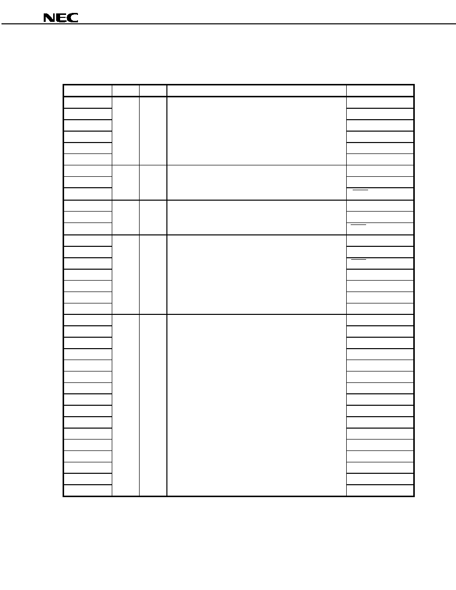
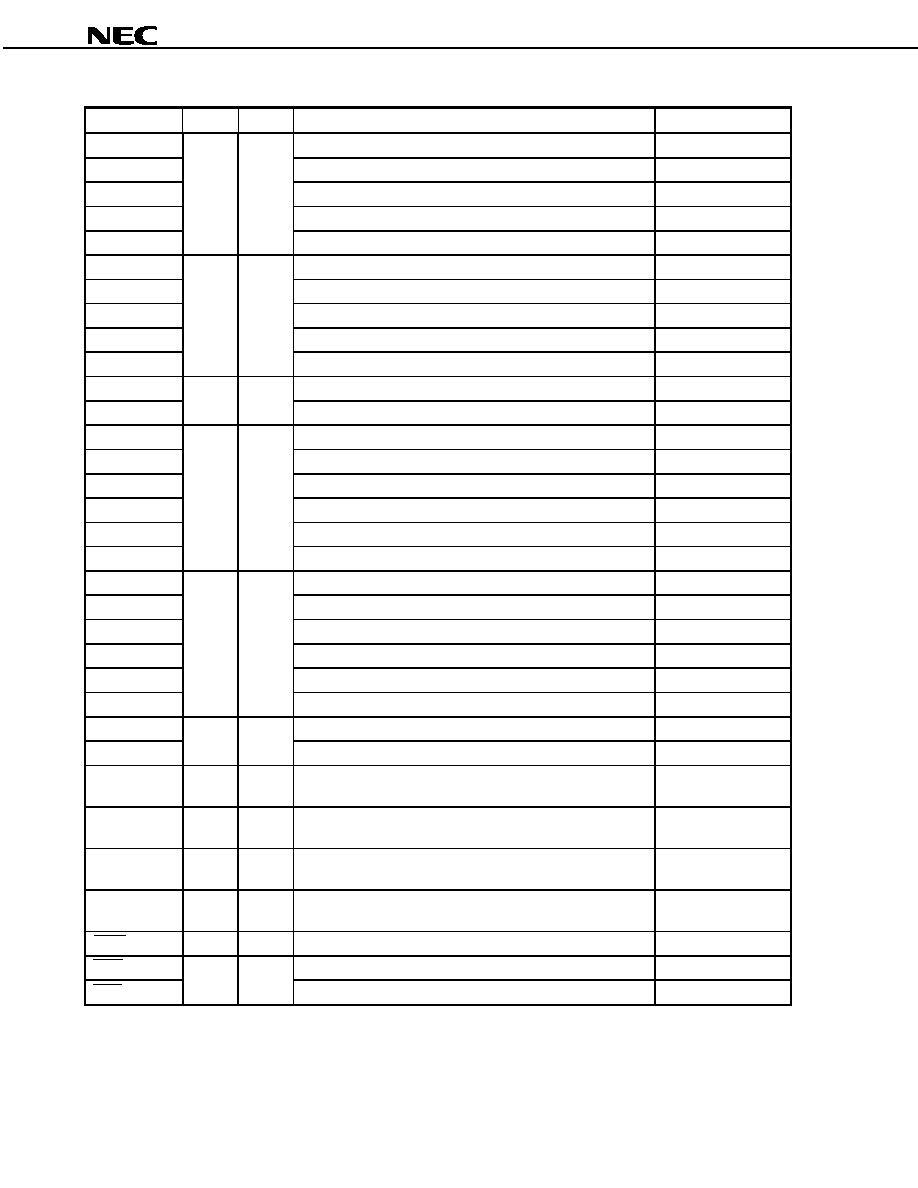
1. PIN FUNCTIONS
1.1 Port Pins
(1/3)
Pin Name
I/O
PULL
Function
Alternate Function
P00
NMI
P01
INTP0/TI2
P02
INTP1/TI3
P03
INTP2/TI4
P04
INTP3/TI5
P05
I/O
Yes
Port 0
6-bit I/O port
Input/output can be specified in 1-bit units.
INTP4
[P20]
[SI4]
[P21]
[SO4]
[P22]
I/O
Yes
Port 2
3-bit I/O port
Input/output can be specified in 1-bit units.
N-ch open drain can be specified in 1-bit units (P21, P22 only).
[SCK4]
P30
SI1/RXD0
P31
SO1/TXD0
P32
I/O
Yes
Port 3
3-bit I/O port
Input/output can be specified in 1-bit units.
N-ch open drain can be specified in 1-bit units (P31, P32 only).
SCK1
P40
SI0
P41
SO0/SDA
Note
P42
SCK0/SCL
Note
P43
INTP00/TI0/TCLR0
P44
INTP01/TO0
P45
INTP10/TI1/TCLR1
P46
I/O
Yes
Port 4
7-bit I/O port
Input/output can be specified in 1-bit units.
N-ch open drain can be specified in 1-bit units (P41, P42 only).
INTP11/TO1
P70
ANI0
P71
ANI1
P72
ANI2
P73
ANI3
P74
ANI4
P75
ANI5
P76
ANI6
P77
ANI7
P78
ANI8
P79
ANI9
P710
ANI10
P711
ANI11
[P712]
[ANI12]
[P713]
[ANI13]
[P714]
[ANI14]
[P715]
Input
No
Port 7
12-bit input port (V850ES/SA2)
16-bit input port (V850ES/SA3)
[ANI15]
Note
Applies to the
µPD703201Y, 703204Y, 70F3201Y, and 70F3204Y only.
Remarks 1. PULL: On-chip pull-up resistor
2. Pins in brackets ([ ]) are only for the V850ES/SA3.
Preliminary Product Information U15436EJ1V0PM
12
µ
µ
µ
µPD703201, 703201Y, 703204, 703204Y, 70F3201, 70F3201Y, 70F3204, 70F3204Y
(2/3)
Pin Name
I/O
PULL
Function
Alternate Function
P80
ANO0
P81
Input
No
Port 8
2-bit input port
ANO1
P90
A0
P91
A1
P92
A2/INTP5
P93
A3/INTP6
P94
A4/TO2
P95
A5/TO3
P96
A6/TO4
P97
A7/TO5
P98
A8/RXD1
P99
A9/TXD1
P910
A10/SI2
P911
A11/SO2
P912
A12/SCK2
P913
A13/SI3
P914
A14/SO3
P915
I/O
Yes
Port 9
16-bit I/O port
Input/output can be specified in 1-bit units.
N-ch open drain can be specified in 1-bit units (P911, P912,
P914, P915 only).
A15/SCK3
[PCD1]
≠
[PCD2]
≠
[PCD3]
I/O
No
Port CD
3-bit I/O port
Input/output can be specified in 1-bit units.
≠
PCM0
WAIT
PCM1
CLKOUT
PCM2
HLDAK
PCM3
HLDRQ
[PCM4]
≠
[PCM5]
I/O
No
4-bit I/O port (V850ES/SA2)
6-bit I/O port (V850ES/SA3)
Input/output can be specified in 1-bit units.
≠
PCS0
CS0
PCS1
CS1
PCS2
CS2
PCS3
CS3
[PCS4]
≠
[PCS5]
≠
[PCS6]
≠
[PCS7]
I/O
No
Port 10
4-bit I/O port (V850ES/SA2)
8-bit I/O port (V850ES/SA3)
Input/output can be specified in 1-bit units.
≠
Remarks 1. PULL: On-chip pull-up resistor
2. Pins in brackets ([ ]) are only for the V850ES/SA3.

Preliminary Product Information U15436EJ1V0PM
13
µ
µ
µ
µPD703201, 703201Y, 703204, 703204Y, 70F3201, 70F3201Y, 70F3204, 70F3204Y
(3/3)
Pin Name
I/O
PULL
Function
Alternate Function
PCT0
WR0
PCT1
WR1
[PCT2]
≠
[PCT3]
≠
PCT4
RD
PCT5
≠
PCT6
ASTB
PCT7
I/O
No
Port CT
6-bit I/O port (V850ES/SA2)
8-bit I/O port (V850ES/SA3)
Input/output can be specified in 1-bit units.
≠
PDH0
A16
PDH1
A17
PDH2
A18
PDH3
A19
PDH4
A20
PDH5
A21
[PDH6]
[A22]
[PDH7]
I/O
No
Port DH
6-bit I/O port (V850ES/SA2)
8-bit I/O port (V850ES/SA3)
Input/output can be specified in 1-bit units.
[A23]
PDL0
AD0
PDL1
AD1
PDL2
AD2
PDL3
AD3
PDL4
AD4
PDL5
AD5/FLMD1
Note
PDL6
AD6
PDL7
AD7
PDL8
AD8
PDL9
AD9
PDL10
AD10
PDL11
AD11
PDL12
AD12
PDL13
AD13
PDL14
AD14
PDL15
I/O
No
Port DL
16-bit I/O port
Input/output can be specified in 1-bit units.
AD15
Note
Applies to the
µPD70F3201, 70F3201Y, 70F3204, and 70F3204Y only.
Remarks 1. PULL: On-chip pull-up resistor
2. Pins in brackets ([ ]) are only for the V850ES/SA3.
Preliminary Product Information U15436EJ1V0PM
14
µ
µ
µ
µPD703201, 703201Y, 703204, 703204Y, 70F3201, 70F3201Y, 70F3204, 70F3204Y
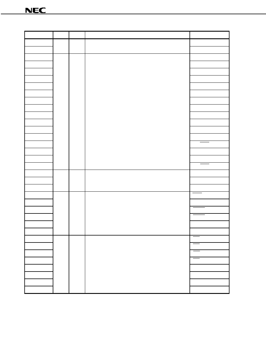
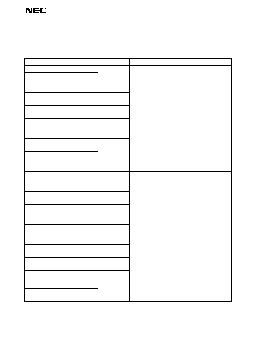
1.2 Non-Port Pins
(1/4)
Pin Name
I/O
PULL
Function
Alternate Function
A0
P90
A1
P91
A2
P92/INTP5
A3
P93/INTP6
A4
P94/TO2
A5
P95/TO3
A6
P96/TO4
A7
P97/TO5
A8
P98/RXD1
A9
P99/TXD1
A10
P910/SI2
A11
P911/SO2
A12
P912/SCK2
A13
P913/SI3
A14
P914/SO3
A15
Output
Yes
Address bus for external memory (when using separate bus)
P915/SCK3
A16 to A21,
[A22, A23]
Output
No
Address bus for external memory
PDH0 to PDH5,
[PDH6, PDH7]
AD0 to AD4
PDL0 to PDL4
AD5
PDL5/FLMD1
Note
AD6 to AD15
I/O
No
Address/data bus for external memory
PDL6 to PDL15
ANI0
P70
ANI1
P71
ANI2
P72
ANI3
P73
ANI4
P74
ANI5
P75
ANI6
P76
ANI7
P77
ANI8
P78
ANI9
P79
ANI10
P710
ANI11
P711
[ANI12]
[P712]
[ANI13]
[P713]
[ANI14]
[P714]
[ANI15]
Input
No
Analog voltage input for A/D converter
[P715]
Note
Applies to the
µPD70F3201, 70F3201Y, 70F3204, and 70F3204Y only.
Remarks 1. PULL: On-chip pull-up resistor
2. Pins in brackets ([ ]) are only for the V850ES/SA3.
Preliminary Product Information U15436EJ1V0PM
15
µ
µ
µ
µPD703201, 703201Y, 703204, 703204Y, 70F3201, 70F3201Y, 70F3204, 70F3204Y
(2/4)
Pin Name
I/O
PULL
Function
Alternate Function
ANO0
P80
ANO1
Output
No
Analog voltage output for D/A converter
P81
ASTB
Output
No
Address strobe signal output for external memory
PCT6
AV
DD
≠
≠
Positive power supply for A/D converter (same potential as V
DD
)
≠
AV
REF0
Reference voltage input for A/D converter
≠
AV
REF1
Input
≠
Reference voltage input for D/A converter
≠
AV
SS
≠
≠
Ground potential for A/D, D/A converters (same potential as V
SS
)
≠
CLKOUT
Output
No
Internal system clock output
PCM1
CS0 to CS3
Output
No
Chip select output
PCS0 to PCS3
EV
DD
≠
≠
Positive power supply for external devices (same potential as
V
DD
)
≠
EV
SS
≠
≠
Ground potential for external devices (same potential as V
SS
)
≠
FLMD0
Note 1
≠
FLMD1
Note 1
Input
No
Flash programming mode lead-in pins
PDL5/AD5
HLDAK
Output
No
Bus hold acknowledge output
PCM2
HLDRQ
Input
No
Bus hold request input
PCM3
IC
≠
≠
Internally connected (directly connect to V
SS
). (
µPD703201,
703201Y, 703204, and 703204Y only)
≠
INTP0 to INTP3
P01/TI2 to P04/TI5
INTP4
P05
INTP5
P92/A2
INTP6
Input
Yes
External interrupt request input (maskable, analog noise
elimination)
P93/A3
INTP00
P43/TI0/TCLR0
INTP01
Capture trigger input (TM0)
P44/TO0
INTP10
P45/TI1/TCLR1
INTP11
Input
Yes
Capture trigger input (TM1)
P46/TO1
NMI
Input
Yes
External interrupt input (non-maskable, analog noise elimination)
P00
RD
Output
No
Read strobe signal output for external memory
PCT4
RESET
Input
≠
System reset input
≠
RXD0
Serial receive data input (UART0)
P30/SI1
RXD1
Input
Yes
Serial receive data input (UART1)
P98/A8
SCK0
Serial clock I/O (CSI0)
P42/SCL
Note 2
SCK1
Serial clock I/O (CSI1)
P32
SCK2
Serial clock I/O (CSI2)
P912/A12
SCK3
Serial clock I/O (CSI3)
P915/A15
[SCK4]
I/O
Yes
Serial clock I/O (CSI4)
[P22]
SCL
Note 2
I/O
Yes
Serial clock I/O (I
2
C)
P42/SCK0
SDA
Note 2
I/O
Yes
Serial transmit/receive data I/O (I
2
C)
P41/SO0
Notes 1. Applies to the
µPD70F3201, 70F3201Y, 70F3204, and 70F3204Y only.
2. Applies to the
µPD703201Y, 703204Y, 70F3201Y, and 70F3204Y only.
Remarks 1. PULL: On-chip pull-up resistor
2. Pins in brackets ([ ]) are only for the V850ES/SA3.
Preliminary Product Information U15436EJ1V0PM
16
µ
µ
µ
µPD703201, 703201Y, 703204, 703204Y, 70F3201, 70F3201Y, 70F3204, 70F3204Y
(3/4)
Pin Name
I/O
PULL
Function
Alternate Function
SI0
Serial receive data input (CSI0)
P40
SI1
Serial receive data input (CSI1)
P30/RXD0
SI2
Serial receive data input (CSI2)
P910/A10
SI3
Serial receive data input (CSI3)
P913/A13
[SI4]
Input
Yes
Serial receive data input (CSI4)
[P20]
SO0
Serial transmit data output (CSI0)
P41/SDA
Note
SO1
Serial transmit data output (CSI1)
P31/TXD0
SO2
Serial transmit data output (CSI2)
P911/A11
SO3
Serial transmit data output (CSI3)
P914/A14
[SO4]
Output
Yes
Serial transmit data output (CSI4)
[P21]
TCLR0
Timer clear input (TM0)
P43/INTP00/TI0
TCLR1
Input
Yes
Timer clear input (TM1)
P45/INTP10/TI1
TI0
External event/clock input (TM0)
P43/INTP00/TCLR0
TI1
External event/clock input (TM1)
P45/INTP10/TCLR1
TI2
External event/clock input (TM2)
P01/INTP0
TI3
External event/clock input (TM3)
P02/INTP1
TI4
External event/clock input (TM4)
P03/INTP2
TI5
Input
Yes
External event/clock input (TM5)
P04/INTP3
TO0
Timer output (TM0)
P44/INTP01
TO1
Timer output (TM1)
P46/INTP11
TO2
Timer output (TM2)
P94/A4
TO3
Timer output (TM3)
P95/A5
TO4
Timer output (TM4)
P96/A6
TO5
Output
Yes
Timer output (TM5)
P97/A7
TXD0
Serial transmit data output (UART0)
P31/SO1
TXD1
Output
Yes
Serial transmit data output (UART1)
P99/A9
V
DD
≠
≠
Positive power supply pin for internal functions (except for
subclock oscillator, RTC, and internal RAM)
≠
V
DD
BU
≠
≠
Positive power supply pin for backup (for subclock oscillator,
RTC and internal RAM)
≠
V
SS
≠
≠
Ground potential for internal functions (except for subclock
oscillator, RTC, and internal RAM)
≠
V
SS
BU
≠
≠
Ground potential for backup (for subclock oscillator, RTC and
internal RAM)
≠
WAIT
Input
No
External wait input
PCM0
WR0
Write strobe for external memory (lower 8 bits)
PCT0
WR1
Output
No
Write strobe for external memory (higher 8 bits)
PCT1
Note
Applies to the
µPD703201Y, 703204Y, 70F3201Y, and 70F3204Y only.
Remarks 1. PULL: On-chip pull-up resistor
2. Pins in brackets ([ ]) are only for the V850ES/SA3.

Preliminary Product Information U15436EJ1V0PM
17
µ
µ
µ
µPD703201, 703201Y, 703204, 703204Y, 70F3201, 70F3201Y, 70F3204, 70F3204Y
(4/4)
Pin Name
I/O
PULL
Function
Alternate Function
X1
Input
≠
X2
≠
No
Connecting resonator for main clock
≠
XT1
Input
≠
XT2
≠
No
Connecting resonator for subclock
≠
Remark
PULL: On-chip pull-up resistor
Preliminary Product Information U15436EJ1V0PM
18
µ
µ
µ
µPD703201, 703201Y, 703204, 703204Y, 70F3201, 70F3201Y, 70F3204, 70F3204Y
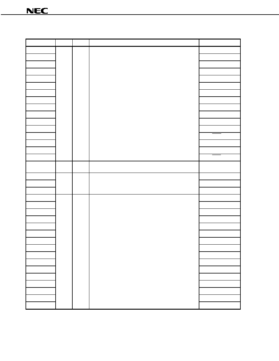
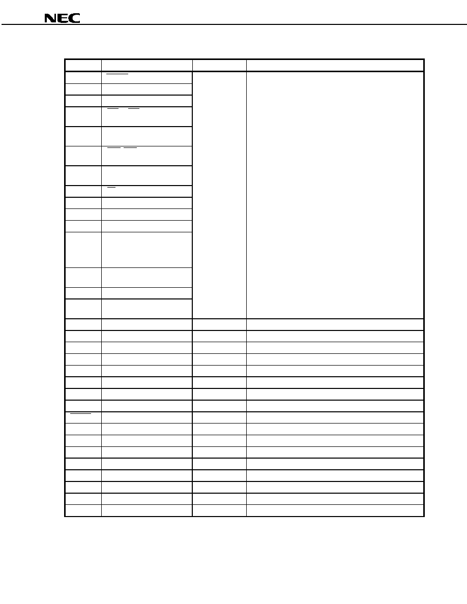
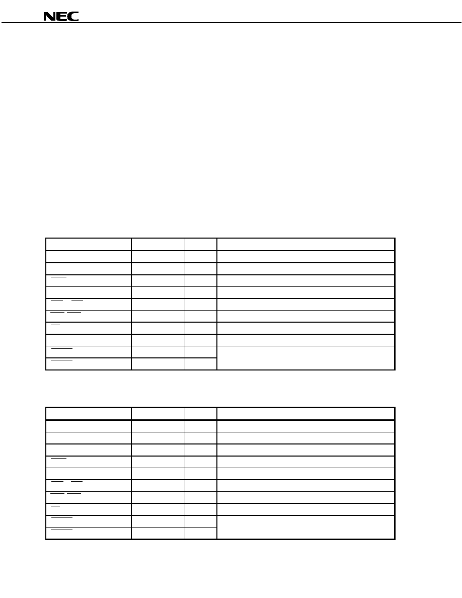
1.3 Pin I/O Circuits and Recommended Connection of Unused Pins
The I/O circuit type of each pin and recommended connection of unused pins are show in Table 1-1. For the
schematic circuit diagram of each type, refer to Figure 1-1.
Table 1-1. Types of Pin I/O Circuits (1/2)
Pin
Alternate Function
I/O Circuit Type
Recommended Connection of Unused Pins
P00
NMI
P01 to P04
INTP0/TI2 to INTP3/TI5
P05
INTP4
5-W
[P20]
[SI4]
5-W
[P21]
[SO4]
10-E
[P22]
[SCK4]
10-F
P30
SI1/RXD0
5-W
P31
SO1/TXD0
10-E
P32
SCK1
10-F
P40
SI0
5-W
P41
SO0/SDA
Note
10-F
P42
SCK0/SCL
Note
10-F
P43
INTP00/TI0/TCLR0
P44
INTP01/TO0
P45
INTP10/TI1/TCLR1
P46
INTP11/TO1
5-W
Input:
Independently connect to EV
DD
or EV
SS
via a resistor.
Output: Leave open.
P70 to
P711,
[P712 to
P715]
ANI0 to ANI15
9
P80, P81
ANO0, ANO1
34
Independently connect to AV
DD
or AV
SS
via a resistor.
P90, P91
A0, A1
5-A
P92, P93
A2/INTP5, A3/INTP6
5-W
P94 to P97
A4/TO2 to A7/TO5
5-A
P98
A8/RXD1
5-W
P99
A9/TXD1
5-A
P910
A10/SI2
5-W
P911
A11/SO2
10-E
P912
A12/SCK2
10-F
P913
A13/SI3
5-W
P914
A14/SO3
10-E
P915
A15/SCK3
10-F
[PCD1 to
PCD3]
≠
PCM0
WAIT
PCM1
CLKOUT
PCM2
HLDAK
5
Input:
Independently connect to EV
DD
or EV
SS
via a resistor.
Output: Leave open.
Note
Applies to the
µPD703201Y, 703204Y, 70F3201Y, and 70F3204Y only.
Remark
Pins in brackets ([ ]) are only for the V850ES/SA3.
Preliminary Product Information U15436EJ1V0PM
19
µ
µ
µ
µPD703201, 703201Y, 703204, 703204Y, 70F3201, 70F3201Y, 70F3204, 70F3204Y
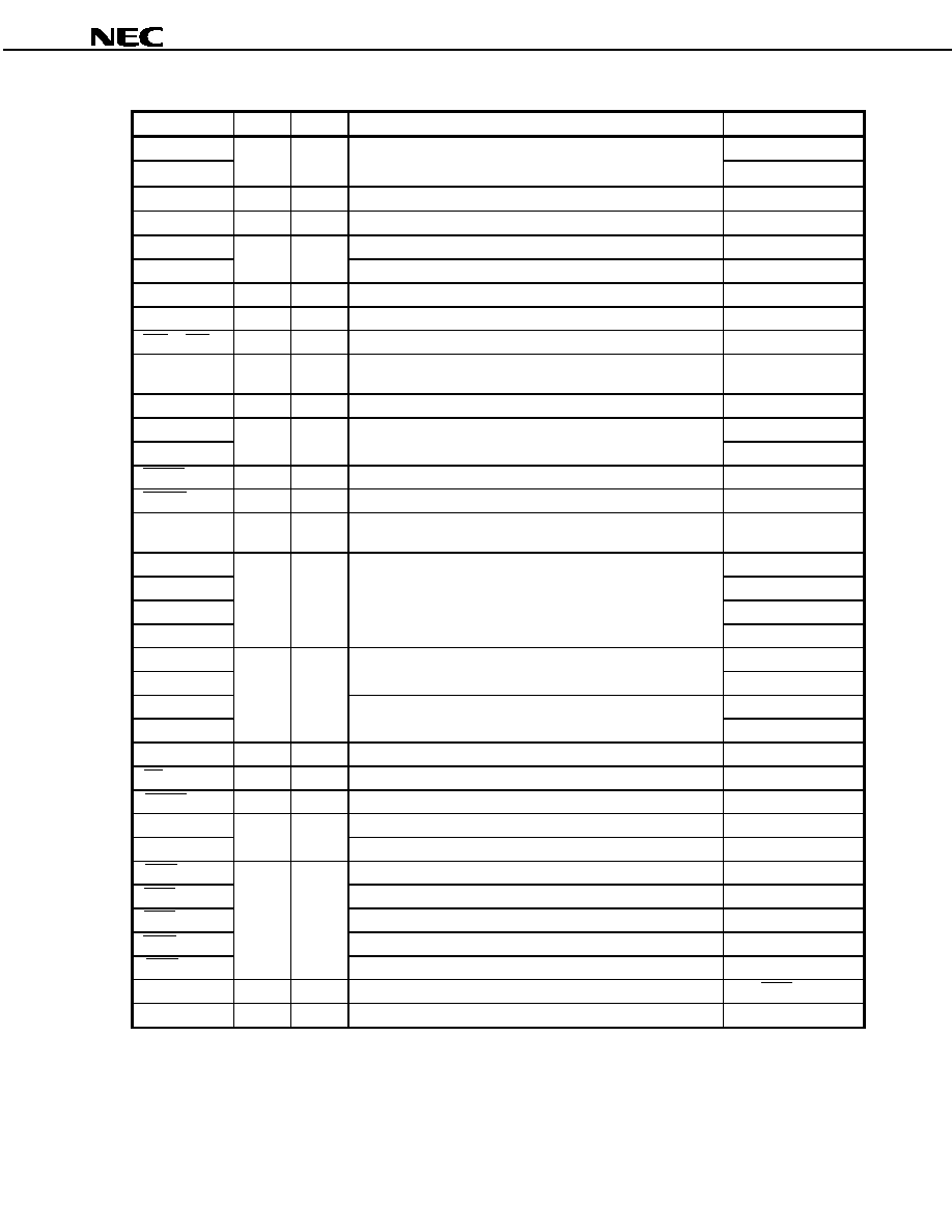
Table 1-1. Types of Pin I/O Circuits (2/2)
Pin
Alternate Function
I/O Circuit Type
Recommended Connection of Unused Pins
PCM3
HLDRQ
[PCM4]
≠
[PCM5]
≠
PCS0 to
PCS3
CS0 to CS3
[PCS4 to
PCS7]
≠
PCT0,
PCT1
WR0, WR1
[PCT2,
PCT3]
≠
PCT4
RD
PCT5
≠
PCT6
ASTB
PCT7
≠
PDH0 to
PDH5,
[PDH6,
PDH7]
A16 to A21, [A22, A23]
PDL0 to
PDL4
AD0 to AD4
PDL5
AD5/FLMD1
Note 1
PDL6 to
PDL15
AD6 to AD15
5
Input:
Independently connect to EV
DD
or EV
SS
via a
resistor.
Output: Leave open.
AV
DD
≠
≠
≠
AV
REF0
≠
≠
Connect to AV
SS
via a resistor.
AV
REF1
≠
≠
Connect to AV
SS
via a resistor.
AV
SS
≠
≠
≠
EV
DD
≠
≠
≠
EV
SS
≠
≠
≠
FLMD0
Note 1
≠
≠
≠
IC
Note 2
≠
≠
≠
RESET
≠
2
≠
V
DD
≠
≠
≠
V
DD
BU
≠
≠
≠
V
SS
≠
≠
≠
V
SS
BU
≠
≠
≠
X1
≠
≠
≠
X2
≠
≠
≠
XT1
≠
16
Connect to V
SS
BU via a resistor.
XT2
≠
16
Leave open.
Notes 1. Applies to the
µPD70F3201, 70F3201Y, 70F3204, and 70F3204Y only.
2. Applies to the
µPD703201, 703201Y, 703204, and 703204Y only.
Remark
Pins in brackets ([ ]) are only for the V850ES/SA3.

Preliminary Product Information U15436EJ1V0PM
20
µ
µ
µ
µPD703201, 703201Y, 703204, 703204Y, 70F3201, 70F3201Y, 70F3204, 70F3204Y
Figure 1-1. Pin I/O Circuits (1/2)
Type 2
Schmitt-triggered input with hysteresis characteristics
IN
Data
Output
disable
P-ch
IN/OUT
EV
DD
N-ch
Input
enable
Data
Output
disable
P-ch
IN/OUT
EV
DD
N-ch
Input
enable
P-ch
EV
DD
Pullup
enable
Data
Output
disable
P-ch
IN/OUT
EV
DD
N-ch
Input
enable
P-ch
EV
DD
Pullup
enable
IN
Comparator
+
≠
AV
REF0
(threshold voltage)
P-ch
N-ch
Input enable
Type 5
Type 5-A
Type 10-E
Type 9
Type 5-W
Input
enable
Data
Output disable
P-ch
IN/OUT
EV
DD
N-ch
P-ch
EV
DD
Pullup
enable
Open drain

Preliminary Product Information U15436EJ1V0PM
21
µ
µ
µ
µPD703201, 703201Y, 703204, 703204Y, 70F3201, 70F3201Y, 70F3204, 70F3204Y
Figure 1-1. Pin I/O Circuits (2/2)
P-ch
Feedback cut-off
XT1
XT2
Type 10-F
Type 34
Type 16
IN/OUT
Analog output voltage
P-ch
N-ch
Input enable
Data
Output
disable
Open drain
P-ch
IN/OUT
EV
DD
N-ch
P-ch
EV
DD
Pullup
enable
Input
enable

Preliminary Product Information U15436EJ1V0PM
22
µ
µ
µ
µPD703201, 703201Y, 703204, 703204Y, 70F3201, 70F3201Y, 70F3204, 70F3204Y
2. FUNCTION BLOCKS
2.1 Internal Units
Each internal unit of the V850ES/SA2 and V850ES/SA3 is described below.
(1) CPU
The CPU uses five-stage pipeline control to enable 1-clock execution of address calculations, arithmetic logic
operations, data transfers, and almost all other instruction processing.
Other dedicated on-chip hardware, such as the multiplier (16 bits
◊ 16 bits 32 bits) and the barrel shifter (32
bits), helps accelerate processing of complex instructions.
(2) Bus control unit (BCU)
The BCU starts the required external bus cycle based on the physical address obtained by the CPU. When an
instruction is fetched from external memory area and the CPU does not send a bus cycle start request, the
BCU generates a prefetch address and prefetches the instruction code. The prefetched instruction code is
stored in an internal instruction queue.
(3) ROM
This consists of a 256 KB mask ROM or flash memory mapped to the address space 0000000H to 003FFFFH.
This area can be accessed by the CPU in 1-clock cycle when an instruction is fetched.
(4) RAM
This consists of a 16 KB RAM mapped to the address space 3FFB000H to 3FFEFFFH. This area can be
accessed by the CPU in 1-clock cycle.
(5) Interrupt controller (INTC)
This controller services hardware interrupt requests (NMI, INTP0 to INTP6) from on-chip peripheral hardware
and external hardware. Eight levels of interrupt priorities can be specified for these interrupt requests, and
multiple servicing control can be performed for interrupt sources.
(6) Clock generator (CG)
The clock generator includes two types of oscillators, one for the main clock (f
XX
) and one for the subclock (f
XT
),
generates five types of clocks (f
XX
, f
XX
/2, f
XX
/4, f
XX
/8, f
XX
/16, and f
XX
/32), and supplies one of them as the
operating clock for the CPU (f
CPU
). The subclock can only be selected as the operation clock of the real-time
counter.
(7) Timer/counter
A two-channel 16-bit timer/event counter and a four-channel 8-bit timer/event counter are incorporated, which
enables measurement of pulse intervals and frequency as well as programmable pulse output.
Two channels of the 8-bit timer/event counter can be connected via a cascade connection to enable use as a
16-bit timer.

Preliminary Product Information U15436EJ1V0PM
23
µ
µ
µ
µPD703201, 703201Y, 703204, 703204Y, 70F3201, 70F3201Y, 70F3204, 70F3204Y
(8) Real-time counter (for watch)
This counter counts the reference time period (1 second) for watch counting by using the 32.768 kHz subclock
or the main clock. At the same time, the real-time counter can also be used as an interval timer that uses the
main clock as a source clock. This counter includes week, date, hour, minute, and second counters, and is
capable of counting up to 4,095 weeks.
(9) Watchdog timer
This timer detects inadvertent program loops, system abnormalities, etc.
It can also be used as an interval timer.
When used as a watchdog timer, it generates a non-maskable interrupt request (INTWDT) after an overflow
occurs. When used as an interval timer, it generates a maskable interrupt request (INTWDTM) after an
overflow occurs.
(10) Serial interface (SIO)
The V850ES/SA2 and V850ES/SA3 incorporate three kinds of serial interfaces: asynchronous serial interfaces
(UART0 and UART1), clocked serial interfaces (V850E/SA2: CSI0 to CSI3, V850ES/SA3: CSI0 to CSI4), and
an I
2
C bus interface (I
2
C). The V850ES/SA2 is capable of using up to 4 channels and the V850ES/SA3 is
capable of using up to 5 channels simultaneously. Among these channels, one channel can be switched
between UART and CSI, and other one channel can be switched between CSI and I
2
C.
For UART0 and UART1, data is transferred via the TXDO, TXD1, RXD0, and RXD1 pins.
For CSI0 to CSI3, data is transferred via the SO0 to SO3, SI0 to SI3, and SCK0 to SCK3 pins.
For CSI4, data is transferred via the SO4, SI4, and SCK4 pins (V850ES/SA3 only).
For I
2
C, data is transferred via the SDA and SCL pins.
I
2
C is incorporated in the
µPD703201Y, 703204Y, 70F3201Y and 70F3204Y only.
UART includes an on-chip dedicated baud rate generator.
(11) A/D converter
This high-speed, high-resolution 10-bit A/D converter includes 12 analog input pins for the V850ES/SA2 and
16 for the V850ES/SA3. Conversion is performed using the successive approximation method.
(12) D/A converter
A two-channel 8-bit resolution D/A converter is incorporated. This D/A converter uses the R string method.
(13) DMA controller
A 4-channel DMA controller is incorporated. Data is transferred between internal RAM, on-chip peripheral I/O,
and external memory based on interrupt requests by the on-chip peripheral I/O.
(14) ROM correction
This is a function that replaces a part of the program in the mask ROM with a program in the internal RAM for
execution. Four points can be corrected.

Preliminary Product Information U15436EJ1V0PM
24
µ
µ
µ
µPD703201, 703201Y, 703204, 703204Y, 70F3201, 70F3201Y, 70F3204, 70F3204Y
(15) Ports
The ports function as both general-purpose ports and control pins, as shown below.
Port
I/O
Port Function
Control Function
P0
6-bit I/O
NMI, external interrupt, timer input
P2
Note
3-bit I/O
Serial interface
P3
3-bit I/O
Serial interface
P4
7-bit I/O
Serial interface, timer I/O, timer trigger
P7
12-bit input (V850ES/SA2)
16-bit input (V850ES/SA3)
A/D converter analog input
P8
2-bit input
D/A converter analog output
P9
16-bit I/O
External address bus, serial interface, timer output, external
interrupt
PCD
Note
3-bit I/O
≠
PCM
4-bit I/O (V850ES/SA2)
6-bit I/O (V850ES/SA3)
External bus interface
PCS
4-bit I/O (V850ES/SA2)
8-bit I/O (V850ES/SA3)
Chip select output
PCT
6-bit I/O (V850ES/SA2)
8-bit I/O (V850ES/SA3)
External bus interface
PDH
6-bit I/O (V850ES/SA2)
8-bit I/O (V850ES/SA3)
External address bus
PDL
16-bit I/O
General-
purpose port
External address/data bus
Note V850ES/SA3 only

Preliminary Product Information U15436EJ1V0PM
25
µ
µ
µ
µPD703201, 703201Y, 703204, 703204Y, 70F3201, 70F3201Y, 70F3204, 70F3204Y
3. CPU FUNCTIONS
The CPU of the V850ES/SA2 and V850ES/SA3 is based on RISC architecture and executes most instructions in a
1-clock cycle by using a 5-stage pipeline.
The features of the CPU are as follows.
Minimum instruction execution time: 59 ns (@ 17 MHz operation with main system clock (f
XX
))
74 ns (@ 13.5 MHz operation with main system clock (f
XX
))
Address space: 64 MB linear
∑ Memory block division function: 2 MB, 2 MB, 4 MB, 8 MB = Total four blocks
General-purpose registers: 32 bits
◊ 32
Internal 32-bit architecture
5-stage pipeline control
Multiplication/division instructions
Saturation operation instructions
1-clock 32-bit shift instruction
Load/store instructions with long/short format
Internal memory
∑ Mask ROM:
256 KB (
µPD703201, 703201Y, 703204, 703204Y)
Flash memory: 256 KB (
µPD70F3201, 70F3201Y, 70F3204, 70F3204Y)
∑ RAM: 16 KB
Four types of bit manipulation instructions
∑ SET1
∑ CLR1
∑ NOT1
∑ TST1

Preliminary Product Information U15436EJ1V0PM
26
µ
µ
µ
µPD703201, 703201Y, 703204, 703204Y, 70F3201, 70F3201Y, 70F3204, 70F3204Y
4. MEMORY MAP
The memory maps of the V850ES/SA2 and V850ES/SA3 are shown below.
Address Space
Program space
Peripheral I/O area
Internal RAM area
Reserved area
External memory area
Programmable peripheral
I/O area
Internal ROM area
(external memory area)
Data space
Image 63
Image 1
Image 0
Peripheral I/O area
Internal RAM area
Reserved area
External memory area
Programmable peripheral
I/O area
Note
or
reserved area
Internal ROM area
(external memory area)
16 MB
64 MB
4 GB
64 MB
Note The programmable peripheral I/O area in the data space can only be used for image 4n (n = 0 to 15). It
cannot be used for other images (reserved area).
Remark Internal ROM: 256 KB (0000000H to 003FFFFH)
Internal RAM: 16 KB (3FFB000H to 3FFEFFFH)
Preliminary Product Information U15436EJ1V0PM
27
µ
µ
µ
µPD703201, 703201Y, 703204, 703204Y, 70F3201, 70F3201Y, 70F3204, 70F3204Y
Data Memory Map
3FFFFFFH
3FEC000H
3FEBFFFH
1000000H
0FFFFFFH
0800000H
07FFFFFH
0400000H
03FFFFFH
0200000H
01FFFFFH
0000000H
01FFFFFH
0100000H
00FFFFFH
3FFB000H
3FFAFFFH
3FFF000H
3FFEFFFH
3FFFFFFH
0000000H
3FEC000H
(80 KB)
Reserved area
External memory area
Note 1
(8 MB)
Internal ROM area
Note 2
(1 MB)
External memory area
(1 MB)
Internal RAM area
(16 KB)
On-chip peripheral area
(4 KB)
Reserved area
External memory area
(4 MB)
External memory area
(2 MB)
(2 MB)
CS0
CS1
CS2
CS3
Notes 1. In the V850ES/SA2, this area is the 4 MB space of 0800000H to 0BFFFFFH (0C00000H to
0FFFFFFH is an image of 0800000H to 0BFFFFFH).
2. This area is used as an external memory area during data write access.
Preliminary Product Information U15436EJ1V0PM
28
µ
µ
µ
µPD703201, 703201Y, 703204, 703204Y, 70F3201, 70F3201Y, 70F3204, 70F3204Y
5. EXTERNAL BUS INTERFACE FUNCTION
The V850ES/SA2 and V850ES/SA3 incorporate an external bus interface function that can be used to connect
memories, such as ROM or RAM, and peripheral I/O externally.
The external bus interface function has the following features.
Separate bus/multiplexed bus output selectable
8-bit/16-bit data bus sizing function
Chip select function for four spaces
Wait function
∑ Programmable wait function
∑ External wait function
Idle state function
Bus hold function
The following pins are used for the external bus interface.
Table 5-1. List of Bus Control Pins (When Multiplexed Bus Is Selected)
Bus Control Pin
Alternate Function
I/O
Function
AD0 to AD15
PDL0 to PDL15
I/O
Address/data bus
A16 to A23
Note
PDH0 to PDH7
Output
Address bus
WAIT
PCM0
Input
External wait control
CLKOUT
PCM1
Output
Internal system clock
CS0 to CS3
PCS0 to PCS3
Output
Chip select
WR0, WR1
PCT0, PCT1
Output
Write strobe signal
RD
PCT4
Output
Read strobe signal
ASTB
PCT6
Output
Address strobe signal
HLDRQ
PCM3
Input
HLDAK
PCM2
Output
Bus hold control
Note A16 to A21 in the V850ES/SA2.
Table 5-2. List of Bus Control Pins (When Separate Bus Is Selected)
Bus Control Pin
Alternate Function
I/O
Function
AD0 to AD15
PDL0 to PDL15
I/O
Data bus
A0 to A15
P90 to P915
Output
Address bus
A16 to A23
Note
PDH0 to PDH7
Output
Address bus
WAIT
PCM0
Input
External wait control
CLKOUT
PCM1
Output
Internal system clock
CS0 to CS3
PCS0 to PCS3
Output
Chip select
WR0, WR1
PCT0, PCT1
Output
Write strobe signal
RD
PCT4
Output
Read strobe signal
HLDRQ
PCM3
Input
HLDAK
PCM2
Output
Bus hold control
Note A16 to A21 in the V850ES/SA2.
Preliminary Product Information U15436EJ1V0PM
29
µ
µ
µ
µPD703201, 703201Y, 703204, 703204Y, 70F3201, 70F3201Y, 70F3204, 70F3204Y
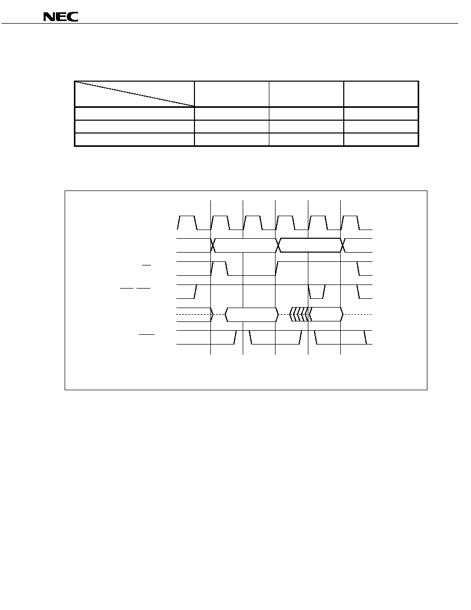
The number of basic clocks required for accessing each area in the address space is as follows.
Table 5-3. Number of Access Clocks
Area (Bus Width)
Bus Cycle Type
Internal ROM
(32 Bits)
Internal RAM
(32 Bits)
External Memory
(16 Bits)
Instruction fetch (normal access)
1
1 or 2
3 + n
Note
Instruction fetch (branch)
2
1 or 2
3 + n
Note
Operand data access
3
1
3 + n
Note
Note 2 + n clocks when the separate bus is selected. n is the number of waits.
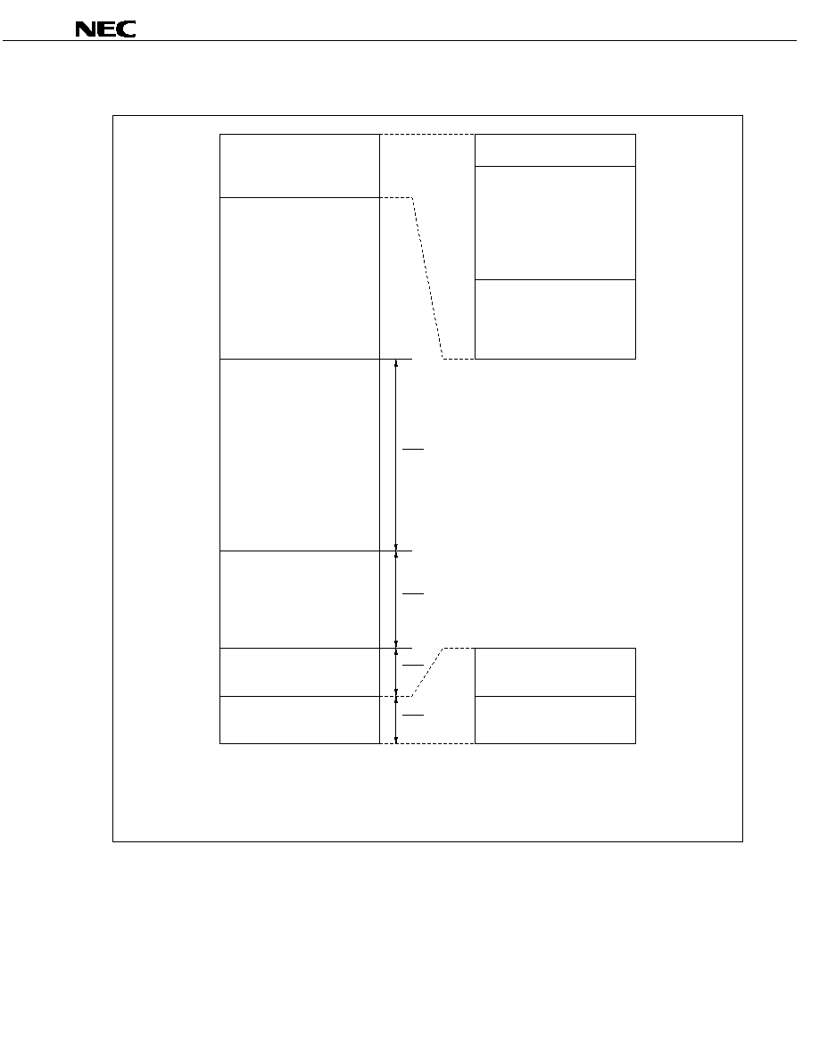
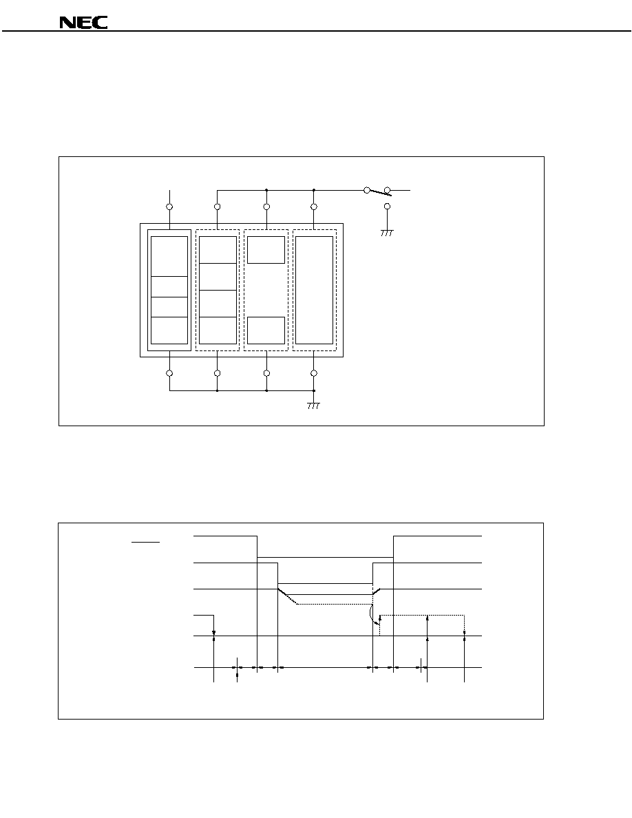
Figure 5-1. Example of Timing In Separate Bus Mode (Read
Write)
T1
T2
Address
Address
Data
Data
WAIT (input)
AD0 to AD15 (I/O)
WR0, WR1 (output)
RD (output)
A0 to A23 (output)
CLKOUT (output)
T2
T1
Remark The broken lines indicates the high-impedance state

Preliminary Product Information U15436EJ1V0PM
30
µ
µ
µ
µPD703201, 703201Y, 703204, 703204Y, 70F3201, 70F3201Y, 70F3204, 70F3204Y
Figure 5-2. Example of Timing In Multiplexed Bus Mode (Read
Write)
T1
T2
T3
CLKOUT (output)
A0 to A23 (output)
AD0 to AD15 (I/O)
Address
Data
Address
ASTB (output)
RD (output)
WAIT (input)
WR0, WR1 (output)
T1
T2
T3
Address
Data
Address
Remark The broken lines indicate the high-impedance state.

Preliminary Product Information U15436EJ1V0PM
31
µ
µ
µ
µPD703201, 703201Y, 703204, 703204Y, 70F3201, 70F3201Y, 70F3204, 70F3204Y
6. INTERRUPT SERVICING/EXCEPTION PROCESSING FUNCTION
The features of the interrupt servicing/exception processing function are as follows.
Interrupt
∑ Non-maskable interrupt: 2 sources
∑ Maskable interrupt
µPD703201, 70F3201: External 8, internal 30 sources
µPD703201Y, 70F3201Y: External 8, internal 31 sources
µPD703204, 70F3204: External 8, internal 31 sources
µPD703204Y, 70F3204Y: External 8, internal 32 sources
∑ 8-level programmable priority control
∑ Mask specification for the interrupt request according to priority
∑ Mask specification for each maskable interrupt request
∑ Noise elimination, edge detection, and valid edge specification of an external interrupt request
Exceptions
∑ Software exception: 32 sources
∑ Exception trap: 2 sources (illegal op code exception, debug trap)
Table 6-1 shows the interrupt/exception sources.
Preliminary Product Information U15436EJ1V0PM
32
µ
µ
µ
µPD703201, 703201Y, 703204, 703204Y, 70F3201, 70F3201Y, 70F3204, 70F3204Y
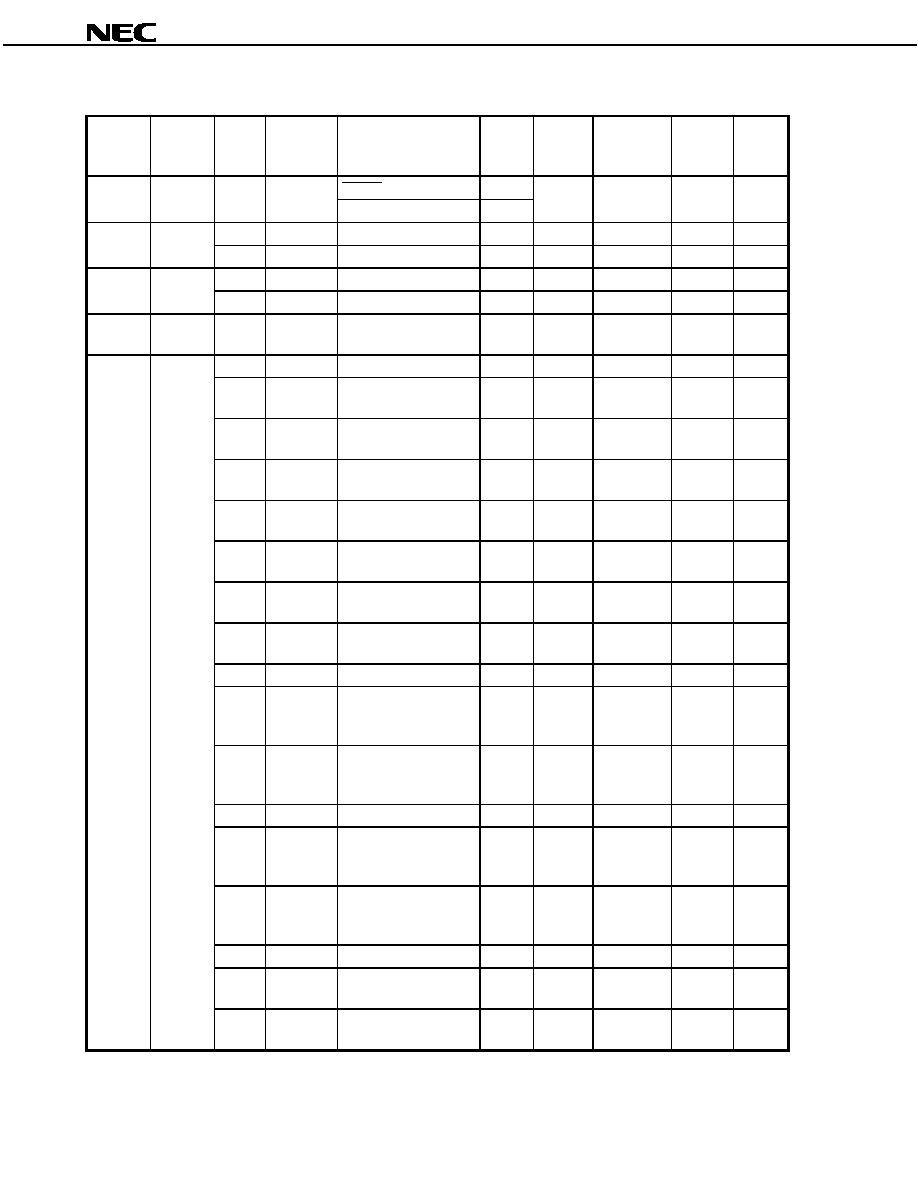
Table 6-1. Interrupt Source List (1/2)
Type
Classifi-
cation
Default
Priority
Name
Trigger
Genera-
ting Unit
Exception
Code
Handler
Address
Restored
PC
Interrupt
Control
Register
RESET pin input
Pin
Reset
Interrupt
-
RESET
WDT overflow
(WDTRES) WDT
0000H
00000000H
Undefined
-
-
NMI
NMI pin valid edge input
-
0010H
00000010H
nextPC
-
Non-
maskable
Interrupt
-
INTWDT
WDT overflow
WDT
0020H
00000020H
nextPC
-
-
TRAP0n
Note
TRAP instruction
-
004nH
Note
00000040H
nextPC
-
Software
exception
Exception
-
TRAP1n
Note
TRAP instruction
-
005nH
Note
00000050H
nextPC
-
Exception
trap
Exception
-
ILGOP/
DBG0
Illegal op code/
DBTRAP instruction
-
0060H
00000060H
nextPC
-
0
INTWDTM
Internal timer overflow
WDT
0080H
00000080H
nextPC
WDTIC
1
INTP0
INTP0 pin valid edge
input
Pin
0090H
00000090H
nextPC
PIC0
2
INTP1
INTP1 pin valid edge
input
Pin
00A0H
000000A0H
nextPC
PIC1
3
INTP2
INTP2 pin valid edge
input
Pin
00B0H
000000B0H
nextPC
PIC2
4
INTP3
INTP3 pin valid edge
input
Pin
00C0H
000000C0H
nextPC
PIC3
5
INTP4
INTP4 pin valid edge
input
Pin
00D0H
000000D0H
nextPC
PIC4
6
INTP5
INTP5 pin valid edge
input
Pin
00E0H
000000E0H
nextPC
PIC5
7
INTP6
INTP6 pin valid edge
input
Pin
00F0H
000000F0H
nextPC
PIC6
8
INTRTC
RTC interrupt
RTC
0100H
00000100H
nextPC
RTCIC
9
INTCC00
CC00 capture trigger
input/match between
TM0 and CC00
TM0
0110H
00000110H
nextPC
CCIC00
10
INTCC01
CC01 capture trigger
input/match between
TM0 and CC01
TM0
0120H
00000120H
nextPC
CCIC01
11
INTOVF0
TM0 overflow
TM0
0130H
00000130H
nextPC
OVFIC0
12
INTCC10
CC10 capture trigger
input/match between
TM1 and CC10
TM1
0140H
00000140H
nextPC
CCIC10
13
INTCC11
CC11 capture trigger
input/match between
TM1 and CC11
TM1
0150H
00000150H
nextPC
CCIC11
14
INTOVF1
TM1 overflow
TM1
0160H
00000160H
nextPC
OVFIC1
15
INTTM2
Match between TM2 and
CR2/TM2 overflow
TM2
0170H
00000170H
nextPC
TMIC2
Maskable
Interrupt
16
INTTM3
Match between TM3 and
CR3/TM3 overflow
TM3
0180H
00000180H
nextPC
TMIC3
Note n: Value of 0 to FH
Preliminary Product Information U15436EJ1V0PM
33
µ
µ
µ
µPD703201, 703201Y, 703204, 703204Y, 70F3201, 70F3201Y, 70F3204, 70F3204Y
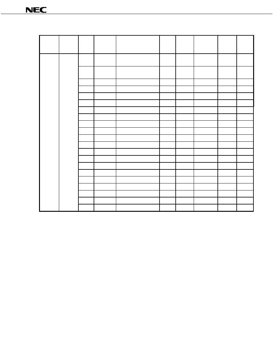
Table 6-1. Interrupt Source List (2/2)
Type
Classifi-
cation
Default
Priority
Name
Trigger
Genera-
ting Unit
Exception
Code
Handler
Address
Restored
PC
Interrupt
Control
Register
17
INTTM4
Match between TM4 and
CR4/TM4 overflow
TM4
0190H
00000190H
nextPC
TMIC4
18
INTTM5
Match between TM5 and
CR5/TM5 overflow
TM5
01A0H
000001A0H
nextPC
TMIC5
19
INTCSI0
CSI0 transfer end
CSI0
01B0H
000001B0H
nextPC
CSIIC0
20
INTIIC
Note 1
I
2
C transfer end
I
2
C
01C0H
000001C0H
nextPC
IICIC0
21
INTCSI1
CSI1 transfer end
CSI1
01D0H
000001D0H
nextPC
CSIIC1
22
INTSRE0
UART0 receive error
UART0
01E0H
000001E0H
nextPC
SREIC0
23
INTSR0
UART0 receive end
UART0
01F0H
000001F0H
nextPC
SRIC0
24
INTST0
UART0 transfer end
UART0
0200H
00000200H
nextPC
STIC0
25
INTCSI2
CSI2 transfer end
CSI2
0210H
00000210H
nextPC
CSIIC2
26
INTSRE1
UART1 receive error
UART1
0220H
00000220H
nextPC
SREIC1
27
INTSR1
UART1 receive end
UART1
0230H
00000230H
nextPC
SRIC1
28
INTST1
UART1 transmit end
UART1
0240H
00000240H
nextPC
STIC1
29
INTCSI3
CSI3 transfer end
CSI3
0250H
00000250H
nextPC
CSIIC3
30
INTCSI4
Note 2
CSI4 transfer end
CSI4
0260H
00000260H
nextPC
CSIIC4
31
INTAD
A/D conversion end
ADC
0270H
00000270H
nextPC
ADIC
32
INTDMA0
DMA0 transfer end
DMA
0280H
00000280H
nextPC
DMAIC0
33
INTDMA1
DMA1 transfer end
DMA
0290H
00000290H
nextPC
DMAIC1
34
INTDMA2
DMA2 transfer end
DMA
02A0H
000002A0H
nextPC
DMAIC2
35
INTDMA3
DMA3 transfer end
DMA
02B0H
000002B0H
nextPC
DMAIC3
36
INTROV
RTC overflow
RTC
02C0H
000002C0H
nextPC
ROVIC
Maskable
Interrupt
37
INTBRG
BRG match
BRG
02D0H
000002D0H
nextPC
BRGIC
Note 1. Valid for the
µPD703201Y, 70F3201Y, 703204Y and 70F3204Y only.
2. Valid for the V850E/SA3 only.
Remarks 1.
Default Priority:
Priority that applies when two or more maskable interrupt requests occur at the
same time. The highest priority is 0.
Restored PC:
The value of the PC saved to EIPC or FEPC when interrupt servicing/exception
processing is started. However, the value of the restored PC saved when an
interrupt is acknowledged during division instruction (DIV, DIVH, DIVU, DIVHU)
execution is the value of the PC of the current instruction (DIV, DIVH, DIVU,
DIVHU).
nextPC:
The value of the PC to be processed after an interrupt/exception.
2.
The execution address of the illegal instruction when an illegal op code exception occurs is
calculated with (Restored PC
- 4).
Preliminary Product Information U15436EJ1V0PM
34
µ
µ
µ
µPD703201, 703201Y, 703204, 703204Y, 70F3201, 70F3201Y, 70F3204, 70F3204Y
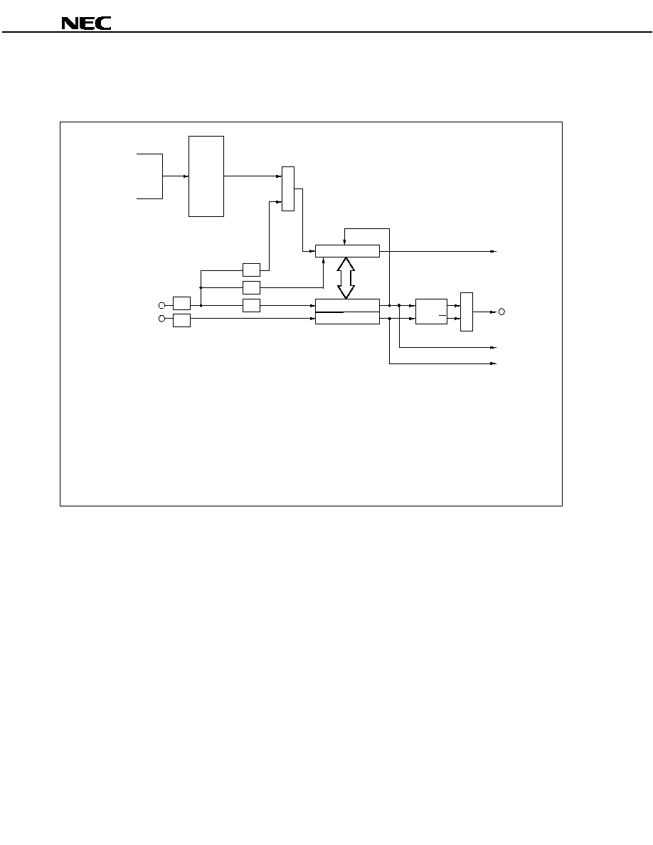
7. CLOCK GENERATION FUNCTION
The clock generation function has the following features.
Main clock oscillator
∑ 2 to 17 MHz (@ V
DD
= 2.3 to 2.7 V operation)
∑ 2 to 13.5 MHz (@ V
DD
= 2.2 to 2.7 V operation)
Subclock oscillator
∑ 32.768 kHz (@ V
DD
= 2.2 to 2.7 V operation)
Internal system clock generation
∑ 6 levels (f
XX
, f
XX
/2, f
XX
/4, f
XX
/8, f
XX
/16, f
XX
/32)
Peripheral clock generation
Clock output function
The following figure shows the configuration of the clock generation function.
FRC bit
MFRC bit
CK2 to CK0 bits
STOP mode
Subclock
oscillator
Port CM
WDT clock control
Prescaler 1
Prescaler 2
IDLE
control
HALT
control
HALT mode
CPU clock
A/D converter
RTC clock
Peripheral clock
WDT clock
Internal system
clock
Prescaler 3
Main clock
oscillator
Main clock
oscillator
stop control
XT1
XT2
CLKOUT
X1
X2
IDLE mode
f
XX
/32
f
XX
/16
f
XX
/8
f
XX
/4
f
XX
/2
f
XX
f
CPU
f
CLK
f
XX
to f
XX
/512
f
X
/2
6
to f
X
/2
9
f
XT
f
XT
f
X
f
XX
f
XW
Selector
Remark f
X,
f
XX
: Main clock frequency
f
XT
: Subclock frequency
f
CPU
: CPU clock frequency
f
CLK
: Internal system clock frequency
f
XW
: Watchdog timer clock frequency

Preliminary Product Information U15436EJ1V0PM
35
µ
µ
µ
µPD703201, 703201Y, 703204, 703204Y, 70F3201, 70F3201Y, 70F3204, 70F3204Y
8. POWER SAVE FUNCTION
The V850ES/SA2 and V850ES/SA3 have the following power save functions to realize an effective low-power-
consuming system.
HALT mode:
Only the clock of the CPU is stopped in this mode.
IDLE mode:
All operations on the chip other than oscillator operation are stopped in this mode.
STOP mode:
All operations on the chip other than subclock oscillator operation are stopped in this mode.
Backup mode:
The power supply other than for the subclock oscillator, real-time counter, and internal
RAM can be disconnected.
The following table shows the operating states of the on-chip peripheral functions in each mode.
Parameter
HALT Mode
IDLE Mode
STOP Mode
Backup Mode
V
DD
, EV
DD
, AV
DD
Power supplied
Power OFF possible
V
DD
BU
Power supplied
CPU operation
Stopped
On-chip peripheral function
operation
Enabled
Stopped
Main clock oscillator operation
Enabled
Stopped
Subclock oscillator operation
Enabled
Real-time counter function,
RAM retention
Enabled
Release condition
∑ Non-maskable interrupt request
∑ Unmasked maskable interrupt request
∑ RESET pin input
RESET pin input
after power is
supplied
Preliminary Product Information U15436EJ1V0PM
36
µ
µ
µ
µPD703201, 703201Y, 703204, 703204Y, 70F3201, 70F3201Y, 70F3204, 70F3204Y
∑
∑
∑
∑ Backup mode overview
The V850ES/SA2 and V850ES/SA3 are put in backup mode by stopping supplying power other than the backup
power supply (V
DD
BU) in STOP mode.
The backup power supply supplies power only to the subclock oscillator, real-time counter, and internal RAM, as
shown in the figure below. Other on-chip functions including the CPU cannot operate since the power supply is
stopped.
Power supply
for backup
Power supply
for operation
Connect to
V
SS
in backup
mode
Backup power
supply status
flag (BPSF)
RAM
Real-time
counter
Subclock
oscillator
Main clock
oscillator
Peripheral
function
ROM
CPU
I/O
function
A/D
converter
D/A
converter
V
DD
BU
V
DD
AV
DD
EV
DD
V
SS
BU
V
SS
AV
SS
EV
SS
In backup mode, subclock oscillator operation, real-time counter count operation, and internal RAM data
retention are enabled.
If the voltage is lower than the data retention voltage in backup mode, a backup power supply status flag (BPSF)
is set and that internal RAM retention data can be detected as invalid. When this flag is set, the real-time
counter and the RAM should be initialized at reset start.
BPSF
clear
BPSF confirmed
(set
initialization)
BPSF
cleared
STOP
execution
Normal
operation
Backup mode
Oscillation
stabilization
Normal
operation
(V
DD
BU is lower than
data retention voltage)
STOP
mode
Reset
mode
Reset
mode
Backup power
supply status flag
(BPSF)
CPU status
V
DD
BU
V
DD
, EV
DD
, AV
DD
RESET (input)

Preliminary Product Information U15436EJ1V0PM
37
µ
µ
µ
µPD703201, 703201Y, 703204, 703204Y, 70F3201, 70F3201Y, 70F3204, 70F3204Y
9. TIMER/COUNTER FUNCTION
The timer/counter function has the following features.
16-bit timer/counter (TM0, TM1)
∑ Capture/compare common registers: 2 for each
∑ Interrupt request sources
∑ Capture/match interrupt requests: 2 sources for each
∑ Overflow interrupt requests: 1 source for each
∑ Timer/counter count clock sources: 2 types
(Selection of external pulse input or internal system clock division)
∑ Either free-running mode or overflow stop mode can be selected as the operation mode when the
timer/counter overflows
∑ Timer/counter can be cleared by a match of the timer/counter and a compare register
∑ External pulse outputs: 1 for each
8-bit timers (TM2 to TM5)
∑ Stand-alone mode (mode in which a single timer is used)
∑ Interval timer
∑ External event counter
∑ Square-wave output
∑ PWM output
∑ Cascade connection mode (mode in which two timers are used connected in cascade: 16-bit resolution)
∑ 16-bit resolution interval timer
∑ 16-bit resolution external event counter
∑ 16-bit resolution square-wave output
3UHOLPLQDU\ 3URGXFW ,QIRUPDWLRQ 8(-930
µ
µ
µ
µ3' < < ) )< ) )<
7KH IROORZLQJ ILJXUH VKRZV WKH FRQILJXUDWLRQ RI WKH WLPHUFRXQWHU IXQFWLRQ
70 70
R
Note 4
Q
S
Q
TMn (16 bits)
Note 3
Note 3
Note 3
CCn0
CCn1
INTOVn
INTCCn0
INTPn1
Note 1
TCLRn/TIn/INTPn0
INTPn0
TCLRn
TIn
INTCCn1
TOn
Note 1
Clear & start
f
XX
/2
f
XX
/4
f
XX
/8
f
XX
/16
f
XX
/32
f
XX
/64
f
XX
/128
f
XX
/256
f
XX
Selector
Selector
Note 2
Note 2
1RWHV 7KH ,173Q SLQ LV XVHG DV WKH 72Q SLQ
1RLVH HOLPLQDWRU
(GJH GHWHFWRU
5HVHW SULRULW\
5HPDUNV Q
I
;;
0DLQ FORFN IUHTXHQF\

Preliminary Product Information U15436EJ1V0PM
39
µ
µ
µ
µPD703201, 703201Y, 703204, 703204Y, 70F3201, 70F3201Y, 70F3204, 70F3204Y
(2) TM2 to TM5
OVF
Clear
Match
Mask circuit
Selector
Selector
Selector
TIn
Count clock
Note
3
Selector
Internal bus
Timer mode control
register n (TMCn)
Timer clock
select register n (TCLn)
Invert
level
Internal bus
TCLn2 TCLn1 TCLn0
TCEn TMCn6 TMCn4 LVSn LVRn TMCn1 TOEn
TOn
INTTMn
S
R
Q
INV
S
R
Q
8-bit counter n
(TMn)
8-bit compare
register n (CRn)
Note The count clock is set by the TCLn register.
∑ When n = 2, 3
∑ When n = 4, 5
f
XX
/4
f
XX
/4
f
XX
/8
f
XX
/8
f
XX
/16
f
XX
/16
f
XX
/32
f
XX
/32
f
XX
/128
f
XX
/128
f
XX
/512
f
XX
/256
Remarks 1.
"
]
" is a signal that can be directly connected to a port.
2.
n = 2 to 5
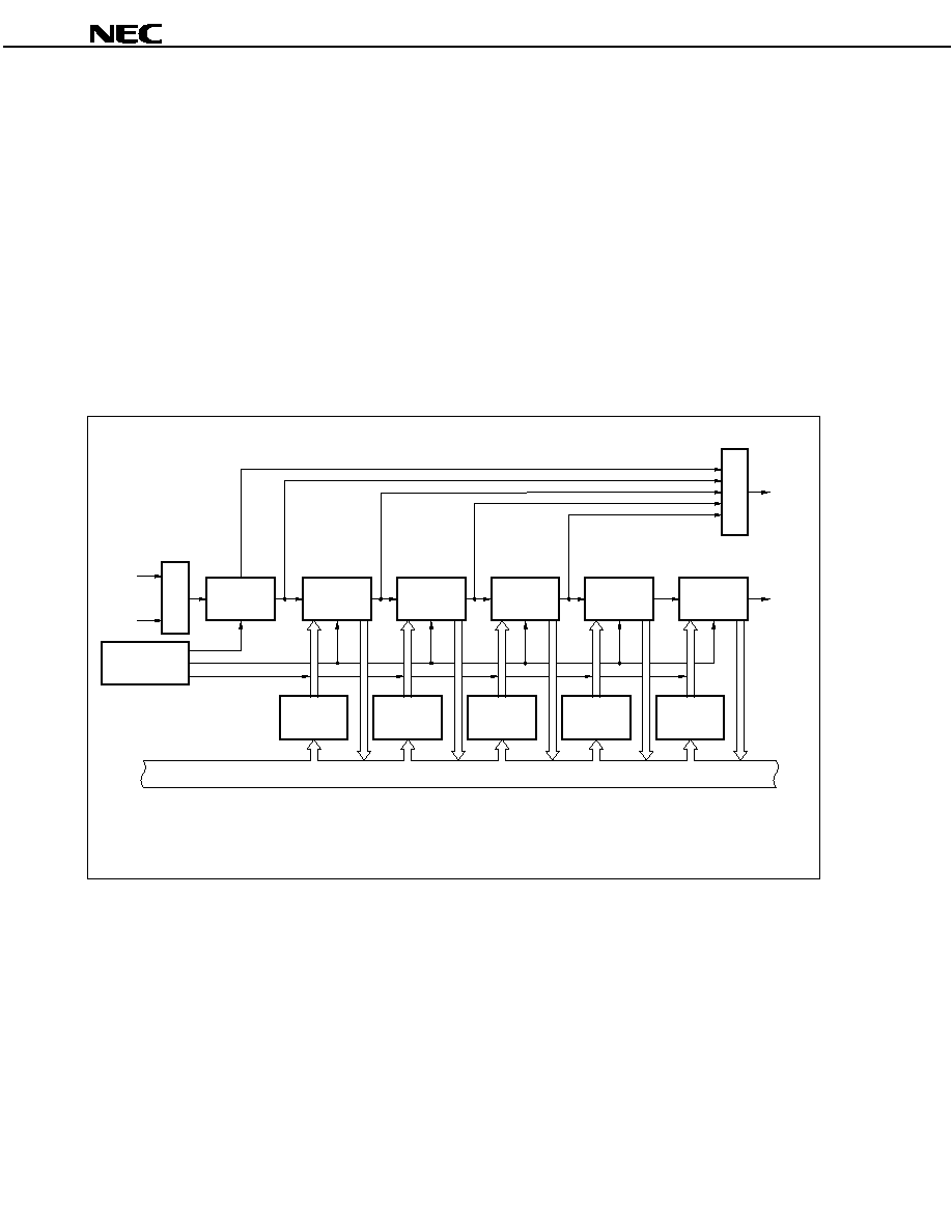
Preliminary Product Information U15436EJ1V0PM
40
µ
µ
µ
µPD703201, 703201Y, 703204, 703204Y, 70F3201, 70F3201Y, 70F3204, 70F3204Y
10. REAL-TIME COUNTER FUNCTION
The real-time counter function has the following features.
Includes counters of weeks, days, hours, minutes, and seconds, and can count up to 4,095 weeks.
Counters of weeks, days, hours, minutes, and seconds can be read during operation and while operation is
stopped.
Week counter overflow interrupt request occurrence (INTROV)
Interval interrupt request occurrence (INTRTC) at a fixed interval (can be selected from the following)
0.015625 seconds, 0.03125 seconds, 0.0625 seconds, 0.125 seconds, 0.25 seconds, 0.5 seconds, 1 second,
1 minute, 1 hour, 1 day
When subclock (f
XT
) is selected, operable only with power supply to V
DD
BU.
The following figure shows the configuration of the real-time counter function.
Count enable/
disable circuit
Subcounter
(15 bits)
Second counter
(6 bits)
Internal bus
Second counter
write buffer
Minute counter
write buffer
Hour counter
write buffer
Day counter
write buffer
Week counter
write buffer
Minute counter
(6 bits)
Hour counter
(5 bits)
Day counter
(3 bits)
Week counter
(12 bits)
INTROV
INTRTC
1 second
0.015625 seconds/0.03125 seconds/0.0625 seconds/0.125 seconds/
0.25 seconds/0.5 seconds
1 minute
1 hour
1 day
Count clock = 32.768 kHz
f
XT
f
X
/2
6
to
f
X
/2
9
Selector
Selector
Remark f
X
:
Main clock frequency
f
XT
: Subclock frequency
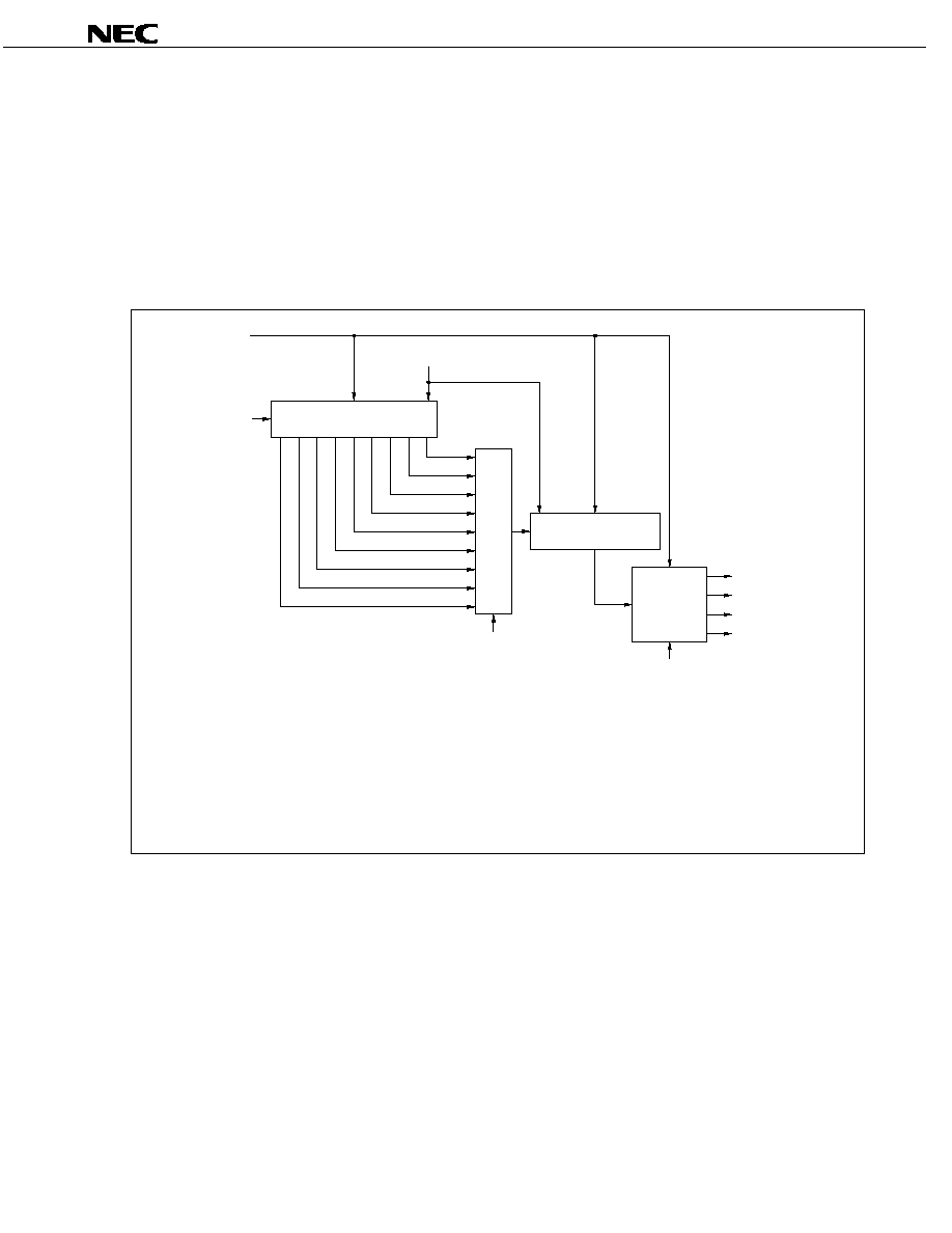
Preliminary Product Information U15436EJ1V0PM
41
µ
µ
µ
µPD703201, 703201Y, 703204, 703204Y, 70F3201, 70F3201Y, 70F3204, 70F3204Y
11. WATCHDOG TIMER FUNCTION
The watchdog timer has the following functions.
Watchdog timer
Interval timer
Timer for oscillation stabilization
The following figure shows the configuration of the watchdog timer function.
OSCMD
13-bit divider
RUN
OSTS0 to OSTS2,
WDCS0 to WDCS2
WDTM3, WDTM4
Clear
Clear
8-bit counter
Output
control
f
XW
f
XW
/2
13
f
XW
/2
12
f
XW
/2
11
f
XW
/2
10
f
XW
/2
9
f
XW
/2
8
f
XW
/2
7
f
XW
/2
6
f
XW
/2
5
OVF
INTWDTM
INTWDT
WDTRES
OSTOVF
Selector
Remarks 1.
WDTRES:
Reset signal triggered by WDT overflow
OSTOVF:
Overflow signal for oscillation stabilization
OSCMD:
Timer mode signal for oscillation stabilization
f
XW
:
Watchdog timer clock frequency
2.
During counting of oscillation stabilization time: f
XW
= f
X
/2
Other than above:
f
XW
= f
XX
/2
Preliminary Product Information U15436EJ1V0PM
42
µ
µ
µ
µPD703201, 703201Y, 703204, 703204Y, 70F3201, 70F3201Y, 70F3204, 70F3204Y
12. SERIAL INTERFACE FUNCTION
The V850ES/SA2 and V850ES/SA3 include the following three types of serial interfaces.
Type
V850ES/SA2
V850ES/SA3
3-wire serial I/O
4 channels (CSI0 to CSI3)
5 channels (CSI0 to CSI4)
Asynchronous serial interface
2 channels (UART0, UART1)
I
2
C bus
Note
1 channel (I
2
C)
Note
Note Available only in the
µPD703201Y, 703204Y, 70F3201Y, and 70F3204Y.
Some functions are used alternately as follows.
∑ CSI0/I
2
C
∑ CSI1/UART0
∑ CSI2
∑ UART1
∑ CSI3
∑ CSI4 (V850ES/SA3 only)
12.1 3-Wire Serial I/O (CSIn)
Remark In this section, the value of n is as follows.
n = 0 to 3 (V850ES/SA2)
n = 0 to 4 (V850ES/SA3)
The 3-wire serial I/O (CSIn) transfers data using following three lines.
∑ SCKn (serial clock)
∑ SOn (serial data output)
∑ SIn (serial data input)
The 3-wire serial I/O (CSIn) has the following features.
Transfer data length: Fixed to 8 bits
Transfer data MSB/LSB first can be switched
Transfer clock can be selected from eight clocks (seven master clocks, one slave clock)
Transmit/receive mode or receive-only mode can be specified
On-chip 8-bit transmit buffer
Transfer data transmit/receive timing with respect to the transfer clock can be changed

Preliminary Product Information U15436EJ1V0PM
43
µ
µ
µ
µPD703201, 703201Y, 703204, 703204Y, 70F3201, 70F3201Y, 70F3204, 70F3204Y
The following figure shows the configuration of the 3-wire serial I/O (CSIn).
CKSn0 to CKSn2
INTCSIn
CSOTn
SOn
Transfer clock controller
Transfer mode controller
Transfer data controller
Transmit buffer (SOTBn)
Selector
SOn latch
SIn
SCKn
Shift register (SIOn)
f
XX
/2
f
XX
/4
f
XX
/8
f
XX
/16
f
XX
/32
f
XX
/64
TOFm
CSIEn, TRMDn, DIRn,
CKPn, DAPn
Selector
Remarks 1.
When n = 0: m = 2
When n = 1: m = 3
When n = 2: m = 4
When n = 3: m = 5
When n = 4: m = 5 (V850ES/SA3 only)
2.
f
XX
: Main clock frequency
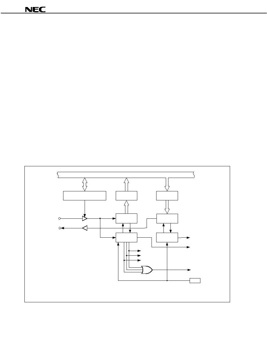
Preliminary Product Information U15436EJ1V0PM
44
µ
µ
µ
µPD703201, 703201Y, 703204, 703204Y, 70F3201, 70F3201Y, 70F3204, 70F3204Y
12.2 Asynchronous Serial Interface (UART0 and UART1)
The asynchronous serial interface (UART0 and UART1) has the following features.
Two modes
∑ Operation stop mode (used when serial transfers are not performed to enable a reduction in power
consumption)
∑ Asynchronous serial interface mode
Full-duplex transmission
2-pin configuration
∑ TXD0 and TXD1: Transmit data output pins
∑ RXD0 and RXD1: Receive data input pins
3 types of interrupt sources
∑ Receive error interrupt (INTSRE0 and INTSRE1)
∑ Receive end interrupt (INTSR0 and INTSR1)
∑ Transmit end interrupt (INTST0 and INTST1)
Character length: 7 bits/8 bits
Parity function: Odd, even, 0, none
Transmission stop bit: 1 bit/2 bits
On-chip baud rate generator
The following figure shows the configuration of the asynchronous serial interface (UART0 and UART1).
Parity
Framing
Overrun
Internal bus
Asynchronous serial interface
mode register n (ASIMn)
Receive
buffer (RXBn)
Receive
shift register
Reception control
parity check
Transmit
buffer (TXBn)
Transmit
shift register
Addition of transmission
control parity
BRGn
INTSREn
INTSRn
INTSTn
RXDn
TXDn
Remark n = 0, 1
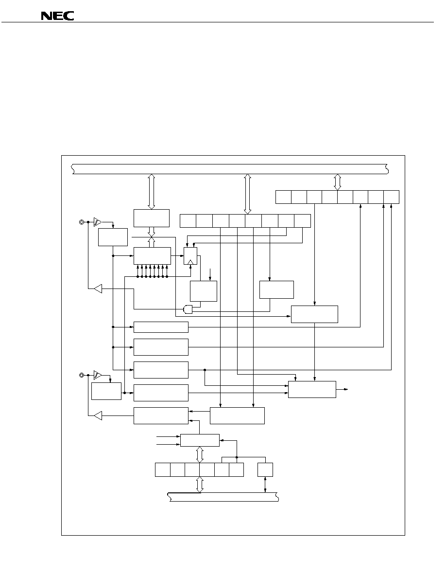
Preliminary Product Information U15436EJ1V0PM
45
µ
µ
µ
µPD703201, 703201Y, 703204, 703204Y, 70F3201, 70F3201Y, 70F3204, 70F3204Y
12.3 I
2
C Bus (I
2
C) (
µ
µ
µ
µ
PD703201Y, 703204Y, 70F3201Y, 70F3204Y)
The I
2
C bus has the following features.
Two modes
∑ Operation stop mode (used when serial transfers are not performed to enable a reduction in power
consumption)
∑ I
2
C bus mode (supporting multi masters)
The following figure shows the configuration of the I
2
C bus
Internal bus
IIC status register 0
(IICS)
IIC control register
(IICC)
Slave address
register (SVA)
Noise
eliminator
Noise
eliminator
Match
signal
IIC shift register
(IIC)
SO latch
IICE
D Q
SET
CLEAR
CL1,
CL0
SDA
SCL
N-ch open
drain output
N-ch open
drain output
Data hold
time correction
circuit
ACK detector
Wake up controller
ACK detector
Stop condition
detector
Serial clock counter
Interrupt request
signal generator
Serial clock controller
Serial clock wait
controller
Prescaler
INTIIC
f
xx
TM4 output
CLD
IIC clock select
register (IICCL)
IIC function expansion
register (IICX)
Internal bus
LREL
WREL
SPIE
WTIM
ACKE
STT
SPT
MSTS
ALD
EXC
COI
TRC
ACKD
STD
SPD
Start condition
detector
DAD
SMC
DFC
CL1
CL0
CLX
Remark f
XX
: Main clock frequency
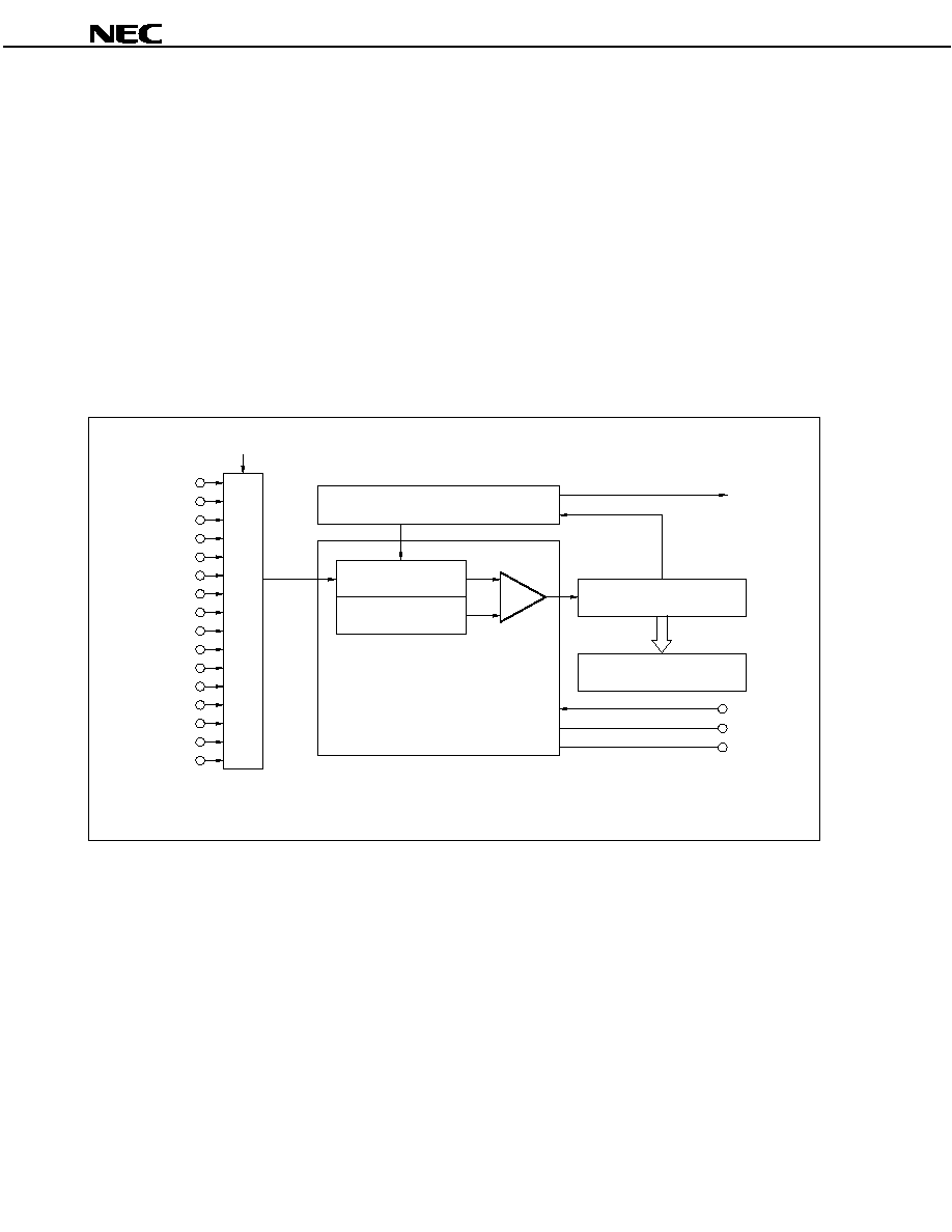
Preliminary Product Information U15436EJ1V0PM
46
µ
µ
µ
µPD703201, 703201Y, 703204, 703204Y, 70F3201, 70F3201Y, 70F3204, 70F3204Y
13. A/D CONVERTER
The A/D converter has the following features.
10-bit resolution
12 channels (V850ES/SA2)
16 channels (V850ES/SA3)
Successive comparison approximation method
Power fail detection function available
Operation voltage: AV
DD
= AV
REF0
= 2.2 to 2.7 V
Analog input voltage: AV
SS
to AV
REF0
Conversion rate: 9.5 to 1.50
µs
The following figure shows the configuration of the A/D converter.
Comparator
AV
REF0
AV
DD
AV
SS
INTAD
Analog input side
C array
Reference side
C array
Controller
Successive approximation
register (SAR)
A/D conversion result
register (ADCR)
ADS0 to ADS3
ANI0
ANI1
ANI2
ANI3
ANI4
ANI5
ANI6
ANI7
ANI8
ANI9
ANI10
ANI11
ANI12
Note
ANI13
Note
ANI14
Note
ANI15
Note
Selector
Note V850ES/SA3 only

Preliminary Product Information U15436EJ1V0PM
47
µ
µ
µ
µPD703201, 703201Y, 703204, 703204Y, 70F3201, 70F3201Y, 70F3204, 70F3204Y
The following figure shows the configuration of the power fail detection function.
A/D converter
Comparator
Power-fail comparison
threshold value register (PFT)
ADS0 to ADS3
PFCM
PFEN
INTAD
ANI0
ANI1
ANI2
ANI3
ANI4
ANI5
ANI6
ANI7
ANI8
ANI9
ANI10
ANI11
ANI12
Note
ANI13
Note
ANI14
Note
ANI15
Note
Selector
Selector
Note V850ES/SA3 only
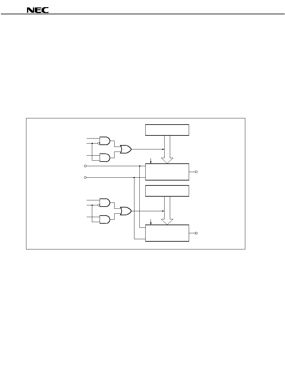
Preliminary Product Information U15436EJ1V0PM
48
µ
µ
µ
µPD703201, 703201Y, 703204, 703204Y, 70F3201, 70F3201Y, 70F3204, 70F3204Y
14. D/A CONVERTER
The D/A converter has the following features.
8-bit resolution
◊ 2 channels (DAC0, DAC1)
R string method
Conversion time: 20
µs max. (AV
REF1
= 2.2 to 2.7 V)
Analog output voltage: AV
REF1
◊ m/256 (m = 0 to 255; Value set in the DACSn register)
Operation mode: Normal mode/real-time output mode
Remark n = 0, 1
The following figure shows the configuration of the D/A converter.
DACS0
R string resistor
R string resistor
DACS1
ANO0
ANO1
DACE0
DACE1
DACS0 write
DAMD0
INTTM2
DACS1 write
DAMD1
INTTM3
AV
REF1
AV
SS
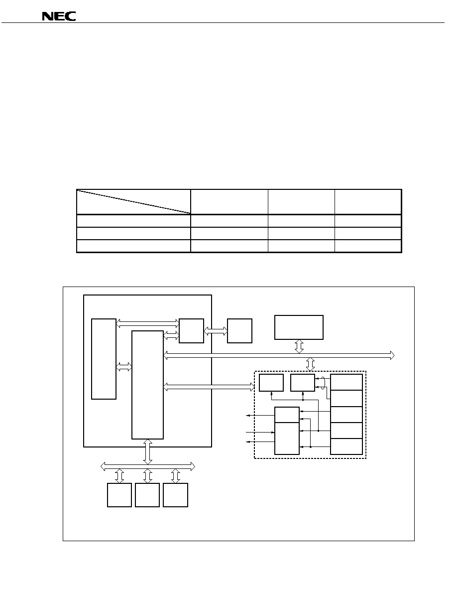
Preliminary Product Information U15436EJ1V0PM
49
µ
µ
µ
µPD703201, 703201Y, 703204, 703204Y, 70F3201, 70F3201Y, 70F3204, 70F3204Y
15. DMA FUNCTION
The DMA function has the following features.
Transfer unit: 8 bits/16 bits
Maximum transfer count: 65,536 (2
16
) times
Transfer type: 2-cycle transfer
Transfer mode: Single transfer
Transfer request: Request via interrupt from on-chip peripheral I/O or external pins, request via software trigger
Transfer object: On-chip peripheral I/O, internal RAM, external memory
The relationship between the transfer type and transfer object is shown below (
: Transfer enabled, ◊: Transfer
disabled).
Transfer Destination
Transfer Source
On-Chip Peripheral I/O
Internal RAM
External Memory
On-chip peripheral I/O
Internal RAM
◊
External memory
The following figure shows the configuration of the DMA function.
V850ES core
CPU
BCU
IRIF
Data control
block
Address control
block
Count control
block
Channel control
block
Internal
RAM
On-chip peripheral
I/O
On-chip peripheral I/O bus
DSAnH/
DSAnL
DDAnH/
DDAnL
DBCn
DCHCn
DADCn
External
I/O
External bus
External
RAM
External
ROM
INTDMAn
DMARQn
DMACTVn
DMAC
Remark n = 0 to 3

Preliminary Product Information U15436EJ1V0PM
50
µ
µ
µ
µPD703201, 703201Y, 703204, 703204Y, 70F3201, 70F3201Y, 70F3204, 70F3204Y
16. ROM CORRECTION FUNCTION
The ROM correction function is a function that replaces part of a program in the mask ROM with a program in the
internal RAM for execution.
First, the address where the program replacement should start (correction address) is set in the correction address
register (CORADn). When the CPU reads the instruction of the address set in CORADn, the instruction is replaced
with the DBTRAP instruction and the program jumps to 00000060H.
A value that is the address saved in the DBPC minus 2 (address to which ROM correction generated) is compared
with the address set in CORADn, and the program jumps to the correction program on the corresponding RAM. After
executing the correction program, a restore address is set in the DBPC, the DBRET instruction is executed, and then
execution is restored to the normal program.
Up to four correction addresses can be specified in CORADn.
Remark n = 3
The following figure shows the configuration of ROM correction.
Instruction address bus
Correction control
register (CORENn bit)
DBTRAP instruction
generation block
ROM
(1 MB space)
Correction address
register (CORADn)
Comparator
Instruction replacement block
Instruction data bus
Remark n = 0 to 3
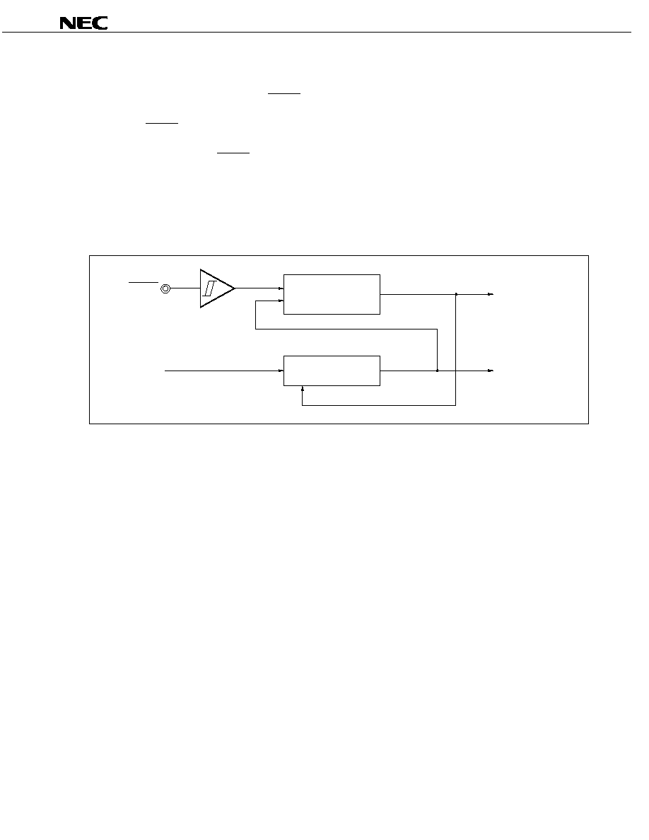
Preliminary Product Information U15436EJ1V0PM
51
µ
µ
µ
µPD703201, 703201Y, 703204, 703204Y, 70F3201, 70F3201Y, 70F3204, 70F3204Y
17. RESET FUNCTION
When a low-level signal is input to the RESET pin or the watchdog timer overflows (WDTRES), a system reset is
applied and the various on-chip hardware devices are reset to their initial states.
When the RESET pin goes from low level to high level, or when the WDTRES signal is automatically canceled, the
reset state is released.
When reset is released via RESET pin input, the CPU starts execution of the program after securing the oscillation
stabilization time (OSTS register reset value: 2
19
/f
XX
).
When reset is released by the WDTRES signal, the main clock oscillator does not stop and oscillation stabilization
time is not inserted.
The following figure shows the configuration of the reset function.
RESET
Count clock
Reset controller
Watchdog timer
Stop
Overflow
Reset signal
Interrupt function

Preliminary Product Information U15436EJ1V0PM
52
µ
µ
µ
µPD703201, 703201Y, 703204, 703204Y, 70F3201, 70F3201Y, 70F3204, 70F3204Y
18. FLASH MEMORY (
µ
µ
µ
µ
PD70F3201, 70F3201Y, 70F3204, 70F3204Y)
The
µPD70F3201 and 70F3201Y, and 70F3204 and 70F3204Y are the flash memory versions of the V850ES/SA2
and V850ES/SA3, respectively, and incorporate 256 KB of flash memory.
Writing to flash memory can be performed while the device is mounted on the target system (on board). Writing is
performed using a dedicated flash programmer connected to the target system or to a writing adapter.
The flash memory has the following features.
Flash memory: 256 KB (4 KB
◊ 4 blocks, 60 KB ◊ 4 blocks)
Erasure/writing possible using single power supply (V
DD
= 2.2 to 2.7 V)
Erasure unit
∑ Overall area batch erasure (256 KB)
∑ Block units erasure (4 KB/block, 60 KB/block)
Erasure/writing method
∑ Serial mode (using CSI0 or UART0)
∑ Self-programming mode
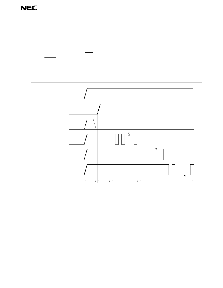
Preliminary Product Information U15436EJ1V0PM
53
µ
µ
µ
µPD703201, 703201Y, 703204, 703204Y, 70F3201, 70F3201Y, 70F3204, 70F3204Y
An overview of flash memory programming is shown below.
Pins used in programming
∑ Power supply pins (V
DD
, EV
DD
, AV
DD
, V
SS
, EV
SS
, AV
SS
, V
DD
BU, V
SS
BU)
∑ Mode pins (FLMD0, FLMD1)
∑ Clock supply pins (X1, X2)
∑ Serial communication pins (SCK0, SO0, SI0 or RXD0, TXD0)
∑ RESET pin
Programming timing
The following figure shows the programming timing (overview) when using UART.
V
DD
V
DD
RESET (input)
FLMD1 (input)
FLMD0 (input)
RXD0 (input)
TXD0 (output)
0 V
V
DD
0 V
V
DD
0 V
V
DD
0 V
V
DD
0 V
V
DD
0 V
(UART mode only)
Power
ON
Oscillation
stabilization
Communication
mode selection
Flash control command communication
(erasure, writing, etc.)
Reset
release
Preliminary Product Information U15436EJ1V0PM
54
µ
µ
µ
µPD703201, 703201Y, 703204, 703204Y, 70F3201, 70F3201Y, 70F3204, 70F3204Y
19. INSTRUCTION SET LIST
19.1 Conventions
(1) Register symbols used to describe operands
Register Symbol
Explanation
reg1
General-purpose register:
Used as source register.
reg2
General-purpose register:
Used mainly as destination register. Also used as source register in some
instructions.
reg3
General-purpose register:
Used mainly to store the remainder of division results and the higher 32 bits of
multiplication results.
bit#3
3-bit data for specifying the bit number
immX
X bit immediate data
dispX
X bit displacement data
regID
System register number
vector
5-bit data that specifies the trap vector (00H to 1FH)
cccc
4-bit data that shows the condition code
sp
Stack pointer (r3)
ep
Element pointer (r30)
listX
X item register list
(2) Register symbols used to describe opcodes
Register Symbol
Explanation
R
1-bit data of the code that specifies reg1 or regID
r
1-bit data of the code that specifies reg2
w
1-bit data of the code that specifies reg3
d
1-bit displacement data
I
1-bit immediate data (indicates the higher bits of immediate data)
i
1-bit immediate data
cccc
4-bit data that shows the condition codes
CCCC
4-bit data that shows the condition codes of the Bcond instruction
bbb
3-bit data for specifying the bit number
L
1-bit data that specifies a program register in the register list
S
1-bit data that specifies a system register in the register list
Preliminary Product Information U15436EJ1V0PM
55
µ
µ
µ
µPD703201, 703201Y, 703204, 703204Y, 70F3201, 70F3201Y, 70F3204, 70F3204Y
(3) Register symbols used in operation
Register Symbol
Explanation
Input for
GR [ ]
General-purpose register
SR [ ]
System register
zero-extend (n)
Expand n with zeros until word length.
sign-extend (n)
Expand n with signs until word length.
load-memory (a, b)
Read size b data from address a.
store-memory (a, b, c)
Write data b into address a in size c.
load-memory-bit (a, b)
Read bit b of address a.
store-memory-bit (a, b, c)
Write c to bit b of address a.
saturated (n)
Execute saturated processing of n (n is a 2's complement).
If, as a result of calculations,
n
7FFFFFFFH, let it be 7FFFFFFFH.
n
80000000H, let it be 80000000H.
result
Reflects the results in a flag.
Byte
Byte (8 bits)
Half-word
Halfword (16 bits)
Word
Word (32 bits)
+
Addition
≠
Subtraction
ll
Bit concatenation
◊
Multiplication
˜
Division
%
Remainder from division results
AND
Logical product
OR
Logical sum
XOR
Exclusive OR
NOT
Logical negation
logically shift left by
Logical shift left
logically shift right by
Logical shift right
arithmetically shift right by
Arithmetic shift right
(4) Register symbols used in an execution clock
Register Symbol
Explanation
i
If executing another instruction immediately after executing the first instruction (issue).
r
If repeating execution of the same instruction immediately after executing the first instruction (repeat).
l
If using the results of instruction execution in the instruction immediately after the execution (latency).
Preliminary Product Information U15436EJ1V0PM
56
µ
µ
µ
µPD703201, 703201Y, 703204, 703204Y, 70F3201, 70F3201Y, 70F3204, 70F3204Y
(5) Register symbols used in flag operations
Identifier
Explanation
(Blank)
No change
0
Clear to 0
X
Set or cleared in accordance with the results.
R
Previously saved values are restored.
(6) Condition codes
Condition Name
(cond)
Condition Code
(cccc)
Condition Expression
Explanation
V
0 0 0 0
OV = 1
Overflow
NV
1 0 0 0
OV = 0
No overflow
C/L
0 0 0 1
CY = 1
Carry
Lower (less than)
NC/NL
1 0 0 1
CY = 0
No carry
Not lower (greater than or equal)
Z/E
0 0 1 0
Z = 1
Zero
Equal
NZ/NE
1 0 1 0
Z = 0
Not zero
Not equal
NH
0 0 1 1
(CY or Z) = 1
Not higher (less than or equal)
H
1 0 1 1
(CY or Z) = 0
Higher (greater than)
N
0 1 0 0
S = 1
Negative
P
1 1 0 0
S = 0
Positive
T
0 1 0 1
--
Always (unconditional)
SA
1 1 0 1
SAT = 1
Saturated
LT
0 1 1 0
(S xor OV) = 1
Less than signed
GE
1 1 1 0
(S xor OV) = 0
Greater than or equal signed
LE
0 1 1 1
((S xor OV) or Z) = 1
Less than or equal signed
GT
1 1 1 1
((S xor OV) or Z) = 0
Greater than signed

Preliminary Product Information U15436EJ1V0PM
57
µ
µ
µ
µPD703201, 703201Y, 703204, 703204Y, 70F3201, 70F3201Y, 70F3204, 70F3204Y
19.2 Instruction Set (In Alphabetical Order)
(1/6)
Execution
Clock
Flags
Mnemonic
Operand
Opcode
Operation
i
r
l
CY OV
S
Z SAT
reg1,reg2
r r r r r 0 0 1 1 1 0 R R R R R
GR[reg2]
GR[reg2]+GR[reg1]
1
1
1
◊
◊
◊
◊
ADD
imm5,reg2
r r r r r 0 1 0 0 1 0 i i i i i
GR[reg2]
GR[reg2]+sign-extend(imm5)
1
1
1
◊
◊
◊
◊
ADDI
imm16,reg1,reg2
r r r r r 1 1 0 0 0 0 R R R R R
i i i i i i i i i i i i i i i i
GR[reg2]
GR[reg1]+sign-extend(imm16)
1
1
1
◊
◊
◊
◊
AND
reg1,reg2
r r r r r 0 0 1 0 1 0 R R R R R
GR[reg2]
GR[reg2]AND GR[reg1]
1
1
1
0
◊
◊
ANDI
imm16,reg1,reg2
r r r r r 1 1 0 1 1 0 R R R R R
i i i i i i i i i i i i i i i i
GR[reg2]
GR[reg1]AND zero-extend(imm16)
1
1
1
0
0
◊
When conditions
are satisfied
2
Note 2
2
Note 2
2
Note 2
Bcond
disp9
ddd dd 101 1d ddc ccc
Note 1
if conditions are satisfied
then PC
PC+sign-extend(disp9)
When conditions
are not satisfied
1
1
1
BSH
reg2,reg3
r r r r r 1 1 1 1 1 1 0 0 0 0 0
wwwww01101000010
GR[reg3]
GR[reg2] (23 : 16) ll GR[reg2] (31 : 24) ll
GR[reg2] (7 : 0) ll GR[reg2] (15 : 8)
1
1
1
◊
0
◊
◊
BSW
reg2,reg3
r r r r r 1 1 1 1 1 1 0 0 0 0 0
wwwww01101000000
GR[reg3]
GR[reg2] (7 : 0) ll GR[reg2] (15 : 8) ll GR
[reg2] (23 : 16) ll GR[reg2] (31 : 24)
1
1
1
◊
0
◊
◊
CALLT
imm6
0 0 0 0 0 0 1 0 0 0 i i i i i i
CTPC
PC+2(return PC)
CTPSW
PSW
adr
CTBP+zero-extend(imm6 logically shift left by 1)
PC
CTBP+zero-extend(Load-memory(adr,Half-word))
4
4
4
bit#3, disp16[reg1]
10bbb111110RRRRR
dddddddddddddddd
adr
GR[reg1]+sign-extend(disp16)
Z flag
Not(Load-memory-bit(adr,bit#3))
Store-memory-bit(adr,bit#3,0)
3
Note 3
3
Note 3
3
Note 3
◊
CLR1
reg2,[reg1]
r r r r r 1 1 1 1 1 1 R R R R R
0000000011100100
adr
GR[reg1]
Z flag
Not(Load-memory-bit(adr,reg2))
Store-memory-bit(adr,reg2,0)
3
Note 3
3
Note 3
3
Note 3
◊
cccc,imm5,reg2,reg3
r r r r r 1 1 1 1 1 1 i i i i i
wwwww011000cccc0
if conditions are satisfied
then GR[reg3]
sign-extended(imm5)
else GR[reg3]
GR[reg2]
1
1
1
CMOV
cccc,reg1,reg2,reg3
r r r r r 1 1 1 1 1 1 R R R R
wwwww011001cccc0
if conditions are satisfied
then GR[reg3]
GR[reg1]
else GR[reg3]
GR[reg2]
1
1
1
reg1,reg2
r r r r r 0 0 1 1 1 1 R R R R R
result
GR[reg2]≠GR[reg1]
1
1
1
◊
◊
◊
◊
CMP
imm5,reg2
r r r r r 0 1 0 0 1 1 i i i i i
result
GR[reg2]≠sign-extend(imm5)
1
1
1
◊
◊
◊
◊
CTRET
0000011111100000
0000000101000100
PC
CTPC
PSW
CTPSW
3
3
3
R
R
R
R
R
DBRET
0000011111100000
0000000101000110
PC
DBPC
PSW
DBPSW
3
3
3
R
R
R
R
R
Preliminary Product Information U15436EJ1V0PM
58
µ
µ
µ
µPD703201, 703201Y, 703204, 703204Y, 70F3201, 70F3201Y, 70F3204, 70F3204Y
(2/6)
Execution
Clock
Flags
Mnemonic
Operand
Opcode
Operation
i
r
l
CY OV
S
Z SAT
DBTRAP
1111100001000000
DBPC
PC+2 (restored PC)
DBPSW
PSW
PSW.NP
1
PSW.EP
1
PSW.ID
1
PC
00000060H
3
3
3
DI
0000011111100000
0000000101100000
PSW.ID
1
1
1
1
imm5,list12
0 0 0 0 0 1 1 0 0 1 i i i i i L
LLLLLLLLLLL00000
sp
sp+zero-extend(imm5 logically shift left by 2)
GR[reg in list12]
Load-memory(sp,Word)
sp
sp+4
repeat 2 steps above until all regs in list12 is loaded
n+1
Note 4
n+1
Note 4
n+1
Note 4
DISPOSE
imm5,list12,[reg1]
0 0 0 0 0 1 1 0 0 1 i i i i i L
LLLLLLLLLLLRRRRR
Note 5
sp
sp+zero-extend(imm5 logically shift left by 2)
R[reg in list12]
Load-memory(sp,Word)
sp
sp+4
repeat 2 steps above until all regs in list12 is loaded
PC
GR[reg1]
n+3
Note 4
n+3
Note 4
n+3
Note 4
DIV
reg1,reg2,reg3
r r r r r 1 1 1 1 1 1 R R R R R
wwwww01011000000
GR[reg2]
GR[reg2}˜GR[reg1]
GR[reg3]
GR[reg2]%GR[reg1]
35
35
35
reg1,reg2
r r r r r 0 0 0 0 1 0 R R R R R
GR[reg2]
GR[reg2]˜GR[reg1]
Note 6
35
35
35
◊
◊
◊
DIVH
reg1,reg2,reg3
r r r r r 1 1 1 1 1 1 R R R R R
wwwww01010000000
GR[reg2]
GR[reg2]˜GR[reg1]
Note 6
GR[reg3]
GR[reg2]%GR[reg1]
35
35
35
◊
◊
◊
DIVHU
reg1,reg2,reg3
r r r r r 1 1 1 1 1 1 R R R R R
wwwww01010000010
GR[reg2]
GR[reg2]˜GR[reg1]
Note 6
GR[reg3]
GR[reg2]%GR[reg1]
34
34
34
◊
◊
◊
DIVU
reg1,reg2,reg3
r r r r r 1 1 1 1 1 1 R R R R R
wwwww01011000010
GR[reg2]
GR[reg2]˜GR[reg1]
GR[reg3]
GR[reg2]%GR[reg1]
34
34
34
◊
◊
◊
EI
1000011111100000
0000000101100000
PSW.ID
0
1
1
1
HALT
0000011111100000
0000000100100000
Stop
1
1
1
HSW
reg2,reg3
r r r r r 1 1 1 1 1 1 0 0 0 0 0
wwwww01101000100
GR[reg3]
GR[reg2](15 : 0) ll GR[reg2] (31 : 16)
1
1
1
◊
0
◊
◊
JARL
disp22,reg2
r r r r r 1 1 1 1 0 d d d d d d
ddddddddddddddd0
Note 7
GR[reg2]
PC+4
PC
PC+sign-extend(disp22)
2
2
2
JMP
[reg1]
00000000011RRRRR
PC
GR[reg1]
3
3
3
JR
disp22
0000011110dddddd
ddddddddddddddd0
Note 7
PC
PC+sign-extend(disp22)
2
2
2
LD.B
disp16[reg1],reg2
r r r r r 1 1 1 0 0 0 R R R R R
dddddddddddddddd
adr
GR[reg1]+sign-extend(disp16)
GR[reg2]
sign-extend(Load-memory(adr,Byte))
1
1
Note
11
LD.BU
disp16[reg1],reg2
r r r r r 1 1 1 1 0 b R R R R R
dddddddddddddd1
Notes 8, 10
adr
GR[reg1]+sign-extend(disp16)
GR[reg2]
zero-extend(Load-memory(adr,Byte))
1
1
Note
11

Preliminary Product Information U15436EJ1V0PM
59
µ
µ
µ
µPD703201, 703201Y, 703204, 703204Y, 70F3201, 70F3201Y, 70F3204, 70F3204Y
(3/6)
Execution
Clock
Flags
Mnemonic
Operand
Opcode
Operation
i
r
l
CY OV
S
Z SAT
LD.H
disp16[reg1],reg2
rrr rr 111 00 1RRRRR
ddddddddddddddd0
Note 8
adr
GR[reg1]+sign-extend(disp16)
GR[reg2]
sign-extend(Load-memory(adr,Half-
word))
1
1
Note
11
Other than regID = PSW
1
1
1
LDSR
reg2,regID
rrr rr 111 11 1RRRRR
0000000000100000
Note 12
SR[regID]
GR[reg2]
regID = PSW
1
1
1
◊
◊
◊
◊
◊
LD.HU
disp16[reg1],reg2
r r r r r 1 1 1 1 1 1 R R R R R
ddddddddddddddd1
Note 8
adr
GR[reg1]+sign-exend(disp16)
GR[reg2]
zero-extend(Load-memory(adr,half-word)
1
1
Note
11
LD.W
disp16[reg1],reg2
r r r r r 1 1 1 0 0 1 R R R R R
ddddddddddddddd1
Note 8
adr
GR[reg1]+sign-exend(disp16)
GR[reg2]
Load-memory(adr,Word)
1
1
Note
11
reg1,reg2
r r r r r 0 0 0 0 0 0 R R R R R
GR[reg2]
GR[reg1]
1
1
1
imm5,reg2
r r r r r 0 1 0 0 0 0 i i i i i
GR[reg2]
sign-extend(imm5)
1
1
1
MOV
imm32,reg1
00000110001RRRRR
i i i i i i i i i i i i i i i i
i i i i i i i i i i i i i i i i
GR[reg1]
imm32
2
2
2
MOVEA
imm16,reg1,reg2
r r r r r 1 1 0 0 0 1 R R R R R
i i i i i i i i i i i i i i i i
GR[reg2]
GR[reg1]+sign-extend(imm16)
1
1
1
MOVHI
imm16,reg1,reg2
r r r r r 1 1 0 0 1 0 R R R R R
i i i i i i i i i i i i i i i i
GR[reg2]
GR[reg1]+(imm16 ll 0
16
)
1
1
1
reg1,reg2,reg3
r r r r r 1 1 1 1 1 1 R R R R R
wwwww01000100000
GR[reg3] ll GR[reg2]
GR[reg2]xGR[reg1]
1
4
5
MUL
imm9,reg2,reg3
r r r r r 1 1 1 1 1 1 i i i i i
w w w w w 0 1 0 0 1 I I I I 0 0
Note 13
GR[reg3] ll GR[reg2]
GR[reg2]xsign-extend(imm9)
1
4
5
reg1,reg2
r r r r r 0 0 0 1 1 1 R R R R R
GR[reg2]
GR[reg2]
Note 6
xGR[reg1]
Note 6
1
1
2
MULH
imm5,reg2
r r r r r 0 1 0 1 1 1 i i i i i
GR[reg2]
GR[reg2]
Note 6
xsign-extend(imm5)
1
1
2
MULHI
imm16,reg1,reg2
r r r r r 1 1 0 1 1 1 R R R R R
i i i i i i i i i i i i i i i i
GR[reg2]
GR[reg1]
Note 6
ximm16
1
1
2
reg1,reg2,reg3
r r r r r 1 1 1 1 1 1 R R R R R
wwwww01000100010
GR[reg3] ll GR[reg2]
GR[reg2]xGR[reg1]
1
4
5
MULU
imm9,reg2,reg3
r r r r r 1 1 1 1 1 1 i i i i i
w w w w w 0 1 0 0 1 I I I I 1 0
Note 13
GR[reg3] ll GR[reg2]
GR[reg2]xzero-extend(imm9)
1
4
5
NOP
000 00 000 00 00 00 00
Pass at least one clock cycle doing nothing.
1
1
1
NOT
reg1,reg2
r r r r r 0 0 0 0 0 1 R R R R R
GR[reg2]
NOT(GR[reg1])
1
1
1
0
◊
◊
bit#3,disp16[reg1]
01bbb111110RRRRR
dddddddddddddddd
adr
GR[reg1]+sign-extend(disp16)
Z flag
Not(Load-memory-bit(adr,bit#3))
Store-memory-bit(adr,bit#3,Z flag)
3
Note 3
3
Note 3
3
Note 3
◊
NOT1
reg2,[reg1]
r r r r r 1 1 1 1 1 1 R R R R R
0000000011100010
adr
GR[reg1]
Z flag
Not(Load-memory-bit(adr,reg2))
Store-memory-bit(adr,reg2,Z flag)
3
Note 3
3
Note 3
3
Note 3
◊
Preliminary Product Information U15436EJ1V0PM
60
µ
µ
µ
µPD703201, 703201Y, 703204, 703204Y, 70F3201, 70F3201Y, 70F3204, 70F3204Y
(4/6)
Execution
Clock
Flags
Mnemonic
Operand
Opcode
Operation
i
r
l
CY OV
S
Z SAT
OR
reg1,reg2
r r r r r 0 0 1 0 0 0 R R R R R
GR[reg2]
GR[reg2]OR GR[reg1]
1
1
1
0
◊
◊
ORI
imm16,reg1,reg2
r r r r r 1 1 0 1 0 0 R R R R R
i i i i i i i i i i i i i i i i
GR[reg2]
GR[reg1]OR zero-extend(imm16)
1
1
1
0
◊
◊
list12,imm5
0 0 0 0 0 1 1 1 1 0 i i i i i L
LLL LL LLL LL L0 00 01
Store-memory(sp≠4,GR[reg in list12],Word)
sp
sp≠4
repeat 1 step above until all regs in list12 is stored
sp
sp-zero-extend(imm5)
n+1
Note 4
n+1
Note 4
n+1
Note 4
PREPARE
list12,imm5,
sp/imm
Note 14
0 0 0 0 0 1 1 1 1 0 i i i i i L
L L L L L L L L L L L f f 0 1 1
imm16/imm32
Note 15
Store-memory(sp≠4,GR[reg in list12],Word)
sp
sp≠4
repeat 1 step above until all regs in list12 is stored
sp
sp-zero-extend(imm5)
ep
sp/imm
n+2
Note 4
Note 16
n+2
Note 4
Note 16
n+2
Note 4
Note 16
RETI
000 00 111 11 10 00 00
000 00 001 01 00 00 00
if PSW.EP=1
then PC
EIPC
PSW
EIPSW
else if PSW.NP=1
then
PC
FEPC
PSW
FEPSW
else
PC
EIPC
PSW
EIPSW
3
3
3
R
R
R
R
R
reg1,reg2
r r r r r 1 1 1 1 1 1 R R R R R
0000000010100000
GR[reg2]
GR[reg2]arithmetically shift right
by GR[reg1]
1
1
1
◊
0
◊
◊
SAR
imm5,reg2
r r r r r 0 1 0 1 0 1 i i i i i
GR[reg2]
GR[reg2]arithmetically shift right
by zero-extend (imm5)
1
1
1
◊
0
◊
◊
SASF
cccc,reg2
r r r r r 1 1 1 1 1 1 0 c c c c
0000001000000000
if conditions are satisfied
then GR[reg2]
(GR[reg2]Logically shift left by 1)
OR 00000001H
else GR[reg2]
(GR[reg2]Logically shift left by 1)
OR 00000000H
1
1
1
reg1,reg2
r r r r r 0 0 0 1 1 0 R R R R R
GR[reg2]
saturated(GR[reg2]+GR[reg1])
1
1
1
◊
◊
◊
◊
◊
SATADD
imm5,reg2
r r r r r 0 1 0 0 0 1 i i i i i
GR[reg2]
saturated(GR[reg2]+sign-extend(imm5)
1
1
1
◊
◊
◊
◊
◊
SATSUB
reg1,reg2
r r r r r 0 0 0 1 0 1 R R R R R
GR[reg2]
saturated(GR[reg2]≠GR[reg1])
1
1
1
◊
◊
◊
◊
◊
SATSUBI
imm16,reg1,reg2
r r r r r 1 1 0 0 1 1 R R R R R
i i i i i i i i i i i i i i i i
GR[reg2]
saturated(GR[reg1]≠sign-extend(imm16)
1
1
1
◊
◊
◊
◊
◊
SATSUBR reg1,reg2
r r r r r 0 0 0 1 0 0 R R R R R
GR[reg2]
saturated(GR[reg1]≠GR[reg2])
1
1
1
◊
◊
◊
◊
◊
SETF
cccc,reg2
r r r r r 1 1 1 1 1 1 0 c c c c
0000000000000000
If conditions are satisfied
then GR[reg2]
00000001H
else GR[reg2]
00000000H
1
1
1
bit#3,disp16[reg1]
00bbb111110RRRRR
dddddddddddddddd
adr
GR[reg1]+sign-extend(disp16)
Z flag
Not (Load-memory-bit(adr,bit#3))
Store-memory-bit(adr,bit#3,1)
3
Note 3
3
Note 3
3
Note 3
◊
SET1
reg2,[reg1]
r r r r r 1 1 1 1 1 1 R R R R R
0000000011100000
adr
GR[reg1]
Z flag
Not(Load-memory-bit(adr,reg2))
Store-memory-bit(adr,reg2,1)
3
Note 3
3
Note 3
3
Note 3
◊
Preliminary Product Information U15436EJ1V0PM
61
µ
µ
µ
µPD703201, 703201Y, 703204, 703204Y, 70F3201, 70F3201Y, 70F3204, 70F3204Y
(5/6)
Execution
Clock
Flags
Mnemonic
Operand
Opcode
Operation
i
r
l
CY OV
S
Z SAT
reg1,reg2
r r r r r 1 1 1 1 1 1 R R R R R
0000000011000000
GR[reg2]
GR[reg2] logically shift left by GR[reg1]
1
1
1
◊
0
◊
◊
SHL
imm5,reg2
r r r r r 0 1 0 1 1 0 i i i i i
GR[reg2]
GR[reg2] logically shift left
by zero-extend(imm5)
1
1
1
◊
0
◊
◊
reg1,reg2
r r r r r 1 1 1 1 1 1 R R R R R
0000000010000000
GR[reg2]
GR[reg2] logically shift right by GR[reg1]
1
1
1
◊
0
◊
◊
SHR
imm5,reg2
r r r r r 0 1 0 1 0 0 i i i i i
GR[reg2]
GR[reg2] logically shift right
by zero-extend(imm5)
1
1
1
◊
0
◊
◊
SLD.B
disp7[ep],reg2
r r r r r 0 1 1 0 d d d d d d d
adr
ep+zero-extend(disp7)
GR[reg2]
sign-extend(Load-memory(adr,Byte))
1
1
Note 9
SLD.BU
disp4[ep],reg2
r r r r r 0 0 0 0 1 1 0 d d d d
Note 17
adr
ep+zero-extend(disp4)
GR[reg2]
zero-extend(Load-memory(adr,Byte))
1
1
Note 9
SLD.H
disp8[ep],reg2
r r r r r 1 0 0 0 d d d d d d d
Note 18
adr
ep+zero-extend(disp8)
GR[reg2]
sign-extend(Load-memory(adr,Half-
word))
1
1
Note 9
SLD.HU
disp5[ep],reg2
r r r r r 0 0 0 0 1 1 1 d d d d
Notes 17, 19
adr
ep+zero-extend(disp5)
GR[reg2]
zero-extend(Load-memory(adr,Half-
word))
1
1
Note 9
SLD.W
disp8[ep],reg2
r r r r r 1 0 1 0 d d d d d d 0
Note 20
adr
ep+zero-extend(disp8)
GR[reg2]
Load-memory(adr,Word)
1
1
Note 9
SST.B
reg2,disp7[ep]
r r r r r 0 1 1 1 d d d d d d d
adr
ep+zero-extend(disp7)
Store-memory(adr,GR[reg2],Byte)
1
1
1
SST.H
reg2,disp8[ep]
r r r r r 1 0 0 1 d d d d d d d
Note 18
adr
ep+zero-extend(disp8)
Store-memory(adr,GR[reg2],Half-word)
1
1
1
SST.W
reg2,disp8[ep]
r r r r r 1 0 1 0 d d d d d d 1
Note 20
adr
ep+zero-extend(disp8)
Store-memory(adr,GR[reg2],Word)
1
1
1
ST.B
reg2,disp16[reg1]
r r r r r 1 1 1 0 1 0 R R R R R
dddddddddddddddd
adr
GR[reg1]+sign-extend(disp16)
Store-memory(adr,GR[reg2],Byte)
1
1
1
ST.H
reg2,disp16[reg1]
r r r r r 1 1 1 0 1 1 R R R R R
ddddddddddddddd0
Note 8
adr
GR[reg1]+sign-extend(disp16)
Store-memory (adr,GR[reg2], Half-word)
1
1
1
ST.W
reg2,disp16[reg1]
rrr rr 111 01 1RRRRR
ddddddddddddddd1
Note 8
adr
GR[reg1]+sign-extend(disp16)
Store-memory (adr,GR[reg2], Word)
1
1
1
STSR
regID,reg2
r r r r r 1 1 1 1 1 1 R R R R R
0000000001000000
GR[reg2]
SR[regID]
1
1
1
SUB
reg1,reg2
r r r r r 0 0 1 1 0 1 R R R R R
GR[reg2]
GR[reg2]≠GR[reg1]
1
1
1
◊
◊
◊
◊
SUBR
reg1,reg2
r r r r r 0 0 1 1 0 0 R R R R R
GR[reg2]
GR[reg1]≠GR[reg2]
1
1
1
◊
◊
◊
◊
SWITCH
reg1
00000000010RRRRR
adr
(PC+2) + (GR [reg1] logically shift left by 1)
PC
(PC+2) + (sign-extend
(Load-memory (adr,Half-word)))
logically shift left by 1
5
5
5
Preliminary Product Information U15436EJ1V0PM
62
µ
µ
µ
µPD703201, 703201Y, 703204, 703204Y, 70F3201, 70F3201Y, 70F3204, 70F3204Y
(6/6)
Execution
Clock
Flags
Mnemonic
Operand
Opcode
Operation
i
r
l
CY OV
S
Z SAT
SXB
reg1
00000000101RRRRR
GR[reg1]
sign-extend
(GR[reg1] (7 : 0))
1
1
1
SXH
reg1
00000000111RRRRR
GR[reg1]
sign-extend
(GR[reg1] (15 : 0))
1
1
1
TRAP
vector
0 0 0 0 0 1 1 1 1 1 1 i i i i i
0000000100000000
EIPC
PC+4
(Restored PC)
EIPSW
PSW
ECR.EICC
Interrupt Code
PSW.EP
1
PSW.ID
1
PC
00000040H
(when vector is 00H to
0FH)
00000050H
(when vector is 10H to
1FH)
3
3
3
TST
reg1,reg2
r r r r r 0 0 1 0 1 1 R R R R R
result
GR[reg2] AND GR[reg1]
1
1
1
0
◊
◊
bit#3,disp16[reg1]
11bbb111110RRRRR
dddddddddddddddd
adr
GR[reg1]+sign-extend(disp16)
Z flag
Not (Load-memory-bit (adr,bit#3))
3
Note 3
3
Note 3
3
Note 3
◊
TST1
reg2, [reg1]
r r r r r 1 1 1 1 1 1 R R R R R
0000000011100110
adr
GR[reg1]
Z flag
Not (Load-memory-bit (adr,reg2))
3
Note 3
3
Note 3
3
Note 3
◊
XOR
reg1,reg2
r r r r r 0 0 1 0 0 1 R R R R R
GR[reg2]
GR[reg2] XOR GR[reg1]
1
1
1
0
◊
◊
XORI
imm16,reg1,reg2
r r r r r 1 1 0 1 0 1 R R R R R
i i i i i i i i i i i i i i i i
GR[reg2]
GR[reg1] XOR zero-extend (imm16)
1
1
1
0
◊
◊
ZXB
reg1
00000000100RRRRR
GR[reg1]
zero-extend (GR[reg1] (7 : 0))
1
1
1
ZXH
reg1
00000000110RRRRR
GR[reg1]
zero-extend (GR[reg1] (15 : 0))
1
1
1
Notes 1.
dddddddd: Higher 8 bits of disp9.
2.
3 clocks if the final instruction includes the PSW write access.
3.
If there is no wait state (3 + the number of read access wait states).
4.
n is the total number of list X load registers. (According to the number of wait states. Also, if there are
no wait states, n is the number of list X registers.)
5.
RRRRR: Other than 00000.
6.
The lower halfword data only is valid.
7.
ddddddddddddddddddddd: The higher 21 bits of disp22.
8.
ddddddddddddddd: The higher 15 bits of disp16.
9.
According to the number of wait states (1 if there are no wait states).
10. b: Bit 0 of disp16.
11.
According to the number of wait states (2 if there are no wait states).
12. In this instruction, for convenience of mnemonic description, the source register is made reg2, but the
reg1 field is used in the opcode. Therefore, the meaning of register specification in the mnemonic
description and in the opcode differs from other instructions.
r r r r r
= regID specification
RRRRR = reg2 specification
13. i i i i i : Lower 5 bits of imm9.
I I I I : Lower 4 bits of imm9.
14. sp/imm: Specified by bits 19 and 20 of the sub-opcode.

Preliminary Product Information U15436EJ1V0PM
63
µ
µ
µ
µPD703201, 703201Y, 703204, 703204Y, 70F3201, 70F3201Y, 70F3204, 70F3204Y
Notes 15. ff = 00: Load sp in ep.
01: Load sign expanded 16-bit immediate data (bits 47 to 32) in ep.
10: Load 16-bit logically left shifted 16-bit immediate data (bits 47 to 32) in ep.
11: Load 32-bit immediate data (bits 63 to 32) in ep.
16. If imm = imm32, n + 3 clocks.
17. r r r r r : Other than 00000.
18. ddddddd: Higher 7 bits of disp8.
19. dddd: Higher 4 bits of disp5.
20. dddddd: Higher 6 bits of disp8.
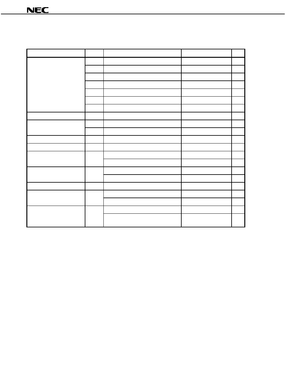
Preliminary Product Information U15436EJ1V0PM
64
µ
µ
µ
µPD703201, 703201Y, 703204, 703204Y, 70F3201, 70F3201Y, 70F3204, 70F3204Y
20. ELECTRICAL SPECIFICATIONS (TARGET VALUES)
Absolute Maximum Ratings (T
A
= 25∞C, V
SS
= 0 V)
Parameter
Symbol
Conditions
Ratings
Unit
V
DD
≠0.5 to +3.6
V
AV
DD
≠0.5 to +3.6
V
EV
DD
≠0.5 to +3.6
V
V
DD
BU
≠0.5 to +3.6
V
AV
SS
≠0.5 to +0.5
V
EV
SS
≠0.5 to +0.5
V
Supply voltage
V
SS
BU
≠0.5 to +0.5
V
Input voltage
V
I
Other than X1, XT1, and port 7
≠0.5 to EV
DD
+ 0.3
Note
V
V
K
X1, V
DD
= 2.2 to 2.7 V
≠0.5 to V
DD
+ 0.3
Note
V
Clock input voltage
V
KT
XT1, V
DD
BU = 2.2 to 2.7 V
≠0.5 to V
DD
BU + 0.3
Note
V
Analog input voltage
V
IAN
Port 7
≠0.5 to AV
DD
+ 0.3
Note
V
Analog reference voltage
AV
REF
AV
REF0
, AV
REF1
≠0.5 to AV
DD
+ 0.3
Note
V
Per pin
4
mA
Output current, low
I
OL
Total for all pins
100
mA
Per pin
≠4
mA
Output current, high
I
OH
Total for all pins
≠100
mA
Output voltage
V
O
V
DD
= 2.5 V ±0.2 V
≠0.5 to V
DD
+ 0.3 V
V
Normal operation mode
≠40 to +85
∞C
Operating ambient
temperature
T
A
Flash programming mode
T.B.D.
∞C
µPD703201, 703201Y, 703204, 703204Y
≠65 to +150
∞C
Storage temperature
T
stg
µPD70F3201, 70F3201Y, 70F3204,
70F3204Y
T.B.D.
∞C
Note Be sure not to exceed the absolute maximum ratings (MAX. value) of each supply voltage.
Cautions
1. Do not directly connect the output (or I/O) pins of IC products to each other, or to V
DD
, V
CC
,
and GND. Open-drain pins or open-collector pins, however, can be directly connected to
each other. Direct connection of the output pins between an IC product and an external
circuit is possible, if the output pins can be set to the high-impedance state and the output
timing of the external circuit is designed to avoid output conflict.
2. Product quality may suffer if the absolute maximum rating is exceeded even momentarily for
any parameter. That is, the absolute maximum ratings are rated values at which the product
is on the verge of suffering physical damage, and therefore the product must be used under
conditions that ensure that the absolute maximum ratings are not exceeded.
The ratings and conditions indicated for DC characteristics and AC characteristics represent
the quality assurance range during normal operation.
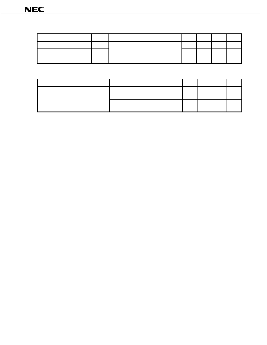
Preliminary Product Information U15436EJ1V0PM
65
µ
µ
µ
µPD703201, 703201Y, 703204, 703204Y, 70F3201, 70F3201Y, 70F3204, 70F3204Y
Capacitance (T
A
= 25∞C, V
DD
= AV
DD
= EV
DD
= V
DD
BU = V
SS
= AV
SS
= EV
SS
= V
SS
BU = 0 V)
Parameter
Symbol
Conditions
MIN.
TYP.
MAX.
Unit
Input capacitance
C
I
10
pF
I/O capacitance
C
IO
10
pF
Output capacitance
C
O
f
X
= 1 MHz
Unmeasured pins returned to 0 V
10
pF
Operating Conditions (V
DD
= AV
DD
= EV
DD
= V
DD
BU)
Parameter
Symbol
Conditions
MIN.
TYP.
MAX.
Unit
@ V
DD
= 2.3 to 2.7 V, operation with main
clock
0.0625
17
MHz
Internal system clock frequency
f
CLK
@ V
DD
= 2.2 to 2.7 V, operation with main
clock
0.0625
13.5
MHz
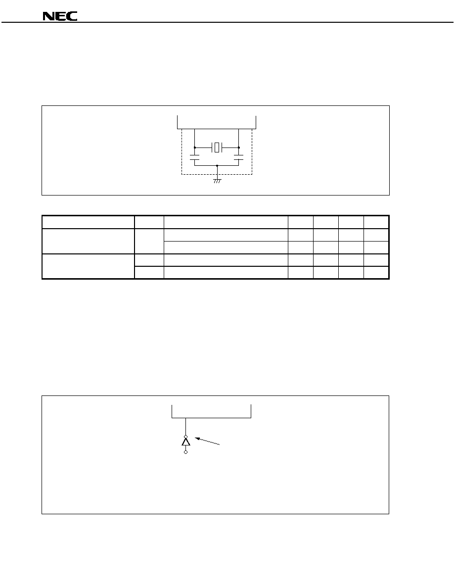
Preliminary Product Information U15436EJ1V0PM
66
µ
µ
µ
µPD703201, 703201Y, 703204, 703204Y, 70F3201, 70F3201Y, 70F3204, 70F3204Y
Recommended Oscillator
(1) Main clock oscillator (T
A
= ≠40 to +85∞C)
(a) Connection of ceramic resonator or crystal resonator
X1
X2
Parameter
Symbol
Conditions
MIN.
TYP.
MAX.
Unit
V
DD
= 2.3 to 2.7 V
2
17
MHz
Oscillation frequency
f
X
(f
XX
)
V
DD
= 2.2 to 2.7 V
2
13.5
MHz
Upon reset release
2
19
/f
X
s
Oscillation stabilization time
Upon STOP mode release
Note
s
Note The TYP. value differs depending on the setting of the oscillation stabilization time select register (OSTS).
Caution Ensure that the duty of the oscillation waveform is between 45% and 55%.
Remarks 1.
Connect the oscillator as close as possible to the X1 and X2 pins.
2.
Do not route the wiring near broken lines.
3.
For the resonator selection and oscillator constant, customers are requested to either evaluate the
oscillation themselves or apply to the resonator manufacturer for evaluation.
(b) External clock input
X1
X2
High-speed CMOS inverter
External clock
Open
Cautions
1. Connect the high-speed CMOS inverter as close as possible to the X1 pin.
2. Sufficiently evaluate the matching between the V850ES/SA2, V850ES/SA3 and the high-
speed CMOS inverter.
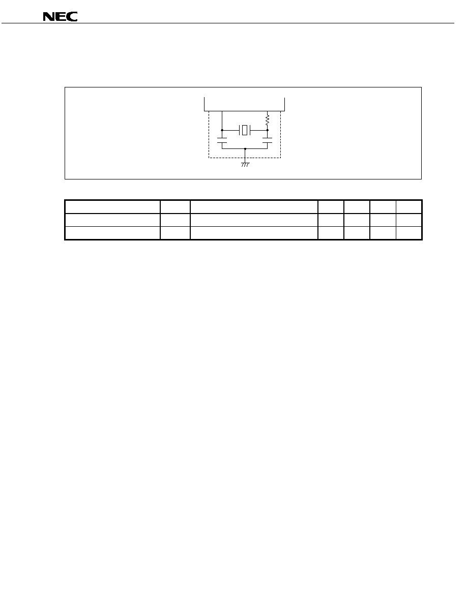
Preliminary Product Information U15436EJ1V0PM
67
µ
µ
µ
µPD703201, 703201Y, 703204, 703204Y, 70F3201, 70F3201Y, 70F3204, 70F3204Y
(2) Subclock oscillator (T
A
= ≠40 to +85∞C)
(a) Connection of crystal resonator
XT1
XT2
Parameter
Symbol
Conditions
MIN.
TYP.
MAX.
Unit
Oscillation frequency
f
XT
32
32.768
35
kHz
Oscillation stabilization time
10
s
Caution Ensure that the duty of the oscillation waveform is between 45% and 55%.
Remarks 1.
Connect the oscillator as close as possible to the XT1 and XT2 pins.
2.
Do not route the wiring near broken lines.
3.
For the resonator selection and oscillator constant, customers are requested to either evaluate the
oscillation themselves or apply to the resonator manufacturer for evaluation.

Preliminary Product Information U15436EJ1V0PM
68
µ
µ
µ
µPD703201, 703201Y, 703204, 703204Y, 70F3201, 70F3201Y, 70F3204, 70F3204Y
DC Characteristics
(T
A
= ≠40 to +85∞C, V
DD
= AV
DD
= EV
DD
= V
DD
BU = 2.2 to 2.7 V, V
SS
= AV
SS
= EV
SS
= V
SS
BU = 0 V) (1/2)
Parameter
Symbol
Conditions
MIN.
TYP.
MAX.
Unit
V
IH1
Note 1
0.7EV
DD
EV
DD
V
V
IH2
Note 2
T.B.D.
EV
DD
V
V
IH3
Note 3
0.7AV
DD
AV
DD
V
V
IH4
X1
0.8V
DD
V
DD
V
Input voltage, high
V
IH5
XT1, XT2
0.8V
DD
BU
V
DD
BU
V
V
IL1
Note 1
EV
SS
0.3EV
DD
V
V
IL2
Note 2
EV
SS
T.B.D.
V
V
IL3
Note 3
AV
SS
0.3AV
DD
V
V
IL4
X1
V
SS
0.2V
DD
V
Input voltage, low
V
IL5
XT1, XT2
V
SS
BU
0.2V
DD
BU
V
V
OH1
Note 4
I
OH
= ≠1 mA
0.8EV
DD
V
Output voltage, high
V
OH2
Note 5
I
OH
= ≠3 mA
0.8EV
DD
V
V
OL1
Note 4 (Except pins
P40 and P42)
I
OL
= 1.6 mA
0.4
V
V
OL2
P40, P42
I
OL
= 3 mA
0.4
V
Output voltage, low
V
OL3
Note 5
I
OL
= 1.6 mA
0.4
V
Input leakage current, high
I
LIH
V
IN
= V
DD
= EV
DD
= V
DD
BU
5
µA
Input leakage current, low
I
LIL
V
IN
= 0 V
≠5
µA
Output leakage current, high
I
LOH
V
O
= V
DD
= EV
DD
= V
DD
BU
5
µA
Output leakage current, low
I
LOL
V
O
= 0 V
≠5
µA
Notes 1. P21, P31, P90, P91, P94 to P97, P99, P911, P914, PCD1 to PCD3, PCM0 to PCM5, PCS0 to PCS7,
PCT0 to PCT7, PDH0 to PDH7, PDL0 to PDL15 (and their alternate-function pins)
2. RESET, P00 to P05, P20, P22, P30, P32, P40 to P46, P92, P93, P98, P910, P912, P913, P915 (and
their alternate-function pins)
3. P70 to P715, P80, P81 (and their alternate-function pins)
4. P00 to P05, P20 to P22, P30 to P32, P40 to P46, PCD1 to PCD3, PCM4 to PCM5, PCS4 to PCS7,
PCT2, PCT3, PCT5, PCT7 (and their alternate-function pins)
5. P90 to P915, PCM0 to PCM3, PCS0 to PCS3, PCT0, PCT1, PCT4, PCT6, PDH0 to PDH7, PDL0 to
PDL15 (and their alternate-function pins)
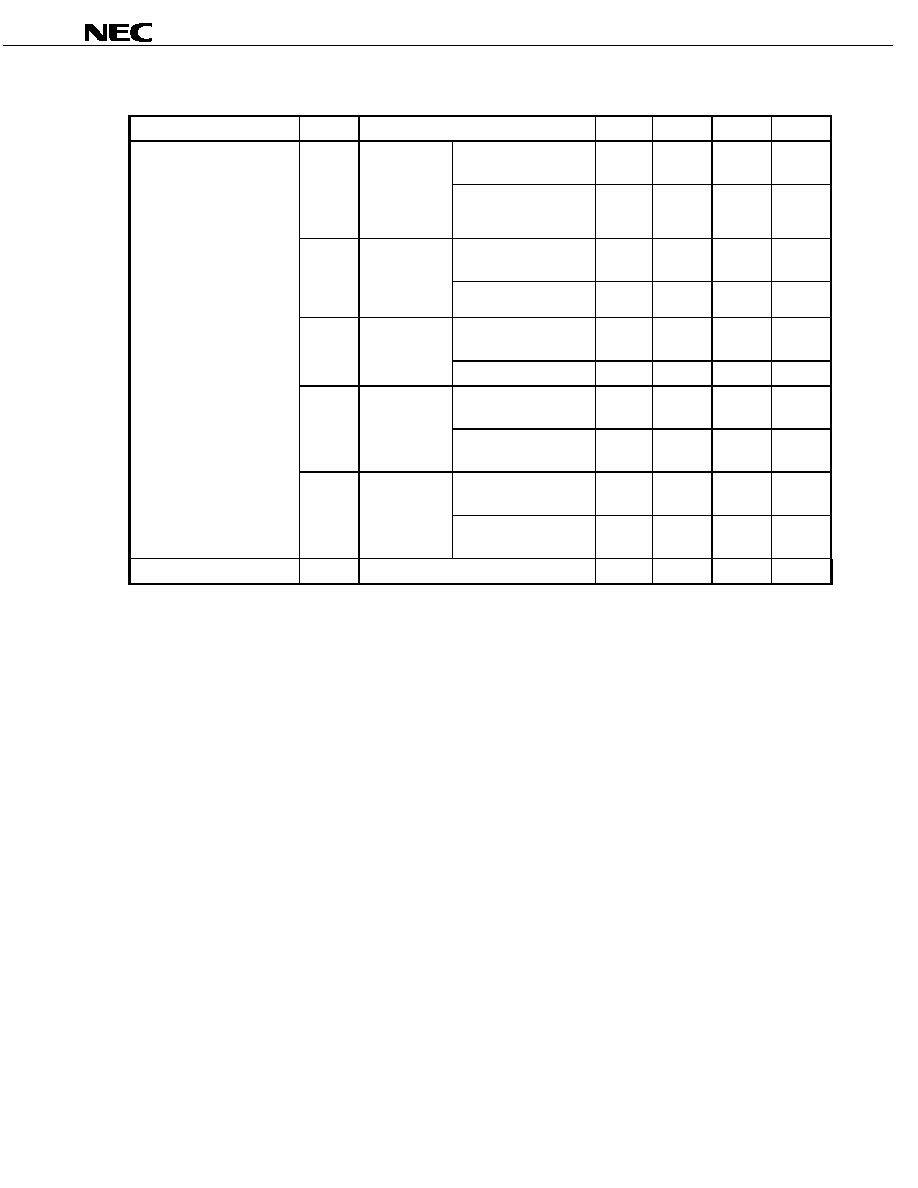
Preliminary Product Information U15436EJ1V0PM
69
µ
µ
µ
µPD703201, 703201Y, 703204, 703204Y, 70F3201, 70F3201Y, 70F3204, 70F3204Y
(T
A
= ≠40 to +85∞C, V
DD
= AV
DD
= EV
DD
= V
DD
BU = 2.2 to 2.7 V, V
SS
= AV
SS
= EV
SS
= V
SS
BU = 0 V) (2/2)
Parameter
Symbol
Conditions
MIN.
TYP.
MAX.
Unit
V
DD
= 2.3 to 2.7 V,
f
XX
= f
CLK
= 17 MHz
T.B.D.
T.B.D.
mA
I
DD1
Normal
operation
All peripheral
functions
operating
f
XX
= f
CLK
= 13.5 MHz
T.B.D.
T.B.D.
mA
V
DD
= 2.3 to 2.7 V,
f
XX
= f
CLK
= 17 MHz
T.B.D.
T.B.D.
mA
I
DD2
HALT mode
All peripheral
functions
operating
f
XX
= f
CLK
= 13.5 MHz
T.B.D.
T.B.D.
mA
V
DD
= 2.3 to 2.7 V,
f
XX
= f
CLK
= 17 MHz
T.B.D.
T.B.D.
mA
I
DD3
IDLE mode
RTC operating
f
XX
= f
CLK
= 13.5 MHz
T.B.D.
T.B.D.
mA
Subclock oscillator,
RTC operating
T.B.D.
T.B.D.
µA
I
DD4
STOP mode
Subclock oscillator
stopped (XT1 = V
SS
)
T.B.D.
T.B.D.
µA
f
XT
= 32.768 kHz,
RTC operating
T.B.D.
T.B.D.
µA
Supply current
I
DD5
Backup mode
Subclock oscillation
stopped (XT1 = V
SS
)
T.B.D.
T.B.D.
µA
Pull-up resistance
R
L
V
IN
= 0 V
10
30
100
k
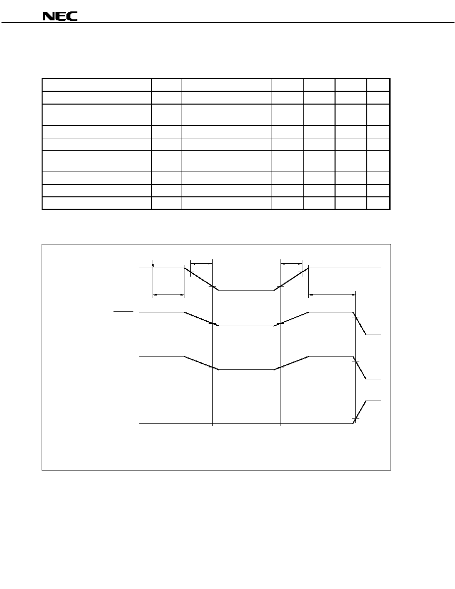
Preliminary Product Information U15436EJ1V0PM
70
µ
µ
µ
µPD703201, 703201Y, 703204, 703204Y, 70F3201, 70F3201Y, 70F3204, 70F3204Y
Data Retention Characteristics
(1) In STOP mode (T
A
= ≠40 to +85∞C, V
SS
= AV
SS
= EV
SS
= V
SS
BU = 0 V)
Parameter
Symbol
Conditions
MIN.
TYP.
MAX.
Unit
Data retention voltage
V
DDDR1
STOP mode
1.8
2.7
V
Data retention current
I
DDDR1
V
DD
= AV
DD
= EV
DD
= V
DD
BU =
V
DDDR1
T.B.D.
T.B.D.
µA
Supply voltage rise time
t
RVD1
200
µs
Supply voltage fall time
t
FVD1
200
µs
Supply voltage hold time
(from STOP mode setting)
t
HVD1
0
ms
STOP release signal input time
t
DREL1
0
ms
Data retention high-level input voltage
V
IHDR1
All input ports
V
IHn
V
DDDR1
V
Data retention low-level input voltage
V
ILDR1
All input ports
0
V
ILn
V
Remark
n = 1 to 5
V
DD
Setting STOP mode
t
HVD1
t
FVD1
RESET
(input)
NMI, INTP0 to INTP6
(input)
NMI, INTP0 to INTP6 (input)
(when STOP mode is released
at rising edge)
t
RVD1
t
DREL1
V
DDDR1
V
IHDR1
V
ILDR1
V
IHDR1
Caution
Shifting to STOP mode and restoring from STOP mode must be performed at V
DD
= 2.3 V min.
(f
CLK
= 17 MHz) and V
DD
= 2.2 V min. (f
CLK
= 13.5 MHz), respectively.

Preliminary Product Information U15436EJ1V0PM
71
µ
µ
µ
µPD703201, 703201Y, 703204, 703204Y, 70F3201, 70F3201Y, 70F3204, 70F3204Y
(2) In backup mode (T
A
= ≠40 to +85
∞
∞
∞
∞C, V
SS
= AV
SS
= EV
SS
= V
SS
BU = V
DD
= AV
DD
= EV
DD
= 0 V)
Parameter
Symbol
Conditions
MIN.
TYP.
MAX.
Unit
Data retention voltage
V
DDDR2
Backup mode
1.6
2.7
V
Data retention current
I
DDDR2
V
DD
BU = V
DDDR2
T.B.D.
T.B.D.
µA
Backup supply voltage rise time
t
RVD2
T.B.D.
µs
Backup supply voltage fall time
t
FVD2
T.B.D.
µs
Mode setting time from RESET
to
V
DD
t
HVD2
T.B.D.
ms
Mode release signal input time from
V
DD
to RESET
t
DREL2
T.B.D.
ms
Caution Shifting to backup mode and restoring from backup mode must be performed at V
DD
= 2.3 V min.
(f
CLK
= 17 MHz) and V
DD
= 2.2 V min. (f
CLK
= 13.5 MHz), respectively.
Setting STOP mode
0 V
Note
t
HVD1
0.8EV
DD
0.2EV
DD
V
DD
, EV
DD
, AV
DD
V
DD
BU
RESET (input)
t
FVD2
t
HVD2
t
DREL2
V
DDDR2
t
HVD2
Note Shifting to backup mode and restoring from backup mode must be performed at V
DD
= 2.3 V min. (f
CLK
= 17
MHz) and V
DD
= 2.2 V min. (f
CLK
= 13.5 MHz), respectively.
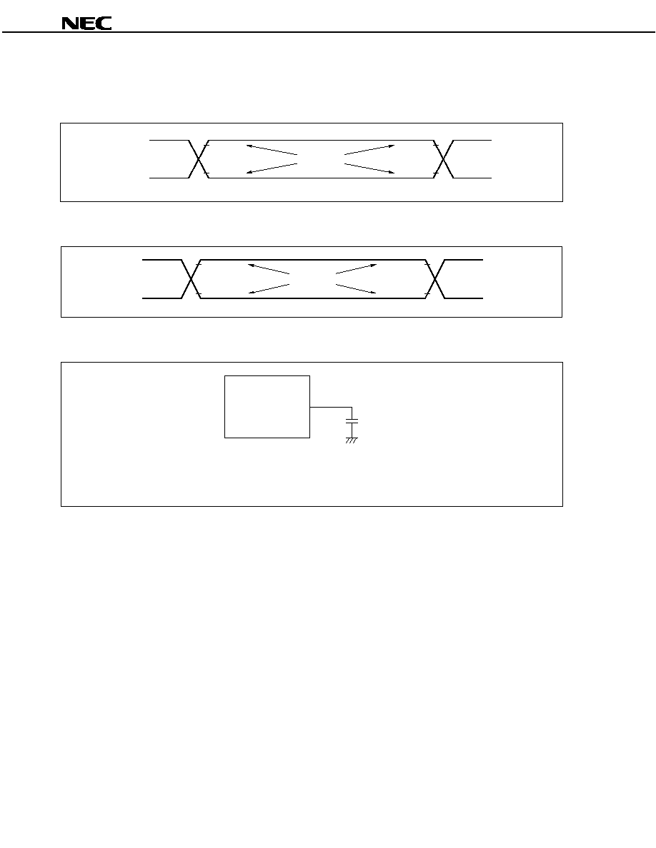
Preliminary Product Information U15436EJ1V0PM
72
µ
µ
µ
µPD703201, 703201Y, 703204, 703204Y, 70F3201, 70F3201Y, 70F3204, 70F3204Y
AC Characteristics
AC test input measurement points (V
DD
, AV
DD
, EV
DD
, V
DD
BU)
V
DD
0 V
V
IH
V
IL
V
IH
V
IL
Measurement points
AC test output measurement points
V
OH
V
OL
V
OH
V
OL
Measurement points
Load conditions
DUT
(Device under test)
C
L
= 50 pF
Caution If the load capacitance exceeds 50 pF due to the circuit configuration, reduce the load
capacitance of the device to 50 pF or less by inserting a buffer or by some other means.
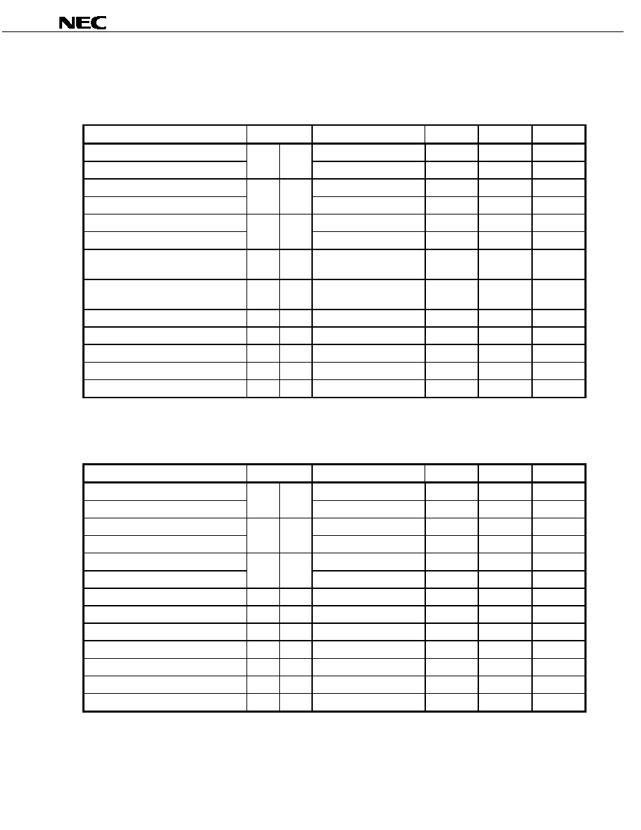
Preliminary Product Information U15436EJ1V0PM
73
µ
µ
µ
µPD703201, 703201Y, 703204, 703204Y, 70F3201, 70F3201Y, 70F3204, 70F3204Y
Clock Timing
(1) Operating conditions (T
A
= ≠40 to +85∞C, V
DD
= AV
DD
= EV
DD
= V
DD
BU = 2.3 to 2.7 V, V
SS
= AV
SS
= EV
SS
=
V
SS
BU = 0 V, C
L
= 50 pF)
Parameter
Symbol
Conditions
MIN.
MAX.
Unit
X1 input cycle
58.8
ns
XT1 input cycle
t
CYX
<1>
28.5
µs
X1 input high-level width
26.4
ns
XT1 input high-level width
t
WXH
<2>
12.8
µs
X1 input low-level width
26.4
ns
XT1 input low-level width
t
WXL
<3>
12.8
µs
X1 input rise time
t
XR
<4>
0.5 (t
CYX
≠
t
WXH
≠ t
WXL
)
ns
X1 input fall time
t
XF
<5>
0.5 (t
CYX
≠
t
WXH
≠ t
WXL
)
ns
CLKOUT output cycle
t
CYK
<6>
58.8 ns
16
µs
CLKOUT high-level width
t
WKH
<7>
0.5t
CYK
≠ 5
ns
CLKOUT low-level width
t
WKL
<8>
0.5t
CYK
≠ 5
ns
CLKOUT rise time
t
KR
<9>
5
ns
CLKOUT fall time
t
KF
<10>
5
ns
Remark
Ensure that the duty for the X1 and XT1 input waveforms is between 45% and 55%.
(2) Operating conditions (T
A
= ≠40 to +85∞C, V
DD
= AV
DD
= EV
DD
= V
DD
BU = 2.2 to 2.7 V, V
SS
= AV
SS
= EV
SS
=
V
SS
BU = 0 V, C
L
= 50 pF)
Parameter
Symbol
Conditions
MIN.
MAX.
Unit
X1 input cycle
T.B.D.
ns
XT1 input cycle
t
CYX
<1>
T.B.D.
µs
X1 input high-level width
T.B.D.
ns
XT1 input high-level width
t
WXH
<2>
T.B.D.
µs
X1 input low-level width
T.B.D.
ns
XT1 input low-level width
t
WXL
<3>
T.B.D.
µs
X1 input rise time
t
XR
<4>
T.B.D.
ns
X1 input fall time
t
XF
<5>
T.B.D.
ns
CLKOUT output cycle
t
CYK
<6>
T.B.D.
T.B.D.
CLKOUT high-level width
t
WKH
<7>
T.B.D.
ns
CLKOUT low-level width
t
WKL
<8>
T.B.D.
ns
CLKOUT rise time
t
KR
<9>
T.B.D.
ns
CLKOUT fall time
t
KF
<10>
T.B.D.
ns
Remark
Ensure that the duty for the X1 and XT1 input waveforms is between 45% and 55%.
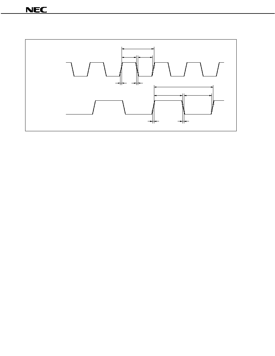
Preliminary Product Information U15436EJ1V0PM
74
µ
µ
µ
µPD703201, 703201Y, 703204, 703204Y, 70F3201, 70F3201Y, 70F3204, 70F3204Y
Clock timing
X1, XT1 (input)
CLKOUT (output)
<2>
<4>
<5>
<1>
<3>
<7>
<9>
<10>
<8>
<6>
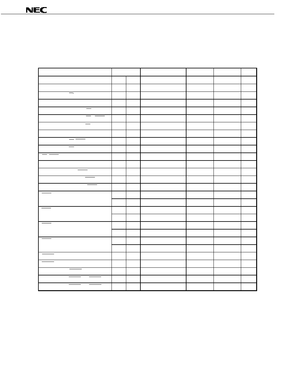
Preliminary Product Information U15436EJ1V0PM
75
µ
µ
µ
µPD703201, 703201Y, 703204, 703204Y, 70F3201, 70F3201Y, 70F3204, 70F3204Y
Bus Timing
(1) Multiplexed bus mode
(a) CLKOUT asynchronous: In multiplexed bus mode
(T
A
= ≠40 to +85∞C, V
DD
= AV
DD
= EV
DD
= V
DD
BU = 2.2 to 2.7 V, V
SS
= AV
SS
= EV
SS
= V
SS
BU = 0 V, C
L
= 50 pF)
Parameter
Symbol
Conditions
MIN.
MAX.
Unit
Address setup time (to ASTB
)
t
SAST
<11>
0.5T
≠ 15
ns
Address hold time (from ASTB
)
t
HSTA
<12>
0.5T
≠ 15
ns
Delay time from RD
to address float
t
FRDA
<13>
2
ns
Data input setup time from address
t
SAID
<14>
(2 + n)T ≠ 25
ns
Data input setup time from RD
t
SRID
<15>
(1 + n)T ≠ 25
ns
Delay time from ASTB
to RD, WRm
t
DSTRDWR
<16>
0.5T
≠ 15
ns
Data input hold time (from RD
)
t
HRDID
<17>
0
ns
Address output time from RD
t
DRDA
<18>
(1 + i)T ≠ 15
ns
Delay time from RD, WRm
to ASTB
t
DRDWRST
<19>
0.5T ≠ 15
ns
Delay time from RD
to ASTB
t
DRDST
<20>
(1.5 + i)T ≠ 15
ns
RD, WRm low-level width
t
WRDWRL
<21>
(1 + n)T ≠ 15
ns
ASTB high-level width
t
WSTH
<22>
T ≠ 15
ns
Data output time from WRm
t
DWROD
<23>
15
ns
Data output setup time (to WRm
)
t
SODWR
<24>
(1 + n)T ≠ 20
ns
Data output hold time (from WRm
)
t
HWROD
<25>
T ≠ 15
ns
t
SAWT1
<26>
n
1
1.5T ≠ 25
ns
WAIT setup time (to address)
t
SAWT2
<27>
n
1
(1.5 + n)T ≠ 25
ns
t
HAWT1
<28>
n
1
(0.5 + n)T
ns
WAIT hold time (from address)
t
HAWT2
<29>
n
1
(1.5 + n)T
ns
t
SSTWT1
<30>
n
1
T ≠ 25
ns
WAIT setup time (to ASTB
)
t
SSTWT2
<31>
n
1
(1 + n)T ≠ 25
ns
t
HSTWT1
<32>
n
1
nT
ns
WAIT hold time (from ASTB
)
t
HSTWT2
<33>
n
1
(1 + n)T
ns
HLDRQ high-level width
t
WHQH
<34>
T + 10
ns
HLDAK low-level width
t
WHAL
<35>
T ≠ 15
ns
Delay time from HLDAK
to bus output
t
DHAC
<36>
≠3
ns
Delay time from HLDRQ
to HLDAK
t
DHQHA1
<37>
1.5T
(2n + 7.5)T + 25
ns
Delay time from HLDRQ
to HLDAK
t
DHQHA2
<38>
0.5T
1.5T + 25
ns
Remarks 1.
T = 1/f
CPU
(f
CPU
: CPU operation clock frequency)
2.
n: Number of wait clocks inserted in the bus cycle.
The sampling timing changes when a programmable wait is inserted.
3.
m = 0, 1
4.
i: Number of idle states inserted after the read cycle (0 or 1).
5.
The values in the above specifications are values for when clocks with a 1:1 duty ratio are input from
X1.

Preliminary Product Information U15436EJ1V0PM
76
µ
µ
µ
µPD703201, 703201Y, 703204, 703204Y, 70F3201, 70F3201Y, 70F3204, 70F3204Y
(b) CLKOUT synchronous: In multiplexed bus mode
(T
A
= ≠40 to +85∞C, V
DD
= AV
DD
= EV
DD
= V
DD
BU = 2.2 to 2.7 V, V
SS
= AV
SS
= EV
SS
= V
SS
BU = 0 V, C
L
= 50 pF)
Parameter
Symbol
Conditions
MIN.
MAX.
Unit
Delay time from CLKOUT
to address
t
DKA
<39>
0
19
ns
Delay time from CLKOUT
to address float t
FKA
<40>
≠12
7
ns
Delay time from CLKOUT
to ASTB
t
DKST
<41>
≠12
7
ns
Delay time from CLKOUT
to RD, WRm
t
DKRDWR
<42>
≠5
14
ns
Data input setup time (to CLKOUT
)
t
SIDK
<43>
15
ns
Data input hold time (from CLKOUT
)
t
HKID
<44>
5
ns
Data output delay time from CLKOUT
t
DKOD
<45>
19
ns
WAIT setup time (to CLKOUT
)
t
SWTK
<46>
15
ns
WAIT hold time (from CLKOUT
)
t
HKWT
<47>
5
ns
HLDRQ setup time (to CLKOUT
)
t
SHQK
<48>
15
ns
HLDRQ hold time (from CLKOUT
)
t
HKHQ
<49>
5
ns
Delay time from CLKOUT
to bus float
t
DKF
<50>
19
ns
Delay time from CLKOUT
to HLDAK
t
DKHA
<51>
19
ns
Remarks 1.
m = 0, 1
2.
The values in the above specifications are values for when clocks with a 1:1 duty ratio are input from
X1.
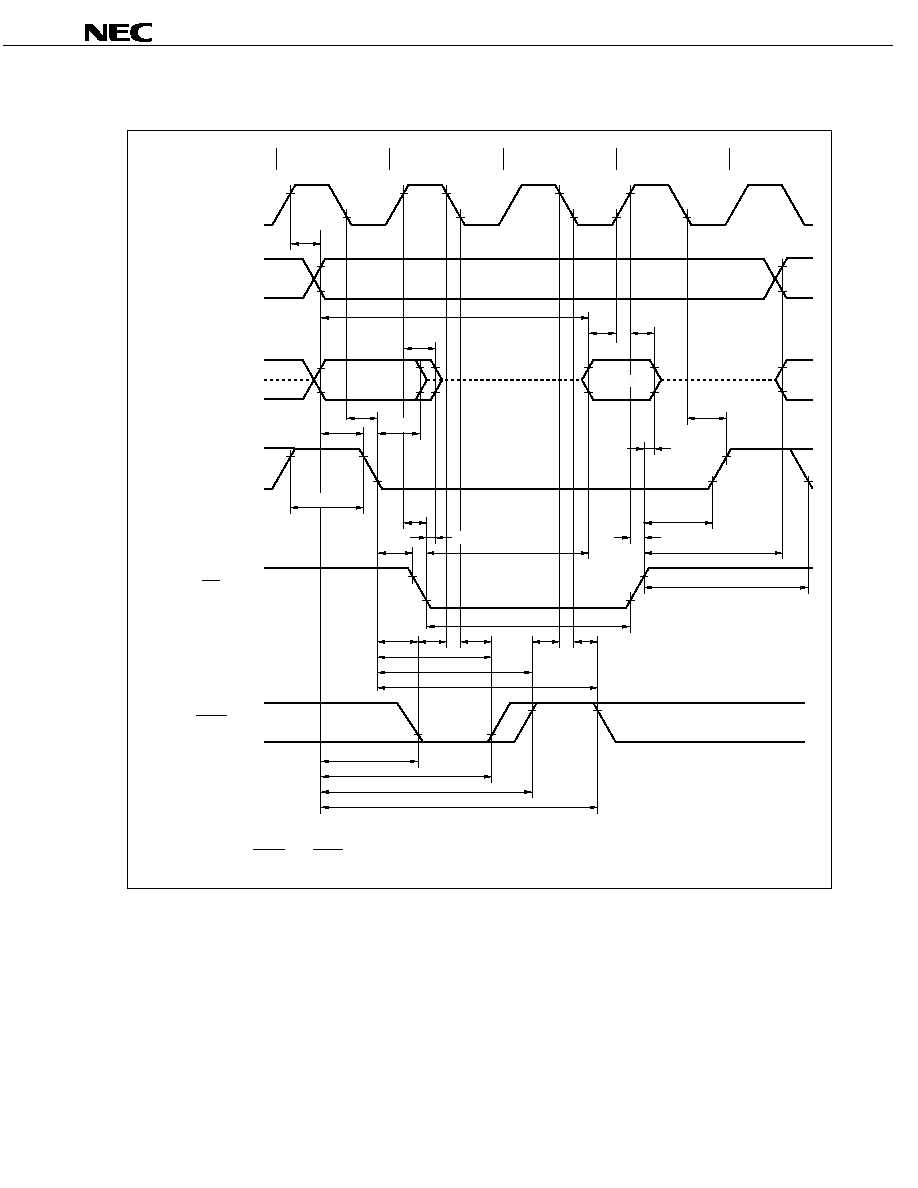
Preliminary Product Information U15436EJ1V0PM
77
µ
µ
µ
µPD703201, 703201Y, 703204, 703204Y, 70F3201, 70F3201Y, 70F3204, 70F3204Y
Read Cycle (CLKOUT Synchronous/Asynchronous, 1 Wait): In Multiplexed Bus Mode
CLKOUT (output)
A16 to A23 (output),
A0 to A15 (output)
AD0 to AD15 (I/O)
ASTB (output)
RD (output)
WAIT (input)
T1
T2
TW
T3
<39>
<40>
<41>
<11>
<42>
<19>
<18>
<20>
<16>
<30> <46>
<32>
<31>
<33>
<26>
<28>
<27>
<29>
<47>
<46>
<47>
<15>
<21>
<17>
<41>
<14>
<43>
<44>
Address
Hi-Z
<13>
<42>
<12>
<22>
Remark WR0 and WR1are high level.
Data

Preliminary Product Information U15436EJ1V0PM
78
µ
µ
µ
µPD703201, 703201Y, 703204, 703204Y, 70F3201, 70F3201Y, 70F3204, 70F3204Y
Write Cycle (CLKOUT Synchronous/Asynchronous, 1 Wait): In Multiplexed Bus Mode
CLKOUT (output)
A16 to A23 (output),
A0 to A15 (output)
AD0 to AD15 (I/O)
ASTB (output)
WR0 (output),
WR1 (output)
WAIT (input)
T1
T2
TW
T3
<39>
<45>
<41>
<11>
<42>
<19>
<25>
<16>
<30> <46>
<32>
<31>
<33>
<26>
<28>
<27>
<29>
<47>
<46>
<47>
<24>
<21>
<22>
<12>
<41>
Data
Address
<23>
<42>
Remark RD is high level.
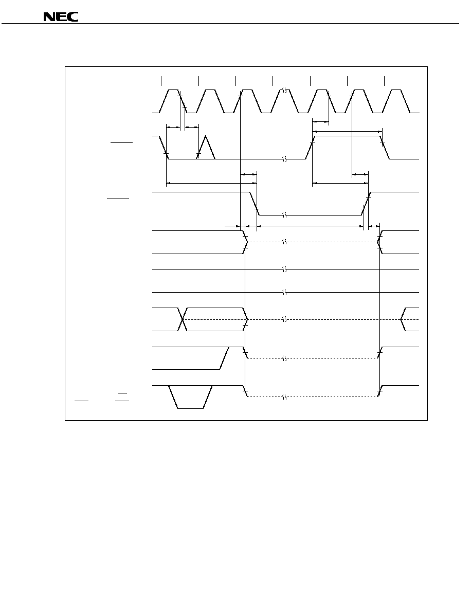
Preliminary Product Information U15436EJ1V0PM
79
µ
µ
µ
µPD703201, 703201Y, 703204, 703204Y, 70F3201, 70F3201Y, 70F3204, 70F3204Y
Bus Hold: In Multiplexed Bus Mode
CLKOUT (output)
HLDRQ (input)
HLDAK (output)
A16 to A23 (output)
A0 to A15 (output)
AD0 to AD15 (I/O)
ASTB (output)
RD (output),
WR0 (output), WR1 (output)
<48>
<49>
<51>
<36>
<35>
<37>
<38>
<48>
<51>
<34>
TH
TH
TH
TI
Hi-Z
Hi-Z
Hi-Z
Data
Hi-Z
<50>
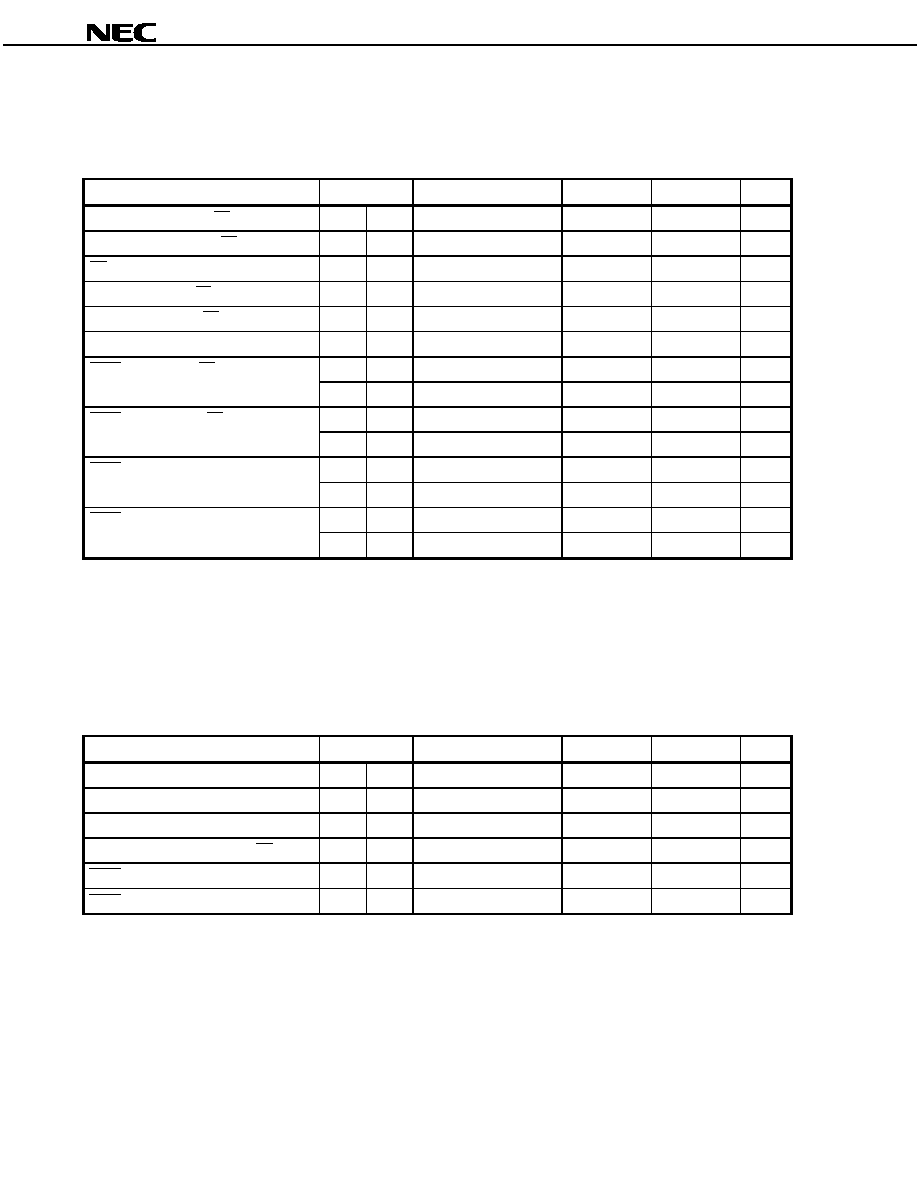
Preliminary Product Information U15436EJ1V0PM
80
µ
µ
µ
µPD703201, 703201Y, 703204, 703204Y, 70F3201, 70F3201Y, 70F3204, 70F3204Y
(2) In separate bus mode
(a) Read cycle (CLKOUT asynchronous): In separate bus mode
(T
A
= ≠40 to +85
∞
∞
∞
∞C, V
DD
= AV
DD
= EV
DD
= V
DD
BU = 2.2 to 2.7 V, V
SS
= AV
SS
= EV
SS
= V
SS
BU = 0 V, C
L
= 50 pF)
Parameter
Symbol
Conditions
MIN.
MAX.
Unit
Address setup time (to RD
)
t
SARD
<52>
0.5T ≠ 15
ns
Address hold time (from RD
)
t
HARD
<53>
2
ns
RD low-level width
t
WRDL
<54>
(1.5 + n) T ≠ 10
ns
Data setup time (to RD
)
t
SISD
<55>
20
ns
Data hold time (from RD
)
t
HISD
<56>
0
ns
Data setup time (to address)
t
SAID
<57>
(2 + n) T ≠ 25
ns
t
SRDWT1
<58>
0.5T ≠ 20
ns
WAIT setup time (to RD
)
t
SRDWT2
<59>
(0.5 + n) T ≠ 20
ns
t
HRDWT1
<60>
0.5T
ns
WAIT hold time (from RD
)
t
HRDWT2
<61>
(0.5 + n) T
ns
t
SAWT1
<62>
T ≠ 20
ns
WAIT setup time (to address)
t
SAWT2
<63>
(1 + n) T ≠ 20
ns
t
HAWT1
<64>
T
ns
WAIT hold time (from address)
t
HAWT2
<65>
(1 + n) T
ns
Remarks 1.
T = 1/f
CPU
(f
CPU
: CPU operation clock frequency)
2.
n: Number of wait clocks inserted in bus cycle
The sampling timing changes when a programmable wait is inserted.
3.
The values in the above specifications are the values for when clocks with a 1:1 duty ratio are input
from X1.
(b) Read cycle (CLKOUT synchronous): In separate bus mode
(T
A
= ≠40 to +85
∞
∞
∞
∞C, V
DD
= AV
DD
= EV
DD
= V
DD
BU = 2.2 to 2.7 V, V
SS
= AV
SS
= EV
SS
= V
SS
BU = 0 V, C
L
= 50 pF)
Parameter
Symbol
Conditions
MIN.
MAX.
Unit
Delay time from CLKOUT
to address, CS t
DKSA
<66>
0
19
ns
Data input setup time (to CLKOUT
)
t
SISDK
<67>
15
ns
Data input hold time (from CLKOUT
)
t
HKISD
<68>
5
ns
Delay time from CLKOUT
to RD
t
DKSR
<69>
0
19
ns
WAIT setup time (to CLKOUT
)
t
SWTK
<70>
15
ns
WAIT hold time (from CLKOUT
)
t
HKWT
<71>
5
ns
Remark The values in the above specifications are the values for when clocks with a 1:1 duty ratio are input from
X1.

Preliminary Product Information U15436EJ1V0PM
81
µ
µ
µ
µPD703201, 703201Y, 703204, 703204Y, 70F3201, 70F3201Y, 70F3204, 70F3204Y
(c) Write cycle (CLKOUT asynchronous): In separate bus mode
(T
A
= ≠40 to +85
∞
∞
∞
∞C, V
DD
= AV
DD
= EV
DD
= V
DD
BU = 2.2 to 2.7 V, V
SS
= AV
SS
= EV
SS
= V
SS
BU = 0 V, C
L
= 50 pF)
Parameter
Symbol
Conditions
MIN.
MAX.
Unit
Address setup time (to WRm
)
t
SAW
<72>
T ≠ 15
ns
Address hold time (from WRm
)
t
HAW
<73>
0.5T ≠ 10
ns
WRm low-level width
t
WWRL
<74>
(0.5 + n) T ≠ 10
ns
Data output time from WRm
t
DOSDW
<75>
≠5
ns
Data setup time (to WRm
)
t
SOSDW
<76>
(0.5 + n) T ≠ 10
ns
Data hold time (from WRm
)
t
HOSDW
<77>
0.5T ≠ 10
ns
Data setup time (to address)
t
SAOD
<78>
T ≠ 25
ns
t
SWRWT1
<79>
20
ns
WAIT setup time (to WRm
)
t
SWRWT2
<80>
nT ≠ 20
ns
t
HWRWT1
<81>
0
ns
WAIT hold time (from WRm
)
t
HWRWT2
<82>
nT
ns
t
SAWT1
<83>
T ≠ 20
ns
WAIT setup time (to address)
t
SAWT2
<84>
(1 + n) T ≠ 20
ns
t
HAWT1
<85>
T
ns
WAIT hold time (from address)
t
HAWT2
<86>
(1 + n) T
ns
Remarks 1.
m = 0, 1
2.
T = 1/f
CPU
(f
CPU
: CPU operation clock frequency)
3.
n: Number of wait clocks inserted in bus cycle
The sampling timing changes when a programmable wait is inserted.
4.
The values in the above specifications are the values for when clocks with a 1:1 duty ratio are input
from X1.
(d) Write cycle (CLKOUT synchronous): In separate bus mode
(T
A
= ≠40 to +85
∞
∞
∞
∞C, V
DD
= AV
DD
= EV
DD
= V
DD
BU = 2.2 to 2.7 V, V
SS
= AV
SS
= EV
SS
= V
SS
BU = 0 V, C
L
= 50 pF)
Parameter
Symbol
Conditions
MIN.
MAX.
Unit
Delay time from CLKOUT
to address, CS t
DKSA
<87>
0
19
ns
Delay time from CLKOUT
to data output
t
DKSD
<88>
0
19
ns
Delay time from CLKOUT
to WRm
t
DKSW
<89>
0
19
ns
WAIT setup time (to CLKOUT
)
t
SWTK
<90>
15
ns
WAIT hold time (from CLKOUT
)
t
HKWT
<91>
5
ns
Remarks 1.
m = 0, 1
2.
The values in the above specifications are the values for when clocks with a 1:1 duty ratio are input
from X1.
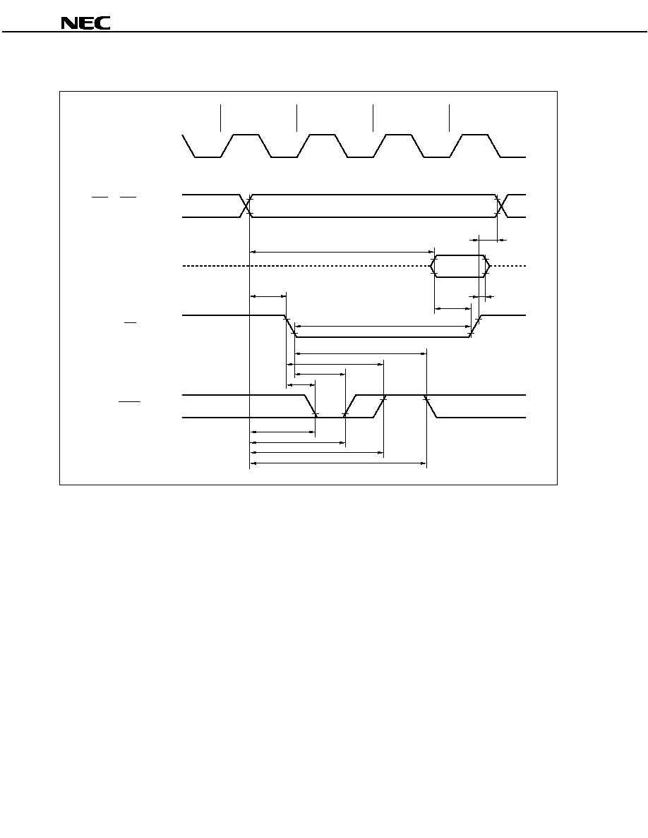
Preliminary Product Information U15436EJ1V0PM
82
µ
µ
µ
µPD703201, 703201Y, 703204, 703204Y, 70F3201, 70F3201Y, 70F3204, 70F3204Y
Read Cycle (CLKOUT Asynchronous, 1 Wait): In Separate Bus Mode
CLKOUT (output)
T1
<57>
Hi-Z
Hi-Z
<52>
<54>
<61>
<59>
<60>
<58>
<62>
<64>
<63>
<65>
<56>
<55>
<53>
TW
T2
RD (output)
CS0 to CS3 (output)
A0 to A23 (output)
AD0 to AD15 (I/O)
WAIT (input)

Preliminary Product Information U15436EJ1V0PM
83
µ
µ
µ
µPD703201, 703201Y, 703204, 703204Y, 70F3201, 70F3201Y, 70F3204, 70F3204Y
Read Cycle (CLKOUT Synchronous, 1 Wait): In Separate Bus Mode
CLKOUT (output)
T1
<69>
<70>
<71>
<70>
<71>
<66>
<69>
<67>
<68>
Hi-Z
Hi-Z
TW
T2
RD (output)
CS0 to CS3 (output)
A0 to A23 (output)
AD0 to AD15 (I/O)
WAIT (input)
<66>
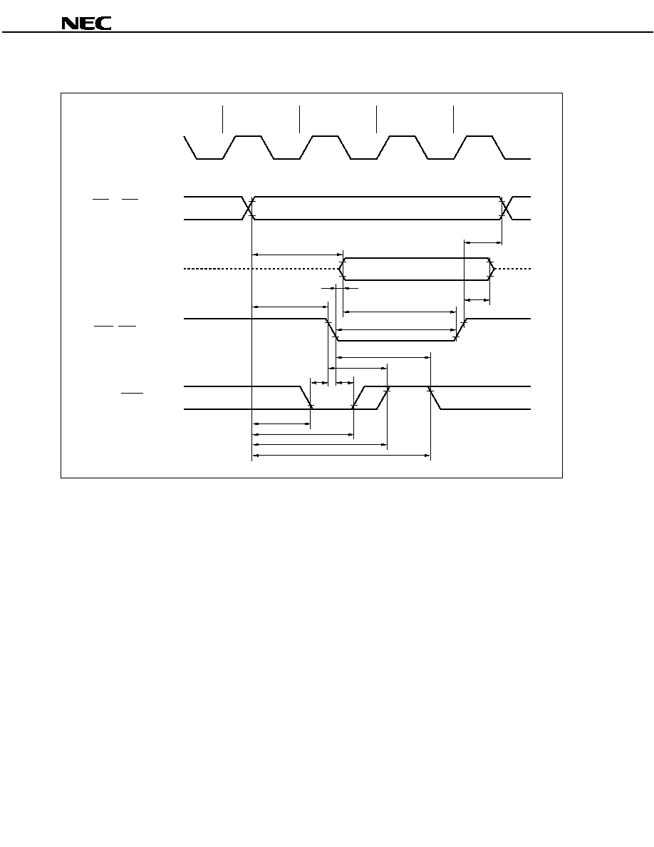
Preliminary Product Information U15436EJ1V0PM
84
µ
µ
µ
µPD703201, 703201Y, 703204, 703204Y, 70F3201, 70F3201Y, 70F3204, 70F3204Y
Write Cycle (CLKOUT Asynchronous, 1 Wait): In Separate Bus Mode
CLKOUT (output)
T1
<78>
<72>
<75>
<74>
<82>
<80>
<81>
<79>
<83>
<85>
<84>
<86>
<77>
<76>
<73>
TW
T2
WR0, WR1 (output)
CS0 to CS3 (output)
A0 to A23 (output)
AD0 to AD15 (I/O)
WAIT (input)
Hi-Z
Hi-Z
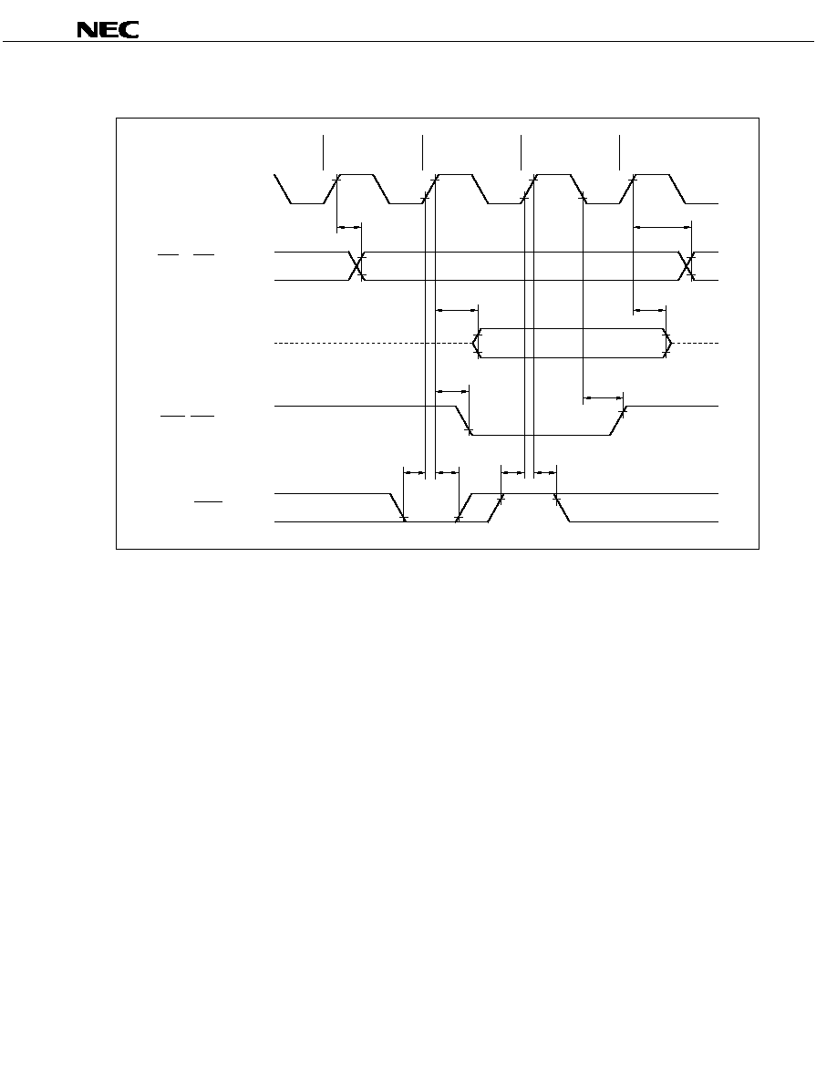
Preliminary Product Information U15436EJ1V0PM
85
µ
µ
µ
µPD703201, 703201Y, 703204, 703204Y, 70F3201, 70F3201Y, 70F3204, 70F3204Y
Write Cycle (CLKOUT Synchronous, 1 Wait): In Separate Bus Mode
CLKOUT (output)
T1
<88>
<89>
<91>
<90>
<89>
TW
T2
WR0, WR1 (output)
CS0 to CS3 (output)
A0 to A23 (output)
AD0 to AD15 (I/O)
WAIT (input)
<87>
<87>
<91>
<90>
<88>
Hi-Z
Hi-Z
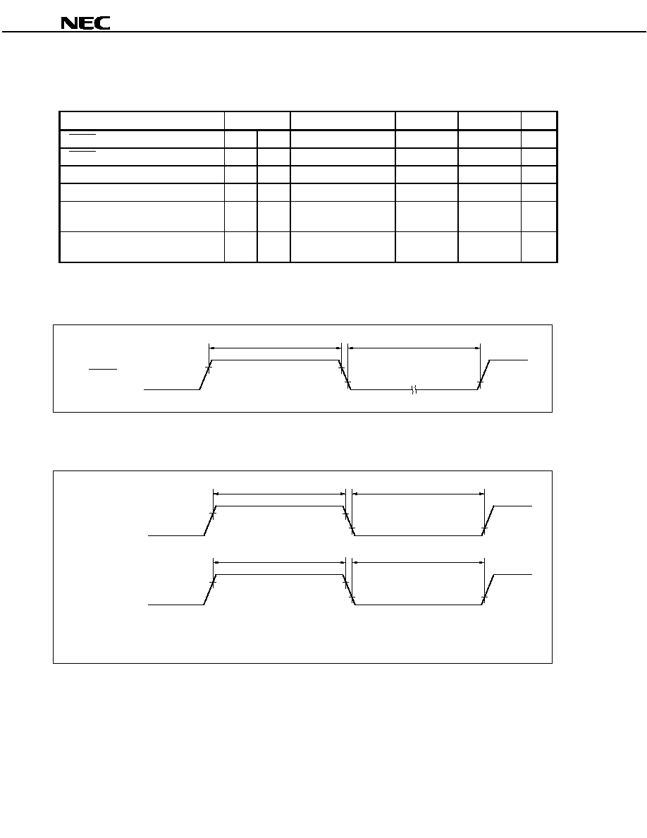
Preliminary Product Information U15436EJ1V0PM
86
µ
µ
µ
µPD703201, 703201Y, 703204, 703204Y, 70F3201, 70F3201Y, 70F3204, 70F3204Y
Reset/Interrupt Timing
(T
A
= ≠40 to +85∞C, V
DD
= AV
DD
= EV
DD
= V
DD
BU = 2.2 to 2.7 V, V
SS
= AV
SS
= EV
SS
= V
SS
BU = 0 V, C
L
= 50 pF)
Parameter
Symbol
Conditions
MIN.
MAX.
Unit
RESET high-level width
t
WRSH
<92>
500
ns
RESET low-level width
t
WRSL
<93>
500
ns
NMI high-level width
t
WNIH
<94>
500
ns
NMI low-level width
t
WNIL
<95>
500
ns
INTPn high-level width
t
WITH
<96>
n = 0 to 6 (analog noise
elimination)
500
ns
INTPn low-level width
t
WITL
<97>
n = 0 to 6 (analog noise
elimination)
500
ns
Remark
T = 1/f
XX
Reset
<92>
<93>
RESET (input)
Interrupt
<94>
<95>
NMI (input)
<96>
<97>
INTPn (input)
Remark n = 0 to 6
Preliminary Product Information U15436EJ1V0PM
87
µ
µ
µ
µPD703201, 703201Y, 703204, 703204Y, 70F3201, 70F3201Y, 70F3204, 70F3204Y
Timer Timing
(T
A
= ≠40 to +85∞C, V
DD
= AV
DD
= EV
DD
= V
DD
BU = 2.2 to 2.7 V, V
SS
= AV
SS
= EV
SS
= V
SS
BU = 0 V, C
L
= 50 pF)
Parameter
Symbol
Conditions
MIN.
MAX.
Unit
n = 0, 1
2T + 20
ns
TIn high-level width
n = 2 to 5
40
ns
n = 0, 1
2T + 20
ns
TIn low-level width
n = 2 to 5
40
ns
TCLRn high-level width
n = 0, 1
2T + 20
ns
TCLRn low-level width
n = 0, 1
2T + 20
ns
INTPnm high-level width
t
WITH
nm = 00, 01, 10, 11
2T + 20
ns
INTPnm low-level width
t
WITL
nm = 00, 01, 10, 11
2T + 20
ns
Remark T = 1/f
XX
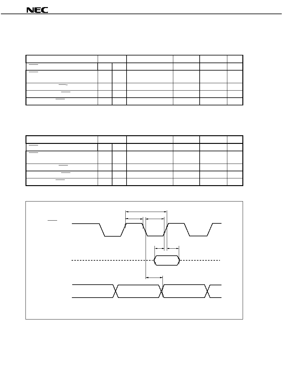
Preliminary Product Information U15436EJ1V0PM
88
µ
µ
µ
µPD703201, 703201Y, 703204, 703204Y, 70F3201, 70F3201Y, 70F3204, 70F3204Y
CSI Timing
(1) Master mode
(T
A
= ≠40 to +85∞C, V
DD
= AV
DD
= EV
DD
= V
DD
BU = 2.2 to 2.7 V, V
SS
= AV
SS
= EV
SS
= V
SS
BU = 0 V, C
L
= 50 pF)
Parameter
Symbol
Conditions
MIN.
MAX.
Unit
SCKn cycle time
t
KCY1
<98>
Output
200
ns
SCKn high-/low-level width
t
KH1
,
t
KL1
<99>
Output
t
KCY1
/2 ≠ 10
ns
SIn setup time (to SCKn
)
t
SIK1
<100>
30
ns
SIn hold time (from SCKn
)
t
KSI1
<101>
30
ns
Delay time from SCKn
to SOn output
t
KSO1
<102>
30
ns
Remark n = 0 to 3 (V850ES/SA2), n = 0 to 4 (V850ES/SA3)
(2) Slave mode
(T
A
= ≠40 to +85∞C, V
DD
= AV
DD
= EV
DD
= V
DD
BU = 2.2 to 2.7 V, V
SS
= AV
SS
= EV
SS
= V
SS
BU = 0 V, C
L
= 50 pF)
Parameter
Symbol
Conditions
MIN.
MAX.
Unit
SCKn cycle time
t
KCY2
<98>
Output
200
ns
SCKn high-/low-level width
t
KH2
,
t
KL2
<99>
Output
90
ns
SIn setup time (to SCKn
)
t
SIK2
<100>
50
ns
SIn hold time (from SCKn
)
t
KSI2
<101>
50
ns
Delay time from SCKn
to SOn output
t
KSO2
<102>
50
ns
Remark n = 0 to 3 (V850ES/SA2), n = 0 to 4 (V850ES/SA3)
<101>
<102>
<100>
<98>
<99>
Hi-Z
Hi-Z
<99>
Remark n = 0 to 3 (V850ES/SA2), n = 0 to 4 (V850ES/SA3)
SCKn (I/O)
SIn (input)
SOn (output)
Input data
Output data
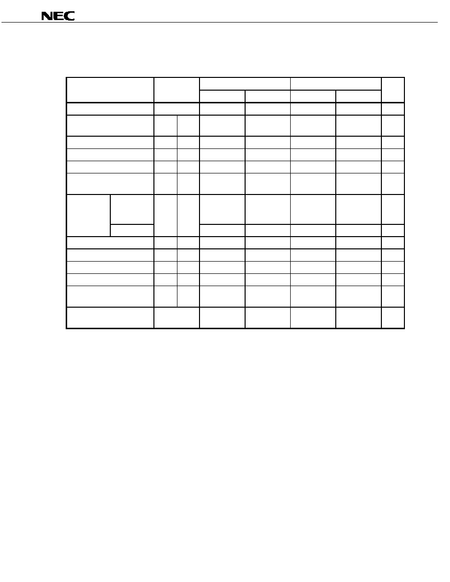
Preliminary Product Information U15436EJ1V0PM
89
µ
µ
µ
µPD703201, 703201Y, 703204, 703204Y, 70F3201, 70F3201Y, 70F3204, 70F3204Y
I
2
C Bus Mode (
µ
µ
µ
µPD703201Y, 703204Y, 70F3201Y, 70F3204Y only)
(T
A
= ≠40 to +85∞C, V
DD
= AV
DD
= EV
DD
= V
DD
BU = 2.2 to 2.7 V, V
SS
= AV
SS
= EV
SS
= V
SS
BU = 0 V)
Normal Mode
High-Speed Mode
Parameter
Symbol
MIN.
MAX.
MIN.
MAX.
Unit
SCL clock frequency
f
CLK
0
100
0
400
kHz
Bus-free time (between
stop/start conditions)
t
BUF
<103>
4.7
≠
1.3
≠
µs
Hold time
Note 1
t
HD:STA
<104>
4.0
≠
0.6
≠
µs
SCL clock low-level width
t
LOW
<105>
4.7
≠
1.3
≠
µs
SCL clock high-level width
t
HIGH
<106>
4.0
≠
0.6
≠
µs
Setup time for start/restart
conditions
t
SU:STA
<107>
4.7
≠
0.6
≠
µs
CBUS
compatible
master
5.0
≠
≠
≠
µs
Data hold
time
I
2
C mode
t
HD:DAT
<108>
0
Note 2
≠
0
Note 2
0.9
Note 3
µs
Data setup time
t
SU:DAT
<109>
250
≠
100
Note 4
≠
ns
SDA and SCL signal rise time
t
R
<110>
≠
1,000
20 + 0.1Cb
Note 5
300
ns
SDA and SCL signal fall time
t
F
<111>
≠
300
20 + 0.1Cb
Note 5
300
ns
Stop condition setup time
t
SU:STO
<112>
4.0
≠
0.6
≠
µs
Pulse width with spike
suppressed by input filter
t
SP
<113>
≠
≠
0
50
ns
Capacitance load of each bus
line
Cb
≠
400
≠
400
pF
Notes 1. At the start condition, the first clock pulse is generated after the hold time.
2. The system requires a minimum of 300 ns hold time internally for the SDA signal (at V
IHmin.
.
of SCL
signal) in order to occupy the undefined area at the falling edge of SCL.
3. If the system does not extend the SCL signal low hold time (t
LOW
), only the maximum data hold time (t
HD
:
DAT
) needs to be satisfied.
4. The high-speed-mode I
2
C bus can be used in a normal-mode I
2
C bus system. In this case, set the high-
speed-mode I
2
C bus so that it meets the following conditions.
∑ If the system does not extend the SCL signal's low state hold time:
t
SU
:
DAT
250 ns
∑ If the system extends the SCL signal's low state hold time:
Transmit the following data bit to the SDA line prior to releasing the SCL line (t
Rmax.
+ t
SU
:
DAT
= 1,000
+ 250 = 1,250 ns: Normal mode I
2
C bus specification).
5.
Cb: Total capacitance of one bus line (unit: pF)
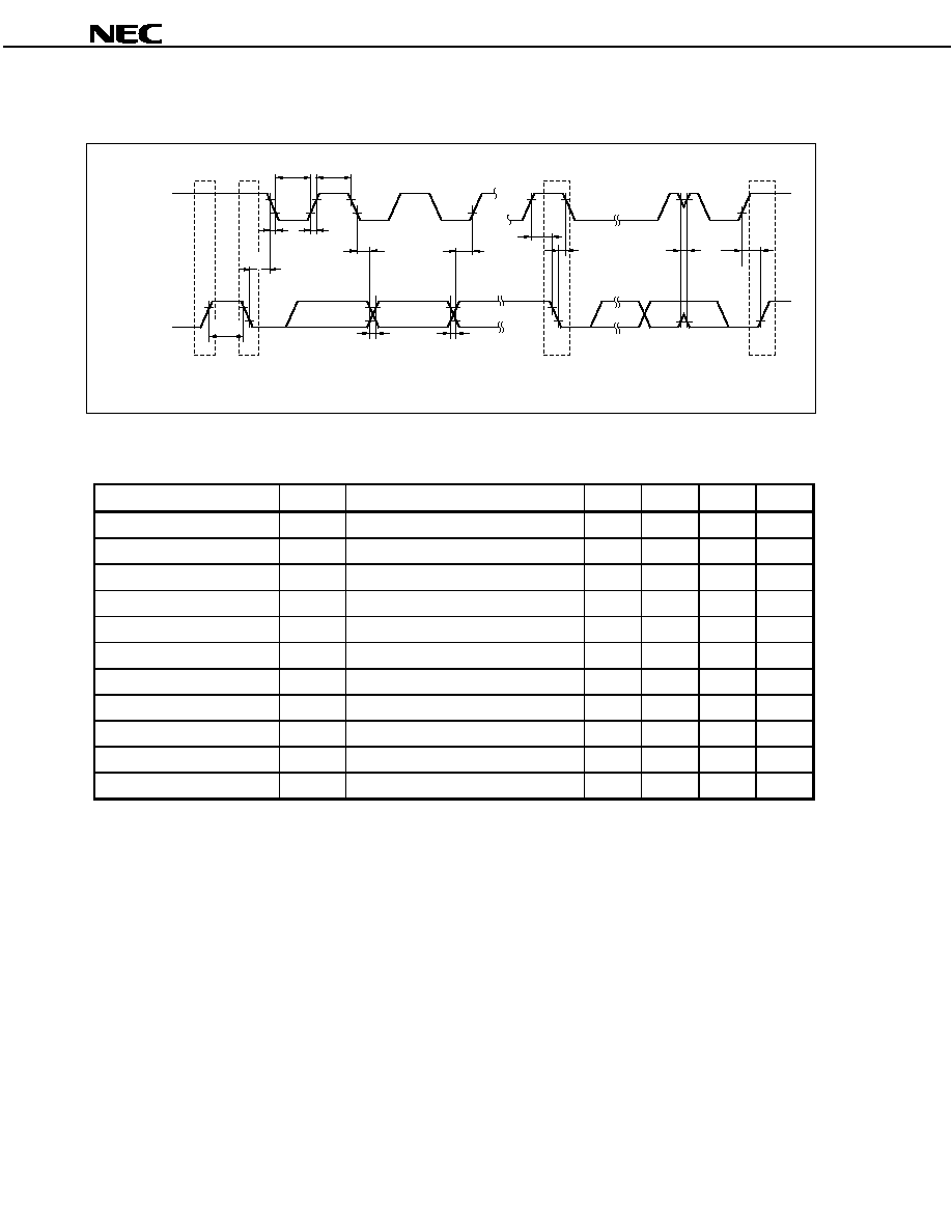
Preliminary Product Information U15436EJ1V0PM
90
µ
µ
µ
µPD703201, 703201Y, 703204, 703204Y, 70F3201, 70F3201Y, 70F3204, 70F3204Y
I
2
C Bus Mode (
µ
µ
µ
µPD703201Y, 703204Y, 70F3201Y, 70F3204Y only)
Stop
condition
Stop
condition
Start
condition
Restart
condition
SCL (I/O)
SDA (I/O)
<105>
<111>
<111>
<110>
<110>
<108>
<109>
<107>
<104>
<103>
<104>
<113>
<112>
<106>
A/D Converter
(T
A
= ≠40 to +85∞C, V
DD
= AV
DD
= AV
REF0
= 2.2 to 2.7 V, AV
SS
= V
SS
= 0 V, C
L
= 50 pF)
Parameter
Symbol
Conditions
MIN.
TYP.
MAX.
Unit
Resolution
10
10
10
bit
Overall error
Note 1
T.B.D.
%FSR
Conversion time
t
CONV
T.B.D.
µs
Zero-scale error
Note 1
T.B.D.
%FSR
Full-scale error
Note 1
T.B.D.
%FSR
Integral linearity error
Note 2
T.B.D.
LSB
Differential linearity error
Note 2
T.B.D.
LSB
Analog reference voltage
AV
REF
AV
REF0
=
AV
DD
2.2
2.7
V
Analog input voltage
V
IAN
AV
SS
AV
REF
V
AV
REF0
current
AI
REF0
T.B.D.
µA
AV
DD
power supply current
AI
DD
T.B.D.
mA
Notes 1. Excluding quantization error (
±0.05 %FSR)
2. Excluding quantization error (
±0.5 LSB)
Remark LSB: Least Significant Bit
FSR: Full Scale Range

Preliminary Product Information U15436EJ1V0PM
91
µ
µ
µ
µPD703201, 703201Y, 703204, 703204Y, 70F3201, 70F3201Y, 70F3204, 70F3204Y
D/A Converter
(T
A
= ≠40 to +85
∞
∞
∞
∞C, V
DD
= AV
DD
= AV
REF1
= 2.2 to 2.7 V, AV
SS
= V
SS
= 0 V, C
L
= 50 pF)
Parameter
Symbol
Conditions
MIN.
TYP.
MAX.
Unit
Resolution
8
8
8
bit
Overall error
Note
Load conditions: 2 M
, 30 pF
AV
REF1
= V
DD
T.B.D.
%FSR
Settling time
T.B.D.
µs
Output resistance
T.B.D.
k
Analog reference voltage
AV
REF
AV
REF1
= V
DD
2.2
2.7
V
AV
REF1
current
AV
REF1
Per channel
T.B.D.
mA
Note Excludes quantization error (
±0.05%FSR).
Preliminary Product Information U15436EJ1V0PM
92
µ
µ
µ
µPD703201, 703201Y, 703204, 703204Y, 70F3201, 70F3201Y, 70F3204, 70F3204Y
21. PACKAGE DRAWINGS
100-PIN PLASTIC LQFP (FINE PITCH) (14x14)
NOTE
Each lead centerline is located within 0.08 mm of
its true position (T.P.) at maximum material condition.
ITEM
MILLIMETERS
A
B
D
G
16.00
±0.20
14.00
±0.20
0.50 (T.P.)
1.00
J
16.00
±0.20
K
C
14.00
±0.20
I
0.08
1.00
±0.20
L
0.50
±0.20
F
1.00
N
P
Q
0.08
1.40
±0.05
0.10
±0.05
S100GC-50-8EU, 8EA-2
S
1.60 MAX.
H
0.22+0.05
-0.04
M
0.17+0.03
-0.07
R
3
∞+7∞
-3∞
1
25
26
50
100
76
75
51
S
S
N
J
detail of lead end
C
D
A
B
R
K
M
L
P
I
S
Q
G
F
M
H

Preliminary Product Information U15436EJ1V0PM
93
µ
µ
µ
µPD703201, 703201Y, 703204, 703204Y, 70F3201, 70F3201Y, 70F3204, 70F3204Y
121-PIN PLASTIC FBGA (12x12)
ITEM
MILLIMETERS
D
12.00
±0.10
E
12.00
±0.10
0.10
P121F1-80-EA6
INDEX MARK
A
w
0.20
A2
A1
A
1.13
e
0.80
1.48
±0.10
0.35
±0.06
x
y
0.20
y1
1.20
ZD
1.20
ZE
0.08
ZE
A2
A1
b
ZD
B
A
S
S
w
A
S
w
B
S
y1
S
e
y
13
12
11
10
9
8
7
6
5
4
3
2
1
N M L K J H G F E D C B A
S
x
A B
M
E
D
b
0.50+0.05
-0.10
Preliminary Product Information U15436EJ1V0PM
94
µ
µ
µ
µPD703201, 703201Y, 703204, 703204Y, 70F3201, 70F3201Y, 70F3204, 70F3204Y
APPENDIX DEVELOPMENT TOOLS
(1) Hardware
Product Name
Description
In-circuit emulator
IE-V850ES-
◊◊
Note
(provisional name)
In-circuit emulator for V850ES
In-circuit emulator option board
IE-703204-MC-EM1
Note
(provisional name)
Option board to emulate V850ES/SA2,
V850ES/SA3 peripheral functions in combination
with in-circuit emulator
V850ES/SA2
Note
Emulation probe for 100-pin LQFP
Emulation probe
V850ES/SA3
Note
Emulation probe for 121-pin FBGA
Power supply unit
IE-70000-MC-PS-B
Power supply for in-circuit emulator
IE-70000-CD-IF-A
Interface board for connection to PC (for PCMCIA)
PC interface board
IE-70000-PCI-IF
Interface board for connection to PC (for PCI)
Flash programmer
Note
Flash programmer for writing a program to a single-
power-supply flash memory product.
V850ES/SA2
Note
Program adapter for 100-pin LQFP
Program adapter
V850ES/SA3
Note
Program adapter for 121-pin FBGA
Note Under development
(2) Software
Product Name
Description
Compiler
CA850
C compiler compliant with ANSI-C
Debugger
ID850
Debugger used in combination with in-circuit
emulator
Real-time OS
RX850
Real-time OS compliant with
µITRON specifications
V850ES/SA2
DF703201
Note
Definition file for V850ES/SA2
Device file
V850ES/SA3
DF703204
Note
Definition file for V850ES/SA3
Note Under development

Preliminary Product Information U15436EJ1V0PM
95
µ
µ
µ
µPD703201, 703201Y, 703204, 703204Y, 70F3201, 70F3201Y, 70F3204, 70F3204Y
[MEMO]

Preliminary Product Information U15436EJ1V0PM
96
µ
µ
µ
µPD703201, 703201Y, 703204, 703204Y, 70F3201, 70F3201Y, 70F3204, 70F3204Y
NOTES FOR CMOS DEVICES
1
PRECAUTION AGAINST ESD FOR SEMICONDUCTORS
Note:
Strong electric field, when exposed to a MOS device, can cause destruction of the gate oxide and
ultimately degrade the device operation. Steps must be taken to stop generation of static electricity
as much as possible, and quickly dissipate it once, when it has occurred. Environmental control
must be adequate. When it is dry, humidifier should be used. It is recommended to avoid using
insulators that easily build static electricity. Semiconductor devices must be stored and transported
in an anti-static container, static shielding bag or conductive material. All test and measurement
tools including work bench and floor should be grounded. The operator should be grounded using
wrist strap. Semiconductor devices must not be touched with bare hands. Similar precautions need
to be taken for PW boards with semiconductor devices on it.
2
HANDLING OF UNUSED INPUT PINS FOR CMOS
Note:
No connection for CMOS device inputs can be cause of malfunction. If no connection is provided
to the input pins, it is possible that an internal input level may be generated due to noise, etc., hence
causing malfunction. CMOS devices behave differently than Bipolar or NMOS devices. Input levels
of CMOS devices must be fixed high or low by using a pull-up or pull-down circuitry. Each unused
pin should be connected to V
DD
or GND with a resistor, if it is considered to have a possibility of
being an output pin. All handling related to the unused pins must be judged device by device and
related specifications governing the devices.
3
STATUS BEFORE INITIALIZATION OF MOS DEVICES
Note:
Power-on does not necessarily define initial status of MOS device. Production process of MOS
does not define the initial operation status of the device. Immediately after the power source is
turned ON, the devices with reset function have not yet been initialized. Hence, power-on does
not guarantee out-pin levels, I/O settings or contents of registers. Device is not initialized until the
reset signal is received. Reset operation must be executed immediately after power-on for devices
having reset function.
Caution
Purchase of NEC I
2
C components conveys a license under the Philips I
2
C Patent Rights to use
these components in an I
2
C system, provided that the system conforms to the I
2
C Standard
Specification as defined by Philips.
The related documents indicated in this publication may include preliminary versions.
However, preliminary versions are not marked as such.
V850 Family, V850ES/SA2, and V850ES/SA3 are trademarks of NEC Corporation.
TRON stands for The Real-time Operating system Nucleus.
ITRON is an abbreviation of Industrial TRON.

Preliminary Product Information U15436EJ1V0PM
97
µ
µ
µ
µPD703201, 703201Y, 703204, 703204Y, 70F3201, 70F3201Y, 70F3204, 70F3204Y
Regional Information
Some information contained in this document may vary from country to country. Before using any NEC
product in your application, pIease contact the NEC office in your country to obtain a list of authorized
representatives and distributors. They will verify:
∑
Device availability
∑
Ordering information
∑
Product release schedule
∑
Availability of related technical literature
∑
Development environment specifications (for example, specifications for third-party tools and
components, host computers, power plugs, AC supply voltages, and so forth)
∑
Network requirements
In addition, trademarks, registered trademarks, export restrictions, and other legal issues may also vary
from country to country.
NEC Electronics Inc. (U.S.)
Santa Clara, California
Tel: 408-588-6000
800-366-9782
Fax: 408-588-6130
800-729-9288
NEC Electronics (Germany) GmbH
Duesseldorf, Germany
Tel: 0211-65 03 02
Fax: 0211-65 03 490
NEC Electronics (UK) Ltd.
Milton Keynes, UK
Tel: 01908-691-133
Fax: 01908-670-290
NEC Electronics Italiana s.r.l.
Milano, Italy
Tel: 02-66 75 41
Fax: 02-66 75 42 99
NEC Electronics (Germany) GmbH
Benelux Office
Eindhoven, The Netherlands
Tel: 040-2445845
Fax: 040-2444580
NEC Electronics (France) S.A.
Velizy-Villacoublay, France
Tel: 01-3067-5800
Fax: 01-3067-5899
NEC Electronics (France) S.A.
Madrid Office
Madrid, Spain
Tel: 091-504-2787
Fax: 091-504-2860
NEC Electronics (Germany) GmbH
Scandinavia Office
Taeby, Sweden
Tel: 08-63 80 820
Fax: 08-63 80 388
NEC Electronics Hong Kong Ltd.
Hong Kong
Tel: 2886-9318
Fax: 2886-9022/9044
NEC Electronics Hong Kong Ltd.
Seoul Branch
Seoul, Korea
Tel: 02-528-0303
Fax: 02-528-4411
NEC Electronics Singapore Pte. Ltd.
Novena Square, Singapore
Tel: 253-8311
Fax: 250-3583
NEC Electronics Taiwan Ltd.
Taipei, Taiwan
Tel: 02-2719-2377
Fax: 02-2719-5951
NEC do Brasil S.A.
Electron Devices Division
Guarulhos-SP, Brasil
Tel: 11-6462-6810
Fax: 11-6462-6829
J01.2

µ
µ
µ
µPD703201, 703201Y, 703204, 703204Y, 70F3201, 70F3201Y, 70F3204, 70F3204Y
The export of these products from Japan is regulated by the Japanese government. The export of some or all of these
products may be prohibited without governmental license. To export or re-export some or all of these products from a
country other than Japan may also be prohibited without a license from that country. Please call an NEC sales
representative.
License not needed:
µPD70F3201, 70F3201Y, 70F3204, 70F3204Y
The customer must judge the need for license:
µPD703201, 703201Y, 703204, 703204Y
∑ The information contained in this document is being issued in advance of the production cycle for the
device. The parameters for the device may change before final production or NEC Corporation, at its own
discretion, may withdraw the device prior to its production.
∑ No part of this document may be copied or reproduced in any form or by any means without the prior written
consent of NEC Corporation. NEC Corporation assumes no responsibility for any errors which may appear in
this document.
∑ NEC Corporation does not assume any liability for infringement of patents, copyrights or other intellectual property
rights of third parties by or arising from use of a device described herein or any other liability arising from use
of such device. No license, either express, implied or otherwise, is granted under any patents, copyrights or other
intellectual property rights of NEC Corporation or others.
∑ Descriptions of circuits, software, and other related information in this document are provided for illustrative
purposes in semiconductor product operation and application examples. The incorporation of these circuits,
software, and information in the design of the customer's equipment shall be done under the full responsibility
of the customer. NEC Corporation assumes no responsibility for any losses incurred by the customer or third
parties arising from the use of these circuits, software, and information.
∑ While NEC Corporation has been making continuous effort to enhance the reliability of its semiconductor devices,
the possibility of defects cannot be eliminated entirely. To minimize risks of damage or injury to persons or
property arising from a defect in an NEC semiconductor device, customers must incorporate sufficient safety
measures in its design, such as redundancy, fire-containment, and anti-failure features.
∑ NEC devices are classified into the following three quality grades:
"Standard", "Special", and "Specific". The Specific quality grade applies only to devices developed based on a
customer designated "quality assurance program" for a specific application. The recommended applications of
a device depend on its quality grade, as indicated below. Customers must check the quality grade of each device
before using it in a particular application.
Standard: Computers, office equipment, communications equipment, test and measurement equipment,
audio and visual equipment, home electronic appliances, machine tools, personal electronic
equipment and industrial robots
Special: Transportation equipment (automobiles, trains, ships, etc.), traffic control systems, anti-disaster
systems, anti-crime systems, safety equipment and medical equipment (not specifically designed
for life support)
Specific: Aircraft, aerospace equipment, submersible repeaters, nuclear reactor control systems, life
support systems or medical equipment for life support, etc.
The quality grade of NEC devices is "Standard" unless otherwise specified in NEC's Data Sheets or Data Books.
If customers intend to use NEC devices for applications other than those specified for Standard quality grade,
they should contact an NEC sales representative in advance.
M5 98. 8