V850ES/JJ2 32-Bit Single-Chip Microcontrollers Hardware PUM

Document No. U17714EJ1V0UD00 (1st edition)
Date Published October 2005 N CP(K)
Printed in Japan
Preliminary User's Manual
V850ES/JJ2
32-Bit Single-Chip Microcontrollers
Hardware
2005
�
PD70F3720
�
PD70F3721
�
PD70F3722
�
PD70F3723
�
PD70F3724

Preliminary User's Manual U17714EJ1V0UD
2
[MEMO]

Preliminary User's Manual U17714EJ1V0UD
3
1
2
3
4
VOLTAGE APPLICATION WAVEFORM AT INPUT PIN
Waveform distortion due to input noise or a reflected wave may cause malfunction. If the input of the
CMOS device stays in the area between V
IL
(MAX) and V
IH
(MIN) due to noise, etc., the device may
malfunction. Take care to prevent chattering noise from entering the device when the input level is fixed,
and also in the transition period when the input level passes through the area between V
IL
(MAX) and
V
IH
(MIN).
HANDLING OF UNUSED INPUT PINS
Unconnected CMOS device inputs can be cause of malfunction. If an input pin is unconnected, it is
possible that an internal input level may be generated due to noise, etc., causing malfunction. CMOS
devices behave differently than Bipolar or NMOS devices. Input levels of CMOS devices must be fixed
high or low by using pull-up or pull-down circuitry. Each unused pin should be connected to V
DD
or GND
via a resistor if there is a possibility that it will be an output pin. All handling related to unused pins must
be judged separately for each device and according to related specifications governing the device.
PRECAUTION AGAINST ESD
A strong electric field, when exposed to a MOS device, can cause destruction of the gate oxide and
ultimately degrade the device operation. Steps must be taken to stop generation of static electricity as
much as possible, and quickly dissipate it when it has occurred. Environmental control must be
adequate. When it is dry, a humidifier should be used. It is recommended to avoid using insulators that
easily build up static electricity. Semiconductor devices must be stored and transported in an anti-static
container, static shielding bag or conductive material. All test and measurement tools including work
benches and floors should be grounded. The operator should be grounded using a wrist strap.
Semiconductor devices must not be touched with bare hands. Similar precautions need to be taken for
PW boards with mounted semiconductor devices.
STATUS BEFORE INITIALIZATION
Power-on does not necessarily define the initial status of a MOS device. Immediately after the power
source is turned ON, devices with reset functions have not yet been initialized. Hence, power-on does
not guarantee output pin levels, I/O settings or contents of registers. A device is not initialized until the
reset signal is received. A reset operation must be executed immediately after power-on for devices
with reset functions.
POWER ON/OFF SEQUENCE
In the case of a device that uses different power supplies for the internal operation and external
interface, as a rule, switch on the external power supply after switching on the internal power supply.
When switching the power supply off, as a rule, switch off the external power supply and then the
internal power supply. Use of the reverse power on/off sequences may result in the application of an
overvoltage to the internal elements of the device, causing malfunction and degradation of internal
elements due to the passage of an abnormal current.
The correct power on/off sequence must be judged separately for each device and according to related
specifications governing the device.
INPUT OF SIGNAL DURING POWER OFF STATE
Do not input signals or an I/O pull-up power supply while the device is not powered. The current
injection that results from input of such a signal or I/O pull-up power supply may cause malfunction and
the abnormal current that passes in the device at this time may cause degradation of internal elements.
Input of signals during the power off state must be judged separately for each device and according to
related specifications governing the device.
NOTES FOR CMOS DEVICES
5
6

Preliminary User's Manual U17714EJ1V0UD
4
IECUBE and MINICUBE are registered trademarks of NEC Electronics Corporation in Japan and Germany.
The information contained in this document is being issued in advance of the production cycle for the
product. The parameters for the product may change before final production or NEC Electronics
Corporation, at its own discretion, may withdraw the product prior to its production.
Not all products and/or types are available in every country. Please check with an NEC Electronics sales
representative for availability and additional information.
No part of this document may be copied or reproduced in any form or by any means without the prior written consent
of NEC Electronics. NEC Electronics assumes no responsibility for any errors that may appear in this document.
NEC Electronics does not assume any liability for infringement of patents, copyrights or other intellectual property
rights of third parties by or arising from the use of NEC Electronics products listed in this document or any other
liability arising from the use of such products. No license, express, implied or otherwise, is granted under any
patents, copyrights or other intellectual property rights of NEC Electronics or others.
Descriptions of circuits, software and other related information in this document are provided for illustrative purposes
in semiconductor product operation and application examples. The incorporation of these circuits, software and
information in the design of a customer's equipment shall be done under the full responsibility of the customer. NEC
Electronics assumes no responsibility for any losses incurred by customers or third parties arising from the use of
these circuits, software and information.
While NEC Electronics endeavors to enhance the quality, reliability and safety of NEC Electronics products,
customers agree and acknowledge that the possibility of defects thereof cannot be eliminated entirely. To minimize
risks of damage to property or injury (including death) to persons arising from defects in NEC Electronics products,
customers must incorporate sufficient safety measures in their design, such as redundancy, fire-containment and
anti-failure features.
NEC Electronics products are classified into the following three quality grades: "Standard", "Special" and "Specific".
The "Specific" quality grade applies only to NEC Electronics products developed based on a customer-designated
"quality assurance program" for a specific application. The recommended applications of an NEC Electronics
products depend on its quality grade, as indicated below. Customers must check the quality grade of each NEC
Electronics product before using it in a particular application.
"Standard": Computers, office equipment, communications equipment, test and measurement equipment, audio and
visual equipment, home electronic appliances, machine tools, personal electronic equipment and
industrial robots.
"Special": Transportation equipment (automobiles, trains, ships, etc.), traffic control systems, anti-disaster
systems, anti-crime systems, safety equipment and medical equipment (not specifically designed for life
support).
"Specific": Aircraft, aerospace equipment, submersible repeaters, nuclear reactor control systems, life support
systems and medical equipment for life support, etc.
The quality grade of NEC Electronics products is "Standard" unless otherwise expressly specified in NEC
Electronics data sheets or data books, etc. If customers wish to use NEC Electronics products in applications
not intended by NEC Electronics, they must contact an NEC Electronics sales representative in advance to
determine NEC Electronics' willingness to support a given application.
(Note)
(1) "NEC Electronics" as used in this statement means NEC Electronics Corporation and also includes its
majority-owned subsidiaries.
(2) "NEC Electronics products" means any product developed or manufactured by or for NEC Electronics (as
defined above).
�
�
�
�
�
�
�
M5D 02. 11-1

Preliminary User's Manual U17714EJ1V0UD
5
Regional Information
�
Device availability
�
Ordering information
�
Product release schedule
�
Availability of related technical literature
�
Development environment specifications (for example, specifications for third-party tools and
components, host computers, power plugs, AC supply voltages, and so forth)
�
Network requirements
In addition, trademarks, registered trademarks, export restrictions, and other legal issues may also vary
from country to country.
[GLOBAL SUPPORT]
http://www.necel.com/en/support/support.html
NEC Electronics America, Inc. (U.S.)
Santa Clara, California
Tel: 408-588-6000
800-366-9782
NEC Electronics Hong Kong Ltd.
Hong Kong
Tel: 2886-9318
NEC Electronics Hong Kong Ltd.
Seoul Branch
Seoul, Korea
Tel: 02-558-3737
NEC Electronics Shanghai Ltd.
Shanghai, P.R. China
Tel: 021-5888-5400
NEC Electronics Taiwan Ltd.
Taipei, Taiwan
Tel: 02-2719-2377
NEC Electronics Singapore Pte. Ltd.
Novena Square, Singapore
Tel: 6253-8311
J05.6
NEC Electronics (Europe) GmbH
Duesseldorf, Germany
Tel: 0211-65030
�
Sucursal en Espa�a
Madrid, Spain
Tel: 091-504 27 87
V�lizy-Villacoublay, France
Tel: 01-30-67 58 00
�
Succursale Fran�aise
�
Filiale Italiana
Milano, Italy
Tel: 02-66 75 41
�
Branch The Netherlands
Eindhoven, The Netherlands
Tel: 040-265 40 10
�
Tyskland Filial
Taeby, Sweden
Tel: 08-63 87 200
�
United Kingdom Branch
Milton Keynes, UK
Tel: 01908-691-133
Some information contained in this document may vary from country to country. Before using any NEC
Electronics product in your application, pIease contact the NEC Electronics office in your country to
obtain a list of authorized representatives and distributors. They will verify:

Preliminary User's Manual U17714EJ1V0UD
6
PREFACE
Readers
This manual is intended for users who wish to understand the functions of the
V850ES/JJ2 and design application systems using the V850ES/JJ2.
Purpose
This manual is intended to give users an understanding of the hardware functions of
the V850ES/JJ2 shown in the Organization below.
Organization
This manual is divided into two parts: Hardware (this manual) and Architecture
(V850ES Architecture User's Manual).
Hardware
Architecture
� Pin functions
� Data types
� CPU function
� Register set
� On-chip peripheral functions
� Instruction format and instruction set
� Flash memory programming
� Interrupts and exceptions
� Electrical specifications (target)
� Pipeline operation
How to Read This Manual
It is assumed that the readers of this manual have general knowledge in the fields of
electrical engineering, logic circuits, and microcontrollers.
To understand the overall functions of the V850ES/JJ2
Read this manual according to the CONTENTS.
To find the details of a register where the name is known
Use APPENDIX A REGISTER INDEX.
To understand the details of an instruction function
Refer to the V850ES Architecture User's Manual available separately.
To know the electrical specifications of the V850ES/JJ2
See CHAPTER 28 ELECTRICAL SPECIFICATIONS (TARGET).
Register format
The name of the bit whose number is in angle brackets (<>) in the figure of the
register format of each register is defined as a reserved word in the device file.
The "yyy bit of the xxx register" is described as the "xxx.yyy bit" in this manual. Note
with caution that if "xxx.yyy" is described as is in a program, however, the
compiler/assembler cannot recognize it correctly.

Preliminary User's Manual U17714EJ1V0UD
7
Conventions
Data significance:
Higher digits on the left and lower digits on the right
Active low representation:
xxx (overscore over pin or signal name)
Memory map address:
Higher addresses on the top and lower addresses on
the bottom
Note:
Footnote for item marked with Note in the text
Caution:
Information requiring particular attention
Remark: Supplementary
information
Numeric representation:
Binary ... xxxx or xxxxB
Decimal ... xxxx
Hexadecimal ... xxxxH
Prefix indicating power of 2
(address space, memory
capacity):
K (kilo): 2
10
= 1,024
M (mega): 2
20
= 1,024
2
G (giga): 2
30
= 1,024
3

Preliminary User's Manual U17714EJ1V0UD
8
Related Documents
The related documents indicated in this publication may include preliminary versions.
However, preliminary versions are not marked as such.
Documents related to V850ES/JJ2
Document Name
Document No.
V850ES Architecture User's Manual
U15943E
V850ES/JJ2 Hardware User's Manual
This manual
Documents related to development tools
Document Name
Document No.
Operation
U17293E
C Language
U17291E
Assembly Language
U17292E
CA850 Ver. 3.00 C Compiler Package
Link Directives
U17294E
PM+ Ver. 6.00 Project Manager
U17178E
ID850QB Ver. 3.10 Integrated Debugger
Operation
U17435E
SM850 Ver. 2.50 System Simulator
Operation
U16218E
SM850 Ver. 2.00 or Later System Simulator
External Part User Open
Interface Specification
U14873E
Operation U17246E
SM+ System Simulator
User Open Interface
U17247E
Basics U13430E
Installation U17419E
Technical U13431E
RX850 Ver. 3.20 or Later Real-Time OS
Task Debugger
U17420E
Basics U13773E
Installation U17421E
Technical U13772E
RX850 Pro Ver. 3.20 Real-Time OS
Task Debugger
U17422E
AZ850 Ver. 3.30 System Performance Analyzer
U17423E
PG-FP4 Flash Memory Programmer
U15260E

Preliminary User's Manual U17714EJ1V0UD
9
CONTENTS
CHAPTER 1 INTRODUCTION .................................................................................................................18
1.1
General .....................................................................................................................................18
1.2
Features....................................................................................................................................21
1.3
Application Fields ...................................................................................................................22
1.4
Ordering Information ..............................................................................................................22
1.5
Pin Configuration (Top View) .................................................................................................23
1.6
Function Block Configuration................................................................................................25
1.6.1
Internal block diagram ............................................................................................................... 25
1.6.2
Internal units .............................................................................................................................. 26
CHAPTER 2 PIN FUNCTIONS ................................................................................................................29
2.1
List of Pin Functions...............................................................................................................29
2.2
Pin States .................................................................................................................................40
2.3
Pin I/O Circuit Types, I/O Buffer Power Supplies and Connection of Unused Pins.........41
2.4
Cautions ...................................................................................................................................45
CHAPTER 3 CPU FUNCTION.................................................................................................................46
3.1
Features....................................................................................................................................46
3.2
CPU Register Set.....................................................................................................................47
3.2.1
Program register set .................................................................................................................. 48
3.2.2
System register set.................................................................................................................... 49
3.3
Operation Modes .....................................................................................................................55
3.3.1
Specifying operation mode ........................................................................................................ 55
3.4
Address Space ........................................................................................................................56
3.4.1
CPU address space................................................................................................................... 56
3.4.2
Wraparound of CPU address space .......................................................................................... 57
3.4.3
Memory map.............................................................................................................................. 58
3.4.4
Areas ......................................................................................................................................... 60
3.4.5
Recommended use of address space ....................................................................................... 67
3.4.6
Peripheral I/O registers.............................................................................................................. 70
3.4.7
Special registers ........................................................................................................................ 82
3.4.8
Cautions .................................................................................................................................... 86
CHAPTER 4 PORT FUNCTIONS............................................................................................................90
4.1
Features....................................................................................................................................90
4.2
Basic Port Configuration ........................................................................................................90
4.3
Port Configuration...................................................................................................................91
4.3.1
Port 0......................................................................................................................................... 96
4.3.2
Port 1......................................................................................................................................... 99
4.3.3
Port 3....................................................................................................................................... 100
4.3.4
Port 4....................................................................................................................................... 106
4.3.5
Port 5....................................................................................................................................... 108
4.3.6
Port 6....................................................................................................................................... 112
4.3.7
Port 7....................................................................................................................................... 116
4.3.8
Port 8....................................................................................................................................... 118
4.3.9
Port 9....................................................................................................................................... 120

Preliminary User's Manual U17714EJ1V0UD
10
4.3.10
Port CD ....................................................................................................................................128
4.3.11
Port CM ...................................................................................................................................129
4.3.12
Port CS ....................................................................................................................................131
4.3.13
Port CT ....................................................................................................................................133
4.3.14
Port DH ....................................................................................................................................135
4.3.15
Port DL ....................................................................................................................................137
4.4
Block Diagrams..................................................................................................................... 140
4.5
Port Register Settings When Alternate Function Is Used ................................................ 172
4.6
Cautions ................................................................................................................................ 181
4.6.1
Cautions on setting port pins ...................................................................................................181
4.6.2
Cautions on bit manipulation instruction for port n register (Pn)...............................................184
4.6.3
Cautions on on-chip debug pins...............................................................................................185
4.6.4
Cautions on P05/INTP2/DRST pin...........................................................................................185
4.6.5
Cautions on P10, P11, and P53 pins when power is turned on ............................................... 185
4.6.6
Hysteresis characteristics ........................................................................................................185
CHAPTER 5 BUS CONTROL FUNCTION .......................................................................................... 186
5.1
Features................................................................................................................................. 186
5.2
Bus Control Pins................................................................................................................... 187
5.2.1
Pin status when internal ROM, internal RAM, or on-chip peripheral I/O is accessed...............187
5.2.2
Pin status in each operation mode...........................................................................................187
5.3
Memory Block Function....................................................................................................... 188
5.4
External Bus Interface Mode Control Function ................................................................. 189
5.5
Bus Access ........................................................................................................................... 190
5.5.1
Number of clocks for access....................................................................................................190
5.5.2
Bus size setting function ..........................................................................................................190
5.5.3
Access by bus size ..................................................................................................................191
5.6
Wait Function ........................................................................................................................ 198
5.6.1
Programmable wait function ....................................................................................................198
5.6.2
External wait function...............................................................................................................199
5.6.3
Relationship between programmable wait and external wait ................................................... 200
5.6.4
Programmable address wait function.......................................................................................201
5.7
Idle State Insertion Function ............................................................................................... 202
5.8
Bus Hold Function................................................................................................................ 203
5.8.1
Functional outline.....................................................................................................................203
5.8.2
Bus hold procedure..................................................................................................................204
5.8.3
Operation in power save mode ................................................................................................204
5.9
Bus Priority ........................................................................................................................... 205
5.10
Bus Timing ............................................................................................................................ 206
CHAPTER 6 CLOCK GENERATION FUNCTION .............................................................................. 212
6.1
Overview................................................................................................................................ 212
6.2
Configuration ........................................................................................................................ 213
6.3
Registers ............................................................................................................................... 215
6.4
Operation............................................................................................................................... 220
6.4.1
Operation of each clock ...........................................................................................................220
6.4.2
Clock output function ...............................................................................................................220
6.5
PLL Function......................................................................................................................... 221
6.5.1
Overview..................................................................................................................................221

Preliminary User's Manual U17714EJ1V0UD
11
6.5.2
Registers ................................................................................................................................. 221
6.5.3
Usage ...................................................................................................................................... 224
CHAPTER 7 16-BIT TIMER/EVENT COUNTER P (TMP) .................................................................225
7.1
Overview.................................................................................................................................225
7.2
Functions ...............................................................................................................................225
7.3
Configuration .........................................................................................................................226
7.4
Registers ................................................................................................................................228
7.5
Operation................................................................................................................................240
7.5.1
Interval timer mode (TPnMD2 to TPnMD0 bits = 000)............................................................. 241
7.5.2
External event count mode (TPnMD2 to TPnMD0 bits = 001) ................................................. 251
7.5.3
External trigger pulse output mode (TPnMD2 to TPnMD0 bits = 010)..................................... 259
7.5.4
One-shot pulse output mode (TPnMD2 to TPnMD0 bits = 011) .............................................. 271
7.5.5
PWM output mode (TPnMD2 to TPnMD0 bits = 100).............................................................. 278
7.5.6
Free-running timer mode (TPnMD2 to TPnMD0 bits = 101) .................................................... 287
7.5.7
Pulse width measurement mode (TPnMD2 to TPnMD0 bits = 110) ........................................ 304
7.5.8
Timer output operations........................................................................................................... 310
7.6 Selector
Function ..................................................................................................................311
7.7
Cautions .................................................................................................................................313
CHAPTER 8 16-BIT TIMER/EVENT COUNTER Q (TMQ) ................................................................314
8.1
Overview.................................................................................................................................314
8.2
Functions ...............................................................................................................................314
8.3
Configuration .........................................................................................................................315
8.4
Registers ................................................................................................................................317
8.5
Operation................................................................................................................................333
8.5.1
Interval timer mode (TQ0MD2 to TQ0MD0 bits = 000) ............................................................ 334
8.5.2
External event count mode (TQ0MD2 to TQ0MD0 bits = 001) ................................................ 343
8.5.3
External trigger pulse output mode (TQ0MD2 to TQ0MD0 bits = 010) .................................... 352
8.5.4
One-shot pulse output mode (TQ0MD2 to TQ0MD0 bits = 011) ............................................. 365
8.5.5
PWM output mode (TQ0MD2 to TQ0MD0 bits = 100) ............................................................. 374
8.5.6
Free-running timer mode (TQ0MD2 to TQ0MD0 bits = 101) ................................................... 385
8.5.7
Pulse width measurement mode (TQ0MD2 to TQ0MD0 bits = 110)........................................ 405
8.5.8
Timer output operations........................................................................................................... 411
8.6
Cautions .................................................................................................................................412
CHAPTER 9 16-BIT INTERVAL TIMER M (TMM).............................................................................413
9.1
Overview.................................................................................................................................413
9.2
Configuration .........................................................................................................................414
9.3
Register ..................................................................................................................................415
9.4
Operation................................................................................................................................416
9.4.1
Interval timer mode.................................................................................................................. 416
9.4.2
Cautions .................................................................................................................................. 420
CHAPTER 10 WATCH TIMER FUNCTIONS .......................................................................................421
10.1
Functions ...............................................................................................................................421
10.2
Configuration .........................................................................................................................422
10.3
Control Registers ..................................................................................................................424
10.4
Operation................................................................................................................................428

Preliminary User's Manual U17714EJ1V0UD
12
10.4.1
Operation as watch timer .........................................................................................................428
10.4.2
Operation as interval timer.......................................................................................................429
10.4.3
Cautions...................................................................................................................................430
CHAPTER 11 FUNCTIONS OF WATCHDOG TIMER 2 ................................................................... 431
11.1
Functions............................................................................................................................... 431
11.2
Configuration ........................................................................................................................ 432
11.3
Registers ............................................................................................................................... 433
11.4
Operation............................................................................................................................... 435
CHAPTER 12 REAL-TIME OUTPUT FUNCTION (RTO)................................................................... 436
12.1
Function................................................................................................................................. 436
12.2
Configuration ........................................................................................................................ 437
12.3
Registers ............................................................................................................................... 439
12.4
Operation............................................................................................................................... 441
12.5
Usage ................................................................................................................................... 442
12.6
Cautions ................................................................................................................................ 442
CHAPTER 13 A/D CONVERTER ......................................................................................................... 443
13.1
Overview................................................................................................................................ 443
13.2
Functions............................................................................................................................... 443
13.3
Configuration ........................................................................................................................ 444
13.4
Registers ............................................................................................................................... 447
13.5
Operation............................................................................................................................... 458
13.5.1
Basic operation ........................................................................................................................458
13.5.2
Conversion operation timing ....................................................................................................459
13.5.3
Trigger mode ...........................................................................................................................460
13.5.4
Operation mode .......................................................................................................................462
13.5.5
Power-fail compare mode ........................................................................................................466
13.6
Cautions ................................................................................................................................ 471
13.7
How to Read A/D Converter Characteristics Table........................................................... 475
CHAPTER 14 D/A CONVERTER ......................................................................................................... 479
14.1
Functions............................................................................................................................... 479
14.2
Configuration ........................................................................................................................ 479
14.3
Registers ............................................................................................................................... 480
14.4
Operation............................................................................................................................... 482
14.4.1
Operation in normal mode .......................................................................................................482
14.4.2
Operation in real-time output mode..........................................................................................482
14.4.3
Cautions...................................................................................................................................483
CHAPTER 15 ASYNCHRONOUS SERIAL INTERFACE A (UARTA) ............................................. 484
15.1
Mode Switching of UARTA and Other Serial Interfaces ................................................... 484
15.1.1
CSIB4 and UARTA0 mode switching.......................................................................................484
15.1.2
UARTA2 and I
2
C00 mode switching.........................................................................................485
15.1.3
UARTA1 and I
2
C02 mode switching.........................................................................................486
15.2
Features................................................................................................................................. 487
15.3
Configuration ........................................................................................................................ 488
15.4
Registers ............................................................................................................................... 490

Preliminary User's Manual U17714EJ1V0UD
13
15.5
Interrupt Request Signals.....................................................................................................496
15.6
Operation................................................................................................................................497
15.6.1
Data format.............................................................................................................................. 497
15.6.2
SBF transmission/reception format.......................................................................................... 499
15.6.3
SBF transmission .................................................................................................................... 501
15.6.4
SBF reception.......................................................................................................................... 502
15.6.5
UART transmission.................................................................................................................. 503
15.6.6
Continuous transmission procedure ........................................................................................ 504
15.6.7
UART reception ....................................................................................................................... 506
15.6.8
Reception errors ...................................................................................................................... 507
15.6.9
Parity types and operations ..................................................................................................... 509
15.6.10
Receive data noise filter .......................................................................................................... 510
15.7
Dedicated Baud Rate Generator ..........................................................................................511
15.8
Cautions .................................................................................................................................519
CHAPTER 16 3-WIRE VARIABLE-LENGTH SERIAL I/O (CSIB) ....................................................520
16.1
Mode Switching of CSIB and Other Serial Interfaces........................................................520
16.1.1
CSIB4 and UARTA0 mode switching ...................................................................................... 520
16.1.2
CSIB0 and I
2
C01 mode switching ............................................................................................ 521
16.2
Features..................................................................................................................................521
16.3
Configuration .........................................................................................................................522
16.4
Registers ................................................................................................................................524
16.5
Operation................................................................................................................................531
16.5.1
Single transfer mode (master mode, transmission/reception mode)........................................ 531
16.5.2
Single transfer mode (master mode, reception mode)............................................................. 532
16.5.3
Continuous mode (master mode, transmission/reception mode)............................................. 533
16.5.4
Continuous mode (master mode, reception mode).................................................................. 534
16.5.5
Continuous reception mode (error) .......................................................................................... 535
16.5.6
Continuous mode (slave mode, transmission/reception mode) ............................................... 536
16.5.7
Continuous mode (slave mode, reception mode) .................................................................... 537
16.5.8
Clock timing ............................................................................................................................. 538
16.6
Output Pins ............................................................................................................................540
16.7
Operation Flow ......................................................................................................................541
16.8
Baud Rate Generator ............................................................................................................547
16.8.1
Baud rate generation ............................................................................................................... 548
16.9
Cautions .................................................................................................................................549
CHAPTER 17 I
2
C BUS...........................................................................................................................550
17.1
Mode Switching of I
2
C Bus and Other Serial Interfaces ....................................................550
17.1.1
UARTA2 and I
2
C00 mode switching ........................................................................................ 550
17.1.2
CSIB0 and I
2
C01 mode switching ............................................................................................ 551
17.1.3
UARTA1 and I
2
C02 mode switching ........................................................................................ 552
17.2
Features..................................................................................................................................553
17.3
Configuration .........................................................................................................................554
17.4
Registers ................................................................................................................................558
17.5
I
2
C Bus Mode Functions .......................................................................................................574
17.5.1
Pin configuration...................................................................................................................... 574
17.6
I
2
C Bus Definitions and Control Methods ...........................................................................575
17.6.1
Start condition.......................................................................................................................... 575

Preliminary User's Manual U17714EJ1V0UD
14
17.6.2
Addresses................................................................................................................................576
17.6.3
Transfer direction specification ................................................................................................577
17.6.4
ACK .........................................................................................................................................578
17.6.5
Stop condition ..........................................................................................................................579
17.6.6
Wait state.................................................................................................................................580
17.6.7
Wait state cancellation method ................................................................................................582
17.7
I
2
C Interrupt Request Signals (INTIICn) .............................................................................. 583
17.7.1
Master device operation...........................................................................................................583
17.7.2
Slave device operation (when receiving slave address data (address match))........................586
17.7.3
Slave device operation (when receiving extension code) ........................................................590
17.7.4
Operation without communication............................................................................................594
17.7.5
Arbitration loss operation (operation as slave after arbitration loss).........................................594
17.7.6
Operation when arbitration loss occurs (no communication after arbitration loss) ...................596
17.8
Interrupt Request Signal (INTIICn) Generation Timing and Wait Control....................... 603
17.9
Address Match Detection Method ...................................................................................... 605
17.10
Error Detection...................................................................................................................... 605
17.11
Extension Code..................................................................................................................... 605
17.12
Arbitration ............................................................................................................................. 606
17.13
Wakeup Function.................................................................................................................. 607
17.14
Communication Reservation............................................................................................... 608
17.14.1
When communication reservation function is enabled (IICFn.IICRSVn bit = 0) .......................608
17.14.2
When communication reservation function is disabled (IICFn.IICRSVn bit = 1).......................612
17.15
Cautions ................................................................................................................................ 613
17.16
Communication Operations ................................................................................................ 614
17.16.1
Master operation 1 ...................................................................................................................614
17.16.2
Master operation 2 ...................................................................................................................616
17.16.3
Slave operation........................................................................................................................617
17.17
Timing of Data Communication .......................................................................................... 620
CHAPTER 18 DMA FUNCTION (DMA CONTROLLER) ................................................................... 627
18.1
Features................................................................................................................................. 627
18.2
Configuration ........................................................................................................................ 628
18.3
Registers ............................................................................................................................... 629
18.4
Transfer Targets ................................................................................................................... 636
18.5
Transfer Modes ..................................................................................................................... 637
18.6
Transfer Types ...................................................................................................................... 637
18.7
DMA Channel Priorities........................................................................................................ 638
18.8
Time Related to DMA Transfer ............................................................................................ 638
18.9
DMA Transfer Start Factors................................................................................................. 639
18.10
DMA Abort Factors ............................................................................................................... 640
18.11
End of DMA Transfer ............................................................................................................ 640
18.12
Operation Timing .................................................................................................................. 640
18.13
Cautions ................................................................................................................................ 645
CHAPTER 19 INTERRUPT/EXCEPTION PROCESSING FUNCTION............................................... 650
19.1
Features................................................................................................................................. 650
19.2
Non-Maskable Interrupts ..................................................................................................... 654
19.2.1
Operation .................................................................................................................................656
19.2.2
Restore ....................................................................................................................................657

Preliminary User's Manual U17714EJ1V0UD
15
19.2.3
NP flag..................................................................................................................................... 658
19.3
Maskable Interrupts ..............................................................................................................659
19.3.1
Operation................................................................................................................................. 659
19.3.2
Restore.................................................................................................................................... 661
19.3.3
Priorities of maskable interrupts .............................................................................................. 662
19.3.4
Interrupt control register (xxICn) .............................................................................................. 666
19.3.5
Interrupt mask registers 0 to 4 (IMR0 to IMR4)........................................................................ 668
19.3.6
In-service priority register (ISPR)............................................................................................. 670
19.3.7
ID flag ...................................................................................................................................... 671
19.3.8
Watchdog timer mode register 2 (WDTM2) ............................................................................. 671
19.4
Software Exception ...............................................................................................................672
19.4.1
Operation................................................................................................................................. 672
19.4.2
Restore.................................................................................................................................... 673
19.4.3
EP flag..................................................................................................................................... 674
19.5
Exception Trap ......................................................................................................................675
19.5.1
Illegal opcode definition ........................................................................................................... 675
19.5.2
Debug trap............................................................................................................................... 677
19.6
External Interrupt Request Input Pins (NMI and INTP0 to INTP8) ....................................679
19.6.1
Noise elimination ..................................................................................................................... 679
19.6.2
Edge detection......................................................................................................................... 679
19.7
Interrupt Acknowledge Time of CPU...................................................................................685
19.8
Periods in Which Interrupts Are Not Acknowledged by CPU...........................................686
19.9
Cautions .................................................................................................................................686
CHAPTER 20 KEY INTERRUPT FUNCTION ......................................................................................687
20.1
Function .................................................................................................................................687
20.2
Register ..................................................................................................................................688
20.3
Cautions .................................................................................................................................688
CHAPTER 21 STANDBY FUNCTION...................................................................................................689
21.1
Overview.................................................................................................................................689
21.2
Registers ................................................................................................................................691
21.3
HALT Mode.............................................................................................................................694
21.3.1
Setting and operation status .................................................................................................... 694
21.3.2
Releasing HALT mode ............................................................................................................ 694
21.4
IDLE1 Mode ............................................................................................................................696
21.4.1
Setting and operation status .................................................................................................... 696
21.4.2
Releasing IDLE1 mode............................................................................................................ 696
21.5
IDLE2 Mode ............................................................................................................................698
21.5.1
Setting and operation status .................................................................................................... 698
21.5.2
Releasing IDLE2 mode............................................................................................................ 698
21.5.3
Securing setup time when releasing IDLE2 mode ................................................................... 700
21.6
STOP Mode ............................................................................................................................701
21.6.1
Setting and operation status .................................................................................................... 701
21.6.2
Releasing STOP mode ............................................................................................................ 701
21.6.3
Securing oscillation stabilization time when releasing STOP mode......................................... 704
21.7
Subclock Operation Mode ....................................................................................................705
21.7.1
Setting and operation status .................................................................................................... 705
21.7.2
Releasing subclock operation mode ........................................................................................ 705

Preliminary User's Manual U17714EJ1V0UD
16
21.8
Sub-IDLE Mode ..................................................................................................................... 707
21.8.1
Setting and operation status ....................................................................................................707
21.8.2
Releasing sub-IDLE mode .......................................................................................................707
CHAPTER 22 RESET FUNCTIONS ..................................................................................................... 709
22.1
Overview................................................................................................................................ 709
22.2
Registers to Check Reset Source....................................................................................... 710
22.3
Operation............................................................................................................................... 711
22.3.1
Reset operation via RESET pin ...............................................................................................711
22.3.2
Reset operation by watchdog timer 2.......................................................................................713
22.3.3
Reset operation by low-voltage detector..................................................................................715
22.3.4
Operation after reset release ...................................................................................................716
22.3.5
Reset function operation flow...................................................................................................719
CHAPTER 23 CLOCK MONITOR ........................................................................................................ 720
23.1
Functions............................................................................................................................... 720
23.2
Configuration ........................................................................................................................ 720
23.3
Register ................................................................................................................................. 721
23.4
Operation............................................................................................................................... 722
CHAPTER 24 LOW-VOLTAGE DETECTOR (LVI) ............................................................................. 725
24.1
Functions............................................................................................................................... 725
24.2
Configuration ........................................................................................................................ 725
24.3
Registers ............................................................................................................................... 726
24.4
Operation............................................................................................................................... 728
24.4.1
To use for internal reset signal.................................................................................................728
24.4.2
To use for interrupt ..................................................................................................................729
24.5
RAM Retention Voltage Detection Operation .................................................................... 730
24.6
Emulation Function .............................................................................................................. 731
CHAPTER 25 REGULATOR ................................................................................................................. 732
25.1
Overview................................................................................................................................ 732
25.2
Operation............................................................................................................................... 733
CHAPTER 26 FLASH MEMORY .......................................................................................................... 734
26.1
Features................................................................................................................................. 734
26.2
Memory Configuration ......................................................................................................... 735
26.3
Functional Outline ................................................................................................................ 736
26.4
Rewriting by Dedicated Flash Programmer....................................................................... 738
26.4.1
Programming environment.......................................................................................................738
26.4.2
Communication mode ..............................................................................................................739
26.4.3
Flash memory control ..............................................................................................................745
26.4.4
Selection of communication mode ...........................................................................................746
26.4.5
Communication commands .....................................................................................................747
26.4.6
Pin connection .........................................................................................................................748
26.5
Rewriting by Self Programming .......................................................................................... 752
26.5.1
Overview..................................................................................................................................752
26.5.2
Features...................................................................................................................................753
26.5.3
Standard self programming flow ..............................................................................................754

Preliminary User's Manual U17714EJ1V0UD
17
26.5.4
Flash functions ........................................................................................................................ 755
26.5.5
Pin processing ......................................................................................................................... 755
26.5.6
Internal resources used ........................................................................................................... 756
CHAPTER 27 ON-CHIP DEBUG FUNCTION......................................................................................757
27.1
Features..................................................................................................................................757
27.2
Connection Circuit Example ................................................................................................758
27.3
Interface Signals....................................................................................................................758
27.4
Register ..................................................................................................................................760
27.5
Operation................................................................................................................................762
27.6
ROM Security Function.........................................................................................................763
27.6.1
Security ID ............................................................................................................................... 763
27.6.2
Setting ..................................................................................................................................... 764
27.7
Cautions .................................................................................................................................765
CHAPTER 28 ELECTRICAL SPECIFICATIONS (TARGET) ..............................................................766
CHAPTER 29 PACKAGE DRAWING ...................................................................................................800
APPENDIX A REGISTER INDEX ..........................................................................................................801
APPENDIX B INSTRUCTION SET LIST..............................................................................................813
B.1
Conventions...........................................................................................................................813
B.2
Instruction Set (in Alphabetical Order) ...............................................................................816

Preliminary User's Manual U17714EJ1V0UD
18
CHAPTER 1 INTRODUCTION
The V850ES/JJ2 is one of the products in the NEC Electronics V850 Series of single-chip microcontrollers
designed for low-power operation for real-time control applications.
1.1 General
The V850ES/JJ2 is a 32-bit single-chip microcontroller that includes the V850ES CPU core and peripheral
functions such as ROM/RAM, a timer/counter, serial interfaces, an A/D converter, and a D/A converter.
In addition to high real-time response characteristics and 1-clock-pitch basic instructions, the V850ES/JJ2 features
multiply instructions, saturated operation instructions, bit manipulation instructions, etc., realized by a hardware
multiplier, as optimum instructions for digital servo control applications. Moreover, as a real-time control system, the
V850ES/JJ2 enables an extremely high cost-performance for applications that require low power consumption, such
as home audio, printers, and digital home electronics.
Table 1-1 lists the products of the V850ES/JJ2.
A model of the V850ES/JJ2 with reduced I/O, timer/counter, and serial interface functions, V850ES/JG2, is also
available. See Table 1-2 V850ES/JG2 Product List.
CHAPTER 1 INTRODUCTION
Preliminary User's Manual U17714EJ1V0UD
19
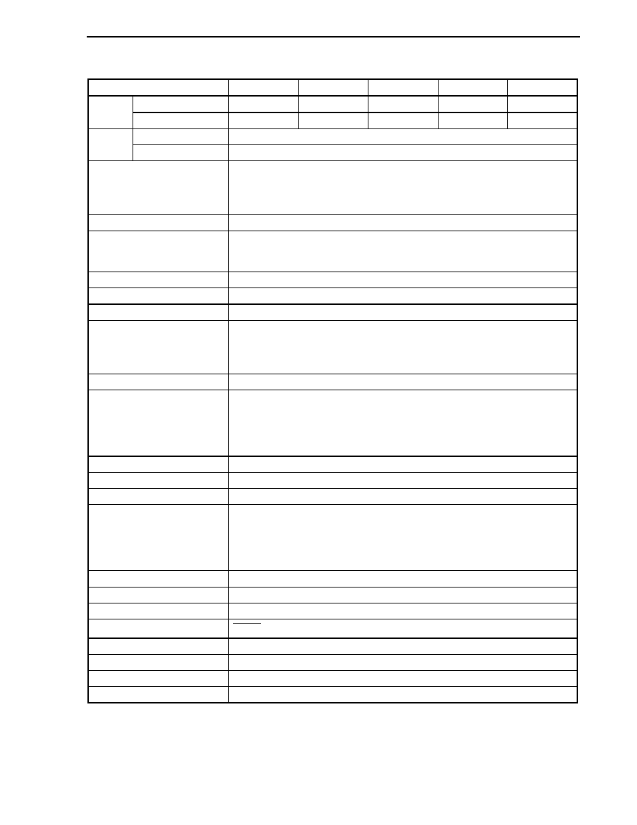
Table 1-1. V850ES/JJ2 Product List
Part Number
�
PD70F3720
�
PD70F3721
�
PD70F3722
�
PD70F3723
�
PD70F3724
Flash memory
128 KB
256 KB
384 KB
512 KB
640 KB
Internal
memory
RAM
12 KB
24 KB
32 KB
40 KB
48 KB
Logical space
64 MB
Memory
space
External memory area
16 MB
External bus interface
Address bus: 24 bits
Data bus: 8/16 bits
Multiplex bus mode/separate bus mode
Chip select signal: 4
General-purpose register
32 bits
� 32 registers
Main clock (oscillation frequency)
Ceramic/crystal/external clock
(in PLL mode: f
X
= 2.5 to 5 MHz (multiplied by 4) or f
X
= 2.5 MHz (multiplied by 8),
in clock through mode: f
X
= 2.5 to 10 MHz)
Subclock (oscillation frequency)
Crystal/external clock (f
XT
= 32.768 kHz)
Internal oscillator
f
R
= 200 kHz (TYP.)
Minimum instruction execution time
50 ns (main clock (f
XX
) = 20 MHz)
DSP function
32
� 32 = 64: 200 to 250 ns (at 20 MHz)
32
� 32 + 32 = 32: 300 ns (at 20 MHz)
16
� 16 = 32: 50 to 100 ns (at 20 MHz)
16
� 16 + 32 = 32: 150 ns (at 20 MHz)
I/O port
I/O: 128 (of which 5 V tolerant/N-ch open-drain output selectable: 60)
Timer
16-bit timer/event counter P: 9 channels
16-bit timer/event counter Q: 1 channel
16-bit interval timer M:
1 channel
Watch timer:
1 channel
Watchdog timer :
1 channel
Real-time output port
6 bits
� 2 channels
A/D converter
10-bit resolution
� 16 channels
D/A converter
8-bit resolution
� 2 channels
Serial interface
UART: 1
channel
UART/CSI: 1
channel
UART/I
2
C bus: 2 channels
CSI: 4
channels
CSI/I
2
C bus:
1 channel
DMA controller
4 channels (transfer target: on-chip peripheral I/O, internal RAM, external memory)
Interrupt source
External: 10 (10)
Note
, internal: 61
Power save function
HALT/IDLE1/IDLE2/STOP/subclock/sub-IDLE mode
Reset
RESET pin input, watchdog timer 2 (WDT2), clock monitor (CLM), low-voltage detector (LVI)
On-chip debug function
Provided (RUN/break)
Operating power supply voltage
2.85 to 3.6 V
Operating ambient temperature
-40 to +85�C
Package
144-pin plastic LQFP (fine pitch) (20
� 20 mm)
Note The figure in parentheses indicates the number of external interrupts that can release the STOP mode.
CHAPTER 1 INTRODUCTION
Preliminary User's Manual U17714EJ1V0UD
20
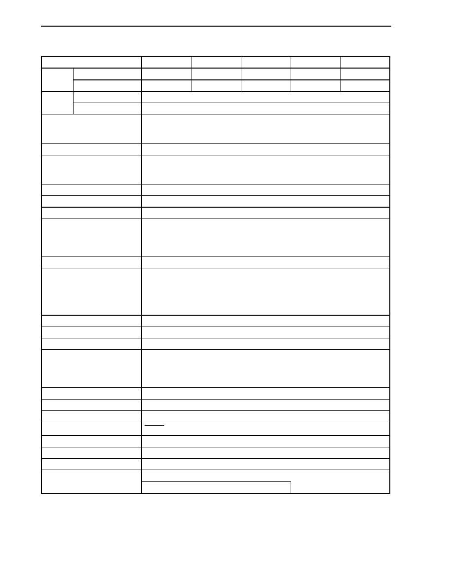
Table 1-2. V850ES/JG2 Product List
Part Number
�
PD70F3715
�
PD70F3716
�
PD70F3717
�
PD70F3718
�
PD70F3719
Flash memory
128 KB
256 KB
384 KB
512 KB
640 KB
Internal
memory
RAM
12 KB
24 KB
32 KB
40 KB
48 KB
Logical space
64 MB
Memory
space
External memory area
16 MB
External bus interface
Address bus: 22 bits
Data bus: 8/16 bits
Multiplex bus mode/separate bus mode
General-purpose register
32 bits
� 32 registers
Main clock (oscillation frequency)
Ceramic/crystal/external clock
(in PLL mode: f
X
= 2.5 to 5 MHz (multiplied by 4) or f
X
= 2.5 MHz (multiplied by 8),
in clock through mode: f
X
= 2.5 to 10 MHz)
Subclock (oscillation frequency)
Crystal/external clock (f
XT
= 32.768 kHz)
Internal oscillator
f
R
= 200 kHz (TYP.)
Minimum instruction execution time
50 ns (main clock (f
XX
) = 20 MHz)
DSP function
32
� 32 = 64: 200 to 250 ns (at 20 MHz)
32
� 32 + 32 = 32: 300 ns (at 20 MHz)
16
� 16 = 32: 50 to 100 ns (at 20 MHz)
16
� 16 + 32 = 32: 150 ns (at 20 MHz)
I/O port
I/O: 84 (of which 5 V tolerant/N-ch open drain-output selectable: 40)
Timer
16-bit timer/event counter P: 6 channels
16-bit timer/event counter Q: 1 channel
16-bit interval timer M:
1 channel
Watch timer:
1 channel
Watchdog timer:
1 channel
Real-time output port
6 bits
� 1 channel
A/D converter
10-bit resolution
� 12 channels
D/A converter
8-bit resolution
� 2 channels
Serial interface
UART/CSI: 1
channel
UART/I
2
C bus: 2 channels
CSI: 3
channels
CSI/I
2
C bus:
1 channel
DMA controller
4 channels (transfer target: on-chip peripheral I/O, internal RAM, external memory)
Interrupt source
External: 9 (9)
Note
, internal: 48
Power save function
HALT/IDLE1/IDLE2/STOP/subclock/sub-IDLE mode
Reset
RESET pin input, watchdog timer 2 (WDT2), clock monitor (CLM), low-voltage detector (LVI)
On-chip debug function
Provided (RUN/break)
Operating power supply voltage
2.85 to 3.6 V
Operating ambient temperature
-40 to +85�C
100-pin plastic LQFP (fine pitch) (14
� 14 mm)
Package
100-pin plastic QFP (14
� 20 mm)
Note The figure in parentheses indicates the number of external interrupts that can release the STOP mode.

CHAPTER 1 INTRODUCTION
Preliminary User's Manual U17714EJ1V0UD
21
1.2 Features
Minimum instruction execution time: 50 ns (operating with main clock (f
XX
) of 20 MHz)
General-purpose registers:
32 bits
� 32 registers
CPU features:
Signed multiplication (16
� 16 32): 1 to 2 clocks
Signed multiplication (32
� 32 64): 1 to 5 clocks
Saturated operations (overflow and underflow detection functions included)
32-bit shift instruction: 1 clock
Bit manipulation instructions
Load/store instructions with long/short format
Memory space:
64 MB of linear address space (for programs and data)
External expansion: Up to 16 MB (including 1 MB used as internal ROM/RAM)
� Internal memory:
RAM:
12/24/32/40/48 KB (see Table 1-1)
Flash memory: 128/256/384/512/640 KB (see Table 1-1)
� External bus interface: Separate bus/multiplexed bus output selectable
8-/16-bit data bus sizing function
Wait function
� Programmable wait function
� External wait function
Idle state function
Bus hold function
Interrupts and exceptions:
Non-maskable interrupts: 2 sources
Maskable interrupts:
60 sources
Software exceptions:
32 sources
Exception trap:
2 sources
I/O lines:
I/O ports:
128
Timer function:
16-bit interval timer M (TMM):
1 channel
16-bit timer/event counter P (TMP): 9 channels
16-bit timer/event counter Q (TMQ): 1 channel
Watch timer:
1 channel
Watchdog timer:
1 channel
Real-time output port:
6 bits
� 2 channels
Serial interface:
Asynchronous serial interface A (UARTA)
3-wire variable-length serial interface B (CSIB)
I
2
C bus interface (I
2
C)
UARTA/CSIB:
1
channel
UARTA/I
2
C: 2
channels
CSIB/I
2
C: 1
channel
CSIB:
4
channels
UARTA:
1
channel
A/D converter:
10-bit resolution: 16 channels
D/A converter:
8-bit resolution: 2 channels
DMA controller:
4 channels
On-chip debug function:
JTAG interface
Clock generator:
During main clock or subclock operation
7-level CPU clock (f
XX
, f
XX
/2, f
XX
/4, f
XX
/8, f
XX
/16, f
XX
/32, f
XT
)
Clock-through mode/PLL mode selectable
Internal oscillation clock:
200 kHz (TYP.)
Power-save functions:
HALT/IDLE1/IDLE2/STOP/subclock/sub-IDLE mode
Package:
144-pin plastic LQFP (fine pitch) (20
� 20)

CHAPTER 1 INTRODUCTION
Preliminary User's Manual U17714EJ1V0UD
22
1.3 Application
Fields
Home audio, printers, digital home electronics, other consumer devices
1.4 Ordering
Information
Part Number
Package
Internal Flash Memory
�
PD70F3720GJ-UEN-A
�
PD70F3721GJ-UEN-A
�
PD70F3722GJ-UEN-A
�
PD70F3723GJ-UEN-A
�
PD70F3724GJ-UEN-A
144-pin plastic LQFP (fine pitch) (20
� 20)
144-pin plastic LQFP (fine pitch) (20
� 20)
144-pin plastic LQFP (fine pitch) (20
� 20)
144-pin plastic LQFP (fine pitch) (20
� 20)
144-pin plastic LQFP (fine pitch) (20
� 20)
128 KB
256 KB
384 KB
512 KB
640 KB
Remark Products with -A at the end of the part number are lead-free products.
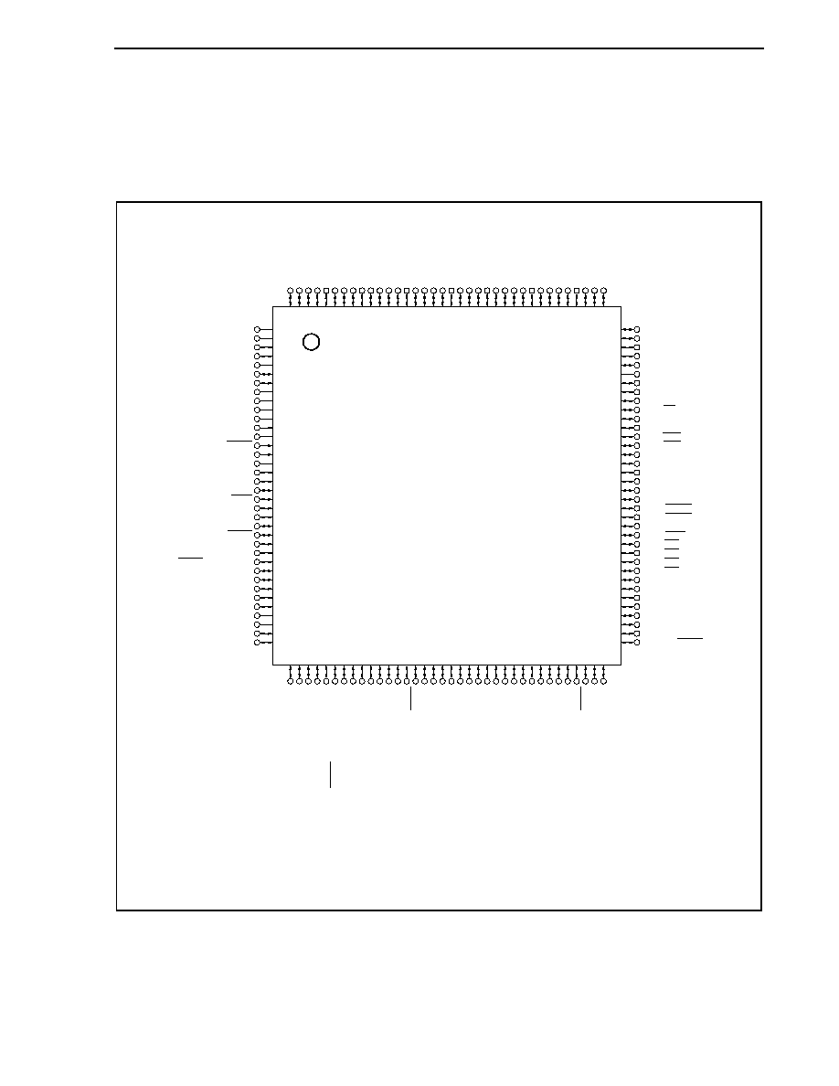
CHAPTER 1 INTRODUCTION
Preliminary User's Manual U17714EJ1V0UD
23
1.5 Pin Configuration (Top View)
144-pin plastic LQFP (fine pitch) (20
� 20)
�
PD70F3720GJ-UEN-A
�
PD70F3722GJ-UEN-A
�
PD70F3724GJ-UEN-A
�
PD70F3721GJ-UEN-A
�
PD70F3723GJ-UEN-A
PDL3/AD3
PDL2/AD2
PDL1/AD1
PDL0/AD0
BV
DD
BV
SS
PCT7
PCT6/ASTB
PCT5
PCT4/RD
PCT3
PCT2
PCT1/WR1
PCT0/WR0
PCS7
PCS6
PCS5
PCS4
PCM5
PCM4
PCM3/HLDRQ
PCM2/HLDAK
PCM1/CLKOUT
PCM0/WAIT
PCS3/CS3
PCS2/CS2
PCS1/CS1
PCS0/CS0
PCD3
PCD2
PCD1
PCD0
P915/A15/INTP6/TIP50/TOP50
P914/A14/INTP5/TIP51/TOP51
P913/A13/INTP4
P912/A12/SCKB3
AV
REF0
AV
SS
P10/ANO0
P11/ANO1
AV
REF1
P00/TIP61/TOP61
P01/TIP60/TOP60
FLMD0
Note 1
V
DD
REGC
Note 2
V
SS
X1
X2
RESET
XT1
XT2
P02/NMI
P03/INTP0/ADTRG
P04/INTP1
P05/INTP2/DRST
P06/INTP3
P40/SIB0/SDA01
P41/SOB0/SCL01
P42/SCKB0
P30/TXDA0/SOB4
P31/RXDA0/INTP7/SIB4
P32/ASCKA0/SCKB4/TIP00/TOP00
P33/TIP01/TOP01
P34/TIP10/TOP10
P35/TIP11/TOP11
P36
P37
EV
SS
EV
DD
P38/TXDA2/SDA00
P39/RXDA2/SCL00
P50/TIQ01/KR0/TOQ01/RTP00
P51/TIQ02/KR1/TOQ02/RTP01
P52/TIQ03/KR2/TOQ03/RTP02/DDI
P53/SIB2/KR3/TIQ00/TOQ00/RTP03/DDO
P54/SOB2/KR4/RTP04/DCK
P55/SCKB2/KR5/RTP05/DMS
P60/RTP10
P61/RTP11
P62/RTP12
P63/RTP13
P64/RTP14
P65/RTP15
P66/SIB5
P67/SOB5
P68/SCKB5
P69/TIP70/TOP70
P610/TIP71
P611/TOP71
P612/TIP80/TOP80
P613/TIP81/TOP81
P614
P615
P80/RXDA3/INTP8
P81/TXDA3
P90/A0/KR6/TXDA1/SDA02
P91/A1/KR7/RXDA1/SCL02
P92/A2/TIP41/TOP41
P93/A3/TIP40/TOP40
P94/A4/TIP31/TOP31
P95/A5/TIP30/TOP30
P96/A6/TIP21/TOP21
P97/A7/SIB1/TIP20/TOP20
P98/A8/SOB1
P99/A9/SCKB1
P910/A10/SIB3
P911A11/SOB3
P70/ANI0
P71/ANI1
P72/ANI2
P73/ANI3
P74/ANI4
P75/ANI5
P76/ANI6
P77/ANI7
P78/ANI8
P79/ANI9
P710/ANI10
P711/ANI11
P712/ANI12
P713/ANI13
P714/ANI14
P715/ANI15
PDH7/A23
PDH6/A22
PDH5/A21
PDH4/A20
PDH3/A19
PDH2/A18
PDH1/A17
PDH0/A16
PDL15/AD15
PDL14/AD14
PDL13/AD13
PDL12/AD12
PDL11/AD11
PDL10/AD10
PDL9/AD9
PDL8/AD8
PDL7/AD7
PDL6/AD6
PDL5/AD5/FLMD1
PDL4/AD4
37
38
39
40
41
42
43
44
45
46
47
48
49
50
51
52
53
54
55
56
57
58
59
60
61
62
63
64
65
66
67
68
69
70
71
72
1
2
3
4
5
6
7
8
9
10
11
12
13
14
15
16
17
18
19
20
21
22
23
24
25
26
27
28
29
30
31
32
33
34
35
36
108
107
106
105
104
103
102
101
100
99
98
97
96
95
94
93
92
91
90
89
88
87
86
85
84
83
82
81
80
79
78
77
76
75
74
73
144
143
142
141
140
139
138
137
136
135
134
133
132
131
130
129
128
127
126
125
124
123
122
121
120
119
118
117
116
115
114
113
112
111
110
109
Notes 1. Connect these pins to V
SS
in the normal mode.
2. Connect the REGC pin to V
SS
via a 4.7
�
F (preliminary value) capacitor.

CHAPTER 1 INTRODUCTION
Preliminary User's Manual U17714EJ1V0UD
24
Pin names
A0 to A23:
AD0 to AD15:
ADTRG:
ANI0 to ANI15:
ANO0, ANO1:
ASCKA0:
ASTB:
AV
REF0
, AV
REF1
:
AV
SS
:
BV
DD
:
BV
SS
:
CLKOUT:
CS0 to CS3:
DCK:
DDI:
DDO:
DMS:
DRST:
EV
DD
:
EV
SS
:
FLMD0, FLMD1:
HLDAK:
HLDRQ:
INTP0 to INTP8:
KR0 to KR7:
NMI:
P00 to P06:
P10, P11:
P30 to P39:
P40 to P42:
P50 to P55:
P60 to P615:
P70 to P715:
P80, P81:
P90 to P915:
PCD0 to PCD3:
PCM0 to PCM5:
PCS0 to PCS7:
PCT0 to PCT7:
PDH0 to PDH7:
Address bus
Address/data bus
A/D trigger input
Analog input
Analog output
Asynchronous serial clock
Address strobe
Analog reference voltage
Analog V
SS
Power supply for bus interface
Ground for bus interface
Clock output
Chip select
Debug clock
Debug data input
Debug data output
Debug mode select
Debug reset
Power supply for port
Ground for port
Flash programming mode
Hold acknowledge
Hold request
External interrupt input
Key return
Non-maskable interrupt request
Port 0
Port 1
Port 3
Port 4
Port 5
Port 6
Port 7
Port 8
Port 9
Port CD
Port CM
Port CS
Port CT
Port DH
PDL0 to PDL15:
RD:
REGC:
RESET:
RTP00 to RTP05,
RTP10 to RTP15:
RXDA0 to RXDA3:
SCKB0 to SCKB5:
SCL00 to SCL02:
SDA00 to SDA02:
SIB0 to SIB5:
SOB0 to SOB5:
TIP00, TIP01,
TIP10, TIP11,
TIP20, TIP21,
TIP30, TIP31,
TIP40, TIP41,
TIP50, TIP51,
TIP60, TIP61,
TIP70, TIP71,
TIP80, TIP81,
TIQ00 to TIQ03:
TOP00, TOP01,
TOP10, TOP11,
TOP20, TOP21,
TOP30, TOP31,
TOP40, TOP41,
TOP50, TOP51,
TOP60, TOP61,
TOP70, TOP71,
TOP80, TOP81,
TOQ00 to TOQ03:
TXDA0 to TXDA3:
V
DD
:
V
SS
:
WAIT:
WR0:
WR1:
X1, X2:
XT1, XT2:
Port DL
Read strobe
Regulator control
Reset
Real-time output port
Receive data
Serial clock
Serial clock
Serial data
Serial input
Serial output
Timer input
Timer output
Transmit data
Power supply
Ground
Wait
Lower byte write strobe
Upper byte write strobe
Crystal for main clock
Crystal for subclock
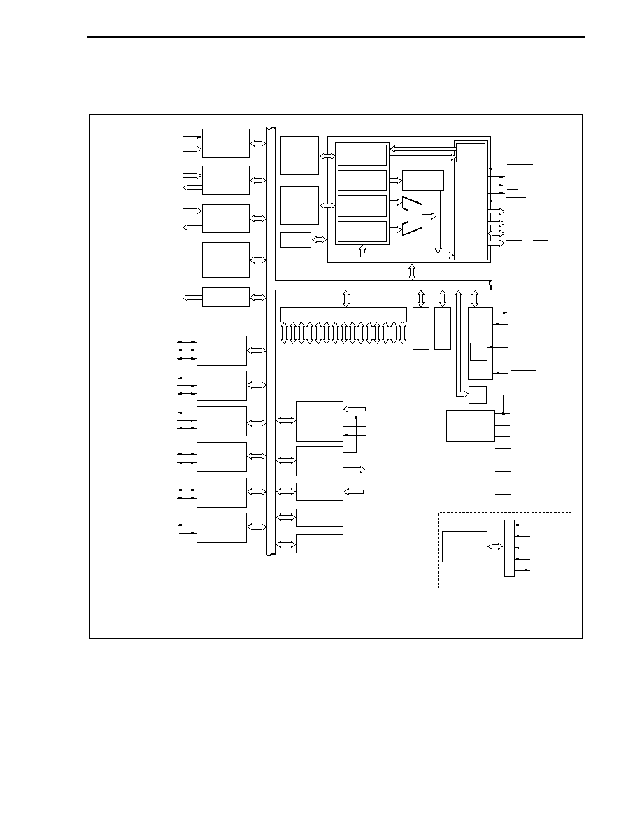
CHAPTER 1 INTRODUCTION
Preliminary User's Manual U17714EJ1V0UD
25
1.6 Function
Block
Configuration
1.6.1 Internal
block
diagram
NMI
TOQ00 to TOQ03
TIQ00 to TIQ03
RTP00 to RTP05,
RTP10 to RTP15
SOB0/SDA01
SIB0/SCL01
SCKB0
INTP0 to INTP8
INTC
TOP00 to TOP80,
TOP01 to TOP81
TIP00 to TIP80,
TIP01 to TIP81
KR0 to KR7
RTO
CSIB1 to CSIB3,
CSIB5
DMAC
Note 1
Note 2
RAM
ROM
PC
ALU
CPU
HLDRQ
HLDAK
ASTB
RD
WAIT
WR0, WR1
A0 to A23
AD0 to AD15
FLMD0
FLMD1
CG
PLL
CS0 to CS3
PCS0 to PCS7
PCM0 to PCM5
PCT0 t
o
PCT7
PDH0 to PDH7
PDL0 to PDL15
PCD0 to PCD3
P90 to P915
P80, P81
P70 to P715
P60 to P615
P50 to P55
P40 to P42
P30 to P39
P10, P11
P00 to P06
AV
REF1
ANO0, ANO1
ANI0 to ANI15
AV
SS
AV
REF0
ADTRG
CLKOUT
XT1
XT2
X1
X2
RESET
V
DD
V
SS
REGC
BV
DD
BV
SS
EV
DD
EV
SS
BCU
SOB1 to SOB3, SOB5
SIB1 to SIB3, SIB5
SCKB1 to SCKB3, SCKB5
TXDA0/SOB4
RXDA0/SIB4
ASCKA0/SCKB4
TXDA2/SDA00
RXDA2/SCL00
CSIB0 I
2
C01
UARTA0 CSIB4
UARTA2 I
2
C00
TXDA3
RXDA3
UARTA3
TXDA1/SDA02
RXDA1/SCL02
UARTA1 I
2
C02
DRST
DMS
DDI
DCK
DDO
16-bit timer/
counter Q:
1 ch
16-bit timer/
counter P:
9 ch
16-bit interval
timer M:
1 ch
General-purpose
registers 32 bits
� 32
Multiplier
16
� 16 32
System
registers
32-bit barrel
shifter
Instruction
queue
Watchdog
timer 2
Watch timer
Key return
function
Regulator
On-chip
debug
function
A/D
converter
D/A
converter
Ports
Internal oscillator
CLM
LVI
Notes 1. 128/256/384/512/640 KB (flash memory) (see Table 1-1)
2. 12/24/32/40/48 KB (see Table 1-1)

CHAPTER 1 INTRODUCTION
Preliminary User's Manual U17714EJ1V0UD
26
1.6.2 Internal
units
(1) CPU
The CPU uses five-stage pipeline control to enable single-clock execution of address calculations, arithmetic
logic operations, data transfers, and almost all other instruction processing.
Other dedicated on-chip hardware, such as a multiplier (16 bits
� 16 bits 32 bits) and a barrel shifter (32
bits) contribute to faster complex processing.
(2) Bus control unit (BCU)
The BCU starts a required external bus cycle based on the physical address obtained by the CPU. When an
instruction is fetched from external memory space and the CPU does not send a bus cycle start request, the
BCU generates a prefetch address and prefetches the instruction code. The prefetched instruction code is
stored in an instruction queue.
(3) ROM
This is a 640/512/384/256/128 KB flash memory mapped to addresses 0000000H to 009FFFFH/0000000H to
007FFFFH/0000000H to 005FFFFH/0000000H to 003FFFFH/0000000H to 001FFFFH. It can be accessed
from the CPU in one clock during instruction fetch.
(4) RAM
This is a 12/24/32/40/48 KB RAM mapped to addresses 3FF3000H to 3FFEFFFH/3FF5000H to
3FFEFFFH/3FF7000H to 3FFEFFFH/3FF9000H to 3FFEFFFH/3FFC000H to 3FFEFFFH. It can be accessed
from the CPU in one clock during data access.
(5) Interrupt controller (INTC)
This controller handles hardware interrupt requests (NMI, INTP0 to INTP8) from on-chip peripheral hardware
and external hardware. Eight levels of interrupt priorities can be specified for these interrupt requests, and
multiple servicing control can be performed.
(6) Clock generator (CG)
A main clock oscillator that generates the main clock oscillation frequency (f
X
) and a subclock oscillator that
generates the subclock oscillation frequency (f
XT
) are available. As the main clock frequency (f
XX
), f
X
is used as
is in the clock-through mode and is multiplied by four or eight in the PLL mode.
The CPU clock frequency (f
CPU
) can be selected from seven types: f
XX
, f
XX
/2, f
XX
/4, f
XX
/8, f
XX
/16, f
XX
/32, and f
XT
.
(7) Internal oscillator
An internal oscillator is provided on chip. The oscillation frequency is 200 kHz (TYP.). An internal oscillator
supplies the clock for watchdog timer 2 and timer M.
(8) Timer/counter
Nine-channel 16-bit timer/event counter P (TMP), one-channel 16-bit timer/event counter Q (TMQ), and one-
channel 16-bit interval timer M (TMM) are provided on chip.
(9) Watch timer
This timer counts the reference time period (0.5 s) for counting the clock (the 32.768 kHz from the subclock or
the 32.768 kHz f
BRG
from prescaler 3). The watch timer can also be used as an interval timer for the main
clock.

CHAPTER 1 INTRODUCTION
Preliminary User's Manual U17714EJ1V0UD
27
(10) Watchdog timer 2
A watchdog timer is provided on chip to detect inadvertent program loops, system abnormalities, etc.
The internal oscillation clock, the main clock, or the subclock can be selected as the source clock.
Watchdog timer 2 generates a non-maskable interrupt request signal (INTWDT2) or a system reset signal
(WDT2RES) after an overflow occurs.
(11) Serial
interface
The V850ES/JJ2 includes three kinds of serial interfaces: asynchronous serial interface A (UARTA), 3-wire
variable-length serial interface B (CSIB), and an I
2
C bus interface (I
2
C).
In the case of UARTA, data is transferred via the TXDA0 to TXDA3 pins and RXDA0 to RXDA3 pins.
In the case of CSIB, data is transferred via the SOB0 to SOB5 pins, SIB0 to SIB5 pins, and SCKB0 to
SCKB5 pins.
In the case of I
2
C, data is transferred via the SDA00 to SDA02 and SCL00 to SCL02 pins.
(12) A/D
converter
This 10-bit A/D converter includes 16 analog input pins. Conversion is performed using the successive
approximation method.
(13) D/A
converter
A two-channel, 8-bit-resolution D/A converter that uses the R-2R ladder method is provided on chip.
(14) DMA
controller
A 4-channel DMA controller is provided on chip. This controller transfers data between the internal RAM and
on-chip peripheral I/O devices in response to interrupt requests sent by on-chip peripheral I/O.
(15) Key interrupt function
A key interrupt request signal (INTKR) can be generated by inputting a falling edge to key input pins (8
channels).
(16) Real-time output function
The real-time output function transfers preset 6-bit data to output latches upon the occurrence of a timer
compare register match signal.
(17) On-chip
debug
function
An on-chip debug function that uses the JTAG (Joint Test Action Group) communication specifications is
provided. Switching between the normal port function and on-chip debugging function is done with the
control pin input level and the OCDM register.

CHAPTER 1 INTRODUCTION
Preliminary User's Manual U17714EJ1V0UD
28
(18) Ports
The general-purpose port functions and control pin functions are listed below.
Port I/O
Alternate
Function
P0
7-bit I/O
Timer I/O, NMI, external interrupt, A/D converter trigger, debug reset
P1
2-bit I/O
D/A converter analog output
P3
10-bit I/O
External interrupt, serial interface, timer I/O
P4
3-bit I/O
Serial interface
P5
6-bit I/O
Timer I/O, real-time output, key interrupt input, serial interface, debug I/O
P6
16-bit I/O
Real-time output, serial interface, timer I/O
P7
16-bit I/O
A/D converter analog input
P8
2-bit I/O
Serial interface, external interrupt
P9
16-bit I/O
External address bus, serial interface, key interrupt input, timer I/O, external interrupt
PCD 4-bit
I/O
-
PCM
6-bit I/O
External control signal
PCS
8-bit I/O
Chip select output
PCT
8-bit I/O
External control signal
PDH
8-bit I/O
External address bus
PDL
16-bit I/O
External address/data bus

Preliminary User's Manual U17714EJ1V0UD
29
CHAPTER 2 PIN FUNCTIONS
2.1 List of Pin Functions
The names and functions of the pins of the V850ES/JJ2 are described below.
There are four types of pin I/O buffer power supplies: AV
REF0
, AV
REF1
, BV
DD
, and EV
DD
. The relationship between
these power supplies and the pins is described below.
Table 2-1. Pin I/O Buffer Power Supplies
Power Supply
Corresponding Pins
AV
REF0
Port
7
AV
REF1
Port
1
BV
DD
Ports CD, CM, CS, CT, DH, DL
EV
DD
RESET, ports 0, 3 to 6, 8, 9
CHAPTER 2 PIN FUNCTIONS
Preliminary User's Manual U17714EJ1V0UD
30
(1) Port pins
(1/4)
Pin Name
Pin No.
I/O
Function
Alternate Function
P00 6
TIP61/TOP61
P01 7
TIP60/TOP60
P02 17
NMI
P03 18
INTP0/ADTRG
P04 19
INTP1
P05
Note
20
INTP2/DRST
P06 21
I/O
Port 0
7-bit I/O port
Input/output can be specified in 1-bit units.
N-ch open-drain output can be specified in 1-bit units.
5 V tolerant.
INTP3
P10 3
ANO0
P11 4
I/O
Port 1
2-bit I/O port
Input/output can be specified in 1-bit units.
ANO1
P30 25
TXDA0/SOB4
P31 26
RXDA0/INTP7/SIB4
P32 27
ASCKA0/SCKB4/TIP00/TOP00
P33 28
TIP01/TOP01
P34 29
TIP10/TOP10
P35 30
TIP11/TOP11
P36 31
-
P37 32
-
P38 35
TXDA2/SDA00
P39 36
I/O
Port 3
10-bit I/O port
Input/output can be specified in 1-bit units.
N-ch open-drain output can be specified in 1-bit units.
5 V tolerant.
RXDA2/SCL00
P40 22
SIB0/SDA01
P41 23
SOB0/SCL01
P42 24
I/O
Port 4
3-bit I/O port
Input/output can be specified in 1-bit units.
N-ch open-drain output can be specified in 1-bit units.
5 V tolerant.
SCKB0
P50 37
TIQ01/KR0/TOQ01/RTP00
P51 38
TIQ02/KR1/TOQ02/RTP01
P52 39
TIQ03/KR2/TOQ03/RTP02/DDI
P53 40
SIB2/KR3/TIQ00/TOQ00/RTP03/
DDO
P54 41
SOB2/KR4/RTP04/DCK
P55 42
I/O
Port 5
6-bit I/O port
Input/output can be specified in 1-bit units.
N-ch open-drain output can be specified in 1-bit units.
5 V tolerant.
SCKB2/KR5/RTP05/DMS
Note Incorporates a pull-down resistor. It can be disconnected by clearing the OCDM.OCDM0 bit.
CHAPTER 2 PIN FUNCTIONS
Preliminary User's Manual U17714EJ1V0UD
31
(2/4)
Pin Name
Pin No.
I/O
Function
Alternate Function
P60 43
RTP10
P61 44
RTP11
P62 45
RTP12
P63 46
RTP13
P64 47
RTP14
P65 48
RTP15
P66 49
SIB5
P67 50
SOB5
P68 51
SCKB5
P69 52
TIP70/TOP70
P610 53
TIP71
P611 54
TOP71
P612 55
TIP80/TOP80
P613 56
TIP81/TOP81
P614 57
-
P615 58
I/O
Port 6
16-bit I/O port
Input/output can be specified in 1-bit units.
N-ch open-drain output can be specified in 1-bit units.
5 V tolerant.
-
P70 144
ANI0
P71 143
ANI1
P72 142
ANI2
P73 141
ANI3
P74 140
ANI4
P75 139
ANI5
P76 138
ANI6
P77 137
ANI7
P78 136
ANI8
P79 135
ANI9
P710 134
ANI10
P711 133
ANI11
P712 132
ANI12
P713 131
ANI13
P714 130
ANI14
P715 129
I/O
Port 7
16-bit I/O port
Input/output can be specified in 1-bit units.
ANI15
P80 59
RXDA3/INTP8
P81 60
I/O
Port 8
2-bit I/O port
Input/output can be specified in 1-bit units.
N-ch open-drain output can be specified in 1-bit units.
5 V tolerant.
TXDA3
CHAPTER 2 PIN FUNCTIONS
Preliminary User's Manual U17714EJ1V0UD
32
(3/4)
Pin Name
Pin No.
I/O
Function
Alternate Function
P90 61
A0/KR6/TXDA1/SDA02
P91 62
A1/KR7/RXDA1/SCL02
P92 63
A2/TIP41/TOP41
P93 64
A3/TIP40/TOP40
P94 65
A4/TIP31/TOP31
P95 66
A5/TIP30/TOP30
P96 67
A6/TIP21/TOP21
P97 68
A7/SIB1/TIP20/TOP20
P98 69
A8/SOB1
P99 70
A9/SCKB1
P910 71
A10/SIB3
P911 72
A11/SOB3
P912 73
A12/SCKB3
P913 74
A13/INTP4
P914 75
A14/INTP5/TIP51/TOP51
P915 76
I/O
Port 9
16-bit I/O port
Input/output can be specified in 1-bit units.
N-ch open-drain output can be specified in 1-bit units.
5 V tolerant.
A15/INTP6/TIP50/TOP50
PCD0 77
-
PCD1 78
-
PCD2 79
-
PCD3 80
I/O
Port CD
4-bit I/O port
Input/output can be specified in 1-bit units.
-
PCM0 85
WAIT
PCM1 86
CLKOUT
PCM2 87
HLDAK
PCM3 88
HLDRQ
PCM4 89
-
PCM5 90
I/O
Port CM
6-bit I/O port
Input/output can be specified in 1-bit units.
-
PCS0 81
CS0
PCS1 82
CS1
PCS2 83
CS2
PCS3 84
CS3
PCS4 91
-
PCS5 92
-
PCS6 93
-
PCS7 94
I/O
Port CS
8-bit I/O port
Input/output can be specified in 1-bit units.
-
CHAPTER 2 PIN FUNCTIONS
Preliminary User's Manual U17714EJ1V0UD
33
(4/4)
Pin Name
Pin No.
I/O
Function
Alternate Function
PCT0 95
WR0
PCT1 96
WR1
PCT2 97
-
PCT3 98
-
PCT4 99
RD
PCT5 100
-
PCT6 101
ASTB
PCT7 102
I/O
Port CT
8-bit I/O port
Input/output can be specified in 1-bit units.
-
PDH0 121
A16
PDH1 122
A17
PDH2 123
A18
PDH3 124
A19
PDH4 125
A20
PDH5 126
A21
PDH6 127
A22
PDH7 128
I/O
Port DH
8-bit I/O port
Input/output can be specified in 1-bit units.
A23
PDL0 105
AD0
PDL1 106
AD1
PDL2 107
AD2
PDL3 108
AD3
PDL4 109
AD4
PDL5 110
AD5/FLMD1
PDL6 111
AD6
PDL7 112
AD7
PDL8 113
AD8
PDL9 114
AD9
PDL10 115
AD10
PDL11 116
AD11
PDL12 117
AD12
PDL13 118
AD13
PDL14 119
AD14
PDL15 120
I/O
Port DL
16-bit I/O port
Input/output can be specified in 1-bit units.
AD15
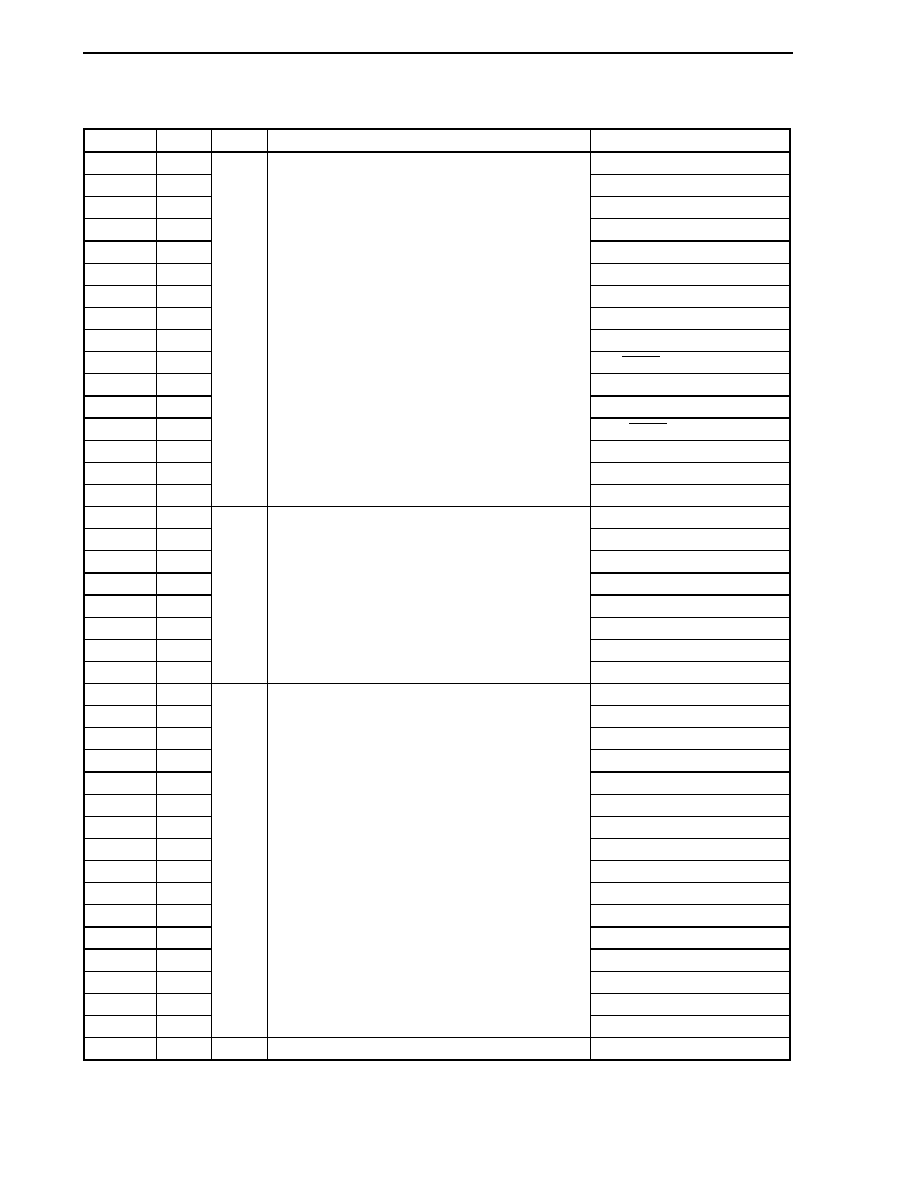
CHAPTER 2 PIN FUNCTIONS
Preliminary User's Manual U17714EJ1V0UD
34
(2) Non-port pins
(1/6)
Pin Name
Pin No.
I/O
Function
Alternate Function
A0 61
P90/KR6/TXDA1/SDA02
A1 62
P91/KR7/RXDA1/SCL02
A2 63
P92/TIP41/TOP41
A3 64
P93/TIP40/TOP40
A4 65
P94/TIP31/TOP31
A5 66
P95/TIP30/TOP30
A6 67
P96/TIP21/TOP21
A7 68
P97/SIB1/TIP20/TOP20
A8 69
P98/SOB1
A9 70
P99/SCKB1
A10 71
P910/SIB3
A11 72
P911/SOB3
A12 73
P912/SCKB3
A13 74
P913/INTP4
A14 75
P914/INTP5/TIP51/TOP51
A15 76
Output
Address bus for external memory
(when using separate bus)
N-ch open-drain output selectable
5 V tolerant.
P915/INTP6/TIP50/TOP50
A16 121
PDH0
A17 122
PDH1
A18 123
PDH2
A19 124
PDH3
A20 125
PDH4
A21 126
PDH5
A22 127
PDH6
A23 128
Output
Address bus for external memory
PDH7
AD0 105
PDL0
AD1 106
PDL1
AD2 107
PDL2
AD3 108
PDL3
AD4 109
PDL4
AD5 110
PDL5/FLMD1
AD6 111
PDL6
AD7 112
PDL7
AD8 113
PDL8
AD9 114
PDL9
AD10 115
PDL10
AD11 116
PDL11
AD12 117
PDL12
AD13 118
PDL13
AD14 119
PDL14
AD15 120
I/O
Address bus/data bus for external memory
PDL15
ADTRG
18
Input
A/D converter external trigger input, 5 V tolerant
P03/INTP0

CHAPTER 2 PIN FUNCTIONS
Preliminary User's Manual U17714EJ1V0UD
35
(2/6)
Pin Name
Pin No.
I/O
Function
Alternate Function
ANI0 144
P70
ANI1 143
P71
ANI2 142
P72
ANI3 141
P73
ANI4 140
P74
ANI5 139
P75
ANI6 138
P76
ANI7 137
P77
ANI8 136
P78
ANI9 135
P79
ANI10 134
P710
ANI11 133
P711
ANI12 132
P712
ANI13 131
P713
ANI14 130
P714
ANI15 129
Input
Analog voltage input for A/D converter
P715
ANO0 3
P10
ANO1 4
Output
Analog voltage output for D/A converter
P11
ASCKA0
27
Input
UARTA0 baud rate clock input, 5 V tolerant
P32/SCKB4/TIP00/TOP00
ASTB
101
Output
Address strobe signal output for external memory
PCT6
AV
REF0
1
Reference voltage input for A/D converter,
positive power supply for alternate-function port 7
-
AV
REF1
5
-
Reference voltage input for D/A converter,
positive power supply for alternate-function port 1
-
AV
SS
2
-
Ground potential for A/D and D/A converters
(same potential as V
SS
)
-
BV
DD
104
-
Positive power supply for bus interface and alternate-function
ports
-
BV
SS
103
-
Ground potential for bus interface and alternate-function ports
-
CLKOUT
86
Output
Internal system clock output
PCM1
CS0 81
PCS0
CS1 82
PCS1
CS2 83
PCS2
CS3 84
Output Chip
select
output
PCS3
DCK
41
Input
Debug clock input, 5 V tolerant
P54/SOB2/KR4/RTP04
DDI
39
Input
Debug data input, 5 V tolerant
P52/TIQ03/KR2/TOQ03/RTP02
DDO
Note
40
Output
Debug data output
N-ch open-drain output selectable, 5 V tolerant
P53/SIB2/KR3/TIQ00/TOQ00/
RTP03
DMS
42
Input
Debug mode select input, 5 V tolerant
P55/SCKB2/KR5/RTP05
DRST
20
Input
Debug reset input, 5 V tolerant
P05/INTP2
EV
DD
34
-
Positive power supply for external (same potential as V
DD
)
-
EV
SS
33
-
Ground potential for external (same potential as V
SS
)
-
FLMD0 8
-
FLMD1 110
Input
Flash memory programming mode setting pin
PDL5/AD5
Note In the on-chip debug mode, high-level output is forcibly set.
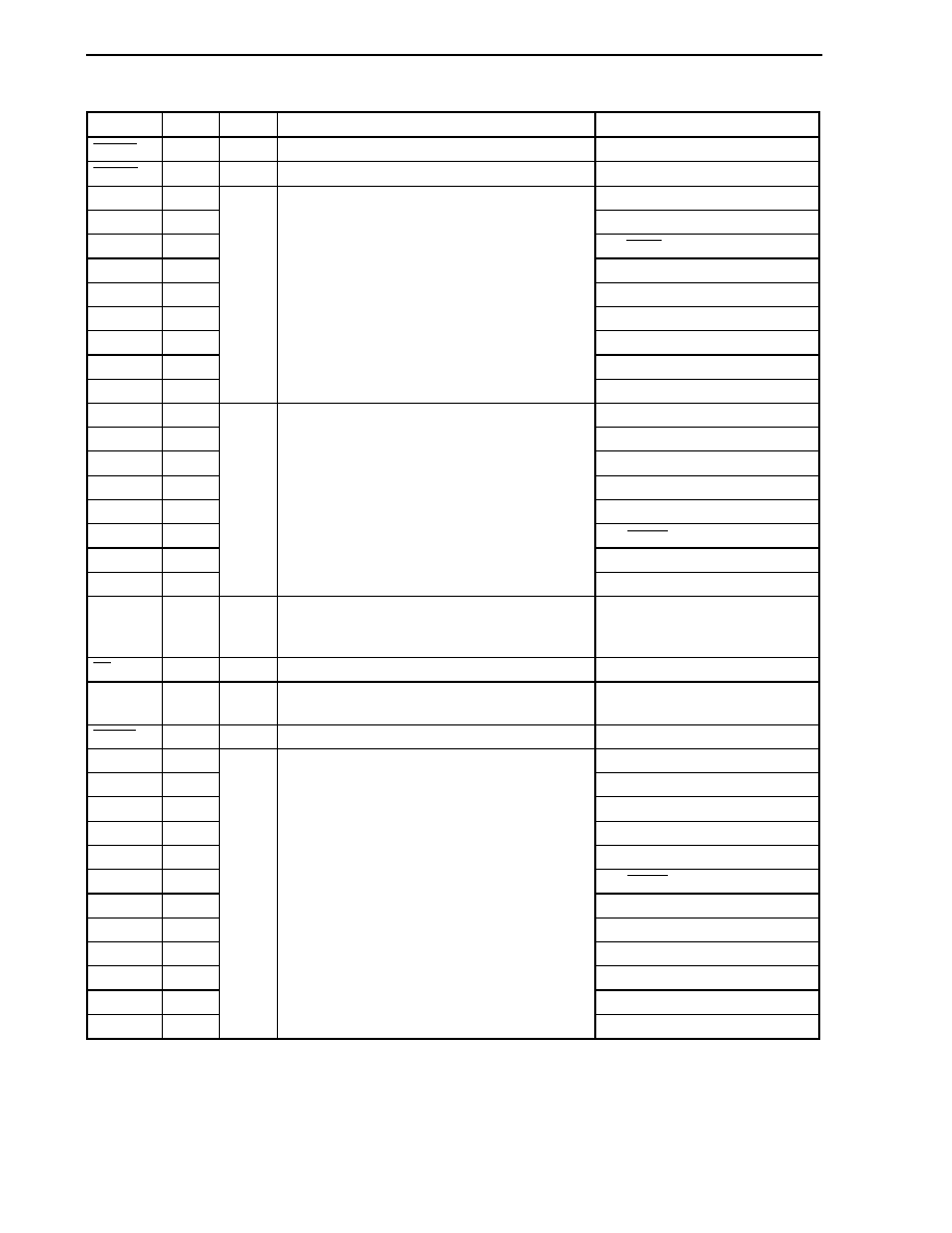
CHAPTER 2 PIN FUNCTIONS
Preliminary User's Manual U17714EJ1V0UD
36
(3/6)
Pin Name
Pin No.
I/O
Function
Alternate Function
HLDAK
87
Output
Bus hold acknowledge output
PCM2
HLDRQ
88
Input
Bus hold request input
PCM3
INTP0 18
P03/ADTRG
INTP1 19
P04
INTP2 20
P05/DRST
INTP3 21
P06
INTP4 74
P913/A13
INTP5 75
P914/A14/TIP51/TOP51
INTP6 76
P915/A15/TIP50/TOP50
INTP7 26
P31/RXDA0/SIB4
INTP8 59
Input
External interrupt request input (maskable, analog
noise elimination). Analog noise elimination/digital
noise elimination selectable for the INTP3 pin.
5 V tolerant
P80/RXDA3
KR0
Note 1
37
P50/TIQ01/TOQ01/RTP00
KR1
Note 1
38
P51/TIQ02/TOQ02/RTP01
KR2
Note 1
39
P52/TIQ03/TOQ03/RTP02/DDI
KR3
Note 1
40
P53/SIB2/TIQ00/TOQ00/RTP03/DDO
KR4
Note 1
41
P54/SOB2/RTP04/DCK
KR5
Note 1
42
P55/SCKB2/RTP05/DMS
KR6
Note 1
61
P90/A0/TXDA1/SDA02
KR7
Note 1
62
Input
Key interrupt input (on-chip analog noise eliminator)
5 V tolerant
P91/A1/RXDA1/SCL02
NMI
Note 2
17
Input
External interrupt input (non-maskable, analog noise
elimination)
5 V tolerant
P02
RD
99
Output
Read strobe signal output for external memory
PCT4
REGC 10
-
Connection of regulator output stabilization capacitance
(4.7
�
F (preliminary value))
-
RESET
14
Input
System reset input
-
RTP00 37
P50/TIQ01/KR0/TOQ01
RTP01 38
P51/TIQ02/KR1/TOQ02
RTP02 39
P52/TIQ03/KR2/TOQ03/DDI
RTP03 40
P53/SIB2/KR3/TIQ00/TOQ00/DDO
RTP04 41
P54/SOB2/KR4/DCK
RTP05 42
P55/SCKB2/KR5/DMS
RTP10 43
P60
RTP11 44
P61
RTP12 45
P62
RTP13 46
P63
RTP14 47
P64
RTP15 48
Output
Real-time output port
N-ch open-drain output selectable
5 V tolerant
P65
Notes 1. Pull this pin up externally.
2. The NMI pin alternately functions as the P02 pin. In functions as the P02 pin after reset. To enable the
NMI pin, set the PMC0.PMC02 bit to 1. The initial setting of the NMI pin is "No edge detected". Select
the NMI pin valid edge using INTF0 and INTR0 registers.
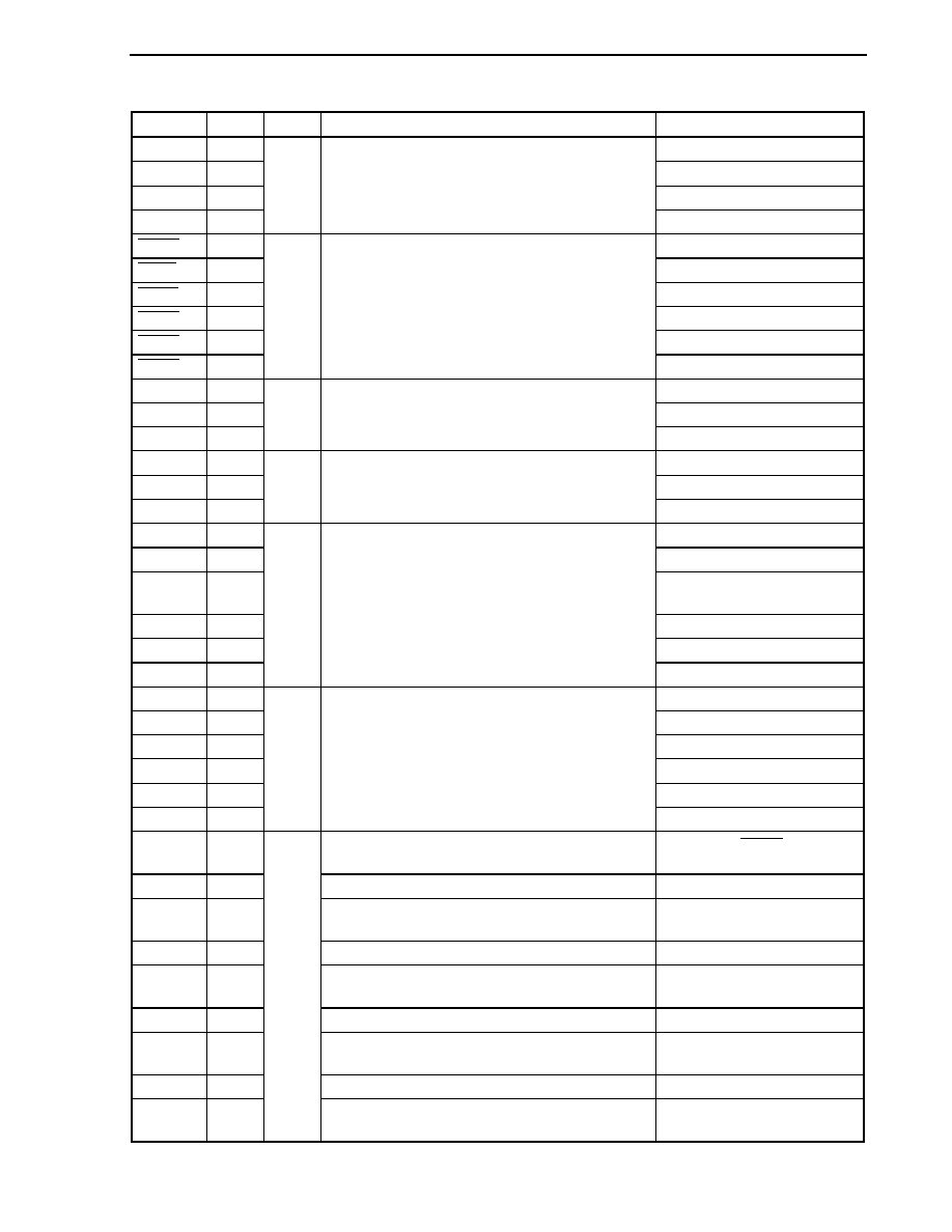
CHAPTER 2 PIN FUNCTIONS
Preliminary User's Manual U17714EJ1V0UD
37
(4/6)
Pin Name
Pin No.
I/O
Function
Alternate Function
RXDA0 26
P31/INTP7/SIB4
RXDA1 62
P91/A1/KR7/SCL02
RXDA2 36
P39/SCL00
RXDA3 59
Input
Serial receive data input (UARTA0 to UARTA3)
5 V tolerant
P80/INTP8
SCKB0 24
P42
SCKB1 70
P99/A9
SCKB2 42
P55/KR5/RTP05/DMS
SCKB3 73
P912/A12
SCKB4 27
P32/ASCKA0/TIP00/TOP00
SCKB5 51
I/O
Serial clock I/O (CSIB0 to CSIB5)
N-ch open-drain output selectable
5 V tolerant
P68
SCL00 36
P39/RXDA2
SCL01 23
P41/SOB0
SCL02 62
I/O
Serial clock I/O (I
2
C00 to I
2
C02)
N-ch open-drain output selectable
5 V tolerant
P91/A1/KR7/RXDA1
SDA00 35
P38/TXDA2
SDA01 22
P40/SIB0
SDA02 61
I/O
Serial transmit/receive data I/O (I
2
C00 to I
2
C02)
N-ch open-drain output selectable
5 V tolerant
P90/A0/KR6/TXDA1
SIB0 22
P40/SDA01
SIB1 68
P97/A7/TIP20/TOP20
SIB2 40
P53/KR3/TIQ00/TOQ00/RTP03/
DDO
SIB3 71
P910/A10
SIB4 26
P31/RXDA0/INTP7
SIB5 49
Input
Serial receive data input (CSIB0 to CSIB5)
5 V tolerant
P66
SOB0 23
P41/SCL01
SOB1 69
P98/A8
SOB2 41
P54/KR4/RTP04/DCK
SOB3 72
P911/A11
SOB4 25
P30/TXDA0
SOB5 50
Output
Serial transmit data output (CSIB0 to CSIB5)
N-ch open-drain output selectable
5 V tolerant
P67
TIP00 27
External event count input/capture trigger input/external
trigger input (TMP0), 5 V tolerant
P32/ASCKA0/SCKB4/TOP00
TIP01
28
Capture trigger input (TMP0), 5 V tolerant
P33/TOP01
TIP10 29
External event count input/capture trigger input/external
trigger input (TMP1), 5 V tolerant
P34/TOP10
TIP11
30
Capture trigger input (TMP1), 5 V tolerant
P35/TOP11
TIP20 68
External event count input/capture trigger input/external
trigger input (TMP2), 5 V tolerant
P97/A7/SIB1/TOP20
TIP21
67
Capture trigger input (TMP2), 5 V tolerant
P96/A6/TOP21
TIP30 66
External event count input/capture trigger input/external
trigger input (TMP3), 5 V tolerant
P95/A5/TOP30
TIP31
65
Capture trigger input (TMP3), 5 V tolerant
P94/A4/TOP31
TIP40 64
Input
External event count input/capture trigger input/external
trigger input (TMP4), 5 V tolerant
P93/A3/TOP40

CHAPTER 2 PIN FUNCTIONS
Preliminary User's Manual U17714EJ1V0UD
38
(5/6)
Pin Name
Pin No.
I/O
Function
Alternate Function
TIP41
63
Capture trigger input (TMP4), 5 V tolerant
P92/A2/TOP41
TIP50 76
External event count input/capture trigger input/external
trigger input (TMP5), 5 V tolerant
P915/A15/INTP6/TOP50
TIP51
75
Capture trigger input (TMP5), 5 V tolerant
P914/A14/INTP5/TOP51
TIP60 7
External event count input/capture trigger input/external
trigger input (TMP6), 5 V tolerant
P01/TOP60
TIP61
6
Capture trigger input (TMP6), 5 V tolerant
P00/TOP61
TIP70 52
External event count input/capture trigger input/external
trigger input (TMP7), 5 V tolerant
P69/TOP70
TIP71
53
Capture trigger input (TMP7), 5 V tolerant
P610
TIP80 55
External event count input/capture trigger input/external
trigger input (TMP8), 5 V tolerant
P612/TOP80
TIP81
56
Capture trigger input (TMP8), 5 V tolerant
P613/TOP81
TIQ00
40
External event count input/capture trigger input/external
trigger input (TMQ0), 5 V tolerant
P53/SIB2/KR3/TOQ00/RTP03/
DDO
TIQ01 37
P50/KR0/TOQ01/RTP00
TIQ02 38
P51/KR1/TOQ02/RTP01
TIQ03 39
Input
Capture trigger input (TMQ0), 5V tolerant
P52/KR2/TOQ03/RTP02/DDI
TOP00 27
P32/ASCKA0/SCKB4/TIP00
TOP01 28
Timer output (TMP0)
N-ch open-drain output selectable, 5 V tolerant
P33/TIP01
TOP10 29
P34/TIP10
TOP11 30
Timer output (TMP1)
N-ch open-drain output selectable, 5 V tolerant
P35/TIP11
TOP20 68
P97/A7/SIB1/TIP20
TOP21 67
Timer output (TMP2)
N-ch open-drain output selectable, 5 V tolerant
P96/A6/TIP21
TOP30 66
P95/A5/TIP30
TOP31 65
Timer output (TMP3)
N-ch open-drain output selectable, 5 V tolerant
P94/A4/TIP31
TOP40 64
P93/A3/TIP40
TOP41 63
Timer output (TMP4)
N-ch open-drain output selectable, 5 V tolerant
P92/A2/TIP41
TOP50 76
P915/A15/INTP6/TIP50
TOP51 75
Timer output (TMP5)
N-ch open-drain output selectable, 5 V tolerant
P914/A14/INTP5/TIP51
TOP60 7
P01/TIP60
TOP61 6
Timer output (TMP6)
N-ch open-drain output selectable, 5 V tolerant
P00/TIP61
TOP70 52
P69/TIP70
TOP71 54
Timer output (TMP7)
N-ch open-drain output selectable, 5 V tolerant
P611
TOP80 55
P612/TIP80
TOP81 56
Output
Timer output (TMP8)
N-ch open-drain output selectable, 5 V tolerant
P613/TIP81
TOQ00 40
P53/SIB2/KR3/TIQ00/RTP03/DDO
TOQ01 37
P50/TIQ01/KR0/RTP00
TOQ02 38
P51/RTP01/KR1/TIQ02
TOQ03 39
Output Timer
output
(TMQ0)
N-ch open-drain output selectable
5 V tolerant
P52/TIQ03/KR2/RTP02/DDI
TXDA0 25
P30/SOB4
TXDA1 61
P90/A0/KR6/SDA02
TXDA2 35
P38/SDA00
TXDA3 60
Output
Serial transmit data output (UARTA0 to UARTA3)
N-ch open-drain output selectable
5 V tolerant
P81
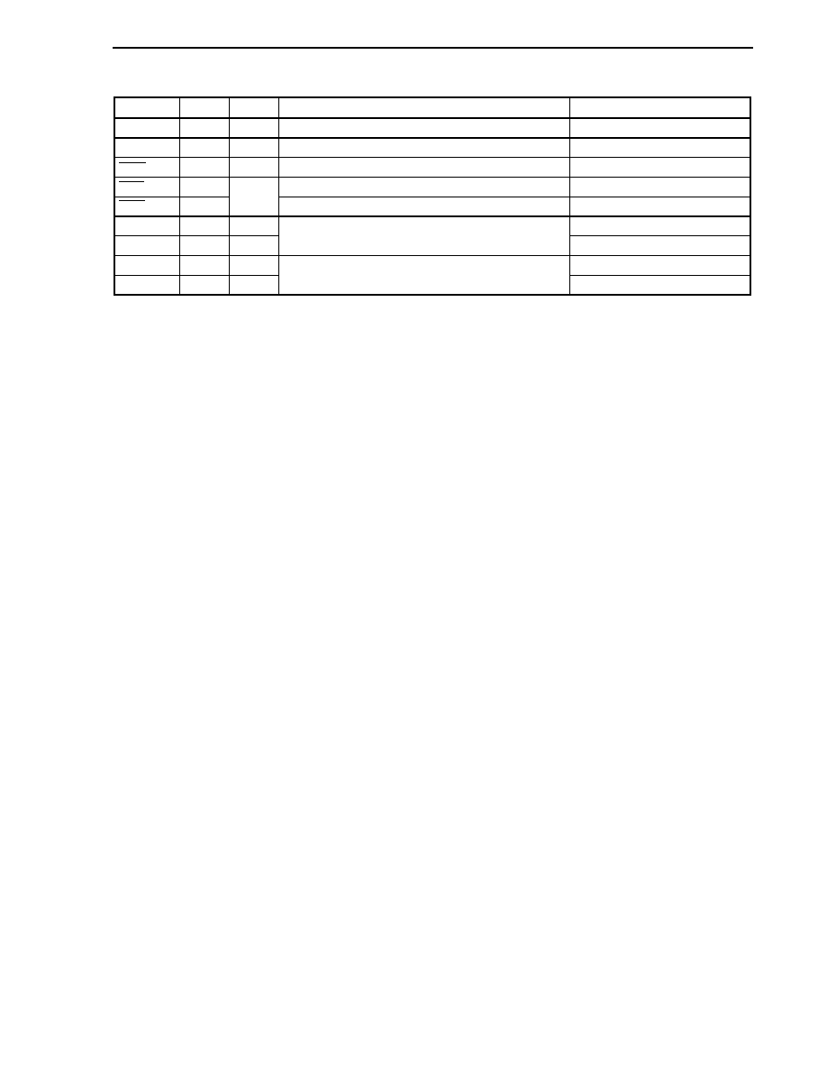
CHAPTER 2 PIN FUNCTIONS
Preliminary User's Manual U17714EJ1V0UD
39
(6/6)
Pin Name
Pin No.
I/O
Function
Alternate Function
V
DD
9
-
Positive power supply pin for internal
-
V
SS
11
-
Ground potential for internal
-
WAIT
85
Input
External wait input
PCM0
WR0
95
Write strobe for external memory (lower 8 bits)
PCT0
WR1 96
Output
Write strove for external memory (higher 8 bits)
PCT1
X1 12
Input
-
X2 13
-
Connection of resonator for main clock
-
XT1 15
Input
-
XT2 16
-
Connection of resonator for subclock
-
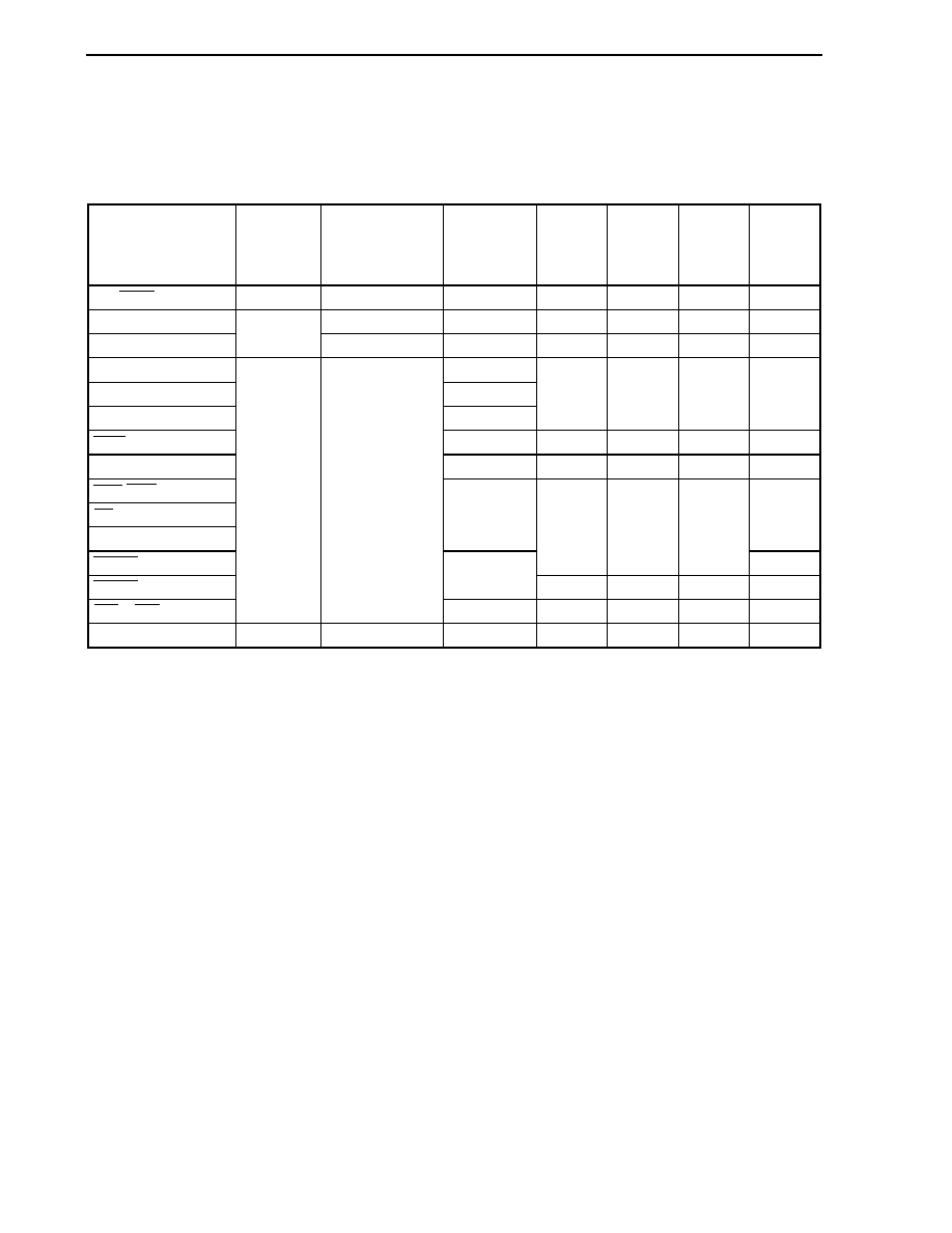
CHAPTER 2 PIN FUNCTIONS
Preliminary User's Manual U17714EJ1V0UD
40
2.2 Pin States
The operation states of pins in the various modes are described below.
Table 2-2. Pin Operation States in Various Modes
Pin Name
When Power
Is Turned
On
Note 1
During Reset
(Except When
Power Is Turned On)
HALT
Mode
Note 2
IDLE1,
IDLE2,
Sub-IDLE
Mode
Note 2
STOP
Mode
Note 2
Idle
State
Note 3
Bus Hold
P05/DRST
Pulled down
Pulled down
Note 4
Held Held
Held
Held
Held
P10/ANO0, P11/ANO1
Hi-Z
Held
Held
Hi-Z
Held
Held
P53/DDO
Undefined
Hi-Z
Note 5
Held
Held
Held
Held
Held
AD0 to AD15
Notes 7, 8
A0 to A15
Undefined
Notes 7, 9
A16 to A23
Undefined
Note 7
Hi-Z Hi-Z Held Hi-Z
WAIT
-
-
-
-
-
CLKOUT Operating
L
L
Operating
Operating
WR0, WR1
RD
ASTB
H
Note 7
Hi-Z
HLDAK
H H H
L
HLDRQ
Operating
Note 7
-
-
-
Operating
CS0 to CS3
Hi-Z
Note 6
Hi-Z
Note 6
H
Note 7
H H
Held
Hi-Z
Other port pins
Hi-Z
Hi-Z
Held
Held
Held
Held
Held
Notes 1. Duration until 1 ms elapses after the supply voltage reaches the operating supply voltage range (lower
limit) when the power is turned on.
2. Operates while alternate functions are operating.
3. In separate bus mode, the state of the pins in the idle state inserted after the T2 state is shown. In
multiplexed bus mode, the state of the pins in the idle state inserted after the T3 state is shown.
4. Pulled down during external reset. During internal reset by the watchdog timer, clock monitor, etc., the
state of this pin differs according to the OCDM.OCDM0 bit setting.
5. DDO output is specified in the on-chip debug mode.
6. The bus control pins function alternately as port pins, so they are initialized to the input mode (port
mode).
7. Operates even in the HALT mode, during DMA operation.
8. In separate bus mode: Hi-Z
In multiplexed bus mode: Undefined
9. In separate bus mode
Remark Hi-Z: High impedance
Held: The state during the immediately preceding external bus cycle is held.
L:
Low-level output
H:
High-level
output
-:
Input without sampling (not acknowledged)
CHAPTER 2 PIN FUNCTIONS
Preliminary User's Manual U17714EJ1V0UD
41
2.3 Pin I/O Circuit Types, I/O Buffer Power Supplies and Connection of Unused Pins
(1/3)
Pin
Alternate Function
Pin No.
I/O Circuit Type
Recommended Connection
P00 TIP61/TOP61
6
P01 TIP60/TOP60
7
P02 NMI
17
P03 INTP0/ADTRG
18
P04 INTP1
19
10-D
Input: Independently connect to EV
DD
or
EV
SS
via a resistor.
Output: Leave open.
P05 INTP2/DRST
20
10-N
Input: Independently connect to EV
SS
via
a resistor.
Fixing to V
DD
level is prohibited.
Output: Leave open.
Internally pull-down after reset by
RESET pin.
P06 INTP3
21
10-D
Input: Independently connect to EV
DD
or
EV
SS
via a resistor.
Output: Leave open.
P10, P11
ANO0, ANO1
3, 4
12-D
Input: Independently connect to AV
REF1
or
AV
SS
via a resistor.
Output: Leave open.
P30 TXDA0/SOB4
25
10-G
P31 RXDA0/INTP7/SIB4
26
P32 ASCKA0/SCKB4/TIP00
27
P33 TIP01/TOP01
28
P34 TIP10/TOP10
29
P35 TIP11/TOP11
30
10-D
P36
-
31
P37
-
32
10-G
P38 TXDA2/SDA00
35
P39 RXDA2/SCL00
36
P40 SIB0/SDA01
22
P41 SOB0/SCL01
23
P42 SCKB0
24
P50 TIQ01/KR0/TOQ01/RTP00 37
P51 TIQ02/KR1/TOQ02/RTP01
38
P52 TIQ03/KR2/TOQ03/RTP02/DDI
39
P53
SIB2/KR3/TIQ00/TOQ00/RTP03/
DDO
40
P54 SOB2/KR4/RTP04/DCK
41
P55 SCKB2/KR5/RTP05/DMS
42
10-D
Input: Independently connect to EV
DD
or
EV
SS
via a resistor.
Output: Leave open.
CHAPTER 2 PIN FUNCTIONS
Preliminary User's Manual U17714EJ1V0UD
42
(2/3)
Pin
Alternate Function
Pin No.
I/O Circuit Type
Recommended Connection
P60 to P65
RTP10 to RTP15
43 to 48
10-G
P66 SIB5
49
10-D
P67 SOB5
50
10-G
P68 SCKB5
51
P69 TIP70/TOP70
52
P610 TIP71
53
10-D
P611 TOP71
54 10-G
P612 TIP80/TOP80
55
P613 TIP81/TOP81
56
10-D
P614, P615
-
57, 58
10-G
Input: Independently connect to EV
DD
or
EV
SS
via a resistor.
Output: Leave open.
P70 to P715
ANI0 to ANI15
144 to 129
11-G
Input: Independently connect to AV
REF0
or
AV
SS
via a resistor.
Output: Leave open.
P80 RXDA3,
INTP8
59
10-D
P81 TXDA3
60
10-G
P90 A0/KR6/TDXA1/SDA02
61
P91 A1/KR7/RXDA1/SCL02
62
P92 A2/TIP41/TOP41
63
P93 A3/TIP40/TOP40
64
P94 A4/TIP31/TOP31
65
P95 A5/TIP30/TOP30
66
P96 A6/TIP21/TOP21
67
P97 A7/SIB1/TIP20/TOP20
68
10-D
P98 A8/SOB1
69
10-G
P99 A9/SCKB1
70
P910 A10/SIB3
71
10-D
P911 A11/SOB3
72 10-G
P912 A12/SCKB3
73
P913 A13/INTP4
74
P914 A14/INTP5/TIP51/TOP51
75
P915 A15/INTP6/TIP50/TOP50
76
10-D
Input: Independently connect to EV
DD
or
EV
SS
via a resistor.
Output: Leave open.
PCD0 to PCD3
-
77 to 80
PCM0 WAIT
85
PCM1 CLKOUT
86
PCM2 HLDAK
87
PCM3 HLDRQ
88
PCM4, PCM5
-
89, 90
PCS0 to PCS3 CS0 to CS3
81 to 84
PCS4 to PCS7
-
91 to 94
5
Input: Independently connect to BV
DD
or
BV
SS
via a resistor.
Output: Leave open.
CHAPTER 2 PIN FUNCTIONS
Preliminary User's Manual U17714EJ1V0UD
43
(3/3)
Pin
Alternate Function
Pin No.
I/O Circuit Type
Recommended Connection
PCT0, PCT1
WR0, WR1
95, 96
PCT2, PCT3
-
97, 98
PCT4 RD
99
PCT5
-
100
PCT6 ASTB
101
PCT7
-
102
PDH0 to PDH7 A16 to A23
121 to 128
PDL0 to PDL4
AD0 to AD4
105 to 109
PDL5 AD5/FLMD1
110
PDL6 to
PDL15
AD6 to AD15
111 to 120
5
Input: Independently connect to BV
DD
or
BV
SS
via a resistor.
Output: Leave open.
AV
REF0
-
1
-
AV
REF1
-
5
-
Always connect this pin to the power supply
(also in the standby mode).
AV
SS
-
2
-
Always connect this pin directly to the
ground (also in the standby mode).
BV
DD
-
104
-
Always connect this pin to the power supply
(also in the standby mode).
BV
SS
-
103
-
Always connect this pin directly to the
ground (also in the standby mode).
EV
DD
-
34
-
Always connect this pin to the power supply
(also in the standby mode).
EV
SS
-
33
-
Always connect this pin to the ground (also
in the standby mode).
FLMD0
-
8
-
Connect to V
SS
in a mode other than the
flash memory programming mode.
REGC
-
10
-
Connect regulator output stabilization
capacitance (4.7
�
F (preliminary value))
RESET
-
14 2
-
V
DD
-
9
-
Always connect this pin to the power supply
(also in the standby mode).
V
SS
-
11
-
Always connect this pin directly to the
ground (also in the standby mode).
X1
-
12
-
-
X2
-
13
-
-
XT1
-
15 16
Connect
to
V
SS
.
XT2
-
16 16
Leave
open.
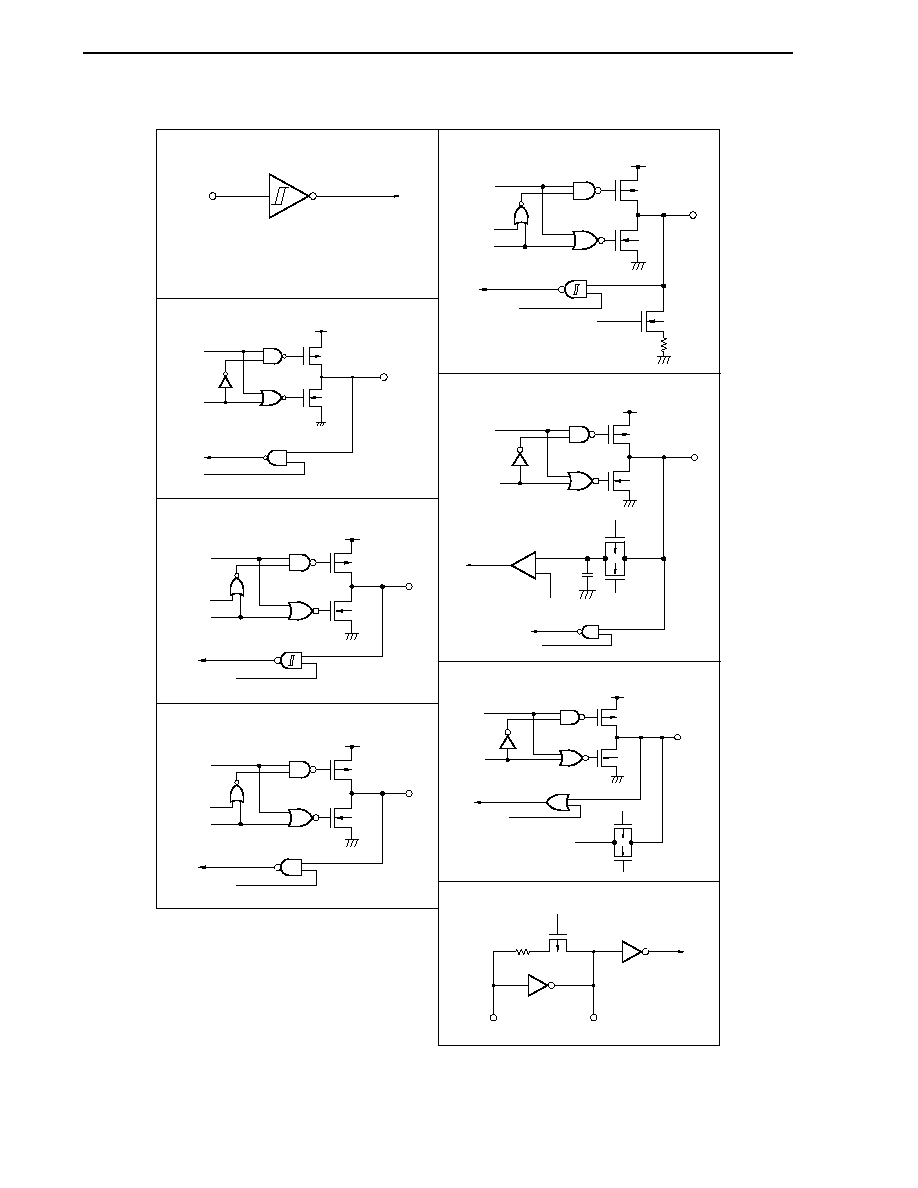
CHAPTER 2 PIN FUNCTIONS
Preliminary User's Manual U17714EJ1V0UD
44
Figure 2-1. Pin I/O Circuits
IN
Data
Output
disable
P-ch
IN/OUT
EV
DD
/BV
DD
EV
SS
/BV
SS
N-ch
Input
enable
Data
Output
disable
EV
DD
EV
SS
P-ch
IN/OUT
N-ch
Open drain
Input
enable
Data
Output
disable
AV
REF0
P-ch
IN/OUT
N-ch
P-ch
N-ch
AV
REF0
Input enable
+
_
AV
SS
AV
SS
Data
Output
disable
Input
enable
AV
REF1
P-ch
IN/OUT
N-ch
P-ch
N-ch
AV
SS
Data
Output
disable
EV
DD
EV
SS
P-ch
IN/OUT
N-ch
Open drain
Input
enable
N-ch
P-ch
Feedback cut-off
XT1
XT2
Data
Output
disable
EV
DD
EV
SS
P-ch
IN/OUT
N-ch
Open drain
Input
enable
Type 2
Schmitt-triggered input with hysteresis characteristics
Type 5
Type 10-N
Type 11-G
Type 12-D
Type 10-D
Type 16
Type 10-G
Analog output voltage
(Threshold voltage)
Note
Note
OCDM0 bit
Note Hysteresis characteristics are not available in port mode.

CHAPTER 2 PIN FUNCTIONS
Preliminary User's Manual U17714EJ1V0UD
45
2.4 Cautions
When the power is turned on, the following pins may output an undefined level temporarily, even during reset.
� P10/ANO0 pin
� P11/ANO1 pin
� P53/SIB2/KR3/TIQ00/TOQ00/RTP03/DDO pin

Preliminary User's Manual U17714EJ1V0UD
46
CHAPTER 3 CPU FUNCTION
The CPU of the V850ES/JJ2 is based on RISC architecture and executes almost all instructions with one clock by
using a 5-stage pipeline.
3.1 Features
Minimum instruction execution time: 50 ns (at 20 MHz operation)
30.5
�
s (with subclock (f
XT
) = 32.768 kHz operation)
Memory space Program (physical address) space: 64 MB linear
Data (logical address) space:
4 GB linear
General-purpose registers: 32 bits
� 32 registers
Internal 32-bit architecture
5-stage pipeline control
Multiplication/division instruction
Saturation operation instruction
32-bit shift instruction: 1 clock
Load/store instruction with long/short format
Four types of bit manipulation instructions
� SET1
� CLR1
� NOT1
� TST1
CHAPTER 3 CPU FUNCTION
Preliminary User's Manual U17714EJ1V0UD
47
3.2 CPU
Register
Set
The registers of the V850ES/JJ2 can be classified into two types: general-purpose program registers and dedicated
system registers. All the registers are 32 bits wide.
For details, refer to the V850ES Architecture User's Manual.
(1) Program register set
(2) System register set
r0
r1
r2
r3
r4
r5
r6
r7
r8
r9
r10
r11
r12
r13
r14
r15
r16
r17
r18
r19
r20
r21
r22
r23
r24
r25
r26
r27
r28
r29
r30
r31
(Zero register)
(Assembler-reserved register)
(Stack pointer (SP))
(Global pointer (GP))
(Text pointer (TP))
(Element pointer (EP))
(Link pointer (LP))
PC
(Program counter)
PSW
(Program status word)
ECR
(Interrupt source register)
FEPC
FEPSW
(NMI status saving register)
(NMI status saving register)
EIPC
EIPSW
(Interrupt status saving register)
(Interrupt status saving register)
31
0
31
0
31
0
CTBP
(CALLT base pointer)
DBPC
DBPSW
(Exception/debug trap status saving register)
(Exception/debug trap status saving register)
CTPC
CTPSW
(CALLT execution status saving register)
(CALLT execution status saving register)
CHAPTER 3 CPU FUNCTION
Preliminary User's Manual U17714EJ1V0UD
48
3.2.1
Program register set
The program registers include general-purpose registers and a program counter.
(1) General-purpose registers (r0 to r31)
Thirty-two general-purpose registers, r0 to r31, are available. Any of these registers can be used to store a
data variable or an address variable.
However, r0 and r30 are implicitly used by instructions and care must be exercised when these registers are
used. r0 always holds 0 and is used for an operation that uses 0 or addressing of offset 0. r30 is used by the
SLD and SST instructions as a base pointer when these instructions access the memory. r1, r3 to r5, and r31
are implicitly used by the assembler and C compiler. When using these registers, save their contents for
protection, and then restore the contents after using the registers. r2 is sometimes used by the real-time OS.
If the real-time OS does not use r2, it can be used as a register for variables.
Table 3-1. Program Registers
Name Usage
Operation
r0
Zero register
Always holds 0.
r1
Assembler-reserved register
Used as working register to create 32-bit immediate data
r2
Register for address/data variable (if real-time OS does not use r2)
r3
Stack pointer
Used to create a stack frame when a function is called
r4
Global pointer
Used to access a global variable in the data area
r5
Text pointer
Used as register that indicates the beginning of a text area (area
where program codes are located)
r6 to r29
Register for address/data variable
r30
Element pointer
Used as base pointer to access memory
r31
Link pointer
Used when the compiler calls a function
PC
Program counter
Holds the instruction address during program execution
Remark For furthers details on the r1, r3 to r5, and r31 that are used in the assembler and C compiler, refer
to the CA850 (C Compiler Package) Assembly Language User's Manual.
(2) Program counter (PC)
The program counter holds the instruction address during program execution. The lower 26 bits of this register
are valid. Bits 31 to 26 are fixed to 0. A carry from bit 25 to 26 is ignored even if it occurs.
Bit 0 is fixed to 0. This means that execution cannot branch to an odd address.
31
26 25
1 0
PC
Fixed to 0
Instruction address during program execution
0
Default value
00000000H

CHAPTER 3 CPU FUNCTION
Preliminary User's Manual U17714EJ1V0UD
49
3.2.2
System register set
The system registers control the status of the CPU and hold interrupt information.
These registers can be read or written by using system register load/store instructions (LDSR and STSR), using
the system register numbers listed below.
Table 3-2. System Register Numbers
Operand Specification
System
Register
Number
System Register Name
LDSR Instruction STSR Instruction
0
Interrupt status saving register (EIPC)
Note 1
1
Interrupt status saving register (EIPSW)
Note 1
2
NMI status saving register (FEPC)
Note 1
3
NMI status saving register (FEPSW)
Note 1
4
Interrupt source register (ECR)
�
5
Program status word (PSW)
6 to 15
Reserved for future function expansion (operation is not guaranteed if these
registers are accessed)
�
�
16
CALLT execution status saving register (CTPC)
17
CALLT execution status saving register (CTPSW)
18
Exception/debug trap status saving register (DBPC)
Note 2
Note 2
19
Exception/debug trap status saving register (DBPSW)
Note 2
Note 2
20
CALLT base pointer (CTBP)
21 to 31
Reserved for future function expansion (operation is not guaranteed if these
registers are accessed)
�
�
Notes 1. Because only one set of these registers is available, the contents of these registers must be saved by
program if multiple interrupts are enabled.
2. These registers can be accessed only during the interval between the execution of the DBTRAP
instruction or illegal opcode and the DBRET instruction.
Caution Even if EIPC or FEPC, or bit 0 of CTPC is set to 1 by the LDSR instruction, bit 0 is ignored when
execution is returned to the main routine by the RETI instruction after interrupt servicing (this is
because bit 0 of the PC is fixed to 0). Set an even value to EIPC, FEPC, and CTPC (bit 0 = 0).
Remark
: Can be accessed
�: Access prohibited
CHAPTER 3 CPU FUNCTION
Preliminary User's Manual U17714EJ1V0UD
50
(1) Interrupt status saving registers (EIPC and EIPSW)
EIPC and EIPSW are used to save the status when an interrupt occurs.
If a software exception or a maskable interrupt occurs, the contents of the program counter (PC) are saved to
EIPC, and the contents of the program status word (PSW) are saved to EIPSW (these contents are saved to
the NMI status saving registers (FEPC and FEPSW) if a non-maskable interrupt occurs).
The address of the instruction next to the instruction under execution, except some instructions (see 19.8
Periods in Which Interrupts Are Not Acknowledged by CPU), is saved to EIPC when a software exception
or a maskable interrupt occurs.
The current contents of the PSW are saved to EIPSW.
Because only one set of interrupt status saving registers is available, the contents of these registers must be
saved by program when multiple interrupts are enabled.
Bits 31 to 26 of EIPC and bits 31 to 8 of EIPSW are reserved for future function expansion (these bits are
always fixed to 0).
The value of EIPC is restored to the PC and the value of EIPSW to the PSW by the RETI instruction.
31
0
EIPC
(Saved PC contents)
0
0
Default value
0xxxxxxxH
(x: Undefined)
26 25
0 0 0 0
31
0
EIPSW
(Saved PSW
contents)
0
0
Default value
000000xxH
(x: Undefined)
8 7
0 0 0 0
0
0
0 0 0 0
0
0
0 0 0 0
0
0
0 0 0 0
CHAPTER 3 CPU FUNCTION
Preliminary User's Manual U17714EJ1V0UD
51
(2) NMI status saving registers (FEPC and FEPSW)
FEPC and FEPSW are used to save the status when a non-maskable interrupt (NMI) occurs.
If an NMI occurs, the contents of the program counter (PC) are saved to FEPC, and those of the program
status word (PSW) are saved to FEPSW.
The address of the instruction next to the one of the instruction under execution, except some instructions, is
saved to FEPC when an NMI occurs.
The current contents of the PSW are saved to FEPSW.
Because only one set of NMI status saving registers is available, the contents of these registers must be saved
by program when multiple interrupts are enabled.
Bits 31 to 26 of FEPC and bits 31 to 8 of FEPSW are reserved for future function expansion (these bits are
always fixed to 0).
The value of FEPC is restored to the PC and the value of FEPSW to the PSW by the RETI instruction.
31
0
FEPC
(Saved PC contents)
0
0
Default value
0xxxxxxxH
(x: Undefined)
26 25
0 0 0 0
31
0
FEPSW
(Saved PSW
contents)
0
0
Default value
000000xxH
(x: Undefined)
8 7
0 0 0 0
0
0
0 0 0 0
0
0
0 0 0 0
0
0
0 0 0 0
(3) Interrupt source register (ECR)
The interrupt source register (ECR) holds the source of an exception or interrupt if an exception or interrupt
occurs. This register holds the exception code of each interrupt source. Because this register is a read-only
register, data cannot be written to this register using the LDSR instruction.
31
0
ECR
FECC
EICC
Default value
00000000H
16 15
Bit position
Bit name
Meaning
31 to 16
FECC
Exception code of non-maskable interrupt (NMI)
15 to 0
EICC
Exception code of exception or maskable interrupt
CHAPTER 3 CPU FUNCTION
Preliminary User's Manual U17714EJ1V0UD
52
(4) Program status word (PSW)
The program status word (PSW) is a collection of flags that indicate the status of the program (result of
instruction execution) and the status of the CPU.
If the contents of a bit of this register are changed by using the LDSR instruction, the new contents are
validated immediately after completion of LDSR instruction execution. However if the ID flag is set to 1,
interrupt requests will not be acknowledged while the LDSR instruction is being executed.
Bits 31 to 8 of this register are reserved for future function expansion (these bits are fixed to 0).
(1/2)
31
0
PSW
RFU
Default value
00000020H
8 7
NP
6
EP
5
ID
4
SAT
3
CY
2
OV
1
S Z
Bit position
Flag name
Meaning
31 to 8
RFU
Reserved field. Fixed to 0.
7
NP
Indicates that a non-maskable interrupt (NMI) is being serviced. This bit is set to 1 when an
NMI request is acknowledged, disabling multiple interrupts.
0: NMI is not being serviced.
1: NMI is being serviced.
6
EP
Indicates that an exception is being processed. This bit is set to 1 when an exception
occurs. Even if this bit is set, interrupt requests are acknowledged.
0: Exception is not being processed.
1: Exception is being processed.
5
ID
Indicates whether a maskable interrupt can be acknowledged.
0: Interrupt enabled
1: Interrupt disabled
4
SAT
Note
Indicates that the result of a saturation operation has overflowed and is saturated. Because
this is a cumulative flag, it is set to 1 when the result of a saturation operation instruction is
saturated, and is not cleared to 0 even if the subsequent operation result is not saturated.
Use the LDSR instruction to clear this bit. This flag is neither set to 1 nor cleared to 0 by
execution of an arithmetic operation instruction.
0: Not saturated
1: Saturated
3
CY
Indicates whether a carry or a borrow occurs as a result of an operation.
0: Carry or borrow does not occur.
1: Carry or borrow occurs.
2
OV
Note
Indicates whether an overflow occurs during operation.
0: Overflow does not occur.
1: Overflow occurs.
1
S
Note
Indicates whether the result of an operation is negative.
0: The result is positive or 0.
1: The result is negative.
0
Z
Indicates whether the result of an operation is 0.
0: The result is not 0.
1: The result is 0.
Remark Also
read
Note on the next page.
CHAPTER 3 CPU FUNCTION
Preliminary User's Manual U17714EJ1V0UD
53
(2/2)
Note The result of the operation that has performed saturation processing is determined by the contents of the
OV and S flags. The SAT flag is set to 1 only when the OV flag is set to 1 when a saturation operation is
performed.
Flag Status
Status of Operation Result
SAT OV S
Result of Operation of
Saturation Processing
Maximum positive value is exceeded
1
1
0
7FFFFFFFH
Maximum negative value is exceeded
1
1
1
80000000H
Positive (maximum value is not exceeded)
0
Negative (maximum value is not exceeded)
Holds value
before operation
0
1
Operation result itself
(5) CALLT execution status saving registers (CTPC and CTPSW)
CTPC and CTPSW are CALLT execution status saving registers.
When the CALLT instruction is executed, the contents of the program counter (PC) are saved to CTPC, and
those of the program status word (PSW) are saved to CTPSW.
The contents saved to CTPC are the address of the instruction next to CALLT.
The current contents of the PSW are saved to CTPSW.
Bits 31 to 26 of CTPC and bits 31 to 8 of CTPSW are reserved for future function expansion (fixed to 0).
31
0
CTPC
(Saved PC contents)
0
0
Default value
0xxxxxxxH
(x: Undefined)
26 25
0 0 0 0
31
0
CTPSW
(Saved PSW
contents)
0
0
Default value
000000xxH
(x: Undefined)
8 7
0 0 0 0
0
0
0 0 0 0
0
0
0 0 0 0
0
0
0 0 0 0
CHAPTER 3 CPU FUNCTION
Preliminary User's Manual U17714EJ1V0UD
54
(6) Exception/debug trap status saving registers (DBPC and DBPSW)
DBPC and DBPSW are exception/debug trap status registers.
If an exception trap or debug trap occurs, the contents of the program counter (PC) are saved to DBPC, and
those of the program status word (PSW) are saved to DBPSW.
The contents to be saved to DBPC are the address of the instruction next to the one that is being executed
when an exception trap or debug trap occurs.
The current contents of the PSW are saved to DBPSW.
This register can be read or written only during the interval between the execution of the DBTRAP instruction
or illegal opcode and the DBRET instruction.
Bits 31 to 26 of DBPC and bits 31 to 8 of DBPSW are reserved for future function expansion (fixed to 0).
The value of DBPC is restored to the PC and the value of DBPSW to the PSW by the DBRET instruction.
31
0
DBPC
(Saved PC contents)
0
0
Default value
0xxxxxxxH
(x: Undefined)
26 25
0 0 0 0
31
0
DBPSW
(Saved PSW
contents)
0
0
Default value
000000xxH
(x: Undefined)
8 7
0 0 0 0
0
0
0 0 0 0
0
0
0 0 0 0
0
0
0 0 0 0
(7) CALLT base pointer (CTBP)
The CALLT base pointer (CTBP) is used to specify a table address or generate a target address (bit 0 is fixed
to 0).
Bits 31 to 26 of this register are reserved for future function expansion (fixed to 0).
31
0
CTBP
(Base address)
0
0
Default value
0xxxxxxxH
(x: Undefined)
26 25
0 0 0 0
0
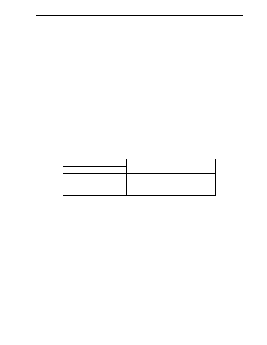
CHAPTER 3 CPU FUNCTION
Preliminary User's Manual U17714EJ1V0UD
55
3.3 Operation
Modes
The V850ES/JJ2 has the following operation modes.
(1) Normal operation mode
In this mode, each pin related to the bus interface is set to the port mode after system reset has been released.
Execution branches to the reset entry address of the internal ROM, and then instruction processing is started.
(2) Flash memory programming mode
In this mode, the internal flash memory can be programmed by using a flash programmer.
(3) On-chip debug mode
The V850ES/JJ2 is provided with an on-chip debug function that employs the JTAG (Joint Test Action Group)
communication specifications.
For details, see CHAPTER 27 ON-CHIP DEBUG FUNCTION.
3.3.1
Specifying operation mode
Specify the operation mode by using the FLMD0 and FLMD1 pins.
In the normal mode, input a low level to the FLMD0 pin when reset is released.
In the flash memory programming mode, a high level is input to the FLMD0 pin from the flash programmer if a flash
programmer is connected, but it must be input from an external circuit in the self-programming mode.
Operation When Reset Is Released
FLMD0 FLMD1
Operation Mode After Reset
L
�
Normal operation mode
H
L
Flash memory programming mode
H H
Setting
prohibited
Remark L: Low-level input
H: High-level input
�: Don't care
CHAPTER 3 CPU FUNCTION
Preliminary User's Manual U17714EJ1V0UD
56
3.4 Address
Space
3.4.1
CPU address space
For instruction addressing, up to a combined total of 16 MB of an external memory area and an internal ROM area,
plus an internal RAM area, are supported in a linear address space (program space) of up to 64 MB. For operand
addressing (data access), up to 4 GB of a linear address space (data space) is supported. The 4 GB address space,
however, is viewed as 64 images of a 64 MB physical address space. This means that the same 64 MB physical
address space is accessed regardless of the value of bits 31 to 26.
Figure 3-1. Image on Address Space
Program space
Internal RAM area
Use-prohibited area
Use-prohibited area
External memory area
Internal ROM area
(external memory area)
Data space
Image 63
Image 1
Image 0
Peripheral I/O area
Internal RAM area
Use-prohibited area
External memory area
Internal ROM area
(external memory area)
16 MB
4 GB
64 MB
64 MB
CHAPTER 3 CPU FUNCTION
Preliminary User's Manual U17714EJ1V0UD
57
3.4.2
Wraparound of CPU address space
(1) Program space
Of the 32 bits of the PC (program counter), the higher 6 bits are fixed to 0 and only the lower 26 bits are valid.
The higher 6 bits ignore a carry or borrow from bit 25 to 26 during branch address calculation.
Therefore, the highest address of the program space, 03FFFFFFH, and the lowest address, 00000000H, are
contiguous addresses. That the highest address and the lowest address of the program space are contiguous
in this way is called wraparound.
Caution Because the 4 KB area of addresses 03FFF000H to 03FFFFFFH is an on-chip peripheral I/O
area, instructions cannot be fetched from this area. Therefore, do not execute an operation in
which the result of a branch address calculation affects this area.
Program space
Program space
(+) direction
(
-) direction
0 0 0 0 0 0 0 1 H
0 0 0 0 0 0 0 0 H
0 3 F F F F F F H
0 3 F F F F F E H
(2) Data space
The result of an operand address calculation operation that exceeds 32 bits is ignored.
Therefore, the highest address of the data space, FFFFFFFFH, and the lowest address, 00000000H, are
contiguous, and wraparound occurs at the boundary of these addresses.
Data space
Data space
(+) direction
(
-) direction
0 0 0 0 0 0 0 1 H
0 0 0 0 0 0 0 0 H
F F F F F F F F H
F F F F F F F E H
CHAPTER 3 CPU FUNCTION
Preliminary User's Manual U17714EJ1V0UD
58
3.4.3 Memory
map
The areas shown below are reserved in the V850ES/JJ2.
Figure 3-2. Data Memory Map (Physical Addresses)
(64 KB)
Use prohibited
External memory area
(14 MB)
Internal ROM area
Note
(1 MB)
External memory area
(1 MB)
Internal RAM area
(60 KB)
On-chip peripheral I/O area
(4 KB)
(2 MB)
0 3 F F F F F F H
0 3 F F 0 0 0 0 H
0 1 0 0 0 0 0 0 H
0 0 F F F F F F H
0 0 2 0 0 0 0 0 H
0 0 1 F F F F F H
0 0 0 0 0 0 0 0 H
0 3 F E F F F F H
0 3 F F F F F F H
0 3 F F F 0 0 0 H
0 3 F F E F F F H
0 3 F F 0 0 0 0 H
0 0 1 F F F F F H
0 0 1 0 0 0 0 0 H
0 0 0 F F F F F H
0 0 0 0 0 0 0 0 H
Note Fetch access and read access to addresses 00000000H to 000FFFFFH is made to the internal ROM
area. However, data write access to these addresses is made to the external memory area.

CHAPTER 3 CPU FUNCTION
Preliminary User's Manual U17714EJ1V0UD
59
Figure 3-3. Program Memory Map
Internal RAM area (60 KB)
Use prohibited
(program fetch prohibited area)
Use prohibited
(program fetch prohibited area)
External memory area
(14 MB)
External memory area
(1 MB)
Internal ROM area
(1 MB)
0 3 F F F F F F H
0 3 F F F 0 0 0 H
0 3 F F E F F F H
0 1 0 0 0 0 0 0 H
0 0 F F F F F F H
0 3 F F 0 0 0 0 H
0 3 F E F F F F H
0 0 2 0 0 0 0 0 H
0 0 1 F F F F F H
0 0 1 0 0 0 0 0 H
0 0 0 F F F F F H
0 0 0 0 0 0 0 0 H
CHAPTER 3 CPU FUNCTION
Preliminary User's Manual U17714EJ1V0UD
60
3.4.4 Areas
(1) Internal ROM area
Up to 1 MB is reserved as an internal ROM area.
(a) Internal ROM (128 KB)
128 KB are allocated to addresses 00000000H to 0001FFFFH in the
�
PD70F3720.
Accessing addresses 00020000H to 000FFFFFH is prohibited.
Figure 3-4. Internal ROM Area (128 KB)
Access-prohibited
area
Internal ROM
(128 KB)
0 0 0 F F F F H
0 0 0 2 0 0 0 0 H
0 0 0 1 F F F F H
0 0 0 0 0 0 0 0 H
(b) Internal ROM (256 KB)
256 KB are allocated to addresses 00000000H to 0003FFFFH in the
�
PD70F3721.
Accessing addresses 00040000H to 000FFFFFH is prohibited.
Figure 3-5. Internal ROM Area (256 KB)
Access-prohibited
area
Internal ROM
(256 KB)
0 0 0 F F F F F H
0 0 0 4 0 0 0 0 H
0 0 0 3 F F F F H
0 0 0 0 0 0 0 0 H
CHAPTER 3 CPU FUNCTION
Preliminary User's Manual U17714EJ1V0UD
61
(c) Internal ROM (384 KB)
384 KB are allocated to addresses 00000000H to 0005FFFFH in the
�
PD70F3722.
Accessing addresses 00060000H to 000FFFFFH is prohibited.
Figure 3-6. Internal ROM Area (384 KB)
Access-prohibited
area
Internal ROM
(384 KB)
0 0 0 6 0 0 0 0 H
0 0 0 5 F F F F H
0 0 0 0 0 0 0 0 H
0 0 0 F F F F F H
(d) Internal ROM (512 KB)
512 KB are allocated to addresses 00000000H to 0007FFFFH in the
�
PD70F3723.
Accessing addresses 00080000H to 000FFFFFH is prohibited.
Figure 3-7. Internal ROM Area (512 KB)
Access-prohibited
area
Internal ROM
(512 KB)
0 0 0 F F F F H
0 0 0 8 0 0 0 0 H
0 0 0 7 F F F F H
0 0 0 0 0 0 0 0 H

CHAPTER 3 CPU FUNCTION
Preliminary User's Manual U17714EJ1V0UD
62
(e) Internal ROM (640 KB)
640 KB are allocated to addresses 00000000H to 0009FFFFH in the
�
PD70F3724.
Accessing addresses 000A0000H to 000FFFFFH is prohibited.
Figure 3-8. Internal ROM Area (640 KB)
Access-prohibited
area
Internal ROM
(640 KB)
0 0 0 A 0 0 0 0 H
0 0 0 9 F F F F H
0 0 0 0 0 0 0 0 H
0 0 0 F F F F F H

CHAPTER 3 CPU FUNCTION
Preliminary User's Manual U17714EJ1V0UD
63
(2) Internal RAM area
Up to 60 KB are reserved as the internal RAM area.
(a) Internal RAM (12 KB)
12 KB are allocated to addresses 03FFC000H to 03FFEFFFH in the
�
PD70F3720.
Accessing addresses 03FF0000H to 03FFBFFFH is prohibited.
Figure 3-9. Internal RAM Area (12 KB)
Access-prohibited
area
Internal RAM
0 3 F F E F F F H
F F F F E F F F H
F F F F C 0 0 0 H
F F F F B F F F H
F F F F 0 0 0 0 H
0 3 F F C 0 0 0 H
0 3 F F B F F F H
0 3 F F 0 0 0 0 H
Physical address space
Logical address space
(b) Internal RAM (24 KB)
24 KB are allocated to addresses 03FF9000H to 03FFEFFFH in the
�
PD70F3721.
Accessing addresses 03FF0000H to 03FF8FFFH is prohibited.
Figure 3-10. Internal RAM Area (24 KB)
Access-prohibited
area
Internal RAM
0 3 F F E F F F H
F F F F E F F F H
0 3 F F 9 0 0 0 H
F F F F 9 0 0 0 H
0 3 F F 8 F F F H
F F F F 8 F F F H
0 3 F F 0 0 0 0 H
F F F F 0 0 0 0 H
Physical address space
Logical address space

CHAPTER 3 CPU FUNCTION
Preliminary User's Manual U17714EJ1V0UD
64
(c) Internal RAM (32 KB)
32 KB are allocated to addresses 03FF7000H to 03FFEFFFH in the
�
PD70F3722.
Accessing addresses 03FF0000H to 03FF6FFFH is prohibited.
Figure 3-11. Internal RAM Area (32 KB)
Access-prohibited
area
Internal RAM
0 3 F F 7 0 0 0 H
0 3 F F 6 F F F H
0 3 F F 0 0 0 0 H
0 3 F F E F F F H
F F F F 7 0 0 0 H
F F F F 6 F F F H
F F F F 0 0 0 0 H
F F F F E F F F H
Physical address space
Logical address space
(d) Internal RAM (40 KB)
40 KB are allocated to addresses 03FF5000H to 03FFEFFFH in the
�
PD70F3723.
Accessing addresses 03FF0000H to 03FF4FFFH is prohibited.
Figure 3-12. Internal RAM Area (40 KB)
Access-prohibited
area
Internal RAM
0 3 F F E F F F H
F F F F E F F F H
0 3 F F 5 0 0 0 H
F F F F 5 0 0 0 H
0 3 F F 4 F F F H
F F F F 4 F F F H
0 3 F F 0 0 0 0 H
F F F F 0 0 0 0 H
Physical address space
Logical address space

CHAPTER 3 CPU FUNCTION
Preliminary User's Manual U17714EJ1V0UD
65
(e) Internal RAM (48 KB)
48 KB are allocated to addresses 03FF3000H to 03FFEFFFH in the
�
PD70F3724.
Accessing addresses 03FF0000H to 03FF2FFFH is prohibited.
Figure 3-13. Internal RAM Area (48 KB)
Access-prohibited
area
Internal RAM
0 3 F F 3 0 0 0 H
0 3 F F 2 F F F H
0 3 F F 0 0 0 0 H
0 3 F F E F F F H
F F F F 3 0 0 0 H
F F F F 2 F F F H
F F F F 0 0 0 0 H
F F F F E F F F H
Physical address space
Logical address space

CHAPTER 3 CPU FUNCTION
Preliminary User's Manual U17714EJ1V0UD
66
(3) On-chip peripheral I/O area
4 KB of addresses 03FFF000H to 03FFFFFFH are reserved as the on-chip peripheral I/O area.
Figure 3-14. On-Chip Peripheral I/O Area
On-chip peripheral I/O area
(4 KB)
0 3 F F F F F F H
0 3 F F F 0 0 0 H
F F F F F F F F H
F F F F F 0 0 0 H
Physical address space
Logical address space
Peripheral I/O registers that have functions to specify the operation mode for and monitor the status of the on-
chip peripheral I/O are mapped to the on-chip peripheral I/O area. Program cannot be fetched from this area.
Cautions 1. When a register is accessed in word units, a word area is accessed twice in halfword
units in the order of lower area and higher area, with the lower 2 bits of the address
ignored.
2. If a register that can be accessed in byte units is accessed in halfword units, the higher 8
bits are undefined when the register is read, and data is written to the lower 8 bits.
3. Addresses not defined as registers are reserved for future expansion. The operation is
undefined and not guaranteed when these addresses are accessed.
(4) External memory area
15 MB (00100000H to 00FFFFFFH) are allocated as the external memory area. For details, see CHAPTER 5
BUS CONTROL FUNCTION.

CHAPTER 3 CPU FUNCTION
Preliminary User's Manual U17714EJ1V0UD
67
3.4.5
Recommended use of address space
The architecture of the V850ES/JJ2 requires that a register that serves as a pointer be secured for address
generation when operand data in the data space is accessed. The address stored in this pointer
�32 KB can be
directly accessed by an instruction for operand data. Because the number of general-purpose registers that can be
used as a pointer is limited, however, by keeping the performance from dropping during address calculation when a
pointer value is changed, as many general-purpose registers as possible can be secured for variables, and the
program size can be reduced.
(1) Program space
Of the 32 bits of the PC (program counter), the higher 6 bits are fixed to 0, and only the lower 26 bits are valid.
Regarding the program space, therefore, a 64 MB space of contiguous addresses starting from 00000000H
unconditionally corresponds to the memory map.
To use the internal RAM area as the program space, access following addresses.
Caution If a branch instruction is at the upper limit of the internal RAM area, a prefetch operation
(invalid fetch) straddling the on-chip peripheral I/O area does not occur.
RAM Size
Access Address
48 KB
03FF3000H to 03FFEFFFH
40 KB
03FF5000H to 03FFEFFFH
32 KB
03FF7000H to 03FFEFFFH
24 KB
03FF9000H to 03FFEFFFH
12 KB
03FFC000H to 03FFEFFFH
CHAPTER 3 CPU FUNCTION
Preliminary User's Manual U17714EJ1V0UD
68
(2) Data space
With the V850ES/JJ2, it seems that there are sixty-four 64 MB address spaces on the 4 GB CPU address
space. Therefore, the least significant bit (bit 25) of a 26-bit address is sign-extended to 32 bits and allocated
as an address.
(a) Application example of wraparound
If R = r0 (zero register) is specified for the LD/ST disp16 [R] instruction, a range of addresses 00000000H
�32 KB can be addressed by sign-extended disp16. All the resources, including the internal hardware, can
be addressed by one pointer.
The zero register (r0) is a register fixed to 0 by hardware, and practically eliminates the need for registers
dedicated to pointers.
Example:
�
PD70F3722
Internal ROM area
On-chip peripheral
I/O area
Internal RAM area
32 KB
4 KB
28 KB
(R = )
0 0 0 5 F F F F H
0 0 0 0 7 F F F H
0 0 0 0 0 0 0 0 H
F F F F F 0 0 0 H
F F F F E F F F H
F F F F 8 0 0 0 H
CHAPTER 3 CPU FUNCTION
Preliminary User's Manual U17714EJ1V0UD
69
Figure 3-15. Recommended Memory Map
Data space
Program space
On-chip
peripheral I/O
On-chip
peripheral I/O
Internal RAM
Internal RAM
Internal ROM
External
memory
Use prohibited
External
memory
Use prohibited
Internal RAM
Program space
64 MB
Internal ROM
Internal ROM
F F F F F F F F H
F F F F F 0 0 0 H
F F F F E F F F H
F F F F 0 0 0 0 H
F F F E F F F F H
0 4 0 0 0 0 0 0 H
0 3 F F F F F F H
0 3 F F F 0 0 0 H
0 3 F F E F F F H
0 3 F F 7 0 0 0 H
0 3 F F 6 F F F H
0 3 F F 0 0 0 0 H
0 3 F E F F F F H
0 1 0 0 0 0 0 0 H
0 0 F F F F F F H
0 0 0 6 0 0 0 0 H
0 0 0 5 F F F F H
0 0 1 0 0 0 0 0 H
0 0 0 F F F F F H
0 0 0 0 0 0 0 0 H
F F F F F F F F H
F F F F F 0 0 0 H
F F F F E F F F H
F F F F 7 0 0 0 H
F F F F 6 F F F H
F F F F 0 0 0 0 H
F F F E F F F F H
0 0 1 0 0 0 0 0 H
0 0 0 F F F F F H
0 0 0 0 0 0 0 0 H
Use prohibited
Remarks 1. indicates the recommended area.
2.
This figure is the recommended memory map of the
�
PD70F3722.
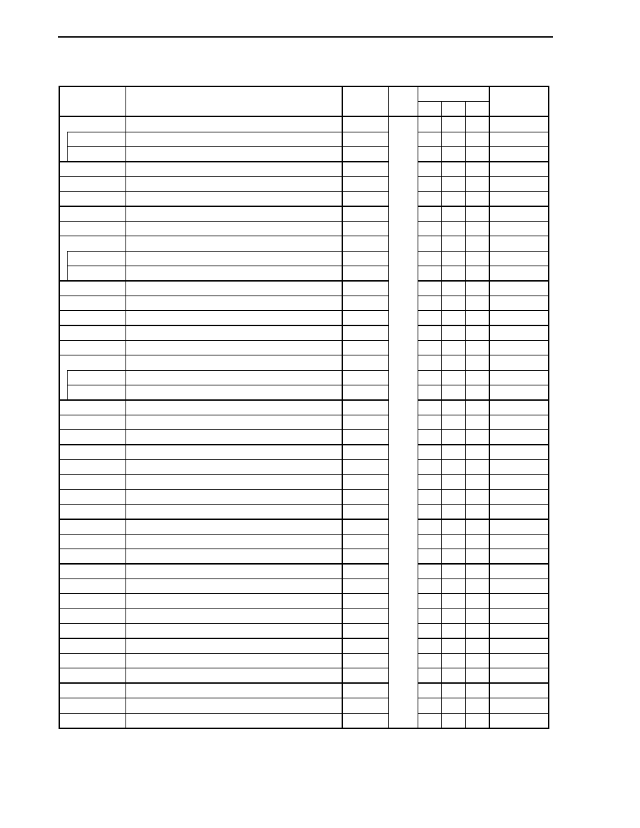
CHAPTER 3 CPU FUNCTION
Preliminary User's Manual U17714EJ1V0UD
70
3.4.6
Peripheral I/O registers
(1/12)
Manipulatable Bits
Address Function
Register
Name
Symbol
R/W
1 8 16
Default Value
FFFFF004H Port
DL
register
PDL
0000H
Note
FFFFF004H Port
DLL
register
PDLL
00H
Note
FFFFF005H Port
DLH
register
PDLH
00H
Note
FFFFF006H Port
DH
register
PDH
00H
Note
FFFFF008H Port
CS
register
PCS
00H
Note
FFFFF00AH Port
CT
register
PCT
00H
Note
FFFFF00CH Port
CM
register
PCM
00H
Note
FFFFF00EH Port
CD
register
PCD
00H
Note
FFFFF024H
Port DL mode register
PMDL
FFFFH
FFFFF024H
Port DL mode register L
PMDLL
FFH
FFFFF025H
Port DL mode register H
PMDLH
FFH
FFFFF026H
Port DH mode register
PMDH
FFH
FFFFF028H
Port CS mode register
PMCS
FFH
FFFFF02AH
Port CT mode register
PMCT
FFH
FFFFF02CH
Port CM mode register
PMCM
FFH
FFFFF02EH
Port CD mode register
PMCD
FFH
FFFFF044H
Port DL mode control register
PMCDL
0000H
FFFFF044H
Port DL mode control register L
PMCDLL
00H
FFFFF045H
Port DL mode control register H
PMCDLH
00H
FFFFF046H
Port DH mode control register
PMCDH
00H
FFFFF048H
Port CS mode control register
PMCCS
00H
FFFFF04AH
Port CT mode control register
PMCCT
00H
FFFFF04CH
Port CM mode control register
PMCCM
00H
FFFFF066H
Bus size configuration register
BSC
5555H
FFFFF06EH
System wait control register
VSWC
77H
FFFFF080H
DMA source address register 0L
DSA0L
Undefined
FFFFF082H
DMA source address register 0H
DSA0H
Undefined
FFFFF084H
DMA destination address register 0L
DDA0L
Undefined
FFFFF086H
DMA destination address register 0H
DDA0H
Undefined
FFFFF088H
DMA source address register 1L
DSA1L
Undefined
FFFFF08AH
DMA source address register 1H
DSA1H
Undefined
FFFFF08CH
DMA destination address register 1L
DDA1L
Undefined
FFFFF08EH
DMA destination address register 1H
DDA1H
Undefined
FFFFF090H
DMA source address register 2L
DSA2L
Undefined
FFFFF092H
DMA source address register 2H
DSA2H
Undefined
FFFFF094H
DMA destination address register 2L
DDA2L
Undefined
FFFFF096H
DMA destination address register 2H
DDA2H
Undefined
FFFFF098H
DMA source address register 3L
DSA3L
Undefined
FFFFF09AH
DMA source address register 3H
DSA3H
Undefined
FFFFF09CH
DMA destination address register 3L
DDA3L
Undefined
FFFFF09EH
DMA destination address register 3H
DDA3H
R/W
Undefined
Note The value of the output latch is 00H or 0000H. The status of the pin is read during input.
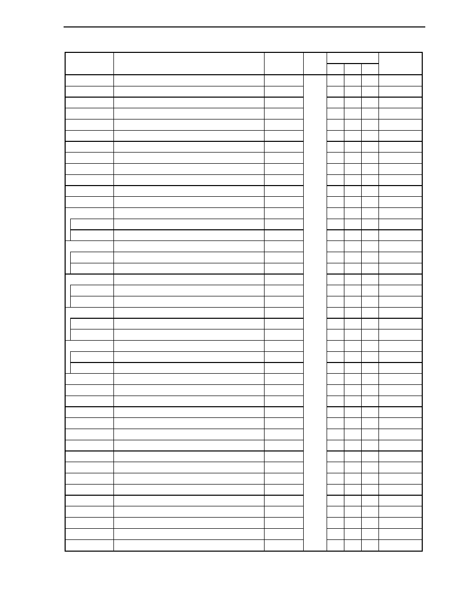
CHAPTER 3 CPU FUNCTION
Preliminary User's Manual U17714EJ1V0UD
71
(2/12)
Manipulatable Bits
Address Function
Register
Name
Symbol
R/W
1 8 16
Default Value
FFFFF0C0H
DMA transfer count register 0
DBC0
Undefined
FFFFF0C2H
DMA transfer count register 1
DBC1
Undefined
FFFFF0C4H
DMA transfer count register 2
DBC2
Undefined
FFFFF0C6H
DMA transfer count register 3
DBC3
Undefined
FFFFF0D0H
DMA addressing control register 0
DADC0
0000H
FFFFF0D2H
DMA addressing control register 1
DADC1
0000H
FFFFF0D4H
DMA addressing control register 2
DADC2
0000H
FFFFF0D6H
DMA addressing control register 3
DADC3
0000H
FFFFF0E0H
DMA channel control register 0
DCHC0
00H
FFFFF0E2H
DMA channel control register 1
DCHC1
00H
FFFFF0E4H
DMA channel control register 2
DCHC2
00H
FFFFF0E6H
DMA channel control register 3
DCHC3
00H
FFFFF100H
Interrupt mask register 0
IMR0
FFFFH
FFFFF100H
Interrupt mask register 0L
IMR0L
FFH
FFFFF101H
Interrupt mask register 0H
IMR0H
FFH
FFFFF102H
Interrupt mask register 1
IMR1
FFFFH
FFFFF102H
Interrupt mask register 1L
IMR1L
FFH
FFFFF103H
Interrupt mask register 1H
IMR1H
FFH
FFFFF104H
Interrupt mask register 2
IMR2
FFFFH
FFFFF104H
Interrupt mask register 2L
IMR2L
FFH
FFFFF105H
Interrupt mask register 2H
IMR2H
FFH
FFFFF106H
Interrupt mask register 3
IMR3
FFFFH
FFFFF106H
Interrupt mask register 3L
IMR3L
FFH
FFFFF107H
Interrupt mask register 3H
IMR3H
FFH
FFFFF108H
Interrupt mask register 4
IMR4
FFFFH
FFFFF108H
Interrupt mask register 4L
IMR4L
FFH
FFFFF109H
Interrupt mask register 4H
IMR4H
FFH
FFFFF110H
Interrupt control register
LVIIC
47H
FFFFF112H
Interrupt control register
PIC0
47H
FFFFF114H
Interrupt control register
PIC1
47H
FFFFF116H
Interrupt control register
PIC2
47H
FFFFF118H
Interrupt control register
PIC3
47H
FFFFF11AH
Interrupt control register
PIC4
47H
FFFFF11CH
Interrupt control register
PIC5
47H
FFFFF11EH
Interrupt control register
PIC6
47H
FFFFF120H
Interrupt control register
PIC7
47H
FFFFF122H
Interrupt control register
TQ0OVIC
47H
FFFFF124H
Interrupt control register
TQ0CCIC0
47H
FFFFF126H
Interrupt control register
TQ0CCIC1
47H
FFFFF128H
Interrupt control register
TQ0CCIC2
47H
FFFFF12AH
Interrupt control register
TQ0CCIC3
47H
FFFFF12CH
Interrupt control register
TP0OVIC
47H
FFFFF12EH
Interrupt control register
TP0CCIC0
R/W
47H

CHAPTER 3 CPU FUNCTION
Preliminary User's Manual U17714EJ1V0UD
72
(3/12)
Manipulatable Bits
Address Function
Register
Name Symbol
R/W
1 8 16
Default Value
FFFFF130H
Interrupt control register
TP0CCIC1
47H
FFFFF132H
Interrupt control register
TP1OVIC
47H
FFFFF134H
Interrupt control register
TP1CCIC0
47H
FFFFF136H
Interrupt control register
TP1CCIC1
47H
FFFFF138H
Interrupt control register
TP2OVIC
47H
FFFFF13AH
Interrupt control register
TP2CCIC0
47H
FFFFF13CH
Interrupt control register
TP2CCIC1
47H
FFFFF13EH
Interrupt control register
TP3OVIC
47H
FFFFF140H
Interrupt control register
TP3CCIC0
47H
FFFFF142H
Interrupt control register
TP3CCIC1
47H
FFFFF144H
Interrupt control register
TP4OVIC
47H
FFFFF146H
Interrupt control register
TP4CCIC0
47H
FFFFF148H
Interrupt control register
TP4CCIC1
47H
FFFFF14AH
Interrupt control register
TP5OVIC
47H
FFFFF14CH
Interrupt control register
TP5CCIC0
47H
FFFFF14EH
Interrupt control register
TP5CCIC1
47H
FFFFF150H
Interrupt control register
TM0EQIC0
47H
FFFFF152H
Interrupt control register
CB0RIC/IICIC1
47H
FFFFF154H
Interrupt control register
CB0TIC
47H
FFFFF156H
Interrupt control register
CB1RIC
47H
FFFFF158H
Interrupt control register
CB1TIC
47H
FFFFF15AH
Interrupt control register
CB2RIC
47H
FFFFF15CH
Interrupt control register
CB2TIC
47H
FFFFF15EH
Interrupt control register
CB3RIC
47H
FFFFF160H
Interrupt control register
CB3TIC
47H
FFFFF162H
Interrupt control register
UA0RIC/CB4RIC
47H
FFFFF164H
Interrupt control register
UA0TIC/CB4TIC
47H
FFFFF166H
Interrupt control register
UA1RIC/IICIC2
47H
FFFFF168H
Interrupt control register
UA1TIC
47H
FFFFF16AH
Interrupt control register
UA2RIC/IICIC0
47H
FFFFF16CH
Interrupt control register
UA2TIC
47H
FFFFF16EH
Interrupt control register
ADIC
47H
FFFFF170H
Interrupt control register
DMAIC0
47H
FFFFF172H
Interrupt control register
DMAIC1
47H
FFFFF174H
Interrupt control register
DMAIC2
47H
FFFFF176H
Interrupt control register
DMAIC3
47H
FFFFF178H
Interrupt control register
KRIC
47H
FFFFF17AH
Interrupt control register
WTIIC
47H
FFFFF17CH
Interrupt control register
WTIC
47H
FFFFF18EH
Interrupt control register
PIC8
47H
FFFFF190H
Interrupt control register
TP6OVIC
47H
FFFFF192H
Interrupt control register
TP6CCIC0
47H
FFFFF194H
Interrupt control register
TP6CCIC1
R/W
47H

CHAPTER 3 CPU FUNCTION
Preliminary User's Manual U17714EJ1V0UD
73
(4/12)
Manipulatable Bits
Address Function
Register
Name Symbol
R/W
1 8 16
Default Value
FFFFF196H
Interrupt control register
TP7OVIC
47H
FFFFF198H
Interrupt control register
TP7CCIC0
47H
FFFFF19AH
Interrupt control register
TP7CCIC1
47H
FFFFF19CH
Interrupt control register
TP8OVIC
47H
FFFFF19EH
Interrupt control register
TP8CCIC0
47H
FFFFF1A0H
Interrupt control register
TP8CCIC1
47H
FFFFF1A2H
Interrupt control register
CB5RIC
47H
FFFFF1A4H
Interrupt control register
CB5TIC
47H
FFFFF1A6H
Interrupt control register
UA3RIC
47H
FFFFF1A8H
Interrupt control register
UA3TIC
R/W
47H
FFFFF1FAH
In-service priority register
ISPR
R
00H
FFFFF1FCH Command
register
PRCMD
W
Undefined
FFFFF1FEH
Power save control register
PSC
00H
FFFFF200H
A/D converter mode register 0
ADA0M0
00H
FFFFF201H
A/D converter mode register 1
ADA0M1
00H
FFFFF202H
A/D converter channel specification register
ADA0S
00H
FFFFF203H
A/D converter mode register 2
ADA0M2
00H
FFFFF204H
Power-fail compare mode register
ADA0PFM
00H
FFFFF205H
Power-fail compare threshold value register
ADA0PFT
R/W
00H
FFFFF210H
A/D conversion result register 0
ADA0CR0
Undefined
FFFFF211H
A/D conversion result register 0H
ADA0CR0H
Undefined
FFFFF212H
A/D conversion result register 1
ADA0CR1
Undefined
FFFFF213H
A/D conversion result register 1H
ADA0CR1H
Undefined
FFFFF214H
A/D conversion result register 2
ADA0CR2
Undefined
FFFFF215H
A/D conversion result register 2H
ADA0CR2H
Undefined
FFFFF216H
A/D conversion result register 3
ADA0CR3
Undefined
FFFFF217H
A/D conversion result register 3H
ADA0CR3H
Undefined
FFFFF218H
A/D conversion result register 4
ADA0CR4
Undefined
FFFFF219H
A/D conversion result register 4H
ADA0CR4H
Undefined
FFFFF21AH
A/D conversion result register 5
ADA0CR5
Undefined
FFFFF21BH
A/D conversion result register 5H
ADA0CR5H
Undefined
FFFFF21CH
A/D conversion result register 6
ADA0CR6
Undefined
FFFFF21DH
A/D conversion result register 6H
ADA0CR6H
Undefined
FFFFF21EH
A/D conversion result register 7
ADA0CR7
Undefined
FFFFF21FH
A/D conversion result register 7H
ADA0CR7H
Undefined
FFFFF220H
A/D conversion result register 8
ADA0CR8
Undefined
FFFFF221H
A/D conversion result register 8H
ADA0CR8H
Undefined
FFFFF222H
A/D conversion result register 9
ADA0CR9
Undefined
FFFFF223H
A/D conversion result register 9H
ADA0CR9H
Undefined
FFFFF224H
A/D conversion result register 10
ADA0CR10
Undefined
FFFFF225H
A/D conversion result register 10H
ADA0CR10H
R
Undefined

CHAPTER 3 CPU FUNCTION
Preliminary User's Manual U17714EJ1V0UD
74
(5/12)
Manipulatable Bits
Address Function
Register
Name
Symbol
R/W
1 8 16
Default Value
FFFFF226H
A/D conversion result register 11
ADA0CR11
Undefined
FFFFF227H
A/D conversion result register 11H
ADA0CR11H
Undefined
FFFFF228H
A/D conversion result register 12
ADA0CR12
Undefined
FFFFF229H
A/D conversion result register 12H
ADA0CR12H
Undefined
FFFFF22AH
A/D conversion result register 13
ADA0CR13
Undefined
FFFFF22BH
A/D conversion result register 13H
ADA0CR13H
Undefined
FFFFF22CH
A/D conversion result register 14
ADA0CR14
Undefined
FFFFF22DH
A/D conversion result register 14H
ADA0CR14H
Undefined
FFFFF22EH
A/D conversion result register 15
ADA0CR15
Undefined
FFFFF22FH
A/D conversion result register 15H
ADA0CR15H
R
Undefined
FFFFF280H
D/A conversion value setting register 0
DA0CS0
00H
FFFFF281H
D/A conversion value setting register 1
DA0CS1
00H
FFFFF282H
D/A converter mode register
DA0M
00H
FFFFF300H
Key return mode register
KRM
00H
FFFFF308H
Selector operation control register 0
SELCNT0
00H
FFFFF318H
Noise elimination control register
NFC
00H
FFFFF320H
Prescaler mode register 1
PRSM1
00H
FFFFF321H
Prescaler compare register 1
PRSCM1
00H
FFFFF324H
Prescaler mode register 2
PRSM2
00H
FFFFF325H
Prescaler compare register 2
PRSCM2
00H
FFFFF328H
Prescaler mode register 3
PRSM3
00H
FFFFF329H
Prescaler compare register 3
PRSCM3
00H
FFFFF340H
IIC division clock select register 0
OCKS0
00H
FFFFF344H
IIC division clock select register 1
OCKS1
00H
FFFFF400H Port
0
register
P0
00H
Note
FFFFF402H Port
1
register
P1
00H
Note
FFFFF406H Port
3
register
P3
0000H
Note
FFFFF406H
Port 3L register
P3L
00H
Note
FFFFF407H
Port 3H register
P3H
00H
Note
FFFFF408H Port
4
register
P4
00H
Note
FFFFF40AH Port
5
register
P5
00H
Note
FFFFF40CH Port
6
register
P6
0000H
Note
FFFFF40CH
Port 6L register
P6L
00H
Note
FFFFF40DH
Port 6H register
P6H
00H
Note
FFFFF40EH
Port 7L register
P7L
00H
Note
FFFFF40FH
Port 7H register
P7H
00H
Note
FFFFF410H Port
8
register
P8
00H
Note
FFFFF412H Port
9
register
P9
0000H
Note
FFFFF412H
Port 9L register
P9L
00H
Note
FFFFF413H
Port 9H register
P9H
00H
Note
FFFFF420H
Port 0 mode register
PM0
R/W
FFH
Note The value of the output latch is 00H or 0000H. The status of the pin is read during input.
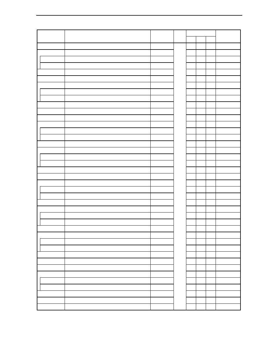
CHAPTER 3 CPU FUNCTION
Preliminary User's Manual U17714EJ1V0UD
75
(6/12)
Manipulatable Bits
Address Function
Register
Name Symbol
R/W
1 8 16
Default Value
FFFFF422H
Port 1 mode register
PM1
FFH
FFFFF426H
Port 3 mode register
PM3
FFFFH
FFFFF426H
Port 3 mode register L
PM3L
FFH
FFFFF427H
Port 3 mode register H
PM3H
FFH
FFFFF428H
Port 4 mode register
PM4
FFH
FFFFF42AH
Port 5 mode register
PM5
FFH
FFFFF42CH
Port 6 mode register
PM6
FFFFH
FFFFF42CH
Port 6 mode register L
PM6L
FFH
FFFFF42DH
Port 6 mode register H
PM6H
FFH
FFFFF42EH
Port 7 mode register L
PM7L
FFH
FFFFF42FH
Port 7 mode register H
PM7H
FFH
FFFFF430H
Port 8 mode register
PM8
FFH
FFFFF432H
Port 9 mode register
PM9
FFFFH
FFFFF432H
Port 9 mode register L
PM9L
FFH
FFFFF433H
Port 9 mode register H
PM9H
FFH
FFFFF440H
Port 0 mode control register
PMC0
00H
FFFFF446H
Port 3 mode control register
PMC3
0000H
FFFFF446H
Port 3 mode control register L
PMC3L
00H
FFFFF447H
Port 3 mode control register H
PMC3H
00H
FFFFF448H
Port 4 mode control register
PMC4
00H
FFFFF44AH
Port 5 mode control register
PMC5
00H
FFFFF44CH
Port 6 mode control register
PMC6
0000H
FFFFF44CH
Port 6 mode control register L
PMC6L
00H
FFFFF44DH
Port 6 mode control register H
PMC6H
00H
FFFFF450H
Port 8 mode control register
PMC8
00H
FFFFF452H
Port 9 mode control register
PMC9
0000H
FFFFF452H
Port 9 mode control register L
PMC9L
00H
FFFFF453H
Port 9 mode control register H
PMC9H
00H
FFFFF460H
Port 0 function control register
PFC0
00H
FFFFF466H
Port 3 function control register
PFC3
0000H
FFFFF466H
Port 3 function control register L
PFC3L
00H
FFFFF467H
Port 3 function control register H
PFC3H
00H
FFFFF468H
Port 4 function control register
PFC4
00H
FFFFF46AH
Port 5 function control register
PFC5
00H
FFFFF46DH
Port 6 function control register H
PFC6H
00H
FFFFF472H
Port 9 function control register
PFC9
0000H
FFFFF472H
Port 9 function control register L
PFC9L
00H
FFFFF473H
Port 9 function control register H
PFC9H
00H
FFFFF484H
Data wait control register 0
DWC0
7777H
FFFFF488H
Address wait control register
AWC
FFFFH
FFFFF48AH
Bus cycle control register
BCC
R/W
AAAAH
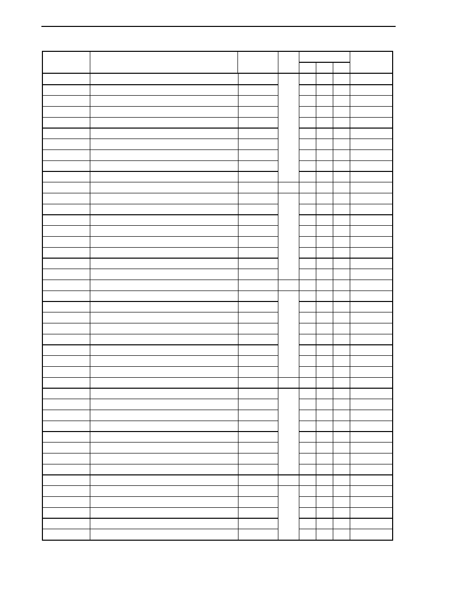
CHAPTER 3 CPU FUNCTION
Preliminary User's Manual U17714EJ1V0UD
76
(7/12)
Manipulatable Bits
Address Function
Register
Name Symbol
R/W
1 8 16
Default Value
FFFFF540H
TMQ0 control register 0
TQ0CTL0
00H
FFFFF541H
TMQ0 control register 1
TQ0CTL1
00H
FFFFF542H
TMQ0 I/O control register 0
TQ0IOC0
00H
FFFFF543H
TMQ0 I/O control register 1
TQ0IOC1
00H
FFFFF544H
TMQ0 I/O control register 2
TQ0IOC2
00H
FFFFF545H
TMQ0 option register 0
TQ0OPT0
00H
FFFFF546H
TMQ0 capture/compare register 0
TQ0CCR0
0000H
FFFFF548H
TMQ0 capture/compare register 1
TQ0CCR1
0000H
FFFFF54AH
TMQ0 capture/compare register 2
TQ0CCR2
0000H
FFFFF54CH
TMQ0 capture/compare register 3
TQ0CCR3
R/W
0000H
FFFFF54EH
TMQ0 counter read buffer register
TQ0CNT
R
0000H
FFFFF590H
TMP0 control register 0
TP0CTL0
00H
FFFFF591H
TMP0 control register 1
TP0CTL1
00H
FFFFF592H
TMP0 I/O control register 0
TP0IOC0
00H
FFFFF593H
TMP0 I/O control register 1
TP0IOC1
00H
FFFFF594H
TMP0 I/O control register 2
TP0IOC2
00H
FFFFF595H
TMP0 option register 0
TP0OPT0
00H
FFFFF596H
TMP0 capture/compare register 0
TP0CCR0
0000H
FFFFF598H
TMP0 capture/compare register 1
TP0CCR1
R/W
0000H
FFFFF59AH
TMP0 counter read buffer register
TP0CNT
R
0000H
FFFFF5A0H
TMP1 control register 0
TP1CTL0
00H
FFFFF5A1H
TMP1 control register 1
TP1CTL1
00H
FFFFF5A2H
TMP1 I/O control register 0
TP1IOC0
00H
FFFFF5A3H
TMP1 I/O control register 1
TP1IOC1
00H
FFFFF5A4H
TMP1 I/O control register 2
TP1IOC2
00H
FFFFF5A5H
TMP1 option register 0
TP1OPT0
00H
FFFFF5A6H
TMP1 capture/compare register 0
TP1CCR0
0000H
FFFFF5A8H
TMP1 capture/compare register 1
TP1CCR1
R/W
0000H
FFFFF5AAH
TMP1 counter read buffer register
TP1CNT
R
0000H
FFFFF5B0H
TMP2 control register 0
TP2CTL0
00H
FFFFF5B1H
TMP2 control register 1
TP2CTL1
00H
FFFFF5B2H
TMP2 I/O control register 0
TP2IOC0
00H
FFFFF5B3H
TMP2 I/O control register 1
TP2IOC1
00H
FFFFF5B4H
TMP2 I/O control register 2
TP2IOC2
00H
FFFFF5B5H
TMP2 option register 0
TP2OPT0
00H
FFFFF5B6H
TMP2 capture/compare register 0
TP2CCR0
0000H
FFFFF5B8H
TMP2 capture/compare register 1
TP2CCR1
R/W
0000H
FFFFF5BAH
TMP2 counter read buffer register
TP2CNT
R
0000H
FFFFF5C0H
TMP3 control register 0
TP3CTL0
00H
FFFFF5C1H
TMP3 control register 1
TP3CTL1
00H
FFFFF5C2H
TMP3 I/O control register 0
TP3IOC0
00H
FFFFF5C3H
TMP3 I/O control register 1
TP3IOC1
00H
FFFFF5C4H
TMP3 I/O control register 2
TP3IOC2
R/W
00H

CHAPTER 3 CPU FUNCTION
Preliminary User's Manual U17714EJ1V0UD
77
(8/12)
Manipulatable Bits
Address Function
Register
Name Symbol
R/W
1 8 16
Default Value
FFFFF5C5H
TMP3 option register 0
TP3OPT0
00H
FFFFF5C6H
TMP3 capture/compare register 0
TP3CCR0
0000H
FFFFF5C8H
TMP3 capture/compare register 1
TP3CCR1
R/W
0000H
FFFFF5CAH
TMP3 counter read buffer register
TP3CNT
R
0000H
FFFFF5D0H
TMP4 control register 0
TP4CTL0
00H
FFFFF5D1H
TMP4 control register 1
TP4CTL1
00H
FFFFF5D2H
TMP4 I/O control register 0
TP4IOC0
00H
FFFFF5D3H
TMP4 I/O control register 1
TP4IOC1
00H
FFFFF5D4H
TMP4 I/O control register 2
TP4IOC2
00H
FFFFF5D5H
TMP4 option register 0
TP4OPT0
00H
FFFFF5D6H
TMP4 capture/compare register 0
TP4CCR0
0000H
FFFFF5D8H
TMP4 capture/compare register 1
TP4CCR1
R/W
0000H
FFFFF5DAH
TMP4 counter read buffer register
TP4CNT
R
0000H
FFFFF5E0H
TMP5 control register 0
TP5CTL0
00H
FFFFF5E1H
TMP5 control register 1
TP5CTL1
00H
FFFFF5E2H
TMP5 I/O control register 0
TP5IOC0
00H
FFFFF5E3H
TMP5 I/O control register 1
TP5IOC1
00H
FFFFF5E4H
TMP5 I/O control register 2
TP5IOC2
00H
FFFFF5E5H
TMP5 option register 0
TP5OPT0
00H
FFFFF5E6H
TMP5 capture/compare register 0
TP5CCR0
0000H
FFFFF5E8H
TMP5 capture/compare register 1
TP5CCR1
R/W
0000H
FFFFF5EAH
TMP5 counter read buffer register
TP5CNT
R
0000H
FFFFF5F0H
TMP6 control register 0
TP6CTL0
00H
FFFFF5F1H
TMP6 control register 1
TP6CTL1
00H
FFFFF5F2H
TMP6 I/O control register 0
TP6IOC0
00H
FFFFF5F3H
TMP6 I/O control register 1
TP6IOC1
00H
FFFFF5F4H
TMP6 I/O control register 2
TP6IOC2
00H
FFFFF5F5H
TMP6 option register 0
TP6OPT0
00H
FFFFF5F6H
TMP6 capture/compare register 0
TP6CCR0
0000H
FFFFF5F8H
TMP6 capture/compare register 1
TP6CCR1
R/W
0000H
FFFFF5FAH
TMP6 counter read buffer register
TP6CNT
R
0000H
FFFFF600H
TMP7 control register 0
TP7CTL0
00H
FFFFF601H
TMP7 control register 1
TP7CTL1
00H
FFFFF602H
TMP7 I/O control register 0
TP7IOC0
00H
FFFFF603H
TMP7 I/O control register 1
TP7IOC1
00H
FFFFF604H
TMP7 I/O control register 2
TP7IOC2
00H
FFFFF605H
TMP7 option register 0
TP7OPT0
00H
FFFFF606H
TMP7 capture/compare register 0
TP7CCR0
0000H
FFFFF608H
TMP7 capture/compare register 1
TP7CCR1
R/W
0000H
FFFFF60AH
TMP7 counter read buffer register
TP7CNT
R
0000H
FFFFF610H
TMP8 control register 0
TP8CTL0
00H
FFFFF611H
TMP8 control register 1
TP8CTL1
R/W
00H
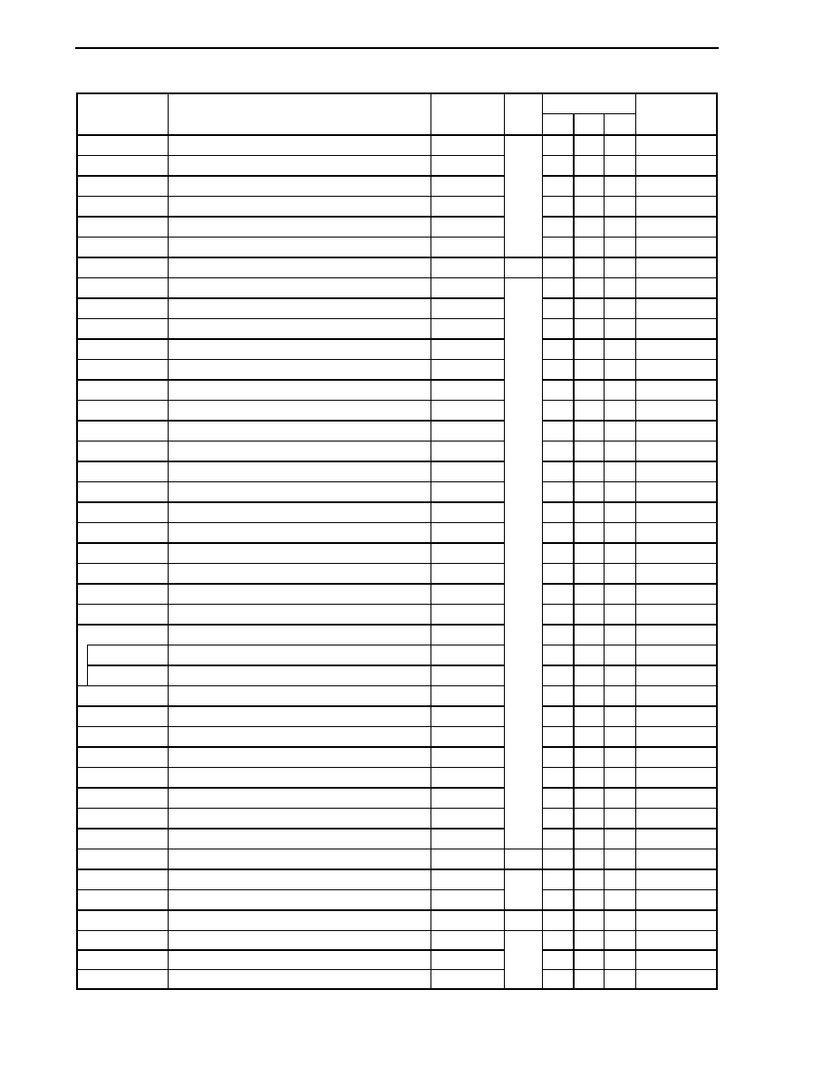
CHAPTER 3 CPU FUNCTION
Preliminary User's Manual U17714EJ1V0UD
78
(9/12)
Manipulatable Bits
Address Function
Register
Name
Symbol
R/W
1 8 16
Default Value
FFFFF612H
TMP8 I/O control register 0
TP8IOC0
00H
FFFFF613H
TMP8 I/O control register 1
TP8IOC1
00H
FFFFF614H
TMP8 I/O control register 2
TP8IOC2
00H
FFFFF615H
TMP8 option register 0
TP8OPT0
00H
FFFFF616H
TMP8 capture/compare register 0
TP8CCR0
0000H
FFFFF618H
TMP8 capture/compare register 1
TP8CCR1
R/W
0000H
FFFFF61AH
TMP8 counter read buffer register
TP8CNT
R
0000H
FFFFF680H
Watch timer operation mode register
WTM
00H
FFFFF690H
TMM0 control register 0
TM0CTL0
00H
FFFFF694H
TMM0 compare register 0
TM0CMP0
0000H
FFFFF6C0H
Oscillation stabilization time select register
OSTS
06H
FFFFF6C1H
PLL lockup time specification register
PLLS
03H
FFFFF6D0H
Watchdog timer mode register 2
WDTM2
67H
FFFFF6D1H
Watchdog timer enable register
WDTE
9AH
FFFFF6E0H
Real-time output buffer register 0L
RTBL0
00H
FFFFF6E2H
Real-time output buffer register 0H
RTBH0
00H
FFFFF6E4H
Real-time output port mode register 0
RTPM0
00H
FFFFF6E5H
Real-time output port control register 0
RTPC0
00H
FFFFF6F0H
Real-time output buffer register 1L
RTBL1
00H
FFFFF6F2H
Real-time output buffer register 1H
RTBH1
00H
FFFFF6F4H
Real-time output port mode register 1
RTPM1
00H
FFFFF6F5H
Real-time output port control register 1
RTPC1
00H
FFFFF706H
Port 3 function control expansion register L
PFCE3L
00H
FFFFF70AH
Port 5 function control expansion register
PFCE5
00H
FFFFF712H
Port 9 function control expansion register
PFCE9
0000H
FFFFF712H
Port 9 function control expansion register L
PFCE9L
00H
FFFFF713H
Port 9 function control expansion register H
PFCE9H
00H
FFFFF802H System
status
register
SYS
00H
FFFFF80CH
Internal oscillation mode register
RCM
00H
FFFFF810H
DMA trigger factor register 0
DTFR0
00H
FFFFF812H
DMA trigger factor register 1
DTFR1
00H
FFFFF814H
DMA trigger factor register 2
DTFR2
00H
FFFFF816H
DMA trigger factor register 3
DTFR3
00H
FFFFF820H
Power save mode register
PSMR
00H
FFFFF822H
Clock control register
CKC
R/W
0AH
FFFFF824H Lock
register
LOCKR R
00H
FFFFF828H
Processor clock control register
PCC
03H
FFFFF82CH
PLL control register
PLLCTL
R/W
01H
FFFFF82EH
CPU operation clock status register
CCLS
R
00H
FFFFF870H
Clock monitor mode register
CLM
00H
FFFFF888H
Reset source flag register
RESF
00H
FFFFF890H Low-voltage
detection
register
LVIM
R/W
00H

CHAPTER 3 CPU FUNCTION
Preliminary User's Manual U17714EJ1V0UD
79
(10/12)
Manipulatable Bits
Address Function
Register
Name
Symbol
R/W
1 8 16
Default Value
FFFFF891H
Low-voltage detection level select register
LVIS
00H
FFFFF892H
Internal RAM data status register
RAMS
01H
FFFFF8B0H
Prescaler mode register 0
PRSM0
00H
FFFFF8B1H
Prescaler compare register 0
PRSCM0
00H
FFFFF9FCH
On-chip debug mode register
OCDM
01H
FFFFF9FEH Peripheral
emulation register 1
PEMU1
Note
00H
FFFFFA00H
UARTA0 control register 0
UA0CTL0
10H
FFFFFA01H
UARTA0 control register 1
UA0CTL1
00H
FFFFFA02H
UARTA0 control register 2
UA0CTL2
FFH
FFFFFA03H
UARTA0 option control register 0
UA0OPT0
14H
FFFFFA04H UARTA0
status
register
UA0STR
R/W
00H
FFFFFA06H
UARTA0 receive data register
UA0RX
R
FFH
FFFFFA07H
UARTA0 transmit data register
UA0TX
FFH
FFFFFA10H
UARTA1 control register 0
UA1CTL0
10H
FFFFFA11H
UARTA1 control register 1
UA1CTL1
00H
FFFFFA12H
UARTA1 control register 2
UA1CTL2
FFH
FFFFFA13H
UARTA1 option control register 0
UA1OPT0
14H
FFFFFA14H UARTA1
status
register
UA1STR
R/W
00H
FFFFFA16H
UARTA1 receive data register
UA1RX
R
FFH
FFFFFA17H
UARTA1 transmit data register
UA1TX
FFH
FFFFFA20H
UARTA2 control register 0
UA2CTL0
10H
FFFFFA21H
UARTA2 control register 1
UA2CTL1
00H
FFFFFA22H
UARTA2 control register 2
UA2CTL2
FFH
FFFFFA23H
UARTA2 option control register 0
UA2OPT0
14H
FFFFFA24H UARTA2
status
register
UA2STR
R/W
00H
FFFFFA26H
UARTA2 receive data register
UA2RX
R
FFH
FFFFFA27H
UARTA2 transmit data register
UA2TX
FFH
FFFFFA30H
UARTA3 control register 0
UA3CTL0
10H
FFFFFA31H
UARTA3 control register 1
UA3CTL1
00H
FFFFFA32H
UARTA3 control register 2
UA3CTL2
FFH
FFFFFA33H
UARTA3 option control register 0
UA3OPT0
14H
FFFFFA34H UARTA3
status
register
UA3STR
R/W
00H
FFFFFA36H
UARTA3 receive data register
UA3RX
R
FFH
FFFFFA37H
UARTA3 transmit data register
UA3TX
FFH
FFFFFC00H
External interrupt falling edge specification register 0
INTF0
00H
FFFFFC06H
External interrupt falling edge specification register 3
INTF3
00H
FFFFFC10H
External interrupt falling edge specification register 8
INTF8
00H
FFFFFC13H
External interrupt falling edge specification register 9H INTF9H
00H
FFFFFC20H
External interrupt rising edge specification register 0
INTR0
00H
FFFFFC26H
External interrupt rising edge specification register 3
INTR3
00H
FFFFFC30H
External interrupt rising edge specification register 8
INTR8
00H
FFFFFC33H
External interrupt rising edge specification register 9H INTR9H
R/W
00H
Note Only during emulation
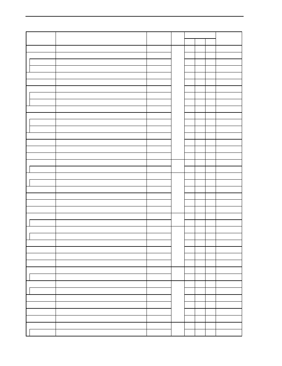
CHAPTER 3 CPU FUNCTION
Preliminary User's Manual U17714EJ1V0UD
80
(11/12)
Manipulatable Bits
Address Function
Register
Name
Symbol
R/W
1 8 16
Default Value
FFFFFC60H
Port 0 function register
PF0
00H
FFFFFC66H
Port 3 function register
PF3
0000H
FFFFFC66H
Port 3 function register L
PF3L
00H
FFFFFC67H
Port 3 function register H
PF3H
00H
FFFFFC68H
Port 4 function register
PF4
00H
FFFFFC6AH
Port 5 function register
PF5
00H
FFFFFC6CH
Port 6 function register
PF6
0000H
FFFFFC6CH
Port 6 function register L
PF6L
00H
FFFFFC6DH
Port 6 function register H
PF6H
00H
FFFFFC70H
Port 8 function register
PF8
00H
FFFFFC72H
Port 9 function register
PF9
0000H
FFFFFC72H
Port 9 function register L
PF9L
00H
FFFFFC73H
Port 9 function register H
PF9H
00H
FFFFFD00H
CSIB0 control register 0
CB0CTL0
01H
FFFFFD01H
CSIB0 control register 1
CB0CTL1
00H
FFFFFD02H
CSIB0 control register 2
CB0CTL2
00H
FFFFFD03H CSIB0
status
register
CB0STR
R/W
00H
FFFFFD04H
CSIB0 receive data register
CB0RX
0000H
FFFFFD04H
CSIB0 receive data register L
CB0RXL
R
00H
FFFFFD06H
CSIB0 transmit data register
CB0TX
0000H
FFFFFD06H
CSIB0 transmit data register L
CB0TXL
00H
FFFFFD10H
CSIB1 control register 0
CB1CTL0
01H
FFFFFD11H
CSIB1 control register 1
CB1CTL1
00H
FFFFFD12H
CSIB1 control register 2
CB1CTL2
00H
FFFFFD13H CSIB1
status
register
CB1STR
R/W
00H
FFFFFD14H
CSIB1 receive data register
CB1RX
0000H
FFFFFD14H
CSIB1 receive data register L
CB1RXL
R
00H
FFFFFD16H
CSIB1 transmit data register
CB1TX
0000H
FFFFFD16H
CSIB1 transmit data register L
CB1TXL
00H
FFFFFD20H
CSIB2 control register 0
CB2CTL0
01H
FFFFFD21H
CSIB2 control register 1
CB2CTL1
00H
FFFFFD22H
CSIB2 control register 2
CB2CTL2
00H
FFFFFD23H CSIB2
status
register
CB2STR
R/W
00H
FFFFFD24H
CSIB2 receive data register
CB2RX
0000H
FFFFFD24H
CSIB2 receive data register L
CB2RXL
R
00H
FFFFFD26H
CSIB2 transmit data register
CB2TX
0000H
FFFFFD26H
CSIB2 transmit data register L
CB2TXL
00H
FFFFFD30H
CSIB3 control register 0
CB3CTL0
01H
FFFFFD31H
CSIB3 control register 1
CB3CTL1
00H
FFFFFD32H
CSIB3 control register 2
CB3CTL2
00H
FFFFFD33H CSIB3
status
register
CB3STR
R/W
00H
FFFFFD34H
CSIB3 receive data register
CB3RX
0000H
FFFFFD34H
CSIB3 receive data register L
CB3RXL
R
00H
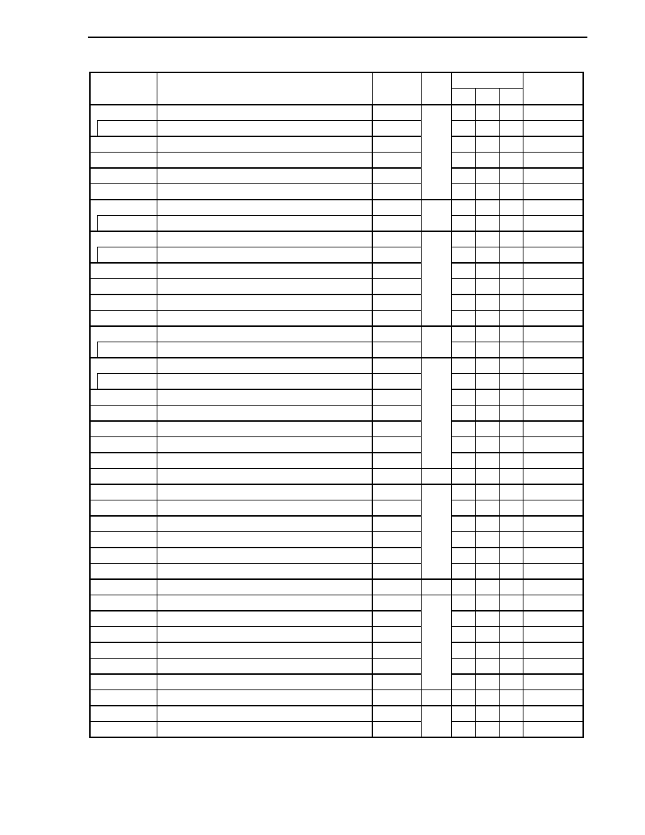
CHAPTER 3 CPU FUNCTION
Preliminary User's Manual U17714EJ1V0UD
81
(12/12)
Manipulatable Bits
Address Function
Register
Name
Symbol
R/W
1 8 16
Default Value
FFFFFD36H
CSIB3 transmit data register
CB3TX
0000H
FFFFFD36H
CSIB3 transmit data register L
CB3TXL
00H
FFFFFD40H
CSIB4 control register 0
CB4CTL0
01H
FFFFFD41H
CSIB4 control register 1
CB4CTL1
00H
FFFFFD42H
CSIB4 control register 2
CB4CTL2
00H
FFFFFD43H CSIB4
status
register
CB4STR
R/W
00H
FFFFFD44H
CSIB4 receive data register
CB4RX
0000H
FFFFFD44H
CSIB4 receive data register L
CB4RXL
R
00H
FFFFFD46H
CSIB4 transmit data register
CB4TX
0000H
FFFFFD46H
CSIB4 transmit data register L
CB4TXL
00H
FFFFFD50H
CSIB5 control register 0
CB5CTL0
01H
FFFFFD51H
CSIB5 control register 1
CB5CTL1
00H
FFFFFD52H
CSIB5 control register 2
CB5CTL2
00H
FFFFFD53H CSIB5
status
register
CB5STR
R/W
00H
FFFFFD54H
CSIB5 receive data register
CB5RX
0000H
FFFFFD54H
CSIB5 receive data register L
CB5RXL
R
00H
FFFFFD56H
CSIB5 transmit data register
CB5TX
0000H
FFFFFD56H
CSIB5 transmit data register L
CB5TXL
00H
FFFFFD80H
IIC shift register 0
IIC0
00H
FFFFFD82H
IIC control register 0
IICC0
00H
FFFFFD83H
Slave address register 0
SVA0
00H
FFFFFD84H
IIC clock select register 0
IICCL0
00H
FFFFFD85H
IIC function expansion register 0
IICX0
R/W
00H
FFFFFD86H
IIC status register 0
IICS0
R
00H
FFFFFD8AH
IIC flag register 0
IICF0
00H
FFFFFD90H
IIC shift register 1
IIC1
00H
FFFFFD92H
IIC control register 1
IICC1
00H
FFFFFD93H
Slave address register 1
SVA1
00H
FFFFFD94H
IIC clock select register 1
IICCL1
00H
FFFFFD95H
IIC function expansion register 1
IICX1
R/W
00H
FFFFFD96H
IIC status register 1
IICS1
R
00H
FFFFFD9AH
IIC flag register 1
IICF1
00H
FFFFFDA0H
IIC shift register 2
IIC2
00H
FFFFFDA2H
IIC control register 2
IICC2
00H
FFFFFDA3H
Slave address register 2
SVA2
00H
FFFFFDA4H
IIC clock select register 2
IICCL2
00H
FFFFFDA5H
IIC function expansion register 2
IICX2
R/W
00H
FFFFFDA6H
IIC status register 2
IICS2
R
00H
FFFFFDAAH
IIC flag register 2
IICF2
00H
FFFFFFBEH
External bus interface mode control register
EXIMC
R/W
00H

CHAPTER 3 CPU FUNCTION
Preliminary User's Manual U17714EJ1V0UD
82
3.4.7 Special
registers
Special registers are registers that are protected from being written with illegal data due to a program hang-up. The
V850ES/JJ2 has the following eight special registers.
� Power save control register (PSC)
� Clock control register (CKC)
� Processor clock control register (PCC)
� Clock monitor mode register (CLM)
� Reset source flag register (RESF)
� Low-voltage detection register (LVIM)
� Internal RAM data status register (RAMS)
� On-chip debug mode register (OCDM)
In addition, the PRCDM register is provided to protect against a write access to the special registers so that the
application system does not inadvertently stop due to a program hang-up. A write access to the special registers is
made in a specific sequence, and an illegal store operation is reported to the SYS register.

CHAPTER 3 CPU FUNCTION
Preliminary User's Manual U17714EJ1V0UD
83
(1) Setting data to special registers
Set data to the special registers in the following sequence.
<1>
Disable DMA operation.
<2>
Prepare data to be set to the special register in a general-purpose register.
<3>
Write the data prepared in <2> to the PRCMD register.
<4>
Write the setting data to the special register (by using the following instructions).
� Store instruction (ST/SST instruction)
� Bit manipulation instruction (SET1/CLR1/NOT1 instruction)
(<5> to <9> Insert NOP instructions (5 instructions).)
Note
<10>
Enable DMA operation if necessary.
[Example] With PSC register (setting standby mode)
ST.B r11, PSMR[r0] ;
Set PSMR register (setting IDLE1, IDLE2, and STOP modes).
<1>CLR1 0, DCHCn[r0]
;
Disable DMA operation. n = 0 to 3
<2>MOV0x02, r10
<3>ST.B r10, PRCMD[r0] ;
Write PRCMD register.
<4>ST.B r10, PSC[r0]
;
Set PSC register.
<5>NOP
Note
;
Dummy instruction
<6>NOP
Note
;
Dummy instruction
<7>NOP
Note
;
Dummy instruction
<8>NOP
Note
;
Dummy instruction
<9>NOP
Note
;
Dummy instruction
<10>SET1 0, DCHCn[r0] ;
Enable DMA operation. n = 0 to 3
(next instruction)
There is no special sequence to read a special register.
Note Five NOP instructions or more must be inserted immediately after setting the IDLE1 mode, IDLE2
mode, or STOP mode (by setting the PSC.STP bit to 1).
Cautions 1. When a store instruction is executed to store data in the command register, interrupts are
not acknowledged. This is because it is assumed that steps <3> and <4> above are
performed by successive store instructions. If another instruction is placed between <3>
and <4>, and if an interrupt is acknowledged by that instruction, the above sequence may
not be established, causing malfunction.
2. Although dummy data is written to the PRCMD register, use the same general-purpose
register used to set the special register (<4> in Example) to write data to the PRCMD
register (<3> in Example). The same applies when a general-purpose register is used for
addressing.
CHAPTER 3 CPU FUNCTION
Preliminary User's Manual U17714EJ1V0UD
84
(2) Command register (PRCMD)
The PRCMD register is an 8-bit register that protects the registers that may seriously affect the application
system from being written, so that the system does not inadvertently stop due to a program hang-up. The first
write access to a special register is valid after data has been written in advance to the PRCMD register. In this
way, the value of the special register can be rewritten only in a specific sequence, so as to protect the register
from an illegal write access.
The PRCMD register is write-only, in 8-bit units (undefined data is read when this register is read).
7
REG7
PRCMD
6
REG6
5
REG5
4
REG4
3
REG3
2
REG2
1
REG1
0
REG0
After reset: Undefined W Address: FFFFF1FCH
CHAPTER 3 CPU FUNCTION
Preliminary User's Manual U17714EJ1V0UD
85
(3) System status register (SYS)
Status flags that indicate the operation status of the overall system are allocated to this register.
This register can be read or written in 8-bit or 1-bit units.
Reset sets this register to 00H.
0
Protection error did not occur
Protection error occurred
PRERR
0
1
Detects protection error
SYS
0
0
0
0
0
0
PRERR
After reset: 00H R/W Address: FFFFF802H
< >
The PRERR flag operates under the following conditions.
(a) Set condition (PRERR flag = 1)
(i) When data is written to a special register without writing anything to the PRCMD register (when <4> is
executed without executing <3> in 3.4.7 (1) Setting data to special registers)
(ii) When data is written to an on-chip peripheral I/O register other than a special register (including
execution of a bit manipulation instruction) after writing data to the PRCMD register (if <4> in 3.4.7 (1)
Setting data to special registers is not the setting of a special register)
Remark Even if an on-chip peripheral I/O register is read (except by a bit manipulation instruction)
between an operation to write the PRCMD register and an operation to write a special register,
the PRERR flag is not set, and the set data can be written to the special register.
(b) Clear condition (PRERR flag = 0)
(i) When 0 is written to the PRERR flag
(ii) When the system is reset
Cautions 1. If 0 is written to the PRERR bit of the SYS register, which is not a special register,
immediately after a write access to the PRCMD register, the PRERR bit is cleared to 0
(the write access takes precedence).
2. If data is written to the PRCMD register, which is not a special register, immediately
after a write access to the PRCMD register, the PRERR bit is set to 1.
CHAPTER 3 CPU FUNCTION
Preliminary User's Manual U17714EJ1V0UD
86
3.4.8 Cautions
(1) Registers to be set first
Be sure to set the following registers first when using the V850ES/JJ2.
� System wait control register (VSWC)
� On-chip debug mode register (OCDM)
� Watchdog timer mode register 2 (WDTM2)
After setting the VSWC, OCDM, and WDTM2 registers, set the other registers as necessary.
When using the external bus, set each pin to the alternate-function bus control pin mode by using the port-
related registers after setting the above registers.
(a) System wait control register (VSWC)
The VSWC register controls wait of bus access to the on-chip peripheral I/O registers.
Three clocks are required to access an on-chip peripheral I/O register (without a wait cycle). The
V850ES/JJ2 requires wait cycles according to the operating frequency. Set the following value to the
VSWC register in accordance with the frequency used.
The VSWC register can be read or written in 8-bit units (address: FFFFF06EH, default value: 77H).
Operating Frequency (f
CLK
)
Set Value of VSWC
Number of Waits
32 kHz
f
CLK
< 16.6 MHz
00H
0 (no waits)
16.6 MHz
f
CLK
< 20 MHz
01H
1
(b) On-chip debug mode register (OCDM)
For details, see CHAPTER 27 ON-CHIP DEBUG FUNCTION.
(c) Watchdog timer mode register 2 (WDTM2)
The WDTM2 register sets the overflow time and the operation clock of watchdog timer 2.
Watchdog timer 2 automatically starts in the reset mode after reset is released. Write the WDTM2 register
to activate this operation.
For details, refer to CHAPTER 11 FUNCTIONS OF WATCHDOG TIMER 2.
CHAPTER 3 CPU FUNCTION
Preliminary User's Manual U17714EJ1V0UD
87
(2) Accessing specific on-chip peripheral I/O registers
This product has two types of internal system buses.
One is a CPU bus and the other is a peripheral bus that interfaces with low-speed peripheral hardware.
The clock of the CPU bus and the clock of the peripheral bus are asynchronous. If an access to the CPU and
an access to the peripheral hardware conflict, therefore, unexpected illegal data may be transferred. If there is
a possibility of a conflict, the number of cycles for accessing the CPU changes when the peripheral hardware is
accessed, so that correct data is transferred. As a result, the CPU does not start processing of the next
instruction but enters the wait state. If this wait state occurs, the number of clocks required to execute an
instruction increases by the number of wait clocks shown below.
This must be taken into consideration if real-time processing is required.
When specific on-chip peripheral I/O registers are accessed, more wait states may be required in addition to
the wait states set by the VSWC register.
The access conditions and how to calculate the number of wait states to be inserted (number of CPU clocks)
at this time are shown below.
Peripheral Function
Register Name
Access
k
TPnCNT
Read
1 or 2
Write
� 1st access: No wait
� Continuous write: 3 or 4
16-bit timer/event counter P (TMP)
(n = 0 to 8)
TPnCCR0, TPnCCR1
Read
1 or 2
TQ0CNT
Read
1 or 2
Write
� 1st access: No wait
� Continuous write: 3 or 4
16-bit timer/event counter Q (TMQ)
TQ0CCR0 to TQ0CCR3
Read
1 or 2
Watchdog timer 2 (WDT2)
WDTM2
Write
(when WDT2 operating)
3
Real-time output function (RTO)
(n = 0, 1)
RTBLn, RTBHn
Write
(RTPCn.RTPOEn bit = 0)
1
ADA0M0
Read
1 or 2
ADA0CR0 to ADA0CR15
Read
1 or 2
A/D converter
ADA0CR0H to ADA0CR15H
Read
1 or 2
I
2
C00 to I
2
C02
IICS0 to IICS2
Read
1
Number of clocks necessary for access = 3 + i + j + (2 + j)
� k
Caution Accessing the above registers is prohibited in the following statuses. If a wait cycle is
generated, it can only be cleared by a reset.
�
When the CPU operates with the subclock and the main clock oscillation is stopped
�
When the CPU operates with the internal oscillation clock
Remark i: Values (0 or 1) of higher 4 bits of VSWC register
j: Values (0 or 1) of lower 4 bits of VSWC register
CHAPTER 3 CPU FUNCTION
Preliminary User's Manual U17714EJ1V0UD
88
(3) System reserved area
In the V850ES/JJ2, 0000007AH to 0000007FH is a system reserved area for function expansion, and therefore
it is recommended that this area not be used.
0 0 0 0 0 0 7 A H
0 0 0 0 0 0 7 F H
0 0 0 0 0 0 8 0 H
0 0 0 0 0 0 7 9 H
0 0 0 0 0 0 7 0 H
0 0 0 0 0 0 0 0 H
System reserved area
Security ID
Note
(10 bytes)
Note For the security ID, see 27.6.1 Security ID.
Caution When the data in the flash memory has been deleted, all the bits are cleared to 1.

CHAPTER 3 CPU FUNCTION
Preliminary User's Manual U17714EJ1V0UD
89
(4) Restriction on conflict between sld instruction and interrupt request
(a) Description
If a conflict occurs between the decode operation of an instruction in <2> immediately before the sld
instruction following an instruction in <1> and an interrupt request before the instruction in <1> is
complete, the execution result of the instruction in <1> may not be stored in a register.
Instruction <1>
� ld instruction:
ld.b, ld.h, ld.w, ld.bu, ld.hu
� sld instruction:
sld.b, sld.h, sld.w, sld.bu, sld.hu
� Multiplication instruction: mul, mulh, mulhi, mulu
Instruction <2>
mov reg1, reg2
satadd reg1, reg2
and reg1, reg2
add reg1, reg2
mulh reg1, reg2
not reg1, reg2
satadd imm5, reg2
tst reg1, reg2
add imm5, reg2
shr imm5, reg2
satsubr reg1, reg2
or reg1, reg2
subr reg1, reg2
cmp reg1, reg2
sar imm5, reg2
satsub reg1, reg2
xor reg1, reg2
sub reg1, reg2
cmp imm5, reg2
shl imm5, reg2
<Example>
<i> ld.w [r11], r10
If the decode operation of the mov instruction <ii> immediately before the sld
instruction <iii> and an interrupt request conflict before execution of the ld
instruction <i> is complete, the execution result of instruction <i> may not be
stored in a register.
<ii> mov r10, r28
<iii> sld.w 0x28, r10
(b) Countermeasure
<1> When compiler (CA850) is used
Use CA850 Ver. 2.61 or later because generation of the corresponding instruction sequence can be
automatically suppressed.
<2> Countermeasure by assembler
When executing the sld instruction immediately after instruction <ii>, avoid the above operation using
either of the following methods.
� Insert a nop instruction immediately before the sld instruction.
� Do not use the same register as the sld instruction destination register in the above instruction <ii>
executed immediately before the sld instruction.
�
�
�
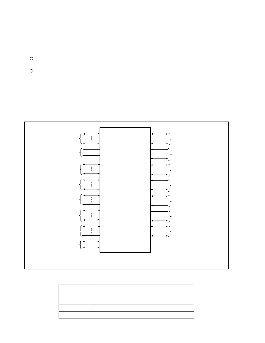
Preliminary User's Manual U17714EJ1V0UD
90
CHAPTER 4 PORT FUNCTIONS
4.1 Features
I/O ports: 128
� 5 V tolerant/N-ch open-drain output switchable: 60 (ports 0, 3 to 6, 8, 9)
Input/output specifiable in 1-bit units
4.2 Basic Port Configuration
The V850ES/JJ2 features a total of 128 I/O ports consisting of ports 0, 1, 3 to 9, CD, CM, CS, CT, DH, and DL. The
port configuration is shown below.
Figure 4-1. Port Configuration Diagram
P00
P06
Port 0
PCD0
PCD3
Port CD
PCM0
PCM5
Port CM
PCS0
PCS7
PCT0
PCT7
Port CS
Port CT
P90
P915
Port 9
PDH0
PDH7
Port DH
PDL0
PDL15
Port DL
P30
P39
Port 3
Port 1
P40
P42
Port 4
P50
P55
Port 5
P60
P615
P70
P715
P80
P81
Port 6
P10
P11
Port 7
Port 8
Caution Ports 0, 3 to 6, 8, and 9 are 5 V tolerant.
Table 4-1. I/O Buffer Power Supplies for Pins
Power Supply
Corresponding Pins
AV
REF0
Port
7
AV
REF1
Port
1
BV
DD
Ports CD, CM, CS, CT, DH, DL
EV
DD
RESET, ports 0, 3 to 6, 8, 9
CHAPTER 4 PORT FUNCTIONS
Preliminary User's Manual U17714EJ1V0UD
91
4.3 Port
Configuration
Table 4-2. Port Configuration
Item Configuration
Control register
Port n mode register (PMn: n = 0, 1, 3 to 9, CD, CM, CS, CT, DH, DL)
Port n mode control register (PMCn: n = 0, 3 to 6, 8, 9, CM, CS, CT, DH, DL)
Port n function control register (PFCn: n = 0, 3 to 6, 9)
Port n function control expansion register (PFCEn: n = 3, 5, 9)
Port n function register (PFn: n = 0, 3 to 6, 8, 9)
Ports I/O:
128
(1) Port n register (Pn)
Data is input from or output to an external device by writing or reading the Pn register.
The Pn register consists of a port latch that holds output data, and a circuit that reads the status of pins.
Each bit of the Pn register corresponds to one pin of port n, and can be read or written in 1-bit units.
Pn7
Outputs 0
Outputs 1
Pnm
0
1
Control of output data (in output mode)
Pn6
Pn5
Pn4
Pn3
Pn2
Pn1
Pn0
0
1
2
3
7
5
6
7
Pn
After reset: 00H (output latch) R/W
Data is written to or read from the Pn register as follows, regardless of the setting of the PMCn register.
Table 4-3. Writing/Reading Pn Register
Setting of PMn Register
Writing to Pn Register
Reading from Pn Register
Output mode
(PMnm = 0)
Data is written to the output latch
Note
.
In the port mode (PMCn = 0), the contents of the output
latch are output from the pins.
The value of the output latch is read.
Input mode
(PMnm = 1)
Data is written to the output latch.
The pin status is not affected
Note
.
The pin status is read.
Note The value written to the output latch is retained until a new value is written to the output latch.
CHAPTER 4 PORT FUNCTIONS
Preliminary User's Manual U17714EJ1V0UD
92
(2) Port n mode register (PMn)
The PMn register specifies the input or output mode of the corresponding port pin.
Each bit of this register corresponds to one pin of port n, and the input or output mode can be specified in 1-bit
units.
PMn7
Output mode
Input mode
PMnm
0
1
Control of input/output mode
PMn6
PMn5
PMn4
PMn3
PMn2
PMn1
PMn0
PMn
After reset: FFH R/W
(3) Port n mode control register (PMCn)
The PMCn register specifies the port mode or alternate function.
Each bit of this register corresponds to one pin of port n, and the mode of the port can be specified in 1-bit
units.
Port mode
Alternate function mode
PMCnm
0
1
Specification of operation mode
PMCn7
PMCn6
PMCn5
PMCn4
PMCn3
PMCn2
PMCn1
PMCn0
PMCn
After reset: 00H R/W
CHAPTER 4 PORT FUNCTIONS
Preliminary User's Manual U17714EJ1V0UD
93
(4) Port n function control register (PFCn)
The PFCn register specifies the alternate function of a port pin to be used if the pin has two alternate functions.
Each bit of this register corresponds to one pin of port n, and the alternate function of a port pin can be
specified in 1-bit units.
PFCn7
PFCn6
PFCn5
PFCn4
PFCn3
PFCn2
PFCn1
PFCn0
PFCn
After reset: 00H R/W
Alternate function 1
Alternate function 2
PFCnm
0
1
Specification of alternate function
(5) Port n function control expansion register (PFCEn)
The PFCEn register specifies the alternate function of a port pin to be used if the pin has three or more
alternate functions.
Each bit of this register corresponds to one pin of port n, and the alternate function of a port pin can be
specified in 1-bit units.
PFCn7
PFCn6
PFCn5
PFCn4
PFCn3
PFCn2
PFCn1
PFCn0
PFCEn7
PFCEn6
PFCEn5 PFCEn4
PFCEn3 PFCEn2
PFCEn1
PFCEn0
After reset: 00H R/W
PFCEn
PFCn
Alternate function 1
Alternate function 2
Alternate function 3
Alternate function 4
PFCEnm
0
0
1
1
Specification of alternate function
PFCnm
0
1
0
1
CHAPTER 4 PORT FUNCTIONS
Preliminary User's Manual U17714EJ1V0UD
94
(6) Port n function register (PFn)
The PFn register specifies normal output or N-ch open-drain output.
Each bit of this register corresponds to one pin of port n, and the output mode of the port pin can be specified
in 1-bit units.
PFn7
PFn6
PFn5
PFn4
PFn3
PFn2
PFn1
PFn0
Normal output (CMOS output)
N-ch open-drain output
PFnm
Note
0
1
Control of normal output/N-ch open-drain output
PFn
After reset: 00H R/W
Note The PFnm bit of the PFn register is valid only when the PMnm bit of the PMn register is 0 (when the
output mode is specified) in port mode (PMCnm bit = 0). When the PMnm bit is 1 (when the input mode
is specified), the set value of the PFn register is invalid.
CHAPTER 4 PORT FUNCTIONS
Preliminary User's Manual U17714EJ1V0UD
95
(7) Port setting
Set a port as illustrated below.
Figure 4-2. Setting of Each Register and Pin Function
PMCn register
Output mode
Input mode
PMn register
"0"
"1"
"0"
"1"
"0"
"1"
(a)
(b)
(c)
(d)
Alternate function
(when two alternate
functions are available)
Port mode
Alternate function 1
Alternate function 2
PFCn register
Alternate function
(when three or more alternate
functions are available)
Alternate function 1
Alternate function 2
Alternate function 3
Alternate function 4
PFCn register
PFCEn register
PFCEnm
0
1
0
1
0
0
1
1
(a)
(b)
(c)
(d)
PFCnm
Remark Set the alternate functions in the following sequence.
<1> Set the PFCn and PFCEn registers.
<2> Set the PFCn register.
<3> Set the INTRn or INTFn register (to specify an external interrupt pin).
If the PMCn register is set first, an unintended function may be set while the PFCn and PFCEn
registers are being set.
CHAPTER 4 PORT FUNCTIONS
Preliminary User's Manual U17714EJ1V0UD
96
4.3.1 Port
0
Port 0 is a 7-bit port for which I/O settings can be controlled in 1-bit units.
Port 0 includes the following alternate-function pins.
Table 4-4. Port 0 Alternate-Function Pins
Pin Name
Pin No.
Alternate-Function Pin Name
I/O
Remark
Block Type
P00 6
TIP61/TOP61
I/O
G-1
P01 7
TIP60/TOP60
I/O
G-1
P02 17 NMI
Input
L-1
P03 18 INTP0/ADTRG
Input
N-1
P04 19 INTP1
Input
L-1
P05 20 INTP2/DRST
Note
Input
AA-1
P06 21 INTP3
Input
Selectable as N-ch open-drain output
L-1
Note The DRST pin is used for on-chip debugging.
If on-chip debugging is not used, fix the P05/INTP2/DRST pin to low level between when the reset signal of
the RESET pin is released and when the OCDM.OCDM0 bit is cleared (0).
For details, see 4.6.3 Cautions on on-chip debug pins.
Caution The P00 to P06 pins have hysteresis characteristics in the input mode of the alternate function,
but do not have hysteresis characteristics in the port mode.
(1) Port 0 register (P0)
0
Outputs 0
Outputs 1
P0n
0
1
Output data control (in output mode) (n = 0 to 6)
P0
P06
P05
P04
P03
P02
P01
P00
After reset: 00H (output latch) R/W Address: FFFFF400H
(2) Port 0 mode register (PM0)
1
Output mode
Input mode
PM0n
0
1
I/O mode control (n = 0 to 6)
PM0
PM06
PM05
PM04
PM03
PM02
PM01
PM00
After reset: FFH R/W Address: FFFFF420H
CHAPTER 4 PORT FUNCTIONS
Preliminary User's Manual U17714EJ1V0UD
97
(3) Port 0 mode control register (PMC0)
0
PMC0
PMC06
PMC05
PMC04
PMC03
PMC02
PMC01
PMC00
I/O port
INTP3 input
PMC06
0
1
Specification of P06 pin operation mode
I/O port
INTP2 input
PMC05
0
1
Specification of P05 pin operation mode
I/O port
INTP1 input
PMC04
0
1
Specification of P04 pin operation mode
I/O port
INTP0 input/ADTRG input
PMC03
0
1
Specification of P03 pin operation mode
I/O port
NMI input
PMC02
0
1
Specification of P02 pin operation mode
After reset: 00H R/W Address: FFFFF440H
I/O port
TIP60 input/TOP60 output
PMC01
0
1
Specification of P01 pin operation mode
I/O port
TIP61 input/TOP61 output
PMC00
0
1
Specification of P00 pin operation mode
Caution The P05/INTP2/DRST pin becomes the DRST pin regardless of the value of the PMC05
bit when the OCDM.OCDM0 bit = 1.
CHAPTER 4 PORT FUNCTIONS
Preliminary User's Manual U17714EJ1V0UD
98
(4) Port 0 function control register (PFC0)
PFC0
After reset: 00H R/W Address: FFFFF460H
0
0
0
0
PFC03
0
PFC01
PFC00
INTP0 input
ADTRG input
PFC03
0
1
Specification of P03 pin alternate function
TIP60 input
TOP60 output
PFC01
0
1
Specification of P01 pin alternate function
TIP61 input
TOP61 output
PFC00
0
1
Specification of P00 pin alternate function
(5) Port 0 function register (PF0)
0
Normal output (CMOS output)
N-ch open drain output
PF0n
0
1
Control of normal output or N-ch open-drain output (n = 0 to 6)
PF0
PF06
PF05
PF04
PF03
PF02
PF01
PF00
After reset: 00H R/W Address: FFFFFC60H
Caution When an output pin is pulled up at EV
DD
or higher, be sure to set the PF0n bit to 1.
CHAPTER 4 PORT FUNCTIONS
Preliminary User's Manual U17714EJ1V0UD
99
4.3.2 Port
1
Port 1 is a 2-bit port for which I/O settings can be controlled in 1-bit units.
Port 1 includes the following alternate-function pins.
Table 4-5. Port 1 Alternate-Function Pins
Pin Name
Pin No.
Alternate-Function Pin Name
I/O
Remark
Block Type
P10 3
ANO0
Output
-
A-2
P11 4
ANO1
Output
-
A-2
Caution When the power is turned on, the P10 and P11 pins may output an undefined level temporarily,
even during reset.
(1) Port 1 register (P1)
0
Outputs 0
Outputs 1
P1n
0
1
Output data control (in output mode) (n = 0, 1)
P1
0
0
0
0
0
P11
P10
After reset: 00H (output latch) R/W Address: FFFFF402H
Caution Do not read or write the P1 register during D/A conversion (see 14.4.3 Cautions).
(2) Port 1 mode register (PM1)
1
Output mode
Input mode
PM1n
0
1
I/O mode control (n = 0, 1)
PM1
1
1
1
1
1
PM11
PM10
After reset: FFH R/W Address: FFFFF422H
Cautions 1. When using P1n as alternate functions (ANOn pin output), set the PM1n bit to 1.
2. When using one of the P10 and P11 pins as an I/O port and the other as a D/A
output pin, do so in an application where the port I/O level does not change during
D/A output.
CHAPTER 4 PORT FUNCTIONS
Preliminary User's Manual U17714EJ1V0UD
100
4.3.3
Port 3
Port 3 is a 10-bit port for which I/O settings can be controlled in 1-bit units.
Port 3 includes the following alternate-function pins.
Table 4-6. Port 3 Alternate-Function Pins
Pin Name
Pin No.
Alternate-Function Pin Name
I/O
Remark
Block Type
P30 25 TXDA0/SOB4
Output
G-3
P31 26 RXDA0/INTP7/SIB4
Input N-3
P32 27 ASCKA0/SCKB4/TIP00/TOP00
I/O
U-1
P33 28 TIP01/TOP01
I/O G-1
P34 29 TIP10/TOP10
I/O G-1
P35 30 TIP11/TOP11
I/O G-1
P36 31
-
Output C-1
P37 32
-
Input C-1
P38 35 TXDA2/SDA00
I/O G-12
P39 36 RXDA2/SCL00
I/O
Selectable as N-ch open-drain output
G-6
Caution The P31 to P35, P38, and P39 pins have hysteresis characteristics in the input mode of the
alternate-function pin, but do not have the hysteresis characteristics in the port mode.
CHAPTER 4 PORT FUNCTIONS
Preliminary User's Manual U17714EJ1V0UD
101
(1) Port 3 register (P3)
Outputs 0
Outputs 1
P3n
0
1
Output data control (in output mode) (n = 0 to 9)
P3 (P3H)
After reset: 0000H (output latch) R/W Address: P3 FFFFF406H,
P3L FFFFF406H, P3H FFFFF407H
0
0
0
0
0
0
P39
P38
P37
P36
P35
P34
P33
P32
P31
P30
8
9
10
11
12
13
14
15
(P3L)
Remarks 1. The P3 register can be read or written in 16-bit units.
However, when using the higher 8 bits of the P3 register as the P3H register and the lower 8
bits as the P3L register, P3 can be read or written in 8-bit or 1-bit units.
2. To read/write bits 8 to 15 of the P3 register in 8-bit or 1-bit units, specify them as bits 0 to 7 of
the P3H register.
(2) Port 3 mode register (PM3)
1
Output mode
Input mode
PM3n
0
1
I/O mode control (n = 0 to 9)
1
1
1
1
1
PM39
PM38
PM37
PM36
PM35
PM34
PM33
PM32
PM31
PM30
After reset: FFFFH R/W Address: PM3 FFFFF426H,
PM3L FFFFF426H, PM3H FFFFF427H
8
9
10
11
12
13
14
15
PM3 (PM3H)
(PM3L)
Remarks 1. The PM3 register can be read or written in 16-bit units.
However, when using the higher 8 bits of the PM3 register as the PM3H register and the
lower 8 bits as the PM3L register, PM3 can be read or written in 8-bit or 1-bit units.
2. To read/write bits 8 to 15 of the PM3 register in 8-bit or 1-bit units, specify them as bits 0 to 7
of the PM3H register.
CHAPTER 4 PORT FUNCTIONS
Preliminary User's Manual U17714EJ1V0UD
102
(3) Port 3 mode control register (PMC3)
I/O port
RXDA2 input/SCL00 I/O
PMC39
0
1
Specification of P39 pin operation mode
I/O port
TXDA2 output/SDA00 I/O
PMC38
0
1
Specification of P38 pin operation mode
After reset: 0000H R/W Address: PMC3 FFFFF446H,
PMC3L FFFFF446H, PMC3H FFFFF447H
0
0
PMC35
PMC34
PMC33
PMC32
PMC31
PMC30
0
0
0
0
0
0
PMC39
PMC38
8
9
10
11
12
13
14
15
PMC3 (PMC3H)
(PMC3L)
I/O port
TIP11 input/TOP11 output
PMC35
0
1
Specification of P35 pin operation mode
I/O port
TIP10 input/TOP10 output/CRXD1 input
PMC34
0
1
Specification of P34 pin operation mode
I/O port
TIP01 input/TOP01 output/CTXD1 output
PMC33
0
1
Specification of P33 pin operation mode
I/O port
ASCKA0 input/SCKB4 I/O/TIP00 input/TOP00 output
PMC32
0
1
Specification of P32 pin operation mode
I/O port
RXDA0 input/SIB4 input/INTP7 input
PMC31
0
1
Specification of P31 pin operation mode
I/O port
TXDA0 output/SOB4 output
PMC30
0
1
Specification of P30 pin operation mode
Caution Be sure to clear bits 15 to 10, 7, and 6 to "0".
Remarks 1. The PMC3 register can be read or written in 16-bit units.
However, when using the higher 8 bits of the PMC3 register as the PMC3H register and the
lower 8 bits as the PMC3L register, PMC3 can be read or written in 8-bit or 1-bit units.
2.
To read/write bits 8 to 15 of the PMC3 register in 8-bit or 1-bit units, specify them as bits 0 to
7 of the PMC3H register.
CHAPTER 4 PORT FUNCTIONS
Preliminary User's Manual U17714EJ1V0UD
103
(4) Port 3 function control register (PFC3)
After reset: 0000H R/W Address: PFC3 FFFFF466H,
PFC3L FFFFF466H, PFC3L FFFFF467H
0
0
0
0
0
0
PFC39
PFC38
0
0
PFC35
PFC34
PFC33
PFC32
PFC31
PFC30
8
9
10
11
12
13
14
15
PFC3 (PFC3H)
(PFC3L)
Remarks 1. For details of alternate function specification, see 4.3.3 (6) Port 3 alternate function
specifications.
2. The PFC3 register can be read or written in 16-bit units.
However, when using the higher 8 bits of the PFC3 register as the PFC3H register and the
lower 8 bits as the PFC3L register, PFC3 can be read or written in 8-bit and 1-bit units.
3. To read/write bits 8 to 15 of the PFC3 register in 8-bit or 1-bit units, specify them as bits 0 to 7
of the PFC3H register.
(5) Port 3 function control expansion register L (PFCE3L)
PFCE3L
After reset: 00H R/W Address: FFFFF706H
0
0
0
0
0
PFCE32
0
0
Caution Be sure to clear bits 7 to 3, 1, and 0 to "0".
Remark For details of alternate function specification, see 4.3.3 (6) Port 3 alternate function
specifications.
CHAPTER 4 PORT FUNCTIONS
Preliminary User's Manual U17714EJ1V0UD
104
(6) Port 3 alternate function specifications
PFC39
Specification of P39 pin alternate function
0 RXDA2
input
1 SCL00
input
PFC38
Specification of P38 pin alternate function
0 TXDA2
output
1 SDA00
I/O
PFC35
Specification of P35 pin alternate function
0 TIP11
input
1 TOP11
output
PFC34
Specification of P34 pin alternate function
0 TIP10
input
1 TOP10
output
PFC33
Specification of P33 pin alternate function
0 TIP01
input
1 TOP01
output
PFCE32 PFC32
Specification
of P32 pin alternate function
0 0
ASCKA0
input
0 1
SCKB4
I/O
1 0
TIP00
input
1 1
TOP00
output
PFC31
Specification of P31 pin alternate function
0 RXDA0
input/INTP7
Note
input
1 SIB4
input
PFC30
Specification of P30 pin alternate function
0 TXDA0
output
1 SOB4
output
Note The INTP7 pin and RXDA0 pin are alternate-function pins. When using the pin as the RXDA0 pin,
disable edge detection for the INTP7 alternate-function pin. (Clear the INTF3.INTF31 bit and the
INTR3.INTR31 bit to 0.) When using the pin as the INTP7 pin, stop UARTA0 reception. (Clear the
UA0CTL0.UA0RXE bit to 0.)
CHAPTER 4 PORT FUNCTIONS
Preliminary User's Manual U17714EJ1V0UD
105
(7) Port 3 function register (PF3)
After reset: 0000H R/W Address: PF3 FFFFFC66H,
PF3L FFFFFC66H, PF3H FFFFFC67H
PF37
PF36
PF35
PF34
PF33
PF32
PF31
PF30
0
0
0
0
0
0
PF39
PF38
8
9
10
11
12
13
14
15
Normal output (CMOS output)
N-ch open-drain output
PF3n
0
1
Control of normal output or N-ch open-drain output (n = 0 to 9)
PF3 (PF3H)
(PF3L)
Caution When an output pin is pulled up at EV
DD
or higher, be sure to set the PF3n bit to 1.
Remarks 1. The PF3 register can be read or written in 16-bit units.
However, when using the higher 8 bits of the PF3 register as the PF3H register and the lower
8 bits as the PF3L register, PF3 can be read or written in 8-bit or 1-bit units.
2. To read/write bits 8 to 15 of the PF3 register in 8-bit or 1-bit units, specify them as bits 0 to 7
of the PF3H register.
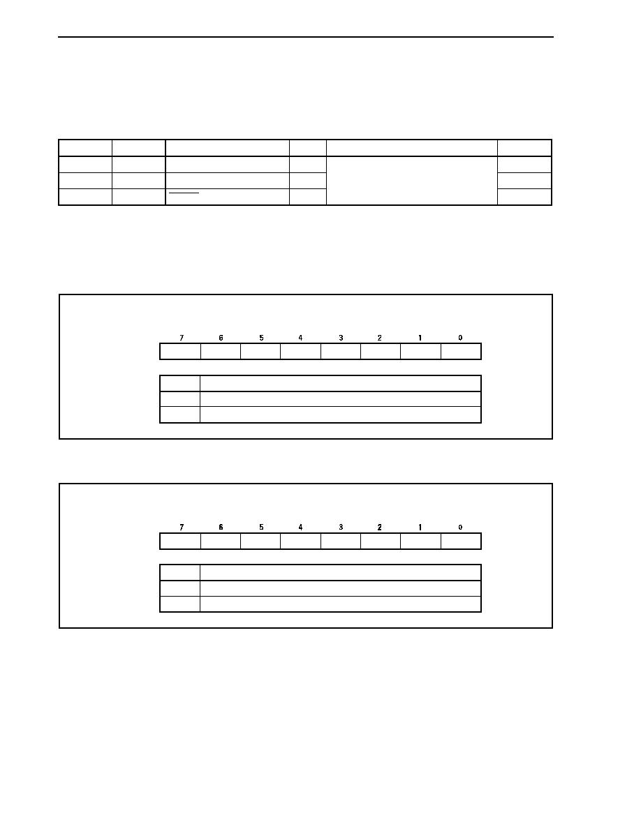
CHAPTER 4 PORT FUNCTIONS
Preliminary User's Manual U17714EJ1V0UD
106
4.3.4 Port
4
Port 4 is a 3-bit port that controls I/O in 1-bit units.
Port 4 includes the following alternate-function pins.
Table 4-7. Port 4 Alternate-Function Pins
Pin Name
Pin No.
Alternate-Function Pin Name
I/O
Remark
Block Type
P40 22 SIB0/SDA01
I/O
G-6
P41 23 SOB0/SCL01
I/O
G-12
P42 24 SCKB0
I/O
Selectable as N-ch open-drain output
E-3
Caution The P40 to P42 pins have hysteresis characteristics in the input mode of the alternate-function
pin, but do not have the hysteresis characteristics in the port mode.
(1) Port 4 register (P4)
0
Outputs 0
Outputs 1
P4n
0
1
Output data control (in output mode) (n = 0 to 2)
P4
0
0
0
0
P42
P41
P40
After reset: 00H (output latch) R/W Address: FFFFF408H
(2) Port 4 mode register (PM4)
1
Output mode
Input mode
PM4n
0
1
I/O mode control (n = 0 to 2)
PM4
1
1
1
1
PM42
PM41
PM40
After reset: FFH R/W Address: FFFFF428H
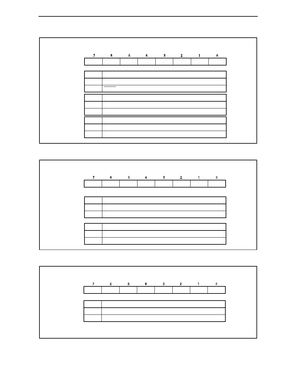
CHAPTER 4 PORT FUNCTIONS
Preliminary User's Manual U17714EJ1V0UD
107
(3) Port 4 mode control register (PMC4)
0
PMC4
0
0
0
0
PMC42
PMC41
PMC40
I/O port
SCKB0 I/O
PMC42
0
1
Specification of P42 pin operation mode
I/O port
SOB0 output/SCL01 I/O
PMC41
0
1
Specification of P41 pin operation mode
I/O port
SIB0 input/SDA01 I/O
PMC40
0
1
Specification of P40 pin operation mode
After reset: 00H R/W Address: FFFFF448H
(4) Port 4 function control register (PFC4)
PFC4
After reset: 00H R/W Address: FFFFF468H
0
0
0
0
0
0
PFC41
PFC40
SOB0 output
SCL01 I/O
PFC41
0
1
Specification of P41 pin alternate function
SIB0 input
SDA01 I/O
PFC40
0
1
Specification of P40 pin alternate function
(5) Port 4 function register (PF4)
0
Normal output (CMOS output)
N-ch open-drain output
PF4n
0
1
Control of normal output or N-ch open-drain output (n = 0 to 2)
PF4
0
0
0
0
PF42
PF41
PF40
After reset: 00H R/W Address: FFFFFC68H
Caution When an output pin is pulled up at EV
DD
or higher, be sure to set the PF4n bit to 1.
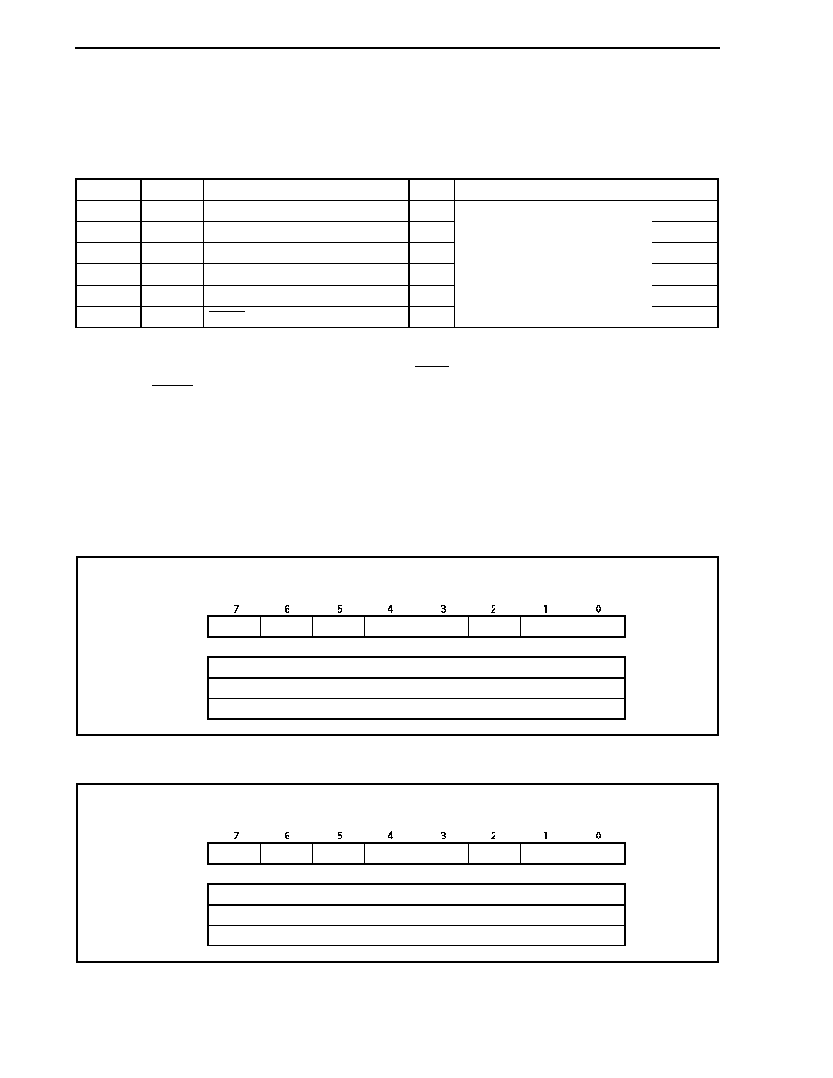
CHAPTER 4 PORT FUNCTIONS
Preliminary User's Manual U17714EJ1V0UD
108
4.3.5
Port 5
Port 5 is a 6-bit port that controls I/O in 1-bit units.
Port 5 includes the following alternate-function pins.
Table 4-8. Port 5 Alternate-Function Pins
Pin Name
Pin No.
Alternate-Function Pin Name
I/O
Remark
Block Type
P50 37 TIQ01/KR0/TOQ01/RTP00
I/O U-5
P51 38 TIQ02/KR1/TOQ02/RTP01
I/O U-5
P52 39 TIQ03/KR2/TOQ03/RTP02/DDI
Note
I/O U-6
P53 40 SIB2/KR3/TIQ00/TOQ00/RTP03/DDO
Note
I/O U-7
P54 41 SOB2/KR4/RTP04/DCK
Note
I/O U-8
P55 42 SCKB2/KR5/RTP05/DMS
Note
I/O
Selectable as N-ch open-drain output
U-9
Note The DDI, DDO, DCK, and DMS pins are used for on-chip debugging.
If on-chip debugging is not used, fix the P05/INTP2/DRST pin to low level between when the reset signal of
the RESET pin is released and when the OCDM.OCDM0 bit is cleared (0).
For details, see 4.6.3 Cautions on on-chip debug pins.
Cautions 1. When the power is turned on, the P53 pin may output undefined level temporarily, even during
reset.
2. The P50 to P55 pins have hysteresis characteristics in the input mode of the alternate
function, but do not have hysteresis characteristics in the port mode.
(1) Port 5 register (P5)
0
Outputs 0
Outputs 1
P5n
0
1
Output data control (in output mode) (n = 0 to 5)
P5
0
P55
P54
P53
P52
P51
P50
After reset: 00H (output latch) R/W Address: FFFFF40AH
(2) Port 5 mode register (PM5)
1
Output mode
Input mode
PM5n
0
1
I/O mode control (n = 0 to 5)
PM5
1
PM55
PM54
PM53
PM52
PM51
PM50
After reset: FFH R/W Address: FFFFF42AH
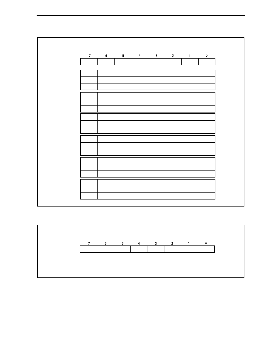
CHAPTER 4 PORT FUNCTIONS
Preliminary User's Manual U17714EJ1V0UD
109
(3) Port 5 mode control register (PMC5)
0
PMC5
0
PMC55
PMC54
PMC53
PMC52
PMC51
PMC50
I/O port
SCKB2 I/O/KR5 input/RTP05 output
PMC55
0
1
Specification of P55 pin operation mode
I/O port
SOB2 output/KR4 input/RTP04 output
PMC54
0
1
Specification of P54 pin operation mode
I/O port
SIB2 input/KR3 input/TIQ00 input/TOQ00 output/RTP03 output
PMC53
0
1
Specification of P53 pin operation mode
I/O port
TIQ03 input/KR2 input/TOQ03 output/RTP02 output
PMC52
0
1
Specification of P52 pin operation mode
I/O port
TIQ02 input/KR1 input/TOQ02 output/RTP01 output
PMC51
0
1
Specification of P51 pin operation mode
I/O port
TIQ01 input/KR0 input/TOQ01 output/RTP00 output
PMC50
0
1
Specification of P50 pin operation mode
After reset: 00H R/W Address: FFFFF44AH
(4) Port 5 function control register (PFC5)
0
PFC5
0
PFC55
PFC54
PFC53
PFC52
PFC51
PFC50
After reset: 00H R/W Address: FFFFF46AH
Remark For details of alternate function specification, see 4.3.5 (6) Port 5 alternate function
specifications.
CHAPTER 4 PORT FUNCTIONS
Preliminary User's Manual U17714EJ1V0UD
110
(5) Port 5 function control expansion register (PFCE5)
0
PFCE5
0
PFCE55 PFCE54
PFCE53 PFCE52
PFCE51
PFCE50
After reset: 00H R/W Address: FFFFF70AH
Remark For details of alternate function specification, see 4.3.5 (6) Port 5 alternate function
specifications.
(6) Port 5 alternate function specifications
PFCE55 PFC55
Specification
of P55 pin alternate function
0 0
SCKB2
I/O
0 1
KR5
input
1 0
Setting
prohibited
1 1
RTP05
output
PFCE54 PFC54
Specification
of P54 pin alternate function
0 0
SOB2
output
0 1
KR4
input
1 0
Setting
prohibited
1 1
RTP04
output
PFCE53 PFC53
Specification
of P53 pin alternate function
0 0
SIB2
input
0 1
TIQ00
input/KR3
Note
input
1 0
TOQ00
output
1 1
RTP03
output
PFCE52 PFC52
Specification
of P52 pin alternate function
0 0
Setting
prohibited
0 1
TIQ03
input/KR2
Note
input
1 0
TOQ03
input
1 1
RTP02
output
PFCE51 PFC51
Specification
of P51 pin alternate function
0 0
Setting
prohibited
0 1
TIQ02
input/KR1
Note
input
1 0
TOQ02
output
1 1
RTP01
output
CHAPTER 4 PORT FUNCTIONS
Preliminary User's Manual U17714EJ1V0UD
111
PFCE50 PFC50
Specification
of P50 pin alternate function
0 0
Setting
prohibited
0 1
TIQ01
input/KR0
Note
input
1 0
TOQ01
output
1 1
RTP00
output
Note The KRn pin and TIQ0m pin are alternate-function pins. When using the pin as the TIQ0m pin,
disable KRn pin key return detection, which is the alternate function. (Clear the KRM.KRMn bit to 0.)
Also, when using the pin as the KRn pin, disable TIQ0m pin edge detection, which is the alternate
function (n = 0 to 3, m = 0 to 3).
Pin Name
Use as TIQ0m Pin
Use as KRn Pin
KR0/TIQ01
KRM.KRM0 bit = 0
TQ0IOC1. TQ0TIG2, TQ0IOC1. TQ0TIG3 bits = 0
KR1/TIQ02
KRM.KRM1 bit = 0
TQ0IOC1.TQ0TIG4, TQ0IOC1.TQ0TIG5 bits = 0
KR2/TIQ03
KRM.KRM2 bit = 0
TQ0IOC1.TQ0TIG6, TQ0IOC1.TQ0TIG7 bits = 0
KR3/TIQ00
KRM.KRM3 bit = 0
TQ0IOC1.TQ0TIG0, TQ0IOC1.TQ0TIG1 bits = 0
TQ0IOC2.TQ0EES0, TQ0IOC2.TQ0EES1 bits = 0
TQ0IOC2.TQ0ETS0, TQ0IOC2.TQ0ETS1 bits = 0
(7) Port 5 function register (PF5)
0
Normal output (CMOS output)
N-ch open-drain output
PF5n
0
1
Control of normal output or N-ch open-drain output (n = 0 to 5)
PF5
0
PF55
PF54
PF53
PF52
PF51
PF50
After reset: 00H R/W Address: FFFFFC6AH
Caution When an output pin is pulled up at EV
DD
or higher, be sure to set the PF5n bit to 1.
CHAPTER 4 PORT FUNCTIONS
Preliminary User's Manual U17714EJ1V0UD
112
4.3.6 Port
6
Port 6 is a 16-bit port for which I/O settings can be controlled in 1-bit units.
Port 6 includes the following alternate-function pins.
Table 4-9. Port 6 Alternate-Function Pins
Pin Name
Pin No.
Alternate-Function Pin Name
I/O
Remark
Block Type
P60 43 RTP10
Output
E-2
P61 44 RTP11
Output
E-2
P62 45 RTP12
Output
E-2
P63 46 RTP13
Output
E-2
P64 47 RTP14
Output
E-2
P65 48 RTP15
Output
E-2
P66 49 SIB5
Input
E-1
P67 50 SOB5
Output
E-2
P68 51 SCKB5
I/O
E-3
P69 52 TIP70/TOP70
I/O
G-1
P610 53
TIP71
Input
E-1
P611 54
TOP71
Output
E-2
P612 55
TIP80/TOP80
I/O
G-1
P613 56
TIP81/TOP81
I/O
G-1
P614 57
-
-
C-1
P615 58
-
-
Selectable as N-ch open-drain output
C-1
Caution The P66, P68 to P610, P612, and P613 pins have hysteresis characteristics in the input mode of
the alternate-function pin, but do not have the hysteresis characteristics in the port mode.
CHAPTER 4 PORT FUNCTIONS
Preliminary User's Manual U17714EJ1V0UD
113
(1) Port 6 register (P6)
P615
Outputs 0
Outputs 1
P6n
0
1
Output data control (in output mode) (n = 0 to 15)
P6 (P6H)
(P6L)
P614
P613
P612
P611
P610
P69
P68
After reset: 0000H (output latch) R/W Address: P6 FFFFF40CH
P6L FFFFF40CH, P6LH FFFFF40DH
P67
P66
P65
P64
P63
P62
P61
P60
8
9
10
11
12
13
14
15
Remarks 1. The P6 register can be read or written in 16-bit units.
However, when using the higher 8 bits of the P6 register as the P6H register and the lower 8
bits as the P6L register, P6 can be read or written in 8-bit or 1-bit units.
2.
To read/write bits 8 to 15 of the P6 register in 8-bit or 1-bit units, specify them as bits 0 to 7 of
the P6H register.
(2) Port 6 mode register (PM6)
PM67
Output mode
Input mode
PM6n
0
1
I/O mode control (n = 0 to 15)
PM66
PM65
PM64
PM63
PM62
PM61
PM60
After reset: FFFFH R/W Address: PM6 FFFFF42CH
PM6L FFFFF42CH, PM6H FFFFF42DH
PM615
PM6 (PM6H)
(PM6L)
PM614
PM613
PM612
PM611
PM610
PM69
PM68
8
9
10
11
12
13
14
15
Remarks 1. The PM6 register can be read or written in 16-bit units.
However, when using the higher 8 bits of the PM6 register as the PM6H register and the
lower 8 bits as the PM6L register, PM6 can be read or written in 8-bit or 1-bit units.
2.
To read/write bits 8 to 15 of the PM6 register in 8-bit or 1-bit units, specify them as bits 0 to 7
of the PM6H register.
CHAPTER 4 PORT FUNCTIONS
Preliminary User's Manual U17714EJ1V0UD
114
(3) Port 6 mode control register (PMC6)
I/O port
TIP81 input/TOP81 output
PMC613
0
1
Specification of P613 pin operation mode
PMC67
PMC66
PMC65
PMC64
PMC63
PMC62
PMC61
PMC60
After reset: 0000H R/W Address: PMC6 FFFFF44CH
PMC6L FFFFF44CH, PMC6H FFFFF44DH
0
PMC6 (PMC6H)
(PMC6L)
0
PMC613 PMC612
PMC611 PMC610
PMC69
PMC68
8
9
10
11
12
13
14
15
I/O port
TIP80 input/TOP80 output
PMC612
0
1
Specification of P612 pin operation mode
I/O port
TIP70 input/TOP70 output
PMC69
0
1
Specification of P69 pin operation mode
I/O port
SCKB5 I/O
PMC68
0
1
Specification of P68 pin operation mode
I/O port
SOB5 output
PMC67
0
1
Specification of P67 pin operation mode
I/O port
TOP71 output
PMC611
0
1
Specification of P611 pin operation mode
I/O port
TIP71 input
PMC610
0
1
Specification of P610 pin operation mode
I/O port
SIB5 input
PMC66
0
1
Specification of P66 pin operation mode
I/O port
RTP1m I/O
PMC6m
0
1
Specification of P6m pin operation mode (m = 0 to 5)
Remarks 1. The PMC6 register can be read or written in 16-bit units.
However, when using the higher 8 bits of the PMC6 register as the PMC6H register and the
lower 8 bits as the PMC6L register, PMC6 can be read or written in 8-bit or 1-bit units.
2.
To read/write bits 8 to 15 of the PMC6 register in 8-bit or 1-bit units, specify them as bits 0 to
7 of the PMC6H register.
CHAPTER 4 PORT FUNCTIONS
Preliminary User's Manual U17714EJ1V0UD
115
(4) Port 6 function control register H (PFC6H)
PFC6H
After reset: 00H R/W Address: FFFFF46DH
0
0
PFC613
PFC612
0
0
PFC69
0
15
14
13
12
11
10
9
8
TIP81 input
TOP81 output
PFC613
0
1
Specification of P613 pin alternate function
TIP80 input
TOP80 output
PFC612
0
1
Specification of P612 pin alternate function
TIP70 input
TOP70 output
PFC69
0
1
Specification of P69 pin alternate function
(5) Port 6 function register (PF6)
PF6 (PF6H)
(PF6L)
After reset: 0000H R/W Address: PF6 FFFFFC6CH
PF6L FFFFFC6CH, PF6H FFFFFC6DH
PF67
PF66
PF65
PF64
PF63
PF62
PF61
PF60
PF615
PF614
PF613
PF612
PF611
PF610
PF69
PF68
8
9
10
11
12
13
14
15
Normal output (CMOS output)
N-ch open-drain output
PF6n
0
1
Normal output/N-ch open-drain output control (n = 0 to 15)
Caution When an output pin is pulled up at EV
DD
or higher, be sure to set the PF6n bit to 1.
Remarks 1. The PF6 register can be read or written in 16-bit units.
However, when using the higher 8 bits of the PF6 register as the PF6H register and the lower
8 bits as the PF6L register, PF6 can be read or written in 8-bit and 1-bit units.
2. To read/write bits 8 to 15 of the PF6 register in 8-bit or 1-bit units, specify them as bits 0 to 7
of the PF6H register.
CHAPTER 4 PORT FUNCTIONS
Preliminary User's Manual U17714EJ1V0UD
116
4.3.7
Port 7
Port 7 is a 16-bit port for which I/O settings can be controlled in 1-bit units.
Port 7 includes the following alternate-function pins.
Table 4-10. Port 7 Alternate-Function Pins
Pin Name
Pin No.
Alternate-Function Pin Name
I/O
Remark
Block Type
P70 144 ANI0
Input
A-1
P71 143 ANI1
Input
A-1
P72 142 ANI2
Input
A-1
P73 141 ANI3
Input
A-1
P74 140 ANI4
Input
A-1
P77 139 ANI5
Input
A-1
P76 138 ANI6
Input
A-1
P77 137 ANI7
Input
A-1
P78 136 ANI8
Input
A-1
P79 135 ANI9
Input
A-1
P710 134 ANI10
Input
A-1
P711 133 ANI11
Input
A-1
P712 132 ANI12
Input
A-1
P713 131 ANI13
Input
A-1
P714 130 ANI14
Input
A-1
P715 129 ANI15
Input
-
A-1
CHAPTER 4 PORT FUNCTIONS
Preliminary User's Manual U17714EJ1V0UD
117
(1) Port 7 register H, port 7 register L (P7H, P7L)
Outputs 0
Outputs 1
P7n
0
1
Output data control (in output mode) (n = 0 to 15)
P7H
P7L
After reset: 00H (output latch) R/W Address: P7L FFFFF40EH, P7H FFFFF40FH
P77
P76
P75
P74
P73
P72
P71
P70
P715
P714
P713
P712
P711
P710
P79
P78
Caution Do not read or write the P7H and P7L registers during A/D conversion (see 13.6 (4)
Alternate I/O).
Remark These registers cannot be accessed in 16-bit units as the P7 register. They can be read or
written in 8-bit or 1-bit units as the P7H and P7L registers.
(2) Port 7 mode register H, port 7 mode register L (PM7H, PM7L)
PM715
Output mode
Input mode
PM7n
0
1
I/O mode control (n = 0 to 15)
PM7H
PM7L
PM714
PM713
PM712
PM711
PM710
PM79
PM78
PM77
PM76
PM75
PM74
PM73
PM72
PM71
PM70
After reset: FFH R/W Address: PM7L FFFFF42EH, PM7H FFFFF42FH
Caution When using the P7n pin as its alternate function (ANIn pin), set the PM7n bit to 1.
Remark These registers cannot be accessed in 16-bit units as the PM7 register. They can be read or
written in 8-bit or 1-bit units as the PM7H and PM7L registers.
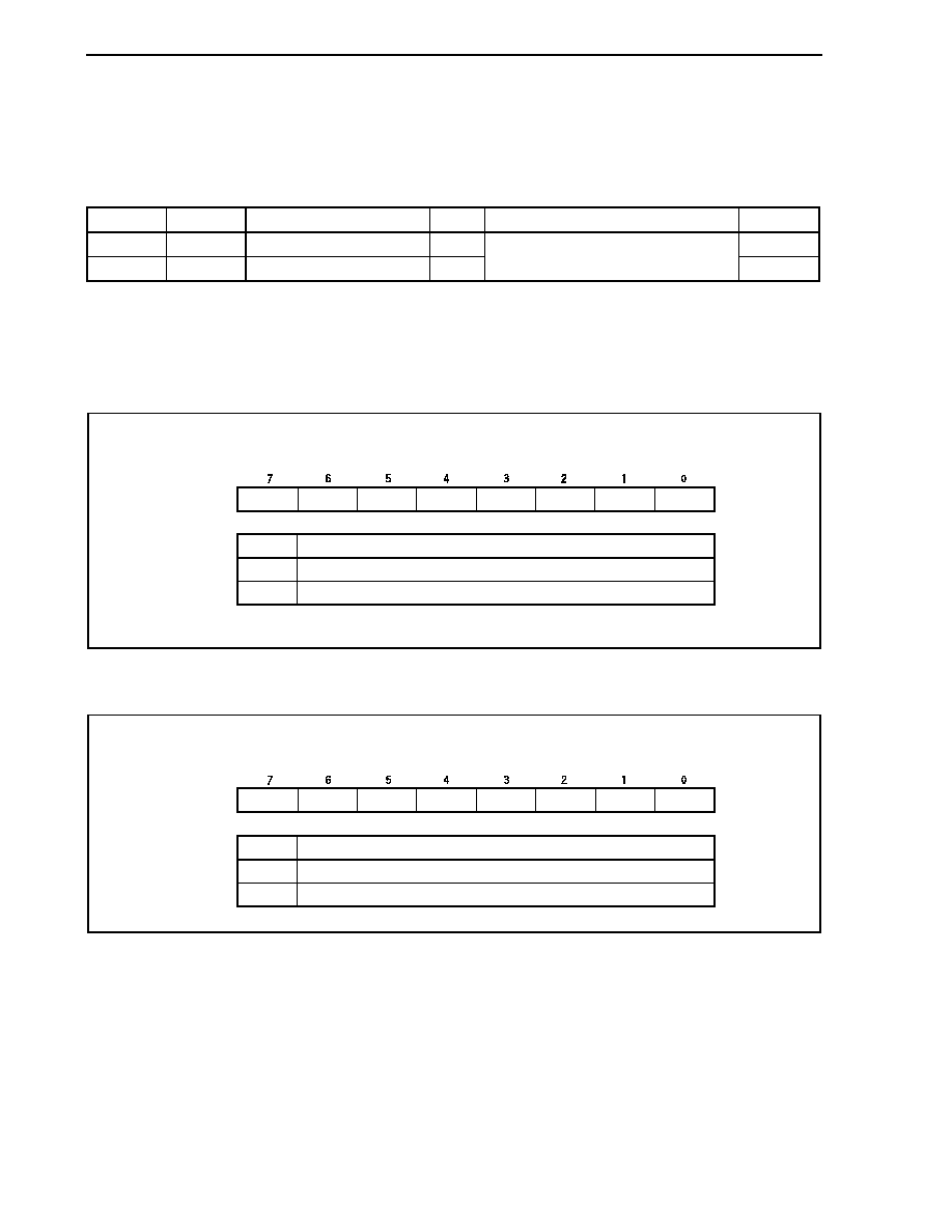
CHAPTER 4 PORT FUNCTIONS
Preliminary User's Manual U17714EJ1V0UD
118
4.3.8 Port
8
Port 8 is a 2-bit port for which I/O settings can be controlled in 1-bit units.
Port 8 includes the following alternate-function pins.
Table 4-11. Port 8 Alternate-Function Pins
Pin Name
Pin No.
Alternate-Function Pin Name
I/O
Remark
Block Type
P80 59 RXDA3/INTP8
Input
L-2
P81 60 TXDA3
Output
Selectable as N-ch open-drain output
E-2
Caution The P80 pin has hysteresis characteristics in the input mode of the alternate-function pin, but
does not have the hysteresis characteristics in the port mode.
(1) Port 8 register (P8)
0
Outputs 0
Outputs 1
P8n
0
1
Output data control (n = 0, 1)
P8
0
0
0
0
0
P81
P80
After reset: 00H (output latch) R/W Address: FFFFF410H
(2) Port 8 mode register (PM8)
1
Output mode
Input mode
PM8n
0
1
I/O mode control (n = 0, 1)
PM8
1
1
1
1
1
PM81
PM80
After reset: FFH R/W Address: FFFFF430H
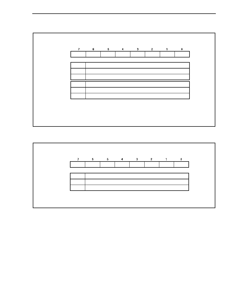
CHAPTER 4 PORT FUNCTIONS
Preliminary User's Manual U17714EJ1V0UD
119
(3) Port 8 mode control register (PMC8)
0
PMC8
0
0
0
0
0
PMC81
PMC80
I/O port
TXDA3 output
PMC81
0
1
Specification of P81 pin operation mode
I/O port
RXDA3 input/INTP8
Note
input
PMC80
0
1
Specification of P80 pin operation mode
After reset: 00H R/W Address: FFFFF450H
Note The INTP8 and RXDA3 pins are alternate-function pins. When using the RXDA3 pin, disable
detection of the edge of the INTP8 pin (INTF8.INTF80 bit = 0 and INTR8.INTR80 bit = 0). When
using the INTP8 pin, stop the reception operation of UARTA3 (UA3CTL0.UA3RXE bit = 0).
(4) Port 8 function register (PF8)
0
Normal output (CMOS output)
N-ch open-drain output
PF8n
0
1
Control of normal output or N-ch open-drain output (n = 0, 1)
PF8
0
0
0
0
0
PF81
PF80
After reset: 00H R/W Address: FFFFFC70H
Caution When an output pin is pulled up at EV
DD
or higher, be sure to set the PF8n bit to 1.
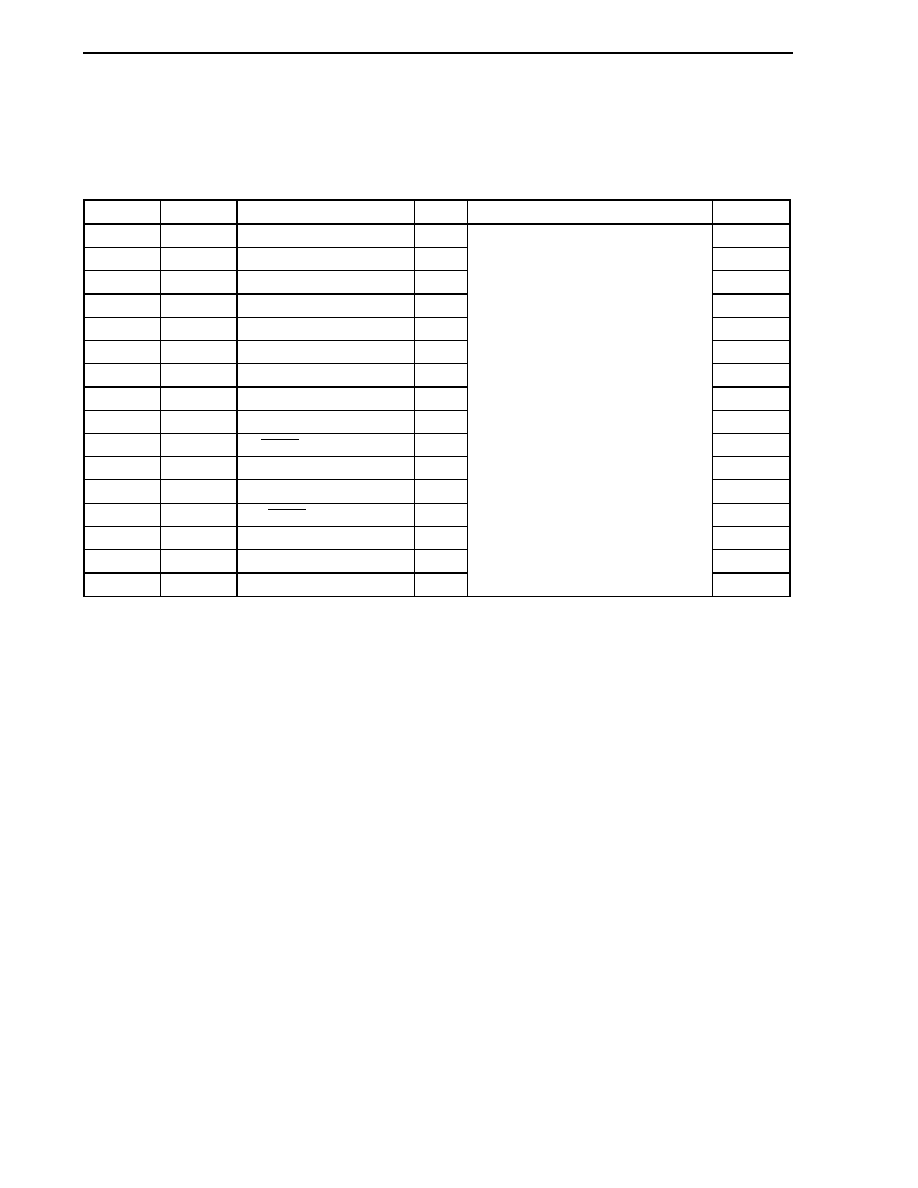
CHAPTER 4 PORT FUNCTIONS
Preliminary User's Manual U17714EJ1V0UD
120
4.3.9
Port 9
Port 9 is a 16-bit port for which I/O settings can be controlled in 1-bit units.
Port 9 includes the following alternate-function pins.
Table 4-12. Port 9 Alternate-Function Pins
Pin Name
Pin No.
Alternate-Function Pin Name
I/O
Remark
Block Type
P90 61 A0/KR6/TXDA1/SDA02
I/O
U-10
P91 62 A1/KR7/RXDA1/SCL02
I/O
U-11
P92 63 A2/TIP41/TOP41
I/O
U-12
P93 64 A3/TIP40/TOP40
I/O
U-12
P94 65 A4/TIP31/TOP31
I/O
U-12
P95 66 A5/TIP30/TOP30
I/O
U-12
P96 67 A6/TIP21/TOP21
I/O
U-13
P97 68 A7/SIB1/TIP20/TOP20
I/O
U-14
P98 69 A8/SOB1
Output
G-3
P99 70 A9/SCKB1
I/O
G-5
P910 71
A10/SIB3
I/O
G-2
P911 72
A11/SOB3
Output
G-3
P912 73
A12/SCKB3
I/O
G-5
P913 74
A13/INTP4
I/O
N-2
P914 75
A14/INTP5/TIP51/TOP51 I/O
U-15
P915 76
A15/INTP6/TIP50/TOP50 I/O
Selectable as N-ch open-drain output
U-15
Caution The P90 to P97, P99, P910, and P912 to P915 pins have hysteresis characteristics in the input
mode of the alternate-function pin, but do not have the hysteresis characteristics in the port
mode.
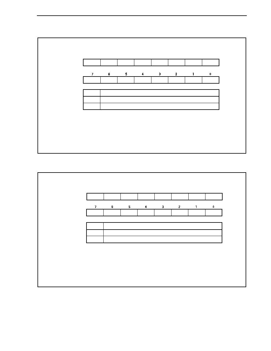
CHAPTER 4 PORT FUNCTIONS
Preliminary User's Manual U17714EJ1V0UD
121
(1) Port 9 register (P9)
P915
Outputs 0
Outputs 1
P9n
0
1
Output data control (in output mode) (n = 0 to 15)
P914
P913
P912
P911
P910
P99
P98
After reset: 0000H (output latch) R/W Address: P9 FFFFF412H,
P9L FFFFF412H, P9H FFFFF413H
P97
P96
P95
P94
P93
P92
P91
P90
8
9
10
11
12
13
14
15
P9 (P9H)
(P9L)
Remarks 1. The P9 register can be read or written in 16-bit units.
However, when using the higher 8 bits of the P9 register as the P9H register and the lower 8
bits as the P9L register, P9 can be read or written in 8-bit or 1-bit units.
2. To read/write bits 8 to 15 of the P9 register in 8-bit or 1-bit units, specify them as bits 0 to 7 of
the P9H register.
(2) Port 9 mode register (PM9)
PM97
Output mode
Input mode
PM9n
0
1
I/O mode control (n = 0 to 15)
PM96
PM95
PM94
PM93
PM92
PM91
PM90
After reset: FFFFH R/W Address: PM9 FFFFF432H,
PM9L FFFFF432H, PM9H FFFFF433H
PM915
PM914
PM913
PM912
PM911
PM910
PM99
PM98
8
9
10
11
12
13
14
15
PM9 (PM9H)
(PM9L)
Remarks 1. The PM9 register can be read or written in 16-bit units.
However, when using the higher 8 bits of the PM9 register as the PM9H register and the
lower 8 bits as the PM9L register, PM9 can be read or written in 8-bit and 1-bit units.
2. To read/write bits 8 to 15 of the PM9 register in 8-bit or 1-bit units, specify them as bits 0 to 7
of the PM9H register.
CHAPTER 4 PORT FUNCTIONS
Preliminary User's Manual U17714EJ1V0UD
122
(3) Port 9 mode control register (PMC9)
(1/2)
I/O port
A15 output/INTP6 input/TIP50 input/TOP50 output
PMC915
0
1
Specification of P915 pin operation mode
PMC97
PMC96
PMC95
PMC94
PMC93
PMC92
PMC91
PMC90
After reset: 0000H R/W Address: PMC9 FFFFF452H,
PMC9L FFFFF452H, PMC9H FFFFF453H
PMC915 PMC914
PMC913 PMC912
PMC911 PMC910
PMC99
PMC98
I/O port
A14 output/INTP5 input/TIP51 input/TOP51 output
PMC914
0
1
Specification of P914 pin operation mode
I/O port
A11 output/SOB3 output
PMC911
0
1
Specification of P911 pin operation mode
I/O port
A10 output/SIB3 input
PMC910
0
1
Specification of P910 pin operation mode
I/O port
A9 output/SCKB1 I/O
PMC99
0
1
Specification of P99 pin operation mode
I/O port
A13 output/INTP4 input
PMC913
0
1
Specification of P913 pin operation mode
I/O port
A12 output/SCKB3 I/O
PMC912
0
1
Specification of P912 pin operation mode
8
9
10
11
12
13
14
15
PMC9 (PMC9H)
(PMC9L)
I/O port
A8 output/SOB1 output
PMC98
0
1
Specification of P98 pin operation mode
Remarks 1. The PMC9 register can be read or written in 16-bit units.
However, when using the higher 8 bits of the PMC9 register as the PMC9H register and the
lower 8 bits as the PMC9L register, PMC9 can be read or written in 8-bit or 1-bit units.
2. To read/write bits 8 to 15 of the PMC9 register in 8-bit or 1-bit units, specify them as bits 0 to
7 of the PMC9H register.
CHAPTER 4 PORT FUNCTIONS
Preliminary User's Manual U17714EJ1V0UD
123
(2/2)
I/O port
A7 output/SIB1 input/TIP20 input/TOP20 output
PMC97
0
1
Specification of P97 pin operation mode
I/O port
A6 output/TIP21 input/TOP21 output
PMC96
0
1
Specification of P96 pin operation mode
I/O port
A5 output/TIP30 input/TOP30 output
PMC95
0
1
Specification of P95 pin operation mode
I/O port
A4 output/TIP31 input/TOP31 output
PMC94
0
1
Specification of P94 pin operation mode
I/O port
A3 output/TIP40 input/TOP40 output
PMC93
0
1
Specification of P93 pin operation mode
I/O port
A2 output/TIP41 input/TOP41 output
PMC92
0
1
Specification of P92 pin operation mode
I/O port
A1 output/KR7 input/RXDA1 input/SCL02 I/O
PMC91
0
1
Specification of P91 pin operation mode
I/O port
A0 output/KR6 input/TXDA1 output/SDA02 I/O
PMC90
0
1
Specification of P90 pin operation mode
Caution Only when using the A0 to A15 pins as the alternate functions of the P90 to P915 pins, set
all 16 bits of the PMC9 register to FFFFH at once.
CHAPTER 4 PORT FUNCTIONS
Preliminary User's Manual U17714EJ1V0UD
124
(4) Port 9 function control register (PFC9)
Caution When
performing
separate address bus output (A0 to A15), set the PMC9 register to FFFFH
for all 16 bits at once after clearing the PFC9 register to 0000H.
After reset: 0000H R/W Address: PFC9 FFFFF472H,
PFC9L FFFFF472H, PFC9H FFFFF473H
PFC97
PFC96
PFC95
PFC94
PFC93
PFC92
PFC91
PFC90
PFC915
PFC914
PFC913
PFC912
PFC911
PFC910
PFC99
PFC98
8
9
10
11
12
13
14
15
PFC9 (PFC9H)
(PFC9L)
Remarks 1. For details of alternate function specification, see 4.3.9 (6) Port 9 alternate function
specifications.
2. The PFC9 register can be read or written in 16-bit units.
However, when using the higher 8 bits of the PFC9 register as the PFC9H register and the
lower 8 bits as the PFC9L register, PFC9 can be read or written in 8-bit or 1-bit units.
3. To read/write bits 8 to 15 of the PFC9 register in 8-bit or 1-bit units, specify them as bits 0 to 7
of the PFC9H register.
(5) Port 9 function control expansion register (PFCE9)
After reset: 0000H R/W Address: PFCE9 FFFFF712H,
PFCE9L FFFFF712H, PFCE9H FFFFF713H
PFCE97
PFCE96
PFCE95 PFCE94
PFCE93 PFCE92
PFCE91
PFCE90
PFCE915 PFCE914
0
0
0
0
0
0
8
9
10
11
12
13
14
15
PFCE9 (PFCE9H)
(PFCE9L)
Remarks 1. For details of alternate function specification, see 4.3.9 (6) Port 9 alternate function
specifications.
2. The PFCE9 register can be read or written in 16-bit units.
However, when using the higher 8 bits of the PFCE9 register as the PFCE9H register and the
lower 8 bits as the PFCE9L register, PFCE9 can be read or written in 8-bit or 1-bit units.
3. To read/write bits 8 to 15 of the PFCE9 register in 8-bit or 1-bit units, specify them as bits 0 to
7 of the PFCE9H register.

CHAPTER 4 PORT FUNCTIONS
Preliminary User's Manual U17714EJ1V0UD
125
(6) Port 9 alternate function specifications
PFCE915
PFC915
Specification of P915 pin alternate function
0 0
A15
output
0 1
INTP6
input
1 0
TIP50
input
1 1
TOP50
output
PFCE914
PFC914
Specification of P914 pin alternate function
0 0
A14
output
0 1
INTP5
input
1 0
TIP51
input
1 1
TOP51
output
PFC913
Specification of P913 pin alternate function
0 A13
output
1 INTP4
input
PFC912
Specification of P912 pin alternate function
0 A12
output
1 SCKB3
I/O
PFC911
Specification of P911 pin alternate function
0 A11
output
1 SOB3
output
PFC910
Specification of P910 pin alternate function
0 A10
output
1 SIB3
input
PFC99
Specification of P99 pin alternate function
0 A9
output
1 SCKB1
I/O
PFC98
Specification of P98 pin alternate function
0 A8
output
1 SOB1
output
PFCE97 PFC97
Specification
of P97 pin alternate function
0 0
A7
output
0 1
SIB1
input
1 0
TIP20
input
1 1
TOP20
output

CHAPTER 4 PORT FUNCTIONS
Preliminary User's Manual U17714EJ1V0UD
126
PFCE96 PFC96
Specification
of P96 pin alternate function
0 0
A6
output
0 1
Setting
prohibited
1 0
TIP21
input
1 1
TOP21
output
PFCE95 PFC95
Specification
of P95 pin alternate function
0 0
A5
output
0 1
TIP30
input
1 0
TOP30
output
1 1
Setting
prohibited
PFCE94 PFC94
Specification
of P94 pin alternate function
0 0
A4
output
0 1
TIP31
input
1 0
TOP31
output
1 1
Setting
prohibited
PFCE93 PFC93
Specification
of P93 pin alternate function
0 0
A3
output
0 1
TIP40
input
1 0
TOP40
output
1 1
Setting
prohibited
PFCE92 PFC92
Specification
of P92 pin alternate function
0 0
A2
output
0 1
TIP41
input
1 0
TOP41
output
1 1
Setting
prohibited
PFCE91 PFC91
Specification
of P91 pin alternate function
0 0
A1
output
0 1
KR7
input
1
0
RXDA1 input/KR7 input
Note
1 1
SCL02
I/O
PFCE90 PFC90
Specification
of P90 pin alternate function
0 0
A0
output
0 1
KR6
input
1 0
TXDA1
output
1 1
SDA02
I/O
Note The RXDA1 and KR7 pins must not be used at the same time. When using the RXDA1 pin, do not use the
KR7 pin. When using the KR7 pin, do not use the RXDA1 pin (it is recommended to set the PFC91 bit to 1
and clear the PFCE91 bit to 0).
CHAPTER 4 PORT FUNCTIONS
Preliminary User's Manual U17714EJ1V0UD
127
(7) Port 9 function register (PF9)
After reset: 0000H R/W Address: PF3 FFFFFC72H,
PF9L FFFFFC72H, PF9H FFFFFC73H
PF97
PF96
PF95
PF94
PF93
PF92
PF91
PF90
PF915
PF914
PF913
PF912
PF911
PF910
PF99
PF98
Normal output (CMOS output)
N-ch open-drain output
PF9n
0
1
Control of normal output or N-ch open-drain output (n = 0 to 15)
8
9
10
11
12
13
14
15
PF9 (PF9H)
(PF9L)
Caution When an output pin is pulled up at EV
DD
or higher, be sure to set the PF9n bit to 1.
Remarks 1. The PF9 register can be read or written in 16-bit units.
However, when using the higher 8 bits of the PF9 register as the PF9H register and the lower
8 bits as the PF9L register, PF9 can be read or written in 8-bit or 1-bit units.
2. To read/write bits 8 to 15 of the PF9 register in 8-bit or 1-bit units, specify them as bits 0 to 7
of the PF9H register.
CHAPTER 4 PORT FUNCTIONS
Preliminary User's Manual U17714EJ1V0UD
128
4.3.10 Port CD
Port CD is a 4-bit port for which I/O settings can be controlled in 1-bit units.
Port CD includes the following alternate-function pins.
Table 4-13. Port CD Alternate-Function Pins
Pin Name
Pin No.
Alternate-Function Pin Name
I/O
Remark
Block Type
PCD0 77
-
-
B-1
PCD1 78
-
-
B-1
PCD2 79
-
-
B-1
PCD3 80
-
-
-
B-1
(1) Port CD register (PCD)
0
Outputs 0
Outputs 1
PCDn
0
1
Output data control (in output mode) (n = 0 to 3)
PCD
0
0
0
PCD3
PCD2
PCD1
PCD0
After reset: 00H (output latch) R/W Address: FFFFF00EH
(2) Port CD mode register (PMCD)
1
Output mode
Input mode
PMCDn
0
1
I/O mode control (n = 0 to 3)
PMCD
1
1
1
PMCD3
PMCD2
PMCD1
PMCD0
After reset: FFH R/W Address: FFFFF02EH
CHAPTER 4 PORT FUNCTIONS
Preliminary User's Manual U17714EJ1V0UD
129
4.3.11 Port CM
Port CM is a 6-bit port for which I/O settings can be controlled in 1-bit units.
Port CM includes the following alternate-function pins.
Table 4-14. Port CM Alternate-Function Pins
Pin Name
Pin No.
Alternate-Function Pin Name
I/O
Remark
Block Type
PCM0 85
WAIT
Input
D-1
PCM1 86
CLKOUT
Output
D-2
PCM2 87
HLDAK
Output
D-2
PCM3 88
HLDRQ
Input
D-1
PCM4 89
-
-
B-1
PCM5 90
-
-
-
B-1
(1) Port CM register (PCM)
0
Outputs 0
Outputs 1
PCMn
0
1
Output data control (in output mode) (n = 0 to 5)
PCM
0
PCM5
PCM4
PCM3
PCM2
PCM1
PCM0
After reset: 00H (output latch) R/W Address: FFFFF00CH
(2) Port CM mode register (PMCM)
1
Output mode
Input mode
PMCMn
0
1
I/O mode control (n = 0 to 5)
PMCM
1
PMCM5
PMCM4
PMCM3
PMCM2
PMCM1
PMCM0
After reset: FFH R/W Address: FFFFF02CH
CHAPTER 4 PORT FUNCTIONS
Preliminary User's Manual U17714EJ1V0UD
130
(3) Port CM mode control register (PMCCM)
0
PMCCM
0
0
0
PMCCM3 PMCCM2 PMCCM1 PMCCM0
I/O port
HLDRQ input
PMCCM3
0
1
Specification of PCM3 pin operation mode
I/O port
HLDAK output
PMCCM2
0
1
Specification of PCM2 pin operation mode
I/O port
CLKOUT output
PMCCM1
0
1
Specification of PCM1 pin operation mode
I/O port
WAIT input
PMCCM0
0
1
Specification of PCM0 pin operation mode
After reset: 00H R/W Address: FFFFF04CH
CHAPTER 4 PORT FUNCTIONS
Preliminary User's Manual U17714EJ1V0UD
131
4.3.12 Port CS
Port CS is an 8-bit port for which I/O settings can be controlled in 1-bit units.
Port CS includes the following alternate-function pins.
Table 4-15. Port CS Alternate-Function Pins
Pin Name
Pin No.
Alternate-Function Pin Name
I/O
Remark
Block Type
PCS0 81
CS0
Output
D-2
PCS1 82
CS1
Output
D-2
PCS2 83
CS2
Output
D-2
PCS3 84
CS3
Output
D-2
PCS4 91
-
-
B-1
PCS5 92
-
-
B-1
PCS6 93
-
-
B-1
PCS7 94
-
-
-
B-1
(1) Port CS register (PCS)
PCS7
Outputs 0
Outputs 1
PCSn
0
1
Output data control (in output mode) (n = 0 to 7)
PCS
PCS6
PCS5
PCS4
PCS3
PCS2
PCS1
PCS0
After reset: 00H (output latch) R/W Address: FFFFF008H
(2) Port CS mode register (PMCS)
PMCS7
Output mode
Input mode
PMCSn
0
1
I/O mode control (n = 0 to 7)
PMCS
PMCS6
PMCS5
PMCS4
PMCS3
PMCS2
PMCS1
PMCS0
After reset: FFH R/W Address: FFFFF028H
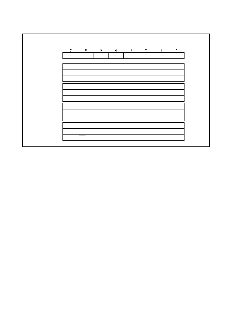
CHAPTER 4 PORT FUNCTIONS
Preliminary User's Manual U17714EJ1V0UD
132
(3) Port CS mode control register (PMCCS)
0
PMCCS
0
0
0
PMCCS3 PMCCS2 PMCCS1 PMCCS0
I/O port
CS3 output
PMCCS3
0
1
Specification of PCS3 pin operation mode
I/O port
CS2 output
PMCCS2
0
1
Specification of PCS2 pin operation mode
I/O port
CS1 output
PMCCS1
0
1
Specification of PCS1 pin operation mode
I/O port
CS0 output
PMCCS0
0
1
Specification of PCS0 pin operation mode
After reset: 00H R/W Address: FFFFF048H

CHAPTER 4 PORT FUNCTIONS
Preliminary User's Manual U17714EJ1V0UD
133
4.3.13 Port CT
Port CT is an 8-bit port for which I/O settings can be controlled in 1-bit units.
Port CT includes the following alternate-function pins.
Table 4-16. Port CT Alternate-Function Pins
Pin Name
Pin No.
Alternate-Function Pin Name
I/O
Remark
Block Type
PCT0 95
WR0
Output
D-2
PCT1 96
WR1
Output
D-2
PCT2 97
-
-
B-1
PCT3 98
-
-
B-1
PCT4 99
RD
Output
D-2
PCT5 100
-
-
B-1
PCT6 101
ASTB
Output
D-2
PCT7 102
-
-
-
B-1
(1) Port CT register (PCT)
PCT7
Outputs 0
Outputs 1
PCTn
0
1
Output data control (in output mode) (n = 0 to 7)
PCT
PCT6
PCT5
PCT4
PCT3
PCT2
PCT1
PCT0
After reset: 00H (output latch) R/W Address: FFFFF00AH
(2) Port CT mode register (PMCT)
PMCT7
Output mode
Input mode
PMCTn
0
1
I/O mode control (n = 0 to 7)
PMCT
PMCT6
PMCT5
PMCT4
PMCT3
PMCT2
PMCT1
PMCT0
After reset: FFH R/W Address: FFFFF02AH

CHAPTER 4 PORT FUNCTIONS
Preliminary User's Manual U17714EJ1V0UD
134
(3) Port CT mode control register (PMCCT)
0
PMCCT
PMCCT6
0
PMCCT4
0
0
PMCCT1 PMCCT0
I/O port
ASTB output
PMCCT6
0
1
Specification of PCT6 pin operation mode
I/O port
RD output
PMCCT4
0
1
Specification of PCT4 pin operation mode
I/O port
WR1 output
PMCCT1
0
1
Specification of PCT1 pin operation mode
I/O port
WR0 output
PMCCT0
0
1
Specification of PCT0 pin operation mode
After reset: 00H R/W Address: FFFFF04AH
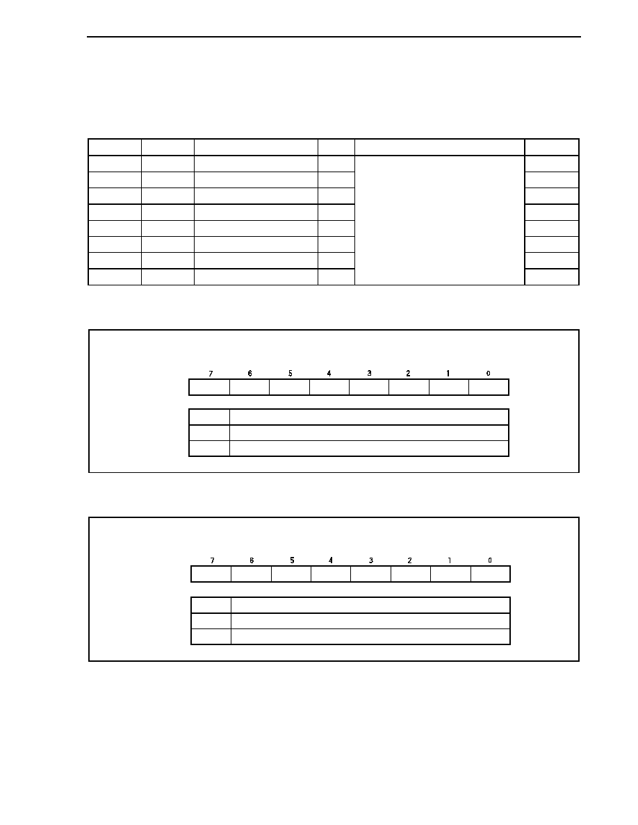
CHAPTER 4 PORT FUNCTIONS
Preliminary User's Manual U17714EJ1V0UD
135
4.3.14 Port DH
Port DH is an 8-bit port for which I/O settings can be controlled in 1-bit units.
Port DH includes the following alternate-function pins.
Table 4-17. Port DH Alternate-Function Pins
Pin Name
Pin No.
Alternate-Function Pin Name
I/O
Remark
Block Type
PDH0 121
A16
Output
D-2
PDH1 122
A17
Output
D-2
PDH2 123
A18
Output
D-2
PDH3 124
A19
Output
D-2
PDH4 125
A20
Output
D-2
PDH5 126
A21
Output
D-2
PDH6 127
A22
Output
D-2
PDH7 128
A23
Output
-
D-2
(1) Port DH register (PDH)
Outputs 0
Outputs 1
PDHn
0
1
Output data control (in output mode) (n = 0 to 7)
PDH
After reset: 00H (output latch) R/W Address: FFFFF006H
PDH7
PDH6
PDH5
PDH4
PDH3
PDH2
PDH1
PDH0
(2) Port DH mode register (PMDH)
PMDH7
Output mode
Input mode
PMDHn
0
1
I/O mode control (n = 0 to 7)
PMDH6
PMDH5
PMDH4
PMDH3
PMDH2
PMDH1
PMDH0
After reset: FFH R/W Address: FFFFF026H
PMDH
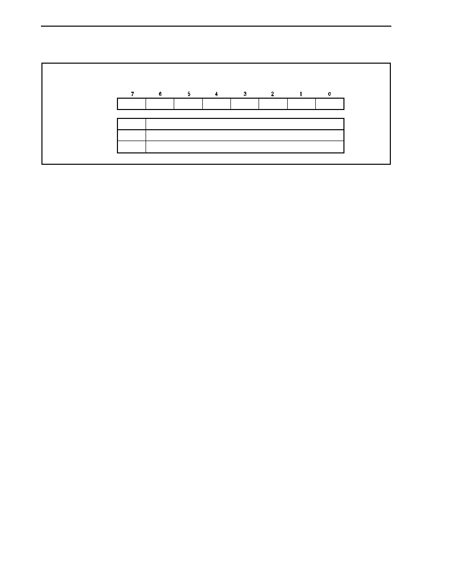
CHAPTER 4 PORT FUNCTIONS
Preliminary User's Manual U17714EJ1V0UD
136
(3) Port DH mode control register (PMCDH)
I/O port
Am output (address bus output) (m = 16 to 23)
PMCDHn
0
1
Specification of PDHn pin operation mode (n = 0 to 7)
PMCDH7 PMCDH6 PMCDH5 PMCDH4 PMCDH3 PMCDH2 PMCDH1 PMCDH0
After reset: 00H R/W Address: FFFFF046H
PMCDH
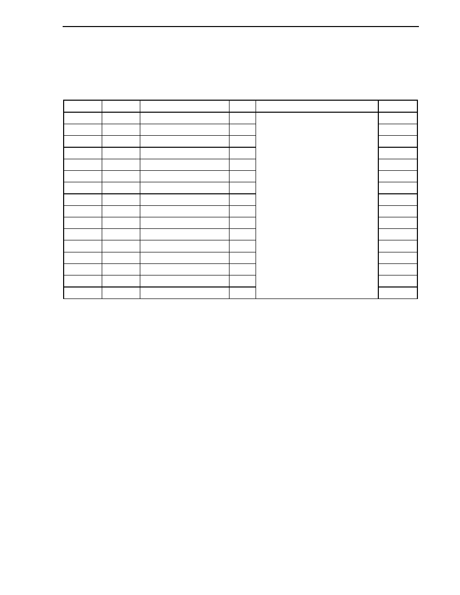
CHAPTER 4 PORT FUNCTIONS
Preliminary User's Manual U17714EJ1V0UD
137
4.3.15 Port DL
Port DL is a 16-bit port for which I/O settings can be controlled in 1-bit units.
Port DL includes the following alternate-function pins.
Table 4-18. Port DL Alternate-Function Pins
Pin Name
Pin No.
Alternate-Function Pin Name
I/O
Remark
Block Type
PDL0 105 AD0
I/O
D-3
PDL1 106 AD1
I/O
D-3
PDL2 107 AD2
I/O
D-3
PDL3 108 AD3
I/O
D-3
PDL4 109 AD4
I/O
D-3
PDL5 110 AD5/FLMD1
Note
I/O
D-3
PDL6 111 AD6
I/O
D-3
PDL7 112 AD7
I/O
D-3
PDL8 113 AD8
I/O
D-3
PDL9 114 AD9
I/O
D-3
PDL10 115
AD10
I/O
D-3
PDL11 116
AD11
I/O
D-3
PDL12 117
AD12
I/O
D-3
PDL13 118
AD13
I/O
D-3
PDL14 119
AD14
I/O
D-3
PDL15 120
AD15
I/O
-
D-3
Note Since this pin is set in the flash memory programming mode, it does not need to be manipulated with the
port control register. For details, see CHAPTER 26 FLASH MEMORY.
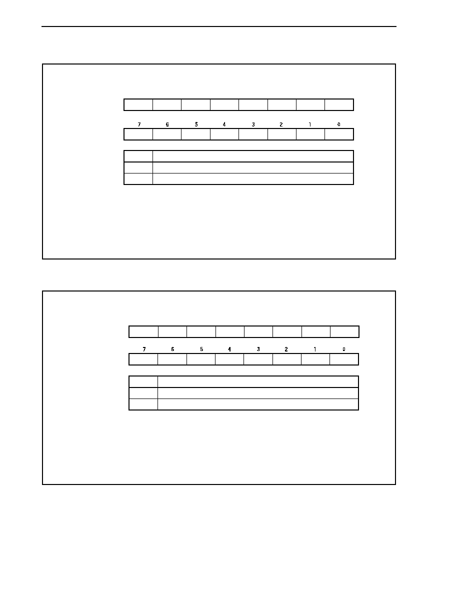
CHAPTER 4 PORT FUNCTIONS
Preliminary User's Manual U17714EJ1V0UD
138
(1) Port DL register (PDL)
PDL15
Outputs 0
Outputs 1
PDLn
0
1
Output data control (in output mode) (n = 0 to 15)
PDL14
PDL13
PDL12
PDL11
PDL10
PDL9
PDL8
After reset: 0000H (output latch) R/W Address: PDL FFFFF004H,
PDLL FFFFF004H, PDLH FFFFF005H
PDL7
PDL6
PDL5
PDL4
PDL3
PDL2
PDL1
PDL0
8
9
10
11
12
13
14
15
PDL (PDLH)
(PDLL)
Remarks 1. The PDL register can be read or written in 16-bit units.
However, when using the higher 8 bits of the PDL register as the PDLH register and the lower
8 bits as the PDLL register, PDL can be read or written in 8-bit or 1-bit units.
2. To read/write bits 8 to 15 of the PDL register in 8-bit or 1-bit units, specify them as bits 0 to 7
of the PDLH register.
(2) Port DL mode register (PMDL)
PMDL7
Output mode
Input mode
PMDLn
0
1
I/O mode control (n = 0 to 15)
PMDL6
PMDL5
PMDL4
PMDL3
PMDL2
PMDL1
PMDL0
After reset: FFFFH R/W Address: PMDL FFFFF024H,
PMDLL FFFFF024H, PMDLH FFFFF025H
PMDL15 PMDL14
PMDL13 PMDL12
PMDL11 PMDL10
PMDL9
PMDL8
8
9
10
11
12
13
14
15
PMDL (PMDLH)
(PMDLL)
Remarks 1. The PMDL register can be read or written in 16-bit units.
However, when using the higher 8 bits of the PMDL register as the PMDLH register and the
lower 8 bits as the PMDLL register, PMDL can be read or written in 8-bit or 1-bit units.
2. To read/write bits 8 to 15 of the PMDL register in 8-bit or 1-bit units, specify them as bits 0 to
7 of the PMDLH register.
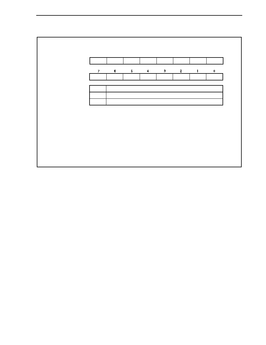
CHAPTER 4 PORT FUNCTIONS
Preliminary User's Manual U17714EJ1V0UD
139
(3) Port DL mode control register (PMCDL)
I/O port
ADn I/O (address/data bus I/O)
PMCDLn
0
1
Specification of PDLn pin operation mode (n = 0 to 15)
PMCDL7 PMCDL6 PMCDL5 PMCDL4 PMCDL3 PMCDL2 PMCDL1 PMCDL0
After reset: 0000H R/W Address: PMCDL FFFFF044H,
PMCDLL FFFFF044H, PMCDLH FFFFF045H
PMCDL15 PMCDL14PMCDL13 PMCDL12 PMCDL11PMCDL10 PMCDL9 PMCDL8
8
9
10
11
12
13
14
15
PMCDL (PMCDLH)
(PMCDLL)
Caution When the SMSEL bit of the EXIMC register = 1 (separate mode) and the BS30 to BS00 bits
of the BSC register = 0 (8-bit bus width), do not specify the AD8 to AD15 pins.
Remarks 1. The PMCDL register can be read or written in 16-bit units.
However, when using the higher 8 bits of the PMCDL register as the PMCDLH register and
the lower 8 bits as the PMCDLL register, PMCDL can be read or written in 8-bit or 1-bit units.
2. To read/write bits 8 to 15 of the PMCDL register in 8-bit or 1-bit units, specify them as bits 0
to 7 of the PMCDLH register.
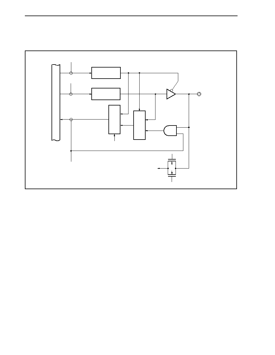
CHAPTER 4 PORT FUNCTIONS
Preliminary User's Manual U17714EJ1V0UD
140
4.4 Block
Diagrams
Figure 4-3. Block Diagram of Type A-1
Address
RD
A/D input signal
WR
PM
PMmn
WR
PORT
Pmn
Pmn
P-ch
N-ch
Inter
nal b
u
s
Selector
Selector
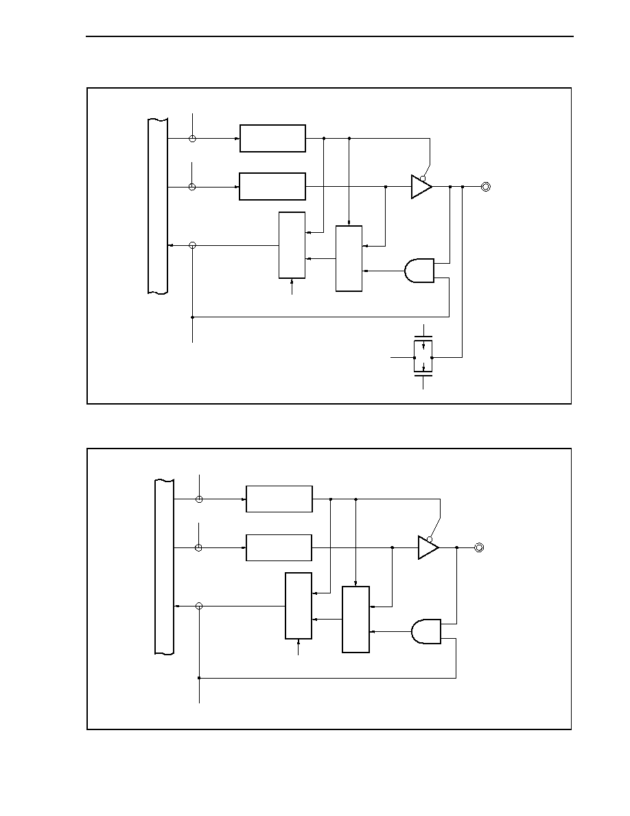
CHAPTER 4 PORT FUNCTIONS
Preliminary User's Manual U17714EJ1V0UD
141
Figure 4-4. Block Diagram of Type A-2
RD
D/A output signal
WR
PM
PMmn
WR
PORT
Pmn
Pmn
P-ch
N-ch
Inter
nal b
u
s
Selector
Selector
Address
Figure 4-5. Block Diagram of Type B-1
RD
WR
PM
PMmn
WR
PORT
Pmn
Pmn
Inter
nal b
u
s
Selector
Selector
Address
CHAPTER 4 PORT FUNCTIONS
Preliminary User's Manual U17714EJ1V0UD
142
Figure 4-6. Block Diagram of Type C-1
Address
RD
WR
PORT
Pmn
WR
PF
PFmn
WR
PM
PMmn
Pmn
EV
DD
EV
SS
P-ch
N-ch
Inter
nal b
u
s
Selector
Selector
CHAPTER 4 PORT FUNCTIONS
Preliminary User's Manual U17714EJ1V0UD
143
Figure 4-7. Block Diagram of Type D-1
WR
PORT
Pmn
WR
PM
PMmn
WR
PMC
PMCmn
RD
Input signal when
alternate function is used
Pmn
Inter
nal b
u
s
Selector
Selector
Address
CHAPTER 4 PORT FUNCTIONS
Preliminary User's Manual U17714EJ1V0UD
144
Figure 4-8. Block Diagram of Type D-2
WR
PORT
Pmn
WR
PM
PMmn
WR
PMC
PMCmn
RD
Output signal when
alternate function is used
Pmn
Inter
nal b
u
s
Selector
Selector
Selector
Address
CHAPTER 4 PORT FUNCTIONS
Preliminary User's Manual U17714EJ1V0UD
145
Figure 4-9. Block Diagram of Type D-3
WR
PORT
Pmn
WR
PM
PMmn
WR
PMC
PMCmn
RD
Pmn
Output signal when
alternate function is used
Input signal when
alternate function is used
Output enable signal
of address/data bus
Input enable signal of
address/data bus
Output buffer off signal
Inter
nal b
u
s
Selector
Selector
Selector
Selector
Address
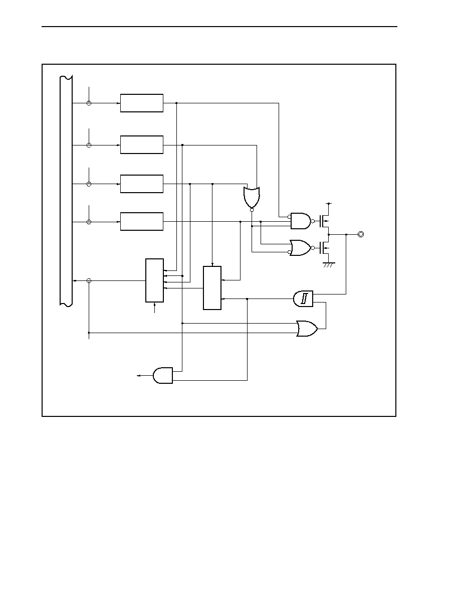
CHAPTER 4 PORT FUNCTIONS
Preliminary User's Manual U17714EJ1V0UD
146
Figure 4-10. Block Diagram of Type E-1
Address
Input signal when
alternate function is used
RD
WR
PORT
Pmn
WR
PMC
PMCmn
WR
PF
PFmn
WR
PM
PMmn
Pmn
EV
DD
EV
SS
P-ch
N-ch
Note
Inter
nal b
u
s
Selector
Selector
Note Hysteresis characteristics are not available in port mode.
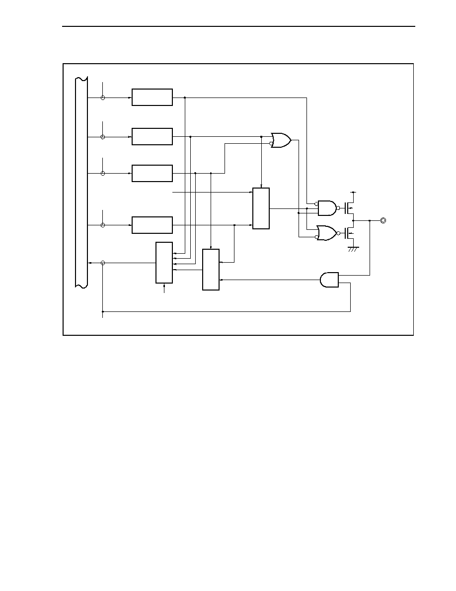
CHAPTER 4 PORT FUNCTIONS
Preliminary User's Manual U17714EJ1V0UD
147
Figure 4-11. Block Diagram of Type E-2
RD
WR
PORT
Pmn
WR
PMC
PMCmn
WR
PF
PFmn
WR
PM
PMmn
Pmn
EV
DD
EV
SS
P-ch
N-ch
Output signal when
alternate function is used
Inter
nal b
u
s
Selector
Selector
Selector
Address
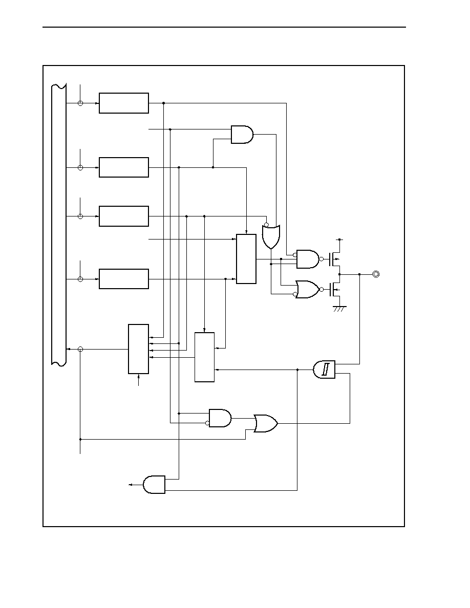
CHAPTER 4 PORT FUNCTIONS
Preliminary User's Manual U17714EJ1V0UD
148
Figure 4-12. Block Diagram of Type E-3
RD
WR
PORT
Pmn
WR
PMC
PMCmn
WR
PF
PFmn
WR
PM
PMmn
Pmn
EV
DD
EV
SS
P-ch
N-ch
Output signal when
alternate function is used
Output enable signal when
alternate function is used
Input signal when
alternate function is used
Note
Inter
nal b
u
s
Selector
Selector
Selector
Address
Note Hysteresis characteristics are not available in port mode.
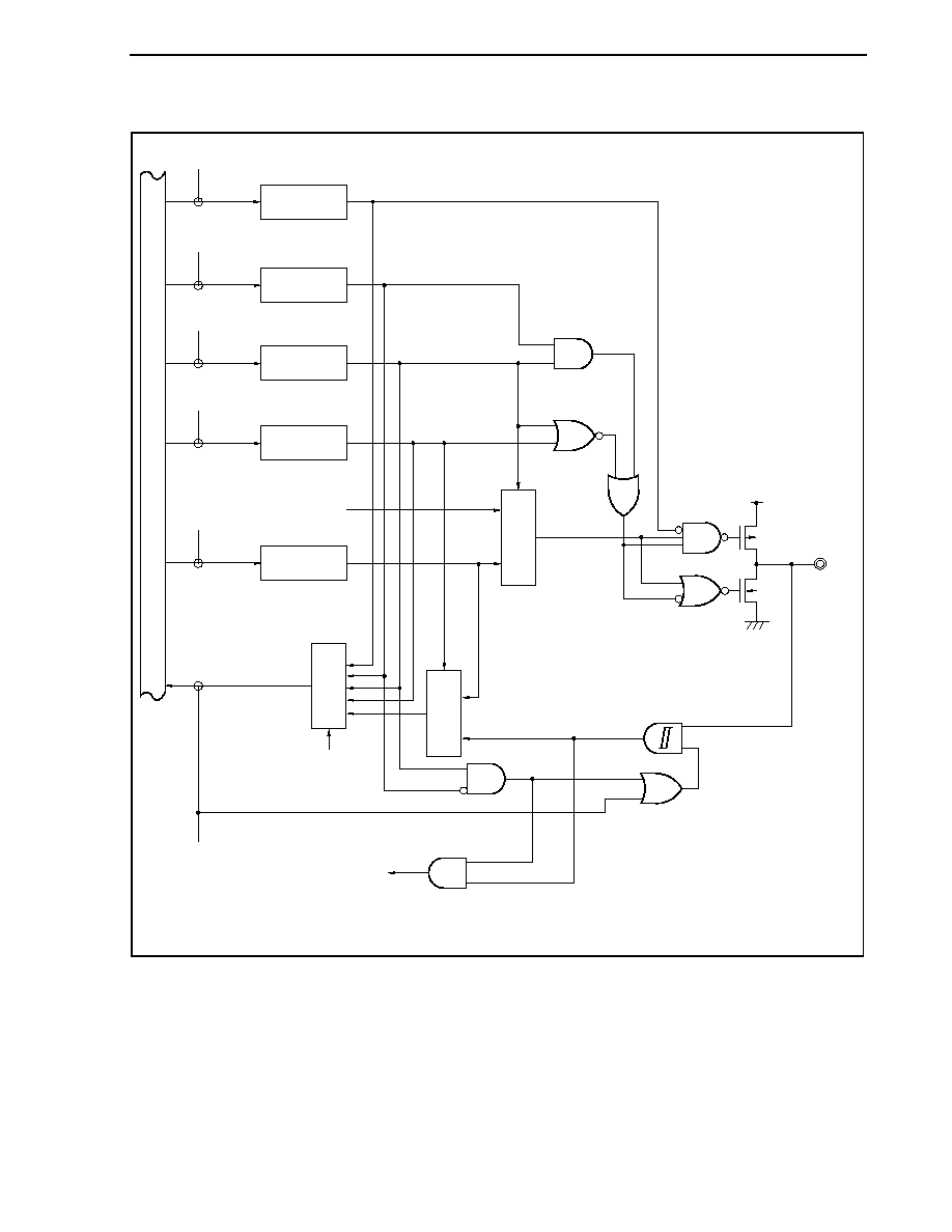
CHAPTER 4 PORT FUNCTIONS
Preliminary User's Manual U17714EJ1V0UD
149
Figure 4-13. Block Diagram of Type G-1
Input signal when
alternate function is used
RD
WR
PORT
Pmn
WR
PFC
PFCmn
WR
PF
PFmn
WR
PMC
PMCmn
WR
PM
PMmn
Output signal when
alternate function is used
Pmn
EV
DD
EV
SS
P-ch
N-ch
Note
Inter
nal b
u
s
Selector
Selector
Selector
Address
Note Hysteresis characteristics are not available in port mode.
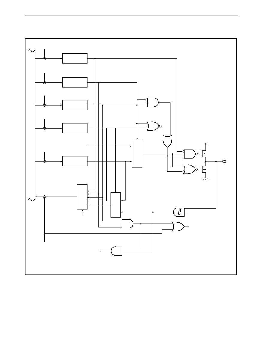
CHAPTER 4 PORT FUNCTIONS
Preliminary User's Manual U17714EJ1V0UD
150
Figure 4-14. Block Diagram of Type G-2
Input signal when
alternate function is used
RD
WR
PORT
Pmn
WR
PFC
PFCmn
WR
PF
PFmn
WR
PMC
PMCmn
WR
PM
PMmn
Output signal when
alternate function is used
Pmn
EV
DD
EV
SS
P-ch
N-ch
Note
Inter
nal b
u
s
Selector
Selector
Selector
Address
Note Hysteresis characteristics are not available in port mode.
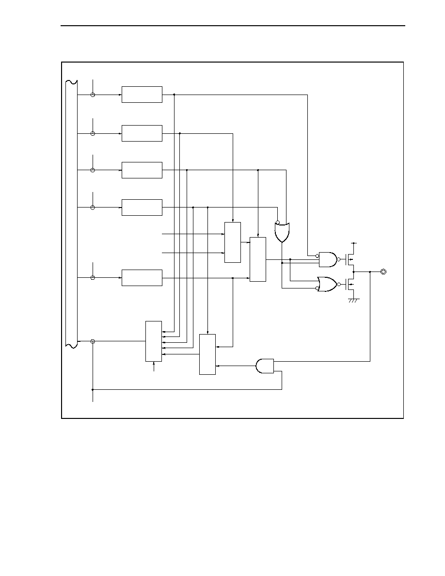
CHAPTER 4 PORT FUNCTIONS
Preliminary User's Manual U17714EJ1V0UD
151
Figure 4-15. Block Diagram of Type G-3
Output signal 2 when
alternate function is used
RD
WR
PORT
Pmn
WR
PFC
PFCmn
WR
PF
PFmn
WR
PMC
PMCmn
WR
PM
PMmn
Output signal 1 when
alternate function is used
Pmn
EV
DD
EV
SS
P-ch
N-ch
Inter
nal b
u
s
Selector
Selector
Selector
Selector
Address
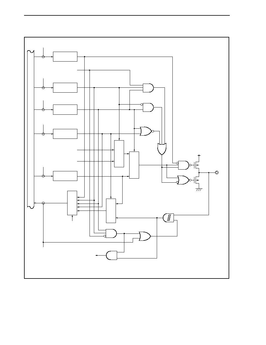
CHAPTER 4 PORT FUNCTIONS
Preliminary User's Manual U17714EJ1V0UD
152
Figure 4-16. Block Diagram of Type G-5
RD
WR
PORT
Pmn
WR
PFC
PFCmn
WR
PF
PFmn
WR
PMC
PMCmn
WR
PM
PMmn
Output signal 2 when
alternate function is used
Output signal 1 when
alternate function is used
Output enable signal when
alternate function is used
Pmn
EV
DD
EV
SS
P-ch
N-ch
Input signal when
alternate function is used
Note
Inter
nal b
u
s
Selector
Selector
Selector
Selector
Address
Note Hysteresis characteristics are not available in port mode.
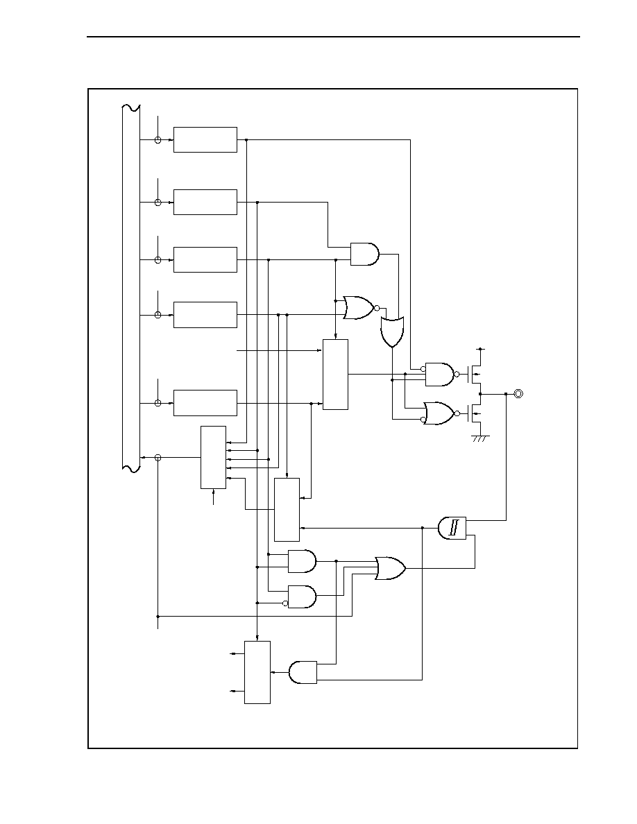
CHAPTER 4 PORT FUNCTIONS
Preliminary User's Manual U17714EJ1V0UD
153
Figure 4-17. Block Diagram of Type G-6
Output signal when
alternate function is used
Input signal 1 when
alternate function is used
Input signal 2 when
alternate function is used
Note
Inter
nal b
u
s
Selector
Selector
Selector
Selector
Address
RD
WR
PORT
Pmn
WR
PFC
PFCmn
WR
PF
PFmn
WR
PMC
PMCmn
WR
PM
PMmn
Pmn
EV
DD
EV
SS
P-ch
N-ch
Note Hysteresis characteristics are not available in port mode.
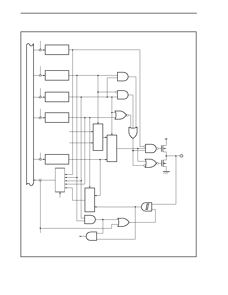
CHAPTER 4 PORT FUNCTIONS
Preliminary User's Manual U17714EJ1V0UD
154
Figure 4-18. Block Diagram of Type G-12
Input signal when
alternate function is used
Output signal 1 when
alternate function is used
Output signal 2 when
alternate function is used
Note
Inter
nal b
u
s
Selector
Address
RD
WR
PORT
Pmn
WR
PFC
PFCmn
WR
PF
PFmn
WR
PMC
PMCmn
WR
PM
PMmn
Pmn
EV
DD
EV
SS
P-ch
N-ch
Selector
Selector
Selector
Note Hysteresis characteristics are not available in port mode.
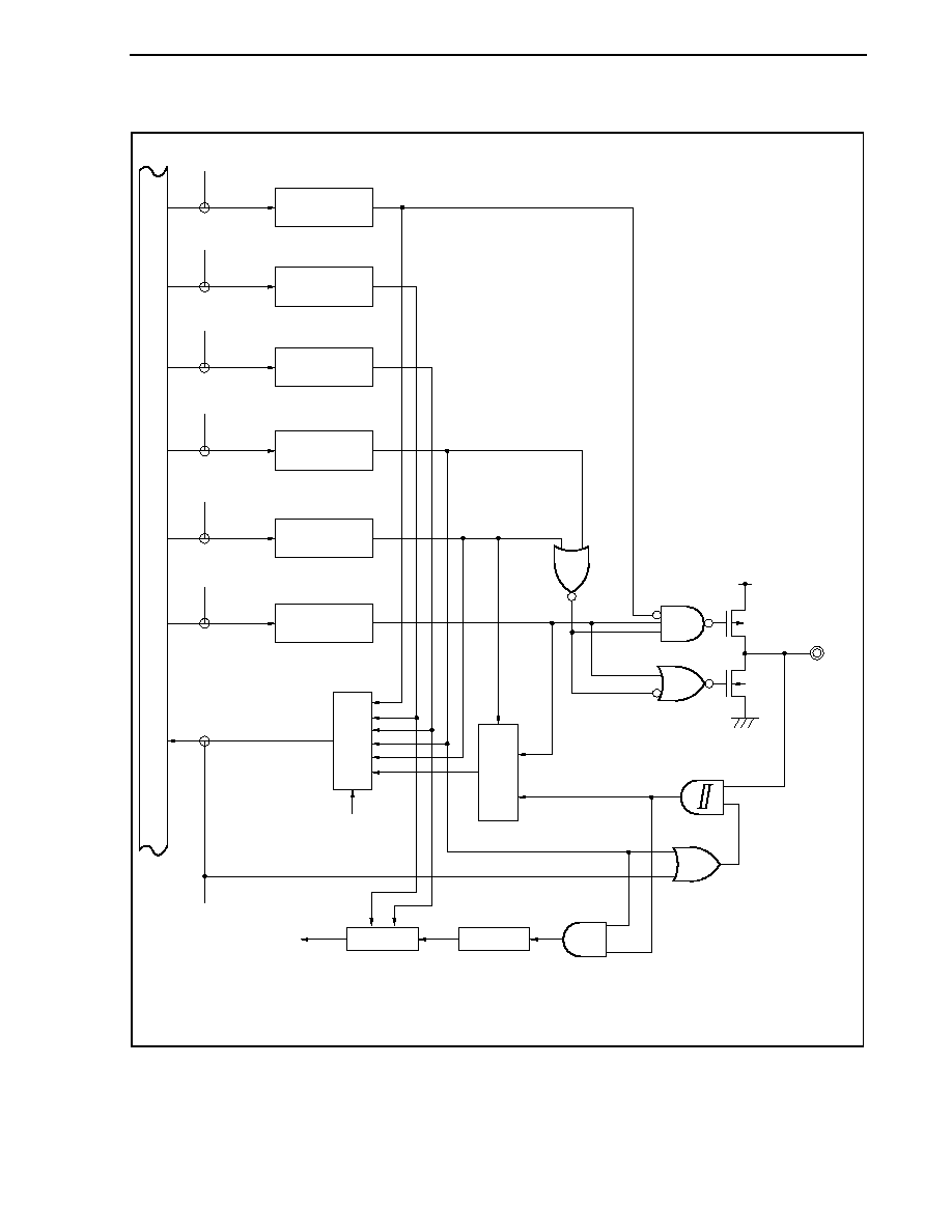
CHAPTER 4 PORT FUNCTIONS
Preliminary User's Manual U17714EJ1V0UD
155
Figure 4-19. Block Diagram of Type L-1
Input signal 1 when
alternate function is used
RD
WR
PORT
Pmn
WR
PMC
PMCmn
WR
INTR
INTRmn
Note 1
WR
INTF
INTFmn
Note 1
WR
PF
PFmn
WR
PM
PMmn
Pmn
EV
DD
EV
SS
P-ch
N-ch
Edge
detection
Noise
elimination
Note 2
Inter
nal b
u
s
Selector
Selector
Address
Notes 1. See
19.6 External Interrupt Request Input Pins (NMI and INTP0 to INTP8).
2. Hysteresis characteristics are not available in port mode.
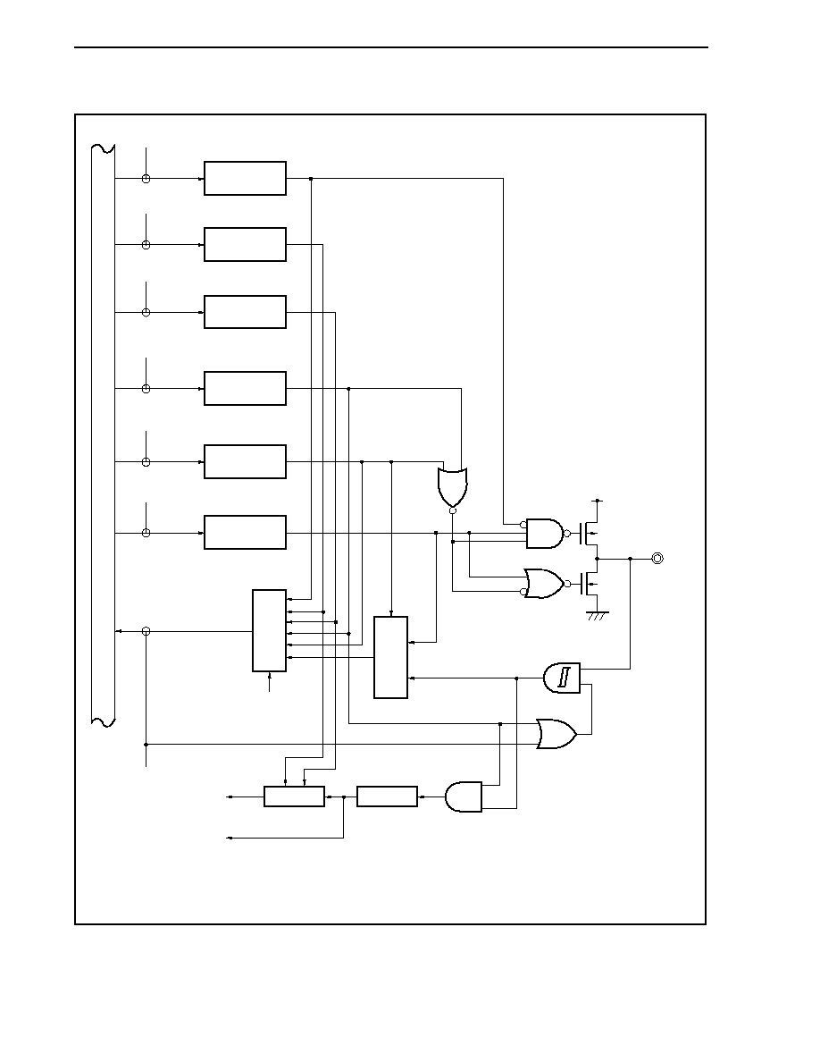
CHAPTER 4 PORT FUNCTIONS
Preliminary User's Manual U17714EJ1V0UD
156
Figure 4-20. Block Diagram of Type L-2
Address
Input signal 1-1 when
alternate function is used
RD
WR
PORT
Pmn
WR
PMC
PMCmn
WR
INTR
INTRmn
Note 1
WR
INTF
INTFmn
Note 1
WR
PF
PFmn
WR
PM
PMmn
Pmn
Input signal 1-2 when
alternate function is used
EV
DD
EV
SS
P-ch
N-ch
Edge
detection
Noise
elimination
Note 2
Inter
nal b
u
s
Selector
Selector
Notes 1. See
19.6 External Interrupt Request Input Pins (NMI and INTP0 to INTP8).
2. Hysteresis characteristics are not available in port mode.
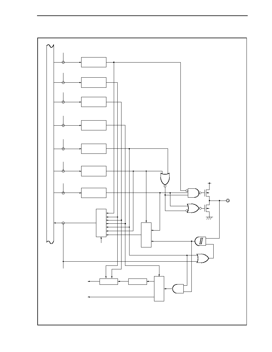
CHAPTER 4 PORT FUNCTIONS
Preliminary User's Manual U17714EJ1V0UD
157
Figure 4-21. Block Diagram of Type N-1
Input signal 1 when
alternate function is used
RD
WR
PORT
Pmn
WR
PMC
PMCmn
WR
INTR
INTRmn
Note 1
WR
INTF
INTFmn
Note 1
WR
PF
PFmn
WR
PM
WR
PFC
PFCmn
PMmn
Pmn
Input signal 2 when
alternate function is used
EV
DD
EV
SS
P-ch
N-ch
Edge
detection
Noise
elimination
Note 2
Inter
nal b
u
s
Selector
Selector
Selector
Address
Notes 1. See
19.6 External Interrupt Request Input Pins (NMI and INTP0 to INTP8).
2. Hysteresis characteristics are not available in port mode.
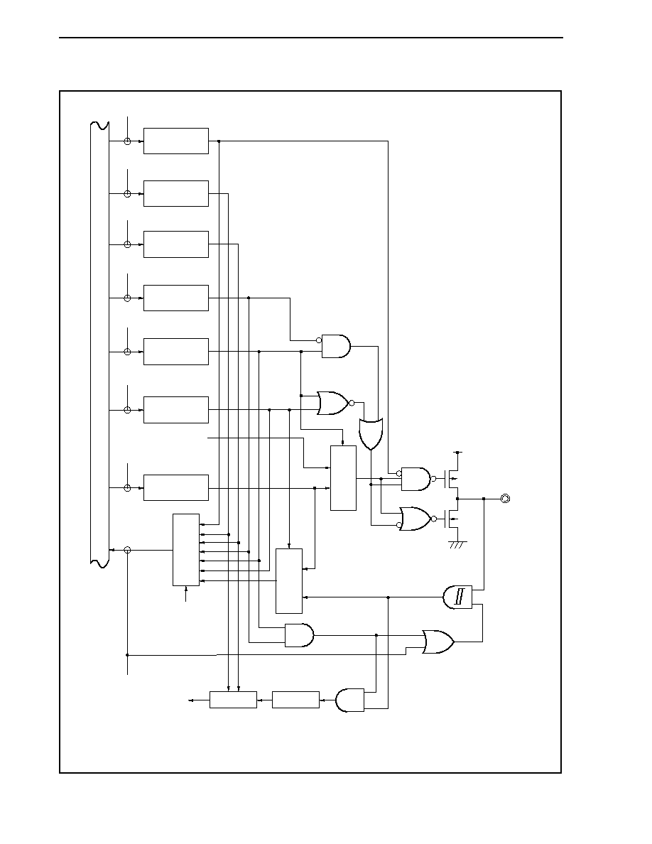
CHAPTER 4 PORT FUNCTIONS
Preliminary User's Manual U17714EJ1V0UD
158
Figure 4-22. Block Diagram of Type N-2
Inter
nal b
u
s
Address
Input signal when
alternate function is used
Selector
Selector
Selector
RD
WR
PORT
Pmn
WR
PMC
PMCmn
WR
INTR
INTRmn
Note 1
WR
INTF
INTFmn
Note 1
WR
PF
PFmn
WR
PM
WR
PFC
PFCmn
PMmn
Pmn
EV
DD
EV
SS
P-ch
N-ch
Edge
detection
Noise
elimination
Note 2
Output signal when
alternate function is used
Notes 1. See
19.6 External Interrupt Request Input Pins (NMI and INTP0 to INTP8).
2. Hysteresis characteristics are not available in port mode.
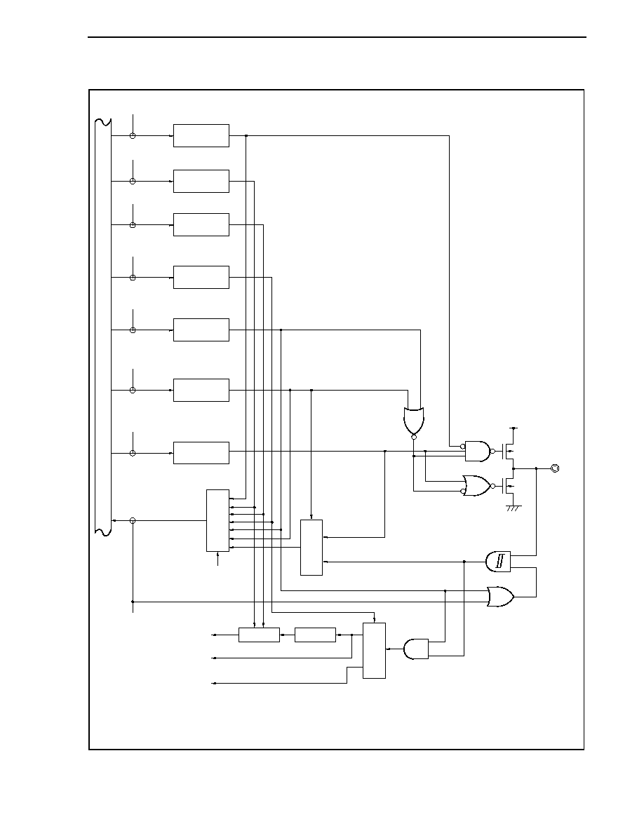
CHAPTER 4 PORT FUNCTIONS
Preliminary User's Manual U17714EJ1V0UD
159
Figure 4-23. Block Diagram of Type N-3
Input signal 1-1 when
alternate function is used
Input signal 1-2 when
alternate function is used
Input signal 2 when
alternate function is used
RD
WR
PORT
Pmn
WR
PMC
PMCmn
WR
INTR
INTRmn
Note 1
WR
INTF
INTFmn
Note 1
WR
PF
PFmn
WR
PM
WR
PFC
PFCmn
PMmn
Pmn
EV
DD
EV
SS
P-ch
N-ch
Note 2
Inter
nal b
u
s
Selector
Selector
Selector
Address
Edge
detection
Noise
elimination
Notes 1. See
19.6 External Interrupt Request Input Pins (NMI and INTP0 to INTP8).
2. Hysteresis characteristics are not available in port mode.
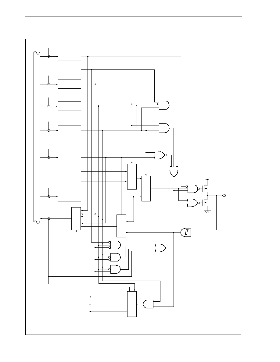
CHAPTER 4 PORT FUNCTIONS
Preliminary User's Manual U17714EJ1V0UD
160
Figure 4-24. Block Diagram of Type U-1
Input signal 2 when
alternate function is used
RD
WR
PORT
Pmn
WR
PFC
PFCmn
WR
PF
PFmn
WR
PMC
PMCmn
WR
PM
PMmn
Input signal 1 when
alternate function is used
Input signal 3 when
alternate function is used
Output signal 2 when
alternate function is used
Output signal 1 when
alternate function is used
Output enable signal when
alternate function is used
Pmn
EV
DD
EV
SS
P-ch
N-ch
WR
PFCE
PFCEmn
Note
Inter
nal b
u
s
Selector
Selector
Selector
Selector
Selector
Address
Note Hysteresis characteristics are not available in port mode.
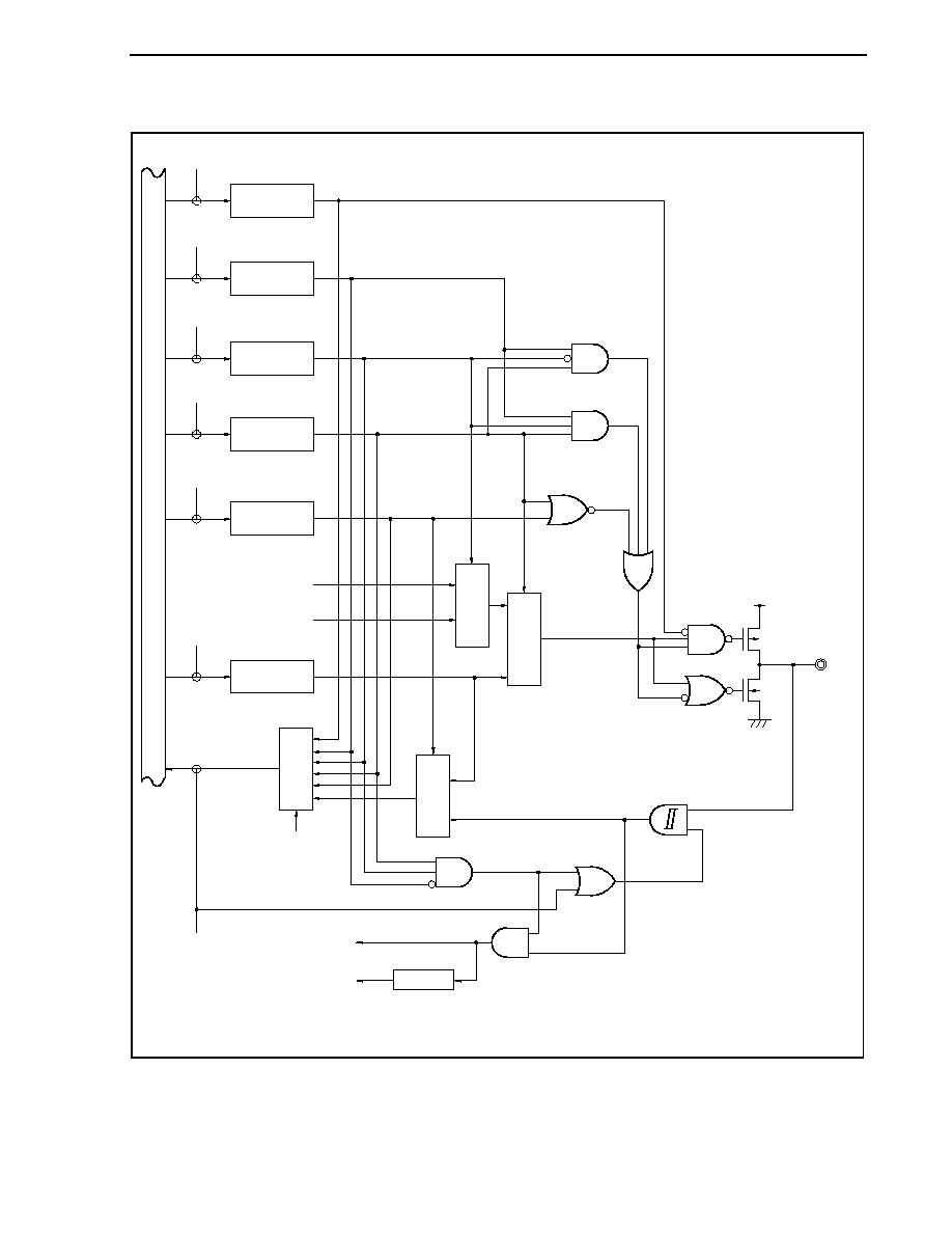
CHAPTER 4 PORT FUNCTIONS
Preliminary User's Manual U17714EJ1V0UD
161
Figure 4-25. Block Diagram of Type U-5
Input signal 1-1 when
alternate function is used
RD
WR
PORT
Pmn
WR
PFC
PFCmn
WR
PF
PFmn
WR
PMC
PMCmn
WR
PM
PMmn
Input signal 1-2 when
alternate function is used
Output signal 2 when
alternate function is used
Output signal 1 when
alternate function is used
Pmn
EV
DD
EV
SS
P-ch
N-ch
WR
PFCE
PFCEmn
Note
Inter
nal b
u
s
Selector
Selector
Selector
Selector
Address
Noise
elimination
Note Hysteresis characteristics are not available in port mode.
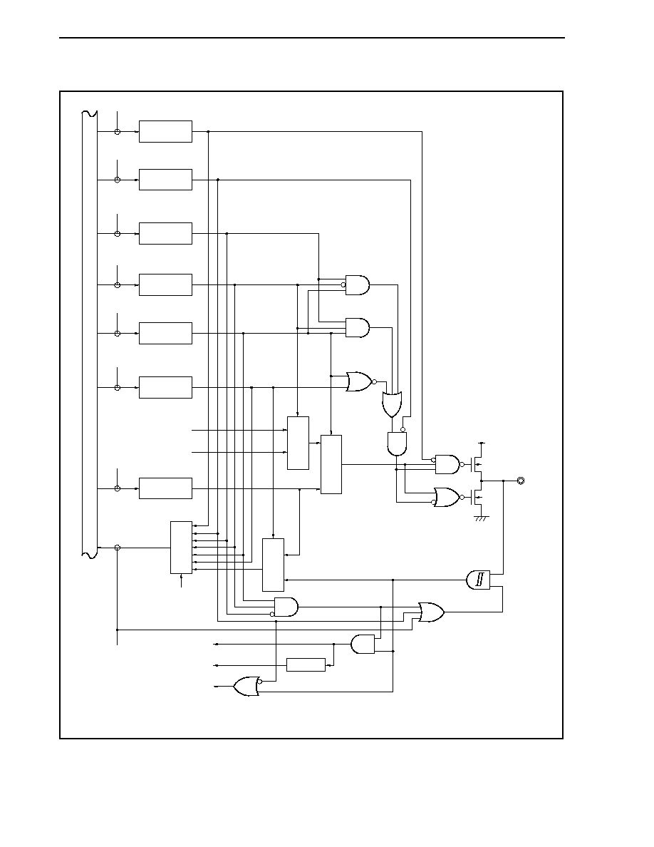
CHAPTER 4 PORT FUNCTIONS
Preliminary User's Manual U17714EJ1V0UD
162
Figure 4-26. Block Diagram of Type U-6
Input signal 1-1 when
alternate function is used
RD
WR
PORT
Pmn
WR
PFC
PFCmn
WR
PF
PFmn
WR
OCDM0
OCDM0
WR
PMC
PMCmn
WR
PM
PMmn
Input signal 1-2 when
alternate function is used
Input signal when
on-chip debugging
Pmn
EV
DD
EV
SS
P-ch
N-ch
WR
PFCE
PFCEmn
Note
Inter
nal b
u
s
Selector
Selector
Selector
Selector
Address
Output signal 2 when
alternate function is used
Output signal 1 when
alternate function is used
Noise
elimination
Note Hysteresis characteristics are not available in port mode.
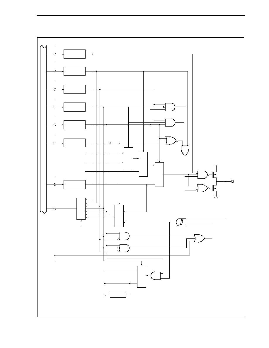
CHAPTER 4 PORT FUNCTIONS
Preliminary User's Manual U17714EJ1V0UD
163
Figure 4-27. Block Diagram of Type U-7
Input signal 1 when
alternate function is used
RD
WR
PORT
Pmn
WR
PFC
PFCmn
WR
PF
PFmn
WR
OCDM0
OCDM0
WR
PMC
PMCmn
WR
PM
PMmn
Input signal 2-1 when
alternate function is used
Input signal 2-2 when
alternate function is used
Output signal when
on-chip debugging
Pmn
EV
DD
EV
SS
P-ch
N-ch
WR
PFCE
PFCEmn
Note
Inter
nal b
u
s
Selector
Selector
Selector
Selector
Selector
Selector
Address
Output signal 2 when
alternate function is used
Output signal 1 when
alternate function is used
Noise
elimination
Note Hysteresis characteristics are not available in port mode.
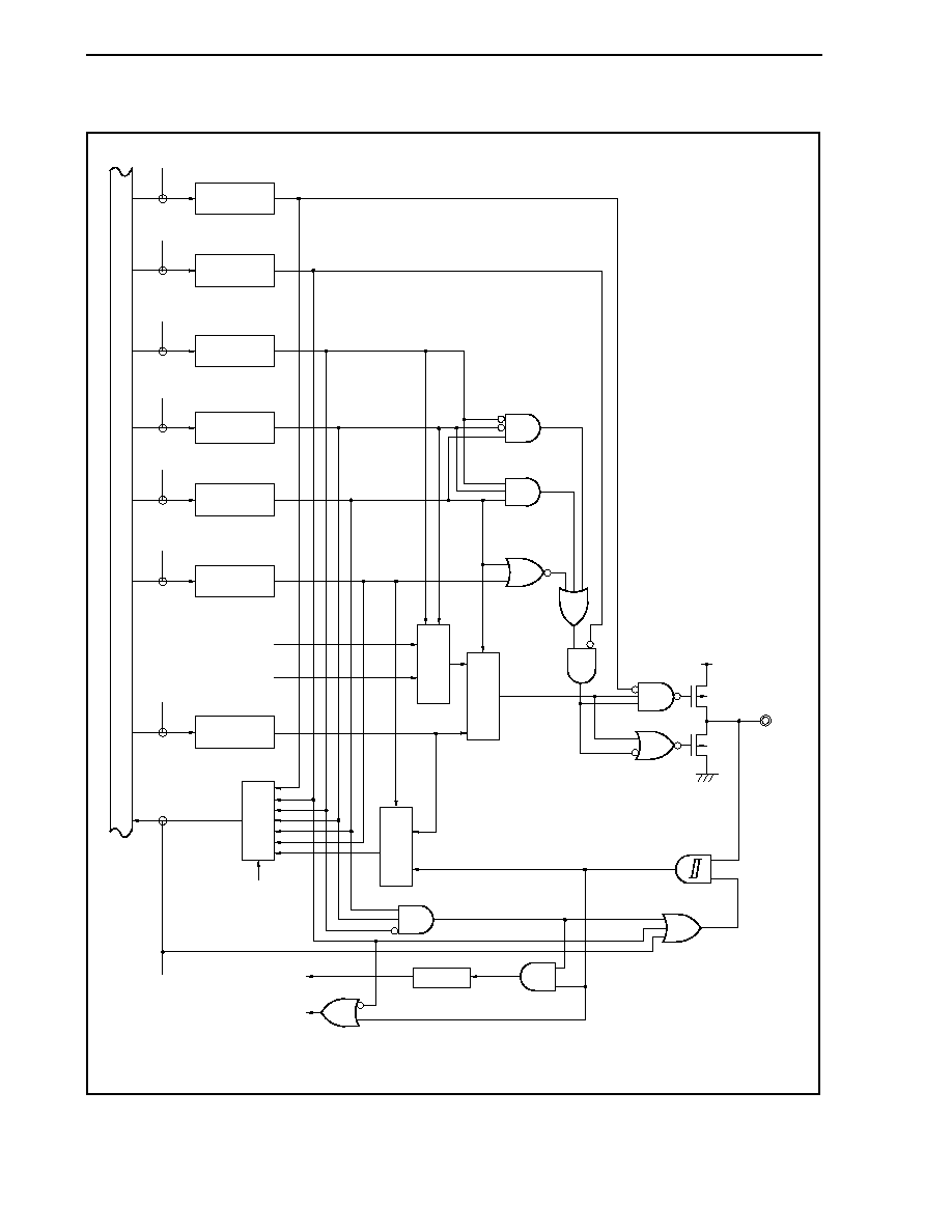
CHAPTER 4 PORT FUNCTIONS
Preliminary User's Manual U17714EJ1V0UD
164
Figure 4-28. Block Diagram of Type U-8
Input signal when
alternate function is used
RD
WR
PORT
Pmn
WR
PFC
PFCmn
WR
PF
PFmn
WR
OCDM0
OCDM0
WR
PMC
PMCmn
WR
PM
PMmn
Input signal when
on-chip debugging
Pmn
EV
DD
EV
SS
P-ch
N-ch
WR
PFCE
PFCEmn
Note
Inter
nal b
u
s
Selector
Selector
Selector
Selector
Address
Output signal 2 when
alternate function is used
Output signal 1 when
alternate function is used
Noise
elimination
Note Hysteresis characteristics are not available in port mode.
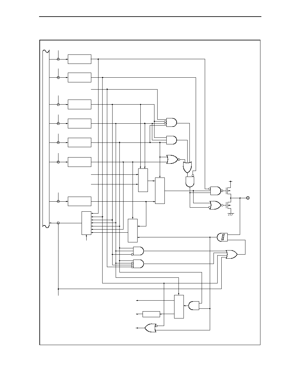
CHAPTER 4 PORT FUNCTIONS
Preliminary User's Manual U17714EJ1V0UD
165
Figure 4-29. Block Diagram of Type U-9
Input signal 1 when
alternate function is used
RD
WR
PORT
Pmn
WR
PFC
PFCmn
WR
PF
PFmn
WR
OCDM0
OCDM0
WR
PMC
PMCmn
WR
PM
PMmn
Input signal 2 when
alternate function is used
Input signal when
on-chip debugging
Output enable signal when
alternate function is used
Pmn
EV
DD
EV
SS
P-ch
N-ch
WR
PFCE
PFCEmn
Note
Inter
nal b
u
s
Selector
Selector
Selector
Selector
Selector
Address
Output signal 2 when
alternate function is used
Output signal 1 when
alternate function is used
Noise
elimination
Note Hysteresis characteristics are not available in port mode.
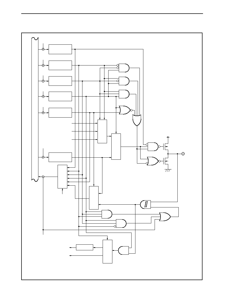
CHAPTER 4 PORT FUNCTIONS
Preliminary User's Manual U17714EJ1V0UD
166
Figure 4-30. Block Diagram of Type U-10
Inter
nal b
u
s
Address
Input signal 1 when
alternate function is used
Selector
Selector
Selector
Selector
RD
WR
PORT
Pmn
WR
PFC
PFCmn
WR
PF
PFmn
WR
PMC
PMCmn
WR
PM
PMmn
Input signal 2 when
alternate function is used
Output signal 2 when
alternate function is used
Output signal 3 when
alternate function is used
Output signal 1 when
alternate function is used
Pmn
EV
DD
EV
SS
P-ch
N-ch
WR
PFCE
PFCEmn
Noise
elimination
Note
Selector
Note Hysteresis characteristics are not available in port mode.
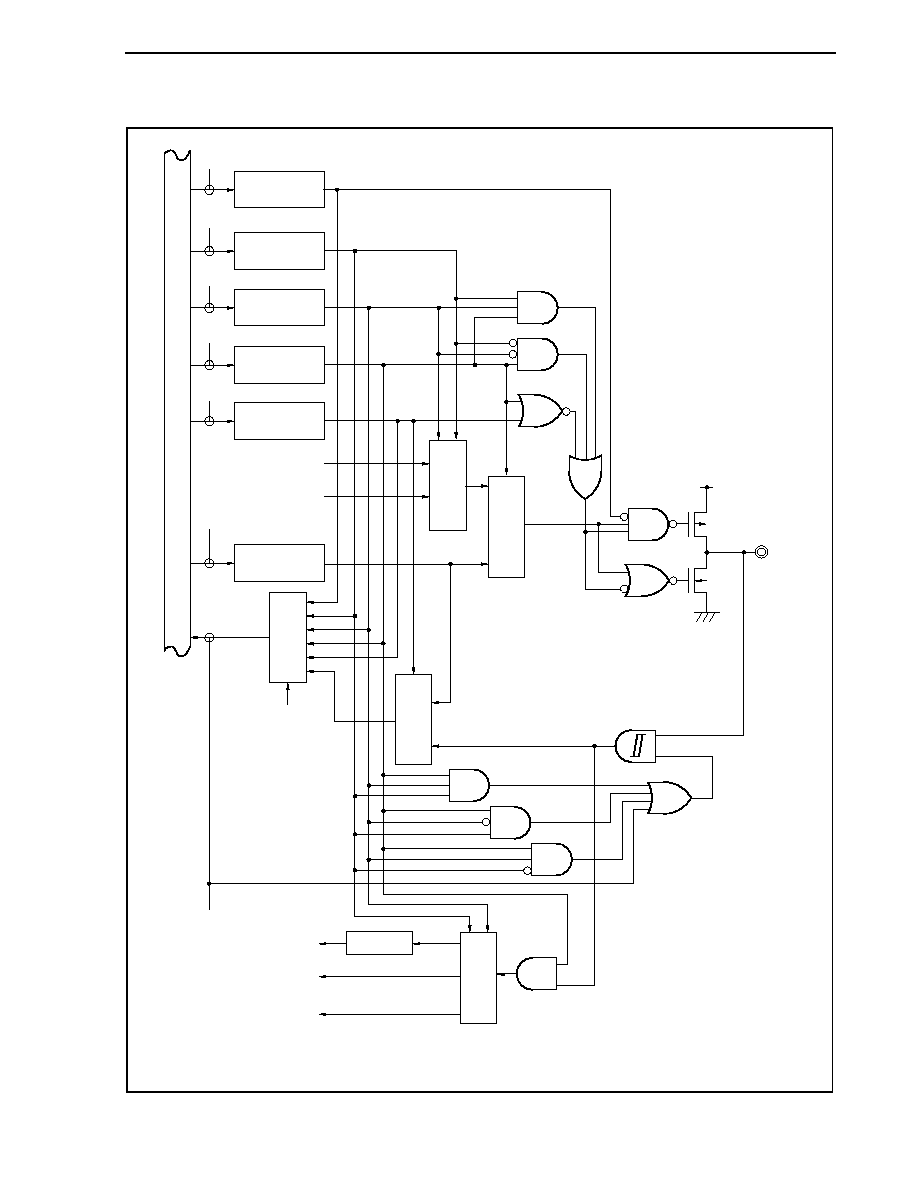
CHAPTER 4 PORT FUNCTIONS
Preliminary User's Manual U17714EJ1V0UD
167
Figure 4-31. Block Diagram of Type U-11
Inter
nal b
u
s
Address
Input signal 1 when
alternate function is used
Selector
Selector
Selector
Selector
RD
WR
PORT
Pmn
WR
PFC
PFCmn
WR
PF
PFmn
WR
PMC
PMCmn
WR
PM
PMmn
Input signal 3 when
alternate function is used
Output signal 2 when
alternate function is used
Output signal 1 when
alternate function is used
Pmn
Input signal 2 when
alternate function is used
EV
DD
EV
SS
P-ch
N-ch
WR
PFCE
PFCEmn
Noise
elimination
Note
Selector
Note Hysteresis characteristics are not available in port mode.
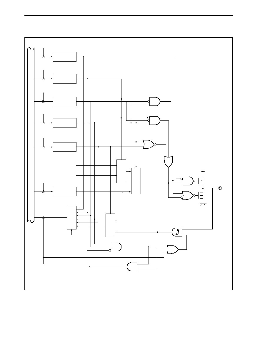
CHAPTER 4 PORT FUNCTIONS
Preliminary User's Manual U17714EJ1V0UD
168
Figure 4-32. Block Diagram of Type U-12
Input signal when
alternate function is used
RD
WR
PORT
Pmn
WR
PFC
PFCmn
WR
PF
PFmn
WR
PMC
PMCmn
WR
PM
PMmn
Output signal 2 when
alternate function is used
Output signal 1 when
alternate function is used
Pmn
EV
DD
EV
SS
P-ch
N-ch
WR
PFCE
PFCEmn
Note
Inter
nal b
u
s
Selector
Selector
Selector
Selector
Address
Note Hysteresis characteristics are not available in port mode.
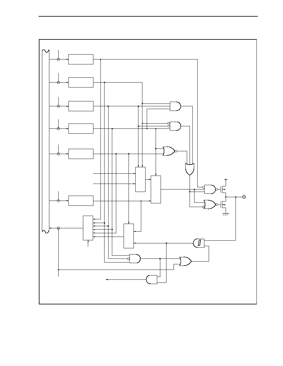
CHAPTER 4 PORT FUNCTIONS
Preliminary User's Manual U17714EJ1V0UD
169
Figure 4-33. Block Diagram of Type U-13
Input signal when
alternate function is used
RD
WR
PORT
Pmn
WR
PFC
PFCmn
WR
PF
PFmn
WR
PMC
PMCmn
WR
PM
PMmn
Output signal 2 when
alternate function is used
Output signal 1 when
alternate function is used
Pmn
EV
DD
EV
SS
P-ch
N-ch
WR
PFCE
PFCEmn
Note
Inter
nal b
u
s
Selector
Selector
Selector
Selector
Address
Note Hysteresis characteristics are not available in port mode.
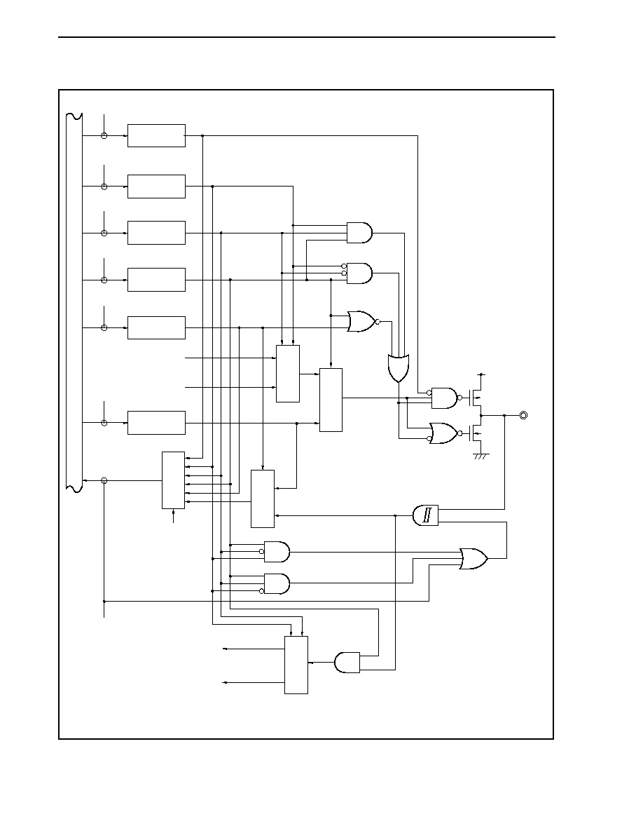
CHAPTER 4 PORT FUNCTIONS
Preliminary User's Manual U17714EJ1V0UD
170
Figure 4-34. Block Diagram of Type U-14
Input signal 1 when
alternate function is used
RD
WR
PORT
Pmn
WR
PFC
PFCmn
WR
PF
PFmn
WR
PMC
PMCmn
WR
PM
PMmn
Input signal 2 when
alternate function is used
Output signal 2 when
alternate function is used
Output signal 1 when
alternate function is used
Pmn
EV
DD
EV
SS
P-ch
N-ch
WR
PFCE
PFCEmn
Note
Inter
nal b
u
s
Selector
Selector
Selector
Selector
Address
Selector
Note Hysteresis characteristics are not available in port mode.
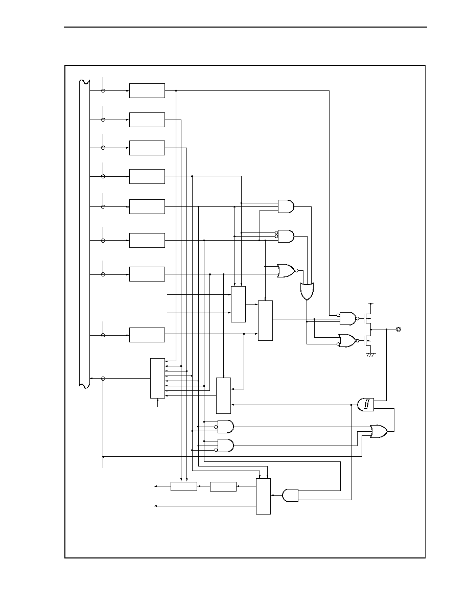
CHAPTER 4 PORT FUNCTIONS
Preliminary User's Manual U17714EJ1V0UD
171
Figure 4-35. Block Diagram of Type U-15
Input signal 1 when
alternate function is used
Input signal 2 when
alternate function is used
RD
WR
PORT
Pmn
WR
PMC
PMCmn
WR
INTR
INTRmn
Note 1
WR
INTF
INTFmn
Note 1
WR
PF
PFmn
WR
PM
WR
PFC
PFCmn
WR
PFCE
PFCEmn
PMmn
Pmn
EV
DD
EV
SS
P-ch
N-ch
Output signal 2 when
alternate function is used
Output signal 1 when
alternate function is used
Note 2
Inter
nal b
u
s
Selector
Selector
Selector
Selector
Address
Edge
detection
Noise
elimination
Selector
Notes 1. See
19.6 External Interrupt Request Input Pins (NMI and INTP0 to INTP8).
2. Hysteresis characteristics are not available in port mode.
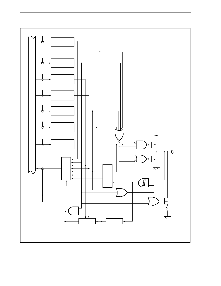
CHAPTER 4 PORT FUNCTIONS
Preliminary User's Manual U17714EJ1V0UD
172
Figure 4-36. Block Diagram of Type AA-1
RD
WR
PORT
Pmn
WR
INTF
INTFmn
Note 1
WR
PF
PFmn
WR
OCDM0
OCDM0
WR
PMC
PMCmn
WR
PM
PMmn
Pmn
EV
DD
EV
SS
P-ch
N-ch
N-ch
WR
INTR
INTRmn
Note 1
EV
SS
Input signal when
on-chip debugging
External
reset signal
Input signal when
alternate function is used
Note 2
Inter
nal b
u
s
Selector
Selector
Address
Edge
detection
Noise
elimination
Notes 1. See
19.6 External Interrupt Request Input Pins (NMI and INTP0 to INTP8).
2. Hysteresis characteristics are not available in port mode.
4.5 Port Register Settings When Alternate Function Is Used
Table 4-19 shows the port register settings when each port is used for an alternate function. When using a port pin
as an alternate-function pin, refer to the description of each pin.

CHAPTER
4 P
O
RT
FU
NCTI
O
NS
Preliminary
User's Manual
U17714EJ
1
V0UD
173
Table 4-19. Using Port Pin as Alternate-Function Pin (1/8)
Alternate Function
Pin Name
Name I/O
Pnx Bit of
Pn Register
PMnx Bit of
PMn Register
PMCnx Bit of
PMCn Register
PFCEnx Bit of
PFCEn Register
PFCnx Bit of
PFCn Register
Other Bits
(Registers)
TIP61 Input
P00 = Setting not required
PM00 = Setting not required
PMC00 = 1
-
PFC00 = 0
P00
TOP61 Output
P00 = Setting not required
PM00 = Setting not required
PMC00 = 1
-
PFC00 = 1
TIP60 Input
P01 = Setting not required
PM01 = Setting not required
PMC01 = 1
-
PFC01 = 0
P01
TOP60 Output
P01 = Setting not required
PM01 = Setting not required
PMC01 = 1
-
PFC01 = 1
P02 NMI Input
P02 = Setting not required
PM02 = Setting not required
PMC02 = 1
-
-
INTP0 Input
P03 = Setting not required
PM03 = Setting not required
PMC03 = 1
-
PFC03 = 0
P03
ADTRG Input
P03 = Setting not required
PM03 = Setting not required
PMC03 = 1
-
PFC03 = 1
P04 INTP1
Input
P04 = Setting not required
PM04 = Setting not required
PMC04 = 1
-
-
INTP2 Input
P05 = Setting not required
PM05 = Setting not required
PMC05 = 1
-
-
P05
DRST Input
P05 = Setting not required
PM05 = Setting not required
PMC05 = Setting not required
-
-
OCDM0 (OCDM) = 1
P06 INTP3
Input
P06 = Setting not required
PM06 = Setting not required
PMC06 = 1
-
-
P10 ANO0
Output
P10 = Setting not required
PM10 = 1
-
-
-
P11 ANO1
Output
P11 = Setting not required
PM11 = 1
-
-
-
TXDA0 Output
P30 = Setting not required
PM30 = Setting not required
PMC30 = 1
-
PFC30 = 0
P30
SOB4 Output
P30 = Setting not required
PM30 = Setting not required
PMC30 = 1
-
PFC30 = 1
RXDA0 Input
P31 = Setting not required
PM31 = Setting not required
PMC31 = 1
-
Note, PFC31 = 0
INTP7 Input
P31 = Setting not required
PM31 = Setting not required
PMC31 = 1
-
Note, PFC31 = 0
P31
SIB4 Input
P31 = Setting not required
PM31 = Setting not required
PMC31 = 1
-
PFC31 = 1
ASCKA0 Input
P32 = Setting not required
PM32 = Setting not required
PMC32 = 1
PFCE32 = 0
PFC32 = 0
SCKB4 I/O
P32 = Setting not required
PM32 = Setting not required
PMC32 = 1
PFCE32 = 0
PFC32 = 1
TIP00 Input
P32 = Setting not required
PM32 = Setting not required
PMC32 = 1
PFCE32 = 1
PFC32 = 0
P32
TOP00 Output
P32 = Setting not required
PM32 = Setting not required
PMC32 = 1
PFCE32 = 1
PFC32 = 1
Note The INTP7 pin and RXDA0 pin are alternate-function pins. When using the pin as the RXDA0 pin, disable edge detection for the INTP7 alternate-function pin.
(Clear the INTF3.INTF31 bit and the INRT3.INTR31 bit to 0.) When using the pin as the INTP7 pin, stop UARTA0 reception. (Clear the UA0CTL0.UA0RXE bit
to 0.)
Caution Between the P10 and P11 pins, when one pin is used as the I/O port, and the other pin is used as the D/A output pin (ANO0, ANO1), make sure
that the port I/O level does not change during D/A output.

CHAPTER
4 P
O
RT
FU
NCTI
O
NS
174
Preliminary
User's Manual
U17714EJ
1
V0UD
Table 4-19. Using Port Pin as Alternate-Function Pin (2/8)
Alternate Function
Pin Name
Name I/O
Pnx Bit of
Pn Register
PMnx Bit of
PMn Register
PMCnx Bit of
PMCn Register
PFCEnx Bit of
PFCEn Register
PFCnx Bit of
PFCn Register
Other Bits
(Registers)
TIP01 Input
P33 = Setting not required
PM33 = Setting not required
PMC33 = 1
-
PFC33 = 0
P33
TOP01 Output
P33 = Setting not required
PM33 = Setting not required
PMC33 = 1
-
PFC33 = 1
TIP10 Input
P34 = Setting not required
PM34 = Setting not required
PMC34 = 1
-
PFC34 = 0
P34
TOP10 Input
P34 = Setting not required
PM34 = Setting not required
PMC34 = 1
-
PFC34 = 1
TIP11 Input
P35 = Setting not required
PM35 = Setting not required
PMC35 = 1
-
PFC35 = 0
P35
TOP11 Output
P35 = Setting not required
PM35 = Setting not required
PMC35 = 1
-
PFC35 = 1
TXDA2 Output
P38 = Setting not required
PM38 = Setting not required
PMC38 = 1
-
PFC38 = 0
P38
SDA00 I/O
P38 = Setting not required
PM38 = Setting not required
PMC38 = 1
-
PFC38 = 1
RXDA2 Input
P39 = Setting not required
PM39 = Setting not required
PMC39 = 1
-
PFC39 = 0
P39
SCL00 I/O
P39 = Setting not required
PM39 = Setting not required
PMC39 = 1
-
PFC39 = 1
SIB0 Input
P40 = Setting not required
PM40 = Setting not required
PMC40 = 1
-
PFC40 = 0
P40
SDA01 I/O
P40 = Setting not required
PM40 = Setting not required
PMC40 = 1
-
PFC40 = 1
SOB0 Output
P41 = Setting not required
PM41 = Setting not required
PMC41 = 1
-
PFC41 = 0
P41
SCL01 I/O
P41 = Setting not required
PM41 = Setting not required
PMC41 = 1
-
PFC41 = 1
P42 SCKB0
I/O
P42 = Setting not required
PM42 = Setting not required
PMC42 = 1
-
-
TIQ01 Input
P50 = Setting not required
PM50 = Setting not required
PMC50 = 1
PFCE50 = 0
PFC50 = 1
KRM0 (KRM) = 0
KR0 Input
P50 = Setting not required
PM50 = Setting not required
PMC50 = 1
PFCE50 = 0
PFC50 = 1
TQ0TIG2, TQ0TIG3 (TQ0IOC1) = 0
TOQ01
Output
P50 = Setting not required
PM50 = Setting not required
PMC50 = 1
PFCE50 = 1
PFC50 = 0
P50
RTP00 Output
P50 = Setting not required
PM50 = Setting not required
PMC50 = 1
PFCE50 = 1
PFC50 = 1
TIQ02 Input
P51 = Setting not required
PM51 = Setting not required
PMC51 = 1
PFCE51 = 0
PFC51 = 1
KRM1 (KRM) = 0
KR1 Input
P51 = Setting not required
PM51 = Setting not required
PMC51 = 1
PFCE51 = 0
PFC51 = 1
TQ0TIG4, TQ0TIG5 (TQ0IOC1) = 0
TOQ02 Output
P51 = Setting not required
PM51 = Setting not required
PMC51 = 1
PFCE51 = 1
PFC51 = 0
P51
RTP01 Output
P51 = Setting not required
PM51 = Setting not required
PMC51 = 1
PFCE51 = 1
PFC51 = 1
TIQ03
Input
P52 = Setting not required
PM52 = Setting not required
PMC52 = 1
PFCE52 = 0
PFC52 = 1
KRM2 (KRM) = 0
KR2 Input
P52 = Setting not required
PM52 = Setting not required
PMC52 = 1
PFCE52 = 0
PFC52 = 1
TQ0TIG6, TQ0TIG7 (TQ0I0C1) = 0
TOQ03 Output
P52 = Setting not required
PM52 = Setting not required
PMC52 = 1
PFCE52 = 1
PFC52 = 0
RTP02 Output
P52 = Setting not required
PM52 = Setting not required
PMC52 = 1
PFCE52 = 1
PFC52 = 1
P52
DDI Input
P52 = Setting not required
PM52 = Setting not required
PMC52 = Setting not required
PFCE52 = Setting not required
PFC52 = Setting not required
OCDM0 (OCDM) = 1

CHAPTER
4 P
O
RT
FU
NCTI
O
NS
Preliminary
User's Manual
U17714EJ
1
V0UD
175
Table 4-19. Using Port Pin as Alternate-Function Pin (3/8)
Alternate Function
Pin Name
Name I/O
Pnx Bit of
Pn Register
PMnx Bit of
PMn Register
PMCnx Bit of
PMCn Register
PFCEnx Bit of
PFCEn Register
PFCnx Bit of
PFCn Register
Other Bits
(Registers)
SIB2
Input
P53 = Setting not required
PM53 = Setting not required
PMC53 = 1
PFCE53 = 0
PFC53 = 0
TIQ00 Input
P53 = Setting not required
PM53 = Setting not required
PMC53 = 1
PFCE53 = 0
PFC53 = 1
KRM3 (KRM) = 0
KR3 Input
P53 = Setting not required
PM53 = Setting not required
PMC53 = 1
PFCE53 = 0
PFC53 = 1
TQ0TIG0, TQ0TIG1 (TQ0IOC1) = 0,
TQ0EES0, TQ0EES1 (TQ0IOC2) = 0,
TQ0ETS0, TQ0ETS1 (TQ0IOC2) = 0
TOQ00 Input
P53 = Setting not required
PM53 = Setting not required
PMC53 = 1
PFCE53 = 1
PFC53 = 0
RTP03 Output
P53 = Setting not required
PM53 = Setting not required
PMC53 = 1
PFCE53 = 1
PFC53 = 1
P53
DDO Output
P53 = Setting not required
PM53 = Setting not required
PMC53 = Setting not required
PFCE53 = Setting not required
PFC53 = Setting not required
OCDM0 (OCDM) = 1
SOB2
Output
P54 = Setting not required
PM54 = Setting not required
PMC54 = 1
PFCE54 = 0
PFC54 = 0
KR4 Input
P54 = Setting not required
PM54 = Setting not required
PMC54 = 1
PFCE54 = 0
PFC54 = 1
RTP04 Output
P54 = Setting not required
PM54 = Setting not required
PMC54 = 1
PFCE54 = 1
PFC54 = 1
P54
DCK Input
P54 = Setting not required
PM54 = Setting not required
PMC54 = Setting not required
PFCE54 = Setting not required
PFC54 = Setting not required
OCDM0 (OCDM) = 1
SCKB2
I/O
P55 = Setting not required
PM55 = Setting not required
PMC55 = 1
PFCE55 = 0
PFC55 = 0
KR5 Input
P55 = Setting not required
PM55 = Setting not required
PMC55 = 1
PFCE55 = 0
PFC55 = 1
RTP05 Output
P55 = Setting not required
PM55 = Setting not required
PMC55 = 1
PFCE55 = 1
PFC55 = 1
P55
DMS Input
P55 = Setting not required
PM55 = Setting not required
PMC55 = Setting not required
PFCE55 = Setting not required
PFC55 = Setting not required
OCDM0 (OCDM) = 1
P60 RTP10
Output
P60 = Setting not required
PM60 = Setting not required
PMC60 = 1
-
-
P61 RTP11
Output
P61 = Setting not required
PM61 = Setting not required
PMC61 = 1
-
-
P62 RTP12
Output
P62 = Setting not required
PM62 = Setting not required
PMC62 = 1
-
-
P63 RTP13
Output
P63 = Setting not required
PM63 = Setting not required
PMC63 = 1
-
-
P64 RTP14
Output
P64 = Setting not required
PM64 = Setting not required
PMC64 = 1
-
-
P65 RTP15
Output
P65 = Setting not required
PM65 = Setting not required
PMC65 = 1
-
-
P66 SIB5 Input
P66 = Setting not required
PM66 = Setting not required
PMC66 = 1
-
-
P67 SOB5
Output
P67 = Setting not required
PM67 = Setting not required
PMC67 = 1
-
-
P68 SCKB5
I/O
P68 = Setting not required
PM68 = Setting not required
PMC68 = 1
-
-
TIP70 Input
P69 = Setting not required
PM69 = Setting not required
PMC69 = 1
-
PFC69 = 0
P69
TOP70 Output
P69 = Setting not required
PM69 = Setting not required
PMC69 = 1
-
PFC69 = 1
P610 TIP71 Input
P610 = Setting not required
PM610 = Setting not required
PMC610 = 1
-
-
P611 TOP71
Output
P611 = Setting not required
PM611 = Setting not required
PMC611 = 1
-
-

CHAPTER
4 P
O
RT
FU
NCTI
O
NS
176
Preliminary
User's Manual
U17714EJ
1
V0UD
Table 4-19. Using Port Pin as Alternate-Function Pin (4/8)
Alternate Function
Pin Name
Name I/O
Pnx Bit of
Pn Register
PMnx Bit of
PMn Register
PMCnx Bit of
PMCn Register
PFCEnx Bit of
PFCEn Register
PFCnx Bit of
PFCn Register
Other Bits
(Registers)
TIP80 Input
P612 = Setting not required
PM612 = Setting not required
PMC612 = 1
-
PFC612 = 0
P612
TOP80 Output
P612 = Setting not required
PM612 = Setting not required
PMC612 = 1
-
PFC612 = 1
TIP81 Input
P613 = Setting not required
PM613 = Setting not required
PMC613 = 1
-
PFC613 = 0
P613
TOP81 Output
P613 = Setting not required
PM613 = Setting not required
PMC613 = 1
-
PFC613 = 1
P70 ANI0 Input
P70 = Setting not required
PM70 = 1
-
-
-
P71 ANI1 Input
P71 = Setting not required
PM71 = 1
-
-
-
P72 ANI2 Input
P72 = Setting not required
PM72 = 1
-
-
-
P73 ANI3 Input
P73 = Setting not required
PM73 = 1
-
-
-
P74 ANI4 Input
P74 = Setting not required
PM74 = 1
-
-
-
P75 ANI5 Input
P75 = Setting not required
PM75 = 1
-
-
-
P76 ANI6 Input
P76 = Setting not required
PM76 = 1
-
-
-
P77 ANI7 Input
P77 = Setting not required
PM77 = 1
-
-
-
P78 ANI8 Input
P78 = Setting not required
PM78 = 1
-
-
-
P79 ANI9 Input
P79 = Setting not required
PM79 = 1
-
-
-
P710 ANI10 Input
P710 = Setting not required
PM710 = 1
-
-
-
P711 ANI11 Input
P711 = Setting not required
PM711 = 1
-
-
-
P712 ANI12 Input
P712 = Setting not required
PM712 = 1
-
-
-
P713 ANI13 Input
P713 = Setting not required
PM713 = 1
-
-
-
P714 ANI14 Input
P714 = Setting not required
PM714 = 1
-
-
-
P715 ANI15 Input
P715 = Setting not required
PM715 = 1
-
-
-
RXDA3 Input
P80 = Setting not required
PM80 = Setting not required
PMC80 = 1
-
-
Note
P80
INTP8 Input
P80 = Setting not required
PM80 = Setting not required
PMC80 = 1
-
-
Note
P81 TXDA3
Output
P81 = Setting not required
PM81 = Setting not required
PMC81 = 1
-
-
Note The INTP8 pin and RXDA3 pin are alternate-function pins. When using the pin as the RXDA3 pin, disable edge detection for the INTP8 alternate-function pin.
(Clear the INTF8.INTF80 bit and the INTR8.INTR80 bit to 0.) When using the pin as the INTP8 pin, stop UARTA3 reception. (Clear the UA0CTL3.UA3RXE bit
to 0.)

CHAPTER
4 P
O
RT
FU
NCTI
O
NS
Preliminary
User's Manual
U17714EJ
1
V0UD
177
Table 4-19. Using Port Pin as Alternate-Function Pin (5/8)
Alternate Function
Pin Name
Name I/O
Pnx Bit of
Pn Register
PMnx Bit of
PMn Register
PMCnx Bit of
PMCn Register
PFCEnx Bit of
PFCEn Register
PFCnx Bit of
PFCn Register
Other Bits
(Registers)
A0 Output
P90 = Setting not required
PM90 = Setting not required
PMC90 = 1
PFCE90 = 0
PFC90 = 0
Note 1
KR6 Input
P90 = Setting not required
PM90 = Setting not required
PMC90 = 1
PFCE90 = 0
PFC90 = 1
TXDA1 Output
P90 = Setting not required
PM90 = Setting not required
PMC90 = 1
PFCE90 = 1
PFC90 = 0
P90
SDA02 I/O
P90 = Setting not required
PM90 = Setting not required
PMC90 = 1
PFCE90 = 1
PFC90 = 1
A1 Output
P91 = Setting not required
PM91 = Setting not required
PMC91 = 1
PFCE91 = 0
PFC91 = 0
Note 1
KR7 Input
P91 = Setting not required
PM91 = Setting not required
PMC91 = 1
PFCE91 = 0
PFC91 = 1
RXDA1/KR7
Note 2
Input
P91 = Setting not required
PM91 = Setting not required
PMC91 = 1
PFCE91 = 1
PFC91 = 0
P91
SCL02 I/O
P91 = Setting not required
PM91 = Setting not required
PMC91 = 1
PFCE91 = 1
PFC91 = 1
A2 Output
P92 = Setting not required
PM92 = Setting not required
PMC92 = 1
PFCE92 = 0
PFC92 = 0
Note 1
TIP41 Input
P92 = Setting not required
PM92 = Setting not required
PMC92 = 1
PFCE92 = 0
PFC92 = 1
P92
TOP41 Output
P92 = Setting not required
PM92 = Setting not required
PMC92 = 1
PFCE92 = 1
PFC92 = 0
A3 Output
P93 = Setting not required
PM93 = Setting not required
PMC93 = 1
PFCE93 = 0
PFC93 = 0
Note 1
TIP40 Input
P93 = Setting not required
PM93 = Setting not required
PMC93 = 1
PFCE93 = 0
PFC93 = 1
P93
TOP40 Output
P93 = Setting not required
PM93 = Setting not required
PMC93 = 1
PFCE93 = 1
PFC93 = 0
A4 Output
P94 = Setting not required
PM94 = Setting not required
PMC94 = 1
PFCE94 = 0
PFC94 = 0
Note 1
TIP31 Input
P94 = Setting not required
PM94 = Setting not required
PMC94 = 1
PFCE94 = 0
PFC94 = 1
P94
TOP31 Output
P94 = Setting not required
PM94 = Setting not required
PMC94 = 1
PFCE94 = 1
PFC94 = 0
A5 Output
P95 = Setting not required
PM95 = Setting not required
PMC95 = 1
PFCE95 = 0
PFC95 = 0
Note 1
TIP30 Input
P95 = Setting not required
PM95 = Setting not required
PMC95 = 1
PFCE95 = 0
PFC95 = 1
P95
TOP30 Output
P95 = Setting not required
PM95 = Setting not required
PMC95 = 1
PFCE95 = 1
PFC95 = 0
A6 Output
P96 = Setting not required
PM96 = Setting not required
PMC96 = 1
PFCE96 = 0
PFC96 = 0
Note 1
TIP21 Input
P96 = Setting not required
PM96 = Setting not required
PMC96 = 1
PFCE96 = 1
PFC96 = 0
P96
TOP21 Output
P96 = Setting not required
PM96 = Setting not required
PMC96 = 1
PFCE96 = 1
PFC96 = 1
Notes 1. When setting pins A0 to A15 as the alternate function, set the PMC9 register to FFFFH for all 16 bits at once.
2. The RXDA1 and KR7 pins must not be used at the same time. When using the RXDA1 pin, do not use the KR7 pin. When using the KR7 pin, do not use
the RXDA1 pin (it is recommended to set the PFC91 bit to 1 and clear the PFCE91 bit to 0).

CHAPTER
4 P
O
RT
FU
NCTI
O
NS
178
Preliminary
User's Manual
U17714EJ
1
V0UD
Table 4-19. Using Port Pin as Alternate-Function Pin (6/8)
Alternate Function
Pin Name
Name I/O
Pnx Bit of
Pn Register
PMnx Bit of
PMn Register
PMCnx Bit of
PMCn Register
PFCEnx Bit of
PFCEn Register
PFCnx Bit of
PFCn Register
Other Bits
(Registers)
A7 Output
P97 = Setting not required
PM97 = Setting not required
PMC97 = 1
PFCE97 = 0
PFC97 = 0
Note
SIB1 Input
P97 = Setting not required
PM97 = Setting not required
PMC97 = 1
PFCE97 = 0
PFC97 = 1
TIP20 Input
P97 = Setting not required
PM97 = Setting not required
PMC97 = 1
PFCE97 = 1
PFC97 = 0
P97
TOP20 Output
P97 = Setting not required
PM97 = Setting not required
PMC97 = 1
PFCE97 = 1
PFC97 = 1
A8 Output
P98 = Setting not required
PM98 = Setting not required
PMC98 = 1
-
PFC98 = 0
Note
P98
SOB1 Output
P98 = Setting not required
PM98 = Setting not required
PMC98 = 1
-
PFC98 = 1
A9 Output
P99 = Setting not required
PM99 = Setting not required
PMC99 = 1
-
PFC99 = 0
Note
P99
SCKB1 I/O
P99 = Setting not required
PM99 = Setting not required
PMC99 = 1
-
PFC99 = 1
A10 Output
P910 = Setting not required
PM910 = Setting not required
PMC910 = 1
-
PFC910 = 0
Note
P910
SIB3 Input
P910 = Setting not required
PM910 = Setting not required
PMC910 = 1
-
PFC910 = 1
A11 Output
P911 = Setting not required
PM911 = Setting not required
PMC911 = 1
-
PFC911 = 0
Note
P911
SOB3 Output
P911 = Setting not required
PM911 = Setting not required
PMC911 = 1
-
PFC911 = 1
A12 Output
P912 = Setting not required
PM912 = Setting not required
PMC912 = 1
-
PFC912 = 0
Note
P912
SCKB3 I/O
P912 = Setting not required
PM912 = Setting not required
PMC912 = 1
-
PFC912 = 1
A13 Output
P913 = Setting not required
PM913 = Setting not required
PMC913 = 1
-
PFC913 = 0
Note
P913
INTP4 Input
P913 = Setting not required
PM913 = Setting not required
PMC913 = 1
-
PFC913 = 1
A14 Output
P914 = Setting not required
PM914 = Setting not required
PMC914 = 1
PFCE914 = 0
PFC914 = 0
Note
INTP5 Input
P914 = Setting not required
PM914 = Setting not required
PMC914 = 1
PFCE914 = 0
PFC914 = 1
TIP51 Input
P914 = Setting not required
PM914 = Setting not required
PMC914 = 1
PFCE914 = 1
PFC914 = 0
P914
TOP51 Output
P914 = Setting not required
PM914 = Setting not required
PMC914 = 1
PFCE914 = 1
PFC914 = 1
A15 Output
P915 = Setting not required
PM915 = Setting not required
PMC915 = 1
PFCE915 = 0
PFC915 = 0
Note
INTP6 Input
P915 = Setting not required
PM915 = Setting not required
PMC915 = 1
PFCE915 = 0
PFC915 = 1
TIP50 Input
P915 = Setting not required
PM915 = Setting not required
PMC915 = 1
PFCE915 = 1
PFC915 = 0
P915
TOP50 Output
P915 = Setting not required
PM915 = Setting not required
PMC915 = 1
PFCE915 = 1
PFC915 = 1
PCS0 CS0 Output
PCS0 = Setting not required
PMCS0 = Setting not required
PMCCS0 = 1
-
-
PCS1 CS1 Output
PCS1 = Setting not required
PMCS1 = Setting not required
PMCCS1 = 1
-
-
PCS2 CS2 Output
PCS2 = Setting not required
PMCS2 = Setting not required
PMCCS2 = 1
-
-
PCS3 CS3 Output
PCS3 = Setting not required
PMCS3 = Setting not required
PMCCS3 = 1
-
-
Note When setting pins A0 to A15 as the alternate function, set the PMC9 register to FFFFH for all 16 bits at once.

CHAPTER
4 P
O
RT
FU
NCTI
O
NS
Preliminary
User's Manual
U17714EJ
1
V0UD
179
Table 4-19. Using Port Pin as Alternate-Function Pin (7/8)
Alternate Function
Pin Name
Name I/O
Pnx Bit of
Pn Register
PMnx Bit of
PMn Register
PMCnx Bit of
PMCn Register
PFCEnx Bit of
PFCEn Register
PFCnx Bit of
PFCn Register
Other Bits
(Registers)
PCM0 WAIT Input
PCM0 = Setting not required
PMCM0 = Setting not required
PMCCM0 = 1
-
-
PCM1 CLKOUT
Output
PCM1 = Setting not required
PMCM1 = Setting not required
PMCCM1 = 1
-
-
PCM2 HLDAK
Output
PCM2 = Setting not required
PMCM2 = Setting not required
PMCCM2 = 1
-
-
PCM3 HLDRQ
Input
PCM3 = Setting not required
PMCM3 = Setting not required
PMCCM3 = 1
-
-
PCT0 WR0 Output
PCT0 = Setting not required
PMCT0 = Setting not required
PMCCT0 = 1
-
-
PCT1 WR1 Output
PCT1 = Setting not required
PMCT1 = Setting not required
PMCCT1 = 1
-
-
PCT4 RD
Output
PCT4 = Setting not required
PMCT4 = Setting not required
PMCCT4 = 1
-
-
PCT6 ASTB Output
PCT6 = Setting not required
PMCT6 = Setting not required
PMCCT6 = 1
-
-
PDH0 A16 Output
PDH0 = Setting not required
PMDH0 = Setting not required
PMCDH0 = 1
-
-
PDH1 A17 Output
PDH1 = Setting not required
PMDH1 = Setting not required
PMCDH1 = 1
-
-
PDH2 A18 Output
PDH2 = Setting not required
PMDH2 = Setting not required
PMCDH2 = 1
-
-
PDH3 A19 Output
PDH3 = Setting not required
PMDH3 = Setting not required
PMCDH3 = 1
-
-
PDH4 A20 Output
PDH4 = Setting not required
PMDH4 = Setting not required
PMCDH4 = 1
-
-
PDH5 A21 Output
PDH5 = Setting not required
PMDH5 = Setting not required
PMCDH5 = 1
-
-
PDH6 A22 Output
PDH6 = Setting not required
PMDH6 = Setting not required
PMCDH6 = 1
-
-
PDH7 A23 Output
PDH7 = Setting not required
PMDH7 = Setting not required
PMCDH7 = 1
-
-
PDL0 AD0 I/O
PDL0 = Setting not required
PMDL0 = Setting not required
PMCDL0 = 1
-
-
PDL1 AD1 I/O
PDL1 = Setting not required
PMDL1 = Setting not required
PMCDL1 = 1
-
-
PDL2 AD2 I/O
PDL2 = Setting not required
PMDL2 = Setting not required
PMCDL2 = 1
-
-
PDL3 AD3 I/O
PDL3 = Setting not required
PMDL3 = Setting not required
PMCDL3 = 1
-
-
PDL4 AD4 I/O
PDL4 = Setting not required
PMDL4 = Setting not required
PMCDL4 = 1
-
-
AD5 I/O
PDL5 = Setting not required
PMDL5 = Setting not required
PMCDL5 = 1
-
-
PDL5
FLMD1
Note
Input
PDL5 = Setting not required
PMDL5 = Setting not required
PMCDL5 = Setting not required
-
-
PDL6 AD6 I/O
PDL6 = Setting not required
PMDL6 = Setting not required
PMCDL6 = 1
-
-
PDL7 AD7 I/O
PDL7 = Setting not required
PMDL7 = Setting not required
PMCDL7 = 1
-
-
Note Since this pin is set in the flash memory programming mode, it does not need to be manipulated with the port control register. For details, see CHAPTER 26
FLASH MEMORY.
CHAPTER
4 P
O
RT
FU
NCTI
O
NS
180
Preliminary
User's Manual
U17714EJ
1
V0UD
Table 4-19. Using Port Pin as Alternate-Function Pin (8/8)
Alternate Function
Pin Name
Name I/O
Pnx Bit of
Pn Register
PMnx Bit of
PMn Register
PMCnx Bit of
PMCn Register
PFCEnx Bit of
PFCEn Register
PFCnx Bit of
PFCn Register
Other Bits
(Registers)
PDL8 AD8 I/O
PDL8 = Setting not required
PMDL8 = Setting not required
PMCDL8 = 1
-
-
PDL9 AD9 I/O
PDL9 = Setting not required
PMDL9 = Setting not required
PMCDL9 = 1
-
-
PDL10 AD10 I/O
PDL10 = Setting not required
PMDL10 = Setting not required
PMCDL10 = 1
-
-
PDL11 AD11 I/O
PDL11 = Setting not required
PMDL11 = Setting not required
PMCDL11 = 1
-
-
PDL12 AD12 I/O
PDL12 = Setting not required
PMDL12 = Setting not required
PMCDL12 = 1
-
-
PDL13 AD13 I/O
PDL13 = Setting not required
PMDL13 = Setting not required
PMCDL13 = 1
-
-
PDL14 AD14 I/O
PDL14 = Setting not required
PMDL14 = Setting not required
PMCDL14 = 1
-
-
PDL15 AD15 I/O
PDL15 = Setting not required
PMDL15 = Setting not required
PMCDL15 = 1
-
-

CHAPTER 4 PORT FUNCTIONS
Preliminary User's Manual U17714EJ1V0UD
181
4.6 Cautions
4.6.1
Cautions on setting port pins
(1) In the V850ES/JJ2, the general-purpose port function and several peripheral function I/O pin share a pin. To
switch between the general-purpose port (port mode) and the peripheral function I/O pin (alternate-function
mode), set by the PMCn register. In regards to this register setting sequence, note with caution the following.
(a) Cautions on switching from port mode to alternate-function mode
To switch from the port mode to alternate-function mode in the following order.
<1> Set the PFn register
Note
:
N-ch open-drain setting
<2> Set the PFCn and PFCEn registers: Alternate-function
selection
<3> Set the corresponding bit of the PMCn register to 1: Switch to alternate-function mode
If the PMCn register is set first, note with caution that, at that moment or depending on the change of the
pin states in accordance with the setting of the PFn, PFCn, and PFCEn registers, unexpected operations
may occur.
A concrete example is shown as Example below.
Note No-ch open-drain output pin only
Caution Regardless of the port mode/alternate-function mode, the Pn register is read and written
as follows.
� Pn register read: Read the port output latch value (when PMn.PMnm bit = 0), or read
the pin states (PMn.PMnm bit = 1).
� Pn register write: Write to the port output latch
[Example] SCL01 pin setting example
The SCL01 pin is used alternately with the P41/SOB0 pin. Select the valid pin functions with
the PMC4, PFC4, and PF4 registers.
PMC41 Bit
PFC41 Bit
PF41 Bit
Valid Pin Functions
0
don't care
1
P41 (in output port mode, N-ch open-drain output)
0
1
SOB0 output (N-ch open-drain output)
1
1
1
SCL01 I/O (N-ch open-drain output)
CHAPTER 4 PORT FUNCTIONS
Preliminary User's Manual U17714EJ1V0UD
182
The order of setting in which malfunction may occur on switching from the P41 pin to the
SCL01 pin are shown below.
Setting Order
Setting Contents
Pin States
Pin Level
<1>
Initial value
(PMC41 bit = 0,
PFC41 bit = 0,
PF41 bit = 0)
Port mode (input)
Hi-Z
<2> PMC41
bit
1
SOB0 output
Low level (high level depending on the
CSIB0 setting)
<3> PFC41
bit
1
SCL01 I/O
High level (CMOS output)
<4> PF41
bit
1
SCL01 I/O
Hi-Z (N-ch open-drain output)
In <2>, I
2
C communication may be affected since the alternate-function SOB0 output is output
to the pin. In the CMOS output period of <2> or <3>, unnecessary current may be generated.
(b) Cautions on alternate-function mode (input)
The input signal to the alternate-function block is low level when the PMCn.PMCnm bit is 0 due to the AND
output of the PMCn register set value and the pin level. Thus, depending on the port setting and alternate-
function operation enable timing, unexpected operations may occur. Therefore, switch between the port
mode and alternate-function mode in the following sequence.
� To switch from port mode to alternate-function mode (input)
Set the pins to the alternate-function mode using the PMCn register and then enable the alternate-
function operation.
� To switch from alternate-function mode (input) to port mode
Stop the alternate-function operation and then switch the pins to the port mode.
The concrete examples are shown as Example 1 and Example 2.
[Example 1] Switch from general-purpose port (P02) to external interrupt pin (NMI)
When the P02/NMI pin is pulled up as shown in Figure 4-37 and the rising edge is specified
in the NMI pin edge detection setting, even though high level is input continuously to the NMI
pin during switching from the P02 pin to the an NMI pin (PMC02 bit = 0
1), this is detected
as a rising edge as if the low level changed to high level, and an NMI interrupt occurs.
To avoid it, set the NMI pin's valid edge after switching from the P02 pin to the NMI pin.
CHAPTER 4 PORT FUNCTIONS
Preliminary User's Manual U17714EJ1V0UD
183
Figure 4-37. Example of Switching from P02 to NMI (Incorrect)
PMC0
NMI interrupt occurrence
7
6
5
4
3
2
P02/NMI
3 V
1
0
0
1
PMC0m bit = 0: Port mode
PMC0m bit = 1: Alternate-function mode
Rising
edge
detector
PMC02 bit = 0: Low level
PMC02 bit = 1: High level
Remark m = 0 to 7
[Example 2] Switch from external pin (NMI) to general-purpose port (P02)
When the P02/NMI pin is pulled up as shown in Figure 4-38 and the falling edge is specified
in the NMI pin edge detection setting, even though high level is input continuously to the NMI
pin at switching from the NMI pin to the P02 pin (PMC02 bit = 1
0), this is detected as
falling edge as if high level changed to low level, and NMI interrupt occurs.
To avoid this, set the NMI pin edge detection as "No edge detected" before switching to the
P02 pin.
Figure 4-38. Example of Switching from NMI to P02 (Incorrect)
PMC0
7
6
5
4
3
2
P02/NMI
3 V
1
0
NMI interrupt occurrence
1
0
PMC0m bit = 0: Port mode
PMC0m bit = 1: Alternate-function mode
Falling
edge
detector
PMC02 bit = 1: High level
PMC02 bit = 0: Low level
Remark m = 0 to 7
(2) In port mode, the PFn.PFnm bit is valid only in the output mode (PMn.PMnm bit = 0). In the input mode
(PMnm bit = 1), the value of the PFnm bit is not reflected in the buffer.
CHAPTER 4 PORT FUNCTIONS
Preliminary User's Manual U17714EJ1V0UD
184
4.6.2
Cautions on bit manipulation instruction for port n register (Pn)
When a 1-bit manipulation instruction is executed on a port that provides both input and output functions, the value
of the output latch of an input port that is not subject to manipulation may be written in addition to the targeted bit.
Therefore, it is recommended to rewrite the output latch when switching a port from input mode to output mode.
<Example>
When P90 pin is an output port, P91 to P97 pins are input ports (all pin statuses are high level), and
the value of the port latch is 00H, if the output of P90 pin is changed from low level to high level via
a bit manipulation instruction, the value of the port latch is FFH.
Explanation: The targets of writing to and reading from the Pn register of a port whose PMnm bit is
1 are the output latch and pin status, respectively.
A bit manipulation instruction is executed in the following order in the V850ES/JJ2.
<1> The Pn register is read in 8-bit units.
<2> The targeted one bit is manipulated.
<3> The Pn register is written in 8-bit units.
In step <1>, the value of the output latch (0) of P90 pin, which is an output port, is read, while the
pin statuses of P91 to P97 pins, which are input ports, are read. If the pin statuses of P91 to P97
pins are high level at this time, the read value is FEH.
The value is changed to FFH by the manipulation in <2>.
FFH is written to the output latch by the manipulation in <3>.
Figure 4-39. Bit Manipulation Instruction (P90 Pin)
Low-level output
Bit manipulation
instruction
(set1 0, P9L[r0])
is executed for
P90 bit.
Pin status: High level
P90
P91 to P97
Port 9L latch
0
0
0
0
0
0
0
0
High-level output
Pin status: High level
P90
P91 to P97
Port 9L latch
1
1
1
1
1
1
1
1
Bit manipulation instruction for P90 bit
<1> P9L register is read in 8-bit units.
� In the case of P90, an output port, the value of the port latch (0) is read.
� In the case of P91 to P97, input ports, the pin status (1) is read.
<2> Set (1) P90 bit.
<3> Write the results of <2> to the output latch of P9L register in 8-bit units.

CHAPTER 4 PORT FUNCTIONS
Preliminary User's Manual U17714EJ1V0UD
185
4.6.3
Cautions on on-chip debug pins
The DRST, DCK, DMS, DDI, and DDO pins are on-chip debug pins.
After reset by the RESET pin, the P05/INTP2/DRST pin is initialized to function as an on-chip debug pin (DRST). If
a high level is input to the DRST pin at this time, the on-chip debug mode is set, and the DCK, DMS, DDI, and DDO
pins can be used.
The following action must be taken if on-chip debugging is not used.
� Clear the OCDM0 bit of the OCDM register (special register) (0)
At this time, fix the P05/INTP2/DRST pin to low level from when reset by the RESET pin is released until the above
action is taken.
If a high level is input to the DRST pin before the above action is taken, it may cause a malfunction (CPU
deadlock). Handle the P05 pin with the utmost care.
Caution After reset by the WDT2RES signal, clock monitor (CLM), or low-voltage detector (LVI), the
P05/INTP2/DRST pin is not initialized to function as an on-chip debug pin (DRST). The OCDM
register holds the current value.
4.6.4
Cautions on P05/INTP2/DRST pin
The P05/INTP2/DRST pin has an internal pull-down resistor (30 k
TYP.). After a reset by the RESET pin, a pull-
down resistor is connected. The pull-down resistor is disconnected when the OCDM0 bit is cleared (0).
4.6.5
Cautions on P10, P11, and P53 pins when power is turned on
When the power is turned on, the following pins may output an undefined level temporarily, even during reset.
� P10/ANO0 pin
� P11/ANO1 pin
� P53/SIB2/KR3/TIQ00/TOQ00/RTP03/DDO pin
4.6.6 Hysteresis
characteristics
In port mode, the following port pins do not have hysteresis characteristics.
P00 to P06
P31 to P35, P38, P39
P40 to P42
P50 to P55
P66, P68 to P610, P612, P613
P80
P90 to P97, P99, P910, P912 to P915

Preliminary User's Manual U17714EJ1V0UD
186
CHAPTER 5 BUS CONTROL FUNCTION
The V850ES/JJ2 is provided with an external bus interface function by which external memories such as ROM and
RAM, and I/O can be connected.
5.1 Features
Output is selectable from a multiplexed bus with a minimum of 3 bus cycles and a separate bus with a minimum
of 2 bus cycles.
8-bit/16-bit data bus selectable
Wait function
� Programmable wait function of up to 7 states
� External wait function using WAIT pin
Idle state function
Bus hold function
Up to 16 MB of physical memory connectable (of which 1 MB is internal ROM space)
The bus can be controlled at a different voltage from the operating voltage when BV
DD
EV
DD
= V
DD
. However,
set BV
DD
= EV
DD
= V
DD
in the separate bus mode.
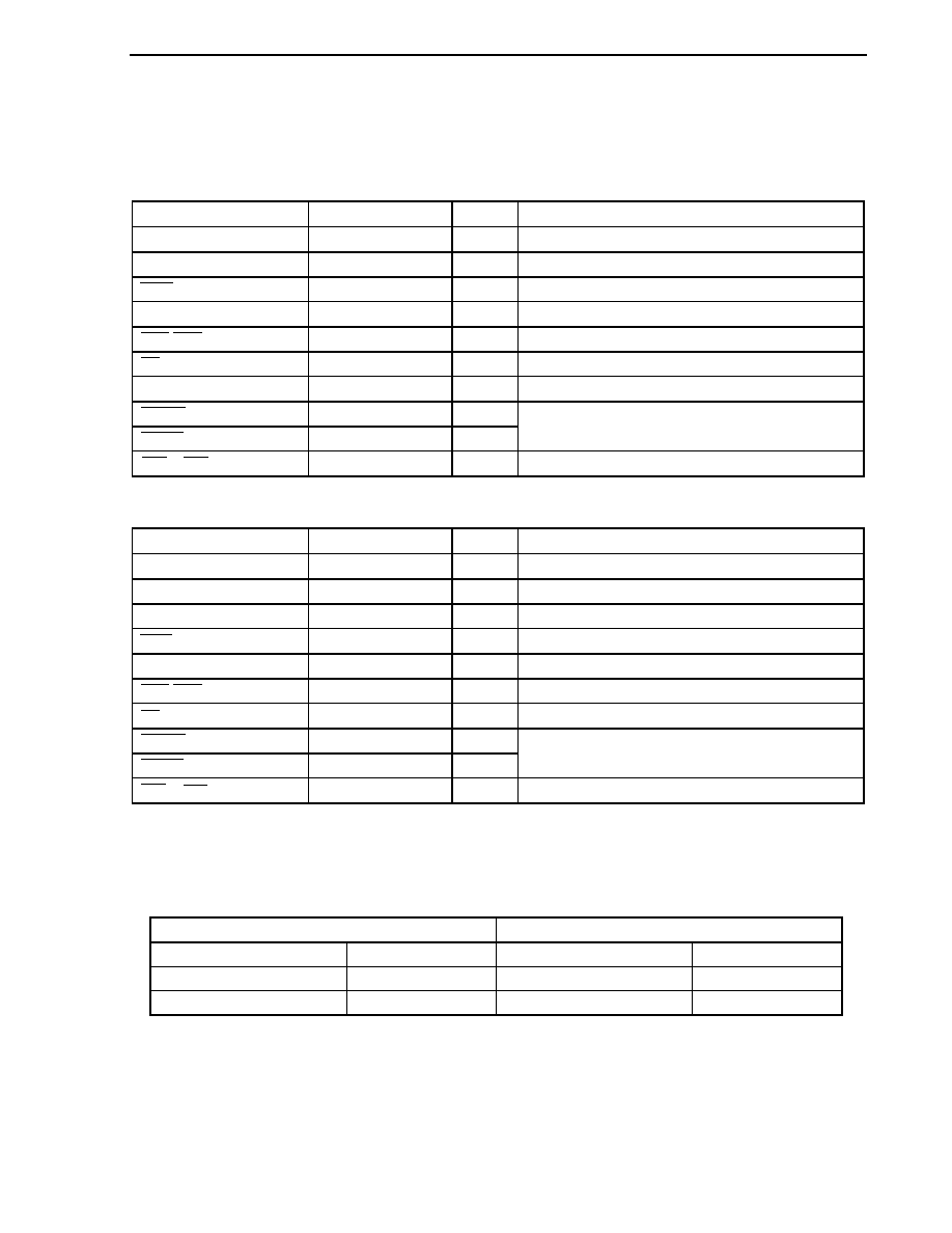
CHAPTER 5 BUS CONTROL FUNCTION
Preliminary User's Manual U17714EJ1V0UD
187
5.2 Bus
Control
Pins
The pins used to connect an external device are listed in the table below.
Table 5-1. Bus Control Pins (Multiplexed Bus)
Bus Control Pin
Alternate-Function Pin
I/O
Function
AD0 to AD15
PDL0 to PDL15
I/O
Address/data bus
A16 to A23
PDH0 to PDH7
Output
Address bus
WAIT
PCM0
Input
External wait control
CLKOUT
PCM1
Output
Internal system clock
WR0, WR1
PCT0, PCT1
Output
Write strobe signal
RD PCT4
Output
Read
strobe
signal
ASTB PCT6
Output
Address
strobe
signal
HLDRQ PCM3
Input
HLDAK PCM2
Output
Bus hold control
CS0 to CS3
PCS0 to PCS3
Output
Chip select
Table 5-2. External Control Pins (Separate Bus)
Bus Control Pin
Alternate-Function Pin
I/O
Function
AD0 to AD15
PDL0 to PDL15
I/O
Data bus
A0 to A15
P90 to P915
Output
Address bus
A16 to A23
PDH0 to PDH7
Output
Address bus
WAIT
PCM0
Input
External wait control
CLKOUT
PCM1
Output
Internal system clock
WR0, WR1
PCT0, PCT1
Output
Write strobe signal
RD PCT4
Output
Read
strobe
signal
HLDRQ PCM3
Input
HLDAK PCM2
Output
Bus hold control
CS0 to CS3
PCS0 to PCS3
Output
Chip select
5.2.1
Pin status when internal ROM, internal RAM, or on-chip peripheral I/O is accessed
When the internal ROM, internal RAM, or on-chip peripheral I/O are accessed, the status of each pin is as follows.
Table 5-3. Pin Statuses When Internal ROM, Internal RAM, or On-Chip Peripheral I/O Is Accessed
Separate Bus Mode
Multiplexed Bus Mode
Address bus (A23 to A0)
Undefined
Address bus (A23 to A16)
Undefined
Data bus (AD15 to AD0)
Hi-Z
Address/data bus (AD15 to AD0) Undefined
Control signal
Inactive
Control signal
Inactive
Caution When a write access is performed to the internal ROM area, address, data, and control signals
are activated in the same way as access to the external memory area.
5.2.2
Pin status in each operation mode
For the pin status of the V850ES/JJ2 in each operation mode, see 2.2 Pin States.
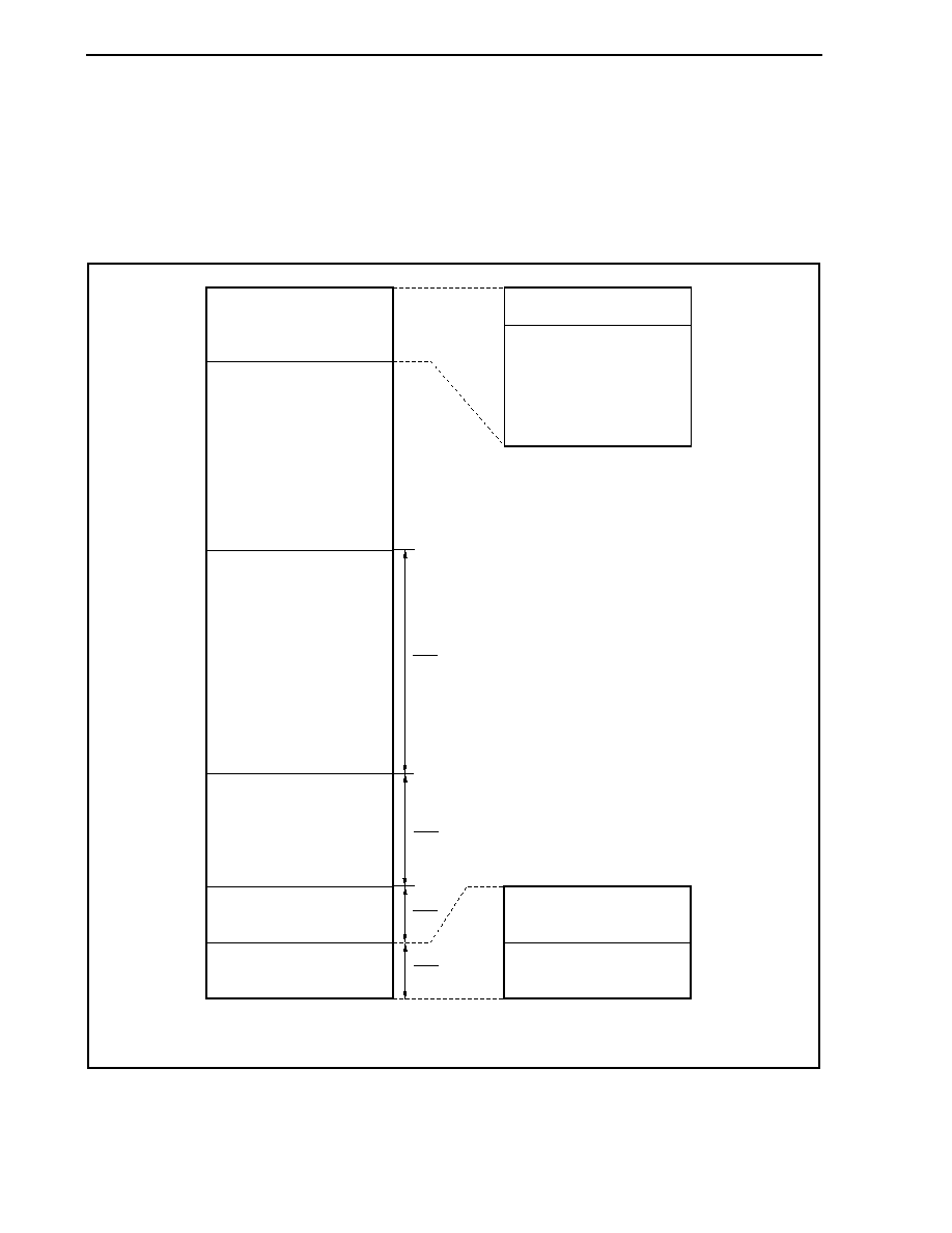
CHAPTER 5 BUS CONTROL FUNCTION
Preliminary User's Manual U17714EJ1V0UD
188
5.3 Memory
Block
Function
The 16 MB external memory space is divided into memory blocks of (lower) 2 MB, 2 MB, 4 MB, and 8 MB. The
programmable wait function and bus cycle operation mode for each of these blocks can be independently controlled in
one-block units.
Figure 5-1. Data Memory Map: Physical Address
(64 KB)
Use prohibited
External memory area
(8 MB)
Internal ROM area
Note
(1 MB)
External memory area
(1 MB)
Internal RAM area
(60 KB)
On-chip peripheral
I/O area (4 KB)
External memory area
(4 MB)
External memory area
(2 MB)
(2 MB)
0 3 F F F F F F H
0 3 F F 0 0 0 0 H
0 3 F E F F F F H
0 1 0 0 0 0 0 0 H
0 0 F F F F F F H
0 0 8 0 0 0 0 0 H
0 0 7 F F F F F H
0 0 4 0 0 0 0 0 H
0 0 3 F F F F F H
0 0 2 0 0 0 0 0 H
0 0 1 F F F F F H
0 0 0 0 0 0 0 0 H
0 3 F F F F F F H
0 3 F F F 0 0 0 H
0 3 F F E F F F H
0 0 1 F F F F F H
0 0 1 0 0 0 0 0 H
0 0 0 F F F F F H
0 0 0 0 0 0 0 0 H
CS3
CS2
CS1
CS0
0 3 F F 0 0 0 0 H
Note This area is an external memory area in the case of a data write access.
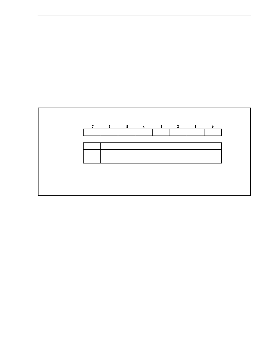
CHAPTER 5 BUS CONTROL FUNCTION
Preliminary User's Manual U17714EJ1V0UD
189
5.4 External Bus Interface Mode Control Function
The V850ES/JJ2 includes the following two external bus interface modes.
� Multiplexed bus mode
� Separate bus mode
These two modes can be selected by using the EXIMC register.
(1) External bus interface mode control register (EXIMC)
The EXIMC register can be read or written in 8-bit or 1-bit units.
Reset sets this register to 00H.
0
Multiplexed bus mode
Separate bus mode
SMSEL
0
1
Mode selection
EXIMC
0
0
0
0
0
0
SMSEL
After reset: 00H R/W Address: FFFFFFBEH
Caution Set the EXIMC register from the internal ROM or internal RAM area before making an
external access.
After setting the EXIMC register, be sure to insert a NOP instruction.
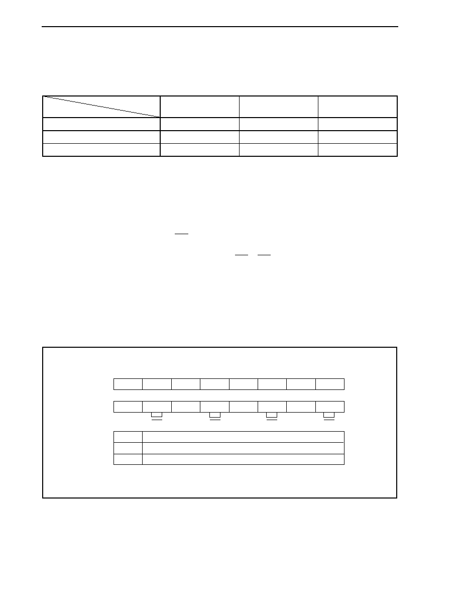
CHAPTER 5 BUS CONTROL FUNCTION
Preliminary User's Manual U17714EJ1V0UD
190
5.5 Bus
Access
5.5.1
Number of clocks for access
The following table shows the number of basic clocks required for accessing each resource.
Area (Bus Width)
Bus Cycle Type
Internal ROM (32 Bits)
Internal RAM (32 Bits)
External Memory (16 Bits)
Instruction fetch (normal access)
1
1
Note 1
3 + n
Note 2
Instruction fetch (branch)
2
2
Note 1
3 + n
Note 2
Operand data access
3
1
3 + n
Note 2
Notes 1. Increases by 1 if a conflict with a data access occurs.
2. 2 + n clocks (n: Number of wait states) when the separate bus mode is selected.
Remark Unit:
Clocks/access
5.5.2
Bus size setting function
Each external memory area selected by CSn can be set by using the BSC register. However, the bus size can be
set to 8 bits and 16 bits only.
The external memory area of the V850ES/JJ2 is selected by CS0 to CS3.
(1) Bus size configuration register (BSC)
The BSC register can be read or written in 16-bit units.
Reset sets this register to 5555H.
Caution Write to the BSC register after reset, and then do not change the set values. Also, do not
access an external memory area until the initial settings of the BSC register are complete.
After reset: 5555H R/W Address: FFFFF066H
0
0
BSn0
0
1
8 bits
16 bits
BSC
1
BS30
0
0
1
BS20
0
0
1
BS10
0
0
1
BS00
8
9
10
11
12
13
Data bus width of CSn space (n = 0 to 3)
14
15
1
2
3
4
5
6
7
0
CS0
CS3
CS2
CS1
Caution Be sure to set bits 14, 12, 10, and 8 to "1", and clear bits 15, 13, 11, 9, 7, 5, 3, and 1 to "0".
CHAPTER 5 BUS CONTROL FUNCTION
Preliminary User's Manual U17714EJ1V0UD
191
5.5.3
Access by bus size
The V850ES/JJ2 accesses the on-chip peripheral I/O and external memory in 8-bit, 16-bit, or 32-bit units. The bus
size is as follows.
� The bus size of the on-chip peripheral I/O is fixed to 16 bits.
� The bus size of the external memory is selectable from 8 bits or 16 bits (by using the BSC register).
The operation when each of the above is accessed is described below. All data is accessed starting from the lower
side.
The V850ES/JJ2 supports only the little-endian format.
Figure 5-2. Little-Endian Address in Word
000BH
000AH
0009H
0008H
0007H
0006H
0005H
0004H
0003H
0002H
0001H
0000H
31
24 23
16 15
8 7
0
(1) Data space
The V850ES/JJ2 has an address misalign function.
With this function, data can be placed at all addresses, regardless of the format of the data (word data or
halfword data). However, if the word data or halfword data is not aligned at the boundary, a bus cycle is
generated at least twice, causing the bus efficiency to drop.
(a) Halfword-length data access
A byte-length bus cycle is generated twice if the least significant bit of the address is 1.
(b) Word-length data access
(i) A byte-length bus cycle, halfword-length bus cycle, and byte-length bus cycle are generated in that
order if the least significant bit of the address is 1.
(ii) A halfword-length bus cycle is generated twice if the lower 2 bits of the address are 10.
CHAPTER 5 BUS CONTROL FUNCTION
Preliminary User's Manual U17714EJ1V0UD
192
(2) Byte access (8 bits)
(a) 16-bit data bus width
<1> Access to even address (2n)
<2> Access to odd address (2n + 1)
7
0
7
0
Byte data
15
8
External data
bus
2n
Address
7
0
7
0
15
8
2n + 1
Address
Byte data
External data
bus
(b) 8-bit data bus width
<1> Access to even address (2n)
<2> Access to odd address (2n + 1)
7
0
7
0
2n
Address
Byte data
External data
bus
7
0
7
0
2n + 1
Address
Byte data
External data
bus
CHAPTER 5 BUS CONTROL FUNCTION
Preliminary User's Manual U17714EJ1V0UD
193
(3) Halfword access (16 bits)
(a) With 16-bit data bus width
<1> Access to even address (2n)
<2> Access to odd address (2n + 1)
7
0
7
0
15
8
2n
Address
15
8
2n + 1
Halfword data External data
bus
First access
Second access
7
0
7
0
15
8
15
8
7
0
7
0
15
8
15
8
2n + 2
Halfword data
External data
bus
2n
Address
Halfword data
External data
bus
Address
2n + 1
(b) 8-bit data bus width
<1> Access to even address (2n)
<2> Access to odd address (2n + 1)
First access
Second access
7
0
7
0
15
8
Address
7
0
7
0
15
8
2n + 1
Address
2n
Halfword data External data
bus
Halfword data External data
bus
First access
Second access
7
0
7
0
15
8
7
0
7
0
15
8
2n + 2
2n + 1
Address
Address
Halfword data External data
bus
Halfword data External data
bus
CHAPTER 5 BUS CONTROL FUNCTION
Preliminary User's Manual U17714EJ1V0UD
194
(4) Word access (32 bits)
(a) 16-bit data bus width (1/2)
<1> Access to address (4n)
First access
Second access
7
0
7
0
15
8
4n
15
8
4n + 1
23
16
31
24
7
0
7
0
15
8
4n + 2
15
8
4n + 3
23
16
31
24
Word data
External data
bus
Address
Word data
External data
bus
Address
<2> Access to address (4n + 1)
First
access
Second
access Third
access
7
0
7
0
15
8
15
8
4n + 1
23
16
31
24
7
0
7
0
15
8
4n + 2
15
8
4n + 3
23
16
31
24
7
0
7
0
15
8
4n + 4
15
8
23
16
31
24
Word data External data
bus
Address
Word data External data
bus
Address
Word data External data
bus
Address
CHAPTER 5 BUS CONTROL FUNCTION
Preliminary User's Manual U17714EJ1V0UD
195
(a) 16-bit data bus width (2/2)
<3> Access to address (4n + 2)
First access
Second access
7
0
7
0
15
8
4n + 2
15
8
4n + 3
23
16
31
24
7
0
7
0
15
8
4n + 4
15
8
4n + 5
23
16
31
24
Word data
External data
bus
Address
Word data
External data
bus
Address
<4> Access to address (4n + 3)
First
access
Second
access Third
access
7
0
7
0
15
8
15
8
4n + 3
23
16
31
24
7
0
7
0
15
8
4n + 4
15
8
4n + 5
23
16
31
24
7
0
7
0
15
8
4n + 6
15
8
23
16
31
24
Word data
External data
bus
Address
Word data
External data
bus
Address
Word data
External data
bus
Address
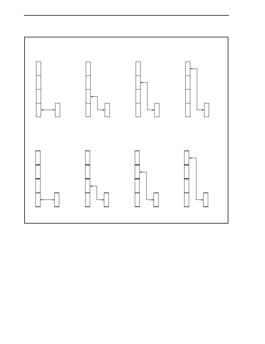
CHAPTER 5 BUS CONTROL FUNCTION
Preliminary User's Manual U17714EJ1V0UD
196
(b) 8-bit data bus width (1/2)
<1> Access to address (4n)
First access
Second access
Third access
Fourth access
7
0
7
0
15
8
4n
23
16
31
24
7
0
7
0
4n + 1
15
8
23
16
31
24
7
0
7
0
4n + 2
15
8
23
16
31
24
7
0
7
0
4n + 3
15
8
23
16
31
24
Word data External data
bus
Address
Word data External data
bus
Address
Word data External data
bus
Address
Word data External data
bus
Address
<2> Access to address (4n + 1)
First access
Second access
Third access
Fourth access
7
0
7
0
15
8
4n + 1
23
16
31
24
7
0
7
0
4n + 2
15
8
23
16
31
24
7
0
7
0
4n + 3
15
8
23
16
31
24
7
0
7
0
4n + 4
15
8
23
16
31
24
Word data External data
bus
Address
Word data External data
bus
Address
Word data External data
bus
Address
Word data External data
bus
Address
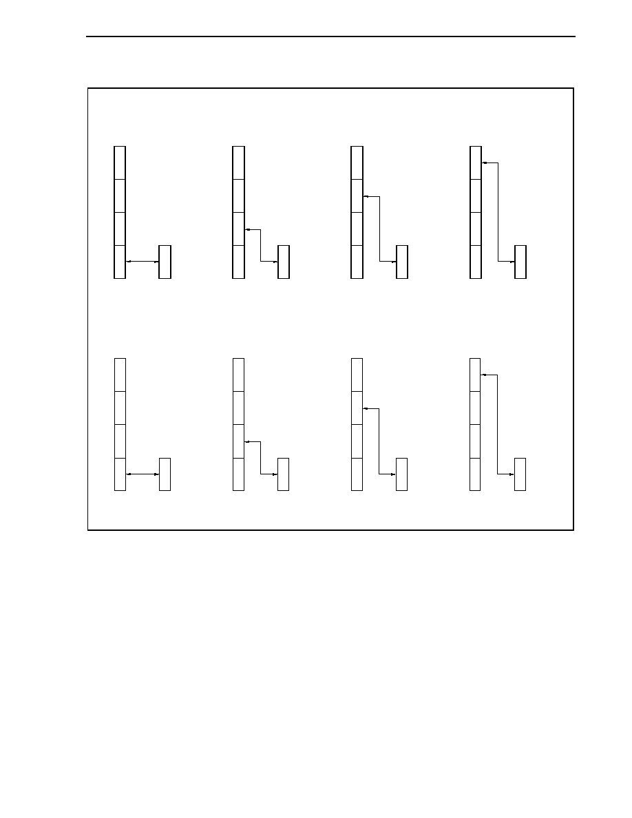
CHAPTER 5 BUS CONTROL FUNCTION
Preliminary User's Manual U17714EJ1V0UD
197
(b) 8-bit data bus width (2/2)
<3> Access to address (4n + 2)
First access
Second access
Third access
Fourth access
Word data External data
bus
Address
Word data External data
bus
Address
Word data External data
bus
Address
Word data External data
bus
Address
7
0
7
0
15
8
4n + 2
23
16
31
24
7
0
7
0
4n + 3
15
8
23
16
31
24
7
0
7
0
4n + 4
15
8
23
16
31
24
7
0
7
0
4n + 5
15
8
23
16
31
24
<4> Access to address (4n + 3)
First access
Second access
Third access
Fourth access
7
0
7
0
15
8
4n + 3
23
16
31
24
7
0
7
0
4n + 4
15
8
23
16
31
24
7
0
7
0
4n + 5
15
8
23
16
31
24
7
0
7
0
4n + 6
15
8
23
16
31
24
Word data External data
bus
Address
Word data External data
bus
Address
Word data External data
bus
Address
Word data External data
bus
Address
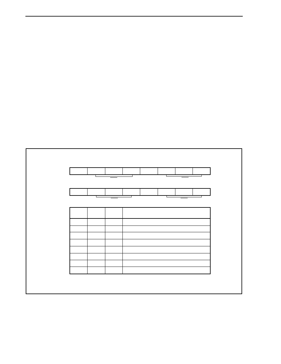
CHAPTER 5 BUS CONTROL FUNCTION
Preliminary User's Manual U17714EJ1V0UD
198
5.6 Wait Function
5.6.1
Programmable wait function
(1) Data wait control register 0 (DWC0)
To realize interfacing with a low-speed memory or I/O, up to seven data wait states can be inserted in the bus
cycle that is executed for each CS space.
The number of wait states can be programmed by using the DWC0 register . Immediately after system reset, 7
data wait states are inserted for all the blocks.
The DWC0 register can be read or written in 16-bit units.
Reset sets this register to 7777H.
Cautions 1. The internal ROM and internal RAM areas are not subject to programmable wait, and are
always accessed without a wait state. The on-chip peripheral I/O area is also not subject
to programmable wait, and only wait control from each peripheral function is performed.
2. Write to the DWC0 register after reset, and then do not change the set values. Also, do
not access an external memory area until the initial settings of the DWC0 register are
complete.
After reset: 7777H R/W Address: FFFFF484H
0
0
DWn2
0
0
0
0
1
1
1
1
DWn1
0
0
1
1
0
0
1
1
DWn0
0
1
0
1
0
1
0
1
None
1
2
3
4
5
6
7
DWC0
DW32
DW12
DW31
DW11
DW30
DW10
0
0
DW22
DW02
DW21
DW01
DW20
DW00
8
9
10
11
12
13
Number of wait states inserted in
CSn space (n = 0 to 3)
14
15
1
2
3
4
5
6
7
0
CS0
CS3
CS2
CS1
Caution Be sure to clear bits 15, 11, 7, and 3 to "0".

CHAPTER 5 BUS CONTROL FUNCTION
Preliminary User's Manual U17714EJ1V0UD
199
5.6.2
External wait function
To synchronize an extremely slow external memory, I/O, or asynchronous system, any number of wait states can
be inserted in the bus cycle by using the external wait pin (WAIT).
When the PCM0 pin is set to alternate function, the external wait function is enabled.
Access to each area of the internal ROM, internal RAM, and on-chip peripheral I/O is not subject to control by the
external wait function, in the same manner as the programmable wait function.
The WAIT signal can be input asynchronously to CLKOUT, and is sampled at the falling edge of the clock in the T2
and TW states of the bus cycle in the multiplexed bus mode. In the separate bus mode, it is sampled at the rising
edge of the clock immediately after the T1 and TW states of the bus cycle. If the setup/hold time of the sampling
timing is not satisfied, a wait state is inserted in the next state, or not inserted at all.
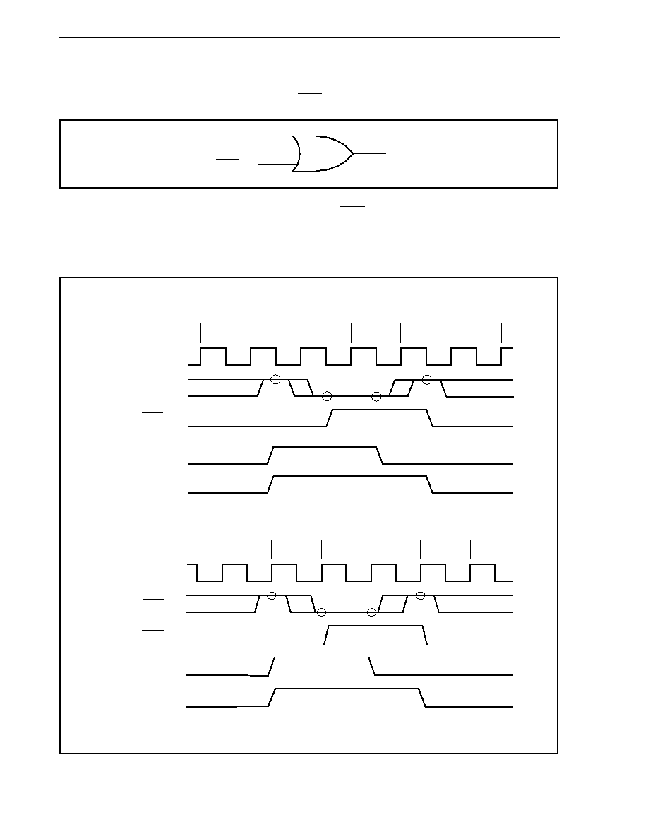
CHAPTER 5 BUS CONTROL FUNCTION
Preliminary User's Manual U17714EJ1V0UD
200
5.6.3 Relationship
between
programmable wait and external wait
Wait cycles are inserted as the result of an OR operation between the wait cycles specified by the set value of the
programmable wait and the wait cycles controlled by the WAIT pin.
Wait control
Programmable wait
Wait via WAIT pin
For example, if the timing of the programmable wait and the WAIT pin signal is as illustrated below, three wait
states will be inserted in the bus cycle.
Figure 5-3. Inserting Wait Example
(a) Multiplexed bus
CLKOUT
T1
T2
TW
TW
TW
T3
WAIT pin
Wait via WAIT pin
Programmable wait
Wait control
(b) Separate bus
T1
TW
TW
TW
T2
CLKOUT
WAIT pin
Wait via WAIT pin
Programmable wait
Wait control
Remark The circles indicate the sampling timing.
CHAPTER 5 BUS CONTROL FUNCTION
Preliminary User's Manual U17714EJ1V0UD
201
5.6.4
Programmable address wait function
Address-setup or address-hold waits to be inserted in each bus cycle can be set by using the AWC register.
Address wait insertion is set for each chip select area (CS0 to CS3).
If an address setup wait is inserted, it seems that the high-clock period of the T1 state is extended by 1 clock. If an
address hold wait is inserted, it seems that the low-clock period of the T1 state is extended by 1 clock.
(1) Address wait control register (AWC)
The AWC register can be read or written in 16-bit units.
Reset sets this register to FFFFH.
Cautions 1. Address setup wait and address hold wait cycles are not inserted when the internal ROM
area, internal RAM area, and on-chip peripheral I/O areas are accessed.
2. Write to the AWC register after reset, and then do not change the set values. Also, do not
access an external memory area until the initial settings of the AWC register are
complete.
After reset: FFFFH R/W Address: FFFFF488H
1
AHW3
AHWn
0
1
Not inserted
Inserted
AWC
1
ASW3
1
AHW2
1
ASW2
1
AHW1
1
ASW1
1
AHW0
1
ASW0
8
9
10
11
12
13
Specifies insertion of address hold wait (n = 0 to 3)
14
15
1
2
3
4
5
6
7
0
ASWn
0
1
Not inserted
Inserted
Specifies insertion of address setup wait (n = 0 to 3)
CS0
CS3
CS2
CS1
Caution Be sure to set bits 15 to 8 to "1".
CHAPTER 5 BUS CONTROL FUNCTION
Preliminary User's Manual U17714EJ1V0UD
202
5.7 Idle State Insertion Function
To facilitate interfacing with low-speed memories, one idle state (TI) can be inserted after the T3 state in the bus
cycle that is executed for each space selected by the chip select function in the multiplex address/data bus mode. In
the separate bus mode, one idle state (TI) can be inserted after the T2 state. By inserting an idle state, the data
output float delay time of the memory can be secured during read access (an idle state cannot be inserted during
write access).
Whether the idle state is to be inserted can be programmed by using the BCC register.
An idle state is inserted for all the areas immediately after system reset.
(1) Bus cycle control register (BCC)
The BCC register can be read or written in 16-bit units.
Reset sets this register to AAAAH.
Cautions 1. The internal ROM, internal RAM, and on-chip peripheral I/O areas are not subject to idle
state insertion.
2. Write to the BCC register after reset, and then do not change the set values. Also, do not
access an external memory area until the initial settings of the BCC register are complete.
After reset: AAAAH R/W Address: FFFFF48AH
1
BC31
BCn1
0
1
Not inserted
Inserted
BCC
0
0
1
BC21
0
0
1
BC11
0
0
1
BC01
0
0
8
9
10
11
12
13
Specifies insertion of idle state (n = 0 to 3)
14
15
1
2
3
4
5
6
7
0
CS0
CS3
CS2
CS1
Caution Be sure to set bits 15, 13, 11, and 9 to "1", and clear bits 14, 12, 10, 8, 6, 4, 2, and 0 to "0".

CHAPTER 5 BUS CONTROL FUNCTION
Preliminary User's Manual U17714EJ1V0UD
203
5.8 Bus
Hold
Function
5.8.1 Functional
outline
The HLDRQ and HLDAK functions are valid if the PCM2 and PCM3 pins are set to alternate function.
When the HLDRQ pin is asserted (low level), indicating that another bus master has requested bus mastership, the
external address/data bus goes into a high-impedance state and is released (bus hold status). If the request for the
bus mastership is cleared and the HLDRQ pin is deasserted (high level), driving these pins is started again.
During the bus hold period, execution of the program in the internal ROM and internal RAM is continued until an
on-chip peripheral I/O register or the external memory is accessed.
The bus hold status is indicated by assertion of the HLDAK pin (low level). The bus hold function enables the
configuration of multi-processor type systems in which two or more bus masters exist.
Note that the bus hold request is not acknowledged during a multiple-access cycle initiated by the bus sizing
function or a bit manipulation instruction.
Status Data
Bus
Width
Access Type
Timing at Which Bus Hold Request
Is Not Acknowledged
Word access to even address
Between first and second access
Between first and second access
Word access to odd address
Between second and third access
16 bits
Halfword access to odd address
Between first and second access
Between first and second access
Between second and third access
Word access
Between third and fourth access
CPU bus lock
8 bits
Halfword access
Between first and second access
Read-modify-write access of bit
manipulation instruction
-
-
Between read access and write
access
CHAPTER 5 BUS CONTROL FUNCTION
Preliminary User's Manual U17714EJ1V0UD
204
5.8.2
Bus hold procedure
The bus hold status transition procedure is shown below.
<1> HLDRQ = 0 acknowledged
<2> All bus cycle start requests inhibited
<3> End of current bus cycle
<4> Shift to bus idle status
<5> HLDAK = 0
<6> HLDRQ = 1 acknowledged
<7> HLDAK = 1
<8> Bus cycle start request inhibition released
<9> Bus cycle starts
Normal status
Bus hold status
Normal status
HLDAK (output)
HLDRQ (input)
<1> <2>
<5>
<3><4>
<7><8><9>
<6>
5.8.3
Operation in power save mode
Because the internal system clock is stopped in the STOP, IDLE1, and IDLE2 modes, the bus hold status is not
entered even if the HLDRQ pin is asserted.
In the HALT mode, the HLDAK pin is asserted as soon as the HLDRQ pin has been asserted, and the bus hold
status is entered. When the HLDRQ pin is later deasserted, the HLDAK pin is also deasserted, and the bus hold
status is cleared.
CHAPTER 5 BUS CONTROL FUNCTION
Preliminary User's Manual U17714EJ1V0UD
205
5.9 Bus
Priority
Bus hold, DMA transfer, operand data accesses, instruction fetch (branch), and instruction fetch (successive) are
executed in the external bus cycle.
Bus hold has the highest priority, followed by DMA transfer, operand data access, instruction fetch (branch), and
instruction fetch (successive).
An instruction fetch may be inserted between the read access and write access in a read-modify-write access.
If an instruction is executed for two or more accesses, an instruction fetch and bus hold are not inserted between
accesses due to bus size limitations.
Table 5-4. Bus Priority
Priority
External Bus Cycle
Bus Master
Bus hold
External device
DMA transfer
DMAC
Operand data access
CPU
Instruction fetch (branch)
CPU
High
Low
Instruction fetch (successive)
CPU
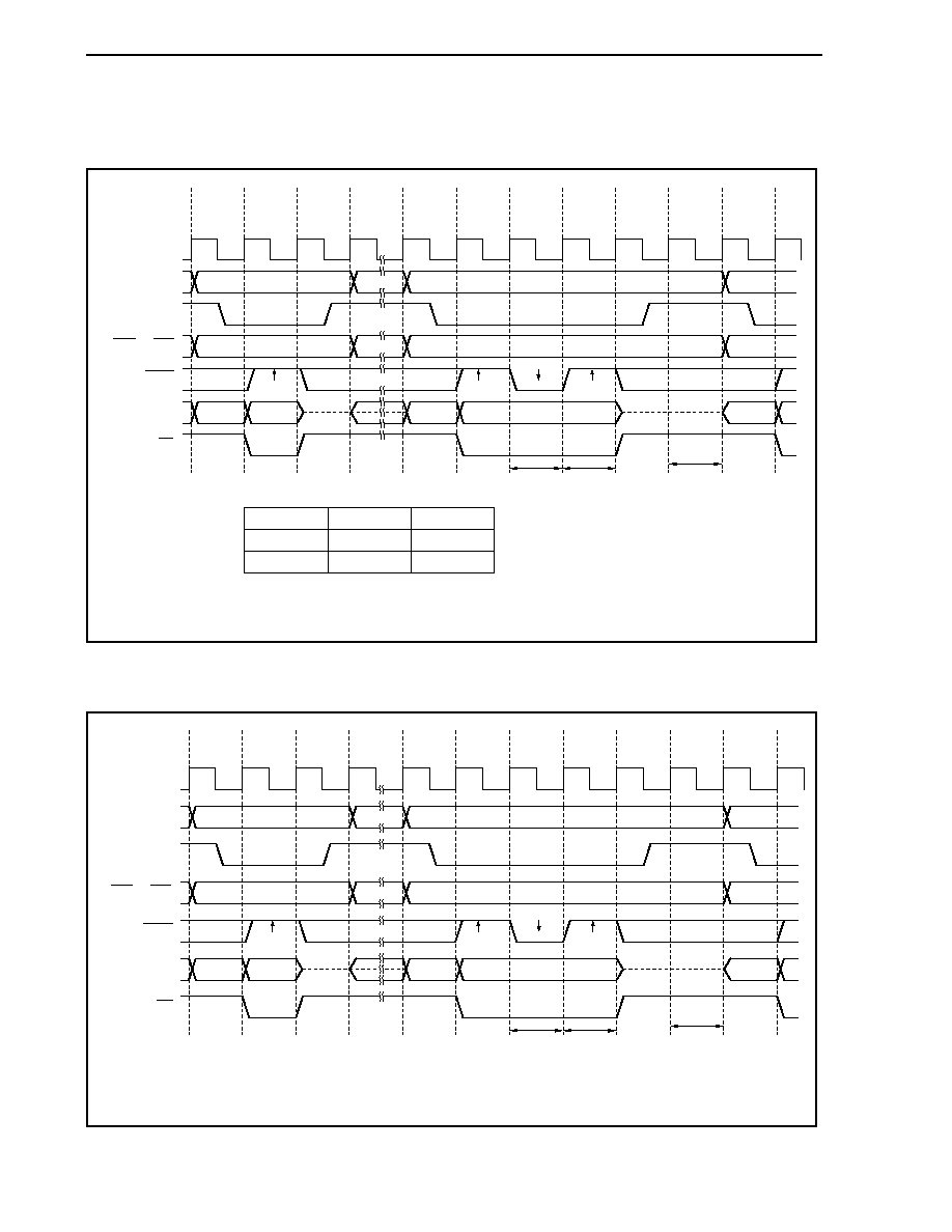
CHAPTER 5 BUS CONTROL FUNCTION
Preliminary User's Manual U17714EJ1V0UD
206
5.10 Bus Timing
Figure 5-4. Multiplexed Bus Read Timing (Bus Size: 16 Bits, 16-Bit Access)
A1
A2
A3
D1
D2
A3
A2
A1
T1
T2
T3
T1
T2
TW
TW
T3
TI
T1
Programmable
wait
External
wait
Idle state
CLKOUT
A23 to A16
ASTB
CS3 to CS0
WAIT
AD15 to AD0
RD
8-bit Access
AD15 to AD8
AD7 to AD0
Odd Address
Active
Hi-Z
Even Address
Hi-Z
Active
Remark The broken lines indicate high impedance.
Figure 5-5. Multiplexed Bus Read Timing (Bus Size: 8 Bits)
A1
A2
A3
D1
D2
A3
A2
A1
T1
T2
T3
T1
T2
TW
TW
T3
TI
T1
Programmable
wait
External
wait
Idle state
CLKOUT
A23 to A16,
AD15 to AD8
ASTB
CS3 to CS0
WAIT
AD7 to AD0
RD
Remark The broken lines indicate high impedance.
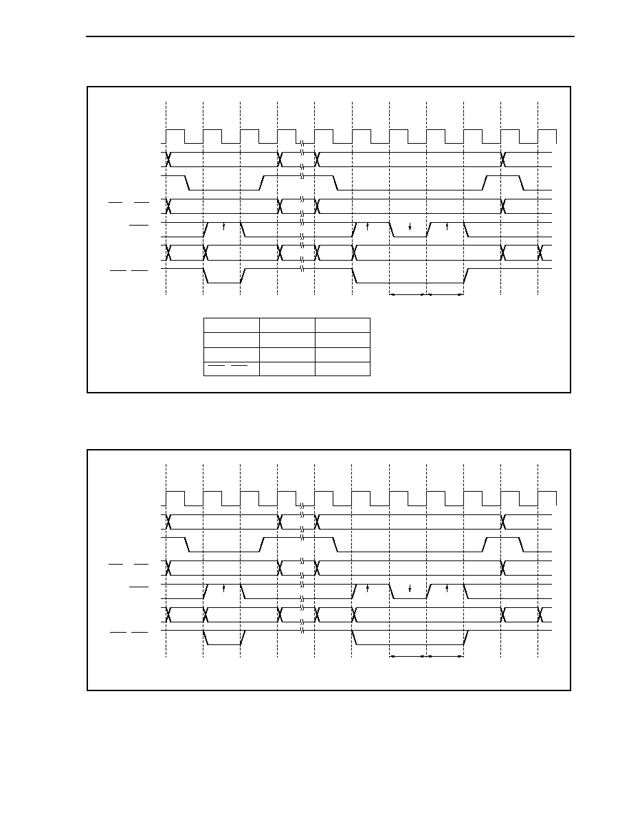
CHAPTER 5 BUS CONTROL FUNCTION
Preliminary User's Manual U17714EJ1V0UD
207
Figure 5-6. Multiplexed Bus Write Timing (Bus Size: 16 Bits, 16-Bit Access)
A1
11
00
11
11
00
11
A2
A3
D1
D2
A3
A2
A1
T2
T3
T1
T1
T2
TW
TW
T3
T1
Programmable
wait
External
wait
CLKOUT
A23 to A16
ASTB
CS3 to CS0
WAIT
AD15 to AD0
WR1, WR0
WR1, WR0
01
10
8-bit Access
AD15 to AD8
AD7 to AD0
Odd Address
Active
Undefined
Even Address
Undefined
Active
Figure 5-7. Multiplexed Bus Write Timing (Bus Size: 8 Bits)
A1
11
10
11
11
10
11
A2
A3
D1
D2
A3
A2
A1
T2
T3
T1
T1
T2
TW
TW
T3
T1
Programmable
wait
External
wait
CLKOUT
A23 to A16,
AD15 to AD8
ASTB
CS3 to CS0
WAIT
AD7 to AD0
WR1, WR0
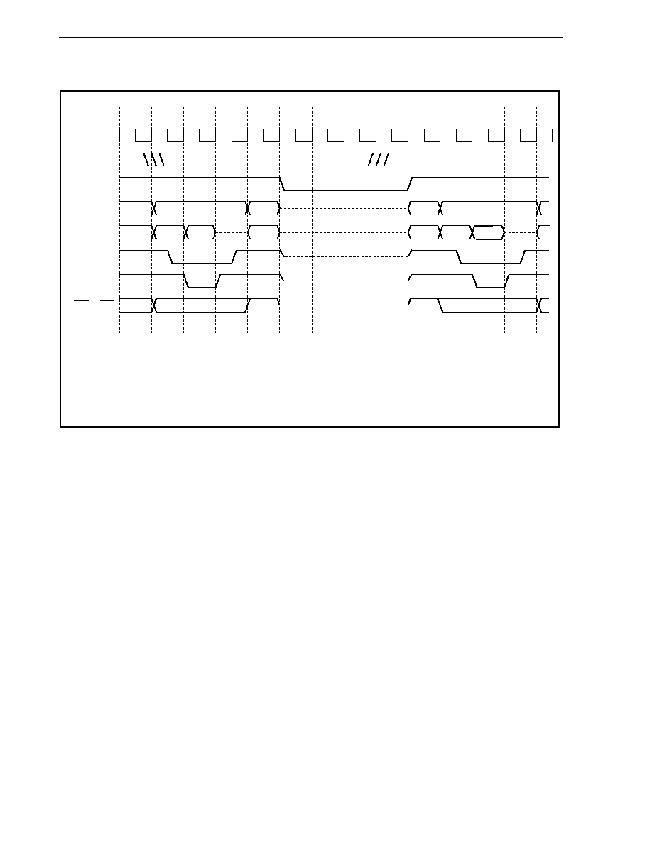
CHAPTER 5 BUS CONTROL FUNCTION
Preliminary User's Manual U17714EJ1V0UD
208
Figure 5-8. Multiplexed Bus Hold Timing (Bus Size: 16 Bits, 16-Bit Access)
T1
A1
Undefined
A1
A2
T2
T3
TI
Note
TH
TH
TH
TH
TI
Note
T1
T2
T3
D1
CLKOUT
HLDRQ
HLDAK
A23 to A16
ASTB
CS3 to CS0
AD15 to AD0
RD
Undefined
Undefined
Undefined
A2
D2
1111
1111
Note This idle state (TI) does not depend on the BCC register settings.
Remarks 1. See
Table 2-2 for the pin statuses in the bus hold mode.
2. The broken lines indicate high impedance.
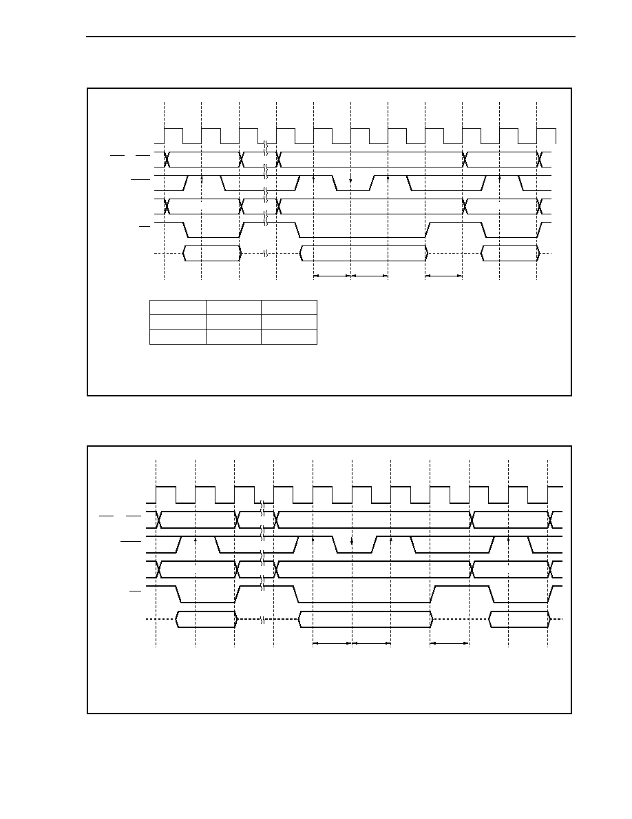
CHAPTER 5 BUS CONTROL FUNCTION
Preliminary User's Manual U17714EJ1V0UD
209
Figure 5-9. Separate Bus Read Timing (Bus Size: 16 Bits, 16-Bit Access)
T1
A1
A2
A3
T2
T1
TW
TW
T2
T2
TI
T1
D3
D2
Programmable
wait
External
wait
Idle state
D1
CLKOUT
A23 to A0
CS3 to CS0
WAIT
AD15 to AD0
RD
8-bit Access
AD15 to AD8
AD7 to AD0
Odd Address
Active
Hi-Z
Even Address
Hi-Z
Active
Remark The broken lines indicate high impedance.
Figure 5-10. Separate Bus Read Timing (Bus Size: 8 Bits)
T1
A1
A2
A3
T2
T1
TW
TW
T2
T2
TI
T1
D3
D2
Programmable
wait
External
wait
Idle state
D1
CLKOUT
A23 to A0
CS3 to CS0
WAIT
AD7 to AD0
RD
Remark The broken lines indicate high impedance.
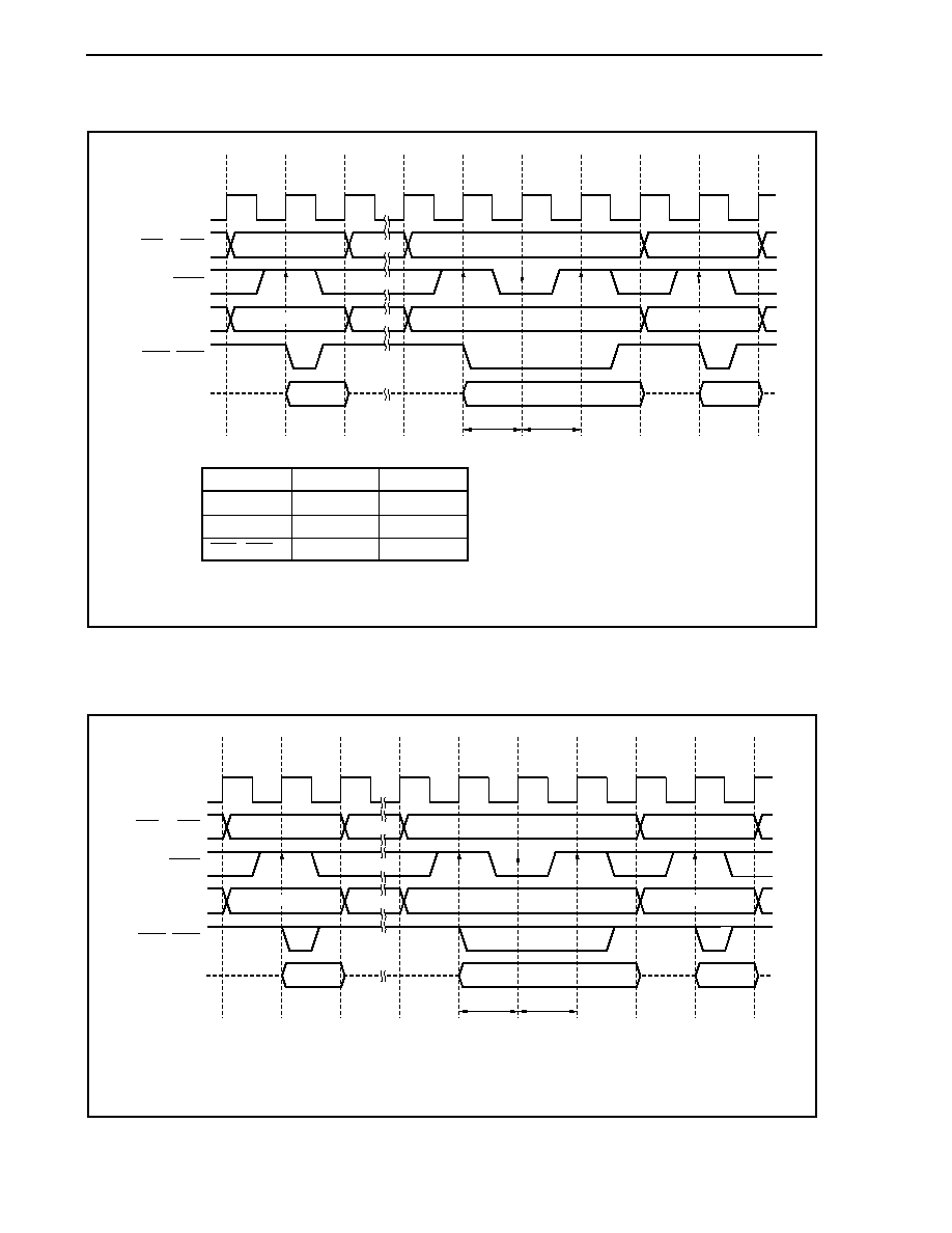
CHAPTER 5 BUS CONTROL FUNCTION
Preliminary User's Manual U17714EJ1V0UD
210
Figure 5-11. Separate Bus Write Timing (Bus Size: 16 Bits, 16-Bit Access)
T1
A1
11
00
00
00
11
11
11
11
A2
A3
T2
T1
TW
TW
T2
T1
T2
D3
D2
Programmable
wait
External
wait
D1
CLKOUT
A23 to A0
CS3 to CS0
WAIT
AD15 to AD0
WR1, WR0
WR1, WR0
01
10
8-bit Access
AD15 to AD8
AD7 to AD0
Odd Address
Active
Undefined
Even Address
Undefined
Active
Remark The broken lines indicate high impedance.
Figure 5-12. Separate Bus Write Timing (Bus Size: 8 Bits)
T1
A1
A2
A3
T2
T1
TW
TW
T2
T1
T2
D3
D2
Programmable
wait
External
wait
D1
CLKOUT
A23 to A0
CS3 to CS0
WAIT
AD7 to AD0
WR1, WR0
11
10
10
10
11
11
11
11
Remark The broken lines indicate high impedance.
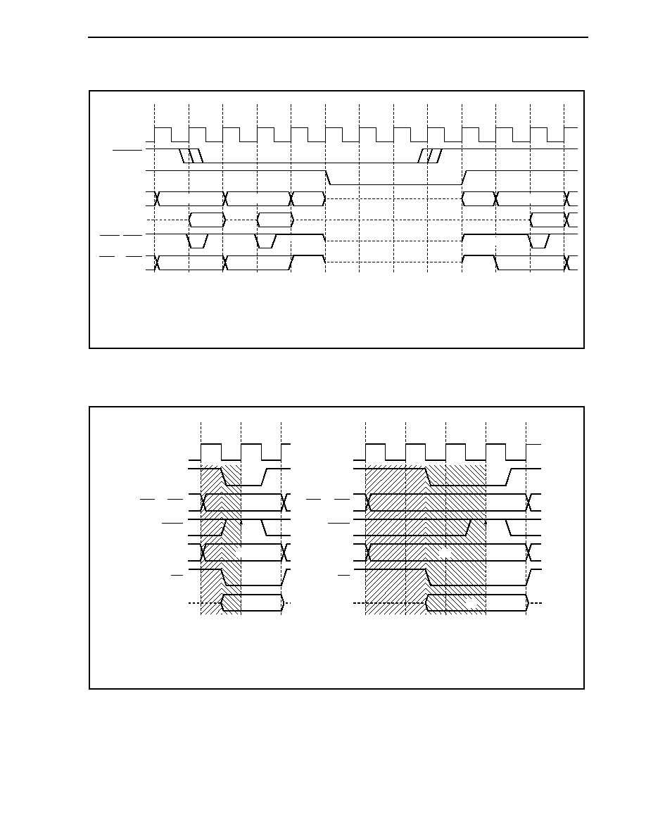
CHAPTER 5 BUS CONTROL FUNCTION
Preliminary User's Manual U17714EJ1V0UD
211
Figure 5-13. Separate Bus Hold Timing (Bus Size: 8 Bits, Write)
CLKOUT
T1
T2
A1
D1
D2
Undefined
A2
Undefined
11
11
10
D3
A3
T1
T2
TH
TI
Note
TI
Note
TH
TH
TH
T1
T2
HLDRQ
HLDAK
A23 to A0
AD7 to AD0
WR1, WR0
CS3 to CS0
11
10
11
10
1111
1111
11
Note This idle state (TI) does not depend on the BCC register settings.
Remark The broken lines indicate high impedance.
Figure 5-14. Address Wait Timing (Separate Bus Read, Bus Size: 16 Bits, 16-Bit Access)
TASW
T1
TAHW
T2
CLKOUT
ASTB
A23 to A0
CS3 to CS0
WAIT
AD15 to AD0
RD
D1
A1
T1
T2
CLKOUT
ASTB
A23 to A0
CS3 to CS0
WAIT
AD15 to AD0
RD
D1
A1
Remarks 1. TASW (address setup wait): Image of high-level width of T1 state expanded.
2. TAHW (address hold wait): Image of low-level width of T1 state expanded.
3. The broken lines indicate high impedance.

Preliminary User's Manual U17714EJ1V0UD
212
CHAPTER 6 CLOCK GENERATION FUNCTION
6.1 Overview
The following clock generation functions are available.
Main clock oscillator
� In clock-through mode
f
X
= 2.5 to 10 MHz (f
XX
= 2.5 to 10 MHz)
� In PLL mode
f
X
= 2.5 to 5 MHz (
�4: f
XX
= 10 to 20 MHz)
f
X
= 2.5 to 4 MHz (
�8: f
XX
= 20 to 32 MHz)
Subclock oscillator
� f
XT
= 32.768 kHz
Multiply (
�4/�8) function by PLL (Phase Locked Loop)
� Clock-through mode/PLL mode selectable
Internal oscillator
� f
R
= 200 kHz (TYP.)
Internal system clock generation
� 7 steps (f
XX
, f
XX
/2, f
XX
/4, f
XX
/8, f
XX
/16, f
XX
/32, f
XT
)
Peripheral clock generation
Clock output function
Remark f
X
: Main clock oscillation frequency
f
XX
: Main clock frequency
f
XT
: Subclock frequency
f
R
: Internal oscillation clock frequency
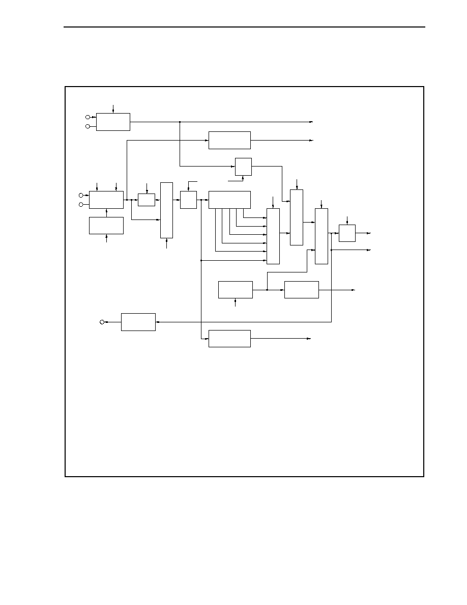
CHAPTER 6 CLOCK GENERATION FUNCTION
Preliminary User's Manual U17714EJ1V0UD
213
6.2 Configuration
Figure 6-1. Clock Generator
Selector
Selector
Note
FRC bit
MFRC
bit
MCK
bit
CK2 to CK0
bits
SELPLL bit
PLLON
bit
CLS, CK3
bits
STOP mode
Subclock
oscillator
Port CM
Prescaler 1
Prescaler 2
IDLE
control
HALT
control
HALT
mode
CPU clock
Watch timer clock
Timer M clock
Watch timer clock,
watchdog timer 2 clock
Peripheral clock,
watchdog timer 2 clock
Watchdog timer 2 clock,
timer M clock
Internal
system clock
Prescaler 3
Main clock
oscillator
Main clock
oscillator
stop control
RSTP bit
Internal
oscillator
1/8 divider
XT1
XT2
CLKOUT
X1
X2
IDLE mode
PLL
f
XX
/32
f
XX
/16
f
XX
/8
f
XX
/4
f
XX
/2
f
XX
f
CPU
f
CLK
f
XX
to f
XX
/1,024
f
BRG
= f
X
/2 to f
X
/2
12
f
XT
f
XT
f
XX
f
X
f
R
f
R
/8
IDLE
control
Selector
Selector
Note The internal oscillation clock is selected when watchdog timer 2 overflows during the oscillation
stabilization time.
Remark f
X
:
Main clock oscillation frequency
f
XX
: Main clock frequency
f
CLK
: Internal system clock frequency
f
XT
: Subclock frequency
f
CPU
: CPU clock frequency
f
BRG
: Watch timer clock frequency
f
R
:
Internal oscillation clock frequency

CHAPTER 6 CLOCK GENERATION FUNCTION
Preliminary User's Manual U17714EJ1V0UD
214
(1) Main clock oscillator
The main resonator oscillates the following frequencies (f
X
).
� In clock-through mode
f
X
= 2.5 to 10 MHz
� In PLL mode
f
X
= 2.5 to 5 MHz (
�4)
f
X
= 2.5 to 4 MHz (
�8)
(2) Subclock oscillator
The sub-resonator oscillates a frequency of 32.768 kHz (f
XT
).
(3) Main clock oscillator stop control
This circuit generates a control signal that stops oscillation of the main clock oscillator.
Oscillation of the main clock oscillator is stopped in the STOP mode or when the PCC.MCK bit = 1 (valid only
when the PCC.CLS bit = 1).
(4) Internal oscillator
Oscillates a frequency (f
R
) of 200 kHz (TYP.).
(5) Prescaler 1
This prescaler generates the clock (f
XX
to f
XX
/1,024) to be supplied to the following on-chip peripheral functions:
TMP0 to TMP8, TMQ0, TMM0, CSIB0 to CSIB5, UARTA0 to UARTA3, I
2
C00 to I
2
C02, ADC, and WDT2
(6) Prescaler 2
This circuit divides the main clock (f
XX
).
The clock generated by prescaler 2 (f
XX
to f
XX
/32) is supplied to the selector that generates the CPU clock
(f
CPU
) and internal system clock (f
CLK
).
f
CLK
is the clock supplied to the INTC, ROM, and RAM blocks, and can be output from the CLKOUT pin.
(7) Prescaler 3
This circuit divides the clock generated by the main clock oscillator (f
X
) to a specific frequency (32.768 kHz)
and supplies that clock to the watch timer block.
For details, see CHAPTER 10 WATCH TIMER FUNCTIONS.
(8) PLL
This circuit multiplies the clock generated by the main clock oscillator (f
X
) by 4 or 8.
It operates in two modes: clock-through mode in which f
X
is output as is, and PLL mode in which a multiplied
clock is output. These modes can be selected by using the PLLCTL.SELPLL bit.
Whether the clock is multiplied by 4 or 8 is selected by the CKC.CKDIV0 bit, and PLL is started or stopped by
the PLLCTL.PLLON bit.

CHAPTER 6 CLOCK GENERATION FUNCTION
Preliminary User's Manual U17714EJ1V0UD
215
6.3 Registers
(1) Processor clock control register (PCC)
The PCC register is a special register. Data can be written to this register only in combination of specific
sequences (see 3.4.7 Special registers).
This register can be read or written in 8-bit or 1-bit units.
Reset sets this register to 03H.
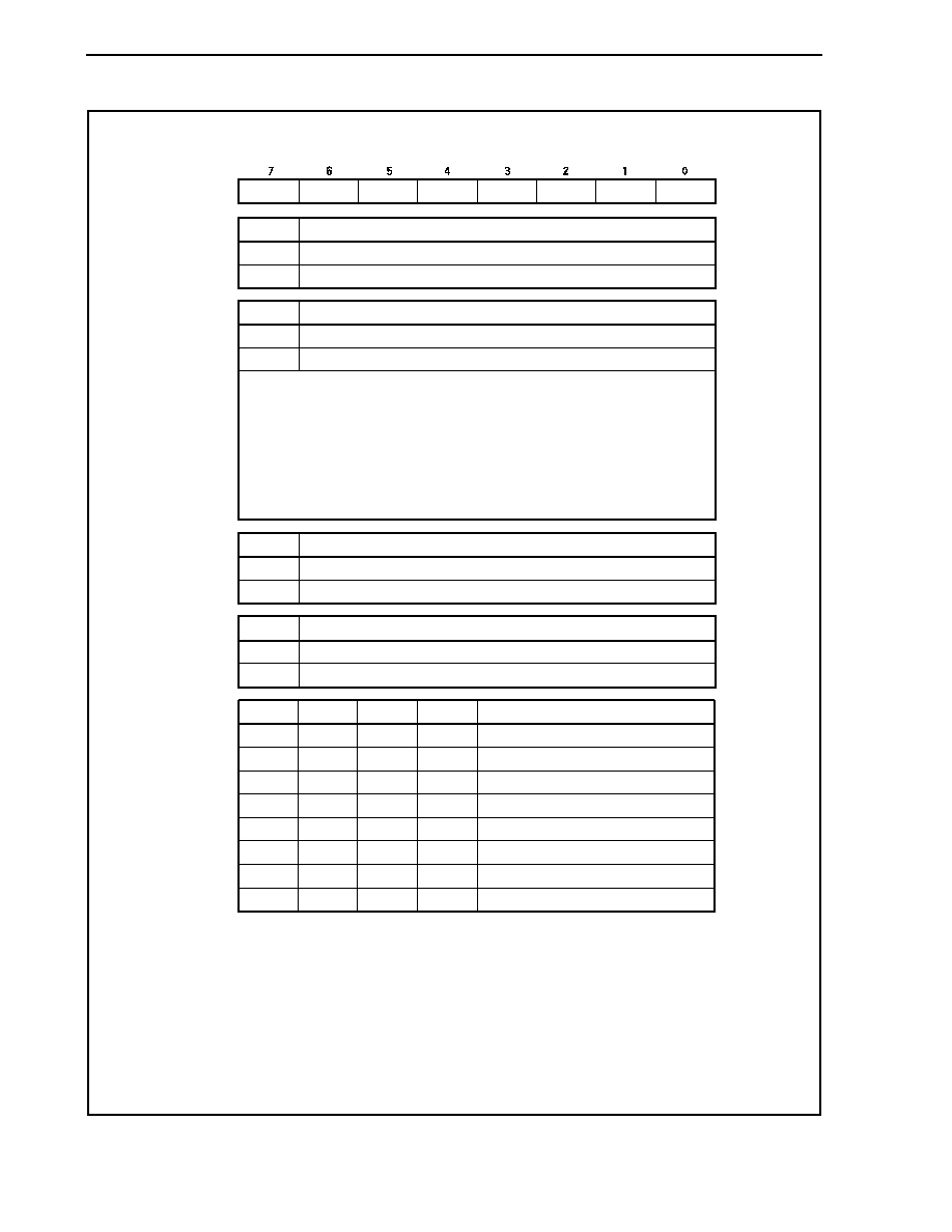
CHAPTER 6 CLOCK GENERATION FUNCTION
Preliminary User's Manual U17714EJ1V0UD
216
FRC
Used
Not used
FRC
0
1
Use of subclock on-chip feedback resistor
PCC
MCK
MFRC
CLS
Note
CK3
CK2
CK1
CK0
Oscillation enabled
Oscillation stopped
MCK
0
1
Main clock oscillator control
Used
Not used
MFRC
0
1
Use of main clock on-chip feedback resistor
After reset: 03H R/W Address: FFFFF828H
Main clock operation
Subclock operation
CLS
Note
0
1
Status of CPU clock (f
CPU
)
Even if the MCK bit is set (1) while the system is operating with the main clock as
the CPU clock, the operation of the main clock does not stop. It stops after the
CPU clock has been changed to the subclock.
Before setting the MCK bit from 0 to 1, stop the on-chip peripheral functions
operating with the main clock.
When the main clock is stopped and the device is operating with the subclock,
clear (0) the MCK bit and secure the oscillation stabilization time by software
before switching the CPU clock to the main clock or operating the on-chip
peripheral functions.
�
�
�
< >
< >
< >
f
XX
f
XX
/2
f
XX
/4
f
XX
/8
f
XX
/16
f
XX
/32
Setting prohibited
f
XT
CK2
0
0
0
0
1
1
1
�
Clock selection (f
CLK
/f
CPU
)
CK1
0
0
1
1
0
0
1
�
CK0
0
1
0
1
0
1
�
�
CK3
0
0
0
0
0
0
0
1
Note The CLS bit is a read-only bit.
Cautions 1. Do not change the CPU clock (by using the CK3 to CK0 bits) while CLKOUT is being
output.
2. Use a bit manipulation instruction to manipulate the CK3 bit. When using an 8-bit
manipulation instruction, do not change the set values of the CK2 to CK0 bits.
Remark
�: don't care

CHAPTER 6 CLOCK GENERATION FUNCTION
Preliminary User's Manual U17714EJ1V0UD
217
(a) Example of setting main clock operation
subclock operation
<1> CK3
bit
1:
Use of a bit manipulation instruction is recommended. Do not change the CK2
to CK0 bits.
<2> Subclock operation: Read the CLS bit to check if subclock operation has started. It takes the
following time after the CK3 bit is set until subclock operation is started.
Max.: 1/f
XT
(1/subclock frequency)
<3> MCK
bit
1:
Set the MCK bit to 1 only when stopping the main clock.
Cautions 1. When stopping the main clock, stop the PLL. Also stop the operations of the on-chip
peripheral functions operating with the main clock.
2. If the following conditions are not satisfied, change the CK2 to CK0 bits so that the
conditions are satisfied, then change to the subclock operation mode.
Internal system clock (f
CLK
) > Subclock (f
XT
: 32.768 kHz)
� 4
Remark Internal system clock (f
CLK
): Clock generated from the main clock (f
XX
) by setting bits CK2 to
CK0
[Description example]
_DMA_DISABLE:
clrl 0,
DCHCn[r0]
-- DMA operation disabled. n = 0 to 3
<1> _SET_SUB_RUN :
st.b r0,
PRCMD[r0]
set1 3,
PCC[r0]
-- CK3 bit
1
<2> _CHECK_CLS :
tst1 4,
PCC[r0]
-- Wait until subclock operation starts.
bz _CHECK_CLS
<3> _STOP_MAIN_CLOCK :
st.b r0,
PRCMD[r0]
set1 6,
PCC[r0]
-- MCK bit
1, main clock is stopped.
_DMA_ENABLE:
setl 0,
DCHCn[r0]
-- DMA operation enabled. n = 0 to 3
Remark The description above is simply an example. Note that in <2> above, the CLS bit is read in a
closed loop.

CHAPTER 6 CLOCK GENERATION FUNCTION
Preliminary User's Manual U17714EJ1V0UD
218
(b) Example of setting subclock operation
main clock operation
<1> MCK
bit
0:
Main clock starts oscillating
<2> Insert waits by the program and wait until the oscillation stabilization time of the main clock elapses.
<3> CK3
bit
0:
Use of a bit manipulation instruction is recommended. Do not change the
CK2 to CK0 bits.
<4> Main clock operation: It takes the following time after the CK3 bit is set until main clock operation
is started.
Max.:
1/f
XT
(1/subclock frequency)
Therefore, insert one NOP instruction immediately after setting the CK3 bit
to 0 or read the CLS bit to check if main clock operation has started.
Caution Enable operation of the on-chip peripheral functions operating with the main clock only
after the oscillation of the main clock stabilizes. If their operations are enabled before
the lapse of the oscillation stabilization time, a malfunction may occur.
[Description example]
_DMA_DISABLE:
clrl 0,
DCHCn[r0]
-- DMA operation disabled. n = 0 to 3
<1> _START_MAIN_OSC :
st.b r0,
PRCMD[r0]
-- Release of protection of special registers
clr1 6,
PCC[r0]
-- Main clock starts oscillating.
<2> movea
0x55, r0, r11
-- Wait for oscillation stabilization time.
_WAIT_OST :
nop
nop
nop
addi
-1, r11, r11
cmp r0,
r11
bne
_WAIT_OST
<3> st.b r0,
PRCMD[r0]
clr1 3,
PCC[r0]
--
CK3
0
<4> _CHECK_CLS :
tst1 4,
PCC[r0]
-- Wait until main clock operation starts.
bnz _CHECK_CLS
_DMA_ENABLE:
setl 0,
DCHCn[r0]
-- DMA operation enabled. n = 0 to 3
Remark The description above is simply an example. Note that in <4> above, the CLS bit is read in a
closed loop.
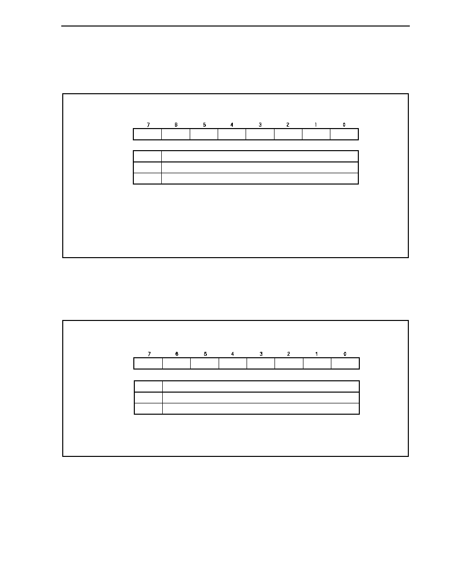
CHAPTER 6 CLOCK GENERATION FUNCTION
Preliminary User's Manual U17714EJ1V0UD
219
(2) Internal oscillation mode register (RCM)
The RCM register is an 8-bit register that sets the operation mode of the internal oscillator.
This register can be read or written in 8-bit or 1-bit units.
Reset sets this register to 00H.
0
RCM
0
0
0
0
0
0
RSTOP
Internal oscillator oscillation
Internal oscillator stopped
RSTOP
0
1
Oscillation/stop of internal oscillator
After reset: 00H R/W Address: FFFFF80CH
< >
Cautions 1. The internal oscillator cannot be stopped while the CPU is operating on the internal
oscillation clock (CCLS.CCLSF bit = 1). Do not set the RSTOP bit to 1.
2. The internal oscillator oscillates if the CCLS.CCLSF bit is set to 1 (when WDT overflow
occurs during oscillation stabilization) even when the RSTOP bit is set to 1. At this time,
the RSTOP bit remains being set to 1.
(3) CPU operation clock status register (CCLS)
The CCLS register indicates the status of the CPU operation clock.
This register is read-only, in 8-bit or 1-bit units.
Reset sets this register to 00H.
0
CCLS
0
0
0
0
0
0
CCLSF
After reset: 00H
Note
R Address: FFFFF82EH
Operating on main clock (f
X
) or subclock (f
XT
).
Operating on internal oscillation clock (f
R
).
CCLSF
0
1
CPU operation clock status
Note If WDT overflow occurs during oscillation stabilization after a reset is released, the CCLSF bit is set
to 1 and the reset value is 01H.
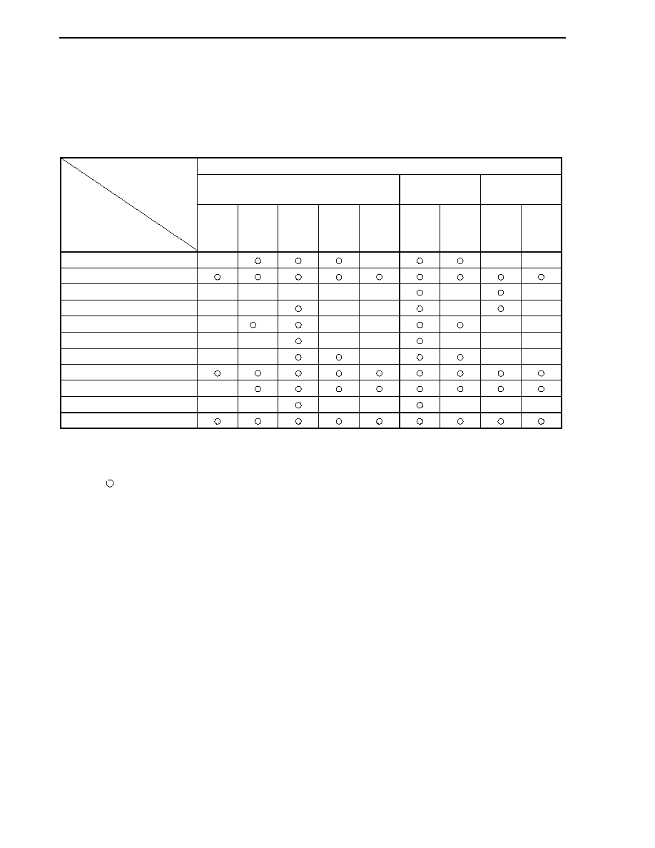
CHAPTER 6 CLOCK GENERATION FUNCTION
Preliminary User's Manual U17714EJ1V0UD
220
6.4 Operation
6.4.1
Operation of each clock
The following table shows the operation status of each clock.
Table 6-1. Operation Status of Each Clock
PCC Register
CLK Bit = 0, MCK Bit = 0
CLS Bit = 1,
MCK Bit = 0
CLS Bit = 1,
MCK Bit = 1
Register Setting and
Operation Status
Target Clock
During
Reset
During
Oscillation
Stabilization
Time Count
HALT
Mode
IDLE1,
IDLE2
Mode
STOP
Mode
Subclock
Mode
Sub-IDLE
Mode
Subclock
Mode
Sub-IDLE
Mode
Main clock oscillator (f
X
)
�
�
�
�
Subclock oscillator (f
XT
)
CPU clock (f
CPU
)
�
�
�
�
�
�
�
Internal system clock (f
CLK
)
�
�
�
�
�
�
Main clock (in PLL mode, f
XX
)
�
Note
�
�
�
�
Peripheral clock (f
XX
to f
XX
/1,024)
�
�
�
�
�
�
�
WT clock (main)
�
�
�
�
�
WT clock (sub)
WDT2 clock (internal oscillation)
�
WDT2 clock (main)
�
�
�
�
�
�
�
WDT2 clock (sub)
Note Lockup
time
Remark
: Operable
�: Stopped
6.4.2
Clock output function
The clock output function is used to output the internal system clock (f
CLK
) from the CLKOUT pin.
The internal system clock (f
CLK
) is selected by using the PCC.CK3 to PCC.CK0 bits.
The CLKOUT pin functions alternately as the PCM1 pin and functions as a clock output pin if so specified by the
control register of port CM.
The status of the CLKOUT pin is the same as the internal system clock in Table 6-1 and the pin can output the
clock when it is in the operable status. It outputs a low level in the stopped status. However, the CLKOUT pin is in
the port mode (PCM1 pin: input mode) after reset and until it is set in the output mode. Therefore, the status of the pin
is Hi-Z.
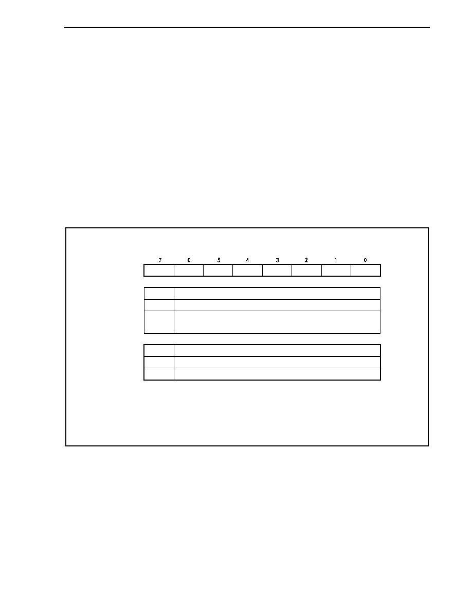
CHAPTER 6 CLOCK GENERATION FUNCTION
Preliminary User's Manual U17714EJ1V0UD
221
6.5 PLL
Function
6.5.1 Overview
In the V850ES/JJ2, an operating clock that is 4 or 8 times higher than the oscillation frequency output by the PLL
function or the clock-through mode can be selected as the operating clock of the CPU and on-chip peripheral
functions.
When PLL function is used (
�4): Input clock = 2.5 to 5 MHz (output: 10 to 20 MHz)
Clock-through mode:
Input clock = 2.5 to 10 MHz (output: 2.5 to 10 MHz)
6.5.2 Registers
(1) PLL control register (PLLCTL)
The PLLCTL register is an 8-bit register that controls the PLL function.
This register can be read or written in 8-bit or 1-bit units.
Reset sets this register to 01H.
0
PLLCTL
0
0
0
0
0
SELPLL
PLLON
PLL stopped
PLL operating
(After PLL operation starts, a lockup time is required for frequency stabilization)
PLLON
0
1
PLL operation stop register
Clock-through mode
PLL mode
SELPLL
0
1
CPU operation clock selection register
After reset: 01H R/W Address: FFFFF82CH
< >
< >
Cautions 1. When the PLLON bit is cleared to 0, the SELPLL bit is automatically cleared to 0 (clock-
through mode).
2. The SELPLL bit can be set to 1 only when the PLL clock frequency is stabilized. If not
(unlocked), "0" is written to the SELPLL bit if data is written to it.
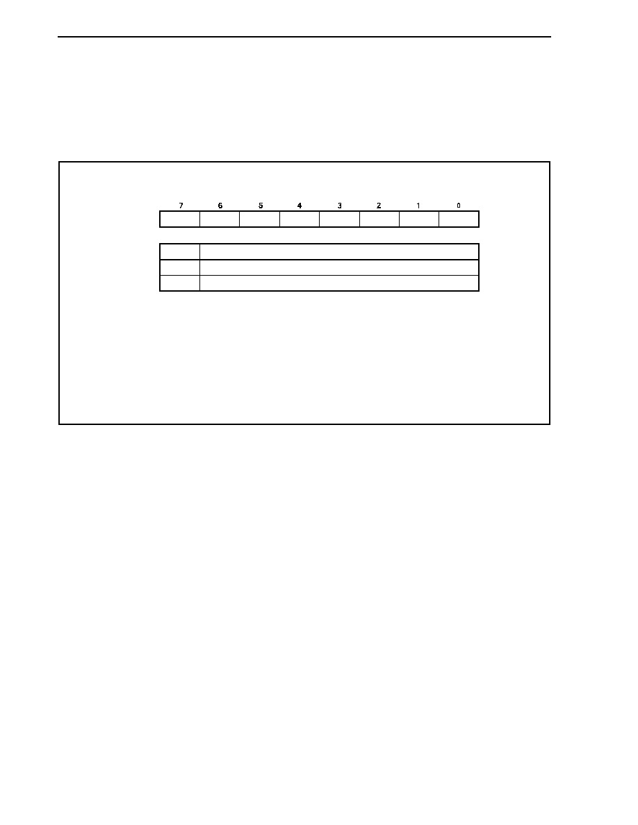
CHAPTER 6 CLOCK GENERATION FUNCTION
Preliminary User's Manual U17714EJ1V0UD
222
(2) Clock control register (CKC)
The CKC register is a special register. Data can be written to this register only in a combination of specific
sequence (see 3.4.7 Special registers).
The CKC register controls the internal system clock in the PLL mode.
This register can be read or written in 8-bit or 1-bit units.
Reset sets this register to 0AH.
0
CKC
0
0
0
1
0
1
CKDIV0
After reset: 0AH R/W Address: FFFFF822H
f
XX
= 4
� f
X
(f
X
= 2.5 to 5.0 MHz)
f
XX
= 8
� f
X
(f
X
= 2.5 to 4.0 MHz)
CKDIV0
0
1
Internal system clock (f
XX
) in PLL mode
Cautions 1. The PLL mode cannot be used at f
X
= 5.0 to 10.0 MHz.
2. Before changing the multiplication factor between 4 and 8 by using the CKC register, set
the clock-through mode and stop the PLL.
3. Be sure to set bits 3 and 1 to "1" and clear bits 7 to 4 and 2 to "0".
Remark Both the CPU clock and peripheral clock are divided by the CKC register, but only the CPU clock is
divided by the PCC register.
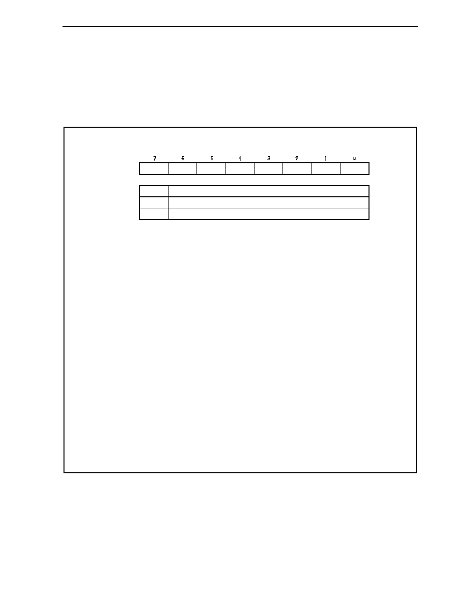
CHAPTER 6 CLOCK GENERATION FUNCTION
Preliminary User's Manual U17714EJ1V0UD
223
(3) Lock register (LOCKR)
Phase lock occurs at a given frequency following power application or immediately after the STOP mode is
released, and the time required for stabilization is the lockup time (frequency stabilization time). This state
until stabilization is called the lockup status, and the stabilized state is called the locked status.
The LOCKR register includes a LOCK bit that reflects the PLL frequency stabilization status.
This register is read-only, in 8-bit or 1-bit units.
Reset sets this register to 00H.
0
LOCKR
0
0
0
0
0
0
LOCK
Locked status
Unlocked status
LOCK
0
1
PLL lock status check
After reset: 00H R Address: FFFFF824H
< >
Caution The LOCK register does not reflect the lock status of the PLL in real time. The set/clear
conditions are as follows.
[Set conditions]
� Upon system reset
Note
� In IDLE2 or STOP mode
� Upon setting of PLL stop (clearing of PLLCTL.PLLON bit to 0)
� Upon stopping main clock and using CPU with subclock (setting of PCC.CK3 bit to 1 and setting of
PCC.MCK bit to 1)
Note This register is set to 01H by reset and cleared to 00H after the reset has been released and the
oscillation stabilization time has elapsed.
[Clear conditions]
� Upon overflow of oscillation stabilization time following reset release (OSTS register default time (see 21.2
(3) Oscillation stabilization time select register (OSTS)))
� Upon oscillation stabilization timer overflow (time set by OSTS register) following STOP mode release,
when the STOP mode was set in the PLL operating status
� Upon PLL lockup time timer overflow (time set by PLLS register) when the PLLCTL.PLLON bit is changed
from 0 to 1
� After the setup time inserted upon release of the IDLE2 mode is released (time set by the OSTS register)
when the IDLE2 mode is set during PLL operation.
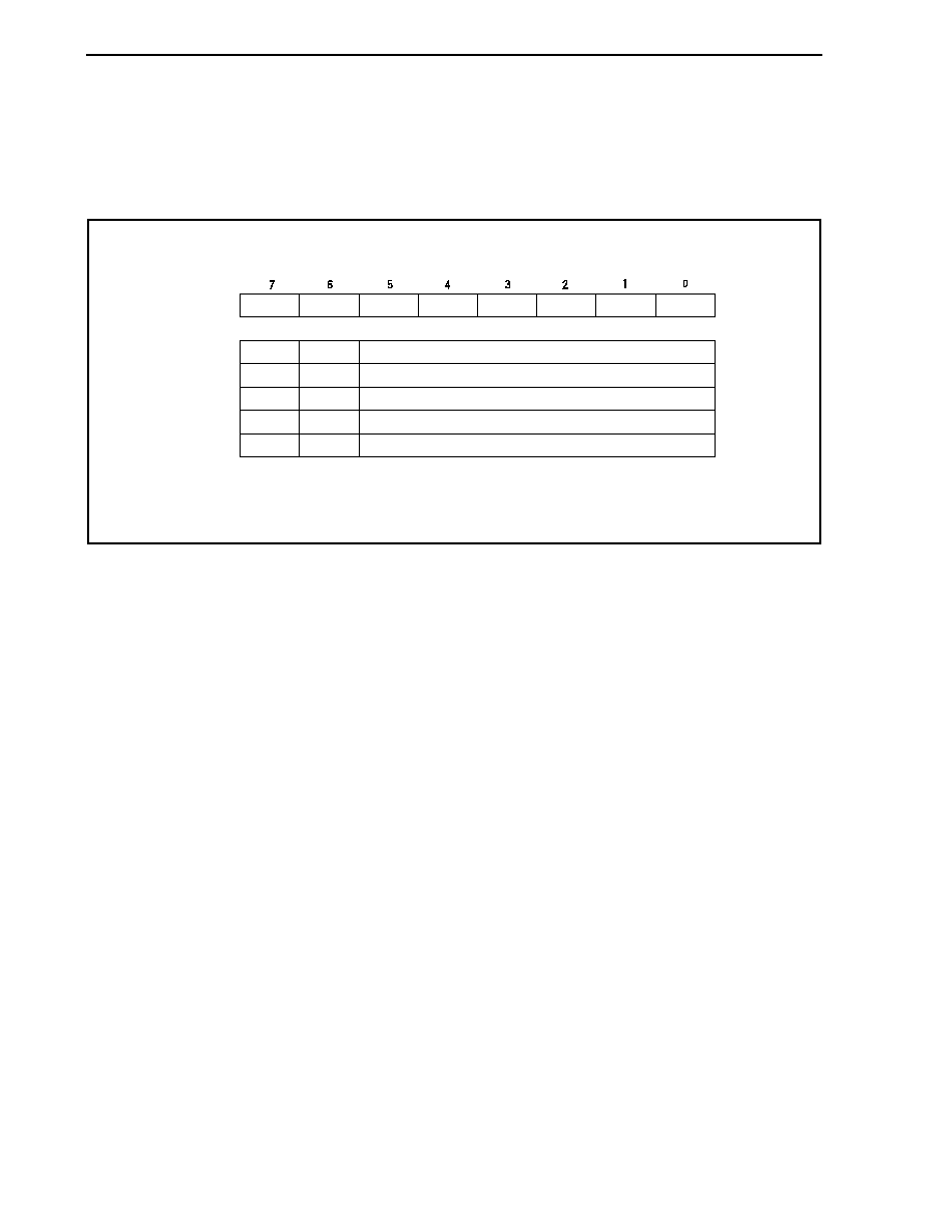
CHAPTER 6 CLOCK GENERATION FUNCTION
Preliminary User's Manual U17714EJ1V0UD
224
(4) PLL lockup time specification register (PLLS)
The PLLS register is an 8-bit register used to select the PLL lockup time when the PLLCTL.PLLON bit is
changed from 0 to 1.
This register can be read or written in 8-bit units.
Reset sets this register to 03H.
0
2
10
/f
X
2
11
f
X
2
12
/f
X
2
13
/f
X
(default value)
PLLS1
0
0
1
1
PLLS0
0
1
0
1
Selection of PLL lockup time
PLLS
0
0
0
0
0
PLLS1
PLLS0
After reset: 03H R/W Address: FFFFF6C1H
Cautions 1. Set so that the lockup time is 800
�
s or longer.
2. Do not change the PLLS register setting during the lockup period.
6.5.3 Usage
(1) When PLL is used
� After the reset signal has been released, the PLL operates (PLLCTL.PLLON bit = 1), but because the default
mode is the clock-through mode (PLLCTL.SELPLL bit = 0), select the PLL mode (SELPLL bit = 1).
� To enable PLL operation, first set the PLLON bit to 1, and then set the SELPLL bit to 1 after the
LOCKR.LOCK bit = 0. To stop the PLL, first select the clock-through mode (SELPLL bit = 0), wait for 8
clocks or more, and then stop the PLL (PLLON bit = 0).
� The PLL stops during transition to the IDLE2 or STOP mode regardless of the setting and is restored from
the IDLE2 or STOP mode to the status before transition. The time required for restoration is as follows.
(a) When transiting to the IDLE2 or STOP mode from the clock through mode
� STOP mode: Set the OSTS register so that the oscillation stabilization time is 1 ms (min.) or longer.
� IDLE2 mode: Set the OSTS register so that the setup time is 350
�
s (min.) or longer.
(b) When transiting to the IDLE 2 or STOP mode while remaining in the PLL operation mode
� STOP mode: Set the OSTS register so that the oscillation stabilization time is 1 ms (min.) or longer.
� IDLE2 mode: Set the OSTS register so that the setup time is 800
�
s (min.) or longer.
When transiting to the IDLE1 mode, the PLL does not stop. Stop the PLL if necessary.
(2) When PLL is not used
� The clock-through mode (SELPLL bit = 0) is selected after the reset signal has been released, but the PLL is
operating (PLLON bit = 1) and must therefore be stopped (PLLON bit = 0).

Preliminary User's Manual U17714EJ1V0UD
225
CHAPTER 7 16-BIT TIMER/EVENT COUNTER P (TMP)
Timer P (TMP) is a 16-bit timer/event counter.
The V850ES/JJ2 has nine timer/event counter channels, TMP0 to TMP8.
7.1 Overview
An outline of TMPn is shown below.
� Clock selection: 8 ways
� Capture/trigger input pins: 2
� External event count input pins: 1
� External trigger input pins: 1
� Timer/counters: 1
� Capture/compare registers: 2
� Capture/compare match interrupt request signals: 2
� Timer output pins: 2
Remark n = 0 to 8
7.2 Functions
TMPn has the following functions.
� Interval timer
� External event counter
� External trigger pulse output
� One-shot pulse output
� PWM output
� Free-running timer
� Pulse width measurement
Remark n = 0 to 8
CHAPTER 7 16-BIT TIMER/EVENT COUNTER P (TMP)
Preliminary User's Manual U17714EJ1V0UD
226
7.3 Configuration
TMPn includes the following hardware.
Table 7-1. Configuration of TMPn
Item Configuration
Timer register
16-bit counter
Registers
TMPn capture/compare registers 0, 1 (TPnCCR0, TPnCCR1)
TMPn counter read buffer register (TPnCNT)
CCR0, CCR1 buffer registers
Timer inputs
2 (TIPn0
Note 1
, TIPn1 pins)
Timer outputs
2 (TOPn0, TOPn1 pins)
Control registers
Note 2
TMPn control registers 0, 1 (TPnCTL0, TPnCTL1)
TMPn I/O control registers 0 to 2 (TPnIOC0 to TPnIOC2)
TMPn option register 0 (TPnOPT0)
Notes 1. The TIPn0 pin functions alternately as a capture trigger input signal, external event count
input signal, and external trigger input signal.
2. When using the functions of the TIPn0, TIPn1,TOPn0, and TOPn1 pins, see Table 4-19
Using Port Pin as Alternate-Function Pin.
Remark n = 0 to 8
Figure 7-1. Block Diagram of TMPn
f
XX
f
XX
/2
f
XX
/4
f
XX
/8
f
XX
/16
f
XX
/32
f
XX
/64
Note 1
, f
XX
/256
Note 2
f
XX
/128
Note 1
, f
XX
/512
Note 2
Selector
Internal bus
Internal bus
TOPn0
TOPn1
TIPn0
TIPn1
Selector
Edge
detector
CCR0
buffer
register
CCR1
buffer
register
TPnCCR0
TPnCCR1
16-bit counter
TPnCNT
INTTPnOV
INTTPnCC0
INTTPnCC1
Output
controller
Clear
Notes 1. TMP0, TMP2, TMP4, TMP6, TMP8
2. TMP1, TMP3, TMP5, TMP7
Remark f
XX
: Main clock frequency

CHAPTER 7 16-BIT TIMER/EVENT COUNTER P (TMP)
Preliminary User's Manual U17714EJ1V0UD
227
(1) 16-bit counter
This 16-bit counter can count internal clocks or external events.
The count value of this counter can be read by using the TPnCNT register.
When the TPnCTL0.TPnCE bit = 0, the value of the 16-bit counter is FFFFH. If the TPnCNT register is read at
this time, 0000H is read.
Reset sets the TPnCE bit to 0. Therefore, the 16-bit counter is set to FFFFH.
(2) CCR0 buffer register
This is a 16-bit compare register that compares the count value of the 16-bit counter.
When the TPnCCR0 register is used as a compare register, the value written to the TPnCCR0 register is
transferred to the CCR0 buffer register. When the count value of the 16-bit counter matches the value of the
CCR0 buffer register, a compare match interrupt request signal (INTTPnCC0) is generated.
The CCR0 buffer register cannot be read or written directly.
The CCR0 buffer register is cleared to 0000H after reset, as the TPnCCR0 register is cleared to 0000H.
(3) CCR1 buffer register
This is a 16-bit compare register that compares the count value of the 16-bit counter.
When the TPnCCR1 register is used as a compare register, the value written to the TPnCCR1 register is
transferred to the CCR1 buffer register. When the count value of the 16-bit counter matches the value of the
CCR1 buffer register, a compare match interrupt request signal (INTTPnCC1) is generated.
The CCR1 buffer register cannot be read or written directly.
The CCR1 buffer register is cleared to 0000H after reset, as the TPnCCR1 register is cleared to 0000H.
(4) Edge detector
This circuit detects the valid edges input to the TIPn0 and TIPn1 pins. No edge, rising edge, falling edge, or
both the rising and falling edges can be selected as the valid edge by using the TPnIOC1 and TPnIOC2
registers.
(5) Output controller
This circuit controls the output of the TOPn0 and TOPn1 pins. The output controller is controlled by the
TPnIOC0 register.
(6) Selector
This selector selects the count clock for the 16-bit counter. Eight types of internal clocks or an external event
can be selected as the count clock.

CHAPTER 7 16-BIT TIMER/EVENT COUNTER P (TMP)
Preliminary User's Manual U17714EJ1V0UD
228
7.4 Registers
The registers that control TMPn are as follows.
� TMPn control register 0 (TPnCTL0)
� TMPn control register 1 (TPnCTL1)
� TMPn I/O control register 0 (TPnIOC0)
� TMPn I/O control register 1 (TPnIOC1)
� TMPn I/O control register 2 (TPnIOC2)
� TMPn option register 0 (TPnOPT0)
� TMPn capture/compare register 0 (TPnCCR0)
� TMPn capture/compare register 1 (TPnCCR1)
� TMPn counter read buffer register (TPnCNT)
Remarks 1. When using the functions of the TIPn0, TIPn1,TOPn0, and TOPn1 pins, see Table 4-19 Using Port
Pin as Alternate-Function Pin.
2. n = 0 to 8
CHAPTER 7 16-BIT TIMER/EVENT COUNTER P (TMP)
Preliminary User's Manual U17714EJ1V0UD
229
(1) TMPn control register 0 (TPnCTL0)
The TPnCTL0 register is an 8-bit register that controls the operation of TMPn.
This register can be read or written in 8-bit or 1-bit units.
Reset sets this register to 00H.
The same value can always be written to the TPnCTL0 register by software.
TPnCE
TMPn operation disabled (TMPn reset asynchronously
Note
).
TMPn operation enabled. TMPn operation started.
TPnCE
0
1
TMPn operation control
TPnCTL0
(n = 0 to 8)
0
0
0
0
TPnCKS2 TPnCKS1 TPnCKS0
6
5
4
3
2
1
After reset: 00H R/W Address:
TP0CTL0 FFFFF590H, TP1CTL0 FFFFF5A0H,
TP2CTL0 FFFFF5B0H, TP3CTL0 FFFFF5C0H,
TP4CTL0 FFFFF5D0H, TP5CTL0 FFFFF5E0H,
TP6CTL0 FFFFF5F0H, TP7CTL0 FFFFF600H,
TP8CTL0 FFFFF610H
<7>
0
f
XX
f
XX
/2
f
XX
/4
f
XX
/8
f
XX
/16
f
XX
/32
f
XX
/64
f
XX
/128
f
XX
/256
f
XX
/512
TPnCKS2
0
0
0
0
1
1
1
1
Internal count clock selection
n = 0, 2, 4, 6, 8
n = 1, 3, 5, 7
TPnCKS1
0
0
1
1
0
0
1
1
TPnCKS0
0
1
0
1
0
1
0
1
Note TPn0PT0.TPnOVF bit, 16-bit counter, timer output (TOPn0, TOPn1 pins)
Cautions 1. Set the TPnCKS2 to TPnCKS0 bits when the TPnCE bit = 0.
When the value of the TPnCE bit is changed from 0 to 1, the
TPnCKS2 to TPnCKS0 bits can be set simultaneously.
2. Be sure to clear bits 3 to 6 to "0".
Remark f
XX
: Main clock frequency
(2) TMPn control register 1 (TPnCTL1)
The TPnCTL1 register is an 8-bit register that controls the operation of TMPn.
This register can be read or written in 8-bit or 1-bit units.
Reset sets this register to 00H.
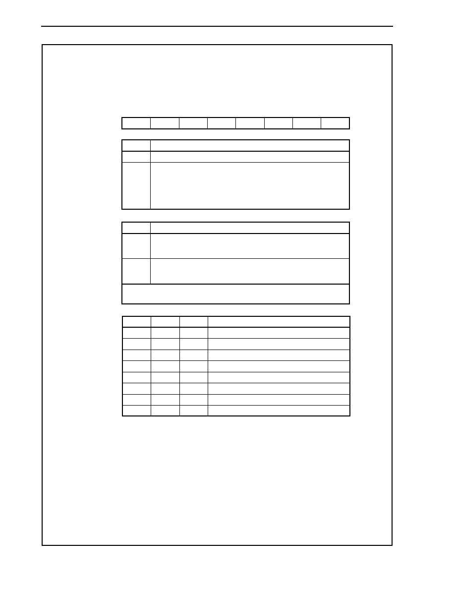
CHAPTER 7 16-BIT TIMER/EVENT COUNTER P (TMP)
Preliminary User's Manual U17714EJ1V0UD
230
0
TPnEST
0
1
Software trigger control
TPnCTL1
(n = 0 to 8)
TPnEST
TPnEEE
0
0
TPnMD2 TPnMD1 TPnMD0
<6>
<5>
4
3
2
1
After reset: 00H R/W Address: TP0CTL1 FFFFF591H, TP1CTL1 FFFFF5A1H,
TP2CTL1 FFFFF5B1H, TP3CTL1 FFFFF5C1H,
TP4CTL1 FFFFF5D1H, TP5CTL1 FFFFF5E1H,
TP6CTL1 FFFFF5F1H, TP7CTL1 FFFFF601H,
TP8CTL1 FFFFF611H
Generate a valid signal for external trigger input.
� In one-shot pulse output mode: A one-shot pulse is output with writing
1 to the TPnEST bit as the trigger.
� In external trigger pulse output mode: A PWM waveform is output with
writing 1 to the TPnEST bit as the
trigger.
Disable operation with external event count input.
(Perform counting with the count clock selected by the TPnCTL0.TPnCK0
to TPnCK2 bits.)
TPnEEE
0
1
Count clock selection
The TPnEEE bit selects whether counting is performed with the internal count clock
or the valid edge of the external event count input.
7
0
Interval timer mode
External event count mode
External trigger pulse output mode
One-shot pulse output mode
PWM output mode
Free-running timer mode
Pulse width measurement mode
Setting prohibited
TPnMD2
0
0
0
0
1
1
1
1
Timer mode selection
TPnMD1
0
0
1
1
0
0
1
1
TPnMD0
0
1
0
1
0
1
0
1
Enable operation with external event count input.
(Perform counting at the valid edge of the external event count input
signal.)
-
Cautions 1. The TPnEST bit is valid only in the external trigger pulse output
mode or one-shot pulse output mode. In any other mode, writing 1
to this bit is ignored.
2. External event count input is selected in the external event count
mode regardless of the value of the TPnEEE bit.
3. Set the TPnEEE and TPnMD2 to TPnMD0 bits when the
TPnCTL0.TPnCE bit = 0. (The same value can be written when the
TPnCE bit = 1.) The operation is not guaranteed when rewriting is
performed with the TPnCE bit = 1. If rewriting was mistakenly
performed, clear the TPnCE bit to 0 and then set the bits again.
4. Be sure to clear bits 3, 4, and 7 to "0".
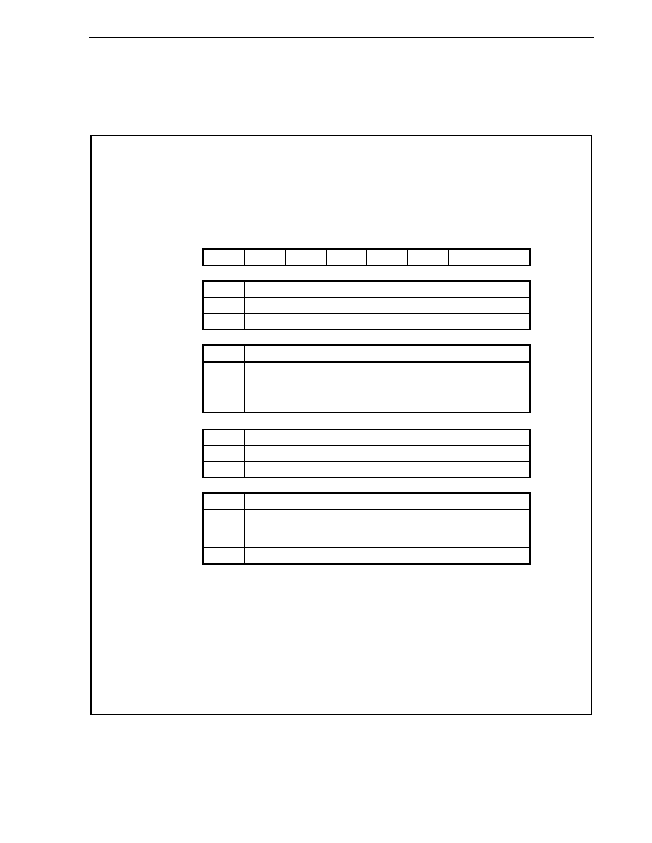
CHAPTER 7 16-BIT TIMER/EVENT COUNTER P (TMP)
Preliminary User's Manual U17714EJ1V0UD
231
(3) TMPn I/O control register 0 (TPnIOC0)
The TPnIOC0 register is an 8-bit register that controls the timer output (TOPn0, TOPn1 pins).
This register can be read or written in 8-bit or 1-bit units.
Reset sets this register to 00H.
0
TPnOL1
0
1
TOPn1 pin output level setting
TOPn1 pin output inversion disabled
TOPn1 pin output inversion enabled
TPnIOC0
(n = 0 to 8)
0
0
0
TPnOL1 TPnOE1
TPnOL0
TPnOE0
6
5
4
3
<2>
1
After reset: 00H R/W Address:
TP0IOC0 FFFFF592H, TP1IOC0 FFFFF5A2H,
TP2IOC0 FFFFF5B2H, TP3IOC0 FFFFF5C2H,
TP4IOC0 FFFFF5D2H, TP5IOC0 FFFFF5E2H,
TP6IOC0 FFFFF5F2H, TP7IOC0 FFFFF602H,
TP8IOC0 FFFFF612H
TPnOE1
0
1
TOPn1 pin output setting
Timer output disabled
� When TPnOL1 bit = 0: Low level is output from the TOPn1 pin
� When TPnOL1 bit = 1: High level is output from the TOPn1 pin
TPnOL0
0
1
TOPn0 pin output level setting
TOPn0 pin output inversion disabled
TOPn0 pin output inversion enabled
TPnOE0
0
1
TOPn0 pin output setting
Timer output disabled
� When TPnOL0 bit = 0: Low level is output from the TOPn0 pin
� When TPnOL0 bit = 1: High level is output from the TOPn0 pin
7
<0>
Timer output enabled (a square wave is output from the TOPn1 pin).
Timer output enabled (a square wave is output from the TOPn0 pin).
Cautions 1. Rewrite the TPnOL1, TPnOE1, TPnOL0, and TPnOE0 bits
when the TPnCTL0.TPnCE bit = 0. (The same value can be
written when the TPnCE bit = 1.) If rewriting was
mistakenly performed, clear the TPnCE bit to 0 and then
set the bits again.
2. Even if the TPnOLm bit is manipulated when the TPnCE
and TPnOEm bits are 0, the TOPnm pin output level varies
(m = 0, 1).
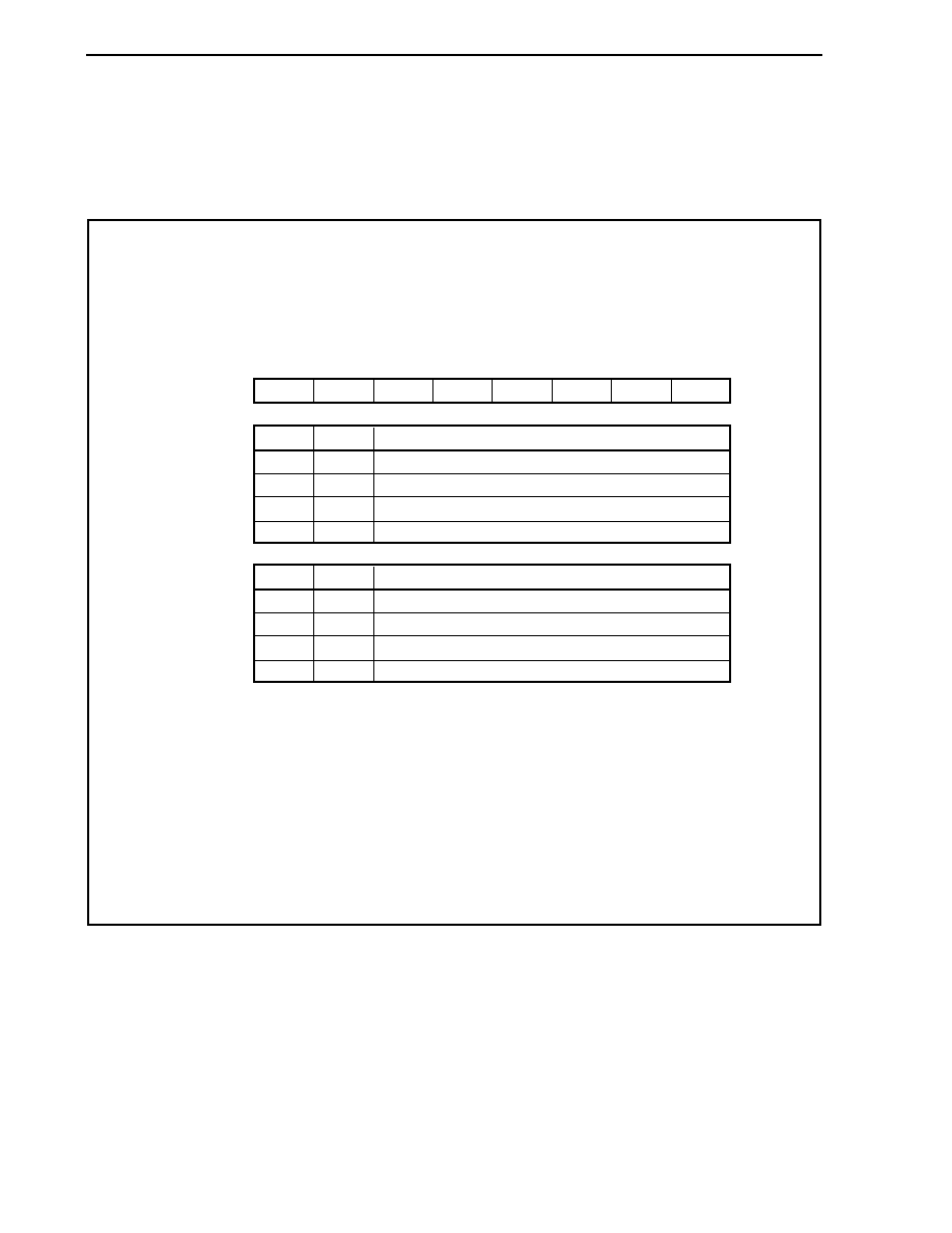
CHAPTER 7 16-BIT TIMER/EVENT COUNTER P (TMP)
Preliminary User's Manual U17714EJ1V0UD
232
(4) TMPn I/O control register 1 (TPnIOC1)
The TPnIOC1 register is an 8-bit register that controls the valid edge of the capture trigger input signals (TIPn0,
TIPn1 pins).
This register can be read or written in 8-bit or 1-bit units.
Reset sets this register to 00H.
0
TPnIS3
0
0
1
1
TPnIS2
0
1
0
1
Capture trigger input signal (TIPn1 pin) valid edge setting
No edge detection (capture operation invalid)
Detection of rising edge
Detection of falling edge
Detection of both edges
TPnIOC1
(n = 0 to 8)
0
0
0
TPnIS3
TPnIS2
TPnIS1
TPnIS0
6
5
4
3
2
1
After reset: 00H R/W Address:
TP0IOC1 FFFFF593H, TP1IOC1 FFFFF5A3H,
TP2IOC1 FFFFF5B3H, TP3IOC1 FFFFF5C3H,
TP4IOC1 FFFFF5D3H, TP5IOC1 FFFFF5E3H,
TP6IOC1 FFFFF5F3H, TP7IOC1 FFFFF603H,
TP8IOC1 FFFFF613H
TPnIS1
0
0
1
1
TPnIS0
0
1
0
1
Capture trigger input signal (TIPn0 pin) valid edge setting
No edge detection (capture operation invalid)
Detection of rising edge
Detection of falling edge
Detection of both edges
7
0
Cautions
1.
Rewrite the TPnIS3 to TPnIS0 bits when the
TPnCTL0.TPnCE bit = 0. (The same value can be written
when the TPnCE bit = 1.) If rewriting was mistakenly
performed, clear the TPnCE bit to 0 and then set the bits
again.
2. The TPnIS3 to TPnIS0 bits are valid only in the free-
running timer mode and the pulse width measurement
mode. In all other modes, a capture operation is not
possible.
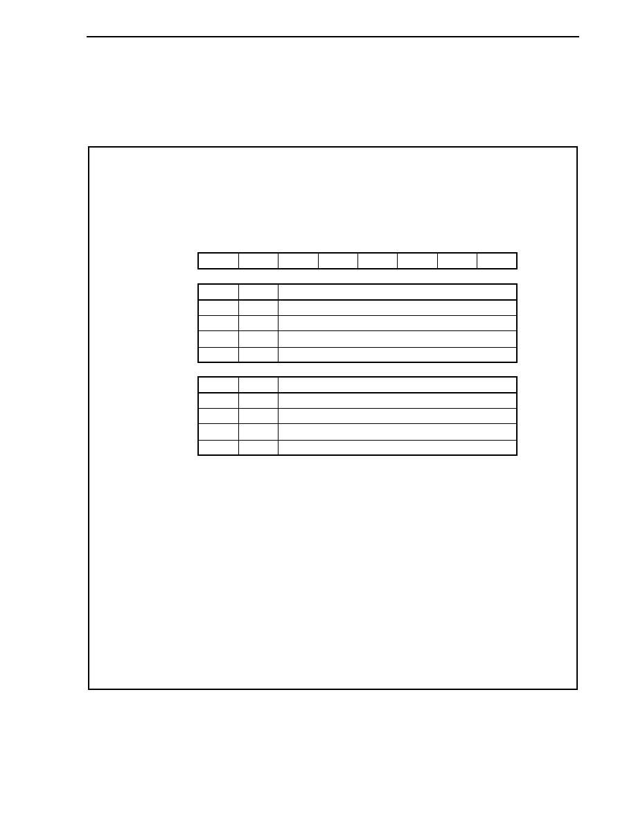
CHAPTER 7 16-BIT TIMER/EVENT COUNTER P (TMP)
Preliminary User's Manual U17714EJ1V0UD
233
(5) TMPn I/O control register 2 (TPnIOC2)
The TPnIOC2 register is an 8-bit register that controls the valid edge of the external event count input signal
(TIPn0 pin) and external trigger input signal (TIPn0 pin).
This register can be read or written in 8-bit or 1-bit units.
Reset sets this register to 00H.
0
TPnEES1
0
0
1
1
TPnEES0
0
1
0
1
External event count input signal (TIPn0 pin) valid edge setting
No edge detection (external event count invalid)
Detection of rising edge
Detection of falling edge
Detection of both edges
TPnIOC2
(n = 0 to 8)
0
0
0
TPnEES1 TPnEES0 TPnETS1 TPnETS0
6
5
4
3
2
1
After reset: 00H R/W Address:
TP0IOC2 FFFFF594H, TP1IOC2 FFFFF5A4H,
TP2IOC2 FFFFF5B4H, TP3IOC2 FFFFF5C4H,
TP4IOC2 FFFFF5D4H, TP5IOC2 FFFFF5E4H,
TP6IOC2 FFFFF5F4H, TP7IOC2 FFFFF604H,
TP8IOC2 FFFFF614H
TPnETS1
0
0
1
1
TPnETS0
0
1
0
1
External trigger input signal (TIPn0 pin) valid edge setting
No edge detection (external trigger invalid)
Detection of rising edge
Detection of falling edge
Detection of both edges
7
0
Cautions 1. Rewrite the TPnEES1, TPnEES0, TPnETS1, and TPnETS0
bits when the TPnCTL0.TPnCE bit = 0. (The same value
can be written when the TPnCE bit = 1.) If rewriting was
mistakenly performed, clear the TPnCE bit to 0 and then
set the bits again.
2. The TPnEES1 and TPnEES0 bits are valid only when the
TPnCTL1.TPnEEE bit = 1 or when the external event
count mode (TPnCTL1.TPnMD2 to TPnCTL1.TPnMD0 bits
= 001) has been set.
3. The TPnETS1 and TPnETS0 bits are valid only when the
external trigger pulse output mode (TPnCTL1.TPnMD2 to
TPnCTL1.TPnMD0 bits = 010) or the one-shot pulse
output mode (TPnCTL1.TPnMD2 to TPnCTL1.TPnMD0 =
011) is set.
CHAPTER 7 16-BIT TIMER/EVENT COUNTER P (TMP)
Preliminary User's Manual U17714EJ1V0UD
234
(6) TMPn option register 0 (TPnOPT0)
The TPnOPT0 register is an 8-bit register used to set the capture/compare operation and detect an overflow.
This register can be read or written in 8-bit or 1-bit units.
Reset sets this register to 00H.
0
TPnCCS1
0
1
TPnCCR1 register capture/compare selection
The TPnCCS1 bit setting is valid only in the free-running timer mode.
Compare register selected
Capture register selected
TPnOPT0
(n = 0 to 8)
0
TPnCCS1 TPnCCS0
0
0
0
TPnOVF
6
5
4
3
2
1
After reset: 00H R/W Address:
TP0OPT0 FFFFF595H, TP1OPT0 FFFFF5A5H,
TP2OPT0 FFFFF5B5H, TP3OPT0 FFFFF5C5H,
TP4OPT0 FFFFF5D5H, TP5OPT0 FFFFF5E5H,
TP6OPT0 FFFFF5F5H, TP7OPT0 FFFFF605H,
TP8OPT0 FFFFF615H
TPnCCS0
0
1
TPnCCR0 register capture/compare selection
The TPnCCS0 bit setting is valid only in the free-running timer mode.
Compare register selected
Capture register selected
TPnOVF
Set (1)
Reset (0)
TMPn overflow detection flag
� The TPnOVF bit is reset when the 16-bit counter count value overflows from
FFFFH to 0000H in the free-running timer mode or the pulse width measurement
mode.
� An interrupt request signal (INTTPnOV) is generated at the same time that the
TPnOVF bit is set to 1. The INTTPnOV signal is not generated in modes other
than the free-running timer mode and the pulse width measurement mode.
� The TPnOVF bit is not cleared even when the TPnOVF bit or the TPnOPT0
register are read when the TPnOVF bit = 1.
� The TPnOVF bit can be both read and written, but the TPnOVF bit cannot be set
to 1 by software. Writing 1 has no influence on the operation of TMPn.
Overflow occurred
TPnOVF bit 0 written or TPnCTL0.TPnCE bit = 0
7
<0>
Cautions 1. Rewrite the TPnCCS1 and TPnCCS0 bits when the TPnCE
bit = 0. (The same value can be written when the TPnCE
bit = 1.) If rewriting was mistakenly performed, clear the
TPnCE bit to 0 and then set the bits again.
2. Be sure to clear bits 1 to 3, 6, and 7 to "0".
CHAPTER 7 16-BIT TIMER/EVENT COUNTER P (TMP)
Preliminary User's Manual U17714EJ1V0UD
235
(7) TMPn capture/compare register 0 (TPnCCR0)
The TPnCCR0 register can be used as a capture register or a compare register depending on the mode.
This register can be used as a capture register or a compare register only in the free-running timer mode,
depending on the setting of the TPnOPT0.TPnCCS0 bit. In the pulse width measurement mode, the TPnCCR0
register can be used only as a capture register. In any other mode, this register can be used only as a
compare register.
The TPnCCR0 register can be read or written during operation.
This register can be read or written in 16-bit units.
Reset sets this register to 0000H.
Caution Accessing the TPnCCR0 register is prohibited in the following statuses. For details, see 3.4.8
(2) Accessing specific on-chip peripheral I/O registers.
�
When the CPU operates with the subclock and the main clock oscillation is stopped
�
When the CPU operates with the internal oscillation clock
TPnCCR0
(n = 0 to 8)
12
10
8
6
4
2
After reset: 0000H R/W Address:
TP0CCR0 FFFFF596H, TP1CCR0 FFFFF5A6H,
TP2CCR0 FFFFF5B6H, TP3CCR0 FFFFF5C6H,
TP4CCR0 FFFFF5D6H, TP5CCR0 FFFFF5E6H,
TP6CCR0 FFFFF5F6H, TP7CCR0 FFFFF606H,
TP8CCR0 FFFFF616H
14
0
13
11
9
7
5
3
15
1

CHAPTER 7 16-BIT TIMER/EVENT COUNTER P (TMP)
Preliminary User's Manual U17714EJ1V0UD
236
(a) Function as compare register
The TPnCCR0 register can be rewritten even when the TPnCTL0.TPnCE bit = 1.
The set value of the TPnCCR0 register is transferred to the CCR0 buffer register. When the value of the
16-bit counter matches the value of the CCR0 buffer register, a compare match interrupt request signal
(INTTPnCC0) is generated. If TOPn0 pin output is enabled at this time, the output of the TOPn0 pin is
inverted.
When the TPnCCR0 register is used as a cycle register in the interval timer mode, external event count
mode, external trigger pulse output mode, one-shot pulse output mode, or PWM output mode, the value of
the 16-bit counter is cleared (0000H) if its count value matches the value of the CCR0 buffer register.
(b) Function as capture register
When the TPnCCR0 register is used as a capture register in the free-running timer mode, the count value
of the 16-bit counter is stored in the TPnCCR0 register if the valid edge of the capture trigger input pin
(TIPn0 pin) is detected. In the pulse-width measurement mode, the count value of the 16-bit counter is
stored in the TPnCCR0 register and the 16-bit counter is cleared (0000H) if the valid edge of the capture
trigger input pin (TIPn0) is detected.
Even if the capture operation and reading the TPnCCR0 register conflict, the correct value of the
TPnCCR0 register can be read.
The following table shows the functions of the capture/compare register in each mode, and how to write data to
the compare register.
Table 7-2. Function of Capture/Compare Register in Each Mode and How to Write Compare Register
Operation Mode
Capture/Compare Register
How to Write Compare Register
Interval timer
Compare register
Anytime write
External event counter
Compare register
Anytime write
External trigger pulse output
Compare register
Batch write
One-shot pulse output
Compare register
Anytime write
PWM output
Compare register
Batch write
Free-running timer
Capture/compare register
Anytime write
Pulse width measurement
Capture register
-
CHAPTER 7 16-BIT TIMER/EVENT COUNTER P (TMP)
Preliminary User's Manual U17714EJ1V0UD
237
(8) TMPn capture/compare register 1 (TPnCCR1)
The TPnCCR1 register can be used as a capture register or a compare register depending on the mode.
This register can be used as a capture register or a compare register only in the free-running timer mode,
depending on the setting of the TPnOPT0.TPnCCS1 bit. In the pulse width measurement mode, the TPnCCR1
register can be used only as a capture register. In any other mode, this register can be used only as a
compare register.
The TPnCCR1 register can be read or written during operation.
This register can be read or written in 16-bit units.
Reset sets this register to 0000H.
Caution Accessing the TPnCCR1 register is prohibited in the following statuses. For details, see 3.4.8
(2) Accessing specific on-chip peripheral I/O registers.
�
When the CPU operates with the subclock and the main clock oscillation is stopped
�
When the CPU operates with the internal oscillation clock
TPnCCR1
(n = 0 to 8)
12
10
8
6
4
2
After reset: 0000H R/W Address:
TP0CCR1 FFFFF598H, TP1CCR1 FFFFF5A8H,
TP2CCR1 FFFFF5B8H, TP3CCR1 FFFFF5C8H,
TP4CCR1 FFFFF5D8H, TP5CCR1 FFFFF5E8H,
TP6CCR1 FFFFF5F8H, TP7CCR1 FFFFF608H,
TP8CCR1 FFFFF618H
14
0
13
11
9
7
5
3
15
1

CHAPTER 7 16-BIT TIMER/EVENT COUNTER P (TMP)
Preliminary User's Manual U17714EJ1V0UD
238
(a) Function as compare register
The TPnCCR1 register can be rewritten even when the TPnCTL0.TPnCE bit = 1.
The set value of the TPnCCR1 register is transferred to the CCR1 buffer register. When the value of the
16-bit counter matches the value of the CCR1 buffer register, a compare match interrupt request signal
(INTTPnCC1) is generated. If TOPn1 pin output is enabled at this time, the output of the TOPn1 pin is
inverted.
(b) Function as capture register
When the TPnCCR1 register is used as a capture register in the free-running timer mode, the count value
of the 16-bit counter is stored in the TPnCCR1 register if the valid edge of the capture trigger input pin
(TIPn1 pin) is detected. In the pulse-width measurement mode, the count value of the 16-bit counter is
stored in the TPnCCR1 register and the 16-bit counter is cleared (0000H) if the valid edge of the capture
trigger input pin (TIPn1) is detected.
Even if the capture operation and reading the TPnCCR1 register conflict, the correct value of the
TPnCCR1 register can be read.
The following table shows the functions of the capture/compare register in each mode, and how to write data to
the compare register.
Table 7-3. Function of Capture/Compare Register in Each Mode and How to Write Compare Register
Operation Mode
Capture/Compare Register
How to Write Compare Register
Interval timer
Compare register
Anytime write
External event counter
Compare register
Anytime write
External trigger pulse output
Compare register
Batch write
One-shot pulse output
Compare register
Anytime write
PWM output
Compare register
Batch write
Free-running timer
Capture/compare register
Anytime write
Pulse width measurement
Capture register
-

CHAPTER 7 16-BIT TIMER/EVENT COUNTER P (TMP)
Preliminary User's Manual U17714EJ1V0UD
239
(9) TMPn counter read buffer register (TPnCNT)
The TPnCNT register is a read buffer register that can read the count value of the 16-bit counter.
If this register is read when the TPnCTL0.TPnCE bit = 1, the count value of the 16-bit timer can be read.
This register is read-only, in 16-bit units.
The value of the TPnCNT register is cleared to 0000H when the TPnCE bit = 0. If the TPnCNT register is read
at this time, the value of the 16-bit counter (FFFFH) is not read, but 0000H is read.
The value of the TPnCNT register is cleared to 0000H after reset, as the TPnCE bit is cleared to 0.
Caution Accessing the TPnCNT register is prohibited in the following statuses. For details, see 3.4.8
(2) Accessing specific on-chip peripheral I/O registers.
�
When the CPU operates with the subclock and the main clock oscillation is stopped
�
When the CPU operates with the internal oscillation clock
TPnCNT
(n = 0 to 8)
12
10
8
6
4
2
After reset: 0000H R Address:
TP0CNT FFFFF59AH, TP1CNT FFFFF5AAH,
TP2CNT FFFFF5BAH, TP3CNT FFFFF5CAH,
TP4CNT FFFFF5DAH, TP5CNT FFFFF5EAH,
TP6CNT FFFFF5FAH, TP7CNT FFFFF60AH,
TP8CNT FFFFF61AH
14
0
13
11
9
7
5
3
15
1

CHAPTER 7 16-BIT TIMER/EVENT COUNTER P (TMP)
Preliminary User's Manual U17714EJ1V0UD
240
7.5 Operation
TMPn can perform the following operations.
Operation
TPnCTL1.TPnEST Bit
(Software Trigger Bit)
TIPn0 Pin
(External Trigger Input)
Capture/Compare
Register Setting
Compare Register
Write
Interval timer mode
Invalid
Invalid
Compare only
Anytime write
External event count mode
Note 1
Invalid Invalid Compare
only
Anytime
write
External trigger pulse output mode
Note 2
Valid Valid Compare
only
Batch
write
One-shot pulse output mode
Note 2
Valid Valid Compare
only
Anytime
write
PWM output mode
Invalid
Invalid
Compare only
Batch write
Free-running timer mode
Invalid
Invalid
Switching enabled
Anytime write
Pulse width measurement mode
Note 2
Invalid Invalid Capture
only
Not
applicable
Notes 1. To use the external event count mode, specify that the valid edge of the TIPn0 pin capture trigger input is
not detected (by clearing the TPnIOC1.TPnIS1 and TPnIOC1.TPnIS0 bits to "00").
2. When using the external trigger pulse output mode, one-shot pulse output mode, and pulse width
measurement mode, select the internal clock as the count clock (by clearing the TPnCTL1.TPnEEE bit
to 0).
Remark n = 0 to 8
CHAPTER 7 16-BIT TIMER/EVENT COUNTER P (TMP)
Preliminary User's Manual U17714EJ1V0UD
241
7.5.1
Interval timer mode (TPnMD2 to TPnMD0 bits = 000)
In the interval timer mode, an interrupt request signal (INTTPnCC0) is generated at the specified interval if the
TPnCTL0.TPnCE bit is set to 1. A square wave whose half cycle is equal to the interval can be output from the
TOPn0 pin.
Usually, the TPnCCR1 register is not used in the interval timer mode.
Figure 7-2. Configuration of Interval Timer
16-bit counter
Output
controller
CCR0 buffer register
TPnCE bit
TPnCCR0 register
Count clock
selection
Clear
Match signal
TOPn0 pin
INTTPnCC0 signal
Remark n = 0 to 8
Figure 7-3. Basic Timing of Operation in Interval Timer Mode
FFFFH
16-bit counter
0000H
TPnCE bit
TPnCCR0 register
TOPn0 pin output
INTTPnCC0 signal
D
0
D
0
D
0
D
0
D
0
Interval (D
0
+ 1)
Interval (D
0
+ 1)
Interval (D
0
+ 1)
Interval (D
0
+ 1)
Remark n = 0 to 8
CHAPTER 7 16-BIT TIMER/EVENT COUNTER P (TMP)
Preliminary User's Manual U17714EJ1V0UD
242
When the TPnCE bit is set to 1, the value of the 16-bit counter is cleared from FFFFH to 0000H in synchronization
with the count clock, and the counter starts counting. At this time, the output of the TOPn0 pin is inverted. Additionally,
the set value of the TPnCCR0 register is transferred to the CCR0 buffer register.
When the count value of the 16-bit counter matches the value of the CCR0 buffer register, the 16-bit counter is
cleared to 0000H, the output of the TOPn0 pin is inverted, and a compare match interrupt request signal
(INTTPnCC0) is generated.
The interval can be calculated by the following expression.
Interval = (Set value of TPnCCR0 register + 1)
� Count clock cycle
Remark n = 0 to 8
Figure 7-4. Register Setting for Interval Timer Mode Operation (1/2)
(a) TMPn control register 0 (TPnCTL0)
0/1
0
0
0
0
TPnCTL0
Select count clock
0: Stop counting
1: Enable counting
0/1
0/1
0/1
TPnCKS2 TPnCKS1 TPnCKS0
TPnCE
(b) TMPn control register 1 (TPnCTL1)
0
0
0/1
Note
0
0
TPnCTL1
0, 0, 0:
Interval timer mode
0: Operate on count
clock selected by
TPnCKS0 to TPnCKS2 bits
1: Count with external
event count input signal
0
0
0
TPnMD2 TPnMD1 TPnMD0
TPnEEE
TPnEST
Note This bit can be set to 1 only when the interrupt request signals (INTTPnCC0 and INTTPnCC1) are
masked by the interrupt mask flags (TPnCCMK0 and TPnCCMK1) and timer output (TOPn1) is
performed at the same time. However, set the TPnCCR0 and TPnCCR1 registers to the same value (see
7.5.1 (2) (d) Operation of TPnCCR1 register).
CHAPTER 7 16-BIT TIMER/EVENT COUNTER P (TMP)
Preliminary User's Manual U17714EJ1V0UD
243
Figure 7-4. Register Setting for Interval Timer Mode Operation (2/2)
(c) TMPn I/O control register 0 (TPnIOC0)
0
0
0
0
0/1
TPnIOC0
0: Disable TOPn0 pin output
1: Enable TOPn0 pin output
Setting of output level with
operation of TOPn0 pin disabled
0: Low level
1: High level
0: Disable TOPn1 pin output
1: Enable TOPn1 pin output
Setting of output level with
operation of TOPn1 pin disabled
0: Low level
1: High level
0/1
0/1
0/1
TPnOE1
TPnOL0
TPnOE0
TPnOL1
(d) TMPn counter read buffer register (TPnCNT)
By reading the TPnCNT register, the count value of the 16-bit counter can be read.
(e) TMPn capture/compare register 0 (TPnCCR0)
If the TPnCCR0 register is set to D
0
, the interval is as follows.
Interval = (D
0
+ 1)
� Count clock cycle
(f) TMPn capture/compare register 1 (TPnCCR1)
Usually, the TPnCCR1 register is not used in the interval timer mode. However, the set value of the
TPnCCR1 register is transferred to the CCR1 buffer register. A compare match interrupt request signal
(INTTPnCC1) is generated when the count value of the 16-bit counter matches the value of the CCR1
buffer register.
Therefore, mask the interrupt request by using the corresponding interrupt mask flag (TPnCCMK1).
Remarks 1. TMPn I/O control register 1 (TPnIOC1), TMPn I/O control register 2 (TPnIOC2), and TMPn
option register 0 (TPnOPT0) are not used in the interval timer mode.
2. n = 0 to 8
CHAPTER 7 16-BIT TIMER/EVENT COUNTER P (TMP)
Preliminary User's Manual U17714EJ1V0UD
244
(1) Interval timer mode operation flow
Figure 7-5. Software Processing Flow in Interval Timer Mode
FFFFH
16-bit counter
0000H
TPnCE bit
TPnCCR0 register
TOPn0 pin output
INTTPnCC0 signal
D
0
D
0
D
0
D
0
<1>
<2>
TPnCE bit = 1
TPnCE bit = 0
Register initial setting
TPnCTL0 register
(TPnCKS0 to TPnCKS2 bits)
TPnCTL1 register,
TPnIOC0 register,
TPnCCR0 register
Initial setting of these registers is performed
before setting the TPnCE bit to 1.
The TPnCKS0 to TPnCKS2 bits can be
set at the same time when counting has
been started (TPnCE bit = 1).
The counter is initialized and counting is
stopped by clearing the TPnCE bit to 0.
START
STOP
<1> Count operation start flow
<2> Count operation stop flow
Remark n = 0 to 8
CHAPTER 7 16-BIT TIMER/EVENT COUNTER P (TMP)
Preliminary User's Manual U17714EJ1V0UD
245
(2) Interval timer mode operation timing
(a) Operation if TPnCCR0 register is set to 0000H
If the TPnCCR0 register is set to 0000H, the INTTPnCC0 signal is generated at each count clock
subsequent to the first count clock, and the output of the TOPn0 pin is inverted.
The value of the 16-bit counter is always 0000H.
Count clock
16-bit counter
TPnCE bit
TPnCCR0 register
TOPn0 pin output
INTTPnCC0 signal
0000H
Interval time
Count clock cycle
Interval time
Count clock cycle
FFFFH
0000H
0000H
0000H
0000H
Remark n = 0 to 8
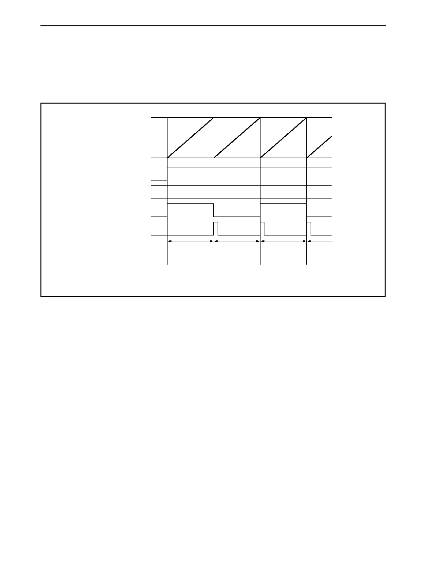
CHAPTER 7 16-BIT TIMER/EVENT COUNTER P (TMP)
Preliminary User's Manual U17714EJ1V0UD
246
(b) Operation if TPnCCR0 register is set to FFFFH
If the TPnCCR0 register is set to FFFFH, the 16-bit counter counts up to FFFFH. The counter is cleared to
0000H in synchronization with the next count-up timing. The INTTPnCC0 signal is generated and the
output of the TOPn0 pin is inverted. At this time, an overflow interrupt request signal (INTTPnOV) is not
generated, nor is the overflow flag (TPnOPT0.TPnOVF bit) set to 1.
FFFFH
16-bit counter
0000H
TPnCE bit
TPnCCR0 register
TOPn0 pin output
INTTPnCC0 signal
FFFFH
Interval time
10000H
�
count clock cycle
Interval time
10000H
�
count clock cycle
Interval time
10000H
�
count clock cycle
Remark n = 0 to 8
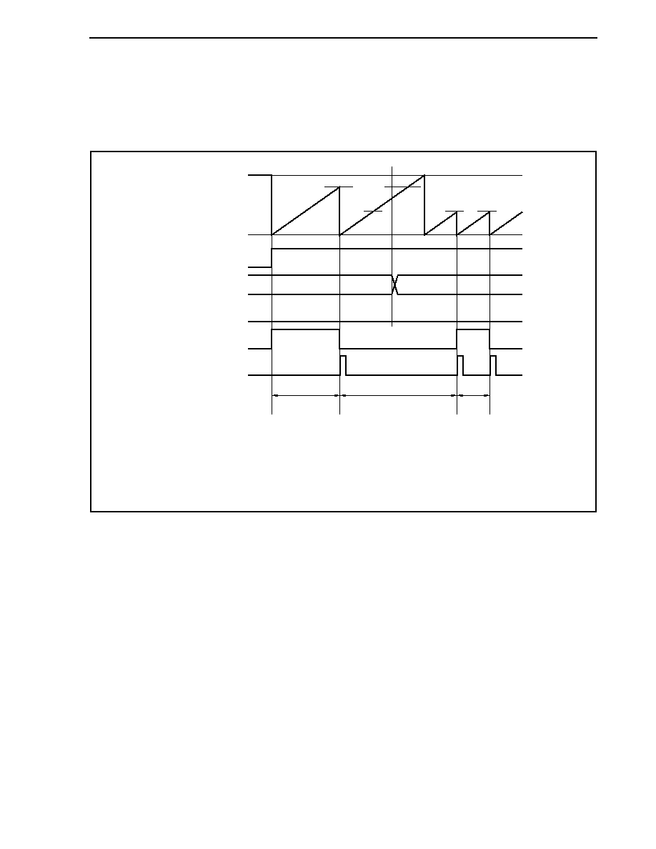
CHAPTER 7 16-BIT TIMER/EVENT COUNTER P (TMP)
Preliminary User's Manual U17714EJ1V0UD
247
(c) Notes on rewriting TPnCCR0 register
To change the value of the TPnCCR0 register to a smaller value, stop counting once and then change the
set value.
If the value of the TPnCCR0 register is rewritten to a smaller value during counting, the 16-bit counter may
overflow.
FFFFH
16-bit counter
0000H
TPnCE bit
TPnCCR0 register
TPnOL0 bit
TOPn0 pin output
INTTPnCC0 signal
D
1
D
2
D
1
D
1
D
2
D
2
D
2
L
Interval time (1)
Interval time (NG)
Interval
time (2)
Remarks 1. Interval time (1): (D
1
+ 1)
� Count clock cycle
Interval time (NG): (10000H + D
2
+ 1)
� Count clock cycle
Interval time (2): (D
2
+ 1)
� Count clock cycle
2. n = 0 to 8
If the value of the TPnCCR0 register is changed from D
1
to D
2
while the count value is greater than D
2
but
less than D
1
, the count value is transferred to the CCR0 buffer register as soon as the TPnCCR0 register
has been rewritten. Consequently, the value of the 16-bit counter that is compared is D
2
.
Because the count value has already exceeded D
2
, however, the 16-bit counter counts up to FFFFH,
overflows, and then counts up again from 0000H. When the count value matches D
2
, the INTTPnCC0
signal is generated and the output of the TOPn0 pin is inverted.
Therefore, the INTTPnCC0 signal may not be generated at the interval time "(D
1
+ 1)
� Count clock cycle"
or "(D
2
+ 1)
� Count clock cycle" originally expected, but may be generated at an interval of "(10000H + D
2
+ 1)
� Count clock period".
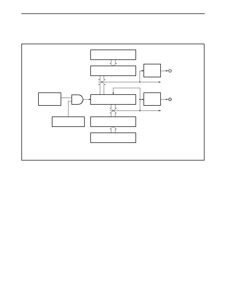
CHAPTER 7 16-BIT TIMER/EVENT COUNTER P (TMP)
Preliminary User's Manual U17714EJ1V0UD
248
(d) Operation of TPnCCR1 register
Figure 7-6. Configuration of TPnCCR1 Register
CCR0 buffer register
TPnCCR0 register
TPnCCR1 register
CCR1 buffer register
TOPn0 pin
INTTPnCC0 signal
TOPn1 pin
INTTPnCC1 signal
16-bit counter
Output
controller
TPnCE bit
Count clock
selection
Clear
Match signal
Output
controller
Match signal
Remark n = 0 to 8
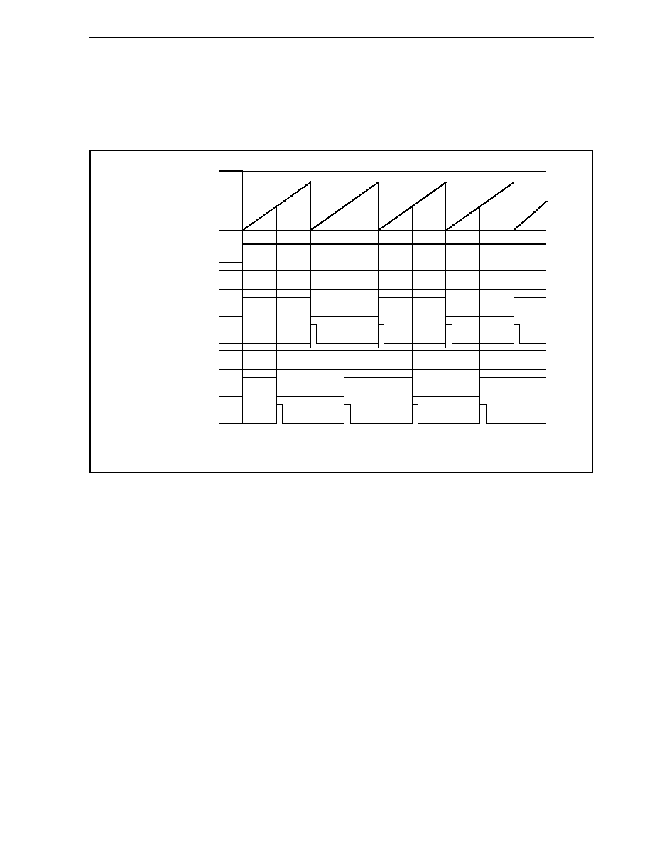
CHAPTER 7 16-BIT TIMER/EVENT COUNTER P (TMP)
Preliminary User's Manual U17714EJ1V0UD
249
If the set value of the TPnCCR1 register is less than the set value of the TPnCCR0 register, the
INTTPnCC1 signal is generated once per cycle. At the same time, the output of the TOPn1 pin is inverted.
The TOPn1 pin outputs a square wave with the same cycle as that output by the TOPn0 pin.
Figure 7-7. Timing Chart When D
01
D
11
FFFFH
16-bit counter
0000H
TPnCE bit
TPnCCR0 register
TOPn0 pin output
INTTPnCC0 signal
TPnCCR1 register
TOPn1 pin output
INTTPnCC1 signal
D
01
D
11
D
01
D
11
D
11
D
11
D
11
D
01
D
01
D
01
Remark n = 0 to 8
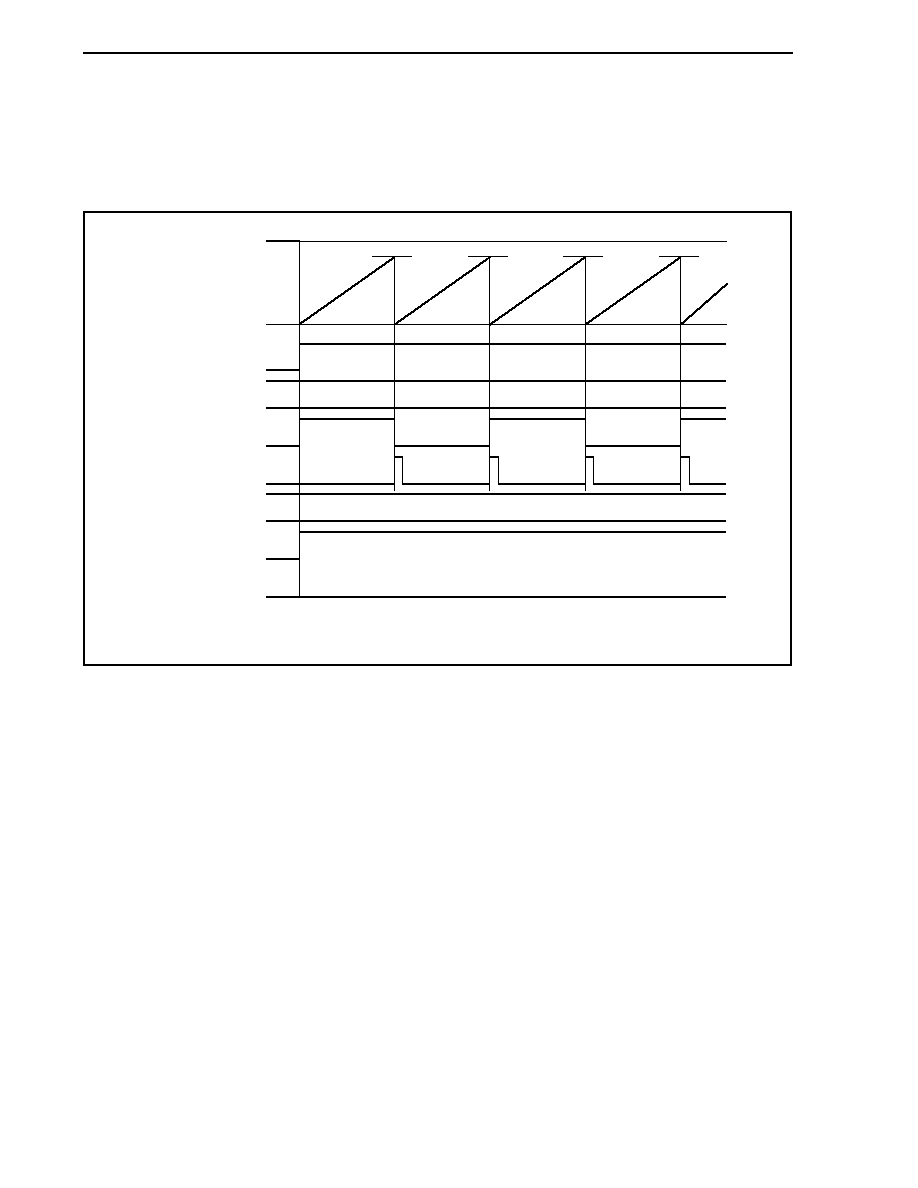
CHAPTER 7 16-BIT TIMER/EVENT COUNTER P (TMP)
Preliminary User's Manual U17714EJ1V0UD
250
If the set value of the TPnCCR1 register is greater than the set value of the TPnCCR0 register, the count
value of the 16-bit counter does not match the value of the TPnCCR1 register. Consequently, the
INTTPnCC1 signal is not generated, nor is the output of the TOPn1 pin changed.
Figure 7-8. Timing Chart When D
01
< D
11
FFFFH
16-bit counter
0000H
TPnCE bit
TPnCCR0 register
TOPn0 pin output
INTTPnCC0 signal
TPnCCR1 register
TOPn1 pin output
INTTPnCC1 signal
D
01
D
11
D
01
D
01
D
01
D
01
L
Remark n = 0 to 8
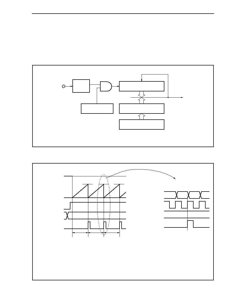
CHAPTER 7 16-BIT TIMER/EVENT COUNTER P (TMP)
Preliminary User's Manual U17714EJ1V0UD
251
7.5.2
External event count mode (TPnMD2 to TPnMD0 bits = 001)
In the external event count mode, the valid edge of the external event count input is counted when the
TPnCTL0.TPnCE bit is set to 1, and an interrupt request signal (INTTPnCC0) is generated each time the specified
number of edges have been counted. The TOPn0 pin cannot be used.
Usually, the TPnCCR1 register is not used in the external event count mode.
Figure 7-9. Configuration in External Event Count Mode
16-bit counter
CCR0 buffer register
TPnCE bit
TPnCCR0 register
Edge
detector
Clear
Match signal
INTTPnCC0 signal
TIPn0 pin
(external event
count input)
Remark n = 0 to 8
Figure 7-10. Basic Timing in External Event Count Mode
FFFFH
16-bit counter
0000H
TPnCE bit
TPnCCR0 register
INTTPnCC0 signal
D
0
D
0
D
0
D
0
16-bit counter
TPnCCR0 register
INTTPnCC0 signal
External event
count input
(TIPn0 pin input)
D
0
External
event
count
interval
(D
0
+ 1)
D
0
- 1
D
0
0000
0001
External
event
count
interval
(D
0
+ 1)
External
event
count
interval
(D
0
+ 1)
Remarks 1. This figure shows the basic timing when the rising edge is specified as the valid edge of
the external event count input.
2. n = 0 to 8
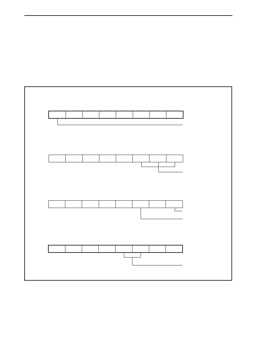
CHAPTER 7 16-BIT TIMER/EVENT COUNTER P (TMP)
Preliminary User's Manual U17714EJ1V0UD
252
When the TPnCE bit is set to 1, the value of the 16-bit counter is cleared from FFFFH to 0000H. The counter
counts each time the valid edge of external event count input is detected. Additionally, the set value of the TPnCCR0
register is transferred to the CCR0 buffer register.
When the count value of the 16-bit counter matches the value of the CCR0 buffer register, the 16-bit counter is
cleared to 0000H, and a compare match interrupt request signal (INTTPnCC0) is generated.
The INTTPnCC0 signal is generated each time the valid edge of the external event count input has been detected
(set value of TPnCCR0 register + 1) times.
Figure 7-11. Register Setting for Operation in External Event Count Mode (1/2)
(a) TMPn control register 0 (TPnCTL0)
0/1
0
0
0
0
TPnCTL0
0: Stop counting
1: Enable counting
0
0
0
TPnCKS2 TPnCKS1 TPnCKS0
TPnCE
(b) TMPn control register 1 (TPnCTL1)
0
0
0
0
0
TPnCTL1
0, 0, 1:
External event count mode
0
0
1
TPnMD2 TPnMD1 TPnMD0
TPnEEE
TPnEST
(c) TMPn I/O control register 0 (TPnIOC0)
0
0
0
0
0
TPnIOC0
0: Disable TOPn0 pin output
0: Disable TOPn1 pin output
0
0
0
TPnOE1
TPnOL0
TPnOE0
TPnOL1
(d) TMPn I/O control register 2 (TPnIOC2)
0
0
0
0
0/1
TPnIOC2
Select valid edge
of external event
count input
0/1
0
0
TPnEES0 TPnETS1 TPnETS0
TPnEES1

CHAPTER 7 16-BIT TIMER/EVENT COUNTER P (TMP)
Preliminary User's Manual U17714EJ1V0UD
253
Figure 7-11. Register Setting for Operation in External Event Count Mode (2/2)
(e) TMPn counter read buffer register (TPnCNT)
The count value of the 16-bit counter can be read by reading the TPnCNT register.
(f) TMPn capture/compare register 0 (TPnCCR0)
If D
0
is set to the TPnCCR0 register, the counter is cleared and a compare match interrupt request
signal (INTTPnCC0) is generated when the number of external event counts reaches (D
0
+ 1).
(g) TMPn capture/compare register 1 (TPnCCR1)
Usually, the TPnCCR1 register is not used in the external event count mode. However, the set value of
the TPnCCR1 register is transferred to the CCR1 buffer register. When the count value of the 16-bit
counter matches the value of the CCR1 buffer register, a compare match interrupt request signal
(INTTPnCC1) is generated.
Therefore, mask the interrupt signal by using the interrupt mask flag (TPnCCMK1).
Remarks 1. TMPn I/O control register 1 (TPnIOC1) and TMPn option register 0 (TPnOPT0) are not
used in the external event count mode.
2. n = 0 to 8
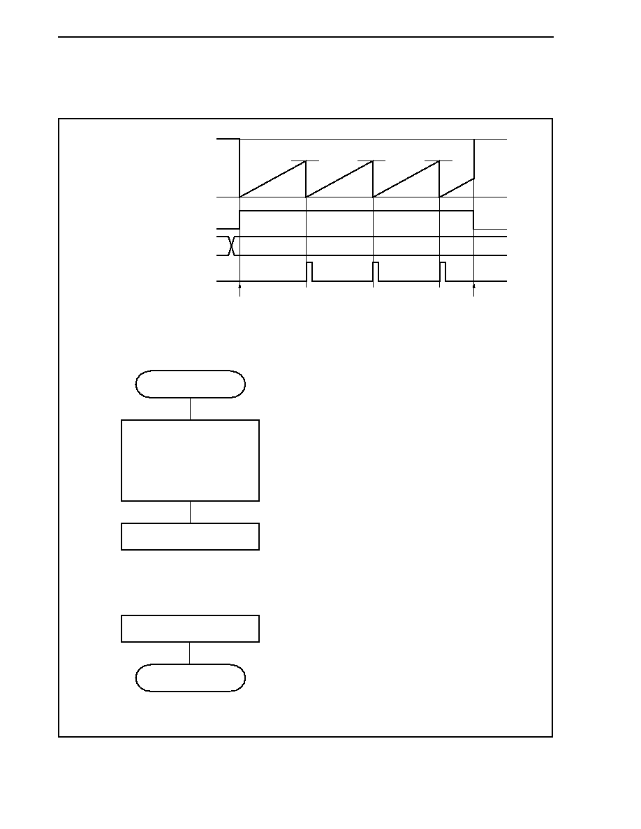
CHAPTER 7 16-BIT TIMER/EVENT COUNTER P (TMP)
Preliminary User's Manual U17714EJ1V0UD
254
(1) External event count mode operation flow
Figure 7-12. Flow of Software Processing in External Event Count Mode
FFFFH
16-bit counter
0000H
TPnCE bit
TPnCCR0 register
INTTPnCC0 signal
D
0
D
0
D
0
D
0
<1>
<2>
TPnCE bit = 1
TPnCE bit = 0
Register initial setting
TPnCTL0 register
(TPnCKS0 to TPnCKS2 bits)
TPnCTL1 register,
TPnIOC0 register,
TPnIOC2 register,
TPnCCR0 register,
Initial setting of these registers
is performed before setting the
TPnCE bit to 1.
The TPnCKS0 to TPnCKS2 bits can
be set at the same time when counting
has been started (TPnCE bit = 1).
The counter is initialized and counting
is stopped by clearing the TPnCE bit to 0.
START
STOP
<1> Count operation start flow
<2> Count operation stop flow
Remark n = 0 to 8
CHAPTER 7 16-BIT TIMER/EVENT COUNTER P (TMP)
Preliminary User's Manual U17714EJ1V0UD
255
(2) Operation timing in external event count mode
Cautions 1. In the external event count mode, do not set the TPnCCR0 register to 0000H.
2. In the external event count mode, use of the timer output is disabled. If performing timer
output using external event count input, set the interval timer mode, and select the
operation enabled by the external event count input for the count clock
(TPnCTL1.TPnMD2 to TPnCTL1.TPnMD0 bits = 000, TPnCTL1.TPnEEE bit = 1).
(a) Operation if TPnCCR0 register is set to FFFFH
If the TPnCCR0 register is set to FFFFH, the 16-bit counter counts to FFFFH each time the valid edge of
the external event count signal has been detected. The 16-bit counter is cleared to 0000H in
synchronization with the next count-up timing, and the INTTPnCC0 signal is generated. At this time, the
TPnOPT0.TPnOVF bit is not set.
FFFFH
16-bit counter
0000H
TPnCE bit
TPnCCR0 register
INTTPnCC0 signal
FFFFH
External event
count signal
interval
External event
count signal
interval
External event
count signal
interval
Remark n = 0 to 8
CHAPTER 7 16-BIT TIMER/EVENT COUNTER P (TMP)
Preliminary User's Manual U17714EJ1V0UD
256
(b) Notes on rewriting the TPnCCR0 register
To change the value of the TPnCCR0 register to a smaller value, stop counting once and then change the
set value.
If the value of the TPnCCR0 register is rewritten to a smaller value during counting, the 16-bit counter may
overflow.
FFFFH
16-bit counter
0000H
TPnCE bit
TPnCCR0 register
INTTPnCC0 signal
D
1
D
2
D
1
D
1
D
2
D
2
D
2
External event
count signal
interval (1)
(D
1
+ 1)
External event count signal
interval (NG)
(10000H + D
2
+ 1)
External event
count signal
interval (2)
(D
2
+ 1)
Remark n = 0 to 8
If the value of the TPnCCR0 register is changed from D
1
to D
2
while the count value is greater than D
2
but
less than D
1
, the count value is transferred to the CCR0 buffer register as soon as the TPnCCR0 register
has been rewritten. Consequently, the value that is compared with the 16-bit counter is D
2
.
Because the count value has already exceeded D
2
, however, the 16-bit counter counts up to FFFFH,
overflows, and then counts up again from 0000H. When the count value matches D
2
, the INTTPnCC0
signal is generated.
Therefore, the INTTPnCC0 signal may not be generated at the valid edge count of "(D
1
+ 1) times" or "(D
2
+ 1) times" originally expected, but may be generated at the valid edge count of "(10000H + D
2
+ 1) times".
CHAPTER 7 16-BIT TIMER/EVENT COUNTER P (TMP)
Preliminary User's Manual U17714EJ1V0UD
257
(c) Operation of TPnCCR1 register
Figure 7-13. Configuration of TPnCCR1 Register
CCR0 buffer register
TPnCE bit
TPnCCR0 register
16-bit counter
TPnCCR1 register
CCR1 buffer register
Clear
Match signal
Match signal
INTTPnCC0 signal
INTTPnCC1 signal
Edge
detector
TIPn0 pin
Remark n = 0 to 8
If the set value of the TPnCCR1 register is smaller than the set value of the TPnCCR0 register, the
INTTPnCC1 signal is generated once per cycle.
Figure 7-14. Timing Chart When D
01
D
11
FFFFH
16-bit counter
0000H
TPnCE bit
TPnCCR0 register
INTTPnCC0 signal
TPnCCR1 register
INTTPnCC1 signal
D
01
D
11
D
01
D
11
D
11
D
11
D
11
D
01
D
01
D
01
Remark n = 0 to 8
CHAPTER 7 16-BIT TIMER/EVENT COUNTER P (TMP)
Preliminary User's Manual U17714EJ1V0UD
258
If the set value of the TPnCCR1 register is greater than the set value of the TPnCCR0 register, the
INTTPnCC1 signal is not generated because the count value of the 16-bit counter and the value of the
TPnCCR1 register do not match.
Figure 7-15. Timing Chart When D
01
< D
11
FFFFH
16-bit counter
0000H
TPnCE bit
TPnCCR0 register
INTTPnCC0 signal
TPnCCR1 register
INTTPnCC1 signal
D
01
D
11
D
01
D
01
D
01
D
01
L
Remark n = 0 to 8

CHAPTER 7 16-BIT TIMER/EVENT COUNTER P (TMP)
Preliminary User's Manual U17714EJ1V0UD
259
7.5.3
External trigger pulse output mode (TPnMD2 to TPnMD0 bits = 010)
In the external trigger pulse output mode, 16-bit timer/event counter P waits for a trigger when the
TPnCTL0.TPnCE bit is set to 1. When the valid edge of an external trigger input signal is detected, 16-bit timer/event
counter P starts counting, and outputs a PWM waveform from the TOPn1 pin.
Pulses can also be output by generating a software trigger instead of using the external trigger. When using a
software trigger, a square wave that has one cycle of the PWM waveform as half its cycle can also be output from the
TOPn0 pin.
Figure 7-16. Configuration in External Trigger Pulse Output Mode
CCR0 buffer register
TPnCE bit
TPnCCR0 register
16-bit counter
TPnCCR1 register
CCR1 buffer register
Clear
Match signal
Match signal
INTTPnCC0 signal
Output
controller
(RS-FF)
Output
controller
TOPn1 pin
INTTPnCC1 signal
TOPn0 pin
Count
clock
selection
Count
start
control
Edge
detector
Software trigger
generation
TIPn0 pin
Transfer
Transfer
S
R
Remark n = 0 to 8
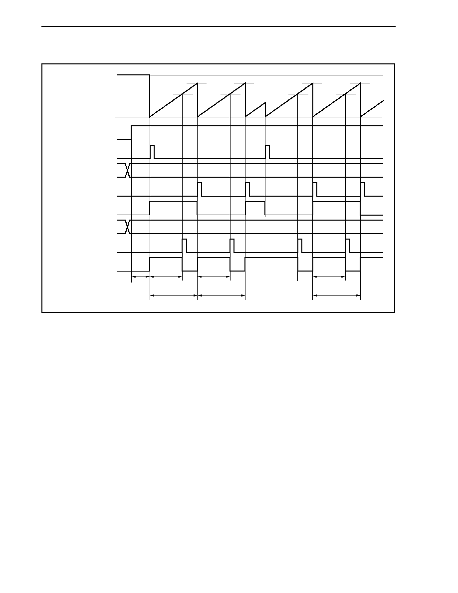
CHAPTER 7 16-BIT TIMER/EVENT COUNTER P (TMP)
Preliminary User's Manual U17714EJ1V0UD
260
Figure 7-17. Basic Timing in External Trigger Pulse Output Mode
FFFFH
16-bit counter
0000H
TPnCE bit
TPnCCR0 register
INTTPnCC0 signal
TPnCCR1 register
INTTPnCC1 signal
TOPn1 pin output
External trigger input
(TIPn0 pin input)
TOPn0 pin output
(only when software
trigger is used)
D
1
D
0
D
0
D
1
D
1
D
1
D
1
D
0
D
0
D
0
Wait
for
trigger
Active level
width (D
1
)
Cycle (D
0
+ 1)
Cycle (D
0
+ 1)
Cycle (D
0
+ 1)
Active level
width (D
1
)
Active level
width (D
1
)
16-bit timer/event counter P waits for a trigger when the TPnCE bit is set to 1. When the trigger is generated, the
16-bit counter is cleared from FFFFH to 0000H, starts counting at the same time, and outputs a PWM waveform from
the TOPn1 pin. If the trigger is generated again while the counter is operating, the counter is cleared to 0000H and
restarted. (The output of the TOPn0 pin is inverted. The TOPn1 pin outputs a high-level regardless of the status
(high/low) when a trigger occurs.)
The active level width, cycle, and duty factor of the PWM waveform can be calculated as follows.
Active level width = (Set value of TPnCCR1 register)
� Count clock cycle
Cycle = (Set value of TPnCCR0 register + 1)
� Count clock cycle
Duty factor = (Set value of TPnCCR1 register)/(Set value of TPnCCR0 register + 1)
The compare match request signal INTTPnCC0 is generated when the 16-bit counter counts next time after its
count value matches the value of the CCR0 buffer register, and the 16-bit counter is cleared to 0000H. The compare
match interrupt request signal INTTPnCC1 is generated when the count value of the 16-bit counter matches the value
of the CCR1 buffer register.
The value set to the TPnCCRm register is transferred to the CCRm buffer register when the count value of the 16-
bit counter matches the value of the CCRm buffer register and the 16-bit counter is cleared to 0000H.
The valid edge of an external trigger input signal, or setting the software trigger (TPnCTL1.TPnEST bit) to 1 is used
as the trigger.
Remark n = 0 to 8, m = 0, 1
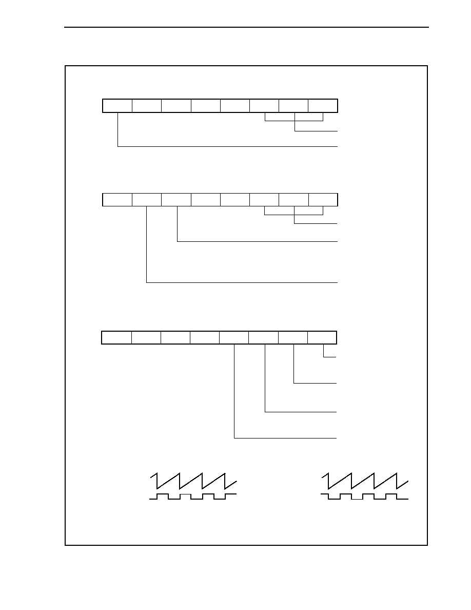
CHAPTER 7 16-BIT TIMER/EVENT COUNTER P (TMP)
Preliminary User's Manual U17714EJ1V0UD
261
Figure 7-18. Setting of Registers in External Trigger Pulse Output Mode (1/2)
(a) TMPn control register 0 (TPnCTL0)
0/1
0
0
0
0
TPnCTL0
Select count clock
Note 1
0: Stop counting
1: Enable counting
0/1
0/1
0/1
TPnCKS2 TPnCKS1 TPnCKS0
TPnCE
(b) TMPn control register 1 (TPnCTL1)
0
0/1
0/1
0
0
TPnCTL1
0: Operate on count
clock selected by
TPnCKS0 to TPnCKS2 bits
1: Count with external
event input signal
Generate software trigger
when 1 is written
0
1
0
TPnMD2 TPnMD1 TPnMD0
TPnEEE
TPnEST
0, 1, 0:
External trigger pulse
output mode
(c) TMPn I/O control register 0 (TPnIOC0)
0
0
0
0
0/1
TPnIOC0
0: Disable TOPn0 pin output
1: Enable TOPn0 pin output
Settings of output level while
operation of TOPn0 pin is disabled
0: Low level
1: High level
0: Disable TOPn1 pin output
1: Enable TOPn1 pin output
Specifies active level of TOPn1
pin output
0: Active-high
1: Active-low
0/1
0/1
0/1
Note 2
TPnOE1
TPnOL0
TPnOE0
TPnOL1
TOPn1 pin output
16-bit counter
� When TPnOL1 bit = 0
TOPn1 pin output
16-bit counter
� When TPnOL1 bit = 1
Notes 1. The setting is invalid when the TPnCTL1.TPnEEE bit = 1.
2. Clear this bit to 0 when the TOPn0 pin is not used in the external trigger pulse output mode.
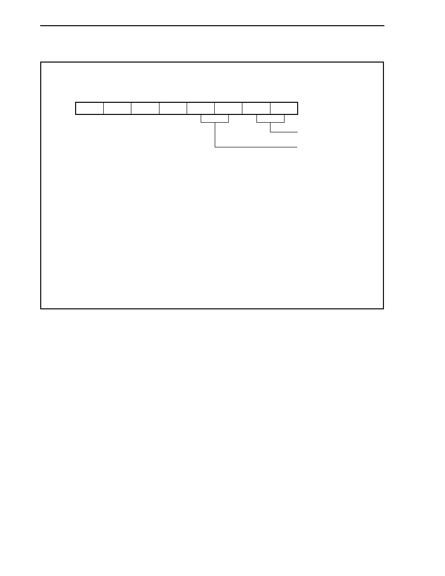
CHAPTER 7 16-BIT TIMER/EVENT COUNTER P (TMP)
Preliminary User's Manual U17714EJ1V0UD
262
Figure 7-18. Setting of Registers in External Trigger Pulse Output Mode (2/2)
(d) TMPn I/O control register 2 (TPnIOC2)
0
0
0
0
0/1
TPnIOC2
Select valid edge of
external trigger input
Select valid edge of
external event count input
0/1
0/1
0/1
TPnEES0 TPnETS1 TPnETS0
TPnEES1
(e) TMPn counter read buffer register (TPnCNT)
The value of the 16-bit counter can be read by reading the TPnCNT register.
(f) TMPn capture/compare registers 0 and 1 (TPnCCR0 and TPnCCR1)
If D
0
is set to the TPnCCR0 register and D
1
to the TPnCCR1 register, the cycle and active level of the
PWM waveform are as follows.
Cycle = (D
0
+ 1)
� Count clock cycle
Active level width = D
1
� Count clock cycle
Remarks 1. TMPn I/O control register 1 (TPnIOC1) and TMPn option register 0 (TPnOPT0) are not
used in the external trigger pulse output mode.
2. n = 0 to 8
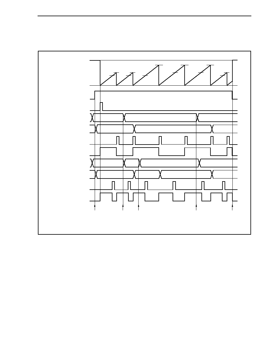
CHAPTER 7 16-BIT TIMER/EVENT COUNTER P (TMP)
Preliminary User's Manual U17714EJ1V0UD
263
(1) Operation flow in external trigger pulse output mode
Figure 7-19. Software Processing Flow in External Trigger Pulse Output Mode (1/2)
FFFFH
16-bit counter
0000H
TPnCE bit
TPnCCR0 register
CCR0 buffer register
INTTPnCC0 signal
TPnCCR1 register
CCR1 buffer register
INTTPnCC1 signal
TOPn1 pin output
External trigger input
(TIPn0 pin input)
TOPn0 pin output
(only when software
trigger is used)
D
10
D
00
D
00
D
01
D
00
D
00
D
10
D
10
D
11
D
10
D
10
D
10
D
11
D
10
D
01
D
00
D
10
D
10
D
00
D
10
D
00
D
11
D
11
D
01
D
01
D
01
<1>
<2>
<3>
<4>
<5>
Remark n = 0 to 8
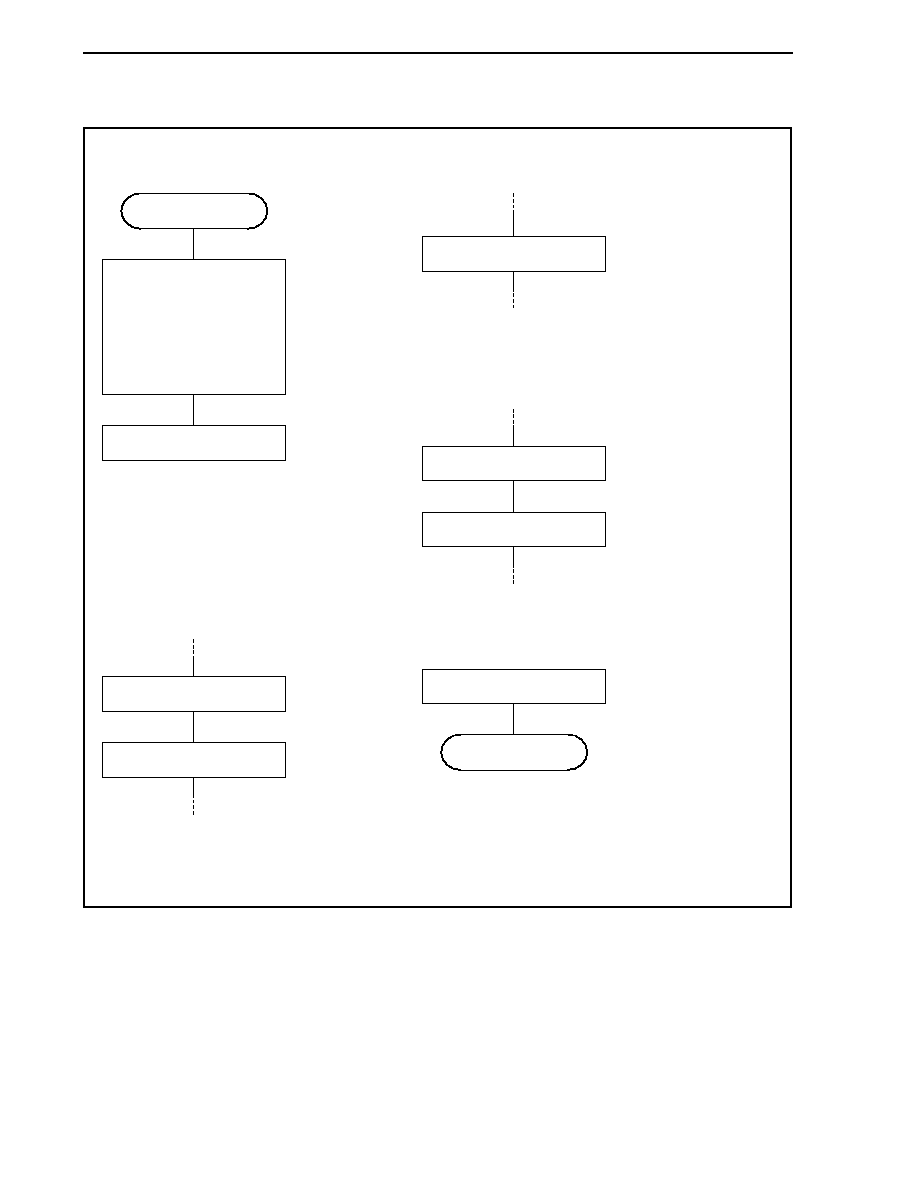
CHAPTER 7 16-BIT TIMER/EVENT COUNTER P (TMP)
Preliminary User's Manual U17714EJ1V0UD
264
Figure 7-19. Software Processing Flow in External Trigger Pulse Output Mode (2/2)
TPnCE bit = 1
Setting of TPnCCR0 register
Register initial setting
TPnCTL0 register
(TPnCKS0 to TPnCKS2 bits)
TPnCTL1 register,
TPnIOC0 register,
TPnIOC2 register,
TPnCCR0 register,
TPnCCR1 register
Initial setting of these
registers is performed
before setting the
TPnCE bit to 1.
The TPnCKS0 to
TPnCKS2 bits can be
set at the same time
when counting is
enabled (TPnCE bit = 1).
Trigger wait status
TPnCCR1 register write
processing is necessary
only when the set
cycle is changed.
When the counter is
cleared after setting,
the value of the TPnCCRm
register is transferred to
the CCRm buffer register.
START
Setting of TPnCCR1 register
<1> Count operation start flow
<2> TPnCCR0 and TPnCCR1 register
setting change flow
Setting of TPnCCR0 register
When the counter is
cleared after setting,
the value of the TPnCCRm
register is transferred to
the CCRm buffer register.
Setting of TPnCCR1 register
<4> TPnCCR0, TPnCCR1 register
setting change flow
Only writing of the TPnCCR1
register must be performed when
the set duty factor is changed.
When the counter is cleared after
setting, the value of the
TPnCCRm register is transferred
to the CCRm buffer register.
Setting of TPnCCR1 register
<3> TPnCCR0, TPnCCR1 register
setting change flow
TPnCE bit = 0
Counting is stopped.
STOP
<5> Count operation stop flow
Remark n = 0 to 8
m = 0, 1
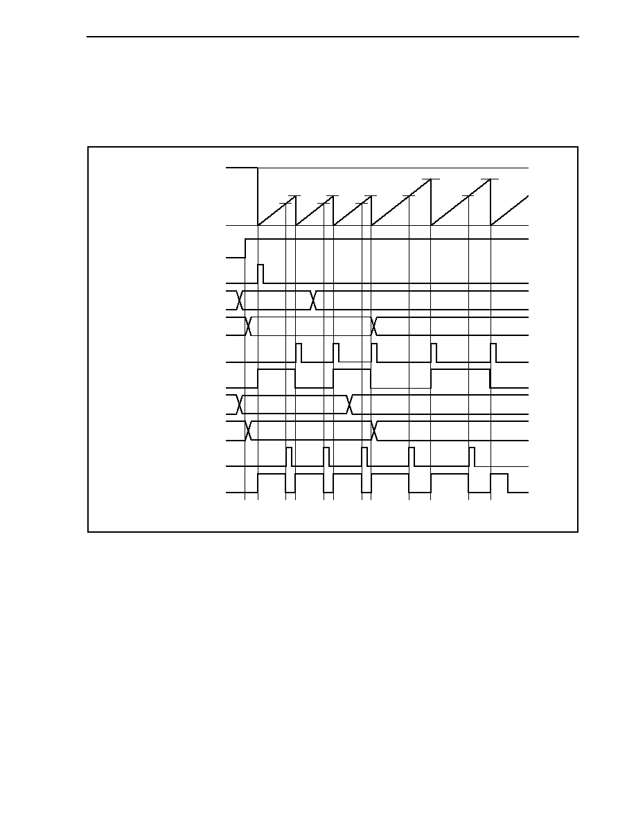
CHAPTER 7 16-BIT TIMER/EVENT COUNTER P (TMP)
Preliminary User's Manual U17714EJ1V0UD
265
(2) External trigger pulse output mode operation timing
(a) Note on changing pulse width during operation
To change the PWM waveform while the counter is operating, write the TPnCCR1 register last.
Rewrite the TPnCCRm register after writing the TPnCCR1 register after the INTTPnCC0 signal is detected.
FFFFH
16-bit counter
0000H
TPnCE bit
TPnCCR0 register
CCR0 buffer register
INTTPnCC0 signal
TPnCCR1 register
CCR1 buffer register
INTTPnCC1 signal
TOPn1 pin output
External trigger input
(TIPn0 pin input)
TOPn0 pin output
(only when software
trigger is used)
D
10
D
00
D
00
D
01
D
00
D
10
D
11
D
10
D
11
D
01
D
10
D
10
D
00
D
00
D
11
D
11
D
01
D
01

CHAPTER 7 16-BIT TIMER/EVENT COUNTER P (TMP)
Preliminary User's Manual U17714EJ1V0UD
266
In order to transfer data from the TPnCCRm register to the CCRm buffer register, the TPnCCR1 register
must be written.
To change both the cycle and active level width of the PWM waveform at this time, first set the cycle to the
TPnCCR0 register and then set the active level width to the TPnCCR1 register.
To change only the cycle of the PWM waveform, first set the cycle to the TPnCCR0 register, and then write
the same value to the TPnCCR1 register.
To change only the active level width (duty factor) of the PWM waveform, only the TPnCCR1 register has
to be set.
After data is written to the TPnCCR1 register, the value written to the TPnCCRm register is transferred to
the CCRm buffer register in synchronization with clearing of the 16-bit counter, and is used as the value
compared with the 16-bit counter.
To write the TPnCCR0 or TPnCCR1 register again after writing the TPnCCR1 register once, do so after the
INTTPnCC0 signal is generated. Otherwise, the value of the CCRm buffer register may become undefined
because the timing of transferring data from the TPnCCRm register to the CCRm buffer register conflicts
with writing the TPnCCRm register.
Remark n = 0 to 8
m = 0, 1

CHAPTER 7 16-BIT TIMER/EVENT COUNTER P (TMP)
Preliminary User's Manual U17714EJ1V0UD
267
(b) 0%/100% output of PWM waveform
To output a 0% waveform, set the TPnCCR1 register to 0000H. If the set value of the TPnCCR0 register is
FFFFH, the INTTPnCC1 signal is generated periodically.
Count clock
16-bit counter
TPnCE bit
TPnCCR0 register
TPnCCR1 register
INTTPnCC0 signal
INTTPnCC1 signal
TOPn1 pin output
D
0
0000H
D
0
0000H
D
0
0000H
D
0
- 1
D
0
0000
FFFF
0000
D
0
- 1
D
0
0000
0001
Remark n = 0 to 8
To output a 100% waveform, set a value of (set value of TPnCCR0 register + 1) to the TPnCCR1 register.
If the set value of the TPnCCR0 register is FFFFH, 100% output cannot be produced.
Count clock
16-bit counter
TPnCE bit
TPnCCR0 register
TPnCCR1 register
INTTPnCC0 signal
INTTPnCC1 signal
TOPn1 pin output
D
0
D
0
+ 1
D
0
D
0
+ 1
D
0
D
0
+ 1
D
0
- 1
D
0
0000
FFFF
0000
D
0
- 1
D
0
0000
0001
Remark n = 0 to 8

CHAPTER 7 16-BIT TIMER/EVENT COUNTER P (TMP)
Preliminary User's Manual U17714EJ1V0UD
268
(c) Conflict between trigger detection and match with TPnCCR1 register
If the trigger is detected immediately after the INTTPnCC1 signal is generated, the 16-bit counter is
immediately cleared to 0000H, the output signal of the TOPn1 pin is asserted, and the counter continues
counting. Consequently, the inactive period of the PWM waveform is shortened.
16-bit counter
TPnCCR1 register
INTTPnCC1 signal
TOPn1 pin output
External trigger input
(TIPn0 pin input)
D
1
D
1
- 1
0000
FFFF
0000
Shortened
Remark n = 0 to 8
If the trigger is detected immediately before the INTTPnCC1 signal is generated, the INTTPnCC1 signal is
not generated, and the 16-bit counter is cleared to 0000H and continues counting. The output signal of the
TOPn1 pin remains active. Consequently, the active period of the PWM waveform is extended.
16-bit counter
TPnCCR1 register
INTTPnCC1 signal
TOPn1 pin output
External trigger input
(TIPn0 pin input)
D
1
D
1
- 2
D
1
- 1
D
1
0000
FFFF
0000
0001
Extended
Remark n = 0 to 8
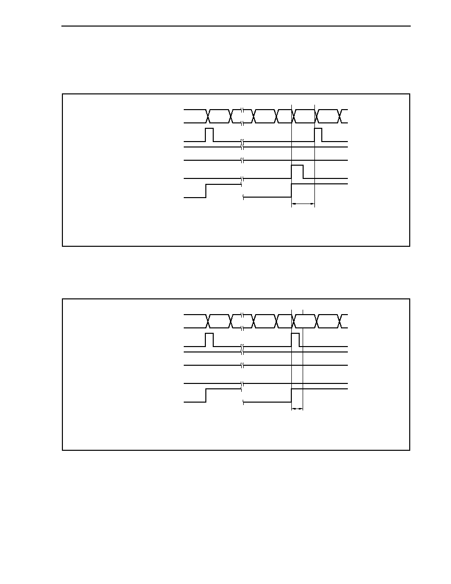
CHAPTER 7 16-BIT TIMER/EVENT COUNTER P (TMP)
Preliminary User's Manual U17714EJ1V0UD
269
(d) Conflict between trigger detection and match with TPnCCR0 register
If the trigger is detected immediately after the INTTPnCC0 signal is generated, the 16-bit counter is
cleared to 0000H and continues counting up. Therefore, the active period of the TOPn1 pin is extended by
time from generation of the INTTPnCC0 signal to trigger detection.
16-bit counter
TPnCCR0 register
INTTPnCC0 signal
TOPn1 pin output
External trigger input
(TIPn0 pin input)
D
0
D
0
- 1
D
0
0000
FFFF
0000
0000
Extended
Remark n = 0 to 8
If the trigger is detected immediately before the INTTPnCC0 signal is generated, the INTTPnCC0 signal is
not generated. The 16-bit counter is cleared to 0000H, the TOPn1 pin is asserted, and the counter
continues counting. Consequently, the inactive period of the PWM waveform is shortened.
16-bit counter
TPnCCR0 register
INTTPnCC0 signal
TOPn1 pin output
External trigger input
(TIPn0 pin input)
D
0
D
0
- 1
D
0
0000
FFFF
0000
0001
Shortened
Remark n = 0 to 8

CHAPTER 7 16-BIT TIMER/EVENT COUNTER P (TMP)
Preliminary User's Manual U17714EJ1V0UD
270
(e) Generation timing of compare match interrupt request signal (INTTPnCC1)
The timing of generation of the INTTPnCC1 signal in the external trigger pulse output mode differs from
the timing of other INTTPnCC1 signals; the INTTPnCC1 signal is generated when the count value of the
16-bit counter matches the value of the TPnCCR1 register.
Count clock
16-bit counter
TPnCCR1 register
TOPn1 pin output
INTTPnCC1 signal
D
1
D
1
- 2
D
1
- 1
D
1
D
1
+ 1
D
1
+ 2
Remark n = 0 to 8
Usually, the INTTPnCC1 signal is generated in synchronization with the next count up, after the count
value of the 16-bit counter matches the value of the TPnCCR1 register.
In the external trigger pulse output mode, however, it is generated one clock earlier. This is because the
timing is changed to match the timing of changing the output signal of the TOPn1 pin.
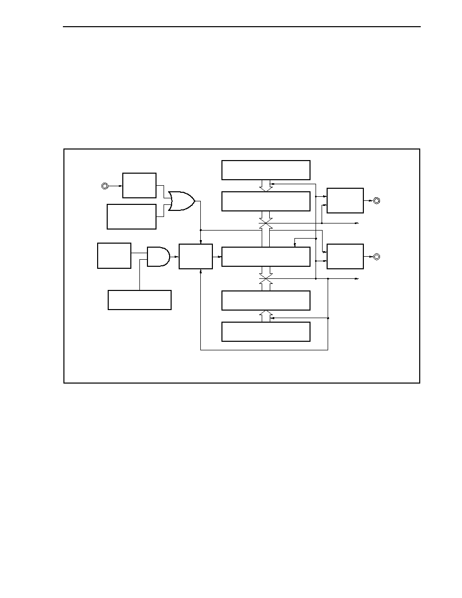
CHAPTER 7 16-BIT TIMER/EVENT COUNTER P (TMP)
Preliminary User's Manual U17714EJ1V0UD
271
7.5.4
One-shot pulse output mode (TPnMD2 to TPnMD0 bits = 011)
In the one-shot pulse output mode, 16-bit timer/event counter P waits for a trigger when the TPnCTL0.TPnCE bit is
set to 1. When the valid edge of an external trigger input is detected, 16-bit timer/event counter P starts counting, and
outputs a one-shot pulse from the TOPn1 pin.
Instead of the external trigger, a software trigger can also be generated to output the pulse. When the software
trigger is used, the TOPn0 pin outputs the active level while the 16-bit counter is counting, and the inactive level when
the counter is stopped (waiting for a trigger).
Figure 7-20. Configuration in One-Shot Pulse Output Mode
CCR0 buffer register
TPnCE bit
TPnCCR0 register
TPnCCR1 register
CCR1 buffer register
Clear
Match signal
Match signal
INTTPnCC0 signal
Output
controller
(RS-FF)
TOPn1 pin
INTTPnCC1 signal
TOPn0 pin
Count clock
selection
Count start
control
Edge
detector
Software trigger
generation
TIPn0 pin
Transfer
Transfer
S
R
Output
controller
(RS-FF)
S
R
16-bit counter
Remark n = 0 to 8
CHAPTER 7 16-BIT TIMER/EVENT COUNTER P (TMP)
Preliminary User's Manual U17714EJ1V0UD
272
Figure 7-21. Basic Timing in One-Shot Pulse Output Mode
FFFFH
16-bit counter
0000H
TPnCE bit
TPnCCR0 register
INTTPnCC0 signal
TPnCCR1 register
INTTPnCC1 signal
TOPn1 pin output
External trigger input
(TIPn0 pin input)
TOPn0 pin output
(only when software
trigger is used)
D
1
D
0
D
0
D
1
D
1
D
1
D
0
D
0
Delay
(D
1
)
Delay
(D
1
)
Delay
(D
1
)
Active
level width
(D
0
- D
1
+ 1)
Active
level width
(D
0
- D
1
+ 1)
Active
level width
(D
0
- D
1
+ 1)
When the TPnCE bit is set to 1, 16-bit timer/event counter P waits for a trigger. When the trigger is generated, the
16-bit counter is cleared from FFFFH to 0000H, starts counting, and outputs a one-shot pulse from the TOPn1 pin.
After the one-shot pulse is output, the 16-bit counter is set to FFFFH, stops counting, and waits for a trigger. If a
trigger is generated again while the one-shot pulse is being output, it is ignored.
The output delay period and active level width of the one-shot pulse can be calculated as follows.
Output delay period = (Set value of TPnCCR1 register)
� Count clock cycle
Active level width = (Set value of TPnCCR0 register
- Set value of TPnCCR1 register + 1) � Count clock cycle
The compare match interrupt request signal INTTPnCC0 is generated when the 16-bit counter counts after its
count value matches the value of the CCR0 buffer register. The compare match interrupt request signal INTTPnCC1
is generated when the count value of the 16-bit counter matches the value of the CCR1 buffer register.
The valid edge of an external trigger input or setting the software trigger (TPnCTL1.TPnEST bit) to 1 is used as the
trigger.
Remark n = 0 to 8
m = 0, 1
CHAPTER 7 16-BIT TIMER/EVENT COUNTER P (TMP)
Preliminary User's Manual U17714EJ1V0UD
273
Figure 7-22. Setting of Registers in One-Shot Pulse Output Mode (1/2)
(a) TMPn control register 0 (TPnCTL0)
0/1
0
0
0
0
TPnCTL0
Select count clock
Note 1
0: Stop counting
1: Enable counting
0/1
0/1
0/1
TPnCKS2 TPnCKS1 TPnCKS0
TPnCE
(b) TMPn control register 1 (TPnCTL1)
0
0/1
0/1
0
0
TPnCTL1
0: Operate on count clock
selected by TPnCKS0 to
TPnCKS2 bits
1: Count external event
input signal
Generate software trigger
when 1 is written
0
1
1
TPnMD2 TPnMD1 TPnMD0
TPnEEE
TPnEST
0, 1, 1:
One-shot pulse output mode
(c) TMPn I/O control register 0 (TPnIOC0)
0
0
0
0
0/1
TPnIOC0
0: Disable TOPn0 pin output
1: Enable TOPn0 pin output
Setting of output level while
operation of TOPn0 pin is disabled
0: Low level
1: High level
0: Disable TOPn1 pin output
1: Enable TOPn1 pin output
Specifies active level of
TOPn1 pin output
0: Active-high
1: Active-low
0/1
0/1
Note 2
0/1
Note 2
TPnOE1
TPnOL0
TPnOE0
TPnOL1
TOPn1 pin output
16-bit counter
� When TPnOL1 bit = 0
TOPn1 pin output
16-bit counter
� When TPnOL1 bit = 1
Notes 1. The setting is invalid when the TPnCTL1.TPnEEE bit = 1.
2. Clear this bit to 0 when the TOPn0 pin is not used in the one-shot pulse output mode.
CHAPTER 7 16-BIT TIMER/EVENT COUNTER P (TMP)
Preliminary User's Manual U17714EJ1V0UD
274
Figure 7-22. Setting of Registers in One-Shot Pulse Output Mode (2/2)
(d) TMPn I/O control register 2 (TPnIOC2)
0
0
0
0
0/1
TPnIOC2
Select valid edge of
external trigger input
Select valid edge of
external event count input
0/1
0/1
0/1
TPnEES0 TPnETS1 TPnETS0
TPnEES1
(e) TMPn counter read buffer register (TPnCNT)
The value of the 16-bit counter can be read by reading the TPnCNT register.
(f) TMPn capture/compare registers 0 and 1 (TPnCCR0 and TPnCCR1)
If D
0
is set to the TPnCCR0 register and D
1
to the TPnCCR1 register, the active level width and output
delay period of the one-shot pulse are as follows.
Active level width = (D
1
- D
0
+ 1)
� Count clock cycle
Output delay period = (D
1
)
� Count clock cycle
Remarks 1. TMPn I/O control register 1 (TPnIOC1) and TMPn option register 0 (TPnOPT0) are not
used in the one-shot pulse output mode.
2.
n = 0 to 8
CHAPTER 7 16-BIT TIMER/EVENT COUNTER P (TMP)
Preliminary User's Manual U17714EJ1V0UD
275
(1) Operation flow in one-shot pulse output mode
Figure 7-23. Software Processing Flow in One-Shot Pulse Output Mode
FFFFH
16-bit counter
0000H
TPnCE bit
TPnCCR0 register
INTTPnCC0 signal
TPnCCR1 register
INTTPnCC1 signal
TOPn1 pin output
External trigger input
(TIPn0 pin input)
<1>
<3>
TPnCE bit = 1
Register initial setting
TPnCTL0 register
(TPnCKS0 to TPnCKS2 bits)
TPnCTL1 register,
TPnIOC0 register,
TPnIOC2 register,
TPnCCR0 register,
TPnCCR1 register
Initial setting of these
registers is performed
before setting the
TPnCE bit to 1.
The TPnCKS0 to
TPnCKS2 bits can be
set at the same time
when counting has been
started (TPnCE bit = 1).
Trigger wait status
START
<1> Count operation start flow
TPnCE bit = 0
Count operation is
stopped
STOP
<3> Count operation stop flow
D
10
D
00
D
11
D
01
D
00
D
10
D
11
<2>
D
01
Setting of TPnCCR0, TPnCCR1
registers
As rewriting the
TPnCCRm register
immediately forwards
to the CCRm buffer
register, rewriting
immediately after
the generation of the
INTTPnCCR0 signal
is recommended.
<2> TPnCCR0, TPnCCR1 register setting change flow
Remark n = 0 to 8
m = 0, 1
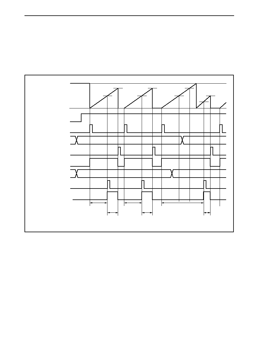
CHAPTER 7 16-BIT TIMER/EVENT COUNTER P (TMP)
Preliminary User's Manual U17714EJ1V0UD
276
(2) Operation timing in one-shot pulse output mode
(a) Note on rewriting TPnCCRm register
To change the set value of the TPnCCRm register to a smaller value, stop counting once, and then change
the set value.
If the value of the TPnCCRm register is rewritten to a smaller value during counting, the 16-bit counter may
overflow.
FFFFH
16-bit counter
0000H
TPnCE bit
TPnCCR0 register
INTTPnCC0 signal
TPnCCR1 register
INTTPnCC1 signal
TOPn1 pin output
External trigger input
(TIPn0 pin input)
TOPn0 pin output
(only when software
trigger is used)
D
10
D
11
D
00
D
01
D
00
D
10
D
10
D
10
D
01
D
11
D
00
D
00
Delay
(D
10
)
Delay
(D
10
)
Active level width
(D
00
- D
10
+ 1)
Active level width
(D
00
- D
10
+ 1)
Delay
(10000H + D
11
)
Active level width
(D
01
- D
11
+ 1)
When the TPnCCR0 register is rewritten from D
00
to D
01
and the TPnCCR1 register from D
10
to D
11
where
D
00
> D
01
and D
10
> D
11
, if the TPnCCR1 register is rewritten when the count value of the 16-bit counter is
greater than D
11
and less than D
10
and if the TPnCCR0 register is rewritten when the count value is greater
than D
01
and less than D
00
, each set value is reflected as soon as the register has been rewritten and
compared with the count value. The counter counts up to FFFFH and then counts up again from 0000H.
When the count value matches D
11
, the counter generates the INTTPnCC1 signal and asserts the TOPn1
pin. When the count value matches D
01
, the counter generates the INTTPnCC0 signal, deasserts the
TOPn1 pin, and stops counting.
Therefore, the counter may output a pulse with a delay period or active period different from that of the
one-shot pulse that is originally expected.
Remark n = 0 to 8
m = 0, 1
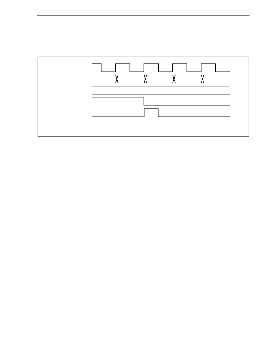
CHAPTER 7 16-BIT TIMER/EVENT COUNTER P (TMP)
Preliminary User's Manual U17714EJ1V0UD
277
(b) Generation timing of compare match interrupt request signal (INTTPnCC1)
The generation timing of the INTTPnCC1 signal in the one-shot pulse output mode is different from other
INTTPnCC1 signals; the INTTPnCC1 signal is generated when the count value of the 16-bit counter
matches the value of the TPnCCR1 register.
Count clock
16-bit counter
TPnCCR1 register
TOPn1 pin output
INTTPnCC1 signal
D
1
D
1
- 2
D
1
- 1
D
1
D
1
+ 1
D
1
+ 2
Remark n = 0 to 8
Usually, the INTTPnCC1 signal is generated when the 16-bit counter counts up next time after its count
value matches the value of the TPnCCR1 register.
In the one-shot pulse output mode, however, it is generated one clock earlier. This is because the timing is
changed to match the change timing of the TOPn1 pin.
Remark n = 0 to 8
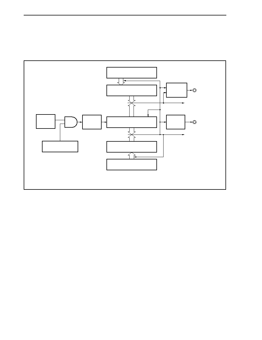
CHAPTER 7 16-BIT TIMER/EVENT COUNTER P (TMP)
Preliminary User's Manual U17714EJ1V0UD
278
7.5.5
PWM output mode (TPnMD2 to TPnMD0 bits = 100)
In the PWM output mode, a PWM waveform is output from the TOPn1 pin when the TPnCTL0.TPnCE bit is set to 1.
In addition, a pulse with one cycle of the PWM waveform as half its cycle is output from the TOPn0 pin.
Figure 7-24. Configuration in PWM Output Mode
CCR0 buffer register
TPnCE bit
TPnCCR0 register
16-bit counter
TPnCCR1 register
CCR1 buffer register
Clear
Match signal
Match signal
INTTPnCC0 signal
Output
controller
(RS-FF)
Output
controller
TOPn1 pin
INTTPnCC1 signal
TOPn0 pin
Count
clock
selection
Count
start
control
Transfer
Transfer
S
R
Remark n = 0 to 8
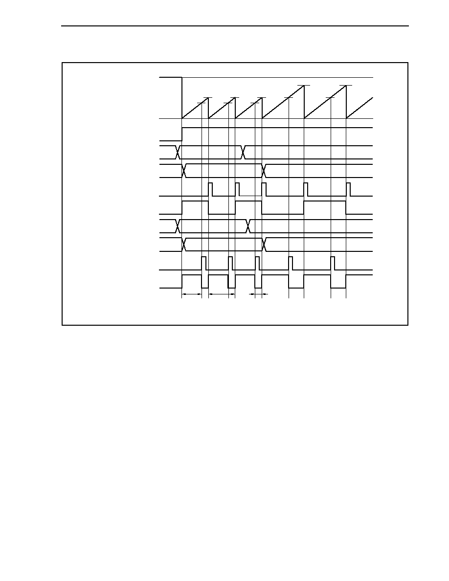
CHAPTER 7 16-BIT TIMER/EVENT COUNTER P (TMP)
Preliminary User's Manual U17714EJ1V0UD
279
Figure 7-25. Basic Timing in PWM Output Mode
FFFFH
16-bit counter
0000H
TPnCE bit
TPnCCR0 register
CCR0 buffer register
INTTPnCC0 signal
TOPn0 pin output
TPnCCR1 register
CCR1 buffer register
INTTPnCC1 signal
TOPn1 pin output
D
10
D
00
D
00
D
01
D
00
D
10
D
11
D
10
D
11
D
01
D
10
D
10
D
00
D
00
D
11
D
11
D
01
D
01
Active period
(D
10
)
Cycle
(D
00
+ 1)
Inactive period
(D
00
- D
10
+ 1)
When the TPnCE bit is set to 1, the 16-bit counter is cleared from FFFFH to 0000H, starts counting, and outputs a
PWM waveform from the TOPn1 pin.
The active level width, cycle, and duty factor of the PWM waveform can be calculated as follows.
Active level width = (Set value of TPnCCR1 register )
� Count clock cycle
Cycle = (Set value of TPnCCR0 register + 1)
� Count clock cycle
Duty factor = (Set value of TPnCCR1 register)/(Set value of TPnCCR0 register + 1)
The PWM waveform can be changed by rewriting the TPnCCRm register while the counter is operating. The newly
written value is reflected when the count value of the 16-bit counter matches the value of the CCR0 buffer register and
the 16-bit counter is cleared to 0000H.
The compare match interrupt request signal INTTPnCC0 is generated when the 16-bit counter counts next time
after its count value matches the value of the CCR0 buffer register, and the 16-bit counter is cleared to 0000H. The
compare match interrupt request signal INTTPnCC1 is generated when the count value of the 16-bit counter matches
the value of the CCR1 buffer register.
The value set to the TPnCCRm register is transferred to the CCRm buffer register when the count value of the 16-
bit counter matches the value of the CCRm buffer register and the 16-bit counter is cleared to 0000H.
Remark n = 0 to 8, m = 0, 1
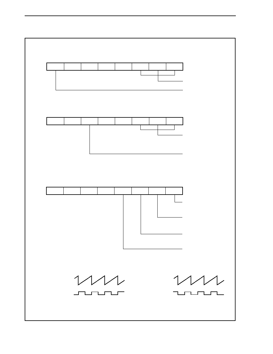
CHAPTER 7 16-BIT TIMER/EVENT COUNTER P (TMP)
Preliminary User's Manual U17714EJ1V0UD
280
Figure 7-26. Setting of Registers in PWM Output Mode (1/2)
(a) TMPn control register 0 (TPnCTL0)
0/1
0
0
0
0
TPnCTL0
Select count clock
Note 1
0: Stop counting
1: Enable counting
0/1
0/1
0/1
TPnCKS2 TPnCKS1 TPnCKS0
TPnCE
(b) TMPn control register 1 (TPnCTL1)
0
0
0/1
0
0
TPnCTL1
1
0
0
TPnMD2 TPnMD1 TPnMD0
TPnEEE
TPnEST
1, 0, 0:
PWM output mode
0: Operate on count clock
selected by TPnCKS0 to
TPnCKS2 bits
1: Count external event
input signal
(c) TMPn I/O control register 0 (TPnIOC0)
0
0
0
0
0/1
TPnIOC0
0: Disable TOPn0 pin output
1: Enable TOPn0 pin output
Setting of output level while
operation of TOPn0 pin is disabled
0: Low level
1: High level
0: Disable TOPn1 pin output
1: Enable TOPn1 pin output
Specifies active level of TOPn1
pin output
0: Active-high
1: Active-low
0/1
0/1
0/1
Note 2
TPnOE1
TPnOL0
TPnOE0
TPnOL1
TOPn1 pin output
16-bit counter
� When TPnOL1 bit = 0
TOPn1 pin output
16-bit counter
� When TPnOL1 bit = 1
Notes 1. The setting is invalid when the TPnCTL1.TPnEEE bit = 1.
2. Clear this bit to 0 when the TOPn0 pin is not used in the PWM output mode.

CHAPTER 7 16-BIT TIMER/EVENT COUNTER P (TMP)
Preliminary User's Manual U17714EJ1V0UD
281
Figure 7-26. Register Setting in PWM Output Mode (2/2)
(d) TMPn I/O control register 2 (TPnIOC2)
0
0
0
0
0/1
TPnIOC2
Select valid edge
of external event
count input.
0/1
0
0
TPnEES0 TPnETS1 TPnETS0
TPnEES1
(e) TMPn counter read buffer register (TPnCNT)
The value of the 16-bit counter can be read by reading the TPnCNT register.
(f) TMPn capture/compare registers 0 and 1 (TPnCCR0 and TPnCCR1)
If D
0
is set to the TPnCCR0 register and D
1
to the TPnCCR1 register, the cycle and active level of the
PWM waveform are as follows.
Cycle = (D
0
+ 1)
� Count clock cycle
Active level width = D
1
� Count clock cycle
Remarks 1. TMPn I/O control register 1 (TPnIOC1) and TMPn option register 0 (TPnOPT0) are not
used in the PWM output mode.
2. n = 0 to 8
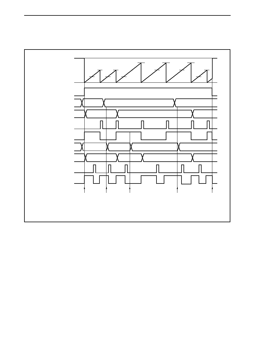
CHAPTER 7 16-BIT TIMER/EVENT COUNTER P (TMP)
Preliminary User's Manual U17714EJ1V0UD
282
(1) Operation flow in PWM output mode
Figure 7-27. Software Processing Flow in PWM Output Mode (1/2)
FFFFH
16-bit counter
0000H
TPnCE bit
TPnCCR0 register
CCR0 buffer register
INTTPnCC0 signal
TOPn0 pin output
TPnCCR1 register
CCR1 buffer register
INTTPnCC1 signal
TOPn1 pin output
D
10
D
00
D
00
D
01
D
00
D
00
D
10
D
10
D
11
D
10
D
10
D
10
D
11
D
10
D
01
D
00
D
10
D
10
D
00
D
10
D
00
D
11
D
11
D
01
D
01
D
01
<2>
<3>
<4>
<5>
<1>
Remark n = 0 to 8
m = 0, 1
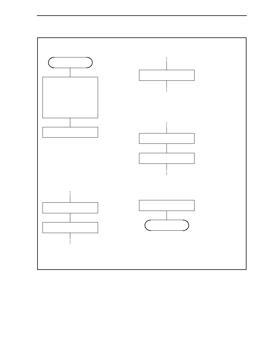
CHAPTER 7 16-BIT TIMER/EVENT COUNTER P (TMP)
Preliminary User's Manual U17714EJ1V0UD
283
Figure 7-27. Software Processing Flow in PWM Output Mode (2/2)
TPnCE bit = 1
Setting of TPnCCR0 register
Register initial setting
TPnCTL0 register
(TPnCKS0 to TPnCKS2 bits)
TPnCTL1 register,
TPnIOC0 register,
TPnIOC2 register,
TPnCCR0 register,
TPnCCR1 register
Initial setting of these
registers is performed
before setting the
TPnCE bit to 1.
The TPnCKS0 to
TPnCKS2 bits can be
set at the same time
when counting is
enabled (TPnCE bit = 1).
TPnCCR1 write
processing is necessary
only when the set cycle
is changed.
When the counter is
cleared after setting,
the value of the TPnCCRm
register is transferred to the
CCRm buffer register.
START
Setting of TPnCCR1 register
<1> Count operation start flow
<2> TPnCCR0, TPnCCR1 register
setting change flow
Setting of TPnCCR0 register
When the counter is
cleared after setting,
the value of the TPnCCRm
register is transferred to the
CCRm buffer register.
Setting of TPnCCR1 register
<4> TPnCCR0, TPnCCR1 register
setting change flow
Only writing of the TPnCCR1
register must be performed
when the set duty factor is
changed. When the counter is
cleared after setting, the
value of compare register m
is transferred to the CCRm
buffer register.
Setting of TPnCCR1 register
<3> TPnCCR0, TPnCCR1 register
setting change flow
TPnCE bit = 0
Counting is stopped.
STOP
<5> Count operation stop flow
Remark n = 0 to 8
m = 0, 1
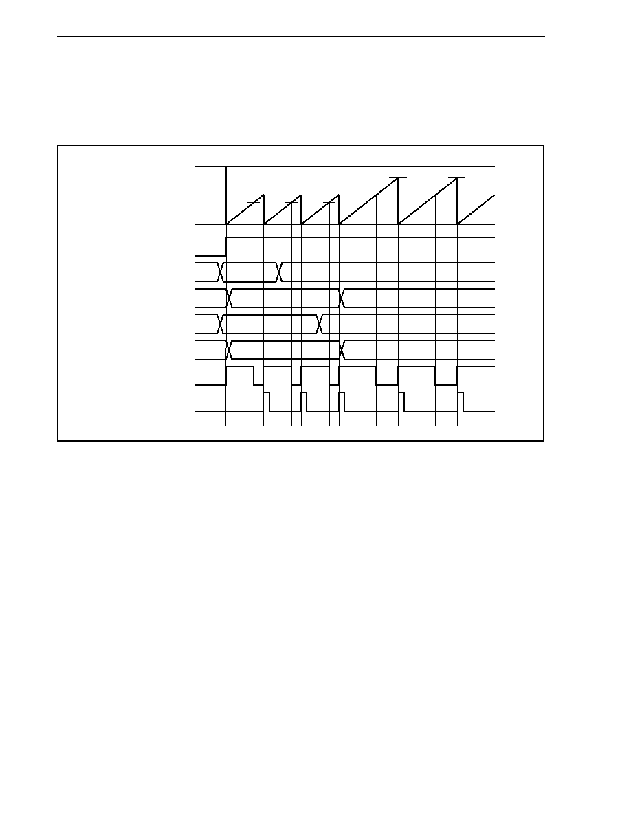
CHAPTER 7 16-BIT TIMER/EVENT COUNTER P (TMP)
Preliminary User's Manual U17714EJ1V0UD
284
(2) PWM output mode operation timing
(a) Changing pulse width during operation
To change the PWM waveform while the counter is operating, write the TPnCCR1 register last.
Rewrite the TPnCCRm register after writing the TPnCCR1 register after the INTTPnCC1 signal is detected.
FFFFH
16-bit counter
0000H
TPnCE bit
TPnCCR0 register
CCR0 buffer register
TPnCCR1 register
CCR1 buffer register
TOPn1 pin output
INTTPnCC0 signal
D
10
D
00
D
00
D
01
D
00
D
10
D
11
D
10
D
11
D
01
D
10
D
10
D
00
D
00
D
11
D
11
D
01
D
01
To transfer data from the TPnCCRm register to the CCRm buffer register, the TPnCCR1 register must be
written.
To change both the cycle and active level of the PWM waveform at this time, first set the cycle to the
TPnCCR0 register and then set the active level to the TPnCCR1 register.
To change only the cycle of the PWM waveform, first set the cycle to the TPnCCR0 register, and then write
the same value to the TPnCCR1 register.
To change only the active level width (duty factor) of the PWM waveform, only the TPnCCR1 register has
to be set.
After data is written to the TPnCCR1 register, the value written to the TPnCCRm register is transferred to
the CCRm buffer register in synchronization with clearing of the 16-bit counter, and is used as the value
compared with the 16-bit counter.
To write the TPnCCR0 or TPnCCR1 register again after writing the TPnCCR1 register once, do so after the
INTTPnCC0 signal is generated. Otherwise, the value of the CCRm buffer register may become undefined
because the timing of transferring data from the TPnCCRm register to the CCRm buffer register conflicts
with writing the TPnCCRm register.
Remark n = 0 to 8, m = 0, 1
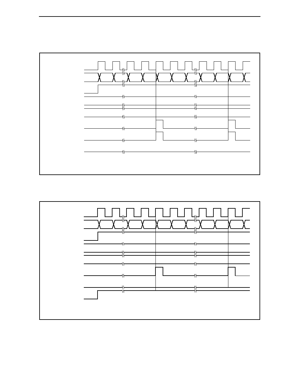
CHAPTER 7 16-BIT TIMER/EVENT COUNTER P (TMP)
Preliminary User's Manual U17714EJ1V0UD
285
(b) 0%/100% output of PWM waveform
To output a 0% waveform, set the TPnCCR1 register to 0000H. If the set value of the TPnCCR0 register is
FFFFH, the INTTPnCC1 signal is generated periodically.
Count clock
16-bit counter
TPnCE bit
TPnCCR0 register
TPnCCR1 register
INTTPnCC0 signal
INTTPnCC1 signal
TOPn1 pin output
D
00
0000H
D
00
0000H
D
00
0000H
D
00
- 1
D
00
0000
FFFF
0000
D
00
- 1
D
00
0000
0001
Remark n = 0 to 8
To output a 100% waveform, set a value of (set value of TPnCCR0 register + 1) to the TPnCCR1 register.
If the set value of the TPnCCR0 register is FFFFH, 100% output cannot be produced.
Count clock
16-bit counter
TPnCE bit
TPnCCR0 register
TPnCCR1 register
INTTPnCC0 signal
INTTPnCC1 signal
TOPn1 pin output
D
00
D
00
+ 1
D
00
D
00
+ 1
D
00
D
00
+ 1
D
00
- 1
D
00
0000
FFFF
0000
D
00
- 1
D
00
0000
0001
Remark n = 0 to 8
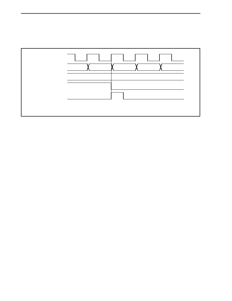
CHAPTER 7 16-BIT TIMER/EVENT COUNTER P (TMP)
Preliminary User's Manual U17714EJ1V0UD
286
(c) Generation timing of compare match interrupt request signal (INTTPnCC1)
The timing of generation of the INTTPnCC1 signal in the PWM output mode differs from the timing of other
INTTPnCC1 signals; the INTTPnCC1 signal is generated when the count value of the 16-bit counter
matches the value of the TPnCCR1 register.
Count clock
16-bit counter
TPnCCR1 register
TOPn1 pin output
INTTPnCC1 signal
D
1
D
1
- 2
D
1
- 1
D
1
D
1
+ 1
D
1
+ 2
Remark n = 0 to 8
Usually, the INTTPnCC1 signal is generated in synchronization with the next counting up after the count
value of the 16-bit counter matches the value of the TPnCCR1 register.
In the PWM output mode, however, it is generated one clock earlier. This is because the timing is changed
to match the change timing of the output signal of the TOPn1 pin.
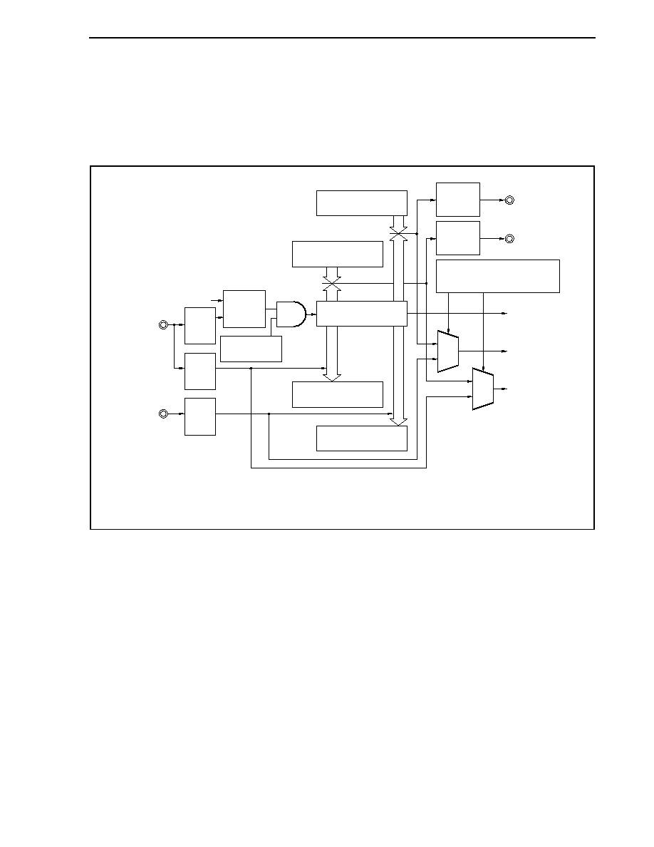
CHAPTER 7 16-BIT TIMER/EVENT COUNTER P (TMP)
Preliminary User's Manual U17714EJ1V0UD
287
7.5.6
Free-running timer mode (TPnMD2 to TPnMD0 bits = 101)
In the free-running timer mode, 16-bit timer/event counter P starts counting when the TPnCTL0.TPnCE bit is set to
1. At this time, the TPnCCRm register can be used as a compare register or a capture register, depending on the
setting of the TPnOPT0.TPnCCS0 and TPnOPT0.TPnCCS1 bits.
Figure 7-28. Configuration in Free-Running Timer Mode
TPnCCR0 register
(capture)
TPnCE bit
TPnCCR1 register
(compare)
16-bit counter
TPnCCR1 register
(compare)
TPnCCR0 register
(capture)
Output
controller
TPnCCS0, TPnCCS1 bits
(capture/compare selection)
TOPn0 pin output
Output
controller
TOPn1 pin output
Edge
detector
Count
clock
selection
Edge
detector
Edge
detector
TIPn0 pin
(external event
count input/
capture
trigger input)
TIPn1 pin
(capture
trigger input)
Internal count clock
0
1
0
1
INTTPnOV signal
INTTPnCC1 signal
INTTPnCC0 signal
Remark n = 0 to 8
m = 0, 1
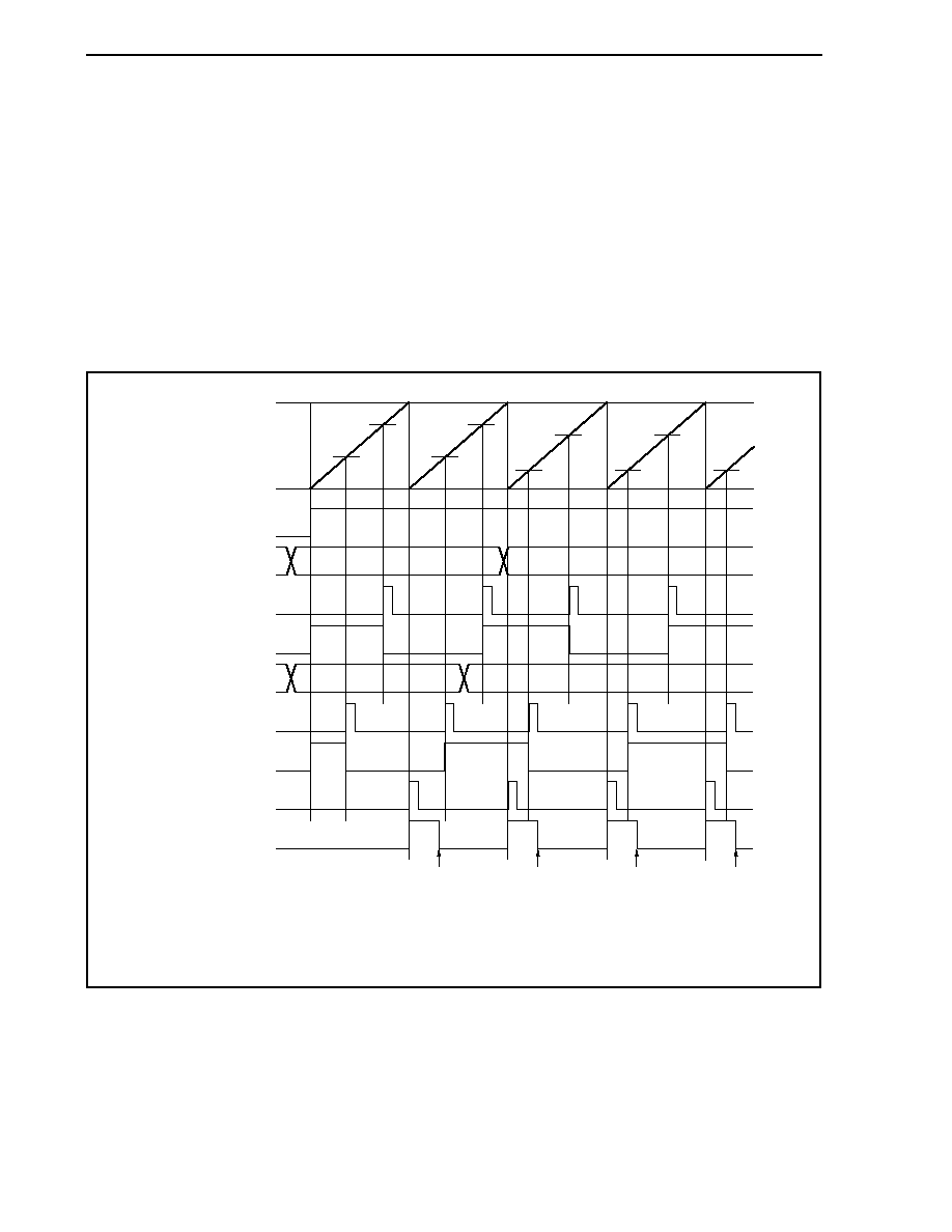
CHAPTER 7 16-BIT TIMER/EVENT COUNTER P (TMP)
Preliminary User's Manual U17714EJ1V0UD
288
When the TPnCE bit is set to 1, 16-bit timer/event counter P starts counting, and the output signals of the TOPn0
and TOPn1 pins are inverted. When the count value of the 16-bit counter later matches the set value of the
TPnCCRm register, a compare match interrupt request signal (INTTPnCCm) is generated, and the output signal of the
TOPnm pin is inverted.
The 16-bit counter continues counting in synchronization with the count clock. When it counts up to FFFFH, it
generates an overflow interrupt request signal (INTTPnOV) at the next clock, is cleared to 0000H, and continues
counting. At this time, the overflow flag (TPnOPT0.TPnOVF bit) is also set to 1. Clear the overflow flag to 0 by
executing the CLR instruction by software.
The TPnCCRm register can be rewritten while the counter is operating. If it is rewritten, the new value is reflected
at that time, and compared with the count value.
Figure 7-29. Basic Timing in Free-Running Timer Mode (Compare Function)
FFFFH
16-bit counter
0000H
TPnCE bit
TPnCCR0 register
INTTPnCC0 signal
TOPn0 pin output
TPnCCR1 register
INTTPnCC1 signal
TOPn1 pin output
INTTPnOV signal
TPnOVF bit
D
00
D
01
D
10
D
11
D
00
D
10
D
10
D
11
D
11
D
11
D
00
D
01
D
01
Cleared to 0 by
CLR instruction
Cleared to 0 by
CLR instruction
Cleared to 0 by
CLR instruction
Cleared to 0 by
CLR instruction
Remark n = 0 to 8
m = 0, 1
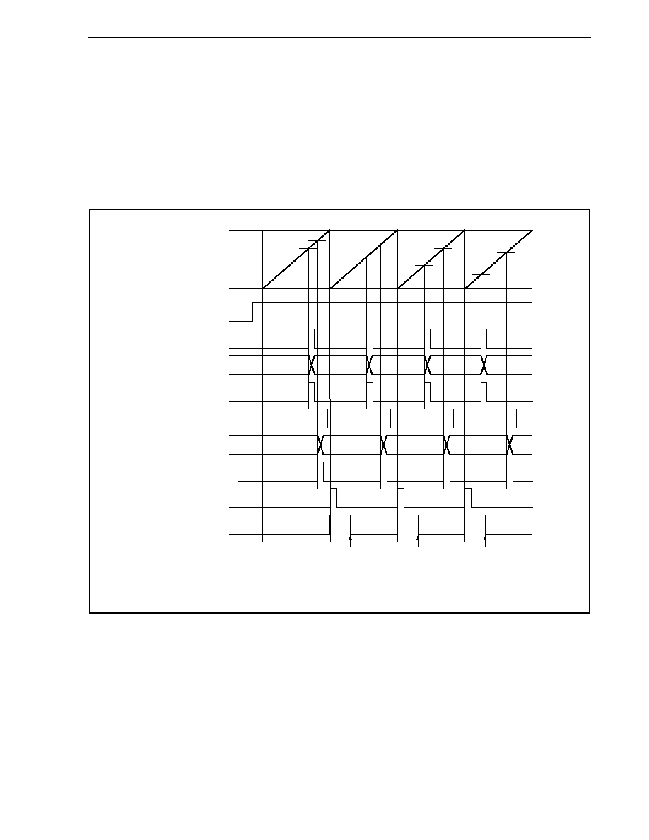
CHAPTER 7 16-BIT TIMER/EVENT COUNTER P (TMP)
Preliminary User's Manual U17714EJ1V0UD
289
When the TPnCE bit is set to 1, the 16-bit counter starts counting. When the valid edge input to the TIPnm pin is
detected, the count value of the 16-bit counter is stored in the TPnCCRm register, and a capture interrupt request
signal (INTTPnCCm) is generated.
The 16-bit counter continues counting in synchronization with the count clock. When it counts up to FFFFH, it
generates an overflow interrupt request signal (INTTPnOV) at the next clock, is cleared to 0000H, and continues
counting. At this time, the overflow flag (TPnOPT0.TPnOVF bit) is also set to 1. Clear the overflow flag to 0 by
executing the CLR instruction by software.
Figure 7-30. Basic Timing in Free-Running Timer Mode (Capture Function)
FFFFH
16-bit counter
0000H
TPnCE bit
TIPn0 pin input
TPnCCR0 register
INTTPnCC0 signal
TIPn1 pin input
TPnCCR1 register
INTTPnCC1 signal
INTTPnOV signal
TPnOVF bit
D
00
D
01
D
02
D
03
D
10
D
00
D
01
D
02
D
03
D
11
D
12
D
13
D
10
D
11
D
12
D
13
Cleared to 0 by
CLR instruction
Cleared to 0 by
CLR instruction
Cleared to 0 by
CLR instruction
Remark n = 0 to 8
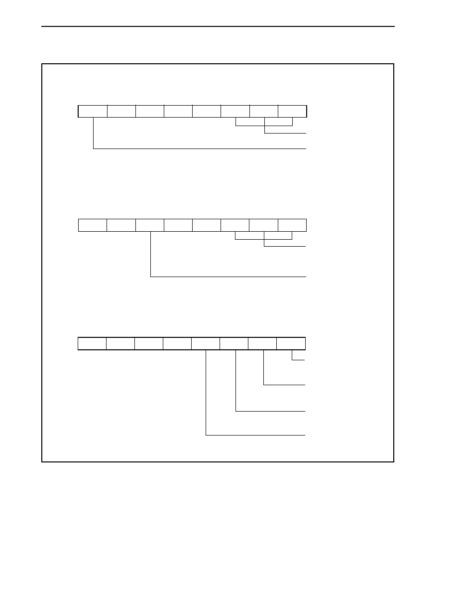
CHAPTER 7 16-BIT TIMER/EVENT COUNTER P (TMP)
Preliminary User's Manual U17714EJ1V0UD
290
Figure 7-31. Register Setting in Free-Running Timer Mode (1/2)
(a) TMPn control register 0 (TPnCTL0)
0/1
0
0
0
0
TPnCTL0
Select count clock
Note
0: Stop counting
1: Enable counting
0/1
0/1
0/1
TPnCKS2 TPnCKS1 TPnCKS0
TPnCE
Note The setting is invalid when the TPnCTL1.TPnEEE bit = 1
(b) TMPn control register 1 (TPnCTL1)
0
0
0/1
0
0
TPnCTL1
1
0
1
TPnMD2 TPnMD1 TPnMD0
TPnEEE
TPnEST
1, 0, 1:
Free-running mode
0: Operate with count
clock selected by
TPnCKS0 to TPnCKS2 bits
1: Count on external
event count input signal
(c) TMPn I/O control register 0 (TPnIOC0)
0
0
0
0
0/1
TPnIOC0
0: Disable TOPn0 pin output
1: Enable TOPn0 pin output
Setting of output level with
operation of TOPn0 pin disabled
0: Low level
1: High level
0: Disable TOPn1 pin output
1: Enable TOPn1 pin output
Setting of output level with
operation of TOPn1 pin disabled
0: Low level
1: High level
0/1
0/1
0/1
TPnOE1
TPnOL0
TPnOE0
TPnOL1
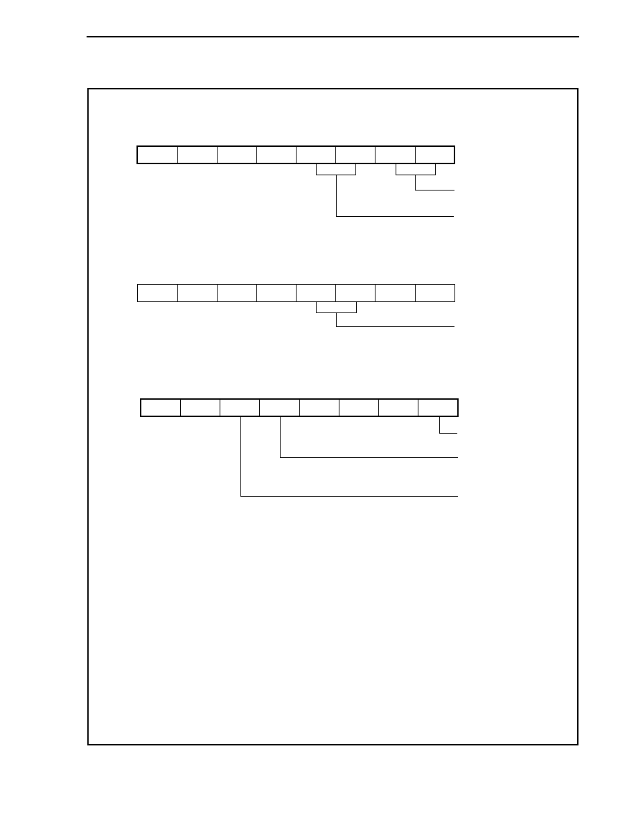
CHAPTER 7 16-BIT TIMER/EVENT COUNTER P (TMP)
Preliminary User's Manual U17714EJ1V0UD
291
Figure 7-31. Register Setting in Free-Running Timer Mode (2/2)
(d) TMPn I/O control register 1 (TPnIOC1)
0
0
0
0
0/1
TPnIOC1
Select valid edge
of TIPn0 pin input
Select valid edge
of TIPn1 pin input
0/1
0/1
0/1
TPnIS2
TPnIS1
TPnIS0
TPnIS3
(e) TMPn I/O control register 2 (TPnIOC2)
0
0
0
0
0/1
TPnIOC2
Select valid edge of
external event count input
0/1
0
0
TPnEES0 TPnETS1 TPnETS0
TPnEES1
(f) TMPn option register 0 (TPnOPT0)
0
0
0/1
0/1
0
TPnOPT0
Overflow flag
Specifies if TPnCCR0
register functions as
capture or compare register
Specifies if TPnCCR1
register functions as
capture or compare register
0
0
0/1
TPnCCS0
TPnOVF
TPnCCS1
(g) TMPn counter read buffer register (TPnCNT)
The value of the 16-bit counter can be read by reading the TPnCNT register.
(h) TMPn capture/compare registers 0 and 1 (TPnCCR0 and TPnCCR1)
These registers function as capture registers or compare registers depending on the setting of the
TPnOPT0.TPnCCSm bit.
When the registers function as capture registers, they store the count value of the 16-bit counter when
the valid edge input to the TIPnm pin is detected.
When the registers function as compare registers and when D
m
is set to the TPnCCRm register, the
INTTPnCCm signal is generated when the counter reaches (D
m
+ 1), and the output signal of the
TOPnm pin is inverted.
Remark n = 0 to 8
m = 0, 1
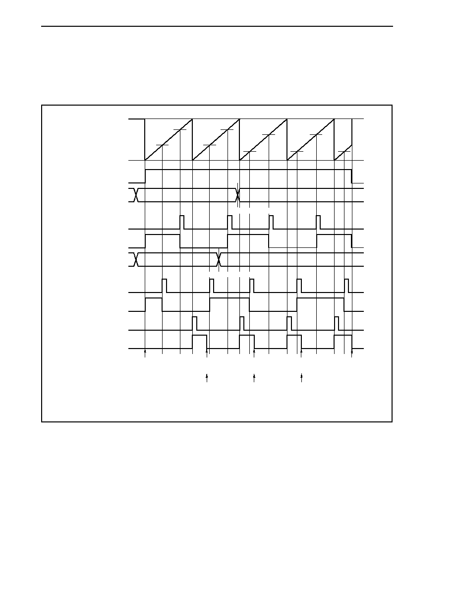
CHAPTER 7 16-BIT TIMER/EVENT COUNTER P (TMP)
Preliminary User's Manual U17714EJ1V0UD
292
(1) Operation flow in free-running timer mode
(a) When using capture/compare register as compare register
Figure 7-32. Software Processing Flow in Free-Running Timer Mode (Compare Function) (1/2)
FFFFH
16-bit counter
0000H
TPnCE bit
TPnCCR0 register
INTTPnCC0 signal
TOPn0 pin output
TPnCCR1 register
INTTPnCC1 signal
TOPn1 pin output
INTTPnOV signal
TPnOVF bit
D
00
D
01
D
10
D
11
D
00
D
10
D
10
D
11
D
11
D
11
D
00
D
01
D
01
Cleared to 0 by
CLR instruction
Set value changed
Cleared to 0 by
CLR instruction
Cleared to 0 by
CLR instruction
<1>
<2>
<2>
<2>
<3>
Set value changed
Remark n = 0 to 8
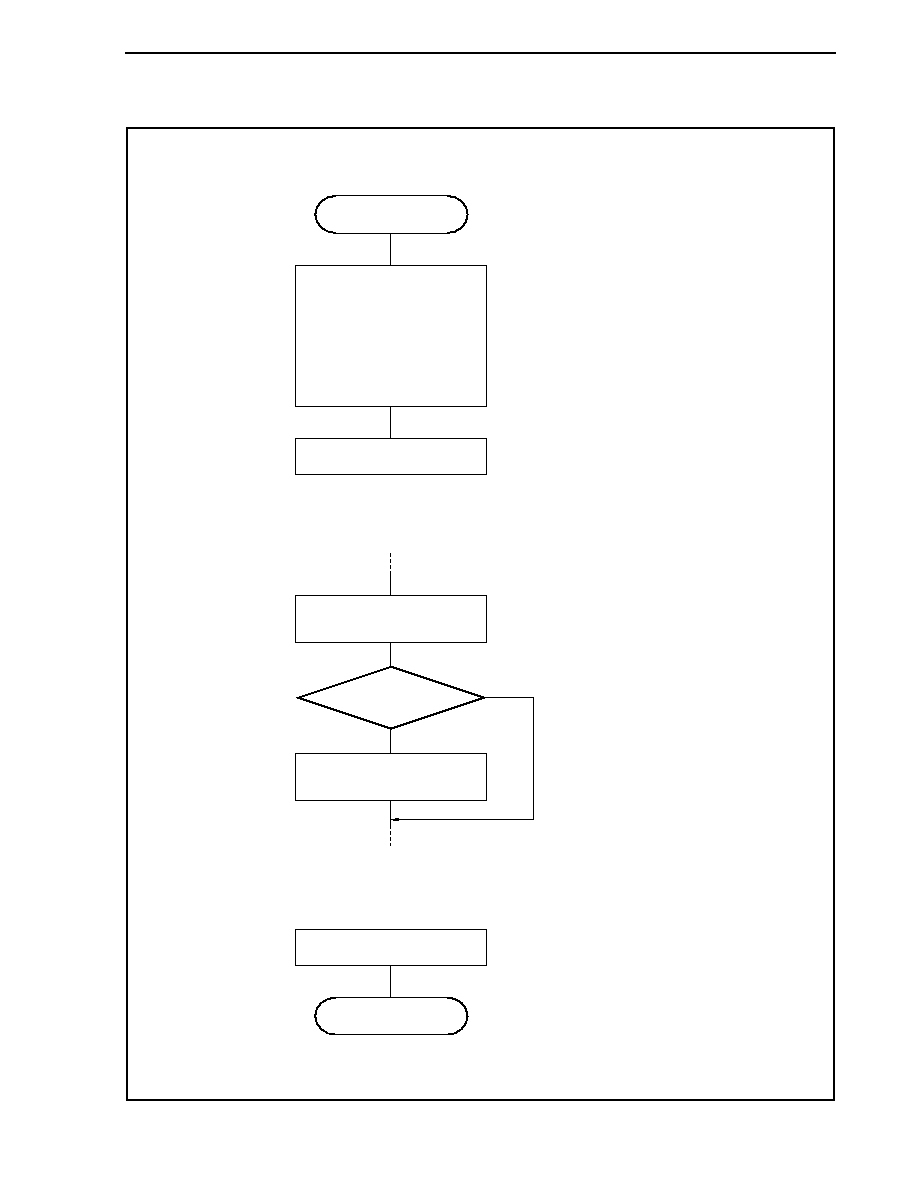
CHAPTER 7 16-BIT TIMER/EVENT COUNTER P (TMP)
Preliminary User's Manual U17714EJ1V0UD
293
Figure 7-32. Software Processing Flow in Free-Running Timer Mode (Compare Function) (2/2)
TPnCE bit = 1
Read TPnOPT0 register
(check overflow flag).
Register initial setting
TPnCTL0 register
(TPnCKS0 to TPnCKS2 bits)
TPnCTL1 register,
TPnIOC0 register,
TPnIOC2 register,
TPnOPT0 register,
TPnCCR0 register,
TPnCCR1 register
Initial setting of these registers
is performed before setting the
TPnCE bit to 1.
The TPnCKS0 to TPnCKS2 bits
can be set at the same time
when counting has been started
(TPnCE bit = 1).
START
Execute instruction to clear
TPnOVF bit (CLR TPnOVF).
<1> Count operation start flow
<2> Overflow flag clear flow
TPnCE bit = 0
Counter is initialized and
counting is stopped by
clearing TPnCE bit to 0.
STOP
<3> Count operation stop flow
TPnOVF bit = 1
NO
YES
Remark n = 0 to 8
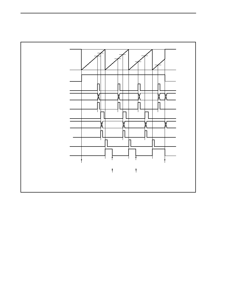
CHAPTER 7 16-BIT TIMER/EVENT COUNTER P (TMP)
Preliminary User's Manual U17714EJ1V0UD
294
(b) When using capture/compare register as capture register
Figure 7-33. Software Processing Flow in Free-Running Timer Mode (Capture Function) (1/2)
FFFFH
16-bit counter
0000H
TPnCE bit
TIPn0 pin input
TPnCCR0 register
INTTPnCC0 signal
TIPn1 pin input
TPnCCR1 register
INTTPnCC1 signal
INTTPnOV signal
TPnOVF bit
D
00
0000
0000
D
01
D
02
D
03
D
10
D
00
D
01
D
02
D
03
D
11
D
12
D
10
0000
D
11
D
12
0000
Cleared to 0 by
CLR instruction
Cleared to 0 by
CLR instruction
<3>
<1>
<2>
<2>
Remark n = 0 to 8
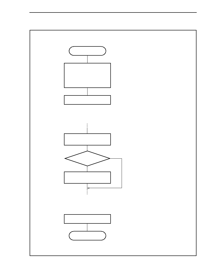
CHAPTER 7 16-BIT TIMER/EVENT COUNTER P (TMP)
Preliminary User's Manual U17714EJ1V0UD
295
Figure 7-33. Software Processing Flow in Free-Running Timer Mode (Capture Function) (2/2)
TPnCE bit = 1
Read TPnOPT0 register
(check overflow flag).
Register initial setting
TPnCTL0 register
(TPnCKS0 to TPnCKS2 bits)
TPnCTL1 register,
TPnIOC1 register,
TPnOPT0 register
Initial setting of these registers
is performed before setting the
TPnCE bit to 1.
The TPnCKS0 to TPnCKS2 bits can
be set at the same time when counting
has been started (TPnCE bit = 1).
START
Execute instruction to clear
TPnOVF bit (CLR TPnOVF).
<1> Count operation start flow
<2> Overflow flag clear flow
TPnCE bit = 0
Counter is initialized and
counting is stopped by
clearing TPnCE bit to 0.
STOP
<3> Count operation stop flow
TPnOVF bit = 1
NO
YES
Remark n = 0 to 8
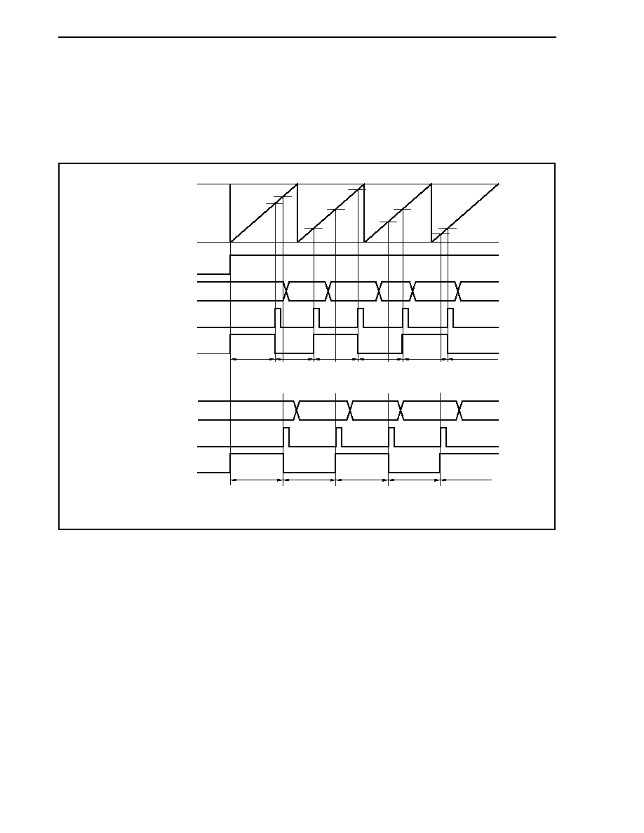
CHAPTER 7 16-BIT TIMER/EVENT COUNTER P (TMP)
Preliminary User's Manual U17714EJ1V0UD
296
(2) Operation timing in free-running timer mode
(a) Interval operation with compare register
When 16-bit timer/event counter P is used as an interval timer with the TPnCCRm register used as a
compare register, software processing is necessary for setting a comparison value to generate the next
interrupt request signal each time the INTTPnCCm signal has been detected.
FFFFH
16-bit counter
0000H
TPnCE bit
TPnCCR0 register
INTTPnCC0 signal
TOPn pin output
TPnCCR1 register
INTTPnCC1 signal
TOPn1 pin output
D
00
D
01
D
02
D
03
D
04
D
05
D
10
D
00
D
11
D
01
D
12
D
04
D
13
D
02
D
03
D
11
D
10
D
12
D
13
D
14
Interval period
(D
10
+ 1)
Interval period
(10000H +
D
11
- D
10
)
Interval period
(10000H +
D
12
- D
11
)
Interval period
(10000H +
D
13
- D
12
)
Interval period
(D
00
+ 1)
Interval period
(10000H +
D
01
- D
00
)
Interval period
(D
02
- D
01
)
Interval period
(10000H +
D
03
- D
02
)
Interval period
(10000H +
D
04
- D
03
)
When performing an interval operation in the free-running timer mode, two intervals can be set with one
channel.
To perform the interval operation, the value of the corresponding TPnCCRm register must be re-set in the
interrupt servicing that is executed when the INTTPnCCm signal is detected.
The set value for re-setting the TPnCCRm register can be calculated by the following expression, where
"D
m
" is the interval period.
Compare register default value: D
m
- 1
Value set to compare register second and subsequent time: Previous set value + D
m
(If the calculation result is greater than FFFFH, subtract 10000H from the result and set this value to the
register.)
Remark n = 0 to 8
m = 0, 1
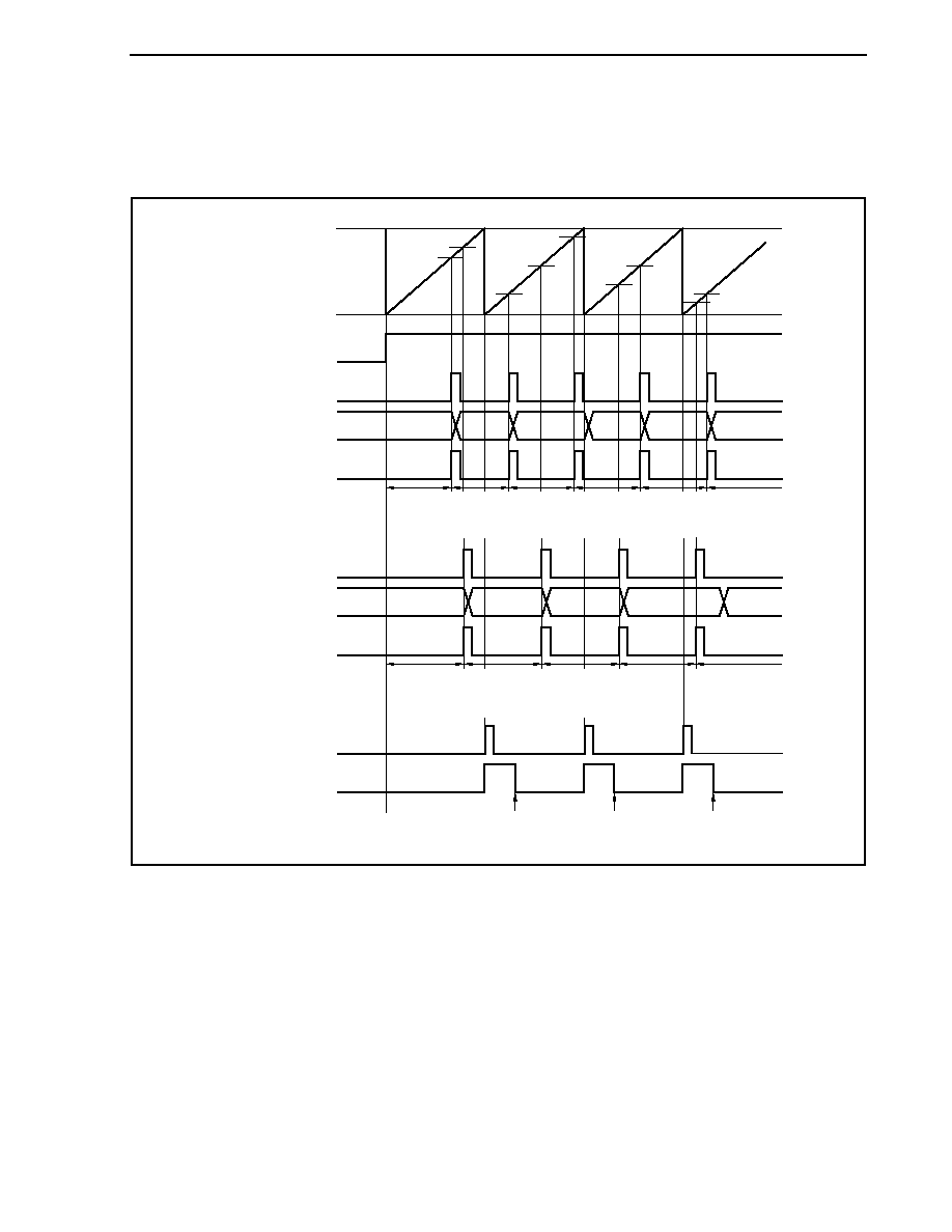
CHAPTER 7 16-BIT TIMER/EVENT COUNTER P (TMP)
Preliminary User's Manual U17714EJ1V0UD
297
(b) Pulse width measurement with capture register
When pulse width measurement is performed with the TPnCCRm register used as a capture register,
software processing is necessary for reading the capture register each time the INTTPnCCm signal has
been detected and for calculating an interval.
FFFFH
16-bit counter
0000H
TPnCE bit
TIPn0 pin input
TPnCCR0 register
INTTPnCC0 signal
TIPn1 pin input
TPnCCR1 register
INTTPnCC1 signal
INTTPnOV signal
TPnOVF bit
0000H
D
00
D
01
D
02
D
03
D
04
D
10
D
00
D
11
D
01
D
12
D
04
D
13
D
02
D
03
D
10
0000H
D
11
D
12
D
13
Pulse interval
(D
00
)
Pulse interval
(10000H +
D
01
- D
00
)
Pulse interval
(D
02
- D
01
)
Pulse interval
(10000H +
D
03
- D
02
)
Pulse interval
(10000H +
D
04
- D
03
)
Pulse interval
(D
10
)
Pulse interval
(10000H +
D
11
- D
10
)
Pulse interval
(10000H +
D
12
- D
11
)
Pulse interval
(10000H +
D
13
- D
12
)
Cleared to 0 by
CLR instruction
Cleared to 0 by
CLR instruction
Cleared to 0 by
CLR instruction
When executing pulse width measurement in the free-running timer mode, two pulse widths can be
measured with one channel.
To measure a pulse width, the pulse width can be calculated by reading the value of the TPnCCRm
register in synchronization with the INTTPnCCm signal, and calculating the difference between the read
value and the previously read value.
Remark n = 0 to 8
m = 0, 1
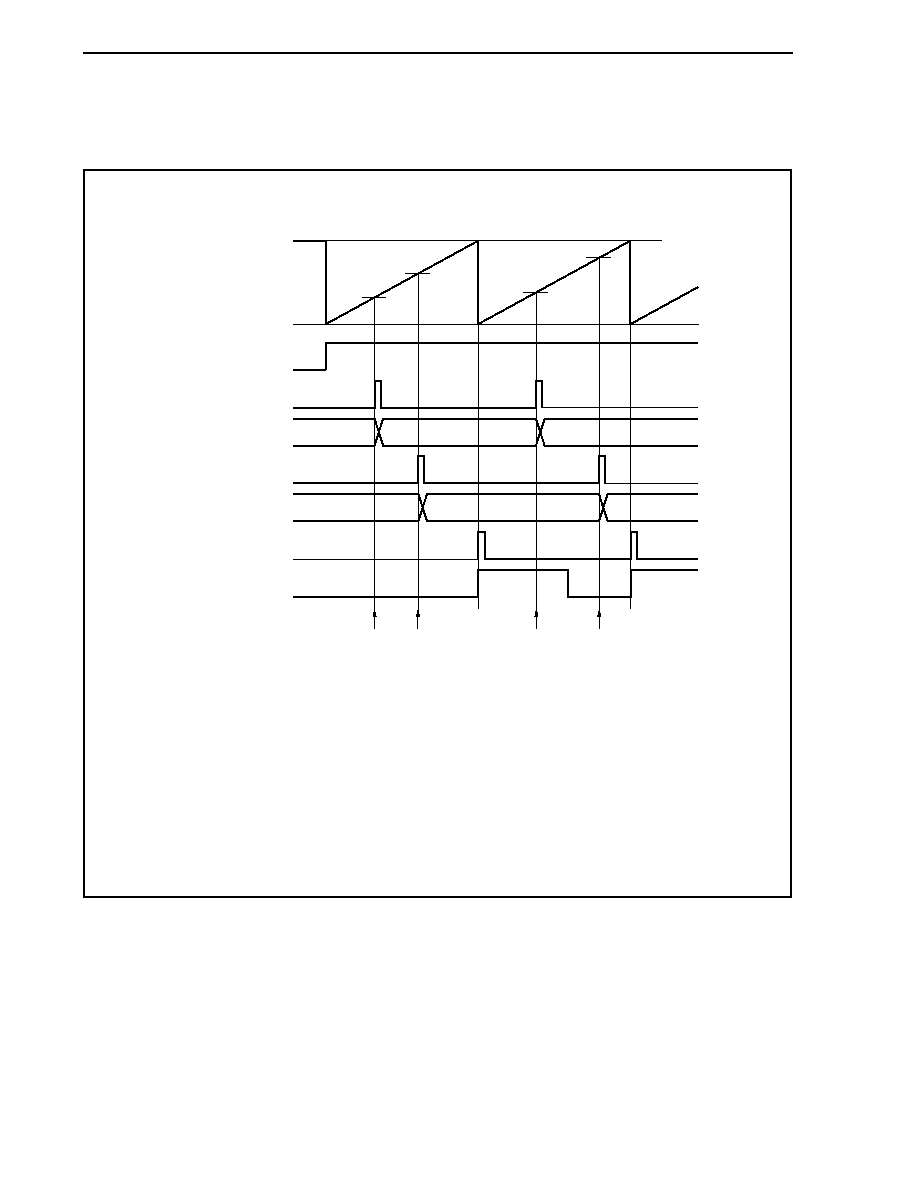
CHAPTER 7 16-BIT TIMER/EVENT COUNTER P (TMP)
Preliminary User's Manual U17714EJ1V0UD
298
(c) Processing of overflow when two capture registers are used
Care must be exercised in processing the overflow flag when two capture registers are used. First, an
example of incorrect processing is shown below.
Example of incorrect processing when two capture registers are used
FFFFH
16-bit counter
0000H
TPnCE bit
TIPn0 pin input
TPnCCR0 register
TIPn1 pin input
TPnCCR1 register
INTTPnOV signal
TPnOVF bit
D
00
D
01
D
10
D
11
D
10
<1>
<2>
<3>
<4>
D
00
D
11
D
01
The following problem may occur when two pulse widths are measured in the free-running timer mode.
<1> Read the TPnCCR0 register (setting of the default value of the TIPn0 pin input).
<2> Read the TPnCCR1 register (setting of the default value of the TIPn1 pin input).
<3> Read the TPnCCR0 register.
Read the overflow flag. If the overflow flag is 1, clear it to 0.
Because the overflow flag is 1, the pulse width can be calculated by (10000H + D
01
- D
00
).
<4> Read the TPnCCR1 register.
Read the overflow flag. Because the flag is cleared in <3>, 0 is read.
Because the overflow flag is 0, the pulse width can be calculated by (D
11
- D
10
) (incorrect).
When two capture registers are used, and if the overflow flag is cleared to 0 by one capture register, the
other capture register may not obtain the correct pulse width.
Use software when using two capture registers. An example of how to use software is shown below.
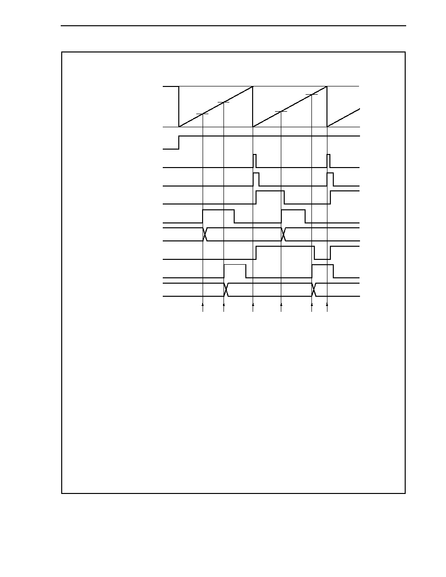
CHAPTER 7 16-BIT TIMER/EVENT COUNTER P (TMP)
Preliminary User's Manual U17714EJ1V0UD
299
(1/2)
Example when two capture registers are used (using overflow interrupt)
FFFFH
16-bit counter
0000H
TPnCE bit
INTTPnOV signal
TPnOVF bit
TPnOVF0 flag
Note
TIPn0 pin input
TPnCCR0 register
TPnOVF1 flag
Note
TIPn1 pin input
TPnCCR1 register
D
10
D
11
D
00
D
01
D
10
<1>
<2>
<5> <6>
<3>
<4>
D
00
D
11
D
01
Note The TPnOVF0 and TPnOVF1 flags are set on the internal RAM by software.
<1> Read the TPnCCR0 register (setting of the default value of the TIPn0 pin input).
<2> Read the TPnCCR1 register (setting of the default value of the TIPn1 pin input).
<3> An overflow occurs. Set the TPnOVF0 and TPnOVF1 flags to 1 in the overflow interrupt servicing,
and clear the overflow flag to 0.
<4> Read the TPnCCR0 register.
Read the TPnOVF0 flag. If the TPnOVF0 flag is 1, clear it to 0.
Because the TPnOVF0 flag is 1, the pulse width can be calculated by (10000H + D
01
- D
00
).
<5> Read the TPnCCR1 register.
Read the TPnOVF1 flag. If the TPnOVF1 flag is 1, clear it to 0 (the TPnOVF0 flag is cleared in
<4>, and the TPnOVF1 flag remains 1).
Because the TPnOVF1 flag is 1, the pulse width can be calculated by (10000H + D
11
- D
10
)
(correct).
<6> Same as <3>
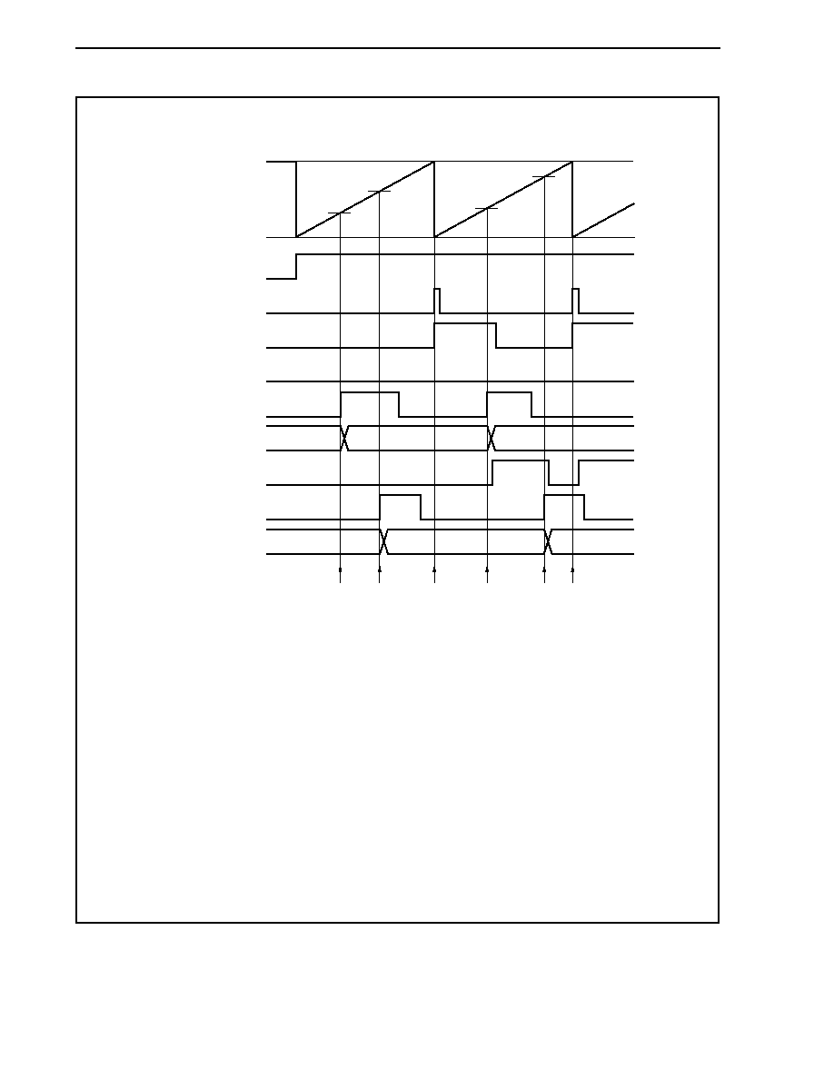
CHAPTER 7 16-BIT TIMER/EVENT COUNTER P (TMP)
Preliminary User's Manual U17714EJ1V0UD
300
(2/2)
Example when two capture registers are used (without using overflow interrupt)
FFFFH
16-bit counter
0000H
TPnCE bit
INTTPnOV signal
TPnOVF bit
TPnOVF0 flag
Note
TIPn0 pin input
TPnCCR0 register
TPnOVF1 flag
Note
TIPn1 pin input
TPnCCR1 register
D
10
D
11
D
00
D
01
D
10
<1>
<2>
<5> <6>
<3>
<4>
D
00
D
11
D
01
Note The TPnOVF0 and TPnOVF1 flags are set on the internal RAM by software.
<1> Read the TPnCCR0 register (setting of the default value of the TIPn0 pin input).
<2> Read the TPnCCR1 register (setting of the default value of the TIPn1 pin input).
<3> An overflow occurs. Nothing is done by software.
<4> Read the TPnCCR0 register.
Read the overflow flag. If the overflow flag is 1, set only the TPnOVF1 flag to 1, and clear the
overflow flag to 0.
Because the overflow flag is 1, the pulse width can be calculated by (10000H + D
01
- D
00
).
<5> Read the TPnCCR1 register.
Read the overflow flag. Because the overflow flag is cleared in <4>, 0 is read.
Read the TPnOVF1 flag. If the TPnOVF1 flag is 1, clear it to 0.
Because the TPnOVF1 flag is 1, the pulse width can be calculated by (10000H + D
11
- D
10
)
(correct).
<6> Same as <3>
CHAPTER 7 16-BIT TIMER/EVENT COUNTER P (TMP)
Preliminary User's Manual U17714EJ1V0UD
301
(d) Processing of overflow if capture trigger interval is long
If the pulse width is greater than one cycle of the 16-bit counter, care must be exercised because an
overflow may occur more than once from the first capture trigger to the next. First, an example of incorrect
processing is shown below.
Example of incorrect processing when capture trigger interval is long
FFFFH
16-bit counter
0000H
TPnCE bit
TIPnm pin input
TPnCCRm register
INTTPnOV signal
TPnOVF bit
D
m0
D
m1
D
m0
D
m1
<1> <2>
<3> <4>
1 cycle of 16-bit counter
Pulse width
The following problem may occur when long pulse width is measured in the free-running timer mode.
<1> Read the TPnCCRm register (setting of the default value of the TIPnm pin input).
<2> An overflow occurs. Nothing is done by software.
<3> An overflow occurs a second time. Nothing is done by software.
<4> Read the TPnCCRm register.
Read the overflow flag. If the overflow flag is 1, clear it to 0.
Because the overflow flag is 1, the pulse width can be calculated by (10000H + D
m1
- D
m0
)
(incorrect).
Actually, the pulse width must be (20000H + D
m1
- D
m0
) because an overflow occurs twice.
If an overflow occurs twice or more when the capture trigger interval is long, the correct pulse width may
not be obtained.
If the capture trigger interval is long, slow the count clock to lengthen one cycle of the 16-bit counter, or
use software. An example of how to use software is shown next.
CHAPTER 7 16-BIT TIMER/EVENT COUNTER P (TMP)
Preliminary User's Manual U17714EJ1V0UD
302
Example when capture trigger interval is long
FFFFH
16-bit counter
0000H
TPnCE bit
TIPnm pin input
TPnCCRm register
INTTPnOV signal
TPnOVF bit
Overflow
counter
Note
D
m0
D
m1
1H
0H
2H
0H
D
m0
D
m1
<1> <2>
<3> <4>
1 cycle of 16-bit counter
Pulse width
Note The overflow counter is set arbitrarily by software on the internal RAM.
<1> Read the TPnCCRm register (setting of the default value of the TIPnm pin input).
<2> An overflow occurs. Increment the overflow counter and clear the overflow flag to 0 in the overflow
interrupt servicing.
<3> An overflow occurs a second time. Increment (+1) the overflow counter and clear the overflow flag
to 0 in the overflow interrupt servicing.
<4> Read the TPnCCRm register.
Read the overflow counter.
When the overflow counter is "N", the pulse width can be calculated by (N � 10000H + D
m1
�
D
m0
).
In this example, the pulse width is (20000H + D
m1
� D
m0
) because an overflow occurs twice.
Clear the overflow counter (0H).
CHAPTER 7 16-BIT TIMER/EVENT COUNTER P (TMP)
Preliminary User's Manual U17714EJ1V0UD
303
(e) Clearing overflow flag
The overflow flag can be cleared to 0 by clearing the TPnOVF bit to 0 with the CLR instruction and by
writing 8-bit data (bit 0 is 0) to the TPnOPT0 register. To accurately detect an overflow, read the TPnOVF
bit when it is 1, and then clear the overflow flag by using a bit manipulation instruction.
(i) Operation to write 0 (without conflict with setting)
(iii) Operation to clear to 0 (without conflict with setting)
(ii) Operation to write 0 (conflict with setting)
(iv) Operation to clear to 0 (conflict with setting)
0 write signal
Overflow
set signal
Register
access signal
Overflow flag
(TPnOVF bit)
Read
Write
0 write signal
Overflow
set signal
Register
access signal
Overflow flag
(TPnOVF bit)
Read
Write
0 write signal
Overflow
set signal
0 write signal
Overflow
set signal
Overflow flag
(TPnOVF bit)
Overflow flag
(TPnOVF bit)
L
H
L
Remark n = 0 to 8
To clear the overflow flag to 0, read the overflow flag to check if it is set to 1, and clear it with the CLR
instruction. If 0 is written to the overflow flag without checking if the flag is 1, the set information of
overflow may be erased by writing 0 ((ii) in the above chart). Therefore, software may judge that no
overflow has occurred even when an overflow actually has occurred.
If execution of the CLR instruction conflicts with occurrence of an overflow when the overflow flag is
cleared to 0 with the CLR instruction, the overflow flag remains set even after execution of the clear
instruction.
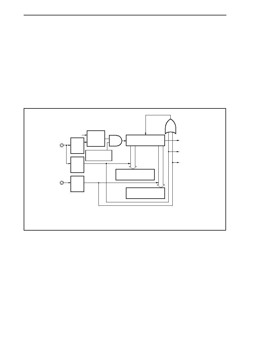
CHAPTER 7 16-BIT TIMER/EVENT COUNTER P (TMP)
Preliminary User's Manual U17714EJ1V0UD
304
7.5.7
Pulse width measurement mode (TPnMD2 to TPnMD0 bits = 110)
In the pulse width measurement mode, 16-bit timer/event counter P starts counting when the TPnCTL0.TPnCE bit
is set to 1. Each time the valid edge input to the TIPnm pin has been detected, the count value of the 16-bit counter is
stored in the TPnCCRm register, and the 16-bit counter is cleared to 0000H.
The interval of the valid edge can be measured by reading the TPnCCRm register after a capture interrupt request
signal (INTTPnCCm) occurs.
Select either the TIPn0 or TIPn1 pin as the capture trigger input pin. Specify "No edge detected" by using the
TPnIOC1 register for the unused pins.
When an external clock is used as the count clock, measure the pulse width of the TIPn1 pin because the external
clock is fixed to the TIPn0 pin. At this time, clear the TPnIOC1.TPnIS1 and TPnIOC1.TPnIS0 bits to 00 (capture
trigger input (TIPn0 pin): No edge detected).
Figure 7-34. Configuration in Pulse Width Measurement Mode
TPnCCR0 register
(capture)
TPnCE bit
TPnCCR1 register
(capture)
Edge
detector
Count
clock
selection
Edge
detector
Edge
detector
TIPn0 pin
(external
event count
input/capture
trigger input)
TIPn1 pin
(capture
trigger input)
Internal count clock
Clear
INTTPnOV
signal
INTTPnCC0
signal
INTTPnCC1
signal
16-bit counter
Remark n = 0 to 8
m = 0, 1
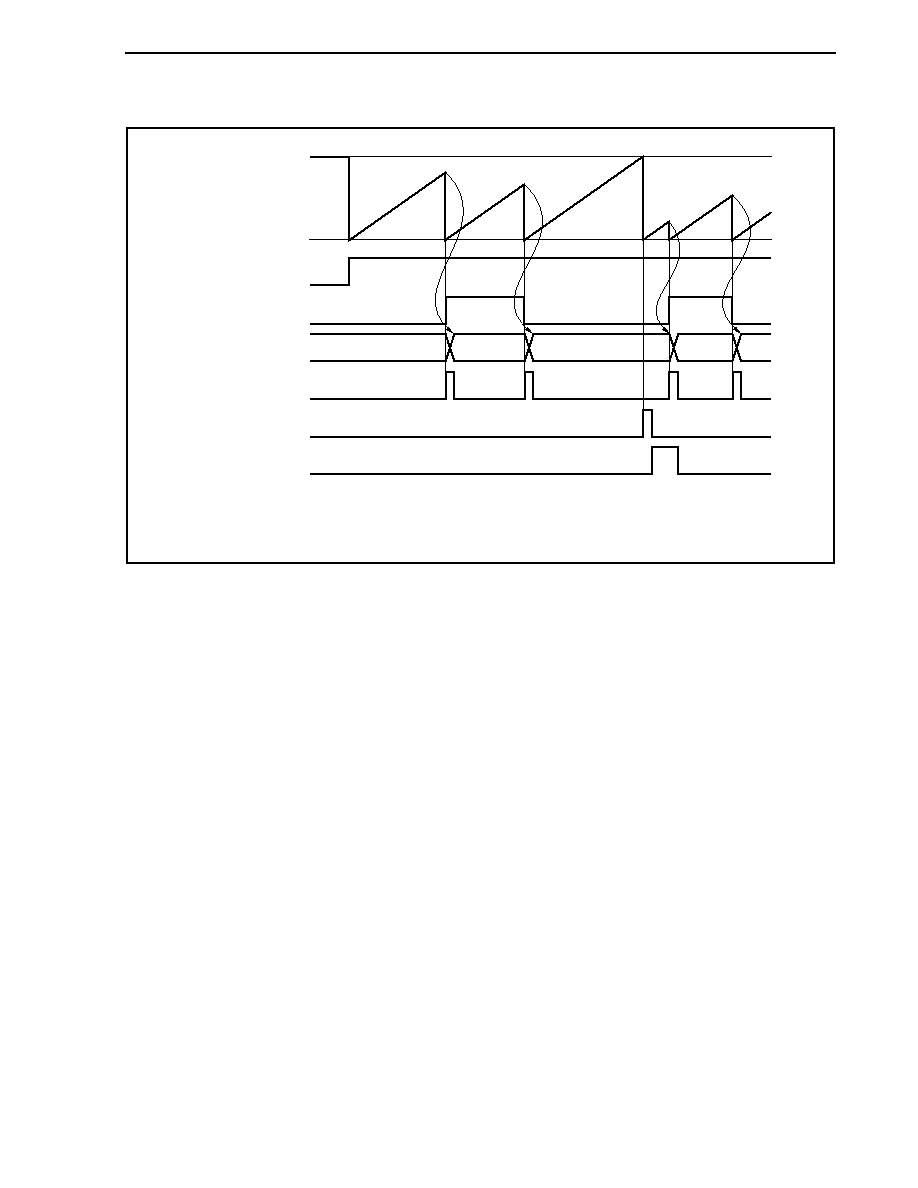
CHAPTER 7 16-BIT TIMER/EVENT COUNTER P (TMP)
Preliminary User's Manual U17714EJ1V0UD
305
Figure 7-35. Basic Timing in Pulse Width Measurement Mode
FFFFH
16-bit counter
0000H
TPnCE bit
TIPnm pin input
TPnCCRm register
INTTPnCCm signal
INTTPnOV signal
TPnOVF bit
D
0
0000H
D
1
D
2
D
3
Cleared to 0 by
CLR instruction
Remark n = 0 to 8
m = 0, 1
When the TPnCE bit is set to 1, the 16-bit counter starts counting. When the valid edge input to the TIPnm pin is
later detected, the count value of the 16-bit counter is stored in the TPnCCRm register, the 16-bit counter is cleared to
0000H, and a capture interrupt request signal (INTTPnCCm) is generated.
The pulse width is calculated as follows.
Pulse width = Captured value
� Count clock cycle
If the valid edge is not input to the TIPnm pin even when the 16-bit counter counted up to FFFFH, an overflow
interrupt request signal (INTTPnOV) is generated at the next count clock, and the counter is cleared to 0000H and
continues counting. At this time, the overflow flag (TPnOPT0.TPnOVF bit) is also set to 1. Clear the overflow flag to 0
by executing the CLR instruction via software.
If the overflow flag is set to 1, the pulse width can be calculated as follows.
Pulse width = (10000H
� TPnOVF bit set (1) count + Captured value) � Count clock cycle
Remark n = 0 to 8
m = 0, 1
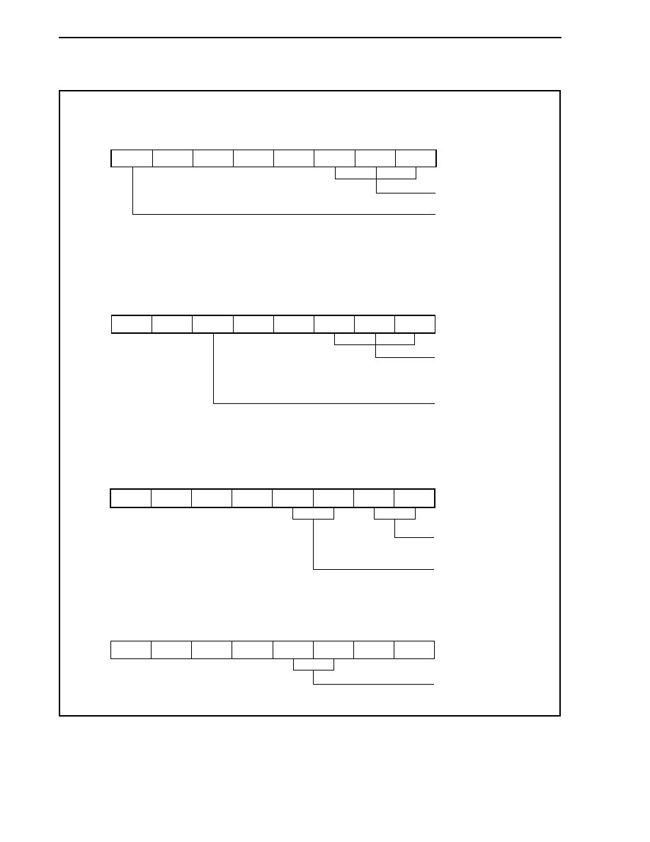
CHAPTER 7 16-BIT TIMER/EVENT COUNTER P (TMP)
Preliminary User's Manual U17714EJ1V0UD
306
Figure 7-36. Register Setting in Pulse Width Measurement Mode (1/2)
(a) TMPn control register 0 (TPnCTL0)
0/1
0
0
0
0
TPnCTL0
Select count clock
Note
0: Stop counting
1: Enable counting
0/1
0/1
0/1
TPnCKS2 TPnCKS1 TPnCKS0
TPnCE
Note Setting is invalid when the TPnEEE bit = 1.
(b) TMPn control register 1 (TPnCTL1)
0
0
0/1
0
0
TPnCTL1
1
1
0
TPnMD2 TPnMD1 TPnMD0
TPnEEE
TPnEST
1, 1, 0:
Pulse width measurement mode
0: Operate with count
clock selected by
TPnCKS0 to TPnCKS2 bits
1: Count external event
count input signal
(c) TMPn I/O control register 1 (TPnIOC1)
0
0
0
0
0/1
TPnIOC1
Select valid edge
of TIPn0 pin input
Select valid edge
of TIPn1 pin input
0/1
0/1
0/1
TPnIS2
TPnIS1
TPnIS0
TPnIS3
(d) TMPn I/O control register 2 (TPnIOC2)
0
0
0
0
0/1
TPnIOC2
Select valid edge of
external event count input
0/1
0
0
TPnEES0 TPnETS1 TPnETS0
TPnEES1

CHAPTER 7 16-BIT TIMER/EVENT COUNTER P (TMP)
Preliminary User's Manual U17714EJ1V0UD
307
Figure 7-36. Register Setting in Pulse Width Measurement Mode (2/2)
(e) TMPn option register 0 (TPnOPT0)
0
0
0
0
0
TPnOPT0
Overflow flag
0
0
0/1
TPnCCS0
TPnOVF
TPnCCS1
(f) TMPn counter read buffer register (TPnCNT)
The value of the 16-bit counter can be read by reading the TPnCNT register.
(g) TMPn capture/compare registers 0 and 1 (TPnCCR0 and TPnCCR1)
These registers store the count value of the 16-bit counter when the valid edge input to the TIPnm pin
is detected.
Remarks 1. TMPn I/O control register 0 (TPnIOC0) is not used in the pulse width measurement mode.
2. n = 0 to 8
m = 0, 1
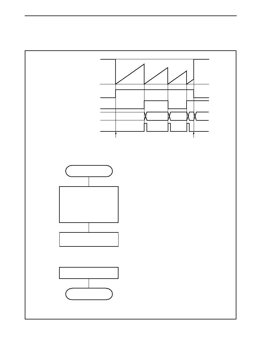
CHAPTER 7 16-BIT TIMER/EVENT COUNTER P (TMP)
Preliminary User's Manual U17714EJ1V0UD
308
(1) Operation flow in pulse width measurement mode
Figure 7-37. Software Processing Flow in Pulse Width Measurement Mode
<1>
<2>
Set TPnCTL0 register
(TPnCE bit = 1)
TPnCE bit = 0
Register initial setting
TPnCTL0 register
(TPnCKS0 to TPnCKS2 bits),
TPnCTL1 register,
TPnIOC1 register,
TPnIOC2 register,
TPnOPT0 register
Initial setting of these registers
is performed before setting the
TPnCE bit to 1.
The TPnCKS0 to TPnCKS2 bits can
be set at the same time when counting
has been started (TPnCE bit = 1).
The counter is initialized and counting
is stopped by clearing the TPnCE bit to 0.
START
STOP
<1> Count operation start flow
<2> Count operation stop flow
FFFFH
16-bit counter
0000H
TPnCE bit
TIPn0 pin input
TPnCCR0 register
INTTPnCC0 signal
D
0
0000H
0000H
D
1
D
2
Remark n = 0 to 8
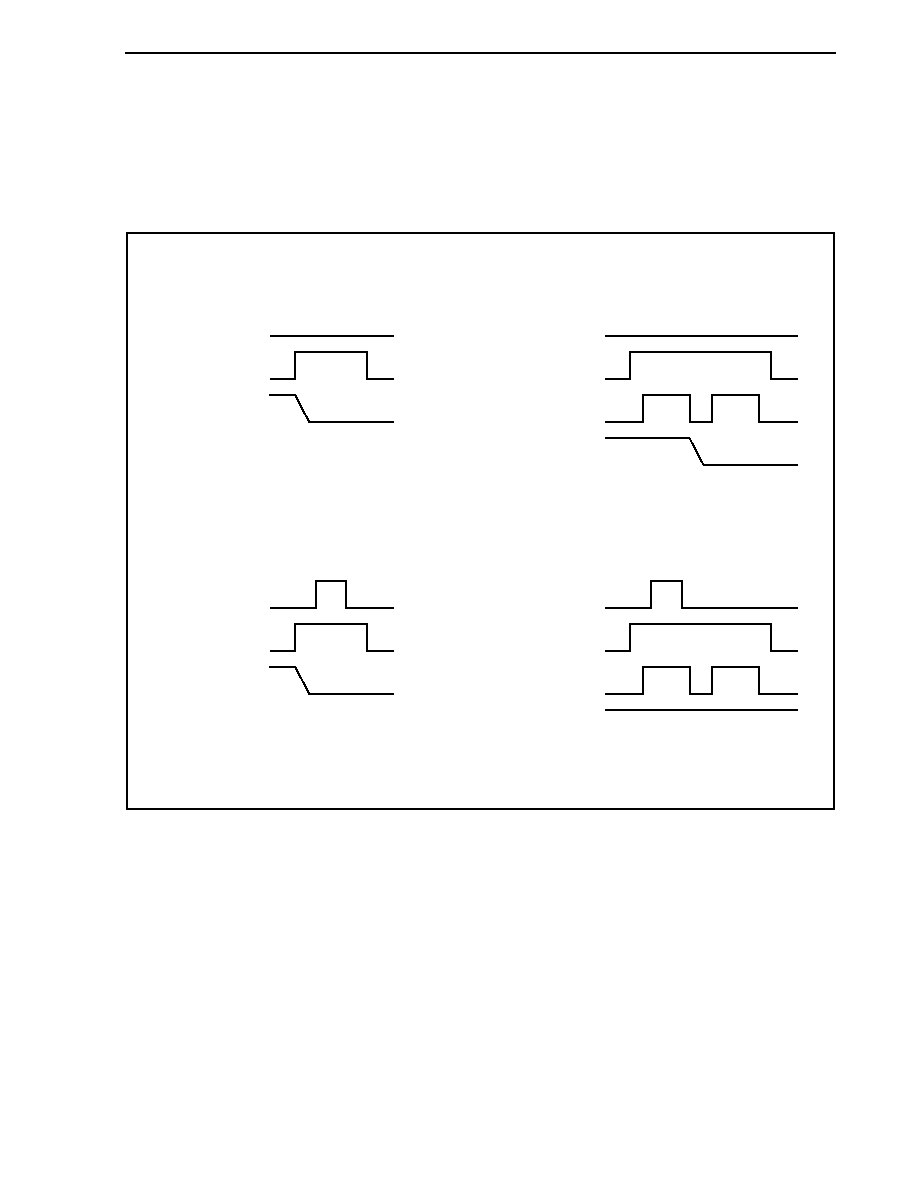
CHAPTER 7 16-BIT TIMER/EVENT COUNTER P (TMP)
Preliminary User's Manual U17714EJ1V0UD
309
(2) Operation timing in pulse width measurement mode
(a) Clearing overflow flag
The overflow flag can be cleared to 0 by clearing the TPnOVF bit to 0 with the CLR instruction and by
writing 8-bit data (bit 0 is 0) to the TPnOPT0 register. To accurately detect an overflow, read the TPnOVF
bit when it is 1, and then clear the overflow flag by using a bit manipulation instruction.
(i) Operation to write 0 (without conflict with setting)
(iii) Operation to clear to 0 (without conflict with setting)
(ii) Operation to write 0 (conflict with setting)
(iv) Operation to clear to 0 (conflict with setting)
0 write signal
Overflow
set signal
Register
access signal
Overflow flag
(TPnOVF bit)
Read
Write
0 write signal
Overflow
set signal
Register
access signal
Overflow flag
(TPnOVF bit)
Read
Write
0 write signal
Overflow
set signal
0 write signal
Overflow
set signal
Overflow flag
(TPnOVF bit)
Overflow flag
(TPnOVF bit)
L
H
L
Remark n = 0 to 8
To clear the overflow flag to 0, read the overflow flag to check if it is set to 1, and clear it with the CLR
instruction. If 0 is written to the overflow flag without checking if the flag is 1, the set information of
overflow may be erased by writing 0 ((ii) in the above chart). Therefore, software may judge that no
overflow has occurred even when an overflow actually has occurred.
If execution of the CLR instruction conflicts with occurrence of an overflow when the overflow flag is
cleared to 0 with the CLR instruction, the overflow flag remains set even after execution of the clear
instruction.
CHAPTER 7 16-BIT TIMER/EVENT COUNTER P (TMP)
Preliminary User's Manual U17714EJ1V0UD
310
7.5.8 Timer
output
operations
The following table shows the operations and output levels of the TOPn0 and TOPn1 pins.
Table 7-4. Timer Output Control in Each Mode
Operation Mode
TOPn1 Pin
TOPn0 Pin
Interval timer mode
Square wave output
External event count mode
Square wave output
-
External trigger pulse output mode
External trigger pulse output
One-shot pulse output mode
One-shot pulse output
PWM output mode
PWM output
Square wave output
Free-running timer mode
Square wave output (only when compare function is used)
Pulse width measurement mode
-
Remark n = 0 to 8
Table 7-5. Truth Table of TOPn0 and TOPn1 Pins Under Control of Timer Output Control Bits
TPnIOC0.TPnOLm Bit
TPnIOC0.TPnOEm Bit
TPnCTL0.TPnCE Bit
Level of TOPnm Pin
0
�
Low-level output
0 Low-level
output
0
1
1
Low level immediately before counting, high
level after counting is started
0
�
High-level output
0 High-level
output
1
1
1
High level immediately before counting, low level
after counting is started
Remark n = 0 to 8
m = 0, 1

CHAPTER 7 16-BIT TIMER/EVENT COUNTER P (TMP)
Preliminary User's Manual U17714EJ1V0UD
311
7.6 Selector
Function
In the V850ES/JJ2, the capture trigger input for TMP1/TMP3 can be selected from the input signal via the
port/timer alternate-function pin (TIP10/TIP11/TIP31) and the peripheral I/O (TMP/UARTA) input signal via the UARTA
reception alternate-function pin (RXDA0/RXDA1/RXDA3).
This function makes the following possible.
� The TIP10 and TIP11 input signals for TMP1 can be selected from the signals via the port/timer alternate-function
pins (TIP10 and TIP11) and the signals via the UARTA reception alternate-function pins (RXDA0 and RXDA1).
Similarly, the TIP31 input signal for TMP3 can be selected from the signal via the port/timer alternate-function pin
(TIP31) and the signal via the UARTA reception alternate-function pin (RXDA3).
When the RXDA0, RXDA1, or RXDA3 signal for UARTA0, for UARTA1, or UARTA3 is selected, the baud rate
error of the UARTA LIN reception transfer rate can be calculated.
Cautions 1. When using the selector function, be sure to set the port/timer alternate function pins for
TMP to be connected to the capture tripper input.
2. Disable the peripheral I/Os to be connected (TMP/UARTA) before setting the selector
function.
The capture trigger input can be selected using the following register.
CHAPTER 7 16-BIT TIMER/EVENT COUNTER P (TMP)
Preliminary User's Manual U17714EJ1V0UD
312
(1) Selector operation control register 0 (SELCNT0)
The SELCNT0 register is an 8-bit register that selects the capture trigger for TMP1 and TMP3.
This register can be read or written in 8-bit or 1-bit units.
Reset sets this register to 00H.
0
TIP31 pin input
RXDA3 pin input
ISEL6
0
1
Selection of TIP31 input signal (TMP3)
SELCNT0
ISEL6
0
ISEL4
ISEL3
0
0
0
TIP11 pin input
RXDA1 pin input
ISEL4
0
1
Selection of TIP11 input signal (TMP1)
TIP10 pin input
RXDA0 pin input
ISEL3
0
1
Selection of TIP10 input signal (TMP1)
After reset: 00H R/W Address: FFFFF308H
< >
< >
< >
Cautions 1. When setting the ISEL3, ISEL4, or ISEL6 bit to 1, be sure to set the
corresponding alternate-function pin to the capture trigger input.
2. Be sure to clear bits 7, 5, 2, 1, and 0 to "0".
CHAPTER 7 16-BIT TIMER/EVENT COUNTER P (TMP)
Preliminary User's Manual U17714EJ1V0UD
313
7.7 Cautions
(1) Capture operation
When the capture operation is used and a slow clock is selected as the count clock, FFFFH, not 0000H, may
be captured in the TPnCCR0 and TPnCCR1 registers if the capture trigger is input immediately after the
TPnCE bit is set to 1.
(a) Free-running timer mode
Count clock
0000H
FFFFH
TPnCE bit
TPnCCR0 register
FFFFH
0001H
0000H
TIPn0 pin input
Capture
trigger input
16-bit counter
Sampling clock (f
XX
)
Capture
trigger input
(b) Pulse width measurement mode
0000H
FFFFH
FFFFH
0002H
0000H
Count clock
TPnCE bit
TPnCCR0 register
TIPn0 pin input
Capture
trigger input
16-bit counter
Sampling clock (f
XX
)
Capture
trigger input

Preliminary User's Manual U17714EJ1V0UD
314
CHAPTER 8 16-BIT TIMER/EVENT COUNTER Q (TMQ)
Timer Q (TMQ) is a 16-bit timer/event counter.
The V850ES/JJ2 incorporates TMQ0.
8.1 Overview
An outline of TMQ0 is shown below.
� Clock selection: 8 ways
� Capture/trigger input pins: 4
� External event count input pins: 1
� External trigger input pins: 1
� Timer/counters: 1
� Capture/compare registers: 4
� Capture/compare match interrupt request signals: 4
� Timer output pins: 4
8.2 Functions
TMQ0 has the following functions.
� Interval timer
� External event counter
� External trigger pulse output
� One-shot pulse output
� PWM output
� Free-running timer
� Pulse width measurement
CHAPTER 8 16-BIT TIMER/EVENT COUNTER Q (TMQ)
Preliminary User's Manual U17714EJ1V0UD
315
8.3 Configuration
TMQ0 includes the following hardware.
Table 8-1. Configuration of TMQ0
Item Configuration
Timer register
16-bit counter
Registers
TMQ0 capture/compare registers 0 to 3 (TQ0CCR0 to TQ0CCR3)
TMQ0 counter read buffer register (TQ0CNT)
CCR0 to CCR3 buffer registers
Timer inputs
4 (TIQ00
Note 1
to TIQ03 pins)
Timer outputs
4 (TOQ00 to TOQ03 pins)
Control registers
Note 2
TMQ0 control registers 0, 1 (TQ0CTL0, TQ0CTL1)
TMQ0 I/O control registers 0 to 2 (TQ0IOC0 to TQ0IOC2)
TMQ0 option register 0 (TQ0OPT0)
Notes 1. The TIQ00 pin functions alternately as a capture trigger input signal, external event count
input signal, and external trigger input signal.
2. When using the functions of the TIQ00 to TIQ03 and TOQ00 to TOQ03 pins, see Table 4-19
Using Port Pin as Alternate-Function Pin.
Figure 8-1. Block Diagram of TMQ0
TQ0CNT
TQ0CCR0
TQ0CCR1
TQ0CCR2
TOQ00
INTTQ0OV
CCR2
buffer
register
TQ0CCR3
CCR3
buffer
register
TOQ01
TOQ02
TOQ03
INTTQ0CC0
INTTQ0CC1
INTTQ0CC2
INTTQ0CC3
f
XX
f
XX
/2
f
XX
/4
f
XX
/8
f
XX
/16
f
XX
/32
f
XX
/64
f
XX
/128
TIQ00
TIQ01
TIQ02
TIQ03
Selector
Internal bus
Internal bus
Selector
Edge detector
CCR0
buffer
register
CCR1
buffer
register
16-bit counter
Output
controller
Clear
Remark f
XX
: Main clock frequency

CHAPTER 8 16-BIT TIMER/EVENT COUNTER Q (TMQ)
Preliminary User's Manual U17714EJ1V0UD
316
(1) 16-bit counter
This 16-bit counter can count internal clocks or external events.
The count value of this counter can be read by using the TQ0CNT register.
When the TQ0CTL0.TQ0CE bit = 0, the value of the 16-bit counter is FFFFH. If the TQ0CNT register is read at
this time, 0000H is read.
Reset sets the TQ0CE bit to 0. Therefore, the 16-bit counter is set to FFFFH.
(2) CCR0 buffer register
This is a 16-bit compare register that compares the count value of the 16-bit counter.
When the TQ0CCR0 register is used as a compare register, the value written to the TQ0CCR0 register is
transferred to the CCR0 buffer register. When the count value of the 16-bit counter matches the value of the
CCR0 buffer register, a compare match interrupt request signal (INTTQ0CC0) is generated.
The CCR0 buffer register cannot be read or written directly.
The CCR0 buffer register is cleared to 0000H after reset, as the TQ0CCR0 register is cleared to 0000H.
(3) CCR1 buffer register
This is a 16-bit compare register that compares the count value of the 16-bit counter.
When the TQ0CCR1 register is used as a compare register, the value written to the TQ0CCR1 register is
transferred to the CCR1 buffer register. When the count value of the 16-bit counter matches the value of the
CCR1 buffer register, a compare match interrupt request signal (INTTQ0CC1) is generated.
The CCR1 buffer register cannot be read or written directly.
The CCR1 buffer register is cleared to 0000H after reset, as the TQ0CCR1 register is cleared to 0000H.
(4) CCR2 buffer register
This is a 16-bit compare register that compares the count value of the 16-bit counter.
When the TQ0CCR2 register is used as a compare register, the value written to the TQ0CCR2 register is
transferred to the CCR2 buffer register. When the count value of the 16-bit counter matches the value of the
CCR2 buffer register, a compare match interrupt request signal (INTTQ0CC2) is generated.
The CCR2 buffer register cannot be read or written directly.
The CCR2 buffer register is cleared to 0000H after reset, as the TQ0CCR2 register is cleared to 0000H.
(5) CCR3 buffer register
This is a 16-bit compare register that compares the count value of the 16-bit counter.
When the TQ0CCR3 register is used as a compare register, the value written to the TQ0CCR3 register is
transferred to the CCR3 buffer register. When the count value of the 16-bit counter matches the value of the
CCR3 buffer register, a compare match interrupt request signal (INTTQ0CC3) is generated.
The CCR3 buffer register cannot be read or written directly.
The CCR3 buffer register is cleared to 0000H after reset, as the TQ0CCR3 register is cleared to 0000H.
(6) Edge detector
This circuit detects the valid edges input to the TIQ00 and TIQ03 pins. No edge, rising edge, falling edge, or
both the rising and falling edges can be selected as the valid edge by using the TQ0IOC1 and TQ0IOC2
registers.
(7) Output controller
This circuit controls the output of the TOQ00 to TOQ03 pins. The output controller is controlled by the
TQ0IOC0 register.
(8) Selector
This selector selects the count clock for the 16-bit counter. Eight types of internal clocks or an external event
can be selected as the count clock.

CHAPTER 8 16-BIT TIMER/EVENT COUNTER Q (TMQ)
Preliminary User's Manual U17714EJ1V0UD
317
8.4 Registers
The registers that control TMQ0 are as follows.
� TMQ0 control register 0 (TQ0CTL0)
� TMQ0 control register 1 (TQ0CTL1)
� TMQ0 I/O control register 0 (TQ0IOC0)
� TMQ0 I/O control register 1 (TQ0IOC1)
� TMQ0 I/O control register 2 (TQ0IOC2)
� TMQ0 option register 0 (TQ0OPT0)
� TMQ0 capture/compare register 0 (TQ0CCR0)
� TMQ0 capture/compare register 1 (TQ0CCR1)
� TMQ0 capture/compare register 2 (TQ0CCR2)
� TMQ0 capture/compare register 3 (TQ0CCR3)
� TMQ0 counter read buffer register (TQ0CNT)
Remark When using the functions of the TIQ00 to TIQ03 and TOQ00 to TOQ03 pins, see Table 4-19 Using Port
Pin as Alternate-Function Pin.
CHAPTER 8 16-BIT TIMER/EVENT COUNTER Q (TMQ)
Preliminary User's Manual U17714EJ1V0UD
318
(1) TMQ0 control register 0 (TQ0CTL0)
The TQ0CTL0 register is an 8-bit register that controls the operation of TMQ0.
This register can be read or written in 8-bit or 1-bit units.
Reset sets this register to 00H.
The same value can always be written to the TQ0CTL0 register by software.
TQ0CE
TMQ0 operation disabled (TMQ0 reset asynchronously
Note
).
TMQ0 operation enabled. TMQ0 operation started.
TQ0CE
0
1
TMQ0 operation control
TQ0CTL0
0
0
0
0
TQ0CKS2 TQ0CKS1 TQ0CKS0
6
5
4
3
2
1
After reset: 00H R/W Address:
FFFFF540H
<7>
0
f
XX
f
XX
/2
f
XX
/4
f
XX
/8
f
XX
/16
f
XX
/32
f
XX
/64
f
XX
/128
TQ0CKS2
0
0
0
0
1
1
1
1
Internal count clock selection
TQ0CKS1
0
0
1
1
0
0
1
1
TQ0CKS0
0
1
0
1
0
1
0
1
Note TQ0OPT0.TQ0OVF bit, 16-bit counter, timer output (TOQ00 to TOQ03 pins)
Cautions 1. Set the TQ0CKS2 to TQ0CKS0 bits when the TQ0CE bit = 0.
When the value of the TQ0CE bit is changed from 0 to 1, the
TQ0CKS2 to TQ0CKS0 bits can be set simultaneously.
2. Be sure to clear bits 3 to 6 to "0".
Remark f
XX
: Main clock frequency
CHAPTER 8 16-BIT TIMER/EVENT COUNTER Q (TMQ)
Preliminary User's Manual U17714EJ1V0UD
319
(2) TMQ0 control register 1 (TQ0CTL1)
The TQ0CTL1 register is an 8-bit register that controls the operation of TMQ0.
This register can be read or written in 8-bit or 1-bit units.
Reset sets this register to 00H.
0
TQ0EST
0
1
Software trigger control
TQ0CTL1
TQ0EST TQ0EEE
0
0
TQ0MD2 TQ0MD1 TQ0MD0
<6>
<5>
4
3
2
1
After reset: 00H R/W Address: FFFFF541H
Generate a valid signal for external trigger input.
� In one-shot pulse output mode: A one-shot pulse is output with writing
1 to the TQ0EST bit as the trigger.
� In external trigger pulse output mode: A PWM waveform is output with
writing 1 to the TQ0EST bit as
the trigger.
Disable operation with external event count input.
(Perform counting with the count clock selected by the TQ0CTL0.TQ0CK0
to TQ0CK2 bits.)
TQ0EEE
0
1
Count clock selection
The TQ0EEE bit selects whether counting is performed with the internal count clock
or the valid edge of the external event count input.
7
0
Interval timer mode
External event count mode
External trigger pulse output mode
One-shot pulse output mode
PWM output mode
Free-running timer mode
Pulse width measurement mode
Setting prohibited
TQ0MD2
0
0
0
0
1
1
1
1
Timer mode selection
TQ0MD1
0
0
1
1
0
0
1
1
TQ0MD0
0
1
0
1
0
1
0
1
Enable operation with external event count input.
(Perform counting at the valid edge of the external event count input
signal.)
-
Cautions 1. The TQ0EST bit is valid only in the external trigger pulse output
mode or one-shot pulse output mode. In any other mode, writing 1
to this bit is ignored.
2. External event count input is selected in the external event count
mode regardless of the value of the TQ0EEE bit.
3. Set the TQ0EEE and TQ0MD2 to TQ0MD0 bits when the
TQ0CTL0.TQ0CE bit = 0. (The same value can be written when the
TQ0CE bit = 1.) The operation is not guaranteed when rewriting is
performed with the TQ0CE bit = 1. If rewriting was mistakenly
performed, clear the TQ0CE bit to 0 and then set the bits again.
4. Be sure to clear bits 3, 4, and 7 to "0".
CHAPTER 8 16-BIT TIMER/EVENT COUNTER Q (TMQ)
Preliminary User's Manual U17714EJ1V0UD
320
(3) TMQ0 I/O control register 0 (TQ0IOC0)
The TQ0IOC0 register is an 8-bit register that controls the timer output (TOQ00 to TOQ03 pins).
This register can be read or written in 8-bit or 1-bit units.
Reset sets this register to 00H.
TQ0OL3
TQ0OLm
0
1
TOQ0m pin output level setting (m = 0 to 3)
TOQ0m pin output inversion disabled
TOQ0m pin output inversion enabled
TQ0IOC0
TQ0OE3
TQ0OL2 TQ0OE2
TQ0OL1 TQ0OE1 TQ0OL0
TQ0OE0
<6>
5
<4>
3
<2>
1
After reset: 00H R/W Address:
FFFFF542H
TQ0OEm
0
1
TOQ0m pin output setting (m = 0 to 3)
Timer output disabled
� When TQ0OLm bit = 0: Low level is output from the TOQ0m pin
� When TQ0OLm bit = 1: High level is output from the TOQ0m pin
7
<0>
Timer output enabled (A square wave is output from the TOQ0m pin).
Cautions 1.
Rewrite the TQ0OLm and TQ0OEm bits when the
TQ0CTL0.TQ0CE bit = 0. (The same value can be written
when the TQ0CE bit = 1.) If rewriting was mistakenly
performed, clear the TQ0CE bit to 0 and then set the bits
again.
2. Even if the TQ0OLm bit is manipulated when the TQ0CE and
TQ0OEm bits are 0, the TOQ0m pin output level varies.
Remark m = 0 to 3
CHAPTER 8 16-BIT TIMER/EVENT COUNTER Q (TMQ)
Preliminary User's Manual U17714EJ1V0UD
321
(4) TMQ0 I/O control register 1 (TQ0IOC1)
The TQ0IOC1 register is an 8-bit register that controls the valid edge of the capture trigger input signals (TIQ00
to TIQ03 pins).
This register can be read or written in 8-bit or 1-bit units.
Reset sets this register to 00H.
TQ0IS7
TQ0IS7
0
0
1
1
TQ0IS6
0
1
0
1
Capture trigger input signal (TIQ03 pin) valid edge setting
No edge detection (capture operation invalid)
Detection of rising edge
Detection of falling edge
Detection of both edges
TQ0IOC1
TQ0IS6
TQ0IS5
TQ0IS4
TQ0IS3
TQ0IS2
TQ0IS1
TQ0IS0
6
5
4
3
2
1
After reset: 00H R/W Address:
FFFFF543H
TQ0IS5
0
0
1
1
TQ0IS4
0
1
0
1
Capture trigger input signal (TIQ02 pin) valid edge detection
No edge detection (capture operation invalid)
Detection of rising edge
Detection of falling edge
Detection of both edges
7
0
TQ0IS3
0
0
1
1
TQ0IS2
0
1
0
1
Capture trigger input signal (TIQ01 pin) valid edge setting
No edge detection (capture operation invalid)
Detection of rising edge
Detection of falling edge
Detection of both edges
TQ0IS1
0
0
1
1
TQ0IS0
0
1
0
1
Capture trigger input signal (TIQ00 pin) valid edge setting
No edge detection (capture operation invalid)
Detection of rising edge
Detection of falling edge
Detection of both edges
Cautions
1.
Rewrite the TQ0IS7 to TQ0IS0 bits when the
TQ0CTL0.TQ0CE bit = 0. (The same value can be written
when the TQ0CE bit = 1.) If rewriting was mistakenly
performed, clear the TQ0CE bit to 0 and then set the bits
again.
2. The TQ0IS7 to TQ0IS0 bits are valid only in the free-
running timer mode and the pulse width measurement
mode. In all other modes, a capture operation is not
possible.
CHAPTER 8 16-BIT TIMER/EVENT COUNTER Q (TMQ)
Preliminary User's Manual U17714EJ1V0UD
322
(5) TMQ0 I/O control register 2 (TQ0IOC2)
The TQ0IOC2 register is an 8-bit register that controls the valid edge of the external event count input signal
(TIQ00 pin) and external trigger input signal (TIQ00 pin).
This register can be read or written in 8-bit or 1-bit units.
Reset sets this register to 00H.
0
TQ0EES1
0
0
1
1
TQ0EES0
0
1
0
1
External event count input signal (TIQ00 pin) valid edge setting
No edge detection (external event count invalid)
Detection of rising edge
Detection of falling edge
Detection of both edges
TQ0IOC2
0
0
0
TQ0EES1 TQ0EES0 TQ0ETS1 TQ0ETS0
6
5
4
3
2
1
After reset: 00H R/W Address:
FFFFF544H
TQ0ETS1
0
0
1
1
TQ0ETS0
0
1
0
1
External trigger input signal (TIQ00 pin) valid edge setting
No edge detection (external trigger invalid)
Detection of rising edge
Detection of falling edge
Detection of both edges
7
0
Cautions 1. Rewrite the TQ0EES1, TQ0EES0, TQ0ETS1, and TQ0ETS0
bits when the TQ0CTL0.TQ0CE bit = 0. (The same value
can be written when the TQ0CE bit = 1.) If rewriting was
mistakenly performed, clear the TQ0CE bit to 0 and then
set the bits again.
2. The TQ0EES1 and TQ0EES0 bits are valid only when the
TQ0CTL1.TQ0EEE bit = 1 or when the external event
count mode (TQ0CTL1.TQ0MD2 to TQ0CTL1.TQ0MD0 bits
= 001) has been set.
3. The TQ0ETS1 and TQ0ETS0 bits are valid only when the
external trigger pulse output mode (TQ0CTL1.TQ0MD2 to
TQ0CTL1.TQ0MD0 bits = 010) or the one-shot pulse
output mode (TQ0CTL1.TQ0MD2 to TQ0CTL1.TQ0MD0 =
011) is set.

CHAPTER 8 16-BIT TIMER/EVENT COUNTER Q (TMQ)
Preliminary User's Manual U17714EJ1V0UD
323
(6) TMQ0 option register 0 (TQ0OPT0)
The TQ0OPT0 register is an 8-bit register used to set the capture/compare operation and detect an overflow.
This register can be read or written in 8-bit or 1-bit units.
Reset sets this register to 00H.
TQ0CCS3
TQ0CCSm
0
1
TQ0CCRm register capture/compare selection
The TQ0CCSm bit setting is valid only in the free-running timer mode.
Compare register selected
Capture register selected
TQ0OPT0
TQ0CCS2 TQ0CCS1 TQ0CCS0
0
0
0
TQ0OVF
6
5
4
3
2
1
After reset: 00H R/W Address:
FFFFF545H
TQ0OVF
Set (1)
Reset (0)
TMQ0 overflow detection
� The TQ0OVF bit is reset when the 16-bit counter count value overflows from
FFFFH to 0000H in the free-running timer mode or the pulse width measurement
mode.
� An interrupt request signal (INTTQ0OV) is generated at the same time that the
TQ0OVF bit is set to 1. The INTTQ0OV signal is not generated in modes other
than the free-running timer mode and the pulse width measurement mode.
� The TQ0OVF bit is not cleared even when the TQ0OVF bit or the TQ0OPT0
register are read when the TQ0OVF bit = 1.
� The TQ0OVF bit can be both read and written, but the TQ0OVF bit cannot be set
to 1 by software. Writing 1 has no influence on the operation of TMQ0.
Overflow occurred
TQ0OVF bit 0 written or TQ0CTL0.TQ0CE bit = 0
7
<0>
Cautions 1.
Rewrite the TQ0CCS3 to TQ0CCS0 bits when the
TQ0CTL0.TQ0CE bit = 0. (The same value can be written
when the TQ0CE bit = 1.) If rewriting was mistakenly
performed, clear the TQ0CE bit to 0 and then set the bits
again.
2. Be sure to clear bits 1 to 3 to "0".
Remark m = 0 to 3
CHAPTER 8 16-BIT TIMER/EVENT COUNTER Q (TMQ)
Preliminary User's Manual U17714EJ1V0UD
324
(7) TMQ0 capture/compare register 0 (TQ0CCR0)
The TQ0CCR0 register can be used as a capture register or a compare register depending on the mode.
This register can be used as a capture register or a compare register only in the free-running timer mode,
depending on the setting of the TQ0OPT0.TQ0CCS0 bit. In the pulse width measurement mode, the
TQ0CCR0 register can be used only as a capture register. In any other mode, this register can be used only
as a compare register.
The TQ0CCR0 register can be read or written during operation.
This register can be read or written in 16-bit units.
Reset sets this register to 0000H.
Caution Accessing the TQ0CCR0 register is prohibited in the following statuses. For details, see 3.4.8
(2) Accessing specific on-chip peripheral I/O registers.
�
When the CPU operates with the subclock and the main clock oscillation is stopped
�
When the CPU operates with the internal oscillation clock
TQ0CCR0
12
10
8
6
4
2
After reset: 0000H R/W Address:
FFFFF546H
14
0
13
11
9
7
5
3
15
1

CHAPTER 8 16-BIT TIMER/EVENT COUNTER Q (TMQ)
Preliminary User's Manual U17714EJ1V0UD
325
(a) Function as compare register
The TQ0CCR0 register can be rewritten even when the TQ0CTL0.TQ0CE bit = 1.
The set value of the TQ0CCR0 register is transferred to the CCR0 buffer register. When the value of the
16-bit counter matches the value of the CCR0 buffer register, a compare match interrupt request signal
(INTTQ0CC0) is generated. If TOQ00 pin output is enabled at this time, the output of the TOQ00 pin is
inverted.
When the TQ0CCR0 register is used as a cycle register in the interval timer mode, external event count
mode, external trigger pulse output mode, one-shot pulse output mode, or PWM output mode, the value of
the 16-bit counter is cleared (0000H) if its count value matches the value of the CCR0 buffer register.
(b) Function as capture register
When the TQ0CCR0 register is used as a capture register in the free-running timer mode, the count value
of the 16-bit counter is stored in the TQ0CCR0 register if the valid edge of the capture trigger input pin
(TIQ00 pin) is detected. In the pulse-width measurement mode, the count value of the 16-bit counter is
stored in the TQ0CCR0 register and the 16-bit counter is cleared (0000H) if the valid edge of the capture
trigger input pin (TIQ00 pin) is detected.
Even if the capture operation and reading the TQ0CCR0 register conflict, the correct value of the
TQ0CCR0 register can be read.
The following table shows the functions of the capture/compare register in each mode, and how to write data to
the compare register.
Table 8-2. Function of Capture/Compare Register in Each Mode and How to Write Compare Register
Operation Mode
Capture/Compare Register
How to Write Compare Register
Interval timer
Compare register
Anytime write
External event counter
Compare register
Anytime write
External trigger pulse output
Compare register
Batch write
One-shot pulse output
Compare register
Anytime write
PWM output
Compare register
Batch write
Free-running timer
Capture/compare register
Anytime write
Pulse width measurement
Capture register
-

CHAPTER 8 16-BIT TIMER/EVENT COUNTER Q (TMQ)
Preliminary User's Manual U17714EJ1V0UD
326
(8) TMQ0 capture/compare register 1 (TQ0CCR1)
The TQ0CCR1 register can be used as a capture register or a compare register depending on the mode.
This register can be used as a capture register or a compare register only in the free-running timer mode,
depending on the setting of the TQ0OPT0.TQ0CCS1 bit. In the pulse width measurement mode, the
TQ0CCR1 register can be used only as a capture register. In any other mode, this register can be used only
as a compare register.
The TQ0CCR1 register can be read or written during operation.
This register can be read or written in 16-bit units.
Reset sets this register to 0000H.
Caution Accessing the TQ0CCR1 register is prohibited in the following statuses. For details, see 3.4.8
(2) Accessing specific on-chip peripheral I/O registers.
�
When the CPU operates with the subclock and the main clock oscillation is stopped
�
When the CPU operates with the internal oscillation clock
TQ0CCR1
12
10
8
6
4
2
After reset: 0000H R/W Address:
FFFFF548H
14
0
13
11
9
7
5
3
15
1

CHAPTER 8 16-BIT TIMER/EVENT COUNTER Q (TMQ)
Preliminary User's Manual U17714EJ1V0UD
327
(a) Function as compare register
The TQ0CCR1 register can be rewritten even when the TQ0CTL0.TQ0CE bit = 1.
The set value of the TQ0CCR1 register is transferred to the CCR1 buffer register. When the value of the
16-bit counter matches the value of the CCR1 buffer register, a compare match interrupt request signal
(INTTQ0CC1) is generated. If TOQ01 pin output is enabled at this time, the output of the TOQ01 pin is
inverted.
(b) Function as capture register
When the TQ0CCR1 register is used as a capture register in the free-running timer mode, the count value
of the 16-bit counter is stored in the TQ0CCR1 register if the valid edge of the capture trigger input pin
(TIQ01 pin) is detected. In the pulse-width measurement mode, the count value of the 16-bit counter is
stored in the TQ0CCR1 register and the 16-bit counter is cleared (0000H) if the valid edge of the capture
trigger input pin (TIQ01 pin) is detected.
Even if the capture operation and reading the TQ0CCR1 register conflict, the correct value of the
TQ0CCR1 register can be read.
The following table shows the functions of the capture/compare register in each mode, and how to write data to
the compare register.
Table 8-3. Function of Capture/Compare Register in Each Mode and How to Write Compare Register
Operation Mode
Capture/Compare Register
How to Write Compare Register
Interval timer
Compare register
Anytime write
External event counter
Compare register
Anytime write
External trigger pulse output
Compare register
Batch write
One-shot pulse output
Compare register
Anytime write
PWM output
Compare register
Batch write
Free-running timer
Capture/compare register
Anytime write
Pulse width measurement
Capture register
-

CHAPTER 8 16-BIT TIMER/EVENT COUNTER Q (TMQ)
Preliminary User's Manual U17714EJ1V0UD
328
(9) TMQ0 capture/compare register 2 (TQ0CCR2)
The TQ0CCR2 register can be used as a capture register or a compare register depending on the mode.
This register can be used as a capture register or a compare register only in the free-running timer mode,
depending on the setting of the TQ0OPT0.TQ0CCS2 bit. In the pulse width measurement mode, the
TQ0CCR2 register can be used only as a capture register. In any other mode, this register can be used only
as a compare register.
The TQ0CCR2 register can be read or written during operation.
This register can be read or written in 16-bit units.
Reset sets this register to 0000H.
Caution Accessing the TQ0CCR2 register is prohibited in the following statuses. For details, see 3.4.8
(2) Accessing specific on-chip peripheral I/O registers.
�
When the CPU operates with the subclock and the main clock oscillation is stopped
�
When the CPU operates with the internal oscillation clock
TQ0CCR2
12
10
8
6
4
2
After reset: 0000H R/W Address:
FFFFF54AH
14
0
13
11
9
7
5
3
15
1

CHAPTER 8 16-BIT TIMER/EVENT COUNTER Q (TMQ)
Preliminary User's Manual U17714EJ1V0UD
329
(a) Function as compare register
The TQ0CCR2 register can be rewritten even when the TQ0CTL0.TQ0CE bit = 1.
The set value of the TQ0CCR2 register is transferred to the CCR2 buffer register. When the value of the
16-bit counter matches the value of the CCR2 buffer register, a compare match interrupt request signal
(INTTQ0CC2) is generated. If TOQ02 pin output is enabled at this time, the output of the TOQ02 pin is
inverted.
(b) Function as capture register
When the TQ0CCR2 register is used as a capture register in the free-running timer mode, the count value
of the 16-bit counter is stored in the TQ0CCR2 register if the valid edge of the capture trigger input pin
(TIQ02 pin) is detected. In the pulse-width measurement mode, the count value of the 16-bit counter is
stored in the TQ0CCR2 register and the 16-bit counter is cleared (0000H) if the valid edge of the capture
trigger input pin (TIQ02 pin) is detected.
Even if the capture operation and reading the TQ0CCR2 register conflict, the correct value of the
TQ0CCR2 register can be read.
The following table shows the functions of the capture/compare register in each mode, and how to write data to
the compare register.
Table 8-4. Function of Capture/Compare Register in Each Mode and How to Write Compare Register
Operation Mode
Capture/Compare Register
How to Write Compare Register
Interval timer
Compare register
Anytime write
External event counter
Compare register
Anytime write
External trigger pulse output
Compare register
Batch write
One-shot pulse output
Compare register
Anytime write
PWM output
Compare register
Batch write
Free-running timer
Capture/compare register
Anytime write
Pulse width measurement
Capture register
-

CHAPTER 8 16-BIT TIMER/EVENT COUNTER Q (TMQ)
Preliminary User's Manual U17714EJ1V0UD
330
(10) TMQ0 capture/compare register 3 (TQ0CCR3)
The TQ0CCR3 register can be used as a capture register or a compare register depending on the mode.
This register can be used as a capture register or a compare register only in the free-running timer mode,
depending on the setting of the TQ0OPT0.TQ0CCS3 bit. In the pulse width measurement mode, the
TQ0CCR3 register can be used only as a capture register. In any other mode, this register can be used only
as a compare register.
The TQ0CCR3 register can be read or written during operation.
This register can be read or written in 16-bit units.
Reset sets this register to 0000H.
Caution Accessing the TQ0CCR3 register is prohibited in the following statuses. For details, see 3.4.8
(2) Accessing specific on-chip peripheral I/O registers.
�
When the CPU operates with the subclock and the main clock oscillation is stopped
�
When the CPU operates with the internal oscillation clock
TQ0CCR3
12
10
8
6
4
2
After reset: 0000H R/W Address:
FFFFF54CH
14
0
13
11
9
7
5
3
15
1

CHAPTER 8 16-BIT TIMER/EVENT COUNTER Q (TMQ)
Preliminary User's Manual U17714EJ1V0UD
331
(a) Function as compare register
The TQ0CCR3 register can be rewritten even when the TQ0CTL0.TQ0CE bit = 1.
The set value of the TQ0CCR3 register is transferred to the CCR3 buffer register. When the value of the
16-bit counter matches the value of the CCR3 buffer register, a compare match interrupt request signal
(INTTQ0CC3) is generated. If TOQ03 pin output is enabled at this time, the output of the TOQ03 pin is
inverted.
(b) Function as capture register
When the TQ0CCR3 register is used as a capture register in the free-running timer mode, the count value
of the 16-bit counter is stored in the TQ0CCR3 register if the valid edge of the capture trigger input pin
(TIQ03 pin) is detected. In the pulse-width measurement mode, the count value of the 16-bit counter is
stored in the TQ0CCR3 register and the 16-bit counter is cleared (0000H) if the valid edge of the capture
trigger input pin (TIQ03 pin) is detected.
Even if the capture operation and reading the TQ0CCR3 register conflict, the correct value of the
TQ0CCR3 register can be read.
The following table shows the functions of the capture/compare register in each mode, and how to write data to
the compare register.
Table 8-5. Function of Capture/Compare Register in Each Mode and How to Write Compare Register
Operation Mode
Capture/Compare Register
How to Write Compare Register
Interval timer
Compare register
Anytime write
External event counter
Compare register
Anytime write
External trigger pulse output
Compare register
Batch write
One-shot pulse output
Compare register
Anytime write
PWM output
Compare register
Batch write
Free-running timer
Capture/compare register
Anytime write
Pulse width measurement
Capture register
-
CHAPTER 8 16-BIT TIMER/EVENT COUNTER Q (TMQ)
Preliminary User's Manual U17714EJ1V0UD
332
(11) TMQ0 counter read buffer register (TQ0CNT)
The TQ0CNT register is a read buffer register that can read the count value of the 16-bit counter.
If this register is read when the TQ0CTL0.TQ0CE bit = 1, the count value of the 16-bit timer can be read.
This register is read-only, in 16-bit units.
The value of the TQ0CNT register is cleared to 0000H when the TQ0CE bit = 0. If the TQ0CNT register is read
at this time, the value of the 16-bit counter (FFFFH) is not read, but 0000H is read.
The value of the TQ0CNT register is cleared to 0000H after reset, as the TQ0CE bit is cleared to 0.
Caution Accessing the TQ0CNT register is prohibited in the following statuses. For details, see 3.4.8
(2) Accessing specific on-chip peripheral I/O registers.
�
When the CPU operates with the subclock and the main clock oscillation is stopped
�
When the CPU operates with the internal oscillation clock
TQ0CNT
12
10
8
6
4
2
After reset: 0000H R Address:
FFFFF54EH
14
0
13
11
9
7
5
3
15
1
CHAPTER 8 16-BIT TIMER/EVENT COUNTER Q (TMQ)
Preliminary User's Manual U17714EJ1V0UD
333
8.5 Operation
TMQ0 can perform the following operations.
Operation
TQ0CTL1.TQ0EST Bit
(Software Trigger Bit)
TIQ00 Pin
(External Trigger Input)
Capture/Compare
Register Setting
Compare Register
Write
Interval timer mode
Invalid
Invalid
Compare only
Anytime write
External event count mode
Note 1
Invalid
Invalid
Compare only
Anytime write
External trigger pulse output mode
Note 2
Valid
Valid
Compare only
Batch write
One-shot pulse output mode
Note 2
Valid
Valid
Compare only
Anytime write
PWM output mode
Invalid
Invalid
Compare only
Batch write
Free-running timer mode
Invalid
Invalid
Switching enabled
Anytime write
Pulse width measurement mode
Note 2
Invalid
Invalid
Capture only
Not applicable
Notes 1. To use the external event count mode, specify that the valid edge of the TIQ00 pin capture trigger input
is not detected (by clearing the TQ0IOC1.TQ0IS1 and TQ0IOC1.TQ0IS0 bits to "00").
2. When using the external trigger pulse output mode, one-shot pulse output mode, and pulse width
measurement mode, select the internal clock as the count clock (by clearing the TQ0CTL1.TQ0EEE bit
to 0).
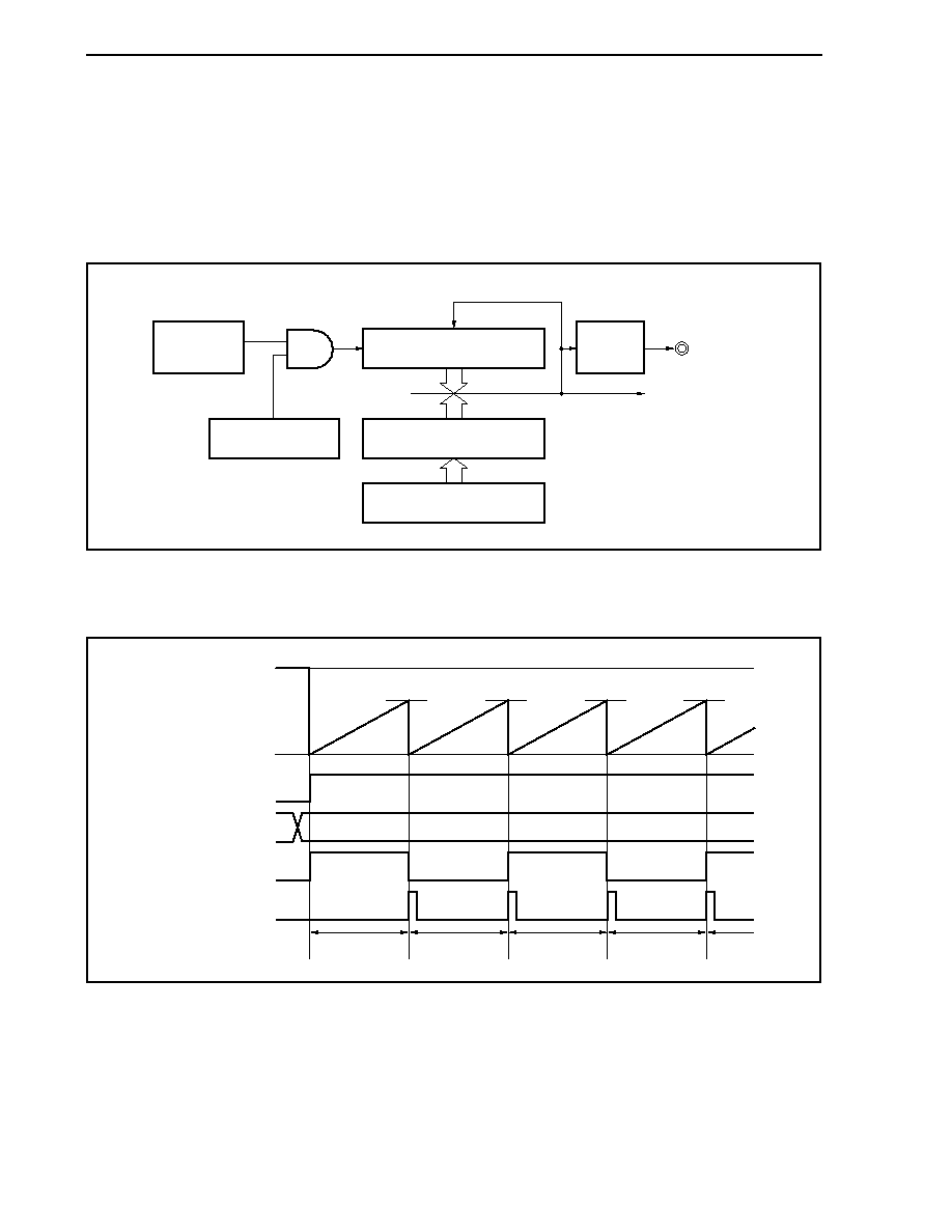
CHAPTER 8 16-BIT TIMER/EVENT COUNTER Q (TMQ)
Preliminary User's Manual U17714EJ1V0UD
334
8.5.1
Interval timer mode (TQ0MD2 to TQ0MD0 bits = 000)
In the interval timer mode, an interrupt request signal (INTTQ0CC0) is generated at the specified interval if the
TQ0CTL0.TQ0CE bit is set to 1. A square wave whose half cycle is equal to the interval can be output from the
TOQ00 pin.
Usually, the TQ0CCR1 to TQ0CCR3 registers are not used in the interval timer mode.
Figure 8-2. Configuration of Interval Timer
16-bit counter
Output
controller
CCR0 buffer register
TQ0CE bit
TQ0CCR0 register
Count clock
selection
Clear
Match signal
TOQ00 pin
INTTQ0CC0 signal
Figure 8-3. Basic Timing of Operation in Interval Timer Mode
FFFFH
16-bit counter
0000H
TQ0CE bit
TQ0CCR0 register
TOQ00 pin output
INTTQ0CC0 signal
D
0
D
0
D
0
D
0
D
0
Interval (D
0
+ 1)
Interval (D
0
+ 1)
Interval (D
0
+ 1)
Interval (D
0
+ 1)
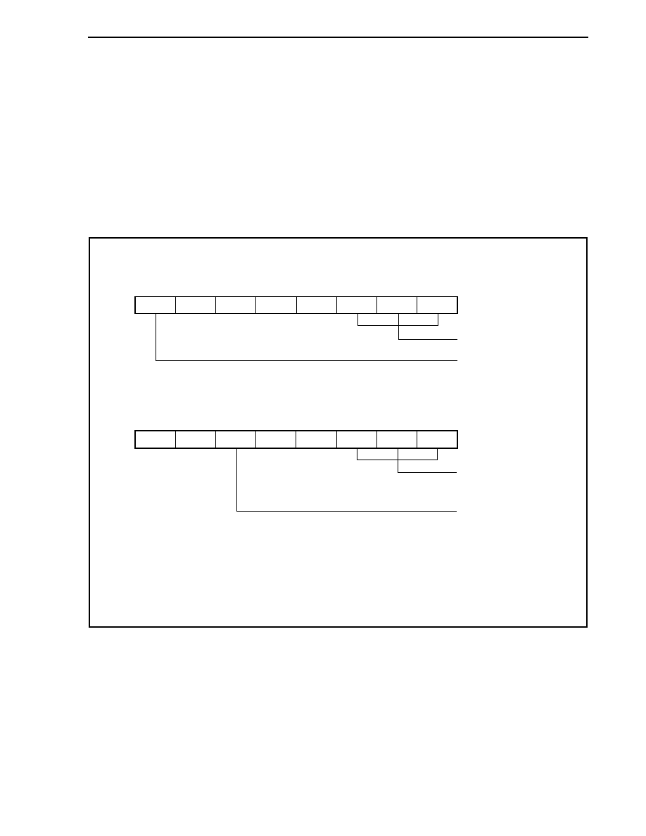
CHAPTER 8 16-BIT TIMER/EVENT COUNTER Q (TMQ)
Preliminary User's Manual U17714EJ1V0UD
335
When the TQ0CE bit is set to 1, the value of the 16-bit counter is cleared from FFFFH to 0000H in synchronization
with the count clock, and the counter starts counting. At this time, the output of the TOQ00 pin is inverted. Additionally,
the set value of the TQ0CCR0 register is transferred to the CCR0 buffer register.
When the count value of the 16-bit counter matches the value of the CCR0 buffer register, the 16-bit counter is
cleared to 0000H, the output of the TOQ00 pin is inverted, and a compare match interrupt request signal
(INTTQ0CC0) is generated.
The interval can be calculated by the following expression.
Interval = (Set value of TQ0CCR0 register + 1)
� Count clock cycle
Figure 8-4. Register Setting for Interval Timer Mode Operation (1/2)
(a) TMQ0 control register 0 (TQ0CTL0)
0/1
0
0
0
0
TQ0CTL0
Select count clock
0: Stop counting
1: Enable counting
0/1
0/1
0/1
TQ0CKS2 TQ0CKS1 TQ0CKS0
TQ0CE
(b) TMQ0 control register 1 (TQ0CTL1)
0
0
0/1
Note
0
0
TQ0CTL1
0, 0, 0:
Interval timer mode
0
0
0
TQ0MD2 TQ0MD1 TQ0MD0
TQ0EEE
TQ0EST
0: Operate on count
clock selected by bits
TQ0CKS0 to TQ0CKS2
1: Count with external
event count input signal
Note This bit can be set to 1 only when the interrupt request signals (INTTQ0CC0 and INTTQ0CCk) are
masked by the interrupt mask flags (TQ0CCMK0 to TQ0CCMKk) and the timer output (TOQ0k) is
performed at the same time. However, the TQ0CCR0 and TQ0CCRk registers must be set to the same
value (see 8.5.1 (2) (d) Operation of TQ0CCR1 to TQ0CCR3 registers) (k = 1 to 3).
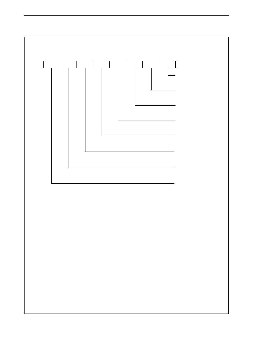
CHAPTER 8 16-BIT TIMER/EVENT COUNTER Q (TMQ)
Preliminary User's Manual U17714EJ1V0UD
336
Figure 8-4. Register Setting for Interval Timer Mode Operation (2/2)
(c) TMQ0 I/O control register 0 (TQ0IOC0)
0/1
0/1
0/1
0/1
0/1
TQ0IOC0
0: Disable TOQ00 pin output
1: Enable TOQ00 pin output
Setting of output level with
operation of TOQ00 pin disabled
0: Low level
1: High level
0: Disable TOQ01 pin output
1: Enable TOQ01 pin output
Setting of output level with
operation of TOQ01 pin disabled
0: Low level
1: High level
0/1
0/1
0/1
TQ0OE1 TQ0OL0
TQ0OE0
TQ0OL1
0: Disable TOQ02 pin output
1: Enable TOQ02 pin output
Setting of output level with
operation of TOQ02 pin disabled
0: Low level
1: High level
0: Disable TOQ03 pin output
1: Enable TOQ03 pin output
Setting of output level with
operation of TOQ03 pin disabled
0: Low level
1: High level
TQ0OE3 TQ0OL2
TQ0OE2
TQ0OL3
(d) TMQ0 counter read buffer register (TQ0CNT)
By reading the TQ0CNT register, the count value of the 16-bit counter can be read.
(e) TMQ0 capture/compare register 0 (TQ0CCR0)
If the TQ0CCR0 register is set to D
0
, the interval is as follows.
Interval = (D
0
+ 1)
� Count clock cycle
(f) TMQ0 capture/compare registers 1 to 3 (TQ0CCR1 to TQ0CCR3)
Usually, the TQ0CCR1 to TQ0CCR3 registers are not used in the interval timer mode. However, the set
value of the TQ0CCR1 to TQ0CCR3 registers are transferred to the CCR1 to CCR3 buffer registers. The
compare match interrupt request signals (INTTQ0CC1 to INTTQ0CCR3) is generated when the count
value of the 16-bit counter matches the value of the CCR1 to CCR3 buffer registers.
Therefore, mask the interrupt request by using the corresponding interrupt mask flags (TQ0CCMK1 to
TQ0CCMK3).
Remark TMQ0 I/O control register 1 (TQ0IOC1), TMQ0 I/O control register 2 (TQ0IOC2), and TMQ0
option register 0 (TQ0OPT0) are not used in the interval timer mode.
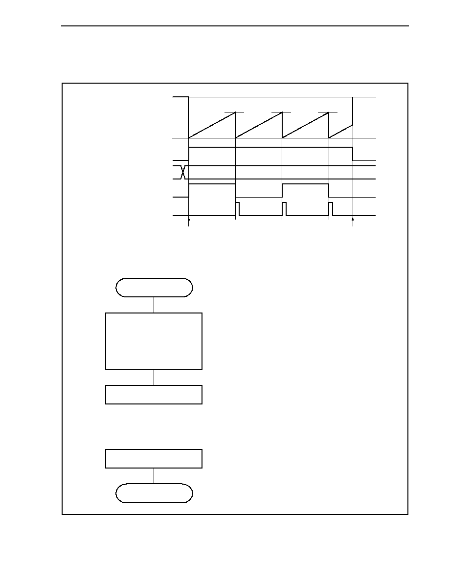
CHAPTER 8 16-BIT TIMER/EVENT COUNTER Q (TMQ)
Preliminary User's Manual U17714EJ1V0UD
337
(1) Interval timer mode operation flow
Figure 8-5. Software Processing Flow in Interval Timer Mode
FFFFH
16-bit counter
0000H
TQ0CE bit
TQ0CCR0 register
TOQ00 pin output
INTTQ0CC0 signal
D
0
D
0
D
0
D
0
<1>
<2>
TQ0CE bit = 1
TQ0CE bit = 0
Register initial setting
TQ0CTL0 register
(TQ0CKS0 to TQ0CKS2 bits)
TQ0CTL1 register,
TQ0IOC0 register,
TQ0CCR0 register
Initial setting of these registers is performed
before setting the TQ0CE bit to 1.
The TQ0CKS0 to TQ0CKS2 bits can be
set at the same time when counting has
been started (TQ0CE bit = 1).
The counter is initialized and counting is
stopped by clearing the TQ0CE bit to 0.
START
STOP
<1> Count operation start flow
<2> Count operation stop flow
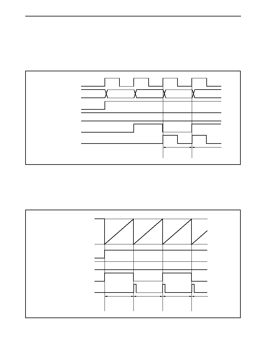
CHAPTER 8 16-BIT TIMER/EVENT COUNTER Q (TMQ)
Preliminary User's Manual U17714EJ1V0UD
338
(2) Interval timer mode operation timing
(a) Operation if TQ0CCR0 register is set to 0000H
If the TQ0CCR0 register is set to 0000H, the INTTQ0CC0 signal is generated at each count clock
subsequent to the first count clock, and the output of the TOQ00 pin is inverted.
The value of the 16-bit counter is always 0000H.
Count clock
16-bit counter
TQ0CE bit
TQ0CCR0 register
TOQ00 pin output
INTTQ0CC0 signal
0000H
Interval time
Count clock cycle
Interval time
Count clock cycle
FFFFH
0000H
0000H
0000H
0000H
(b) Operation if TQ0CCR0 register is set to FFFFH
If the TQ0CCR0 register is set to FFFFH, the 16-bit counter counts up to FFFFH. The counter is cleared to
0000H in synchronization with the next count-up timing. The INTTQ0CC0 signal is generated and the
output of the TOQ00 pin is inverted. At this time, an overflow interrupt request signal (INTTQ0OV) is not
generated, nor is the overflow flag (TQ0OPT0.TQ0OVF bit) set to 1.
FFFFH
16-bit counter
0000H
TQ0CE bit
TQ0CCR0 register
TOQ00 pin output
INTTQ0CC0 signal
FFFFH
Interval time
10000H
�
count clock cycle
Interval time
10000H
�
count clock cycle
Interval time
10000H
�
count clock cycle
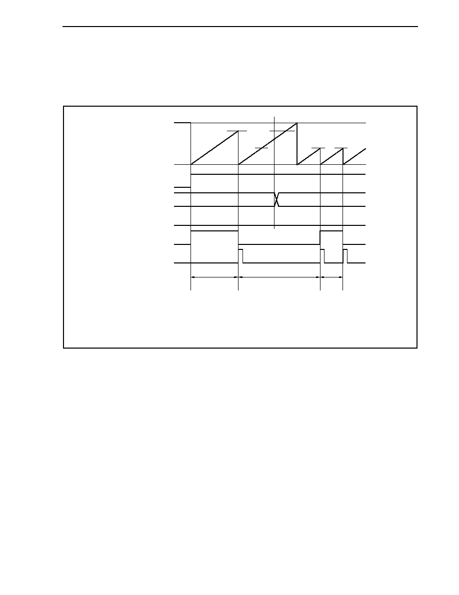
CHAPTER 8 16-BIT TIMER/EVENT COUNTER Q (TMQ)
Preliminary User's Manual U17714EJ1V0UD
339
(c) Notes on rewriting TQ0CCR0 register
To change the value of the TQ0CCR0 register to a smaller value, stop counting once and then change the
set value.
If the value of the TQ0CCR0 register is rewritten to a smaller value during counting, the 16-bit counter may
overflow.
FFFFH
16-bit counter
0000H
TQ0CE bit
TQ0CCR0 register
TQ0OL0 bit
TOQ00 pin output
INTTQ0CC0 signal
D
1
D
2
D
1
D
1
D
2
D
2
D
2
L
Interval time (1)
Interval time (NG)
Interval
time (2)
Remark Interval time (1): (D
1
+ 1)
� Count clock cycle
Interval time (NG): (10000H + D
2
+ 1)
� Count clock cycle
Interval time (2): (D
2
+ 1)
� Count clock cycle
If the value of the TQ0CCR0 register is changed from D
1
to D
2
while the count value is greater than D
2
but
less than D
1
, the count value is transferred to the CCR0 buffer register as soon as the TQ0CCR0 register
has been rewritten. Consequently, the value of the 16-bit counter that is compared is D
2
.
Because the count value has already exceeded D
2
, however, the 16-bit counter counts up to FFFFH,
overflows, and then counts up again from 0000H. When the count value matches D
2
, the INTTQ0CC0
signal is generated and the output of the TOQ00 pin is inverted.
Therefore, the INTTQ0CC0 signal may not be generated at the interval time "(D
1
+ 1)
� Count clock cycle"
or "(D
2
+ 1)
� Count clock cycle" originally expected, but may be generated at an interval of "(10000H + D
2
+ 1)
� Count clock period".
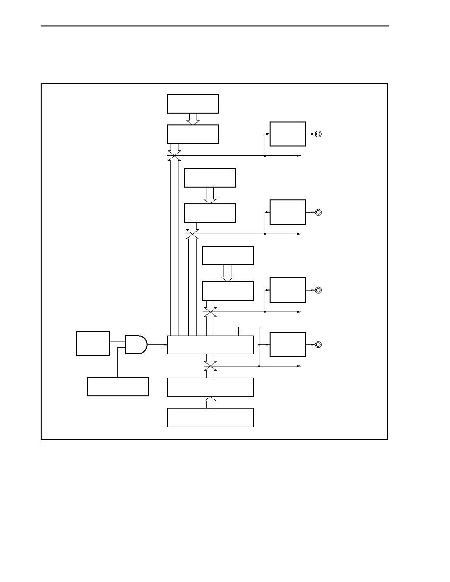
CHAPTER 8 16-BIT TIMER/EVENT COUNTER Q (TMQ)
Preliminary User's Manual U17714EJ1V0UD
340
(d) Operation of TQ0CCR1 to TQ0CCR3 registers
Figure 8-6. Configuration of TQ0CCR1 to TQ0CCR3 Registers
CCR0 buffer register
TQ0CE bit
TQ0CCR0 register
Clear
Match signal
INTTQ0CC0 signal
TOQ03 pin
INTTQ0CC3 signal
TOQ00 pin
TQ0CCR1
register
CCR1 buffer
register
Match signal
TOQ01 pin
INTTQ0CC1 signal
TQ0CCR3
register
CCR3 buffer
register
Match signal
TOQ02 pin
INTTQ0CC2 signal
TQ0CCR2
register
CCR2 buffer
register
Match signal
Output
controller
Count
clock
selection
Output
controller
Output
controller
Output
controller
16-bit counter
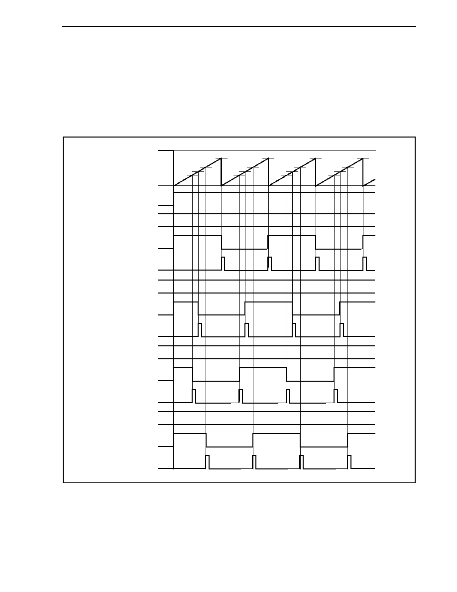
CHAPTER 8 16-BIT TIMER/EVENT COUNTER Q (TMQ)
Preliminary User's Manual U17714EJ1V0UD
341
If the set value of the TQ0CCRk register is less than the set value of the TQ0CCR0 register, the
INTTQ0CCk signal is generated once per cycle. At the same time, the output of the TOPQ0k pin is
inverted.
The TOQ0k pin outputs a square wave with the same cycle as that output by the TOQ00 pin.
Remark k = 1 to 3
Figure 8-7. Timing Chart When D
01
D
k1
D
01
D
11
D
21
D
31
D
21
D
11
D
31
D
01
D
01
D
21
D
11
D
31
D
01
D
21
D
11
D
31
D
01
D
21
D
11
D
31
FFFFH
16-bit counter
0000H
TQ0CE bit
TQ0CCR0 register
TOQ00 pin output
INTTQ0CC0 signal
TQ0CCR1 register
TOQ01 pin output
INTTQ0CC1 signal
TQ0CCR2 register
TOQ02 pin output
INTTQ0CC2 signal
TQ0CCR3 register
TOQ03 pin output
INTTQ0CC3 signal
CHAPTER 8 16-BIT TIMER/EVENT COUNTER Q (TMQ)
Preliminary User's Manual U17714EJ1V0UD
342
If the set value of the TQ0CCRk register is greater than the set value of the TQ0CCR0 register, the count
value of the 16-bit counter does not match the value of the TQ0CCRk register. Consequently, the
INTTQ0CCk signal is not generated, nor is the output of the TOQ0k pin changed.
Remark k = 1 to 3
Figure 8-8. Timing Chart When D
01
< D
k1
D
01
D
11
D
21
L
L
L
D
31
D
01
D
01
D
01
D
01
FFFFH
16-bit counter
0000H
TQ0CE bit
TQ0CCR0 register
TOQ00 pin output
INTTQ0CC0 signal
TQ0CCR1 register
TOQ01 pin output
INTTQ0CC1 signal
TQ0CCR2 register
TOQ02 pin output
INTTQ0CC2 signal
TQ0CCR3 register
TOQ03 pin output
INTTQ0CC3 signal
CHAPTER 8 16-BIT TIMER/EVENT COUNTER Q (TMQ)
Preliminary User's Manual U17714EJ1V0UD
343
8.5.2
External event count mode (TQ0MD2 to TQ0MD0 bits = 001)
In the external event count mode, the valid edge of the external event count input is counted when the
TQ0CTL0.TQ0CE bit is set to 1, and an interrupt request signal (INTTQ0CC0) is generated each time the specified
number of edges have been counted. The TOQ00 pin cannot be used.
Usually, the TQ0CCR1 to TQ0CCR3 registers are not used in the external event count mode.
Figure 8-9. Configuration in External Event Count Mode
16-bit counter
CCR0 buffer register
TQ0CE bit
TQ0CCR0 register
Edge
detector
Clear
Match signal
INTTQ0CC0 signal
TIQ00 pin
(external event
count input)
Figure 8-10. Basic Timing in External Event Count Mode
FFFFH
16-bit counter
0000H
TQ0CE bit
TQ0CCR0 register
INTTQ0CC0 signal
D
0
D
0
D
0
D
0
16-bit counter
TQ0CCR0 register
NTTQ0CC0 signal
External event
count input
(TIQ00 pin input)
D
0
External
event
count
interval
(D
0
+ 1)
D
0
- 1
D
0
0000
0001
External
event
count
interval
(D
0
+ 1)
External
event
count
interval
(D
0
+ 1)
Remark This figure shows the basic timing when the rising edge is specified as the valid edge of the
external event count input.
CHAPTER 8 16-BIT TIMER/EVENT COUNTER Q (TMQ)
Preliminary User's Manual U17714EJ1V0UD
344
When the TQ0CE bit is set to 1, the value of the 16-bit counter is cleared from FFFFH to 0000H. The counter
counts each time the valid edge of external event count input is detected. Additionally, the set value of the TQ0CCR0
register is transferred to the CCR0 buffer register.
When the count value of the 16-bit counter matches the value of the CCR0 buffer register, the 16-bit counter is
cleared to 0000H, and a compare match interrupt request signal (INTTQ0CC0) is generated.
The INTTQ0CC0 signal is generated each time the valid edge of the external event count input has been detected
(set value of TQ0CCR0 register + 1) times.
Figure 8-11. Register Setting for Operation in External Event Count Mode (1/2)
(a) TMQ0 control register 0 (TQ0CTL0)
0/1
0
0
0
0
TQ0CTL0
0: Stop counting
1: Enable counting
0
0
0
TQ0CKS2 TQ0CKS1 TQ0CKS0
TQ0CE
(b) TMQ0 control register 1 (TQ0CTL1)
0
0
0
0
0
TQ0CTL1
0, 0, 1:
External event count mode
0
0
1
TQ0MD2 TQ0MD1 TQ0MD0
TQ0EEE
TQ0EST
(c) TMQ0 I/O control register 0 (TQ0IOC0)
0
0
0
0
0
TQ0IOC0
0: Disable TOQ00 pin output
0: Disable TOQ01 pin output
0
0
0
TQ0OE1 TQ0OL0
TQ0OE0
TQ0OL1
TQ0OE3 TQ0OL2
TQ0OE2
TQ0OL3
0: Disable TOQ02 pin output
0: Disable TOQ03 pin output
(d) TMQ0 I/O control register 2 (TQ0IOC2)
0
0
0
0
0/1
TQ0IOC2
Select valid edge
of external event
count input
0/1
0
0
TQ0EES0 TQ0ETS1 TQ0ETS0
TQ0EES1
(e) TMQ0 counter read buffer register (TQ0CNT)
The count value of the 16-bit counter can be read by reading the TQ0CNT register.

CHAPTER 8 16-BIT TIMER/EVENT COUNTER Q (TMQ)
Preliminary User's Manual U17714EJ1V0UD
345
Figure 8-11. Register Setting for Operation in External Event Count Mode (2/2)
(f) TMQ0
capture/compare
register 0 (TQ0CCR0)
If D
0
is set to the TQ0CCR0 register, the counter is cleared and a compare match interrupt request
signal (INTTQ0CC0) is generated when the number of external event counts reaches (D
0
+ 1).
(g) TMQ0 capture/compare registers 1 to 3 (TQ0CCR1 to TQ0CCR3)
Usually, the TQ0CCR1 to TQ0CCR3 registers are not used in the external event count mode. However,
the set value of the TQ0CCR1 to TQ0CCR3 registers are transferred to the CCR1 to CCR3 buffer
registers. When the count value of the 16-bit counter matches the value of the CCR1 to CCR3 buffer
registers, compare match interrupt request signals (INTTQ0CC1 to INTTQ0CC3) are generated.
Therefore, mask the interrupt signal by using the interrupt mask flags (TQ0CCMK1 to TQ0CCMK3).
Remark The TMQ0 I/O control register 1 (TQ0IOC1) and TMQ0 option register 0 (TQ0OPT0) are not
used in the external event count mode.
CHAPTER 8 16-BIT TIMER/EVENT COUNTER Q (TMQ)
Preliminary User's Manual U17714EJ1V0UD
346
(1) External event count mode operation flow
Figure 8-12. Flow of Software Processing in External Event Count Mode
FFFFH
16-bit counter
0000H
TQ0CE bit
TQ0CCR0 register
INTTQ0CC0 signal
D
0
D
0
D
0
D
0
<1>
<2>
TQ0CE bit = 1
TQ0CE bit = 0
Register initial setting
TQ0CTL0 register
(TQ0CKS0 to TQ0CKS2 bits)
TQ0CTL1 register,
TQ0IOC0 register,
TQ0IOC2 register,
TQ0CCR0 register
Initial setting of these registers
is performed before setting the
TQ0CE bit to 1.
The TQ0CKS0 to TQ0CKS2 bits can
be set at the same time when counting
has been started (TQ0CE bit = 1).
The counter is initialized and counting
is stopped by clearing the TQ0CE bit to 0.
START
STOP
<1> Count operation start flow
<2> Count operation stop flow
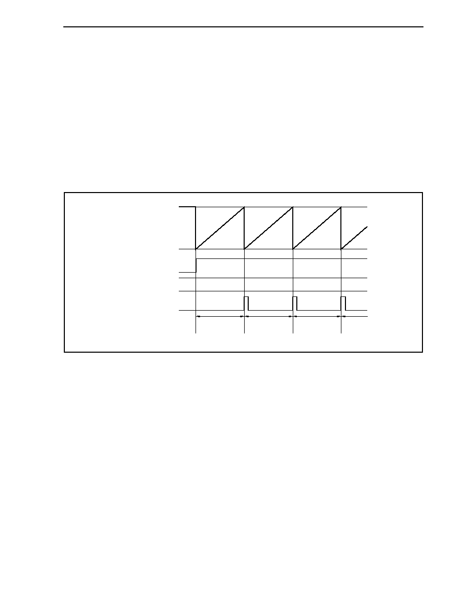
CHAPTER 8 16-BIT TIMER/EVENT COUNTER Q (TMQ)
Preliminary User's Manual U17714EJ1V0UD
347
(2) Operation timing in external event count mode
Cautions 1. In the external event count mode, do not set the TQ0CCR0 register to 0000H.
2. In the external event count mode, use of the timer output is disabled. If performing timer
output using external event count input, set the interval timer mode, and select the
operation enabled by the external event count input for the count clock
(TQ0CTL1.TQ0MD2 to TQ0CTL1.TQ0MD0 bits = 000, TQ0CTL1.TQ0EEE bit = 1).
(a) Operation if TQ0CCR0 register is set to FFFFH
If the TQ0CCR0 register is set to FFFFH, the 16-bit counter counts to FFFFH each time the valid edge of
the external event count signal has been detected. The 16-bit counter is cleared to 0000H in
synchronization with the next count-up timing, and the INTTQ0CC0 signal is generated. At this time, the
TQ0OPT0.TQ0OVF bit is not set.
FFFFH
16-bit counter
0000H
TQ0CE bit
TQ0CCR0 register
INTTQ0CC0 signal
FFFFH
External event
count signal
interval
External event
count signal
interval
External event
count signal
interval
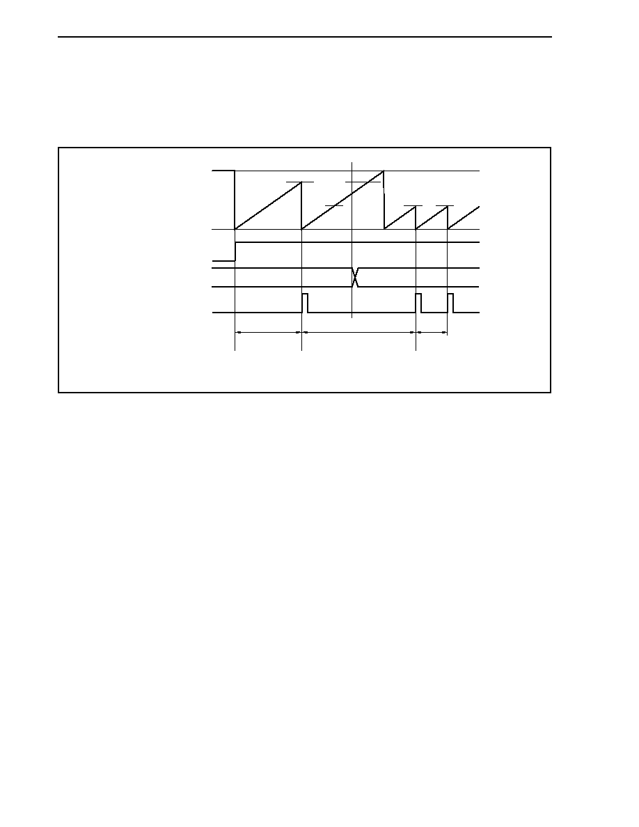
CHAPTER 8 16-BIT TIMER/EVENT COUNTER Q (TMQ)
Preliminary User's Manual U17714EJ1V0UD
348
(b) Notes on rewriting the TQ0CCR0 register
To change the value of the TQ0CCR0 register to a smaller value, stop counting once and then change the
set value.
If the value of the TQ0CCR0 register is rewritten to a smaller value during counting, the 16-bit counter may
overflow.
FFFFH
16-bit counter
0000H
TQ0CE bit
TQ0CCR0 register
INTTQ0CC0 signal
D
1
D
2
D
1
D
1
D
2
D
2
D
2
External event
count signal
interval (1)
(D
1
+ 1)
External event count signal
interval (NG)
(10000H + D
2
+ 1)
External event
count signal
interval (2)
(D
2
+ 1)
If the value of the TQ0CCR0 register is changed from D
1
to D
2
while the count value is greater than D
2
but
less than D
1
, the count value is transferred to the CCR0 buffer register as soon as the TQ0CCR0 register
has been rewritten. Consequently, the value that is compared with the 16-bit counter is D
2
.
Because the count value has already exceeded D
2
, however, the 16-bit counter counts up to FFFFH,
overflows, and then counts up again from 0000H. When the count value matches D
2
, the INTTQ0CC0
signal is generated.
Therefore, the INTTQ0CC0 signal may not be generated at the valid edge count of "(D
1
+ 1) times" or "(D
2
+ 1) times" originally expected, but may be generated at the valid edge count of "(10000H + D
2
+ 1) times".
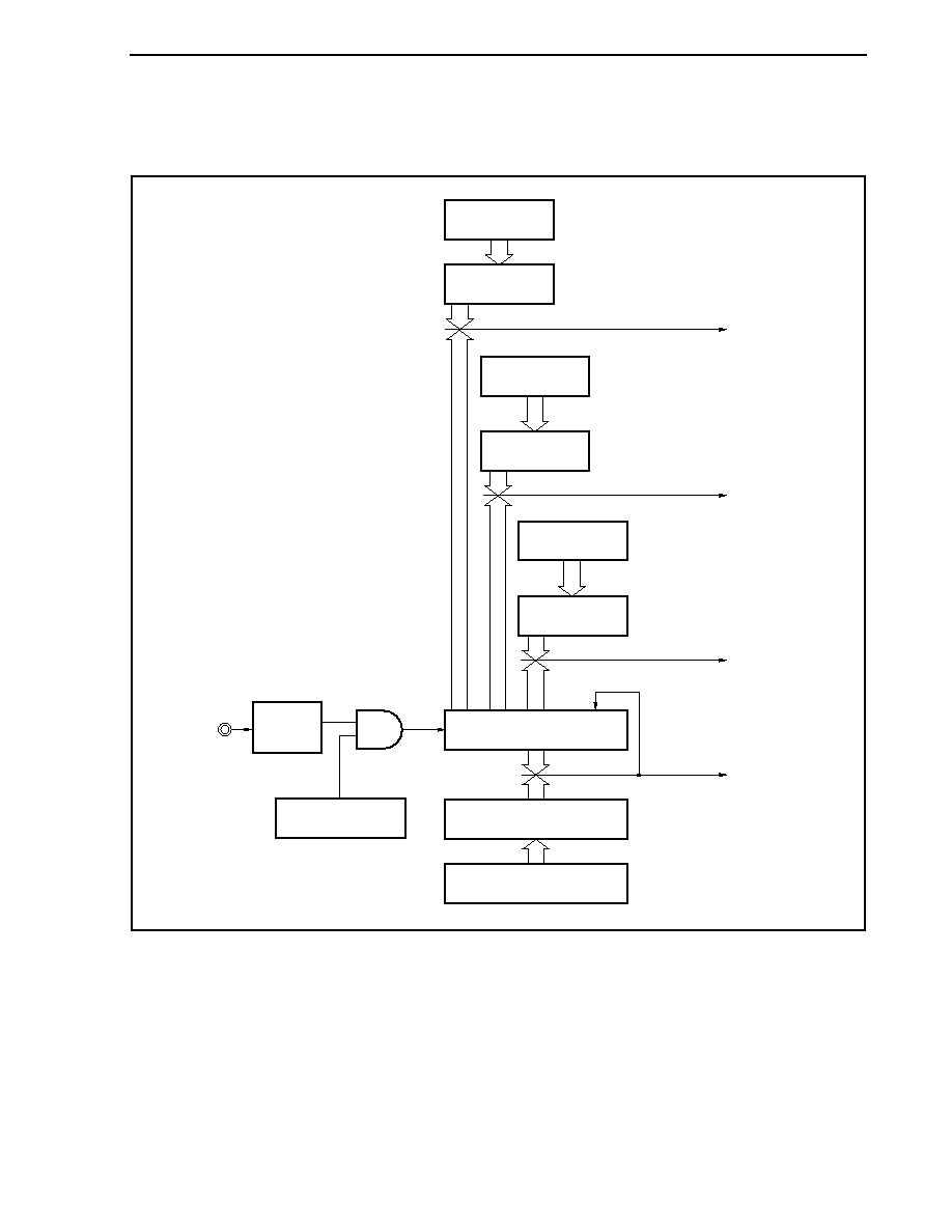
CHAPTER 8 16-BIT TIMER/EVENT COUNTER Q (TMQ)
Preliminary User's Manual U17714EJ1V0UD
349
(c) Operation of TQ0CCR1 to TQ0CCR3 registers
Figure 8-13. Configuration of TQ0CCR1 to TQ0CCR3 Registers
CCR0 buffer register
TQ0CE bit
TQ0CCR0 register
Clear
Match signal
INTTQ0CC0 signal
INTTQ0CC3 signal
TIQ00 pin
TQ0CCR1
register
CCR1 buffer
register
Match signal
INTTQ0CC1 signal
TQ0CCR3
register
CCR3 buffer
register
Match signal
INTTQ0CC2 signal
TQ0CCR2
register
CCR2 buffer
register
Match signal
16-bit counter
Edge
detector
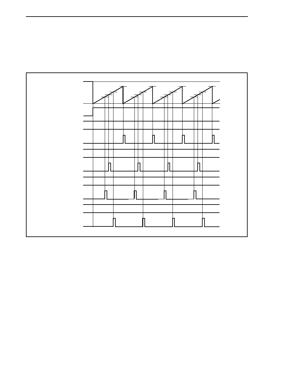
CHAPTER 8 16-BIT TIMER/EVENT COUNTER Q (TMQ)
Preliminary User's Manual U17714EJ1V0UD
350
If the set value of the TQ0CCRk register is smaller than the set value of the TQ0CCR0 register, the
INTTQ0CCk signal is generated once per cycle.
Remark k = 1 to 3
Figure 8-14. Timing Chart When D
01
D
k1
D
01
D
11
D
21
D
31
D
21
D
11
D
31
D
01
D
01
D
21
D
11
D
31
D
01
D
21
D
11
D
31
D
01
D
21
D
11
D
31
FFFFH
16-bit counter
0000H
TQ0CE bit
TQ0CCR0 register
INTTQ0CC0 signal
TQ0CCR1 register
INTTQ0CC1 signal
TQ0CCR2 register
INTTQ0CC2 signal
TQ0CCR3 register
INTTQ0CC3 signal
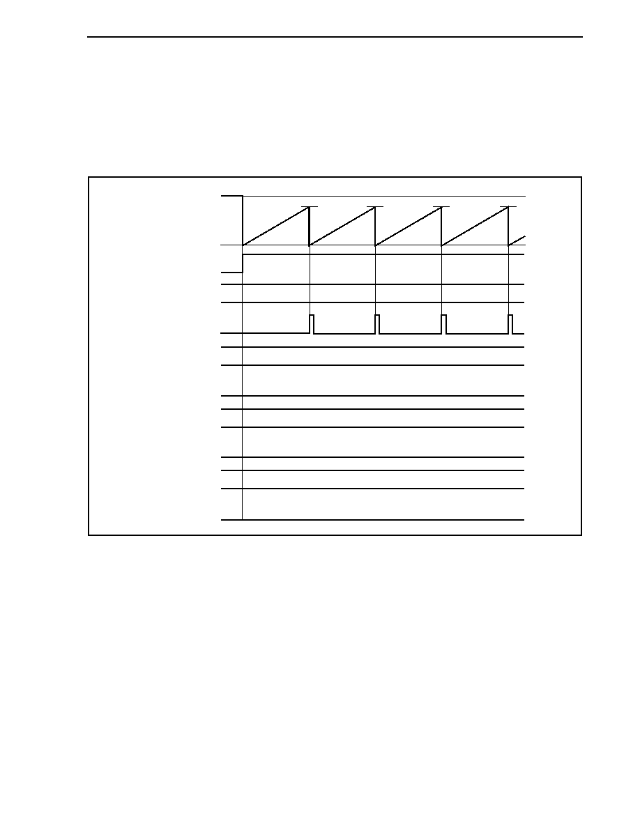
CHAPTER 8 16-BIT TIMER/EVENT COUNTER Q (TMQ)
Preliminary User's Manual U17714EJ1V0UD
351
If the set value of the TQ0CCRk register is greater than the set value of the TQ0CCR0 register, the
INTTQ0CCk signal is not generated because the count value of the 16-bit counter and the value of the
TQ0CCRk register do not match.
Remark k = 1 to 3
Figure 8-15. Timing Chart When D
01
< D
k1
D
01
D
11
D
21
L
L
L
D
31
D
01
D
01
D
01
D
01
FFFFH
16-bit counter
0000H
TQ0CE bit
TQ0CCR0 register
INTTQ0CC0 signal
TQ0CCR1 register
INTTQ0CC1 signal
TQ0CCR2 register
INTTQ0CC2 signal
TQ0CCR3 register
INTTQ0CC3 signal
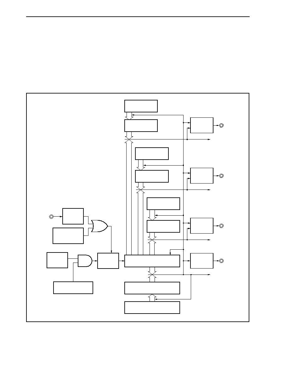
CHAPTER 8 16-BIT TIMER/EVENT COUNTER Q (TMQ)
Preliminary User's Manual U17714EJ1V0UD
352
8.5.3
External trigger pulse output mode (TQ0MD2 to TQ0MD0 bits = 010)
In the external trigger pulse output mode, 16-bit timer/event counter Q waits for a trigger when the
TQ0CTL0.TQ0CE bit is set to 1. When the valid edge of an external trigger input signal is detected, 16-bit timer/event
counter Q starts counting, and outputs a PWM waveform from the TOQ01 to TOQ03 pins.
Pulses can also be output by generating a software trigger instead of using the external trigger. When using a
software trigger, a square wave that has one cycle of the PWM waveform as half its cycle can also be output from the
TOQ00 pin.
Figure 8-16. Configuration in External Trigger Pulse Output Mode
CCR0 buffer register
TQ0CE bit
TQ0CCR0 register
Clear
Match signal
INTTQ0CC0 signal
TOQ03 pin
INTTQ0CC3 signal
TOQ00 pin
TIQ00 pin
Transfer
S
R
TQ0CCR1
register
CCR1 buffer
register
Match signal
TOQ01 pin
INTTQ0CC1 signal
Transfer
Transfer
S
R
TQ0CCR3
register
CCR3 buffer
register
Match signal
Transfer
TOQ02 pin
INTTQ0CC2 signal
S
R
TQ0CCR2
register
CCR2 buffer
register
Match signal
16-bit counter
Count
clock
selection
Count
start
control
Edge
detector
Software trigger
generation
Output
controller
(RS-FF)
Output
controller
Output
controller
(RS-FF)
Output
controller
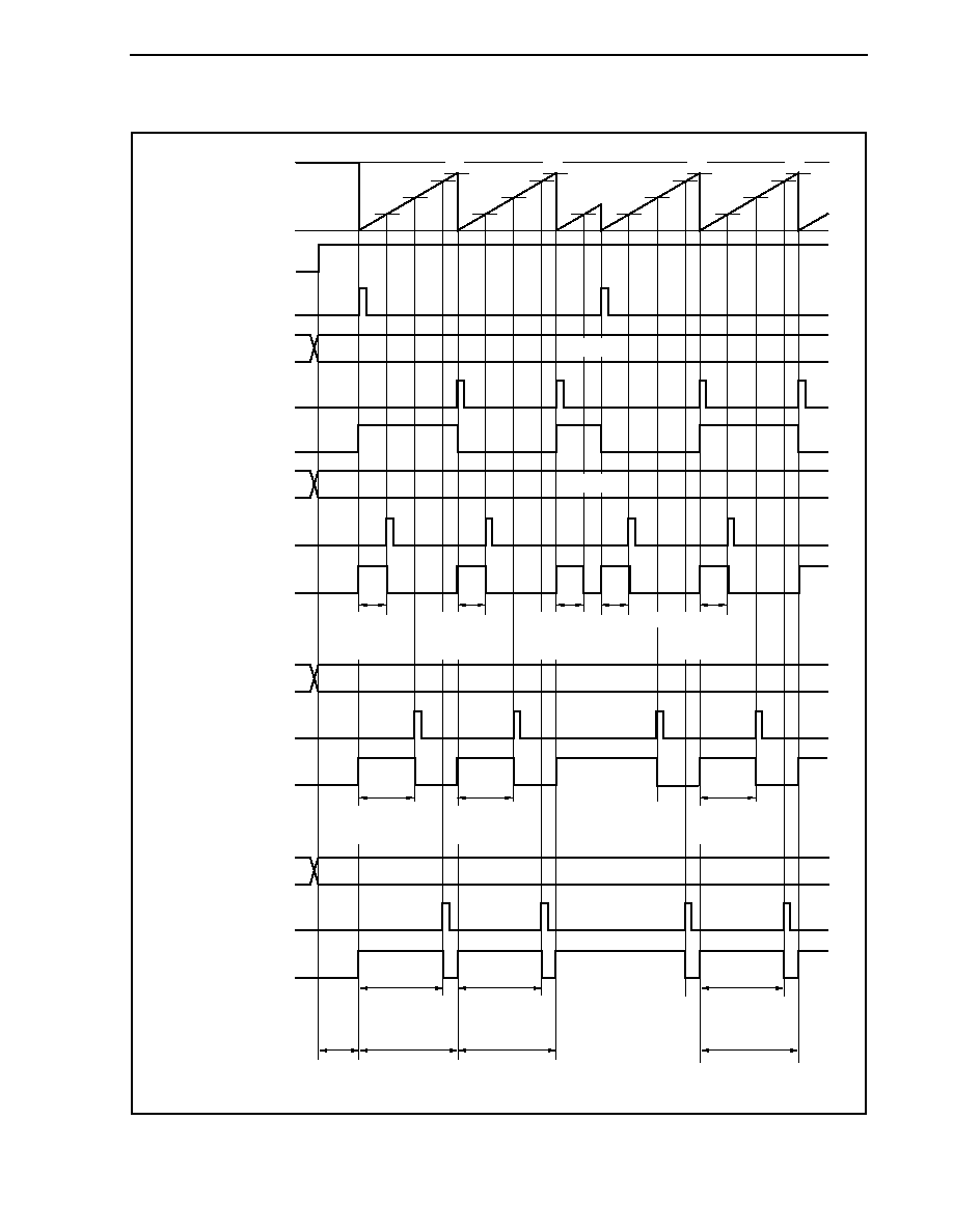
CHAPTER 8 16-BIT TIMER/EVENT COUNTER Q (TMQ)
Preliminary User's Manual U17714EJ1V0UD
353
Figure 8-17. Basic Timing in External Trigger Pulse Output Mode
D
1
D
2
D
3
D
1
D
2
D
3
D
1
D
2
D
3
D
1
D
1
D
2
D
3
Active level
width (D
2
)
Active level
width (D
2
)
Active level
width (D
2
)
Active level
width (D
3
)
Active level
width (D
3
)
Cycle (D
0
+ 1)
Cycle (D
0
+ 1)
Wait
for trigger
Active level
width (D
3
)
Cycle (D
0
+ 1)
FFFFH
16-bit counter
0000H
TQ0CE bit
External trigger input
(TIQ00 pin input)
TQ0CCR0 register
INTTQ0CC0 signal
TOQ00 pin output
(only when software
trigger is used)
TQ0CCR1 register
INTTQ0CC1 signal
TOQ01 pin output
TQ0CCR2 register
INTTQ0CC2 signal
TOQ02 pin output
TQ0CCR3 register
INTTQ0CC3 signal
TOQ03 pin output
Active level
width
(D
1
)
Active level
width
(D
1
)
Active level
width
(D
1
)
Active level
width
(D
1
)
Active level
width
(D
1
)
D
0
D
1
D
3
D
2
D
0
D
0
D
0
D
0
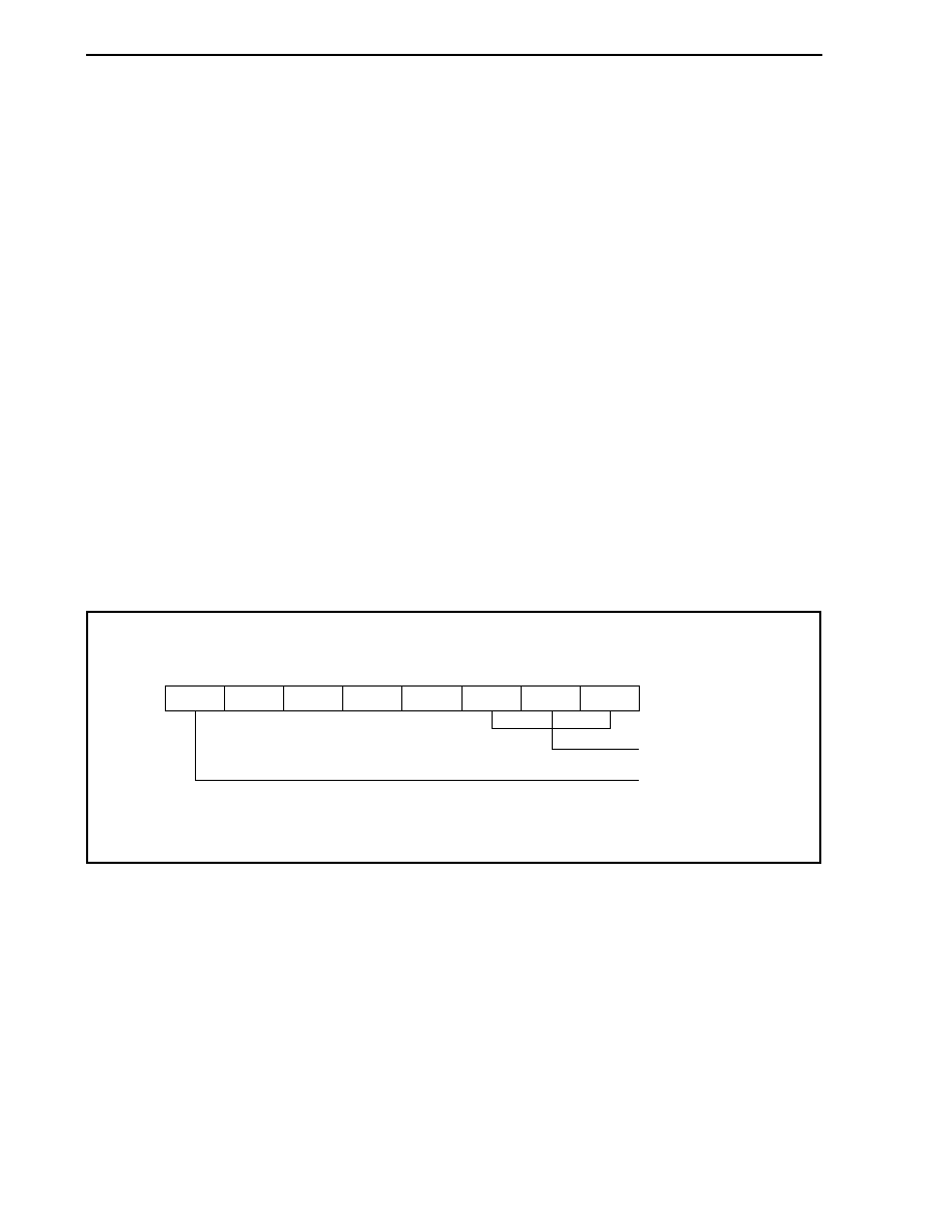
CHAPTER 8 16-BIT TIMER/EVENT COUNTER Q (TMQ)
Preliminary User's Manual U17714EJ1V0UD
354
16-bit timer/event counter Q waits for a trigger when the TQ0CE bit is set to 1. When the trigger is generated, the
16-bit counter is cleared from FFFFH to 0000H, starts counting at the same time, and outputs a PWM waveform from
the TOQ0k pin. If the trigger is generated again while the counter is operating, the counter is cleared to 0000H and
restarted. (The output of the TOQ00 pin is inverted. The TOQ0k pin outputs a high-level regardless of the status
(high/low) when a trigger is generated.)
The active level width, cycle, and duty factor of the PWM waveform can be calculated as follows.
Active level width = (Set value of TQ0CCRk register)
� Count clock cycle
Cycle = (Set value of TQ0CCR0 register + 1)
� Count clock cycle
Duty factor = (Set value of TQ0CCRk register)/(Set value of TQ0CCR0 register + 1)
The compare match request signal INTTQ0CC0 is generated when the 16-bit counter counts next time after its
count value matches the value of the CCR0 buffer register, and the 16-bit counter is cleared to 0000H. The compare
match interrupt request signal INTTQ0CCk is generated when the count value of the 16-bit counter matches the value
of the CCRk buffer register.
The value set to the TQ0CCRm register is transferred to the CCRm buffer register when the count value of the 16-
bit counter matches the value of the CCR0 buffer register and the 16-bit counter is cleared to 0000H.
The valid edge of an external trigger input signal, or setting the software trigger (TQ0CTL1.TQ0EST bit) to 1 is
used as the trigger.
Remark k = 1 to 3, m = 0 to 3
Figure 8-18. Setting of Registers in External Trigger Pulse Output Mode (1/3)
(a) TMQ0 control register 0 (TQ0CTL0)
0/1
0
0
0
0
TQ0CTL0
Select count clock
Note
0: Stop counting
1: Enable counting
0/1
0/1
0/1
TQ0CKS2 TQ0CKS1 TQ0CKS0
TQ0CE
Note The setting is invalid when the TQ0CTL1.TQ0EEE bit = 1.
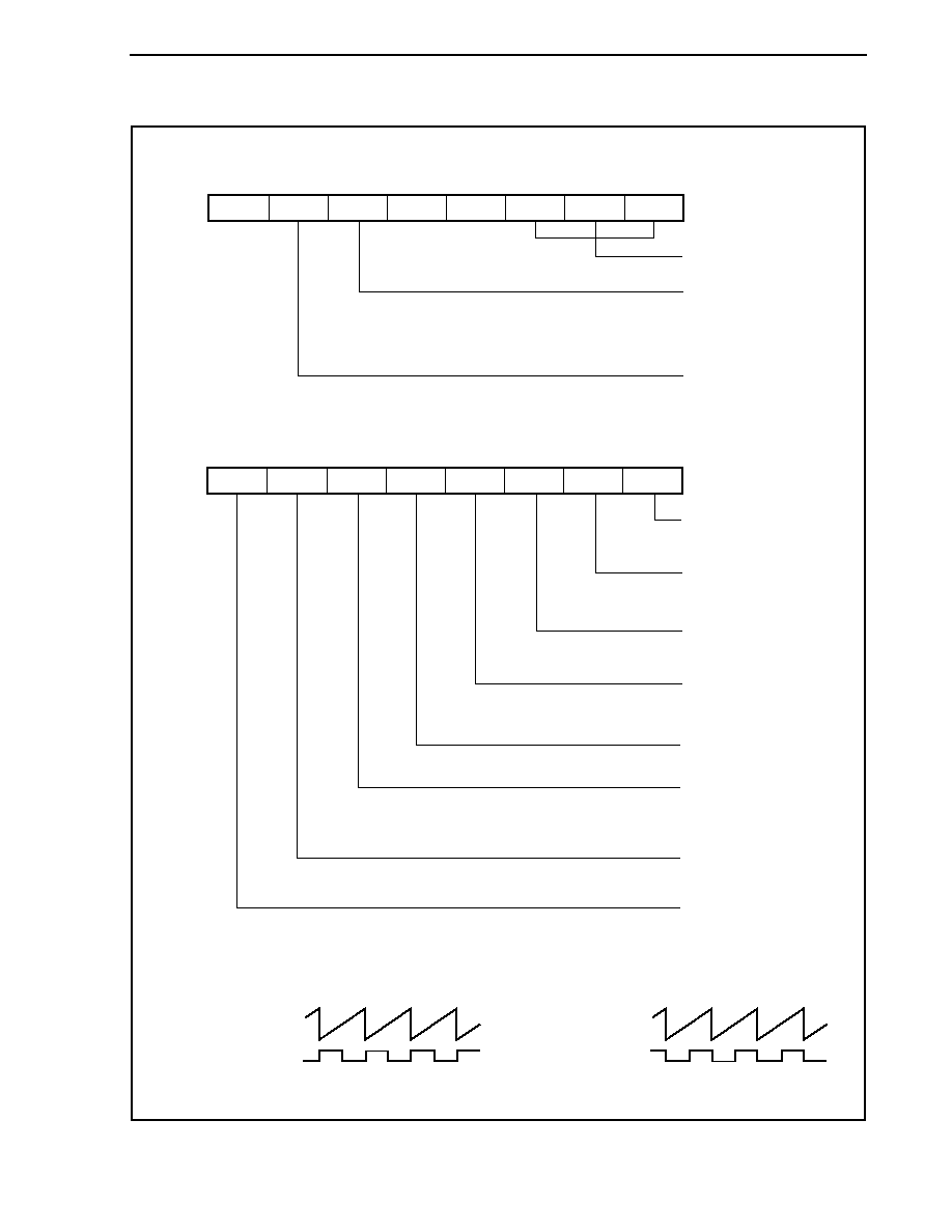
CHAPTER 8 16-BIT TIMER/EVENT COUNTER Q (TMQ)
Preliminary User's Manual U17714EJ1V0UD
355
Figure 8-18. Setting of Registers in External Trigger Pulse Output Mode (2/3)
(b) TMQ0 control register 1 (TQ0CTL1)
0
0/1
0/1
0
0
TQ0CTL1
0: Operate on count
clock selected by
TQ0CKS0 to TQ0CKS2 bits
1: Count with external
event input signal
Generate software trigger
when 1 is written
0
1
0
TQ0MD2 TQ0MD1 TQ0MD0
TQ0EEE
TQ0EST
0, 1, 0:
External trigger pulse
output mode
(c) TMQ0 I/O control register 0 (TQ0IOC0)
0/1
0/1
0/1
0/1
0/1
TQ0IOC0
0: Disable TOQ00 pin output
1: Enable TOQ00 pin output
Setting of output level while
operation of TOQ00 pin is disabled
0: Low level
1: High level
0: Disable TOQ01 pin output
1: Enable TOQ01 pin output
Specification of active level
of TOQ01 pin output
0: Active-high
1: Active-low
0/1
0/1
0/1
Note
TQ0OE1 TQ0OL0
TQ0OE0
TQ0OL1
TOQ0k pin output
16-bit counter
� When TQ0OLk bit = 0
TOQ0k pin output
16-bit counter
� When TQ0OLk bit = 1
TQ0OE3 TQ0OL2
TQ0OE2
TQ0OL3
Specification of active level
of TOQ03 pin output
0: Active-high
1: Active-low
0: Disable TOQ02 pin output
1: Enable TOQ02 pin output
Specification of active level
of TOQ02 pin output
0: Active-high
1: Active-low
0: Disable TOQ03 pin output
1: Enable TOQ03 pin output
Note Clear this bit to 0 when the TOQ00 pin is not used in the external trigger pulse output mode.
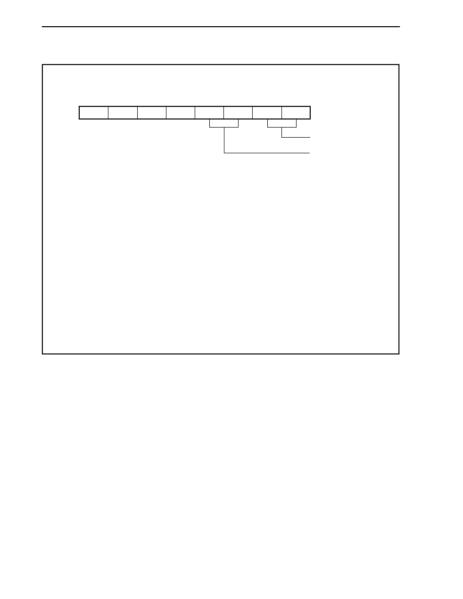
CHAPTER 8 16-BIT TIMER/EVENT COUNTER Q (TMQ)
Preliminary User's Manual U17714EJ1V0UD
356
Figure 8-18. Setting of Registers in External Trigger Pulse Output Mode (3/3)
(d) TMQ0 I/O control register 2 (TQ0IOC2)
0
0
0
0
0/1
TQ0IOC2
Select valid edge of
external trigger input
Select valid edge of
external event count input
0/1
0/1
0/1
TQ0EES0 TQ0ETS1 TQ0ETS0
TQ0EES1
(e) TMQ0 counter read buffer register (TQ0CNT)
The value of the 16-bit counter can be read by reading the TQ0CNT register.
(f) TMQ0 capture/compare registers 0 to 3 (TQ0CCR0 to TQ0CCR3)
If D
0
is set to the TQ0CCR0 register, D
1
to the TQ0CCR1 register, D
2
to the TQ0CCR2 register, and D
3
,
to the TQ0CCR3 register, the cycle and active level of the PWM waveform are as follows.
Cycle = (D
0
+ 1)
� Count clock cycle
TOQ01 pin PWM waveform active level width = D
1
� Count clock cycle
TOQ02 pin PWM waveform active level width = D
2
� Count clock cycle
TOQ03 pin PWM waveform active level width = D
3
� Count clock cycle
Remarks 1. TMQ0 I/O control register 1 (TQ0IOC1) and TMQ0 option register 0 (TQ0OPT0) are not
used in the external trigger pulse output mode.
2. Updating TMQ0 capture/compare register 2 (TQ0CCR2) and TMQ0 capture/compare
register 3 (TQ0CCR3) is validated by writing TMQ0 capture/compare register 1 (TQ0CCR1).
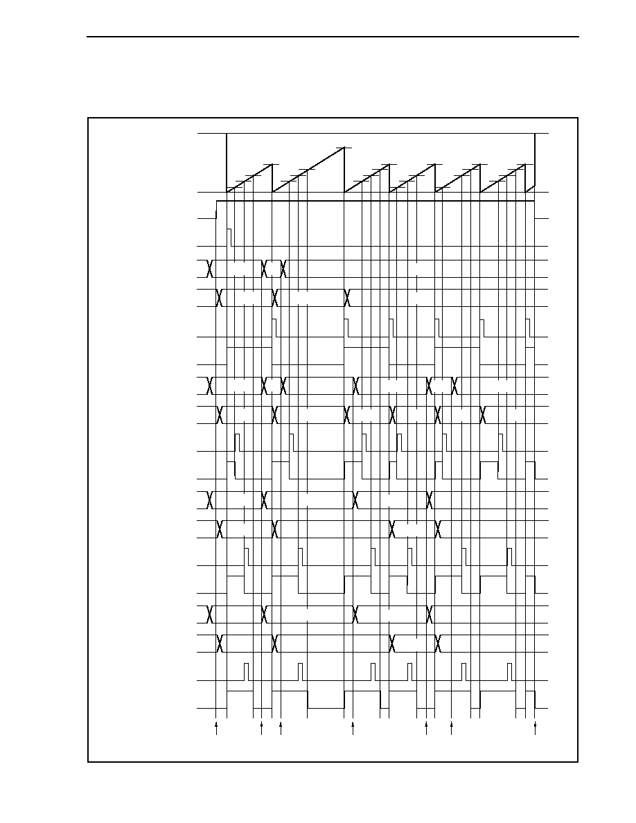
CHAPTER 8 16-BIT TIMER/EVENT COUNTER Q (TMQ)
Preliminary User's Manual U17714EJ1V0UD
357
(1) Operation flow in external trigger pulse output mode
Figure 8-19. Software Processing Flow in External Trigger Pulse Output Mode (1/2)
D
10
D
10
D
10
D
20
D
30
D
00
D
11
D
21
D
01
D
31
D
11
D
21
D
00
D
31
D
20
D
30
D
00
D
21
D
00
D
31
D
11
D
21
D
00
D
31
FFFFH
16-bit counter
0000H
TQ0CE bit
External trigger input
(TIQ00 pin input)
TQ0CCR0 register
CCR0 buffer register
INTTQ0CC0 signal
TOQ00 pin output
(only when software
trigger is used)
TQ0CCR1 register
CCR1 buffer register
INTTQ0CC1 signal
TOQ01 pin output
TQ0CCR2 register
CCR2 buffer register
INTTQ0CC2 signal
TOQ02 pin output
TQ0CCR3 register
CCR3 buffer register
INTTQ0CC3 signal
TOQ03 pin output
D
00
D
01
D
00
D
00
D
01
D
00
D
10
D
11
D
10
D
10
D
11
D
10
D
11
D
10
D
11
D
20
D
21
D
20
D
21
D
20
D
21
D
21
D
30
D
31
D
30
D
31
D
30
D
31
D
30
D
31
<1>
<2> <3>
<4>
<5>
<6>
<7>
D
11
D
11
D
20
D
10
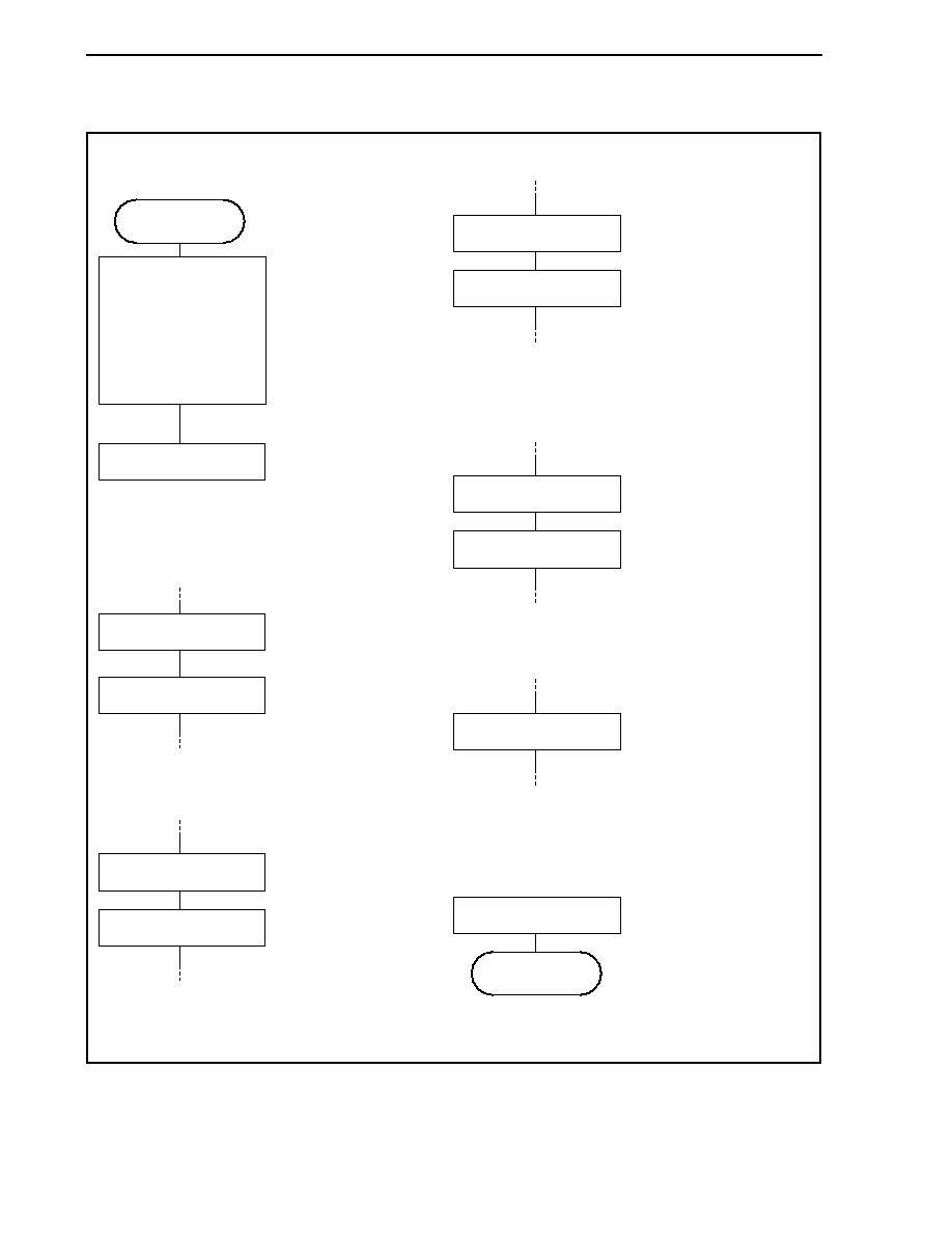
CHAPTER 8 16-BIT TIMER/EVENT COUNTER Q (TMQ)
Preliminary User's Manual U17714EJ1V0UD
358
Figure 8-19. Software Processing Flow in External Trigger Pulse Output Mode (2/2)
START
<1> Count operation start flow
TQ0CE bit = 1
Register initial setting
TQ0CTL0 register
(TQ0CKS0 to TQ0CKS2 bits)
TQ0CTL1 register,
TQ0IOC0 register,
TQ0IOC2 register,
TQ0CCR0 to TQ0CCR3
registers
Initial setting of these
registers is performed
before setting the
TQ0CE bit to 1.
Writing of the TQ0CCR1
register must be performed
when the set duty factor is only
changed after writing the
TQ0CCR2 and TQ0CCR3
registers.
When the counter is cleared
after setting, the value of the
TQ0CCRm register is transferred
to the CCRm buffer register.
TQ0CCR1 register writing of the
same value is necessary only
when the set duty factor of
TOQ02 and TOQ03 pin
outputs is changed.
When the counter is
cleared after setting,
the value of the TQ0CCRm
register is transferred to
the CCRm buffer register.
Only writing of the TQ0CCR1
register must be performed when
the set duty factor is only changed.
When counter is cleared after
setting, the value of the TQ0CCRm
register is transferred to the CCRm
buffer register.
Counting is stopped.
The TQ0CKS0 to
TQ0CKS2 bits can be
set at the same time
when counting is
enabled (TQ0CE bit = 1).
Trigger wait status
Writing of the TQ0CCR1
register must be performed
after writing the TQ0CCR0,
TQ0CCR2, and TQ0CCR3
registers.
When the counter is cleared
after setting, the value
of the TQ0CCRm register is
transferred to the CCRm buffer
registers.
TQ0CCR1 register writing
of the same value is
necessary only when the
set cycle is changed.
<2> TQ0CCR0 to TQ0CCR3 register
setting change flow
<3> TQ0CCR0 register setting change flow
<4> TQ0CCR1 to TQ0CCR3 register
setting change flow
<5> TQ0CCR2, TQ0CCR3 register
setting change flow
<6> TQ0CCR1 register setting change flow
<7> Count operation stop flow
TQ0CE bit = 0
Setting of TQ0CCR2,
TQ0CCR3 registers
Setting of TQ0CCR1 register
Setting of TQ0CCR2,
TQ0CCR3 registers
Setting of TQ0CCR1 register
STOP
Setting of TQ0CCR1 register
Setting of TQ0CCR0 register
Setting of TQ0CCR1 register
Setting of TQ0CCR0, TQ0CCR2,
and TQ0CCR3 registers
TQ0CCR1 register
When the counter is
cleared after setting,
the value of the TQ0CCRm
register is transferred to
the CCRm buffer register.
Remark m = 0 to 3
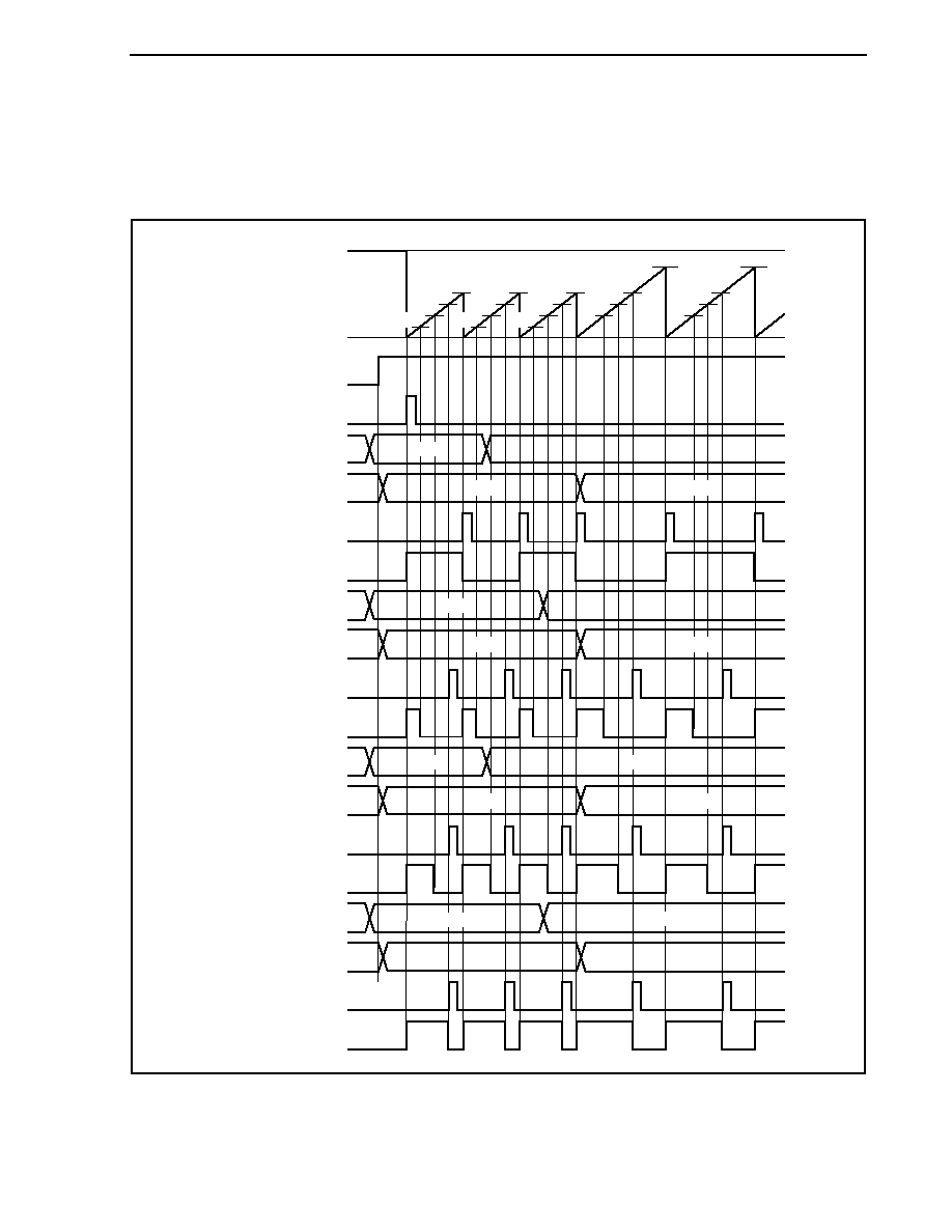
CHAPTER 8 16-BIT TIMER/EVENT COUNTER Q (TMQ)
Preliminary User's Manual U17714EJ1V0UD
359
(2) External trigger pulse output mode operation timing
(a) Note on changing pulse width during operation
To change the PWM waveform while the counter is operating, write the TQ0CCR1 register last.
Rewrite the TQ0CCRk register after writing the TQ0CCR1 register after the INTTQ0CC0 signal is detected.
FFFFH
16-bit counter
0000H
TQ0CE bit
External trigger input
(TIQ00 pin input)
D
30
D
00
D
01
D
30
D
30
D
20
D
20
D
20
D
21
D
11
D
00
D
00
D
31
D
01
D
01
D
21
D
11
D
31
TQ0CCR0 register
CCR0 buffer register
INTTQ0CC0 signal
TQ0CCR1 register
CCR1 buffer register
INTTQ0CC1 signal
TOQ01 pin output
TQ0CCR2 register
CCR2 buffer register
INTTQ0CC2 signal
TOQ02 pin output
TQ0CCR3 register
CCR3 buffer register
INTTQ0CC3 signal
TOQ03 pin output
TOQ00 pin output
(only when software
trigger is used)
D
10
D
10
D
10
D
00
D
11
D
10
D
11
D
10
D
21
D
20
D
21
D
20
D
31
D
30
D
31
D
30
D
00
D
01

CHAPTER 8 16-BIT TIMER/EVENT COUNTER Q (TMQ)
Preliminary User's Manual U17714EJ1V0UD
360
In order to transfer data from the TQ0CCRm register to the CCRm buffer register, the TQ0CCR1 register
must be written.
To change both the cycle and active level width of the PWM waveform at this time, first set the cycle to the
TQ0CCR0 register, set the active level width to the TQ0CCR2 and TQ0CCR3 registers, and then set an
active level to the TQ0CCR1 register.
To change only the cycle of the PWM waveform, first set the cycle to the TQ0CCR0 register, and then write
the same value to the TQ0CCR1 register.
To change only the active level width (duty factor) of the PWM waveform, first set an active level to the
TQ0CCR2 and TQ0CCR3 registers and then set an active level to the TQ0CCR1 register.
To change only the active level width (duty factor) of the PWM waveform output by the TOQ01 pin, only the
TQ0CCR1 register has to be set.
To change only the active level width (duty factor) of the PWM waveform output by the TOQ02 and TOQ03
pins, first set an active level width to the TQ0CCR2 and TQ0CCR3 registers, and then write the same
value to the TQ0CCR1 register.
After data is written to the TQ0CCR1 register, the value written to the TQ0CCRm register is transferred to
the CCRm buffer register in synchronization with clearing of the 16-bit counter, and is used as the value
compared with the 16-bit counter.
To write the TQ0CCR0 to TQ0CCR3 registers again after writing the TQ0CCR1 register once, do so after
the INTTQ0CC0 signal is generated. Otherwise, the value of the CCRm buffer register may become
undefined because timing of transferring data from the TQ0CCRm register to the CCRm buffer register
conflicts with writing the TQ0CCRm register.
Remark m = 0 to 3
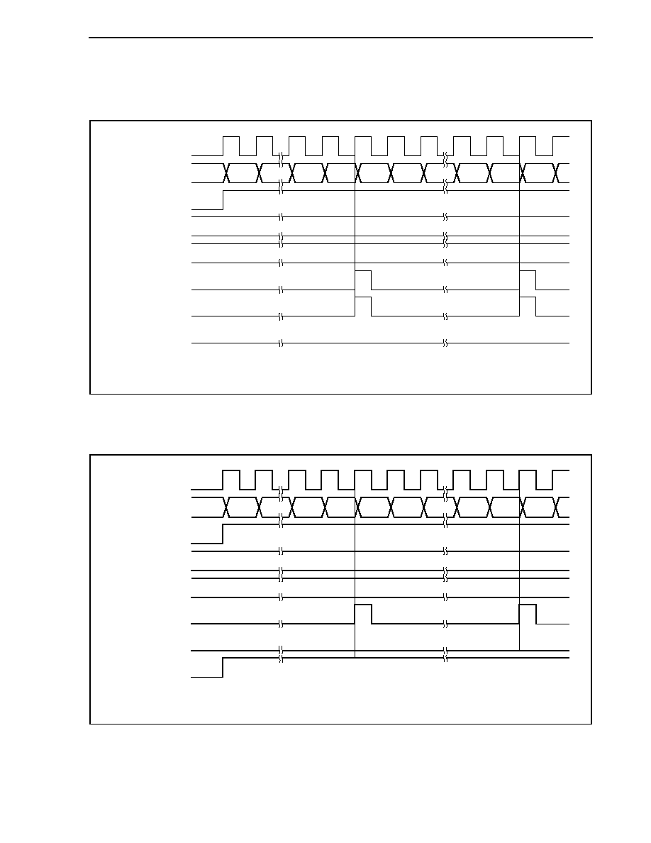
CHAPTER 8 16-BIT TIMER/EVENT COUNTER Q (TMQ)
Preliminary User's Manual U17714EJ1V0UD
361
(b) 0%/100% output of PWM waveform
To output a 0% waveform, set the TQ0CCRk register to 0000H. If the set value of the TQ0CCR0 register is
FFFFH, the INTTQ0CCk signal is generated periodically.
Count clock
16-bit counter
TQ0CE bit
TQ0CCR0 register
TQ0CCRk register
INTTQ0CC0 signal
INTTQ0CCk signal
TOQ0k pin output
D
0
0000H
D
0
0000H
D
0
0000H
D
0
- 1
D
0
0000
FFFF
0000
D
0
- 1
D
0
0000
0001
L
Remark k = 1 to 3
To output a 100% waveform, set a value of (set value of TQ0CCR0 register + 1) to the TQ0CCRk register.
If the set value of the TQ0CCR0 register is FFFFH, 100% output cannot be produced.
Count clock
16-bit counter
TQ0CE bit
TQ0CCR0 register
TQ0CCRk register
INTTQ0CC0 signal
INTTQ0CCk signal
TOQ0k pin output
D
0
D
0
+ 1
D
0
D
0
+ 1
D
0
D
0
+ 1
D
0
- 1
D
0
0000
FFFF
0000
D
0
- 1
D
0
0000
0001
Remark k = 1 to 3
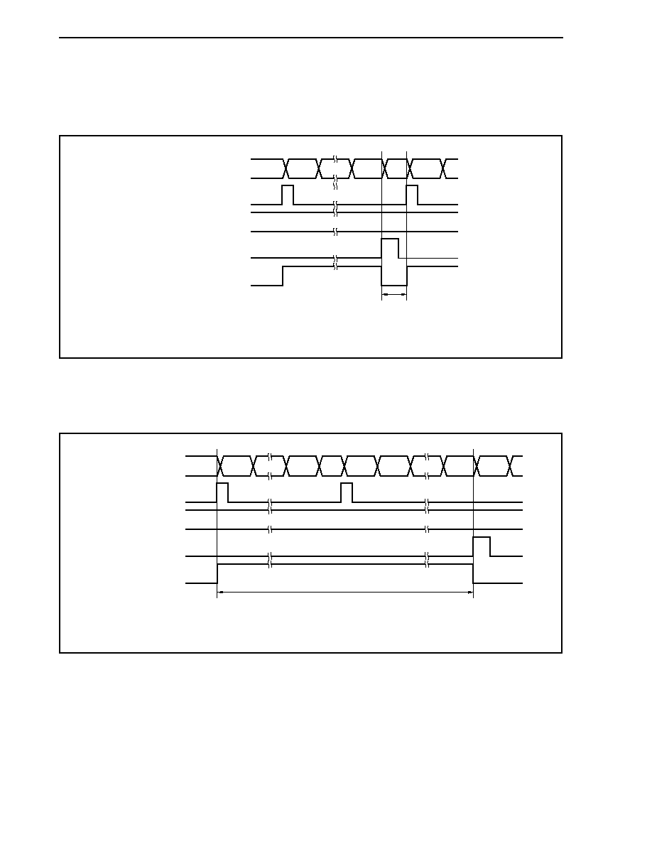
CHAPTER 8 16-BIT TIMER/EVENT COUNTER Q (TMQ)
Preliminary User's Manual U17714EJ1V0UD
362
(c) Conflict between trigger detection and match with CCRk buffer register
If the trigger is detected immediately after the INTTQ0CCk signal is generated, the 16-bit counter is
immediately cleared to 0000H, the output signal of the TOQ0k pin is asserted, and the counter continues
counting. Consequently, the inactive period of the PWM waveform is shortened.
16-bit counter
CCRk buffer register
INTTQ0CCk signal
TOQ0k pin output
External trigger input
(TIQ00 pin input)
D
k
D
k
- 1
0000
FFFF
0000
Shortened
D
k
Remark k = 1 to 3
If the trigger is detected immediately before the INTTQ0CCk signal is generated, the INTTQ0CCk signal is
not generated, and the 16-bit counter is cleared to 0000H and continues counting. The output signal of the
TOQ0k pin remains active. Consequently, the active period of the PWM waveform is extended.
16-bit counter
CCRk buffer register
INTTQ0CCk signal
TOQ0k pin output
External trigger input
(TIQ00 pin input)
D
k
D
k
- 2
D
k
- 1
D
k
0000
FFFF
0000
0001
Extended
Remark k = 1 to 3
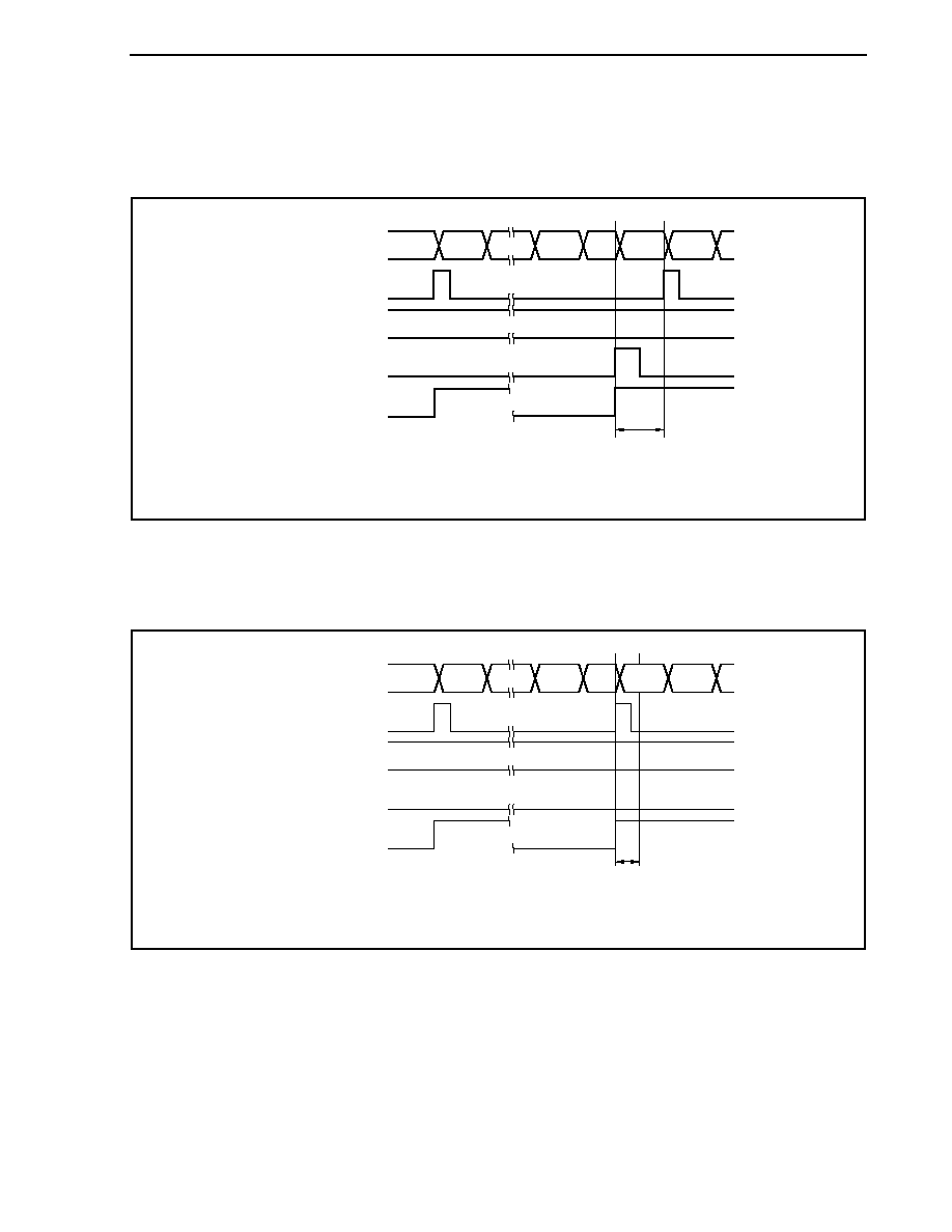
CHAPTER 8 16-BIT TIMER/EVENT COUNTER Q (TMQ)
Preliminary User's Manual U17714EJ1V0UD
363
(d) Conflict between trigger detection and match with CCR0 buffer register
If the trigger is detected immediately after the INTTQ0CC0 signal is generated, the 16-bit counter is
cleared to 0000H and continues counting up. Therefore, the active period of the TOQ0k pin is extended by
time from generation of the INTTQ0CC0 signal to trigger detection.
16-bit counter
CCR0 buffer register
INTTQ0CC0 signal
TOQ0k pin output
External trigger input
(TIQ00 pin input)
D
0
D
0
- 1
D
0
0000
FFFF
0000
0000
Extended
Remark k = 1 to 3
If the trigger is detected immediately before the INTTQ0CC0 signal is generated, the INTTQ0CC0 signal is
not generated. The 16-bit counter is cleared to 0000H, the TOQ0k pin is asserted, and the counter
continues counting. Consequently, the inactive period of the PWM waveform is shortened.
16-bit counter
CCR0 buffer register
INTTQ0CC0 signal
TOQ0k pin output
External trigger input
(TIQ00 pin input)
D
0
D
0
- 1
D
0
0000
FFFF
0000
0001
Shortened
Remark k = 1 to 3
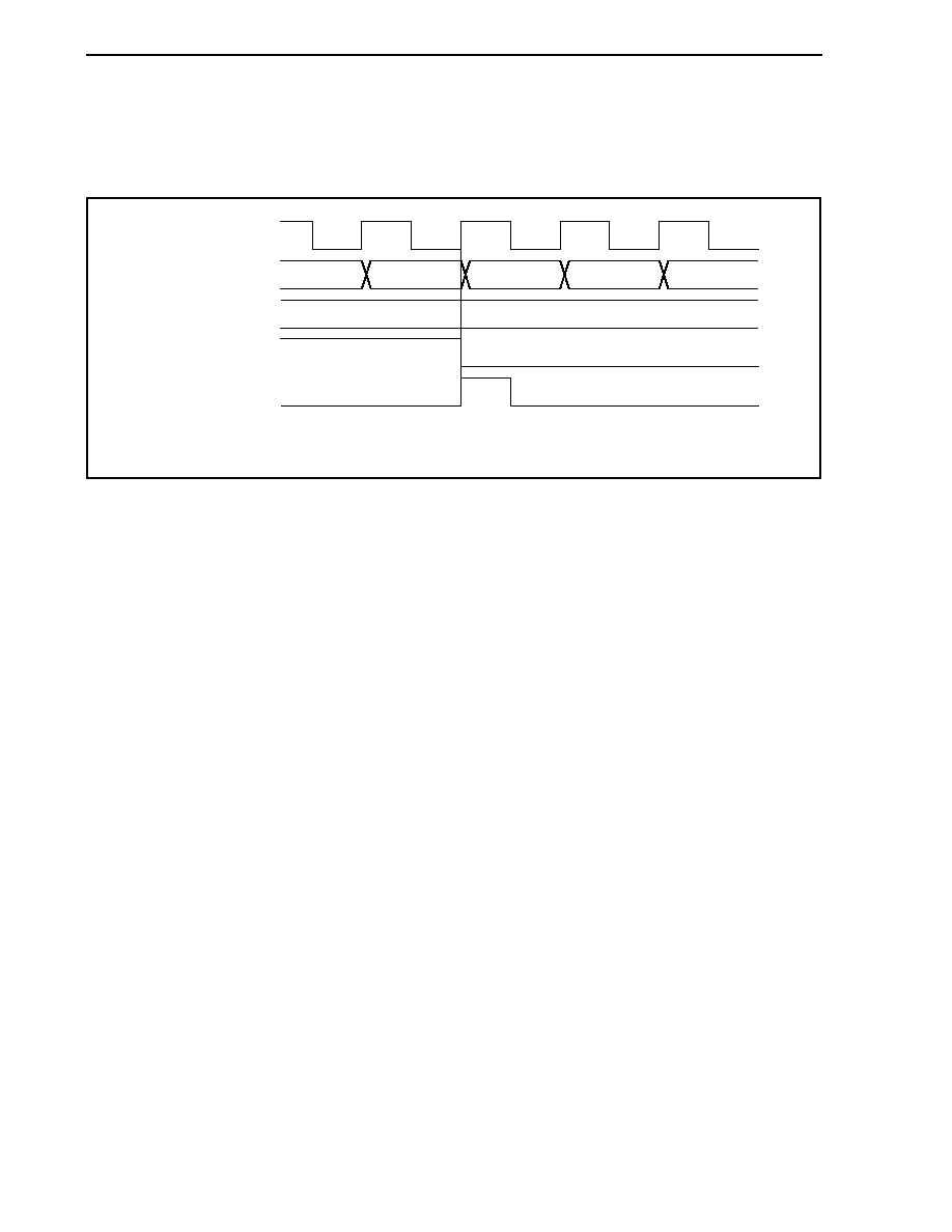
CHAPTER 8 16-BIT TIMER/EVENT COUNTER Q (TMQ)
Preliminary User's Manual U17714EJ1V0UD
364
(e) Generation timing of compare match interrupt request signal (INTTQ0CCk)
The timing of generation of the INTTQ0CCk signal in the external trigger pulse output mode differs from
the timing of other INTTQ0CCk signals; the INTTQ0CCk signal is generated when the count value of the
16-bit counter matches the value of the CCRk buffer register.
Count clock
16-bit counter
CCRk buffer register
TOQ0k pin output
INTTQ0CCk signal
D
k
D
k
- 2
D
k
- 1
D
k
D
k
+ 1
D
k
+ 2
Remark k = 1 to 3
Usually, the INTTQ0CCk signal is generated in synchronization with the next count up after the count value
of the 16-bit counter matches the value of the CCRk buffer register.
In the external trigger pulse output mode, however, it is generated one clock earlier. This is because the
timing is changed to match the timing of changing the output signal of the TOQ0k pin.
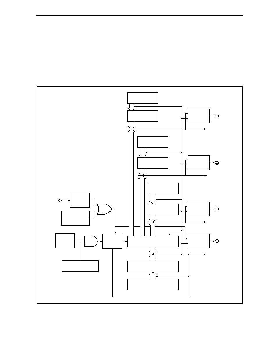
CHAPTER 8 16-BIT TIMER/EVENT COUNTER Q (TMQ)
Preliminary User's Manual U17714EJ1V0UD
365
8.5.4
One-shot pulse output mode (TQ0MD2 to TQ0MD0 bits = 011)
In the one-shot pulse output mode, 16-bit timer/event counter Q waits for a trigger when the TQ0CTL0.TQ0CE bit is
set to 1. When the valid edge of an external trigger input is detected, 16-bit timer/event counter Q starts counting, and
outputs a one-shot pulse from the TOQ01 to TOQ03 pins.
Instead of the external trigger, a software trigger can also be generated to output the pulse. When the software
trigger is used, the TOQ00 pin outputs the active level while the 16-bit counter is counting, and the inactive level when
the counter is stopped (waiting for a trigger).
Figure 8-20. Configuration in One-Shot Pulse Output Mode
CCR0 buffer register
TQ0CE bit
TQ0CCR0 register
Clear
Match signal
INTTQ0CC0 signal
TOQ03 pin
INTTQ0CC3 signal
TOQ00 pin
TIQ00 pin
Transfer
S
R
S
R
TQ0CCR1
register
CCR1 buffer
register
Match signal
TOQ01 pin
INTTQ0CC1 signal
Transfer
Transfer
S
R
TQ0CCR3
register
CCR3 buffer
register
Match signal
Transfer
TOQ02 pin
INTTQ0CC2 signal
S
R
TQ0CCR2
register
CCR2 buffer
register
Match signal
16-bit counter
Count clock
selection
Count start
control
Edge
detector
Software trigger
generation
Output
controller
(RS-FF)
Output
controller
(RS-FF)
Output
controller
(RS-FF)
Output
controller
(RS-FF)
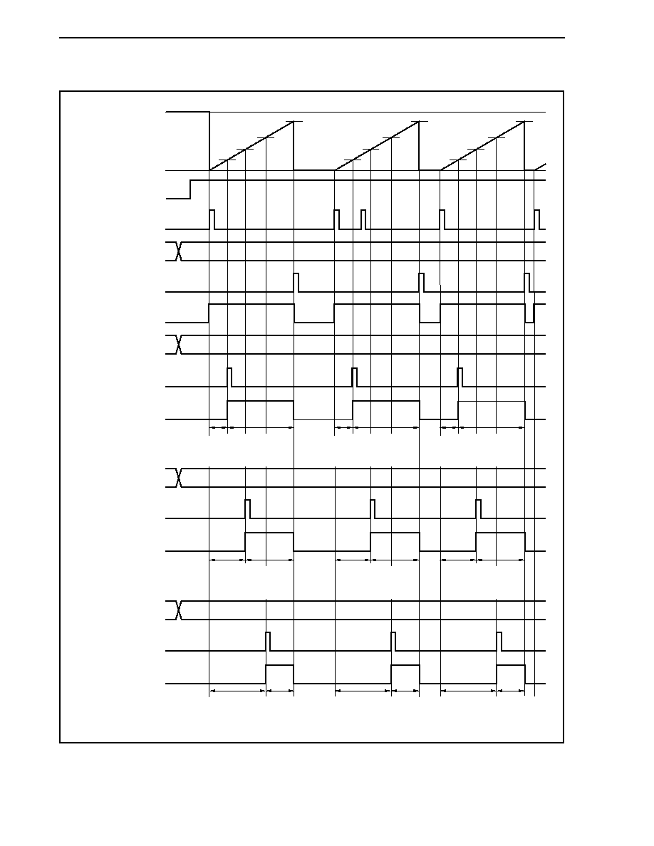
CHAPTER 8 16-BIT TIMER/EVENT COUNTER Q (TMQ)
Preliminary User's Manual U17714EJ1V0UD
366
Figure 8-21. Basic Timing in One-Shot Pulse Output Mode
D
0
D
1
D
2
D
3
D
1
D
2
D
3
D
0
D
1
D
2
D
3
D
0
D
1
D
2
D
3
D
0
Delay
(D
1
)
Active
level width
(D
0
- D
1
+ 1)
Delay
(D
1
)
Active
level width
(D
0
- D
1
+ 1)
Delay
(D
1
)
Active
level width
(D
0
- D
1
+ 1)
Delay
(D
2
)
Active
level width
(D
0
- D
2
+ 1)
Delay
(D
2
)
Active
level width
(D
0
- D
2
+ 1)
Delay
(D
2
)
Active
level width
(D
0
- D
2
+ 1)
Delay
(D
3
)
Active
level width
(D
0
- D
3
+ 1)
Delay
(D
3
)
Active
level width
(D
0
- D
3
+ 1)
Delay
(D
3
)
Active
level width
(D
0
- D
3
+ 1)
FFFFH
16-bit counter
0000H
TQ0CE bit
External trigger input
(TIQ00 pin input)
TQ0CCR0 register
INTTQ0CC0 signal
TQ0CCR2 register
INTTQ0CC2 signal
TOQ02 pin output
TQ0CCR3 register
INTTQ0CC3 signal
TOQ03 pin output
TQ0CCR1 register
INTTQ0CC1 signal
TOQ01 pin output
TOQ00 pin output
(only when software
trigger is used)
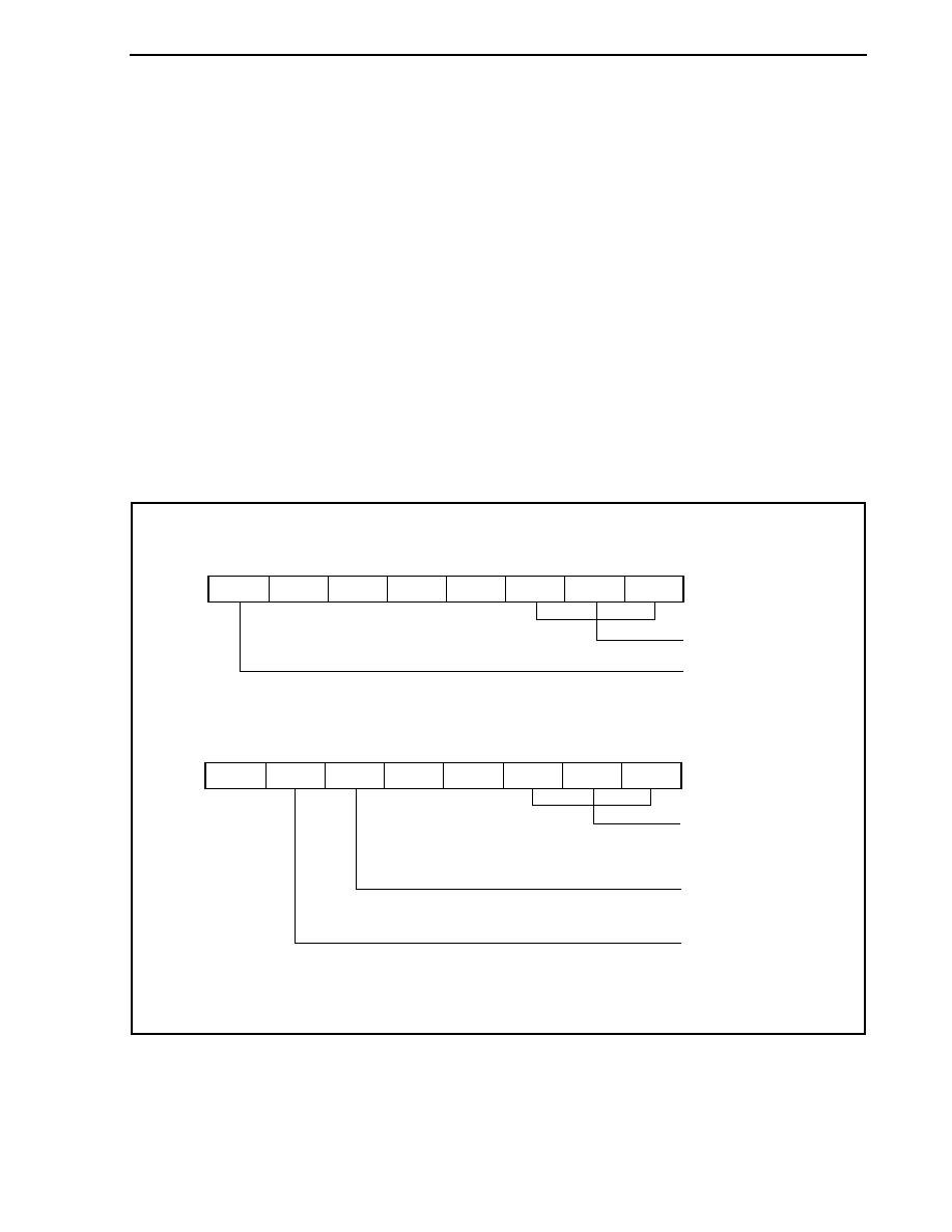
CHAPTER 8 16-BIT TIMER/EVENT COUNTER Q (TMQ)
Preliminary User's Manual U17714EJ1V0UD
367
When the TQ0CE bit is set to 1, 16-bit timer/event counter Q waits for a trigger. When the trigger is generated, the
16-bit counter is cleared from FFFFH to 0000H, starts counting, and outputs a one-shot pulse from the TOQ0k pin.
After the one-shot pulse is output, the 16-bit counter is set to FFFFH, stops counting, and waits for a trigger. If a
trigger is generated again while the one-shot pulse is being output, it is ignored.
The output delay period and active level width of the one-shot pulse can be calculated as follows.
Output delay period = (Set value of TQ0CCRk register)
� Count clock cycle
Active level width = (Set value of TQ0CCR0 register
- Set value of TQ0CCRk register + 1) � Count clock cycle
The compare match interrupt request signal INTTQ0CC0 is generated when the 16-bit counter counts after its
count value matches the value of the CCR0 buffer register. The compare match interrupt request signal INTTQ0CCk
is generated when the count value of the 16-bit counter matches the value of the CCRk buffer register.
The valid edge of an external trigger input or setting the software trigger (TQ0CTL1.TQ0EST bit) to 1 is used as the
trigger.
Remark k = 1 to 3
Figure 8-22. Setting of Registers in One-Shot Pulse Output Mode (1/3)
(a) TMQ0 control register 0 (TQ0CTL0)
0/1
0
0
0
0
TQ0CTL0
Select count clock
Note
0: Stop counting
1: Enable counting
0/1
0/1
0/1
TQ0CKS2 TQ0CKS1 TQ0CKS0
TQ0CE
(b) TMQ0 control register 1 (TQ0CTL1)
0
0/1
0/1
0
0
TQ0CTL1
0: Operate on count clock
selected by TQ0CKS0 to
TQ0CKS2 bits
1: Count external event
input signal
Generate software trigger
when 1 is written
0
1
1
TQ0MD2 TQ0MD1 TQ0MD0
TQ0EEE
TQ0EST
0, 1, 1:
One-shot pulse output mode
Note The setting is invalid when the TQ0CTL1.TQ0EEE bit = 1.
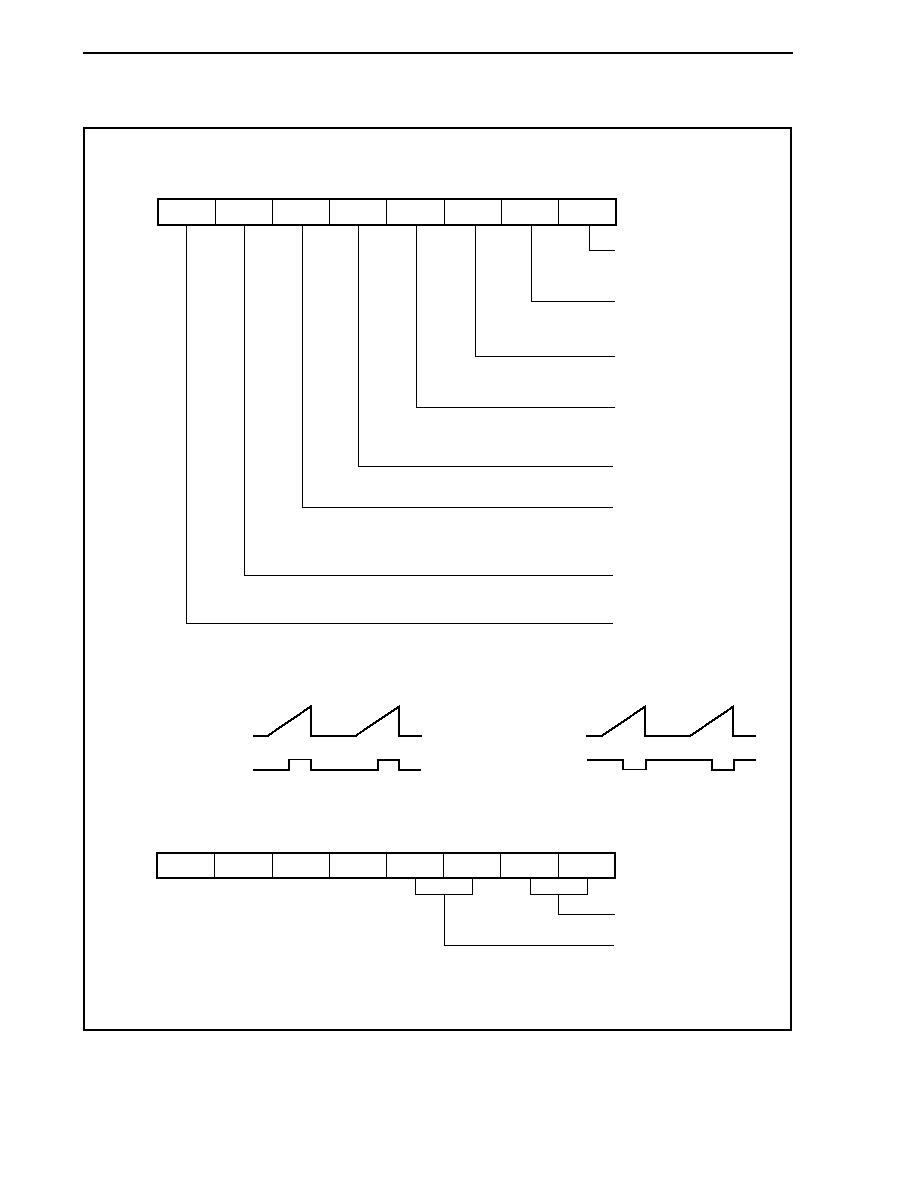
CHAPTER 8 16-BIT TIMER/EVENT COUNTER Q (TMQ)
Preliminary User's Manual U17714EJ1V0UD
368
Figure 8-22. Register Setting in One-Shot Pulse Output Mode (2/3)
(c) TMQ0 I/O control register 0 (TQ0IOC0)
TOQ0k pin output
16-bit counter
� When TQ0OLk bit = 0
TOQ0k pin output
16-bit counter
� When TQ0OLk bit = 1
0/1
0/1
0/1
0/1
0/1
TQ0IOC0
0: Disable TOQ00 pin output
1: Enable TOQ00 pin output
Setting of output level while
operation of TOQ00 pin is disabled
0: Low level
1: High level
0: Disable TOQ01 pin output
1: Enable TOQ01 pin output
Specification of active level
of TOQ01 pin output
0: Active-high
1: Active-low
0/1
0/1
0/1
Note
TQ0OE1 TQ0OL0
TQ0OE0
TQ0OL1
TQ0OE3 TQ0OL2
TQ0OE2
TQ0OL3
Specification of active level
of TOQ03 pin output
0: Active-high
1: Active-low
0: Disable TOQ02 pin output
1: Enable TOQ02 pin output
Specification of active level
of TOQ02 pin output
0: Active-high
1: Active-low
0: Disable TOQ03 pin output
1: Enable TOQ03 pin output
(d) TMQ0 I/O control register 2 (TQ0IOC2)
0
0
0
0
0/1
TQ0IOC2
Select valid edge of
external trigger input
Select valid edge of
external event count input
0/1
0/1
0/1
TQ0EES0 TQ0ETS1 TQ0ETS0
TQ0EES1
Note Clear this bit to 0 when the TOQ00 pin is not used in the one-shot pulse output mode.

CHAPTER 8 16-BIT TIMER/EVENT COUNTER Q (TMQ)
Preliminary User's Manual U17714EJ1V0UD
369
Figure 8-22. Register Setting in One-Shot Pulse Output Mode (3/3)
(e) TMQ0 counter read buffer register (TQ0CNT)
The value of the 16-bit counter can be read by reading the TQ0CNT register.
(f) TMQ0 capture/compare registers 0 to 3 (TQ0CCR0 to TQ0CCR3)
If D
0
is set to the TQ0CCR0 register and D
k
to the TQ0CCRk register, the active level width and output
delay period of the one-shot pulse are as follows.
Active level width = (D
k
- D
0
+ 1)
� Count clock cycle
Output delay period = (D
k
)
� Count clock cycle
Remarks 1. TMQ0 I/O control register 1 (TQ0IOC1) and TMQ0 option register 0 (TQ0OPT0) are not
used in the one-shot pulse output mode.
2.
k = 1 to 3
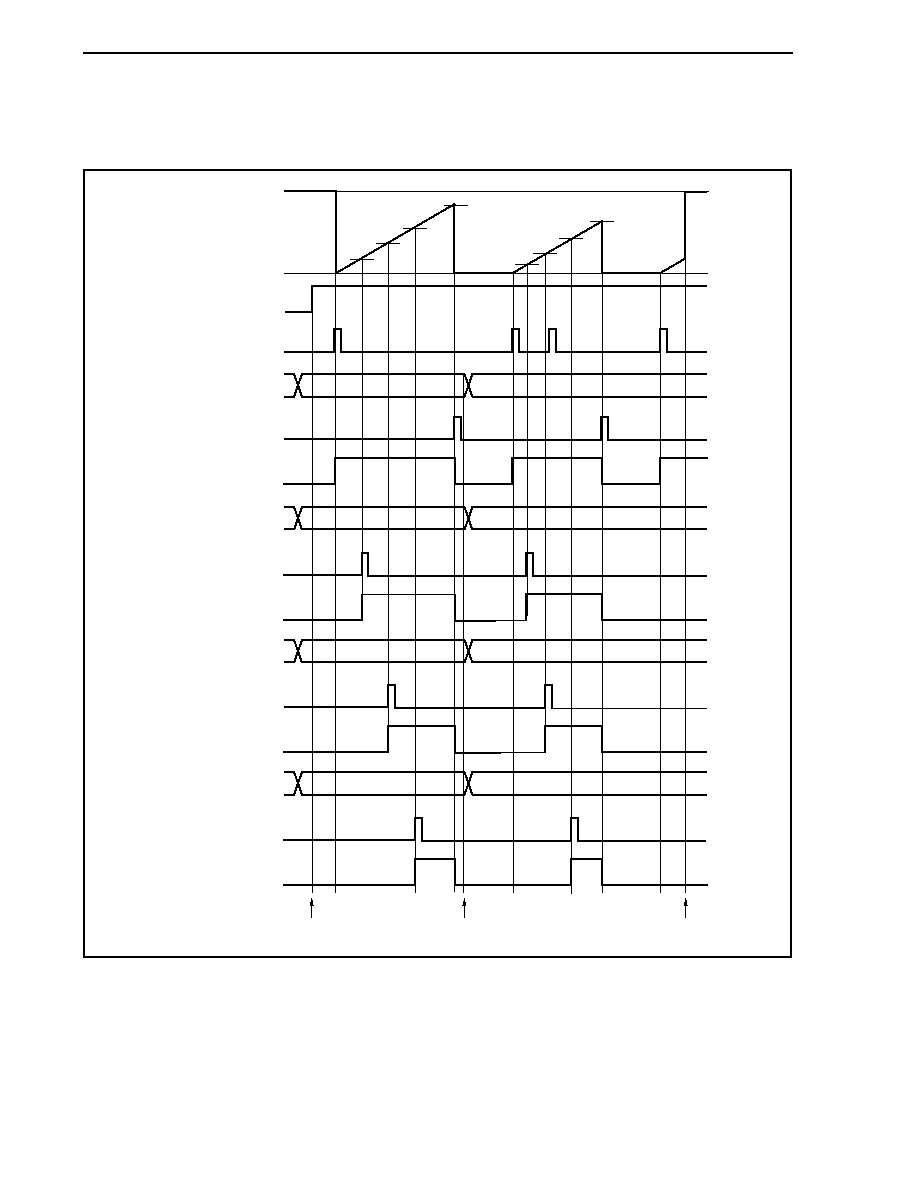
CHAPTER 8 16-BIT TIMER/EVENT COUNTER Q (TMQ)
Preliminary User's Manual U17714EJ1V0UD
370
(1) Operation flow in one-shot pulse output mode
Figure 8-23. Software Processing Flow in One-Shot Pulse Output Mode (1/2)
FFFFH
16-bit counter
0000H
TQ0CE bit
External trigger input
(TIQ00 pin input)
TQ0CCR0 register
INTTQ0CC0 signal
TOQ00 pin output
(only when software
trigger is used)
TQ0CCR1 register
INTTQ0CC1 signal
TOQ01 pin output
TQ0CCR2 register
INTTQ0CC2 signal
TOQ02 pin output
TQ0CCR3 register
INTTQ0CC3 signal
TOQ03 pin output
D
00
D
01
D
11
D
10
D
21
D
20
D
31
D
30
D
10
D
20
D
30
D
11
D
21
D
31
D
00
D
01
<3>
<1>
<2>
CHAPTER 8 16-BIT TIMER/EVENT COUNTER Q (TMQ)
Preliminary User's Manual U17714EJ1V0UD
371
Figure 8-23. Software Processing Flow in One-Shot Pulse Output Mode (2/2)
TQ0CE bit = 1
Register initial setting
TQ0CTL0 register
(TQ0CKS0 to TQ0CKS2 bits)
TQ0CTL1 register,
TQ0IOC0 register,
TQ0IOC2 register,
TQ0CCR0 to TQ0CCR3 registers
Initial setting of these
registers is performed
before setting the
TQ0CE bit to 1.
The TQ0CKS0 to
TQ0CKS2 bits can be
set at the same time
when counting has been
started (TQ0CE bit = 1).
Trigger wait status
START
<1> Count operation start flow
TQ0CE bit = 0
Count operation is
stopped
STOP
<3> Count operation stop flow
Setting of TQ0CCR0 to TQ0CCR3
registers
As rewriting the
TQ0CCRm register
immediately forwards
to the CCRm buffer
register, rewriting
immediately after
the generation of the
INTTQ0CCR0 signal
is recommended.
<2> TQ0CCR0 to TQ0CCR3 register setting change flow
Remark m = 0 to 3
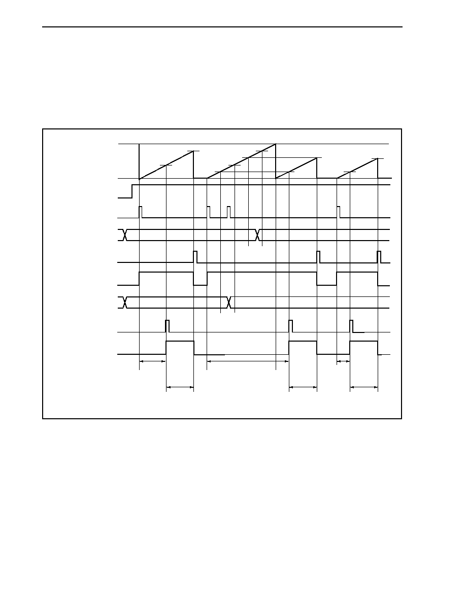
CHAPTER 8 16-BIT TIMER/EVENT COUNTER Q (TMQ)
Preliminary User's Manual U17714EJ1V0UD
372
(2) Operation timing in one-shot pulse output mode
(a) Note on rewriting TQ0CCRm register
To change the set value of the TQ0CCRm register to a smaller value, stop counting once, and then change
the set value.
If the value of the TQ0CCR0 register is rewritten to a smaller value during counting, the 16-bit counter may
overflow.
D
k0
D
k1
D
01
D
01
D
00
D
k1
D
01
D
k0
D
k0
D
k1
D
00
D
00
FFFFH
16-bit counter
0000H
TQ0CE bit
External trigger input
(TIQ00 pin input)
TQ0CCR0 register
INTTQ0CC0 signal
TOQ00 pin output
(only when software
trigger is used)
TQ0CCRk register
INTTQ0CCk signal
TOQ0k pin output
Delay
(D
k0
)
Active level width
(D
00
- D
k0
+ 1)
Active level width
(D
01
- D
k1
+ 1)
Active level width
(D
01
- D
k1
+ 1)
Delay
(D
k1
)
Delay
(10000H + D
k1
)
When the TQ0CCR0 register is rewritten from D
00
to D
01
and the TQ0CCRk register from D
k0
to D
k1
where
D
00
> D
01
and D
k0
> D
k1
, if the TQ0CCRk register is rewritten when the count value of the 16-bit counter is
greater than D
k1
and less than D
k0
and if the TQ0CCR0 register is rewritten when the count value is
greater than D
01
and less than D
00
, each set value is reflected as soon as the register has been rewritten
and compared with the count value. The counter counts up to FFFFH and then counts up again from
0000H. When the count value matches D
k1
, the counter generates the INTTQ0CCk signal and asserts the
TOQ0k pin. When the count value matches D
01
, the counter generates the INTTQ0CC0 signal, deasserts
the TOQ0k pin, and stops counting.
Therefore, the counter may output a pulse with a delay period or active period different from that of the
one-shot pulse that is originally expected.
Remark k = 1 to 3
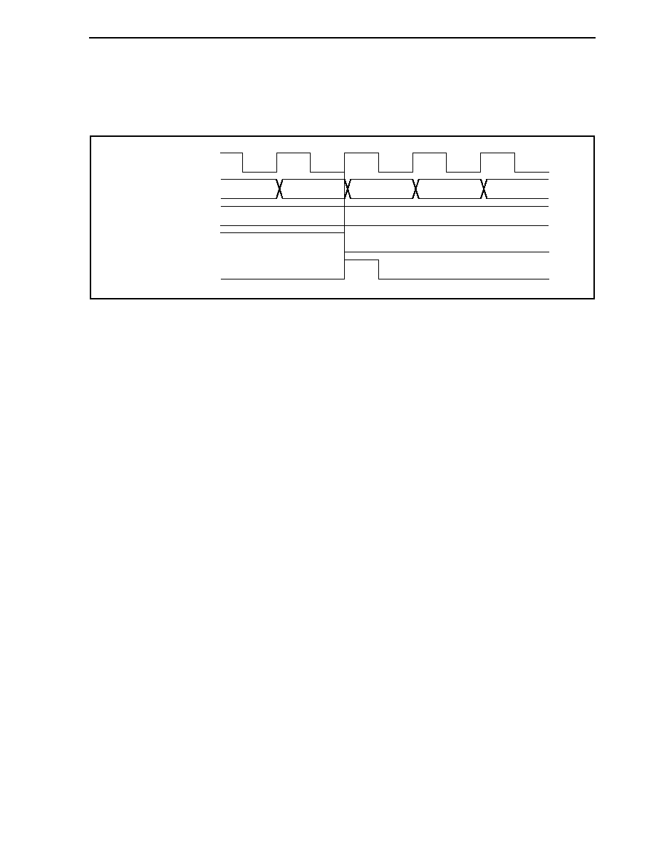
CHAPTER 8 16-BIT TIMER/EVENT COUNTER Q (TMQ)
Preliminary User's Manual U17714EJ1V0UD
373
(b) Generation timing of compare match interrupt request signal (INTTQ0CCk)
The generation timing of the INTTQ0CCk signal in the one-shot pulse output mode is different from other
INTTQ0CCk signals; the INTTQ0CCk signal is generated when the count value of the 16-bit counter
matches the value of the TQ0CCRk register.
Count clock
16-bit counter
TQ0CCRk register
TOQ0k pin output
INTTQ0CCk signal
D
k
D
k
- 2
D
k
- 1
D
k
D
k
+ 1
D
k
+ 2
Usually, the INTTQ0CCk signal is generated when the 16-bit counter counts up next time after its count
value matches the value of the TQ0CCRk register.
In the one-shot pulse output mode, however, it is generated one clock earlier. This is because the timing is
changed to match the change timing of the TOQ0k pin.
Remark k = 1 to 3
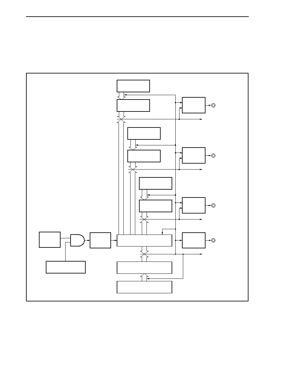
CHAPTER 8 16-BIT TIMER/EVENT COUNTER Q (TMQ)
Preliminary User's Manual U17714EJ1V0UD
374
8.5.5
PWM output mode (TQ0MD2 to TQ0MD0 bits = 100)
In the PWM output mode, a PWM waveform is output from the TOQ01 to TOQ03 pins when the TQ0CTL0.TQ0CE
bit is set to 1.
In addition, a pulse with one cycle of the PWM waveform as half its cycle is output from the TOQ00 pin.
Figure 8-24. Configuration in PWM Output Mode
CCR0 buffer register
TQ0CE bit
TQ0CCR0 register
Clear
Match signal
INTTQ0CC0 signal
TOQ03 pin
INTTQ0CC3 signal
TOQ00 pin
Transfer
S
R
TQ0CCR1
register
CCR1 buffer
register
Match signal
TOQ01 pin
INTTQ0CC1 signal
Transfer
Transfer
S
R
TQ0CCR3
register
CCR3 buffer
register
Match signal
Transfer
TOQ02 pin
INTTQ0CC2 signal
S
R
TQ0CCR2
register
CCR2 buffer
register
Match signal
16-bit counter
Count
clock
selection
Count
start
control
Output
controller
(RS-FF)
Output
controller
Output
controller
(RS-FF)
Output
controller
(RS-FF)
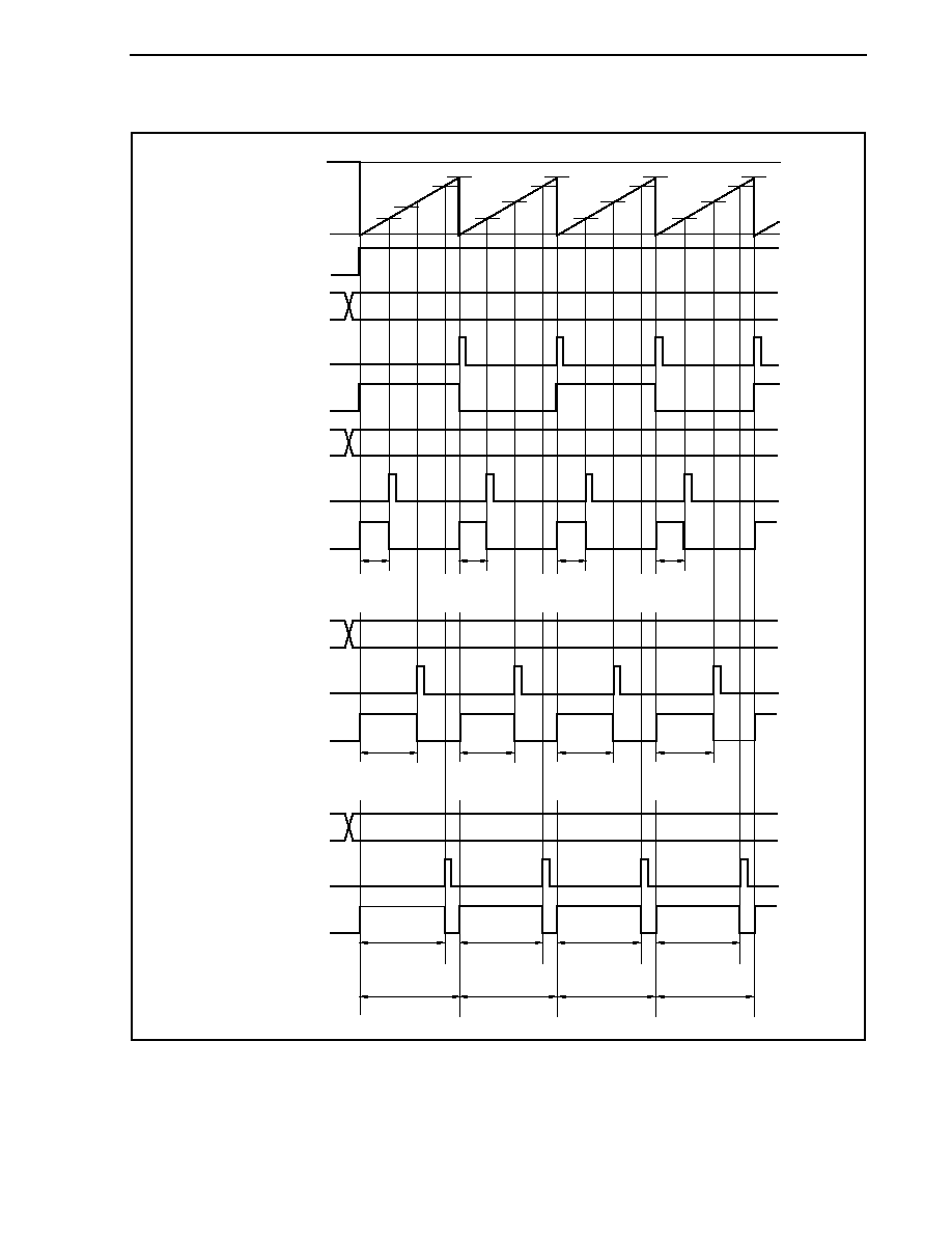
CHAPTER 8 16-BIT TIMER/EVENT COUNTER Q (TMQ)
Preliminary User's Manual U17714EJ1V0UD
375
Figure 8-25. Basic Timing in PWM Output Mode
D
0
D
1
D
2
D
3
D
1
D
2
D
3
D
0
D
0
D
1
D
2
D
3
D
0
D
1
D
2
D
3
D
0
D
1
D
2
D
3
FFFFH
16-bit counter
0000H
TQ0CE bit
TQ0CCR0 register
INTTQ0CC0 signal
TOQ00 pin output
TQ0CCR1 register
INTTQ0CC1 signal
TOQ01 pin output
TQ0CCR2 register
INTTQ0CC2 signal
TOQ02 pin output
TQ0CCR3 register
INTTQ0CC3 signal
TOQ03 pin output
Active level
width (D
3
)
Cycle (D
0
+ 1)
Cycle (D
0
+ 1)
Cycle (D
0
+ 1)
Cycle (D
0
+ 1)
Active level
width (D
3
)
Active level
width (D
3
)
Active level
width (D
3
)
Active
level width
(D
1
)
Active
level width
(D
1
)
Active
level width
(D
1
)
Active
level width
(D
1
)
Active
level width
(D
2
)
Active
level width
(D
2
)
Active
level width
(D
2
)
Active
level width
(D
2
)
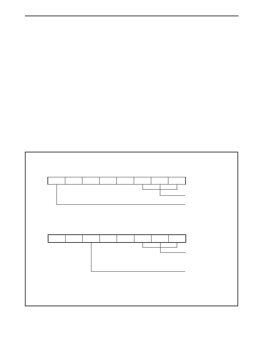
CHAPTER 8 16-BIT TIMER/EVENT COUNTER Q (TMQ)
Preliminary User's Manual U17714EJ1V0UD
376
When the TQ0CE bit is set to 1, the 16-bit counter is cleared from FFFFH to 0000H, starts counting, and outputs
PWM waveform from the TOQ0k pin.
The active level width, cycle, and duty factor of the PWM waveform can be calculated as follows.
Active level width = (Set value of TQ0CCRk register )
� Count clock cycle
Cycle = (Set value of TQ0CCR0 register + 1)
� Count clock cycle
Duty factor = (Set value of TQ0CCRk register)/(Set value of TQ0CCR0 register + 1)
The PWM waveform can be changed by rewriting the TQ0CCRm register while the counter is operating. The newly
written value is reflected when the count value of the 16-bit counter matches the value of the CCR0 buffer register and
the 16-bit counter is cleared to 0000H.
The compare match interrupt request signal INTTQ0CC0 is generated when the 16-bit counter counts next time
after its count value matches the value of the CCR0 buffer register, and the 16-bit counter is cleared to 0000H. The
compare match interrupt request signal INTTQ0CCk is generated when the count value of the 16-bit counter matches
the value of the CCRk buffer register.
Remark k = 1 to 3, m = 0 to 3
Figure 8-26. Setting of Registers in PWM Output Mode (1/3)
(a) TMQ0 control register 0 (TQ0CTL0)
0/1
0
0
0
0
TQ0CTL0
Select count clock
Note
0: Stop counting
1: Enable counting
0/1
0/1
0/1
TQ0CKS2 TQ0CKS1 TQ0CKS0
TQ0CE
(b) TMQ0 control register 1 (TQ0CTL1)
0
0
0/1
0
0
TQ0CTL1
1
0
0
TQ0MD2 TQ0MD1 TQ0MD0
TQ0EEE
TQ0EST
1, 0, 0:
PWM output mode
0: Operate on count clock
selected by TQ0CKS0 to
TQ0CKS2 bits
1: Count external event
input signal
Note The setting is invalid when the TQ0CTL1.TQ0EEE bit = 1.
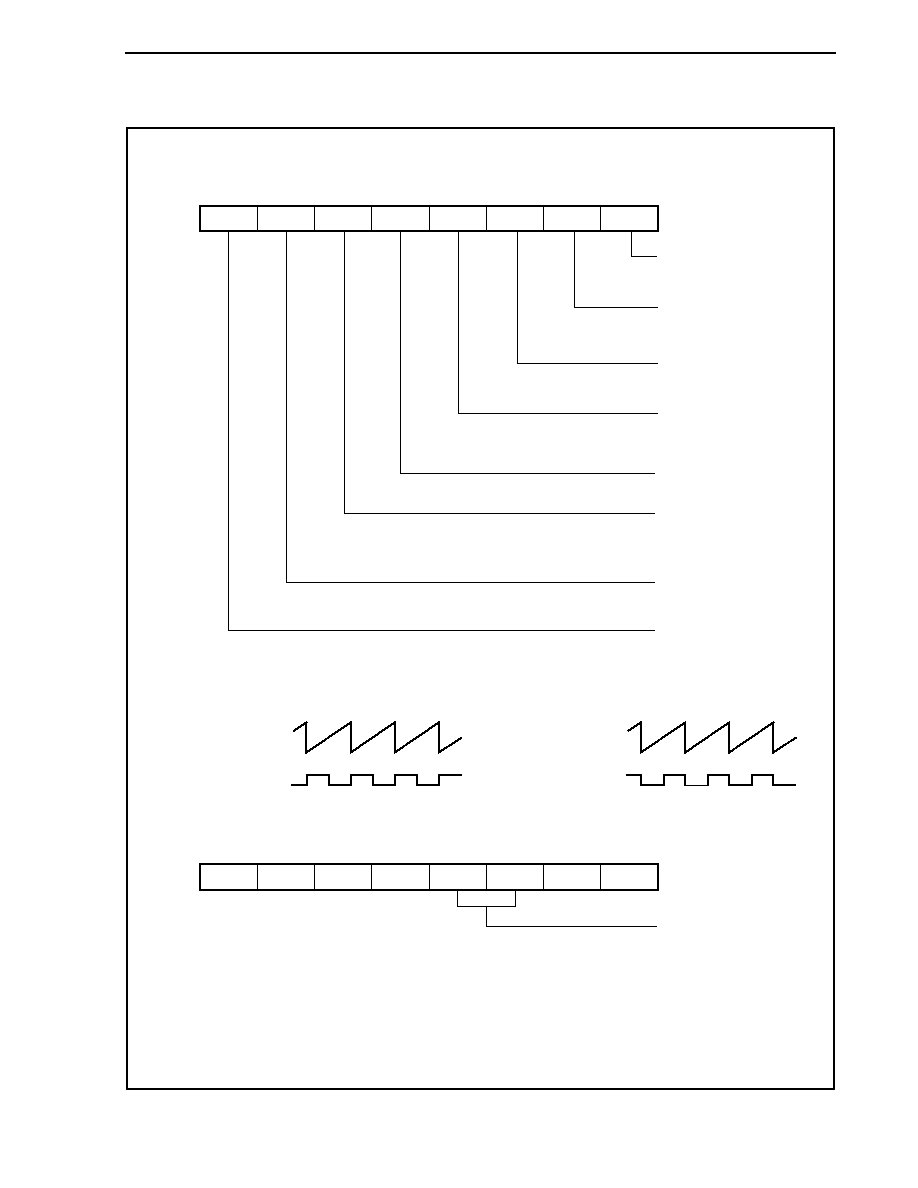
CHAPTER 8 16-BIT TIMER/EVENT COUNTER Q (TMQ)
Preliminary User's Manual U17714EJ1V0UD
377
Figure 8-26. Setting of Registers in PWM Output Mode (2/3)
(c) TMQ0 I/O control register 0 (TQ0IOC0)
TOQ0k pin output
16-bit counter
� When TQ0OLk bit = 0
TOQ0k pin output
16-bit counter
� When TQ0OLk bit = 1
0/1
0/1
0/1
0/1
0/1
TQ0IOC0
0: Disable TOQ00 pin output
1: Enable TOQ00 pin output
Setting of output level while
operation of TOQ00 pin is disabled
0: Low level
1: High level
0: Disable TOQ01 pin output
1: Enable TOQ01 pin output
Specification of active level of
TOQ01 pin output
0: Active-high
1: Active-low
0/1
0/1
0/1
Note
TQ0OE1 TQ0OL0
TQ0OE0
TQ0OL1
TQ0OE3 TQ0OL2
TQ0OE2
TQ0OL3
Specification of active level
of TOQ03 pin output
0: Active-high
1: Active-low
0: Disable TOQ02 pin output
1: Enable TOQ02 pin output
Specification of active level
of TOQ02 pin output
0: Active-high
1: Active-low
0: Disable TOQ03 pin output
1: Enable TOQ03 pin output
(d) TMQ0 I/O control register 2 (TQ0IOC2)
0
0
0
0
0/1
TQ0IOC2
Select valid edge
of external event
count input.
0/1
0
0
TQ0EES0 TQ0ETS1 TQ0ETS0
TQ0EES1
(e) TMQ0 counter read buffer register (TQ0CNT)
The value of the 16-bit counter can be read by reading the TQ0CNT register.
Note Clear this bit to 0 when the TOQ00 pin is not used in the PWM output mode.

CHAPTER 8 16-BIT TIMER/EVENT COUNTER Q (TMQ)
Preliminary User's Manual U17714EJ1V0UD
378
Figure 8-26. Register Setting in PWM Output Mode (3/3)
(f) TMQ0 capture/compare registers 0 to 3 (TQ0CCR0 to TQ0CCR3)
If D
0
is set to the TQ0CCR0 register and D
k
to the TQ0CCR1 register, the cycle and active level of the
PWM waveform are as follows.
Cycle = (D
0
+ 1)
� Count clock cycle
Active level width = D
k
� Count clock cycle
Remarks 1. TMQ0 I/O control register 1 (TQ0IOC1) and TMQ0 option register 0 (TQ0OPT0) are not
used in the PWM output mode.
2. Updating the TMQ0 capture/compare register 2 (TQ0CCR2) and TMQ0 capture/compare
register 3 (TQ0CCR3) is validated by writing the TMQ0 capture/compare register 1
(TQ0CCR1).
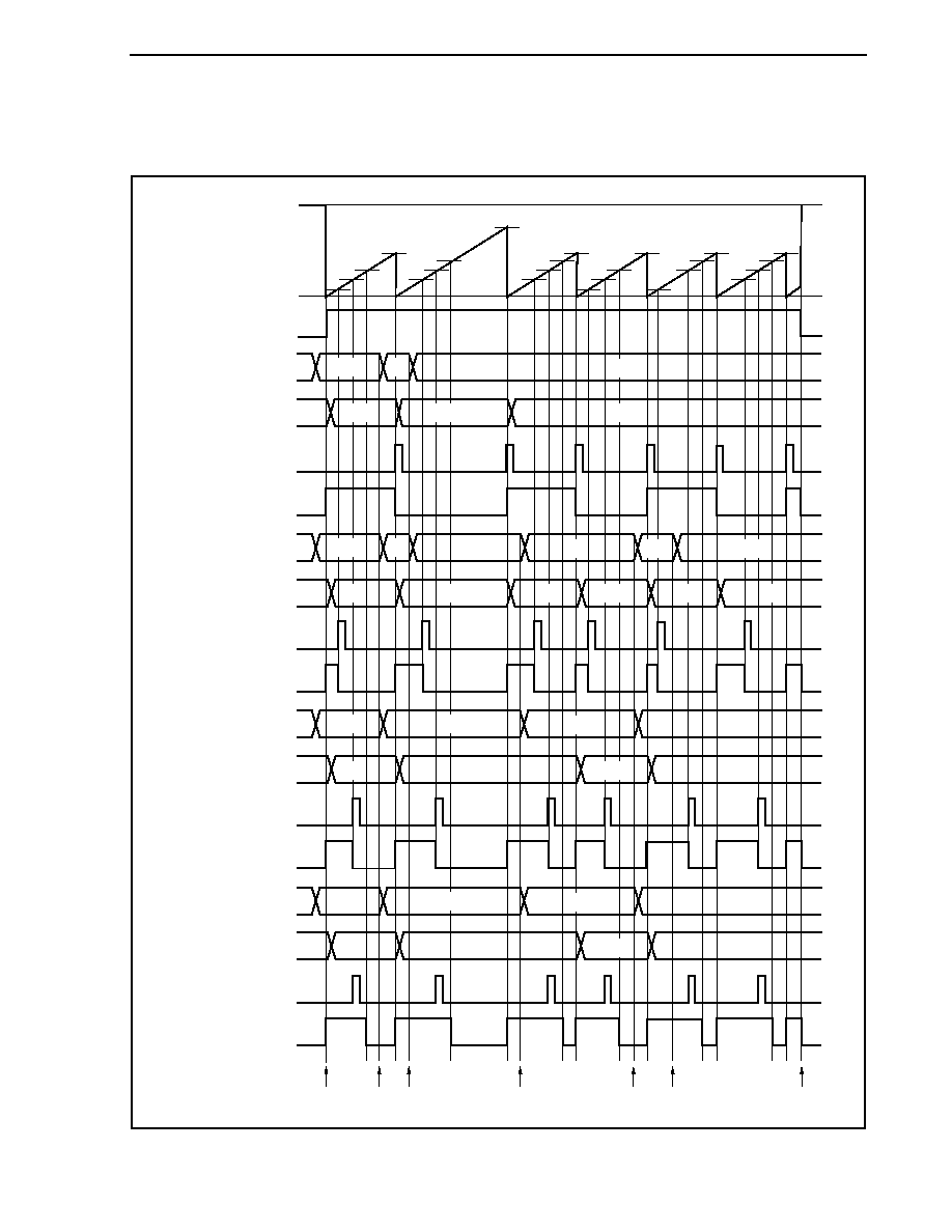
CHAPTER 8 16-BIT TIMER/EVENT COUNTER Q (TMQ)
Preliminary User's Manual U17714EJ1V0UD
379
(1) Operation flow in PWM output mode
Figure 8-27. Software Processing Flow in PWM Output Mode (1/2)
D
10
D
10
D
10
D
20
D
30
D
00
D
11
D
21
D
01
D
31
D
11
D
21
D
00
D
31
D
20
D
30
D
00
D
21
D
00
D
31
D
11
D
21
D
00
D
31
FFFFH
16-bit counter
0000H
TQ0CE bit
TQ0CCR0 register
CCR0 buffer register
INTTQ0CC0 signal
TOQ00 pin output
TQ0CCR1 register
CCR1 buffer register
INTTQ0CC1 signal
TOQ01 pin output
TQ0CCR2 register
CCR2 buffer register
INTTQ0CC2 signal
TOQ02 pin output
TQ0CCR3 register
CCR3 buffer register
INTTQ0CC3 signal
TOQ03 pin output
D
00
D
01
D
00
D
00
D
01
D
00
D
10
D
11
D
10
D
10
D
11
D
10
D
11
D
10
D
11
D
11
D
20
D
21
D
20
D
21
D
20
D
21
D
21
D
30
D
31
D
30
D
31
D
30
D
31
D
30
D
31
<1>
<2> <3>
<4>
<5>
<6>
<7>
D
11
D
10
D
20
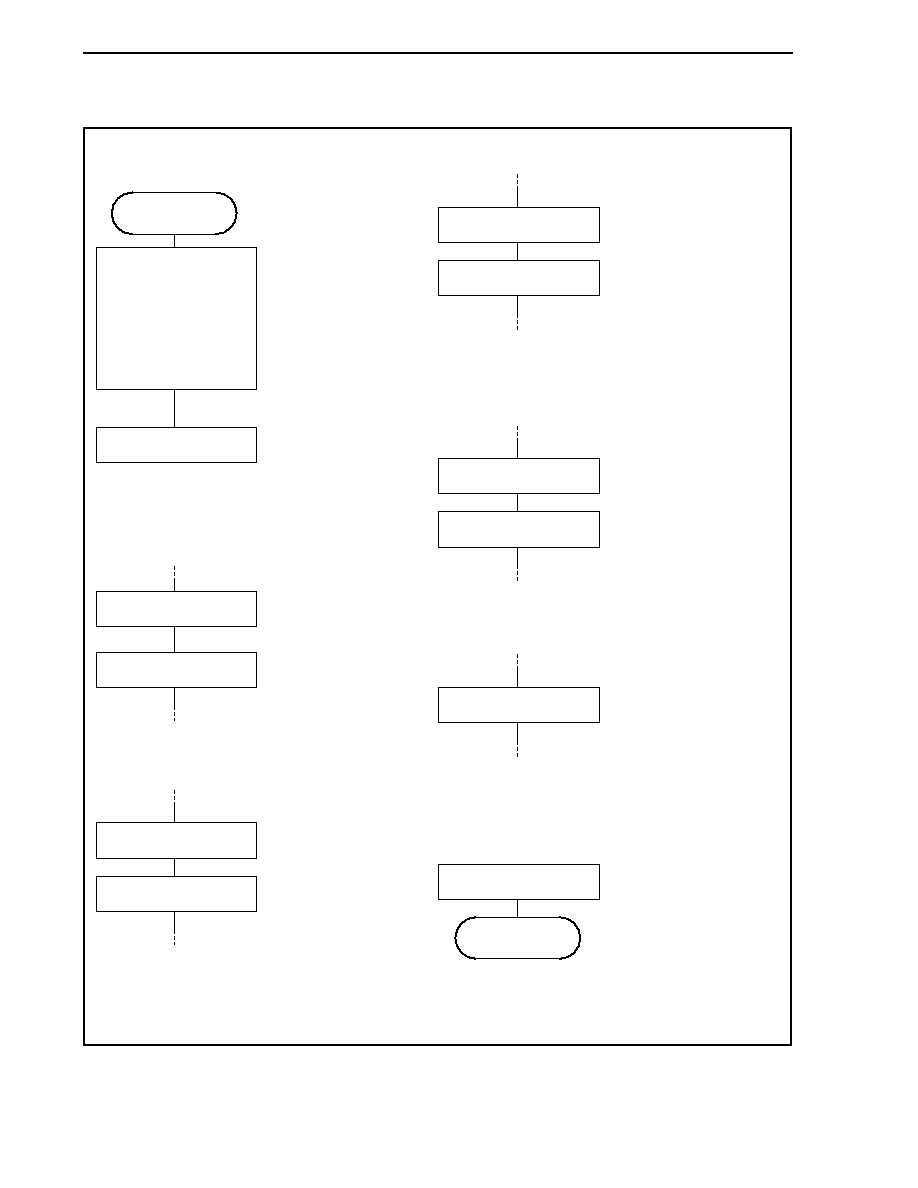
CHAPTER 8 16-BIT TIMER/EVENT COUNTER Q (TMQ)
Preliminary User's Manual U17714EJ1V0UD
380
Figure 8-27. Software Processing Flow in PWM Output Mode (2/2)
START
<1> Count operation start flow
TQ0CE bit = 1
Register initial setting
TQ0CTL0 register
(TQ0CKS0 to TQ0CKS2 bits)
TQ0CTL1 register,
TQ0IOC0 register,
TQ0IOC2 register,
TQ0CCR0 to TQ0CCR3
registers
Initial setting of these
registers is performed
before setting the
TQ0CE bit to 1.
Only writing of the TQ0CCR1
register must be performed
when the set duty factor is only
changed after writing the
TQ0CCR2 and TQ0CCR3
registers.
When the counter is cleared after
setting, the value of the
TQ0CCRm register is transferred
to the CCRm buffer register.
TQ0CCR1 register writing of the
same value is necessary only
when the set duty factor of
TOQ02 and TOQ03 pin
outputs is changed.
When the counter is
cleared after setting,
the value of the TQ0CCRm
register is transferred to
the CCRm buffer register.
Only writing of the TQ0CCR1
register must be performed when
the set duty factor is only changed.
When counter is cleared after
setting, the value of the TQ0CCRm
register is transferred to the CCRm
buffer register.
Counting is stopped.
The TQ0CKS0 to
TQ0CKS2 bits can be
set at the same time
when counting is
enabled (TQ0CE bit = 1).
Writing of the TQ0CCR1
register must be performed
after writing the TQ0CCR0,
TQ0CCR2, and TQ0CCR3
registers.
When the counter is cleared
after setting, the value
of the TQ0CCRm register is
transferred to the CCRm buffer
registers.
TQ0CCR1 writing
of the same value is
necessary only when the
set cycle is changed.
<2> TQ0CCR0 to TQ0CCR3 register
setting change flow
<3> TQ0CCR0 register setting change flow
<4> TQ0CCR1 to TQ0CCR3 register
setting change flow
<5> TQ0CCR2, TQ0CCR3 register
setting change flow
<6> TQ0CCR1 register setting change flow
<7> Count operation stop flow
TQ0CE bit = 0
Setting of TQ0CCR2,
TQ0CCR3 registers
Setting of TQ0CCR1 register
Setting of TQ0CCR2,
TQ0CCR3 registers
Setting of TQ0CCR1 register
STOP
Setting of TQ0CCR1 register
Setting of TQ0CCR0 register
Setting of TQ0CCR1 register
Setting of TQ0CCR0, TQ0CCR2,
and TQ0CCR3 registers
TQ0CCR1 register
When the counter is
cleared after setting, the
value of the TQ0CCRm
register is transferred to
the CCRm buffer register.
Remark k = 1 to 3
m = 0 to 3
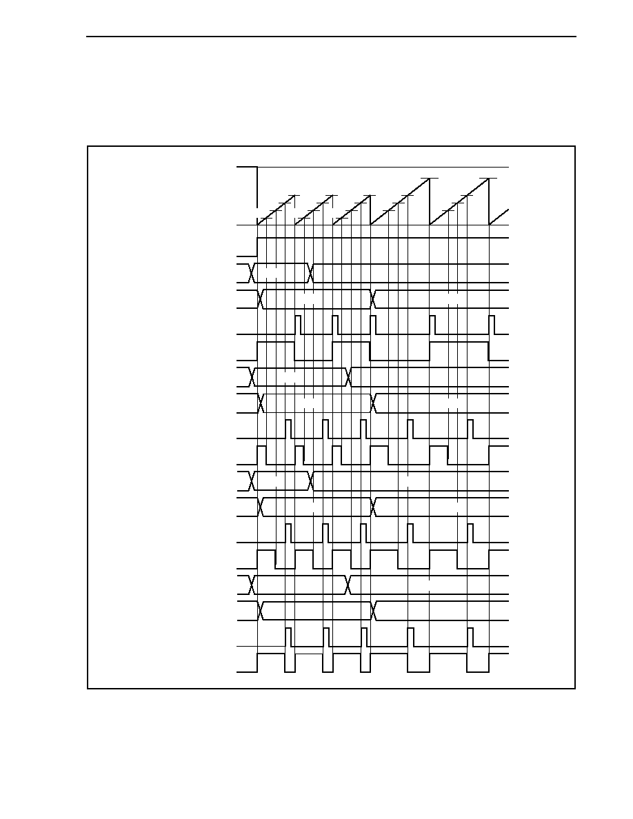
CHAPTER 8 16-BIT TIMER/EVENT COUNTER Q (TMQ)
Preliminary User's Manual U17714EJ1V0UD
381
(2) PWM output mode operation timing
(a) Changing pulse width during operation
To change the PWM waveform while the counter is operating, write the TQ0CCR1 register last.
Rewrite the TQ0CCRk register after writing the TQ0CCR1 register after the INTTQ0CC1 signal is detected.
FFFFH
16-bit counter
0000H
TQ0CE bit
D
30
D
00
D
01
D
30
D
30
D
20
D
20
D
20
D
21
D
11
D
00
D
00
D
31
D
01
D
01
D
21
D
11
D
31
TQ0CCR0 register
CCR0 buffer register
INTTQ0CC0 signal
TQ0CCR1 register
CCR1 buffer register
INTTQ0CC1 signal
TOQ01 pin output
TQ0CCR2 register
CCR2 buffer register
INTTQ0CC2 signal
TOQ02 pin output
TQ0CCR3 register
CCR3 buffer register
INTTQ0CC3 signal
TOQ03 pin output
TOQ00 pin output
D
10
D
10
D
10
D
00
D
11
D
10
D
11
D
10
D
21
D
20
D
21
D
20
D
31
D
30
D
31
D
30
D
00
D
01

CHAPTER 8 16-BIT TIMER/EVENT COUNTER Q (TMQ)
Preliminary User's Manual U17714EJ1V0UD
382
To transfer data from the TQ0CCRm register to the CCRm buffer register, the TQ0CCR1 register must be
written.
To change both the cycle and active level of the PWM waveform at this time, first set the cycle to the
TQ0CCR0 register, set the active level width to the TQ0CCR2 and TQ0CCR3 registers, and then set an
active level width to the TQ0CCR1 register.
To change only the active level width (duty factor) of PWM wave, first set the active level to the TQ0CCR2
and TQ0CCR3 registers, and then set an active level to the TQ0CCR1 register.
To change only the active level width (duty factor) of the PWM waveform output by the TOQ01 pin, only the
TQ0CCR1 register has to be set.
To change only the active level width (duty factor) of the PWM waveform output by the TOQ02 and TOQ03
pins, first set an active level width to the TQ0CCR2 and TQ0CCR3 registers, and then write the same
value to the TQ0CCR1 register.
After the TQ0CCR1 register is written, the value written to the TQ0CCRm register is transferred to the
CCRm buffer register in synchronization with the timing of clearing the 16-bit counter, and is used as a
value to be compared with the value of the 16-bit counter.
To change only the cycle of the PWM waveform, first set a cycle to the TQ0CCR0 register, and then write
the same value to the TQ0CCR1 register.
To write the TQ0CCR0 to TQ0CCR3 registers again after writing the TQ0CCR1 register once, do so after
the INTTQ0CC0 signal is generated. Otherwise, the value of the CCRm buffer register may become
undefined because the timing of transferring data from the TQ0CCRm register to the CCRm buffer register
conflicts with writing the TQ0CCRm register.
Remark m = 0 to 3
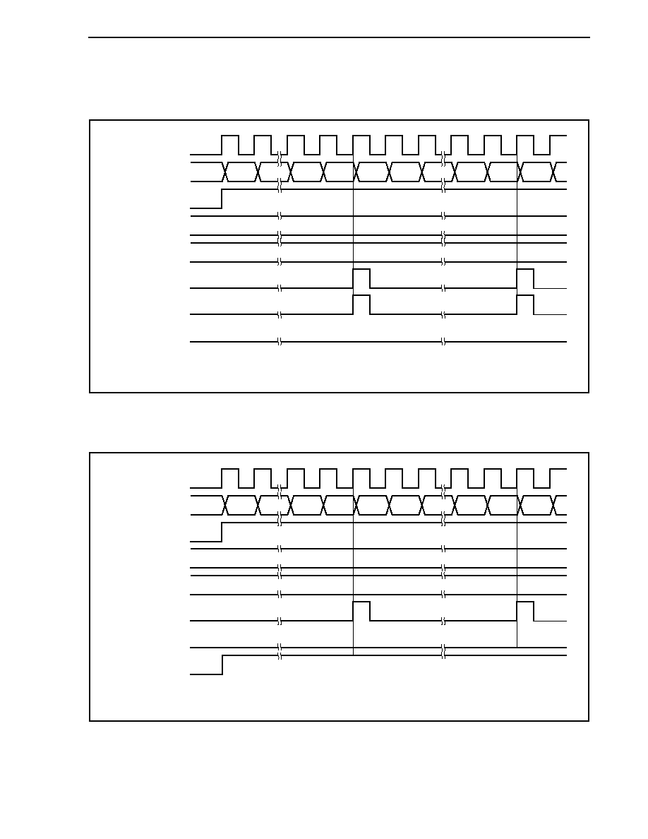
CHAPTER 8 16-BIT TIMER/EVENT COUNTER Q (TMQ)
Preliminary User's Manual U17714EJ1V0UD
383
(b) 0%/100% output of PWM waveform
To output a 0% waveform, set the TQ0CCRk register to 0000H. If the set value of the TQ0CCR0 register is
FFFFH, the INTTQ0CCk signal is generated periodically.
Count clock
16-bit counter
TQ0CE bit
TQ0CCR0 register
TQ0CCRk register
INTTQ0CC0 signal
INTTQ0CCk signal
TOQ0k pin output
D
0
0000H
D
0
0000H
D
0
0000H
D
0
- 1
D
0
0000
FFFF
0000
D
0
- 1
D
0
0000
0001
Remark k = 1 to 3
To output a 100% waveform, set a value of (set value of TQ0CCR0 register + 1) to the TQ0CCRk register.
If the set value of the TQ0CCR0 register is FFFFH, 100% output cannot be produced.
Count clock
16-bit counter
TQ0CE bit
TQ0CCR0 register
TQ0CCRk register
INTTQ0CC0 signal
INTTQ0CCk signal
TOQ0k pin output
D
0
D
0
+ 1
D
0
D
0
+ 1
D
0
D
0
+ 1
D
0
- 1
D
0
0000
FFFF
0000
D
0
- 1
D
0
0000
0001
Remark k = 1 to 3
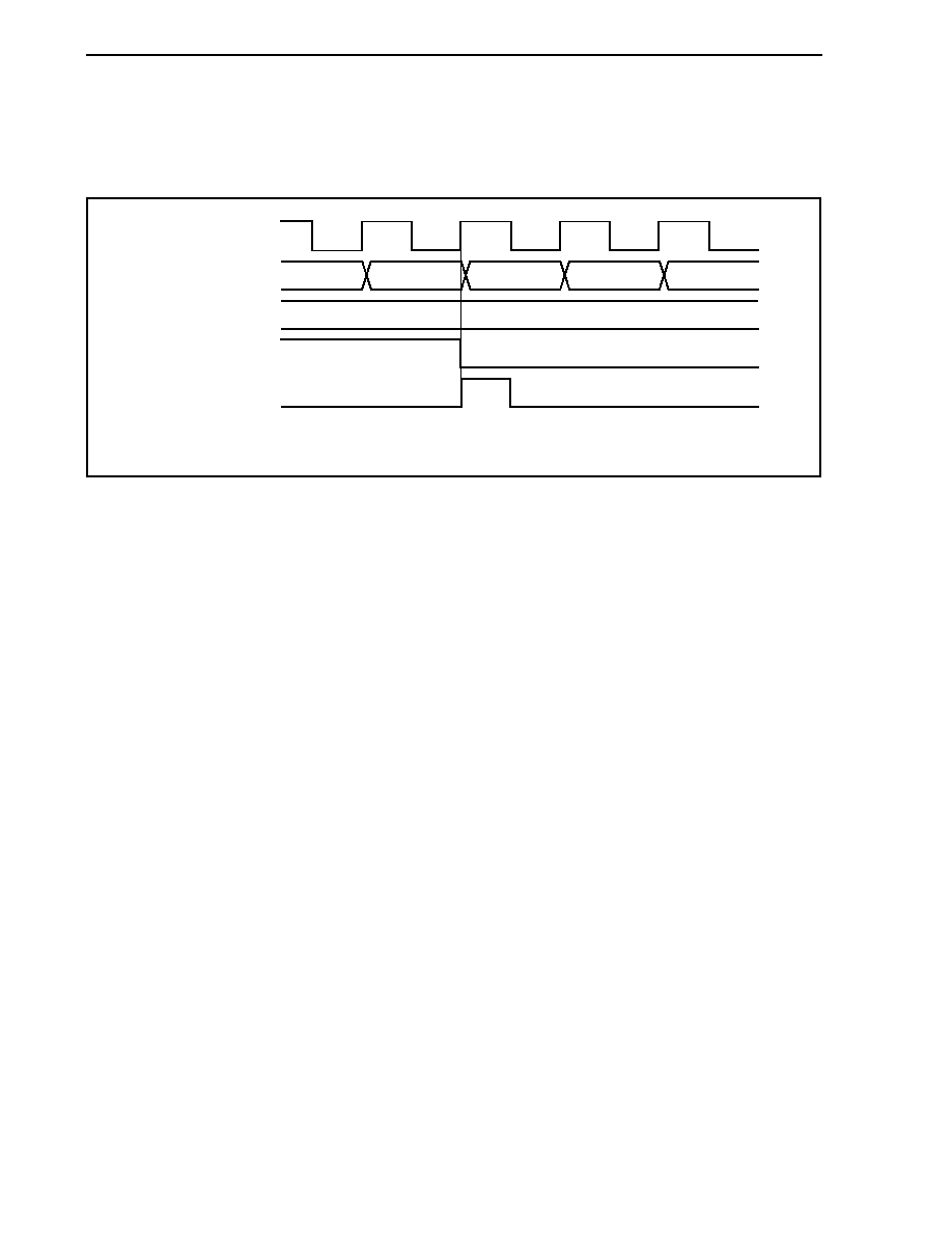
CHAPTER 8 16-BIT TIMER/EVENT COUNTER Q (TMQ)
Preliminary User's Manual U17714EJ1V0UD
384
(c) Generation timing of compare match interrupt request signal (INTTQ0CCk)
The timing of generation of the INTTQ0CCk signal in the PWM output mode differs from the timing of other
INTTQ0CCk signals; the INTTQ0CCk signal is generated when the count value of the 16-bit counter
matches the value of the TQ0CCRk register.
Count clock
16-bit counter
CCRk buffer register
TOQ0k pin output
INTTQ0CCk signal
D
k
D
k
- 2
D
k
- 1
D
k
D
k
+ 1
D
k
+ 2
Remark k = 1 to 3
Usually, the INTTQ0CCk signal is generated in synchronization with the next counting up after the count
value of the 16-bit counter matches the value of the TQ0CCRk register.
In the PWM output mode, however, it is generated one clock earlier. This is because the timing is changed
to match the change timing of the output signal of the TOQ0k pin.
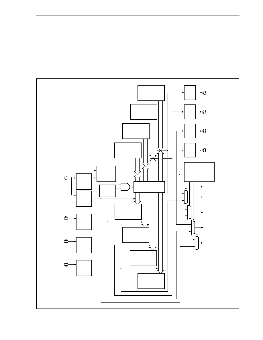
CHAPTER 8 16-BIT TIMER/EVENT COUNTER Q (TMQ)
Preliminary User's Manual U17714EJ1V0UD
385
8.5.6
Free-running timer mode (TQ0MD2 to TQ0MD0 bits = 101)
In the free-running timer mode, 16-bit timer/event counter Q starts counting when the TQ0CTL0.TQ0CE bit is set to
1. At this time, the TQ0CCRm register can be used as a compare register or a capture register, depending on the
setting of the TQ0OPT0.TQ0CCS0 and TQ0OPT0.TQ0CCS1 bits.
Remark m = 0 to 3
Figure 8-28. Configuration in Free-Running Timer Mode
TOQ03 pin output
TOQ02 pin output
TOQ01 pin output
TOQ00 pin output
INTTQ0OV signal
TQ0CCS0,
TQ0CCS1 bits
(capture/compare
selection)
INTTQ0CC3 signal
INTTQ0CC2 signal
INTTQ0CC1 signal
INTTQ0CC0 signal
TIQ03 pin
(capture
trigger input)
TQ0CCR3
register
(capture)
TIQ00pin
(external event
count input/
capture
trigger input)
Internal count clock
TQ0CE
bit
TIQ01 pin
(capture
trigger input)
TIQ02 pin
(capture
trigger input)
TQ0CCR0
register
(capture)
TQ0CCR1
register
(capture)
TQ0CCR2
register
(capture)
TQ0CCR3
register
(compare)
TQ0CCR2
register
(compare)
TQ0CCR1
register
(compare)
0
1
0
1
0
1
0
1
16-bit counter
TQ0CCR0
register
(compare)
Output
controller
Output
controller
Output
controller
Output
controller
Count
clock
selection
Edge
detector
Edge
detector
Edge
detector
Edge
detector
Edge
detector
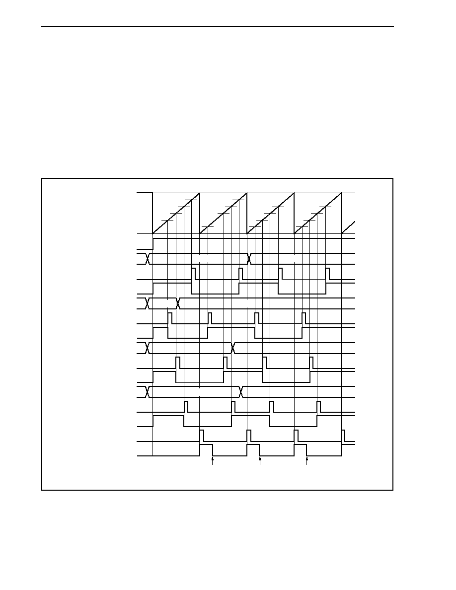
CHAPTER 8 16-BIT TIMER/EVENT COUNTER Q (TMQ)
Preliminary User's Manual U17714EJ1V0UD
386
When the TQ0CE bit is set to 1, 16-bit timer/event counter Q starts counting, and the output signals of the TOQ00
to TOQ03 pins are inverted. When the count value of the 16-bit counter later matches the set value of the TQ0CCRm
register, a compare match interrupt request signal (INTTQ0CCm) is generated, and the output signal of the TOQ0m
pin is inverted.
The 16-bit counter continues counting in synchronization with the count clock. When it counts up to FFFFH, it
generates an overflow interrupt request signal (INTTQ0OV) at the next clock, is cleared to 0000H, and continues
counting. At this time, the overflow flag (TQ0OPT0.TQ0OVF bit) is also set to 1. Clear the overflow flag to 0 by
executing the CLR instruction by software.
The TQ0CCRm register can be rewritten while the counter is operating. If it is rewritten, the new value is reflected
at that time, and compared with the count value.
Figure 8-29. Basic Timing in Free-Running Timer Mode (Compare Function)
D
10
D
20
D
30
D
00
D
20
D
31
D
31
D
30
D
00
D
11
D
11
D
21
D
01
D
11
D
21
D
01
Cleared to 0 by
CLR instruction
Cleared to 0 by
CLR instruction
Cleared to 0 by
CLR instruction
FFFFH
16-bit counter
0000H
TOQ01 pin output
TQ0CCR2 register
INTTQ0CC2 signal
TOQ02 pin output
TQ0CCR3 register
INTTQ0CC3 signal
TOQ03 pin output
INTTQ0OV signal
TQ0OVF bit
TOQ00 pin output
TQ0CCR1 register
INTTQ0CC1 signal
TQ0CE bit
TQ0CCR0 register
INTTQ0CC0 signal
D
00
D
01
D
11
D
10
D
21
D
20
D
31
D
30
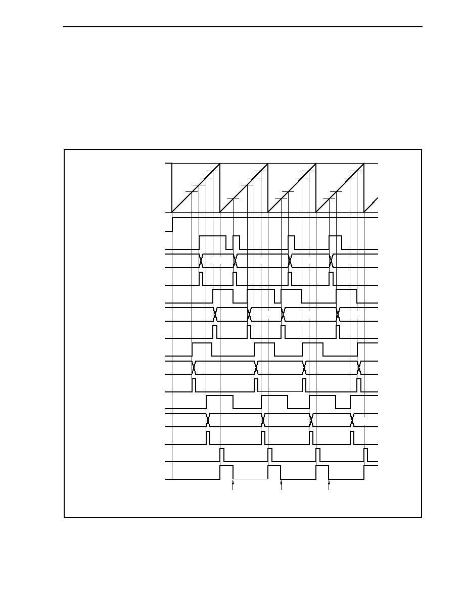
CHAPTER 8 16-BIT TIMER/EVENT COUNTER Q (TMQ)
Preliminary User's Manual U17714EJ1V0UD
387
When the TQ0CE bit is set to 1, the 16-bit counter starts counting. When the valid edge input to the TIQ0m pin is
detected, the count value of the 16-bit counter is stored in the TQ0CCRm register, and a capture interrupt request
signal (INTTQ0CCm) is generated.
The 16-bit counter continues counting in synchronization with the count clock. When it counts up to FFFFH, it
generates an overflow interrupt request signal (INTTQ0OV) at the next clock, is cleared to 0000H, and continues
counting. At this time, the overflow flag (TQ0OVF bit) is also set to 1. Clear the overflow flag to 0 by executing the
CLR instruction by software.
Figure 8-30. Basic Timing in Free-Running Timer Mode (Capture Function)
D
20
D
00
D
30
D
10
D
11
D
21
D
31
D
12
D
01
D
02
D
22
D
32
D
03
D
13
D
33
D
23
0000
D
00
D
01
D
02
D
03
0000
D
10
D
11
D
12
D
13
0000
D
20
D
21
D
23
D
22
0000
D
30
D
31
D
32
D
33
Cleared to 0 by
CLR instruction
Cleared to 0 by
CLR instruction
Cleared to 0 by
CLR instruction
FFFFH
16-bit counter
0000H
TIQ02 pin input
TQ0CCR2 register
INTTQ0CC2 signal
TIQ03 pin input
TQ0CCR3 register
INTTQ0CC3 signal
INTTQ0OV signal
TQ0OVF bit
TIQ01 pin input
TQ0CCR1 register
INTTQ0CC1 signal
TQ0CE bit
TIQ00 pin input
TQ0CCR0 register
INTTQ0CC0 signal
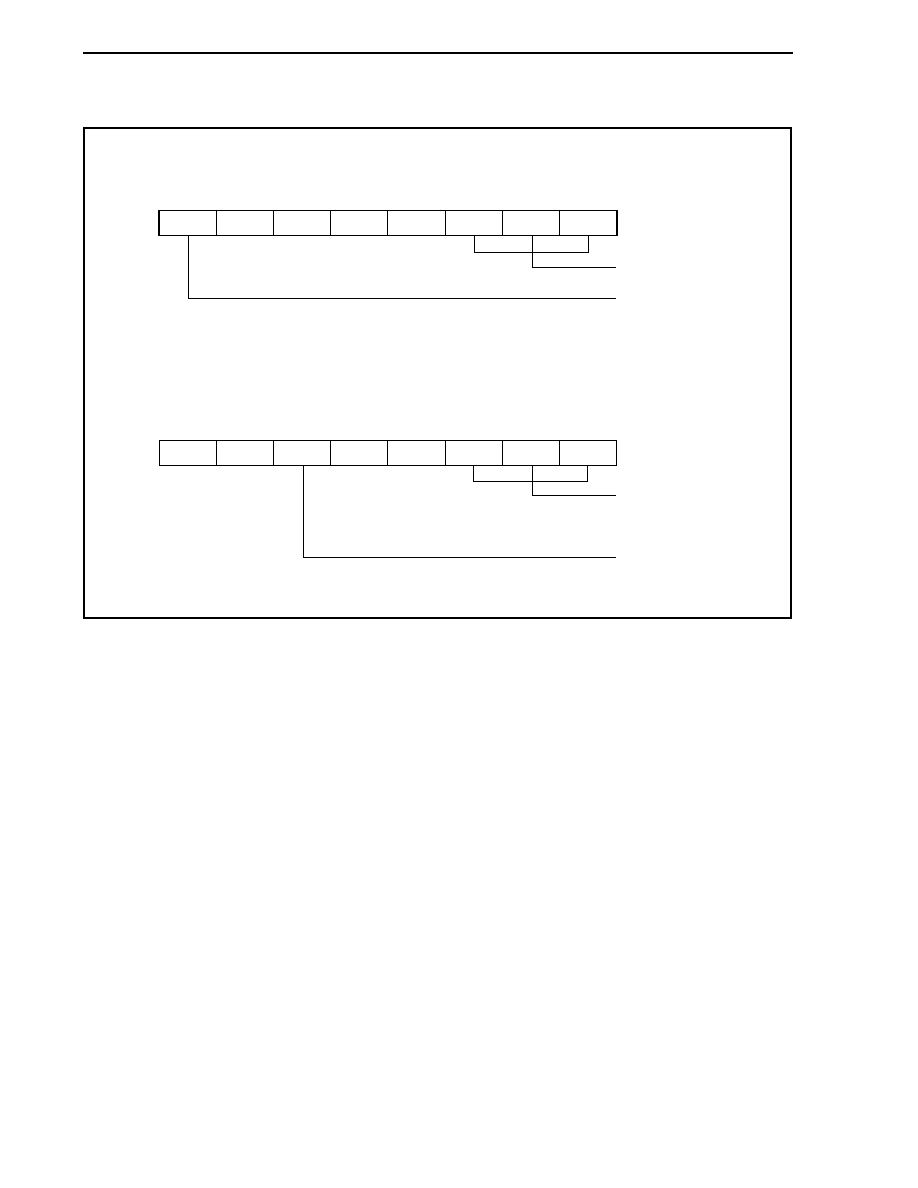
CHAPTER 8 16-BIT TIMER/EVENT COUNTER Q (TMQ)
Preliminary User's Manual U17714EJ1V0UD
388
Figure 8-31. Register Setting in Free-Running Timer Mode (1/3)
(a) TMQ0 control register 0 (TQ0CTL0)
0/1
0
0
0
0
TQ0CTL0
Select count clock
Note
0: Stop counting
1: Enable counting
0/1
0/1
0/1
TQ0CKS2 TQ0CKS1 TQ0CKS0
TQ0CE
Note The setting is invalid when the TQ0CTL1.TQ0EEE bit = 1
(b) TMQ0 control register 1 (TQ0CTL1)
0
0
0/1
0
0
TQ0CTL1
1
0
1
TQ0MD2 TQ0MD1 TQ0MD0
TQ0EEE
TQ0EST
1, 0, 1:
Free-running mode
0: Operate with count
clock selected by
TQ0CKS0 to TQ0CKS2 bits
1: Count on external
event count input signal
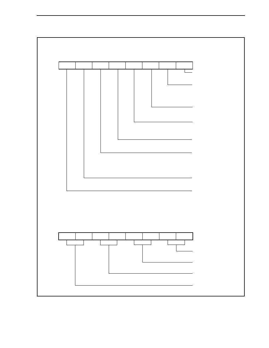
CHAPTER 8 16-BIT TIMER/EVENT COUNTER Q (TMQ)
Preliminary User's Manual U17714EJ1V0UD
389
Figure 8-31. Register Setting in Free-Running Timer Mode (2/3)
(c) TMQ0 I/O control register 0 (TQ0IOC0)
0/1
0/1
0/1
0/1
0/1
TQ0IOC0
0: Disable TOQ00 pin output
1: Enable TOQ00 pin output
0: Disable TOQ01 pin output
1: Enable TOQ01 pin output
Setting of output level with
operation of TOQ01 pin
disabled
0: Low level
1: High level
0/1
0/1
0/1
TQ0OE1 TQ0OL0
TQ0OE0
TQ0OL1
TQ0OE3 TQ0OL2
TQ0OE2
TQ0OL3
Setting of output level with
operation of TOQ03 pin
disabled
0: Low level
1: High level
0: Disable TOQ02 pin output
1: Enable TOQ02 pin output
Setting of output level with
operation of TOQ02 pin
disabled
0: Low level
1: High level
0: Disable TOQ03 pin output
1: Enable TOQ03 pin output
Setting of output level with
operation of TOQ00 pin disabled
0: Low level
1: High level
(d) TMQ0 I/O control register 1 (TQ0IOC1)
0/1
0/1
0/1
0/1
0/1
TQ0IOC1
Select valid edge
of TIQ00 pin input
Select valid edge
of TIQ01 pin input
0/1
0/1
0/1
TQ0IS2
TQ0IS1
TQ0IS0
TQ0IS3
TQ0IS6
TQ0IS5
TQ0IS4
TQ0IS7
Select valid edge
of TIQ02 pin input
Select valid edge
of TIQ03 pin input
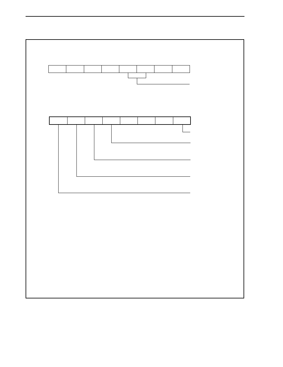
CHAPTER 8 16-BIT TIMER/EVENT COUNTER Q (TMQ)
Preliminary User's Manual U17714EJ1V0UD
390
Figure 8-31. Register Setting in Free-Running Timer Mode (3/3)
(e) TMQ0 I/O control register 2 (TQ0IOC2)
0
0
0
0
0/1
TQ0IOC2
Select valid edge of
external event count input
0/1
0
0
TQ0EES0 TQ0ETS1 TQ0ETS0
TQ0EES1
(f) TMQ0 option register 0 (TQ0OPT0)
0/1
0/1
0/1
0/1
0
TQ0OPT0
Overflow flag
Specifies if TQ0CCR0
register functions as
capture or compare register
Specifies if TQ0CCR1
register functions as
capture or compare register
0
0
0/1
TQ0CCS0
TQ0OVF
TQ0CCS1
TQ0CCS2
TQ0CCS3
Specifies if TQ0CCR2
register functions as
capture or compare register
Specifies if TQ0CCR3
register functions as
capture or compare register
(g) TMQ0 counter read buffer register (TQ0CNT)
The value of the 16-bit counter can be read by reading the TQ0CNT register.
(h) TMQ0 capture/compare registers 0 to 3 (TQ0CCR0 to TQ0CCR3)
These registers function as capture registers or compare registers depending on the setting of the
TQ0OPT0.TQ0CCSm bit.
When the registers function as capture registers, they store the count value of the 16-bit counter when
the valid edge input to the TIQ0m pin is detected.
When the registers function as compare registers and when D
m
is set to the TQ0CCRm register, the
INTTQ0CCm signal is generated when the counter reaches (D
m
+ 1), and the output signal of the
TOQ0m pin is inverted.
Remark m = 0 to 3
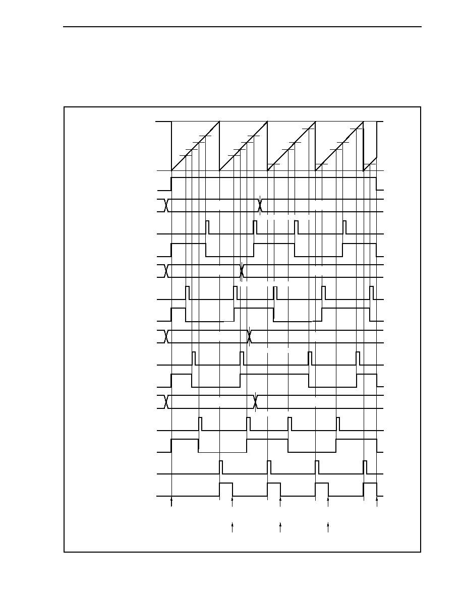
CHAPTER 8 16-BIT TIMER/EVENT COUNTER Q (TMQ)
Preliminary User's Manual U17714EJ1V0UD
391
(1) Operation flow in free-running timer mode
(a) When using capture/compare register as compare register
Figure 8-32. Software Processing Flow in Free-Running Timer Mode (Compare Function) (1/2)
D
10
D
20
D
30
D
00
D
10
D
20
D
30
D
00
D
11
D
31
D
01
D
21
D
21
D
11
D
11
D
31
D
01
FFFFH
16-bit counter
0000H
TQ0CE bit
TQ0CCR0 register
INTTQ0CC0 signal
TOQ00 pin output
TQ0CCR1 register
INTTQ0CC1 signal
TOQ01 pin output
TQ0CCR2 register
INTTQ0CC2 signal
TOQ02 pin output
TQ0CCR3 register
INTTQ0CC3 signal
TOQ03 pin output
INTTQ0OV signal
TQ0OVF bit
D
00
D
10
D
20
D
30
D
01
D
11
D
21
D
31
Cleared to 0 by
CLR instruction
Set value changed
Set value changed
Set value changed
Set value changed
Cleared to 0 by
CLR instruction
Cleared to 0 by
CLR instruction
<3>
<1>
<2>
<2>
<2>
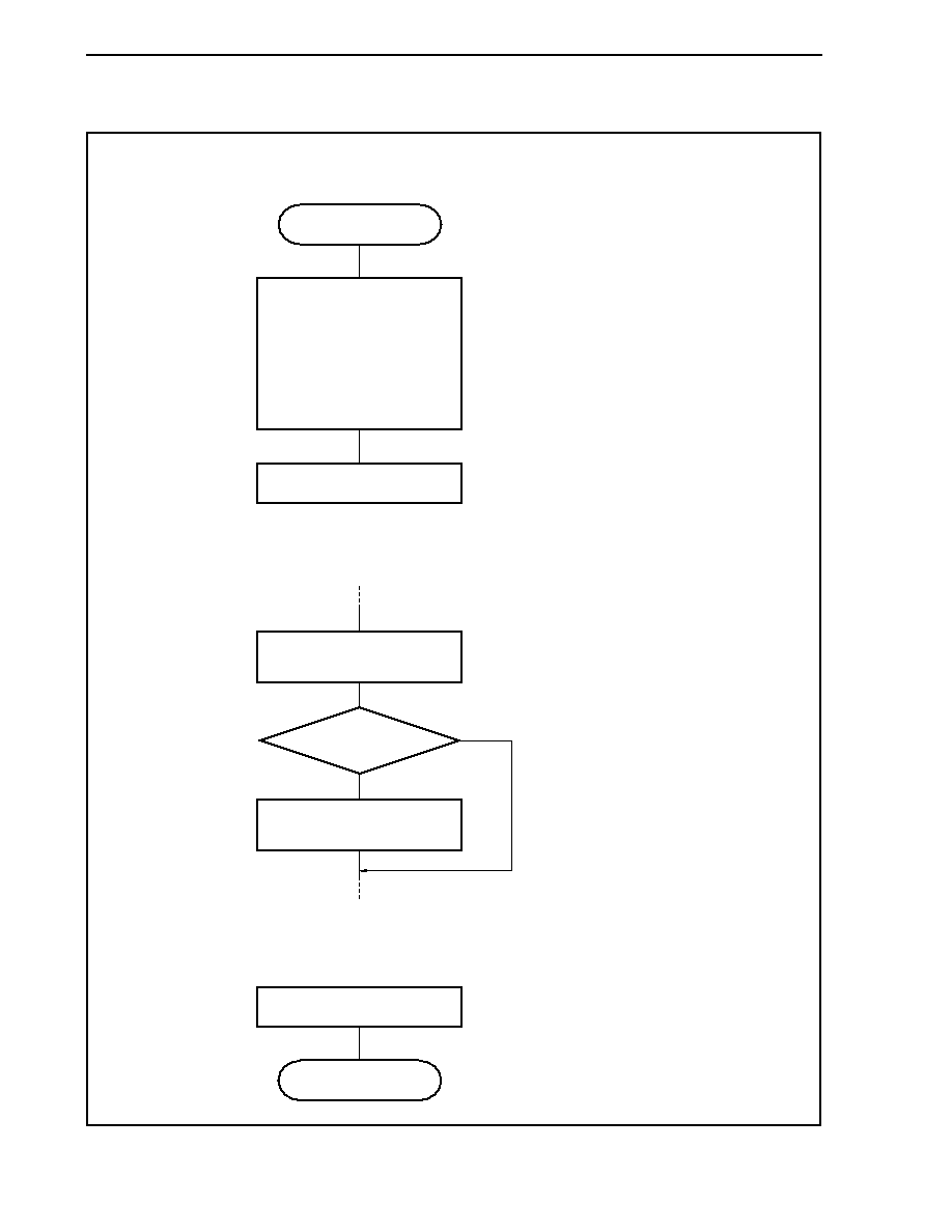
CHAPTER 8 16-BIT TIMER/EVENT COUNTER Q (TMQ)
Preliminary User's Manual U17714EJ1V0UD
392
Figure 8-32. Software Processing Flow in Free-Running Timer Mode (Compare Function) (2/2)
TQ0CE bit = 1
Read TQ0OPT0 register
(check overflow flag).
Register initial setting
TQ0CTL0 register
(TQ0CKS0 to TQ0CKS2 bits)
TQ0CTL1 register,
TQ0IOC0 register,
TQ0IOC2 register,
TQ0OPT0 register,
TQ0CCR0 to TQ0CCR3 registers
Initial setting of these registers
is performed before setting the
TQ0CE bit to 1.
The TQ0CKS0 to TQ0CKS2 bits
can be set at the same time
when counting has been started
(TQ0CE bit = 1).
START
Execute instruction to clear
TQ0OVF bit (CLR TQ0OVF).
<1> Count operation start flow
<2> Overflow flag clear flow
TQ0CE bit = 0
Counter is initialized and
counting is stopped by
clearing TQ0CE bit to 0.
STOP
<3> Count operation stop flow
TQ0OVF bit = 1
NO
YES
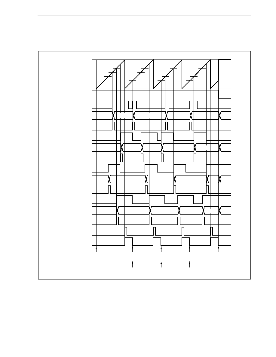
CHAPTER 8 16-BIT TIMER/EVENT COUNTER Q (TMQ)
Preliminary User's Manual U17714EJ1V0UD
393
(b) When using capture/compare register as capture register
Figure 8-33. Software Processing Flow in Free-Running Timer Mode (Capture Function) (1/2)
D
20
D
00
D
30
D
10
D
11
D
21
D
31
D
12
D
01
D
02
D
22
D
32
D
03
D
13
D
33
D
23
0000
D
00
D
01
D
02
D
03
0000
0000
0000
0000
0000
D
10
D
11
D
12
D
13
0000
D
20
D
21
D
23
D
22
0000
D
30
D
31
D
32
D
33
Cleared to 0 by
CLR instruction
Cleared to 0 by
CLR instruction
Cleared to 0 by
CLR instruction
<3>
<1>
<2>
<2>
<2>
FFFFH
16-bit counter
0000H
TQ0CE bit
TIQ02 pin input
TQ0CCR2 register
INTTQ0CC2 signal
TIQ03 pin input
TQ0CCR3 register
INTTQ0CC3 signal
INTTQ0OV signal
TQ0OVF bit
TIQ01 pin input
TQ0CCR1 register
INTTQ0CC1 signal
TIQ00 pin input
TQ0CCR0 register
INTTQ0CC0 signal
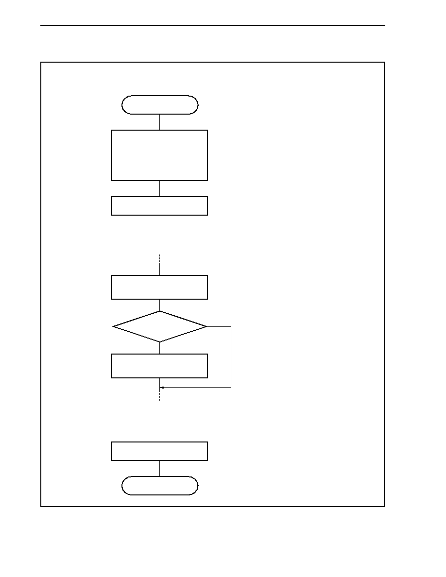
CHAPTER 8 16-BIT TIMER/EVENT COUNTER Q (TMQ)
Preliminary User's Manual U17714EJ1V0UD
394
Figure 8-33. Software Processing Flow in Free-Running Timer Mode (Capture Function) (2/2)
TQ0CE bit = 1
Read TQ0OPT0 register
(check overflow flag).
Register initial setting
TQ0CTL0 register
(TQ0CKS0 to TQ0CKS2 bits)
TQ0CTL1 register,
TQ0IOC1 register,
TQ0OPT0 register
Initial setting of these registers
is performed before setting the
TQ0CE bit to 1.
The TQ0CKS0 to TQ0CKS2 bits can
be set at the same time when counting
has been started (TQ0CE bit = 1).
START
Execute instruction to clear
TQ0OVF bit (CLR TQ0OVF).
<1> Count operation start flow
<2> Overflow flag clear flow
TQ0CE bit = 0
Counter is initialized and
counting is stopped by
clearing TQ0CE bit to 0.
STOP
<3> Count operation stop flow
TQ0OVF bit = 1
NO
YES
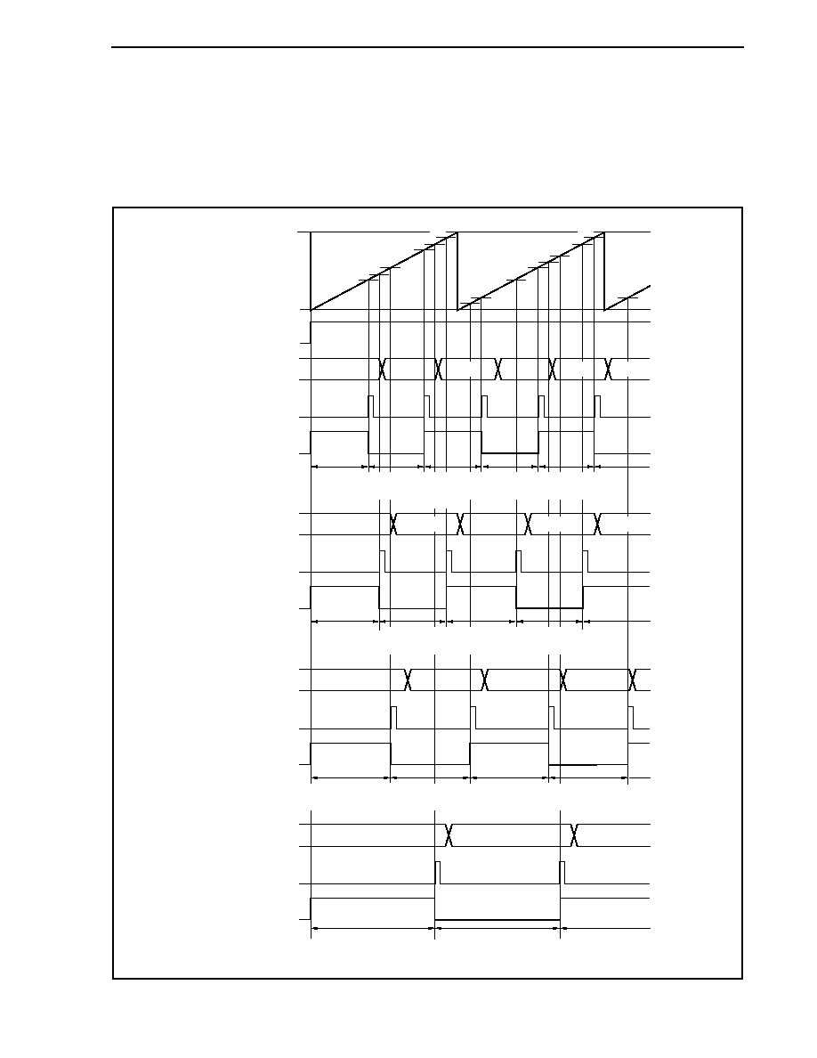
CHAPTER 8 16-BIT TIMER/EVENT COUNTER Q (TMQ)
Preliminary User's Manual U17714EJ1V0UD
395
(2) Operation timing in free-running timer mode
(a) Interval operation with compare register
When 16-bit timer/event counter Q is used as an interval timer with the TQ0CCRm register used as a
compare register, software processing is necessary for setting a comparison value to generate the next
interrupt request signal each time the INTTQ0CCm signal has been detected.
D
00
D
10
D
20
D
01
D
30
D
12
D
03
D
22
D
31
D
21
D
23
D
02
D
13
FFFFH
16-bit counter
0000H
TQ0CE bit
TQ0CCR0 register
INTTQ0CC0 signal
TOQ00 pin output
TQ0CCR1 register
INTTQ0CC1 signal
TOQ01 pin output
TQ0CCR2 register
INTTQ0CC2 signal
TOQ02 pin output
TQ0CCR3 register
INTTQ0CC3 signal
TOQ03 pin output
Interval period
(D
00
+ 1)
Interval period
(10000H +
D
02
- D
01
)
Interval period
(D
01
- D
00
)
Interval period
(D
03
- D
02
)
Interval period
(D
04
- D
03
)
D
00
D
01
D
02
D
03
D
04
D
05
Interval period
(D
10
+ 1)
Interval period
(10000H + D
12
- D
11
)
Interval period
(D
11
- D
10
)
Interval period
(D
13
- D
12
)
D
10
D
11
D
12
D
13
D
14
Interval period
(D
20
+ 1)
Interval period
(10000H + D
21
- D
20
)
Interval period
(10000H + D
23
- D
22
)
Interval period
(D
22
- D
21
)
Interval period
(D
30
+ 1)
Interval period
(10000H + D
31
- D
30)
D
20
D
21
D
22
D
23
D
31
D
30
D
32
D
04
D
11

CHAPTER 8 16-BIT TIMER/EVENT COUNTER Q (TMQ)
Preliminary User's Manual U17714EJ1V0UD
396
When performing an interval operation in the free-running timer mode, two intervals can be set with one
channel.
To perform the interval operation, the value of the corresponding TQ0CCRm register must be re-set in the
interrupt servicing that is executed when the INTTQ0CCm signal is detected.
The set value for re-setting the TQ0CCRm register can be calculated by the following expression, where
"D
m
" is the interval period.
Compare register default value: D
m
- 1
Value set to compare register second and subsequent time: Previous set value + D
m
(If the calculation result is greater than FFFFH, subtract 10000H from the result and set this value to the
register.)
Remark m = 0 to 3
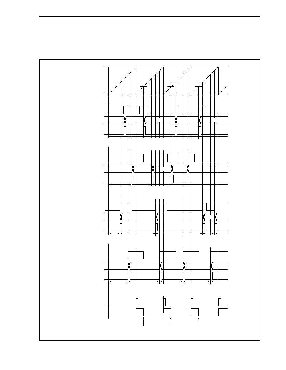
CHAPTER 8 16-BIT TIMER/EVENT COUNTER Q (TMQ)
Preliminary User's Manual U17714EJ1V0UD
397
(b) Pulse width measurement with capture register
When pulse width measurement is performed with the TQ0CCRm register used as a capture register,
software processing is necessary for reading the capture register each time the INTTQ0CCm signal has
been detected and for calculating an interval.
D
20
D
00
D
30
D
10
D
11
D
21
D
31
D
12
D
01
D
02
D
32
D
13
D
03
D
22
D
33
D
23
0000
Pulse interval
(10000H +
D
01
- D
00
)
Pulse interval
(10000H +
D
02
- D
01
)
Pulse interval
(10000H +
D
03
- D
02
)
D
00
D
01
D
02
D
03
Pulse interval
(D
00
+ 1)
0000
Pulse interval
(10000H +
D
11
- D
10
)
Pulse interval
(10000H +
D
12
- D
11
)
Pulse interval
(D
13
- D
12
)
D
10
D
11
D
12
D
13
Pulse interval
(D
10
+ 1)
0000
Pulse interval
(10000H +
D
21
- D
20
)
Pulse interval
(20000H +
D
22
- D
21
)
Pulse interval
(D
23
- D
22
)
D
20
D
21
D
23
D
22
Pulse interval
(D
20
+ 1)
0000
Pulse interval
(10000H +
D
31
- D
30
)
Pulse interval
(10000H +
D
32
- D
31
)
Pulse interval
(10000H +
D
33
- D
32
)
D
30
D
31
D
32
D
33
Pulse interval
(D
30
+ 1)
Cleared to 0 by
CLR instruction
Cleared to 0 by
CLR instruction
Cleared to 0 by
CLR instruction
FFFFH
16-bit counter
0000H
TQ0CE bit
TIQ00 pin input
TQ0CCR0 register
INTTQ0CC0 signal
TIQ02 pin input
TQ0CCR2 register
INTTQ0CC2 signal
TIQ03 pin input
TQ0CCR3 register
INTTQ0CC3 signal
INTTQ0OV signal
TQ0OVF bit
TIQ01 pin input
TQ0CCR1 register
INTTQ0CC1 signal

CHAPTER 8 16-BIT TIMER/EVENT COUNTER Q (TMQ)
Preliminary User's Manual U17714EJ1V0UD
398
When executing pulse width measurement in the free-running timer mode, four pulse widths can be
measured with one channel.
To measure a pulse width, the pulse width can be calculated by reading the value of the TQ0CCRm
register in synchronization with the INTTQ0CCm signal, and calculating the difference between the read
value and the previously read value.
Remark m = 0 to 3
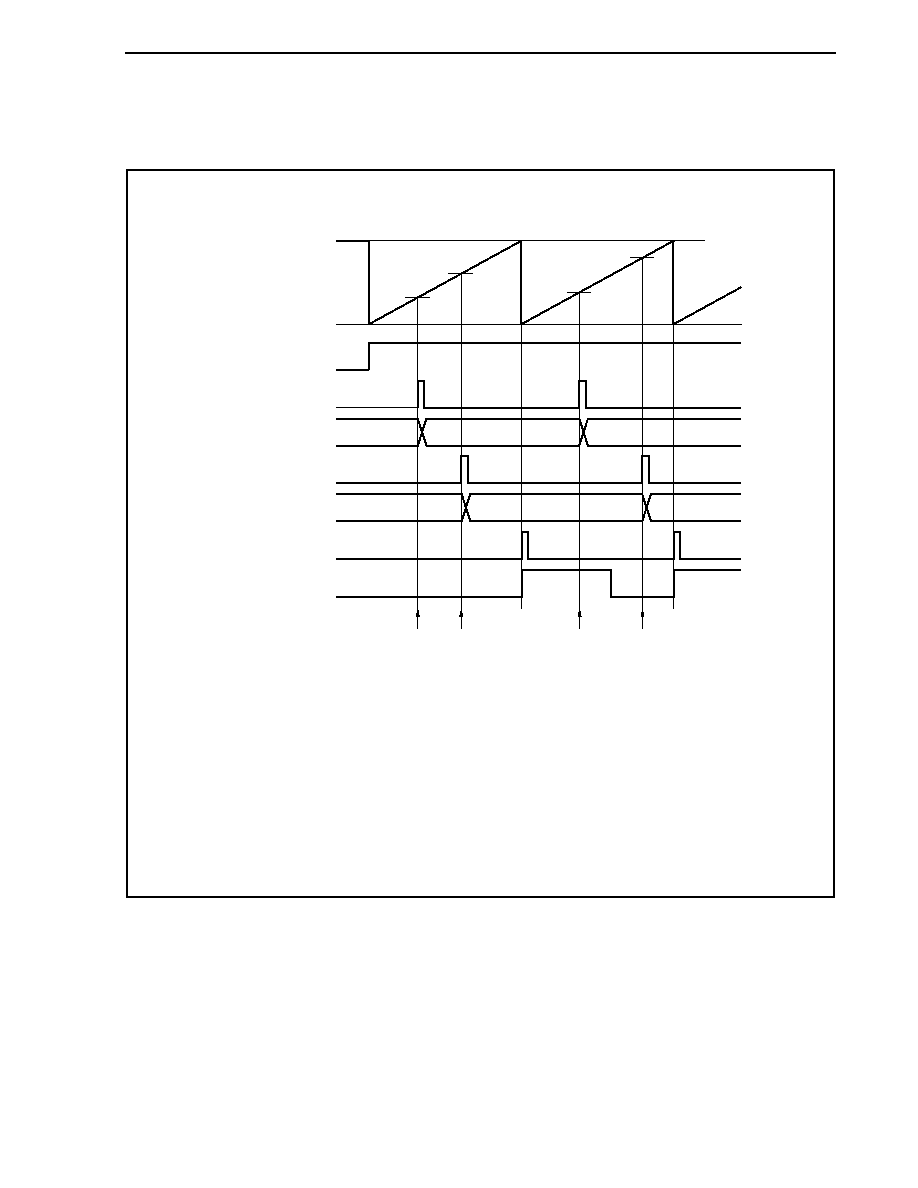
CHAPTER 8 16-BIT TIMER/EVENT COUNTER Q (TMQ)
Preliminary User's Manual U17714EJ1V0UD
399
(c) Processing of overflow when two or more capture registers are used
Care must be exercised in processing the overflow flag when two capture registers are used. First, an
example of incorrect processing is shown below.
Example of incorrect processing when two or more capture registers are used
FFFFH
16-bit counter
0000H
TQ0CE bit
TIQ00 pin input
TQ0CCR0 register
TIQ01 pin input
TQ0CCR1 register
INTTQ0OV signal
TQ0OVF bit
D
00
D
01
D
10
D
11
D
10
<1>
<2>
<3>
<4>
D
00
D
11
D
01
The following problem may occur when two pulse widths are measured in the free-running timer mode.
<1> Read the TQ0CCR0 register (setting of the default value of the TIQ00 pin input).
<2> Read the TQ0CCR1 register (setting of the default value of the TIQ01 pin input).
<3> Read the TQ0CCR0 register.
Read the overflow flag. If the overflow flag is 1, clear it to 0.
Because the overflow flag is 1, the pulse width can be calculated by (10000H + D
01
- D
00
).
<4> Read the TQ0CCR1 register.
Read the overflow flag. Because the flag is cleared in <3>, 0 is read.
Because the overflow flag is 0, the pulse width can be calculated by (D
11
- D
10
) (incorrect).
When two capture registers are used, and if the overflow flag is cleared to 0 by one capture register, the
other capture register may not obtain the correct pulse width.
Use software when using two capture registers. An example of how to use software is shown below.
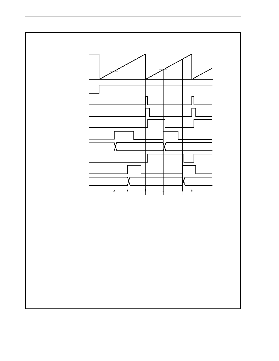
CHAPTER 8 16-BIT TIMER/EVENT COUNTER Q (TMQ)
Preliminary User's Manual U17714EJ1V0UD
400
(1/2)
Example when two capture registers are used (using overflow interrupt)
FFFFH
16-bit counter
0000H
TQ0CE bit
INTTQ0OV signal
TQ0OVF bit
TQ0OVF0 flag
Note
TIQ00 pin input
TQ0CCR0 register
TQ0OVF1 flag
Note
TIQ01 pin input
TQ0CCR1 register
D
10
D
11
D
00
D
01
D
10
<1>
<2>
<5> <6>
<3>
<4>
D
00
D
11
D
01
Note The TQ0OVF0 and TQ0OVF1 flags are set on the internal RAM by software.
<1> Read the TQ0CCR0 register (setting of the default value of the TIQ00 pin input).
<2> Read the TQ0CCR1 register (setting of the default value of the TIQ01 pin input).
<3> An overflow occurs. Set the TQ0OVF0 and TQ0OVF1 flags to 1 in the overflow interrupt servicing,
and clear the overflow flag to 0.
<4> Read the TQ0CCR0 register.
Read the TQ0OVF0 flag. If the TQ0OVF0 flag is 1, clear it to 0.
Because the TQ0OVF0 flag is 1, the pulse width can be calculated by (10000H + D
01
- D
00
).
<5> Read the TQ0CCR1 register.
Read the TQ0OVF1 flag. If the TQ0OVF1 flag is 1, clear it to 0 (the TQ0OVF0 flag is cleared in
<4>, and the TQ0OVF1 flag remains 1).
Because the TQ0OVF1 flag is 1, the pulse width can be calculated by (10000H + D
11
- D
10
)
(correct).
<6> Same as <3>

CHAPTER 8 16-BIT TIMER/EVENT COUNTER Q (TMQ)
Preliminary User's Manual U17714EJ1V0UD
401
(2/2)
Example when two capture registers are used (without using overflow interrupt)
FFFFH
16-bit counter
0000H
TQ0CE bit
INTTQ0OV signal
TQ0OVF bit
TQ0OVF0 flag
Note
TIQ00 pin input
TQ0CCR0 register
TQ0OVF1 flag
Note
TIQ01 pin input
TQ0CCR1 register
D
10
D
11
D
00
D
01
D
10
<1>
<2>
<5> <6>
<3>
<4>
D
00
D
11
D
01
Note The TQ0OVF0 and TQ0OVF1 flags are set on the internal RAM by software.
<1> Read the TQ0CCR0 register (setting of the default value of the TIQ00 pin input).
<2> Read the TQ0CCR1 register (setting of the default value of the TIQ01 pin input).
<3> An overflow occurs. Nothing is done by software.
<4> Read the TQ0CCR0 register.
Read the overflow flag. If the overflow flag is 1, set only the TQ0OVF1 flag to 1, and clear the
overflow flag to 0.
Because the overflow flag is 1, the pulse width can be calculated by (10000H + D
01
- D
00
).
<5> Read the TQ0CCR1 register.
Read the overflow flag. Because the overflow flag is cleared in <4>, 0 is read.
Read the TQ0OVF1 flag. If the TQ0OVF1 flag is 1, clear it to 0.
Because the TQ0OVF1 flag is 1, the pulse width can be calculated by (10000H + D
11
- D
10
)
(correct).
<6> Same as <3>
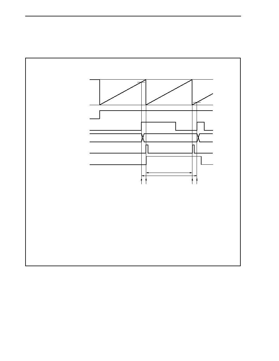
CHAPTER 8 16-BIT TIMER/EVENT COUNTER Q (TMQ)
Preliminary User's Manual U17714EJ1V0UD
402
(d) Processing of overflow if capture trigger interval is long
If the pulse width is greater than one cycle of the 16-bit counter, care must be exercised because an
overflow may occur more than once from the first capture trigger to the next. First, an example of incorrect
processing is shown below.
Example of incorrect processing when capture trigger interval is long
FFFFH
16-bit counter
0000H
TQ0CE bit
TIQ0m pin input
TQ0CCRm register
INTTQ0OV signal
TQ0OVF bit
D
m0
D
m1
D
m0
D
m1
<1> <2>
<3> <4>
1 cycle of 16-bit counter
Pulse width
The following problem may occur when a long pulse width in the free-running timer mode.
<1> Read the TQ0CCRm register (setting of the default value of the TIQ0m pin input).
<2> An overflow occurs. Nothing is done by software.
<3> An overflow occurs a second time. Nothing is done by software.
<4> Read the TQ0CCRm register.
Read the overflow flag. If the overflow flag is 1, clear it to 0.
Because the overflow flag is 1, the pulse width can be calculated by (10000H + D
m1
- D
m0
)
(incorrect).
Actually, the pulse width must be (20000H + D
m1
- D
m0
) because an overflow occurs twice.
If an overflow occurs twice or more when the capture trigger interval is long, the correct pulse width may
not be obtained.
If the capture trigger interval is long, slow the count clock to lengthen one cycle of the 16-bit counter, or
use software. An example of how to use software is shown next.
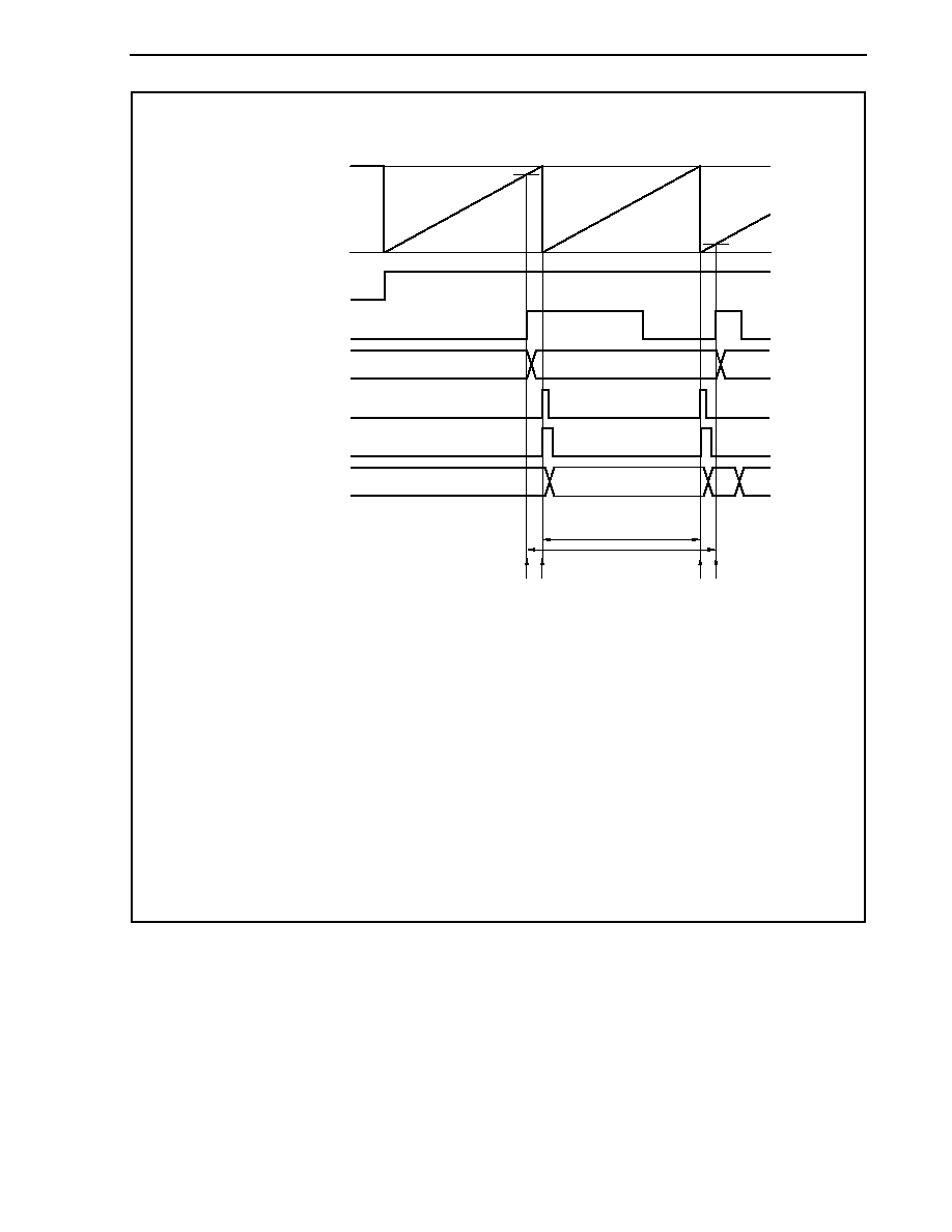
CHAPTER 8 16-BIT TIMER/EVENT COUNTER Q (TMQ)
Preliminary User's Manual U17714EJ1V0UD
403
Example when capture trigger interval is long
FFFFH
16-bit counter
0000H
TQ0CE bit
TIQ0m pin input
TQ0CCRm register
INTTQ0OV signal
TQ0OVF bit
Overflow
counter
Note
D
m0
D
m1
1H
0H
2H
0H
D
m0
D
m1
<1> <2>
<3> <4>
1 cycle of 16-bit counter
Pulse width
Note The overflow counter is set arbitrarily by software on the internal RAM.
<1> Read the TQ0CCRm register (setting of the default value of the TIQ0m pin input).
<2> An overflow occurs. Increment the overflow counter and clear the overflow flag to 0 in the overflow
interrupt servicing.
<3> An overflow occurs a second time. Increment (+1) the overflow counter and clear the overflow flag
to 0 in the overflow interrupt servicing.
<4> Read the TQ0CCRm register.
Read the overflow counter.
When the overflow counter is "N", the pulse width can be calculated by (N � 10000H + D
m1
�
D
m0
).
In this example, the pulse width is (20000H + D
m1
� D
m0
) because an overflow occurs twice.
Clear the overflow counter (0H).
CHAPTER 8 16-BIT TIMER/EVENT COUNTER Q (TMQ)
Preliminary User's Manual U17714EJ1V0UD
404
(e) Clearing overflow flag
The overflow flag can be cleared to 0 by clearing the TQ0OVF bit to 0 with the CLR instruction and by
writing 8-bit data (bit 0 is 0) to the TQ0OPT0 register. To accurately detect an overflow, read the TQ0OVF
bit when it is 1, and then clear the overflow flag by using a bit manipulation instruction.
(i) Operation to write 0 (without conflict with setting)
(iii) Operation to clear to 0 (without conflict with setting)
(ii) Operation to write 0 (conflict with setting)
(iv) Operation to clear to 0 (conflict with setting)
0 write signal
Overflow
set signal
Register
access signal
Overflow flag
(TQ0OVF bit)
Read
Write
0 write signal
Overflow
set signal
Register
access signal
Overflow flag
(TQ0OVF bit)
Read
Write
0 write signal
Overflow
set signal
0 write signal
Overflow
set signal
Overflow flag
(TQ0OVF bit)
Overflow flag
(TQ0OVF bit)
L
H
L
To clear the overflow flag to 0, read the overflow flag to check if it is set to 1, and clear it with the CLR
instruction. If 0 is written to the overflow flag without checking if the flag is 1, the set information of
overflow may be erased by writing 0 ((ii) in the above chart). Therefore, software may judge that no
overflow has occurred even when an overflow actually has occurred.
If execution of the CLR instruction conflicts with occurrence of an overflow when the overflow flag is
cleared to 0 with the CLR instruction, the overflow flag remains set even after execution of the clear
instruction.
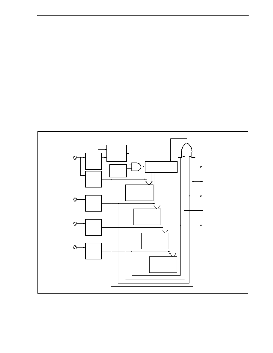
CHAPTER 8 16-BIT TIMER/EVENT COUNTER Q (TMQ)
Preliminary User's Manual U17714EJ1V0UD
405
8.5.7
Pulse width measurement mode (TQ0MD2 to TQ0MD0 bits = 110)
In the pulse width measurement mode, 16-bit timer/event counter Q starts counting when the TQ0CTL0.TQ0CE bit
is set to 1. Each time the valid edge input to the TIQ0m pin has been detected, the count value of the 16-bit counter is
stored in the TQ0CCRm register, and the 16-bit counter is cleared to 0000H.
The interval of the valid edge can be measured by reading the TQ0CCRm register after a capture interrupt request
signal (INTTQ0CCm) occurs.
Select either of the TIQ00 to TIQ03 pins as the capture trigger input pin. Specify "No edge detected" by using the
TQ0IOC1 register for the unused pins.
When an external clock is used as the count clock, measure the pulse width of the TIQ0k pin because the external
clock is fixed to the TIQ00 pin. At this time, clear the TQ0IOC1.TQ0IS1 and TQ0IOC1.TQ0IS0 bits to 00 (capture
trigger input (TIQ00 pin): No edge detected).
Remark m = 0 to 3
k = 1 to 3
Figure 8-34. Configuration in Pulse Width Measurement Mode
INTTQ0OV signal
INTTQ0CC0 signal
INTTQ0CC1 signal
INTTQ0CC2 signal
INTTQ0CC3 signal
TIQ03 pin
(capture
trigger input)
TQ0CCR3
register
(capture)
TIQ00 pin
(external
event count
input/capture
trigger input)
Internal count clock
TQ0CE
bit
TIQ01 pin
(capture
trigger input)
TIQ02 pin
(capture
trigger input)
TQ0CCR0
register
(capture)
TQ0CCR1
register
(capture)
TQ0CCR2
register
(capture)
16-bit counter
Clear
Edge
detector
Edge
detector
Edge
detector
Edge
detector
Edge
detector
Count
clock
selection
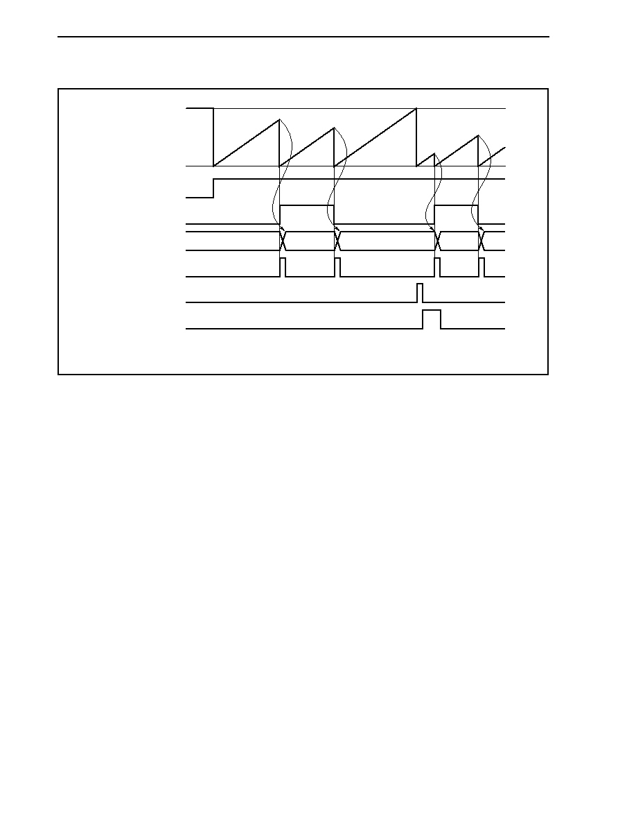
CHAPTER 8 16-BIT TIMER/EVENT COUNTER Q (TMQ)
Preliminary User's Manual U17714EJ1V0UD
406
Figure 8-35. Basic Timing in Pulse Width Measurement Mode
FFFFH
16-bit counter
0000H
TQ0CE bit
TIQ0m pin input
TQ0CCRm register
INTTQ0CCm signal
INTTQ0OV signal
TQ0OVF bit
D
0
0000H
D
1
D
2
D
3
Cleared to 0 by
CLR instruction
Remark m = 0 to 3
When the TQ0CE bit is set to 1, the 16-bit counter starts counting. When the valid edge input to the TIQ0m pin is
later detected, the count value of the 16-bit counter is stored in the TQ0CCRm register, the 16-bit counter is cleared to
0000H, and a capture interrupt request signal (INTTQ0CCm) is generated.
The pulse width is calculated as follows.
Pulse width = Captured value
� Count clock cycle
If the valid edge is not input to the TIQ0m pin even when the 16-bit counter counted up to FFFFH, an overflow
interrupt request signal (INTTQ0OV) is generated at the next count clock, and the counter is cleared to 0000H and
continues counting. At this time, the overflow flag (TQ0OPT0.TQ0OVF bit) is also set to 1. Clear the overflow flag to 0
by executing the CLR instruction via software.
If the overflow flag is set to 1, the pulse width can be calculated as follows.
Pulse width = (10000H
� TQ0OVF bit set (1) count + Captured value) � Count clock cycle
Remark m = 0 to 3
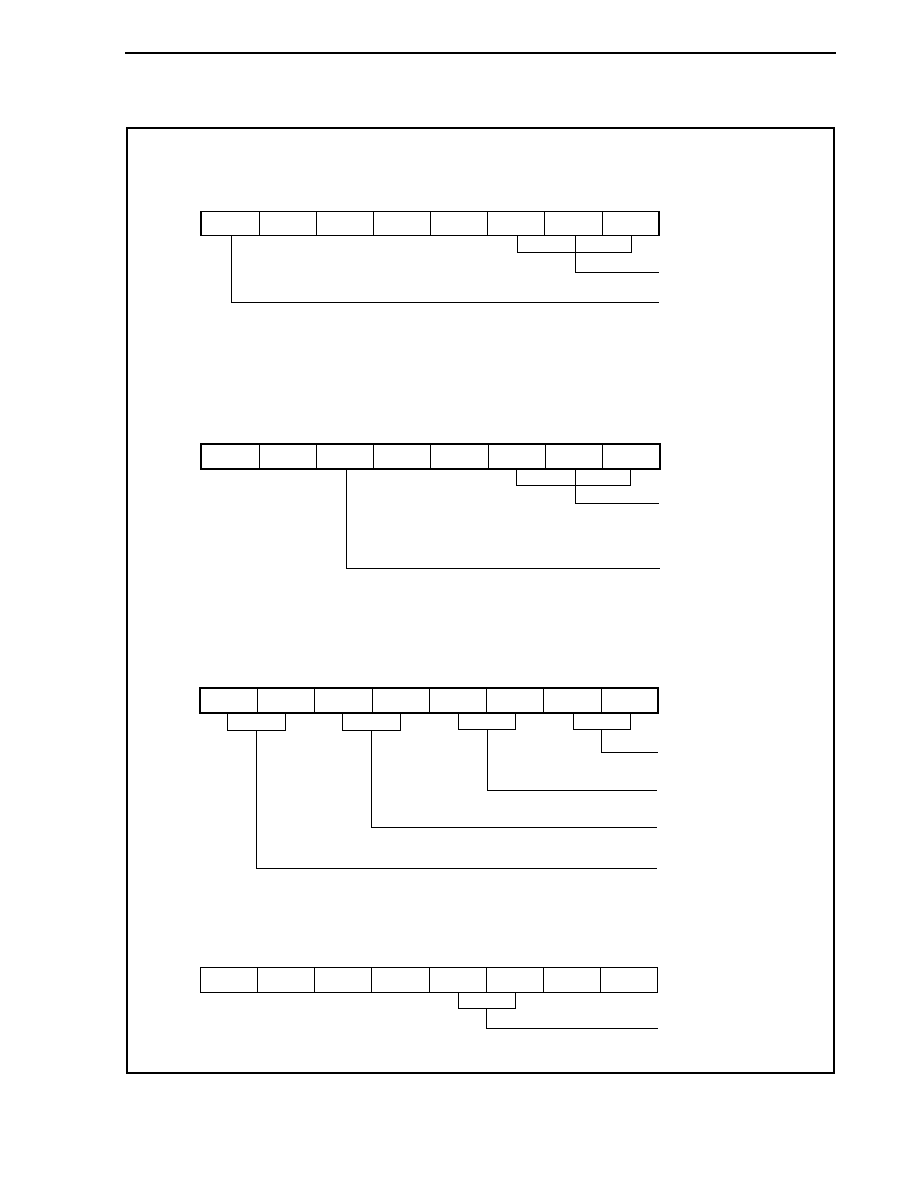
CHAPTER 8 16-BIT TIMER/EVENT COUNTER Q (TMQ)
Preliminary User's Manual U17714EJ1V0UD
407
Figure 8-36. Register Setting in Pulse Width Measurement Mode (1/2)
(a) TMQ0 control register 0 (TQ0CTL0)
0/1
0
0
0
0
TQ0CTL0
Select count clock
Note
0: Stop counting
1: Enable counting
0/1
0/1
0/1
TQ0CKS2 TQ0CKS1 TQ0CKS0
TQ0CE
Note Setting is invalid when the TQ0EEE bit = 1.
(b) TMQ0 control register 1 (TQ0CTL1)
0
0
0/1
0
0
TQ0CTL1
1
1
0
TQ0MD2 TQ0MD1 TQ0MD0
TQ0EEE
TQ0EST
1, 1, 0:
Pulse width measurement mode
0: Operate with count
clock selected by
TQ0CKS0 to TQ0CKS2 bits
1: Count external event
count input signal
(c) TMQ0 I/O control register 1 (TQ0IOC1)
0/1
0/1
0/1
0/1
0/1
TQ0IOC1
Select valid edge
of TIQ00 pin input
Select valid edge
of TIQ01 pin input
0/1
0/1
0/1
TQ0IS2
TQ0IS1
TQ0IS0
TQ0IS3
TQ0IS6
TQ0IS5
TQ0IS4
TQ0IS7
Select valid edge
of TIQ02 pin input
Select valid edge
of TIQ03 pin input
(d) TMQ0 I/O control register 2 (TQ0IOC2)
0
0
0
0
0/1
TQ0IOC2
Select valid edge of
external event count input
0/1
0
0
TQ0EES0 TQ0ETS1 TQ0ETS0
TQ0EES1

CHAPTER 8 16-BIT TIMER/EVENT COUNTER Q (TMQ)
Preliminary User's Manual U17714EJ1V0UD
408
Figure 8-36. Register Setting in Pulse Width Measurement Mode (2/2)
(e) TMQ0 option register 0 (TQ0OPT0)
0
0
0
0
0
TQ0OPT0
Overflow flag
0
0
0/1
TQ0CCS0
TQ0OVF
TQ0CCS1
TQ0CCS2
TQ0CCS3
(f) TMQ0 counter read buffer register (TQ0CNT)
The value of the 16-bit counter can be read by reading the TQ0CNT register.
(g) TMQ0 capture/compare registers 0 to 3 (TQ0CCR0 to TQ0CCR3)
These registers store the count value of the 16-bit counter when the valid edge input to the TIQ0m pin
is detected.
Remarks 1. TMQ0 I/O control register 0 (TQ0IOC0) is not used in the pulse width measurement mode.
2. m = 0 to 3
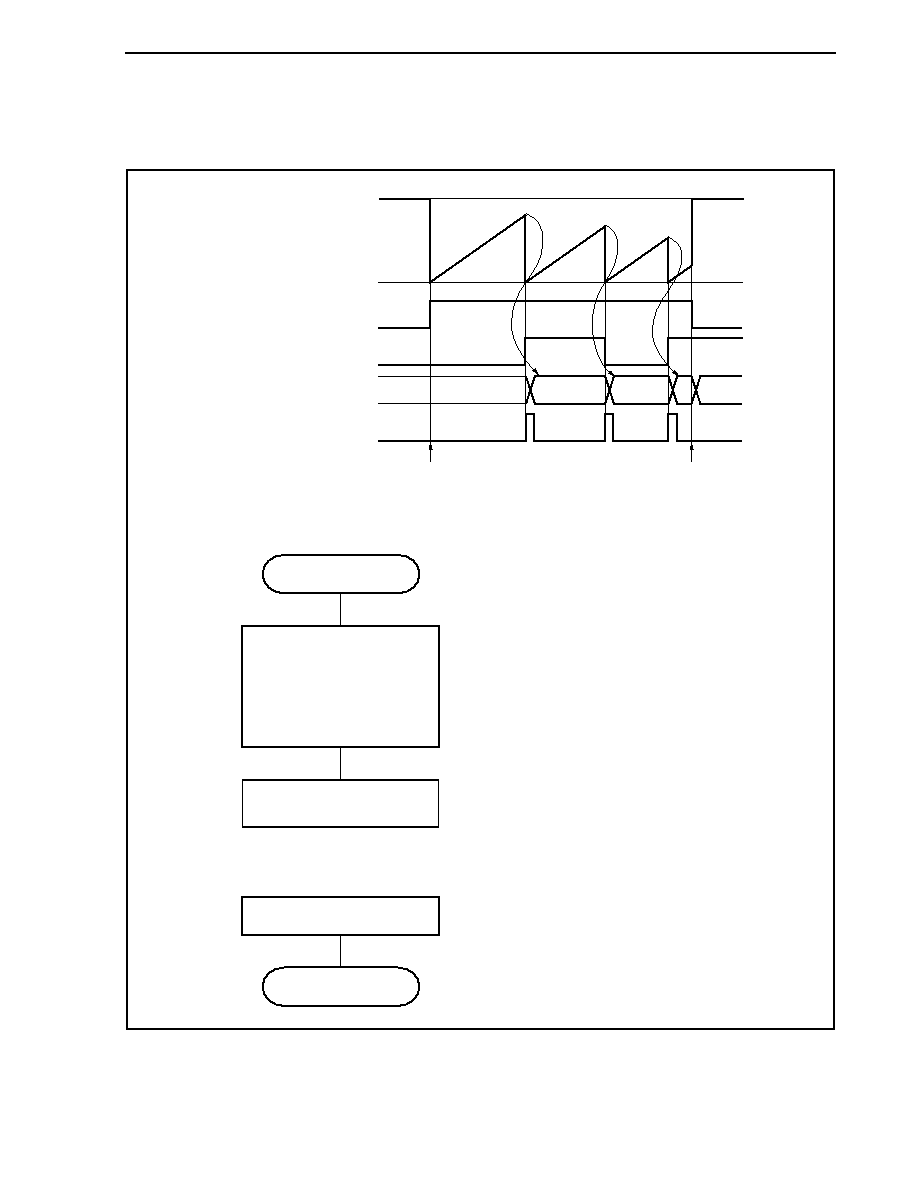
CHAPTER 8 16-BIT TIMER/EVENT COUNTER Q (TMQ)
Preliminary User's Manual U17714EJ1V0UD
409
(1) Operation flow in pulse width measurement mode
Figure 8-37. Software Processing Flow in Pulse Width Measurement Mode
<1>
<2>
Set TQ0CTL0 register
(TQ0CE bit = 1)
TQ0CE bit = 0
Register initial setting
TQ0CTL0 register
(TQ0CKS0 to TQ0CKS2 bits),
TQ0CTL1 register,
TQ0IOC1 register,
TQ0IOC2 register,
TQ0OPT0 register
Initial setting of these registers
is performed before setting the
TQ0CE bit to 1.
The TQ0CKS0 to TQ0CKS2 bits can
be set at the same time when counting
has been started (TQ0CE bit = 1).
The counter is initialized and counting
is stopped by clearing the TQ0CE bit to 0.
START
STOP
<1> Count operation start flow
<2> Count operation stop flow
FFFFH
16-bit counter
0000H
TQ0CE bit
TIQ00 pin input
TQ0CCR0 register
INTTQ0CC0 signal
D
0
0000H
0000H
D
1
D
2
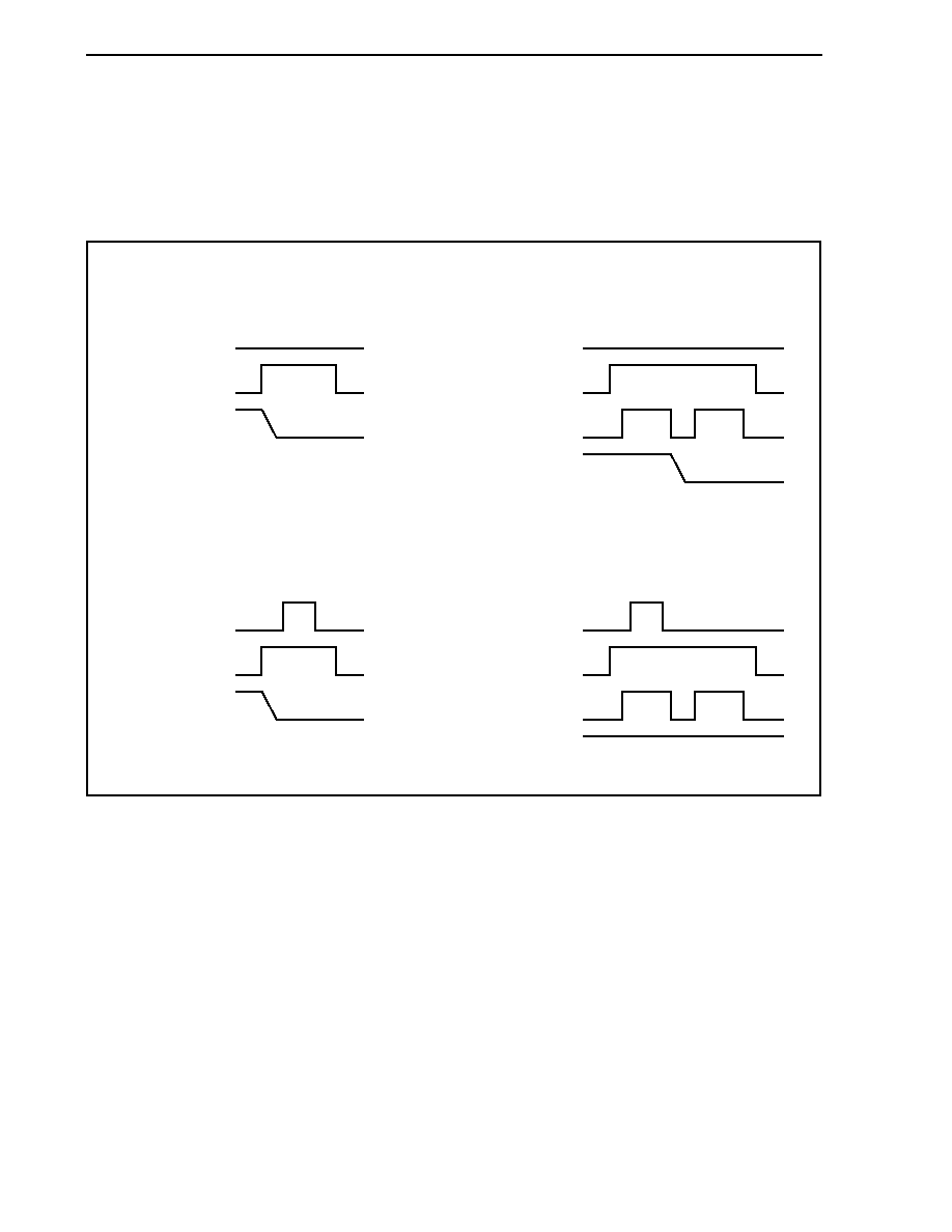
CHAPTER 8 16-BIT TIMER/EVENT COUNTER Q (TMQ)
Preliminary User's Manual U17714EJ1V0UD
410
(2) Operation timing in pulse width measurement mode
(a) Clearing overflow flag
The overflow flag can be cleared to 0 by clearing the TQ0OVF bit to 0 with the CLR instruction and by
writing 8-bit data (bit 0 is 0) to the TQ0OPT0 register. To accurately detect an overflow, read the TQ0OVF
bit when it is 1, and then clear the overflow flag by using a bit manipulation instruction.
(i) Operation to write 0 (without conflict with setting)
(iii) Operation to clear to 0 (without conflict with setting)
(ii) Operation to write 0 (conflict with setting)
(iv) Operation to clear to 0 (conflict with setting)
0 write signal
Overflow
set signal
Register
access signal
Overflow flag
(TQ0OVF bit)
Read
Write
0 write signal
Overflow
set signal
Register
access signal
Overflow flag
(TQ0OVF bit)
Read
Write
0 write signal
Overflow
set signal
0 write signal
Overflow
set signal
Overflow flag
(TQ0OVF bit)
Overflow flag
(TQ0OVF bit)
L
H
L
To clear the overflow flag to 0, read the overflow flag to check if it is set to 1, and clear it with the CLR
instruction. If 0 is written to the overflow flag without checking if the flag is 1, the set information of
overflow may be erased by writing 0 ((ii) in the above chart). Therefore, software may judge that no
overflow has occurred even when an overflow actually has occurred.
If execution of the CLR instruction conflicts with occurrence of an overflow when the overflow flag is
cleared to 0 with the CLR instruction, the overflow flag remains set even after execution of the clear
instruction.
CHAPTER 8 16-BIT TIMER/EVENT COUNTER Q (TMQ)
Preliminary User's Manual U17714EJ1V0UD
411
8.5.8 Timer
output
operations
The following table shows the operations and output levels of the TOQ00 to TOQ03 pins.
Table 8-6. Timer Output Control in Each Mode
Operation Mode
TOQ00 Pin
TOQ01 Pin
TOQ02 Pin
TOQ03 Pin
Interval timer mode
Square wave output
External event count mode
Square wave output
-
External trigger pulse output mode
External trigger pulse
output
External trigger pulse
output
External trigger pulse
output
One-shot pulse output mode
One-shot pulse
output
One-shot pulse
output
One-shot pulse
output
PWM output mode
Square wave output
PWM output
PWM output
PWM output
Free-running timer mode
Square wave output (only when compare function is used)
Pulse width measurement mode
-
Table 8-7. Truth Table of TOQ00 to TOQ03 Pins Under Control of Timer Output Control Bits
TQ0IOC0.TQ0OLm Bit
TQ0IOC0.TQ0OEm Bit
TQ0CTL0.TQ0CE Bit
Level of TOQ0m Pin
0
�
Low-level output
0 Low-level
output
0
1
1
Low level immediately before counting, high
level after counting is started
0
�
High-level output
0 High-level
output
1
1
1
High level immediately before counting, low level
after counting is started
Remark m = 0 to 3
CHAPTER 8 16-BIT TIMER/EVENT COUNTER Q (TMQ)
Preliminary User's Manual U17714EJ1V0UD
412
8.6 Cautions
(1) Capture operation
When the capture operation is used and a slow clock is selected as the count clock, FFFFH, not 0000H, may
be captured in the TQ0CCR0, TQ0CCR1, TQ0CCR2, and TQ0CCR3 registers if the capture trigger is input
immediately after the TQ0CE bit is set to 1.
(a) Free-running timer mode
Count clock
0000H
FFFFH
TQ0CE bit
TQ0CCR0 register
FFFFH
0001H
0000H
TIQ00 pin input
Capture
trigger input
16-bit counter
Sampling clock (f
XX
)
Capture
trigger input
(b) Pulse width measurement mode
0000H
FFFFH
FFFFH
0002H
0000H
Count clock
TQ0CE bit
TQ0CCR0 register
TIQ00 pin input
Capture
trigger input
16-bit counter
Sampling clock (f
XX
)
Capture
trigger input

Preliminary User's Manual U17714EJ1V0UD
413
CHAPTER 9 16-BIT INTERVAL TIMER M (TMM)
9.1 Overview
� Interval function
� 8 clocks selectable
� 16-bit counter � 1
(The 16-bit counter cannot be read during timer count operation.)
� Compare register � 1
(The compare register cannot be written during timer counter operation.)
� Compare match interrupt � 1
Timer M supports only the clear & start mode. The free-running timer mode is not supported.
CHAPTER 9 16-BIT INTERVAL TIMER M (TMM)
Preliminary User's Manual U17714EJ1V0UD
414
9.2 Configuration
TMM0 includes the following hardware.
Table 9-1. Configuration of TMM0
Item Configuration
Timer register
16-bit counter
Register
TMM0 compare register 0 (TM0CMP0)
Control register
TMM0 control register 0 (TM0CTL0)
Figure 9-1. Block Diagram of TMM0
TM0CTL0
Internal bus
f
XX
f
XX
/2
f
XX
/4
f
XX
/64
f
XX
/512
INTWT
f
R
/8
f
XT
Controller
16-bit counter
Match
Clear
INTTM0EQ0
TM0CMP0
TM0CE TM0CKS2 TM0CKS1TM0CKS0
Selector
Remark f
XX
:
Main clock frequency
f
R
:
Internal oscillation clock frequency
f
XT
:
Subclock frequency
INTWT: Watch timer interrupt request signal
(1) 16-bit counter
This is a 16-bit counter that counts the internal clock.
The 16-bit counter cannot be read or written.
(2) TMM0 compare register 0 (TM0CMP0)
The TM0CMP0 register is a 16-bit compare register.
This register can be read or written in 16-bit units.
Reset sets this register to 0000H.
The same value can always be written to the TM0CMP0 register by software.
TM0CMP0 register rewrite is prohibited when the TM0CTL0.TM0CE bit = 1.
TM0CMP0
12
10
8
6
4
2
After reset: 0000H R/W Address: FFFFF694H
14
0
13
11
9
7
5
3
15
1
CHAPTER 9 16-BIT INTERVAL TIMER M (TMM)
Preliminary User's Manual U17714EJ1V0UD
415
9.3 Register
(1) TMM0 control register (TM0CTL0)
The TM0CTL0 register is an 8-bit register that controls the TMM0 operation.
This register can be read or written in 8-bit or 1-bit units.
Reset sets this register to 00H.
The same value can always be written to the TM0CTL0 register by software.
TM0CE
TMM0 operation disabled (16-bit counter reset asynchronously).
Operation clock application stopped.
TMM0 operation enabled. Operation clock application started. TMM0
operation started.
TM0CE
0
1
Internal clock operation enable/disable specification
TM0CTL0
0
0
0
0
TM0CKS2 TM0CKS1 TM0CKS0
6
5
4
3
2
1
After reset: 00H R/W Address: FFFFF690H
The internal clock control and internal circuit reset for TMM0 are performed
asynchronously with the TM0CE bit. When the TM0CE bit is cleared to 0, the
internal clock of TMM0 is disabled (fixed to low level) and 16-bit counter is reset
asynchronously.
<7>
0
f
XX
f
XX
/2
f
XX
/4
f
XX
/64
f
XX
/512
INTWT
f
R
/8
f
XT
TM0CKS2
0
0
0
0
1
1
1
1
Count clock selection
TM0CKS1
0
0
1
1
0
0
1
1
TM0CKS0
0
1
0
1
0
1
0
1
Cautions 1. Set the TM0CKS2 to TM0CKS0 bits when TM0CE bit = 0.
When changing the value of TM0CE from 0 to 1, it is not possible to set
the value of the TM0CKS2 to TM0CKS0 bits simultaneously.
2. Be sure to clear bits 3 to 6 to "0".
Remark f
XX
: Main clock frequency
f
R
: Internal oscillation clock frequency
f
XT
: Subclock frequency
CHAPTER 9 16-BIT INTERVAL TIMER M (TMM)
Preliminary User's Manual U17714EJ1V0UD
416
9.4 Operation
Caution Do not set the TM0CMP0 register to FFFFH.
9.4.1
Interval timer mode
In the interval timer mode, an interrupt request signal (INTTM0EQ0) is generated at the specified interval if the
TM0CTL0.TM0CE bit is set to 1.
Figure 9-2. Configuration of Interval Timer
16-bit counter
TM0CMP0 register
TM0CE bit
Count clock
selection
Clear
Match signal
INTTM0EQ0 signal
Figure 9-3. Basic Timing of Operation in Interval Timer Mode
FFFFH
16-bit counter
0000H
TM0CE bit
TM0CMP0 register
INTTM0EQ0 signal
D
D
D
D
D
Interval (D + 1)
Interval (D + 1)
Interval (D + 1)
Interval (D + 1)
When the TM0CE bit is set to 1, the value of the 16-bit counter is cleared from FFFFH to 0000H in synchronization
with the count clock, and the counter starts counting.
When the count value of the 16-bit counter matches the value of the TM0CMP0 register, the 16-bit counter is
cleared to 0000H and a compare match interrupt request signal (INTTM0EQ0) is generated.
The interval can be calculated by the following expression.
Interval = (Set value of TM0CMP0 register + 1)
� Count clock cycle
CHAPTER 9 16-BIT INTERVAL TIMER M (TMM)
Preliminary User's Manual U17714EJ1V0UD
417
Figure 9-4. Register Setting for Interval Timer Mode Operation
(a) TMM0 control register 0 (TM0CTL0)
0/1
0
0
0
0
TM0CTL0
0/1
0/1
0/1
TM0CKS2 TM0CKS1 TM0CKS0
TM0CE
0: Stop counting
1: Enable counting
Select count clock
(b) TMM0 compare register 0 (TM0CMP0)
If the TM0CMP0 register is set to D, the interval is as follows.
Interval = (D + 1)
� Count clock cycle
CHAPTER 9 16-BIT INTERVAL TIMER M (TMM)
Preliminary User's Manual U17714EJ1V0UD
418
(1) Interval timer mode operation flow
Figure 9-5. Software Processing Flow in Interval Timer Mode
FFFFH
16-bit counter
0000H
TM0CE bit
TM0CMP0 register
INTTM0EQ0 signal
D
D
D
D
<1>
<2>
TM0CE bit = 1
TM0CE bit = 0
Register initial setting
TM0CTL0 register
(TM0CKS0 to TM0CKS2 bits)
TM0CMP0 register
Initial setting of these registers is performed
before setting the TM0CE bit to 1.
The TM0CKS0 to TM0CKS2 bits can be
set at the same time when counting has
been started (TM0CE bit = 1).
The counter is initialized and counting is
stopped by clearing the TM0CE bit to 0.
START
STOP
<1> Count operation start flow
<2> Count operation stop flow
CHAPTER 9 16-BIT INTERVAL TIMER M (TMM)
Preliminary User's Manual U17714EJ1V0UD
419
(2) Interval timer mode operation timing
Caution Do not set the TM0CMP0 register to FFFFH.
(a) Operation if TM0CMP0 register is set to 0000H
If the TM0CMP0 register is set to 0000H, the INTTM0EQ0 signal is generated at each count clock.
The value of the 16-bit counter is always 0000H.
Count clock
16-bit counter
TM0CE bit
TM0CMP0 register
INTTM0EQ0 signal
0000H
Interval time
Count clock cycle
FFFFH
0000H
0000H
0000H
0000H
Interval time
Count clock cycle
(b) Operation if TM0CMP0 register is set to N
If the TM0CMP0 register is set to N, the 16-bit counter counts up to N. The counter is cleared to 0000H in
synchronization with the next count-up timing and the INTTM0EQ0 signal is generated.
FFFFH
16-bit counter
0000H
TM0CE bit
TM0CMP0 register
INTTM0EQ0 signal
N
Interval time
(N + 1)
�
count clock cycle
Interval time
(N + 1)
�
count clock cycle
Interval time
(N + 1)
�
count clock cycle
N
Remark 0000H < N < FFFFH
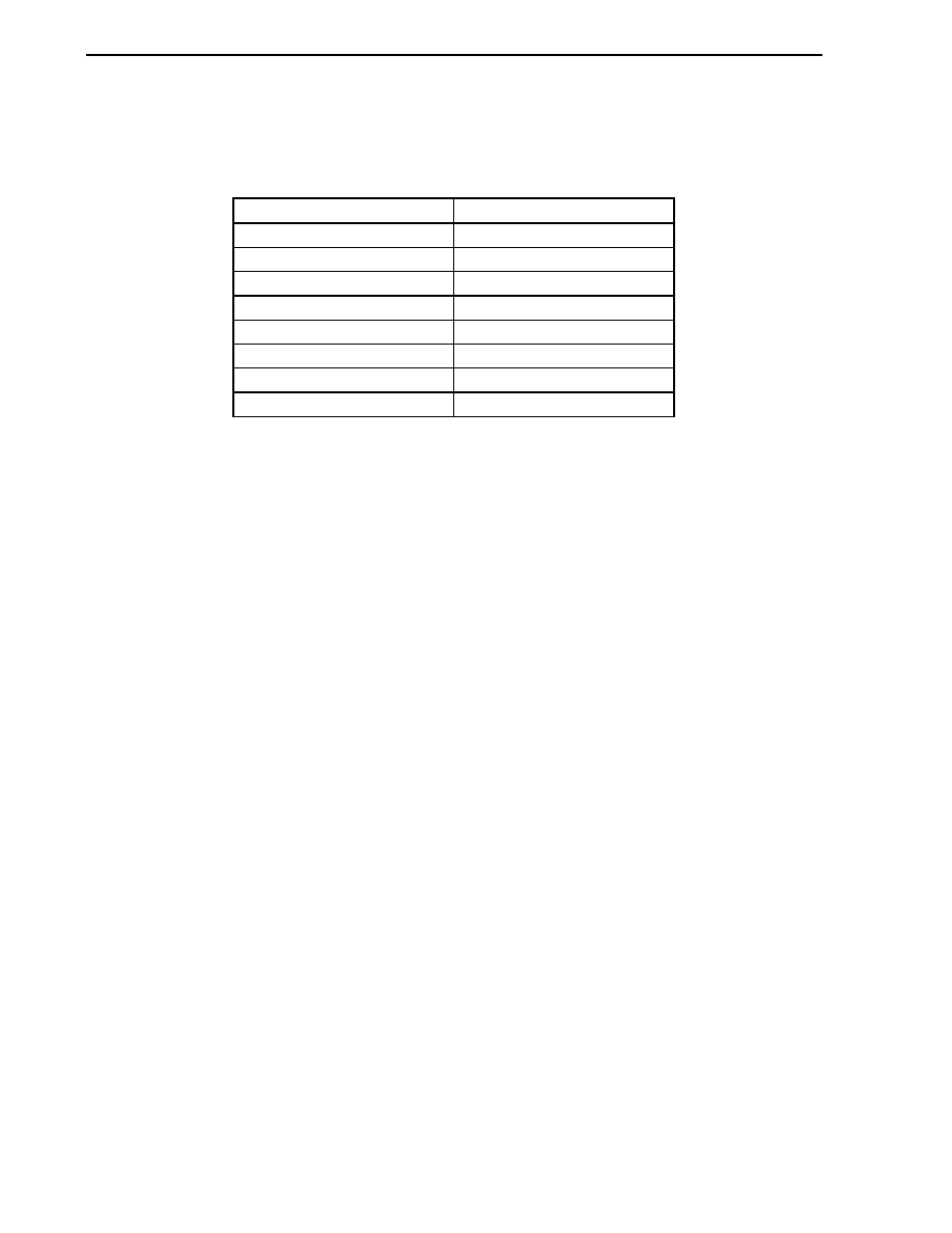
CHAPTER 9 16-BIT INTERVAL TIMER M (TMM)
Preliminary User's Manual U17714EJ1V0UD
420
9.4.2 Cautions
(1) It takes the 16-bit counter up to the following time to start counting after the TM0CTL0.TM0CE bit is set to 1,
depending on the count clock selected.
Selected Count Clock
Maximum Time Before Counting Start
f
XX
2/f
XX
f
XX
/2 6/f
XX
f
XX
/4 24/f
XX
f
XX
/64 128/f
XX
f
XX
/512 1024/f
XX
INTWT
Second rising edge of INTWT signal
f
R
/8 16/f
R
f
XT
2/f
XT
(2) Rewriting the TM0CMP0 and TM0CTL0 registers is prohibited while TMM0 is operating.
If these registers are rewritten while the TM0CE bit is 1, the operation cannot be guaranteed.
If they are rewritten by mistake, clear the TM0CTL0.TM0CE bit to 0, and re-set the registers.

Preliminary User's Manual U17714EJ1V0UD
421
CHAPTER 10 WATCH TIMER FUNCTIONS
10.1 Functions
The watch timer has the following functions.
� Watch timer: An interrupt request signal (INTWT) is generated at intervals of 0.5 or 0.25 seconds by using the
main clock or subclock.
� Interval timer: An interrupt request signal (INTWTI) is generated at set intervals.
The watch timer and interval timer functions can be used at the same time.
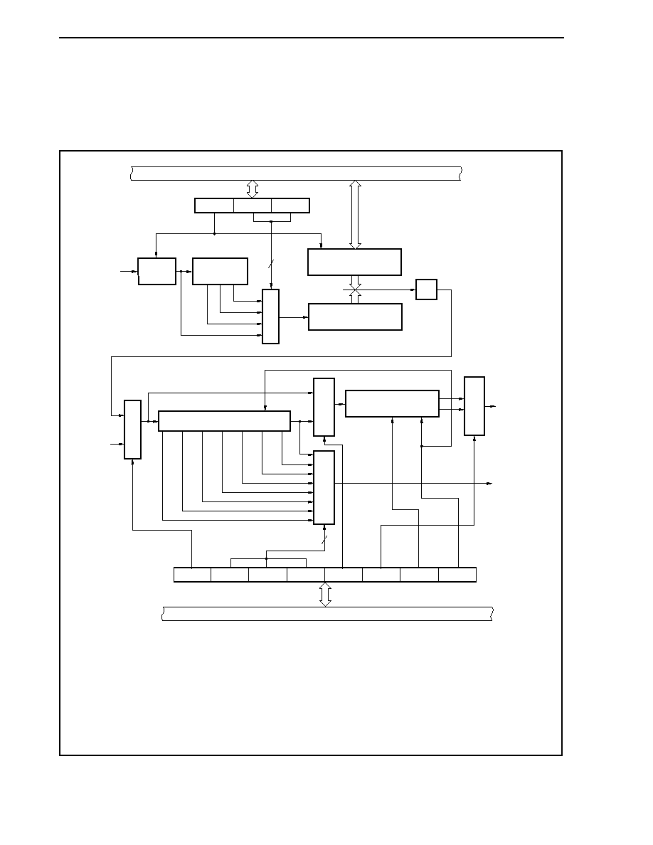
CHAPTER 10 WATCH TIMER FUNCTIONS
Preliminary User's Manual U17714EJ1V0UD
422
10.2 Configuration
The block diagram of the watch timer is shown below.
Figure 10-1. Block Diagram of Watch Timer
Internal bus
Watch timer operation mode register
(WTM)
f
BRG
f
W
/2
4
f
W
/2
5
f
W
/2
6
f
W
/2
7
f
W
/2
8
f
W
/2
10
f
W
/2
11
f
W
/2
9
f
XT
11-bit prescaler
Clear
Clear
INTWT
INTWTI
WTM0
WTM1
WTM2
WTM3
WTM4
WTM5
WTM6
WTM7
5-bit counter
f
W
3
f
X
f
X
/8
f
X
/4
f
X
/2
f
X
BGCS00
BGCS01
BGCE0
3-bit
prescaler
8-bit counter
Clear
Match
f
BGCS
PRSM0 register
PRSCM0 register
1/2
2
Internal bus
Clock
control
Selector
Selector
Selector
Selector
Selector
Remark f
X
:
Main clock oscillation frequency
f
BGCS
:
Watch timer source clock frequency
f
BRG
:
Watch timer count clock frequency
f
XT
: Subclock
frequency
f
W
:
Watch timer clock frequency
INTWT: Watch timer interrupt request signal
INTWTI: Interval timer interrupt request signal

CHAPTER 10 WATCH TIMER FUNCTIONS
Preliminary User's Manual U17714EJ1V0UD
423
(1) Clock
control
This block controls supplying and stopping the operating clock (f
X
) when the watch timer operates on the main
clock.
(2) 3-bit
prescaler
This prescaler divides f
X
to generate f
X
/2, f
X
/4, or f
X
/8.
(3) 8-bit
counter
This 8-bit counter counts the source clock (f
BGCS
).
(4) 11-bit
prescaler
This prescaler divides f
W
to generate a clock of f
W
/2
4
to f
W
/2
11
.
(5) 5-bit
counter
This counter counts f
W
or f
W
/2
9
, and generates a watch timer interrupt request signal at intervals of 2
4
/f
W
, 2
5
/f
W
,
2
12
/f
W
, or 2
14
/f
W
.
(6) Selector
The watch timer has the following five selectors.
� Selector that selects one of f
X
, f
X
/2, f
X
/4, or f
X
/8 as the source clock of the watch timer
� Selector that selects the main clock (f
X
) or subclock (f
XT
) as the clock of the watch timer
� Selector that selects f
W
or f
W
/2
9
as the count clock frequency of the 5-bit counter
� Selector that selects 2
4
/f
W
, 2
13
/f
W
, 2
5
/f
W
, or 2
14
/f
W
as the INTWT signal generation time interval
� Selector that selects 2
4
/f
W
to 2
11
/f
W
as the interval timer interrupt request signal (INTWTI) generation time
interval
(7) PRSCM
register
This is an 8-bit compare register that sets the interval time.
(8) PRSM
register
This register controls clock supply to the watch timer.
(9) WTM
register
This is an 8-bit register that controls the operation of the watch timer/interval timer, and sets the interrupt
request signal generation interval.
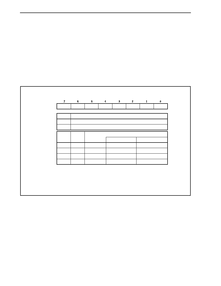
CHAPTER 10 WATCH TIMER FUNCTIONS
Preliminary User's Manual U17714EJ1V0UD
424
10.3 Control Registers
The following registers are provided for the watch timer.
� Prescaler mode register 0 (PRSM0)
� Prescaler compare register 0 (PRSCM0)
� Watch timer operation mode register (WTM)
(1) Prescaler mode register 0 (PRSM0)
The PRSM0 register controls the generation of the watch timer count clock.
This register can be read or written in 8-bit or 1-bit units.
Reset sets this register to 00H.
0
PRSM0
0
0
BGCE0
0
0
BGCS01 BGCS00
Disabled
Enabled
BGCE0
0
1
Main clock operation enable
f
X
f
X
/2
f
X
/4
f
X
/8
5 MHz
200 ns
400 ns
800 ns
1.6 s
4 MHz
250 ns
500 ns
1 s
2 s
BGCS01
0
0
1
1
BGCS00
0
1
0
1
Selection of watch timer source clock (f
BGCS
)
After reset: 00H R/W Address: FFFFF8B0H
�
�
< >
�
Cautions 1. Do not change the values of the BGCS00 and BGCS01 bits during watch timer operation.
2. Set the PRSM0 register before setting the BGCE0 bit to 1.
3. Set the PRSM0 and PRSCM0 registers according to the main clock frequency that is used
so as to obtain an f
BRG
frequency of 32.768 kHz.
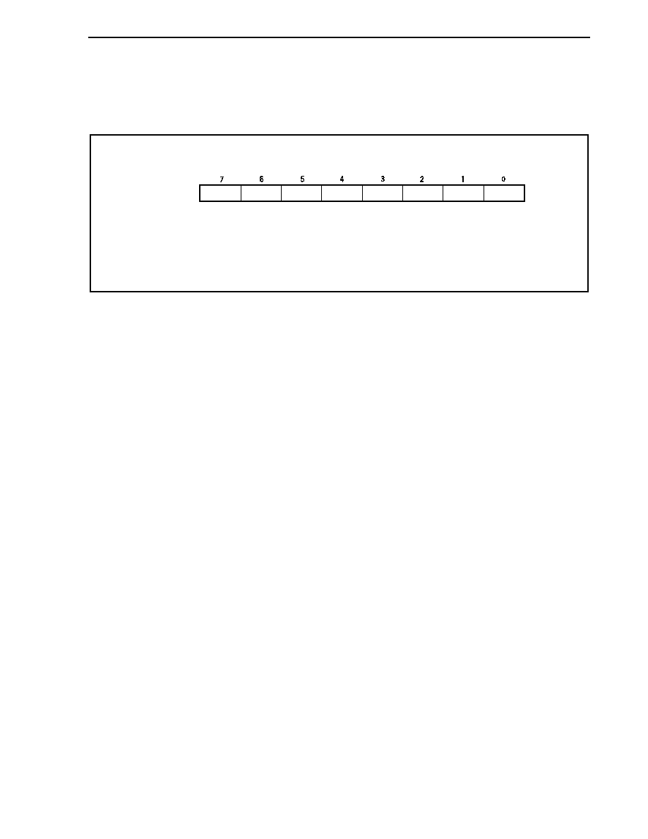
CHAPTER 10 WATCH TIMER FUNCTIONS
Preliminary User's Manual U17714EJ1V0UD
425
(2) Prescaler compare register 0 (PRSCM0)
The PRSCM0 register is an 8-bit compare register.
This register can be read or written in 8-bit units.
Reset sets this register to 00H.
PRSCM07
PRSCM0
PRSCM06 PRSCM05 PRSCM04 PRSCM03 PRSCM02 PRSCM01 PRSCM00
After reset: 00H R/W Address: FFFFF8B1H
Cautions 1. Do not rewrite the PRSCM0 register during watch timer operation.
2. Set the PRSCM0 register before setting the PRSM0.BGCE0 bit to 1.
3. Set the PRSM0 and PRSCM0 registers according to the main clock frequency that is used
so as to obtain an f
BRG
frequency of 32.768 kHz.
The calculation for f
BRG
is shown below.
f
BRG
= f
BGCS
/2N
Remark f
BGCS
: Watch timer source clock set by the PRSM0 register
N:
Set value of PRSCM0 register = 1 to 256
However, N = 256 only when PRSCM0 register is set to 00H.
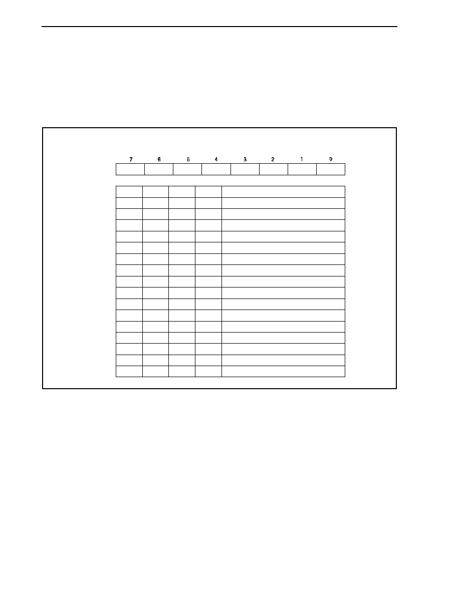
CHAPTER 10 WATCH TIMER FUNCTIONS
Preliminary User's Manual U17714EJ1V0UD
426
(3) Watch timer operation mode register (WTM)
The WTM register enables or disables the count clock and operation of the watch timer, sets the interval time
of the prescaler, controls the operation of the 5-bit counter, and sets the set time of the watch flag.
Set the PRSM0 register before setting the WTM register.
This register can be read or written in 8-bit or 1-bit units.
Reset sets this register to 00H.
(1/2)
WTM7
2
4
/f
W
(488 s: f
W
= f
XT
)
2
5
/f
W
(977 s: f
W
= f
XT
)
2
6
/f
W
(1.95 ms: f
W
= f
XT
)
2
7
/f
W
(3.91 ms: f
W
= f
XT
)
2
8
/f
W
(7.81 ms: f
W
= f
XT
)
2
9
/f
W
(15.6 ms: f
W
= f
XT
)
2
10
/f
W
(31.3 ms: f
W
= f
XT
)
2
11
/f
W
(62.5 ms: f
W
= f
XT
)
2
4
/f
W
(488 s: f
W
= f
BRG
)
2
5
/f
W
(977 s: f
W
= f
BRG
)
2
6
/f
W
(1.95 ms: f
W
= f
BRG
)
2
7
/f
W
(3.90 ms: f
W
= f
BRG
)
2
8
/f
W
(7.81 ms: f
W
= f
BRG
)
2
9
/f
W
(15.6 ms: f
W
= f
BRG
)
2
10
/f
W
(31.2 ms: f
W
= f
BRG
)
2
11
/f
W
(62.5 ms: f
W
= f
BRG
)
WTM7
0
0
0
0
0
0
0
0
1
1
1
1
1
1
1
1
WTM6
0
0
0
0
1
1
1
1
0
0
0
0
1
1
1
1
Selection of interval time of prescaler
WTM
WTM6
WTM5
WTM4
WTM3
WTM2
WTM1
WTM0
WTM5
0
0
1
1
0
0
1
1
0
0
1
1
0
0
1
1
WTM4
0
1
0
1
0
1
0
1
0
1
0
1
0
1
0
1
After reset: 00H R/W Address: FFFFF680H
�
�
�
�
< >
< >
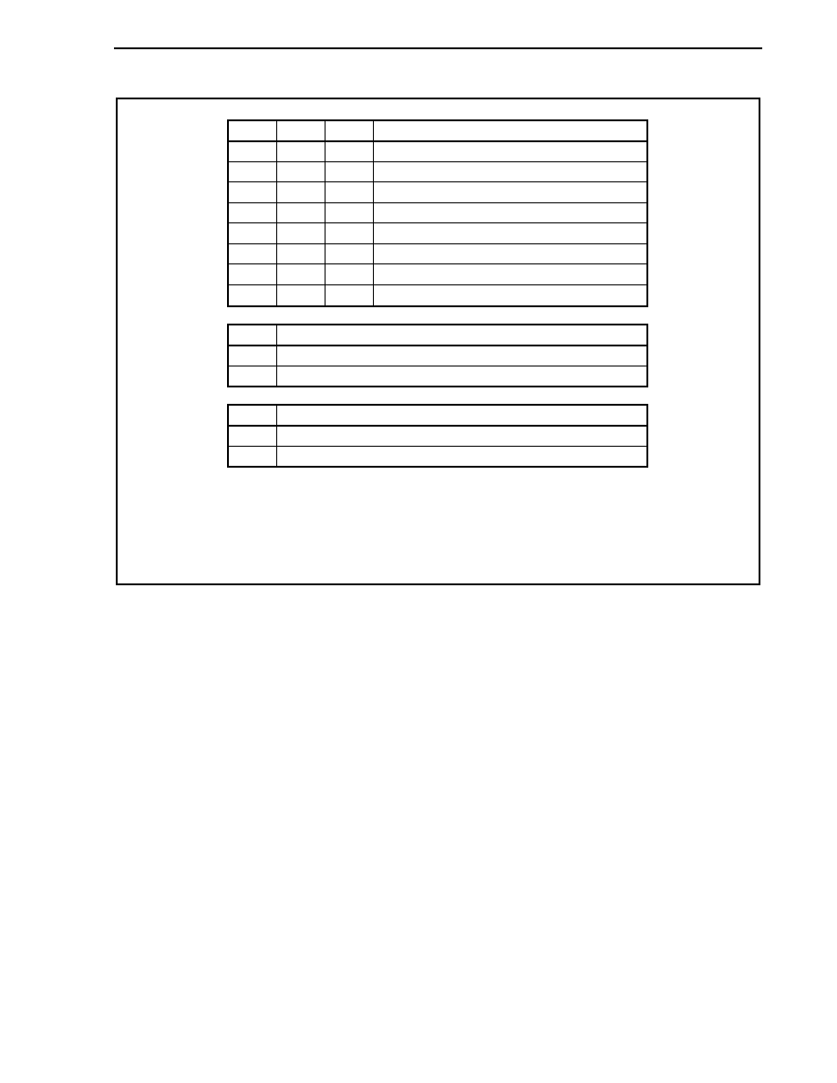
CHAPTER 10 WATCH TIMER FUNCTIONS
Preliminary User's Manual U17714EJ1V0UD
427
(2/2)
2
14
/f
W
(0.5 s: f
W
= f
XT
)
2
13
/f
W
(0.25 s: f
W
= f
XT
)
2
5
/f
W
(977 s: f
W
= f
XT
)
2
4
/f
W
(488 s: f
W
= f
XT
)
2
14
/f
W
(0.5 s: f
W
= f
BRG
)
2
13
/f
W
(0.25 s: f
W
= f
BRG
)
2
5
/f
W
(977 s: f
W
= f
BRG
)
2
4
/f
W
(488 s: f
W
= f
BRG
)
WTM7
0
0
0
0
1
1
1
1
Selection of set time of watch flag
Clears after operation stops
Starts
WTM1
0
1
Control of 5-bit counter operation
WTM3
0
0
1
1
0
0
1
1
WTM2
0
1
0
1
0
1
0
1
Stops operation (clears both prescaler and 5-bit counter)
Enables operation
WTM0
0
1
Watch timer operation enable
�
�
�
�
Caution Rewrite the WTM2 to WTM7 bits while both the WTM0 and WTM1 bits are 0.
Remarks 1. f
W
: Watch timer clock frequency
2. Values in parentheses apply to operation with f
W
= 32.768 kHz

CHAPTER 10 WATCH TIMER FUNCTIONS
Preliminary User's Manual U17714EJ1V0UD
428
10.4 Operation
10.4.1 Operation as watch timer
The watch timer generates an interrupt request signal (INTWT) at fixed time intervals. The watch timer operates
using time intervals of 0.25 or 0.5 seconds with the subclock (32.768 kHz) or main clock.
The count operation starts when the WTM.WTM1 and WTM.WTM0 bits are set to 11. When the WTM0 bit is
cleared to 0, the 11-bit prescaler and 5-bit counter are cleared and the count operation stops.
The time of the watch timer can be adjusted by clearing the WTM1 bit to 0 and then the 5-bit counter when
operating at the same time as the interval timer. At this time, an error of up to 15.6 ms may occur for the watch timer,
but the interval timer is not affected.
If the main clock is used as the count clock of the watch timer, set the count clock using the PRSM0.BGCS01 and
BGCS00 bits, the 8-bit comparison value using the PRSCM0 register, and the count clock frequency (f
BRG
) of the
watch timer to 32.768 kHz.
When the PRSM0.BGCE0 bit is set (1), f
BRG
is supplied to the watch timer.
f
BRG
can be calculated by the following expression.
f
BRG
= f
X
/(2
m+1
� N)
To set f
BRG
to 32.768 kHz, perform the following calculation and set the BGCS01 and BGCS00 bits and the
PRSCM0 register.
<1> Set N = f
X
/65,536. Set m = 0.
<2> When the value resulting from rounding up the first decimal place of N is even, set N before the roundup as
N/2 and m as m + 1.
<3> Repeat <2> until N is odd or m = 3.
<4> Set the value resulting from rounding up the first decimal place of N to the PRSCM0 register and m to the
BGCS01 and BGCS00 bits.
Example: When
f
X
= 4.00 MHz
<1> N = 4,000,000/65,536 = 61.03..., m = 0
<2>, <3> Because N (round up the first decimal place) is odd, N = 61, m = 0.
<4> Set value of PRSCM0 register: 3DH (61), set value of BGCS01 and BGCS00 bits: 00
At this time, the actual f
BRG
frequency is as follows.
f
BRG
= f
X
/(2
m+1
� N) = 4,000,000/(2 � 61)
= 32.787 kHz
Remark m: Division value (set value of BGCS01 and BGCS00 bits) = 0 to 3
N: Set value of PRSCM0 register = 1 to 256
However, N = 256 only when PRSCM0 register is set to 00H.
f
X
: Main clock oscillation frequency
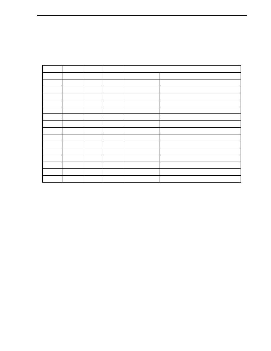
CHAPTER 10 WATCH TIMER FUNCTIONS
Preliminary User's Manual U17714EJ1V0UD
429
10.4.2 Operation as interval timer
The watch timer can also be used as an interval timer that repeatedly generates an interrupt request signal
(INTWTI) at intervals specified by a preset count value.
The interval time can be selected by the WTM4 to WTM7 bits of the WTM register.
Table 10-1. Interval Time of Interval Timer
WTM7 WTM6 WTM5 WTM4
Interval
Time
0 0 0 0
2
4
� 1/fw
488
�
s (operating at f
W
= f
XT
= 32.768 kHz)
0 0 0 1
2
5
� 1/fw
977
�
s (operating at f
W
= f
XT
= 32.768 kHz)
0 0 1 0
2
6
� 1/fw
1.95 ms (operating at f
W
= f
XT
= 32.768 kHz)
0 0 1 1
2
7
� 1/fw
3.91 ms (operating at f
W
= f
XT
= 32.768 kHz)
0 1 0 0
2
8
� 1/fw
7.81 ms (operating at f
W
= f
XT
= 32.768 kHz)
0 1 0 1
2
9
� 1/fw
15.6 ms (operating at f
W
= f
XT
= 32.768 kHz)
0 1 1 0
2
10
� 1/fw
31.3 ms (operating at f
W
= f
XT
= 32.768 kHz)
0 1 1 1
2
11
� 1/fw
62.5 ms (operating at f
W
= f
XT
= 32.768 kHz)
1 0 0 0
2
4
� 1/fw
488
�
s (operating at f
W
= f
BRG
= 32.768 kHz)
1 0 0 1
2
5
� 1/fw
977
�
s (operating at f
W
= f
BRG
= 32.768 kHz)
1 0 1 0
2
6
� 1/fw
1.95 ms (operating at f
W
= f
BRG
= 32.768 kHz)
1 0 1 1
2
7
� 1/fw
3.91 ms (operating at f
W
= f
BRG
= 32.768 kHz)
1 1 0 0
2
8
� 1/fw
7.81 ms (operating at f
W
= f
BRG
= 32.768 kHz)
1 1 0 1
2
9
� 1/fw
15.6 ms (operating at f
W
= f
BRG
= 32.768 kHz)
1 1 1 0
2
10
� 1/fw
31.3 ms (operating at f
W
= f
BRG
= 32.768 kHz)
1 1 1 1
2
11
� 1/fw
62.5 ms (operating at f
W
= f
BRG
= 32.768 kHz)
Remark f
W
: Watch timer clock frequency
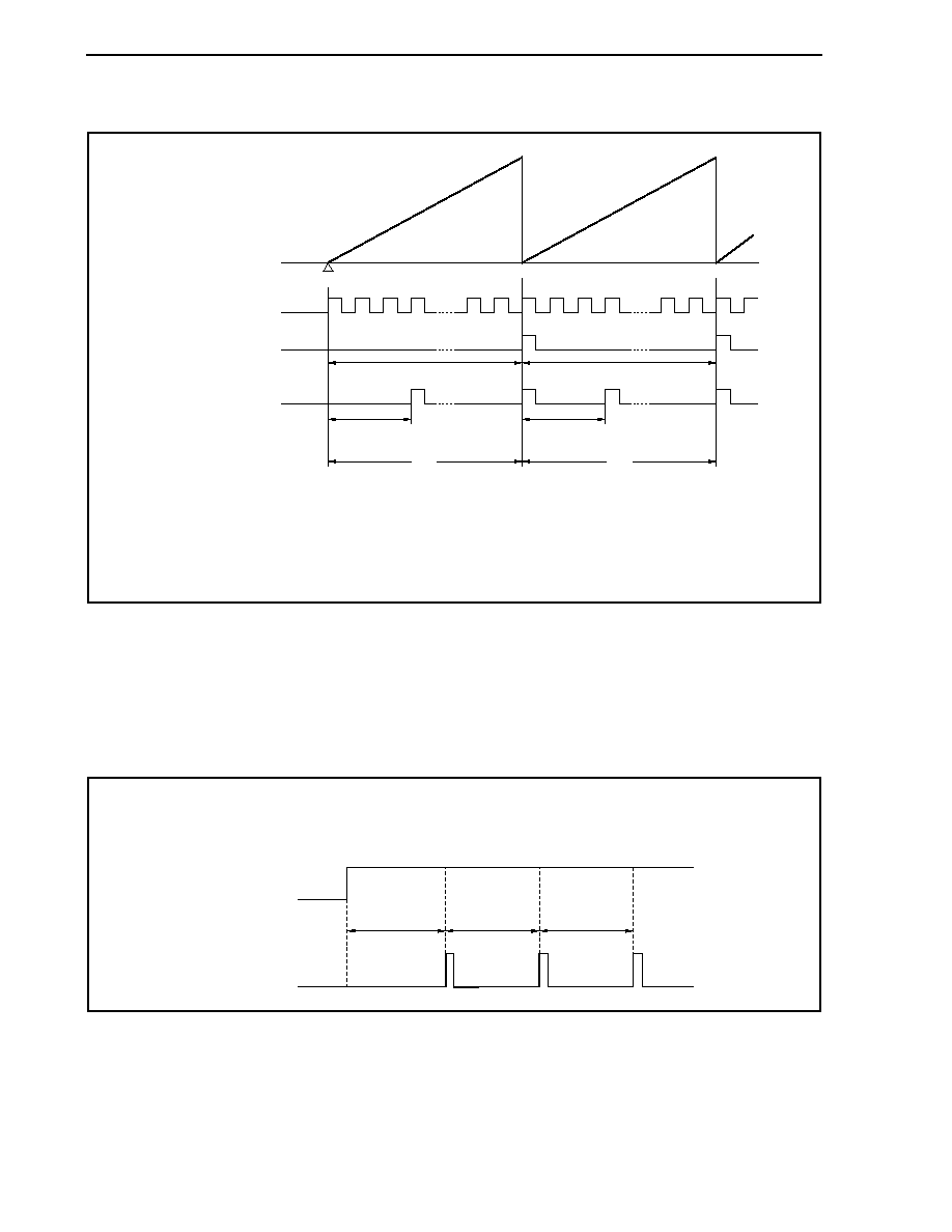
CHAPTER 10 WATCH TIMER FUNCTIONS
Preliminary User's Manual U17714EJ1V0UD
430
Figure 10-2. Operation Timing of Watch Timer/Interval Timer
Start
Overflow
Overflow
0H
Interrupt time of watch timer (0.5 s)
Interrupt time of watch timer (0.5 s)
Interval time (T)
Interval time (T)
nT
nT
5-bit counter
Count clock
f
W
or f
W
/2
9
Watch timer interrupt
INTWT
Interval timer interrupt
INTWTI
Remarks 1. When 0.5 seconds of the watch timer interrupt time is set.
2. f
W
: Watch timer clock frequency
Values in parentheses apply to operation with f
W
= 32.768 kHz.
n: Number of interval timer operations
10.4.3 Cautions
Some time is required before the first watch timer interrupt request signal (INTWT) is generated after operation is
enabled (WTM.WTM1 and WTM.WTM0 bits = 1).
Figure 10-3. Example of Generation of Watch Timer Interrupt Request Signal (INTWT)
(When Interrupt Cycle = 0.5 s)
It takes 0.515625 seconds (max.) for the first INTWT signal to be generated (2
9
� 1/32768 = 0.015625 seconds
longer (max.)). The INTWT signal is then generated every 0.5 seconds.
0.5 s
0.5 s
0.515625 s
WTM0, WTM1
INTWT

Preliminary User's Manual U17714EJ1V0UD
431
CHAPTER 11 FUNCTIONS OF WATCHDOG TIMER 2
11.1 Functions
Watchdog timer 2 has the following functions.
� Default-start watchdog timer
Note 1
Reset mode: Reset operation upon overflow of watchdog timer 2 (generation of WDT2RES signal)
Non-maskable interrupt request mode: NMI operation upon overflow of watchdog timer 2 (generation of
INTWDT2 signal)
Note 2
� Input selectable from main clock, internal oscillation clock, and subclock as the source clock
Notes 1. Watchdog timer 2 automatically starts in the reset mode following reset release.
When watchdog timer 2 is not used, either stop its operation before reset is executed via this
function, or clear watchdog timer 2 once and stop it within the next interval time.
Also, write to the WDTM2 register for verification purposes only once, even if the default settings
(reset mode, interval time: f
R
/2
19
) do not need to be changed.
2. For the non-maskable interrupt servicing due to a non-maskable interrupt request signal (INTWDT2),
see 19.2.2 (2) From INTWDT2 signal.
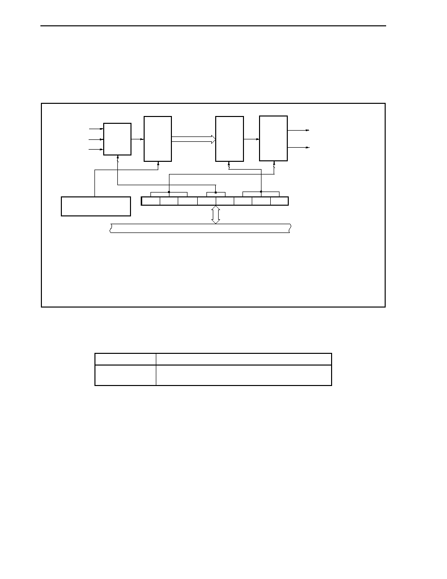
CHAPTER 11 FUNCTIONS OF WATCHDOG TIMER 2
Preliminary User's Manual U17714EJ1V0UD
432
11.2 Configuration
The following shows the block diagram of watchdog timer 2.
Figure 11-1. Block Diagram of Watchdog Timer 2
f
XX
/2
9
Clock
input
controller
Output
controller
WDT2RES
(internal reset signal)
WDCS22
Internal bus
INTWDT2
WDCS21 WDCS20
f
XT
WDCS23
WDCS24
0
WDM21 WDM20
Selector
16-bit
counter
f
XX
/2
18
to f
XX
/2
25
,
f
XT
/2
9
to f
XT
/2
16
,
f
R
/2
12
to f
R
/2
19
Watchdog timer enable
register (WDTE)
Watchdog timer mode
register 2 (WDTM2)
3
3
2
Clear
f
R
/2
3
Remark f
XX
:
Main clock frequency
f
XT
: Subclock
frequency
f
R
:
Internal oscillation clock frequency
INTWDT2:
Non-maskable interrupt request signal from watchdog timer 2
WDTRES2: Watchdog timer 2 reset signal
Watchdog timer 2 includes the following hardware.
Table 11-1. Configuration of Watchdog Timer 2
Item Configuration
Control registers
Watchdog timer mode register 2 (WDTM2)
Watchdog timer enable register (WDTE)
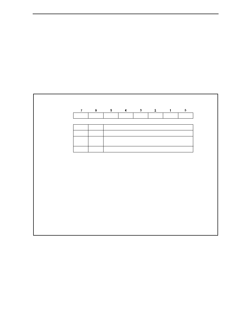
CHAPTER 11 FUNCTIONS OF WATCHDOG TIMER 2
Preliminary User's Manual U17714EJ1V0UD
433
11.3 Registers
(1) Watchdog timer mode register 2 (WDTM2)
The WDTM2 register sets the overflow time and operation clock of watchdog timer 2.
This register can be read or written in 8-bit units. This register can be read any number of times, but it can be
written only once following reset release.
Reset sets this register to 67H.
Caution Accessing the WDTM2 register is prohibited in the following statuses. For details, see 3.4.8
(2) Accessing specific on-chip peripheral I/O registers.
�
When the CPU operates with the subclock and the main clock oscillation is stopped
�
When the CPU operates with the internal oscillation clock
0
WDTM2
WDM21
WDM20 WDCS24 WDCS23 WDCS22 WDCS21 WDCS20
After reset: 67H R/W Address: FFFFF6D0H
Stops operation
Non-maskable interrupt request mode
(generation of INTWDT2 signal)
Reset mode (generation of WDT2RES signal)
WDM21
0
0
1
WDM20
0
1
�
Selection of operation mode of watchdog timer 2
Cautions 1. For details of the WDCS20 to WDCS24 bits, see Table 11-2 Watchdog Timer 2 Clock
Selection.
2. Although watchdog timer 2 can be stopped just by stopping the operation of the internal
oscillator, clear the WDTM2 register to 00H to securely stop the timer (to avoid selection
of the main clock or subclock due to an erroneous write operation).
3. If the WDTM2 register is rewritten twice after reset, an overflow signal is forcibly
generated and the counter is reset.
4. To intentionally generate an overflow signal, write to the WDTM2 register only twice or
write a value other than ACH to the WDTE register once.
5. To stop the operation of watchdog timer 2, set the RCM.RSTP bit to 1 (to stop the internal
oscillator) and write 00H in the WDTM2 register. If the RCM.RSTP bit cannot be set to 1,
set the WDCS23 bit to 1 (2
n
/f
XX
is selected and the clock can be stopped in the IDLE1,
IDLW2, sub-IDLE, and subclock operation modes).
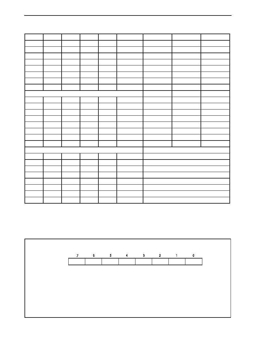
CHAPTER 11 FUNCTIONS OF WATCHDOG TIMER 2
Preliminary User's Manual U17714EJ1V0UD
434
Table 11-2. Watchdog Timer 2 Clock Selection
WDCS24 WDCS23 WDCS22 WDCS21 WDCS20
Selected Clock
100 kHz (MIN.)
200 kHz (TYP.)
400 kHz (MAX.)
0 0 0 0 0
2
12
/f
R
41.0 ms
20.5 ms
10.2 ms
0 0 0 0 1
2
13
/f
R
81.9 ms
41.0 ms
20.5 ms
0 0 0 1 0
2
14
/f
R
163.8 ms
81.9 ms
41.0 ms
0 0 0 1 1
2
15
/f
R
327.7 ms
163.8 ms
81.9 ms
0 0 1 0 0
2
16
/f
R
655.4 ms
327.7 ms
163.8 ms
0 0 1 0 1
2
17
/f
R
1,310.7 ms
655.4 ms
327.7 ms
0 0 1 1 0
2
18
/f
R
2,621.4 ms
1,310.7 ms
655.4 ms
0 0 1 1 1
2
19
/f
R
5,242.9 ms
2,621.47 ms
1,310.7 ms
f
XX
= 20 MHz
f
XX
= 16 MHz
f
XX
= 10 MHz
0 1 0 0 0
2
18
/f
XX
13.1 ms
16.4 ms
26.2 ms
0 1 0 0 1
2
19
/f
XX
26.2 ms
32.8 ms
52.4 ms
0 1 0 1 0
2
20
/f
XX
52.4 ms
65.5 ms
104.9 ms
0 1 0 1 1
2
21
/f
XX
104.9 ms
131.1 ms
209.7 ms
0 1 1 0 0
2
22
/f
XX
209.7 ms
262.1 ms
419.4 ms
0 1 1 0 1
2
23
/f
XX
419.4 ms
524.3 ms
838.9 ms
0 1 1 1 0
2
24
/f
XX
838.9 ms
1,048.6 ms
1,677.7 ms
0 1 1 1 1
2
25
/f
XX
1,677.7 ms
2,097.2 ms
3,355.4 ms
f
XT
= 32.768 kHz
1
�
0 0 0
2
9
/f
XT
15.625
ms
1
�
0 0 1
2
10
/f
XT
31.25
ms
1
�
0 1 0
2
11
/f
XT
62.5
ms
1
�
0 1 1
2
12
/f
XT
125
ms
1
�
1 0 0
2
13
/f
XT
250
ms
1
�
1 0 1
2
14
/f
XT
500
ms
1
�
1 1 0
2
15
/f
XT
1,000
ms
1
�
1 1 1
2
16
/f
XT
2,000
ms
(2) Watchdog timer enable register (WDTE)
The counter of watchdog timer 2 is cleared and counting restarted by writing "ACH" to the WDTE register.
The WDTE register can be read or written in 8-bit units.
Reset sets this register to 9AH.
WDTE
After reset: 9AH R/W Address: FFFFF6D1H
Cautions 1. When a value other than "ACH" is written to the WDTE register, an overflow signal is
forcibly output.
2. When a 1-bit memory manipulation instruction is executed for the WDTE register, an
overflow signal is forcibly output.
3. To intentionally generate an overflow signal, write a value other than ACH to the WDTE
register once or write to the WDTM2 register only twice.
4. The read value of the WDTE register is "9AH" (which differs from written value "ACH").

CHAPTER 11 FUNCTIONS OF WATCHDOG TIMER 2
Preliminary User's Manual U17714EJ1V0UD
435
11.4 Operation
Watchdog timer 2 automatically starts in the reset mode following reset release.
The WDTM2 register can be written to only once following reset using byte access. To use watchdog timer 2, write
the operation mode and the interval time to the WDTM2 register using an 8-bit memory manipulation instruction. After
this, the operation of watchdog timer 2 cannot be stopped.
The WDCS24 to WDCS20 bits of the WDTM2 register are used to select the watchdog timer 2 loop detection time
interval.
Writing ACH to the WDTE register clears the counter of watchdog timer 2 and starts the count operation again.
After the count operation has started, write ACH to WDTE within the loop detection time interval.
If the time interval expires without ACH being written to the WDTE register, a reset signal (WDT2RES) or a non-
maskable interrupt request signal (INTWDT2) is generated, depending on the set values of the WDM21 and
WDTM2.WDM20 bits.
When the WDTM2.WDM21 bit is set to 1 (reset mode), if a WDT overflow occurs during oscillation stabilization
after a reset or standby is released, no internal reset will occur and the CPU clock will switch to the internal oscillation
clock.
To not use watchdog timer 2, write 00H to the WDTM2 register.
For the non-maskable interrupt servicing while the non-maskable interrupt request mode is set, see 19.2.2 (2)
From INTWDT2 signal.

Preliminary User's Manual U17714EJ1V0UD
436
CHAPTER 12 REAL-TIME OUTPUT FUNCTION (RTO)
12.1 Function
The real-time output function transfers preset data to the RTBLn and RTBHn registers, and then transfers this data
by hardware to an external device via the output latches, upon occurrence of a timer interrupt. The pins through
which the data is output to an external device constitute a port called the real-time output function (RTO).
Because RTO can output signals without jitter, it is suitable for controlling a stepper motor.
In the V850ES/JJ2, two 6-bit real-time output port channels are provided.
The real-time output port can be set to the port mode or real-time output port mode in 1-bit units.
Remark n = 0, 1
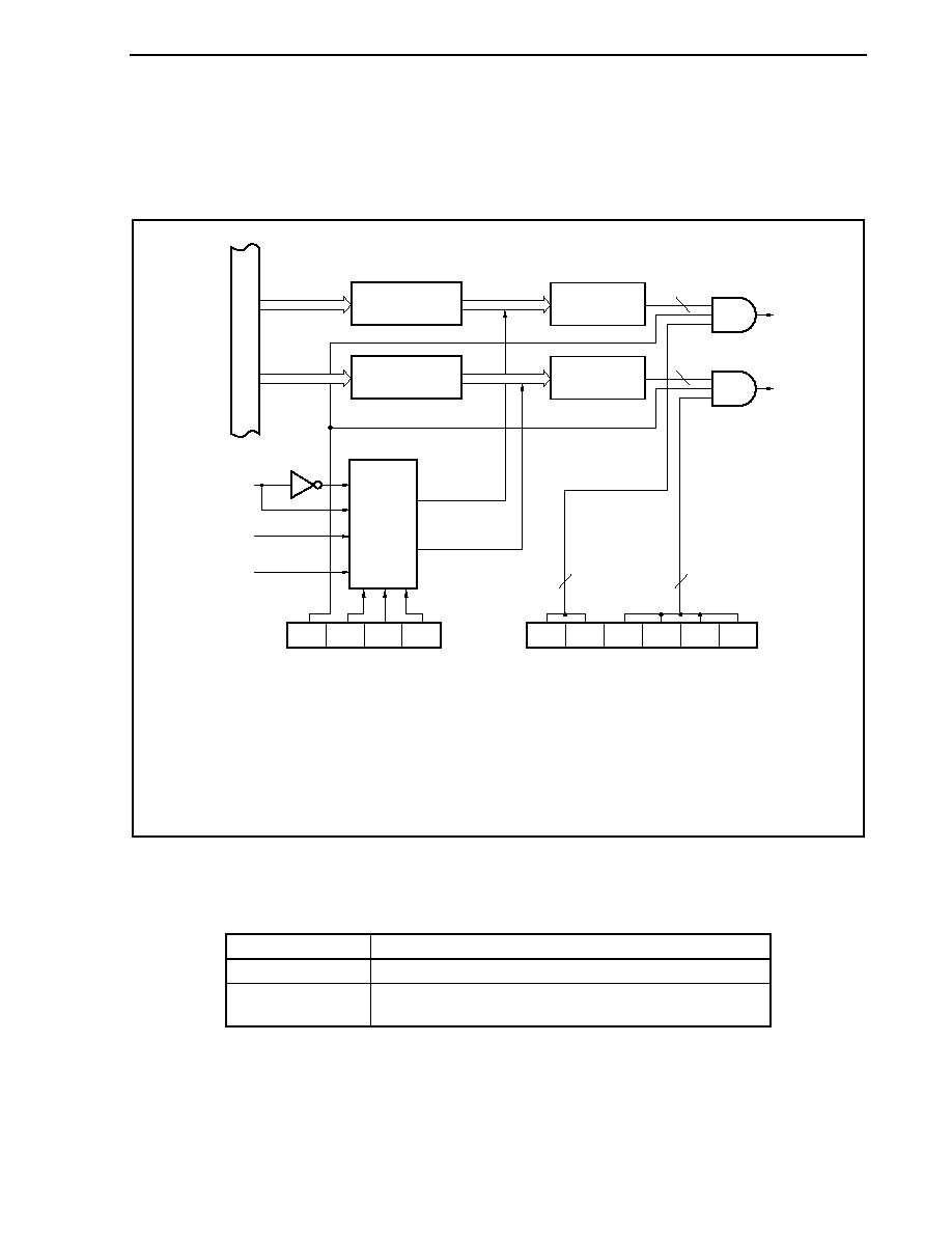
CHAPTER 12 REAL-TIME OUTPUT FUNCTION (RTO)
Preliminary User's Manual U17714EJ1V0UD
437
12.2 Configuration
The block diagram of RTO is shown below.
Figure 12-1. Block Diagram of RTO
INTTP0CC0,
INTTP6CC0
Note 1
INTTP5CC0,
INTTP8CC0
Note 2
INTTP4CC0,
INTTP7CC0
Note 3
RTPOEn RTPEGn BYTEn
EXTRn
RTPMn5 RTPMn4 RTPMn3 RTPMn2 RTPMn1 RTPMn0
4
2
2
4
RTPn4,
RTPn5
RTPn0 to
RTPn3
Real-time output
buffer register nH
(RTBHn)
Real-time output
latch nH
Selector
Real-time output
latch nL
Real-time output port control
register n (RTPCn)
Transfer trigger (H)
Transfer trigger (L)
Real-time output port mode
register n (RTPMn)
Inter
nal b
us
Real-time output
buffer register nL
(RTBLn)
Notes 1. INTTP0CC0 when n = 0, INTTP6CC0 when n = 1
2. INTTP5CC0 when n = 0, INTTP8CC0 when n = 1
3. INTTP4CC0 when n = 0, INTTP7CC0 when n = 1
Remark n = 0, 1
RTO includes the following hardware.
Table 12-1. Configuration of RTO
Item Configuration
Registers
Real-time output buffer registers nL, nH (RTBLn, RTBHn)
Control registers
Real-time output port mode register n (RTPMn)
Real-time output port control register n (RTPCn)
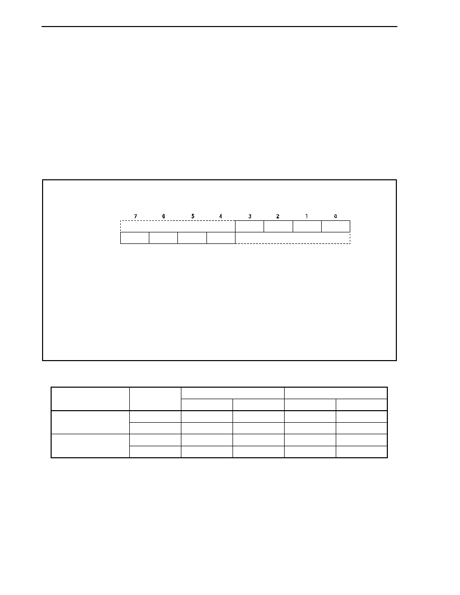
CHAPTER 12 REAL-TIME OUTPUT FUNCTION (RTO)
Preliminary User's Manual U17714EJ1V0UD
438
(1) Real-time output buffer registers nL, nH (RTBLn, RTBHn)
The RTBLn and RTBHn registers are 4-bit registers that hold preset output data.
These registers are mapped to independent addresses in the peripheral I/O register area.
These registers can be read or written in 8-bit or 1-bit units.
Reset sets these registers to 00H.
If an operation mode of 4 bits
� 1 channel or 2 bits � 1 channel is specified (RTPCn.BYTEn bit = 0), data can
be individually set to the RTBLn and RTBHn registers. The data of both these registers can be read at once
by specifying the address of either of these registers.
If an operation mode of 6 bits
� 1 channel is specified (BYTEn bit = 1), 8-bit data can be set to both the RTBLn
and RTBHn registers by writing the data to either of these registers. Moreover, the data of both these
registers can be read at once by specifying the address of either of these registers.
Table 12-2 shows the operation when the RTBLn and RTBHn registers are manipulated.
0
RTBLn
RTBHn
0
RTBHn5 RTBHn4
RTBLn3
RTBLn2
RTBLn1
RTBLn0
After reset: 00H R/W Address: RTBL0 FFFFF6E0H, RTBH0 FFFFF6E2H,
RTBL1 FFFFF6F0H, RTBH1 FFFFF6F2H
Cautions 1. When writing to bits 6 and 7 of the RTBHn register, always write 0.
2. Accessing the RTBLn and RTBHn registers is prohibited in the following
statuses. For details, see 3.4.8 (2) Accessing specific on-chip peripheral I/O
registers.
�
When the CPU operates with the subclock and the main clock oscillation is
stopped
�
When the CPU operates with the internal oscillation clock
Remark n = 0, 1
Table 12-2. Operation During Manipulation of RTBLn and RTBHn Registers
Read Write
Note
Operation Mode
Register to Be
Manipulated
Higher 4 Bits
Lower 4 Bits
Higher 4 Bits
Lower 4 Bits
RTBLn RTBHn RTBLn Invalid RTBLn
4 bits
� 1 channel,
2 bits
� 1 channel
RTBHn RTBHn RTBLn RTBHn Invalid
RTBLn RTBHn RTBLn RTBHn RTBLn
6 bits
� 1 channel
RTBHn RTBHn RTBLn RTBHn RTBLn
Note After setting the real-time output port, set output data to the RTBLn and RTBHn registers by the time a real-
time output trigger is generated.
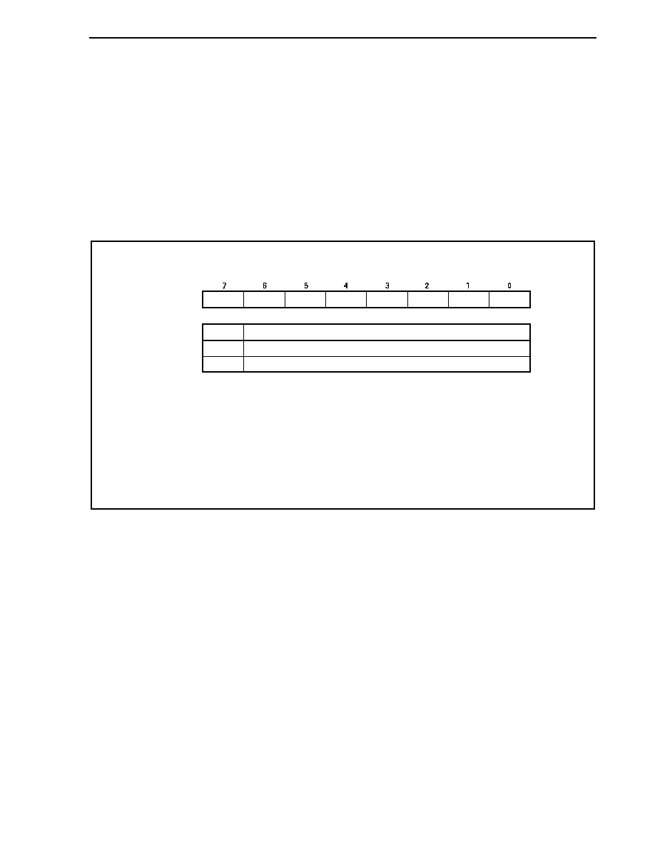
CHAPTER 12 REAL-TIME OUTPUT FUNCTION (RTO)
Preliminary User's Manual U17714EJ1V0UD
439
12.3 Registers
RTO is controlled using the following two registers.
� Real-time output port mode register n (RTPMn)
� Real-time output port control register n (RTPCn)
(1) Real-time output port mode register n (RTPMn)
The RTPMn register selects the real-time output port mode or port mode in 1-bit units.
This register can be read or written in 8-bit or 1-bit units.
Reset sets this register to 00H.
0
RTPMnm
0
1
Real-time output disabled
Real-time output enabled
Control of real-time output port (m = 0 to 5)
RTPMn
(n = 0, 1)
0
RTPMn5 RTPMn4 RTPMn3 RTPMn2 RTPMn1 RTPMn0
After reset: 00H R/W Address: RTPM0 FFFFF6E4H, RTPM1 FFFFF6F4H
Cautions 1. By enabling the real-time output operation (RTPCn.RTPOEn bit = 1), the bits
enabled to real-time output among the RTPn0 to RTPn5 signals perform real-
time output, and the bits set to port mode output 0.
2. If real-time output is disabled (RTPOEn bit = 0), the real-time output pins
(RTPn0 to RTPn5) all output 0, regardless of the RTPMn register setting.
3. In order to use this register as the real-time output pins (RTPn0 to RTPn5), set
these pins as real-time output port pins using the PMC and PFC registers.
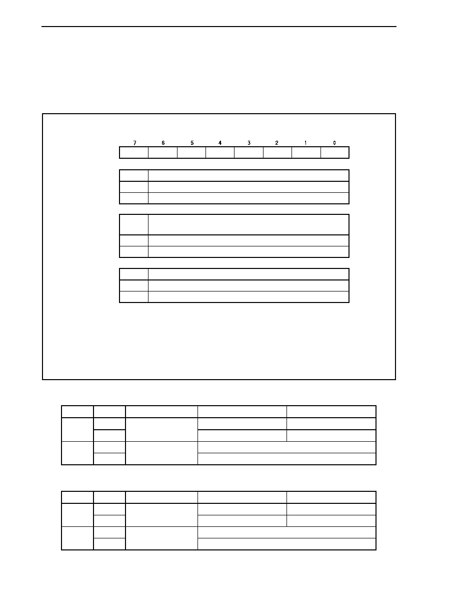
CHAPTER 12 REAL-TIME OUTPUT FUNCTION (RTO)
Preliminary User's Manual U17714EJ1V0UD
440
(2) Real-time output port control register n (RTPCn)
The RTPCn register is a register that sets the operation mode and output trigger of the real-time output port.
The relationship between the operation mode and output trigger of the real-time output port is as shown in
Tables 12-3 and 12-4.
This register can be read or written in 8-bit or 1-bit units.
Reset sets this register to 00H.
RTPOEn
Disables operation
Note 1
Enables operation
RTPOEn
0
1
Control of real-time output operation
RTPCn
(n = 0, 1)
RTPEGn
BYTEn
EXTRn
0
0
0
0
Falling edge
Note 2
Rising edge
RTPEGn
0
1
Valid edge of INTTPaCC0 (n = 0, a = 0, 4, 5) and
INTTPbCC0 (n = 1, b = 6 to 8) signals
4 bits
� 2 channels, 2 bits � 2 channels
6 bits
� 2 channels
BYTEn
0
1
Specification of channel configuration for real-time output
After reset: 00H R/W Address: RTPC0 FFFFF6E5H, RTPC1 FFFFF6F5H
< >
Notes 1. When the real-time output operation is disabled (RTPOEn bit = 0), all the bits of the
real-time output signals (RTPn0 to RTPn5) output "0".
2. The INTTP0CC0 and INTTP6CC0 signals are output for 1 clock of the count clock
selected by TMP0 or TMP6.
Caution Set the RTPEGn, BYTEn, and EXTRn bits only when RTPOEn bit = 0.
Table 12-3. Operation Modes and Output Triggers of Real-Time Output Port (n = 0)
BYTE0 EXTR0
Operation
Mode
RTBH0
(RTP04, RTP05)
RTBL0 (RTP00 to RTP03)
0 INTTP5CC0
INTTP4CC0
0
1
4 bits
� 1 channel,
2 bits
� 1 channel
INTTP4CC0 INTTP0CC0
0 INTTP4CC0
1
1
6 bits
� 1 channel
INTTP0CC0
Table 12-4. Operation Modes and Output Triggers of Real-Time Output Port (n = 1)
BYTE1 EXTR1
Operation
Mode
RTBH1
(RTP14, RTP15)
RTBL1 (RTP10 to RTP13)
0 INTTP8CC0
INTTP7CC0
0
1
4 bits
� 1 channel,
2 bits
� 1 channel
INTTP7CC0 INTTP6CC0
0 INTTP7CC0
1
1
6 bits
� 1 channel
INTTP6CC0
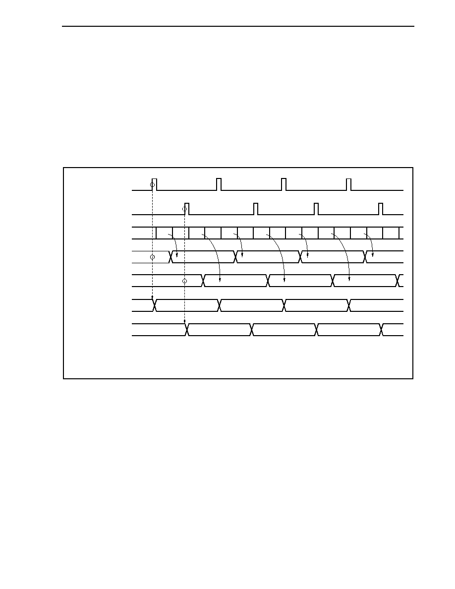
CHAPTER 12 REAL-TIME OUTPUT FUNCTION (RTO)
Preliminary User's Manual U17714EJ1V0UD
441
12.4 Operation
If the real-time output operation is enabled by setting the RTPCn.RTPOEn bit to 1, the data of the RTBHn and
RTBLn registers is transferred to the real-time output latch in synchronization with the generation of the selected
transfer trigger (set by the RTPCn.EXTRn and RTPCn.BYTEn bits). Of the transferred data, only the data of the bits
for which real-time output is enabled by the RTPMn register is output from the RTPn0 to RTPn5 bits. The bits for
which real-time output is disabled by the RTPMn register output 0.
If the real-time output operation is disabled by clearing the RTPOEn bit to 0, the RTPn0 to RTPn5 signals output 0
regardless of the setting of the RTPMn register.
Figure 12-2. Example of Operation Timing of RTO0 (When EXTR0 Bit = 0, BYTE0 Bit = 0)
A
B
A
B
A
B
A
B
D01
D02
D03
D04
D11
D12
D13
D14
D11
D12
D13
D14
D01
D02
D03
D04
INTTP5CC0 (internal)
INTTP4CC0 (internal)
CPU operation
RTBH0
RTBL0
RT output latch 0 (H)
RT output latch 0 (L)
A: Software processing by INTTP5CC0 interrupt request (RTBH0 write)
B: Software processing by INTTP4CC0 interrupt request (RTBL0 write)
Remark For the operation during standby, see CHAPTER 21 STANDBY FUNCTION.

CHAPTER 12 REAL-TIME OUTPUT FUNCTION (RTO)
Preliminary User's Manual U17714EJ1V0UD
442
12.5 Usage
(1) Disable real-time output.
Clear the RTPCn.RTPOEn bit to 0.
(2) Perform initialization as follows.
� Set the alternate-function pins of port 5
Set the PFC5.PFC5m bit and PFCE5.PFCE5m bit to 1, and then set the PMC5.PMC5m bit to 1 (m = 0 to 5).
� Specify the real-time output port mode or port mode in 1-bit units.
Set the RTPMn register.
� Channel configuration: Select the trigger and valid edge.
Set the RTPCn.EXTRn, RTPCn.BYTEn, and RTPCn.RTPEGn bits.
� Set the initial values to the RTBHn and RTBLn registers
Note 1
.
(3) Enable real-time output.
Set the RTPOEn bit = 1.
(4) Set the next output value to the RTBHn and RTBLn registers by the time the selected transfer trigger is
generated
Note 2
.
(5) Set the next real-time output value to the RTBHn and RTBLn registers via interrupt servicing corresponding to
the selected trigger.
Notes 1. If the RTBHn and RTBLn registers are written when the RTPOEn bit = 0, that value is transferred
to real-time output latches nH and nL, respectively.
2. Even if the RTBHn and RTBLn registers are written when the RTPOEn bit = 1, data is not
transferred to real-time output latches nH and nL.
12.6 Cautions
(1) Prevent the following conflicts by software.
� Conflict between real-time output disable/enable switching (RTPOEn bit) and selected real-time output
trigger.
� Conflict between writing to the RTBHn and RTBLn registers in the real-time output enabled status and the
selected real-time output trigger.
(2) Before performing initialization, disable real-time output (RTPOEn bit = 0).
(3) Once real-time output has been disabled (RTPOEn bit = 0), be sure to initialize the RTBHn and RTBLn
registers before enabling real-time output again (RTPOEn bit = 0
1).

Preliminary User's Manual U17714EJ1V0UD
443
CHAPTER 13 A/D CONVERTER
13.1 Overview
The A/D converter converts analog input signals into digital values, has a resolution of 10 bits, and can handle 16
analog input signal channels (ANI0 to ANI15).
The A/D converter has the following features.
10-bit resolution
16 channels
Successive approximation method
Operating voltage: AV
REF0
= 3.0 to 3.6 V
Analog input voltage: 0 V to AV
REF0
The following functions are provided as operation modes.
� Continuous select mode
� Continuous scan mode
� One-shot select mode
� One-shot scan mode
The following functions are provided as trigger modes.
� Software trigger mode
� External trigger mode (external, 1)
� Timer trigger mode
Power-fail monitor function (conversion result compare function)
13.2 Functions
(1) 10-bit resolution A/D conversion
An analog input channel is selected from ANI0 to ANI15, and an A/D conversion operation is repeated at a
resolution of 10 bits. Each time A/D conversion has been completed, an interrupt request signal (INTAD) is
generated.
(2) Power-fail detection function
This function is used to detect a drop in the battery voltage. The result of A/D conversion (the value of the
ADA0CRnH register) is compared with the value of the ADA0PFT register, and the INTAD signal is generated
only when a specified comparison condition is satisfied (n = 0 to 15).
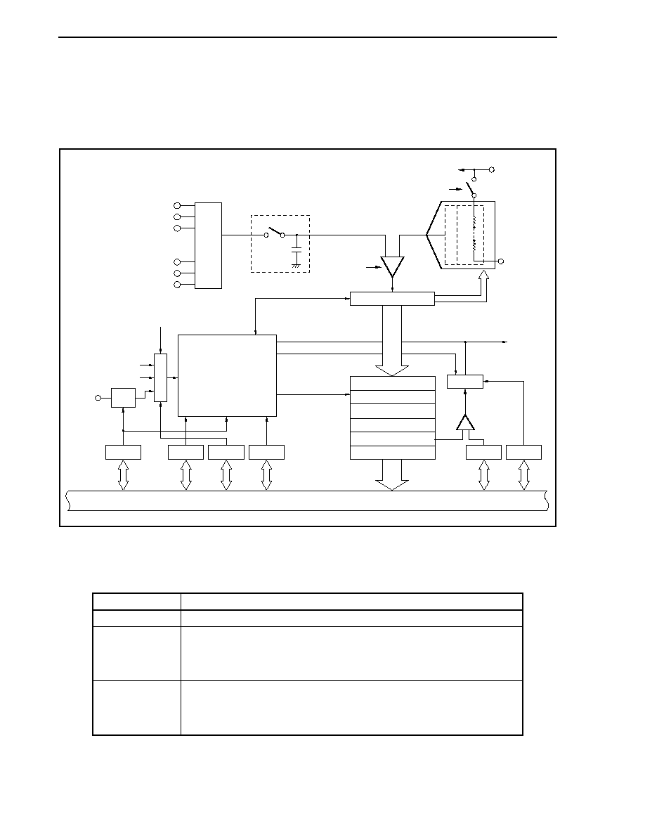
CHAPTER 13 A/D CONVERTER
Preliminary User's Manual U17714EJ1V0UD
444
13.3 Configuration
The block diagram of the A/D converter is shown below.
Figure 13-1. Block Diagram of A/D Converter
ANI0
:
:
ANI1
ANI2
ANI13
ANI14
ANI15
ADA0M2
ADA0M1
ADA0M0
ADA0S
ADA0PFT
Controller
Voltage
comparator
ADA0PFM
Voltage
comparator
ADA0CR0
ADA0CR1
:
:
ADA0CR2
ADA0CR14
ADA0CR15
Internal bus
AV
REF0
ADA0CE bit
AV
SS
INTAD
Edge
detection
ADTRG
Controller
Sample & hold circuit
Tap selector
ADA0ETS0 bit
INTTP2CC0
INTTP2CC1
ADA0ETS1 bit
ADA0CE bit
ADA0TMD1 bit
ADA0TMD0 bit
Selector
Selector
ADA0PFE bit
ADA0PFC bit
SAR
The A/D converter includes the following hardware.
Table 13-1. Configuration of A/D Converter
Item Configuration
Analog inputs
16 channels (ANI0 to ANI15 pins)
Registers
Successive approximation register (SAR)
A/D conversion result registers 0 to 15 (ADA0CR0 to ADA0CR15)
A/D conversion result registers 0H to 15H (ADCR0H to ADCR15H): Only higher 8 bits
can be read
Control registers
A/D converter mode registers 0 to 2 (ADA0M0 to ADA0M2)
A/D converter channel specification register 0 (ADA0S)
Power fail compare mode register (ADA0PFM)
Power fail compare threshold value register (ADA0PFT)

CHAPTER 13 A/D CONVERTER
Preliminary User's Manual U17714EJ1V0UD
445
(1) Successive approximation register (SAR)
The SAR register compares the voltage value of the analog input signal with the voltage tap (compare voltage)
value from the series resistor string, and holds the comparison result starting from the most significant bit
(MSB).
When the comparison result has been held down to the least significant bit (LSB) (i.e., when A/D conversion is
complete), the contents of the SAR register are transferred to the ADA0CRn register.
Remark n = 0 to 15
(2) A/D conversion result register n (ADA0CRn), A/D conversion result register nH (ADA0CRnH)
The ADA0CRn register is a 16-bit register that stores the A/D conversion result. ADA0ARn consist of 16
registers and the A/D conversion result is stored in the 10 higher bits of the AD0CRn register corresponding to
analog input. (The lower 6 bits are fixed to 0.)
(3) A/D converter mode register 0 (ADA0M0)
This register specifies the operation mode and controls the conversion operation by the A/D converter.
(4) A/D converter mode register 1 (ADA0M1)
This register sets the conversion time of the analog input signal to be converted.
(5) A/D converter mode register 2 (ADA0M2)
This register sets the hardware trigger mode.
(6) A/D converter channel specification register (ADA0S)
This register sets the input port that inputs the analog voltage to be converted.
(7) Power-fail compare mode register (ADA0PFM)
This register sets the power-fail monitor mode.
(8) Power-fail compare threshold value register (ADA0PFT)
The ADA0PFT register sets a threshold value that is compared with the value of A/D conversion result register
nH (ADA0CRnH). The 8-bit data set to the ADA0PFT register is compared with the higher 8 bits of the A/D
conversion result register (ADA0CRnH).
(9) Controller
The controller compares the result of the A/D conversion (the value of the ADA0CRnH register) with the value
of the ADA0PFT register when A/D conversion is completed or when the power-fail detection function is used,
and generates the INTAD signal only when a specified comparison condition is satisfied.
(10) Sample & hold circuit
The sample & hold circuit samples each of the analog input signals selected by the input circuit and sends the
sampled data to the voltage comparator. This circuit also holds the sampled analog input signal voltage
during A/D conversion.
(11) Voltage
comparator
The voltage comparator compares a voltage value that has been sampled and held with the voltage value of
the series resistor string.

CHAPTER 13 A/D CONVERTER
Preliminary User's Manual U17714EJ1V0UD
446
(12) Series resistor string
This series resistor string is connected between AV
REF0
and AV
SS
and generates a voltage for comparison
with the analog input signal.
(13) ANI0 to ANI15 pins
These are analog input pins for the 16 A/D converter channels and are used to input analog signals to be
converted into digital signals. Pins other than the one selected as the analog input by the ADA0S register
can be used as input port pins.
Caution Make sure that the voltages input to the ANI0 to ANI15 pins do not exceed the rated values.
In particular if a voltage of AV
REF0
or higher is input to a channel, the conversion value of
that channel becomes undefined, and the conversion values of the other channels may also
be affected.
(14) AV
REF0
pin
This is the pin used to input the reference voltage of the A/D converter. Always make the potential at this pin
the same as that at the V
DD
pin even when the A/D converter is not used. The signals input to the ANI0 to
ANI15 pins are converted to digital signals based on the voltage applied between the AV
REF0
and AV
SS
pins.
(15) AV
SS
pin
This is the ground pin of the A/D converter. Always make the potential at this pin the same as that at the V
SS
pin even when the A/D converter is not used.

CHAPTER 13 A/D CONVERTER
Preliminary User's Manual U17714EJ1V0UD
447
13.4 Registers
The A/D converter is controlled by the following registers.
� A/D converter mode registers 0, 1, 2 (ADA0M0, ADA0M1, ADA0M2)
� A/D converter channel specification register 0 (ADA0S)
� Power-fail compare mode register (ADA0PFM)
The following registers are also used.
� A/D conversion result register n (ADA0CRn)
� A/D conversion result register nH (ADA0CRnH)
� Power-fail compare threshold value register (ADA0PFT)
(1) A/D converter mode register 0 (ADA0M0)
The ADA0M0 register is an 8-bit register that specifies the operation mode and controls conversion operations.
This register can be read or written in 8-bit or 1-bit units. However, ADA0EF bit is read-only.
Reset sets this register to 00H.
Caution Accessing the ADA0M0 register is prohibited in the following statuses. For details, see 3.4.8
(2) Accessing specific on-chip peripheral I/O registers.
� When the CPU operates with the subclock and the main clock oscillation is stopped
� When the CPU operates with the internal oscillation clock
(1/2)
ADA0CE
ADA0CE
0
1
Stops A/D conversion
Enables A/D conversion
A/D conversion control
ADA0M0
0
<7>
6
5
4
3
2
1
<0>
ADA0MD1 ADA0MD0 ADA0ETS1 ADA0ETS0 ADA0TMD
ADA0EF
ADA0MD1
0
0
1
1
ADA0MD0
0
1
0
1
Continuous select mode
Continuous scan mode
One-shot select mode
One-shot scan mode
Specification of A/D converter operation mode
After reset: 00H R/W Address: FFFFF200H
CHAPTER 13 A/D CONVERTER
Preliminary User's Manual U17714EJ1V0UD
448
(2/2)
ADA0TMD
0
1
Software trigger mode
External trigger mode/timer trigger mode
Trigger mode specification
ADA0EF
0
1
A/D conversion stopped
A/D conversion in progress
A/D converter status display
ADA0ETS1
0
0
1
1
ADA0ETS0
0
1
0
1
No edge detection
Falling edge detection
Rising edge detection
Detection of both rising and falling edges
Specification of external trigger (ADTRG pin) input valid edge
Cautions 1. A write operation to bit 0 is ignored.
2. Changing the ADA0M1.ADA0FR2 to ADA0M1.ADA0FR0 bits is prohibited while A/D
conversion is enabled (ADA0CE bit = 1).
3. When writing data to the ADA0M0, ADA0M2, ADA0S, ADA0PFM, or ADA0PFT register in
the following modes, stop the A/D conversion by clearing the ADA0CE bit to 0. After
the data is written to the register, enable the A/D conversion again by setting the
ADA0CE bit to 1.
�
Normal conversion mode
�
One-shot select mode/one-shot scan mode in high-speed conversion mode
If the ADA0M0, ADA0M2, ADA0S, ADA0PFM, and ADA0PFT registers are written in the
other modes during A/D conversion (ADA0EF bit = 1), the following will be performed
according to the mode.
�
In software trigger mode
A/D conversion is stopped and started again from the beginning.
�
In hardware trigger mode
A/D conversion is stopped, and the trigger standby status is set.
4. To select the external trigger mode/timer trigger mode (ADA0TMD bit = 1), set the high-
speed conversion mode (ADA0M1.ADA0HS1 bit = 1). Do not input a trigger during
stabilization time that is inserted once after the A/D conversion operation is enabled
(ADA0CE bit = 1).
5. When not using the A/D converter, stop the operation by setting the ADA0CE bit to 0 to
reduce the power consumption.
CHAPTER 13 A/D CONVERTER
Preliminary User's Manual U17714EJ1V0UD
449
(2) A/D converter mode register 1 (ADA0M1)
The ADA0M1 register is an 8-bit register that specifies the conversion time.
This register can be read or written in 8-bit or 1-bit units.
Reset sets this register to 00H.
ADA0HS1
ADA0M1
0
0
0
0
ADA0FR2 ADA0FR1 ADA0FR0
After reset: 00H R/W Address: FFFFF201H
ADA0HS1
0
1
Normal conversion mode
High-speed conversion mode
Specification of normal conversion mode/high-speed mode (A/D conversion time)
Cautions 1. Changing the ADA0M1 register is prohibited while A/D conversion is enabled
(ADA0M0.ADA0CE bit = 1).
2. To select the external trigger mode/timer trigger mode (ADA0M0.ADA0TMD bit = 1), set
the high-speed conversion mode (ADA0HS1 bit = 1). Do not input a trigger during
stabilization time that is inserted once after the A/D conversion operation is enabled
(ADA0CE bit = 1).
3. Be sure to clear bits 6 to 3 to "0".
Remark For A/D conversion time setting examples, see Tables 13-2 and 13-3.
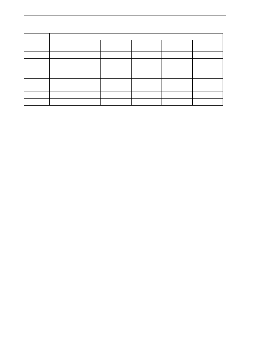
CHAPTER 13 A/D CONVERTER
Preliminary User's Manual U17714EJ1V0UD
450
Table 13-2. Conversion Time Selection in Normal Conversion Mode (ADA0HS1 Bit = 0)
A/D Conversion Time
ADA0FR2 to
ADA0FR0 Bits
Stabilization Time
+ Conversion Time + Wait Time
f
XX
= 20 MHz
f
XX
= 16 MHz
f
XX
= 4 MHz
Trigger Response
Time
000 13/f
XX
+ 26/f
XX
+ 26/f
XX
Setting prohibited Setting prohibited 16.25
�
s 4/f
XX
001 26/f
XX
+ 52/f
XX
+ 52/f
XX
6.5
�
s 8.125
�
s Setting
prohibited
5/f
XX
010 39/f
XX
+ 78/f
XX
+ 78/f
XX
9.75
�
s 12.1875
�
s Setting
prohibited 6/f
XX
011 50/f
XX
+ 104/f
XX
+ 104/f
XX
12.9
�
s 16.125
�
s Setting
prohibited 7/f
XX
100 50/f
XX
+ 130/f
XX
+ 130/f
XX
15.5
�
s 19.375
�
s Setting
prohibited 8/f
XX
101 50/f
XX
+ 156/f
XX
+ 156/f
XX
18.1
�
s 22.625
�
s Setting
prohibited 9/f
XX
110 50/f
XX
+ 182/f
XX
+ 182/f
XX
20.7
�
s
Setting prohibited Setting prohibited
10/f
XX
111 50/f
XX
+ 208/f
XX
+ 208/f
XX
23.3
�
s
Setting prohibited Setting prohibited
11/f
XX
Remark Stabilization time:
A/D converter setup time (1
�
s or longer)
Conversion time:
Actual A/D conversion time (2.6 to 10.4
�
s)
Wait time:
Wait time inserted before the next conversion
Trigger response time: If a software trigger, external trigger, or timer trigger is generated after the
stabilization time, it is inserted before the conversion time.
In the normal conversion mode, the conversion is started after the stabilization time elapsed from the
ADA0M0.ADA0CE bit is set to 1, and A/D conversion is performed only during the conversion time (2.6 to
10.4
�
s). Operation is stopped after the conversion ends and the A/D conversion end interrupt request
signal (INTAD) is generated after the wait time is elapsed.
Because the conversion operation is stopped during the wait time, operation current can be reduced.
Caution Set as 2.6
�
s
conversion time 10.4
�
s.

CHAPTER 13 A/D CONVERTER
Preliminary User's Manual U17714EJ1V0UD
451
Table 13-3. Conversion Time Selection in High-Speed Conversion Mode (ADA0HS1 Bit = 1)
A/D Conversion Time
ADA0FR2 to
ADA0FR0 Bits
Conversion Time
(+ Stabilization Time)
f
XX
= 20 MHz
f
XX
= 16 MHz
f
XX
= 4 MHz
Trigger Response
Time
000 26/f
XX
(+ 13/f
XX
) Setting
prohibited
Setting prohibited 6.5
�
s
(+ 3.25
�
s)
4/f
XX
001 52/f
XX
(+ 26/f
XX
)
2.6
�
s
(+ 1.3
�
s)
3.25
�
s
(+ 1.625
�
s)
Setting prohibited
5/f
XX
010 78/f
XX
(+ 39/f
XX
)
3.9
�
s
(+ 1.95
�
s)
4.875
�
s
(+ 2.4375
�
s)
Setting prohibited
6/f
XX
011 104/f
XX
(+ 50/f
XX
)
5.2
�
s
(+ 2.5
�
s)
6.5
�
s
(+ 3.125
�
s)
Setting prohibited
7/f
XX
100 130/f
XX
(+ 50/f
XX
)
6.5
�
s
(+ 2.5
�
s)
8.125
�
s
(+ 3.125
�
s)
Setting prohibited
8/f
XX
101 156/f
XX
(+ 50/f
XX
)
7.8
�
s
(+ 2.5
�
s)
9.75
�
s
(+ 3.125
�
s)
Setting prohibited
9/f
XX
110 182/f
XX
(+ 50/f
XX
)
9.1
�
s
(+ 2.5
�
s)
Setting prohibited Setting prohibited
10/f
XX
111 208/f
XX
(+ 50/f
XX
)
10.4
�
s
(+ 2.5
�
s)
Setting prohibited Setting prohibited
11/f
XX
Remark Conversion time:
Actual A/D conversion time (2.6 to 10.4
�
s)
Stabilization time:
A/D converter setup time (1
�
s or longer)
Trigger response time: If a software trigger, external trigger, or timer trigger is generated after the
stabilization time, it is inserted before the conversion time.
In the high-speed conversion mode, the conversion is started after the stabilization time elapsed from the
ADA0M0.ADA0CE bit is set to 1, and A/D conversion is performed only during the conversion time (2.6 to
10.4
�
s). The A/D conversion end interrupt request signal (INTAD) is generated immediately after the
conversion ends.
In continuous conversion mode, the stabilization time is inserted only before the first conversion, and not
inserted after the second conversion (the A/D converter remains running).
Caution Set as 2.6
�
s
conversion time 10.4
�
s.
CHAPTER 13 A/D CONVERTER
Preliminary User's Manual U17714EJ1V0UD
452
(3) A/D converter mode register 2 (ADA0M2)
The ADA0M2 register specifies the hardware trigger mode.
This register can be read or written in 8-bit or 1-bit units.
Reset sets this register to 00H.
0
ADA0M2
0
0
0
0
0
ADA0TMD1 ADA0TMD0
ADA0TMD1
0
0
1
1
ADA0TMD0
0
1
0
1
Specification of hardware trigger mode
External trigger mode (when ADTRG pin valid edge detected)
Timer trigger mode 0
(when INTTP2CC0 interrupt request generated)
Timer trigger mode 1
(when INTTP2CC1 interrupt request generated)
Setting prohibited
After reset: 00H R/W Address: FFFFF203H
6
5
4
3
2
1
0
7
Cautions 1. When writing data to the ADA0M2 register in the following modes, stop the A/D
conversion by clearing the AD0M0.ADA0CE bit to 0. After the data is written to the
register, enable the A/D conversion again by setting the ADA0CE bit to 1.
�
Normal conversion mode
�
One-shot select mode/one-shot scan mode in high-speed conversion mode
2. Be sure to clear bits 7 to 2 to "0".
CHAPTER 13 A/D CONVERTER
Preliminary User's Manual U17714EJ1V0UD
453
(4) A/D converter channel specification register 0 (ADA0S)
The ADA0S register specifies the pin that inputs the analog voltage to be converted into a digital signal.
This register can be read or written in 8-bit or 1-bit units.
Reset sets this register to 00H.
0
ADA0S
0
0
0
ADA0S3 ADA0S2
ADA0S1
ADA0S0
After reset: 00H R/W Address: FFFFF202H
ANI0
ANI1
ANI2
ANI3
ANI4
ANI5
ANI6
ANI7
ANI8
ANI9
ANI10
ANI11
ANI12
ANI13
ANI14
ANI15
ANI0
ANI0, ANI1
ANI0 to ANI2
ANI0 to ANI3
ANI0 to ANI4
ANI0 to ANI5
ANI0 to ANI6
ANI0 to ANI7
ANI0 to ANI8
ANI0 to ANI9
ANI0 to ANI10
ANI0 to ANI11
ANI0 to ANI12
ANI0 to ANI13
ANI0 to ANI14
ANI0 to ANI15
ADA0S3
0
0
0
0
0
0
0
0
1
1
1
1
1
1
1
1
ADA0S2
0
0
0
0
1
1
1
1
0
0
0
0
1
1
1
1
ADA0S1
0
0
1
1
0
0
1
1
0
0
1
1
0
0
1
1
ADA0S0
0
1
0
1
0
1
0
1
0
1
0
1
0
1
0
1
Select mode
Scan mode
Cautions 1. When writing data to the ADA0S register in the following modes, stop the A/D
conversion by clearing the AD0M0.ADA0CE bit to 0. After the data is written to the
register, enable the A/D conversion again by setting the ADA0CE bit to 1.
�
Normal conversion mode
�
One-shot select mode/one-shot scan mode in high-speed conversion mode
2. Be sure to clear bits 7 to 4 to "0".
CHAPTER 13 A/D CONVERTER
Preliminary User's Manual U17714EJ1V0UD
454
(5) A/D conversion result registers n, nH (ADA0CRn, ADA0CRnH)
The ADA0CRn and ADA0CRnH registers store the A/D conversion results.
These registers are read-only, in 16-bit or 8-bit units. However, specify the ADA0CRn register for 16-bit access
and the ADA0CRnH register for 8-bit access. The 10 bits of the conversion result are read from the higher 10
bits of the ADA0CRn register, and 0 is read from the lower 6 bits. The higher 8 bits of the conversion result are
read from the ADA0CRnH register.
Caution Accessing the ADA0CRn and ADA0CRnH registers is prohibited in the following statuses.
For details, see 3.4.8 (2) Accessing specific on-chip peripheral I/O registers.
�
When the CPU operates with the subclock and the main clock oscillation is stopped
�
When the CPU operates with the internal oscillation clock
After reset: Undefined R Address: ADA0CR0 FFFFF210H, ADA0CR1 FFFFF212H,
ADA0CR2 FFFFF214H, ADA0CR3 FFFFF216H,
ADA0CR4 FFFFF218H, ADA0CR5 FFFFF21AH,
ADA0CR6 FFFFF21CH, ADA0CR7 FFFFF21EH,
ADA0CR8 FFFFF220H, ADA0CR9 FFFFF222H,
ADA0CR10 FFFFF224H, ADA0CR11 FFFFF226H,
ADA0CR12 FFFFF228H, ADA0CR13 FFFFF22AH,
ADA0CR14 FFFFF22CH, ADA0CR15 FFFFF22EH
ADA0CRn
(n = 0 to 15)
AD9 AD8 AD7 AD6
AD0
0
0
0
0
0
0
AD1
AD2
AD3
AD4
AD5
AD9
ADA0CRnH
(n = 0 to 15)
AD8
AD7
AD6
AD5
AD4
AD3
AD2
7
6
5
4
3
2
1
0
After reset: Undefined R Address: ADA0CR0H FFFFF211H, ADA0CR1H FFFFF213H,
ADA0CR2H FFFFF215H, ADA0CR3H FFFFF217H,
ADA0CR4H FFFFF219H, ADA0CR5H FFFFF21BH,
ADA0CR6H FFFFF21DH, ADA0CR7H FFFFF21FH,
ADA0CR8H FFFFF221H, ADA0CR9H FFFFF223H,
ADA0CR10H FFFFF225H, ADA0CR11H FFFFF227H,
ADA0CR12H FFFFF229H, ADA0CR13H FFFFF22BH,
ADA0CR14H FFFFF22DH, ADA0CR15H FFFFF22FH
Caution A write operation to the ADA0M0 and ADA0S registers may cause the contents of the
ADA0CRn register to become undefined. After the conversion, read the conversion result
before writing to the ADA0M0 and ADA0S registers. Correct conversion results may not
be read if a sequence other than the above is used.
CHAPTER 13 A/D CONVERTER
Preliminary User's Manual U17714EJ1V0UD
455
The relationship between the analog voltage input to the analog input pins (ANI0 to ANI15) and the A/D conversion
result (ADA0CRn register) is as follows.
V
IN
SAR = INT (
AV
REF0
� 1,024 + 0.5)
ADA0CR
Note
= SAR
� 64
Or,
AV
REF0
AV
REF0
(SAR
- 0.5) �
1,024
V
IN
< (SAR + 0.5)
�
1,024
INT( ):
Function that returns the integer of the value in ( )
V
IN
:
Analog input voltage
AV
REF0
:
AV
REF0
pin voltage
ADA0CR: Value of ADA0CRn register
Note The lower 6 bits of the ADA0CRn register are fixed to 0.
The following shows the relationship between the analog input voltage and the A/D conversion results.
Figure 13-2. Relationship Between Analog Input Voltage and A/D Conversion Results
1,023
1,022
1,021
3
2
1
0
Input voltage/AV
REF0
1
2,048
1
1,024
3
2,048
2
1,024
5
2,048
3
1,024
2,043
2,048
1,022
1,024
2,045
2,048
1,023
1,024
2,047
2,048
1
A/D conversion results
ADA0CRn
SAR
FFC0H
FF80H
FF40H
00C0H
0080H
0040H
0000H
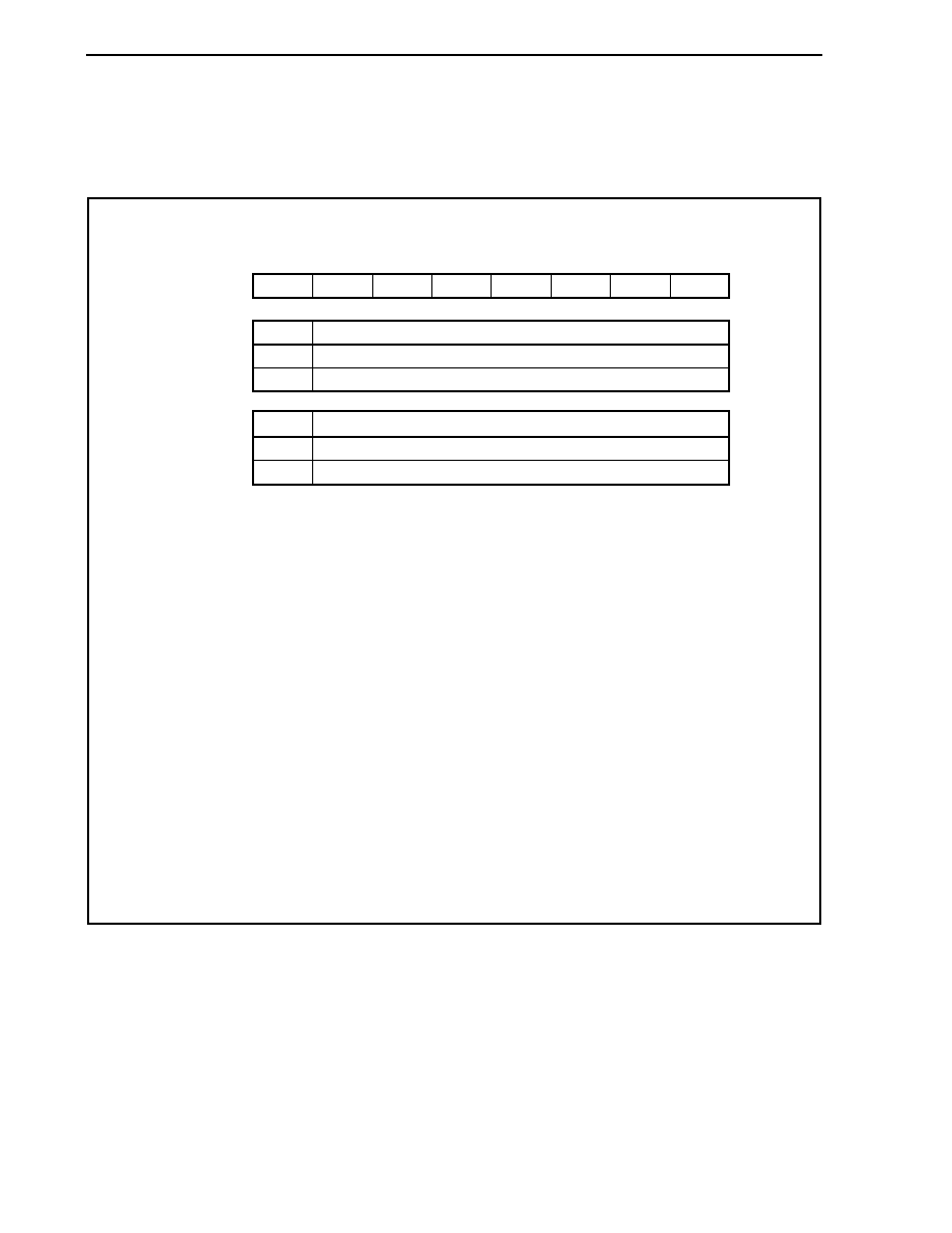
CHAPTER 13 A/D CONVERTER
Preliminary User's Manual U17714EJ1V0UD
456
(6) Power-fail compare mode register (ADA0PFM)
The ADA0PFM register is an 8-bit register that sets the power-fail compare mode.
This register can be read or written in 8-bit or 1-bit units.
Reset sets this register to 00H.
ADA0PFE
Power-fail compare disabled
Power-fail compare enabled
ADA0PFE
0
1
Selection of power-fail compare enable/disable
ADA0PFM
ADA0PFC
0
0
0
0
0
0
Generates an interrupt request signal (INTAD) when ADA0CRnH
ADA0PFT
Generates an interrupt request signal (INTAD) when ADA0CRnH < ADA0PFT
ADA0PFC
0
1
Selection of power-fail compare mode
After reset: 00H R/W Address: FFFFF204H
<7>
6
5
4
3
2
1
0
Cautions 1. In the select mode, the 8-bit data set to the ADA0PFT register is compared with the
value of the ADA0CRnH register specified by the ADA0S register. If the result matches
the condition specified by the ADA0PFC bit, the conversion result is stored in the
ADA0CRn register and the INTAD signal is generated. If it does not match, however,
the interrupt signal is not generated.
2. In the scan mode, the 8-bit data set to the ADA0PFT register is compared with the
contents of the ADA0CR0H register. If the result matches the condition specified by
the ADA0PFC bit, the conversion result is stored in the ADA0CR0 register and the
INTAD signal is generated. If it does not match, however, the INTAD signal is not
generated. Regardless of the comparison result, the scan operation is continued and
the conversion result is stored in the ADA0CRn register until the scan operation is
completed. However, the INTAD signal is not generated after the scan operation has
been completed.
3. When writing data to the ADA0PFM register in the following modes, stop the A/D
conversion by clearing the AD0M0.ADA0CE bit to 0. After the data is written to the
register, enable the A/D conversion again by setting the ADA0CE bit to 1.
�
Normal conversion mode
�
One-shot select mode/one-shot scan mode in high-speed conversion mode
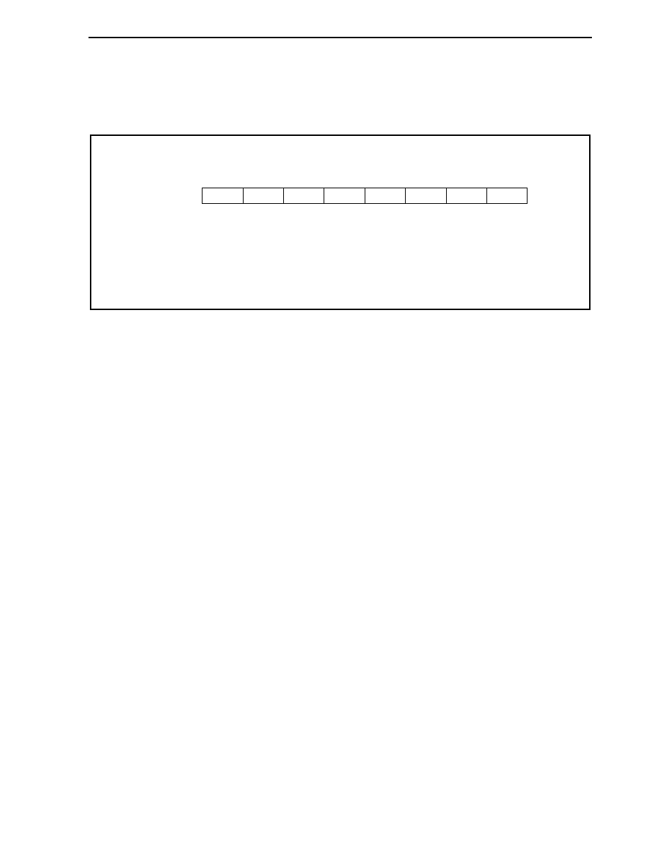
CHAPTER 13 A/D CONVERTER
Preliminary User's Manual U17714EJ1V0UD
457
(7) Power-fail compare threshold value register (ADA0PFT)
The ADA0PFT register sets the compare value in the power-fail compare mode.
This register can be read or written in 8-bit or 1-bit units.
Reset sets this register to 00H.
ADA0PFT
After reset: 00H R/W Address: FFFFF205H
7
6
5
4
3
2
1
0
Caution When writing data to the ADA0PFT register in the following modes, stop the A/D
conversion by clearing the AD0M0.ADA0CE bit to 0. After the data is written to the
register, enable the A/D conversion again by setting the ADA0CE bit to 1.
�
Normal conversion mode
�
One-shot select mode/one-shot scan mode in high-speed conversion mode

CHAPTER 13 A/D CONVERTER
Preliminary User's Manual U17714EJ1V0UD
458
13.5 Operation
13.5.1 Basic operation
<1> Set the operation mode, trigger mode, and conversion time for executing A/D conversion by using the
ADA0M0, ADA0M1, ADA0M2, and ADA0S registers. When the ADA0CE bit of the ADA0M0 register is set,
conversion is started in the software trigger mode and the A/D converter waits for a trigger in the external or
timer trigger mode.
<2> When A/D conversion is started, the voltage input to the selected analog input channel is sampled by the
sample & hold circuit.
<3> When the sample & hold circuit samples the input channel for a specific time, it enters the hold status, and
holds the input analog voltage until A/D conversion is complete.
<4> Set bit 9 of the successive approximation register (SAR). The tap selector selects (1/2) AV
REF0
as the voltage
tap of the series resistor string.
<5> The voltage difference between the voltage of the series resistor string and the analog input voltage is
compared by the voltage comparator. If the analog input voltage is higher than (1/2) AV
REF0
, the MSB of the
SAR register remains set. If it is lower than (1/2) AV
REF0
, the MSB is reset.
<6> Next, bit 8 of the SAR register is automatically set and the next comparison is started. Depending on the
value of bit 9, to which a result has been already set, the voltage tap of the series resistor string is selected
as follows.
� Bit 9 = 1: (3/4) AV
REF0
� Bit 9 = 0: (1/4) AV
REF0
This voltage tap and the analog input voltage are compared and, depending on the result, bit 8 is
manipulated as follows.
Analog input voltage
Voltage tap: Bit 8 = 1
Analog input voltage
Voltage tap: Bit 8 = 0
<7> This comparison is continued to bit 0 of the SAR register.
<8> When comparison of the 10 bits is complete, the valid digital result is stored in the SAR register, which is then
transferred to and stored in the ADA0CRn register. After that, an A/D conversion end interrupt request signal
(INTAD) is generated.
<9> In one-shot select mode, conversion is stopped
Note
. In one-shot scan mode, conversion is stopped after
scanning once
Note
. In continuous select mode, repeat steps <2> to <8> until the ADA0M0.ADA0CE bit is
cleared to 0. In continuous scan mode, repeat steps <2> to <8> for each channel.
Note In the external trigger mode, timer trigger mode 0, or timer trigger mode 1, the trigger standby status
is entered.
Remark The trigger standby status means the status after the stabilization time has passed.
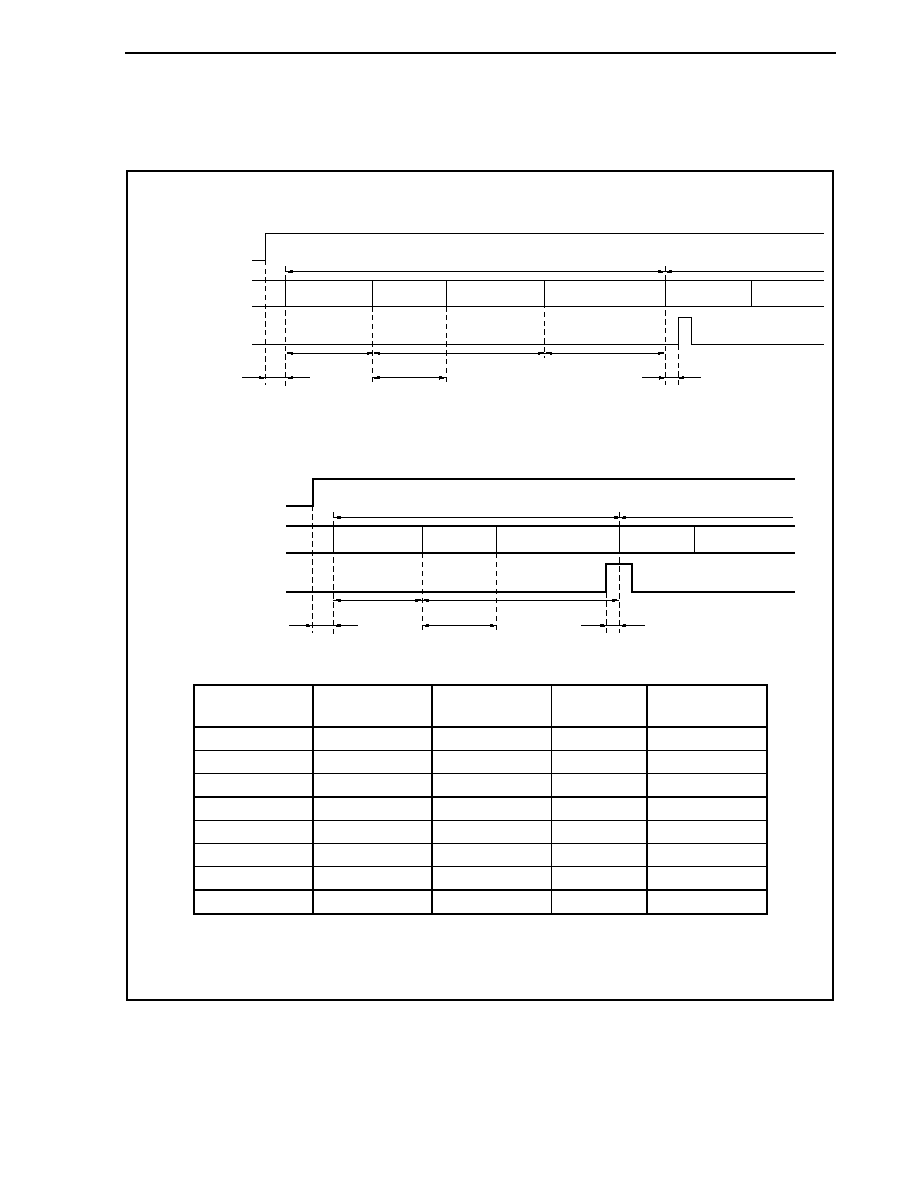
CHAPTER 13 A/D CONVERTER
Preliminary User's Manual U17714EJ1V0UD
459
13.5.2 Conversion operation timing
Figure 13-3. Conversion Operation Timing (Continuous Conversion)
(1) Operation in normal conversion mode (ADA0HS1 bit = 0)
ADA0M0.ADA0CE bit
Processing state
Setup
Stabilization
time
Conversion time
Wait time
Sampling
First conversion
Second conversion
Setup
Sampling
Wait
A/D conversion
INTAD signal
2/f
XX
(MAX.)
0.5/f
XX
Sampling
time
(2) Operation in high-speed conversion mode (ADA0HS1 bit = 1)
ADA0M0.ADA0CE bit
Processing state
Setup
Conversion time
Sampling
First conversion
Second conversion
Sampling
A/D conversion
A/D conversion
INTAD signal
0.5/f
XX
Stabilization
time
2/f
XX
(MAX.)
Sampling
time
ADA0FR2 to
ADA0FR0 Bits
Stabilization Time
Conversion Time
(Sampling Time)
Wait Time
Trigger Response
Time
000 13/f
XX
26/f
XX
(4/f
XX
) 26/f
XX
4/f
XX
001 26/f
XX
52/f
XX
(8/f
XX
) 52/f
XX
5/f
XX
010 39/f
XX
78/f
XX
(12/f
XX
) 78/f
XX
6/f
XX
011 50/f
XX
104/f
XX
(16/f
XX
) 104/f
XX
7/f
XX
100 50/f
XX
130/f
XX
(20/f
XX
) 130/f
XX
8/f
XX
101 50/f
XX
156/f
XX
(24/f
XX
) 156/f
XX
9/f
XX
110 50/f
XX
182/f
XX
(28/f
XX
) 182/f
XX
10/f
XX
111 50/f
XX
208/f
XX
(32/f
XX
) 208/f
XX
11/f
XX
Remark The above timings are when a trigger generates within the stabilization time. If the trigger
generates after the stabilization time, a trigger response time is inserted.

CHAPTER 13 A/D CONVERTER
Preliminary User's Manual U17714EJ1V0UD
460
13.5.3 Trigger mode
The timing of starting the conversion operation is specified by setting a trigger mode. The trigger mode includes a
software trigger mode and hardware trigger modes. The hardware trigger modes include timer trigger modes 0 and 1,
and external trigger mode. The ADA0M0.ADA0TMD bit is used to set the trigger mode. The hardware trigger modes
are set by the ADA0M2.ADA0TMD1 and ADA0M2.ADA0TMD0 bits.
(1) Software trigger mode
When the ADA0M0.ADA0CE bit is set to 1, the signal of the analog input pin (ANI0 to ANI15 pin) specified by
the ADA0S register is converted. When conversion is complete, the result is stored in the ADA0CRn register.
At the same time, the A/D conversion end interrupt request signal (INTAD) is generated.
If the operation mode specified by the ADA0M0.ADA0MD1 and ADA0M0.ADA0MD0 bits is the continuous
select/scan mode, the next conversion is started, unless the ADA0CE bit is cleared to 0 after completion of the
first conversion. Conversion is performed once and ends if the operation mode is the one-shot select/scan
mode.
When conversion is started, the ADA0M0.ADA0EF bit is set to 1 (indicating that conversion is in progress).
If the ADA0M0, ADA0M2, ADA0S, ADA0PFM, or ADA0PFT register is written during conversion, the
conversion is aborted and started again from the beginning. However, writing to these registers is prohibited in
the normal conversion mode and one-shot select mode/one-shot scan mode in the high-speed conversion
mode.
(2) External trigger mode
In this mode, converting the signal of the analog input pin (ANI0 to ANI15) specified by the ADA0S register is
started when an external trigger is input (to the ADTRG pin). Which edge of the external trigger is to be
detected (i.e., the rising edge, falling edge, or both rising and falling edges) can be specified by using the
ADA0M0.ADA0ETS1 and ADA0M0.ATA0ETS0 bits. When the ADA0CE bit is set to 1, the A/D converter waits
for the trigger, and starts conversion after the external trigger has been input.
When conversion is completed, the result of conversion is stored in the ADA0CRn register, regardless of
whether the continuous select, continuous scan, one-shot select, or one-shot scan mode is set as the
operation mode by the ADA0MD1 and ADA0MD0 bits. At the same time, the INTAD signal is generated, and
the A/D converter waits for the trigger again.
When conversion is started, the ADA0EF bit is set to 1 (indicating that conversion is in progress). While the
A/D converter is waiting for the trigger, however, the ADA0EF bit is cleared to 0 (indicating that conversion is
stopped). If the valid trigger is input during the conversion operation, the conversion is aborted and started
again from the beginning.
If the ADA0M0, ADA0M2, ADA0S, ADA0PFM, or ADA0PFT register is written during the conversion operation,
the conversion is not aborted, and the A/D converter waits for the trigger again. However, writing to these
registers is prohibited in the one-shot select mode/one-shot scan mode.
Caution To select the external trigger mode, set the high-speed conversion mode. Do not input a
trigger during stabilization time that is inserted once after the A/D conversion operation is
enabled (ADA0M0.ADA0CE bit = 1).
Remark The trigger standby status means the status after the stabilization time has passed.

CHAPTER 13 A/D CONVERTER
Preliminary User's Manual U17714EJ1V0UD
461
(3) Timer trigger mode
In this mode, converting the signal of the analog input pin (ANI0 to ANI15) specified by the ADA0S register is
started by the compare match interrupt request signal (INTTP2CC0 or INTTP2CC1) of the capture/compare
register connected to the timer. The INTTP2CC0 or INTTP2CC1 signal is selected by the ADA0TMD1 and
ADA0TMD0 bits, and conversion is started at the rising edge of the specified compare match interrupt request
signal. When the ADA0CE bit is set to 1, the A/D converter waits for a trigger, and starts conversion when the
compare match interrupt request signal of the timer is input.
When conversion is completed, regardless of whether the continuous select, continuous scan, one-shot select,
or one-shot scan mode is set as the operation mode by the ADA0MD1 and ADA0MD0 bits, the result of the
conversion is stored in the ADA0CRn register. At the same time, the INTAD signal is generated, and the A/D
converter waits for the trigger again.
When conversion is started, the ADA0EF bit is set to 1 (indicating that conversion is in progress). While the
A/D converter is waiting for the trigger, however, the ADA0EF bit is cleared to 0 (indicating that conversion is
stopped). If the valid trigger is input during the conversion operation, the conversion is aborted and started
again from the beginning.
If the ADA0M0, ADA0M2, ADA0S, ADA0PFM, or ADA0PFT register is written during conversion, the
conversion is stopped and the A/D converter waits for the trigger again. However, writing to these registers is
prohibited in the one-shot select mode/one-shot scan mode.
Caution To select the timer trigger mode, set the high-speed conversion mode. Do not input a trigger
during stabilization time that is inserted once after the A/D conversion operation is enabled
(ADA0M0.ADA0CE bit = 1).
Remark The trigger standby status means the status after the stabilization time has passed.
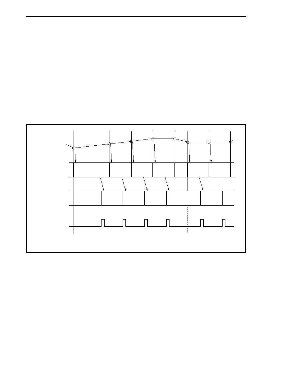
CHAPTER 13 A/D CONVERTER
Preliminary User's Manual U17714EJ1V0UD
462
13.5.4 Operation mode
Four operation modes are available as the modes in which to set the ANI0 to ANI15 pins: continuous select mode,
continuous scan mode, one-shot select mode, and one-shot scan mode.
The operation mode is selected by the ADA0M0.ADA0MD1 and ADA0M0.ADA0MD0 bits.
(1) Continuous select mode
In this mode, the voltage of one analog input pin selected by the ADA0S register is continuously converted into
a digital value.
The conversion result is stored in the ADA0CRn register corresponding to the analog input pin. In this mode,
an analog input pin corresponds to an ADA0CRn register on a one-to-one basis. Each time A/D conversion is
completed, the A/D conversion end interrupt request signal (INTAD) is generated. After completion of
conversion, the next conversion is started, unless the ADA0M0.ADA0CE bit is cleared to 0 (n = 0 to 15).
Figure 13-4. Timing Example of Continuous Select Mode Operation (ADA0S Register = 01H)
ANI1
A/D conversion
Data 1
(ANI1)
Data 2
(ANI1)
Data 3
(ANI1)
Data 4
(ANI1)
Data 5
(ANI1)
Data 6
(ANI1)
Data 7
(ANI1)
Data 1
Data 2
Data 3
Data 4
Data 5
Data 6
Data 7
Data 1
(ANI1)
Data 2
(ANI1)
Data 3
(ANI1)
Data 4
(ANI1)
Data 6
(ANI1)
ADA0CR1
INTAD
Conversion start
Set ADA0CE bit = 1
Conversion start
Set ADA0CE bit = 1
(2) Continuous scan mode
In this mode, analog input pins are sequentially selected, from the ANI0 pin to the pin specified by the ADA0S
register, and their values are converted into digital values.
The result of each conversion is stored in the ADA0CRn register corresponding to the analog input pin. When
conversion of the analog input pin specified by the ADA0S register is complete, the INTAD signal is generated,
and A/D conversion is started again from the ANI0 pin, unless the ADA0CE bit is cleared to 0 (n = 0 to 15).
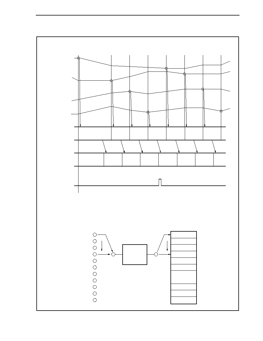
CHAPTER 13 A/D CONVERTER
Preliminary User's Manual U17714EJ1V0UD
463
Figure 13-5. Timing Example of Continuous Scan Mode Operation (ADA0S Register = 03H)
(a) Timing example
A/D conversion
Data 1
(ANI0)
Data 2
(ANI1)
Data 3
(ANI2)
Data 4
(ANI3)
Data 5
(ANI0)
Data 6
(ANI1)
Data 7
(ANI2)
Data 1
(ANI0)
Data 2
(ANI1)
Data 3
(ANI2)
Data 4
(ANI3)
Data 5
(ANI0)
Data 6
(ANI1)
ADA0CRn
INTAD
Conversion start
Set ADA0CE bit = 1
ANI3
ANI0
ANI1
ANI2
Data 1
Data 2
Data 3
Data 4
Data 6
Data 5
Data 7
(b) Block diagram
A/D converter
ADA0CRn register
Analog input pin
ANI0
ANI1
ANI2
ANI3
ANI4
ANI5
ANI13
ANI14
ANI15
.
.
.
.
ADA0CR0
ADA0CR1
ADA0CR2
ADA0CR3
ADA0CR4
ADA0CR5
ADA0CR13
ADA0CR14
ADA0CR15
.
.
.
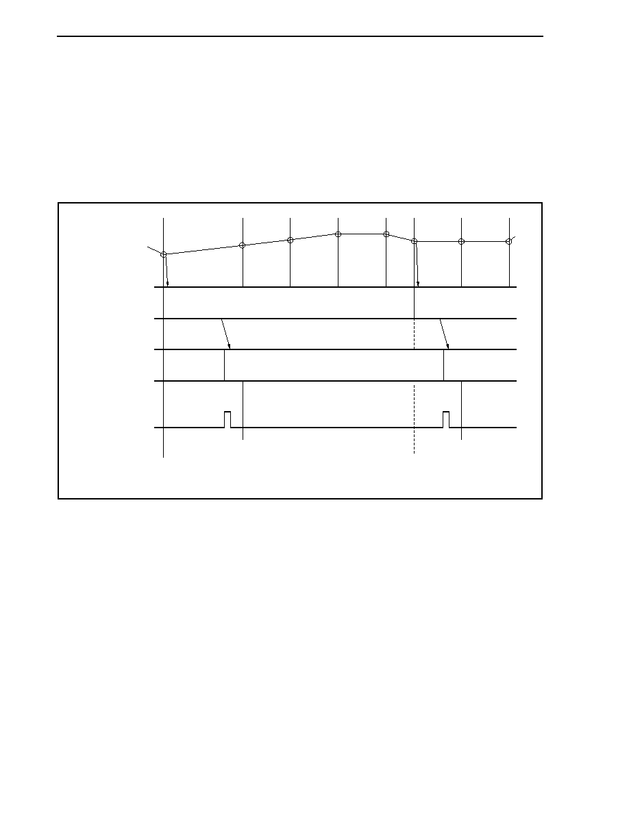
CHAPTER 13 A/D CONVERTER
Preliminary User's Manual U17714EJ1V0UD
464
(3) One-shot select mode
In this mode, the voltage on the analog input pin specified by the ADA0S register is converted into a digital
value only once.
The conversion result is stored in the ADA0CRn register corresponding to the analog input pin. In this mode,
an analog input pin and an ADA0CRn register correspond on a one-to-one basis. When A/D conversion has
been completed once, the INTAD signal is generated. The A/D conversion operation is stopped after it has
been completed (n = 0 to 15).
Figure 13-6. Timing Example of One-Shot Select Mode Operation (ADA0S Register = 01H)
ANI1
A/D conversion
Data 1
(ANI1)
Data 6
(ANI1)
Data 1
Data 2
Data 3
Data 4
Data 5
Data 6
Data 7
Data 1
(ANI1)
Data 6
(ANI1)
ADA0CR1
INTAD
Conversion start
Set ADA0CE bit = 1
Conversion start
Set ADA0CE bit = 1
Conversion end
Conversion end
(4) One-shot scan mode
In this mode, analog input pins are sequentially selected, from the ANI0 pin to the pin specified by the ADA0S
register, and their values are converted into digital values.
Each conversion result is stored in the ADA0CRn register corresponding to the analog input pin. When
conversion of the analog input pin specified by the ADA0S register is complete, the INTAD signal is generated.
A/D conversion is stopped after it has been completed (n = 0 to 15).
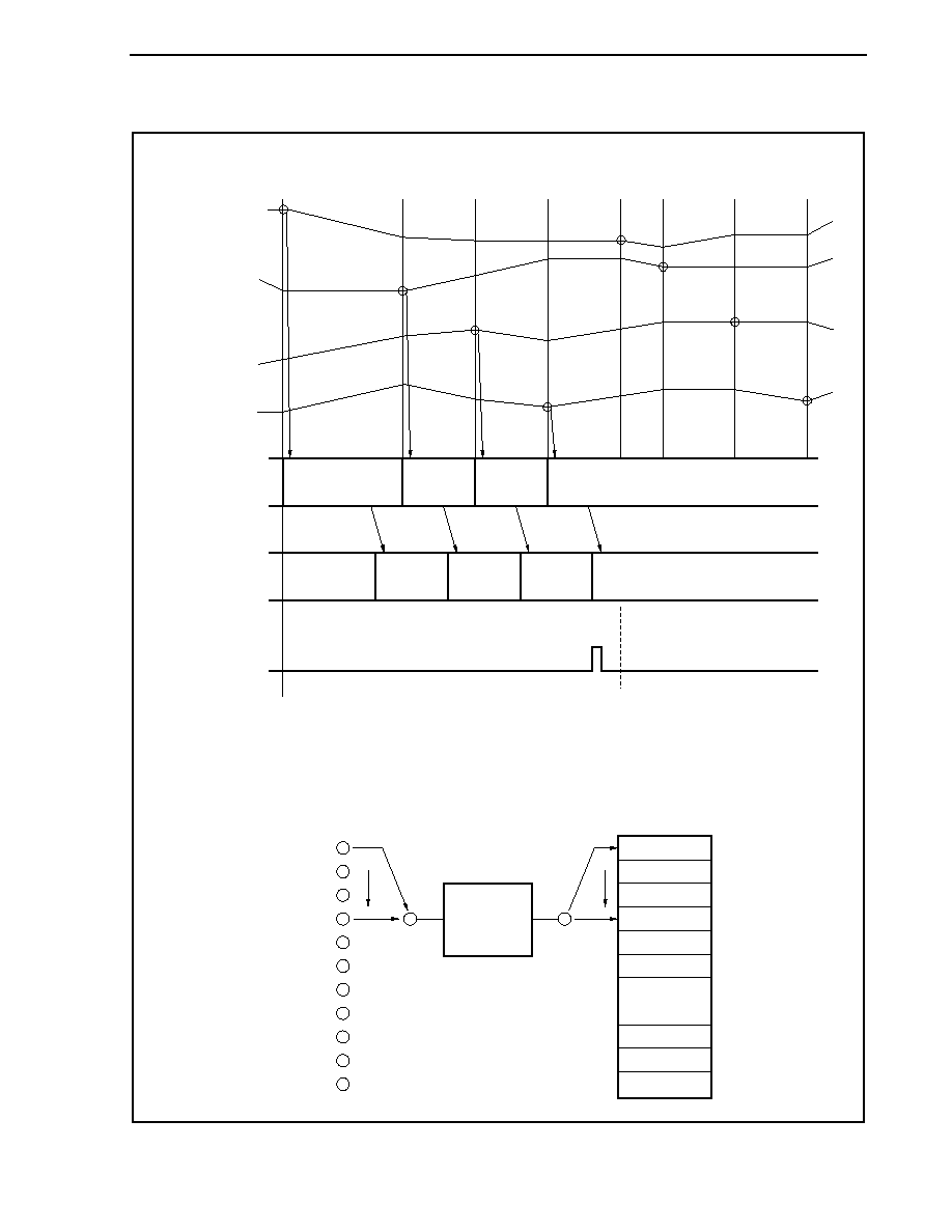
CHAPTER 13 A/D CONVERTER
Preliminary User's Manual U17714EJ1V0UD
465
Figure 13-7. Timing Example of One-Shot Scan Mode Operation (ADA0S Register = 03H)
(a) Timing example
A/D conversion
Data 1
(ANI0)
Data 2
(ANI1)
Data 3
(ANI2)
Data 4
(ANI3)
Data 1
(ANI0)
Data 2
(ANI1)
Data 3
(ANI2)
Data 4
(ANI3)
ADA0CRn
INTAD
Conversion start
Set ADA0CE bit = 1
Conversion end
ANI3
ANI0
ANI1
ANI2
Data 1
Data 2
Data 3
Data 4
Data 6
Data 5
Data 7
(b) Block diagram
A/D converter
ADA0CRn register
Analog input pin
ANI0
ANI1
ANI2
ANI3
ANI4
ANI5
ANI13
ANI14
ANI15
.
.
.
.
ADA0CR0
ADA0CR1
ADA0CR2
ADA0CR3
ADA0CR4
ADA0CR5
ADA0CR13
ADA0CR14
ADA0CR15
.
.
.

CHAPTER 13 A/D CONVERTER
Preliminary User's Manual U17714EJ1V0UD
466
13.5.5 Power-fail compare mode
The A/D conversion end interrupt request signal (INTAD) can be controlled as follows by the ADA0PFM and
ADA0PFT registers.
� When the ADA0PFM.ADA0PFE bit = 0, the INTAD signal is generated each time conversion is completed
(normal use of the A/D converter).
� When the ADA0PFE bit = 1 and when the ADA0PFM.ADA0PFC bit = 0, the value of the ADA0CRnH register is
compared with the value of the ADA0PFT register when conversion is completed, and the INTAD signal is
generated only if ADA0CRnH
ADA0PFT.
� When the ADA0PFE bit = 1 and when the ADA0PFC bit = 1, the value of the ADA0CRnH register is compared
with the value of the ADA0PFT register when conversion is completed, and the INTAD signal is generated only if
ADA0CRnH < ADA0PFT.
Remark n = 0 to 15
In the power-fail compare mode, four modes are available as modes in which to set the ANI0 to ANI15 pins:
continuous select mode, continuous scan mode, one-shot select mode, and one-shot scan mode.
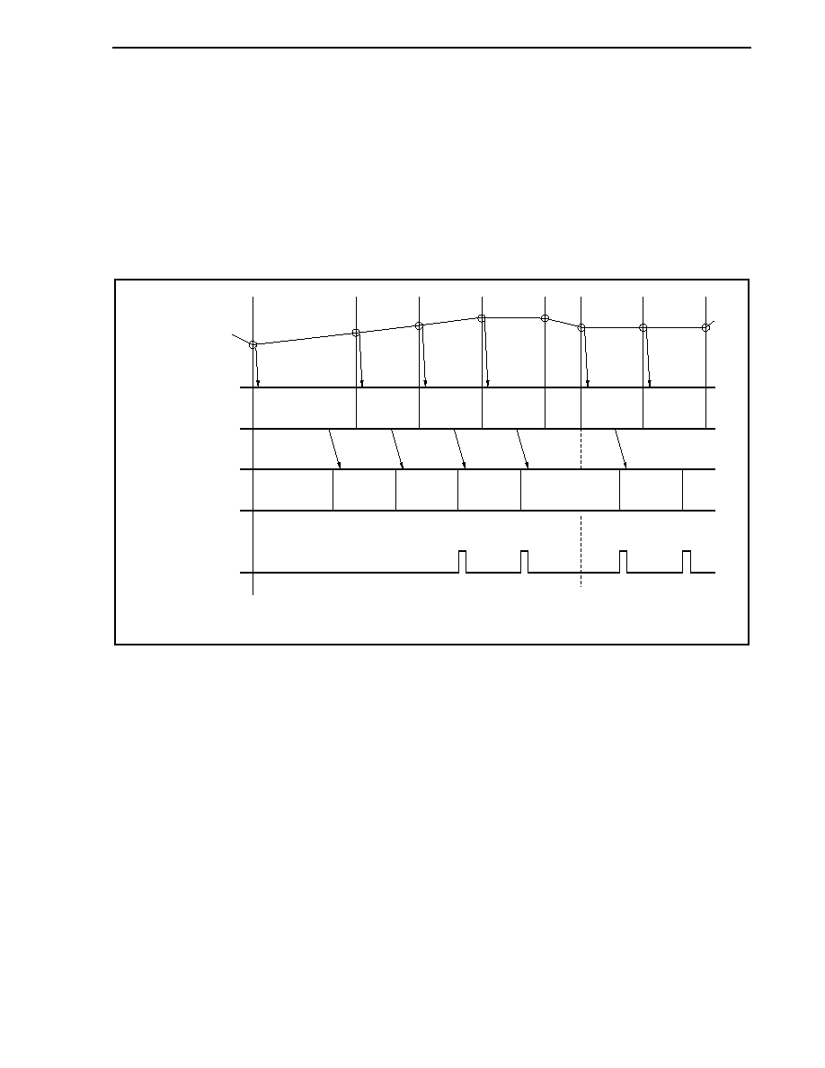
CHAPTER 13 A/D CONVERTER
Preliminary User's Manual U17714EJ1V0UD
467
(1) Continuous select mode
In this mode, the result of converting the voltage of the analog input pin specified by the ADA0S register is
compared with the set value of the ADA0PFT register. If the result of power-fail comparison matches the
condition set by the ADA0PFC bit, the conversion result is stored in the ADA0CRn register, and the INTAD
signal is generated. If it does not match, the conversion result is stored in the ADA0CRn register, and the
INTAD signal is not generated. After completion of the first conversion, the next conversion is started, unless
the ADA0M0.ADA0CE bit is cleared to 0 (n = 0 to 15).
Figure 13-8. Timing Example of Continuous Select Mode Operation
(When Power-Fail Comparison Is Made: ADA0S Register = 01H)
ANI1
A/D conversion
Data 1
(ANI1)
Data 2
(ANI1)
Data 3
(ANI1)
Data 4
(ANI1)
Data 5
(ANI1)
Data 6
(ANI1)
Data 7
(ANI1)
Data 1
Data 2
Data 3
Data 4
Data 5
Data 6
Data 7
Data 1
(ANI1)
Data 2
(ANI1)
Data 3
(ANI1)
Data 4
(ANI1)
Data 6
(ANI1)
ADA0CR1
INTAD
Conversion start
Set ADA0CE bit = 1
ADA0PFT
unmatch
ADA0PFT
unmatch
ADA0PFT
match
ADA0PFT
match
ADA0PFT
match
Conversion start
Set ADA0CE bit = 1
(2) Continuous scan mode
In this mode, the results of converting the voltages of the analog input pins sequentially selected from the ANI0
pin to the pin specified by the ADA0S register are stored, and the set value of the ADA0CR0H register of
channel 0 is compared with the value of the ADA0PFT register. If the result of power-fail comparison matches
the condition set by the ADA0PFC bit, the conversion result is stored in the ADA0CR0 register, and the INTAD
signal is generated. If it does not match, the conversion result is stored in the ADA0CR0 register, and the
INTAD signal is not generated.
After the result of the first conversion has been stored in the ADA0CR0 register, the results of sequentially
converting the voltages on the analog input pins up to the pin specified by the ADA0S register are continuously
stored. After completion of conversion, the next conversion is started from the ANI0 pin again, unless the
ADA0CE bit is cleared to 0.
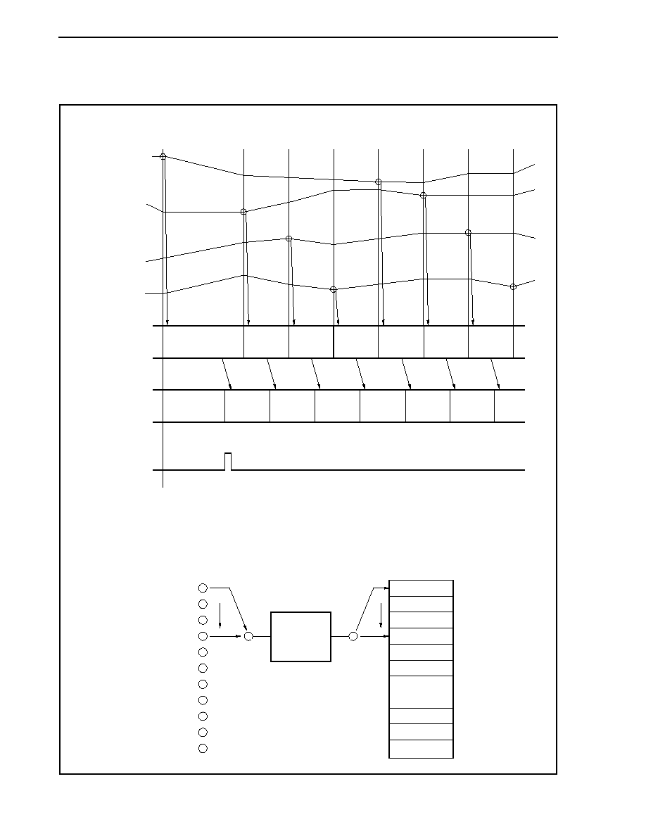
CHAPTER 13 A/D CONVERTER
Preliminary User's Manual U17714EJ1V0UD
468
Figure 13-9. Timing Example of Continuous Scan Mode Operation
(When Power-Fail Comparison Is Made: ADA0S Register = 03H)
(a) Timing example
A/D conversion
Data 1
(ANI0)
Data 2
(ANI1)
Data 3
(ANI2)
Data 4
(ANI3)
Data 5
(ANI0)
Data 6
(ANI1)
Data 7
(ANI2)
Data 1
(ANI0)
Data 2
(ANI1)
Data 3
(ANI2)
Data 4
(ANI3)
Data 5
(ANI0)
Data 6
(ANI1)
ADA0CRn
INTAD
Conversion start
Set ADA0CE bit = 1
ADA0PFT
match
ADA0PFT
unmatch
ANI3
ANI0
ANI1
ANI2
Data 1
Data 2
Data 3
Data 4
Data 6
Data 5
Data 7
(b) Block diagram
A/D converter
ADA0CRn register
Analog input pin
ANI0
ANI1
ANI2
ANI3
ANI4
ANI5
ANI13
ANI14
ANI15
.
.
.
.
ADA0CR0
ADA0CR1
ADA0CR2
ADA0CR3
ADA0CR4
ADA0CR5
ADA0CR13
ADA0CR14
ADA0CR15
.
.
.
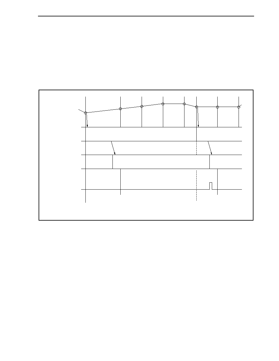
CHAPTER 13 A/D CONVERTER
Preliminary User's Manual U17714EJ1V0UD
469
(3) One-shot select mode
In this mode, the result of converting the voltage of the analog input pin specified by the ADA0S register is
compared with the set value of the ADA0PFT register. If the result of power-fail comparison matches the
condition set by the ADA0PFC bit, the conversion result is stored in the ADA0CRn register, and the INTAD
signal is generated. If it does not match, the conversion result is stored in the ADA0CRn register, and the
INTAD signal is not generated. Conversion is stopped after it has been completed.
Figure 13-10. Timing Example of One-Shot Select Mode Operation
(When Power-Fail Comparison Is Made: ADA0S Register = 01H)
ANI1
A/D conversion
Data 1
(ANI1)
Data 6
(ANI1)
Data 1
Data 2
Data 3
Data 4
Data 5
Data 6
Data 7
Data 1
(ANI1)
Data 6
(ANI1)
ADA0CR1
INTAD
Conversion start
Set ADA0CE bit = 1
Conversion start
Set ADA0CE bit = 1
ADA0PFT match
Conversion end
ADA0PFT unmatch
Conversion end
(4) One-shot scan mode
In this mode, the results of converting the voltages of the analog input pins sequentially selected from the ANI0
pin to the pin specified by the ADA0S register are stored, and the set value of the ADA0CR0H register of
channel 0 is compared with the set value of the ADA0PFT register. If the result of power-fail comparison
matches the condition set by the ADA0PFC bit, the conversion result is stored in the ADA0CR0 register and
the INTAD signal is generated. If it does not match, the conversion result is stored in the ADA0CR0 register,
and the INTAD0 signal is not generated. After the result of the first conversion has been stored in the
ADA0CR0 register, the results of converting the signals on the analog input pins specified by the ADA0S
register are sequentially stored. The conversion is stopped after it has been completed.
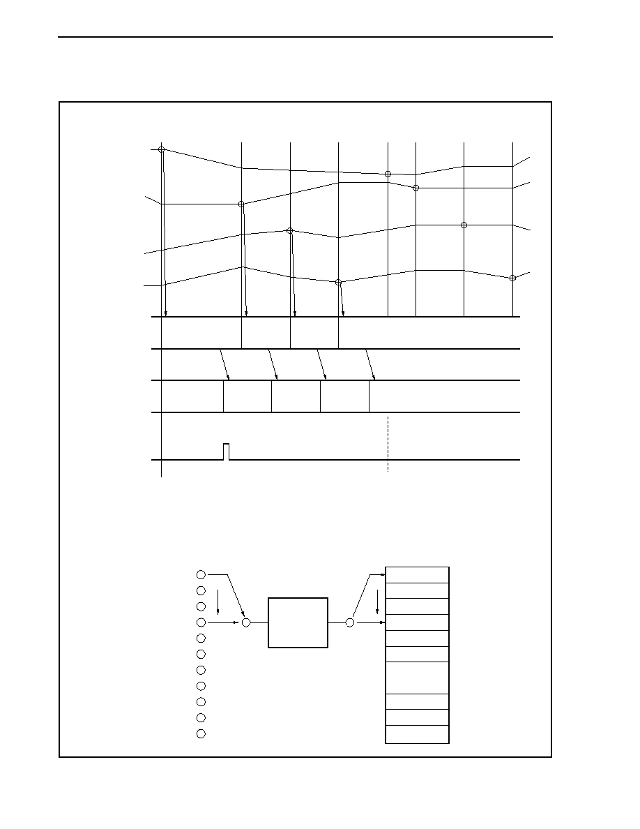
CHAPTER 13 A/D CONVERTER
Preliminary User's Manual U17714EJ1V0UD
470
Figure 13-11. Timing Example of One-Shot Scan Mode Operation
(When Power-Fail Comparison Is Made: ADA0S Register = 03H)
(a) Timing example
A/D conversion
Data 1
(ANI0)
Data 2
(ANI1)
Data 3
(ANI2)
Data 4
(ANI3)
Data 1
(ANI0)
Data 2
(ANI1)
Data 3
(ANI2)
Data 4
(ANI3)
ADA0CRn
INTAD
Conversion start
Set ADA0CE bit = 1
Conversion end
ADA0PFT
match
ANI3
ANI0
ANI1
ANI2
Data 1
Data 2
Data 3
Data 4
Data 6
Data 5
Data 7
(b) Block diagram
A/D converter
ADA0CRn register
Analog input pin
ANI0
ANI1
ANI2
ANI3
ANI4
ANI5
ANI13
ANI14
ANI15
.
.
.
.
ADA0CR0
ADA0CR1
ADA0CR2
ADA0CR3
ADA0CR4
ADA0CR5
ADA0CR13
ADA0CR14
ADA0CR15
.
.
.
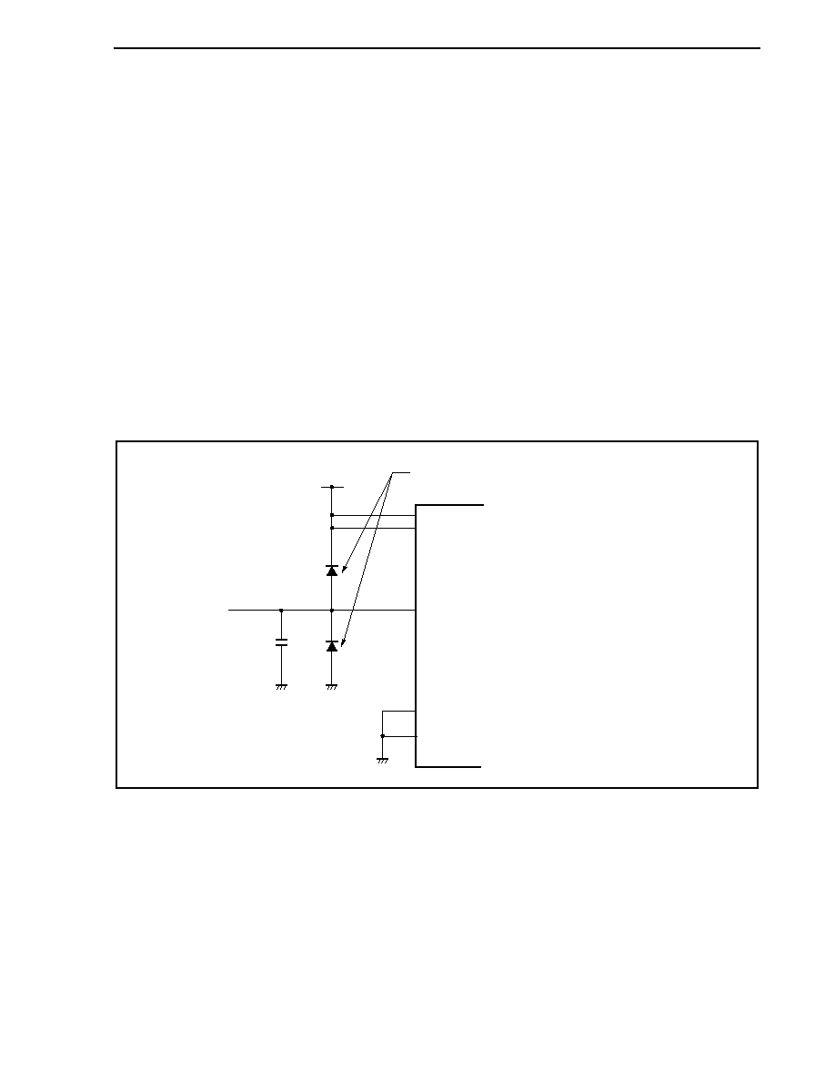
CHAPTER 13 A/D CONVERTER
Preliminary User's Manual U17714EJ1V0UD
471
13.6 Cautions
(1) When A/D converter is not used
When the A/D converter is not used, the power consumption can be reduced by clearing the
ADA0M0.ADA0CE bit to 0.
(2) Input range of ANI0 to ANI15 pins
Input the voltage within the specified range to the ANI0 to ANI15 pins. If a voltage equal to or higher than
AV
REF0
or equal to or lower than AV
SS
(even within the range of the absolute maximum ratings) is input to any
of these pins, the conversion value of that channel is undefined, and the conversion value of the other
channels may also be affected.
(3) Countermeasures against noise
To maintain the 10-bit resolution, the ANI0 to ANI15 pins must be effectively protected from noise. The
influence of noise increases as the output impedance of the analog input source becomes higher. To lower the
noise, connecting an external capacitor as shown in Figure 13-12 is recommended.
Figure 13-12. Processing of Analog Input Pin
AV
REF0
V
DD
V
SS
AV
SS
Clamp with a diode with a low V
F
(0.3 V or less)
if noise equal to or higher than AV
REF0
or equal
to or lower than AV
SS
may be generated.
ANI0 to ANI15
(4) Alternate I/O
The analog input pins (ANI0 to ANI15) function alternately as port pins. When selecting one of the ANI0 to
ANI15 pins to execute A/D conversion, do not execute an instruction to read an input port or write to an output
port during conversion as the conversion resolution may drop.
Also the conversion resolution may drop at the pins set as output port pins during A/D conversion if the output
current fluctuates due to the effect of the external circuit connected to the port pins.
If a digital pulse is applied to a pin adjacent to the pin whose input signal is being converted, the A/D
conversion value may not be as expected due to the influence of coupling noise. Therefore, do not apply a
pulse to a pin adjacent to the pin undergoing A/D conversion.
CHAPTER 13 A/D CONVERTER
Preliminary User's Manual U17714EJ1V0UD
472
(5) Interrupt request flag (ADIF)
The interrupt request flag (ADIF) is not cleared even if the contents of the ADA0S register are changed. If the
analog input pin is changed during A/D conversion, therefore, the result of converting the previously selected
analog input signal may be stored and the conversion end interrupt request flag may be set immediately before
the ADA0S register is rewritten. If the ADIF flag is read immediately after the ADA0S register is rewritten, the
ADIF flag may be set even though the A/D conversion of the newly selected analog input pin has not been
completed. When A/D conversion is stopped, clear the ADIF flag before resuming conversion.
Figure 13-13. Generation Timing of A/D Conversion End Interrupt Request
ADA0S rewriting
(ANIn conversion start)
ADA0S rewriting
(ANIm conversion start)
ADIF is set, but ANIm
conversion does not end
A/D conversion
ADA0CRn
INTAD
ANIn
ANIn
ANIm
ANIm
ANIm
ANIn
ANIn
ANIm
Remark n = 0 to 15
m = 0 to 15
(6) Internal equivalent circuit
The following shows the equivalent circuit of the analog input block.
Figure 13-14. Internal Equivalent Circuit of ANIn Pin
ANIn
C
IN
R
IN
R
IN
C
IN
2 k
4.9
pF
Remarks 1. The above values are reference values.
2. n = 0 to 15
CHAPTER 13 A/D CONVERTER
Preliminary User's Manual U17714EJ1V0UD
473
(7) AV
REF0
pin
(a) The AV
REF0
pin is used as the power supply pin of the A/D converter and also supplies power to the
alternate-function ports. In an application where a backup power supply is used, be sure to supply the
same voltage as V
DD
to the AV
REF0
pin as shown in Figure 13-15.
(b) The AV
REF0
pin is also used as the reference voltage pin of the A/D converter. If the source supplying
power to the AV
REF0
pin has a high impedance or if the power supply has a low current supply capability,
the reference voltage may fluctuate due to the current that flows during conversion (especially, immediately
after the conversion operation enable bit ADA0CE has been set to 1). As a result, the conversion accuracy
may drop. To avoid this, it is recommended to connect a capacitor across the AV
REF0
and AV
SS
pins to
suppress the reference voltage fluctuation as shown in Figure 13-15.
(c) If the source supplying power to the AV
REF0
pin has a high DC resistance (for example, because of
insertion of a diode), the voltage when conversion is enabled may be lower than the voltage when
conversion is stopped, because of a voltage drop caused by the A/D conversion current.
Figure 13-15. AV
REF0
Pin Processing Example
AV
REF0
Note
AV
SS
Main power supply
Note Parasitic
inductance
(8) Reading ADA0CRn register
When the ADA0M0 to ADA0M2 or ADA0S register is written, the contents of the ADA0CRn register may be
undefined. Read the conversion result after completion of conversion and before writing to the ADA0M0 to
ADA0M2 and ADA0S registers. The correct conversion result may not be read at a timing different from the
above.
(9) Standby mode
Because the A/D converter stops operating in the STOP mode, conversion results are invalid, so power
consumption can be reduced. Operations are resumed after the STOP mode is released, but the A/D
conversion results after the STOP mode is released are invalid. When using the A/D converter after the STOP
mode is released, before setting the STOP mode or releasing the STOP mode, clear the ADA0M0.ADA0CE bit
to 0 then set the ADA0CE bit to 1 after releasing the STOP mode.
In the IDLE1, IDLE2, or subclock operation mode, operation continues. To lower the power consumption,
therefore, clear the ADA0M0.ADA0CE bit to 0. In the IDLE1 and IDLE2 modes, since the analog input voltage
value cannot be retained, the A/D conversion results after the IDLE1 and IDLE2 modes are released are invalid.
The results of conversions before the IDLE1 and IDLE2 modes were set are valid.

CHAPTER 13 A/D CONVERTER
Preliminary User's Manual U17714EJ1V0UD
474
(10) Restrictions for each mode
(a) To select the external trigger mode/timer trigger mode, set the high-speed conversion mode. Do not input
a trigger during stabilization time that is inserted once after the A/D conversion operation is enabled
(ADA0M0.ADA0CE bit = 1).
(b) When writing data to an A/D control register in the following modes, stop the A/D conversion by clearing
the AD0M0.ADA0CE bit to 0. After the data is written to the register, enable the A/D conversion again by
setting the ADA0CE bit to 1.
� Normal conversion mode
� One-shot select mode/one-shot scan mode in high-speed conversion mode
Remark A/D control registers: ADA0M0, ADA0M2, ADA0S, ADA0PFM, and ADA0PFT registers
(11) Variation of A/D conversion results
The results of the A/D conversion may vary depending on the fluctuation of the supply voltage, or may be
affected by noise. To reduce the variation, take counteractive measures with the program such as averaging
the A/D conversion results.
(12) A/D conversion result hysteresis characteristics
The successive comparison type A/D converter holds the analog input voltage in the internal sample & hold
capacitor and then performs A/D conversion. After the A/D conversion has finished, the analog input voltage
remains in the internal sample & hold capacitor. As a result, the following phenomena may occur.
� When the same channel is used for A/D conversions, if the voltage is higher or lower than the previous A/D
conversion, then hysteresis characteristics may appear where the conversion result is affected by the
previous value. Thus, even if the conversion is performed at the same potential, the result may vary.
� When switching the analog input channel, hysteresis characteristics may appear where the conversion
result is affected by the previous channel value. This is because one A/D converter is used for the A/D
conversions. Thus, even if the conversion is performed at the same potential, the result may vary.
CHAPTER 13 A/D CONVERTER
Preliminary User's Manual U17714EJ1V0UD
475
13.7 How to Read A/D Converter Characteristics Table
This section describes the terms related to the A/D converter.
(1) Resolution
The minimum analog input voltage that can be recognized, i.e., the ratio of an analog input voltage to 1 bit of
digital output is called 1 LSB (least significant bit). The ratio of 1 LSB to the full scale is expressed as %FSR
(full-scale range). %FSR is the ratio of a range of convertible analog input voltages expressed as a percentage,
and can be expressed as follows, independently of the resolution.
1%FSR = (Maximum value of convertible analog input voltage � Minimum value of convertible analog
input voltage)/100
=
(AV
REF0
- 0)/100
=
AV
REF0
/100
When the resolution is 10 bits, 1 LSB is as follows:
1 LSB = 1/2
10
= 1/1,024
=
0.098%FSR
The accuracy is determined by the overall error, independently of the resolution.
(2) Overall error
This is the maximum value of the difference between an actually measured value and a theoretical value.
It is a total of zero-scale error, full-scale error, linearity error, and a combination of these errors.
The overall error in the characteristics table does not include the quantization error.
Figure 13-16. Overall Error
Ideal line
Overall error
1......1
0......0
0
AV
REF0
Analog input
Digital output
CHAPTER 13 A/D CONVERTER
Preliminary User's Manual U17714EJ1V0UD
476
(3) Quantization error
This is an error of
�1/2 LSB that inevitably occurs when an analog value is converted into a digital value.
Because the A/D converter converts analog input voltages in a range of
�1/2 LSB into the same digital codes,
a quantization error is unavoidable.
This error is not included in the overall error, zero-scale error, full-scale error, integral linearity error, or
differential linearity error in the characteristics table.
Figure 13-17. Quantization Error
Quantization error
1......1
0......0
0
AV
REF0
Analog input
Digital output
1/2 LSB
1/2 LSB
(4) Zero-scale error
This is the difference between the actually measured analog input voltage and its theoretical value when the
digital output changes from 0...000 to 0...001 (1/2 LSB).
Figure 13-18. Zero-Scale Error
AV
REF0
Analog input (LSB)
Digital output (lower 3 bits)
Ideal line
111
-1
0
1
2
3
100
011
010
001
000
Zero-scale error
CHAPTER 13 A/D CONVERTER
Preliminary User's Manual U17714EJ1V0UD
477
(5) Full-scale error
This is the difference between the actually measured analog input voltage and its theoretical value when the
digital output changes from 1...110 to 1...111 (full scale
- 3/2 LSB).
Figure 13-19. Full-Scale Error
AV
REF0
Analog input (LSB)
Digital output (lower 3 bits)
111
AV
REF0
-
3
0
AV
REF0
-
2 AV
REF0
-
1
100
011
010
000
Full-scale error
(6) Differential linearity error
Ideally, the width to output a specific code is 1 LSB. This error indicates the difference between the actually
measured value and its theoretical value when a specific code is output. This indicates the basic
characteristics of the A/D conversion when the voltage applied to the analog input pins of the same channel is
consistently increased bit by bit from AV
SS
to AV
REF0
. When the input voltage is increased or decreased, or
when two or more channels are used, see 13.7 (2) Overall error.
Figure 13-20. Differential Linearity Error
Ideal width of 1 LSB
Differential
linearity error
1......1
0......0
AV
REF0
Analog input
Digital output
CHAPTER 13 A/D CONVERTER
Preliminary User's Manual U17714EJ1V0UD
478
(7) Integral linearity error
This error indicates the extent to which the conversion characteristics differ from the ideal linear relationship. It
indicates the maximum value of the difference between the actually measured value and its theoretical value
where the zero-scale error and full-scale error are 0.
Figure 13-21. Integral Linearity Error
1......1
0......0
0
AV
REF0
Analog input
Digital output
Ideal line
Integral
linearity error
(8) Conversion time
This is the time required to obtain a digital output after each trigger has been generated.
The conversion time in the characteristics table includes the sampling time.
(9) Sampling time
This is the time for which the analog switch is ON to load an analog voltage to the sample & hold circuit.
Figure 13-22. Sampling Time
Sampling time
Conversion time
Preliminary User's Manual U17714EJ1V0UD
479
CHAPTER 14 D/A CONVERTER
14.1 Functions
The D/A converter has the following functions.
8-bit resolution
� 2 channels (DA0CS0, DA0CS1)
R-2R ladder method
Settling time: 3
�
s max. (when AV
REF1
is 3.0 to 3.6 V and external load is 20 pF)
Analog output voltage: AV
REF1
� m/256 (m = 0 to 255; value set to DA0CSn register)
Operation modes: Normal mode, real-time output mode
Remark n = 0, 1
14.2 Configuration
The D/A converter configuration is shown below.
Figure 14-1. Block Diagram of D/A Converter
DACS0 register
Selector
Selector
DACS1 register
ANO0 pin
ANO1 pin
DA0M.DACE0 bit
DA0M.DACE1 bit
DACS0 register write
DA0M.DAMD0 bit
INTTP2CC0 signal
DACS1 register write
DA0M.DAMD1 bit
INTTP3CC0 signal
AV
REF1
pin
AV
SS
pin
Cautions 1. DAC0 and DAC1 share the AV
REF1
pin.
2. DAC0 and DAC1 share the AV
SS
pin. The AV
SS
pin is also shared by the A/D converter.
CHAPTER 14 D/A CONVERTER
Preliminary User's Manual U17714EJ1V0UD
480
The D/A converter includes the following hardware.
Table 14-1. Configuration of D/A Converter
Item Configuration
Control registers
D/A converter mode register (DA0M)
D/A conversion value setting registers 0, 1 (DA0CS0, DA0CS1)
14.3 Registers
The registers that control the D/A converter are as follows.
� D/A converter mode register (DA0M)
� D/A conversion value setting registers 0, 1 (DA0CS0, DA0CS1)
(1) D/A converter mode register (DA0M)
The DA0M register controls the operation of the D/A converter.
This register can be read or written in 8-bit or 1-bit units.
Reset sets this register to 00H.
0
Normal mode
Real-time output mode
Note
DA0MDn
0
1
Selection of D/A converter operation mode (n = 0, 1)
DA0M
0
DA0CE1 DA0CE0
0
0
DA0MD1 DA0MD0
After reset: 00H R/W Address: FFFFF282H
Disables operation
Enables operation
DA0CEn
0
1
Control of D/A converter operation enable/disable (n = 0, 1)
< >
< >
Note The output trigger in the real-time output mode (DA0MDn bit = 1) is as follows.
� When n = 0: INTTP2CC0 signal (see CHAPTER 7 16-BIT TIMER/EVENT COUNTER P (TMP))
� When n = 1: INTTP3CC0 signal (see CHAPTER 7 16-BIT TIMER/EVENT COUNTER P (TMP))
CHAPTER 14 D/A CONVERTER
Preliminary User's Manual U17714EJ1V0UD
481
(2) D/A conversion value setting registers 0, 1 (DA0CS0, DA0CS1)
The DA0CS0 and DA0CS1 registers set the analog voltage value output to the ANO0 and ANO1 pins.
These registers can be read or written in 8-bit units.
Reset sets these registers to 00H.
DA0CSn7
DA0CSn
DA0CSn6 DA0CSn5 DA0CSn4 DA0CSn3 DA0CSn2 DA0CSn1 DA0CSn0
After reset: 00H R/W Address: DA0CS0 FFFFF280H, DA0CS1 FFFFF281H
Caution In the real-time output mode (DA0M.DA0MDn bit = 1), set the DA0CSn register before the
INTTP2CC0/INTTP3CC0 signals are generated. D/A conversion starts when the
INTTP2CC0/INTTP3CC0 signals are generated.
Remark n = 0, 1

CHAPTER 14 D/A CONVERTER
Preliminary User's Manual U17714EJ1V0UD
482
14.4 Operation
14.4.1 Operation in normal mode
D/A conversion is performed using a write operation to the DA0CSn register as the trigger.
The setting method is described below.
<1> Set the DA0M.DA0MDn bit to 0 (normal mode).
<2> Set the analog voltage value to be output to the ANOn pin to the DA0CSn register.
Steps <1> and <2> above constitute the initial settings.
<3> Set the DA0M.DA0CEn bit to 1 (D/A conversion enable).
D/A conversion starts when this setting is performed.
<4> To perform subsequent D/A conversions, write to the DA0CSn register.
The previous D/A conversion result is held until the next D/A conversion is performed.
Remarks 1. For the alternate-function pin settings, see Table 4-19 Using Port Pin as Alternate-Function Pin.
2. n = 0, 1
14.4.2 Operation in real-time output mode
D/A conversion is performed using the interrupt request signals (INTTP2CC0 and INTTP3CC0) of TMP2 and TMP3
as triggers.
The setting method is described below.
<1> Set the DA0M.DA0MDn bit to 1 (real-time output mode).
<2> Set the analog voltage value to be output to the ANOn pin to the DA0CSn register.
<3> Set the DA0M.DA0CEn bit to 1 (D/A conversion enable).
Steps <1> to <3> above constitute the initial settings.
<4> Operate TMP2 and TMP3.
<5> D/A conversion starts when the INTTP2CC0 and INTTP3CC0 signals are generated.
<6> After that, the value set in DA0CSn register is output every time the INTTP2CC0 and INTTP3CC0 signals are
generated.
Remarks 1. The output values of the ANO0 and ANO1 pins up to <5> above are undefined.
2. For the output values of the ANO0 and ANO1 pins in the HALT, IDLE1, IDLE2, and STOP modes,
see CHAPTER 21 STANDBY FUNCTION.
3. For the alternate-function pin settings, see Table 4-19 Using Port Pin as Alternate-Function Pin.
CHAPTER 14 D/A CONVERTER
Preliminary User's Manual U17714EJ1V0UD
483
14.4.3 Cautions
Observe the following cautions when using the D/A converter of the V850ES/JJ2.
(1) Do not change the set value of the DA0CSn register while the trigger signal is being issued in the real-time
output mode.
(2) Before changing the operation mode, be sure to clear the DA0M.DA0CEn bit to 0.
(3) When using one of the P10/AN00 and P11/AN01 pins as an I/O port and the other as a D/A output pin, do so
in an application where the port I/O level does not change during D/A output.
(4) Make sure that AV
REF0
= V
DD
= AV
REF1
= 3.0 to 3.6 V. If this range is exceeded, the operation is not guaranteed.
(5) Apply power to AV
REF1
at the same timing as AV
REF0
.
(6) No current can be output from the ANOn pin (n = 0, 1) because the output impedance of the D/A converter is
high. When connecting a resistor of 2 M
or less, insert a JFET input operational amplifier between the
resistor and the ANOn pin.
Figure 14-2. External Pin Connection Example
AV
REF1
V
DD
Output
10 F
0.1 F
10 F
0.1 F
AV
REF0
ANOn
AV
SS
-
+
JFET input
operational amplifier
�
�
�
�
(7) Because the D/A converter stops operation in the STOP mode, the ANO0 and ANO1 pins go into a high-
impedance state, and the power consumption can be reduced.
In the IDLE1, IDLE2, or subclock operation mode, however, the operation continues. To lower the power
consumption, therefore, clear the DA0M.DA0CEn bit to 0.

Preliminary User's Manual U17714EJ1V0UD
484
CHAPTER 15 ASYNCHRONOUS SERIAL INTERFACE A (UARTA)
15.1 Mode Switching of UARTA and Other Serial Interfaces
15.1.1 CSIB4 and UARTA0 mode switching
In the V850ES/JJ2, CSIB4 and UARTA0 are alternate functions of the same pin and therefore cannot be used
simultaneously. Set UARTA0 in advance, using the PMC3 and PFC3 registers, before use.
Caution The transmit/receive operation of CSIB4 and UARTA0 is not guaranteed if these functions are
switched during transmission or reception. Be sure to disable the one that is not used.
Figure 15-1. CSIB4 and UARTA0 Mode Switch Settings
PMC3
After reset: 0000H R/W Address: FFFFF446H, FFFFF447H
0
0
PMC35
PMC34
PMC33
PMC32
PMC31
PMC30
0
0
0
0
0
0
PMC39
PMC38
8
9
10
11
12
13
14
15
PFC3
After reset: 0000H R/W Address: FFFFF466H, FFFFF467H
0
0
0
0
0
0
PFC39
PFC38
0
0
PFC35
PFC34
PFC33
PFC32
PFC31
PFC30
8
9
10
11
12
13
14
15
PFCE3L
After reset: 00H R/W Address: FFFFF706H
0
0
0
0
0
PFCE32
0
0
Port I/O mode
ASCKA0 mode
SCKB4 mode
Port I/O mode
UARTA0 mode
CSIB4 mode
PMC32
0
1
1
PMC3n
0
1
1
Operation mode
Operation mode
PFCE32
�
0
0
PFC32
�
0
1
PFC3n
�
0
1
Remarks 1. n = 0, 1
2.
� = don't care
CHAPTER 15 ASYNCHRONOUS SERIAL INTERFACE A (UARTA)
Preliminary User's Manual U17714EJ1V0UD
485
15.1.2 UARTA2 and I
2
C00 mode switching
In the V850ES/JJ2, UARTA2 and I
2
C00 are alternate functions of the same pin and therefore cannot be used
simultaneously. Set UARTA2 in advance, using the PMC3 and PFC3 registers, before use.
Caution The transmit/receive operation of UARTA2 and I
2
C00 is not guaranteed if these functions are
switched during transmission or reception. Be sure to disable the one that is not used.
Figure 15-2. UARTA2 and I
2
C00 Mode Switch Settings
PMC3
After reset: 0000H R/W Address: FFFFF446H, FFFFF447H
PMC37
PMC36
PMC35
PMC34
PMC33
PMC32
PMC31
PMC30
0
0
0
0
0
0
PMC39
PMC38
8
9
10
11
12
13
14
15
PFC3
After reset: 0000H R/W Address: FFFFF466H, FFFFF467H
0
0
0
0
0
0
PFC39
PFC38
PFC37
PFC36
PFC35
PFC34
PFC33
PFC32
PFC31
PFC30
8
9
10
11
12
13
14
15
Port I/O mode
UARTA2 mode
I
2
C00 mode
PMC3n
0
1
1
Operation mode
PFC3n
�
0
1
Remarks 1. n = 8, 9
2.
� = don't care
CHAPTER 15 ASYNCHRONOUS SERIAL INTERFACE A (UARTA)
Preliminary User's Manual U17714EJ1V0UD
486
15.1.3 UARTA1 and I
2
C02 mode switching
In the V850ES/JJ2, UARTA1 and I
2
C02 are alternate functions of the same pin and therefore cannot be used
simultaneously. Set UARTA1 in advance, using the PMC9, PFC9, and PMCE9 registers, before use.
Caution The transmit/receive operation of UARTA1 and I
2
C02 is not guaranteed if these functions are
switched during transmission or reception. Be sure to disable the one that is not used.
Figure 15-3. UARTA1 and I
2
C02 Mode Switch Settings
PMC9
After reset: 0000H R/W Address: FFFFF452H, FFFFF453H
PMC97
PMC96
PMC95
PMC94
PMC93
PMC92
PMC91
PMC90
PMC915 PMC914
PMC913 PMC912
PMC911 PMC910
PMC99
PMC98
8
9
10
11
12
13
14
15
PFC9
After reset: 0000H R/W Address: FFFFF472H, FFFFF473H
PFC915
PFC914
PFC913
PFC912
PFC911
PFC910
PFC99
PFC98
PFC97
PFC96
PFC95
PFC94
PFC93
PFC92
PFC91
PFC90
8
9
10
11
12
13
14
15
PFCE915 PFCE914
0
0
0
0
0
0
PFCE97
PFCE96
PFCE95 PFCE94
PFCE93 PFCE92
PFCE91
PFCE90
8
9
10
11
12
13
14
15
PFCE9
After reset: 0000H R/W Address: FFFFF712H, FFFFF713H
UARTA1 mode
I
2
C02 mode
PMC9n
1
1
Operation mode
PFCE9n
1
1
PFC9n
0
1
Remark n = 0, 1

CHAPTER 15 ASYNCHRONOUS SERIAL INTERFACE A (UARTA)
Preliminary User's Manual U17714EJ1V0UD
487
15.2 Features
Transfer rate: 300 bps to 312.5 kbps (using internal system clock of 20 MHz and dedicated baud rate generator)
Full-duplex communication: Internal UARTAn receive data register (UAnRX)
Internal UARTAn transmit data register (UAnTX)
2-pin configuration:
TXDAn: Transmit data output pin
RXDAn: Receive data input pin
Reception error output function
� Parity error
� Framing error
� Overrun error
Interrupt sources: 2
� Reception complete interrupt (INTUAnR):
This interrupt occurs upon transfer of receive data from the
receive shift register to receive data register after serial
transfer completion, in the reception enabled status.
� Transmission enable interrupt (INTUAnT):
This interrupt occurs upon transfer of transmit data from the
transmit data register to the transmit shift register in the
transmission enabled status.
Character length: 7, 8 bits
Parity function: Odd, even, 0, none
Transmission stop bit: 1, 2 bits
On-chip dedicated baud rate generator
MSB-/LSB-first transfer selectable
Transmit/receive data inverted input/output possible
SBF (Sync Break Field) transmission/reception in the LIN (Local Interconnect Network) communication format
possible
� 13 to 20 bits selectable for SBF transmission
� Recognition of 11 bits or more possible for SBF reception
� SBF reception flag provided
Remark n = 0 to 3
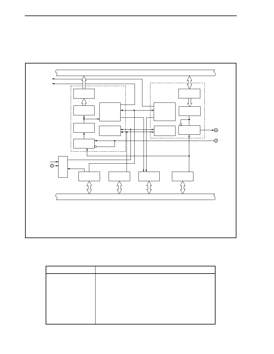
CHAPTER 15 ASYNCHRONOUS SERIAL INTERFACE A (UARTA)
Preliminary User's Manual U17714EJ1V0UD
488
15.3 Configuration
The block diagram of the UARTAn is shown below.
Figure 15-4. Block Diagram of Asynchronous Serial Interface An
Internal bus
Internal bus
UAnOTP0
UAnCTL0
UAnSTR
UAnCTL1
UAnCTL2
Receive
shift register
UAnRX
Filter
Selector
UAnTX
Transmit
shift register
Transmission
controller
Reception
controller
Selector
Baud rate
generator
Baud rate
generator
INTUAnR
INTUAnT
TXDAn
RXDAn
f
XX
to f
XX
/2
10
ASCKA0
Note
Reception unit
Transmission
unit
Clock
selector
Note UARTA0
only
Remarks 1. n = 0 to 3
2. For the configuration of the baud rate generator, see Figure 15-16.
UARTAn includes the following hardware.
Table 15-1. Configuration of UARTAn
Item Configuration
Registers
UARTAn control register 0 (UAnCTL0)
UARTAn control register 1 (UAnCTL1)
UARTAn control register 2 (UAnCTL2)
UARTAn option control register 0 (UAnOPT0)
UARTAn status register (UAnSTR)
UARTAn receive shift register
UARTAn receive data register (UAnRX)
UARTAn transmit shift register
UARTAn transmit data register (UAnTX)

CHAPTER 15 ASYNCHRONOUS SERIAL INTERFACE A (UARTA)
Preliminary User's Manual U17714EJ1V0UD
489
(1) UARTAn control register 0 (UAnCTL0)
The UAnCTL0 register is an 8-bit register used to specify the UARTAn operation.
(2) UARTAn control register 1 (UAnCTL1)
The UAnCTL1 register is an 8-bit register used to select the input clock for the UARTAn.
(3) UARTAn control register 2 (UAnCTL2)
The UAnCTL2 register is an 8-bit register used to control the baud rate for the UARTAn.
(4) UARTAn option control register 0 (UAnOPT0)
The UAnOPT0 register is an 8-bit register used to control serial transfer for the UARTAn.
(5) UARTAn status register (UAnSTR)
The UAnSTRn register consists of flags indicating the error contents when a reception error occurs. Each one
of the reception error flags is set (to 1) upon occurrence of a reception error and is reset (to 0) by reading the
UAnSTR register.
(6) UARTAn receive shift register
This is a shift register used to convert the serial data input to the RXDAn pin into parallel data. Upon reception
of 1 byte of data and detection of the stop bit, the receive data is transferred to the UAnRX register.
This register cannot be manipulated directly.
(7) UARTAn receive data register (UAnRX)
The UAnRX register is an 8-bit register that holds receive data. When 7 characters are received, 0 is stored in
the highest bit (when data is received LSB first).
In the reception enabled status, receive data is transferred from the UARTAn receive shift register to the
UAnRX register in synchronization with the completion of shift-in processing of 1 frame.
Transfer to the UAnRX register also causes the reception complete interrupt request signal (INTUAnR) to be
output.
(8) UARTAn transmit shift register
The transmit shift register is a shift register used to convert the parallel data transferred from the UAnTX
register into serial data.
When 1 byte of data is transferred from the UAnTX register, the shift register data is output from the TXDAn pin.
This register cannot be manipulated directly.
(9) UARTAn transmit data register (UAnTX)
The UAnTX register is an 8-bit transmit data buffer. Transmission starts when transmit data is written to the
UAnTX register. When data can be written to the UAnTX register (when data of one frame is transferred from
the UAnTX register to the UARTAn transmit shift register), the transmission enable interrupt request signal
(INTUAnT) is generated.
CHAPTER 15 ASYNCHRONOUS SERIAL INTERFACE A (UARTA)
Preliminary User's Manual U17714EJ1V0UD
490
15.4 Registers
(1) UARTAn control register 0 (UAnCTL0)
The UAnCTL0 register is an 8-bit register that controls the UARTAn serial transfer operation.
This register can be read or written in 8-bit or 1-bit units.
Reset sets this register to 10H.
(1/2)
UAnPWR
Disable UARTAn operation (UARTAn reset asynchronously)
Enable UARTAn operation
UAnPWR
0
1
UARTAn operation control
UAnCTL0
(n = 0 to 3)
UAnTXE UAnRXE UAnDIR
UAnPS1 UAnPS0
UAnCL
UAnSL
<6>
<5>
<4>
3
2
1
After reset: 10H R/W Address: UA0CTL0 FFFFFA00H, UA1CTL0 FFFFFA10H,
UA2CTL0 FFFFFA20H, UA3CTL0 FFFFFA30H
The UARTAn operation is controlled by the UAnPWR bit. The TXDAn pin output
is fixed to high level by clearing the UAnPWR bit to 0 (fixed to low level if
UAnOPT0.UAnTDL bit = 1).
Disable transmission operation
Enable transmission operation
UAnTXE
0
1
Transmission operation enable
� To start transmission, set the UAnPWR bit to 1 and then set the UAnTXE bit to 1.
To stop, transmission clear the UAnTXE bit to 0 and then UAnPWR bit to 0.
� To initialize the transmission unit, clear the UAnTXE bit to 0, wait for two cycles of
the base clock, and then set the UAnTXE bit to 1 again. Otherwise, initialization
may not be executed (for the base clock, see 15.7 (1) (a) Base clock).
Disable reception operation
Enable reception operation
UAnRXE
0
1
Reception operation enable
� To start reception, set the UAnPWR bit to 1 and then set the UAnRXE bit to 1.
To stop reception, clear the UAnRXE bit to 0 and then UAnPWR bit to 0.
� To initialize the reception unit, clear the UAnRXE bit to 0, wait for two periods of
the base clock, and then set the UAnRXE bit to 1 again. Otherwise, initialization
may not be executed (for the base clock, see 15.7 (1) (a) Base clock).
<7>
0
CHAPTER 15 ASYNCHRONOUS SERIAL INTERFACE A (UARTA)
Preliminary User's Manual U17714EJ1V0UD
491
(2/2)
7 bits
8 bits
UAnCL
0
1
Specification of data character length of 1 frame of transmit/receive data
This register can be rewritten only when the UAnPWR bit = 0 or the UAnTXE bit =
the UAnRXE bit = 0.
1 bit
2 bits
UAnSL
0
1
Specification of length of stop bit for transmit data
This register can be rewritten only when the UAnPWR bit = 0 or the UAnTXE bit =
the UAnRXE bit = 0.
� This register is rewritten only when the UAnPWR bit = 0 or the UAnTXE bit = the
UAnRXE bit = 0.
� If "Reception with 0 parity" is selected during reception, a parity check is not performed.
Therefore, the UAnSTR.UAnPE bit is not set.
� When transmission and reception are performed in the LIN format, clear the
UAnPS1 and UAnPS0 bits to 00.
No parity output
0 parity output
Odd parity output
Even parity output
Reception with no parity
Reception with 0 parity
Odd parity check
Even parity check
UAnPS1
0
0
1
1
Parity selection during transmission Parity selection during reception
UAnPS0
0
1
0
1
MSB-first transfer
LSB-first transfer
UAnDIR
0
1
Transfer direction selection
This register can be rewritten only when the UAnPWR bit = 0 or the UAnTXE bit =
the UAnRXE bit = 0.
Remark For details of parity, see 15.6.9 Parity types and operations.
CHAPTER 15 ASYNCHRONOUS SERIAL INTERFACE A (UARTA)
Preliminary User's Manual U17714EJ1V0UD
492
(2) UARTAn control register 1 (UAnCTL1)
For details, see 15.7 (2) UARTAn control register 1 (UAnCTL1).
(3) UARTAn control register 2 (UAnCTL2)
For details, see 15.7 (3) UARTAn control register 2 (UAnCTL2).
(4) UARTAn option control register 0 (UAnOPT0)
The UAnOPT0 register is an 8-bit register that controls the serial transfer operation of the UARTAn register.
This register can be read or written in 8-bit or 1-bit units.
Reset sets this register to 14H.
(1/2)
UAnSRF
When the UAnCTL0.UAnPWR bit = UAnCTL0.UAnRXE bit = 0 are set.
Also upon normal end of SBF reception.
During SBF reception
UAnSRF
0
1
SBF reception flag
UAnOPT0
(n = 0 to 3)
UAnSRT
UAnSTT UAnSLS2 UAnSLS1 UAnSLS0 UAnTDL
UAnRDL
6
5
4
3
2
1
After reset: 14H R/W Address: UA0OPT0 FFFFFA03H, UA1OPT0 FFFFFA13H,
UA2OPT0 FFFFFA23H, UA3OPT0 FFFFFA33H
SBF reception trigger
UAnSRT
0
1
SBF reception trigger
� SBF (Sync Break Field) reception is judged during LIN communication.
� The UAnSRF bit is held at 1 when an SBF reception error occurs, and then SBF
reception is started again.
� This is the SBF reception trigger bit during LIN communication, and when read,
"0" is always read. For SBF reception, set the UAnSRT bit (to 1) to enable SBF
reception.
� Set the UAnSRT bit after setting the UAnPWR bit = UAnRXE bit = 1.
� This is the SBF transmission trigger bit during LIN communication, and when read,
"0" is always read.
� Set the UAnSTT bit after setting the UAnPWR bit = UAnTXE bit = 1.
SBF transmission trigger
UAnSTT
0
1
SBF transmission trigger
<7>
0
-
-
Caution Do not set the UAnSRT and UAnSTT bits (to 1) during SBF reception (UAnSRF bit = 1).
CHAPTER 15 ASYNCHRONOUS SERIAL INTERFACE A (UARTA)
Preliminary User's Manual U17714EJ1V0UD
493
(2/2)
UAnSLS2
1
1
1
0
0
0
0
1
UAnSLS1
0
1
1
0
0
1
1
0
UAnSLS0
1
0
1
0
1
0
1
0
13-bit output (reset value)
14-bit output
15-bit output
16-bit output
17-bit output
18-bit output
19-bit output
20-bit output
SBF transmit length selection
� The output level of the TXDAn pin can be inverted using the UAnTDL bit.
� This register can be set when the UAnPWR bit = 0 or when the UAnTXE bit = 0.
This register can be set when the UAnPWR bit = 0 or when the UAnTXE bit = 0.
Normal output of transfer data
Inverted output of transfer data
UAnTDL
0
1
Transmit data level bit
� The input level of the RXDAn pin can be inverted using the UAnRDL bit.
� This register can be set when the UAnPWR bit = 0 or the UAnRXE bit = 0.
Normal input of transfer data
Inverted input of transfer data
UAnRDL
0
1
Receive data level bit
(5) UARTAn status register (UAnSTR)
The UAnSTR register is an 8-bit register that displays the UARTAn transfer status and reception error contents.
This register can be read or written in 8-bit or 1-bit units, but the UAnTSF bit is a read-only bit, while the
UAnPE, UAnFE, and UAnOVE bits can both be read and written. However, these bits can only be cleared by
writing 0; they cannot be set by writing 1 (even if 1 is written to them, the value is retained).
The initialization conditions are shown below.
Register/Bit Initialization
Conditions
UAnSTR register
� Reset
� UAnCTL0.UAnPWR = 0
UAnTSF bit
� UAnCTL0.UAnTXE = 0
UAnPE, UAnFE, UAnOVE bits
� 0 write
� UAnCTL0.UAnRXE = 0
CHAPTER 15 ASYNCHRONOUS SERIAL INTERFACE A (UARTA)
Preliminary User's Manual U17714EJ1V0UD
494
UAnTSF
� When the UAnPWR bit = 0 or the UAnTXE bit = 0 has been set.
� When, following transfer completion, there was no next data transfer
from UAnTX register
Write to UAnTX register
UAnTSF
0
1
Transfer status flag
UAnSTR
(n = 0 to 3)
0
0
0
0
UAnPE
UAnFE
UAnOVE
6
5
4
3
<2>
<1>
After reset: 00H R/W Address: UA0STR FFFFFA04H, UA1STR FFFFFA14H,
UA2STR FFFFFA24H, UA3STR FFFFFA34H
The UAnTSF bit is always 1 when performing continuous transmission. When
initializing the transmission unit, check that the UAnTSF bit = 0 before performing
initialization. The transmit data is not guaranteed when initialization is performed
while the UAnTSF bit = 1.
� When the UAnPWR bit = 0 or the UAnRXE bit = 0 has been set.
� When 0 has been written
When parity of data and parity bit do not match during reception.
UAnPE
0
1
Parity error flag
� The operation of the UAnPE bit is controlled by the settings of the
UAnCTL0.UAnPS1 and UAnCTL0.UAnPS0 bits.
� The UAnPE bit can be read and written, but it can only be cleared by writing 0 to it, and
it cannot be set by writing 1 to it. When 1 is written to this bit, the value is retained.
� When the UAnPWR bit = 0 or the UAnRXE bit = 0 has been set
� When 0 has been written
When no stop bit is detected during reception
UAnFE
0
1
Framing error flag
� Only the first bit of the receive data stop bits is checked, regardless of the value
of the UAnCTL0.UAnSL bit.
� The UAnFE bit can be both read and written, but it can only be cleared by
writing 0 to it, and it cannot be set by writing 1 to it. When 1 is written to this bit,
the value is retained.
� When the UAnPWR bit = 0 or the UAnRXE bit = 0 has been set.
� When 0 has been written
When receive data has been set to the UAnRX register and the next
receive operation is completed before that receive data has been read
UAnOVE
0
1
Overrun error flag
� When an overrun error occurs, the data is discarded without the next receive data
being written to the receive buffer.
� The UAnOVE bit can be both read and written, but it can only be cleared by writing
0 to it. When 1 is written to this bit, the value is retained.
<7>
<0>
CHAPTER 15 ASYNCHRONOUS SERIAL INTERFACE A (UARTA)
Preliminary User's Manual U17714EJ1V0UD
495
(6) UARTAn receive data register (UAnRX)
The UAnRX register is an 8-bit buffer register that stores parallel data converted by the receive shift register.
The data stored in the receive shift register is transferred to the UAnRX register upon completion of reception
of 1 byte of data.
During LSB-first reception when the data length has been specified as 7 bits, the receive data is transferred to
bits 6 to 0 of the UAnRX register and the MSB always becomes 0. During MSB-first reception, the receive data
is transferred to bits 7 to 1 of the UAnRX register and the LSB always becomes 0.
When an overrun error (UAnOVE) occurs, the receive data at this time is not transferred to the UAnRX register
and is discarded.
This register is read-only, in 8-bit units.
In addition to reset input, the UAnRX register can be set to FFH by clearing the UAnCTL0.UAnPWR bit to 0.
UAnRX
(n = 0 to 3)
6
5
4
3
2
1
After reset: FFH R Address: UA0RX FFFFFA06H, UA1RX FFFFFA16H,
UA2RX FFFFFA26H, UA3RX FFFFFA36H
7
0
(7) UARTAn transmit data register (UAnTX)
The UAnTX register is an 8-bit register used to set transmit data.
This register can be read or written in 8-bit units.
Reset sets this register to FFH.
UAnTX
(n = 0 to 3)
6
5
4
3
2
1
After reset: FFH R/W Address: UA0TX FFFFFA07H, UA1TX FFFFFA17H,
UA2TX FFFFFA27H, UA3TX FFFFFA37H
7
0

CHAPTER 15 ASYNCHRONOUS SERIAL INTERFACE A (UARTA)
Preliminary User's Manual U17714EJ1V0UD
496
15.5 Interrupt Request Signals
The following two interrupt request signals are generated from UARTAn.
� Reception complete interrupt request signal (INTUAnR)
� Transmission enable interrupt request signal (INTUAnT)
The default priority for these two interrupt request signals is reception complete interrupt request signal then
transmission enable interrupt request signal.
Table 15-2. Interrupts and Their Default Priorities
Interrupt Priority
Reception complete
High
Transmission enable
Low
(1) Reception complete interrupt request signal (INTUAnR)
A reception complete interrupt request signal is output when data is shifted into the receive shift register and
transferred to the UAnRX register in the reception enabled status.
When a reception complete interrupt request signal is received and the data is read, read the UAnSTR register
and check that the reception result is not an error.
No reception complete interrupt request signal is generated in the reception disabled status.
(2) Transmission enable interrupt request signal (INTUAnT)
If transmit data is transferred from the UAnTX register to the UARTAn transmit shift register with transmission
enabled, the transmission enable interrupt request signal is generated.

CHAPTER 15 ASYNCHRONOUS SERIAL INTERFACE A (UARTA)
Preliminary User's Manual U17714EJ1V0UD
497
15.6 Operation
15.6.1 Data format
Full-duplex serial data reception and transmission is performed.
As shown in Figure 15-5, one data frame of transmit/receive data consists of a start bit, character bits, parity bit,
and stop bit(s).
Specification of the character bit length within 1 data frame, parity selection, specification of the stop bit length, and
specification of MSB/LSB-first transfer are performed using the UAnCTL0 register.
Moreover, control of UART output/inverted output for the TXDAn bit is performed using the UAnOPT0.UAnTDL bit.
� Start
bit ................. 1 bit
� Character bits........ 7 bits/8 bits
� Parity bit ................ Even parity/odd parity/0 parity/no parity
� Stop
bit.................. 1 bit/2 bits
CHAPTER 15 ASYNCHRONOUS SERIAL INTERFACE A (UARTA)
Preliminary User's Manual U17714EJ1V0UD
498
Figure 15-5. UARTA Transmit/Receive Data Format
(a) 8-bit data length, LSB first, even parity, 1 stop bit, transfer data: 55H
1 data frame
Start
bit
D0
D1
D2
D3
D4
D5
D6
D7
Parity
bit
Stop
bit
(b) 8-bit data length, MSB first, even parity, 1 stop bit, transfer data: 55H
1 data frame
Start
bit
D7
D6
D5
D4
D3
D2
D1
D0
Parity
bit
Stop
bit
(c) 8-bit data length, MSB first, even parity, 1 stop bit, transfer data: 55H, TXDAn inversion
1 data frame
Start
bit
D7
D6
D5
D4
D3
D2
D1
D0
Parity
bit
Stop
bit
(d) 7-bit data length, LSB first, odd parity, 2 stop bits, transfer data: 36H
1 data frame
Start
bit
D0
D1
D2
D3
D4
D5
D6
Parity
bit
Stop
bit
Stop
bit
(e) 8-bit data length, LSB first, no parity, 1 stop bit, transfer data: 87H
1 data frame
Start
bit
D0
D1
D2
D3
D4
D5
D6
D7
Stop
bit
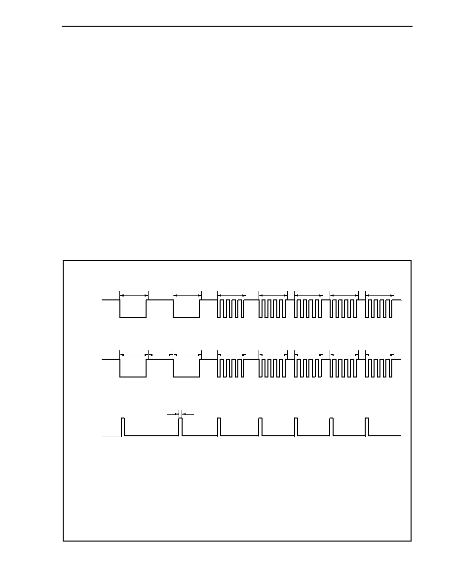
CHAPTER 15 ASYNCHRONOUS SERIAL INTERFACE A (UARTA)
Preliminary User's Manual U17714EJ1V0UD
499
15.6.2 SBF transmission/reception format
The V850ES/JJ2 has an SBF (Sync Break Field) transmission/reception control function to enable use of the LIN
function.
Remark LIN stands for Local Interconnect Network and is a low-speed (1 to 20 kbps) serial communication
protocol intended to aid the cost reduction of an automotive network.
LIN communication is single-master communication, and up to 15 slaves can be connected to one
master.
The LIN slaves are used to control the switches, actuators, and sensors, and these are connected to the
LIN master via the LIN network.
Normally, the LIN master is connected to a network such as CAN (Controller Area Network).
In addition, the LIN bus uses a single-wire method and is connected to the nodes via a transceiver that
complies with ISO9141.
In the LIN protocol, the master transmits a frame with baud rate information and the slave receives it and
corrects the baud rate error. Therefore, communication is possible when the baud rate error in the slave
is
�15% or less.
Figures 15-6 and 15-7 outline the transmission and reception manipulations of LIN.
Figure 15-6. LIN Transmission Manipulation Outline
LIN
bus
Wake-up
signal
frame
Sync
break
field
Sync
field
Identifier
field
DATA
field
DATA
field
Check
SUM
field
INTUAnT
interrupt
TXDAn (output)
Note 3
8 bits
Note 1
Note 2
13 bits
SBF transmission
Note 4
55H
transmission
Data
transmission
Data
transmission
Data
transmission
Data
transmission
Notes 1. The interval between each field is controlled by software.
2. SBF output is performed by hardware. The output width is the bit length set by the
UAnOPT0.UAnSBL2 to UAnOPT0.UAnSBL0 bits. If even finer output width adjustments are
required, such adjustments can be performed using the UAnCTLn.UAnBRS7 to UAnCTLn.UAnBRS0
bits.
3. 80H transfer in the 8-bit mode is substituted for the wakeup signal frame.
4. A transmission enable interrupt request signal (INTUAnT) is output at the start of each transmission.
The INTUAnT signal is also output at the start of each SBF transmission.
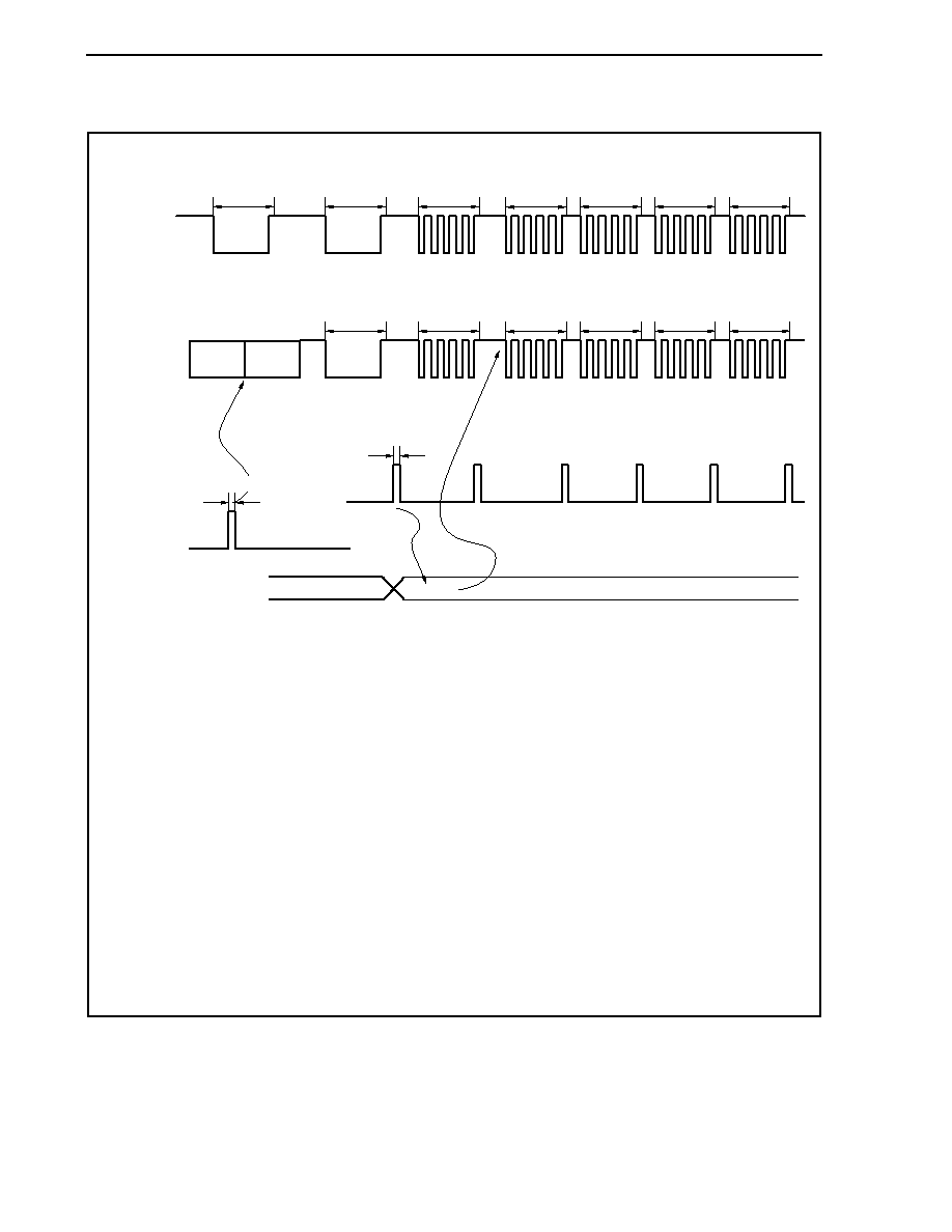
CHAPTER 15 ASYNCHRONOUS SERIAL INTERFACE A (UARTA)
Preliminary User's Manual U17714EJ1V0UD
500
Figure 15-7. LIN Reception Manipulation Outline
Reception interrupt (INTUAnR)
Edge detection
Capture timer
Disable
Disable
Enable
RXDAn (input)
Enable
Note 2
13 bits
SBF
reception
Note 3
Note 4
Note 1
SF reception
ID reception
Data
transmission
Data
transmission
Note 5
Data transmission
LIN
bus
Wake-up
signal
frame
Sync
break
field
Sync
field
Identifier
field
DATA
field
DATA
field
Check
SUM
field
Notes 1. The wakeup signal is sent by the pin edge detector, UARTAn is enabled, and the SBF reception
mode is set.
2. The receive operation is performed until detection of the stop bit. Upon detection of SBF reception
of 11 or more bits, normal SBF reception end is judged, and an interrupt signal is output. Upon
detection of SBF reception of less than 11 bits, an SBF reception error is judged, no interrupt signal
is output, and the mode returns to the SBF reception mode.
3. If SBF reception ends normally, an interrupt request signal is output. The timer is enabled by an SBF
reception complete interrupt. Moreover, error detection for the UAnSTR.UAnOVE, UAnSTR.UAnPE,
and UAnSTR.UAnFE bits is suppressed and UART communication error detection processing and
UARTAn receive shift register and data transfer of the UAnRX register are not performed. The
UARTAn receive shift register holds the initial value, FFH.
4. The RXDAn pin is connected to TI (capture input) of the timer, the transfer rate is calculated, and the
baud rate error is calculated. The value of the UAnCTL2 register obtained by correcting the baud
rate error after dropping UARTA enable is set again, causing the status to become the reception
status.
5. Check-sum field distinctions are made by software. UARTAn is initialized following CSF reception,
and the processing for setting the SBF reception mode again is performed by software.
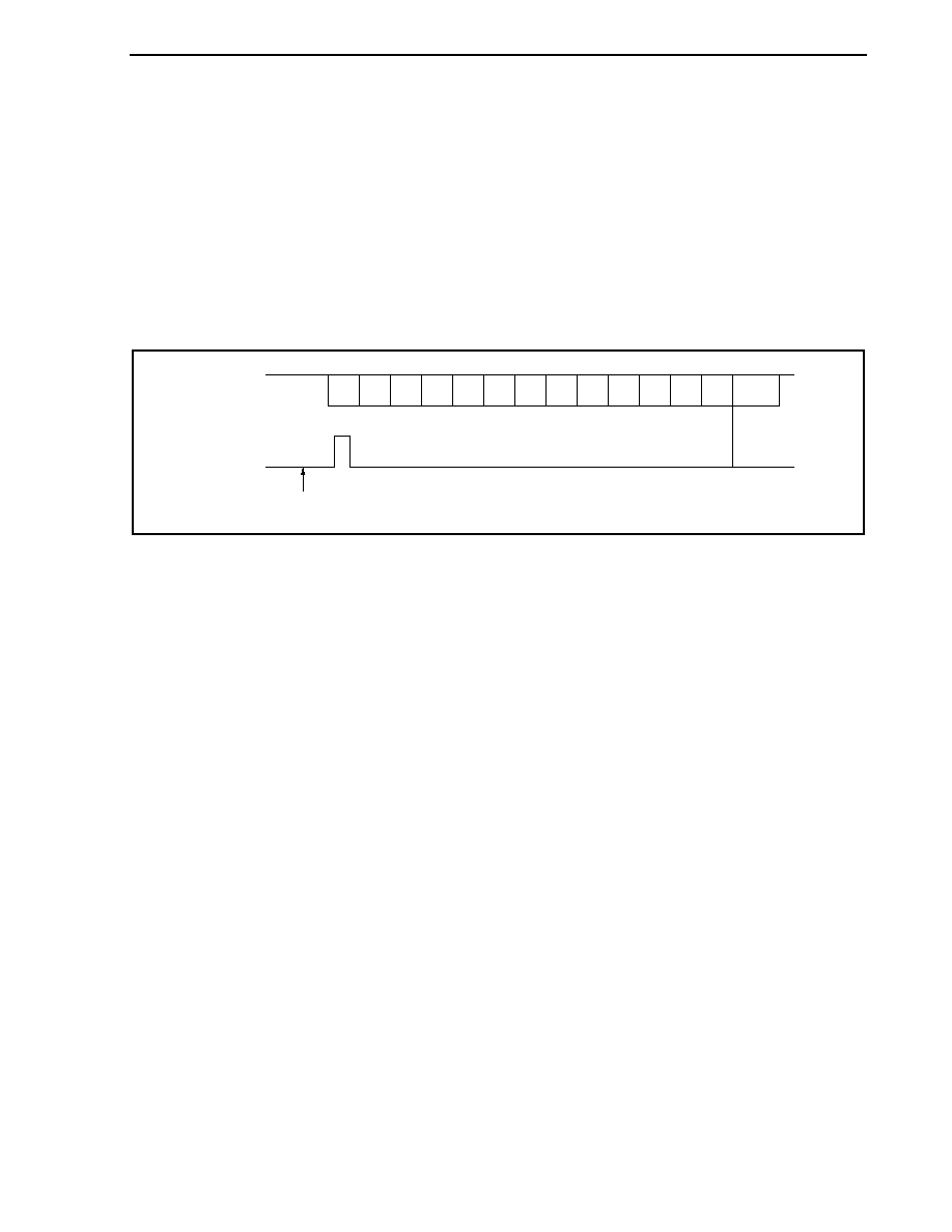
CHAPTER 15 ASYNCHRONOUS SERIAL INTERFACE A (UARTA)
Preliminary User's Manual U17714EJ1V0UD
501
15.6.3 SBF transmission
When the UAnCTL0.UAnPWR bit = UAnCTL0.UAnTXE bit = 1, the transmission enabled status is entered, and
SBF transmission is started by setting (to 1) the SBF transmission trigger (UAnOPT0.UAnSTT bit).
Thereafter, a low level the width of bits 13 to 20 specified by the UAnOPT0.UAnSLS2 to UAnOPT0.UAnSLS0 bits is
output. A transmission enable interrupt request signal (INTUAnT) is generated upon SBF transmission start.
Following the end of SBF transmission, the UAnSTT bit is automatically cleared. Thereafter, the UART transmission
mode is restored.
Transmission is suspended until the data to be transmitted next is written to the UAnTX register, or until the SBF
transmission trigger (UAnSTT bit) is set.
Figure 15-8. SBF Transmission
INTUAnT
interrupt
TXDAn
1
2
3
4
5
6
7
8
9
10
11
12
13
Stop
bit
Setting of UAnSTT bit
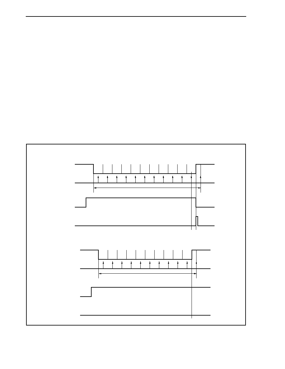
CHAPTER 15 ASYNCHRONOUS SERIAL INTERFACE A (UARTA)
Preliminary User's Manual U17714EJ1V0UD
502
15.6.4 SBF reception
The reception enabled status is achieved by setting the UAnCTL0.UAnPWR bit to 1 and then setting the
UAnCTL0.UAnRXE bit to 1.
The SBF reception wait status is set by setting the SBF reception trigger (UAnOPT0.UAnSTR bit) to 1.
In the SBF reception wait status, similarly to the UART reception wait status, the RXDAn pin is monitored and start
bit detection is performed.
Following detection of the start bit, reception is started and the internal counter counts up according to the set baud
rate.
When a stop bit is received, if the SBF width is 11 or more bits, normal processing is judged and a reception
complete interrupt request signal (INTUAnR) is output. The UAnOPT0.UAnSRF bit is automatically cleared and SBF
reception ends. Error detection for the UAnSTR.UAnOVE, UAnSTR.UAnPE, and UAnSTR.UAnFE bits is suppressed
and UART communication error detection processing is not performed. Moreover, data transfer of the UARTAn
reception shift register and UAnRX register is not performed and FFH, the initial value, is held. If the SBF width is 10
or fewer bits, reception is terminated as error processing without outputting an interrupt, and the SBF reception mode
is returned to. The UAnSRF bit is not cleared at this time.
Figure 15-9. SBF Reception
(a) Normal SBF reception (detection of stop bit in more than 10.5 bits)
UAnSRF
RXDAn
1
2
3
4
5
6
11.5
7
8
9
10
11
INTUAnR
interrupt
(b) SBF reception error (detection of stop bit in 10.5 or fewer bits)
UAnSRF
RXDAn
1
2
3
4
5
6
10.5
7
8
9
10
INTUAnR
interrupt
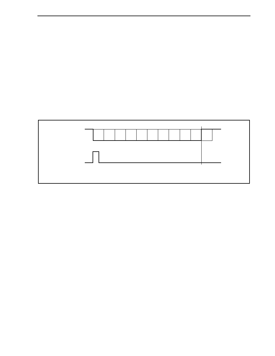
CHAPTER 15 ASYNCHRONOUS SERIAL INTERFACE A (UARTA)
Preliminary User's Manual U17714EJ1V0UD
503
15.6.5 UART transmission
A high level is output to the TXDAn pin by setting the UAnCTL0.UAnPWR bit to 1.
Next, the transmission enabled status is set by setting the UAnCTL0.UAnTXE bit to 1, and transmission is started
by writing transmit data to the UAnTX register. The start bit, parity bit, and stop bit are automatically added.
Since the CTS (transmit enable signal) input pin is not provided in UARTAn, use a port to check that reception is
enabled at the transmit destination.
The data in the UAnTX register is transferred to the UARTAn transmit shift register upon the start of the transmit
operation.
A transmission enable interrupt request signal (INTUAnT) is generated upon completion of transmission of the data
of the UAnTX register to the UARTAn transmit shift register, and thereafter the contents of the UARTAn transmit shift
register are output to the TXDAn pin.
Write of the next transmit data to the UAnTX register is enabled after the INTUAnT signal is generated.
Figure 15-10. UART Transmission
Start
bit
D0
D1
D2
D3
D4
D5
D6
D7
Parity
bit
Stop
bit
INTUAnT
TXDAn
Remark LSB
first
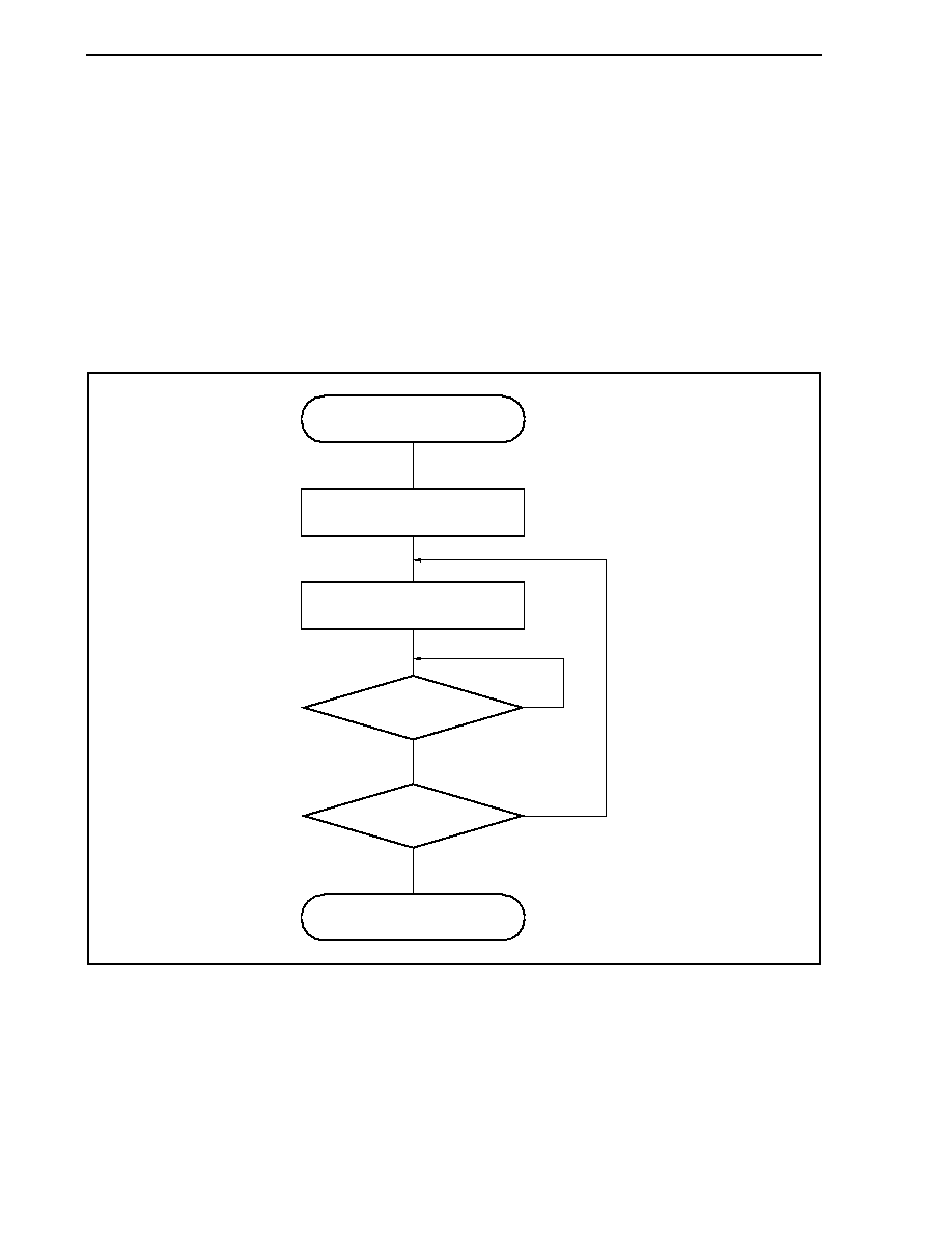
CHAPTER 15 ASYNCHRONOUS SERIAL INTERFACE A (UARTA)
Preliminary User's Manual U17714EJ1V0UD
504
15.6.6 Continuous transmission procedure
UARTAn can write the next transmit data to the UAnTX register when the UARTAn transmit shift register starts the
shift operation. The transmit timing of the UARTAn transmit shift register can be judged from the transmission enable
interrupt request signal (INTUAnT).
An efficient communication rate is realized by writing the data to be transmitted next to the UAnTX register during
transfer.
Caution When initializing transmissions during the execution of continuous transmissions, make sure
that the UAnSTR.UAnTSF bit is 0, then perform the initialization. Transmit data that is initialized
when the UAnTSF bit is 1 cannot be guaranteed.
Figure 15-11. Continuous Transmission Processing Flow
Start
Register settings
UAnTX write
Yes
Yes
No
No
Occurrence of transmission
interrupt?
Required number of
writes performed?
End
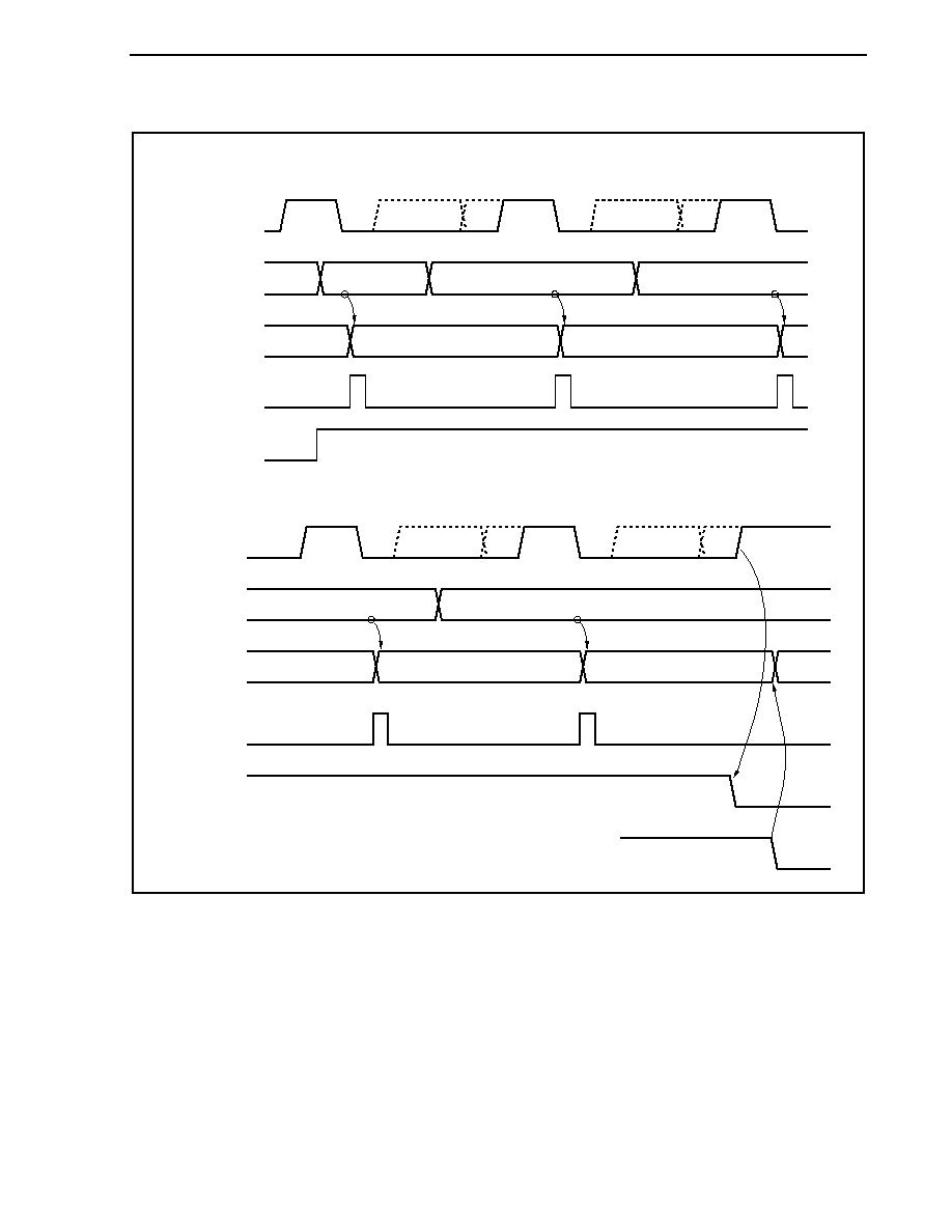
CHAPTER 15 ASYNCHRONOUS SERIAL INTERFACE A (UARTA)
Preliminary User's Manual U17714EJ1V0UD
505
Figure 15-12. Continuous Transmission Operation Timing
(a) Transmission start
Start Data
(1)
Data (1)
TXDAn
UAnTX
Transmission
shift register
INTUAnT
UAnTSF
Data (2)
Data (2)
Data (1)
Data (3)
Parity
Stop
Start Data
(2)
Parity
Stop
Start
(b) Transmission end
Start
Data (n � 1)
Data (n � 1)
Data (n � 1)
Data (n)
FF
Data (n)
TXDAn
UAnTX
Transmission
shift register
INTUAnT
UAnTSF
UAnPWR or UAnTXE bit
Parity
Stop
Stop
Start
Data (n)
Parity
Parity
Stop
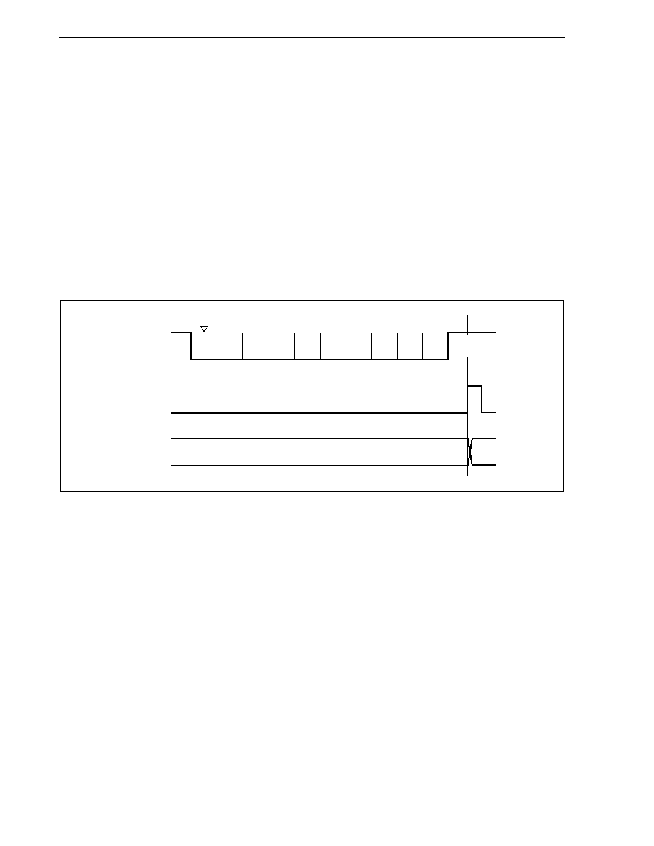
CHAPTER 15 ASYNCHRONOUS SERIAL INTERFACE A (UARTA)
Preliminary User's Manual U17714EJ1V0UD
506
15.6.7 UART reception
The reception wait status is set by setting the UAnCTL0.UAnPWR bit to 1 and then setting the UAnCTL0.UAnRXE
bit to 1. In the reception wait status, the RXDAn pin is monitored and start bit detection is performed.
Start bit detection is performed using a two-step detection routine.
First the rising edge of the RXDAn pin is detected and sampling is started at the falling edge. The start bit is
recognized if the RXDAn pin is low level at the start bit sampling point. After a start bit has been recognized, the
receive operation starts, and serial data is saved to the UARTAn receive shift register according to the set baud rate.
When the reception complete interrupt request signal (INTUAnR) is output upon reception of the stop bit, the data
of the UARTAn receive shift register is written to the UAnRX register. However, if an overrun error (UAnSTR.UAnOVE
bit) occurs, the receive data at this time is not written to the UAnRX register and is discarded.
Even if a parity error (UAnSTR.UAnPE bit) or a framing error (UAnSTR.UAnFE bit) occurs during reception,
reception continues until the reception position of the first stop bit, and INTUAnR is output following reception
completion.
Figure 15-13. UART Reception
Start
bit
D0
D1
D2
D3
D4
D5
D6
D7
Parity
bit
Stop
bit
INTUAnR
RXDAn
UAnRX
Cautions 1. Be sure to read the UAnRX register even when a reception error occurs. If the UAnRX register
is not read, an overrun error occurs during reception of the next data, and reception errors
continue occurring indefinitely.
2. The operation during reception is performed assuming that there is only one stop bit. A
second stop bit is ignored.
3. When reception is completed, read the UAnRX register after the reception complete interrupt
request signal (INTUAnR) has been generated, and clear the UAnPWR or UAnRXE bit to 0. If
the UAnPWR or UAnRXE bit is cleared to 0 before the INTUAnR signal is generated, the read
value of the UAnRX register cannot be guaranteed.
4. If receive completion processing (INTUAnR signal generation) of UARTAn and the UAnPWR
bit = 0 or UAnRXE bit = 0 conflict, the INTUAnR signal may be generated in spite of these
being no data stored in the UAnRX register.
To complete reception without waiting INTUAnR signal generation, be sure to clear (0) the
interrupt request flag (UAnRIF) of the UAnRIC register, after setting (1) the interrupt mask flag
(UAnRMK) of the interrupt control register (UAnRIC) and then set (1) the UAnPWR bit = 0 or
UAnRXE bit = 0.
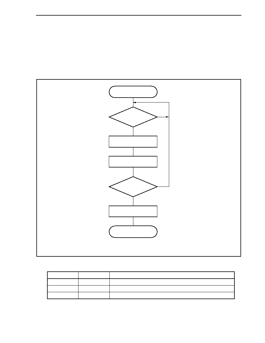
CHAPTER 15 ASYNCHRONOUS SERIAL INTERFACE A (UARTA)
Preliminary User's Manual U17714EJ1V0UD
507
15.6.8 Reception errors
Errors during a receive operation are of three types: parity errors, framing errors, and overrun errors. Data
reception result error flags are set in the UAnSTR register and a reception complete interrupt request signal
(INTUAnR) is output when an error occurs.
It is possible to ascertain which error occurred during reception by reading the contents of the UAnSTR register.
Clear the reception error flag by writing 0 to it after reading it.
� Receive data read flow
START
No
INTUAnR signal
generated?
Error occurs?
END
Yes
No
Yes
Error processing
Read UAnRX register
Read UAnSTR register
Caution When an INTUAnR signal is generated, the UAnSTR register must be read to check for errors.
� Reception error causes
Error Flag
Reception Error
Cause
UAnPE
Parity error
Received parity bit does not match the setting
UAnFE
Framing error
Stop bit not detected
UAnOVE
Overrun error
Reception of next data completed before data was read from receive buffer

CHAPTER 15 ASYNCHRONOUS SERIAL INTERFACE A (UARTA)
Preliminary User's Manual U17714EJ1V0UD
508
When reception errors occur, perform the following procedures depending upon the kind of error.
� Parity error
If false data is received due to problems such as noise in the reception line, discard the received data and
retransmit.
� Framing error
A baud rate error may have occurred between the reception side and transmission side or the start bit may have
been erroneously detected. Since this is a fatal error for the communication format, check the operation stop in
the transmission side, perform initialization processing each other, and then start the communication again.
� Overrun error
Since the next reception is completed before reading receive data, 1 frame of data is discarded. If this data was
needed, do a retransmission.
Caution If a receive error interrupt occurs during continuous reception, read the contents of the UAnSTR
register must be read before the next reception is completed, then perform error processing.

CHAPTER 15 ASYNCHRONOUS SERIAL INTERFACE A (UARTA)
Preliminary User's Manual U17714EJ1V0UD
509
15.6.9 Parity types and operations
Caution When using the LIN function, fix the UAnPS1 and UAnPS0 bits of the UAnCTL0 register to 00.
The parity bit is used to detect bit errors in the communication data. Normally the same parity is used on the
transmission side and the reception side.
In the case of even parity and odd parity, it is possible to detect odd-count bit errors. In the case of 0 parity and no
parity, errors cannot be detected.
(a) Even parity
(i) During transmission
The number of bits whose value is "1" among the transmit data, including the parity bit, is controlled so as
to be an even number. The parity bit values are as follows.
� Odd number of bits whose value is "1" among transmit data: 1
� Even number of bits whose value is "1" among transmit data: 0
(ii) During reception
The number of bits whose value is "1" among the reception data, including the parity bit, is counted, and if
it is an odd number, a parity error is output.
(b) Odd parity
(i) During transmission
Opposite to even parity, the number of bits whose value is "1" among the transmit data, including the parity
bit, is controlled so that it is an odd number. The parity bit values are as follows.
� Odd number of bits whose value is "1" among transmit data: 0
� Even number of bits whose value is "1" among transmit data: 1
(ii) During reception
The number of bits whose value is "1" among the receive data, including the parity bit, is counted, and if it
is an even number, a parity error is output.
(c) 0 parity
During transmission, the parity bit is always made 0, regardless of the transmit data.
During reception, parity bit check is not performed. Therefore, no parity error occurs, regardless of whether the
parity bit is 0 or 1.
(d) No parity
No parity bit is added to the transmit data.
Reception is performed assuming that there is no parity bit. No parity error occurs since there is no parity bit.
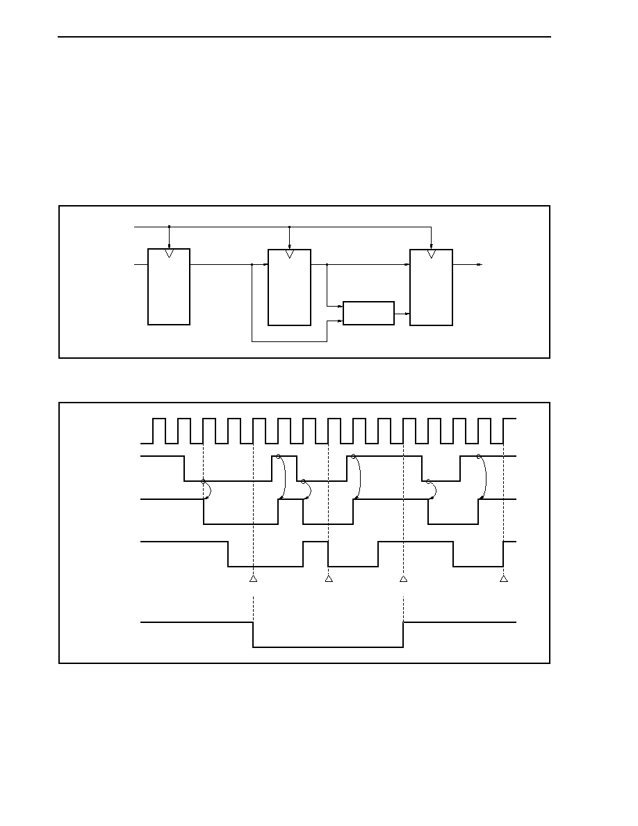
CHAPTER 15 ASYNCHRONOUS SERIAL INTERFACE A (UARTA)
Preliminary User's Manual U17714EJ1V0UD
510
15.6.10 Receive data noise filter
This filter samples the RXDAn pin using the base clock of the prescaler output.
When the same sampling value is read twice, the match detector output changes and the RXDAn signal is sampled
as the input data. Therefore, data not exceeding 2 clock width is judged to be noise and is not delivered to the internal
circuit (see Figure 15-15). See 15.7 (1) (a) Base clock regarding the base clock.
Moreover, since the circuit is as shown in Figure 15-14, the processing that goes on within the receive operation is
delayed by 3 clocks in relation to the external signal status.
Figure 15-14. Noise Filter Circuit
Match
detector
In
Base clock (f
UCLK
)
RXDAn
Q
In
LD_EN
Q
Internal signal C
Internal signal B
In
Q
Internal signal A
Figure 15-15. Timing of RXDAn Signal Judged as Noise
Internal signal B
Base clock
RXDAn (input)
Internal signal C
Mismatch
(judged as noise)
Internal signal A
Mismatch
(judged as noise)
Match
Match
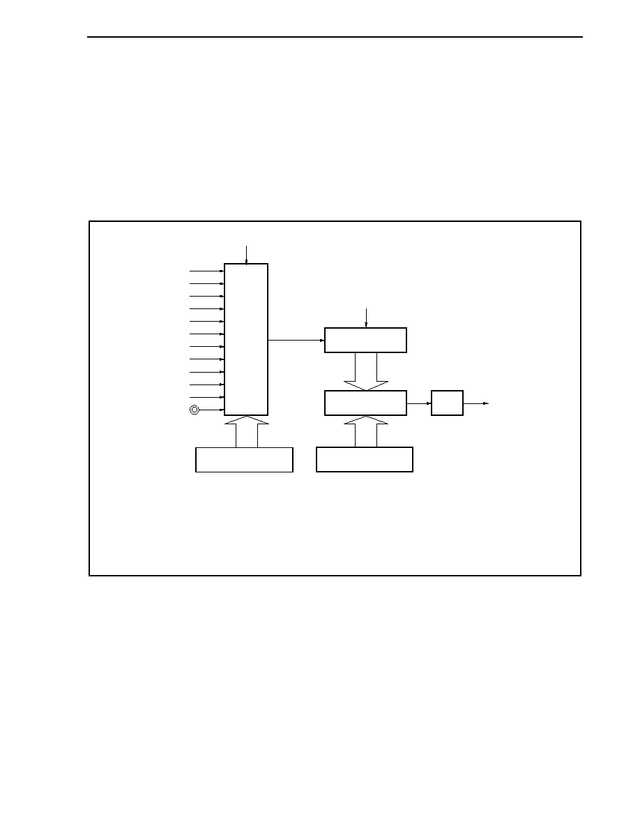
CHAPTER 15 ASYNCHRONOUS SERIAL INTERFACE A (UARTA)
Preliminary User's Manual U17714EJ1V0UD
511
15.7 Dedicated Baud Rate Generator
The dedicated baud rate generator consists of a source clock selector block and an 8-bit programmable counter,
and generates a serial clock during transmission and reception with UARTAn. Regarding the serial clock, a dedicated
baud rate generator output can be selected for each channel.
There is an 8-bit counter for transmission and another one for reception.
(1) Baud rate generator configuration
Figure 15-16. Configuration of Baud Rate Generator
f
UCLK
Selector
UAnPWR
8-bit counter
Match detector
Baud rate
UAnCTL2:
UAnBRS7 to UAnBRS0
1/2
UAnPWR, UAnTXEn bits (or UAnRXE bit)
UAnCTL1:
UAnCKS3 to UAnCKS0
f
XX
f
XX
/2
f
XX
/4
f
XX
/8
f
XX
/16
f
XX
/32
f
XX
/64
f
XX
/128
f
XX
/256
f
XX
/512
f
XX
/1024
ASCKA0
Note
Note Only UARTA0 is valid; setting UARTA1 to UARTA3 is prohibited.
Remarks 1. n = 0 to 3
2. f
XX
: Main clock frequency
f
UCLK
: Base clock frequency
(a) Base clock
When the UAnCTL0.UAnPWR bit is 1, the clock selected by the UAnCTL1.UAnCKS3 to
UAnCTL1.UAnCKS0 bits is supplied to the 8-bit counter. This clock is called the base clock (f
UCLK
).
(b) Serial clock generation
A serial clock can be generated by setting the UAnCTL1 register and the UAnCTL2 register (n = 0 to 3).
The base clock is selected by UAnCTL1.UAnCKS3 to UAnCTL1.UAnCKS0 bits.
The frequency division value for the 8-bit counter can be set using the UAnCTL2.UAnBRS7 to
UAnCTL2.UAnBRS0 bits.
CHAPTER 15 ASYNCHRONOUS SERIAL INTERFACE A (UARTA)
Preliminary User's Manual U17714EJ1V0UD
512
(2) UARTAn control register 1 (UAnCTL1)
The UAnCTL1 register is an 8-bit register that selects the UARTAn base clock.
This register can be read or written in 8-bit units.
Reset sets this register to 00H.
Caution Clear the UAnCTL0.UAnPWR bit to 0 before rewriting the UAnCTL1 register.
0
UAnCTL1
(n = 0 to 3)
0
0
0
UAnCKS3 UAnCKS2 UAnCKS1 UAnCKS0
6
5
4
3
2
1
After reset: 00H R/W Address: UA0CTL1 FFFFFA01H, UA1CTL1 FFFFFA11H,
UA2CTL1 FFFFFA21H, UA3CTL1 FFFFFA31H
7
0
f
XX
f
XX
/2
f
XX
/4
f
XX
/8
f
XX
/16
f
XX
/32
f
XX
/64
f
XX
/128
f
XX
/256
f
XX
/512
f
XX
/1,024
External clock
Note
(ASCKA0 pin)
Setting prohibited
UAnCKS2
0
0
0
0
1
1
1
1
0
0
0
0
UAnCKS3
0
0
0
0
0
0
0
0
1
1
1
1
Base clock (f
UCLK
) selection
UAnCKS1
0
0
1
1
0
0
1
1
0
0
1
1
UAnCKS0
0
1
0
1
0
1
0
1
0
1
0
1
Other than above
Note Only UARTA0 is valid; setting UARTA1 to UARTA3 is prohibited.
Remark f
XX
: Main clock frequency
CHAPTER 15 ASYNCHRONOUS SERIAL INTERFACE A (UARTA)
Preliminary User's Manual U17714EJ1V0UD
513
(3) UARTAn control register 2 (UAnCTL2)
The UAnCTL2 register is an 8-bit register that selects the baud rate (serial transfer speed) clock of UARTAn.
This register can be read or written in 8-bit units.
Reset sets this register to FFH.
Caution Clear the UAnCTL0.UAnPWR bit to 0 or clear the UAnTXE and UAnRXE bits to 00 before
rewriting the UAnCTL2 register.
UAnBRS7
UAnCTL2
(n = 0 to 3)
UAnBRS6 UAnBRS5 UAnBRS4 UAnBRS3 UAnBRS2 UAnBRS1 UAnBRS0
6
5
4
3
2
1
After reset FFH R/W Address: UA0CTL2 FFFFFA02H, UA1CTL2 FFFFFA12H,
UA2CTL2 FFFFFA22H, UA3CTL2 FFFFFA32H
7
0
UAn
BRS7
0
0
0
0
:
1
1
1
1
UAn
BRS6
0
0
0
0
:
1
1
1
1
UAn
BRS5
0
0
0
0
:
1
1
1
1
UAn
BRS4
0
0
0
0
:
1
1
1
1
UAn
BRS3
0
0
0
0
:
1
1
1
1
UAn
BRS2
0
1
1
1
:
1
1
1
1
UAn
BRS1
�
0
0
1
:
0
0
1
1
UAn
BRS0
�
0
1
0
:
0
1
0
1
Default
(k)
�
4
5
6
:
252
253
254
255
Serial
clock
f
UCLK
/4
f
UCLK
/5
f
UCLK
/6
:
f
UCLK
/252
f
UCLK
/253
f
UCLK
/254
f
UCLK
/255
Setting
prohibited
Remark f
UCLK
: Clock frequency selected by the UAnCTL1.UAnCKS3 to
UAnCTL1.UAnCKS0 bits

CHAPTER 15 ASYNCHRONOUS SERIAL INTERFACE A (UARTA)
Preliminary User's Manual U17714EJ1V0UD
514
(4) Baud rate
The baud rate is obtained by the following equation.
Baud rate = [bps]
When using the internal clock, the equation will be as follows (when using the ASCKA0 pin as clock at
UARTA0, calculate using the above equation).
Baud rate = [bps]
Remark f
UCLK
= Frequency of base clock selected by the UAnCTL1.UAnCKS3 to UAnCTL1.UAnCKS0 bits
f
XX
: Main clock frequency
m = Value set using the UAnCTL1.UAnCKS3 to UAnCTL1.UAnCKS0 bits (m = 0 to 10)
k = Value set using the UAnCTL2.UAnBRS7 to UAnCTL2.UAnBRS0 bits (k = 4 to 255)
The baud rate error is obtained by the following equation.
Error (%) =
- 1 � 100 [%]
=
- 1 � 100 [%]
When using the internal clock, the equation will be as follows (when using the ASCKA0 pin as clock at
UARTA0, calculate the baud rate error using the above equation).
Error (%) =
- 1 � 100 [%]
Cautions 1. The baud rate error during transmission must be within the error tolerance on the
receiving side.
2. The baud rate error during reception must satisfy the range indicated in (5) Allowable
baud rate range during reception.
f
UCLK
2
� k
Actual baud rate (baud rate with error)
Target baud rate (correct baud rate)
f
XX
2
m+1
� k
f
UCLK
2
� k � Target baud rate
f
XX
2
m+1
� k � Target baud rate

CHAPTER 15 ASYNCHRONOUS SERIAL INTERFACE A (UARTA)
Preliminary User's Manual U17714EJ1V0UD
515
To set the baud rate, perform the following calculation for setting the UAnCTL1 and UAnCTL2 registers (when
using internal clock).
<1> Set k to fxx/(2
� target baud rate) and m to 0.
<2> If k is 256 or greater (k
256), reduce k to half (k/2) and increment m by 1 (m + 1).
<3> Repeat Step <2> until k becomes less than 256 (k < 256).
<4> Round off the first decimal point of k to the nearest whole number.
If k becomes 256 after round-off, perform Step <2> again to set k to 128.
<5> Set the value of m to UAnCTL1 register and the value of k to the UAnCTL2 register.
Example: When f
XX
= 20 MHz and target baud rate = 153,600 bps
<1> k = 20,000,000/(2
� 153,600) = 65.10..., m = 0
<2>, <3> k = 65.10... < 256, m = 0
<4> Set value of UAnCTL2 register: k = 65 = 41H, set value of UAnCTL1 register: m = 0
Actual baud rate = 20,000,000/(2
� 65)
= 153,846 [bps]
Baud rate error = {20,000,000/(2
� 65 � 153,600) - 1} � 100
= 0.160 [%]
The representative examples of baud rate settings are shown below.
Table 15-3. Baud Rate Generator Setting Data
Baud Rate
f
XX
= 20 MHz
f
XX
= 18.874 MHz
f
XX
= 16 MHz
f
XX
= 10 MHz
(bps)
UAnCTL1 UAnCTL2
ERR (%)
UAnCTL1 UAnCTL2
ERR (%)
UAnCTL1 UAnCTL2
ERR (%)
UAnCTL1 UAnCTL2
ERR (%)
300 08H
82H
0.16
07H
F6H
-0.10 07H D0H 0.16 07H 82H 0.16
600 07H
82H
0.16
06H
F6H
-0.10 06H D0H 0.16 06H 82H 0.16
1,200 06H
82H
0.16
05H
F6H
-0.10 05H D0H 0.16 05H 82H 0.16
2,400 05H
82H
0.16
04H
F6H
-0.10 04H D0H 0.16 04H 82H 0.16
4,800 04H
82H
0.16
03H
F6H
-0.10 03H D0H 0.16 03H 82H 0.16
9,600 03H
82H
0.16
02H
F6H
-0.10 02H D0H 0.16 02H 82H 0.16
19,200
02H 82H 0.16 01H F6H
-0.10 01H D0H 0.16 01H 82H 0.16
31,250 01H
A0H
0
01H
97H
-0.01 01H 80H 0
00H A0H 0
38,400
01H 82H 0.16 00H F6H
-0.10 00H D0H 0.16 00H 82H 0.16
76,800
00H 82H 0.16 00H 7BH
-0.10 00H 68H 0.16 00H 41H 0.16
153,600
00H 41H 0.16 00H 3DH 0.72 00H 34H 0.16 00H 21H
-1.36
312,500 00H
20H
0
00H
1EH
0.66
00H
1AH
-1.54 00H 10H 0
Remark f
XX
:
Main clock frequency
ERR: Baud rate error (%)
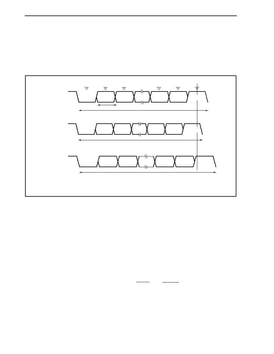
CHAPTER 15 ASYNCHRONOUS SERIAL INTERFACE A (UARTA)
Preliminary User's Manual U17714EJ1V0UD
516
(5) Allowable baud rate range during reception
The baud rate error range at the destination that is allowable during reception is shown below.
Caution The baud rate error during reception must be set within the allowable error range using the
following equation.
Figure 15-17. Allowable Baud Rate Range During Reception
FL
1 data frame (11
� FL)
FLmin
FLmax
UARTAn
transfer rate
Start bit
Bit 0
Bit 1
Bit 7
Parity bit
Minimum
allowable
transfer rate
Maximum
allowable
transfer rate
Stop bit
Start bit
Bit 0
Bit 1
Bit 7
Parity bit
Latch timing
Stop bit
Start bit
Bit 0
Bit 1
Bit 7
Parity bit
Stop bit
Remark n = 0 to 3
As shown in Figure 15-17, the receive data latch timing is determined by the counter set using the UAnCTL2
register following start bit detection. The transmit data can be normally received if up to the last data (stop bit)
can be received in time for this latch timing.
When this is applied to 11-bit reception, the following is the theoretical result.
FL = (Brate)
-
1
Brate: UARTAn baud rate (n = 0 to 3)
k:
Setting value of UAnCTL2.UAnBRS7 to UAnCTL2.UAnBRS0 bits (n = 0 to 3)
FL:
1-bit data length
Latch timing margin: 2 clocks
Minimum allowable transfer rate: FLmin = 11
� FL - � FL = FL
k
- 2
2k
21k + 2
2k
CHAPTER 15 ASYNCHRONOUS SERIAL INTERFACE A (UARTA)
Preliminary User's Manual U17714EJ1V0UD
517
Therefore, the maximum baud rate that can be received by the destination is as follows.
BRmax = (FLmin/11)
-
1
= Brate
Similarly, obtaining the following maximum allowable transfer rate yields the following.
� FLmax = 11 � FL - � FL = FL
FLmax = FL
� 11
Therefore, the minimum baud rate that can be received by the destination is as follows.
BRmin = (FLmax/11)
-
1
= Brate
Obtaining the allowable baud rate error for UARTAn and the destination from the above-described equations for
obtaining the minimum and maximum baud rate values yields the following.
Table 15-4. Maximum/Minimum Allowable Baud Rate Error
Division Ratio (k)
Maximum Allowable Baud Rate Error
Minimum Allowable Baud Rate Error
4 +2.32%
-2.43%
8 +3.52%
-3.61%
20 +4.26%
-4.30%
50 +4.56%
-4.58%
100 +4.66%
-4.67%
255 +4.72%
-4.72%
Remarks 1. The reception accuracy depends on the bit count in 1 frame, the input clock
frequency, and the division ratio (k). The higher the input clock frequency
and the larger the division ratio (k), the higher the accuracy.
2. k: Setting value of UAnCTL2.UAnBRS7 to UAnCTL2.UAnBRS0 bits (n = 0 to 3)
10
11
k + 2
2
� k
21k
- 2
2
� k
21k
- 2
20 k
22k
21k + 2
20k
21k
- 2
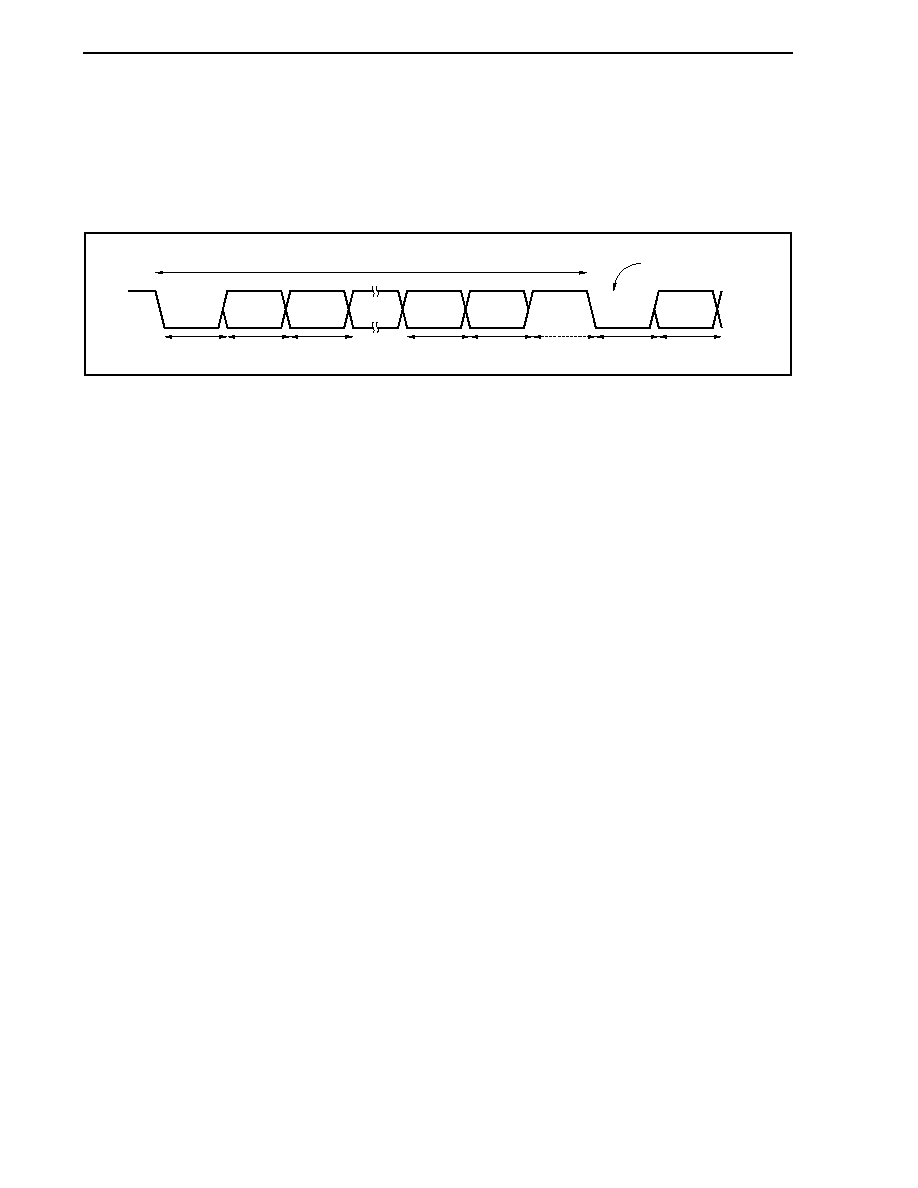
CHAPTER 15 ASYNCHRONOUS SERIAL INTERFACE A (UARTA)
Preliminary User's Manual U17714EJ1V0UD
518
(6) Baud rate during continuous transmission
During continuous transmission, the transfer rate from the stop bit to the next start bit is usually 2 base clocks
longer. However, timing initialization is performed via start bit detection by the receiving side, so this has no
influence on the transfer result.
Figure 15-18. Transfer Rate During Continuous Transfer
Start bit
Bit 0
Bit 1
Bit 7
Parity bit
Stop bit
FL
1 data frame
FL
FL
FL
FL
FL
FL
FLstp
Start bit of 2nd byte
Start bit
Bit 0
Assuming 1 bit data length: FL; stop bit length: FLstp; and base clock frequency: f
UCLK
, we obtain the following
equation.
FLstp = FL + 2/f
UCLK
Therefore, the transfer rate during continuous transmission is as follows.
Transfer rate = 11
� FL + (2/f
UCLK
)

CHAPTER 15 ASYNCHRONOUS SERIAL INTERFACE A (UARTA)
Preliminary User's Manual U17714EJ1V0UD
519
15.8 Cautions
(1) When the clock supply to UARTAn is stopped (for example, in IDLE1, IDLE2, or STOP mode), the operation
stops with each register retaining the value it had immediately before the clock supply was stopped. The
TXDAn pin output also holds and outputs the value it had immediately before the clock supply was stopped.
However, the operation is not guaranteed after the clock supply is resumed. Therefore, after the clock supply
is resumed, the circuits should be initialized by setting the UAnCTL0.UAnPWR, UAnCTL0.UAnRXEn, and
UAnCTL0.UAnTXEn bits to 000.
(2) The RXDA1 and KR7 pins must not be used at the same time. To use the RXDA1 pin, do not use the KR7 pin.
To use the KR7 pin, do not use the RXDA1 pin (it is recommended to set the PFC91 bit to 1 and clear
PFCE91 bit to 0).
(3) In UARTAn, the interrupt caused by a communication error does not occur. When performing the transfer of
transmit data and receive data using DMA transfer, error processing cannot be performed even if errors (parity,
overrun, framing) occur during transfer. Either read the UAnSTR register after DMA transfer has been
completed to make sure that there are no errors, or read the UAnSTR register during communication to check
for errors.
(4) Start up the UARTAn in the following sequence.
<1> Set the UAnCTL0.UAnPWR bit to 1.
<2> Set the ports.
<3> Set the UAnCTL0.UAnTXE bit to 1, UAnCTL0.UAnRXE bit to 1.
(5) Stop the UARTAn in the following sequence.
<1> Set the UAnCTL0.UAnTXE bit to 0, UAnCTL0.UAnRXE bit to 0.
<2> Set the ports and set the UAnCTL0.UAnPWR bit to 0 (it is not a problem if port setting is not changed).
(6) In transmit mode (UAnCTL0.UAnPWR bit = 1 and UAnCTL0.UAnTXE bit = 1), do not overwrite the same value
to the UAnTX register by software because transmission starts by writing to this register. To transmit the same
value continuously, overwrite the same value.
(7) In continuous transmission, the communication rate from the stop bit to the next start bit is extended 2 base
clocks more than usual. However, the reception side initializes the timing by detecting the start bit, so the
reception result is not affected.
Preliminary User's Manual U17714EJ1V0UD
520
CHAPTER 16 3-WIRE VARIABLE-LENGTH SERIAL I/O (CSIB)
16.1 Mode Switching of CSIB and Other Serial Interfaces
16.1.1 CSIB4 and UARTA0 mode switching
In the V850ES/JJ2, CSIB4 and UARTA0 are alternate functions of the same pin and therefore cannot be used
simultaneously. Set CSIB4, in advance, using the PMC3 and PFC3 registers, before use.
Caution The transmit/receive operation of CSIB4 and UARTA0 is not guaranteed if these functions are
switched during transmission or reception. Be sure to disable the one that is not used.
Figure 16-1. CSIB4 and UARTA0 Mode Switch Settings
PMC3
After reset: 0000H R/W Address: FFFFF446H, FFFFF447H
0
0
PMC35
PMC34
PMC33
PMC32
PMC31
PMC30
0
0
0
0
0
0
PMC39
PMC38
8
9
10
11
12
13
14
15
PFC3
After reset: 0000H R/W Address: FFFFF466H, FFFFF467H
0
0
0
0
0
0
PFC39
PFC38
0
0
PFC35
PFC34
PFC33
PFC32
PFC31
PFC30
8
9
10
11
12
13
14
15
PFCE3L
After reset: 00H R/W Address: FFFFF706H
0
0
0
0
0
PFCE32
0
0
Port I/O mode
ASCKA0 mode
SCKB4 mode
Port I/O mode
UARTA0 mode
CSIB4 mode
PMC32
0
1
1
PMC3n
0
1
1
Operation mode
Operation mode
PFCE32
�
0
0
PFC32
�
0
1
PFC3n
�
0
1
Remarks 1. n = 0, 1
2.
� = don't care
CHAPTER 16 3-WIRE VARIABLE-LENGTH SERIAL I/O (CSIB)
Preliminary User's Manual U17714EJ1V0UD
521
16.1.2 CSIB0 and I
2
C01 mode switching
In the V850ES/JJ2, CSIB0 and I
2
C01 are alternate functions of the same pin and therefore cannot be used
simultaneously. Set CSIB0 in advance, using the PMC4 and PFC4 registers, before use.
Caution The transmit/receive operation of CSIB0 and I
2
C01 is not guaranteed if these functions are
switched during transmission or reception. Be sure to disable the one that is not used.
Figure 16-2. CSIB0 and I
2
C01 Mode Switch Settings
Port I/O mode
CSIB0 mode
I
2
C01 mode
PMC4n
0
1
1
Operation mode
PFC4n
�
0
1
0
PMC4
0
0
0
0
PMC42
PMC41
PMC40
After reset: 00H R/W Address: FFFFF448H
PFC4
After reset: 00H R/W Address: FFFFF468H
0
0
0
0
0
0
PFC41
PFC40
Remarks 1. n = 0, 1
2.
� = don't care
16.2 Features
Transfer rate: 8 Mbps to 4.9 kbps (f
XX
= 20 MHz, using internal clock)
Master mode and slave mode selectable
8-bit to 16-bit transfer, 3-wire serial interface
Interrupt request signals (INTCBnT, INTCBnR)
� 2
Serial clock and data phase switchable
Transfer data length selectable in 1-bit units between 8 and 16 bits
Transfer data MSB-first/LSB-first switchable
3-wire transfer SOBn: Serial data output
SIBn:
Serial data input
SCKBn: Serial clock I/O
Transmission mode, reception mode, and transmission/reception mode specifiable
Remark n = 0 to 5
CHAPTER 16 3-WIRE VARIABLE-LENGTH SERIAL I/O (CSIB)
Preliminary User's Manual U17714EJ1V0UD
522
16.3 Configuration
The following shows the block diagram of CSIBn.
Figure 16-3. Block Diagram of CSIBn
Internal bus
CBnCTL2
CBnCTL0
CBnSTR
Controller
INTCBnR
SOBn
INTCBnT
CBnTX
SO latch
Phase
control
Shift register
CBnRX
CBnCTL1
Phase control
SIBn
f
BRGm
f
XX
/2
f
XX
/4
f
XX
/8
f
XX
/16
f
XX
/32
f
XX
/64
SCKBn
Selector
Remarks n = 0 to 5
m = 1 (n = 0, 1)
m = 2 (n = 2, 3)
m = 3 (n = 4, 5)
CSIBn includes the following hardware.
Table 16-1. Configuration of CSIBn
Item Configuration
Registers
CSIBn receive data register (CBnRX)
CSIBn transmit data register (CBnTX)
Control registers
CSIBn control register 0 (CBnCTL0)
CSIBn control register 1 (CBnCTL1)
CSIBn control register 2 (CBnCTL2)
CSIBn status register (CBnSTR)
CHAPTER 16 3-WIRE VARIABLE-LENGTH SERIAL I/O (CSIB)
Preliminary User's Manual U17714EJ1V0UD
523
(1) CSIBn receive data register (CBnRX)
The CBnRX register is a 16-bit buffer register that holds receive data.
This register is read-only, in 16-bit units.
The receive operation is started by reading the CBnRX register in the reception enabled status.
If the transfer data length is 8 bits, the lower 8 bits of this register are read-only in 8-bit units as the CBnRXL
register.
Reset sets this register to 0000H.
In addition to reset input, the CBnRX register can be initialized by clearing (to 0) the CBnPWR bit of the
CBnCTL0 register.
After reset: 0000H R Address: CB0RX FFFFFD04H, CB1RX FFFFFD14H,
CB2RX FFFFFD24H, CB3RX FFFFFD34H,
CB4RX FFFFFD44H, CB5RX FFFFFD54H
CBnRX
(n = 0 to 5)
(2) CSIBn transmit data register (CBnTX)
The CBnTX register is a 16-bit buffer register used to write the CSIBn transfer data.
This register can be read or written in 16-bit units.
The transmit operation is started by writing data to the CBnTX register in the transmission enabled status.
If the transfer data length is 8 bits, the lower 8 bits of this register are read-only in 8-bit units as the CBnTXL
register.
Reset sets this register to 0000H.
After reset 0000H R/W Address: CB0TX FFFFFD06H, CB1TX FFFFFD16H,
CB2TX FFFFFD26H, CB3TX FFFFFD36H,
CB4TX FFFFFD46H, CB5TX FFFFFD56H
CBnTX
(n = 0 to 5)
Remark The communication start conditions are shown below.
Transmission mode (CBnTXE bit = 1, CBnRXE bit = 0):
Write to CBnTX register
Transmission/reception mode (CBnTXE bit = 1, CBnRXE bit = 1): Write to CBnTX register
Reception mode (CBnTXE bit = 0, CBnRXE bit = 1):
Read from CBnRX register
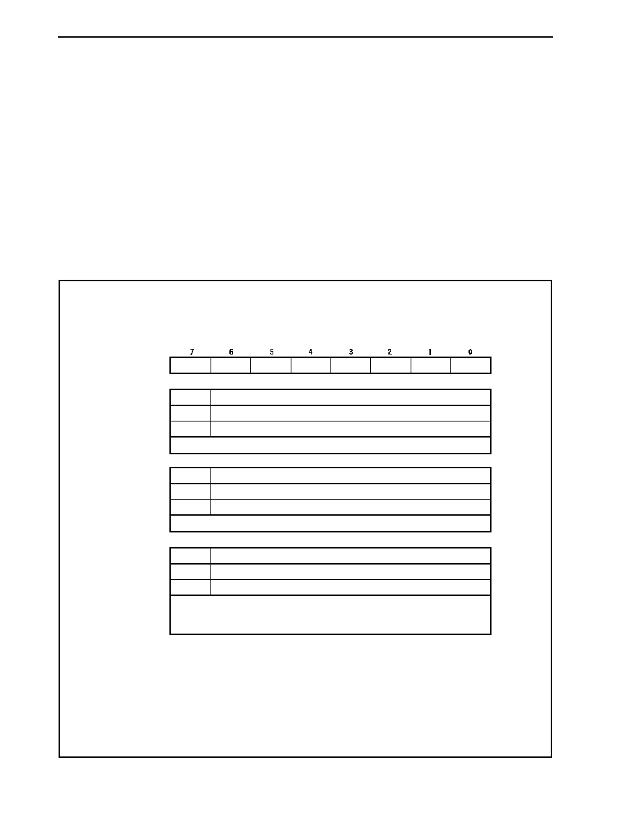
CHAPTER 16 3-WIRE VARIABLE-LENGTH SERIAL I/O (CSIB)
Preliminary User's Manual U17714EJ1V0UD
524
16.4 Registers
The following registers are used to control CSIBn.
� CSIBn control register 0 (CBnCTL0)
� CSIBn control register 1 (CBnCTL1)
� CSIBn control register 2 (CBnCTL2)
� CSIBn status register (CBnSTR)
(1) CSIBn control register 0 (CBnCTL0)
CBnCTL0 is a register that controls the CSIBn serial transfer operation.
This register can be read or written in 8-bit or 1-bit units.
Reset sets this register to 01H.
(1/3)
CBnPWR
Disable CSIBn operation and reset the CBnSTR register
Enable CSIBn operation
CBnPWR
0
1
Specification of CSIBn operation disable/enable
CBnCTL0
(n = 0 to 5)
CBnTXE
Note
CBnRXE
Note
CBnDIR
Note
0
0
CBnTMS
Note
CBnSCE
After reset: 01H R/W Address: CB0CTL0 FFFFFD00H, CB1CTL0 FFFFFD10H,
CB2CTL0 FFFFFD20H, CB3CTL0 FFFFFD30H,
CB4CTL0 FFFFFD40H, CB5CTL0 FFFFFD50H
� The CBnPWR bit controls the CSIBn operation and resets the internal circuit.
Disable transmit operation
Enable transmit operation
CBnTXE
Note
0
1
Specification of transmit operation disable/enable
� The SOBn output is low level when the CBnTXE bit is 0.
� When the CBnRXE bit is cleared to 0, no reception complete interrupt is output
even when the prescribed data is transferred in order to disable the receive
operation, and the receive data (CBnRX register) is not updated.
Disable receive operation
Enable receive operation
CBnRXE
Note
0
1
Specification of receive operation disable/enable
< >
< >
< >
< >
< >
Note These bits can only be rewritten when the CBnPWR bit = 0.
However, CBnPWR bit = 1 can also be set at the same time as
rewriting these bits.
Caution To forcibly suspend transmission/reception, clear the CBnPWR
bit instead of the CBnRxE bit to 0.
At this time, the clock output is stopped.

CHAPTER 16 3-WIRE VARIABLE-LENGTH SERIAL I/O (CSIB)
Preliminary User's Manual U17714EJ1V0UD
525
(2/3)
Single transfer mode
Continuous transfer mode
CBnTMS
Note
0
1
Transfer mode specification
[In single transfer mode]
The reception complete interrupt request signal (INTCBnR) is generated.
Even if transmission is enabled (CBnTXE bit = 1), the transmission enable interrupt
request signal (INTCBnT) is not generated.
If the next transmit data is written during communication (CBnSTR.CBnTSF bit =
1), it is ignored and the next communication is not started. Also, if reception-only
communication is set (CBnTXE bit = 0, CBnRXE bit = 1), the next communication
is not started even if the receive data is read during communication (CBnSTR.
CBbTSF bit = 1).
[In continuous transfer mode]
The continuous transmission is enabled by writing the next transmit data during
communication (CBnSTR.CBnTSF bit = 1). Writing the next transmission data is
enabled after a transmission enable interrupt (INTCBnT) occurrence.
If reception-only communication is set (CBnTXE bit = 0, CBnRXE bit = 1) in the
continuous transfer mode, the next reception is started continuously after a
reception complete interrupt (INTCBnR) regardless of the read operation of the
CBnRX register.
Therefore, read immediately the receive data from the CBnRX register. If this read
operation is delayed, an overrun error (CBnOVE bit = 1) occurs.
CBnDIR
Note
0
1
Specification of transfer direction mode (MSB/LSB)
MSB-first transfer
LSB-first transfer
Note These bits can only be rewritten when the CBnPWR bit = 0.
However, CBnPWR bit = 1 can also be set at the same time as rewriting these bits.

CHAPTER 16 3-WIRE VARIABLE-LENGTH SERIAL I/O (CSIB)
Preliminary User's Manual U17714EJ1V0UD
526
(3/3)
Communication start trigger invalid
Communication start trigger valid
CBnSCE
0
1
Specification of start transfer disable/enable
� In master mode
This bit enables or disables the communication start trigger.
(a) In single transmission or transmission/reception mode, or continuous
transmission or continuous transmission/reception mode
The setting of the CBnSCE bit has no influence on communication operation.
(b) In single reception mode
Clear the CBnSCE bit to 0 before reading the last receive data because
reception is started by reading the receive data (CBnRX register) to disable
the reception startup
Note 1
.
(c) In continuous reception mode
Clear the CBnSCE bit to 0 one communication clock before reception of the
last data is completed to disable the reception startup after the last data is
received
Note 2
.
� In slave mode
This bit enables or disables the communication start trigger.
Set the CBnSCE bit to 1.
[Usage of CBnSCE bit]
� In single reception mode
<1>When reception of the last data is completed by INTCBnR interrupt
servicing, clear the CBnSCE bit to 0 before reading the CBnRX register.
<2>After confirming the CBnSTR.CBnTSF bit = 0, clear the CBnRXE bit to 0 to
disable reception.
To continue reception, set the CBnSCE bit to 1 to start up the next reception
by dummy-reading the CBnRX register.
� In continuous reception mode
<1>Clear the CBnSCE bit to 0 during the reception of the last data by INTCBnR
interrupt servicing.
<2>Read the CBnRX register.
<3>Read the last reception data by reading the CBnRX register after
acknowledging the CBnTIR interrupt.
<4>After confirming the CBnSTR.CBnTSF bit = 0, clear the CBnRXE bit to 0 to
disable reception.
To continue reception, set the CBnSCE bit to 1 to wait for the next reception
by dummy-reading the CBnRX register.
Notes 1. If the CBnSCE bit is read while it is 1, the next communication operation is started.
2.
The CBnSCE bit is not cleared to 0 one communication clock before the completion
of the last data reception, the next communication operation is automatically
started.
Caution Be sure to clear bits 3 and 2 to "0".
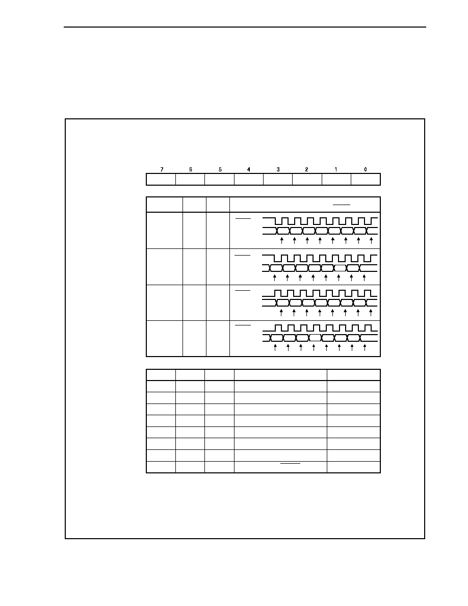
CHAPTER 16 3-WIRE VARIABLE-LENGTH SERIAL I/O (CSIB)
Preliminary User's Manual U17714EJ1V0UD
527
(2) CSIBn control register 1 (CBnCTL1)
CBnCTL1 is an 8-bit register that controls the CSIBn serial transfer operation.
This register can be read or written in 8-bit or 1-bit units.
Reset sets this register to 00H.
Caution The CBnCTL1 register can be rewritten only when the CBnCTL0.CBnPWR bit = 0.
0
CBnCKP
0
0
1
1
Specification of data transmission/
reception timing in relation to SCKBn
CBnCTL1
(n = 0 to 5)
0
CBnDAP
0
1
0
1
0
CBnCKP CBnDAP CBnCKS2 CBnCKS1 CBnCKS0
After reset 00H R/W Address: CB0CTL1 FFFFFD01H, CB1CTL1 FFFFFD11H,
CB2CTL1 FFFFFD21H, CB3CTL1 FFFFFD31H,
CB4CTL1 FFFFFD41H, CB5CTL1 FFFFFD51H
CBnCKS2
0
0
0
0
1
1
1
1
CBnCKS1
0
0
1
1
0
0
1
1
CBnCKS0
0
1
0
1
0
1
0
1
Communication clock
f
XX
/2
f
XX
/4
f
XX
/8
f
XX
/16
f
XX
/32
f
XX
/64
f
BRGm
External clock (SCKBn)
Master mode
Master mode
Master mode
Master mode
Master mode
Master mode
Master mode
Slave mode
Mode
D7
D6
D5
D4
D3
D2
D1
D0
SCKBn (I/O)
SIBn capture
SOBn (output)
D7
D6
D5
D4
D3
D2
D1
D0
SCKBn (I/O)
SIBn capture
SOBn (output)
D7
D6
D5
D4
D3
D2
D1
D0
SCKBn (I/O)
SIBn capture
SOBn (output)
D7
D6
D5
D4
D3
D2
D1
D0
SCKBn (I/O)
SIBn capture
SOBn (output)
Communication
type 1
Communication
type 2
Communication
type 3
Communication
type 4
Remark When n = 0, 1, m = 1
When n = 2, 3, m = 2
When n = 4, 5, m = 3
For details of f
BRGm
, see 16.8 Baud Rate Generator.

CHAPTER 16 3-WIRE VARIABLE-LENGTH SERIAL I/O (CSIB)
Preliminary User's Manual U17714EJ1V0UD
528
(3) CSIBn control register 2 (CBnCTL2)
CBnCTL2 is an 8-bit register that controls the number of CSIBn serial transfer bits.
This register can be read or written in 8-bit units.
Reset sets this register to 00H.
Caution The CBnCTL2 register can be rewritten only when the CBnCTL0.CBnPWR bit = 0 or when
both the CBnTXE and CBnRXE bits = 0.
After reset: 00H R/W Address: CB0CTL2 FFFFFD02H, CB1CTL2 FFFFFD12H,
CB2CTL2 FFFFFD22H, CB3CTL2 FFFFFD32H,
CB4CTL2 FFFFFD42H, CB5CTL2 FFFFFD52H
0
CBnCTL2
(n = 0 to 5)
0
0
0
CBnCL3
CBnCL2
CBnCL1
CBnCL0
8 bits
9 bits
10 bits
11 bits
12 bits
13 bits
14 bits
15 bits
16 bits
CBnCL3
0
0
0
0
0
0
0
0
1
CBnCL2
0
0
0
0
1
1
1
1
�
CBnCL1
0
0
1
1
0
0
1
1
�
CBnCL0
0
1
0
1
0
1
0
1
�
Serial register bit length
Remarks 1. If the number of transfer bits is other than 8 or 16, prepare and
use data stuffed from the LSB of the CBnTX and CBnRX
registers.
2.
�: don't care
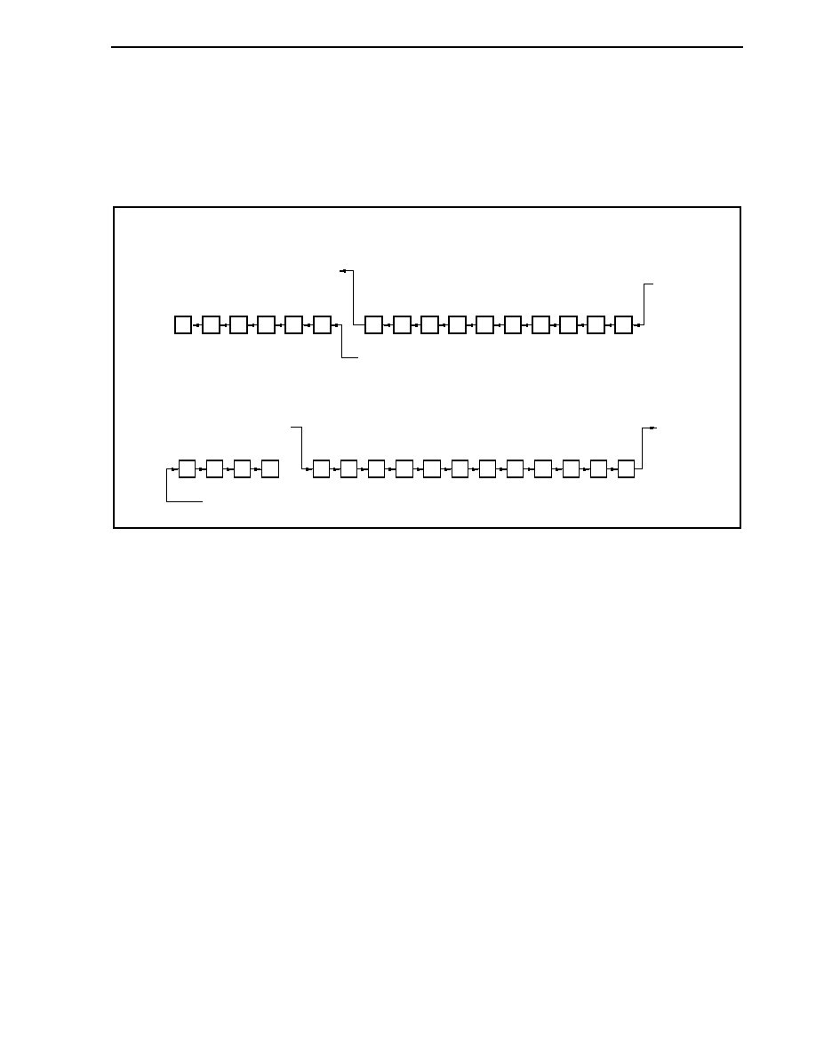
CHAPTER 16 3-WIRE VARIABLE-LENGTH SERIAL I/O (CSIB)
Preliminary User's Manual U17714EJ1V0UD
529
(a) Transfer data length change function
The CSIBn transfer data length can be set in 1-bit units between 8 and 16 bits using the
CBnCTL2.CBnCL3 to CBnCTL2.CBnCL0 bits.
When the transfer bit length is set to a value other than 16 bits, set the data to the CBnTX or CBnRX
register starting from the LSB, regardless of whether the transfer start bit is the MSB or LSB. Any data can
be set for the higher bits that are not used, but the receive data becomes 0 following serial transfer.
(i) Transfer bit length = 10 bits, MSB first
15
10
9
0
SOBn
SIBn
Insertion of 0
(ii) Transfer bit length = 12 bits, LSB first
0
SOBn
11
12
15
SIBn
Insertion of 0
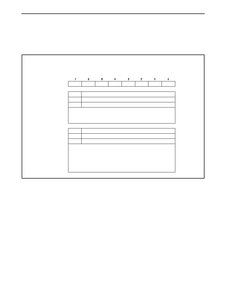
CHAPTER 16 3-WIRE VARIABLE-LENGTH SERIAL I/O (CSIB)
Preliminary User's Manual U17714EJ1V0UD
530
(4) CSIBn status register (CBnSTR)
CBnSTR is an 8-bit register that displays the CSIBn status.
This register can be read or written in 8-bit or 1-bit units, but the CBnTSF flag is read-only.
Reset sets this register to 00H.
In addition to reset input, the CBnSTR register can be initialized by clearing (0) the CBnCTL0.CBnPWR bit.
CBnTSF
Communication stopped
Communicating
CBnTSF
0
1
Communication status flag
CBnSTR
(n = 0 to 5)
0
0
0
0
0
0
CBnOVE
After reset 00H R/W Address: CB0STR FFFFFD03H, CB1STR FFFFFD13H,
CB2STR FFFFFD23H, CB3STR FFFFFD33H,
CB4STR FFFFFD43H, CB5STR FFFFFD53H
� During transmission, this register is set when data is prepared in the CBnTX
register, and during reception, it is set when a dummy read of the CBnRX register
is performed.
When transfer ends, this flag is cleared to 0 at the last edge of the clock.
No overrun
Overrun
CBnOVE
0
1
Overrun error flag
� An overrun error occurs when the next reception starts without reading the value of
the receive buffer by CPU, upon completion of the receive operation.
The CBnOVE flag displays the overrun error occurrence status in this case.
� The CBnOVE bit is valid also in the single transfer mode. Therefore, when only
using transmission, note the following.
� Do not check the CBnOVE flag.
� Read this bit even if reading the reception data is not required.
� The CBnOVE flag is cleared by writing 0 to it. It cannot be set even by writing 1 to it.
< >
< >
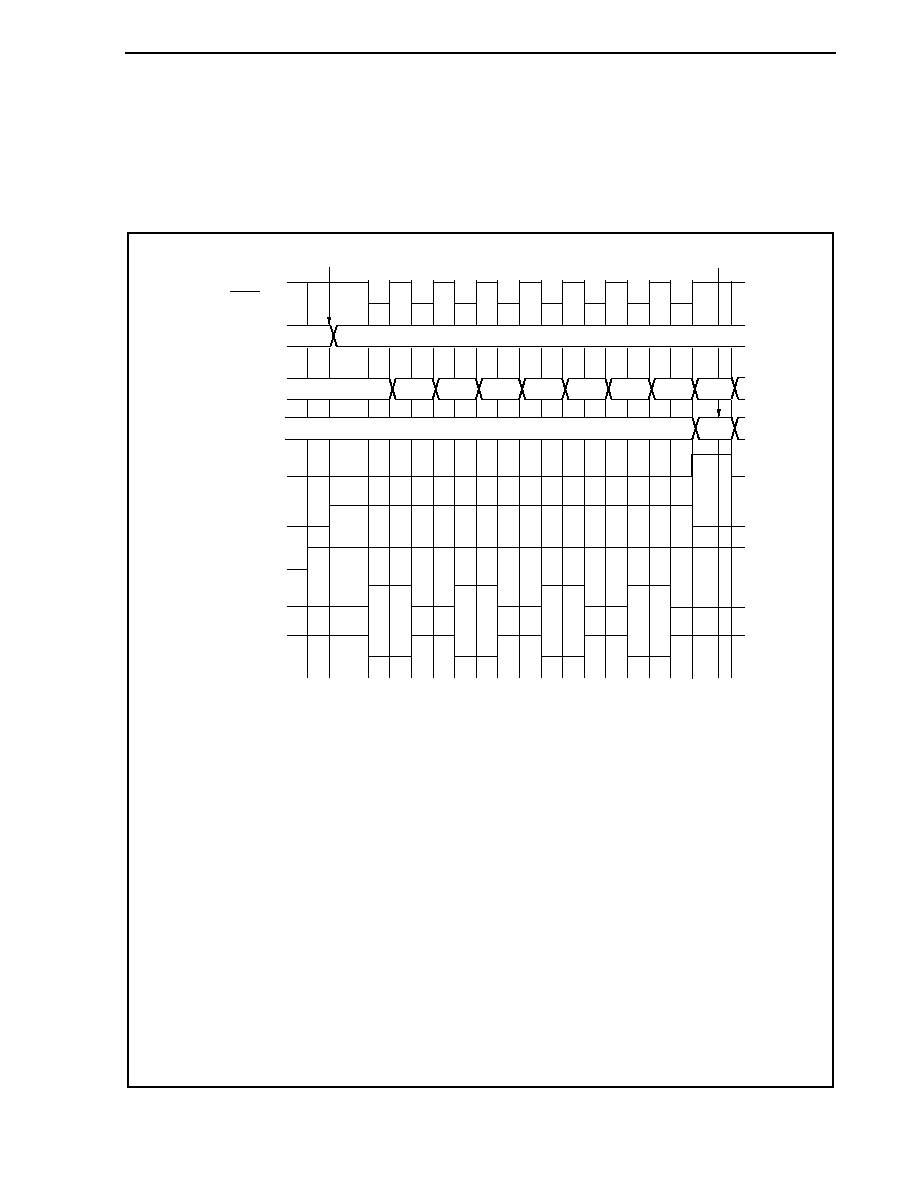
CHAPTER 16 3-WIRE VARIABLE-LENGTH SERIAL I/O (CSIB)
Preliminary User's Manual U17714EJ1V0UD
531
16.5 Operation
16.5.1 Single transfer mode (master mode, transmission/reception mode)
This section shows a case of MSB first (CBnCTL0.CBnDIR bit = 0), communication type 1 (see 16.4 (2) CSIBn
control register 1 (CBnCTL1)), and transfer data length = 8 bits (CBnCTL2.CBnCL3 to CBnCTL2.CBnCL0 bits = 0, 0,
0, 0).
CBnTX write (55H)
CBnRX read (AAH)
(AAH)
(55H)
1
0
1
1
0
1
ABH
56H
ADH
5AH
B5H
6AH
D5H
AAH
55H (transmit data)
SCKBn pin
CBnTX register
AAH
00H
CBnRX register
Shift
register
INTCBnR signal
Note
SIBn pin
SOBn pin
0
0
0
1
0
0
1
0
1
1
CBnTSF bit
CBnSCE bit
(1)
(5)
(6)
(8)
(7)
(2)
(3)
(4)
(1) Clear the CBnCTL0.CBnPWR bit to 0.
(2) Set the CBnCTL1 and CBnCTL2 registers to specify the transfer mode.
(3) Set the CBnTXE, CBnRXE, and CBnSCE bits of the CBnCTL0 register to 1 at the same time as
specifying the transfer mode using the CBnDIR bit, to set the transmission/reception enabled status.
(4) Set the CBnPWR bit to 1 to enable the CSIBn operation.
(5) Write transfer data to the CBnTX register (transmission start).
(6) The reception complete interrupt request signal (INTCBnR) is output.
(7) Read the CBnRX register before clearing the CBnPWR bit to 0.
(8) Check that the CBnSTR.CBnTSF bit = 0 and set the CBnPWR bit to 0 to stop operation of CSIBn (end
of transmission/reception).
Note In single transmission or single transmission/reception mode, the INTCBnT signal is not generated.
When communication is complete, the INTCBnR signal is generated.
Remark The processing of steps (3) and (4) can be set simultaneously.
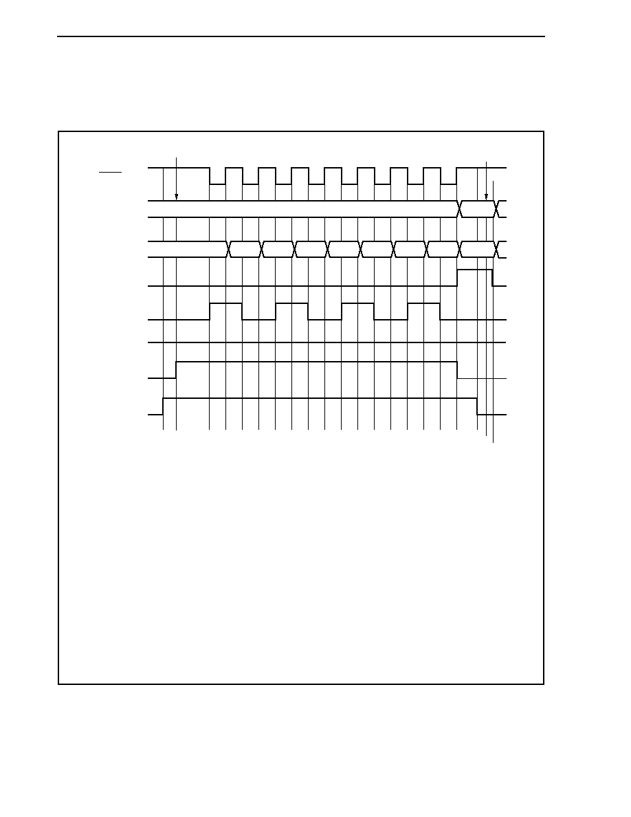
CHAPTER 16 3-WIRE VARIABLE-LENGTH SERIAL I/O (CSIB)
Preliminary User's Manual U17714EJ1V0UD
532
16.5.2 Single transfer mode (master mode, reception mode)
This section shows the case using MSB first (CBnCTL0.CBnDIR bit = 0) and communication type 1 (see 16.4 (2)
CSIBn control register 1 (CBnCTL1)), transfer data length = 8 bits (CBnCTL2.CBnCL3 to CBnCTL2.CBnCL0 bits =
0, 0, 0, 0).
(AAH)
1
0
1
1
0
0
1
01H
02H
05H
0AH
15H
2AH
55H
AAH
00H
SCKBn pin
CBnRX register
CBnRX read (dummy read)
Shift
register
CBnSCE bit
CBnTSF bit
INTCBnR signal
SIBn pin
SOBn pin
0
L
(1)
(2)
(3)
(4)
(5)
(6)
(7)
(9)
(8)
CBnRX read (AAH)
AAH
00H
(1) Clear the CBnCTL0.CBnPWR bit to 0.
(2) Set the CBnCTL1 and CBnCTL2 registers to specify the transfer mode.
(3) Set the CBnCTL0.CBnRXE and CBnCTL0.CBnSCE bits to 1 at the same time as specifying the
transfer mode using the CBnDIR bit, to set the reception enabled status.
(4) Set the CBnPWR bit to 1 to enable the CSIBn operation.
(5) Perform a dummy read of the CBnRX register (reception start trigger).
(6) The reception complete interrupt request signal (INTCBnR) is output.
(7) Set the CBnSCE bit to 0 to set the final receive data status.
(8) Read the CBnRX register.
(9) Check that the CBnSTR.CBnTSF bit = 0 and set the CBnPWR bit to 0 to stop the CSIBn operation
(end of reception).
Remark The processing of steps (3) and (4) can be set simultaneously.
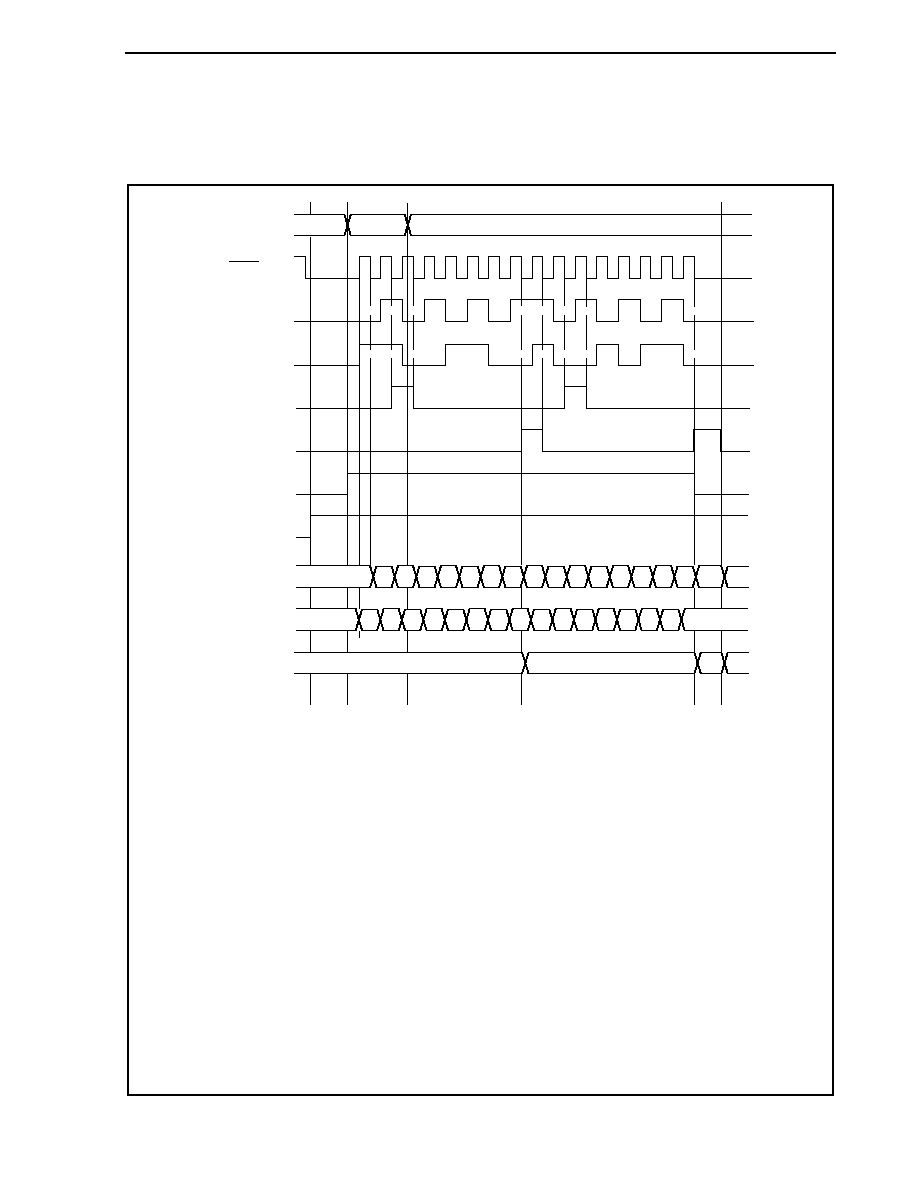
CHAPTER 16 3-WIRE VARIABLE-LENGTH SERIAL I/O (CSIB)
Preliminary User's Manual U17714EJ1V0UD
533
16.5.3 Continuous mode (master mode, transmission/reception mode)
This section shows the case using MSB first (CBnCTL0.CBnDIR bit = 0) and communication type 3 (see 16.4 (2)
CSIBn control register 1 (CBnCTL1)), transfer data length = 8 bits (CBnCTL2.CBnCL3 to CBnCTL2.CBnCL0 bits =
0, 0, 0, 0).
(8)
(7)
(7)
(6)
(5)
(1)
(2)
(3)
(4)
96H
00H
CCH
1
1
1
1
1
1
0
0
0
0
0
0
1
1
1
1
1
55H
CBnTX register
SCKBn pin
SOBn pin
SIBn pin
INTCBnT signal
INTCBnR signal
CBnTSF bit
CBnSCE bit
Shift register
SO latch
CBnRX register
0
0
0
0
AAH
96H
CCH
1
1
1
0
0
0
1
0
1
0
0
(1) Clear the CBnCTL0.CBnPWR bit to 0.
(2) Set the CBnCTL1 and CBnCTL2 registers to specify the transfer mode.
(3) Set the CBnTXE, CBnRXE, and CBnSCE bits of the CBnCTL0 register to 1 at the same time as
specifying the transfer mode using the CBnDIR bit, to set the transmission/reception enabled status.
(4) Set the CBnPWR bit to 1 to enable the CSIBn operation.
(5) Write transfer data to the CBnTX register (transmission start).
(6) The transmission enable interrupt request signal (INTCBnT) is received and transfer data is written to
the CBnTX register.
(7) The reception complete interrupt request signal (INTCBnR) is output.
Read the CBnRX register before the next receive data arrives or before the CBnPWR bit is cleared to 0.
(8) Check that the CBnSTR.CBnTSF bit = 0 and set the CBnPWR bit to 0 to stop the operation of CSIBn
(end of transmission/reception).
To continue transfer, repeat steps (5) to (7) before (8).
In transmission mode or transmission/reception mode, the communication is not started by reading the
CBnRX register.
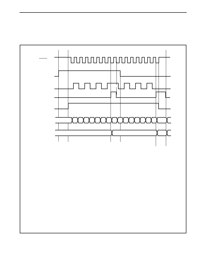
CHAPTER 16 3-WIRE VARIABLE-LENGTH SERIAL I/O (CSIB)
Preliminary User's Manual U17714EJ1V0UD
534
16.5.4 Continuous mode (master mode, reception mode)
This section shows the case using MSB first (CBnCTL0.CBnDIR bit = 0) and communication type 2 (see 16.4 (2)
CSIBn control register 1 (CBnCTL1)), transfer data length = 8 bits (CBnCTL2.CBnCL3 to CBnCTL2.CBnCL0 bits =
0, 0, 0, 0).
(8)
(6)
(6)
(7)
(5)
(1)
(2)
(3)
(4)
1
0
0
0
0
0
0
0
1
1
1
1
1
55H
SCKBn pin
CBnSCE bit
SIBn pin
INTCnR signal
CBnTSF bit
Shift register
CBnRX register
1
1
0
55H
AAH
AAH
00H
(1) Clear the CBnCTL0.CBnPWR bit to 0.
(2) Set the CBnCTL1 and CBnCTL2 registers to specify the transfer mode.
(3) Set the CBnCTL0.CBnRXE bit to 1 at the same time as specifying the transfer mode using the CBnDIR
bit, to set the reception enabled status.
(4) Set the CBnPWR bit to 1 to enable the CSIBn operation.
(5) Perform a dummy read of the CBnRX register (reception start trigger).
(6) The reception complete interrupt request signal (INTCBnR) is output.
Read the CBnRX register before the next receive data arrives or before the CBnPWR bit is cleared to
0.
(7) Set the CBnCTL0.CBnSCE bit = 0 while the last data being received to set the final receive data status.
(8) Check that the CBnSTR.CBnTSF bit = 0 and set the CBnPWR bit to 0 to stop the operation of CSIBn
(end of reception).
To continue transfer, repeat steps (5) and (6) before (7).
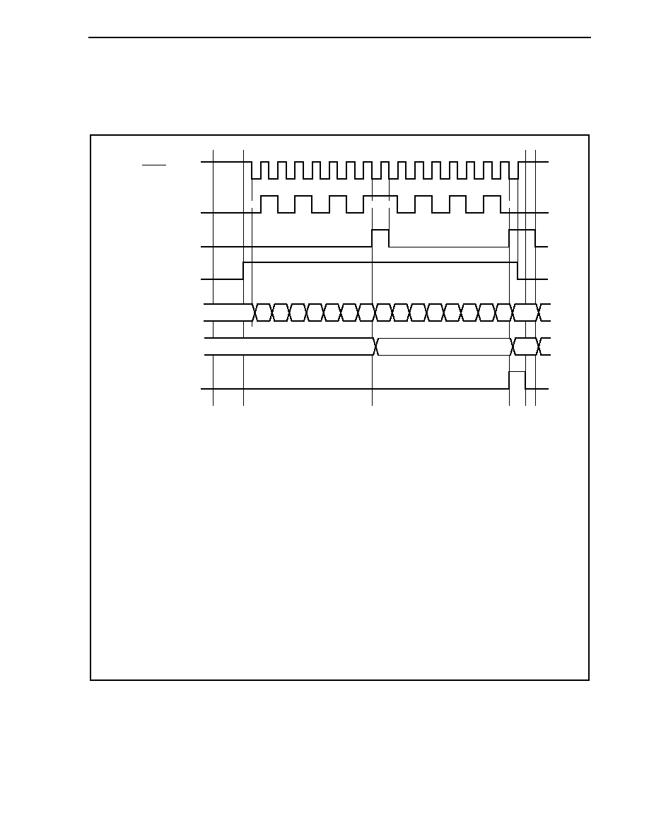
CHAPTER 16 3-WIRE VARIABLE-LENGTH SERIAL I/O (CSIB)
Preliminary User's Manual U17714EJ1V0UD
535
16.5.5 Continuous reception mode (error)
This section shows the case using MSB first (CBnCTL0.CBnDIR bit = 0) and communication type 2 (see 16.4 (2)
CSIBn control register 1 (CBnCTL1)), transfer data length = 8 bits (CBnCTL2.CBnCL3 to CBnCTL2.CBnCL0 bits =
0, 0, 0, 0).
(8) (9) (10)
(7)
(6)
(5)
AAH
00H
1
0
0
0
0
0
0
1
1
1
1
1
SCKBn pin
SIBn pin
INTCBnR signal
CBnTSF bit
Shift register
CBnRX register
CBnOVE bit
55H
55H
0
1
0
AAH
1
(1)
(2)
(3)
(4)
(1) Clear the CBnCTL0.CBnPWR bit to 0.
(2) Set the CBnCTL1 and CBnCTL2 registers to specify the transfer mode.
(3) Set the CBnCTL0.CBnRXE bit to 1 at the same time as specifying the transfer mode using the CBnDIR
bit, to set the reception enabled status.
(4) Set the CBnPWR bit = 1 to enable CSIBn operation.
(5) Perform a dummy read of the CBnRX register (reception start trigger).
(6) The reception complete interrupt request signal (INTCBnR) is output.
(7) If the data could not be read before the end of the next transfer, the CBnSTR.CBnOVE flag is set to 1
upon the end of reception and the INTCBnR signal is output.
(8) Overrun error processing is performed after checking that the CBnOVE bit = 1 in the INTCBnR interrupt
servicing.
(9) Clear CBnOVE bit to 0.
(10) Check that the CBnSTR.CBnTSF bit = 0 and set the CBnPWR bit to 0 to stop the operation CSIBn
(end of reception).
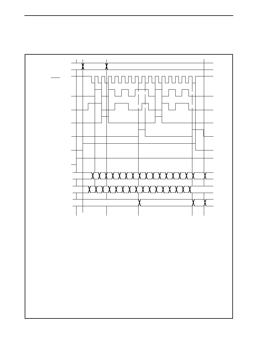
CHAPTER 16 3-WIRE VARIABLE-LENGTH SERIAL I/O (CSIB)
Preliminary User's Manual U17714EJ1V0UD
536
16.5.6 Continuous mode (slave mode, transmission/reception mode)
This section shows the case using MSB first (CBnCTL0.CBnDIR bit = 0) and communication type 2 (see 16.4 (2)
CSIBn control register 1 (CBnCTL1)), transfer data length = 8 bits (CBnCTL2.CSnCL3 to CBnCTL2.CBnCL0 bits =
0, 0, 0, 0).
(8)
(7)
(7)
(6)
(5)
96H
00H
CCH
1
1
1
1
1
1
1
0
0
0
0
0
0
0
1
1
1
1
1
1
55H
CBnTX register
SCKBn pin
SOBn pin
SIBn pin
INTCBnT signal
INTCBnR signal
Shift register
SO latch
CBnRX register
0
0
0
0
0
0
AAH
96H
CCH
1
0
0
0
1
1
CBnTSF bit
CBnSCE bit
(1)
(2)
(3)
(4)
(1) Clear the CBnCTL0.CBnPWR bit to 0.
(2) Set the CBnCTL1 and CBnCTL2 registers to specify the transfer mode.
(3) Set the CBnTXE, CBnRXE and CBnSCE bits of the CBnCTL0 register to 1 at the same time as
specifying the transfer mode using the CBnDIR bit, to set the transmission/reception enabled status.
(4) Set the CBnPWR bit to 1 to enable supply of the CSIBn operation.
(5) Write the transfer data to the CBnTX register.
(6) The transmission enable interrupt request signal (INTCBnT) is received and the transfer data is written
to the CBnTX register.
(7) The reception complete interrupt request signal (INTCBnR) is output.
Read the CBnRX register.
(8) Check that the CBnSTR.CBnTSF bit = 0 and set the CBnPWR bit to 0 to stop the operation of CSIBn
(end of transmission/reception).
To continue transfer, repeat steps (5) to (7) before (8).
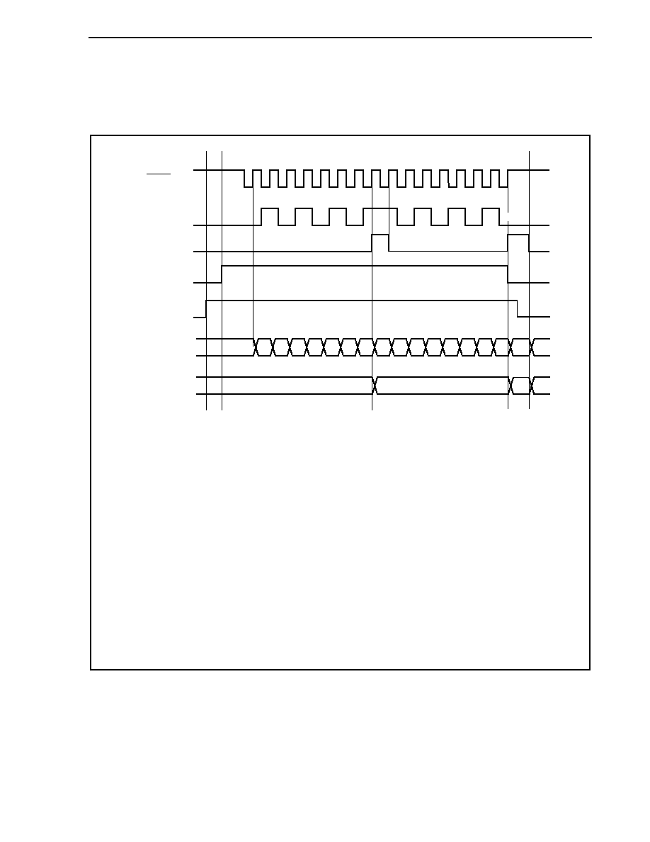
CHAPTER 16 3-WIRE VARIABLE-LENGTH SERIAL I/O (CSIB)
Preliminary User's Manual U17714EJ1V0UD
537
16.5.7 Continuous mode (slave mode, reception mode)
This section shows the case using MSB first (CBnCTL0.CBnDIR bit = 0) and communication type 1 (see 16.4 (2)
CSIBn control register 1 (CBnCTL1)), transfer data length = 8 bits (CBnCTL2.CBnCL3 to CBnCTL2.CBnCL0 bits =
0, 0, 0, 0).
(7)
(6)
(6)
(5)
1
0
0
0
0
0
0
0
1
1
1
1
1
55H
SCKBn pin
SIBn pin
INTCBnR signal
CBnTSF bit
CBnSCE bit
Shift register
CBnRX register
1
1
55H
AAH
00H
AAH
0
(1)
(2)
(3)
(4)
(1) Clear the CBnCTL0.CBnPWR bit to 0.
(2) Set the CBnCTL1 and CBnCTL2 registers to specify the transfer mode.
(3) Set the CBnCTL0.CBnRXE and CBnCTL0.CBnSCE bits to 1 at the same time as specifying the
transfer mode using the CBnDIR bit, to set the reception enabled status.
(4) Set the CBnPWR bit = 1 to enable CSIBn operation.
(5) Perform a dummy read of the CBnRX register (reception start trigger).
(6) The reception complete interrupt request signal (INTCBnR) is output.
Read the CBnRX register. When reading the last data, clear the CBnCTL0.CBnSCE bit to 0 before
reading the CBnRX register.
(7) Check that the CBnSTR.CBnTSF bit = 0 and set the CBnPWR bit to 0 to stop the operation of CSIBn
(end of reception).
To continue transfer, repeat steps (5) and (6) before (7).
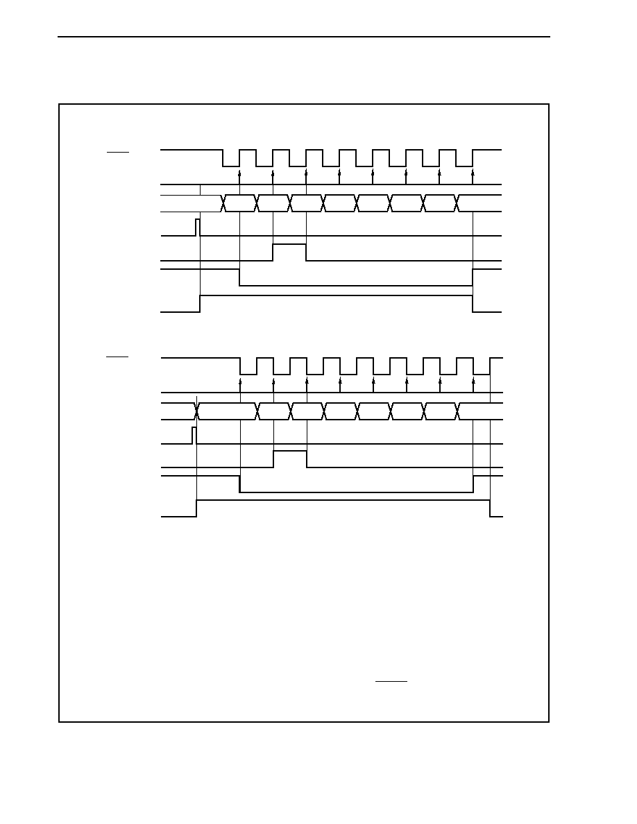
CHAPTER 16 3-WIRE VARIABLE-LENGTH SERIAL I/O (CSIB)
Preliminary User's Manual U17714EJ1V0UD
538
16.5.8 Clock timing
(1/2)
(1) Communication type 1 (CBnCKP = 0, CBnDAP = 0)
D6
D5
D4
D3
D2
D1
SCKBn pin
SIBn
capture
Reg-R/W
SOBn pin
INTCBnT
interrupt
Note 1
INTCBnR
interrupt
Note 2
CBnTSF bit
D0
D7
(2) Communication type 2 (CBnCKP = 0, CBnDAP = 1)
D6
D5
D4
D3
D2
D1
D0
D7
SCKBn pin
SIBn
capture
Reg-R/W
SOBn pin
INTCBnT
interrupt
Note 1
INTCBnR
interrupt
Note 2
CBnTSF bit
Notes 1. The INTCBnT interrupt is set when the data written to the transmit buffer is transferred to the data
shift register in the continuous transmission or continuous transmission/reception mode. In the
single transmission or single transmission/reception mode, the INTCBnT interrupt request signal is
not generated, but the INTCBnR interrupt request signal is generated upon completion of
communication.
2. The INTCBnR interrupt occurs if reception is correctly completed and receive data is ready in the
CBnRX register while reception is enabled, and if an overrun error occurs. In the single mode, the
INTCBnR interrupt request signal is generated even in the transmission mode, upon completion of
communication.
Caution In communication type 2, the CBnTSF bit is cleared half a SCKBn clock after generation of an
INTCBnR interrupt request signal.
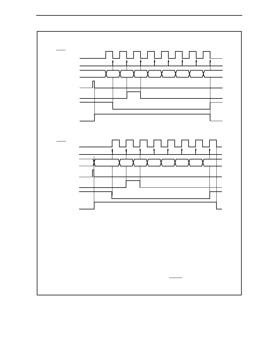
CHAPTER 16 3-WIRE VARIABLE-LENGTH SERIAL I/O (CSIB)
Preliminary User's Manual U17714EJ1V0UD
539
(2/2)
(3) Communication type 3 (CBnCKP = 1, CBnDAP = 0)
D6
D5
D4
D3
D2
D1
D0
D7
SCKBn pin
SIBn
capture
Reg-R/W
SOBn pin
INTCBnT
interrupt
Note 1
INTCBnR
interrupt
Note 2
CBnTSF bit
(4) Communication type 4 (CBnCKP = 1, CBnDAP = 1)
D6
D5
D4
D3
D2
D1
D0
D7
SCKBn pin
SIBn
capture
Reg-R/W
SOBn pin
INTCBnT
interrupt
Note 1
INTCBnR
interrupt
Note 2
CBnTSF bit
Notes 1. The INTCBnT interrupt is set when the data written to the transmit buffer is transferred to the data
shift register in the continuous transmission or continuous transmission/reception modes. In the
single transmission or single transmission/reception modes, the INTCBnT interrupt request signal is
not generated, but the INTCBnR interrupt request signal is generated upon completion of
communication.
2. The INTCBnR interrupt occurs if reception is correctly completed and receive data is ready in the
CBnRX register while reception is enabled, and if an overrun error occurs. In the single mode, the
INTCBnR interrupt request signal is generated even in the transmission mode, upon completion of
communication.
Caution In communication type 4, the CBnTSF bit is cleared half a SCKBn clock after generation of an
INTCBnR interrupt request signal.
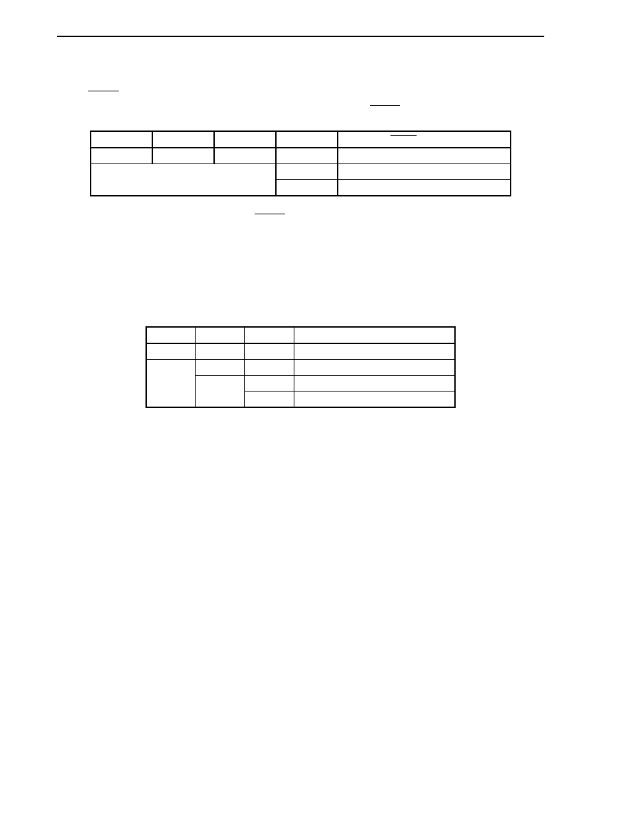
CHAPTER 16 3-WIRE VARIABLE-LENGTH SERIAL I/O (CSIB)
Preliminary User's Manual U17714EJ1V0UD
540
16.6 Output Pins
(1) SCKBn pin
When CSIBn operation is disabled (CBnCTL0.CBnPWR bit = 0), the SCKBn pin output status is as follows.
CBnCKS2 CBnCKS1 CBnCKS0 CBnCKP
SCKBn
Pin
Output
1 1 1
�
High impedance
0
Fixed to high level
Other than above
1
Fixed to low level
Remarks 1. The output level of the SCKBn pin changes if any of the CBnCTL1.CBnCKP and
CBnCKS2 to CBnCKS0 bits is rewritten.
2. n = 0 to 5
3.
�: don't care
(2) SOBn pin
When CSIBn operation is disabled (CBnPWR bit = 0), the SOBn pin output status is as follows.
CBnTXE
CBnDAP
CBnDIR
SOBn Pin Output
0
�
�
Fixed to low level
0
�
SOBn latch value (low level)
0
CBnTX register value (MSB)
1
1
1
CBnTX register value (LSB)
Remarks 1. The SOBn pin output changes when any one of the
CBnCTL0.CBnTXE, CBnCTL0.CBnDIR bits, and
CBnCTL1.CBnDAP bit is rewritten.
2. n = 0 to 5
3.
�: don't care
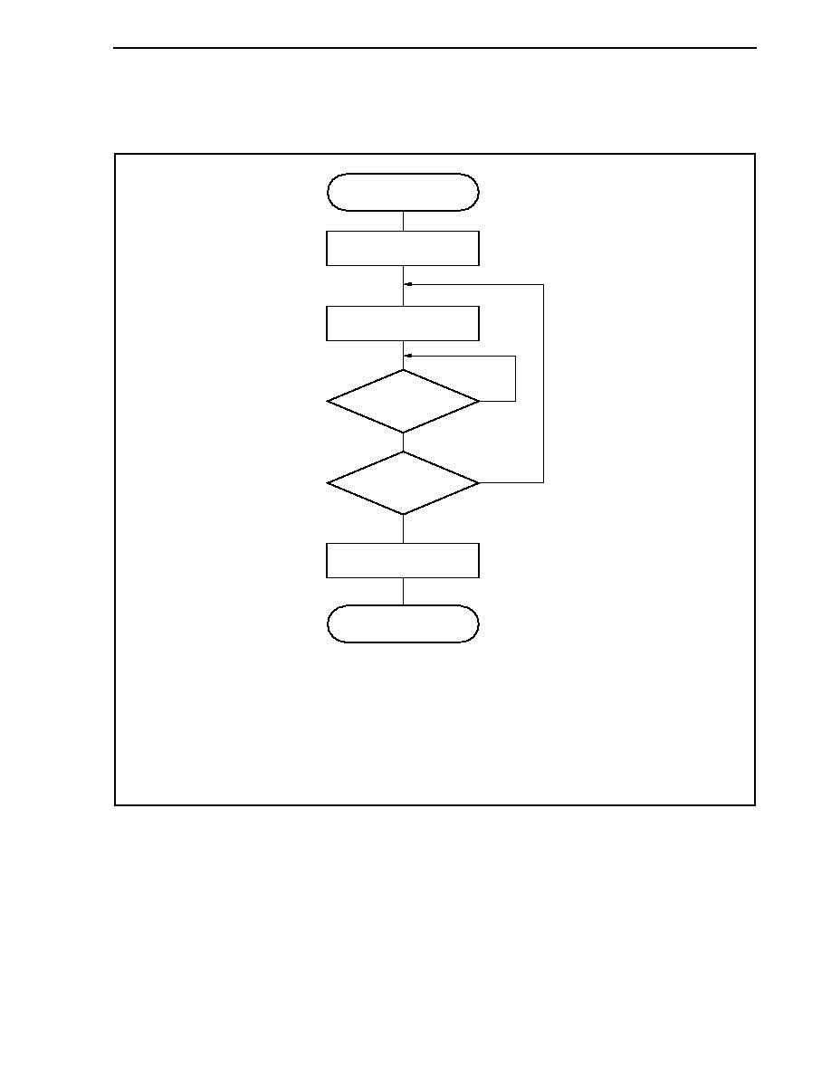
CHAPTER 16 3-WIRE VARIABLE-LENGTH SERIAL I/O (CSIB)
Preliminary User's Manual U17714EJ1V0UD
541
16.7 Operation Flow
(1) Single transmission
START
No
Yes
INTCBnR signal is
generated?
Transfer data exists?
END
Yes
No
Initial setting (CBnCTL0
Note
,
CBnCTL1 registers, etc.)
Write CBnTX register
(start transfer).
CBnPWR bit = 0
(CBnCTL0)
Note Set the CBnSCE bit to 1 in the initial setting.
Caution In the slave mode, data cannot be correctly transmitted if the next transfer clock is input
earlier than the CBnTX register is written.
Remark n = 0 to 5
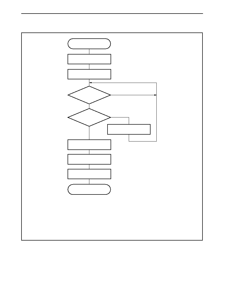
CHAPTER 16 3-WIRE VARIABLE-LENGTH SERIAL I/O (CSIB)
Preliminary User's Manual U17714EJ1V0UD
542
(2) Single reception
START
No
INTCBnR signal is
generated?
Last data?
END
Yes
Yes
No
Initial setting (CBnCTL0
Note
,
CBnCTL1 registers, etc.)
CBnRX register dummy read
(start reception)
CBnSCE bit = 0
(CBnCTL0)
CBnPWR bit = 0
(CBnCTL0)
CBnRX register read
CBnRX register read
Note Set the CBnSCE bit to 1 in the initial setting.
Caution In the single mode, data cannot be correctly received if the next transfer clock is input
earlier than the CBnRX register is read.
Remark n = 0 to 5
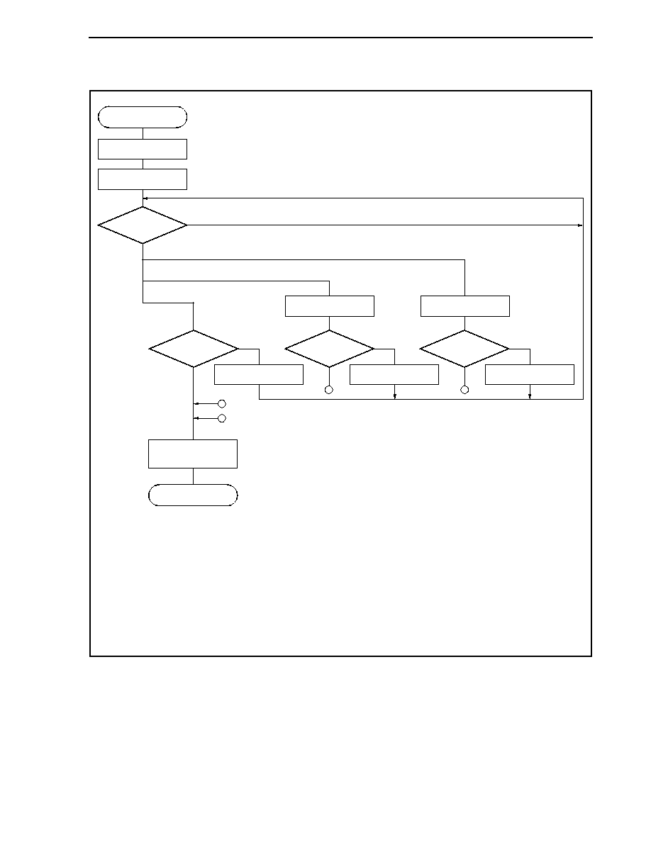
CHAPTER 16 3-WIRE VARIABLE-LENGTH SERIAL I/O (CSIB)
Preliminary User's Manual U17714EJ1V0UD
543
(3) Single transmission/reception
START
Initial setting (CBnCTL0
Note 1
,
CBnCTL1 registers, etc.)
Write CBnTX register
(start transfer).
END
CBnPWR bit = 0,
CBnTXE bit = CBnRXE bit = 0
(CBnCTL0)
No
Transmission/reception
Transmission
Reception
INTCBnR signal is
generated?
Yes
Transfer end?
Write CBnTX register
Note 2
.
Read CBnRX register.
Read CBnRX register.
No
Yes
Transfer end?
Write CBnTX register
Note 2
.
No
Yes
Transfer end?
Write CBnTX register
Note 2
.
No
Yes
B
B
A
A
Notes 1. Set the CBnSCE bit to 1 in the initial setting.
2. If the next transfer is reception only, dummy data is written to the CBnTX register.
Caution Even in the single mode, the CBnSTR.CBnOVE flag is set to 1. If only transmission is
used in the transmission/reception mode, therefore, checking the CBnOVE flag is not
required.
Remark n = 0 to 5
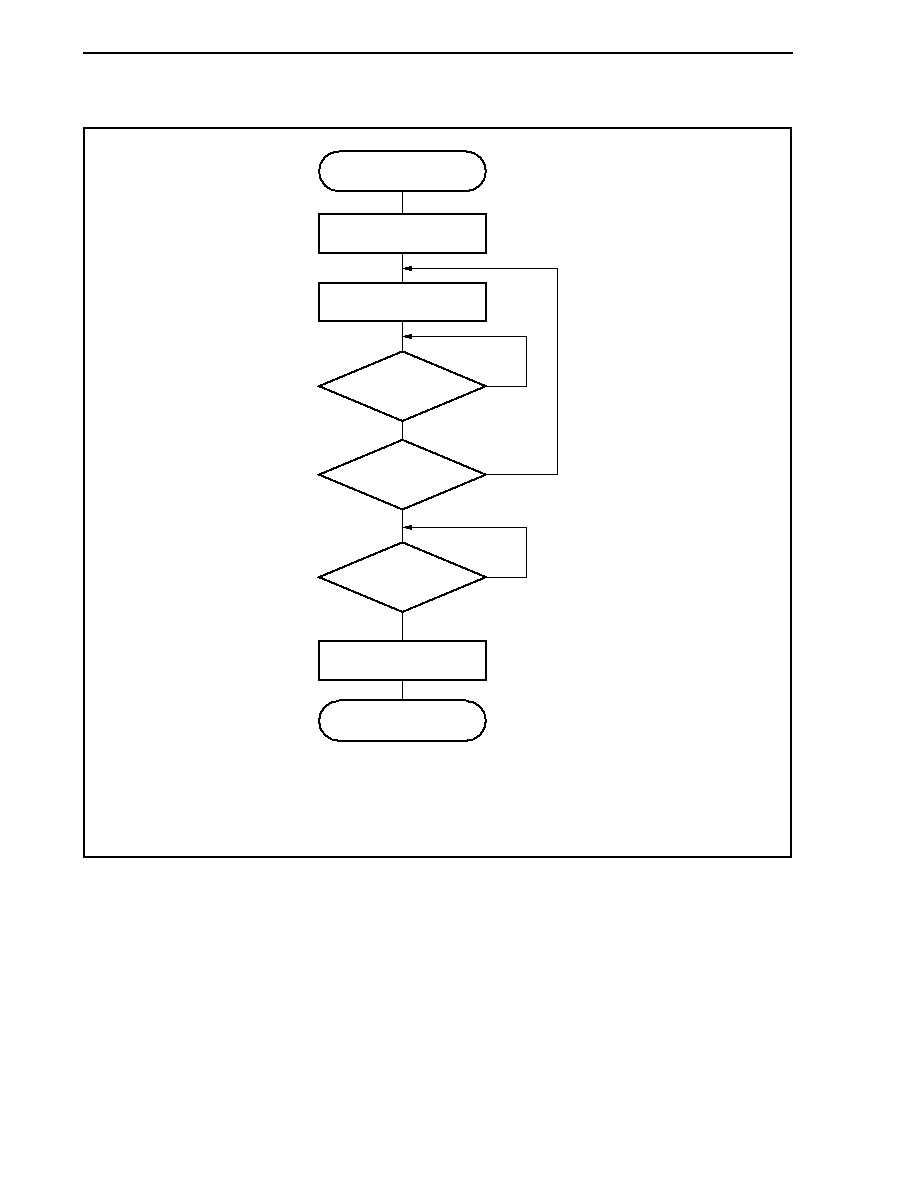
CHAPTER 16 3-WIRE VARIABLE-LENGTH SERIAL I/O (CSIB)
Preliminary User's Manual U17714EJ1V0UD
544
(4) Continuous transmission
START
No
Yes
INTCBnT signal is
generated?
Data to be
transferred next exists?
END
Yes
No
Initial setting (CBnCTL0
Note
,
CBnCTL1 registers, etc.)
Write CBnTX register
(start transfer).
CBnPWR bit = 0
(CBnCTL0)
No
CBnTSF bit = 1?
(CBnSTR)
Yes
Note Set the CBnSCE bit to 1 in the initial setting.
Remark n = 0 to 5
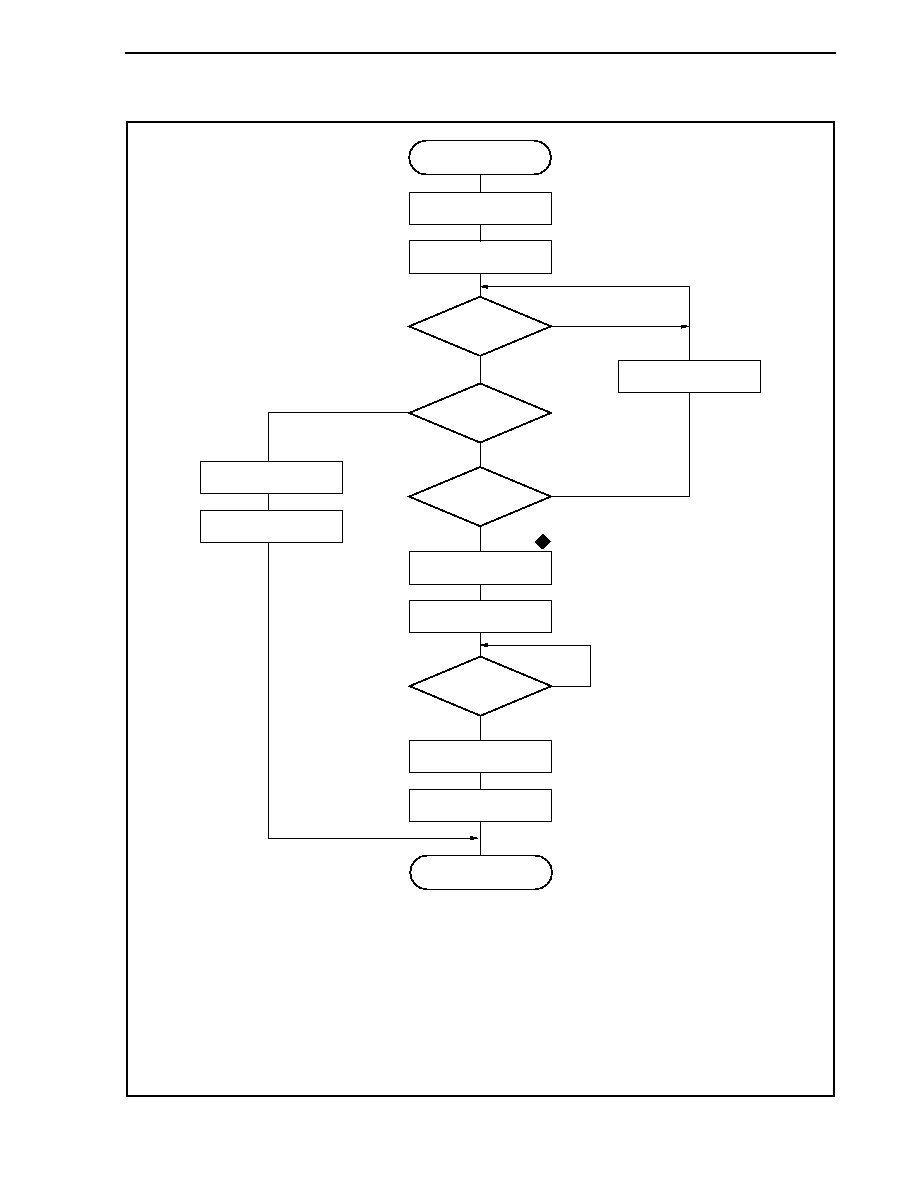
CHAPTER 16 3-WIRE VARIABLE-LENGTH SERIAL I/O (CSIB)
Preliminary User's Manual U17714EJ1V0UD
545
(5) Continuous reception
START
END
No
No
Yes
INTCBnR signal is
generated?
CBnOVE bit = 1?
(CBnSTR)
No
Yes
Initial setting (CBnCTL0
Note
,
CBnCTL1 registers, etc.)
CBnRX register dummy read
(start reception)
CBnRX register read
CBnRX register read
CBnRX register read
CBnRX register read
Yes
Is data being
received last data?
CBnSCE bit = 0
(CBnCTL0)
CBnSCE bit = 1
(CBnCTL0)
No
INTCBnR signal is
generated?
Yes
CBnOVE bit clear
(CBnSTR)
Note Set the CBnSCE bit to 1 in the initial setting
Caution In the master mode, the clock is output without limit when dummy data is read from the
CBnRX register. To stop the clock, execute the flow marked
in the above flowchart.
In the slave mode, malfunction due to noise during communication can be prevented by
executing the flow marked
in the above flowchart.
Before resuming communication, set the CBnCTL0.CBnSCE bit to 1, and read dummy
data from the CBnRX register.
Remark n = 0 to 5
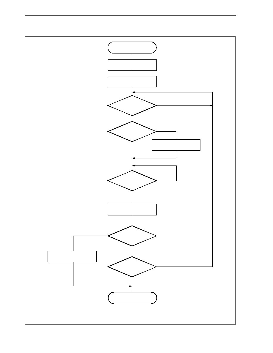
CHAPTER 16 3-WIRE VARIABLE-LENGTH SERIAL I/O (CSIB)
Preliminary User's Manual U17714EJ1V0UD
546
(6) Continuous transmission/reception
START
END
No
No
INTCBnR signal is
generated?
Yes
No
INTCBnT signal is
generated?
Yes
Initial setting (CBnCTL0
Note
,
CBnCTL1 registers, etc.)
Write CBnTX register.
CBnRX register read
Yes
Yes
Is data completely
received last data?
No
Write CBnTX register.
Yes
Is data being
transferred last data?
No
CBnOVE bit = 0?
(CBnSTR)
CBnOVE bit clear
(CBnSTR)
Note Set the CBnSCE bit to 1 in the initial setting.
Remark n = 0 to 5
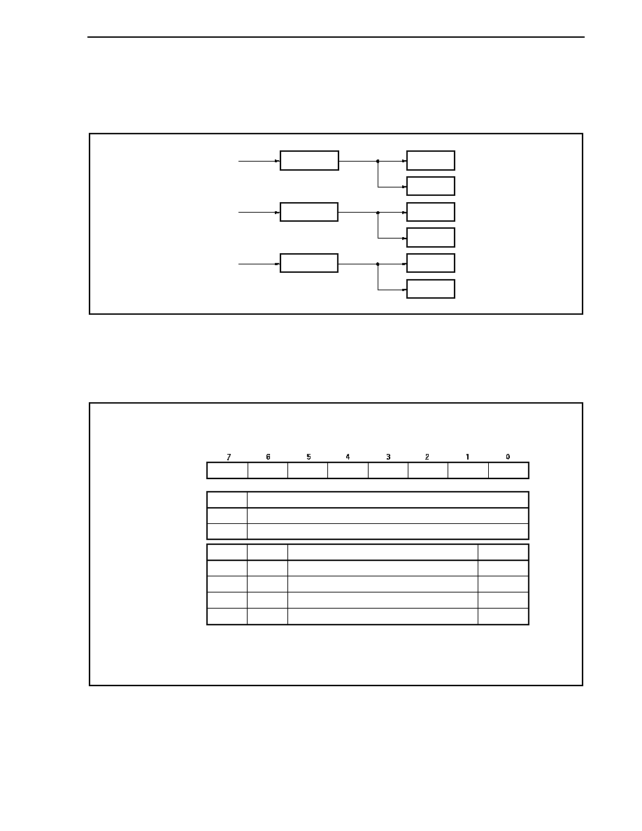
CHAPTER 16 3-WIRE VARIABLE-LENGTH SERIAL I/O (CSIB)
Preliminary User's Manual U17714EJ1V0UD
547
16.8 Baud Rate Generator
The BRG1 to BRG3 and CSIB0 to CSIB5 baud rate generators are connected as shown in the following block
diagram.
CSIB0
CSIB1
CSIB2
CSIB3
CSIB4
BRG1
BRG2
BRG3
CSIB5
f
X
f
X
f
X
f
BRG1
f
BRG2
f
BRG3
(1) Prescaler mode registers 1 to 3 (PRSM1 to PRSM3)
The PRSM1 to PRSM3 registers control generation of the baud rate signal for CSIB.
These registers can be read or written in 8-bit or 1-bit units.
Reset sets these registers to 00H.
0
PRSMm
(m = 1 to 3)
0
0
BGCEm
0
0
BGCSm1 BGCSm0
Disabled
Enabled
BGCEm
0
1
Baud rate output
f
XX
f
XX
/2
f
XX
/4
f
XX
/8
Setting value (k)
0
1
2
3
BGCSm1
0
0
1
1
BGCSm0
0
1
0
1
Input clock selection (f
BGCSm
)
After reset: 00H R/W Address: PRSM1 FFFFF320H, PRSM2 FFFFF324H,
PRSM3 FFFFF328H
< >
Cautions 1. Do not rewrite the PRSMm register during operation.
2. Set the PRSMm register before setting the BGCEm bit to 1.
CHAPTER 16 3-WIRE VARIABLE-LENGTH SERIAL I/O (CSIB)
Preliminary User's Manual U17714EJ1V0UD
548
(2) Prescaler compare registers 1 to 3 (PRSCM1 to PRSCM3)
The PRSCM1 to PRSCM3 registers are 8-bit compare registers.
These registers can be read or written in 8-bit units.
Reset sets these registers to 00H.
PRSCMm7
PRSCMm
(m = 1 to 3)
PRSCMm6 PRSCMm5 PRSCMm4 PRSCMm3 PRSCMm2 PRSCMm1 PRSCMm0
After reset: 00H R/W Address: PRSCM1 FFFFF321H, PRSCM2 FFFFF325H,
PRSCM3 FFFFF329H
Cautions 1. Do not rewrite the PRSCMm register during operation.
2. Set the PRSCMm register before setting the PRSMm.BGCEm bit to 1.
16.8.1 Baud rate generation
The transmission/reception clock is generated by dividing the main clock. The baud rate generated from the main
clock is obtained by the following equation.
f
BRGm
=
Remark f
BRGm
: BRGm count clock
f
XX
:
Main clock oscillation frequency
k:
PRSMm register setting value = 0 to 3
N:
PRSCMm register setting value = 1 to 256
However, N = 256 only when PRSCMm register is set to 00H.
m = 1 to 3
f
XX
2
k+1
� N

CHAPTER 16 3-WIRE VARIABLE-LENGTH SERIAL I/O (CSIB)
Preliminary User's Manual U17714EJ1V0UD
549
16.9 Cautions
(1) When transferring transmit data and receive data using DMA transfer, error processing cannot be performed
even if an overrun error occurs during serial transfer. Check that the no overrun error has occurred by reading
the CBnSTR.CBnOVE bit after DMA transfer has been completed.
(2) In regards to registers that are forbidden from being rewritten during operations (CBnCTL0.CBnPWR bit is 1),
if rewriting has been carried out by mistake during operations, set the CBnCTL0.CBnPWR bit to 0 once, then
initialize CSIBn.
Registers to which rewriting during operation are prohibited are shown below.
� CBnCTL0 register: CBnTXE, CBnRXE, CBnDIR, CBnTMS bits
� CBnCTL1 register: CBnCKP, CBnDAP, CBnCKS2 to CBnCKS0 bits
� CBnCTL2 register: CBnCL3 to CBnCL0 bits
(3) In communication type 2 and 4 (CBnCTL1.CBnDAP bit = 1), the CBnSTR.CBnTSF bit is cleared half a SCKBn
clock after occurrence of a reception complete interrupt (INTCBnR).
In the single transfer mode, writing the next transmit data is ignored during communication (CBnTSF bit = 1),
and the next communication is not started. Also if reception-only communication (CBnCTL0.CBnTXE bit = 0,
CBnCTL0.CBnRXE bit = 1) is set, the next communication is not started even if the receive data is read during
communication (CBnTSF bit = 1).
Therefore, when using the single transfer mode with communication type 2 or 4 (CBnDAP bit = 1), pay
particular attention to the following.
� To start the next transmission, confirm that CBnTSF bit = 0 and then write the transmit data to the CBnTX
register.
� To perform the next reception continuously when reception-only communication (CBnTXE bit = 0, CBnRXE
bit = 1) is set, confirm that CBnTSF bit = 0 and then read the CBnRX register.
Or, use the continuous transfer mode instead of the single transfer mode. Use of the continuous transfer mode
is recommend especially for using DMA.
Remark n = 0 to 5
Preliminary User's Manual U17714EJ1V0UD
550
CHAPTER 17 I
2
C BUS
To use the I
2
C bus function, use the P38/SDA00, P39/SCL00, P40/SDA01, P41/SCL01, P90/SDA02, and
P91/SCL02 pins as the serial transmit/receive data I/O pins (SDA00 to SDA02) and serial clock I/O pins
(SCL00 to SCL02), respectively, and set them to N-ch open-drain output
.
17.1 Mode Switching of I
2
C Bus and Other Serial Interfaces
17.1.1 UARTA2 and I
2
C00 mode switching
In the V850ES/JJ2, UARTA2 and I
2
C00 are alternate functions of the same pin and therefore cannot be used
simultaneously. Set I
2
C00 in advance, using the PMC3 and PFC3 registers, before use.
Caution The
transmit/receive
operation of UARTA2 and I
2
C00 is not guaranteed if these functions are
switched during transmission or reception. Be sure to disable the one that is not used.
Figure 17-1. UARTA2 and I
2
C00 Mode Switch Settings
PMC3
After reset: 0000H R/W Address: FFFFF446H, FFFFF447H
0
0
PMC35
PMC34
PMC33
PMC32
PMC31
PMC30
0
0
0
0
0
0
PMC39
PMC38
8
9
10
11
12
13
14
15
PFC3
After reset: 0000H R/W Address: FFFFF466H, FFFFF467H
0
0
0
0
0
0
PFC39
PFC38
0
0
PFC35
PFC34
PFC33
PFC32
PFC31
PFC30
8
9
10
11
12
13
14
15
Port I/O mode
UARTA2 mode
I
2
C00 mode
PMC3n
0
1
1
Operation mode
PFC3n
�
0
1
Remarks 1. n = 8, 9
2.
� = don't care
CHAPTER 17 I
2
C BUS
Preliminary User's Manual U17714EJ1V0UD
551
17.1.2 CSIB0 and I
2
C01 mode switching
In the V850ES/JJ2, CSIB0 and I
2
C01 are alternate functions of the same pin and therefore cannot be used
simultaneously. Set I
2
C01 in advance, using the PMC4 and PFC4 registers, before use.
Caution The transmit/receive operation of CSIB0 and I
2
C01 is not guaranteed if these functions are
switched during transmission or reception. Be sure to disable the one that is not used.
Figure 17-2. CSIB0 and I
2
C01 Mode Switch Settings
Port I/O mode
CSIB0 mode
I
2
C01 mode
PMC4n
0
1
1
Operation mode
PFC4n
�
0
1
0
PMC4
0
0
0
0
PMC42
PMC41
PMC40
After reset: 00H R/W Address: FFFFF448H
PFC4
After reset: 00H R/W Address: FFFFF468H
0
0
0
0
0
0
PFC41
PFC40
Remarks 1. n = 0, 1
2.
� = don't care
CHAPTER 17 I
2
C BUS
Preliminary User's Manual U17714EJ1V0UD
552
17.1.3 UARTA1 and I
2
C02 mode switching
In the V850ES/JJ2, UARTA1 and I
2
C02 are alternate functions of the same pin and therefore cannot be used
simultaneously. Set I
2
C02 in advance, using the PMC9, PFC9, and PMCE9 registers, before use.
Caution The
transmit/receive
operation of UARTA1 and I
2
C02 is not guaranteed if these functions are
switched during transmission or reception. Be sure to disable the one that is not used.
Figure 17-3. UARTA1 and I
2
C02 Mode Switch Settings
PMC9
After reset: 0000H R/W Address: FFFFF452H, FFFFF453H
PMC97
PMC96
PMC95
PMC94
PMC93
PMC92
PMC91
PMC90
PMC915 PMC914
PMC913 PMC912
PMC911 PMC910
PMC99
PMC98
8
9
10
11
12
13
14
15
PFC9
After reset: 0000H R/W Address: FFFFF472H, FFFFF473H
PFC915
PFC914
PFC913
PFC912
PFC911
PFC910
PFC99
PFC98
PFC97
PFC96
PFC95
PFC94
PFC93
PFC92
PFC91
PFC90
8
9
10
11
12
13
14
15
PFCE915 PFCE914
0
0
0
0
0
0
PFCE97
PFCE96
PFCE95 PFCE94
PFCE93 PFCE92
PFCE91
PFCE90
8
9
10
11
12
13
14
15
PFCE9
After reset: 0000H R/W Address: FFFFF712H, FFFFF713H
UARTA1 mode
I
2
C02 mode
PMC9n
1
1
Operation mode
PFCE9n
1
1
PFC9n
0
1
Remark n = 0, 1

CHAPTER 17 I
2
C BUS
Preliminary User's Manual U17714EJ1V0UD
553
17.2 Features
I
2
C00 to I
2
C02 have the following two modes.
� Operation stopped mode
� I
2
C (Inter IC) bus mode (multimasters supported)
(1) Operation stopped mode
In this mode, serial transfers are not performed, thus enabling a reduction in power consumption.
(2) I
2
C bus mode (multimaster support)
This mode is used for 8-bit data transfers with several devices via two lines: a serial clock pin (SCL0n) and a
serial data bus pin (SDA0n).
This mode complies with the I
2
C bus format and the master device can generate "start condition", "address",
"transfer direction specification", "data", and "stop condition" data to the slave device via the serial data bus.
The slave device automatically detects the received statuses and data by hardware. This function can simplify
the part of an application program that controls the I
2
C bus.
Since SCL0n and SDA0n pins are used for N-ch open-drain outputs, I
2
C0n requires pull-up resistors for the
serial clock line and the serial data bus line.
Remark n = 0 to 2
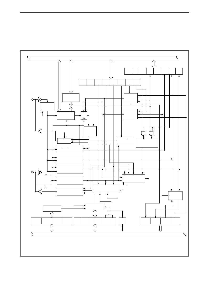
CHAPTER 17 I
2
C BUS
Preliminary User's Manual U17714EJ1V0UD
554
17.3 Configuration
The block diagram of the I
2
C0n is shown below.
Figure 17-4. Block Diagram of I
2
C0n
Internal bus
IIC status register n (IICSn)
IIC control register n
(IICCn)
SO latch
IICEn
D Q
CLn1,
CLn0
TRCn
DFCn
DFCn
SDA0n
SCL0n
Output control
INTIICn
IIC shift register n
(IICn)
IICCn.STTn, SPTn
IICSn.MSTSn, EXCn, COIn
IICSn.MSTSn,
EXCn, COIn
LRELn WRELn SPIEn WTIMn ACKEn STTn SPTn
MSTSn ALDn EXCn COIn TRCn ACKDn STDn SPDn
Internal bus
CLDn DADn SMCn DFCn CLn1 CLn0
CLXn
IIC clock select
register n (IICCLn)
STCFn IICBSYn STCENn IICRSVn
IIC flag register n
(IICFn)
IIC function expansion
register n (IICXn)
fxx
IIC division clock select
register m (OCKSm)
fxx to fxx/5
OCKSTHm
OCKSENm
OCKSm1 OCKSm0
Clear
Slave address
register n (SVAn)
Match
signal
Set
Noise
eliminator
IIC shift
register n (IICn)
Data
retention time
correction
circuit
N-ch open-drain
output
ACK detector
ACK
generator
Start condition
detector
Stop condition
detector
Serial clock counter
Serial clock
controller
Noise
eliminator
N-ch open-drain
output
Start
condition
generator
Stop
condition
generator
Wakeup controller
Interrupt request
signal generator
Serial clock
wait controller
Bus status
detector
Prescaler
Prescaler
Remark n = 0 to 2
m = 0, 1
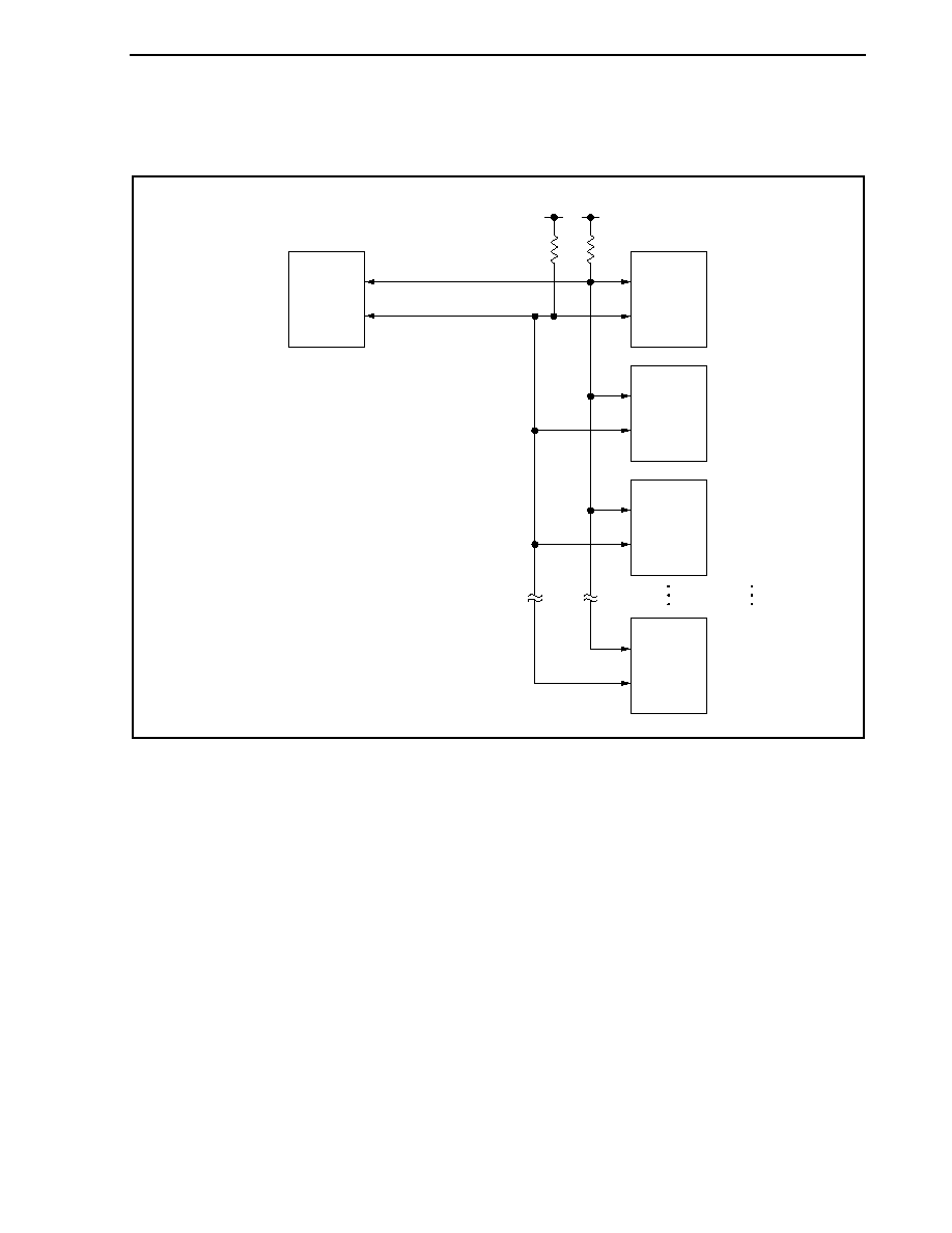
CHAPTER 17 I
2
C BUS
Preliminary User's Manual U17714EJ1V0UD
555
A serial bus configuration example is shown below.
Figure 17-5. Serial Bus Configuration Example Using I
2
C Bus
SDA
SCL
SDA
+V
DD
+V
DD
SCL
SDA
SCL
Slave CPU3
Address 3
SDA
SCL
Slave IC
Address 4
SDA
SCL
Slave IC
Address N
Master CPU1
Slave CPU1
Address 1
Serial data bus
Serial clock
Master CPU2
Slave CPU2
Address 2

CHAPTER 17 I
2
C BUS
Preliminary User's Manual U17714EJ1V0UD
556
I
2
C0n includes the following hardware (n = 0 to 2).
Table 17-1. Configuration of I
2
C0n
Item Configuration
Registers
IIC shift register n (IICn)
Slave address register n (SVAn)
Control registers
IIC control register n (IICCn)
IIC status register n (IICSn)
IIC flag register n (IICFn)
IIC clock select register n (IICCLn)
IIC function expansion register n (IICXn)
IIC division clock select registers 0, 1 (OCKS0, OCKS1)
(1) IIC shift register n (IICn)
The IICn register converts 8-bit serial data into 8-bit parallel data and vice versa, and can be used for both
transmission and reception (n = 0 to 2).
Write and read operations to the IICn register are used to control the actual transmit and receive operations.
This register can be read or written in 8-bit units.
Reset sets this register to 00H.
(2) Slave address register n (SVAn)
The SVAn register sets local addresses when in slave mode (n = 0 to 2).
This register can be read or written in 8-bit units.
Reset sets this register to 00H.
(3) SO latch
The SO latch is used to retain the output level of the SDA0n pin (n = 0 to 2).
(4) Wakeup controller
This circuit generates an interrupt request signal (INTIICn) when the address received by this register matches
the address value set to the SVAn register or when an extension code is received (n = 0 to 2).
(5) Prescaler
This selects the sampling clock to be used.
(6) Serial clock counter
This counter counts the serial clocks that are output and the serial clocks that are input during transmit/receive
operations and is used to verify that 8-bit data was transmitted or received.

CHAPTER 17 I
2
C BUS
Preliminary User's Manual U17714EJ1V0UD
557
(7) Interrupt request signal generator
This circuit controls the generation of interrupt request signals (INTIICn).
An I
2
C interrupt is generated following either of two triggers.
� Falling edge of eighth or ninth clock of the serial clock (set by IICCn.WTIMn bit)
� Interrupt occurrence due to stop condition detection (set by IICCn.SPIEn bit)
Remark n = 0 to 2
(8) Serial clock controller
In master mode, this circuit generates the clock output via the SCL0n pin from the sampling clock (n = 0 to 2).
(9) Serial clock wait controller
This circuit controls the wait timing.
(10) ACK generator, stop condition detector, start condition detector, and ACK detector
These circuits are used to generate and detect various statuses.
(11) Data hold time correction circuit
This circuit generates the hold time for data corresponding to the falling edge of the SCL0n pin.
(12) Start condition generator
A start condition is generated when the IICCn.STTn bit is set.
However, in the communication reservation disabled status (IICFn.IICRSVn bit = 1), this request is ignored
and the IICFn.STCFn bit is set to 1 if the bus is not released (IICFn.IICBSYn bit = 1).
(13) Stop condition generator
A stop condition is generated when the IICCn.SPTn bit is set.
(14) Bus status detector
Whether the bus is released or not is ascertained by detecting a start condition and stop condition.
However, the bus status cannot be detected immediately after operation, so set the bus status detector to the
initial status by using the IICFn.STCENn bit.

CHAPTER 17 I
2
C BUS
Preliminary User's Manual U17714EJ1V0UD
558
17.4 Registers
I
2
C00 to I
2
C02 are controlled by the following registers.
� IIC control registers 0 to 2 (IICC0 to IICC2)
� IIC status registers 0 to 2 (IICS0 to IICS2)
� IIC flag registers 0 to 2 (IICF0 to IICF2)
� IIC clock select registers 0 to 2 (IICCL0 to IICCL2)
� IIC function expansion registers 0 to 2 (IICX0 to IICX2)
� IIC division clock select registers 0, 1 (OCKS0, OCKS1)
The following registers are also used.
� IIC shift registers 0 to 2 (IIC0 to IIC2)
� Slave address registers 0 to 2 (SVA0 to SVA2)
Remark For the alternate-function pin settings, see Table 4-19 Using Port Pin as Alternate-Function Pin.
(1) IIC control registers 0 to 2 (IICC0 to IICC2)
The IICCn register enables/stops I
2
C0n operations, sets the wait timing, and sets other I
2
C operations (n = 0 to
2).
This register can be read or written in 8-bit or 1-bit units. However, set the SPIEn, WTIMn, and ACKEn bits
when the IICEn bit is 0 or during the wait period. When setting the IICEn bit from "0" to "1", these bits can also
be set at the same time.
Reset sets this register to 00H.
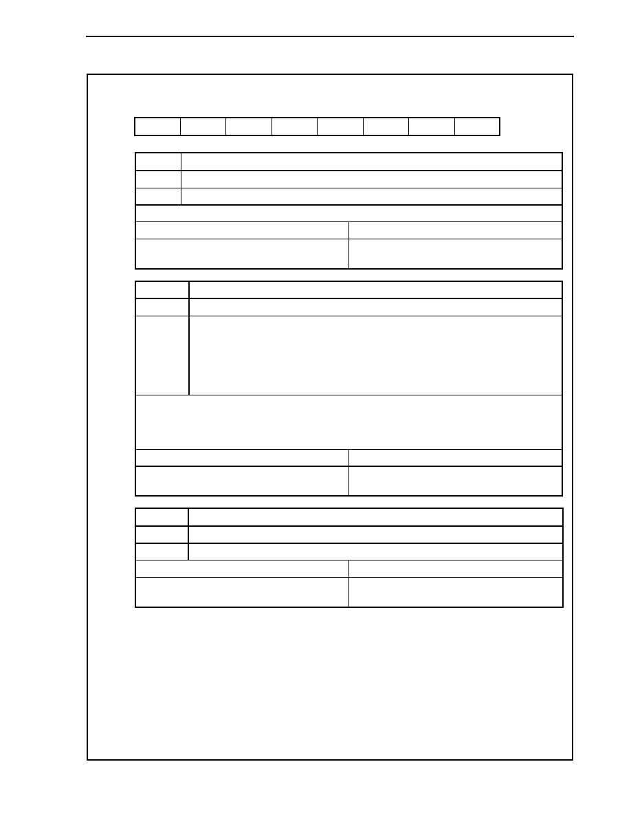
CHAPTER 17 I
2
C BUS
Preliminary User's Manual U17714EJ1V0UD
559
(1/4)
After reset: 00H
R/W
Address: IICC0 FFFFFD82H, IICC1 FFFFFD92H, IICC2 FFFFFDA2H
<7> <6> <5> <4> <3> <2> <1> <0>
IICCn IICEn LRELn WRELn SPIEn WTIMn ACKEn STTn SPTn
(n = 0 to 2)
IICEn
Specification of I
2
Cn operation enable/disable
0
Operation stopped. IICSn register reset
Note 1
. Internal operation stopped.
1 Operation
enabled.
Be sure to set this bit to 1 when the SCL0n and SDA0n lines are high level.
Condition for clearing (IICEn bit = 0)
Condition for setting (IICEn bit = 1)
� Cleared by instruction
� After reset
� Set by instruction
LRELn
Note 2
Exit from communications
0 Normal
operation
1
This exits from the current communication operation and sets standby mode. This setting is
automatically cleared after being executed. Its uses include cases in which a locally irrelevant
extension code has been received.
The SCL0n and SDA0n lines are set to high impedance.
The STTn and SPTn bits and the MSTSn, EXCn, COIn, TRCn, ACKDn, and STDn bits of the IICSn
register are cleared.
The standby mode following exit from communications remains in effect until the following communication entry
conditions are met.
� After a stop condition is detected, restart is in master mode.
� An address match occurs or an extension code is received after the start condition.
Condition for clearing (LRELn bit = 0)
Condition for setting (LRELn bit = 1)
� Automatically cleared after execution
� After reset
� Set by instruction
WRELn
Note 2
Wait state cancellation control
0
Wait state not canceled
1
Wait state canceled. This setting is automatically cleared after wait state is canceled.
Condition for clearing (WRELn bit = 0)
Condition for setting (WRELn bit = 1)
� Automatically cleared after execution
� After reset
� Set by instruction
Notes 1. The IICSn register, IICFn.STCFn and IICFn.IICBSYn bits, and IICCLn.CLDn and IICCLn.DADn
bits are reset.
2. This flag's signal is invalid when the IICEn bit = 0.
Caution If the I
2
Cn operation is enabled (IICEn bit = 1) when the SCL0n line is high level and the
SDA0n line is low level, the start condition is detected immediately. To avoid this, after
enabling the I
2
Cn operation, immediately set the LRELn bit to 1 with a bit manipulation
instruction.
Remark
The LRELn and WRELn bits are 0 when read after the data has been set.
CHAPTER 17 I
2
C BUS
Preliminary User's Manual U17714EJ1V0UD
560
(2/4)
SPIEn
Note
Enable/disable generation of interrupt request when stop condition is detected
0 Disabled
1 Enabled
Condition for clearing (SPIEn bit = 0)
Condition for setting (SPIEn bit = 1)
� Cleared by instruction
� After reset
� Set by instruction
WTIMn
Note
Control of wait state and interrupt request generation
0
Interrupt request is generated at the eighth clock's falling edge.
Master mode: After output of eight clocks, clock output is set to low level and the wait state is set.
Slave mode: After input of eight clocks, the clock is set to low level and the wait state is set for the
master device.
1
Interrupt request is generated at the ninth clock's falling edge.
Master mode: After output of nine clocks, clock output is set to low level and the wait state is set.
Slave mode: After input of nine clocks, the clock is set to low level and the wait state is set for the
master device.
During address transfer, an interrupt occurs at the falling edge of the ninth clock regardless of this bit setting. This
bit setting becomes valid when the address transfer is completed. In master mode, a wait state is inserted at the
falling edge of the ninth clock during address transfer. For a slave device that has received a local address, a wait
state is inserted at the falling edge of the ninth clock after ACK is generated. When the slave device has received
an extension code, however, a wait state is inserted at the falling edge of the eighth clock.
Condition for clearing (WTIMn bit = 0)
Condition for setting (WTIMn bit = 1)
� Cleared by instruction
� After reset
� Set by instruction
ACKEn
Note
Acknowledgment
control
0 Acknowledgment
disabled.
1
Acknowledgment enabled. During the ninth clock period, the SDA0n line is set to low level.
The ACKEn bit setting is invalid for address reception by the slave device. In this case, ACK is generated when
the addresses match.
However, the ACKEn bit setting is valid for reception of the extension code. Set the ACKEn bit in the system that
receives the extension code.
Condition for clearing (ACKEn bit = 0)
Condition for setting (ACKEn bit = 1)
� Cleared by instruction
� After reset
� Set by instruction
Note This flag's signal is invalid when the IICEn bit = 0.
Remark
n = 0 to 2

CHAPTER 17 I
2
C BUS
Preliminary User's Manual U17714EJ1V0UD
561
(3/4)
STTn
Start condition trigger
0
Start condition is not generated.
1
When bus is released (in STOP mode):
A start condition is generated (for starting as master). The SDA0n line is changed from high level to
low level while the SCLn line is high level and then the start condition is generated. Next, after the
rated amount of time has elapsed, the SCL0n line is changed to low level.
During communication with a third party:
If the communication reservation function is enabled (IICFn.IICRSVn bit = 0)
� This trigger functions as a start condition reserve flag. When set to 1, it releases the bus and then
automatically generates a start condition.
If the communication reservation function is disabled (IICRSVn = 1)
� The IICFn.STCFn bit is set to 1 to clear the information set (1) to the STTn bit. This trigger does
not generate a start condition.
In the wait state (when master device):
A restart condition is generated after the wait state is released.
Cautions concerning set timing
For master reception:
Cannot be set to 1 during transfer. Can be set to 1 only when the ACKEn bit has been
set to 0 and the slave has been notified of final reception.
For master transmission: A start condition cannot be generated normally during the ACK period. Set to 1 during
the wait period that follows output of the ninth clock.
For slave:
Even when the communication reservation function is disabled (IICRSVn bit = 1), the
communication reservation status is entered.
� Setting to 1 at the same time as the SPTn bit is prohibited.
� When the STTn bit is set to 1, setting the STTn bit to 1 again is disabled until the setting is cleared to 0.
Condition for clearing (STTn bit = 0)
Condition for setting (STTn bit = 1)
� When the STTn bit is set to 1 in the communication
reservation disabled status
� Cleared by loss in arbitration
� Cleared after start condition is generated by master
device
� When the LRELn bit = 1 (communication save)
� When the IICEn bit = 0 (operation stop)
� After reset
� Set by instruction
Remarks 1. The STTn bit is 0 if it is read immediately after data setting.
2. n = 0 to 2

CHAPTER 17 I
2
C BUS
Preliminary User's Manual U17714EJ1V0UD
562
(4/4)
SPTn
Stop condition trigger
0
Stop condition is not generated.
1
Stop condition is generated (termination of master device's transfer).
After the SDA0n line goes to low level, either set the SCL0n line to high level or wait until the SCL0n
pin goes to high level. Next, after the rated amount of time has elapsed, the SDA0n line is changed
from low level to high level and a stop condition is generated.
Cautions concerning set timing
For master reception:
Cannot be set to 1 during transfer.
Can be set to 1 only when the ACKEn bit has been set to 0 and during the wait period
after the slave has been notified of final reception.
For master transmission: A stop condition cannot be generated normally during the ACK reception period. Set to
1 during the wait period that follows output of the ninth clock.
� Cannot be set to 1 at the same time as the STTn bit.
� The SPTn bit can be set to 1 only when in master mode
Note
.
� When the WTIMn bit has been set to 0, if the SPTn bit is set to 1 during the wait period that follows output of
eight clocks, note that a stop condition will be generated during the high-level period of the ninth clock.
The WTIMn bit should be changed from 0 to 1 during the wait period following output of eight clocks, and the
SPTn bit should be set to 1 during the wait period that follows output of the ninth clock.
� When the SPTn bit is set to 1, setting the SPTn bit to 1 again is disabled until the setting is cleared to 0.
Condition for clearing (SPTn bit = 0)
Condition for setting (SPTn bit = 1)
� Cleared by loss in arbitration
� Automatically cleared after stop condition is detected
� When the LRELn bit = 1 (communication save)
� When the IICEn bit = 0 (operation stop)
� After reset
� Set by instruction
Note Set the SPTn bit to 1 only in master mode. However, when the IICRSVn bit is 0, the SPTn bit must be
set to 1 and a stop condition generated before the first stop condition is detected following the switch
to the operation enabled status. For details, see 17.15 Cautions.
Caution When the TRCn bit = 1, the WRELn bit is set to 1 during the ninth clock and the wait
state is canceled, after which the TRCn bit is cleared to 0 and the SDA0n line is set to
high impedance.
Remarks 1. The SPTn bit is 0 if it is read immediately after data setting.
2. n = 0 to 2
CHAPTER 17 I
2
C BUS
Preliminary User's Manual U17714EJ1V0UD
563
(2) IIC status registers 0 to 2 (IICS0 to IICS2)
The IICSn register indicates the status of the I
2
C0n (n = 0 to 2).
This register is read-only, in 8-bit or 1-bit units. However, the IICSn register can only be read when the
IICCn.STTn bit is 1 or during the wait period.
Reset sets this register to 00H.
Caution Accessing the IICSn register is prohibited in the following statuses. For details, see 3.4.8 (2)
Accessing specific on-chip peripheral I/O registers.
�
When the CPU operates with the subclock and the main clock oscillation is stopped
�
When the CPU operates with the internal oscillation clock
(1/3)
After reset: 00H
R
Address: IICS0 FFFFFD86H, IICS1 FFFFFD96H, IICS2 FFFFFDA6H
<7> <6> <5> <4> <3> <2> <1> <0>
IICSn MSTSn ALDn EXCn COIn TRCn ACKDn STDn SPDn
(n = 0 to 2)
MSTSn
Master device status
0
Slave device status or communication standby status
1
Master device communication status
Condition for clearing (MSTSn bit = 0)
Condition for setting (MSTSn bit = 1)
� When a stop condition is detected
� When the ALDn bit = 1 (arbitration loss)
� Cleared by LRELn bit = 1 (communication save)
� When the IICEn bit changes from 1 to 0 (operation
stop)
� After reset
� When a start condition is generated
ALDn
Arbitration loss detection
0
This status means either that there was no arbitration or that the arbitration result was a "win".
1
This status indicates the arbitration result was a "loss". The MSTSn bit is cleared to 0.
Condition for clearing (ALDn bit = 0)
Condition for setting (ALDn bit = 1)
� Automatically cleared after the IICSn register is
read
Note
� When the IICEn bit changes from 1 to 0 (operation
stop)
� After reset
� When the arbitration result is a "loss".
EXCn
Detection of extension code reception
0
Extension code was not received.
1
Extension code was received.
Condition for clearing (EXCn bit = 0)
Condition for setting (EXCn bit = 1)
� When a start condition is detected
� When a stop condition is detected
� Cleared by LRELn bit = 1 (communication save)
� When the IICEn bit changes from 1 to 0 (operation
stop)
� After reset
� When the higher four bits of the received address
data are either "0000" or "1111" (set at the rising
edge of the eighth clock).
Note The ALDn bit is also cleared when a bit manipulation instruction is executed for another bit in
the IICSn register.
CHAPTER 17 I
2
C BUS
Preliminary User's Manual U17714EJ1V0UD
564
(2/3)
COIn
Matching address detection
0
Addresses do not match.
1 Addresses
match.
Condition for clearing (COIn bit = 0)
Condition for setting (COIn bit = 1)
� When a start condition is detected
� When a stop condition is detected
� Cleared by LRELn bit = 1 (communication save)
� When the IICEn bit changes from 1 to 0 (operation
stop)
� After reset
� When the received address matches the local
address (SVAn register) (set at the rising edge of the
eighth clock).
TRCn
Transmit/receive status detection
0
Receive status (other than transmit status). The SDA0n line is set to high impedance.
1
Transmit status. The value in the SO latch is enabled for output to the SDA0n line (valid starting at
the falling edge of the first byte's ninth clock).
Condition for clearing (TRCn bit = 0)
Condition for setting (TRCn bit = 1)
� When a stop condition is detected
� Cleared by LRELn bit = 1 (communication save)
� When the IICEn bit changes from 1 to 0 (operation
stop)
� Cleared by IICCn.WRELn bit = 1
Note
� When the ALDn bit changes from 0 to 1 (arbitration
loss)
� After reset
Master
� When "1" is output to the first byte's LSB (transfer
direction specification bit)
Slave
� When a start condition is detected
When not used for communication
Master
� When a start condition is generated
� When "0" is output to the first byte's LSB (transfer
direction specification bit)
Slave
� When "1" is input by the first byte's LSB (transfer
direction specification bit)
ACKDn ACK
detection
0
ACK was not detected.
1
ACK was detected.
Condition for clearing (ACKDn bit = 0)
Condition for setting (ACKDn bit = 1)
� When a stop condition is detected
� At the rising edge of the next byte's first clock
� Cleared by LRELn bit = 1 (communication save)
� When the IICEn bit changes from 1 to 0 (operation
stop)
� After reset
� After the SDA0n bit is set to low level at the rising
edge of the SCL0n pin's ninth clock
Note The TRCn bit is cleared to 0 and SDA0n line becomes high impedance when the WRELn bit is
set to 1 and the wait state is canceled to 0 at the ninth clock by TRCn bit = 1.
Remark n = 0 to 2

CHAPTER 17 I
2
C BUS
Preliminary User's Manual U17714EJ1V0UD
565
(3/3)
STDn
Start condition detection
0
Start condition was not detected.
1
Start condition was detected. This indicates that the address transfer period is in effect
Condition for clearing (STDn bit = 0)
Condition for setting (STDn bit = 1)
� When a stop condition is detected
� At the rising edge of the next byte's first clock
following address transfer
� Cleared by LRELn bit = 1 (communication save)
� When the IICEn bit changes from 1 to 0 (operation
stop)
� After reset
� When a start condition is detected
SPDn
Stop condition detection
0
Stop condition was not detected.
1
Stop condition was detected. The master device's communication is terminated and the bus is
released.
Condition for clearing (SPDn bit = 0)
Condition for setting (SPDn bit = 1)
� At the rising edge of the address transfer byte's first
clock following setting of this bit and detection of a
start condition
� When the IICEn bit changes from 1 to 0 (operation
stop)
� After reset
� When a stop condition is detected
Remark n = 0 to 2

CHAPTER 17 I
2
C BUS
Preliminary User's Manual U17714EJ1V0UD
566
(3) IIC flag registers 0 to 2 (IICF0 to IICF2)
The IICFn register sets the I
2
C0n operation mode and indicates the I
2
C bus status.
This register can be read or written in 8-bit or 1-bit units. However, the STCFn and IICBSYn bits are read-only.
IICRSVn enables/disables the communication reservation function (see 17.14 Communication Reservation).
The initial value of the IICBSYn bit is set by using the STCENn bit (see 17.15 Cautions).
The IICRSVn and STCENn bits can be written only when operation of I
2
C0n is disabled (IICCn.IICEn bit = 0).
After operation is enabled, IICFn can be read (n = 0 to 2).
Reset sets this register to 00H.
CHAPTER 17 I
2
C BUS
Preliminary User's Manual U17714EJ1V0UD
567
After reset: 00H
R/W
Note
Address: IICF0 FFFFFD8AH, IICF1 FFFFFD9AH, IICF2 FFFFFDAAH
<7>
<6>
5 4 3 2
<1>
<0>
IICFn
STCFn
IICBSYn
0 0 0 0
STCENn
IICRSVn
(n = 0 to 2)
STCFn
STTn bit clear
0
Start condition issued
1
Start condition cannot be issued, STTn bit cleared
Condition for clearing (STCFn bit = 0)
Condition for setting (STCFn bit = 1)
� Cleared by IICCn.STTn bit = 1
� When the IICCn.IICEn bit = 0
� After reset
� When start condition is not issued and STTn flag is
cleared to 0 during communication reservation is
disabled (IICRSVn bit = 1).
IICBSYn I
2
C0n bus status
0
Bus released status (default communication status when STCENn bit = 1)
1
Bus communication status (default communication status when STCENn bit = 0)
Condition for clearing (IICBSYn bit = 0)
Condition for setting (IICBSYn bit = 1)
� When stop condition is detected
� When the IICEn bit = 0
� After reset
� When start condition is detected
� By setting the IICEn bit when the STCENn bit = 0
STCENn
Initial start enable trigger
0
Start conditions cannot be generated until a stop condition is detected following operation enable
(IICEn bit = 1).
1
Start conditions can be generated even if a stop condition is not detected following operation enable
(IICEn bit = 1).
Condition for clearing (STCENn bit = 0)
Condition for setting (STCENn bit = 1)
� When start condition is detected
� After reset
� Setting by instruction
IICRSVn Communication
reservation function disable bit
0
Communication reservation enabled
1
Communication reservation disabled
Condition for clearing (IICRSVn bit = 0)
Condition for setting (IICRSVn bit = 1)
� Clearing by instruction
� After reset
� Setting by instruction
Note Bits 6 and 7 are read-only bits.
Cautions 1. Write the STCENn bit only when operation is stopped (IICEn bit = 0).
2. When the STCENn bit = 1, the bus released status (IICBSYn bit = 0) is recognized
regardless of the actual bus status immediately after the I
2
Cn bus operation is
enabled. Therefore, to issue the first start condition (STTn bit = 1), it is necessary
to confirm that the bus has been released, so as to not disturb other
communications.
3. Write the IICRSVn bit only when operation is stopped (IICEn bit = 0).
CHAPTER 17 I
2
C BUS
Preliminary User's Manual U17714EJ1V0UD
568
(4) IIC clock select registers 0 to 2 (IICCL0 to IICCL2)
The IICCLn register sets the transfer clock for the I
2
C0n.
This register can be read or written in 8-bit or 1-bit units. However, the CLDn and DADn bits are read-only.
Set the IICCLn register when the IICCn.IICEn bit = 0.
The SMCn, CLn1, and CLn0 bits are set by the combination of the IICXn.CLXn bit and the OCKSTHm,
OCKSm1, and OCKSm0 bits of the OCKSm register (see 17.4 (6) I
2
C0n transfer clock setting method) (n = 0
to 2, m = 0, 1).
Reset sets this register to 00H.
After reset: 00H
R/W
Note
Address: IICCL0 FFFFFD84H, IICCL1 FFFFFD94H, IICCL2 FFFFFDA4H
7 6 <5>
<4> 3 2 1 0
IICCLn 0
0 CLDn
DADn
SMCn
DFCn
CLn1
CLn0
(n = 0 to 2)
CLDn
Detection of SCL0n pin level (valid only when IICCn.IICEn bit = 1)
0
The SCL0n pin was detected at low level.
1
The SCL0n pin was detected at high level.
Condition for clearing (CLDn bit = 0)
Condition for setting (CLDn bit = 1)
� When the SCL0n pin is at low level
� When the IICEn bit = 0 (operation stop)
� After reset
� When the SCL0n pin is at high level
DADn
Detection of SDA0n pin level (valid only when IICEn bit = 1)
0
The SDA0n pin was detected at low level.
1
The SDA0n pin was detected at high level.
Condition for clearing (DADn bit = 0)
Condition for setting (DADn bit = 1)
� When the SDA0n pin is at low level
� When the IICEn bit = 0 (operation stop)
� After reset
� When the SDA0n pin is at high level
SMCn
Operation mode switching
0
Operation in standard mode.
1
Operation in high-speed mode.
DFCn
Digital filter operation control
0
Digital filter off.
1
Digital filter on.
The digital filter can be used only in high-speed mode.
In high-speed mode, the transfer clock does not vary regardless of the DFCn bit setting (on/off).
The digital filter is used to eliminate noise in high-speed mode.
Note Bits 4 and 5 are read-only bits.
Caution Be sure to clear bits 7 and 6 to "0".
Remark When the IICCn.IICEn bit = 0, 0 is read when reading the CLDn and DADn bits.
CHAPTER 17 I
2
C BUS
Preliminary User's Manual U17714EJ1V0UD
569
(5) IIC function expansion registers 0 to 2 (IICX0 to IICX2)
The IICXn register sets I
2
C0n function expansion (valid only in the high-speed mode).
This register can be read or written in 8-bit or 1-bit units.
Setting of the CLXn bit is performed in combination with the SMCn, CLn1, and CLn0 bits of the IICCLn register
and the OCKSTHm, OCKSm1, and OCKSm0 bits of the OCKSm register (see 17.4 (6) I
2
C0n transfer clock
setting method) (m = 0, 1).
Set the IICXn register when the IICCn.IICEn bit = 0.
Reset sets this register to 00H.
IICXn
(n = 0 to 2)
After reset: 00H R/W Address: IICX0 FFFFFD85H, IICX1 FFFFFD95H, IICX2 FFFFFDA5H
0
0
0
0
0
0
0
CLXn
< >
(6) I
2
C0n transfer clock setting method
The I
2
C0n transfer clock frequency (f
SCL
) is calculated using the following expression (n = 0 to 2).
f
SCL
= 1/(m
� T + t
R
+ t
F
)
m = 12, 18, 24, 36, 44, 48, 54, 60, 66, 72, 86, 88, 96, 132, 172, 176, 198, 220, 258, 344 (see Table
17-2 Clock Settings).
T: 1/f
XX
t
R
:
SCL0n pin rise time
t
F
:
SCL0n pin fall time
For example, the I
2
C0n transfer clock frequency (f
SCL
) when f
XX
= 19.2 MHz, m = 198, t
R
= 200 ns, and t
F
= 50
ns is calculated using following expression.
f
SCL
= 1/(198
� 52 ns + 200 ns + 50 ns) 94.7 kHz
m
� T + t
R
+ t
F
m/2
� T
t
F
t
R
m/2
� T
SCL0n
SCL0n inversion
SCL0n inversion
SCL0n inversion
The clock to be selected can be set by the combination of the SMCn, CLn1, and CLn0 bits of the IICCLn
register, the CLXn bit of the IICXn register, and the OCKSTHm, OCKSm1, and OCKSm0 bits of the OCKSm
register (n = 0 to 2, m = 0, 1).
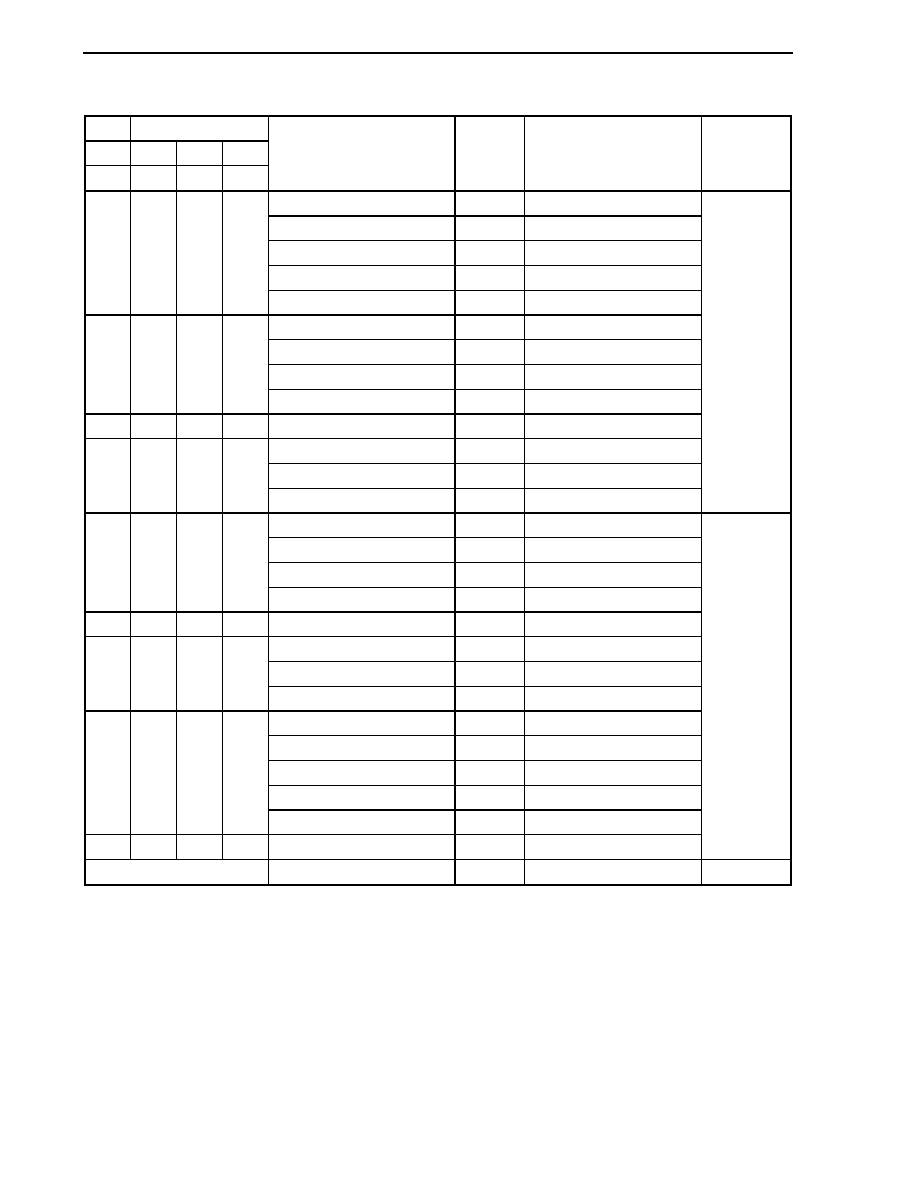
CHAPTER 17 I
2
C BUS
Preliminary User's Manual U17714EJ1V0UD
570
Table 17-2. Clock Settings (1/2)
IICX0 IICCL0
Bit 0
Bit 3
Bit 1
Bit 0
CLX0 SMC0 CL01 CL00
Selection Clock
Transfer
Clock
Settable Main Clock
Frequency (f
XX
) Range
Operating
Mode
f
XX
(when OCKS0 = 18H set)
f
XX
/44 2.00
MHz
f
XX
4.19 MHz
f
XX
/2 (when OCKS0 = 10H set)
f
XX
/88 4.00
MHz
f
XX
8.38 MHz
f
XX
/3 (when OCKS0 = 11H set)
f
XX
/132 6.00
MHz
f
XX
12.57 MHz
f
XX
/4 (when OCKS0 = 12H set)
f
XX
/176 8.00
MHz
f
XX
16.76 MHz
0 0 0 0
f
XX
/5 (when OCKS0 = 13H set)
f
XX
/220 10.00
MHz
f
XX
20.00 MHz
f
XX
(when OCKS0 = 18H set)
f
XX
/86 4.19
MHz
f
XX
8.38 MHz
f
XX
/2 (when OCKS0 = 10H set)
f
XX
/172 8.38
MHz
f
XX
16.76 MHz
f
XX
/3 (when OCKS0 = 11H set)
f
XX
/258 12.57
MHz
f
XX
20.00 MHz
0 0 0 1
f
XX
/4 (when OCKS0 = 12H set)
f
XX
/344 16.76
MHz
f
XX
20.00 MHz
0 0 1 0
f
XX
Note
f
XX
/86 4.19
MHz
f
XX
8.38 MHz
f
XX
(when OCKS0 = 18H set)
f
XX
/66 6.40
MHz
f
XX
/2 (when OCKS0 = 10H set)
f
XX
/132 12.80
MHz
0 0 1 1
f
XX
/3 (when OCKS0 = 11H set)
f
XX
/198 19.20
MHz
Standard mode
(SMC0 bit = 0)
f
XX
(when OCKS0 = 18H set)
f
XX
/24 4.19
MHz
f
XX
8.38 MHz
f
XX
/2 (when OCKS0 = 10H set)
f
XX
/48 8.00
MHz
f
XX
16.76 MHz
f
XX
/3 (when OCKS0 = 11H set)
f
XX
/72 12.00
MHz
f
XX
20.00 MHz
0 1 0
�
f
XX
/4 (when OCKS0 = 12H set)
f
XX
/96 16.00
MHz
f
XX
20.00 MHz
0 1 1 0
f
XX
Note
f
XX
/24 4.00
MHz
f
XX
8.38 MHz
f
XX
(when OCKS0 = 18H set)
f
XX
/18 6.40
MHz
f
XX
/2 (when OCKS0 = 10H set)
f
XX
/36 12.80
MHz
0 1 1 1
f
XX
/3 (when OCKS0 = 11H set)
f
XX
/54 19.20
MHz
f
XX
(when OCKS0 = 18H set)
f
XX
/12 4.00
MHz
f
XX
4.19 MHz
f
XX
/2 (when OCKS0 = 10H set)
f
XX
/24 8.00
MHz
f
XX
8.38 MHz
f
XX
/3 (when OCKS0 = 11H set)
f
XX
/36 12.00
MHz
f
XX
12.57 MHz
f
XX
/4 (when OCKS0 = 12H set)
f
XX
/48 16.00
MHz
f
XX
16.67 MHz
1 1 0
�
f
XX
/5 (when OCKS0 = 13H set)
f
XX
/60 20.00
MHz
1 1 1 0
f
XX
Note
f
XX
/12 4.00
MHz
f
XX
4.19 MHz
High-speed
mode
(SMC0 bit = 1)
Other than above
Setting prohibited
-
-
-
Note Since the selection clock is f
XX
regardless of the value set to the OCKS0 register, clear the OCKS0 register
to 00H (I
2
C division clock stopped status).
Remark
�: don't care
CHAPTER 17 I
2
C BUS
Preliminary User's Manual U17714EJ1V0UD
571
Table 17-2. Clock Settings (2/2)
IICXm IICCLm
Bit 0
Bit 3
Bit 1
Bit 0
CLXm SMCm CLm1 CLm0
Selection Clock
Transfer
Clock
Settable Main Clock
Frequency (f
XX
) Range
Operating
Mode
f
XX
(when OCKS1 = 18H set)
f
XX
/44 2.00
MHz
f
XX
4.19 MHz
f
XX
/2 (when OCKS1 = 10H set)
f
XX
/88 4.00
MHz
f
XX
8.38 MHz
f
XX
/3 (when OCKS1 = 11H set)
f
XX
/132 6.00
MHz
f
XX
12.57 MHz
f
XX
/4 (when OCKS1 = 12H set)
f
XX
/176 8.00
MHz
f
XX
16.76 MHz
0 0 0 0
f
XX
/5 (when OCKS1 = 13H set)
f
XX
/220 10.00
MHz
f
XX
20.00 MHz
f
XX
(when OCKS1 = 18H set)
f
XX
/86 4.19
MHz
f
XX
8.38 MHz
f
XX
/2 (when OCKS1 = 10H set)
f
XX
/172 8.38
MHz
f
XX
16.76 MHz
f
XX
/3 (when OCKS1 = 11H set)
f
XX
/258 12.57
MHz
f
XX
20.00 MHz
0 0 0 1
f
XX
/4 (when OCKS1 = 12H set)
f
XX
/344 16.76
MHz
f
XX
20.00 MHz
0 0 1 0
f
XX
Note
f
XX
/86 4.19
MHz
f
XX
8.38 MHz
f
XX
(when OCKS1 = 18H set)
f
XX
/66 6.40
MHz
f
XX
/2 (when OCKS1 = 10H set)
f
XX
/132 12.80
MHz
0 0 1 1
f
XX
/3 (when OCKS1 = 11H set)
f
XX
/198 19.20
MHz
Standard
mode
(SMCm bit = 0)
f
XX
(when OCKS1 = 18H set)
f
XX
/24 4.19
MHz
f
XX
8.38 MHz
f
XX
/2 (when OCKS1 = 10H set)
f
XX
/48 8.00
MHz
f
XX
16.76 MHz
f
XX
/3 (when OCKS1 = 11H set)
f
XX
/72 12.00
MHz
f
XX
20.00 MHz
0 1 0
�
f
XX
/4 (when OCKS1 = 12H set)
f
XX
/96 16.00
MHz
f
XX
20.00 MHz
0 1 1 0
f
XX
Note
f
XX
/24 4.00
MHz
f
XX
8.38 MHz
f
XX
(when OCKS1 = 18H set)
f
XX
/18 6.40
MHz
f
XX
/2 (when OCKS1 = 10H set)
f
XX
/36 12.80
MHz
0 1 1 1
f
XX
/3 (when OCKS1 = 11H set)
f
XX
/54 19.20
MHz
f
XX
(when OCKS1 = 18H set)
f
XX
/12 4.00
MHz
f
XX
4.19 MHz
f
XX
/2 (when OCKS1 = 10H set)
f
XX
/24 8.00
MHz
f
XX
8.38 MHz
f
XX
/3 (when OCKS1 = 11H set)
f
XX
/36 12.00
MHz
f
XX
12.57 MHz
f
XX
/4 (when OCKS1 = 12H set)
f
XX
/48 16.00
MHz
f
XX
16.67 MHz
1 1 0
�
f
XX
/5 (when OCKS1 = 13H set)
f
XX
/60 20.00
MHz
1 1 1 0
f
XX
Note
f
XX
/12 4.00
MHz
f
XX
4.19 MHz
High-speed
mode
(SMCm bit = 1)
Other than above
Setting prohibited
-
-
-
Note Since the selection clock is f
XX
regardless of the value set to the OCKS1 register, clear the OCKS1 register
to 00H (I
2
C division clock stopped status).
Remarks 1. m = 1, 2
2.
�: don't care
CHAPTER 17 I
2
C BUS
Preliminary User's Manual U17714EJ1V0UD
572
(7) IIC division clock select registers 0, 1 (OCKS0, OCKS1)
The OCKSm register controls the I
2
C0n division clock (n = 0 to 2, m = 0, 1).
This register controls the I
2
C00 division clock via the OCKS0 register and the I
2
C01 and I
2
C02 division clocks
via the OCKS1 register.
This register can be read or written in 8-bit units.
Reset sets this register to 00H.
0
OCKSm
(m = 0, 1)
0
0
OCKSENm OCKSTHm
0
OCKSm1 OCKSm0
After reset: 00H R/W Address: OCKS0 FFFFF340H, OCKS1 FFFFF344H
Disable I
2
C division clock operation
Enable I
2
C division clock operation
OCKSENm
0
1
Operation setting of I
2
C division clock
OCKSm1
0
0
1
1
0
Other than above
OCKSm0
0
1
0
1
0
Selection of I
2
C division clock
f
XX
/2
f
XX
/3
f
XX
/4
f
XX
/5
f
XX
Setting prohibited
OCKSTHm
0
0
0
0
1
(8) IIC shift registers 0 to 2 (IIC0 to IIC2)
The IICn register is used for serial transmission/reception (shift operations) synchronized with the serial clock.
This register can be read or written in 8-bit units, but data should not be written to the IICn register during a data
transfer.
Access (read/write) the IICn register only during the wait period. Accessing this register in communication
states other than the wait period is prohibited. However, for the master device, the IICn register can be written
once only after the transmission trigger bit (IICCn.STTn bit) has been set to 1.
A wait state is released by writing the IICn register during the wait period, and data transfer is started (n = 0 to 2).
Reset sets this register to 00H.
After reset: 00H
R/W
Address: IIC0 FFFFFD80H, IIC1 FFFFFD90H, IIC2 FFFFFDA0H
7 6 5 4 3 2 1 0
IICn
(n = 0 to 2)
CHAPTER 17 I
2
C BUS
Preliminary User's Manual U17714EJ1V0UD
573
(9) Slave address registers 0 to 2 (SVA0 to SVA2)
The SVAn register holds the I
2
C bus's slave addresses (n = 0 to 2).
This register can be read or written in 8-bit units, but bit 0 should be fixed to 0. However, rewriting this register
is prohibited when the IICSn.STDn bit = 1 (start condition detection).
Reset sets this register to 00H.
After reset: 00H
R/W
Address: SVA0 FFFFFD83H, SVA1 FFFFFD93H, SVA2 FFFFFDA3H
7 6 5 4 3 2 1 0
SVAn
0
(n = 0 to 2)
CHAPTER 17 I
2
C BUS
Preliminary User's Manual U17714EJ1V0UD
574
17.5 I
2
C Bus Mode Functions
17.5.1 Pin configuration
The serial clock pin (SCL0n) and serial data bus pin (SDA0n) are configured as follows (n = 0 to 2).
SCL0n ................This pin is used for serial clock input and output.
This pin is an N-ch open-drain output for both master and slave devices. Input is Schmitt input.
SDA0n ................This pin is used for serial data input and output.
This pin is an N-ch open-drain output for both master and slave devices. Input is Schmitt input.
Since outputs from the serial clock line and the serial data bus line are N-ch open-drain outputs, an external pull-up
resistor is required.
Figure 17-6. Pin Configuration Diagram
V
DD
SCL0n
SDA0n
SCL0n
SDA0n
V
DD
Clock output
Master device
(Clock input)
Data output
Data input
(Clock output)
Clock input
Data output
Data input
Slave device
CHAPTER 17 I
2
C BUS
Preliminary User's Manual U17714EJ1V0UD
575
17.6 I
2
C Bus Definitions and Control Methods
The following section describes the I
2
C bus's serial data communication format and the signals used by the I
2
C bus.
The transfer timing for the "start condition", "address", "transfer direction specification", "data", and "stop condition"
generated on the I
2
C bus's serial data bus is shown below.
Figure 17-7. I
2
C Bus Serial Data Transfer Timing
1 to 7
8
9
1 to 8
9
1 to 8
9
SCL0n
SDA0n
R/W
Start
condition
Address
ACK
Data
Data
Stop
condition
ACK
ACK
The master device generates the start condition, slave address, and stop condition.
ACK can be generated by either the master or slave device (normally, it is generated by the device that receives 8-
bit data).
The serial clock (SCL0n) is continuously output by the master device. However, in the slave device, the SCL0n
pin's low-level period can be extended and a wait state can be inserted (n = 0 to 2).
17.6.1 Start condition
A start condition is met when the SCL0n pin is high level and the SDA0n pin changes from high level to low level.
The start condition for the SCL0n and SDA0n pins is a signal that the master device outputs to the slave device when
starting a serial transfer. The slave device can defect the start condition (n = 0 to 2).
Figure 17-8. Start Condition
H
SCL0n
SDA0n
A start condition is output when the IICCn.STTn bit is set (1) after a stop condition has been detected (IICSn.SPDn
bit = 1). When a start condition is detected, the IICSn.STDn bit is set (1) (n = 0 to 2).
Caution When the IICCn.IICEn bit of the V850ES/JJ2 is set to 1 while communications with other devices
are in progress, the start condition may be detected depending on the status of the
communication line. Be sure to set the IICCn.IICEn bit to 1 when the SCL0n and SDA0n lines are
high level.
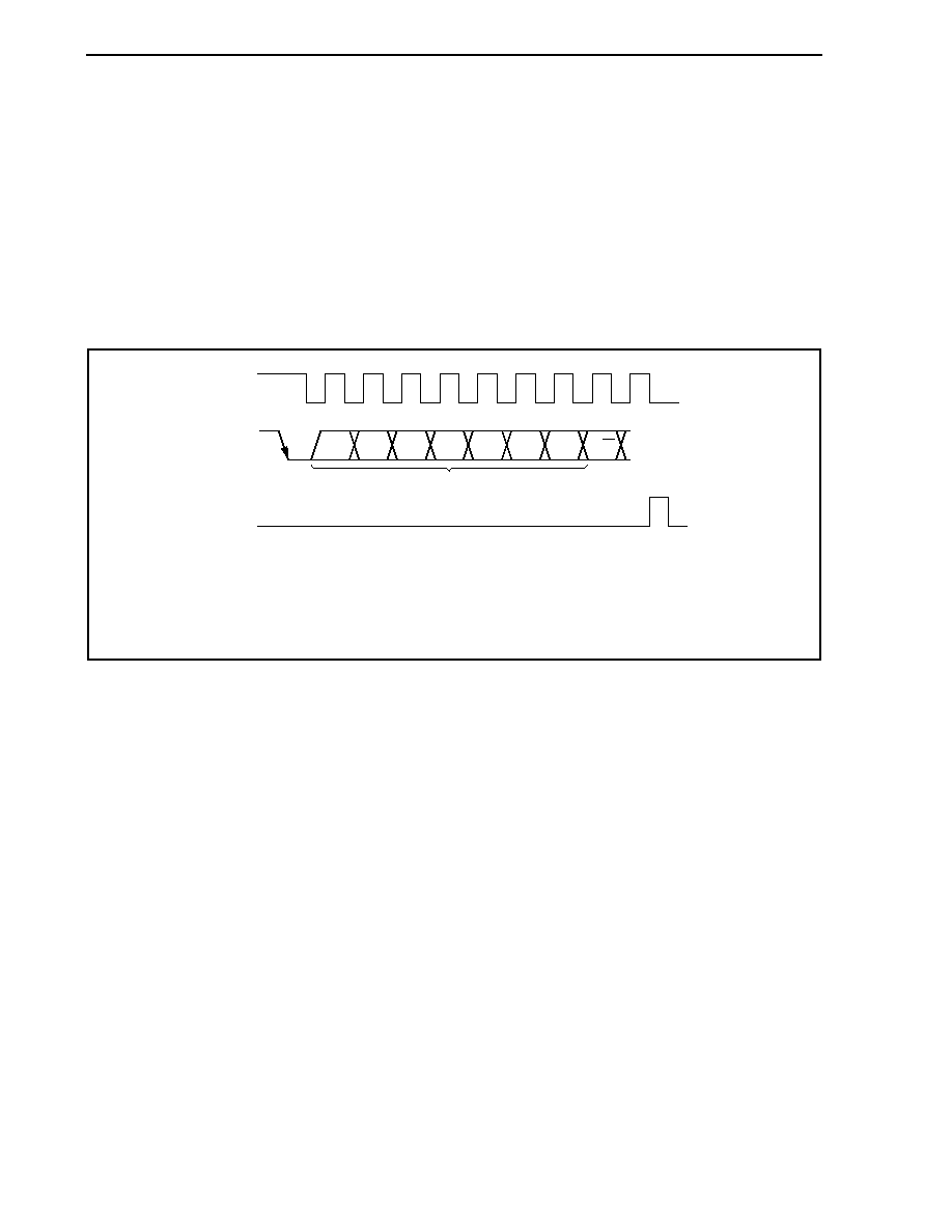
CHAPTER 17 I
2
C BUS
Preliminary User's Manual U17714EJ1V0UD
576
17.6.2 Addresses
The 7 bits of data that follow the start condition are defined as an address.
An address is a 7-bit data segment that is output in order to select one of the slave devices that are connected to
the master device via the bus lines. Therefore, each slave device connected via the bus lines must have a unique
address.
The slave devices include hardware that detects the start condition and checks whether or not the 7-bit address
data matches the data values stored in the SVAn register. If the address data matches the values of the SVAn register,
the slave device is selected and communicates with the master device until the master device generates a start
condition or stop condition (n = 0 to 2).
Figure 17-9. Address
Address
SCL0n
1
SDA0n
INTIICn
Note
2
3
4
5
6
7
8
9
AD6
AD5
AD4
AD3
AD2
AD1
AD0
R/W
Note The interrupt request signal (INTIICn) is generated if a local address or extension code is received
during slave device operation.
Remark
n = 0 to 2
The slave address and the eighth bit, which specifies the transfer direction as described in 17.6.3 Transfer
direction specification below, are written together to IIC shift register n (IICn) and then output. Received addresses
are written to the IICn register (n = 0 to 2).
The slave address is assigned to the higher 7 bits of the IICn register.
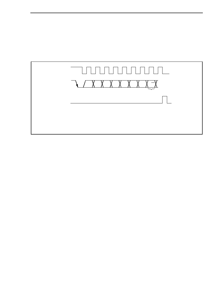
CHAPTER 17 I
2
C BUS
Preliminary User's Manual U17714EJ1V0UD
577
17.6.3 Transfer direction specification
In addition to the 7-bit address data, the master device sends 1 bit that specifies the transfer direction. When this
transfer direction specification bit has a value of 0, it indicates that the master device is transmitting data to a slave
device. When the transfer direction specification bit has a value of 1, it indicates that the master device is receiving
data from a slave device.
Figure 17-10. Transfer Direction Specification
SCL0n
1
SDA0n
INTIICn
2
3
4
5
6
7
8
9
AD6
AD5
AD4
AD3
AD2
AD1
AD0
R/W
Transfer direction specification
Note
Note The INTIICn signal is generated if a local address or extension code is received during slave device
operation.
Remark
n = 0 to 2
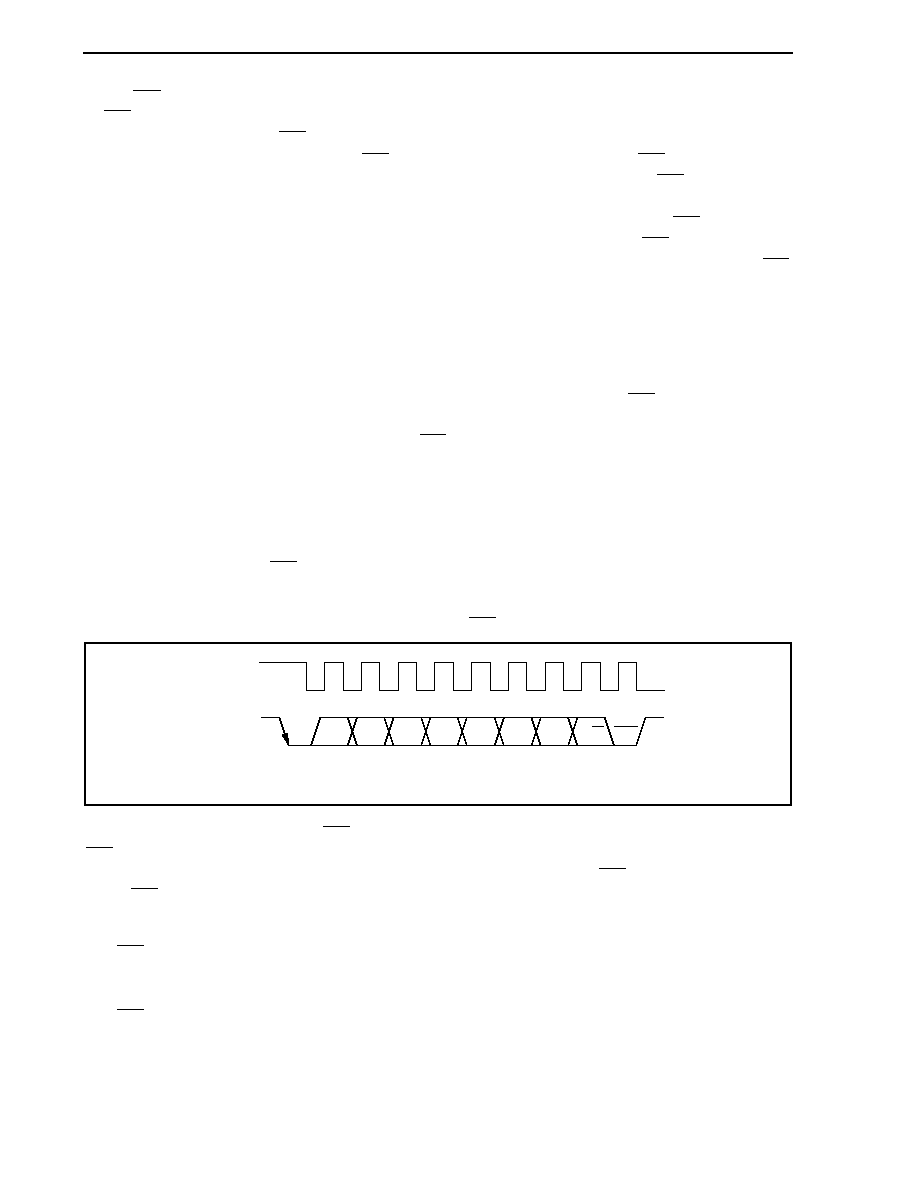
CHAPTER 17 I
2
C BUS
Preliminary User's Manual U17714EJ1V0UD
578
17.6.4 ACK
ACK is used to confirm the serial data status of the transmitting and receiving devices.
The receiving device returns ACK for every 8 bits of data it receives.
The transmitting device normally receives ACK after transmitting 8 bits of data. When ACK is returned from the
receiving device, the reception is judged as normal and processing continues. The detection of ACK is confirmed with
the IICSn.ACKDn bit.
When the master device is the receiving device, after receiving the final data, it does not return ACK and generates
the stop condition. When the slave device is the receiving device and does not return ACK, the master device
generates either a stop condition or a restart condition, and then stops the current transmission. Failure to return ACK
may be caused by the following factors.
(a) Reception was not performed normally.
(b) The final data was received.
(c) The receiving device (slave) does not exist for the specified address.
When the receiving device sets the SDA0n line to low level during the ninth clock, ACK is generated (normal
reception).
When the IICCn.ACKEn bit is set to 1, automatic ACK generation is enabled. Transmission of the eighth bit
following the 7 address data bits causes the IICSn.TRCn bit to be set. Normally, set the ACKEn bit to 1 for reception
(TRCn bit = 0).
When the slave device is receiving (when TRCn bit = 0), if the slave device cannot receive data or does not need to
receive any more data, clear the ACKEn bit to 0 to indicate to the master that no more data can be received.
Similarly, when the master device is receiving (when TRCn bit = 0) and the subsequent data is not needed, clear
the ACKEn bit to 0 to prevent ACK from being generated. This notifies the slave device (transmitting device) of the
end of the data transmission (transmission stopped).
Figure 17-11. ACK
SCL0n
1
SDA0n
2
3
4
5
6
7
8
9
AD6
AD5
AD4
AD3
AD2
AD1
AD0
R/W ACK
Remark n = 0 to 2
When the local address is received, ACK is automatically generated regardless of the value of the ACKEn bit. No
ACK is generated if the received address is not a local address (NACK).
When receiving the extension code, set the ACKEn bit to 1 in advance to generate ACK.
The ACK generation method during data reception is based on the wait timing setting, as described by the following.
� When 8-clock wait is selected (IICCn.WTIMn bit = 0):
ACK is generated at the falling edge of the SCL0n pin's eighth clock if the ACKEn bit is set to 1 before the wait
state cancellation.
� When 9-clock wait is selected (IICCn.WTIMn bit = 1):
ACK is generated if the ACKEn bit is set to 1 in advance.
Remark n = 0 to 2

CHAPTER 17 I
2
C BUS
Preliminary User's Manual U17714EJ1V0UD
579
17.6.5 Stop condition
When the SCL0n pin is high level, changing the SDA0n pin from low level to high level generates a stop condition (n
= 0 to 2).
A stop condition is generated when serial transfer from the master device to the slave device has been completed.
When used as the slave device, the start condition can be detected.
Figure 17-12. Stop Condition
H
SCL0n
SDA0n
Remark n = 0 to 2
A stop condition is generated when the IICCn.SPTn bit is set to 1. When the stop condition is detected, the
IICSn.SPDn bit is set to 1 and the interrupt request signal (INTIICn) is generated when the IICCn.SPIEn bit is set to 1
(n = 0 to 2).
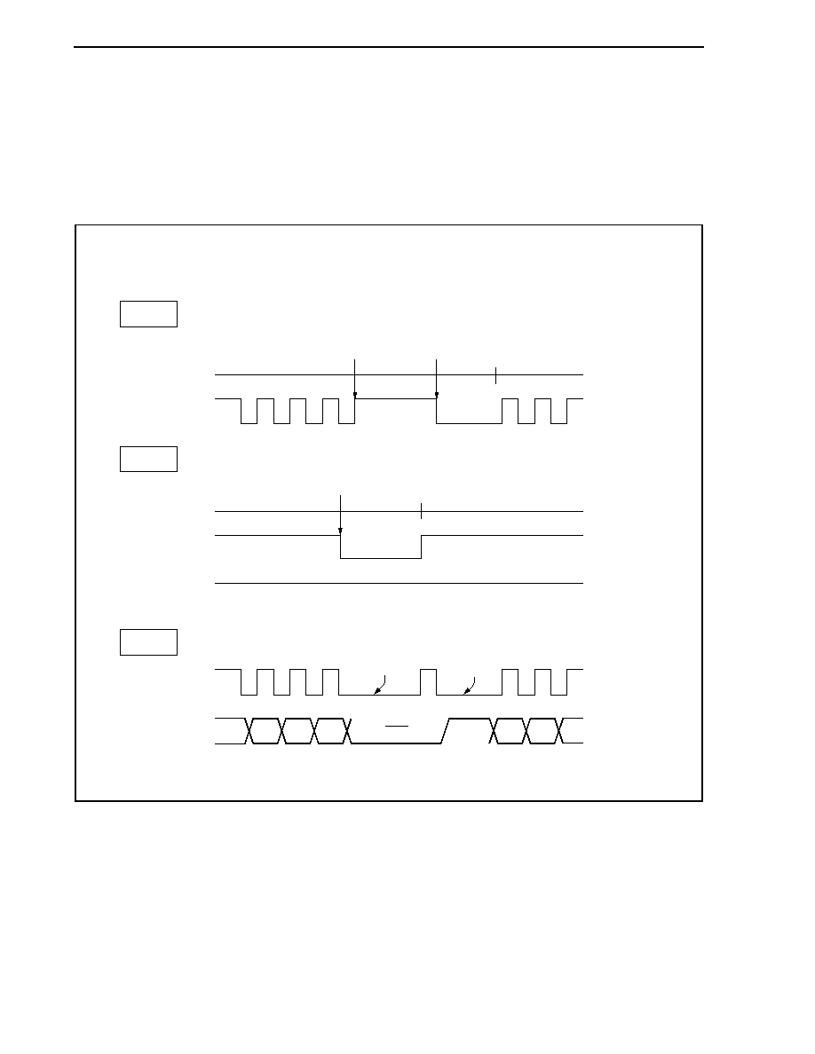
CHAPTER 17 I
2
C BUS
Preliminary User's Manual U17714EJ1V0UD
580
17.6.6 Wait state
A wait state is used to notify the communication partner that a device (master or slave) is preparing to transmit or
receive data (i.e., is in a wait state).
Setting the SCL0n pin to low level notifies the communication partner of the wait state. When the wait state has
been canceled for both the master and slave devices, the next data transfer can begin (n = 0 to 2).
Figure 17-13. Wait State (1/2)
(a) When master device has a nine-clock wait and slave device has an eight-clock wait
(master: transmission, slave: reception, and IICCn.ACKEn bit = 1)
SCL0n
6
SDA0n
7
8
9
1
2
3
SCL0n
IICn
6
H
7
8
1
2
3
D2
D1
D0
ACK
D7
D6
D5
9
IICn
SCL0n
ACKEn
Master
Master returns to high
impedance but slave
is in wait state (low level).
Wait after output
of ninth clock.
IICn data write (cancel wait state)
Slave
Wait after output
of eighth clock.
FFH is written to IICn register or
IICCn.WRELn bit is set to 1.
Transfer lines
Wait state
from slave
Wait state
from master
Remark n = 0 to 2
CHAPTER 17 I
2
C BUS
Preliminary User's Manual U17714EJ1V0UD
581
Figure 17-13. Wait State (2/2)
(b) When master and slave devices both have a nine-clock wait
(master: transmission, slave: reception, and ACKEn bit = 1)
SCL0n
6
SDA0n
7
8
9
1
2
3
SCL0n
IICn
6
H
7
8
1
2
3
D2
D1
D0
ACK
D7
D6
D5
9
IICn
SCL0n
ACKEn
Master
Master and slave both wait
after output of ninth clock.
IICn data write (cancel wait state)
Slave
FFH is written to IICn register
or WRELn bit is set to 1.
Generated according to previously set ACKEn bit value
Transfer lines
Wait state
from master/
slave
Wait state
from slave
Remark n = 0 to 2
A wait state may be automatically generated depending on the setting of the IICCn.WTIMn bit (n = 0 to 2).
Normally, when the IICCn.WRELn bit is set to 1 or when FFH is written to the IICn register on the receiving side,
the wait state is canceled and the transmitting side writes data to the IICn register to cancel the wait state.
The master device can also cancel the wait state via either of the following methods.
� By setting the IICCn.STTn bit to 1
� By setting the IICCn.SPTn bit to 1

CHAPTER 17 I
2
C BUS
Preliminary User's Manual U17714EJ1V0UD
582
17.6.7 Wait state cancellation method
In the case of I
2
C0n, wait state can be canceled normally in the following ways (n = 0 to 2).
� By writing data to the IICn register
� By setting the IICCn.WRELn bit to 1 (wait state cancellation)
� By setting the IICCn.STTn bit to 1 (start condition generation)
� By setting the IICCn.SPTn bit to 1 (stop condition generation)
If any of these wait state cancellation actions is performed, I
2
C0n will cancel wait state and restart communication.
When canceling wait state and sending data (including address), write data to the IICn register.
To receive data after canceling wait state, or to complete data transmission, set the WRELn bit to 1.
To generate a restart condition after canceling wait state, set the STTn bit to 1.
To generate a stop condition after canceling wait state, set the SPTn bit to 1.
Execute cancellation only once for each wait state.
For example, if data is written to the IICn register following wait state cancellation by setting the WRELn bit to 1,
conflict between the SDAn line change timing and IICn register write timing may result in the data output to the SDAn
line may be incorrect.
Even in other operations, if communication is stopped halfway, clearing the IICCn.IICEn bit to 0 will stop
communication, enabling wait state to be cancelled.
If the I
2
C bus dead-locks due to noise, etc., setting the IICCn.LRELn bit to 1 causes the communication operation to
be exited, enabling wait state to be cancelled.
CHAPTER 17 I
2
C BUS
Preliminary User's Manual U17714EJ1V0UD
583
17.7 I
2
C Interrupt Request Signals (INTIICn)
The following shows the value of the IICSn register at the INTIICn interrupt request signal generation timing and at
the INTIICn signal timing (n = 0 to 2).
17.7.1 Master device operation
(1) Start ~ Address ~ Data ~ Data ~ Stop (normal transmission/reception)
<1> When IICCn.WTIMn bit = 0
IICCn.SPTn bit = 1
ST
AD6 to AD0
R/W
ACK
D7 to D0
ACK
D7 to D0
ACK
SP
1
2
3
4
5
1: IICSn register = 1000X110B
2: IICSn register = 1000X000B
3: IICSn register = 1000X000B (WTIMn bit = 1)
4: IICSn register = 1000XX00B
5: IICSn register = 00000001B
Remarks 1.
: Always generated
: Generated only when SPIEn bit = 1
X:
don't
care
2. n = 0 to 2
<2> When WTIMn bit = 1
SPTn bit = 1
ST
AD6 to AD0
R/W
ACK
D7 to D0
ACK
D7 to D0
ACK
SP
1
2
3
4
1: IICSn register = 1000X110B
2: IICSn register = 1000X100B
3: IICSn register = 1000XX00B
4: IICSn register = 00000001B
Remarks 1.
: Always generated
: Generated only when SPIEn bit = 1
X:
don't
care
2. n = 0 to 2
CHAPTER 17 I
2
C BUS
Preliminary User's Manual U17714EJ1V0UD
584
(2) Start ~ Address ~ Data ~ Start ~ Address ~ Data ~ Stop (restart)
<1> When WTIMn bit = 0
STTn bit = 1
SPTn bit = 1
ST
AD6 to AD0
R/W
ACK
D7 to D0
ACK
ST
AD6 to AD0
R/W
ACK
D7 to D0
ACK
SP
1
2
3
4
5
6
7
1: IICSn register = 1000X110B
2: IICSn register = 1000X000B (WTIMn bit = 1)
3: IICSn register = 1000XX00B (WTIMn bit = 0)
4: IICSn register = 1000X110B (WTIMn bit = 0)
5: IICSn register = 1000X000B (WTIMn bit = 1)
6: IICSn register = 1000XX00B
7: IICSn register = 00000001B
Remarks 1.
: Always generated
: Generated only when SPIEn bit = 1
X:
don't
care
2. n = 0 to 2
<2> When WTIMn bit = 1
STTn bit = 1
SPTn bit = 1
ST
AD6 to AD0
R/W
ACK
D7 to D0
ACK
ST
AD6 to AD0
R/W
ACK
D7 to D0
ACK
SP
1 2
3 4
5
1: IICSn register = 1000X110B
2: IICSn register = 1000XX00B
3: IICSn register = 1000X110B
4: IICSn register = 1000XX00B
5: IICSn register = 00000001B
Remarks 1.
: Always generated
: Generated only when SPIEn bit = 1
X:
don't
care
2. n = 0 to 2
CHAPTER 17 I
2
C BUS
Preliminary User's Manual U17714EJ1V0UD
585
(3) Start ~ Code ~ Data ~ Data ~ Stop (extension code transmission)
<1> When WTIMn bit = 0
SPTn bit = 1
ST
AD6 to AD0
R/W
ACK
D7 to D0
ACK
D7 to D0
ACK
SP
1
2
3
4
5
1: IICSn register = 1010X110B
2: IICSn register = 1010X000B
3: IICSn register = 1010X000B (WTIMn bit = 1)
4: IICSn register = 1010XX00B
5: IICSn register = 00000001B
Remarks 1.
: Always generated
: Generated only when SPIEn bit = 1
X:
don't
care
2. n = 0 to 2
<2> When WTIMn bit = 1
SPTn bit = 1
ST
AD6 to AD0
R/W
ACK
D7 to D0
ACK
D7 to D0
ACK
SP
1
2
3
4
1: IICSn register = 1010X110B
2: IICSn register = 1010X100B
3: IICSn register = 1010XX00B
4: IICSn register = 00000001B
Remarks 1. : Always generated
: Generated only when SPIEn bit = 1
X:
don't
care
2. n = 0 to 2
CHAPTER 17 I
2
C BUS
Preliminary User's Manual U17714EJ1V0UD
586
17.7.2 Slave device operation (when receiving slave address data (address match))
(1) Start ~ Address ~ Data ~ Data ~ Stop
<1> When IICCn.WTIMn bit = 0
ST
AD6 to AD0
R/W
ACK
D7 to D0
ACK
D7 to D0
ACK
SP
1
2
3
4
1: IICSn register = 0001X110B
2: IICSn register = 0001X000B
3: IICSn register = 0001X000B
4: IICSn register = 00000001B
Remarks 1.
: Always generated
: Generated only when IICCn.SPIEn bit = 1
X:
don't
care
2. n = 0 to 2
<2> When WTIMn bit = 1
ST
AD6 to AD0
R/W
ACK
D7 to D0
ACK
D7 to D0
ACK
SP
1
2
3
4
1: IICSn register = 0001X110B
2: IICSn register = 0001X100B
3: IICSn register = 0001XX00B
4: IICSn register = 00000001B
Remarks 1.
: Always generated
: Generated only when SPIEn bit = 1
X:
don't
care
2. n = 0 to 2

CHAPTER 17 I
2
C BUS
Preliminary User's Manual U17714EJ1V0UD
587
(2) Start ~ Address ~ Data ~ Start ~ Address ~ Data ~ Stop
<1> When WTIMn bit = 0 (after restart, address match)
ST
AD6 to AD0
R/W
ACK
D7 to D0
ACK
ST
AD6 to AD0
R/W
ACK
D7 to D0
ACK
SP
1
2
3
4
5
1: IICSn register = 0001X110B
2: IICSn register = 0001X000B
3: IICSn register = 0001X110B
4: IICSn register = 0001X000B
5: IICSn register = 00000001B
Remarks 1.
: Always generated
: Generated only when SPIEn bit = 1
X:
don't
care
2. n = 0 to 2
<2> When WTIMn bit = 1 (after restart, address match)
ST
AD6 to AD0
R/W
ACK
D7 to D0
ACK
ST
AD6 to AD0
R/W
ACK
D7 to D0
ACK
SP
1 2
3 4
5
1: IICSn register = 0001X110B
2: IICSn register = 0001XX00B
3: IICSn register = 0001X110B
4: IICSn register = 0001XX00B
5: IICSn register = 00000001B
Remarks 1.
: Always generated
: Generated only when SPIEn bit = 1
X:
don't
care
2. n = 0 to 2

CHAPTER 17 I
2
C BUS
Preliminary User's Manual U17714EJ1V0UD
588
(3) Start ~ Address ~ Data ~ Start ~ Code ~ Data ~ Stop
<1> When WTIMn bit = 0 (after restart, extension code reception)
ST
AD6 to AD0
R/W
ACK
D7 to D0
ACK
ST
AD6 to AD0
R/W
ACK
D7 to D0
ACK
SP
1
2
3
4
5
1: IICSn register = 0001X110B
2: IICSn register = 0001X000B
3: IICSn register = 0010X010B
4: IICSn register = 0010X000B
5: IICSn register = 00000001B
Remarks 1.
: Always generated
: Generated only when SPIEn bit = 1
X:
don't
care
2. n = 0 to 2
<2> When WTIMn bit = 1 (after restart, extension code reception)
ST
AD6 to AD0
R/W
ACK
D7 to D0
ACK
ST
AD6 to AD0
R/W
ACK
D7 to D0
ACK
SP
1 2
3
4 5
6
1: IICSn register = 0001X110B
2: IICSn register = 0001XX00B
3: IICSn register = 0010X010B
4: IICSn register = 0010X110B
5: IICSn register = 0010XX00B
6: IICSn register = 00000001B
Remarks 1.
: Always generated
: Generated only when SPIEn bit = 1
X:
don't
care
2. n = 0 to 2
CHAPTER 17 I
2
C BUS
Preliminary User's Manual U17714EJ1V0UD
589
(4) Start ~ Address ~ Data ~ Start ~ Address ~ Data ~ Stop
<1> When WTIMn bit = 0 (after restart, address mismatch (= not extension code))
ST
AD6 to AD0
R/W
ACK
D7 to D0
ACK
ST
AD6 to AD0
R/W
ACK
D7 to D0
ACK
SP
1
2
3
4
1: IICSn register = 0001X110B
2: IICSn register = 0001X000B
3: IICSn register = 00000X10B
4: IICSn register = 00000001B
Remarks 1.
: Always generated
: Generated only when SPIEn bit = 1
X:
don't
care
2. n = 0 to 2
<2> When WTIMn bit = 1 (after restart, address mismatch (= not extension code))
ST
AD6 to AD0
R/W
ACK
D7 to D0
ACK
ST
AD6 to AD0
R/W
ACK
D7 to D0
ACK
SP
1 2
3
4
1: IICSn register = 0001X110B
2: IICSn register = 0001XX00B
3: IICSn register = 00000X10B
4: IICSn register = 00000001B
Remarks 1.
: Always generated
: Generated only when SPIEn bit = 1
X:
don't
care
2. n = 0 to 2
CHAPTER 17 I
2
C BUS
Preliminary User's Manual U17714EJ1V0UD
590
17.7.3 Slave device operation (when receiving extension code)
(1) Start ~ Code ~ Data ~ Data ~ Stop
<1> When IICCn.WTIMn bit = 0
ST
AD6 to AD0
R/W
ACK
D7 to D0
ACK
D7 to D0
ACK
SP
1
2
3
4
1: IICSn register = 0010X010B
2: IICSn register = 0010X000B
3: IICSn register = 0010X000B
4: IICSn register = 00000001B
Remarks 1.
: Always generated
: Generated only when IICCn.SPIEn bit = 1
X:
don't
care
2. n = 0 to 2
<2> When WTIMn bit = 1
ST
AD6 to AD0
R/W
ACK
D7 to D0
ACK
D7 to D0
ACK
SP
1
2
3
4
5
1: IICSn register = 0010X010B
2: IICSn register = 0010X110B
3: IICSn register = 0010X100B
4: IICSn register = 0010XX00B
5: IICSn register = 00000001B
Remarks 1.
: Always generated
: Generated only when SPIEn bit = 1
X:
don't
care
2. n = 0 to 2

CHAPTER 17 I
2
C BUS
Preliminary User's Manual U17714EJ1V0UD
591
(2) Start ~ Code ~ Data ~ Start ~ Address ~ Data ~ Stop
<1> When WTIMn bit = 0 (after restart, address match)
ST
AD6 to AD0
R/W
ACK
D7 to D0
ACK
ST
AD6 to AD0
R/W
ACK
D7 to D0
ACK
SP
1
2
3
4
5
1: IICSn register = 0010X010B
2: IICSn register = 0010X000B
3: IICSn register = 0001X110B
4: IICSn register = 0001X000B
5: IICSn register = 00000001B
Remarks 1.
: Always generated
: Generated only when SPIEn bit = 1
X:
don't
care
2. n = 0 to 2
<2> When WTIMn bit = 1 (after restart, address match)
ST
AD6 to AD0
R/W
ACK
D7 to D0
ACK
ST
AD6 to AD0
R/W
ACK
D7 to D0
ACK
SP
1
2 3
4 5
6
1: IICSn register = 0010X010B
2: IICSn register = 0010X110B
3: IICSn register = 0010XX00B
4: IICSn register = 0001X110B
5: IICSn register = 0001XX00B
6: IICSn register = 00000001B
Remarks 1.
: Always generated
: Generated only when SPIEn bit = 1
X:
don't
care
2. n = 0 to 2
CHAPTER 17 I
2
C BUS
Preliminary User's Manual U17714EJ1V0UD
592
(3) Start ~ Code ~ Data ~ Start ~ Code ~ Data ~ Stop
<1> When WTIMn bit = 0 (after restart, extension code reception)
ST
AD6 to AD0
R/W
ACK
D7 to D0
ACK
ST
AD6 to AD0
R/W
ACK
D7 to D0
ACK
SP
1
2
3
4
5
1: IICSn register = 0010X010B
2: IICSn register = 0010X000B
3: IICSn register = 0010X010B
4: IICSn register = 0010X000B
5: IICSn register = 00000001B
Remarks 1.
: Always generated
: Generated only when SPIEn bit = 1
X:
don't
care
2. n = 0 to 2
<2> When WTIMn bit = 1 (after restart, extension code reception)
ST
AD6 to AD0
R/W
ACK
D7 to D0
ACK
ST
AD6 to AD0
R/W
ACK
D7 to D0
ACK
SP
1
2 3
4
5 6
7
1: IICSn register = 0010X010B
2: IICSn register = 0010X110B
3: IICSn register = 0010XX00B
4: IICSn register = 0010X010B
5: IICSn register = 0010X110B
6: IICSn register = 0010XX00B
7: IICSn register = 00000001B
Remarks 1.
: Always generated
: Generated only when SPIEn bit = 1
X:
don't
care
2. n = 0 to 2

CHAPTER 17 I
2
C BUS
Preliminary User's Manual U17714EJ1V0UD
593
(4) Start ~ Code ~ Data ~ Start ~ Address ~ Data ~ Stop
<1> When WTIMn bit = 0 (after restart, address mismatch (= not extension code))
ST
AD6 to AD0
R/W
ACK
D7 to D0
ACK
ST
AD6 to AD0
R/W
ACK
D7 to D0
ACK
SP
1
2
3
4
1: IICSn register = 0010X010B
2: IICSn register = 0010X000B
3: IICSn register = 00000X10B
4: IICSn register = 00000001B
Remarks 1.
: Always generated
: Generated only when SPIEn bit = 1
X:
don't
care
2. n = 0 to 2
<2> When WTIMn bit = 1 (after restart, address mismatch (= not extension code))
ST
AD6 to AD0
R/W
ACK
D7 to D0
ACK
ST
AD6 to AD0
R/W
ACK
D7 to D0
ACK
SP
1
2 3
4
5
1: IICSn register = 0010X010B
2: IICSn register = 0010X110B
3: IICSn register = 0010XX00B
4: IICSn register = 00000X10B
5: IICSn register = 00000001B
Remarks 1.
: Always generated
: Generated only when SPIEn bit = 1
X:
don't
care
2. n = 0 to 2
CHAPTER 17 I
2
C BUS
Preliminary User's Manual U17714EJ1V0UD
594
17.7.4 Operation without communication
(1) Start ~ Code ~ Data ~ Data ~ Stop
ST
AD6 to AD0
R/W
ACK
D7 to D0
ACK
D7 to D0
ACK
SP
1
1: IICSn register = 00000001B
Remarks 1.
: Generated only when SPIEn bit = 1
2. n = 0 to 2
17.7.5 Arbitration loss operation (operation as slave after arbitration loss)
(1) When arbitration loss occurs during transmission of slave address data
<1> When IICCn.WTIMn bit = 0
ST
AD6 to AD0
R/W
ACK
D7 to D0
ACK
D7 to D0
ACK
SP
1
2
3
4
1: IICSn register = 0101X110B (Example: When IICSn.ALDn bit is read during interrupt servicing)
2: IICSn register = 0001X000B
3: IICSn register = 0001X000B
4: IICSn register = 00000001B
Remarks 1.
: Always generated
: Generated only when IICCn.SPIEn bit = 1
X:
don't
care
2. n = 0 to 2
<2> When WTIMn bit = 1
ST
AD6 to AD0
R/W
ACK
D7 to D0
ACK
D7 to D0
ACK
SP
1
2
3
4
1: IICSn register = 0101X110B (Example: When ALDn bit is read during interrupt servicing)
2: IICSn register = 0001X100B
3: IICSn register = 0001XX00B
4: IICSn register = 00000001B
Remarks 1.
: Always generated
: Generated only when SPIEn bit = 1
X:
don't
care
2. n = 0 to 2
CHAPTER 17 I
2
C BUS
Preliminary User's Manual U17714EJ1V0UD
595
(2) When arbitration loss occurs during transmission of extension code
<1> When WTIMn bit = 0
ST
AD6 to AD0
R/W
ACK
D7 to D0
ACK
D7 to D0
ACK
SP
1
2
3
4
1: IICSn register = 0110X010B (Example: When ALDn bit is read during interrupt servicing)
2: IICSn register = 0010X000B
3: IICSn register = 0010X000B
4: IICSn register = 00000001B
Remarks 1.
: Always generated
: Generated only when SPIEn bit = 1
X:
don't
care
2. n = 0 to 2
<2> When WTIMn bit = 1
ST
AD6 to AD0
R/W
ACK
D7 to D0
ACK
D7 to D0
ACK
SP
1
2
3
4
5
1: IICSn register = 0110X010B (Example: When ALDn bit is read during interrupt servicing)
2: IICSn register = 0010X110B
3: IICSn register = 0010X100B
4: IICSn register = 0010XX00B
5: IICSn register = 00000001B
Remarks 1.
: Always generated
: Generated only when SPIEn bit = 1
X:
don't
care
2. n = 0 to 2
CHAPTER 17 I
2
C BUS
Preliminary User's Manual U17714EJ1V0UD
596
17.7.6 Operation when arbitration loss occurs (no communication after arbitration loss)
(1) When arbitration loss occurs during transmission of slave address data
ST
AD6 to AD0
R/W
ACK
D7 to D0
ACK
D7 to D0
ACK
SP
1
2
1: IICSn register = 01000110B (Example: When IICSn.ALDn bit is read during interrupt servicing)
2: IICSn register = 00000001B
Remarks 1.
: Always generated
: Generated only when IICCn.SPIEn bit = 1
2. n = 0 to 2
(2) When arbitration loss occurs during transmission of extension code
ST
AD6 to AD0
R/W
ACK
D7 to D0
ACK
D7 to D0
ACK
SP
1
2
1:
IICSn register = 0110X010B (Example: When ALDn bit is read during interrupt servicing)
IICCn.LRELn bit is set to 1 by software
2:
IICSn register = 00000001B
Remarks 1.
: Always generated
: Generated only when SPIEn bit = 1
X:
don't
care
2. n = 0 to 2
CHAPTER 17 I
2
C BUS
Preliminary User's Manual U17714EJ1V0UD
597
(3) When arbitration loss occurs during data transfer
<1> When IICCn.WTIMn bit = 0
ST
AD6 to AD0
R/W
ACK
D7 to D0
ACK
D7 to D0
ACK
SP
1
2
3
1: IICSn register = 10001110B
2: IICSn register = 01000000B (Example: When ALDn bit is read during interrupt servicing)
3: IICSn register = 00000001B
Remarks 1.
: Always generated
: Generated only when SPIEn bit = 1
2. n = 0 to 2
<2> When WTIMn bit = 1
ST
AD6 to AD0
R/W
ACK
D7 to D0
ACK
D7 to D0
ACK
SP
1
2
3
1: IICSn register = 10001110B
2: IICSn register = 01000100B (Example: When ALDn bit is read during interrupt servicing)
3: IICSn register = 00000001B
Remarks 1.
: Always generated
: Generated only when SPIEn bit = 1
2. n = 0 to 2
CHAPTER 17 I
2
C BUS
Preliminary User's Manual U17714EJ1V0UD
598
(4) When arbitration loss occurs due to restart condition during data transfer
<1> Not extension code (Example: Address mismatch)
ST
AD6 to AD0
R/W
ACK
D7 to Dn
ST
AD6 to AD0
R/W
ACK
D7 to D0
ACK
SP
1
2
3
1: IICSn register = 1000X110B
2: IICSn register = 01000110B (Example: When ALDn bit is read during interrupt servicing)
3: IICSn register = 00000001B
Remarks 1.
: Always generated
: Generated only when SPIEn bit = 1
X:
don't
care
2. Dn = D6 to D0
n = 0 to 2
<2> Extension code
ST
AD6 to AD0
R/W
ACK
D7 to Dn
ST
AD6 to AD0
R/W
ACK
D7 to D0
ACK
SP
1
2
3
1: IICSn register = 1000X110B
2: IICSn register = 0110X010B (Example: When ALDn bit is read during interrupt servicing)
IICCn.LRELn bit is set to 1 by software
3: IICSn register = 00000001B
Remarks 1.
: Always generated
: Generated only when SPIEn bit = 1
X:
don't
care
2. Dn = D6 to D0
n = 0 to 2

CHAPTER 17 I
2
C BUS
Preliminary User's Manual U17714EJ1V0UD
599
(5) When arbitration loss occurs due to stop condition during data transfer
ST
AD6 to AD0
R/W
ACK
D7 to Dn
SP
1
2
1: IICSn register = 1000X110B
2: IICSn register = 01000001B
Remarks 1.
: Always generated
: Generated only when SPIEn bit = 1
X:
don't
care
2. Dn = D6 to D0
n = 0 to 2
CHAPTER 17 I
2
C BUS
Preliminary User's Manual U17714EJ1V0UD
600
(6) When arbitration loss occurs due to low level of SDA0n pin when attempting to generate a restart
condition
<1> When WTIMn bit = 0
IICCn.STTn bit = 1
ST
AD6 to AD0
R/W
ACK
D7 to D0
ACK
D7 to D0
ACK
D7 to D0
ACK
SP
1
2
3
4
5
1: IICSn register = 1000X110B
2: IICSn register = 1000X000B (WTIMn bit = 1)
3: IICSn register = 1000XX00B (WTIMn bit = 0)
4: IICSn register = 01000000B (Example: When ALDn bit is read during interrupt servicing)
5: IICSn register = 00000001B
Remarks 1.
: Always generated
: Generated only when SPIEn bit = 1
X:
don't
care
2. n = 0 to 2
<2> When WTIMn bit = 1
IICCn.STTn bit = 1
ST
AD6 to AD0
R/W
ACK
D7 to D0
ACK
D7 to D0
ACK
D7 to D0
ACK
SP
1
2
3
4
1: IICSn register = 1000X110B
2: IICSn register = 1000XX00B
3: IICSn register = 01000100B (Example: When ALDn bit is read during interrupt servicing)
4: IICSn register = 00000001B
Remarks 1.
: Always generated
: Generated only when SPIEn bit = 1
X:
don't
care
2. n = 0 to 2
CHAPTER 17 I
2
C BUS
Preliminary User's Manual U17714EJ1V0UD
601
(7) When arbitration loss occurs due to a stop condition when attempting to generate a restart condition
<1> When WTIMn bit = 0
STTn bit = 1
ST
AD6 to AD0
R/W
ACK
D7 to D0
ACK
SP
1
2
3
4
1: IICSn register = 1000X110B
2: IICSn register = 1000X000B (WTIMn bit = 1)
3: IICSn register = 1000XX00B
4: IICSn register = 01000001B
Remarks 1.
: Always generated
: Generated only when SPIEn bit = 1
X:
don't
care
2. n = 0 to 2
<2> When WTIMn bit = 1
STTn bit = 1
ST
AD6 to AD0
R/W
ACK
D7 to D0
ACK
SP
1
2
3
1: IICSn register = 1000X110B
2: IICSn register = 1000XX00B
3: IICSn register = 01000001B
Remarks 1.
: Always generated
: Generated only when SPIEn bit = 1
X:
don't
care
2. n = 0 to 2
CHAPTER 17 I
2
C BUS
Preliminary User's Manual U17714EJ1V0UD
602
(8) When arbitration loss occurs due to low level of SDA0n pin when attempting to generate a stop
condition
<1> When WTIMn bit = 0
IICCn.SPTn bit = 1
ST
AD6 to AD0
R/W
ACK
D7 to D0
ACK
D7 to D0
ACK
D7 to D0
ACK
SP
1
2
3
4
5
1: IICSn register = 1000X110B
2: IICSn register = 1000X000B (WTIMn bit = 1)
3: IICSn register = 1000XX00B (WTIMn bit = 0)
4: IICSn register = 01000000B (Example: When ALDn bit is read during interrupt servicing)
5: IICSn register = 00000001B
Remarks 1.
: Always generated
: Generated only when SPIEn bit = 1
X:
don't
care
2. n = 0 to 2
<2> When WTIMn bit = 1
IICCn.SPTn bit = 1
ST
AD6 to AD0
R/W
ACK
D7 to D0
ACK
D7 to D0
ACK
D7 to D0
ACK
SP
1
2
3
4
1: IICSn register = 1000X110B
2: IICSn register = 1000XX00B
3: IICSn register = 01000000B (Example: When ALDn bit is read during interrupt servicing)
4: IICSn register = 00000001B
Remarks 1.
: Always generated
: Generated only when SPIEn bit = 1
X:
don't
care
2. n = 0 to 2
CHAPTER 17 I
2
C BUS
Preliminary User's Manual U17714EJ1V0UD
603
17.8 Interrupt Request Signal (INTIICn) Generation Timing and Wait Control
The setting of the IICCn.WTIMn bit determines the timing by which the INTIICn register is generated and the
corresponding wait control, as shown below (n = 0 to 2).
Table 17-3. INTIICn Generation Timing and Wait Control
During Slave Device Operation
During Master Device Operation
WTIMn Bit
Address
Data Reception Data Transmission
Address
Data Reception Data Transmission
0 9
Notes 1, 2
8
Note 2
8
Note 2
9 8 8
1 9
Notes 1, 2
9
Note 2
9
Note 2
9 9 9
Notes 1. The slave device's INTIICn signal and wait period occur at the falling edge of the ninth clock only when
there is a match with the address set to the SVAn register.
At this point, ACK is generated regardless of the value set to the IICCn.ACKEn bit. For a slave device
that has received an extension code, the INTIICn signal occurs at the falling edge of the eighth clock.
When the address does not match after restart, the INTIICn signal is generated at the falling edge of the
ninth clock, but no wait occurs.
2. If the received address does not match the contents of the SVAn register and an extension code is not
received, neither the INTIICn signal nor a wait state is generated.
Remarks 1. The numbers in the table indicate the number of the serial clock's clock signals. Interrupt requests
and wait control are both synchronized with the falling edge of these clock signals.
2. n = 0 to 2
(1) During address transmission/reception
� Slave device operation: Interrupt and wait timing are determined regardless of the WTIMn bit.
� Master device operation: Interrupt and wait timing occur at the falling edge of the ninth clock regardless of
the WTIMn bit.
(2) During data reception
� Master/slave device operation: Interrupt and wait timing is determined according to the WTIMn bit.
(3) During data transmission
� Master/slave device operation: Interrupt and wait timing is determined according to the WTIMn bit.

CHAPTER 17 I
2
C BUS
Preliminary User's Manual U17714EJ1V0UD
604
(4) Wait state cancellation method
The four wait state cancellation methods are as follows.
� By setting the IICCn.WRELn bit to 1
� By writing to the IICn register
� By start condition setting (IICCn.STTn bit = 1)
Note
� By stop condition setting (IICCn.SPTn bit = 1)
Note
Note Master
only
When an 8-clock wait has been selected (WTIMn bit = 0), whether or not ACK has been generated must be
determined prior to wait cancellation.
Remark n = 0 to 2
(5) Stop condition detection
The INTIICn signal is generated when a stop condition is detected.
Remark n = 0 to 2
CHAPTER 17 I
2
C BUS
Preliminary User's Manual U17714EJ1V0UD
605
17.9 Address Match Detection Method
In I
2
C bus mode, the master device can select a particular slave device by transmitting the corresponding slave
address.
Address match detection is performed automatically by hardware. The INTIICn signal occurs when a local address
has been set to the SVAn register and when the address set to the SVAn register matches the slave address sent by
the master device, or when an extension code has been received (n = 0 to 2).
17.10 Error Detection
In I
2
C bus mode, the status of the serial data bus pin (SDA0n) during data transmission is captured by the IICn
register of the transmitting device, so the data of the IICn register prior to transmission can be compared with the
transmitted IICn data to enable detection of transmission errors. A transmission error is judged as having occurred
when the compared data values do not match (n = 0 to 2).
17.11 Extension Code
(1) When the higher 4 bits of the receive address are either 0000 or 1111, the extension code flag (IICSn.EXCn
bit) is set for extension code reception and an interrupt request signal (INTIICn) is issued at the falling edge of
the eighth clock (n = 0 to 2).
The local address stored in the SVAn register is not affected.
(2) If 11110xx0 is set to the SVAn register by a 10-bit address transfer and 11110xx0 is transferred from the
master device, the results are as follows. Note that the INTIICn signal occurs at the falling edge of the eighth
clock (n = 0 to 2).
� Higher four bits of data match: EXCn bit = 1
� Seven bits of data match:
IICSn.COIn bit = 1
(3) Since the processing after the interrupt request signal occurs differs according to the data that follows the
extension code, such processing is performed by software.
For example, when operation as a slave is not desired after the extension code is received, set the
IICCn.LRELn bit to 1 and the CPU will enter the next communication wait state.
Table 17-4. Extension Code Bit Definitions
Slave Address
R/W Bit
Description
0000 000
0
General call address
0000 000
1
Start byte
0000 001
X
CBUS address
0000 010
X
Address that is reserved for different bus format
1111 0xx
X
10-bit slave address specification
CHAPTER 17 I
2
C BUS
Preliminary User's Manual U17714EJ1V0UD
606
17.12 Arbitration
When several master devices simultaneously generate a start condition (when the IICCn.STTn bit is set to 1 before
the IICSn.STDn bit is set to 1), communication between the master devices is performed while the number of clocks is
adjusted until the data differs. This kind of operation is called arbitration (n = 0 to 2).
When one of the master devices loses in arbitration, an arbitration loss flag (IICSn.ALDn bit) is set to 1 via the
timing by which the arbitration loss occurred, and the SCL0n and SDA0n lines are both set to high impedance, which
releases the bus (n = 0 to 2).
Arbitration loss is detected based on the timing of the next interrupt request signal (INTIICn) (the eighth or ninth
clock, when a stop condition is detected, etc.) and the setting of the ALDn bit to 1, which is made by software (n = 0 to
2).
For details of interrupt request timing, see 17.7 I
2
C Interrupt Request Signals (INTIICn).
Figure 17-14. Arbitration Timing Example
Master 1
Master 2
Transfer lines
SCL0n
SDA0n
SCL0n
SDA0n
SCL0n
SDA0n
Master 1 loses arbitration
Hi-Z
Hi-Z
Remark n = 0 to 2

CHAPTER 17 I
2
C BUS
Preliminary User's Manual U17714EJ1V0UD
607
Table 17-5. Status During Arbitration and Interrupt Request Signal Generation Timing
Status During Arbitration
Interrupt Request Generation Timing
Transmitting address transmission
Read/write data after address transmission
Transmitting extension code
Read/write data after extension code transmission
Transmitting data
ACK transfer period after data reception
When restart condition is detected during data transfer
At falling edge of eighth or ninth clock following byte transfer
Note 1
When stop condition is detected during data transfer
When stop condition is generated (when IICCn.SPIEn bit = 1)
Note 2
When SDA0n pin is low level while attempting to generate
restart condition
At falling edge of eighth or ninth clock following byte transfer
Note 1
When stop condition is detected while attempting to
generate restart condition
When stop condition is generated (when IICCn.SPIEn bit = 1)
Note 2
When DSA0n pin is low level while attempting to generate
stop condition
When SCL0n pin is low level while attempting to generate
restart condition
At falling edge of eighth or ninth clock following byte transfer
Note 1
Notes 1. When the IICCn.WTIMn bit = 1, an INTIICn signal occurs at the falling edge of the ninth clock. When
the WTIMn bit = 0 and the extension code's slave address is received, an INTIICn signal occurs at the
falling edge of the eighth clock (n = 0 to 2).
2. When there is a possibility that arbitration will occur, set the SPIEn bit to 1 for master device operation
(n = 0 to 2).
17.13 Wakeup Function
The I
2
C bus slave function is a function that generates an interrupt request signal (INTIICn) when a local address
and extension code have been received.
This function makes processing more efficient by preventing unnecessary the INTIICn signal from occurring when
addresses do not match.
When a start condition is detected, wakeup standby mode is set. This wakeup standby mode is in effect while
addresses are transmitted due to the possibility that an arbitration loss may change the master device (which has
generated a start condition) to a slave device.
However, when a stop condition is detected, the IICCn.SPIEn bit is set regardless of the wakeup function, and this
determines whether INTIICn signal is enabled or disabled (n = 0 to 2).

CHAPTER 17 I
2
C BUS
Preliminary User's Manual U17714EJ1V0UD
608
17.14 Communication Reservation
17.14.1 When communication reservation function is enabled (IICFn.IICRSVn bit = 0)
To start master device communications when not currently using the bus, a communication reservation can be
made to enable transmission of a start condition when the bus is released. There are two modes in which the bus is
not used.
� When arbitration results in neither master nor slave operation
� When an extension code is received and slave operation is disabled (ACK is not returned and the bus was
released when the IICCn.LRELn bit was set to 1) (n = 0 to 2).
If the IICCn.STTn bit is set to 1 while the bus is not used, a start condition is automatically generated and a wait
state is set after the bus is released (after a stop condition is detected).
When the bus release is detected (when a stop condition is detected), writing to the IICn register causes master
address transfer to start. At this point, the IICCn.SPIEn bit should be set to 1 (n = 0 to 2).
When STTn has been set to 1, the operation mode (as start condition or as communication reservation) is
determined according to the bus status (n = 0 to 2).
If the bus has been released .............................................A start condition is generated
If the bus has not been released (standby mode)..............Communication reservation
To detect which operation mode has been determined for the STTn bit, set the STTn bit to 1, wait for the wait
period, then check the IICSn.MSTSn bit (n = 0 to 2).
The wait periods, which should be set via software, are listed in Table 17-6. These wait periods can be set by the
SMCn, CLn1, and CLn0 bits of the IICCLn register and the IICXn.CLXn bit (n = 0 to 2).

CHAPTER 17 I
2
C BUS
Preliminary User's Manual U17714EJ1V0UD
609
Table 17-6. Wait Periods
Clock Selection
CLXn
SMCn
CLn1
CLn0
Wait Period
f
XX
(when OCKSm = 18H set)
0
0
0
0
26 clocks
f
XX
/2 (when OCKSm = 10H set)
0
0
0
0
52 clocks
f
XX
/3 (when OCKSm = 11H set)
0
0
0
0
78 clocks
f
XX
/4 (when OCKSm = 12H set)
0
0
0
0
104 clocks
f
XX
/5 (when OCKSm = 13H set)
0
0
0
0
130 clocks
f
XX
(when OCKSm = 18H set)
0
0
0
1
47 clocks
f
XX
/2 (when OCKSm = 10H set)
0
0
0
1
94 clocks
f
XX
/3 (when OCKSm = 11H set)
0
0
0
1
141 clocks
f
XX
/4 (when OCKSm = 12H set)
0
0
0
1
188 clocks
f
XX
0 0 1 0
47
clocks
f
XX
(when OCKSm = 18H set)
0
1
0
� 16
clocks
f
XX
/2 (when OCKSm = 10H set)
0
1
0
� 32
clocks
f
XX
/3 (when OCKSm = 11H set)
0
1
0
� 48
clocks
f
XX
/4 (when OCKSm = 12H set)
0
1
0
� 64
clocks
f
XX
0 1 1 0
16
clocks
f
XX
(when OCKSm = 18H set)
1
1
0
� 10
clocks
f
XX
/2 (when OCKSm = 10H set)
1
1
0
� 20
clocks
f
XX
/3 (when OCKSm = 11H set)
1
1
0
� 30
clocks
f
XX
/4 (when OCKSm = 12H set)
1
1
0
� 40
clocks
f
XX
1 1 1 0
10
clocks
Remarks 1. n = 0 to 2
m = 0, 1
2.
� = don't care
The communication reservation timing is shown below.
CHAPTER 17 I
2
C BUS
Preliminary User's Manual U17714EJ1V0UD
610
Figure 17-15. Communication Reservation Timing
2
1
3
4
5
6
2
1
3
4
5
6
7
8
9
SCL0n
SDA0n
Program processing
Hardware processing
Write to
IICn
Set SPDn
and INTIICn
STTn
= 1
Communication
reservation
Set
STDn
Generated by master with bus access
Remark n = 0 to 2
STTn:
Bit of IICCn register
STDn:
Bit of IICSn register
SPDn: Bit of IICSn register
Communication reservations are accepted via the following timing. After the IICSn.STDn bit is set to 1, a
communication reservation can be made by setting the IICCn.STTn bit to 1 before a stop condition is detected (n = 0
to 2).
Figure 17-16. Timing for Accepting Communication Reservations
SCL0n
SDA0n
STDn
SPDn
Standby mode
Remark n = 0 to 2
CHAPTER 17 I
2
C BUS
Preliminary User's Manual U17714EJ1V0UD
611
The communication reservation flowchart is illustrated below.
Figure 17-17. Communication Reservation Flowchart
DI
SET1 STTn
Define communication
reservation
Wait
Cancel communication
reservation
No
Yes
IICn register
xxH
EI
MSTSn bit = 0?
(Communication reservation)
Note
(Generate start condition)
Sets STTn bit (communication reservation).
Secures wait period set by software (see Table 17-6).
Confirmation of communication reservation
Clears user flag.
IICn register write operation
Defines that communication reservation is in effect
(defines and sets user flag to any part of RAM).
Note The communication reservation operation executes a write to the IICn register when a stop
condition interrupt request occurs.
Remark n = 0 to 2
CHAPTER 17 I
2
C BUS
Preliminary User's Manual U17714EJ1V0UD
612
17.14.2 When communication reservation function is disabled (IICFn.IICRSVn bit = 1)
When the IICCn.STTn bit is set when the bus is not used in a communication during bus communication, this
request is rejected and a start condition is not generated. There are two modes in which the bus is not used.
� When arbitration results in neither master nor slave operation
� When an extension code is received and slave operation is disabled (ACK is not returned and the bus was
released when the IICCn.LRELn bit was set to 1) (n = 0 to 2).
To confirm whether the start condition was generated or request was rejected, check the IICFn.STCFn flag. The
time shown in Table 17-7 is required until the STCFn flag is set after setting the STTn bit to 1. Therefore, secure the
time by software.
Table 17-7. Wait Periods
OCKSENm OCKSm1 OCKSm0
CLn1
CLn0
Wait
Period
1 0 0 0
� 6
clocks
1 0 1 0
� 9
clocks
1 1 0 0
� 12
clocks
1 1 1 0
� 15
clocks
0 0 0 1 0 3
clocks
Remarks 1.
�: don't care
2. n = 0 to 2
m = 0, 1

CHAPTER 17 I
2
C BUS
Preliminary User's Manual U17714EJ1V0UD
613
17.15 Cautions
(1) When IICFn.STCENn bit = 0
Immediately after the I
2
C0n operation is enabled, the bus communication status (IICFn.IICBSYn bit = 1) is
recognized regardless of the actual bus status. To execute master communication in the status where a stop
condition has not been detected, generate a stop condition and then release the bus before starting the master
communication.
Use the following sequence for generating a stop condition.
<1> Set the IICCLn register.
<2> Set the IICCn.IICEn bit.
<3> Set the IICCn.SPTn bit.
(2) When IICFn.STCENn bit = 1
Immediately after I
2
C0n operation is enabled, the bus released status (IICBSYn bit = 0) is recognized
regardless of the actual bus status. To generate the first start condition (IICCn.STTn bit = 1), it is necessary to
confirm that the bus has been released, so as to not disturb other communications.
(3) When the IICCn.IICEn bit of the V850ES/JJ2 is set to 1 while communications with other devices are in
progress, the start condition may be detected depending on the status of the communication line. Be sure to
set the IICCn.IICEn bit to 1 when the SCL0n and SDA0n lines are high level.
(4) Determine the operation clock frequency by the IICCLn, IICXn, and OCKSm registers before enabling the
operation (IICCn.IICEn bit = 1). To change the operation clock frequency, clear the IICCn.IICEn bit to 0 once.
(5) After the IICCn.STTn and IICCn.SPTn bits have been set to 1, they must not be re-set without being cleared to
0 first.
(6) If transmission has been reserved, set the IICCN.SPIEn bit to 1 so that an interrupt request is generated by the
detection of a stop condition. After an interrupt request has been generated, the wait state will be released by
writing communication data to I
2
Cn, then transferring will begin. If an interrupt is not generated by the detection
of a stop condition, transmission will halt in the wait state because an interrupt request was not generated.
However, it is not necessary to set the SPIEn bit to 1 for the software to detect the IICSn.MSTSn bit.
Remark n = 0 to 2
m = 0, 1

CHAPTER 17 I
2
C BUS
Preliminary User's Manual U17714EJ1V0UD
614
17.16 Communication Operations
Remark Set the P38, P39, P40, P41, P90, and P91 pins to I
2
C mode (SDA0n, SCL0n) referencing Table 4-19
Using Port Pin as Alternate-Function Pin, before starting communication (n = 0 to 2).
17.16.1 Master operation 1
The following shows the flowchart for master communication when the communication reservation function is
enabled (IICFn.IICRSVn bit = 0) and the master operation is started after a stop condition is detected (IICFn.STCENn bit =
0).
CHAPTER 17 I
2
C BUS
Preliminary User's Manual U17714EJ1V0UD
615
Figure 17-18. Master Operation Flowchart (1)
IICCn
��H
IICEn = SPIEn = WTIMn
= SPTn = 1
IICCLn
��H
Select transfer clock
STTn = 1
START
ACKEn = 0
No
No
No
No
No
No
No
No
No
Yes
Yes
Yes
Yes
Yes
Yes
Yes
INTIICn = 1?
WTIMn = 0
ACKEn = 1
INTIICn = 1?
INTIICn = 1?
TRCn = 1?
ACKDn = 1?
MSTSn = 1?
Yes
No
INTIICn = 1?
INTIICn = 1?
ACKDn = 1?
WRELn = 1
Start reception
Yes (stop condition detection)
Wait
Wait time is secured by
software (see Table 17-6)
Yes (start condition generation)
Communication reservation
Start IICn write transfer
Stop condition detection,
start condition generation by
communication reservation
Generate stop condition
(no slave with matching address)
No (receive)
Address transfer
completion
Yes (transmit)
End
Start IICn write transfer
Data processing
Transfer completed?
Generate stop condition
SPTn = 1
(restart)
End
Transfer completed?
Data processing
Remark n = 0 to 2
CHAPTER 17 I
2
C BUS
Preliminary User's Manual U17714EJ1V0UD
616
17.16.2 Master operation 2
The following shows the flowchart for master communication when the communication reservation function is
disabled (IICRSVn bit = 1) and the master operation is started without detecting a stop condition (STCENn bit = 1).
Figure 17-19. Master Operation Flowchart (2)
No (receive)
IICCLn
��H
IICFn
��H
IICCn
��H
IICEn = SPIEn = WTIMn = 1
STTn = 1
START
No
Yes
IICBSYn = 0?
No
Yes
WTIMn = 0
ACKEn = 1
WRELn = 1
Start reception
ACKEn = 0
SPTn = 1
Generate stop condition
No
Yes
Yes (transmit)
INTIICn = 1?
No
Yes
Yes
INTIICn = 1?
No
Yes
INTIICn = 1?
No
Yes
ACKDn = 1?
No
Yes
No
ACKDn = 1?
TRCn = 1?
STCFn = 0?
End
Transfer clock selection
IICFn register setting
IICCn register initial setting
Wait time is secured by software
(see Table 17-7)
Insert wait state
Start IICn write transfer
Stop master communication
Master communication is
stopped because bus is occupied
Yes (address transfer completion)
Start IICn write transfer
Generate stop condition
(no slave with matching address)
End
Data processing
Data processing
Reception completed?
Transfer completed?
(restart)
Remark n = 0 to 2
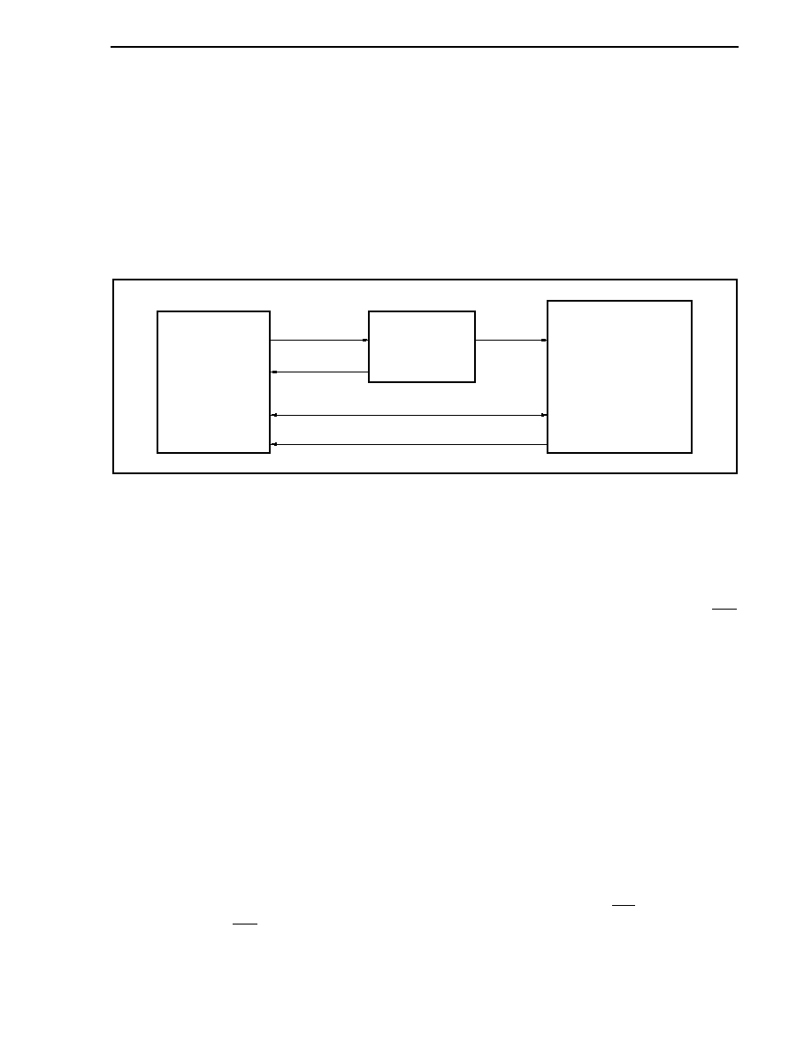
CHAPTER 17 I
2
C BUS
Preliminary User's Manual U17714EJ1V0UD
617
17.16.3 Slave operation
The following shows the processing procedure of the slave operation.
Basically, the operation of the slave device is event-driven. Therefore, processing by an INTIICn interrupt
(processing requiring a significant change of the operation status, such as stop condition detection during
communication) is necessary.
The following description assumes that data communication does not support extension codes. Also, it is assumed
that the INTIICn interrupt servicing performs only status change processing and that the actual data communication is
performed during the main processing.
Figure 17-20. Software Outline During Slave Operation
I
2
C
INTIICn signal
Setting, etc.
Setting, etc.
Flag
Data
Main processing
Interrupt servicing
Therefore, the following three flags are prepared so that the data transfer processing can be performed by
transmitting these flags to the main processing instead of INTIICn signal.
(1) Communication mode flag
This flag indicates the following communication statuses.
Clear mode:
Data communication not in progress
Communication mode: Data communication in progress (valid address detection stop condition detection, ACK
from master not detected, address mismatch)
(2) Ready flag
This flag indicates that data communication is enabled. This is the same status as an INTIICn interrupt during
normal data transfer. This flag is set in the interrupt processing block and cleared in the main processing block.
The ready flag for the first data for transmission is not set in the interrupt processing block, so the first data is
transmitted without clear processing (the address match is regarded as a request for the next data).
(3) Communication direction flag
This flag indicates the direction of communication and is the same as the value of IICSn.TRCn bit.
The following shows the operation of the main processing block during slave operation.
Start I
2
C0n and wait for the communication enabled status. When communication is enabled, perform transfer
using the communication mode flag and ready flag (the processing of the stop condition and start condition is
performed by interrupts, conditions are confirmed by flags).
For transmission, repeat the transmission operation until the master device stops returning ACK. When the master
device stops returning ACK , transfer is complete.
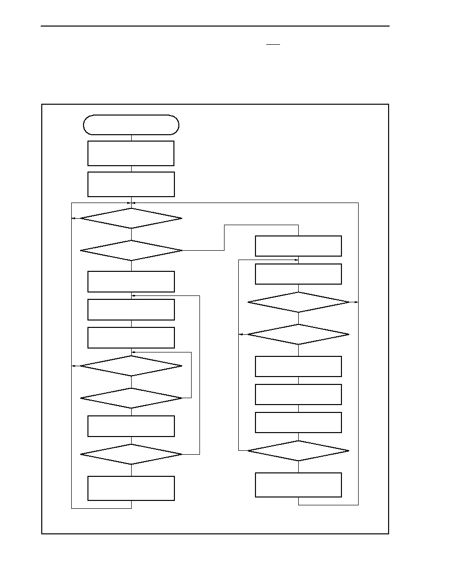
CHAPTER 17 I
2
C BUS
Preliminary User's Manual U17714EJ1V0UD
618
For reception, receive the required number of data and do not return ACK for the next data immediately after
transfer is complete. After that, the master device generates the stop condition or restart condition. This causes exit
from communications.
Figure 17-21. Slave Operation Flowchart (1)
Yes
Yes
Yes
Yes
No
Yes
Yes
Yes
No
No
No
No
Yes
No
No
No
START
Communication mode?
Communication mode?
Communication mode?
Ready?
Ready?
Read data
Clear ready flag
Clear ready flag
Communication
direction flag = 1?
WTIMn = 1
WRELn = 1
ACKEn = 0
WRELn = 1
ACKEn = WTIMn = 1
ACKDn = 1?
WRELn = 1
Clear communication mode flag
Data processing
Data processing
Transfer completed?
IICn
data
IICCn
XXH
IICEn = 1
IICCLn
XXH
IICFn
XXH
Selection of transfer flag
IICFn register setting
Remark n = 0 to 2
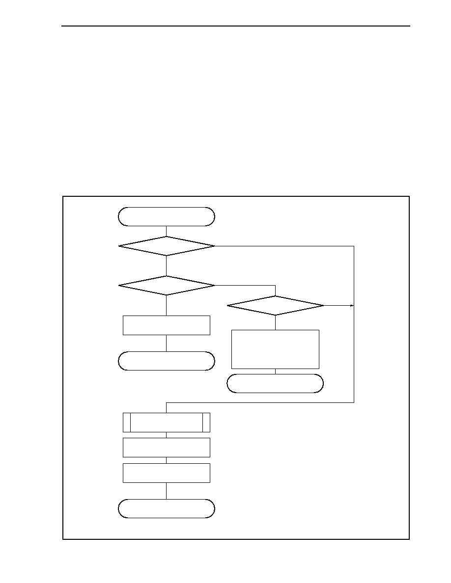
CHAPTER 17 I
2
C BUS
Preliminary User's Manual U17714EJ1V0UD
619
The following shows an example of the processing of the slave device by an INTIICn interrupt (it is assumed that no
extension codes are used here). During an INTIICn interrupt, the status is confirmed and the following steps are
executed.
<1> When a stop condition is detected, communication is terminated.
<2> When a start condition is detected, the address is confirmed. If the address does not match, communication
is terminated. If the address matches, the communication mode is set and wait state is released, and
operation returns from the interrupt (the ready flag is cleared).
<3> For data transmission/reception, when the ready flag is set, operation returns from the interrupt while the
I
2
C0n bus remains in the wait state.
Remark <1> to <3> in the above correspond to <1> to <3> in Figure 17-22 Slave Operation Flowchart (2).
Figure 17-22. Slave Operation Flowchart (2)
Yes
Yes
Yes
No
No
No
INTIICn generated
Set ready flag
Interrupt servicing completed
Interrupt servicing completed
Interrupt servicing completed
Termination processing
SPDn = 1?
STDn = 1?
COIn = 1?
LRELn = 1
Clear communication mode
Communication direction flag
TRCn
Set communication mode flag
Clear ready flag
<1>
<2>
<3>
Remark n = 0 to 2

CHAPTER 17 I
2
C BUS
Preliminary User's Manual U17714EJ1V0UD
620
17.17 Timing of Data Communication
When using I
2
C bus mode, the master device outputs an address via the serial bus to select one of several slave
devices as its communication partner.
After outputting the slave address, the master device transmits the IICSn.TRCn bit, which specifies the data
transfer direction, and then starts serial communication with the slave device.
The shift operation of the IICn register is synchronized with the falling edge of the serial clock pin (SCL0n). The
transmit data is transferred to the SO latch and is output (MSB first) via the SDA0n pin.
Data input via the SDA0n pin is captured by the IICn register at the rising edge of the SCL0n pin.
The data communication timing is shown below.
Remark n = 0 to 2
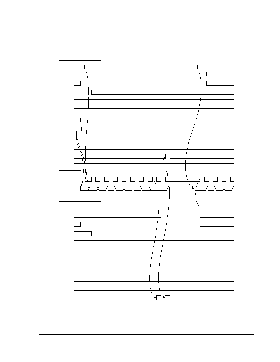
CHAPTER 17 I
2
C BUS
Preliminary User's Manual U17714EJ1V0UD
621
Figure 17-23. Example of Master to Slave Communication
(When 9-Clock Wait Is Selected for Both Master and Slave) (1/3)
(a) Start condition ~ Address
IICn
ACKDn
STDn
SPDn
WTIMn
H
H
L
L
L
L
H
H
H
L
L
ACKEn
MSTSn
STTn
SPTn
WRELn
INTIICn
TRCn
IICn
ACKDn
STDn
SPDn
WTIMn
ACKEn
MSTSn
STTn
SPTn
WRELn
INTIICn
TRCn
SCL0n
SDA0n
Processing by master device
Transfer lines
Processing by slave device
1
2
3
4
5
6
7
8
9
4
3
2
1
AD6 AD5 AD4 AD3 AD2 AD1 AD0
W
ACK
D4
D5
D6
D7
IICn
address
IICn
data
IICn
FFH
Transmit
Start condition
Receive
(When EXCn = 1)
Note
Note
Note To cancel slave wait, write FFH to IICn or set WRELn.
Remark n = 0 to 2
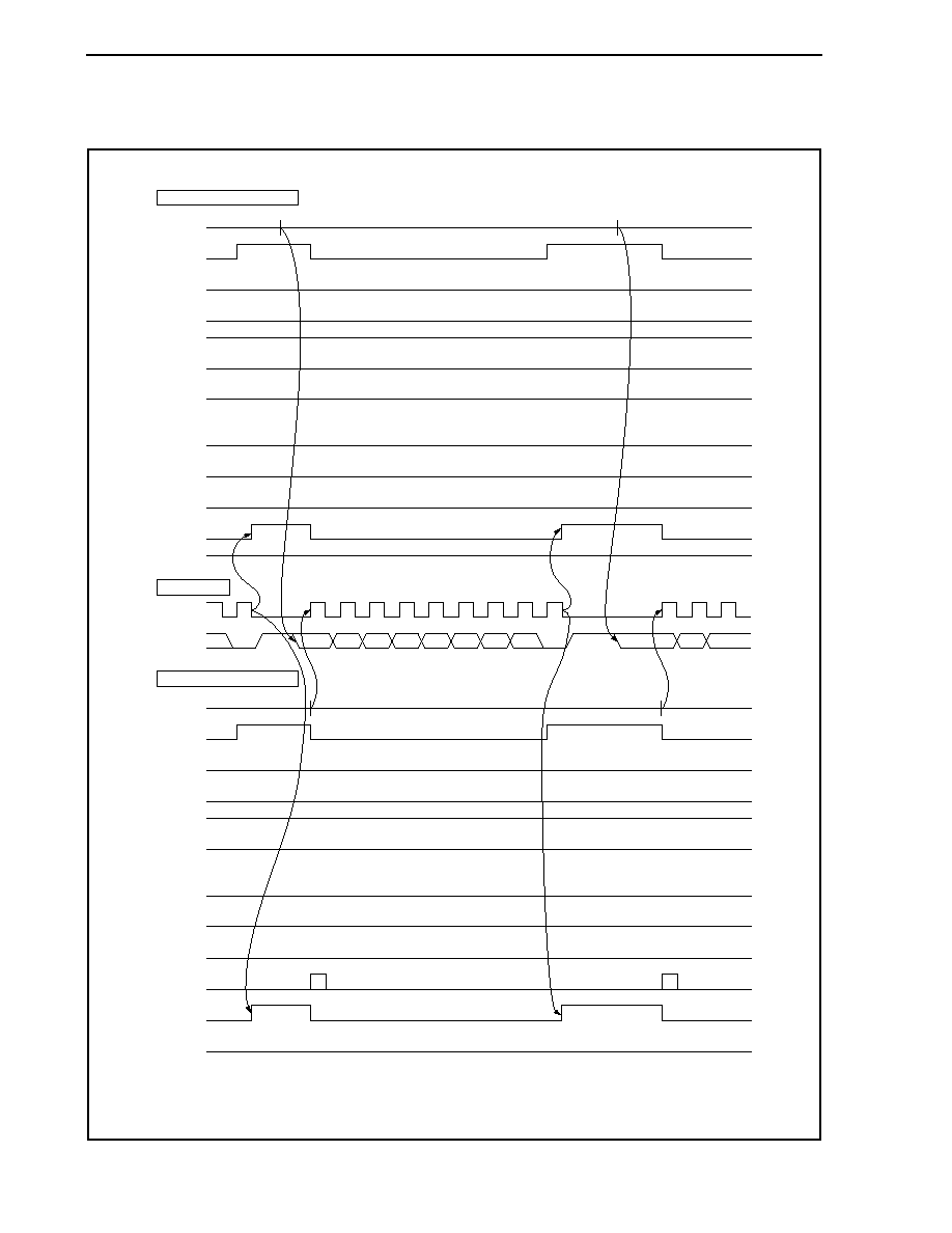
CHAPTER 17 I
2
C BUS
Preliminary User's Manual U17714EJ1V0UD
622
Figure 17-23. Example of Master to Slave Communication
(When 9-Clock Wait Is Selected for Both Master and Slave) (2/3)
(b) Data
IICn
ACKDn
STDn
SPDn
WTIMn
H
H
L
L
L
L
L
L
H
H
H
H
L
L
L
L
L
ACKEn
MSTSn
STTn
SPTn
WRELn
INTIICn
TRCn
IICn
ACKDn
STDn
SPDn
WTIMn
ACKEn
MSTSn
STTn
SPTn
WRELn
INTIICn
TRCn
SCL0n
SDA0n
Processing by master device
Transfer lines
Processing by slave device
1
9
8
2
3
4
5
6
7
8
9
3
2
1
D7
D0
D6
D5
D4
D3
D2
D1
D0
D5
D6
D7
IICn
data
IICn
FFH Note
IICn
FFH Note
IICn
data
Transmit
Receive
Note
Note
Note To cancel slave wait, write FFH to IICn or set WRELn.
Remark n = 0 to 2
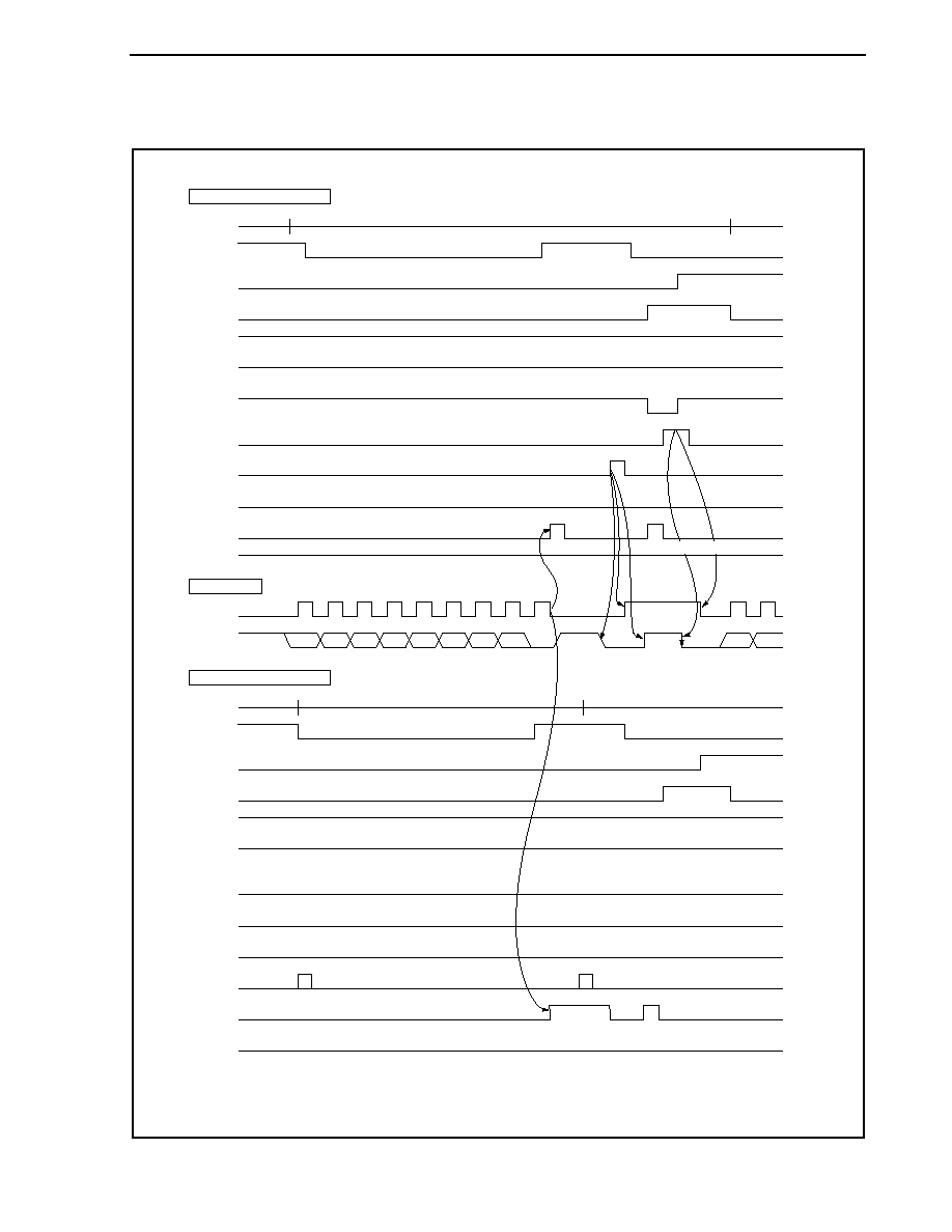
CHAPTER 17 I
2
C BUS
Preliminary User's Manual U17714EJ1V0UD
623
Figure 17-23. Example of Master to Slave Communication
(When 9-Clock Wait Is Selected for Both Master and Slave) (3/3)
(c) Stop condition
IICn
ACKDn
STDn
SPDn
WTIMn
H
H
L
L
L
L
H
H
H
L
ACKEn
MSTSn
STTn
SPTn
WRELn
INTIICn
TRCn
IICn
ACKDn
STDn
SPDn
WTIMn
ACKEn
MSTSn
STTn
SPTn
WRELn
INTIICn
TRCn
SCL0n
SDA0n
Processing by master device
Transfer lines
Processing by slave device
1
2
3
4
5
6
7
8
9
2
1
D7
D6
D5
D4
D3
D2
D1
D0
AD5
AD6
IICn
data
IICn
address
IICn
FFH Note
IICn
FFH Note
Stop
condition
Start
condition
Transmit
Note
Note
(When SPIEn = 1)
Receive
(When SPIEn = 1)
Note To cancel slave wait, write FFH to IICn or set WRELn.
Remark n = 0 to 2
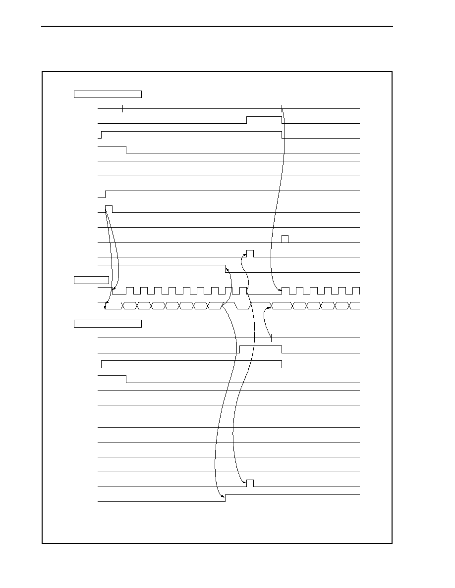
CHAPTER 17 I
2
C BUS
Preliminary User's Manual U17714EJ1V0UD
624
Figure 17-24. Example of Slave to Master Communication
(When 9-Clock Wait Is Selected for Both Master and Slave) (1/3)
(a) Start condition ~ Address
IICn
ACKDn
STDn
SPDn
WTIMn
H
H
L
L
H
H
L
ACKEn
MSTSn
STTn
L
L
SPTn
WRELn
INTIICn
TRCn
IICn
ACKDn
STDn
SPDn
WTIMn
ACKEn
MSTSn
STTn
SPTn
WRELn
INTIICn
TRCn
SCL0n
SDA0n
Processing by master device
Transfer lines
Processing by slave device
1
2
3
4
5
6
7
8
9
4
5
6
3
2
1
AD6 AD5 AD4 AD3 AD2 AD1 AD0
R
D4
D3
D2
D5
D6
D7
IICn
address
IICn
FFH Note
Note
IICn
data
Start condition
Note To cancel master wait, write FFH to IICn or set WRELn.
Remark n = 0 to 2
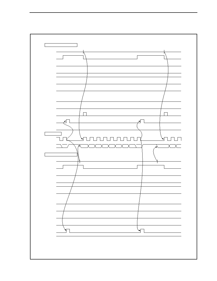
CHAPTER 17 I
2
C BUS
Preliminary User's Manual U17714EJ1V0UD
625
Figure 17-24. Example of Slave to Master Communication
(When 9-Clock Wait Is Selected for Both Master and Slave) (2/3)
(b) Data
IICn
ACKDn
STDn
SPDn
WTIMn
H
H
H
L
L
L
L
L
L
H
H
H
L
L
L
L
L
ACKEn
MSTSn
STTn
SPTn
WRELn
INTIICn
TRCn
IICn
ACKDn
STDn
SPDn
WTIMn
ACKEn
MSTSn
STTn
SPTn
WRELn
INTIICn
TRCn
SCL0n
SDA0n
Processing by master device
Transfer lines
Processing by slave device
1
8
9
2
3
4
5
6
7
8
9
3
2
1
D7
D0
ACK
D6
D5
D4
D3
D2
D1
D0
ACK
D5
D6
D7
Note
Note
Receive
Transmit
IICn
data
IICn
data
IICn
FFH Note
IICn
FFH Note
Note To cancel master wait, write FFH to IICn or set WRELn.
Remark n = 0 to 2
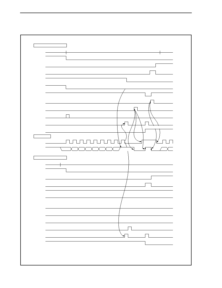
CHAPTER 17 I
2
C BUS
Preliminary User's Manual U17714EJ1V0UD
626
Figure 17-24. Example of Slave to Master Communication
(When 9-Clock Wait Is Selected for Both Master and Slave) (3/3)
(c) Stop condition
IICn
ACKDn
STDn
SPDn
WTIMn
H
H
L
L
L
H
ACKEn
MSTSn
STTn
SPTn
WRELn
INTIICn
TRCn
IICn
ACKDn
STDn
SPDn
WTIMn
ACKEn
MSTSn
STTn
SPTn
WRELn
INTIICn
TRCn
SCL0n
SDA0n
Processing by master device
Transfer lines
Processing by slave device
1
2
3
4
5
6
7
8
9
2
1
D7
D6
D5
D4
D3
D2
D1
D0
AD5
AD6
IICn
address
IICn
FFH Note
Note
IICn
data
Stop
condition
Start
condition
(When SPIEn = 1)
NACK
(When SPIEn = 1)
Note To cancel master wait, write FFH to IICn or set WRELn.
Remark n = 0 to 2

Preliminary User's Manual U17714EJ1V0UD
627
CHAPTER 18 DMA FUNCTION (DMA CONTROLLER)
The V850ES/JJ2 includes a direct memory access (DMA) controller (DMAC) that executes and controls DMA
transfer.
The DMAC controls data transfer between memory and I/O, between memories, or between I/Os based on DMA
requests issued by the on-chip peripheral I/O (serial interface, timer/counter, and A/D converter), interrupts from
external input pins, or software triggers (memory refers to internal RAM or external memory).
18.1 Features
� 4 independent DMA channels
� Transfer unit: 8/16 bits
� Maximum transfer count: 65,536 (2
16
)
� Transfer type: Two-cycle transfer
� Transfer mode: Single transfer mode
� Transfer requests
� Request by interrupts from on-chip peripheral I/O (serial interface, timer/counter, A/D converter) or interrupts
from external input pin
� Requests by software trigger
� Transfer targets
� Internal RAM Peripheral I/O
� Peripheral I/O Peripheral I/O
� Internal RAM External memory
� External memory Peripheral I/O
� External memory External memory
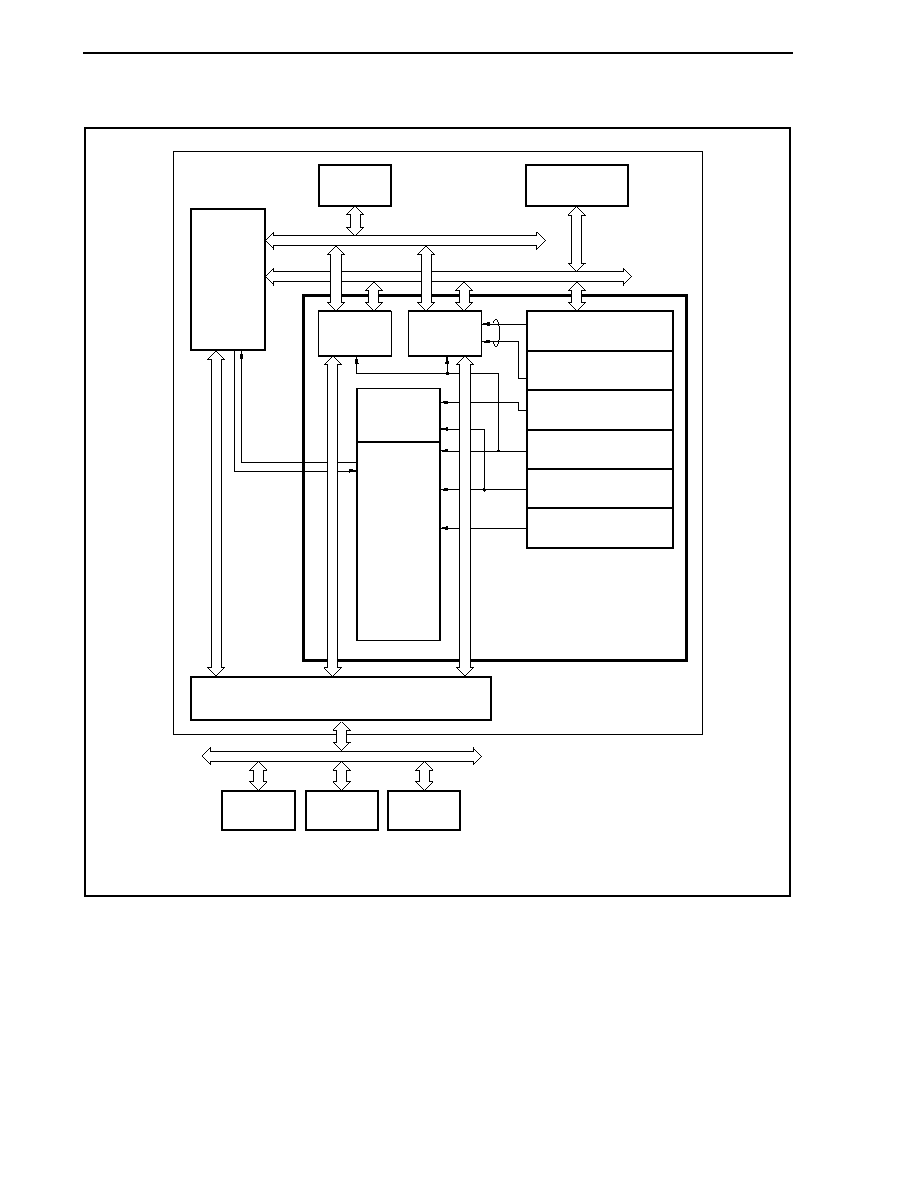
CHAPTER 18 DMA FUNCTION (DMA CONTROLLER)
Preliminary User's Manual U17714EJ1V0UD
628
18.2 Configuration
CPU
Internal RAM
On-chip
peripheral I/O
On-chip peripheral I/O bus
Internal bus
Data
control
Address
control
Count
control
Channel
control
DMAC
V850ES/JJ2
Bus interface
External bus
External
RAM
External
ROM
External I/O
DMA source address
register n (DSAnH/DSAnL)
DMA transfer count
register n (DBCn)
DMA channel control
register n (DCHCn)
DMA destination address
register n (DDAnH/DDAnL)
DMA addressing control
register n (DADCn)
DMA trigger factor
register n (DTFRn)
Remark n = 0 to 3
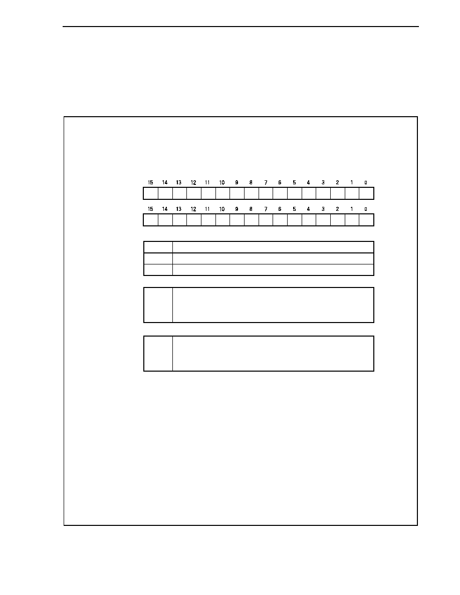
CHAPTER 18 DMA FUNCTION (DMA CONTROLLER)
Preliminary User's Manual U17714EJ1V0UD
629
18.3 Registers
(1) DMA source address registers 0 to 3 (DSA0 to DSA3)
The DSA0 to DSA3 registers set the DMA source addresses (26 bits each) for DMA channel n (n = 0 to 3).
These registers are divided into two 16-bit registers, DSAnH and DSAnL.
These registers can be read or written in 16-bit units.
External memory or on-chip peripheral I/O
Internal RAM
IR
0
1
Specification of DMA transfer source
Set the address (A25 to A16) of the DMA transfer source
(default value is undefined).
During DMA transfer, the next DMA transfer source address is held.
When DMA transfer is completed, the DMA address set first is held.
SA25 to SA16
Set the address (A15 to A0) of the DMA transfer source
(default value is undefined).
During DMA transfer, the next DMA transfer source address is held.
When DMA transfer is completed, the DMA address set first is held.
SA15 to SA0
After reset: Undefined R/W Address: DSA0H FFFFF082H, DSA1H FFFFF08AH,
DSA2H FFFFF092H, DSA3H FFFFF09AH,
DSA0L FFFFF080H, DSA1L FFFFF088H,
DSA2L FFFFF090H, DSA3L FFFFF098H
DSAnL
(n = 0 to 3)
SA15 SA14 SA13 SA12
SA6 SA5 SA4 SA3 SA2 SA1 SA0
SA7
SA8
SA9
SA10
SA11
DSAnH
(n = 0 to 3)
IR
0
0
0
SA22 SA21 SA20 SA19 SA18 SA17 SA16
SA23
SA24
SA25
0
0
Cautions 1. Be sure to clear bits 14 to 10 of the DSAnH register to 0.
2. Set the DSAnH and DSAnL registers at the following timing when DMA transfer is disabled
(DCHCn.Enn bit = 0).
� Period from after reset to start of first DMA transfer
� Period from after channel initialization by DCHCn.INITn bit to start of DMA transfer
� Period from after completion of DMA transfer (DCHCn.TCn bit = 1) to start of the next
DMA transfer
3. When the value of the DSAn register is read, two 16-bit registers, DSAnH and DSAnL, are
read. If reading and updating conflict, the value being updated may be read (see 18.13
Cautions).
4. Following reset, set the DSAnH, DSAnL, DDAnH, DDAnL, and DBCn registers before
starting DMA transfer. If these registers are not set, the operation when DMA transfer is
started is not guaranteed.
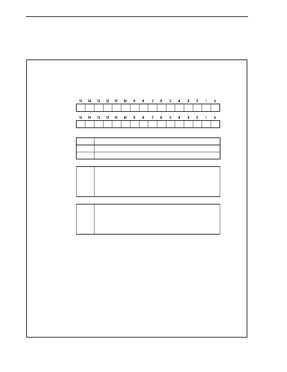
CHAPTER 18 DMA FUNCTION (DMA CONTROLLER)
Preliminary User's Manual U17714EJ1V0UD
630
(2) DMA destination address registers 0 to 3 (DDA0 to DDA3)
The DDA0 to DDA3 registers set the DMA destination address (26 bits each) for DMA channel n (n = 0 to 3).
These registers are divided into two 16-bit registers, DDAnH and DDAnL.
These registers can be read or written in 16-bit units.
External memory or on-chip peripheral I/O
Internal RAM
IR
0
1
Specification of DMA transfer destination
Set an address (A25 to A16) of DMA transfer destination
(default value is undefined).
During DMA transfer, the next DMA transfer destination address is held.
When DMA transfer is completed, the DMA transfer source address set
first is held.
DA25 to DA16
Set an address (A15 to A0) of DMA transfer destination
(default value is undefined).
During DMA transfer, the next DMA transfer destination address is held.
When DMA transfer is completed, the DMA transfer source address set
first is held.
DA15 to DA0
After reset: Undefined R/W Address: DDA0H FFFFF086H, DDA1H FFFFF08EH,
DDA2H FFFFF096H, DDA3H FFFFF09EH,
DDA0L FFFFF084H, DDA1L FFFFF08CH,
DDA2L FFFFF094H, DDA3L FFFFF09CH
DDAnL
(n = 0 to 3)
DA15 DA14 DA13 DA12
DA6 DA5 DA4 DA3 DA2 DA1 DA0
DA7
DA8
DA9
DA10
DA11
DDAnH
(n = 0 to 3)
IR
0
0
0
DA22 DA21 DA20 DA19 DA18 DA17 DA16
DA23
DA24
DA25
0
0
Cautions 1. Be sure to clear bits 14 to 10 of the DDAnH register to 0.
2. Set the DDAnH and DDAnL registers at the following timing when DMA transfer is disabled
(DCHCn.Enn bit = 0).
� Period from after reset to start of first DMA transfer
� Period from after channel initialization by DCHCn.INITn bit to start of DMA transfer
� Period from after completion of DMA transfer (DCHCn.TCn bit = 1) to start of the next
DMA transfer
3. When the value of the DDAn register is read, two 16-bit registers, DDAnH and DDAnL, are
read. If reading and updating conflict, a value being updated may be read (see 18.13
Cautions).
4. Following reset, set the DSAnH, DSAnL, DDAnH, DDAnL, and DBCn registers before
starting DMA transfer. If these registers are not set, the operation when DMA transfer is
started is not guaranteed.
CHAPTER 18 DMA FUNCTION (DMA CONTROLLER)
Preliminary User's Manual U17714EJ1V0UD
631
(3) DMA byte count registers 0 to 3 (DBC0 to DBC3)
The DBC0 to DBC3 registers are 16-bit registers that set the byte transfer count for DMA channel n (n = 0 to 3).
These registers hold the remaining transfer count during DMA transfer.
These registers are decremented by 1 per one transfer regardless of the transfer data unit (8/16 bits), and the
transfer is terminated if a borrow occurs.
These registers can be read or written in 16-bit units.
Byte transfer count 1 or remaining byte transfer count
Byte transfer count 2 or remaining byte transfer count
:
Byte transfer count 65,536 (2
16
) or remaining byte transfer count
BC15 to
BC0
0000H
0001H
:
FFFFH
Byte transfer count setting or remaining
byte transfer count during DMA transfer
After reset: Undefined R/W Address: DBC0 FFFFF0C0H, DBC1 FFFFF0C2H,
DBC2 FFFFF0C4H, DBC3 FFFFF0C6H
DBCn
(n = 0 to 3)
15
BC15
14
BC14
13
BC13
12
BC12
11
BC11
10
BC10
9
BC9
8
BC8
7
BC7
6
BC6
5
BC5
4
BC4
3
BC3
2
BC2
1
BC1
0
BC0
The number of transfer data set first is held when DMA transfer is complete.
Cautions 1. Set the DBCn register at the following timing when DMA transfer is disabled (DCHCn.Enn
bit = 0).
� Period from after reset to start of first DMA transfer
� Period from after channel initialization by DCHCn.INITn bit to start of DMA transfer
� Period from after completion of DMA transfer (DCHCn.TCn bit = 1) to start of the next
DMA transfer
2. Following reset, set the DSAnH, DSAnL, DDAnH, DDAnL, and DBCn registers before
starting DMA transfer. If these registers are not set, the operation when DMA transfer is
started is not guaranteed.
CHAPTER 18 DMA FUNCTION (DMA CONTROLLER)
Preliminary User's Manual U17714EJ1V0UD
632
(4) DMA addressing control registers 0 to 3 (DADC0 to DADC3)
The DADC0 to DADC3 registers are 16-bit registers that control the DMA transfer mode for DMA channel n (n
= 0 to 3).
These registers can be read or written in 16-bit units.
Reset sets these registers to 0000H.
DADCn
(n = 0 to 3)
8 bits
16 bits
DS0
0
1
Setting of transfer data size
Increment
Decrement
Fixed
Setting prohibited
SAD1
0
0
1
1
SAD0
0
1
0
1
Setting of count direction of the transfer source address
Increment
Decrement
Fixed
Setting prohibited
DAD1
0
0
1
1
DAD0
0
1
0
1
Setting of count direction of the destination address
After reset: 0000H R/W Address: DADC0 FFFFF0D0H, DADC1 FFFFF0D2H,
DADC2 FFFFF0D4H, DADC3 FFFFF0D6H
SAD1
SAD0
DAD1
DAD0
0
0
0
0
0
DS0
0
0
0
0
0
0
8
9
10
11
12
13
14
15
0
1
2
3
4
5
6
7
Cautions 1. Be sure to clear bits 15, 13 to 8, and 3 to 0 of the DADCn register to "0".
2. Set the DADCn register at the following timing when DMA transfer is disabled (DCHCn.Enn
bit = 0).
� Period from after reset to start of first DMA transfer
� Period from after channel initialization by DCHCn.INITn bit to start of DMA transfer
� Period from after completion of DMA transfer (DCHCn.TCn bit = 1) to start of the next
DMA transfer
3. The DS0 bit specifies the size of the transfer data, and does not control bus sizing. If 8-bit
data (DS0 bit = 0) is set, therefore, the lower data bus is not always used.
4. If the transfer data size is set to 16 bits (DS0 bit = 1), transfer cannot be started from an
odd address. Transfer is always started from an address with the first bit of the lower
address aligned to 0.
5. If DMA transfer is executed on an on-chip peripheral I/O register (as the transfer source or
destination), be sure to specify the same transfer size as the register size. For example, to
execute DMA transfer on an 8-bit register, be sure to specify 8-bit transfer.
CHAPTER 18 DMA FUNCTION (DMA CONTROLLER)
Preliminary User's Manual U17714EJ1V0UD
633
(5) DMA channel control registers 0 to 3 (DCHC0 to DCHC3)
The DCHC0 to DCHC3 registers are 8-bit registers that control the DMA transfer operating mode for DMA
channel n.
These registers can be read or written in 8-bit or 1-bit units. (However, bit 7 is read-only and bits 1 and 2 are
write-only. If bit 1 or 2 is read, the read value is always 0.)
Reset sets these registers to 00H.
DCHCn
(n = 0 to 3)
DMA transfer had not completed.
DMA transfer had completed.
It is set to 1 on the last DMA transfer and cleared to 0 when it is read.
TCn
Note 1
0
1
Status flag indicates whether DMA transfer
through DMA channel n has completed or not
DMA transfer disabled
DMA transfer enabled
DMA transfer is enabled when the Enn bit is set to 1.
When DMA transfer is completed (when a terminal count is generated), this bit is
automatically cleared to 0.
To abort DMA transfer, clear the Enn bit to 0 by software. To resume, set the Enn
bit to 1 again.
When aborting or resuming DMA transfer, however, be sure to observe the
procedure described in 18.13 Cautions.
Enn
0
1
Setting of whether DMA transfer through
DMA channel n is to be enabled or disabled
This is a software startup trigger of DMA transfer.
If this bit is set to 1 in the DMA transfer enable state (TCn bit = 0, Enn
bit = 1), DMA transfer is started.
STGn
Note 2
After reset: 00H R/W Address: DCHC0 FFFFF0E0H, DCHC1 FFFFF0E2H,
DCHC2 FFFFF0E4H, DCHC3 FFFFF0E6H
TCn
Note 1
0
0
0
0
INITn
Note 2
STGn
Note 2
Enn
<0>
<1>
<2>
3
4
5
6
<7>
INITn
Note 2
If the INITn bit is set to 1 with DMA transfer disabled (Enn bit = 0), the
DMA transfer status can be initialized.
When re-setting the DMA transfer status (re-setting the DDAnH, DDAnL,
DSAnH, DSAnL, DBCn, and DADCn registers) before DMA transfer is
completed (before the TCn bit is set to 1), be sure to initialize the DMA
channel.
When initializing the DMA controller, however, be sure to observe the
procedure described in 18.13 Cautions.
Notes 1. The TCn bit is read-only.
2. The INITn and STGn bits are write-only.
Cautions 1. Be sure to clear bits 6 to 3 of the DCHCn register to 0.
2. When DMA transfer is completed (when a terminal count is generated), the Enn bit is
cleared to 0 and then the TCn bit is set to 1. If the DCHCn register is read while its bits are
being updated, a value indicating "transfer not completed and transfer is disabled" (TCn
bit = 0 and Enn bit = 0) may be read.
CHAPTER 18 DMA FUNCTION (DMA CONTROLLER)
Preliminary User's Manual U17714EJ1V0UD
634
(6) DMA trigger factor registers 0 to 3 (DTFR0 to DTFR3)
The DTFR0 to DTFR3 registers are 8-bit registers that control the DMA transfer start trigger via interrupt
request signals from on-chip peripheral I/O.
The interrupt request signals set by these registers serve as DMA transfer start factors.
These registers can be read or written in 8-bit units. However, DFn bit can be read or written in 1-bit units.
Reset sets these registers to 00H.
DTFRn
(n = 0 to 3)
No DMA transfer request
DMA transfer request
DFn
Note
0
1
DMA transfer request flag
After reset: 00H R/W Address: DTFR0 FFFFF810H, DTFR1 FFFFF812H,
DTFR2 FFFFF814H, DTFR3 FFFFF816H
DFn
0
IFCn5
IFCn4
IFCn3
IFCn2
IFCn1
IFCn0
0
1
2
3
4
5
6
<7>
Note The DFn bit is a write-only bit. Write 0 to this bit to clear a DMA transfer request if an interrupt that is
specified as the cause of starting DMA transfer occurs while DMA transfer is disabled.
Cautions 1. Set the IFCn5 to IFCn0 bits at the following timing when DMA transfer is disabled
(DCHCn.Enn bit = 0).
� Period from after reset to start of first DMA transfer
� Period from after channel initialization by DCHCn.INITn bit to start of DMA transfer
� Period from after completion of DMA transfer (DCHCn.TCn bit = 1) to start of the next
DMA transfer
2. An interrupt request that is generated in the standby mode (IDEL1, IDLE2, STOP, or sub-
IDLE mode) does not start the DMA transfer cycle (nor is the DFn bit set to 1).
3. If a DMA start factor is selected by the IFCn5 to IFCn0 bits, the DFn bit is set to 1 when an
interrupt occurs from the selected on-chip peripheral I/O, regardless of whether the DMA
transfer is enabled or disabled. If DMA is enabled in this status, DMA transfer is
immediately started.
Remark For the IFCn5 to IFCn0 bits, see Table 18-1 DMA Start Factors.

CHAPTER 18 DMA FUNCTION (DMA CONTROLLER)
Preliminary User's Manual U17714EJ1V0UD
635
Table 18-1. DMA Start Factors (1/2)
IFCn5 IFCn4 IFCn3 IFCn2 IFCn1 IFCn0
Interrupt
Source
0
0
0
0
0
0
DMA request by interrupt disabled
0 0 0 0 0 1
INTP0
0 0 0 0 1 0
INTP1
0 0 0 0 1 1
INTP2
0 0 0 1 0 0
INTP3
0 0 0 1 0 1
INTP4
0 0 0 1 1 0
INTP5
0 0 0 1 1 1
INTP6
0 0 1 0 0 0
INTP7
0 0 1 0 0 1
INTTQ0OV
0 0 1 0 1 0
INTTQ0CC0
0 0 1 0 1 1
INTTQ0CC1
0 0 1 1 0 0
INTTQ0CC2
0 0 1 1 0 1
INTTQ0CC3
0 0 1 1 1 0
INTTP0OV
0 0 1 1 1 1
INTTP0CC0
0 1 0 0 0 0
INTTP0CC1
0 1 0 0 0 1
INTTP1OV
0 1 0 0 1 0
INTTP1CC0
0 1 0 0 1 1
INTTP1CC1
0 1 0 1 0 0
INTTP2OV
0 1 0 1 0 1
INTTP2CC0
0 1 0 1 1 0
INTTP2CC1
0 1 0 1 1 1
INTTP3CC0
0 1 1 0 0 0
INTTP3CC1
0 1 1 0 0 1
INTTP4CC0
0 1 1 0 1 0
INTTP4CC1
0 1 1 0 1 1
INTTP5CC0
0 1 1 1 0 0
INTTP5CC1
0 1 1 1 0 1
INTTM0EQ0
0 1 1 1 1 0
INTCB0R/INTIIC1
0 1 1 1 1 1
INTCB0T
1 0 0 0 0 0
INTCB1R
1 0 0 0 0 1
INTCB1T
1 0 0 0 1 0
INTCB2R
1 0 0 0 1 1
INTCB2T
1 0 0 1 0 0
INTCB3R
1 0 0 1 0 1
INTCB3T
1 0 0 1 1 0
INTUA0R/INTCB4R
1 0 0 1 1 1
INTUA0T/INTCB4T
1 0 1 0 0 0
INTUA1R/INTIIC2
1 0 1 0 0 1
INTUA1T
1 0 1 0 1 0
INTUA2R/INTIIC0
Remark n = 0 to 3
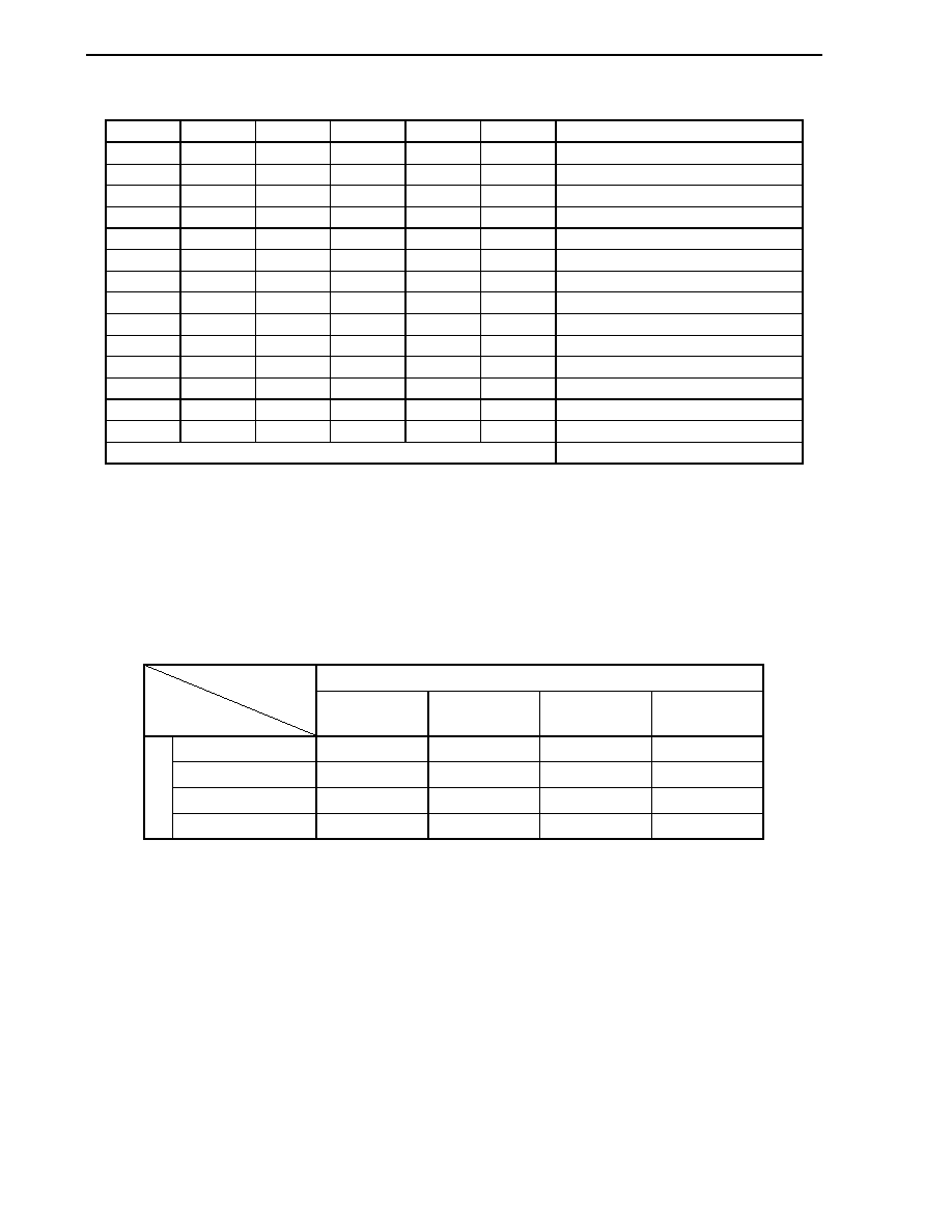
CHAPTER 18 DMA FUNCTION (DMA CONTROLLER)
Preliminary User's Manual U17714EJ1V0UD
636
Table 18-1. DMA Start Factors (2/2)
IFCn5 IFCn4 IFCn3 IFCn2 IFCn1 IFCn0
Interrupt
Source
1 0 1 0 1 1
INTUA2T
1 0 1 1 0 0
INTAD
1 0 1 1 0 1
INTKR
1 1 0 0 0 1
INTP8
1 1 0 0 1 0
INTTP6CC0
1 1 0 0 1 1
INTTP6CC1
1 1 0 1 0 0
INTTP7CC0
1 1 0 1 0 1
INTTP7CC1
1 1 0 1 1 0
INTTP8CC0
1 1 0 1 1 1
INTTP8CC1
1 1 1 0 0 0
INTCB5R
1 1 1 0 0 1
INTCB5T
1 1 1 0 1 0
INTUA3R
1 1 1 0 1 1
INTUA3T
Other than above
Setting prohibited
Remark n = 0 to 3
18.4 Transfer Targets
Table 18-2 shows the relationship between the transfer targets (
: Transfer enabled, �: Transfer disabled).
Table 18-2. Relationship Between Transfer Targets
Transfer Destination
Internal ROM
On-Chip
Peripheral I/O
Internal RAM
External Memory
On-chip
peripheral I/O
�
Internal RAM
�
�
External memory
�
Source
Internal ROM
�
�
�
�
Caution The operation is not guaranteed for combinations of transfer destination and source marked with
"
�" in Table 18-2.

CHAPTER 18 DMA FUNCTION (DMA CONTROLLER)
Preliminary User's Manual U17714EJ1V0UD
637
18.5 Transfer Modes
Single transfer is supported as the transfer mode.
In single transfer mode, the bus is released at each byte/halfword transfer. If there is a subsequent DMA transfer
request, transfer is performed again once. This operation continues until a terminal count occurs.
When the DMAC has released the bus, if another higher priority DMA transfer request is issued, the higher priority
DMA request always takes precedence.
If a new transfer request of the same channel and a transfer request of another channel with a lower priority are
generated in a transfer cycle, DMA transfer of the channel with the lower priority is executed after the bus is released
to the CPU (the new transfer request of the same channel is ignored in the transfer cycle).
18.6 Transfer Types
As a transfer type, the 2-cycle transfer is supported.
In two-cycle transfer, data transfer is performed in two cycles, a read cycle and a write cycle.
In the read cycle, the transfer source address is output and reading is performed from the source to the DMAC. In
the write cycle, the transfer destination address is output and writing is performed from the DMAC to the destination.
An idle cycle of one clock is always inserted between a read cycle and a write cycle. If the data bus width differs
between the transfer source and destination for DMA transfer of two cycles, the operation is performed as follows.
<16-bit data transfer>
<1> Transfer from 32-bit bus
16-bit bus
A read cycle (the higher 16 bits are in a high-impedance state) is generated, followed by generation of a
write cycle (16 bits).
<2> Transfer from 16-/32-bit bus to 8-bit bus
A 16-bit read cycle is generated once, and then an 8-bit write cycle is generated twice.
<3> Transfer from 8-bit bus to 16-/32-bit bus
An 8-bit read cycle is generated twice, and then a 16-bit write cycle is generated once.
<4> Transfer between 16-bit bus and 32-bit bus
A 16-bit read cycle is generated once, and then a 16-bit write cycle is generated once.
For DMA transfer executed to an on-chip peripheral I/O register (transfer source/destination), be sure to specify the
same transfer size as the register size. For example, for DMA transfer to an 8-bit register, be sure to specify byte (8-
bit) transfer.
Remark The bus width of each transfer target (transfer source/destination) is as follows.
� On-chip peripheral I/O: 16-bit bus width
� Internal RAM:
32-bit bus width
� External memory:
8-bit or 16-bit bus width
CHAPTER 18 DMA FUNCTION (DMA CONTROLLER)
Preliminary User's Manual U17714EJ1V0UD
638
18.7 DMA Channel Priorities
The DMA channel priorities are fixed as follows.
DMA channel 0 > DMA channel 1 > DMA channel 2 > DMA channel 3
The priorities are checked for every transfer cycle.
18.8 Time Related to DMA Transfer
The time required to respond to a DMA request, and the minimum number of clocks required for DMA transfer are
shown below.
Single transfer: DMA response time (<1>) + Transfer source memory access (<2>) + 1
Note 1
+ Transfer
destination memory access (<2>)
DMA Cycle
Minimum Number of Execution Clocks
<1> DMA request response time
4 clocks (MIN.) + Noise elimination time
Note 2
External memory access
Depends on connected memory.
Internal RAM access
2 clocks
Note 3
<2> Memory access
Peripheral I/O register access
3 clocks + Number of wait cycles specified by VSWC register
Note 4
Notes 1. One clock is always inserted between a read cycle and a write cycle in DMA transfer.
2. If an external interrupt (INTPn) is specified as the trigger to start DMA transfer, noise elimination time is
added (n = 0 to 7).
3. Two clocks are required for a DMA cycle.
4. More wait cycles are necessary for accessing a specific peripheral I/O register (for details, see 3.4.8 (2)).

CHAPTER 18 DMA FUNCTION (DMA CONTROLLER)
Preliminary User's Manual U17714EJ1V0UD
639
18.9 DMA Transfer Start Factors
There are two types of DMA transfer start factors, as shown below.
(1) Request by software
If the STGn bit is set to 1 while the DCHCn.TCn bit = 1 and Enn bit = 1 (DMA transfer enabled), DMA transfer
is started.
To request the next DMA transfer cycle immediately after that, confirm, by using the DBCn register, that the
preceding DMA transfer cycle has been completed, and set the STGn bit to 1 again (n = 0 to 3).
TCn bit = 0, Enn bit = 1
STGn bit = 1 ... Starts the first DMA transfer.
Confirm that the contents of the DBCn register have been updated.
STGn bit = 1 ... Starts the second DMA transfer.
:
Generation of terminal count ... Enn bit = 0, TCn bit = 1, and INTDMAn signal is generated.
(2) Request by on-chip peripheral I/O
If an interrupt request is generated from the on-chip peripheral I/O set by the DTFRn register when the
DCHCn.TCn bit = 0 and Enn bit = 1 (DMA transfer enabled), DMA transfer is started.
Cautions 1. Two start factors (software trigger and hardware trigger) cannot be used for one DMA
channel. If two start factors are simultaneously generated for one DMA channel, only one
of them is valid. The start factor that is valid cannot be identified.
2. A new transfer request that is generated after the preceding DMA transfer request was
generated or in the preceding DMA transfer cycle is ignored (cleared).
3. The transfer request interval of the same DMA channel varies depending on the setting of
bus wait in the DMA transfer cycle, the start status of the other channels, or the external
bus hold request. In particular, as described in Caution 2, a new transfer request that is
generated for the same channel before the DMA transfer cycle or during the DMA transfer
cycle is ignored. Therefore, the transfer request intervals for the same DMA channel must
be sufficiently separated by the system. When the software trigger is used, completion of
the DMA transfer cycle that was generated before can be checked by updating the DBCn
register.

CHAPTER 18 DMA FUNCTION (DMA CONTROLLER)
Preliminary User's Manual U17714EJ1V0UD
640
18.10 DMA Abort Factors
DMA transfer is aborted if a bus hold occurs.
The same applies if transfer is executed between the internal memory/on-chip peripheral I/O and internal
memory/on-chip peripheral I/O.
When the bus hold is cleared, DMA transfer is resumed.
18.11 End of DMA Transfer
When DMA transfer has been completed the number of times set to the DBCn register and when the DCHCn.Enn
bit is cleared to 0 and TCn bit is set to 1, a DMA transfer end interrupt request signal (INTDMAn) is generated for the
interrupt controller (INTC) (n = 0 to 3).
The V850ES/JJ2 does not output a terminal count signal to an external device. Therefore, confirm completion of
DMA transfer by using the DMA transfer end interrupt or polling the TCn bit.
18.12 Operation Timing
Figures 18-1 to 18-4 show DMA operation timing.
CHAPTER
18
DMA FU
NCTI
O
N (DMA
CONT
R
O
LLER
)
Prelimina
r
y User's Man
ual
U17714EJ
1
V0UD
641
Figure 18-1. Priority of DMA (1)
Preparation
for transfer
Read
Write
Idle
End
processing
DMA2
processing
CPU processing
DMA1 processing
CPU processing
CPU processing
DMA0 processing
DMA0 transfer request
System clock
DMA1 transfer request
DMA2 transfer request
DMA transfer
Mode of processing
DF0 bit
DF1 bit
DF2 bit
Preparation
for transfer
Read
Write
Idle
End
processing
Preparation
for transfer
Read
Remarks 1. Transfer in the order of DMA0
DMA1 DMA2
2. In the case of transfer between external memory spaces (multiplexed bus, no wait)
CHAPTER
18
DMA FU
NCTI
O
N (DMA
CONT
R
O
LLER
)
Prelimina
r
y User's Man
ual
U17714EJ
1
V0UD
642
Figure 18-2. Priority of DMA (2)
Preparation
for transfer
Read
Write
Idle
DMA0 transfer request
System clock
DMA1 transfer request
DMA2 transfer request
DMA transfer
Mode of processing
DF0 bit
DF1 bit
DF2 bit
CPU processing
DMA0 processing
CPU processing
DMA1 processing
CPU processing
DMA0
processing
Read
Write
Idle
End
processing
Read
Preparation
for transfer
Preparation
for transfer
End
processing
Remarks 1. Transfer in the order of DMA0
DMA1 DMA0 (DMA2 is held pending.)
2. In the case of transfer between external memory spaces (multiplexed bus, no wait)
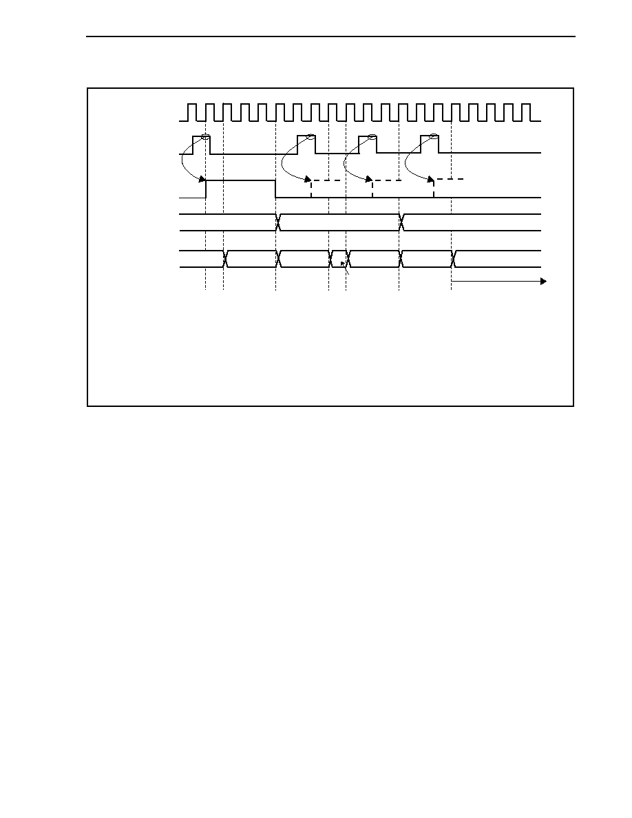
CHAPTER 18 DMA FUNCTION (DMA CONTROLLER)
Preliminary User's Manual U17714EJ1V0UD
643
Figure 18-3. Period in Which DMA Transfer Request Is Ignored (1)
Preparation
for transfer
Read cycle
Write cycle
Idle
End
processing
DMA transfer
Mode of processing
DFn bit
System clock
Transfer request generated
after this can be acknowledged
DMA0 processing
CPU processing
CPU processing
Note 2
Note 2
DMAn transfer
request
Note 1
Note 2
Notes 1. Interrupt from on-chip peripheral I/O, or software trigger (STGn bit)
2. New DMA request of the same channel is ignored between when the first request is generated and
the end processing is complete.
Remark In the case of transfer between external memory spaces (multiplexed bus, no wait)
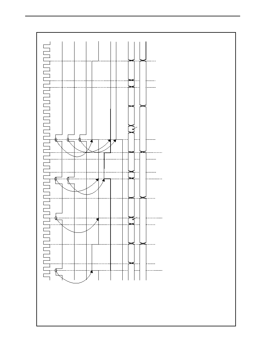
CHAPTER
18
DMA FU
NCTI
O
N (DMA
CONT
R
O
LLER
)
Prelimina
r
y User's Man
ual
U17714EJ
1
V0UD
644
Figure 18-4. Period in Which DMA Transfer Request Is Ignored (2)
Preparation
for transfer
Read
Write
Idle
<1>
<2>
<3>
<4>
CPU processing
DMA0 processing
CPU processing
DMA1 processing
CPU processing
DMA0
processing
DMA0 transfer request
System clock
DMA1 transfer request
DMA2 transfer request
DMA transfer
Mode of processing
DF0 bit
DF1 bit
DF2 bit
Preparation
for transfer
Read
Write
Idle
Preparation
for transfer
Read
End
processing
End
processing
<1> DMA0 transfer request
<2> New DMA0 transfer request is generated during DMA0 transfer.
A DMA transfer request of the same channel is ignored during DMA transfer.
<3> Requests for DMA0 and DMA1 are generated at the same time.
DMA0 request is ignored (a DMA transfer request of the same channel during transfer is ignored).
DMA1 request is acknowledged.
<4> Requests for DMA0, DMA1, and DMA2 are generated at the same time.
DMA1 request is ignored (a DMA transfer request of the same channel during transfer is ignored).
DMA0 request is acknowledged according to priority. DMA2 request is held pending (transfer of DMA2 occurs next).

CHAPTER 18 DMA FUNCTION (DMA CONTROLLER)
Preliminary User's Manual U17714EJ1V0UD
645
18.13 Cautions
(1) Caution for VSWC register
When using the DMAC, be sure to set an appropriate value, in accordance with the operating frequency, to the
VSWC register.
When the default value (77H) of the VSWC register is used, or if an inappropriate value is set to the VSWC
register, the operation is not correctly performed (for details of the VSWC register, see 3.4.8 (1) (a) System
wait control register (VSWC)).
(2) Caution for DMA transfer executed on internal RAM
When executing the following instructions located in the internal RAM, do not execute a DMA transfer that
transfers data to/from the internal RAM (transfer source/destination), because the CPU may not operate
correctly afterward.
� Bit manipulation instruction located in internal RAM (SET1, CLR1, or NOT1)
� Data access instruction to misaligned address located in internal RAM
Conversely, when executing a DMA transfer to transfer data to/from the internal RAM (transfer
source/destination), do not execute the above two instructions.
(3) Caution for reading DCHCn.TCn bit (n = 0 to 3)
The TCn bit is cleared to 0 when it is read, but it is not automatically cleared even if it is read at a specific
timing. To accurately clear the TCn bit, add the following processing.
(a) When waiting for completion of DMA transfer by polling TCn bit
Confirm that the TCn bit has been set to 1 (after TCn bit = 1 is read), and then read the TCn bit three more
times.
(b) When reading TCn bit in interrupt servicing routine
Execute reading the TCn bit three times.

CHAPTER 18 DMA FUNCTION (DMA CONTROLLER)
Preliminary User's Manual U17714EJ1V0UD
646
(4) DMA transfer initialization procedure (setting DCHCn.INITn bit to 1)
Even if the INITn bit is set to 1 when the channel executing DMA transfer is to be initialized, the channel may
not be initialized. To accurately initialize the channel, execute either of the following two procedures.
(a) Temporarily stop transfer of all DMA channels
Initialize the channel executing DMA transfer using the procedure in <1> to <7> below.
Note, however, that TCn bit is cleared to 0 when step <5> is executed. Make sure that the other
processing programs do not expect that the TCn bit is 1.
<1> Disable interrupts (DI).
<2> Read the DCHCn.Enn bit of DMA channels other than the one to be forcibly terminated, and transfer
the value to a general-purpose register.
<3> Clear the Enn bit of the DMA channels used (including the channel to be forcibly terminated) to 0. To
clear the Enn bit of the last DMA channel, execute the clear instruction twice. If the target of DMA
transfer (transfer source/destination) is the internal RAM, execute the instruction three times.
Example: Execute instructions in the following order if channels 0, 1, and 2 are used (if the target of
transfer is not the internal RAM).
� Clear DCHC0.E00 bit to 0.
� Clear DCHC1.E11 bit to 0.
� Clear DCHC2.E22 bit to 0.
� Clear DCHC2.E22 bit to 0 again.
<4> Set the INITn bit of the channel to be forcibly terminated to 1.
<5> Read the TCn bit of each channel not to be forcibly terminated. If both the TCn bit and the Enn bit
read in <2> are 1 (logical product (AND) is 1), clear the saved Enn bit to 0.
<6> After the operation in <5>, write the Enn bit value to the DCHCn register.
<7> Enable interrupts (EI).
Caution Be sure to execute step <5> above to prevent illegal setting of the Enn bit of the channels
whose DMA transfer has been normally completed between <2> and <3>.

CHAPTER 18 DMA FUNCTION (DMA CONTROLLER)
Preliminary User's Manual U17714EJ1V0UD
647
(b) Repeatedly execute setting INITn bit until transfer is forcibly terminated correctly
<1> Suppress a request from the DMA request source of the channel to be forcibly terminated (stop
operation of the on-chip peripheral I/O).
<2> Check that the DMA transfer request of the channel to be forcibly terminated is not held pending, by
using the DTFRn.DFn bit. If a DMA transfer request is held pending, wait until execution of the
pending request is completed.
<3> When it has been confirmed that the DMA request of the channel to be forcibly terminated is not held
pending, clear the Enn bit to 0.
<4> Again, clear the Enn bit of the channel to be forcibly terminated.
If the target of transfer for the channel to be forcibly terminated (transfer source/destination) is the
internal RAM, execute this operation once more.
<5> Copy the initial number of transfers of the channel to be forcibly terminated to a general-purpose
register.
<6> Set the INITn bit of the channel to be forcibly terminated to 1.
<7> Read the value of the DBCn register of the channel to be forcibly terminated, and compare it with the
value copied in <5>. If the two values do not match, repeat operations <6> and <7>.
Remarks 1. When the value of the DBCn register is read in <7>, the initial number of transfers is read if
forced termination has been correctly completed. If not, the remaining number of transfers
is read.
2. Note that method (b) may take a long time if the application frequently uses DMA transfer for
a channel other than the DMA channel to be forcibly terminated.
(5) Procedure of temporarily stopping DMA transfer (clearing Enn bit)
Stop and resume the DMA transfer under execution using the following procedure.
<1> Suppress a transfer request from the DMA request source (stop the operation of the on-chip peripheral
I/O).
<2> Check the DMA transfer request is not held pending, by using the DFn bit (check if the DFn bit = 0).
If a request is pending, wait until execution of the pending DMA transfer request is completed.
<3> If it has been confirmed that no DMA transfer request is held pending, clear the Enn bit to 0 (this
operation stops DMA transfer).
<4> Set the Enn bit to 1 to resume DMA transfer.
<5> Resume the operation of the DMA request source that has been stopped (start the operation of the on-
chip peripheral I/O).
(6) Memory boundary
The operation is not guaranteed if the address of the transfer source or destination exceeds the area of the
DMA target (external memory, internal RAM, or on-chip peripheral I/O) during DMA transfer.
(7) Transferring misaligned data
DMA transfer of misaligned data with a 16-bit bus width is not supported.
If an odd address is specified as the transfer source or destination, the least significant bit of the address is
forcibly assumed to be 0.

CHAPTER 18 DMA FUNCTION (DMA CONTROLLER)
Preliminary User's Manual U17714EJ1V0UD
648
(8) Bus arbitration for CPU
Because the DMA controller has a higher priority bus mastership than the CPU, a CPU access that takes place
during DMA transfer is held pending until the DMA transfer cycle is completed and the bus is released to the
CPU.
However, the CPU can access the external memory, on-chip peripheral I/O, and internal RAM to/from which
DMA transfer is not being executed.
� The CPU can access the internal RAM when DMA transfer is being executed between the external memory
and on-chip peripheral I/O.
� The CPU can access the internal RAM and on-chip peripheral I/O when DMA transfer is being executed
between the external memory and external memory.
(9) Registers/bits that must not be rewritten during DMA operation
Set the following registers at the following timing when a DMA operation is not under execution.
[Registers]
� DSAnH, DSAnL, DDAnH, DDAnL, DBCn, and DADCn registers
� DTFRn.IFCn5 to DTFRn.IFCn0 bits
[Timing of setting]
� Period from after reset to start of the first DMA transfer
� Time after channel initialization to start of DMA transfer
� Period from after completion of DMA transfer (TCn bit = 1) to start of the next DMA transfer
(10) Be sure to set the following register bits to 0.
� Bits 14 to 10 of DSAnH register
� Bits 14 to 10 of DDAnH register
� Bits 15, 13 to 8, and 3 to 0 of DADCn register
� Bits 6 to 3 of DCHCn register
(11) DMA start factor
Do not start two or more DMA channels with the same start factor. If two or more channels are started with
the same factor, a DMA channel with a lower priority may be acknowledged earlier than a DMA channel with a
higher priority.

CHAPTER 18 DMA FUNCTION (DMA CONTROLLER)
Preliminary User's Manual U17714EJ1V0UD
649
(12) Read values of DSAn and DDAn registers
Values in the middle of updating may be read from the DSAn and DDAn registers during DMA transfer (n = 0
to 3).
For example, if the DSAnH register and then the DSAnL register are read when the DMA transfer source
address (DSAn register) is 0000FFFFH and the count direction is incremental (DADCn.SAD1 and
DADCn.SAD0 bits = 00), the value of the DSAn register differs as follows, depending on whether DMA
transfer is executed immediately after the DSAnH register is read.
(a) If DMA transfer does not occur while DSAn register is read
<1> Read value of DSAnH register: DSAnH = 0000H
<2> Read value of DSAnL register: DSAnL = FFFFH
(b) If DMA transfer occurs while DSAn register is read
<1> Read value of DSAnH register: DSAnH = 0000H
<2> Occurrence of DMA transfer
<3> Incrementing DSAn register: DSAn = 00100000H
<4> Read value of DSAnL register: DSAnL = 0000H

Preliminary User's Manual U17714EJ1V0UD
650
CHAPTER 19 INTERRUPT/EXCEPTION PROCESSING FUNCTION
The V850ES/JJ2 is provided with a dedicated interrupt controller (INTC) for interrupt servicing and can process a
total of 71 interrupt requests.
An interrupt is an event that occurs independently of program execution, and an exception is an event whose
occurrence is dependent on program execution.
The V850ES/JJ2 can process interrupt request signals from the on-chip peripheral hardware and external sources.
Moreover, exception processing can be started by the TRAP instruction (software exception) or by generation of an
exception event (i.e. fetching of an illegal opcode) (exception trap).
19.1 Features
Interrupts
� Non-maskable interrupts: 2 sources
� Maskable interrupts:
External: 9, Internal: 60 sources
� 8 levels of programmable priorities (maskable interrupts)
� Multiple interrupt control according to priority
� Masks can be specified for each maskable interrupt request.
� Noise elimination, edge detection, and valid edge specification for external interrupt request signals.
Exceptions
� Software exceptions: 32 sources
� Exception trap:
2 sources (illegal opcode exception, debug trap)
Interrupt/exception sources are listed in Table 19-1.

CHAPTER 19 INTERRUPT/EXCEPTION PROCESSING FUNCTION
Preliminary User's Manual U17714EJ1V0UD
651
Table 19-1. Interrupt Source List (1/3)
Type Classification
Default
Priority
Name Trigger
Generating
Unit
Exception
Code
Handler
Address
Restored
PC
Interrupt
Control
Register
Reset Interrupt
-
RESET
RESET pin input
Reset by internal source
RESET 0000H 00000000H
Undefined
-
-
NMI
NMI pin valid edge input
Pin
0010H
00000010H
nextPC
-
Non-
maskable
Interrupt
- INTWDT2 WDT2
overflow
WDT2 0020H 00000020H
Note 1
-
-
TRAP0n
Note 2
TRAP instruction
-
004nH
Note 2
00000040H nextPC
-
Software
exception
Exception
-
TRAP1n
Note 2
TRAP instruction
-
005nH
Note 2
00000050H nextPC
-
Exception
trap
Exception
- ILGOP/
DBG0
Illegal opcode/DBTRAP instruction
- 0060H 00000060H
nextPC
-
0 INTLVI
Low-voltage
detection
POCLVI 0080H 00000080H
nextPC LVIIC
1
INTP0
External interrupt pin input edge
detection (INTP0)
Pin 0090H
00000090H
nextPC
PIC0
2
INTP1
External interrupt pin input edge
detection (INTP1)
Pin 00A0H
000000A0H
nextPC
PIC1
3
INTP2
External interrupt pin input edge
detection (INTP2)
Pin 00B0H
000000B0H
nextPC
PIC2
4
INTP3
External interrupt pin input edge
detection (INTP3)
Pin 00C0H
000000C0H
nextPC
PIC3
5
INTP4
External interrupt pin input edge
detection (INTP4)
Pin 00D0H
000000D0H
nextPC
PIC4
6
INTP5
External interrupt pin input edge
detection (INTP5)
Pin 00E0H
000000E0H
nextPC
PIC5
7
INTP6
External interrupt pin input edge
detection (INTP6)
Pin 00F0H
000000F0H
nextPC
PIC6
8
INTP7
External interrupt pin input edge
detection (INTP7)
Pin 0100H
00000100H
nextPC
PIC7
9 INTTQ0OV
TMQ0
overflow
TMQ0 0110H 00000110H
nextPC TQ0OVIC
10
INTTQ0CC0 TMQ0 capture 0/compare 0 match TMQ0
0120H
00000120H nextPC
TQ0CCIC0
11
INTTQ0CC1
TMQ0 capture 1/compare 1 match TMQ0
0130H
00000130H nextPC
TQ0CCIC1
12
INTTQ0CC2
TMQ0 capture 2/compare 2 match TMQ0
0140H
00000140H nextPC
TQ0CCIC2
13
INTTQ0CC3
TMQ0 capture 3/compare 3 match TMQ0
0150H
00000150H nextPC
TQ0CCIC3
14 INTTP0OV TMP0
overflow
TMP0
0160H 00000160H nextPC TP0OVIC
15
INTTP0CC0 TMP0 capture 0/compare 0 match TMP0
0170H
00000170H nextPC
TP0CCIC0
16
INTTP0CC1 TMP0 capture 1/compare 1 match TMP0
0180H
00000180H nextPC
TP0CCIC1
17 INTTP1OV TMP1
overflow
TMP1
0190H 00000190H nextPC TP1OVIC
18
INTTP1CC0
TMP1 capture 0/compare 0 match TMP1
01A0H
000001A0H nextPC
TP1CCIC0
19
INTTP1CC1
TMP1 capture 1/compare 1 match TMP1
01B0H
000001B0H nextPC
TP1CCIC1
20 INTTP2OV TMP2
overflow
TMP2
01C0H 000001C0H
nextPC TP2OVIC
21
INTTP2CC0
TMP2 capture 0/compare 0 match TMP2
01D0H
000001D0H nextPC
TP2CCIC0
22
INTTP2CC1
TMP2 capture 1/compare 1 match TMP2
01E0H
000001E0H nextPC
TP2CCIC1
23 INTTP3OV TMP3
overflow
TMP3
01F0H 000001F0H
nextPC TP3OVIC
24
INTTP3CC0
TMP3 capture 0/compare 0 match TMP3
0200H
00000200H nextPC
TP3CCIC0
Maskable Interrupt
25
INTTP3CC1
TMP3 capture 1/compare 1 match TMP3
0210H
00000210H nextPC
TP3CCIC1
Notes 1. For the restoring in the case of INTWDT2, see 19.2.2 (2) From INTWDT2 signal.
2. n = 0 to FH

CHAPTER 19 INTERRUPT/EXCEPTION PROCESSING FUNCTION
Preliminary User's Manual U17714EJ1V0UD
652
Table 19-1. Interrupt Source List (2/3)
Type Classification
Default
Priority
Name Trigger
Generating
Unit
Exception
Code
Handler
Address
Restored
PC
Interrupt
Control
Register
26 INTTP4OV TMP4
overflow
TMP4
0220H 00000220H nextPC TP4OVIC
27
INTTP4CC0
TMP4 capture 0/compare 0 match
TMP4 0230H
00000230H
nextPC
TP4CCIC0
28
INTTP4CC1
TMP4 capture 1/compare 1 match
TMP4 0240H
00000240H
nextPC
TP4CCIC1
29 INTTP5OV TMP5
overflow
TMP5
0250H 00000250H nextPC TP5OVIC
30
INTTP5CC0
TMP5 capture 0/compare 0 match
TMP5 0260H
00000260H
nextPC
TP5CCIC0
31
INTTP5CC1
TMP5 capture 1/compare 1 match
TMP5 0270H
00000270H
nextPC
TP5CCIC1
32
INTTM0EQ0 TMM0 compare match
TMM0
0280H
00000280H
nextPC
TM0EQIC0
33 INTCB0R/
INTIIC1
CSIB0 reception completion/
CSIB0 reception error/
IIC1 transfer completion
CSIB0/
IIC1
0290H 00000290H
nextPC CB0RIC/
IICIC1
34 INTCB0T CSIB0
consecutive
transmission
write enable
CSIB0 02A0H
000002A0H
nextPC
CB0TIC
35 INTCB1R CSIB1
reception
completion/
CSIB1 reception error
CSIB1 02B0H
000002B0H
nextPC
CB1RIC
36 INTCB1T CSIB1
consecutive
transmission
write enable
CSIB1 02C0H
000002C0H nextPC CB1TIC
37 INTCB2R CSIB2
reception
completion/
CSIB2 reception error
CSIB2 02D0H
000002D0H nextPC CB2RIC
38 INTCB2T CSIB2
consecutive
transmission
write enable
CSIB2 02E0H
000002E0H
nextPC
CB2TIC
39 INTCB3R CSIB3
reception
completion/
CSIB3 reception error
CSIB3 02F0H
000002F0H nextPC CB3RIC
40 INTCB3T CSIB3
consecutive
transmission
write enable
CSIB3 0300H 00000300H
nextPC
CB3TIC
41 INTUA0R/
INTCB4R
UARTA0 reception completion/
CSIB4 reception completion/
CSIB4 reception error
UARTA0/
CSIB4
0310H 00000310H
nextPC UA0RIC/
CB4RIC
42 INTUA0T/
INTCB4T
UARTA0 consecutive transmission
enable/
CSIB4 consecutive transmission
write enable
UARTA0/
CSIB4
0320H 00000320H
nextPC UA0TIC/
CB4TIC
43 INTUA1R/
INTIIC2
UARTA1 reception completion/
UARTA1 reception error/
IIC2 transfer completion
UARTA1/
IIC2
0330H 00000330H
nextPC UA1RIC/
IICIC2
44
INTUA1T
UARTA1 consecutive transmission
enable
UARTA1 0340H 00000340H
nextPC UA1TIC
45 INTUA2R/
INTIIC0
UARTA2 reception completion/
IIC0 transfer completion
UARTA/
IIC0
0350H 00000350H
nextPC UA2RIC/
IICIC0
46
INTUA2T
UARTA2 consecutive transmission
enable
UARTA2 0360H 00000360H
nextPC UA2TIC
47
INTAD
A/D conversion completion A/D 0370H
00000370H
nextPC
ADIC
48 INTDMA0 DMA0
transfer
completion DMA
0380H
00000380H
nextPC
DMAIC0
49 INTDMA1 DMA1
transfer
completion DMA
0390H
00000390H
nextPC
DMAIC1
50 INTDMA2 DMA2
transfer
completion
DMA 03A0H
000003A0H
nextPC
DMAIC2
51 INTDMA3 DMA3
transfer
completion
DMA 03B0H
000003B0H
nextPC
DMAIC3
52
INTKR
Key return interrupt
KR 03C0H
000003C0H
nextPC
KRIC
53 INTWTI
Watch
timer
interval
WT 03D0H
000003D0H nextPC WTIIC
Maskable Interrupt
54
INTWT
Watch timer reference time WT 03E0H
000003E0H
nextPC
WTIC

CHAPTER 19 INTERRUPT/EXCEPTION PROCESSING FUNCTION
Preliminary User's Manual U17714EJ1V0UD
653
Table 19-1. Interrupt Source List (3/3)
Type Classification
Default
Priority
Name Trigger
Generating
Unit
Exception
Code
Handler
Address
Restored
PC
Interrupt
Control
Register
55
INTP8
External interrupt pin input edge
detection (INTP8)
Pin 0470H
00000470H
nextPC
PIC8
56 INTTP6OV TMP6
overflow
TMP6
0480H 00000480H nextPC TP6OVIC
57
INTTP6CC0 TMP6 capture 0/compare 0 match TMP6
0490H
00000490H nextPC
TP6CCIC0
58
INTTP6CC1 TMP6 capture 1/compare 1 match TMP6
04A0H
000004A0H nextPC
TP6CCIC1
59 INTTP7OV TMP7
overflow
TMP7
04B0H 000004B0H nextPC TP7OVIC
60
INTTP7CC0 TMP7 capture 1/compare 0 match TMP7
04C0H
000004C0H nextPC
TP7CCIC0
61
INTTP7CC1 TMP7 capture 1/compare 1 match TMP7
04D0H
000004D0H nextPC
TP7CCIC1
62 INTTP8OV TMP8
overflow
TMP8
04E0H 000004E0H nextPC TP8OVIC
63
INTTP8CC0 TMP8 capture 0/compare 0 match TMP8
04F0H
000004F0H nextPC
TP8CCIC0
64
INTTP8CC1 TMP8 capture 1/compare 1 match TMP8
0500H
00000500H nextPC
TP8CCIC1
65 INTCB5R CSIB5
reception
completion
CSIB5 0510H 00000510H nextPC CB5RIC
66 INTCB5T CSIB5
consecutive
transmission
write enable
CSIB5 0520H 00000520H
nextPC
CB5TIC
67 INTUA3R UART3
consecutive
reception
completion
UARTA3 0530H 00000530H nextPC UA3RIC
Maskable Interrupt
68 INTUA3T UARTA3
consecutive
transmission
enable
UARTA3 0540H 00000540H nextPC UA3TIC
Remarks 1. Default Priority: The priority order when two or more maskable interrupt requests occur at the same
time. The highest priority is 0.
The priority order of non-maskable interrupt is INTWDT2 > NMI.
Restored PC: The value of the program counter (PC) saved to EIPC, FEPC, or DBPC when
interrupt servicing is started. Note, however, that the restored PC when a non-
maskable or maskable interrupt is acknowledged while one of the following
instructions is being executed does not become the nextPC (if an interrupt is
acknowledged during interrupt execution, execution stops, and then resumes after
the interrupt servicing has finished).
� Load instructions (SLD.B, SLD.BU, SLD.H, SLD.HU, SLD.W)
� Division instructions (DIV, DIVH, DIVU, DIVHU)
� PREPARE, DISPOSE instructions (only if an interrupt is generated before the
stack pointer is updated)
nextPC:
The PC value that starts the processing following interrupt/exception processing.
2. The execution address of the illegal instruction when an illegal opcode exception occurs is calculated
by (Restored PC
- 4).

CHAPTER 19 INTERRUPT/EXCEPTION PROCESSING FUNCTION
Preliminary User's Manual U17714EJ1V0UD
654
19.2 Non-Maskable Interrupts
A non-maskable interrupt request signal is acknowledged unconditionally, even when interrupts are in the interrupt
disabled (DI) status. An NMI is not subject to priority control and takes precedence over all the other interrupt request
signals.
This product has the following two non-maskable interrupt request signals.
� NMI pin input (NMI)
� Non-maskable interrupt request signal generated by overflow of watchdog timer (INTWDT2)
The valid edge of the NMI pin can be selected from four types: "rising edge", "falling edge", "both edges", and "no
edge detection".
The non-maskable interrupt request signal generated by overflow of watchdog timer 2 (INTWDT2) functions when
the WDTM2.WDM21 and WDTM2.WDM20 bits are set to "01".
If two or more non-maskable interrupt request signals occur at the same time, the interrupt with the higher priority
is serviced, as follows (the interrupt request signal with the lower priority is ignored).
INTWDT2 > NMI
If a new NMI or INTWDT2 request signal is issued while an NMI is being serviced, it is serviced as follows.
(1) If new NMI request signal is issued while NMI is being serviced
The new NMI request signal is held pending, regardless of the value of the PSW.NP bit. The pending NMI
request signal is acknowledged after the NMI currently under execution has been serviced (after the RETI
instruction has been executed).
(2) If INTWDT2 request signal is issued while NMI is being serviced
The INTWDT2 request signal is held pending if the NP bit remains set (1) while the NMI is being serviced. The
pending INTWDT2 request signal is acknowledged after the NMI currently under execution has been serviced
(after the RETI instruction has been executed).
If the NP bit is cleared (0) while the NMI is being serviced, the newly generated INTWDT2 request signal is
executed (the NMI servicing is stopped).
Caution For the non-maskable interrupt servicing executed by the non-maskable interrupt request
signal (INTWDT2), see 19.2.2 (2) From INTWDT2 signal.
Figure 19-1. Non-Maskable Interrupt Request Signal Acknowledgment Operation (1/2)
(a) NMI and INTWDT2 request signals generated at the same time
Main routine
System reset
NMI and INTWDT2 requests
(generated simultaneously)
INTWDT2 servicing
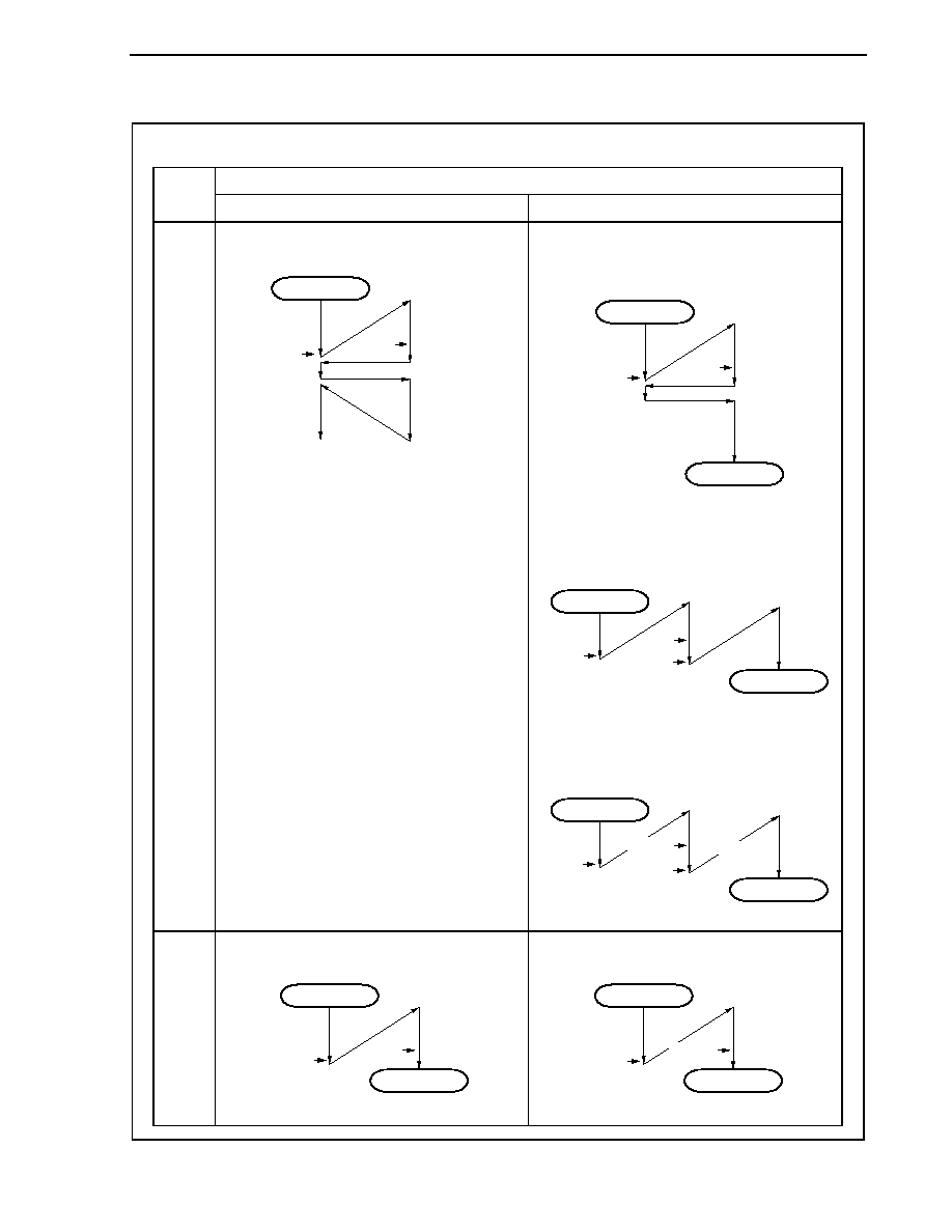
CHAPTER 19 INTERRUPT/EXCEPTION PROCESSING FUNCTION
Preliminary User's Manual U17714EJ1V0UD
655
Figure 19-1. Non-Maskable Interrupt Request Signal Acknowledgment Operation (2/2)
(b) Non-maskable interrupt request signal generated during non-maskable interrupt servicing
Non-maskable
interrupt being
serviced
Non-maskable interrupt request signal generated during non-maskable interrupt servicing
NMI
INTWDT2
NMI
� NMI request generated during NMI servicing
� INTWDT2 request generated during NMI servicing
(NP bit = 1 retained before INTWDT2 request)
Main routine
NMI
request
NMI servicing
(Held pending)
Servicing of
pending NMI
NMI
request
Main routine
System reset
NMI
request
NMI servicing
(Held pending)
INTWDT2
servicing
INTWDT2
request
� INTWDT2 request generated during NMI servicing
(NP bit = 0 set before INTWDT2 request)
Main routine
System reset
NMI
request
NMI
servicing
INTWDT2
servicing
INTWDT2
request
NP = 0
� INTWDT2 request generated during NMI servicing
(NP = 0 set after INTWDT2 request)
Main routine
System reset
NMI
request
NMI
servicing
INTWDT2
servicing
NP = 0
� INTWDT2 request generated during INTWDT2 servicing
Main routine
System reset
INTWDT2 request
INTWDT2 servicing
(Invalid)
� NMI request generated during INTWDT2 servicing
INTWDT2
Main routine
System reset
INTWDT2 request
INTWDT2 servicing
(Invalid)
NMI
request
(Held pending)
INTWDT2
request
INTWDT2
request
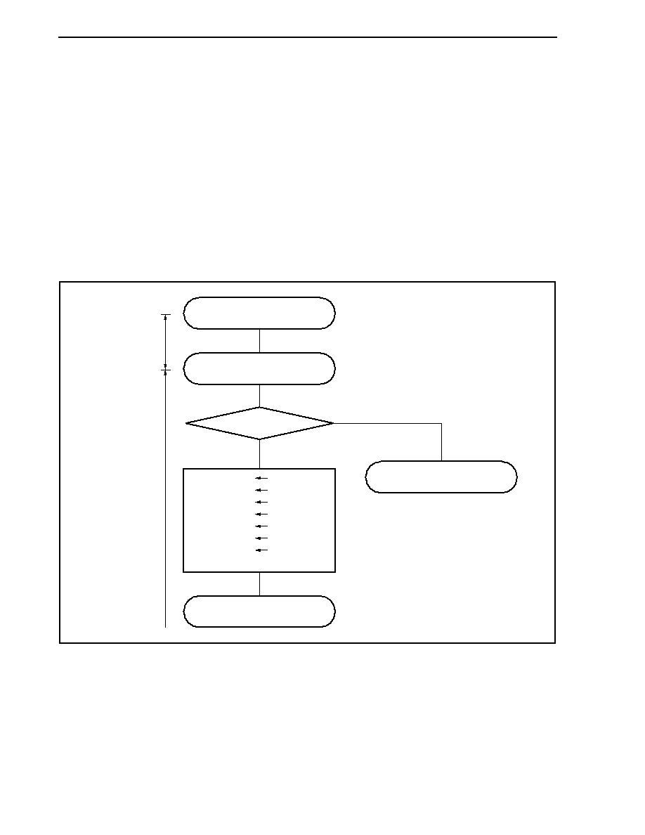
CHAPTER 19 INTERRUPT/EXCEPTION PROCESSING FUNCTION
Preliminary User's Manual U17714EJ1V0UD
656
19.2.1 Operation
If a non-maskable interrupt request signal is generated, the CPU performs the following processing, and transfers
control to the handler routine.
<1> Saves the restored PC to FEPC.
<2> Saves the current PSW to FEPSW.
<3> Writes exception code (0010H, 0020H) to the higher halfword (FECC) of ECR.
<4> Sets the PSW.NP and PSW.ID bits to 1 and clears the PSW.EP bit to 0.
<5> Sets the handler address (00000010H, 00000020H) corresponding to the non-maskable interrupt to the PC,
and transfers control.
The servicing configuration of a non-maskable interrupt is shown below.
Figure 19-2. Servicing Configuration of Non-Maskable Interrupt
PSW.NP
FEPC
FEPSW
ECR.FECC
PSW.NP
PSW.EP
PSW.ID
PC
Restored PC
PSW
0010H, 0020H
1
0
1
00000010H,
00000020H
1
0
NMI input
Non-maskable interrupt request
Interrupt servicing
Interrupt request held pending
INTC
acknowledged
CPU processing
CHAPTER 19 INTERRUPT/EXCEPTION PROCESSING FUNCTION
Preliminary User's Manual U17714EJ1V0UD
657
19.2.2 Restore
(1) From NMI pin input
Execution is restored from the NMI servicing by the RETI instruction.
When the RETI instruction is executed, the CPU performs the following processing, and transfers control to the
address of the restored PC.
<1> Loads the restored PC and PSW from FEPC and FEPSW, respectively, because the PSW.EP bit is 0 and
the PSW.NP bit is 1.
<2> Transfers control back to the address of the restored PC and PSW.
The processing of the RETI instruction is shown below.
Figure 19-3. RETI Instruction Processing
PSW.EP
RETI instruction
PSW.NP
Original processing restored
1
1
0
0
PC
PSW
EIPC
EIPSW
PC
PSW
FEPC
FEPSW
Caution When the EP and NP bits are changed by the LDSR instruction during non-maskable interrupt
servicing, in order to restore the PC and PSW correctly during recovery by the RETI
instruction, it is necessary to set the EP bit back to 0 and the NP bit back to 1 using the LDSR
instruction immediately before the RETI instruction.
Remark The solid line shows the CPU processing flow.
CHAPTER 19 INTERRUPT/EXCEPTION PROCESSING FUNCTION
Preliminary User's Manual U17714EJ1V0UD
658
(2) From INTWDT2 signal
Restoring from non-maskable interrupt servicing executed by the non-maskable interrupt request (INTWDT2)
by using the RETI instruction is disabled. Execute the following software reset processing.
Figure 19-4. Software Reset Processing
INTWDT2 occurs.
FEPC
Software reset processing address
FEPSW
Value that sets NP bit = 1, EP bit = 0
RETI
RETI 10 times (FEPC and FEPSW
Note
must be set.)
PSW
PSW default value setting
Initialization processing
INTWDT2 servicing routine
Software reset processing routine
Note FEPSW
Value that sets NP bit = 1, EP bit = 0
19.2.3 NP flag
The NP flag is a status flag that indicates that non-maskable interrupt servicing is under execution.
This flag is set when a non-maskable interrupt request signal has been acknowledged, and masks non-maskable
interrupt requests to prohibit multiple interrupts from being acknowledged.
0
NP
EP
ID SAT CY
OV
S
Z
PSW
No NMI interrupt servicing
NMI interrupt currently being serviced
NP
0
1
NMI interrupt servicing status
After reset: 00000020H

CHAPTER 19 INTERRUPT/EXCEPTION PROCESSING FUNCTION
Preliminary User's Manual U17714EJ1V0UD
659
19.3 Maskable Interrupts
Maskable interrupt request signals can be masked by interrupt control registers. The V850ES/JJ2 has 69
maskable interrupt sources.
If two or more maskable interrupt request signals are generated at the same time, they are acknowledged
according to the default priority. In addition to the default priority, eight levels of priorities can be specified by using
the interrupt control registers (programmable priority control).
When an interrupt request signal has been acknowledged, the acknowledgment of other maskable interrupt
request signals is disabled and the interrupt disabled (DI) status is set.
When the EI instruction is executed in an interrupt service routine, the interrupt enabled (EI) status is set, which
enables servicing of interrupts having a higher priority than the interrupt request signal in progress (specified by the
interrupt control register). Note that only interrupts with a higher priority will have this capability; interrupts with the
same priority level cannot be nested.
To enable multiple interrupts, however, save EIPC and EIPSW to memory or general-purpose registers before
executing the EI instruction, and execute the DI instruction before the RETI instruction to restore the original values of
EIPC and EIPSW.
19.3.1 Operation
If a maskable interrupt occurs, the CPU performs the following processing, and transfers control to a handler
routine.
<1> Saves the restored PC to EIPC.
<2> Saves the current PSW to EIPSW.
<3> Writes an exception code to the lower halfword of ECR (EICC).
<4> Sets the PSW. ID bit to 1 and clears the PSW. EP bit to 0.
<5> Sets the handler address corresponding to each interrupt to the PC, and transfers control.
The maskable interrupt request signal masked by INTC and the maskable interrupt request signal generated while
another interrupt is being serviced (while the PSW.NP bit = 1 or the PSW.ID bit = 1) are held pending inside INTC. In
this case, servicing a new maskable interrupt is started in accordance with the priority of the pending maskable
interrupt request signal if either the maskable interrupt is unmasked or the NP and ID bits are cleared to 0 by using the
RETI or LDSR instruction.
How maskable interrupts are serviced is illustrated below.
CHAPTER 19 INTERRUPT/EXCEPTION PROCESSING FUNCTION
Preliminary User's Manual U17714EJ1V0UD
660
Figure 19-5. Maskable Interrupt Servicing
INT input
xxIF = 1
No
xxMK = 0
No
Is the interrupt
mask released?
Yes
Yes
No
No
No
Maskable interrupt request
Interrupt request held pending
PSW.NP
PSW.ID
1
1
Interrupt request held pending
0
0
Interrupt servicing
CPU processing
INTC acknowledged
Yes
Yes
Yes
Priority higher than
that of interrupt currently
being serviced?
Priority higher
than that of other interrupt
request?
Highest default
priority of interrupt requests
with the same priority?
EIPC
EIPSW
ECR.EICC
PSW.EP
PSW.ID
Corresponding
bit of ISPR
Note
PC
Restored PC
PSW
Exception code
0
1
1
Handler address
Interrupt requested?
Note For the ISPR register, see 19.3.6 In-service priority register (ISPR).
CHAPTER 19 INTERRUPT/EXCEPTION PROCESSING FUNCTION
Preliminary User's Manual U17714EJ1V0UD
661
19.3.2 Restore
Recovery from maskable interrupt servicing is carried out by the RETI instruction.
When the RETI instruction is executed, the CPU performs the following processing, and transfers control to the
address of the restored PC.
<1> Loads the restored PC and PSW from EIPC and EIPSW, respectively, because the PSW.EP bit is 0 and the
PSW.NP bit is 0.
<2> Transfers control back to the address of the restored PC and PSW.
The processing of the RETI instruction is shown below.
Figure 19-6. RETI Instruction Processing
PSW.EP
RETI instruction
PSW.NP
Restores original processing
1
1
0
0
PC
PSW
Corresponding
bit of ISPR
Note
EIPC
EIPSW
0
PC
PSW
FEPC
FEPSW
Note For the ISPR register, see 19.3.6 In-service priority register (ISPR).
Caution When the EP and NP bits are changed by the LDSR instruction during maskable interrupt
servicing, in order to restore the PC and PSW correctly during recovery by the RETI
instruction, it is necessary to set the EP bit back to 0 and the NP bit back to 0 using the LDSR
instruction immediately before the RETI instruction.
Remark The solid line shows the CPU processing flow.

CHAPTER 19 INTERRUPT/EXCEPTION PROCESSING FUNCTION
Preliminary User's Manual U17714EJ1V0UD
662
19.3.3 Priorities of maskable interrupts
The INTC performs multiple interrupt servicing in which an interrupt is acknowledged while another interrupt is
being serviced. Multiple interrupts can be controlled by priority levels.
There are two types of priority level control: control based on the default priority levels, and control based on the
programmable priority levels that are specified by the interrupt priority level specification bit (xxPRn) of the interrupt
control register (xxICn). When two or more interrupts having the same priority level specified by the xxPRn bit are
generated at the same time, interrupt request signals are serviced in order depending on the priority level allocated to
each interrupt request type (default priority level) beforehand. For more information, see Table 19-1 Interrupt
Source List. The programmable priority control customizes interrupt request signals into eight levels by setting the
priority level specification flag.
Note that when an interrupt request signal is acknowledged, the PSW.ID flag is automatically set to 1. Therefore,
when multiple interrupts are to be used, clear the ID flag to 0 beforehand (for example, by placing the EI instruction in
the interrupt service program) to set the interrupt enable mode.
Remark xx: Identification name of each peripheral unit (see Table 19-2 Interrupt Control Register (xxICn))
n: Peripheral unit number (see Table 19-2 Interrupt Control Register (xxICn)).
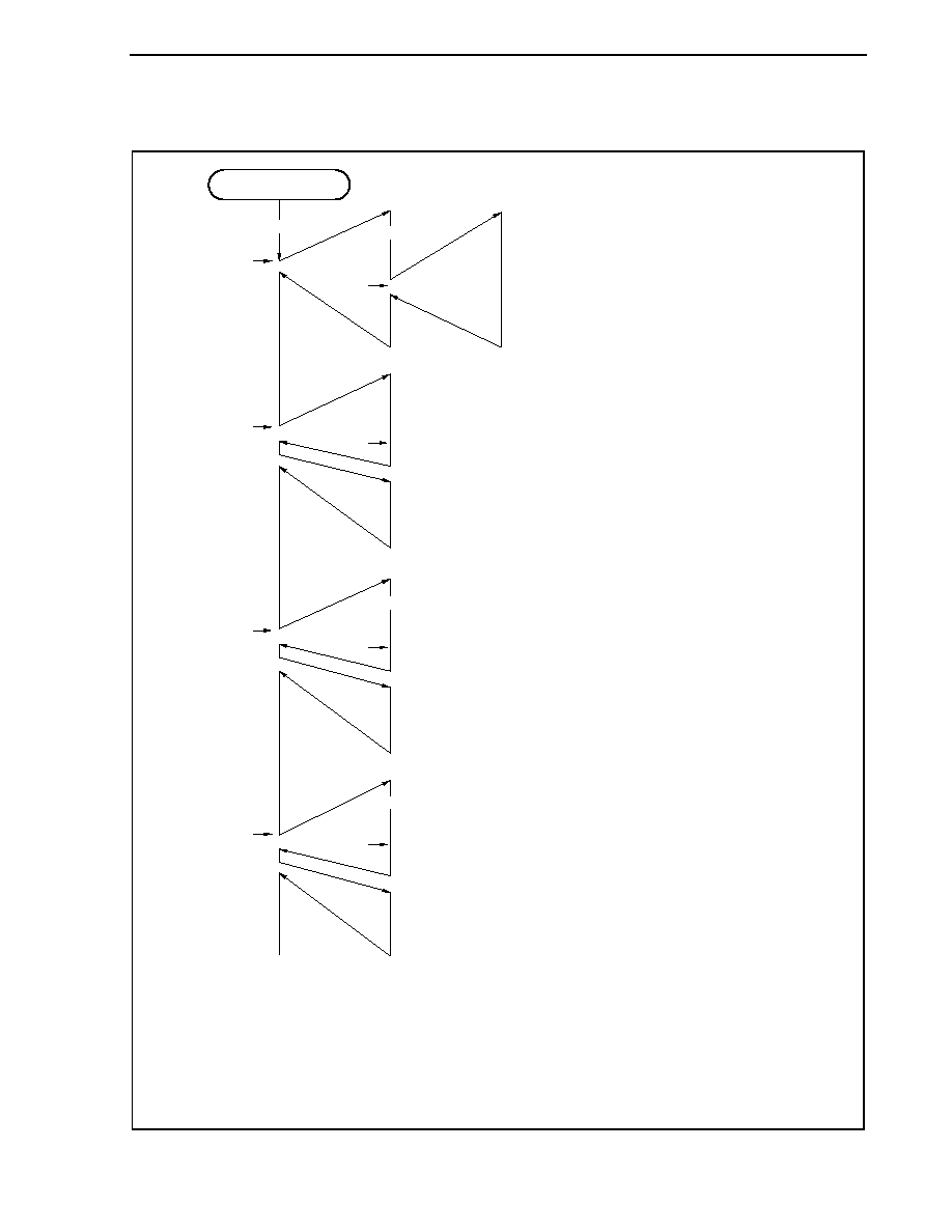
CHAPTER 19 INTERRUPT/EXCEPTION PROCESSING FUNCTION
Preliminary User's Manual U17714EJ1V0UD
663
Figure 19-7. Example of Processing in Which Another Interrupt Request Signal Is Issued
While an Interrupt Is Being Serviced (1/2)
Main routine
EI
EI
Interrupt request a
(level 3)
Servicing of a
Servicing of b
Servicing of c
Interrupt request c
(level 3)
Servicing of d
Servicing of e
EI
Interrupt request e
(level 2)
Servicing of f
EI
Servicing of g
Interrupt request g
(level 1)
Interrupt request h
(level 1)
Servicing of h
Interrupt request b is acknowledged because the
priority of b is higher than that of a and interrupts are
enabled.
Although the priority of interrupt request d is higher
than that of c, d is held pending because interrupts
are disabled.
Interrupt request f is held pending even if interrupts are
enabled because its priority is lower than that of e.
Interrupt request h is held pending even if interrupts are
enabled because its priority is the same as that of g.
Interrupt
request b
(level 2)
Interrupt request d
(level 2)
Interrupt request f
(level 3)
Caution To perform multiple interrupt servicing, the values of the EIPC and EIPSW registers must be
saved before executing the EI instruction. When returning from multiple interrupt servicing,
restore the values of EIPC and EIPSW after executing the DI instruction.
Remarks 1. a to u in the figure are the temporary names of interrupt request signals shown for the sake of
explanation.
2. The default priority in the figure indicates the relative priority between two interrupt request
signals.
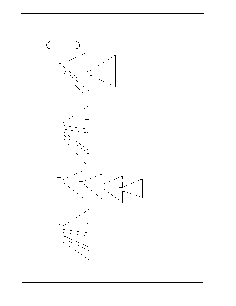
CHAPTER 19 INTERRUPT/EXCEPTION PROCESSING FUNCTION
Preliminary User's Manual U17714EJ1V0UD
664
Figure 19-7. Example of Processing in Which Another Interrupt Request Signal Is Issued
While an Interrupt Is Being Serviced (2/2)
Main routine
EI
Interrupt request i
(level 2)
Servicing of i
Servicing of k
Interrupt
request j
(level 3)
Servicing of j
Interrupt request l
(level 2)
EI
EI
EI
Interrupt request o
(level 3)
Interrupt request s
(level 1)
Interrupt request k
(level 1)
Servicing of l
Servicing of n
Servicing of m
Servicing of s
Servicing of u
Servicing of t
Interrupt
request m
(level 3)
Interrupt request n
(level 1)
Servicing of o
Interrupt
request p
(level 2)
Interrupt
request q
(level 1)
Interrupt
request r
(level 0)
Interrupt request u
(level 2)
Note 2
Interrupt
request t
(level 2)
Note 1
Servicing of p
Servicing of q
Servicing of r
EI
If levels 3 to 0 are acknowledged
Interrupt request j is held pending because its
priority is lower than that of i.
k that occurs after j is acknowledged because it
has the higher priority.
Interrupt requests m and n are held pending
because servicing of l is performed in the interrupt
disabled status.
Pending interrupt requests are acknowledged after
servicing of interrupt request l.
At this time, interrupt request n is acknowledged
first even though m has occurred first because the
priority of n is higher than that of m.
Pending interrupt requests t and u are
acknowledged after servicing of s.
Because the priorities of t and u are the same, u is
acknowledged first because it has the higher
default priority, regardless of the order in which the
interrupt requests have been generated.
Caution To perform multiple interrupt servicing, the values of the EIPC and EIPSW registers must be
saved before executing the EI instruction. When returning from multiple interrupt servicing,
restore the values of EIPC and EIPSW after executing the DI instruction.
Notes 1. Lower default priority
2. Higher
default
priority
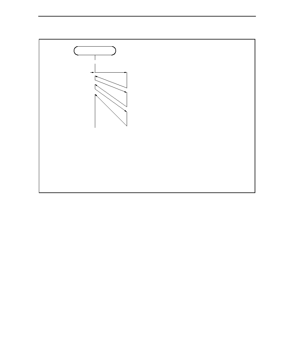
CHAPTER 19 INTERRUPT/EXCEPTION PROCESSING FUNCTION
Preliminary User's Manual U17714EJ1V0UD
665
Figure 19-8. Example of Servicing Interrupt Request Signals Simultaneously Generated
Default priority
a > b > c
Main routine
EI
Interrupt request a (level 2)
Interrupt request b (level 1)
Interrupt request c (level 1)
Servicing of interrupt request b
.
.
Servicing of interrupt request c
Servicing of interrupt request a
Interrupt request b and c are
acknowledged first according to
their priorities.
Because the priorities of b and c are
the same, b is acknowledged first
according to the default priority.
Caution To perform multiple interrupt servicing, the values of the EIPC and EIPSW registers must be
saved before executing the EI instruction. When returning from multiple interrupt servicing,
restore the values of EIPC and EIPSW after executing the DI instruction.
Remarks 1. a to c in the figure are the temporary names of interrupt request signals shown for the sake of
explanation.
2. The default priority in the figure indicates the relative priority between two interrupt request
signals.
CHAPTER 19 INTERRUPT/EXCEPTION PROCESSING FUNCTION
Preliminary User's Manual U17714EJ1V0UD
666
19.3.4 Interrupt control register (xxICn)
The xxICn register is assigned to each interrupt request signal (maskable interrupt) and sets the control conditions
for each maskable interrupt request.
This register can be read or written in 8-bit or 1-bit units.
Reset sets this register to 47H.
Caution Disable interrupts (DI) or mask the interrupt to read the xxICn.xxIFn bit. If the xxIFn bit is read
while interrupts are enabled (EI) or while the interrupt is unmasked, the correct value may not be
read when acknowledging an interrupt and reading the bit conflict.
xxIFn
Interrupt request not issued
Interrupt request issued
xxIFn
0
1
Interrupt request flag
Note
xxICn
xxMKn
0
0
0
xxPRn2
xxPRn1
xxPRn0
Interrupt servicing enabled
Interrupt servicing disabled (pending)
xxMKn
0
1
Interrupt mask flag
Specifies level 0 (highest).
Specifies level 1.
Specifies level 2.
Specifies level 3.
Specifies level 4.
Specifies level 5.
Specifies level 6.
Specifies level 7 (lowest).
xxPRn2
0
0
0
0
1
1
1
1
Interrupt priority specification bit
xxPRn1
0
0
1
1
0
0
1
1
xxPRn0
0
1
0
1
0
1
0
1
After reset: 47H R/W Address: FFFFF112H to FFFFF1A8H
<6>
<7>
Note The flag xxlFn is reset automatically by the hardware if an interrupt request signal is acknowledged.
Remark xx: Identification name of each peripheral unit (see Table 19-2 Interrupt Control Register (xxICn))
n: Peripheral unit number (see Table 19-2 Interrupt Control Register (xxICn)).
The addresses and bits of the interrupt control registers are as follows.

CHAPTER 19 INTERRUPT/EXCEPTION PROCESSING FUNCTION
Preliminary User's Manual U17714EJ1V0UD
667
Table 19-2. Interrupt Control Register (xxICn) (1/2)
Bit
Address Register
<7>
<6>
5 4 3 2 1 0
FFFFF110H LVIIC
LVIIF
LVIMK
0
0
0
LVIPR2
LVIPR1
LVIPR0
FFFFF112H PIC0
PIF0
PMK0
0
0
0
PPR02
PPR01
PPR00
FFFFF114H PIC1
PIF1
PMK1
0
0
0
PPR12
PPR11
PPR10
FFFFF116H PIC2
PIF2
PMK2
0
0
0
PPR22
PPR21
PPR20
FFFFF118H PIC3
PIF3
PMK3
0
0
0
PPR32
PPR31
PPR30
FFFFF11AH PIC4
PIF4
PMK4
0
0
0
PPR42
PPR41
PPR40
FFFFF11CH PIC5
PIF5
PMK5
0
0
0
PPR52
PPR51
PPR50
FFFFF11EH PIC6
PIF6
PMK6
0
0
0
PPR62
PPR61
PPR60
FFFFF120H PIC7
PIF7
PMK7
0
0
0
PPR72
PPR71
PPR70
FFFFF122H TQ0OVIC TQ0OVIF TQ0OVMK
0
0
0
TQ0OVPR2
TQ0OVPR1
TQ0OVPR0
FFFFF124H TQ0CCIC0
TQ0CCIF0 TQ0CCMK0
0
0
0
TQ0CCPR02
TQ0CCPR01 TQ0CCPR00
FFFFF126H TQ0CCIC1
TQ0CCIF1 TQ0CCMK1
0
0
0
TQ0CCPR12
TQ0CCPR11 TQ0CCPR10
FFFFF128H TQ0CCIC2
TQ0CCIF2 TQ0CCMK2
0
0
0
TQ0CCPR22
TQ0CCPR21 TQ0CCPR20
FFFFF12AH TQ0CCIC3 TQ0CCIF3 TQ0CCMK3
0
0
0
TQ0CCPR32
TQ0CCPR31 TQ0CCPR30
FFFFF12CH TP0OVIC TP0OVIF TP0OVMK
0
0
0
TP0OVPR2
TP0OVPR1
TP0OVPR0
FFFFF12EH TP0CCIC0 TP0CCIF0 TP0CCMK0
0
0
0
TP0CCPR02
TP0CCPR01 TP0CCPR00
FFFFF130H TP0CCIC1 TP0CCIF1 TP0CCMK1
0
0
0
TP0CCPR12
TP0CCPR11 TP0CCPR10
FFFFF132H TP1OVIC TP1OVIF TP1OVMK
0
0
0
TP1OVPR2
TP1OVPR1
TP1OVPR0
FFFFF134H TP1CCIC0 TP1CCIF0 TP1CCMK0
0
0
0
TP1CCPR02
TP1CCPR01 TP1CCPR00
FFFFF136H TP1CCIC1 TP1CCIF1 TP1CCMK1
0
0
0
TP1CCPR12
TP1CCPR11 TP1CCPR10
FFFFF138H TP2OVIC TP2OVIF TP2OVMK
0
0
0
TP2OVPR2
TP2OVPR1
TP2OVPR0
FFFFF13AH TP2CCIC0 TP2CCIF0 TP2CCMK0
0
0
0
TP2CCPR02
TP2CCPR01 TP2CCPR00
FFFFF13CH TP2CCIC1 TP2CCIF1 TP2CCMK1
0
0
0
TP2CCPR12
TP2CCPR11 TP2CCPR10
FFFFF13EH TP3OVIC TP3OVIF TP3OVMK
0
0
0
TP3OVPR2
TP3OVPR1
TP3OVPR0
FFFFF140H TP3CCIC0 TP3CCIF0 TP3CCMK0
0
0
0
TP3CCPR02
TP3CCPR01 TP3CCPR00
FFFFF142H TP3CCIC1 TP3CCIF1 TP3CCMK1
0
0
0
TP3CCPR12
TP3CCPR11 TP3CCPR10
FFFFF144H TP4OVIC TP4OVIF TP4OVMK
0
0
0
TP4OVPR2
TP4OVPR1
TP4OVPR0
FFFFF146H TP4CCIC0 TP4CCIF0 TP4CCMK0
0
0
0
TP4CCPR02
TP4CCPR01 TP4CCPR00
FFFFF148H TP4CCIC1 TP4CCIF1 TP4CCMK1
0
0
0
TP4CCPR12
TP4CCPR11 TP4CCPR10
FFFFF14AH TP5OVIC TP5OVIF TP5OVMK
0
0
0
TP5OVPR2
TP5OVPR1
TP5OVPR0
FFFFF14CH TP5CCIC0 TP5CCIF0 TP5CCMK0
0
0
0
TP5CCPR02
TP5CCPR01 TP5CCPR00
FFFFF14EH TP5CCIC1 TP5CCIF1 TP5CCMK1
0
0
0
TP5CCPR12
TP5CCPR11 TP5CCPR10
FFFFF150H TM0EQIC0
TM0EQIF0 TM0EQMK0
0 0 0
TM0EQPR02
TM0EQPR01 TM0EQPR00
FFFFF152H CB0RIC/
IICIC1
CB0RIF/
IICIF1
CB0RMK/
IICMK1
0 0 0
CB0RPR2/
IICPR12
CB0RPR1/
IICPR11
CB0RPR0/
IICPR10
FFFFF154H CB0TIC CB0TIF
CB0TMK
0 0 0
CB0TPR2
CB0TPR1
CB0TPR0
FFFFF156H CB1RIC CB1RIF
CB1RMK
0 0 0
CB1RPR2
CB1RPR1
CB1RPR0
FFFFF158H CB1TIC CB1TIF
CB1TMK
0 0 0
CB1TPR2
CB1TPR1
CB1TPR0
FFFFF15AH CB2RIC CB2RIF
CB2RMK
0 0 0
CB2RPR2
CB2RPR1
CB2RPR0
FFFFF15CH CB2TIC
CB2TIF
CB2TMK
0 0 0
CB2TPR2
CB2TPR1
CB2TPR0
FFFFF15EH CB3RIC CB3RIF
CB3RMK
0 0 0
CB3RPR2
CB3RPR1
CB3RPR0
FFFFF160H CB3TIC CB3TIF
CB3TMK
0 0 0
CB3TPR2
CB3TPR1
CB3TPR0

CHAPTER 19 INTERRUPT/EXCEPTION PROCESSING FUNCTION
Preliminary User's Manual U17714EJ1V0UD
668
Table 19-2. Interrupt Control Register (xxICn) (2/2)
Bit
Address Register
<7>
<6>
5 4 3 2 1 0
FFFFF162H UA0RIC/
CB4RIC
UA0RIF/
CB4RIF
UA0RMK/
CB4RMK
0 0 0
UA0RPR2/
CB4RPR2
UA0RPR1/
CB4RPR1
UA0RPR0/
CB4RPR0
FFFFF164H UA0TIC/
CB4TIC
UA0TIF/
CB4TIF
UA0TMK/
CB4TMK
0 0 0
UA0TPR2/
CB4TPR2
UA0TPR1/
CB4TPR1
UA0TPR0/
CB4TPR0
FFFFF166H UA1RIC/
IICIC2
UA1RIF/
IICIF2
UA1RMK/
IICMK2
0 0 0
UA1RPR2/
IICPR22
UA1RPR1/
IICPR21
UA1RPR0/
IICPR20
FFFFF168H UA1TIC UA1TIF
UA1TMK
0 0 0
UA1TPR2
UA1TPR1
UA1TPR0
FFFFF16AH UA2RIC/
IICIC0
UA2RIF/
IICIF0
UA2RMK/
IICMK0
0 0 0
UA2RPR2/
IICPR02
UA2RPR1/
IICPR01
UA2RPR0/
IICPR00
FFFFF16CH UA2TIC
UA2TIF
UA2TMK
0 0 0
UA2TPR2
UA2TPR1
UA2TPR0
FFFFF16EH ADIC
ADIF
ADMK
0
0
0 ADPR2 ADPR1 ADPR0
FFFFF170H DMAIC0 DMAIF0 DMAMK0
0 0 0
DMAPR02
DMAPR01
DMAPR00
FFFFF172H DMAIC1 DMAIF1 DMAMK1
0 0 0
DMAPR12
DMAPR11
DMAPR10
FFFFF174H DMAIC2 DMAIF2 DMAMK2
0 0 0
DMAPR22
DMAPR21
DMAPR20
FFFFF176H DMAIC3 DMAIF3 DMAMK3
0 0 0
DMAPR32
DMAPR31
DMAPR30
FFFFF178H KRIC
KRIF
KRMK
0
0
0 KRPR2 KRPR1 KRPR0
FFFFF17AH
WTIIC
WTIIF
WTIMK 0 0 0
WTIPR2
WTIPR1
WTIPR0
FFFFF17CH
WTIC
WTIF
WTMK 0 0 0
WTPR2
WTPR1
WTPR0
FFFFF18EH
PIC8
PIF8
PMK8 0 0 0
PPR82
PPR81
PPR80
FFFFF190H
TP6OVIC
TP6OVIF
TP6OVMK
0 0 0
TP6OVPR2
TP6OVPR1
TP6OVPR0
FFFFF192H TP6CCIC0 TP6CCIF0 TP6CCMK0
0 0 0
TP6CCPR02 TP6CCPR01
TP6CCPR00
FFFFF194H TP6CCIC1 TP6CCIF1 TP6CCMK1
0 0 0
TP6CCPR12 TP6CCPR11
TP6CCPR10
FFFFF196H
TP7OVIC
TP7OVIF
TP7OVMK
0 0 0
TP7OVPR2
TP7OVPR1
TP7OVPR0
FFFFF198H TP7CCIC0 TP7CCIF0 TP7CCMK0
0 0 0
TP7CCPR02 TP7CCPR01
TP7CCPR00
FFFFF19AH TP7CCIC1 TP7CCIF1 TP7CCMK1
0 0 0
TP7CCPR12 TP7CCPR11
TP7CCPR10
FFFFF19CH
TP8OVIC
TP8OVIF
TP8OVMK
0 0 0
TP8OVPR2
TP8OVPR1
TP8OVPR0
FFFFF19EH TP8CCIC0 TP8CCIF0 TP8CCMK0
0 0 0
TP8CCPR02 TP8CCPR01
TP8CCPR00
FFFFF1A0H TP8CCIC1 TP8CCIF1
TP8CCMK1
0 0 0
TP8CCPR12 TP8CCPR11
TP8CCPR10
FFFFF1A2H
CB5RIC
CB5RIF
CB5RMK
0 0 0
CB5RPR2
CB5RPR1
CB5RPR0
FFFFF1A4H
CB5TIC
CB5TIF
CB5TMK
0 0 0
CB5TPR2
CB5TPR1
CB5TPR0
FFFFF1A6H
UA3RIC
UA3RIF
UA3RMK
0 0 0
UA3RPR2
UA3RPR1
UA3RPR0
FFFFF1A8H UA3TIC
UA3TIF
UA3TMK
0 0 0
UA3TPR2
UA3TPR1
UA3TPR0
19.3.5 Interrupt mask registers 0 to 4 (IMR0 to IMR4)
The IMR0 to IMR4 registers set the interrupt mask state for the maskable interrupts. The xxMKn bit of the IMR0 to
IMR4 registers is equivalent to the xxICn.xxMKn bit.
The IMRm register can be read or written in 16-bit units (m = 0 to 4).
If the higher 8 bits of the IMRm register are used as an IMRmH register and the lower 8 bits as an IMRmL register,
these registers can be read or written in 8-bit or 1-bit units (m = 0 to 4).
Reset sets these registers to FFFFH.
Caution The device file defines the xxICn.xxMKn bit as a reserved word. If a bit is manipulated using the
name of xxMKn, the contents of the xxICn register, instead of the IMRm register, are rewritten (as
a result, the contents of the IMRm register are also rewritten).
CHAPTER 19 INTERRUPT/EXCEPTION PROCESSING FUNCTION
Preliminary User's Manual U17714EJ1V0UD
669
TP0CCMK0
PMK6
IMR0 (IMR0H
Note
)
IMR0L
TP0OVMK
PMK5
TQ0CCMK3
PMK4
TQ0CCMK2
PMK3
TQ0CCMK1
PMK2
TQ0CCMK0
PMK1
TQ0OVMK
PMK0
PMK7
LVIMK
After reset: FFFFH R/W Address: IMR0 FFFFF100H,
IMR0L FFFFF100H, IMR0H FFFFF101H
After reset: FFFFH R/W Address: IMR1 FFFFF102H,
IMR1L FFFFF102H, IMR1H FFFFF103H
After reset: FFFFH R/W Address: IMR2 FFFFF104H,
IMR2L FFFFF104H, IMR2H FFFFF105H
TP5CCMK1
TP3OVMK
IMR1 (IMR1H
Note
)
IMR1L
TP5CCMK0
TP2CCMK1
TP5OVMK
TP2CCMK0
TP4CCMK1
TP2OVMK
TP4CCMK0
TP1CCMK1
TP4OVMK
TP1CCMK0
TP3CCMK1
TP1OVMK
TP3CCMK0
TP0CCMK1
ADMK
CB3RMK
CB3TMK
TM0EQMK0
xxMKn
0
1
Interrupt servicing enabled
Interrupt servicing disabled
IMR2 (IMR2H
Note
)
IMR2L
UA2TMK
CB2TMK CB2RMK
UA1TMK
CB1TMK CB1RMK CB0TMK
UA0TMK/
CB4TMK
UA2RMK/
IICMK0
UA0RMK/
CB4RMK
CB0RMK/
IICMK1
8
9
10
11
12
13
14
15
1
2
3
4
5
6
7
0
PMK8
IMR3 (IMR3H
Note
)
IMR3L
1
WTMK
1
WTIMK
1
KRMK
1
DMAMK3 DMAMK2 DMAMK1 DMAMK0
After reset: FFFFH R/W Address: IMR3 FFFFF106H,
IMR3L FFFFF106H, IMR3H FFFFF107H
8
1
9
1
10
1
11
12
13
14
15
1
2
3
4
5
6
7
1
0
8
9
10
11
12
13
14
15
1
2
3
4
5
6
7
0
8
9
10
11
12
13
Setting of interrupt mask flag
14
15
1
2
3
4
5
6
7
0
UA1RMK/
IIC2MK
1
IMR4 (IMR4H
Note
)
IMR4L
1
TP8OVMK
1
TP7CCMK1
UA3TMK
TP7CCMK0
UA3RMK
TP7OVMK TP6CCMK1 TP6CCMK0 TP6OVMK
After reset: FFFFH R/W Address: IMR4 FFFFF108H,
IMR4L FFFFF108H, IMR4H FFFFF109H
8
TP8CCMK1
9
CB5RMK
10
CB5TMK
11
12
13
14
15
1
2
3
4
5
6
7
TP8CCMK0
0
Note To read bits 8 to 15 of the IMR0 to IMR4 registers in 8-bit or 1-bit units, specify them as bits 0 to 7 of
IMR0H to IMR4H registers.
Caution Set bits 13 to 15 of the IMR4 register and bits 7 to 14 of the IMR3 register to 1. If the setting of
these bits is changed, the operation is not guaranteed.
Remark xx: Identification name of each peripheral unit (see Table 19-2 Interrupt Control Register
(xxICn)).
n: Peripheral unit number (see Table 19-2 Interrupt Control Register (xxICn))
CHAPTER 19 INTERRUPT/EXCEPTION PROCESSING FUNCTION
Preliminary User's Manual U17714EJ1V0UD
670
19.3.6 In-service priority register (ISPR)
The ISPR register holds the priority level of the maskable interrupt currently acknowledged. When an interrupt
request signal is acknowledged, the bit of this register corresponding to the priority level of that interrupt request signal
is set to 1 and remains set while the interrupt is serviced.
When the RETI instruction is executed, the bit corresponding to the interrupt request signal having the highest
priority is automatically reset to 0 by hardware. However, it is not reset to 0 when execution is returned from non-
maskable interrupt servicing or exception processing.
This register is read-only, in 8-bit or 1-bit units.
Reset sets this register to 00H.
Caution If an interrupt is acknowledged while the ISPR register is being read in the interrupt enabled (EI)
status, the value of the ISPR register after the bits of the register have been set by
acknowledging the interrupt may be read. To accurately read the value of the ISPR register
before an interrupt is acknowledged, read the register while interrupts are disabled (DI).
ISPR7
Interrupt request signal with priority n not acknowledged
Interrupt request signal with priority n acknowledged
ISPRn
0
1
Priority of interrupt currently acknowledged
ISPR
ISPR6
ISPR5
ISPR4
ISPR3
ISPR2
ISPR1
ISPR0
After reset: 00H R Address: FFFFF1FAH
<7>
<6>
<5>
<4>
<3>
<2>
<1>
<0>
Remark n = 0 to 7 (priority level)
CHAPTER 19 INTERRUPT/EXCEPTION PROCESSING FUNCTION
Preliminary User's Manual U17714EJ1V0UD
671
19.3.7 ID flag
This flag controls the maskable interrupt's operating state, and stores control information regarding enabling or
disabling of interrupt request signals. An interrupt disable flag (ID) is assigned to the PSW.
Reset sets this flag to 00000020H.
0
NP
EP
ID SAT CY
OV
S
Z
PSW
Maskable interrupt request signal acknowledgment enabled
Maskable interrupt request signal acknowledgment disabled (pending)
ID
0
1
Specification of maskable interrupt servicing
Note
After reset: 00000020H
Note Interrupt disable flag (ID) function
This bit is set to 1 by the DI instruction and cleared to 0 by the EI instruction. Its value is also modified by
the RETI instruction or LDSR instruction when referencing the PSW.
Non-maskable interrupt request signals and exceptions are acknowledged regardless of this flag. When
a maskable interrupt request signal is acknowledged, the ID flag is automatically set to 1 by hardware.
The interrupt request signal generated during the acknowledgment disabled period (ID flag = 1) is
acknowledged when the xxICn.xxIFn bit is set to 1, and the ID flag is cleared to 0.
19.3.8 Watchdog timer mode register 2 (WDTM2)
This register can be read or written in 8-bit units (for details, see CHAPTER 11 FUNCTIONS OF WATCHDOG
TIMER 2).
Reset sets this register to 67H.
0
WDTM2
WDM21
WDM20
0
0
0
0
0
After reset: 67H R/W Address: FFFFF6D0H
Stops operation
Non-maskable interrupt request mode
Reset mode (initial-value)
WDM21
0
0
1
WDM20
0
1
�
Selection of watchdog timer operation mode
CHAPTER 19 INTERRUPT/EXCEPTION PROCESSING FUNCTION
Preliminary User's Manual U17714EJ1V0UD
672
19.4 Software Exception
A software exception is generated when the CPU executes the TRAP instruction, and can always be
acknowledged.
19.4.1 Operation
If a software exception occurs, the CPU performs the following processing, and transfers control to the handler
routine.
<1> Saves the restored PC to EIPC.
<2> Saves the current PSW to EIPSW.
<3> Writes an exception code to the lower 16 bits (EICC) of ECR (interrupt source).
<4> Sets the PSW.EP and PSW.ID bits to 1.
<5> Sets the handler address (00000040H or 00000050H) corresponding to the software exception to the PC,
and transfers control.
The processing of a software exception is shown below.
Figure 19-9. Software Exception Processing
TRAP instruction
EIPC
EIPSW
ECR.EICC
PSW.EP
PSW.ID
PC
Restored PC
PSW
Exception code
1
1
Handler address
CPU processing
Exception processing
Note
Note TRAP instruction format: TRAP vector (the vector is a value from 00H to 1FH.)
The handler address is determined by the TRAP instruction's operand (vector). If the vector is 00H to 0FH, it
becomes 00000040H, and if the vector is 10H to 1FH, it becomes 00000050H.
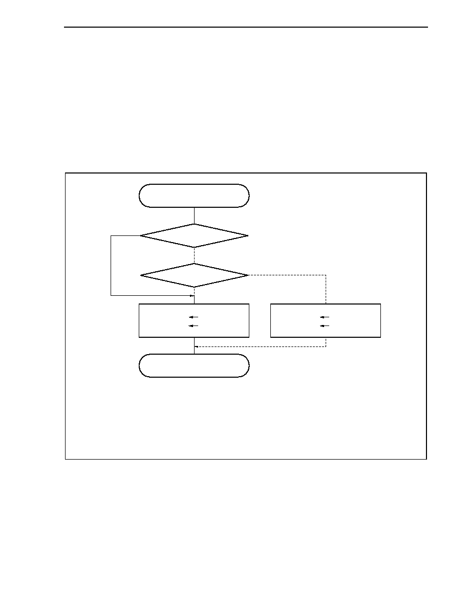
CHAPTER 19 INTERRUPT/EXCEPTION PROCESSING FUNCTION
Preliminary User's Manual U17714EJ1V0UD
673
19.4.2 Restore
Recovery from software exception processing is carried out by the RETI instruction.
By executing the RETI instruction, the CPU carries out the following processing and shifts control to the restored
PC's address.
<1> Loads the restored PC and PSW from EIPC and EIPSW because the PSW.EP bit is 1.
<2> Transfers control to the address of the restored PC and PSW.
The processing of the RETI instruction is shown below.
Figure 19-10. RETI Instruction Processing
PSW.EP
RETI instruction
PC
PSW
EIPC
EIPSW
PSW.NP
Original processing restored
PC
PSW
FEPC
FEPSW
1
1
0
0
Caution When the EP and NP bits are changed by the LDSR instruction during the software exception
processing, in order to restore the PC and PSW correctly during recovery by the RETI
instruction, it is necessary to set the EP bit back to 1 and the NP bit back to 0 using the LDSR
instruction immediately before the RETI instruction.
Remark The solid line shows the CPU processing flow.
CHAPTER 19 INTERRUPT/EXCEPTION PROCESSING FUNCTION
Preliminary User's Manual U17714EJ1V0UD
674
19.4.3 EP flag
The EP flag is a status flag used to indicate that exception processing is in progress. It is set when an exception
occurs.
0
NP
EP
ID SAT CY
OV
S
Z
PSW
Exception processing not in progress.
Exception processing in progress.
EP
0
1
Exception processing status
After reset: 00000020H
CHAPTER 19 INTERRUPT/EXCEPTION PROCESSING FUNCTION
Preliminary User's Manual U17714EJ1V0UD
675
19.5 Exception Trap
An exception trap is an interrupt that is requested when the illegal execution of an instruction takes place. In the
V850ES/JJ2, an illegal opcode exception (ILGOP: Illegal Opcode Trap) is considered as an exception trap.
19.5.1 Illegal opcode definition
The illegal instruction has an opcode (bits 10 to 5) of 111111B, a sub-opcode (bits 26 to 23) of 0111B to 1111B,
and a sub-opcode (bit 16) of 0B. An exception trap is generated when an instruction applicable to this illegal
instruction is executed.
15
16
23 22
x x x x x x 0
x
x
x
x
x
x
x
x
x
x
1
1
1
1
1
1
x
x
x
x
x
27 26
31
0
4
5
10
11
1
1
1
1
1
1
0
1
to
x: Arbitrary
Caution Since it is possible to assign this instruction to an illegal opcode in the future, it is recommended
that it not be used.
(1) Operation
If an exception trap occurs, the CPU performs the following processing, and transfers control to the handler
routine.
<1> Saves the restored PC to DBPC.
<2> Saves the current PSW to DBPSW.
<3> Sets the PSW.NP, PSW.EP, and PSW.ID bits to 1.
<4> Sets the handler address (00000060H) corresponding to the exception trap to the PC, and transfers
control.
The processing of the exception trap is shown below.
Figure 19-11. Exception Trap Processing
Exception trap (ILGOP) occurs
DBPC
DBPSW
PSW.NP
PSW.EP
PSW.ID
PC
Restored PC
PSW
1
1
1
00000060H
Exception processing
CPU processing
CHAPTER 19 INTERRUPT/EXCEPTION PROCESSING FUNCTION
Preliminary User's Manual U17714EJ1V0UD
676
(2) Restore
Recovery from an exception trap is carried out by the DBRET instruction. By executing the DBRET
instruction, the CPU carries out the following processing and controls the address of the restored PC.
<1> Loads the restored PC and PSW from DBPC and DBPSW.
<2> Transfers control to the address indicated by the restored PC and PSW.
Caution DBPC and DBPSW can be accessed only during the interval between the execution of an
illegal opcode and the DBRET instruction.
The restore processing from an exception trap is shown below.
Figure 19-12. Restore Processing from Exception Trap
DBRET instruction
PC
PSW
DBPC
DBPSW
Jump to address of restored PC
CHAPTER 19 INTERRUPT/EXCEPTION PROCESSING FUNCTION
Preliminary User's Manual U17714EJ1V0UD
677
19.5.2 Debug trap
A debug trap is an exception that is generated when the DBTRAP instruction is executed and is always
acknowledged.
(1) Operation
Upon occurrence of a debug trap, the CPU performs the following processing.
<1> Saves restored PC to DBPC.
<2> Saves current PSW to DBPSW.
<3> Sets the PSW.NP, PSW.EP, and PSW.ID bits to 1.
<4> Sets handler address (00000060H) for debug trap to PC and transfers control.
The debug trap processing format is shown below.
Figure 19-13. Debug Trap Processing Format
DBTRAP instruction
DBPC
DBPSW
PSW.NP
PSW.EP
PSW.ID
PC
Restored PC
PSW
1
1
1
00000060H
Exception processing
CPU processing
CHAPTER 19 INTERRUPT/EXCEPTION PROCESSING FUNCTION
Preliminary User's Manual U17714EJ1V0UD
678
(2) Restoration
Restoration from a debug trap is executed with the DBRET instruction.
With the DBRET instruction, the CPU performs the following steps and transfers control to the address of the
restored PC.
<1> The restored PC and PSW are read from DBPC and DBPSW.
<2> Control is transferred to the fetched address of the restored PC and PSW.
Caution DBPC and DBPSW can be accessed only during the interval between the execution of the
DBTRAP instruction and the DBRET instruction.
The processing format for restoration from a debug trap is shown below.
Figure 19-14. Processing Format of Restoration from Debug Trap
DBRET instruction
PC
PSW
DBPC
DBPSW
Jump to address of restored PC

CHAPTER 19 INTERRUPT/EXCEPTION PROCESSING FUNCTION
Preliminary User's Manual U17714EJ1V0UD
679
19.6 External Interrupt Request Input Pins (NMI and INTP0 to INTP8)
19.6.1 Noise elimination
(1) Eliminating noise on NMI pin
The NMI pin has an internal noise elimination circuit that uses analog delay. Therefore, the input level of the
NMI pin is not detected as an edge unless it is maintained for a specific time or longer. Therefore, an edge is
detected after specific time.
The NMI pin can be used to release the STOP mode. In the STOP mode, noise is not eliminated by using the
system clock because the internal system clock is stopped.
(2) Eliminating noise on INTP0 to INTP8 pins
The INTP0 to INTP8 pins have an internal noise elimination circuit that uses analog delay. Therefore, the input
level of the NMI pin is not detected as an edge unless it is maintained for a specific time or longer. Therefore,
an edge is detected after specific time.
19.6.2 Edge detection
The valid edge of each of the NMI and INTP0 to INTP8 pins can be selected from the following four.
� Rising edge
� Falling edge
� Both rising and falling edges
� No edge detected
The edge of the NMI pin is not detected after reset. Therefore, the interrupt request signal is not acknowledged
unless a valid edge is enabled by using the INTF0 and INTR0 register (the NMI pin functions as a normal port pin).
CHAPTER 19 INTERRUPT/EXCEPTION PROCESSING FUNCTION
Preliminary User's Manual U17714EJ1V0UD
680
(1) External interrupt falling, rising edge specification register 0 (INTF0, INTR0)
The INTF0 and INTR0 registers are 8-bit registers that specify detection of the falling and rising edges of the
NMI pin via bit 2 and the external interrupt pins (INTP0 to INTP3) via bits 3 to 6.
These registers can be read or written in 8-bit or 1-bit units.
Reset sets these registers to 00H.
Caution When the function is changed from the external interrupt function (alternate function) to the
port function, an edge may be detected. Therefore, clear the INTF0n and INTR0n bits to 00,
and then set the port mode.
0
INTF0
INTF06
INTP3
INTF05
INTF04
INTF03
INTF02
0
0
After reset: 00H R/W Address: INTF0 FFFFFC00H, INTR0 FFFFFC20H
0
INTR0
INTR06
INTR05
INTR04
INTR03
INTR02
0
0
INTP2
INTP1
INTP0
NMI
INTP3
INTP2
INTP1
INTP0
NMI
Remark For how to specify a valid edge, see Table 19-3.
Table 19-3. Valid Edge Specification
INTF0n
INTR0n
Valid Edge Specification (n = 2 to 6)
0
0
No edge detected
0 1
Rising
edge
1 0
Falling
edge
1
1
Both rising and falling edges
Caution Be sure to clear the INTF0n and INTR0n bits to 00 when these registers are not used as the
NMI or INTP0 to INTP3 pins.
Remark n = 2:
Control of NMI pin
n = 3 to 6: Control of INTP0 to INTP3 pins
CHAPTER 19 INTERRUPT/EXCEPTION PROCESSING FUNCTION
Preliminary User's Manual U17714EJ1V0UD
681
(2) External interrupt falling, rising edge specification register 3 (INTF3, INTR3)
The INTF3 and INTR3 registers are 8-bit registers that specify detection of the falling and rising edges of the
external interrupt pin (INTP7).
These registers can be read or written in 8-bit or 1-bit units.
Reset sets these registers to 00H.
Cautions 1. When the function is changed from the external interrupt function (alternate function) to
the port function, an edge may be detected. Therefore, clear the INTF31 and INTR31 bits
to 00, and then set the port mode.
2. The INTP7 pin and RXDA0 pin are alternate-function pins. When using the pin as the
RXDA0 pin, disable edge detection for the INTP7 alternate-function pin (clear the
INTF3.INTF31 bit and the INRT3.INTR31 bit to 0). When using the pin as the INTP7 pin,
stop UARTA0 reception (clear the UA0CTL0.UA0RXE bit to 0).
INTF3
After reset: 00H R/W Address: INTF3 FFFFFC06H, INTR3 FFFFFC26H
0
0
0
0
0
0
INTF31
0
INTR3
0
0
0
0
0
0
INTR31
0
INTP7
INTP7
Remark For how to specify a valid edge, see Table 19-4.
Table 19-4. Valid Edge Specification
INTF31
INTR31
Valid Edge Specification
0
0
No edge detected
0 1
Rising
edge
1 0
Falling
edge
1
1
Both rising and falling edges
Caution Be sure to clear the INTF31 and INTR31 bits to 00 when these registers are not used as
INTP7 pin.
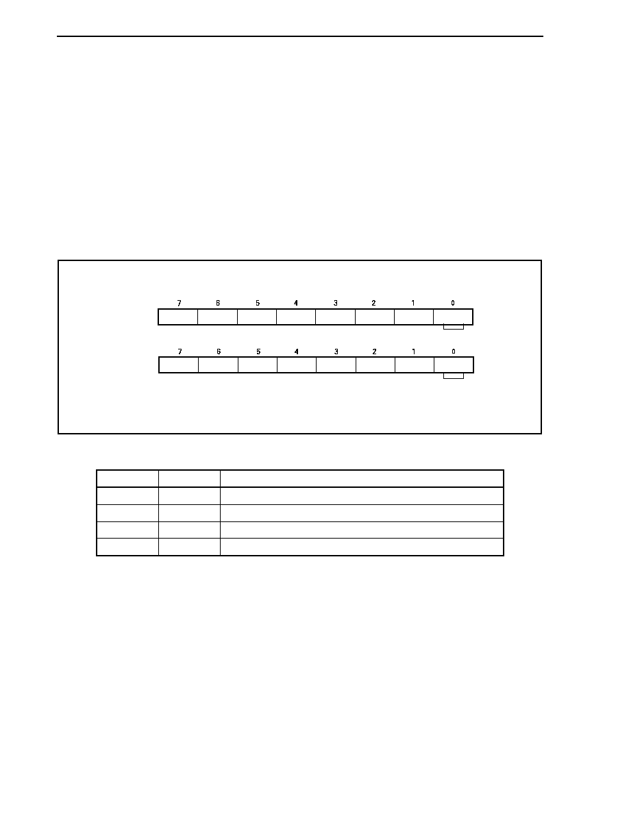
CHAPTER 19 INTERRUPT/EXCEPTION PROCESSING FUNCTION
Preliminary User's Manual U17714EJ1V0UD
682
(3) External interrupt falling, rising edge specification register 8 (INTF8, INTR8)
The INTF8 and INTR8 registers are 8-bit registers that specify detection of the falling and rising edges of the
external interrupt pin (INTP8).
These registers can be read or written in 8-bit or 1-bit units.
Reset sets these registers to 00H.
Cautions 1. When the function is changed from the external interrupt function (alternate function) to
the port function, an edge may be detected. Therefore, clear the INTF80 and INTR80 bits
to 00, and then set the port mode.
2. The INTP8 pin and RXDA3 pin are alternate-function pins. When using the pin as the
RXDA3 pin, disable edge detection for the INTP8 alternate-function pin (clear the
INTF8.INTF80 bit and the INTR8.INTR80 bit to 0). When using the pin as the INTP8 pin,
stop UARTA3 reception (clear the UA3CTL0.UA3RXE bit to 0).
INTF8
After reset: 00H R/W Address: INTF8 FFFFFC10H, INTR8 FFFFFC30H
0
0
0
0
0
0
0
INTF80
INTR8
0
0
0
0
0
0
0
INTR80
INTP8
INTP8
Remark For how to specify a valid edge, see Table 19-5.
Table 19-5. Valid Edge Specification
INTF80
INTR80
Valid Edge Specification
0
0
No edge detected
0 1
Rising
edge
1 0
Falling
edge
1
1
Both rising and falling edges
Caution Be sure to clear the INTF80 and INTR80 bits to 00 when these registers are not used as
INTP8 pin.
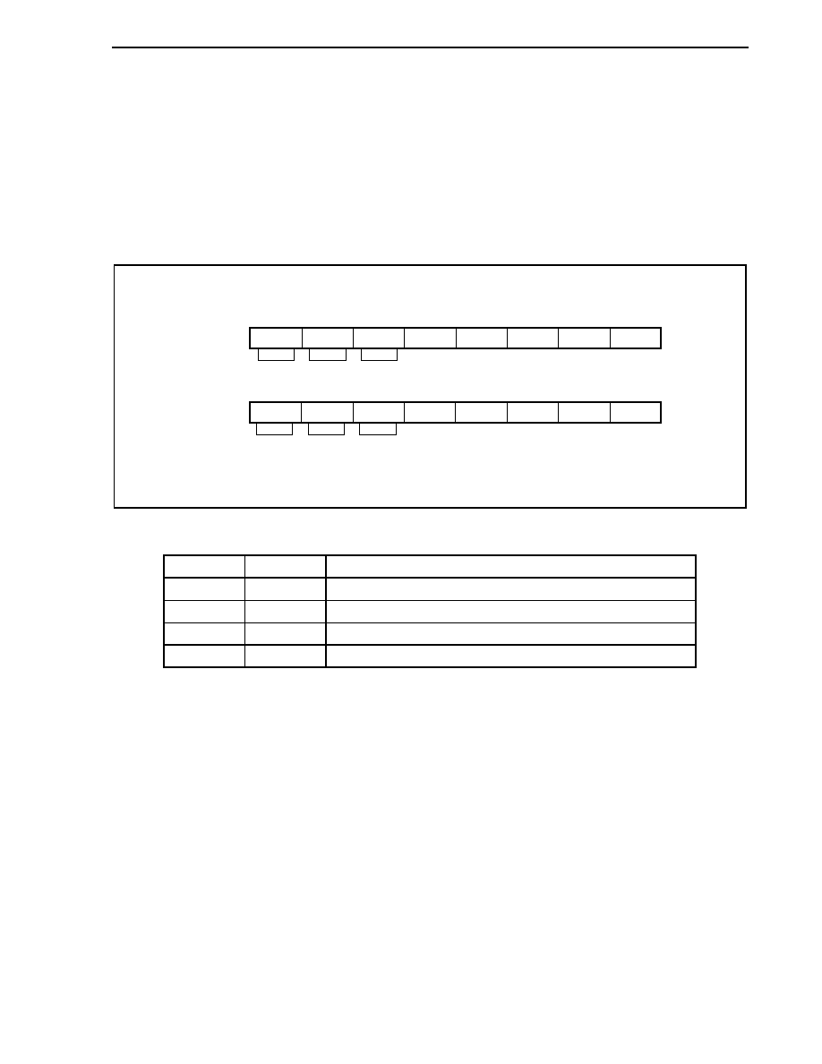
CHAPTER 19 INTERRUPT/EXCEPTION PROCESSING FUNCTION
Preliminary User's Manual U17714EJ1V0UD
683
(4) External interrupt falling, rising edge specification register 9H (INTF9H, INTR9H)
The INTF9H and INTR9H registers are 8-bit registers that specify detection of the falling and rising edges of
the external interrupt pins (INTP4 to INTP6).
These registers can be read or written in 8-bit or 1-bit units.
Reset sets these registers to 00H.
Caution When the function is changed from the external interrupt function (alternate function) to the
port function, an edge may be detected. Therefore, clear the INTF9n and INTR9n bits to 0,
and then set the port mode.
INTF9H
After reset: 00H R/W Address: INTF9H FFFFFC13H, INTR9H FFFFFC33H
INTF915 INTF914
INTF913
0
0
0
0
0
8
9
10
11
12
13
14
15
INTR9H
INTR915 INTR914 INTR913
0
0
0
0
0
8
9
10
11
12
13
14
15
INTP6
INTP5
INTP4
INTP6
INTP5
INTP4
Remark For how to specify a valid edge, see Table 19-6.
Table 19-6. Valid Edge Specification
INTF9n
INTR9n
Valid Edge Specification (n = 13 to 15)
0
0
No edge detected
0 1
Rising
edge
1 0
Falling
edge
1
1
Both rising and falling edges
Caution Be sure to clear the INTF9n and INTR9n bits to 00 when these registers are not used as
INTP4 to INTP6 pins.
Remark n = 13 to 15: Control of INTP4 to INTP6 pins

CHAPTER 19 INTERRUPT/EXCEPTION PROCESSING FUNCTION
Preliminary User's Manual U17714EJ1V0UD
684
(5) Noise elimination control register (NFC)
Digital noise elimination can be selected for the INTP3 pin. The noise elimination settings are performed using
the NFC register.
When digital noise elimination is selected, the sampling clock for digital sampling can be selected from among
f
XX
/64, f
XX
/128, f
XX
/256, f
XX
/512, f
XX
/1,024, and f
XT
. Sampling is performed three times.
When digital noise elimination is selected, if the clock that performs sampling in the standby mode is stopped,
then the INTP3 interrupt request signal cannot be used for releasing the standby mode. When f
XT
is used as
the sampling clock, the INTP3 interrupt request signal can be used for releasing either the subclock operating
mode or the IDLE1/IDLE2/STOP/sub-IDLE mode.
This register can be read or written in 8-bit units.
Reset sets this register to 00H.
Caution After the sampling clock has been changed, it takes 3 sampling clocks to initialize the digital
noise eliminator. Therefore, if an INTP3 valid edge is input within these 3 sampling clocks
after the sampling clock has been changed, an interrupt request signal may be generated.
Therefore, be careful about the following points when using the interrupt and DMA functions.
� When using the interrupt function, after the 3 sampling clocks have elapsed, enable
interrupts after the interrupt request flag (PIC3.PIF3 bit) has been cleared.
� When using the DMA function (started by INTP3), enable DMA after 3 sampling clocks
have elapsed.
NFEN
NFC
0
0
0
0
NFC2
NFC1
NFC0
f
XX
/64
f
XX
/128
f
XX
/256
f
XX
/512
f
XX
/1,024
f
XT
(subclock)
NFC2
0
0
0
0
1
1
Digital sampling clock
Setting prohibited
NFC1
0
0
1
1
0
0
NFC0
0
1
0
1
0
1
After reset: 00H R/W Address: FFFFF318H
Analog noise elimination (60 ns (TYP.))
Digital noise elimination
NFEN
0
1
Settings of INTP3 pin noise elimination
Other than above
Remarks 1. Since sampling is performed three times, the reliably eliminated noise width is 2 sampling clocks.
2. In the case of noise with a width smaller than 2 sampling clocks, an interrupt request signal is
generated if noise synchronized with the sampling clock is input.
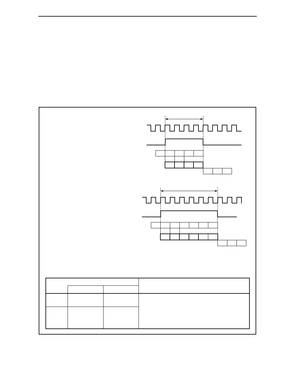
CHAPTER 19 INTERRUPT/EXCEPTION PROCESSING FUNCTION
Preliminary User's Manual U17714EJ1V0UD
685
19.7 Interrupt Acknowledge Time of CPU
Except the following cases, the interrupt acknowledge time of the CPU is 4 clocks minimum. To input interrupt
request signals successively, input the next interrupt request signal at least 5 clocks after the preceding interrupt.
� In IDLE1/IDLE2/STOP mode
� When the external bus is accessed
� When interrupt request non-sampling instructions are successively executed (see 19.8 Periods in Which
Interrupts Are Not Acknowledged by CPU.)
� When the interrupt control register is accessed
Figure 19-15. Pipeline Operation at Interrupt Request Signal Acknowledgment (Outline)
(1) Minimum interrupt response time
IF
ID
EX
Internal clock
Instruction 1
Instruction 2
Interrupt acknowledgment operation
Instruction (first instruction of interrupt servicing routine)
Interrupt request
IF
ID
EX MEM WB
IFX
IDX
INT1 INT2 INT3 INT4
4 system clocks
(2) Maximum interrupt response time
IF
ID
EX
Internal clock
Instruction 1
Instruction 2
Interrupt acknowledgment operation
Instruction (first instruction of interrupt servicing routine)
Interrupt request
IF
ID
EX MEM MEM MEM WB
IFX
IDX
INT1 INT2 INT3 INT3 INT3 INT4
6 system clocks
Remark INT1 to INT4: Interrupt acknowledgment processing
IFX:
Invalid instruction fetch
IDX:
Invalid instruction decode
Interrupt acknowledge time (internal system clock)
Internal interrupt
External interrupt
Condition
Minimum
4
4 +
Analog delay time
Maximum
6
6 +
Analog delay time
The following cases are exceptions.
� In IDLE1/IDLE2/STOP mode
� External bus access
� Two or more interrupt request non-sample instructions are
executed in succession
� Access to peripheral I/O register

CHAPTER 19 INTERRUPT/EXCEPTION PROCESSING FUNCTION
Preliminary User's Manual U17714EJ1V0UD
686
19.8 Periods in Which Interrupts Are Not Acknowledged by CPU
An interrupt is acknowledged by the CPU while an instruction is being executed. However, no interrupt will be
acknowledged between an interrupt request non-sample instruction and the next instruction (interrupt is held pending).
The interrupt request non-sample instructions are as follows.
� EI instruction
� DI instruction
� LDSR reg2, 0x5 instruction (for PSW)
� The store instruction for the PRCMD register
� The store, SET1, NOT1, or CLR1 instructions for the following registers.
� Interrupt-related registers:
Interrupt control register (xxICn), interrupt mask registers 0 to 4 (IMR0 to IMR4)
� Power save control register (PSC)
� On-chip debug mode register (OCDM)
Remark xx: Identification name of each peripheral unit (see Table 19-2 Interrupt Control Register (xxICn))
n: Peripheral unit number (see Table 19-2 Interrupt Control Register (xxICn)).
19.9 Cautions
The NMI pin and P02 pin are an alternate-function pin, and function as a normal port pin after being reset. To
enable the NMI pin, validate the NMI pin with the PMC0 register. The initial setting of the NMI pin is "No edge
detected". Select the NMI pin valid edge using the INTF0 and INTR0 registers.
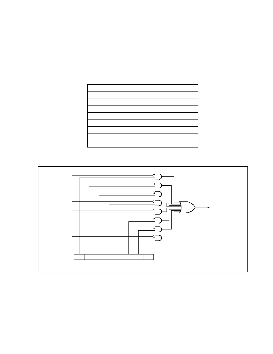
Preliminary User's Manual U17714EJ1V0UD
687
CHAPTER 20 KEY INTERRUPT FUNCTION
20.1 Function
A key interrupt request signal (INTKR) can be generated by inputting a falling edge to the eight key input pins (KR0
to KR7) by setting the KRM register.
Table 20-1. Assignment of Key Return Detection Pins
Flag Pin
Description
KRM0
Controls KR0 signal in 1-bit units
KRM1
Controls KR1 signal in 1-bit units
KRM2
Controls KR2 signal in 1-bit units
KRM3
Controls KR3 signal in 1-bit units
KRM4
Controls KR4 signal in 1-bit units
KRM5
Controls KR5 signal in 1-bit units
KRM6
Controls KR6 signal in 1-bit units
KRM7
Controls KR7 signal in 1-bit units
Figure 20-1. Key Return Block Diagram
INTKR
Key return mode register (KRM)
KRM7 KRM6 KRM5 KRM4 KRM3 KRM2 KRM1 KRM0
KR7
KR6
KR5
KR4
KR3
KR2
KR1
KR0
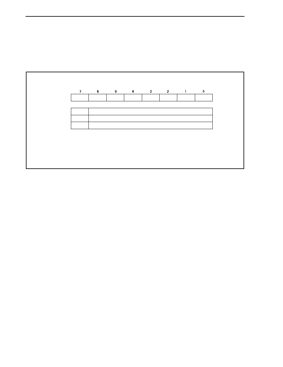
CHAPTER 20 KEY INTERRUPT FUNCTION
Preliminary User's Manual U17714EJ1V0UD
688
20.2 Register
(1) Key return mode register (KRM)
The KRM register controls the KRM0 to KRM7 bits using the KR0 to KR7 signals.
This register can be read or written in 8-bit or 1-bit units.
Reset sets this register to 00H.
KRM7
Does not detect key return signal
Detects key return signal
KRMn
0
1
Control of key return mode
KRM
KRM6
KRM5
KRM4
KRM3
KRM2
KRM1
KRM0
After reset: 00H R/W Address: FFFFF300H
Caution Rewrite the KRM register after once clearing the KRM register to 00H.
Remark For the alternate-function pin settings, see Table 4-19 Using Port Pin as Alternate-
Function Pin.
20.3 Cautions
(1) If a low level is input to any of the KR0 to KR7 pins, the INTKR signal is not generated even if the falling edge
of another pin is input.
(2) The RXDA1 and KR7 pins must not be used at the same time. To use the RXDA1 pin, do not use the KR7 pin.
To use the KR7 pin, do not use the RXDA1 pin (it is recommended to set the PFC91 bit to 1 and clear
PFCE91 bit to 0).
(3) If the KRM register is changed, an interrupt request signal (INTKR) may be generated. To prevent this,
change the KRM register after disabling interrupts (DI) or masking, then clear the interrupt request flag
(KRIC.KRIF bit) to 0, and enable interrupts (EI) or clear the mask.
(4) To use the key interrupt function, be sure to set the port pin to the key return pin and then enable the operation
with the KRM register. To switch from the key return pin to the port pin, disable the operation with the KRM
register and then set the port pin.

Preliminary User's Manual U17714EJ1V0UD
689
CHAPTER 21 STANDBY FUNCTION
21.1 Overview
The power consumption of the system can be effectively reduced by using the standby modes in combination and
selecting the appropriate mode for the application. The available standby modes are listed in Table 21-1.
Table 21-1. Standby Modes
Mode Functional
Outline
HALT mode
Mode in which only the operating clock of the CPU is stopped
IDLE1 mode
Mode in which all the operations of the internal circuits except the oscillator, PLL
Note
, and flash
memory are stopped
IDLE2 mode
Mode in which all the operations of internal circuits except the oscillator are stopped
STOP mode
Mode in which all the operations of internal circuits except the subclock oscillator are stopped
Subclock operation mode
Mode in which the subclock is used as the internal system clock
Sub-IDLE mode
Mode in which all the operations of internal circuits except the oscillator are stopped, in the
subclock operation mode
Note The PLL holds the previous operating status.
CHAPTER 21 STANDBY FUNCTION
Preliminary User's Manual U17714EJ1V0UD
690
Figure 21-1. Status Transition
Reset
Subclock operation mode
(fx operates, PLL operates)
Subclock operation mode
(fx stops, PLL stops)
Sub-IDLE mode
(fx operates, PLL operates)
Sub-IDLE mode
(fx stops, PLL stops)
STOP mode
(fx stops, PLL stops)
IDLE2 mode
(fx operates, PLL stops)
IDLE1 mode
(fx operates, PLL operates)
IDLE1 mode
(fx operates, PLL stops)
HALT mode
(fx operates, PLL stops)
HALT mode
(fx operates, PLL operates)
Normal operation mode
Oscillation
stabilization wait
Clock through mode
(PLL operates)
Clock through mode
(PLL stops)
PLL mode
(PLL operates)
Internal oscillation
clock operation
WDT overflow
Oscillation
stabilization wait
Note
PLL lockup
time wait
Oscillation
stabilization wait
Note
Oscillation
stabilization wait
Note
Note If a WDT overflow occurs during an oscillation stabilization time, the CPU operates on the internal
oscillation clock.
Remark f
X
: Main clock
CHAPTER 21 STANDBY FUNCTION
Preliminary User's Manual U17714EJ1V0UD
691
21.2 Registers
(1) Power save control register (PSC)
The PSC register is an 8-bit register that controls the standby function. The STP bit of this register is used to
specify the STOP mode. This register is a special register that can be written only by the special sequence
combinations (see 3.4.7 Special registers).
This register can be read or written in 8-bit or 1-bit units.
Reset sets this register to 00H.
0
IDLE1, sub-IDLE modes
STOP, sub-IDLE modes
IDLE2, sub-IDLE modes
STOP mode
PSM1
0
0
1
1
Specification of operation in software standby mode
PSMR
0
0
0
0
0
PSM1
PSM0
After reset: 00H R/W Address: FFFFF820H
PSM0
0
1
0
1
< >
< >
Note Standby mode set by STP bit: IDLE1, IDLE2, STOP, or sub-IDLE mode
Cautions 1. Before setting the IDLE1, IDLE2, STOP, or sub-IDLE mode, set the PSMR.PSM1
and PSMR.PSM0 bits and then set the STP bit.
2. Settings of the NMI1M, NMI0M, and INTM bits are invalid when HALT mode is
released.
CHAPTER 21 STANDBY FUNCTION
Preliminary User's Manual U17714EJ1V0UD
692
(2) Power save mode register (PSMR)
The PSMR register is an 8-bit register that controls the operation status in the power save mode and the clock
operation.
This register can be read or written in 8-bit or 1-bit units.
Reset sets this register to 00H.
0
IDLE1, sub-IDLE modes
STOP, sub-IDLE modes
IDLE2, sub-IDLE modes
STOP mode
PSM1
0
0
1
1
Specification of operation in software standby mode
PSMR
0
0
0
0
0
PSM1
PSM0
After reset: 00H R/W Address: FFFFF820H
PSM0
0
1
0
1
< >
< >
Cautions 1. Be sure to clear bits 2 to 7 to "0".
2. The PSM0 and PSM1 bits are valid only when the PSC.STP bit is 1.
Remark IDLE1:
In this mode, all operations except the oscillator operation and some other circuits (flash
memory and PLL) are stopped.
After the IDLE1 mode is released, the normal operation mode is restored without needing
to secure the oscillation stabilization time, like the HALT mode.
IDLE2:
In this mode, all operations except the oscillator operation are stopped.
After the IDLE2 mode is released, the normal operation mode is restored following the
lapse of the setup time specified by the OSTS register (flash memory and PLL).
STOP:
In this mode, all operations except the subclock oscillator operation are stopped.
After the STOP mode is released, the normal operation mode is restored following the
lapse of the oscillation stabilization time specified by the OSTS register.
Sub-IDLE: In this mode, all other operations are halted except for the oscillator. After the IDLE mode
has been released by the interrupt request signal, the subclock operation mode will be
restored after 12 cycles of the subclock have been secured.
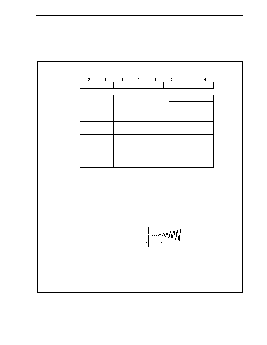
CHAPTER 21 STANDBY FUNCTION
Preliminary User's Manual U17714EJ1V0UD
693
(3) Oscillation stabilization time select register (OSTS)
The wait time until the oscillation stabilizes after the STOP mode is released or the wait time until the on-chip
flash memory stabilizes after the IDLE2 mode is released is controlled by the OSTS register.
The OSTS register can be read or written 8-bit units.
Reset sets this register to 06H.
0
OSTS
0
0
0
0
OSTS2
OSTS1
OSTS0
OSTS2
0
0
0
0
1
1
1
1
Selection of oscillation stabilization time/setup time
Note
OSTS1
0
0
1
1
0
0
1
1
OSTS0
0
1
0
1
0
1
0
1
After reset: 06H R/W Address: FFFFF6C0H
2
10
/f
X
2
11
/f
X
2
12
/f
X
2
13
/f
X
2
14
/f
X
2
15
/f
X
2
16
/f
X
4 MHz
0.256 ms
0.512 ms
1.024 ms
2.048 ms
4.096 ms
8.192 ms
16.38 ms
5 MHz
0.205 ms
0.410 ms
0.819 ms
1.638 ms
3.277 ms
6.554 ms
13.107 ms
f
X
Setting prohibited
Note The oscillation stabilization time and setup time are required when the STOP mode and
IDLE2 mode are released, respectively.
Cautions 1. The wait time following release of the STOP mode does not include the time
until the clock oscillation starts ("a" in the figure below) following release of
the STOP mode, regardless of whether the STOP mode is released by reset or
the occurrence of an interrupt request signal.
a
STOP mode release
Voltage waveform of X1 pin
V
SS
2. Be sure to clear bits 3 to 7 to "0".
3. The oscillation stabilization time following reset release is 2
16
/f
X
(because the
initial value of the OSTS register = 06H).
Remark
f
X
= Main clock oscillation frequency

CHAPTER 21 STANDBY FUNCTION
Preliminary User's Manual U17714EJ1V0UD
694
21.3 HALT Mode
21.3.1 Setting and operation status
The HALT mode is set when a dedicated instruction (HALT) is executed in the normal operation mode.
In the HALT mode, the clock oscillator continues operating. Only clock supply to the CPU is stopped; clock supply
to the other on-chip peripheral functions continues.
As a result, program execution is stopped, and the internal RAM retains the contents before the HALT mode was
set. The on-chip peripheral functions that are independent of instruction processing by the CPU continue operating.
Table 21-3 shows the operating status in the HALT mode.
The average current consumption of the system can be reduced by using the HALT mode in combination with the
normal operation mode for intermittent operation.
Cautions 1. Insert five or more NOP instructions after the HALT instruction.
2. If the HALT instruction is executed while an unmasked interrupt request signal is being held
pending, the status shifts to HALT mode, but the HALT mode is then released immediately by
the pending interrupt request.
21.3.2 Releasing HALT mode
The HALT mode is released by a non-maskable interrupt request signal (NMI pin input, INTWDT2 signal),
unmasked external interrupt request signal (INTP0 to INTP8 pin input), unmasked internal interrupt request signal
from a peripheral function operable in the HALT mode, or reset signal (reset by RESET pin input, WDT2RES signal,
low-voltage detector (LVI), or clock monitor (CLM)).
After the HALT mode has been released, the normal operation mode is restored.
(1) Releasing HALT mode by non-maskable interrupt request signal or unmasked maskable interrupt
request signal
The HALT mode is released by a non-maskable interrupt request signal or an unmasked maskable interrupt
request signal, regardless of the priority of the interrupt request signal. If the HALT mode is set in an interrupt
servicing routine, however, an interrupt request signal that is issued later is serviced as follows.
(a) If an interrupt request signal with a priority lower than that of the interrupt request currently being serviced
is issued, the HALT mode is released, but that interrupt request signal is not acknowledged. The interrupt
request signal itself is retained.
(b) If an interrupt request signal with a priority higher than that of the interrupt request currently being serviced
is issued (including a non-maskable interrupt request signal), the HALT mode is released and that
interrupt request signal is acknowledged.
Table 21-2. Operation After Releasing HALT Mode by Interrupt Request Signal
Release Source
Interrupt Enabled (EI) Status
Interrupt Disabled (DI) Status
Non-maskable interrupt request
signal
Execution branches to the handler address.
Maskable interrupt request signal
Execution branches to the handler address
or the next instruction is executed.
The next instruction is executed.
CHAPTER 21 STANDBY FUNCTION
Preliminary User's Manual U17714EJ1V0UD
695
(2) Releasing HALT mode by reset
The same operation as the normal reset operation is performed.
Table 21-3. Operating Status in HALT Mode
Setting of HALT Mode
Operating Status
Item
When Subclock Is Not Used
When Subclock Is Used
Main clock oscillator
Oscillation enabled
Subclock oscillator
-
Oscillation enabled
Internal oscillator
Oscillation enabled
PLL Operable
CPU Stops
operation
DMA Operable
Interrupt controller
Operable
Timer P (TMP0 to TMP8)
Operable
Timer Q (TMQ0)
Operable
Timer M (TMM0)
Operable when a clock other than f
XT
is
selected as the count clock
Operable
Watch timer
Operable when f
X
(divided BRG) is
selected as the count clock
Operable
Watchdog timer 2
Operable when a clock other than f
XT
is
selected as the count clock
Operable
CSIB0 to CSIB5
Operable
I
2
C00 to I
2
C02 Operable
Serial interface
UARTA0 to UARTA3
Operable
A/D converter
Operable
D/A converter
Operable
Real-time output function (RTO)
Operable
Key interrupt function (KR)
Operable
External bus interface
See 2.2 Pin States.
Port function
Retains status before HALT mode was set
Internal data
The CPU registers, statuses, data, and all other internal data such as the contents of
the internal RAM are retained as they were before the HALT mode was set.

CHAPTER 21 STANDBY FUNCTION
Preliminary User's Manual U17714EJ1V0UD
696
21.4 IDLE1 Mode
21.4.1 Setting and operation status
The IDLE1 mode is set by clearing the PSMR.PSM1 and PSMR.PSM0 bits to 00 and setting the PSC.STP bit to 1
in the normal operation mode.
In the IDLE1 mode, the clock oscillator, PLL, and flash memory continue operating but clock supply to the CPU and
other on-chip peripheral functions stops.
As a result, program execution stops and the contents of the internal RAM before the IDLE1 mode was set are
retained. The CPU and other on-chip peripheral functions stop operating. However, the on-chip peripheral functions
that can operate with the subclock or an external clock continue operating.
Table 21-5 shows the operating status in the IDLE1 mode.
The IDLE1 mode can reduce the power consumption more than the HALT mode because it stops the operation of
the on-chip peripheral functions. The main clock oscillator does not stop, so the normal operation mode can be
restored without waiting for the oscillation stabilization time after the IDLE1 mode has been released, in the same
manner as when the HALT mode is released.
Cautions 1. Insert five or more NOP instructions after the instruction that stores data in the PSC register
to set the IDLE1 mode.
2. If the IDLE1 mode is set while an unmasked interrupt request signal is being held pending,
the IDLE1 mode is released immediately by the pending interrupt request.
21.4.2 Releasing IDLE1 mode
The IDLE1 mode is released by a non-maskable interrupt request signal (NMI pin input, INTWDT2 signal),
unmasked external interrupt request signal (INTP0 to INTP8 pin input), unmasked internal interrupt request signal
from a peripheral function operable in the IDLE1 mode, or reset signal (reset by RESET pin input, WDT2RES signal,
low-voltage detector (LVI), or clock monitor (CLM)).
After the IDLE1 mode has been released, the normal operation mode is restored.
(1) Releasing IDLE1 mode by non-maskable interrupt request signal or unmasked maskable interrupt
request signal
The IDLE1 mode is released by a non-maskable interrupt request signal or an unmasked maskable interrupt
request signal, regardless of the priority of the interrupt request signal. If the IDLE1 mode is set in an interrupt
servicing routine, however, an interrupt request signal that is issued later is processed as follows.
(a) If an interrupt request signal with a priority lower than that of the interrupt request currently being serviced
is issued, the IDLE1 mode is released, but that interrupt request signal is not acknowledged. The interrupt
request signal itself is retained.
(b) If an interrupt request signal with a priority higher than that of the interrupt request currently being serviced
is issued (including a non-maskable interrupt request signal), the IDLE1 mode is released and that
interrupt request signal is acknowledged.
Caution An interrupt request signal that is disabled by setting the PSC.NMI1M, PSC.NMI0M, and
PSC.INTM bits to 1 becomes invalid and IDLE1 mode is not released.

CHAPTER 21 STANDBY FUNCTION
Preliminary User's Manual U17714EJ1V0UD
697
Table 21-4. Operation After Releasing IDLE1 Mode by Interrupt Request Signal
Release Source
Interrupt Enabled (EI) Status
Interrupt Disabled (DI) Status
Non-maskable interrupt request
signal
Execution branches to the handler address.
Maskable interrupt request signal
Execution branches to the handler address
or the next instruction is executed.
The next instruction is executed.
(2) Releasing IDLE1 mode by reset
The same operation as the normal reset operation is performed.
Table 21-5. Operating Status in IDLE1 Mode
Setting of IDLE1 Mode
Operating Status
Item
When Subclock Is Not Used
When Subclock Is Used
Main clock oscillator
Oscillation enabled
Subclock oscillator
-
Oscillation enabled
Internal oscillator
Oscillation enabled
PLL Operable
CPU Stops
operation
DMA Stops
operation
Interrupt controller
Stops operation (but standby mode release is possible)
Timer P (TMP0 to TMP8)
Stops operation
Timer Q (TMQ0)
Stops operation
Timer M (TMM0)
Operable when f
R
/8 is selected as the
count clock
Operable when f
R
/8 or f
XT
is selected as
the count clock
Watch timer
Operable when f
X
(divided BRG) is
selected as the count clock
Operable
Watchdog timer 2
Operable when f
R
is selected as the
count clock
Operable when f
R
or f
XT
is selected as
the count clock
CSIB0 to CSIB5
Operable when the SCKBn input clock is selected as the count clock (n = 0 to 5)
I
2
C00 to I
2
C02 Stops
operation
Serial interface
UARTA0 to UARTA3
Stops operation (but UARTA0 is operable when the ASCKA0 input clock is selected)
A/D converter
Holds operation (conversion result held)
Note
D/A converter
Holds operation (output held
Note
)
Real-time output function (RTO)
Stops operation (output held)
Key interrupt function (KR)
Operable
External bus interface
See 2.2 Pin States.
Port function
Retains status before IDLE1 mode was set
Internal data
The CPU registers, statuses, data, and all other internal data such as the contents of
the internal RAM are retained as they were before the IDLE1 mode was set.
Note To realize low power consumption, stop the A/D converter and D/A converter before shifting to the IDLE1 mode.

CHAPTER 21 STANDBY FUNCTION
Preliminary User's Manual U17714EJ1V0UD
698
21.5 IDLE2 Mode
21.5.1 Setting and operation status
The IDLE2 mode is set by setting the PSMR.PSM1 and PSMR.PSM0 bits to 10 and setting the PSC.STP bit to 1 in
the normal operation mode.
In the IDLE2 mode, the clock oscillator continues operation but clock supply to the CPU, PLL, flash memory, and
other on-chip peripheral functions stops.
As a result, program execution stops and the contents of the internal RAM before the IDLE2 mode was set are
retained. The CPU, PLL, and other on-chip peripheral functions stop operating. However, the on-chip peripheral
functions that can operate with the subclock or an external clock continue operating.
Table 21-7 shows the operating status in the IDLE2 mode.
The IDLE2 mode can reduce the power consumption more than the IDLE1 mode because it stops the operations of
the on-chip peripheral functions, PLL, and flash memory. However, because the PLL and flash memory are stopped,
a setup time for the PLL and flash memory is required when IDLE2 mode is released.
Cautions 1. Insert five or more NOP instructions after the instruction that stores data in the PSC register
to set the IDLE2 mode.
2. If the IDLE2 mode is set while an unmasked interrupt request signal is being held pending,
the IDLE2 mode is released immediately by the pending interrupt request.
21.5.2 Releasing IDLE2 mode
The IDLE2 mode is released by a non-maskable interrupt request signal (NMI pin input, INTWDT2 signal),
unmasked external interrupt request signal (INTP0 to INTP8 pin input), unmasked internal interrupt request signal
from the peripheral functions operable in the IDLE2 mode, or reset signal (reset by RESET pin input, WDT2RES
signal, low-voltage detector (LVI), or clock monitor (CLM)). The PLL returns to the operating status it was in before
the IDLE2 mode was set.
After the IDLE2 mode has been released, the normal operation mode is restored.
(1) Releasing IDLE2 mode by non-maskable interrupt request signal or unmasked maskable interrupt
request signal
The IDLE2 mode is released by a non-maskable interrupt request signal or an unmasked maskable interrupt
request signal, regardless of the priority of the interrupt request signal. If the IDLE2 mode is set in an interrupt
servicing routine, however, an interrupt request signal that is issued later is processed as follows.
(a) If an interrupt request signal with a priority lower than that of the interrupt request currently being serviced
is issued, the IDLE2 mode is released, but that interrupt request signal is not acknowledged. The
interrupt request signal itself is retained.
(b) If an interrupt request signal with a priority higher than that of the interrupt request currently being
serviced is issued (including a non-maskable interrupt request signal), the IDLE2 mode is released and
that interrupt request signal is acknowledged.
Caution The interrupt request signal that is disabled by setting the PSC.NMI1M, PSC.NMI0M, and
PSC.INTM bits to 1 becomes invalid and IDLE2 mode is not released.

CHAPTER 21 STANDBY FUNCTION
Preliminary User's Manual U17714EJ1V0UD
699
Table 21-6. Operation After Releasing IDLE2 Mode by Interrupt Request Signal
Release Source
Interrupt Enabled (EI) Status
Interrupt Disabled (DI) Status
Non-maskable interrupt request
signal
Execution branches to the handler address after securing the prescribed setup time.
Maskable interrupt request signal
Execution branches to the handler address
or the next instruction is executed after
securing the prescribed setup time.
The next instruction is executed after
securing the prescribed setup time.
(2) Releasing IDLE2 mode by reset
The same operation as the normal reset operation is performed.
Table 21-7. Operating Status in IDLE2 Mode
Setting of IDLE2 Mode
Operating Status
Item
When Subclock Is Not Used
When Subclock Is Used
Main clock oscillator
Oscillation enabled
Subclock oscillator
-
Oscillation enabled
Internal oscillator
Oscillation enabled
PLL Stops
operation
CPU Stops
operation
DMA Stops
operation
Interrupt controller
Stops operation (but standby mode release is possible)
Timer P (TMP0 to TMP8)
Stops operation
Timer Q (TMQ0)
Stops operation
Timer M (TMM0)
Operable when f
R
/8 is selected as the
count clock
Operable when f
R
/8 or f
XT
is selected as
the count clock
Watch timer
Operable when f
X
(divided BRG) is
selected as the count clock
Operable
Watchdog timer 2
Operable when f
R
is selected as the
count clock
Operable when f
R
or f
XT
is selected as
the count clock
CSIB0 to CSIB5
Operable when the SCKBn input clock is selected as the count clock (n = 0 to 5)
I
2
C00 to I
2
C02 Stops
operation
Serial interface
UARTA0 to UARTA3
Stops operation (but UARTA0 is operable when the ASCKA0 input clock is selected)
A/D converter
Holds operation (conversion result held)
Note
D/A converter
Holds operation (output held
Note
)
Real-time output function (RTO)
Stops operation (output held)
Key interrupt function (KR)
Operable
External bus interface
See 2.2 Pin States.
Port function
Retains status before IDLE2 mode was set
Internal data
The CPU registers, statuses, data, and all other internal data such as the contents of
the internal RAM are retained as they were before the IDLE2 mode was set.
Note To realize low power consumption, stop the A/D converter and D/A converter before shifting to the IDLE2 mode.
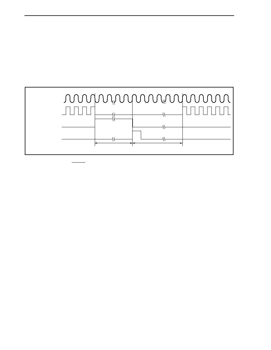
CHAPTER 21 STANDBY FUNCTION
Preliminary User's Manual U17714EJ1V0UD
700
21.5.3 Securing setup time when releasing IDLE2 mode
Secure the setup time for the flash memory after releasing the IDLE2 mode because the operation of the blocks
other than the main clock oscillator stops after the IDLE2 mode is set.
(1) Releasing IDLE2 mode by non-maskable interrupt request signal or unmasked maskable interrupt
request signal
Secure the specified setup time by setting the OSTS register.
When the releasing source is generated, the dedicated internal timer starts counting according to the OSTS
register setting. When it overflows, the normal operation mode is restored.
Oscillated waveform
ROM circuit stopped
Setup time count
Main clock
IDLE mode status
Interrupt request
(2) Release by reset (RESET pin input, WDT2RES generation)
This operation is the same as that of a normal reset.
The oscillation stabilization time is the initial value of the OSTS register, 2
16
/f
X
.

CHAPTER 21 STANDBY FUNCTION
Preliminary User's Manual U17714EJ1V0UD
701
21.6 STOP Mode
21.6.1 Setting and operation status
The STOP mode is set by setting the PSMR.PSM1 and PSMR.PSM0 bits to 01 or 11 and setting the PSC.STP bit
to 1 in the normal operation mode.
In the STOP mode, the subclock oscillator continues operating but the main clock oscillator stops. Clock supply to
the CPU and the on-chip peripheral functions is stopped.
As a result, program execution stops, and the contents of the internal RAM before the STOP mode was set are
retained. The on-chip peripheral functions that operate with the clock oscillated by the subclock oscillator or an
external clock continue operating.
Table 21-9 shows the operating status in the STOP mode.
Because the STOP mode stops operation of the main clock oscillator, it reduces the power consumption to a level
lower than the IDLE2 mode. If the subclock oscillator, internal oscillator, and external clock are not used, the power
consumption can be minimized with only leakage current flowing.
Cautions 1. Insert five or more NOP instructions after the instruction that stores data in the PSC register
to set the STOP mode.
2. If the STOP mode is set while an unmasked interrupt request signal is being held pending, the
STOP mode is released immediately by the pending interrupt request.
21.6.2 Releasing STOP mode
The STOP mode is released by a non-maskable interrupt request signal (NMI pin input, INTWDT2 signal),
unmasked external interrupt request signal (INTP0 to INTP8 pin input), unmasked internal interrupt request signal
from the peripheral functions operable in the STOP mode, or reset signal (reset by RESET pin input, WDT2RES
signal, or low-voltage detector (LVI)).
After the STOP mode has been released, the normal operation mode is restored after the oscillation stabilization
time has been secured.
(1) Releasing STOP mode by non-maskable interrupt request signal or unmasked maskable interrupt
request signal
The STOP mode is released by a non-maskable interrupt request signal or an unmasked maskable interrupt
request signal, regardless of the priority of the interrupt request signal. If the STOP mode is set in an interrupt
servicing routine, however, an interrupt request signal that is issued later is serviced as follows.
(a) If an interrupt request signal with a priority lower than that of the interrupt request currently being serviced
is issued, the STOP mode is released, but that interrupt request signal is not acknowledged. The interrupt
request signal itself is retained.
(b) If an interrupt request signal with a priority higher than that of the interrupt request currently being serviced
is issued (including a non-maskable interrupt request signal), the STOP mode is released and that
interrupt request signal is acknowledged.
Caution The interrupt request that is disabled by setting the PSC.NMI1M, PSC.NMI0M, and PSC.INTM
bits to 1 becomes invalid and STOP mode is not released.

CHAPTER 21 STANDBY FUNCTION
Preliminary User's Manual U17714EJ1V0UD
702
Table 21-8. Operation After Releasing STOP Mode by Interrupt Request Signal
Release Source
Interrupt Enabled (EI) Status
Interrupt Disabled (DI) Status
Non-maskable interrupt request
signal
Execution branches to the handler address after securing the oscillation stabilization time.
Maskable interrupt request signal
Execution branches to the handler address
or the next instruction is executed after
securing the oscillation stabilization time.
The next instruction is executed after
securing the oscillation stabilization time.

CHAPTER 21 STANDBY FUNCTION
Preliminary User's Manual U17714EJ1V0UD
703
(2) Releasing STOP mode by reset
The same operation as the normal reset operation is performed.
Table 21-9. Operating Status in STOP Mode
Setting of STOP Mode
Operating Status
Item
When Subclock Is Not Used
When Subclock Is Used
Main clock oscillator
Stops oscillation
Subclock oscillator
-
Oscillation enabled
Internal oscillator
Oscillation enabled
PLL Stops
operation
CPU Stops
operation
DMA Stops
operation
Interrupt controller
Stops operation (but standby mode release is possible)
Timer P (TMP0 to TMP8)
Stops operation
Timer Q (TMQ0)
Stops operation
Timer M (TMM0)
Operable when f
R
/8 is selected as the
count clock
Operable when f
R
/8 or f
XT
is selected as
the count clock
Watch timer
Stops operation
Operable when f
XT
is selected as the
count clock
Watchdog timer 2
Operable when f
R
is selected as the
count clock
Operable when f
R
or f
XT
is selected as
the count clock
CSIB0 to CSIB5
Operable when the SCKBn input clock is selected as the count clock (n = 0 to 5)
I
2
C00 to I
2
C02 Stops
operation
Serial interface
UARTA0 to UARTA3
Stops operation (but UARTA0 is operable when the ASCKA0 input clock is selected)
A/D converter
Stops operation (conversion result undefined)
Notes 1, 2
D/A converter
Stops operation
Notes 3, 4
(high impedance is output)
Real-time output function (RTO)
Stops operation (output held)
Key interrupt function (KR)
Operable
External bus interface
See 2.2 Pin States.
Port function
Retains status before STOP mode was set
Internal data
The CPU registers, statuses, data, and all other internal data such as the contents of
the internal RAM are retained as they were before the STOP mode was set.
Notes 1. If the STOP mode is set while the A/D converter is operating, the A/D converter is automatically stopped
and starts operating again after the STOP mode is released. However, in that case, the A/D conversion
results after the STOP mode is released are invalid. All the A/D conversion results before the STOP
mode is set are invalid.
2.
Even if the STOP mode is set while the A/D converter is operating, the power consumption is reduced
equivalently to when the A/D converter is stopped before the STOP mode is set.
3.
If the STOP mode is set while the D/A converter is operating, the D/A converter is automatically stopped
and the pin status becomes high impedance. After the STOP mode is released, D/A conversion
resumes, the setting time elapses, and the status returns to the output level before the STOP mode was
set.
4.
Even if the STOP mode is set while the D/A converter is operating, the power consumption is reduced
equivalently to when the D/A converter is stopped before the STOP mode is set.
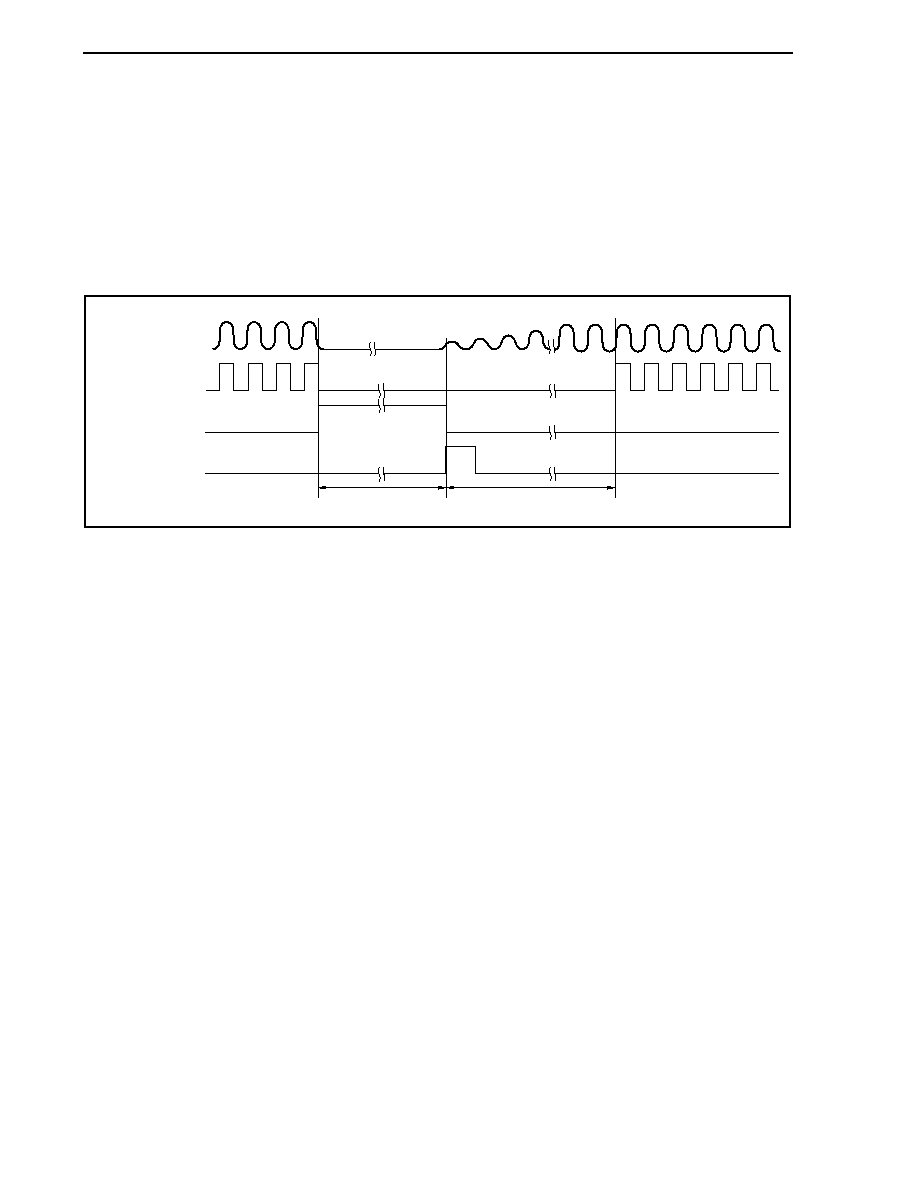
CHAPTER 21 STANDBY FUNCTION
Preliminary User's Manual U17714EJ1V0UD
704
21.6.3 Securing oscillation stabilization time when releasing STOP mode
Secure the oscillation stabilization time for the main clock oscillator after releasing the STOP mode because the
operation of the main clock oscillator stops after STOP mode is set.
(1) Releasing STOP mode by non-maskable interrupt request signal or unmasked maskable interrupt
request signal
Secure the oscillation stabilization time by setting the OSTS register.
When the releasing source is generated, the dedicated internal timer starts counting according to the OSTS
register setting. When it overflows, the normal operation mode is restored.
Oscillated waveform
ROM circuit stopped
Setup time count
Main clock
STOP status
Interrupt request
(2) Release by reset
This operation is the same as that of a normal reset.
The oscillation stabilization time is the initial value of the OSTS register, 2
16
/f
X
.

CHAPTER 21 STANDBY FUNCTION
Preliminary User's Manual U17714EJ1V0UD
705
21.7 Subclock Operation Mode
21.7.1 Setting and operation status
The subclock operation mode is set by setting the PCC.CK3 bit to 1 in the normal operation mode.
When the subclock operation mode is set, the internal system clock is changed from the main clock to the subclock.
Check whether the clock has been switched by using the PCC.CLS bit.
When the PCC.MCK bit is set to 1, the operation of the main clock oscillator is stopped. As a result, the system
operates only on the subclock.
In the subclock operation mode, the power consumption can be reduced to a level lower than in the normal
operation mode because the subclock is used as the internal system clock. In addition, the power consumption can
be further reduced to the level of the STOP mode by stopping the operation of the main clock oscillator.
Table 21-10 shows the operating status in subclock operation mode.
Cautions 1. When manipulating the CK3 bit, do not change the set values of the PCC.CK2 to PCC.CK0 bits
(using a bit manipulation instruction to manipulate the bit is recommended). For details of
the PCC register, see 6.3 (1) Processor clock control register (PCC).
2. If the following conditions are not satisfied, change the CK2 to CK0 bits so that the conditions
are satisfied and set the subclock operation mode.
Internal system clock (f
CLK
) > Subclock (f
XT
= 32.768 kHz)
� 4
Remark Internal system clock (f
CLK
): Clock generated from main clock (f
XX
) in accordance with the settings of the
CK2 to CK0 bits
21.7.2 Releasing subclock operation mode
The subclock operation mode is released by a reset signal (reset by RESET pin input, WDT2RES signal, low-
voltage detector (LVI), or clock monitor (CLM)) when the CK3 bit is cleared to 0.
If the main clock is stopped (MCK bit = 1), set the MCK bit to 1, secure the oscillation stabilization time of the main
clock by software, and clear the CK3 bit to 0.
The normal operation mode is restored when the subclock operation mode is released.
Caution When manipulating the CK3 bit, do not change the set values of the CK2 to CK0 bits (using a bit
manipulation instruction to manipulate the bit is recommended).
For details of the PCC register, see 6.3 (1) Processor clock control register (PCC).
CHAPTER 21 STANDBY FUNCTION
Preliminary User's Manual U17714EJ1V0UD
706
Table 21-10. Operating Status in Subclock Operation Mode
Operating Status
Setting of Subclock Operation Mode
Item
When Main Clock Is Oscillating
When Main Clock Is Stopped
Subclock oscillator
Oscillation enabled
Internal oscillator
Oscillation enabled
PLL Operable
Stops
operation
Note
CPU Operable
DMA Operable
Interrupt controller
Operable
Timer P (TMP0 to TMP8)
Operable
Stops operation
Timer Q (TMQ0)
Operable
Stops operation
Timer M (TMM0)
Operable
Operable when f
R
/8 or f
XT
is selected as
the count clock
Watch timer
Operable
Operable when f
XT
is selected as the
count clock
Watchdog timer 2
Operable
Operable when f
R
or f
XT
is selected as
the count clock
CSIB0 to CSIB5
Operable
Operable when the SCKBn input clock is
selected as the count clock (n = 0 to 5)
I
2
C00 to I
2
C02 Operable
Stops
operation
Serial interface
UARTA0 to UARTA3
Operable
Stops operation (but UARTA0 is
operable when the ASCKA0 input clock
is selected)
A/D converter
Operable
Stops operation
D/A converter
Operable
Real-time output function (RTO)
Operable
Stops operation (output held)
Key interrupt function (KR)
Operable
External bus interface
See 2.2 Pin States.
Port function
Settable
Internal data
Settable
Note Be sure to stop the PLL (PLLCTL.PLLON bit = 0) before stopping the main clock.
Caution When the CPU is operating on the subclock and main clock oscillation is stopped, accessing a
register in which a wait occurs is disabled. If a wait is generated, it can be released only by reset
(see 3.4.8 (2)).

CHAPTER 21 STANDBY FUNCTION
Preliminary User's Manual U17714EJ1V0UD
707
21.8 Sub-IDLE Mode
21.8.1 Setting and operation status
The sub-IDLE mode is set by setting the PSMR.PSM1 and PSMR.PSM0 bits to 00 or 10 and setting the PSC.STP
bit to 1 in the subclock operation mode.
In this mode, the clock oscillator continues operating but clock supply to the CPU, flash memory, and the other on-
chip peripheral functions is stopped.
As a result, program execution stops and the contents of the internal RAM before the sub-IDLE mode was set are
retained. The CPU and the other on-chip peripheral functions are stopped. However, the on-chip peripheral functions
that can operate with the subclock or an external clock continue operating.
Because the sub-IDLE mode stops operation of the CPU, flash memory, and other on-chip peripheral functions, it
can reduce the power consumption more than the subclock operation mode. If the sub-IDLE mode is set after the
main clock has been stopped, the current consumption can be reduced to a level as low as that in the STOP mode.
Table 21-12 shows the operating status in the sub-IDLE mode.
Cautions 1. Following the store instruction to set the PSC register to the sub-IDLE mode, insert the five or
more NOP instructions.
2. If the sub-IDLE mode is set while an unmasked interrupt request signal is being held pending,
the sub-IDLE mode is then released immediately by the pending interrupt request.
21.8.2 Releasing sub-IDLE mode
The sub-IDLE mode is released by a non-maskable interrupt request signal (NMI pin input, INTWDT2 signal),
unmasked external interrupt request signal (INTP0 to INTP8 pin input), unmasked internal interrupt request signal
from the peripheral functions operable in the sub-IDLE mode, or reset signal (reset by RESET pin input, WDT2RES
signal, low-voltage detector (LVI), or clock monitor (CLM)). The PLL returns to the operating status it was in before
the sub-IDLE mode was set.
When the sub-IDLE mode is released by an interrupt request signal, the subclock operation mode is set.
(1) Releasing sub-IDLE mode by non-maskable interrupt request signal or unmasked maskable interrupt
request signal
The sub-IDLE mode is released by a non-maskable interrupt request signal or an unmasked maskable
interrupt request signal, regardless of the priority of the interrupt request signal.
If the sub-IDLE mode is set in an interrupt servicing routine, however, an interrupt request signal that is issued
later is serviced as follows.
(a) If an interrupt request signal with a priority lower than that of the interrupt request currently being serviced
is issued, the sub-IDLE mode is released, but that interrupt request signal is not acknowledged. The
interrupt request signal itself is retained.
(b) If an interrupt request signal with a priority higher than that of the interrupt request currently being serviced
is issued (including a non-maskable interrupt request signal), the sub-IDLE mode is released and that
interrupt request signal is acknowledged.
Cautions 1. The interrupt request signal that is disabled by setting the PSC.NMI1M, PSC.NMI0M, and
PSC.INTM bits to 1 becomes invalid and sub-IDLE mode is not released.
2. When the sub-IDLE mode is released, 12 cycles of the subclock (about 366
�
s) elapse
from when the interrupt request signal that releases the sub-IDLE mode is generated to
when the mode is released.
CHAPTER 21 STANDBY FUNCTION
Preliminary User's Manual U17714EJ1V0UD
708
Table 21-11. Operation After Releasing Sub-IDLE Mode by Interrupt Request Signal
Release Source
Interrupt Enabled (EI) Status
Interrupt Disabled (DI) Status
Non-maskable interrupt request
signal
Execution branches to the handler address.
Maskable interrupt request signal
Execution branches to the handler address
or the next instruction is executed.
The next instruction is executed.
(2) Releasing sub-IDLE mode by reset
The same operation as the normal reset operation is performed.
Table 21-12. Operating Status in Sub-IDLE Mode
Setting of Sub-IDLE Mode
Operating Status
Item
When Main Clock Is Oscillating
When Main Clock Is Stopped
Subclock oscillator
Oscillation enabled
Internal oscillator
Oscillation enabled
PLL Operable
Stops
operation
Note 1
CPU Stops
operation
DMA Stops
operation
Interrupt controller
Stops operation (but standby mode release is possible)
Timer P (TMP0 to TMP8)
Stops operation
Timer Q (TMQ0)
Stops operation
Timer M (TMM0)
Operable when f
R
/8 or f
XT
is selected as the count clock
Watch timer
Stops operation
Operable when f
XT
is selected as the
count clock
Watchdog timer 2
Operable when f
R
or f
XT
is selected as the count clock
CSIB0 to CSIB5
Operable when the SCKBn input clock is selected as the count clock (n = 0 to 5)
I
2
C00 to I
2
C02 Stops
operation
Serial interface
UARTA0 to UARTA3
Stops operation (but UARTA0 is operable when the ASCKA0 input clock is selected)
A/D converter
Holds operation (conversion result held)
Note 2
D/A converter
Holds operation (output held
Note 2
)
Real-time output function (RTO)
Stops operation (output held)
Key interrupt function (KR)
Operable
External bus interface
See 2.2 Pin States (same operation status as IDLE1, IDLE2 mode).
Port function
Retains status before sub-IDLE mode was set
Internal data
The CPU registers, statuses, data, and all other internal data such as the contents of
the internal RAM are retained as they were before the sub-IDLE mode was set.
Notes 1. Be sure to stop the PLL (PLLCTL.PLLON bit = 0) before stopping the main clock.
2. To realize low power consumption, stop the A/D and D/A converters before shifting to the sub-IDLE
mode.
Preliminary User's Manual U17714EJ1V0UD
709
CHAPTER 22 RESET FUNCTIONS
22.1 Overview
The following reset functions are available.
(1) Four kinds of reset sources
� External reset input via the RESET pin
� Reset via the watchdog timer 2 (WDT2) overflow (WDT2RES)
� System reset via the comparison of the low-voltage detector (LVI) supply voltage and detected voltage
� System reset via the detecting clock monitor (CLM) oscillation stop
After a reset is released, the source of the reset can be confirmed with the reset source flag register (RESF).
(2) Emergency operation mode
If the WDT2 overflows during the main clock oscillation stabilization time inserted after reset, a main clock
oscillation anomaly is judged and the CPU starts operating on the internal oscillation clock.
Caution When the CPU is being operated with the internal oscillation clock, access to the register in
which a wait state is generated is prohibited. For the register in which a wait state is
generated, see 3.4.8 (2) Accessing specific on-chip peripheral I/O registers.
Figure 22-1. Block Diagram of Reset Function
CLMRF
LVIRF
WDT2RF
Reset source flag
register (RESF)
Internal bus
WDT2 reset signal
CLM reset signal
RESET
LVI reset signal
Reset signal
Reset signal
Reset signal to
LVIM/LVIS register
Clear
Set
Set
Clear
Clear
Set
Caution An LVI circuit internal reset does not reset the LVI circuit.
Remarks 1. LVIM: Low-voltage detection register
2. LVIS: Low-voltage detection level selection register
CHAPTER 22 RESET FUNCTIONS
Preliminary User's Manual U17714EJ1V0UD
710
22.2 Registers to Check Reset Source
The V850ES/JJ2 has four kinds of reset sources. After a reset has been released, the source of the reset that
occurred can be checked with the reset source flag register (RESF).
(1) Reset source flag register (RESF)
The RESF register is a special register that can be written only by a combination of specific sequences (see
3.4.7 Special registers).
The RESF register indicates the source from which a reset signal is generated.
This register is read or written in 8-bit or 1-bit units.
RESET pin input clears this register to 00H. The default value differs if the source of reset is other than the
RESET pin signal.
0
WDT2RF
0
1
Not generated
Generated
RESF
0
0
WDT2RF
0
0
CLMRF
LVIRF
After reset: 00H
Note
R/W Address: FFFFF888H
Reset signal from WDT2
LVIRF
0
1
Not generated
Generated
Reset signal from LVI
CLMRF
0
1
Not generated
Generated
Reset signal from CLM
Note The value of the RESF register is cleared to 00H when a reset is executed via the RESET pin. When a
reset is executed by the watchdog timer 2 (WDT2), low-voltage detector (LVI), or clock monitor (CLM),
the reset flags of this register (WDT2RF bit, CLMRF bit, and LVIRF bit) are set. However, other sources
are retained.
Caution Only "0" can be written to each bit of this register. If writing "0" conflicts with setting the flag
(occurrence of reset), setting the flag takes precedence.

CHAPTER 22 RESET FUNCTIONS
Preliminary User's Manual U17714EJ1V0UD
711
22.3 Operation
22.3.1 Reset operation via RESET pin
When a low level is input to the RESET pin, the system is reset, and each hardware unit is initialized.
When the level of the RESET pin is changed from low to high, the reset status is released.
Table 22-1. Hardware Status on RESET Pin Input
Item
During Reset
After Reset
Main clock oscillator (f
X
)
Oscillation stops
Oscillation starts
Subclock oscillator (f
XT
) Oscillation
continues
Internal oscillator
Oscillation stops
Oscillation starts
Peripheral clock (f
X
to f
X
/1,024) Operation
stops
Operation
starts after securing oscillation
stabilization time
Internal system clock (f
CLK
),
CPU clock (f
CPU
)
Operation stops
Operation starts after securing oscillation
stabilization time (initialized to fXX/8)
CPU
Initialized
Program execution starts after securing
oscillation stabilization time
Watchdog timer 2
Operation stops (initialized to 0)
Counts up from 0 with internal oscillation
clock as source clock.
Internal RAM
Undefined if power-on reset or CPU access and reset input conflict (data is damaged).
Otherwise value immediately after reset input is retained
Note 1
.
I/O lines (ports/alternate-function
pins)
High impedance
Note 2
On-chip peripheral I/O registers
Initialized to specified status, OCDM register is set (01H).
Other on-chip peripheral functions
Operation stops
Operation can be started after securing
oscillation stabilization time
Notes 1. The firmware of the V850ES/JJ2 uses a part of the internal RAM after the internal system reset status
has been released because it supports a boot swap function. Therefore, the contents of some RAM
areas are not retained after power-on reset. For details, see 22.3.4 Operation after reset release.
2. When the power is turned on, the following pins may output an undefined level temporarily, even during
reset.
� P10/ANO0 pin
� P11/ANO1 pin
� P53/SIB2/KR3/TIQ00/TOQ00/RTP03/DDO pin
Caution The OCDM register is initialized by the RESET pin input. Therefore, note with caution that, if a
high level is input to the P05/DRST pin after a reset release before the OCDM.OCDM0 bit is
cleared, the on-chip debug mode is entered. For details, see CHAPTER 4 PORT FUNCTIONS.
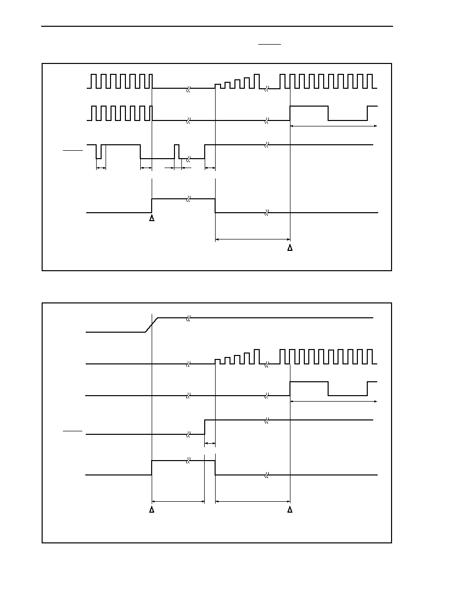
CHAPTER 22 RESET FUNCTIONS
Preliminary User's Manual U17714EJ1V0UD
712
Figure 22-2. Timing of Reset Operation by RESET Pin Input
Counting of oscillation
stabilization time
Initialized to f
XX
/8 operation
Oscillation stabilization timer overflows
Internal system
reset signal
Analog delay
(eliminated as noise)
Analog delay
Analog delay
(eliminated as noise)
RESET
f
X
f
CLK
Analog delay
Figure 22-3. Timing of Power-on Reset Operation
Oscillation stabilization
time count
Must be on-chip
regulator stabilization
time (1 ms (max.))
or longer.
Initialized to f
XX
/8 operation
Overflow of timer for oscillation stabilization
Internal system
reset signal
RESET
f
X
V
DD
f
CLK
Analog delay

CHAPTER 22 RESET FUNCTIONS
Preliminary User's Manual U17714EJ1V0UD
713
22.3.2 Reset operation by watchdog timer 2
When watchdog timer 2 is set to the reset operation mode due to overflow, upon watchdog timer 2 overflow
(WDT2RES signal generation), a system reset is executed and the hardware is initialized to the initial status.
Following watchdog timer 2 overflow, the reset status is entered and lasts the predetermined time (analog delay),
and the reset status is then automatically released.
The main clock oscillator is stopped during the reset period.
Table 22-2. Hardware Status During Watchdog Timer 2 Reset Operation
Item
During Reset
After Reset
Main clock oscillator (f
X
)
Oscillation stops
Oscillation starts
Subclock oscillator (f
XT
)
Oscillation continues
Internal oscillator
Oscillation stops
Oscillation starts
Peripheral clock (f
XX
to f
XX
/1,024) Operation
stops
Operation
starts after securing oscillation
stabilization time
Internal system clock (f
XX
),
CPU clock (f
CPU
)
Operation stops
Operation starts after securing oscillation
stabilization time (initialized to fXX/8)
CPU
Initialized
Program execution after securing
oscillation stabilization time
Watchdog timer 2
Operation stops (initialized to 0)
Counts up from 0 with internal oscillation
clock as source clock.
Internal RAM
Undefined if power-on reset or CPU access and reset input conflict (data is damaged).
Otherwise value immediately after reset input is retained
Note
.
I/O lines (ports/alternate-function
pins)
High impedance
On-chip peripheral I/O register
Initialized to specified status, OCDM register retains its value.
On-chip peripheral functions other
than above
Operation stops
Operation can be started after securing
oscillation stabilization time.
Note The firmware of the V850ES/JJ2 uses a part of the internal RAM after the internal system reset status has
been released because it supports a boot swap function. Therefore, the contents of some RAM areas are
not retained after power-on reset. For details, see 22.3.4 Operation after reset release.
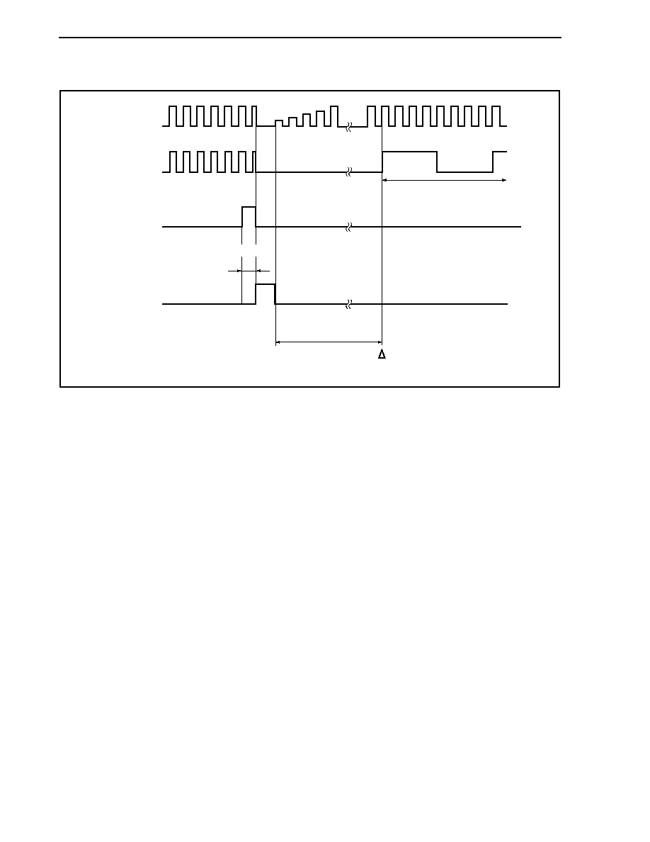
CHAPTER 22 RESET FUNCTIONS
Preliminary User's Manual U17714EJ1V0UD
714
Figure 22-4. Timing of Reset Operation by WDT2RES Signal Generation
Counting of oscillation
stabilization time
Initialized to f
XX
/8 operation
Oscillation stabilization timer overflow
Internal system
reset signal
WDT2RES
f
X
f
CLK
Analog delay

CHAPTER 22 RESET FUNCTIONS
Preliminary User's Manual U17714EJ1V0UD
715
22.3.3 Reset operation by low-voltage detector
If the supply voltage falls below the voltage detected by the low-voltage detector when LVI operation is enabled, a
system reset is executed (when the LVIM.LVIMD bit is set to 1), and the hardware is initialized to the initial status.
The reset status lasts from when a supply voltage drop has been detected until the supply voltage rises above the
LVI detection voltage.
The main clock oscillator is stopped during the reset period.
When the LVIMD bit = 0, an interrupt request signal (INTLVI) is generated if a low voltage is detected.
Table 22-3. Hardware Status During Reset Operation by Low-Voltage Detector
Item
During Reset
After Reset
Main clock oscillator (f
X
)
Oscillation stops
Oscillation starts
Subclock oscillator (f
XT
)
Oscillation continues
Internal oscillator
Oscillation stops
Oscillation starts
Peripheral clock (f
X
to f
X
/1,024) Operation
stops
Operation
starts after securing oscillation
stabilization time
Internal system clock (f
XX
),
CPU clock (f
CPU
)
Operation stops
Operation starts after securing oscillation
stabilization time (initialized to f
XX
/8)
CPU
Initialized
Program execution starts after securing
oscillation stabilization time
WDT2
Operation stops (initialized to 0)
Counts up from 0 with internal oscillation
clock as source clock.
Internal RAM
Undefined if power-on reset or CPU access and reset input conflict (data is damaged).
Otherwise value immediately after reset input is retained
Note
.
I/O lines (ports/alternate-function
pins)
High impedance
On-chip peripheral I/O register
Initialized to specified status, OCDM register retains its value.
LVI Operation
continues
On-chip peripheral functions other
than above
Operation stops
Operation can be started after securing
oscillation stabilization time.
Note The firmware of the V850ES/JJ2 uses a part of the internal RAM after the internal system reset status has
been released because it supports a boot swap function. Therefore, the contents of some RAM areas are
not retained after power-on reset. For details, see 22.3.4 Operation after reset release.
Remark For the reset timing of the low-voltage detector, see CHAPTER 24 LOW-VOLTAGE DETECTOR (LVI).
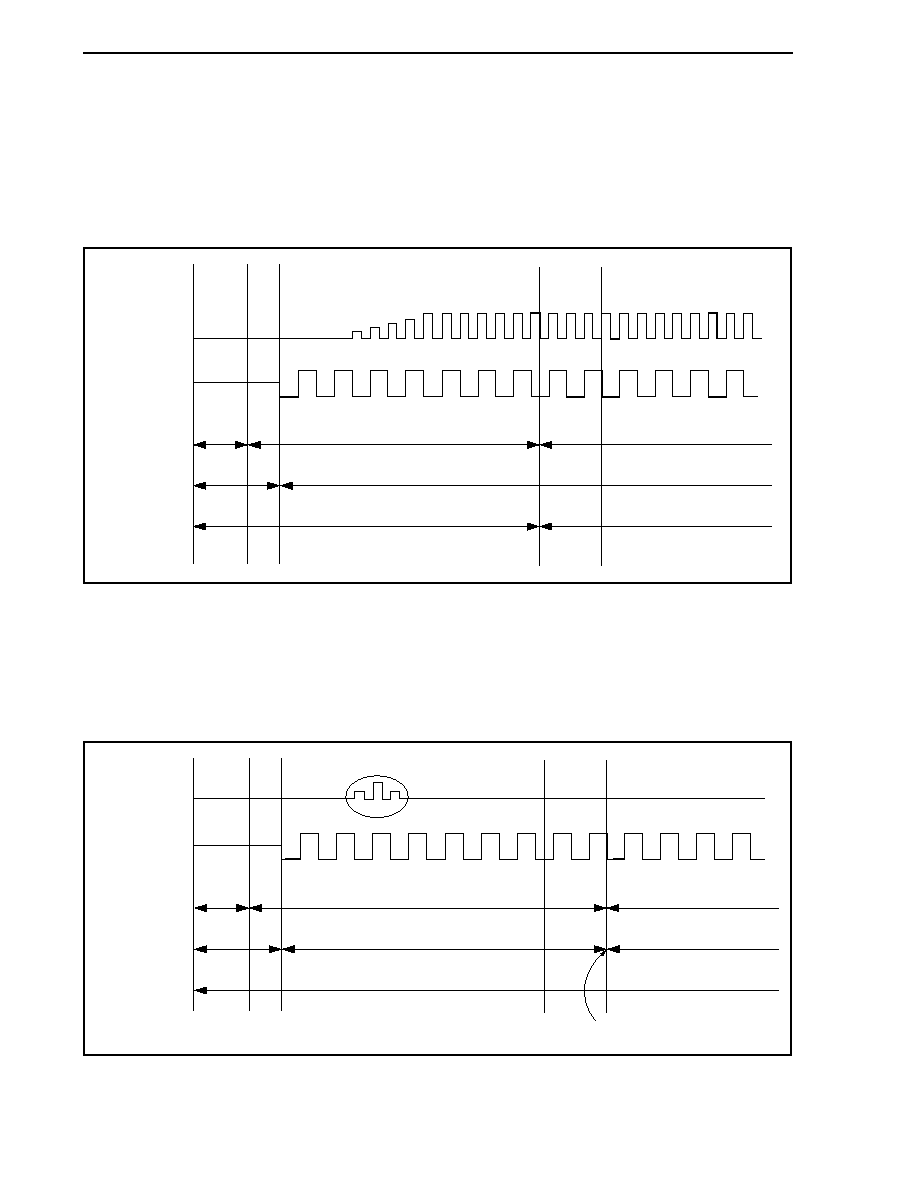
CHAPTER 22 RESET FUNCTIONS
Preliminary User's Manual U17714EJ1V0UD
716
22.3.4 Operation after reset release
After the reset is released, the main clock starts oscillation and oscillation stabilization time (OSTS register initial
value: 2
16
/f
X
) is secured, and the CPU starts program execution.
WDT2 immediately begins to operate after a reset has been released using the internal oscillation clock as a
source clock.
Figure 22-5. Operation After Reset Release
Main clock
Reset
Counting of oscillation stabilization time
Normal operation (f
CPU
= Main clock)
Operation
stops
Operation in progress
Operation stops
Operation in progress
Clock monitor
Internal oscillation
clock
V850ES/JJ2
WDT2
(1) Emergent operation mode
If an anomaly occurs in the main clock before oscillation stabilization time is secured, WDT2 overflows before
executing the CPU program. At this time, the CPU starts program execution by using the internal oscillation
clock as the source clock.
Figure 22-6. Operation After Reset Release
Main clock
Reset
Counting of oscillation stabilization time
WDT overflows
Emergency mode
(f
CPU
= internal oscillation clock)
Operation
stops
Operation in progress
Operation in progress (re-count)
Operation stops
Clock monitor
Internal oscillation
clock
V850ES/JJ2
WDT2
The CPU operation clock states can be checked with the CPU operation clock status register (CCLS).

CHAPTER 22 RESET FUNCTIONS
Preliminary User's Manual U17714EJ1V0UD
717
(2) Firmware operation
In the V850ES/JJ2, after the reset status is released, the internal firmware starts operation before the user
program is started to support the boot swap function.
Reset
Oscillation
stabilization time
User program operation start
Firmware
operation
Firmware operation time: 14974
� (1/f
X
) (seconds)
Remark f
X
: Main clock oscillation frequency (MHz)
Since the firmware uses a part of the internal RAM, the contents of the following RAM areas are not retained
after power-on reset.
� Version with 12 KB RAM: 03FFEFBAH to 03FFEFFFH
� Version with 24 KB RAM: 03FFEFBAH to 03FFEFFFH
� Version with 32 KB RAM: 03FF7000H to 03FF7095H, 03FFEFBAH to 03FFEFFFH
� Version with 40 KB RAM: 03FFEFBAH to 03FFEFFFH
� Version with 48 KB RAM: 03FF3000H to 03FF3095H, 03FFEFBAH to 03FFEFFFH
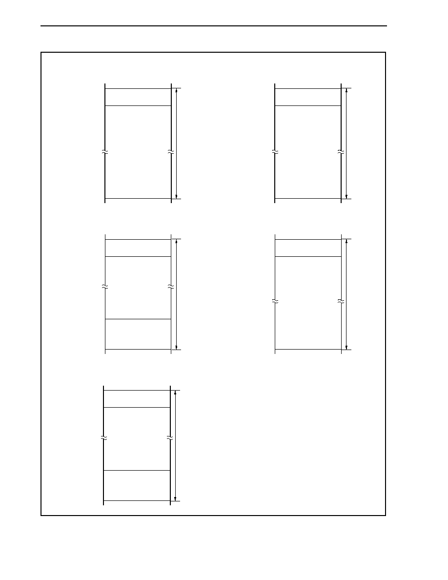
CHAPTER 22 RESET FUNCTIONS
Preliminary User's Manual U17714EJ1V0UD
718
(a) Version with 12 KB RAM
(b) Version with 24 KB RAM
RAM retention disabled area
(70 bytes)
RAM retention
enabled area
12 KB
RAM retention disabled area
(70 bytes)
RAM retention
enabled area
24 KB
0 3 F F E F F F H
0 3 F F E F B A H
0 3 F F E F B 9 H
0 3 F F C 0 0 0 H
0 3 F F E F F F H
0 3 F F E F B A H
0 3 F F E F B 9 H
0 3 F F 9 0 0 0 H
(c) Version with 32 KB RAM
(d) Version with 40 KB RAM
RAM retention
disabled area
(150 bytes)
RAM retention disabled area
(70 bytes)
RAM retention
enabled area
32 KB
RAM retention disabled area
(70 bytes)
RAM retention
enabled area
40 KB
0 3 F F E F F F H
0 3 F F E F B A H
0 3 F F E F B 9 H
0 3 F F 7 0 9 6 H
0 3 F F 7 0 9 5 H
0 3 F F 7 0 0 0 H
0 3 F F E F F F H
0 3 F F E F B A H
0 3 F F E F B 9 H
0 3 F F 5 0 0 0 H
(e) Version with 48 KB RAM
RAM retention
disabled area
(150 bytes)
RAM retention disabled area
(70 bytes)
RAM retention
enabled area
48 KB
0 3 F F E F F F H
0 3 F F E F B A H
0 3 F F E F B 9 H
0 3 F F 3 0 9 6 H
0 3 F F 3 0 9 5 H
0 3 F F 3 0 0 0 H
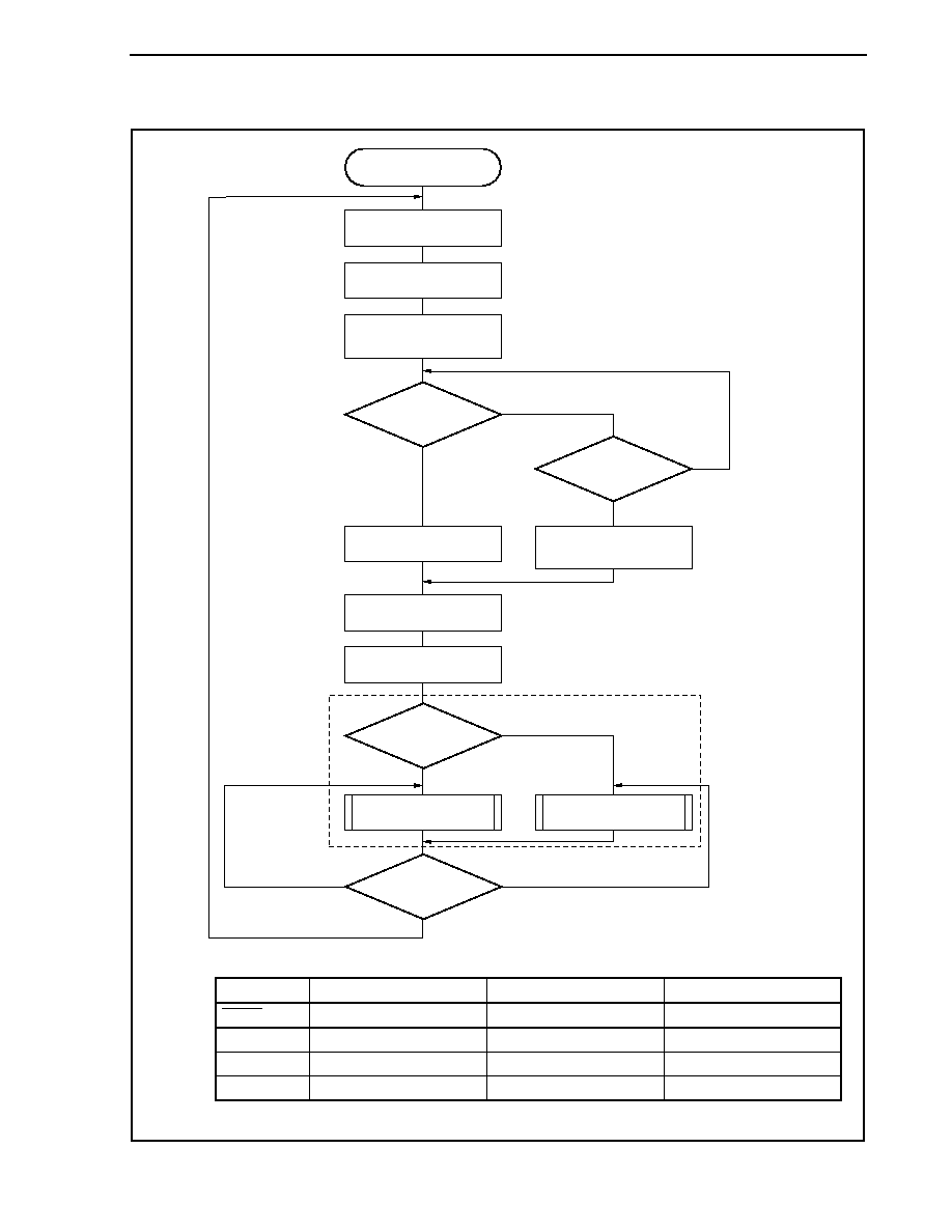
CHAPTER 22 RESET FUNCTIONS
Preliminary User's Manual U17714EJ1V0UD
719
22.3.5 Reset function operation flow
Start (reset source occurs)
Main clock
oscillation stabilization
time secured?
No
CCLS.CCLSF bit = 1?
Yes
No
(in normal operation mode)
No
(in emergent operation mode)
Reset source generated?
Yes
No
Yes (in normal
operation mode)
WDT2 overflow?
No
Yes (in emergent operation mode)
Set RESF register
Note 1
Reset occurs
reset release
Emergent operation
Software processing
Normal operation
CPU operation starts from reset address
(f
CPU
= f
X
/8, f
R
)
Firmware opration
f
CPU
= f
X
f
CPU
= f
R
Note 2
CCLS.CCLSF bit
1
WDT2 restart
Internal oscillation and main clock
oscillation start,
WDT2 count up starts
(reset mode)
Notes 1. Bit to be set differs depending on the reset source.
Reset Source
WDT2RF Bit
CRMRF Bit
LVIRF Bit
RESET
pin
0 0 0
WDT2
1
Value before reset is retained.
Value before reset is retained.
CLM
Value before reset is retained.
1
Value before reset is retained.
LVI
Value before reset is retained.
Value before reset is retained.
1
2. The internal oscillator cannot be stopped.
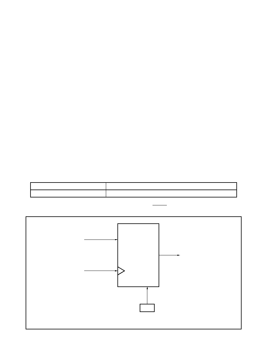
Preliminary User's Manual U17714EJ1V0UD
720
CHAPTER 23 CLOCK MONITOR
23.1 Functions
The clock monitor samples the main clock by using the internal oscillation clock and generates a reset request
signal when oscillation of the main clock is stopped.
Once the operation of the clock monitor has been enabled by an operation enable flag, it cannot be cleared to 0 by
any means other than reset.
When a reset by the clock monitor occurs, the RESF.CLMRF bit is set. For details on the RESF register, see 22.2
Registers to Check Reset Source.
The clock monitor automatically stops under the following conditions.
� During oscillation stabilization time after STOP mode is released
� When the main clock is stopped (from when the PCC.MCK bit = 1 during subclock operation, until the PCC.CLS
bit = 0 during main clock operation)
� When the sampling clock (internal oscillation clock) is stopped
� When the CPU operates with the internal oscillation clock
23.2 Configuration
The clock monitor includes the following hardware.
Table 23-1. Configuration of Clock Monitor
Item Configuration
Control register
Clock monitor mode register (CLM)
Figure 23-1. Timing of Reset via the RESET Pin Input
Main clock
Internal oscillation
clock
Internal reset signal
Enable/disable
CLME
Clock monitor mode
register (CLM)
CHAPTER 23 CLOCK MONITOR
Preliminary User's Manual U17714EJ1V0UD
721
23.3 Register
The clock monitor is controlled by the clock monitor mode register (CLM).
(1) Clock monitor mode register (CLM)
The CLM register is a special register. This can be written only in a special combination of sequences (see
3.4.7 Special registers).
This register is used to set the operation mode of the clock monitor.
This register can be read or written in 8-bit or 1-bit units.
Reset sets this register to 00H.
After
reset:
00H
R/W
Address:
FFFFF870H
7 6 5 4 3 2 1
<0>
CLM
0 0 0 0 0 0 0
CLME
CLME
Clock monitor operation enable or disable
0
Disable clock monitor operation.
1
Enable clock monitor operation.
Cautions 1. Once the CLME bit has been set to 1, it cannot be cleared to 0 by any means other
than reset.
2. When a reset by the clock monitor occurs, the CLME bit is cleared to 0 and the
RESF.CLMRF bit is set to 1.
CHAPTER 23 CLOCK MONITOR
Preliminary User's Manual U17714EJ1V0UD
722
23.4 Operation
This section explains the functions of the clock monitor. The start and stop conditions are as follows.
<Start condition>
Enabling operation by setting the CLM.CLME bit to 1
<Stop conditions>
� While oscillation stabilization time is being counted after STOP mode is released
� When the main clock is stopped (from when PCC.MCK bit = 1 during subclock operation to when PCC.CLS
bit = 0 during main clock operation)
� When the sampling clock (internal oscillation clock) is stopped
� When the CPU operates using the internal oscillation clock
Table 23-2. Operation Status of Clock Monitor
(When CLM.CLME Bit = 1, During Internal Oscillation Clock Operation)
CPU Operating Clock
Operation Mode
Status of Main Clock
Status of Internal
Oscillation Clock
Status of Clock Monitor
HALT mode
Oscillates
Oscillates
Note 1
Operates
Note 2
IDLE1, IDLE2 modes
Oscillates
Oscillates
Note 1
Operates
Note 2
Main clock
STOP mode
Stops
Oscillates
Note 1
Stops
Subclock (MCK bit of
PCC register = 0)
Sub-IDLE mode
Oscillates
Oscillates
Note 1
Operates
Note 2
Subclock (MCK bit of
PCC register = 1)
Sub-IDLE mode
Stops
Oscillates
Note 1
Stops
Internal oscillation clock
�
Stops
Oscillates
Note 3
Stops
During reset
�
Stops
Stops
Stops
Notes 1. The internal oscillator can be stopped by setting the RCM.RSTOP bit to 1.
2. The clock monitor is stopped while the internal oscillator is stopped.
3.
The internal oscillator cannot be stopped by software.
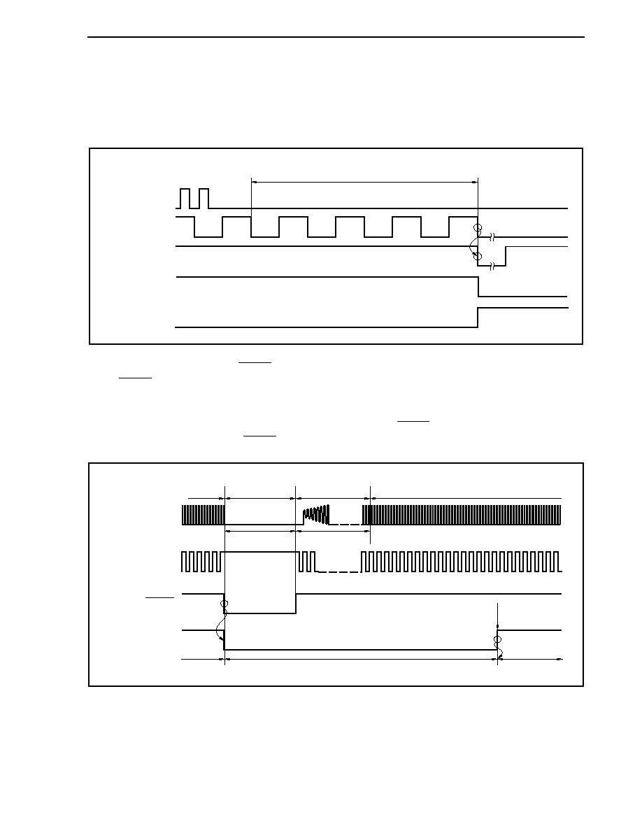
CHAPTER 23 CLOCK MONITOR
Preliminary User's Manual U17714EJ1V0UD
723
(1) Operation when main clock oscillation is stopped (CLME bit = 1)
If oscillation of the main clock is stopped when the CLME bit = 1, an internal reset signal is generated as
shown in Figure 23-2.
Figure 23-2. Reset Period Due to That Oscillation of Main Clock Is Stopped
Four internal oscillation clocks
Main clock
Internal oscillation
clock
Internal reset
signal
CLM.CLME bit
RESF.CLMRF bit
(2) Clock monitor status after RESET input
RESET input clears the CLM.CLME bit to 0 and stops the clock monitor operation. When CLME bit is set to 1
by software at the end of the oscillation stabilization time of the main clock, monitoring is started.
Figure 23-3. Clock Monitor Status After RESET Input
(CLM.CLME bit = 1 is set after RESET input and at the end of main clock oscillation stabilization time)
CPU operation
Clock monitor status
CLME
RESET
Internal oscillation
clock
Main clock
Reset
Oscillation
stabilization time
Normal
operation
Clock supply
stopped
Normal operation
Monitoring
Monitoring stopped
Monitoring
Set to 1 by software
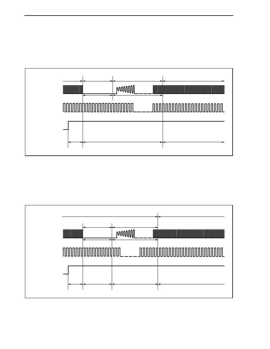
CHAPTER 23 CLOCK MONITOR
Preliminary User's Manual U17714EJ1V0UD
724
(3) Operation in STOP mode or after STOP mode is released
If the STOP mode is set with the CLM.CLME bit = 1, the monitor operation is stopped in the STOP mode and
while the oscillation stabilization time is being counted. After the oscillation stabilization time, the monitor
operation is automatically started.
Figure 23-4. Operation in STOP Mode or After STOP Mode Is Released
Clock monitor
status
During
monitor
Monitor stops
During monitor
CLME
Internal oscillation
clock
Main clock
CPU
operation
Normal
operation
STOP
Oscillation stabilization time
Normal operation
Oscillation stops
Oscillation stabilization time
(set by OSTS register)
(4) Operation when main clock is stopped (arbitrary)
During subclock operation (PCC.CLS bit = 1) or when the main clock is stopped by setting the PCC.MCK bit to
1, the monitor operation is stopped until the main clock operation is started (PCC.CLS bit = 0). The monitor
operation is automatically started when the main clock operation is started.
Figure 23-5. Operation When Main Clock Is Stopped (Arbitrary)
Clock monitor
status
During
monitor
Monitor stops
Monitor stops
During monitor
CLME
Internal oscillation
clock
Main clock
CPU
operation
Oscillation stops
Subclock operation
Main clock operation
Oscillation stabilization time
(set by OSTS register)
Oscillation stabilization
time count by software
PCC.MCK bit = 1
(5) Operation while CPU is operating on internal oscillation clock (CCLS.CCLSF bit = 1)
The monitor operation is not stopped when the CCLSF bit is 1, even if the CLME bit is set to 1.
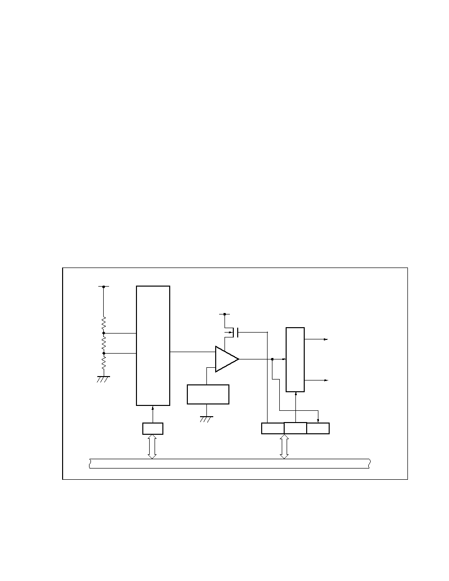
Preliminary User's Manual U17714EJ1V0UD
725
CHAPTER 24 LOW-VOLTAGE DETECTOR (LVI)
24.1 Functions
The low-voltage detector (LVI) has the following functions.
� Compares the supply voltage (V
DD
) and detected voltage (V
LVI
) and generates an internal interrupt signal or
internal reset signal when V
DD
< V
LVI
.
� The level of the supply voltage to be detected can be changed by software (in two steps).
� Interrupt or reset signal can be selected by software.
� Can operate in STOP mode.
If the low-voltage detector is used to generate a reset signal, the RESF.LVIRF bit is set to 1 when the reset signal is
generated. For details of RESF register, see 22.2 Registers to Check Reset Source.
24.2 Configuration
The block diagram of the low-voltage detector is shown below.
Figure 24-1. Block Diagram of Low-Voltage Detector
LVIS0
LVION
Detected voltage
source (V
LVI
)
V
DD
V
DD
INTLVI
Internal bus
N-ch
Low-voltage detection level
select register (LVIS)
Low-voltage detection
register (LVIM)
LVIMD
LVIF
Internal reset signal
Selector
Low-
voltage
detection
level
selector
-
+
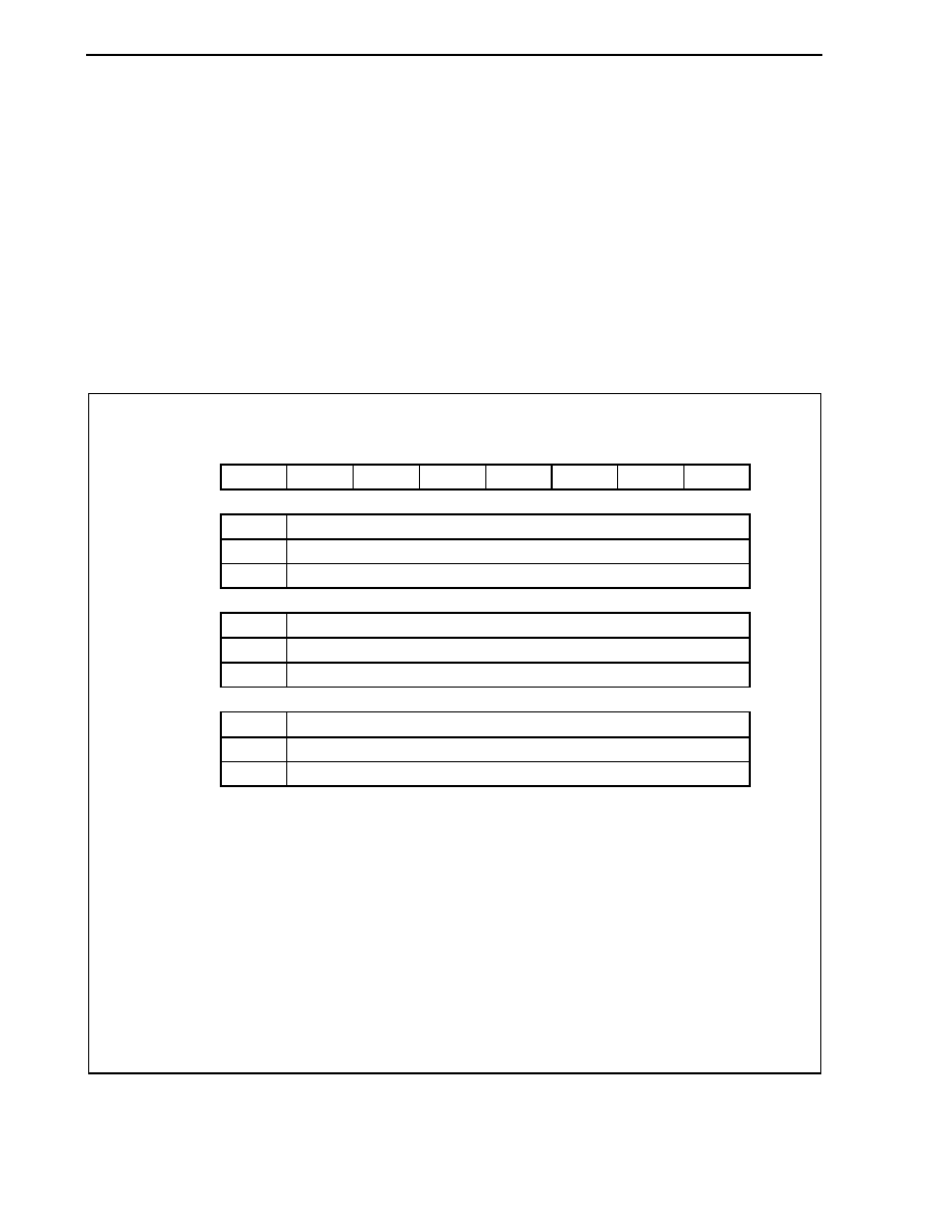
CHAPTER 24 LOW-VOLTAGE DETECTOR (LVI)
Preliminary User's Manual U17714EJ1V0UD
726
24.3 Registers
The low-voltage detector is controlled by the following registers.
� Low-voltage detection register (LVIM)
� Low-voltage detection level select register (LVIS)
(1) Low-voltage detection register (LVIM)
The LVIM register is a special register. This can be written only in the special combination of the sequences
(see 3.4.7 Special registers).
The LVIM register is used to enable or disable low-voltage detection, and to set the operation mode of the low-
voltage detector.
This register can be read or written in 8-bit or 1-bit units. However, the LVIF bit is read-only.
After
reset:
Note 1
R/W
Address:
FFFFF890H
<7>
6 5 4 3 2
<1>
<0>
LVIM
LVION
0 0 0 0 0
LVIMD
LVIF
LVION
Low-voltage detection operation enable or disable
0
Disable
operation.
1
Enable
operation.
LVIMD
Selection of operation mode of low-voltage detection
0
Generate interrupt request signal INTLVI when supply voltage < detected voltage.
1
Generate internal reset signal LVIRES when supply voltage < detected voltage.
LVIF
Note 2
Low-voltage
detection
flag
0
When supply voltage > detected voltage, or when operation is disabled
1
Supply voltage of connected power supply < detected voltage
Notes 1. Reset by low-voltage detection: 82H
Reset due to other source: 00H
2. The value of the LVIF flag is output as the interrupt request signal INTLVI when the LVION
bit = 1 and LVIMD bit = 0.
Cautions 1. When the LVION and LVIMD bits to 1, the low-voltage detector cannot be stopped
until the reset request due to other than the low-voltage detection is generated.
2. When the LVION bit is set to 1, the comparator in the LVI circuit starts operating.
Wait 0.2 ms or longer by software before checking the voltage at the LVIF bit after
the LVION bit is set.
3. Be sure to clear bits 6 to 2 to "0".
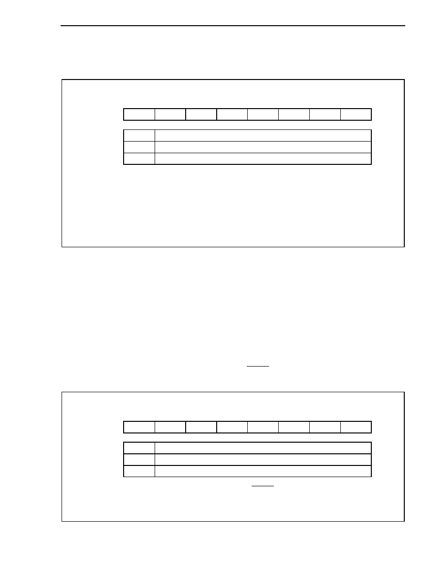
CHAPTER 24 LOW-VOLTAGE DETECTOR (LVI)
Preliminary User's Manual U17714EJ1V0UD
727
(2) Low-voltage detection level select register (LVIS)
The LVIS register is used to select the level of low voltage to be detected.
This register can be read or written in 8-bit or 1-bit units.
After
reset:
Note
R/W
Address:
FFFFF891H
7 6 5 4 3 2 1 0
LVIS
0 0 0 0 0 0 0
LVIS0
LVIS0
Detection
level
0
3.0 V �0.15 V
1
2.85 V �0.15 V (setting prohibited)
Note Reset by low-voltage detection: Retained
Reset due to other source: 00H
Cautions 1. This register cannot be written until a reset request due to something other than
low-voltage detection is generated after the LVIM.LVION and LVIM.LVIMD bits are
set to 1.
2. Be sure to clear bits 7 to 1 to "0".
(3) Internal RAM data status register (RAMS)
The RAMS register is a special register. This can be written only in a special combination of sequences (see
3.4.7 Special registers).
This register is a flag register that indicates whether the internal RAM is valid or not.
This register can be read or written in 8-bit or 1-bit units.
The set/clear conditions for the RAMF bit are shown below.
� Setting conditions: Detection of voltage lower than specified level
Set by instruction
Generation of reset signal by WDT2 and CLM
Generation of reset signal while RAM is being accessed
Generation of reset signal via the RESET pin while internal RAM is being accessed.
� Clearing condition: Writing of 0 in specific sequence
After
reset:
01H
Note
R/W
Address:
FFFFF892H
7 6 5 4 3 2 1
<0>
RAMS
0 0 0 0 0 0 0
RAMF
RAMF
Internal RAM data valid/invalid
0
Valid
1
Invalid
Note This register is set to 01H after reset by the RESET pin input (only for RAM access), watchdog
timer 2 overflow, or clock monitor. After reset by other sources, the register value at that time
is retained.
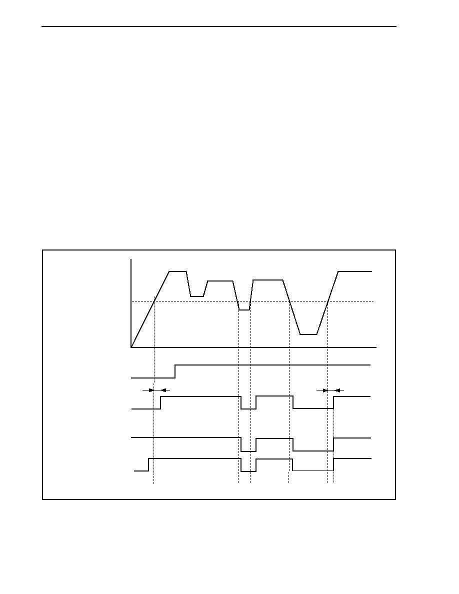
CHAPTER 24 LOW-VOLTAGE DETECTOR (LVI)
Preliminary User's Manual U17714EJ1V0UD
728
24.4 Operation
Depending on the setting of the LVIM.VIMD bit, an interrupt signal (INTLVI) or an internal reset signal is generated.
How to specify each operation is described below, together with timing charts.
24.4.1 To use for internal reset signal
<To start operation>
<1> Mask the interrupt of LVI.
<2> Select the voltage to be detected by using the LVIS.LVIS0 bit.
<3> Set the LVIM.LVION bit to 1 (to enable operation).
<4> Insert a wait cycle of 0.2 ms (max.) or more by software.
<5> By using the LVIM.LVIF bit, check if the supply voltage > detected voltage.
<6> Set the LVIMD bit to 1 (to generate an internal reset signal).
Caution If the LVIMD bit is set to 1, the contents of the LVIM and LVIS registers cannot be changed until a
reset request other than LVI is generated.
Figure 24-2. Operation Timing of Low-Voltage Detector (LVIMD Bit = 1)
Supply voltage (V
DD
)
LVI detected voltage
(3.0
�0.15 V)
LVION bit
LVI detected signal
Internal reset signal
(active low)
LVI reset request signal
Delay
Clear
Delay
Time
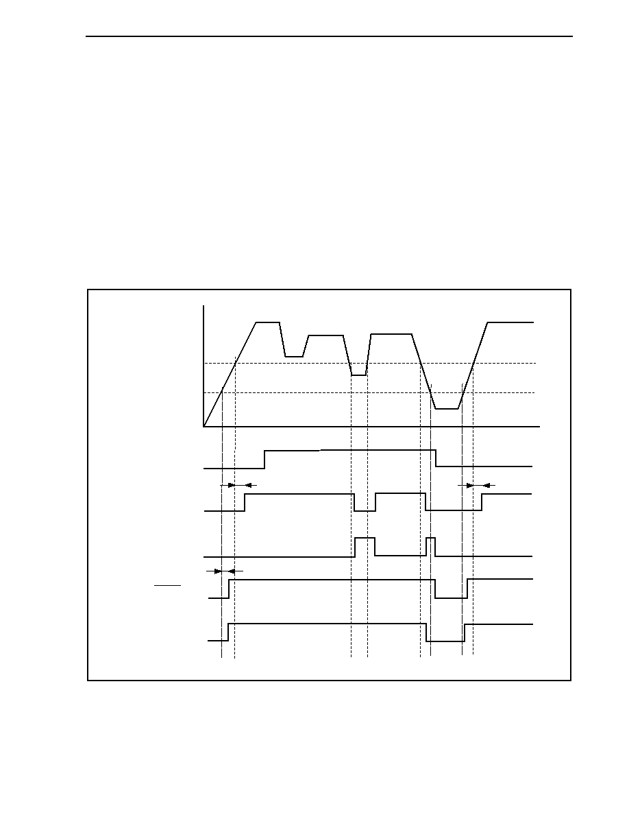
CHAPTER 24 LOW-VOLTAGE DETECTOR (LVI)
Preliminary User's Manual U17714EJ1V0UD
729
24.4.2 To use for interrupt
<To start operation>
<1> Mask the interrupt of LVI.
<2> Select the voltage to be detected by using the LVIS.LVIS0 bit.
<3> Set the LVIM.LVION bit to 1 (to enable operation).
<4> Insert a wait cycle of 0.2 ms (max.) or more by software.
<5> By using the LVIM.LVIF bit, check if the supply voltage > detected voltage.
<6> Clear the interrupt request flag of LVI.
<7> Unmask the interrupt of LVI.
<To stop operation>
Clear the LVION bit to 0.
Figure 24-3. Operation Timing of Low-Voltage Detector (LVIMD Bit = 0)
External RESETIC
detected voltage
RESET pin
INTLVI signal
Supply voltage (V
DD
)
LVI detected voltage
(3.0
�0.15 V)
LVION bit
LVI detected signal
Internal reset signal
(active low)
Delay
Clear
Delay
Time
Delay
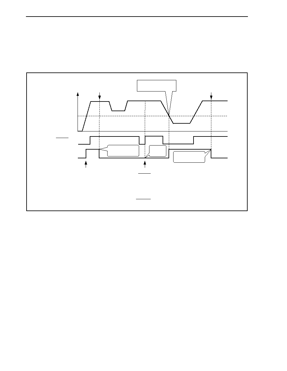
CHAPTER 24 LOW-VOLTAGE DETECTOR (LVI)
Preliminary User's Manual U17714EJ1V0UD
730
24.5 RAM Retention Voltage Detection Operation
The supply voltage and detected voltage are compared. When the supply voltage drops below the detected voltage
(including on power application), the RAMS.RAMF bit is set to 1.
Figure 24-4. Operation Timing of RAM Retention Voltage Detection Function
Supply voltage (V
DD
)
2.0 V
(minimum RAM
retention voltage)
RESET pin
RAMS.RAMF bit
Initialize RAM
(RAMF bit is also cleared)
When power application,
RAMF bit is set
RAM data
is retained
RAM data
is retained
RAMF bit = 0 is retained regardless
of RESET pin if V
DD
> 2.0 V
Initialize RAM
(RAMF bit is also cleared)
V
DD
< 2.0 V detected
Set RAMF bit
RAM data is
not retained
Remarks 1. The RAMF bit is set to 1 if the supply voltage drops under the minimum RAM retention voltage
(2.0 V (TYP.)).
2. The RAMF bit operates regardless of the RESET pin status.
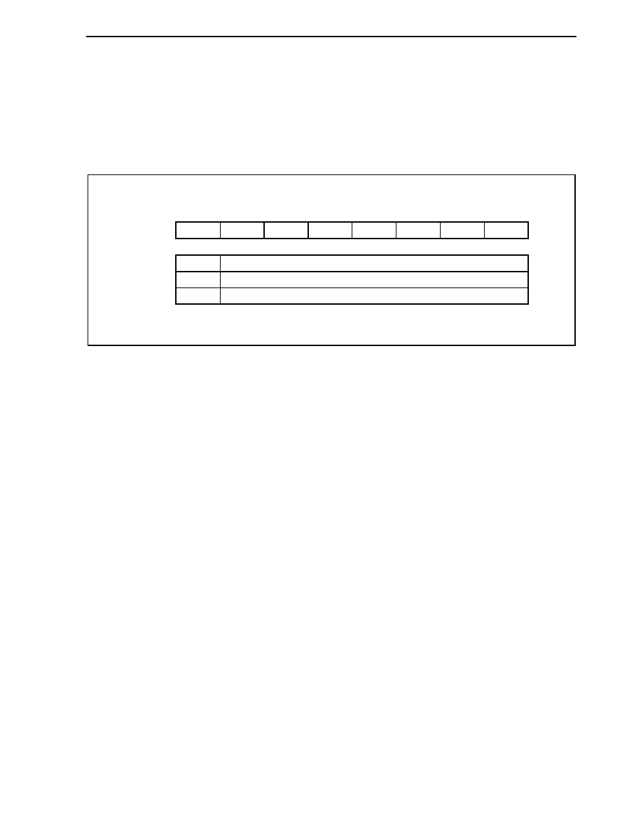
CHAPTER 24 LOW-VOLTAGE DETECTOR (LVI)
Preliminary User's Manual U17714EJ1V0UD
731
24.6 Emulation Function
When an in-circuit emulator is used, the operation of the RAM retention flag (RAMS.RAMF bit) can be pseudo-
controlled and emulated by manipulating the PEMU1 register on the debugger.
This register is valid only in the emulation mode. It is invalid in the normal mode.
(1) Peripheral emulation register 1 (PEMU1)
After
reset:
00H
R/W
Address:
FFFFF9FEH
7 6 5 4 3 2 1 0
PEMU1
0 0 0 0 0
EVARAMIN
0 0
EVARAMIN
Pseudo specification of RAM retention voltage detection signal
0
Do not detect voltage lower than RAM retention voltage.
1
Detect voltage lower than RAM retention voltage (set RAMF flag).
Caution This bit is not automatically cleared.
[Usage]
When an in-circuit emulator is used, pseudo emulation of RAMF is realized by rewriting this register on the
debugger.
<1> CPU break (CPU operation stops.)
<2> Set the EVARAMIN bit to 1 by using a register write command.
By setting the EVARAMIN bit to 1, the RAMF bit is set to 1 on hardware (the internal RAM data is invalid).
<3> Clear the EVARAMIN bit to 0 by using a register write command again.
Unless this operation is performed (clearing the EVARAMIN bit to 0), the RAMF bit cannot be cleared to 0 by
a CPU operation instruction.
<4> Run the CPU and resume emulation.
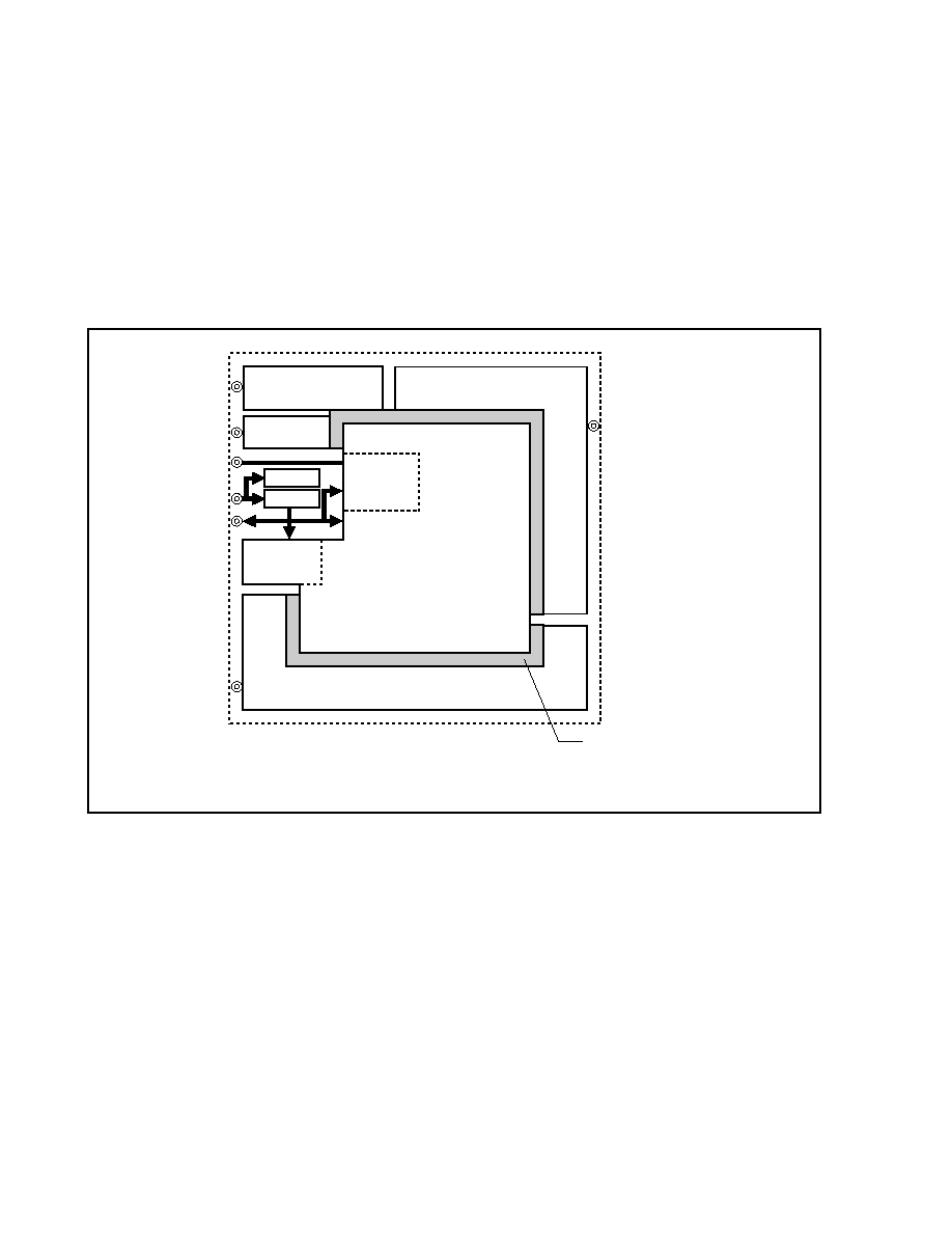
Preliminary User's Manual U17714EJ1V0UD
732
CHAPTER 25 REGULATOR
25.1 Overview
The V850ES/JJ2 includes a regulator to reduce power consumption and noise.
This regulator supplies a stepped-down V
DD
power supply voltage to the oscillator block and internal logic circuits
(except the A/D converter, D/A converter, and output buffers). The regulator output voltage is set to 2.5 V (TYP.).
Figure 25-1. Regulator
BV
DD
AV
REF0
AV
REF1
FLMD0
V
DD
EV
DD
REGC
EV
DD
I/O buffer
Bidirectional level shifter
BV
DD
I/O buffer
Regulator
A/D converter
D/A converter
Flash
memory
Main
oscillator
Internal digital circuits
2.5 V (TYP.)
Sub-oscillator
Caution Use the regulator with a setting of V
DD
= EV
DD
= AV
REF0
= AV
REF1
BV
DD
.
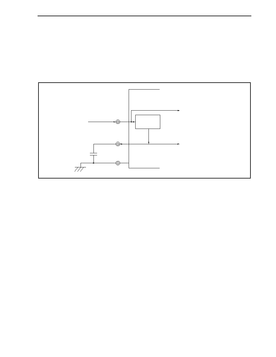
CHAPTER 25 REGULATOR
Preliminary User's Manual U17714EJ1V0UD
733
25.2 Operation
The regulator of this product always operates in any mode (normal operation mode, HALT mode, IDLE1 mode,
IDLE2 mode, STOP mode, or during reset).
Be sure to connect a capacitor (4.7
�
F (preliminary value)) to the REGC pin to stabilize the regulator output.
A diagram of the regulator pin connection method is shown below.
Figure 25-2. REGC Pin Connection
REG
V
DD
V
SS
REGC
Input voltage = 2.85 to 3.6 V
Voltage supply to main oscillator/internal logic = 2.5 V (TYP.)
4.7 F
(preliminary value)
�
Voltage supply to sub-oscillator

Preliminary User's Manual U17714EJ1V0UD
734
CHAPTER 26 FLASH MEMORY
The V850ES/JJ2 incorporates a flash memory.
�
�
PD70F3720: 128 KB flash memory
�
�
PD70F3721: 256 KB flash memory
�
�
PD70F3722: 384 KB flash memory
�
�
PD70F3723: 512 KB flash memory
�
�
PD70F3724: 640 KB flash memory
Flash memory versions offer the following advantages for development environments and mass production
applications.
For altering software after the V850ES/JJ2 is soldered onto the target system.
For data adjustment when starting mass production.
For differentiating software according to the specification in small scale production of various models.
For facilitating inventory management.
For updating software after shipment.
26.1 Features
4-byte/1-clock access (when instruction is fetched)
Capacity: 640/512/384/256/128 KB
Write voltage: Erase/write with a single power supply
Rewriting method
� Rewriting by communication with dedicated flash programmer via serial interface (on-board/off-board
programming)
� Rewriting flash memory by user program (self programming)
Flash memory write prohibit function supported (security function)
Safe rewriting of entire flash memory area by self programming using boot swap function
Interrupts can be acknowledged during self programming.
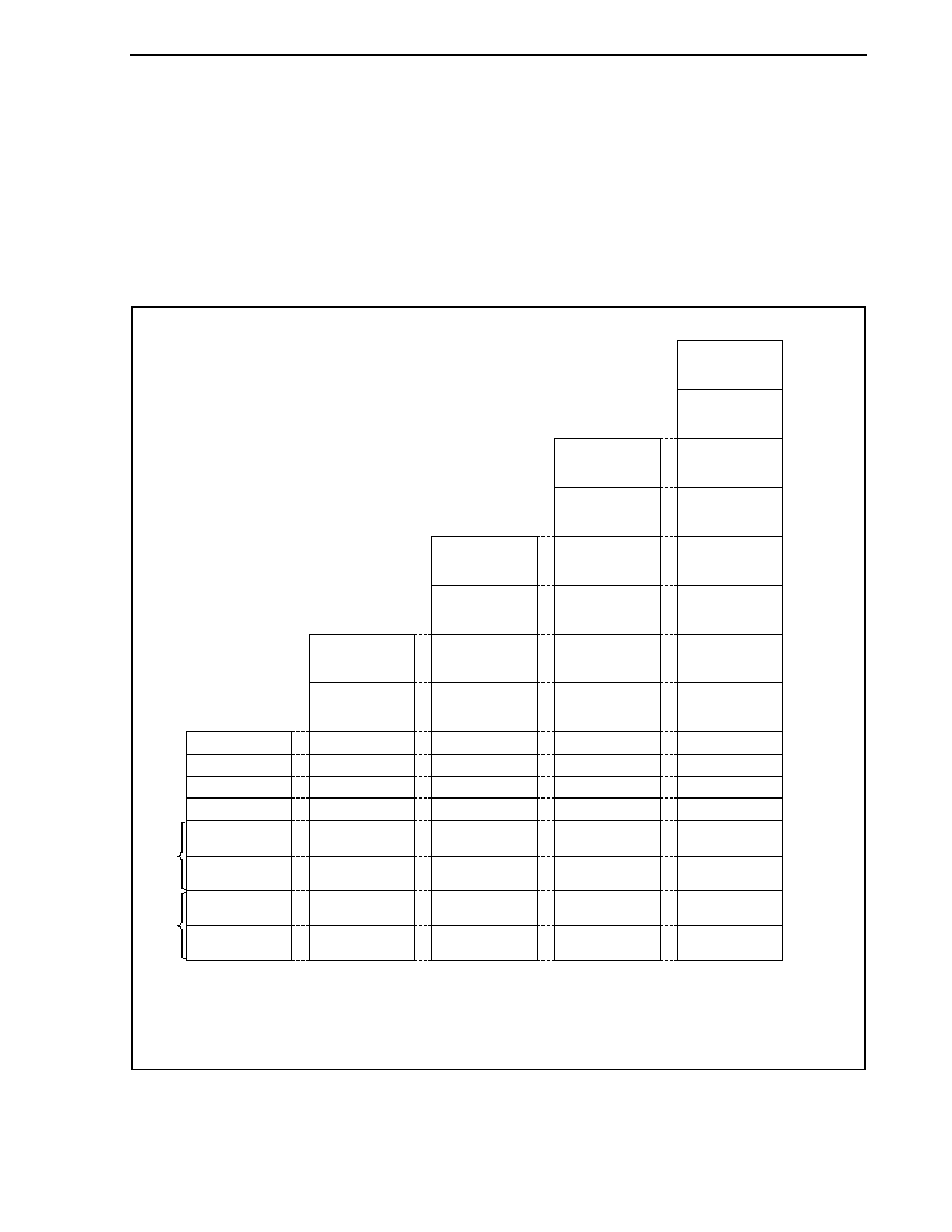
CHAPTER 26 FLASH MEMORY
Preliminary User's Manual U17714EJ1V0UD
735
26.2 Memory Configuration
The V850ES/JJ2 internal flash memory area is divided into 16, 14, 12, 10, or 8 blocks and can be
programmed/erased in block units. All of the blocks can also be erased at once.
When the boot swap function is used, the physical memory allocated at the addresses of blocks 0 and 1 is replaced
by the physical memory allocated at the addresses of blocks 2 and 3. For details of the boot swap function, see 26.5
Rewriting by Self Programming.
Figure 26-1. Flash Memory Mapping
640 KB
Block 0 (28 KB)
Block 1 (28 KB)
Block 2 (28 KB)
Block 3 (28 KB)
Block 5 (4 KB)
Block 6 (4 KB)
Block 7 (4 KB)
Block 8 (64 KB)
Block 4 (4 KB)
Block 9 (64 KB)
Block 10 (64 KB)
Block 11 (64 KB)
Block 12 (64 KB)
Block 13 (64 KB)
512 KB
Block 0 (28 KB)
Block 1 (28 KB)
Block 2 (28 KB)
Block 3 (28 KB)
Block 5 (4 KB)
Block 6 (4 KB)
Block 7 (4 KB)
Block 8 (64 KB)
Block 4 (4 KB)
Block 9 (64 KB)
Block 10 (64 KB)
Block 11 (64 KB)
Block 12 (64 KB)
Block 13 (64 KB)
Block 15 (64 KB)
Block 14 (64 KB)
Note 2
384 KB
Block 0 (28 KB)
Block 1 (28 KB)
Block 2 (28 KB)
Block 3 (28 KB)
Block 5 (4 KB)
Block 6 (4 KB)
Block 7 (4 KB)
Block 8 (64 KB)
Block 4 (4 KB)
Block 9 (64 KB)
Block 10 (64 KB)
Block 11 (64 KB)
256 KB
Block 0 (28 KB)
Block 1 (28 KB)
Block 2 (28 KB)
Block 3 (28 KB)
Block 5 (4 KB)
Block 6 (4 KB)
Block 7 (4 KB)
Block 8 (64 KB)
Block 4 (4 KB)
Block 9 (64 KB)
128 KB
Block 0 (28 KB)
Block 1 (28 KB)
Block 2 (28 KB)
Block 3 (28 KB)
Block 5 (4 KB)
Block 6 (4 KB)
Block 7 (4 KB)
Block 4 (4 KB)
Note 1
0 0 0 0 0 0 0 0 H
0 0 0 0 6 F F F H
0 0 0 0 7 0 0 0 H
0 0 0 0 D F F F H
0 0 0 0 E 0 0 0 H
0 0 0 1 4 F F F H
0 0 0 1 5 0 0 0 H
0 0 0 1 B F F F H
0 0 0 1 C 0 0 0 H
0 0 0 1 C F F F H
0 0 0 1 D 0 0 0 H
0 0 0 1 D F F F H
0 0 0 1 E 0 0 0 H
0 0 0 1 E F F F H
0 0 0 1 F 0 0 0 H
0 0 0 1 F F F F H
0 0 0 2 0 0 0 0 H
0 0 0 2 F F F F H
0 0 0 3 0 0 0 0 H
0 0 0 3 F F F F H
0 0 0 4 0 0 0 0 H
0 0 0 4 F F F F H
0 0 0 5 0 0 0 0 H
0 0 0 5 F F F F H
0 0 0 6 0 0 0 0 H
0 0 0 6 F F F F H
0 0 0 7 0 0 0 0 H
0 0 0 7 F F F F H
0 0 0 8 0 0 0 0 H
0 0 0 8 F F F F H
0 0 0 9 0 0 0 0 H
0 0 0 9 F F F F H
0 0 0 A 0 0 0 0 H
Notes 1. Blocks 2 and 3: Area to be replaced with the boot area by the boot swap function
2. Blocks 0 and 1: Boot area

CHAPTER 26 FLASH MEMORY
Preliminary User's Manual U17714EJ1V0UD
736
26.3 Functional Outline
The internal flash memory of the V850ES/JJ2 can be rewritten by using the rewrite function of the dedicated flash
programmer, regardless of whether the V850ES/JJ2 has already been mounted on the target system or not (off-
board/on-board programming).
In addition, a security function that prohibits rewriting the user program written to the internal flash memory is also
supported, so that the program cannot be changed by an unauthorized person.
The rewrite function using the user program (self programming) is ideal for an application where it is assumed that
the program is changed after production/shipment of the target system. A boot swap function that rewrites the entire
flash memory area safely is also supported. In addition, interrupt servicing is supported during self programming, so
that the flash memory can be rewritten under various conditions, such as while communicating with an external device.
Table 26-1. Rewrite Method
Rewrite Method
Functional Outline
Operation Mode
On-board programming
Flash memory can be rewritten after the device is mounted on the
target system, by using a dedicated flash programmer.
Off-board programming
Flash memory can be rewritten before the device is mounted on the
target system, by using a dedicated flash programmer and a dedicated
program adapter board (FA series).
Flash memory
programming mode
Self programming
Flash memory can be rewritten by executing a user program that has
been written to the flash memory in advance by means of off-board/on-
board programming. (During self-programming, instructions cannot be
fetched from or data access cannot be made to the internal flash
memory area. Therefore, the rewrite program must be transferred to
the internal RAM or external memory in advance.)
Normal operation mode
Remark The FA series is a product of Naito Densei Machida Mfg. Co., Ltd.
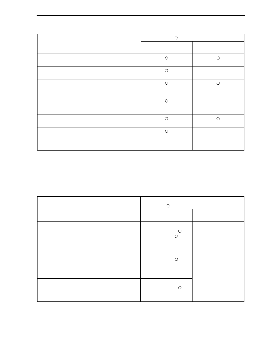
CHAPTER 26 FLASH MEMORY
Preliminary User's Manual U17714EJ1V0UD
737
Table 26-2. Basic Functions
Support (
: Supported,
�: Not supported)
Function Functional
Outline
On-Board/Off-Board
Programming
Self Programming
Block erasure
The contents of specified memory blocks
are erased.
Chip erasure
The contents of the entire memory area
are erased all at once.
�
Write
Writing to specified addresses, and a
verify check to see if write level is secured
are performed.
Verify/checksum
Data read from the flash memory is
compared with data transferred from the
flash programmer.
�
(Can be read by user
program)
Blank check
The erasure status of the entire memory is
checked.
Security setting
Use of the block erase command, chip
erase command, and program command
can be prohibited.
�
(Only values set by on-
board/off-board programming
can be retained)
The following table lists the security functions. The block erase command prohibit, chip erase command prohibit,
and program command prohibit functions are enabled by default after shipment, and security can be set by rewriting
via on-board/off-board programming. Each security function can be used in combination with the others at the same
time.
Table 26-3. Security Functions
Rewriting Operation When Prohibited
(
: Executable,
�: Not Executable)
Function Function
Outline
On-Board/Off-Board
Programming
Self Programming
Block erase
command
prohibit
Execution of a block erase command on
all blocks is prohibited. Setting of
prohibition can be initialized by execution
of a chip erase command.
Block erase command:
�
Chip erase command:
Program command:
Chip erase
command
prohibit
Execution of block erase and chip erase
commands on all the blocks is prohibited.
Once prohibition is set, setting of
prohibition cannot be initialized because
the chip erase command cannot be
executed.
Block erase command:
�
Chip erase command:
�
Program command:
Program
command
prohibit
Write and block erase commands on all
the blocks are prohibited. Setting of
prohibition can be initialized by execution
of the chip erase command.
Block erase command:
�
Chip erase command:
Program command:
�
Can always be rewritten
regardless of setting of
prohibition
CHAPTER 26 FLASH MEMORY
Preliminary User's Manual U17714EJ1V0UD
738
26.4 Rewriting by Dedicated Flash Programmer
The flash memory can be rewritten by using a dedicated flash programmer after the V850ES/JJ2 is mounted on the
target system (on-board programming). The flash memory can also be rewritten before the device is mounted on the
target system (off-board programming) by using a dedicated program adapter (FA series).
26.4.1 Programming environment
The following shows the environment required for writing programs to the flash memory of the V850ES/JJ2.
Figure 26-2. Environment Required for Writing Programs to Flash Memory
Host machine
RS-232C
Dedicated flash
programmer
V850ES/JJ2
FLMD1
Note
V
DD
V
SS
RESET
UARTA0/CSIB0/CSIB3
PG-FP4
(Flash Pro4)
Cxxxxxx
Bxxxxx
Axxxx
XXX YYY
X
X
X
X
X
X
X
X
X
X
X
X
X
X
X
XXXX YYYY
STATVE
FLMD0
USB
Note Connect the FLMD1 pin to the flash programmer or connect to a GND via a pull-down resistor on the board.
A host machine is required for controlling the dedicated flash programmer.
UARTA0, CSIB0, or CSIB3 is used for the interface between the dedicated flash programmer and the V850ES/JJ2
to perform writing, erasing, etc. A dedicated program adapter (FA series) required for off-board writing.
Remark The FA series is a product of Naito Densei Machida Mfg. Co., Ltd.
CHAPTER 26 FLASH MEMORY
Preliminary User's Manual U17714EJ1V0UD
739
26.4.2 Communication mode
Communication between the dedicated flash programmer and the V850ES/JJ2 is performed by serial
communication using the UARTA0, CSIB0, or CSIB3 interfaces of the V850ES/JJ2.
(1) UARTA0
Transfer rate: 9,600 to 153,600 bps
Figure 26-3. Communication with Dedicated Flash Programmer (UARTA0)
Dedicated flash
programmer
V850ES/JJ2
V
DD
V
SS
RESET
TXDA0
RXDA0
FLMD1
FLMD1
Note
V
DD
GND
RESET
RxD
TxD
PG-FP4
(Flash Pro4)
Cxxxxxx
Bxxxxx
Axxxx
XXX YYY
X
X
X
X
X
X
X
X
X
X
X
X
X
X
X
XXXX YYYY
STATVE
FLMD0
FLMD0
Note Connect the FLMD1 pin to the flash programmer or connect to GND via a pull-down resistor on the board.
(2) CSIB0, CSIB3
Serial clock: 2.4 kHz to 2.5 MHz (MSB first)
Figure 26-4. Communication with Dedicated Flash Programmer (CSIB0, CSIB3)
Dedicated flash
programmer
V850ES/JJ2
FLMD1
Note
V
DD
V
SS
RESET
SOB0, SOB3
SIB0, SIB3
SCKB0, SCKB3
FLMD1
V
DD
GND
RESET
SI
SO
SCK
PG-FP4
(Flash Pro4)
Cxxxxxx
Bxxxxx
Axxxx
X
XX YYY
X
X
X
X
X
X
X
X
X
X
X
X
X
X
X
XXXX YYYY
STATVE
FLMD0
FLMD0
Note Connect the FLMD1 pin to the flash programmer or connect to GND via a pull-down resistor on the board.
CHAPTER 26 FLASH MEMORY
Preliminary User's Manual U17714EJ1V0UD
740
(3) CSIB0 + HS, CSIB3 + HS
Serial clock: 2.4 kHz to 2.5 MHz (MSB first)
Figure 26-5. Communication with Dedicated Flash Programmer (CSIB0 + HS, CSIB3 + HS)
Dedicated flash
programmer
V850ES/JJ2
V
DD
V
SS
RESET
SOB0, SOB3
SIB0, SIB3
SCKB0, SCKB3
PCM0
V
DD
FLMD1
FLMD1
Note
GND
RESET
SI
SO
SCK
HS
PG-FP4
(Flash Pro4)
Cxxxxxx
Bxxxxx
Axxxx
XXX YYY
X
X
X
X
X
X
X
X
X
X
X
X
X
X
X
XXXX YYYY
STATVE
FLMD0
FLMD0
Note Connect the FLMD1 pin to the flash programmer or connect to a GND via a pull-down resistor on the board.
The dedicated flash programmer outputs the transfer clock, and the V850ES/JJ2 operates as a slave.
When the PG-FP4 is used as the dedicated flash programmer, it generates the following signals to the V850ES/JJ2.
For details, refer to the PG-FP4 User's Manual (U15260E).
Table 26-4. Signal Connections of Dedicated Flash Programmer (PG-FP4)
PG-FP4 V850ES/JJ2
Processing for Connection
Signal Name
I/O
Pin Function
Pin Name
UARTA0
CSIB0,
CSIB3
CSIB0 + HS,
CSIB3 + HS
FLMD0 Output
Write
enable/disable
FLMD0
FLMD1 Output
Write
enable/disable
FLMD1
Note 1
Note 1
Note 1
VDD
-
V
DD
voltage generation/voltage monitor
V
DD
GND
-
Ground V
SS
CLK
Output
Clock output to V850ES/JJ2
X1, X2
�
Note 2
�
Note 2
�
Note 2
RESET Output
Reset
signal
RESET
SI/RxD Input
Receive
signal
SOB0, SOB3/
TXDA0
SO/TxD Output
Transmit
signal
SIB0, SIB3/
RXDA0
SCK Output
Transfer
clock
SCKB0,
SCKB3
�
HS Input
Handshake signal for CSIB0 + HS, CSIB3
+ HS communication
PCM0
�
�
Notes 1. Wire these pins as shown in Figure 26-6, or connect then to GND via pull-down resistor on board.
2. Clock cannot be supplied via the CLK pin of the flash programmer. Create an oscillator on board and
supply the clock.
Remark
: Must be connected.
�: Does not have to be connected.
CHAPTER 26 FLASH MEMORY
Preliminary User's Manual U17714EJ1V0UD
741
Table 26-5. Wiring of Flash Writing Adapter for V850ES/JJ2 (FA-144GJ-UEN) (1/2)
Flash Programmer (PG-FP4)
Connection Pins
When CSIB0 + HS Is
Used
When CSIB0 Is Used
When UARTA0 Is Used
Signal
Name
I/O Pin
Function
Pin Name
on FA
Board
Pin Name
Pin
No.
Pin Name
Pin
No.
Pin Name
Pin
No.
SI/RxD Input
Receive
signal SI
P41/SOB0/SCL01 23 P41/SOB0/SCL01
23 P30/TXDA0/SOB4 25
SO/TxD Output Transmit
signal SO
P40/SIB0/SDA01 22 P40/SIB0/SDA01 22 P31/RXDA0/INTP7/
SIB4
26
SCK Output
Transfer
clock
SCK
P42/SCKB0
24
P42/SCKB0
24
Not
necessary
-
X1 Not
necessary
-
Not necessary
- Not necessary
-
CLK Output
Clock
to
V850ES/JJ2
X2 Not
necessary
-
Not necessary
- Not necessary
-
/RESET Output Reset signal
/RESET
RESET
14
RESET
14 RESET
14
FLMD0 Input Write
voltage FLMD0 FLMD0
8 FLMD0
8 FLMD0
8
FLMD1 Input Write
voltage FLMD1 PDL5/AD5/FLMD1 110 PDL5/AD5/FLMD1 110
PDL5/AD5/FLMD1 110
HS Input
Handshake
signal of CSI0
+ HS
communication
RESERVE/
HS
PCM0/WAIT 85
Not
necessary
- Not necessary
-
V
DD
9
V
DD
9
V
DD
9
BV
DD
104
BV
DD
104
BV
DD
104
EV
DD
34
EV
DD
34
EV
DD
34
AV
REF0
1
AV
REF0
1
AV
REF0
1
VDD
-
VDD voltage
generation/
voltage monitor
VDD
AV
REF1
5
AV
REF1
5
AV
REF1
5
V
SS
11
V
SS
11
V
SS
11
AV
SS
2
AV
SS
2
AV
SS
2
BV
SS
103
BV
SS
103
BV
SS
103
GND
-
Ground GND
EV
SS
33
EV
SS
33
EV
SS
33
Cautions 1. Be sure to connect the REGC pin to GND via a 4.7
�
F capacitor.
2. A clock cannot be supplied from the CLK pin of the flash programmer. Create an oscillator on
the board and supply the clock from that oscillator.
CHAPTER 26 FLASH MEMORY
Preliminary User's Manual U17714EJ1V0UD
742
Table 26-5. Wiring of Flash Writing Adapter for V850ES/JJ2 (FA-144GJ-UEN) (2/2)
Flash Programmer (PG-FP4)
Connection Pins
When CSIB3 + HS Is Used
When CSIB3 Is Used
Signal
Name
I/O Pin
Function
Pin Name on
FA Board
Pin Name
Pin
No.
Pin Name
Pin
No.
SI/RxD
Input
Receive
signal
SI
P911/A11/SOB3 72
P911/A11/SOB3 72
SO/TxD
Output
Transmit
signal
SO P910/A10/SIB3 71
P910/A10/SIB3 71
SCK
Output
Transfer
clock
SCK
P912/A12/SCKB3 73
P912/A12/SCKB3 73
X1 Not
necessary
-
Not necessary
-
CLK Output
Clock
to
V850ES/JJ2
X2 Not
necessary
-
Not necessary
-
/RESET
Output
Reset
signal
/RESET
RESET 14
RESET 14
FLMD0
Input
Write
voltage
FLMD0
FLMD0 8
FLMD0 8
FLMD1
Input
Write
voltage
FLMD1 PDL5/AD5/FLMD1 110
PDL5/AD5/FLMD1 110
HS Input
Handshake
signal
of CSI0 + HS
communication
RESERVE/HS PCM0/WAIT
85 Not
necessary
-
V
DD
9
V
DD
9
BV
DD
104
BV
DD
104
EV
DD
34
EV
DD
34
AV
REF0
1
AV
REF0
1
VDD
-
VDD voltage
generation/
voltage monitor
VDD
AV
REF1
5
AV
REF1
5
V
SS
11
V
SS
11
AV
SS
2
AV
SS
2
BV
SS
103
BV
SS
103
GND
-
Ground GND
EV
SS
33
EV
SS
33
Cautions 1. Be sure to connect the REGC pin to GND via a 4.7
�
F capacitor.
2. A clock cannot be supplied from the CLK pin of the flash programmer. Create an oscillator on
the board and supply the clock from that oscillator.
CHAPTER 26 FLASH MEMORY
Preliminary User's Manual U17714EJ1V0UD
743
Figure 26-6. Example of Wiring of V850ES/JJ2 Flash Writing Adapter (FA-144GJ-UEN)
(in CSIB0 + HS Mode) (1/2)
V850ES/JJ2
VDD
GND
GND
VDD
GND
VDD
VDD
GND
25
30
20
15
75
80
85
90
95
100
105
35
40
45
50
55
60
65
70
110
115
120
125
130
135
140
1
5
10
RFU-3
RFU-2
VDE
FLMD1 FLMD0
RFU-1
SI
SO
SCK
/RESET
V
PP
RESERVE/HS
CLKOUT
Note 4
Note 1
Note 2
2
Note 3
Connect to VDD
Connect to GND
4.7 F (preliminary value)
�
CHAPTER 26 FLASH MEMORY
Preliminary User's Manual U17714EJ1V0UD
744
Figure 26-6. Example of Wiring of V850ES/JJ2 Flash Writing Adapter (FA-144GJ-UEN)
(in CSIB0 + HS Mode) (2/2)
Notes 1. Wire the FLMD1 pin as shown below, or connect it to GND on board via a pull-down resistor.
2. Pins used when CSIB3 is used
3. Supply a clock by creating an oscillator on the flash writing adapter (enclosed by the broken lines).
Here is an example of the oscillator.
Example
X1
X2
4. Pins used when UARTA0 is used.
Caution Do not input a high level to the DRST pin.
Remarks 1. Process the pins not shown in accordance with processing of unused pins (see 2.3 Pin I/O
Circuit Types, I/O Buffer Power Supplies and Handling of Unused Pins).
2. This adapter is for the 144-pin plastic LQFP package.
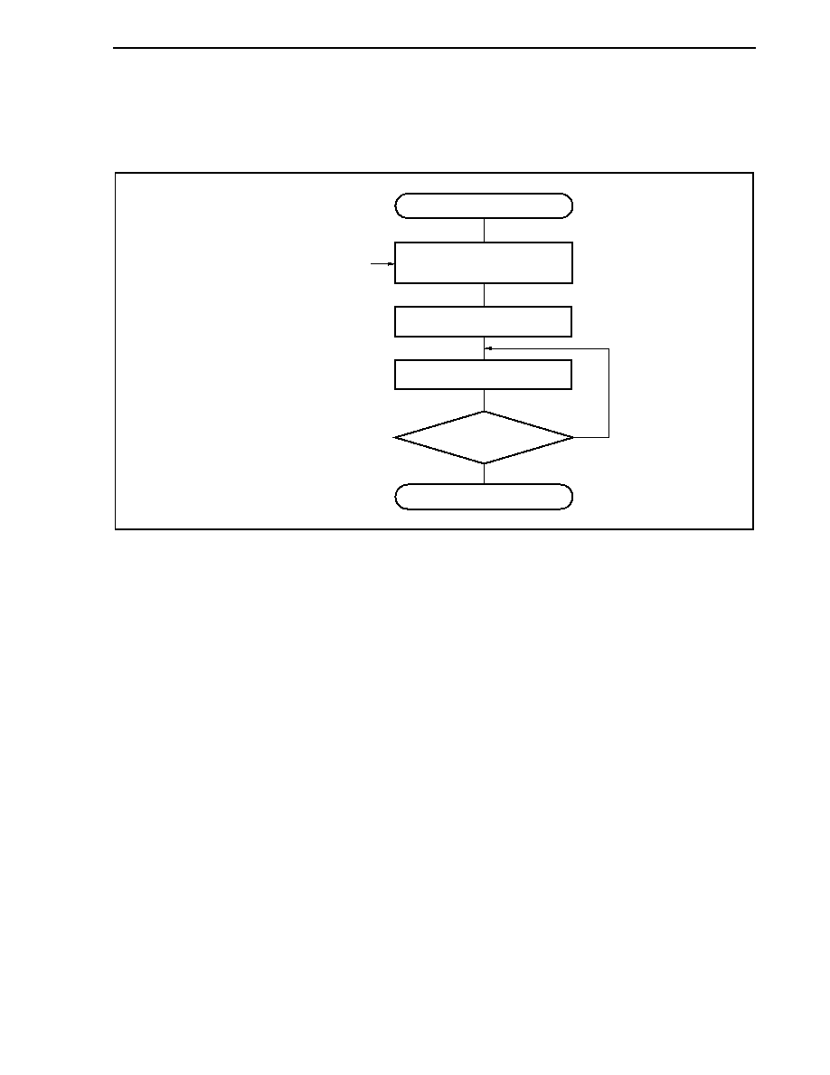
CHAPTER 26 FLASH MEMORY
Preliminary User's Manual U17714EJ1V0UD
745
26.4.3 Flash memory control
The following shows the procedure for manipulating the flash memory.
Figure 26-7. Procedure for Manipulating Flash Memory
Start
Select communication system
Manipulate flash memory
End?
Yes
Supplies FLMD0 pulse
No
End
Switch to flash memory
programming mode
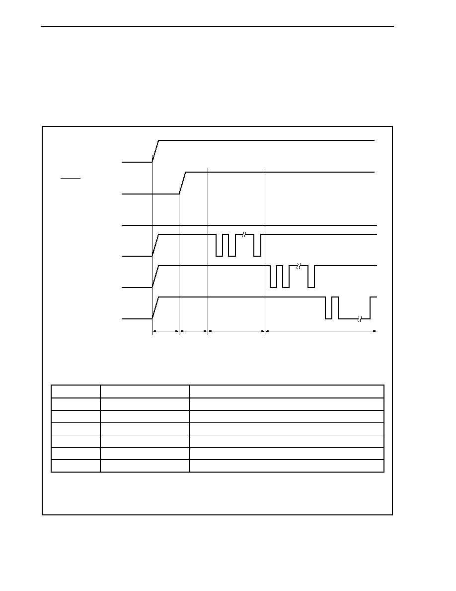
CHAPTER 26 FLASH MEMORY
Preliminary User's Manual U17714EJ1V0UD
746
26.4.4 Selection of communication mode
In the V850ES/JJ2, the communication mode is selected by inputting pulses (12 pulses max.) to the FLMD0 pin
after switching to the flash memory programming mode. The FLMD0 pulse is generated by the dedicated flash
programmer.
The following shows the relationship between the number of pulses and the communication mode.
Figure 26-8. Selection of Communication Mode
V
DD
V
DD
RESET (input)
FLMD1 (input)
FLMD0 (input)
RXDA0 (input)
TXDA0 (output)
V
SS
V
DD
V
SS
V
DD
V
SS
V
DD
V
SS
V
DD
V
SS
V
DD
V
SS
(Note)
Power on
Oscillation
stabilized
Communication
mode selected
Flash control command communication
(erasure, write, etc.)
Reset
released
Note The number of clocks is as follows depending on the communication mode.
FLMD0 Pulse
Communication Mode
Remarks
0
UARTA0
Communication rate: 9,600 bps (after reset), LSB first
8
CSIB0
V850ES/JJ2 performs slave operation, MSB first
9
CSIB3
V850ES/JJ2 performs slave operation, MSB first
11 CSIB0
+ HS
V850ES/JJ2 performs slave operation, MSB first
12 CSIB3
+ HS
V850ES/JJ2 performs slave operation, MSB first
Other RFU
Setting
prohibited
Caution
When UARTA0 is selected, the receive clock is calculated based on the reset command sent
from the dedicated flash programmer after receiving the FLMD0 pulse.
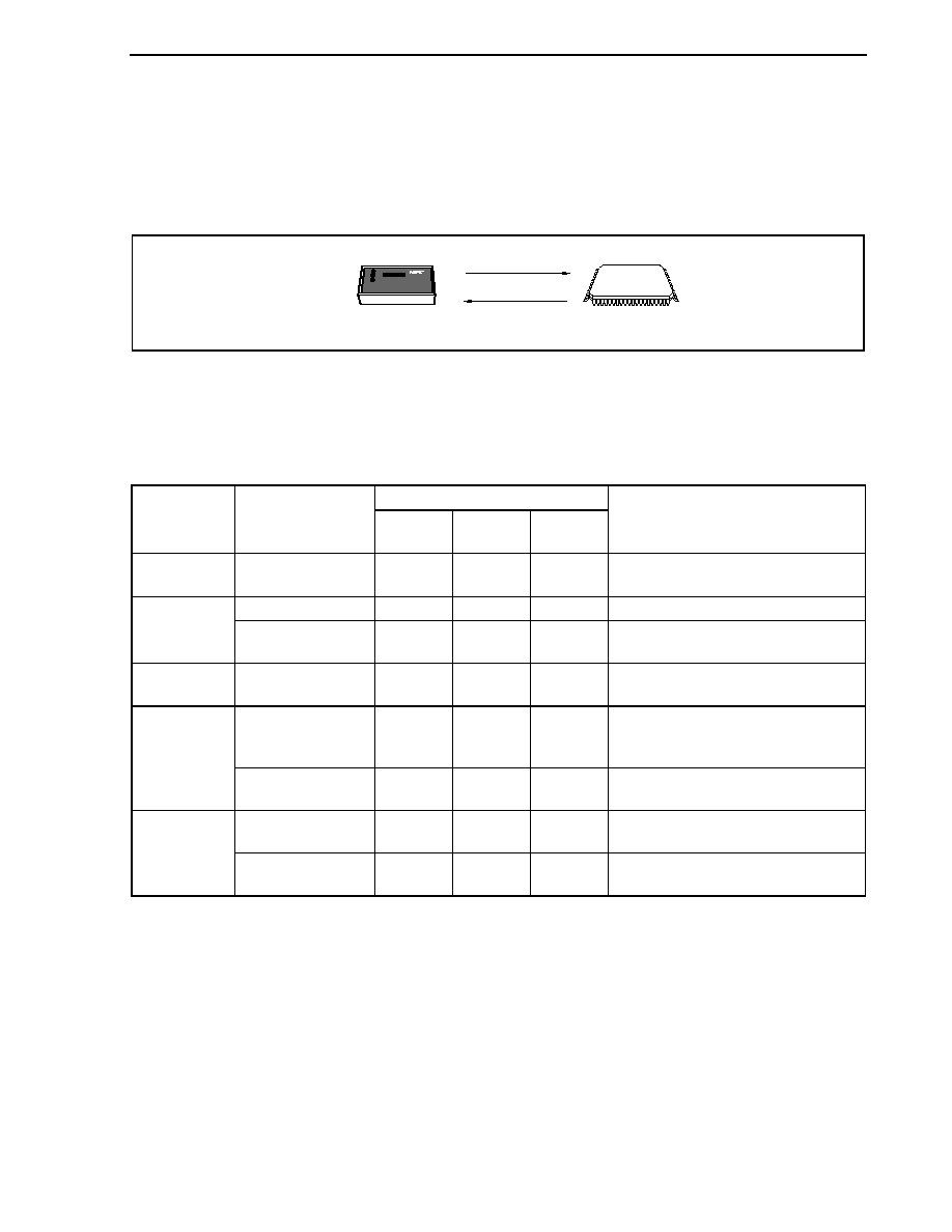
CHAPTER 26 FLASH MEMORY
Preliminary User's Manual U17714EJ1V0UD
747
26.4.5 Communication commands
The V850ES/JJ2 communicates with the dedicated flash programmer by means of commands. The signals sent
from the dedicated flash programmer to the V850ES/JJ2 are called "commands". The response signals sent from the
V850ES/JJ2 to the dedicated flash programmer are called "response commands".
Figure 26-9. Communication Commands
Dedicated flash programmer
V850ES/JJ2
Command
Response command
PG-FP4
(Flash Pro4)
Cxxxxxx
Bxxxxx
Axxxx
XXX YYY
X
X
X
X
X
X
X
X
X
X
X
X
X
X
X
XXXX YYYY
STATVE
The following shows the commands for flash memory control in the V850ES/JJ2. All of these commands are
issued from the dedicated flash programmer, and the V850ES/JJ2 performs the processing corresponding to the
commands.
Table 26-6. Flash Memory Control Commands
Support
Classification Command
Name
CSIB0,
CSIB3
CSIB0 + HS,
CSIB3 + HS
UARTA0
Function
Blank check
Block blank check
command
Checks if the contents of the memory in the
specified block have been correctly erased.
Chip erase command
Erases the contents of the entire memory.
Erase
Block erase command
Erases the contents of the memory of the
specified block.
Write Write
command
Writes the specified address range, and
executes a contents verify check.
Verify command
Compares the contents of memory in the
specified address range with data
transferred from the flash programmer.
Verify
Checksum command
Reads the checksum in the specified
address range.
Silicon signature
command
Reads silicon signature information.
System setting,
control
Security setting
command
Disables the chip erase command, block
erase command, and write command.
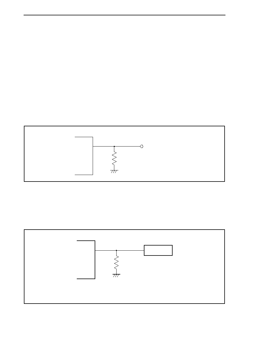
CHAPTER 26 FLASH MEMORY
Preliminary User's Manual U17714EJ1V0UD
748
26.4.6 Pin connection
When performing on-board writing, mount a connector on the target system to connect to the dedicated flash
programmer. Also, incorporate a function on-board to switch from the normal operation mode to the flash memory
programming mode.
In the flash memory programming mode, all the pins not used for flash memory programming become the same
status as that immediately after reset. Therefore, pin handling is required when the external device does not
acknowledge the status immediately after a reset.
(1) FLMD0 pin
In the normal operation mode, input a voltage of V
SS
level to the FLMD0 pin. In the flash memory
programming mode, supply a write voltage of V
DD
level to the FLMD0 pin.
Because the FLMD0 pin serves as a write protection pin in the self programming mode, a voltage of V
DD
level
must be supplied to the FLMD0 pin via port control, etc., before writing to the flash memory. For details, see
26.5.5 (1) FLMD0 pin.
Figure 26-10. FLMD0 Pin Connection Example
V850ES/JJ2
FLMD0
Dedicated flash programmer connection pin
Pull-down resistor (R
FLMD0
)
(2) FLMD1 pin
When 0 V is input to the FLMD0 pin, the FLMD1 pin does not function. When V
DD
is supplied to the FLMD0
pin, the flash memory programming mode is entered, so 0 V must be input to the FLMD1 pin. The following
shows an example of the connection of the FLMD1 pin.
Figure 26-11. FLMD1 Pin Connection Example
FLMD1
Pull-down resistor (R
FLMD1
)
Other device
V850ES/JJ2
Caution If the V
DD
signal is input to the FLMD1 pin from another device during on-board writing and
immediately after reset, isolate this signal.
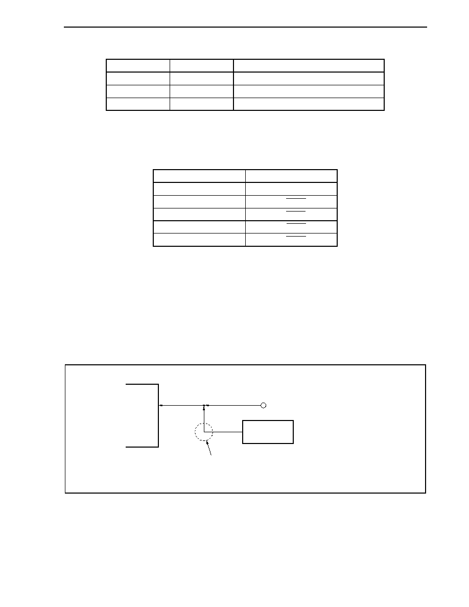
CHAPTER 26 FLASH MEMORY
Preliminary User's Manual U17714EJ1V0UD
749
Table 26-7. Relationship Between FLMD0 and FLMD1 Pins and Operation Mode When Reset Is Released
FLMD0 FLMD1
Operation
Mode
0
Don't care
Normal operation mode
V
DD
0
Flash memory programming mode
V
DD
V
DD
Setting
prohibited
(3) Serial interface pin
The following shows the pins used by each serial interface.
Table 26-8. Pins Used by Serial Interfaces
Serial Interface
Pins Used
UARTA0 TXDA0,
RXDA0
CSIB0
SOB0, SIB0, SCKB0
CSIB3
SOB3, SIB3, SCKB3
CSIB0
+ HS
SOB0, SIB0, SCKB0, PCM0
CSIB3 + HS
SOB3, SIB3, SCKB3, PCM0
When connecting a dedicated flash programmer to a serial interface pin that is connected to another device
on-board, care should be taken to avoid conflict of signals and malfunction of the other device.
(a) Conflict of signals
When the dedicated flash programmer (output) is connected to a serial interface pin (input) that is
connected to another device (output), a conflict of signals occurs. To avoid the conflict of signals, isolate
the connection to the other device or set the other device to the output high-impedance status.
Figure 26-12. Conflict of Signals (Serial Interface Input Pin)
V850ES/JJ2
Input pin
Conflict of signals
Dedicated flash programmer
connection pins
Other device
Output pin
In the flash memory programming mode, the signal that the dedicated flash
programmer sends out conflicts with signals another device outputs.
Therefore, isolate the signals on the other device side.
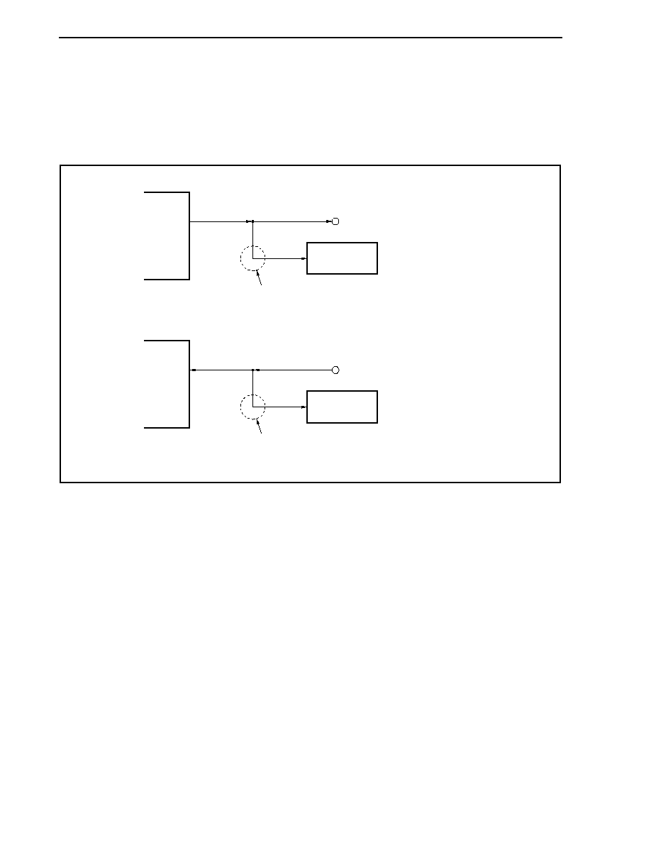
CHAPTER 26 FLASH MEMORY
Preliminary User's Manual U17714EJ1V0UD
750
(b) Malfunction of other device
When the dedicated flash programmer (output or input) is connected to a serial interface pin (input or
output) that is connected to another device (input), the signal is output to the other device, causing the
device to malfunction. To avoid this, isolate the connection to the other device.
Figure 26-13. Malfunction of Other Device
V850ES/JJ2
Pin
Dedicated flash programmer
connection pin
Other device
Input pin
In the flash memory programming mode, if the signal the V850ES/JJ2
outputs affects the other device, isolate the signal on the other device side.
V850ES/JJ2
Pin
Dedicated flash programmer
connection pin
Other device
Input pin
In the flash memory programming mode, if the signal the dedicated flash
programmer outputs affects the other device, isolate the signal on the other
device side.
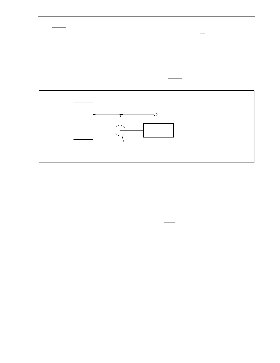
CHAPTER 26 FLASH MEMORY
Preliminary User's Manual U17714EJ1V0UD
751
(4) RESET pin
When the reset signals of the dedicated flash programmer are connected to the RESET pin that is connected
to the reset signal generator on-board, a conflict of signals occurs. To avoid the conflict of signals, isolate the
connection to the reset signal generator.
When a reset signal is input from the user system in the flash memory programming mode, the programming
operation will not be performed correctly. Therefore, do not input signals other than the reset signals from the
dedicated flash programmer.
Figure 26-14. Conflict of Signals (RESET Pin)
V850ES/JJ2
RESET
Dedicated flash programmer
connection pin
Reset signal generator
Conflict of signals
Output pin
In the flash memory programming mode, the signal the reset signal generator
outputs conflicts with the signal the dedicated flash programmer outputs.
Therefore, isolate the signals on the reset signal generator side.
(5) Port pins (including NMI)
When the system shifts to the flash memory programming mode, all the pins that are not used for flash
memory programming are in the same status as that immediately after reset. If the external device connected
to each port does not recognize the status of the port immediately after reset, pins require appropriate
processing, such as connecting to V
DD
via a resistor or connecting to V
SS
via a resistor.
(6) Other signal pins
Connect X1, X2, XT1, XT2, and REGC in the same status as that in the normal operation mode.
During flash memory programming, input a low level to the DRST pin or leave it open. Do not input a high
level.
(7) Power supply
Supply the same power (V
DD
, V
SS
, EV
DD
, EV
SS
, BV
DD
, BV
SS
, AV
REF0
, AV
REF1
, AV
SS
) as in normal operation
mode.
CHAPTER 26 FLASH MEMORY
Preliminary User's Manual U17714EJ1V0UD
752
26.5 Rewriting by Self Programming
26.5.1 Overview
The V850ES/JJ2 supports a flash macro service that allows the user program to rewrite the internal flash memory
by itself. By using this interface and a self programming library that is used to rewrite the flash memory with a user
application program, the flash memory can be rewritten by a user application transferred in advance to the internal
RAM or external memory. Consequently, the user program can be upgraded and constant data can be rewritten in the
field.
Figure 26-15. Concept of Self Programming
Application program
Self programming library
Flash macro service
Flash memory
Flash function execution
Flash information
Erase, write
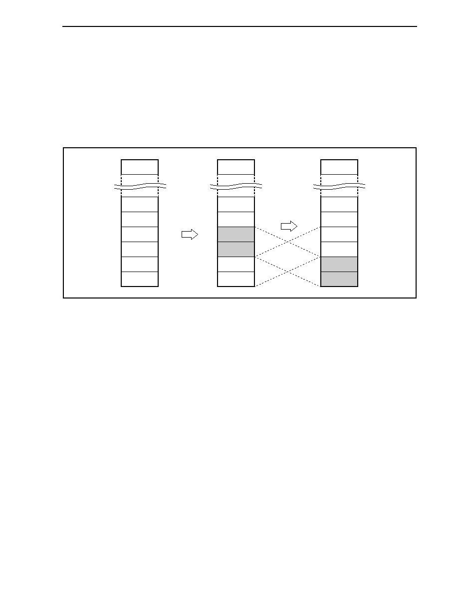
CHAPTER 26 FLASH MEMORY
Preliminary User's Manual U17714EJ1V0UD
753
26.5.2 Features
(1) Secure self programming (boot swap function)
The V850ES/JJ2 supports a boot swap function that can exchange the physical memory of blocks 0 and 1 with
the physical memory of blocks 2 and 3. By writing the start program to be rewritten to blocks 2 and 3 in
advance and then swapping the physical memory, the entire area can be safely rewritten even if a power
failure occurs during rewriting because the correct user program always exists in blocks 0 and 1.
Figure 26-16. Rewriting Entire Memory Area (Boot Swap)
Block 15
Block 5
Block 4
Block 3
Block 2
Block 1
Block 0
Block 15
Block 5
Block 4
Block 3
Block 2
Block 1
Block 0
Block 15
Boot swap
Rewriting blocks
2 and 3
Block 5
Block 4
Block 3
Block 2
Block 1
Block 0
(2) Interrupt support
Instructions cannot be fetched from the flash memory during self programming. Conventionally, a user handler
written to the flash memory could not be used even if an interrupt occurred.
With the V850ES/JJ2, a user handler can be registered to an entry RAM area by using a library function, so
that interrupt servicing can be performed by internal RAM or external memory execution.
CHAPTER 26 FLASH MEMORY
Preliminary User's Manual U17714EJ1V0UD
754
26.5.3 Standard self programming flow
The entire processing to rewrite the flash memory by flash self programming is illustrated below.
Figure 26-17. Standard Self Programming Flow
Flash environment initialization processing
Erase processing
Write processing
Flash information setting processing
Note 1
Internal verify processing
Boot area swap processing
Note 2
Flash environment end processing
Flash memory manipulation
End of processing
All blocks end?
� Disable accessing flash area
� Disable setting of STOP mode
� Disable stopping clock
Yes
No
Notes 1. If a security setting is not performed, flash information setting processing does not have to be
executed.
2. If boot swap is not used, flash information setting processing and boot swap processing do not have
to be executed.
CHAPTER 26 FLASH MEMORY
Preliminary User's Manual U17714EJ1V0UD
755
26.5.4 Flash functions
Table 26-9. Flash Function List
Function Name
Outline
Support
FlashEnv Initialization
of flash control macro
FlashBlockErase
Erasure of only specified one block
FlashWordWrite
Writing from specified address
FlashBlockIVerify
Internal verification of specified one block
FlashBlockBlankCheck
Blank check of specified one block
FlashFLMDCheck
Check of FLMD pin
FlashStatusCheck
Status check of operation specified immediately before
FlashGetInfo
Reading of flash information
FlashSetInfo
Setting of flash information
FlashBootSwap
Swapping of boot area
FlashSetUserHandler User
interrupt handler registration function
26.5.5 Pin processing
(1) FLMD0 pin
The FLMD0 pin is used to set the operation mode when reset is released and to protect the flash memory from
being written during self rewriting. It is therefore necessary to keep the voltage applied to the FLMD0 pin at 0
V when reset is released and a normal operation is executed. It is also necessary to apply a voltage of V
DD
level to the FLMD0 pin during the self programming mode period via port control before the memory is
rewritten.
When self programming has been completed, the voltage on the FLMD0 pin must be returned to 0 V.
Figure 26-18. Mode Change Timing
RESET signal
FLMD0 pin
V
DD
0 V
V
DD
0 V
Self programming mode
Normal
operation mode
Normal
operation mode
Caution Make sure that the FLMD0 pin is at 0 V when reset is released.

CHAPTER 26 FLASH MEMORY
Preliminary User's Manual U17714EJ1V0UD
756
26.5.6 Internal resources used
The following table lists the internal resources used for self programming. These internal resources can also be
used freely for purposes other than self programming.
Table 26-10. Internal Resources Used
Resource Name
Description
Entry RAM area
(124 bytes of either internal
RAM/external RAM)
Routines and parameters used for the flash macro service are located in this area. The
entry program and default parameters are copied by calling a library initialization
function.
Stack area (user stack + 300 bytes)
An extension of the stack used by the user is used by the library (can be used in both the
internal RAM and external RAM).
Library code (1900 bytes)
Program entity of library (can be used anywhere other than the flash memory block to be
manipulated).
Application program
Executed as user application.
Calls flash functions.
Maskable interrupt
Can be used in the user application execution status or self programming status. To use
this interrupt in the self programming status, the interrupt servicing start address must be
registered in advance by a registration function.
NMI interrupt
Can be used in the user application execution status or self programming status. To use
this interrupt in the self programming status, the interrupt servicing start address must be
registered in advance by a registration function.

Preliminary User's Manual U17714EJ1V0UD
757
CHAPTER 27 ON-CHIP DEBUG FUNCTION
The V850ES/JJ2 has an on-chip debug function that uses the JTAG (Joint Test Action Group) interface (DRST,
DCK, DMS, DDI, and DDO pins) and that can be used via an on-chip debug emulator (MINICUBE
).
27.1 Features
Hardware break function: 2 points
Software break function: 4 points
Real-time RAM monitor function: Memory contents can be read during program execution.
Dynamic memory modification function (DMM function): RAM contents can be rewritten during program execution.
Mask function: RESET, NMI, HLDRQ, WAIT
ROM security function: 10-byte ID code authentication
Caution The
following
functions are not supported.
� Trace function
� Event function
� Debug interrupt interface function (DBINT)
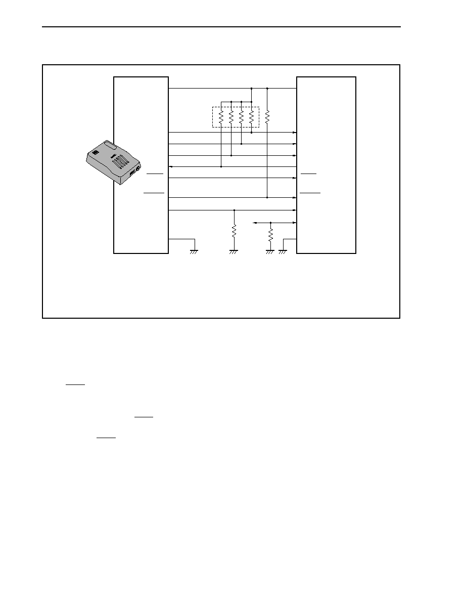
CHAPTER 27 ON-CHIP DEBUG FUNCTION
Preliminary User's Manual U17714EJ1V0UD
758
27.2 Connection Circuit Example
MINICUBE
V850ES/JJ2
VDD
DCK
DMS
DDI
DDO
DRST
RESET
FLMD0
GND
EV
DD
DCK
DMS
DDI
DDO
DRST
Note 2
RESET
FLMD0
Note 3
FLMD1/PDL5
EV
SS
Note 1
ST
A
TUS
T
ARGET
PO
WER
Notes 1. Example of pin connection when MINICUBE is not connected
2. A pull-down resistor is provided on chip.
3. For flash memory rewriting
27.3 Interface Signals
The interface signals are described below.
(1) DRST
This is a reset input signal for the on-chip debug unit. It is a negative-logic signal that asynchronously
initializes the debug control unit.
MINICUBE raises the DRST signal when it detects V
DD
of the target system after the integrated debugger is
started, and starts the on-chip debug unit of the device.
When the DRST signal goes high, a reset signal is also generated in the CPU.
When starting debugging by starting the integrated debugger, a CPU reset is always generated.
(2) DCK
This is a clock input signal. It supplies a 20 MHz clock from MINICUBE. In the on-chip debug unit, the DMS
and DDI signals are sampled at the rising edge of the DCK signal, and the data DDO is output at its falling
edge.

CHAPTER 27 ON-CHIP DEBUG FUNCTION
Preliminary User's Manual U17714EJ1V0UD
759
(3) DMS
This is a transfer mode select signal. The transfer status in the debug unit changes depending on the level of
the DMS signal.
(4) DDI
This is a data input signal. It is sampled in the on-chip debug unit at the rising edge of DCK.
(5) DDO
This is a data output signal. It is output from the on-chip debug unit at the falling edge of the DCK signal.
(6) EV
DD
This signal is used to detect VDD of the target system. If VDD from the target system is not detected, the
signals output from MINICUBE (DRST, DCK, DMS, DDI, FLMD0, and RESET) go into a high-impedance state.
(7) FLMD0
The flash self programming function is used for the function to download data to the flash memory via the
integrated debugger. During flash self programming, the FLMD0 pin must be kept high. In addition, connect a
pull-down resistor to the FLMD0 pin.
The FLMD0 pin can be controlled in either of the following two ways.
<1> To control from MINICUBE
Connect the FLMD0 signal of MINICUBE to the FLMD0 pin.
In the normal mode, nothing is driven by MINICUBE (high impedance).
During a break, MINICUBE raises the FLMD0 pin to the high level when the download function of the
integrated debugger is executed.
<2> To control from port
Connect any port of the device to the FLMD0 pin.
The same port as the one used by the user program to realize the flash self programming function may
be used.
On the console of the integrated debugger, make a setting to raise the port pin to high level before
executing the download function, or lower the port pin after executing the download function.
For details, refer to the ID850QB Ver. 3.10 Integrated Debugger Operation User's Manual (U17435E).
(8) RESET
This is a system reset input pin. If the DRST pin is made invalid by the value of the OCDM0 bit of the OCDM
register set by the user program, on-chip debugging cannot be executed. Therefore, reset is effected by
MINICUBE, using the RESET pin, to make the DRST pin valid (initialization).

CHAPTER 27 ON-CHIP DEBUG FUNCTION
Preliminary User's Manual U17714EJ1V0UD
760
27.4 Register
(1) On-chip debug mode register (OCDM)
The OCDM register is used to select the normal operation mode or on-chip debug mode. This register is a
special register and can be written only in a combination of specific sequences (see 3.4.7 Special registers).
This register is also used to specify whether a pin provided with an on-chip debug function is used as an on-
chip debug pin or as an ordinary port/peripheral function pin. It also is used to disconnect the internal pull-
down resistor of the P05/INTP2/DRST pin.
The OCDM register can be written only while a low level is input to the DRST pin.
This register can be read or written in 8-bit or 1-bit units.
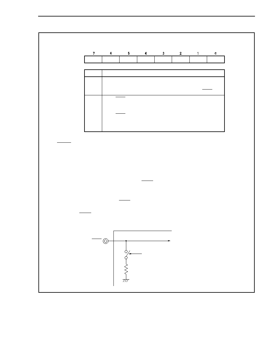
CHAPTER 27 ON-CHIP DEBUG FUNCTION
Preliminary User's Manual U17714EJ1V0UD
761
0
OCDM0
0
1
Operation mode
OCDM
0
0
0
0
0
0
OCDM0
After reset: 01H
Note
R/W Address: FFFFF9FCH
When DRST pin is low:
Normal operation mode (in which a pin that functions alternately as an
on-chip debug function pin is used as a port/peripheral function pin)
When DRST pin is high:
On-chip debug mode (in which a pin that functions alternately as an
on-chip debug function pin is used as an on-chip debug mode pin)
Selects normal operation mode (in which a pin that functions alternately
as on-chip debug function pin is used as a port/peripheral function pin) and
disconnects the on-chip pull-down resistor of the P05/INTP2/DRST pin.
< >
Note RESET input sets this register to 01H. After reset by the WDT2RES signal, clock monitor (CLM), or low-
voltage detector (LVI), however, the value of the OCDM register is retained.
Cautions 1. When using the DDI, DDO, DCK, and DMS pins not as on-chip debug pins but as port pins
after external reset, any of the following actions must be taken.
� Input a low level to the P05/INTP2/DRST pin.
� Set the OCDM0 bit. In this case, take the following actions.
<1> Clear the OCDM0 bit to 0.
<2> Fix the P05/INTP2/DRST pin to the low level until <1> is completed.
2. The DRST pin has an on-chip pull-down resistor. This resistor is disconnected when the
OCDM0 flag is cleared to 0.
OCDM0 flag
(1: Pull-down ON, 0: Pull-down OFF)
10 to 100 k
(30 k
(TYP.))
DRST
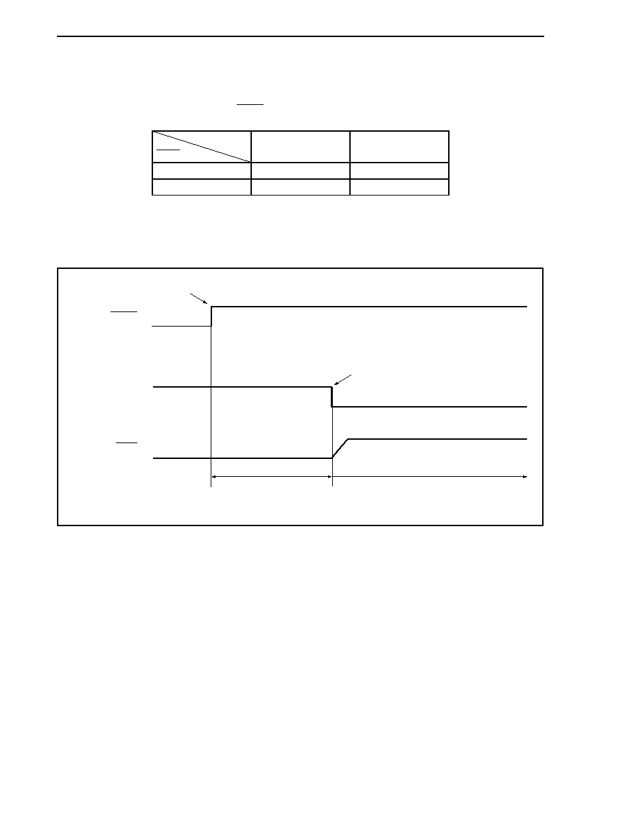
CHAPTER 27 ON-CHIP DEBUG FUNCTION
Preliminary User's Manual U17714EJ1V0UD
762
27.5 Operation
The on-chip debug function is made invalid under the conditions shown in the table below.
When this function is not used, keep the DRST pin low until the OCDM.OCDM0 flag is cleared to 0.
OCDM0 Flag
DRST Pin
0 1
L Invalid
Invalid
H Invalid
Valid
Remark L: Low-level input
H: High-level input
Figure 27-1. Timing When On-Chip Debug Function Is Not Used
Low-level input
After OCDM0 bit is cleared,
high level can be input/output.
Clearing OCDM0 bit
Releasing reset
RESET
OCDM0
P05/INTP2/DRST
CHAPTER 27 ON-CHIP DEBUG FUNCTION
Preliminary User's Manual U17714EJ1V0UD
763
27.6 ROM Security Function
27.6.1 Security
ID
The flash memory versions of the V850ES/JJ2 perform authentication using a 10-byte ID code to prevent the
contents of the flash memory from being read by an unauthorized person during on-chip debugging by the on-chip
debug emulator.
Set the ID code in the 10-byte on-chip flash memory area from 0000070H to 0000079H to allow the debugger
perform ID authentication.
If the IDs match, the security is released and reading flash memory and using the on-chip debug emulator are
enabled.
� Set the 10-byte ID code to 0000070H to 0000079H.
� Bit 7 of 0000079H is the on-chip debug emulator enable flag (0: Disable, 1: Enable).
� When the on-chip debug emulator is started, the debugger requests ID input. When the ID code input on the
debugger and the ID code set in 0000070H to 0000079H match, the debugger starts.
� Debugging cannot be performed if the on-chip debug emulator enable flag is 0, even if the ID codes match.
0 0 0 0 0 7 A H
0 0 0 0 0 7 F H
0 0 0 0 0 8 0 H
0 0 0 0 0 7 9 H
0 0 0 0 0 7 0 H
0 0 0 0 0 0 0 H
System reserved area
Security ID
(10 bytes)
Caution When the data in the flash memory has been erased, all the bits are set to 1.

CHAPTER 27 ON-CHIP DEBUG FUNCTION
Preliminary User's Manual U17714EJ1V0UD
764
27.6.2 Setting
Example When the following values are set to addresses 0x70 to 0x79
Address Value
0x70 0x12
0x71 0x34
0x72 0x56
0x73 0x78
0x74 0x9A
0x75 0xBC
0x76 0xDE
0x77 0xF1
0x78 0x23
0x79 0xD4
The following shows program examples when the CA850 is used.
[Program example]
Enter the 10-byte security code using the "SECURITY_ID" section (address 0x70).
#---------------------------------------
# SECURITY_ID
#---------------------------------------
.section "SECURITY_ID"
.word 0x78563412 --0-3 byte code
.word 0xF1DEBC9A --4-7 byte code
.hword 0xD423 --8-9 byte code

CHAPTER 27 ON-CHIP DEBUG FUNCTION
Preliminary User's Manual U17714EJ1V0UD
765
27.7 Cautions
(1) If a reset signal is input (from the target system or a reset signal from an internal reset source) during RUN
(program execution), the break function may malfunction.
(2) Even if the reset signal is masked by the mask function, the I/O buffer (port pin) may be reset if a reset signal
is input from a pin.
(3) Because a software breakpoint set in the internal flash memory is made temporarily invalid by target reset or
internal reset generated by watchdog timer 2. The breakpoint becomes valid again when a hardware break or
forced break occurs, but a software break does not occur until then.
(4) Pin reset during a break is masked and the CPU and peripheral I/O are not reset. If pin reset or internal reset
is generated as soon as the flash memory is rewritten by DMA or read by the RAM monitor function while the
user program is being executed, the CPU and peripheral I/O may not be correctly reset.
(5) When the following conditions (a) and (b) are satisfied and operation is stopped on the emulator (IECUBE
,
MINICUBE) due to a break, etc., watchdog timer 2 does not stop and a reset or non-maskable interrupt occurs.
When a reset occurs, the debugger hangs up.
(a) The main clock or subclock is used as the source clock for watchdog timer 2.
(b) The internal oscillation clock is stopped (RCM.RSTOP bit = 1).
To avoid this, perform either of the following.
� When an emulator is used, use the internal oscillation clock as the source clock.
� When an emulator is used, do not stop the internal oscillator.
(6) When the following conditions (a) and (b) are satisfied and operation is stopped on the emulator (IECUBE,
MINICUBE) due to a break, etc., TMM does not stop even if the peripheral break function is set to "Break".
(a) Either the INTWT, internal oscillation clock (f
R
/8), or subclock are selected as the TMM source clock.
(b) The main clock is stopped.
To avoid this, perform either of the following.
� When an emulator is used, the main clock (f
XX
, f
XX
/2, f
XX
/4, f
XX
/64, f
XX
/512) is used as the source clock.
� When an emulator is used, disable the main clock oscillation.
(7) In the on-chip debug mode, the DDO pin is forcibly set to the high-level output.

Preliminary User's Manual U17714EJ1V0UD
766
CHAPTER 28 ELECTRICAL SPECIFICATIONS (TARGET)
Absolute Maximum Ratings (T
A
= 25
�C) (1/2)
Parameter Symbol
Conditions
Ratings
Unit
V
DD
V
DD
= EV
DD
= AV
REF0
= AV
REF1
-0.5 to +4.6
V
BV
DD
-0.5 to +4.6
V
EV
DD
V
DD
= EV
DD
= AV
REF0
= AV
REF1
-0.5 to +4.6
V
AV
REF0
V
DD
= EV
DD
= AV
REF0
= AV
REF1
-0.5 to +4.6
V
AV
REF1
V
DD
= EV
DD
= AV
REF0
= AV
REF1
-0.5 to +4.6
V
V
SS
V
SS
= EV
SS
= BV
SS
= AV
SS
-0.5 to +0.5
V
AV
SS
V
SS
= EV
SS
= BV
SS
= AV
SS
-0.5 to +0.5
V
BV
SS
V
SS
= EV
SS
= BV
SS
= AV
SS
-0.5 to +0.5
V
Supply voltage
EV
SS
V
SS
= EV
SS
= BV
SS
= AV
SS
-0.5 to +0.5
V
V
I1
RESET,
FLMD0
-0.5 to EV
DD
+ 0.5
Note 1
V
V
I2
PCD0 to PCD3, PCM0 to PCM5, PCS0 to
PCS7, PCT0 to PCT7, PDH0 to PDH7, PDL0 to
PDL15
-0.5 to BV
DD
+ 0.5
Note 1
V
V
I3
P10,
P11
-0.5 to AV
REF1
+ 0.5
Note 1
V
V
I4
X1, X2, XT1, XT2
-0.5 to V
RO
Note 2
+ 0.5
Note 1
V
Input voltage
V
I5
P00 to P06, P30 to P39, P40 to P42, P50 to
P55, P60 to P615, P80, P81, P90 to P915
-0.5 to +6.0
V
Analog input voltage
V
IAN
P70 to P715
-0.5 to AV
REF0
+ 0.5
Note 1
V
Notes 1. Be sure not to exceed the absolute maximum ratings (MAX. value) of each supply voltage.
2.
On-chip regulator output voltage (2.5 V (TYP.))
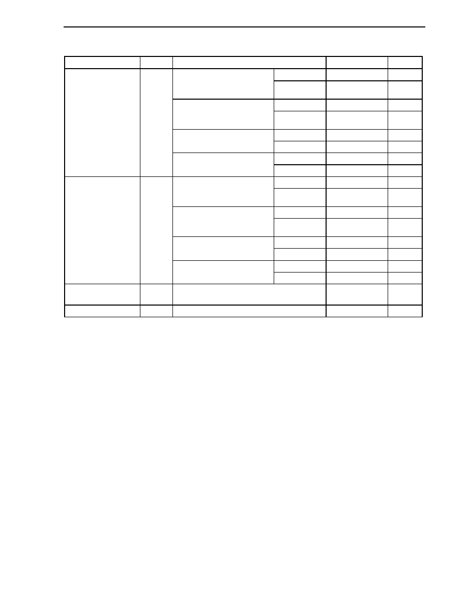
CHAPTER 28 ELECTRICAL SPECIFICATIONS (TARGET)
Preliminary User's Manual U17714EJ1V0UD
767
Absolute Maximum Ratings (T
A
= 25
�C) (2/2)
Parameter Symbol
Conditions
Ratings Unit
Per pin
4
mA
P00 to P06, P30 to P39, P40 to
P42, P50 to P55, P60 to P615,
P80, P81, P90 to P915
Total of all pins
50
mA
Per pin
4
mA
PCD0 to PCD3, PCM0 to PCM5,
PCS0 to PCS7, PCT0 to PCT7,
PDH0 to PDH7, PDL0 to PDL15
Total of all pins
50
mA
Per pin
4
mA
P10, P11
Total of all pins
8
mA
Per pin
4
mA
Output current, low
I
OL
P70 to P715
Total of all pins
20
mA
Per pin
-4 mA
P00 to P06, P30 to P39, P40 to
P42, P50 to P55, P60 to P615,
P80, P81, P90 to P915
Total of all pins
-50 mA
Per pin
-4 mA
PCD0 to PCD3, PCM0 to PCM5,
PCS0 to PCS7, PCT0 to PCT7,
PDH0 to PDH7, PDL0 to PDL15
Total of all pins
-50 mA
Per pin
-4 mA
P10, P11
Total of all pins
-8 mA
Per pin
-4 mA
Output current, high
I
OH
P70 to P715
Total of all pins
-20 mA
Operating ambient
temperature
T
A
-40 to +85
�C
Storage temperature
T
stg
-40 to +125
�C
Cautions 1. Do not directly connect the output (or I/O) pins of IC products to each other, or to V
DD
, V
CC
, and
GND. Open-drain pins or open-collector pins, however, can be directly connected to each
other.
Direct connection of the output pins between an IC product and an external circuit is possible, if
the output pins can be set to the high-impedance state and the output timing of the external
circuit is designed to avoid output conflict.
2. Product quality may suffer if the absolute maximum rating is exceeded even momentarily for any
parameter. That is, the absolute maximum ratings are rated values at which the product is on
the verge of suffering physical damage, and therefore the product must be used under
conditions that ensure that the absolute maximum ratings are not exceeded. The ratings and
conditions indicated for DC characteristics and AC characteristics represent the quality
assurance range during normal operation.
Remark Unless specified otherwise, the characteristics of alternate-function pins are the same as those of port pins.

CHAPTER 28 ELECTRICAL SPECIFICATIONS (TARGET)
Preliminary User's Manual U17714EJ1V0UD
768
Capacitance (T
A
=
-40 to +85�C, BV
DD
V
DD
= EV
DD
= AV
REF0
= AV
REF1
, V
SS
= EV
SS
= BV
SS
= AV
SS
= 0 V)
Parameter Symbol
Conditions
MIN.
TYP.
MAX.
Unit
I/O capacitance
C
IO
f
X
= 1 MHz
Unmeasured pins returned to 0 V
10
pF
Operating Conditions
(T
A
=
-40 to +85�C, BV
DD
V
DD
= EV
DD
= AV
REF0
= AV
REF1
, V
SS
= EV
SS
= BV
SS
= AV
SS
= 0 V)
Supply Voltage
Internal System Clock Frequency
Conditions
V
DD
EV
DD
BV
DD
AV
REF0
,
AV
REF1
Unit
C = 4.7
�
F (preliminary value),
A/D converter stopped,
D/A converter stopped
2.85 to 3.6
2.85 to 3.6
2.7 to 3.6
2.85 to 3.6
V
f
XX
= 2.5 to 20 MHz
C = 4.7
�
F (preliminary value),
A/D converter operating,
D/A converter operating
3.0 to 3.6
3.0 to 3.6
2.7 to 3.6
3.0 to 3.6
V
f
XT
= 32.768 kHz
C = 4.7
�
F (preliminary value),
A/D converter stopped,
D/A converter stopped
2.85 to 3.6
2.85 to 3.6
2.7 to 3.6
2.85 to 3.6
V
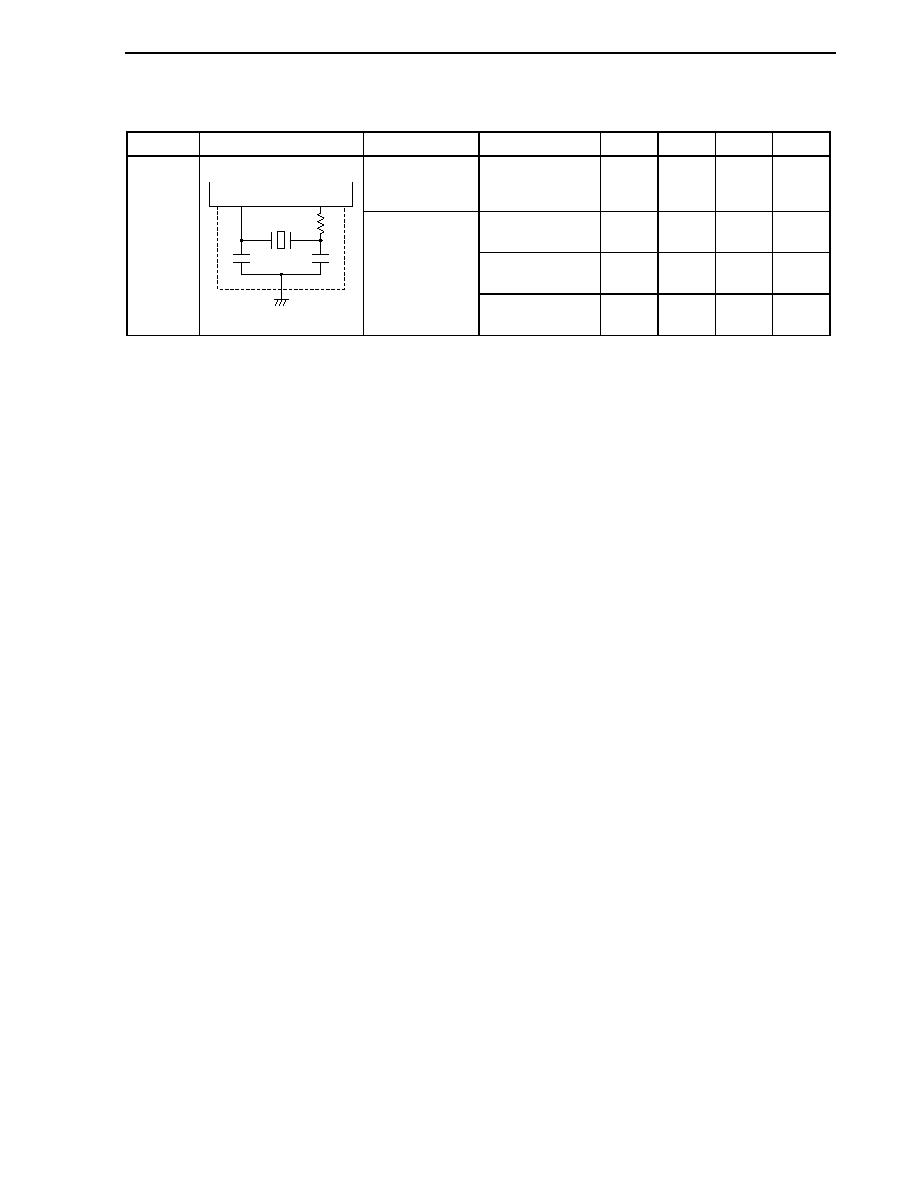
CHAPTER 28 ELECTRICAL SPECIFICATIONS (TARGET)
Preliminary User's Manual U17714EJ1V0UD
769
Main Clock Oscillator Characteristics
(T
A
=
-40 to +85�C, BV
DD
V
DD
= EV
DD
= AV
REF0
= AV
REF1
, V
SS
= EV
SS
= BV
SS
= AV
SS
= 0 V)
Resonator Circuit
Example
Parameter
Conditions MIN.
TYP.
MAX.
Unit
Oscillation
frequency (f
X
)
Note 1
2.5
10 MHz
After reset is
released
2
16
/f
X
s
After STOP mode is
released
1
Note 4
Note 3
ms
Ceramic
resonator/
Crystal
resonator
X2
X1
Oscillation
stabilization
time
Note 2
After IDLE2 mode is
released
350
Note 4
Note 3
�
s
Notes 1. The oscillation frequency shown above indicates only oscillator characteristics. Use the V850ES/JJ2 so
that the internal operation conditions do not exceed the ratings shown in AC Characteristics and DC
Characteristics.
2.
Time required from start of oscillation until the resonator stabilizes.
3. The value varies depending on the setting of the OSTS register.
4. Time required to set up the flash memory. Secure the setup time using the OSTS register.
Cautions 1. When using the main clock oscillator, wire as follows in the area enclosed by the broken lines in
the above figure to avoid an adverse effect from wiring capacitance.
� Keep the wiring length as short as possible.
� Do not cross the wiring with the other signal lines.
� Do not route the wiring near a signal line through which a high fluctuating current flows.
� Always make the ground point of the oscillator capacitor the same potential as V
SS
.
� Do not ground the capacitor to a ground pattern through which a high current flows.
� Do not fetch signals from the oscillator.
2. When the main clock is stopped and the device is operating on the subclock, wait until the
oscillation stabilization time has been secured by the program before switching back to the
main clock.
3. For the resonator selection and oscillator constant, customers are requested to either evaluate
the oscillation themselves or apply to the resonator manufacturer for evaluation.
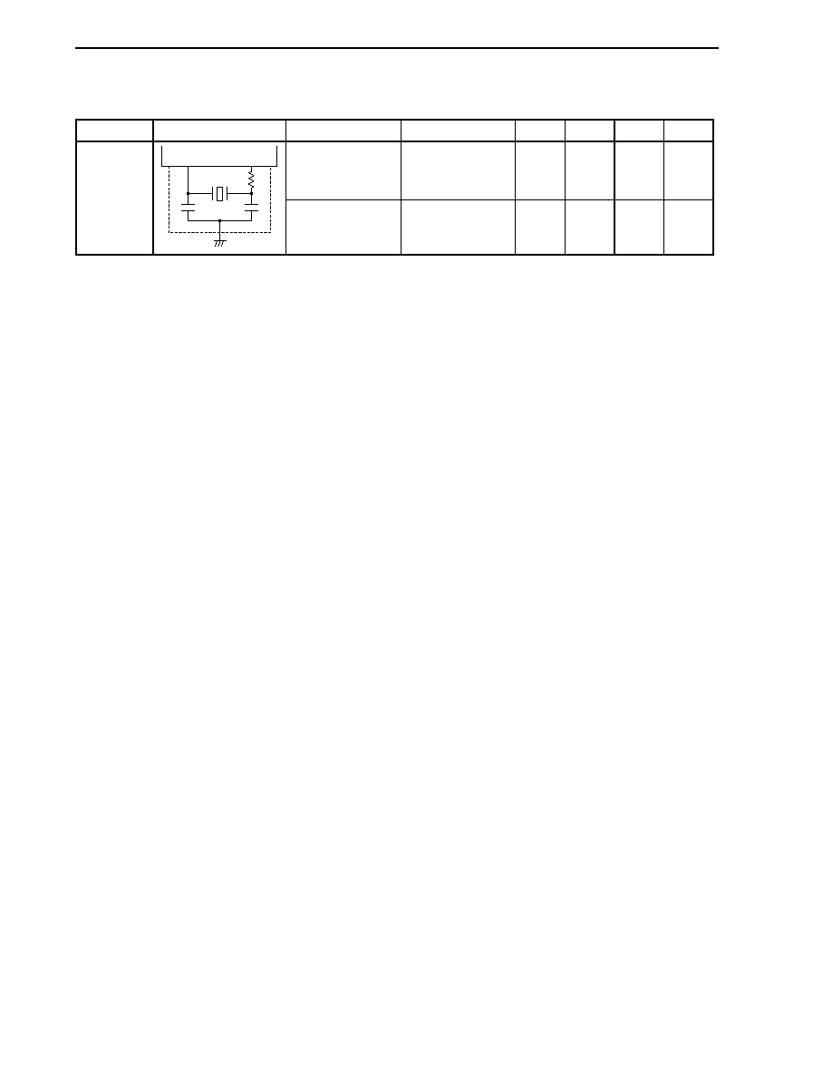
CHAPTER 28 ELECTRICAL SPECIFICATIONS (TARGET)
Preliminary User's Manual U17714EJ1V0UD
770
Subclock Oscillator Characteristics
(T
A
=
-40 to +85�C, BV
DD
V
DD
= EV
DD
= AV
REF0
= AV
REF1
, V
SS
= EV
SS
= BV
SS
= AV
SS
= 0 V)
Resonator Circuit
Example
Parameter
Conditions MIN.
TYP.
MAX.
Unit
Oscillation frequency
(f
XT
)
Note 1
32
32.768
35
kHz
Crystal
resonator
XT2
XT1
Oscillation
stabilization time
Note 2
10
s
Notes 1. The oscillation frequency shown above indicates only oscillator characteristics. Use the V850ES/JJ2 so
that the internal operation conditions do not exceed the ratings shown in AC Characteristics and DC
Characteristics.
2.
Time required from when V
DD
reaches the oscillation voltage range (2.85 V (MIN.)) to when the crystal
resonator stabilizes.
Cautions 1. When using the subclock oscillator, wire as follows in the area enclosed by the broken lines in
the above figures to avoid an adverse effect from wiring capacitance.
� Keep the wiring length as short as possible.
� Do not cross the wiring with the other signal lines.
� Do not route the wiring near a signal line through which a high fluctuating current flows.
� Always make the ground point of the oscillator capacitor the same potential as V
SS
.
� Do not ground the capacitor to a ground pattern through which a high current flows.
� Do not fetch signals from the oscillator.
2. The subclock oscillator is designed as a low-amplitude circuit for reducing power consumption,
and is more prone to malfunction due to noise than the main clock oscillator.
Particular care is therefore required with the wiring method when the subclock is used.
3. For the resonator selection and oscillator constant, customers are requested to either evaluate
the oscillation themselves or apply to the resonator manufacturer for evaluation.
CHAPTER 28 ELECTRICAL SPECIFICATIONS (TARGET)
Preliminary User's Manual U17714EJ1V0UD
771
PLL Characteristics
(T
A
=
-40 to +85�C, BV
DD
V
DD
= EV
DD
= AV
REF0
= AV
REF1
, V
SS
= EV
SS
= BV
SS
= AV
SS
= 0 V)
Parameter Symbol
Conditions
MIN.
TYP.
MAX.
Unit
�4 mode
2.5
5 MHz
Input frequency
f
X
�8 mode
2.5
2.5 MHz
�4 mode
10
20 MHz
Output frequency
f
XX
�8 mode
20
20 MHz
Lock time
t
PLL
After
V
DD
reaches 2.85 V (MIN.)
800
�
s
Internal Oscillator Characteristics
(T
A
=
-40 to +85�C, BV
DD
V
DD
= EV
DD
= AV
REF0
= AV
REF1
, V
SS
= EV
SS
= BV
SS
= AV
SS
= 0 V)
Parameter Symbol
Conditions
MIN.
TYP.
MAX.
Unit
Output frequency
f
R
100
200
400
kHz
Regulator Characteristics
(T
A
=
-40 to +85�C, BV
DD
V
DD
= EV
DD
= AV
REF0
= AV
REF1
, V
SS
= EV
SS
= BV
SS
= AV
SS
= 0 V)
Parameter Symbol
Conditions
MIN.
TYP.
MAX.
Unit
Input voltage
V
DD
f
XX
= 20 MHz (MAX.)
2.85
3.6 V
Output voltage
V
RO
2.5
V
Regulator output
stabilization time
t
REG
After V
DD
reaches 2.85 V (MIN.),
Stabilization capacitance C = 4.7
�
F
(preliminary value) connected to REGC pin
1 ms
V
DD
V
RO
t
REG
RESET
CHAPTER 28 ELECTRICAL SPECIFICATIONS (TARGET)
Preliminary User's Manual U17714EJ1V0UD
772
DC Characteristics
(T
A
=
-40 to +85�C, BV
DD
V
DD
= EV
DD
= AV
REF0
= AV
REF1
, V
SS
= EV
SS
= BV
SS
= AV
SS
= 0 V) (1/3)
Parameter Symbol
Conditions
MIN.
TYP.
MAX.
Unit
V
IH1
RESET,
FLMD0
0.8EV
DD
EV
DD
V
V
IH2
P00 to P06, P30 to P37, P42, P50 to P55,
P60 to P615, P80, P81, P92 to P915
0.8EV
DD
5.5 V
V
IH3
P38, P39, P40, P41, P90, P91
0.7EV
DD
5.5 V
V
IH4
PCD0 to PCD3, PCM0 to PCM5, PCS0 to
PCS7, PCT0 to PCT7, PDH0 to PDH7,
PDL0 to PDL15
0.7BV
DD
BV
DD
V
V
IH5
P70 to P715
0.7AV
REF0
AV
REF0
V
Input voltage, high
V
IH6
P10,
P11
0.7AV
REF1
AV
REF1
V
V
IL1
RESET,
FLMD0
EV
SS
0.2EV
DD
V
V
IL2
P00 to P06, P30 to P37, P42, P50 to P55,
P60 to P615, P80, P81, P92 to P915
EV
SS
0.2EV
DD
V
V
IL3
P38, P39, P40, P41, P90, P91
EV
SS
0.3EV
DD
V
V
IL4
PCD0 to PCD3, PCM0 to PCM5, PCS0 to
PCS7, PCT0 to PCT7, PDH0 to PDH7,
PDL0 to PDL15
BV
SS
0.3BV
DD
V
V
IL5
P70 to P715
AV
SS
0.3AV
REF0
V
Input voltage, low
V
IL6
P10,
P11
AV
SS
0.3AV
REF1
V
Input leakage current, high
I
LIH
V
I
= V
DD
= EV
DD
= BV
DD
= AV
REF0
= AV
REF1
5
�
A
Input leakage current, low
I
LIL
V
I
= 0 V
-5
�
A
Output leakage current, high
I
LOH
V
O
= V
DD
= EV
DD
= BV
DD
= AV
REF0
=
AV
REF1
5
�
A
Output leakage current, low
I
LOL
V
O
= 0 V
-5
�
A
Remark Unless specified otherwise, the characteristics of alternate-function pins are the same as those of port pins.

CHAPTER 28 ELECTRICAL SPECIFICATIONS (TARGET)
Preliminary User's Manual U17714EJ1V0UD
773
DC Characteristics
(T
A
=
-40 to +85�C, BV
DD
V
DD
= EV
DD
= AV
REF0
= AV
REF1
, V
SS
= EV
SS
= BV
SS
= AV
SS
= 0 V) (2/3)
Parameter Symbol
Conditions
MIN. TYP. MAX.
Unit
Per pin
I
OH
=
-1.0 mA
Total of all pins
-20 mA
EV
DD
- 1.0
EV
DD
V
V
OH1
P00 to P06,
P30 to P39,
P40 to P42,
P50 to P55,
P60 to P615, P80,
P81, P90 to P915
Per pin
I
OH
=
-100
�
A
Total of all pins
-6.0 mA
EV
DD
- 0.5
EV
DD
V
Per pin
I
OH
=
-1.0 mA
Total of all pins
-20 mA
BV
DD
- 1.0
BV
DD
V
V
OH2
PCD0 to PCD3,
PCM0 to PCM5,
PCS0 to PCS7,
PCT0 to PCT7,
PDH0 to PDH7,
PDL0 to PDL15
Per pin
I
OH
=
-100
�
A
Total of all pins
-5.0 mA
BV
DD
- 0.5
BV
DD
V
Per pin
I
OH
=
-0.4 mA
Total of all pins
-6.4 mA
AV
REF0
- 1.0
AV
REF0
V
V
OH3
P70 to P715
Per pin
I
OH
=
-100
�
A
Total of all pins
-1.6 mA
AV
REF0
- 0.5
AV
REF0
V
Per pin
I
OH
=
-0.4 mA
Total of all pins
-0.8 mA
AV
REF1
- 1.0
AV
REF1
V
Output voltage,
high
V
OH4
P10,
P11
Per pin
I
OH
=
-100
�
A
Total of all pins
-0.2 mA
AV
REF1
- 0.5
AV
REF1
V
V
OL1
P00 to P06,
P30 to P37, P42,
P50 to P55,
P60 to P615, P80,
P81, P92 to P915
Per pin
I
OL
= 1.0 mA
0 0.4
V
V
OL2
P38, P39, P40,
P41, P90, P91
Per pin
I
OL
= 3.0 mA
Total of all pins
20 mA
0 0.4
V
V
OL3
PCD0 to PCD3,
PCM0 to PCM5,
PCS0 to PCS7,
PCT0 to PCT7,
PDH0 to PDH7,
PDL0 to PDL15
Per pin
I
OL
= 1.0 mA
Total of all pins
20 mA
0 0.4
V
Output voltage, low
V
OL4
P10, P11,
P70 to P715
Per pin
I
OL
= 0.4 mA
Total of all pins
7.2 mA
0 0.4
V
Software pull-down
resistor
R
1
P05
V
I
= V
DD
10
30
100
k
Remarks 1. Unless specified otherwise, the characteristics of alternate-function pins are the same as those of port
pins.
2.
When the I
OH
and I
OL
conditions are not satisfied for a pin but the total value of all pins is satisfied, only
that pin does not satisfy the DC characteristics.

CHAPTER 28 ELECTRICAL SPECIFICATIONS (TARGET)
Preliminary User's Manual U17714EJ1V0UD
774
DC Characteristics
(T
A
=
-40 to +85�C, BV
DD
V
DD
= EV
DD
= AV
REF0
= AV
REF1
, V
SS
= EV
SS
= BV
SS
= AV
SS
= 0 V) (3/3)
Parameter Symbol
Conditions
MIN.
TYP.
MAX.
Unit
Note 2
35 55 mA
I
DD1
Normal
operation
f
XX
= 20 MHz
(f
X
= 5 MHz)
Note 3
34 54 mA
Note 2
20 30 mA
I
DD2
HALT
mode f
XX
= 20 MHz
(f
X
= 5 MHz)
Note 3
19 28 mA
I
DD3
IDLE1
mode f
XX
= 5 MHz (f
X
= 5 MHz),
PLL off
0.8 1.6 mA
I
DD4
IDLE2
mode f
XX
= 5 MHz (f
X
= 5 MHz),
PLL off
0.3 0.8 mA
Note 2
300 600
�
A
I
DD5
Subclock
operating mode
f
XT
= 32.768 kHz,
main clock,
internal oscillator
stopped
Note 3
200 400
�
A
Note 2
18 100
�
A
I
DD6
Sub-IDLE
mode
f
XT
= 32.768 kHz,
main clock,
internal oscillator
stopped
Note 3
18 80
�
A
Subclock stopped, internal
oscillator stopped
7 50
�
A
Subclock operating, internal
oscillator stopped
10 60
�
A
I
DD7
STOP
mode
Subclock stopped, internal
oscillator operating
10 60
�
A
Note 2
38
61
mA
Supply current
Note 1
I
DD8
Flash memory
programming
mode
f
XX
= 20 MHz
(f
X
= 5 MHz)
Note 3
37
60
mA
Notes 1. Total of V
DD
, EV
DD
, and BV
DD
currents. Current flowing through the output buffers, A/D converter, D/A
converter, and on-chip pull-down resistor is not included.
2.
�
PD70F3723, 70F3724
3.
�
PD70F3720, 70F3721, 70F3722
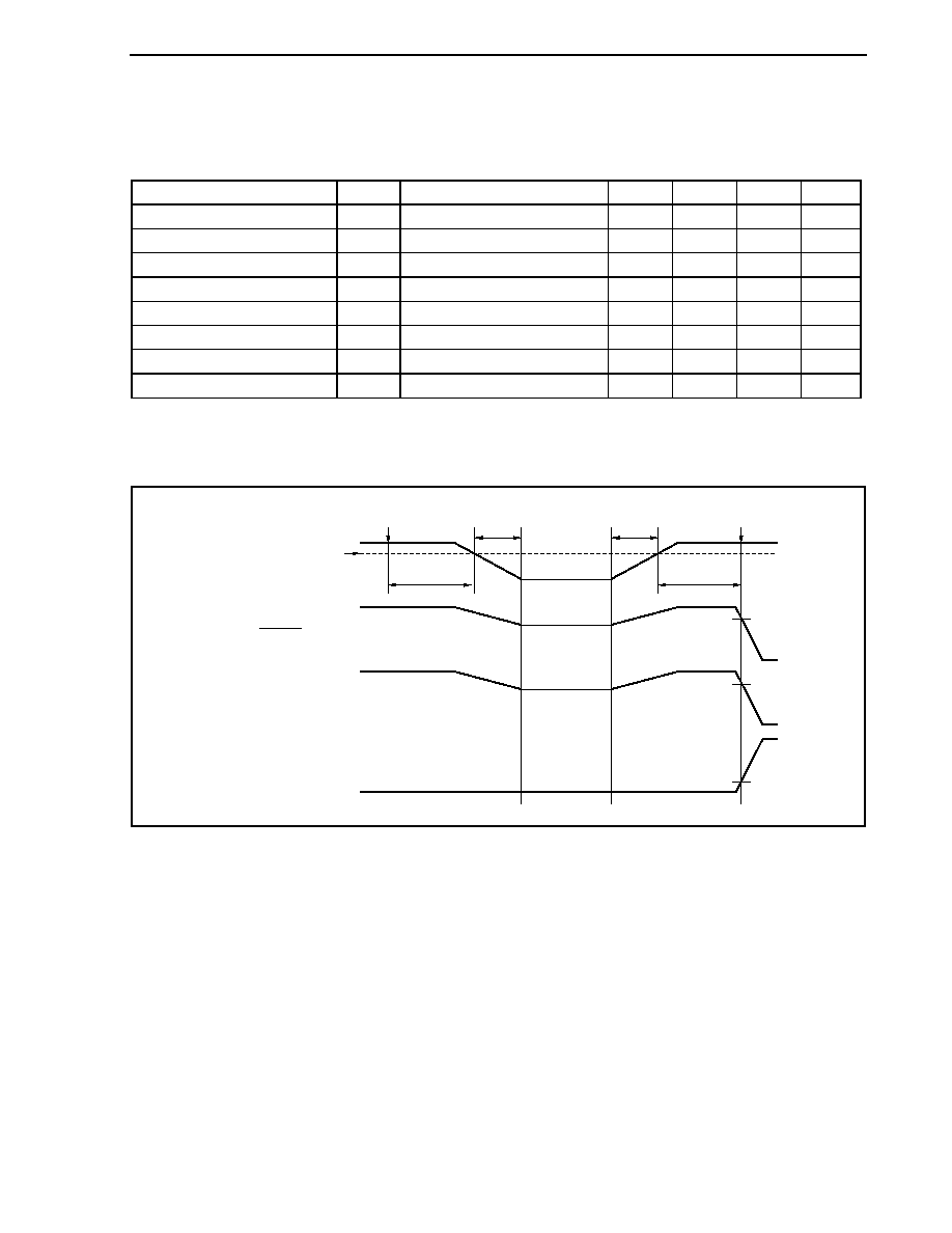
CHAPTER 28 ELECTRICAL SPECIFICATIONS (TARGET)
Preliminary User's Manual U17714EJ1V0UD
775
Data Retention Characteristics
In STOP mode
(T
A
=
-40 to +85�C, BV
DD
V
DD
= EV
DD
= AV
REF0
= AV
REF1
, V
SS
= EV
SS
= BV
SS
= AV
SS
= 0 V)
Parameter Symbol Conditions MIN.
TYP.
MAX.
Unit
Data retention voltage
V
DDDR
STOP mode (all functions stopped)
1.9
3.6
V
Data retention current
I
DDDR
STOP mode (all functions stopped)
7
50
�
A
Supply voltage rise time
t
RVD
200
�
s
Supply voltage fall time
t
FVD
200
�
s
Supply voltage retention time
t
HVD
After STOP mode setting
0
ms
STOP release signal input time
t
DREL
After V
DD
reaches 2.85 V (MIN.)
0
ms
Data retention input voltage, high
V
IHDR
V
DD
= EV
DD
= BV
DD
= V
DDDR
0.9V
DDDR
V
DDDR
V
Data retention input voltage, low
V
ILDR
V
DD
= EV
DD
= BV
DD
= V
DDDR
0
0.1V
DDDR
V
Caution Shifting to STOP mode and restoring from STOP mode must be performed within the rated
operating range.
t
DREL
t
HVD
t
FVD
t
RVD
STOP release signal input
STOP mode setting
V
DDDR
V
IHDR
V
IHDR
V
ILDR
V
DD
/EV
DD
/BV
DD
RESET (input)
STOP mode release
interrupt (NMI, etc.)
(Released by falling edge)
STOP mode release
interrupt (NMI, etc.)
(Released by rising edge)
Operating voltage lower limit
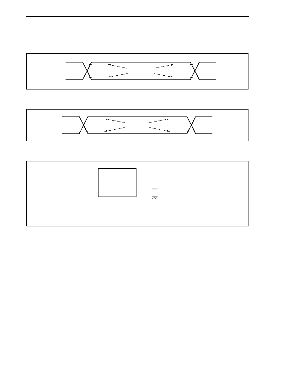
CHAPTER 28 ELECTRICAL SPECIFICATIONS (TARGET)
Preliminary User's Manual U17714EJ1V0UD
776
AC Characteristics
AC Test Input Measurement Points (V
DD
, AV
REF0
, AV
REF1
, EV
DD
, BV
DD
)
V
DD
0 V
V
IH
V
IL
V
IH
V
IL
Measurement points
AC Test Output Measurement Points
V
OH
V
OL
V
OH
V
OL
Measurement points
Load Conditions
DUT
(Device under
measurement)
C
L
= 50 pF
Caution If the load capacitance exceeds 50 pF due to the circuit configuration, bring the load
capacitance of the device to 50 pF or less by inserting a buffer or by some other means.
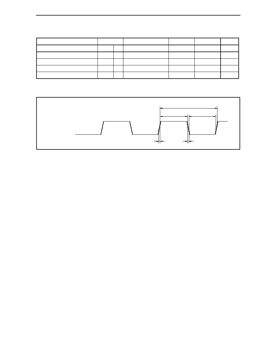
CHAPTER 28 ELECTRICAL SPECIFICATIONS (TARGET)
Preliminary User's Manual U17714EJ1V0UD
777
CLKOUT Output Timing
(T
A
=
-40 to +85�C, BV
DD
V
DD
= EV
DD
= AV
REF0
= AV
REF1
, V
SS
= EV
SS
= BV
SS
= AV
SS
= 0 V)
Parameter Symbol
Conditions
MIN.
MAX.
Unit
Output cycle
t
CYK
<1>
50 ns
31.25
�
s
High-level width
t
WKH
<2>
t
CYK
/2
- 10
ns
Low-level width
t
WKL
<3>
t
CYK
/2
- 10
ns
Rise time
t
KR
<4>
10
ns
Fall time
t
KF
<5>
10
ns
Clock Timing
CLKOUT (output)
<1>
<2>
<3>
<4>
<5>
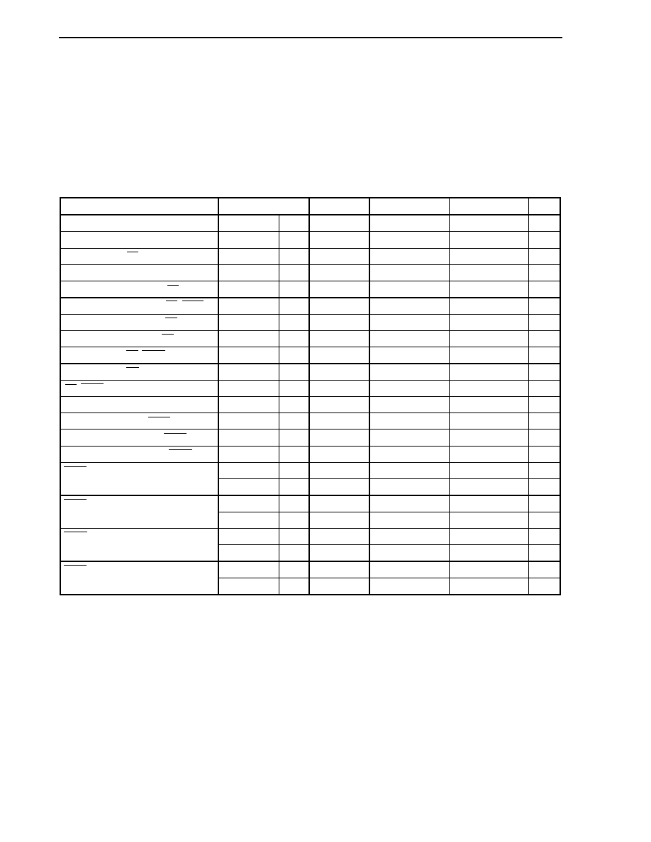
CHAPTER 28 ELECTRICAL SPECIFICATIONS (TARGET)
Preliminary User's Manual U17714EJ1V0UD
778
Bus Timing
(1) In multiplexed bus mode
Caution When operating at f
XX
> 20 MHz, be sure to insert address hold waits and address setup waits.
(a) Read/write cycle (CLKOUT asynchronous)
(T
A
=
-40 to +85�C, BV
DD
V
DD
= EV
DD
= AV
REF0
= AV
REF1
, V
SS
= EV
SS
= BV
SS
= AV
SS
= 0 V, C
L
= 50 pF)
Parameter Symbol
Conditions
MIN.
MAX.
Unit
Address setup time (to ASTB
) t
SAST
<6>
(0.5 + t
ASW
)T
- 20
ns
Address hold time (from ASTB
) t
HSTA
<7>
(0.5 + t
AHW
)T
- 15
ns
Delay time from RD
to address float
t
FRDA
<8>
16 ns
Data input setup time from address
t
SAID
<9>
(2
+
n + t
ASW
+ t
AHW
)T
- 35
ns
Data input setup time from RD
t
SRID
<10>
(1
+
n)T
- 25
ns
Delay time from ASTB
to RD, WRm
t
DSTRDWR
<11>
(0.5 + t
AHW
)T
- 15
ns
Data input hold time (from RD
) t
HRDID
<12>
0
ns
Address output time from RD
t
DRDA
<13>
(1
+
i)T
- 15
ns
Delay time from RD, WRm
to ASTB
t
DRDWRST
<14>
0.5T
- 15
ns
Delay time from RD
to ASTB
t
DRDST
<15>
(1.5
+
i + t
ASW
)T
- 15
ns
RD, WRm low-level width
t
WRDWRL
<16>
(1
+
n)T
- 15
ns
ASTB high-level width
t
WSTH
<17>
(1
+
i + t
ASW
)T
- 15
ns
Data output time from WRm
t
DWROD
<18>
15
ns
Data output setup time (to WRm
) t
SODWR
<19>
(1
+
n)T
- 20
ns
Data output hold time (from WRm
) t
HWROD
<20>
T
- 15
ns
t
SAWT1
<21>
n
1
(1.5 + t
ASW
+ t
AHW
)T
- 35
ns
WAIT setup time (to address)
t
SAWT2
<22>
(1.5
+
n + t
ASW
+ t
AHW
)T
- 35
ns
t
HAWT1
<23>
n
1
(0.5
+
n + t
ASW
+ t
AHW
)T
ns
WAIT hold time (from address)
t
HAWT2
<24>
(1.5
+
n + t
ASW
+ t
AHW
)T
ns
t
SSTWT1
<25>
n
1
(1 + t
AHW
)T
- 25
ns
WAIT setup time (to ASTB
)
t
SSTWT2
<26>
(1
+
n + t
AHW
)T
- 25
ns
t
HSTWT1
<27>
n
1
(n + t
AHW
)T
ns
WAIT hold time (from ASTB
)
t
HSTWT2
<28>
(1
+
n + t
AHW
)T ns
Remarks 1. t
ASW
: Number of address setup wait clocks
t
AHW
: Number of address hold wait clocks
2. T = 1/f
CPU
(f
CPU
: CPU operating clock frequency)
3. n: Number of wait clocks inserted in the bus cycle
The sampling timing changes when a programmable wait is inserted.
4. m = 0, 1
5. i: Number of idle states inserted after a read cycle (0 or 1)
6. The values in the above specifications are values for when clocks with a 1:1 duty ratio are input from
X1.
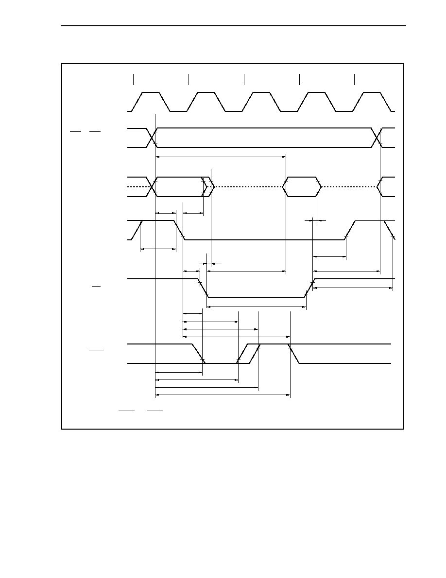
CHAPTER 28 ELECTRICAL SPECIFICATIONS (TARGET)
Preliminary User's Manual U17714EJ1V0UD
779
Read Cycle (CLKOUT Asynchronous): In Multiplexed Bus Mode
CLKOUT (output)
CS0 to CS3 (output)
A16 to A23 (output)
AD0 to AD15 (I/O)
ASTB (output)
RD (output)
WAIT (input)
T1
T2
TW
T3
Data
Address
Hi-Z
<6>
<7>
<17>
<9>
<12>
<14>
<10>
<11>
<25>
<27>
<26>
<28>
<21>
<23>
<22>
<24>
<16>
<8>
<13>
<15>
Remark WR0 and WR1 are high level.
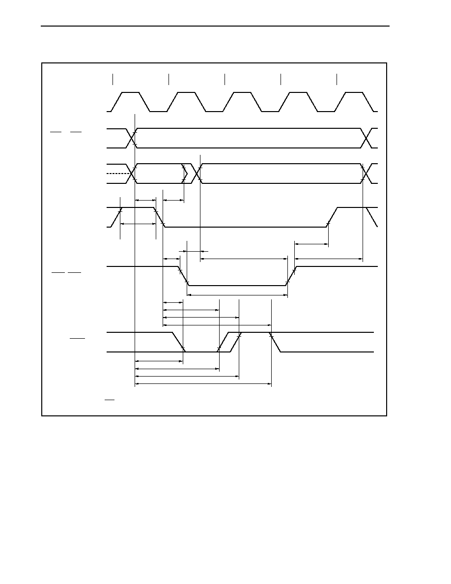
CHAPTER 28 ELECTRICAL SPECIFICATIONS (TARGET)
Preliminary User's Manual U17714EJ1V0UD
780
Write Cycle (CLKOUT Asynchronous): In Multiplexed Bus Mode
CLKOUT (output)
AD0 to AD15 (I/O)
WR0, WR1 (output)
ASTB (output)
WAIT (input)
T1
T2
TW
T3
Data
Address
<25>
<27>
<26>
<28>
<21>
<23>
<22>
<24>
<6>
<17>
<7>
<14>
<20>
<19>
<16>
<11>
<18>
CS0 to CS3 (output)
A16 to A23 (output)
Remark RD is high level.
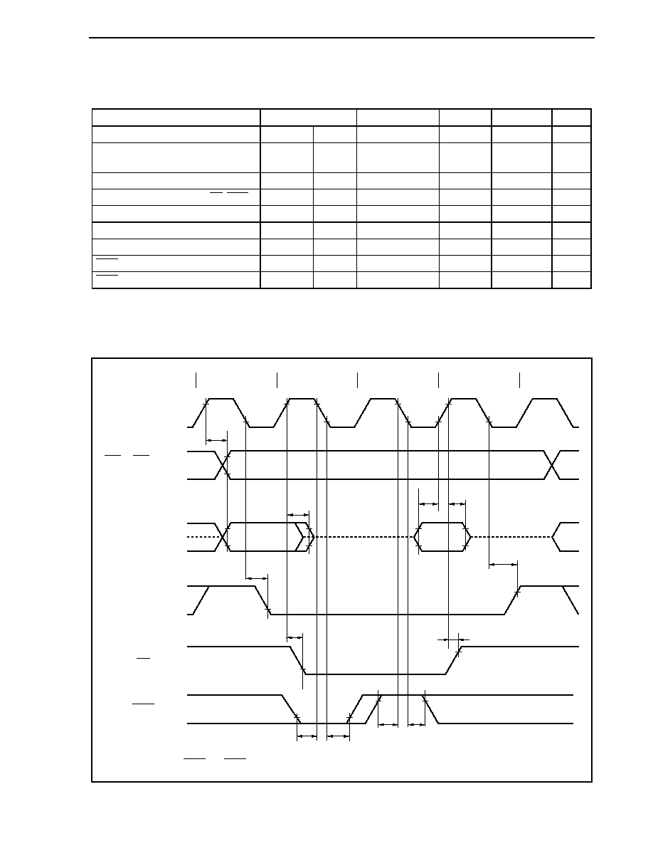
CHAPTER 28 ELECTRICAL SPECIFICATIONS (TARGET)
Preliminary User's Manual U17714EJ1V0UD
781
(b) Read/write cycle (CLKOUT synchronous): In multiplexed bus mode
(T
A
=
-40 to +85�C, BV
DD
V
DD
= EV
DD
= AV
REF0
= AV
REF1
, V
SS
= EV
SS
= BV
SS
= AV
SS
= 0 V, C
L
= 50 pF)
Parameter Symbol
Conditions
MIN.
MAX.
Unit
Delay time from CLKOUT
to address
t
DKA
<29>
0 25 ns
Delay time from CLKOUT
to address
float
t
FKA
<30>
0 19 ns
Delay time from CLKOUT
to ASTB
t
DKST
<31>
-12 7 ns
Delay time from CLKOUT
to RD, WRm
t
DKRDWR
<32>
-5 14
ns
Data input setup time (to CLKOUT
) t
SIDK
<33>
15
ns
Data input hold time (from CLKOUT
) t
HKID
<34>
5
ns
Data output delay time from CLKOUT
t
DKOD
<35>
19 ns
WAIT setup time (to CLKOUT
) t
SWTK
<36>
20
ns
WAIT hold time (from CLKOUT
) t
HKWT
<37>
5
ns
Remarks 1. m = 0, 1
2. The values in the above specifications are values for when clocks with a 1:1 duty ratio are input from X1.
Read Cycle (CLKOUT Synchronous): In Multiplexed Bus Mode
CLKOUT (output)
AD0 to AD15 (I/O)
CS0 to CS3 (output)
A16 to A23 (output)
ASTB (output)
RD (output)
WAIT (input)
T1
T2
TW
T3
Data
Address
Hi-Z
<29>
<31>
<32>
<30>
<31>
<32>
<36>
<36>
<37>
<37>
<33>
<34>
Remark WR0 and WR1 are high level.
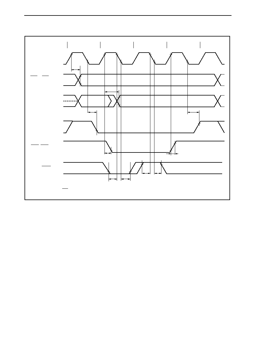
CHAPTER 28 ELECTRICAL SPECIFICATIONS (TARGET)
Preliminary User's Manual U17714EJ1V0UD
782
Write Cycle (CLKOUT Synchronous): In Multiplexed Bus Mode
CLKOUT (output)
AD0 to AD15 (I/O)
ASTB (output)
WR0, WR1 (output)
WAIT (input)
T1
T2
TW
T3
Data
Address
<29>
<31>
<32>
<32>
<37>
<37>
<36>
<36>
<31>
<35>
CS0 to CS3 (output)
A16 to A23 (output)
Remark
RD is high level.
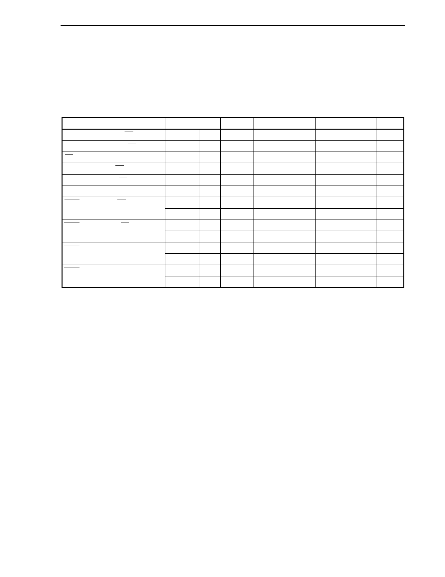
CHAPTER 28 ELECTRICAL SPECIFICATIONS (TARGET)
Preliminary User's Manual U17714EJ1V0UD
783
(2) In separate bus mode
Caution When operating at f
XX
> 20 MHz, be sure to insert an address hold wait and address setup wait.
(a) Read cycle (CLKOUT asynchronous): In separate bus mode
(T
A
=
-40 to +85�C, BV
DD
V
DD
= EV
DD
= AV
REF0
= AV
REF1
, V
SS
= EV
SS
= BV
SS
= AV
SS
= 0 V, C
L
= 50 pF)
Parameter Symbol
Conditions
MIN.
MAX.
Unit
Address setup time (to RD
) t
SARD
<38>
(0.5 + t
ASW
)T
- 23
ns
Address hold time (from RD
) t
HARD
<39>
iT + 1
ns
RD low-level width
t
WRDL
<40>
(1.5
+
n + t
AHW
)T
- 10
ns
Data setup time (to RD
) t
SISD
<41>
23
ns
Data hold time (from RD
) t
HISD
<42>
0
ns
Data setup time (to address)
t
SAID
<43>
(2
+
n + t
ASW
+ t
AHW
)T
- 40
ns
t
SRDWT1
<44>
(0.5 + t
AHW
)T
- 25
ns
WAIT setup time (to RD
)
t
SRDWT2
<45>
(0.5 + n + t
AHW
)T
- 25
ns
t
HRDWT1
<46>
(n
- 0.5 + t
AHW
)T ns
WAIT hold time (from RD
)
t
HRDWT2
<47>
(n + 0.5 + t
AHW
)T ns
t
SAWT1
<48>
(1 + t
ASW
+ t
AHW
)T
- 45
ns
WAIT setup time (to address)
t
SAWT2
<49>
(1 + n + t
ASW
+ t
AHW
)T
- 45
ns
t
HAWT1
<50>
(1 + t
ASW
+ t
AHW
)T ns
WAIT hold time (from address)
t
HAWT2
<51>
(1 + n + t
ASW
+ t
AHW
)T
ns
Remarks 1. t
ASW
: Number of address setup wait clocks
t
AHW
: Number of address hold wait clocks
2. T = 1/f
CPU
(f
CPU
: CPU operating clock frequency)
3. n: Number of wait clocks inserted in the bus cycle
The sampling timing changes when a programmable wait is inserted
4. i: Number of idle states inserted after a read cycle (0 or 1)
5. The values in the above specifications are values for when clocks with a 1:1 duty ratio are input from X1.
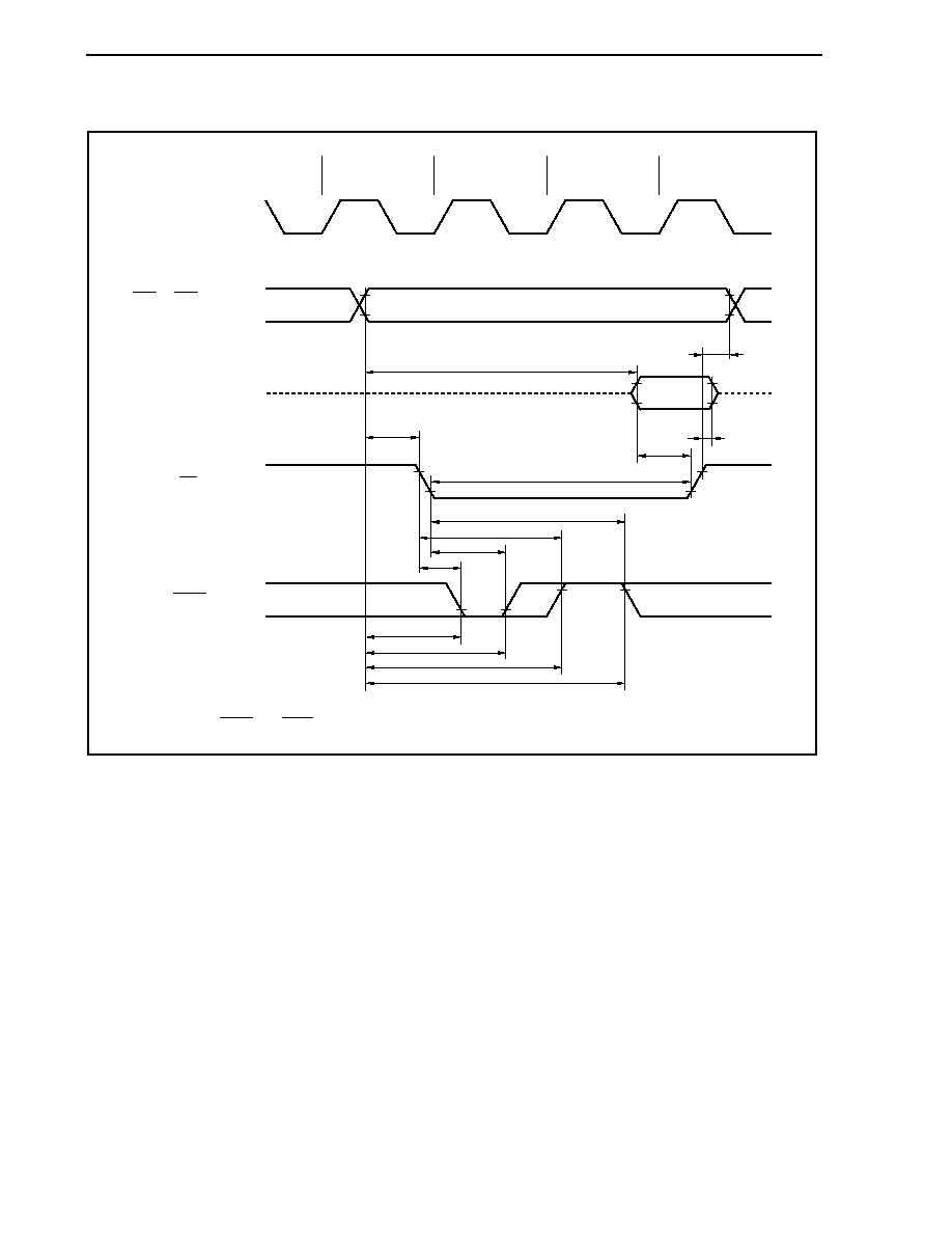
CHAPTER 28 ELECTRICAL SPECIFICATIONS (TARGET)
Preliminary User's Manual U17714EJ1V0UD
784
Read Cycle (CLKOUT Asynchronous): In Separate Bus Mode
CLKOUT (output)
T1
<43>
Hi-Z
Hi-Z
<38>
<40>
<47>
<45>
<46>
<44>
<48>
<50>
<49>
<51>
<42>
<41>
<39>
TW
T2
RD (output)
CS0 to CS3 (output)
A0 to A23 (output)
AD0 to AD15 (I/O)
WAIT (input)
Remark WR0 and WR1 are high level.
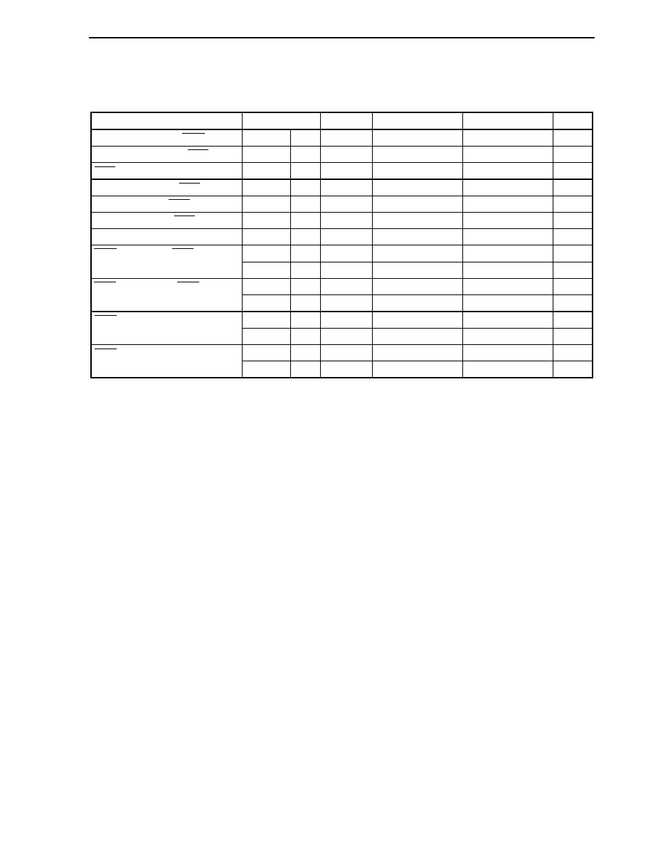
CHAPTER 28 ELECTRICAL SPECIFICATIONS (TARGET)
Preliminary User's Manual U17714EJ1V0UD
785
(b) Write cycle (CLKOUT asynchronous): In separate bus mode
(T
A
=
-40 to +85�C, BV
DD
V
DD
= EV
DD
= AV
REF0
= AV
REF1
, V
SS
= EV
SS
= BV
SS
= AV
SS
= 0 V, C
L
= 50 pF)
Parameter Symbol
Conditions
MIN.
MAX.
Unit
Address setup time (to WRm
) t
SAWR
<52>
(1 + t
ASW
+ t
AHW
)T
- 23
ns
Address hold time (from WRm
) t
HAWR
<53>
0.5T
- 10
ns
WRm low-level width
t
WWRL
<54>
(0.5
+
n)T
- 10
ns
Data output time from WRm
t
DOSDW
<55>
-5
ns
Data setup time (to WRm
) t
SOSDW
<56>
(0.5
+
n)T
- 20
ns
Data hold time (from WRm
) t
HOSDW
<57>
0.5T
- 10
ns
Data setup time (to address)
t
SAOD
<58>
(1 + t
ASW
+ t
AHW
)T
- 25
ns
t
SWRWT1
<59>
22
ns
WAIT setup time (to WRm
)
t
SWRWT2
<60>
nT
- 22
ns
t
HWRWT1
<61>
0
ns
WAIT hold time (from WRm
)
t
HWRWT2
<62>
nT
ns
t
SAWT1
<63>
(1 + t
ASW
+ t
AHW
)T
- 45
ns
WAIT setup time (to address)
t
SAWT2
<64>
(1 + n + t
ASW
+ t
AHW
)T
- 45
ns
t
HAWT1
<65>
(n + t
ASW
+ t
AHW
)T ns
WAIT hold time (from address)
t
HAWT2
<66>
(1
+
n + t
ASW
+ t
AHW
)T
ns
Remarks 1. m = 0, 1
2. t
ASW
: Number of address setup wait clocks
t
AHW
: Number of address hold wait clocks
3. T = 1/f
CPU
(f
CPU
: CPU operating clock frequency)
4. n: Number of wait clocks inserted in the bus cycle
The sampling timing changes when a programmable wait is inserted.
5. The values in the above specifications are values for when clocks with a 1:1 duty ratio are input from X1.
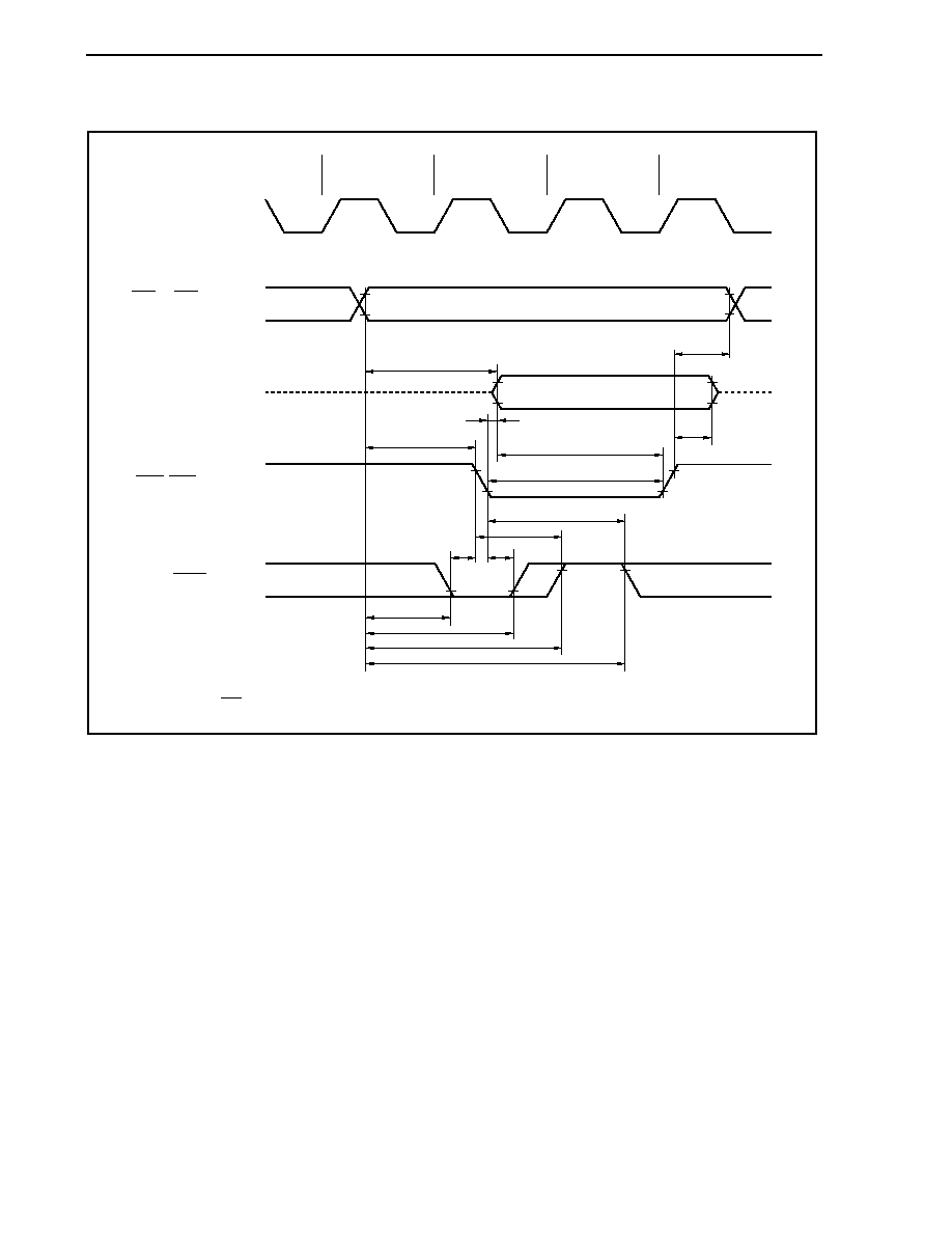
CHAPTER 28 ELECTRICAL SPECIFICATIONS (TARGET)
Preliminary User's Manual U17714EJ1V0UD
786
Write Cycle (CLKOUT Asynchronous): In Separate Bus Mode
CLKOUT (output)
T1
<58>
<52>
<55>
<54>
<62>
<60>
<61>
<59>
<63>
<65>
<64>
<66>
<57>
<56>
<53>
TW
T2
WR0, WR1 (output)
CS0 to CS3 (output)
A0 to A23 (output)
AD0 to AD15 (I/O)
WAIT (input)
Hi-Z
Hi-Z
Remark RD is high level.
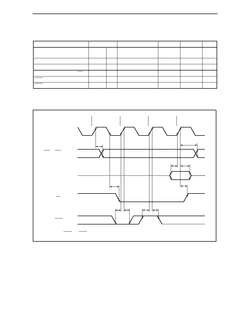
CHAPTER 28 ELECTRICAL SPECIFICATIONS (TARGET)
Preliminary User's Manual U17714EJ1V0UD
787
(c) Read cycle (CLKOUT synchronous): In separate bus mode
(T
A
=
-40 to +85�C, BV
DD
V
DD
= EV
DD
= AV
REF0
= AV
REF1
, V
SS
= EV
SS
= BV
SS
= AV
SS
= 0 V, C
L
= 50 pF)
Parameter Symbol
Conditions
MIN.
MAX.
Unit
Delay time from CLKOUT
to
address, CS
t
DKSA
<67>
2
25
ns
Data input setup time (to CLKOUT
) t
SISDK
<68>
20
ns
Data input hold time (from CLKOUT
) t
HKISD
<69>
0
ns
Delay time from CLKOUT
to RD
t
DKSR
<70>
-2 12
ns
WAIT setup time (to CLKOUT
) t
SWTK
<71>
20
ns
WAIT hold time (from CLKOUT
) t
HKWT
<72>
0
ns
Remark The values in the above specifications are values for when clocks with a 1:1 duty ratio are input from X1.
Read Cycle (CLKOUT Synchronous, 1 Wait): In Separate Bus Mode
CLKOUT (output)
T1
<70>
<71>
<72>
<71>
<72>
<67>
<70>
<68>
<69>
Hi-Z
Hi-Z
TW
T2
RD (output)
CS0 to CS3 (output)
A0 to A23 (output)
AD0 to AD15 (I/O)
WAIT (input)
<67>
Remark WR0 and WR1 are high level.
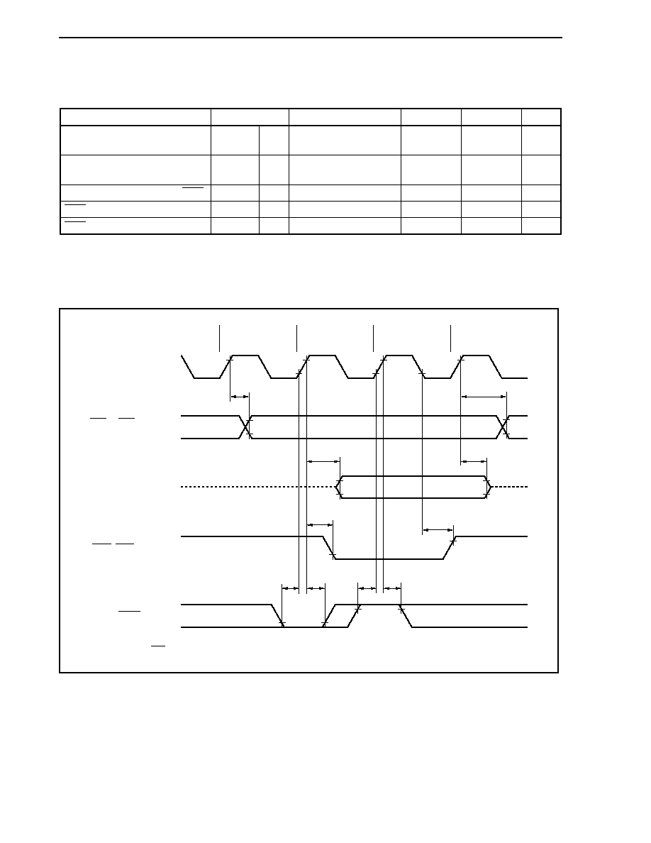
CHAPTER 28 ELECTRICAL SPECIFICATIONS (TARGET)
Preliminary User's Manual U17714EJ1V0UD
788
(d) Write cycle (CLKOUT synchronous): In separate bus mode
(T
A
=
-40 to +85�C, BV
DD
V
DD
= EV
DD
= AV
REF0
= AV
REF1
, V
SS
= EV
SS
= BV
SS
= AV
SS
= 0 V, C
L
= 50 pF)
Parameter Symbol
Conditions
MIN.
MAX.
Unit
Delay time from CLKOUT
to
address, CS
t
DKSA
<73>
2
25
ns
Delay time from CLKOUT
to data
output
t
DKSD
<74>
2
15
ns
Delay time from CLKOUT
to WRm
t
DKSW
<75>
-2 12
ns
WAIT setup time (to CLKOUT
) t
SWTK
<76>
20
ns
WAIT hold time (from CLKOUT
) t
HKWT
<77>
0
ns
Remarks 1. m = 0, 1
2. The values in the above specifications are values for when clocks with a 1:1 duty ratio are input from X1.
Write Cycle (CLKOUT Synchronous): In Separate Bus Mode
CLKOUT (output)
T1
<74>
<75>
<77>
<76>
<75>
TW
T2
WR0, WR1 (output)
CS0 to CS3 (output)
A0 to A23 (output)
AD0 to AD15 (I/O)
WAIT (input)
<73>
<73>
<77>
<76>
<74>
Hi-Z
Hi-Z
Remark RD is high level.
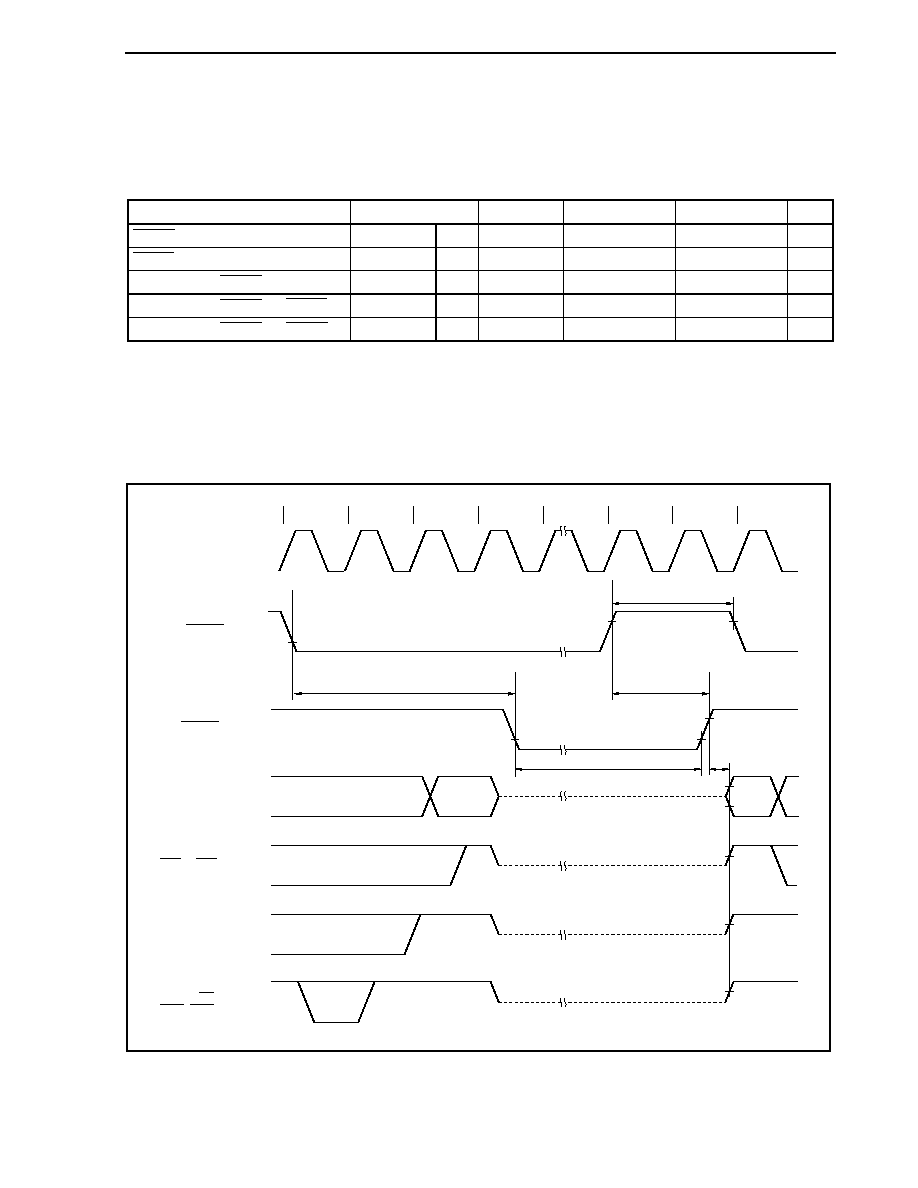
CHAPTER 28 ELECTRICAL SPECIFICATIONS (TARGET)
Preliminary User's Manual U17714EJ1V0UD
789
(3) Bus
hold
(a) CLKOUT
asynchronous
(T
A
=
-40 to +85�C, BV
DD
V
DD
= EV
DD
= AV
REF0
= AV
REF1
, V
SS
= EV
SS
= BV
SS
= AV
SS
= 0 V, C
L
= 50 pF)
Parameter Symbol
Conditions
MIN.
MAX.
Unit
HLDRQ high-level width
t
WHQH
<78>
T
+
10
ns
HLDAK low-level width
t
WHAL
<79>
T
- 15
ns
Delay time from HLDAK
to bus output
t
DHAC
<80>
-3
ns
Delay time from HLDRQ
to HLDAK
t
DHQHA1
<81>
(2n
+
7.5)T
+
25 ns
Delay time from HLDRQ
to HLDAK
t
DHQHA2
<82>
0.5T
1.5T
+
25 ns
Remarks 1. T = 1/f
CPU
(f
CPU
: CPU operating clock frequency)
2. n: Number of wait clocks inserted in the bus cycle
The sampling timing changes when a programmable wait is inserted.
3. The values in the above specifications are values for when clocks with a 1:1 duty ratio are input from X1.
Bus Hold (CLKOUT Asynchronous)
CLKOUT (output)
HLDRQ (input)
HLDAK (output)
Address bus (output)
Data bus (I/O)
TH
TH
TH
TI
TI
Hi-Z
CS0 to CS3 (output)
Hi-Z
ASTB (output)
RD (output),
WR0, WR1 (output)
Hi-Z
Hi-Z
<78>
<82>
<79>
<80>
<81>
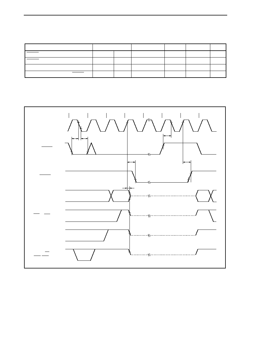
CHAPTER 28 ELECTRICAL SPECIFICATIONS (TARGET)
Preliminary User's Manual U17714EJ1V0UD
790
(b) CLKOUT synchronous
(T
A
=
-40 to +85�C, BV
DD
V
DD
= EV
DD
= AV
REF0
= AV
REF1
, V
SS
= EV
SS
= BV
SS
= AV
SS
= 0 V, C
L
= 50 pF)
Parameter Symbol
Conditions
MIN.
MAX.
Unit
HLDRQ setup time (to CLKOUT
) t
SHQK
<83>
20
ns
HLDRQ hold time (from CLKOUT
) t
HKHQ
<84>
5
ns
Delay time from CLKOUT
to bus float
t
DKF
<85>
19 ns
Delay time from CLKOUT
to HLDAK
t
DKHA
<86>
19 ns
Remark The values in the above specifications are values for when clocks with a 1:1 duty ratio are input from X1.
Bus Hold (CLKOUT Synchronous)
CLKOUT (output)
HLDRQ (input)
HLDAK (output)
Address bus (output)
Data bus (I/O)
TH
TH
TH
T2
T3
TI
TI
Hi-Z
CS0 to CS3 (output)
Hi-Z
ASTB (output)
RD (output),
WR0, WR1 (output)
Hi-Z
Hi-Z
<83>
<83>
<86>
<86>
<84>
<85>
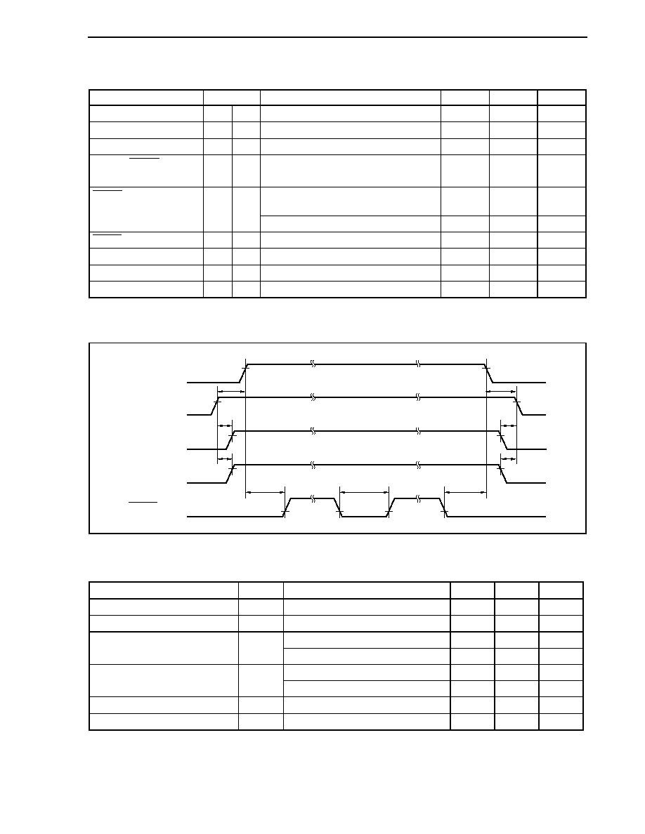
CHAPTER 28 ELECTRICAL SPECIFICATIONS (TARGET)
Preliminary User's Manual U17714EJ1V0UD
791
Power On/Power Off/Reset Timing
(T
A
=
-40 to +85�C, V
SS
= AV
SS
= BV
SS
= EV
SS
= 0 V, C
L
= 50 pF)
Parameter Symbol
Conditions
MIN.
MAX.
Unit
EV
DD
V
DD
t
REL
<87>
0
ns
EV
DD
BV
DD
t
REB
<88>
0 t
REL
ns
EV
DD
AV
REF0
, AV
REF1
t
REA
<89>
0 t
REL
ns
EV
DD
RESET
t
RER
<90>
500 +
t
REG
Note
ns
Analog noise elimination (during flash erase/
writing)
500 ns
RESET low-level width
t
WRSL
<91>
Analog noise elimination
500 ns
RESET
V
DD
t
FRE
<92>
500 ns
V
DD
EV
DD
t
FEL
<93>
0 ns
BV
DD
EV
DD
t
FEB
<94>
0 t
FEL
ns
AV
REF0
EV
DD
t
FEA
<95>
0
t
FEL
ns
Note Depends on the on-chip regulator characteristics.
V
DD
EV
DD
BV
DD
V
I
V
I
V
I
V
I
AV
REF0
RESET (input)
<88>
<87>
<90>
<92>
<91>
<89>
<94>
<93>
<95>
Interrupt, FLMD0 Pin Timing
(T
A
=
-40 to +85�C, BV
DD
V
DD
= EV
DD
= AV
REF0
= AV
REF1
, V
SS
= EV
SS
= BV
SS
= AV
SS
= 0 V, C
L
= 50 pF)
Parameter Symbol
Conditions
MIN.
MAX.
Unit
NMI high-level width
t
WNIH
Analog noise elimination
500
ns
NMI low-level width
t
WNIL
Analog noise elimination
500
ns
n = 0 to 8 (Analog noise elimination)
500
ns
INTPn high-level width
t
WITH
n = 3 (Digital noise elimination)
3T
SMP
+ 20
ns
n = 0 to 8 (Analog noise elimination)
500
ns
INTPn low-level width
t
WITL
n = 3 (Digital noise elimination)
3T
SMP
+ 20
ns
FLMD0 high-level width
t
WMDH
500
ns
FLMD0 low-level width
t
WMDL
500
ns
Remark T
SMP
: Noise elimination sampling clock cycle
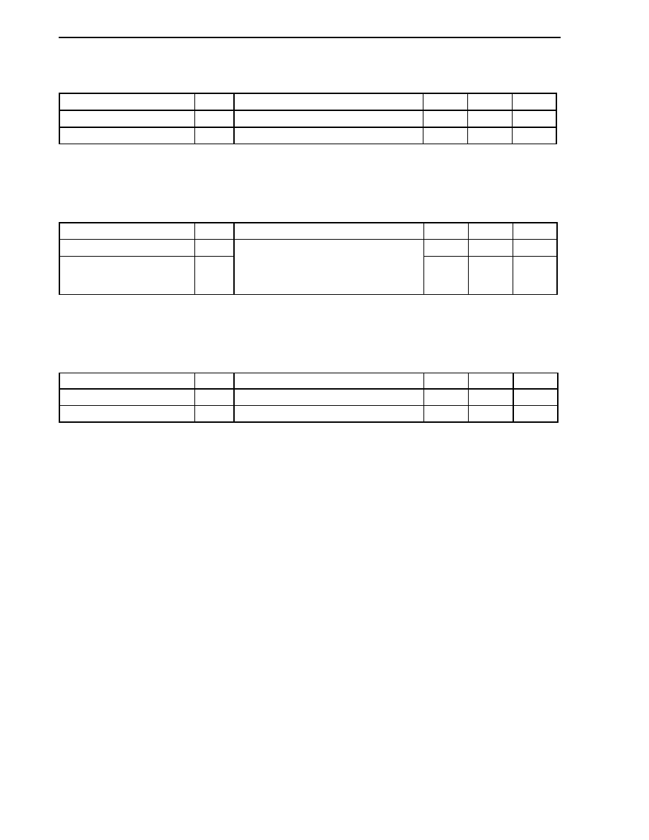
CHAPTER 28 ELECTRICAL SPECIFICATIONS (TARGET)
Preliminary User's Manual U17714EJ1V0UD
792
Key Return Timing
(T
A
=
-40 to +85�C, BV
DD
V
DD
= EV
DD
= AV
REF
0
= AV
REF1
, V
SS
= EV
SS
= BV
SS
= AV
SS
= 0 V, C
L
= 50 pF)
Parameter Symbol
Conditions
MIN.
MAX.
Unit
KRn high-level width
t
WKRH
Analog noise elimination
500
ns
KRn low-level width
t
WKRL
Analog noise elimination
500
ns
Remark n = 0 to 7
Timer Timing
(T
A
=
-40 to +85�C, BV
DD
V
DD
= EV
DD
= AV
REF0
= AV
REF1
, V
SS
= EV
SS
= BV
SS
= AV
SS
= 0 V, C
L
= 50 pF)
Parameter Symbol
Conditions
MIN.
MAX.
Unit
TI high-level width
t
TIH
2T + 20
ns
TI low-level width
t
TIL
TIP00, TIP01, TIP10, TIP11, TIP20, TIP21,
TIP30, TIP31, TIP40, TIP41, TIP50, TIP51,
TIP60, TIP61, TIP70, TIP71, TIP80, TIP81,
TIQ00 to TIQ03
2T + 20
ns
Remark T = 1/f
XX
UART Timing
(T
A
=
-40 to +85�C, BV
DD
V
DD
= EV
DD
= AV
REF0
= AV
REF1
, V
SS
= EV
SS
= BV
SS
= AV
SS
= 0 V, C
L
= 50 pF)
Parameter Symbol
Conditions
MIN.
MAX.
Unit
Transmit rate
312.5
kbps
ASCK0 cycle time
10
MHz
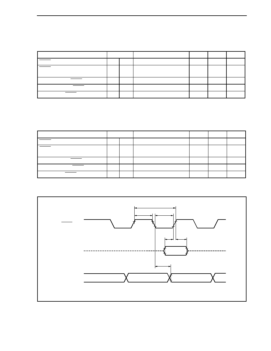
CHAPTER 28 ELECTRICAL SPECIFICATIONS (TARGET)
Preliminary User's Manual U17714EJ1V0UD
793
CSIB Timing
(1) Master
mode
(T
A
=
-40 to +85�C, BV
DD
V
DD
= EV
DD
= AV
REF0
= AV
REF1
, V
SS
= EV
SS
= BV
SS
= AV
SS
= 0 V, C
L
= 50 pF)
Parameter Symbol
Conditions
MIN.
MAX.
Unit
SCKBn cycle time
t
KCY1
<96>
125
ns
SCKBn high-/low-level width
t
KH1
,
t
KL1
<97>
t
KCY1
/2
- 5
ns
SIBn setup time (to SCKBn
) t
SIK1
<98>
30
ns
SIBn hold time (from SCKBn
) t
KSI1
<99>
30
ns
Delay time from SCKBn
to SOBn output t
KSO1
<100>
30
ns
Remark n = 0 to 5
(2) Slave
mode
(T
A
=
-40 to +85�C, BV
DD
V
DD
= EV
DD
= AV
REF0
= AV
REF1
, V
SS
= EV
SS
= BV
SS
= AV
SS
= 0 V, C
L
= 50 pF)
Parameter Symbol
Conditions
MIN.
MAX.
Unit
SCKBn cycle time
t
KCY2
<96>
125
ns
SCKBn high-/low-level width
t
KH2
,
t
KL2
<97>
57.5
ns
SIBn setup time (to SCKBn
) t
SIK2
<98>
30
ns
SIBn hold time (from SCKBn
) t
KSI2
<99>
30
ns
Delay time from SCKBn
to SOBn output t
KSO2
<100>
30
ns
Remark n = 0 to 5
SOBn (output)
Input data
Output data
SIBn (input)
SCKBn (I/O)
<96>
<97>
<97>
<98>
<99>
<100>
Hi-Z
Hi-Z
Remark n = 0 to 5
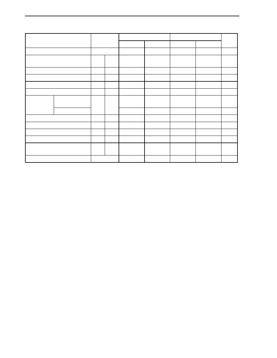
CHAPTER 28 ELECTRICAL SPECIFICATIONS (TARGET)
Preliminary User's Manual U17714EJ1V0UD
794
I
2
C Bus Mode (T
A
=
-40 to +85�C, BV
DD
V
DD
= EV
DD
= AV
REF0
= AV
REF1
, V
SS
= EV
SS
= BV
SS
= AV
SS
= 0 V, C
L
= 50 pF)
Normal Mode
High-Speed Mode
Parameter Symbol
MIN. MAX. MIN. MAX.
Unit
SCL0n clock frequency
f
CLK
0 100 0 400
kHz
Bus free time
(Between start and stop conditions)
t
BUF
<101> 4.7
-
1.3
-
�
s
Hold time
Note 1
t
HD: STA
<102> 4.0
-
0.6
-
�
s
SCL0n clock low-level width
t
LOW
<103> 4.7
-
1.3
-
�
s
SCL0n clock high-level width
t
HIGH
<104> 4.0
-
0.6
-
�
s
Setup time for start/restart conditions
t
SU: STA
<105> 4.7
-
0.6
-
�
s
CBUS compatible
master
5.0
-
-
-
�
s
Data hold time
I
2
C mode
t
HD: DAT
<106>
0
Note 2
-
0
Note 2
0.9
Note 3
�
s
Data setup time
t
SU: DAT
<107> 250
-
100
Note 4
-
ns
SDA0n and SCL0n signal rise time
t
R
<108>
-
1000
20 + 0.1Cb
Note 5
300
ns
SDA0n and SCL0n signal fall time
t
F
<109>
-
300
20 + 0.1Cb
Note 5
300
ns
Stop condition setup time
t
SU: STO
<110> 4.0
-
0.6
-
�
s
Pulse width of spike suppressed by
input filter
t
SP
<111>
-
-
0 50
ns
Capacitance load of each bus line
Cb
-
400
-
400 pF
Notes 1. At the start condition, the first clock pulse is generated after the hold time.
2.
The system requires a minimum of 300 ns hold time internally for the SDA0n signal (at V
IHmin.
of SCL0n
signal) in order to occupy the undefined area at the falling edge of SCL0n.
3.
If the system does not extend the SCL0n signal low hold time (t
LOW
), only the maximum data hold time
(t
HD
:
DAT
) needs to be satisfied.
4.
The high-speed mode I
2
C bus can be used in the normal-mode I
2
C bus system. In this case, set the
high-speed mode I
2
C bus so that it meets the following conditions.
� If the system does not extend the SCL0n signal's low state hold time:
t
SU
:
DAT
250 ns
� If the system extends the SCL0n signal's low state hold time:
Transmit the following data bit to the SDA0n line prior to the SCL0n line release (t
Rmax.
+ t
SU:DAT
= 1,000
+ 250 = 1,250 ns: Normal mode I
2
C bus specification).
5.
Cb: Total capacitance of one bus line (unit: pF)
Remark n = 0 to 2
CHAPTER 28 ELECTRICAL SPECIFICATIONS (TARGET)
Preliminary User's Manual U17714EJ1V0UD
795
I
2
C Bus Mode
Stop
condition
Start
condition
Restart
condition
Stop
condition
SCL0n (I/O)
SDA0n (I/O)
<103>
<109>
<109>
<108>
<108>
<106>
<107>
<105>
<102>
<101>
<102>
<111>
<110>
<104>
Remark n = 0 to 2
A/D Converter
(T
A
=
-40 to +85�C, BV
DD
V
DD
= EV
DD
= AV
REF0
= AV
REF1
, 3.0 V
AV
REF0
3.6 V, V
SS
= EV
SS
= BV
SS
= AV
SS
= 0 V, C
L
= 50 pF)
Parameter Symbol
Conditions
MIN.
TYP.
MAX.
Unit
Resolution
10
bit
Overall error
Note
3.0
AV
REF0
3.6 V
�0.6 %FSR
Conversion time
t
CONV
2.6
24
�
s
Zero scale error
�0.5
%FSR
Full scale error
�0.5
%FSR
Non-linearity error
�4.0
LSB
Differential linearity error
�4.0
LSB
Analog input voltage
V
IAN
AV
SS
AV
REF0
V
Reference voltage
AV
REF0
3.0
3.6
V
Normal conversion mode
3
6.5
mA
High-speed conversion mode
4
10
mA
AV
REF0
current
AI
REF0
When A/D converter unused
5
�
A
Note Excluding quantization error (
�0.05 %FSR).
Caution Do not set (read/write) alternate-function ports during A/D conversion; otherwise the conversion
resolution may be degraded.
Remark LSB: Least Significant Bit
FSR: Full Scale Range
CHAPTER 28 ELECTRICAL SPECIFICATIONS (TARGET)
Preliminary User's Manual U17714EJ1V0UD
796
D/A Converter
(T
A
=
-40 to +85�C, BV
DD
V
DD
= EV
DD
= AV
REF0
= AV
REF1
, 3.0 V
AV
REF1
3.6 V, V
SS
= EV
SS
= BV
SS
= AV
SS
= 0 V, C
L
= 50 pF)
Parameter Symbol
Conditions
MIN.
TYP.
MAX.
Unit
Resolution
8 bit
Overall error
Note 1
R = 2 M
�1.2 %FSR
Settling time
C = 20 pF
3
�
s
Output resistor
R
O
Output data 55H
3.5
k
Reference voltage
AV
REF1
3.0
3.6
V
D/A conversion operating
1 2.5
mA
AV
REF1
current
Note 2
AI
REF1
D/A conversion stopped
5
�
A
Notes 1. Excluding quantization error (
�0.5 LSB).
2.
Value of 1 channel of D/A converter
Remark R is the output pin load resistance and C is the output pin load capacitance.
LVI Circuit Characteristics
(T
A
=
-40 to +85�C, BV
DD
V
DD
= EV
DD
= AV
REF0
= AV
REF1
, V
SS
= EV
SS
= BV
SS
= AV
SS
= 0 V, C
L
= 50 pF)
Parameter Symbol
Conditions MIN.
TYP.
MAX.
Unit
Detection voltage
V
LVI0
2.85
3.0
3.15
V
Response time
Note
t
LD
After V
DD
reaches V
LVI0
(MAX.),
or after V
DD
has dropped to V
LVI0
(MAX.)
0.2
2.0
ms
Minimum pulse width
t
LW
0.2
ms
Reference voltage stabilization wait
time
t
LWAIT
After V
DD
reaches 2.85 V (MIN.)
0.1
0.2
ms
Note Time required to detect the detection voltage and output an interrupt or reset signal.
Supply voltage
(V
DD
)
Time
Detection voltage (MIN.)
Operating voltage (MIN.)
Detection voltage (TYP.)
Detection voltage (MAX.)
t
LWAIT
t
LW
t
LD
t
LD
LVION bit = 0
1
CHAPTER 28 ELECTRICAL SPECIFICATIONS (TARGET)
Preliminary User's Manual U17714EJ1V0UD
797
RAM Retention Detection
(T
A
=
-40 to +85�C, BV
DD
V
DD
= EV
DD
= AV
REF0
= AV
REF1
, V
SS
= EV
SS
= BV
SS
= AV
SS
= 0 V, C
L
= 50 pF)
Parameter Symbol
Conditions MIN.
TYP.
MAX.
Unit
Detection voltage
V
RAMH
1.9
2.0
2.1
V
Supply voltage rise time
t
RAMHTH
V
DD
= 0 to 2.85 V
0.002
ms
Response time
Note
t
RAMHD
After V
DD
reaches 2.1 V
0.2 2.0 ms
Minimum pulse width
t
RAMHW
0.2
ms
Note Time required to detect the detection voltage and set the RAMS.RAMF bit.
Supply voltage
(V
DD
)
Time
Detection voltage (MIN.)
Operating voltage (MIN.)
Detection voltage (TYP.)
Detection voltage (MAX.)
t
RAMHW
t
RAMHD
t
RAMHD
t
RAMHTH
RAMS.RAMF bit
Cleared by instruction
CHAPTER 28 ELECTRICAL SPECIFICATIONS (TARGET)
Preliminary User's Manual U17714EJ1V0UD
798
Flash Memory Programming Characteristics
(T
A
=
-40 to +85�C, BV
DD
V
DD
= EV
DD
= AV
REF0
= AV
REF1
, V
SS
= EV
SS
= BV
SS
= AV
SS
= 0 V, C
L
= 50 pF)
(1) Basic
characteristics
Parameter Symbol
Conditions
MIN.
TYP.
MAX.
Unit
Operating frequency
f
CPU
2.5
20 MHz
Supply voltage
V
DD
2.85 3.6 V
Number of rewrites
C
WRT
100
times
Programming temperature
t
PRG
-40 +85 �C
(2) Serial write operation characteristics
Parameter Symbol
Conditions
MIN.
TYP.
MAX.
Unit
FLMD0, FLMD1 setup time
t
MDSET
2
3000 ms
FLMD0 count start time from RESET
t
RFCF
f
X
= 2.5 to 10 MHz
17855/f
X
+
s
FLMD0 counter high-level width/
low-level width
t
CH
/t
CL
10
100
�
s
FLMD0 counter rise time/fall time
t
R
/t
F
50
�
s
Remark
= oscillation stabilization time
Flash write mode setup timing
V
DD
FLMD1
0 V
V
DD
RESET (input)
0 V
V
DD
FLMD0
0 V
t
RFCF
t
CL
t
F
t
R
t
CH
t
MDSET
CHAPTER 28 ELECTRICAL SPECIFICATIONS (TARGET)
Preliminary User's Manual U17714EJ1V0UD
799
(3) Programming
characteristics
Parameter Symbol
Conditions
MIN.
TYP.
MAX.
Unit
Note 1
304 ms
Note 2
1405 ms
Block erase time
f
XX
= 20 MHz
Note 3
3057 ms
Write time per 256 bytes
f
XX
= 20 MHz
8.1
ms
Note 1
20 ms
Note 2
141 ms
Block internal verify time
f
XX
= 20 MHz
Note 3
322 ms
Note 1
9.2 ms
Note 2
64 ms
Block blank check time
f
XX
= 20 MHz
Note 3
147 ms
Flash memory
information setting time
f
XX
= 20 MHz
1.0
ms
Notes 1. Block size = 4 KB
2. Block size = 28 KB
3. Block size = 64 KB
Caution When writing initially to shipped products, it is counted as one rewrite for both "erase to write" and
"write only".
Example (P: Write, E: Erase)
Shipped
product
P E P E P: 3 rewrites
Shipped
product
E P E P E P: 3 rewrites
Preliminary User's Manual U17714EJ1V0UD
800
CHAPTER 29 PACKAGE DRAWING
108
73
1
36
109
144
72
37
144-PIN PLASTIC LQFP (FINE PITCH) (20x20)
ITEM
MILLIMETERS
NOTE
A
22.0
�0.2
B
20.0
�0.2
C
20.0
�0.2
D
F
1.25
22.0
�0.2
S144GJ-50-UEN
S
1.5
�0.1
K
1.0
�0.2
L
0.5
�0.2
R
3
�+4�
-3�
G
1.25
H
0.22
�0.05
I
0.08
J
0.5 (T.P.)
M
0.17
N
0.08
P
1.4
Q
0.10
�0.05
+0.03
-0.07
Each lead centerline is located within 0.08 mm of
its true position (T.P.) at maximum material condition.
S
S
M
detail of lead end
I
J
F
G
H
Q
R
P
K
M
L
N
C
D
S
A
B

Preliminary User's Manual U17714EJ1V0UD
801
APPENDIX A REGISTER INDEX
(1/12)
Symbol Name
Unit
Page
ADA0CR0
A/D conversion result register 0
ADC
454
ADA0CR0H
A/D conversion result register 0H
ADC
454
ADA0CR1
A/D conversion result register 1
ADC
454
ADA0CR1H
A/D conversion result register 1H
ADC
454
ADA0CR2
A/D conversion result register 2
ADC
454
ADA0CR2H
A/D conversion result register 2H
ADC
454
ADA0CR3
A/D conversion result register 3
ADC
454
ADA0CR3H
A/D conversion result register 3H
ADC
454
ADA0CR4
A/D conversion result register 4
ADC
454
ADA0CR4H
A/D conversion result register 4H
ADC
454
ADA0CR5
A/D conversion result register 5
ADC
454
ADA0CR5H
A/D conversion result register 5H
ADC
454
ADA0CR6
A/D conversion result register 6
ADC
454
ADA0CR6H
A/D conversion result register 6H
ADC
454
ADA0CR7
A/D conversion result register 7
ADC
454
ADA0CR7H
A/D conversion result register 7H
ADC
454
ADA0CR8
A/D conversion result register 8
ADC
454
ADA0CR8H
A/D conversion result register 8H
ADC
454
ADA0CR9
A/D conversion result register 9
ADC
454
ADA0CR9H
A/D conversion result register 9H
ADC
454
ADA0CR10
A/D conversion result register 10
ADC
454
ADA0CR10H
A/D conversion result register 10H
ADC
454
ADA0CR11
A/D conversion result register 11
ADC
454
ADA0CR11H
A/D conversion result register 11H
ADC
454
ADA0CR12
A/D conversion result register 12
ADC
454
ADA0CR12H
A/D conversion result register 12H
ADC
454
ADA0CR13
A/D conversion result register 13
ADC
454
ADA0CR13H
A/D conversion result register 13H
ADC
454
ADA0CR14
A/D conversion result register 14
ADC
454
ADA0CR14H
A/D conversion result register 14H
ADC
454
ADA0CR15
A/D conversion result register 15
ADC
454
ADA0CR15H
A/D conversion result register 15H
ADC
454
ADA0M0
A/D converter mode register 0
ADC
447
ADA0M1
A/D converter mode register 1
ADC
449
ADA0M2
A/D converter mode register 2
ADC
452
ADA0PFM
Power-fail compare mode register
ADC
456
ADA0PFT
Power-fail compare threshold value register
ADC
457
ADA0S
A/D converter channel specification register
ADC
453
ADIC
Interrupt control register
INTC
668
AWC
Address wait control register
BCU
201
BCC
Bus cycle control register
BCU
202
BSC
Bus size configuration register
BCU
190

APPENDIX A REGISTER INDEX
Preliminary User's Manual U17714EJ1V0UD
802
(2/12)
Symbol Name
Unit
Page
CB0CTL0
CSIB0 control register 0
CSI
524
CB0CTL1
CSIB0 control register 1
CSI
527
CB0CTL2
CSIB0 control register 2
CSI
528
CB0RIC
Interrupt control register
INTC
667
CB0RX
CSIB0 receive data register
CSI
523
CB0RXL
CSIB0 receive data register L
CSI
523
CB0STR
CSIB0 status register
CSI
530
CB0TIC
Interrupt control register
INTC
667
CB0TX
CSIB0 transmit data register
CSI
523
CB0TXL
CSIB0 transmit data register L
CSI
523
CB1CTL0
CSIB1 control register 0
CSI
524
CB1CTL1
CSIB1 control register 1
CSI
527
CB1CTL2
CSIB1 control register 2
CSI
528
CB1RIC
Interrupt control register
INTC
667
CB1RX
CSIB1 receive data register
CSI
523
CB1RXL
CSIB1 receive data register L
CSI
523
CB1STR
CSIB1 status register
CSI
530
CB1TIC
Interrupt control register
INTC
667
CB1TX
CSIB1 transmit data register
CSI
523
CB1TXL
CSIB1 transmit data register L
CSI
523
CB2CTL0
CSIB2 control register 0
CSI
524
CB2CTL1
CSIB2 control register 1
CSI
527
CB2CTL2
CSIB2 control register 2
CSI
528
CB2RIC
Interrupt control register
INTC
667
CB2RX
CSIB2 receive data register
CSI
523
CB2RXL
CSIB2 receive data register L
CSI
523
CB2STR
CSIB2 status register
CSI
530
CB2TIC
Interrupt control register
INTC
667
CB2TX
CSIB2 transmit data register
CSI
523
CB2TXL
CSIB2 transmit data register L
CSI
523
CB3CTL0
CSIB3 control register 0
CSI
524
CB3CTL1
CSIB3 control register 1
CSI
527
CB3CTL2
CSIB3 control register 2
CSI
528
CB3RIC
Interrupt control register
INTC
667
CB3RX
CSIB3 receive data register
CSI
523
CB3RXL
CSIB3 receive data register L
CSI
523
CB3STR
CSIB3 status register
CSI
530
CB3TIC
Interrupt control register
INTC
667
CB3TX
CSIB3 transmit data register
CSI
523
CB3TXL
CSIB3 transmit data register L
CSI
523
CB4CTL0
CSIB4 control register 0
CSI
524
CB4CTL1
CSIB4 control register 1
CSI
527
CB4CTL2
CSIB4 control register 2
CSI
528
CB4RIC
Interrupt control register
INTC
668
CB4RX
CSIB4 receive data register
CSI
523

APPENDIX A REGISTER INDEX
Preliminary User's Manual U17714EJ1V0UD
803
(3/12)
Symbol Name
Unit
Page
CB4RXL
CSIB4 receive data register L
CSI
523
CB4STR
CSIB4 status register
CSI
530
CB4TIC
Interrupt control register
INTC
668
CB4TX
CSIB4 transmit data register
CSI
523
CB4TXL
CSIB4 transmit data register L
CSI
523
CB5CTL0
CSIB5 control register 0
CSI
524
CB5CTL1
CSIB5 control register 1
CSI
527
CB5CTL2
CSIB5 control register 2
CSI
528
CB5RIC
Interrupt control register
INTC
668
CB5RX
CSIB5 receive data register
CSI
523
CB5RXL
CSIB5 receive data register L
CSI
523
CB5STR
CSIB5 status register
CSI
530
CB5TIC
Interrupt control register
INTC
668
CB5TX
CSIB5 transmit data register
CSI
523
CB5TXL
CSIB5 transmit data register L
CSI
523
CCLS
CPU operation clock status register
CG
219
CKC
Clock control register
CLM
222
CLM
Clock monitor mode register
CG
721
CTBP CALLT
base
pointer
CPU
54
CTPC
CALLT execution status saving register
CPU
53
CTPSW
CALLT execution status saving register
CPU
53
DA0CS0
D/A conversion value setting register 0
DAC
481
DA0CS1
D/A conversion value setting register 1
DAC
481
DA0M
D/A converter mode register
DAC
480
DADC0
DMA addressing control register 0
DMA
632
DADC1
DMA addressing control register 1
DMA
632
DADC2
DMA addressing control register 2
DMA
632
DADC3
DMA addressing control register 3
DMA
632
DBC0
DMA transfer count register 0
DMA
631
DBC1
DMA transfer count register 1
DMA
631
DBC2
DMA transfer count register 2
DMA
631
DBC3
DMA transfer count register 3
DMA
631
DBPC
Exception/debug trap status saving register
CPU
54
DBPSW
Exception/debug trap status saving register
CPU
54
DCHC0
DMA channel control register 0
DMA
633
DCHC1
DMA channel control register 1
DMA
633
DCHC2
DMA channel control register 2
DMA
633
DCHC3
DMA channel control register 3
DMA
633
DDA0H
DMA destination address register 0H
DMA
630
DDA0L
DMA destination address register 0L
DMA
630
DDA1H
DMA destination address register 1H
DMA
630
DDA1L
DMA destination address register 1L
DMA
630
DDA2H
DMA destination address register 2H
DMA
630
DDA2L
DMA destination address register 2L
DMA
630
DDA3H
DMA destination address register 3H
DMA
630

APPENDIX A REGISTER INDEX
Preliminary User's Manual U17714EJ1V0UD
804
(4/12)
Symbol Name
Unit
Page
DDA3L
DMA destination address register 3L
DMA
630
DMAIC0
Interrupt control register
INTC
668
DMAIC1
Interrupt control register
INTC
668
DMAIC2
Interrupt control register
INTC
668
DMAIC3
Interrupt control register
INTC
668
DSA0H
DMA source address register 0H
DMA
629
DSA0L
DMA source address register 0L
DMA
629
DSA1H
DMA source address register 1H
DMA
629
DSA1L
DMA source address register 1L
DMA
629
DSA2H
DMA source address register 2H
DMA
629
DSA2L
DMA source address register 2L
DMA
629
DSA3H
DMA source address register 3H
DMA
629
DSA3L
DMA source address register 3L
DMA
629
DTFR0
DMA trigger factor register 0
DMA
634
DTFR1
DMA trigger factor register 1
DMA
634
DTFR2
DMA trigger factor register 2
DMA
634
DTFR3
DMA trigger factor register 3
DMA
634
DWC0
Data wait control register 0
BCU
198
ECR
Interrupt source register
CPU
51
EIPC
Interrupt status saving register
CPU
50
EIPSW
Interrupt status saving register
CPU
50
EXIMC
External bus interface mode control register
BCU
189
FEPC
NMI status saving register
CPU
51
FEPSW
NMI status saving register
CPU
51
IIC0
IIC shift register 0
I
2
C 572
IIC1
IIC shift register 1
I
2
C 572
IIC2
IIC shift register 2
I
2
C 572
IICC0
IIC control register 0
I
2
C 558
IICC1
IIC control register 1
I
2
C 558
IICC2
IIC control register 2
I
2
C 558
IICCL0
IIC clock select register 0
I
2
C 568
IICCL1
IIC clock select register 1
I
2
C 568
IICCL2
IIC clock select register 2
I
2
C 568
IICF0
IIC flag register 0
I
2
C 566
IICF1
IIC flag register 1
I
2
C 566
IICF2
IIC flag register 2
I
2
C 566
IICIC0
Interrupt control register
INTC
668
IICIC1
Interrupt control register
INTC
667
IICIC2
Interrupt control register
INTC
668
IICS0
IIC status register 0
I
2
C 563
IICS1
IIC status register 1
I
2
C 563
IICS2
IIC status register 2
I
2
C 563
IICX0
IIC function expansion register 0
I
2
C 569
IICX1
IIC function expansion register 1
I
2
C 569
IICX2
IIC function expansion register 2
I
2
C 569

APPENDIX A REGISTER INDEX
Preliminary User's Manual U17714EJ1V0UD
805
(5/12)
Symbol Name
Unit
Page
IMR0
Interrupt mask register 0
INTC
668
IMR0H
Interrupt mask register 0H
INTC
668
IMR0L
Interrupt mask register 0L
INTC
668
IMR1
Interrupt mask register 1
INTC
668
IMR1H
Interrupt mask register 1H
INTC
668
IMR1L
Interrupt mask register 1L
INTC
668
IMR2
Interrupt mask register 2
INTC
668
IMR2H
Interrupt mask register 2H
INTC
668
IMR2L
Interrupt mask register 2L
INTC
668
IMR3
Interrupt mask register 3
INTC
668
IMR3H
Interrupt mask register 3H
INTC
668
IMR3L
Interrupt mask register 3L
INTC
668
IMR4
Interrupt mask register 4
INTC
668
IMR4H
Interrupt mask register 4H
INTC
668
IMR4L
Interrupt mask register 4L
INTC
668
INTF0
External falling edge specification register 0
INTC
680
INTF3
External falling edge specification register 3
INTC
681
INTF8
External falling edge specification register 8
INTC
682
INTF9H
External falling edge specification register 9H
INTC
683
INTR0
External rising edge specification register 0
INTC
680
INTR3
External rising edge specification register 3
INTC
681
INTR8
External rising edge specification register 8
INTC
682
INTR9H
External rising edge specification register 9H
INTC
683
ISPR
In-service priority register
INTC
670
KRIC
Interrupt control register
INTC
668
KRM
Key return mode register
KR
688
LOCKR
Lock register
CG 223
LVIIC
Interrupt control register
INTC
667
LVIM
Low-voltage detection register
LVI
726
LVIS
Low-voltage detection level select register
LVI
727
NFC
Noise elimination control register
INTC
684
OCDM
On-chip debug mode register
Debug
760
OCKS0
IIC division clock select register 0
I
2
C 572
OCKS1
IIC division clock select register 1
I
2
C 572
OSTS
Oscillation stabilization time select register
WDT
693
P0
Port 0 register
Port
96
P1
Port 1 register
Port
99
P3
Port 3 register
Port
101
P3H
Port 3 register H
Port
101
P3L
Port 3 register L
Port
101
P4
Port 4 register
Port
106
P5
Port 5 register
Port
108
P6
Port 6 register
Port
113
P6H
Port 6 register H
Port
113
P6L
Port 6 register L
Port
113

APPENDIX A REGISTER INDEX
Preliminary User's Manual U17714EJ1V0UD
806
(6/12)
Symbol Name
Unit
Page
P7H
Port 7 register H
Port
117
P7L
Port 7 register L
Port
117
P8
Port 8 register
Port
118
P9
Port 9 register
Port
121
P9H
Port 9 register H
Port
121
P9L
Port 9 register L
Port
121
PC Program
counter
CPU
48
PCC
Processor clock control register
CG
215
PCD
Port CD register
Port
128
PCM
Port CM register
Port
129
PCS
Port CS register
Port
131
PCT
Port CT register
Port
133
PDH
Port DH register
Port
135
PDL
Port DL register
Port
138
PDLH
Port DL register H
Port
138
PDLL
Port DL register L
Port
138
PEMU1
Peripheral emulation register 1
CPU
731
PF0
Port 0 function register
Port
98
PF3
Port 3 function register
Port
105
PF3H
Port 3 function register H
Port
105
PF3L
Port 3 function register L
Port
105
PF4
Port 4 function register
Port
107
PF5
Port 5 function register
Port
111
PF6
Port 6 function register
Port
115
PF6H
Port 6 function register H
Port
115
PF6L
Port 6 function register L
Port
115
PF8
Port 8 function register
Port
119
PF9
Port 9 function register
Port
127
PF9H
Port 9 function register H
Port
127
PF9L
Port 9 function register L
Port
127
PFC0
Port 0 function control register
Port
98
PFC3
Port 3 function control register
Port
103
PFC3H
Port 3 function control register H
Port
103
PFC3L
Port 3 function control register L
Port
103
PFC4
Port 4 function control register
Port
107
PFC5
Port 5 function control register
Port
109
PFC6H
Port 6 function control register H
Port
115
PFC9
Port 9 function control register
Port
124
PFC9H
Port 9 function control register H
Port
124
PFC9L
Port 9 function control register L
Port
124
PFCE3L
Port 3 function control expansion register L
Port
103
PFCE5
Port 5 function control expansion register
Port
110
PFCE9
Port 9 function control expansion register
Port
124
PFCE9H
Port 9 function control expansion register H
Port
124
PFCE9L
Port 9 function control expansion register L
Port
124

APPENDIX A REGISTER INDEX
Preliminary User's Manual U17714EJ1V0UD
807
(7/12)
Symbol Name
Unit
Page
PIC0
Interrupt control register
INTC
667
PIC1
Interrupt control register
INTC
667
PIC2
Interrupt control register
INTC
667
PIC3
Interrupt control register
INTC
667
PIC4
Interrupt control register
INTC
667
PIC5
Interrupt control register
INTC
667
PIC6
Interrupt control register
INTC
667
PIC7
Interrupt control register
INTC
667
PIC8
Interrupt control register
INTC
668
PLLCTL
PLL control register
CG
221
PLLS
PLL lockup time specification register
CG
224
PM0
Port 0 mode register
Port
96
PM1
Port 1 mode register
Port
99
PM3
Port 3 mode register
Port
101
PM3H
Port 3 mode register H
Port
101
PM3L
Port 3 mode register L
Port
101
PM4
Port 4 mode register
Port
106
PM5
Port 5 mode register
Port
108
PM6
Port 6 mode register
Port
113
PM6H
Port 6 mode register H
Port
113
PM6L
Port 6 mode register L
Port
113
PM7H
Port 7 mode register H
Port
117
PM7L
Port 7 mode register L
Port
117
PM8
Port 8 mode register
Port
118
PM9
Port 9 mode register
Port
121
PM9H
Port 9 mode register H
Port
121
PM9L
Port 9 mode register L
Port
121
PMC0
Port 0 mode control register
Port
97
PMC3
Port 3 mode control register
Port
102
PMC3H
Port 3 mode control register H
Port
102
PMC3L
Port 3 mode control register L
Port
102
PMC4
Port 4 mode control register
Port
107
PMC5
Port 5 mode control register
Port
109
PMC6
Port 6 mode control register
Port
114
PMC6H
Port 6 mode control register H
Port
114
PMC6L
Port 6 mode control register L
Port
114
PMC8
Port 8 mode control register
Port
119
PMC9
Port 9 mode control register
Port
122
PMC9H
Port 9 mode control register H
Port
122
PMC9L
Port 9 mode control register L
Port
122
PMCCM
Port CM mode control register
Port
130
PMCCS
Port CS mode control register
Port
132
PMCCT
Port CT mode control register
Port
134
PMCD
Port CD mode register
Port
128
PMCDH
Port DH mode control register
Port
136

APPENDIX A REGISTER INDEX
Preliminary User's Manual U17714EJ1V0UD
808
(8/12)
Symbol Name
Unit
Page
PMCDL
Port DL mode control register
Port
139
PMCDLH
Port DL mode control register H
Port
139
PMCDLL
Port DL mode control register L
Port
139
PMCM
Port CM mode register
Port
129
PMCS
Port CS mode register
Port
131
PMCT
Port CT mode register
Port
133
PMDH
Port DH mode register
Port
135
PMDL
Port DL mode register
Port
138
PMDLH
Port DL mode register H
Port
138
PMDLL
Port DL mode register L
Port
138
PRCMD
Command register
CPU
84
PRSCM0
Prescaler compare register 0
WT
425
PRSCM1
Prescaler compare register 1
CSI
548
PRSCM2
Prescaler compare register 2
CSI
548
PRSCM3
Prescaler compare register 3
CSI
548
PRSM0
Prescaler mode register 0
WT
424
PRSM1
Prescaler mode register 1
CSI
547
PRSM2
Prescaler mode register 2
CSI
547
PRSM3
Prescaler mode register 3
CSI
547
PSC
Power save control register
CG
691
PSMR
Power save mode register
CG
692
PSW Program
status
word
CPU
52
r0 to r31
General-purpose registers
CPU
48
RAMS
Internal RAM data status register
CG
727
RCM
Internal oscillation mode register
CG
219
RESF
Reset source flag register
Reset
710
RTBH0
Real-time output buffer register 0H
RTP
438
RTBH1
Real-time output buffer register 1H
RTP
438
RTBL0
Real-time output buffer register 0L
RTP
438
RTBL1
Real-time output buffer register 1L
RTP
438
RTPC0
Real-time output port control register 0
RTP
440
RTPC1
Real-time output port control register 1
RTP
440
RTPM0
Real-time output port mode register 0
RTP
439
RTPM1
Real-time output port mode register 1
RTP
439
SELCNT0
Selector operation control register 0
Timer
312
SVA0
Slave address register 0
I
2
C 573
SVA1
Slave address register 1
I
2
C 573
SVA2
Slave address register 2
I
2
C 573
SYS
System status register
CPU
85
TM0CMP0
TMM0 compare register 0
Timer
414
TM0CTL0
TMM0 control register 0
Timer
415
TM0EQIC0
Interrupt control register
INTC
667
TP0CCIC0
Interrupt control register
INTC
667
TP0CCIC1
Interrupt control register
INTC
667
TP0CCR0
TMP0 capture/compare register 0
Timer
235

APPENDIX A REGISTER INDEX
Preliminary User's Manual U17714EJ1V0UD
809
(9/12)
Symbol Name
Unit
Page
TP0CCR1
TMP0 capture/compare register 1
Timer
237
TP0CNT
TMP0 counter read buffer register
Timer
239
TP0CTL0
TMP0 control register 0
Timer
229
TP0CTL1
TMP0 control register 1
Timer
229
TP0IOC0
TMP0 I/O control register 0
Timer
231
TP0IOC1
TMP0 I/O control register 1
Timer
232
TP0IOC2
TMP0 I/O control register 2
Timer
233
TP0OPT0
TMP0 option register 0
Timer
234
TP0OVIC
Interrupt control register
INTC
667
TP1CCIC0
Interrupt control register
INTC
667
TP1CCIC1
Interrupt control register
INTC
667
TP1CCR0
TMP1 capture/compare register 0
Timer
235
TP1CCR1
TMP1 capture/compare register 1
Timer
237
TP1CNT
TMP1 counter read buffer register
Timer
239
TP1CTL0
TMP1 control register 0
Timer
229
TP1CTL1
TMP1 control register 1
Timer
229
TP1IOC0
TMP1 I/O control register 0
Timer
231
TP1IOC1
TMP1 I/O control register 1
Timer
232
TP1IOC2
TMP1 I/O control register 2
Timer
233
TP1OPT0
TMP1 option register 0
Timer
234
TP1OVIC
Interrupt control register
INTC
667
TP2CCIC0
Interrupt control register
INTC
667
TP2CCIC1
Interrupt control register
INTC
667
TP2CCR0
TMP2 capture/compare register 0
Timer
235
TP2CCR1
TMP2 capture/compare register 1
Timer
237
TP2CNT
TMP2 counter read buffer register
Timer
239
TP2CTL0
TMP2 control register 0
Timer
229
TP2CTL1
TMP2 control register 1
Timer
229
TP2IOC0
TMP2 I/O control register 0
Timer
231
TP2IOC1
TMP2 I/O control register 1
Timer
232
TP2IOC2
TMP2 I/O control register 2
Timer
233
TP2OPT0
TMP2 option register 0
Timer
234
TP2OVIC
Interrupt control register
INTC
667
TP3CCIC0
Interrupt control register
INTC
667
TP3CCIC1
Interrupt control register
INTC
667
TP3CCR0
TMP3 capture/compare register 0
Timer
235
TP3CCR1
TMP3 capture/compare register 1
Timer
237
TP3CNT
TMP3 counter read buffer register
Timer
239
TP3CTL0
TMP3 control register 0
Timer
229
TP3CTL1
TMP3 control register 1
Timer
229
TP3IOC0
TMP3 I/O control register 0
Timer
231
TP3IOC1
TMP3 I/O control register 1
Timer
232
TP3IOC2
TMP3 I/O control register 2
Timer
233
TP3OPT0
TMP3 option register 0
Timer
234
TP3OVIC
Interrupt control register
INTC
667

APPENDIX A REGISTER INDEX
Preliminary User's Manual U17714EJ1V0UD
810
(10/12)
Symbol Name
Unit
Page
TP4CCIC0
Interrupt control register
INTC
667
TP4CCIC1
Interrupt control register
INTC
667
TP4CCR0
TMP4 capture/compare register 0
Timer
235
TP4CCR1
TMP4 capture/compare register 1
Timer
237
TP4CNT
TMP4 counter read buffer register
Timer
239
TP4CTL0
TMP4 control register 0
Timer
229
TP4CTL1
TMP4 control register 1
Timer
229
TP4IOC0
TMP4 I/O control register 0
Timer
231
TP4IOC1
TMP4 I/O control register 1
Timer
232
TP4IOC2
TMP4 I/O control register 2
Timer
233
TP4OPT0
TMP4 option register 0
Timer
234
TP4OVIC
Interrupt control register
INTC
667
TP5CCIC0
Interrupt control register
INTC
667
TP5CCIC1
Interrupt control register
INTC
667
TP5CCR0
TMP5 capture/compare register 0
Timer
235
TP5CCR1
TMP5 capture/compare register 1
Timer
237
TP5CNT
TMP5 counter read buffer register
Timer
239
TP5CTL0
TMP5 control register 0
Timer
229
TP5CTL1
TMP5 control register 1
Timer
229
TP5IOC0
TMP5 I/O control register 0
Timer
231
TP5IOC1
TMP5 I/O control register 1
Timer
232
TP5IOC2
TMP5 I/O control register 2
Timer
233
TP5OPT0
TMP5 option register 0
Timer
234
TP5OVIC
Interrupt control register
INTC
667
TP6CCIC0
Interrupt control register
INTC
668
TP6CCIC1
Interrupt control register
INTC
668
TP6CCR0
TMP6 capture/compare register 0
Timer
235
TP6CCR1
TMP6 capture/compare register 1
Timer
237
TP6CNT
TMP6 counter read buffer register
Timer
239
TP6CTL0
TMP6 control register 0
Timer
229
TP6CTL1
TMP6 control register 1
Timer
229
TP6IOC0
TMP6 I/O control register 0
Timer
231
TP6IOC1
TMP6 I/O control register 1
Timer
232
TP6IOC2
TMP6 I/O control register 2
Timer
233
TP6OPT0
TMP6 option register 0
Timer
234
TP6OVIC
Interrupt control register
INTC
668
TP7CCIC0
Interrupt control register
INTC
668
TP7CCIC1
Interrupt control register
INTC
668
TP7CCR0
TMP7 capture/compare register 0
Timer
235
TP7CCR1
TMP7 capture/compare register 1
Timer
237
TP7CNT
TMP7 counter read buffer register
Timer
239
TP7CTL0
TMP7 control register 0
Timer
229
TP7CTL1
TMP7 control register 1
Timer
229
TP7IOC0
TMP7 I/O control register 0
Timer
231
TP7IOC1
TMP7 I/O control register 1
Timer
232

APPENDIX A REGISTER INDEX
Preliminary User's Manual U17714EJ1V0UD
811
(11/12)
Symbol Name
Unit
Page
TP7IOC2
TMP7 I/O control register 2
Timer
233
TP7OPT0
TMP7 option register 0
Timer
234
TP7OVIC
Interrupt control register
INTC
668
TP8CCIC0
Interrupt control register
INTC
668
TP8CCIC1
Interrupt control register
INTC
668
TP8CCR0
TMP8 capture/compare register 0
Timer
235
TP8CCR1
TMP8 capture/compare register 1
Timer
237
TP8CNT
TMP8 counter read buffer register
Timer
239
TP8CTL0
TMP8 control register 0
Timer
229
TP8CTL1
TMP8 control register 1
Timer
229
TP8IOC0
TMP8 I/O control register 0
Timer
231
TP8IOC1
TMP8 I/O control register 1
Timer
232
TP8IOC2
TMP8 I/O control register 2
Timer
233
TP8OPT0
TMP8 option register 0
Timer
234
TP8OVIC
Interrupt control register
INTC
668
TQ0CCIC0
Interrupt control register
INTC
667
TQ0CCIC1
Interrupt control register
INTC
667
TQ0CCIC2
Interrupt control register
INTC
667
TQ0CCIC3
Interrupt control register
INTC
667
TQ0CCR0
TMQ0 capture/compare register 0
Timer
324
TQ0CCR1
TMQ0 capture/compare register 1
Timer
326
TQ0CCR2
TMQ0 capture/compare register 2
Timer
328
TQ0CCR3
TMQ0 capture/compare register 3
Timer
330
TQ0CNT
TMQ0 counter read buffer register
Timer
332
TQ0CTL0
TMQ0 control register 0
Timer
318
TQ0CTL1
TMQ0 control register 1
Timer
319
TQ0IOC0
TMQ0 I/O control register 0
Timer
320
TQ0IOC1
TMQ0 I/O control register 1
Timer
321
TQ0IOC2
TMQ0 I/O control register 2
Timer
322
TQ0OPT0
TMQ0 option register 0
Timer
323
TQ0OVIC
Interrupt control register
INTC
667
UA0CTL0
UARTA0 control register 0
UART
490
UA0CTL1
UARTA0 control register 1
UART
512
UA0CTL2
UARTA0 control register 2
UART
513
UA0OPT0
UARTA0 option control register 0
UART
492
UA0RIC
Interrupt control register
INTC
668
UA0RX
UARTA0 receive data register
UART
495
UA0STR
UARTA0 status register
UART
493
UA0TIC
Interrupt control register
INTC
668
UA0TX
UARTA0 transmit data register
UART
495
UA1CTL0
UARTA1 control register 0
UART
490
UA1CTL1
UARTA1 control register 1
UART
512
UA1CTL2
UARTA1 control register 2
UART
513
UA1OPT0
UARTA1 option control register 0
UART
492
UA1RIC
Interrupt control register
INTC
668

APPENDIX A REGISTER INDEX
Preliminary User's Manual U17714EJ1V0UD
812
(12/12)
Symbol Name
Unit
Page
UA1RX
UARTA1 receive data register
UART
495
UA1STR
UARTA1 status register
UART
493
UA1TIC
Interrupt control register
INTC
668
UA1TX
UARTA1 transmit data register
UART
495
UA2CTL0
UARTA2 control register 0
UART
490
UA2CTL1
UARTA2 control register 1
UART
512
UA2CTL2
UARTA2 control register 2
UART
513
UA2OPT0
UARTA2 option control register 0
UART
492
UA2RIC
Interrupt control register
INTC
668
UA2RX
UARTA2 receive data register
UART
495
UA2STR
UARTA2 status register
UART
493
UA2TIC
Interrupt control register
INTC
668
UA2TX
UARTA2 transmit data register
UART
495
UA3CTL0
UARTA3 control register 0
UART
490
UA3CTL1
UARTA3 control register 1
UART
512
UA3CTL2
UARTA3 control register 2
UART
513
UA3OPT0
UARTA3 option control register 0
UART
492
UA3RIC
Interrupt control register
INTC
668
UA3RX
UARTA3 receive data register
UART
495
UA3STR
UARTA3 status register
UART
493
UA3TIC
Interrupt control register
INTC
668
UA3TX
UARTA3 transmit data register
UART
495
VSWC
System wait control register
CPU
86
WDTE
Watchdog timer enable register
WDT
434
WDTM2
Watchdog timer mode register 2
WDT
433
WTIC
Interrupt control register
INTC
668
WTIIC
Interrupt control register
INTC
668
WTM
Watch timer operation mode register
WT
426

Preliminary User's Manual U17714EJ1V0UD
813
APPENDIX B INSTRUCTION SET LIST
B.1 Conventions
(1) Register symbols used to describe operands
Register Symbol
Explanation
reg1 General-purpose
registers: Used as source registers.
reg2
General-purpose registers: Used mainly as destination registers. Also used as source register in some
instructions.
reg3
General-purpose registers: Used mainly to store the remainders of division results and the higher 32 bits
of multiplication results.
bit#3
3-bit data for specifying the bit number
immX
X bit immediate data
dispX
X bit displacement data
regID System
register
number
vector
5-bit data that specifies the trap vector (00H to 1FH)
cccc
4-bit data that shows the conditions code
sp Stack
pointer
(r3)
ep
Element pointer (r30)
listX
X item register list
(2) Register symbols used to describe opcodes
Register Symbol
Explanation
R
1-bit data of a code that specifies reg1 or regID
r
1-bit data of the code that specifies reg2
w
1-bit data of the code that specifies reg3
d
1-bit displacement data
I
1-bit immediate data (indicates the higher bits of immediate data)
i
1-bit immediate data
cccc
4-bit data that shows the condition codes
CCCC
4-bit data that shows the condition codes of Bcond instruction
bbb
3-bit data for specifying the bit number
L
1-bit data that specifies a program register in the register list

APPENDIX B INSTRUCTION SET LIST
Preliminary User's Manual U17714EJ1V0UD
814
(3) Register symbols used in operations
Register Symbol
Explanation
Input for
GR [ ]
General-purpose register
SR [ ]
System register
zero-extend (n)
Expand n with zeros until word length.
sign-extend (n)
Expand n with signs until word length.
load-memory (a, b)
Read size b data from address a.
store-memory (a, b, c)
Write data b into address a in size c.
load-memory-bit (a, b)
Read bit b of address a.
store-memory-bit (a, b, c)
Write c to bit b of address a.
saturated (n)
Execute saturated processing of n (n is a 2's complement).
If, as a result of calculations,
n
7FFFFFFFH, let it be 7FFFFFFFH.
n
80000000H, let it be 80000000H.
result
Reflects the results in a flag.
Byte Byte
(8
bits)
Halfword
Half word (16 bits)
Word
Word (32 bits)
+ Addition
� Subtraction
ll Bit
concatenation
�
Multiplication
�
Division
% Remainder
from
division results
AND Logical
product
OR Logical
sum
XOR Exclusive
OR
NOT Logical
negation
logically shift left by
Logical shift left
logically shift right by
Logical shift right
arithmetically shift right by Arithmetic
shift
right
(4) Register symbols used in execution clock
Register Symbol
Explanation
i
If executing another instruction immediately after executing the first instruction (issue).
r
If repeating execution of the same instruction immediately after executing the first instruction (repeat).
l
If using the results of instruction execution in the instruction immediately after the execution (latency).

APPENDIX B INSTRUCTION SET LIST
Preliminary User's Manual U17714EJ1V0UD
815
(5) Register symbols used in flag operations
Identifier Explanation
(Blank) No
change
0
Clear to 0
X
Set or cleared in accordance with the results.
R
Previously saved values are restored.
(6) Condition codes
Condition Code
(cccc)
Condition Formula
Explanation
0 0 0 0
OV = 1
Overflow
1 0 0 0
OV = 0
No overflow
0 0 0 1
CY = 1
Carry
Lower (Less than)
1 0 0 1
CY = 0
No carry
Not lower (Greater than or equal)
0 0 1 0
Z = 1
Zero
1 0 1 0
Z = 0
Not zero
0 0 1 1
(CY or Z) = 1
Not higher (Less than or equal)
1 0 1 1
(CY or Z) = 0
Higher (Greater than)
0 1 0 0
S = 1
Negative
1 1 0 0
S = 0
Positive
0 1 0 1
-
Always (Unconditional)
1 1 0 1
SAT = 1
Saturated
0 1 1 0
(S xor OV) = 1
Less than signed
1 1 1 0
(S xor OV) = 0
Greater than or equal signed
0 1 1 1
((S xor OV) or Z) = 1
Less than or equal signed
1 1 1 1
((S xor OV) or Z) = 0
Greater than signed

APPENDIX B INSTRUCTION SET LIST
Preliminary User's Manual U17714EJ1V0UD
816
B.2 Instruction Set (in Alphabetical Order)
(1/6)
Execution
Clock
Flags
Mnemonic Operand
Opcode
Operation
i r l
CY
OV
S Z
SAT
reg1,reg2 r r r r r 0 0 1 1 1 0 R RRR R
GR[reg2]
GR[reg2]+GR[reg1]
1 1 1
� � � �
ADD
imm5,reg2
r r r r r 0 1 0 0 1 0 i i i i i GR[reg2]
GR[reg2]+sign-extend(imm5)
1 1 1
� � � �
ADDI imm16,reg1,reg2
r r r r r 1 1 0 0 0 0 R RRR R
i i i i i i i i i i i i i i i i
GR[reg2]
GR[reg1]+sign-extend(imm16)
1 1 1
� � � �
AND reg1,reg2
r r r r r 0 0 1 0 1 0 R RRR R
GR[reg2]
GR[reg2]AND
GR[reg1]
1 1 1 0
� �
ANDI imm16,reg1,reg2
r r r r r 1 1 0 1 1 0 R RRR R
i i i i i i i i i i i i i i i i
GR[reg2]
GR[reg1]AND
zero-extend(imm16)
1 1 1 0
� �
When conditions
are satisfied
2
Note 2
2
Note 2
2
Note 2
Bcond disp9
ddddd1011dddcccc
Note 1
if conditions are satisfied
then PC
PC+sign-extend(disp9)
When conditions
are not satisfied
1 1 1
BSH reg2,reg3
r r r r r 1 1 1 1 1 1 0 0 0 0 0
wwwww01101000010
GR[reg3]
GR[reg2] (23 : 16) ll GR[reg2] (31 : 24) ll
GR[reg2] (7 : 0) ll GR[reg2] (15 : 8)
1 1 1
� 0 � �
BSW reg2,reg3
r r r r r 1 1 1 1 1 1 0 0 0 0 0
wwwww01101000000
GR[reg3]
GR[reg2] (7 : 0) ll GR[reg2] (15 : 8) ll GR
[reg2] (23 : 16) ll GR[reg2] (31 : 24)
1 1 1
� 0 � �
CALLT imm6
0 0 0 0 0 0 1 0 0 0 i i i i i i
CTPC
PC+2(return PC)
CTPSW
PSW
adr
CTBP+zero-extend(imm6 logically shift left by 1)
PC
CTBP+zero-extend(Load-memory(adr,Halfword))
4 4 4
bit#3,disp16[reg1] 10bbb111110RRRRR
dddddddddddddddd
adr
GR[reg1]+sign-extend(disp16)
Z flag
Not(Load-memory-bit(adr,bit#3))
Store-memory-bit(adr,bit#3,0)
3
Note 3
3
Note 3
3
Note 3
�
CLR1
reg2,[reg1] r r r r r 1 1 1 1 1 1 R RRR R
0000000011100100
adr
GR[reg1]
Z flag
Not(Load-memory-bit(adr,reg2))
Store-memory-bit(adr,reg2,0)
3
Note 3
3
Note 3
3
Note 3
�
cccc,imm5,reg2,reg3 r r r r r 1 1 1 1 1 1 i i i i i
wwwww011000cccc0
if conditions are satisfied
then GR[reg3]
sign-extended(imm5)
else GR[reg3]
GR[reg2]
1 1 1
CMOV
cccc,reg1,reg2,reg3 r r r r r 1 1 1 1 1 1 R RRR
wwwww011001cccc0
if conditions are satisfied
then GR[reg3]
GR[reg1]
else GR[reg3]
GR[reg2]
1
1
1
reg1,reg2 r r r r r 0 0 1 1 1 1 R RRR R
result
GR[reg2]�GR[reg1]
1 1 1
� � � �
CMP
imm5,reg2
r r r r r 0 1 0 0 1 1 i i i i i result
GR[reg2]�sign-extend(imm5)
1 1 1
� � � �
CTRET
0000011111100000
0000000101000100
PC
CTPC
PSW
CTPSW
3 3 3 R R R R R
DBRET
0000011111100000
0000000101000110
PC
DBPC
PSW
DBPSW
3 3 3 R R R R R

APPENDIX B INSTRUCTION SET LIST
Preliminary User's Manual U17714EJ1V0UD
817
(2/6)
Execution
Clock
Flags
Mnemonic Operand
Opcode
Operation
i r l
CY OV
S Z
SAT
DBTRAP
1111100001000000 DBPC
PC+2 (restored PC)
DBPSW
PSW
PSW.NP
1
PSW.EP
1
PSW.ID
1
PC
00000060H
3
3
3
DI
0000011111100000
0000000101100000
PSW.ID
1
1
1
1
imm5,list12 0 0 0 0 0 1 1 0 0 1 i i i i i L
LLLLLLLLLLL00000
sp
sp+zero-extend(imm5 logically shift left by 2)
GR[reg in list12]
Load-memory(sp,Word)
sp
sp+4
repeat 2 steps above until all regs in list12 is loaded
n+1
Note 4
n+1
Note 4
n+1
Note 4
DISPOSE
imm5,list12,[reg1] 0 0 0 0 0 1 1 0 0 1 i i i i i L
LLLLLLLLLLLRRRRR
Note 5
sp
sp+zero-extend(imm5 logically shift left by 2)
GR[reg in list12]
Load-memory(sp,Word)
sp
sp+4
repeat 2 steps above until all regs in list12 is loaded
PC
GR[reg1]
n+3
Note 4
n+3
Note 4
n+3
Note 4
DIV reg1,reg2,reg3
r r r r r 1 1 1 1 1 1 R RRR R
wwwww01011000000
GR[reg2]
GR[reg2]�GR[reg1]
GR[reg3]
GR[reg2]%GR[reg1]
35 35 35
� � �
reg1,reg2 r r r r r 0 0 0 0 1 0 R RRR R
GR[reg2]
GR[reg2]�GR[reg1]
Note 6
35 35 35
� � �
DIVH
reg1,reg2,reg3 r r r r r 1 1 1 1 1 1 R RRR R
wwwww01010000000
GR[reg2]
GR[reg2]�GR[reg1]
Note 6
GR[reg3]
GR[reg2]%GR[reg1]
35 35 35
� � �
DIVHU reg1,reg2,reg3 r r r r r 1 1 1 1 1 1 R RRR R
wwwww01010000010
GR[reg2]
GR[reg2]�GR[reg1]
Note 6
GR[reg3]
GR[reg2]%GR[reg1]
34 34 34
� � �
DIVU reg1,reg2,reg3 r r r r r 1 1 1 1 1 1 R RRR R
wwwww01011000010
GR[reg2]
GR[reg2]�GR[reg1]
GR[reg3]
GR[reg2]%GR[reg1]
34 34 34
� � �
EI
1000011111100000
0000000101100000
PSW.ID
0
1
1
1
HALT
0000011111100000
0000000100100000
Stop
1
1
1
HSW reg2,reg3
r r r r r 1 1 1 1 1 1 0 0 0 0 0
wwwww01101000100
GR[reg3]
GR[reg2](15 : 0) ll GR[reg2] (31 : 16)
1
1
1
� 0 � �
JARL disp22,reg2
r r r r r 1 1 1 1 0 d d d d d d
ddddddddddddddd0
Note 7
GR[reg2]
PC+4
PC
PC+sign-extend(disp22)
2
2
2
JMP [reg1]
00000000011RRRRR
PC
GR[reg1]
3
3
3
JR disp22
0000011110dddddd
ddddddddddddddd0
Note 7
PC
PC+sign-extend(disp22)
2
2
2
LD.B disp16[reg1],reg2
r r r r r 1 1 1 0 0 0 R RRR R
dddddddddddddddd
adr
GR[reg1]+sign-extend(disp16)
GR[reg2]
sign-extend(Load-memory(adr,Byte))
1 1
Note
11
LD.BU disp16[reg1],reg2
r r r r r 1 1 1 1 0 b R RRR R
dddddddddddddd1
Notes 8, 10
adr
GR[reg1]+sign-extend(disp16)
GR[reg2]
zero-extend(Load-memory(adr,Byte))
1 1
Note
11

APPENDIX B INSTRUCTION SET LIST
Preliminary User's Manual U17714EJ1V0UD
818
(3/6)
Execution
Clock
Flags
Mnemonic Operand
Opcode
Operation
i r l
CY
OV
S Z
SAT
LD.H disp16[reg1],reg2
rrrrr111001RRRRR
ddddddddddddddd0
Note 8
adr
GR[reg1]+sign-extend(disp16)
GR[reg2]
sign-extend(Load-memory(adr,Halfword))
1 1
Note
11
Other than regID = PSW
1
1
1
LDSR reg2,regID
rrrrr111111RRRRR
0000000000100000
Note 12
SR[regID]
GR[reg2]
regID = PSW
1
1
1
� � � � �
LD.HU disp16[reg1],reg2
r r r r r 1 1 1 1 1 1 R RRR R
ddddddddddddddd1
Note 8
adr
GR[reg1]+sign-extend(disp16)
GR[reg2]
zero-extend(Load-memory(adr,Halfword)
1 1
Note
11
LD.W disp16[reg1],reg2
r r r r r 1 1 1 0 0 1 R RRR R
ddddddddddddddd1
Note 8
adr
GR[reg1]+sign-extend(disp16)
GR[reg2]
Load-memory(adr,Word)
1 1
Note
11
reg1,reg2 r r r r r 0 0 0 0 0 0 R RRR R
GR[reg2]
GR[reg1]
1 1 1
imm5,reg2
r r r r r 0 1 0 0 0 0 i i i i i GR[reg2]
sign-extend(imm5)
1 1 1
MOV
imm32,reg1
00000110001RRRRR
i i i i i i i i i i i i i i i i
I I I I I I I I I I I I I I I I
GR[reg1]
imm32
2 2 2
MOVEA imm16,reg1,reg2 r r r r r 1 1 0 0 0 1 R RRR R
i i i i i i i i i i i i i i i i
GR[reg2]
GR[reg1]+sign-extend(imm16)
1 1 1
MOVHI imm16,reg1,reg2 rr r r r 1 1 0 0 1 0 R RRR R
i i i i i i i i i i i i i i i i
GR[reg2]
GR[reg1]+(imm16 ll 0
16
)
1 1 1
reg1,reg2,reg3 r r r r r 1 1 1 1 1 1 R RRR R
wwwww01000100000
GR[reg3] ll GR[reg2]
GR[reg2]xGR[reg1]
Note 14
1 4 5
MUL
imm9,reg2,reg3
r r r r r 1 1 1 1 1 1 i i i i i
w w w w w 0 1 0 0 1 I I I I 0 0
Note 13
GR[reg3] ll GR[reg2]
GR[reg2]xsign-extend(imm9)
1 4 5
reg1,reg2 r r r r r 0 0 0 1 1 1 R RRR R
GR[reg2]
GR[reg2]
Note 6
xGR[reg1]
Note 6
1 1 2
MULH
imm5,reg2
r r r r r 0 1 0 1 1 1 i i i i i GR[reg2]
GR[reg2]
Note 6
xsign-extend(imm5)
1 1 2
MULHI imm16,reg1,reg2
r r r r r 1 1 0 1 1 1 R RRR R
i i i i i i i i i i i i i i i i
GR[reg2]
GR[reg1]
Note 6
ximm16
1 1 2
reg1,reg2,reg3 r r r r r 1 1 1 1 1 1 R RRR R
wwwww01000100010
GR[reg3] ll GR[reg2]
GR[reg2]xGR[reg1]
Note 14
1 4 5
MULU
imm9,reg2,reg3
r r r r r 1 1 1 1 1 1 i i i i i
w w w w w 0 1 0 0 1 I I I I 1 0
Note 13
GR[reg3] ll GR[reg2]
GR[reg2]xzero-extend(imm9)
1 4 5
NOP
0000000000000000 Pass at least one clock cycle
doing
nothing.
1 1 1
NOT reg1,reg2
r r r r r 0 0 0 0 0 1 R RRR R
GR[reg2]
NOT(GR[reg1])
1 1 1 0
� �
bit#3,disp16[reg1] 01bbb111110RRRRR
dddddddddddddddd
adr
GR[reg1]+sign-extend(disp16)
Z flag
Not(Load-memory-bit(adr,bit#3))
Store-memory-bit(adr,bit#3,Z flag)
3
Note 3
3
Note 3
3
Note 3
�
NOT1
reg2,[reg1] r r r r r 1 1 1 1 1 1 R RRR R
0000000011100010
adr
GR[reg1]
Z flag
Not(Load-memory-bit(adr,reg2))
Store-memory-bit(adr,reg2,Z flag)
3
Note 3
3
Note 3
3
Note 3
�

APPENDIX B INSTRUCTION SET LIST
Preliminary User's Manual U17714EJ1V0UD
819
(4/6)
Execution
Clock
Flags
Mnemonic Operand
Opcode
Operation
i r l
CY OV
S Z
SAT
OR reg1,reg2
r r r r r 0 0 1 0 0 0 R RRR R
GR[reg2]
GR[reg2]OR
GR[reg1]
1 1 1 0
� �
ORI imm16,reg1,reg2
r r r r r 1 1 0 1 0 0 R RRR R
i i i i i i i i i i i i i i i i
GR[reg2]
GR[reg1]OR
zero-extend(imm16)
1 1 1 0
� �
list12,imm5 0 0 0 0 0 1 1 1 1 0 i i i i i L
LLLLLLLLLLL00001
Store-memory(sp�4,GR[reg in list12],Word)
sp
sp�4
repeat 1 step above until all regs in list12 is stored
sp
sp-zero-extend(imm5)
n+1
Note 4
n+1
Note 4
n+1
Note 4
PREPARE
list12,imm5,
sp/imm
Note 15
0 0 0 0 0 1 1 1 1 0 i i i i i L
L L L L L L L L L L L f f 0 1 1
imm16/imm32
Note 16
Store-memory(sp�4,GR[reg in list12],Word)
sp
sp+4
repeat 1 step above until all regs in list12 is stored
sp
sp-zero-extend (imm5)
ep
sp/imm
n+2
Note 4
Note 17
n+2
Note 4
Note 17
n+2
Note 4
Note 17
RETI
0000011111100000
0000000101000000
if PSW.EP=1
then PC
EIPC
PSW
EIPSW
else if PSW.NP=1
then
PC
FEPC
PSW
FEPSW
else
PC
EIPC
PSW
EIPSW
3 3 3 R R R R R
reg1,reg2 r r r r r 1 1 1 1 1 1 R RRR R
0000000010100000
GR[reg2]
GR[reg2]arithmetically shift right
by GR[reg1]
1 1 1
� 0 � �
SAR
imm5,reg2
r r r r r 0 1 0 1 0 1 i i i i i GR[reg2]GR[reg2]arithmetically shift right
by zero-extend (imm5)
1 1 1
� 0 � �
SASF cccc,reg2
r r r r r 1 1 1 1 1 1 0 c c c c
0000001000000000
if conditions are satisfied
then GR[reg2]
(GR[reg2]Logically shift left by 1)
OR 00000001H
else GR[reg2]
(GR[reg2]Logically shift left by 1)
OR 00000000H
1
1
1
reg1,reg2 r r r r r 0 0 0 1 1 0 R RRR R
GR[reg2]
saturated(GR[reg2]+GR[reg1]) 1
1
1
� � � � �
SATADD
imm5,reg2
r r r r r 0 1 0 0 0 1 i i i i i GR[reg2]
saturated(GR[reg2]+sign-extend(imm5) 1
1
1
� � � � �
SATSUB reg1,reg2
r r r r r 0 0 0 1 0 1 R RRR R
GR[reg2]
saturated(GR[reg2]�GR[reg1]) 1
1
1
� � � � �
SATSUBI imm16,reg1,reg2 r r r r r 1 1 0 0 1 1 R RRR R
i i i i i i i i i i i i i i i i
GR[reg2]
saturated(GR[reg1]�sign-extend(imm16) 1 1 1 � � � � �
SATSUBR reg1,reg2
r r r r r 0 0 0 1 0 0 R RRR R
GR[reg2]
saturated(GR[reg1]�GR[reg2]) 1
1
1
� � � � �
SETF cccc,reg2
r r r r r 1 1 1 1 1 1 0 c c c c
0000000000000000
If conditions are satisfied
then GR[reg2]
00000001H
else GR[reg2]
00000000H
1
1
1

APPENDIX B INSTRUCTION SET LIST
Preliminary User's Manual U17714EJ1V0UD
820
(5/6)
Execution
Clock
Flags
Mnemonic Operand
Opcode
Operation
i r l
CY
OV
S Z
SAT
bit#3,disp16[reg1] 00bbb111110RRRRR
dddddddddddddddd
adr
GR[reg1]+sign-extend(disp16)
Z flag
Not (Load-memory-bit(adr,bit#3))
Store-memory-bit(adr,bit#3,1)
3
Note 3
3
Note 3
3
Note 3
�
SET1
reg2,[reg1] r r r r r 1 1 1 1 1 1 R RRR R
0000000011100000
adr
GR[reg1]
Z flag
Not(Load-memory-bit(adr,reg2))
Store-memory-bit(adr,reg2,1)
3
Note 3
3
Note 3
3
Note 3
�
reg1,reg2 r r r r r 1 1 1 1 1 1 R RRR R
0000000011000000
GR[reg2]
GR[reg2] logically shift left by GR[reg1]
1
1
1
� 0 � �
SHL
imm5,reg2
r r r r r 0 1 0 1 1 0 i i i i i GR[reg2]GR[reg2] logically shift left
by zero-extend(imm5)
1 1 1
� 0 � �
reg1,reg2 r r r r r 1 1 1 1 1 1 R RRR R
0000000010000000
GR[reg2]
GR[reg2] logically shift right by GR[reg1]
1
1
1
� 0 � �
SHR
imm5,reg2
r r r r r 0 1 0 1 0 0 i i i i i GR[reg2]GR[reg2] logically shift right
by zero-extend(imm5)
1 1 1
� 0 � �
SLD.B disp7[ep],reg2 r r r r r 0 1 1 0 d d d d d d d
adr
ep+zero-extend(disp7)
GR[reg2]
sign-extend(Load-memory(adr,Byte))
1 1
Note 9
SLD.BU disp4[ep],reg2
r r r r r 0 0 0 0 1 1 0 d d d d
Note 18
adr
ep+zero-extend(disp4)
GR[reg2]
zero-extend(Load-memory(adr,Byte))
1 1
Note 9
SLD.H disp8[ep],reg2 r r r r r 1 0 0 0 d d d d d d d
Note 19
adr
ep+zero-extend(disp8)
GR[reg2]
sign-extend(Load-memory(adr,Halfword))
1 1
Note 9
SLD.HU disp5[ep],reg2
r r r r r 0 0 0 0 1 1 1 d d d d
Notes 18, 20
adr
ep+zero-extend(disp5)
GR[reg2]
zero-extend(Load-memory(adr,Halfword))
1 1
Note 9
SLD.W disp8[ep],reg2
r r r r r 1 0 1 0 d d d d d d 0
Note 21
adr
ep+zero-extend(disp8)
GR[reg2]
Load-memory(adr,Word)
1 1
Note 9
SST.B reg2,disp7[ep] r r r r r 0 1 1 1 d d d d d d d
adr
ep+zero-extend(disp7)
Store-memory(adr,GR[reg2],Byte)
1 1 1
SST.H reg2,disp8[ep] r r r r r 1 0 0 1 d d d d d d d
Note 19
adr
ep+zero-extend(disp8)
Store-memory(adr,GR[reg2],Halfword)
1 1 1
SST.W reg2,disp8[ep] r r r r r 1 0 1 0 d d d d d d 1
Note 21
adr
ep+zero-extend(disp8)
Store-memory(adr,GR[reg2],Word)
1 1 1
ST.B reg2,disp16[reg1]
r r r r r 1 1 1 0 1 0 R RRR R
dddddddddddddddd
adr
GR[reg1]+sign-extend(disp16)
Store-memory(adr,GR[reg2],Byte)
1 1 1
ST.H reg2,disp16[reg1]
r r r r r 1 1 1 0 1 1 R RRR R
ddddddddddddddd0
Note 8
adr
GR[reg1]+sign-extend(disp16)
Store-memory (adr,GR[reg2], Halfword)
1 1 1
ST.W reg2,disp16[reg1]
rrrrr111011RRRRR
ddddddddddddddd1
Note 8
adr
GR[reg1]+sign-extend(disp16)
Store-memory (adr,GR[reg2], Word)
1 1 1
STSR regID,reg2
r r r r r 1 1 1 1 1 1 R RRR R
0000000001000000
GR[reg2]
SR[regID]
1 1 1

APPENDIX B INSTRUCTION SET LIST
Preliminary User's Manual U17714EJ1V0UD
821
(6/6)
Execution
Clock
Flags
Mnemonic Operand
Opcode
Operation
i r l
CY OV
S Z
SAT
SUB reg1,reg2
r r r r r 0 0 1 1 0 1 R RRR R
GR[reg2]
GR[reg2]�GR[reg1] 1
1
1
� � � �
SUBR reg1,reg2
r r r r r 0 0 1 1 0 0 R RRR R
GR[reg2]
GR[reg1]�GR[reg2] 1
1
1
� � � �
SWITCH reg1
00000000010RRRRR
adr
(PC+2) + (GR [reg1] logically shift left by 1)
PC
(PC+2) + (sign-extend
(Load-memory (adr,Halfword))
logically shift left by 1
5
5
5
SXB reg1
00000000101RRRRR
GR[reg1]
sign-extend
(GR[reg1] (7 : 0))
1
1
1
SXH reg1
00000000111RRRRR
GR[reg1]
sign-extend
(GR[reg1] (15 : 0))
1
1
1
TRAP vector
0 0 0 0 0 1 1 1 1 1 1 i i i i i
0000000100000000
EIPC
PC+4 (Restored PC)
EIPSW
PSW
ECR.EICC
Interrupt code
PSW.EP
1
PSW.ID
1
PC
00000040H
(when vector is 00H to 0FH)
00000050H
(when vector is 10H to 1FH)
3
3
3
TST reg1,reg2
r r r r r 0 0 1 0 1 1 R RRR R
result
GR[reg2]
AND
GR[reg1]
1 1 1 0
� �
bit#3,disp16[reg1] 11bbb111110RRRRR
dddddddddddddddd
adr
GR[reg1]+sign-extend(disp16)
Z flag
Not (Load-memory-bit (adr,bit#3))
3
Note 3
3
Note 3
3
Note 3
�
TST1
reg2, [reg1]
r r r r r 1 1 1 1 1 1 R RRR R
0000000011100110
adr
GR[reg1]
Z flag
Not (Load-memory-bit (adr,reg2))
3
Note 3
3
Note 3
3
Note 3
�
XOR reg1,reg2
r r r r r 0 0 1 0 0 1 R RRR R
GR[reg2]
GR[reg2] XOR GR[reg1]
1
1
1
0
� �
XORI imm16,reg1,reg2
r r r r r 1 1 0 1 0 1 R RRR R
i i i i i i i i i i i i i i i i
GR[reg2]
GR[reg1] XOR zero-extend (imm16)
1
1
1
0
� �
ZXB reg1
00000000100RRRRR
GR[reg1]
zero-extend (GR[reg1] (7 : 0))
1
1
1
ZXH reg1
00000000110RRRRR
GR[reg1]
zero-extend (GR[reg1] (15 : 0))
1
1
1
Notes 1. dddddddd: Higher 8 bits of disp9.
2. 3 if there is an instruction that rewrites the contents of the PSW immediately before.
3. If there is no wait state (3 + the number of read access wait states).
4. n is the total number of list12 load registers. (According to the number of wait states. Also, if there
are no wait states, n is the total number of list12 registers. If n = 0, same operation as when n = 1)
5. RRRRR: other than 00000.
6. The lower halfword data only are valid.
7. ddddddddddddddddddddd: The higher 21 bits of disp22.
8. ddddddddddddddd: The higher 15 bits of disp16.
9. According to the number of wait states (1 if there are no wait states).
10. b: bit 0 of disp16.
11. According to the number of wait states (2 if there are no wait states).

APPENDIX B INSTRUCTION SET LIST
Preliminary User's Manual U17714EJ1V0UD
822
Notes 12. In this instruction, for convenience of mnemonic description, the source register is made reg2, but the
reg1 field is used in the opcode. Therefore, the meaning of register specification in the mnemonic
description and in the opcode differs from other instructions.
r r r r r
= regID specification
RRRRR = reg2 specification
13. i i i i i : Lower 5 bits of imm9.
I I I I : Higher 4 bits of imm9.
14. Do not specify the same register for general-purpose registers reg1 and reg3.
15. sp/imm: specified by bits 19 and 20 of the sub-opcode.
16. ff = 00: Load sp in ep.
01: Load sign expanded 16-bit immediate data (bits 47 to 32) in ep.
10: Load 16-bit logically left shifted 16-bit immediate data (bits 47 to 32) in ep.
11: Load 32-bit immediate data (bits 63 to 32) in ep.
17. If imm = imm32, n + 3 clocks.
18. r r r r r : Other than 00000.
19. ddddddd: Higher 7 bits of disp8.
20. dddd: Higher 4 bits of disp5.
21. dddddd: Higher 6 bits of disp8.
Document Outline
- COVER
- PREFACE
- CHAPTER 1 INTRODUCTION
- 1.1 General
- 1.2 Features
- 1.3 Application Fields
- 1.4 Ordering Information
- 1.5 Pin Configuration (Top View)
- 1.6 Function Block Configuration
- 1.6.1 Internal block diagram
- 1.6.2 Internal units
- CHAPTER 2 PIN FUNCTIONS
- 2.1 List of Pin Functions
- 2.2 Pin States
- 2.3 Pin I/O Circuit Types, I/O Buffer Power Supplies and Connection of Unused Pins
- 2.4 Cautions
- CHAPTER 3 CPU FUNCTION
- 3.1 Features
- 3.2 CPU Register Set
- 3.2.1 Program register set
- 3.2.2 System register set
- 3.3 Operation Modes
- 3.3.1 Specifying operation mode
- 3.4 Address Space
- 3.4.1 CPU address space
- 3.4.2 Wraparound of CPU address space
- 3.4.3 Memory map
- 3.4.4 Areas
- 3.4.5 Recommended use of address space
- 3.4.6 Peripheral I/O registers
- 3.4.7 Special registers
- 3.4.8 Cautions
- CHAPTER 4 PORT FUNCTIONS
- 4.1 Features
- 4.2 Basic Port Configuration
- 4.3 Port Configuration
- 4.3.1 Port 0
- 4.3.2 Port 1
- 4.3.3 Port 3
- 4.3.4 Port 4
- 4.3.5 Port 5
- 4.3.6 Port 6
- 4.3.7 Port 7
- 4.3.8 Port 8
- 4.3.9 Port 9
- 4.3.10 Port CD
- 4.3.11 Port CM
- 4.3.12 Port CS
- 4.3.13 Port CT
- 4.3.14 Port DH
- 4.3.15 Port DL
- 4.4 Block Diagrams
- 4.5 Port Register Settings When Alternate Function Is Used
- 4.6 Cautions
- 4.6.1 Cautions on setting port pins
- 4.6.2 Cautions on bit manipulation instruction for port n register (Pn)
- 4.6.3 Cautions on on-chip debug pins
- 4.6.4 Cautions on P05/INTP2/DRST# pin
- 4.6.5 Cautions on P10, P11, and P53 pins when power is turned on
- 4.6.6 Hysteresis characteristics
- CHAPTER 5 BUS CONTROL FUNCTION
- 5.1 Features
- 5.2 Bus Control Pins
- 5.2.1 Pin status when internal ROM, internal RAM, or on-chip peripheral I/O is accessed
- 5.2.2 Pin status in each operation mode
- 5.3 Memory Block Function
- 5.4 External Bus Interface Mode Control Function
- 5.5 Bus Access
- 5.5.1 Number of clocks for access
- 5.5.2 Bus size setting function
- 5.5.3 Access by bus size
- 5.6 Wait Function
- 5.6.1 Programmable wait function
- 5.6.2 External wait function
- 5.6.3 Relationship between programmable wait and external wait
- 5.6.4 Programmable address wait function
- 5.7 Idle State Insertion Function
- 5.8 Bus Hold Function
- 5.8.1 Functional outline
- 5.8.2 Bus hold procedure
- 5.8.3 Operation in power save mode
- 5.9 Bus Priority
- 5.10 Bus Timing
- CHAPTER 6 CLOCK GENERATION FUNCTION
- 6.1 Overview
- 6.2 Configuration
- 6.3 Registers
- 6.4 Operation
- 6.4.1 Operation of each clock
- 6.4.2 Clock output function
- 6.5 PLL Function
- 6.5.1 Overview
- 6.5.2 Registers
- 6.5.3 Usage
- CHAPTER 7 16-BIT TIMER/EVENT COUNTER P (TMP)
- 7.1 Overview
- 7.2 Functions
- 7.3 Configuration
- 7.4 Registers
- 7.5 Operation
- 7.5.1 Interval timer mode (TPnMD2 to TPnMD0 bits = 000)
- 7.5.2 External event count mode (TPnMD2 to TPnMD0 bits = 001)
- 7.5.3 External trigger pulse output mode (TPnMD2 to TPnMD0 bits = 010)
- 7.5.4 One-shot pulse output mode (TPnMD2 to TPnMD0 bits = 011)
- 7.5.5 PWM output mode (TPnMD2 to TPnMD0 bits = 100)
- 7.5.6 Free-running timer mode (TPnMD2 to TPnMD0 bits = 101)
- 7.5.7 Pulse width measurement mode (TPnMD2 to TPnMD0 bits = 110)
- 7.5.8 Timer output operations
- 7.6 Selector Function
- 7.7 Cautions
- CHAPTER 8 16-BIT TIMER/EVENT COUNTER Q (TMQ)
- 8.1 Overview
- 8.2 Functions
- 8.3 Configuration
- 8.4 Registers
- 8.5 Operation
- 8.5.1 Interval timer mode (TQ0MD2 to TQ0MD0 bits = 000)
- 8.5.2 External event count mode (TQ0MD2 to TQ0MD0 bits = 001)
- 8.5.3 External trigger pulse output mode (TQ0MD2 to TQ0MD0 bits = 010)
- 8.5.4 One-shot pulse output mode (TQ0MD2 to TQ0MD0 bits = 011)
- 8.5.5 PWM output mode (TQ0MD2 to TQ0MD0 bits = 100)
- 8.5.6 Free-running timer mode (TQ0MD2 to TQ0MD0 bits = 101)
- 8.5.7 Pulse width measurement mode (TQ0MD2 to TQ0MD0 bits = 110)
- 8.5.8 Timer output operations
- 8.6 Cautions
- CHAPTER 9 16-BIT INTERVAL TIMER M (TMM)
- 9.1 Overview
- 9.2 Configuration
- 9.3 Register
- 9.4 Operation
- 9.4.1 Interval timer mode
- 9.4.2 Cautions
- CHAPTER 10 WATCH TIMER FUNCTIONS
- 10.1 Functions
- 10.2 Configuration
- 10.3 Control Registers
- 10.4 Operation
- 10.4.1 Operation as watch timer
- 10.4.2 Operation as interval timer
- 10.4.3 Cautions
- CHAPTER 11 FUNCTIONS OF WATCHDOG TIMER 2
- 11.1 Functions
- 11.2 Configuration
- 11.3 Registers
- 11.4 Operation
- CHAPTER 12 REAL-TIME OUTPUT FUNCTION (RTO)
- 12.1 Function
- 12.2 Configuration
- 12.3 Registers
- 12.4 Operation
- 12.5 Usage
- 12.6 Cautions
- CHAPTER 13 A/D CONVERTER
- 13.1 Overview
- 13.2 Functions
- 13.3 Configuration
- 13.4 Registers
- 13.5 Operation
- 13.5.1 Basic operation
- 13.5.2 Conversion operation timing
- 13.5.3 Trigger mode
- 13.5.4 Operation mode
- 13.5.5 Power-fail compare mode
- 13.6 Cautions
- 13.7 How to Read A/D Converter Characteristics Table
- CHAPTER 14 D/A CONVERTER
- 14.1 Functions
- 14.2 Configuration
- 14.3 Registers
- 14.4 Operation
- 14.4.1 Operation in normal mode
- 14.4.2 Operation in real-time output mode
- 14.4.3 Cautions
- CHAPTER 15 ASYNCHRONOUS SERIAL INTERFACE A (UARTA)
- 15.1 Mode Switching of UARTA and Other Serial Interfaces
- 15.1.1 CSIB4 and UARTA0 mode switching
- 15.1.2 UARTA2 and I2C00 mode switching
- 15.1.3 UARTA1 and I2C02 mode switching
- 15.2 Features
- 15.3 Configuration
- 15.4 Registers
- 15.5 Interrupt Request Signals
- 15.6 Operation
- 15.6.1 Data format
- 15.6.2 SBF transmission/reception format
- 15.6.3 SBF transmission
- 15.6.4 SBF reception
- 15.6.5 UART transmission
- 15.6.6 Continuous transmission procedure
- 15.6.7 UART reception
- 15.6.8 Reception errors
- 15.6.9 Parity types and operations
- 15.6.10 Receive data noise filter
- 15.7 Dedicated Baud Rate Generator
- 15.8 Cautions
- CHAPTER 16 3-WIRE VARIABLE-LENGTH SERIAL I/O (CSIB)
- 16.1 Mode Switching of CSIB and Other Serial Interfaces
- 16.1.1 CSIB4 and UARTA0 mode switching
- 16.1.2 CSIB0 and I2C01 mode switching
- 16.2 Features
- 16.3 Configuration
- 16.4 Registers
- 16.5 Operation
- 16.5.1 Single transfer mode (master mode, transmission/reception mode)
- 16.5.2 Single transfer mode (master mode, reception mode)
- 16.5.3 Continuous mode (master mode, transmission/reception mode)
- 16.5.4 Continuous mode (master mode, reception mode)
- 16.5.5 Continuous reception mode (error)
- 16.5.6 Continuous mode (slave mode, transmission/reception mode)
- 16.5.7 Continuous mode (slave mode, reception mode)
- 16.5.8 Clock timing
- 16.6 Output Pins
- 16.7 Operation Flow
- 16.8 Baud Rate Generator
- 16.8.1 Baud rate generation
- 16.9 Cautions
- CHAPTER 17 I2C BUS
- 17.1 Mode Switching of I2C Bus and Other Serial Interfaces
- 17.1.1 UARTA2 and I2C00 mode switching
- 17.1.2 CSIB0 and I2C01 mode switching
- 17.1.3 UARTA1 and I2C02 mode switching
- 17.2 Features
- 17.3 Configuration
- 17.4 Registers
- 17.5 I2C Bus Mode Functions
- 17.6 I2C Bus Definitions and Control Methods
- 17.6.1 Start condition
- 17.6.2 Addresses
- 17.6.3 Transfer direction specification
- 17.6.4 ACK#
- 17.6.5 Stop condition
- 17.6.6 Wait state
- 17.6.7 Wait state cancellation method
- 17.7 I2C Interrupt Request Signals (INTIICn)
- 17.7.1 Master device operation
- 17.7.2 Slave device operation (when receiving slave address data (address match))
- 17.7.3 Slave device operation (when receiving extension code)
- 17.7.4 Operation without communication
- 17.7.5 Arbitration loss operation (operation as slave after arbitration loss)
- 17.7.6 Operation when arbitration loss occurs (no communication after arbitration loss)
- 17.8 Interrupt Request Signal (INTIICn) Generation Timing and Wait Control
- 17.9 Address Match Detection Method
- 17.10 Error Detection
- 17.11 Extension Code
- 17.12 Arbitration
- 17.13 Wakeup Function
- 17.14 Communication Reservation
- 17.14.1 When communication reservation function is enabled (IICFn.IICRSVn bit = 0)
- 17.14.2 When communication reservation function is disabled (IICFn.IICRSVn bit = 1)
- 17.15 Cautions
- 17.16 Communication Operations
- 17.16.1 Master operation 1
- 17.16.2 Master operation 2
- 17.16.3 Slave operation
- 17.17 Timing of Data Communication
- CHAPTER 18 DMA FUNCTION (DMA CONTROLLER)
- 18.1 Features
- 18.2 Configuration
- 18.3 Registers
- 18.4 Transfer Targets
- 18.5 Transfer Modes
- 18.6 Transfer Types
- 18.7 DMA Channel Priorities
- 18.8 Time Related to DMA Transfer
- 18.9 DMA Transfer Start Factors
- 18.10 DMA Abort Factors
- 18.11 End of DMA Transfer
- 18.12 Operation Timing
- 18.13 Cautions
- CHAPTER 19 INTERRUPT/EXCEPTION PROCESSING FUNCTION
- 19.1 Features
- 19.2 Non-Maskable Interrupts
- 19.2.1 Operation
- 19.2.2 Restore
- 19.2.3 NP flag
- 19.3 Maskable Interrupts
- 19.3.1 Operation
- 19.3.2 Restore
- 19.3.3 Priorities of maskable interrupts
- 19.3.4 Interrupt control register (xxICn)
- 19.3.5 Interrupt mask registers 0 to 4 (IMR0 to IMR4)
- 19.3.6 In-service priority register (ISPR)
- 19.3.7 ID flag
- 19.3.8 Watchdog timer mode register 2 (WDTM2)
- 19.4 Software Exception
- 19.4.1 Operation
- 19.4.2 Restore
- 19.4.3 EP flag
- 19.5 Exception Trap
- 19.5.1 Illegal opcode definition
- 19.5.2 Debug trap
- 19.6 External Interrupt Request Input Pins (NMI and INTP0 to INTP8)
- 19.6.1 Noise elimination
- 19.6.2 Edge detection
- 19.7 Interrupt Acknowledge Time of CPU
- 19.8 Periods in Which Interrupts Are Not Acknowledged by CPU
- 19.9 Cautions
- CHAPTER 20 KEY INTERRUPT FUNCTION
- 20.1 Function
- 20.2 Register
- 20.3 Cautions
- CHAPTER 21 STANDBY FUNCTION
- 21.1 Overview
- 21.2 Registers
- 21.3 HALT Mode
- 21.3.1 Setting and operation status
- 21.3.2 Releasing HALT mode
- 21.4 IDLE1 Mode
- 21.4.1 Setting and operation status
- 21.4.2 Releasing IDLE1 mode
- 21.5 IDLE2 Mode
- 21.5.1 Setting and operation status
- 21.5.2 Releasing IDLE2 mode
- 21.5.3 Securing setup time when releasing IDLE2 mode
- 21.6 STOP Mode
- 21.6.1 Setting and operation status
- 21.6.2 Releasing STOP mode
- 21.6.3 Securing oscillation stabilization time when releasing STOP mode
- 21.7 Subclock Operation Mode
- 21.7.1 Setting and operation status
- 21.7.2 Releasing subclock operation mode
- 21.8 Sub-IDLE Mode
- 21.8.1 Setting and operation status
- 21.8.2 Releasing sub-IDLE mode
- CHAPTER 22 RESET FUNCTIONS
- 22.1 Overview
- 22.2 Registers to Check Reset Source
- 22.3 Operation
- 22.3.1 Reset operation via RESET# pin
- 22.3.2 Reset operation by watchdog timer 2
- 22.3.3 Reset operation by low-voltage detector
- 22.3.4 Operation after reset release
- 22.3.5 Reset function operation flow
- CHAPTER 23 CLOCK MONITOR
- 23.1 Functions
- 23.2 Configuration
- 23.3 Register
- 23.4 Operation
- CHAPTER 24 LOW-VOLTAGE DETECTOR (LVI)
- 24.1 Functions
- 24.2 Configuration
- 24.3 Registers
- 24.4 Operation
- 24.4.1 To use for internal reset signal
- 24.4.2 To use for interrupt
- 24.5 RAM Retention Voltage Detection Operation
- 24.6 Emulation Function
- CHAPTER 25 REGULATOR
- 25.1 Overview
- 25.2 Operation
- CHAPTER 26 FLASH MEMORY
- 26.1 Features
- 26.2 Memory Configuration
- 26.3 Functional Outline
- 26.4 Rewriting by Dedicated Flash Programmer
- 26.4.1 Programming environment
- 26.4.2 Communication mode
- 26.4.3 Flash memory control
- 26.4.4 Selection of communication mode
- 26.4.5 Communication commands
- 26.4.6 Pin connection
- 26.5 Rewriting by Self Programming
- 26.5.1 Overview
- 26.5.2 Features
- 26.5.3 Standard self programming flow
- 26.5.4 Flash functions
- 26.5.5 Pin processing
- 26.5.6 Internal resources used
- CHAPTER 27 ON-CHIP DEBUG FUNCTION
- 27.1 Features
- 27.2 Connection Circuit Example
- 27.3 Interface Signals
- 27.4 Register
- 27.5 Operation
- 27.6 ROM Security Function
- 27.6.1 Security ID
- 27.6.2 Setting
- 27.7 Cautions
- CHAPTER 28 ELECTRICAL SPECIFICATIONS (TARGET)
- CHAPTER 29 PACKAGE DRAWING
- APPENDIX A REGISTER INDEX
- APPENDIX B INSTRUCTION SET LIST
- B.1 Conventions
- B.2 Instruction Set (in Alphabetical Order)