 | –≠–ª–µ–∫—Ç—Ä–æ–Ω–Ω—ã–π –∫–æ–º–ø–æ–Ω–µ–Ω—Ç: UPD720012 | –°–∫–∞—á–∞—Ç—å:  PDF PDF  ZIP ZIP |
Document Outline
- COVER
- FEATURES
- ORDERING INFORMATION
- PIN CONFIGURATION (Top View)
- PIN NAME
- 1. PIN FUNCTIONS
- 1.1 List of Pin Functions
- 1.2 Tables by Pin Function
- 1.3 Equivalent Circuits of Pins
- 2. DESCRIPTORS
- 2.1 Standard Device Descriptor
- 2.2 Standard Configuration Descriptor
- 2.3 Standard Interface Descriptor
- 2.4 Standard Endpoint Descriptor 1
- 2.5 HUB Class Descriptor
- 2.6 Standard String Descriptor 0
- 2.7 Standard String Descriptors 1 Through 5
- 3. ELECTRICAL SPECIFICATIONS
- 4. PACKAGE DRAWINGS
- 5. RECOMMENDED SOLDERING CONDITIONS

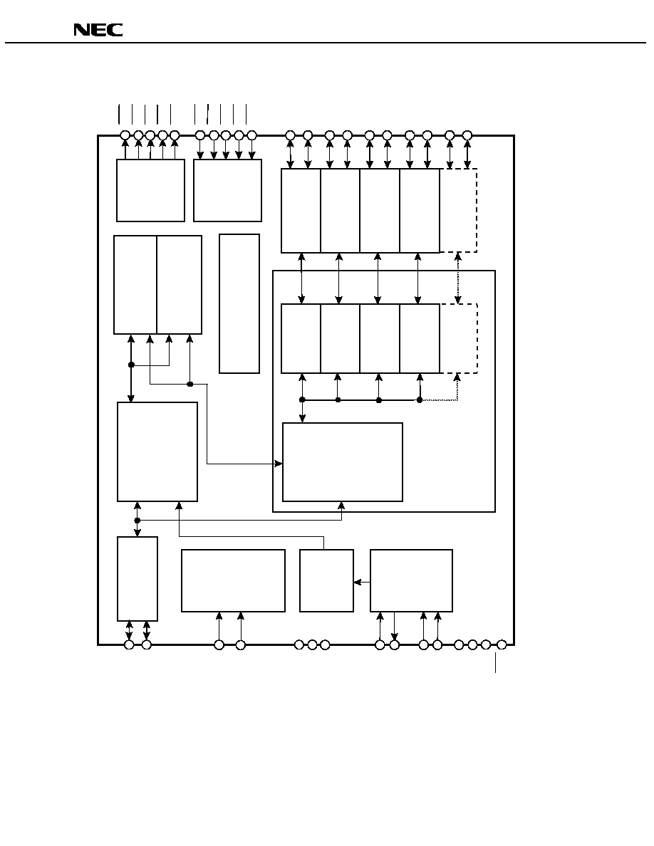
HUB CONTROLLER FOR UNIVERSAL SERIAL BUS
DATA SHEET
MOS INTEGRATED CIRCUIT
µ
µ
µ
µ
PD72012
Document No. S13918EJ3V0DS00 (3rd edition)
Date Published April 2001 NS CP(K)
Printed in Japan
The
µPD72012 is a dedicated LSI for a HUB connected to a universal serial bus (USB) system.
It is an upgrade of NEC's
µPD72011. It complies with USB specification revision 1.1.
By putting descriptors into ROM, information such as a user's vendor ID can be implemented in the chip.
FEATURES
Compliant with Chapter 11 (HUB Specifications) of USB Specification 1.1.
Descriptors into ROM
∑ The user can customize the vendor ID and product ID by using Mask ROM option.
Supports 5 kinds of string descriptors (for Mask ROM code product only)
On-chip sequencer
∑ There is an on-chip descriptor and request response sequencer. External initial setup and control is not needed
and HUB functions can be realized using only the
µPD72012.
Downstream ports
∑ Four or five ports can be selected using a pin function.
Power modes
∑ Bus power or self-power can be selected using a pin function (an external power control circuit is required).
Corresponds to standard descriptor products
∑ Two kinds of standard ROM code products are provided. Standard and HUB class descriptors are on-chip in
the
µPD72012.
ROM code: 003 (individual overcurrent monitoring type Generic HUB)
ROM code: 004 (collective overcurrent monitoring type Generic HUB)
Supports two kinds of clock input
∑ 48 MHz oscillator input or a 4 MHz crystal resonator can be supported
Power control
∑ Port power control and overcurrent detection functions are on-chip. Individual port control or collective control
can be selected for these.
ORDERING INFORMATION
Part No.
Package
µPD72012CU-XXX
42-pin plastic SDIP (15.24 mm (600))
µPD72012GB-XXX-3B4
44-pin plastic QFP (10
◊ 10)
1999
The information in this document is subject to change without notice. Before using this document, please
confirm that this is the latest version.
Not all devices/types available in every country. Please check with local NEC representative for
availability and additional information.
The mark shows major revised points.
2
Data Sheet S13918EJ3V0DS
µ
PD72012
Ser
i
al
In
t
e
r
f
a
c
e
Engi
ne
Endpoi
nt
0
Repea
t
e
r
C
o
mmo
n
Cont
r
o
l
Repea
t
e
r
Buf
f
er
/
T
r
an
s
c
ei
v
e
r
Buf
f
er
/
T
r
an
s
c
ei
v
e
r
Endpoi
nt
1
PP
1
DV
DD
Buf
f
er
/
T
r
an
s
c
ei
v
e
r
Buf
f
er
/
T
r
an
s
c
ei
v
e
r
Buf
f
er
/
T
r
an
s
c
ei
v
e
r
PS
SE
L
X1
C
L
KS
EL
PV
SEL
OS
L
Buf
f
er
/
T
r
an
s
c
ei
v
e
r
Por
t
Cont
r
o
l
1
Por
t
Cont
r
o
l
2
Por
t
Cont
r
o
l
3
Por
t
Cont
r
o
l
5
Por
t
Cont
r
o
l
4
D10
D11
D20
D21
D30
D31
D40
D41
D50
D51
Pow
e
r
Cont
r
o
l
O
u
t
put
Ov
e
r
Cur
r
ent
Det
e
c
t
PP
2
PP
3
PP
4
PP
5
CS
1
CS
2
CS
3
CS
4
CS
5
HUB
MO
D
E
Cont
r
o
l
UD
0
UD1
CLK
48 M
H
z
DP
LL
DGND
CLK
/
X
2
AV
DD
1
AV
DD
2
A
G
ND1
A
G
ND2
Des
c
r
i
pt
or
R
O
M
(
S
t
and
ar
d/
St
r
i
ng)
CLK
:
Con
nec
t
t
o
48 M
H
z
O
S
C O
u
t
put
X1,
X2
:
C
o
nnec
t
t
o
4 M
H
z
Xt
al
RS
T
Data Sheet S13918EJ3V0DS
3
µ
PD72012
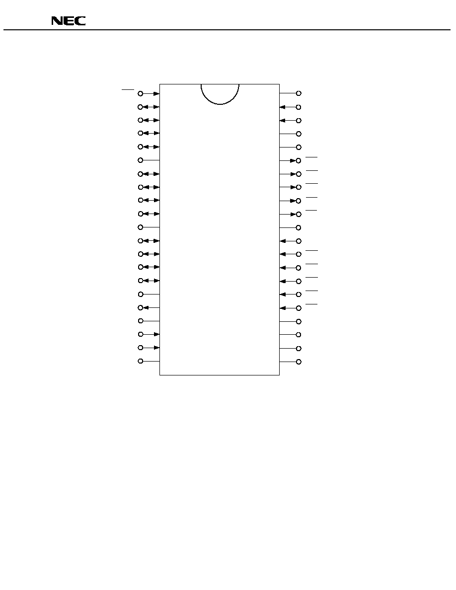
PIN CONFIGURATION (Top View)
∑ 42-pin plastic SDIP (15.24 mm (600))
1
2
3
4
5
6
7
8
9
10
11
12
13
14
15
16
17
18
19
20
21
DGND
PVSEL
PSSEL
DGND
DV
DD
PP5
PP4
PP3
PP2
PP1
DV
DD
(Buffer)
CLKSEL
CS5
CS4
CS3
CS2
CS1
DGND (Buffer)
DV
DD
AV
DD2
AGND2
42
41
40
39
38
37
36
35
34
33
32
31
30
29
28
27
26
25
24
23
22
RST
UD0
UD1
D10
D11
DGND
D20
D21
D30
D31
DGND
D40
D41
D50
D51
DGND
OSL
AV
DD1
CLK/X2
X1
AGND1
4
Data Sheet S13918EJ3V0DS
µ
PD72012
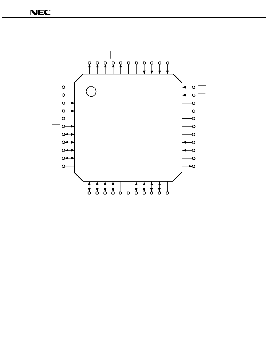
∑ 44-pin plastic QFP (10◊10)
44 43 42 41 40 39 38 37 36 35 34
1
2
3
4
5
6
7
8
9
10
11
33
32
31
30
29
28
27
26
25
24
23
12 13 14 15 16 17 18 19 20 21 22
CS2
CS1
DGND (Buffer)
DV
DD
AV
DD2
AGND2
AGND1
X1
CLK/X2
AV
DD1
OSL
PP5
PP4
PP3
PP2
PP1
DV
DD
DV
DD
(
B
u
ffe
r
)
C
L
KSEL
CS
5
CS
4
CS
3
D20
D21
D30
D31
DGND
DGND
D40
D41
D50
D51
DGND
DV
DD
DGND
PSSEL
PVSEL
DGND
RST
UD0
UD1
D10
D11
DGND

Data Sheet S13918EJ3V0DS
5
µ
PD72012
PIN NAME
AGND1
: Analog GND1 (Xtal)
AGND2
: Analog GND2 (DPLL)
AV
DD1
: Analog V
DD1
(Xtal)
AV
DD2
: Analog V
DD2
(DPLL)
CLKSEL
: Clock Frequency Control
CLK/X2
: 48 MHz OSC, 4 MHz Xtal
Clock Input
CS1
: Over Current Detect #1
CS2
: Over Current Detect #2
CS3
: Over Current Detect #3
CS4
: Over Current Detect #4
CS5
: Over Current Detect #5
D10
: Downstream Port #1 D+
D11
: Downstream Port #1 D≠
D20
: Downstream Port #2 D+
D21
: Downstream Port #2 D≠
D30
: Downstream Port #3 D+
D31
: Downstream Port #3 D≠
D40
: Downstream Port #4 D+
D41
: Downstream Port #4 D≠
D50
: Downstream Port #5 D+
D51
: Downstream Port #5 D≠
DGND
: Digital GND
DGND (Buffer)
: Digital GND (Buffer)
DV
DD
: Digital V
DD
DV
DD
(Buffer)
: Digital V
DD
(Buffer)
OSL
: OSC Suspend Output
PP1
: Port Power Control #1
PP2
: Port Power Control #2
PP3
: Port Power Control #3
PP4
: Port Power Control #4
PP5
: Port Power Control #5
PSSEL
: Powered Mode Control
PVSEL
: Down Port Value Control
RST
: Reset
UD0
: Root Port #0 D+
UD1
: Root Port #0 D≠
X1
: 4 MHz Xtal Clock Input

6
Data Sheet S13918EJ3V0DS
µ
PD72012
CONTENTS
1. PIN FUNCTIONS ...................................................................................................................................................... 7
1.1
List of Pin Functions ......................................................................................................................................... 7
1.2
Tables by Pin Function ................................................................................................................................... 10
1.3
Equivalent Circuits of Pins.............................................................................................................................. 11
2. DESCRIPTORS ...................................................................................................................................................... 12
2.1
Standard Device Descriptor............................................................................................................................ 12
2.2
Standard Configuration Descriptor ................................................................................................................. 14
2.3
Standard Interface Descriptor......................................................................................................................... 16
2.4
Standard Endpoint Descriptor 1 ..................................................................................................................... 17
2.5
HUB Class Descriptor..................................................................................................................................... 17
2.6
Standard String Descriptor 0 .......................................................................................................................... 21
2.7
Standard String Descriptors 1 Through 5 ....................................................................................................... 21
3. ELECTRICAL SPECIFICATIONS .......................................................................................................................... 22
4. PACKAGE DRAWINGS ......................................................................................................................................... 32
5. RECOMMENDED SOLDERING CONDITIONS ..................................................................................................... 34
Data Sheet S13918EJ3V0DS
7
µ
PD72012
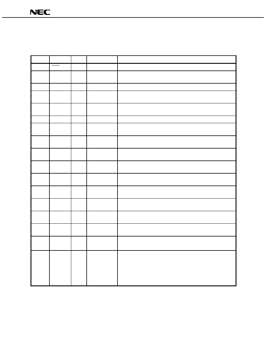
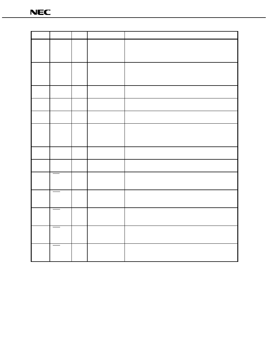
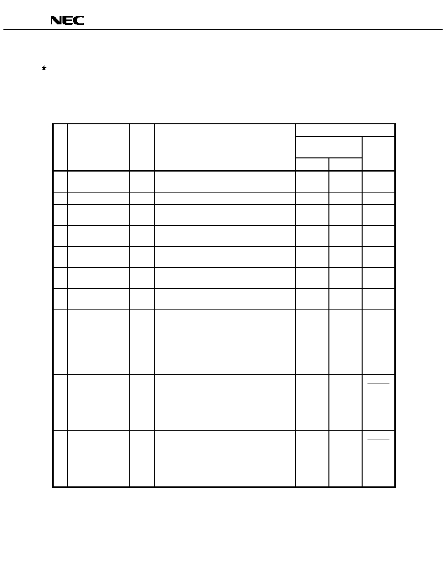
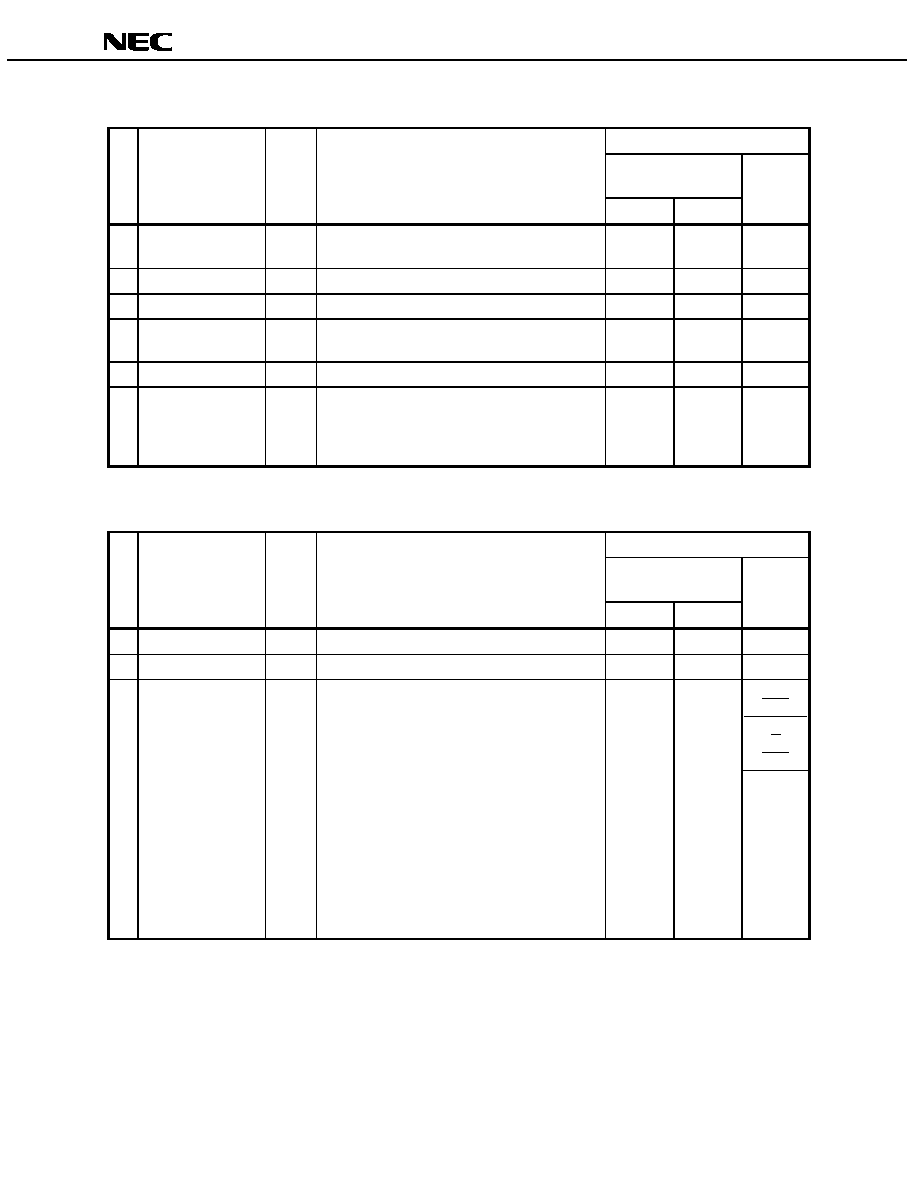
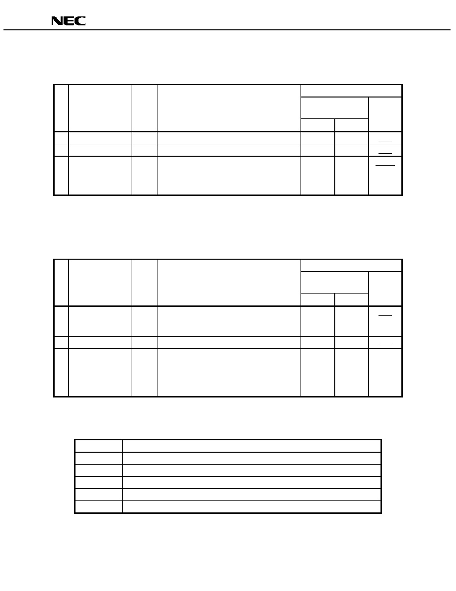
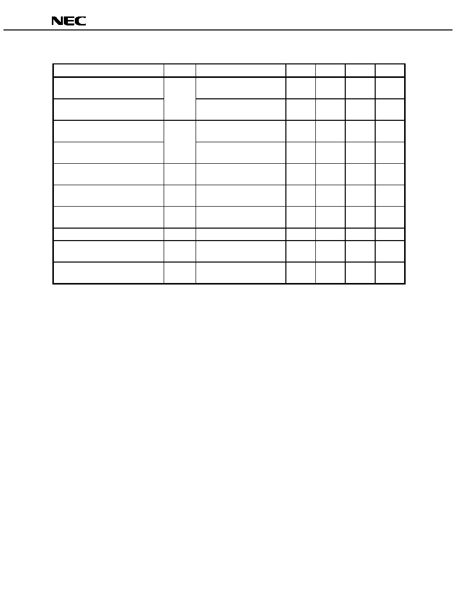
1. PIN FUNCTIONS
1.1 List of Pin Functions
(1/3)
Pin No.
Note
Pin Name
I/O
Signal Name
Function
1(6)
RST
I
RESET
Inputs reset signals.
2(7)
UD0
I/O
Data0
Connects to upstream port #0 D+ signal line.
Pull up to 3.3 V line using 1.5 k
.
3(8)
UD1
I/O
Data1
Connects to upstream port #0 D≠ signal line.
4(9)
D10
I/O
Data0
Connects to downstream port #1 D+ signal line.
Pull down to GND using 15 k
.
5(10)
D11
I/O
Data1
Connects to downstream port #1 D≠ signal line.
Pull down to GND using 15 k
.
6(11)
DGND
-
DGND
Connect to GND.
7(12)
D20
I/O
Data0
Connects to downstream port #2 D+ signal line.
Pull down to GND using 15 k
.
8(13)
D21
I/O
Data1
Connects to downstream port #2 D≠ signal line.
Pull down to GND using 15 k
.
9(14)
D30
I/O
Data0
Connects to downstream port #3 D+ signal line.
Pull down to GND using 15 k
.
10(15)
D31
I/O
Data1
Connects to downstream port #3 D≠ signal line.
Pull down to GND using 15 k
.
11(16,
17)
DGND
-
DGND
Connect to GND.
This pin is used as both pins 16 and 17 internally in the QFP product.
12(18)
D40
I/O
Data0
Connects to downstream port #4 D+ signal line.
Pull down to GND using 15 k
.
13(19)
D41
I/O
Data1
Connects to downstream port #4 D≠ signal line.
Pull down to GND using 15 k
.
14(20)
D50
I/O
Data0
Connects to downstream port #5 D+ signal line.
Pull down to GND using 15 k
.
15(21)
D51
I/O
Data1
Connects to downstream port #5 D≠ signal line.
Pull down to GND using 15 k
.
16(22)
DGND
-
DGND
(TS3)
Test pin of
µPD72012 (corresponds to TS3 pin in µPD72011). Connect
to GND.
17(23)
OSL
O
OSC CTL
Pin that outputs high level on suspend. Can be used by LED switch or to
turn oscillator ON/OFF on suspend.
CAUTION
For self-power, always input an oscillator output signal. If the clock
is cut-off, subsequent operation my not be possible.
Note QFP pin numbers are shown in ( ).
8
Data Sheet S13918EJ3V0DS
µ
PD72012
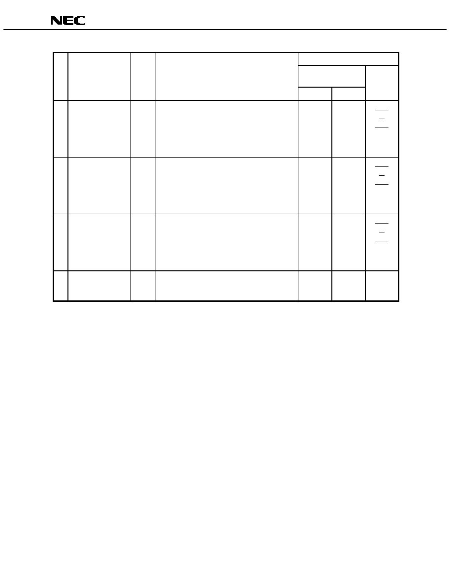
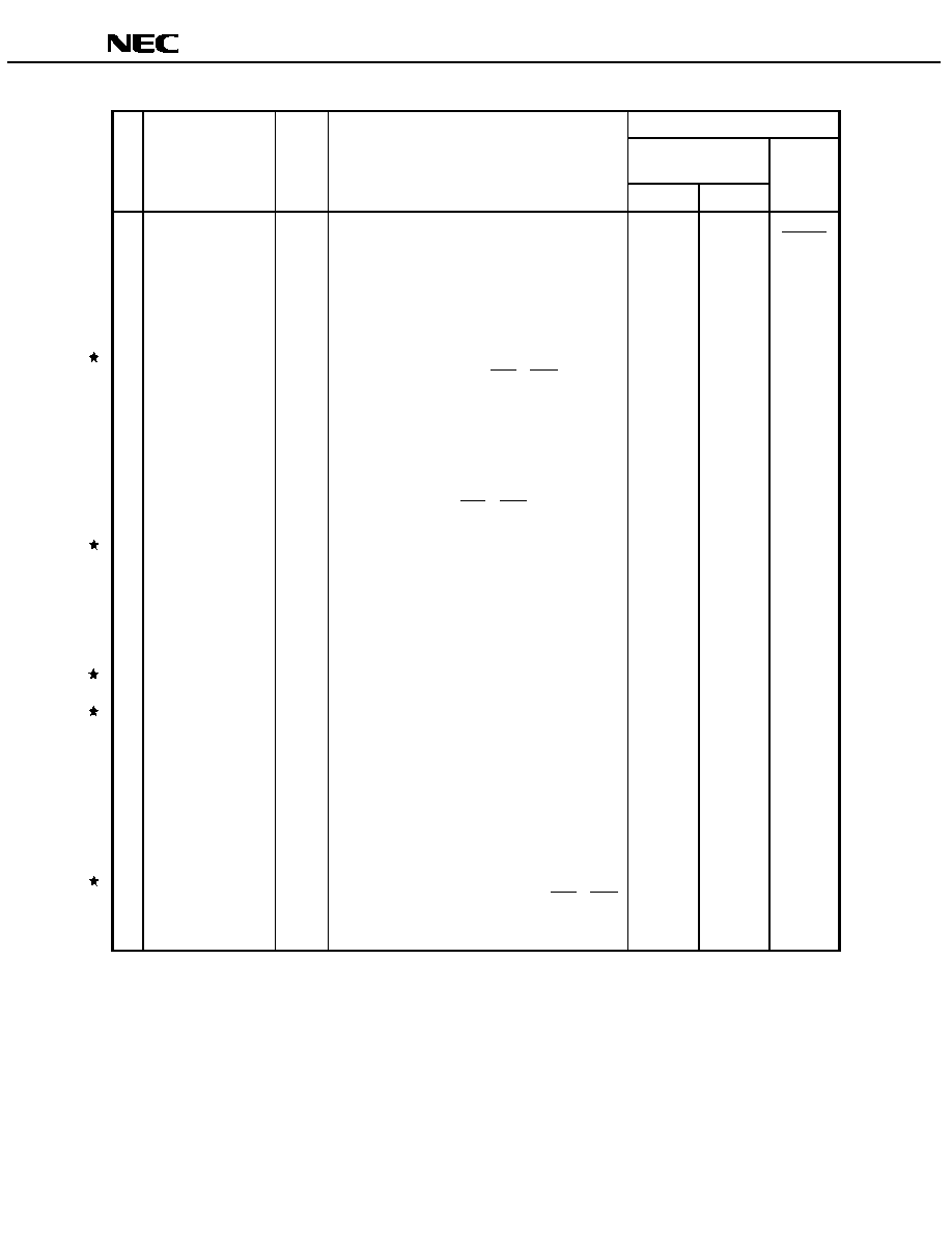
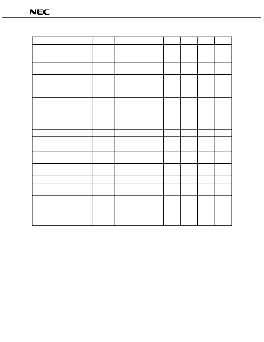
(2/3)
Pin No.
Note 1
Pin Name
I/O
Signal Name
Function
18(24)
AV
DD1
-
AVDD1
Power supply pin of on-chip clock drive circuit.
To stabilize the power supply, connect directly to a stable power
supply using the shortest wire possible or connect to GND via a
capacitor along the wire (3.3 V input).
19(25)
CLK / X2
I
CLOCK / XTAL
When you input a clock signal from an oscillator, input at the 48 MHz
CMOS level (5 V can be input).
When using a 4 MHz crystal oscillator, connect the oscillator to this
pin.
20(26)
X1
I
XTAL
When using a 4 MHz crystal oscillator, connect the oscillator to this
pin.
21(27)
AGND1
-
AGND1
GND pin of on-chip clock drive circuit.
Connect to GND.
22(28)
AGND2
-
AGND2
GND pin of on-chip frequency multiplier (PLL).
Connect to GND.
23(29)
AV
DD2
-
AVDD2
Power supply pin of on-chip frequency multiplier (PLL).
To stabilize the power supply, connect directly to a stable power
supply using the shortest wire possible or connect to GND via a
capacitor along the wire (3.3 V input).
24(30)
DV
DD
-
DVDD
(TS1)
Test pin of
µPD72012 (corresponds to TS1 pin in µPD72011).
Connect to 3.3 V power supply.
25(31)
DGND
(Buffer)
-
DGND
(Buffer)
Connect to GND.
26(32)
CS1
I
PORTCURRENT1
Low active input pin that inputs overcurrent states detected by
external circuit of downstream port #1.
When not using this pin, connect it directly to V
DD
.
Note 2
27(33)
CS2
I
PORTCURRENT2
Low active input pin that inputs overcurrent states detected by
external circuit of downstream port #2.
When not using this pin, connect it directly to V
DD
.
Note 2
28(34)
CS3
I
PORTCURRENT3
Low active input pin that inputs overcurrent states detected by
external circuit of downstream port #3.
When not using this pin, connect it directly to V
DD
.
Note 2
29(35)
CS4
I
PORTCURRENT4
Low active input pin that inputs overcurrent states detected by
external circuit of downstream port #4.
When not using this pin, connect it directly to V
DD
.
Note 2
30(36)
CS5
I
PORTCURRENT5
Low active input pin that inputs overcurrent states detected by
external circuit of downstream port #5.
When not using this pin, connect it directly to V
DD
.
Note 2
Notes 1.
Pin numbers for QFP are shown in ( ).
2.
For details, refer to Table 1-3 in 1.2 Tables by Pin Function.
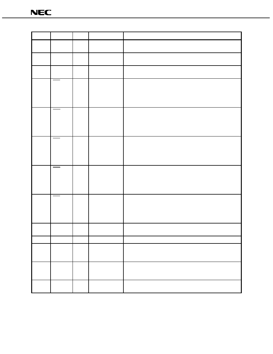
Data Sheet S13918EJ3V0DS
9
µ
PD72012
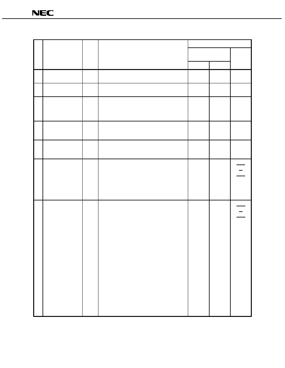
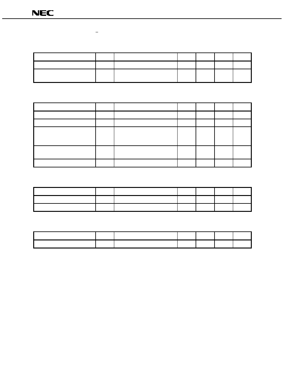
(3/3)
Pin No.
Note 1
Pin Name
I/O
Signal Name
Function
31(37)
CLKSEL
I
CLK SELECT
Pin for selecting whether to use 48 MHz oscillator or 4 MHz crystal
oscillator (refer to Table 1-1).
32(38)
DV
DD
(Buffer)
-
DVDD
(Buffer)
Connect to 3.3 V power supply.
(39)
DV
DD
-
DVDD
Connect to 3.3 V power supply. This pin is used together with pin No.
32 internally in the shrink DIP product.
33(40)
PP1
O
PORTPOWER#1
Low active open drain output pin that controls downstream port #1
power supply.
Input the output of this pin to the power control element of an external
circuit.
If not using this pin, leave it unconnected.
Note 2
34(41)
PP2
O
PORTPOWER#2
Low active open drain output pin that controls downstream port #2
power supply.
Input the output of this pin to the power control element of an external
circuit.
If not using this pin, leave it unconnected.
Note 2
35(42)
PP3
O
PORTPOWER#3
Low active open drain output pin that controls downstream port #3
power supply.
Input the output of this pin to the power control element of an external
circuit.
If not using this pin, leave it unconnected.
Note 2
36(43)
PP4
O
PORTPOWER#4
Low active open drain output pin that controls downstream port #4
power supply.
Input the output of this pin to the power control element of an external
circuit.
If not using this pin, leave it unconnected.
Note 2
37(44)
PP5
O
PORTPOWER#5
Low active open drain output pin that controls downstream port #5
power supply.
Input the output of this pin to the power control element of an external
circuit.
If not using this pin, leave it unconnected.
Note 2
38(1)
DV
DD
-
DVDD
(TS0)
Test pin of
µPD72012 (corresponds to TS0 pin in µPD72011).
Connect to 3.3 V power supply.
39(2)
DGND
-
DGND
Connect to GND.
40(3)
PSSEL
I
Power SW
Pin that selects switching between bus power and self-power (refer to
Table 1-2).
To make high level, pull up to 3.3 V.
41(4)
PVSEL
I
Port Value
Pin that selects switching between number (4 or 5) of downstream
ports (refer to Table 1-2).
To make high level, pull up to 3.3 V.
42(5)
DGND
-
DGND
(TS2)
Test pin of
µPD72012 (corresponds to TS2 pin in µPD72011).
Connect to GND.
Notes 1.
QFP pin numbers are shown in ( ).
2.
For details, refer to Table 1-4 of 1.2 Tables by Pin Function.
10
Data Sheet S13918EJ3V0DS
µ
PD72012
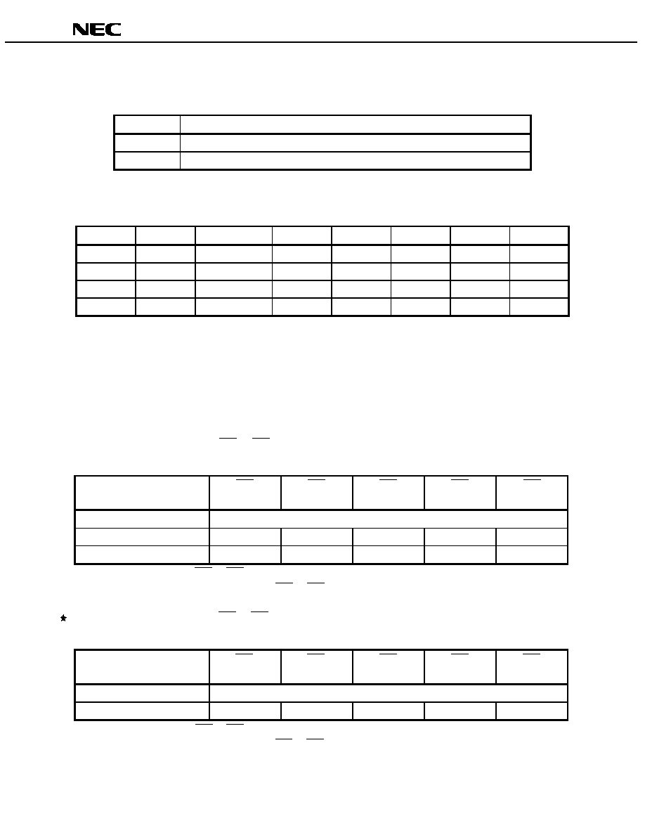
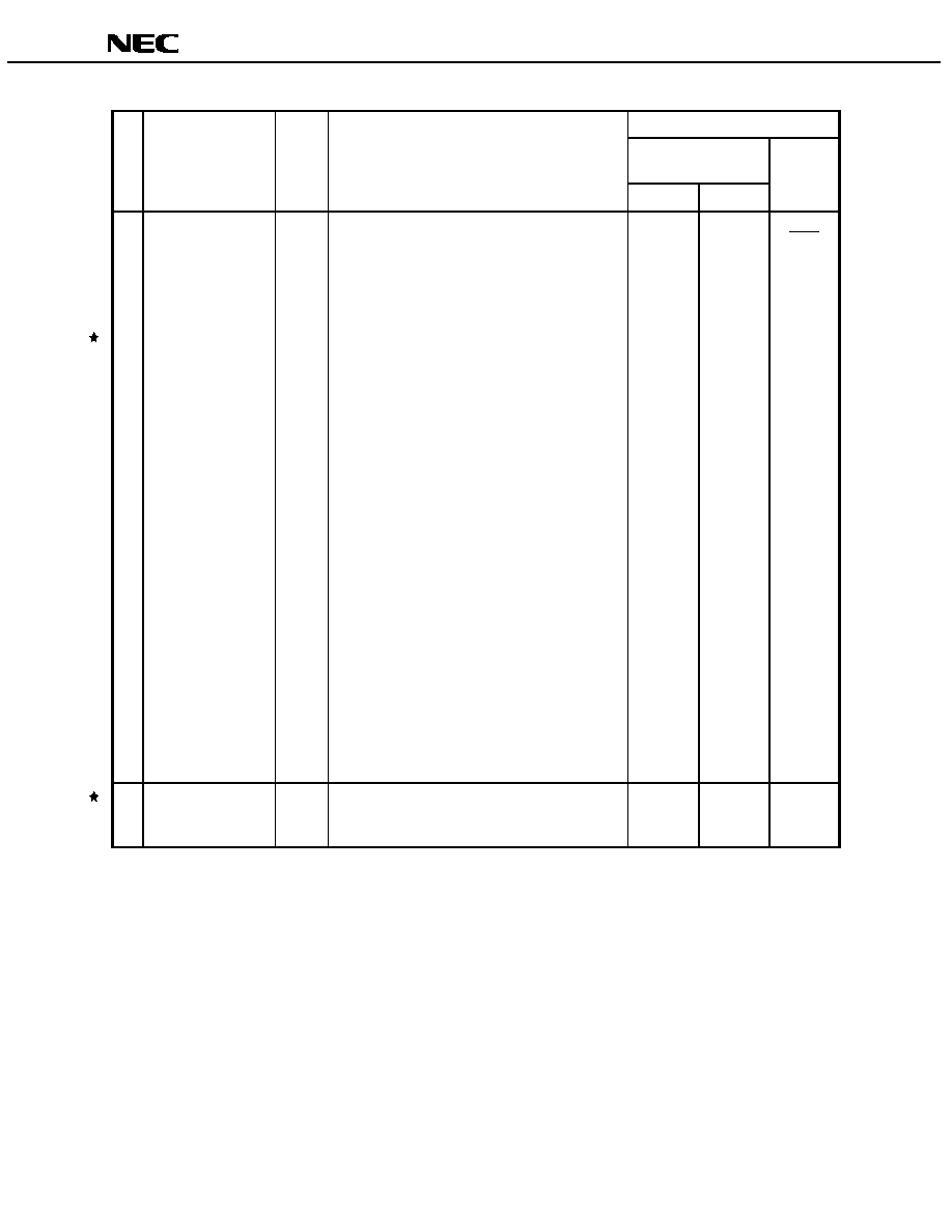
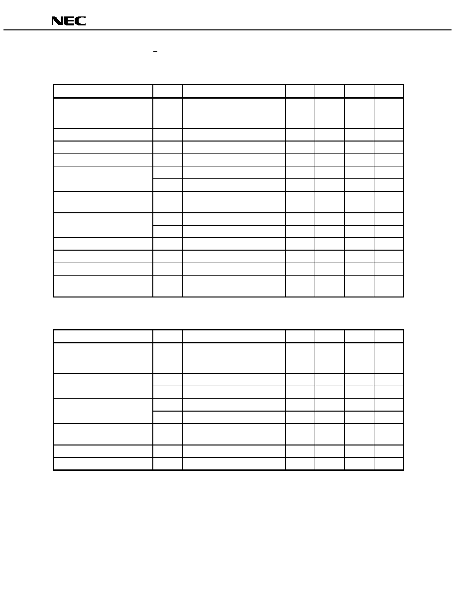
1.2 Tables by Pin Function
Table 1-1. Oscillator Circuit Switching Control (CLKSEL)
CLKSEL
Type of oscillator circuit
L
Input clocks from 48 MHz oscillator
H
Clock input using 4 MHz crystal resonator (drive circuit is incorporated)
Remark
Directly connect to V
DD
when using CLKSEL="H". Even 5 V is no trouble.
Table 1-2. Power Mode/Downstream Port Number Control (PSSEL, PVSEL)
PSSEL
PVSEL
Power mode
Port #1
Port #2
Port #3
Port #4
Port #5
L
L
Self-power
Note 1
◊
L
H
Self-power
Note 1
H
L
Bus power
Note 2
◊
H
H
Prohibited
Note 3
≠
≠
≠
≠
≠
Notes 1.
Do not cut-off clock input when using self-power. If it is cut-off, internal functions stop and operation
may not be possible even if clocks are input again.
2.
When using bus power, up to four ports can be used.
3.
The combination PSSEL="H", PVSEL="H" is prohibited. Operation in this case is not guaranteed.
Remark
Also set according to this table when setting the number of ports in a Mask ROM code product to up to
5 ports. Directly connect data lines of unused ports to GND.
Table 1-3. Handling of Pins CS1 to CS5 According to Setting of wHubCharacteristics Field of HUB Class
Descriptor
wHubCharacteristics
Bits 4, 3
CS1
CS2
CS3
CS4
CS5
0b00
Common in all ports
0b01
Port #1
Port #2
Port #3
Port #4
Port #5
0b10 or 0b11
Not available
Not available
Not available
Not available
Not available
Remark
Connect pins CS1 to CS5 to the Over Current Detect output pin of the power switch IC.
Clamp an unused or unavailable CS1 to CS5 pin to 3.3 V.
Table 1-4. Handling of Pins PP1 to PP5 According to Setting of wHubCharacteristics Field of HUB Class
Descriptor
wHubCharacteristics
Bits 1, 0
PP1
PP2
PP3
PP4
PP5
0b00
Common in all ports
0b01
Port #1
Port #2
Port #3
Port #4
Port #5
Remark
Connect pins PP1 to PP5 to the Port Power Control input pin of the power switch IC.
Leave an unused or unavailable PP1 to PP5 pin open.
Data Sheet S13918EJ3V0DS
11
µ
PD72012
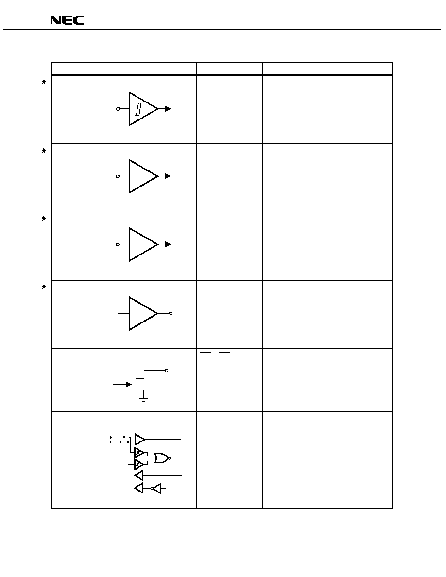
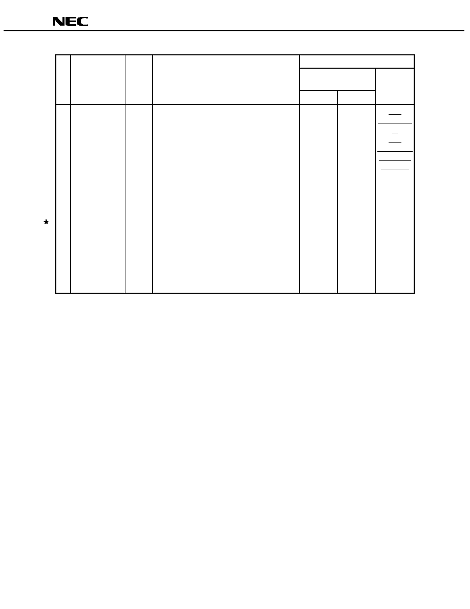
1.3 Equivalent Circuits of Pins
Type
Equivalent Circuit
Pins
Function
5 V tolerant
input pin
(Schmitt)
5 V Schmitt on-chip
RST, CS1 to CS5
3.3 V Schmitt input pin with 5 V tolerant.
5 V tolerant
input pin
5 V
CLKSEL, PSSEL,
PVSEL
3.3 V input pin with 5 V tolerant.
5 V tolerant
clock input
pin
5 V
X1, CLK/X2
3.3 V dedicated clock input pin with 5 V
tolerant.
5 V tolerant
3.3 V output
pin
3.3 V, I
OL
=6 mA
OSL
3.3 V output pin with 5 V tolerant.
Pull-up to 5 V line is possible.
Open-drain
output pin
PP1 to PP5
Open-drain structure pin.
USB buffer
IN/OUT(D+)
(D
≠)
RxDATA
RxSE0
TxDATA
UD0, UD1, D10 to
D50, D11 to D51
USB buffer. The two kinds of receiver are
DATA receiver and SE0 (single end 0) receiver
on the receiving side.
On the sending side, rise and fall times are
managed in the last stage of the buffer in
order to create a difference between low-speed
and full-speed.
12
Data Sheet S13918EJ3V0DS
µ
PD72012
2. DESCRIPTORS
Caution
For a Mask ROM code product, we release the software to make a data for Mask ROM option.
Please contact to Local NEC to get the software if you would like to make Mask ROM code
product.
2.1 Standard Device Descriptor
(1/2)
Value
Standard ROM code
product
No.
Field
Size
(Bytes)
Contents
003
004
Mask
ROM code
product
0
bLength
1
Shows the size in bytes of the standard device
descriptor.
0x12
0x12
0x12
1
bDescriptorType
1
Shows that this is a standard device descriptor.
0x01
0x01
0x01
2
bcdUSB
2
Shows that the
µPD72012 compliant with USB
Specifications Revision 1.1.
0x0110
0x0110
0x0110
4
bDeviceClass
1
HUB class code defined by USB
(HUB_CLASSCODE="0x09").
0x09
0x09
0x09
5
bDeviceSubClass
1
HUB subclass code defined by USB. Not defined in
HUB class.
0x00
0x00
0x00
6
bDeviceProtocol
1
Protocol code defined by USB. Not defined in HUB
class.
0x00
0x00
0x00
7
bMaxPacketSize0
1
Shows the maximum packet size in bytes of
endpoint 0 of the
µPD72012.
0x08
0x08
0x08
8
idVendor
2
Shows the vendor ID code registered in USB
standards.
For a standard ROM code product (003, 004), this is
"0x0409" (NEC vendor ID).
When using in a Mask ROM code product, set a
vendor ID for each manufacturer registered in USB
standards.
0x0409
0x0409
0xXXXX
10
IdProduct
2
Shows the product ID code registered in USB
standards.
For a standard ROM code product (003, 004), this is
"0x55AB" (Generic_HUB).
In a Mask ROM code product, this value can be set
as you wish.
0x55AB
0x55AB
0xXXXX
12
bcdDevice
2
Shows the version number of the
µPD72012 using
decimal notation in XX.XX format.
For a standard ROM code product (003, 004), this is
"0x0200" (Ver. 2.0).
When using in a Mask ROM code product, manage
by varying the number for each ROM code.
0x0200
0x0200
0xXXXX
Data Sheet S13918EJ3V0DS
13
µ
PD72012
(2/2)
Value
Standard ROM code
product
No.
Field
Size
(Bytes)
Contents
003
004
Mask
ROM code
product
14
iManufacture
1
Shows the index of the string descriptor for a
comment about a manufacturer using the HUB.
Since not used for a standard ROM code product
(003, 004), its value is "0x00".
When using this for a Mask ROM code product, set it
to "0x01".
0x00
0x00
0x00
or
0x01
15
iProduct
1
Shows the index of the string descriptor for a
comment about a product using the HUB.
Since not used for a standard ROM code product
(003, 004), its value is "0x00".
When using this for a Mask ROM code product, set it
to "0x02".
0x00
0x00
0x00
or
0x02
16
iSerialNumber
1
Shows the index of the string descriptor for the serial
number of a product using the HUB.
Since not used for a standard ROM code product
(003, 004), its value is "0x00".
When using this for a Mask ROM code product, set it
to "0x03".
0x00
0x00
0x00
or
0x03
17
bNumConfiguration
1
Shows the number of configurations that can be set
for this HUB.
Its value is fixed at "0x01" for the
µPD72012
0x01
0x01
0x01
14
Data Sheet S13918EJ3V0DS
µ
PD72012
2.2 Standard Configuration Descriptor
(1/2)
Value
Standard ROM code
product
No.
Field
Size
(Bytes)
Contents
003
004
Mask
ROM code
product
0
bLength
1
Shows the size in bytes of the standard
configuration descriptor.
0x09
0x09
0x09
1
bDescriptorType
1
Shows that this is a standard configuration
descriptor.
0x02
0x02
0x02
2
wTotalLength
2
Shows the total length of descriptors returned on a
host Get_Descriptor (Configuration) request
(standard configuration, standard interface, each
standard endpoint, and HUB class descriptors).
0x0019
0x0019
0x0019
4
bNumInteface
1
Shows the number of interfaces that can be set in
this configuration.
Its value is fixed at "0x01" for the
µPD72012.
0x01
0x01
0x01
5
bConfigurationValue
1
Specifying this value in a Set_Configuration request
from the host sets this configuration in the
µPD72012.
0x01
0x01
0x01
6
iConfiguration
1
Shows the index of the string descriptor for a
comment about the configuration of a product using
the HUB.
Since not used for a standard ROM code product
(003, 004), its value is "0x00".
When using this for a Mask ROM code product, set it
to "0x04".
0x00
0x00
0x00
or
0x04
7
bmAttributes
1
Uses a bitmap to show the power supply attributes
of this configuration of the
µPD72012.
Caution Since the information "Self-power" in
the status returned on a Get_Status
request from the host reflects the level
input to the PSSEL pin, be sure that
there are no inconsistencies.
"0xE0": Corresponds to both "bus power" and "self-
power" modes and shows that "Remote Wakeup" is
supported. A standard ROM code product has this
setting.
Use this setting when using in "self-power" mode
only or when switching between "bus power" and
"self-power" by performing a PSSEL pin function.
"0xA0": Corresponds to "bus power" mode only and
shows that "Remote Wakeup" is supported.
Make this setting when using in "bus power" mode
only.
0xE0
0xE0
0xE0
or
0xA0
Data Sheet S13918EJ3V0DS
15
µ
PD72012
(2/2)
Value
Standard ROM code
product
No.
Field
Size
(Bytes)
Contents
003
004
Mask ROM
code
product
8
MaxPower
1
Shows the maximum current the HUB consumes in
normal operation in hexadecimal notation using
units of 2 mA.
Since it provides 1 UnitLoad (= 100 mA) to each
port downstream, this is not included in MaxPower.
However, if a non-removable device is connected
downstream, this is included (for details inquire in
the USB-IF).
Switching the input level of the PSSEL pin changes
the value that is returned. In short, two-way setting
of the
µPD72012 is possible for "self-power" and
"bus power".
Mask ROM code product
For a "bus power" setting (PSSEL="H"), normally set
this to 0x32 (100 mA). However, when making a
subordinate port a non-removable port, add the
current consumed by the device connected to that
port when you set the MaxPower value. On the
other hand, For a "self-power" setting (PSSEL="L"),
0x32 (100 mA) is fixed.
0x32
(PSSEL="L")
or
0x32
(PSSEL="H")
0x32
(PSSEL="L")
or
0x32
(PSSEL="H")
0x32
(PSSEL="L")
or
0x32
(PSSEL="H")
(recommen-
ded value)

16
Data Sheet S13918EJ3V0DS
µ
PD72012
2.3 Standard Interface Descriptor
Value
Standard ROM code
product
No.
Field
Size
(Bytes)
Contents
003
004
Mask
ROM code
product
0
bLength
1
Shows the size in bytes of the standard interface
descriptor.
0x09
0x09
0x09
1
bDescriptorType
1
Shows that this is a standard interface descriptor.
0x04
0x04
0x04
2
bInterfaceNumber
1
If there are multiple interfaces, the host specifying
this value in a Set_Interface request selects this
interface.
This is "0x00" for the
µPD72012.
0x00
0x00
0x00
3
bAlternateSetting
1
This value is used if there is an alternate setting of
the interface. It is "0x00" for the
µPD72012.
0x00
0x00
0x00
4
bNumEndpoints
1
Shows the number of endpoints defined in this
interface.
0x01
0x01
0x01
5
bIntefaceClass
1
HUB class code defined by USB
(HUB_CLASSCODE="0x09").
0x09
0x09
0x09
6
bInterfaceSubClass
1
HUB subclass code defined by USB.
0x00
0x00
0x00
7
bInterfaceProtocol
1
Protocol code defined by USB. Not defined in HUB
class.
0x00
0x00
0x00
8
iInteface
1
Shows the index of the string descriptor for a
comment about the interface of a product using the
HUB.
Since not used for a standard ROM code product
(003, 004), its value is "0x00".
When using this for a Mask ROM code product, set it
to "0x05".
0x00
0x00
0x00
or
0x05
Data Sheet S13918EJ3V0DS
17
µ
PD72012
2.4 Standard Endpoint Descriptor 1
Value
Standard ROM code
product
No.
Field
Size
(Bytes)
Contents
003
004
Mask
ROM code
product
0
bLength
1
Shows the size in bytes of standard endpoint
descriptor 1.
0x07
0x07
0x07
1
bDescriptorType
1
Shows that this is a standard endpoint descriptor.
0x05
0x05
0x05
2
bEndpointAddress
1
Shows the EndpointAddress of endpoint 1.
0x81
0x81
0x81
3
bmAttributes
1
Shows the attributes of endpoint 1
(Interrupt="0x03").
0x03
0x03
0x03
4
wMaxPacketSize
2
Shows the maximum packet size of endpoint 1.
0x0001
0x0001
0x0001
6
bInterval
1
For an Interrupt attribute endpoint, shows the polling
time in milliseconds using hexadecimal notation. For
a HUB, the maximum value that can be set ("0xFF")
is entered.
0xFF
0xFF
0xFF
2.5 HUB Class Descriptor
(1/4)
Value
Standard ROM code
product
No.
Field
Size
(Bytes)
Contents
003
004
Mask
ROM code
product
0
bDescLength
1
Shows the size in bytes of the HUB class descriptor.
0x09
0x09
0x09
1
bDescriptorType
1
Shows that this is a HUB class descriptor.
0x29
0x29
0x29
2
bNbrPort
1
Shows the number of downstream ports the HUB
supports in a set.
For a standard ROM code product (003, 004), the
value varies according to the PVSEL pin setting.
It is "0x05" for a 5-port HUB (PVSEL="H"), and
"0x04" for a 4-port HUB (PVSEL="L").
For a Mask ROM code product, the value in this field
can be set arbitrarily. Since two-way setting by
switching the PVSEL input level is possible for these
values, perform two-way specification. Note that the
values that are set for PVSEL="H" are from "0x01" to
"0x05", and the values that are set for PVSEL="L"
are from "0x01" to "0x04". The
µPD72012 enables
ports in turn starting from the smallest port number.
0x04
(PVSEL="L")
or
0x05
(PVSEL="H")
0x04
(PVSEL="L")
or
0x05
(PVSEL="H")
0xXX
(PVSEL="L")
or
0xYY
(PVSEL="H")
18
Data Sheet S13918EJ3V0DS
µ
PD72012
(2/4)
Value
Standard ROM code
product
No.
Field
Size
(Bytes)
Contents
003
004
Mask
ROM code
product
3
wHubCharacteristics
2
Uses a bitmap to show attributes of the
µPD72012.
The meaning of each bit is as follows.
Bits 1,0: Show the power switch switching attribute.
"0b00": Enable all power switches at once.
This is the value for a standard ROM code
product (004).
If this value is set for a Mask ROM code
product, all of pins PP1 to PP5 operate at
once.
"0b01": Enable power switches individually for
each port.
This is the value for a standard ROM code
product (003).
If this value is set for a Mask ROM code
product, pins PP1 to PP5 operate
individually.
"0b1X": Reserved. Used only on 1.0 compliant
hubs that implement no power switching.
You can not use this setting for
µPD72012.
Bit 2:
Identifier of a compound device. Set this
to "0b0" when using the
µPD72012 as a
unit HUB and to "0b1" when using it as
compound devices.
"0b0":
Shows that the
µPD72012 is standalone
HUB unit.
"0b1":
Shows that
µPD72012 is a part of
compound devices.
Bits 4,3: Show the overcurrent protection switching
attribute.
"0b00": Monitor overcurrent for all ports in a batch.
Since this is the value for a standard ROM
code product (004), a circuit that can
control all overcurrent protection functions
at once externally is needed.
If this value is set for a Mask ROM code
product, when one of the pins CS1 to CS5
detect overcurrent, Hub reports
overcurrent on per- hub basis.
0x0009
0x0000
0x00XX
Data Sheet S13918EJ3V0DS
19
µ
PD72012
(3/4)
Value
Standard ROM code
product
No.
Field
Size
(Bytes)
Contents
003
004
Mask
ROM code
product
3
wHubCharacteristics
2
"0b01": Monitor overcurrent for each port
individually.
Since this is the setting for a standard
ROM code product (003), a circuit that can
individually control overcurrent protection
functions externally is needed.
If this value is set for a Mask ROM code
when one of the pins CS1 to CS5 detect
overcurrent, Hub reports overcurrent on
per- port basis.
"0b1X": Shows that there is no overcurrent
protection function. This setting is allowed
only for bus-powered hubs that do not
implement over-current protection.
If this value is set for a Mask ROM code
product, clamp all of the pins CS1 to CS5
to 3.3 V.
Bits 15-5: These bits are reserved in the USB
standard for future extended functions.
For a Mask ROM code product, be sure to
set these bits to "0".
Caution Be sure to set the values in bits 3 and 0
the same in Mask ROM code product
settings.
0x0009
0x0000
0x00XX
5
bPowerOn2PwrGood
1
Shows the time from detecting a device at a port and
starting the power-on sequence until the power
supply stabilizes.
Two milliseconds are taken as one unit. This is 100
ms for the
µPD72012.
0x32
0x32
0x32
6
bHubContrCurrent
1
Shows the maximum current consumption of the
HUB in mA. Note that this value does not show the
rated current consumption value for the
µPD72012
itself.
For a standard ROM code product, "0x50" is applied
for compatibility with the
µPD72011. This value can
be defined for a Mask ROM code product. However,
this value should not be less than the current
consumption value of the
µPD72012 that is
described in 3. ELECTRICAL SPECIFICATIONS.
0x50
0x50
0xXX
20
Data Sheet S13918EJ3V0DS
µ
PD72012
(4/4)
Value
Standard ROM code
product
No.
Field
Size
(Bytes)
Contents
003
004
Mask
ROM code
product
7
bDeviceRemovable
1
Uses a bitmap to show whether or not removable
devices are connected to HUB ports.
"1" shows that the connected device is non-
removable, and "0" shows that it is removable. Set
"1" if a port that is used cannot be connected nor
disconnected using an external circuit.
Note that, if a non-removable device is connected to
a downstream port of the HUB, bit 2 of
wHubCharacteristics field should be set to "1".
When the number of ports that can be port enabled
is limited by the PVSEL pin setting or Mask ROM
code product settings, set "0" for all ports that are
not port enabled. The meaning of the bitmap is as
follows.
Bit 0:
Always set to "0".
Bit 1:
If "1", the device connected to port 1 is
non-removable.
Bit 2:
If "1", the device connected to port 2 is
non-removable.
Bit 3:
If "1", the device connected to port 3 is
non-removable.
Bit 4:
If "1", the device connected to port 4 is
non-removable.
Bit 5:
If "1", the device connected to port 5 is
non-removable.
Bits 7,6: Always set to "0".
For a standard ROM code product (003, 004), all
ports are removable.
0x00
0x00
0xXX
8
bPortPwrCtrlMask
1
This field exists for reasons of compatibility with
software written for 1.0 compliant devices. All bits in
this field should be set to 1B.
0xFF
0xFF
0xFF
Data Sheet S13918EJ3V0DS
21
µ
PD72012
2.6 Standard String Descriptor 0
Standard string descriptor 0 cannot be used in a standard ROM code product.
Value
Standard ROM code
product
No.
Field
Size
(Bytes)
Contents
003
004
Mask
ROM code
product
0
bLength
1
Shows the size of standard string descriptor 0.
0x00
0x00
0x04
1
bDescriptorType
1
Shows that this is a standard string descriptor.
0x00
0x00
0x03
2
wLANGID[0]
2
Shows the LanguageID of standard string descriptor
0. The LanguageID used is "0x0409" (Generic).
The
µPD72012 uses this LanguageID in common for
all string descriptors.
0x0000
0x0000
0x0409
2.7 Standard String Descriptors 1 Through 5
Standard string descriptors 1 through 5 cannot be used in a standard ROM code product.
This format is the common format for standard string descriptors #1 through #5 of the
µPD72012.
Value
Standard ROM code
product
No.
Field
Size
(Bytes)
Contents
003
004
Mask
ROM code
product
0
bLength
1
Shows the size of standard string descriptors 1
through 5. Its value is fixed at 66 bytes (0x42). The
string itself is this size ≠2 (64 bytes).
0x00
0x00
0x42
1
bDescriptorType
1
Shows that this is a standard string descriptor.
0x00
0x00
0x03
2
bString
64
Stores the standard string descriptor in UNICODE.
A string requires 2 bytes for each character. Strings
of up to 32 characters can be specified. If there are
white space characters, pad using NULL characters
(0x0000).
All 0
All 0
≠
Remark
Five kinds of standard string descriptors can be defined and these describe the following contents
using 32 UNICODE characters.
Index
Contents
1
Comment about manufacturer (Manufacture) that uses HUB
2
Comment about product (Product) that uses HUB
3
Serial number (SerialNumber) of product that uses HUB
4
Comment about configuration (Configuration) of product that uses HUB
5
Comment about interface (Interface) of product that uses HUB
Refer to "The Unicode Standard, Worldwide Character Encoding, Version 1.0, Volume 1 and 2", The Unicode
Consortium, Addison-Wesley Publishing Company, Reading, Massachusetts regarding UNICODE.
22
Data Sheet S13918EJ3V0DS
µ
PD72012
3. ELECTRICAL SPECIFICATIONS
Absolute Maximum Ratings
Parameter
Symbol
Conditions
Rating
Unit
Power supply voltage
V
DD
≠0.5 to +4.6
V
USB buffer
UD0, UD1, D10 to D50, D11 to D51
≠0.5 to +4.6
V
Clock input buffer
X1, CLK/X2
≠0.5 to +6.6
V
5 V Schmitt input buffer
RST, CS1 to CS5
≠0.5 to +6.6
V
Input voltage
V
I
5 V input buffer
CLKSEL, PSSEL, PVSEL
≠0.5 to +4.6
V
USB buffer
UD0, UD1, D10 to D50, D11 to D51
≠0.5 to +4.6
V
Open drain output buffer
PP1 to PP5
≠0.5 to +6.6
V
Output voltage
V
O
5 V output buffer
OSL
≠0.5 to +6.6
V
Output current
I
O
100
mA
Operating ambient temperature
T
A
0 to +70
∞C
Storage temperature
T
stg
≠65 to +150
∞C
Caution
Product quality may suffer if the absolute maximum rating is exceeded even momentarily for
any parameter. That is, the absolute maximum ratings are rated values at which the product is
on the verge of suffering physical damage, and therefore the product must be used under
conditions that ensure that the absolute maximum ratings are not exceeded.
Recommended Operating Conditions (T
A
= 0 to +70
∞
∞
∞
∞C)
Parameter
Symbol
Conditions
MIN.
TYP.
MAX.
Unit
Power supply voltage
V
DD
3.0
3.3
3.6
V
High level input voltage
V
IH
2.0
V
DD
V
Low level input voltage
V
IL
USB pin
UD0, UD1, D10 to D50, D11 to D51
0
0.8
V
High level input voltage
V
IH
2.3
5.5
V
Low level input voltage
V
IL
5 V Schmitt input pin
RST, CS1 to CS5
0
0.8
V
Input rise time for RST
tr
0.3 V to 2.7 V
10
ms
High level input voltage
V
IH
2.0
5.5
V
Low level input voltage
V
IL
5 V input pin
CLKSEL, PSSEL, PVSEL
0
0.8
V
High level input voltage
V
IH
2.3
5.5
V
Low level input voltage
V
IL
Clock input pin (at 48 MHz input)
X1, CLK/X2
0
0.8
V
Oscillator input (+100 ppm)
48.00
MHz
Clock input frequency
f
CK
Oscillator input (+50 ppm)
4.0
MHz

Data Sheet S13918EJ3V0DS
23
µ
PD72012
Recommended Oscillator Circuit Constants
Crystal oscillator (T
A
= 0 to +70
∞
∞
∞
∞C)
Oscillator circuit constant (pF)
Manufacturer
Product name
Frequency (MHz)
C1
C2
AT-49
4.000
10
10
DAISHINKU CORP.
HC-49/U
4.000
9
9
X1
X2
C2
C1
Cautions 1. The oscillator circuit constants, which show the conditions for stabilizing and oscillating,
do not guarantee oscillation frequency accuracy. If the mounting circuit requires oscillation
frequency accuracy, it must be possible to adjust the oscillation frequency of the oscillator
in the mounting circuit. Therefore, ask the manufacturer of the oscillator you use about this
directly.
2. When using an oscillator circuit, wire portions shown using broken lines in the figure as
follows to avoid affecting wire capacitance.
∑ Keep the wiring length as short as possible.
∑ Do not cross the wiring with the other signal lines.
∑ Do not route the wring near a signal line through which a high fluctuating current flows.
∑ Always keep the ground point of the oscillator capacitor to the same potential as V
SS
.
∑ Do not ground the capacitor to a ground pattern in which a high current flows.
∑ Do not fetch signals from the oscillator.
24
Data Sheet S13918EJ3V0DS
µ
PD72012
DC Characteristics (V
DD
= 3.3 V +0.3 V, T
A
= 0 to +70
∞
∞
∞
∞C)
(1) Current consumption
Parameter
Symbol
Conditions
MIN.
TYP.
MAX.
Unit
Current consumption
I
DD
f
CK
= 48 MHz, 4 MHz
40
mA
Current consumption (during
suspend)
I
DD(SUS)
120
µA
(2) USB input/output buffer
Parameter
Symbol
Conditions
MIN.
TYP.
MAX.
Unit
High level output voltage
V
OH
14.2 k
R
H
for GND
2.8
3.6
V
Low level output voltage
V
OL
1.42 k
R
L
for 3.6 V
0
0.3
V
Differential common mode range
V
CM
Includes V
DI
range
Absolute value of (D+) ≠ (D≠)
0.2 Vmin
0.8
2.5
V
Data line leakage current in input
pin high impedance state
I
LO
0 V < V
IN
< 3.3 V
±10
µA
Crossover output voltage
V
CRS
1.3
2.0
V
(3) 5 V output buffer
Parameter
Symbol
Conditions
MIN.
TYP.
MAX.
Unit
High level output voltage
V
OH
I
OH
= ≠6 mA
2.4
V
Low level output voltage
V
OL
I
OH
= 6 mA
0.4
V
(4) Open drain output buffer
Parameter
Symbol
Conditions
MIN.
TYP.
MAX.
Unit
Low level output voltage
V
OL
I
OL
= 6 mA
0.4
V
Data Sheet S13918EJ3V0DS
25
µ
PD72012
AC Characteristics (V
DD
= 3.3 V +0.3 V, T
A
= 0 to +70
∞
∞
∞
∞C)
(1) Full-speed output driver characteristics
Parameter
Symbol
Conditions
MIN.
TYP.
MAX.
Unit
Output rise time (FS)
Output fall time (FS)
t
FR
, t
FF
UD0, UD1
C
L
= 50 pF, T
A
= 25
∞C,
10% to 90%
4
20
ns
Crossover output voltage
V
CRS
1.3
2.0
V
Driver output resistance
Z
DRV
28
44
Full-speed data rate
t
FDRATE
12Mbps
±0.25%
11.97
12.03
Mbps
t
DJ1
Continuous transition
±3.5
ns
Differential driver jitter (FS)
t
DJ2
Pair transition
±4.0
ns
Source jitter on SE0 transition from
differential transition (FS)
t
FDEOP
≠2
+5
ns
t
JR1
Continuous transition
±18.5
ns
Receiver jitter (FS)
t
JR2
Pair transition
±9
ns
One-way propagation delay
t
FPROP
26
ns
EOP source SE0 interval
t
FEOPT
160
175
ns
EOP receiver SE0 interval
t
FEOPR
Accept as effective EOP.
82
ns
SE0 time interval on differential
transition
t
FST
14
ns
(2) HUB repeater characteristics (Full-speed)
Parameter
Symbol
Conditions
MIN.
TYP.
MAX.
Unit
Output rise time (LS)
Output fall time (LS)
t
r
, t
f
D10 to D50, D11 to D51
C
L
= 50 pF, T
A
= 25
∞C,
10% to 90%
4
20
ns
t
HDD1
With cable
70
ns
Differential data delay (LS)
t
HDD2
Without cable
44
ns
t
HDJ1
Continuous transition
±3
ns
Differential driver jitter (LS)
t
HDJ2
Pair transition
±1
ns
Data bit length distortion after SOP
(LS)
t
FSOP
+5
ns
HUB EOP delay for t
HDD1
t
FEOPD
0
15
ns
EOP output width skew (LS)
t
FHESK
±15
ns
26
Data Sheet S13918EJ3V0DS
µ
PD72012
(3) HUB event timing
Parameter
Symbol
Conditions
MIN.
TYP.
MAX.
Unit
Time to detect downstream port
connection event (wake-up HUB)
2.5
2000
µs
Time to detect downstream port
connection event (suspend HUB)
t
DCNN
2.5
12000
µs
Time to detect disconnect event at
downstream port (wake-up HUB)
2
2.5
µs
Time to detect disconnect event at
downstream port (suspend HUB)
t
DDIS
2
10000.0
µs
Period to drive resume at downstream
port (from control HUB only)
t
DRSMDN
20
ms
Time from detecting downstream
resume to re-broadcasting
t
URSM
100
µs
Time to detect long K state from
upstream
t
URLK
2.5
5.5
µs
Time to detect long SE0 from upstream
t
URLSE0
2.5
10000
µs
Period to repeat SE0 upstream
t
URPSE0
23
FS Bit
time
Period to transmit SE0 upstream after
EOF1
t
UDEOP
Optional
2
FS Bit
time
Data Sheet S13918EJ3V0DS
27
µ
PD72012
(4) Device event timing
Parameter
Symbol
Conditions
MIN.
TYP.
MAX.
Unit
Time from internal power becoming
effective until device pulls D+/D≠
above VIHZ (MIN.) (signal attach)
t
SIGATT
100
ms
Time for USB system software to
perform debounce after attach
t
ATTDB
100
ms
Time for which bus is continuously in
idling state, maximum time device
draws more power than suspend
power
t
2SUSP
10
ms
Maximum value of average suspend
time
t
SUSAVGI
1
s
Period to drive upstream on resume
t
DRSMUP
1
15
ms
Resume restore period
t
RSMRCY
Supplied by USB system
software
10
ms
Time to detect reset from upstream
t
DETRST
Same as t
URLSE0
2.5
10000
µs
Reset restore time
t
RSTRCY
10
ms
Inter-packet delay
t
IPD
2
Bit time
Inter-packet delay of device
responses using detachable cable
t
PDRSP1
6.5
Bit time
Inter-packet delay of device
responses using captive cable
t
PDRSP2
7.5
Bit time
SetAddress() completion time
t
DSETADDR
50
ms
Time to complete standard request
without data stage
t
DRQCMPLTND
50
ms
Time to deliver first and subsequent
data (excluding last) for standard
request
t
DRETDATA1
500
ms
Time to deliver last data for standard
request
t
DRETDATAN
50
ms
28
Data Sheet S13918EJ3V0DS
µ
PD72012
Measurement Conditions
(1) Differential data jitter
t
PERIOD
Differential data lines
Crossover
points
Pair transition
N
◊ t
PERIOD
+ t
xDJ2
Continuous
transition
N
◊ t
PERIOD
+ t
xJR1
(2) EOP transition skew and EOP length differential
t
PERIOD
Differential data lines
Crossover point
Extension
crossover points
Source EOP width: t
FEOPT
, t
LEOPT
From differential
data until SE0 skew
N
◊ t
PERIOD
+ t
DEOP
Receiver EOP width: t
FEOPR
, t
LEOPR
(3) Permissible range of receiver jitter
Differential data lines
Pair transition
N
◊ t
PERIOD
+ t
JR2
t
PERIOD
Continuous transition
N
◊ t
PERIOD
+ t
JR1
t
JR
t
JR1
t
JR2
Remark
t
PERIOD
is the data rate of a receiver that has the range that is defined in paragraph 7.1.11 of USB
Specification Revision 1.1.

Data Sheet S13918EJ3V0DS
29
µ
PD72012
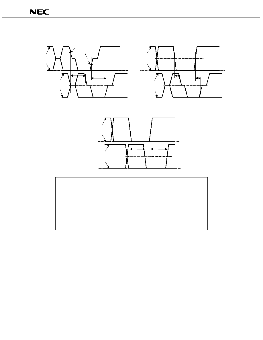
(4) HUB differential delay, differential jitter, and SOP distortion
50% point of
initial swing
V
SS
Downstream
port of HUB
Upstream
end of cable
V
SS
(b) Downstream HUB delay excluding cable
HUB operation jitter:
t
HDJ1
= t
HDDx
(J)
- t
HDDx
(K) or t
HDDx
(K)
- t
HDDx
(J) Continuous transition
t
HDJ2
= t
HDDx
(J)
- t
HDDx
(J) or t
HDDx
(K)
- t
HDDx
(K) Pair transition
Bit after SOP width distortion (same as data jitter of next transition of SOP):
t
FSOP
= t
HDDx
(next J)
- t
HDDx
(SOP)
The low-speed timing below is determined by the same method.
t
LHDD
, t
LDHJ1
, t
LDJH2
, t
LUHJ1
, t
LUJH2
, and t
LSOP
(a) Downstream HUB delay including cable
Downstream
end of HUB
HUB delay
downstream
t
HDD1
Crossover point
50% point of
initial swing
HUB delay
downstream
t
HDD2
Upstream
port of HUB
Crossover point
V
SS
Downstream
port of HUB
V
SS
(c) Upstream HUB delay with and without cable
Upstream port or
end of cable
HUB delay
upstream
t
HDD1
, t
HDD2
Crossover point
V
SS
V
SS
30
Data Sheet S13918EJ3V0DS
µ
PD72012
(5) HUB EOP delay and EOP skew
50% point of
initial swing
V
SS
(b) Downstream EOP delay excluding cable
EOP delay:
t
EOPD
= t
EOPy
- t
EHDDx
(t
EOPy
means apply this expression to t
EOP≠
and t
EOP+
.)
EOP skew:
t
HESK
= t
EOP+
- t
EOP≠
The low speed timing below is determined by the same method.
t
LEOPD
, t
LHESK
Upstream
end of cable
Upstream port or
end of cable
(c) Downstream EOP delay with and without cable
Expansion
crossover points
Downstream
port
t
EOP-
t
EOP+
V
SS
t
EOP+
t
EOP-
Downstream
port of HUB
V
SS
t
EOP+
t
EOP-
Downstream
end of HUB
V
SS
(a) Downstream EOP delay including cable
Expansion
crossover points
Expansion
crossover points
Upstream port
of HUB
V
SS
V
SS
Data Sheet S13918EJ3V0DS
31
µ
PD72012
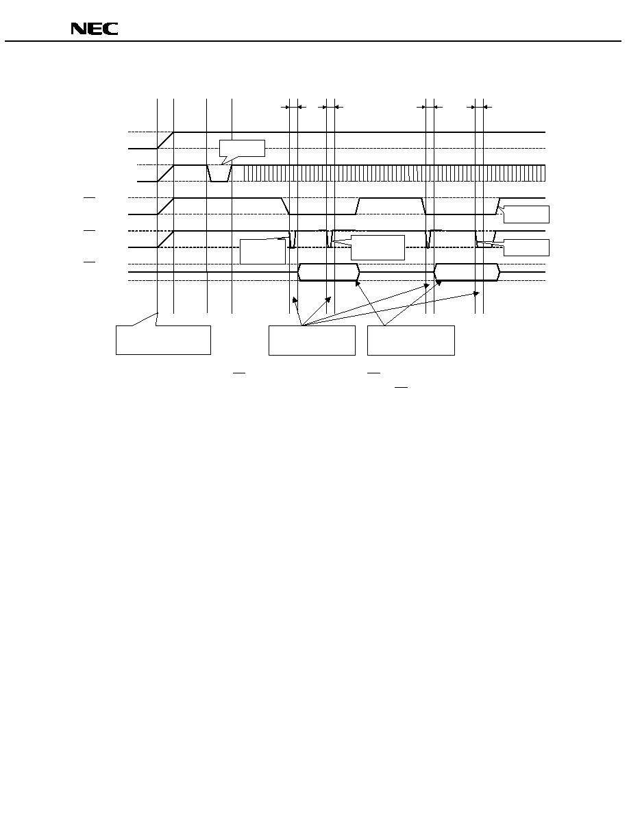
CS Timing Chart
500
µsec
HUB power supply
Up port D+ line
PP pin output
CS pin input
CS pin operation
region
Power supply ON
Bus power: Up port connection
Self-power: Power supply ON
BUS reset
Port power
supply ON
DEVICE
connection
inrush current
Overcurrent
generation
Output cut-off
CS active period
CS detection
delay time
500
µsec
500
µsec
500
µsec
Remark
The active period of the CS pin is in effect only when the PP pin is ON.
There is a delay time of approximately 500
µsec duration at the CS pin.
32
Data Sheet S13918EJ3V0DS
µ
PD72012
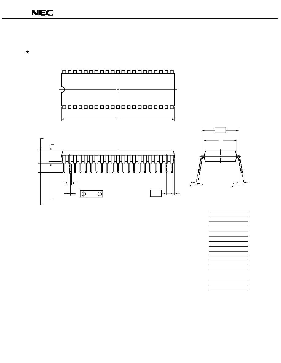
4. PACKAGE DRAWINGS
ITEM
MILLIMETERS
A
B
C
F
G
H
I
J
K
39.13 MAX.
1.778 (T.P.)
3.2
±0.3
0.51 MIN.
4.31 MAX.
1.78 MAX.
0.17
15.24 (T.P.)
5.08 MAX.
N
0.9 MIN.
R
P42C-70-600A-2
C
D
NOTES
1. Each lead centerline is located within 0.17 mm of
its true position (T.P.) at maximum material condition.
D
0.50
±0.10
M
0.25+0.10
-0.05
0
15∞
M
N
L
13.2
2. Item "K" to center of leads when formed parallel.
42
1
22
21
M
R
B
F
42-PIN PLASTIC SDIP (15.24mm(600))
I
H
G
K
L
J
A

Data Sheet S13918EJ3V0DS
33
µ
PD72012
33
34
22
44
1
12
11
23
44-PIN PLASTIC QFP (10x10)
ITEM
MILLIMETERS
A
B
D
G
13.6
±0.4
10.0
±0.2
0.15
1.0
I
13.6
±0.4
J
P44GB-80-3B4-5
C
10.0
±0.2
0.8 (T.P.)
K
1.8
±0.2
L
0.8
±0.2
F
1.0
N
P
Q
S
0.10
2.7
±0.1
0.1
±0.1
3.0 MAX.
R
5
∞±5∞
H
0.35+0.08
-0.07
M
0.17+0.08
-0.07
I
J
detail of lead end
M
C
D
A
B
Q
R
K
M
L
P
S
S
N
G
F
NOTE
Each lead centerline is located within 0.15 mm of
its true position (T.P.) at maximum material condition.
H
S
34
Data Sheet S13918EJ3V0DS
µ
PD72012
5. RECOMMENDED SOLDERING CONDITIONS
The
µPD72012 should be soldered and mounted under the following recommended conditions. For the details of
the recommended soldering conditions, refer to the document Semiconductor Device Mounting Technology
Manual (C10535E).
For soldering methods and conditions other than those recommended below, contact your NEC sales
representative.
Surface mount type soldering conditions
µ
µ
µ
µPD72012GB-XXX-3B4: 44-pin plastic QFP (10 ◊◊◊◊ 10)
Soldering Method
Soldering Conditions
Recommended
Condition Code
Infrared reflow
Peak package temperature: 235
∞C, Time: 30 sec. max. (210∞C min.), Count: three
times or less
IR35-00-3
VPS
Peak package temperature: 215
∞C, Time: 40 sec. max. (200∞C min.), Count: three
times or less
VP15-00-3
Wave soldering
Solder bath temperature: 260
∞C max., Time: 10 sec. max., Count: once,
Preheating temperature: 120
∞C max. (package surface temperature)
WS60-00-1
Pin partial heating
Pin temperature: 300
∞C max., Time: 3 sec. max. (per device side)
≠
Caution
Avoid using different soldering methods together. (However, the pin partial heating method is
excluded.)
Through-hole type soldering conditions
µ
µ
µ
µPD72012CU-XXX: 42-pin plastic SDIP (15.24 mm (600))
Soldering Method
Soldering Conditions
Wave soldering (pins
only)
Solder bath temperature: 260
∞C max., Time: 10 sec. max.
Pin partial heating
Pin temperature: 300
∞C max., Time: 3 sec. max. (per pin)
Caution
Apply wave soldering only to the pins, and exercise care that solder does not directly contact
the package.

Data Sheet S13918EJ3V0DS
35
µ
PD72012
NOTES FOR CMOS DEVICES
1
PRECAUTION AGAINST ESD FOR SEMICONDUCTORS
Note:
Strong electric field, when exposed to a MOS device, can cause destruction of the gate oxide and
ultimately degrade the device operation. Steps must be taken to stop generation of static electricity
as much as possible, and quickly dissipate it once, when it has occurred. Environmental control
must be adequate. When it is dry, humidifier should be used. It is recommended to avoid using
insulators that easily build static electricity. Semiconductor devices must be stored and transported
in an anti-static container, static shielding bag or conductive material. All test and measurement
tools including work bench and floor should be grounded. The operator should be grounded using
wrist strap. Semiconductor devices must not be touched with bare hands. Similar precautions need
to be taken for PW boards with semiconductor devices on it.
2
HANDLING OF UNUSED INPUT PINS FOR CMOS
Note:
No connection for CMOS device inputs can be cause of malfunction. If no connection is provided
to the input pins, it is possible that an internal input level may be generated due to noise, etc., hence
causing malfunction. CMOS devices behave differently than Bipolar or NMOS devices. Input levels
of CMOS devices must be fixed high or low by using a pull-up or pull-down circuitry. Each unused
pin should be connected to V
DD
or GND with a resistor, if it is considered to have a possibility of
being an output pin. All handling related to the unused pins must be judged device by device and
related specifications governing the devices.
3
STATUS BEFORE INITIALIZATION OF MOS DEVICES
Note:
Power-on does not necessarily define initial status of MOS device. Production process of MOS
does not define the initial operation status of the device. Immediately after the power source is
turned ON, the devices with reset function have not yet been initialized. Hence, power-on does
not guarantee out-pin levels, I/O settings or contents of registers. Device is not initialized until the
reset signal is received. Reset operation must be executed immediately after power-on for devices
having reset function.

µ
PD72012
The export of this product from Japan is prohibited without governmental license. To export or re-export this product from
a country other than Japan may also be prohibited without a license from that country. Please call an NEC sales
representative.
M8E 00. 4
The information in this document is current as of April, 2001. The information is subject to change
without notice. For actual design-in, refer to the latest publications of NEC's data sheets or data
books, etc., for the most up-to-date specifications of NEC semiconductor products. Not all products
and/or types are available in every country. Please check with an NEC sales representative for
availability and additional information.
No part of this document may be copied or reproduced in any form or by any means without prior
written consent of NEC. NEC assumes no responsibility for any errors that may appear in this document.
NEC does not assume any liability for infringement of patents, copyrights or other intellectual property rights of
third parties by or arising from the use of NEC semiconductor products listed in this document or any other
liability arising from the use of such products. No license, express, implied or otherwise, is granted under any
patents, copyrights or other intellectual property rights of NEC or others.
Descriptions of circuits, software and other related information in this document are provided for illustrative
purposes in semiconductor product operation and application examples. The incorporation of these
circuits, software and information in the design of customer's equipment shall be done under the full
responsibility of customer. NEC assumes no responsibility for any losses incurred by customers or third
parties arising from the use of these circuits, software and information.
While NEC endeavours to enhance the quality, reliability and safety of NEC semiconductor products, customers
agree and acknowledge that the possibility of defects thereof cannot be eliminated entirely. To minimize
risks of damage to property or injury (including death) to persons arising from defects in NEC
semiconductor products, customers must incorporate sufficient safety measures in their design, such as
redundancy, fire-containment, and anti-failure features.
NEC semiconductor products are classified into the following three quality grades:
"Standard", "Special" and "Specific". The "Specific" quality grade applies only to semiconductor products
developed based on a customer-designated "quality assurance program" for a specific application. The
recommended applications of a semiconductor product depend on its quality grade, as indicated below.
Customers must check the quality grade of each semiconductor product before using it in a particular
application.
"Standard": Computers, office equipment, communications equipment, test and measurement equipment, audio
and visual equipment, home electronic appliances, machine tools, personal electronic equipment
and industrial robots
"Special":
Transportation equipment (automobiles, trains, ships, etc.), traffic control systems, anti-disaster
systems, anti-crime systems, safety equipment and medical equipment (not specifically designed
for life support)
"Specific": Aircraft, aerospace equipment, submersible repeaters, nuclear reactor control systems, life
support systems and medical equipment for life support, etc.
The quality grade of NEC semiconductor products is "Standard" unless otherwise expressly specified in NEC's
data sheets or data books, etc. If customers wish to use NEC semiconductor products in applications not
intended by NEC, they must contact an NEC sales representative in advance to determine NEC's willingness
to support a given application.
(Note)
(1) "NEC" as used in this statement means NEC Corporation and also includes its majority-owned subsidiaries.
(2) "NEC semiconductor products" means any semiconductor product developed or manufactured by or for
NEC (as defined above).
∑
∑
∑
∑
∑
∑