 | –≠–ª–µ–∫—Ç—Ä–æ–Ω–Ω—ã–π –∫–æ–º–ø–æ–Ω–µ–Ω—Ç: UPD720113 | –°–∫–∞—á–∞—Ç—å:  PDF PDF  ZIP ZIP |
Document Outline
- COVER
- FEATURES
- ORDERING INFORMATION
- BLOCK DIAGRAM
- PIN CONFIGURATION (TOP VIEW)
- 1. PIN INFORMATION
- 2. ELECTRICAL SPECIFICATIONS
- 2.1 Buffer List
- 2.2 Terminology
- 2.3 Electrical Specifications
- 3. PACKAGE DRAWING
- 4. RECOMMENDED SOLDERING CONDITIONS
The information in this document is subject to change without notice. Before using this document, please
confirm that this is the latest version.
Not all products and/or types are available in every country. Please check with an NEC Electronics
sales representative for availability and additional information.
MOS INTEGRATED CIRCUIT
µ
PD720113
USB 2.0 HUB CONTROLLER
Document No. S16618EJ3V0DS00 (3rd edition)
Date Published March 2005 NS CP (N)
Printed in Japan
DATA SHEET
The mark shows major revised points.
2003
The
µ
PD720113 is a USB 2.0 hub device that complies with the Universal Serial Bus (USB) Specification Revision
2.0 and works up to 480 Mbps. USB 2.0 compliant transceivers are integrated for upstream and all downstream ports.
The
µ
PD720113 works backward compatible either when any one of the downstream ports is connected to a USB 1.1
compliant device, or when the upstream port is connected to a USB 1.1 compliant host.
Detailed function descriptions are provided in the following user's manual. Be sure to read the manual before designing.
µ
PD720113 User's Manual: S16619E
FEATURES
∑ Compliant with Universal Serial Bus Specification Revision 2.0 (Data Rate 1.5/12/480 Mbps)
∑ Certified by USB implementers forum and granted the USB 2.0 high-speed Logo
∑ High-speed or full-speed packet protocol sequencer for Endpoint 0/1
∑ 7 (Max.) downstream facing ports
∑ All downstream facing ports can handle high-speed (480 Mbps), full-speed (12 Mbps), and low-speed (1.5
Mbps) transaction.
∑ Supports split transaction to handle full-speed and low-speed transaction on downstream facing ports when
Hub controller is working in high-speed mode.
∑ One Transaction Translator per Hub and supports four non-periodic buffers
∑ Support self-powered mode
∑ Supports Over-current detection and Individual or ganged power control
∑ Supports configurable vendor ID, product ID, string descriptors and others with external Serial ROM
∑ Supports "non-removable" attribution on individual port
∑ Uses 30 MHz X'tal, or clock input
∑ 2.5 V and 3.3 V power supplies

Data Sheet S16618EJ3V0DS
2
µ
PD720113
ORDERING INFORMATION
Part Number
Package
Remark
µ
PD720113GK-9EU
80-pin plastic TQFP (Fine pitch) (12
◊ 12)
µ
PD720113GK-9EU-A
80-pin plastic TQFP (Fine pitch) (12
◊ 12)
Lead-free product
BLOCK DIAGRAM
Upstream facing port
UP_PHY
Downstream facing port #1
SERDES
SIE_2H
CDR
APLL
OSB
UPC
ROM I/F
ALL_TT
F_TIM
EP1
EP0
DP(1)_PHY
Downstream facing port #2
DP(2)_PHY
Downstream facing port #3
DP(3)_PHY
Downstream facing port #4
DP(4)_PHY
DPC
FS_REP
To Host/Hub
downstream
facing port
X1_CLK/X2
PPB(
7
:
1
)
CSB(
7
:
1
)
To Hub/Function
upstream facing port
To Hub/Function
upstream facing port
To Hub/Function
upstream facing port
To Hub/Function
upstream facing port
External
Serial ROM
CDR
Downstream facing port #5
DP(5)_PHY
Downstream facing port #6
DP(6)_PHY
Downstream facing port #7
DP(7)_PHY
To Hub/Function
upstream facing port
To Hub/Function
upstream facing port
To Hub/Function
upstream facing port

Data Sheet S16618EJ3V0DS
3
µ
PD720113
APLL
: Generates all clocks of Hub.
ALL_TT
: Translates the high-speed transactions (split transactions) for full/low-speed device
to full/low-speed transactions. ALL_TT buffers the data transfer from either
upstream or downstream direction. For OUT transaction, ALL_TT buffers data from
upstream port and sends it out to the downstream facing ports after speed
conversion from high-speed to full/low-speed. For IN transaction, ALL_TT buffers
data from downstream ports and sends it out to the upstream facing ports after
speed conversion from full/low-speed to high-speed.
CDR
: Data & clock recovery circuit
DPC
: Downstream Port Controller handles Port Reset, Enable, Disable, Suspend and
Resume
DP(n)_PHY
: Downstream transceiver supports high-speed (480 Mbps), full-speed (12 Mbps), and
low-speed (1.5 Mbps) transaction
EP0
: Endpoint 0 controller
EP1
: Endpoint 1 controller
F_TIM (Frame Timer)
: Manages hub's synchronization by using micro-SOF which is received at upstream
port, and generates SOF packet when full/low-speed device is attached to
downstream facing port.
FS_REP
: Full/low-speed repeater is enabled when the
µ
PD720113 are worked at full-speed
mode
OSB :
Oscillator
Block
ROM I/F
: Interface block for external Serial ROM which contains user-defined descriptors
SERDES :
Serializer
and
Deserializer
SIE_2H
: Serial Interface Engine (SIE) controls USB2.0 and 1.1 protocol sequencer.
UP_PHY
: Upstream Transceiver supports high-speed (480 Mbps), full-speed (12 Mbps)
transaction
UPC
: Upstream Port Controller handles Suspend and Resume

Data Sheet S16618EJ3V0DS
4
µ
PD720113
PIN CONFIGURATION (TOP VIEW)
∑ 80-pin plastic TQFP (Fine pitch) (12 ◊ 12)
µ
PD720113GK-9EU
µ
PD720113GK-9EU-A
1
5
10
15
20
25
21
30
40
41
35
45
50
55
61
65
60
70
75
80
V
DD33
V
DD25
V
SS
DM6
DP6
V
DD33
V
SS
DM7
DP7
V
SS
V
DD25
V
SS
TEST
SCAN_MODE
V
SS
LPWRM
EXROM_EN
SCL
SDA/GANG_B
V
SS
V
DD33
VBUSM
S
YSRSTB
PPB1
CSB1
PPB2
CSB2
PPB3
CSB3
PPB4
V
DD25
V
SS
CSB4
PPB5
CSB5
PPB6
CSB6
PPB7
CSB7
V
DD33
V
DD33
RPU
V
SS
V
DD25
DPU
DMU
V
SS
V
DD33
V
DD25
V
SS
AV
DD
AV
SS
AV
DD
AV
SS
(R)
RREF
AV
SS
V
DD25
X2
X1_CLK
V
SS
DM
1
DP
1
V
DD2
5
V
SS
DM
2
DP
2
V
DD3
3
V
SS
DM
3
DP
3
V
DD3
3
V
SS
V
DD2
5
V
SS
DM
4
DP
4
V
DD2
5
V
SS
DM
5
DP
5
Data Sheet S16618EJ3V0DS
5
µ
PD720113
Pin No.
Pin Name
Pin No.
Pin Name
Pin No.
Pin Name
Pin No.
Pin Name
1 V
DD33
21
V
DD33
41
V
SS
61
DM1
2 V
DD25
22
CSB7 42
X1_CLK
62
DP1
3 V
SS
23
PPB7
43
X2 63
V
DD25
4 DM6
24 CSB6
44
V
DD25
64
V
SS
5 DP6
25 PPB6
45
AV
SS
65
DM2
6 V
DD33
26
CSB5 46
RREF 66
DP2
7 V
SS
27
PPB5
47
AV
SS
(R) 67
V
DD33
8 DM7
28 CSB4
48
AV
DD
68
V
SS
9 DP7
29 V
SS
49
AV
SS
69
DM3
10 V
SS
30
V
DD25
50
AV
DD
70
DP3
11 V
DD25
31
PPB4 51
V
SS
71
V
DD33
12 V
SS
32
CSB3
52
V
DD25
72
V
SS
13 TEST
33 PPB3
53 V
DD33
73
V
DD25
14 SCAN_MODE
34 CSB2
54 V
SS
74
V
SS
15 V
SS
35
PPB2
55
DMU
75
DM4
16 LPWRM 36 CSB1
56 DPU
76 DP4
17 EXROM_EN
37 PPB1
57 V
DD25
77
V
DD25
18 SCL
38 SYSRSTB 58 V
SS
78
V
SS
19 SDA/GANG_B
39 VBUSM
59 RPU
79 DM5
20 V
SS
40
V
DD33
60
V
DD33
80
DP5
Remark AV
SS
(R) should be used to connect RREF through 1 % precision reference resistor of 2.43 k
.

Data Sheet S16618EJ3V0DS
6
µ
PD720113
1. PIN INFORMATION
Pin Name
I/O
Buffer Type
Active
Level
Function
X1_CLK
I
2.5 V Input
Crystal oscillator in or clock input
X2
O
2.5 V Output
Oscillator out
SYSRSTB
I
5 V tolerant Schmitt Input
Low
Asynchronous chip reset
RPU
A (O)
USB Pull-up control
External 1.5 k
pull-up resistor control
DP(7:1) I/O
USB
D
+ signal I/O
USB's downstream facing port D
+ signal
DM(7:1) I/O
USB
D
- signal I/O
USB's downstream facing port D
- signal
DPU I/O
USB
D
+ signal I/O
USB's upstream facing port D
+ signal
DMU I/O
USB
D
- signal I/O
USB's upstream facing port D
- signal
LPWRM
I
3.3 V Schmitt Input
Local power monitor
RREF
A (O)
Analog
Reference resistor
CSB(7:1)
I
5 V tolerant Input
Low
Port's over-current status input
PPB(7:1)
O
5 V tolerant N-ch open drain
Low
Port's power supply control output
VBUSM
I
5 V tolerant Schmitt input
V
BUS
monitor
SCL
O
3.3 V Output
External serial ROM clock out
SDA/GANG_B
I/O
3.3 V Schmitt I/O
External serial ROM data IO or power
management mode select
EXROM_EN
I
3.3 V Schmitt Input
External serial ROM input enable
TEST
I
3.3 V Input
Test signal
SCAN_MODE
I
3.3 V Input
Test signal
V
DD33
3.3 V V
DD
V
DD25
2.5 V V
DD
AV
DD
2.5 V V
DD
for analog circuit
V
SS
V
SS
AV
SS
V
SS
for analog circuit
AV
SS
(R)
V
SS
for reference resistor. Connect to AV
SS
.
Remark "5 V tolerant" means that the buffer is 3 V buffer with 5 V tolerant circuit.

Data Sheet S16618EJ3V0DS
7
µ
PD720113
2. ELECTRICAL SPECIFICATIONS
2.1 Buffer
List
∑ 2.5 V Oscillator interface
X1_CLK, X2
∑ 5 V Schmitt input buffer
SYSRSTB, CSB(7:1), VBUSM
∑ 3.3 V Schmitt input buffer
LPWRM
∑ 3.3 V input buffer
EXROM_EN, TEST, SCAN_MODE
∑ 3.3 V I
OL
= 3 mA bi-directional Schmitt input buffer with input enable (OR-type)
SDA/GANG_B
∑ 3.3 V I
OL
= 3 mA output buffer
SCL
∑ 5 V I
OL
= 12 mA N-ch open drain buffer
PPB(7:1)
∑ USB2.0
interface
RPU, DPU, DMU, DP(7:1), DM(7:1), RREF
Above, "5 V" refers to a 3 V input buffer that is 5 V tolerant (has 5 V maximum input voltage). Therefore, it is
possible to have a 5 V connection for an external bus.
Data Sheet S16618EJ3V0DS
8
µ
PD720113
2.2 Terminology
Terms Used in Absolute Maximum Ratings
Parameter Symbol
Meaning
Power supply voltage
V
DD33
V
DD25
AV
DD
Indicates voltage range within which damage or reduced reliability will not
result when power is applied to a V
DD
pin.
Input voltage
V
I
Indicates voltage range within which damage or reduced reliability will not
result when power is applied to an input pin.
Output voltage
V
O
Indicates voltage range within which damage or reduced reliability will not
result when power is applied to an output pin.
Output current
I
O
Indicates absolute tolerance values for DC current to prevent damage or
reduced reliability when current flows out of or into an output pin.
Operating temperature
T
A
Indicates the ambient temperature range for normal logic operations.
Storage temperature
T
stg
Indicates the element temperature range within which damage or reduced
reliability will not result while no voltage or current are applied to the device.
Terms Used in Recommended Operating Range
Parameter Symbol
Meaning
Power supply voltage
V
DD33
V
DD25
AV
DD
Indicates the voltage range for normal logic operations to occur when V
SS
= 0
V.
High-level input voltage
V
IH
Indicates the voltage, applied to the input pins of the device, which indicates
the high level state for normal operation of the input buffer.
* If a voltage that is equal to or greater than the "MIN." value is applied, the
input voltage is guaranteed as high level voltage.
Low-level input voltage
V
IL
Indicates the voltage, applied to the input pins of the device, which indicates
the low level state for normal operation of the input buffer.
* If a voltage that is equal to or less than the "MAX." value is applied, the
input voltage is guaranteed as low level voltage.
Hysteresis voltage
V
H
Indicates the differential between the positive trigger voltage and the negative
trigger voltage.
Input rise time
t
ri
Indicates allowable input signal transition time from 0.1
◊ V
DD
to 0.9
◊ V
DD
.
Input fall time
t
fi
Indicates allowable input signal transition time from 0.9
◊ V
DD
to 0.1
◊ V
DD
.

Data Sheet S16618EJ3V0DS
9
µ
PD720113
Terms Used in DC Characteristics
Parameter Symbol
Meaning
Off-state output leakage current
I
OZ
Indicates the current that flows into a 3-state output pin when it is in a high-
impedance state and a voltage is applied to the pin.
Output short circuit current
I
OS
Indicates the current that flows from an output pin when it is shorted to GND
while it is at high-level.
Input leakage current
I
I
Indicates the current that flows into an input pin when a voltage is applied to
the pin.
Low-level output current
I
OL
Indicates the current that can flow into an output pin in the low-level state
without raising the output voltage above the specified V
OL
.
High-level output current
I
OH
Indicates the current that can flow out of an output pin in the high-level state
without reducing the output voltage below the specified V
OH
. (A negative
current indicates current flowing out of the pin.)
2.3 Electrical
Specifications
Absolute Maximum Ratings
Parameter Symbol
Condition
Rating Unit
Power supply voltage
V
DD33
-0.5 to +4.6 V
V
DD25
-0.5 to +3.6
V
AV
DD
-0.5 to +3.6
V
Input/output voltage
V
I
/V
O
2.5 V input/output voltage
2.3 V
V
DD25
2.7 V
V
I
/V
O
< V
DD25
+ 0.9 V
-0.5 to +3.6 V
3.3 V input/output voltage
3.0 V
V
DD33
3.6 V
V
I
/V
O
< V
DD33
+ 1.0 V
-0.5 to +4.6 V
5 V input/out voltage
3.0 V
V
DD33
3.6 V
V
I
/V
O
< V
DD33
+ 3.0 V
-0.5 to +6.6 V
Output current
I
O
I
OL
= 3 mA
I
OL
= 6 mA
I
OL
= 12 mA
10
20
40
mA
mA
mA
Operating temperature
T
A
0
to
+70
∞C
Storage temperature
T
stg
-65 to +150
∞C
Caution Product quality may suffer if the absolute maximum rating is exceeded even momentarily for any
parameters. That is, the absolute maximum ratings are rated values at which the product is on the
verge of suffering physical damage, and therefore the product must be used under conditions
that ensure that the absolute maximum ratings are not exceeded.
The ratings and conditions indicated for DC characteristics and AC characteristics represent the
quality assurance range during normal operation.

Data Sheet S16618EJ3V0DS
10
µ
PD720113
Recommended Operating Ranges
Parameter Symbol
Condition
MIN.
TYP.
MAX.
Unit
Operating voltage
V
DD33
3.3 V for V
DD33
pins
3.14
3.30
3.46
V
V
DD25
2.5 V for V
DD25
pins
2.3
2.5
2.7
V
AV
DD
2.5 V for AV
DD
pins
2.3
2.5
2.7
V
High-level input voltage
V
IH
2.5 V High-level input voltage
1.7
V
DD25
V
3.3 V High-level input voltage
2.0
V
DD33
V
5.0 V High-level input voltage
2.0
5.5
V
Low-level input voltage
V
IL
2.5 V Low-level input voltage
0
0.7
V
3.3 V Low-level input voltage
0
0.8
V
5.0 V Low-level input voltage
0
0.8
V
Hysteresis voltage
V
H
5 V Hysteresis voltage
0.3
1.5
V
3.3 V Hysteresis voltage
0.2
1.0
V
Input rise time for SYSRSTB
t
rst
10
ms
Input rise time
t
ri
Normal buffer
0
200
ns
Schmitt buffer
0
10
ms
Input fall time
t
fi
Normal buffer
0
200
ns
Schmitt buffer
0
10
ms
Two power supply rails limitation.
The
µ
PD720113 has two power supply rails (2.5 V, 3.3 V).
The system will require the time when power supply
rail is stable at V
DD
level. And, there will be difference between the time of V
DD25
and V
DD33
. The
µ
PD720113
requires that V
DD25
should be stable before V
DD33
becomes stable. At any case, the system must ensure that the
absolute maximum ratings for V
I
/V
O
are not exceeded. System reset signaling should be asserted more than
specified time after both V
DD25
and V
DD33
are stable.

Data Sheet S16618EJ3V0DS
11
µ
PD720113
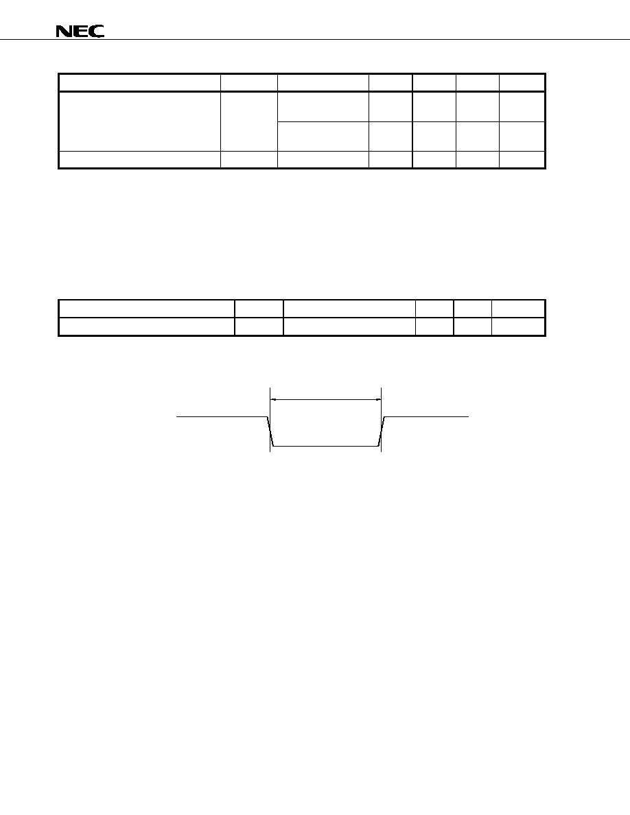
DC Characteristics
Parameter Symbol
Condition
MIN.
MAX.
Unit
Off-state output leakage current
I
OZ
V
O
= V
DD33,
V
DD25
or V
SS
±10
µ
A
Output short circuit current
I
OS
Note
-250 mA
Low-level output current
I
OL
3.3 V low-level output current
V
OL
= 0.4 V
3
mA
3.3 V low-level output current
V
OL
= 0.4 V
6
mA
5.0 V low-level output current
V
OL
= 0.4 V
12
mA
High-level output current
I
OH
3.3 V high-level output current
V
OH
= 2.4 V
-3 mA
3.3 V high-level output current
V
OH
= 2.4 V
-6 mA
5.0 V high-level output current
V
OH
= 2.4 V
-2 mA
Input leakage current
I
I
3.3 V buffer
V
I
= V
DD
or V
SS
±10
µ
A
5.0 V buffer
V
I
= V
DD
or V
SS
±10
µ
A
Note The output short circuit time is measured at one second or less and is tested with only one pin on the LSI.
Data Sheet S16618EJ3V0DS
12
µ
PD720113
USB Interface Block
Parameter Symbol
Conditions
MIN
MAX
Unit
Output pin impedance
Z
HSDRV
Includes
R
S
resistor
40.5
49.5
Bus pull-up resistor on upstream facing
port
R
PU
1.425 1.575 k
Bus pull-up resistor on downstream
facing port
R
PD
14.25 15.75 k
Termination voltage for upstream facing
port pullup (full-speed)
V
TERM
3.0
3.6
V
Input Levels for Low-/full-speed:
High-level input voltage (drive)
V
IH
2.0
V
High-level input voltage (floating)
V
IHZ
2.7 3.6 V
Low-level input voltage
V
IL
0.8 V
Differential input sensitivity
V
DI
(D+) - (D-) 0.2
V
Differential common mode range
V
CM
Includes
V
DI
range
0.8
2.5
V
Output Levels for Low-/full-speed:
High-level output voltage
V
OH
R
L
of 14.25 k
to GND
2.8
3.6
V
Low-level output voltage
V
OL
R
L
of 1.425 k
to 3.6 V
0.0
0.3
V
SE1 V
OSE1
0.8
V
Output signal crossover point voltage
V
CRS
1.3
2.0 V
Input Levels for High-speed:
High-speed squelch detection threshold
(differential signal)
V
HSSQ
100
150 mV
High-speed disconnect detection
threshold (differential signal)
V
HSDSC
525
625 mV
High-speed data signaling common
mode voltage range
V
HSCM
-50
+500 mV
High-speed differential input signaling
levels
See Figure 2-4.
Output Levels for High-speed:
High-speed idle state
V
HSOI
-10.0
+10 mV
High-speed data signaling high
V
HSOH
360
440 mV
High-speed data signaling low
V
HSOL
-10.0
+10 mV
Chirp J level (different signal)
V
CHIRPJ
700
1100 mV
Chirp K level (different signal)
V
CHIRPK
-900
-500 mV

Data Sheet S16618EJ3V0DS
13
µ
PD720113
Figure 2-1. Differential Input Sensitivity Range for Low-/full-speed
4.6
-1.0
Input Voltage Range (Volts)
Differential Input Voltage Range
Differential Output
Crossover
Voltage Range
0.0
0.2
0.4
0.6
0.8
1.0
1.2
1.4
1.6
1.8
2.0
2.2
2.4
2.6
2.8
3.0
3.2
Figure 2-2. Full-speed Buffer V
OH
/I
OH
Characteristics for High-speed Capable Transceiver
Max.
Min.
-
80
-
60
-
40
-
20
0
V
DD
-
0.3
V
OUT
(V)
I
OUT
(mA)
V
DD
-
2.3
V
DD
-
3.3
V
DD
-
0.8
V
DD
V
DD
-
1.3
V
DD
-
1.8
V
DD
-
2.8
Figure 2-3. Full-speed Buffer V
OL
/I
OL
Characteristics for High-speed Capable Transceiver
Max.
Min.
80
60
40
20
0
0
0.5
1
1.5
2
2.5
3
V
OUT
(V)
I
OUT
(mA)

Data Sheet S16618EJ3V0DS
14
µ
PD720113
Figure 2-4. Receiver Sensitivity for Transceiver at DP/DM
0 V
Differential
+
400 mV
Differential
-
400 mV
Differential
Unit Interval
Level 1
Level 2
0%
100%
Point 5
Point 2
Point 1
Point 3
Point 4
Point 6
Figure 2-5. Receiver Measurement Fixtures
V
BUS
D+
D-
GND
15.8
+
To 50
Inputs of a
High Speed Differential
Oscilloscope, or 50
Outputs of a High Speed
Differential Data Generator
-
50
Coax
50
Coax
USB
Connector
Nearest
Device
Test Supply Voltage
15.8
143
143

Data Sheet S16618EJ3V0DS
15
µ
PD720113
Power Consumption
Parameter Symbol
Condition
TYP. Unit
Power Consumption
P
W-0
The power consumption under the state without suspend.
All the ports do not connect to any function.
Note
Hub controller is operating at full-speed mode.
Hub controller is operating at high-speed mode.
44
2.2
84
23
mA (2.5 V)
mA (3.3 V)
mA (2.5 V)
mA (3.3 V)
P
W-5
The power consumption under the state without suspend.
The number of active ports is 5.
Hub controller is operating at full-speed mode.
Hub controller is operating at high-speed mode.
44
8.9
138
85
mA (2.5 V)
mA (3.3 V)
mA (2.5 V)
mA (3.3 V)
P
W-6
The power consumption under the state without suspend.
The number of active ports is 6.
Hub controller is operating at full-speed mode.
Hub controller is operating at high-speed mode.
44
10
148
98
mA (2.5 V)
mA (3.3 V)
mA (2.5 V)
mA (3.3 V)
P
W-7
The power consumption under the state without suspend.
The number of active ports is 7.
Hub controller is operating at full-speed mode.
Hub controller is operating at high-speed mode.
44
12
158
111
mA (2.5 V)
mA (3.3 V)
mA (2.5 V)
mA (3.3 V)
P
W_S
The power consumption under suspend state.
The internal clock is stopped.
0.68
0.24
mA (2.5 V)
mA (3.3 V)
Note
When any device is not connected to all the ports, the power consumption does not depend on the number
of active ports.
Data Sheet S16618EJ3V0DS
16
µ
PD720113
System Clock Ratings
Parameter Symbol
Condition
MIN.
TYP.
MAX.
Unit
Clock frequency
f
CLK
X'tal
-500
ppm
30
+500
ppm
MHz
Oscillator
block
-500
ppm
30
+500
ppm
MHz
Clock Duty cycle
t
DUTY
40 50 60 %
Remarks 1. Recommended accuracy of clock frequency is
± 100 ppm.
2. Required accuracy of X'tal or oscillator block is including initial frequency accuracy, the spread of
X'tal capacitor loading, supply voltage, temperature, and aging, etc.
AC Characteristics (V
DD
= 3.14 to 3.46 V, T
A
= 0 to
+70∞C)
System Reset Timing
Parameter Symbol
Conditions
MIN.
MAX.
Unit
Reset active time (Figure 2-6)
t
rst
5
µ
s
Figure 2-6. System Reset Timing
SYSRSTB
t
rst

Data Sheet S16618EJ3V0DS
17
µ
PD720113
Over-current Response Timing
Parameter Symbol
Condition
MIN.
TYP.
MAX.
Unit
Over-current response time from CSB
low to PPB high (Figure 2-7)
t
OC
500
625
µ
s
Figure 2-7. Over-current Response Timing
CSB(7:1)
PPB(7:1)
t
OC
Figure 2-8. CSB/PPB Timing
Bus reset
500
µ
s
500
µ
s
500
µ
s
500
µ
s
Hub power supply
PPB pin output
CSB pin input
CSB pin operation region
Up port D
+
line
Port power
supply ON
Output
cut-off
Overcurrent
generation
CSB detection
delay time
CSB active
period
Device
connection
inrush current
Bus power: Up port connection
Self power: Power supply ON
Remark The active period of the CSB pin is in effect only when the PPB pin is ON.
There is a delay time of approximately 500
µ
s duration at the CSB pin.
Data Sheet S16618EJ3V0DS
18
µ
PD720113
External Serial ROM Timing
Parameter Symbol
Condition
MIN.
TYP.
MAX.
Unit
Clock frequency
f
SCL
94.6
100
kHz
Clock pulse width low
t
LOW
4700
ns
Clock pulse width high
t
HIGH
4000
ns
Clock low to data out valid
t
AA
100
3500
ns
Time the bus must be free before a new
transmission can start
t
BUF
4700
ns
Start hold time
t
HD.STA
4000 ns
Start setup time
t
SU.STA
4700 ns
Data in hold time
t
HD.DTA
0 ns
Data in setup time
t
SU.DTA
250 ns
Stop setup time
t
SU.STO
4700 ns
Data out hold time
t
DH
300
ns
Write cycle time
t
WR
15
ms
Figure 2-9. External Serial ROM Bus Timing
SCL
SDA
(Output)
SDA
(Input)
t
SU.STA
t
HD.STA
t
SU.DAT
t
HIGH
t
LOW
t
LOW
t
HD.DAT
t
AA
t
DH
t
SU.STO
t
BUF
Figure 2-10. External Serial ROM Write Cycle Timing
SCL
SDA
Word n
8th bit
ACK
Stop
condition
Start
condition
t
WR
Data Sheet S16618EJ3V0DS
19
µ
PD720113
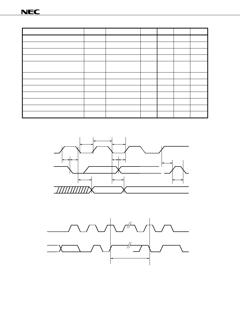
USB Interface Block
(1/4)
Parameter Symbol
Conditions
MIN.
MAX.
Unit
Low-speed Electrical Characteristics
Rise time (10% to 90%)
t
LR
C
L
= 200 pF to 600 pF
75
300
ns
Fall time (90% to 10%)
t
LF
C
L
= 200 pF to 600 pF
75
300
ns
Differential rise and fall time matching
t
LRFM
(t
LR
/t
LF
)
Note
80
125
%
Low-speed data rate
t
LDRATHS
Average bit rate
1.49925
1.50075
Mbps
Downstream facing port source jitter total
(including frequency tolerance) (Figure
2-15):
To next transition
For paired transitions
t
DDJ1
t
DDJ2
-25
-14
+25
+14
ns
ns
Downstream facing port differential
receiver jitter total (including frequency
tolerance) (Figure 2-17):
To next transition
For paired transitions
t
UJR1
t
UJR2
-152
-200
+152
+200
ns
ns
Source SE0 interval of EOP (Figure 2-16)
t
LEOPT
1.25
1.5
µ
s
Receiver SE0 interval of EOP (Figure 2-16)
t
LEOPR
670
ns
Width of SE0 interval during differential
transition
t
LST
210
ns
Hub differential data delay (Figure 2-13)
t
LHDD
300 ns
Hub differential driver jitter (including cable)
(Figure 2-13):
Downstream facing port
To next transition
For paired transitions
Upstream facing port
To next transition
For paired transitions
t
LDHJ1
t
LDHJ2
t
LUHJ1
t
LUHJ2
-45
-15
-45
-45
+45
+15
+45
+45
ns
ns
ns
ns
Data bit width distortion after SOP (Figure
2-13)
t
LSOP
-60
+60 ns
Hub EOP delay relative to t
HDD
(Figure
2-14)
t
LEOPD
0
200 ns
Hub EOP output width skew (Figure 2-14)
t
LHESK
-300
+300 ns
Full-speed Electrical Characteristics
Rise time (10% to 90%)
t
FR
C
L
= 50 pF,
R
S
= 36
4 20
ns
Fall time (90% to 10%)
t
FF
C
L
= 50 pF,
R
S
= 36
4 20
ns
Differential rise and fall time matching
t
FRFM
(t
FR
/t
FF
) 90
111.11
%
Full-speed data rate
t
FDRATHS
Average bit rate
11.9940
12.0060
Mbps
Frame interval
t
FRAME
0.9995 1.0005 ms
Note Excluding the first transition from the Idle state.

Data Sheet S16618EJ3V0DS
20
µ
PD720113
(2/4)
Parameter Symbol
Conditions
MIN.
MAX.
Unit
Full-speed Electrical Characteristics (Continued)
Consecutive frame interval jitter
t
RFI
No clock adjustment
42
ns
Source jitter total (including frequency
tolerance) (Figure 2-15):
To next transition
For paired transitions
t
DJ1
t
DJ2
Note
-3.5
-4.0
+3.5
+4.0
ns
ns
Source jitter for differential transition to
SE0 transition (Figure 2-16)
t
FDEOP
-2
+5 ns
Receiver jitter (Figure 2-17):
To Next Transition
For
Paired
Transitions
t
JR1
t
JR2
-18.5
-9
+18.5
+9
ns
ns
Source SE0 interval of EOP (Figure 2-16)
t
FEOPT
160
175 ns
Receiver SE0 interval of EOP (Figure 2-16)
t
FEOPR
82
ns
Width of SE0 interval during differential
transition
t
FST
14 ns
Hub differential data delay (Figure 2-13)
(with cable)
(without cable)
t
HDD1
t
HDD2
70
44
ns
ns
Hub differential driver jitter (including cable)
(Figure 2-13):
To next transition
For paired transitions
t
HDJ1
t
HDJ2
-3
-1
+3
+1
ns
ns
Data bit width distortion after SOP (Figure
2-13)
t
FSOP
-5
+5 ns
Hub EOP delay relative to t
HDD
(Figure
2-14)
t
FEOPD
0
15
ns
Hub EOP output width skew (Figure 2-14)
t
FHESK
-15
+15 ns
High-speed Electrical Characteristics
Rise time (10% to 90%)
t
HSR
500
ps
Fall time (90% to 10%)
t
HSF
500
ps
Driver waveform
See Figure 2-11.
High-speed data rate
t
HSDRAT
479.760 480.240 Mbps
Microframe interval
t
HSFRAM
124.9375 125.0625
µ
s
Consecutive microframe interval difference
t
HSRFI
4
high-
speed
Bit
times
Data source jitter
See Figure 2-11.
Receiver jitter tolerance
See Figure 2-4.
Hub data delay (without cable)
t
HSHDD
36
high-
speed
+4 ns
Bit
times
Hub data jitter
See Figure 2-4, Figure 2-11.
Hub delay variation range
t
HSHDV
5
high-
speed
Bit
times
Note Excluding the first transition from the Idle state.

Data Sheet S16618EJ3V0DS
21
µ
PD720113
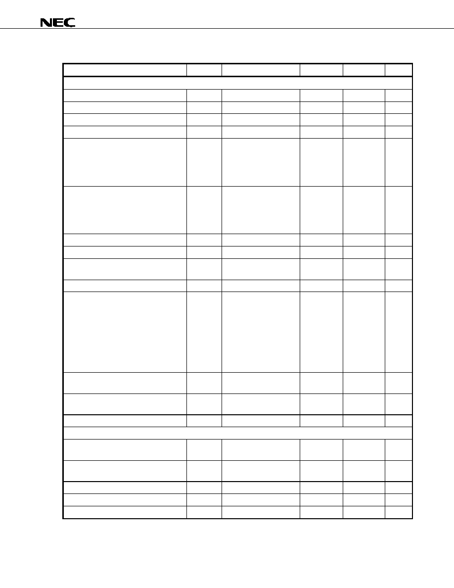
(3/4)
Parameter Symbol
Conditions
MIN.
MAX.
Unit
Hub Event Timings
Time to detect a downstream facing port
connect event (Figure 2-19):
Awake
hub
Suspended
hub
t
DCNN
2.5
2.5
2000
12000
µ
s
µ
s
Time to detect a disconnect event at a
hub's downstream facing port (Figure 2-18)
t
DDIS
2.0
2.5
µ
s
Duration of driving resume to a
downstream port (only from a controlling
hub)
t
DRSMDN
20
ms
Time from detecting downstream resume
to rebroadcast
t
URSM
1.0 ms
Duration of driving reset to a downstream
facing port (Figure 2-20)
t
DRST
Only for a SetPortFeature
(PORT_RESET) request
10 20
ms
Time to detect a long K from upstream
t
URLK
2.5
100
µ
s
Time to detect a long SE0 from upstream
t
URLSE0
2.5
10000
µ
s
Duration of repeating SE0 upstream (for
low-/full-speed repeater)
t
URPSE0
23 FS
Bit
times
Inter-packet delay (for high-speed) of
packets traveling in same direction
t
HSIPDSD
88
Bit
times
Inter-packet delay (for high-speed) of
packets traveling in opposite direction
t
HSIPDOD
8
Bit
times
Inter-packet delay for device/root hub
response with detachable cable for high-
speed
t
HSRSPIPD1
192
Bit
times
Time of which a Chirp J or Chirp K must be
continuously detected (filtered) by hub or
device during Reset handshake
t
FILT
2.5
µ
s
Time after end of device Chirp K by which
hub must start driving first Chirp K in the
hub's chirp sequence
t
WTDCH
100
µ
s
Time for which each individual Chirp J or
Chirp K in the chirp sequence is driven
downstream by hub during reset
t
DCHBIT
40
60
µ
s
Time before end of reset by which a hub
must end its downstream chirp sequence
t
DCHSE0
100
500
µ
s
Time from internal power good to device
pulling D
+ beyond V
IHZ
(Figure 2-20)
t
SIGATT
100 ms
Debounce interval provided by USB
system software after attach (Figure 2-20)
t
ATTDB
100 ms
Maximum duration of suspend averaging
interval
t
SUSAVGI
1
s
Period of idle bus before device can initiate
resume
t
WTRSM
5
ms
Duration of driving resume upstream
t
DRSMUP
1
15
ms

Data Sheet S16618EJ3V0DS
22
µ
PD720113
(4/4)
Parameter Symbol
Conditions
MIN.
MAX.
Unit
Hub Event Timings (Continued)
Resume recovery time
t
RSMRCY
Remote-wakeup
is
enabled
10
ms
Time to detect a reset from upstream for
non high-speed capable devices
t
DETRST
2.5
10000
µ
s
Reset recovery time (Figure 2-20)
t
RSTRCY
10
ms
Inter-packet delay for full-speed
t
IPD
2
Bit
times
Inter-packet delay for device response with
detachable cable for full-speed
t
RSPIPD1
6.5
Bit
times
SetAddress() completion time
t
DSETADDR
50
ms
Time to complete standard request with no
data
t
DRQCMPLTND
50
ms
Time to deliver first and subsequent
(except last) data for standard request
t
DRETDATA1
500
ms
Time to deliver last data for standard
request
t
DRETDATAN
50
ms
Time for which a suspended hub will see a
continuous SE0 on upstream before
beginning the high-speed detection
handshake
t
FILTSE0
2.5
µ
s
Time a hub operating in non-suspended
full-speed will wait after start of SE0 on
upstream before beginning the high-speed
detection handshake
t
WTRSTFS
2.5
3000
ms
Time a hub operating in high-speed will
wait after start of SE0 on upstream before
reverting to full-speed
t
WTREV
3.0
3.125 ms
Time a hub will wait after reverting to full-
speed before sampling the bus state on
upstream and beginning the high-speed
will wait after start of SE0 on upstream
before reverting to full-speed
t
WTRSTHS
100
875
ms
Minimum duration of a Chirp K on
upstream from a hub within the reset
protocol
t
UCH
1.0
ms
Time after start of SE0 on upstream by
which a hub will complete its Chirp K within
the reset protocol
t
UCHEND
7.0
ms
Time between detection of downstream
chip and entering high-speed state
t
WTHS
500
µ
s
Time after end of upstream Chirp at which
hub reverts to full-speed default state if no
downstream Chirp is detected
t
WTFS
1.0
2.5 ms
Data Sheet S16618EJ3V0DS
23
µ
PD720113
Figure 2-11. Transmit Waveform for Transceiver at DP/DM
0 V
Differential
+
400 mV
Differential
-
400 mV
Differential
Unit Interval
Level 1
Level 2
0%
100%
Point 4
Point 3
Point 1
Point 2
Point 5
Point 6
Figure 2-12. Transmitter Measurement Fixtures
V
BUS
D+
D-
GND
15.8
+
To 50
Inputs of a
High Speed Differential
Oscilloscope, or 50
Outputs of a High Speed
Differential Data Generator
-
50
Coax
50
Coax
USB
Connector
Nearest
Device
Test Supply Voltage
15.8
143
143

Data Sheet S16618EJ3V0DS
24
µ
PD720113
Timing Diagram
Figure 2-13. Hub Differential Delay, Differential Jitter, and SOP Distortion
C. Upstream Hub Delay with or without Cable
D. Measurement Points
50% Point of
Initial Swing
50% Point of
Initial Swing
Upstream
End of
Cable
Upstream
Port of Hub
Downstream
Port of Hub
Downstream
Port of Hub
Downstream
Port of Hub
Upstream Port
or
End of Cable
A. Downstream Hub Delay with Cable
B. Downstream Hub Delay without Cable
Hub Delay
Downstream
t
HDD1
Hub Delay
Upstream
t
HDD1
t
HDD2
Crossover
Point
Crossover
Point
Crossover
Point
V
SS
Hub Differential Jitter:
t
HDJ1
= t
HDDx
(J)
-
t
HDDx
(K) or t
HDDx
(K)
-
t
HDDx
(J) Consecutive Transitions
t
HDJ2
= t
HDDx
(J)
-
t
HDDx
(J) or t
HDDx
(K)
-
t
HDDx
(K) Paired Transitions
Bit after SOP Width Distortion (same as data jitter for SOP and next J transition):
t
FSOP
= t
HDDx
(next J)
-
t
HDDx
(SOP)
Low-speed timings are determined in the same way for:
t
LHDD
, t
LDHJ1
, t
LDJH2
, t
LUHJ1
, t
LUJH2
, and t
LSOP
Host or
Hub
Hub
Function
Upstream end of cable
Upstream port
Downstream port
Downstream signaling
Upstream signaling
Plug
Receptacle
Hub Delay
Downstream
t
HDD2
V
SS
V
SS
V
SS
V
SS
V
SS

Data Sheet S16618EJ3V0DS
25
µ
PD720113
Figure 2-14. Hub EOP Delay and EOP Skew
t
EOP-
t
EOP+
t
EOP-
t
EOP+
t
EOP-
t
EOP+
C. Upstream EOP Delay with or without Cable
Upstream
End of
Cable
Upstream
Port of Hub
Downstream
Port of Hub
Downstream
Port of Hub
Downstream
Port of Hub
Upstream Port
or
End of Cable
A. Downstream EOP Delay with Cable
B. Downstream EOP Delay without Cable
V
SS
V
SS
V
SS
V
SS
V
SS
V
SS
50% Point of
Initial Swing
Crossover
Point
Extended
Crossover
Point
Extended
Crossover
Point
Extended
EOP Delay:
t
FEOPD
= t
EOPy
-
t
HDDx
(t
EOPy
means that this equation applies to t
EOP-
and t
EOP+
)
EOP Skew:
t
FHESK
= t
EOP+
-
t
EOP-
Low-speed timings are determined in the same way for:
t
LEOPD
and t
LHESK

Data Sheet S16618EJ3V0DS
26
µ
PD720113
Figure 2-15. USB Differential Data Jitter for Low-/full-speed
t
PERIOD
Differential
Data Lines
Crossover
Points
Consecutive
Transitions
N
◊
t
PERIOD
+
t
xDJ1
Paired
Transitions
N
◊
t
PERIOD
+
t
xDJ2
Figure 2-16. USB Differential-to-EOP Transition Skew and EOP Width for Low-/full-speed
t
PERIOD
Differential
Data Lines
Crossover
Point
Crossover
Point Extended
Source EOP Width: t
FEOPT
Receiver EOP Width: t
FEOPR
t
LEOPT
t
LEOPR
Diff. Data-to-
SE0 Skew
N
◊
t
PERIOD
+
t
xDEOP
Figure 2-17. USB Receiver Jitter Tolerance for Low-/full-speed
Differential
Data Lines
t
PERIOD
t
xJR
t
xJR1
t
xJR2
Consecutive
Transitions
N
◊
t
PERIOD
+
t
xJR1
Paired
Transitions
N
◊
t
PERIOD
+
t
xJR2
Data Sheet S16618EJ3V0DS
27
µ
PD720113
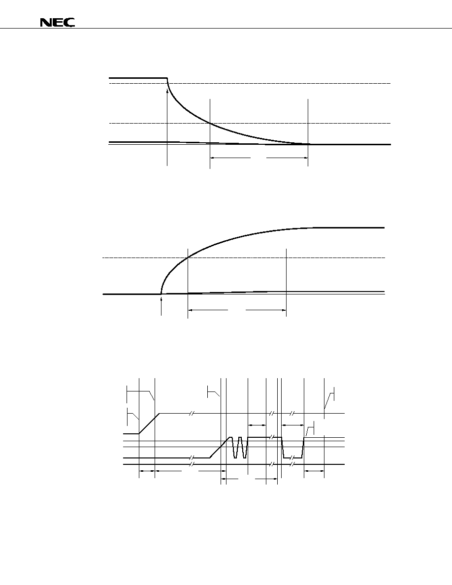
Figure 2-18. Low-/full-speed Disconnect Detection
D
-
/D
+
D
+
/D
-
V
IHZ
(min)
V
IL
V
SS
Device
Disconnected
Disconnect
Detected
t
DDIS
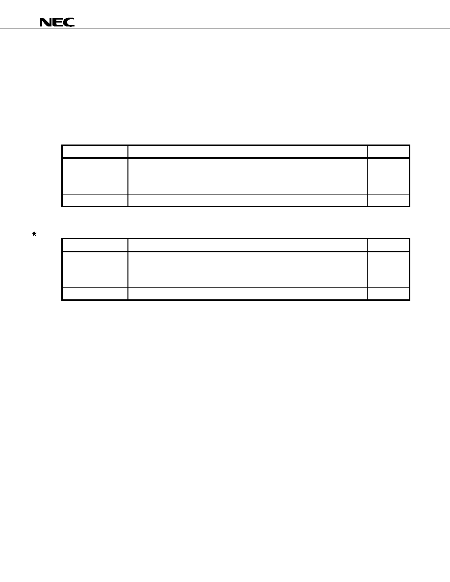
Figure 2-19. Full-/high-speed Device Connect Detection
V
IH
V
SS
Device
Connected
Connect
Detected
D
-
D
+
t
DCNN
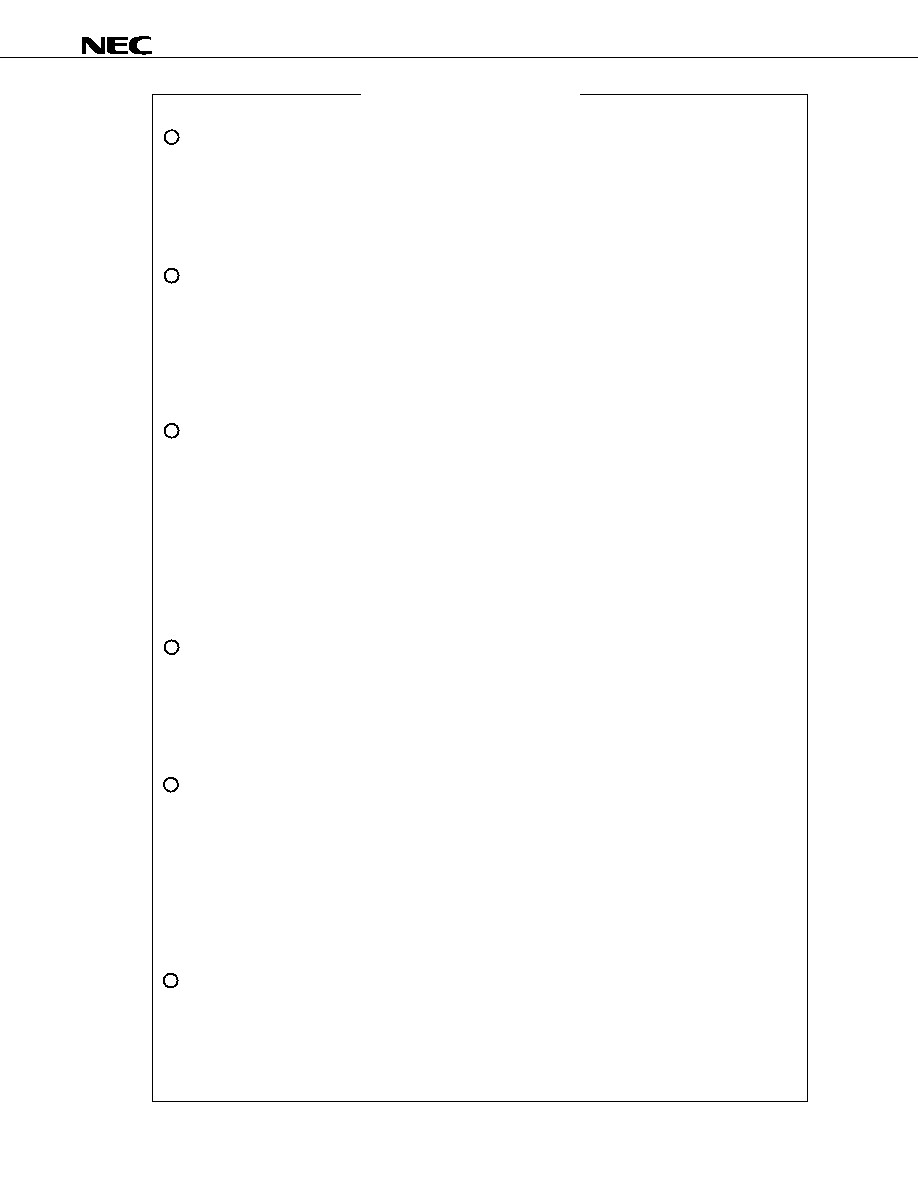
Figure 2-20. Power-on and Connection Events Timing
t
SIGATT
t1
t
RSTRCY
D
+
or
D
-
Hub port
power OK
Attatch detected
Reset recovery
time
USB system software
reads device speed
4.01 V
V
BUS
V
IH
(min)
V
IH
Hub port
power-on
t
ATTDB
t
2SUSP
t
DRST

Data Sheet S16618EJ3V0DS
28
µ
PD720113
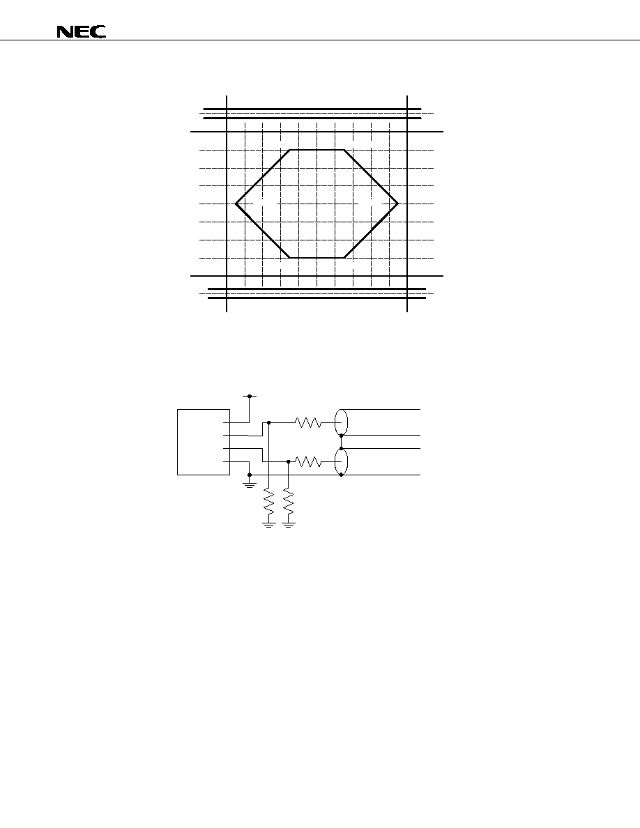
3. PACKAGE DRAWING
80-PIN PLASTIC TQFP (FINE PITCH) (12x12)
L1
L
ZE
A1
ZD
A3
Lp
A
A2
detail of lead end
60
41
40
21
61
80
1
20
E
HE
HD
D
c
S
y
e
S
x
b
M
0.17
+
0.03
-
0.07
(UNIT:mm)
ITEM
DIMENSIONS
D
E
A2
HD
HE
A
A1
A3
Lp
b
e
x
y
ZD
ZE
L
L1
12.00
±
0.20
12.00
±
0.20
1.00
14.00
±
0.20
14.00
±
0.20
1.10
±
0.10
0.10
±
0.05
0.25
0.60
±
0.15
0.22
±
0.05
0.50
0.08
0.08
1.25
1.25
0.50
1.00
±
0.20
K80GK-50-9EU
c
3
∞+
4
∞
-
3
∞
NOTE
Each lead centerline is located within 0.08 mm of
its true position at maximum material condition.
Data Sheet S16618EJ3V0DS
29
µ
PD720113
4. RECOMMENDED SOLDERING CONDITIONS
The
µ
PD720113 should be soldered and mounted under the following recommended conditions.
For soldering methods and conditions other than those recommended below, contact an NEC Electronics sales
representative.
For technical information, see the following website.
Semiconductor Device Mount Manual (http://www.necel.com/pkg/en/mount/index.html)
µ
PD720113GK-9EU:
80-pin plastic TQFP (Fine pitch) (12
◊ 12)
Soldering Method
Soldering Conditions
Symbol
Infrared reflow
Package peak temperature: 235∞C, Time: 30 seconds max. (at 210∞C or higher),
Count: Three times or less
Exposure limit: 3 days
Note
(after that, prebake at 125∞C for 10 hours)
IR35-103-3
Partial heating
Pin temperature: 300∞C max., Time: 3 seconds max. (per pin row)
≠
Note After opening the dry pack, store it at 25∞C or less and 65% RH or less for the allowable storage period.
µ
PD720113GK-9EU-A:
80-pin plastic TQFP (Fine pitch) (12
◊ 12) Lead-free product
Soldering Method
Soldering Conditions
Symbol
Infrared reflow
Package peak temperature: 245∞C, Time: 60 seconds max. (at 220∞C or higher),
Count: Three times or less
Exposure limit: 7 days
Note
(after that, prebake at 125∞C for 10 hours)
IR45-107-3
Partial heating
Pin temperature: 300∞C max., Time: 3 seconds max. (per pin row)
≠
Note After opening the dry pack, store it at 25∞C or less and 65% RH or less for the allowable storage period.

Data Sheet S16618EJ3V0DS
30
µ
PD720113
[MEMO]
Data Sheet S16618EJ3V0DS
31
µ
PD720113
1
2
3
4
VOLTAGE APPLICATION WAVEFORM AT INPUT PIN
Waveform distortion due to input noise or a reflected wave may cause malfunction. If the input of the
CMOS device stays in the area between V
IL
(MAX) and V
IH
(MIN) due to noise, etc., the device may
malfunction. Take care to prevent chattering noise from entering the device when the input level is fixed,
and also in the transition period when the input level passes through the area between V
IL
(MAX) and
V
IH
(MIN).
HANDLING OF UNUSED INPUT PINS
Unconnected CMOS device inputs can be cause of malfunction. If an input pin is unconnected, it is
possible that an internal input level may be generated due to noise, etc., causing malfunction. CMOS
devices behave differently than Bipolar or NMOS devices. Input levels of CMOS devices must be fixed
high or low by using pull-up or pull-down circuitry. Each unused pin should be connected to V
DD
or GND
via a resistor if there is a possibility that it will be an output pin. All handling related to unused pins must
be judged separately for each device and according to related specifications governing the device.
PRECAUTION AGAINST ESD
A strong electric field, when exposed to a MOS device, can cause destruction of the gate oxide and
ultimately degrade the device operation. Steps must be taken to stop generation of static electricity as
much as possible, and quickly dissipate it when it has occurred. Environmental control must be
adequate. When it is dry, a humidifier should be used. It is recommended to avoid using insulators that
easily build up static electricity. Semiconductor devices must be stored and transported in an anti-static
container, static shielding bag or conductive material. All test and measurement tools including work
benches and floors should be grounded. The operator should be grounded using a wrist strap.
Semiconductor devices must not be touched with bare hands. Similar precautions need to be taken for
PW boards with mounted semiconductor devices.
STATUS BEFORE INITIALIZATION
Power-on does not necessarily define the initial status of a MOS device. Immediately after the power
source is turned ON, devices with reset functions have not yet been initialized. Hence, power-on does
not guarantee output pin levels, I/O settings or contents of registers. A device is not initialized until the
reset signal is received. A reset operation must be executed immediately after power-on for devices
with reset functions.
POWER ON/OFF SEQUENCE
In the case of a device that uses different power supplies for the internal operation and external
interface, as a rule, switch on the external power supply after switching on the internal power supply.
When switching the power supply off, as a rule, switch off the external power supply and then the
internal power supply. Use of the reverse power on/off sequences may result in the application of an
overvoltage to the internal elements of the device, causing malfunction and degradation of internal
elements due to the passage of an abnormal current.
The correct power on/off sequence must be judged separately for each device and according to related
specifications governing the device.
INPUT OF SIGNAL DURING POWER OFF STATE
Do not input signals or an I/O pull-up power supply while the device is not powered. The current
injection that results from input of such a signal or I/O pull-up power supply may cause malfunction and
the abnormal current that passes in the device at this time may cause degradation of internal elements.
Input of signals during the power off state must be judged separately for each device and according to
related specifications governing the device.
NOTES FOR CMOS DEVICES
5
6

µ
PD720113
USB logo is a trademark of USB Implementers Forum, Inc.
The information in this document is current as of March, 2005. The information is subject to change
without notice. For actual design-in, refer to the latest publications of NEC Electronics data sheets or
data books, etc., for the most up-to-date specifications of NEC Electronics products. Not all
products and/or types are available in every country. Please check with an NEC Electronics sales
representative for availability and additional information.
No part of this document may be copied or reproduced in any form or by any means without the prior
written consent of NEC Electronics. NEC Electronics assumes no responsibility for any errors that may
appear in this document.
NEC Electronics does not assume any liability for infringement of patents, copyrights or other intellectual
property rights of third parties by or arising from the use of NEC Electronics products listed in this document
or any other liability arising from the use of such products. No license, express, implied or otherwise, is
granted under any patents, copyrights or other intellectual property rights of NEC Electronics or others.
Descriptions of circuits, software and other related information in this document are provided for illustrative
purposes in semiconductor product operation and application examples. The incorporation of these
circuits, software and information in the design of a customer's equipment shall be done under the full
responsibility of the customer. NEC Electronics assumes no responsibility for any losses incurred by
customers or third parties arising from the use of these circuits, software and information.
While NEC Electronics endeavors to enhance the quality, reliability and safety of NEC Electronics products,
customers agree and acknowledge that the possibility of defects thereof cannot be eliminated entirely. To
minimize risks of damage to property or injury (including death) to persons arising from defects in NEC
Electronics products, customers must incorporate sufficient safety measures in their design, such as
redundancy, fire-containment and anti-failure features.
NEC Electronics products are classified into the following three quality grades: "Standard", "Special" and
"Specific".
The "Specific" quality grade applies only to NEC Electronics products developed based on a customer-
designated "quality assurance program" for a specific application. The recommended applications of an NEC
Electronics product depend on its quality grade, as indicated below. Customers must check the quality grade of
each NEC Electronics product before using it in a particular application.
The quality grade of NEC Electronics products is "Standard" unless otherwise expressly specified in NEC
Electronics data sheets or data books, etc. If customers wish to use NEC Electronics products in applications
not intended by NEC Electronics, they must contact an NEC Electronics sales representative in advance to
determine NEC Electronics' willingness to support a given application.
(Note)
∑
∑
∑
∑
∑
∑
M8E 02. 11-1
(1)
(2)
"NEC Electronics" as used in this statement means NEC Electronics Corporation and also includes its
majority-owned subsidiaries.
"NEC Electronics products" means any product developed or manufactured by or for NEC Electronics (as
defined above).
Computers, office equipment, communications equipment, test and measurement equipment, audio
and visual equipment, home electronic appliances, machine tools, personal electronic equipment
and industrial robots.
Transportation equipment (automobiles, trains, ships, etc.), traffic control systems, anti-disaster
systems, anti-crime systems, safety equipment and medical equipment (not specifically designed
for life support).
Aircraft, aerospace equipment, submersible repeaters, nuclear reactor control systems, life
support systems and medical equipment for life support, etc.
"Standard":
"Special":
"Specific":