Document Outline
- COVER
- FEATURES
- ORDERING INFORMATION
- BLOCK DIAGRAM
- PIN CONFIGURATION
- 1. PIN INFORMATION
- 2. ELECTRICAL SPECIFICATIONS
- 2.1 Buffer List
- 2.2 Terminology
- 2.3 Absolute Maximum Ratings
- 2.4 Recommended Operating Range
- 2.5 DC Characteristics
- 2.5.1 DC characteristics of USB interface
- 2.5.2 DC characteristics of BIU
- 2.5.3 Pin capacitance
- 2.5.4 Power consumption
- 2.6 AC Characteristics (TA = 0 to +70 degrees, VDD = 3.3 V +/-10%)
- 2.6.1 Overall AC characteristics and those of BIU
- 2.6.2 AC characteristics of BIU block with Function 1 selected
- 2.6.3 AC characteristics of BIU block with function 2 or 3 selected
- 2.6.4 External local bus
- 2.6.5 USB interface timing
- 3. PACKAGE DRAWING
- 4. RECOMMENDED SOLDERING CONDITIONS
µ
PD720122
MOS Integrated Circuit
DATA SHEET
USB2.0 Generic Device Controller
Document No.
S16685EJ2V0DS00 (2nd edition)
Date Published June 2003 NS CP (K)
Printed in Japan
The information in this document is subject to change without notice. Before using this document, please
confirm that this is the latest version.
Not all products and/or types are available in every country. Please check with an NEC Electronics
sales representative for availability and additional information.
2003
The mark shows major revised points.
The µPD720122 is USB2.0 Generic Device Controller, which combines the NEC Electronics USB2.0 PHY and End-
point Controller. The Controller has certified by USB Implementers Forum. End-point Controller has banked two Bulk End-
point and one Interrupt End-point, and selectable three general CPU bus-types, suitable for designing various USB
device. The controller has the external local bus, that enables to perform high speed data transferring when CPU is
accessing to the controller. These IP Blocks in the controller are based completely on an NEC Electronics ASIC core, so
µPD720122 is suitable to design for the prototype system that are intended to design ASIC in the future.
Detailed function descriptions are provided in the following user's manual. Be sure to read the manual before designing.
µ
µ
µ
µPD720122 User's Manual: S15829E
FEATURES
∑ Complaint with USB2.0 specification (Maximum data transferring rate: 480 Mbps)
∑ USB2.0 certified (TestID=40000822)
∑ High(480Mbps) / Full(12Mbps)- Speed support and switch automatically
∑ Easy to design NEC Electronics ASIC
∑ Generic USB2.0 Device Controller
∑ Two Bulk End-points and One Interrupt End-point
∑ Performed Data Local Bus independent from CPU bus.
(Maximum Data Transferring rate: 21 MBps with DMA mode )
∑ Selectable three CPU Bus Interface
ORDERING INFORMATION
Part Number
Package
µPD720122GC-9EU
100-pin plastic TQFP (Fine pitch) (14
◊ 14)
µPD720122F1-DN2
109-pin plastic FBGA (11
◊ 11)

Data Sheet S16685EJ2V0DS
2
µPD720122
BLOCK DIAGRAM
PHY Core
: USB2.0 transceiver with serial interface engine
EPC2 Core
: Endpoint controller
BIU Core
: Bus Interface Unit
BIU Core
EPC2 Core
PHY Core
EP1 BulkOUT
512 Byte x2
EP3 Interrupt IN
8 Byte
EP2 BulkIN
512 Byte x2
EP0 Control IN
64 Byte
Protocol
Controller
CPU BUS
Local BUS
USB BUS
EP0 Control OUT
64 Byte

Data Sheet S16685EJ2V0DS
3
µPD720122
PIN CONFIGURATION
∑ 100-pin plastic TQFP (Fine pitch) (14
◊
◊
◊
◊ 14)
µ PD720122GC-9EU
Top View
Remark The function of the pin is shown with Function 1/Function 2/Function 3 from the left.

Data Sheet S16685EJ2V0DS
4
µPD720122
µ
µ
µ
µ PD720122GC-9EU (1/2)
Pin
No.
Pin Name
Function1
Pin Name
Function2
Pin Name
Function3
Pin
No.
Pin Name
Function1
Pin Name
Function2
Pin Name
Function3
1
V
DD
V
DD
V
DD
26
GND
GND
GND
2
RESETB
RESETB
RESETB
27
D8
Reserved
D8
3
GND
GND
GND
28
D9
Reserved
D9
4
XIN_CLK
XIN_CLK
XIN_CLK
29
D10
Reserved
D10
5
XOUT
XOUT
XOUT
30
D11
Reserved
D11
6
GND
GND
GND
31
D12
Reserved
D12
7
CSB
CSB
CSB
32
D13
Reserved
D13
8
INTB_ALL
ALE
ALE
33
D14
Reserved
D14
9
A1
INTB_ALL
INTB_ALL
34
D15
Reserved
D15
10
A2
Reserved
Reserved
35
V
DD
V
DD
V
DD
11
A3
Reserved
Reserved
36
GND
GND
GND
12
A4
Reserved
Reserved
37
WRB
WRB
WRB
13
A5
Reserved
Reserved
38
RDB
RDB
RDB
14
A6
Reserved
Reserved
39
INT0B
INT0B
INT0B
15
A7
Reserved
Reserved
40
INT1B
INT1B
INT1B
16
GND
GND
GND
41
INT2B
INT2B
INT2B
17
D0
AD0
D0
42
ACTIVE
ACTIVE
ACTIVE
18
D1
AD1
AD1
43
SCAN1
SCAN1
SCAN1
19
D2
AD2
AD2
44
SCAN0
SCAN0
SCAN0
20
D3
AD3
AD3
45
M2
M2
M2
21
D4
AD4
AD4
46
EP1_DRQB
EP1_DRQB
EP1_DRQB
22
D5
AD5
AD5
47
EP1_DACKB
EP1_DACKB
EP1_DACKB
23
D6
AD6
AD6
48
EP1_RDB
EP1_RDB
Reserved
24
D7
AD7
AD7
49
EP1_TCB
EP1_TCB
EP1_TCB
25
V
DD
V
DD
V
DD
50
GND
GND
GND
Data Sheet S16685EJ2V0DS
5
µPD720122
µ
µ
µ
µ PD720122GC-9EU (2/2)
Pin
No.
Pin Name
Fucntion1
Pin Name
Function2
Pin Name
Function3
Pin
No.
Pin Name
Fucntion1
Pin Name
Function2
Pin Name
Function3
51
V
DD
V
DD
V
DD
76
GND
GND
GND
52
FM21
FM21
FM21
77
BUNRI
BUNRI
BUNRI
53
EP2_DRQB
EP2_DRQB
EP2_DRQB
78
RREF
RREF
RREF
54
EP2_DACKB
EP2_DACKB
EP2_DACKB
79
AV
SS
(R)
AV
SS
(R)
AV
SS
(R)
55
EP2_WRB
EP2_WRB
Reserved
80
AV
DD
AV
DD
AV
DD
56
EP2_TCB
EP2_TCB
EP2_TCB
81
AV
SS
AV
SS
AV
SS
57
LD0
LD0
Reserved
82
RPU
RPU
RPU
58
LD1
LD1
Reserved
83
V
SS
V
SS
V
SS
59
LD2
LD2
Reserved
84
RSDP
RSDP
RSDP
60
LD3
LD3
Reserved
85
DP
DP
DP
61
GND
GND
GND
86
V
DD
V
DD
V
DD
62
LD4
LD4
Reserved
87
DM
DM
DM
63
LD5
LD5
Reserved
88
RSDM
RSDM
RSDM
64
LD6
LD6
Reserved
89
V
SS
V
SS
V
SS
65
LD7
LD7
Reserved
90
NC
NC
NC
66
LD8
LD8
Reserved
91
PV
SS
PV
SS
PV
SS
67
LD9
LD9
Reserved
92
NC
NC
NC
68
GND
GND
GND
93
PV
DD
PV
DD
PV
DD
69
LD10
LD10
Reserved
94
V
SS
V
SS
V
SS
70
LD11
LD11
Reserved
95
V
DD
V
DD
V
DD
71
LD12
LD12
Reserved
96
V
SS
V
SS
V
SS
72
LD13
LD13
Reserved
97
M1
M1
M1
73
LD14
LD14
Reserved
98
M0
M0
M0
74
LD15
LD15
Reserved
99
VBUS
VBUS
VBUS
75
V
DD
V
DD
V
DD
100
GND
GND
GND
Remark AV
SS
(R) should be used to connect RREF through 1 % precision reference resistor of 9.1 k
.

Data Sheet S16685EJ2V0DS
6
µPD720122
∑ 109-pin plastic FBGA (11
◊
◊
◊
◊ 11)
µ PD720122F1-DN2
Bottom View
Remarks The pin name is showing it with Function1.
As for the pin name of Function2 and Function3, please refer to the table of the next page.

Data Sheet S16685EJ2V0DS
7
µPD720122
µ
µ
µ
µ PD720122F1-DN2 (1/2)
Pin
No.
Pin Name
Function1
Pin Name
Function2
Pin Name
Function3
Pin
No.
Pin Name
Function1
Pin Name
Function2
Pin Name
Function3
1
NC
NC
NC
26
AV
SS
AV
SS
AV
SS
2
D8
Reserved
D8
27
RSDP
RSDP
RSDP
3
D10
Reserved
D10
28
V
DD
V
DD
V
DD
4
D12
Reserved
D12
29
NC
NC
NC
5
D15
Reserved
D15
30
NC
NC
NC
6
GND
GND
GND
31
V
DD
V
DD
V
DD
7
INT1B
INT1B
INT1B
32
M1
M1
M1
8
ACTIVE
ACTIVE
ACTIVE
33
VBUS
VBUS
VBUS
9
M2
M2
M2
34
NC
NC
NC
10
EP1_DACKB
EP1_DACKB
EP1_DACKB
35
RESETB
RESETB
RESETB
11
EP1_TCB
EP1_TCB
EP1_TCB
36
XIN_CLK
XIN_CLK
XIN_CLK
12
NC
NC
NC
37
GND
GND
GND
13
FM21
FM21
FM21
38
A1
INTB_ALL
INTB_ALL
14
EP2_DACKB
EP2_DACKB
EP2_DACKB
39
A3
Reserved
Reserved
15
EP2_TCB
EP2_TCB
EP2_TCB
40
A7
Reserved
Reserved
16
LD2
LD2
Reserved
41
D0
AD0
D0
17
GND
GND
GND
42
D3
AD3
AD3
18
LD7
LD7
Reserved
43
D5
AD5
AD5
19
LD9
LD9
Reserved
44
D7
AD7
AD7
20
LD11
LD11
Reserved
45
NC
NC
NC
21
LD13
LD13
Reserved
46
D9
Reserved
D9
22
LD15
LD15
Reserved
47
D11
Reserved
D11
23
NC
NC
NC
48
D14
Reserved
D14
24
BUNRI
BUNRI
BUNRI
49
RDB
RDB
RDB
25
AV
SS
(R)
AV
SS
(R)
AV
SS
(R)
50
INT2B
INT2B
INT2B
Remark AV
SS
(R) should be used to connect RREF through 1 % precision reference resistor of 9.1 k
.

Data Sheet S16685EJ2V0DS
8
µPD720122
µ
µ
µ
µ PD720122F1-DN2 (2/2)
Pin
No.
Pin Name
Function1
Pin Name
Function2
Pin Name
Function3
Pin
No.
Pin Name
Function1
Pin Name
Function2
Pin Name
Function3
51
SCAN0
SCAN0
SCAN0
81
GND
GND
GND
52
EP1_DRQB
EP1_DRQB
EP1_DRQB
82
D13
Reserved
D13
53
EP1_RDB
EP1_RDB
Reserved
83
V
DD
V
DD
V
DD
54
NC
NC
NC
84
INT0B
INT0B
INT0B
55
EP2_DRQB
EP2_DRQB
EP2_DRQB
85
WRB
WRB
WRB
56
EP2_WRB
EP2_WRB
Reserved
86
SCAN1
SCAN1
SCAN1
57
LD1
LD1
Reserved
87
V
DD
V
DD
V
DD
58
LD5
LD5
Reserved
88
GND
GND
GND
59
LD8
LD8
Reserved
89
LD0
LD0
Reserved
60
LD10
LD10
Reserved
90
LD3
LD3
Reserved
61
LD12
LD12
Reserved
91
LD6
LD6
Reserved
62
LD14
LD14
Reserved
92
LD4
LD4
Reserved
63
NC
NC
NC
93
GND
GND
GND
64
RREF
RREF
RREF
94
V
DD
V
DD
V
DD
65
AV
DD
AV
DD
AV
DD
95
GND
GND
GND
66
GND
GND
GND
96
RPU
RPU
RPU
67
RSDM
RSDM
RSDM
97
DP
DP
DP
68
PV
SS
PV
SS
PV
SS
98
GND
GND
GND
69
GND
GND
GND
99
DM
DM
DM
70
GND
GND
GND
100
PV
DD
PV
DD
PV
DD
71
M0
M0
M0
101
V
DD
V
DD
V
DD
72
NC
NC
NC
102
GND
GND
GND
73
GND
GND
GND
103
CSB
CSB
CSB
74
XOUT
XOUT
XOUT
104
A2
Reserved
Reserved
75
INTB_ALL
ALE
ALE
105
A6
Reserved
Reserved
76
A5
Reserved
Reserved
106
A4
Reserved
Reserved
77
GND
GND
GND
107
D1
AD1
AD1
78
D2
AD2
AD2
108
V
DD
V
DD
V
DD
79
D4
AD4
AD4
109
GND
GND
GND
80
D6
AD6
AD6
-
-
-
-

Data Sheet S16685EJ2V0DS
9
µPD720122
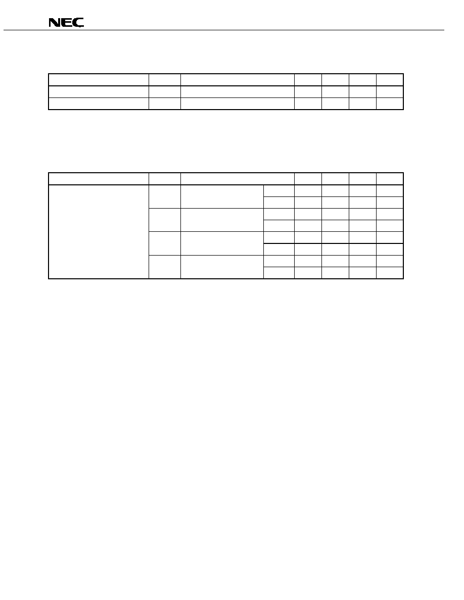
1.
PIN INFORMATION
(1/2)
Pin Name
I/O
Buffer Type
Active
Level
Function
RESETB
I
5 V tolerant Input Schmitt
Low
Asynchronous reset signaling
XIN_CLK
I
3.3 V Input
System clock input or oscillator In
XOUT
O
3.3 V Output
Oscillator out
CSB
I
5 V tolerant Input
Low
Chip select signal
INTB_ALL
O
5 V tolerant Output
Low
Interrupt request signal
ALE
I
5 V tolerant Input
High
Address strobe signal (Function2/3)
A(7:1)
I
5 V tolerant Input
Address input (Function1)
D(15:0)
I/O
5 V tolerant I/O
Data bus (I/O) (Function1)
AD(7:0)
I/O
5 V tolerant I/O
Address/data multiplexed bus (I/O) (Function2)
D0
I/O
5 V tolerant I/O
Data bus (I/O) (Function3)
AD(7:1)
I/O
5 V tolerant I/O
Address/data multiplexed bus (I/O) (Function3)
D(15:8)
I/O
5 V tolerant I/O
Data bus (I/O) (Function3)
WRB
I
5 V tolerant Input
Low
Write command input
RDB
I
5 V tolerant Input
Low
Read command input
INT0B
O
5 V tolerant Output
Low
Interrupt request (INT Status 0)
INT1B
O
5 V tolerant Output
Low
Interrupt request (INT Status 1)
INT2B
O
5 V tolerant Output
Low
Interrupt request (INT Status 2)
ACTIVE
I
5 V tolerant Input
DMA-related pins active level select(Function2/3)
SCAN(1:0)
I
3.3 V Input 50 k
Pull Down
Chip test pin.
M2
O
5 V tolerant Output
Status output pin
EP1_DRQB
O
5 V tolerant Output
Low
DMA transfer request output pin of EP1
EP1_DACKB
I
5 V tolerant Input
Low
DMA transfer enable input pin of EP1
EP1_RDB
I
5 V tolerant Input
Low
DMA Read command input pin of EP1
EP1_TCB
I
5 V tolerant Input
Low
DMA terminal count input pin of EP1
FM21
I
3.3 V Input
NEC Electronics test pin
EP2_DRQB
O
5 V tolerant Output
Low
DMA transfer request output pin of EP2
EP2_DACKB
I
5 V tolerant Input
Low
DMA transfer enable input pin of EP2
EP2_WRB
I
5 V tolerant Input
Low
DMA Write command input pin of EP2
EP2_TCB
I
5 V tolerant Input
Low
DMA terminal count input pin of EP2
LD(15:0)
I/O
5 V tolerant I/O
Data bus (I/O) pin for external local bus
BUNRI
I
5V torelant Input
NEC Electronics test pin
RREF
A
Analog
Reference resistor
RPU
A
USB pull-up control
USB's 1.5 k
pull-up resistor control
RSDP
O
USB full speed D+ O
USB's full speed D+ signal
DP
I/O
USB high speed D+ I/O
USB's high speed D+ signal
DM
I/O
USB high speed D- I/O
USB's high speed D
- signal

Data Sheet S16685EJ2V0DS
10
µPD720122
(2/2)
Pin Name
I/O
Buffer Type
Active Level
Function
RSDM
O
USB full speed D- O
USB's full speed D
- signal
M(1:0)
I
5 V tolerant Input
Function mode setting
VBUS
I
5 V tolerant Input
Note
VBUS monitoring
AV
DD
, PV
DD
3.3 V
DD
for Analog circuit
V
DD
3.3 V
DD
AV
SS
, PV
SS
V
SS
for Analog circuit
V
SS
, GND
V
SS
NC
Not connect
Reserved
Not used
Note
VBUS pin may be used to monitor for VBUS line even if V
DD
, AV
DD
, and PV
DD
are shut off. System must
ensure that the input voltage level for VBUS pin is less than 3.0 V due to the absolute maximum rating is not
exceeded.
Remark
"5 V tolerant" means that the buffer is 3.3 V buffer with 5 V tolerant circuit.
The operation mode of the BIU can be set by external pins, as shown below. Fix external pins (M1 and M0) when
using them.
Pin
M1
M0
BIU Operation Mode
Outline
0
0
16-bit mode
(Function 1)
A 16-bit CPU bus and an external local bus dedicated to data transfer for bulk IN/OUT can
be used in this mode. The internal register length is 16 bits.
0
1
8-bit mode
(Function 2)
Multiplexed bus mode of 8-bit address bus and 8-bit data bus.
The register length is 8 bits only in this mode (registers can only be accessed in byte units).
Therefore, the address space in this mode differs from that in the other modes.
The active levels of some external local bus control pins can be changed by the Active pin.
1
0
16-bit mix mode
(Function 3)
Multiplexed bus mode of 8-bit address bus and 16-bit data bus.
The internal register length is 16 bits.
The active levels of some external local bus control pins can be changed by the Active pin.
1
1
Setting prohibited
(Function 4)
Setting prohibited
Data Sheet S16685EJ2V0DS
11
µPD720122
2.
ELECTRICAL SPECIFICATIONS
2.1
Buffer List
∑ 3.3 V oscillator interface
XIN,XOUT
∑ 3.3 V input buffer
FM21,SCAN(1:0)
∑ 5V torelant input buffer
RESETB,CSB,A(7:0),WRB,RDB,ACTIVE,EP1_DACKB,EP1_RDB,EP1_TCB,EP2_DACKB,EP2_WRB,
EP2_TCB,BUNRI,M0,M1,VBUS,ALE
∑ 5V torelant output buffer
INTB_ALL,INT0B,INT1B,INT2B,M2,EP1_DRQB,EP2_DRQB
∑ 5V torelant I/O buffer
D(15:0),LD(15:0),AD(7:0),D0,AD(7:1),D(15:8)
∑ USB interface
DP,DM,RSDP,RSDM,RREF,RPU
2.2
Terminology
Terms Used in Absolute Maximum Ratings
Parameter
Symbol
Meaning
Power supply voltage
V
DD
Indicates voltage range within which damage or reduced reliability will not result
when power is applied to a V
DD
pin.
Input voltage
V
I
Indicates voltage range within which damage or reduced reliability will not result
when power is applied to an input pin.
Output voltage
V
O
Indicates voltage range within which damage or reduced reliability will not result
when power is applied to an output pin.
Output current
I
O
Indicates absolute tolerance value for DC current to prevent damage or reduced
reliability when a current flows out of or into an output pin.
Operating temperature
T
A
Indicates the ambient temperature range for normal logic operations.
Storage temperature
T
stg
Indicates the element temperature range within which damage or reduced reliability
will not result while no voltage or current are applied to the device.

Data Sheet S16685EJ2V0DS
12
µPD720122
Terms Used in Recommended Operating Range
Parameter
Symbol
Meaning
Power supply voltage
V
DD
Indicates the voltage range for normal logic operations occur when V
SS
= 0 V.
High-level input voltage
V
IH
Indicates the voltage, which is applied to the input pins of the device, is the voltage
indicates that the high level states for normal operation of the input buffer.
* If a voltage that is equal to or greater than the "Min." value is applied, the input
voltage is guaranteed as high level voltage.
Low-level input voltage
V
IL
Indicates the voltage, which is applied to the input pins of the device, is the voltage
indicates that the low level states for normal operation of the input buffer.
* If a voltage that is equal to or lesser than the "Max." value is applied, the input
voltage is guaranteed as low level voltage.
Hysteresys voltage
V
H
Indicates the differential between the positive trigger voltage and the negative trigger
voltage.
Input rise time
t
ri
Indicates allowable input rise time to input pins. Input rise time is transition time from
0.1
◊ V
DD
to 0.9
◊ V
DD
.
Input fall time
t
fi
Indicates allowable input fall time to input pins. Input fall time is transition time from
0.9
◊ V
DD
to 0.1
◊ V
DD
.
Terms Used in DC Characteristics
Parameter
Symbol
Meaning
Off-state output leakage
current
I
OZ
Indicates the current that flows from the power supply pins when the rated power
supply voltage is applied when a 3-state output has high impedance.
Output short circuit current
I
OS
Indicates the current that flows when the output pin is shorted (to GND pins) when
output is at high-level.
Input leakage current
I
I
Indicates the current that flows when the input voltage is supplied to the input pin.
Low-level output current
I
OL
Indicates the current that flows to the output pins when the rated low-level output
voltage is being applied.
High-level output current
I
OH
Indicates the current that flows from the output pins when the rated high-level output
voltage is being applied.

Data Sheet S16685EJ2V0DS
13
µPD720122
2.3
Absolute Maximum Ratings
Parameter
Symbol
Conditions
Ratings
Unit
Voltage
V
DD
-0.5 to +4.6
V
I/O voltage
V
I
/V
O
Note 1
V
I
/V
O
< V
DD
+3.0 V
-0.5 to +6.6
V
Note 2
V
I
/V
O
< V
DD
+0.3 V
-0.5 to +4.6
V
Output current
I
O
Note 3
I
OL
= 6 mA
6
mA
Operating ambient temperature
T
A
0 to +70
∞C
Storage temperature
T
stg
-65 to +150
∞C
Notes 1.
5 V torelant input buffer, output buffer, I/O buffer
2.
3.3 V input buffer,3.3 V oscillator interface
3.
5 V torelant output buffer, I/O buffer(OUT)
Caution
Product quality may suffer if the absolute maximum rating is exceeded even momentarily for any
parameter. That is, the absolute maximum ratings are rated values at which the product is on the
verge of suffering physical damage, and therefore the product must be used under conditions that
ensure that the absolute maximum ratings are not exceeded.
2.4
Recommended Operating Range
Parameter
Symbol
Conditions
Min.
Typ.
Max.
Unit
Power supply voltage
V
DD
3.3 V Power
3.0
3.3
3.6
V
Negative trigger voltage
V
N
0.6
1.8
V
Positive trigger voltage
V
P
1.2
2.4
V
Hysteresis voltage
V
H
0.3
1.5
V
Input voltage, low
V
IL
0
0.8
V
3.3 V input buffer
2.0
V
DD
V
Input voltage, high
V
IH
5V torelant input buffer, I/O buffer
2.0
5.5
V
Rise/fall time
t
r
/t
f
0
200
ns

Data Sheet S16685EJ2V0DS
14
µPD720122
2.5
DC Characteristics
The DC characteristics are classified into those of the USB interface and those of the BIU block.
2.5.1
DC characteristics of USB interface
Parameter
Symbol
Conditions
Min.
Max.
Unit
Serial resistor between DP (DM) and RSDP (RSDM)
R
S
35.64
36.36
Driver output resistance
(also serves as high-speed termination)
Z
HSDRV
Includes R
S
resistor
40.5
49.5
Bus pull-up resistor on upstream facing port
R
PU
1.425
1.575
Termination voltage for upstream facing port pull-up
(full-speed)
V
TERM
3.0
3.6
V
Input levels for full-speed:
High-level input voltage (driven)
V
IH
2.0
V
High-level input voltage (floating)
V
IHZ
2.7
3.6
Low-level input voltage
V
IL
0.8
V
Differential input sensitivity
V
DI
(D+) - (D-)
0.2
V
Differential common mode range
V
CM
Includes V
DI
range
0.8
2.5
V
Output levels for full-speed:
High-level output voltage
V
OH
R
L
of 14.25 k
to V
SS
2.8
3.6
V
Low-level output voltage
V
OL
R
L
of 1.425 k
to 3.6 V
0.0
0.3
V
SE1
V
OSE1
0.8
V
Output signal crossover voltage
V
CRS
1.3
2.0
V
Input levels for high-speed:
High-speed squelch detection threshold (differential
signal amplitude)
V
HSSQ
100
150
mV
High-speed disconnect detection threshold
(differential signal amplitude)
V
HSDSC
525
625
mV
High-speed data signaling common mode voltage
range (guideline for receiver)
V
HSCM
-50
500
mV
High-speed differential input signaling level
See Figure 2-4
Output levels for high-speed:
High-speed idle level
V
HSOI
-10.0
10
mV
High-speed data signaling high
V
HSOH
360
440
mV
High-speed data signaling low
V
HSOL
-10.0
10
mV
Chirp J level (different voltage)
V
CHIRPJ
700
1100
mV
Chirp K level (different voltage)
V
CHIRPK
-900
-500
mV
Data Sheet S16685EJ2V0DS
15
µPD720122
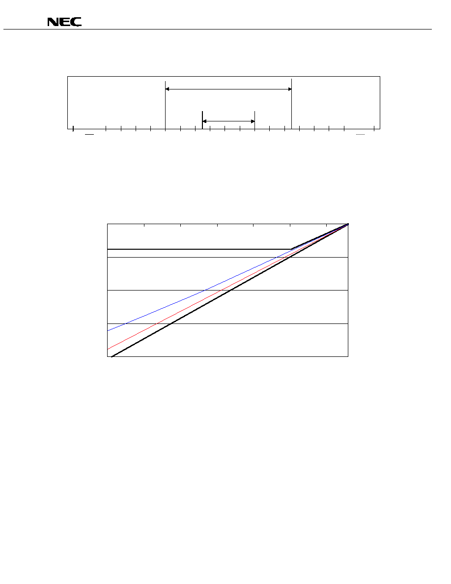
Figure 2-1. Differential Input Sensitivity Range for Low-/Full-Speed
4.6
-
1.0
Input voltage range (volts)
0.0
0.2
0.4
0.6
0.8
1.0
1.2
1.4
1.6
1.8
2.0
2.2
2.4
2.6
2.8
3.0
3.2
Differential output
crossover
voltage range
Differential input voltage range
Figure 2-2. Full-Speed Buffer Voh/Ioh Characteristics for High-Speed Capable Transceiver
Max
Min
≠80
≠60
≠40
≠20
0
V
DD
≠0.3
Vout (V)
Iout (mA)
V
DD
≠2.3
V
DD
≠3.3
V
DD
≠0.8
V
DD
V
DD
≠1.3
V
DD
≠1.8
V
DD
≠2.8

Data Sheet S16685EJ2V0DS
16
µPD720122
Figure 2-3. Full-Speed Buffer Vol/Iol Characteristics for High-Speed Capable Transceiver
Max
Min
80
60
40
20
0
0
0.5
1
1.5
2
2.5
3
Vout (V)
Iout (mA)
Figure 2-4. Receiver Sensitivity for Transceiver at D+/D
-
-
-
-
0 V
differential
+400 mV
differential
≠400 mV
differential
Unit interval
Level 1
Level 2
Point 1
Point 2
Point 3
Point 4
Point 5
Point 6
0%
100%

Data Sheet S16685EJ2V0DS
17
µPD720122
Figure 2-5. Receiver Measurement Fixtures
Vbus
D+
D-
Gnd
15.8
+
To 50-
input of a
high-speed differential
oscilloscope, or 50-
outputs of a high-speed
differential data generator
≠
50-
Coax
50-
Coax
USB
connector
nearest
device
Test supply voltage
15.8
143
143

Data Sheet S16685EJ2V0DS
18
µPD720122
2.5.2
DC characteristics of BIU
Parameter
Symbol
Conditions
Min.
Typ.
Max.
Unit
Off-state output current
I
OZ
V
O
= V
DD
or GND
±10
µA
Output short current
I
OS
-250
mA
Input leakage current
I
I
V
I
= V
DD
or GND
±10
-5
µA
Output current, low
I
OL
V
OL
= 0.4 V
Note
6
mA
Output current, high
I
OH
V
OH
= 2.4 V
-2
mA
Output voltage, low
V
OL
I
OL
= 0 mA
0.1
V
Output voltage, high
V
OH
I
OH
= 0 mA
V
DD
-0.2
V
Note
5V-Tolerant Output
Data Sheet S16685EJ2V0DS
19
µPD720122
2.5.3
Pin capacitance
Parameter
Symbol
Conditions
Min.
Typ.
Max.
Unit
Input capacitance
C
IN
4.5
6.5
pF
Output/bidirectional capacitance
C
OUT
8.5
11
pF
Remark
These are just estimated values.
2.5.4
Power consumption
Parameter
Symbol
Conditions
Min.
Typ.
Max.
Unit
V
DD
195
273
mA
P
H
HS mode
AV
DD
12
17
mA
V
DD
120
168
mA
P
F
FS mode
AV
DD
12
17
mA
V
DD
1.5
2.2
mA
P
S1
Suspend mode 1
Note 1
AV
DD
0.1
0.2
µA
V
DD
370
520
µA
Power consumption
P
S2
Suspend mode 2
Note 2
AV
DD
0.1
0.2
µA
Notes 1.
SND PHY Reg. SPND bit = 1
2.
SND PHY Reg. SPND bit = 1
GPR Reg. CONNECTB bit = 0
GPR Reg. PUE bit = 0
BIU Control 0 Reg. OSC_DISCONB bit = 1

Data Sheet S16685EJ2V0DS
20
µPD720122
2.6
AC Characteristics (T
A
= 0 to +70
∞
∞
∞
∞C, V
DD
= 3.3 V
±
±
±
±10%)
The AC characteristics are classified into those of the USB interface block and those of the BIU.
2.6.1
Overall AC characteristics and those of BIU
(1) Clock
Parameter
Symbol
Condition
Min.
Typ.
Max.
Unit
Clock frequency
f
CLK
X'tal
-500ppm
30
+500ppm
MHz
Oscillator block
-500ppm
30
+500ppm
MHz
Clock Duty cycle
T
DUTY
40
50
60
%
Remarks 1.
Reccomended accurarcy of clock frequency is ±100ppm.
2.
Required accurarcy of X'tal or Oscillator block is includeing initial frequency accuracy, the spread of
X'tal capacityor loading, supply voltage, temperature, and aging etc.
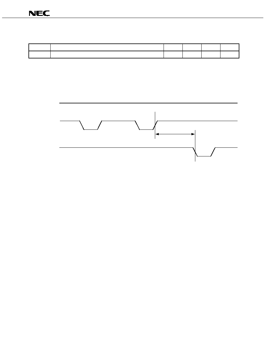
(2) Reset
Symbol
Specification
Min.
Typ.
Max.
Unit
TR
Reset width
2
µs
HW reset timing
RESETB
TR

Data Sheet S16685EJ2V0DS
21
µPD720122
2.6.2
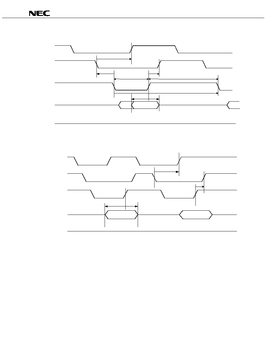
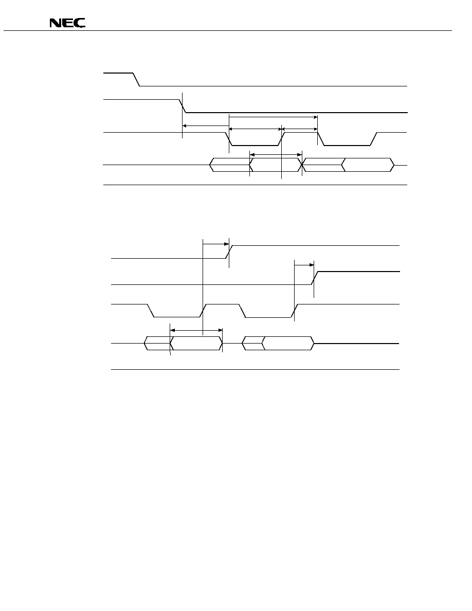
AC characteristics of BIU block with Function 1 selected
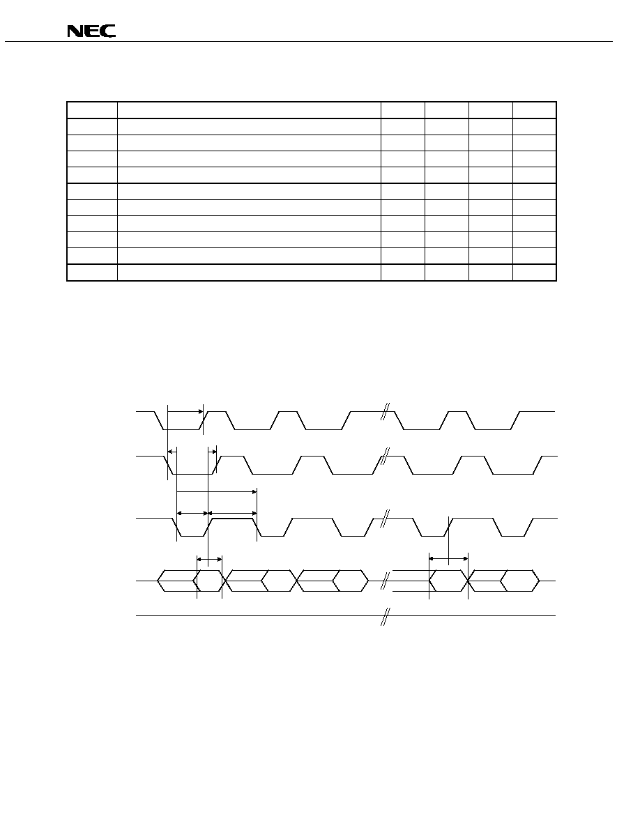
(1) CPU BUS read operation
Symbol
Parameter
Min.
Typ.
Max.
Unit
T1
Read cycle time
91
ns
T2
Address setup time (RDB
)
5
ns
T3
Chip select setup time (RDB
)
5
ns
T4
Buffer direction change time (RDB
)
-
14
ns
T5
Output data delay time (RDB
)
-
57
ns
T6
Read command width
57
ns
T7
Chip select hold time (RDB
)
5
ns
T8
Address hold time (RDB
)
5
ns
T9
RDB inactive time
34
ns
T10
Output data hold time (RDB
)
4
-
ns
Remark
It is assumed that the external pin capacitance is 15 pF (data bus = 50 pF).
CPU bus read timing
RDB
WRB
A7 to A1
D15 to D0
CSB
VALID
VALID
t
3
t
5
t
6
t
10
t
8
t
7
High level
INVALID
t
4
High level
t
1
t
9
t
2
Data Sheet S16685EJ2V0DS
22
µPD720122
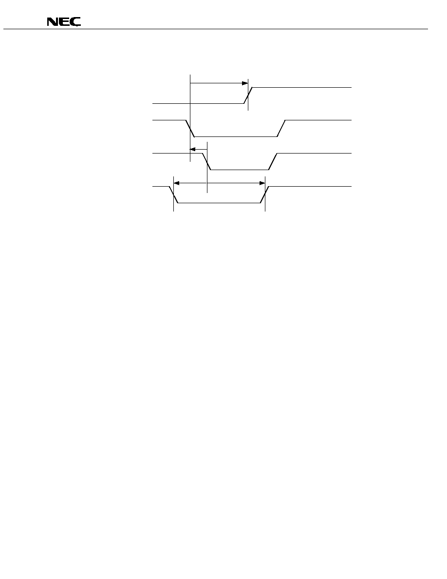
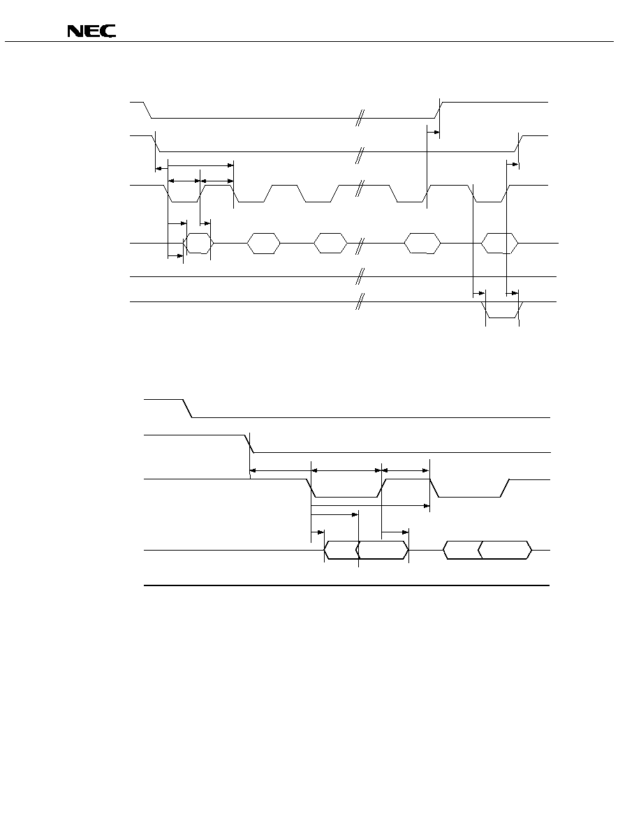
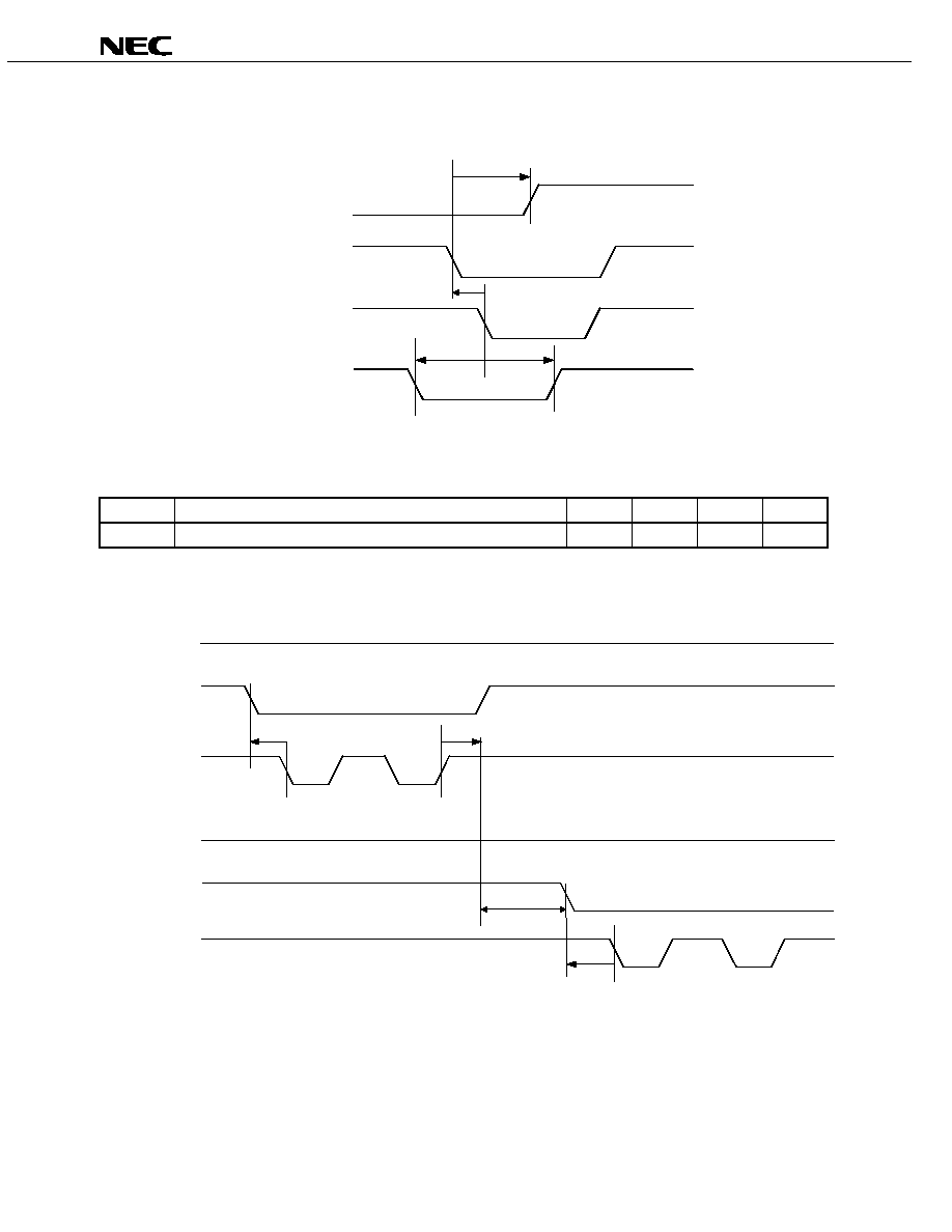
(2) CPU bus write operation
Symbol
Parameter
Min.
Typ.
Max.
Unit
T11
Write cycle time
68
ns
T12
Address setup time (WRB
)
5
ns
T13
Chip select setup time (WRB
)
5
ns
T14
Write command width
34
ns
T15
Address hold time (WRB
)
5
ns
T16
Chip select hold time (WRB
)
5
ns
T17
WRB inactive time
34
ns
T18
Input data setup time
10
ns
T19
Input data hold time
0
ns
Remark
It is assumed that the external pin capacitance is 15 pF (data bus = 50 pF).
CPU bus write timing
WRB
RDB
A7 to A1
D15 to D0
CSB
VALID
t
12
t
13
t
14
t
19
t
15
t
16
t
18
High level
t
11
t
17
VALID
Data Sheet S16685EJ2V0DS
23
µPD720122
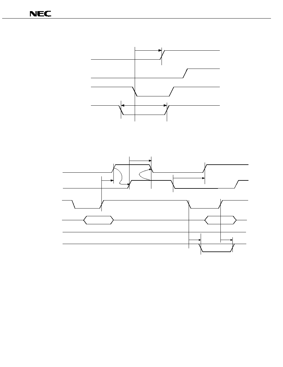
(3) CPU BUS RDB vs. WRB timing
Symbol
Parameter
Min.
Typ.
Max.
Unit
T20
WRB vs. RDB inactive time
34
ns
Remark
It is assumed that the external pin capacitance is 15 pF (data bus = 50 pF).
CPU bus read vs. write change timing
WRB
RDB
CSB
Low level
t
20
Data Sheet S16685EJ2V0DS
24
µPD720122
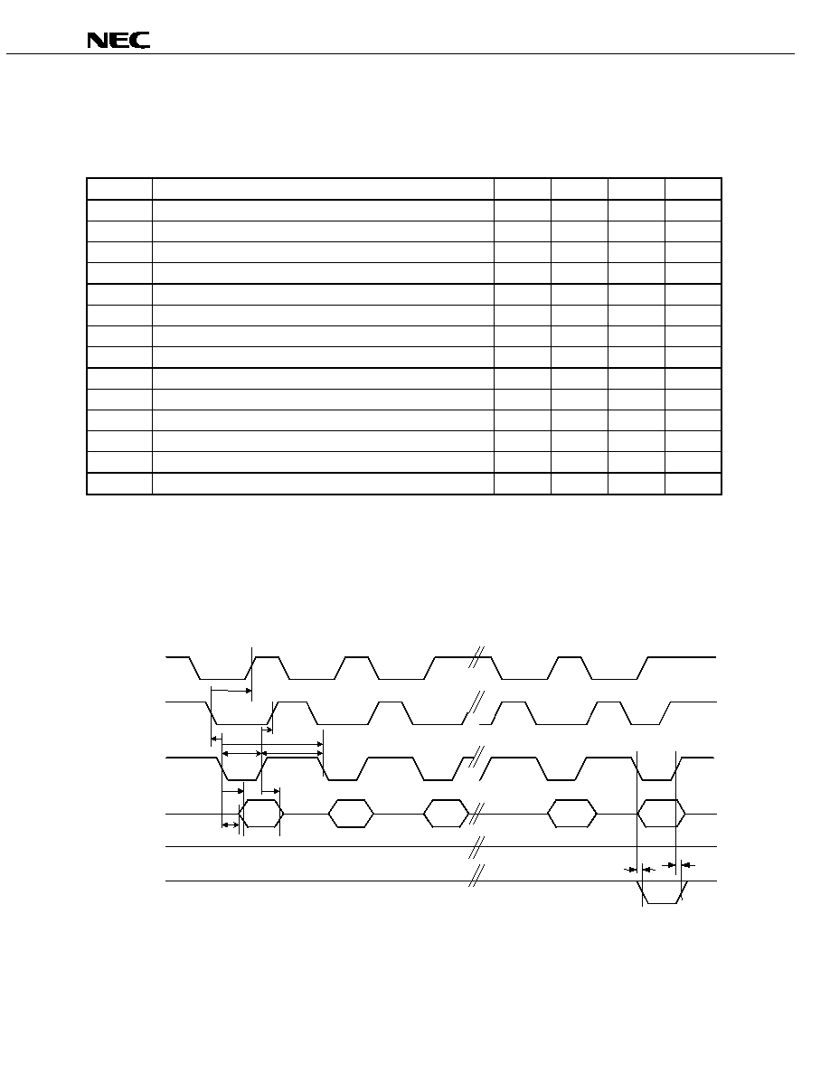
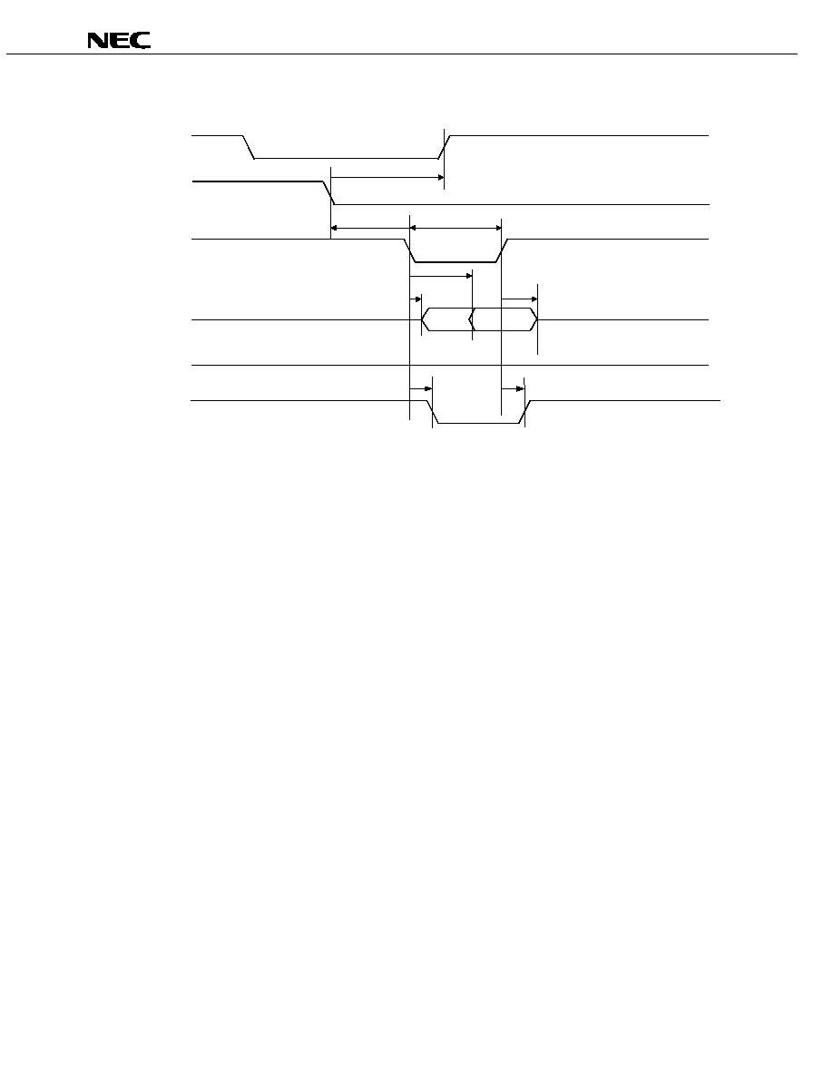
(4) CPU bus DMA transfer
(a) CPU bus DMA single mode read transfer timing
Symbol
Parameter
Min.
Typ.
Max.
Unit
T21
DMA request acknowledge setup time (RDB
)
0
ns
T22
DMA request off time (EP1_DACKB
)
-
54
ns
T23
DMA single mode read transfer cycle time
91
ns
T24
Read command width
57
ns
T25
Read command inactive time
34
ns
T26
Read data delay time (RDB
)
-
57
ns
T27
Buffer direction change time (RDB
)
-
14
ns
T28
Read data hold time (RDB
)
4
-
ns
T29
EP1_TCB setup time (RDB
)
0
Note
ns
T30
EP1_TCB hold time (RDB
)
17
ns
T31
EP1_STOPB delay time (RDB
)
-
15
ns
T32
EP1_STOPB OFF delay time (RDB
)
3
-
ns
T33
DMA request acknowledge hold time (RDB
)
0
ns
T34
Undefined
-
-
ns
Note
Can be input after previous RDB
.
Remark
It is assumed that the external pin capacitance is 15 pF (data bus = 50 pF).
(Overall)
EP1_DRQB
EP1_TCB
D15 to D0
RDB
EP1_DACKB
t
22
t
33
t
24
t
25
t
26
t
28
High level
EP1_STOPB
High level
EP1_STOPB is not asserted in the
case of a full packet.
N cycle
N
-
-
-
-
1 cycle
1 cycle
t
21
t
23
t
27
t
31
t
32

Data Sheet S16685EJ2V0DS
25
µPD720122
(Start timing)
EP1_DACKB
RDB
EP1_DRQB
EP1_TCB
D15 to D0
High level
t
21
t
24
t
25
t
26
t
28
t
27
t
33
t
22
t
23
VALID
VALID
EP1_STOPB
High level
(End timing)
EP1_DACKB
RDB
EP1_DRQB
t
22
EP1_TCB
High level
EP1_STOPB
t
33
High level
D15 to D0
t
31
t
32
EP1_STOPB is not asserted in
the case of a full packet.
Last
- 1
Last
VALID
VALID

Data Sheet S16685EJ2V0DS
26
µPD720122
(TCB timing)
EP1_DACKB
EP1_DRQB
EP1_TCB
t
22
t
29
t
21
t
30
RDB

Data Sheet S16685EJ2V0DS
27
µPD720122
(b) CPU bus DMA single mode write transfer
Symbol
Parameter
Min.
Typ.
Max.
Unit
T35
DMA request acknowledge setup time (WRB
)
0
ns
T36
DMA request off time (EP2_DACKB
)
-
54
ns
T37
DMA single mode write transfer cycle time
88
ns
T38
Write command width
54
ns
T39
Write command inactive time
34
ns
T40
Write data setup time (WRB
)
10
ns
T41
Write data hold time (WRB
)
0
ns
T42
EP2_TCB setup time (WRB
)
0
Note
ns
T43
EP2_TCB hold time (WRB
)
17
ns
T44
DMA request acknowledge hold time (WRB
)
0
ns
Note
Can be input after immediately previous WRB
.
Remark
It is assumed that the external pin capacitance is 15 pF (data bus = 50 pF).
(Overall)
EP2_DRQB
EP2_TCB
D15 to D0
WRB
EP2_DACKB
t
36
t
38
t
37
t
39
t
40
t
41
High level
N cycle
N
-
-
-
- 1 cycle
1 cycle
t
35
t
44
t
40
t
41
t
44
Data Sheet S16685EJ2V0DS
28
µPD720122
(Start timing)
EP2_DACKB
WRB
EP2_DRQB
High level
t
35
t
38
EP2_TCB
t
39
D15 to D0
t
40
t
41
t
44
t
36
t
37
VALID
VALID
(End timing)
EP2_DACKB
WRB
EP2_DRQB
t
36
EP2_TCB
High level
t
44
D15 to D0
VALID
VALID
Last
- 1
Last
t
40
t
41
Data Sheet S16685EJ2V0DS
29
µPD720122
(TCB timing)
EP2_DACKB
EP2_DRQB
EP2_TCB
t
36
t
42
WRB
t
35
t
43

Data Sheet S16685EJ2V0DS
30
µPD720122
(c) CPU bus DMA demand read transfer timing
Symbol
Parameter
Min.
Typ.
Max.
Unit
T45
DMA request acknowledge setup time (RDB
)
0
ns
T46
DMA demand mode read transfer cycle time
91
ns
T47
Read command width
57
ns
T48
Read command inactive time
34
ns
T49
Read data delay time (RDB
)
-
57
ns
T50
Buffer direction change time (RDB
)
-
14
ns
T51
Read data hold time (RDB
)
4
-
ns
T52
EP1_TCB setup time (RDB
)
0
Note
ns
T53
EP1_TCB hold time (RDB
)
17
ns
T54
EP1_STOPB delay time (RDB
)
-
15
ns
T55
EP1_STOPB delay time (RDB
)
3
-
ns
T56
DMA request off time (RDB
)
-
59
ns
T57
DMA request acknowledge hold time (RDB
)
0
ns
T69
DMA request off time (EP1_DACKB
)
-
38
ns
T71
DMA request off time (EP1_DACKB
) 1 cycle transfer
-
38
ns
T72
DMA request on time (EP1_DACKB
)
-
88
ns
T74
DMA request off time (RDB
)
-
60
ns
Note
Can be input after immediately previous RDB
.
Remark
It is assumed that the external pin capacitance is 15 pF (data bus = 50 pF).
(Overall)
EP1_DRQB
EP1_TCB
D15 to D0
RDB
EP1_DACKB
N cycle
N
-
-
-
- 1 cycle
1 cycle
t
46
t
47
t
48
t
49
t
51
t
56
High level
t
45
t
50
t
57
EP1_STOPB
High level
t
54
t
55
EP1_STOPB is not asserted in the
case of a full packet.

Data Sheet S16685EJ2V0DS
31
µPD720122
(Start timing)
EP1_DACKB
RDB
EP1_DRQB
High level
t
45
t
47
EP1_TCB
t
48
D15 to D0
VALID
VALID
t
50
t
51
t
49
(End timing)
EP1_DACKB
RDB
EP1_DRQB
t
56
EP1_TCB
High level
EP1_STOPB
t
57
High level
D15 to D0
VALID
VALID
Last
- 1
Last
t
54
t
55
EP1_STOPB is not asserted in the
case of a full packet.
Data Sheet S16685EJ2V0DS
32
µPD720122
(TCB timing)
RDB
EP1_TCB
t
74
t
53
EP1_DRQB
EP1_DACKB
t
52
(Retransmission timing)
EP1_DACKB
RDB
EP1_DRQB
t
56
EP1_TCB
High level
EP1_STOPB
t
69
High level
D15 to D0
VALID
VALID
Last
- 1
Last
t
54
t
55
EP1_STOPB is not asserted in the
case of a full packet.
DMA transfer retry timing
If EP1_DACKB is deasserted without
RDB access after EP1_DRQB has
been deasserted, EP1_DRQB is
asserted again.
t
72

Data Sheet S16685EJ2V0DS
33
µPD720122
(If EP1_TCB is input when retransmission is executed)
RDB
EP1_TCB
t
52
t
53
EP1_DRQB
EP1_DACKB
t
69
t
45
(One-cycle transfer)
EP1_DACKB
RDB
EP1_DRQB
High level
t
45
t
47
EP1_TCB
D15 to D0
VALID
t
50
t
51
t
49
t
71
EP1_STOPB
t
54
t
55

Data Sheet S16685EJ2V0DS
34
µPD720122
(d) CPU bus DMA demand write transfer timing
Symbol
Parameter
Min.
Typ.
Max.
Unit
T58
DMA request acknowledge setup time (WRB
)
0
ns
T59
DMA demand mode write transfer cycle time
72
ns
T60
Write command width
38
ns
T61
Write command inactive time
34
ns
T62
Write data setup time (WRB
)
10
ns
T63
Write data hold time (WRB
)
0
ns
T64
EP2_TCB setup time (WRB
)
0
Note
ns
T65
EP2_TCB hold time (WRB
)
17
ns
T66
DMA request off time (WRB
)
-
60
ns
T67
DMA request acknowledge hold time (WRB
)
0
ns
T70
DMA request off time (EP2_DACKB
)
-
38
ns
T73
DMA request on time (EP2_DACKB
)
-
88
ns
T75
DMA request off time (WRB
)
-
60
ns
Note
Can be input after immediately previous WRB
.
Remark
It is assumed that the external pin capacitance is 15 pF (data bus = 50 pF).
(Overall)
EP2_DRQB
EP2_TCB
D15 to D0
WRB
EP2_DACKB
N cycle
N
-
-
-
- 1 cycle
1 cycle
t
59
t
60
t
61
t
62
t
63
t
66
High level
t
58
t
67

Data Sheet S16685EJ2V0DS
35
µPD720122
(Start timing)
EP2_DACKB
WRB
EP2_DRQB
EP2_TCB
D15 to D0
High level
t
58
t
60
t
61
VALID
VALID
t
62
t
63
(End timing)
EP2_DACKB
WRB
EP2_DRQB
EP2_TCB
Last
- 1
Last
D15 to D0
VALID
VALID
t
62
t
63
t
66
t
67

Data Sheet S16685EJ2V0DS
36
µPD720122
(TCB timing)
WRB
EP2_TCB
t
75
t
65
EP2_DRQB
EP2_DACKB
t
64
(Retransmission timing)
EP2_DACKB
WRB
EP2_DRQB
t
66
EP2_TCB
High level
t
70
D15 to D0
VALID
VALID
Last
- 1
Last
DMA transfer retry timing
If EP2_DACKB is deasserted without
WRB access after EP2_DRQB has
been deasserted, EP2_DRQB is
asserted again.
t
73
t
62
t
63

Data Sheet S16685EJ2V0DS
37
µPD720122
(If EP1_TCB is input when retransmission is executed)
WRB
EP2_TCB
t
64
t
65
EP2_DRQB
EP2_DACKB
t
70
t
58

Data Sheet S16685EJ2V0DS
38
µPD720122
(a) CPU bus DMA read transfer vs. write transfer timing
Symbol
Parameter
Min.
Typ.
Max.
Unit
T68
RDB vs. WRB command inactive time
34
ns
Remark
It is assumed that the external pin capacitance is 15 pF (data bus = 50 pF).
EP1_DACKB
RDB
EP1_DRQB
EP2_DACKB
WRB
EP2_DRQB
t
45
t
57
t
58
t
68
Low level
Low level

Data Sheet S16685EJ2V0DS
39
µPD720122
2.6.3
AC characteristics of BIU block with function 2 or 3 selected
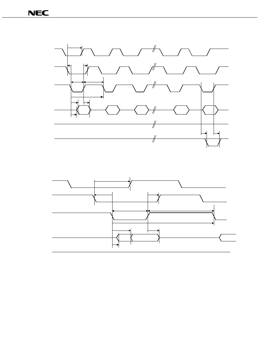
(1) CPU bus read operation
Symbol
Parameter
Min.
Typ.
Max.
Unit
TB1
Read cycle time
86
ns
TB2
Address setup time (ALE
)
10
ns
TB3
Chip select setup time (ALE
)
17
ns
TB4
Read command delay time (ALE
)
7
ns
TB5
Output data delay time (RDB
)
-
57
ns
TB6
Read command width
57
ns
TB7
Output data hold time (RDB
)
4
-
ns
TB8
Chip select hold time (RDB
)
5
ns
TB9
ALE width
10
ns
TB10
Address hold time (ALE
)
0
ns
TB11
Chip select setup time (RDB
)
5
ns
TB12
Buffer direction change time (RDB
)
-
14
ns
Remark
It is assumed that the external pin capacitance is 15 pF (data bus = 50 pF).
CPU bus read timing
RDB
AD7 to AD0
Note
D15 to D8
CSB
ADDRES
VALID
tb
7
tb
6
tb
5
ALE
DATA
VALID
tb
2
tb
4
tb
8
ADDRES
VALID
tb
1
tb
9
tb
11
tb
12
tb
10
DATA
invalid
tb
3
Note
D7 to D0 for Function 2

Data Sheet S16685EJ2V0DS
40
µPD720122
(2) CPU bus write operation
Symbol
Parameter
Min.
Typ.
Max.
Unit
TB13
Write cycle time
58
ns
TB14
Address setup time (ALE
)
17
ns
TB15
Chip select setup time (ALE
)
17
ns
TB16
Write command delay time (ALE
)
7
ns
TB17
Input data setup time (WRB
)
10
ns
TB18
Input data hold time (WRB
)
0
ns
TB19
Write command width
34
ns
TB20
Chip select hold time (WRB
)
0
ns
TB21
Chip select setup time (WRB
)
5
ns
Remark
It is assumed that the external pin capacitance is 15 pF (data bus = 50 pF).
CPU bus write timing
WRB
AD7 to AD0
Note
D15 to D8
CSB
ADDRESS
VALID
tb
18
tb
19
ALE
DATA
VALID
tb
2
tb
16
tb
20
ADDRESS
VALID
tb
13
tb
17
tb
10
tb
21
tb
15
tb
9
Note
D7 to D0 for Function 2

Data Sheet S16685EJ2V0DS
41
µPD720122
2.6.4
External local bus
(1) External local bus 16-bit mode
(a) External local bus 16-bit mode DMA single mode read transfer timing
Symbol
Parameter
Min.
Typ.
Max.
Unit
L16T21
DMA request acknowledge setup time (EP1_RDB
)
0
ns
L16T22
DMA request off time 1 (EP1_DACKB
)
-
54
ns
L16T23
DMA single mode read transfer cycle time
91
ns
L16T24
Read command width
57
ns
L16T25
Read command inactive time
34
ns
L16T26
Read data delay time (EP1_RDB
)
-
57
ns
L16T27
Buffer direction change time (EP1_RDB
)
-
14
ns
L16T28
Read data hold time (EP1_RDB
)
4
-
ns
L16T29
EP1_TCB setup time (EP1_RDB
)
0
Note
ns
L16T30
EP1_TCB hold time (EP1_RDB
)
17
ns
L16T31
EP1_STOPB delay time (EP1_RDB
)
-
15
ns
L16T32
EP1_STOPB delay time (EP1_RDB
)
3
-
ns
L16T33
DMA request acknowledge hold time (EP1_RDB
)
0
ns
L16T34
Undefined
-
-
ns
Note
Can be input after previous EP1_RDB
.
Remark
It is assumed that the external pin capacitance is 15 pF (data bus = 50 pF).
Data Sheet S16685EJ2V0DS
42
µPD720122
(Overall)
EP1_DRQB
EP1_TCB
LD15 to LD0
EP1_RDB
EP1_DACKB
N cycle
N
-
-
-
- 1 cycle
1 cycle
L16t
22
L16t
23
L16t
24
L16t
25
L16t
26
L16t
28
High level
EP1_STOPB
High level
EP1_STOPB is not asserted in
the case of a full packet.
L16t
21
L16t
33
L16t
27
L16t
31
L16t
32
(Start timing)
EP1_DACKB
EP1_RDB
EP1_DRQB
EP1_TCB
LD15 to LD0
High level
L16t
21
L16t
24
L16t
25
VALID
VALID
L16t
26
L16t
28
L16t
27
L16t
33
L16t
22
L16t
23

Data Sheet S16685EJ2V0DS
43
µPD720122
(End timing)
L16t
22
High level
L16t
33
High level
VALID
VALID
Last
- 1
Last
L16t
31
L16t
32
EP1_STOPB is not asserted in the
case of a full packet.
EP1_DACKB
EP1_RDB
EP1_DRQB
EP1_TCB
EP1_STOPB
LD15 to LD0
(TCB timing)
EP1_DACKB
EP1_DRQB
EP1_RDB
EP1_TCB
L16T
22
L16T
21
L16T
29
L16T
30
Data Sheet S16685EJ2V0DS
44
µPD720122
(a) External local bus 16-bit mode DMA single mode write transfer
Symbol
Parameter
Min.
Typ.
Max.
Unit
L16T35
DMA request acknowledge setup time (EP2_WRB
)
0
ns
L16T36
DMA request off time 1 (EP2_DACKB
)
-
54
ns
L16T37
DMA single mode write transfer cycle time
88
ns
L16T38
Write command width
54
ns
L16T39
Write command inactive time
34
ns
L16T40
Write data setup time (EP2_WRB
)
10
ns
L16T41
Write data hold time (EP2_WRB
)
0
ns
L16T42
EP2_TCB setup time (EP2_WRB
)
0
Note
ns
L16T43
EP2_TCB hold time (EP2_WRB
)
17
ns
L16T44
DMA request acknowledge hold time (EP2_WRB
)
0
ns
Note
Can be input after previous EP2_WRB
.
Remark
It is assumed that the external pin capacitance is 15 pF (data bus = 50 pF).
(Overall)
EP2_DRQB
EP2_TCB
LD15 to LD0
EP2_WRB
EP2_DACKB
N cycle
N
-
-
-
- 1 cycle
1 cycle
L16t
36
L16t
38
L16t
37
L16t
39
L16t
40
L16t
41
High level
L16t
35
L16t
44
L16t
41
L16t
40

Data Sheet S16685EJ2V0DS
45
µPD720122
(Start timing)
EP2_DACKB
EP2_WRB
EP2_DRQB
EP2_TCB
LD15 to LD0
High level
L16t
35
L16t
38
L16t
39
VALID
VALID
L16t
40
L16t
41
L16t
44
L16t
36
L16t
37
(End timing)
EP2_DACKB
EP2_WRB
EP2_DRQB
L16t
36
EP2_TCB
High level
L16t
44
LD15 to LD0
VALID
VALID
Last
- 1
Last
L16t
40
L16t
41

Data Sheet S16685EJ2V0DS
46
µPD720122
(TCB timing)
EP2_DACKB
EP2_DRQB
EP2_WRB
L16t
36
L16t
35
EP2_TCB
L16t
43
L16t
42
Data Sheet S16685EJ2V0DS
47
µPD720122
(c) External local bus 16-bit mode DMA demand read transfer timing
Symbol
Parameter
Min.
Typ.
Max.
Unit
L16T45
DMA request acknowledge setup time (EP1_RDB
)
0
ns
L16T46
DMA demand mode read transfer cycle time
91
ns
L16T47
Read command width
57
ns
L16T48
Read command inactive time
34
ns
L16T49
Read data delay time (EP1_RDB
)
-
57
ns
L16T50
Buffer direction change time (EP1_RDB
)
-
14
ns
L16T51
Read data hold time (EP1_RDB
)
4
-
ns
L16T52
EP1_TCB setup time (EP1_RDB
)
0
Note
ns
L16T53
EP1_TCB hold time (EP1_RDB
)
17
ns
L16T54
EP1_STOPB delay time (EP1_RDB
)
-
15
ns
L16T55
EP1_STOPB delay time (EP1_RDB
)
3
-
ns
L16T56
DMA request off time (EP1_RDB
)
-
59
ns
L16T57
DMA request acknowledge hold time (EP1_RDB
)
0
ns
L16T69
DMA request off time (EP1_DACKB
)
-
38
ns
L16T71
DMA request off time (EP1_DACKB
) 1 cycle transfer
-
38
ns
L16T72
DMA request on time (EP1_DACKB
)
-
88
ns
L16T74
DMA request off time (EP1_RDB
)
-
60
ns
Note
Can be input after immediately previous EP1_RDB
.
Remark
It is assumed that the external pin capacitance is 15 pF (data bus = 50 pF).
Data Sheet S16685EJ2V0DS
48
µPD720122
(Overall)
EP1_DRQB
EP1_TCB
LD15 to LD0
EP1_RDB
EP1_DACKB
N cycle
N
-
-
-
- 1 cycle
1 cycle
L16t
46
L16t
47
L16t
48
L16t
49
L16t
51
L16t
56
High Level
EP1_STOPB
High Level
L16t
57
L16t
54
L16t
55
EP1_STOPB is not asserted in the
case of a full packet.
L16t
45
L16t
50
(Start timing)
EP1_DACKB
EP1_RDB
EP1_DRQB
High level
L16t
45
L16t
47
EP1_TCB
L16t
48
LD15 to LD0
VALID
VALID
L16t
50
L16t
51
L16t
49
L16t
46

Data Sheet S16685EJ2V0DS
49
µPD720122
(End timing)
EP1_DACKB
EP1_RDB
EP1_DRQB
L16t
56
EP1_TCB
High level
EP1_STOPB
L16t
57
High level
LD15 to LD0
VALID
VALID
Last
- 1
Last
L16t
54
L16t
55
EP1_STOPB is not asserted in the
case of a full packet.
(TCB timing)
EP1_RDB
EP1_TCB
L16t
53
EP1_DRQB
EP1_DACKB
L16t
74
L16t
52

Data Sheet S16685EJ2V0DS
50
µPD720122
(Retransmission timing)
EP1_DACKB
EP1_RDB
EP1_DRQB
L16t
56
EP1_TCB
High level
EP1_STOPB
L16t
69
High level
LD15 to LD0
VALID
VALID
Last
- 1
Last
L16t
54
L16t
55
EP1_STOPB is not asserted in the case of
a full packet.
DMA transfer retry timing
If EP1_DACKB is deasserted without RDB
access after EP1_DRQB has been
deasserted, EP1_DRQB is asserted again.
However, note that the retry operation
cannot be performed in the 8-bit mode.
L16t
72
(If EP1_TCB is input when retransmission is executed)
EP1_RDB
EP1_TCB
L16t
53
EP1_DRQB
EP1_DACKB
L16t
69
L16t
52
L16t
45
Data Sheet S16685EJ2V0DS
51
µPD720122
(One-cycle transfer)
EP1_DACKB
EP1_RDB
EP1_DRQB
High level
L16t
45
L16t
47
EP1_TCB
LD15 to LD0
VALID
L16t
50
L16t
51
L16t
49
L16t
71
EP1_STOPB
L16t
54
L16t
55

Data Sheet S16685EJ2V0DS
52
µPD720122
(d) External local bus 16-bit mode DMA demand write transfer timing
Symbol
Parameter
Min.
Typ.
Max.
Unit
L16T58
DMA request acknowledge setup time (EP2_WRB
)
0
ns
L16T59
DMA demand mode write transfer cycle time
72
ns
L16T60
Write command width
38
ns
L16T61
Write command inactive time
34
ns
L16T62
Write data setup time (EP2_WRB
)
10
ns
L16T63
Write data hold time (EP2_WRB
)
0
ns
L16T64
EP2_TCB setup time (EP2_WRB
)
0
Note
ns
L16T65
EP2_TCB hold time (EP2_WRB
)
17
ns
L16T66
DMA request off time (EP2_WRB
)
-
60
ns
L16T67
DMA request acknowledge hold time (EP2_WRB
)
0
ns
L16T70
DMA request off time (EP2_DACKB
)
-
38
ns
L16T73
DMA request on time (EP2_DACKB
)
-
88
ns
L16T75
DMA request off time (EP2_WRB
)
-
60
ns
Note
Can be input after previous EP2_WRB
.
Remark
It is assumed that the external pin capacitance is 15 pF (data bus = 50 pF).
(Overall)
EP2_DRQB
EP2_TCB
LD15 to LD0
EP2_WRB
EP2_DACKB
N cycle
N
-
-
-
- 1 cycle
1 cycle
L16t
59
L16t
60
L16t
61
L16t
62
L16t
63
L16t
66
High level
L16t
58
L16t
67
Data Sheet S16685EJ2V0DS
53
µPD720122
(Start timing)
EP2_DACKB
EP2_WRB
EP2_DRQB
High level
L16t
58
L16t
60
EP2_TCB
L16t
61
LD15 to LD0
VALID
VALID
L16t
62
L16t
63
L16t
59
(End timing)
EP2_DACKB
EP2_WRB
EP2_DRQB
EP2_TCB
Last
- 1
Last
LD15 to LD0
VALID
VALID
L16t
62
L16t
63
L16t
66
L16t
67
High level

Data Sheet S16685EJ2V0DS
54
µPD720122
(TCB timing)
EP2_WRB
EP2_TCB
L16t
75
L16t
65
EP2_DRQB
EP2_DACKB
L16t
64
(Retransmission timing)
EP2_DACKB
EP2_WRB
EP2_DRQB
L16t
66
EP2_TCB
High level
L16t
70
LD15 to LD0
VALID
VALID
Last
- 1
Last
DMA transfer retry timing
If EP2_DACKB is deasserted without RDB
access after EP2_DRQB has been
deasserted, EP2_DRQB is asserted again.
However, note that the retry operation
cannot be performed in the 8-bit mode.
L16t
73
L16t
62
L16t
63
Data Sheet S16685EJ2V0DS
55
µPD720122
(If EP1_TCB is input when retransmission is executed)
EP2_WRB
EP2_TCB
L16t
64
L16t
65
EP2_DRQB
EP2_DACKB
L16t
70
L16t
58
(e) External local bus 16-bit mode DMA EP1_Read transfer vs. EP2_Write transfer timing
Symbol
Parameter
Min.
Typ.
Max.
Unit
L16T68
EP1_RDB vs. EP2_WRB command inactive time
34
ns
Remark
It is assumed that the external pin capacitance is 15 pF (data bus = 50 pF).
EP1_DACKB
EP1_RDB
EP1_DRQB
EP2_DACKB
EP2_WRB
EP2_DRQB
L16t
45
L16t
57
L16t
58
L16t
68
Low level
Low level

Data Sheet S16685EJ2V0DS
56
µPD720122
(2) External local bus 8-bit mode
(a) External local bus 8-bit mode DMA single mode read transfer timing
Symbol
Parameter
Min.
Typ.
Max.
Unit
L8T21
DMA request acknowledge setup time (EP1_RDB
)
0
ns
L8T22
DMA request off time 1 (EP1_DACKB
)
-
10
ns
L8T23
DMA single mode read transfer cycle time
91
ns
L8T24
Read command width
57
ns
L8T25
Read command inactive time
34
ns
L8T26
Read data delay time (EP1_RDB
)
-
57
ns
L8T27
Buffer direction change time (EP1_RDB
)
-
14
ns
L8T28
Read data hold time (EP1_RDB
)
4
-
ns
L8T31
EP1_STOPB delay time (EP1_RDB
)
-
15
ns
L8T32
EP1_STOPB delay time (EP1_RDB
)
3
-
ns
L8T33
DMA request acknowledge hold time (EP1_RDB
)
0
ns
L8T34
Undefined
-
-
ns
Remarks 1.
Use of EP1_TCB is prohibited in the 8-bit external local bus mode. Clamp this signal to the inactive
status.
2.
LD15 to 8 are undefined in the 8-bit external local bus mode (these signals are invalid when input and
undefined when output).
3.
It is assumed that the external pin capacitance is 15 pF (data bus = 50 pF).
(Overall)
EP1_DRQB
EP1_TCB
LD7 to LD0
EP1_RDB
EP1_DACKB
N cycle
N
-
-
-
- 1 cycle
1 cycle
L8t
22
L8t
23
L8t
24
L8t
25
L8t
26
L8t
28
High level
EP1_STOPB
High level
EP1_STOPB is not asserted in
the case of a full packet.
L8t
21
L8t
27
L8t
31
L8t
32
L8t
33

Data Sheet S16685EJ2V0DS
57
µPD720122
(Start timing)
EP1_DACKB
EP1_RDB
EP1_DRQB
EP1_TCB
LD7 to LD0
VALID
High level
L8t
21
L8t
24
L8t
25
VALID
L8t
26
L8t
28
L8t
27
L8t
33
L8t
22
L8t
23
(End timing)
EP1_DACKB
EP1_RDB
EP1_DRQB
L8t
22
EP1_TCB
High level
EP1_STOPB
L8t
33
High level
LD7 to LD0
VALID
VALID
Last
- 1
Last
L8t
31
L8t
32
EP1_STOPB is not asserted in the
case of a full packet.

Data Sheet S16685EJ2V0DS
58
µPD720122
(b) External local bus 8-bit mode DMA single mode write transfer
Symbol
Parameter
Min.
Typ.
Max.
Unit
L8T35
DMA request acknowledge setup time (EP2_WRB
)
0
ns
L8T36
DMA request off time 1 (EP2_DACKB
)
-
54
Note
ns
L8T37
DMA single mode write transfer cycle time
88
ns
L8T38
Write command width
54
ns
L8T39
Write command inactive time
34
ns
L8T40
Write data setup time (EP2_WRB
)
10
ns
L8T41
Write data hold time (EP2_WRB
)
0
ns
L8T44
DMA request acknowledge hold time (EP2_WRB
)
0
ns
Remarks 1.
Use of EP1_TCB is prohibited in the 8-bit external local bus mode. Clamp this signal to the inactive
status.
2.
LD15 to 8 are undefined in the 8-bit external local bus mode (these signals are invalid when input and
undefined when output).
3.
It is assumed that the external pin capacitance is 15 pF (data bus = 50 pF).
Note
The difference in specifications when compared with L8T22 is that BIU processing is performed for EP1 and
that EPC2 processing is performed for EP2.
(Overall)
EP2_DRQB
EP2_TCB
LD7 to LD0
EP2_WRB
EP2_DACKB
N cycle
N
-
-
-
- 1 cycle
1 cycle
L8t
36
L8t
38
L8t
44
L8t
39
L8t
40
L8t
41
High Level
L8t
35
L8t
37
L8t
44
L8t
40
L8t
41

Data Sheet S16685EJ2V0DS
59
µPD720122
(Start timing)
EP2_DACKB
EP2_WRB
EP2_DRQB
EP2_TCB
LD7 to LD0
High level
L8t
35
L8t
38
L8t
39
VALID
VALID
L8t
40
L8t
41
L8t
44
L8t
36
L8t
37
(End timing)
EP2_DACKB
EP2_WRB
EP2_DRQB
L8t
36
EP2_TCB
High level
L8t
44
LD7 to LD0
VALID
VALID
Last
- 1
Last
L8t
40
L8t
41

Data Sheet S16685EJ2V0DS
60
µPD720122
(c) External local bus 8-bit mode DMA demand read transfer timing
Symbol
Parameter
Min.
Typ.
Max.
Unit
L8T45
DMA request acknowledge setup time (EP1_RDB
)
0
ns
L8T46
DMA demand mode read transfer cycle time
90
ns
L8T47
Read command width
56
ns
L8T48
Read command inactive time
34
ns
L8T49
Read data delay time (EP1_RDB
)
-
56
ns
L8T50
Buffer direction change time (EP1_RDB
)
-
14
ns
L8T51
Read data hold time (EP1_RDB
)
4
-
ns
L8T54
EP1_STOPB delay time (EP1_RDB
)
-
15
ns
L8T55
EP1_STOPB delay time (EP1_RDB
)
3
-
ns
L8T56
DMA request off time (EP1_RDB
)
-
60
ns
L8T57
DMA request acknowledge hold time (EP1_RDB
)
0
ns
Remarks 1.
Use of EP1_TCB is prohibited in the 8-bit external local bus mode. Clamp this signal to the inactive
status.
2.
LD15 to 8 are undefined in the 8-bit external local bus mode (these signals are invalid when input and
undefined when output).
3.
It is assumed that the external pin capacitance is 15 pF (data bus = 50 pF).
(Overall)
EP1_DRQB
EP1_TCB
LD7 to LD0
EP1_RDB
EP1_DACKB
N cycle
N
-
-
-
- 1 cycle
1 cycle
L8t
46
L8t
47
L8t
48
L8t
49
L8t
51
L8t
56
High level
EP1_STOPB
High level
L8t
54
L8t
55
L8t
57
EP1_STOPB is not asserted in the
case of a full Packet.
L8t
50
L8t
45

Data Sheet S16685EJ2V0DS
61
µPD720122
(Start timing)
EP1_DACKB
EP1_RDB
EP1_DRQB
High level
L8t
45
L8t
47
EP1_TCB
L8t
48
LD7 to LD0
VALID
VALID
L8t
50
L8t
51
L8t
49
(End timing)
EP1_DACKB
EP1_RDB
EP1_DRQB
L8t
56
EP1_TCB
High level
EP1_STOPB
L8t
57
High level
LD7 to LD0
VALID
VALID
Last
- 1
Last
L8t
54
L8t
55
EP1_STOPB is not asserted in the
case of a full packet.

Data Sheet S16685EJ2V0DS
62
µPD720122
(d) External local bus 8-bit mode DMA demand write transfer timing
Symbol
Parameter
Min.
Typ.
Max.
Unit
L8T58
DMA request acknowledge setup time (EP2_WRB
)
0
ns
L8T59
DMA demand mode write transfer cycle time
72
ns
L8T60
Write command width
38
ns
L8T61
Write command inactive time
34
ns
L8T62
Write data setup time (EP2_WRB
)
10
ns
L8T63
Write data hold time (EP2_WRB
)
0
ns
L8T66
DMA request off time (EP2_WRB
)
-
60
ns
L8T67
DMA request acknowledge hold time (EP2_WRB
)
0
ns
Remarks 1.
Use of EP1_TCB is prohibited in the 8-bit external local bus mode. Clamp this signal to the inactive
status.
2.
LD15 to 8 are undefined in the 8-bit external local bus mode (these signals are invalid when input and
undefined when output).
3.
It is assumed that the external pin capacitance is 15 pF (data bus = 50 pF).
(Overall)
EP2_DRQB
EP2_TCB
LD7 to LD0
EP2_WRB
EP2_DACKB
N cycle
N
-
-
-
- 1 cycle
1 cycle
L8t
59
L8t
60
L8t
61
L8t
62
L8t
63
L8t
66
High level
L8t
67
L8t
62
L8t
63
L8t
58

Data Sheet S16685EJ2V0DS
63
µPD720122
(Start timing)
EP2_DACKB
EP2_WRB
EP2_DRQB
High level
L8t
58
L8t
60
EP2_TCB
L8t
61
LD7 to LD0
VALID
VALID
L8t
62
L8t
63
L8t
59
(End timing)
EP2_DACKB
EP2_WRB
EP2_DRQB
EP2_TCB
Last
- 1
Last
LD7 to LD0
VALID
VALID
L8t
62
L8t
63
L8t
66
L8t
67

Data Sheet S16685EJ2V0DS
64
µPD720122
(e) External local bus 8-bit mode DMA EP1_Read transfer vs. EP2_Write transfer timing
Symbol
Parameter
Min.
Typ.
Max.
Unit
L8T68
EP1_RDB vs. EP2_WRB command inactive time
34
ns
Remark
It is assumed that the external pin capacitance is 15 pF (data bus = 50 pF).
EP1_DACKB
EP1_RDB
EP1_DRQB
L8t
45
L8t
57
EP2_DACKB
EP2_WRB
EP2_DRQB
L8t
58
L8t
68
Low level
Low level
Data Sheet S16685EJ2V0DS
65
µPD720122
2.6.5
USB interface timing
Parameter
Symbol
Conditions
Min.
Max.
Unit
Full-speed source electrical characteristics
Rise time
T
FR
C
L
= 50 pF,
R
S
= 36
4
20
ns
Fall time
T
FF
C
L
= 50 pF,
R
S
= 36
4
20
ns
Differential rise and fall time matching
T
FRFM
(T
FR
/T
FF
)
90
111.11
%
Full-speed data rate for hubs and devices
that are high-speed capable
T
FDRATHS
Average bit rate
11.9940
12.0060
Mb/s
Frame interval
T
FRAME
0.9995
1.0005
ms
Consecutive frame interval jitter
T
RFI
No clock adjustment
42
ns
Source jitter total (including frequency
tolerance):
To next transition
For paired transitions
T
DJ1
T
DJ2
-3.5
-4.0
3.5
4.0
ns
ns
Source jitter for differential transition to SE0
transition
T
FDEOP
-2
5
ns
Receiver jitter:
To next transition
For paired transitions
T
JR1
T
JR2
-18.5
-9
18.5
9
ns
ns
Source SE0 interval of EOP
T
FEOPT
160
175
ns
Receiver SE0 interval of EOP
T
FEOPR
82
ns
Width of SE0 interval during differential
transition
T
FST
14
ns
High-speed source electrical characteristics
Rise time (10% to 90%)
T
HSR
500
ps
Fall time (10% to 90%)
T
HSF
500
ps
Driver waveform requirements
See Figure 2-6
High-speed data rate
T
HSDRAT
479.760
480.240
Mb/s
Microframe interval
T
HSFRAM
124.9375
125.0625
µs
Consecutive microframe interval difference
T
HSRFI
4 high-speed
Bit times
Data source jitter
See Figure 2-6.
Receiver jitter tolerance
See Figure 2-4.

Data Sheet S16685EJ2V0DS
66
µPD720122
Parameter
Symbol
Conditions
Min.
Max.
Unit
Device event timing
Time from internal power good to device
pulling D+/D
- beyond V
IHZ
(min.) (signaling
attach)
T
SIGATT
100
ms
Debounce interval provided by USB system
software after attach
T
ATTDB
100
ms
Inter-packet delay (for low-/full-speed)
T
IPD
2
Bit times
Inter-packet delay for device response
w/detachable cable for low-/full-speed
T
RSPIPD1
6.5
Bit times
High-speed detection start time from
suspend
T
SCA
2.5
µs
Sample time for suspend vs. reset
T
CSR
100
875
µs
Power down under suspend
T
SUS
10
ms
SUSPEND set time (SPNDOUT)
T
SSP
0
-
SUSPEND clear time (RSUMOUT)
T
CSP
0
-
Reversion time from suspend to high-speed
T
RHS
1.333
µs
SUSPEND setup time (RSUMIN)
T
SRW
0
-
RSUMIN active pulse width
T
RWP
1
15
ms
Drive chirp K width
T
CKO
1
ms
Finish chirp K assertion
T
FCA
7
ms
Start sequencing chirp K-J-K-J-K-J
T
SSC
100
µs
Finish sequencing chirp K-J
T
FSC
-500
-100
µs
Detect sequencing chirp K-J width
T
CSI
2.5
µs
Sample time for sequencing chirp
T
SCS
1.0
2.5
ms
Reversion time to high-speed
T
RHA
500
µs
High-speed detection start time
T
HDS
2.5
3000
µs
Reset completed time
T
DRS
10
ms

Data Sheet S16685EJ2V0DS
67
µPD720122
Figure 2-6. Transmit Waveform for Transceiver at D+/D
-
-
-
-
0 V
differential
+400 mV
differential
≠400 mV
differential
Unit interval
Level 1
Level 2
Point 1
Point 2
Point 3
Point 4
Point 5
Point 6
0%
100%
Figure 2-7. Transmitter Measurement Fixtures
Vbus
D+
D≠
Gnd
15.8
+
To 50-
input of a
high-speed differential
oscilloscope, or 50-
output of a high speed
differential data generator
≠
50
Coax
50
Coax
USB
connector
nearest
device
Test supply voltage
15.8
143
143

Data Sheet S16685EJ2V0DS
68
µPD720122
(1) Power-on and connection events
Figure 2-8. Power-on and Connection Event Timing
t1
100 ms
T
SIGATT
4.01 V
D+
or
D
-
100 ms
T
ATTDB
Hub port
power-on
Hub port
power OK
Attach detected
t4
t5
USB system software
reads device speed
V
IH
(min)
10 ms
Reset recovery
time
t6
V
BUS
V
IH
(2) USB signals
Figure 2-9. USB Differential Data Jitter for Full-Speed
T
PERIOD
Differential
data lines
Crossover
points
Paired
transitions
N * T
PERIOD
+ T
xDJ2
Consecutive
transitions
N * T
PERIOD
+ T
xDJ1

Data Sheet S16685EJ2V0DS
69
µPD720122
Figure 2-10. USB Differential-to-EOP Transition Skew and EOP Width for Full-Speed
T
PERIOD
Differential
data lines
Crossover
point
Crossover point
extended
Source EOP width:
T
FEOPT
T
LEOPT
Receiver EOP width: T
FEOPR
,
T
LEOPR
Diff. Data-to-
SE0 skew
N * T
PERIOD
+ T
xDEOP

Data Sheet S16685EJ2V0DS
70
µPD720122
Figure 2-11. USB Receiver Jitter Tolerance for Full-Speed
Differential
data lines
Paired
transitions
N * T
PERIOD
+ T
xJR2
T
PERIOD
Consecutive
transitions
N * T
PERIOD
+ T
xJR1
T
xJR
T
xJR1
T
xJR2
(3) USB connection sequence on USB1.1 bus
The PHY core implemented on the
µPD720122 automatically determines the Up port.
Check the SP_MODE bit (SP_MODE) of the Int Status 2 register after an EPC2_STG bus reset interrupt has
occurred to determine whether the USB is connected to FS or HS.
Figure 2-12. USB Connection Sequence on USB 1.1 Bus
t
HDS
t
SCA
t
CKO
t
CKI
t
SCS
t
FCA
t
DRS
Chirp K device out
Reversion to full-speed mode
FS J
FS J
Pull-up is active.
T
0
High
USB bus
USBRST
SPMODE

Data Sheet S16685EJ2V0DS
71
µPD720122
(4) USB connection sequence on USB 2.0 bus
Figure 2-13. USB Connection Sequence on USB 2.0 Bus
t
HDS
t
SCA
t
CKO
t
CKI
t
SCS
t
FCA
Chirp K device out
Reversion to high-speed mode
FS J
Pull-up is active.
T
0
USB bus
USBRST
SPMODE
t
SSC
t
CSO
t
CSI
t
RHA
t
FSC
Chirp state from host/hub
Reset Complete
K
J
K
J
K
J
K
J
(5) Bus reset sequence (1)
The bus reset sequence when connected to a USB 1.1 bus is shown below.
Figure 2-14. Bus Reset Sequence (1)
t
SPD
t
SCA
t
CKO
t
CKI
t
SCS
t
DRS
Chirp K device out
Reversion to full-speed mode
FS J
Pull-up is inactive.
T
0
USB bus
USBRST
SPMODE
t
FCA
t
CSR
High-speed packet

Data Sheet S16685EJ2V0DS
72
µPD720122
(6) Bus reset sequence (2)
The bus reset sequence when connected to a USB 2.0 bus is shown below.
Figure 2-15. Bus Reset Sequence (2)
t
SPD
t
CSR
t
CKO
t
CKI
t
SCS
t
FCA
Chirp K device out
Reversion to high-speed mode
Pull-up is inactive
T
0
USB bus
USBRST
SPMODE
t
SSC
t
CSO
t
CSI
t
RHA
t
FSC
Chirp state from host/hub
Reset Complete
K
J
K
J
K
J
K
J
High-speed packet
t
SCA
Reversion to full-speed mode

Data Sheet S16685EJ2V0DS
73
µPD720122
(7) USB reset from suspend state (1)
Figure 2-16. USB Reset from Suspend State (1)
t
SCA
t
CKO
t
CKI
t
SCS
t
FCA
t
DRS
Chirp K device out
FS J
FS J
Pull-up is active.
T
0
USB bus
USB_RST
SPMODE
(8) USB reset from suspend state (2)
Figure 2-17. USB Reset from Suspend State (2)
t
CKO
t
CKI
t
SCS
t
FCA
Chirp K device out
Reversion to high-speed mode
Pull-up is inactive.
T
0
USB bus
USBRST
SPMODE
t
SSC
t
CSO
t
CSI
t
RHA
t
FSC
Chirp state from host/hub
Reset Complete
K
J
K
J
K
J
K
J
t
SCA
FS J
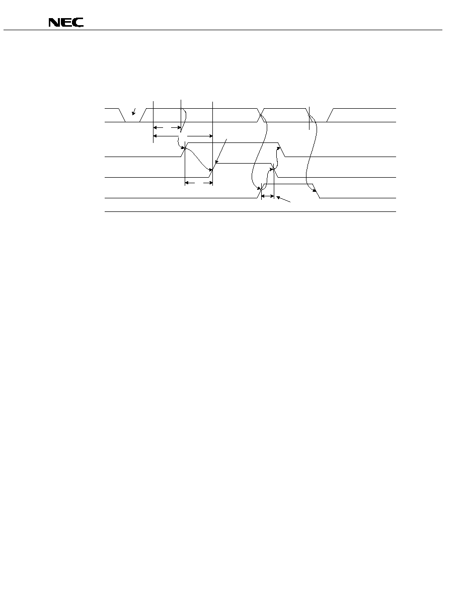
Data Sheet S16685EJ2V0DS
74
µPD720122
(9) Suspend and resume on USB1.1 bus
Figure 2-18. Suspend and Resume on USB 1.1 Bus
USB bus
SUSPEND
SPMODE
FS J
FS J
FS K
FS EOP
t
SPD
t
SUS
t
SSP
t
CSP
Current source and
PLL, etc. are disabled.
Note time required to relock PLL
and stabilize oscillator.
High
SPNDOUT
RSUMOUT

Data Sheet S16685EJ2V0DS
75
µPD720122
(10) Suspend and resume on USB2.0 bus
Figure 2-19. Suspend and Resume on USB 2.0 Bus
USB bus
SUSPEND
SPMODE
FS J
FS K
High-speed packet
t
SPD
t
SUS
t
SSP
t
CSP
Current source and
PLL, etc. are disabled.
Note time required to relock PLL
and stabilize oscillator.
Low
SPNDOUT
RSUMOUT
t
CSR
Reversion to full-speed mode
t
RHS
High-speed packet
Reversion to high-speed mode
T
0
(11) Remote wakeup on USB1.1
Figure 2-20. Remote Wakeup on USB 1.1
USB bus
SUSPEND
SPMODE
FS J
FS K
t
SPD
t
SUS
t
SSP
Current source and
PLL, etc. are disabled.
High
SPNDOUT
RSUMOUT
FS J
FS EOP
t
RWP
t
SRW
RSUMIN
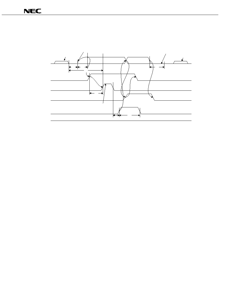
Data Sheet S16685EJ2V0DS
76
µPD720122
(12) Remote wakeup on USB2.0
Figure 2-21. Remote Wakeup on USB 2.0
USB bus
SUSPEND
SPEEDMODE
FS J
FS K
t
SPD
t
SUS
t
SSP
Current source and
PLL, etc. are disabled.
Low
SPNDOUT
RSUMOUT
T
0
t
RWP
t
SRW
RSUMIN
High-speed packet
Reversion to full-speed mode
t
RHS
Reversion to high-speed mode
t
CSR
High-speed packet
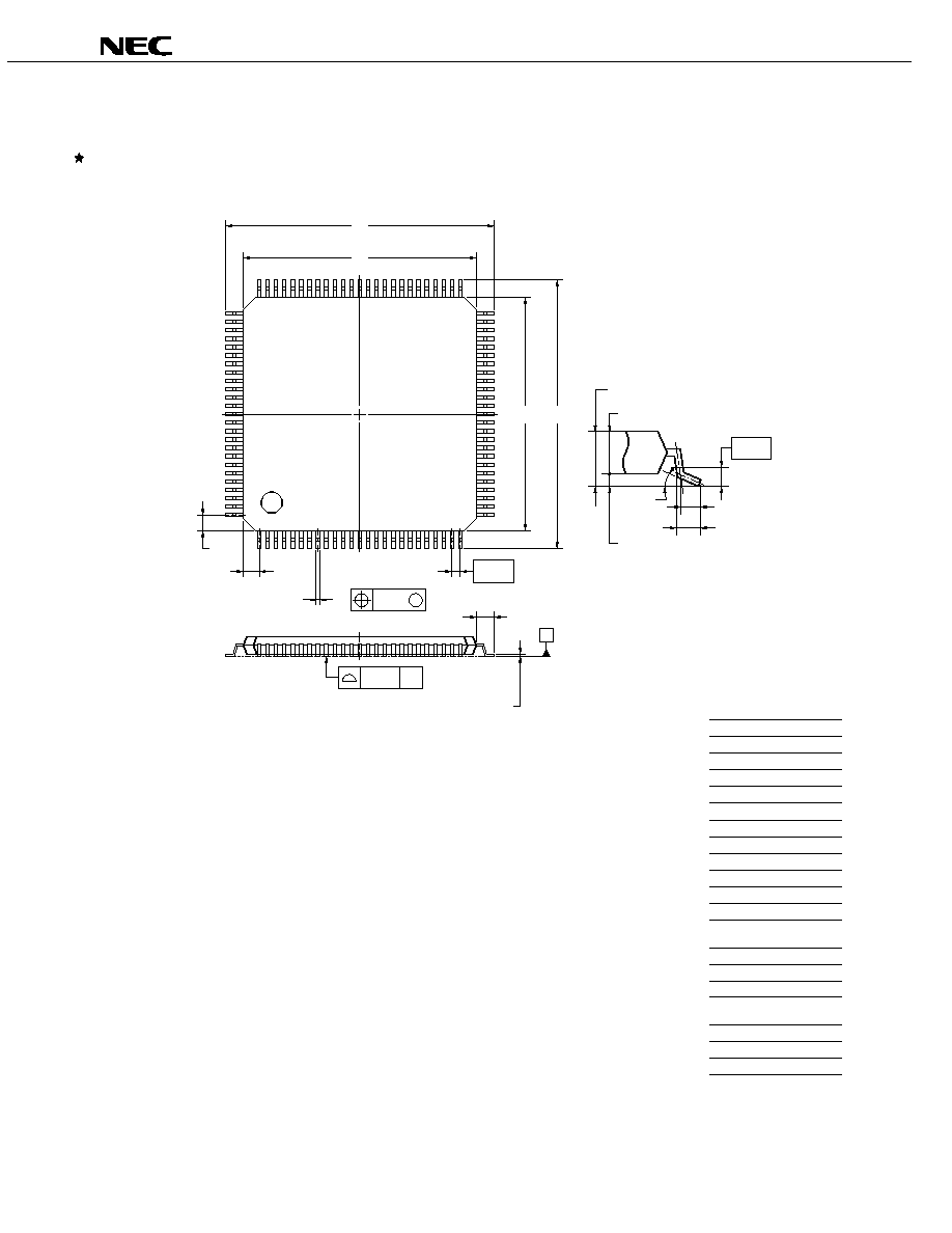
Data Sheet S16685EJ2V0DS
77
µPD720122
3.
PACKAGE DRAWING
75
76
50
100
1
26
25
51
S
100-PIN PLASTIC TQFP (FINE PITCH) (14x14)
ITEM
MILLIMETERS
B
14.0
±0.2
D
16.0
±0.2
F
1.0
G
1.0
A
16.0
±0.2
C
14.0
±0.2
H
0.22
±0.05
I
0.08
J
K
NOTE
Each lead centerline is located within 0.08 mm of
its true position (T.P.) at maximum material condition.
1.0
±0.2
0.5 (T.P.)
A
R
detail of lead end
S
M
H
I
G
F
B
C
D
L
0.5
N
0.08
P
1.0
Q
0.1
±0.05
P100GC-50-9EU
M
0.17+0.03
-0.07
S
1.1
±0.1
T
0.25
U
0.6
±0.15
R
3
∞+4∞
-3∞
K
J
P
Q
L
U
T
M
S
N

Data Sheet S16685EJ2V0DS
78
µPD720122
B
S
A
D
E
S
w
A
S
w
B
INDEX MARK
ZE
A
A2
A1
ZD
12
11
10
9
8
7
6
5
4
3
2
1
A
B
C
D
E
F
G
H
J
K
L
M
y1
S
S
y
S
e
x
b
A B
M
ITEM
DIMENSIONS
D
E
w
A
A1
A2
e
b
x
y
y1
ZD
ZE
11.00
±0.10
11.00
±0.10
0.80
0.08
0.10
0.20
1.10
1.10
0.20
0.35
±0.06
1.28
±0.10
0.93
P109F1-80-DN2
(UNIT:mm)
0.50+0.05
≠0.10
109-PIN PLASTIC FBGA (11x11)

Data Sheet S16685EJ2V0DS
79
µPD720122
4.
RECOMMENDED SOLDERING CONDITIONS
The
µPD720122 should be soldered and mounted under the following recommended conditions.
For soldering methods and conditions other than those recommended below, contact your NEC Electronics sales
representative.
For technical information, see the following website.
Semiconductor Device Mount Manual (http://www.necel.com/pkg/en/mount/index.html)
∑
µ
µ
µ
µ PD720122GC-9EU : 100-pin plastic TQFP (Fine pitch) (14 ◊◊◊◊ 14)
Soldering Method
Soldering Conditions
Symbol
Infrared reflow
Package peak temperature: 235∞C, Time: 30 seconds max. (at 210∞C or higher),
Count: Two times or less
Exposure limit: 3 days
Note
(after that, prebake at 125∞C for 10 hours)
IR35-103-2
Partial heating
Pin temperature: 300∞C max., Time: 3 seconds max. (per pin row)
≠
Note After opening the dry pack, store it at 25∞C or less and 65% RH or less for the allowable storage period.
∑
µ
µ
µ
µ PD720122F1-GN2 : 109-pin plastic FBGA (11 ◊◊◊◊ 11)
Soldering Method
Soldering Conditions
Symbol
Infrared reflow
Package peak temperature: 235∞C, Time: 30 seconds max. (at 210∞C or higher),
Count: Three times or less
Exposure limit: 3 days
Note
(after that, prebake at 125∞C for 10 hours)
IR35-103-3
Partial heating
Pin temperature: 300∞C max., Time: 3 seconds max. (per pin row)
≠
Note After opening the dry pack, store it at 25∞C or less and 65% RH or less for the allowable storage period.

Data Sheet S16685EJ2V0DS
80
µPD720122
[MEMO]

Data Sheet S16685EJ2V0DS
81
µPD720122
NOTES FOR CMOS DEVICES
1
PRECAUTION AGAINST ESD FOR SEMICONDUCTORS
Note:
Strong electric field, when exposed to a MOS device, can cause destruction of the gate oxide and
ultimately degrade the device operation. Steps must be taken to stop generation of static electricity
as much as possible, and quickly dissipate it once, when it has occurred. Environmental control
must be adequate. When it is dry, humidifier should be used. It is recommended to avoid using
insulators that easily build static electricity. Semiconductor devices must be stored and transported
in an anti-static container, static shielding bag or conductive material. All test and measurement
tools including work bench and floor should be grounded. The operator should be grounded using
wrist strap. Semiconductor devices must not be touched with bare hands. Similar precautions need
to be taken for PW boards with semiconductor devices on it.
2
HANDLING OF UNUSED INPUT PINS FOR CMOS
Note:
No connection for CMOS device inputs can be cause of malfunction. If no connection is provided
to the input pins, it is possible that an internal input level may be generated due to noise, etc., hence
causing malfunction. CMOS devices behave differently than Bipolar or NMOS devices. Input levels
of CMOS devices must be fixed high or low by using a pull-up or pull-down circuitry. Each unused
pin should be connected to V
DD
or GND with a resistor, if it is considered to have a possibility of
being an output pin. All handling related to the unused pins must be judged device by device and
related specifications governing the devices.
3
STATUS BEFORE INITIALIZATION OF MOS DEVICES
Note:
Power-on does not necessarily define initial status of MOS device. Production process of MOS
does not define the initial operation status of the device. Immediately after the power source is
turned ON, the devices with reset function have not yet been initialized. Hence, power-on does
not guarantee out-pin levels, I/O settings or contents of registers. Device is not initialized until the
reset signal is received. Reset operation must be executed immediately after power-on for devices
having reset function.

µPD720122
EEPROM is a trademark of NEC Electronics Corporation.
USB logo is a trademark of USB Implementers Forum, Inc.
The information in this document is current as of June, 2003. The information is subject to change
without notice. For actual design-in, refer to the latest publications of NEC Electronics data sheets or
data books, etc., for the most up-to-date specifications of NEC Electronics products. Not all
products and/or types are available in every country. Please check with an NEC Electronics sales
representative for availability and additional information.
No part of this document may be copied or reproduced in any form or by any means without the prior
written consent of NEC Electronics. NEC Electronics assumes no responsibility for any errors that may
appear in this document.
NEC Electronics does not assume any liability for infringement of patents, copyrights or other intellectual
property rights of third parties by or arising from the use of NEC Electronics products listed in this document
or any other liability arising from the use of such products. No license, express, implied or otherwise, is
granted under any patents, copyrights or other intellectual property rights of NEC Electronics or others.
Descriptions of circuits, software and other related information in this document are provided for illustrative
purposes in semiconductor product operation and application examples. The incorporation of these
circuits, software and information in the design of a customer's equipment shall be done under the full
responsibility of the customer. NEC Electronics assumes no responsibility for any losses incurred by
customers or third parties arising from the use of these circuits, software and information.
While NEC Electronics endeavors to enhance the quality, reliability and safety of NEC Electronics products,
customers agree and acknowledge that the possibility of defects thereof cannot be eliminated entirely. To
minimize risks of damage to property or injury (including death) to persons arising from defects in NEC
Electronics products, customers must incorporate sufficient safety measures in their design, such as
redundancy, fire-containment and anti-failure features.
NEC Electronics products are classified into the following three quality grades: "Standard", "Special" and
"Specific".
The "Specific" quality grade applies only to NEC Electronics products developed based on a customer-
designated "quality assurance program" for a specific application. The recommended applications of an NEC
Electronics product depend on its quality grade, as indicated below. Customers must check the quality grade of
each NEC Electronics product before using it in a particular application.
The quality grade of NEC Electronics products is "Standard" unless otherwise expressly specified in NEC
Electronics data sheets or data books, etc. If customers wish to use NEC Electronics products in applications
not intended by NEC Electronics, they must contact an NEC Electronics sales representative in advance to
determine NEC Electronics' willingness to support a given application.
(Note)
∑
∑
∑
∑
∑
∑
M8E 02. 11-1
(1)
(2)
"NEC Electronics" as used in this statement means NEC Electronics Corporation and also includes its
majority-owned subsidiaries.
"NEC Electronics products" means any product developed or manufactured by or for NEC Electronics (as
defined above).
Computers, office equipment, communications equipment, test and measurement equipment, audio
and visual equipment, home electronic appliances, machine tools, personal electronic equipment
and industrial robots.
Transportation equipment (automobiles, trains, ships, etc.), traffic control systems, anti-disaster
systems, anti-crime systems, safety equipment and medical equipment (not specifically designed
for life support).
Aircraft, aerospace equipment, submersible repeaters, nuclear reactor control systems, life
support systems and medical equipment for life support, etc.
"Standard":
"Special":
"Specific":