Document Outline
- COVER
- FEATURES
- ORDERING INFORMATION
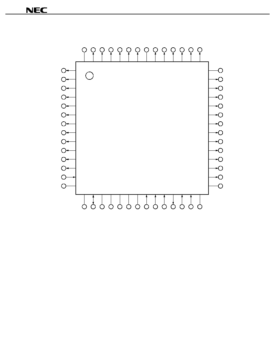
- PIN CONFIGURATION: (Top View)
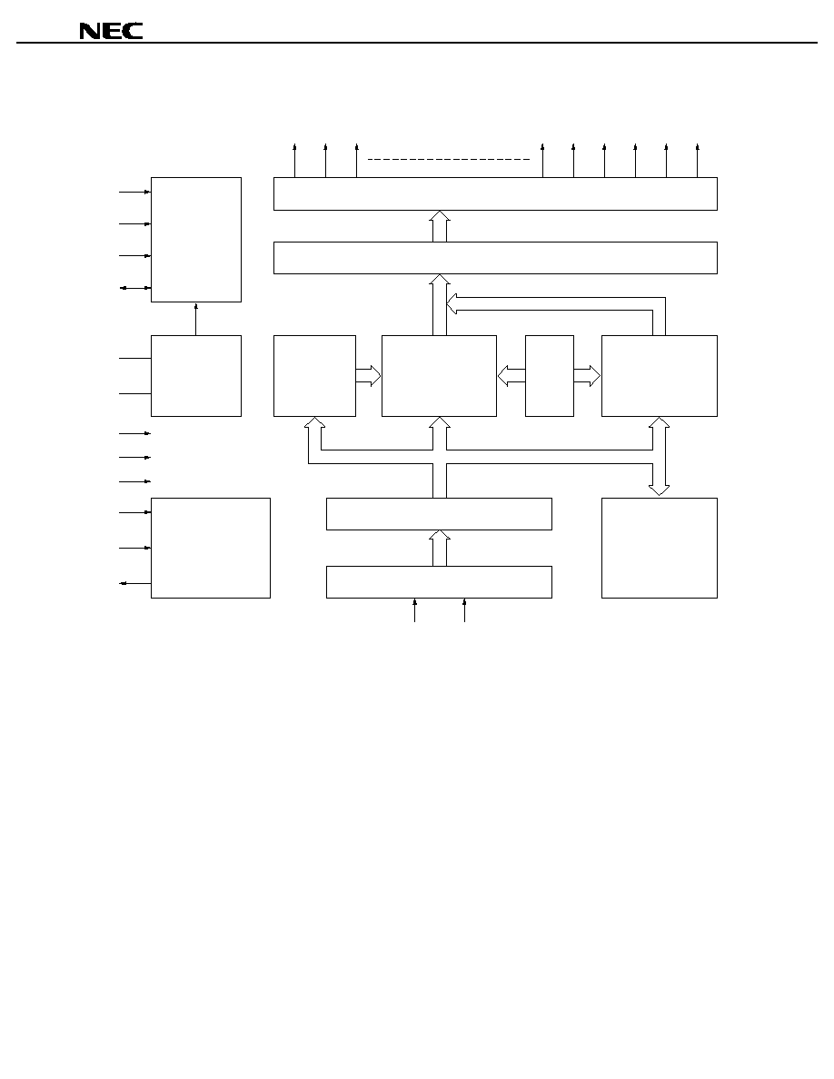
- BLOCK DIAGRAM
- 1. PIN FUNCTIONS
- 1.1 SI (Serial Input) ......Input
- 1.2 /SCK (Serial Clock) ......nput
- 1.3 C, /D (Command/Data) ......Input
- 1.4 /BUSY......Tri-state output
- 1.5 /CS (Chip Select) ......Input
- 1.6 /SYNC (SYNChronous) ......Input/Output
- 1.7 /RESET......Input
- 1.8 S0-S31 (Segment) ......Output
- 1.9 COM0-COM3 (COMmon) ......Output
- 1.10 CL1, CL2 (Clock)
- 1.11 VLC1, VLC2, VLC3
- 1.12 VDD
- 1.13 VSS
- 2. INTERNAL SYSTEM CONFIGURATION
- 2.1 Serial Interface
- 2.2 Command/Data Register
- 2.3 Command Decoder
- 2.4 Segment Decoders
- 2.5 Data Memory/Data Pointer
- 2.6 Blinking Data Memory
- 2.7 Display Data Latch
- 2.8 LCD Driver
- 2.9 LCD Timing Control
- 3. FRAME FREQUENCY AND BLINKING FREQUENCY SETTING
- 3.1 Frame Frequency Setting
- 3.2 Blinking Frequency Setting
- 4. LCD DRIVE POWER SUPPLY PIN VOLTAGE SETTING
- 5. CLOCK CIRCUIT
- 6. RESET FUNCTION
- 7. SERIAL DATA INPUT
- 8. COMMAND
- 8.1 MODE SET
- 8.2 SYNCHRONIZED TRANSFER
- 8.3 UNSYNCHRONIZED TRANSFER
- 8.4 PAUSE TRANSFER
- 8.5 BLINKING ON
- 8.6 BLINKING OFF
- 8.7 DISPLAY ON
- 8.8 DISPLAY OFF
- 8.9 WITH SEGMENT DECODER
- 8.10 WITHOUT SEGMENT DECODER
- 8.11 LOAD DATA POINTER
- 8.12 WRITE DATA MEMORY
- 8.13 OR DATA MEMORY
- 8.14 AND DATA MEMORY
- 8.15 CLEAR DATA MEMORY
- 8.16 WRITE BLINKING DATA MEMORY
- 8.17 OR BLINKING DATA MEMORY
- 8.18 AND BLINKING DATA MEMORY
- 8.19 CLEAR BLINKING DATA MEMORY
- 9. DISPLAY OUTPUT
- 9.1 Static
- 9.2 Divide-by-2 Time Division
- 9.3 Divide-by-3 Time Division
- 9.4 Divide-by-4 Time Division
- 10. ELECTRICAL CHARACTERISTICS
- 11. PACKAGE DRAWINGS
- 12. RECOMMENDED SOLDERING CONDITIONS

MOS INTEGRATED CIRCUIT
µ
µ
µ
µ
PD7225
PROGRAMMABLE LCD CONTROLLER/DRIVER
DATA SHEET
Document No. S14308EJ6V0DS00 (6th edition)
(O.D. No. IC-1555)
Date Published June 1999 N CP (K)
Printed in Japan
©
1986, 1999
The mark
shows major revised points.
The
µ
PD7225 is a software-programmable LCD (Liquid Crystal Display) controller/driver. The
µ
PD7225 can be
serially interfaced with the CPU in a microcomputer and can directly drive 2, 3, or 4-time division LCD. The
µ
PD7225
contains a segment decoder which can generate specific segment patterns. In addition, the
µ
PD7225 can be used to
control on/off (blinking) operation of a display.
FEATURES
∑ Can directly drive LCD
∑ Programmable time-division multiplexing
∑
Static drive
∑
Divide-by-2, 3, or -4 time division multiplexing
∑ Number of digits displayed
∑
7-segment
Divide-by-4 time division ............... 16 digits
Divide-by-3 time division ............... 10 2/3 digits
Divide-by-2 time division ............... 8 digits
Static................................................. 4 digits
∑
14-segment
Divide-by-4 time division ............... 8 digits
∑ Bias method
Static, 1/2, 1/3
∑ Segment decoder output
∑
7-segment : Numeric characters 0 to 9, six symbols
∑
14-segment : 36 alphanumeric characters, 13 symbols
∑ Blinking operation
∑ Multi-chip configuration possible
∑ 8-bit serials interface
75X series and 78K series compatible
∑ CMOS
∑ Single power supply
ORDERING INFORMATION
Part Number Package
µ
PD7225G00 52-pin plastic QFP (14
◊
14 mm)
µ
PD7225G01 52-pin plastic QFP (straight) ( 14 mm)
µ
PD7225GB-3B7 56-pin plastic QFP (10
◊
10 mm)
µ
PD7225GC-AB6 52-pin plastic QFP (14
◊
14 mm)
The information in this document is subject to change without notice. Before using this document, please
confirm that this is the latest version.
Not all devices/types available in every country. Please check with local NEC representative for
availability and additional information.

Data Sheet S14308EJ6V0DS00
2
µ
µ
µ
µ
PD7225
PIN CONFIGURATION: (Top View)
µ
µ
µ
µ
PD7225G00
52-pin plastic QFP (14
◊
◊
◊
◊
14 mm)
µ
µ
µ
µ
PD7225G01
52-pin plastic QFP (straight) ( 14 mm)
µ
µ
µ
µ
PD7225GC-AB6
52-pin plastic QFP (14
◊
◊
◊
◊
14 mm)
52
1
2
3
4
5
6
7
8
9
10
11
12
13
S19
S18
S17
S16
S15
S14
V
DD
S13
S12
S11
S10
S9
S8
CL1
S31
S30
S29
S28
S27
S26
S25
S24
S23
S22
S21
S20
NC
COM0
COM1
COM2
COM3
S0
S1
S2
S3
S4
S5
S6
S7
CL2
/SYNC
V
LC1
V
LC2
V
LC3
V
SS
V
DD
/SCK
SI
/CS
/BUSY
C, /D
/RESET
39
38
37
36
35
34
33
32
31
30
29
28
27
51
50
49
48
47
46
45
44
43
42
41
40
14
15
16
17
18
19
20
21
22
23
24
25
26
SI
: Serial Input
CL1
: External Resistor 1 (External Clock)
/SCK
: Serial Clock
CL2
: External Resistor 2
C, /D
: Command/Data
RESET
: Reset
/CS
: Chip Select
V
LC1
-V
LC3
: Power Supply For LCD Drive
/BUSY
: Busy
V
DD
: Power Supply
SYNC
: Sync
V
SS
: Ground
S0-S31
: Segment
IC
: Internally Connected
COM0-COM3 : Common
NC
: Non-connection
Remark
/
◊◊◊
indicates active low signal.
Data Sheet S14308EJ6V0DS00
3
µ
µ
µ
µ
PD7225
µ
µ
µ
µ
PD7225GB-3B7 56-pin plastic QFP (10
◊
◊
◊
◊
10 mm)
1
2
3
4
5
6
7
8
9
10
11
12
13
14
IC
S7
S6
S5
S4
S3
S2
S1
S0
COM3
COM2
COM1
COM0
NC
IC
S19
S18
S17
S16
S15
S14
V
DD
S13
S12
S11
S10
S9
S8
CL2
/SYNC
V
LC1
V
LC2
V
LC3
V
SS
V
DD
/SCK
SI
/CS
/BUSY
C, /D
/RESET
IC
S20
S21
S22
S23
S24
S25
S26
S27
S28
S29
S30
S31
CL1
IC
42
41
40
39
38
37
36
35
34
33
32
31
30
29
56
55
54
53
52
51
50
49
48
47
46
45
44
43
15
16
17
18
19
20
21
22
23
24
25
26
27
28
Note
IC Pin must be connected to V
DD
or left unconnected.
Data Sheet S14308EJ6V0DS00
4
µ
µ
µ
µ
PD7225
BLOCK DIAGRAM
COM
0
COM
1
COM
2
S0
COM
3
S1
S29
S30
S31
DISPLAY DATA LATCH
DATA
MEMORY
DATA
POINTER
BLINKING
DATA
MEMORY
SEGMENT
DECODER
WRITE
CONTROL
COMMAND/DATA REGISTER
SERIAL INTERFACE
COMMAND
DECODER
/SCK
SI
V
LC1
V
LC2
V
LC3
/SYNC
CL1
CL2
V
DD
V
SS
/RESET
/CS
C, /D
/BUSY
OSC
LCD
TIMING
CONTROL
LCD DRIVER
Data Sheet S14308EJ6V0DS00
5
µ
µ
µ
µ
PD7225
1.
PIN FUNCTIONS
1.1 SI (Serial Input)
......
......
......
......
Input
This pin is used for inputting serial data (commands/data). Data to be displayed as well as 19 deffernet
commands for controlling the operation of the
µ
PD7225 can be input to this pin.
1.2 /SCK (Serial Clock)
......
......
......
......
Input
This pin is used for inputting the shift clock for serial data (SI input). The content of the SI input is read into the
serial register at the rising edge of this clock one bit at a time. /SCK input is effective when /CS = 0 and /BUSY = 1.
If /BUSY = 0, this input is ignored. If /CS = 1, this signal is ignored regardless of the /BUSY status.
1.3 C, /D (Command/Data)
......
......
......
......
Input
This input indicates whether the signal input from the SI pin is a command or data. A low level indicates data; a
high level indicates a command.
1.4 /BUSY
......
......
......
......
Tri-state output
This is an active-low output pin that is used to control serial data input disable/enable. A low level disables serial
data input; a high level enables serial data input. This pin becomes high impedance when /CS = 1.
1.5 /CS (Chip Select)
......
......
......
......
Input
When /CS is changed from high level to low level, the SCK counter in the
µ
PD7225 is cleared and serial data
input is enabled. At the same time, the data pointer is initialized to address 0. When /CS is set to high level after
serial data is input, the contents of the data memory are transferred to the display latch and displayed on the LCD.
1.6 /SYNC (SYNChronous)
......
......
......
......
Input/Output
The /SYNC pin is used to make a wired-OR connection when the common pins are shared or when blinking
operation is synchronized in a multi-chip configuration.
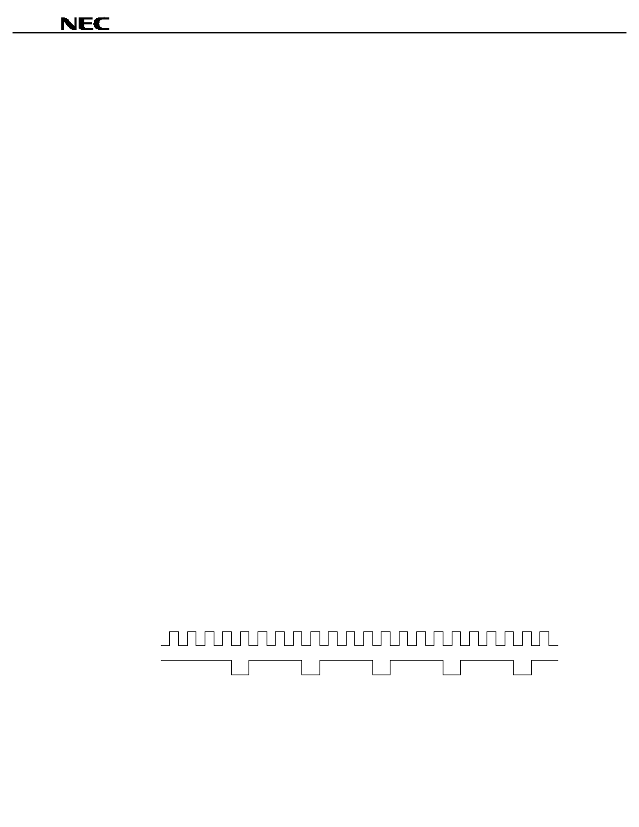
When the
µ
PD7225 is reset (/RESET = 0), the /SYNC pin outputs the clock frequency (f
CL
) divided by four (refer to
Figure 1-1), and synchronizes the system clock (f
CL
/4) of the
µ
PD7225. When the reset is released (/RESET =1), the
display timing of each
µ
PD7225 is synchronized with the common drive signal timing shown in Figure 1-2.
Figure 1-1. /SYNC Pin Status During Reset (/RESET = 0)
f
CL
/SYNC