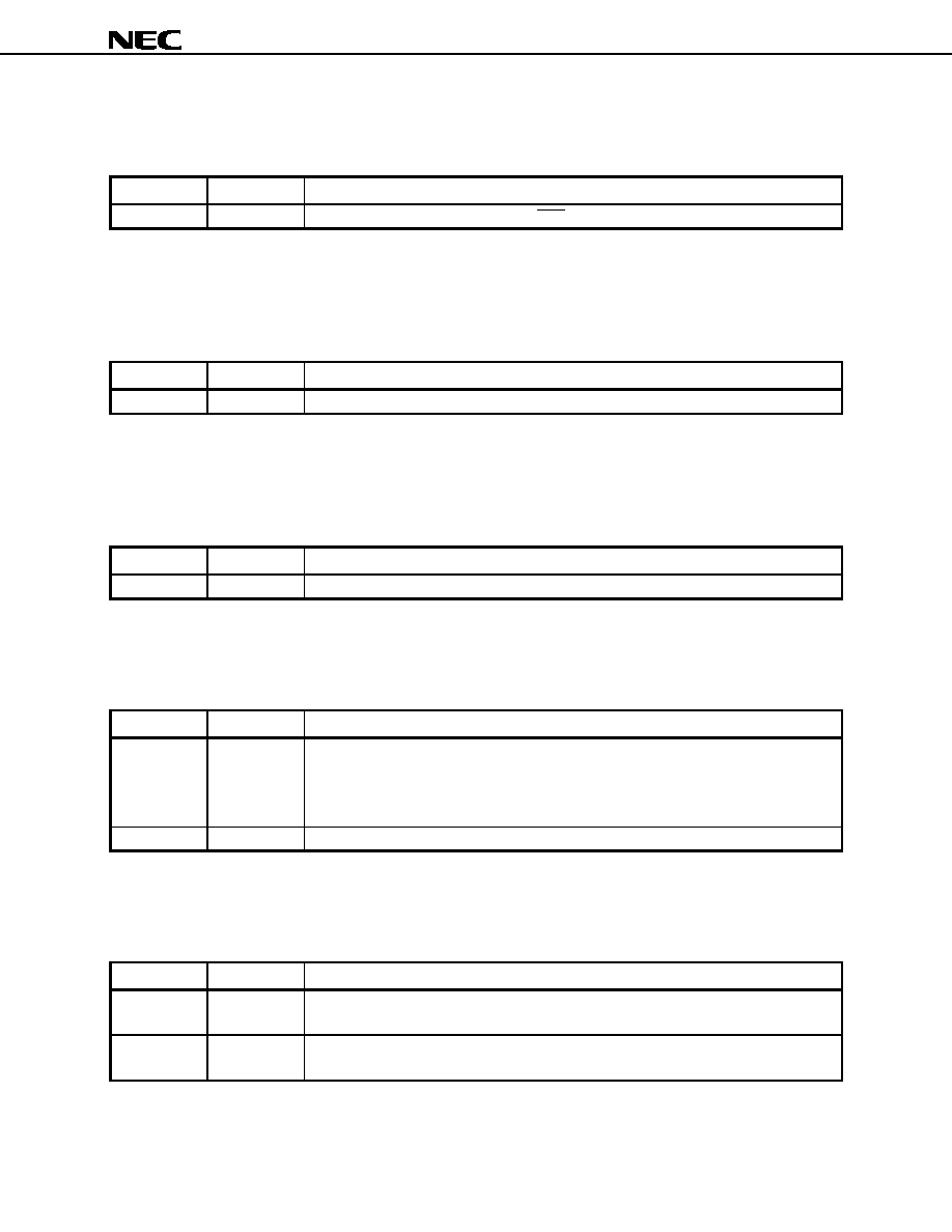
 | –≠–ª–µ–∫—Ç—Ä–æ–Ω–Ω—ã–π –∫–æ–º–ø–æ–Ω–µ–Ω—Ç: UPD72874 | –°–∫–∞—á–∞—Ç—å:  PDF PDF  ZIP ZIP |
Document Outline
- COVER
- FEATURES
- ORDERING INFORMATION
- Firewarden(TM) ROADMAP
- BLOCK DIAGRAMS
- PIN CONFIGURATION (TOP VIEW)
- PIN NAME
- 1. PIN FUNCTIONS
- 1.1 PCI/Cardbus Interface Signals: (52 pins)
- 1.2 PHY Signals: (20 pins)
- 1.3 PHY Control Signals: (4 pins)
- 1.4 PCI/Cardbus Select Signal: (1 pin)
- 1.5 Serial ROM Interface Signals: (3 pins)
- 1.6 D3cold Wake Up Function Signals: (2 pins)
- 1.7 IC: (7 pins)
- 1.8 VDD
- 1.9 GND
- 2. PHY REGISTERS
- 2.1 Complete Structure for PHY Registers
- 2.2 Port Status Page (Page 000)
- 2.3 Vendor ID Page (Page 001)
- 2.4 Vendor Dependent Page (Page 111 : Port_select 0001)
- 3. CONFIGURATION REGISTERS
- 3.1 PCI Bus Mode Configuration Register (CARD_ON = Low)
- 3.1.1 Offset_00 Vendor ID Register
- 3.1.2 Offset_02 Device ID Register
- 3.1.3 Offset_04 Command Register
- 3.1.4 Offset_06 Status Register
- 3.1.5 Offset_08 Revision ID Register
- 3.1.6 Offset_09 Class Code Register
- 3.1.7 Offset_0C Cache Line Size Register
- 3.1.8 Offset_0D Latency Timer Register
- 3.1.9 Offset_0E Header Type Register
- 3.1.10 Offset_0F BIST Register
- 3.1.11 Offset_10 Base Address 0 Register
- 3.1.12 Offset_2C Subsystem Vendor ID Register
- 3.1.13 Offset_2E Subsystem ID Register
- 3.1.14 Offset_34 Cap_Ptr Register
- 3.1.15 Offset_3C Interrupt Line Register
- 3.1.16 Offset_3D Interrupt Pin Register
- 3.1.17 Offset_3E Min_Gnt Register
- 3.1.18 Offset_3F Max_Lat Register
- 3.1.19 Offset_40 PCI_OHCI_Control Register
- 3.1.20 Offset_60 Cap_ID & Next_Item_Ptr Register
- 3.1.21 Offset_62 Power Management Capabilities Register
- 3.1.22 Offset_64 Power Management Control/Status Register
- 3.2 CardBus Mode Configuration Register (CARD_ON = High)
- 3.2.1 Offset_14/18 Base Address 1/2 Register (Cardbus Status Registers)
- 3.2.2 Offset_28 Cardbus CIS Pointer
- 3.2.3 Offset_80 CIS Area
- 4. PHY FUNCTION
- 4.1 Cable Interface
- 4.1.1 Connections
- 4.1.2 Cable Interface Circuit
- 4.1.3 CPS
- 4.1.4 Unused Ports
- 4.2 PLL and Crystal Oscillation Circuit
- 4.2.1 Crystal Oscillation Circuit
- 4.2.2 PLL
- 4.3 PC0 to PC2
- 4.4 P_RESET#
- 4.5 RI0, RI1
- 5. ELECTRICAL SPECIFICATIONS
- 6. PACKAGE DRAWING
- 7. RECOMMENDED SOLDERING CONDITIONS

2001
IEEE1394 OHCI 1.1 COMPLIANT 3PORT PHY-LINK 1-CHIP HOST CONTROLLER
PRELIMINARY DATA SHEET
MOS INTEGRATED CIRCUIT
µ
µ
µ
µ
PD72874
Document No. S15306EJ2V0DS00 (2nd edition)
Date Published April 2002 NS CP (K)
Printed in Japan
The information in this document is subject to change without notice. Before using this document, please
confirm that this is the latest version.
Not all devices/types available in every country. Please check with local NEC representative for
availability and additional information.
The
µPD72874 is the LSI that integrated OHCI-Link and PHY function into a single chip. The µPD72874 complies
with the 1394 OHCI Specification 1.1 and the IEEE Std 1394a-2000 specifications, and works up to 400 Mbps.
It makes design so compact for PC and PC card application.
FEATURES
∑
Compliant with Link Layer Services as defined in 1394 Open Host Controller Interface specification release 1.1
∑
Compliant with Physical Layer Services as defined in IEEE Std 1394a-2000
∑
Provides three cable ports at 100/200/400 Mbps
∑
Super Low power consumption for Physical Layer
∑
Compliant with protocol enhancement as defined in IEEE Std1394a-2000
∑
Modular 32-bit host interface compliant to PCI Specification release 2.2
∑
Supports PCI-Bus Power Management Interface Specification release 1.1
∑
Modular 32-bit host interface compliant to Card Bus Specification
∑
Cycle Master and Isochronous Resource Manager capable
∑
Built-in FIFOs for isochronous transmit (2048 bytes), asynchronous transmit (2048 bytes), and receive (3072
bytes)
∑
Supports D0, D1, D2, D3hot
∑
Supports wake up function from D3cold
∑
32-bit CRC generation and checking for receive/transmit packets
∑
4 isochronous transmit DMAs and 4 isochronous receive DMAs supported
∑
32-bit DMA channels for physical memory read/write
∑
Clock generation by 24.576 MHz X'tal
∑
2-wire Serial EEPROM
TM
interface supported
∑
Separate power supply Link and PHY
∑
Programmable latency timer from serial EEPROM in Cardbus mode (CARD_ON = 1)
ORDERING INFORMATION
Part number
Package
µPD72874GC-YEB
120-pin plastic TQFP (Fine pitch) (14 x 14)
The mark shows major revised points.
Preliminary Data Sheet S15306EJ2V0DS
2
µ
µ
µ
µ
PD72874
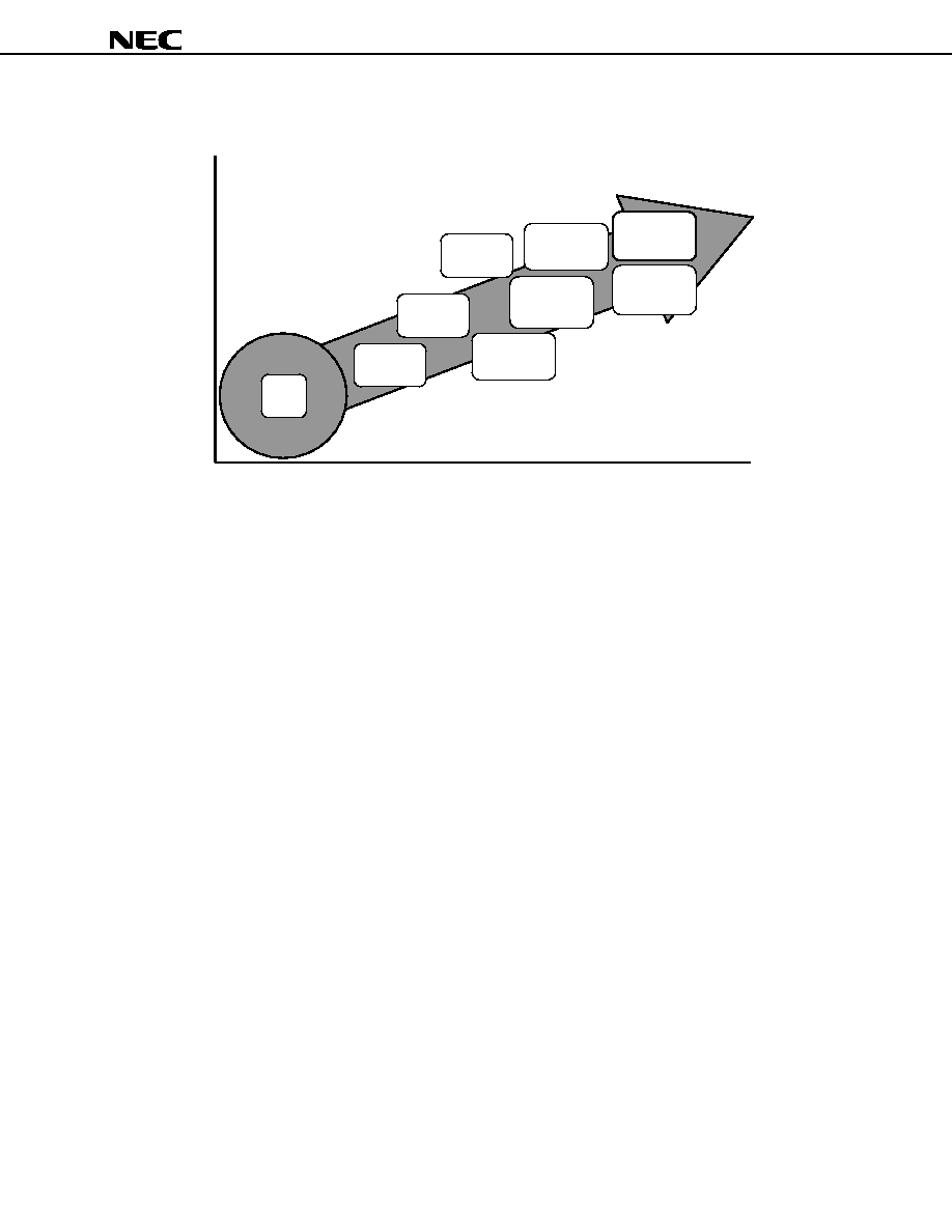
FirewardenTM ROADMAP
IEEE1394-1995
Core Development
Firewarden Series
OHCI Link
µPD72860
OHCI Link
µPD72861
1-Chip
OHCI+PHY
µPD72872
OHCI Link
µPD72862
1-Chip
OHCI+PHY
µPD72870
1-Chip
OHCI+PHY
µPD72870A,
72870B
1-Chip
OHCI 1.1+PHY
µPD72874
1-Chip
OHCI 1.1+PHY
µPD72873
Link
Core
Preliminary Data Sheet S15306EJ2V0DS
3
µ
µ
µ
µ
PD72874
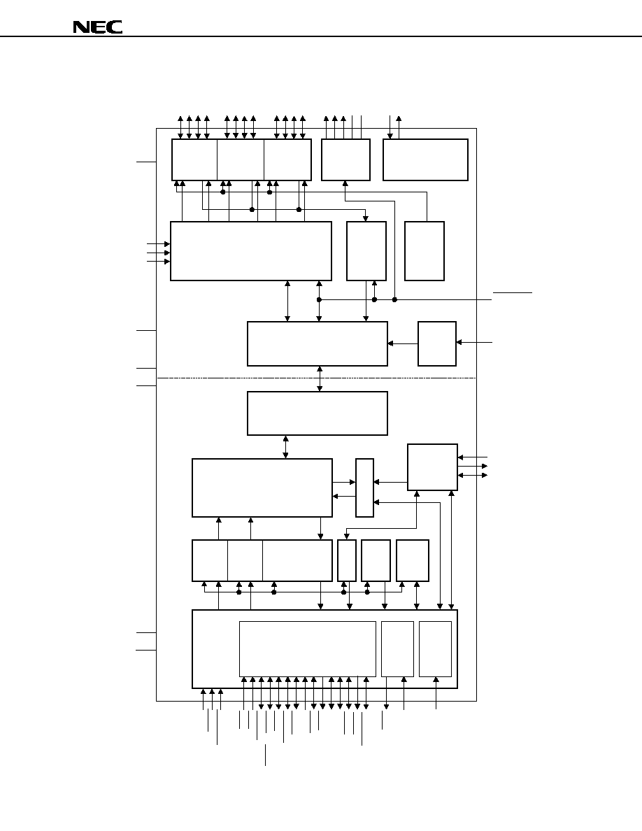
BLOCK DIAGRAMS
Li
nk
Cor
e
St
a
t
e
M
a
ch
i
n
e
Lo
gic
PC
I
C
o
nt
ro
ll
er
IT
FI
F
O
AT FI
FO
IR
F
I
F
O
Po
w
e
r
Mana
gem
en
t
C
o
nt
ro
ll
er
CS
R
Reg
i
s
t
er
PH
Y
In
te
r
f
a
c
e
DMA
C
o
nt
ro
ll
er
Co
m
a
n
d
FI
F
O
PC
I
Con
f
i
gur
at
i
o
n
Reg
i
s
t
er
PM
E
AD
0
t
o
AD
3
1
C
BE0 t
o
C
BE3
FR
AM
E
RE
Q
GNT
I
RDY
T
RDY
D
EVS
EL
STOP IN
T
A
PAR
I
D
SEL
CLK
R
U
N
PER
R
SER
R
PR
ST
PC
L
K
RS
MRS
T
D3CS
U
P
PC
I
In
te
r
f
a
c
e
I/
O
ROM
In
te
r
f
a
c
e
I/
O
GROM_EN
GROM_SCL
GROM_SDA
CA
RD_
O
N
A
r
bi
t
r
at
io
n
an
d Co
nt
rol
St
a
t
e
M
a
ch
i
n
e
Lo
gic
Li
nk
In
te
r
f
a
c
e
Rec
e
i
v
e Dat
a
Dec
oder
and
Ret
i
m
e
r
T
r
ans
m
i
t
Da
t
a
E
n
c
oder
V
o
l
t
age
an
d
Cur
r
e
n
t
G
ene
ra
t
o
r
Cr
y
s
t
a
l
O
sci
l
l
a
t
o
r
PL
L
Sy
s
t
e
m
an
d
T
r
ans
m
i
t
Cl
oc
k
G
ene
ra
t
o
r
Cab
l
e
Po
w
e
r
St
a
t
u
s
CPS
PC0
PC1
PC2
Tp
A
0
p
Tp
A
0
n
Tp
B
0
p
Tp
B
0
n
Tp
A
1
p
Tp
A
1
n
Tp
B
1
p
Tp
B
1
n
Tp
A
2
p
Tp
A
2
n
Tp
B
2
p
Tp
B
2
n
Cab
l
e
Po
rt
0
Cab
l
e
Po
rt
1
Cab
l
e
Po
rt
2
Tp
B
i
a
s
0
Tp
B
i
a
s
1
Tp
B
i
a
s
2
R0 R1
XO
XI
P_RESET
L_V
DD
PCI_V
DD
P_DV
DD
P_AV
DD
GND
GND
LINK BLOCK
P
H
Y
B
L
O
C
K
Preliminary Data Sheet S15306EJ2V0DS
4
µ
µ
µ
µ
PD72874
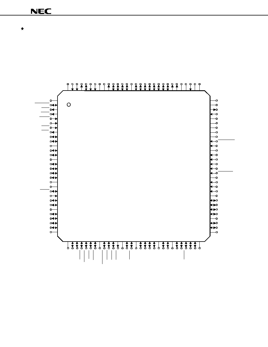
PIN CONFIGURATION (TOP VIEW)
∑ 120-pin plastic TQFP (Fine pitch) (14 x 14)
µ
µ
µ
µPD72874GC-YEB
L_V
DD
CLKRUN
PME
INTA
PRST
PCLK
GNT
REQ
GND
AD31
AD30
AD29
AD27
AD26
AD25
AD28
AD24
L_V
DD
GND
CBE3
IDSEL
AD23
AD22
AD21
AD20
GND
AD19
AD18
PCI_V
DD
L_V
DD
GND
XO
XI
P_AV
DD
IC(N)
GND
GND
P_DV
DD
IC(L)
P_RESET
L_V
DD
IC(L)
IC(H)
RSMRST
P_DV
DD
PC2
PC1
PC0
GND
IC(L)
P_DV
DD
90
89
88
86
85
84
83
87
82
81
80
79
78
77
76
75
74
73
72
71
70
69
68
67
66
65
64
62
63
61
AD4
PC
I_
V
DD
GND
CB
E
2
GND
STO
P
AD
1
5
AD
1
4
AD
1
3
AD
1
2
AD
1
1
AD
1
0
AD
9
AD
8
L_V
DD
C
BE0
AD
7
AD
6
AD
1
7
AD
1
6
FR
AM
E
IR
D
Y
L_V
DD
T
RDY
DE
V
S
E
L
GND
31
32
33
34
35
36
37
38
39
40
41
42
43
45
46
47
48
44
49
50
51
52
53
54
55
56
57
58
59
60
PER
R
SER
R
PAR
L_V
DD
CB
E
1
GND
120
119
118
116
115
114
113
117
112
111
110
109
108
107
106
105
104
103
102
101
100
99
98
97
96
95
94
92
93
91
TpA2p
P_
A
V
DD
TpBias
2
CA
RD_ON
IC
(
L
)
D3CS
UP
TpA2n
RI
1
TpB2n
GND
TpA1p
TpA1n
TpB1p
TpB1n
TpA0p
TpA0n
TpB0p
TpB0n
TpBias
1
TpBias
0
P_
A
V
DD
GND
RI
0
TpB2p
1
2
3
4
5
6
7
8
9
10
11
12
13
15
16
17
18
14
19
20
21
22
23
24
25
26
27
28
29
30
GROM
_S
DA
GROM
_S
CL
GROM
_E
N
AD0
AD1
AD2
AD3
GND
GND
AD5
P_AV
DD
CP
S
IC(L)

Preliminary Data Sheet S15306EJ2V0DS
5
µ
µ
µ
µ
PD72874
PIN NAME
AD0 to AD31 : PCI Multiplexed Address and Data
CARD_ON
: PCI/Card Select
CBE0 to
CBE3
: Command/Byte Enables
CLKRUN
: PCICLK Running
CPS
: Cable Power Status Input
D3CSUP
: D3cold Support
DEVSEL
: Device Select
FRAME
: Cycle Frame
GND
: GND
GNT
: Bus_master Grant
GROM_EN : Serial EEPROM Enable
GROM_SCL : Serial EEPROM Clock Output
GROM_SDA : Serial EEPROM Data Input / Output
IC(H)
: Internally Connected (High Clamped)
IC(L)
: Internally Connected (Low Clamped)
IC(N)
: Internally Connected (Open)
IDSEL
: ID Select
INTA
: Interrupt
IRDY
: Initiator Ready
L_V
DD
: V
DD
for Link Digital Core and Link I/Os
PAR
: Parity
PC0 to PC2
: Power Class Input
PCI_V
DD
: V
DD
for PCI I/Os
PCLK
: PCI Clock
PERR
: Parity Error
PME
: PME Output
PRST
: Reset
P_AV
DD
: PHY Analog V
DD
P_DV
DD
: PHY Digital V
DD
P_RESET
: PHY Power on Reset Input
REQ
: Bus_master Request
RI0
: Resistor0 for Reference Current Setting
RI1
: Resistor1 for Reference Current Setting
RSMRST
: Resume Reset
SERR
: System Error
STOP
: PCI Stop
TpA0n
: Port-1 Twisted Pair A Negative Input/Output
TpA0p
: Port-1 Twisted Pair A Positive Input/Output
TpA1n
: Port-2 Twisted Pair A Negative Input/Output
TpA1p
: Port-2 Twisted Pair A Positive Input/Output
TpA2n
: Port-3 Twisted Pair A Negative Input/Output
TpA2p
: Port-3 Twisted Pair A Positive Input/Output
TpB0n
: Port-1 Twisted Pair B Negative Input/Output
TpB0p
: Port-1 Twisted Pair B Positive Input/Output
TpB1n
: Port-2 Twisted Pair B Negative Input/Output
TpB1p
: Port-2 Twisted Pair B Positive Input/Output
TpB2n
: Port-3 Twisted Pair B Negative Input/Output
TpB2p
: Port-3 Twisted Pair B Positive Input/Output
TpBias0
: Port-1 Twisted Pair Bias Voltage Output
TpBias1
: Port-2 Twisted Pair Bias Voltage Output
TpBias2
: Port-3 Twisted Pair Bias Voltage Output
TRDY
: Target Ready
XI
: X'tal XI
XO
: X'tal XO

Preliminary Data Sheet S15306EJ2V0DS
6
µ
µ
µ
µ
PD72874
CONTENTS
1. PIN FUNCTIONS..................................................................................................................................... 8
1.1 PCI/Cardbus Interface Signals: (52 pins) ...................................................................................... 8
1.2 PHY Signals: (20 pins) .................................................................................................................. 10
1.3 PHY Control Signals: (4 pins)....................................................................................................... 10
1.4 PCI/Cardbus Select Signal: (1 pin)............................................................................................... 10
1.5 Serial ROM Interface Signals: (3 pins)......................................................................................... 11
1.6 D3cold Wake Up Function Signals: (2 pins) ............................................................................... 11
1.7 IC: (7 pins) ...................................................................................................................................... 11
1.8 V
DD
................................................................................................................................................... 12
1.9 GND................................................................................................................................................. 12
2. PHY REGISTERS................................................................................................................................... 13
2.1 Complete Structure for PHY Registers........................................................................................ 13
2.2 Port Status Page (Page 000)......................................................................................................... 16
2.3 Vendor ID Page (Page 001) ........................................................................................................... 17
2.4 Vendor Dependent Page (Page 111 : Port_select 0001) ............................................................ 17
3. CONFIGURATION REGISTERS .......................................................................................................... 18
3.1 PCI Bus Mode Configuration Register (CARD_ON = Low)........................................................ 18
3.1.1 Offset_00 Vendor ID Register ........................................................................................................... 19
3.1.2 Offset_02 Device ID Register............................................................................................................ 19
3.1.3 Offset_04 Command Register ........................................................................................................... 19
3.1.4 Offset_06 Status Register ................................................................................................................. 20
3.1.5 Offset_08 Revision ID Register ......................................................................................................... 21
3.1.6 Offset_09 Class Code Register......................................................................................................... 21
3.1.7 Offset_0C Cache Line Size Register................................................................................................. 21
3.1.8 Offset_0D Latency Timer Register .................................................................................................... 21
3.1.9 Offset_0E Header Type Register ...................................................................................................... 21
3.1.10 Offset_0F BIST Register .................................................................................................................. 21
3.1.11 Offset_10 Base Address 0 Register ................................................................................................ 22
3.1.12 Offset_2C Subsystem Vendor ID Register ...................................................................................... 22
3.1.13 Offset_2E Subsystem ID Register................................................................................................... 22
3.1.14 Offset_34 Cap_Ptr Register ............................................................................................................ 22
3.1.15 Offset_3C Interrupt Line Register.................................................................................................... 22
3.1.16 Offset_3D Interrupt Pin Register ..................................................................................................... 23
3.1.17 Offset_3E Min_Gnt Register ........................................................................................................... 23
3.1.18 Offset_3F Max_Lat Register ........................................................................................................... 23
3.1.19 Offset_40 PCI_OHCI_Control Register ........................................................................................... 23
3.1.20 Offset_60 Cap_ID & Next_Item_Ptr Register .................................................................................. 23
3.1.21 Offset_62 Power Management Capabilities Register...................................................................... 24
3.1.22 Offset_64 Power Management Control/Status Register.................................................................. 25
3.2 CardBus Mode Configuration Register (CARD_ON = High)...................................................... 26
3.2.1 Offset_14/18 Base Address 1/2 Register (Cardbus Status Registers).............................................. 27
3.2.2 Offset_28 Cardbus CIS Pointer ......................................................................................................... 28
3.2.3 Offset_80 CIS Area ........................................................................................................................... 28

Preliminary Data Sheet S15306EJ2V0DS
7
µ
µ
µ
µ
PD72874
4. PHY FUNCTION.................................................................................................................................... 29
4.1 Cable Interface............................................................................................................................... 29
4.1.1 Connections ......................................................................................................................................... 29
4.1.2 Cable Interface Circuit.......................................................................................................................... 30
4.1.3 CPS ...................................................................................................................................................... 30
4.1.4 Unused Ports........................................................................................................................................ 30
4.2 PLL and Crystal Oscillation Circuit ............................................................................................. 30
4.2.1 Crystal Oscillation Circuit ..................................................................................................................... 30
4.2.2 PLL ....................................................................................................................................................... 30
4.3 PC0 to PC2 ..................................................................................................................................... 30
4.4 P_RESET ........................................................................................................................................ 30
4.5 RI0, RI1 ........................................................................................................................................... 30
5. ELECTRICAL SPECIFICATIONS......................................................................................................... 31
6. PACKAGE DRAWING .......................................................................................................................... 34
7. RECOMMENDED SOLDERING CONDITIONS................................................................................... 35
Preliminary Data Sheet S15306EJ2V0DS
8
µ
µ
µ
µ
PD72874
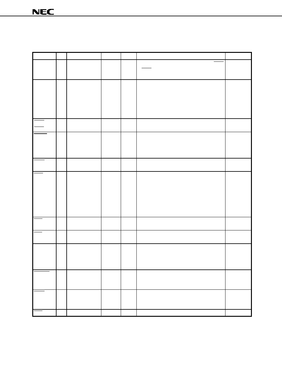
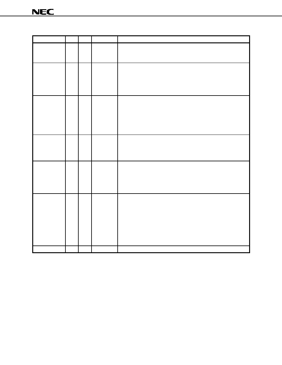
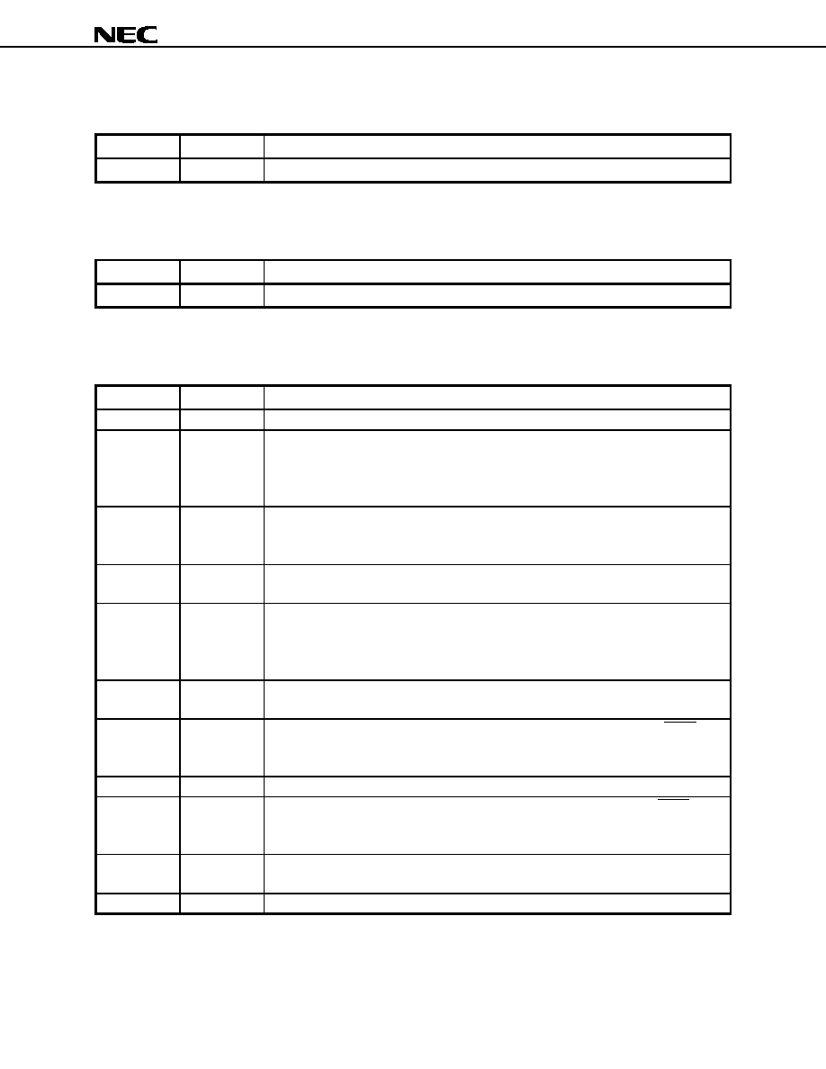
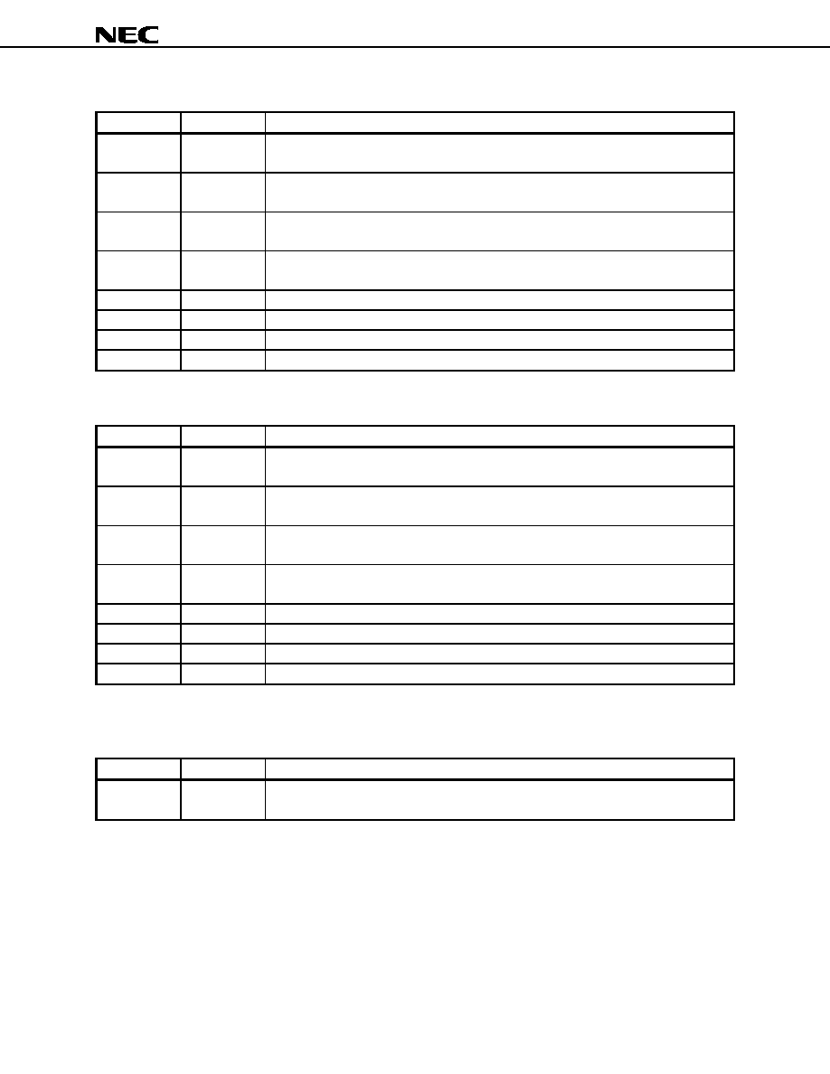
1. PIN FUNCTIONS
1.1 PCI/Cardbus Interface Signals: (52 pins)
(1/2)
Name
I/O
Pin No.
I
OL
Volts(V)
Function
Block *
PAR
I/O
44
PCI/Cardbus
5/3.3
Parity is even parity across AD0 to AD31 and CBE0
to CBE3. It is an input when AD0 to AD31 is an
input; it is an output when AD0 to AD31 is an output.
Link
AD0 to AD31
I/O
9, 10, 12, 13,
15 to18, 23, 24,
26 to 29, 32, 33,
47 to 50, 52, 53,
55, 56, 58, 59, 62,
63, 65 to 68
PCI/Cardbus
5/3.3
PCI Multiplexed Address and Data
Link
CBE0 to
CBE3
I/O
21, 34, 45, 57
-
5/3.3
Command/Byte Enables are multiplexed bus
commands & byte enables.
Link
FRAME
I/O
35
PCI/Cardbus
5/3.3
Frame is asserted by the initiator to indicate the
cycle beginning and is kept asserted during the
burst cycle. If Cardbus mode (CARD_ON = 1), this
pin should be pulled up to V
DD
.
Link
TRDY
I/O
37
PCI/Cardbus
5/3.3
Target Ready indicates that the current data phase
of the transaction is ready to be completed.
Link
IRDY
I/O
36
PCI/Cardbus
5/3.3
Initiator Ready indicates that the current bus
master is ready to complete the current data phase.
During a write, its assertion indicates that the
initiator is driving valid data onto the data bus.
During a read, its assertion indicates that the
initiator is ready to accept data from the currently-
addressed target.
Link
REQ
O
8
PCI/Cardbus
5/3.3
Bus_master Request indicates to the bus arbiter
that this device wants to become a bus master.
Link
GNT
I
7
-
5/3.3
Bus_master Grant indicates to this device that
access to the bus has been granted.
Link
IDSEL
I
22
-
5/3.3
Initialization Device Select is used as chip select
for configuration read/write transaction during the
phase of device initialization. If Cardbus mode
(CARD_ON = 1), this pin should be pulled up to V
DD
.
Link
DEVSEL
I/O
39
PCI/Cardbus
5/3.3
Device Select when actively driven, indicates that
the driving device has decoded its address as the
target of the current access.
Link
STOP
I/O
40
PCI/Cardbus
5/3.3
PCI Stop when actively driven, indicates that the
target is requesting the current bus master to stop
the transaction.
Link
PME
O
3
PCI/Cardbus
5/3.3
PME Output for power management event.
Link
Remark *: If the Link pin is pulled up, it should be connected to L_V
DD
.
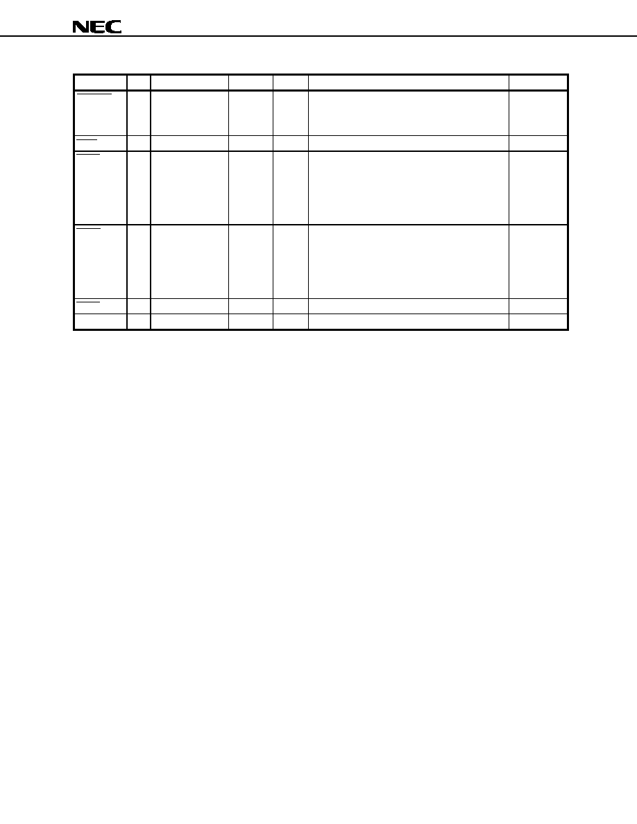
Preliminary Data Sheet S15306EJ2V0DS
9
µ
µ
µ
µ
PD72874
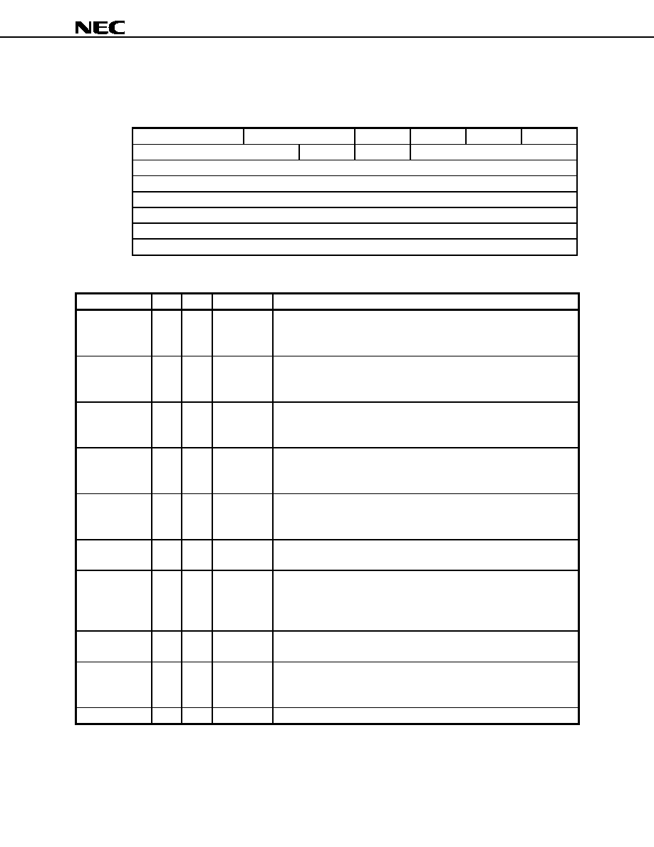
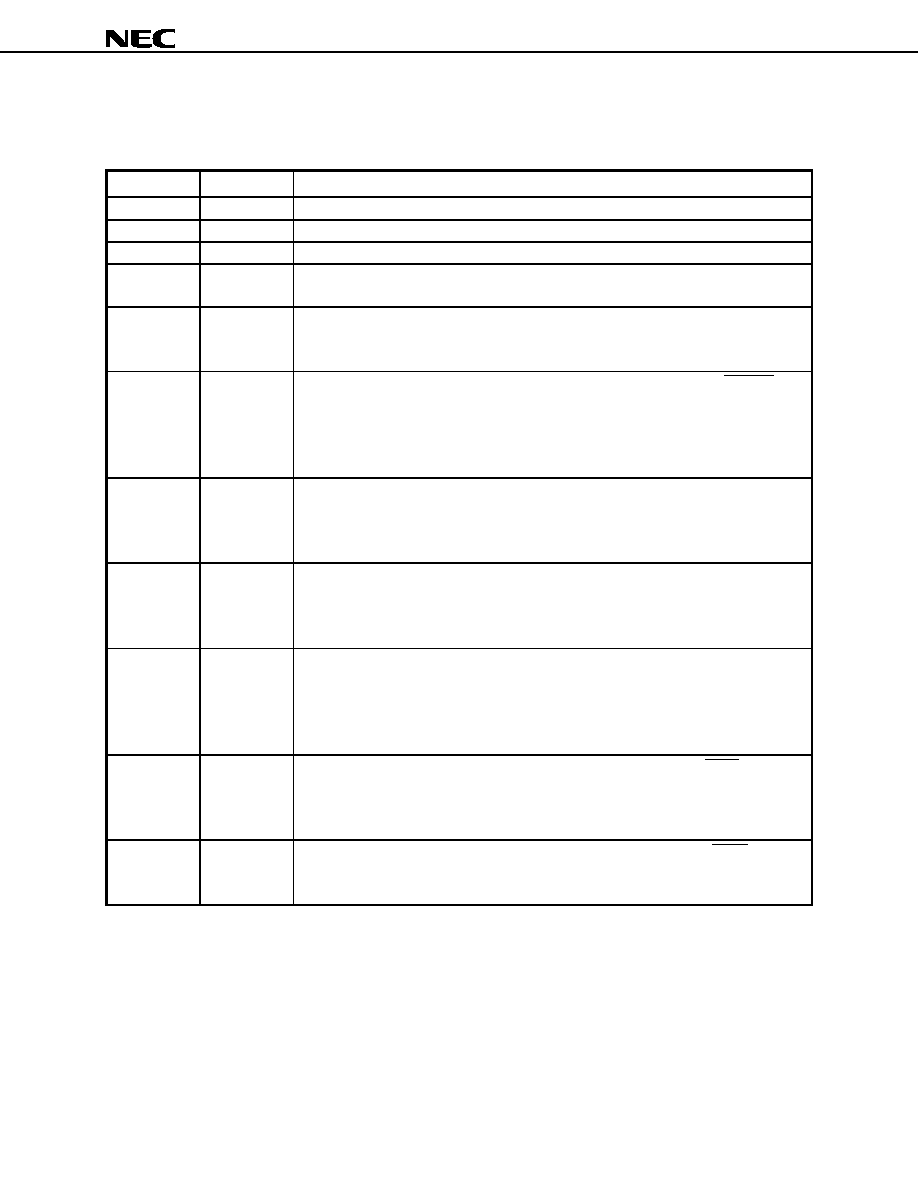
(2/2)
Name
I/O
Pin No.
I
OL
Volts(V)
Function
Block *
CLKRUN
I/O
2
PCI/Cardbus
5/3.3
PCICLK Running as input, to determine the status
of PCLK; as output, to request starting or speeding
up clock.
Link
INTA
O
4
PCI/Cardbus
5/3.3
Interrupt the PCI interrupt request A.
Link
PERR
I/O
41
PCI/Cardbus
5/3.3
Parity Error is used for reporting data parity errors
during all PCI transactions, except a special cycle.
It is an output when AD0 to AD31 and PAR are both
inputs. It is an input when AD0 to AD31 and PAR
are both outputs.
Link
SERR
O
42
PCI/Cardbus
5/3.3
System Error is used for reporting address parity
errors, data parity errors during the special cycle, or
any other system error where the effect can be
catastrophic. When reporting address parity errors,
it is an output.
Link
PRST
I
5
-
5/3.3
Reset PCI reset
Link
PCLK
I
6
-
5/3.3
PCI Clock 33 MHz system bus clock.
Link
Remark *: If the Link pin is pulled up, it should be connected to L_V
DD
.
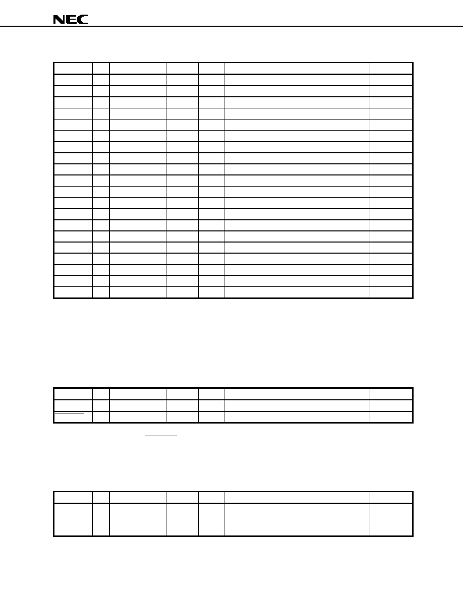
Preliminary Data Sheet S15306EJ2V0DS
10
µ
µ
µ
µ
PD72874
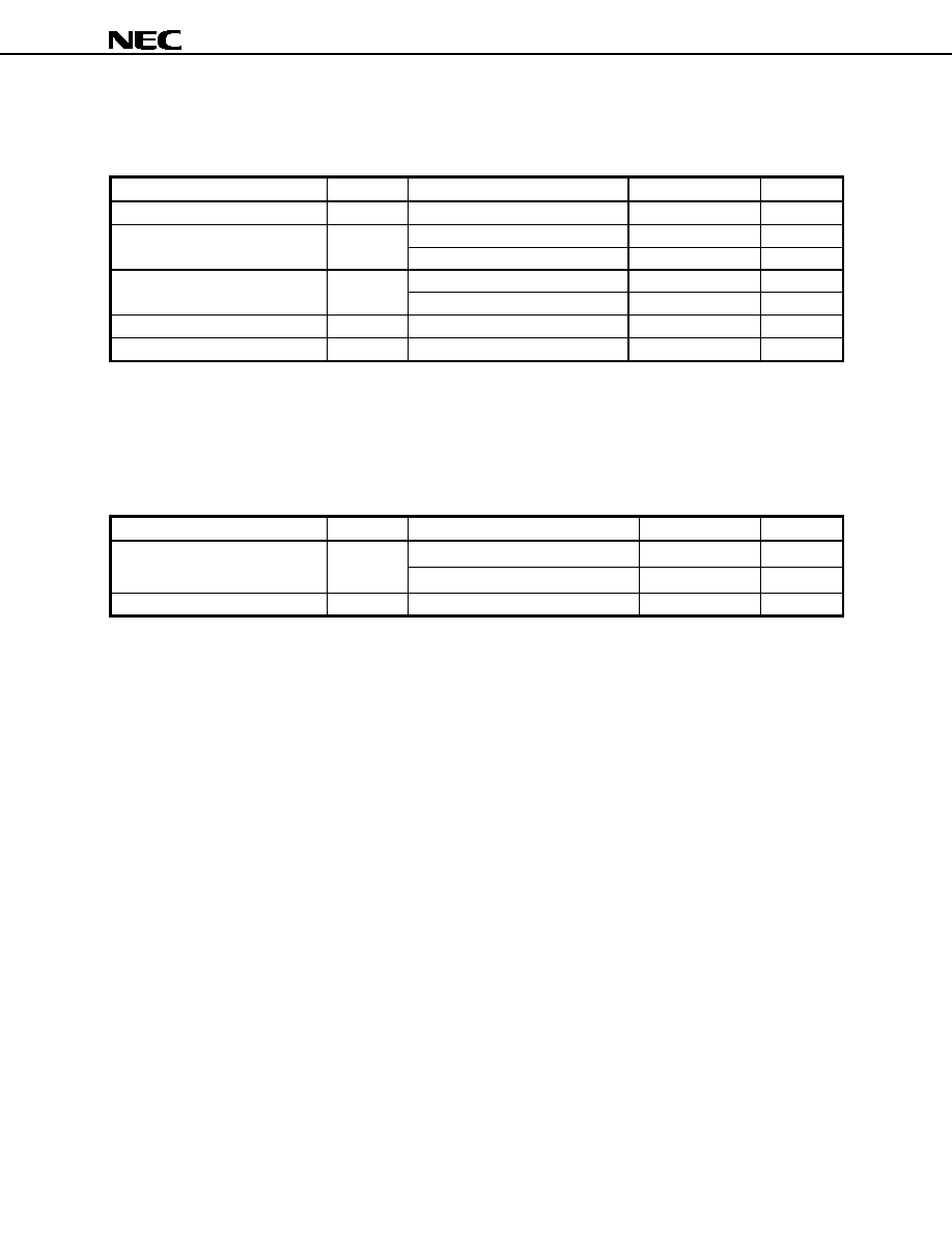
1.2 PHY Signals: (20 pins)
Name
I/O
Pin No.
I
OL
Volts(V)
Function
Block *
TpA0p
I/O
101
-
-
Port-1 Twisted Pair A Positive Input/Output
Note 1
PHY Analog
TpA0n
I/O
100
-
-
Port-1 Twisted Pair A Negative Input/Output
Note 1
PHY Analog
TpB0p
I/O
99
-
-
Port-1 Twisted Pair B Positive Input/Output
Note 1
PHY Analog
TpB0n
I/O
98
-
-
Port-1 Twisted Pair B Negative Input/Output
Note 1
PHY Analog
TpA1p
I/O
105
-
-
Port-2 Twisted Pair A Positive Input/Output
Note 1
PHY Analog
TpA1n
I/O
104
-
-
Port-2 Twisted Pair A Negative Input/Output
Note 1
PHY Analog
TpB1p
I/O
103
-
-
Port-2 Twisted Pair B Positive Input/Output
Note 1
PHY Analog
TpB1n
I/O
102
-
-
Port-2 Twisted Pair B Negative Input/Output
Note 1
PHY Analog
TpA2p
I/O
110
-
-
Port-3 Twisted Pair A Positive Input/Output
Note 1
PHY Analog
TpA2n
I/O
109
-
-
Port-3 Twisted Pair A Negative Input/Output
Note 1
PHY Analog
TpB2p
I/O
108
-
-
Port-3 Twisted Pair B Positive Input/Output
Note 1
PHY Analog
TpB2n
I/O
107
-
-
Port-3 Twisted Pair B Negative Input/Output
Note 1
PHY Analog
CPS
I
93
-
-
Cable Power Status Input
Note2
PHY Digital
TpBias0
O
96
-
-
Port-1 Twisted Pair Bias Voltage Output
Note 1
PHY Analog
TpBias1
O
97
-
-
Port-2 Twisted Pair Bias Voltage Output
Note 1
PHY Analog
TpBias2
O
111
-
-
Port-3 Twisted Pair Bias Voltage Output
Note 1
PHY Analog
RI0
-
91
-
-
Resistor0 for Reference Current Setting
Note 3
PHY Analog
RI1
-
92
-
-
Resistor1 for Reference Current Setting
Note 3
PHY Analog
XI
I
87
-
-
X'tal XI
PHY Analog
XO
O
88
-
-
X'tal XO
PHY Analog
Notes 1. If unused port, please refer to 4.1.4 Unused Ports.
2. Please refer to 4.1.3 CPS.
3. Please refer to 4.5 RI0, RI1.
Remark *: If the PHY Digital pin is pulled up, it should be connected to P_DV
DD
.
If the PHY Analog pin is pulled up, it should be connected to P_AV
DD
.
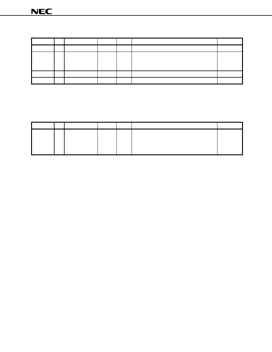
1.3 PHY Control Signals: (4 pins)
Name
I/O
Pin No.
I
OL
Volts(V)
Function
Block *
PC0 to PC2
I
70 to 72
-
3.3
Power Class Input
Note 1
PHY Digital
P_RESET
I
81
-
-
PHY Power on Reset Input
Note 2
PHY Digital
Notes 1. Please refer to 4.3 PC0 to PC2.
2. Please refer to 4.4 P_RESET.
Remark *: If the PHY Digital pin is pulled up, it should be connected to P_DV
DD
.
1.4 PCI/Cardbus Select Signal: (1 pin)
Name
I/O
Pin No.
I
OL
Volts(V)
Function
Block *
CARD_ON
I
119
-
3.3
PCI/CardBus Select
1:Cardbus mode
0:PCI bus mode
Link
Remark *: If the Link pin is pulled up, it should be connected to L_V
DD
.

Preliminary Data Sheet S15306EJ2V0DS
11
µ
µ
µ
µ
PD72874
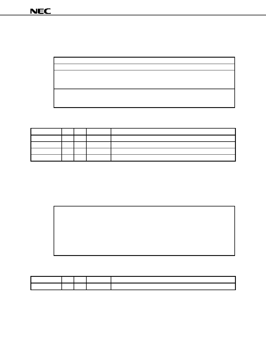
1.5 Serial ROM Interface Signals: (3 pins)
Name
I/O
Pin No.
I
OL
Volts(V)
Function
Block *
GROM_SDA
I/O
116
6 mA
3.3
Serial EEPROM Data Input / Output
Link
GROM_SCL
O
117
6 mA
3.3
Serial EEPROM Clock Output
Link
GROM_EN
I
118
-
3.3
Serial EEPROM Enable
1: GUID Load enable
0: GUID Load disable
Link
Remark *: If the Link pin is pulled up, it should be connected to L_V
DD
.
1.6 D3cold Wake Up Function Signals: (2 pins)
Name
I/O
Pin No.
I
OL
Volts(V)
Function
Block *
D3CSUP
I
114
-
5/3.3
D3cold Support
1: D3cold wake up enable
0: D3cold wake up disable
Link
RSMRST
I
74
-
5/3.3
Resume Reset
D3cold support (114 pin) = `1'
As this mode supports D3cold wake up,
RSMRST must connect system RSMRST
signal.
D3cold support (114 pin) = `0'
As this mode is the
µPD72872 compatible,
RSMRST clamp to `1'.
Link
Remark *: If the Link pin is pulled up, it should be connected to L_V
DD
.
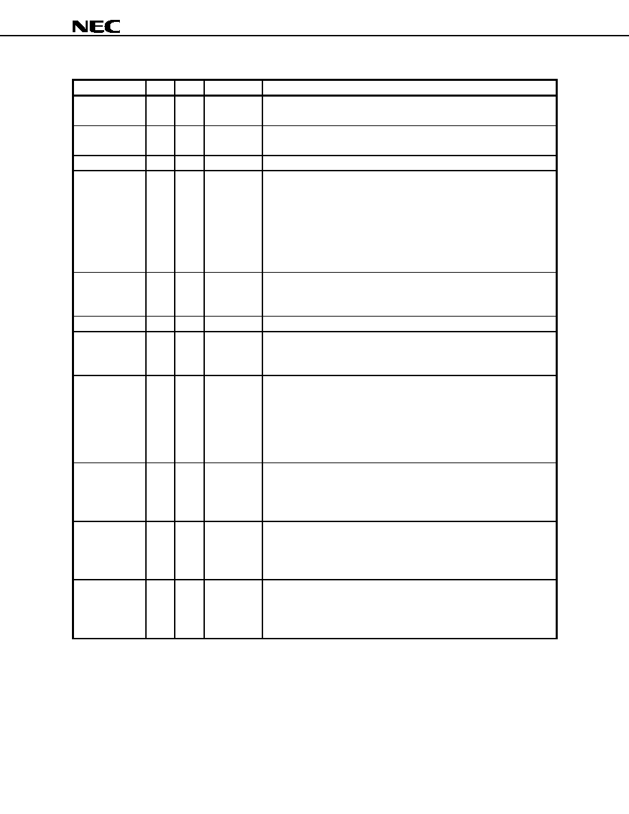
1.7 IC: (7 pins)
Name
I/O
Pin No.
I
OL
Volts(V)
Function
Block *
IC(H)
I
75
-
-
Internally Connected (High clamped)
Link
IC(L)
I
76 to 78, 80, 115
-
-
Internally Connected (Low clamped)
-
IC(N)
-
85
-
-
Internally Connected (Open)
-
Remark *: If the Link pin is pulled up, it should be connected to L_V
DD
.
Preliminary Data Sheet S15306EJ2V0DS
12
µ
µ
µ
µ
PD72874
1.8 V
DD
Name
I/O
Pin No.
I
OL
Volts(V)
Function
Block *
PCI_V
DD
-
19, 60
-
5/3.3
V
DD
for PCI I/Os
Link
L_V
DD
-
1, 14, 25, 31, 43,
51, 64
-
3.3
V
DD
for Link digital Core and Link I/Os
To use D3cold wake up function, L_V
DD
must switch
V
DD
to Vaux when the system suspend.
Link
P_DV
DD
-
73, 79, 82
-
3.3
PHY digital V
DD
PHY Digital
P_AV
DD
-
86, 90, 95, 112
-
3.3
PHY Analog V
DD
PHY Analog
Remark *: If the Link pin is pulled up, it should be connected to L_V
DD
.
If the PHY Digital pin is pulled up, it should be connected to P_DV
DD
.
If the PHY Analog pin is pulled up, it should be connected to P_AV
DD
.
1.9 GND
Name
I/O
Pin No.
I
OL
Volts(V)
Function
Block
GND
-
11, 20, 30, 38, 46,
54, 61, 69, 83, 84,
89, 94, 106, 113,
120
-
-
GND
-

Preliminary Data Sheet S15306EJ2V0DS
13
µ
µ
µ
µ
PD72874
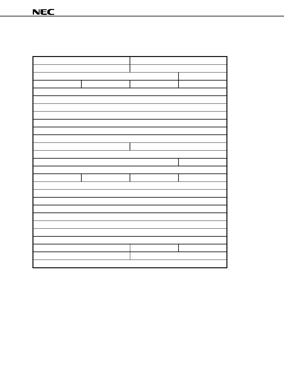
2. PHY REGISTERS
2.1 Complete Structure for PHY Registers
Figure 2-1. Complete Structure of PHY Registers
0
1
2
3
4
5
6
7
0000
Physical_ID
R
PS
0001
RHB
IBR
Gap_count
0010
Extended (7)
Reserved
Total_ports
0011
Max_speed
Reserved
Delay
0100
Link_active
Contender
Jitter
Pwr_class
0101
Watchdog
ISBR
Loop
Pwr_fail
Timeout
Port_event
Enab_accel
Enab_multi
0110
Reserved
0111
Page_select
Reserved
Port_select
1000
Register0 (page_select)
1001
Register1 (page_select)
1010
Register2 (page_select)
1011
Register3 (page_select)
1100
Register4 (page_select)
1101
Register5 (page_select)
1110
Register6 (page_select)
1111
Register7 (page_select)
Table 2-1. Bit Field Description (1/3)
Field
Size
R/W
Reset value
Description
Physical_ID
6
R
000000
Physical_ID value selected from Self_ID period.
R
1
R
0
If this bit is 1, the node is root.
1: Root
0: Not root
PS
1
R
Cable power status.
1: Cable power on
0: Cable power off
RHB
1
R/W
0
Root Hold -off bit. If 1, becomes root at the bus reset.
IBR
1
R/W
0
Initiate bus reset.
Setting to 1 begins a long bus reset.
Long bus reset signal duration: 166
µsec.
Returns to 0 at the beginning of bus reset.
Gap_count
6
R/W
111111
Gap count value.
It is updated by the changes of transmitting and receiving the PHY
configuration packet Tx/Rx.
The value is maintained after first bus reset.
After the second bus reset it returns to reset value.
Extended
3
R
111
Shows the extended register map.
Preliminary Data Sheet S15306EJ2V0DS
14
µ
µ
µ
µ
PD72874
Table 2-1. Bit Field Description (2/3)
Field
Size
R/W
Reset value
Description
Total_ports
4
R
0011
Supported port number.
0011: 3 ports
Max_speed
3
R
010
Indicate the maximum speed that this node supports.
010: 98.304, 196.608 and 393.216 Mbps
Delay
4
R
0000
Indicate worst case repeating delay time. 144 + (Delay x 20) = 144 nsec
Link_active
1
R/W
1
Link active.
1: Enable
0: Disable
The logical AND status of this bit and LPS.
State will be referred to "L bit" of Self-ID Packet#0.
The LPS is a PHY/Link interface signal and is defined in P1394a-2000. It is
an internal signal in the
µPD72874.
Contender
1
R/W
0
Contender.
"1" indicate this node support bus manager function. This bit will be referred
to "C bit" of Self-ID Packet#0.
Jitter
3
R
010
The difference of repeating time (Max.-Min.). (2+1) x 20=60 nsec
Pwr_class
3
R/W
See
Description
Power class.
Please refer to IEEE1394a-2000 [4.3.4.1].
This bit will be referred to Pwr field of Self-ID Packet#0.
Watchdog
1
R/W
0
Watchdog Enable.
This bit serves two purposes.
When set to 1, if any one port does resume, the Port_event bit becomes 1.
To determine whether or not an interrupt condition shall be indicated to the
link. On condition of LPS = 0 and Watchdog = 0, LKON as interrupt of Loop,
Pwr_fail, Timeout is not output.
ISBR
1
R/W
0
Initiate short (arbitrated) bus reset.
Setting to 1 acquires the bus and begins short bus reset.
Short bus reset signal output : 1.3
µsec
Returns to 0 at the beginning of the bus reset.
Loop
1
R/W
0
Loop detection output.
1: Detection
Writing 1 to this bit clears it to 0.
Writing 0 has no effect.
Pwr_fail
1
R/W
1
Power cable disconnect detect.
It becomes 1 when there is a change from 1 to 0 in the CPS bit.
Writing 1 to this bit clears it to 0.
Writing 0 has no effect.
Preliminary Data Sheet S15306EJ2V0DS
15
µ
µ
µ
µ
PD72874
Table 2-1. Bit Field Description (3/3)
Field
Size
R/W
Reset value
Description
Timeout
1
R/W
0
Arbitration state machine time-out.
Writing 1 to this bit clears it to 0.
Writing 0 has no effect.
Port_event
1
R/W
0
Set to 1 when the Int_enable bit in the register map of each port is 1 and
there is a change in the ports connected, Bias, Disabled and Fault bits.
Set to 1 when the Watchdog bit is 1 and any one port does resume.
Writing 1 to this bit clears it to 0.
Writing 0 has no effect.
Enab_accel
1
R/W
0
Enables arbitration acceleration.
Ack-acceleration and Fly-by arbitration are enabled.
1: Enabled
0: Disabled
If this bit changes while the bus request is pending, the operation is not
guaranteed.
Enab_multi
1
R/W
0
Enable multi-speed packet concatenation.
Setting this bit to 1 follows multi-speed transmission.
When this bit is set to 0,the packet will be transmitted with the same speed
as the first packet.
Page_select
3
R/W
000
Select page address between 1000 to 1111.
000: Port Status Page
001: Vendor ID Page
111: Vendor Dependent Page
Others: Unused
Port_select
4
R/W
0000
Port Selection.
Selecting 000 (Port Status Page) with the Page_select selects the port.
Selecting 111 (Vendor Dependent Page) with the Page_select have to select
the Port 1.
0000: Port 0
0001: Port 1
0010: Port 2
Others: Unused
Reserved
-
R
000...
Reserved. Read as 0.
Preliminary Data Sheet S15306EJ2V0DS
16
µ
µ
µ
µ
PD72874
2.2 Port Status Page (Page 000)
Figure 2-2. Port Status Page
0
1
2
3
4
5
6
7
1000
AStat
BStat
Child
Connected
Bias
Disabled
1001
Negotiated_speed
Int_enable
Fault
Reserved
1010
Reserved
1011
Reserved
1100
Reserved
1101
Reserved
1110
Reserved
1111
Reserved
Table 2-2. Bit Field Description
Field
Size
R/W
Reset value
Description
AStat
2
R
XX
A port status value.
00: invalid, 10: "0"
01: "1", 11: "Z"
BStat
2
R
XX
B port status value.
00: invalid, 10: "0"
01: "1", 11: "Z"
Child
1
R
Child node status value.
1: Connected to child node
0: Connected to parent node
Connected
1
R
0
Connection status value.
1: Connected
0: Disconnected
Bias
1
R
Bias voltage status value.
1: Bias voltage
0: No bias voltage
Disabled
1
R/W
See
Description
The reset value is set to 0: Enabled.
Negotiated_
Speed
3
R
Shows the maximum data transfer rate of the node connected to this port.
000: 100 Mbps
001: 200 Mbps
010: 400 Mbps
Int_enable
1
R/W
0
When set to 1, the Port_event is set to 1 if any of this port's Connected, Bias,
Disabled or Fault bits change state.
Fault
1
R/W
0
Set to 1 if an error occurs during Suspend/Resume.
Writing 1 to this bit clears it to 0.
Writing 0 has no effect.
Reserved
-
R
000...
Reserved. Read as 0.
Preliminary Data Sheet S15306EJ2V0DS
17
µ
µ
µ
µ
PD72874
2.3 Vendor ID Page (Page 001)
Figure 2-3. Vendor ID Page
0
1
2
3
4
5
6
7
1000
Compliance_level
1001
Reserved
1010
1011
1100
Vendor_ID
1101
1110
1111
Product_ID
Table 2-3. Bit Field Description
Field
Size
R/W
Reset value
Description
Compliance_level
8
R
00000001
According to IEEE1394a-2000.
Vendor_ID
24
R
00004CH
Company ID Code value, NEC IEEE OUI.
Product_ID
24
R
Product code.
Reserved
-
R
000...
Reserved. Read as 0.
2.4 Vendor Dependent Page (Page 111 : Port_select 0001)
Figure 2-4. Vendor Dependent Page
0
1
2
3
4
5
6
7
1000
1001
1010
1011
1100
1101
1110
1111
Reg_array
Table 2-4. Bit Field Description
Field
Size
R/W
Reset value
Description
Reg_array
64
R/W
0
This register array is possible R/W.
Preliminary Data Sheet S15306EJ2V0DS
18
µ
µ
µ
µ
PD72874
3. CONFIGURATION REGISTERS
3.1 PCI Bus Mode Configuration Register (CARD_ON = Low)
31
24
23
16
15
08
07
00
Device ID
Vendor ID
00H
Status
Command
04H
Class Code
Revision ID
08H
BIST
Header Type
Latency Timer
Cache Line Size
0CH
Base Address 0
10H
Reserved
14H
Reserved
18H
Reserved
1CH
Reserved
20H
Reserved
24H
Reserved
28H
Subsystem ID
Subsystem Vendor ID
2CH
Reserved
30H
Reserved
Cap_Ptr
34H
Reserved
38H
Max_Lat
Min_Gnt
Interrupt Pin
Interrupt Line
3CH
PCI_OHCI_Control
40H
Reserved
44H
Reserved
48H
Reserved
4CH
Reserved
50H
Reserved
54H
Reserved
58H
Reserved
5CH
Power Management Capabilities
Next_Item_Ptr
Cap_ID
60H
Reserved
Power Management Control/Status
64H
Reserved
68H
FCH
Preliminary Data Sheet S15306EJ2V0DS
19
µ
µ
µ
µ
PD72874
3.1.1 Offset_00 Vendor ID Register
This register identifies the manufacturer of the
µPD72874. The ID is assigned by the PCI_SIG committee.
Bits
R/W
Description
15-0
R
Constant value of 1033H.
3.1.2 Offset_02 Device ID Register
This register identifies the type of the device for the
µPD72874. The ID is assigned by NEC Corporation.
Bits
R/W
Description
15-0
R
Constant value of 00F2H.
3.1.3 Offset_04 Command Register
The register provides control over the device's ability to generate and respond to PCI cycles.
Bits
R/W
Description
0
R
I/O enable Constant value of 0. The
µPD72874 does not respond to PCI I/O accesses.
1
R/W
Memory enable Default value of 1. It defines if the
µPD72874 responds to PCI memory
accesses. This bit should be set to one upon power-up reset.
0: The
µPD72874 does not respond to PCI memory cycles
1: The
µPD72874 responds to PCI memory cycles
2
R/W
Master enable Default value of 1. It enables the
µPD72874 as bus-master on the PCI-bus.
0: The
µPD72874 cannot generate PCI accesses by being a bus-master
1: The
µPD72874 is capable of acting as a bus-master
3
R
Special cycle monitor enable Constant value of 0. The special cycle monitor is always
disabled.
4
R/W
Memory write and invalidate enable Default value of 0. It enables Memory Write and Invalid
Command generation.
0: Memory write must be used
1: The
µPD72874, when acts as PCI master, can generate the command
5
R
VGA
TM
color palette invalidate enable Constant value of 0. VGA color palette invalidate is
always disabled.
6
R/W
Parity error response Default value of 0. It defines if the
µPD72874 responds to PERR.
0: Ignore parity error
1: Respond to parity error
7
R
Stepping enable Constant value of 0. Stepping is always disabled.
8
R/W
System error enable Default value of 0. It defines if the
µPD72874 responds to SERR.
0: Disable system error checking
1: Enable system error checking
9
R
Fast back-to-back enable Constant value of 0. Fast back-to-back transactions are only
allowed to the same agent.
15-10
R
Reserved Constant value of 000000.
Preliminary Data Sheet S15306EJ2V0DS
20
µ
µ
µ
µ
PD72874
3.1.4 Offset_06 Status Register
This register tracks the status information of PCI-bus related events which are relevant to the
µPD72874. "Read"
and "Write" are handled somewhat differently.
Bits
R/W
Description
3-0
R
Reserved Constant value of 0000.
4
R
New capabilities Constant value of 1. It indicates the existence of the Capabilities List.
6,5
R
Reserved Constant value of 00.
7
R
Fast back-to-back capable Constant value of 1. It indicates that the
µPD72874, as a target,
cannot accept fast back-to-back transactions when the transactions are not to the same agent.
8
R/W
Signaled parity error Default value of 0. It indicates the occurrence of any "Data Parity".
0: No parity detected (default)
1: Parity detected
10,9
R
DEVSEL timing Constant value of 01. These bits define the decode timing for DEVSEL.
0: Fast (1 cycle)
1: Medium (2 cycles)
2: Slow (3 cycles)
3: undefined
11
R/W
Signaled target abort Default value of 0. This bit is set by a target device whenever it
terminates a transaction with "Target Abort".
0: The
µPD72874 did not terminate a transaction with Target Abort
1: The
µPD72874 has terminated a transaction with Target Abort
12
R/W
Received target abort Default value of 0. This bit is set by a master device whenever its
transaction is terminated with a "Target Abort".
0: The
µPD72874 has not received a Target Abort
1: The
µPD72874 has received a Target Abort from a bus-master
13
R/W
Received master abort Default value of 0. This bit is set by a master device whenever its
transaction is terminated with "Master Abort". The
µPD72874 asserts "Master Abort" when a
transaction response exceeds the time allocated in the latency timer field.
0: Transaction was not terminated with a Master Abort
1: Transaction has been terminated with a Master Abort
14
R/W
Signaled system error Default value of 0. It indicates that the assertion of SERR by the
µPD72874.
0: System error was not signaled
1: System error was signaled
15
R/W
Received parity error Default value of 0. It indicates the occurrence of any PERR.
0: No parity error was detected
1: Parity error was detected
Preliminary Data Sheet S15306EJ2V0DS
21
µ
µ
µ
µ
PD72874
3.1.5 Offset_08 Revision ID Register
This register specifies a revision number assigned by NEC Corporation for the
µPD72874.
Bits
R/W
Description
7-0
R
Default value of 01H. It specifies the silicon revision. It will be incremented for subsequent
silicon revisions.
3.1.6 Offset_09 Class Code Register
This register identifies the class code, sub-class code, and programming interface of the
µPD72874.
Bits
R/W
Description
7-0
R
Constant value of 10H. It specifies an IEEE1394 OHCI-compliant Host Controller.
15-8
R
Constant value of 00H. It specifies an "IEEE1394" type.
23-16
R
Constant value of 0CH. It specifies a "Serial Bus Controller".
3.1.7 Offset_0C Cache Line Size Register
This register specifies the system cache line size, which is PC-host system dependent, in units of 32-bit words.
The following cache line sizes are supported: 2, 4, 8, 16, 32, 64, and 128. All other values will be recognized as 0,
i.e. cache disabled.
Bits
R/W
Description
7-0
R/W
Default value of 00H.
3.1.8 Offset_0D Latency Timer Register
This register defines the maximum amount of time that the
µPD72874 is permitted to retain ownership of the bus
after it has acquired bus ownership and initiated a subsequent transaction.
Bits
R/W
Description
7-0
R/W
Default value of 00H. It specifies the number of PCI-bus clocks that the
µPD72874 may hold
the PCI bus as a bus-master.
3.1.9 Offset_0E Header Type Register
Bits
R/W
Description
7-0
R
Constant value of 00H. It specifies a single function device.
3.1.10 Offset_0F BIST Register
Bits
R/W
Description
7-0
R
Constant value of 00H. It specifies whether the device is capable of Built-in Self Test.
Preliminary Data Sheet S15306EJ2V0DS
22
µ
µ
µ
µ
PD72874
3.1.11 Offset_10 Base Address 0 Register
This register specifies the base memory address for accessing all the "Operation registers" (i.e. control,
configuration, and status registers) of the
µPD72874, while the BIOS is expected to set this value during power-up
reset.
Bits
R/W
Description
11-0
R
Constant value of 000H. These bits are "read-only".
31-12
R/W
-
3.1.12 Offset_2C Subsystem Vendor ID Register
This register identifies the subsystem that contains the NEC's
µPD72874 function. While the ID is assigned by the
PCI_SIG committee, the value should be loaded into the register from the external serial ROM after power-up reset.
Access to this register through PCI-bus is prohibited.
Bits
R/W
Description
15-0
R
Default value of 1033H.
3.1.13 Offset_2E Subsystem ID Register
This register identifies the type of the subsystem that contains the NEC's
µPD72874 function. While the ID is
assigned by the manufacturer, the value should be loaded into the register from the external serial EEPROM after
power-up reset. Access to this register through PCI-bus is prohibited.
Bits
R/W
Description
15-0
R
Default value of 00F2H.
3.1.14 Offset_34 Cap_Ptr Register
This register points to a linked list of additional capabilities specific to the
µPD72874, the NEC's implementation of
the 1394 OHCI specification.
Bits
R/W
Description
7-0
R
Constant value of 60H. The value represents an offset into the
µPD72874's PCI Configuration
Space for the location of the first item in the New Capabilities Linked List.
3.1.15 Offset_3C Interrupt Line Register
This register provides the interrupt line routing information specific to the
µPD72874, the NEC's implementation of
the 1394 OHCI specification.
Bits
R/W
Description
7-0
R/W
Default value of 00H. It specifies which input of the host system interrupt controller the
interrupt pin of the
µPD72874 is connected to.
Preliminary Data Sheet S15306EJ2V0DS
23
µ
µ
µ
µ
PD72874
3.1.16 Offset_3D Interrupt Pin Register
This register provides the interrupt line routing information specific to the
µPD72874, the NEC's implementation of
the 1394 OHCI specification.
Bits
R/W
Description
7-0
R
Constant value of 01H. It specifies PCI INTA is used for interrupting the host system.
3.1.17 Offset_3E Min_Gnt Register
This register specifies how long of a burst period the
µPD72874 needs, assuming a clock rate of 33 MHz.
Resolution is in units of º
µs. The value should be loaded into the register from the external serial EEPROM upon
power-up reset, and access to this register through PCI-bus is prohibited.
Bits
R/W
Description
7-0
R
Default value of 00H. Its value contributes to the desired setting for Latency Timer value.
3.1.18 Offset_3F Max_Lat Register
This register specifies how often the
µPD72874 needs to gain access to the PCI-bus, assuming a clock rate of 33
MHz. Resolution is in units of º
µs. The value should be loaded into the register from the external serial EEPROM
after hardware reset, and access to this register through PCI-bus is prohibited.
Bits
R/W
Description
7-0
R
Default value of 00H. Its value contributes to the desired setting for Latency Timer value.
3.1.19 Offset_40 PCI_OHCI_Control Register
This register specifies the control bits that are IEEE1394 OHCI specific. Vendor options are not allowed in this
register. It is reserved for OHCI use only.
Bits
R/W
Description
0
R/W
PCI global SWAP Default value of 0. When this bit is 1, all quadrates read from and written to
the PCI Interface are byte swapped, thus a "PCI Global Swap". PCI addresses for expansion
ROM and PCI Configuration registers, are, however, unaffected by this bit. This bit is not
required for motherboard implementations.
31-1
R
Reserved Constant value of all 0.
3.1.20 Offset_60 Cap_ID & Next_Item_Ptr Register
The Cap_ID signals that this item in the Linked List is the registers defined for PCI Power Management, while the
Next_Item_Ptr describes the location of the next item in the
µPD72874's Capability List.
Bits
R/W
Description
7-0
R
Cap_ID Constant value of 01H. The default value identified the Link List item as being the PCI
Power Management registers, while the ID value is assigned by the PCI SIG.
15-8
R
Next_Item_Ptr Constant value of 00H. It indicated that there are no more items in the Link
List.
Preliminary Data Sheet S15306EJ2V0DS
24
µ
µ
µ
µ
PD72874
3.1.21 Offset_62 Power Management Capabilities Register
This is a 16-bit read-only register that provides information on the power management capabilities of the
µPD72874.
Bits
R/W
Description
2-0
R
Version Constant value of 010. The power management registers are implemented as
defined in revision 1.1 of PCI Bus Power Management Interface Specification.
3
R
PME clock Constant value of 0.
4
R
Reserved Constant value of 0.
5
R
DSI Constant value of 0.
8-6
R
Auxiliary Power Default value of 000. This field reports the Vaux power requirements for the
µPD72874. This data is programable from EEPROM.
111 ≠ 375 mA maximum current required for a 3.3 Vaux,
110 ≠ 320 mA maximum current required for a 3.3 Vaux,
101 ≠ 270 mA maximum current required for a 3.3 Vaux,
100 ≠ 220 mA maximum current required for a 3.3 Vaux,
011 ≠ 160 mA maximum current required for a 3.3 Vaux,
010 ≠ 100 mA maximum current required for a 3.3 Vaux,
001 ≠ 55 mA maximum current required for a 3.3 Vaux,
000 ≠ 0 (self powered)
9
R
D1_support Constant value of 1. The
µPD72874 supports the D1 Power Management state.
10
R
D2_support Constant value of 1. The
µPD72874 supports the D2 Power Management state.
15-11
R
PME_support
D3SUP = `High' : Constant value of 11111.
D3SUP = `Low' : Constant value of 01111.
This field indicates the power states in which the
µPD72874 may assert PME. A value of "0" for
any bit indicates that the function is not capable of asserting the PME signal while in that power
state.
bit (11) ≠ PME_D0. PME can be asserted from D0.
bit (12) ≠ PME_D1. PME can be asserted from D1.
bit (13) ≠ PME_D2. PME can be asserted from D2.
bit (14) ≠ PME_D3hot. PME can be asserted from D3hot.
bit (15) ≠ PME_D3cold. PME can be asserted from D3cold.

Preliminary Data Sheet S15306EJ2V0DS
25
µ
µ
µ
µ
PD72874
3.1.22 Offset_64 Power Management Control/Status Register
This is a 16-bit register that provides control status information of the
µPD72874.
Bits
R/W
Description
1,0
R/W
PowerState Default value is undefined. This field is used both to determine the current power
state of the
µPD72874 and to set the µPD72874 into a new power state.
00: D0 (DMA contexts: ON, Link Layer: ON, PME will be asserted upon INTA being active.)
01: D1 (DMA contexts: OFF, Link Layer: ON, PME will be asserted upon INTA being active)
10: D2 (DMA contexts: OFF, Link Layer: OFF, LPS: OFF, PME will be asserted upon
LinkON being active)
11: D3 (DMA contexts: OFF, Link Layer: OFF, LPS: OFF, PME will be asserted upon
LinkON being active)
The LPS is a PHY/Link interface signal and is defined in P1394a-2000. It is an internal signal in
the
µPD72874.
7-2
R
Reserved Constant value of 000000.
8
R/W
PME_En Default value of 0. This field is used to enable the specific power management
features of the
µPD72874.
12-9
R
Data_Select Constant value of 0000.
14,13
R
Data_Scale Constant value of 00.
15
R/W
PME_Status Default value is undefined. A write of `1' clears this bit, while a write of `0' is
ignored.
Preliminary Data Sheet S15306EJ2V0DS
26
µ
µ
µ
µ
PD72874
3.2 CardBus Mode Configuration Register (CARD_ON = High)
31
24
23
16
15
08
07
00
Device ID
Vendor ID
00H
Status
Command
04H
Class Code
Revision ID
08H
BIST
Header Type
Latency Timer
Cache Line Size
0CH
Base Address 0
10H
Base Address 1 (Cardbus Status Reg)
Note
14H
Base Address 2 (Cardbus Status Reg)
Note
18H
Reserved
1CH
Reserved
20H
Reserved
24H
Cardbus CIS Pointer
Note
28H
Subsystem ID
Subsystem Vendor ID
2CH
Reserved
30H
Reserved
Cap_Ptr
34H
Reserved
38H
Max_Lat
Min_Gnt
Interrupt Pin
Interrupt Line
3CH
PCI_OHCI_Control
40H
Reserved
44H
Reserved
48H
Reserved
4CH
Reserved
50H
Reserved
54H
Reserved
58H
Reserved
5CH
Power Management Capabilities
Next_Item_Ptr
Cap_ID
60H
Reserved
Power Management Control/Status
64H
Reserved
68H
Reserved
6CH
Reserved
70H
Reserved
74H
Reserved
78H
Reserved
7CH
CIS Area
Note
80H
FCH
Note Different from PCI Bus Mode Configuration Register.
Preliminary Data Sheet S15306EJ2V0DS
27
µ
µ
µ
µ
PD72874
3.2.1 Offset_14/18 Base Address 1/2 Register (Cardbus Status Registers)
Bits
R/W
Description
7-0
R
Constant value of 00.
31-8
R/W
-
(1) Function Event Register (FER) (Base Address 1 (2) + 0H)
Bits
R/W
Description
0
R
Write Protect (No Use).
Read only as `0'
1
R
Ready Status (No Use).
Read only as `0'
2
R
Battery Voltage Detect 2 (No Use).
Read only as `0'
3
R
Battery Voltage Detect 1 (No Use).
Read only as `0'
4
R/W
General Wake Up
14-5
R
Reserved. Read only as `0'
15
R/W
Interrupt
31-16
R
Reserved. Read only as `0'
(2) Function Event Mask Register (FEMR) (Base Address 1 (2) + 4H)
Bits
R/W
Description
0
R
Write Protect (No Use).
Read only as `0'
1
R
Ready Status (No Use).
Read only as `0'
2
R
Battery Voltage Detect 2 (No Use).
Read only as `0'
3
R
Battery Voltage Detect 1 (No Use).
Read only as `0'
4
R/W
General Wake Up Mask
5
R
BAM. Read only as `0'
6
R
PWM. Read only as `0'
13-7
R
Reserved. Read only as `0'
14
R/W
Wake Up Mask
15
R/W
Interrupt
31-16
R
Reserved. Read only as `0'
Preliminary Data Sheet S15306EJ2V0DS
28
µ
µ
µ
µ
PD72874
(3) Function Reset Status Register (FRSR) (Base Address 1 (2) + 8H)
Bits
R/W
Description
0
R
Write Protect (No Use).
Read only as `0'
1
R
Ready Status (No Use).
Read only as `0'
2
R
Battery Voltage Detect 2 (No Use).
Read only as `0'
3
R
Battery Voltage Detect 1 (No Use).
Read only as `0'
4
R/W
General Wake Up Mask
14-5
R
Reserved. Read only as `0'
15
R/W
Interrupt
31-16
R
Reserved. Read only as `0'
(4) Function Force Event Register (FFER) (Base Address 1 (2) + CH)
Bits
R/W
Description
0
R
Write Protect (No Use).
Read only as `0'
1
R
Ready Status (No Use).
Read only as `0'
2
R
Battery Voltage Detect 2 (No Use).
Read only as `0'
3
R
Battery Voltage Detect 1 (No Use).
Read only as `0'
4
R/W
General Wake Up Mask
14-5
-
No Use
15
R/W
Interrupt
31-16
R
Reserved. Read only as `0'
3.2.2 Offset_28 Cardbus CIS Pointer
This register specifies start memory address of the Cardbus CIS Area.
Bits
R/W
Description
31-0
R
Starting Pointer of CIS Area.
Constant value of 00000080H.
3.2.3 Offset_80 CIS Area
The
µPD72874 supports external Serial ROM (AT24C02 compatible) interface.
CIS Area Register can be loaded from external Serial ROM in the CIS area when CARD_ON is 1.
Preliminary Data Sheet S15306EJ2V0DS
29
µ
µ
µ
µ
PD72874
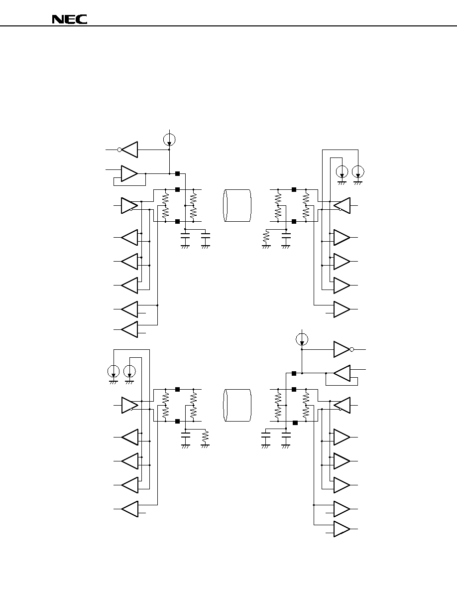
4. PHY FUNCTION
4.1 Cable Interface
4.1.1 Connections
Figure 4-1. Cable Interface
+
-
+
-
+
-
+
-
+
-
+
-
56
56
7 k
7 k
Connection Detection Current
Connection Detection Comparator
TpAp
TpBias
TpAn
Driver
Receiver
Arbitration Comparators
Common Mode Comparators
+
-
+
-
+
-
+
-
56
56
7 k
7 k
TpBp
TpBn
Driver
Receiver
Arbitration Comparators
Common Mode Comparator
Common Mode Speed Current Driver
1
µ
F
270 pF
5.1 k
+
-
+
-
+
-
+
-
+
-
+
-
56
56
7 k
7 k
Connection Detection Current
Connection Detection Comparator
TpAp
TpBias
TpAn
Driver
Receiver
Arbitration Comparators
Common Mode Comparators
1
µ
F
+
-
+
-
+
-
+
-
56
56
7 k
7 k
TpBp
TpBn
Driver
Receiver
Arbitration Comparators
Common Mode Comparator
Common Mode Speed Current driver
270 pF
5.1 k
0.01
µ
F
0.01
µ
F

Preliminary Data Sheet S15306EJ2V0DS
30
µ
µ
µ
µ
PD72874
4.1.2 Cable Interface Circuit
Each port is configured with two twisted-pairs of TpA and TpB.
TpA and TpB are used to monitor the state of the Transmit/Receive line, control signals, data and cables.
During transmission to the IEEE1394 bus, the Data/Strobe signal received from the Link layer controller is
encoded, converted from parallel to serial and transmitted.
While receiving from the IEEE1394 bus, the Data/Strobe signal from TpA, TpB is converted from serial to parallel
after synchronization by SCLK
Note
, then transmitted to the Link layer controller in 2/4/8 bits according to the data rate
of 100/200/400 Mbps.
The bus arbitration for TpA and TpB and the state of the line are monitored by the built-in comparator. The state of
the 1394 bus is transmitted to the state machine in the LSI.
Note The SCLK is a PHY/Link interface signal and is defined in P1394a-2000. It is an internal signal in the
µPD72874.
4.1.3 CPS
Connect an external resistor of 390 k
between the CPS pin and the power cable, and an external resistor of 100
k
between the CPS pin and the GND to monitor the power of the power cable.
If the cable power falls under 7.5 V there is an indication to the Link layer that the power has failed.
4.1.4 Unused Ports
TpAp, TpAn : Not connected
TpBp, TpBn : AGND
TpBias : Not connected
4.2 PLL and Crystal Oscillation Circuit
4.2.1 Crystal Oscillation Circuit
To supply the clock of 24.576 MHz ± 100 ppm, use an external capacitor of 10 pF and a crystal of 50 ppm.
4.2.2 PLL
The crystal oscillator multiplies the 24.576 MHz frequency by 16 (393.216 MHz).
4.3 PC0 to PC2
The PC0 to PC2 pin corresponds to the power field of the Self_ID packet and Pwr_class in the PHY register. Refer
to Section 4.3.4.1 of the IEEE1394-1995 specification for information regarding the Pwr_class. The value of Pwr can
be changed with software through the Link layer; this pin sets the initial value during Power-on Reset. Use a pull-up
or pull-down resistor of 1 k
based on the application.
4.4 P_RESET
Connect an external capacitor of 0.1
µF between the pins P_RESET and GND. If the voltage drops below 0 V, a
reset pulse is generated. All of the circuits are initialized, including the contents of the PHY register.
4.5 RI0, RI1
Connect an external resistor of 9.1 k
± 0.5 % to limit the LSI's current.
Preliminary Data Sheet S15306EJ2V0DS
31
µ
µ
µ
µ
PD72874
5. ELECTRICAL SPECIFICATIONS
Absolute Maximum Ratings
Parameter
Symbol
Condition
Rating
Unit
Power supply voltage
V
DD
≠0.5 to +4.6
V
LVTTL @ (V
I
< 0.5 V + V
DD
)
≠0.5 to +4.6
V
Input voltage
V
I
PCI @ (V
I
< 3.0 V + V
DD
)
≠0.5 to +6.6
V
LVTTL @ (V
O
< 0.5 V + V
DD
)
≠0.5 to +4.6
V
Output voltage
V
O
PCI @ (V
O
< 3.0 V + V
DD
)
≠0.5 to +6.6
V
Operating ambient temperature
T
A
0 to +70
∞C
Storage temperature
T
stg
≠65 to +150
∞C
Caution Product quality may suffer if the absolute maximum rating is exceeded even momentarily for any
parameter. That is, the absolute maximum ratings are rated values at which the product is on the
verge of suffering physical damage, and therefore the product must be used under conditions that
ensure that the absolute maximum ratings are not exceeded.
Recommended Operating Ranges
Parameter
Symbol
Condition
Rating
Unit
Used to clamp reflection on PCI bus.
4.5 to 5.5
V
Power supply voltage
V
DD
3.0 to 3.6
V
Operating ambient temperature
T
A
0 to +70
∞C
Preliminary Data Sheet S15306EJ2V0DS
32
µ
µ
µ
µ
PD72874
DC Characteristics (V
DD
= 3.3 V
±
±
±
± 10 %, V
SS
= 0 V, T
A
= 0 to +70
∞
∞
∞
∞C)
Parameter
Symbol
Condition
MIN.
TYP.
MAX.
Unit
High-level input voltage
V
IH
2.0
V
DD
+0.5
V
Low-level input voltage
V
IL
≠0.5
+0.8
V
High-level output current
I
OH
V
OH
= 2.4 V,
GROM_SDA, GROM_SCL
≠6
mA
Low-level output current
I
OL
V
OL
= 0.4 V,
GROM_SDA, GROM_SCL
6
mA
Input leakage current
I
L
V
IN
= V
DD
or GND
±10.0
µA
PCI interface
High-level input voltage
V
IH
2.0
5.5
V
Low-level input voltage
V
IL
≠0.5
+0.8
V
High-level output current
I
OH
V
OH
= 2.4 V
≠2
mA
Low-level output current
I
OL
V
OL
= 0.4 V
9
mA
Input leakage current
I
L
V
IN
= V
DD
or GND
±10.0
µA
Cable interface
Cable input, 100 Mbps operation
142
260
mV
Cable input, 200 Mbps operation
132
260
mV
Differential input voltage
V
ID
Cable input, 400 Mbps operation
118
260
mV
100 Mbps speed signaling off
1.165
2.515
V
200 Mbps speed signaling
0.935
2.515
V
TpB common mode input voltage
V
ICM
400 Mbps speed signaling
0.523
2.515
V
Differential output voltage
V
OD
Cable output (Test load 55
)
172.0
265.0
mV
100 Mbps speed signaling off
1.665
2.015
V
200 Mbps speed signaling
1.438
2.015
V
TpA common mode output voltage
V
OCM
400 Mbps speed signaling
1.030
2.015
V
100 Mbps speed signaling off
≠0.81
+0.44
mA
200 Mbps speed signaling
≠4.84
≠2.53
mA
TpA common mode output current
I
CM
400 Mbps speed signaling
≠12.40
≠8.10
mA
Power status threshold voltage
V
TH
CPS
7.5
V
TpBias output voltage
V
TPBIAS
1.665
2.015
V
Remarks 1. Digital core runs at 3.3 V.
2. PCI Interface can run at 5 or 3.3 V, depending on the choice of 5 V-PCI or 3.3 V-PCI.
3. All other I/Os are 3.3 V driving, and 5 V tolerant.
4. 5 V are used only for 5 V-PCI clamping diode.
3.3 V
Protection Circuit
5.0 V
I/O Buffer

Preliminary Data Sheet S15306EJ2V0DS
33
µ
µ
µ
µ
PD72874
AC Characteristics
PCI Interface
See PCI local bus specification Revision 2.2.
Serial ROM Interface
See AT24C01A/02/04/08/16 Spec. Sheet.
Preliminary Data Sheet S15306EJ2V0DS
34
µ
µ
µ
µ
PD72874
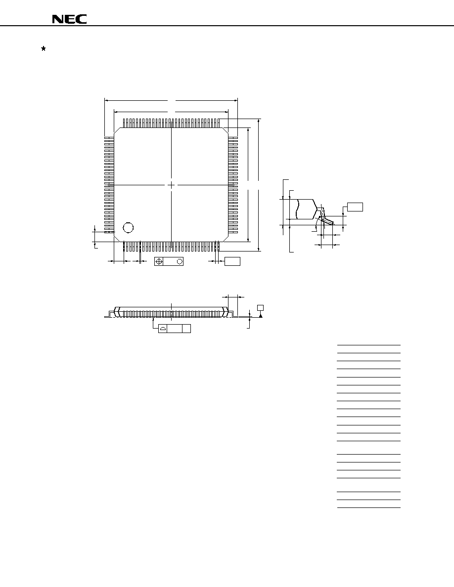
6. PACKAGE DRAWING
90
60
61
120
1
31
30
91
S
120-PIN PLASTIC TQFP (FINE PITCH) (14x14)
ITEM
MILLIMETERS
I
J
0.40 (T.P.)
0.07
A
16.00
±0.20
F
1.20
G
H
0.18
±0.05
1.20
K
1.00
±0.20
S
1.20MAX.
R
3
∞
T
0.25
+4∞
-3∞
R
H
K
L
J
F
N
Q
M
G
I
A
B
C D
S
M
T
U
S
P
detail of lead end
NOTE
Each lead centerline is located within 0.07 mm of
its true position (T.P.) at maximum material condition.
B
14.00
±0.20
C
D
16.00
±0.20
14.00
±0.20
L
0.50
M
0.17 +0.03
-0.07
N
0.08
P
1.00
±0.05
Q
0.10
±0.05
P120GC-40-YEB
Preliminary Data Sheet S15306EJ2V0DS
35
µ
µ
µ
µ
PD72874
7. RECOMMENDED SOLDERING CONDITIONS
The
µPD72874 should be soldered and mounted under the following recommended conditions.
For the details of the recommended soldering conditions, refer to the document Semiconductor Device Mounting
Technology Manual (C10535E).
For soldering methods and conditions other than those recommended below, contact your NEC sales
representative.
Table 7-1. Surface Mounting Type Soldering Conditions
µ
µ
µ
µPD72874GC-YEB: 120-pin plastic TQFP (Fine pitch) (14 x 14)
Soldering
Method
Soldering Conditions
Recommended
Condition Symbol
Infrared reflow
Package peak temperature: 235∞C, Time: 30 sec. Max. (at 210∞C or higher).
Count: three times or less
Exposure limit: 3 days
Note
(after that prebake at 125∞C for 10 hours)
IR35-103-3
Partial heating
Pin temperature: 300∞C Max., Time: 3 sec. Max. (per pin row)
--
Note After opening the dry pack, store it at 25∞C or less and 65% RH or less for the allowable storage period.

Preliminary Data Sheet S15306EJ2V0DS
36
µ
µ
µ
µ
PD72874
[MEMO]

Preliminary Data Sheet S15306EJ2V0DS
37
µ
µ
µ
µ
PD72874
[MEMO]

Preliminary Data Sheet S15306EJ2V0DS
38
µ
µ
µ
µ
PD72874
[MEMO]

Preliminary Data Sheet S15306EJ2V0DS
39
µ
µ
µ
µ
PD72874
NOTES FOR CMOS DEVICES
1
PRECAUTION AGAINST ESD FOR SEMICONDUCTORS
Note:
Strong electric field, when exposed to a MOS device, can cause destruction of the gate oxide and
ultimately degrade the device operation. Steps must be taken to stop generation of static electricity
as much as possible, and quickly dissipate it once, when it has occurred. Environmental control
must be adequate. When it is dry, humidifier should be used. It is recommended to avoid using
insulators that easily build static electricity. Semiconductor devices must be stored and transported
in an anti-static container, static shielding bag or conductive material. All test and measurement
tools including work bench and floor should be grounded. The operator should be grounded using
wrist strap. Semiconductor devices must not be touched with bare hands. Similar precautions need
to be taken for PW boards with semiconductor devices on it.
2
HANDLING OF UNUSED INPUT PINS FOR CMOS
Note:
No connection for CMOS device inputs can be cause of malfunction. If no connection is provided
to the input pins, it is possible that an internal input level may be generated due to noise, etc., hence
causing malfunction. CMOS devices behave differently than Bipolar or NMOS devices. Input levels
of CMOS devices must be fixed high or low by using a pull-up or pull-down circuitry. Each unused
pin should be connected to V
DD
or GND with a resistor, if it is considered to have a possibility of
being an output pin. All handling related to the unused pins must be judged device by device and
related specifications governing the devices.
3
STATUS BEFORE INITIALIZATION OF MOS DEVICES
Note:
Power-on does not necessarily define initial status of MOS device. Production process of MOS
does not define the initial operation status of the device. Immediately after the power source is
turned ON, the devices with reset function have not yet been initialized. Hence, power-on does
not guarantee out-pin levels, I/O settings or contents of registers. Device is not initialized until the
reset signal is received. Reset operation must be executed immediately after power-on for devices
having reset function.

µ
µ
µ
µ
PD72874
EEPROM and Firewarden are trademarks of NEC Corporation.
VGA is a trademark of IBM Corporation.
M8E 00. 4
The information in this document is current as of April, 2002. The information is subject to change
without notice. For actual design-in, refer to the latest publications of NEC's data sheets or data
books, etc., for the most up-to-date specifications of NEC semiconductor products. Not all products
and/or types are available in every country. Please check with an NEC sales representative for
availability and additional information.
No part of this document may be copied or reproduced in any form or by any means without prior
written consent of NEC. NEC assumes no responsibility for any errors that may appear in this document.
NEC does not assume any liability for infringement of patents, copyrights or other intellectual property rights of
third parties by or arising from the use of NEC semiconductor products listed in this document or any other
liability arising from the use of such products. No license, express, implied or otherwise, is granted under any
patents, copyrights or other intellectual property rights of NEC or others.
Descriptions of circuits, software and other related information in this document are provided for illustrative
purposes in semiconductor product operation and application examples. The incorporation of these
circuits, software and information in the design of customer's equipment shall be done under the full
responsibility of customer. NEC assumes no responsibility for any losses incurred by customers or third
parties arising from the use of these circuits, software and information.
While NEC endeavours to enhance the quality, reliability and safety of NEC semiconductor products, customers
agree and acknowledge that the possibility of defects thereof cannot be eliminated entirely. To minimize
risks of damage to property or injury (including death) to persons arising from defects in NEC
semiconductor products, customers must incorporate sufficient safety measures in their design, such as
redundancy, fire-containment, and anti-failure features.
NEC semiconductor products are classified into the following three quality grades:
"Standard", "Special" and "Specific". The "Specific" quality grade applies only to semiconductor products
developed based on a customer-designated "quality assurance program" for a specific application. The
recommended applications of a semiconductor product depend on its quality grade, as indicated below.
Customers must check the quality grade of each semiconductor product before using it in a particular
application.
"Standard": Computers, office equipment, communications equipment, test and measurement equipment, audio
and visual equipment, home electronic appliances, machine tools, personal electronic equipment
and industrial robots
"Special":
Transportation equipment (automobiles, trains, ships, etc.), traffic control systems, anti-disaster
systems, anti-crime systems, safety equipment and medical equipment (not specifically designed
for life support)
"Specific": Aircraft, aerospace equipment, submersible repeaters, nuclear reactor control systems, life
support systems and medical equipment for life support, etc.
The quality grade of NEC semiconductor products is "Standard" unless otherwise expressly specified in NEC's
data sheets or data books, etc. If customers wish to use NEC semiconductor products in applications not
intended by NEC, they must contact an NEC sales representative in advance to determine NEC's willingness
to support a given application.
(Note)
(1) "NEC" as used in this statement means NEC Corporation and also includes its majority-owned subsidiaries.
(2) "NEC semiconductor products" means any semiconductor product developed or manufactured by or for
NEC (as defined above).
∑
∑
∑
∑
∑
∑