
DATA SHEET
MOS INTEGRATED CIRCUIT
µ
PD750004,750006,750008,750004(A),750006(A),750008(A)
4 BIT SINGLE-CHIP MICROCONTROLLER
The
µ
PD750008 is one of the 75XL series 4-bit single-chip microcontrollers, which provide data processing
capability equal to that of an 8-bit microcontroller.
The
µ
PD750008 is an advanced model of the
µ
PD75008. It features an enhanced CPU function and enables high-
speed operation at a low voltage of 2.2 V. It can be substituted for the
µ
PD75008. In addition, it is best suited to
applications using batteries. The
µ
PD750008(A) has a higher reliability than the
µ
PD750008.
A built-in one-time PROM product,
µ
PD75P0016, is also available. It is suitable for small-scale production and
evaluation of application systems.
The following user's manual describes the details of the functions of the
µ
PD750008. Be sure to read it
before designing application systems.
µ
PD750008 User's Manual: U10740E
FEATURES
∑ Capable of low-voltage operation: V
DD
= 2.2 to 5.5 V
∑ Internal memory
Program memory (ROM)
: 4096
◊
8 bits (
µ
PD750004 and
µ
PD750004(A))
: 6144
◊
8 bits (
µ
PD750006 and
µ
PD750006(A))
: 8192
◊
8 bits (
µ
PD750008 and
µ
PD750008(A))
Data memory (RAM)
: 512
◊
4 bits
APPLICATIONS
∑
µ
PD750004,
µ
PD750006, and
µ
PD750008
Cordless telephones, radio devices, audio products, and home electric appliances
∑
µ
PD750004(A),
µ
PD750006(A), and
µ
PD750008(A)
Electrical equipment for automobiles
The
µ
PD750004,
µ
PD750006,
µ
PD750008,
µ
PD750004(A),
µ
PD750006(A), and
µ
PD750008(A) differ only in
quality grade. In this manual, the
µ
PD750008 is described unless otherwise specified. Users of other than the
µ
PD750008 should read
µ
PD750008 as referring to the pertinent product.
When the description differs among
µ
PD750004,
µ
PD750006, and
µ
PD750008, they also refer to the pertinent
(A) products.
µ
PD750004
µ
PD750004(A),
µ
PD750006
µ
PD750006(A),
µ
PD750008
µ
PD750008(A)
The information in this document is subject to change without notice.
©
1990
The mark shows major revised points.
∑ Function for specifying the instruction execution time
(useful for high-speed operation and saving power)
0.95
µ
s, 1.91
µ
s, 3.81
µ
s, 15.3
µ
s (when operating at
4.19 MHz)
0.67
µ
s, 1.33
µ
s, 2.67
µ
s, 10.7
µ
s (when operating at
6.0 MHz)
122
µ
s (when operating at 32.768 kHz)
∑ Enhanced timer function (4 channels)
∑ Can be easily substituted for the
µ
PD75008 because
this product succeeds to the functions and instructions
of the
µ
PD75008.
1994
Document No.
U10738EJ3V0DS00 (3rd edition)
Date Published February 1997 J
Printed in Japan

2
µ
PD750004, 750006, 750008, 750004(A), 750006(A), 750008(A)
ORDERING INFORMATION
Part number
Package
Quality grade
µ
PD750004CU-
◊◊◊
42-pin plastic shrink DIP (600 mil, 1.778 mm pitch)
Standard
µ
PD750004GB-
◊◊◊
-3BS-MTX
44-pin plastic QFP (10
◊
10 mm, 0.8 mm pitch)
Standard
µ
PD750006CU-
◊◊◊
42-pin plastic shrink DIP (600 mil, 1.778 mm pitch)
Standard
µ
PD750006GB-
◊◊◊
-3BS-MTX
44-pin plastic QFP (10
◊
10 mm, 0.8 mm pitch)
Standard
µ
PD750008CU-
◊◊◊
42-pin plastic shrink DIP (600 mil, 1.778 mm pitch)
Standard
µ
PD750008GB-
◊◊◊
-3BS-MTX
44-pin plastic QFP (10
◊
10 mm, 0.8 mm pitch)
Standard
µ
PD750004CU(A)-
◊◊◊
42-pin plastic shrink DIP (600 mil, 1.778 mm pitch)
Special
µ
PD750004GB(A)-
◊◊◊
-3BS-MTX
44-pin plastic QFP (10
◊
10 mm, 0.8 mm pitch)
Special
µ
PD750006CU(A)-
◊◊◊
42-pin plastic shrink DIP (600 mil, 1.778 mm pitch)
Special
µ
PD750006GB(A)-
◊◊◊
-3BS-MTX
44-pin plastic QFP (10
◊
10 mm, 0.8 mm pitch)
Special
µ
PD750008CU(A)-
◊◊◊
42-pin plastic shrink DIP (600 mil, 1.778 mm pitch)
Special
µ
PD750008GB(A)-
◊◊◊
-3BS-MTX
44-pin plastic QFP (10
◊
10 mm, 0.8 mm pitch)
Special
Remark
◊◊◊
is a mask ROM code number.
DIFFERENCES BETWEEN
µ
PD75000
◊
AND
µ
PD75000
◊
(A)
Product number
Item
Quality grade
Standard
Special
Please refer to "Quality Grades on NEC Semiconductor Devices" (Document No. C11531E) published by
NEC Corporation to know the specification of quality grade on the devices and its recommended applications.
µ
PD750004
µ
PD750006
µ
PD750008
µ
PD750004(A)
µ
PD750006(A)
µ
PD750008(A)

3
µ
PD750004, 750006, 750008, 750004(A), 750006(A), 750008(A)
ROM
RAM
FUNCTIONS
CMOS input
CMOS I/O
N-ch open
drain I/O
Total
8
18
8
34
Can incorporate 7 pull-up resistors that are specified with the software.
Can directly drive the LED.
Can incorporate 18 pull-up resistors that are specified with the software.
Can directly drive the LED.
Can withstand 13 V.
Can incorporate pull-up resistors that are specified with the mask option.
Serial interface
Clock output (PCL)
Buzzer output (BUZ)
Vectored interrupt
Test input
System clock oscillator
Standby
Operating ambient
temperature range
Supply voltage
Package
Item
Command execution
time
Internal memory
General-purpose
register
I/O port
Timer
Bit sequential buffer (BSB)
4 channels
∑
8-bit timer/event counter: 1 channel
∑
8-bit timer counter: 1 channel
∑
Basic interval timer/watchdog timer: 1 channel
∑
lock timer: 1 channel
∑
Three-wire serial I/O mode ... switchable between the start LSB and the start MSB
∑
Two-wire serial I/O mode
∑
SBI mode
16 bits
∑
, 524 kHz, 262 kHz, 65.5 kHz (when the main system clock operates at 4.19 MHz)
∑
, 750 kHz, 375 kHz, 93.8 kHz (when the main system clock operates at 6.0 MHz)
∑
2 kHz, 4 kHz, 32 kHz (when the main system clock operates at 4.19 MHz or when the
subsystem clock operates at 32.768 kHz)
∑
2.93 kHz, 5.86 kHz, 46.9 kHz (when the main system clock operates at 6.0 MHz)
External :
3
Internal :
4
External :
1
Internal :
1
∑
Ceramic or crystal oscillator for main system clock
∑
Crystal oscillator for subsystem clock
STOP/HALT mode
T
A
= -40 to +85
∞
C
V
DD
= 2.2 to 5.5 V
42-pin plastic shrink DIP (600 mil, 1.778 mm pitch)
44-pin plastic QFP (10
◊
10 mm, 0.8 mm pitch)
Function
∑ 0.95, 1.91, 3.81, 15.3
µ
s (when the main system clock operates at 4.19 MHz)
∑ 0.67, 1.33, 2.67, 10.7
µ
s (when the main system clock operates at 6.0 MHz)
∑ 122
µ
s (when the subsystem clock operates at 32.768 kHz)
4096
◊
8 bits (
µ
PD750004)
6144
◊
8 bits (
µ
PD750006)
8192
◊
8 bits (
µ
PD750008)
512
◊
4 bits
∑ When operating in 4 bits: 8
◊
4 banks
∑ When operating in 8 bits: 4
◊
4 banks

4
µ
PD750004, 750006, 750008, 750004(A), 750006(A), 750008(A)
CONTENTS
1.
PIN CONFIGURATION (TOP VIEW) .........................................................................................
6
2.
BLOCK DIAGRAM ......................................................................................................................
8
3.
PIN FUNCTIONS .........................................................................................................................
9
3.1
PORT PINS ......................................................................................................................................
9
3.2
NON-PORT PINS ............................................................................................................................
10
3.3
PIN INPUT/OUTPUT CIRCUITS .....................................................................................................
11
3.4
CONNECTION OF UNUSED PINS ................................................................................................
13
4.
Mk
MODE/Mk
MODE SWITCH FUNCTION ........................................................................
14
4.1
DIFFERENCES BETWEEN Mk
MODE AND Mk
MODE ........................................................
14
4.2
SETTING OF THE STACK BANK SELECTION REGISTER (SBS) ............................................
15
5.
MEMORY CONFIGURATION .....................................................................................................
16
6.
PERIPHERAL HARDWARE FUNCTIONS ................................................................................
21
6.1
DIGITAL I/O PORTS .......................................................................................................................
21
6.2
CLOCK GENERATOR ....................................................................................................................
21
6.3
CONTROL FUNCTIONS OF SUBSYSTEM CLOCK OSCILLATOR ............................................
23
6.4
CLOCK OUTPUT CIRCUIT ............................................................................................................
24
6.5
BASIC INTERVAL TIMER/WATCHDOG TIMER ...........................................................................
25
6.6
CLOCK TIMER ................................................................................................................................
26
6.7
TIMER/EVENT COUNTER ..............................................................................................................
27
6.8
SERIAL INTERFACE ......................................................................................................................
30
6.9
BIT SEQUENTIAL BUFFER ...........................................................................................................
32
7.
INTERRUPT FUNCTIONS AND TEST FUNCTIONS ................................................................
33
8.
STANDBY FUNCTION ................................................................................................................
35
9.
RESET FUNCTION .....................................................................................................................
36
10. MASK OPTION ...........................................................................................................................
39
11. INSTRUCTION SET ....................................................................................................................
40
12. ELECTRICAL CHARACTERISTICS ..........................................................................................
53
13. CHARACTERISTIC CURVE (REFERENCE VALUES) .............................................................
67

5
µ
PD750004, 750006, 750008, 750004(A), 750006(A), 750008(A)
14. PACKAGE DRAWINGS ..............................................................................................................
70
15. RECOMMENDED SOLDERING CONDITIONS .........................................................................
73
APPENDIX A FUNCTIONS OF THE
µ
PD75008,
µ
PD750008, AND
µ
PD75P0016 ......................
74
APPENDIX B DEVELOPMENT TOOLS ..........................................................................................
76
APPENDIX C RELATED DOCUMENTS ..........................................................................................
80
6
µ
PD750004, 750006, 750008, 750004(A), 750006(A), 750008(A)
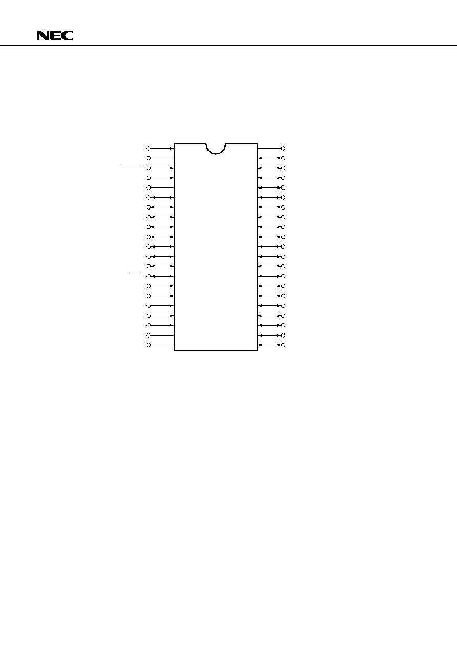
1. PIN CONFIGURATION (TOP VIEW)
∑
42-pin plastic shrink DIP (600 mil, 1.778 mm pitch)
µ
PD750004CU-
◊◊◊
,
µ
PD750004CU(A)-
◊◊◊
µ
PD750006CU-
◊◊◊
,
µ
PD750006CU(A)-
◊◊◊
µ
PD750008CU-
◊◊◊
,
µ
PD750008CU(A)-
◊◊◊
IC : Internally connected (Connect directly to V
DD
.)
V
SS
P40
P41
P42
P43
P50
P51
P52
P53
P60/KR0
P61/KR1
P62/KR2
P63/KR3
P70/KR4
P71/KR5
P72/KR6
P73/KR7
P20/PTO0
P21/PTO1
P22/PCL
P23/BUZ
XT1
XT2
RESET
X1
X2
P33
P32
P31
P30
P81
P80
P03/SI/SB1
P02/SO/SB0
P01/SCK
P00/INT4
P13/TI0
P12/INT2
P11/INT1
P10/INT0
IC
V
DD
1
2
3
4
5
6
7
8
9
10
11
12
13
14
15
16
17
18
19
20
21
42
41
40
39
38
37
36
35
34
33
32
31
30
29
28
27
26
25
24
23
22

7
µ
PD750004, 750006, 750008, 750004(A), 750006(A), 750008(A)
∑
44-pin plastic QFP (10
◊
10 mm, 0.8 mm pitch)
µ
PD750004GB-
◊◊◊
-3BS-MTX,
µ
PD750004GB(A)-
◊◊◊
-3BS-MTX
µ
PD750006GB-
◊◊◊
-3BS-MTX,
µ
PD750006GB(A)-
◊◊◊
-3BS-MTX
µ
PD750008GB-
◊◊◊
-3BS-MTX,
µ
PD750008GB(A)-
◊◊◊
-3BS-MTX
IC : Internally connected (Connect directly to V
DD
.)
PIN NAMES
P00 - 03
:
Port 0
SO
:
Serial Output
P10 - 13
:
Port 1
SB0, SB1
:
Serial Data Bus 0, 1
P20 - 23
:
Port 2
RESET
:
Reset
P30 - 33
:
Port 3
TI0
:
Timer Input 0
P40 - 43
:
Port 4
PTO0, PTO1 :
Programmable Timer Output 0, 1
P50 - 53
:
Port 5
BUZ
:
Buzzer Clock
P60 - 63
:
Port 6
PCL
:
Programmable Clock
P70 - 73
:
Port 7
INT0, 1, 4
:
External Vectored Interrupt 0, 1, 4
P80, 81
:
Port 8
INT2
:
External Test Input 2
KR0 - KR7 :
Key Return 0 - 7
X1, X2
:
Main System Clock Oscillation 1, 2
SCK
:
Serial Clock
XT1, XT2
:
Subsystem Clock Oscillation 1, 2
SI
:
Serial Input
NC
:
No Connection
IC
:
Internally Connected
P13/TI0
P00/INT4
P01/SCK
P02/SO/SB0
P03/SI/SB1
P80
P81
P30
P31
P32
P33
P72/KR6
P71/KR5
P70/KR4
P63/KR3
P62/KR2
P61/KR1
P60/KR0
P53
P52
P51
P50
33
32
31
30
29
28
27
26
25
24
23
1
2
3
4
5
6
7
8
9
10
11
NC
P43
P42
P41
P40
V
SS
XT1
XT2
RESET
X1
X2
P73/KR7
P20/PTO0
P21/PTO1
P22/PCL
P23/BUZ
V
DD
IC
P10/INT0
P11/INT1
P12/INT2
NC
44 43 42 41 40 39 38 37 36 35 34
12 13 14 15 16 17 18 19 20 21 22

8
µ
PD750004, 750006, 750008, 750004(A), 750006(A), 750008(A)
2. BLOCK DIAGRAM
Note The ROM capacity depends on the product.
BIT SEQ.
BUFFER (16)
PORT 0
P00 - P03
4
PORT 1
PORT 2
4
PORT 3
P30 - P33
4
PORT 4
P40 - P43
4
PORT 5
P50 - P53
4
PORT 6
P60 - P63
4
V
SS
V
DD
RESET
IC
CPU CLOCK
STAND BY
CONTROL
X2
X1
XT2
XT1
SYSTEM CLOCK
GENERATOR
MAIN
SUB
CLOCK
DIVIDER
CLOCK
OUTPUT
CONTROL
fx/2
N
PCL/P22
GENERAL
REGISTER
DATA
MEMORY
(RAM)
512
◊
4 BITS
BANK
SBS
SP (8)
CY
ALU
PROGRAM
COUNTER
PROGRAM
MEMORY
Note
(ROM)
DECODE
AND
CONTROL
BASIC INTERVAL
TIMER/
WATCHDOG
TIMER
TI0/P13
INTBT
8-BIT
TIMER/EVENT
COUNTER #0
PTO0/P20
INTT0
TOUT0
8-BIT TIMER
COUNTER #1
INTT1
TOUT0
CLOCKED
SERIAL
INTERFACE
SI/SB1/P03
INTERRUPT
CONTROL
INT0/P10
SO/SB0/P02
SCK/P01
INT1/P11
INT2/P12
INT4/P00
KR0/P60-
KR7/P73
WATCH
TIMER
8
PORT 7
P70 - P73
4
PORT 8
P80, P81
2
P10 - P13
4
P20 - P23
PTO1/P21
INTCSI
INTW
BUZ/P23

9
µ
PD750004, 750006, 750008, 750004(A), 750006(A), 750008(A)
3. PIN FUNCTIONS
3.1 PORT PINS
Notes 1. The circle (
) indicates the Schmitt trigger input.
2. When pull-up resistors that can be specified with the mask option are not incorporated (when pins are used
as N-ch open-drain input ports), the input leak low current increases when an input instruction or bit
operation instruction is executed.
I/O circuit
type
Note 1
-A
-B
-C
-C
E-B
E-B
M-D
M-D
-A
-A
E-B
When reset
Input
Input
Input
Input
High level (when
pull-up resistors
are provided) or
high impedance
High level (when
pull-up resistors
are provided) or
high impedance
Input
Input
Input
8-bit
I/O
◊
◊
◊
◊
◊
Function
4-bit input port (PORT0).
For P01 - P03, built-in pull-up resistors
can be connected by software in units
of 3 bits.
4-bit input port (PORT1).
Built-in pull-up resistors can be
connected by software in units of 4 bits.
A noise eliminator can be selected only
when the P10/INT0 pin is used.
4-bit I/O port (PORT2).
Built-in pull-up resistors can be
connected by software in units of 4 bits.
Programmable 4-bit I/O port (PORT3).
I/O can be specified bit by bit. Built-in
pull-up resistors can be connected by
software in units of 4 bits.
N-ch open-drain 4-bit I/O port (PORT4).
A pull-up resistor can be provided bit by
bit (mask option). Withstand voltage is
13 V in open-drain mode.
N-ch open-drain 4-bit I/O port (PORT5).
A pull-up resistor can be provided bit by
bit (mask option). Withstand voltage is
13 V in open-drain mode.
Programmable 4-bit I/O port (PORT6).
I/O can be specified bit by bit. Built-in
pull-up resistors can be connected by
software in units of 4 bits.
4-bit I/O port (PORT7).
Built-in pull-up resistors can be
connected by software in units of 4 bits.
2-bit I/O port (PORT8).
Built-in pull-up resistors can be
connected by software in units of 2
bits.
B
F
F
M
B
Pin name
P00
P01
P02
P03
P10
P11
P12
P13
P20
P21
P22
P23
P30 - P33
P40 - P43
Notes 2
P50 - P53
Notes 2
P60
P61
P62
P63
P70
P71
P72
P73
P80
P81
Input/
output
Input
I/O
I/O
I/O
Input
I/O
I/O
I/O
I/O
I/O
I/O
I/O
F
F
Shared
pin
INT4
SCK
SO/SB0
SI/SB1
INT0
INT1
INT2
TI0
PTO0
PTO1
PCL
BUZ
-
-
-
KR0
KR1
KR2
KR3
KR4
KR5
KR6
KR7
-
-

10
µ
PD750004, 750006, 750008, 750004(A), 750006(A), 750008(A)
3.2 NON-PORT PINS
Notes 1. The circle (
) indicates the Schmitt trigger input.
2. With a noise eliminator/asynchronously selectable
3. Asynchronous
B
B
F
F
M
B
Function
Inputs external event pulse to the timer/event
counter
Timer/event counter output
Timer counter output
Clock output
Arbitrary frequency output (for buzzer output or
system clock trimming)
Serial clock I/O
Serial data output
Serial data bus I/O
Serial data input
Serial data bus I/O
Edge detection vectored interrupt input (both
rising and falling edges are detected)
Rising edge detection testable input
Falling edge detection testable input
Falling edge detection testable input
Crystal/ceramic connection pin for main system
clock generation. When external clock signal is
used, it is applied to X1, and its reverse phase
signal is applied to X2.
Crystal connection pin for subsystem clock
generation. When external clock signal is used, it
is applied to XT1, and it reverse phase signal is
applied to XT2.
XT1 can be used as a 1-bit input (test).
System reset input (active low)
Internally connected. (To be connected directly to
V
DD
)
Positive power supply
Ground potential
Input/
output
Input
Output
I/O
Input
Input
Input
I/O
I/O
Input
-
Input
-
Input
-
-
-
When reset
Input
Input
Input
Input
Input
Input
-
-
-
-
-
-
Edge detection vectored interrupt input
(detection edge selectable). A noise eliminator
can be selected when INT0/P10 is used.
Shared
pin
P13
P20
P21
P22
P23
P01
P02
P03
P00
P10
P11
P12
P60 - P63
P70 - P73
-
-
-
-
-
-
Note 3
Note 2
Note 3
I/O circuit
type
Note 1
-C
E-B
-A
-B
-C
-C
-A
-A
-
-
-
-
-
B
Pin name
TI0
PTO0
PTO1
PCL
BUZ
SCK
SO/SB0
SI/SB1
INT4
INT0
INT1
INT2
KR0 - KR3
KR4 - KR7
X1
X2
XT1
XT2
RESET
IC
V
DD
V
SS
F
F
11
µ
PD750004, 750006, 750008, 750004(A), 750006(A), 750008(A)
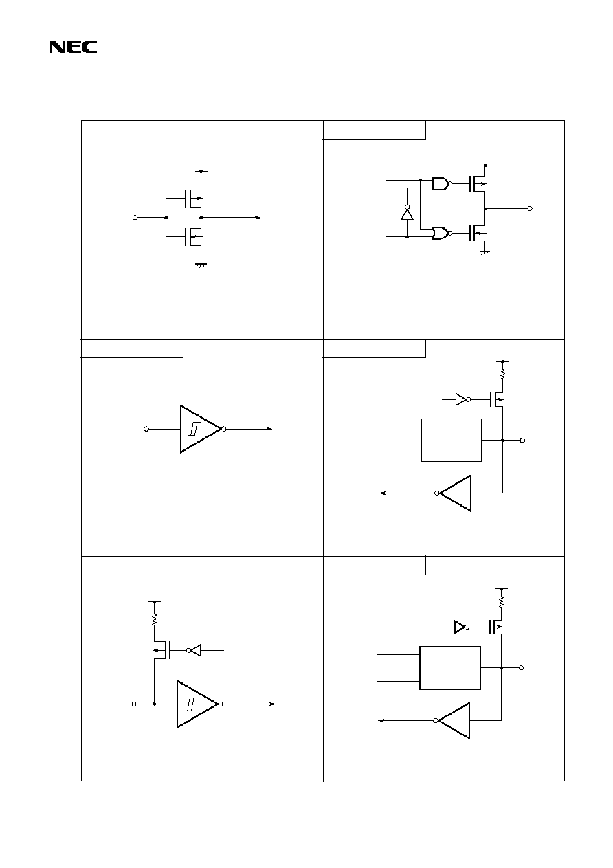
3.3 PIN INPUT/OUTPUT CIRCUITS
The input/output circuit of each
µ
PD750008 pin is shown below in a simplified manner.
Type A
Type D
Type B
Type E-B
Type B-C
Type F-A
Schmitt trigger input with hysteresis
IN
P.U.R.: Pull-Up Resistor
IN
P-ch
P.U.R.
enable
P.U.R.
V
DD
P.U.R.: Pull-Up Resistor
P.U.R.
V
DD
P.U.R.
enable
P-ch
IN/OUT
Data
Output
disable
Type D
Type A
P.U.R.
V
DD
P.U.R.
enable
P-ch
IN/OUT
Data
Output
disable
Type D
Type B
P.U.R.: Pull-Up Resistor
Push-pull output which can be set to high-impedance output
(off for both P-ch and N-ch)
V
DD
P-ch
N-ch
OUT
Data
Output
disable
CMOS input buffer
V
DD
IN
P-ch
N-ch

12
µ
PD750004, 750006, 750008, 750004(A), 750006(A), 750008(A)
Type F-B
Type M-C
Type M-D
P.U.R.: Pull-Up Resistor
V
DD
P-ch
N-ch
IN/OUT
V
DD
P-ch
P.U.R.
P.U.R.
enable
Output
disable
(P)
Data
Output
disable
Output
disable
(N)
P.U.R.: Pull-Up Resistor
N-ch
P.U.R.
Data
Output
disable
P.U.R.
enable
V
DD
P-ch
IN/OUT
P.U.R.: Pull-Up Resistor
N-ch
(Withstand
voltage:
+13 V)
IN/OUT
Data
V
DD
Output
disable
P.U.R.
(Mask option)
Note
P.U.R
Note
V
DD
P-ch
Input
instruction
Pull-up resistor that operates only when pull-up resistors
that can be specified with the mask option are not
incorporated and an input instruction is executed.
(When the pin is low, the current flows from V
DD
to the pin.)
Voltage
restriction
circuit
(Withstand voltage: +13 V)

13
µ
PD750004, 750006, 750008, 750004(A), 750006(A), 750008(A)
Input state
: To be connected to V
SS
or V
DD
through a separate resistor
Output state : To be left open
Input state
: To be connected to V
SS
or V
DD
through a separate resistor
Output state : To be left open
Input state
: To be connected to V
SS
Output state : To be connected to V
SS
(Do not connect to a pull-up
resistor specified with a mask
option.)
3.4 CONNECTION OF UNUSED PINS
Table 3-1 Connection of Unused Pins
Note When the subsystem clock is not used, set SOS.0 to 1 (not to use the built-
in feedback resistor).
Pin name
Recommended connection
P00/INT4
To be connected to V
SS
or V
DD
P01/SCK
P02/SO/SB0
P03/SI/SB1
To be connected to V
SS
P10/INT0 - P12/INT2
To be connected to V
SS
or V
DD
P13/TI0
P20/PTO0
P21/PTO1
P22/PCL
P23/BUZ
P30 - P33
P40 - P43
P50 - P53
P60/KR0 - P63/KR3
P70/KR4 - P73/KR7
P80, P81
XT1
Note
To be connected to V
SS
XT2
Note
To be left open
IC
To be connected directly to V
DD
To be connected to V
SS
or V
DD
through a
separate resistor

14
µ
PD750004, 750006, 750008, 750004(A), 750006(A), 750008(A)
4.
Mk
MODE/Mk
MODE SWITCH FUNCTION
4.1 DIFFERENCES BETWEEN Mk
MODE AND Mk
MODE
The CPU of the
µ
PD750008 has two modes (Mk
mode and Mk
mode) and which mode is used is selectable.
Bit 3 of the stack bank selection register (SBS) determines the mode.
∑ Mk
mode:
This mode has the upward compatibility with the
µ
PD75008.
It can be used in the 75XL CPUs having a ROM of up to 16 KB.
∑ Mk
mode:
This mode is not compatible with the
µ
PD75008.
It can be used in all 75XL CPUs, including those having a ROM of 16 KB or more.
Table 4-1 shows the differences between Mk
mode and Mk
mode.
Table 4-1 Differences between Mk
Mode and Mk
Mode
Caution Mk
mode can be used to support a program area larger than 16K bytes in the 75X series or 75XL
series. This mode enhances a software compatibility with products whose program area is larger
than 16K bytes. In Mk
mode, one more stack byte is required for execution of subroutine call
instructions per stack compared with Mk
mode. When a CALL !addr or CALLF !faddr instruction
is executed, it takes one more machine cycle. Therefore, Mk
mode should be used for applications
for which RAM efficiency or processing capabilities is more critical than a software compatibility.
Number of stack bytes in a
subroutine instruction
BRA !addr1 instruction
CALLA !addr1 instruction
CALL !addr instruction
CALLF !faddr instruction
2 bytes
None
3 machine cycles
2 machine cycles
3 bytes
Available
4 machine cycles
3 machine cycles
Mk
mode
Mk
mode

15
µ
PD750004, 750006, 750008, 750004(A), 750006(A), 750008(A)
4.2 SETTING OF THE STACK BANK SELECTION REGISTER (SBS)
The Mk
mode and Mk
mode are switched by stack bank selection register. Fig. 4-1 shows the register
configuration.
The stack bank selection register is set with a 4-bit memory operation instruction. To use the CPU in Mk
mode,
initialize the register to 100
◊
B
Note
at the beginning of the program. To use the CPU in Mk
mode, initialize it to
000
◊
B
Note
.
Note Specify the desired value in
◊
.
Fig. 4-1 Stack Bank Selection Register Format
Caution The CPU operates in Mk
mode after the RESET signal is issued, because bit 3 of SBS is set to 1.
Set bit 3 of SBS to 0 (Mk
mode) to use the CPU in Mk
mode.
SBS0
SBS1
SBS2
SBS3
0
1
2
3
F84H
Address
SBS
Symbol
0
0
0
1
Memory bank 0
Memory bank 1
Other settings are inhibited.
0
1
Mk
mode
Mk
mode
Mode switching designation
Bit 2 must be set to 0.
Stack area designation
0

16
µ
PD750004, 750006, 750008, 750004(A), 750006(A), 750008(A)
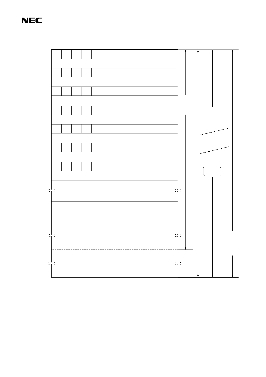
5. MEMORY CONFIGURATION
∑ Program memory (ROM) : 4096
◊
8 bits (0000H-0FFFH):
µ
PD750004
6144
◊
8 bits (0000H-17FFH):
µ
PD750006
8192
◊
8 bits (0000H-1FFFH):
µ
PD750008
∑
0000H to 0001H
Vector address table for holding the RBE and MBE values and program start address when a RESET signal is
issued (allowing a reset start at an arbitrary address)
∑
0002H to 000DH
Vector address table for holding the RBE and MBE values and program start address for each vectored interrupt
(allowing interrupt processing to be started at an arbitrary address)
∑
0020H to 007FH
Table area referenced by the GETI instruction
∑ Data memory (RAM)
∑
Data area
: 512
◊
4 bits (000H to 1FFH)
∑
Peripheral hardware area: 128
◊
4 bits (F80H to FFFH)
17
µ
PD750004, 750006, 750008, 750004(A), 750006(A), 750008(A)
Fig. 5-1 Program Memory Map (in
µ
PD750004)
Note Can be used only in the Mk
mode.
Remark In addition to the above, the BR PCDE and BR PCXA instructions can cause a branch to an address with
only the 8 low-order bits of the PC changed.
0 0 0 H
Address
7
6
5
4
MBE RBE
0
0
Internal reset start address
(high-order 4 bits)
0
0 0 2 H MBE RBE
0
0
INTBT/INT4
(high-order 4 bits)
start address
0 0 4 H MBE RBE
0
0
INT0
(high-order 4 bits)
start address
0 0 6 H MBE RBE
0
0
INT1
(high-order 4 bits)
start address
0 0 8 H MBE RBE
0
0
INTCSI
(high-order 4 bits)
start address
0 0 A H MBE RBE
0
0
INTT0
(high-order 4 bits)
start address
0 0 C H MBE RBE
0
0
INTT1
(high-order 4 bits)
start address
0 2 0 H
0 7 F H
0 8 0 H
7 F F H
8 0 0 H
F F F H
GETI instruction reference table
(low-order 8 bits)
(low-order 8 bits)
(low-order 8 bits)
(low-order 8 bits)
(low-order 8 bits)
(low-order 8 bits)
(low-order 8 bits)
CALLF
! faddr
instruction
entry
address
Branch address
of BR BCXA, BR
BCDE, BR !addr,
BRA !addr1
Note
or
CALLA !addr1
Note
instruction
CALL !addr
instruction
subroutine entry
address
BR $addr
instruction relative
branch address
BRCB
!caddr
instruction
branch
address
-15 to -1,
+2 to +16
Branch destination
address and
subroutine entry
address when
GETI instruction
is executed
Internal reset start address
INTBT/INT4
start address
INT0
start address
INT1
start address
INTCSI
start address
INTT0
start address
INTT1
start address

18
µ
PD750004, 750006, 750008, 750004(A), 750006(A), 750008(A)
Fig. 5-2 Program Memory Map (in
µ
PD750006)
Note Can be used only in the Mk
mode.
Remark In addition to the above, the BR PCDE and BR PCXA instructions can cause a branch to an address with
only the 8 low-order bits of the PC changed.
0 0 0 0 H
Address
0 0 0 2 H MBE RBE
0
INTBT/INT4
(high-order 5 bits)
start address
0 0 0 4 H MBE RBE
0
INT0
(high-order 5 bits)
start address
0 0 0 6 H MBE RBE
0
INT1
(high-order 5 bits)
start address
0 0 0 8 H MBE RBE
0
INTCSI
(high-order 5 bits)
start address
0 0 0 A H MBE RBE
0
INTT0
(high-order 5 bits)
start address
0 0 2 0 H
0 0 7 F H
0 0 8 0 H
0 7 F F H
0 8 0 0 H
MBE RBE
0
Internal reset start address
(high-order 5 bits)
0 F F F H
1 0 0 0 H
1 7 F F H
GETI instruction reference table
0 0 0 C H MBE RBE
0
INTT1
(high-order 5 bits)
start address
(low-order 8 bits)
(low-order 8 bits)
(low-order 8 bits)
(low-order 8 bits)
(low-order 8 bits)
(low-order 8 bits)
(low-order 8 bits)
CALLF
!faddr
instruction
entry
address
BRCB !caddr
instruction
branch
address
Branch address
of BR BCXA, BR
BCDE, BR !addr,
BRA !addr1
Note
or
CALLA !addr1
Note
instruction
CALL !addr
instruction
subroutine entry
address
BR $addr
instruction relative
branch address
-15 to -1,
+2 to +16
Branch destination
address and
subroutine entry
address when GETI
instruction is executed
BRCB !caddr
instruction
branch
address
7
6
5
0
Internal reset start address
INTBT/INT4
INT0
INT1
INTCSI
INTT0
INTT1
start address
start address
start address
start address
start address
start address

19
µ
PD750004, 750006, 750008, 750004(A), 750006(A), 750008(A)
Fig. 5-3 Program Memory Map (in
µ
PD750008)
Note Can be used only in the Mk
mode.
Remark In addition to the above, the BR PCDE and BR PCXA instructions can cause a branch to an address with
only the 8 low-order bits of the PC changed.
0 0 0 0 H
Address
0 0 0 2 H MBE RBE
0
INTBT/INT4
(high-order 5 bits)
start address
0 0 0 4 H MBE RBE
0
INT0
(high-order 5 bits)
start address
0 0 0 6 H MBE RBE
0
INT1
(high-order 5 bits)
start address
0 0 0 8 H MBE RBE
0
INTCSI
(high-order 5 bits)
start address
0 0 0 A H MBE RBE
0
INTT0
(high-order 5 bits)
start address
0 0 2 0 H
0 0 7 F H
0 0 8 0 H
0 7 F F H
0 8 0 0 H
MBE RBE
0
Internal reset start address
(high-order 5 bits)
0 F F F H
1 0 0 0 H
1 F F F H
GETI instruction reference table
0 0 0 C H MBE RBE
0
INTT1
(high-order 5 bits)
start address
(low-order 8 bits)
(low-order 8 bits)
(low-order 8 bits)
(low-order 8 bits)
(low-order 8 bits)
(low-order 8 bits)
(low-order 8 bits)
CALLF
!faddr
instruction
entry
address
BRCB !caddr
instruction
branch
address
Branch address
of BR BCXA, BR
BCDE, BR !addr,
BRA !addr1
or
CALLA !addr1
Note
instruction
CALL !addr
instruction
subroutine entry
address
BR $addr
instruction relative
branch address
-15 to -1,
+2 to +16
Branch destination
address and
subroutine entry
address when GETI
instruction is executed
BRCB !caddr
instruction
branch
address
7
6
5
0
Internal reset start address
INTBT/INT4
INT0
INT1
INTCSI
INTT0
INTT1
start address
start address
start address
start address
start address
start address

20
µ
PD750004, 750006, 750008, 750004(A), 750006(A), 750008(A)
Fig. 5-4 Data Memory Map
Note Memory bank 0 or 1 can be selected as the stack area.
(32
◊
4)
Data memory
000H
01FH
020H
0FFH
100H
1FFH
F80H
FFFH
256
◊
4
(224
◊
4)
256
◊
4
128
◊
4
0
1
15
Stack
area
Note
Area for
general-purpose
register
Data area
Static RAM
(512
◊
4)
Peripheral
hardware area
Not contained
Memory bank

21
µ
PD750004, 750006, 750008, 750004(A), 750006(A), 750008(A)
When the serial interface function is used, dual-function pins
function as output pins in some operation modes.
4-bit input port
Allows input or output mode setting in units of 4 bits.
Allows input or output mode setting in units of 1 bit.
Operation and feature
Port name
PORT0
PORT1
PORT2
PORT3
PORT4
PORT5
PORT6
PORT7
PORT8
6. PERIPHERAL HARDWARE FUNCTIONS
6.1 DIGITAL I/O PORTS
The
µ
PD750008 has the following three types of I/O port:
∑ 8 CMOS input pins (PORT0 and PORT1)
∑ 18 CMOS I/O pins (PORT2, PORT3, and PORT6 to PORT8)
∑ 8 N-ch open-drain I/O pins (PORT4 and PORT5)
Total: 34 pins
Table 6-1 Digital Ports and Their Features
6.2 CLOCK GENERATOR
The clock generator generates clocks which are supplied to the peripheral hardware in the CPU. Fig. 6-1 shows
the configuration of the clock generator.
Operation of the clock generator is specified by the processor clock control register (PCC) and system clock control
register (SCC).
The main system clock and subsystem clock are used.
The instruction execution time can be made variable.
∑ 0.95
µ
s, 1.91
µ
s, 3.81
µ
s, 15.3
µ
s (when the main system clock is at 4.19 MHz)
∑ 0.67
µ
s, 1.33
µ
s, 2.67
µ
s, 10.7
µ
s (when the main system clock is at 6.0 MHz)
∑ 122
µ
s (when the subsystem clock is at 32.768 kHz)
Allows input or output mode setting in
units of 4 bits. Whether to use pull-up
resistors can be specified bit by bit with
the mask option.
Allows input or output mode setting in
units of 1 bit.
Allows input or output mode setting in
units of 4 bits.
Ports 4 and 5 can be
paired, allowing data
I/O in units of 8 bits.
Ports 6 and 7 can be
paired, allowing data
I/O in units of 8 bits.
4-bit input
4-bit I/O
4-bit I/O (N-ch
open-drain can
withstand 13 V)
4-bit I/O
2-bit I/O
Also used as INT4, SCK,
SO/SB0, or SI/SB1.
Also used as INT0, INTI,
INT2 or TI0.
Also used as PTO0,
PTO1, PCL, or BUZ.
-
Also used as one of KR0
to KR3.
Also used as one of KR4
to KR7.
-
Allows input or output mode setting in units of 2 bits.
Function
Remarks

22
µ
PD750004, 750006, 750008, 750004(A), 750006(A), 750008(A)
Fig. 6-1 Clock Generator Block Diagram
Note Instruction execution
Remarks 1. f
X
= Main system clock frequency
2. f
XT
= Subsystem clock frequency
3.
= CPU clock
4. PCC: Processor clock control register
5. SCC: System clock control register
6. One clock cycle (t
CY
) of the CPU clock (
) is equal to one machine cycle of an instruction.
Subsystem
clock generator
Main system
clock generator
Clock timer
∑
Basic interval timer (BT)
∑
Timer/event counter
∑
Timer counter
∑
Serial interface
∑
Clock timer
∑
INT0 noise eliminator
∑
Clock output circuit
1/1 to 1/4096
Frequency divider
Selec-
tor
Selec-
tor
Frequency
divider
Oscillator
disable
signal
Internal bus
HALT
Note
STOP
Note
PCC2, PCC3
clear signal
Wait release signal from BT
Standby release signal from
interrupt control circuit
RESET signal
XT1
XT2
X1
X2
4
SCC
SCC3
SCC0
PCC
PCC0
PCC1
PCC2
PCC3
STOP flip-flop
Q
S
R
HALT flip-flop
S
Q
R
f
XT
f
X
1/2
1/16
1/4
1/4
WM.3
∑
CPU
∑
INT0 noise
eliminator
∑
Clock
output
circuit

23
µ
PD750004, 750006, 750008, 750004(A), 750006(A), 750008(A)
6.3 CONTROL FUNCTIONS OF SUBSYSTEM CLOCK OSCILLATOR
The subsystem clock oscillator of the
µ
PD750008 subseries has two control functions to decrease the supply
current.
∑ The function to select with the software whether to use the built-in feedback resistor
Note
∑ The function to suppress the supply current by reducing the drive current of the built-in inverter when the supply
voltage is high (V
DD
2.7 V)
Note When the subsystem clock is not used, set SOS.0 to 1 (not to use the built-in feedback resistor), connect
XT1 to V
SS
, and open XT2. This makes it possible to reduce the supply current required by the subsystem
clock oscillator.
Each function can be used by switching bits 0 and 1 in the sub-oscillator control register (SOS). (See Fig. 6-2.)
Fig. 6-2 Subsystem Clock Oscillator
SOS.0
SOS.1
XT1
XT2
Inverter
Feedback resistor
V
DD

24
µ
PD750004, 750006, 750008, 750004(A), 750006(A), 750008(A)
6.4 CLOCK OUTPUT CIRCUIT
The clock output circuit outputs a clock pulse from the P22/PCL pin. This clock pulse is used for remote control
waveform output, peripheral LSIs, etc.
∑ Clock output (PCL):
, 524, 262, or 65.5 kHz (at 4.19 MHz)
, 750, 375, or 93.8 kHz (at 6.0 MHz)
Fig. 6-3 Clock Output Circuit Configuration
Remark Measures are taken to prevent outputting a narrow pulse when selecting clock output enable/disable.
From the clock
generator
CLOM
Selector
Output
buffer
Port 2 input/
output mode
specification bit
P22 output
latch
PCL/P22
Internal bus
4
PORT2.2
Bit 2 of PMGB
CLOM0
CLOM1
0
CLOM3
f
X
/2
3
f
X
/2
4
f
X
/2
6

25
µ
PD750004, 750006, 750008, 750004(A), 750006(A), 750008(A)
6.5 BASIC INTERVAL TIMER/WATCHDOG TIMER
The basic interval timer/watchdog timer has these functions:
∑ Interval timer operation which generates a reference timer interrupt
∑ Operation as a watchdog timer for detecting program crashes and resetting the CPU
∑ Selection of wait time for releasing the standby mode and counting the wait time
∑ Reading out the count value
Fig. 6-4 Block Diagram of the Basic Interval Timer/Watchdog Timer
Note Instruction execution
From the clock
generator
Internal bus
4
f
X
/2
5
f
X
/2
7
f
X
/2
9
f
X
/2
12
MPX
Basic interval timer
(8-bit frequency divider)
Clear signal
Clear signal
BT interrupt
request flag
Vectored
interrupt
request
signal
IRQBT
Wait release
signal for standby
release
Set
signal
BT
8
BTM3
BTM2
BTM1
BTM0
BTM
SET1
Note
3
1
WDTM
Internal
reset signal
SET1
Note

26
µ
PD750004, 750006, 750008, 750004(A), 750006(A), 750008(A)
6.6 CLOCK TIMER
The
µ
PD750008 contains one channel for a clock timer. The clock timer provides the following functions:
∑ Sets the test flag (IRQW) with a 0.5 sec interval. The standby mode can be released by IRQW.
∑ The 0.5 second interval can be generated from either the main system clock (4.194304 MHz) or subsystem clock
(32.768 kHz).
∑ The time interval can be made 128 times faster (3.91 ms) by selecting the fast mode. This is convenient for
program debugging, testing, etc.
∑ Any of the frequencies 2.048 kHz, 4.096 kHz, and 32.768 kHz can be output to the P23/BUZ pin. This can be
used for beep and system clock frequency trimming.
∑ The frequency divider circuit can be cleared so that a zero-second start of the clock can be made.
Fig. 6-5 Clock Timer Block Diagram
( ) is for f
X
= 4.194304 MHz, f
XT
= 32.768 kHz.
P23/BUZ
Internal bus
8
Selector
From the
clock
generator
f
X
128
(32.768 kHz)
f
XT
(32.768 kHz)
Selector
Frequency divider
Selector
INTW
IRQW
set signal
2 Hz
0.5 sec
WM7
0
WM5
WM4
WM3
WM2
WM1
WM0
P23 output
latch
Bit 2 of PMGB
PORT2.3
Output buffer
Clear
f
W
(32.768 kHz)
Bit test instruction
Port 2 input/
output mode
WM
(4 kHz) (2 kHz)
f
w
2
7
(256 Hz: 3.91 ms)
f
w
2
14
f
w
2
3
f
w
2
4

27
µ
PD750004, 750006, 750008, 750004(A), 750006(A), 750008(A)
6.7 TIMER/EVENT COUNTER
The
µ
PD750008 contains one channel for a timer/event counter and one channel for a timer counter. Figs.
6-6 and 6-7 show their configurations.
The timer/event counter provides the following functions:
∑ Programmable interval timer operation
∑ Outputs square-wave signal of an arbitrary frequency to the PTOn pin (n = 0, 1)
∑ Event counter operation (channel 0 only)
∑ Divides the TI0 pin input by N and outputs to the PTO0 pin (frequency divider operation) (channel 0 only)
∑ Supplies serial shift clock to the serial interface circuit (channel 0 only)
∑ Count read function

28
µ
PD750004, 750006, 750008, 750004(A), 750006(A), 750008(A)
Fig. 6-6 Timer/Event Counter Block Diagram
Count register (8)
TI0/P13
MPX
Timer operation start signal
8
8
8
From the clock
generator
Internal bus
TM06
TM05
TM04
TM03
TM02
Port input
buffer
Comparator (8)
Modulo register (8)
T0 enable
flag
P20
output
latch
signal
Port 2
input/
output
mode
Clear signal
T0
TMOD0
Bit 2 of PMGB
PTO0/P20
Output
buffer
Reset
RESET
IRQT0 clear
signal
TOUT
flip-flop
TM0
Input buffer
IRQT0
set signal
INTT0
PORT2.0
TOUT0
To serial
interface
CP
Match
8
8
TOE0
SET1
Note
f
X
/2
4
f
X
/2
6
f
X
/2
8
f
X
/2
10
Note
Instruction execution

29
µ
PD750004, 750006, 750008, 750004(A), 750006(A), 750008(A)
Fig. 6-7 Timer Counter Block Diagram
Count register (8)
MPX
Timer operation start signal
8
8
8
0
From the clock
generator
Internal bus
TM16
TM15
TM14
TM13
TM12
Comparator (8)
Modulo register (8)
T1 enable
flag
P21
output
latch
Port 2
input/
output
mode
Clear signal
T1
TMOD1
Bit 2 of PMGB
PTO1/P21
Output
buffer
Reset
RESET
IRQT1 clear
signal
TOUT
flip-flop
TM1
SET1
Note
IRQT1
set signal
INTT1
PORT2.1
TOE1
CP
Match
8
8
f
X
/2
6
f
X
/2
8
f
X
/2
10
f
X
/2
12
Note
Instruction execution

30
µ
PD750004, 750006, 750008, 750004(A), 750006(A), 750008(A)
6.8 SERIAL INTERFACE
µ
PD750008 has an 8-bit synchronous serial interface. The serial interface has the following four types of mode.
∑ Operation stop mode
∑ Three-wire serial I/O mode
∑ Two-wire serial I/O mode
∑ SBI mode

31
µ
PD750004, 750006, 750008, 750004(A), 750006(A), 750008(A)
Fig. 6-8 Serial Interface Block Diagram
Internal bus
8
8
8
8/4
P03/SI/SB1
P02/SO/SB0
P01/SCK
(8)
f
x
/2
3
f
x
/2
4
f
x
/2
6
TOUT0
(from timer/event counter)
CSIM
RELD
CMDD
ACKD
ACKT
ACKE
BSYE
RELT
CMDT
DQ
SET
CLR
(8)
(8)
SBIC
Bit
test
Slave address register (SVA)
Address comparator
Coincidence
signal
Bit manipulation
SO latch
Bit test
Selec-
tor
Selec-
tor
Busy/
acknowledge
output circuit
Bus release/
command/
acknowledge
detection circuit
Serial clock
counter
Serial clock
control circuit
INTCSI
control circuit
IRQCSI
set signal
INTCSI
P01
output latch
Serial clock
selector
External SCK
Shift register (SIO)

32
µ
PD750004, 750006, 750008, 750004(A), 750006(A), 750008(A)
6.9 BIT SEQUENTIAL BUFFER: 16 BITS
The bit sequential buffer (BSB) is a data memory specifically provided for bit manipulation. With this buffer,
addresses and bit specifications can be sequentially updated by bit manipulation operation. Therefore, this buffer
is very useful for processing long data in bit units.
Fig. 6-9 Bit Sequential Buffer Format
Remarks 1. In pmem.@L addressing, bit specification is shifted according to the L register.
2. In pmem.@L addressing, the bit sequential buffer can be manipulated at any time regardless of MBE/
MBS specification.
3
2
1
0
3
2
1
0
3
2
1
0
3
2
1
0
BSB3
BSB2
BSB1
BSB0
FC3H
FC2H
FC1H
FC0H
L = FH
L = CH L = BH
L = 8H L = 7H
L = 4H L = 3H
L = 0H
DECS L
INCS L
Address
Bit
L register
Symbol

33
µ
PD750004, 750006, 750008, 750004(A), 750006(A), 750008(A)
7. INTERRUPT FUNCTIONS AND TEST FUNCTIONS
The
µ
PD750008 has seven interrupt sources and two test sources. One test source, INT2, has two types of edge
detection testable input pins.
The interrupt control circuit of the
µ
PD750008 has the following functions.
(1) Interrupt functions
∑ Hardware controlled vectored interrupt function which can control whether or not to accept an interrupt using
the interrupt flag (IE
◊◊◊
) and interrupt master enable flag (IME).
∑ The interrupt start address can be set arbitrarily.
∑ Multiple interrupt function which can specify the priority by the interrupt priority specification register (IPS)
∑ Test function of an interrupt request flag (IRQ
◊◊◊
)
(The software can confirm that an interrupt occurred.)
∑ Release of the standby mode (Interrupts released by an interrupt enable flag can be selected.)
(2) Test functions
∑
Whether test request flags (IRQ
◊◊◊
) are issued can be checked with software.
∑
Release of the standby mode (A test source to be released can be selected with test enable flags.)

34
µ
PD750004, 750006, 750008, 750004(A), 750006(A), 750008(A)
Fig. 7-1 Interrupt Control Circuit Block Diagram
Note
Noise eliminator (Standby release is not possible when the noise eliminator is selected.)
2
IM2
14
IRQBT
IRQ4
IRQ0
IRQ1
IRQCSI
IRQT0
IRQT1
IRQW
IRQ2
INTBT
INT4/P00
INT0/P10
INT1/P11
INTCSI
INTT0
INTT1
INTW
INT2/P12
Both-edge
detector
IM0
Edge
detector
Edge
detector
Rising edge
detector
Falling edge
detector
KR0/P60
KR7/P73
Selec-
tor
IM2
Interrupt enable flag (IE
◊◊◊
)
IPS
IST0
IME
Priority control circuit
Decoder
VRQn
Vector table
address
generator
Standby release signal
Internal bus
Selector
Note
IM1
IST1

35
µ
PD750004, 750006, 750008, 750004(A), 750006(A), 750008(A)
8. STANDBY FUNCTION
The
µ
PD750008 has two different standby modes (STOP mode and HALT mode) to reduce power dissipation while
waiting for program execution.
Table 8-1 Standby Mode Statuses
Notes 1. Operation is possible only when the main system clock operates.
2. Operation is possible only when the noise eliminator is not selected by bit 2 of the edge detection mode
register (IM0) (when IM02 = 1).
Instruction for setting
System clock for setting
Clock oscillator
Basic interval
timer/watchdog
timer
Serial interface
Timer/event
counter
Timer counter
Clock timer
External interrupt
CPU
Release signal
HALT mode
HALT instruction
Can be set either with the main system
clock or the subsystem clock.
Only the CPU clock
stops its operation
(oscillation continues).
Can operate only at main system clock
oscillation. (IRQBT is set at reference time
intervals.)
Can operate only when external SCK input
is selected as the serial clock or at main
system clock oscillation.
Can operate only when TI0 pin input is
specified as the count clock or at main
system clock oscillation.
Can operate.
Note 1
Can operate.
STOP mode
STOP instruction
Can be set only when operating on the
main system clock.
The main system clock stops its operation.
Does not operate.
Can operate only when the external SCK
input is selected for the serial clock.
Can operate only when the TI0 pin input is
selected for the count clock.
Does not operate.
Can operate when f
XT
is selected as the
count clock.
INT1, INT2, and INT4 can operate.
Only INT0 cannot operate.
Note 2
Does not operate.
Opera-
tion
status
Item
Mode
An interrupt request signal from hardware whose operation is enabled by the interrupt
enable flag or the generation of a RESET signal
36
µ
PD750004, 750006, 750008, 750004(A), 750006(A), 750008(A)
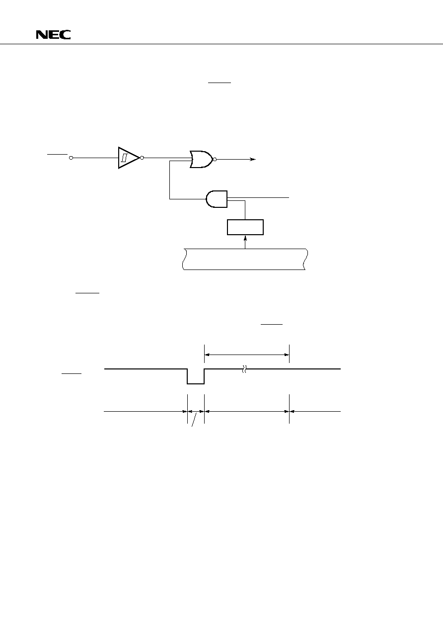
9. RESET FUNCTION
The
µ
PD750008 is reset with the external reset signal (RESET) or the reset signal received from the basic interval
timer/watchdog timer. When either reset signal is input, the internal reset signal is generated. Fig. 9-1 shows the
configuration of the reset circuit.
Fig. 9-1 Configuration of Reset Functions
When the RESET signal is generated, all hardware is initialized as indicated in Table 9-1. Fig. 9-2 shows the reset
operation timing.
Fig. 9-2 Reset Operation by Generation of RESET Signal
Note Either of the following two values can be selected by a mask option:
2
17
/f
X
(21.8 ms at 6.0 MHz, 31.3 ms at 4.19 MHz)
2
15
/f
X
(5.46 ms at 6.0 MHz, 7.81 ms at 4.19 MHz)
WDTM
RESET
Internal reset signal
Reset signal from basic
interval timer/watchdog timer
Internal bus
RESET signal is generated
Operating mode or
standby mode
HALT mode
Operating mode
Internal reset operation
Wait
Note

37
µ
PD750004, 750006, 750008, 750004(A), 750006(A), 750008(A)
Table 9-1 Status of the Hardware after a Reset (1/2)
Program counter (PC)
PSW
Stack pointer (SP)
Stack bank selection register (SBS)
Data memory (RAM)
General-purpose registers (X, A, H, L, D, E, B, C)
Bank selection register (MBS, RBS)
Timer/event
counter
Timer counter
Clock timer
Serial interface
4 low-order bits at address 0000H
in program memory are set in PC
bits 11 to 8, and the data at address
0001H are set in PC bits 7 to 0.
5 low-order bits at address 0000H
in program memory are set in PC
bits 12 to 8, and the data at address
0001H are set in PC bits 7 to 0.
Held
0
0
Bit 6 at address 0000H in
program memory is set in RBE,
and bit 7 is set in MBE.
Undefined
1000B
Held
Held
0, 0
Undefined
0
0
0
FFH
0
0, 0
0
FFH
0
0, 0
0
Held
0
0
Held
4 low-order bits at address 0000H
in program memory are set in PC
bits 11 to 8, and the data at address
0001H are set in PC bits 7 to 0.
5 low-order bits at address 0000H
in program memory are set in PC
bits 12 to 8, and the data at address
0001H are set in PC bits 7 to 0.
Undefined
0
0
Bit 6 at address 0000H in program
memory is set in RBE, and bit 7 is
set in MBE.
Undefined
1000B
Undefined
Undefined
0, 0
Undefined
0
0
0
FFH
0
0, 0
0
FFH
0
0, 0
0
Undefined
0
0
Undefined
Generation of a RESET signal
during operation
Generation of a RESET signal in
a standby mode
Hardware
Carry flag (CY)
Skip flags (SK0 to SK2)
Interrupt status flags (IST0, IST1)
Bank enable flags (MBE, RBE)
µ
PD750004
µ
PD750006, 750008
Counter (BT)
Mode register (BTM)
Watchdog timer enable flag
(WDTM)
Counter (T0)
Modulo register (TMOD0)
Mode register (TM0)
TOE0, TOUT flip-flop
Counter (T1)
Modulo register (TMOD1)
Mode register (TM1)
TOE1, TOUT flip-flop
Mode register (WM)
Shift register (SIO)
Operation mode register (CSIM)
SBI control register (SBIC)
Slave address register (SVA)
Basic interval
timer/ watchdog
timer

38
µ
PD750004, 750006, 750008, 750004(A), 750006(A), 750008(A)
Table 9-1 Status of the Hardware after a Reset (2/2)
0
0
0
0
Reset (0)
0
0
0, 0, 0
Off
Clear (0)
0
0
Undefined
Generation of a RESET signal
during operation
Clock generator,
clock output cir-
cuit
Interrupt
Digital ports
Processor clock control register (PCC)
System clock control register (SCC)
Clock output mode register (CLOM)
Interrupt request flag (IRQ
◊◊◊
)
Interrupt enable flag (IE
◊◊◊
)
Priority selection register (IPS)
INT0, INT1, and INT2 mode registers
(IM0, IM1, IM2)
Output buffer
Output latch
I/O mode registers (PMGA, PMGB,
PMGC)
Pull-up resistor specification registers
(POGA, POGB)
Generation of a RESET signal in
a standby mode
Hardware
Sub-oscillator control register (SOS)
0
0
0
0
Reset (0)
0
0
0, 0, 0
Off
Clear (0)
0
0
Held
Bit sequential buffers (BSB0 to BSB3)

39
µ
PD750004, 750006, 750008, 750004(A), 750006(A), 750008(A)
10. MASK OPTION
The
µ
PD750008 has the following mask options:
∑
Mask option of P40 to P43 and P50 to P53
Can specify whether to incorporate the pull-up resistor.
The pull-up resistor is incorporated bit by bit.
The pull-up resistor is not incorporated.
∑
Mask option of standby function
Can specify the wait time with the RESET signal.
2
17
/f
X
(21.8 ms at f
X
= 6.0 MHz, 31.3 ms at f
X
= 4.19 MHz)
2
15
/f
X
(5.46 ms at f
X
= 6.0 MHz, 7.81 ms at f
X
= 4.19 MHz)
∑
Mask option of subsystem clock
Can specify whether to enable the built-in feedback resistor.
The built-in feedback resistor is enabled (it is turned on or off by software).
The built-in feedback resistor is disabled (it is cut by hardware).
1
2
1
2
1
2

40
µ
PD750004, 750006, 750008, 750004(A), 750006(A), 750008(A)
Description
Representation
format
11. INSTRUCTION SET
(1) Operand identifier and its descriptive method
The operands are described in the operand column of each instruction according to the descriptive method for
the operand format of the appropriate instructions. (For details, refer to
RA75X Assembler Package User's
Manual: Language (EEU-1363).) For descriptions in which alternatives exist, one element should be selected.
Capital letters and plus and minus signs are keywords; therefore, they should be described as they are.
For immediate data, the appropriate numerical values or labels should be described.
The symbols of register flags can be used as a label instead of mem, fmem, pmem, and bit. (For details, refer
to
µ
PD750008 User's Manual (U10740E).) However, there are some restrictions on usable labels for fmem and
pmem.
Note Only even address can be specified for 8-bit data processing.
X, A, B, C, D, E, H, L
X, B, C, D, E, H, L
XA, BC, DE, HL
BC, DE, HL
BC, DE
XA, BC, DE, HL, XA', BC', DE', HL'
BC, DE, HL, XA', BC', DE', HL'
HL, HL+, HL-, DE, DL
DE, DL
4-bit immediate data or label
8-bit immediate data or label
8-bit immediate data or label
Note
2-bit immediate data or label
FB0H - FBFH, FF0H - FFFH immediate data or label
FC0H - FFFH immediate data or label
0000H - 0FFFH immediate data or label (
µ
PD750004)
0000H - 17FFH immediate data or label (
µ
PD750006)
0000H - 1FFFH immediate data or label (
µ
PD750008)
0000H - 0FFFH immediate data or label (
µ
PD750004)
0000H - 17FFH immediate data or label (
µ
PD750006)
0000H - 1FFFH immediate data or label (
µ
PD750008)
12-bit immediate data or label
11-bit immediate data or label
20H - 7FH immediate data (however, bit 0 = 0) or label
PORT0 - PORT8
IEBT, IET0, IET1, IE0 - IE2, IE4, IECSI, IEW
RB0 - RB3
MB0, MB1, MB15
reg
reg1
rp
rp1
rp2
rp'
rp'1
rpa
rpa1
n4
n8
mem
bit
fmem
pmem
addr
addr1(for Mk
mode only)
caddr
faddr
taddr
PORTn
IE
◊◊◊
RBn
MBn

41
µ
PD750004, 750006, 750008, 750004(A), 750006(A), 750008(A)
(2) Symbol definitions in operation description
A
:
A register; 4-bit accumulator
B
:
B register
C
:
C register
D
:
D register
E
:
E register
H
:
H register
L
:
L register
X
:
X register
XA
:
Register pair (XA); 8-bit accumulator
BC
:
Register pair (BC)
DE
:
Register pair (DE)
HL
:
Register pair (HL)
XA'
:
Extended register pair (XA')
BC'
:
Extended register pair (BC')
DE'
:
Extended register pair (DE')
HL'
:
Extended register pair (HL')
PC
:
Program counter
SP
:
Stack pointer
CY
:
Carry flag; Bit accumulator
PSW
:
Program status word
MBE
:
Memory bank enable flag
RBE
:
Register bank enable flag
PORTn :
Port n (n = 0 to 8)
IME
:
Interrupt master enable flag
IPS
:
Interrupt priority specification register
IE
◊◊◊
:
Interrupt enable flag
RBS
:
Register bank selection register
MBS
:
Memory bank selection register
PCC
:
Processor clock control register
.
:
Address bit delimiter
(
◊◊
)
:
Contents addressed by
◊◊
◊◊
H
:
Hexadecimal data

42
µ
PD750004, 750006, 750008, 750004(A), 750006(A), 750008(A)
(3) Symbols used for the addressing area column
Remarks 1. MB indicates the memory bank that can be accessed.
2. For *2, MB = 0 regardless of MBE and MBS settings.
3. For *4 and *5, MB = 15 regardless of MBE and MBS settings.
4. For *6 to *11, each addressable area is indicated.
(4) Description of machine cycle column
S indicates the number of machine cycles necessary for skipping any skip instruction. The value of S changes
as follows:
∑
When no skip is performed
: S = 0
∑
When a 1-byte or 2-byte instruction is skipped : S = 1
∑
When a 3-byte instruction
Note
is skipped
: S = 2
Note 3-byte instruction: BR !addr, BRA !addr1, CALL !addr, and CALLA !addr1 instructions.
Caution The GETI instruction is skipped in one machine cycle.
One machine cycle is equal to one cycle (= t
CY
) of the CPU clock (
), and four types of times are available for
selection according to the PCC setting.
* 1
MB = MBE ∑ MBS (MBS = 0, 1, 15)
* 2
MB = 0
* 3
MBE = 0
MBE = 1
:
:
MB = 0 (000H - 07FH), MB = 15 (F80H - FFFH)
MB = MBS (MBS = 0, 1, 15)
* 4
MB = 15, fmem = FB0H - FBFH, FF0H - FFFH
* 5
MB = 15, pmem = FC0H - FFFH
* 6
addr = 0000H - 0FFFH (
PD750004), 0000H - 17FFH (
PD750006)
0000H - 1FFFH (
PD750008)
µ
µ
µ
* 7
addr, addr1 = (Current PC) - 15 to (Current PC) - 1
(Current PC) + 2 to (Current PC) + 16
* 8
caddr = 0000H - 0FFFH ( PD750004)
0000H - 0FFFH (PC
12
= 0:
PD750006, 750008)
1000H - 17FFH (PC
12
= 1:
PD750006)
1000H - 1FFFH (PC
12
= 1:
PD750008)
µ
µ
µ
* 9
faddr = 0000H - 07FFH
* 10
taddr = 0020H - 007FH
Data memory
addressing
Program memory
addressing
µ
Mk
mode only
addr1 =
µ
µ
µ
0000H - 0FFFH ( PD750004)
0000H - 17FFH (
PD750006)
0000H - 1FFFH (
PD750008)
* 11

43
µ
PD750004, 750006, 750008, 750004(A), 750006(A), 750008(A)
Group
Transfer
Table
reference
Mne-
monic
MOV
XCH
MOVT
Operand
A, #n4
reg1, #n4
XA, #n8
HL, #n8
rp2, #n8
A, @HL
A, @HL+
A, @HL-
A, @rpa1
XA, @HL
@HL, A
@HL, XA
A, mem
XA, mem
mem, A
mem, XA
A, reg
XA, rp'
reg1, A
rp'1, XA
A, @HL
A, @HL+
A, @HL-
A, @rpa1
XA, @HL
A, mem
XA, mem
A, reg1
XA, rp'
XA, @PCDE
XA, @PCXA
XA, @BCDE
XA, @BCXA
Bytes
1
2
2
2
2
1
1
1
1
2
1
2
2
2
2
2
2
2
2
2
1
1
1
1
2
2
2
1
2
1
1
1
1
Machin-
ing
cycle
1
2
2
2
2
1
2 + S
2 + S
1
2
1
2
2
2
2
2
2
2
2
2
1
2 + S
2 + S
1
2
2
2
1
2
3
3
3
3
Skip
condition
String A
String A
String B
L = 0
L = FH
L = 0
L = FH
Address-
ing area
*1
*1
*1
*2
*1
*1
*1
*3
*3
*3
*3
*1
*1
*1
*2
*1
*3
*3
*6
*6
Operation
A
n4
reg1
n4
XA
n8
HL
n8
rp2
n8
A
(HL)
A
(HL), then L
L + 1
A
(HL), then L
L - 1
A
(rpa1)
XA
(HL)
(HL)
A
(HL)
XA
A
(mem)
XA
(mem)
(mem)
A
(mem)
XA
A
reg
XA
rp'
reg1
A
rp'1
XA
A
(HL)
A
(HL), then L
L + 1
A
(HL), then L
L - 1
A
(rpa1)
XA
(HL)
A
(mem)
XA
(mem)
A
reg1
XA
rp'
∑
µ
PD750004
XA
(PC
11-8
+ DE)
ROM
∑
µ
PD750006, 750008
XA
(PC
12-8
+ DE)
ROM
∑
µ
PD750004
XA
(PC
11-8
+ XA)
ROM
∑
µ
PD750006, 750008
XA
(PC
12-8
+ XA)
ROM
XA
(BCDE)
ROM
Note
XA
(BCXA)
ROM
Note
Note Set register B to 0 in the
µ
PD750004. Only the LSB is valid in register B in the
µ
PD750006 and
µ
PD750008.

44
µ
PD750004, 750006, 750008, 750004(A), 750006(A), 750008(A)
Group
Bit transfer
Arithme-
tic
Accumulator
manipulation
Increment/
decrement
Mne-
monic
MOV1
ADDS
ADDC
SUBS
SUBC
AND
OR
XOR
RORC
NOT
INCS
DECS
Operand
CY, fmem.bit
CY, pmem.@L
CY, @H+mem.bit
fmem.bit, CY
pmem.@L, CY
@H+mem.bit, CY
A, #n4
XA, #n8
A, @HL
XA, rp'
rp'1, XA
A, @HL
XA, rp'
rp'1, XA
A, @HL
XA, rp'
rp'1, XA
A, @HL
XA, rp'
rp'1, XA
A, #n4
A, @HL
XA, rp'
rp'1, XA
A, #n4
A, @HL
XA, rp'
rp'1, XA
A, #n4
A, @HL
XA, rp'
rp'1, XA
A
A
reg
rp1
@HL
mem
reg
rp'
Bytes
2
2
2
2
2
2
1
2
1
2
2
1
2
2
1
2
2
1
2
2
2
1
2
2
2
1
2
2
2
1
2
2
1
2
1
1
2
2
1
2
Machin-
ing
cycle
2
2
2
2
2
2
1 + S
2 + S
1 + S
2 + S
2 + S
1
2
2
1 + S
2 + S
2 + S
1
2
2
2
1
2
2
2
1
2
2
2
1
2
2
1
2
1 + S
1 + S
2 + S
2 + S
1 + S
2 + S
Skip
condition
carry
carry
carry
carry
carry
borrow
borrow
borrow
reg = 0
rp1 = 00H
(HL) = 0
(mem) = 0
reg = FH
rp' = FFH
Address-
ing area
*4
*5
*1
*4
*5
*1
*1
*1
*1
*1
*1
*1
*1
*1
*3
Operation
CY
(fmem.bit)
CY
(pmem
7-2
+ L
3-2
.bit(L
1-0
))
CY
(H + mem
3-0
.bit)
(fmem.bit)
CY
(pmem
7-2
+ L
3-2
.bit(L
1-0
))
CY
(H + mem
3-0
.bit)
CY
A
A + n4
XA
XA + n8
A
A + (HL)
XA
XA + rp'
rp'1
rp'1 + XA
A, CY
A + (HL) + CY
XA, CY
XA + rp' + CY
rp'1, CY
rp'1 + XA + CY
A
A - (HL)
XA
XA - rp'
rp'1
rp'1 - XA
A, CY
A - (HL) - CY
XA, CY
XA - rp' - CY
rp'1, CY
rp'1 - XA - CY
A
A
n4
A
A
(HL)
XA
XA
rp'
rp'1
rp'1
XA
A
A
n4
A
A
(HL)
XA
XA
rp'
rp'1
rp'1
XA
A
A
n4
A
A
(HL)
XA
XA
rp'
rp'1
rp'1
XA
CY
A
0
, A
3
CY, A
n-1
A
n
A
A
reg
reg + 1
rp1
rp1 + 1
(HL)
(HL) + 1
(mem)
(mem) + 1
reg
reg - 1
rp'
rp' - 1

45
µ
PD750004, 750006, 750008, 750004(A), 750006(A), 750008(A)
Group
Compari-
son
Carry flag
manipula-
tion
Memory
bit
manipula-
tion
Mne-
monic
SKE
SET1
CLR1
SKT
NOT1
SET1
CLR1
SKT
SKF
SKTCLR
AND1
OR1
XOR1
Operand
reg, #n4
@HL, #n4
A, @HL
XA, @HL
A, reg
XA, rp'
CY
CY
CY
CY
mem.bit
fmem.bit
pmem. @L
@H+mem.bit
mem.bit
fmem.bit
pmem. @L
@H+mem.bit
mem.bit
fmem.bit
pmem. @L
@H+mem.bit
mem.bit
fmem.bit
pmem. @L
@H+mem.bit
fmem.bit
pmem. @L
@H+mem.bit
CY, fmem.bit
CY, pmem. @L
CY, @H+mem.bit
CY, fmem.bit
CY, pmem. @L
CY, @H+mem.bit
CY, fmem.bit
CY, pmem.@L
CY, @H+mem.bit
Bytes
2
2
1
2
2
2
1
1
1
1
2
2
2
2
2
2
2
2
2
2
2
2
2
2
2
2
2
2
2
2
2
2
2
2
2
2
2
2
Machin-
ing
cycle
2 + S
2 + S
1 + S
2 + S
2 + S
2 + S
1
1
1 + S
1
2
2
2
2
2
2
2
2
2 + S
2 + S
2 + S
2 + S
2 + S
2 + S
2 + S
2 + S
2 + S
2 + S
2 + S
2
2
2
2
2
2
2
2
2
Skip
condition
reg = n4
(HL) = n4
A = (HL)
XA = (HL)
A = reg
XA = rp'
CY = 1
(mem.bit) = 1
(fmem.bit) = 1
(pmem.@L) = 1
(@H + mem.bit) = 1
(mem.bit) = 0
(fmem.bit) = 0
(pmem.@L) = 0
(@H + mem.bit) = 0
(fmem.bit) = 1
(pmem.@L) = 1
(@H + mem.bit) = 1
Address-
ing area
*1
*1
*1
*3
*4
*5
*1
*3
*4
*5
*1
*3
*4
*5
*1
*3
*4
*5
*1
*4
*5
*1
*4
*5
*1
*4
*5
*1
*4
*5
*1
Operation
Skip if reg = n4
Skip if (HL) = n4
Skip if A = (HL)
Skip if XA = (HL)
Skip if A = reg
Skip if XA = rp'
CY
1
CY
0
Skip if CY = 1
CY
CY
(mem.bit)
1
(fmem.bit)
1
(pmem
7-2
+ L
3-2
.bit(L
1-0
))
1
(H + mem
3-0
.bit)
1
(mem.bit)
0
(fmem.bit)
0
(pmem
7-2
+ L
3-2
.bit(L
1-0
))
0
(H + mem
3-0
.bit)
0
Skip if (mem.bit) = 1
Skip if (fmem.bit) = 1
Skip if (pmem
7-2
+ L
3-2
.bit(L
1-0
)) = 1
Skip if (H + mem
3-0
.bit) = 1
Skip if (mem.bit) = 0
Skip if (fmem.bit) = 0
Skip if (pmem
7-2
+ L
3-2
.bit(L
1-0
)) = 0
Skip if (H + mem
3-0
.bit) = 0
Skip if (fmem.bit) = 1 and clear
Skip if (pmem
7-2
+ L
3-2
.bit(L
1-0
)) = 1 and clear
Skip if (H + mem
3-0
.bit) = 1 and clear
CY
CY
(fmem.bit)
CY
CY
(pmem
7-2
+ L
3-2
.bit(L
1-0
))
CY
CY
(H + mem
3-0
.bit)
CY
CY
(fmem.bit)
CY
CY
(pmem
7-2
+ L
3-2
.bit(L
1-0
))
CY
CY
(H + mem
3-0
.bit)
CY
CY
(fmem.bit)
CY
CY
(pmem
7-2
+ L
3-2
.bit(L
1-0
))
CY
CY
(H + mem
3-0
.bit)

46
µ
PD750004, 750006, 750008, 750004(A), 750006(A), 750008(A)
Group
Branch
Mne-
monic
BR
Note
Operand
addr
addr1
!addr
$addr
$addr1
Skip
condition
Address-
ing area
*6
*11
*6
*7
Note The shaded portion is supported in Mk
mode only. The other portions are supported in Mk
mode only.
Bytes
-
-
3
1
1
Machin-
ing
cycle
-
-
3
2
2
Operation
∑
µ
PD750004
PC
11-0
addr
The assembler selects the most
adequate instruction from BR !addr,
BRCB !caddr, or BR $addr.
∑
µ
PD750006, 750008
PC
12-0
addr
The assembler selects the most
adequate instruction from BR !addr,
BRCB !caddr, or BR $addr.
∑
µ
PD750004
PC
11-0
addr1
The assembler selects the most
adequate instruction from
instructions below.
∑ BR !addr
∑ BRA !addr1
∑ BRCB !caddr
∑ BR $addr1
∑
µ
PD750006, 750008
PC
12-0
addr1
The assembler selects the most
adequate instruction from
instructions below.
∑ BR !addr
∑ BRA !addr1
∑ BRCB !caddr
∑ BR $addr1
∑
µ
PD750004
PC
11-0
addr
∑
µ
PD750006, 750008
PC
12-0
addr
∑
µ
PD750004
PC
11-0
addr
∑
µ
PD750006, 750008
PC
12-0
addr
∑
µ
PD750004
PC
11-0
addr1
∑
µ
PD750006, 750008
PC
12-0
addr1

47
µ
PD750004, 750006, 750008, 750004(A), 750006(A), 750008(A)
Group
Branch
Subrou-
tine stack
control
Mne-
monic
BR
BRA
Note 3
BRCB
CALLA
Note 3
Operand
PCDE
PCXA
BCDE
BCXA
!addr1
!caddr
!addr1
Bytes
2
2
2
2
3
2
3
Machin-
ing
cycle
3
3
3
3
3
2
3
Skip
condition
Address-
ing area
*6
*6
*11
*8
*11
Operation
∑
µ
PD750004
PC
11-0
PC
11-8
+ DE
∑
µ
PD750006, 750008
PC
12-0
PC
12-8
+ DE
∑
µ
PD750004
PC
11-0
PC
11-8
+ XA
∑
µ
PD750006, 750008
PC
12-0
PC
12-8
+ XA
∑
µ
PD750004
PC
11-0
BCDE
Note 1
∑
µ
PD750006, 750008
PC
12-0
BCDE
Note 2
∑
µ
PD750004
PC
11-0
BCXA
Note 1
∑
µ
PD750006, 750008
PC
12-0
BCXA
Note 2
∑
µ
PD750004
PC
11-0
addr1
∑
µ
PD750006, 750008
PC
12-0
addr1
∑
µ
PD750004
PC
11-0
caddr
11-0
∑
µ
PD750006, 750008
PC
12-0
PC
12
+ caddr
11-0
∑
µ
PD750004
(SP - 2)
◊
,
◊
, MBE, RBE
(SP - 6) (SP - 3) (SP - 4)
PC
11-0
(SP - 5)
0, 0, 0, 0
PC
11-0
addr1, SP
SP - 6
∑
µ
PD750006, 750008
(SP - 2)
◊
,
◊
, MBE, RBE
(SP - 6) (SP - 3) (SP - 4)
PC
11-0
(SP - 5)
0, 0, 0, PC
12
PC
12-0
addr1, SP
SP - 6
Notes 1. Set register B to 0.
2. Only the LSB is valid in register B.
3. The shaded portion is supported in Mk
mode only. The other portions are supported in Mk
mode only.

48
µ
PD750004, 750006, 750008, 750004(A), 750006(A), 750008(A)
Group
Subrou-
tine stack
control
Mne-
monic
CALL
Note
CALLF
Note
Operand
!addr
!faddr
Bytes
3
2
Machin-
ing
cycle
3
4
2
3
Skip
condition
Address-
ing area
*6
*9
Operation
∑
µ
PD750004
(SP - 3)
MBE, RBE, 0, 0
(SP - 4) (SP - 1) (SP - 2)
PC
11-0
PC
11-0
addr, SP
SP - 4
∑
µ
PD750006, 750008
(SP - 3)
MBE, RBE, 0, PC
12
(SP - 4) (SP - 1) (SP - 2)
PC
11-0
PC
12-0
addr, SP
SP - 4
∑
µ
PD750004
(SP - 2)
◊
,
◊
, MBE, RBE
(SP - 6) (SP - 3) (SP - 4)
PC
11-0
(SP - 5)
0, 0, 0, 0
PC
11-0
addr, SP
SP - 6
∑
µ
PD750006, 750008
(SP - 2)
◊
,
◊
, MBE, RBE
(SP - 6) (SP - 3) (SP - 4)
PC
11-0
(SP - 5)
0, 0, 0, PC
12
PC
12-0
addr, SP
SP - 6
∑
µ
PD750004
(SP - 3)
MBE, RBE, 0, 0
(SP - 4) (SP - 1) (SP - 2)
PC
11-0
PC
11-0
0 + faddr, SP
SP - 4
∑
µ
PD750006, 750008
(SP - 3)
MBE, RBE, 0, PC
12
(SP - 4) (SP - 1) (SP - 2)
PC
11-0
PC
12-0
00 + faddr, SP
SP - 4
∑
µ
PD750004
(SP - 2)
◊
,
◊
, MBE, RBE
(SP - 6) (SP - 3) (SP - 4)
PC
11-0
(SP - 5)
0, 0, 0, 0
PC
11-0
0 + faddr, SP
SP - 6
∑
µ
PD750006, 750008
(SP - 2)
◊
,
◊
, MBE, RBE
(SP - 6) (SP - 3) (SP - 4)
PC
11-0
(SP - 5)
0, 0, 0, PC
12
PC
12-0
00 + faddr, SP
SP - 6
Note The shaded portion is supported in Mk
mode only. The other portions are supported in Mk
mode only.

49
µ
PD750004, 750006, 750008, 750004(A), 750006(A), 750008(A)
Group
Subrou-
tine stack
control
Mne-
monic
RET
Note
RETS
Note
Operand
Bytes
1
1
Machin-
ing
cycle
3
3
3 + S
3 + S
Skip
condition
Uncondition
Address-
ing area
Operation
∑
µ
PD750004
PC
11-0
(SP) (SP + 3) (SP + 2)
MBE, RBE, 0, 0
(SP + 1), SP
SP + 4
∑
µ
PD750006, 750008
PC
11-0
(SP) (SP + 3) (SP + 2)
MBE, RBE, 0, PC
12
(SP + 1)
SP
SP + 4
∑
µ
PD750004
◊
,
◊
, MBE, RBE
(SP + 4)
0, 0, 0, 0
(SP + 1)
PC
11-0
(SP) (SP + 3) (SP + 2)
SP
SP + 6
∑
µ
PD750006, 750008
◊
,
◊
, MBE, RBE
(SP + 4)
MBE, 0, 0, PC
12
(SP + 1)
PC
11-0
(SP) (SP + 3) (SP + 2)
SP
SP + 6
∑
µ
PD750004
MBE, RBE, 0, 0
(SP + 1)
PC
11-0
(SP) (SP + 3) (SP + 2)
SP
SP + 4
then skip unconditionally
∑
µ
PD750006, 750008
MBE, RBE, 0
PC
12
(SP + 1)
PC
11-0
(SP) (SP + 3) (SP + 2)
SP
SP + 4
then skip unconditionally
∑
µ
PD750004
0, 0, 0, 0
(SP + 1)
PC
11-0
(SP) (SP + 3) (SP + 2)
◊
,
◊
, MBE, RBE
(SP + 4)
SP
SP + 6
then skip unconditionally
∑
µ
PD750006, 750008
0, 0, 0, PC
12
(SP + 1)
PC
11-0
(SP) (SP + 3) (SP + 2)
◊
,
◊
, MBE, RBE
(SP + 4)
SP
SP + 4
then skip unconditionally
Note The shaded portion is supported in Mk
mode only. The other portions are supported in Mk
mode only.

50
µ
PD750004, 750006, 750008, 750004(A), 750006(A), 750008(A)
Group
Subrou-
tine stack
control
Interrupt
control
Input/
output
CPU
control
Mne-
monic
RETI
Note 1
PUSH
POP
EI
DI
IN
Note 2
OUT
Note 2
HALT
STOP
NOP
Operand
rp
BS
rp
BS
IE
◊◊◊
IE
◊◊◊
A, PORTn
XA, PORTn
PORTn, A
PORTn, XA
Bytes
1
1
2
1
2
2
2
2
2
2
2
2
2
2
2
1
Machin-
ing
cycle
3
1
2
1
2
2
2
2
2
2
2
2
2
2
2
1
Skip
condition
Address-
ing area
Operation
∑
µ
PD750004
MBE, RBE, 0, 0
(SP + 1)
PC
11-0
(SP) (SP + 3) (SP + 2)
PSW
(SP + 4) (SP + 5), SP
SP + 6
∑
µ
PD750006, 750008
MBE, RBE, 0, PC
12
(SP + 1)
PC
11-0
(SP) (SP + 3) (SP + 2)
PSW
(SP + 4) (SP + 5), SP
SP + 6
∑
µ
PD750004
0, 0, 0, 0
(SP + 1)
PC
11-0
(SP) (SP + 3) (SP + 2)
PSW
(SP + 4) (SP + 5), SP
SP + 6
∑
µ
PD750006, 750008
0, 0, 0, PC
12
(SP + 1)
PC
11-0
(SP) (SP + 3) (SP + 2)
PSW
(SP + 4) (SP + 5), SP
SP + 6
(SP - 1)(SP - 2)
rp, SP
SP - 2
(SP - 1)
MBS, (SP - 2)
RBS,
SP
SP - 2
rp
(SP + 1)(SP), SP
SP + 2
MBS
(SP + 1), RBS
(SP),
SP
SP + 2
IME (IPS.3)
1
IE
◊◊◊
1
IME (IPS.3)
0
IE
◊◊◊
0
A
PORTn
(n = 0 - 8)
XA
PORTn
+1
,PORTn
(n = 4, 6)
PORTn
A
(n = 2 - 8)
PORTn
+1
,PORTn
XA
(n = 4, 6)
Set HALT Mode (PCC.2
1)
Set STOP Mode (PCC.3
1)
No Operation
Notes 1. The shaded portion is supported in Mk
mode only. The other portions are supported in Mk
mode only.
2. When executing the IN/OUT instruction, MBE must be set to 0 or MBE and MBS must be set to 1 and 15,
respectively.
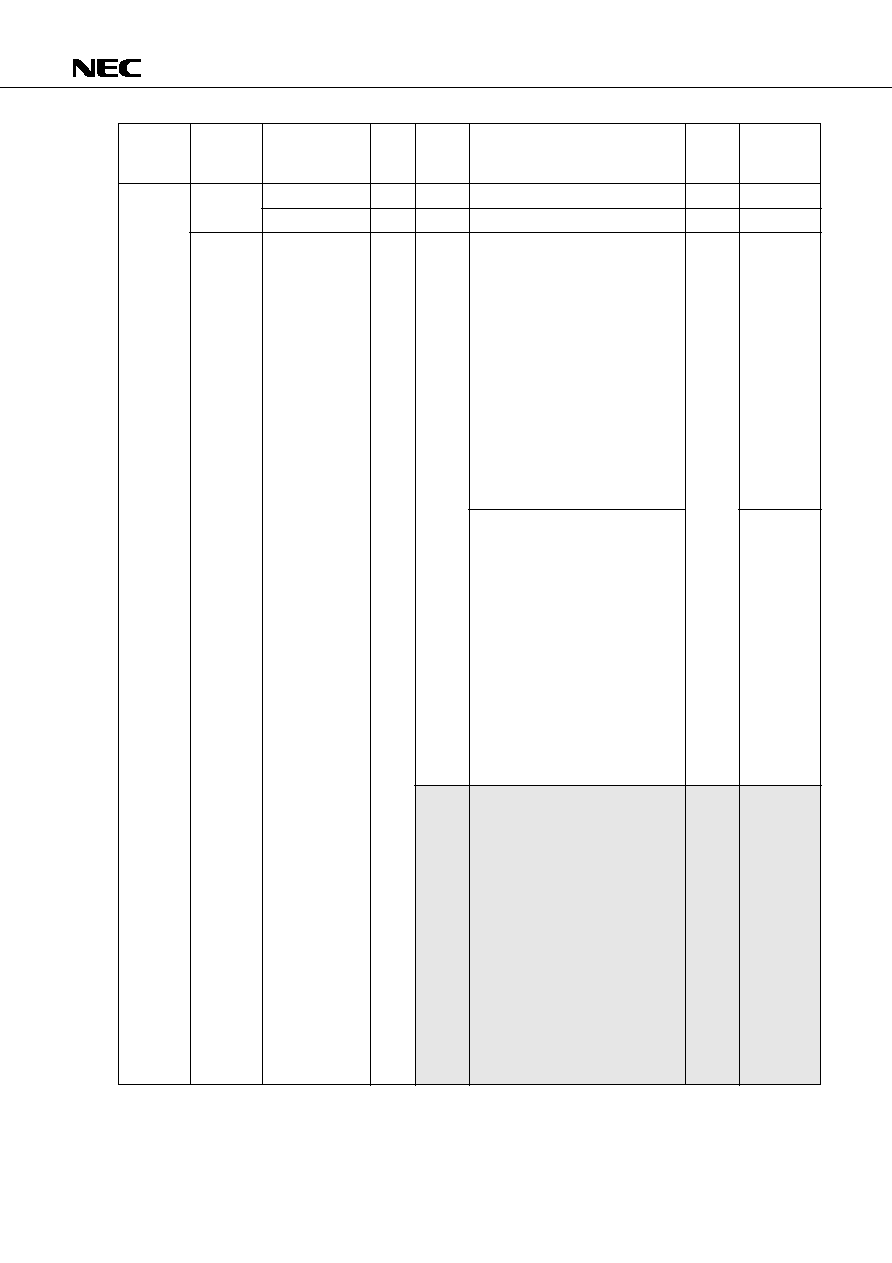
51
µ
PD750004, 750006, 750008, 750004(A), 750006(A), 750008(A)
Group
Special
Mne-
monic
SEL
GETI
Notes 1, 2
Operand
RBn
MBn
taddr
Bytes
2
2
1
Machin-
ing
cycle
2
2
3
3
4
3
Skip
condition
Depends
on the
referenced
instruction.
Depends
on the
referenced
instruction.
Depends
on the
referenced
instruction.
Address-
ing area
*10
*10
Operation
RBS
n (n = 0 - 3)
MBS
n (n = 0, 1, 15)
∑
µ
PD750004
When the TBR instruction is used
PC
11-0
(taddr)
3-0
+ (taddr + 1)
When the TCALL instruction is used
(SP - 4) (SP - 1) (SP - 2)
PC
11-0
(SP - 3)
MBE, RBE, 0, 0
PC
11-0
(taddr)
3-0
+ (taddr + 1)
SP
SP - 4
When an instruction other than the
TBR and TCALL instructions is used
Execution of (taddr)(taddr + 1)
instruction
∑
µ
PD750006, 750008
When the TBR instruction is used
PC
12-0
(taddr)
4-0
+ (taddr + 1)
When the TCALL instruction is used
(SP - 4) (SP - 1) (SP - 2)
PC
11-0
(SP - 3)
MBE, RBE, 0, PC12
PC
12-0
(taddr)
4-0
+ (taddr + 1)
SP
SP - 4
When an instruction other than the
TBR and TCALL instructions is used
Execution of (taddr)(taddr + 1)
instruction
∑
µ
PD750004
When the TBR instruction is used
PC
11-0
(taddr)
3-0
+ (taddr + 1)
When the TCALL instruction is used
(SP - 6) (SP - 3) (SP - 4)
PC
11-0
(SP - 5)
0, 0, 0, 0
(SP - 2)
◊
,
◊
, MBE, RBE
PC
11-0
(taddr)
3-0
+ (taddr + 1)
SP
SP - 6
When an instruction other than the TBR
and TCALL instructions is used
Execution of (taddr)(taddr + 1)
instruction
Notes 1. The shaded portion is supported in Mk
mode only. The other portions are supported in Mk
mode only.
2. TBR and TCALL instructions are assembler pseudo instructions to define tables used for GETI instructions.
.........................................................
.........................................................
.........................................................
.........................................................
......................
......................
........................................................................
........................................................................
......................

52
µ
PD750004, 750006, 750008, 750004(A), 750006(A), 750008(A)
Group
Special
Mne-
monic
GETI
Notes 1, 2
Operand
taddr
Bytes
1
Machin-
ing
cycle
3
4
3
Skip
condition
Depends
on the
referenced
instruction.
Address-
ing area
*10
Operation
∑
µ
PD750006, 750008
When the TBR instruction is used
PC
12-0
(taddr)
4-0
+ (taddr + 1)
When the TCALL instruction is used
(SP - 6) (SP - 3) (SP - 4)
PC
11-0
(SP - 5)
0, 0, 0, PC
12
(SP - 2)
◊
,
◊
, MBE, RBE
PC
12-0
(taddr)
4-0
+ (taddr + 1)
SP
SP - 6
When an instruction other than the TBR
and TCALL instructions is used
Execution of (taddr)(taddr + 1)
instruction
Notes 1. The shaded portion is supported in Mk
mode only.
2. TBR and TCALL instructions are assembler pseudo instructions to define tables used for GETI instructions.
........................................................................
........................................................................
......................

53
µ
PD750004, 750006, 750008, 750004(A), 750006(A), 750008(A)
12. ELECTRICAL CHARACTERISTICS
ABSOLUTE MAXIMUM RATINGS (T
A
= 25
∞
C)
Caution Absolute maximum ratings are rated values beyond which physical damage will be caused to the
product; if the rated value of any of the parameters in the above table is exceeded, even momentarily,
the quality of the product may deteriorate. Always use the product within its rated values.
CAPACITANCE (T
A
= 25
∞
C, V
DD
= 0 V)
Unit
V
V
V
V
V
mA
mA
mA
mA
∞
C
∞
C
Rated value
-0.3 to +7.0
-0.3 to V
DD
+ 0.3
-0.3 to V
DD
+ 0.3
-0.3 to +14
-0.3 to V
DD
+ 0.3
-10
-30
30
220
-40 to +85
-65 to +150
Conditions
Other than ports 4 and 5
Ports
With a built-in pull-up resistor
4 and 5
With open drain
Each pin
Total of all pins
Each pin
Total of all pins
Parameter
Supply voltage
Input voltage
Output voltage
High-level output current
Low-level output current
Operating ambient temperature
Storage temperature
Symbol
V
DD
V
I1
V
I2
V
O
I
OH
I
OL
T
A
T
stg
Parameter
Input capacitance
Output capacitance
I/O capacitance
Symbol
C
IN
C
OUT
C
IO
Max.
15
15
15
Unit
pF
pF
pF
Typ.
Conditions
f = 1 MHz
0 V for pins other than pins to be
measured
Min.
54
µ
PD750004, 750006, 750008, 750004(A), 750006(A), 750008(A)
Resonator
Ceramic
resonator
Crystal
External
clock
Recommended
constant
CHARACTERISTICS OF THE MAIN SYSTEM CLOCK OSCILLATOR (T
A
= -40 to +85
∞
C)
Notes 1. The oscillator frequency and X1 input frequency indicate only the oscillator characteristics. See the item
of AC characteristics for the instruction execution time.
2. When the supply voltage is 2.2 V
V
DD
< 2.7 V and the oscillator frequency is 4.7 MHz < f
X
6.0 MHz,
set the processor clock control register (PCC) to a value other than 0011. When the PCC is set to 0011,
the time for one machine cycle cannot satisfy the defined setting of 0.85
µ
s.
3. The oscillation settling time means the time required for the oscillation to settle after V
DD
is applied or after
the STOP mode is released.
4. When the supply voltage is 1.8 V
V
DD
< 2.7 V and the X1 input frequency is 4.19 MHz < fx
6.0 MHz,
set the PCC to a value other than 0011. When the PCC is set to 0011, the time for one machine cycle cannot
satisfy the defined setting of 0.95
µ
s.
Caution When the main system clock oscillator is used, conform to the following guidelines when wiring
at the portions surrounded by dotted lines in the figures above to eliminate the influence of the
wiring capacity.
∑ The wiring must be as short as possible.
∑ Other signal lines must not run in these areas.
∑ Any line carrying a high fluctuating current must be kept away as far as possible.
∑ The grounding point of the capacitor of the oscillator must have the same potential as that of V
SS
.
∑ It must not be grounded to ground patterns carrying a large current.
∑ No signal must be taken from the oscillator.
Typ.
Parameter
Oscillator frequency (f
X
)
Note 1
Oscillation settling time
Note 3
Oscillator frequency (f
X
)
Note 1
Oscillation settling time
Note 3
X1 input frequency (f
X
)
Note 1
X1 input high/low level width
(t
XH
, t
XL
)
Min.
1.0
1.0
1.0
83.3
Max.
6.0
Note 2
4
6.0
Note 2
10
30
6.0
Note 4
500
Unit
MHz
ms
MHz
ms
ms
MHz
ns
Conditions
V
DD
= 2.2 to 5.5 V
After V
DD
reaches
Min. of the oscillation
voltage range
V
DD
= 2.2 to 5.5 V
V
DD
= 4.5 to 5.5 V
V
DD
= 2.2 to 5.5 V
V
DD
= 1.8 to 5.5 V
V
DD
= 1.8 to 5.5 V
X1
X2
C1
C2
X1
X2
C1
C2
X1
X2

55
µ
PD750004, 750006, 750008, 750004(A), 750006(A), 750008(A)
Recommended
constant
Resonator
Parameter
kHz
s
s
kHz
µ
s
Unit
Max.
Typ.
Min.
35
2
10
100
15
32.768
1.0
32
32
5
Conditions
Crystal
External
clock
XT1
XT2
Oscillator frequency (f
XT
)
Note 1
Oscillation settling time
Note 2
XT1 input frequency (f
XT
)
Note 1
XT1 input high/low level width
(t
XTH
, t
XTL
)
V
DD
= 2.2 to 5.5 V
V
DD
= 4.5 to 5.5 V
V
DD
= 2.2 to 5.5 V
V
DD
= 1.8 to 5.5 V
V
DD
= 1.8 to 5.5 V
CHARACTERISTICS OF THE SUBSYSTEM CLOCK OSCILLATOR (T
A
= -40 to +85
∞
C)
Notes 1. The oscillator frequency and input frequency indicate only the oscillator characteristics. See the item of
AC characteristics for the instruction execution time.
2. The oscillation settling time means the time required for the oscillation to settle after V
DD
is applied.
Caution When the subsystem clock oscillator is used, conform to the following guidelines when wiring at
the portions of surrounded by dotted lines in the figures above to eliminate the influence of the
wiring capacity.
∑ The wiring must be as short as possible.
∑ Other signal lines must not run in these areas.
∑ Any line carrying a high fluctuating current must be kept away as far as possible.
∑ The grounding point of the capacitor of the oscillator must have the same potential as that of V
SS
∑ It must not be grounded to ground patterns carrying a large current.
∑ No signal must be taken from the oscillator.
When the subsystem clock is used, pay special attention to its wiring; the subsystem clock
oscillator has low amplification to minimize current consumption and is more likely to malfunction
due to noise than the main system clock oscillator.
C3
C4
R
XT1
XT2

56
µ
PD750004, 750006, 750008, 750004(A), 750006(A), 750008(A)
RECOMMENDED PARAMETERS FOR THE OSCILLATION CIRCUIT
When a ceramic resonator is used for the main system clock (T
A
= -40 to +85
∞
C)
Note When the CSB1000J (1.0 MHz) manufactured by Murata Mfg. is used, a limiting resistor (Rd = 4.7 k
) is
necessary (see the following figure). When one of other resonators is used, no limiting resistor is required.
Manufacturer
Product name
Oscillation frequency
Oscillation
Oscillation
Remarks
(MHz)
circuit constant
voltage range
C1 (pF)
C2 (pF)
Min. (V)
Max. (V)
Murata Mfg.
CSB1000J
Note
1.0
100
100
2.8
5.5
Rd = 4.7 k
CSA2.00MG040
2.0
100
100
2.8
CST2.00MG040
Incorporated
Incorporated
2.8
CSA4.00MG
4.0
30
30
2.8
CST4.00MGW
Incorporated
Incorporated
2.8
CSA4.00MGU
30
30
2.6
CST4.00MGWU
Incorporated
Incorporated
2.6
CSA4.19MG
4.19
30
30
2.8
CST4.19MGW
Incorporated
Incorporated
2.8
CSA4.19MGU
30
30
2.8
CST4.19MGWU
Incorporated
Incorporated
2.8
CSA6.00MGU
6.0
30
30
2.9
CST6.00MGWU
Incorporated
Incorporated
2.9
CSA6.00MG
30
30
2.7
CST6.00MGW
Incorporated
Incorporated
2.7
Kyocera
KBR-1000F/Y
1.0
220
220
2.45
5.5
KBR-2.0MS
2.0
82
82
2.5
PBRC 2.00A
82
82
2.5
KBR-4.0MSA
4.0
33
33
2.5
KBR-4.0MKS
Incorporated
Incorporated
2.5
PBRC4.00A
33
33
2.5
PBRC4.00B
Incorporated
Incorporated
2.5
KBR-6.0MSA
6.0
33
33
2.5
KBR-6.0MKS
Incorporated
Incorporated
2.5
PBRC6.00A
33
33
2.5
PBRC6.00B
Incorporated
Incorporated
2.5
TDK
FCR2.0M3
2.0
33
33
2.2
5.5
FCR4.0M5
4.0
15
15
2.0
FCR4.19M5
4.19
15
15
2.2
FCR6.0M5
6.0
15
15
2.5
57
µ
PD750004, 750006, 750008, 750004(A), 750006(A), 750008(A)
Recommended sample circuit for the main system clock when the CSB1000J manufactured by Murata Mfg.
is used
When a crystal is used for the subsystem clock (T
A
= -10 to +60
∞
C)
Caution The oscillation circuit constant and oscillation voltage range indicate the conditions to settle the
oscillation, not to guarantee the accuracy of the oscillation frequency. When an accuracy
oscillation frequency is needed for the implemented circuit, the oscillation frequency of the
resonator should be adjusted on the circuit. Ask the manufacturer of the resonator you use.
Manufacturer
Product name
Oscillation
Oscillation
Oscillation
Remarks
frequency (kHz)
circuit constant
voltage range
C3 (pF) C4 (pF) R (k
)
Min. (V)
Max. (V)
Daishinku
DT-38
32.768
10
10
220
2.7
5.5
Low-current-drain mode
2.2
5.5
Low-voltage mode
CSB1000J
X1
X2
Rd
C2
C1

58
µ
PD750004, 750006, 750008, 750004(A), 750006(A), 750008(A)
DC CHARACTERISTICS (T
A
= -40 to +85
∞
C, V
DD
= 2.2 to 5.5 V)
Parameter
Symbol
mA
mA
V
V
V
V
V
V
V
V
V
V
V
V
V
V
V
V
V
V
µ
A
µ
A
µ
A
µ
A
µ
A
µ
A
µ
A
µ
A
µ
A
µ
A
µ
A
µ
A
k
k
I
OL
V
IH1
V
IH2
V
IH3
V
IH4
V
IL1
V
IL2
V
IL3
V
OH
V
OL1
V
OL2
I
LIH1
I
LIH2
I
LIH3
I
LIL1
I
LIL2
I
LIL3
I
LOH1
I
LOH2
I
LOL
R
L1
R
L2
2.7 V
V
DD
5.5 V
2.2 V
V
DD
< 2.7 V
2.7 V
V
DD
5.5 V
2.2 V
V
DD
< 2.7 V
2.7 V
V
DD
5.5 V
2.2 V
V
DD
< 2.7 V
2.7 V
V
DD
5.5 V
2.2 V
V
DD
< 2.7 V
2.7 V
V
DD
5.5 V
2.2 V
V
DD
< 2.7 V
2.7 V
V
DD
5.5 V
2.2 V
V
DD
< 2.7 V
0.7V
DD
0.9V
DD
0.8V
DD
0.9V
DD
0.7V
DD
0.9V
DD
0.7V
DD
0.9V
DD
V
DD
- 0.1
0
0
0
0
0
V
DD
- 0.5
50
15
I
OL
= 15 mA, V
DD
= 4.5 to 5.5 V
I
OL
= 1.6 mA
SCK, SO,
and ports
2 to 8
V
DD
= 5.0 V
V
DD
= 3.0 V
0.2
-10
-3
100
30
15
150
V
DD
V
DD
V
DD
V
DD
V
DD
V
DD
13
13
V
DD
0.3V
DD
0.1V
DD
0.2V
DD
0.1V
DD
0.1
2.0
0.4
0.2V
DD
3
20
20
-3
-20
-3
-30
-27
-8
3
20
-3
200
60
Min.
Typ.
Max.
Unit
Low-level output
current
High-level input
voltage
Low-level input
voltage
High-level output voltage
Low-level output
voltage
High-level input
leakage current
Low-level input
leakage current
High-level output
leakage current
Low-level output
leakage current
Built-in pull-up
resistor
Ports 4 and 5 (With N-ch
open drain)
When the input instruction
is executed
With a Built-in pull-up
resistor
With N-ch open drain
Each pin
Total of all pins
Ports 2, 3, and 8
Ports 0, 1, 6, and 7 and RESET
Ports 4 and
5
X1, XT1
Ports 2 to 5, and 8
Ports 0, 1, 6, and 7 and RESET
X1, XT1
SCK, SO, and ports 0, 2, 3, and 6 to 8 IOH = -1.0 mA
SB0, SB1
N-ch open drain Pull-up resistor
1 k
V
IN
= V
DD
Other than X1 and XT1
X1, XT1
V
IN
= 13 V
Ports 4 and 5 (With N-ch open drain)
V
IN
= 0 V
Other than X1, XT1, and ports 4 and 5
X1, XT1
Ports 4 and 5 (With N-ch open drain)
At other than input instruction execution
V
OUT
= V
DD
SCK, SO/SB0, SB1, and ports 2, 3, and 6
to 8
Ports 4 and 5 (With a built-in pull-up resistor)
V
OUT
= 13 V Ports 4 and 5 (With N-ch open drain)
V
OUT
= 0 V
V
IN
= 0 V
Ports 0 to 3 and 6 to 8 (except P00 pin)
Ports 4 and 5 (mask option)
Conditions

59
µ
PD750004, 750006, 750008, 750004(A), 750006(A), 750008(A)
Parameter
Power supply
current
Note 1
Min.
Conditions
6.0
MHz
Note 2
crystal
C1 = C2 =
22 pF
4.19
MHz
Note 2
crystal
C1 = C2 =
22 pF
32.768
kHz
Note 5
crystal
V
DD
= 5.0 V
±
10%
V
DD
= 3.0 V
±
10 %
V
DD
= 5.0 V
±
10%
V
DD
= 3.0 V
±
10%
V
DD
= 3.0 V
±
10%
V
DD
= 2.5 V
±
10%
V
DD
= 3.0 V, T
A
= 25
∞
C
V
DD
= 3.0 V
±
10%
V
DD
= 3.0 V, T
A
= 25
∞
C
Low-current-
drain
mode
Note 7
DC CHARACTERISTICS (T
A
= -40 to +85
∞
C, V
DD
= 2.2 to 5.5 V)
Notes 1. This current excludes the current which flows through the built-in pull-up resistors.
2. This value applies also when the subsystem clock oscillates.
3. Value when the processor clock control register (PCC) is set to 0011 and the
µ
PD750008 is operated in
the high-speed mode.
4. Value when the PCC is set to 0000 and the
µ
PD750008 is operated in the low-speed mode.
5. This value applies when the system clock control register (SCC) is set to 1001 to stop the main system
clock pulse and to start the subsystem clock pulse.
6. Mode when the sub-oscillator control register (SOS) is set to 0000.
7. Mode when the SOS is set to 0010.
8. This value applies when the SOS is set to 00
◊
1 and the sub-oscillator feedback resistor is not used (
◊
=
don't care).
Symbol
I
DD1
I
DD2
I
DD1
I
DD2
I
DD3
I
DD4
I
DD5
Typ.
1.9
0.4
0.72
0.27
1.5
0.25
0.7
0.23
12
7
12
6
6
8.5
5
8.5
3.5
3.5
0.05
0.02
0.02
Max.
6.0
1.3
2.1
0.8
4.0
0.75
2.0
0.7
35
21
24
18
12
25
15
17
12
7
10
5
3
Unit
mA
mA
mA
mA
mA
mA
mA
mA
µ
A
µ
A
µ
A
µ
A
µ
A
µ
A
µ
A
µ
A
µ
A
µ
A
µ
A
µ
A
µ
A
V
DD
= 5.0 V
±
10%
Note 3
V
DD
= 3.0 V
±
10%
Note 4
HALT mode
V
DD
= 5.0 V
±
10%
Note 3
V
DD
= 3.0 V
±
10%
Note 4
HALT mode
Low-voltage
mode
Note 6
HALT mode
Low-volt-
age
mode
Note 6
V
DD
= 5.0 V
±
10%
V
DD
= 3.0 V
±
10%
Low-cur-
rent-drain
mode
Note 7
XT1 =
0 V
Note 8
STOP
mode
V
DD
= 3.0 V
±
10%
V
DD
= 2.5 V
±
10%
V
DD
= 3.0 V, T
A
= 25
∞
C
V
DD
= 3.0 V
±
10%
V
DD
= 3.0 V, T
A
= 25
∞
C
T
A
= 25
∞
C
60
µ
PD750004, 750006, 750008, 750004(A), 750006(A), 750008(A)
AC CHARACTERISTICS (T
A
= -40 to +85
∞
C, V
DD
= 2.2 to 5.5 V)
CPU clock cycle
time
Note 1
(minimum
instruction execution time
= 1 machine cycle)
TI0 input frequency
TI0 input high/low level
width
Interrupt input high/low
level width
RESET low level width
V
DD
= 2.7 to 5.5 V
V
DD
= 1.8 to 5.5 V
V
DD
= 2.7 to 5.5 V
Remark The shaded portion is guaranteed only when the
external clock is used.
When external
clock is used
IM02 = 0
IM02 = 1
Notes 1. The cycle time of the CPU clock (
)
(minimum instruction execution time) de-
pends on the frequency of connected reso-
nator (and external clock), the system
clock control register (SCC), and the proc-
essor clock control register (PCC).
The figure on the right side shows the
cycle time t
CY
characteristics for the sup-
ply voltage V
DD
during main system clock
operation.
2. This value becomes 2t
CY
or 128/f
X
accord-
ing to the setting of the interrupt mode
register (IM0).
When ceramic
or crystal is
used
Operated
by main
system
clock
pulse
t
CY
f
TI
t
TIH
,
t
TIL
t
INTH
,
t
INTL
t
RSL
Conditions
Min.
Typ.
Max.
Unit
0.67
64
µ
s
0.85
64
µ
s
0.67
64
µ
s
0.95
64
µ
s
Operated by subsystem clock pulse
114
122
125
µ
s
V
DD
= 2.7 to 5.5 V
0
1.0
MHz
0
275
kHz
V
DD
= 2.7 to 5.5 V
0.48
µ
s
1.8
µ
s
INT0
Note 2
µ
s
10
µ
s
INT1, INT2, and INT4
10
µ
s
KR0 to KR7
10
µ
s
10
µ
s
Parameter
Symbol
0
1
2
3
4
5
6
0.5
1
2
3
4
5
6
60
64
t
CY
vs. V
DD
(Main system clock in operation)
Operation guaranteed
range
1.8
2.2 2.7
5.5
0.67
0.95
0.85
Cycle time t
CY
[ s]
µ
Power supply voltage V
DD
[V]

61
µ
PD750004, 750006, 750008, 750004(A), 750006(A), 750008(A)
Typ.
Max.
250
1000
Unit
ns
ns
ns
ns
ns
ns
ns
ns
ns
ns
Min.
1300
3800
t
KCY1
/2 - 50
t
KCY1
/2 - 150
150
500
400
600
0
0
Conditions
V
DD
= 2.7 to 5.5 V
V
DD
= 2.7 to 5.5 V
V
DD
= 2.7 to 5.5 V
V
DD
= 2.7 to 5.5 V
R
L
= 1 k
V
DD
= 2.7 to 5.5 V
C
L
= 100 pF
Note 2
Symbol
t
KCY1
t
KL1
,
t
KH1
t
SIK1
t
KSI1
t
KSO1
Parameter
SCK cycle time
SCK high/low level
width
SI
Note 1
setup time
(referred to SCK
)
SI
Note 1
hold time
(referred to SCK
)
Delay time from SCK
to SO
Note 1
output
SERIAL TRANSFER OPERATION
Two-wire and three-wire serial I/O modes (SCK: Internal clock output): (T
A
= -40 to +85
∞
C, V
DD
= 2.2 to 5.5 V)
Notes 1. In two-wire serial I/O mode, SO should be read as SB0 or SB1.
2. R
L
is the resistance of the SO output line load, while C
L
is the capacitance.
Two-wire and three-wire serial I/O modes (SCK: External clock input): (T
A
= -40 to +85
∞
C, V
DD
= 2.2 to 5.5 V)
Notes 1. In two-wire serial I/O mode, SO should be read as SB0 or SB1.
2. R
L
is the resistance of the SO output line load, while C
L
is the capacitance.
Typ.
Max.
300
1000
Unit
ns
ns
ns
ns
ns
ns
ns
ns
ns
ns
Min.
800
3200
400
1600
100
150
400
600
0
0
Conditions
V
DD
= 2.7 to 5.5 V
V
DD
= 2.7 to 5.5 V
V
DD
= 2.7 to 5.5 V
V
DD
= 2.7 to 5.5 V
R
L
= 1 k
V
DD
= 2.7 to 5.5 V
C
L
= 100 pF
Note 2
Symbol
t
KCY2
t
KL2
,
t
KH2
t
SIK2
t
KSI2
t
KSO2
Parameter
SCK cycle time
SCK high/low level
width
SI
Note 1
setup time
(referred to SCK
)
SI
Note 1
hold time
(referred to SCK
)
Delay time from SCK
to SO
Note 1
output

62
µ
PD750004, 750006, 750008, 750004(A), 750006(A), 750008(A)
SBI mode (SCK: Internal clock output (master)): (T
A
= -40 to +85
∞
C, V
DD
= 2.2 to 5.5 V)
Note R
L
is the resistance of the SB0/SB1 output line load, while C
L
is the capacitance.
SBI mode (SCK: External clock input (slave)): (T
A
= -40 to +85
∞
C, V
DD
= 2.2 to 5.5 V)
Note R
L
is the resistance of the SB0/SB1 output line load, while C
L
is the capacitance.
Typ.
Max.
250
1000
Unit
ns
ns
ns
ns
ns
ns
ns
ns
ns
ns
ns
ns
ns
Min.
1300
3800
t
KCY3
/2 - 50
t
KCY3
/2 - 150
150
500
t
KCY3
/2
0
0
t
KCY3
t
KCY3
t
KCY3
t
KCY3
Conditions
V
DD
= 2.7 to 5.5 V
V
DD
= 2.7 to 5.5 V
V
DD
= 2.7 to 5.5 V
R
L
= 1 k
V
DD
= 2.7 to 5.5 V
C
L
= 100 pF
Note
Symbol
t
KCY3
t
KL3
,
t
KH3
t
SIK3
t
KSI3
t
KSO3
t
KSB
t
SBK
t
SBL
t
SBH
Parameter
SCK cycle time
SCK high/low level
width
SB0/SB1 setup time
(referred to SCK
)
SB0/SB1 hold time
(referred to SCK
)
Delay time from SCK
to SB0/SB1 output
From SCK
to SB0/SB1
From SB0/SB1
to SCK
SB0/SB1 low level width
SB0/SB1 high level
width
Typ.
Max.
300
1000
Unit
ns
ns
ns
ns
ns
ns
ns
ns
ns
ns
ns
ns
ns
Min.
800
3200
400
1600
100
150
t
KCY4
/2
0
0
t
KCY4
t
KCY4
t
KCY4
t
KCY4
Conditions
V
DD
= 2.7 to 5.5 V
V
DD
= 2.7 to 5.5 V
V
DD
= 2.7 to 5.5 V
R
L
= 1 k
V
DD
= 2.7 to 5.5 V
C
L
= 100 pF
Note
Symbol
t
KCY4
t
KL4
,
t
KH4
t
SIK4
t
KSI4
t
KSO4
t
KSB
t
SBK
t
SBL
t
SBH
Parameter
SCK cycle time
SCK high/low level
width
SB0/SB1 setup time
(referred to SCK
)
SB0/SB1 hold time
(referred to SCK
)
Delay time from SCK
to SB0/SB1 output
From SCK
to SB0/SB1
From SB0/SB1
to SCK
SB0/SB1 low level width
SB0/SB1 high level
width

63
µ
PD750004, 750006, 750008, 750004(A), 750006(A), 750008(A)
V
IL
(Max.)
V
IH
(Min.)
V
IL
(Max.)
V
IH
(Min.)
V
OL
(Max.)
V
OH
(Min.)
V
OL
(Max.)
V
OH
(Min.)
AC timing measurement points (excluding X1 and XT1 inputs)
C
lock timing
TI0 timing
t
XL
t
XH
1/f
X
X1 input
V
DD
- 0.1 V
0.1 V
t
XTL
t
XTH
1/f
XT
XT1 input
V
DD
- 0.1 V
0.1 V
t
TIL
t
TIH
1/f
TI
TI0

64
µ
PD750004, 750006, 750008, 750004(A), 750006(A), 750008(A)
Serial transfer timing
Three-wire serial I/O mode:
Two-wire serial I/O mode:
t
KCY1
t
KCY2
t
KL1
t
KL2
t
KH1
t
KH2
t
SIK1
t
SIK2
t
KSI1
t
KSI2
t
KSO1
t
KSO2
SCK
SB0 and SB1
Input data
Output data
SCK
SI
SO
t
KCY1
t
KCY2
t
SIK1
t
SIK2
t
KSI1
t
KSI2
t
KL1
t
KL2
t
KH1
t
KH2
t
KSO1
t
KSO2
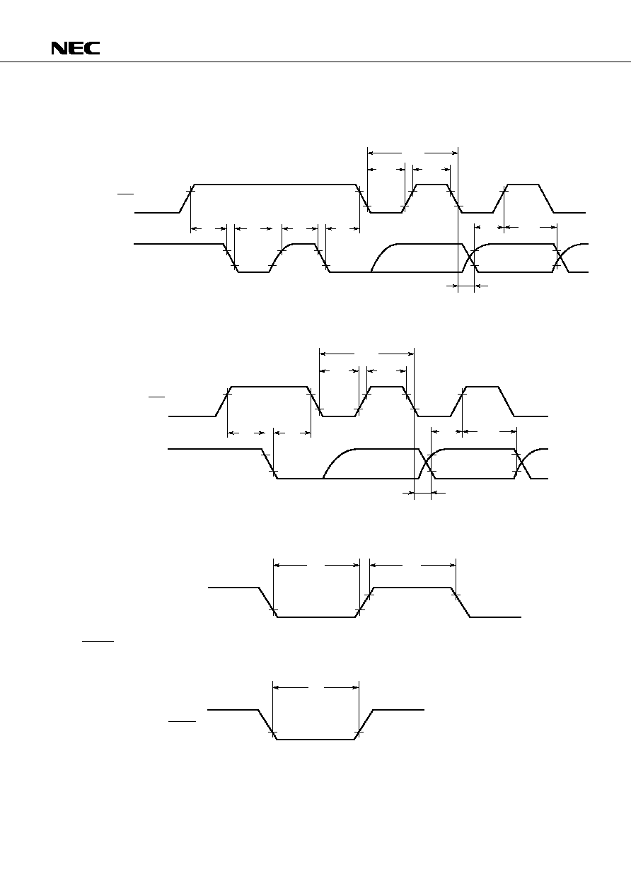
65
µ
PD750004, 750006, 750008, 750004(A), 750006(A), 750008(A)
Serial transfer timing
Bus release signal transfer:
Command signal transfer:
Interrupt input timing
RESET input timing
SCK
SB0 and SB1
t
KSB
t
KL3
t
KL4
t
KCY3
t
KCY4
t
KSO3
t
KSO4
t
SBK
t
KH3
t
KH4
t
SIK3
t
SIK4
t
KSI3
t
KSI4
INT0, INT1, INT2,
and INT4
KR0 - KR7
t
INTL
t
INTH
RESET
t
RSL
SCK
SB0 and SB1
t
KSB
t
SBL
t
SBH
t
SBK
t
KCY3
t
KCY4
t
KSO3
t
KSO4
t
KL3
t
KL4
t
KH3
t
KH4
t
KSI3
t
KSI4
t
SIK3
t
SIK4

66
µ
PD750004, 750006, 750008, 750004(A), 750006(A), 750008(A)
Parameter
Symbol
Release signal setting time
Oscillation settling time
Note 1
t
SREL
t
WAIT
Note 2
Note 3
Release by RESET
Release by interrupt request
Conditions
DATA HOLD CHARACTERISTICS BY LOW SUPPLY VOLTAGE IN DATA MEMORY STOP MODE
(T
A
= -40 to +85
∞
C)
Notes 1. CPU operation stop time for preventing unstable operation at the beginning of oscillation.
2. Select either 2
17
/f
X
or 2
15
/f
X
with the mask option.
3. This value depends on the settings of the basic interval timer mode register (BTM) shown below.
Data hold timing (STOP mode release by RESET)
Data hold timing (standby release signal: STOP mode release by interrupt signal)
-
-
-
-
0
1
0
1
0
1
1
1
0
0
1
1
2
20
/f
X
(approx. 250 ms)
2
17
/f
X
(approx. 31.3 ms)
2
15
/f
X
(approx. 7.81 ms)
2
13
/f
X
(approx. 1.95 ms)
0
Min.
Typ.
Max.
Unit
µ
s
ms
ms
2
20
/f
X
(approx. 175 ms)
2
17
/f
X
(approx. 21.8 ms)
2
15
/f
X
(approx. 5.46 ms)
2
13
/f
X
(approx. 1.37 ms)
Wait time
At f
X
= 4.19 MHz
At f
X
= 6.0 MHz
Standby release signal
(Interrupt request)
V
DD
t
SREL
t
WAIT
HALT mode
Operation
mode
STOP instruction execution
Data hold mode
STOP mode
RESET
V
DD
t
SREL
t
WAIT
Internal reset operation
HALT mode
Operation
mode
STOP instruction execution
Data hold mode
STOP mode
BTM3
BTM2
BTM1
BTM0

67
µ
PD750004, 750006, 750008, 750004(A), 750006(A), 750008(A)
13. CHARACTERISTIC CURVE (REFERENCE VALUES)
I
DD
vs. V
DD
(When the main system clock is operating at 6.0 MHz with a crystal)
Supply voltage V
DD
(V)
Main system clock
STOP mode + 32 kHz oscillation,
and subsystem clock HALT mode
(SOS.1 = 0)
Subsystem clock operating mode
(SOS.1 = 0)
Subsystem clock operating mode
(SOS.1 = 1)
Subsystem clock
HALT mode
(SOS.1 = 1)
Main system clock
HALT mode + 32 kHz oscillation
Supply current I
DD
(mA)
0
1
2
3
4
5
6
7
0.001
(T
A
= 25
∞
C)
X1
X2
XT1
XT2
22 pF
330 k
Crystal
22 pF
22 pF
22 pF
6.0 MHz
Crystal
32.768 kHz
8
0.005
0.01
0.05
0.1
0.5
1.0
5.0
10
PCC = 0011
PCC = 0010
PCC = 0001
PCC = 0000

68
µ
PD750004, 750006, 750008, 750004(A), 750006(A), 750008(A)
I
DD
vs. V
DD
(When the main system clock is operating at 4.19 MHz with a crystal)
Supply voltage V
DD
(V)
Main system clock
STOP mode + 32 kHz oscillation,
and subsystem clock HALT mode
(SOS.1 = 0)
Subsystem clock operating mode
(SOS.1 = 0)
Subsystem clock operating mode
(SOS.1 = 1)
Subsystem clock HALT mode
(SOS.1 = 1)
Main system clock
HALT mode + 32 kHz oscillation
Supply current I
DD
(mA)
0
1
2
3
4
5
6
7
0.001
(T
A
= 25
∞
C)
X1
X2
XT1
XT2
22 pF
330 k
Crystal
22 pF
22 pF
22 pF
4.19 MHz
Crystal
32.768 kHz
8
0.005
0.01
0.05
0.1
0.5
1.0
5.0
10
PCC = 0011
PCC = 0010
PCC = 0001
PCC = 0000

69
µ
PD750004, 750006, 750008, 750004(A), 750006(A), 750008(A)
I
OH
vs. V
DD
- V
OH
(Ports 2, 3, 6, 7, and 8)
I
OL
vs. V
OL
(Ports 2, 3, 6, 7, and 8)
15
10
5
0
0
0.5
1.0
1.5
2.0
2.5
3.0
V
DD
= 1.8 V
V
DD
= 2.2 V
V
DD
= 3 V
V
DD
= 4 V
V
DD
= 5.5 V
V
DD
= 5 V
V
DD
- V
OH
[V]
(T
A
= 25
∞
C)
I
OH
[mA]
40
30
20
10
0
0
0.5
1.0
1.5
2.0
V
DD
= 1.8 V
V
DD
= 2.2 V
V
DD
= 3 V
V
DD
= 4 V
V
DD
= 5 V
V
DD
= 5.5 V
(T
A
= 25
∞
C)
I
OL
[mA]
V
OL
[V]

70
µ
PD750004, 750006, 750008, 750004(A), 750006(A), 750008(A)
14. PACKAGE DRAWINGS
Package drawings of mass-produced products (1/2)
Caution The ES version is different from the corresponding mass-produced products in shape and material.
See "ES package drawings."
44 PIN PLASTIC QFP ( 10)
S44GB-80-3BS
ITEM
MILLIMETERS
INCHES
N
P
Q
0.125±0.075
0.10
2.7
0.004
0.106
0.005±0.003
NOTE
Each lead centerline is located within 0.16 mm (0.007 inch) of
its true position (T.P.) at maximum material condition.
J
I
H
N
A
13.2±0.2
0.520+0.008
≠0.009
B
10.0±0.2
0.394+0.008
≠0.009
C
10.0±0.2
0.394+0.008
≠0.009
D
13.2±0.2
0.520+0.008
≠0.009
F
G
H
1.0
0.37
1.0
0.039
0.039
0.015+0.003
≠0.004
I
J
K
0.8 (T.P.)
1.6±0.2
0.16
0.007
0.031 (T.P.)
0.063±0.008
L
0.8±0.2
0.031 +0.009
≠0.008
M
0.17
0.007 +0.002
≠0.003
S
3.0 MAX.
0.119 MAX.
R
3
∞
3
∞
+7
∞
≠3
∞
+0.08
≠0.07
+0.06
≠0.05
+7
∞
≠3
∞
detail of lead end
Q
F
G
K
M
L
R
M
33
34
22
44
1
12
11
23
S
P
C
D
A
B

71
µ
PD750004, 750006, 750008, 750004(A), 750006(A), 750008(A)
Package drawings of mass-produced products (2/2)
Caution The shape and material of the ES version are the same as those of the corresponding mass-
produced products.
42PIN PLASTIC SHRINK DIP (600 mil)
ITEM
MILLIMETERS
INCHES
A
B
C
F
G
H
I
J
K
39.13 MAX.
1.778 (T.P.)
3.2±0.3
0.51 MIN.
4.31 MAX.
1.78 MAX.
0.17
15.24 (T.P.)
5.08 MAX.
N
0.9 MIN.
R
1.541 MAX.
0.070 MAX.
0.035 MIN.
0.126±0.012
0.020 MIN.
0.170 MAX.
0.200 MAX.
0.600 (T.P.)
0.007
0.070 (T.P.)
P42C-70-600A-1
A
C
D
G
NOTES
1) Each lead centerline is located within 0.17 mm (0.007 inch) of
its true position (T.P.) at maximum material condition.
D
0.50±0.10
0.020
M
0.25
0.010
+0.10
≠0.05
0~15∞
0~15∞
+0.004
≠0.003
+0.004
≠0.005
M
K
N
L
13.2
0.520
2) Item "K" to center of leads when formed parallel.
42
1
22
21
L
M
R
B
F
H
J
I

72
µ
PD750004, 750006, 750008, 750004(A), 750006(A), 750008(A)
ES package drawing
44 PIN CERAMIC QFP FOR ES (REFERENCE)
Cautions 1. Find the location of pin 1 by checking the location of pin 17, which is connected to the metal
cap.
2. The metal cap is connected to pin 17. The electrical level of the metal cap is V
SS
(GND).
3. The lead length has not been specified because leads are cut without any detailed specifications.
2.25
11.43
8.0
1
11
12
22
23
33
34
44
11.43
8.0
0.15
0.32
0.8
(Bottom)

73
µ
PD750004, 750006, 750008, 750004(A), 750006(A), 750008(A)
15. RECOMMENDED SOLDERING CONDITIONS
The
µ
PD750004,
µ
PD750006, and
µ
PD750008 should be soldered and mounted under the conditions recom-
mended in the table below.
For detail of recommended soldering conditions, refer to the information document
SMD Surface Mount Technology
Manual (C10535E).
For soldering methods and conditions other than those recommended below, contact our sales personnel.
Table 15-1 Surface Mounting Type Soldering Conditions
µ
PD750004GB-
◊◊◊
-3BS-MTX
: 44-pin plastic QFP (10
◊
10 mm, 0.8 mm pitch)
µ
PD750006GB-
◊◊◊
-3BS-MTX
: 44-pin plastic QFP (10
◊
10 mm, 0.8 mm pitch)
µ
PD750008GB-
◊◊◊
-3BS-MTX
: 44-pin plastic QFP (10
◊
10 mm, 0.8 mm pitch)
µ
PD750004GB(A)-
◊◊◊
-3BS-MTX : 44-pin plastic QFP (10
◊
10 mm, 0.8 mm pitch)
µ
PD750006GB(A)-
◊◊◊
-3BS-MTX : 44-pin plastic QFP (10
◊
10 mm, 0.8 mm pitch)
µ
PD750008GB(A)-
◊◊◊
-3BS-MTX : 44-pin plastic QFP (10
◊
10 mm, 0.8 mm pitch)
Caution Use of more than one soldering method should be avoided (except for partial heating method).
Table 15-2 Insertion Type Soldering Conditions
µ
PD750004CU-
◊◊◊
: 42-pin plastic shrink DIP (600 mil, 1.778 mm pitch)
µ
PD750006CU-
◊◊◊
: 42-pin plastic shrink DIP (600 mil, 1.778 mm pitch)
µ
PD750008CU-
◊◊◊
: 42-pin plastic shrink DIP (600 mil, 1.778 mm pitch)
µ
PD750004CU(A)-
◊◊◊
: 42-pin plastic shrink DIP (600 mil, 1.778 mm pitch)
µ
PD750006CU(A)-
◊◊◊
: 42-pin plastic shrink DIP (600 mil, 1.778 mm pitch)
µ
PD750008CU(A)-
◊◊◊
: 42-pin plastic shrink DIP (600 mil, 1.778 mm pitch)
Package peak temperature: 235
∞
C
Duration: 30 seconds max. (at 210
∞
C or above)
Maximum allowable number of reflow processes: 3
Package peak temperature: 215
∞
C
Duration: 40 seconds max. (at 200
∞
C or above)
Maximum allowable number of reflow processes: 3
Solder bath temperature: 260
∞
C max.
Duration: 10 seconds max.
Number of times: 1
Preliminary heat temperature: 120
∞
C max. (package surface temperature)
Terminal temperature: 300
∞
C max.
Duration: 3 seconds max. (per device side)
IR35-00-3
VP15-00-3
WS60-00-1
-
Infrared reflow
VPS
Wave
soldering
Partial heating
method
Soldering
method
Soldering conditions
Soldering method
Soldering conditions
Wave soldering (terminal only)
Partial heating method
Solder bath temperature: 260
∞
C max., Duration: 10 seconds max.
Terminal temperature: 300
∞
C max., Duration: 3 seconds max. (for each pin)
Caution Apply wave soldering to terminals only. See to it that the jet solder does not contact with the chip
directly.
Symbol
74
µ
PD750004, 750006, 750008, 750004(A), 750006(A), 750008(A)
APPENDIX A FUNCTIONS OF THE
µ
PD75008,
µ
PD750008, AND
µ
PD75P0016
Item
µ
PD75008
µ
PD750008
µ
PD75P0016
Masked ROM
0000H - 1F7FH
(8064
◊
8 bits)
75X standard CPU
4 bits
◊
8 or 8 bits
◊
4
∑ 0.95, 1.91, 15.3
µ
s
(when operating at
4.19 MHz)
Not provided
000H - 0FFH
2-byte stack
Not available
3 machine cycles
2 machine cycles
∑
, 524, 262, 65.5 kHz
(when the main system
clock operates at
4.19 MHz)
∑ 2 kHz
One-time PROM
0000H - 3FFFH
(16384
◊
8 bits)
(1/2)
Program memory
Data memory
CPU
General-purpose register
When selecting the main
system clock
When selecting the subsys-
tem clock
SBS register
Stack area
Stack operation for a
subroutine call instruction
BRA !addr1
CALLA !addr1
MOVT XA, @BCDE
MOVT XA, @BCXA
BR BCDE
BR BCXA
CALL !addr
CALLF !faddr
Timer
Clock output (PCL)
BUZ output (BUZ)
122
µ
s (when operating at 32.768 kHz)
Instruction
execution time
3 channels
∑ Basic interval timer:
1 channel
∑ 8-bit timer/event counter:
1 channel
∑ Clock timer: 1 channel
Stack
Instruction
000H - 1FFH
(512
◊
4 bits)
Masked ROM
0000H - 1FFFH
(8192
◊
8 bits)
75XL CPU
(4 bits
◊
8 or 8 bit
◊
4)
◊
4 banks
∑ 0.95, 1.91, 3.81, 15.3
µ
s (when operating at 4.19 MHz)
∑ 0.67, 1.33, 2.67, 10.7
µ
s (when operating at 6.0 MHz)
Provided
SBS.3 = 1: Mk
mode selection
SBS.3 = 0: Mk
mode selection
n00H - nFFH (n = 0, 1)
Mk
mode: 2-byte stack
Mk
mode: 3-byte stack
Mk
mode: Not available
Mk
mode: Available
Available
Mk
mode: 3 machine cycles
Mk
mode: 4 machine cycles
Mk
mode: 2 machine cycles
Mk
mode: 3 machine cycles
4 channels
∑ Basic interval timer/watchdog timer: 1 channel
∑ 8-bit timer/event counter: 1 channel
∑ 8-bit timer counter: 1 channel
∑ Clock timer: 1 channel
∑
, 524, 262, 65.5 kHz
(when the main system clock operates at 4.19 MHz)
∑
, 750, 375, 93.8 kHz
(when the main system clock operates at 6.0 MHz)
∑ 2, 4, 32 kHz
(when the main system clock operates at 4.19 MHz)
∑ 2.93, 5.86, 46.9 kHz
(when the main system clock operates at 6.0 MHz)

75
µ
PD750004, 750006, 750008, 750004(A), 750006(A), 750008(A)
Item
Serial interface
Feedback resistor cut flag
(SOS.0)
Sub-oscillator current cut flag
(SOS.1)
Register bank selection register
(RBS)
Standby release with INT0
Number of vectored interrupts
Processor clock control register
Power supply
Operating ambient temperature
Package
µ
PD75008
µ
PD750008
µ
PD75P0016
3 modes are supported.
∑ Three-wire serial I/O mode: First transferred bit switchable between the LSB and
MSB
∑ Two-wire serial I/O mode
∑ SBI mode
(2/2)
Can incorporate feedback
resistors that are specified
with the mask option.
Not provided
Not provided
Disable
External: 3, internal: 3
Available when PCC is 0,
2, or 3
V
DD
= 2.7 to 6.0 V
Incorporated
Incorporated
Provided
Enable
External: 3, internal: 4
Available when PCC is 0 to 3
V
DD
= 2.2 to 5.5 V
SOS register
T
A
= -40 to +85
∞
C
∑ 42-pin plastic shrink DIP (600 mil, 1.778 mm pitch)
∑ 44-pin plastic QFP (10
◊
10 mm, 0.8 mm pitch)

76
µ
PD750004, 750006, 750008, 750004(A), 750006(A), 750008(A)
APPENDIX B DEVELOPMENT TOOLS
The following development tools are provided for the development of a system which employs the
µ
PD750008.
In the 75XL series, use the common relocatable assembler together with a device file of each model.
Language processors
Note These software products cannot use the task swap function, which is available in MS-DOS Ver. 5.00 or later.
Remark The operations of the assembler and device file are guaranteed only on the above host machines and OSs.
OS
MS-DOS
TM
Ver. 3.30
to
Ver. 6.2
Note
See "OS for IBM PC."
OS
MS-DOS
Ver. 3.30
to
Ver. 6.2
Note
See "OS for IBM PC."
Part number
µ
S5A13DF750008
µ
S5A10DF750008
µ
S7B13DF750008
µ
S7B10DF750008
Host machine
PC-9800 series
IBM PC/AT
and
compatibles
Host machine
PC-9800 series
IBM PC/AT
TM
and
compatibles
Device file
RA75X relocatable assembler
Part number
µ
S5A13RA75X
µ
S5A10RA75X
µ
S7B13RA75X
µ
S7B10RA75X
Distribution media
3.5-inch 2HD
5.25-inch 2HD
3.5-inch 2HC
5.25-inch 2HC
Distribution media
3.5-inch 2HD
5.25-inch 2HD
3.5-inch 2HC
5.25-inch 2HC

77
µ
PD750004, 750006, 750008, 750004(A), 750006(A), 750008(A)
PROM programming tools
Note These software products cannot use the task swap function, which is available in MS-DOS Ver. 5.00 or later.
Remark Operation of the PG-1500 controller is guaranteed only on the above host machines and OSs.
Hardware
Software
PG-1500
PA-75P008CU
PG-1500 controller
OS
MS-DOS
Ver. 3.30
to
Ver. 6.2
Note
See "OS for IBM PC."
Host machine
PC-9800 series
IBM PC/AT and
compatibles
Distribution media
3.5-inch 2HD
5.25-inch 2HD
3.5-inch 2HD
5.25-inch 2HC
Part number
µ
S5A13PG1500
µ
S5A10PG1500
µ
S7B13PG1500
µ
S7B10PG1500
The PG-1500 PROM programmer is used together with an accessory board and optional
program adapter. It allows the user to program a single chip microcontroller containing
PROM from a standalone terminal or a host machine. The PG-1500 can be used to
program typical 256K-bit to 4M-bit PROMs.
The PA-75P008CU is a PROM programmer adapter provided for the
µ
PD75P0016CU/GB.
It is used in conjunction with the PG-1500.
This program enables the host machine to control the PG-1500 through the serial and
parallel interfaces.

78
µ
PD750004, 750006, 750008, 750004(A), 750006(A), 750008(A)
Hardware
Part number
µ
S5A13IE75X
µ
S5A10IE75X
µ
S7B13IE75X
µ
S7B10IE75X
Distribution media
3.5-inch 2HD
5.25-inch 2HD
3.5-inch 2HC
5.25-inch 2HC
Debugging tools
The in-circuit emulators (IE-75000-R and IE-75001-R) are provided to debug programs used for the
µ
PD750008.
The system configuration is shown below.
Notes 1. Maintenance service only
2. These software products cannot use the task swap function, which is available in MS DOS Ver. 5.00 or
later.
Remarks 1. Operation of the IE control program is guaranteed only on the above host machines and OSs.
2. The
µ
PD750004,
µ
PD750006,
µ
PD750008, and
µ
PD75P0016 are collectively called the
µ
PD750008
subseries.
OS
MS-DOS
Ver. 3.30
to
Ver. 6.2
Note 2
See "OS for IBM PC."
The IE-75000-R is an in-circuit emulator used to debug hardware and software when
developing an application system using the 75X series and 75XL series. Use this
emulator together with optional emulation board IE-75300-R-EM and emulation probe
EP-75008CU-R or EP-75008G to develop application systems of the
µ
PD750008
subseries.
For efficient debugging, connect the emulator to the host machine and a PROM
programmer.
The IE-75000-R contains emulation board IE-75000-R-EM. The board is connected
to the IE-75000-R.
The IE-75001-R is an in-circuit emulator used to debug hardware and software when
developing an application system using the 75X series and 75XL series. Use this
emulator together with optional emulation board IE-75300-R-EM and emulation probe
EP-75008CU-R or EP-75008GB-R to develop application systems of the
µ
PD750008
subseries.
For efficient debugging, connect the emulator to the host machine and a PROM
programmer.
The IE-75300-R-EM is an emulation board used to evaluate an application system
using the
µ
PD750008 subseries.
Use this board together with the IE-75000-R or IE-75001-R.
The EP-75008CU-R is an emulation probe for the
µ
PD750008CU.
Connect this emulation probe to the IE-75000-R or IE-75001-R, and the IE-75300-R-
EM.
The EP-75008GB-R is an emulation probe for the
µ
PD750008GB.
Connect this emulation probe to the IE-75000-R or IE-75001-R, and the IE-75300-R-
EM.
A 44-pin conversion socket, the EV-9200G-44, supplied with this probe facilitates the
connection of the probe to the target system.
This program enables the host machine to control the IE-75000-R or IE-75001-R
through the RS-232-C and Centronics interface.
IE-75000-R
Note 1
IE-75001-R
IE-75300-R-EM
EP-75008CU-R
EP-75008GB-R
IE control program
Software
EV-9200G-44
Host machine
PC-9800 series
IBM PC/AT
and
compatibles

79
µ
PD750004, 750006, 750008, 750004(A), 750006(A), 750008(A)
OS for IBM PC
The following IBM PC OSs are supported.
OS
Version
PC DOS
TM
Ver. 3.1 to Ver. 6.3
J6.1/V
Note
to J6.3/V
Note
MS-DOS
Ver. 5.0 to Ver. 6.22
5.0/V
Note
to 6.2/V
Note
IBM DOS
TM
J5.02/V
Note
Note Only English version is supported.
Caution These software products cannot use the task swap function, which is available in MS-DOS
Ver. 5.0 or later.

80
µ
PD750004, 750006, 750008, 750004(A), 750006(A), 750008(A)
µ
PD750004, 750006, 750008, 750004(A), 750006(A), 750008(A) Data
Sheet
µ
PD75P0016 Data Sheet
µ
PD750008 User's Manual
µ
PD750008 Instruction List
75XL Series Selection Guide
U10738E (This manual)
U10328E
U10740E
-
U10453E
Document number
Japanese
English
Document number
Japanese
English
Hardware
Software
IE-75000-R/IE-75001-R User's Manual
IE-75300-R-EM User's Manual
EP-75008CU-R User's Manual
EP-75008GB-R User's Manual
PG-1500 User's Manual
RA75X Assembler Package User's
Manual
PG-1500 Controller
User's Manual
PC-9800 series (MS-DOS) base
IBM PC series (PC DOS) base
Operation
Language
Document number
Japanese
English
C10535E
C11531E
C10983E
-
MEI-1202
-
IC Package Manual
Semiconductor Device Mounting Technology Manual
Quality Grade on NEC Semiconductor Devices
Reliability and Quality Control of NEC Semiconductor Devices
Electrostatic Discharge (ESD) Test
Semiconductor Device Quality Guarantee Guide
Microcontroller-Related Products Guide - by third parties
Document name
Document name
Document name
APPENDIX C RELATED DOCUMENTS
Some documents are preliminary editions, but they are not so specified in the tables below.
Documents related to devices
Documents related to development tools
Other related documents
Caution The above related documents are subject to change without notice. Be sure to use the latest edition
when you design your system.
U10738J
U10328J
U10740J
IEM-5593
U10453J
EEU-846
U11354J
EEU-699
EEU-698
U11940J
EEU-731
EEU-730
EEU-704
EEU-5008
EEU-1416
U11354E
EEU-1317
EEU-1305
EEU-1335
EEU-1346
EEU-1363
EEU-1291
U10540E
C10943X
C10535J
C11531J
C10983J
MEM-539
C11893J
U11416J

81
µ
PD750004, 750006, 750008, 750004(A), 750006(A), 750008(A)
NOTES FOR CMOS DEVICES
1
PRECAUTION AGAINST ESD FOR SEMICONDUCTORS
Note: Strong electric field, when exposed to a MOS device, can cause destruction of
the gate oxide and ultimately degrade the device operation. Steps must be taken
to stop generation of static electricity as much as possible, and quickly dissipate
it once, when it has occurred. Environmental control must be adequate. When
it is dry, humidifier should be used. It is recommended to avoid using insulators
that easily build static electricity. Semiconductor devices must be stored and
transported in an anti-static container, static shielding bag or conductive
material. All test and measurement tools including work bench and floor should
be grounded. The operator should be grounded using wrist strap. Semiconduc-
tor devices must not be touched with bare hands. Similar precautions need to
be taken for PW boards with semiconductor devices on it.
2
HANDLING OF UNUSED INPUT PINS FOR CMOS
Note: No connection for CMOS device inputs can be cause of malfunction. If no
connection is provided to the input pins, it is possible that an internal input level
may be generated due to noise, etc., hence causing malfunction. CMOS device
behave differently than Bipolar or NMOS devices. Input levels of CMOS devices
must be fixed high or low by using a pull-up or pull-down circuitry. Each unused
pin should be connected to V
DD
or GND with a resistor, if it is considered to have
a possibility of being an output pin. All handling related to the unused pins must
be judged device by device and related specifications governing the devices.
3
STATUS BEFORE INITIALIZATION OF MOS DEVICES
Note: Power-on does not necessarily define initial status of MOS device. Production
process of MOS does not define the initial operation status of the device.
Immediately after the power source is turned ON, the devices with reset function
have not yet been initialized. Hence, power-on does not guarantee out-pin
levels, I/O settings or contents of registers. Device is not initialized until the
reset signal is received. Reset operation must be executed immediately after
power-on for devices having reset function.

82
µ
PD750004, 750006, 750008, 750004(A), 750006(A), 750008(A)
NEC Electronics Inc. (U.S.)
Santa Clara, California
Tel: 800-366-9782
Fax: 800-729-9288
NEC Electronics (Germany) GmbH
Duesseldorf, Germany
Tel: 0211-65 03 02
Fax: 0211-65 03 490
NEC Electronics (UK) Ltd.
Milton Keynes, UK
Tel: 01908-691-133
Fax: 01908-670-290
NEC Electronics Italiana s.r.1.
Milano, Italy
Tel: 02-66 75 41
Fax: 02-66 75 42 99
NEC Electronics Hong Kong Ltd.
Hong Kong
Tel: 2886-9318
Fax: 2886-9022/9044
NEC Electronics Hong Kong Ltd.
Seoul Branch
Seoul, Korea
Tel: 02-528-0303
Fax: 02-528-4411
NEC Electronics Singapore Pte. Ltd.
United Square, Singapore 1130
Tel: 253-8311
Fax: 250-3583
NEC Electronics Taiwan Ltd.
Taipei, Taiwan
Tel: 02-719-2377
Fax: 02-719-5951
NEC do Brasil S.A.
Sao Paulo-SP, Brasil
Tel: 011-889-1680
Fax: 011-889-1689
NEC Electronics (Germany) GmbH
Benelux Office
Eindhoven, The Netherlands
Tel: 040-2445845
Fax: 040-2444580
NEC Electronics (France) S.A.
Velizy-Villacoublay, France
Tel: 01-30-67 58 00
Fax: 01-30-67 58 99
NEC Electronics (France) S.A.
Spain Office
Madrid, Spain
Tel: 01-504-2787
Fax: 01-504-2860
NEC Electronics (Germany) GmbH
Scandinavia Office
Taeby, Sweden
Tel: 08-63 80 820
Fax: 08-63 80 388
Regional Information
Some information contained in this document may vary from country to country. Before using any NEC
product in your application, please contact the NEC office in your country to obtain a list of authorized
representatives and distributors. They will verify:
∑ Device availability
∑ Ordering information
∑ Product release schedule
∑ Availability of related technical literature
∑ Development environment specifications (for example, specifications for third-party tools and
components, host computers, power plugs, AC supply voltages, and so forth)
∑ Network requirements
In addition, trademarks, registered trademarks, export restrictions, and other legal issues may also vary
from country to country.
J96. 8

83
PD750004, 750006, 750008, 750004(A), 750006(A), 750008(A)
[MEMO]

µ
PD750004, 750006, 750008, 750004(A), 750006(A), 750008(A)
MS-DOS is a trademark of Microsoft Corporation.
IBM DOS, PC/AT, and PC DOS is a trademark of IBM Corporation.
No part of this document may be copied or reproduced in any form or by any means without the prior written
consent of NEC Corporation. NEC Corporation assumes no responsibility for any errors which may appear in this
document.
NEC Corporation does not assume any liability for infringement of patents, copyrights or other intellectual
property rights of third parties by or arising from use of a device described herein or any other liability arising
from use of such device. No license, either express, implied or otherwise, is granted under any patents,
copyrights or other intellectual property rights of NEC Corporation or others.
While NEC Corporation has been making continuous effort to enhance the reliability of its semiconductor devices,
the possibility of defects cannot be eliminated entirely. To minimize risks of damage or injury to persons or
property arising from a defect in an NEC semiconductor device, customers must incorporate sufficient safety
measures in its design, such as redundancy, fire-containment, and anti-failure features.
NEC devices are classified into the following three quality grades:
"Standard", "Special", and "Specific". The Specific quality grade applies only to devices developed based on
a customer designated "quality assurance program" for a specific application. The recommended applications
of a device depend on its quality grade, as indicated below. Customers must check the quality grade of each
device before using it in a particular application.
Standard: Computers, office equipment, communications equipment, test and measurement equipment,
audio and visual equipment, home electronic appliances, machine tools, personal electronic
equipment and industrial robots
Special: Transportation equipment (automobiles, trains, ships, etc.), traffic control systems, anti-disaster
systems, anti-crime systems, safety equipment and medical equipment (not specifically designed
for life support)
Specific: Aircrafts, aerospace equipment, submersible repeaters, nuclear reactor control systems, life
support systems or medical equipment for life support, etc.
The quality grade of NEC devices is "Standard" unless otherwise specified in NEC's Data Sheets or Data Books.
If customers intend to use NEC devices for applications other than those specified for Standard quality grade,
they should contact an NEC sales representative in advance.
Anti-radioactive design is not implemented in this product.
M4 96. 5
The export of this product from Japan is regulated by the Japanese government. To export this product may be prohibited
without governmental license, the need for which must be judged by the customer. The export or re-export of this product
from a country other than Japan may also be prohibited without a license from that country. Please call an NEC sales
representative.