 | –≠–ª–µ–∫—Ç—Ä–æ–Ω–Ω—ã–π –∫–æ–º–ø–æ–Ω–µ–Ω—Ç: UPD750066 | –°–∫–∞—á–∞—Ç—å:  PDF PDF  ZIP ZIP |
Document Outline
- COVER
- Features
- Applications
- Ordering Information
- Differences between uPD75006x and uPD75006x(A)
- Functional Outline
- 1. PIN CONFIGURATION (Top View)
- 2. BLOCK DIAGRAM
- 3. PIN FUNCTION
- 3.1 Port Pins
- 3.2 Non-port Pins
- 3.3 Pin Input/Output Circuits
- 3.4 Recommended Connection of Unused Pins
- 4. SWITCHING FUNCTION BETWEEN Mk I MODE AND Mk II MODE
- 4.1 Differences between Mk I Mode and Mk II Mode
- 4.2 Setting Method of Stack Bank Select Register (SBS)
- 5. MEMORY CONFIGURATION
- 6. PERIPHERAL HARDWARE FUNCTION
- 6.1 Port
- 6.2 Clock Generator
- 6.3 Subsystem Clock Oscillator Control Function
- 6.4 Clock Output Circuit
- 6.5 Basic Interval Timer/Watchdog Timer
- 6.6 Watch Timer
- 6.7 Timer/Event Counter
- 6.8 Serial Interface
- 6.9 A/D Converter
- 6.10 Bit Sequential Buffer
- 7. INTERRUPT FUNCTION AND TEST FUNCTION
- 8. STANDBY FUNCTION
- 9. RESET FUNCTION
- 10. MASK OPTION
- 11. INSTRUCTION SET
- 12. ELECTRICAL SPECIFICATIONS
- 13. CHARACTERISTICS CURVES (REFERENCE VALUES)
- 14. PACKAGE DRAWINGS
- 15. RECOMMENDED SOLDERING CONDITIONS
- APPENDIX A. uPD75068, 750068 AND 75P0076 FUNCTIONAL LIST
- APPENDIX B. DEVELOPMENT TOOLS
- APPENDIX C. RELATED DOCUMENTS
©
1995
DATA SHEET
4-BIT SINGLE-CHIP MICROCONTROLLERS
The
µ
PD750068 is one of the 75XL Series 4-bit single-chip microcontrollers and has a data processing capability
comparable to that of an 8-bit microcontroller.
The
µ
PD750068 provides more CPU functions compared to the 75X Series and realizes high-speed operation
at the low voltage of 1.8 V, making it ideal for battery-driven applications. This device has on-chip A/D converters,
and sophisticated timers capable of operating as a 16-bit timer. The
µ
PD750068(A) has a higher reliability than
the
µ
PD750068.
A version with on-chip one-time PROM,
µ
PD75P0076, is also available for the evaluation during system
development or for small-scale production.
Detailed function descriptions are provided in the following user's manual. Be sure to read
the document before designing.
µ
PD750068 User's Manual: U10670E
µ
PD750064, 750066, 750068, 750064(A), 750066(A), 750068(A)
MOS INTEGRATED CIRCUIT
Features
O
Low-voltage operation: V
DD
= 1.8 to 5.5 V
O
On-chip memory
∑ Program memory (ROM):
4096
◊
8 bits (
µ
PD750064, 750064(A))
6144
◊
8 bits (
µ
PD750066, 750066(A))
8192
◊
8 bits (
µ
PD750068, 750068(A))
∑ Data memory (RAM):
512
◊
4 bits
O
Variable instruction execution time for high-speed
operation and power-saved operation
∑ 0.95, 1.91, 3.81, 15.3
µ
s (@ 4.19-MHz operation)
∑ 0.67, 1.33, 2.67, 10.7
µ
s (@ 6.0-MHz operation)
∑ 122
µ
s (@ 32.768-kHz operation)
O
Internal low-voltage A/D converters
(AV
REF
= 1.8 to 5.5 V)
8-bit resolution
◊
8 channels
O
Small packages (shrink SOP, shrink DIP)
O
Uses instructions of 75X Series for easy replacement
Applications
O
µ
PD750064, 750066, 750068
Cordless phones, audio-visual equipment, home appliances, office machines, fitness machines, meters, gas
ranges, etc.
O
µ
PD750064(A), 750066(A), 750068(A)
Electrical equipment for automobiles
The
µ
PD750064, 750066, 750068 and
µ
PD750064(A), 750066(A), 750068(A) differ only in quality grade. In
this manual, the
µ
PD750068 is described as typical product unless otherwise specified.
Users of other than the
µ
PD750068 should read the
µ
PD750068 as referring to the pertinent product.
When the description differs among the
µ
PD750064, 750066, and 750068, they also refer to the pertinent (A)
products.
µ
PD750064
µ
PD750064(A),
µ
PD750066
µ
PD750066(A),
µ
PD750068
µ
PD750068(A)
The mark shows major revised points.
Document No. U10165EJ2V0DS00 (2nd edition)
Date Published April 1999 N CP(K)
Printed in Japan
The information in this document is subject to change without notice. Before using this document, please
confirm that this is the latest version.
Not all devices/types available in every country. Please check with local NEC representative for
availability and additional information.
2
µ
PD750064, 750066, 750068, 750064(A), 750066(A), 750068(A)
Data Sheet U10165EJ2V0DS00
Ordering Information
Part Number
Package
Quality Grade
µ
PD750064CU-
◊◊◊
42-pin plastic shrink DIP (600 mil, 1.778-mm pitch)
Standard
µ
PD750064GT-
◊◊◊
42-pin plastic shrink SOP (375 mil, 0.8-mm pitch)
Standard
µ
PD750066CU-
◊◊◊
42-pin plastic shrink DIP (600 mil, 1.778-mm pitch)
Standard
µ
PD750066GT-
◊◊◊
42-pin plastic shrink SOP (375 mil, 0.8-mm pitch)
Standard
µ
PD750068CU-
◊◊◊
42-pin plastic shrink DIP (600 mil, 1.778-mm pitch)
Standard
µ
PD750068GT-
◊◊◊
42-pin plastic shrink SOP (375 mil, 0.8-mm pitch)
Standard
µ
PD750064CU(A)-
◊◊◊
42-pin plastic shrink DIP (600 mil, 1.778-mm pitch)
Special
µ
PD750064GT(A)-
◊◊◊
42-pin plastic shrink SOP (375 mil, 0.8-mm pitch)
Special
µ
PD750066CU(A)-
◊◊◊
42-pin plastic shrink DIP (600 mil, 1.778-mm pitch)
Special
µ
PD750066GT(A)-
◊◊◊
42-pin plastic shrink SOP (375 mil, 0.8-mm pitch)
Special
µ
PD750068CU(A)-
◊◊◊
42-pin plastic shrink DIP (600 mil, 1.778-mm pitch)
Special
µ
PD750068GT(A)-
◊◊◊
42-pin plastic shrink SOP (375 mil, 0.8-mm pitch)
Special
Remark
◊◊◊
indicates ROM code suffix.
Differences between
µ
PD75006
◊
and
µ
PD75006
◊
(A)
Part Number
µ
PD750064
µ
PD750064(A)
µ
PD750066
µ
PD750066(A)
Item
µ
PD750068
µ
PD750068(A)
Quality grade
Standard
Special
P l e a s e r e f e r t o " Q u a l i t y G r a d e s o n N E C S e m i c o n d u c t o r D e v i c e s " ( D o c u m e n t N o . C 1 1 5 3 1 E ) p u b l i s h e d b y
NEC Corporation to know the specification of quality grade on the devices and its recommended applications.
3
µ
PD750064, 750066, 750068, 750064(A), 750066(A), 750068(A)
Data Sheet U10165EJ2V0DS00
Functional Outline
Item
Function
Instruction execution time
∑ 0.95
µ
s, 1.91
µ
s, 3.81
µ
s, 15.3
µ
s (@ 4.19-MHz operation with main system clock)
∑ 0.67
µ
s, 1.33
µ
s, 2.67
µ
s, 10.7
µ
s (@ 6.0-MHz operation with main system clock)
∑ 122
µ
s (@ 32.768-kHz operation with subsystem clock)
On-chip memory
ROM
4096
◊
8 bits (
µ
PD750064)
6144
◊
8 bits (
µ
PD750066)
8192
◊
8 bits (
µ
PD750068)
RAM
512
◊
4 bits
General-purpose register
∑ 4-bit operation: 8
◊
4 banks
∑ 8-bit operation: 4
◊
4 banks
Input/
CMOS input
12
On-chip pull-up resistors can be specified by software: 7
output
Also used for analog input pins: 4
port
CMOS input/output
12
On-chip pull-up resistors can be specified by software: 12
Also used for analog input pins: 4
N-ch open-drain
8
13 V withstand voltage
input/output pins
On-chip pull-up resistors can be specified by mask option
Total
32
Timer
4 channels
∑ 8-bit timer/event counter: 2 channels (can be used as the 16-bit timer/event counter)
∑ Basic interval timer/watchdog timer: 1 channel
∑ Watch timer: 1 channel
Serial interface
∑ 3-wire serial I/O mode ∑∑∑ MSB or LSB can be selected for transferring first bit
∑ 2-wire serial I/O mode
A/D converter
8-bit resolution
◊
8 channels (1.8 V
AV
REF
V
DD
)
Bit sequential buffer
16 bits
Clock output (PCL)
∑
, 1.05 MHz, 262 kHz, 65.5 kHz (@ 4.19-MHz operation with main system clock)
∑
, 1.5 MHz, 375 kHz, 93.8 kHz (@ 6.0-MHz operation with main system clock)
Buzzer output (BUZ)
∑ 2 kHz, 4 kHz, 32 kHz (@ 4.19-MHz operation with main system clock or
@ 32.768-kHz operation with subsystem clock)
∑ 2.93 kHz, 5.86 kHz, 46.9 kHz (@ 6.0-MHz operation with main system clock)
Vectored interrupt
External: 3, Internal: 4
Test input
External: 1, Internal: 1
System clock oscillator
∑ Ceramic or crystal oscillator for main system clock oscillation
∑ Crystal oscillator for subsystem clock oscillation
Standby function
STOP/HALT mode
Operating ambient temperature
T
A
= ≠40 to +85∞C
Power supply voltage
V
DD
= 1.8 to 5.5 V
Package
∑ 42-pin plastic shrink DIP (600 mil, 1.778-mm pitch)
∑ 42-pin plastic shrink SOP (375 mil, 0.8-mm pitch)

4
µ
PD750064, 750066, 750068, 750064(A), 750066(A), 750068(A)
Data Sheet U10165EJ2V0DS00
CONTENTS
1.
PIN CONFIGURATION (Top View) ...................................................................................................... 6
2.
BLOCK DIAGRAM ................................................................................................................................ 7
3.
PIN FUNCTION ..................................................................................................................................... 8
3.1
Port Pins ...................................................................................................................................... 8
3.2
Non-port Pins ............................................................................................................................ 10
3.3
Pin Input/Output Circuits ......................................................................................................... 12
3.4
Recommended Connection of Unused Pins .......................................................................... 15
4.
SWITCHING FUNCTION BETWEEN Mk I MODE AND Mk II MODE ................................................ 16
4.1
Differences between Mk I Mode and Mk II Mode .................................................................... 16
4.2
Setting Method of Stack Bank Select Register (SBS) ........................................................... 17
5.
MEMORY CONFIGURATION ............................................................................................................. 18
6.
PERIPHERAL HARDWARE FUNCTION ........................................................................................... 23
6.1
Port ............................................................................................................................................. 23
6.2
Clock Generator ........................................................................................................................ 23
6.3
Subsystem Clock Oscillator Control Function ...................................................................... 25
6.4
Clock Output Circuit ................................................................................................................. 26
6.5
Basic Interval Timer/Watchdog Timer ..................................................................................... 27
6.6
Watch Timer .............................................................................................................................. 28
6.7
Timer/Event Counter ................................................................................................................. 29
6.8
Serial Interface .......................................................................................................................... 32
6.9
A/D Converter ............................................................................................................................ 33
6.10 Bit Sequential Buffer ................................................................................................................ 34
7.
INTERRUPT FUNCTION AND TEST FUNCTION .............................................................................. 35
8.
STANDBY FUNCTION ........................................................................................................................ 37
9.
RESET FUNCTION ............................................................................................................................. 38
10. MASK OPTION ................................................................................................................................... 41
11. INSTRUCTION SET ............................................................................................................................ 42
12. ELECTRICAL SPECIFICATIONS ....................................................................................................... 55
13. CHARACTERISTICS CURVES (REFERENCE VALUES) ................................................................. 68
14. PACKAGE DRAWINGS ...................................................................................................................... 70
15. RECOMMENDED SOLDERING CONDITIONS .................................................................................. 72

5
µ
PD750064, 750066, 750068, 750064(A), 750066(A), 750068(A)
Data Sheet U10165EJ2V0DS00
APPENDIX A.
µ
PD75068, 750068 AND 75P0076 FUNCTIONAL LIST .................................................. 73
APPENDIX B. DEVELOPMENT TOOLS ................................................................................................. 75
APPENDIX C. RELATED DOCUMENTS ................................................................................................. 79
6
µ
PD750064, 750066, 750068, 750064(A), 750066(A), 750068(A)
Data Sheet U10165EJ2V0DS00
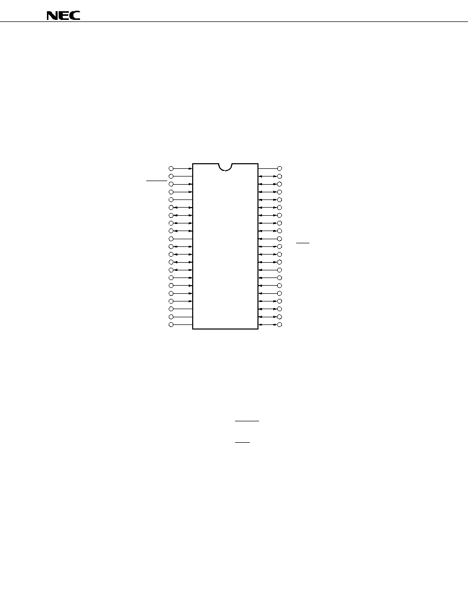
1. PIN CONFIGURATION (Top View)
∑
42-pin plastic shrink DIP (600 mil, 1.778-mm pitch)
µ
PD750064CU-
◊◊◊
,
µ
PD750064CU(A)-
◊◊◊
µ
PD750066CU-
◊◊◊
,
µ
PD750066CU(A)-
◊◊◊
µ
PD750068CU-
◊◊◊
,
µ
PD750068CU(A)-
◊◊◊
∑
42-pin plastic shrink SOP (375 mil, 0.8-mm pitch)
µ
PD750064GT-
◊◊◊
,
µ
PD750064GT(A)-
◊◊◊
µ
PD750066GT-
◊◊◊
,
µ
PD750066GT(A)-
◊◊◊
µ
PD750068GT-
◊◊◊
,
µ
PD750068GT(A)-
◊◊◊
1
2
3
4
5
6
7
8
9
10
11
12
13
14
15
16
17
18
19
20
21
42
41
40
39
38
37
36
35
34
33
32
31
30
29
28
27
26
25
24
23
22
XT1
XT2
RESET
X1
X2
P33
P32
P31
P30
AV
SS
P63/KR3/AN7
P62/KR2/AN6
P61/KR1/AN5
P60/KR0/AN4
P113/AN3
P112/AN2
P111/AN1
P110/AN0
AV
REF
IC
V
DD
V
SS
P40
P41
P42
P43
P50
P51
P52
P53
P00/INT4
P01/SCK
P02/SO/SB0
P03/SI/SB1
P10/INT0
P11/INT1
P12/TI1/INT2
P13/TI0
P20/PTO0
P21/PTO1
P22/PCL
P23/BUZ
IC: Internally Connected (Connect pin directly to V
DD
).
Pin Identification
AN0 to AN7
: Analog Input 0 to 7
AV
REF
: Analog Reference
AV
SS
: Analog Ground
BUZ
: Buzzer Clock
IC
: Internally Connected
INT0, INT1, INT4 : External Vectored Interrupt 0, 1, 4
INT2
: External Test Input 2
KR0 to KR3
: Key Return 0 to 3
P00 to P03
: Port 0
P10 to P13
: Port 1
P20 to P23
: Port 2
P30 to P33
: Port 3
P40 to P43
: Port 4
P50 to P53
: Port 5
P60 to P63
: Port 6
P110 to P113
: Port 11
PCL
: Programmable Clock
PTO0, PTO1
: Programmable Timer Output 0, 1
RESET
: Reset Input
SB0, SB1
: Serial Data Bus 0, 1
SCK
: Serial Clock
SI
: Serial Input
SO
: Serial Output
TI0, TI1
: Timer Input 0, 1
V
DD
: Positive Power Supply
V
SS
: Ground
X1, X2
: Main System Clock Oscillation 1, 2
XT1, XT2
: Subsystem Clock Oscillation 1, 2
7
µ
PD750064, 750066, 750068, 750064(A), 750066(A), 750068(A)
Data Sheet U10165EJ2V0DS00
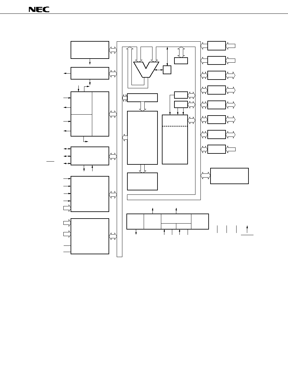
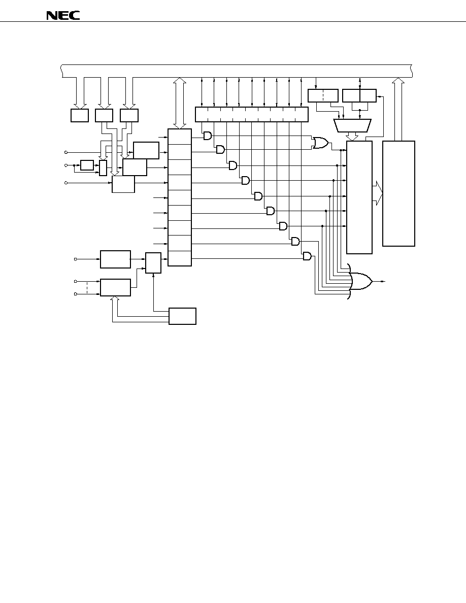
2. BLOCK DIAGRAM
Note The ROM capacity varies depending on the product.
Basic interval
timer/watchdog
timer
Watch timer
8-bit
timer/
event
counter#0
8-bit
timer/
event
counter#1
Cascaded
16-bit
timer/
event
counter
Clocked serial
interface
Interrupt
control
A/D converter
INTBT
INTW
INTT0
INTW
INTT1
TOUT0
INTCSI
BUZ/P23
TI0/P13
PTO0/P20
TI1/P12/INT2
PTO1/P21
SI/SB1/P03
SO/SB0/P02
SCK/P01
INT0/P10
INT1/P11
INT4/P00
INT2/P12/TI1
KR0/P60 to
KR3/P63
AN0/P110 to
AN3/P113
AN4/P60 to
AN7/P63
AV
REF
AV
SS
CY
SP (8)
SBS
BANK
Program counter
Program
memory
Note
(ROM)
Decode
and
control
General reg.
Data memory
(RAM)
512
◊
4 bits
Port 0
Port 1
Port 2
Port 3
Port 4
Port 5
Port 6
Port 11
Bit seq. buffer (16)
P00 to P03
4
4
4
4
4
4
P10 to P13
P20 to P23
P30 to P33
P40 to P43
P50 to P53
P60 to P63
P110 to P113
fx/2
N
CPU Clock
Clock
output
control
Clock
divider
Sub
Main
System clock
generator
Stand by
control
PCL/P22
XT1 XT2 X1 X2
IC
V
DD
V
SS
RESET
ALU
4
4
4
4
4
8
µ
PD750064, 750066, 750068, 750064(A), 750066(A), 750068(A)
Data Sheet U10165EJ2V0DS00
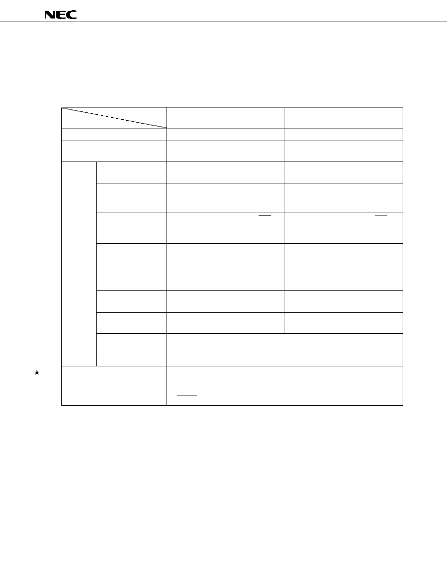
3. PIN FUNCTION
3.1 Port Pins (1/2)
Pin Name
Input/Output
Alternate
Function
8-bit
After Reset
I/O Circuit
Function
I/O
Type
Note 1
P00
Input
INT4
No
Input
<B>
P01
Input/Output
SCK
<F>-A
P02
Input/Output
SO/SB0
<F>-B
P03
Input/Output
SI/SB1
<M>-C
P10
Input
INT0
No
Input
<B>-C
P11
INT1
P12
TI1/INT2
P13
TI0
P20
Input/Output
PTO0
No
Input
E-B
P21
PTO1
P22
PCL
P23
BUZ
P30 to P33
Input/Output
≠
No
Input
E-B
P40 to P43
Note 2
Input/Output
≠
Yes
M-D
P50 to P53
Note 2
Input/Output
≠
M-D
Notes 1.
Circuit types enclosed in brackets indicate the Schmitt trigger input.
2.
If on-chip pull-up resistors are not specified by mask option (when used as N-ch open-drain input port),
low-level input leakage current increases when input or bit manipulation instruction is executed.
High level
(when pull-up
resistors are
provided) or
high-
impedance
4-bit input port (PORT0).
For P01 to P03, connection of on-chip pull-
up resistors can be specified by software in
3-bit units.
4-bit input port (PORT1).
Connection of on-chip pull-up resistors can
be specified by software in 4-bit units.
P10/INT0 can select noise elimination circuit.
4-bit input/output port (PORT2).
Connection of on-chip pull-up resistors can
be specified by software in 4-bit units.
Programmable 4-bit input/output port (PORT3).
This port can be specified for input/output in
1-bit units.
Connection of on-chip pull-up resistor can be
specified by software in 4-bit units.
N-ch open-drain 4-bit input/output port (PORT4).
A pull-up resistor can be contained in 1-bit
units (mask option).
Withstand voltage is 13 V in open-drain
mode.
N-ch open-drain 4-bit input/output port (PORT5).
A pull-up resistor can be contained in 1-bit
units (mask option).
Withstand voltage is 13 V in open-drain
mode.
High level
(when pull-up
resistors are
provided) or
high-
impedance
9
µ
PD750064, 750066, 750068, 750064(A), 750066(A), 750068(A)
Data Sheet U10165EJ2V0DS00
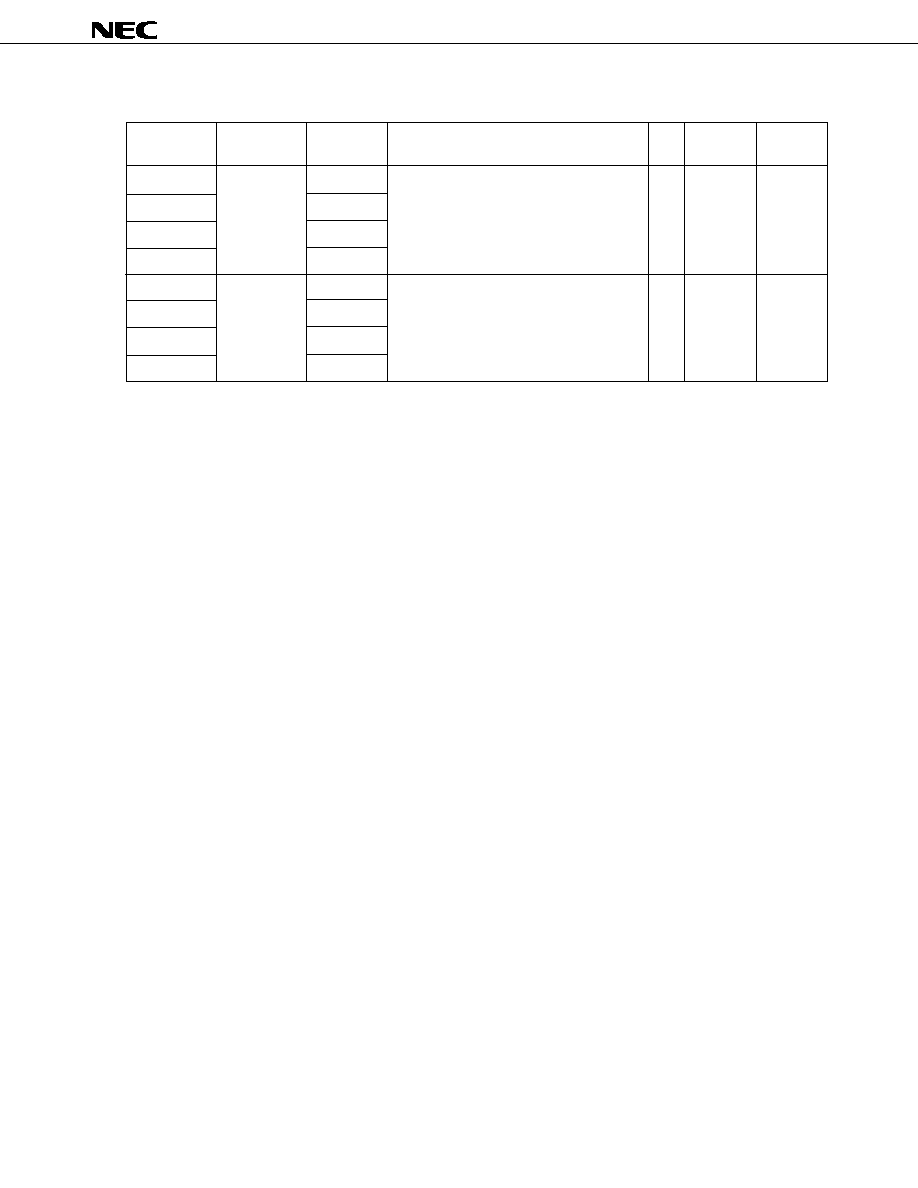
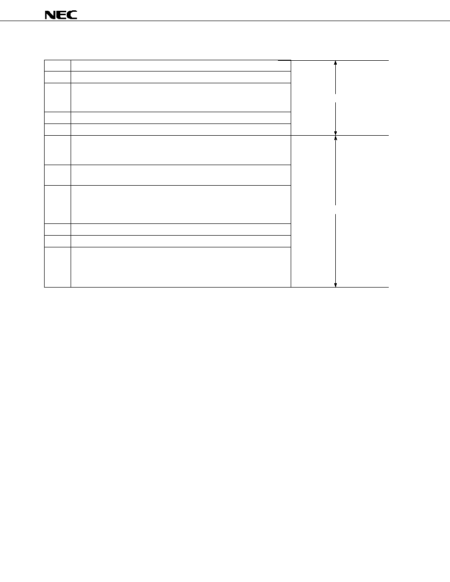
3.1 Port Pins (2/2)
Pin Name
Input/Output
Alternate
Function
8-bit
After Reset
I/O Circuit
Function
I/O
Type
Note
P60
Input/Output
KR0/AN4
No
Input
<Y>-D
P61
KR1/AN5
P62
KR2/AN6
P63
KR3/AN7
P110
Input
AN0
No
Input
Y-A
P111
AN1
P112
AN2
P113
AN3
Note
Circuit types enclosed in brackets indicate the Schmitt trigger input.
Programmable 4-bit input/output port (PORT6).
This port can be specified for input/output in
1-bit units.
Connection of on-chip pull-up resistors can
be specified by software in 4-bit units.
4-bit input port (PORT11).
10
µ
PD750064, 750066, 750068, 750064(A), 750066(A), 750068(A)
Data Sheet U10165EJ2V0DS00
3.2 Non-port Pins (1/2)
Pin Name
Input/Output
Alternate
Function
After Reset
I/O Circuit
Function
Type
Note
TI0
Input
P13
Inputs external event pulses to the timer/event
Input
<B>-C
TI1
P12/INT2
counter.
PTO0
Output
P20
Timer/event counter output
Input
E-B
PTO1
P21
PCL
P22
Clock output
BUZ
P23
Optional frequency output (for buzzer output
or system clock trimming)
SCK
Input/Output
P01
Serial clock input/output
Input
<F>-A
SO
Output
P02
Serial data output
<F>-B
SB0
Input/Output
Serial data bus input/output
SI
Input
P03
Serial data input
<M>-C
SB1
Input/Output
Serial data bus input/output
INT4
Input
P00
Edge detection vectored interrupt input (both
<B>
rising edge and falling edge detection)
INT0
Input
P10
Input
<B>-C
INT1
P11
Asynchronous
INT2
Input
P12/TI1
Rising edge detection
Asynchronous
Input
<B>-C
testable input
KR0 to KR3
Input
P60/AN4 to
Falling edge detection testable input
Input
<Y>-D
P63/AN7
AN0 to AN3
Input
P110 to P113
Analog signal input
Input
Y-A
AN4 to AN7
P60/KR0 to
<Y>-D
P63/KR3
AV
REF
≠
≠
A/D converter reference voltage
≠
Z-N
AV
SS
≠
≠
A/D converter reference GND potential
≠
Z-N
Note
Circuit types enclosed in brackets indicate the Schmitt trigger input.
Edge detection vectored
Noise elimination
interrupt input (detection
circuit/asynchronous
edge can be selected).
selection
INT0/P10 can select noise
elimination circuit.
11
µ
PD750064, 750066, 750068, 750064(A), 750066(A), 750068(A)
Data Sheet U10165EJ2V0DS00
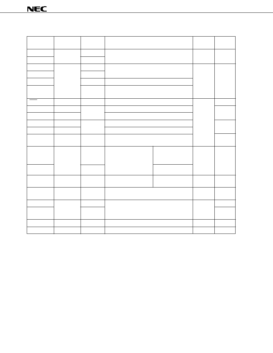
3.2 Non-port Pins (2/2)
Pin Name
Input/Output
Alternate
Function
After Reset
I/O Circuit
Function
Type
Note
X1
Input
≠
≠
≠
X2
≠
XT1
Input
≠
≠
≠
XT2
≠
RESET
Input
≠
System reset input (low-level active)
≠
<B>
IC
≠
≠
Internally connected. Connect directly to V
DD
.
≠
≠
V
DD
≠
≠
Positive power supply
≠
≠
V
SS
≠
≠
Ground potential
≠
≠
Note
Circuit types enclosed in brackets indicate the Schmitt trigger input.
Crystal/ceramic connection pin for the main system
clock oscillation. When inputting the external
clock, input the external clock to pin X1, and the
inverted phase of the external clock to pin X2.
Crystal connection pin for the subsystem clock
oscillation. When the external clock is used, input
the external clock to pin XT1, and the inverted
phase of the external clock to pin XT2. Pin XT1 can
be used as a 1-bit input (test) pin.
12
µ
PD750064, 750066, 750068, 750064(A), 750066(A), 750068(A)
Data Sheet U10165EJ2V0DS00
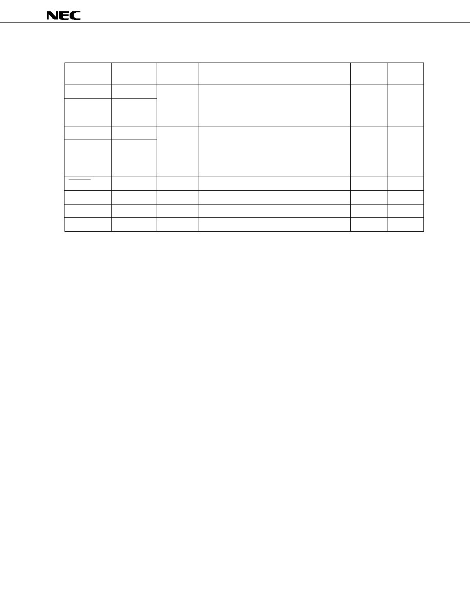
3.3 Pin Input/Output Circuits
The
µ
PD750068 pin input/output circuits are shown schematically.
(1/3)
TYPE A
TYPE B
TYPE D
TYPE E-B
TYPE B-C
TYPE F-A
V
DD
IN
P-ch
N-ch
data
output
disable
N-ch
P-ch
IN
OUT
V
DD
P-ch
output
disable
data
P.U.R.
enable
Type D
Type A
IN/OUT
V
DD
P.U.R.
enable
P.U.R.
P-ch
IN
V
DD
P.U.R.
P.U.R.
enable
P-ch
IN/OUT
Type D
Type B
output
disable
data
P.U.R. : Pull-Up Resistor
P.U.R. : Pull-Up Resistor
P.U.R. : Pull-Up Resistor
Schmitt-triggered input with hysteresis characteristics
CMOS standard input buffer
Push-pull output that can be placed in output
high-impedance (both P-ch and N-ch off).
P.U.R.
V
DD
13
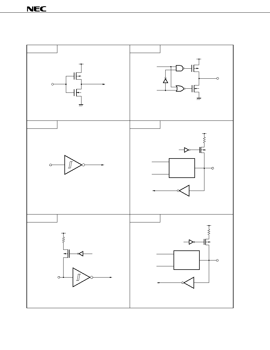
µ
PD750064, 750066, 750068, 750064(A), 750066(A), 750068(A)
Data Sheet U10165EJ2V0DS00
(2/3)
output
disable
(P)
output
disable
data
output
disable
(N)
P.U.R.
enable
P-ch
P.U.R.
IN/OUT
P-ch
N-ch
V
DD
V
DD
P.U.R. : Pull-Up Resistor
TYPE F-B
TYPE Y
IN
P-ch
N-ch
V
DD
V
DD
AV
SS
AV
SS
input
enable
Reference voltage
(from the voltage tap of
the series resistor string)
TYPE Y-A
Input butfer
Type A
Type Y
IN
TYPE M-C
output
disable
data
P.U.R.
enable
P-ch
P.U.R.
IN/OUT
N-ch
V
DD
P.U.R. : Pull-Up Resistor
TYPE M-D
IN instruction
Sampling C
+
≠
P.U.R.
Note
V
DD
N-ch
IN/OUT
P.U.R.
(Mask Option)
data
output
disable
Note This pull-up resistor operates only when an
input instruction is executed without a pull-up
resistor connected using the mask option
(current flows from V
DD
to the pin when the pin is low).
Input
instruction
V
DD
P-ch
(+13 V
withstand
voltage)
(+13 V
withstand
voltage)
Voltage
limitation
circuit
14
µ
PD750064, 750066, 750068, 750064(A), 750066(A), 750068(A)
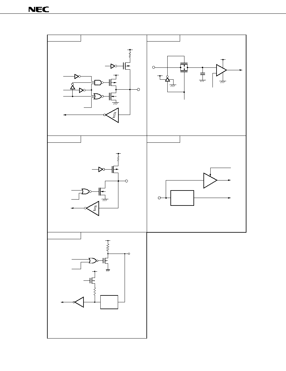
Data Sheet U10165EJ2V0DS00
(3/3)
TYPE Z-N
P.U.R.
enable
P.U.R.
V
DD
P-ch
IN/OUT
P.U.R.: Pull-Up Resistor
TYPE Y-D
data
output
disable
Type Y
Type D
Type B
ADEN
Reference
voltage
AV
REF
N-ch
AV
SS
15
µ
PD750064, 750066, 750068, 750064(A), 750066(A), 750068(A)
Data Sheet U10165EJ2V0DS00
3.4 Recommended Connection of Unused Pins
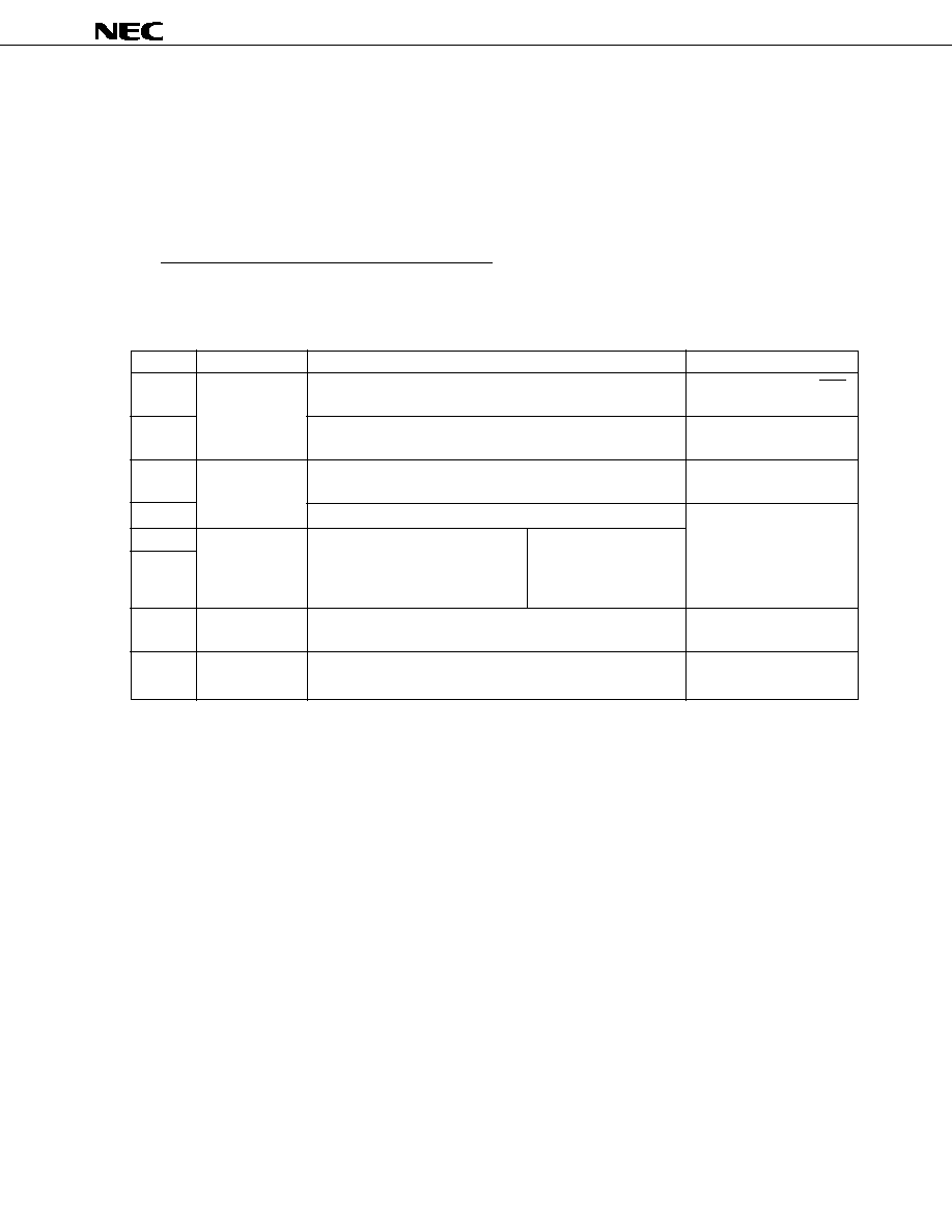
Table 3-1. List of Recommended Connection of Unused Pins
Pin
Recommended Connection
P00/INT4
Connect to V
SS
or V
DD
.
P01/SCK
Independently connect to V
SS
or V
DD
via a resistor.
P02/SO/SB0
P03/SI/SB1
Connect to V
SS
.
P10/INT0, P11/INT1
Connect to V
SS
or V
DD
.
P12/TI1/INT2
P13/TI0
P20/PTO0
Input state:
Independently connect to V
SS
or V
DD
P21/PTO1
via a resistor.
P22/PCL
Output state:
Leave open.
P23/BUZ
P30 to P33
P40 to P43
Connect to V
SS
(do not connect a pull-up resistor
P50 to P53
of mask option).
P60/KR0/AN4 to
Input state:
Independently connect to V
SS
or V
DD
P63/KR3/AN7
via a resistor.
Output state:
Leave open.
P110/AN0 to P113/AN3
Connect directly to V
SS
or
V
DD
.
XT1
Note
Connect to V
SS
.
XT2
Note
Leave open.
IC
Connect directly to V
DD
.
AV
REF
Connect to V
SS
.
AV
SS
Note
When the subsystem clock is not used, set SOS.0 to 1 (so as not to
use the internal feedback resistor).

16
µ
PD750064, 750066, 750068, 750064(A), 750066(A), 750068(A)
Data Sheet U10165EJ2V0DS00
4. SWITCHING FUNCTION BETWEEN Mk I MODE AND Mk II MODE
4.1 Differences between Mk I Mode and Mk II Mode
The CPU of the
µ
PD750068 has the following two modes: Mk I and Mk II, either of which can be selected.
The mode can be switched by the bit 3 of the stack bank select register (SBS).
∑
Mk I mode:
Upward compatible with
µ
PD75068. Can be used in the 75XL CPU with a ROM capacity
of up to 16 Kbytes.
∑
Mk II mode:
Incompatible with
µ
PD75068. Can be used in all the 75XL CPUs including those products
whose ROM capacity is more than 16 Kbytes.
Table 4-1. Differences between Mk I Mode and Mk II Mode
Mk I Mode
Mk II Mode
Number of stack bytes
2 bytes
3 bytes
for subroutine instructions
BRA !addr1 instruction
Not available
Available
CALLA !addr1 instruction
CALL !addr instruction
3 machine cycles
4 machine cycles
CALLF !faddr instruction
2 machine cycles
3 machine cycles
Caution
The Mk II mode supports a program area exceeding 16 Kbytes for the 75X and
75XL Series. Therefore, this mode is effective for enhancing software compatibility
with products exceeding 16 Kbytes.
When the Mk II mode is selected, the number of stack bytes used during
execution of subroutine call instructions increases by one byte per stack
compared to the Mk I mode. When the CALL !addr and CALLF !faddr instructions
are used, the machine cycle becomes longer by one machine cycle. Therefore,
use the Mk I mode if the RAM efficiency and processing performance are more
important than software compatibility.
17
µ
PD750064, 750066, 750068, 750064(A), 750066(A), 750068(A)
Data Sheet U10165EJ2V0DS00
4.2 Setting Method of Stack Bank Select Register (SBS)
Switching between the Mk I mode and Mk II mode can be done by the stack bank select register (SBS). Figure
4-1 shows the format.
The SBS is set by a 4-bit memory manipulation instruction.
When using the Mk I mode, the SBS must be initialized to 100
◊
B
Note
at the beginning of a program. When using
the Mk II mode, it must be initialized to 000
◊
B
Note
.
Note
Set the desired value in the
◊
position.
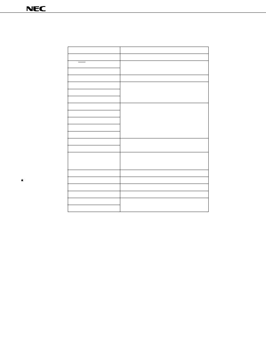
Figure 4-1. Stack Bank Select Register Format
SBS3
SBS2
SBS1
SBS0
3
2
1
0
Symbol
SBS
Address
F84H
0
0
0
1
0
1
0
Memory bank 0
Memory bank 1
Other than above setting prohibited
0 must be set in the bit 2 position.
Stack area specification
Mk II mode
Mk I mode
Mode switching specification
Caution
Since SBS. 3 is set to "1" after a RESET signal is generated, the CPU operates in the Mk I mode.
When executing an instruction in the Mk II mode, set SBS. 3 to "0" to select the Mk II mode.

18
µ
PD750064, 750066, 750068, 750064(A), 750066(A), 750068(A)
Data Sheet U10165EJ2V0DS00
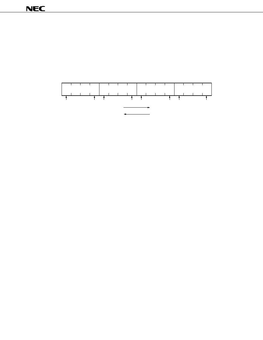
5. MEMORY CONFIGURATION
Program memory (ROM) .... 4096
◊
8 bits (
µ
PD750064)
.... 6144
◊
8 bits (
µ
PD750066)
.... 8192
◊
8 bits (
µ
PD750068)
∑
Addresses 0000H and 0001H
Vector table wherein the program start address and the values set for the RBE and MBE at the time a RESET
signal is generated are written. Reset start is possible from any address.
∑
Addresses 0002H to 000DH
Vector table wherein the program start address and the values set for the RBE and MBE by each vectored
interrupt are written. Interrupt processing can start from any address.
∑
Addresses 0020H to 007FH
Table area referenced by the GETI instruction
Note
.
Note
The GETI instruction realizes a 1-byte instruction on behalf of any 2-byte instruction, 3-byte
instruction, or two 1-byte instructions. It is used to decrease the number of program steps.
Data memory (RAM)
∑
Data area
.... 512 words
◊
4 bits (000H to 1FFH)
∑
Peripheral hardware area .... 128 words
◊
4 bits (F80H to FFFH)
19
µ
PD750064, 750066, 750068, 750064(A), 750066(A), 750068(A)
Data Sheet U10165EJ2V0DS00
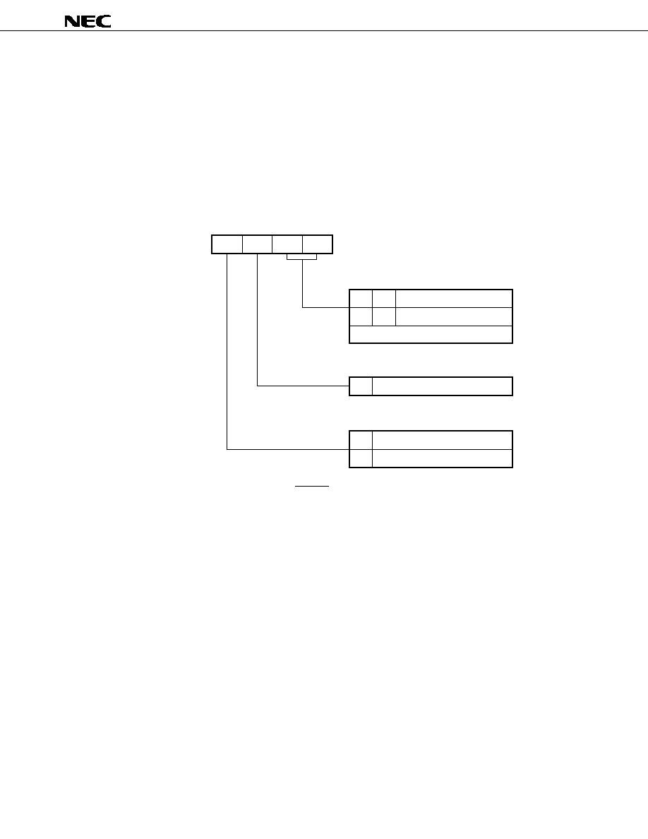
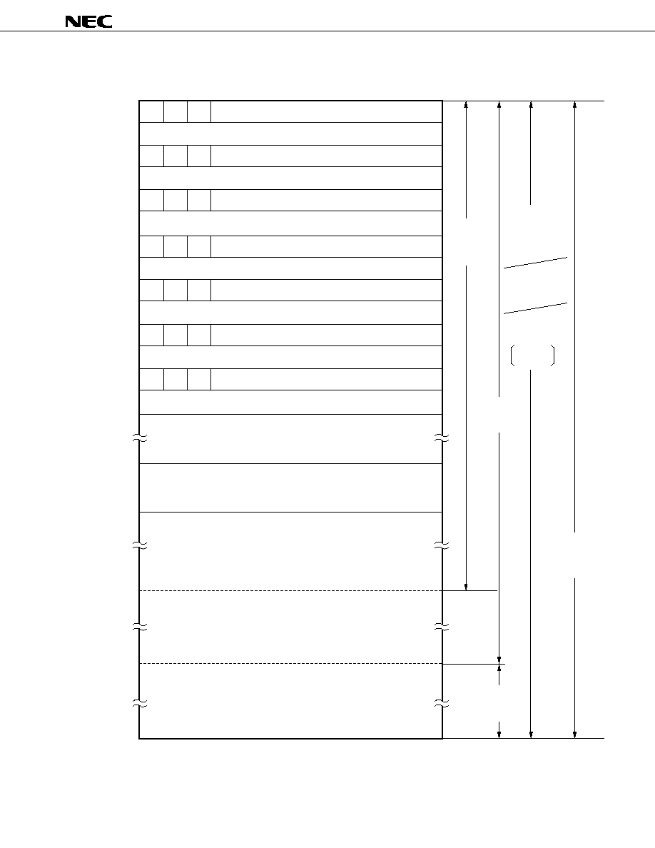
Figure 5-1. Program Memory Map (
µ
PD750064)
0 0 0 H
Address
7
6
5
4
MBE RBE
0
0
Internal reset start address
(high-order 4 bits)
0
0 0 2 H MBE RBE
0
0
INTBT/INT4
(high-order 4 bits)
start address
0 0 4 H MBE RBE
0
0
INT0
(high-order 4 bits)
start address
0 0 6 H MBE RBE
0
0
INT1
(high-order 4 bits)
start address
0 0 8 H MBE RBE
0
0
INTCSI
(high-order 4 bits)
start address
0 0 A H MBE RBE
0
0
INTT0
(high-order 4 bits)
start address
0 0 C H MBE RBE
0
0
INTT1
(high-order 4 bits)
start address
0 2 0 H
0 7 F H
0 8 0 H
7 F F H
8 0 0 H
F F F H
GETI instruction reference table
(low-order 8 bits)
(low-order 8 bits)
(low-order 8 bits)
(low-order 8 bits)
(low-order 8 bits)
(low-order 8 bits)
(low-order 8 bits)
CALLF
! faddr
instruction
entry
address
Branch address
of BR BCXA, BR
BCDE, BR !addr,
BRA !addr1
Note
or
CALLA !addr1
Note
instruction
CALL !addr
instruction
subroutine entry
address
BR $addr
instruction relative
branch address
BRCB
!caddr
instruction
branch
address
≠15 to ≠1,
+2 to +16
Branch destination
address and
subroutine entry
address when
GETI instruction
is executed
Internal reset start address
INTBT/INT4
start address
INT0
start address
INT1
start address
INTCSI
start address
INTT0
start address
INTT1
start address
Note
Can be used only in the Mk II mode.
Remark In addition to the above, a branch can be taken to the address indicated by changing only the low-order
eight bits of PC by executing the BR PCDE or BR PCXA instruction.
20
µ
PD750064, 750066, 750068, 750064(A), 750066(A), 750068(A)
Data Sheet U10165EJ2V0DS00
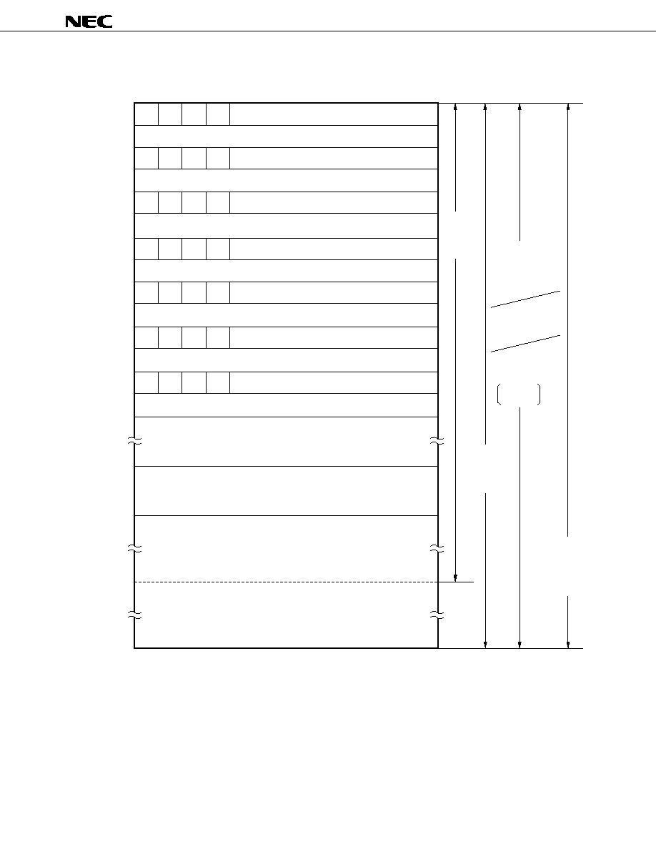
Figure 5-2. Program Memory Map (
µ
PD750066)
0 0 0 0 H
Address
0 0 0 2 H MBE RBE
0
INTBT/INT4
(high-order 5 bits)
start address
0 0 0 4 H MBE RBE
0
INT0
(high-order 5 bits)
start address
0 0 0 6 H MBE RBE
0
INT1
(high-order 5 bits)
start address
0 0 0 8 H MBE RBE
0
INTCSI
(high-order 5 bits)
start address
0 0 0 A H MBE RBE
0
INTT0
(high-order 5 bits)
start address
0 0 2 0 H
0 0 7 F H
0 0 8 0 H
0 7 F F H
0 8 0 0 H
MBE RBE
0
Internal reset start address
(high-order 5 bits)
0 F F F H
1 0 0 0 H
1 7 F F H
GETI instruction reference table
0 0 0 C H MBE RBE
0
INTT1
(high-order 5 bits)
start address
(low-order 8 bits)
(low-order 8 bits)
(low-order 8 bits)
(low-order 8 bits)
(low-order 8 bits)
(low-order 8 bits)
(low-order 8 bits)
CALLF
! faddr
instruction
entry
address
BRCB ! caddr
instruction
branch
address
Branch address
of BR BCXA, BR
BCDE, BR ! addr,
BRA ! addr1
Note
or
CALLA ! addr1
Note
instruction
CALL ! addr
instruction
subroutine entry
address
BR $ addr
instruction relative
branch address
≠15 to ≠1,
+2 to +16
Branch destination
address and
subroutine entry
address when GETI
instruction is executed
BRCB ! caddr
instruction
branch
address
7
6
5
0
Internal reset start address
INTBT/INT4
INT0
INT1
INTCSI
INTT0
INTT1
start address
start address
start address
start address
start address
start address
Note
Can be used only in the Mk II mode.
Remark In addition to the above, a branch can be taken to the address indicated by changing only the low-order
eight bits of PC by executing the BR PCDE or BR PCXA instruction.
21
µ
PD750064, 750066, 750068, 750064(A), 750066(A), 750068(A)
Data Sheet U10165EJ2V0DS00
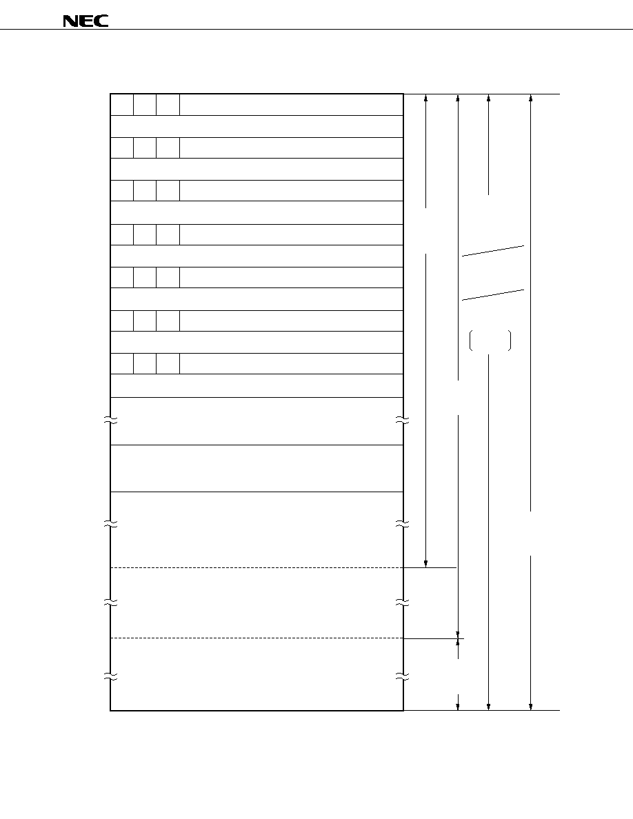
Figure 5-3. Program Memory Map (
µ
PD750068)
0 0 0 0 H
Address
0 0 0 2 H MBE RBE
0
INTBT/INT4
(high-order 5 bits)
start address
0 0 0 4 H MBE RBE
0
INT0
(high-order 5 bits)
start address
0 0 0 6 H MBE RBE
0
INT1
(high-order 5 bits)
start address
0 0 0 8 H MBE RBE
0
INTCSI
(high-order 5 bits)
start address
0 0 0 A H MBE RBE
0
INTT0
(high-order 5 bits)
start address
0 0 2 0 H
0 0 7 F H
0 0 8 0 H
0 7 F F H
0 8 0 0 H
MBE RBE
0
Internal reset start address
(high-order 5 bits)
0 F F F H
1 0 0 0 H
1 F F F H
GETI instruction reference table
0 0 0 C H MBE RBE
0
INTT1
(high-order 5 bits)
start address
(low-order 8 bits)
(low-order 8 bits)
(low-order 8 bits)
(low-order 8 bits)
(low-order 8 bits)
(low-order 8 bits)
(low-order 8 bits)
CALLF
! faddr
instruction
entry
address
BRCB ! caddr
instruction
branch
address
Branch address
of BR BCXA, BR
BCDE, BR ! addr,
BRA ! addr1
Note
or
CALLA ! addr1
Note
instruction
CALL ! addr
instruction
subroutine entry
address
BR $ addr
instruction relative
branch address
≠15 to ≠1,
+2 to +16
Branch destination
address and
subroutine entry
address when GETI
instruction is executed
BRCB ! caddr
instruction
branch
address
7
6
5
0
Internal reset start address
INTBT/INT4
INT0
INT1
INTCSI
INTT0
INTT1
start address
start address
start address
start address
start address
start address
Note
Can be used only in the Mk II mode.
Remark In addition to the above, a branch can be taken to the address indicated by changing only the low-order
eight bits of PC by executing the BR PCDE or BR PCXA instruction.
22
µ
PD750064, 750066, 750068, 750064(A), 750066(A), 750068(A)
Data Sheet U10165EJ2V0DS00
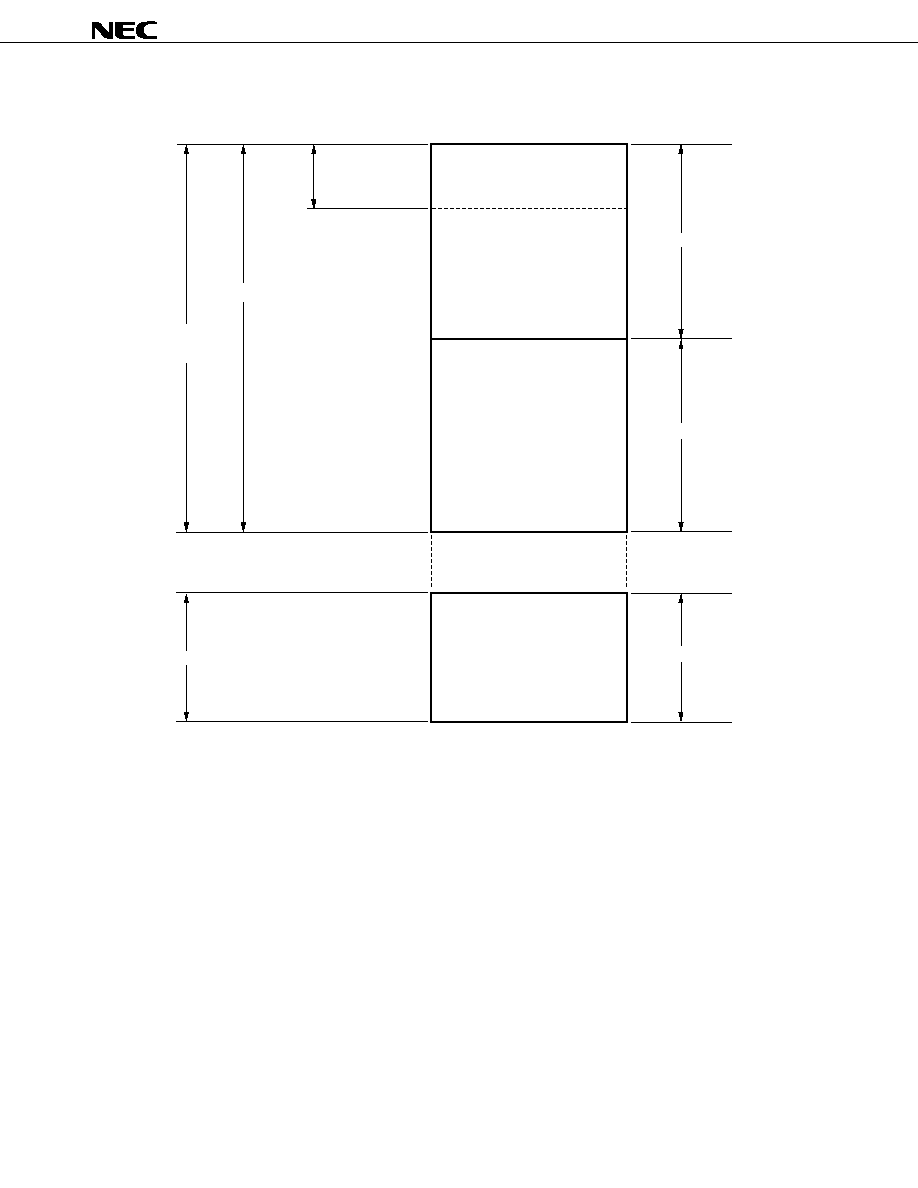
Figure 5-4. Data Memory Map
Data area
static RAM
(512
◊
4)
Stack area
Note
General-purpose
register area
0 0 0 H
0 1 F H
0 2 0 H
0 F F H
1 0 0 H
F 8 0 H
F F F H
Peripheral hardware area
Data memory
Memory bank
0
(32
◊
4)
(224
◊
4)
256
◊
4
256
◊
4
Not incorporated
128
◊
4
15
1
1 F F H
Note
Memory bank 0 or 1 can be selected as the stack area.
23
µ
PD750064, 750066, 750068, 750064(A), 750066(A), 750068(A)
Data Sheet U10165EJ2V0DS00
6. PERIPHERAL HARDWARE FUNCTION
6.1 Port
The following three types of I/O ports are available.
∑ CMOS input (PORT0, 1, 11)
: 12
∑ CMOS input/output (PORT2, 3, 6)
: 12
∑ N-ch open-drain input/output (PORT4, 5)
: 8
Total
32
Table 6-1. Types and Features of Digital Ports
Port Name
Function
Operation and Features
Remarks
PORT0
4-bit input
When the serial interface function is used, the alternate-function
Also used for the INT4, SCK,
pins function as output ports depending on the operation mode.
SO/SB0, SI/SB1 pins.
PORT1
4-bit input only port.
Also used for the INT0 to
INT2/TI1, TI0 pins.
PORT2
4-bit input/output Can be set to input mode or output mode in 4-bit units.
Also used for the PTO0,
PTO1, PCL, BUZ pins.
PORT3
Can be set to input mode or output mode in 1-bit units.
≠
PORT4
4-bit input/output
Can be set to input mode or output
Ports 4 and 5 are paired
PORT5
(N-ch open drain,
mode in 4-bit units. On-chip pull-up
and data can be input/
13 V withstand
resistor can be specified in 1-bit
output in 8-bit units.
voltage)
units by mask option.
PORT6
4-bit input/output Can be set to input mode or output mode in 1-bit units.
Also used for the KR0 to
KR3, AN4 to AN7 pins.
PORT11
4-bit input
4-bit input only port.
Also used for the AN0 to
AN3 pins.
6.2 Clock Generator
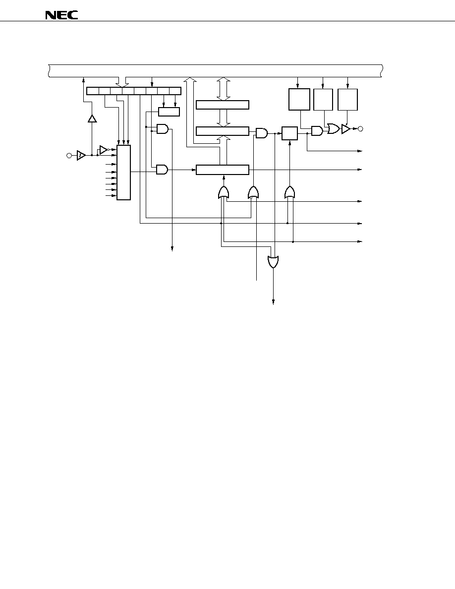
The clock generator generates clocks which are supplied to the peripheral hardware in the CPU. Figure 6-1
shows the configuration of the clock generator.
Operation of the clock generator is determined by the processor clock control register (PCC) and system clock
control register (SCC).
Two types of system clocks are available; main system clock and subsystem clock.
The instruction execution time can be changed.
∑ 0.95
µ
s, 1.91
µ
s, 3.81
µ
s, 15.3
µ
s (@ 4.19-MHz operation with main system clock)
∑ 0.67
µ
s, 1.33
µ
s, 2.67
µ
s, 10.7
µ
s (@ 6.0-MHz operation with main system clock)
∑ 122
µ
s (@ 32.768-kHz operation with subsystem clock)
24
µ
PD750064, 750066, 750068, 750064(A), 750066(A), 750068(A)
Data Sheet U10165EJ2V0DS00
Figure 6-1. Clock Generator Block Diagram
XT1
X1
XT2
X2
f
XT
f
X
Subsystem
clock oscillator
Main system
clock oscillator
4
HALT
Note
STOP
Note
WM.3
SCC
SCC3
SCC0
PCC0
PCC1
PCC2
PCC3
PCC2,
PCC3
Clear
STOP F/F
Q
S
R
Oscillation
stop
HALT F/F
S
R
Wait release signal from BT
RESET signal
Standby release signal from
interrupt control circuit
∑ CPU
∑ INT0 noise eliminator
∑ Clock output circuit
1/4
Divider
1/1 to 1/4096
Divider
1/2 1/4 1/16
∑ Basic interval timer (BT)
∑ Timer/event counter
∑ Serial interface
∑ Watch timer
∑ INT0 noise eliminator
∑ Clock output circuit
PCC
Q
Selector
Selector
Internal bus
Watch timer
Note Instruction execution
Remarks 1.
f
X
= Main system clock frequency
2.
f
XT
= Subsystem clock frequency
3.
= CPU clock
4.
PCC: Processor Clock Control Register
5.
SCC: System Clock Control Register
6.
One clock cycle (t
CY
) of the CPU clock is equal to one machine cycle of the instruction.
25
µ
PD750064, 750066, 750068, 750064(A), 750066(A), 750068(A)
Data Sheet U10165EJ2V0DS00
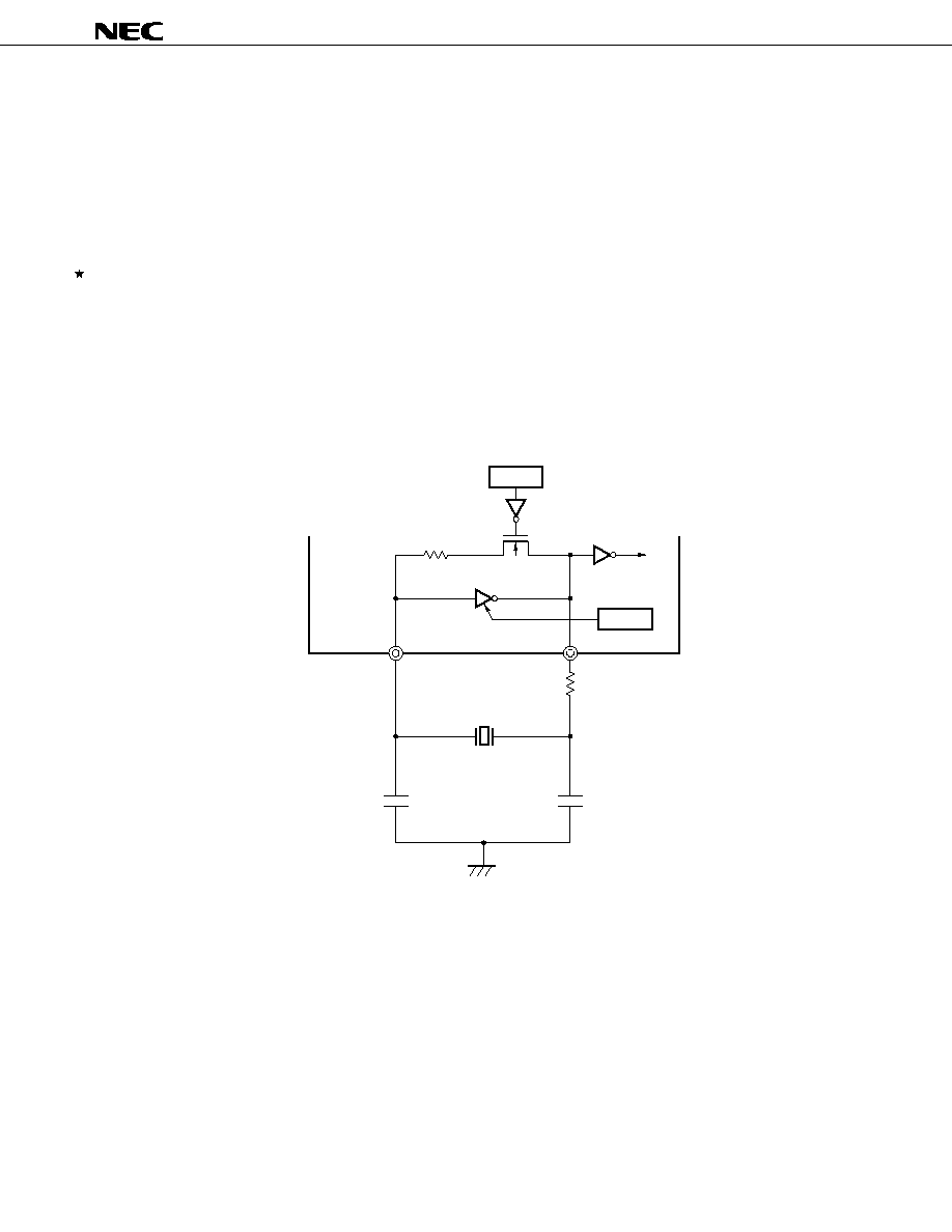
6.3 Subsystem Clock Oscillator Control Function
The subsystem clock oscillator of the
µ
PD750068 has the following two control functions to decrease the supply
current.
∑ Selects by software whether an internal feedback resistor is to be used or not
Note
.
∑ Reduces current consumption by decreasing the drive current of the on-chip inverter when the supply
voltage is high (V
DD
2.7 V).
Note
When the subsystem clock is not used, set SOS.0 to 1 (so as not to use the internal feedback resistor)
by software, connect XT1 to V
SS
, and open XT2. This makes it possible to reduce the current
consumption in the subsystem clock oscillator.
The above functions can be used by switching the bits 0 and 1 of the sub-oscillator control register (SOS). (Refer
to Figure 6-2.)
Figure 6-2. Subsystem Clock Oscillator
Feedback resistor
SOS.0
SOS.1
XT1
XT2
Inverter

26
µ
PD750064, 750066, 750068, 750064(A), 750066(A), 750068(A)
Data Sheet U10165EJ2V0DS00
6.4 Clock Output Circuit
The clock output circuit is provided to output the clock pulses from the P22/PCL pin to the remote control wave
output applications and peripheral LSIs.
∑ Clock output (PCL) :
, 1.05 MHz, 262 kHz, 65.5 kHz (@ 4.19-MHz operation)
:
, 1.5 MHz, 375 kHz, 93.8 kHz (@ 6.0-MHz operation)
Figure 6-3. Clock Output Circuit Block Diagram
From clock
generator
f
X
/2
2
f
X
/2
4
f
X
/2
6
Selector
CLOM3
0
CLOM1 CLOM0
4
CLOM
P22
output latch
Port 2 I/O mode
specification bit
PORT2.2
Bit 2 of PMGB
Internal bus
Output buffer
PCL/P22
Remark Special care has been taken in designing the chip so that small-width pulses may not be output
when switching clock output enable/disable.
27
µ
PD750064, 750066, 750068, 750064(A), 750066(A), 750068(A)
Data Sheet U10165EJ2V0DS00
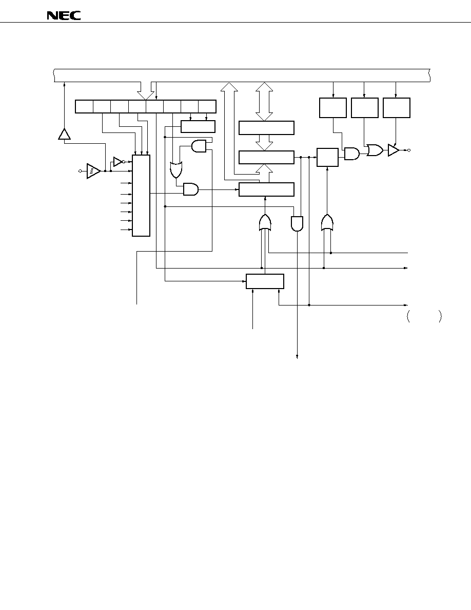
6.5 Basic Interval Timer/Watchdog Timer
The basic interval timer/watchdog timer has the following functions.
(a) Interval timer operation to generate a reference time interrupt
(b) Watchdog timer operation to detect a runaway of program and reset the CPU
(c) Selects and counts the wait time when the standby mode is released
(d) Reads the contents of counting
Figure 6-4. Basic Interval Timer/Watchdog Timer Block Diagram
From clock
generator
f
X
/2
5
f
X
/2
7
f
X
/2
9
f
X
/2
12
MPX
BTM3 BTM2 BTM1 BTM0 BTM
4
SET1
Note
Internal bus
8
1
Basic interval timer
(8-bit frequency divider)
Clear
BT
Wait release signal
when standby is
released
Set
Clear
3
WDTM
SET1
Note
Internal reset
signal
Vectored
interrupt
request
signal
BT
interrupt
request flag
IRQBT
Note Instruction execution
28
µ
PD750064, 750066, 750068, 750064(A), 750066(A), 750068(A)
Data Sheet U10165EJ2V0DS00
6.6 Watch Timer
The
µ
PD750068 has one channel of watch timer. The watch timer has the following functions.
(a) Sets the test flag (IRQW) with 0.5 sec interval. The standby mode can be released by the IRQW.
(b) 0.5 sec interval can be created by both the main system clock (4.194304 MHz) and subsystem clock (32.768
kHz).
(c) Convenient for program debugging and checking as interval becomes 128 times longer (3.91 ms) with the
fast feed mode.
(d) Outputs the frequencies (2.048, 4.096, 32.768 kHz) to the P23/BUZ pin, usable for buzzer and trimming
of system clock frequencies.
(e) Clears the frequency divider to make the clock start with zero seconds.
(f)
Uses the clock of 0.5 sec as the clock source of the timer/event counter to continue the standby mode until
the longest time 9 hours (by using timer 0, 1) to be in the lowest consumption mode.
Figure 6-5. Watch Timer Block Diagram
From
clock
generator
Selector
f
X
128
(32.768 kHz)
f
XT
(32.768 kHz)
f
W
(32.768 kHz)
Divider
4 kHz 2 kHz
f
W
2
3
f
W
2
4
Clear
Selector
f
W
2
7
(256 Hz : 3.91 ms)
f
W
2
14
Selector
2 Hz
0.5 sec
IRQW
set signal
INTW
Output buffer
PMGB bit 2
PORT2.3
WM
WM7
0
WM5
WM4
WM3
WM2
WM1
WM0
P23
output latch
Port 2 input/
output mode
8
Internal bus
Bit test instruction
P23/BUZ
Remark The values enclosed in parentheses are applied when f
X
= 4.194304 MHz and f
XT
= 32.768 kHz.
29
µ
PD750064, 750066, 750068, 750064(A), 750066(A), 750068(A)
Data Sheet U10165EJ2V0DS00
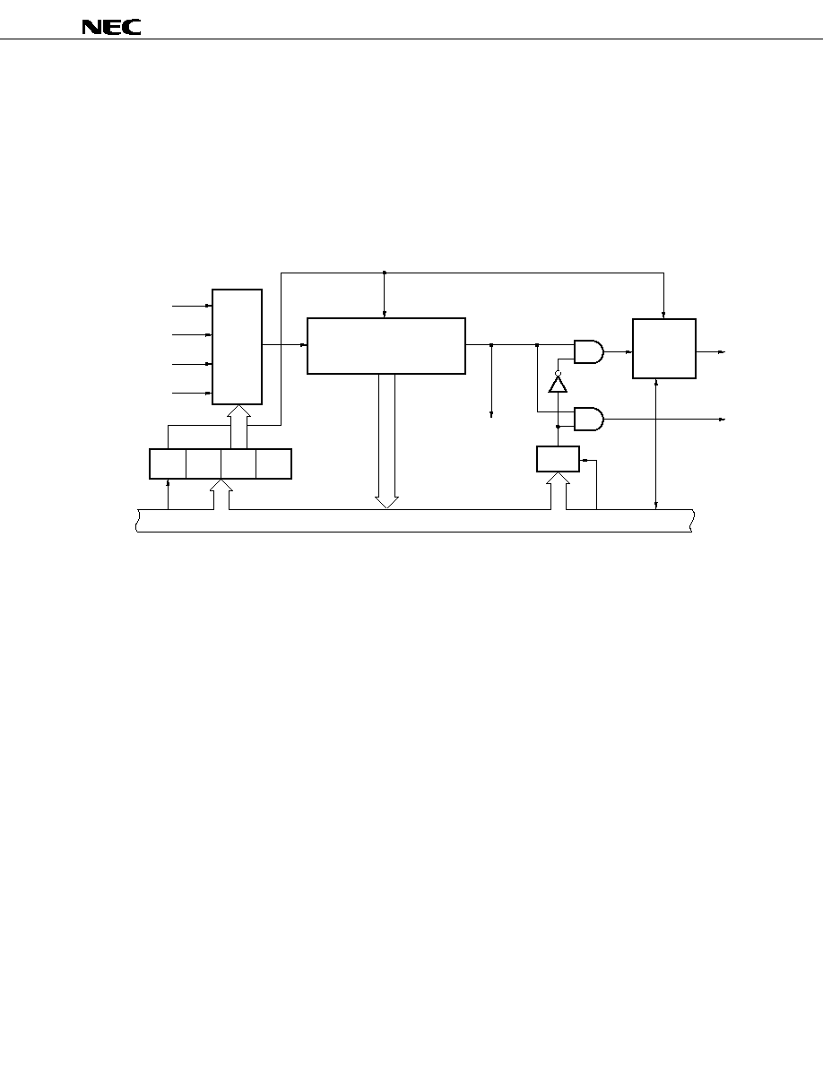
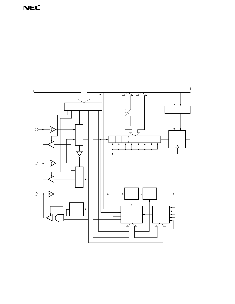
6.7 Timer/Event Counter
The
µ
PD750068 has two channels of timer/event counters. Its configuration is shown in Figures 6-6 and 6-7.
The timer/event counter has the following functions.
(a) Programmable interval timer operation
(b) Square wave output of any frequency to the PTOn pin (n = 0, 1)
(c) Event counter operation
(d) Divides the frequency of signal input via the TIn pin to 1-Nth of the original signal and outputs the divided
frequency to the PTOn pin (frequency divider operation).
(e) Supplies the shift clock to the serial interface circuit.
(f)
Reads the count value.
The timer/event counter operates in the following two modes as set by the mode register.
Table 6-2. Operation Modes of Timer/Event Counter
Channel
Channel 0
Channel 1
Mode
8-bit timer/event counter mode
Yes
Yes
16-bit timer/event counter mode
Yes
30
µ
PD750064, 750066, 750068, 750064(A), 750066(A), 750068(A)
Data Sheet U10165EJ2V0DS00
Figure 6-6. Timer/Event Counter Block Diagram (Channel 0)
Timer/event
counter
TM06
Modulo register (8)
TM05 TM04 TM03 TM02 TM01 TM00
≠
8
TM0
Decoder
Internal bus
8
PORT1. 3
Input
buffer
TI0/P13
Watch timer (INTW) output
From clock
generator
f
X
/2
2
f
X
/2
4
f
X
/2
6
f
X
/2
8
f
X
/2
10
MPX
TMOD0
8
Comparator (8)
Count register (8)
CP
Clear
Reset
T0
16-bit
timer/event
counter mode
Timer
operation
start
Timer/event counter (channel 1) TM12 signal
(When 16-bit timer/event counter mode)
Timer/event counter (channel 1) match signal
(When 16-bit timer/event counter mode)
Timer/event counter (channel 1) clear signal
(When 16-bit timer/event counter mode)
Overflow
TOUT0
TOE0
TOUT
F/F
PORT2.0
PMGB bit 2
TO
P20
To serial
interface
P20/PTO0
Output
buffer
(channel 1)
clock input
INTT0
(IRQT0
set signal)
IRQT0
clear signal
RESET
8
Match
enable
flag
output
latch
Port 2
input/
output
mode
31
µ
PD750064, 750066, 750068, 750064(A), 750066(A), 750068(A)
Data Sheet U10165EJ2V0DS00
Figure 6-7. Timer/Event Counter Block Diagram (Channel 1)
PORT1.2
Input
buffer
TI1/P12/INT2
Timer/event counter output
(channel 0)
From clock
generator
MPX
≠
TM16 TM15 TM14 TM13 TM12 TM11 TM10
TM1
Decoder
16 bit timer/event
counter mode
CP
Timer operation start
Clear
8
8
8
8
Modulo register (8)
Comparator (8)
Count register (8)
Timer/event counter (channel 0) match signal/operation start
(When 16-bit timer/event counter mode)
Timer/event counter (channel 0) comparator
(When 16-bit timer/event counter mode)
T1
TMOD1
Match
TOUT
F/F
Reset
TO
enable flag
P21
output latch
Port 2
input/output
mode
INTT1
IRQT1
set signal
IRQT1
clear signal
RESET
TOE1
PORT2.1
PMGB bit 2
P21/PTO1
Output
buffer
Internal bus
Timer/event counter (channel 0) TM02 signal
(When 16-bit timer/event counter mode)
Selector
f
X
/2
2
f
X
/2
6
f
X
/2
8
f
X
/2
10
f
X
/2
12
32
µ
PD750064, 750066, 750068, 750064(A), 750066(A), 750068(A)
Data Sheet U10165EJ2V0DS00
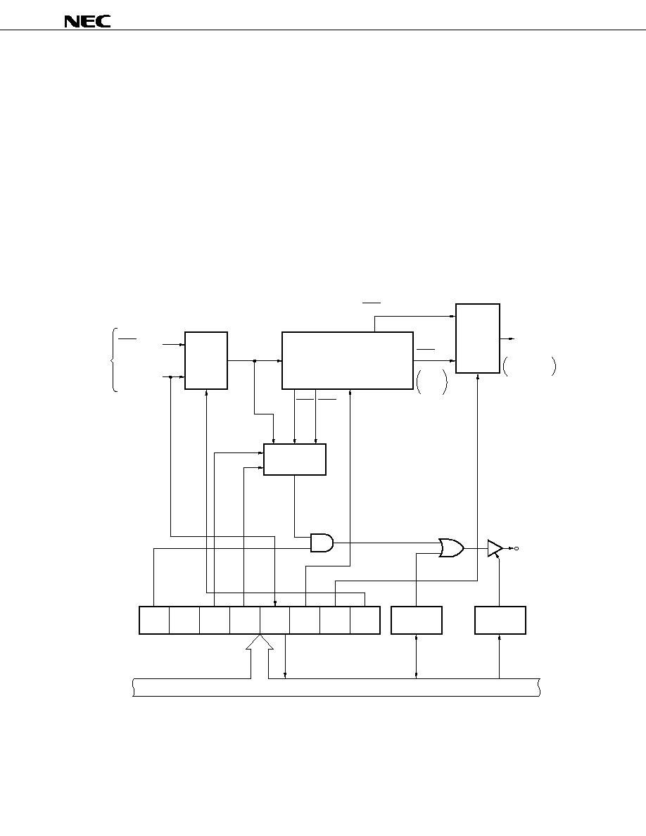
6.8 Serial Interface
The serial interface has the following three modes.
∑ Operation stop mode
∑ 3-wire serial I/O mode
∑ 2-wire serial I/O mode
The 3-wire serial I/O mode enables connections to be made with the 75X Series, 78K Series, and many other
types of I/O devices. The 2-wire serial I/O mode enables communication with two or more devices.
Figure 6-8. Serial Interface Block Diagram
Internal bus
8/4
Bit
test
P03/SI/SB1
P02/SO/SB0
P01/SCK
8
8
SBIC
RELT
CMDT
SET CLR
D
Q
(8)
INTCSI
IRQCSI
set signal
f
X
/2
3
f
X
/2
4
f
X
/2
6
TOUT0
P01
Output
latch
Selector
Selector
Serial
clock
counter
Serial clock
control circuit
Serial
clock
selector
SO
latch
Shift register (SIO)
External
SCK
From
timer/event
counter 0
Bit
manipu-
lation
INTCSI
control
circuit
CSIM
33
µ
PD750064, 750066, 750068, 750064(A), 750066(A), 750068(A)
Data Sheet U10165EJ2V0DS00
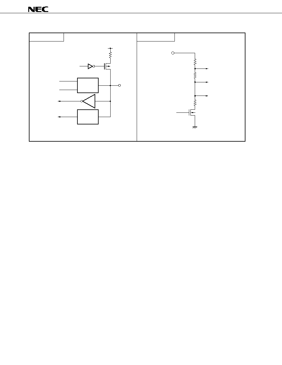
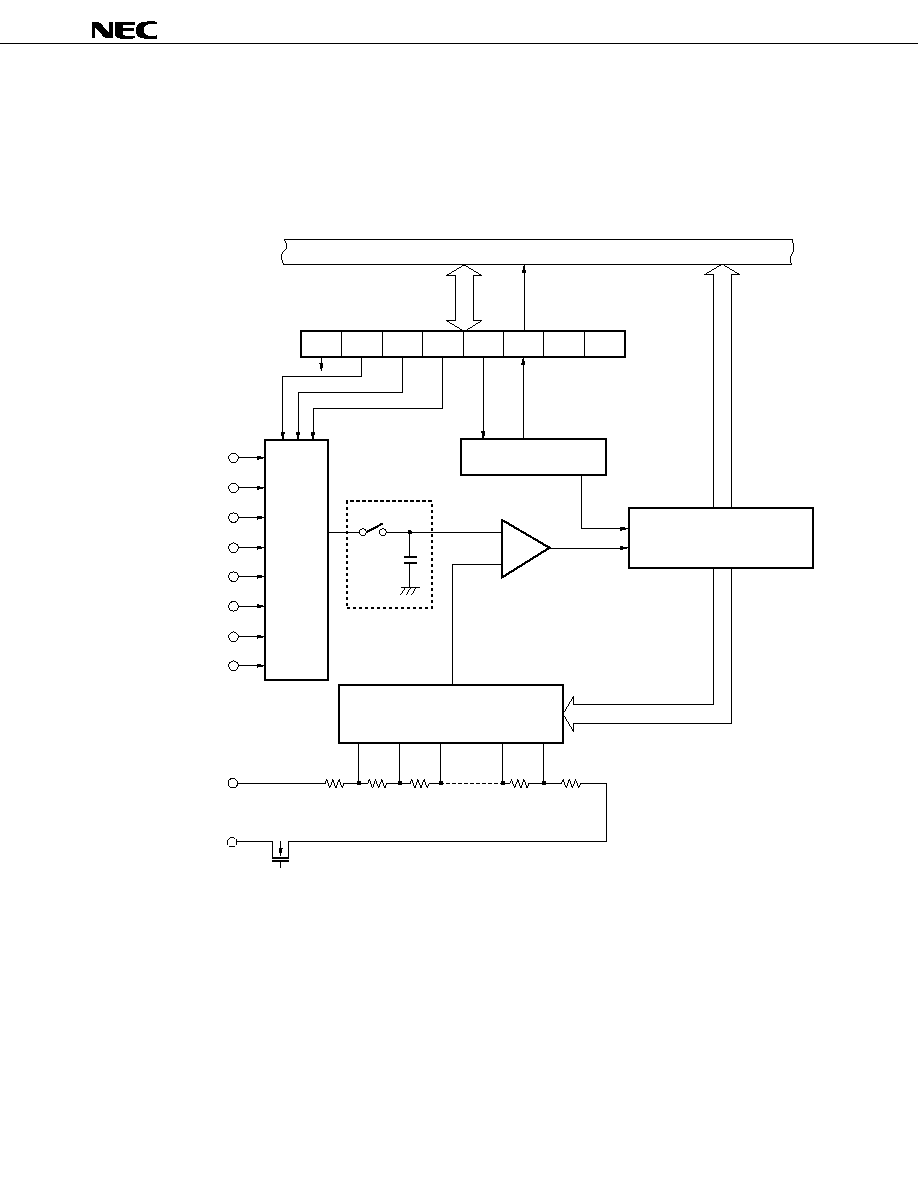
6.9 A/D Converter
The
µ
PD750068 incorporates the 8-bit resolution A/D converter which has eight channels analog input pins
(AN0 to AN7).
This A/D converter is a successive approximation type.
Figure 6-9. A/D Converter Block Diagram
≠
+
Internal bus
8
ADEN ADM6 ADM5 ADM4
SOC
EOC
0
0
Controller
Sample hold
circuit
Comparator
SA register (8)
8
8
Tap decoder
Multiplexer
AN0/P110
AN1/P111
AN2/P112
AN3/P113
AN4/P60/KR0
AN5/P61/KR1
AN6/P62/KR2
AN7/P63/KR3
AV
REF
AV
SS
R/2
R
R
R
R/2
ADEN
34
µ
PD750064, 750066, 750068, 750064(A), 750066(A), 750068(A)
Data Sheet U10165EJ2V0DS00
6.10 Bit Sequential Buffer ....... 16 Bits
The bit sequential buffer (BSB) is a special data memory for bit manipulation and the bit manipulation can be
easily performed by changing the address specification and bit specification in sequence, therefore it is useful
when processing a long data bit-wise.
Figure 6-10. Bit Sequential Buffer Format
Address
Bit
Symbol
L register
L = FH
L = CH L = BH
L = 8H
L = 7H
L = 4H L = 3H
L = 0H
DECS L
INCS L
BSB3
BSB2
BSB1
BSB0
3
2
1
0
3
2
1
0
3
2
1
0
3
2
1
0
FC3H
FC2H
FC1H
FC0H
Remarks 1.
In the pmem.@L addressing, the specified bit moves corresponding to the L register.
2.
In the pmem.@L addressing, the BSB can be manipulated regardless of MBE/MBS specification.

35
µ
PD750064, 750066, 750068, 750064(A), 750066(A), 750068(A)
Data Sheet U10165EJ2V0DS00
7. INTERRUPT FUNCTION AND TEST FUNCTION
The
µ
PD750068 has seven interrupt sources and two test sources. One test source, INT2, has two types of
edge detection testable inputs.
The interrupt control circuit of the
µ
PD750068 has the following functions.
(1) Interrupt function
∑ Vectored interrupt function for hardware control, enabling/disabling the interrupt acceptance by the
interrupt enable flag (IE
◊◊◊
) and interrupt master enable flag (IME).
∑ Can set any interrupt start address.
∑ Multiple interrupts wherein the order of priority can be specified by the interrupt priority select register
(IPS).
∑ Test function of interrupt request flag (IRQ
◊◊◊
). An interrupt generated can be checked by software.
∑ Release the standby mode. A release interrupt can be selected by the interrupt enable flag.
(2) Test function
∑ Test request flag (IRQ
◊◊◊
) generation can be checked by software.
∑ Release the standby mode. The test source to be released can be selected by the test enable flag.
36
µ
PD750064, 750066, 750068, 750064(A), 750066(A), 750068(A)
Data Sheet U10165EJ2V0DS00
Figure 7-1. Interrupt Control Circuit Block Diagram
IST0
IST1
Internal bus
Interrupt enable flag (IE
◊◊◊
)
IRQBT
IRQ4
IRQ0
IRQ1
IRQCSI
IRQT0
IRQT1
IRQW
IRQ2
INTCSI
INTT0
INTT1
INTW
Both edge
detector
Edge
detector
Edge
detector
Selector
INT4/P00
INT0/P10
INT1/P11
INT2/P12
KR0/P60
KR3/P63
Rising edge
detector
Falling edge
detector
Selector
IM2
Standby
release
signal
Priority
control
circuit
Vector
table
address
generator
VRQn
IM2
IM0
2
1
4
INTBT
Note
IME IPS
Decoder
IM1
Note
Noise elimination circuit (Standby release is disabled when noise elimination circuit is selected.)
37
µ
PD750064, 750066, 750068, 750064(A), 750066(A), 750068(A)
Data Sheet U10165EJ2V0DS00
8. STANDBY FUNCTION
In order to save power dissipation while a program is in a standby mode, two types of standby modes (STOP
mode and HALT mode) are provided for the
µ
PD750068.
Table 8-1. Operation Status in Standby Mode
Mode
STOP Mode
HALT Mode
Item
Set instruction
STOP instruction
HALT instruction
System clock when set
Settable only when the main system
Settable both by the main system clock
clock is used.
and subsystem clock.
Operation
Clock generator
The main system clock stops oscillation.
Only the CPU clock
halts (oscillation
status
continues).
Basic interval timer/
Operation stops.
Operable only when the main system
watchdog timer
clock is oscillated (The IRQBT is set in
the reference time interval).
Serial interface
Operable only when an external SCK
Operable only when an external SCK
input is selected as the serial clock.
input is selected as the serial clock or
when the main system clock is oscillated.
Timer/event counter
Operable only when a signal input to
Operable only when a signal input to
the TI0 and TI1 pins or a watch timer
the TI0 and TI1 pins or a watch timer
which selected f
XT
is specified as the
which selected f
XT
is specified as the
count clock.
count clock or when the main system
clock is oscillated.
Watch timer
Operable when f
XT
is selected as the
Operable.
count clock.
A/D converter
Operation stops.
Operable only when the main system
clock is oscillated.
External interrupt
The INT1, 2, and 4 are operable.
Only the INT0 is not operated
Note
.
CPU
Operation stops.
Release signal
∑ Interrupt request signal sent from the operable hardware enabled by the interrupt
enable flag.
∑ Test request signal sent from the test source enabled by the test enable flag
∑ RESET signal generation
Note
Can operate only when the noise elimination circuit is not used (IM02 = 1) by bit 2 of the edge detection
mode register (IM0).

38
µ
PD750064, 750066, 750068, 750064(A), 750066(A), 750068(A)
Data Sheet U10165EJ2V0DS00
9. RESET FUNCTION
There are two reset inputs: external reset signal (RESET) and reset signal sent from the basic interval timer/
watchdog timer. When either one of the reset signals are input, an internal reset signal is generated. Figure 9-
1 shows the configuration of the above two inputs.
Figure 9-1. Configuration of Reset Function
RESET
Internal reset signal
Reset signal sent from the
basic interval timer/watchdog timer
WDTM
Internal bus
When the RESET signal is generated, each hardware is initialized as listed in Table 9-1. Figure 9-2 shows
the timing chart of the reset operation.
Figure 9-2. Reset Operation by RESET Signal Generation
Operation mode or
standby mode
Wait
Note
RESET
signal
generated
Operation mode
HALT mode
Internal reset operation
Note
The following two times can be selected by the mask option.
2
17
/f
X
(21.8 ms: @6.0-MHz operation, 31.3 ms: @4.19-MHz operation)
2
15
/f
X
(5.46 ms: @6.0-MHz operation, 7.81 ms: @4.19-MHz operation)

39
µ
PD750064, 750066, 750068, 750064(A), 750066(A), 750068(A)
Data Sheet U10165EJ2V0DS00
Table 9-1. Status of Each Hardware After Reset (1/2)
Hardware
RESET Signal Generation
RESET Signal Generation
in Standby Mode
in Operation
Program counter (PC)
µ
PD750064
Sets the low-order 4 bits of
Sets the low-order 4 bits of
program memory's address
program memory's address
0000H to the PC11 to PC8 and
0000H to the PC11 to PC8 and
the contents of address 0001H
the contents of address 0001H
to the PC7 to PC0.
to the PC7 to PC0.
µ
PD750066,
Sets the low-order 5 bits of
Sets the low-order 5 bits of
750068
program memory's address
program memory's address
0000H to the PC12 to PC8 and
0000H to the PC12 to PC8 and
the contents of address 0001H
the contents of address 0001H
to the PC7 to PC0.
to the PC7 to PC0.
PSW
Carry flag (CY)
Held
Undefined
Skip flag (SK0 to SK2)
0
0
Interrupt status flag (IST0, IST1)
0
0
Bank enable flag (MBE, RBE)
Sets the bit 6 of program
Sets the bit 6 of program
memory's address 0000H to
memory's address 0000H to
the RBE and bit 7 to the MBE.
the RBE and bit 7 to the MBE.
Stack pointer (SP)
Undefined
Undefined
Stack bank select register (SBS)
1000B
1000B
Data memory (RAM)
Held
Undefined
General-purpose register (X, A, H, L, D, E, B, C)
Held
Undefined
Bank select register (MBS, RBS)
0, 0
0, 0
Basic interval
Counter (BT)
Undefined
Undefined
timer/watchdog
Mode register (BTM)
0
0
timer
Watchdog timer enable flag (WDTM)
0
0
Timer/event
Counter (T0)
0
0
counter (T0)
Modulo register (TMOD0)
FFH
FFH
Mode register (TM0)
0
0
TOE0, TOUT F/F
0, 0
0, 0
Timer/event
Counter (T1)
0
0
counter (T1)
Modulo register (TMOD1)
FFH
FFH
Mode register (TM1)
0
0
TOE1, TOUT F/F
0, 0
0, 0
Watch timer
Mode register (WM)
0
0

40
µ
PD750064, 750066, 750068, 750064(A), 750066(A), 750068(A)
Data Sheet U10165EJ2V0DS00
Table 9-1. Status of Each Hardware After Reset (2/2)
Hardware
RESET Signal Generation
RESET Signal Generation
in Standby Mode
in Operation
Serial interface
Shift register (SIO)
Held
Undefined
Operation mode register (CSIM)
0
0
SBI control register (SBIC)
0
0
Clock generator,
Processor clock control register (PCC)
0
0
clock output
System clock control register (SCC)
0
0
circuit
Clock output mode register (CLOM)
0
0
Sub-oscillator control register (SOS)
0
0
A/D converter
Mode register (ADM)
04H
04H
SA register (SA)
7FH
7FH
Interrupt
Interrupt request flag (IRQ
◊◊◊
)
Reset (0)
Reset (0)
function
Interrupt enable flag (IE
◊◊◊
)
0
0
Interrupt priority selection register (IPS)
0
0
INT0, 1, 2 mode registers (IM0, IM1, IM2)
0, 0, 0
0, 0, 0
Digital port
Output buffer
Off
Off
Output latch
Cleared (0)
Cleared (0)
I/O mode registers (PMGA, PMGB)
0
0
Pull-up resistor setting register (POGA)
0
0
Bit sequential buffer (BSB0 to BSB3)
Held
Undefined

41
µ
PD750064, 750066, 750068, 750064(A), 750066(A), 750068(A)
Data Sheet U10165EJ2V0DS00
10. MASK OPTION
The
µ
PD750068 has the following mask options.
∑ Mask option of P40 to P43 and P50 to P53
Can select whether to incorporate the pull-up resistor.
(1) The pull-up resistor is incorporated in 1-bit units.
(2) The pull-up resistor is not incorporated.
∑ Mask option of standby function
Can select the wait time with the RESET signal.
(1) 2
17
/f
X
(21.8 ms at f
X
= 6.0 MHz, 31.3 ms at f
X
= 4.19 MHz)
(2) 2
15
/f
X
(5.46 ms at f
X
= 6.0 MHz, 7.81 ms at f
X
= 4.19 MHz)
∑ Mask option of subsystem clock
Can select whether to enable the internal feedback resistor.
(1) The internal feedback resistor is enabled (switch internal feedback resistor ON/OFF by software).
(2) The internal feedback resistor is disabled (disconnect internal feedback resistor by hardware).

42
µ
PD750064, 750066, 750068, 750064(A), 750066(A), 750068(A)
Data Sheet U10165EJ2V0DS00
11. INSTRUCTION SET
(1) Expression formats and description methods of operands
The operand is described in the operand column of each instruction in accordance with the description
method for the operand expression format of the instruction. For details, refer to "RA75X Assembler
Package User's Manual----Language (U12385E)". If there are several elements, one of them is
selected. Capital letters and the + and ≠ symbols are key words and are described as they are.
For immediate data, appropriate numbers or labels are described.
Instead of the labels such as mem, fmem, pmem, and bit, the symbols of the register flags can be described.
However, there are restrictions in the labels that can be described for fmem and pmem. For details, see
µ
PD750068 User's Manual (U10670E).
Expression
Description Method
Format
reg
X, A, B, C, D, E, H, L
reg1
X, B, C, D, E, H, L
rp
XA, BC, DE, HL
rp1
BC, DE, HL
rp2
BC, DE
rp'
XA, BC, DE, HL, XA', BC', DE', HL'
rp'1
BC, DE, HL, XA', BC', DE', HL'
rpa
HL, HL+, HL≠, DE, DL
rpa1
DE, DL
n4
4-bit immediate data or label
n8
8-bit immediate data or label
mem
8-bit immediate data or label
Note
bit
2-bit immediate data or label
fmem
FB0H to FBFH, FF0H to FFFH immediate data or label
pmem
FC0H to FFFH immediate data or label
addr, addr1
0000H to 0FFFH immediate data or label (
µ
PD750064)
(Mk II mode only)
0000H to 17FFH immediate data or label (
µ
PD750066)
0000H to 1FFFH immediate data or label (
µ
PD750068)
caddr
12-bit immediate data or label
faddr
11-bit immediate data or label
taddr
20H to 7FH immediate data (where bit0 = 0) or label
PORTn
PORT0 to PORT6, PORT11
IE
◊◊◊
IEBT, IET0, IET1, IE0 to IE2, IE4, IECSI, IEW
RBn
RB0 to RB3
MBn
MB0, MB1, MB15
Note mem can be only used for even address in 8-bit data processing.

43
µ
PD750064, 750066, 750068, 750064(A), 750066(A), 750068(A)
Data Sheet U10165EJ2V0DS00
(2) Legend in explanation of operation
A
: A register; 4-bit accumulator
B
: B register
C
: C register
D
: D register
E
: E register
H
: H register
L
: L register
X
: X register
XA
: XA register pair; 8-bit accumulator
BC
: BC register pair
DE
: DE register pair
HL
: HL register pair
XA'
: XA' expanded register pair
BC'
: BC' expanded register pair
DE'
: DE' expanded register pair
HL'
: HL' expanded register pair
PC
: Program counter
SP
: Stack pointer
CY
: Carry flag; bit accumulator
PSW
: Program status word
MBE
: Memory bank enable flag
RBE
: Register bank enable flag
PORTn
: Port n (n = 0 to 6, 11)
IME
: Interrupt master enable flag
IPS
: Interrupt priority selection register
IE
◊◊◊
: Interrupt enable flag
RBS
: Register bank selection register
MBS
: Memory bank selection register
PCC
: Processor clock control register
.
: Separation between address and bit
(
◊◊
)
: The contents addressed by
◊◊
◊◊
H
: Hexadecimal data
44
µ
PD750064, 750066, 750068, 750064(A), 750066(A), 750068(A)
Data Sheet U10165EJ2V0DS00
(3) Explanation of symbols under addressing area column
*1
MB = MBE∑MBS (MBS = 0, 1, 15)
*2
MB = 0
*3
MBE = 0 : MB = 0 (000H to 07FH)
MB = 15 (F80H to FFFH)
Data memory addressing
MBE = 1 : MB = MBS (MBS = 0, 1, 15)
*4
MB = 15, fmem = FB0H to FBFH, FF0H to FFFH
*5
MB = 15, pmem = FC0H to FFFH
*6
addr = 0000H to 0FFFH (
µ
PD750064)
0000H to 17FFH (
µ
PD750066)
0000H to 1FFFH (
µ
PD750068)
*7
addr, addr1 = (Current PC) ≠ 15 to (Current PC) ≠ 1
(Current PC) + 2 to (Current PC) + 16
*8
caddr = 0000H to 0FFFH (
µ
PD750064)
0000H to 0FFFH (PC
12
= 0:
µ
PD750066, 750068)
1000H to 17FFH (PC
12
= 1:
µ
PD750066)
Program memory addressing
1000H to 1FFFH (PC
12
= 1:
µ
PD750068)
*9
faddr = 0000H to 07FFH
*10
taddr = 0020H to 007FH
*11
Mk II mode only
addr1 = 0000H to 0FFFH (
µ
PD750064)
0000H to 17FFH (
µ
PD750066)
0000H to 1FFFH (
µ
PD750068)
Remarks 1.
MB indicates memory bank that can be accessed.
2.
In *2, MB = 0 independently of how MBE and MBS are set.
3.
In *4 and *5, MB = 15 independently of how MBE and MBS are set.
4.
*6 to *11 indicate the areas that can be addressed.
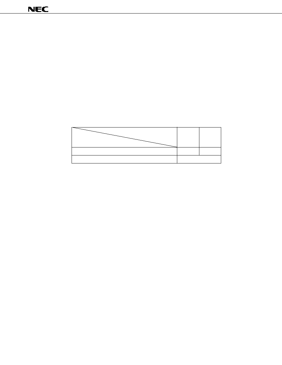
(4) Explanation of number of machine cycles column
S denotes the number of machine cycles required by skip operation when a skip instruction is executed.
The value of S varies as follows.
∑
When no skip is made: S = 0
∑
When the skipped instruction is a 1- or 2-byte instruction: S = 1
∑
When the skipped instruction is a 3-byte instruction
Note
: S = 2
Note 3-byte instruction: BR !addr, BRA !addr1, CALL !addr or CALLA !addr1 instruction
Caution The GETI instruction is skipped in one machine cycle.
One machine cycle is equal to one cycle (= t
CY
) of CPU clock
; time can be selected from among four
types by setting PCC.
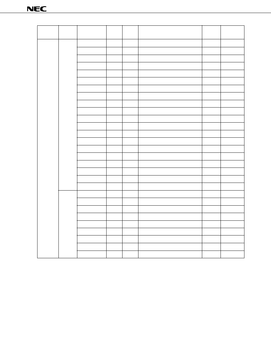
45
µ
PD750064, 750066, 750068, 750064(A), 750066(A), 750068(A)
Data Sheet U10165EJ2V0DS00
Instruction
Number
Number
Addressing
Mnemonic
Operand
of Machine
Operation
Skip Condition
Group
of Bytes
Cycles
Area
Transfer
MOV
A, #n4
1
1
A
n4
String effect A
reg1, #n4
2
2
reg1
n4
XA, #n8
2
2
XA
n8
String effect A
HL, #n8
2
2
HL
n8
String effect B
rp2, #n8
2
2
rp2
n8
A, @HL
1
1
A
(HL)
*1
A, @HL+
1
2+S
A
(HL), then L
L+1
*1
L = 0
A, @HL≠
1
2+S
A
(HL), then L
L≠1
*1
L = FH
A, @rpa1
1
1
A
(rpa1)
*2
XA, @HL
2
2
XA
(HL)
*1
@HL, A
1
1
(HL)
A
*1
@HL, XA
2
2
(HL)
XA
*1
A, mem
2
2
A
(mem)
*3
XA, mem
2
2
XA
(mem)
*3
mem, A
2
2
(mem)
A
*3
mem, XA
2
2
(mem)
XA
*3
A, reg
2
2
A
reg
XA, rp'
2
2
XA
rp'
reg1, A
2
2
reg1
A
rp'1, XA
2
2
rp'1
XA
XCH
A, @HL
1
1
A
(HL)
*1
A, @HL+
1
2+S
A
(HL), then L
L+1
*1
L = 0
A, @HL≠
1
2+S
A
(HL), then L
L≠1
*1
L = FH
A, @rpa1
1
1
A
(rpa1)
*2
XA, @HL
2
2
XA
(HL)
*1
A, mem
2
2
A
(mem)
*3
XA, mem
2
2
XA
(mem)
*3
A, reg1
1
1
A
reg1
XA, rp'
2
2
XA
rp'

µ
PD750064, 750066, 750068, 750064(A), 750066(A), 750068(A)
46
Data Sheet U10165EJ2V0DS00
Instruction
Number
Number
Addressing
Mnemonic
Operand
of Machine
Operation
Skip Condition
Group
of Bytes
Cycles
Area
Table
MOVT
XA, @PCDE
1
3
µ
PD750064
reference
XA
(PC
11≠8
+DE)
ROM
µ
PD750066, 750068
XA
(PC
12≠8
+DE)
ROM
XA, @PCXA
1
3
µ
PD750064
XA
(PC
11≠8
+XA)
ROM
µ
PD750066, 750068
XA
(PC
12≠8
+XA)
ROM
XA, @BCDE
1
3
XA
(BCDE)
ROM
Note
*6
XA, @BCXA
1
3
XA
(BCXA)
ROM
Note
*6
Bit transfer
MOV1
CY, fmem.bit
2
2
CY
(fmem.bit)
*4
CY, pmem.@L
2
2
CY
(pmem
7≠2
+L
3≠2
.bit(L
1≠0
))
*5
CY, @H+mem.bit
2
2
CY
(H+mem
3≠0
.bit)
*1
fmem.bit, CY
2
2
(fmem.bit)
CY
*4
pmem.@L, CY
2
2
(pmem
7≠2
+L
3≠2
.bit(L
1≠0
))
CY
*5
@H+mem.bit, CY
2
2
(H+mem
3≠0
.bit)
CY
*1
Operation
ADDS
A, #n4
1
1+S
A
A+n4
carry
XA, #n8
2
2+S
XA
XA+n8
carry
A, @HL
1
1+S
A
A+(HL)
*1
carry
XA, rp'
2
2+S
XA
XA+rp'
carry
rp'1, XA
2
2+S
rp'1
rp'1+XA
carry
ADDC
A, @HL
1
1
A, CY
A+(HL)+CY
*1
XA, rp'
2
2
XA, CY
XA+rp'+CY
rp'1, XA
2
2
rp'1, CY
rp'1+XA+CY
SUBS
A, @HL
1
1+S
A
A≠(HL)
*1
borrow
XA, rp'
2
2+S
XA
XA≠rp'
borrow
rp'1, XA
2
2+S
rp'1
rp'1≠XA
borrow
SUBC
A, @HL
1
1
A, CY
A≠(HL)≠CY
*1
XA, rp'
2
2
XA, CY
XA≠rp'≠CY
rp'1, XA
2
2
rp'1, CY
rp'1≠XA≠CY
Note
Set "0" to register B if the
µ
PD750064 is used. Only low-order one bit of register B will be valid if the
µ
PD750066, 750068 is used.
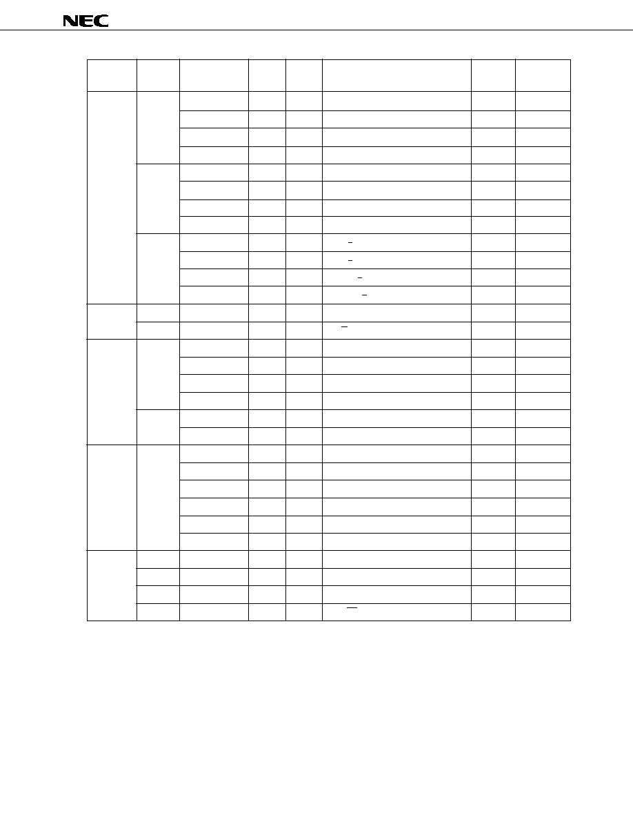
47
µ
PD750064, 750066, 750068, 750064(A), 750066(A), 750068(A)
Data Sheet U10165EJ2V0DS00
Instruction
Number
Number
Addressing
Mnemonic
Operand
of Machine
Operation
Skip Condition
Group
of Bytes
Cycles
Area
Operation
AND
A, #n4
2
2
A
A
n4
A, @HL
1
1
A
A
(HL)
*1
XA, rp'
2
2
XA
XA
rp'
rp'1, XA
2
2
rp'1
rp'1
XA
OR
A, #n4
2
2
A
A
n4
A, @HL
1
1
A
A
(HL)
*1
XA, rp'
2
2
XA
XA
rp'
rp'1, XA
2
2
rp'1
rp'1
XA
XOR
A, #n4
2
2
A
A v n4
A, @HL
1
1
A
A v (HL)
*1
XA, rp'
2
2
XA
XA v rp'
rp'1, XA
2
2
rp'1
rp'1 v XA
Accumulator
RORC
A
1
1
CY
A
0
, A
3
CY, A
n≠1
A
n
manipulation
NOT
A
2
2
A
A
Increment
INCS
reg
1
1+S
reg
reg+1
reg = 0
and
Decrement
rp1
1
1+S
rp1
rp1+1
rp1 = 00H
@HL
2
2+S
(HL)
(HL)+1
*1
(HL) = 0
mem
2
2+S
(mem)
(mem)+1
*3
(mem) = 0
DECS
reg
1
1+S
reg
reg≠1
reg = FH
rp'
2
2+S
rp'
rp'≠1
rp' = FFH
Comparison
SKE
reg, #n4
2
2+S
Skip if reg = n4
reg = n4
@HL, #n4
2
2+S
Skip if (HL) = n4
*1
(HL) = n4
A, @HL
1
1+S
Skip if A = (HL)
*1
A = (HL)
XA, @HL
2
2+S
Skip if XA = (HL)
*1
XA = (HL)
A, reg
2
2+S
Skip if A = reg
A = reg
XA, rp'
2
2+S
Skip if XA = rp'
XA = rp'
Carry flag
SET1
CY
1
1
CY
1
manipulation
CLR1
CY
1
1
CY
0
SKT
CY
1
1+S
Skip if CY = 1
CY = 1
NOT1
CY
1
1
CY
CY
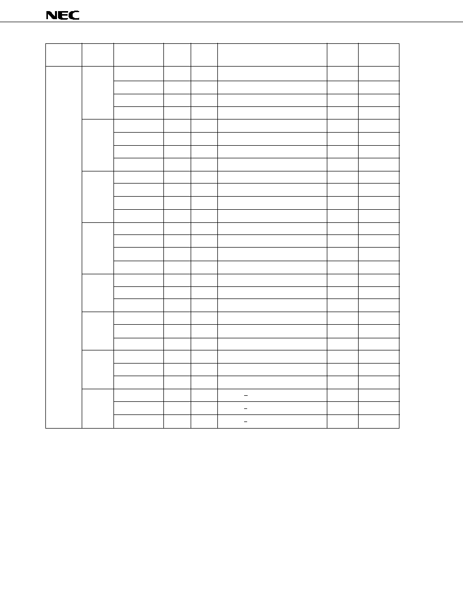
µ
PD750064, 750066, 750068, 750064(A), 750066(A), 750068(A)
48
Data Sheet U10165EJ2V0DS00
Instruction
Number
Number
Addressing
Mnemonic
Operand
of Machine
Operation
Skip Condition
Group
of Bytes
Cycles
Area
Memory bit
SET1
mem.bit
2
2
(mem.bit)
1
*3
manipulation
fmem.bit
2
2
(fmem.bit)
1
*4
pmem.@L
2
2
(pmem
7≠2
+L
3≠2
.bit(L
1≠0
))
1
*5
@H+mem.bit
2
2
(H+mem
3≠0
.bit)
1
*1
CLR1
mem.bit
2
2
(mem.bit)
0
*3
fmem.bit
2
2
(fmem.bit)
0
*4
pmem.@L
2
2
(pmem
7≠2
+L
3≠2
.bit(L
1≠0
))
0
*5
@H+mem.bit
2
2
(H+mem
3≠0
.bit)
0
*1
SKT
mem.bit
2
2+S
Skip if (mem.bit)=1
*3
(mem.bit)=1
fmem.bit
2
2+S
Skip if (fmem.bit)=1
*4
(fmem.bit)=1
pmem.@L
2
2+S
Skip if (pmem
7≠2
+L
3≠2
.bit(L
1≠0
))=1
*5
(pmem.@L)=1
@H+mem.bit
2
2+S
Skip if (H+mem
3≠0
.bit)=1
*1
(@H+mem.bit)=1
SKF
mem.bit
2
2+S
Skip if (mem.bit)=0
*3
(mem.bit)=0
fmem.bit
2
2+S
Skip if (fmem.bit)=0
*4
(fmem.bit)=0
pmem.@L
2
2+S
Skip if (pmem
7≠2
+L
3≠2
.bit(L
1≠0
))=0
*5
(pmem.@L)=0
@H+mem.bit
2
2+S
Skip if (H+mem
3≠0
.bit)=0
*1
(@H+mem.bit)=0
SKTCLR
fmem.bit
2
2+S
Skip if (fmem.bit)=1 and clear
*4
(fmem.bit)=1
pmem.@L
2
2+S
Skip if (pmem
7≠2
+L
3≠2
.bit(L
1≠0
))=1 and clear
*5
(pmem.@L)=1
@H+mem.bit
2
2+S
Skip if (H+mem
3≠0
.bit)=1 and clear
*1
(@H+mem.bit)=1
AND1
CY, fmem.bit
2
2
CY
CY
(fmem.bit)
*4
CY, pmem.@L
2
2
CY
CY
(pmem
7≠2
+L
3≠2
.bit(L
1≠0
))
*5
CY, @H+mem.bit
2
2
CY
CY
(H+mem
3≠0
.bit)
*1
OR1
CY, fmem.bit
2
2
CY
CY
(fmem.bit)
*4
CY, pmem.@L
2
2
CY
CY
(pmem
7≠2
+L
3≠2
.bit(L
1≠0
))
*5
CY, @H+mem.bit
2
2
CY
CY
(H+mem
3≠0
.bit)
*1
XOR1
CY, fmem.bit
2
2
CY
CY v (fmem.bit)
*4
CY, pmem.@L
2
2
CY
CY v (pmem
7≠2
+L
3≠2
.bit(L
1≠0
))
*5
CY, @H+mem.bit
2
2
CY
CY v (H+mem
3≠0
.bit)
*1
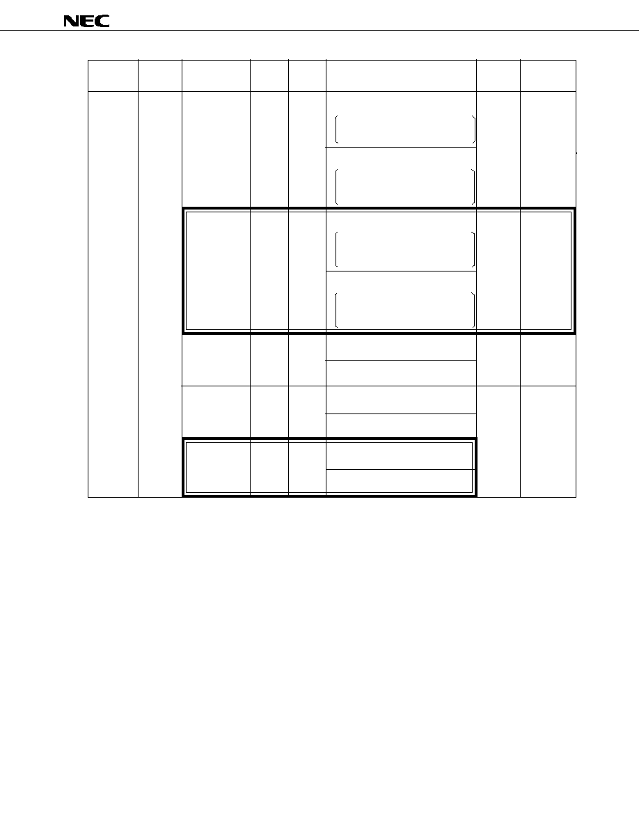
49
µ
PD750064, 750066, 750068, 750064(A), 750066(A), 750068(A)
Data Sheet U10165EJ2V0DS00
Instruction
Number
Number
Addressing
Mnemonic
Operand
of Machine
Operation
Skip Condition
Group
of Bytes
Cycles
Area
Branch
BR
Note
addr
≠
≠
µ
PD750064
*6
PC
11≠0
addr
Select appropriate instruction from among
BR !addr, BRCB !caddr and BR $addr
according to the assembler being used.
µ
PD750066, 750068
PC
12≠0
addr
Select appropriate instruction from
among BR !addr, BRCB !caddr and BR
$addr according to the assembler
being used.
addr1
≠
≠
µ
PD750064
*11
PC
11-0
addr1
Select appropriate instruction from
among BR !addr, BRA !addr1, BRCB
!caddr and BR $addr1 according to the
assembler being used.
µ
PD750066, 750068
PC
12≠0
addr1
Select appropriate instruction from
among BR !addr, BRA !addr1, BRCB
!caddr and BR $addr1 according to the
assembler being used.
! addr
3
3
µ
PD750064
*6
PC
11≠0
addr
µ
PD750066, 750068
PC
12≠0
addr
$addr
1
2
µ
PD750064
*7
PC
11≠0
addr
µ
PD750066, 750068
PC
12≠0
addr
$addr1
1
2
µ
PD750064
PC
11≠0
addr1
µ
PD750066, 750068
PC
12≠0
addr1
Note
The operations indicated with thick lines can be performed only in the Mk II mode. The other operations
can be performed only in the Mk I mode.
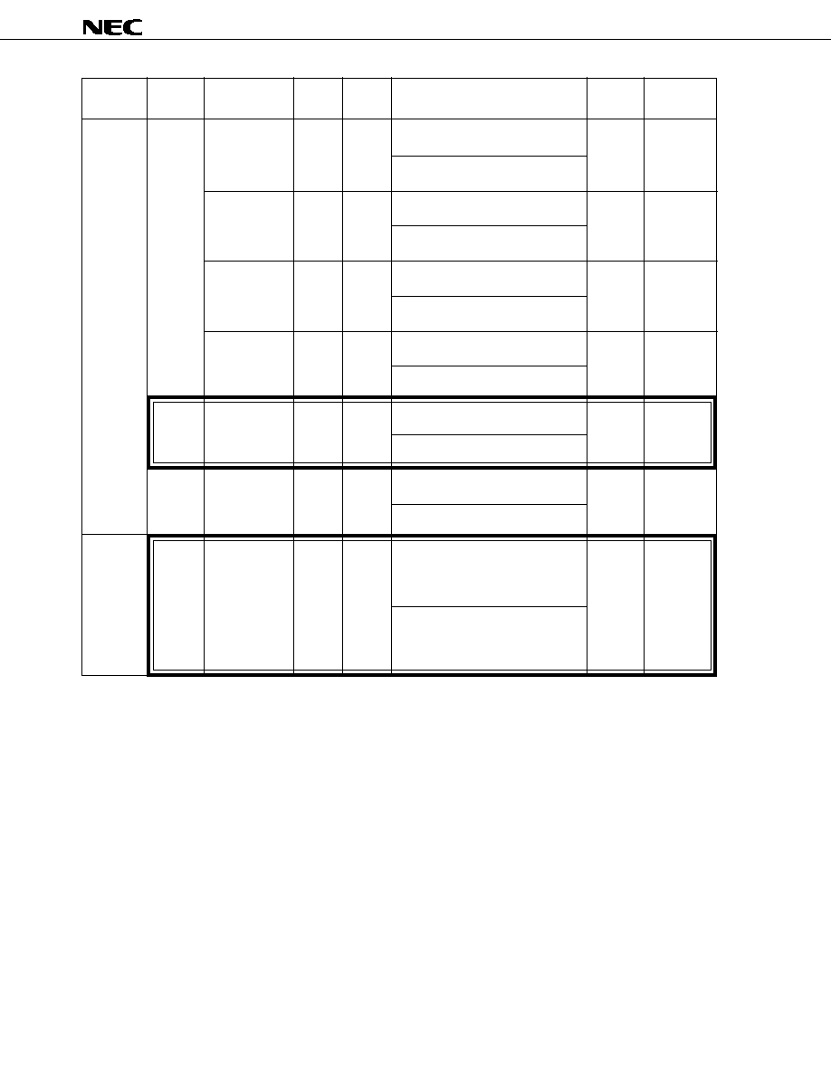
µ
PD750064, 750066, 750068, 750064(A), 750066(A), 750068(A)
50
Data Sheet U10165EJ2V0DS00
Instruction
Number
Number
Addressing
Mnemonic
Operand
of Machine
Operation
Skip Condition
Group
of Bytes
Cycles
Area
Branch
BR
PCDE
2
3
µ
PD750064
PC
11≠0
PC
11-8
+DE
µ
PD750066, 750068
PC
12≠0
PC
12-8
+DE
PCXA
2
3
µ
PD750064
PC
11≠0
PC
11-8
+XA
µ
PD750066, 750068
PC
12≠0
PC
12-8
+XA
BCDE
2
3
µ
PD750064
*6
PC
11≠0
BCDE
Note 1
µ
PD750066, 750068
PC
12≠0
BCDE
Note 2
BCXA
2
3
µ
PD750064
*6
PC
11≠0
BCXA
Note 1
µ
PD750066, 750068
PC
12≠0
BCXA
Note 2
BRA
Note 3
3
3
µ
PD750064
*11
PC
11≠0
addr1
µ
PD750066, 750068
PC
12≠0
addr1
BRCB
!caddr
2
2
µ
PD750064
*8
PC
11≠0
caddr
11≠0
µ
PD750066, 750068
PC
12≠0
PC
12
+caddr
11≠0
Subroutine
CALLA
Note 3
!addr1
3
3
µ
PD750064
*11
stack control
(SP≠2)
◊
,
◊
, MBE, RBE
(SP≠6) (SP≠3) (SP≠4)
PC
11≠0
(SP≠5)
0, 0, 0, 0
PC
11≠0
addr1, SP
SP≠6
µ
PD750066, 750068
(SP≠2)
◊
,
◊
, MBE, RBE
(SP≠6) (SP≠3) (SP≠4)
PC
11≠0
(SP≠5)
0, 0, 0, PC
12
PC
12≠0
addr1, SP
SP≠6
Notes 1.
"0" must be set to B register.
2.
Only low-order one bit is valid in B register.
3.
The operations indicated with thick lines can be performed only in the Mk II mode. The other operations
can be performed only in the Mk I mode.
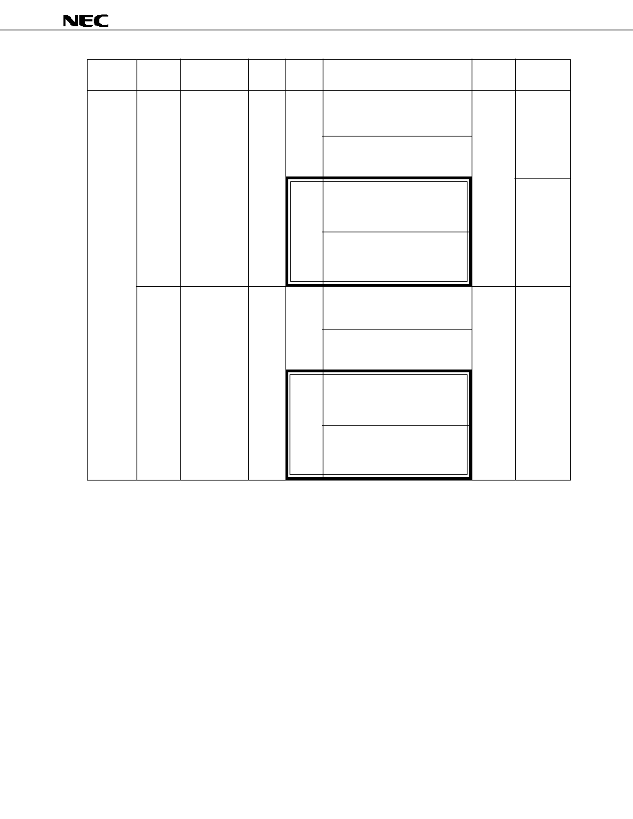
51
µ
PD750064, 750066, 750068, 750064(A), 750066(A), 750068(A)
Data Sheet U10165EJ2V0DS00
Instruction
Number
Number
Addressing
Mnemonic
Operand
of Machine
Operation
Skip Condition
Group
of Bytes
Cycles
Area
Subroutine
CALL
Note
!addr
3
3
µ
PD750064
*6
stack control
(SP≠3)
MBE, RBE, 0, 0
(SP≠4) (SP≠1) (SP≠2)
PC
11≠0
PC
11≠0
addr, SP
SP≠4
µ
PD750066, 750068
(SP≠3)
MBE, RBE, 0, PC
12
(SP≠4) (SP≠1) (SP≠2)
PC
11≠0
PC
12≠0
addr, SP
SP≠4
4
µ
PD750064
(SP≠2)
◊
,
◊
, MBE, RBE
(SP≠6) (SP≠3) (SP≠4)
PC
11≠0
(SP≠5)
0, 0, 0, 0
PC
11≠0
addr, SP
SP≠6
µ
PD750066, 750068
(SP≠2)
◊
,
◊
, MBE, RBE
(SP≠6) (SP≠3) (SP≠4)
PC
11≠0
(SP≠5)
0, 0, 0, PC
12
PC
12≠0
addr, SP
SP≠6
CALLF
Note
!faddr
2
2
µ
PD750064
*9
(SP≠3)
MBE, RBE, 0, 0
(SP≠4) (SP≠1) (SP≠2)
PC
11≠0
PC
11≠0
0+faddr, SP
SP≠4
µ
PD750066, 750068
(SP≠3)
MBE, RBE, 0, PC
12
(SP≠4) (SP≠1) (SP≠2)
PC
11≠0
PC
12≠0
00+faddr, SP
SP≠4
3
µ
PD750064
(SP≠2)
◊
,
◊
, MBE, RBE
(SP≠6) (SP≠3) (SP≠4)
PC
11≠0
(SP≠5)
0, 0, 0, 0
PC
11≠0
0+faddr, SP
SP≠6
µ
PD750066, 750068
(SP≠2)
◊
,
◊
, MBE, RBE
(SP≠6) (SP≠3) (SP≠4)
PC
11≠0
(SP≠5)
0, 0, 0, PC
12
PC
12≠0
00+faddr, SP
SP≠6
Note
The operations indicated with thick lines can be performed only in the Mk II mode. The other operations
can be performed only in the Mk I mode.
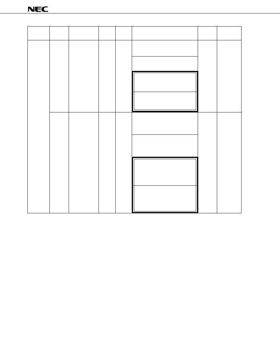
µ
PD750064, 750066, 750068, 750064(A), 750066(A), 750068(A)
52
Data Sheet U10165EJ2V0DS00
Instruction
Number
Number
Addressing
Mnemonic
Operand
of Machine
Operation
Skip Condition
Group
of Bytes
Cycles
Area
Subroutine
RET
Note
1
3
µ
PD750064
stack control
PC
11≠0
(SP) (SP+3) (SP+2)
MBE, RBE, 0, 0
(SP+1), SP
SP+4
µ
PD750066, 750068
PC
11≠0
(SP) (SP+3) (SP+2)
MBE, RBE, 0, PC
12
(SP+1), SP
SP+4
µ
PD750064
◊
,
◊
, MBE, RBE
(SP+4)
0, 0, 0, 0,
(SP+1)
PC
11≠0
(SP) (SP+3) (SP+2), SP
SP+6
µ
PD750066, 750068
◊
,
◊
, MBE, RBE
(SP+4)
MBE, 0, 0, PC
12
(SP+1)
PC
11≠0
(SP) (SP+3) (SP+2), SP
SP+6
RETS
Note
1
3+S
µ
PD750064
Unconditional
MBE, RBE, 0, 0
(SP+1)
PC
11≠0
(SP) (SP+3) (SP+2)
SP
SP+4
then skip unconditionally
µ
PD750066, 750068
MBE, RBE, 0, PC
12
(SP+1)
PC
11≠0
(SP) (SP+3) (SP+2)
SP
SP+4
then skip unconditionally
µ
PD750064
0, 0, 0, 0
(SP+1)
PC
11≠0
(SP) (SP+3) (SP+2)
◊
,
◊
, MBE, RBE
(SP+4)
SP
SP+6
then skip unconditionally
µ
PD750066, 750068
0, 0, 0, PC
12
(SP+1)
PC
11≠0
(SP) (SP+3) (SP+2)
◊
,
◊
, MBE, RBE
(SP+4)
SP
SP+4
then skip unconditionally
Note
The operations indicated with thick lines can be performed only in the Mk II mode. The other operations
can be performed only in the Mk I mode.
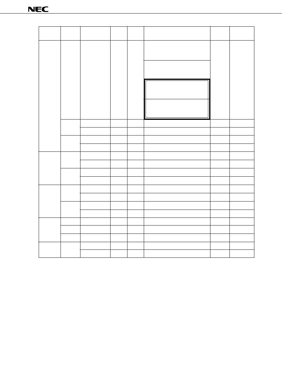
53
µ
PD750064, 750066, 750068, 750064(A), 750066(A), 750068(A)
Data Sheet U10165EJ2V0DS00
Instruction
Number
Number
Addressing
Mnemonic
Operand
of Machine
Operation
Skip Condition
Group
of Bytes
Cycles
Area
Subroutine
RETI
Note 1
1
3
µ
PD750064
stack control
MBE, RBE, 0, 0
(SP+1)
PC
11≠0
(SP) (SP+3) (SP+2)
PSW
(SP+4) (SP+5), SP
SP+6
µ
PD750066, 750068
MBE, RBE, 0, PC
12
(SP+1)
PC
11≠0
(SP) (SP+3) (SP+2)
PSW
(SP+4) (SP+5), SP
SP+6
µ
PD750064
0, 0, 0, 0
(SP+1)
PC
11≠0
(SP) (SP+3) (SP+2)
PSW
(SP+4) (SP+5), SP
SP+6
µ
PD750066, 750068
0, 0, 0, PC
12
(SP+1)
PC
11≠0
(SP) (SP+3) (SP+2)
PSW
(SP+4) (SP+5), SP
SP+6
PUSH
rp
1
1
(SP≠1)(SP≠2)
rp, SP
SP≠2
BS
2
2
(SP≠1)
MBS, (SP≠2)
RBS, SP
SP≠2
POP
rp
1
1
rp
(SP+1) (SP), SP
SP+2
BS
2
2
MBS
(SP+1), RBS
(SP), SP
SP+2
Interrupt
EI
2
2
IME (IPS.3)
1
control
IE
◊◊◊
2
2
IE
◊◊◊
1
DI
2
2
IME (IPS.3)
0
IE
◊◊◊
2
2
IE
◊◊◊
0
Input/output
IN
Note 2
A, PORTn
2
2
A
PORTn
(n = 0-6, 11)
XA, PORTn
2
2
XA
PORTn+1, PORTn
(n = 4)
OUT
Note 2
PORTn, A
2
2
PORTn
A
(n = 2-6)
PORTn, XA
2
2
PORTn+1, PORTn
XA
(n = 4)
CPU control
HALT
2
2
Set HALT Mode (PCC.2
1)
STOP
2
2
Set STOP Mode (PCC.3
1)
NOP
1
1
No Operation
Special
SEL
RBn
2
2
RBS
n
(n = 0-3)
MBn
2
2
MBS
n
(n = 0, 1, 15)
Notes 1.
The operations indicated with thick lines can be performed only in the Mk II mode. The other operations
can be performed only in the Mk I mode.
2.
While the IN instruction and OUT instruction are being executed, the MBE must be set to 0 or 1, and
MBS must be set to 15.
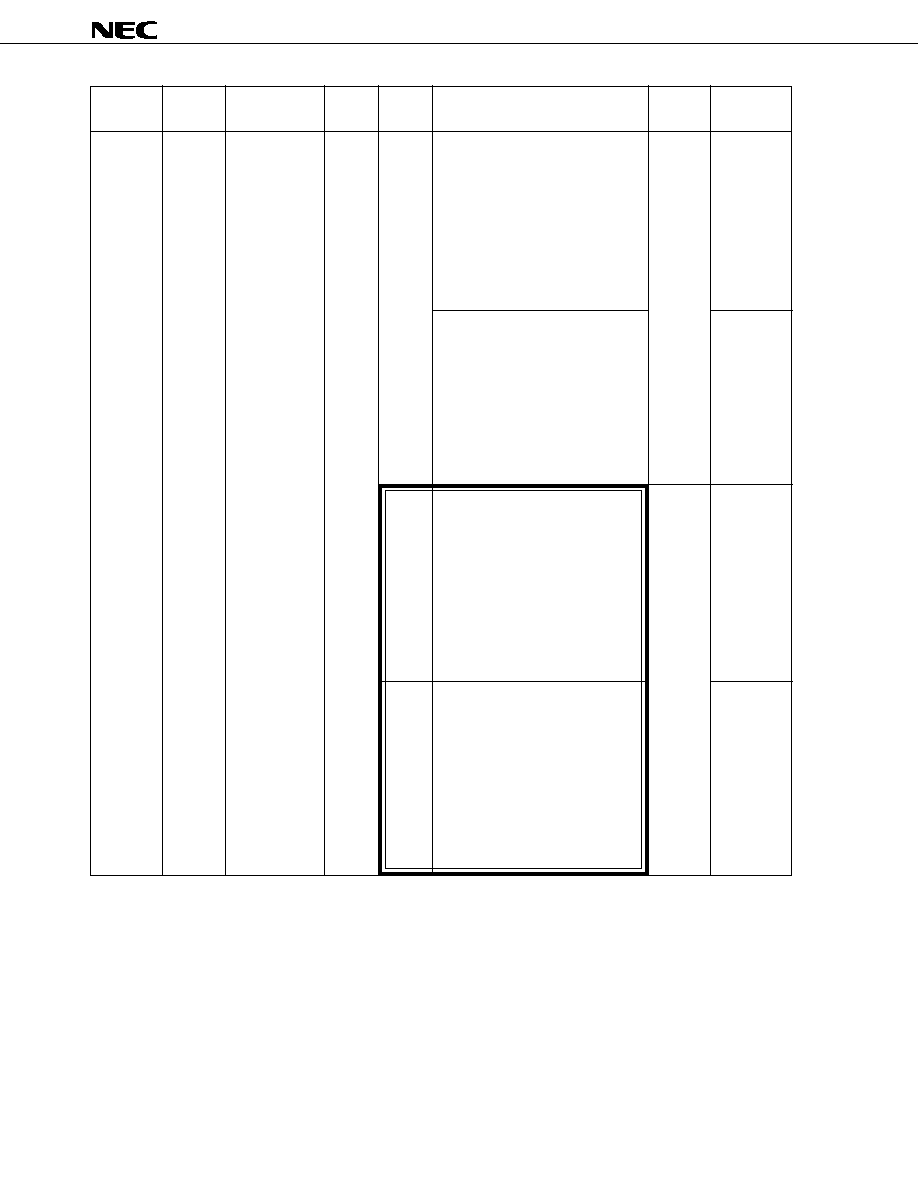
µ
PD750064, 750066, 750068, 750064(A), 750066(A), 750068(A)
54
Data Sheet U10165EJ2V0DS00
Instruction
Number
Number
Addressing
Mnemonic
Operand
of Machine
Operation
Skip Condition
Group
of Bytes
Cycles
Area
Special
GETI
Notes 1, 2
taddr
1
3
µ
PD750064
*10
∑ When TBR instruction
PC
11≠0
(taddr)
3≠0
+ (taddr+1)
∑ When TCALL instruction
(SP≠4) (SP≠1) (SP≠2)
PC
11≠0
(SP≠3)
MBE, RBE, 0, 0
PC
11≠0
(taddr)
3≠0
+ (taddr+1)
SP
SP≠4
∑ When instruction other than TBR and
Depending on
TCALL instructions
the reference
(taddr) (taddr+1) instruction is executed.
instruction
µ
PD750066, 750068
∑ When TBR instruction
PC
12≠0
(taddr)
4≠0
+ (taddr+1)
∑ When TCALL instruction
(SP≠4) (SP≠1) (SP≠2)
PC
11≠0
(SP≠3)
MBE, RBE, 0, PC
12
PC
12≠0
(taddr)
4≠0
+ (taddr+1)
SP
SP≠4
∑ When instruction other than TBR and
Depending on
TCALL instructions
the reference
(taddr) (taddr+1) instruction is executed.
instruction
3
µ
PD750064
*10
∑ When TBR instruction
PC
11≠0
(taddr)
3≠0
+ (taddr+1)
4
∑ When TCALL instruction
(SP≠6) (SP≠3) (SP≠4)
PC
11≠0
(SP≠5)
0, 0, 0, 0
(SP≠2)
◊
,
◊
, MBE, RBE
PC
11≠0
(taddr)
3≠0
+ (taddr+1)
SP
SP≠6
3
∑ When instruction other than TBR and
Depending on
TCALL instructions
the reference
(taddr) (taddr+1) instruction is executed.
instruction
3
µ
PD750066, 750068
∑ When TBR instruction
PC
12≠0
(taddr)
4≠0
+ (taddr+1)
4
∑ When TCALL instruction
(SP≠6) (SP≠3) (SP≠4)
PC
11≠0
(SP≠5)
0, 0, 0, PC
12
(SP≠2)
◊
,
◊
, MBE, RBE
PC
12≠0
(taddr)
4≠0
+ (taddr+1)
SP
SP≠6
3
∑ When instruction other than TBR and
Depending on
TCALL instructions
the reference
(taddr) (taddr+1) instruction is executed.
instruction
Notes 1.
The TBR and TCALL instructions are the table definition assembler pseudo instructions of the GETI
instruction.
2.
The operations indicated with thick lines can be performed only in the Mk II mode. The other operations
can be performed only in the Mk I mode.
≠ ≠ ≠ ≠ ≠ ≠ ≠ ≠ ≠ ≠ ≠ ≠ ≠ ≠ ≠ ≠ ≠ ≠ ≠ ≠ ≠ ≠ ≠ ≠ ≠ ≠ ≠ ≠ ≠ ≠ ≠ ≠ ≠ ≠
≠ ≠ ≠ ≠ ≠ ≠ ≠ ≠ ≠ ≠ ≠ ≠ ≠
≠ ≠ ≠ ≠ ≠ ≠ ≠ ≠ ≠ ≠ ≠ ≠ ≠ ≠ ≠ ≠ ≠ ≠ ≠ ≠ ≠ ≠ ≠ ≠ ≠ ≠ ≠ ≠ ≠ ≠ ≠ ≠ ≠ ≠
≠ ≠ ≠ ≠ ≠ ≠ ≠ ≠ ≠ ≠ ≠ ≠ ≠
≠ ≠ ≠ ≠ ≠ ≠ ≠ ≠ ≠ ≠ ≠ ≠ ≠ ≠ ≠ ≠ ≠ ≠ ≠ ≠ ≠ ≠ ≠ ≠ ≠ ≠ ≠ ≠ ≠ ≠ ≠ ≠ ≠ ≠
≠ ≠ ≠ ≠ ≠ ≠ ≠ ≠ ≠ ≠ ≠ ≠ ≠
≠ ≠ ≠ ≠ ≠ ≠ ≠ ≠ ≠ ≠ ≠ ≠ ≠ ≠ ≠ ≠ ≠ ≠ ≠ ≠ ≠ ≠ ≠ ≠ ≠ ≠ ≠ ≠ ≠ ≠ ≠ ≠ ≠ ≠
≠ ≠ ≠ ≠ ≠ ≠ ≠ ≠ ≠ ≠ ≠ ≠ ≠
≠ ≠ ≠ ≠ ≠ ≠ ≠ ≠ ≠ ≠ ≠ ≠ ≠
≠ ≠ ≠ ≠ ≠ ≠ ≠ ≠ ≠ ≠ ≠ ≠ ≠
≠ ≠ ≠ ≠ ≠ ≠ ≠ ≠ ≠ ≠ ≠ ≠ ≠ ≠ ≠ ≠ ≠ ≠ ≠ ≠ ≠ ≠ ≠ ≠ ≠ ≠ ≠ ≠ ≠ ≠ ≠ ≠ ≠ ≠ ≠ ≠ ≠ ≠ ≠ ≠ ≠
≠ ≠ ≠ ≠ ≠ ≠ ≠ ≠ ≠ ≠ ≠ ≠ ≠ ≠ ≠ ≠ ≠ ≠ ≠ ≠ ≠ ≠ ≠ ≠ ≠ ≠ ≠ ≠ ≠ ≠ ≠ ≠ ≠ ≠ ≠ ≠ ≠ ≠ ≠ ≠ ≠
≠ ≠ ≠ ≠ ≠ ≠ ≠ ≠ ≠ ≠ ≠ ≠ ≠
≠ ≠ ≠ ≠ ≠ ≠ ≠ ≠ ≠ ≠ ≠ ≠ ≠ ≠ ≠ ≠ ≠ ≠ ≠ ≠ ≠ ≠ ≠ ≠ ≠ ≠ ≠ ≠ ≠ ≠ ≠ ≠ ≠ ≠ ≠ ≠ ≠ ≠ ≠ ≠ ≠
≠ ≠ ≠ ≠ ≠ ≠ ≠ ≠ ≠ ≠ ≠ ≠ ≠
≠ ≠ ≠ ≠ ≠ ≠ ≠ ≠ ≠ ≠ ≠ ≠ ≠ ≠ ≠ ≠ ≠ ≠ ≠ ≠ ≠ ≠ ≠ ≠ ≠ ≠ ≠ ≠ ≠ ≠ ≠ ≠ ≠ ≠ ≠ ≠ ≠ ≠ ≠ ≠ ≠
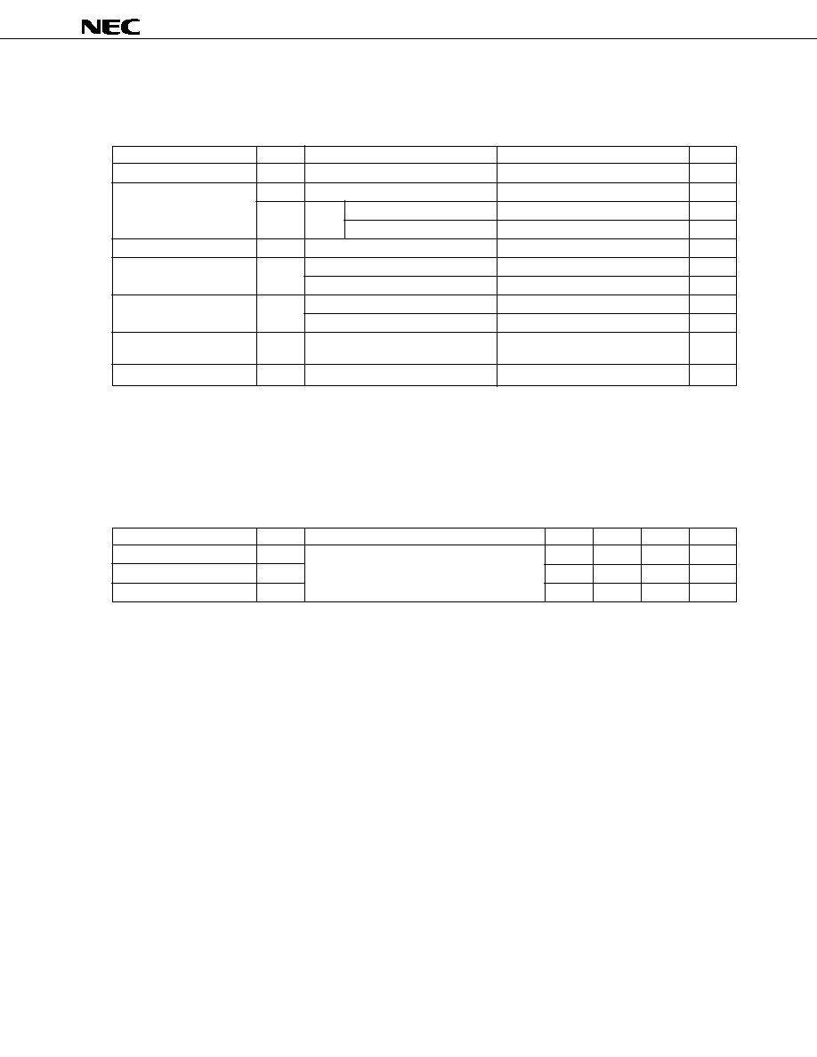
55
µ
PD750064, 750066, 750068, 750064(A), 750066(A), 750068(A)
Data Sheet U10165EJ2V0DS00
Ports
4, 5
12. ELECTRICAL SPECIFICATIONS
Absolute Maximum Ratings (T
A
= 25∞C)
Parameter
Symbol
Conditions
Ratings
Unit
Supply voltage
V
DD
≠0.3 to +7.0
V
Input voltage
V
I1
Other than ports 4, 5
≠0.3 to V
DD
+ 0.3
V
V
I2
Pull-up resistor provided
≠0.3 to V
DD
+ 0.3
V
N-ch open drain
≠0.3 to +14
V
Output voltage
V
O
≠0.3 to V
DD
+ 0.3
V
Output current, high
I
OH
Per pin
≠10
mA
Total of all pins
≠30
mA
Output current, low
I
OL
Per pin
30
mA
Total of all pins
220
mA
Operating ambient
T
A
≠40 to +85
∞C
temperature
Storage temperature
T
stg
≠65 to +150
∞C
Caution Product quality may suffer if the absolute maximum rating is exceeded even momentarily for
any parameter. That is, the absolute maximum ratings are rated values at which the product
is on the verge of suffering physical damage, and therefore the product must be used under
conditions that ensure that the absolute maximum ratings are not exceeded.
Capacitance (T
A
= 25∞C, V
DD
= 0 V)
Parameter
Symbol
Conditions
MIN.
TYP.
MAX.
Unit
Input capacitance
C
IN
f = 1 MHz
15
pF
Output capacitance
C
OUT
Unmeasured pins returned to 0 V
15
pF
I/O capacitance
C
IO
15
pF
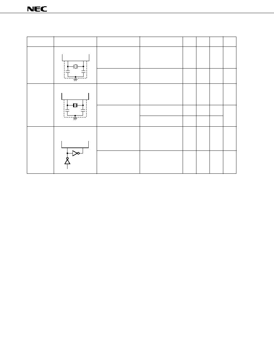
µ
PD750064, 750066, 750068, 750064(A), 750066(A), 750068(A)
56
Data Sheet U10165EJ2V0DS00
Main System Clock Oscillator Characteristics (T
A
= ≠40 to +85∞C, V
DD
= 1.8 to 5.5 V)
Resonator
Recommended
Parameter
Conditions
MIN.
TYP.
MAX.
Unit
Constants
Ceramic
Oscillation frequency
1.0
6.0
Note 2
MHz
resonator
(f
X
)
Note 1
Oscillation
After V
DD
reaches
4
ms
stabilization time
Note 3
oscillation voltage
range MIN. value
Crystal
Oscillation frequency
1.0
6.0
Note 2
MHz
resonator
(f
X
)
Note 1
Oscillation
V
DD
= 4.5 to 5.5 V
10
ms
stabilization time
Note 3
30
External
X1 input frequency
1.0
6.0
Note 2
MHz
clock
(f
X
)
Note 1
X1 input high-/
83.3
500
ns
low-level width
(t
XH
, t
XL
)
Notes 1.
The oscillation frequency and X1 input frequency shown above indicate only oscillator characteristics.
Refer to AC Characteristics for instruction execution time.
2.
If the oscillation frequency is 4.19 MHz < f
X
6.0 MHz at 1.8 V
V
DD
< 2.7 V, do not select the processor
clock control register (PCC) = 0011. If PCC = 0011, one machine cycle time is less than 0.95
µ
s, falling
short of the rated value of 0.95
µ
s.
3.
The oscillation stabilization time is the time required to stabilize oscillation after V
DD
has been applied
or STOP mode has been released.
Caution When using the main system clock oscillator, wire as follows in the area enclosed by the broken
lines in the above figures to avoid an adverse effect from wiring capacitance.
∑
Keep the wiring length as short as possible.
∑
Do not cross the wiring with the other signal lines.
∑
Do not route the wiring near a signal line through which a high fluctuating current flows.
∑
Always make the ground point of the oscillator capacitor the same potential as V
SS
.
∑
Do not ground the capacitor to a ground pattern through which a high current flows.
∑
Do not fetch signals from the oscillator.
X1
X2
X1
X2
C1
C2
X1
X2
C1
C2
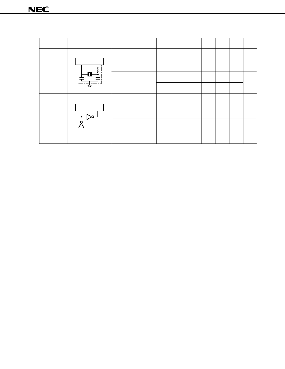
57
µ
PD750064, 750066, 750068, 750064(A), 750066(A), 750068(A)
Data Sheet U10165EJ2V0DS00
XT1
XT2
Subsystem Clock Oscillator Characteristics (T
A
= ≠40 to +85∞C, V
DD
= 1.8 to 5.5 V)
Resonator
Recommended
Parameter
Conditions
MIN.
TYP.
MAX.
Unit
Constants
Crystal
Oscillation frequency
32
32.768
35
kHz
resonator
(f
XT
)
Note 1
Oscillation
V
DD
= 4.5 to 5.5 V
1.0
2
s
stabilization time
Note 2
10
External
XT1 input frequency
32
100
kHz
clock
(f
XT
)
Note 1
XT1 input high-/
5
15
µ
s
low-level width
(t
XTH
, t
XTL
)
Notes 1.
The oscillation frequency and XT1 input frequency shown above indicate only oscillator characteristics.
Refer to AC Characteristics for instruction execution time.
2.
The oscillation stabilization time is the time required to stabilize oscillation after V
DD
has been applied.
Caution When using the subsystem clock oscillator, wire as follows in the area enclosed by the broken
lines in the above figure to avoid an adverse effect from wiring capacitance.
∑
Keep the wiring length as short as possible.
∑
Do not cross the wiring with the other signal lines.
∑
Do not route the wiring near a signal line through which a high fluctuating current flows.
∑
Always make the ground point of the oscillator capacitor the same potential as V
SS
.
∑
Do not ground the capacitor to a ground pattern through which a high current flows.
∑
Do not fetch signals from the oscillator.
The subsystem clock oscillator is designed as a low-amplitude circuit for reducing current
consumption, and is more prone to malfunction due to noise than the main system clock
oscillator. Particular care is therefore required with the wiring method when the subsystem
clock is used.
XT1
XT2
C3
C4
R

µ
PD750064, 750066, 750068, 750064(A), 750066(A), 750068(A)
58
Data Sheet U10165EJ2V0DS00
Recommended Oscillator Constant
Ceramic resonator (T
A
= ≠40 to +85∞C)
Oscillator
Oscillation
Manufacturer
Part Number
Frequency
Constant (pF)
Voltage Range
Remarks
(MHz)
(V
DD
)
C1
C2
MIN.
MAX.
Murata Mfg.
CSB1000J
Note
1.0
100
100
2.0
5.5
Rd = 1 k
Co., Ltd.
CSA2.00MG040
2.0
100
100
2.3
≠
CST2.00MG040
≠
≠
Capacitor-contained model
CSA4.19MG
4.19
30
30
1.9
≠
CST4.19MGW
≠
≠
Capacitor-contained model
CSA4.19MGU
30
30
1.8
≠
CST4.19MGWU
≠
≠
Capacitor-contained model
CSA6.00MG
6.0
30
30
3.0
≠
CST6.00MGW
≠
≠
Capacitor-contained model
CSA6.00MGU
30
30
2.4
≠
CST6.00MGWU
≠
≠
Capacitor-contained model
Kyocera Corp.
KBR-1000F/Y
1.0
100
100
1.8
5.5
≠
KBR-2.0MS
2.0
68
68
1.95
KBR-4.19MSA
4.19
33
33
1.8
KBR-6.0MSA
6.0
33
33
TDK
CCR1000K2
1.0
100
100
1.8
5.5
≠
CCR2.0MC33
2.0
≠
≠
2.0
Capacitor-contained model
CCR4.19MC3
4.19
FCR4.19MC5
2.2
CCR6.0MC3
6.0
2.0
FCR6.0MC5
2.2
Note
When using the CSB1000J (1.0 MHz) by Murata Mfg. Co., Ltd. as a ceramic resonator, a limiting resistor
(Rd = 1 k
) is necessary (refer to the figure below). The limiting resistor is not necessary when using the
other recommended resonators.
Caution The oscillator constants and oscillation voltage range indicate conditions for stable oscillation
but do not guarantee precision of the oscillation frequency. If the application circuit requires
precision of the oscillation frequency, it is necessary to set the oscillation frequency of the
resonator in the application circuit. For this, it is necessary to directly contact the manufacturer
of the resonator being used.
X1
X2
C1
C2
Rd
CSB1000J
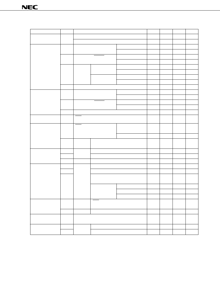
59
µ
PD750064, 750066, 750068, 750064(A), 750066(A), 750068(A)
Data Sheet U10165EJ2V0DS00
DC Characteristics (T
A
= ≠40 to +85∞C, V
DD
= 1.8 to 5.5 V)
Parameter
Symbol
Conditions
MIN.
TYP.
MAX.
Unit
Output current, low
I
OL
Per pin
15
mA
Total of all pins
150
mA
Input voltage, high
V
IH1
Ports 2, 3, 11
2.7 V
V
DD
5.5 V
0.7V
DD
V
DD
V
1.8 V
V
DD
< 2.7 V
0.9V
DD
V
DD
V
V
IH2
Ports 0, 1, 6, RESET
2.7 V
V
DD
5.5 V
0.8V
DD
V
DD
V
1.8 V
V
DD
< 2.7 V
0.9V
DD
V
DD
V
V
IH3
Ports 4, 5
Pull-up resistor
2.7 V
V
DD
5.5 V
0.7V
DD
V
DD
V
provided
1.8 V
V
DD
< 2.7 V
0.9V
DD
V
DD
V
N-ch open drain
2.7 V
V
DD
5.5 V
0.7V
DD
13
V
1.8 V
V
DD
< 2.7 V
0.9V
DD
13
V
V
IH4
X1, XT1
V
DD
≠0.1
V
DD
V
Input voltage, low
V
IL1
Ports 2, 3, 4, 5, 11
2.7 V
V
DD
5.5 V
0
0.3V
DD
V
1.8 V
V
DD
< 2.7 V
0
0.1V
DD
V
V
IL2
Ports 0, 1, 6, RESET
2.7 V
V
DD
5.5 V
0
0.2V
DD
V
1.8 V
V
DD
< 2.7 V
0
0.1V
DD
V
V
IL3
X1, XT1
0
0.1
V
Output voltage, high
V
OH
SCK, SO, ports 2, 3, 6 I
OH
= ≠1.0 mA
V
DD
≠0.5
V
Output voltage, low
V
OL1
SCK, SO, ports 2, 3, 4, 5, 6
I
OL
= 15 mA
0.2
2.0
V
V
DD
= 4.5 to 5.5 V
I
OL
= 1.6 mA
0.4
V
V
OL2
SB0, SB1
N-ch open drain
0.2V
DD
V
Pull-up resistor
1 k
Input leakage
I
LIH1
V
IN
= V
DD
Pins other than X1, XT1
3
µ
A
current, high
I
LIH2
X1, XT1
20
µ
A
I
LIH3
V
IN
= 13 V
Ports 4, 5 (N-ch open drain)
20
µ
A
Input leakage
I
LIL1
V
IN
= 0 V
Pins other than ports 4, 5, X1, XT1
≠3
µ
A
current, low
I
LIL2
X1, XT1
≠20
µ
A
I
LIL3
Ports 4, 5 (N-ch open drain)
≠3
µ
A
When input instruction is not executed
≠30
µ
A
V
DD
= 5.0 V
≠10
≠27
µ
A
V
DD
= 3.0 V
≠3
≠8
µ
A
Output leakage
I
LOH1
V
OUT
= V
DD
SCK, SO/SB0, SB1, ports 2, 3, 6,
3
µ
A
current, high
ports 4, 5 (Pull-up resistor provided)
I
LOH2
V
OUT
= 13 V
Ports 4, 5 (N-ch open drain)
20
µ
A
Output leakage
I
LOL
V
OUT
= 0 V
≠3
µ
A
current, low
Internal pull-up
R
L1
V
IN
= 0 V
Ports 0, 1, 2, 3, 6 (except pin P00)
50
100
200
k
resistor
R
L2
Ports 4, 5 (Mask option)
15
30
60
k
Ports 4, 5 (N-ch
open drain)
When input instruc-
tion is executed
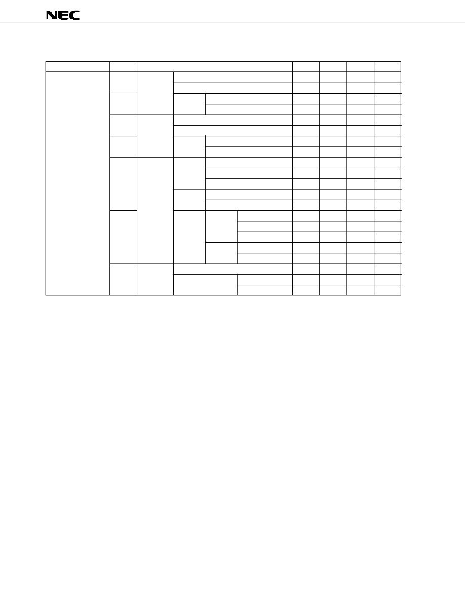
µ
PD750064, 750066, 750068, 750064(A), 750066(A), 750068(A)
60
Data Sheet U10165EJ2V0DS00
DC Characteristics (T
A
= ≠40 to +85∞C, V
DD
= 1.8 to 5.5 V)
Parameter
Symbol
Conditions
MIN.
TYP.
MAX.
Unit
Supply current
Note 1
I
DD1
V
DD
= 5.0 V
±
10%
Note 3
2.2
6.6
mA
V
DD
= 3.0 V
±
10%
Note 4
0.48
1.5
mA
I
DD2
HALT
V
DD
= 5.0 V
±
10%
0.86
2.6
mA
mode
V
DD
= 3.0 V
±
10%
0.43
1.3
mA
I
DD1
V
DD
= 5.0 V
±
10%
Note 3
1.7
4.5
mA
V
DD
= 3.0 V
±
10%
Note 4
0.4
1.2
mA
I
DD2
HALT
V
DD
= 5.0 V
±
10%
0.7
2
mA
mode
V
DD
= 3.0 V
±
10%
0.39
1.2
mA
I
DD3
Low-
V
DD
= 3.0 V
±
10%
11
33
µ
A
voltage
V
DD
= 2.0 V
±
10%
5.5
17
µ
A
mode
Note 6
V
DD
= 3.0 V, T
A
= 25∞C
11
22
µ
A
V
DD
= 3.0 V
±
10%
9.2
27
µ
A
V
DD
= 3.0 V, T
A
= 25∞C
9.2
18
µ
A
I
DD4
HALT
Low-
V
DD
= 3.0 V
±
10%
6.4
20
µ
A
mode
voltage
V
DD
= 2.0 V
±
10%
2.5
8
µ
A
mode
Note 6
V
DD
= 3.0 V, T
A
= 25∞C
6.4
12.8
µ
A
V
DD
= 3.0 V
±
10%
4.6
13.8
µ
A
V
DD
= 3.0 V, T
A
= 25∞C
4.6
9.2
µ
A
I
DD5
XT1 =
V
DD
= 5.0 V
±
10%
0.05
10
µ
A
0 V
Note 8
V
DD
= 3.0 V
±
10%
0.02
5
µ
A
STOP mode
T
A
= 25∞C
0.02
3
µ
A
Notes 1.
The current flowing to the internal pull-up resistor is not included.
2.
Including the case when the subsystem clock oscillates.
3.
When the device operates in high-speed mode with the processor clock control register (PCC) set to
0011.
4.
When the device operates in low-speed mode with PCC set to 0000.
5.
When the device operates on the subsystem clock, with the system clock control register (SCC) set
to 1001 and oscillation of the main system clock stopped.
6.
When the sub-oscillation circuit control register (SOS) is set to 0000.
7.
When SOS is set to 0010.
8.
When SOS is set to 00
◊
1, and the sub-oscillation circuit feedback resistor is not used (
◊:
don't care).
6.0-MHz
Note 2
crystal
oscillation
C1 = C2
= 22 pF
4.19-MHz
Note 2
crystal
oscillation
C1 = C2
= 22 pF
32.768-
kHz
Note 5
crystal
oscillation
Low current
dissipation
mode
Note 7
Low current
dissipation
mode
Note 7

61
µ
PD750064, 750066, 750068, 750064(A), 750066(A), 750068(A)
Data Sheet U10165EJ2V0DS00
AC Characteristics (T
A
= ≠40 to +85∞C, V
DD
= 1.8 to 5.5 V)
Parameter
Symbol
Conditions
MIN.
TYP.
MAX.
Unit
CPU clock cycle time
Note 1
t
CY
Operates with
V
DD
= 2.7 to 5.5 V
0.67
64
µ
s
(minimum instruction
main system clock
0.95
64
µ
s
execution time = 1
Operates with
114
122
125
µ
s
machine cycle)
subsystem clock
TI0, TI1 input frequency
f
TI
V
DD
= 2.7 to 5.5 V
0
1.0
MHz
0
275
kHz
TI0, TI1 input high-/low-level
t
TIH
, t
TIL
V
DD
= 2.7 to 5.5 V
0.48
µ
s
width
1.8
µ
s
Interrupt input high-/
t
INTH
, t
INTL
INT0
IM02 = 0
Note 2
µ
s
low-level width
IM02 = 1
10
µ
s
INT1, 2, 4
10
µ
s
KR0 to 3
10
µ
s
RESET low-level width
t
RSL
10
µ
s
Notes 1.
The cycle time (minimum instruction
execution time) of the CPU clock (
)
is determined by the oscillation frequency
of the connected resonator (and external
clock), the system clock control register
(SCC), and processor clock control
register (PCC).
The figure on the right shows the supply
voltage V
DD
vs. cycle time t
CY
characteristics when the device operates
with the main system clock.
2.
2t
CY
or 128/f
X
depending on the setting
of the interrupt mode register (IM0).
0
1
2
3
4
5
6
1
0.5
2
3
4
5
6
60
64
(with main system clock)
t
CY
vs V
DD
Guaranteed operation range
Cycle time t
CY
[ s]
µ
Supply voltage V
DD
[V]
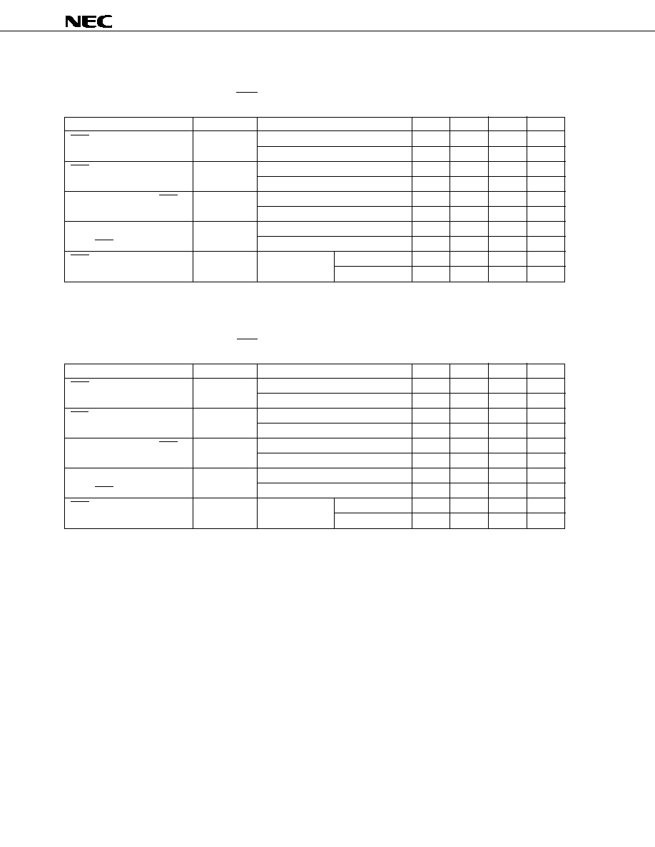
µ
PD750064, 750066, 750068, 750064(A), 750066(A), 750068(A)
62
Data Sheet U10165EJ2V0DS00
Note 2
Note 2
Serial transfer operation
2-wire and 3-wire serial I/O modes (SCK ∑∑∑ internal clock output): (T
A
= ≠40 to +85∞C, V
DD
= 1.8 to 5.5 V)
Parameter
Symbol
Conditions
MIN.
TYP.
MAX.
Unit
SCK cycle time
t
KCY1
V
DD
= 2.7 to 5.5 V
1300
ns
3800
ns
SCK high-/low-level width
t
KL1
,
V
DD
= 2.7 to 5.5 V
t
KCY1
/2≠50
ns
t
KH1
t
KCY1
/2≠150
ns
SI
Note 1
setup time (to SCK
)
t
SIK1
V
DD
= 2.7 to 5.5 V
150
ns
500
ns
SI
Note 1
hold time
t
KSI1
V
DD
= 2.7 to 5.5 V
400
ns
(from SCK
)
600
ns
SCK
SO
Note 1
output
t
KSO1
R
L
= 1 k
,
V
DD
= 2.7 to 5.5 V
0
250
ns
delay time
C
L
= 100 pF
0
1000
ns
Notes 1.
Read as SB0 or SB1 when using the 2-wire serial I/O mode.
2.
R
L
and C
L
are the load resistance and load capacitance of the SO output line.
2-wire and 3-wire serial I/O modes (SCK ∑∑∑ external clock input): (T
A
= ≠40 to +85∞C, V
DD
= 1.8 to 5.5 V)
Parameter
Symbol
Conditions
MIN.
TYP.
MAX.
Unit
SCK cycle time
t
KCY2
V
DD
= 2.7 to 5.5 V
800
ns
3200
ns
SCK high-/low-level width
t
KL2
,
V
DD
= 2.7 to 5.5 V
400
ns
t
KH2
1600
ns
SI
Note 1
setup time (to SCK
)
t
SIK2
V
DD
= 2.7 to 5.5 V
100
ns
150
ns
SI
Note 1
hold time
t
KSI2
V
DD
= 2.7 to 5.5 V
400
ns
(from SCK
)
600
ns
SCK
SO
Note 1
output
t
KSO2
R
L
= 1 k
,
V
DD
= 2.7 to 5.5 V
0
300
ns
delay time
C
L
= 100 pF
0
1000
ns
Notes 1.
Read as SB0 or SB1 when using the 2-wire serial I/O mode.
2.
R
L
and C
L
are the load resistance and load capacitance of the SO output line.

63
µ
PD750064, 750066, 750068, 750064(A), 750066(A), 750068(A)
Data Sheet U10165EJ2V0DS00
A/D Converter Characteristics (T
A
= ≠40 to +85∞C, V
DD
= 1.8 to 5.5 V, 1.8 V
AV
REF
V
DD
)
Parameter
Symbol
Conditions
MIN.
TYP.
MAX.
Unit
Resolution
8
8
8
bit
Absolute accuracy
Note 1
V
DD
= AV
REF
2.7 V
V
DD
1.5
LSB
1.8 V
V
DD
< 2.7 V
3
LSB
V
DD
AV
REF
3
LSB
Conversion time
t
CONV
Note 2
168/f
X
µ
s
Sampling time
t
SAMP
Note 3
44/f
X
µ
s
Analog input voltage
V
IAN
AV
SS
AV
REF
V
Analog input impedance
R
AN
1000
M
AV
REF
current
I
REF
0.25
2.0
mA
Notes 1.
Absolute accuracy excluding quantization error (
±
1/2LSB)
2.
Time until end of conversion (EOC = 1) after execution of conversion start instruction (40.1
µ
s: f
X
=
4.19 MHz).
3.
Time until end of sampling after execution of conversion start instruction (10.5
µ
s: f
X
= 4.19 MHz).
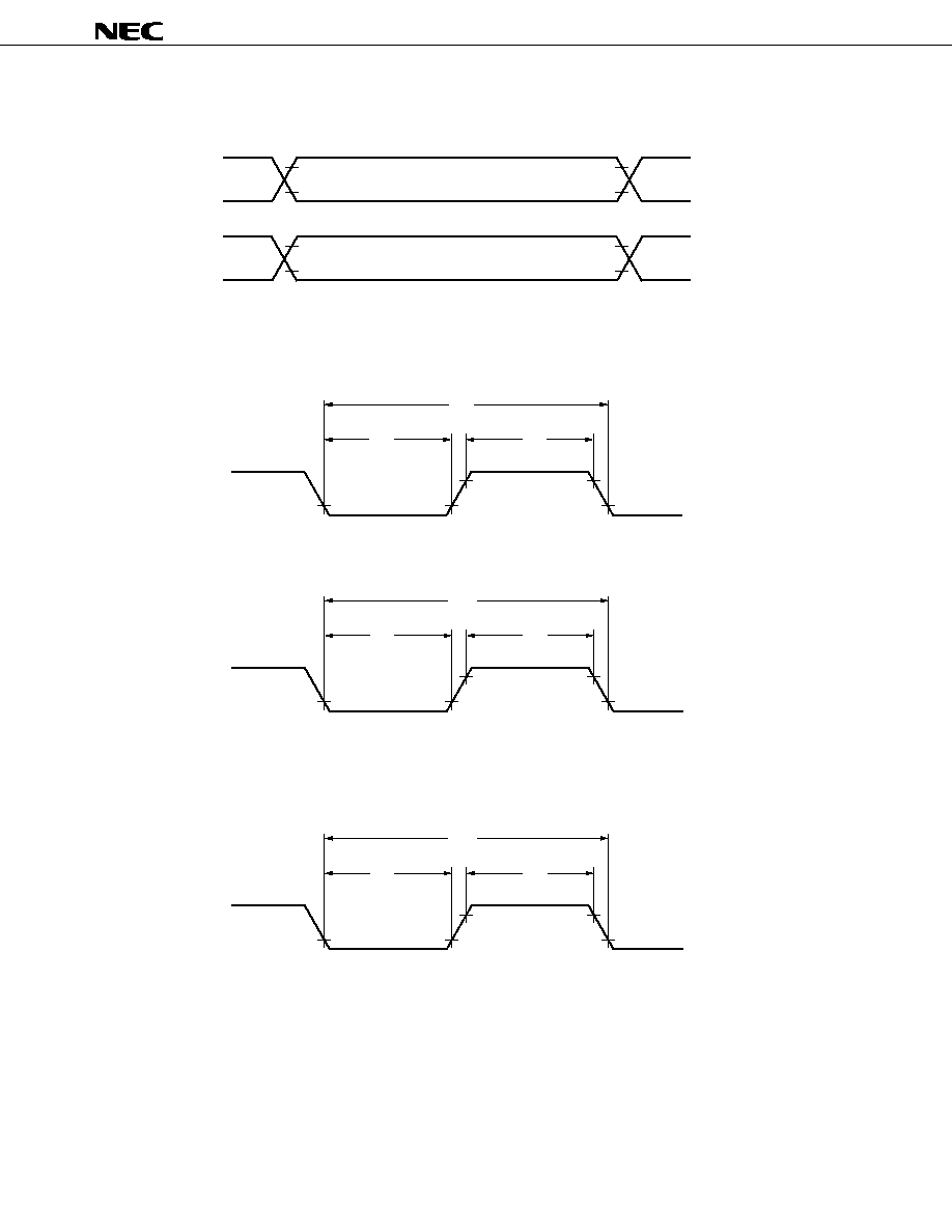
µ
PD750064, 750066, 750068, 750064(A), 750066(A), 750068(A)
64
Data Sheet U10165EJ2V0DS00
AC timing test points (excluding X1 and XT1 inputs)
Clock timing
TI0, TI1 timing
V
IH
(MIN.)
V
IL
(MAX.)
V
IH
(MIN.)
V
IL
(MAX.)
V
OH
(MIN.)
V
OL
(MAX.)
V
OH
(MIN.)
V
OL
(MAX.)
1/f
XT
t
XTL
t
XTH
V
DD
≠ 0.1 V
0.1 V
XT1 input
1/f
X
t
XL
t
XH
V
DD
≠ 0.1 V
0.1 V
X1 input
1/f
TI
t
TIL
t
TIH
TI0, TI1
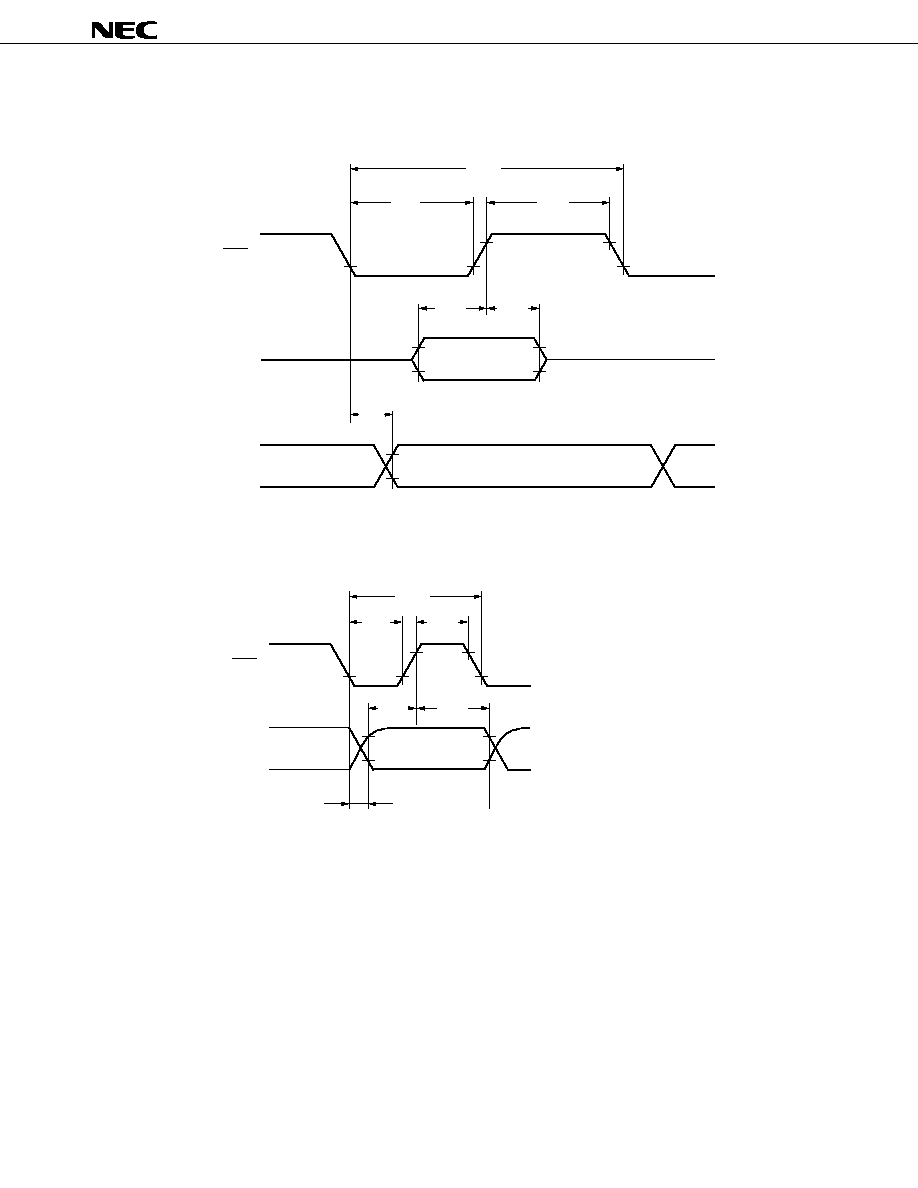
65
µ
PD750064, 750066, 750068, 750064(A), 750066(A), 750068(A)
Data Sheet U10165EJ2V0DS00
Serial transfer timing
3-wire serial I/O mode
2-wire serial I/O mode
t
KCY1, 2
t
KL1, 2
t
KH1, 2
SCK
Output data
SO
Input data
SI
t
SIK1, 2
t
KSI1, 2
t
KSO1, 2
t
KCY1, 2
t
KL1, 2
t
KH1, 2
SCK
SB0, 1
t
SIK1, 2
t
KSI1, 2
t
KSO1, 2
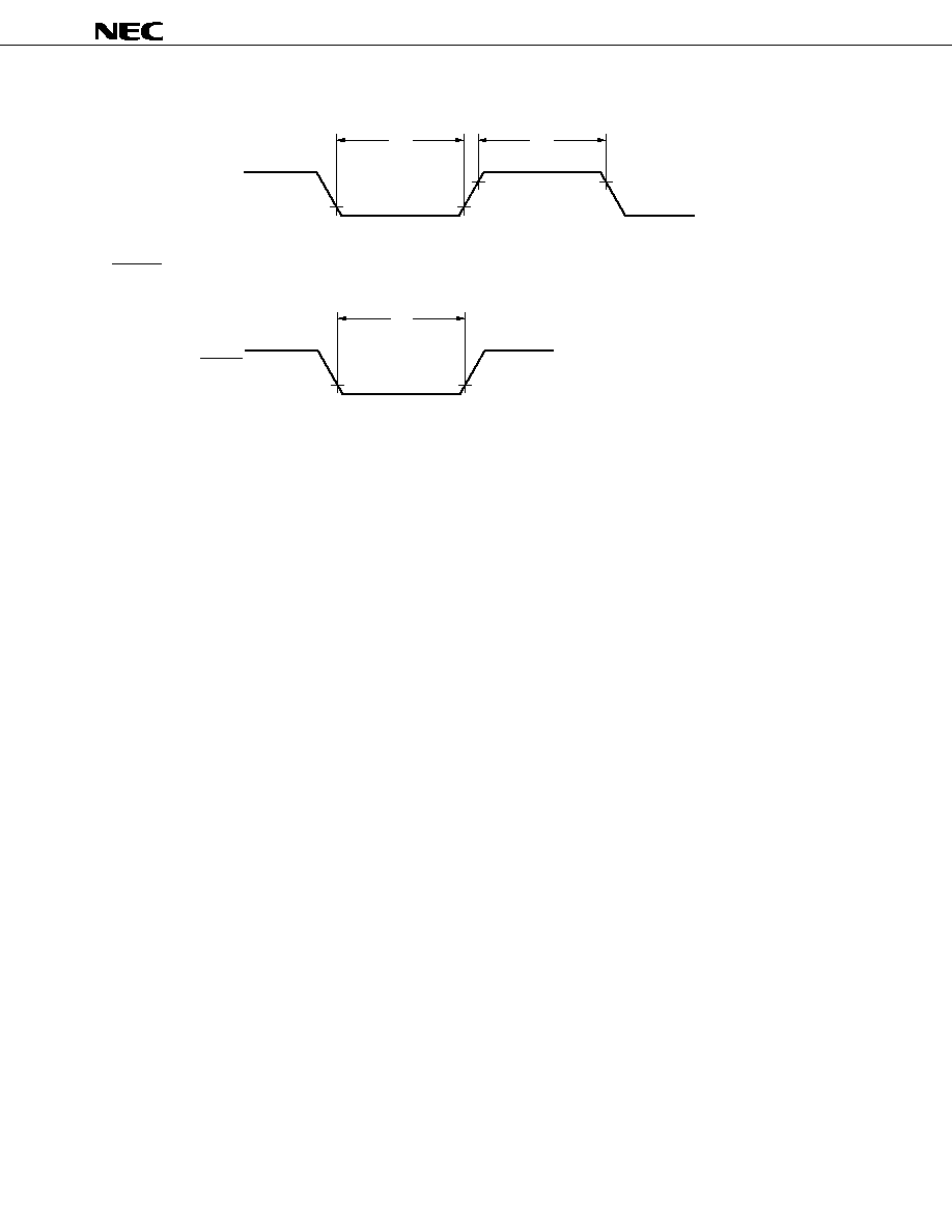
µ
PD750064, 750066, 750068, 750064(A), 750066(A), 750068(A)
66
Data Sheet U10165EJ2V0DS00
Interrupt input timing
RESET input timing
RESET
t
RSL
INT0, 1, 2, 4
KR0 to 3
t
INTL
t
INTH
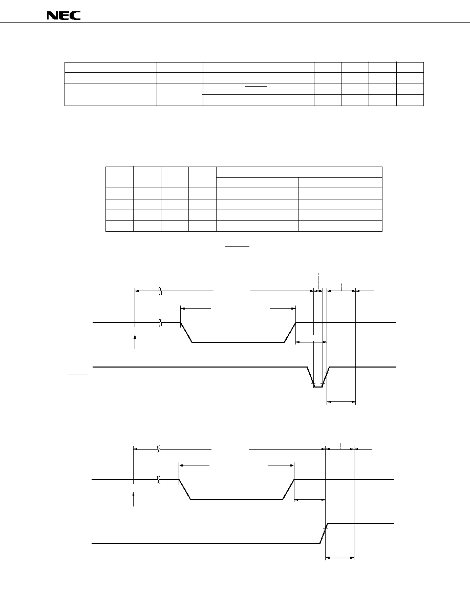
67
µ
PD750064, 750066, 750068, 750064(A), 750066(A), 750068(A)
Data Sheet U10165EJ2V0DS00
Data Memory STOP Mode Low Supply Voltage Data Retention Characteristics (T
A
= ≠40 to +85∞C)
Parameter
Symbol
Conditions
MIN.
TYP.
MAX.
Unit
Release signal set time
t
SREL
0
µ
s
Oscillation stabilization
t
WAIT
Released by RESET
Note 2
ms
wait time
Note 1
Released by interrupt request
Note 3
ms
Notes 1.
The oscillation stabilization wait time is the time during which the CPU stops operating to prevent
unstable operation when oscillation is started.
2.
Either 2
17
/f
X
or 2
15
/f
X
can be selected by mask option.
3.
Set by the basic interval timer mode register (BTM). (Refer to the table below.)
BTM3
BTM2
BTM1
BTM0
Wait Time
f
X
= 4.19 MHz
f
X
= 6.0 MHz
≠
0
0
0
2
20
/f
X
(approx. 250 ms)
2
20
/f
X
(approx. 175 ms)
≠
0
1
1
2
17
/f
X
(approx. 31.3 ms)
2
17
/f
X
(approx. 21.8 ms)
≠
1
0
1
2
15
/f
X
(approx. 7.81 ms)
2
15
/f
X
(approx. 5.46 ms)
≠
1
1
1
2
13
/f
X
(approx. 1.95 ms)
2
13
/f
X
(approx. 1.37 ms)
Data retention timing (STOP mode release by RESET)
Data retention timing (standby release signal: STOP mode release by interrupt signal)
STOP mode
Data retention mode
Internal reset operation
Operation mode
STOP instruction execution
HALT mode
V
DD
RESET
V
DDDR
t
WAIT
t
SREL
STOP mode
Data retention mode
Operation mode
HALT mode
t
SREL
V
DDDR
t
WAIT
STOP instruction execution
V
DD
Standby release signal
(interrupt request)

µ
PD750064, 750066, 750068, 750064(A), 750066(A), 750068(A)
68
Data Sheet U10165EJ2V0DS00
13. CHARACTERISTICS CURVES (REFERENCE VALUES)
I
DD
vs V
DD
(main system clock: 6.0-MHz crystal resonator)
10
5.0
1.0
0.5
0.1
0.05
0.01
0.005
0.001
0
1
2
3
4
5
6
7
8
PCC = 0011
PCC = 0010
PCC = 0001
XT1
XT2
X1
X2
6.0 MHz
32.768 kHz
330 k
22 pF
22 pF
33 pF
33 pF
Supply Current I
DD
(mA)
Main system clock
HALT mode + 32-kHz oscillation
Subsystem clock operation
mode (SOS.1 = 0)
Subsystem clock HALT mode
(SOS.1 = 0) and main system
clock STOP mode + 32-kHz
oscillation (SOS.1 = 0)
Crystal
resonator
Crystal
resonator
Supply Voltage V
DD
(V)
(T
A
= 25∞C)
PCC = 0000
Subsystem clock HALT mode
(SOS.1 = 1) and main system
clock STOP mode + 32-kHz
oscillation (SOS.1 = 1)

69
µ
PD750064, 750066, 750068, 750064(A), 750066(A), 750068(A)
Data Sheet U10165EJ2V0DS00
I
DD
vs V
DD
(main system clock: 4.19-MHz crystal resonator)
10
5.0
1.0
0.5
0.1
0.05
0.01
0.005
0.001
0
1
2
3
4
5
6
7
8
PCC = 0011
PCC = 0010
PCC = 0001
XT1
XT2
X1
X2
4.19 MHz
32.768 kHz
330 k
22 pF
22 pF
33 pF
33 pF
Supply Current I
DD
(mA)
Main system clock
HALT mode + 32-kHz oscillation
Subsystem clock operation
mode (SOS.1 = 0)
Subsystem clock HALT mode
(SOS.1 = 0) and main system
clock STOP mode + 32-kHz
oscillation (SOS.1 = 0)
Crystal
resonator
Crystal
resonator
Supply Voltage V
DD
(V)
(T
A
= 25∞C)
PCC = 0000
Subsystem clock HALT mode
(SOS.1 = 1) and main system
clock STOP mode + 32-kHz
oscillation (SOS.1 = 1)
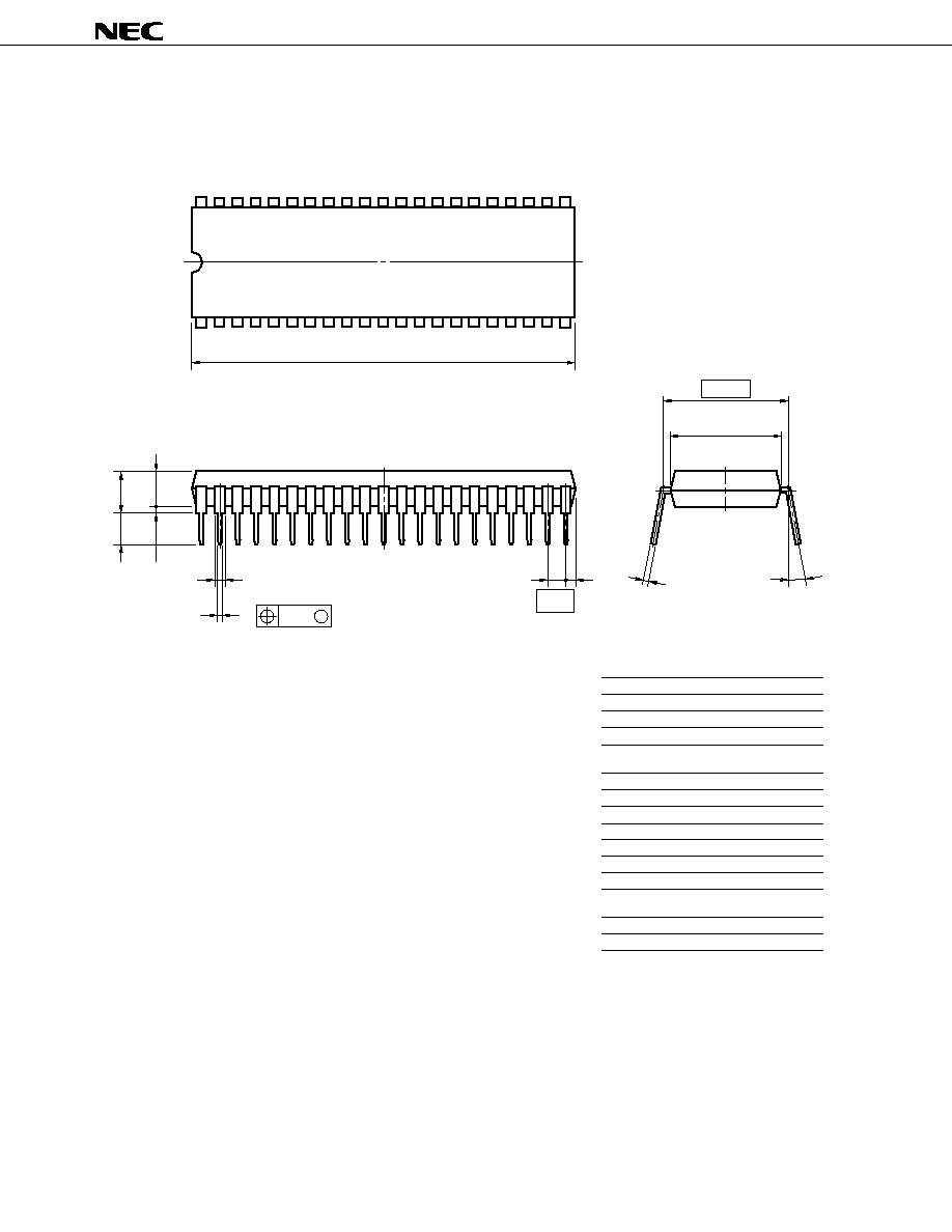
µ
PD750064, 750066, 750068, 750064(A), 750066(A), 750068(A)
70
Data Sheet U10165EJ2V0DS00
14. PACKAGE DRAWINGS
42 PIN PLASTIC SHRINK DIP (600 mil)
ITEM
MILLIMETERS
INCHES
A
B
C
F
G
H
I
J
K
39.13 MAX.
1.778 (T.P.)
3.2±0.3
0.51 MIN.
4.31 MAX.
1.78 MAX.
0.17
15.24 (T.P.)
5.08 MAX.
N
0.9 MIN.
R
1.541 MAX.
0.070 MAX.
0.035 MIN.
0.126±0.012
0.020 MIN.
0.170 MAX.
0.200 MAX.
0.600 (T.P.)
0.007
0.070 (T.P.)
P42C-70-600A-1
A
C
D
G
NOTES
1) Each lead centerline is located within 0.17 mm (0.007 inch) of
its true position (T.P.) at maximum material condition.
D
0.50±0.10
0.020
M
0.25
0.010
+0.10
≠0.05
0~15∞
0~15∞
+0.004
≠0.003
+0.004
≠0.005
M
K
N
L
13.2
0.520
2) Item "K" to center of leads when formed parallel.
42
1
22
21
L
M
R
B
F
H
J
I
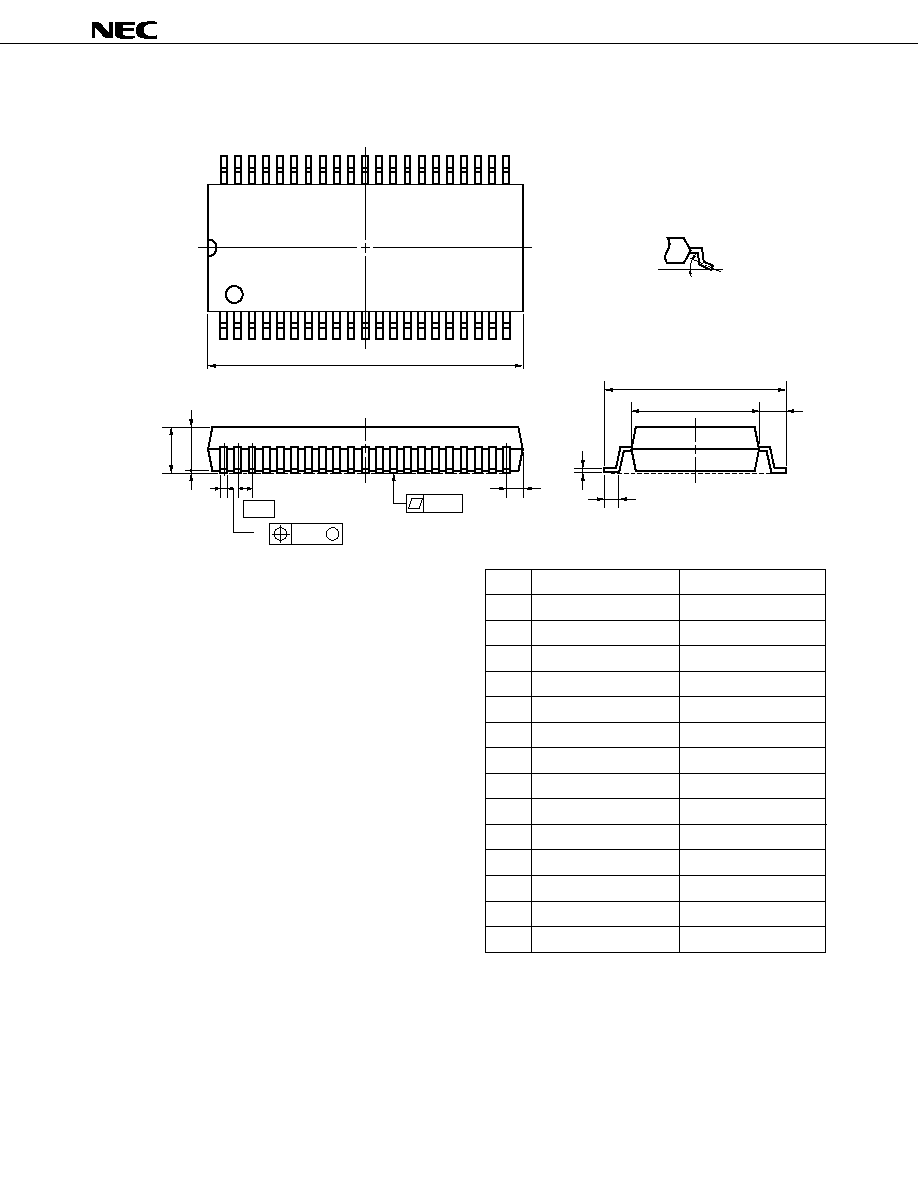
71
µ
PD750064, 750066, 750068, 750064(A), 750066(A), 750068(A)
Data Sheet U10165EJ2V0DS00
42 PIN PLASTIC SHRINK SOP (375 mil)
1
21
A
42
22
detail of lead end
C
M
M
N
B
D
E
F
G
I
J
H
K
L
3∞
+7∞
≠3∞
S42GT-80-375B-1
ITEM
MILLIMETERS
INCHES
A
B
C
D
F
G
H
I
J
K
L
18.16 MAX.
0.8 (T.P.)
2.9 MAX.
2.5±0.2
10.3±0.3
1.13 MAX.
0.715 MAX.
0.005±0.003
0.115 MAX.
0.406
0.281
0.044 MAX.
NOTE
M
N
0.10
0.8±0.2
1.6±0.2
7.15±0.2
0.004
0.031
+0.009
≠0.008
Each lead centerline is located within 0.10
mm (0.004 inch) of its true position (T.P.) at
maximum material condition.
0.063±0.008
0.098
0.031 (T.P.)
0.15
0.006
0.10
0.004
0.014
0.35
0.125±0.075
+0.004
≠0.002
+0.009
≠0.008
+0.10
≠0.05
+0.004
≠0.003
E
+0.012
≠0.013
+0.009
≠0.008
+0.10
≠0.05

µ
PD750064, 750066, 750068, 750064(A), 750066(A), 750068(A)
72
Data Sheet U10165EJ2V0DS00
15. RECOMMENDED SOLDERING CONDITIONS
The
µ
PD750068 should be soldered and mounted under the following recommended conditions.
For the details of the recommended soldering conditions, refer to the document Semiconductor Device
Mounting Technology Manual (C10535E).
For soldering methods and conditions other than those recommended below, contact your NEC sales
representative.
Table 15-1. Surface Mounting Type Soldering Conditions
µ
PD750064GT-
◊◊◊
: 42-pin plastic shrink SOP (375 mil, 0.8-mm pitch)
µ
PD750066GT-
◊◊◊
: 42-pin plastic shrink SOP (375 mil, 0.8-mm pitch)
µ
PD750068GT-
◊◊◊
: 42-pin plastic shrink SOP (375 mil, 0.8-mm pitch)
µ
PD750064GT(A)-
◊◊◊
: 42-pin plastic shrink SOP (375 mil, 0.8-mm pitch)
µ
PD750066GT(A)-
◊◊◊
: 42-pin plastic shrink SOP (375 mil, 0.8-mm pitch)
µ
PD750068GT(A)-
◊◊◊
: 42-pin plastic shrink SOP (375 mil, 0.8-mm pitch)
Soldering Method
Soldering Conditions
Recommended
Condition Symbol
Infrared reflow
Package peak temperature: 235∞C, Time: 30 sec. Max. (at 210∞C or higher), IR35-00-2
Count: two times or less
VPS
Package peak temperature: 215∞C, Time: 40 sec. Max. (at 200∞C or higher), VP15-00-2
Count: two times or less
Wave soldering
Solder bath temperature: 260∞C Max., Time: 10 sec. Max.,
WS60-00-1
Count: once
Preheating temperature: 120∞C Max. (package surface temperature)
Partial heating
Pin temperature: 300∞C Max., Time: 3 sec. Max. (per pin row)
--
Caution Do not use different soldering methods together (except for partial heating).
Table 15-2. Through Hole Type Soldering Conditions
µ
PD750064CU-
◊◊◊
: 42-pin plastic shrink DIP (600 mil, 1.778-mm pitch)
µ
PD750066CU-
◊◊◊
: 42-pin plastic shrink DIP (600 mil, 1.778-mm pitch)
µ
PD750068CU-
◊◊◊
: 42-pin plastic shrink DIP (600 mil, 1.778-mm pitch)
µ
PD750064CU(A)-
◊◊◊
: 42-pin plastic shrink DIP (600 mil, 1.778-mm pitch)
µ
PD750066CU(A)-
◊◊◊
: 42-pin plastic shrink DIP (600 mil, 1.778-mm pitch)
µ
PD750068CU(A)-
◊◊◊
: 42-pin plastic shrink DIP (600 mil, 1.778-mm pitch)
Soldering Method
Soldering Conditions
Wave soldering (pin only)
Solder bath temperature: 260∞C Max., Time: 10 sec. Max.
Partial heating
Pin temperature: 300∞C Max., Time: 3 sec. Max. (per pin)
Caution
In wave soldering, apply solder only to the pins. Care must be taken that
jet solder does not come in contact with the main body of the package.
73
µ
PD750064, 750066, 750068, 750064(A), 750066(A), 750068(A)
Data Sheet U10165EJ2V0DS00
APPENDIX A.
µ
PD75068, 750068 AND 75P0076 FUNCTIONAL LIST
Item
µ
PD75068
µ
PD750068
µ
PD75P0076
Program memory
Mask ROM
Mask ROM
One-time PROM
0000H to 1F7FH
0000H to 1FFFH
0000H to 3FFFH
(8064
◊
8 bits)
(8192
◊
8 bits)
(16384
◊
8 bits)
Data memory
000H to 1FFH
(512
◊
4 bits)
CPU
75X Standard CPU
75XL CPU
General-purpose register
4 bits
◊
8 or 8 bits
◊
4
(4 bits
◊
8 or 8 bits
◊
4)
◊
4 banks
Instruction
When main system
0.95, 1.91, 15.3
µ
s
∑ 0.67, 1.33, 2.67, 10.7
µ
s (@6.0-MHz operation)
execution
clock is selected
(@4.19-MHz operation)
∑ 0.95, 1.91, 3.81, 15.3
µ
s (@4.19-MHz operation)
time
When subsystem
122
µ
s (@32.768-kHz operation)
clock is selected
I/O port
CMOS input
12 (on-chip pull-up resistor specified by software: 7)
CMOS input/output
12 (on-chip pull-up resistor specified by software)
N-ch open-drain
8 (on-chip pull-up resistor
8 (on-chip pull-up resistor
8 (no mask option)
input/output
specified by mask option)
specified by mask option)
Withstand voltage is 13 V
Withstand voltage is 10 V
Withstand voltage is 13 V
Total
32
Timer
3 channels
4 channels
∑ 8-bit timer/event counter
∑ 8-bit timer/event counter 0 (watch timer output added)
∑ 8-bit basic interval timer
∑ 8-bit timer/event counter 1 (can be used as a 16-bit timer/
∑ Watch timer
event counter)
∑ 8-bit basic interval timer/watchdog timer
∑ Watch timer
A/D converter
∑ 8-bit resolution
◊
8 channels
∑ 8-bit resolution
◊
8 channels
(successive approximation)
(successive approximation)
∑ Can operate at the voltage
∑ Can operate at the voltage from V
DD
= 1.8 V
from V
DD
= 2.7 V
µ
PD750064, 750066, 750068, 750064(A), 750066(A), 750068(A)
74
Data Sheet U10165EJ2V0DS00
Item
µ
PD75068
µ
PD750068
µ
PD75P0076
Clock output (PCL)
, 524, 262, 65.5 kHz
∑
, 1.05 MHz, 262 kHz, 65.5 kHz
(@4.19-MHz operation with
(@4.19-MHz operation with main system clock)
main system clock)
∑
, 1.5 MHz, 375 kHz, 93.8 kHz
(@6.0-MHz operation with main system clock)
Buzzer output (BUZ)
2, 4, 32 kHz
∑ 2, 4, 32 kHz
(@4.19-MHz operation
(@4.19-MHz operation with main system clock or
with main system clock
@32.768-kHz operation with subsystem clock)
or @32.768-kHz operation
∑ 2.93, 5.86, 46.9 kHz
with subsystem clock)
(@6.0-MHz operation with main system clock)
Serial interface
3 modes are available
2 modes are available
∑ 3-wire serial I/O mode
∑ 3-wire serial I/O mode
∑∑∑ MSB/LSB can be selected
∑∑∑ MSB/LSB can be selected for transfer first bit
for transfer first bit
∑ 2-wire serial I/O mode
∑ 2-wire serial I/O mode
∑ SBI mode
Vectored interrupt
External: 3, internal: 3
External: 3, internal: 4
Test input
External: 1, internal: 1
Supply voltage
V
DD
= 2.7 to 6.0 V
V
DD
= 1.8 to 5.5 V
Operating ambient temperature
T
A
= ≠40 to +85∞C
Package
∑ 42-pin plastic shrink DIP
∑ 42-pin plastic shrink DIP (600 mil, 1.778-mm pitch)
(600 mil)
∑ 42-pin plastic shrink SOP (375 mil, 0.8-mm pitch)
∑ 44-pin plastic QFP
(10
◊
10 mm)
75
µ
PD750064, 750066, 750068, 750064(A), 750066(A), 750068(A)
Data Sheet U10165EJ2V0DS00
APPENDIX B. DEVELOPMENT TOOLS
The following development tools are available for system development using the
µ
PD750068.
In the 75XL Series, the relocatable assembler which is common to the series is used in combination with the
device file of each product.
Language processor
RA75X relocatable assembler
Host Machine
Part Number
OS
Supply Media
(Product Name)
PC-9800 Series
MS-DOS
TM
3.5-inch 2HD
µ
S5A13RA75X
Ver. 3.30 to
5-inch 2HD
µ
S5A10RA75X
Ver. 6.2
Note
IBM PC/AT
TM
Refer to
3.5-inch 2HC
µ
S7B13RA75X
compatible machines
"OS for IBM PC"
5-inch 2HC
µ
S7B10RA75X
Device file
Host Machine
Part Number
OS
Supply Media
(Product Name)
PC-9800 Series
MS-DOS
3.5-inch 2HD
µ
S5A13DF750068
Ver. 3.30 to
5-inch 2HD
µ
S5A10DF750068
Ver.6.2
Note
IBM PC/AT
Refer to
3.5-inch 2HC
µ
S7B13DF750068
compatible machines
"OS for IBM PC"
5-inch 2HC
µ
S7B10DF750068
Note
Ver. 5.00 or later has the task swap function, but it cannot be used for this software.
Remark Operation of the assembler and device file is guaranteed only on the above host machines and OSs.

µ
PD750064, 750066, 750068, 750064(A), 750066(A), 750068(A)
76
Data Sheet U10165EJ2V0DS00
PROM write tools
Hardware
PG-1500
PG-1500 is a PROM programmer which enables you to program single-chip microcontrollers
including PROM by stand-alone or host machine operation by connecting an attached board
and optional programmer adapter to PG-1500. It also enables you to program typical PROM
devices of 256K bits to 4M bits.
PA-75P0076CU
PROM programmer adapter for the
µ
PD75P0076CU and 75P0076GT. Connect the
programmer adapter to PG-1500 for use.
Software
PG-1500 controller
PG-1500 and a host machine are connected by serial and parallel interfaces and PG-1500
is controlled on the host machine.
Host Machine
Part Number
OS
Supply Media
(Product Name)
PC-9800 Series
MS-DOS
3.5-inch 2HD
µ
S5A13PG1500
Ver. 3.30 to
5-inch 2HD
µ
S5A10PG1500
Ver. 6.2
Note
IBM PC/AT
Refer to
3.5-inch 2HD
µ
S7B13PG1500
compatible machines
"OS for IBM PC"
5-inch 2HC
µ
S7B10PG1500
Note
Ver. 5.00 or later has the task swap function, but it cannot be used for this software.
Remark Operation of the PG-1500 controller is guaranteed only on the above host machines and OSs.
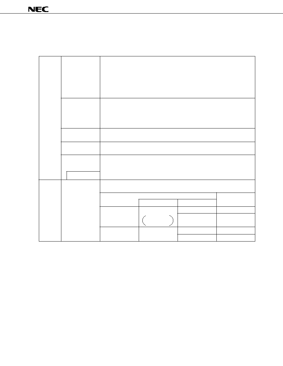
77
µ
PD750064, 750066, 750068, 750064(A), 750066(A), 750068(A)
Data Sheet U10165EJ2V0DS00
Debugging tool
The in-circuit emulators (IE-75000-R and IE-75001-R) are available as the program debugging tool for the
µ
PD750068.
The system configurations are described as follows.
Hardware
IE-75000-R
Note 1
In-circuit emulator for debugging the hardware and software when developing the application
systems that use the 75X Series and 75XL Series. When developing a
µ
PD750068
Subseries, the emulation board IE-75300-R-EM and emulation probe that are sold separately
must be used with the IE-75000-R.
By connecting with the host machine and the PROM programmer, efficient debugging can
be made.
It contains the emulation board IE-75000-R-EM which is connected.
IE-75001-R
In-circuit emulator for debugging the hardware and software when developing the application
systems that use the 75X Series and 75XL Series. When developing a
µ
PD750068
Subseries, the emulation board IE-75300-R-EM and emulation probe that are sold separately
must be used with the IE-75001-R.
It can debug the system efficiently by connecting the host machine and PROM programmer.
IE-75300-R-EM
Emulation board for evaluating the application systems that use a
µ
PD750068 Subseries.
It must be used with the IE-75000-R or IE-75001-R.
EP-750068CU-R
Emulation probe for the
µ
PD750068CU.
It must be connected to IE-75000-R (or IE-75001-R) and IE-75300-R-EM.
EP-750068GT-R
Emulation probe for the
µ
PD750068GT.
It must be connected to the IE-75000-R (or IE-75001-R) and IE-75300-R-EM.
It is supplied with the flexible board EV-9500GT-42 which facilitates connection to
EV-9500GT-42
a target system.
Software
IE control program
Connects the IE-75000-R or IE-75001-R to a host machine via RS-232-C and Centronix
I/F and controls the IE-75000-R or IE-75001-R on a host machine.
Host Machine
Part Number
OS
Supply Media
(Product Name)
PC-9800 Series
MS-DOS
3.5-inch 2HD
µ
S5A13IE75X
Ver. 3.30 to
5-inch 2HD
µ
S5A10IE75X
Ver. 6.2
Note 2
IBM PC/AT
Refer to
3.5-inch 2HC
µ
S7B13IE75X
compatible machines
"OS for IBM PC"
5-inch 2HC
µ
S7B10IE75X
Notes 1.
Maintenance product
2.
Ver. 5.00 or later has the task swap function, but it cannot be used for this software.
Remarks 1.
Operation of the IE control program is guaranteed only on the above host machines and OSs.
2.
The
µ
PD750064, 750066, 750068, and 75P0076 are commonly referred to as the
µ
PD750068
Subseries.

µ
PD750064, 750066, 750068, 750064(A), 750066(A), 750068(A)
78
Data Sheet U10165EJ2V0DS00
OS for IBM PC
The following IBM PC OS's are supported.
OS
Version
PC DOS
TM
Ver. 5.02 to Ver. 6.3
J6.1/V
Note
to J6.3/V
Note
MS-DOS
Ver. 5.0 to Ver. 6.22
5.0/V
Note
to 6.2/V
Note
IBM DOS
TM
J5.02/V
Note
Note Only English version is supported.
Caution Ver. 5.0 or later has the task swap function, but it cannot be used for this software.
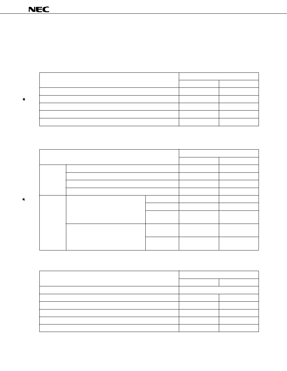
79
µ
PD750064, 750066, 750068, 750064(A), 750066(A), 750068(A)
Data Sheet U10165EJ2V0DS00
APPENDIX C. RELATED DOCUMENTS
The related documents indicated in this publication may include preliminary versions. However, preliminary
versions are not marked as such.
Documents related to device
Document Name
Document No.
Japanese
English
µ
PD750064, 750066, 750068, 750064(A), 750066(A), 750068(A) Data Sheet
U10165J
U10165E (this document)
µ
PD75P0076 Data Sheet
U10232J
U10232E
µ
PD750068 User's Manual
U10670J
U10670E
µ
PD750068 Instruction Table
IEM-5606
≠
75XL Series Selection Guide
U10453J
U10453E
Documents related to development tool
Document Name
Document No.
Japanese
English
Hardware
IE-75000-R/IE-75001-R User's Manual
EEU-846
EEU-1416
IE-75300-R-EM User's Manual
U11354J
U11354E
EP-750068CU/GT-R User's Manual
U10950J
U10950E
PG-1500 User's Manual
U11940J
U11940E
Software
RA75X Assembler Package User's Manual
Operation
U12622J
U12622E
Language
U12385J
U12385E
Structured Assembler U12598J
U12598E
Preprocessor
PG-1500 Controller User's Manual
PC-9800 Series
EEU-704
EEU-1291
(MS-DOS) Based
IBM PC Series
EEU-5008
U10540E
(PC DOS) Based
Other related documents
Document Name
Document No.
Japanese
English
SEMICONDUCTORS SELECTION GUIDE Products & Packages (CD-ROM)
X13769X
Semiconductor Device Mounting Technology Manual
C10535J
C10535E
Quality Grades on NEC Semiconductor Devices
C11531J
C11531E
NEC Semiconductor Device Reliability/Quality Control System
C10983J
C10983E
Guide to Prevent Damage for Semiconductor Devices by Electrostatic Discharge (ESD) C11892J
C11892E
Guide to Microcomputer-Related Products by Third Party
U11416J
≠
Caution
The related documents listed above are subject to change without notice. Be sure to use the
latest version of each document for designing.

µ
PD750064, 750066, 750068, 750064(A), 750066(A), 750068(A)
80
Data Sheet U10165EJ2V0DS00
NOTES FOR CMOS DEVICES
1
PRECAUTION AGAINST ESD FOR SEMICONDUCTORS
Note: Strong electric field, when exposed to a MOS device, can cause destruction
of the gate oxide and ultimately degrade the device operation. Steps must be
taken to stop generation of static electricity as much as possible, and quickly
dissipate it once, when it has occurred. Environmental control must be
adequate. When it is dry, humidifier should be used. It is recommended to
avoid using insulators that easily build static electricity. Semiconductor
devices must be stored and transported in an anti-static container, static
shielding bag or conductive material. All test and measurement tools including
work bench and floor should be grounded. The operator should be grounded
using wrist strap. Semiconductor devices must not be touched with bare
hands. Similar precautions need to be taken for PW boards with semiconductor
devices on it.
2
HANDLING OF UNUSED INPUT PINS FOR CMOS
Note: No connection for CMOS device inputs can be cause of malfunction. If no
connection is provided to the input pins, it is possible that an internal input
level may be generated due to noise, etc., hence causing malfunction. CMOS
device behave differently than Bipolar or NMOS devices. Input levels of CMOS
devices must be fixed high or low by using a pull-up or pull-down circuitry.
Each unused pin should be connected to V
DD
or GND with a resistor, if it is
considered to have a possibility of being an output pin. All handling related
to the unused pins must be judged device by device and related specifications
governing the devices.
3
STATUS BEFORE INITIALIZATION OF MOS DEVICES
Note: Power-on does not necessarily define initial status of MOS device. Production
process of MOS does not define the initial operation status of the device.
Immediately after the power source is turned ON, the devices with reset
function have not yet been initialized. Hence, power-on does not guarantee
out-pin levels, I/O settings or contents of registers. Device is not initialized
until the reset signal is received. Reset operation must be executed immediately
after power-on for devices having reset function.

81
µ
PD750064, 750066, 750068, 750064(A), 750066(A), 750068(A)
Data Sheet U10165EJ2V0DS00
Regional Information
Some information contained in this document may vary from country to country. Before using any NEC
product in your application, pIease contact the NEC office in your country to obtain a list of authorized
representatives and distributors. They will verify:
∑
Device availability
∑
Ordering information
∑
Product release schedule
∑
Availability of related technical literature
∑
Development environment specifications (for example, specifications for third-party tools and
components, host computers, power plugs, AC supply voltages, and so forth)
∑
Network requirements
In addition, trademarks, registered trademarks, export restrictions, and other legal issues may also vary
from country to country.
NEC Electronics Inc. (U.S.)
Santa Clara, California
Tel: 408-588-6000
800-366-9782
Fax: 408-588-6130
800-729-9288
NEC Electronics (Germany) GmbH
Duesseldorf, Germany
Tel: 0211-65 03 02
Fax: 0211-65 03 490
NEC Electronics (UK) Ltd.
Milton Keynes, UK
Tel: 01908-691-133
Fax: 01908-670-290
NEC Electronics Italiana s.r.l.
Milano, Italy
Tel: 02-66 75 41
Fax: 02-66 75 42 99
NEC Electronics (Germany) GmbH
Benelux Office
Eindhoven, The Netherlands
Tel: 040-2445845
Fax: 040-2444580
NEC Electronics (France) S.A.
Velizy-Villacoublay, France
Tel: 01-30-67 58 00
Fax: 01-30-67 58 99
NEC Electronics (France) S.A.
Spain Office
Madrid, Spain
Tel: 91-504-2787
Fax: 91-504-2860
NEC Electronics (Germany) GmbH
Scandinavia Office
Taeby, Sweden
Tel: 08-63 80 820
Fax: 08-63 80 388
NEC Electronics Hong Kong Ltd.
Hong Kong
Tel: 2886-9318
Fax: 2886-9022/9044
NEC Electronics Hong Kong Ltd.
Seoul Branch
Seoul, Korea
Tel: 02-528-0303
Fax: 02-528-4411
NEC Electronics Singapore Pte. Ltd.
United Square, Singapore 1130
Tel: 65-253-8311
Fax: 65-250-3583
NEC Electronics Taiwan Ltd.
Taipei, Taiwan
Tel: 02-2719-2377
Fax: 02-2719-5951
NEC do Brasil S.A.
Electron Devices Division
Rodovia Presidente Dutra, Km 214
07210-902-Guarulhos-SP Brasil
Tel: 55-11-6465-6810
Fax: 55-11-6465-6829
J99.1

µ
PD750064, 750066, 750068, 750064(A), 750066(A), 750068(A)
MS-DOS is either a registered trademark or a trademark of Microsoft Corporation in the United States
and/or other countries.
IBM DOS, PC/AT, and PC DOS are trademarks of International Business Machines Corporation.
The export of this product from Japan is regulated by the Japanese government. To export this product may be prohibited
without governmental license, the need for which must be judged by the customer. The export or re-export of this product
from a country other than Japan may also be prohibited without a license from that country. Please call an NEC sales
representative.
∑
The information in this document is subject to change without notice. Before using this document, please
confirm that this is the latest version.
∑
No part of this document may be copied or reproduced in any form or by any means without the prior written
consent of NEC Corporation. NEC Corporation assumes no responsibility for any errors which may appear in
this document.
∑
NEC Corporation does not assume any liability for infringement of patents, copyrights or other intellectual property
rights of third parties by or arising from use of a device described herein or any other liability arising from use
of such device. No license, either express, implied or otherwise, is granted under any patents, copyrights or other
intellectual property rights of NEC Corporation or others.
∑
Descriptions of circuits, software, and other related information in this document are provided for illustrative
purposes in semiconductor product operation and application examples. The incorporation of these circuits,
software, and information in the design of the customer's equipment shall be done under the full responsibility
of the customer. NEC Corporation assumes no responsibility for any losses incurred by the customer or third
parties arising from the use of these circuits, software, and information.
∑
While NEC Corporation has been making continuous effort to enhance the reliability of its semiconductor devices,
the possibility of defects cannot be eliminated entirely. To minimize risks of damage or injury to persons or
property arising from a defect in an NEC semiconductor device, customers must incorporate sufficient safety
measures in its design, such as redundancy, fire-containment, and anti-failure features.
∑
NEC devices are classified into the following three quality grades:
"Standard", "Special", and "Specific". The Specific quality grade applies only to devices developed based on a
customer designated "quality assurance program" for a specific application. The recommended applications of
a device depend on its quality grade, as indicated below. Customers must check the quality grade of each device
before using it in a particular application.
Standard: Computers, office equipment, communications equipment, test and measurement equipment,
audio and visual equipment, home electronic appliances, machine tools, personal electronic
equipment and industrial robots
Special: Transportation equipment (automobiles, trains, ships, etc.), traffic control systems, anti-disaster
systems, anti-crime systems, safety equipment and medical equipment (not specifically designed
for life support)
Specific: Aircraft, aerospace equipment, submersible repeaters, nuclear reactor control systems, life
support systems or medical equipment for life support, etc.
The quality grade of NEC devices is "Standard" unless otherwise specified in NEC's Data Sheets or Data Books.
If customers intend to use NEC devices for applications other than those specified for Standard quality grade,
they should contact an NEC sales representative in advance.
M7 98. 8