 | –≠–ª–µ–∫—Ç—Ä–æ–Ω–Ω—ã–π –∫–æ–º–ø–æ–Ω–µ–Ω—Ç: UPD75008 | –°–∫–∞—á–∞—Ç—å:  PDF PDF  ZIP ZIP |

DESCRIPTION
The
µ
PD75008 is one of the 75X Series 4-bit single-chip microcomputer.
In addition to high-speed operation with 0.95
µ
s minimum instruction execution time for the CPU, the
µ
PD75008 employs a serial bus interface with standard NEC format, the
µ
PD75004 is a powerful product with
a high cost/performance ratio.
The
µ
PD75P008 with PROM, which is provided with
µ
PD75008, is applicable for evaluating systems under
development, or for small-scale production of developed systems.
Detailed functions are described in the following user's manual. Be sure to read it for designing.
µ
PD7500X Series User's Manual: IEM-5033
FEATURES
∑
Capable of high-speed operation and variable instruction execution time to power save
∑ 0.95
µ
s, 1.91
µ
s, 15.3
µ
s (Main system clock: operating at 4.19 MHz)
∑ 122
µ
s (Subsystem clock: operating at 32.768 kHz)
∑
75X architecture comparable to that for an 8-bit microcomputer is employed
∑
Built-in NEC standard serial bus interface (SBI)
∑
Clock operation at reduced power dissipation (5
µ
A TYP. : operating at 3 V)
∑
Enhanced timer function (3 channels)
∑
Interrupt functions especially enhanced for applications, such as remote control receiver
APPLICATIONS
VCRs, CD players, telephones, cameras, blood pressure gauges, etc.
©
NEC Corporation 1990
Document No.
IC-2633C
(O. D. No.
IC-7673E)
Date Published
November 1993 P
Printed in Japan
DATA SHEET
MOS INTEGRATED CIRCUIT
µ
PD75004, 75006, 75008
The information in this document is subject to change without notice.
4-BIT SINGLE-CHIP MICROCOMPUTER
The mark 5 shows major revised points.
Unless otherwise specified,
µ
PD75008 is treated as the representative model throughout this manual.

µ
PD75004, 75006, 75008
2
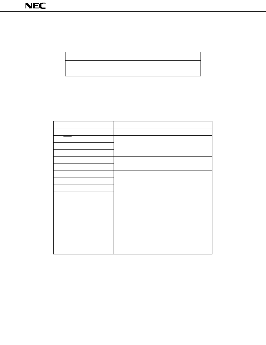
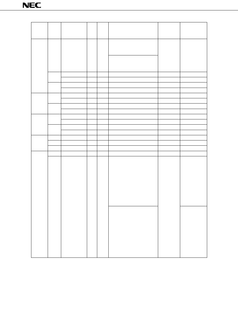
ORDERING INFORMATION
Part Number
Package
Quality Grade
µ
PD75004CU-xxx
42-pin plastic shrink DIP (600 mil)
Standard
µ
PD75004GB-xxx-3B4
44-pin plastic QFP (
s
s
10 mm)
Standard
µ
PD75006CU-xxx
42-pin plastic shrink DIP (600 mil)
Standard
µ
PD75006GB-xxx-3B4
44-pin plastic QFP (
s
s
10 mm)
Standard
µ
PD75008CU-xxx
42-pin plastic shrink DIP (600 mil)
Standard
µ
PD75008GB-xxx-3B4
44-pin plastic QFP (
s
s
10 mm)
Standard
Remarks: xxx is ROM code number.
Please refer to "Quality Grade on NEC Semiconductor Devices" (Document Number IEI-1209) published by
NEC Corporation to know the specification of quality grade on the devices and its recommended applications.

µ
PD75004, 75006, 75008
3
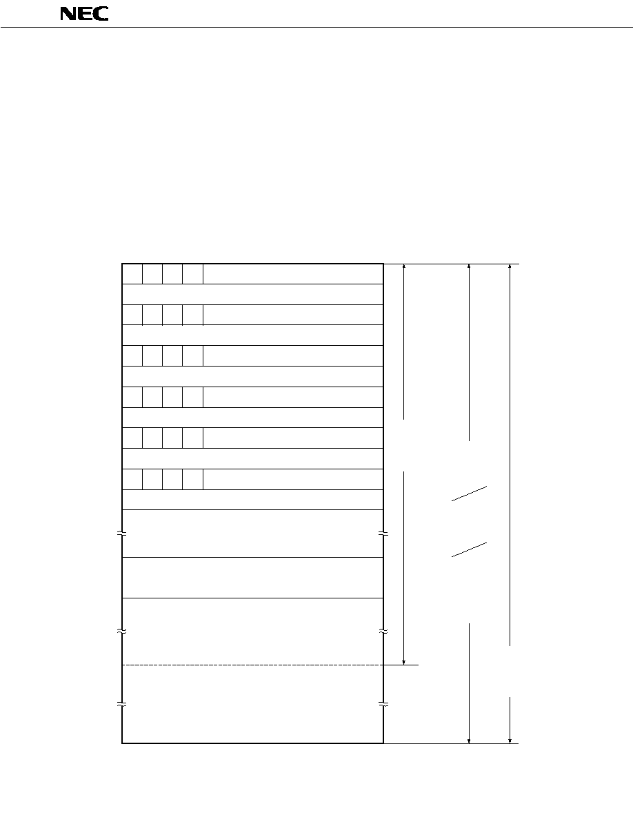
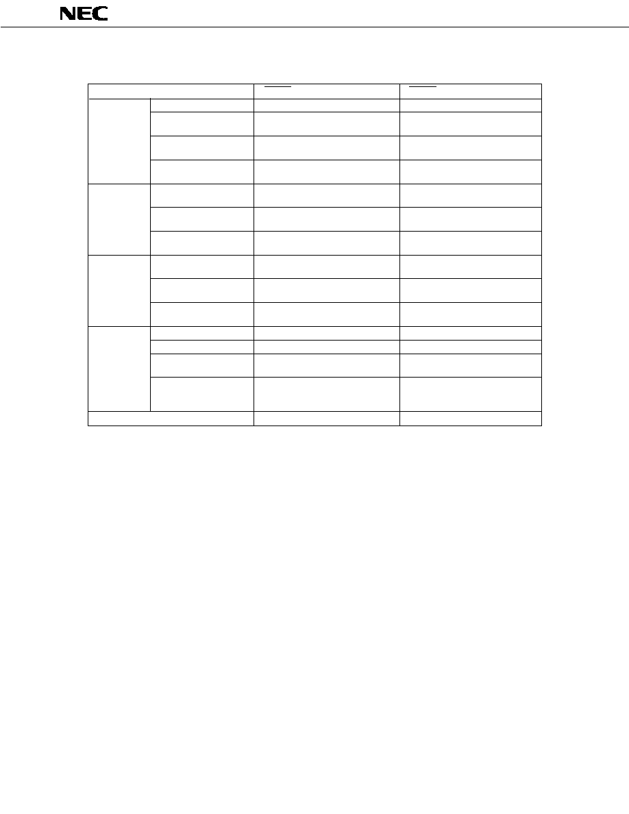
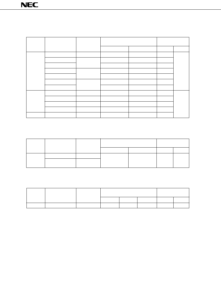
FUNCTIONAL OUTLINE
Item
Function
Instruction
0.95, 1.91, and 15.3
µ
s, (Main system clock: operating at 4.19 MHz)
Execution Time
122
µ
s (Subsystem clock: operating at 32.768 kHz)
4096
◊
8-bit (
µ
PD75004)
ROM
6016
◊
8-bit (
µ
PD75006)
8064
◊
8-bit (
µ
PD75008)
RAM
512
◊
4-bit
General-Purpose
∑ 4-bit manipulation: 8
Registers
∑ 8-bit manipulation: 4
8
CMOS Input pins
Internal pull-up resistor
specification by software
18
CMOS input/output pins
is possible. : 25
34
Can directly drive LED: 4
8
N-ch open-drain
Withstand voltage: 10V
input/output
Internal pull-up resistor
Can directly drive LED: 8
specification by mask option
is possible.
Timer/event counter
Timer
3 chs
Basic interval timer: Also serves as watchdog timer
Watch timer: Buzzer output possible
Serial
3-line serial I/O mode
Interface
2-line serial I/O mode
SBI mode
Bit Sequential
16 bits
Buffer
Clock Output Function
,
f
x
/2
3
,
f
x
/2
4
,
f
x
/2
6
Vector Interrupt
External: 3, Internal: 3
Test Input
External: 1, Internal: 1
System Clock
Main system clock oscillation ceramic/crystal oscillator
Oscillator
Subsystem clock oscillation crysal ocillator
Standby Function
STOP/HALT mode
Operating
≠40 to +85
∞
C
Temperature Range
Operating Supply
2.7 to 6.0 V
Voltage
Package
42-pin plastic shrink DIP (600 mil)
44-pin plastic QFP (
s
s
10 mm)
Internal
Memory
I/O Port

µ
PD75004, 75006, 75008
4
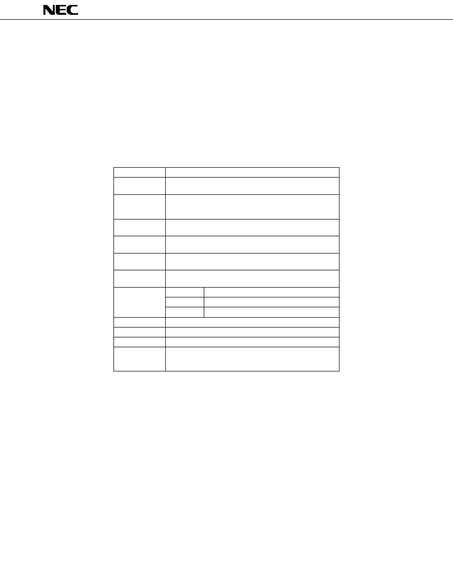
CONTENTS
1.
PIN CONFIGURATION (TOP VIEW) ...............................................................................................
6
2.
BLOCK DIAGRAM ...........................................................................................................................
8
3.
PIN FUNCTIONS ..............................................................................................................................
9
3.1
PORT PINS .............................................................................................................................................
9
3.2
NON PORT PINS ...................................................................................................................................
11
3.3
PIN INPUT/OUTPUT CIRCUITS ...........................................................................................................
12
3.4
SELECTION OF MASK OPTION ..........................................................................................................
14
3.5
RECOMMENDED PROCESSING OF UNUSED PINS ..........................................................................
14
3.6
NOTES ON USING THE P00/INT4, AND RESET PINS ......................................................................
15
4.
MEMORY CONFIGURATION ..........................................................................................................
16
5.
PERIPHERAL HARDWARE FUNCTIONS ........................................................................................
20
5.1
PORTS ....................................................................................................................................................
20
5.2
CLOCK GENERATOR CIRCUIT ............................................................................................................
21
5.3
CLOCK OUTPUT CIRCUIT ....................................................................................................................
22
5.4
BASIC INTERVAL TIMER .....................................................................................................................
23
5.5
WATCH TIMER ......................................................................................................................................
24
5.6
TIMER/EVENT COUNTER .....................................................................................................................
24
5.7
SERIAL INTERFACE ..............................................................................................................................
26
5.8
BIT SEQUENTIAL BUFFER ...................................................................................................................
28
6.
INTERRUPT FUNCTIONS ................................................................................................................
28
7.
STANDBY FUNCTIONS ..................................................................................................................
30
8.
RESET FUNCTION ...........................................................................................................................
31
9.
INSTRUCTION SET .........................................................................................................................
33
10. ELECTRICAL SPECIFICATIONS ......................................................................................................
40
11. CHARACTERISTIC CURVES ...........................................................................................................
53

µ
PD75004, 75006, 75008
5
12. PACKAGE DRAWINGS ...................................................................................................................
58
13. RECOMMENDED SOLDERING CONDITIONS ...............................................................................
61
APPENDIX A. DEVELOPMENT TOOLS ..............................................................................................
62
APPENDIX B.
RELATED DOCUMENTS ..............................................................................................
63
µ
PD75004, 75006, 75008
6
1.
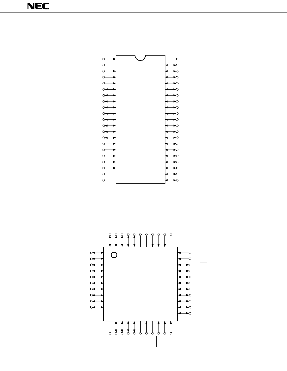
PIN CONFIGURATION (Top View)
∑ 42-pin plastic shrink DIP (600 mil)
P72/KR6
NC
P03/TI0
P73/KR7
PD75004GB≠xxx≠3B4
µ
P20/PTO0
P21
P22/PCL
P23/BUZ
V
NC
P10/INT0
P11/INT1
P12/INT2
NC
P43
P42
P40
V
XT1
XT2
RESET
X1
X2
1
44 43 42 41 40 39 38 37 36 35 34
12 13 14 15 16 17 18 19 20 21 22
P71/KR5
P70/KR4
P63/KR3
P62/KR2
P61/KR1
P60/KR0
P53
P52
P51
P50
2
3
4
5
6
7
8
9
10
11
33
32
31
30
29
28
27
26
25
24
23
P00/INT4
P01/SCK
P02/SO/SB0
P03/SI/SB1
P80
P81
P30
P31
P32
P33
P41
DD
SS
PD75006GB≠xxx≠3B4
µ
PD75008GB≠xxx≠3B4
µ
XT1
V
PD75004CU-xxx
µ
1
XT2
RESET
X1
X2
P33
P32
P31
P30
P81
P80
SI/SB1/P03
SO/SB0/P02
SCK/P01
INT4/P00
TI0/P13
INT2/P12
INT1/P11
INT0/P10
NC
2
3
4
5
6
7
8
9
10
11
12
13
14
15
16
17
18
19
20
42
41
40
39
38
37
36
35
34
33
32
31
30
29
28
27
26
25
24
23
P40
P41
P42
P43
P50
P51
P52
P53
P60/KR0
P61/KR1
P62/KR2
P63/KR3
P70/KR4
P71/KR5
P72/KR6
P73/KR7
P20/PTO0
P21
P22/PCL
21
22
SS
P23/BUZ
PD75006CU-xxx
µ
PD75008CU-xxx
µ
V
DD
∑ 44-pin plastic QFP (
s
s
10 mm)

µ
PD75004, 75006, 75008
7
Pin names
P00-P03 : Port 0
SO
: Serial Output
P10-P13 : Port 1
SB0,SB1
: Serial Bus 0,1
P20-P23 : Port 2
RESET
: Reset Input
P30-P33 : Port 3
TI0
: Timer Input 0
P40-P43 : Port 4
PTO0
: Programmable Timer Output 0
P50-P53 : Port 5
BUZ
: Buzzer Clock
P60-P63 : Port 6
PCL
: Programmable Clock
P70-P73 : Port 7
INT0, 1, 4
: External Test Interrupt 0,1,4
P80-P81 : Port 8
INT2
: External Test Input 2
KR0-KR7 : Key Return
X1, 2
: Main System Clock Oscillation 1,2
SCK
: Serial Clock
XT1, 2
: Subsystem Clock Oscillation 1,2
SI
: Serial Input
NC
: No Connection
µ
PD75004,
75006,
75008
8
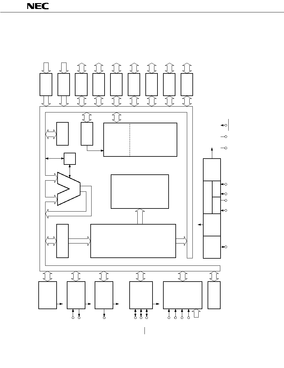
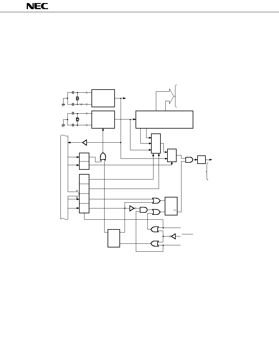
2.
BLOCK DIAGRAM
TI0/P13
BASIC
INTERVAL
TIMER
INTBT
TIMER/EVENT
COUNTER
#0
INTT0
PTO0/P20
BUZ/P23
WATCH
TIMER
INTW
INTCSI
CLOCKED
SERIAL
INTERFACE
SI/SB1/P03
SO/SB0/P02
SCK/P01
PROGRAM
COUNTER *
ALU
CY
SP (8)
BANK
INT0/P10
INT1/P11
INT2/P12
INT4/P00
KR0/P60
≠KR7/P73
INTERRUPT
CONTROL
BIT SEQ.
BUFFER (16)
PROGRAM
MEMORY
(ROM)
4096 8 BITS
( PD75004)
6016 8 BITS
( PD75006)
8064 8 BITS
( PD75008)
◊
DECODE
AND
CONTROL
GENERAL REG.
DATA
MEMORY
(RAM)
512 4 BITS
◊
f /2
X
N
V
DD
V
SS
RESET
PCL/P22
XT1
XT2 X1
X2
SUB
MAIN
CLOCK
OUTPUT
CONTROL
CLOCK
DIVIDER
SYSTEM CLOCK
GENERATOR
STAND BY
CONTROL
CPU
CLOCK
PORT 8
P80-P81
2
PORT 6
P60-P63
4
PORT 5
P50-P53
4
PORT 4
P40-P43
4
PORT 3
P30-P33
4
PORT 2
P20-P23
4
PORT 1
P10-P13
4
PORT 0
P00-P03
4
◊
µ
µ
PORT 7
P70-P73
4
◊
µ
*: For PD75004, 12 bits. For PD75006 and PD75008, 13 bits.
µ
µ
µ
µ
PD75004, 75006, 75008
9
3.
PIN FUNCTIONS
3.1
PORT PINS (1/2)
Input/
Output
Circuit
TYPE*
1
P00
P01
P02
P03
P10
P11
P12
P13
P20
P21
P22
P23
P30*
2
P31*
2
P32*
2
P33*
2
P40-43*
2
P50-53*
2
Pin Name Input/Output
Function
8-Bit I/O
When Reset
Also Served
As
INT4
SCK
SO/SB0
SO/SB1
INT0
INT1
INT2
TI0
PTO0
--
PCL
BUZ
--
--
--
--
--
--
4-bit input port (PORT0)
Pull-up resistors can be specified in 3-bit
units for the P01 to P03 pins by software.
With noise elimination function
4-bit input port (PORT1)
Internal pull-up resistors can be
specified in 4-bit units by software.
4-bit input/output port (PORT2)
Internal pull-up resistors can be
specified in 4-bit units by software.
Programmable 4-bit input/output port
(PORT3)
This port can be specified for input/
output in bit units.
Internal pull-up resistors can be
specified in 4-bit units by software.
N-ch open-drain 4-bit input/output port
(PORT4)
Internal pull-up resistors can be
specified in bit units. (mask option)
Resistive voltage is 10 V in the open-
drain mode.
N-ch open-drain 4-bit input/output port
(PORT5)
Internal pull-up resistors can be
specified in bit units. (mask option)
Resistive voltage is 10 V in the open-
drain mode.
Input
Input
Input
Input
High level
(with internal
pull-up
resistor) or
high imped-
ance
B
B -C
E-B
E-B
M
M
X
X
X
X
*1: Circles indicate Schmitt trigger inputs.
2: Can directly drive LED.
Input
Input/
Output
Input/
Output
Input/
Output
Input
Input/
Output
Input/
Output
Input/
Output
Input/
Output
q
q
F -A
M -C
F -B
High level
(with internal
pull-up
resistor) or
high imped-
ance

µ
PD75004, 75006, 75008
10
P60
P61
P62
P63
P70
P71
P72
P73
P80
P81
KR0
KR1
KR2
KR3
KR4
KR5
KR6
KR7
--
--
q
q
Input/
Output
Input/
Output
Input/
Output
Also Served
As
3.1
PORT PINS (2/2)
Input/
Output
Circuit
TYPE*
1
Programmable 4-bit input/output port
(PORT6)
This port can be specified for input/
output in bit units.
Internal pull-up resistors can be
specified in 4-bit units by software.
Input
F -A
4-bit input/output port (PORT7)
Internal pull-up resistors can be
specified in 4-bit units by software.
Input
F -A
Pin Name Input/Output
Function
8-Bit I/O
When Reset
2-bit input/output port (PORT8)
Internal pull-up resistors can be
specified in 2-bit units by software.
X
Input
E-B
*1: Circles indicate Schmitt trigger inputs.
2: Can directly drive LED.

µ
PD75004, 75006, 75008
11
TI0
PTO0
PCL
BUZ
SCK
SO/SB0
SI/SB1
INT4
INT0
INT1
INT2
KR0-KR3
KR4-KR7
P13
P20
P22
P23
P01
P02
P03
P00
P10
P11
P12
P60-P63
P70-P73
Input
Input
Input
Input
Input
Input
Input
Input
Input
Input
Input
Input
B -C
E-B
E-B
E-B
F -A
F -B
M -C
B
B -C
B -C
F -A
F -A
Pin Name Input/Output
Also Served
As
Functon
When Reset
Input/
Output
Circuit
TYPE*
1
3.2
NON PORT PINS
Timer/event counter external event pulse Input
Timer/event counter output
Clock output
Fixed frequency output (for buzzer or for trim-
ming the system clock)
Serial clock input/output
Serial data output
Serial bus input/output
Serial data input
Serial bus input/output
Edge detection vector interrupt input (both
rising and falling edge detection are effective)
Edge detection vector
interrupt input (detection
edge can be selected)
Edge detection testable
input (rising edge detection)
Clock synchronous
Asynchronous
Asynchronous
X1, X2
RESET
NC *
2
V
DD
V
SS
Input
--
Input
--
--
--
--
--
--
--
B
--
--
--
--
--
--
--
Input
--
--
*1: Circles indicate Schmitt trigger inputs.
2: When sharing the printed circut board with the
µ
PD75P008, the NC pin must be directly
connected to V
DD
.
Input
Input/
Output
Input/
Output
Input/
Output
Input/
Output
Input/
Output
Input/
Output
Input
Input
Input
Input/
Output
Input/
Output
XT1
XT2
--
Input
--
Input
--
Parallel falling edge detection testable input
Parallel falling edge detection testable input
To connect the crystal/ceramic oscillator to the
main system clock generator. When inputting the
external clock, input the external clock to pin X1,
and the reverse phase of the external clock to pin
X2.
To connect the crystal oscillator to the subsystem
clock generator.
When the external clock is used, pin XT1 inputs
the external clock. In this case, pin XT2 must be
left open.
System reset input
No connection
Positive power supply
GND
µ
PD75004, 75006, 75008
12
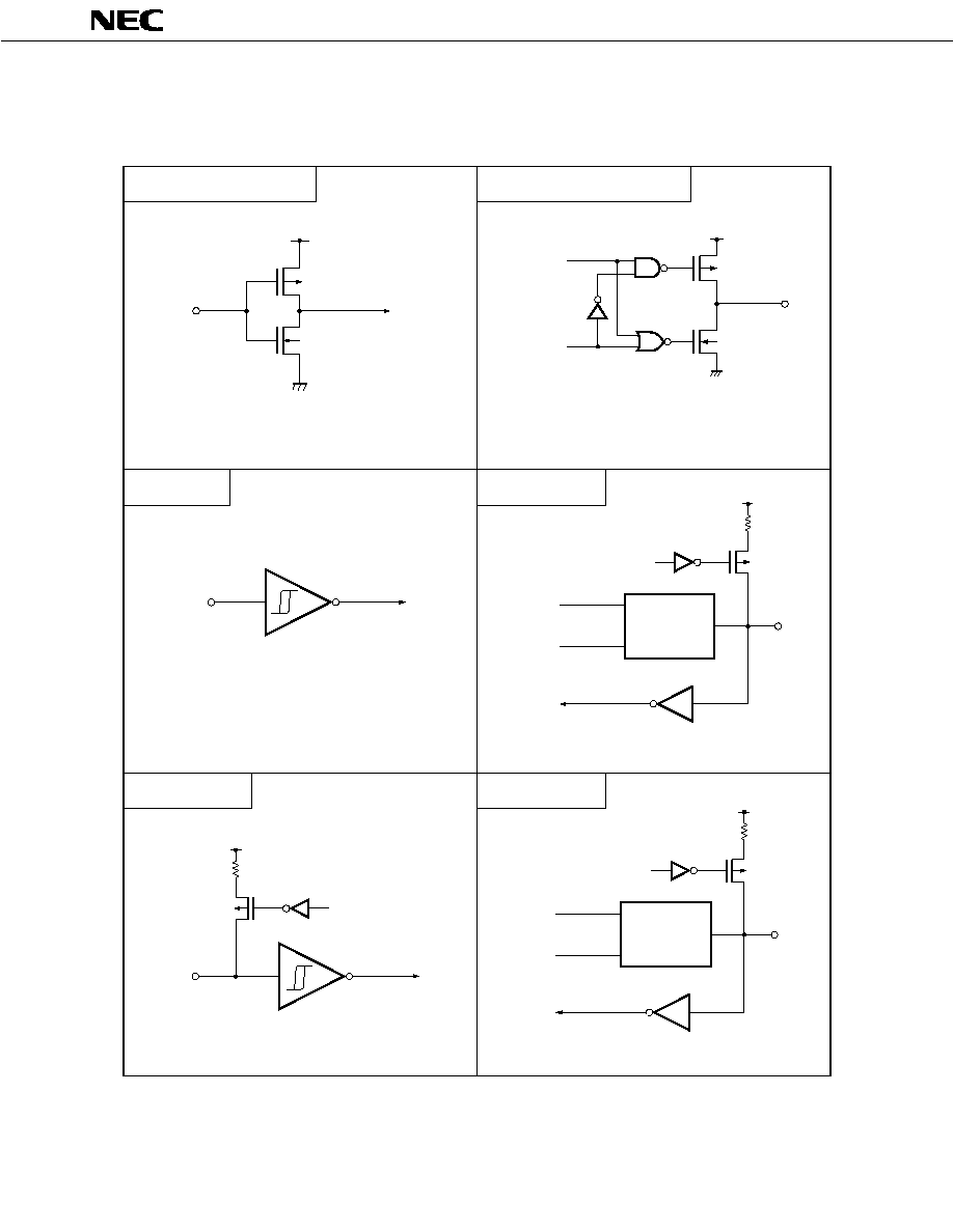
3.3
PIN INPUT/OUTPUT CIRCUITS
The following shows a simplified input/output circuit diagram for each pin of the
µ
PD75008.
TYPE A (for TYPE E≠B)
TYPE D (for TYPE E
≠
B, F
TYPE B
TYPE E≠B
IN
V
DD
Input buffer of CMOS standard
data
output
disable
OUT
P≠ch
N≠ch
Push≠pull output that can be set in a output
high≠impedance state (both P≠ch and N≠ch are off)
IN
Schmitt trigger input with hysteresis characteristics
data
output
disable
Type D
Type A
P.U.R.
enable
V
DD
P.U.R.
P≠ch
IN/OUT
P.U.R. : Pull≠Up Resistor
P.U.R.
enable
V
DD
P.U.R.
P≠ch
TYPE B≠C
TYPE F≠A
IN
data
output
disable
Type D
Type B
P.U.R.
enable
V
DD
P.U.R.
P≠ch
IN/OUT
P.U.R. : Pull≠Up Resistor
P.U.R. : Pull≠Up Resistor
A)
≠
V
DD

µ
PD75004, 75006, 75008
13
TYPE M≠C
TYPE F≠B
data
output
disable
P.U.R.
enable
V
DD
IN/OUT
Middle voltage input buffer
(withstand voltage: +10 V)
P.U.R. : Pull≠Up Resistor
data
output
disable
P.U.R.
enable
V
DD
P.U.R.
P≠ch
N-ch
P-ch
output
disable
(P)
output
disable
(N)
V
DD
(Mask option)
P.U.R. : Pull≠Up Resistor
IN/OUT
data
output
disable
P.U.R.
enable
V
DD
P.U.R.
IN/OUT
P≠ch
N-ch
P.U.R. : Pull≠Up Resistor
N-ch
(withstand
voltage:
+10 V)
TYPE M
µ
PD75004, 75006, 75008
14
3.4
SELECTION OF MASK OPTION
The following mask operations are available and can be specified for each pin.
Table 3-1 Mask Option Selection
Pin
Mask Option
P40-P43,
P50-P53
∑ With pull-up resistor
∑ Without pull-up resistor
*: Mask option can be specified in bit units.
3.5
RECOMMENDED PROCESSING OF UNUSED PINS
Table 3-2 Processing of Unused Pins
Pin
Recommended Connections
P00/INT4
Connect to V
SS
P01/SCK
P02/SO/SB0
Connect to V
SS
or V
DD
P03/SI/SB1
P10/INT0-P12/INT2
P13/TI0
P20/PTO0
P21
P22/PCL
P23/BUZ
P30-P33
Input
: Connect to V
SS
or V
DD
P40-P43
Output: Open
P50-P53
P60-P63
P70-P73
P80-P81
XT1
Connect to V
SS
or V
DD
XT2
Open
Connect to V
SS
5

µ
PD75004, 75006, 75008
15
3.6
NOTES ON USING THE P00/INT4, AND RESET PINS
In addition to the functions described in Sections 3.1 PORT PINS and 3.2 NON PORT PINS, an exclusive
function for setting the test mode, in which the internal fuctions of the
µ
PD75008 are tested (solely used for
IC tests), is provided to the P00/INT4 and RESET pins.
If a voltage exceeding V
DD
is applied to either of these pins, the
µ
PD75008 is put into test mode. Therefore,
even when the
µ
PD75008 is in normal operation, if noise exceeding the V
DD
is input into any of these pins, the
µ
PD75008 will enter the test mode, and this will cause problems for normal operation.
As an example, if the wiring to the P00/INT4 pin or the RESET pin is long, stray noise may be picked up
and the above montioned problem may occur.
Therefore, all wiring to these pins must be made short enough to not pick up stray noise. If noise cannot
be avoided, suppress the noise using a capacitor or diode as shown in the figure below.
∑
Connect a capacitor across P00/INT4 and
RESET, and V
DD
.
V
DD
V
DD
P00/INT4, RESET
V
DD
V
DD
P00/INT4, RESET
Low V
F
diode
∑
Connect a diode having a low V
F
across
P00/INT4 and RESET, and V
DD
. (0.3 V max.)
5
µ
PD75004, 75006, 75008
16
4.
MEMORY CONFIGURATION
∑
Program memory (ROM) ... 4096
◊
8 bits (0000H-0FFFH) :
µ
PD75004
... 6016
◊
8 bits (0000H-177FH) :
µ
PD75006
... 8064
◊
8 bits (0000H-1F7FH) :
µ
PD75008
∑ 0000H-0001H : Vector table to which address from which program is started is written after reset
∑ 0002H-000BH: Vector table to which address from which program is started is written after interrupt
∑ 0020H-007FH : Table area referenced by GETI instruction
∑
Data memory (RAM)
∑ Data area .... 512
◊
4 bits (000H≠1FFH)
∑ Peripheral hardware area .... 128
◊
4 bits (F80H≠FFFH)
7
6
5
MBE
0
0
MBE
0
0
MBE
0
0
MBE
0
0
MBE
0
0
MBE
0
0
Internal reset start address (upper 4 bits)
Internal reset start address (lower 8 bits)
INTBT/INT4 start address (upper 4 bits)
INTBT/INT4 start address (lower 8 bits)
INT0 start address (upper 4 bits)
INT0 start address (lower 8 bits)
INT1 start address (upper 4 bits)
INT1 start address (lower 8 bits)
INTCSI start address (upper 4 bits)
INTCSI start address (lower 8 bits)
INTT0 start address (upper 4 bits)
INTT0 start address (lower 8 bits)
000H
002H
004H
006H
008H
00AH
020H
07FH
080H
7FFH
800H
FFFH
GETI instruction reference table
0
CALLF
!faddr
instruction
entry
address
BRCD ! caddr
instruction
branch address
CALL ! addr
instruction
subroutine
entry address
BR $addr
instruction
relational
branch address
(≠15 to ≠1,
+2 to +16)
Branch destination
address and
subroutine entry
address for
GETI instruction
Address
4
0
0
0
0
0
0
Fig. 4-1 Program Memory Map (
µ
PD75004)
µ
PD75004, 75006, 75008
17
7
6
5
MBE
0
0
MBE
0
0
MBE
0
0
MBE
0
0
MBE
0
0
MBE
0
0
Internal reset start address (upper 5 bits)
Internal reset start address (lower 8 bits)
INTBT/INT4 start address (upper 5 bits)
INTBT/INT4 start address (lower 8 bits)
INT0 start address (upper 5 bits)
INT0 start address (lower 8 bits)
INT1 start address (upper 5 bits)
INT1 start address (lower 8 bits)
INTCSI start address (upper 5 bits)
INTCSI start address (lower 8 bits)
INTT0 start address (upper 5 bits)
INTT0 start address (lower 8 bits)
0000H
0002H
0004H
0006H
0008H
000AH
0020H
007FH
0080H
07FFH
0800H
0FFFH
1000H
177FH
GETI instruction reference table
0
BRCB
! caddr
instruction
branch
address
CALLF
! faddr
instruction
entry
address
BR ! addr
instruction
branch address
CALL ! addr
instruction
subroutine
entry address
BR $addr
instruction
relational
branch address
(≠15 to ≠1,
+2 to +16)
Branch destination
address and
subroutine entry
address for
GETI instruction
Address
BRCB ! caddr
instruction
branch address
Fig. 4-2 Program Memory Map (
µ
PD75006)

µ
PD75004, 75006, 75008
18
7
6
5
MBE
0
0
MBE
0
0
MBE
0
0
MBE
0
0
MBE
0
0
MBE
0
0
Internal reset start address (upper 5 bits)
Internal reset start address (lower 8 bits)
INTBT/INT4 start address (upper 5 bits)
INTBT/INT4 start address (lower 8 bits)
INT0 start address (upper 5 bits)
INT0 start address (lower 8 bits)
INT1 start address (upper 5 bits)
INT1 start address (lower 8 bits)
INTCSI start address (upper 5 bits)
INTCSI start address (lower 8 bits)
INTT0 start address (upper 5 bits)
INTT0 start address (lower 8 bits)
0000H
0002H
0004H
0006H
0008H
000AH
0020H
007FH
0080H
07FFH
0800H
0FFFH
1000H
1F7FH
GETI instruction reference table
0
BRCB
! caddr
instruction
branch
address
CALLF
! faddr
instruction
entry
address
BR ! addr
instruction
branch address
CALL ! addr
instruction
subroutine
entry address
BR $addr
instruction
relational
branch address
(≠15 to ≠1,
+2 to +16)
Branch destination
address and
subroutine entry
address for
GETI instruction
Address
BRCB ! caddr
instruction
branch address
Fig. 4-3 Program Memory Map (
µ
PD75008)

µ
PD75004, 75006, 75008
19
000H
007H
008H
0FFH
100H
1FFH
F80H
FFFH
Data memory
Memory bank
(8
◊
4)
256
◊
4
(248
◊
4)
Not provided
128
◊
4
0
1
15
General-purpose
register area
Stack area
Data area
Static RAM
(512
◊
4)
Peripheral hardware area
256
◊
4
Fig. 4-4 Data Memory Map

µ
PD75004, 75006, 75008
20
5.
PERIPHERAL HARDWARE FUNCTIONS
5.1
PORTS
I/O ports are classified into the following 3 kinds:
∑
CMOS input (PORT0, 1)
:
8
∑
CMOS input/output (PORT2, 3, 6, 7, and 8) : 18
∑
N-ch open-drain input/output (PORT4, 5)
:
8
Total
: 34
Remarks
Multiplexed with SO/SB0,
SI/SB1, SCK, INT0-2, 4,
and TIO
Port 6 is multiplexed with
KR0 to KR3.
Port 2 is multiplexed with
PTO0, PCL, and BUZ.
Port 7 is multiplexed with
KR4-KR7.
Can be connected to a
pull-up resistor in 1-bit
units by using mask
option.
--
PORT0
PORT1
PORT3*
PORT6
PORT2
PORT7
PORT4*
PORT5*
PORT8
Function
4-bit input
4-bit input/output
4-bit input/output
(N-ch open-drain,
10 V)
2-bit input/output
Table 5-1 Port Function
Operation and Feature
Can be always read or tested regardless of opera-
tion mode of multiplexed pin.
Can be set in input or output mode in 1-bit units.
Can be set in input or output mode in 4-bit units.
Ports 6 and 7 are used in pairs to input/output data
in 8-bit units.
Can be set in input or output mode in 4-bit units.
Ports 4 and 5 are used in pairs to input/output data
in 8-bit units.
Can be set input or output mode in 2-bit units.
*: Can directly drive LED.
Port Name
(Symbol)
µ
PD75004, 75006, 75008
21
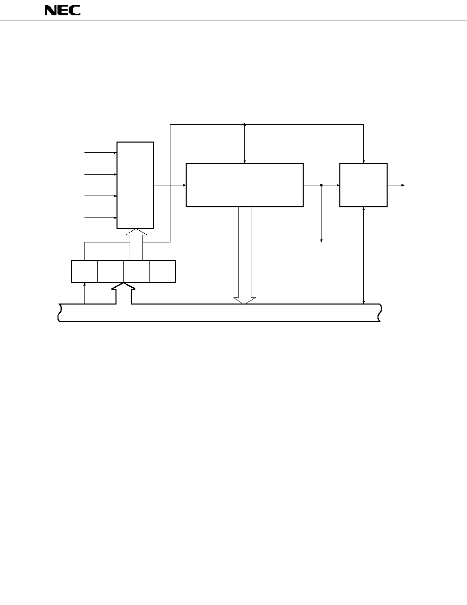
5.2
CLOCK GENERATOR CIRCUIT
The operation of the clock generator circuit is determined by the processor clock control regiser (PPC) and
system clock control register (SCC).
This circuit can generate two types of clocks: main system clock and subsystem clock.
In addition, it can also change the instruction execution time.
∑
0.95
µ
s, 1.91
µ
s, 15.3
µ
s (main system clock: 4.19 MHz)
∑
122
µ
s (subsystem clock: 32.768 kHz)
*: instruction execution.
Remarks 1: f
X
= Main system clock frequency
2: f
XT
= Subsystem clock frequency
3:
=
CPU clock
4: PCC: Processor clock control register
5: SCC: System clock control register
6: One clock cysle (t
CY
) of
is one machine cycle of an instruction. For t
CY
, refer to AC
characteristics in 10. ELECTRICAL SPECIFICATIONS.
Fig. 5-1 Clock Generator Block Diagram
XT1
XT2
X1
X2
f
XT
f
X
Watch timer
Subsystem
clock
oscillator
Main system
clock
oscillator
1/2 1/16
1/8 to 1/4096
Frequency divider
∑ Basic interval timer (BT)
∑ Timer/event counter
∑ Serial interface
∑ Watch timer
∑ INT0 noise rejecter circuit
∑ Clock output circuit
Internal bus
WM.3
SCC
SCC3
SCC0
PCC
PCC0
PCC1
PCC2
PCC3
HALT*
STOP*
4
PCC2, PCC3
clear signal
STOP F/F
Q
S
R
Q
S
R
HALT F/F
Oscillator
disable
signal
Frequency
divider
1/4
Selector
Selector
∑ CPU
∑ INT0 noise
rejecter circuit
∑ Clock output
circuit
Wait release
signal from BT
RESET signal
Standby release
signal from interrupt
control circuit
5

µ
PD75004, 75006, 75008
22
5.3
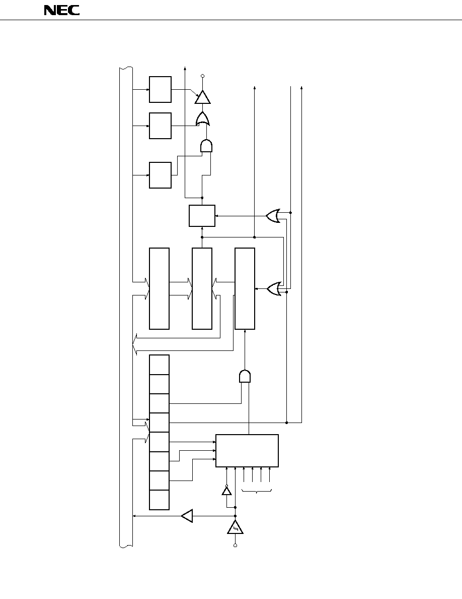
CLOCK OUTPUT CIRCUIT
The clock output circuit outputs clock pulse from the P22/PCL pin. This clock output circuit is used to output
clock pulses to the remote control output, peripheral LSIs, etc.
∑
Clock output (PCL)
:
, 524, 262, 65.5 kHz (operating at 4.19 MHz)
∑
Buzzer output (BUZ) : 2 kHz (operating at 4.19 MHz, or 32.768 kHz)
Fig. 5-2 shows the clock output circuit configuration.
Selector
Output
buffer
PCL/P22
Bit 2 of PMGB
PORT2.2
Port 2 input/
output mode
specification
bit
P22 output
latch
Internal bus
CLOM3 CLOM2 CLOM1 CLOM0 CLOM
4
f
X
/2
3
f
X
/2
4
f
X
/2
6
From the
clock
generator
Fig. 5-2 Clock Output Circuit Configuration
Remarks:
A measures to prevent outputting narrow width pulse when selecting clock output enable/
disable is taken.
µ
PD75004, 75006, 75008
23
5.4
BASIC INTERVAL TIMER
The basic interval timer has these functions:
∑
Interval timer operation which generates a reference time interrupt
∑
Watchdog timer application which detects a program runaway
∑
Selects the wait time for releasing the standby mode and counts the wait time
∑
Reads out the count value
Remarks : *: Instruction execution
Fig. 5-3 Basic Interval Timer Configuration
From the
clock generator
f
X
/2
5
f
X
/2
7
f
X
/2
9
f
X
/2
12
MPX
Clear
Basic interval timer
(8-bit frequency divider circuit)
3
4
8
BT
Clear
Set
signal
BT
interrupt
request flag
IRQBT
Wait release signal
for standby release
Vector
interrupt
request
signal
Internal bus
BTM3
BTM2
BTM1
BTM0
BTM
SET1*

µ
PD75004, 75006, 75008
24
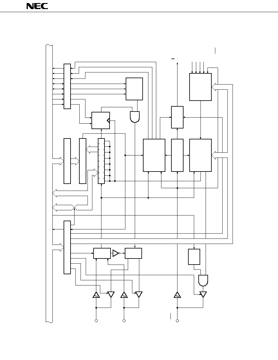
5.5
WATCH TIMER
The
µ
PD75008 has a built-in 1-ch watch timer. The watch timer is configured as shown in Fig. 5-4.
∑
Sets the test flag (IRQW) with 0.5 sec interval.
The standby mode can be released by IRQW.
∑
0.5 second interval can be generated either from the main system clock or subsystem clock.
∑
Time interval can be advanced to 128 times faster (3.91 ms) by setting the fast mode. This is convenient
for program debugging, test, etc.
∑
Fixed frequency (2.048 kHz) can be output to the P23/BUZ pin. This can be used for beep and system clock
frequency trimming.
∑
The frequency divider circuit can be cleared so that zero second watch start is possible.
WM7 WM6 WM5 WM4 WM3 WM2 WM1 WM0
Selector
Frequency divider
f
W
2
7
(256 Hz: 3.91 ms)
INTW
(IRQW
set signal)
f
W
2
14
(2 Hz
0.5 sec)
Selector
f
W
(32.768
kHz)
f
W
16
(2.048
kHz)
Clear
f
X
128
(32.768 kHz)
f
XT
(32.768 kHz)
From the
clock
generator
WM
PORT2.3
Bit 2 of PMGB
Output buffer
P23/BUZ
P23
output
latch
Port 2
input/output
mode
Bit test
instruction
8
Internal bus
( ) is for f
X
= 4.194304 MHz, f
XT
= 32.768 kHz.
Fig. 5-4 Watch Timer Block Diagram
5.6
TIMER/EVENT COUNTER
The
µ
PD75008 has a built-in 1-ch timer/event counter. The timer/even counter has these functions:
∑
Programmable interval timer operation
∑
Outputs square-wave signal of an arbitrary frequency to the PTO0 pin.
∑
Event counter operation
∑
Divides the TI0 pin input in N and outputs to the PTO0 pin (frequency divider operation).
∑
Supplies serial shift clock to the serial interface circuit.
∑
Count condition read out function
µ
PD75004,
75006,
75008
25
Internal bus
8
8
SET1*
TM07 TM06 TM05 TM04 TM03 TM02 TM01 TM00
TM0
PORT1.3
Input
buffer
P13/TI0
From
the clock
generator
MPX
*1: SET1: Instruction execution
*2: Refer to Fig. 5-1.
Timer operation start signal
CP
8
8
Modulo register (8)
Comparator (8)
Count register (8)
Clear
T0
TMOD0
Reset
TOE0
PORT2.0
Bit 2 of PGMB
To serial interface
P20/PTO0
INTT0
IRQT0
set signal
(
)
RESET
IRQT0
clear signal
Output
buffer
TOUT
F/F
TO
enable
flag
P20
output
latch
Port 2
input/
output
mode
Coinci-
dence
8
Fig. 5-5 Timer/Event Counter Block Diagram
1
2
*

µ
PD75004, 75006, 75008
26
5.7
SERIAL INTERFACE
The
µ
PD75008 is equipped with a serial interface that operates in the following modes:
∑
Three-line serial I/O mode (MSB/LSB first selectable)
∑
Two-line serial I/O mode (MSB first)
∑
SBI mode (MSB first)
In the three-line I/O mode, the microcomputer can be connected to a microcomputer in the 75X series or 78K
series devices, or various I/O devices. In the two-line serial mode and SBI mode, communication can be established
with two or more devices.
µ
PD75004,
75006,
75008
27
Internal bus
8/4
8
8
8
CSIM
P03/SI/SB1
P02/SO/SB0
P01/SCK
P01
output
latch
Selector
Selector
Bit
test
Slave address register
(SVA)
Address comparator
Shift register (SIO)
SET CLR
Bit manipulation
(8)
(8)
Coincidence
signal
SBIC
RELT
CMDT
SO latch
Bit test
ACKT
ACKE
BSYE
Busy/
acknowledge
output
circuit
Bus release/
command/
acknowledge
detector
circuit
RELD
CMDD
ACKD
Serial clock
counter
Serial clock
control
circuit
INTCSI
control
circuit
Serial clock
selector
INTCSI
IRQCSI
set signal
(
)
D
Q
f
X
/2
3
f
X
/2
4
f
X
/2
6
TOUT F/F
(from timer/
event counter)
External SCK
(8)
Fig. 5-6 Serial Interface Block Diagram

µ
PD75004, 75006, 75008
28
5.8
BIT SEQUENTIAL BUFFER .... 16 BITS
The bit sequential buffer is a data memory specifically provided for bit manipulation. With this buffer,
addresses and bit specifications can be sequentially up-dated in bit manipulation operation. Therefore, this
buffer is very useful for processing long data in bit units.
Remarks: For the pmem.@L addressing, the specification bit is shifted according to the L register.
Fig. 5-7 Bit Sequential Buffer Format
6. INTERRUPT FUNCTIONS
The
µ
PD75008 has 8 different interrupt sources and multiplexed interrupt through the software control.
In addition to that, the
µ
PD75008 is also provided with two types of edge detection testable inputs.
The interrupt control circuit of the
µ
PD75008 has these functions:
∑
Hardware controlled vector interrupt function which can control whether or not to accept an interrupt by
using the interrupt flag (IExxx) and interrupt master enable flag (IME).
∑
The interrupt start address can be arbitrarily set.
∑
Interrupt request flag (IRQxxx) test function (an interrupt generation can be confirmed by means of
software).
∑
Standby mode release (Interrupts to be released can be selected by the interrupt enable flag).
Address bit
Symbol
L register
3
2
1
0
3
2
1
0
3
2
1
0
3
2
1
0
L = F
L = C L = B
L = 8 L = 7
L = 4 L = 3
L = 0
BSB3
BSB2
BSB1
BSB0
DECS L
INCS L
FC3H
FC2H
FC1H
FC0H

µ
PD75004,
75006,
75008
29
Internal bus
2
1
3
IM2
IM1
IM0
IRQBT
INT4
/P00
INT0
/P10
INT1
/P11
INT2
/P12
KR0/P60
KR7/P73
Noise
elimination
circuit
INT
BT
INTCSI
INTT0
INTW
Selector
Both edge
delection
circuit
Edge
delection
circuit
Edge
delection
circuit
Rising edge
delection
circuit
Falling edge
delection
circuit
IRQ4
IRQ0
IRQ1
IRQCSI
IRQT0
IRQW
IRQ2
IM2
Interrupt enable flag (IE )
◊◊◊
IME
VRQn
Decoder
IST0
Priority control
circuit
Vector table
address
generator
Standby
release signal
Fig. 6-1 Interrupt Control Block Diagram
µ
PD75004, 75006, 75008
30
7. STANDBY FUNCTIONS
The
µ
PD75008 has two different standby modes (STOP mode and HALT mode) to reduce the power
consumption while waiting for program execution.
Table 7-1 Each Status in Standby Mode
Setting Instruction
STOP instrtuction
HALT instruction
Can be set only when operating on
the main system clock
Can be set either with the main
system clock or the subsystem clock
Operation
Status
Clock Generator
Only the main system clock stops its
operation.
Only the CPU clock
stops its
operation. (oscillation continues)
Basic Interval
Timer
No operation
Can operate only when main system
clock oscillates (Sets IRQBT at
reference time interval)
Serial Interface
Can operate only when the external
SCK input is selected for the serial
clock
Can operate only when external SCK
input is selected as serial clock, or
when main system clock oscillates
Timer/Event
Counter
Can operate only when the TI0 pin
input is selected for the count clock
Can operate only when TI0 pin input
is selected as count clock, or when
main system clock oscillates
Watch Timer
Can operate when f
XT
is selected as
the count clock
Can operate
STOP Mode
HALT Mode
System Clock for Setting
Release Signal
An interrupt request signal from a
hardware whose operation is
enabled by the interrupt enable flag
or the RESET signal input
An interrupt request signal from a
hardware whose operation is
enabled by the interrupt enable flag
or the RESET signal input
External Interrupt
INT1, INT2, and INT4 can operate.
Only INT0 can not operate.
CPU
No operation

µ
PD75004, 75006, 75008
31
8. RESET FUNCTION
When the RESET signal is input, the
µ
PD75008 is reset and each hardware is initialized as indicated in Table
8-1. Fig. 8-1 shows the reset operation timing.
RESET input
Wait
(31.3ms/4.19MHz)
Operation mode
or standby mode
HALT mode
Operation mode
Internal reset operation
Fig. 8-1 Reset Operation by RESET Input
Table 8-1 Status of Each Hardware after Reset (1/2)
Hardware
RESET Input in Standby Mode
RESET Input during Operation
Program Counter (PC)
The contents of the lower 4 bits
of address 000H of the program
memory are set to PC11-8, and
the contents of address 001H are
set to PC7-0.
Same as at left
PSW
Carry Flag (CY)
Retained
Undefined
Skip Flag (SK0-2)
0
0
Interrupt Status Flag (IST0)
0
0
Bank Enable Flag (MBE)
The contents of bit 7 of address
000H of the program memory is
set to MBE.
Same as at left
Stack Pointer (SP)
Undefined
Undefined
Data Memory (RAM)
Retained
Undefined
General-Purpose Register
(X, A, H, L, D, E, B, C)
Bank Selection Register (MBS)
0
Undefined
Timer/Event
Counter
Counter (T0)
0
0
Module Register
(TMOD0)
Mode Register (TM0)
0
0
TOE0, TOUT F/F
0, 0
0, 0
Mode Register (BTM)
0
0
Mode Register (WM)
0
Watch Timer
0
*
Basic Interval
Timer
Counter (BT)
0
Undefined
*: Data of address 0F8H to 0FDH of the data memory becomes undefined when a RESET signal is input.
Retained
Undefined
FFH
FFH
µ
PD75004, 75006, 75008
32
Serial
Shift Register (SIO)
Retained
Undefined
Interface
Operation Mode
0
0
Register (CSIM)
SBI Control Register
0
0
(SBIC)
Slave Address Register
Retained
Undefined
(SVA)
Clock
Processor Clock Control
0
0
Generator,
Register (PCC)
Clock Output
System Clock Control
0
0
Circuit
Register (SCC)
Clock Output Mode
0
0
Register (CLOM)
Interrupt
Interrupt Enable Flag
0
0
Function
(IExxx)
Interrupt Master Enable
0
0
Flag (IME)
INT0, INT1, INT2 Mode
0, 0, 0
0, 0, 0
Registers (IM0, 1, 2)
Digital Port
Output Buffer
Off
Off
Output Latch
Clear (0)
Clear (0)
Input/Output Mode
0
0
Register (PMGA, B, C)
Pull-Up Resistor
0
0
Specification Register
(POGA, B)
Bit sequential buffer (BSB0-3)
Retained
Specified
Hardware
RESET Input during Operation
RESET Input in Standby Mode
Table 8-1 Status of Each Hardware after Reset (2/2)
µ
PD75004, 75006, 75008
33
9.
INSTRUCTION SET
(1)
Operand representation and description
Describe one or more operands in the operand field of each instruction according to the operand
representation and description methods of the instruction (for details, refer to RA75X Assembler Package
User's Manual - Language (EEU-730)). With some instructions, only one operand should be selected from
several operands. The uppercase characters, +, and ≠ are keywords and must be described as is.
Describe an appropriate numeric value or label as immediate data.
The symbols in the register and flag symbols can be described as labels in the places of mem, fmem,
pmem, and bit (for details, refer to
µ
PD7500X Series User`s Manual (IEM-5033)). However, fmem and
pmem restricts the label that can be described.
Representation
Description
reg
X, A, B, C, D, E, H, L
reg1
X, B, C, D, E, H, L
rp
XA, BC, DE, HL
rp1
BC, DE, HL
rp2
BC, DE
rpa
HL, DE, DL
rpa1
DE, DL
n4
4-bit immediate data or label
n8
8-bit immediate data or label
mem*
8-bit immediate data or label
bit
2-bit immediate data or label
fmem
FB0H to FBFH,FF0H to FFFH immediate data or label
pmem
FC0H to FFFH immediate data or label
µ
PD75004
0000H to 0FFFH immediate data or label
addr
µ
PD75006
0000H to 177FH immediate data or label
µ
PD75008
0000H to 1F7FH immediate data or label
caddr
12-bit immediate data or label
faddr
11-bit immediate data or label
taddr
20H to 7FH immediate data (where bit0 = 0) or label
PORTn
PORT0 to PORT8
IExxx
IEBT, IECSI, IET0, IE0, IE1, IE2, IE4, IEW
MBn
MB0, MB1, MB15
*: Only even address can be described as mem for 8-bit data processing.

µ
PD75004, 75006, 75008
34
(2)
Legend of operation field
A
: A register; 4-bit accumulator
B
: B register; 4-bit accumulator
C
: C register; 4-bit accumulator
D
: D register; 4-bit accumulator
E
: E register; 4-bit accumulator
H
: H register; 4-bit accumulator
L
: L register; 4-bit accumulator
X
: X register; 4-bit accumulator
XA
: Register pair (XA); 8-bit accumulator
BC
: Register pair (BC); 8-bit accumulator
DE
: Register pair (DE); 8-bit accumulator
HL
: Register pair (HL); 8-bit accumulator
PC
: Program counter
SP
: Stack pointer
CY
: Carry flag; or bit accumulator
PSW
: Program status word
MBE
: Memory bank enable flag
PORTn : Port n (n = 0 to 8)
IME
: Interrupt mask enable flag
IExxx
: Interrupt enable flag
MBS
: Memory bank selector register
PCC
: Processor clock control register
.
: Delimiter of address and bit
(xx)
: Contents addressed by xx
xxH
: Hexadecimal data
µ
PD75004, 75006, 75008
35
(3)
Symbols in addressing area field
*1
MB = MBE . MBS
(MBS = 0, 1, 15)
*2
MB = 0
*3
MBE = 0 : MB = 0 (00H-7FH)
Data memory
MB = 15 (80H-FFH)
addressing
MBE = 1 : MB = MBS (MBS = 0, 1, 15)
*4
MB = 15, fmem = FB0H-FBFH,
FF0H-FFFH
*5
MB = 15, pmem = FC0H-FFFH
*6
addr = 000H-FFFH (
µ
PD75004)
0000H-177FH (
µ
PD75006)
0000H-1F7FH (
µ
PD75008)
*7
addr = (Current PC) ≠ 15 to (Current PC) ≠ 1
(Current PC) + 2 to (Current PC) + 16
Program
*8
caddr = 000H-FFFH (
µ
PD75004)
memory
0000H-0FFFH (PC
12
= 0 :
µ
PD75006, 75008)
addressing
0000H-177FH (PC
12
= 1 :
µ
PD75006)
0000H-1F7FH (PC
12
= 1 :
µ
PD75008)
*9
faddr = 0000H-07FFH
*10
taddr = 0020H-007FH
Remarks 1:
MB indicates memory bank that can be accessed.
2:
In *2, MB = 0 regardless of MBE and MBS.
3:
In *4 and *5, MB = 15 regardless of MBE and MBS.
4:
*6 to *10 indicate areas that can be addressed.
(4)
Machine cycle field
In this field, S indicates the number of machine cycles required when an instruction having a skip
function skips. The value of S varies as follows:
∑
When no instruction is skipped ........................................................................
S = 0
∑
When 1-byte or 2-byte instruction is skipped .................................................
S = 1
∑
When 3-byte instruction (BR ! addr or CALL ! addr) is skipped ..................
S = 2
Note : The GETI instruction is skipped in one machine cycle.
One machine cycle equals to one cycle of the CPU clock
, (=t
CY
), and can be changed in three steps
depending on the setting of the processor clock control register (PCC).
µ
PD75004, 75006, 75008
36
Ma-
Ad-
Instruc-
Mne-
Operand
Bytes
chine
Operation
dress-
Skip
tions
monics
Cyc-
ing
Conditions
les
Area
Transfer MOV
A, #n4
1
1
A
n4
String effect A
reg1, #n4
2
2
reg1
n4
XA, #n8
2
2
XA
n8
String effect A
HL, #n8
2
2
HL
n8
String effect B
rp2, #n8
2
2
rp2
n8
A, @HL
1
1
A
(HL)
*1
A, @rpa1
1
1
A
(rpa1)
*2
XA, @HL
2
2
XA
(HL)
*1
@HL, A
1
1
(HL)
A
*1
@HL, XA
2
2
(HL)
XA
*1
A,mem
2
2
A
(mem)
*3
XA, mem
2
2
XA
(mem)
*3
mem, A
2
2
(mem)
A
*3
mem, XA
2
2
(mem)
XA
*3
A, reg
2
2
A
reg
XA, rp
2
2
XA
rp
reg1, A
2
2
reg1
A
rp1, XA
2
2
rp1
XA
XCH
A, @HL
1
1
A
(HL)
*1
A, @rpa1
1
1
A
(rpa1)
*2
XA, @HL
2
2
XA
(HL)
*1
A, mem
2
2
A
(mem)
*3
XA, mem
2
2
XA
(mem)
*3
A, reg1
1
1
A
reg1
XA, rp
2
2
XA
rp
MOVT
XA, @PCDE
1
3
∑
µ
PD75004
XA
(PC
11-8
+DE)
ROM
∑
µ
PD75006, 75008
XA
(PC
12-8
+DE)
ROM
XA, @PCXA
1
3
∑
µ
PD75004
XA
(PC
11-8
+XA)
ROM
∑
µ
PD75006, 75008
XA
(PC
12-8
+XA)
ROM
Arith-
ADDS
A, #n4
1
1+S
A
A+n4
carry
metic
A, @HL
1
1+S
A
A+(HL)
*1
carry
Opera-
ADDC
A, @HL
1
1
A, CY
A+(HL)+CY
*1
tion
SUBS
A, @HL
1
1+S
A
A-(HL)
*1
borrow
SUBC
A, @HL
1
1
A, CY
A-(HL)-CY
*1
AND
A, #n4
2
2
A
A
n4
A, @HL
1
1
A
A
(HL)
*1
OR
A, #n4
2
2
A
A
n4
A, @HL
1
1
A
A
(HL)
*1
XOR
A, #n4
2
2
A
A
n4
A, @HL
1
1
A
A
(HL)
*1
Accumu- RORC
A
1
1
CY
A
0
, A
3
CY, A
n-1
A
n
lator
Manipu-
NOT
A
2
2
A
A
lation

µ
PD75004, 75006, 75008
37
Ma-
Ad-
Instruc-
Mne-
Operand
Bytes
chine
Operation
dress-
Skip
tions
monics
Cyc-
ing
Conditions
les
Area
Incre-
INCS
reg
1
1+S
reg
reg+1
reg = 0
ment/
@HL
2
2+S
(HL)
(HL)+1
*1
(HL) = 0
Decre-
mem
2
2+S
(mem)
(mem)+1
*3
(mem) = 0
ment
DECS
reg
1
1+S
reg
reg-1
reg = FH
Compare SKE
reg, #n4
2
2+S
Skip if reg = n4
reg = n4
@HL, #n4
2
2+S
Skip if (HL) = n4
*1 (HL) = n4
A, @HL
1
1+S
Skip if A = (HL)
*1
A = (HL)
A, reg
2
2+S
Skip if A = reg
A = reg
Carry
SET1
CY
1
1
CY
1
flag
CLR1
CY
1
1
CY
0
Manipu- SKT
CY
1
1+S
Skip if CY = 1
CY = 1
lation
NOT1
CY
1
1
CY
CY
Memory/ SET1
mem.bit
2
2
(mem.bit)
1
*3
Bit
fmem.bit
2
2
(fmem.bit)
1
*4
Manipu-
pmem.@L
2
2
(pmem
7-2
+ L
3-2
.bit(L
1-0
))
1
*5
lation
@H+mem.bit
2
2
(H + mem
3-0
.bit)
1
*1
CLR1
mem.bit
2
2
(mem.bit)
0
*3
fmem.bit
2
2
(fmem.bit)
0
*4
pmem.@L
2
2
(pmem
7-2
+ L
3-2
.bit(L
1-0
))
0
*5
@H+mem.bit
2
2
(H+mem
3-0
.bit)
0
*1
SKT
mem.bit
2
2+S
Skip if (mem.bit) = 1
*3
(mem.bit) = 1
fmem.bit
2
2+S
Skip if (fmem.bit) = 1
*4
(fmem.bit) = 1
pmem.@L
2
2+S
Skip if (pmem
7-2
+L
3-2
.bit (L
1-0
)) = 1
*5
(pmem.@L) = 1
@H+mem.bit
2
2+S
Skip if (H + mem
3-0
.bit) = 1
*1
(@H+mem.bit) = 1
SKF
mem.bit
2
2+S
Skip if (mem.bit) = 0
*3
(mem.bit) = 0
fmem.bit
2
2+S
Skip if (fmem.bit) = 0
*4
(fmem.bit) = 0
pmem.@L
2
2+S
Skip if (pmem
7-2
+L
3-2
.bit (L
1-0
)) = 0
*5
(pmem.@L) = 0
@H+mem.bit
2
2+S
Skip if (H + mem
3-0
.bit) = 0
*1
(@H+mem.bit) = 0
SKTCLR fmem.bit
2
2+S
Skip if (fmem.bit) = 1 and clear
*4
(fmem.bit) = 1
pmem.@L
2
2+S
Skip if (pmem
7-2
+L
3-2
.bit
*5
(pmem.@L) = 1
(L
1-0
)) = 1 and clear
@H+mem.bit
2
2+S
Skip if (H+mem
3-0
.
bit) = 1 and clear
*1
(@H+mem.bit) = 1
AND1
CY,fmem.bit
2
2
CY
CY
(fmem.bit)
*4
CY,pmem.@L
2
2
CY
CY
(pmem
7-2
+L
3-2
.bit(L
1-0
)) *5
CY,@H+mem.bit
2
2
CY
CY
(H+mem
3-0
.bit)
*1
OR1
CY,fmem.bit
2
2
CY
CY
(fmem.bit)
*4
CY,pmem.@L
2
2
CY
CY
(pmem
7-2
+L
3-2
.bit (L
1-0
))
*5
CY,@H+mem.bit
2
2
CY
CY
(H+mem
3-0
.bit)
*1
XOR1
CY,fmem.bit
2
2
CY
CY
(fmem.bit)
*4
CY,pmem.@L
2
2
CY
CY
(pmem
7-2
+L
3-2
.
bit (L
1-0
))
*5
CY,@H+mem.bit
2
2
CY
CY
(H+mem
3-0
.bit)
*1

µ
PD75004, 75006, 75008
38
Ma-
Ad-
Instruc-
Mne-
Operand
Bytes
chine
Operation
dress-
Skip
tions
monics
Cyc-
ing
Conditions
les
Area
Branch
BR
addr
--
--
∑
µ
PD75004
*6
PC
11-0
addr
(The most suitable instruction
is selectable from among
BRCB !caddr, and BR $addr
depending on the assembler.)
∑
µ
PD75006, 75008
PC
12-0
addr
(The most suitable instruction
is selectable from among BR
!addr, BRCB !caddr, and BR
$addr depending on the
assembler.)
!addr
3
3
∑
µ
PD75006, 75008
*6
PC
12-0
addr
$addr
1
2
∑
µ
PD75004
*7
PC
11-0
addr
∑
µ
PD75006, 75008
PC
12-0
addr
BRCB
!caddr
2
2
∑
µ
PD75004
*8
PC
11-0
caddr
11-0
∑
µ
PD75006, 75008
PC
12-0
PC
12
+ caddr
11-0
Subrou-
CALL
!addr
3
3
∑
µ
PD75004
*6
tine/
(SP-4)(SP-1)(SP-2)
PC
11-0
Stack
(SP-3)
MBE, 0, 0, 0
Control
PC
11-0
addr, SP
SP-4
∑
µ
PD75006, 75008
(SP-4)(SP-1)(SP-2)
PC
11-0
(SP-3)
MBE, 0, 0, PC
12
PC
12-0
addr, SP
SP-4
CALLF
!faddr
2
2
∑
µ
PD75004
*9
(SP-4)(SP-1)(SP-2)
PC
11-0
(SP-3)
MBE, 0, 0, 0
PC
11-0
0,
faddr, SP
SP-4
∑
µ
PD75006, 75008
(SP-4)(SP-1)(SP-2)
PC
11-0
(SP-3)
MBE, 0, 0, PC
12
PC
12-0
0, 0, faddr, SP
SP-4
RET
1
3
∑
µ
PD75004
MBE, x, x, x
(SP+1)
PC
11-0
(SP)(SP+3)(SP+2)
SP
SP+4
∑
µ
PD75006, 75008
MBE, x, x, PC
12
(SP+1)
PC
11-0
(SP)(SP+3)(SP+2)
SP
SP+4
RETS
1
3+S
∑
µ
PD75004
Undefined
MBE, x, x, x
(SP+1)
PC
11-0
(SP)(SP+3)(SP+2)
SP
SP+4,
then skip unconditionally
∑
µ
PD75006, 75008
MBE, x, x, PC
12
(SP+1)
PC
11-0
(SP)(SP+3)(SP+2)
SP
SP+4,
then skip unconditionally
µ
PD75004, 75006, 75008
39
Ma-
Ad-
Instruc-
Mne-
Operand
Bytes
chine
Operation
dress-
Skip
tions
monics
Cyc-
ing
Conditions
les
Area
RETI
1
3
∑
µ
PD75004
MBE, x, x, x
(SP+1)
PC
11-0
(SP)(SP+3)(SP+2)
PSW
(SP+4)(SP+5), SP
SP+6
∑
µ
PD75006, 75008
MBE, x, x, PC
12
(SP+1)
PC
11-0
(SP)(SP+3)(SP+2)
PSW
(SP+4)(SP+5), SP
SP+6
PUSH
rp
1
1
(SP-1)(SP-2)
rp, SP
SP-2
BS
2
2
(SP-1)
MBS, (SP-2)
0, SP
SP-2
POP
rp
1
1
rp
(SP+1)(SP), SP
SP+2
BS
2
2
MBS
(SP+1), SP
SP+2
Inter-
EI
2
2
IME
1
rupt
IExxx
2
2
IExxx
1
Control
DI
2
2
IME
0
IExxx
2
2
IExxx
0
I/O
IN *
A, PORTn
2
2
A
PORT
n
(n = 0-8)
XA, PORTn
2
2
XA
PORT
n+1
,PORT
n
(n = 4, 6)
OUT *
PORTn, A
2
2
PORT
n
A
(n = 2-8)
PORTn, XA
2
2
PORT
n+1
, PORT
n
XA
(n = 4, 6)
CPU
HALT
2
2
Set HALT Mode (PCC.2
1)
Control
STOP
2
2
Set STOP Mode (PCC.3
1)
NOP
1
1
No Operation
Special
SEL
MBn
2
2
MBS
n (n = 0, 1, 15)
GETI
taddr
1
3
∑
µ
PD75004
*10
Where TBR instruction,
PC
11-0
(taddr)
3-0
+(taddr+1)
Where TCALL instruction,
(SP-4)(SP-1)(SP-2)
PC
11-0
(SP-3)
MBE, 0, 0, 0
PC
11-0
(taddr)
3-0
+(taddr+1)
SP
SP-4
Except for TBR and TCALL
Depends on
instructions,
referenced
Instruction execution of
instruction
(taddr)(taddr+1)
∑
µ
PD75006, 75008
Where TBR instruction,
PC
12-0
(taddr)
4-0
+(taddr+1)
Where TCALL instruction,
(SP-4)(SP-1)(SP-2)
PC
11-0
(SP-3)
MBE, 0, 0, PC
12
PC
12-0
(taddr)
4-0
+(taddr+1)
SP
SP-4
Except for TBR and TCALL
Depends on
instructions,
referenced
Instruction execution of
instruction
(taddr)(taddr+1)
*: When executing the IN/OUT instruction, MBE = 0, or MBE = 1, and MBS = 15.
.........................................................
.............................
.........................................................
.............................
.........................................................
.............................
.........................................................
.............................
Subrou-
tine/
Stack
Control
(Cont`d)

µ
PD75004, 75006, 75008
40
10. ELECTRICAL SPECIFICATIONS
ABSOLUTE MAXIMUM RATINGS (T
a
= 25
∞
C)
Parameter
Symbol
Conditions
Ratings
Unit
Supply Voltage
V
DD
-0.3 to +7.0
V
V
I1
Other than ports 4, 5
-0.3 to V
DD
+0.3
V
Input Voltage
V
I2
Ports 4, 5
w/pull-up
-0.3 to V
DD
+0.3
V
resistor
Open drain
-0.3 to +11
V
Output Voltage
V
O
-0.3 to V
DD
+0.3
V
High-Level Output
I
OH
1 pin
-10
mA
Current
All pins
-30
mA
Low-Level Output
I
OL
*
Ports 0, 3, 4, 5
Peak
30
mA
Current
1 pin
rms
15
mA
Other than ports 0, 3, 4, 5
Peak
20
mA
1 pin
rms
10
mA
Total of ports 0, 3, 4, 5, 8
Peak
160
mA
rms
120
mA
Total of ports 2, 6, 7
Peak
66
mA
rms
33
mA
Operating Temperature
T
opt
-40 to +85
∞
C
Storage Temperature
T
stg
-65 to +150
∞
C
*: rms = Peak value x
Duty
CAPACITANCE (T
a
= 25
∞
C, V
DD
= 0 V)
Parameter
Symbol
Conditions
MIN.
TYP.
MAX.
Unit
Input Capacitance
C
IN
f = 1 MHz
15
pF
Output Capacitance
C
OUT
Pins other than thosemeasured are at 0 V
15
pF
Input/Output
C
IO
15
pF
Capacitance

µ
PD75004, 75006, 75008
41
MAIN SYSTEM CLOCK OSCILLATOR CIRCUIT CHARACTERISTICS
(T
a
= -40 to +85
∞
C, V
DD
= 2.7 to 6.0 V)
Oscillator
Recommended
Item
Conditions
MIN.
TYP.
MAX.
Unit
Constants
Ceramic
Oscillation
V
DD
= Oscillation
1.0
5.0
MHz
frequency(f
XX
)*
1
voltage range
Oscillation stabiliza- After V
DD
come to
tion time*
2
MIN. of oscillation
voltage range
4
ms
Crystal
Oscillation
1.0
4.19
5.0
MHz
frequency (f
XX
)*
1
Oscillation stabiliza- V
DD
= 4.5 to 6.0 V
10
ms
tion time*
2
30
ms
External Clock
X1 input frequency
1.0
5.0
MHz
(f
X
)*
1
X1 input high-,
low-level widths
(t
XH
, t
XL
)
100
500
ns
*1: The oscillation frequency and X1 input frequency are indicated only to express the characteristics
of the oscillator circuit. For instruction execution time, refer to AC Characteristics.
2: Time required for oscillation to stabilize after V
DD
has been applied or the STOP mode has been
released.
3: When the oscillation frequency is 4.19 MHz
<
fx
5.0 MHz, do not select PCC = 0011 as the
instruction execution time: otherwise, one machine cycle is set to less than 0.95
µ
s, falling short
of the rated minimum value of 0.95
µ
s.
Note:
When using the oscillation circuit of the main system clock, wire the portion enclosed in dotted
line in the figures as follows to avoid adverse influences on the wiring capacity:
∑ Keep the wiring length as short as possible.
∑ Do not cross the wiring over the other signal lines.
∑ Do not route the wiring in the vicinity of lines through which a high alternating current flows.
∑ Always keep the ground point of the capacitor of the osccillator circuit at the same potential
as V
SS
. Do not connect the ground pattern through which a high current flows.
∑ Do not extract signals from the oscillation circuit.
X1
X2
C1
C2
X1
X2
C1
C2
X1
X2
PD74HCU04
µ
*
3
*
3
*
3
5
5

µ
PD75004, 75006, 75008
42
SUBSYSTEM CLOCK OSCILLATOR CIRCUIT CHARACTERISTICS
(T
a
= -40 to +85
∞
C, V
DD
= 2.7 to 6.0 V)
Oscillator
Recommended
Item
Conditions
MIN.
TYP.
MAX.
Unit
Constants
Crystal
Oscillation
32
32.768
35
kHz
frequency (f
XT
)*
1
Oscillation stabiliza- V
DD
= 4.5 to 6.0 V
1.0
2
s
tion time*
2
10
s
External Clock
XT1 input frequency
32
100
kHz
(f
XT
)*
1
XT1 input high-,
low-level widths
5
15
µ
s
(t
XTH
, t
XTL
)
XT1
XT2
R
C3
C4
XT1
XT2
Open
*1: Express the characteristcs of the oscillator circuit.
2: Time required for oscillator to stabilize after V
DD
has been applied.
Note: When using the oscillation circuit of the subsystem clock, wire the portion enclosed in dotted line
in the figures as follows to avoid adverse influences on the wiring capacity:
∑
Keep the wiring length as short as possible.
∑
Do not cross the wiring over the other signal lines.
∑
Do not route the wiring in the vicinity of lines through which a high alternating current flows.
∑
Always keep the ground point of the capacitor of the oscillator circuit at the same potential as V
SS
.
Do not connect the ground pattern through which a high current flows.
∑
Do not extract signals from the oscillation circuit.
The amplification factor of the subsystem clock oscillation circuit is designed to be low to reduce
the current dissipation and therefore, the subsystem clock oscillation circuit is influenced by noise
more easily than the main system clock oscillation circuit. When using the subsystem clock,
therefore, exercise utmost care in wiring the circuit.
5
µ
PD75004, 75006, 75008
43
RECOMMENDED OSCILLATION CIRCUIT CONSTANTS
MAIN SYSTEM CLOCK: CERAMIC OSCILLATOR (T
a
= -40 to +85
∞
C)
CSA x.xxMK*
1.00 to 1.99
30
30
2.7
CSA x.xxMG093*
30
30
2.7
CST x.xxMG093*
--
--
2.7
CSA x.xxMGU*
30
30
2.7
CST x.xxMGU*
--
--
2.7
CSA x.xxMG*
30
30
3.0
CST x.xxMG*
--
--
3.0
KBR-1000H
1.00
100
100
2.7
KBR-2.0MS
2.00
47
47
2.7
KBR-4.0MS
4.00
33
33
2.7
6.0
KBR-5.0M
5.00
33
33
3.0
CRHB4.00M
4.00
27
27
3.0
C1 (pF)
Murata
Mfg.
Frequency
(MHz)
Product Name
Manufac-
turer
MAX. (V)
MIN. (V)
Recommended Circuit
Constants
Operating
Voltage Range
C2 (pF)
Kyoto
Ceramic
2.00 to 2.44
2.45 to 5.00
2.00 to 5.00
*: x.xx indicates frequency.
HC-6U
1.0 to 2.0
HC-18U
2.0 to 5.0
20 *
22
2.7
6.0
HC-43U, 49/U
C1 (pF)
Kinseki
Frequency
(MHz)
Product Name
Manufac-
turer
MAX. (V)
MIN. (V)
Recommended Circuit
Constants
Operating
Voltage Range
C2 (pF)
MAIN SYSTEM CLOCK: XTAL (T
a
= -20 to +70
∞
C)
*: Adjust the oscillation frequency in a range of C
1
= 15 to 33 pF.
P-3
32.768
18 *
18
330
2.7
C3 (pF)
Kinseki
Frequency
(MHz)
Product Name
Manufac-
turer
MAX. (V)
MIN. (V)
Recommended Circuit
Constants
Operating
Voltage Range
6.0
SUBSYSTEM CLOCK: XTAL (T
a
= -10 to +60
∞
C)
C4 (pF)
R (k
)
*: Adjust the oscillation frequency in a range of C3 = 10 to 33 pF.
6.0
Toko

µ
PD75004, 75006, 75008
44
Parameter
Symbol
Conditions
MIN.
TYP.
MAX.
Unit
High-Level Input
V
IH1
Ports 2, 3, 8
0.7V
DD
V
DD
V
Voltage
V
IH2
Ports 0, 1, 6, 7, RESET
0.8V
DD
V
DD
V
V
IH3
Ports 4, 5
w/pull-up resistor
0.7V
DD
V
DD
V
Open-drain
0.7V
DD
10
V
V
IH4
X1, X2, XT1
V
DD
-0.5
V
DD
V
Low-level Input
V
IL1
Ports 2, 3, 4, 5, 8
0
0.3V
DD
V
Voltage
V
IL2
Ports 0, 1, 6, 7, RESET
0
0.2V
DD
V
V
IL3
X1, X2, XT1
0
0.4
V
High-Level Output
V
OH1
V
DD
= 4.5 to 6.0 V,
V
DD
-1.0
V
Voltage
I
OH
= -1 mA
I
OH
= -100
µ
A
V
DD
-0.5
V
Low-Level Output
V
OL1
Ports 4 and 5
Voltage
V
DD
= 4.5 to 6.0 V
0.4
2.0
V
I
OL
= 15 mA
Ports 3
V
DD
= 4.5 to 6.0 V
0.6
2.0
V
I
OL
= 15 mA
V
DD
= 4.5 to 6.0 V
I
OL
= 1.6 mA
0.4
V
I
OL
= 400
µ
A
0.5
V
SB0, 1
Pull-up
1 k
0.2V
DD
V
V
OL2
Open-drain
V
DD
= 4.5 to 6.0 V
Pull-up
5 k
0.2V
DD
V
High-Level Input
I
LIH1
V
IN
= V
DD
Other than below
3
µ
A
Leakage Current
I
LIH2
X1, X2, XT1
20
µ
A
I
LIH3
V
IN
= 10 V
Ports 4, 5
20
µ
A
(open-drain)
Low-Level Input
I
LIL1
V
IN
= 0 V
Other than below
-3
µ
A
Leakage Current
I
LIL2
X1, X2, XT1
-20
µ
A
High-Level Output
I
LOH1
V
OUT
= V
DD
Other than below
3
µ
A
Leakage Current
I
LOH2
V
OUT
= 10 V
Ports 4, 5
20
µ
A
(open-drain)
Low-Level Output
I
LOL
V
OUT
= 0 V
-3
µ
A
Leakage Current
Internal Pull-Up Resistor
R
L1
Ports 0, 1, 2, 3, 6, 7, 8 V
DD
= 5.0 V
±
10%
15
40
80
k
(except P00) V
IN
= 0V
V
DD
= 3.0 V
±
10%
30
300
k
R
L2
Ports 4, 5
V
DD
= 5.0 V
±
10%
15
40
70
k
V
OUT
= V
DD
-2.0 V
V
DD
= 3.0 V
±
10%
10
60
k
Ports 0, 2, 3, 6, 7,
8
.....
DC CHARACTERISTICS (T
a
= -40 to +85
∞
C, V
DD
= 2.7 to 6.0 V)
Ports 0, 2, 3, 4, 5,
6, 7, 8
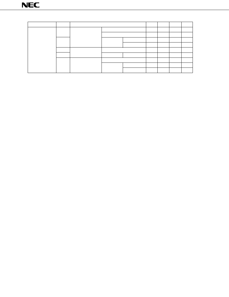
µ
PD75004, 75006, 75008
45
Parameter
Symbol
Conditions
MIN.
TYP.
MAX.
Unit
Supply Current *
1
I
DD1
4.19 MHz*
4
V
DD
= 5.0 V
±
10%*
2
2.5
8
mA
crystal oscillator
V
DD
= 3.0 V
±
10%*
3
0.35
1.2
mA
I
DD2
C1 = C2 = 22pF
HALT mode
V
DD
= 5 V
±
10%
500
1500
µ
A
V
DD
= 3 V
±
10%
150
450
µ
A
I
DD3
32.768 kHz*
5
V
DD
= 3 V
±
10%
30
90
µ
A
I
DD4
crystal oscillator
HALT mode
V
DD
= 3 V
±
10%
5
15
µ
A
I
DD5
XT1 = 0 V
V
DD
= 5 V
±
10%
0.5
20
µ
A
STOP mode
V
DD
= 3 V
±
10%
0.1
10
µ
A
T
a
= 25
∞
C
0.1
5
µ
A
*1: Current for the built-in pull-up resistor is not included.
2: When operand in the high-speed mode with the processor clock control register (PCC) set to 0011.
3: When operated in the low-speed mode with the PCC set to 0000.
4: Including when the subsystem clock is operated.
5: When operated with the subsystem clock by setting the system clock control register (SCC) to 1011
to stop the main system clock operation.
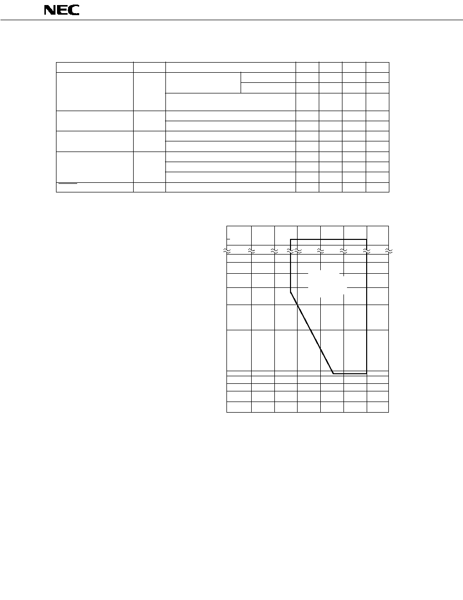
µ
PD75004, 75006, 75008
46
AC CHARACTERISTICS (T
a
= -40 to +85
∞
C, V
DD
= 2.7 to 6.0 V)
Parameter
Symbol
Conditions
MIN.
TYP.
MAX.
Unit
CPU Clock Cycle Time*
1
t
CY
w/main system clock
V
DD
= 4.5 to 6.0 V
0.95
64
µ
s
(Minimum Instruction
3.8
64
µ
s
Execution Time
w/subsystem clock
114
122
125
µ
s
= 1 Machine Cycle)
TI0 Input Frequency
f
TI
V
DD
= 4.5 to 6.0 V
0
1
MHz
0
275
kHz
TI0 Input High-, Low-
t
TIH
,
V
DD
= 4.5 to 6.0 V
0.48
µ
s
Level Widths
t
TIL
1.8
µ
s
Interrupt Input High-,
t
INTH
,
INT0
*2
µ
s
Low-Level Widths
t
INTL
INT1, 2, 4
10
µ
s
KR0-7
10
µ
s
RESET Low-Level Width
t
RSL
10
µ
s
0
1
2
3
4
5
6
0.5
1
2
3
4
5
6
60
Supply voltage V
DD
[V]
Cycle time t
CY
[ s]
t
CY
vs V
DD
(with main system clock)
µ
64
70
Operation
guaranteed
range
*1: The CPU clock (
) cycle time (minimum
instruction execution time) is
determined by the oscillation frequency
of the connected oscillator, system clock
control register (SCC), and processor
clock control register (PCC).
The figure on the right is cycle time t
CY
vs. supply voltage V
DD
characteristics
at the main system clock.
2: 2t
CY
or 128/f
X
depending on the setting
of the interrupt mode register (IM0).
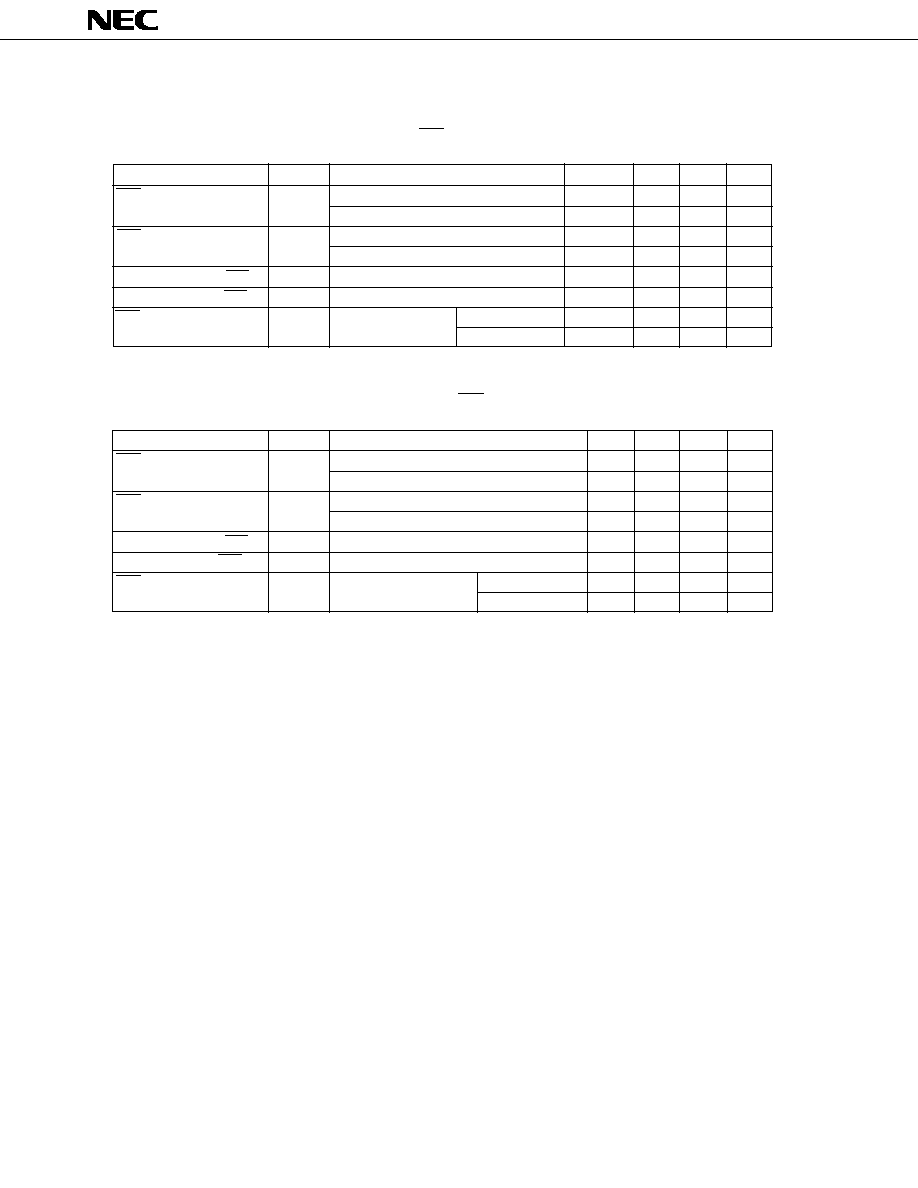
µ
PD75004, 75006, 75008
47
SERIAL TRANSFER OPERATION
Two-Line and Three-Line Serial I/O Modes (SCK: internal clock output):
Parameter
Symbol
Conditions
MIN.
TYP.
MAX.
Unit
SCK Cycle Time
t
KCY1
V
DD
= 4.5 to 6.0 V
1600
ns
3800
ns
SCK High-, Low-Level
t
KL1
V
DD
= 4.5 to 6.0 V
t
KCY1
/2-50
ns
Widths
t
KH1
t
KCY1
/2-150
ns
SI Set-Up Time (vs. SCK
)
t
SIK1
150
ns
SI Hold Time (vs. SCK
) t
KSI1
400
ns
SCK
SO Output
t
KSO1
R
= 1 k
,
V
DD
= 4.5 to 6.0 V
0
250
ns
Delay Time
C
= 100 pF*
0
1000
ns
TWO-LINE AND THREE-LINE SERIAL I/O MODES (SCK: external clock input):
Parameter
Symbol
Conditions
MIN.
TYP.
MAX.
Unit
SCK Cycle Time
t
KCY2
V
DD
= 4.5 to 6.0 V
800
ns
3200
ns
SCK High-, Low-Level
t
KL2
V
DD
= 4.5 to 6.0 V
400
ns
Widths
t
KH2
1600
ns
SI Set-Up Time (vs. SCK
)
t
SIK2
100
ns
SI Hold Time (vs. SCK
)
t
KSI2
400
ns
SCK
SO Output
t
KSO2
R
= 1 k
, C
= 100 pF*
V
DD
= 4.5 to 6.0 V
0
300
ns
Delay Time
0
1000
ns
*: R and C are load resistance and load capacitance of the SO output line.
µ
PD75004, 75006, 75008
48
SBI MODE (SCK: internal clock output (master)):
Parameter
Symbol
Conditions
MIN.
TYP.
MAX.
Unit
SCK Cycle Time
t
KCY3
V
DD
= 4.5 to 6.0 V
1600
ns
3800
ns
SCK High-, Low-Level
t
KL3
V
DD
= 4.5 to 6.0 V
t
KCY3
/2-50
ns
Widths
t
KH3
t
KCY3
/2-150
ns
SB0, 1 Set-Up Time
t
SIK3
150
ns
(vs. SCK
)
SB0, 1 Hold Time
t
KSI3
t
KCY3
/2
ns
(vs. SCK
)
SCK
SB0, 1 Output
t
KSO3
R
= 1 k
,
V
DD
= 4.5 to 6.0 V
0
250
ns
Delay Time
C
= 100 pF*
0
1000
ns
SCK
SB0, 1
t
KSB
t
KCY3
ns
SB0,1
SCK
t
SBK
t
KCY3
ns
SB0, 1 Low-Level Width
t
SBL
t
KCY3
ns
SB0, 1 High-Level Width
t
SBH
t
KCY3
ns
SBI MODE (SCK: external clock input (slave)):
Parameter
Symbol
Conditions
MIN.
TYP.
MAX.
Unit
SCK Cycle Time
t
KCY4
V
DD
= 4.5 to 6.0 V
800
ns
3200
ns
SCK High-, Low-Level
t
KL4
V
DD
= 4.5 to 6.0 V
400
ns
Widths
t
KH4
1600
ns
SB0, 1 Set-Up Time
t
SIK4
100
ns
(vs. SCK
)
SB0, 1 Hold Time
t
KSI4
t
KCY4
/2
ns
(vs. SCK
)
SCK
SB0, 1 Output
t
KSO4
R
= 1 k
,
V
DD
= 4.5 to 6.0 V
0
300
ns
Delay Time
C
= 100 pF*
0
1000
ns
SCK
SB0, 1
t
KSB
t
KCY4
ns
SB0,1
SCK
t
SBK
t
KCY4
ns
SB0, 1 Low-Level Width
t
SBL
t
KCY4
ns
SB0, 1 High-Level Width
t
SBH
t
KCY4
ns
*: R and C are load resistance and load capacitance of the SB0 and SB1 output lines.

µ
PD75004, 75006, 75008
49
AC TIMING TEST POINT (excluding X1 and XT1 inputs)
CLOCK TIMING
TI0 TIMING
X1 input
V
DD
≠0.5V
0.4 V
t
XL
t
XH
1/f
X
XT1 input
V
DD
≠0.5V
0.4 V
t
XTL
t
XTH
1/f
XT
TI0
t
TIL
t
TIH
1/f
TI
Test points
0.8 V
DD
0.2 V
DD
0.8 V
DD
0.2 V
DD

µ
PD75004, 75006, 75008
50
SERIAL TRANSFER TIMING
THREE-LINE SERIAL I/O MODE:
SCK
t
KL1
t
KH1
t
KCY1
Output data
t
SIK1
t
KSI1
t
KSO1
Input data
SI
SO
TWO-LINE SERIAL I/O MODE:
SCK
t
KL2
t
KH2
t
KCY2
t
SIK2
t
KSI2
t
KSO2
SB0,1
µ
PD75004, 75006, 75008
51
SERIAL TRANSFER TIMING
BUS RELEASE SIGNAL TRANSFER:
SCK
t
KL3,4
t
KCY3,4
t
SIK3,4
t
KSI3,4
t
KSO3,4
SB0,1
t
KH3,4
t
SBK
t
SBH
t
SBL
t
KSB
COMMAND SIGNAL TRANSFER:
SCK
t
KL3,4
t
KCY3,4
t
SIK3,4
t
KSI3,4
t
KSO3,4
SB0,1
t
KH3,4
t
SBK
t
KSB
RESET
t
RSL
RESET INPUT TIMING:
INT0, 1, 2, 4
KR0-7
t
INTL
t
INTH
INTERRUPT INPUT TIMING:
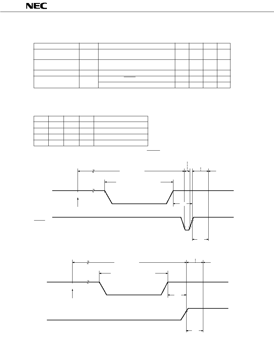
µ
PD75004, 75006, 75008
52
LOW-VOLTAGE DATA RETENTION CHARACTERISTICS OF DATA MEMORY IN STOP MODE
(T
a
= ≠40 to +85
∞
C)
Parameter
Symbol
Conditions
MIN.
TYP.
MAX.
Unit
Data Retention Supply
V
DDDR
2.0
6.0
V
Voltage
Data Retention Supply
I
DDDR
V
DDDR
= 2.0 V
0.1
10
µ
A
Current*
1
Release Signal Set Time
t
SREL
0
µ
s
Oscillation Stabilization
t
WAIT
Released by RESET
2
17
/f
X
ms
Wait Time*
2
Released by interrupt request
*3
ms
*1: Does not include current flowing through internal pull-up resistor
2: The oscillation stabilization wait time is the time during which the CPU is stopped to prevent
unstable operation when oscillation is started.
3: Depends on the setting of the basic interval timer mode register (BTM) as follows:
BTM3
BTM2
BTM1
BTM0
WAIT time ( ): f
XX
= 4.19 MH
z
≠
0
0
0
2
20
/f
XX
(approx. 250 ms)
≠
0
1
1
2
17
/f
XX
(approx. 31.3 ms)
≠
1
0
1
2
15
/f
XX
(approx. 7.82 ms)
≠
1
1
1
2
13
/f
XX
(approx. 1.95 ms)
DATA RETENTION TIMING (releasing STOP mode by RESET)
STOP mode
Data retention mode
STOP instruction
execution
V
DD
RESET
V
DDDR
t
SREL
t
WAIT
Operation
mode
Internal reset operation
HALT mode
STOP mode
Data retention mode
STOP instruction execution
V
DD
V
DDDR
t
SREL
t
WAIT
Operation
mode
HALT mode
Standby release signal
(interrupt request)
DATA RETENTION TIMING (standby release signal: releasing STOP mode by interrupt)

µ
PD75004, 75006, 75008
53
11. CHARACTERISTIC CURVES
I
DD
vs V
DD
(Crystal oscillation)
5000
1000
500
100
50
10
5
1
0
1
2
3
4
5
6
7
20 pF
18 pF
18 pF
330 k
X'tal
4.19 MHz
X'tal
32.768 kHz
18 pF
X1
X2
XT1
XT2
HALT mode
Low-speed mode
PCC = 0000
Middle-speed mode
PCC = 0010
High-speed mode
PCC = 0011
(T = 25∞C)
a
Operating current I [ A]
DD
µ
Operating voltage V [V]
DD
Subsystem clock*
Operation mode
Main system clock
HALT mode*
*: Main system clock halts.
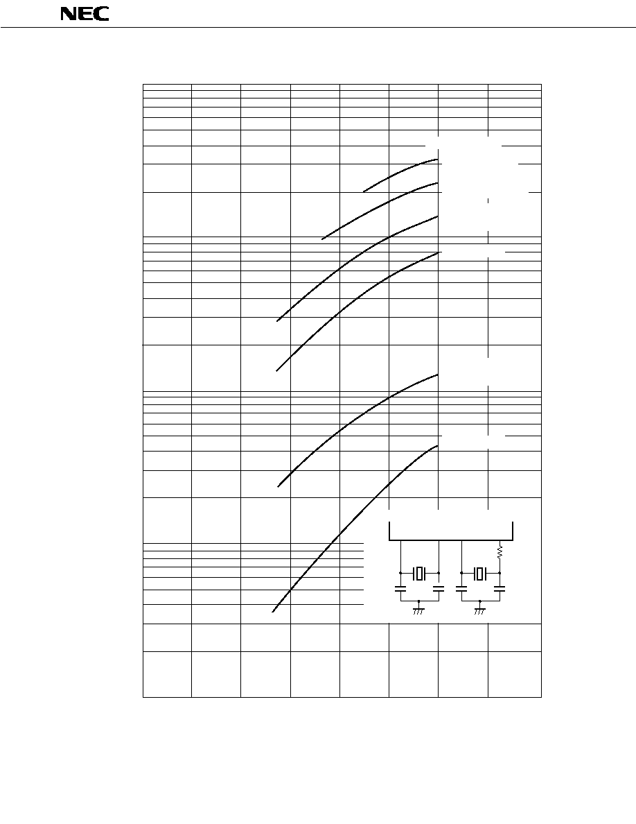
µ
PD75004, 75006, 75008
54
I
DD
vs V
DD
(Ceramic oscillation)
5000
1000
500
100
50
10
5
1
0
1
2
3
4
5
6
7
30 pF
30 pF
18 pF
330 k
Ceramic
oscillator
32.768 kHz
18 pF
X1
X2
XT1
XT2
Low-speed mode
PCC = 0000
Middle-speed mode
PCC = 0010
High-speed mode
PCC = 0011
(T = 25∞C)
a
Operating current I [ A]
DD
µ
Operating voltage V [V]
DD
Subsystem clock*
Operation mode
CSA4.19 MGU
HALT mode*
1
2
HALT mode*
2
X'tal
Main system clock
*1: When compared to crystal oscillation, increased by approximately 10%.
2: Main system clock halts.

µ
PD75004, 75006, 75008
55
I
DD
vs V
DD
(Ceramic oscillation)
5000
1000
500
100
50
10
5
1
0
1
2
3
4
5
6
7
30 pF
30 pF
18 pF
330 k
Ceramic
oscillator
X'tal
18 pF
X1
X2
XT1
XT2
Low-speed mode
PCC = 0000
Middle-speed mode
PCC = 0010
High-speed mode
PCC = 0011
(T = 25∞C)
a
Operating current I [ A]
DD
µ
Operating voltage V [V]
DD
Subsystem clock*
Operation mode
CSA2.00MG093
Main system clock
HALT mode
HALT mode*
32.768 kHz
*: Main system clock halts.
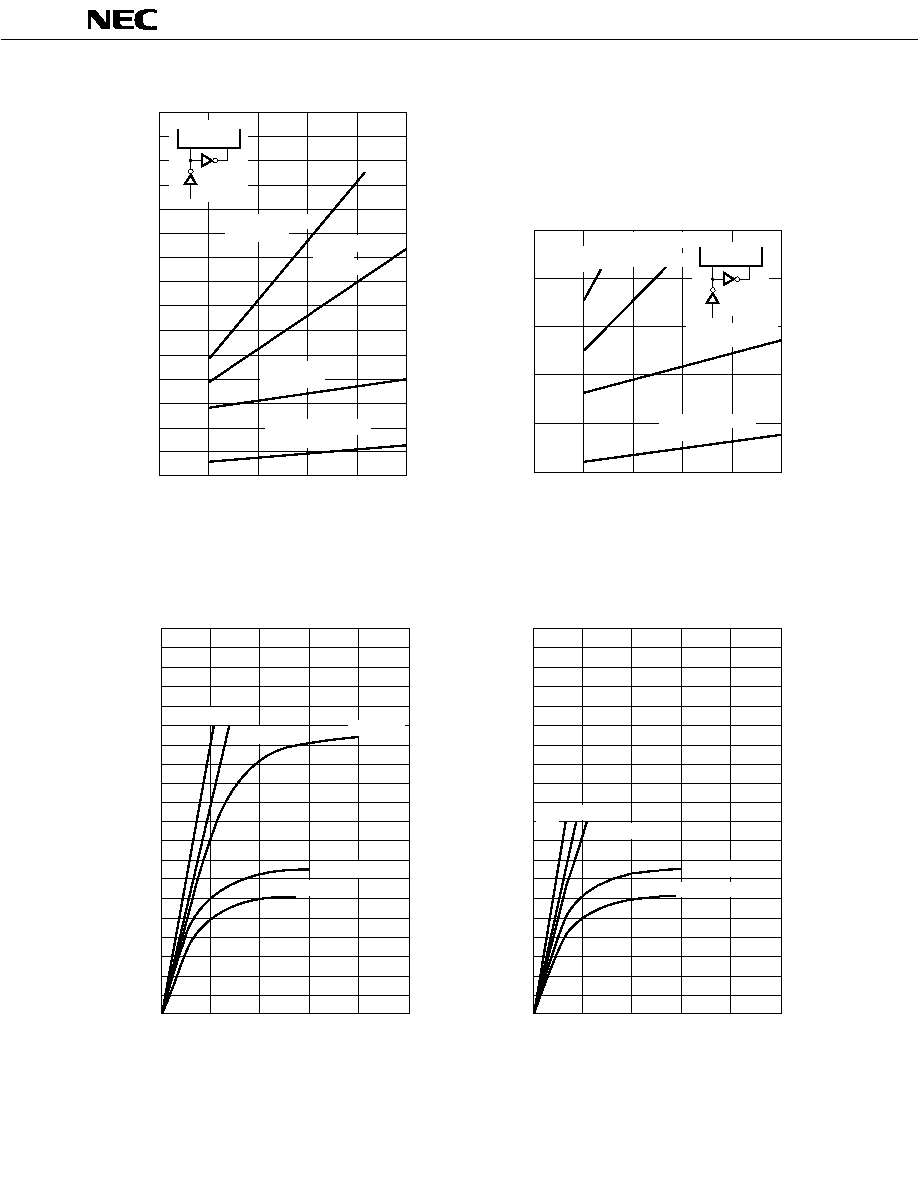
µ
PD75004, 75006, 75008
56
3
2
1
0
1
2
3
4
5
f [MHz]
x
I
DD
vs f
x
(V = 5V, T = 25∞C)
DD
a
Main system clock
HALT mode
I
DD
vs f
x
(V = 3V, T = 25∞C)
DD
a
0.5
0.4
0.3
0.2
0.1
0
1
2
3
4
5
f [MHz]
x
X1
X2
High-speed mode
PCC = 0011
Middle-speed
mode
PCC = 0010
Low-speed mode
PCC = 0000
Main system clock
HALT mode
V
OL
vs I
OL
(T = 25∞C)
a
(Port 0)
40
30
20
10
0
1
2
3
4
5
V [V]
OL
V = 5 V
DD
V = 4 V
DD
V = 3 V
DD
V = 2.7 V
DD
V
OL
vs I
OL
(Port 2, 6, 7)
40
30
20
10
0
1
2
3
4
5
[mA]
I
DD
V = 6 V
DD
[mA]
I
OL
V = 5 V
DD
V = 4 V
DD
V = 2.7 V
DD
V = 3 V
DD
V [V]
OL
(T = 25∞C)
a
X1
X2
High-speed mode
PCC = 0011
Middle-speed
mode
PCC = 0010
Low-speed mode
PCC = 0000
[mA]
I
DD
5
V =
6 V
DD
[mA]
I
OL
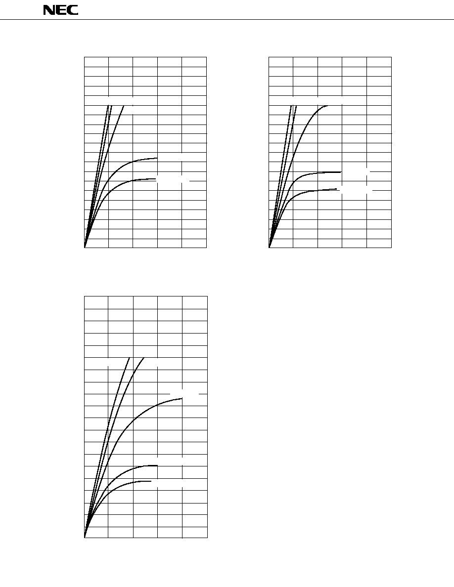
µ
PD75004, 75006, 75008
57
V
OH
vs I
OH
(T = 25∞C)
a
15
10
5
0
I
[mA]
OH
20
1
2
3
4
5
V - V [V]
DD
OH
V = 5 V
DD
V = 2.7 V
DD
V = 6 V
DD
V = 3 V
DD
V = 4 V
DD
V
OL
vs I
OL
(Port 4, 5)
40
30
20
10
0
1
2
3
4
5
I
[mA]
OL
V = 5 V
DD
V = 6 V
DD
V = 4 V
DD
V = 2.7 V
DD
V = 3 V
DD
V [V]
OL
(T = 25∞C)
a
V
OL
vs I
OL
(Port 3)
40
30
20
10
0
1
2
3
4
5
I
[mA]
OL
V = 5 V
DD
V = 6 V
DD
V = 4 V
DD
V = 2.7 V
DD
V = 3 V
DD
V [V]
OL
(T = 25∞C)
a
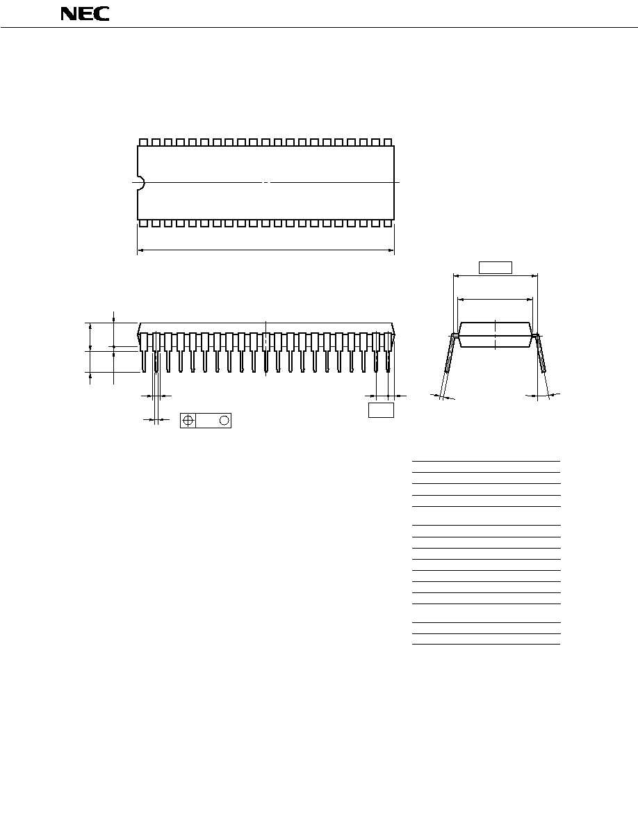
µ
PD75004, 75006, 75008
58
12. PACKAGE DRAWINGS
42PIN PLASTIC SHRINK DIP (600 mil)
ITEM MILLIMETERS
INCHES
A
B
C
F
G
H
I
J
K
39.13 MAX.
1.778 (T.P.)
3.2±0.3
0.51 MIN.
4.31 MAX.
1.78 MAX.
0.17
15.24 (T.P.)
5.08 MAX.
N
0.9 MIN.
R
1.541 MAX.
0.070 MAX.
0.035 MIN.
0.126±0.012
0.020 MIN.
0.170 MAX.
0.200 MAX.
0.600 (T.P.)
0.007
0.070 (T.P.)
P42C-70-600A-1
A
C
D
G
NOTES
1) Each lead centerline is located within 0.17 mm (0.007 inch) of
its true position (T.P.) at maximum material condition.
D
0.50±0.10
0.020
M
0.25
0.010
+0.10
≠0.05
0~15∞
0~15∞
+0.004
≠0.003
+0.004
≠0.005
M
K
N
L
13.2
0.520
2) Item "K" to center of leads when formed parallel.
42
1
22
21
L
M
R
B
F
H
J
I

µ
PD75004, 75006, 75008
59
5
44 PIN PLASTIC QFP ( 10)
NOTE
Each lead centerline is located within 0.15 mm (0.006 inch) of
its true position (T.P.) at maximum material condition.
P44GB-80-3B4-3
ITEM
MILLIMETERS
INCHES
A
B
C
13.6±0.4
10.0±0.2
10.0±0.2
0.535
0.394
0.394
D
13.6±0.4
0.535
F
1.0
0.039
G
1.0
0.039
H
0.35±0.10
0.014
I
0.15
0.006
J
0.8 (T.P.)
0.031 (T.P)
K
1.8±0.2
0.071
L
0.8±0.2
0.031
M
0.15
0.006
N
0.10
0.004
P
2.7
0.106
Q
0.1±0.1
0.004±0.004
R
5∞±5∞
5∞±5∞
S
3.0 MAX.
0.119 MAX.
+0.017
≠0.016
+0.008
≠0.009
+0.008
≠0.009
+0.017
≠0.016
+0.004
≠0.005
+0.008
≠0.009
+0.009
≠0.008
+0.004
≠0.003
N
L
detail of lead end
G
M
I
J
H
A
F
M
Q
R
B
33
34
22
44
1
12
11
23
C
D
S
P
K
+0.10
≠0.05
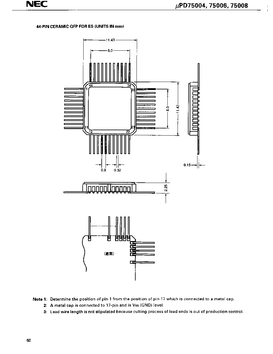

µ
PD75004, 75006, 75008
61
13. RECOMMENDED SOLDERING CONDITIONS
It is recommended that
µ
PD75004, 75006, and 75008 be soldered under the following conditions.
For details on the recommended soldering conditions, refer to Information Document "Semiconductor
Devices Mounting Manual" (IEI-616).
The soldering methods and conditions are not listed here, consult NEC.
Table 13-1 Soldering Conditions
µ
PD75004GB - xxx - 3B4: 44-pin plastic QFP (
s
s
10 mm)
µ
PD75006GB - xxx - 3B4: 44-pin plastic QFP (
s
s
10 mm)
µ
PD75008GB - xxx - 3B4: 44-pin plastic QFP (
s
s
10 mm)
Soldering Method
Soldering Conditions
Infrared Reflow
Package peak temperature: 230
∞
C, time: 30 seconds max.
IR30-107-1
(210
∞
C min.), number of times: 1, number of days: 7 days*,
(afterwards, 10 hours of prebaking at 125
∞
C is required.)
VPS
Package peak temperature: 215
∞
C, time: 40 seconds max.
VP15-107-1
(200
∞
C min.), number of times: 1, number of days: 7 days*,
(afterwards, 10 hours of prebaking at 125
∞
C is required.)
Wave Soldering
Soldering bath temperature: 260
∞
C max., time: 10 seconds
WS60-00-1
max., number of times: 1, number of days: 7 days*,
(afterwards, 10 hours of prebaking at 125
∞
C is required.)
pre-heating temperature: 120
∞
C max. (package surface
temperature)
Pin Partial Heating
Pin temperature: 300
∞
C max.,
--
time: 3 seconds max. (per side)
*:
This means the number of days after unpacking the dry pack. Storage conditions are 25
∞
C and 65%
RH max.
Caution: Do not use two or more soldering methods in combination (except the pin partial heating
method).
5
Table 13-2 Soldering Conditions of Through-Hole Type
µ
PD75004CU - xxx : 42-pin plastic shrink DIP (600 mil)
µ
PD75006CU - xxx : 42-pin plastic shrink DIP (600 mil)
µ
PD75008CU - xxx : 42-pin plastic shrink DIP (600 mil)
Symbol for Recommended
Condition
Soldering Method
Soldering Conditions
Wave Soldering
Soldering bath temperature: 260
∞
C max., Time: 10 seconds max.
(Only for lead part)
Pin Partial Heating
Pin temperature: 260
∞
C max., Time: 10 seconds max.
Notice
A model that can be soldered under the more stringent conditions (infrared reflow peak temperature:
235
∞
C, number of times: 2, and an extended number of days) is also available.
For details, consult NEC.
µ
PD75004, 75006, 75008
62
APPENDIX A.
DEVELOPMENT TOOLS
The following development support tools are readily available to support development of systems using
µ
PD75008:
Hardware
IE-75000-R *
1
In-circuit emulator for 75X series
IE-75001-R
IE-75000-R-EM *
2
Emulation board for IE-75000-R and IE-75001-R
EP-75008CU/GB-R
Emulation prove for
µ
PD75004CU/GB, 75006CU/GB, 75008CU/GB
PG-1500
PROM programmer
PA-75P008CU
PROM programmer adapter solely used for
µ
PD75P008CU/GB.
It is connected to PG-1500.
Software
IE Control Program
PG-1500 Controller
RA75X Relocatable
Assembler
*1: Maintenance product
2: Not provided with IE-75001-R.
3: Ver.5.00/5.00A has a task swap function, but this function cannot be used with this function.
Remarks: For development tools from other companies, refer to 75X Series Selection Guide (IF-151).
Host machine
∑ PC-9800 series (MS-DOS
TM
Ver.3.30 to Ver.5.00A*
3
)
∑ IBM PC/AT
TM
(PC DOS
TM
Ver.3.1)

µ
PD75004, 75006, 75008
63
APPENDIX B. RELATED DOCUMENTS
5

µ
PD75004, 75006, 75008
64
[MEMO]
µ
PD75004, 75006, 75008
65
1
STATIC ELECTRICITY (ALL MOS DEVICES)
Exercise care so that MOS devices are not adversely influenced by static electricity while being
handled.
The insulation of the gates of the MOS device may be destroyed by a strong static charge.
Therefore, when transporting or storing the MOS device, use a conductive tray, magazine case,
or conductive buffer materials, or the metal case NEC uses for packaging and shipment, and use
grounding when assembling the MOS device system. Do not leave the MOS device on a plastic
plate and do not touch the pins of the device.
Handle boards on which MOS devices are mounted similarly .
2
PROCESSING OF UNUSED PINS (CMOS DEVICES ONLY)
Fix the input level of CMOS devices.
Unlike bipolar or NMOS devices, if a CMOS device is operated with nothing connected to its
input pin, intermediate level input may be generated due to noise, and an inrush current may flow
through the device, causing the device to malfunction. Therefore, fix the input level of the device
by using a pull-down or pull-up resistor. If there is a possibility that an unused pin serves as an
output pin (whose timing is not specified), each pin should be connected to V
DD
or GND through
a resistor.
Refer to "Processing of Unused Pins" in the documents of each devices.
3
STATUS BEFORE INITIALIZATION (ALL MOS DEVICES)
The initial status of MOS devices is undefined upon power application.
Since the characteristics of an MOS device are determined by the quantity of injection at the
molecular level, the initial status of the device is not controlled during the production process. The
output status of pins, I/O setting, and register contents upon power application are not guaranteed.
However, the items defined for reset operation and mode setting are subject to guarantee after
the respective operations have been executed.
When using a device with a reset function, be sure to reset the device after power application.
GENERAL NOTES ON CMOS DEVICES

µ
PD75004, 75006, 75008
66
[MEMO]
No p
art of this document may be copied or reproduced in any form or by any means without the prior
written consent of NEC Corporation. NEC Corporation assumes no responsibility for any errors which
may appear in this document.
NEC Corporation does not assume any liability for infringement of patents, copyrights or other
intellectual property rights of third parties b y or arising from use of a device described herein or any
other liability arising from use of such device. No license, either express, implied or otherwise, is granted
under any patents, copyrights or other intellectual property rights of NEC Corporation or others.
The devices listed in this document are not suitable for uses in aerospace equipment, submarine cables,
nuclear reactor control systems and life support systems. If customers intend to use NEC devices for
above applications or they intend to use "Standard" quality grade NEC devices for the applications not
intended by NEC, please contact our sales people in advance.
Application examples recommended by NEC Corporation
Standard: Computer, Office equipment, Communication equipment, Test and Measurement equipment,
Machine tools, Industrial robots, Audio and Visual equipment, Other consumer products, etc.
Special:
Automotive and Transportation equipment, Traffic control systems, Antidisaster systems,
Anticrime system, etc.
MS-DOS is a trademark of Microsoft Corporation.
PC/AT and PC DOS are trademarks of IBM Corporation.
M4 92.6