Электронный компонент:
UPD75028CWA
Скачать:
PDF
ZIP
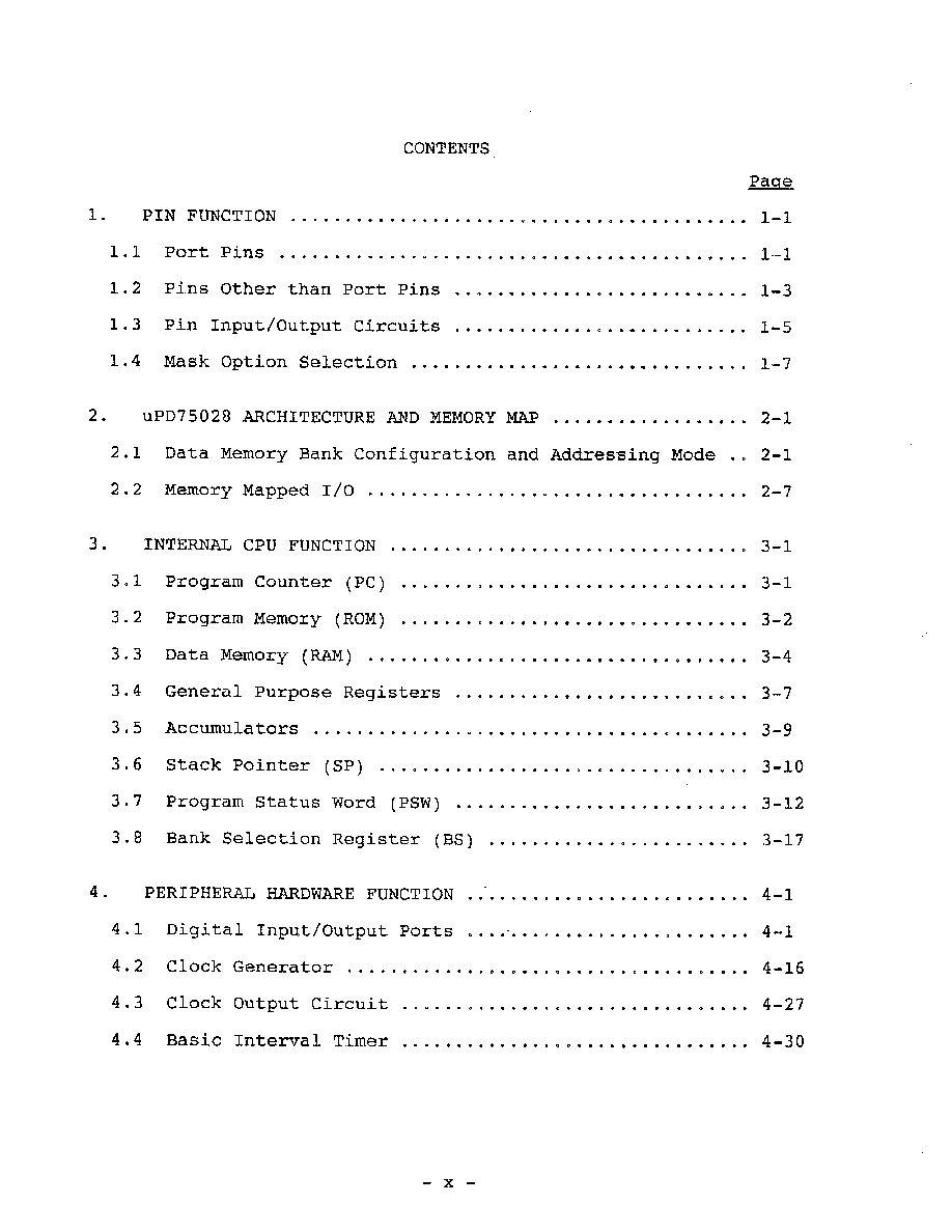
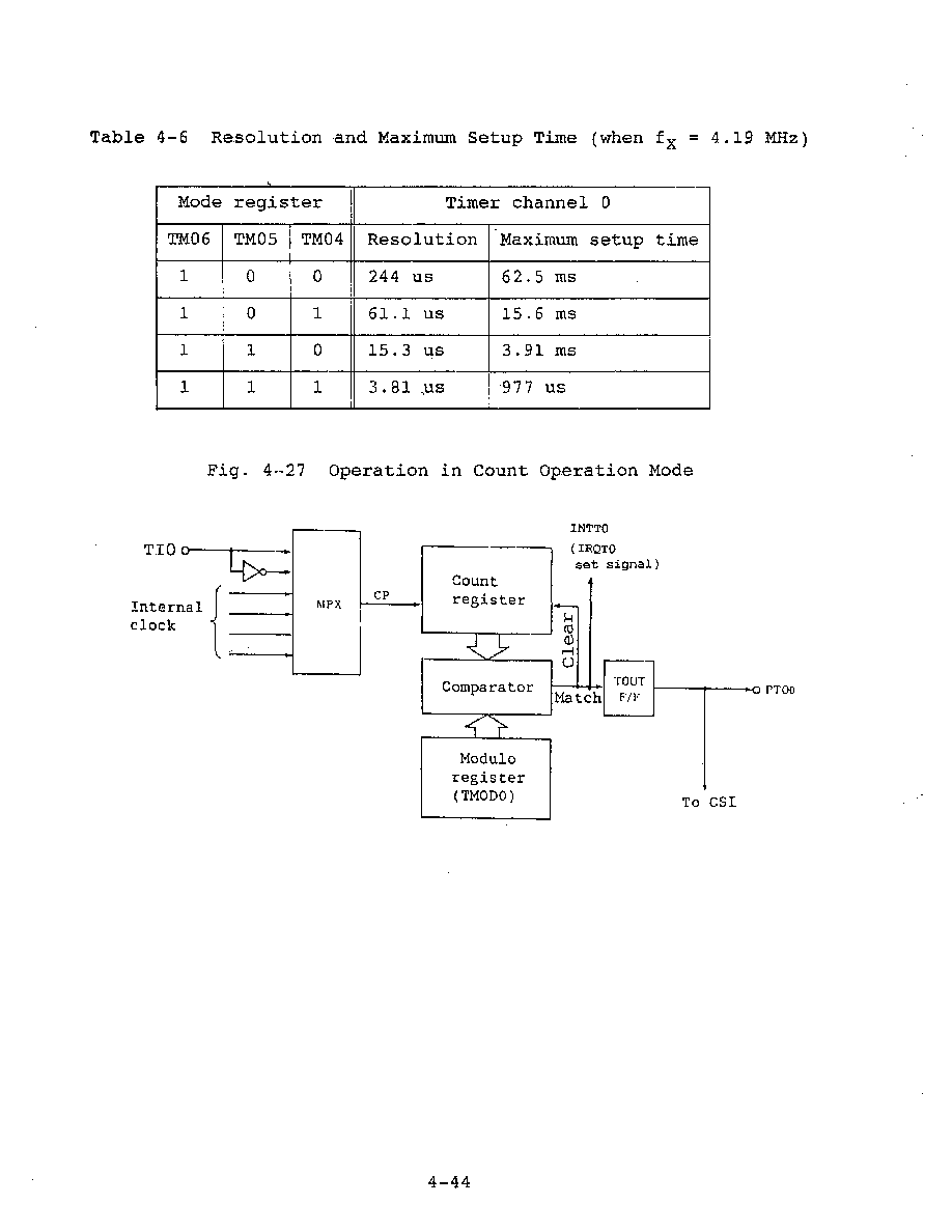
Document Outline
COVER
Features
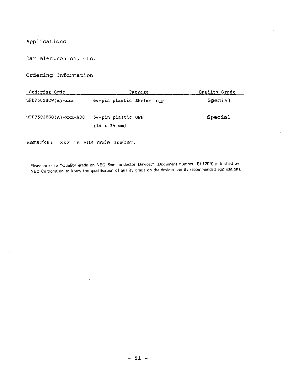
Applications
Oedering Information
Difference between uPD75028 (A) and uPD75028
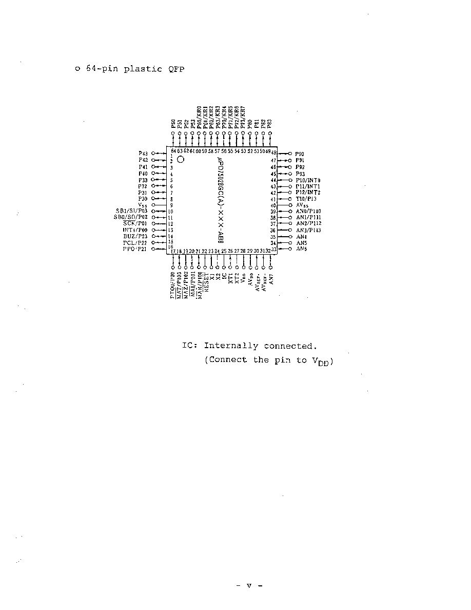
Pin Configuration (Top View)
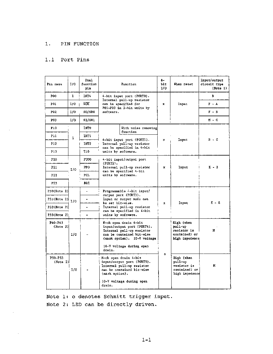
Pin names
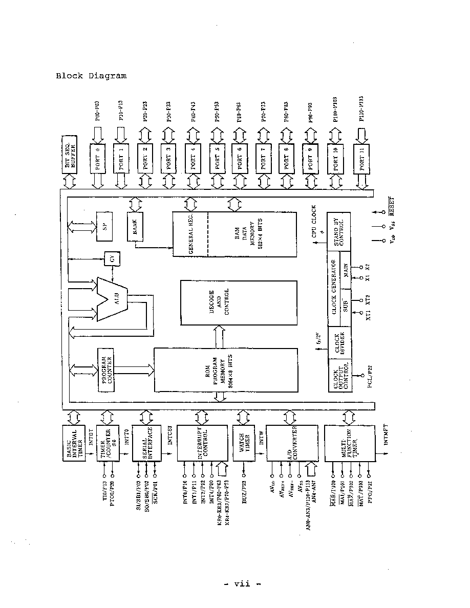
Block Diagram
Function Outline
1. PIN FUNCTION
1.1 Port Pins
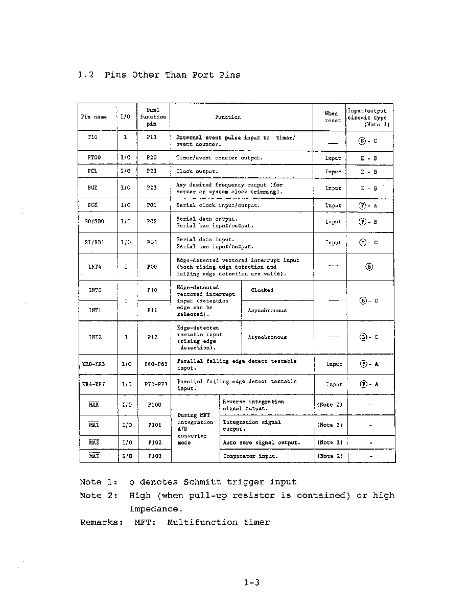
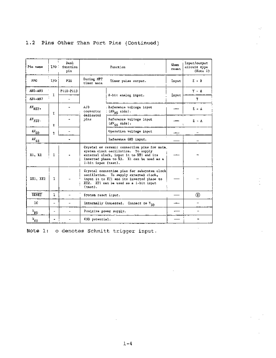
1.2 Pins Other Than Port Pins
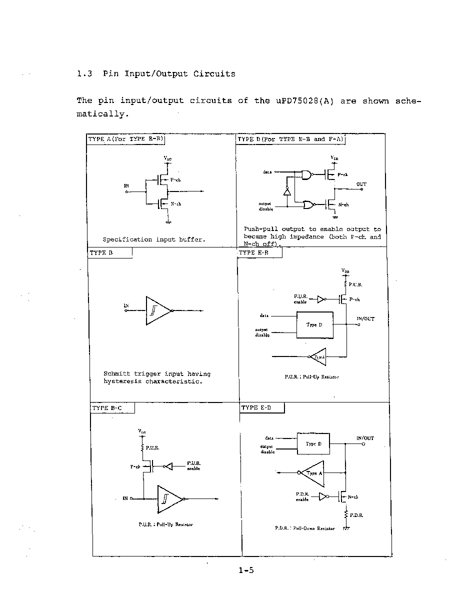
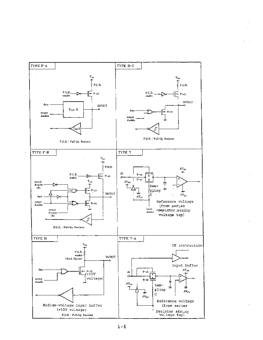
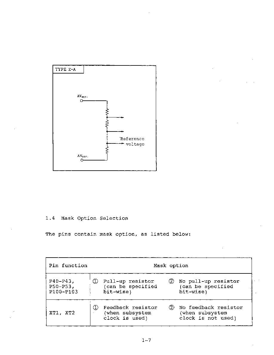
1.3 Pin Input/Output Circuits
1.4 Mask Option Selection
2. uPD75028 (A) ARCHITECTURE AND MEMORY MAP
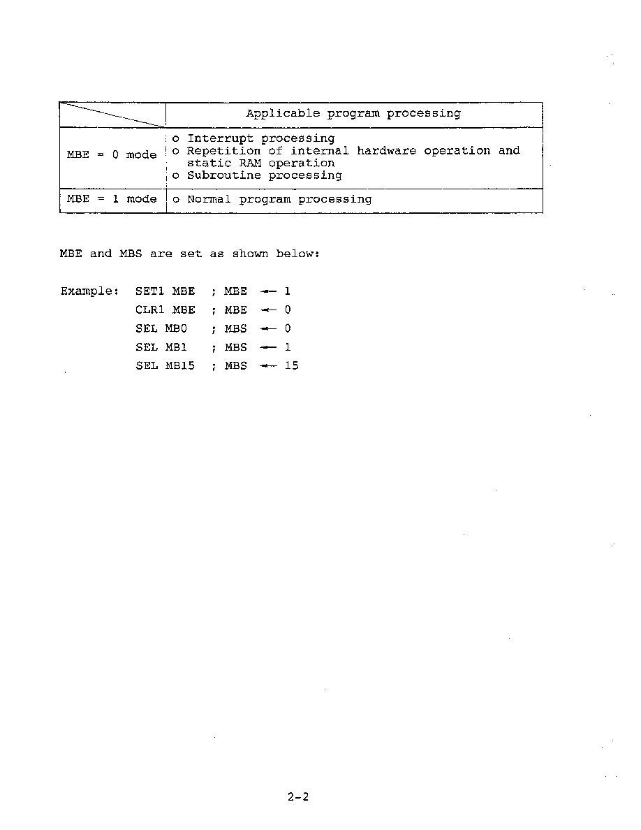
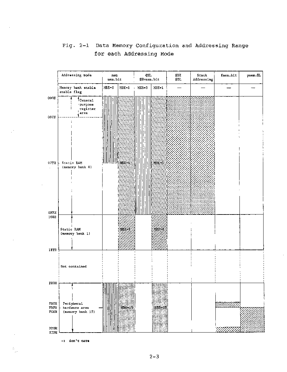
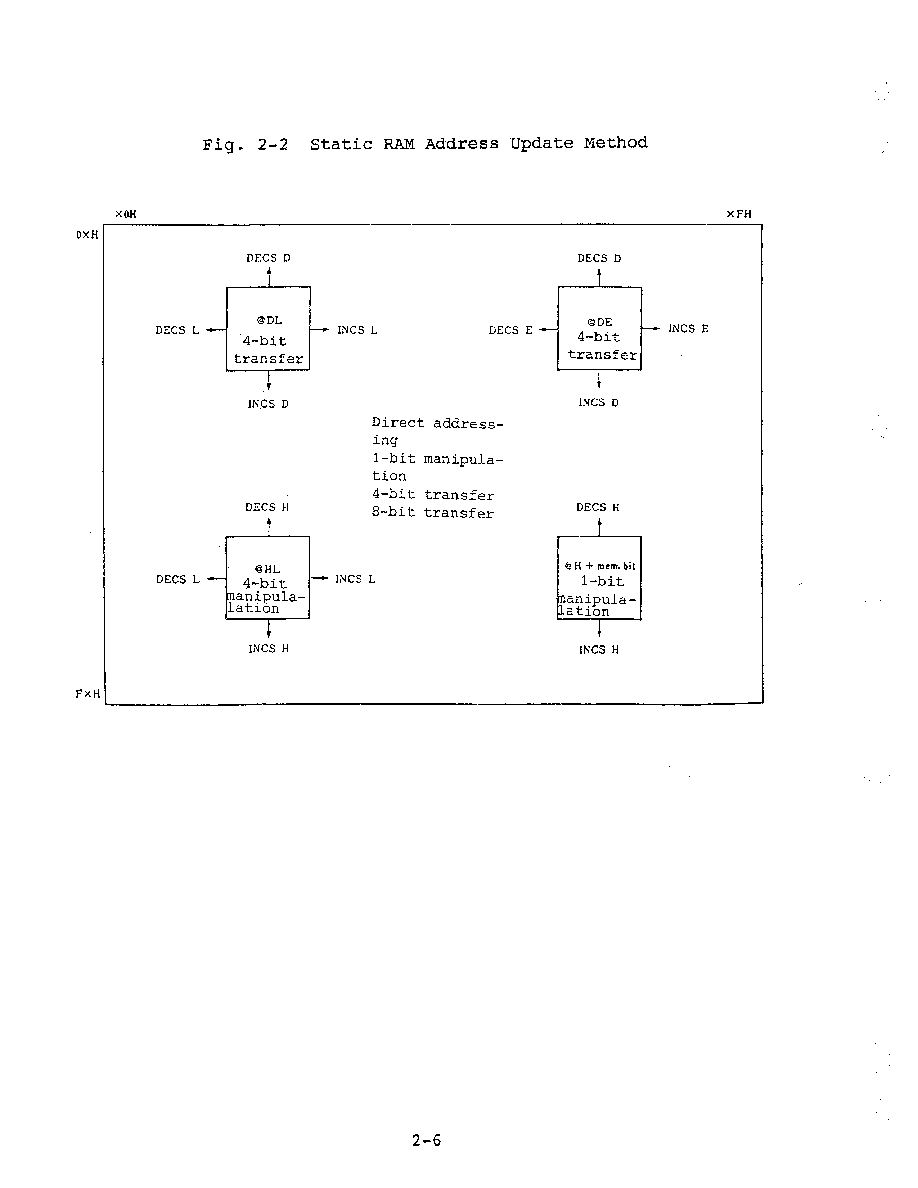
2.1 Data Memory Bank Configuration and Addressing Mode
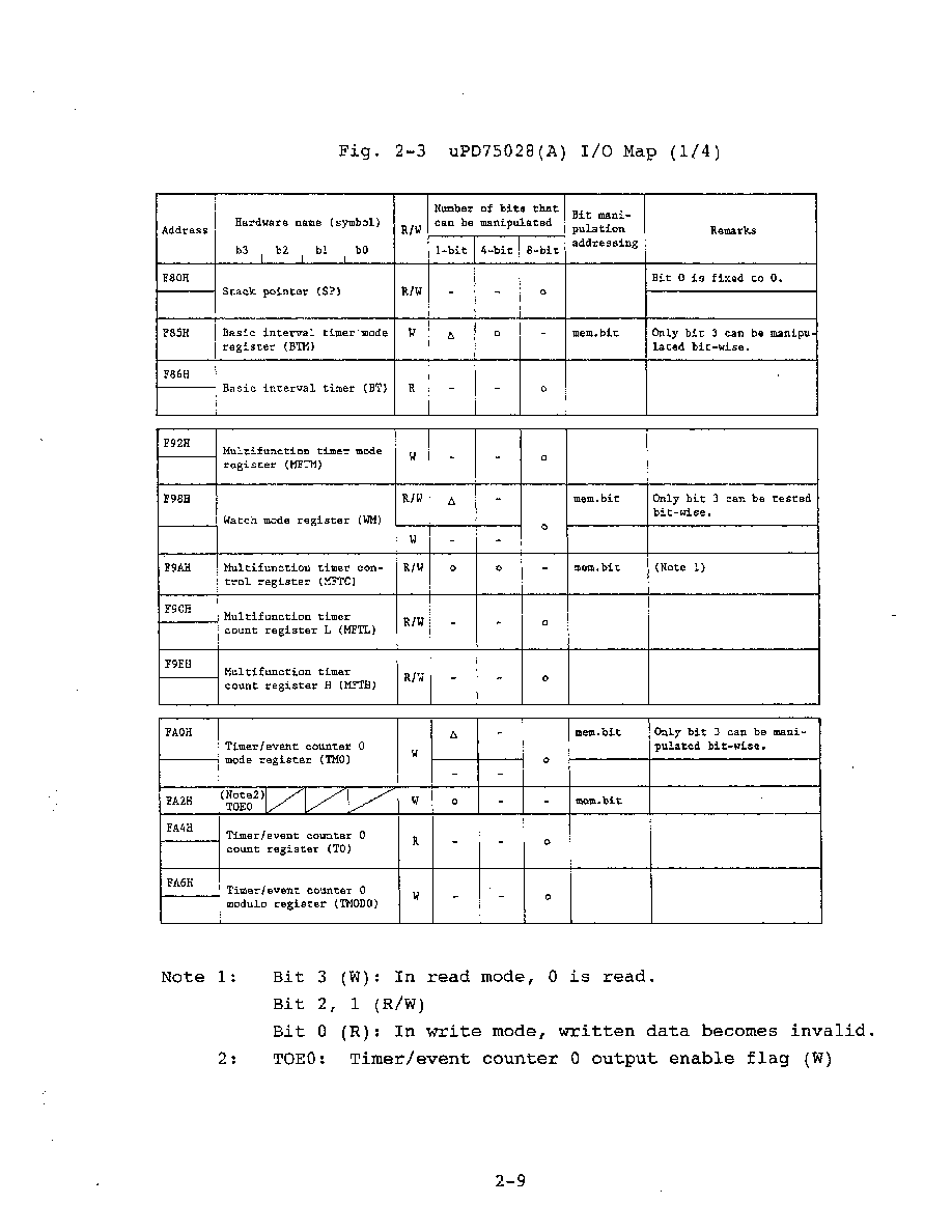
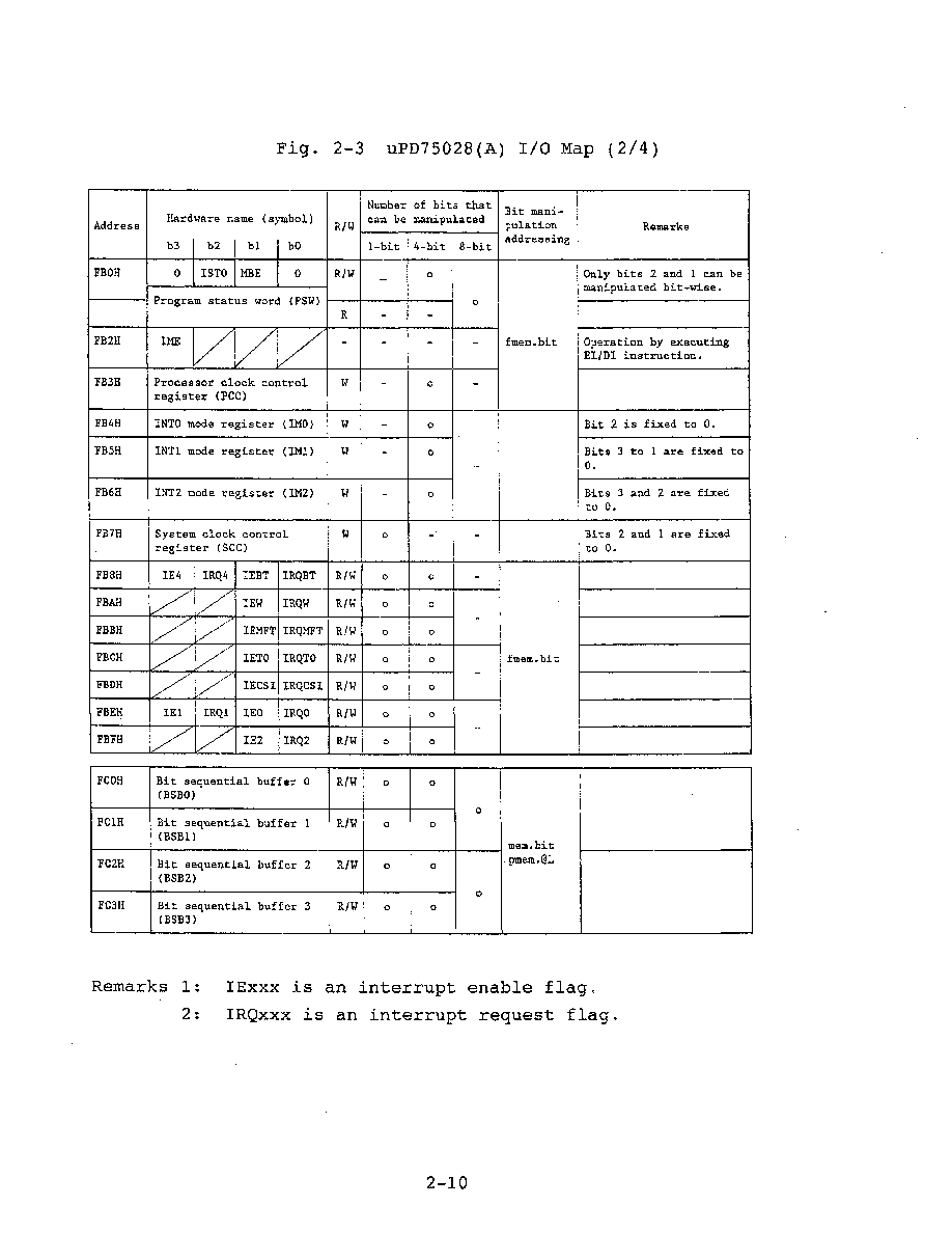
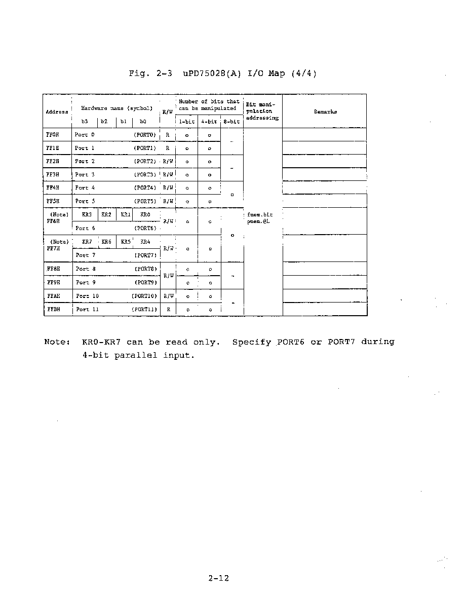
2.2 Memory Mapped I/O
3. INTERNAL CPU FUNCTION
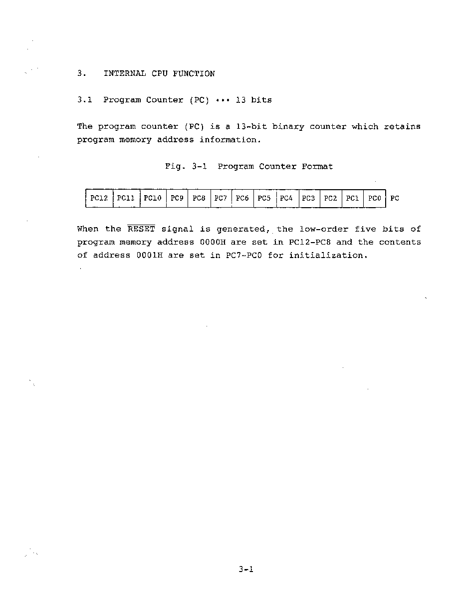
3.1 Program Counter (PC)
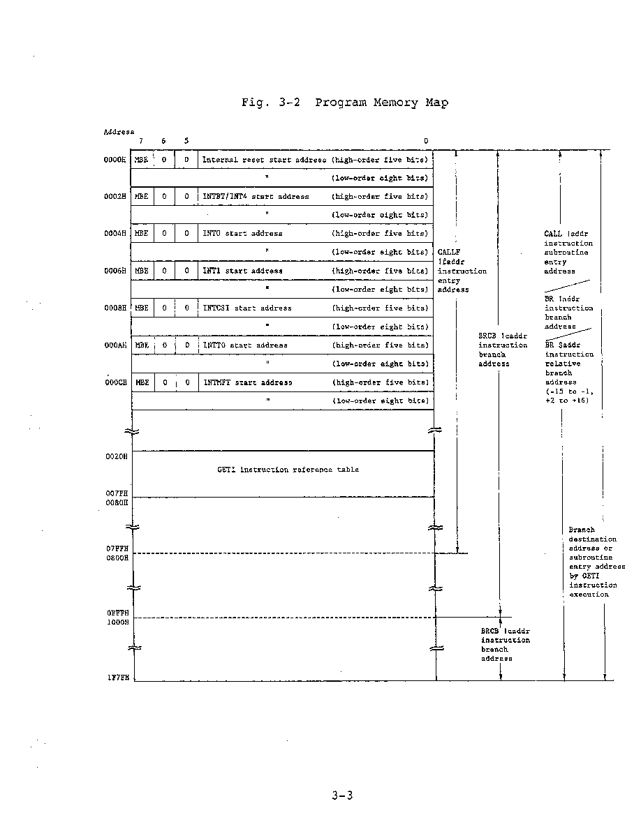
3.2 Program Memory (ROM)
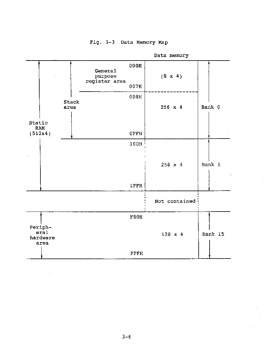
3.3 Data Memory (RAM)
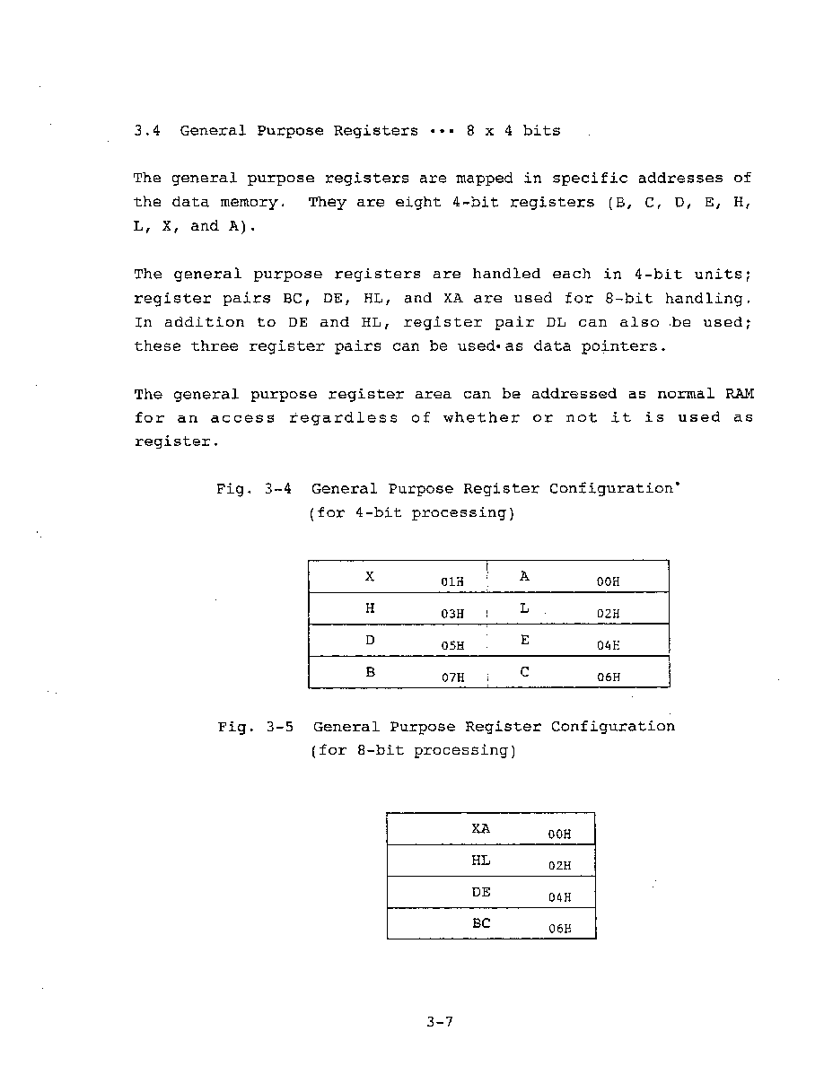
3.4 General Purpose Registers
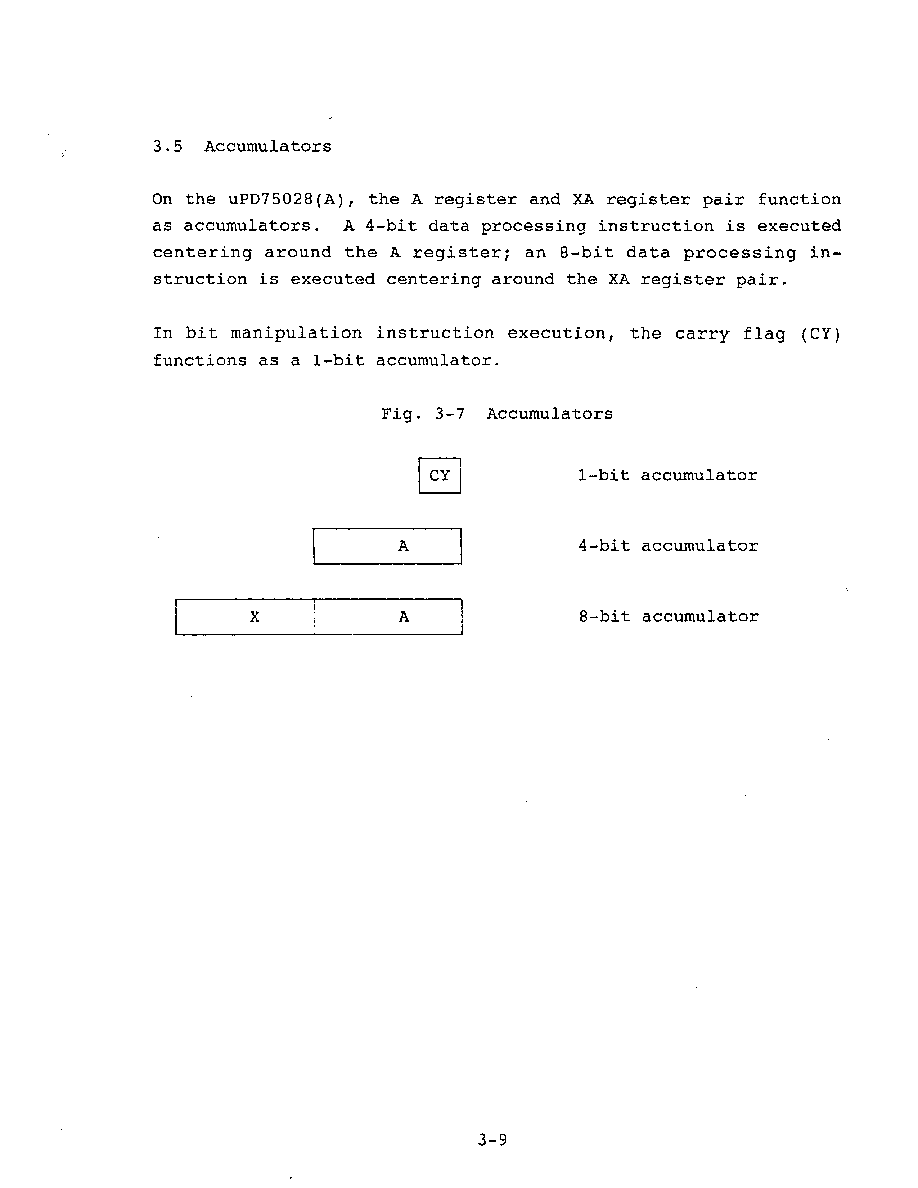
3.5 Accumulators
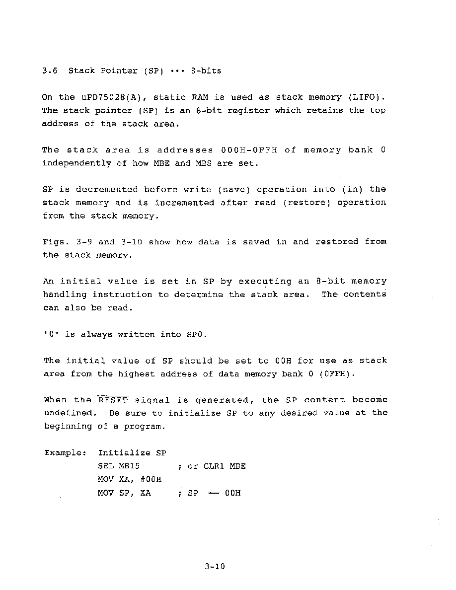
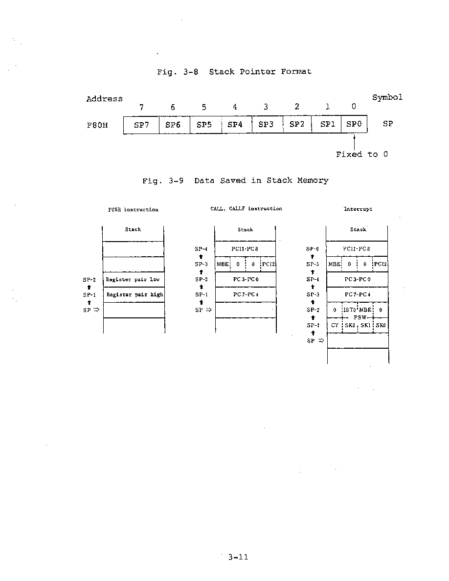
3.6 Stack Pointer (SP)
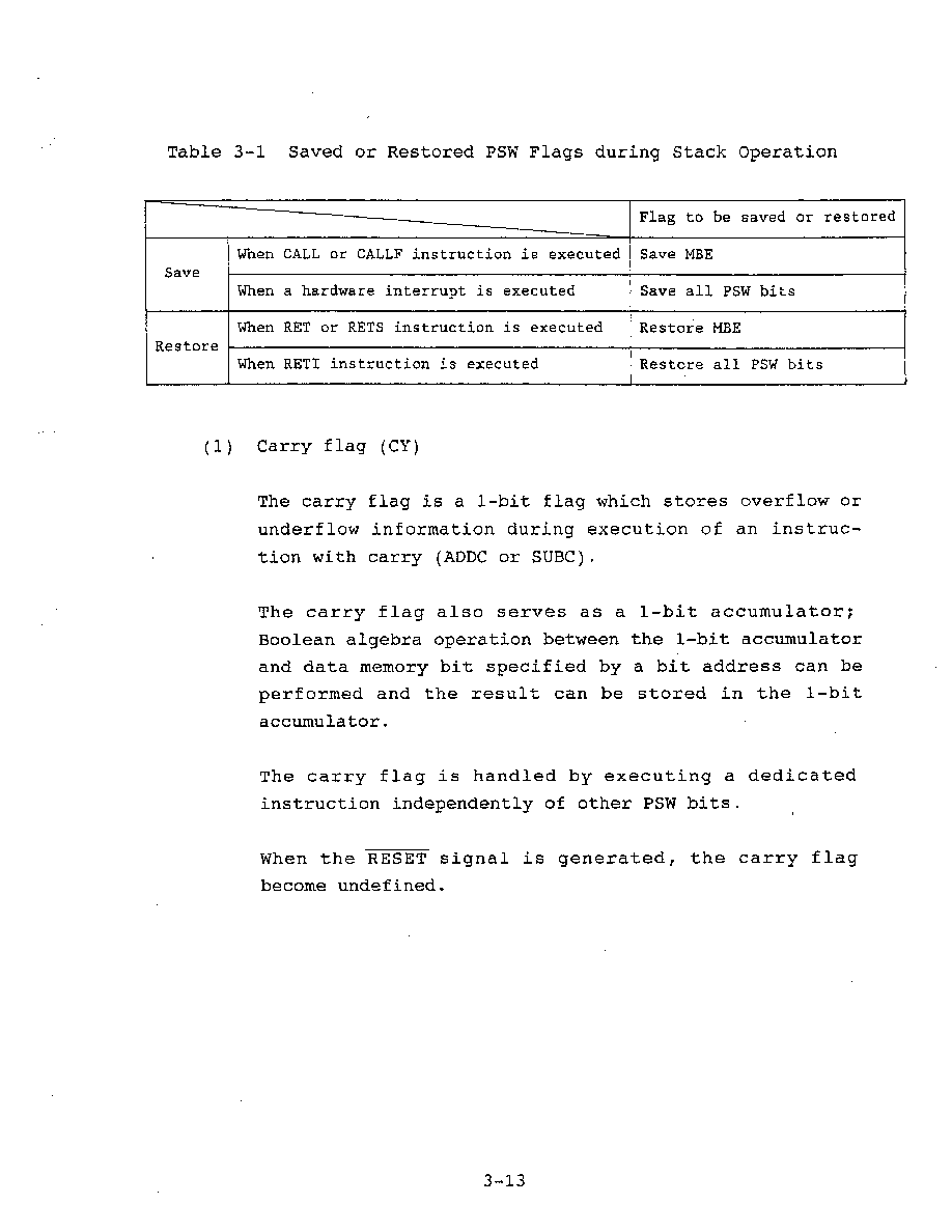
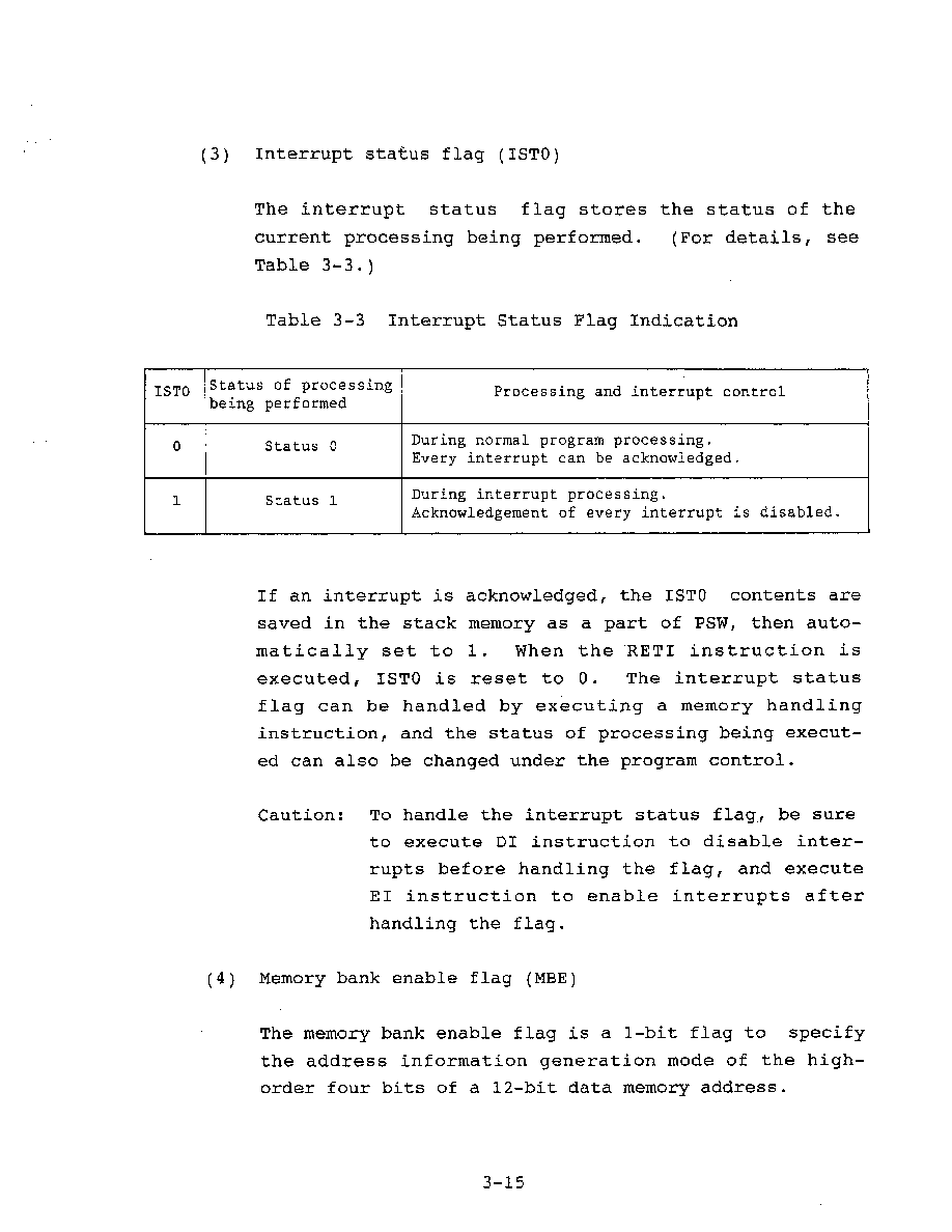
3.7 Program Status Word (PSW)
3.8 Bank Selection Register (BS)
4. PERIPHERAL HARDWARE FUNCTION
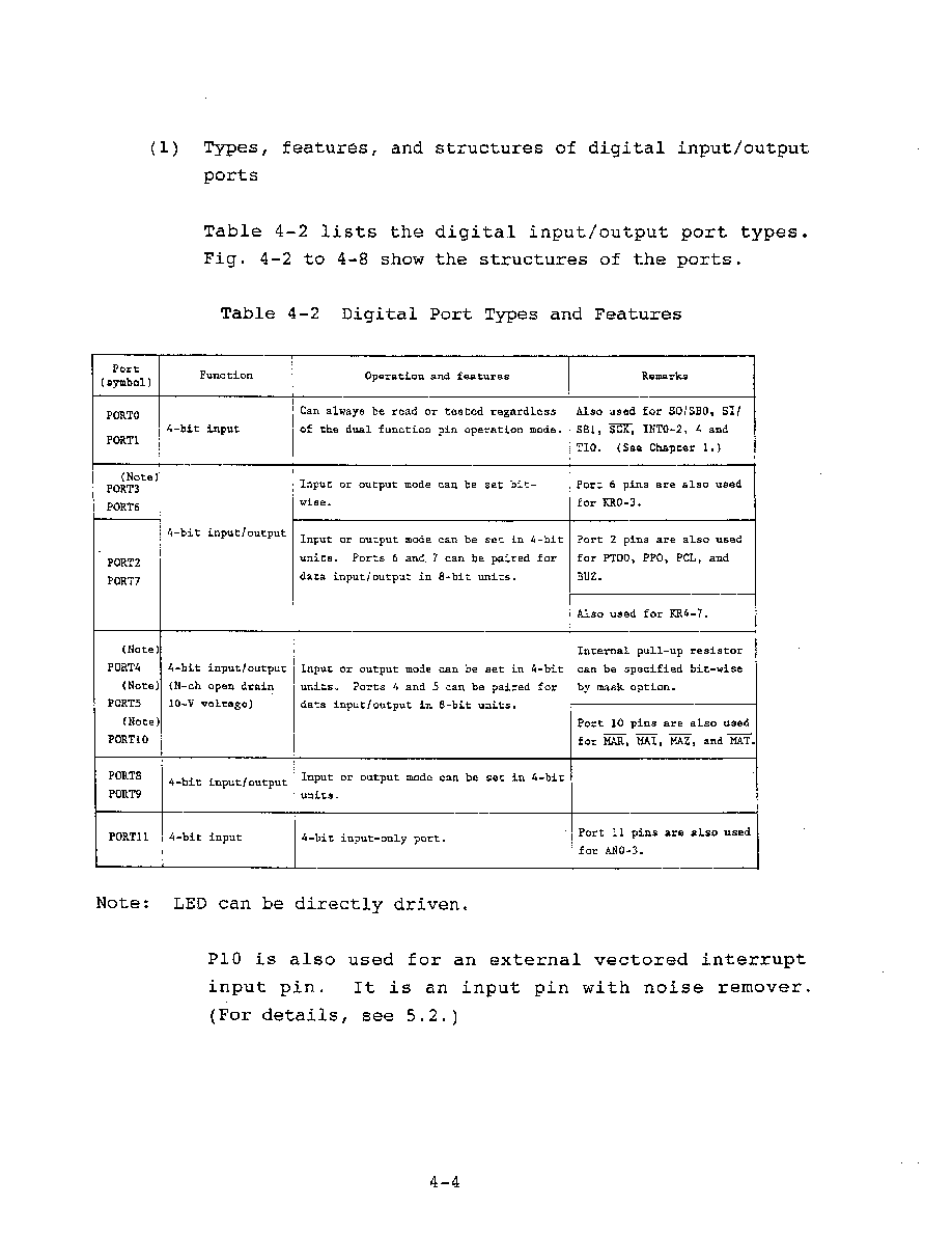
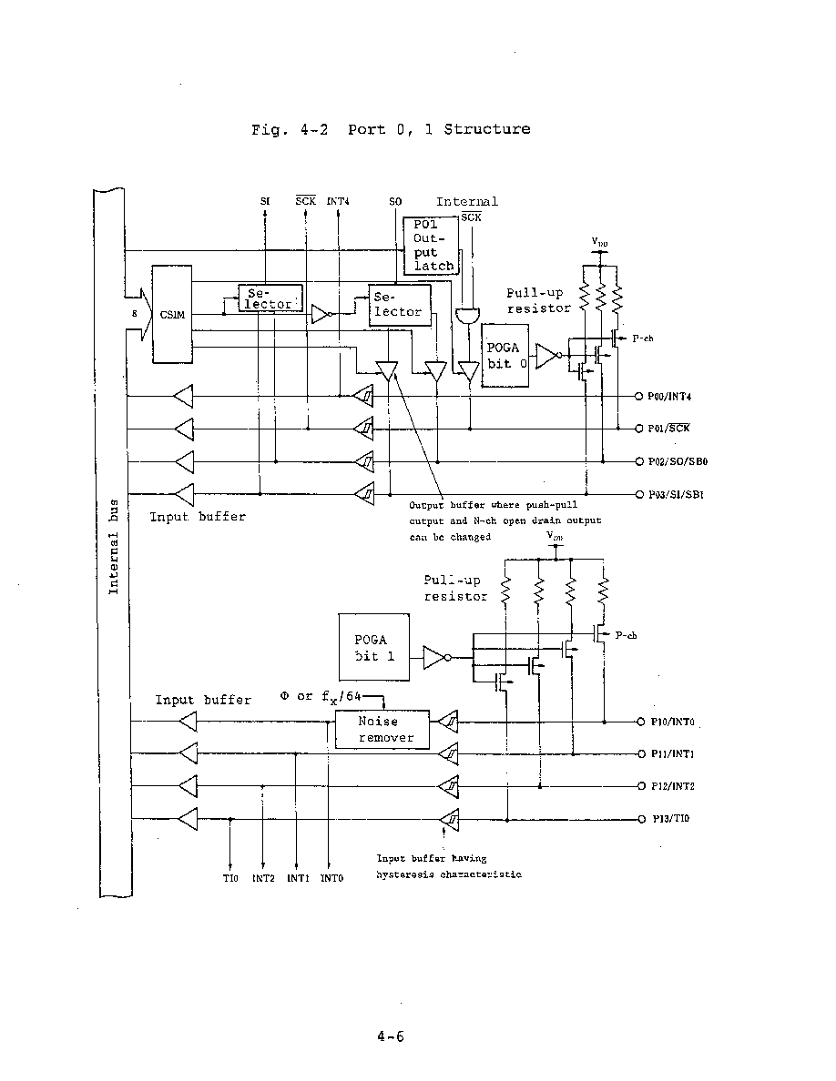
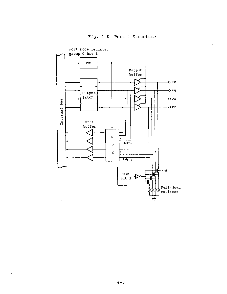
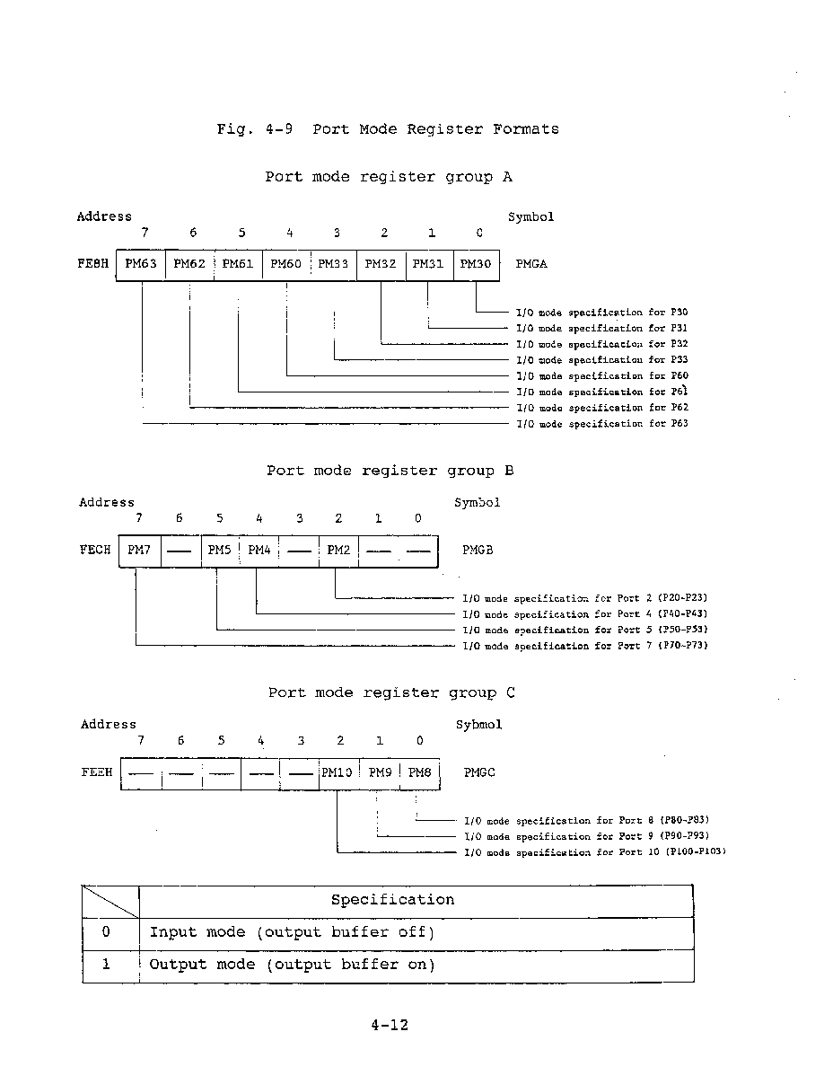
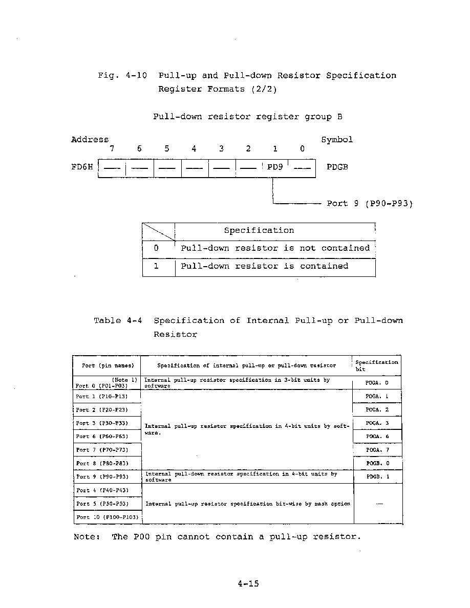
4.1 Digital Input/Output Ports
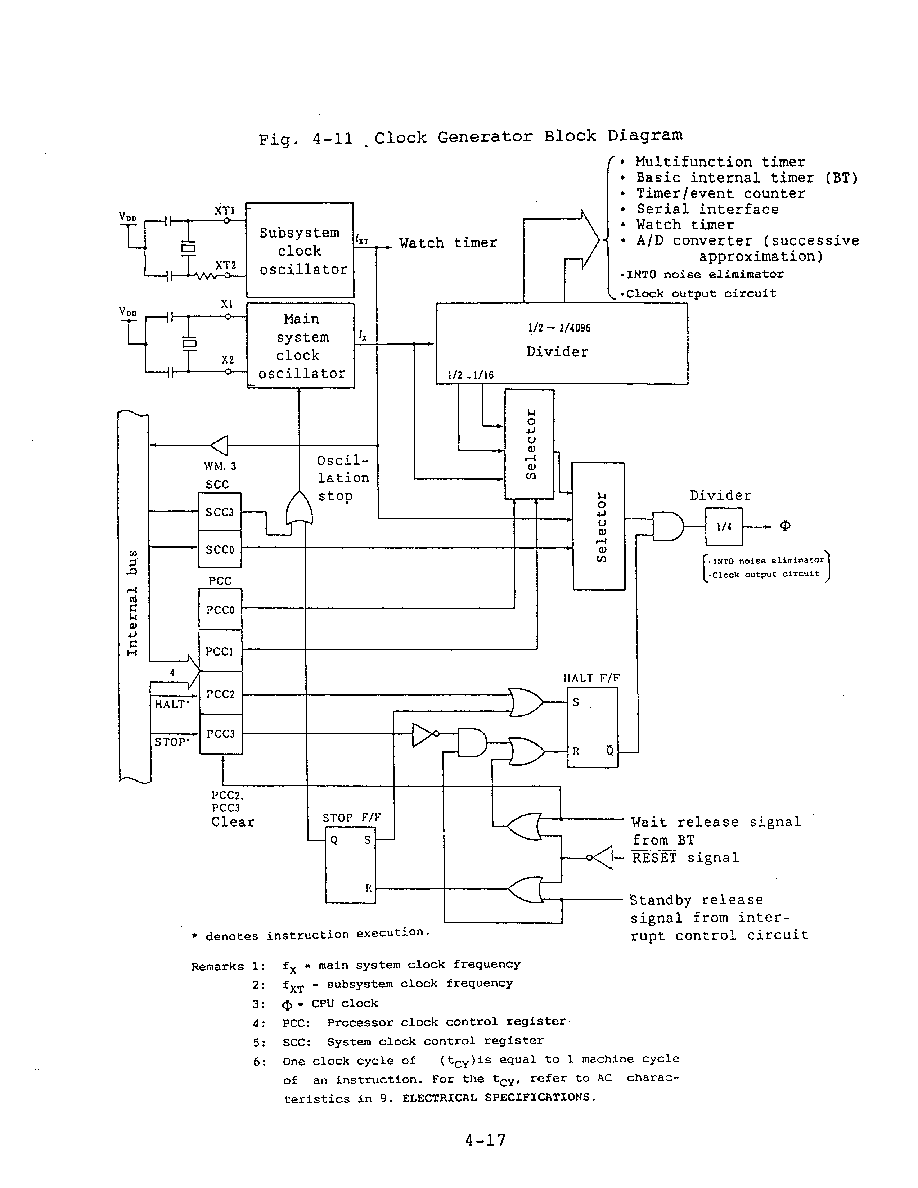
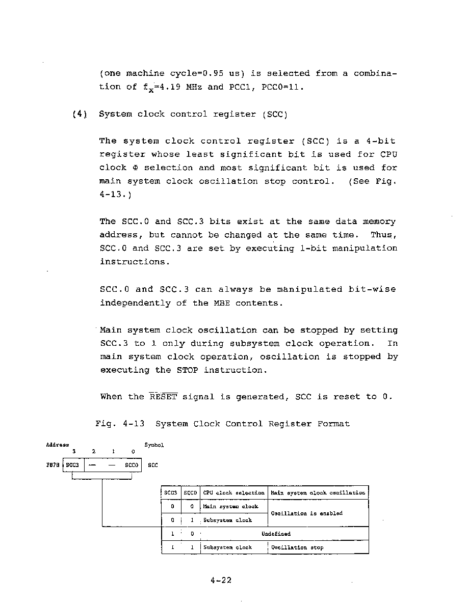
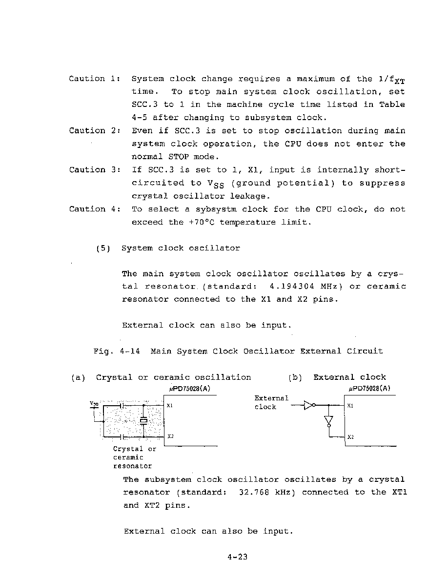
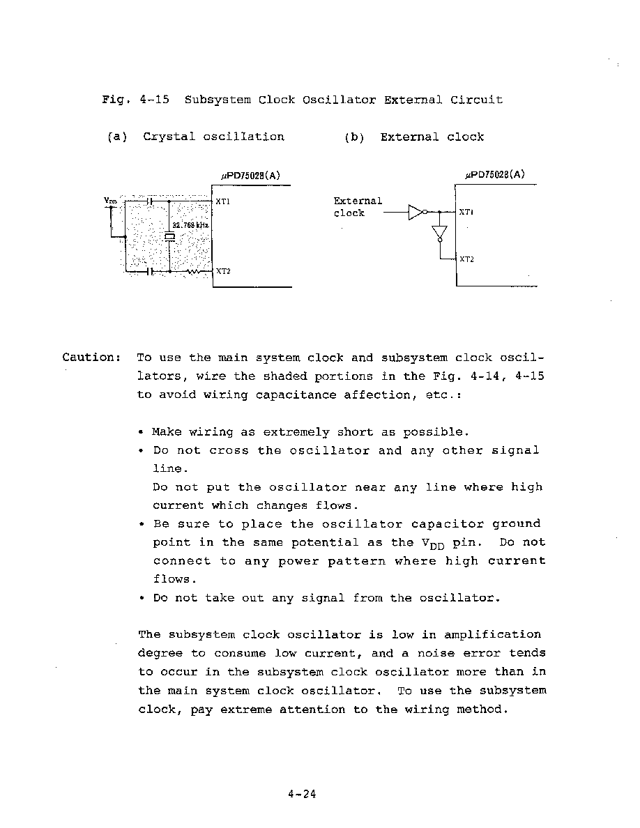
4.2 Clock Generator
4.3 Clock Output Circuit
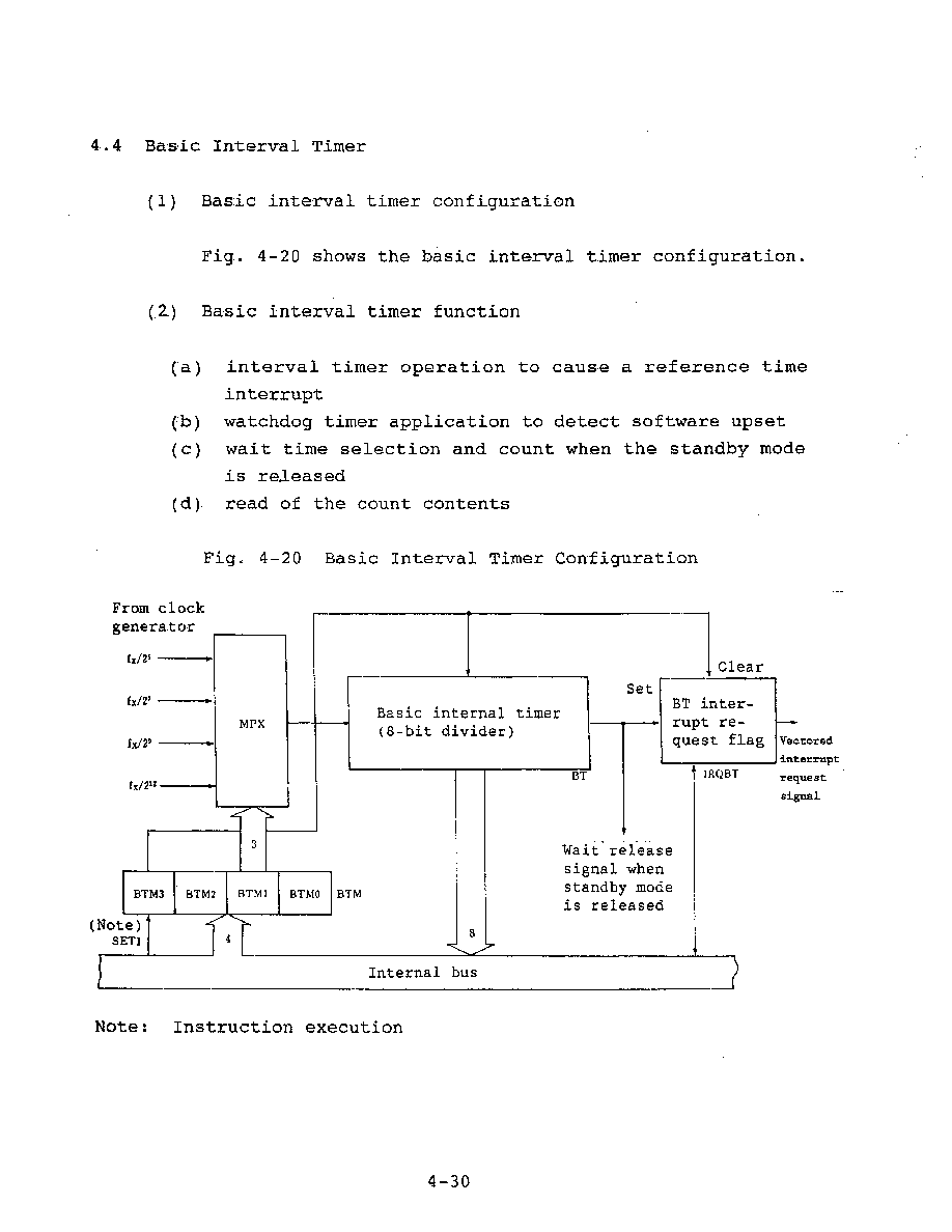
4.4 Basic Interval Timer
4.5 Watch Timer
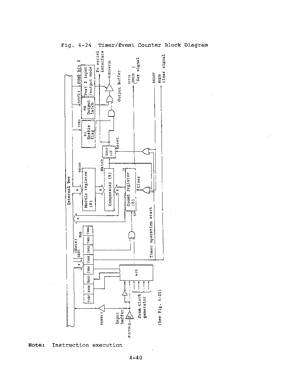
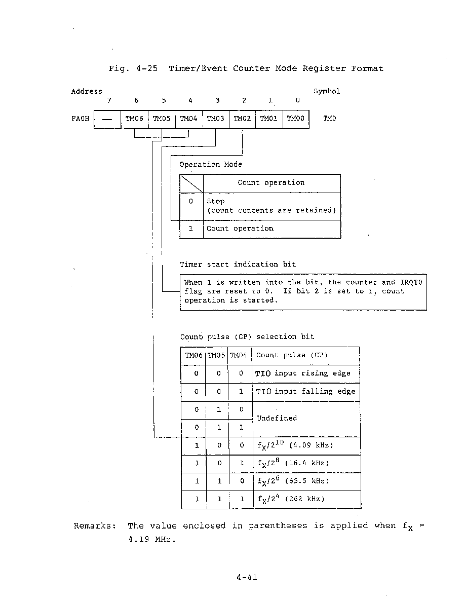
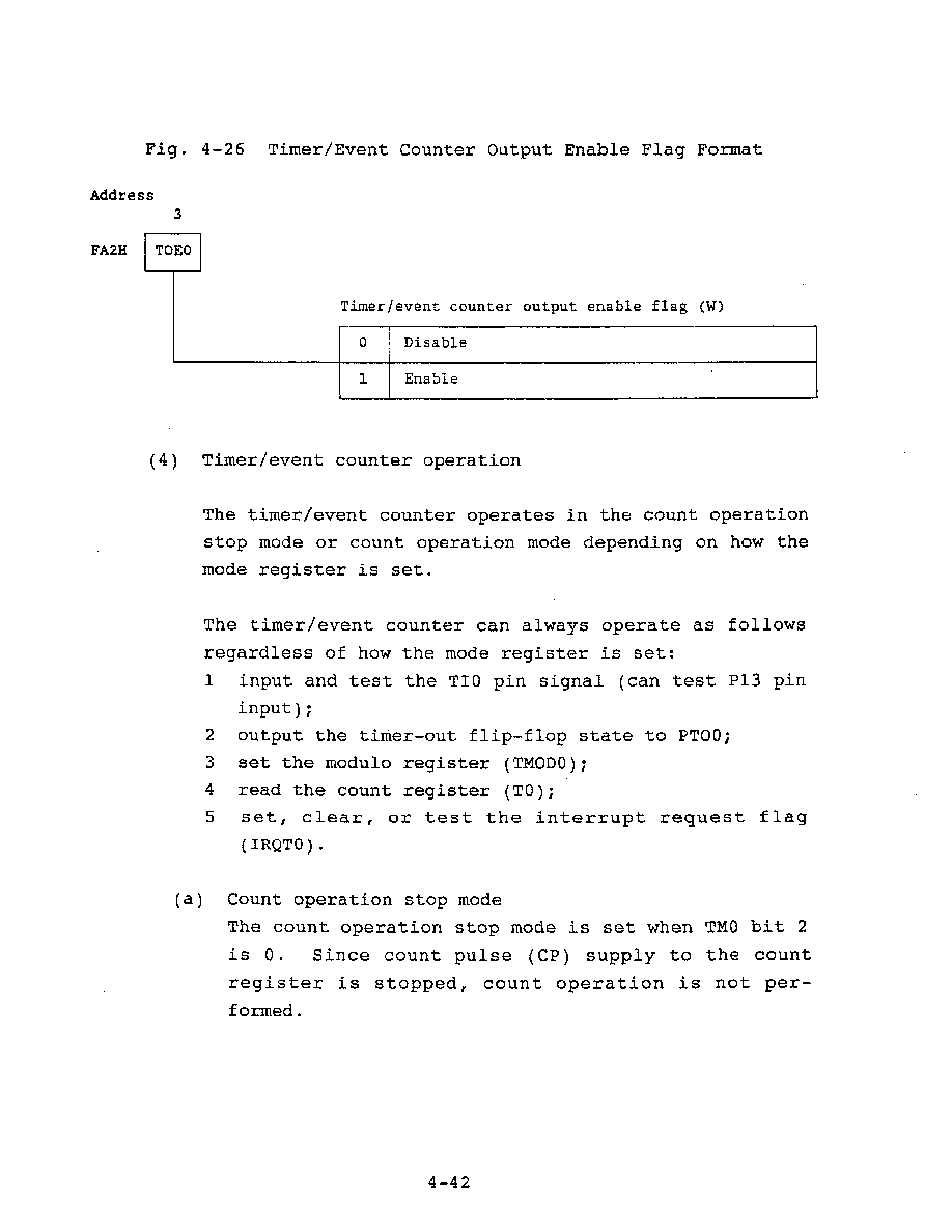
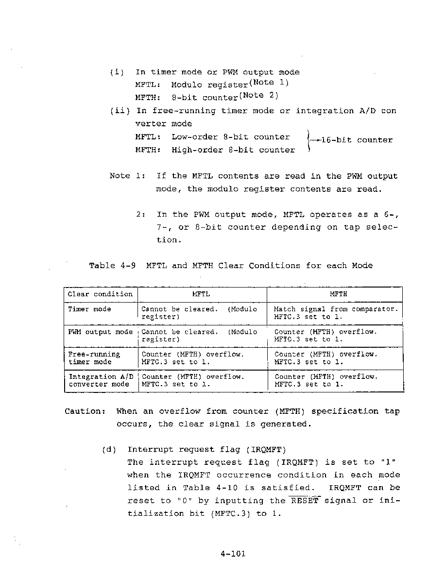
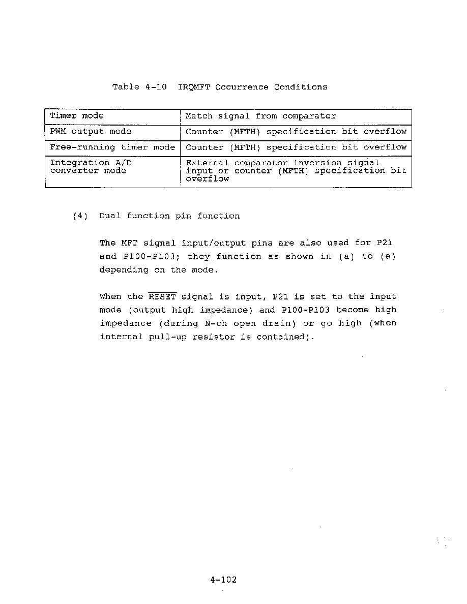
4.6 Timer/Event Counter
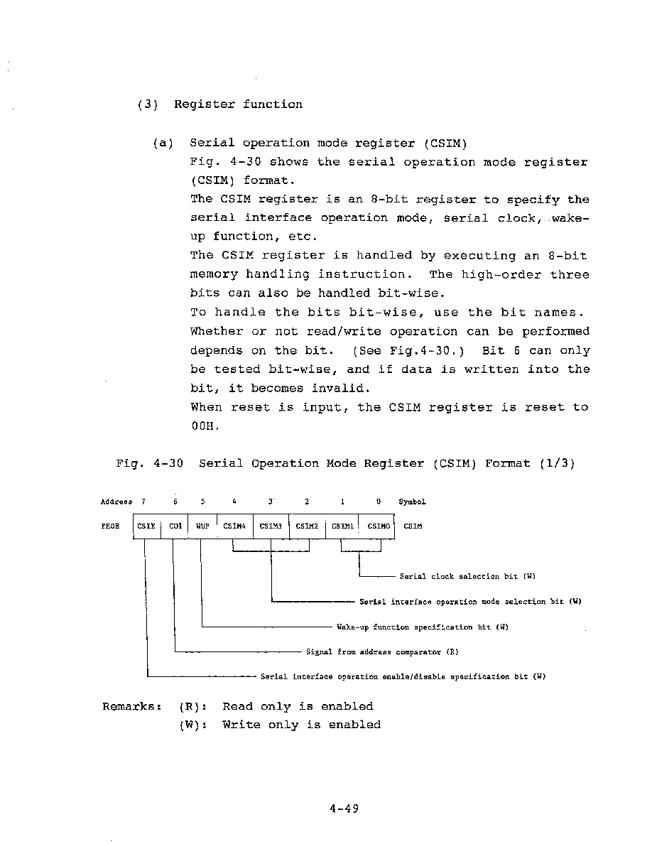
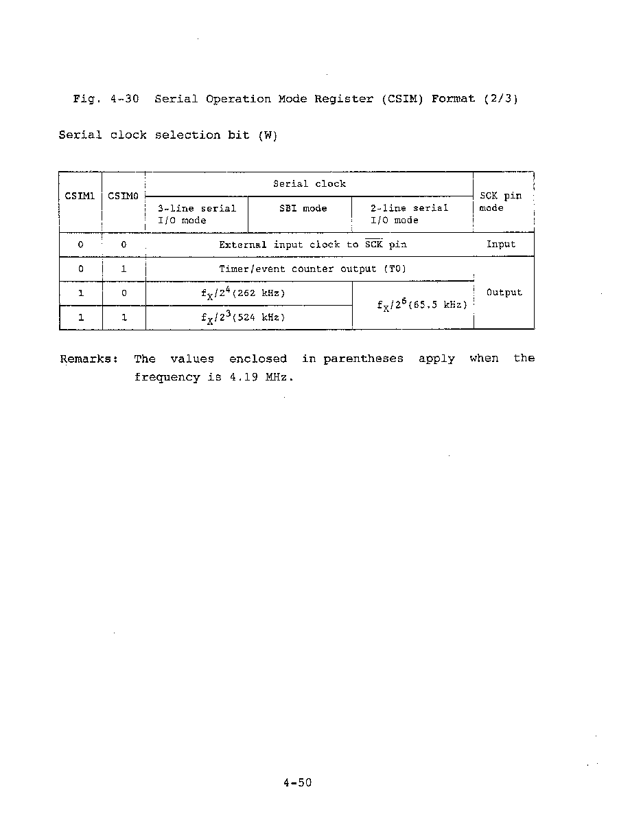
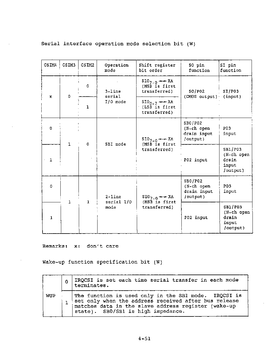
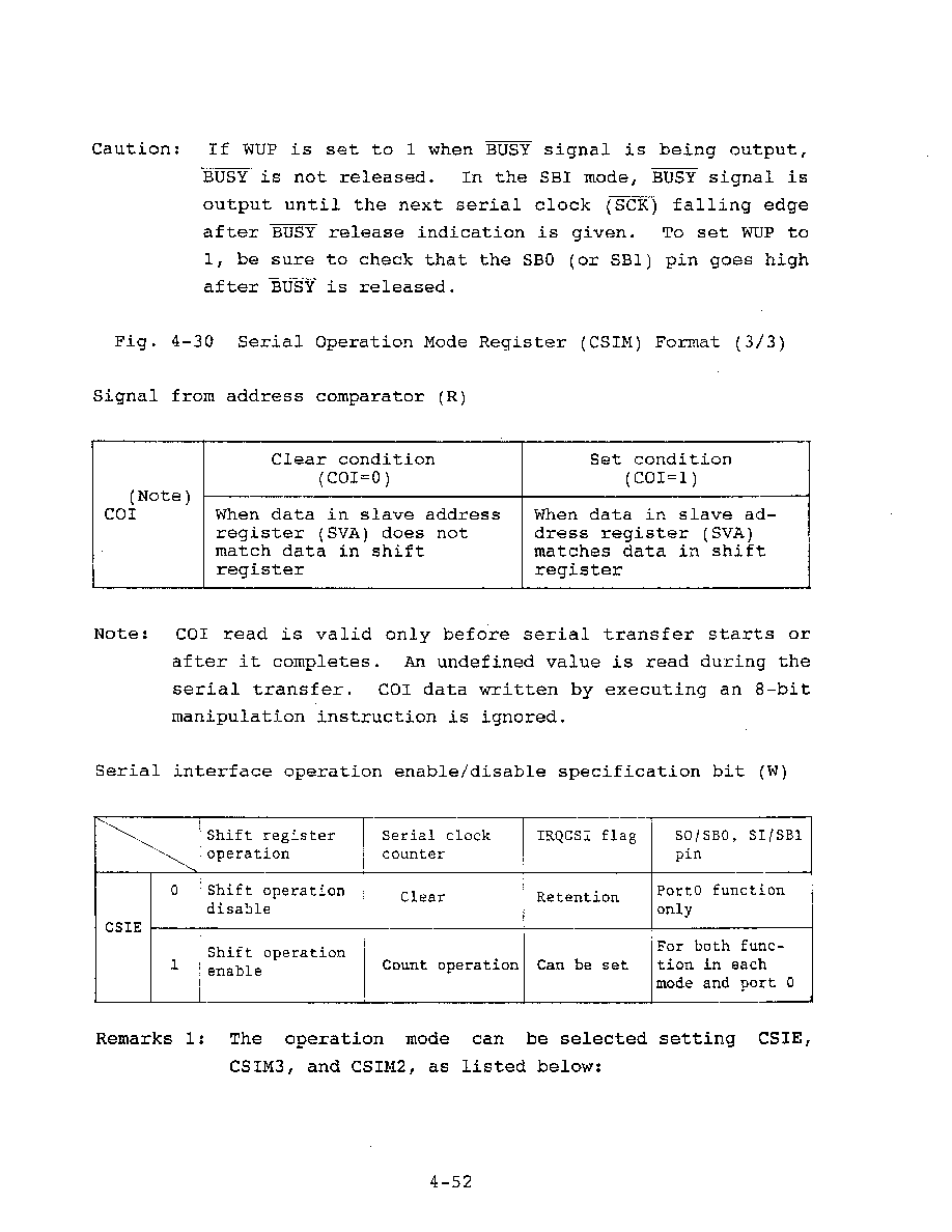
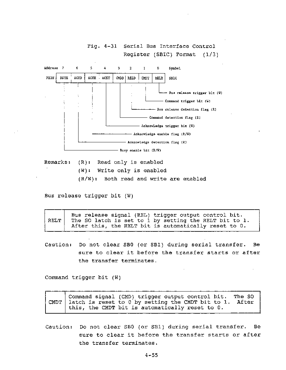
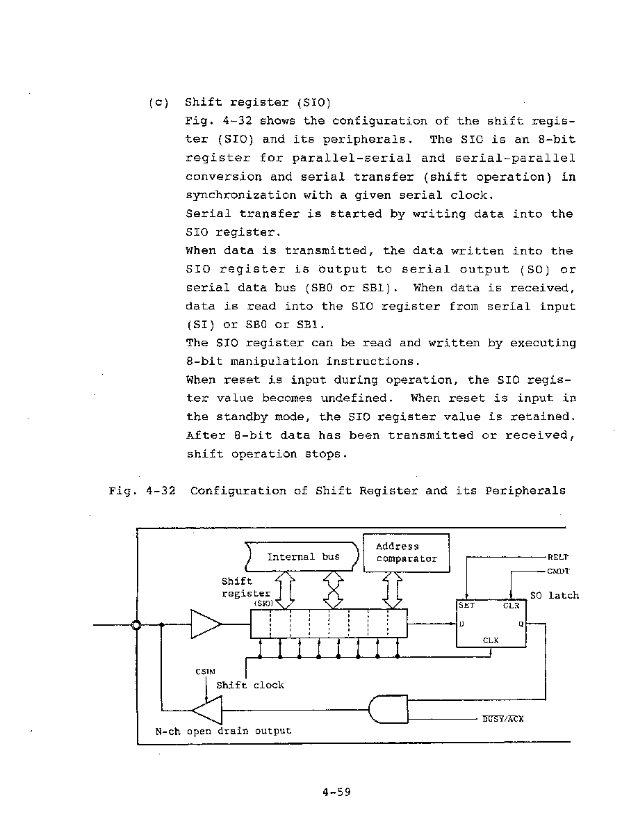
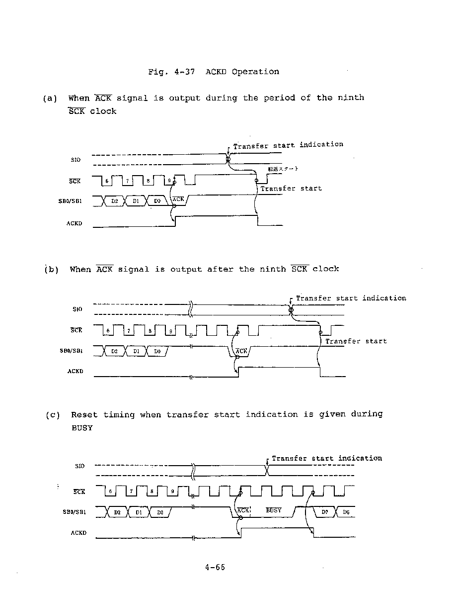
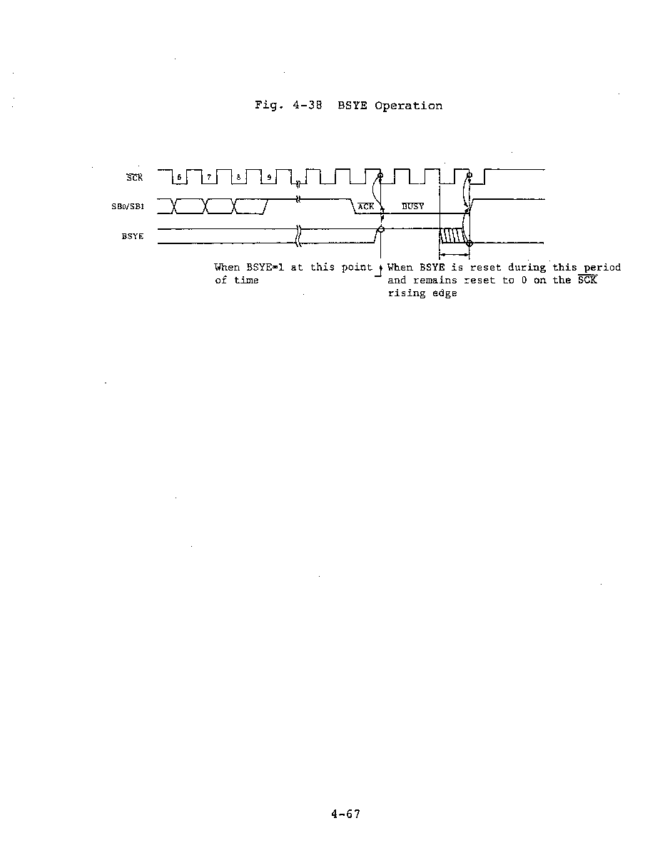
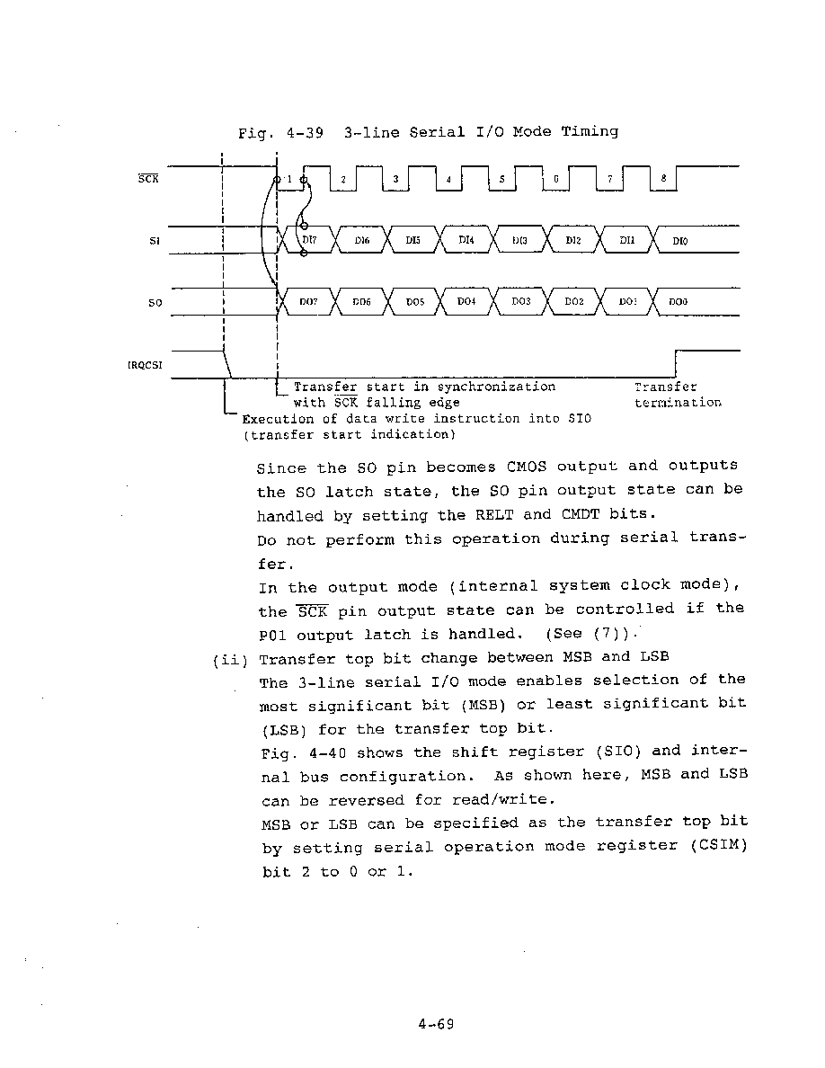
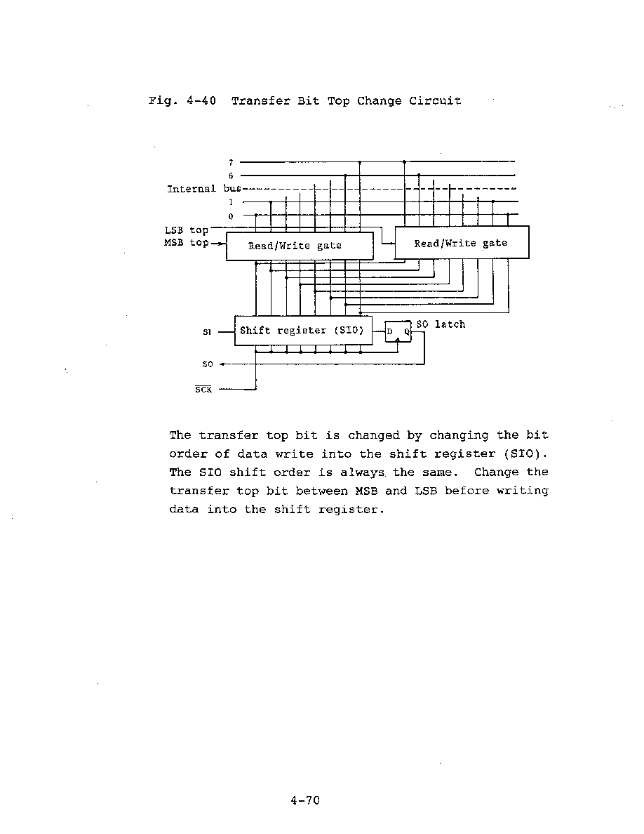
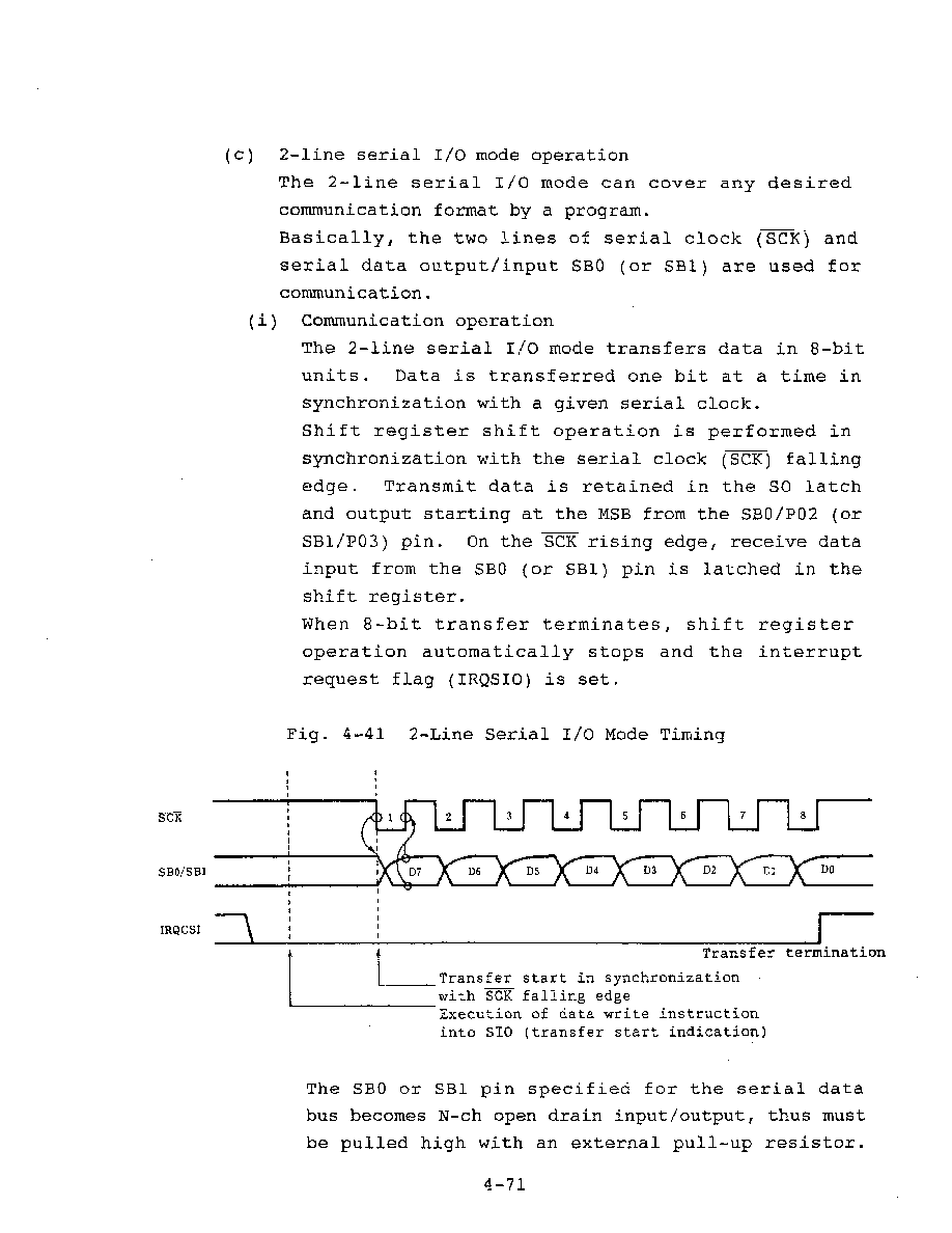
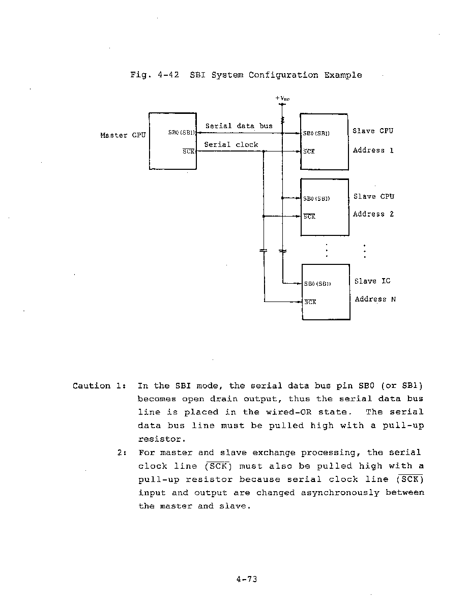
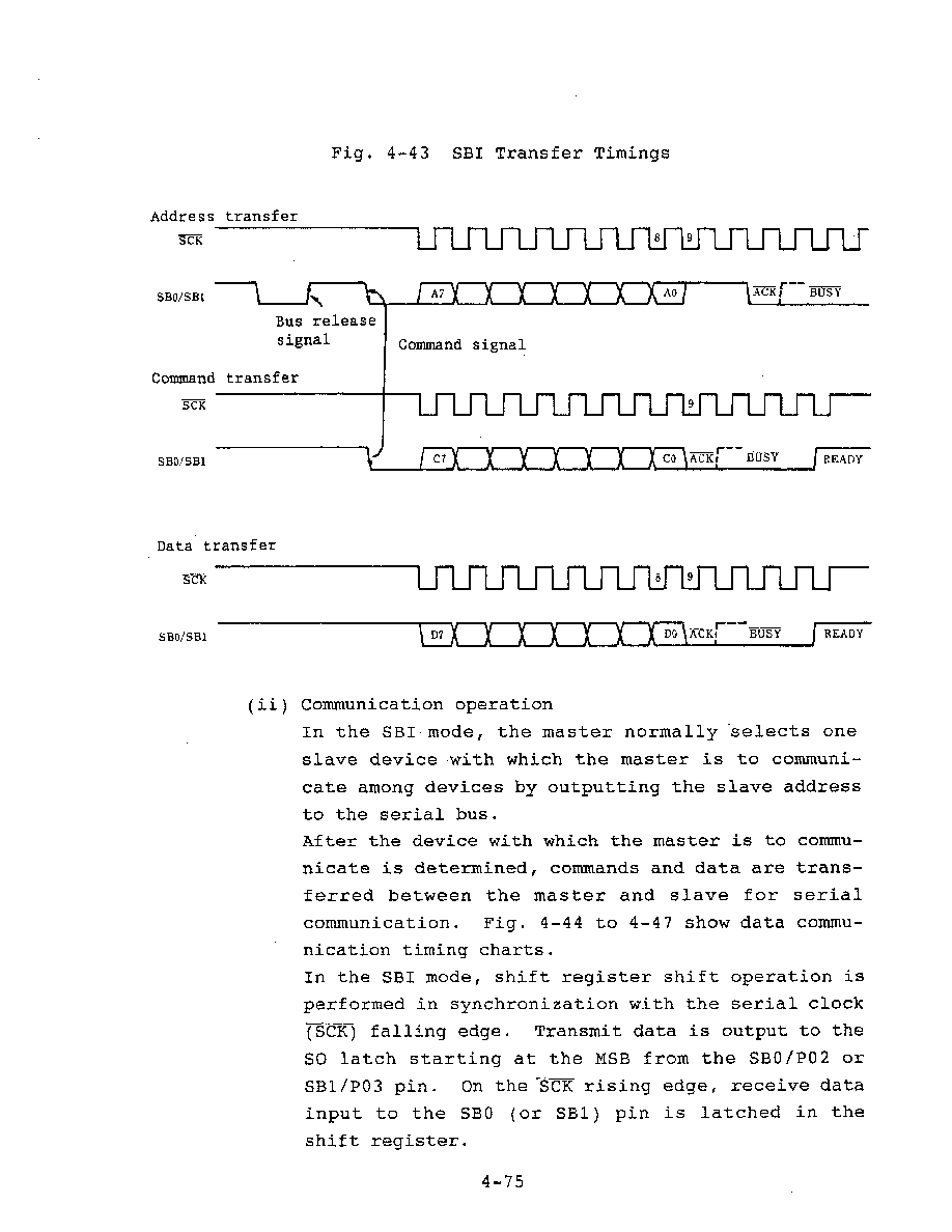
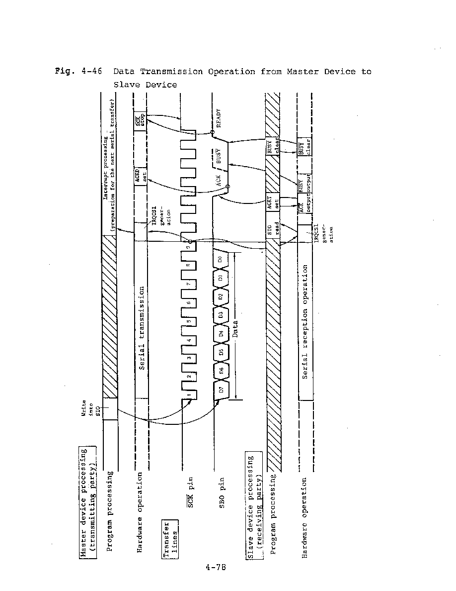
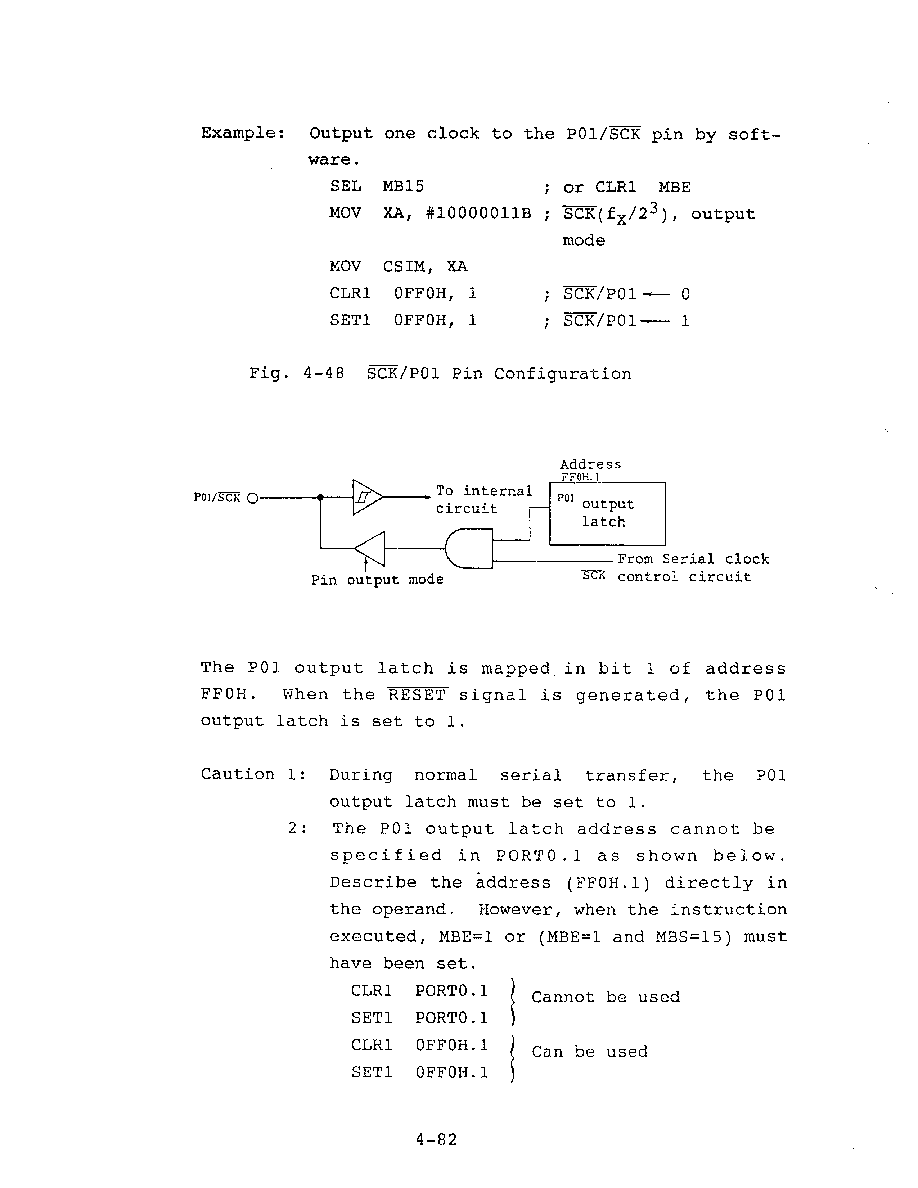
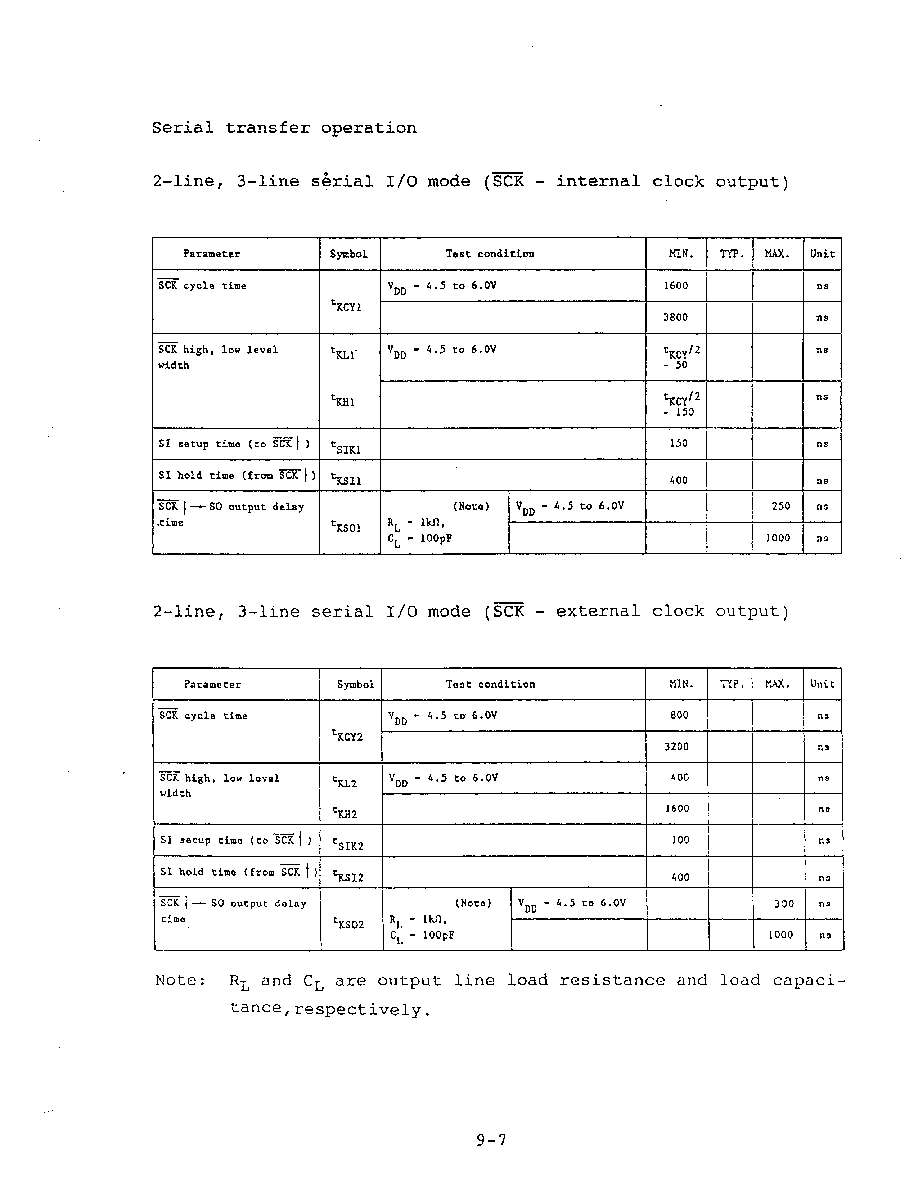
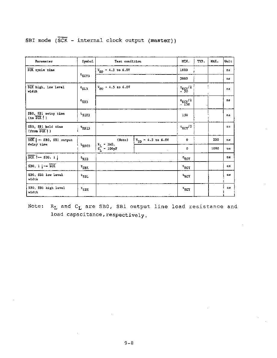
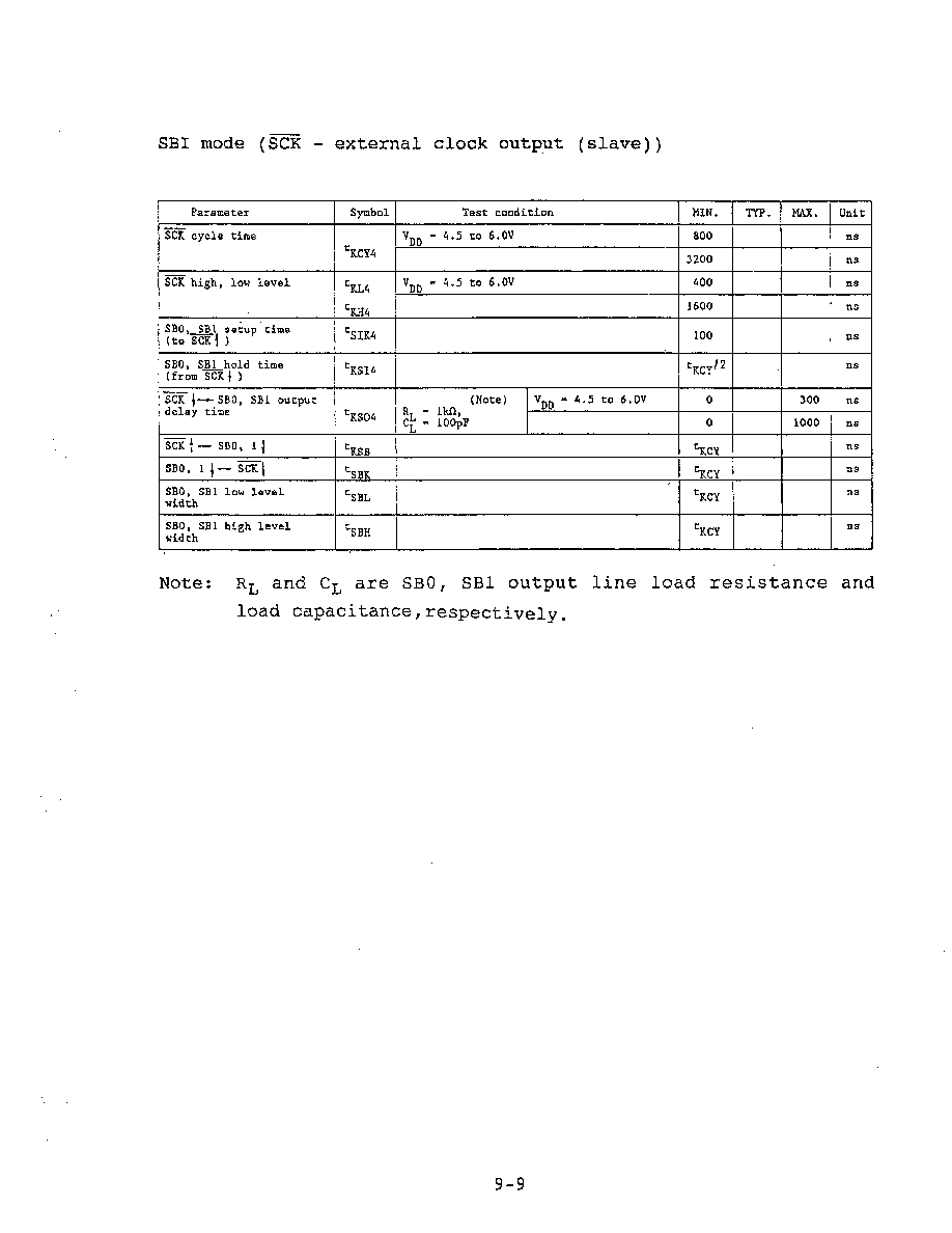
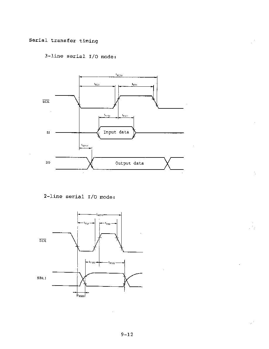
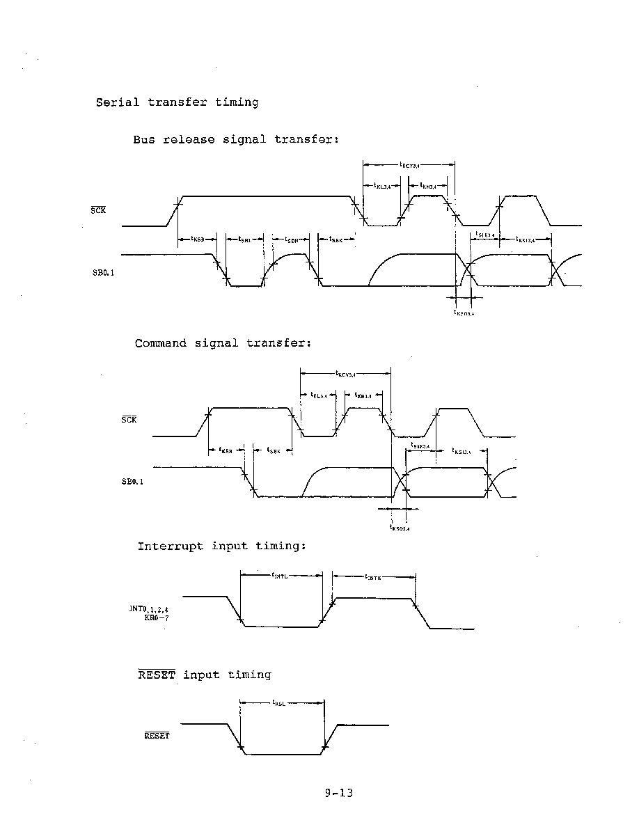
4.7 Serial Interface
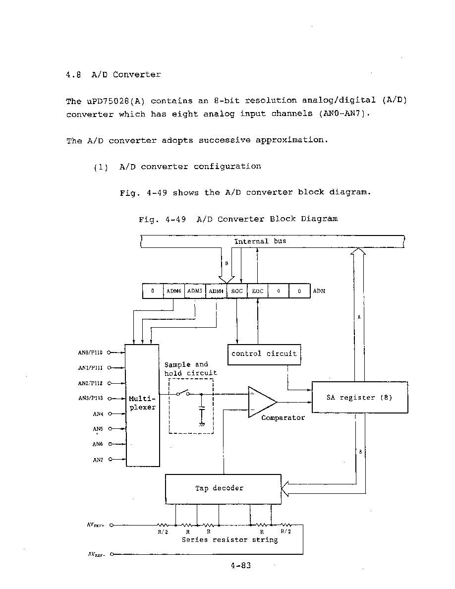
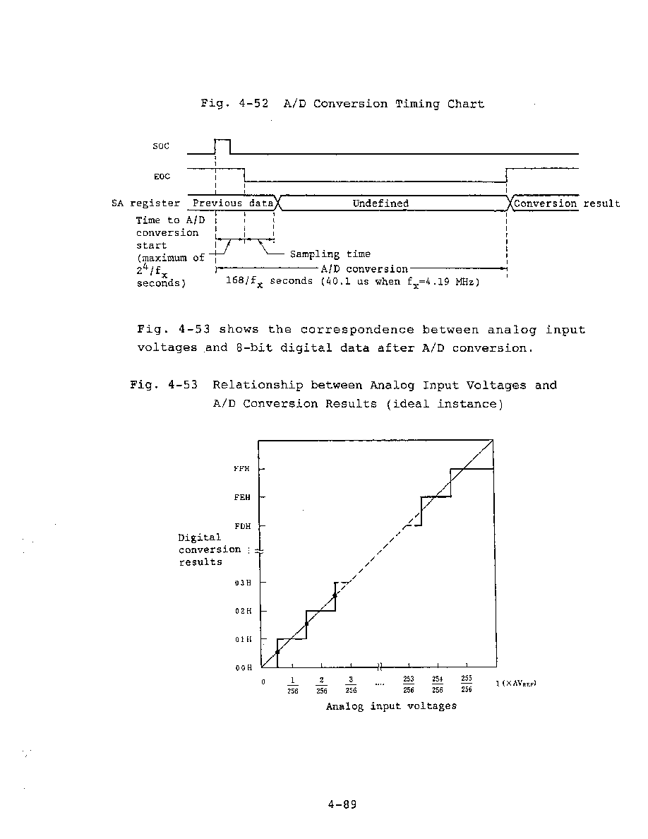
4.8 A/D Converter
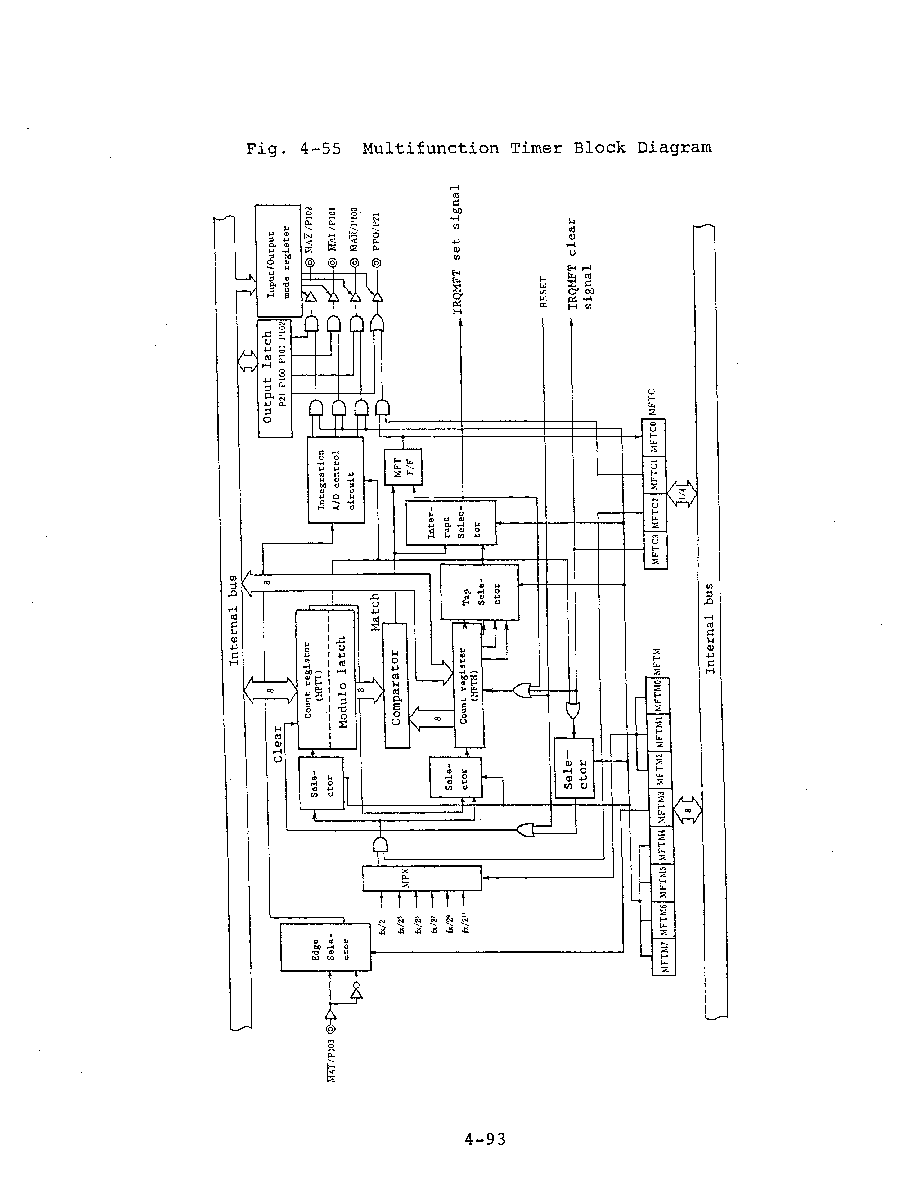
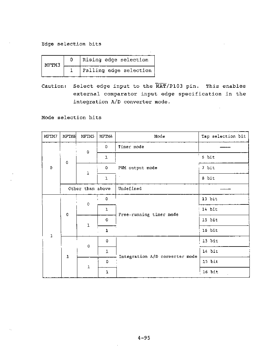
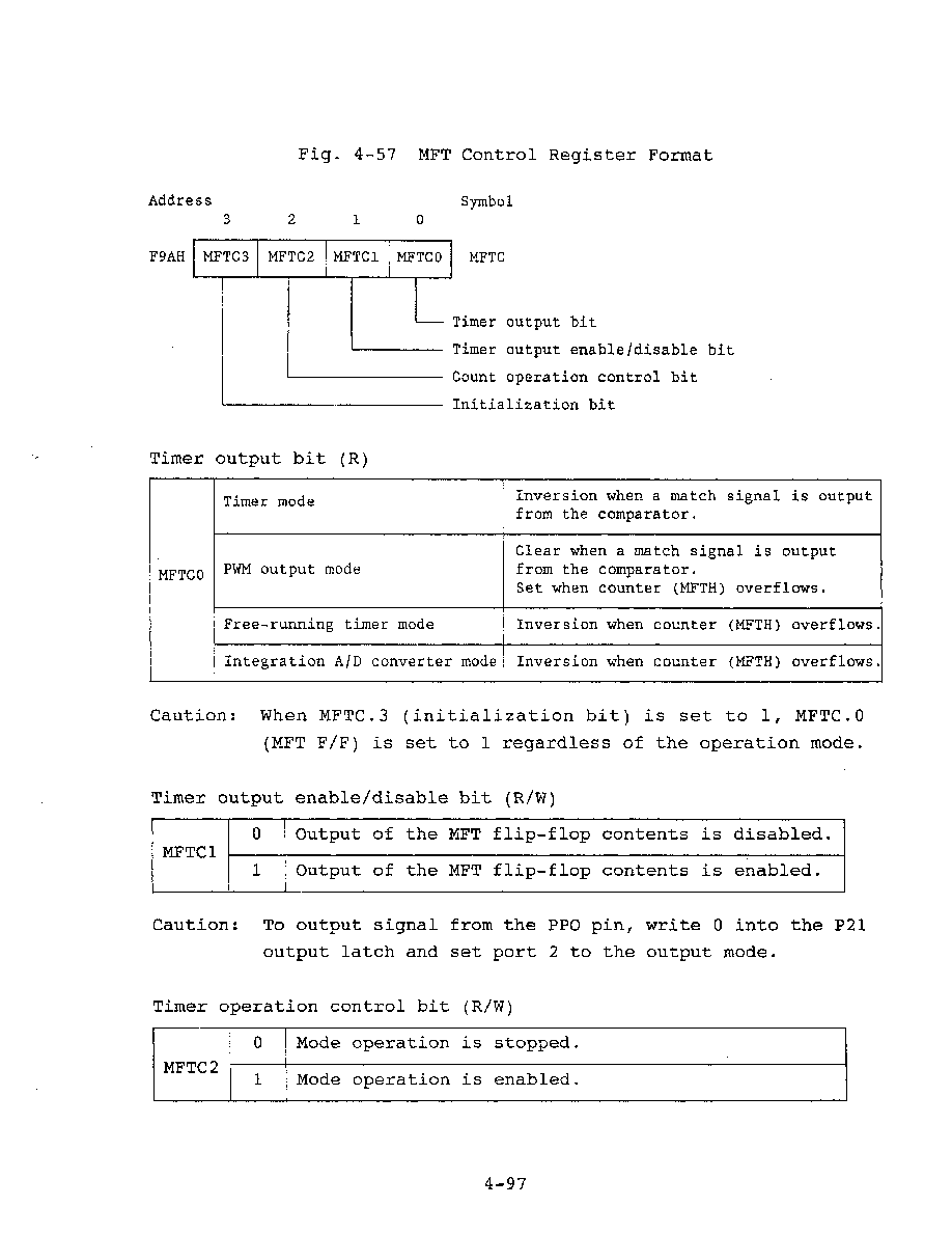
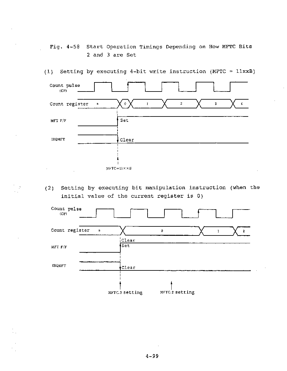
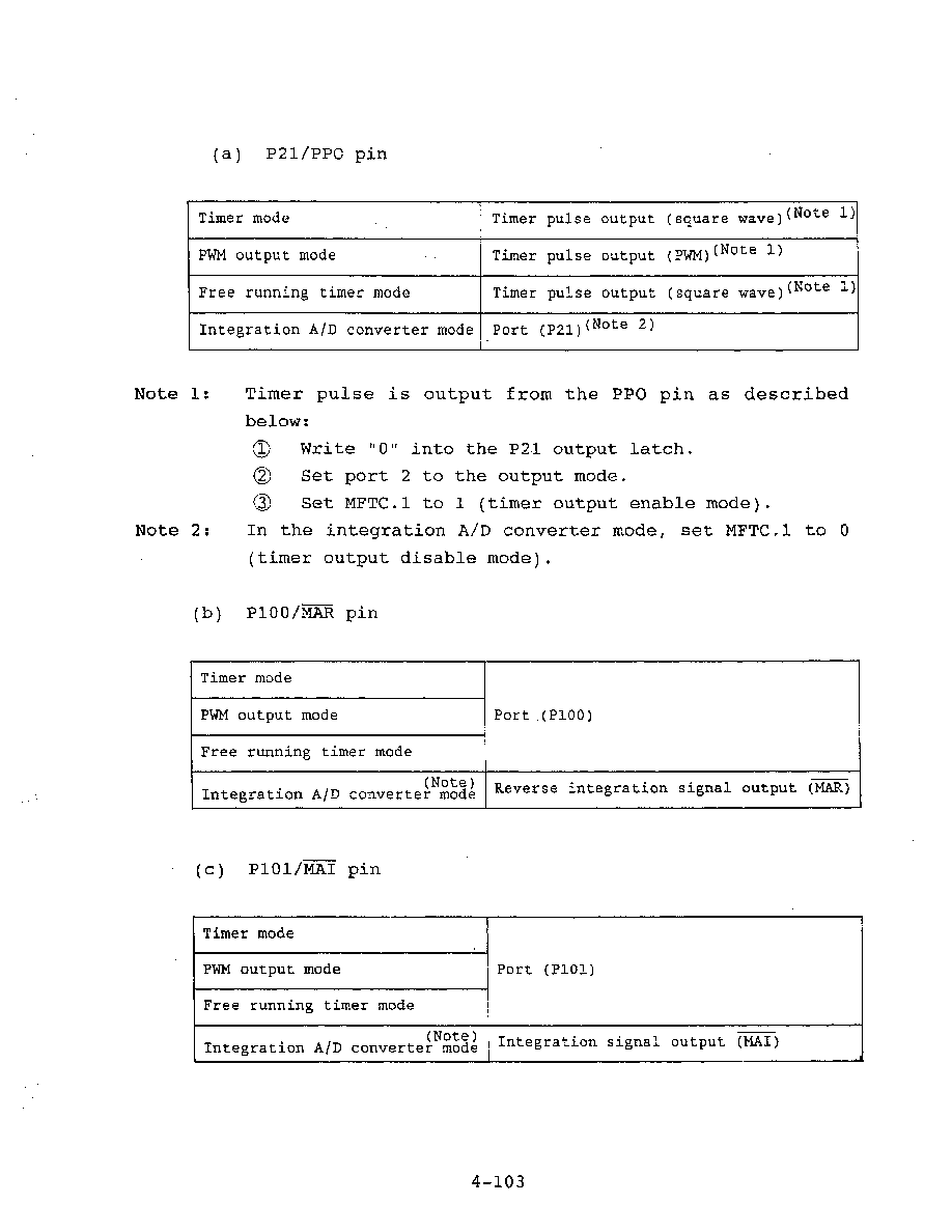
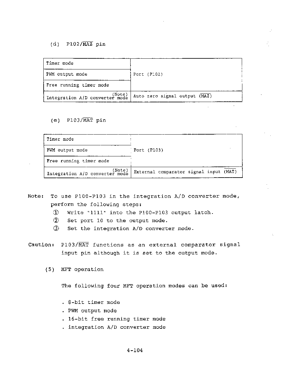
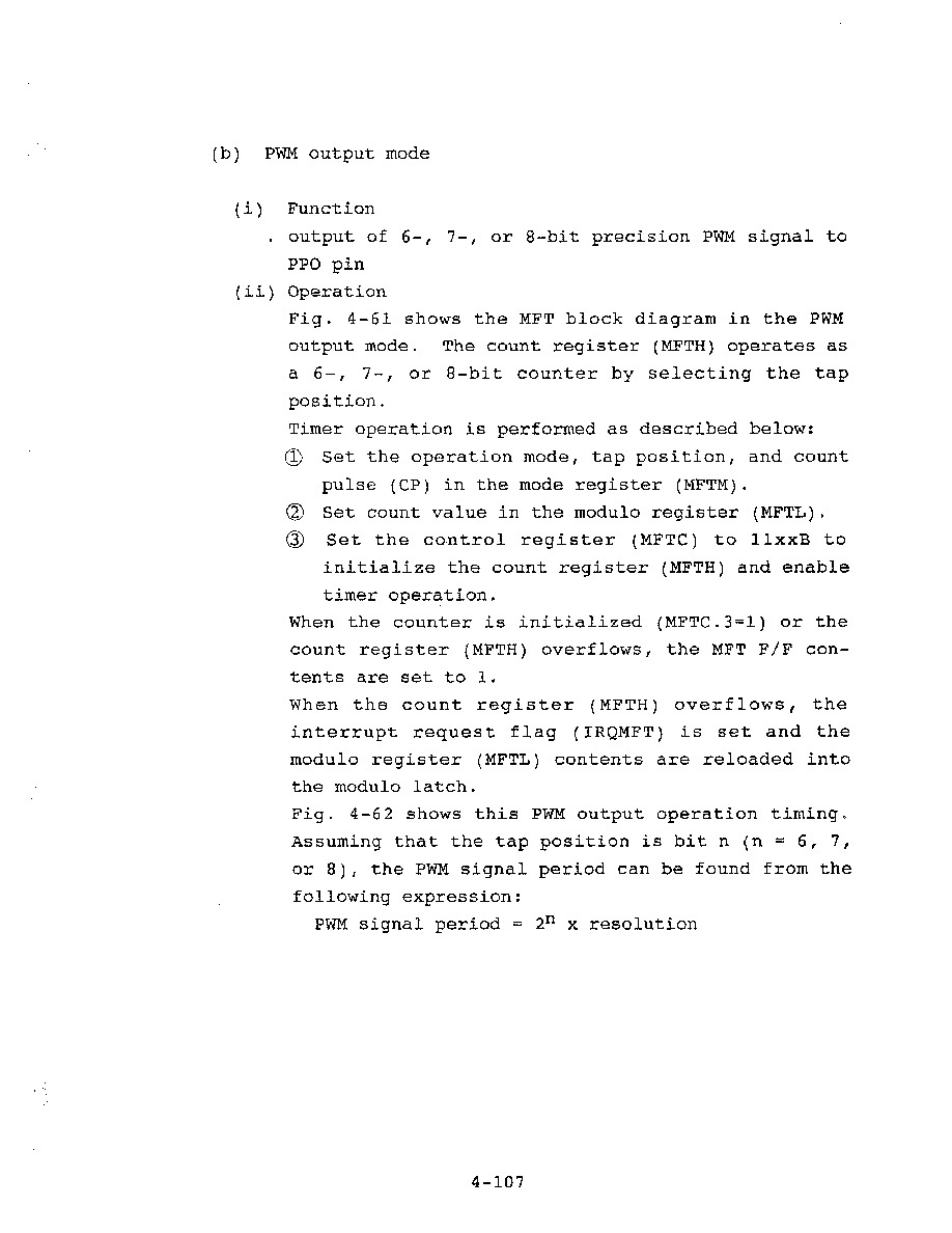
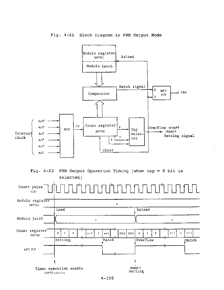
4.9 Multifunction Timer (MFT)
4.10 Bit Sequential Buffer
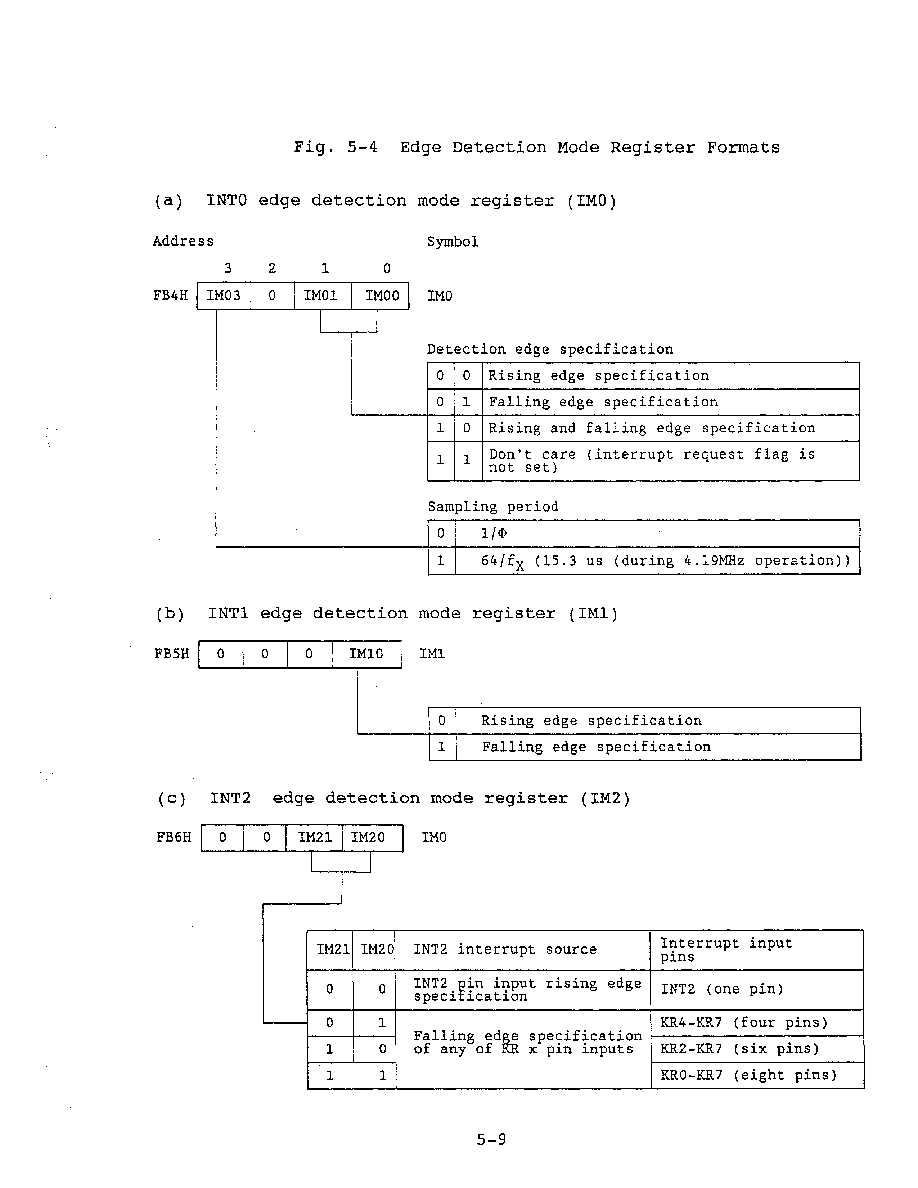
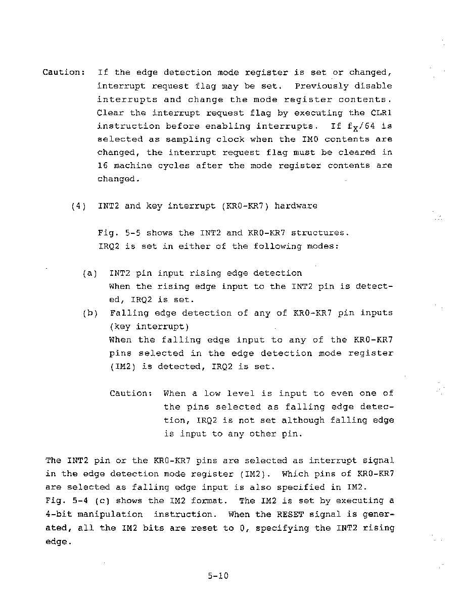
5. INTERRUPT FUNCTION
5.1 Interrupt Control Circuit Configuration
5.2 Interrupt Control Circuit Hardware
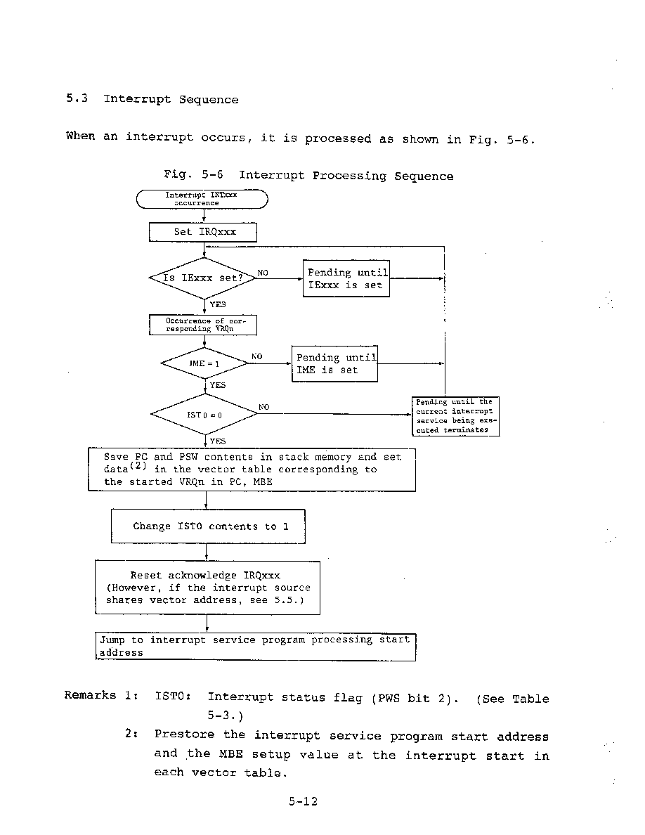
5.3 Interrupt Sequence
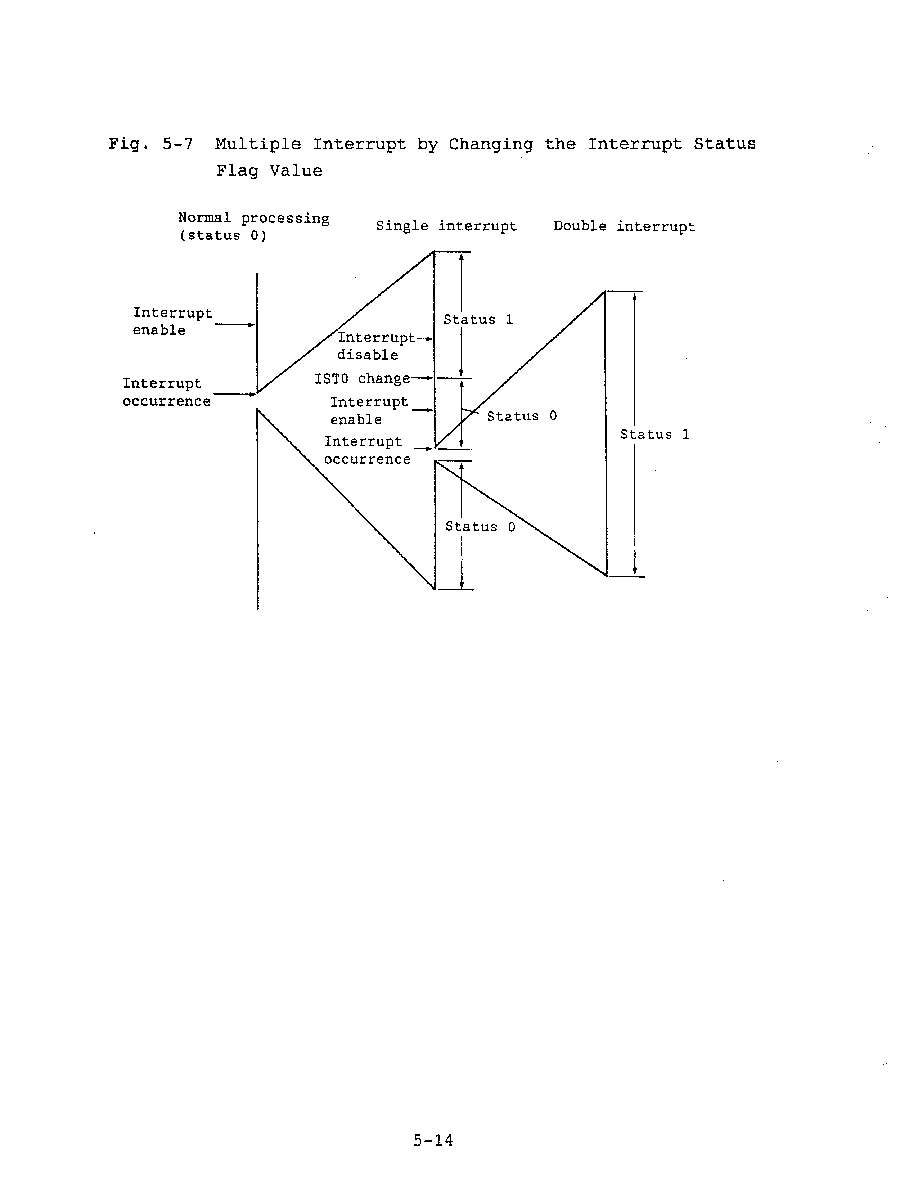
5.4 Multiple Interrupt Processing Control
5.5 Vector Address Sharing Interrupt Processing
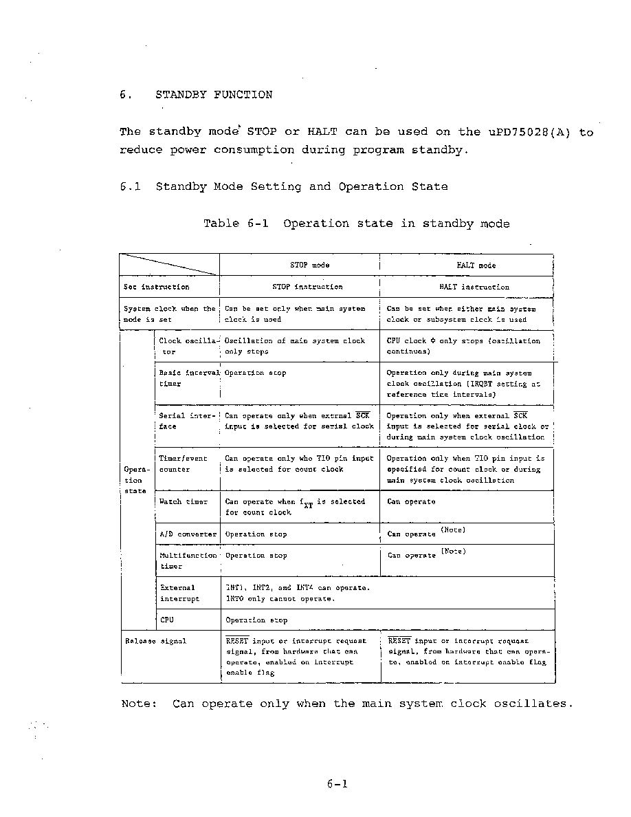
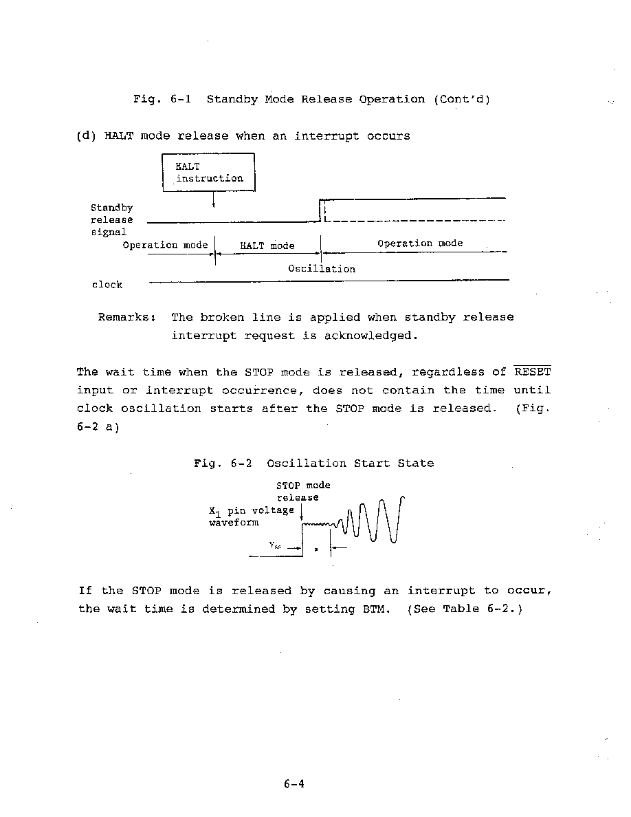
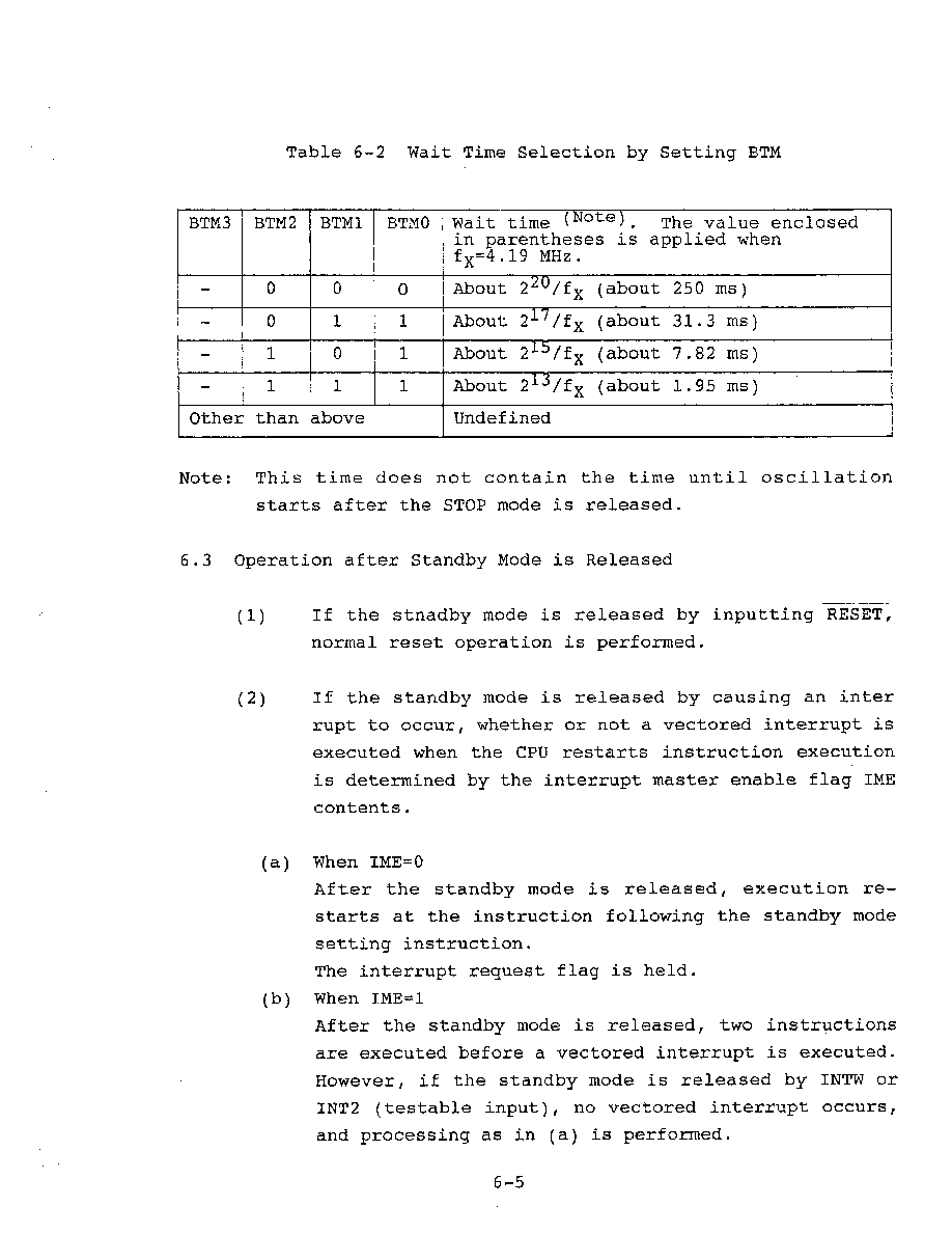
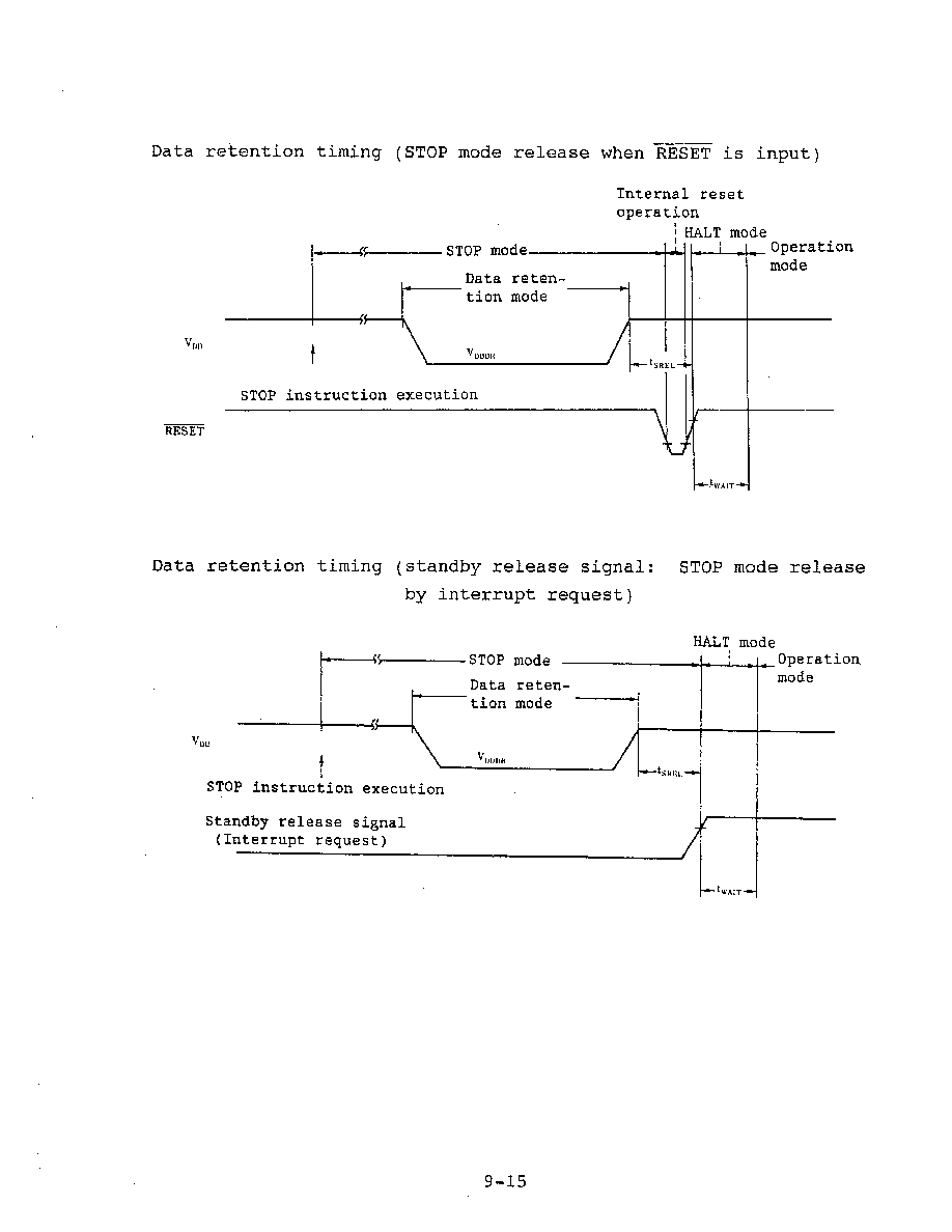
6. STANDBY FUNCTION
6.1 Standby Mode Setting and Operation State
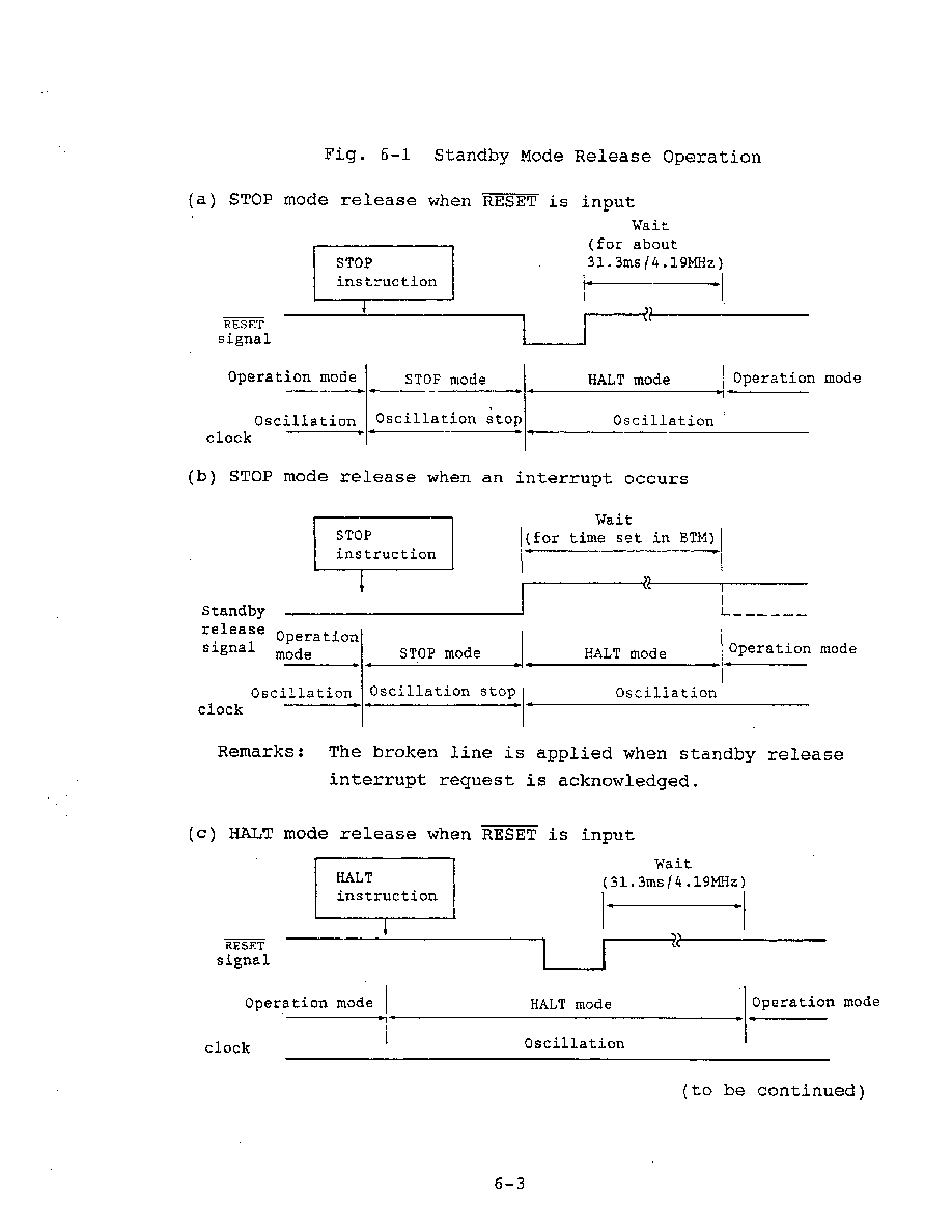
6.2 Standby Mode Release
6.3 Operation after Standby Mode is Released
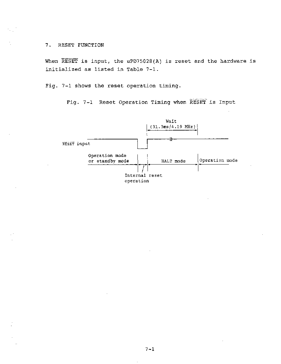
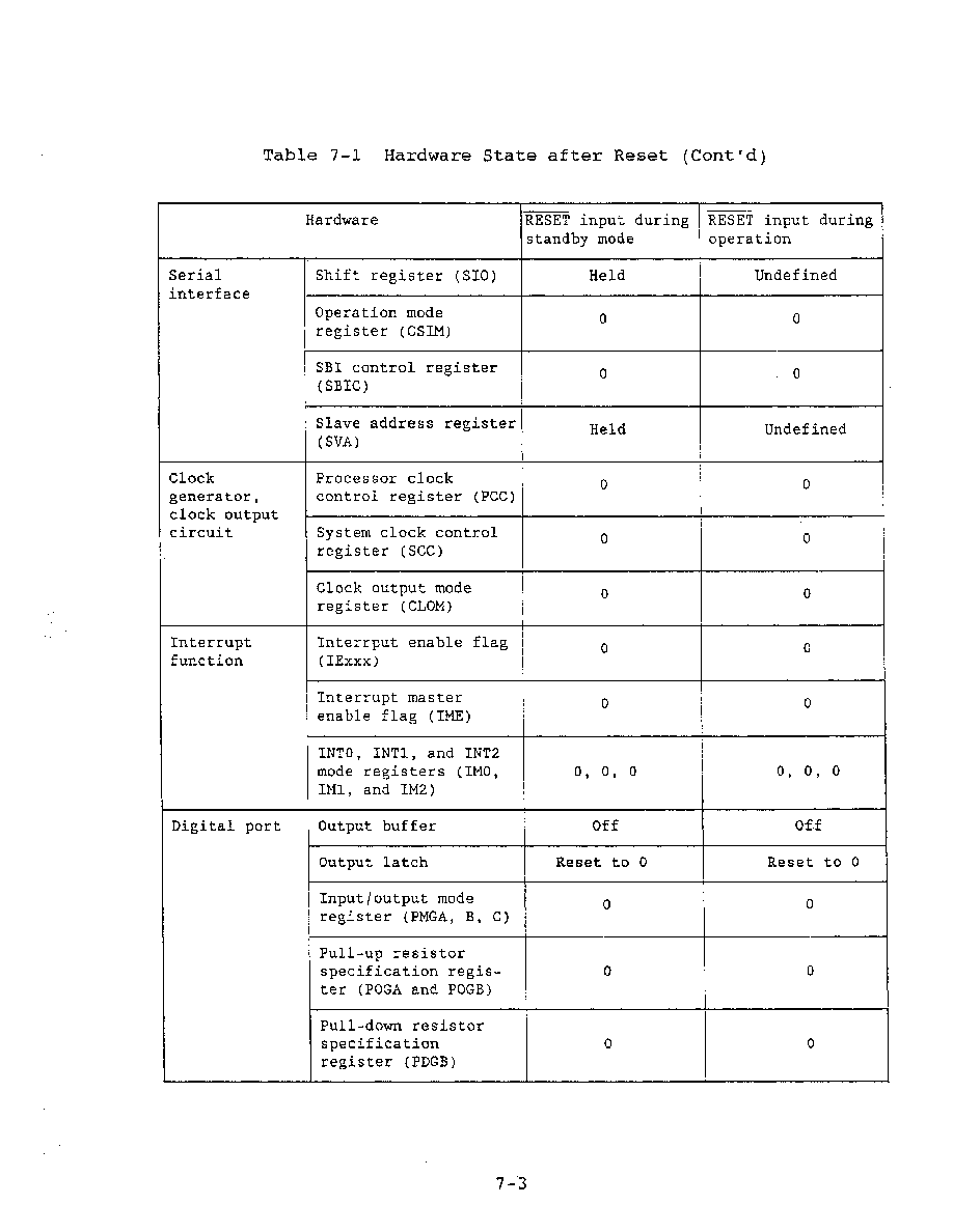
7. RESET FUNCTION
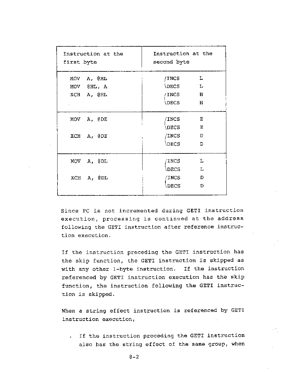
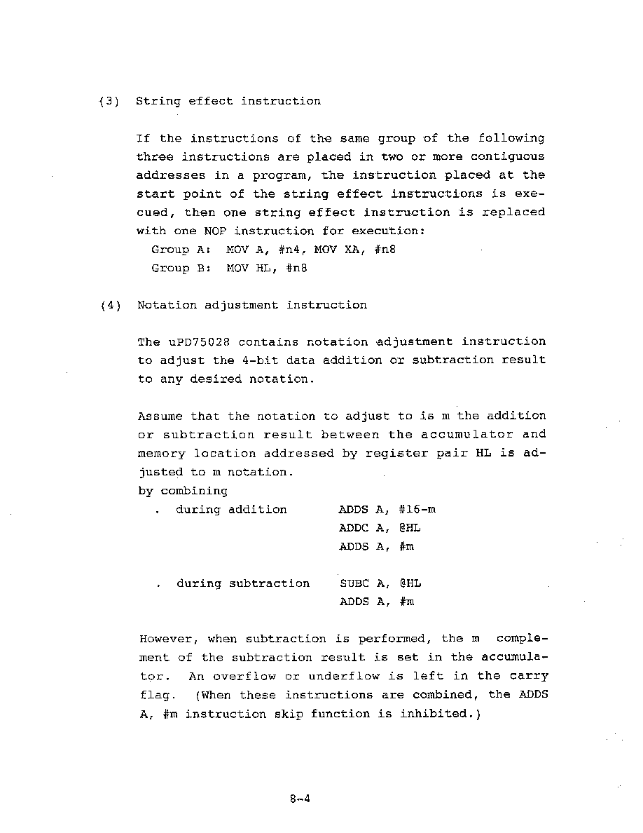
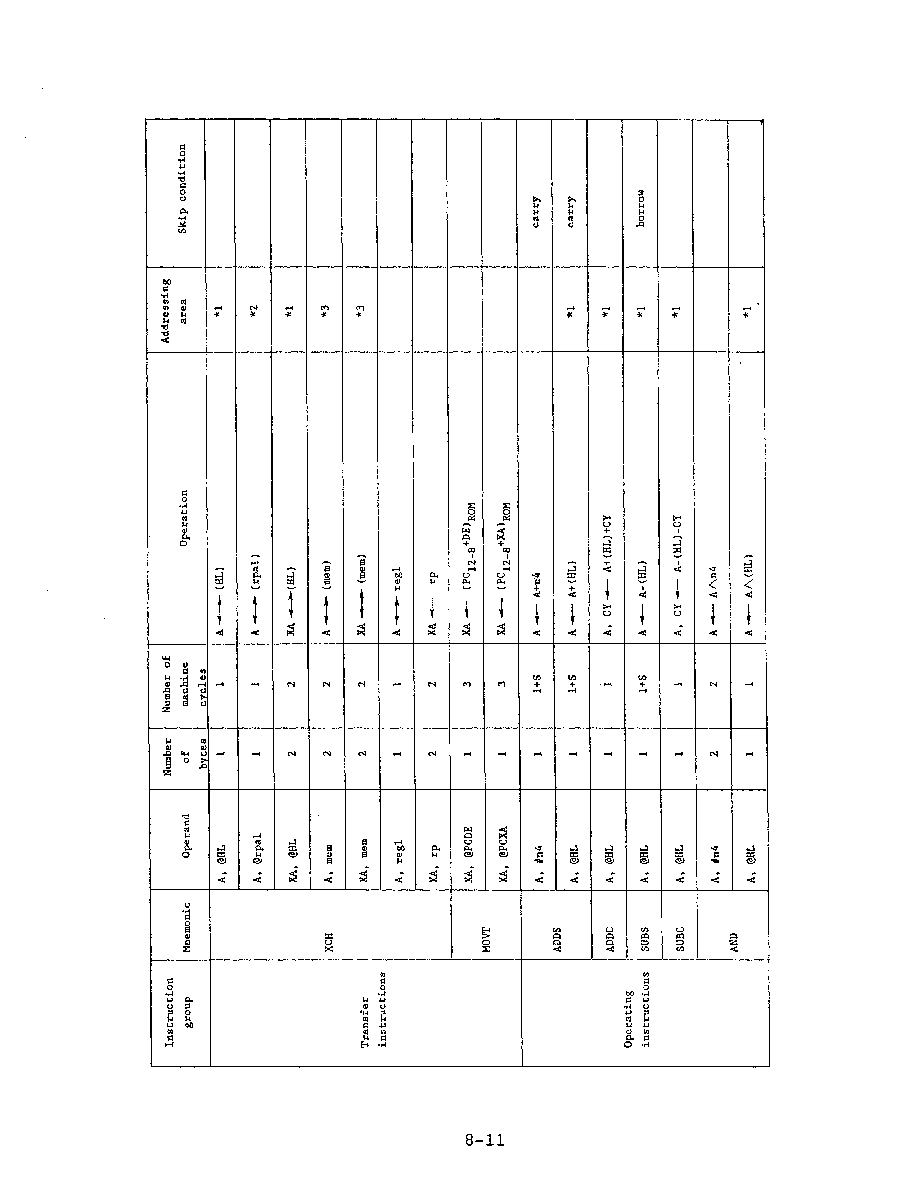
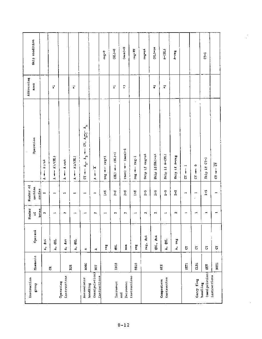
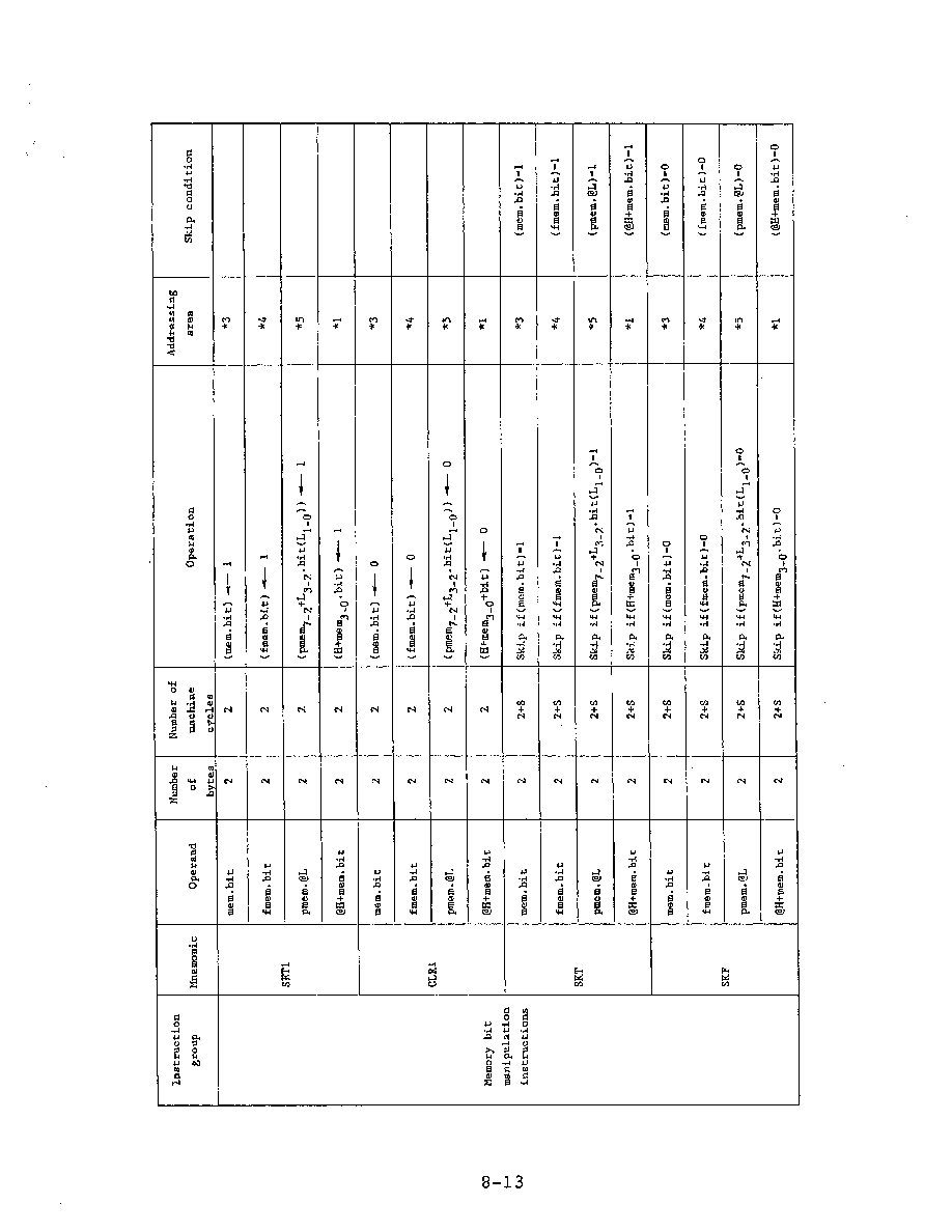
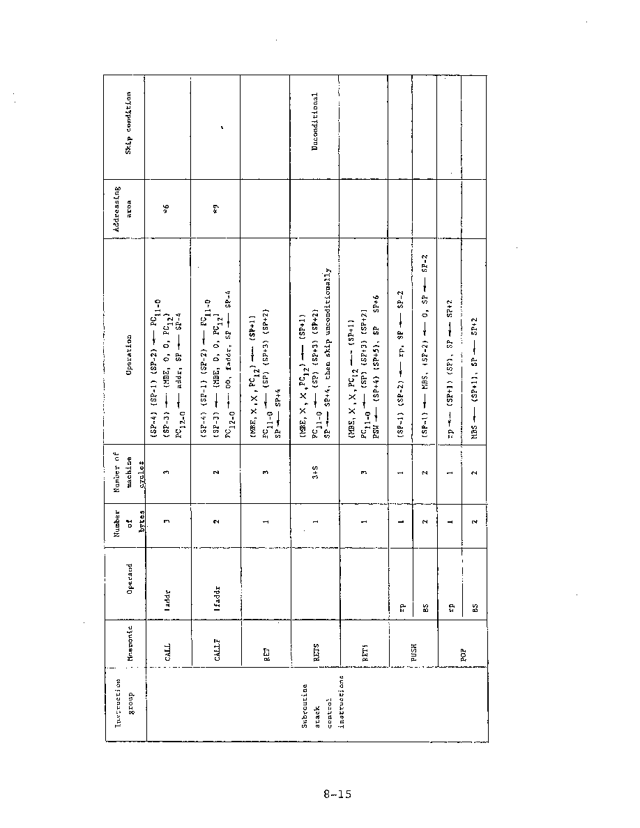
8. INSTRUCTION SET
8.1 uPD75028 (A) Featuring Instruction
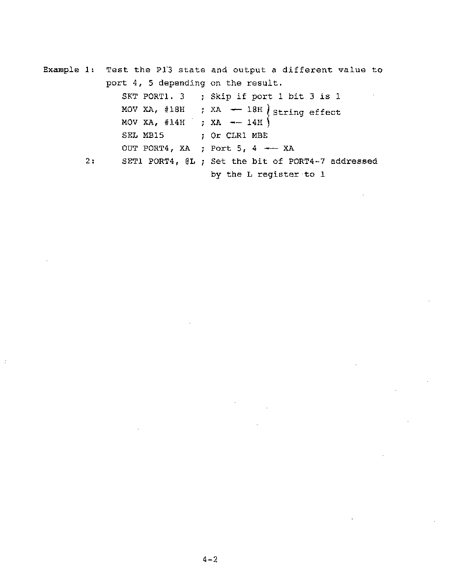
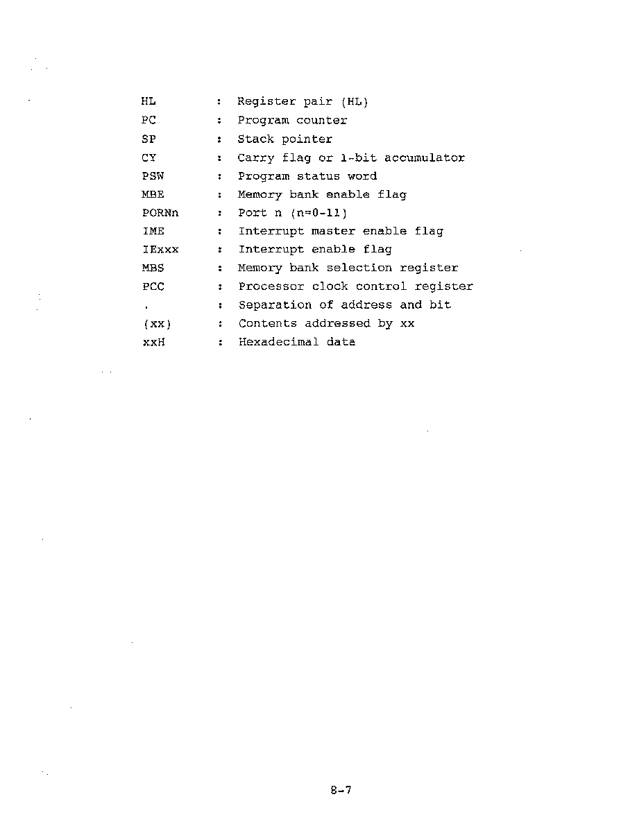
8.2 Instruction Set and Operation
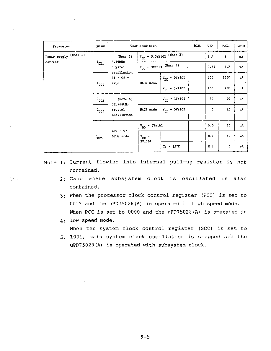
9. ELECTRICAL CHARACTERISTICS
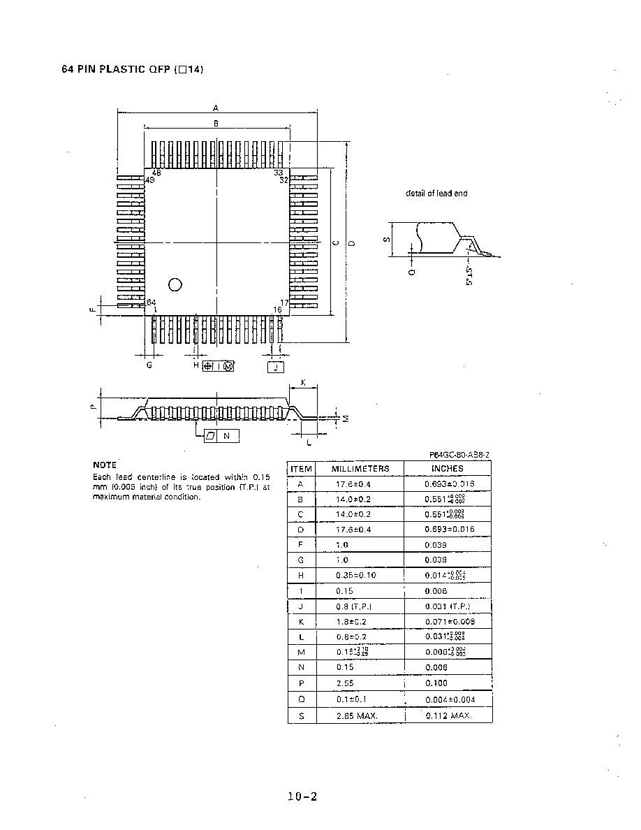
10. PACKAGE INFORMATION
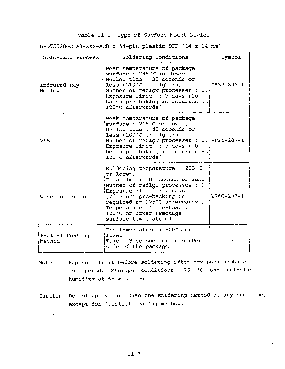
11. RECOMMENDED CONDITIONS FOR SOLDERING
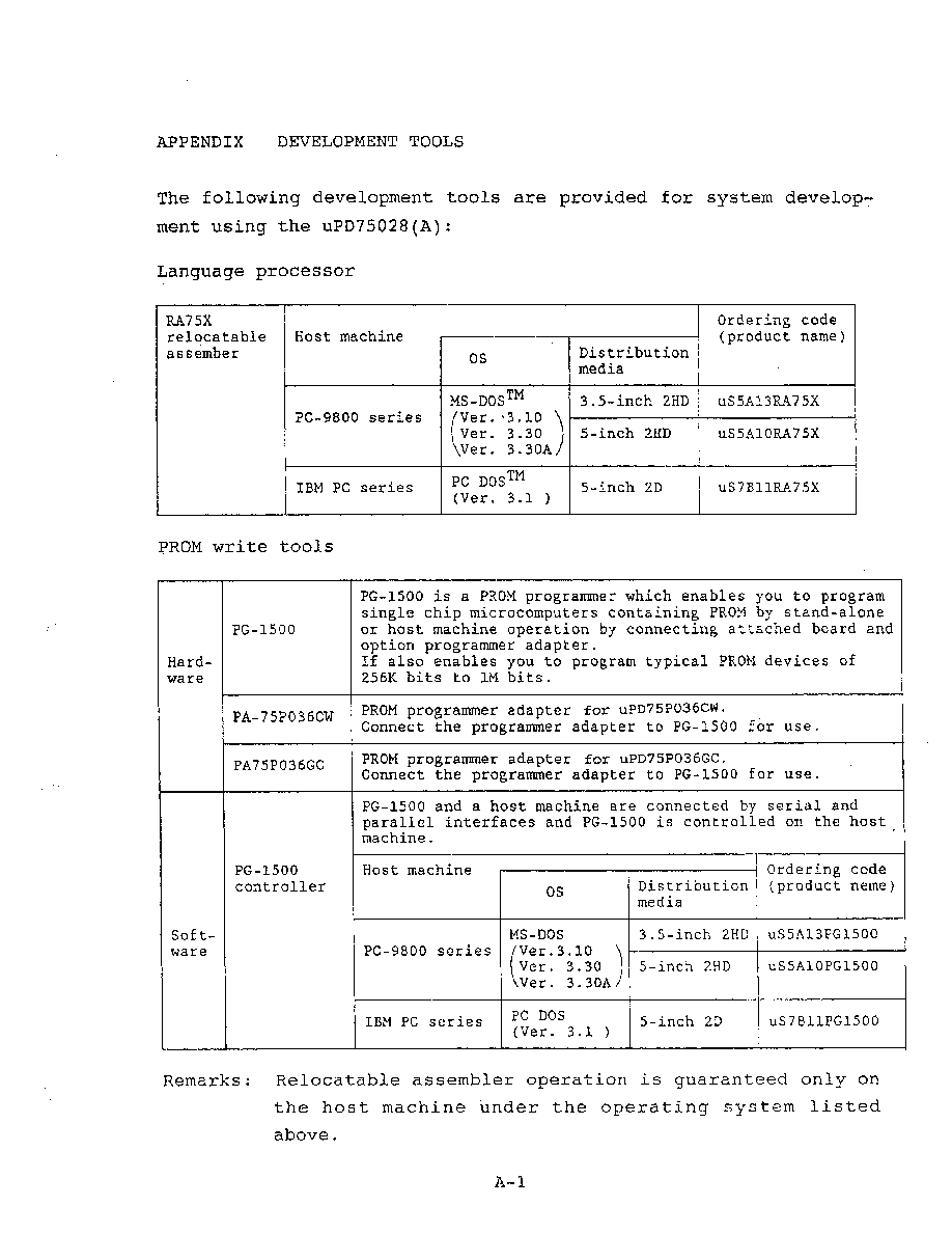
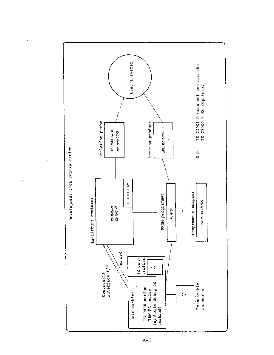
APPENDIX DEVELOPMENT TOOLS