
MOS INTEGRATED CIRCUIT
DATA SHEET
µ
PD75064, 75066, 75068,
75064(A), 75066(A), 75068(A)
4-BIT SINGLE-CHIP MICROCOMPUTER
The
µ
PD75068 is a member of the 75X series of 4-bit single-chip microcomputers.
The minimum instruction execution time of the
µ
PD75068's CPU is 0.95
µ
s. In addition to this high-speed
capability, the chip contains an A /D converter and furnishes high-performance functions such as the serial
bus interface (SBI) function compliant with the NEC standard format, providing powerful features and high
cost performance. The
µ
PD75068(A) is a high-reliability version of the
µ
PD75068.
NEC also provides PROM versions suitable for small-scale production or evaluation samples in system
development. The
µ
PD75P068 is the PROM version for the
µ
PD75064, 75066, 75068, and the
µ
PD75P068(A)
is that for the
µ
PD75064(A), 75066(A), 75068(A).
The detailed function descriptions are described in the document below. Please make sure to read this
document before starting design.
µ
PD75068 User's Manual: IEU-1366
FEATURES
∑
Variable instruction execution time advantageous to high-speed operation and power-saving:
∑
0.95
µ
s, 1.91
µ
s, or 15.3
µ
s (at 4.19 MHz with the main system clock selected)
∑
122
µ
s (at 32.768 kHz with the subsystem clock selected)
∑
A /D converter (8-bit resolution, successive approximation): 8 channels
∑
Capable of low-voltage operation: V
DD
= 2.7 to 6.0 V
∑
Timer function: 3 channels
∑
On-chip NEC standard serial bus interface (SBI)
∑
Very low-power watch operation enabled (5
µ
A TYP. at 3 V)
∑
Pull-up resistor option allowed for 27 I/O lines
∑
The
µ
PD75P068 and 75P068(A) (PROM versions) available: Capable of low-voltage operation (V
DD
= 2.7 to
6.0 V)
APPLICATIONS
∑
µ
PD75064, 75066, 75068
Home electronic appliances, air conditioners, cameras, and electronic measuring instruments
∑
µ
PD75064(A), 75066(A), 75068(A)
Automotive electronics
The mark 5 shows revised points.
The information in this document is subject to change without notice.
Document No. IC-3140B
( O.D. No. IC-8629B)
Date Published December 1994 P
Printed in Japan
5
NEC CORPORATION 1993

2
µ
PD75064, 75066, 75068, 75064(A), 75066(A), 75068(A)
Part number
µ
PD75064
µ
PD75064(A)
µ
PD75066
µ
PD75066(A)
Parameter
µ
PD75068
µ
PD75068(A)
Quality grade
Standard
Special
ORDERING INFORMATION
Part number
Package
Quality Grade
µ
PD75064CU-xxx
42-pin plastic shrink DIP (600 mil)
Standard
µ
PD75064GB-xxx-3B4
44-pin plastic QFP (10x10 mm)
Standard
µ
PD75066CU-xxx
42-pin plastic shrink DIP (600 mil)
Standard
µ
PD75066GB-xxx-3B4
44-pin plastic QFP (10x10 mm)
Standard
µ
PD75068CU-xxx
42-pin plastic shrink DIP (600 mil)
Standard
µ
PD75068GB-xxx-3B4
44-pin plastic QFP (10x10 mm)
Standard
µ
PD75064CU(A)-xxx
42-pin plastic shrink DIP (600 mil)
Special
µ
PD75064GB(A)-xxx-3B4
44-pin plastic QFP (10x10 mm)
Special
µ
PD75066CU(A)-xxx
42-pin plastic shrink DIP (600 mil)
Special
µ
PD75066GB(A)-xxx-3B4
44-pin plastic QFP (10x10 mm)
Special
µ
PD75068CU(A)-xxx
42-pin plastic shrink DIP (600 mil)
Special
µ
PD75068GB(A)-xxx-3B4
44-pin plastic QFP (10x10 mm)
Special
Remark xxx : ROM code suffix
Please refer to "Quality grade on NEC Semiconductor Devices" (Document number IEI-1209) published
by NEC Corporation to know the specification of quality grade on the devices and its recommended
applications.
DIFFERENCE BETWEEN
µ
PD7506x SUBSERIES AND
µ
PD7506x(A) SUBSERIES
5
5
5
5
5
5
The
µ
PD75064, 75066, 75068 and
µ
PD75064(A), 75066(A), 75068(A) differ only in their quality grade.
Unless otherwise specified, this data sheet describes the
µ
PD75068 as the representative product.
For products with the suffix (A) attached, please make the following substitutions when reading:
µ
PD75064 -->
µ
PD75064(A)
µ
PD75066 -->
µ
PD75066(A)
µ
PD75068 -->
µ
PD75068(A)
5
3
µ
PD75064, 75066, 75068, 75064(A), 75066(A), 75068(A)
FUNCTION OVERVIEW
Item
Function
Instruction execution time
∑
Main system clock : 0.95
µ
s, 1.91
µ
s, 15.3
µ
s (at 4.19 MHz)
∑
Subsystem clock : 122
µ
s (at 32.768 kHz)
Internal memory
ROM
∑
µ
PD75064 : 4096
◊
8 bits
∑
µ
PD75066 : 6016
◊
8 bits
∑
µ
PD75068 : 8064
◊
8 bits
RAM
512
◊
4 bits
General register
∑
When operating in 4 bits: 8
∑
When operating in 8 bits: 4
I/O port
32
12
CMOS input
Of these, seven with software-specifiable on-chip
pull-up resistors
12
CMOS I/O
Software-specifiable on-chip pull-up resistors
Four pins can directly drive LEDs.
8
N-ch open-drain I/O
Breakdown voltage: 10 V
Mask-option-specifiable on-chip pull-up resistors
Can directly drive LEDs.
Timer
3 chs.
∑
Timer/event counter
∑
Basic interval timer : Applicable to watchdog timer
∑
Watch timer : Capable of buzzer output
Serial interface
∑
3-wire serial I/O mode
∑
2-wire serial I/O mode
∑
SBI mode
Bit sequencial buffer
16 bits
Clock output function
, f
x
/2
3
, f
x
/2
4
, f
x
/2
6
(Main system clock: at 4.19 MHz operation)
A/D converter
∑
8-bit resolution x 8 channels
∑
Low-power operation possible : V
DD
= 2.7 to 6.0 V
Vectored interrupt
External : 3 , Internal : 3
Test input
External : 1, Internal : 1
System clock oscillator
∑
Ceramic/crystal oscillator for main system clock
∑
Crystal oscillator for subsystem clock
Standby function
STOP / HALT mode
Operating ambient
≠40 to +85
∞
C
temperature
Operating supply
2.7 to 6.0 V
voltage
Package
∑
42-pin plastic shrink DIP (600 mil)
∑
44-pin plastic QFP (10 x 10 mm)

4
µ
PD75064, 75066, 75068, 75064(A), 75066(A), 75068(A)
CONTENTS
1.
PIN CONFIGURATION (TOP VIEW) ∑∑∑∑∑∑∑∑∑∑∑∑∑∑∑∑∑∑∑∑∑∑∑∑∑∑∑∑∑∑∑∑∑∑∑∑∑∑∑∑∑∑∑∑∑∑∑∑∑∑∑∑∑∑∑∑∑∑∑∑∑∑∑∑∑∑∑∑∑∑∑∑∑∑∑∑∑∑∑∑∑∑∑∑∑∑∑∑∑∑
5
2.
BLOCK DIAGRAM ∑∑∑∑∑∑∑∑∑∑∑∑∑∑∑∑∑∑∑∑∑∑∑∑∑∑∑∑∑∑∑∑∑∑∑∑∑∑∑∑∑∑∑∑∑∑∑∑∑∑∑∑∑∑∑∑∑∑∑∑∑∑∑∑∑∑∑∑∑∑∑∑∑∑∑∑∑∑∑∑∑∑∑∑∑∑∑∑∑∑∑∑∑∑∑∑∑∑∑∑∑∑∑∑∑∑∑∑∑∑∑∑∑∑∑∑∑∑∑∑
7
3.
PIN FUNCTIONS ∑∑∑∑∑∑∑∑∑∑∑∑∑∑∑∑∑∑∑∑∑∑∑∑∑∑∑∑∑∑∑∑∑∑∑∑∑∑∑∑∑∑∑∑∑∑∑∑∑∑∑∑∑∑∑∑∑∑∑∑∑∑∑∑∑∑∑∑∑∑∑∑∑∑∑∑∑∑∑∑∑∑∑∑∑∑∑∑∑∑∑∑∑∑∑∑∑∑∑∑∑∑∑∑∑∑∑∑∑∑∑∑∑∑∑∑∑∑∑∑∑∑
8
3.1
Port Pins ∑∑∑∑∑∑∑∑∑∑∑∑∑∑∑∑∑∑∑∑∑∑∑∑∑∑∑∑∑∑∑∑∑∑∑∑∑∑∑∑∑∑∑∑∑∑∑∑∑∑∑∑∑∑∑∑∑∑∑∑∑∑∑∑∑∑∑∑∑∑∑∑∑∑∑∑∑∑∑∑∑∑∑∑∑∑∑∑∑∑∑∑∑∑∑∑∑∑∑∑∑∑∑∑∑∑∑∑∑∑∑∑∑∑∑∑∑∑∑∑∑∑∑∑∑∑∑∑∑∑∑∑∑∑∑∑∑∑∑∑∑∑∑
8
3.2
Non-Port Pins ∑∑∑∑∑∑∑∑∑∑∑∑∑∑∑∑∑∑∑∑∑∑∑∑∑∑∑∑∑∑∑∑∑∑∑∑∑∑∑∑∑∑∑∑∑∑∑∑∑∑∑∑∑∑∑∑∑∑∑∑∑∑∑∑∑∑∑∑∑∑∑∑∑∑∑∑∑∑∑∑∑∑∑∑∑∑∑∑∑∑∑∑∑∑∑∑∑∑∑∑∑∑∑∑∑∑∑∑∑∑∑∑∑∑∑∑∑∑∑∑∑∑∑∑∑∑∑∑∑∑∑∑∑∑∑
9
3.3
Pin Input/Output Circuits ∑∑∑∑∑∑∑∑∑∑∑∑∑∑∑∑∑∑∑∑∑∑∑∑∑∑∑∑∑∑∑∑∑∑∑∑∑∑∑∑∑∑∑∑∑∑∑∑∑∑∑∑∑∑∑∑∑∑∑∑∑∑∑∑∑∑∑∑∑∑∑∑∑∑∑∑∑∑∑∑∑∑∑∑∑∑∑∑∑∑∑∑∑∑∑∑∑∑∑∑∑∑∑∑∑∑∑∑∑∑∑∑∑∑∑
10
3.4
Mask Option Selection ∑∑∑∑∑∑∑∑∑∑∑∑∑∑∑∑∑∑∑∑∑∑∑∑∑∑∑∑∑∑∑∑∑∑∑∑∑∑∑∑∑∑∑∑∑∑∑∑∑∑∑∑∑∑∑∑∑∑∑∑∑∑∑∑∑∑∑∑∑∑∑∑∑∑∑∑∑∑∑∑∑∑∑∑∑∑∑∑∑∑∑∑∑∑∑∑∑∑∑∑∑∑∑∑∑∑∑∑∑∑∑∑∑∑∑∑∑∑∑∑
12
3.5
Handling Unused Pins ∑∑∑∑∑∑∑∑∑∑∑∑∑∑∑∑∑∑∑∑∑∑∑∑∑∑∑∑∑∑∑∑∑∑∑∑∑∑∑∑∑∑∑∑∑∑∑∑∑∑∑∑∑∑∑∑∑∑∑∑∑∑∑∑∑∑∑∑∑∑∑∑∑∑∑∑∑∑∑∑∑∑∑∑∑∑∑∑∑∑∑∑∑∑∑∑∑∑∑∑∑∑∑∑∑∑∑∑∑∑∑∑∑∑∑∑∑∑∑∑∑
13
4.
MEMORY CONFIGURATION ∑∑∑∑∑∑∑∑∑∑∑∑∑∑∑∑∑∑∑∑∑∑∑∑∑∑∑∑∑∑∑∑∑∑∑∑∑∑∑∑∑∑∑∑∑∑∑∑∑∑∑∑∑∑∑∑∑∑∑∑∑∑∑∑∑∑∑∑∑∑∑∑∑∑∑∑∑∑∑∑∑∑∑∑∑∑∑∑∑∑∑∑∑∑∑∑∑∑∑∑∑
14
5.
PERIPHERAL HARDWARE FUNCTIONS ∑∑∑∑∑∑∑∑∑∑∑∑∑∑∑∑∑∑∑∑∑∑∑∑∑∑∑∑∑∑∑∑∑∑∑∑∑∑∑∑∑∑∑∑∑∑∑∑∑∑∑∑∑∑∑∑∑∑∑∑∑∑∑∑∑∑∑∑∑∑∑∑∑∑∑∑∑∑∑∑∑∑∑
18
5.1
Ports ∑∑∑∑∑∑∑∑∑∑∑∑∑∑∑∑∑∑∑∑∑∑∑∑∑∑∑∑∑∑∑∑∑∑∑∑∑∑∑∑∑∑∑∑∑∑∑∑∑∑∑∑∑∑∑∑∑∑∑∑∑∑∑∑∑∑∑∑∑∑∑∑∑∑∑∑∑∑∑∑∑∑∑∑∑∑∑∑∑∑∑∑∑∑∑∑∑∑∑∑∑∑∑∑∑∑∑∑∑∑∑∑∑∑∑∑∑∑∑∑∑∑∑∑∑∑∑∑∑∑∑∑∑∑∑∑∑∑∑∑∑∑∑∑∑∑∑∑∑∑
18
5.2
Clock Generator ∑∑∑∑∑∑∑∑∑∑∑∑∑∑∑∑∑∑∑∑∑∑∑∑∑∑∑∑∑∑∑∑∑∑∑∑∑∑∑∑∑∑∑∑∑∑∑∑∑∑∑∑∑∑∑∑∑∑∑∑∑∑∑∑∑∑∑∑∑∑∑∑∑∑∑∑∑∑∑∑∑∑∑∑∑∑∑∑∑∑∑∑∑∑∑∑∑∑∑∑∑∑∑∑∑∑∑∑∑∑∑∑∑∑∑∑∑∑∑∑∑∑∑∑∑∑∑∑∑∑∑
19
5.3
Clock Output Circuit ∑∑∑∑∑∑∑∑∑∑∑∑∑∑∑∑∑∑∑∑∑∑∑∑∑∑∑∑∑∑∑∑∑∑∑∑∑∑∑∑∑∑∑∑∑∑∑∑∑∑∑∑∑∑∑∑∑∑∑∑∑∑∑∑∑∑∑∑∑∑∑∑∑∑∑∑∑∑∑∑∑∑∑∑∑∑∑∑∑∑∑∑∑∑∑∑∑∑∑∑∑∑∑∑∑∑∑∑∑∑∑∑∑∑∑∑∑∑∑∑∑∑∑∑
20
5.4
Basic Interval Timer ∑∑∑∑∑∑∑∑∑∑∑∑∑∑∑∑∑∑∑∑∑∑∑∑∑∑∑∑∑∑∑∑∑∑∑∑∑∑∑∑∑∑∑∑∑∑∑∑∑∑∑∑∑∑∑∑∑∑∑∑∑∑∑∑∑∑∑∑∑∑∑∑∑∑∑∑∑∑∑∑∑∑∑∑∑∑∑∑∑∑∑∑∑∑∑∑∑∑∑∑∑∑∑∑∑∑∑∑∑∑∑∑∑∑∑∑∑∑∑∑∑∑∑∑∑
21
5.5
Watch Timer ∑∑∑∑∑∑∑∑∑∑∑∑∑∑∑∑∑∑∑∑∑∑∑∑∑∑∑∑∑∑∑∑∑∑∑∑∑∑∑∑∑∑∑∑∑∑∑∑∑∑∑∑∑∑∑∑∑∑∑∑∑∑∑∑∑∑∑∑∑∑∑∑∑∑∑∑∑∑∑∑∑∑∑∑∑∑∑∑∑∑∑∑∑∑∑∑∑∑∑∑∑∑∑∑∑∑∑∑∑∑∑∑∑∑∑∑∑∑∑∑∑∑∑∑∑∑∑∑∑∑∑∑∑∑∑∑∑
22
5.6
Timer/Event Counter ∑∑∑∑∑∑∑∑∑∑∑∑∑∑∑∑∑∑∑∑∑∑∑∑∑∑∑∑∑∑∑∑∑∑∑∑∑∑∑∑∑∑∑∑∑∑∑∑∑∑∑∑∑∑∑∑∑∑∑∑∑∑∑∑∑∑∑∑∑∑∑∑∑∑∑∑∑∑∑∑∑∑∑∑∑∑∑∑∑∑∑∑∑∑∑∑∑∑∑∑∑∑∑∑∑∑∑∑∑∑∑∑∑∑∑∑∑∑∑∑∑∑∑
23
5.7
Serial Interface ∑∑∑∑∑∑∑∑∑∑∑∑∑∑∑∑∑∑∑∑∑∑∑∑∑∑∑∑∑∑∑∑∑∑∑∑∑∑∑∑∑∑∑∑∑∑∑∑∑∑∑∑∑∑∑∑∑∑∑∑∑∑∑∑∑∑∑∑∑∑∑∑∑∑∑∑∑∑∑∑∑∑∑∑∑∑∑∑∑∑∑∑∑∑∑∑∑∑∑∑∑∑∑∑∑∑∑∑∑∑∑∑∑∑∑∑∑∑∑∑∑∑∑∑∑∑∑∑∑∑∑∑∑
24
5.8
A/D Converter ∑∑∑∑∑∑∑∑∑∑∑∑∑∑∑∑∑∑∑∑∑∑∑∑∑∑∑∑∑∑∑∑∑∑∑∑∑∑∑∑∑∑∑∑∑∑∑∑∑∑∑∑∑∑∑∑∑∑∑∑∑∑∑∑∑∑∑∑∑∑∑∑∑∑∑∑∑∑∑∑∑∑∑∑∑∑∑∑∑∑∑∑∑∑∑∑∑∑∑∑∑∑∑∑∑∑∑∑∑∑∑∑∑∑∑∑∑∑∑∑∑∑∑∑∑∑∑∑∑∑∑∑∑∑
25
5.9
Bit Sequential Buffer ∑∑∑∑∑∑∑∑∑∑∑∑∑∑∑∑∑∑∑∑∑∑∑∑∑∑∑∑∑∑∑∑∑∑∑∑∑∑∑∑∑∑∑∑∑∑∑∑∑∑∑∑∑∑∑∑∑∑∑∑∑∑∑∑∑∑∑∑∑∑∑∑∑∑∑∑∑∑∑∑∑∑∑∑∑∑∑∑∑∑∑∑∑∑∑∑∑∑∑∑∑∑∑∑∑∑∑∑∑∑∑∑∑∑∑∑∑∑∑∑∑∑∑
26
6. INTERRUPT FUNCTIONS ∑∑∑∑∑∑∑∑∑∑∑∑∑∑∑∑∑∑∑∑∑∑∑∑∑∑∑∑∑∑∑∑∑∑∑∑∑∑∑∑∑∑∑∑∑∑∑∑∑∑∑∑∑∑∑∑∑∑∑∑∑∑∑∑∑∑∑∑∑∑∑∑∑∑∑∑∑∑∑∑∑∑∑∑∑∑∑∑∑∑∑∑∑∑∑∑∑∑∑∑∑∑∑∑∑∑∑
27
7.
STANDBY FUNCTION ∑∑∑∑∑∑∑∑∑∑∑∑∑∑∑∑∑∑∑∑∑∑∑∑∑∑∑∑∑∑∑∑∑∑∑∑∑∑∑∑∑∑∑∑∑∑∑∑∑∑∑∑∑∑∑∑∑∑∑∑∑∑∑∑∑∑∑∑∑∑∑∑∑∑∑∑∑∑∑∑∑∑∑∑∑∑∑∑∑∑∑∑∑∑∑∑∑∑∑∑∑∑∑∑∑∑∑∑∑∑∑∑
29
8.
RESET OPERATION ∑∑∑∑∑∑∑∑∑∑∑∑∑∑∑∑∑∑∑∑∑∑∑∑∑∑∑∑∑∑∑∑∑∑∑∑∑∑∑∑∑∑∑∑∑∑∑∑∑∑∑∑∑∑∑∑∑∑∑∑∑∑∑∑∑∑∑∑∑∑∑∑∑∑∑∑∑∑∑∑∑∑∑∑∑∑∑∑∑∑∑∑∑∑∑∑∑∑∑∑∑∑∑∑∑∑∑∑∑∑∑∑∑∑∑∑
30
9.
INSTRUCTION SET ∑∑∑∑∑∑∑∑∑∑∑∑∑∑∑∑∑∑∑∑∑∑∑∑∑∑∑∑∑∑∑∑∑∑∑∑∑∑∑∑∑∑∑∑∑∑∑∑∑∑∑∑∑∑∑∑∑∑∑∑∑∑∑∑∑∑∑∑∑∑∑∑∑∑∑∑∑∑∑∑∑∑∑∑∑∑∑∑∑∑∑∑∑∑∑∑∑∑∑∑∑∑∑∑∑∑∑∑∑∑∑∑∑∑∑∑
32
10. ELECTRICAL SPECIFICATIONS ∑∑∑∑∑∑∑∑∑∑∑∑∑∑∑∑∑∑∑∑∑∑∑∑∑∑∑∑∑∑∑∑∑∑∑∑∑∑∑∑∑∑∑∑∑∑∑∑∑∑∑∑∑∑∑∑∑∑∑∑∑∑∑∑∑∑∑∑∑∑∑∑∑∑∑∑∑∑∑∑∑∑∑∑∑∑∑∑∑∑∑∑∑∑∑∑∑
40
11. CHARACTERISTIC CURVES (FOR REFERENCE ONLY) ∑∑∑∑∑∑∑∑∑∑∑∑∑∑∑∑∑∑∑∑∑∑∑∑∑∑∑∑∑∑∑∑∑∑∑∑∑∑∑∑∑∑∑∑∑∑∑∑∑∑∑∑∑∑∑∑∑∑∑
54
12. PACKAGE DRAWINGS ∑∑∑∑∑∑∑∑∑∑∑∑∑∑∑∑∑∑∑∑∑∑∑∑∑∑∑∑∑∑∑∑∑∑∑∑∑∑∑∑∑∑∑∑∑∑∑∑∑∑∑∑∑∑∑∑∑∑∑∑∑∑∑∑∑∑∑∑∑∑∑∑∑∑∑∑∑∑∑∑∑∑∑∑∑∑∑∑∑∑∑∑∑∑∑∑∑∑∑∑∑∑∑∑∑∑∑∑∑∑∑
60
13. RECOMMENDED SOLDERING CONDITIONS ∑∑∑∑∑∑∑∑∑∑∑∑∑∑∑∑∑∑∑∑∑∑∑∑∑∑∑∑∑∑∑∑∑∑∑∑∑∑∑∑∑∑∑∑∑∑∑∑∑∑∑∑∑∑∑∑∑∑∑∑∑∑∑∑∑∑∑∑∑∑∑∑∑∑∑
62
APPENDIX A. DEVELOPMENT TOOLS ∑∑∑∑∑∑∑∑∑∑∑∑∑∑∑∑∑∑∑∑∑∑∑∑∑∑∑∑∑∑∑∑∑∑∑∑∑∑∑∑∑∑∑∑∑∑∑∑∑∑∑∑∑∑∑∑∑∑∑∑∑∑∑∑∑∑∑∑∑∑∑∑∑∑∑∑∑∑∑∑∑∑∑∑∑∑∑∑
64
APPENDIX B. RELATED DOCUMENTS ∑∑∑∑∑∑∑∑∑∑∑∑∑∑∑∑∑∑∑∑∑∑∑∑∑∑∑∑∑∑∑∑∑∑∑∑∑∑∑∑∑∑∑∑∑∑∑∑∑∑∑∑∑∑∑∑∑∑∑∑∑∑∑∑∑∑∑∑∑∑∑∑∑∑∑∑∑∑∑∑∑∑∑∑∑∑∑∑
65
5
µ
PD75064, 75066, 75068, 75064(A), 75066(A), 75068(A)
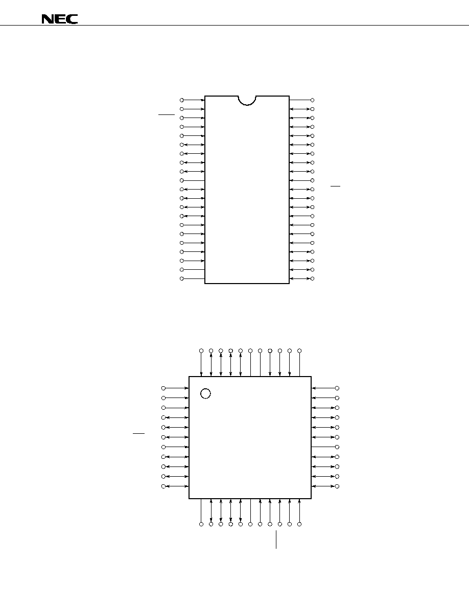
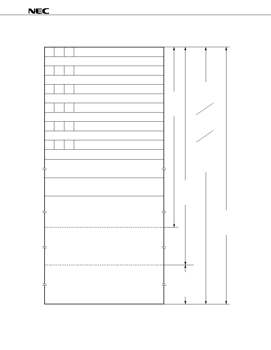
1. PIN CONFIGURATION (TOP VIEW)
∑ 42-pin plastic shrink DIP
V
SS
P40
P41
P42
P43
P50
P51
P52
P53
P00/INT4
P01/SCK
P02/SO/SB0
P03/SI/SB1
P10/INT0
P11/INT1
P12/INT2
P13/ TI0
P20/PTO0
P21
P22/PCL
P23/BUZ
XT1
XT2
RESET
X1
X2
P33
P32
P31
P30
AV
SS
AN7/KR3/P63
AN6/KR2/P62
AN5/KR1/P61
AN4/KR0/P60
AN3/P113
AN2/P112
AN1/P111
AN0/P110
AV
REF
IC
V
DD
1
2
3
4
5
6
7
8
9
10
11
12
13
14
15
16
17
18
19
20
21
42
41
40
39
38
37
36
35
34
33
32
31
30
29
28
27
26
25
24
23
22
µ
PD75064CU-
◊◊◊
PD75066CU-
◊◊◊
PD75068CU-
◊◊◊
µ
µ
∑
44-pin plastic QFP
IC : Internally Connected (This pin should be directly connected to V
DD
)
P112/AN2
P113/AN3
P60/KR0/AN4
P61/KR1/AN5
P62/KR2/AN6
P63/KR3/AN7
AV
SS
P30
P31
P32
P33
INT2/P12
INT1/P11
INT0/P10
SB1/SI/P03
SB0/SO/P02
SCK /P01
INT4/P00
P53
P52
P51
P50
33
32
31
30
29
28
27
26
25
24
23
1
2
3
4
5
6
7
8
9
10
11
NC
P43
P42
P41
P40
V
SS
XT1
XT2
RESET
X1
X2
P13/
TI0
P20/PTO0
P21
P22/PCL
P23/BUZ
V
DD
IC
AV
REF
P110/AN0
P111/AN1
NC
44 43 42 41 40 39 38 37 36 35 34
12 13 14 15 16 17 18 19 20 21 22
µ
PD75064GB-
◊◊◊
-3B4
PD75066GB-
◊◊◊
-3B4
PD75068GB-
◊◊◊
-3B4
µ
µ

6
µ
PD75064, 75066, 75068, 75064(A), 75066(A), 75068(A)
PIN IDENTIFICATIONS
P00 - 03
:
Port 0
P10 - 13
:
Port 1
P20 - 23
:
Port 2
P30 - 33
:
Port 3
P40 - 43
:
Port 4
P50 - 53
:
Port 5
P60 - 63
:
Port 6
P110 - 113 :
Port 11
KR0 - 3
:
Key Return
SCK
:
Serial Clock
SI
:
Serial Input
SO
:
Serial Output
SB0, 1
:
Serial Bus 0, 1
RESET
:
Reset Input
TI0
:
Timer Input 0
PTO0
:
Programmable Timer Output 0
BUZ
:
Buzzer Clock
PCL
:
Programmable Clock
INT0, 1, 4 :
External Vectored Interrupt 0, 1, 4
INT2
:
External Test Input 2
X1, 2
:
Main System Clock Oscillation 1, 2
XT1, 2
:
Subsystem Clock Oscillation 1, 2
AN0 - 7
:
Analog Input 0 - 7
AV
REF
:
Analog Reference
AV
SS
:
Analog V
SS
V
DD
:
Positive Power Supply
V
SS
:
Ground

7
µ
PD75064, 75066, 75068, 75064(A), 75066(A), 75068(A)
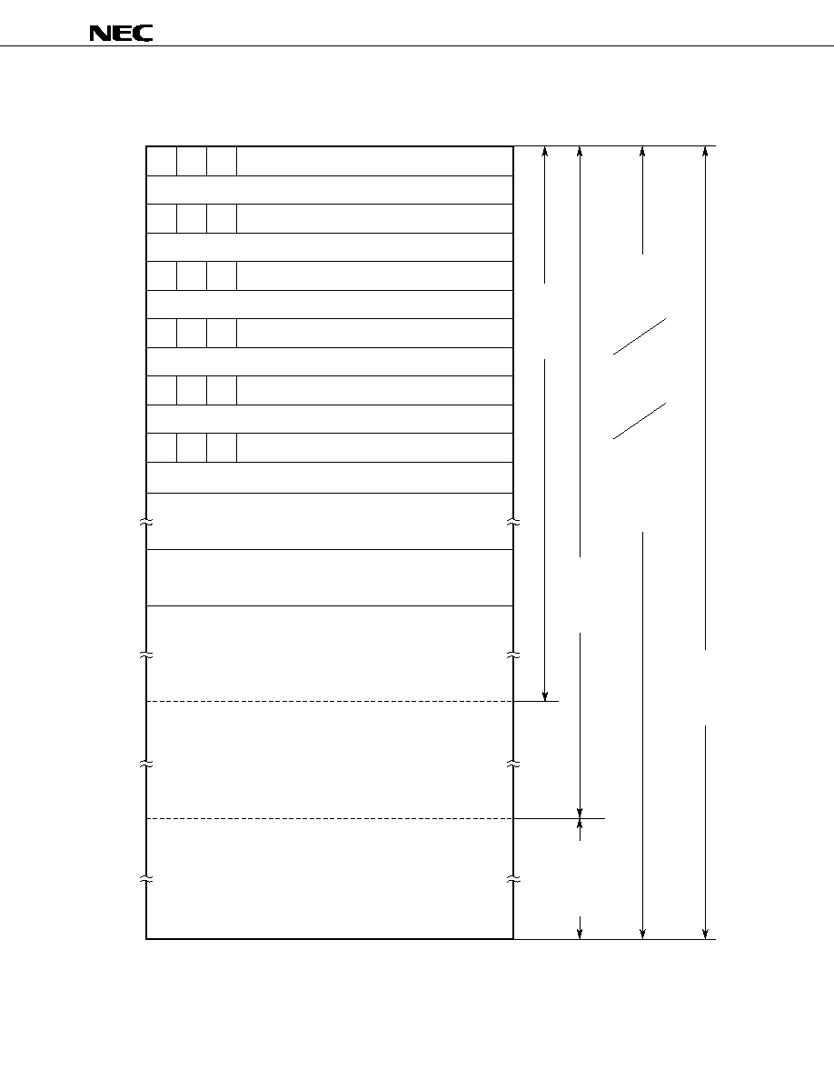
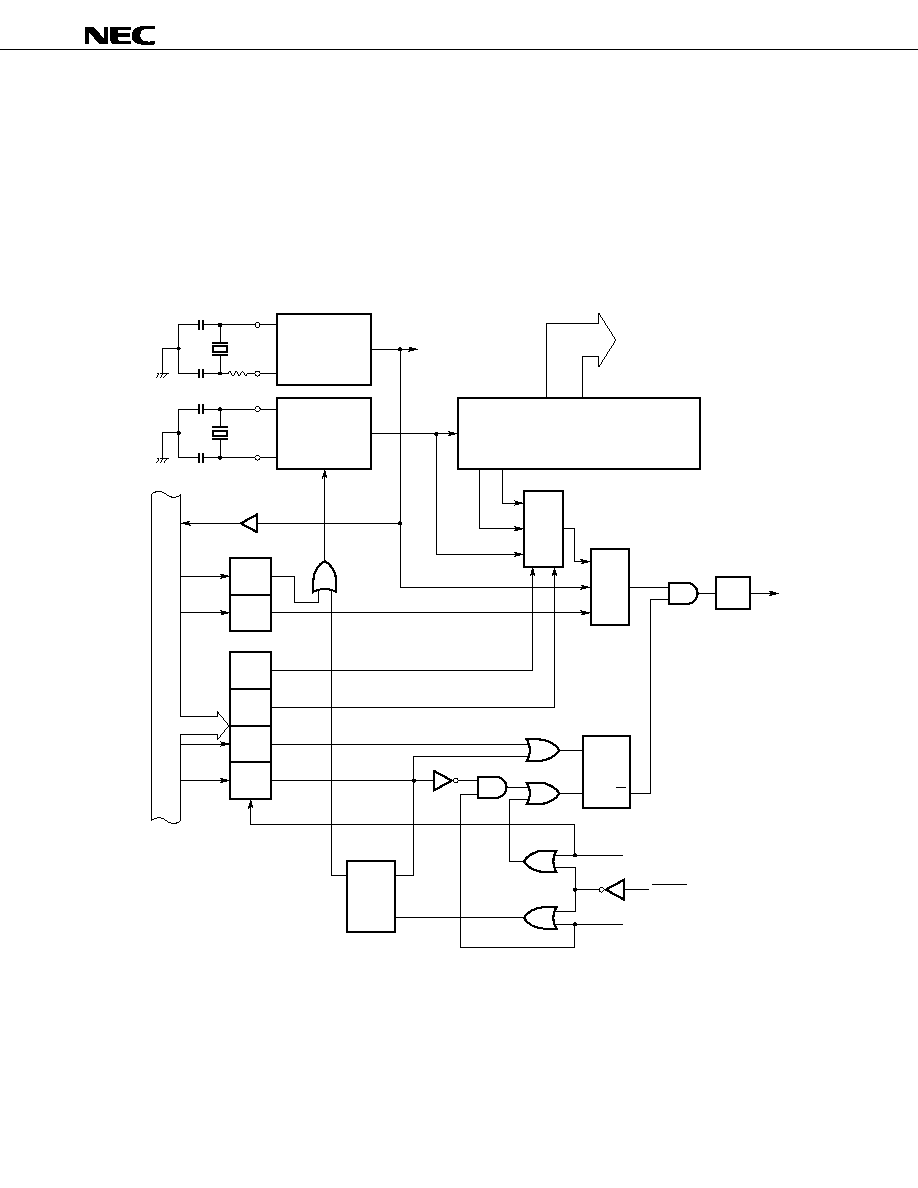
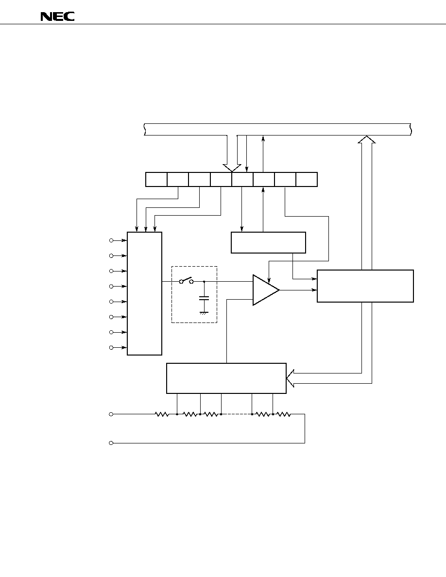
2. BLOCK DIAGRAM
BASIC
INTERVAL
TIMER
TIMER/
COUNTER
#0
SERIAL
INTERFACE
INTERRUPT
CONTROL
WATCH
TIMER
A/D
CONVERTER
INTBT
INTT0
INTCSI
INTW
TI0/P13
PTO0/P20
SI/SB1/P03
SO/SB0/P02
SCK/P01
INT0/P10
INT1/P11
INT2/P12
INT4/P00
BUZ/P23
AV
REF
AV
SS
ALU
ROM
PROGRAM
MEMORY
4096
◊
8 BITS
( PD75064)
6016
◊
8 BITS
( PD75066)
8064
◊
8 BITS
( PD75068)
DECODE
AND
CONTROL
PROGRAM
COUNTER
CY
SP
BANK
GENERAL
REGISTER
RAM
DATA
MEMORY
512
◊
4 BITS
BIT SEQ.
BUFFER
PORT 0
PORT 1
PORT 2
PORT 3
PORT 4
PORT 5
PORT 6
PORT 11
P00 - P03
P10 - P13
P20 - P23
P30 - P33
P40 - P43
P50 - P53
P60 - P63
P110 - P113
CLOCK
OUTPUT
CONTROL
CLOCK
DIVIDER
CLOCK GENERATOR
SUB
MAIN
STAND BY
CONTROL
f
X
/2
N
CPU CLOCK
RESET
V
SS
V
DD
PCL/P22
XT1 XT2
X1 X2
KR0 - KR3
/ P60 - P63
4
8
µ
µ
µ
4
4
4
4
4
4
4
4
Note
AN0 - AN3
/ P110 - P113
AN4 - AN7
/ P60 - P63
Note
The
µ
PD75064 uses the program counter of a 12-bit configuration, the
µ
PD75066 and
µ
PD75068
use that of a 13-bit configuration.
8
µ
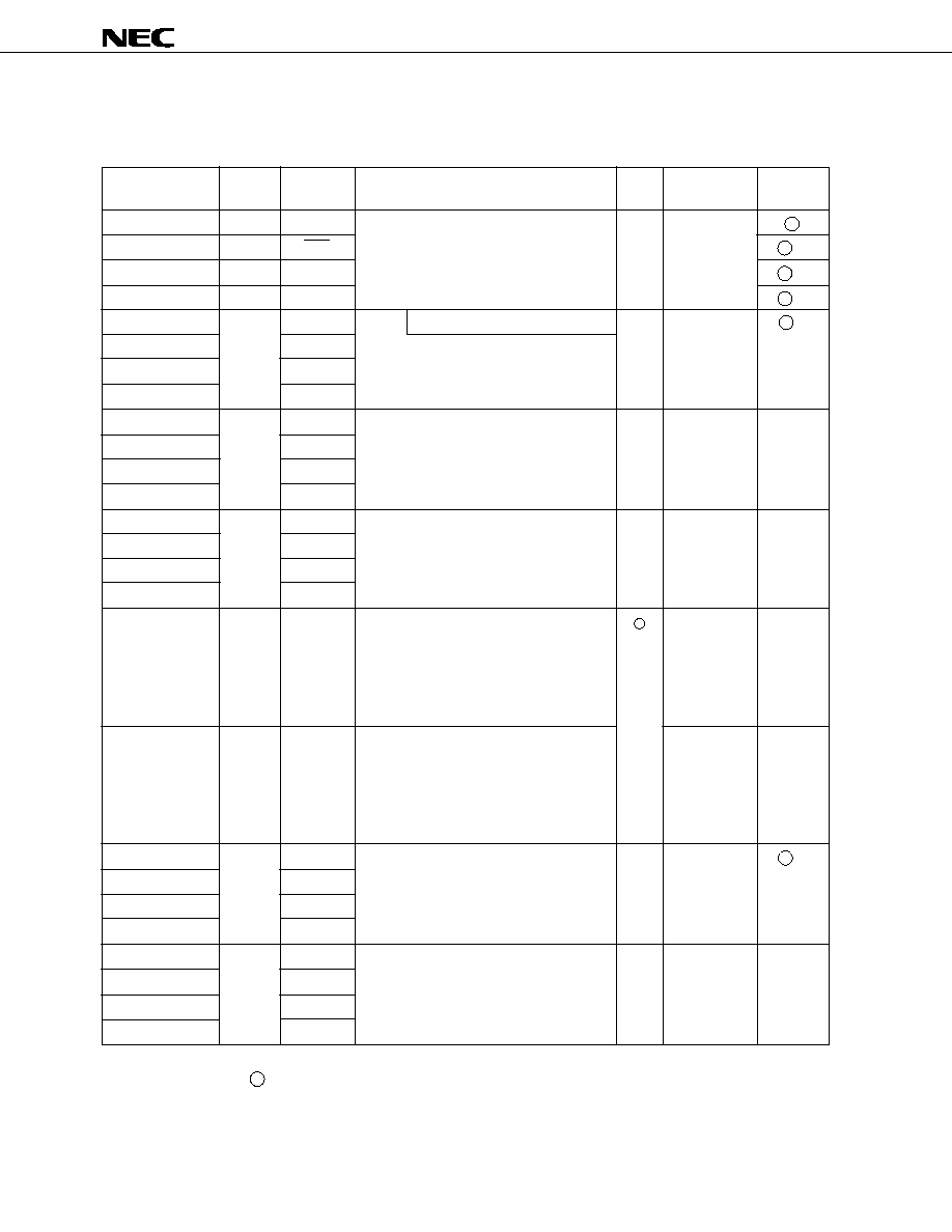
PD75064, 75066, 75068, 75064(A), 75066(A), 75068(A)
Pin name
P00
P01
P02
P03
P10
P11
P12
P13
P20
P21
P22
P23
P30
Note 2
P31
Note 2
P32
Note 2
P33
Note 2
P40 - P43
Note 2
P50 - P53
Note 2
P60
P61
P62
P63
P110
P111
P112
P113
I/O circuit
type
Note 1
-A
-B
-C
-C
E-B
E-B
M
M
-D
Y-A
Input/
output
Input
I/O
I/O
I/O
Input
I/O
I/O
I/O
I/O
I/O
Input
When reset
Input
Input
Input
Input
High level
(when pull-
up resistors
are provided)
or high
impedance
High level
(when pull-
up resistors
are provided)
or high
impedance
Input
Input
8-bit
I/O
◊
◊
◊
◊
◊
◊
Function
4-bit input port (PORT0).
For P01 to P03, pull-up resistors can be
provided by software in units of 3 bits.
With noise elimination function
4-bit input port (PORT1).
Pull-up resistors can be provided by soft-
ware in units of 4 bits.
4-bit I/O port (PORT2).
Pull-up resistors can be provided by soft-
ware in units of 4 bits.
Programmable 4-bit I/O port (PORT3).
I/O can be specified bit by bit. Pull-up
resistors can be provided by software in
units of 4 bits.
N-ch open-drain 4-bit I/O port (PORT4).
A pull-up resistor can be provided for
each bit (mask option). Breakdown volt-
age is 10 V in open-drain mode.
N-ch open-drain 4-bit I/O port (PORT5).
A pull-up resistor can be provided for
each bit (mask option). Breakdown volt-
age is 10 V in open-drain mode.
Programmable 4-bit I/O port (PORT6).
I/O can be specified bit by bit. Pull-up
resistors can be provided by software in
units of 4 bits.
4-bit input port (PORT11).
Notes 1. The circle (
) indicates the Schmitt trigger input.
2. Can directly drive LEDs.
B
F
F
M
B
Y
3. PIN FUNCTIONS
3.1 Port Pins
Shared
with
INT4
SCK
SO/SB0
SI/SB1
INT0
INT1
INT2
TI0
PTO0
≠
PCL
BUZ
≠
≠
≠
≠
≠
≠
KR0/AN4
KR1/AN5
KR2/AN6
KR3/AN7
AN0
AN1
AN2
AN3
9
µ
PD75064, 75066, 75068, 75064(A), 75066(A), 75068(A)
Pin name
TI0
PTO0
PCL
BUZ
SCK
SO/SB0
SI/SB1
INT4
INT0
INT1
INT2
KR0 - KR3
AN0 - AN3
AN4 - AN7
AV
REF
AV
SS
X1, X2
XT1, XT2
RESET
IC
V
DD
V
SS
I/O circuit
type
Note 1
-C
E-B
E-B
E-B
-A
-B
-C
-C
-C
-D
Y-A
-D
Z
Z
≠
≠
≠
≠
≠
Shared
with
P13
P20
P22
P23
P01
P02
P03
P00
P10
P11
P12
P60 - P63/
AN4 - AN7
P110 - P113
P60 - P63/
KR0 - KR3
≠
≠
≠
≠
≠
≠
≠
≠
When reset
≠
Input
Input
Input
Input
Input
Input
≠
≠
≠
Input
Input
≠
≠
≠
≠
≠
≠
≠
≠
Input/
output
Input
I/O
I/O
I/O
I/O
I/O
I/O
Input
Input
Input
I/O
Input
I/O
Input
≠
Input
Input
Input
≠
≠
≠
Function
Input for receiving external event pulse signal for
timer/event counter
Timer/event counter output
Clock output
Output frequency selectable
(for buzzer output or system clock trimming)
Serial clock I/O
Serial data output
Serial bus I/O
Serial data input
Serial bus I/O
Edge-detective vectored interrupt input
(both rising and falling edges enabled)
Edge-detective vectored interrupt input
(detection edge selectable)
Edge-detective testable input
(rising edge detection)
Parallel falling edge detection testable input
For A /D converter only
Crystal/ceramic connection for main system clock
generation. When external clock signal is used,
the signal should be applied to X1, and its reverse
phase signal to X2.
Crystal connection for subsystem clock genera-
tion. When external clock signal is used, the
signal should be applied to XT1, and its reverse
phase signal to XT2. XT1 can be used as a 1-bit
input (test).
System reset input
Internally connected.
(Connect this pin directly to V
DD
)
Positive power supply
GND potential
3.2 Non-Port Pins
8-bit analog input
Reference voltage input
GND potential
B
F
F
M
B
B
B
Y
Y
B
Note 2
Note 3
Note 3
Notes 1. The circle (
) indicates the Schmitt trigger input.
2. Clock synchronous
3. Asynchronous

10
µ
PD75064, 75066, 75068, 75064(A), 75066(A), 75068(A)
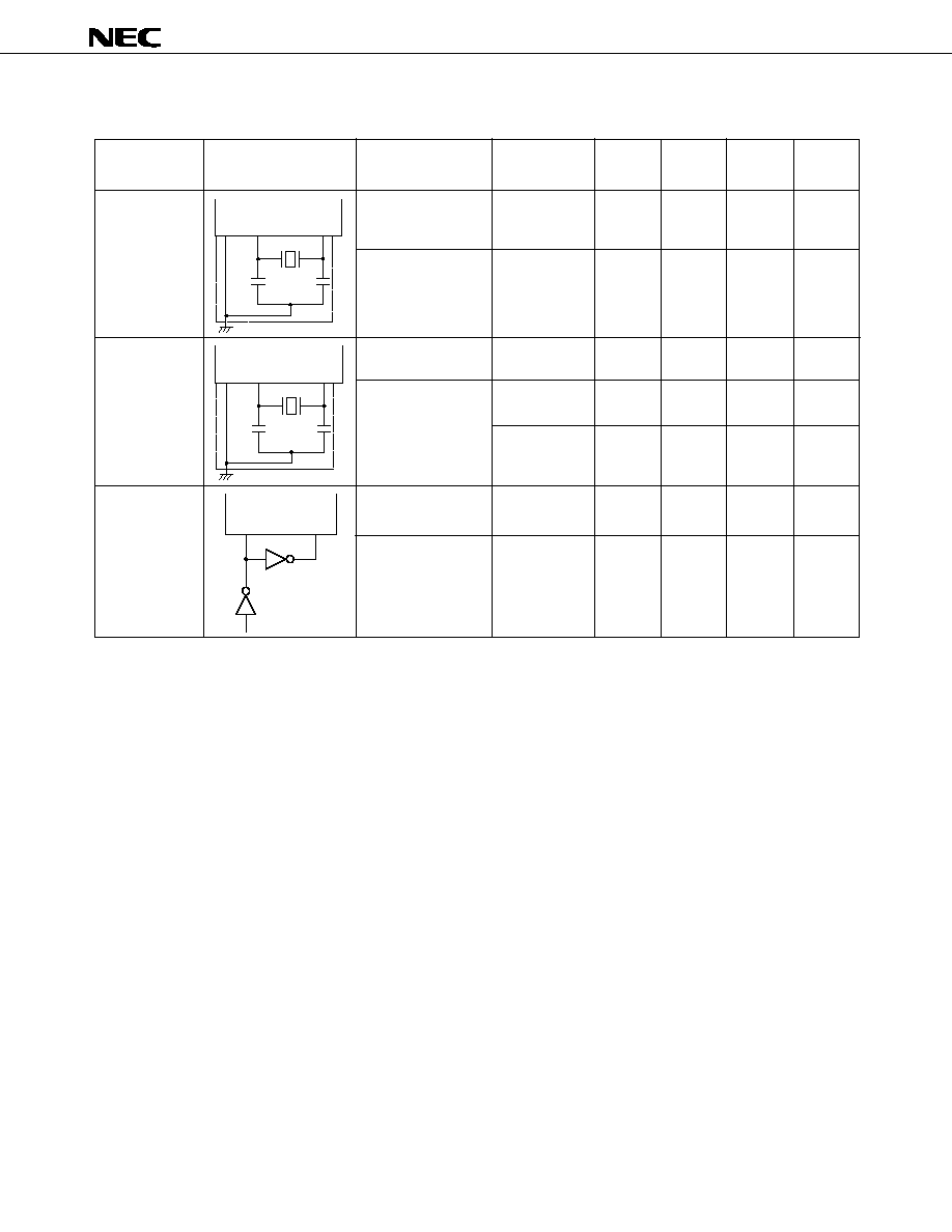
3.3 Pin Input/Output Circuits
The input/output circuit of each
µ
PD75068 pin is shown below in a simplified manner.
Type A (For type E-B)
CMOS input buffer
Schmitt trigger input with hysteresis
Push-pull output which can be set to high impedance output
(off for both P-ch and N-ch)
P.U.R.: Pull-Up Resistor
P.U.R.: Pull-Up Resistor
Type B
Type E-B
Type B-C
Type D (For type E-B, F-A)
V
DD
IN
P-ch
N-ch
IN
IN
P-ch
P.U.R.
enable
P.U.R.
V
DD
V
DD
P-ch
N-ch
OUT
Data
Output
disable
P.U.R.
V
DD
P.U.R.
enable
P-ch
IN/OUT
Data
Output
disable
Type D
Type A
(1/3)
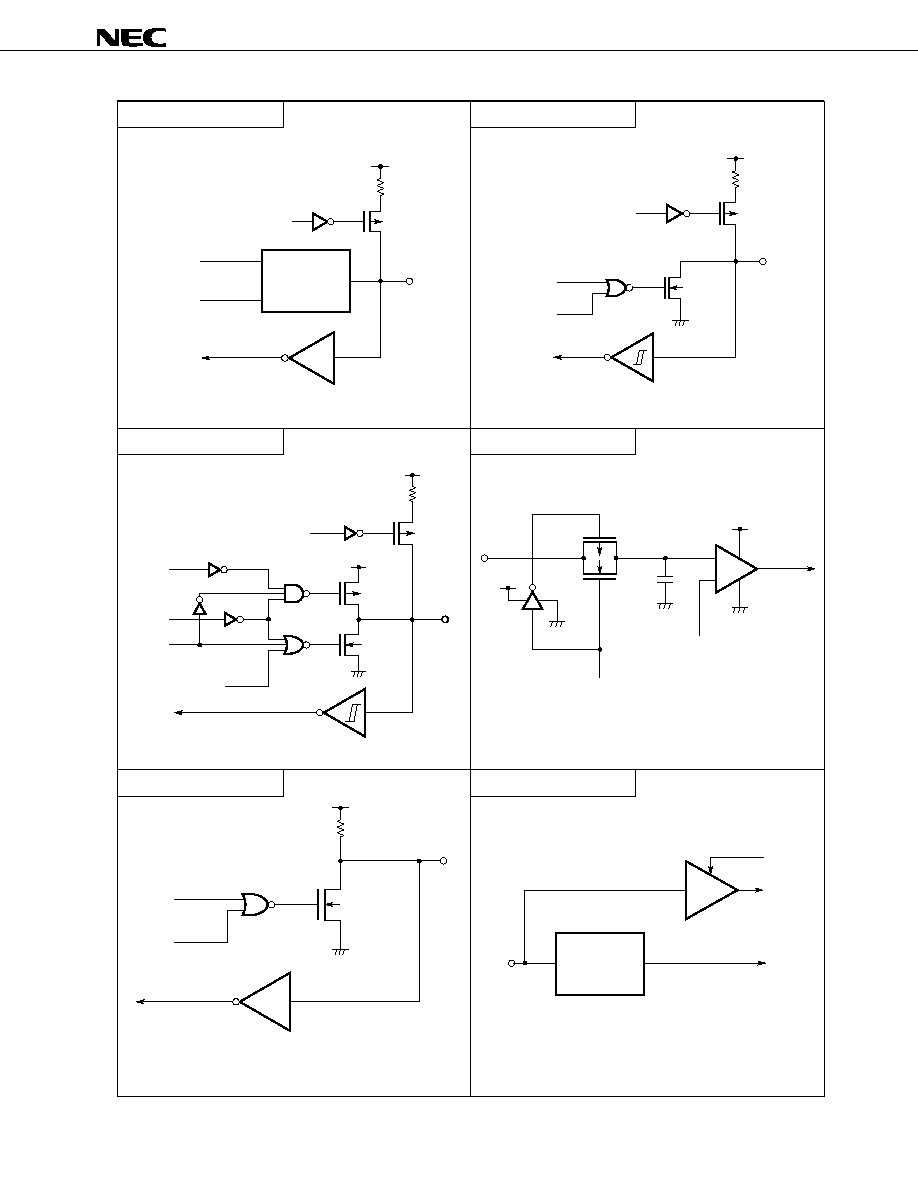
11
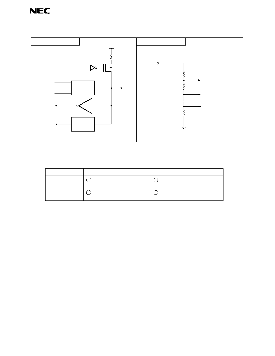
µ
PD75064, 75066, 75068, 75064(A), 75066(A), 75068(A)
Type F-B
Type F-A
Type M
Type Y (For type Y-A , Y-D)
Type M-C
Type Y-A
P.U.R.: Pull-Up Resistor
P.U.R.: Pull-Up Resistor
P.U.R.: Pull-Up Resistor
P.U.R.: Pull-Up Resistor
P.U.R.
V
DD
P.U.R.
enable
P-ch
IN/OUT
Data
Output
disable
Type D
Type B
V
DD
P-ch
N-ch
IN/OUT
V
DD
P-ch
P.U.R.
P.U.R.
enable
Output
disable
(P)
Data
Output
disable
Output
disable
(N)
N-ch
(Can
withstand
+10 V)
IN/OUT
Data
V
DD
Output
disable
P.U.R.
enable
(Mask option)
Middle-voltage input buffer
(Can withstand +10 V)
N-ch
P.U.R.
Data
Output
disable
P.U.R.
enable
V
DD
P-ch
IN/OUT
V
DD
V
DD
P-ch
AV
SS
N-ch
Sampl-
ing C
AV
SS
Reference voltage
(from voltage tap of
serial resistor string)
Input
enable
IN
IN
Input buffer
IN instruction
+
≠
(2/3)
Type Y
Type A
12
µ
PD75064, 75066, 75068, 75064(A), 75066(A), 75068(A)
Type Y-D
P.U.R.: Pull-Up Resistor
Type Z
P.U.R.
V
DD
P.U.R.
enable
P-ch
IN/OUT
Data
Output
disable
Type D
Type Y
Type B
AV
REF
Reference voltage
AV
SS
(3/3)
3.4 Mask Option Selection
The following mask options are available for selection for each pin.
Pin name
P40 - P43,
P50 - P53
XT1, XT2
1
Pull-up resistor enabled
(specifiable bit by bit)
1
Feedback resistor enabled
(if a subsystem clock is used)
2
Pull-up resistor disabled
(specifiable bit by bit)
2
Feedback resistor disabled
(if a subsystem clock is not used)
Mask option
13
µ
PD75064, 75066, 75068, 75064(A), 75066(A), 75068(A)
3.5 Handling Unused Pins
Table 3-1. Handling Unused Pins
Pin
Recommended connection
P00/INT4
Connect to V
SS
.
P01/SCK
Connect to V
SS
or V
DD
.
P02/SO/SB0
P03/SI/SB1
P10/INT0-P12/INT2
Connect to V
SS
.
P13/TI0
P20/PTO0
Input state: Connect to V
SS
or V
DD
.
P21
Output state: Open
P22/PCL
P23/BUZ
P30-P33
P40-P43
P50-53
P60/KR0/AN4-P63/KR3/AN7
P110/AN0-P113/AN3
Connect to V
SS
or V
DD
.
AV
REF
Connect to V
SS
.
AV
SS
XT1
Connect to V
SS
or V
DD
.
XT2
Open
IC
Directly connect to V
DD
.
14
µ
PD75064, 75066, 75068, 75064(A), 75066(A), 75068(A)
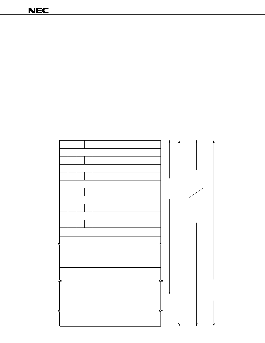
4. MEMORY CONFIGURATION
∑ Program memory (ROM) ..... 4096
◊
8 bits (0000H to 0FFFH) :
µ
PD75064
..... 6016
◊
8 bits (0000H to 177FH) :
µ
PD75066
..... 8064
◊
8 bits (0000H to 1F7FH) :
µ
PD75068
∑ 0000H to 0001H : Vector table in which the program start address by reset is stored
∑ 0002H to 000BH : Vector table in which the program start address by interrupt is stored
∑ 0020H to 007FH : Table area to be referenced by GETI instruction
∑ Data memory
∑ Data area
..... 512
◊
4 bits
(000H to 1FFH)
∑ Peripheral hardware area ..... 128
◊
4 bits
(F80H to FFFH)
Figure 4-1. Program Memory Map
(a)
µ
PD75064
MBE
0
0
7
6
5
0000H
Address
MBE
0
0
0002H
MBE
0
0
0004H
MBE
0
0
0006H
MBE
0
0
0008H
MBE
0
0
000AH
007FH
0080H
0020H
07FFH
0800H
0FFFH
0
Internal reset start address (high-order 4 bits)
Internal reset start address (low-order 8 bits)
INTBT/INT4 start address (high-order 4 bits)
INTBT/INT4 start address (low-order 8 bits)
INT0 start address (high-order 4 bits)
INT0 start address (low-order 8 bits)
INT1 start address (high-order 4 bits)
INT1 start address (low-order 8 bits)
INTCSI start address
(high-order 4 bits)
INTCSI start address (low-order 8 bits)
INTT0 start address (high-order 4 bits)
INTT0 start address (low-order 8 bits)
GETI instruction reference table
CALL ! addr
instruction
subroutine entry
address
BR $addr
instruction
relative branch
address
(≠15 to ≠1,
+2 to +16)
CALLF
! faddr
instruction
entry
address
BRCB
! caddr
instruction
branch
address
Branch destination
address specified
by GETI instruction,
Subroutine entry
address
0
0
0
0
0
0
4
15
µ
PD75064, 75066, 75068, 75064(A), 75066(A), 75068(A)
(b)
µ
PD75066
MBE
0
0
7
6
5
0000H
Address
MBE
0
0
0002H
MBE
0
0
0004H
MBE
0
0
0006H
MBE
0
0
0008H
MBE
0
0
000AH
007FH
0080H
0020H
07FFH
0800H
0FFFH
1000H
177FH
0
Internal reset start address
(high-order 5 bits)
Internal reset start address
(low-order 8 bits)
INTBT/INT4 start address (high-order 5 bits)
INTBT/INT4 start address (low-order 8 bits)
INT0 start address (high-order 5 bits)
INT0 start address (low-order 8 bits)
INT1 start address (high-order 5 bits)
INT1 start address (low-order 8 bits)
INTCSI start address
(high-order 5 bits)
INTCSI start address
(low-order 8 bits)
INTT0 start address (high-order 5 bits)
INTT0 start address (low-order 8 bits)
GETI instruction reference table
CALL ! addr
instruction
subroutine entry
address
BR ! addr
instruction brach
address
BR $addr
instruction
relative branch
address
(≠15 to ≠1,
+2 to +16)
CALLF
! faddr
instruction
entry
address
BRCB
! caddr
instruction
branch
address
BRCB
! caddr
instruction
branch
address
Branch destination
address specified
by GETI instruction,
Subroutine entry
address
16
µ
PD75064, 75066, 75068, 75064(A), 75066(A), 75068(A)
(c)
µ
PD75068
MBE
0
0
7
6
5
0000H
Address
MBE
0
0
0002H
MBE
0
0
0004H
MBE
0
0
0006H
MBE
0
0
0008H
MBE
0
0
000AH
007FH
0080H
0020H
07FFH
0800H
0FFFH
1000H
1F7FH
0
Internal reset start address
(high-order 5 bits)
Internal reset start address
(low-order 8 bits)
INTBT/INT4 start address (high-order 5 bits)
INTBT/INT4 start address (low-order 8 bits)
INT0 start address (high-order 5 bits)
INT0 start address (low-order 8 bits)
INT1 start address (high-order 5 bits)
INT1 start address (low-order 8 bits)
INTCSI start address
(high-order 5 bits)
INTCSI start address
(low-order 8 bits)
INTT0 start address (high-order 5 bits)
INTT0 start address (low-order 8 bits)
GETI instruction reference table
CALL ! addr
instruction
subroutine entry
address
BR ! addr
instruction brach
address
BR $addr
instruction
relative branch
address
(≠15 to ≠1,
+2 to +16)
CALLF
! faddr
instruction
entry
address
BRCB
! caddr
instruction
branch
address
BRCB
! caddr
instruction
branch
address
Branch destination
address specified
by GETI instruction,
Subroutine entry
address
17
µ
PD75064, 75066, 75068, 75064(A), 75066(A), 75068(A)
Figure 4-2. Data Memory Map
(8
◊
4)
Data memory
000H
007H
008H
0FFH
100H
1FFH
F80H
FFFH
256
◊
4
256
◊
4
128
◊
4
Bank 0
Bank 1
Bank 15
Stack
area
General
register
area
Static RAM
(512
◊
4)
Peripheral
hardware area
Not contained
18
µ
PD75064, 75066, 75068, 75064(A), 75066(A), 75068(A)
5. PERIPHERAL HARDWARE FUNCTIONS
5.1 Ports
The following three types of I/O port are provided:
∑ CMOS input ports (PORT0, 1, 11)
: 12
∑ CMOS input/output ports (PORT2, 3, 6)
: 12
∑ N-ch open-drain input/output ports (PORT4, 5) :
8
Total
32
Table 5-1. Functions of Port
Note Can directly drive LEDs.
Port (Symbol)
PORT0
PORT1
PORT3
Note
PORT6
PORT2
PORT4
Note
PORT5
Note
PORT11
Function
4-bit input
4-bit I/O
4-bit I/O
(N-ch open-drain,
can withstand 10 V)
4-bit input
Operation/features
Can be read or tested regard-
less of the operation mode of
the dual function pin.
Can be specified for input/
output in bit units.
Can be specified for input/
output in 4-bit units.
Can be specified for input/
output in 4-bit units.
Ports 4 and 5 can be paired to
input/output data in 8-bit units.
4-bit port dedicated to input
Remarks
Shared with the SO/SB0, SI/SB1, SCK,
INT0-2, 4, and TI0 pins.
Port 6 is shared with pins KR0 to KR3 and
pins AN4 to AN7.
Port 2 is shared with PTO0, PCL, and BUZ
pins.
Whether or not the internal pull-up
resistor is provided can be specified for
each bit by mask option.
Port 11 is shared with pins AN0 to AN3.
19
µ
PD75064, 75066, 75068, 75064(A), 75066(A), 75068(A)
Subsystem
clock generator
Main system
clock generator
Watch timer
∑ Basic interval timer (BT)
∑ Timer/event counter
∑ Serial interface
∑ Watch timer
∑ A /D converter
(successive approximation type)
∑ INT0 noise eliminator
∑ Clock output circuit
1/2 to 1/4096
Frequency divider
Selec-
tor
Selec-
tor
Frequency
divider
∑ CPU
∑ INT0 noise
eliminator
∑ Clock output
circuit
Oscillator
disable
signal
Internal bus
HALT
Note
STOP
Note
PCC2, PCC3
clear signal
Wait release signal from BT
Standby release signal from
interrupt control circuit
RESET signal
XT1
XT2
X1
X2
4
WM.3
SCC
SCC3
SCC0
PCC
PCC0
PCC1
PCC2
PCC3
STOP F/F
Q
S
R
HALT F/F
S
Q
R
f
XT
f
X
1/2 1/16
1/4
5.2 Clock Generator
The clock generator operates according to the statuses of the processor clock control register (PCC) and
the system clock control register (SCC). Two types of clock are provided: main system clock and subsystem
clock, and the instruction execution time can be changed.
∑ 0.95
µ
s / 1.91
µ
s / 15.3
µ
s (operated with main system clock at 4.19 MHz)
∑ 122
µ
s (operated with subsystem clock at 32.768 kHz)
Figure 5-1. Clock Generator Block Diagram
Note Instruction execution
Remarks
1. f
X
= Main system clock frequency
2. f
XT
= Subsystem clock frequency
3.
= CPU clock
4. PCC: Processor clock control register
5. SCC: System clock control register
6. One clock cycle (t
CY
) at
is equal to one machine cycle of an instruction.
For t
CY
, refer to AC Characteristics in 10. ELECTRICAL SPECIFICATIONS.
20
µ
PD75064, 75066, 75068, 75064(A), 75066(A), 75068(A)
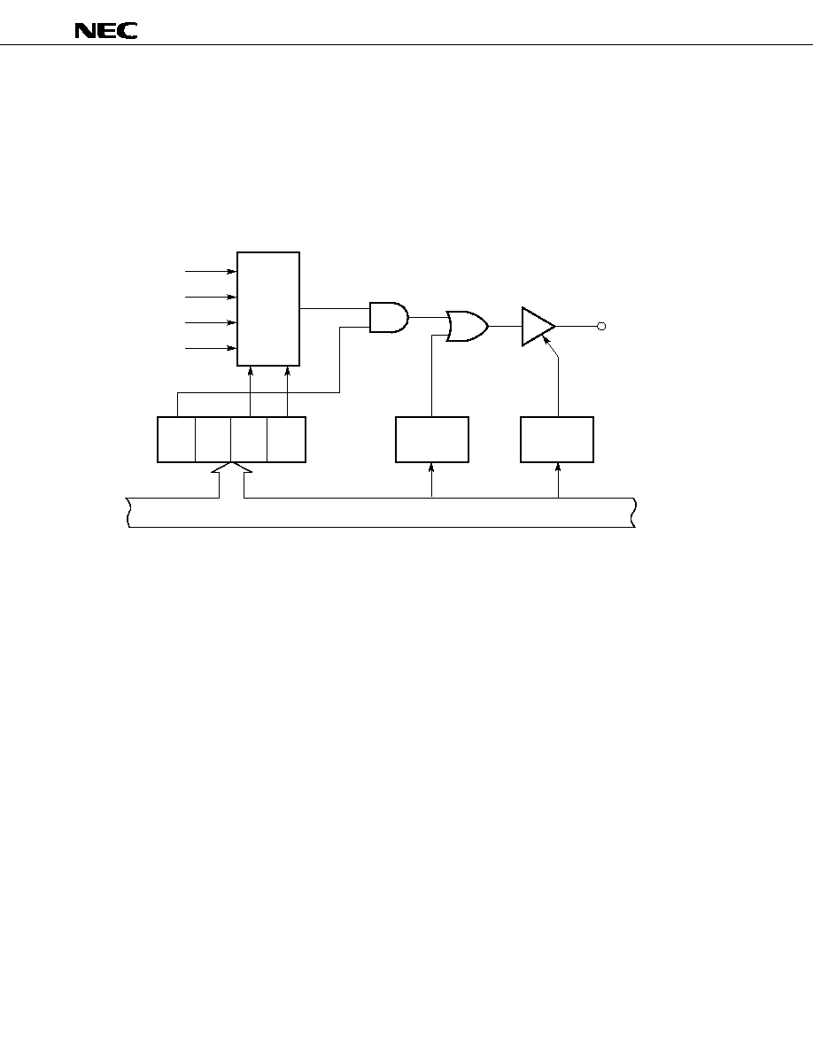
5.3 Clock Output Circuit
The clock output circuit outputs clock pulses from the P22/PCL pin, and is used to supply clock pulses to
remote unit controller and peripheral LSIs.
∑ Clock output (PCL):
, 524 kHz, 262 kHz, 65.5 kHz (f
X
= at 4.19 MHz)
Figure 5-2. Clock Output Circuit Configuration
Remark Measures are taken to prevent outputting a narrow pulse when selecting clock output
enable/disable.
From the clock
generator
CLOM3 0 CLOM1 CLOM0 CLOM
Selector
Output
buffer
Port 2 input/
output mode
specification bit
P22 output
latch
P22/PCL
Internal bus
4
f
X
/ 2
3
f
X
/ 2
4
f
X
/ 2
6
PORT2.2
Bit 2 of PMGB
21
µ
PD75064, 75066, 75068, 75064(A), 75066(A), 75068(A)
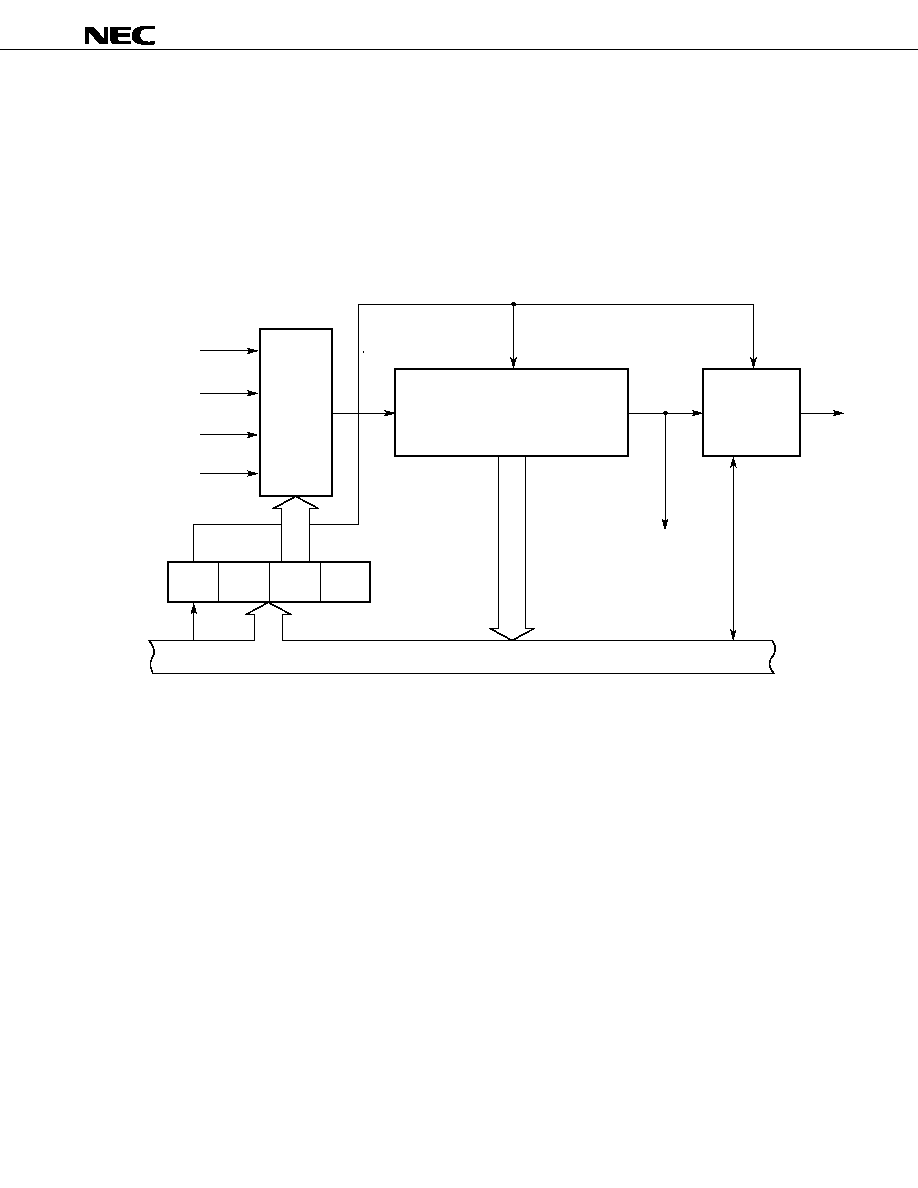
5.4 Basic Interval Timer
The basic interval timer has these functions:
∑ Interval timer operation which generates a reference timer interrupt
∑ Watchdog timer application which detects a program runaway
∑ Selection of wait time for releasing the standby mode and counting the wait time
∑ Reading out the count value
Figure 5-3. Basic Interval Timer Configuration
Note Instruction execution
From the clock
generator
Internal bus
4
f
X
/2
5
f
X
/2
7
f
X
/2
9
f
X
/2
12
MPX
Basic interval timer
(8-bit frequency divider circuit)
Clear signal
Clear signal
BT interrupt
request flag
Vectored
interrupt
request
signal
IRQBT
Wait release
signal for standby
release
Set
signal
BT
8
BTM3
BTM2
BTM1
BTM0
BTM
SET1
Note
3

22
µ
PD75064, 75066, 75068, 75064(A), 75066(A), 75068(A)
5.5 Watch Timer
The
µ
PD75068 has an on-chip 1-ch watch timer. The watch timer has the following functions:
∑ Sets the test flag (IRQW) with a 0.5-sec interval. The standby mode can be released by IRQW.
∑ The 0.5-second interval can be generated from either the main system clock or subsystem clock.
∑ The time interval can be made 128 times faster (3.91 ms) by selecting the fast mode. This is convenient
for program debugging, testing, etc.
∑ Any of the frequencies 2.048 kHz, 4.096 kHz, and 32.768 kHz can be output to the P23/BUZ pin. This
can be used for beep and system clock frequency trimming.
∑ The frequency divider circuit can be cleared so that a zero-second start of the watch can be made.
Figure 5-4. Watch Timer Block Diagram
Remark ( ) is for f
X
= 4.194304 MHz, f
XT
= 32.768 kHz.
P23/BUZ
Internal bus
8
Selector
From the
clock
generator
f
X
128
(32.768 kHz)
f
XT
(32.768 kHz)
Selector
Frequency divider
Selector
INTW
IRQW
set signal
2 Hz
0.5 sec
WM7
0
WM5 WM4 WM3 WM2 WM1 WM0
P23 output
latch
Bit 2 of PMGB
PORT2.3
Output buffer
Clear signal
f
W
(32.768 kHz)
Bit test instruction
Port 2 input/
output mode
WM
(4 kHz)(2 kHz)
f
w
2
7
(256 Hz: 3.91 ms)
f
w
2
14
f
w
2
3
f
w
2
4

23
µ
PD75064, 75066, 75068, 75064(A), 75066(A), 75068(A)
5.6 Timer/Event Counter
The
µ
PD75068 has an on-chip 1-ch timer/event counter. The timer/event counter has the following
functions:
∑ Programmable interval timer operation
∑ Outputs square-wave signal of a user-selectable frequency to the PTO0 pin
∑ Event counter operation
∑ Divides the TI0 pin input by N and outputs to the PTO0 pin (frequency divider operation)
∑ Supplies serial shift clock to the serial interface circuit
∑ Count condition read-out function.
Figure 5-5. Block Diagram of Timer / Event Counter
Count register (8)
P13/
TI0
Note Instruction execution
MPX
Timer operation start signal
8
8
8
From the
clock
generator
Internal bus
TM07 TM06 TM05 TM04 TM03 TM02 TM01 TM00
PORT1.3
(Refer to Fig. 5-1.)
Comparator (8)
Modulo register (8)
TO
enable
flag
P20
output
latch
signal
Port 2
input/
output
mode
Clear
signal
T0
TMOD0
Bit 2 of PGMB
P20/PTO0
Output
buffer
Reset
RESET
IRQT0 clear
signal
TOUT
F/F
TM0
SET1
Note
Input buffer
IRQT0
set signal
INTT0
PORT2.0
TOE0
To serial
interface
CP
Match
8
8
24
µ
PD75064, 75066, 75068, 75064(A), 75066(A), 75068(A)
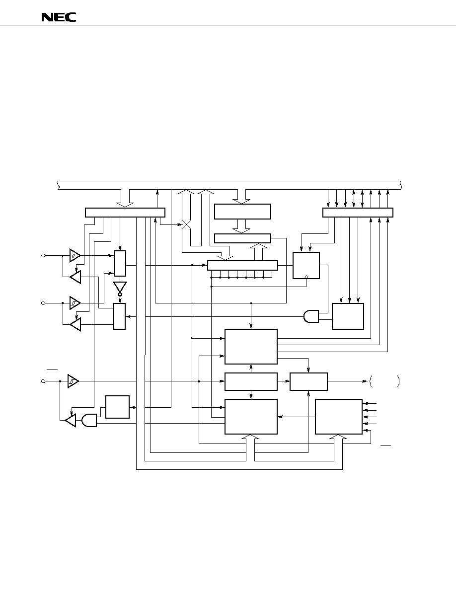
5.7 Serial Interface
(1) Serial interface function
The
µ
PD75068 contains a clock synchronous 8-bit serial interface, which has four modes.
∑ Operation halt mode
∑ 3-wire serial I/O mode
∑ 2-wire serial I/O mode
∑ SBI (serial bus interface mode)
Figure 5-6. Block Diagram of Serial Interface
Internal bus
8
8
8
8/4
P03/SI/SB1
P02/SO/SB0
P01/SCK
(8)
f
x
/2
3
f
x
/2
4
f
x
/2
6
TOUT F/F
(from timer/
event counter)
CSIM
RELD
CMDD
ACKD
ACKT
ACKE
BSYE
RELT
CMDT
D
Q
SET CLR
(8)
(8)
SBIC
Bit
test
Slave address
register (SVA)
Address comparator
Shift register (SIO)
Match
signal
Bit manipulation
SO
latch
Bit
test
Selector
Busy/
acknowledge
output circuit
Bus release/
command/
acknowledge
detection circuit
Serial clock
counter
Serial clock
control circuit
INTCSI
control circuit
IRQCSI
set signal
INTCSI
P01
output
latch
Serial clock
selector
External SCK
Selector
25
µ
PD75064, 75066, 75068, 75064(A), 75066(A), 75068(A)
5.8 A/D Converter
The
µ
PD75068 contains an 8-bit analog/digital (A / D) converter that has eight analog input channels
(AN0 - AN7).
The A /D converter employs the successive-approximation method.
Figure 5-7. Block Diagram of A/D Converter
Internal bus
8
+
≠
AN0/P110
AN1/P111
AN2/P112
AN3/P113
AN4/KR0/P60
AN5/KR1/P61
AN6/KR2/P62
AN7/KR3/P63
AV
REF
AV
SS
R
8
R
R/2
R/2
8
ADM
0
ADM1
EOC
SOC
ADM4
ADM5
ADM6
0
Control circuit
Multi-
plexer
Sample and hold circuit
Comparator
SA register (8)
Tap decoder
Series resistor string
R
26
µ
PD75064, 75066, 75068, 75064(A), 75066(A), 75068(A)
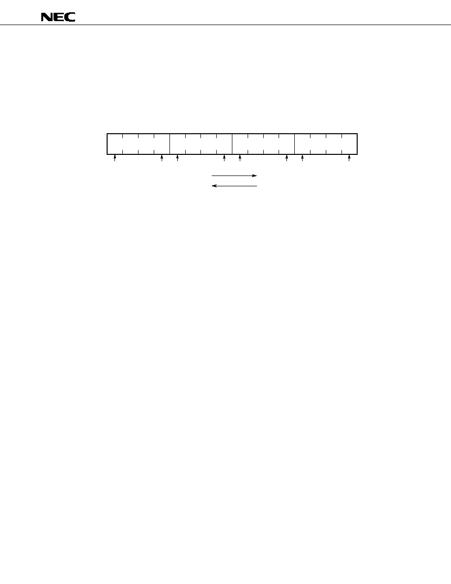
5.9 Bit Sequential Buffer: 16 Bits
The bit sequential buffer is a data memory specifically provided for bit manipulation. With this buffer,
addresses and bit specifications can be sequentially updated by bit manipulation operation. Therefore, this
buffer is very useful for processing long data in bit units.
Figure 5-8. Bit Sequential Buffer Format
3
2
1
0
3
2
1
0
3
2
1
0
3
2
1
0
BSB3
BSB2
BSB1
BSB0
FC3H
FC2H
FC1H
FC0H
L = F
L = C L = B
L = 8 L = 7
L = 4 L = 3
L = 0
DECS L
INCS L
Address
Bit
L register
Symbol
Remark For "pmem.@L" addressing, the specification bit is shifted according to the L register.
27
µ
PD75064, 75066, 75068, 75064(A), 75066(A), 75068(A)
6. INTERRUPT FUNCTIONS
The
µ
PD75068 has six different interrupt sources. In addition, multiple interrupts with priority control are
possible. Two types of test sources are provided. Of these test sources, INT2 has two types of edge detection
testable inputs.
Table 6-1. Interruption Source Types
Interruption
Vectored Interrupt Request Signal
Interruption Source
IN/OUT
Order
Note1
(Vector table address)
(Reference time interval signal from
basic interval timer)
(Detection of both rising edge and
falling edge is valid.)
OUT
2
VRQ2 (0004H)
OUT
3
VRQ3 (0006H)
(Serial data transmission completion
signal)
(Coincidence signal of programmable
INTT0
timer/counter count register and modulo
IN
5
VRQ5 (000AH)
register)
(Detection of rising edge of input to
INT2
Note2
INT2 pin or detection of falling edge of
OUT
any input to KR0 to KR3)
INTW
Note2
(Signal from watch timer)
IN
Notes 1. The interruption order shows the priority order of the pins when several interruption requests occur
at the same time.
2. Test source. Like the interruption source, it is influenced by the interruption enable flag. However,
vectored interrupt will not occur.
The interrupt control circuit of the
µ
PD75068 has the following functions:
∑ Hardware controlled vectored interrupt function which can control whether or not to acknowledge an
interrupt based on the interrupt flag (IE
◊◊◊
) and interrupt master enable flag (IME)
∑ The interrupt start address can be set arbitrarily.
∑ Interrupt request flag (IRQ
◊◊◊
) test function (an interrupt generation can be confirmed by software)
∑ Standby mode release (interrupts to be released can be selected by the interrupt enable flag)
IN
INTBT
INT4
(Selection of rising edge detection or
falling edge detection)
INT0
INT1
INTCSI
VRQ1 (0002H)
1
Test input signal (Set IRQ and IRQW)
VRQ4 (0008H)
4
IN
OUT

28
µ
PD75064, 75066, 75068, 75064(A), 75066(A), 75068(A)
Figure 6-1. Block Diagram of Interrupt Control Circuit
Internal bus
3
1
IRQBT
IRQ4
IRQ0
IRQ1
IRQCSI
IRQT0
IRQW
IRQ2
INT4
/P00
INT0
/P10
INT1
/P11
Note
INTCSI
INTT0
INTW
INT2
/P12
AN4/KR0/P60
AN7/KR3/P63
VRQn
IME
IST0
IM2
INT
BT
Interrupt enable flag (IExxx)
Both-edge
detection
circuit
Edge
detection
circuit
Rising edge
detection
circuit
Falling edge
detection
circuit
Selec-
tor
Decoder
Priority
control
circuit
Vector
table
address
generator
Standby
release
signal
IM0
IM1
Note Noise eliminator
Edge
detection
circuit
29
µ
PD75064, 75066, 75068, 75064(A), 75066(A), 75068(A)
7. STANDBY FUNCTION
The
µ
PD75068 has two different standby modes (STOP mode and HALT mode) to reduce power dissipation
while waiting for program execution.
Table 7-1. Standby Mode Statuses
Note A/D converter's operation in HALT mode is possible only when the main system clock operates.
Instruction for setting
System clock for setting
Clock oscillator
Basic interval
timer
Serial interface
Timer/event
counter
Watch timer
A/D converter
External
interrupt
CPU
Release signal
HALT mode
HALT instruction
Can be set either with the main system
clock or the subsystem clock.
Only the CPU clock
stops its operation
(oscillation continues).
Can operate only at main system clock
oscillation (IRQBT is set at reference
time intervals.).
Can operate only when external SCK
input is selected as the serial clock or at
main system clock oscillation.
Can operate only when TI0 pin input is
specified as the count clock or at main
system clock oscillation.
Can operate.
Can operate.
Note
An interrupt request signal from hard-
ware whose operation is enabled by the
interrupt enable flag or the RESET signal
input
STOP mode
STOP instruction
Can be set only when operating on the
main system clock.
Only the main system clock stops its
operation.
Does not operate.
Can operate only when the external SCK
input is selected for the serial clock.
Can operate only when the TI0 pin input
is selected for the count clock.
Can operate when f
XT
is selected as the
count clock.
Does not operate.
INT1, INT2, and INT4 can operate.
Only INT0 cannot operate.
Does not operate.
An interrupt request signal from hard-
ware whose operation is enabled by the
interrupt enable flag or the RESET signal
input
Opera-
tion
status
30
µ
PD75064, 75066, 75068, 75064(A), 75066(A), 75068(A)
RESET input in standby mode
Contents of lower 4 bits of address 0000H
in program memory are set to PC11 - 8,
and that of 0001H are set to PC7 - 0.
Contents of lower 5 bits of address 0000H
in program memory are set to PC12 - 8,
and that of 0001H are set to PC7 - 0.
Retained
0
0
The contents of bit 7 of address 0000H
of the program memory is set to MBE.
Undefined
Retained
Note
Retained
0
Undefined
0
0
FFH
0
0, 0
0
Counter (BT)
Mode register (BTM)
Counter (T0)
Modulo register (TMOD0)
Mode register (TM0)
TOE0, TOUT F/F
Mode register (WM)
Basic interval
timer
Timer/event
counter
Watch timer
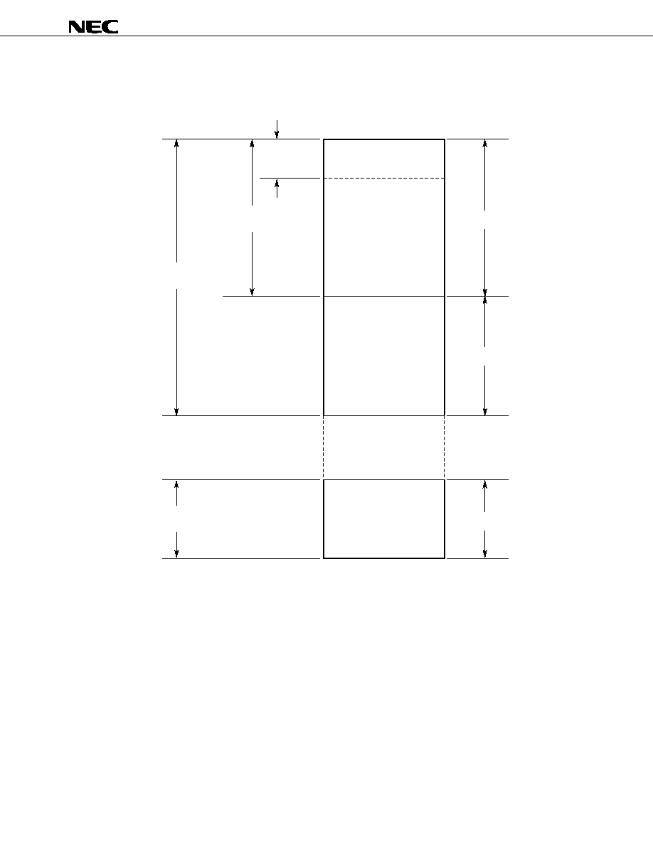
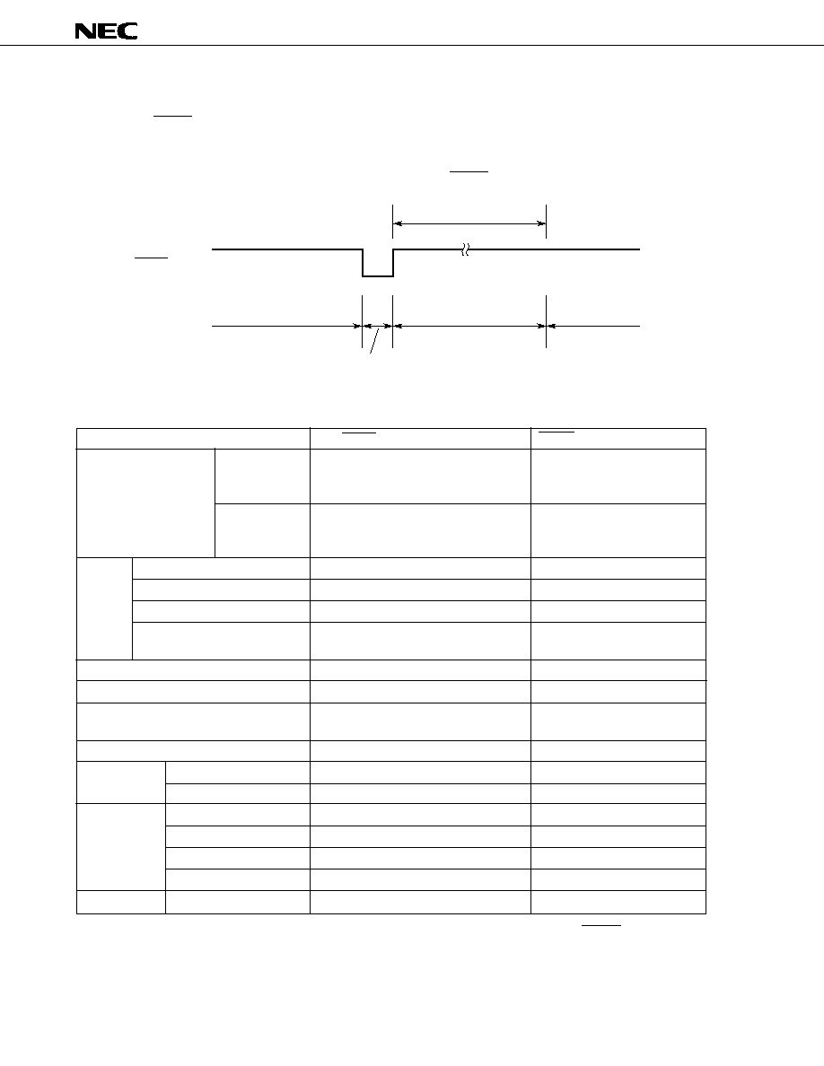
8. RESET OPERATION
When the RESET signal is input, the
µ
PD75068 is reset and all hardware is initialized as indicated in Table
8-1. Figure 8-1 shows the reset operation timing.
Figure 8-1. Reset Operation by RESET Input
Table 8-1. Status of All Hardware after Reset (1/2)
RESET input during operation
Same operation as that in
standby state
Same operation as that in
standby state
Undefined
0
0
Same operation as that in
standby state
Undefined
Undefined
Undefined
0
Undefined
0
0
FFH
0
0, 0
0
Note Data of address 0F8H to 0FDH of the data memory becomes undefined when the RESET signal is input.
Hardware
Program counter (PC)
µ
PD75064
µ
PD75066
µ
PD75068
PSW
Carry flag (CY)
Skip flag (SK0-2)
Interrupt status flag (IST0)
Bank enable flag (MBE)
Stack pointer (SP)
Data memory (RAM)
General purpose register
(X, A, H, L, D, E, B, C)
Bank selection register (MBS)
RESET input
Operation mode or
standby mode
HALT mode
Operation mode
Internal reset operation
Wait
(Approx. 31.3 ms/4.19 MHz)

31
µ
PD75064, 75066, 75068, 75064(A), 75066(A), 75068(A)
Shift register (SIO)
Operation mode register (CSIM)
SBI control register (SBIC)
Slave address register (SVA)
Processor clock control register
(PCC)
System clock control register
(SCC)
Clock output mode register
(CLOM)
Interrupt
IRQ1, IRQ2,
request flag
and IRQ4
( IRQxxx )
Other than above
Interrupt enable flag (IE
◊◊◊
)
Interrupt master enable flag
(IME)
INT0, 1, 2, mode register
(IM0, IM1, IM2)
Output buffer
Output latch
Input/output mode register
(PMGA, PMGB)
Pull-up resistor specification
register (POGA)
Mode register (ADM)
SA register (SA)
RESET input during operation
Undefined
0
0
Undefined
0
0
0
Undefined
0
0
0
0, 0, 0
Off
Clear (0)
0
0
04H
Undefined
Undefined
RESET input in standby mode
Retained
0
0
Retained
0
0
0
Undefined
0
0
0
0, 0, 0
Off
Clear (0)
0
0
04H
Undefined
Retained
Table 8-1. Status of All Hardware after Reset (2/2)
Serial
interface
Clock genera-
tor, Clock
output circuit
Interrupt
function
Digital port
A/D converter
Hardware
Bit sequential buffer (BSB0-BSB3)
32
µ
PD75064, 75066, 75068, 75064(A), 75066(A), 75068(A)
9. INSTRUCTION SET
(1) Operand identifier and its descriptive method
The operands are described in the operand column of each instruction according to the descriptive method
for the operand format of the appropriate instructions. Details should be followed by "RA75X Assembler
Package User's Manual, Language." For descriptions in which alternatives exist, one element should be
selected. Capital letters and plus and minus signs are keywords; therefore, they should be described as
they are.
For immediate data, the appropriate numerical values or labels should be described.
Identifier
reg
reg1
rp
rp1
rp2
rpa
rpa1
n4
n8
mem
Note
bit
fmem
pmem
addr
caddr
faddr
taddr
PORTn
IExxx
MBn
Description
X, A, B, C, D, E, H, L
X, B, C, D, E, H, L
XA, BC, DE, HL
BC, DE, HL
BC, DE
HL, DE, DL
DE, DL
4-bit immediate data or label
8-bit immediate data or label
8-bit immediate data or label
2-bit immediate data or label
FB0H - FBFH, FF0H - FFFH immediate data or label
FC0H - FFFH immediate data or label
µ
PD75064
0000H - 0FFFH immediate data or label
µ
PD75066
0000H - 177FH immediate data or label
µ
PD75068
0000H - 1F7FH immediate data or label
12-bit immediate data or label
11-bit immediate data or label
20H - 7FH immediate data (however, bit 0 = 0) or label
PORT0 - PORT6, PORT11
IEBT, IECSI, IET0, IE0, IE1, IE2, IE4, IEW
MB0, MB1, MB15
Note Only even address can be specified for mem when processing 8-bit data.
(2) Symbol definitions in operation description
A
: A register; 4-bit accumulator
B
: B register
C
: C register
D
: D register
E
: E register
H
: H register
L
: L register
X
: X register
XA
: Pair register (XA); 8-bit accumulator
BC
: Pair register (BC)
DE
: Pair register (DE)

33
µ
PD75064, 75066, 75068, 75064(A), 75066(A), 75068(A)
HL
: Pair register (HL)
PC
: Program counter
SP
: Stack pointer
CY
: Carry flag; Bit accumulator
PSW
: Program status word
MBE
: Memory bank enable flag
PORTn : Port n (n = 0 to 6, 11)
IME
: Interrupt master enable flag
IE
◊◊◊
: Interrupt enable flag
MBS
: Memory bank selection register
PCC
: Processor clock control register
.
: Address bit delimiter
(
◊◊
)
: Contents addressed by
◊◊
◊◊
H
: Hexadecimal data
(3) Symbols used for the addressing area column
Remarks 1. MB indicates the memory bank that can be accessed.
2. For *2, MB = 0 regardless of MBE and MBS settings.
3. For *4 and *5, MB = 15 regardless of MBE and MBS.
4. For *6 to *10, each addressable area is indicated.
MB = MBE ∑ MBS
(MBS = 0, 1, 15)
MB = 0
MBE = 0: MB = 0 (00H - 7FH)
MB = 15 (80H - FFH)
MBE = 1: MB = MBS (MBS = 0, 1, 15)
MB = 15, fmem = FB0H - FBFH,
FF0H - FFFH
MB = 15, pmem = FC0H - FFFH
PD75064 addr = 0000H - 0FFFH
PD75066 addr = 0000H - 177FH
PD75068 addr = 0000H - 1F7FH
addr = (Current PC) ≠ 15 to (Current PC) ≠ 1
(Current PC) + 2 to (Current PC) + 16
PD75064 caddr = 0000H - 0FFFH
PD75066 caddr = 0000H - 0FFFH (PC
12
= 0) or
PD75068 caddr = 0000H - 0FFFH (PC
12
= 0) or
= 1000H - 1F7FH (PC
12
= 1)
faddr = 0000H - 07FFH
taddr = 0020H - 007FH
*1
*2
*3
*4
*5
*6
*7
*8
*9
*10
Data memory
addressing
Program memory
addressing
µ
µ
µ
µ
µ
µ
= 1000H - 177FH (PC
12
= 1)
34
µ
PD75064, 75066, 75068, 75064(A), 75066(A), 75068(A)
µ
PD75064,
µ
PD75064(A)
µ
PD75066,
µ
PD75066(A)
µ
PD75068,
µ
PD75068(A)
µ
PD75064
µ
PD75066
µ
PD75068
(4) Description of machine cycle column
S indicates the number of machine cycles necessary for skipping any skip instruction. The value of S
changes as follows:
∑ When no skip is performed ∑∑∑∑∑∑∑∑∑∑∑∑∑∑∑∑∑∑∑∑∑∑∑∑∑∑∑∑∑∑∑∑∑∑∑∑∑∑∑∑∑∑∑∑∑∑∑∑∑∑∑∑∑∑∑∑∑∑∑∑∑∑∑∑∑∑∑∑∑∑∑∑∑∑∑∑∑∑∑∑∑∑∑∑∑∑∑∑∑∑∑∑∑∑∑∑∑∑∑∑∑∑∑∑∑∑∑∑ S = 0
∑ When a 1-byte or 2-byte instruction is skipped ∑∑∑∑∑∑∑∑∑∑∑∑∑∑∑∑∑∑∑∑∑∑∑∑∑∑∑∑∑∑∑∑∑∑∑∑∑∑∑∑∑∑∑∑∑∑∑∑∑∑∑∑∑∑∑∑∑∑∑∑∑∑∑∑∑∑∑∑∑∑∑∑∑∑∑∑ S = 1
∑ When a 3-byte instruction (BR !addr
Note
, CALL !addr instruction) is skipped ∑∑∑∑∑∑∑∑∑∑∑∑∑∑∑∑∑∑∑∑∑∑∑ S = 2
Note BR !addr instruction is not provided in the
µ
PD75064.
Caution The GETI instruction is skipped in one machine cycle.
One machine cycle is equivalent to one CPU clock
cycle. Therefore, the length of the machine cycle
can be selected from three different lengths by the PCC setting.
(5) Representative products listed in operation column
The products listed in the operation column (
µ
PD75064, 75066, 75068) stand for the products listed below.
5
35
µ
PD75064, 75066, 75068, 75064(A), 75066(A), 75068(A)
Group
Transfer
Table
reference
Arithme-
tic
Mne-
monic
MOV
XCH
MOVT
ADDS
ADDC
SUBS
SUBC
Operand
A, #n4
reg1, #n4
XA, #n8
HL, #n8
rp2, #n8
A, @HL
A, @rpa1
XA, @HL
@HL, A
@HL, XA
A, mem
XA, mem
mem, A
mem, XA
A, reg
XA, rp
reg1, A
rp1, XA
A, @HL
A, @rpa1
XA, @HL
A, mem
XA, mem
A, reg1
XA, rp
XA, @PCDE
XA, @PCXA
A, #n4
A, @HL
A, @HL
A, @HL
A, @HL
Bytes
1
2
2
2
2
1
1
2
1
2
2
2
2
2
2
2
2
2
1
1
2
2
2
1
2
1
1
1
1
1
1
1
Ma-
chine
cycle
1
2
2
2
2
1
1
2
1
2
2
2
2
2
2
2
2
2
1
1
2
2
2
1
2
3
3
1 + S
1 + S
1
1 + S
1
Skip
condition
String A
String A
String B
carry
carry
borrow
Address-
ing area
*1
*2
*1
*1
*1
*3
*3
*3
*3
*1
*2
*1
*3
*3
*1
*1
*1
*1
Operation
A
n4
reg1
n4
XA
n8
HL
n8
rp2
n8
A
(HL)
A
(rpa1)
XA
(HL)
(HL)
A
(HL)
XA
A
(mem)
XA
(mem)
(mem)
A
(mem)
XA
A
reg
XA
rp
reg1
A
rp1
XA
A
(HL)
A
(rpa1)
XA
(HL)
A
(mem)
XA
(mem)
A
reg1
XA
rp
∑
µ
PD75064
XA
(PC
11-8
+ DE)
ROM
∑
µ
PD75066, 75068
XA
(PC
12-8
+ DE)
ROM
∑
µ
PD75064
XA
(PC
11-8
+ XA)
ROM
∑
µ
PD75066, 75068
XA
(PC
12-8
+ XA)
ROM
A
A + n4
A
A + (HL)
A, CY
A + (HL) + CY
A
A ≠ (HL)
A, CY
A ≠ (HL) ≠ CY
36
µ
PD75064, 75066, 75068, 75064(A), 75066(A), 75068(A)
Group
Arithmetic
Accumulator
manipulation
Increment/
decrement
Compari-
son
Carry
flag
manipu-
lation
Memory
bit
manipu-
lation
Mne-
monic
AND
OR
XOR
RORC
NOT
INCS
DECS
SKE
SET1
CLR1
SKT
NOT1
SET1
CLR1
SKT
SKF
SKTCLR
Operand
A, #n4
A, @HL
A, #n4
A, @HL
A, #n4
A, @HL
A
A
reg
@HL
mem
reg
reg, #n4
@HL, #n4
A, @HL
A, reg
CY
CY
CY
CY
mem.bit
fmem.bit
pmem. @L
@H+mem.bit
mem.bit
fmem.bit
pmem. @L
@H+mem.bit
mem.bit
fmem.bit
pmem. @L
@H+mem.bit
mem.bit
fmem.bit
pmem. @L
@H+mem.bit
fmem.bit
pmem. @L
@H+mem.bit
Bytes
2
1
2
1
2
1
1
2
1
2
2
1
2
2
1
2
1
1
1
1
2
2
2
2
2
2
2
2
2
2
2
2
2
2
2
2
2
2
2
Ma-
chine
cycle
2
1
2
1
2
1
1
2
1 + S
2 + S
2 + S
1 + S
2 + S
2 + S
1 + S
2 + S
1
1
1 + S
1
2
2
2
2
2
2
2
2
2 + S
2 + S
2 + S
2 + S
2 + S
2 + S
2 + S
2 + S
2 + S
2 + S
2 + S
Skip
condition
reg = 0
(HL) = 0
(mem) = 0
reg = FH
reg = n4
(HL) = n4
A = (HL)
A = reg
CY = 1
(mem.bit) = 1
(fmem.bit) = 1
(pmem.@L) = 1
(@H + mem.bit) = 1
(mem.bit) = 0
(fmem.bit) = 0
(pmem.@L) = 0
(@H + mem.bit) = 0
(fmem.bit) = 1
(pmem.@L) = 1
(@H + mem.bit) = 1
Address-
ing area
*1
*1
*1
*1
*3
*1
*1
*3
*4
*5
*1
*3
*4
*5
*1
*3
*4
*5
*1
*3
*4
*5
*1
*4
*5
*1
Operation
A
A
n4
A
A
(HL)
A
A
n4
A
A
(HL)
A
A
n4
A
A
(HL)
CY
A
0
, A
3
CY, A
n≠1
A
n
A
A
reg
reg + 1
(HL)
(HL) + 1
(mem)
(mem) + 1
reg
reg ≠ 1
Skip if reg = n4
Skip if (HL) = n4
Skip if A = (HL)
Skip if A = reg
CY
1
CY
0
Skip if CY = 1
CY
CY
(mem.bit)
1
(fmem.bit)
1
(pmem
7-2
+ L
3-2
.bit(L
1-0
))
1
(H + mem
3-0
.bit)
1
(mem.bit)
0
(fmem.bit)
0
(pmem
7-2
+ L
3-2
.bit(L
1-0
))
0
(H + mem
3-0
.bit)
0
Skip if (mem.bit) = 1
Skip if (fmem.bit) = 1
Skip if (pmem
7-2
+ L
3-2
.bit(L
1-0
)) = 1
Skip if (H + mem
3-0
.bit) = 1
Skip if (mem.bit) = 0
Skip if (fmem.bit) = 0
Skip if (pmem
7-2
+ L
3-2
.bit(L
1-0
)) = 0
Skip if (H + mem
3-0
.bit) = 0
Skip if (fmem.bit) = 1 and clear
Skip if (pmem
7-2
+ L
3-2
.bit(L
1-0
)) = 1 and clear
Skip if (H + mem
3-0
.bit) = 1 and clear
37
µ
PD75064, 75066, 75068, 75064(A), 75066(A), 75068(A)
Mne-
monic
AND1
OR1
XOR1
BR
BRCB
CALL
Operand
CY, fmem.bit
CY, pmem. @L
CY, @H+mem.bit
CY, fmem.bit
CY, pmem. @L
CY, @H+mem.bit
CY, fmem.bit
CY, pmem.@L
CY, @H+mem.bit
addr
!addr
Note
$addr
!caddr
!addr
Bytes
2
2
2
2
2
2
2
2
2
≠
3
1
2
3
Ma-
chine
cycle
2
2
2
2
2
2
2
2
2
≠
3
2
2
3
Skip
condition
Address-
ing area
*4
*5
*1
*4
*5
*1
*4
*5
*1
*6
*6
*7
*8
*6
Operation
CY
CY
(fmem.bit)
CY
CY
(pmem
7-2
+ L
3-2
.bit(L
1-0
))
CY
CY
(H + mem
3-0
.bit)
CY
CY
(fmem.bit)
CY
CY
(pmem
7-2
+ L
3-2
.bit(L
1-0
))
CY
CY
(H + mem
3-0
.bit)
CY
CY
(fmem.bit)
CY
CY
(pmem
7-2
+ L
3-2
.bit(L
1-0
))
CY
CY
(H + mem
3-0
.bit)
∑
µ
PD75064
PC
11-0
addr
(Appropriate instructions are
selected from BRCB !caddr, and
BR $addr by the assembler.)
∑
µ
PD75066, 75068
PC
12-0
addr
(Appropriate instructions are
selected from BR !addr, BRCB
!caddr, and BR $addr by the
assembler.)
∑
µ
PD75066, 75068
PC
12-0
addr
∑
µ
PD75064
PC
11-0
addr
∑
µ
PD75066, 75068
PC
12-0
addr
∑
µ
PD75064
PC
11-0
caddr
11-0
∑
µ
PD75066, 75068
PC
12-0
PC
12
+ caddr
11-0
∑
µ
PD75064
(SP ≠ 4)(SP ≠ 1)(SP ≠ 2)
PC
11-0
(SP ≠ 3)
MBE, 0, 0, 0
PC
11-0
addr, SP
SP ≠ 4
∑
µ
PD75066, 75068
(SP ≠ 4)(SP ≠ 1)(SP ≠ 2)
PC
11-0
(SP≠3)
MBE, 0, 0, PC
12
PC
12-0
addr, SP
SP ≠ 4
Note BR !addr instruction is not provided in the
µ
PD75064.
Group
Memory
bit mani-
pulation
Branch
Sub-
routine
stack
control
38
µ
PD75064, 75066, 75068, 75064(A), 75066(A), 75068(A)
Group
Sub-
routine
stack
control
Mne-
monic
CALLF
RET
RETS
RETI
PUSH
POP
Operand
!faddr
rp
BS
rp
BS
Bytes
2
1
1
1
1
2
1
2
Ma-
chine
cycle
2
3
3 + S
3
1
2
1
2
Skip
condition
Un-
condi-
tional
Address-
ing area
*9
Operation
∑
µ
PD75064
(SP ≠ 4)(SP ≠ 1)(SP ≠ 2)
PC
11-0
(SP≠3)
MBE, 0, 0, 0
PC
11-0
00, faddr, SP
SP ≠ 4
∑
µ
PD75066, 75068
(SP ≠ 4)(SP ≠ 1)(SP ≠ 2)
PC
11-0
(SP≠3)
MBE, 0, 0, PC
12
PC
12-0
00, faddr, SP
SP ≠ 4
∑
µ
PD75064
MBE, 0, 0, 0
(SP + 1)
PC
11-0
(SP)(SP + 3)(SP + 2)
SP
SP + 4
∑
µ
PD75066, 75068
MBE, 0, 0, PC
12
(SP + 1)
PC
11-0
(SP)(SP + 3)(SP + 2)
SP
SP + 4
∑
µ
PD75064
MBE, 0, 0, 0
(SP + 1)
PC
11-0
(SP)(SP + 3)(SP + 2)
SP
SP + 4, then skip unconditionally
∑
µ
PD75066, 75068
MBE, 0, 0, PC
12
(SP + 1)
PC
11-0
(SP)(SP + 3)(SP + 2)
SP
SP + 4, then skip unconditionally
∑
µ
PD75064
MBE, 0, 0, 0
(SP + 1)
PC
11-0
(SP)(SP + 3)(SP + 2)
PSW
(SP + 4)(SP + 5), SP
SP + 6
∑
µ
PD75066, 75068
MBE, 0, 0, PC
12
(SP + 1)
PC
11-0
(SP)(SP + 3)(SP + 2)
PSW
(SP + 4)(SP + 5), SP
SP + 6
(SP ≠ 1)(SP ≠ 2)
rp, SP
SP ≠ 2
(SP ≠ 1)
MBS, (SP ≠ 2)
0, SP
SP ≠ 2
rp
(SP + 1)(SP), SP
SP + 2
MBS
(SP + 1), SP
SP + 2
39
µ
PD75064, 75066, 75068, 75064(A), 75066(A), 75068(A)
Group
Interrupt
control
Input/
output
CPU
control
Special
Mne-
monic
EI
DI
IN
OUT
HALT
STOP
NOP
SEL
GETI
Operand
IExxx
IExxx
A, PORTn
XA, PORTn
PORTn, A
PORTn, XA
MBn
taddr
Bytes
2
2
2
2
2
2
2
2
2
2
1
2
1
Ma-
chine
cycle
2
2
2
2
2
2
2
2
2
2
1
2
3
Address-
ing area
*10
Operation
IME
1
IExxx
1
IME
0
IExxx
0
A
PORTn (n = 0 - 6, 11)
XA
PORTn
+1
,PORTn
(n = 4, 6)
PORTn
A
(n = 2 - 6)
PORTn
+1
, PORTn
XA (n = 4, 6)
Set HALT Mode (PCC.2
1)
Set STOP Mode (PCC.3
1)
No Operation
MBS
n (n = 0, 1, 15)
∑
µ
PD75064
∑
For the TBR instruction
PC
11-0
(taddr)
3-0
+ (taddr + 1)
∑
For the TCALL instruction
(SP ≠ 4)(SP ≠ 1)(SP ≠ 2)
PC
11-0
(SP ≠ 3)
MBE, 0, 0, 0
PC
11-0
(taddr)
3-0
+ (taddr + 1)
SP
SP ≠ 4
∑
For other than the TBR and
TCALL instruction
(taddr) (taddr + 1) is executed.
∑
µ
PD75066, 75068
∑
For the TBR instruction
PC
12-0
(taddr)
4-0
+ (taddr + 1)
∑
For the TCALL instruction
(SP ≠ 4)(SP ≠ 1)(SP ≠ 2)
PC
11-0
(SP ≠ 3)
MBE, 0, 0, PC
12
PC
12-0
(taddr)
4-0
+ (taddr + 1)
SP
SP ≠ 4
∑
For other than the TBR and
TCALL instruction
(taddr) (taddr + 1) is executed.
----------------------------------------------
----------------------------------------------
-----------------
-----------------
----------------------------------------------
----------------------------------------------
-----------------
-----------------
Skip
condition
Depends on
the refer-
ence
instruction.
Depends on
the refer-
ence
instruction.
Caution When executing the IN/OUT instruction, MBE must be set to 0, or MBE and MBS must be set to
1 and 15, respectively.

40
µ
PD75064, 75066, 75068, 75064(A), 75066(A), 75068(A)
10. ELECTRICAL SPECIFICATIONS
Absolute Maximum Ratings (T
a
= 25
∞
C)
Parameter
Symbol
Conditions
Ratings
Unit
Power supply
voltage
Except ports 4 and 5
≠0.3 to V
DD
+0.3
V
Input voltage
On-chip pull-up resistor
≠0.3 to V
DD
+0.3
V
Ports 4 and 5
N-ch open≠drain
≠0.3 to +11
V
Output voltage
≠0.3 to V
DD
+0.3
V
High level output
Per pin
≠10
mA
current
All output pins
≠30
mA
Low level output
Peak value
30
mA
current
One pin of ports 0, 3, 4, and 5
rms value
15
mA
Peak value
20
mA
One pin of ports 2 and 6
rms value
5
mA
Peak value
160
mA
Total of ports 0, 3, 4 and 5
rms value
120
mA
Peak value
30
mA
Total of ports 2 and 6
rms value
20
mA
Operating ambient
temperature
Storage
temperature
Note Rms value is calculated using the following expression: [rms value] = [peak value]
◊
duty ratio
Caution
If any of the items exceeds the absolute maximum ratings, even momentarily, this may damage product
quality. The absolute maximum ratings are values that may physically damage products. Be sure to use
the products within the ratings.
V
DD
V
I1
V
I2
V
O
I
OH
I
OL
Note
T
opt
T
stg
≠65 to +150
∞
C
≠40 to +85
∞
C
≠0.3 to +7.0
V
41
µ
PD75064, 75066, 75068, 75064(A), 75066(A), 75068(A)
Main System Clock Oscillator Characteristics (T
a
= ≠40 to +85
∞
C, V
DD
= 2.7 to 6.0 V)
Recommended
Resonator
Parameter
Conditions
MIN.
TYP.
MAX.
Unit
Constant
V
DD
= Oscilla-
tion voltage
1.0
5.0
Note3
MHz
range
Oscillation
stabilization
time
Note2
Oscillation
frequency (f
x
)
Note1
V
DD
= 4.5
to 6.0 V
Oscillation
stabilization
time
Note2
30
ms
X1 input
frequency (f
x
)
Note1
X1 input
high-/low-level
100
500
ns
width (t
XH
, t
XL
)
4
ms
1.0
5.0
Note3
MHz
Notes 1. The oscillation frequency indicates characteristics of the oscillator only. For the instruction execution time,
refer to the AC characteristics.
2. The oscillation stabilization time is the required time for oscillation to stabilize after the voltage level of
V
DD
reaches the MIN. value of the oscillation voltage range or releasing the STOP mode.
3. When the oscillation frequency is "4.19 MHz < f
X
5.0 MHz", selection of "PCC = 0011" with 1 machine
cycle of less than 0.95
µ
s for instruction execution time is not possible.
Caution
If the main system clock oscillator is used, the wiring in the area indicated with broken lines in the
recommended constant illustration should be routed observing the points described below to avoid
influence of wiring capacitance, etc.
∑ Route as short as possible.
∑ Do not cross the wires.
∑ Route the wires away from lines where changing high current flows.
∑ Make the connecting point of the capacitors in the oscillation circuit to have always the same potential
as V
SS
. Do not route the connecting point to another ground pattern on the board where high current
flows.
∑ Do not use the oscillator as a signal source of other circuits.
Ceramic
resonator
Crystal
resonator
External
clock
X1
X2
C2
C1
V
SS
X1
X2
C2
C1
V
SS
10
ms
1.0
4.19
5.0
Note3
MHz
X1
X2
PD74HCU04
µ
Oscillation
frequency (f
x
)
Note1
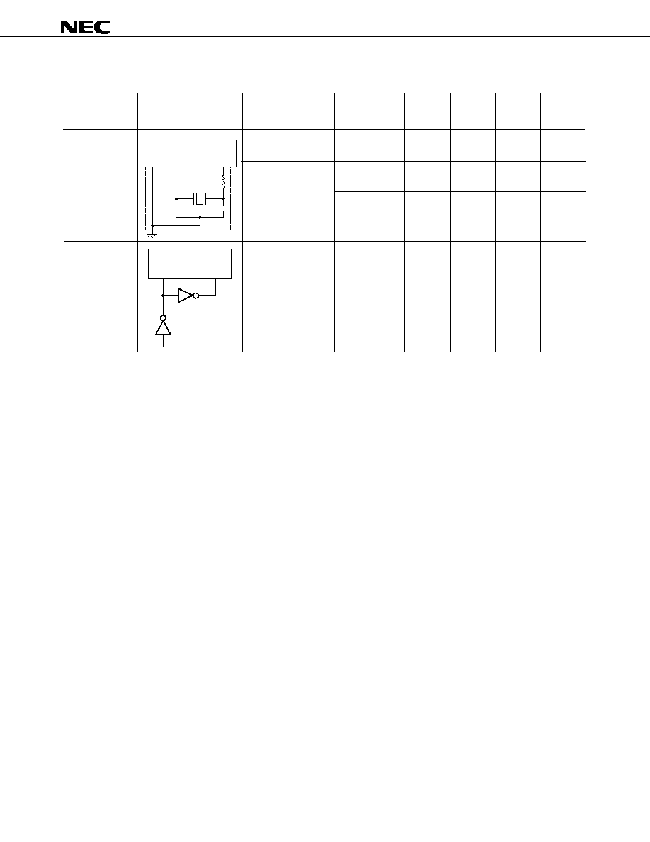
42
µ
PD75064, 75066, 75068, 75064(A), 75066(A), 75068(A)
Subsystem Clock Oscillator Characteristics (T
a
= ≠40 to +85
∞
C, V
DD
= 2.7 to 6.0 V)
Recommended
MIN.
TYP.
MAX.
Unit
Resonator
Parameter
Conditions
Constant
Oscillation
frequency (f
XT
)
Note1
V
DD
= 4.5
to 6.0 V
Oscillation
stabilization
time
Note2
XT1 input
32
100
kHz
frequency (f
XT
)
Note1
XT1 input high-/
low-level width
(t
XTH
,t
XTL
)
Notes 1. The oscillation frequency indicates characteristics of the oscillator only. For the instruction execution
time, refer to the AC characteristics.
2. The oscillation stabilization time is the required time for oscillation to stabilize after the voltage level
of V
DD
reaches the MIN. value of the oscillation voltage range.
Caution If the subsystem clock oscillator is used, the wiring in the area indicated with broken lines in the
recommended constant illustration should be routed observing the points described below to avoid
influence of wiring capacitance, etc.
∑ Route as short as possible.
∑ Do not cross the wires.
∑ Route the wires away from lines where changing high current flows.
∑ Make the connecting point of the capacitors in the oscillation circuit to have always the same potential
as V
SS
. Do not route the connecting point to another ground pattern on the board where high current
flows.
∑ Do not use the oscillator as a signal source of other circuits.
Especially when using the subsystem clock, be sure to design wiring so as to minimize noise. The
subsystem clock oscillator uses a low-amplification circuit to minimize power dissipation. As a result,
malfunctions due to noise are more liable to occur than with the main system clock oscillator.
32
32.768
50
kHz
1.0
2
s
10
s
5
15
µ
s
Crystal
resonator
External
clock
XT1
XT2
C4
C3
V
SS
R
XT1
XT2

43
µ
PD75064, 75066, 75068, 75064(A), 75066(A), 75068(A)
Recommended Oscillator Constant
Main system clock: Ceramic (T
a
= ≠40 to +85
∞
C)
Frequency
(MHz)
KBR-2.0 MS
PBRC 2.00A
KBR-4.19 MSA
PBRC 4.19A
KBR-4.19 MKS
KBR-4.19 MWS
CSB1000J
Note
1.00
100
100
2.7
Rd = 5.6 k
CSA2.0MG040
100
100
2.8
CST2.0MGW093
2.00
Internal
Internal
CSAC2.0MGCME
15
15
Chip product
CSA4.19MGU
30
30
CST4.19MGUW
Internal
Internal
Note
When the Murata's CSB1000J ceramic resonator (1.00 MHz) is used, the limiting resistor (Rd = 5.6 k
) is
required (see figure below). When using other recommended resonators, the limiting resistor is not required.
Example of Recommended Main System Clock Circuit (when using CSB1000J of Murata)
Main System Clock: XTAL
Frequency
(MHz)
2.00
2.8
DAISINKU
HC-49/U
4.19
8
8
6.0
(T
a
= ≠40 to +85
∞
C)
5.00
2.00
3.1
4.19
3.2
Manufacturer
C1 (pF)
C2 (pF)
Part number
MIN. (V)
MAX. (V)
Remarks
6.0
6.0
2.00
47
47
2.5
4.19
33
33
4.19
2.7
KYOCERA
MURATA
Manufacturing
2.7
Oscillation
voltage range
Recommended
circuit constant
Part number
Manufacturer
MIN. (V)
MAX. (V)
Remarks
2.7
C1 (pF)
C2 (pF)
KINSEKI
HC-49/U
22
22
6.0
(T
a
= ≠20 to +70
∞
C)
Recommended
circuit constant
Oscillation
voltage range
X1
X2
Rd
C2
C1
CSB1000J
4.19
Internal
Internal
44
µ
PD75064, 75066, 75068, 75064(A), 75066(A), 75068(A)
DC Characteristics (T
a
= ≠40 to +85
∞
C, V
DD
= 2.7 to 6.0 V)
Parameter
Symbol
Conditions
MIN.
TYP.
MAX.
Unit
High-level input
V
IH1
Ports 2, 3, and 11
0.7 V
DD
V
DD
V
voltage
V
IH2
Ports 0,1,6, RESET
0.8 V
DD
V
DD
V
On-chip pull-up resistor
0.7 V
DD
V
DD
V
V
IH3
Ports 4 and 5
N-ch open-drain
0.7 V
DD
10
V
V
IH4
X1, X2, XT1, XT2
V
DD
≠0.5
V
DD
V
Low-level input
V
IL1
Ports 2 through 5 and 11
0
0.3 V
DD
V
voltage
V
IL2
Ports 0, 1, 6, RESET
0
0.2 V
DD
V
V
IL3
X1, X2, XT1, XT2
0
0.4
V
High-level output
V
DD
= 4.5 to 6.0 V , I
OH
= ≠1 mA
V
DD
≠1.0
V
voltage
I
OH
= ≠100
µ
A
V
DD
≠0.5
V
Low-level output
V
OL
Ports 4 and 5
V
DD
= 4.5 to 6.0 V
0.7
2.0
V
I
OL
= 15 mA
Port 3
V
DD
= 4.5 to 6.0 V
0.3
2.0
V
I
OL
= 15 mA
V
DD
= 4.5 to 6.0 V , I
OL
= 1.6 mA
0.4
V
I
OL
= 400
µ
A
0.5
V
SB0, SB1
N-ch open-drain
0.2 V
DD
V
pull-up resistor
1 k
High-level input
I
LIH1
Other than pins below
3
µ
A
leakage current
V
I
= V
DD
I
LIH2
X1, X2, XT1, XT2
20
µ
A
Ports 4 and 5
(N-ch open-drain)
Low-level input
I
LIL1
Other than pins below
≠3
µ
A
leakage current
V
I
= 0 V
I
LIL2
X1, X2, XT1, XT2
≠20
µ
A
High-level output
I
LOH1
V
O
= V
DD
3
µ
A
leakage current
Ports 4 and 5
(N-ch open-drain)
Low-level output
I
LOL
V
O
= 0 V
≠3
µ
A
leakage current
On-chip pull-up
P01, 02, 03,
V
DD
= 5.0 V
±
10 %
15
40
80
k
resistor
R
U1
Ports 1, 2, 3 and 6
V
I
= 0 V
V
DD
= 3.0 V
±
10 %
30
300
k
Ports 4 and 5
V
DD
= 5.0 V
±
10 %
15
40
70
k
R
U2
V
O
= V
DD
≠ 2.0 V
V
DD
= 3.0 V
±
10 %
10
60
k
V
OH
voltage
I
LIH3
V
I
= 10 V
20
µ
A
I
LOH2
V
O
= 10 V
20
µ
A
(Cont.)

45
µ
PD75064, 75066, 75068, 75064(A), 75066(A), 75068(A)
I
DD4
5
15
µ
A
Parameter
Symbol
Conditions
MIN.
TYP.
MAX.
Unit
Supply current
Note1
V
DD
= 5.0 V
±
10 %
Note
3
2.0
6.0
mA
I
DDI
4.19 MHz
Note
2
V
DD
= 3.0 V
±
10 %
Note
4
0.2
0.6
mA
crystal oscillation
C1 = C2 = 22 pF
HALT
V
DD
= 5.0 V
±
10 %
400
1200
µ
A
I
DD2
mode
V
DD
= 3.0 V
±
10 %
120
400
µ
A
I
DD3
V
DD
= 3.0 V
±
10 %
10
30
µ
A
32.768 kHz
Note
5
crystal oscillation
HALT
V
DD
= 3.0 V
±
10 %
mode
V
DD
= 5.0 V
±
10 %
0.5
20
µ
A
I
DD5
0.1
10
µ
A
T
a
= 25
∞
C
0.1
5
µ
A
Notes 1. Current which flows in the on-chip pull-up resistor is not included.
2. Including oscillation of the subsystem clock.
3. When the processor clock control register (PCC) is set to 0011 and the device is operated in the high-
speed mode.
4. When PCC is set to 0000 and the device is operated in the low-speed mode.
5. When the system clock control register (SCC) is set to 1001 and the device is operated on the sub-
system clock, with main system clock oscillation stopped.
DC Characteristics (T
a
= ≠40 to +85
∞
C, V
DD
= 2.7 to 6.0 V)
V
DD
=
3.0 V
±
10 %
XT1 = 0 V
STOP mode
46
µ
PD75064, 75066, 75068, 75064(A), 75066(A), 75068(A)
AC Characteristics (T
a
= ≠40 to +85
∞
C, V
DD
= 2.7 to 6.0 V)
Parameter
Symbol
Conditions
MIN.
TYP.
MAX.
Unit
CPU clock
Operating on main
V
DD
= 4.5 to 6.0 V
0.95
64
µ
s
cycle time
Note
1
system clock
( minimum
3.8
64
µ
s
instruction
execution time =
Operating on subsystem clock
114
122
125
µ
s
1 machine cycle )
TI0 input
V
DD
= 4.5 to 6.0 V
0
1
MHz
frequency
f
TI
0
275
kHz
TI0 input high and
V
DD
= 4.5 to 6.0 V
0.48
µ
s
low level width
1.8
µ
s
Interrupt input high
INT0
Note2
µ
s
and low level width
INT1, INT2, INT4
10
µ
s
KR0 to KR3
10
µ
s
RESET low level
t
RSL
10
µ
s
width
Capacitance (T
a
= 25
∞
C, V
DD
= 0 V)
Parameter
Symbol
Conditions
MIN.
TYP.
MAX.
Unit
Input capacitance
C
I
f = 1 MHz
15
pF
Unmeasured pins returned to 0 V.
Output capacitance
C
O
15
pF
I/O capacitance
C
IO
15
pF
t
CY
t
TIH
,
t
TIL
t
INTH
,
t
INTL
t
CY
vs V
DD
(Operating on Main System Clock)
Cycle Time t
CY
[
s]
Supply Voltage V
DD
[V]
0
1
2
3
4
5
6
0.5
1
2
3
4
5
60
64
70
6
Operation
guarantee range
µ
Notes 1. The cycle time (minimum instruction
execution time) of the CPU clock (
) is
determined by the oscillation frequency of
the connected resonator, the system clock
control register (SCC), and the processor
clock control register (PCC). The figure at
the right indicates the cycle time t
CY
versus
supply voltage V
DD
characteristic with the
main system clock operating.
2. 2t
CY
or 128/f
X
is set by setting the interrupt
mode register (IM0).
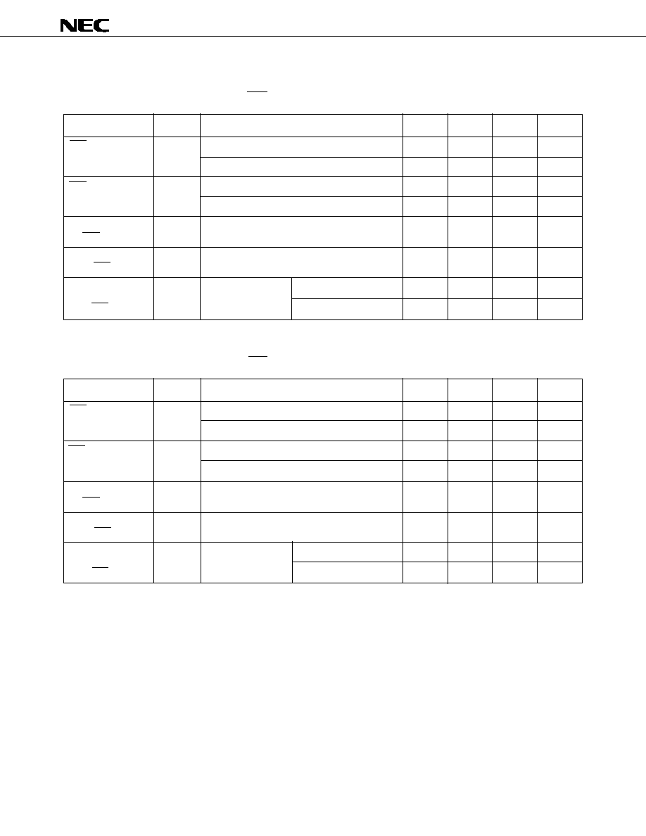
47
µ
PD75064, 75066, 75068, 75064(A), 75066(A), 75068(A)
t
SIK2
100
ns
Serial Transfer Operation
2-Wire and 3-Wire Serial I/O Modes (SCK ... Internal clock output)
Parameter
Symbol
Conditions
MIN.
TYP.
MAX.
Unit
SCK cycle time
V
DD
= 4.5 to 6.0 V
1600
ns
t
KCY1
3800
ns
SCK high- and low-
V
DD
= 4.5 to 6.0 V
t
KCY1
/2-50
ns
level width
t
KCY1
/2-150
ns
SI setup time
(to SCK
)
SI hold time
(from SCK
)
SO output
V
DD
= 4.5 to 6.0 V
0
250
ns
delay time
t
KSO1
from SCK
0
1000
ns
2-Wire and 3-Wire Serial I/O Modes (SCK ... External clock input)
Parameter
Symbol
Conditions
MIN.
TYP.
MAX.
Unit
SCK cycle time
V
DD
= 4.5 to 6.0 V
800
ns
t
KCY2
3200
ns
SCK high- and low-
V
DD
= 4.5 to 6.0 V
400
ns
level width
1600
ns
SI setup time
(to SCK
)
SI hold time
(from SCK
)
SO output
V
DD
= 4.5 to 6.0 V
0
300
ns
delay time
t
KSO2
from SCK
0
1000
ns
Note R
L
and C
L
are load resistance and load capacitance of the SO output line, respectively.
t
SIK1
150
ns
t
KSI1
400
ns
t
KL1
t
KH1
R
L
= 1 k
,
C
L
= 100 pF
Note
t
KSI2
400
ns
t
KL2
t
KH2
R
L
= 1 k
,
C
L
= 100 pF
Note
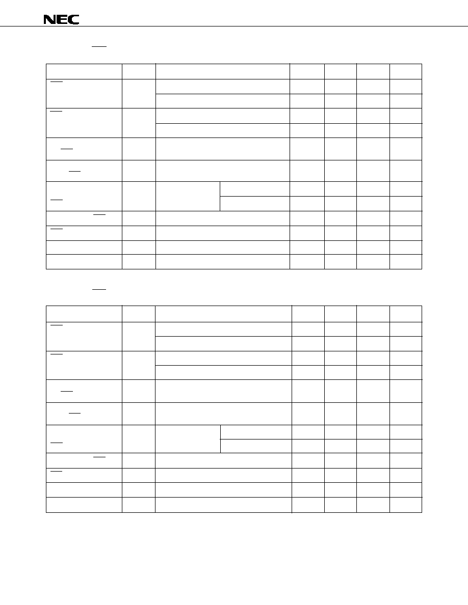
48
µ
PD75064, 75066, 75068, 75064(A), 75066(A), 75068(A)
SBI Mode (SCK ... Internal clock output (Master))
Parameter
Symbol
Conditions
MIN.
TYP.
MAX.
Unit
SCK cycle time
V
DD
= 4.5 to 6.0 V
1600
ns
t
KCY3
3800
ns
SCK high- and low-level
V
DD
= 4.5 to 6.0 V
t
KCY3
/2-50
ns
width
t
KCY3
/2-150
ns
SB0, 1 setup time
(to SCK
)
SB0, 1 hold time
(from SCK
)
SB0, 1 output
V
DD
= 4.5 to 6.0 V
0
250
ns
delay time from
t
KSO3
SCK
0
1000
ns
SB0, 1
from SCK
t
KSB
t
KCY3
ns
SCK
from SB0, 1
t
SBK
t
KCY3
ns
SB0, 1 low-level width
t
SBL
t
KCY3
ns
SB0, 1 high-level width
t
SBH
t
KCY3
ns
SBI Mode (SCK ... External clock input (Slave))
Parameter
Symbol
Conditions
MIN.
TYP.
MAX.
Unit
SCK cycle time
V
DD
= 4.5 to 6.0 V
800
ns
t
KCY4
3200
ns
SCK high- and low-level
V
DD
= 4.5 to 6.0 V
400
ns
width
1600
ns
SB0, 1 setup time
(to SCK
)
SB0, 1 hold time
(from SCK
)
SB0, 1 output
V
DD
= 4.5 to 6.0 V
0
300
ns
delay time from
t
KSO4
SCK
0
1000
ns
SB0, 1
from SCK
t
KSB
t
KCY4
ns
SCK
from SB0, 1
t
SBK
t
KCY4
ns
SB0, 1 low-level width
t
SBL
t
KCY4
ns
SB0, 1 high-level width
t
SBH
t
KCY4
ns
Note R
L
and C
L
are load resistance and load capacitance, respectively, for the SB0 and SB1 output lines.
t
KSI4
t
KCY4
/2
ns
t
SIK3
150
ns
t
KSI3
t
KCY3
/2
ns
t
SIK4
100
ns
R
L
= 1 k
,
C
L
= 100 pF
Note
t
KL4
t
KH4
R
L
= 1 k
,
C
L
= 100 pF
Note
t
KL3
t
KH3
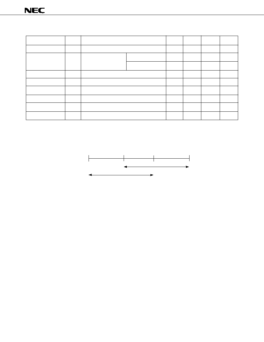
49
µ
PD75064, 75066, 75068, 75064(A), 75066(A), 75068(A)
A/D Converter (T
a
= ≠40 to +85
∞
C, V
DD
= 2.7 to 6.0 V, AV
SS
= V
SS
= 0 V)
Parameter
Symbol
Conditions
MIN.
TYP.
MAX.
Unit
Resolution
8
8
8
bit
Absolute
≠10
T
a
+85
∞
C
±
1.5
LSB
accuracy
Note1
2.5 V
AV
REF
V
DD
Note2
≠40
T
a
<
≠10
∞
C
±
2.0
LSB
Conversion time
Note3
t
CONV
168/fx
µ
s
Sampling time
Note4
t
SAMP
44/f
X
µ
s
AV
REF
2.5
V
DD
V
Analog input voltage
V
IAN
AV
SS
AV
REF
V
R
AN
1000
M
AV
REF
current
AI
REF
0.7
2.0
mA
Notes 1. Absolute accuracy excluding quantization error (
±
1/2 LSB)
2. ADM1 should be set according to the A/D converter reference voltage (AV
REF
) as follows:
When the AV
REF
is between 0.6V
DD
and 0.65V
DD
, either 1 or 0 can be set.
2.5 V
0.6 V
DD
0.65 V
DD
V
DD
(2.7 to 6.0 V)
AV
REF
ADM1 = 0
ADM1 = 1
3. The time from conversion start instruction execution to conversion end (EOC=1) (40.1
µ
s : at f
X
= 4.19
MHz)
4. The time from conversion start instruction execution to sampling end (10.5
µ
s : at f
X
= 4.19 MHz)
Analog input
impedance
Reference
input voltage
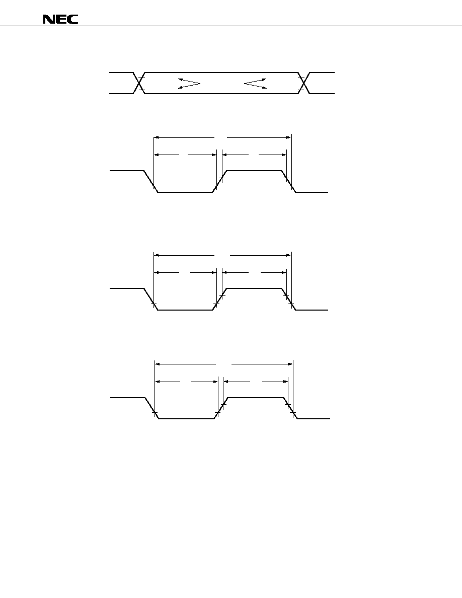
50
µ
PD75064, 75066, 75068, 75064(A), 75066(A), 75068(A)
AC Timing Test Points (excluding X1 and XT1 inputs):
Clock Timings:
TI0 Timings:
0.8 V
DD
0.2 V
DD
0.8 V
DD
0.2 V
DD
Test Points
X1 Input
1/f
X
t
XL
t
XH
V
DD
≠0.5 V
0.4 V
XT1 Input
1/f
XT
t
XTL
t
XTH
V
DD
≠0.5 V
0.4 V
TI0
1/f
TI
t
TIL
t
TIH
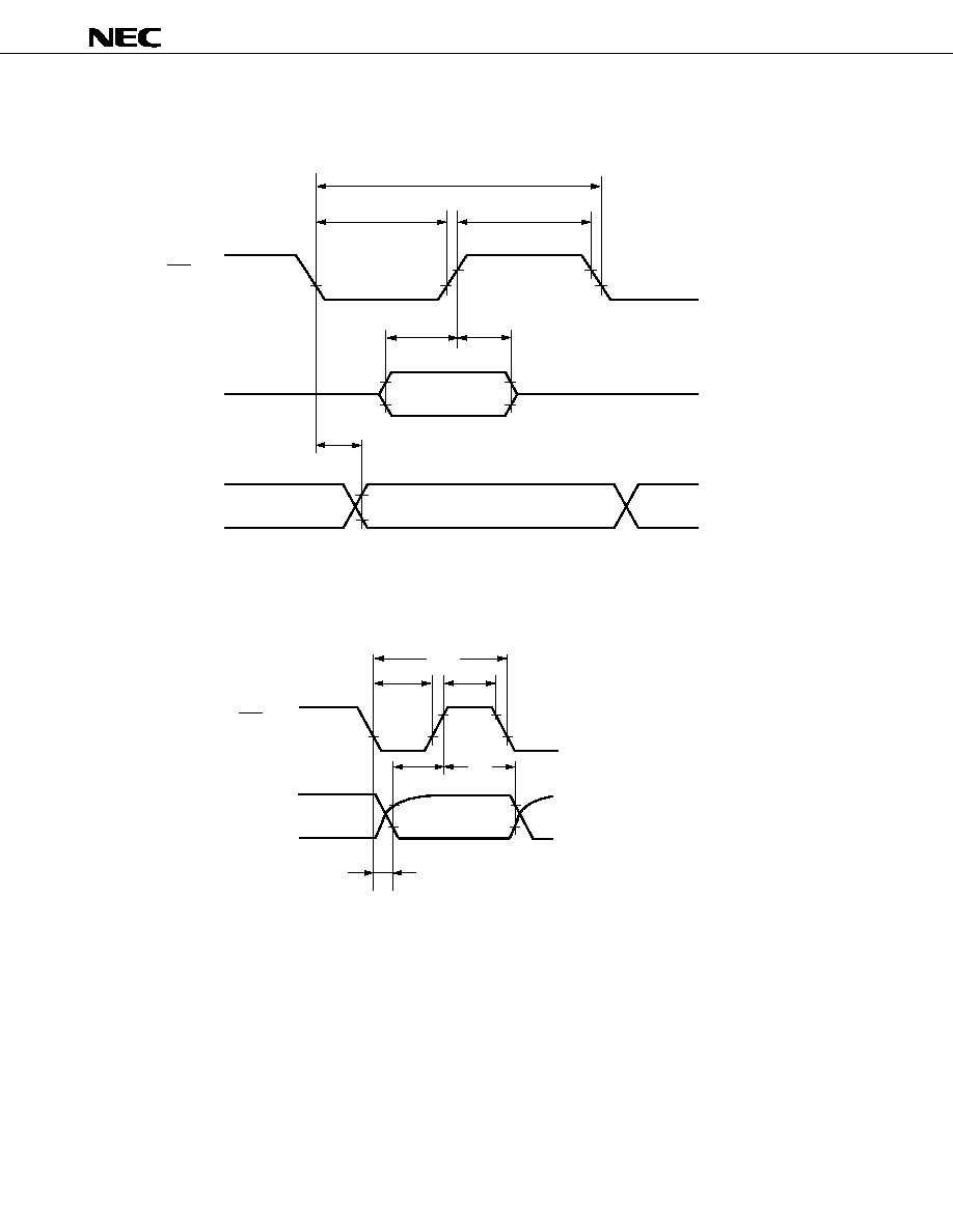
51
µ
PD75064, 75066, 75068, 75064(A), 75066(A), 75068(A)
Serial Transfer Timing
3-wire serial I/O mode:
2-wire serial I/O mode:
SCK
t
KCY1
t
KH1
t
KL1
Input Data
Output Data
t
SIK1
t
KSI1
t
KSO1
SI
SO
t
KSO2
t
KL2
t
KH2
t
KCY2
SCK
SB0,1
t
SIK2
t
KSI2
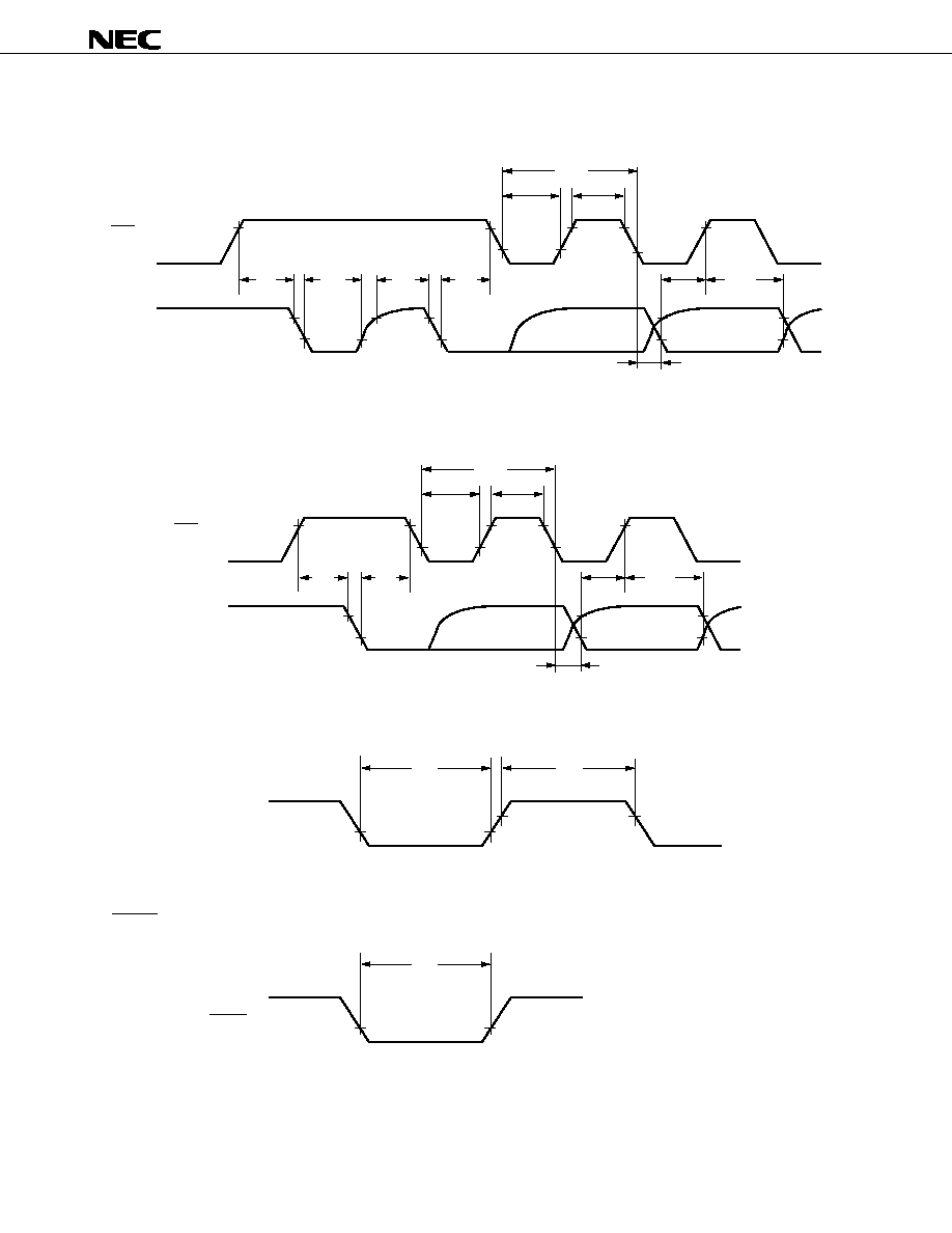
52
µ
PD75064, 75066, 75068, 75064(A), 75066(A), 75068(A)
Serial Transfer Timing
Bus release signal transfer:
Command signal transfer:
Interrupt Input Timing
RESET Input Timing
t
INTL
t
INTH
INT0,1,2,4
KR0-3
t
RSL
RESET
t
KSB
t
SBL
t
SBH
t
SBK
t
KSO3,4
t
SIK3,4
t
KSI3,4
t
KL3,4
t
KH3,4
t
KCY3,4
SCK
SB0,1
t
KSB
t
KSO3,4
t
SIK3,4
t
KSI3,4
t
KL3,4
t
KH3,4
t
KCY3,4
SCK
SB0,1
t
SBK

53
µ
PD75064, 75066, 75068, 75064(A), 75066(A), 75068(A)
Data Memory STOP Mode Low Supply Voltage Data Retention Characteristics (T
a
= ≠40 to +85
∞
C)
Parameter
Symbol
Conditions
MIN.
TYP.
MAX.
Unit
Data retention supply voltage
V
DDDR
2.0
6.0
V
Data retention supply current
Note
1
I
DDDR
V
DDDR
= 2.0 V
0.1
10
µ
A
Release signal setting time
t
SREL
0
µ
s
Oscillation stabilization
Release by RESET
2
17
/fx
ms
wait time
Note
2
t
WAIT
Release by interrupt request
Note3
ms
Notes 1. Current which flows in the on-chip pull-up resistor is not included.
2. The oscillation stabilization wait time is the time during which the CPU operation is stopped to
prevent unstable operation at the oscillation start.
3. Depends on the basic interval timer mode register (BTM) settings (See the table below).
Wait Time
BTM3
BTM2
BTM1
BTM0
(Figures in parentheses are for operation at fx = 4.19 MHz)
--
0
0
0
2
20
/fx (approx. 250 ms)
--
0
1
1
2
17
/fx (approx. 31.3 ms)
--
1
0
1
2
15
/fx (approx. 7.82 ms)
--
1
1
1
2
13
/fx (approx. 1.95 ms)
Data Retention Timing (STOP mode release by RESET)
Data Retention Timing (Standby release signal: STOP mode release by interrupt signal)
STOP Mode
Data Retention Mode
STOP Instruction Execution
RESET
V
DD
Internal Reset Operation
HALT Mode
Operating
Mode
V
DDDR
t
SREL
t
WAIT
STOP Mode
Data Retention Mode
STOP Instruction Execution
V
DD
HALT Mode
Operating
Mode
V
DDDR
t
SREL
t
WAIT
Standby Release Signal
(Interrupt Request)
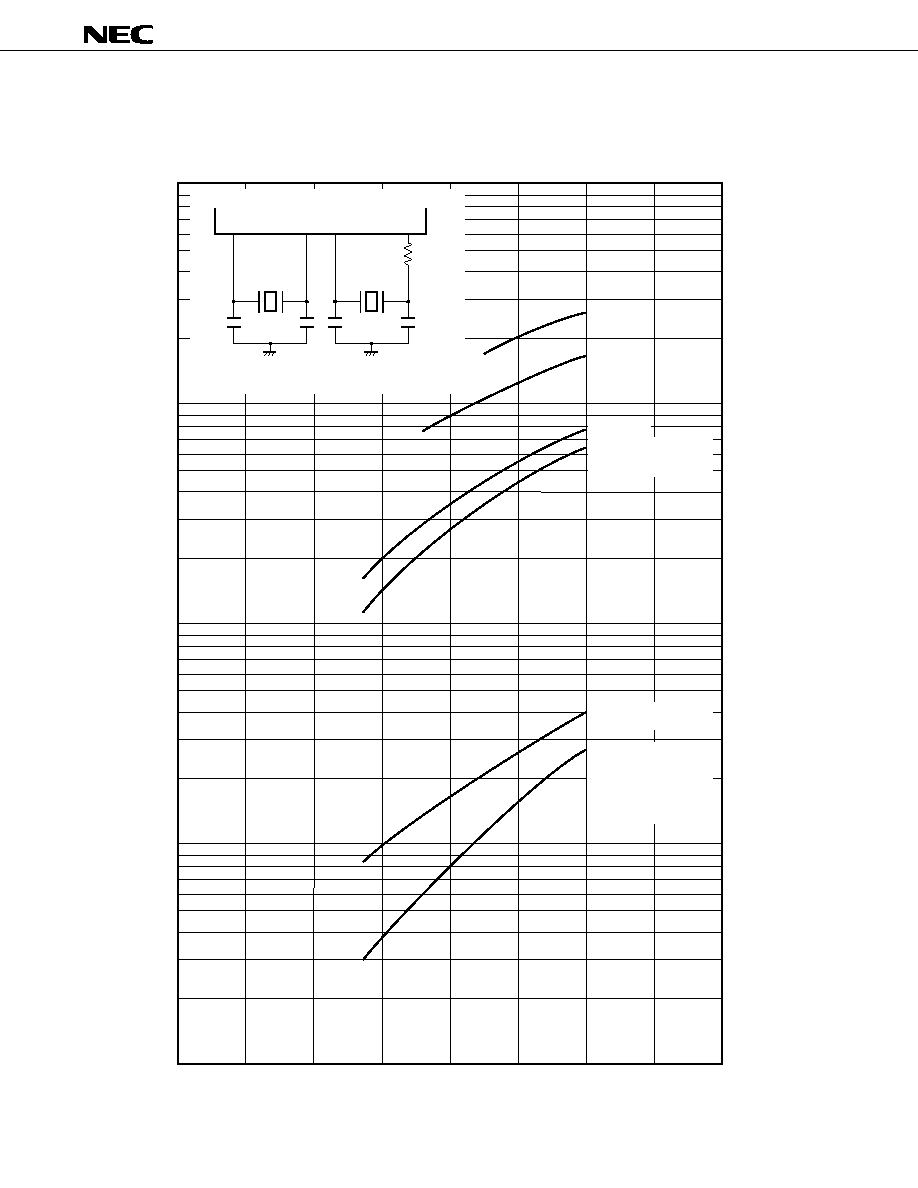
54
µ
PD75064, 75066, 75068, 75064(A), 75066(A), 75068(A)
11. CHARACTERISTIC CURVES (FOR REFERENCE ONLY)
I
DD
vs V
DD
(Main system clock: 4.19-MHz crystal resonator)
3.0
5.0
1.0
0.5
0.1
0.05
0.01
0.005
0.001
0
2
4
6
8
(T
a
=25 ∞C)
PCC=0011
PCC=0010
PCC=0000
Main system clock
HALT mode + 32 kHz
oscillation
Subsystem clock
operation mode
Main system clock
STOP mode + 32 kHz
oscillation
and
subsystem clock
HALT mode
Supply Current I
DD
[mA]
X1
X2
Crystal
resonator
4.19 MHz
XT1
XT2
330 k
22 pF
Crystal
resonator
32.768 kHz
18 pF
22 pF
18 pF
Supply Voltage V
DD
[V]
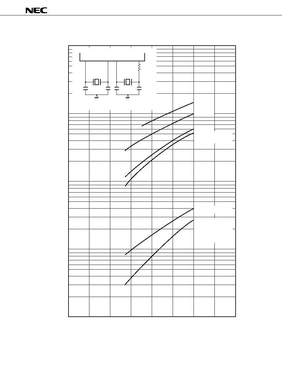
55
µ
PD75064, 75066, 75068, 75064(A), 75066(A), 75068(A)
I
DD
vs V
DD
(Main system clock: 2.0-MHz crystal resonator)
3.0
5.0
1.0
0.5
0.1
0.05
0.01
0.005
0.001
0
2
4
6
8
(T
a
=25 ∞C)
PCC=0011
PCC=0010
PCC=0000
Main system clock
HALT mode + 32 kHz
oscillation
Subsystem clock
operation mode
Main system clock
STOP mode + 32 kHz
oscillation
and
subsystem clock
HALT mode
Supply Voltage V
DD
[V]
Supply Current I
DD
[mA]
X1
X2
Crystal
resonator
2.0 MHz
XT1
XT2
330 k
22 pF
Crystal
resonator
32.768 kHz
18 pF
22 pF
18 pF
56
µ
PD75064, 75066, 75068, 75064(A), 75066(A), 75068(A)
I
DD
vs V
DD
(Main system clock: 4.19-MHz ceramic resonator)
3.0
5.0
1.0
0.5
0.1
0.05
0.01
0.005
0.001
0
2
4
6
8
(T
a
=25 ∞C)
PCC=0011
PCC=0010
PCC=0000
Main system clock
HALT mode + 32 kHz
oscillation
Subsystem clock
operation mode
Main system clock
STOP mode + 32 kHz
oscillation
and
subsystem clock
HALT mode
Supply Voltage V
DD
[V]
Supply Current I
DD
[mA]
X1
X2
Ceramic
resonator
4.19 MHz
XT1
XT2
330 k
30 pF
Crystal
resonator
32.768 kHz
18 pF
30 pF
18 pF
57
µ
PD75064, 75066, 75068, 75064(A), 75066(A), 75068(A)
I
DD
vs V
DD
(Main system clock: 2.0-MHz ceramic resonator)
3.0
5.0
1.0
0.5
0.1
0.05
0.01
0.005
0.001
0
2
4
6
8
(T
a
=25 ∞C)
PCC=0011
PCC=0010
PCC=0000
Main system clock
HALT mode + 32 kHz
oscillation
Subsystem clock
operation mode
Main system clock
STOP mode + 32 kHz
oscillation
and
subsystem clock
HALT mode
Supply Voltage V
DD
[V]
Supply Current I
DD
[mA]
X1
X2
Ceramic
resonator
2.0 MHz
XT1
XT2
330 k
30 pF
Crystal
resonator
32.768 kHz
18 pF
30 pF
18 pF
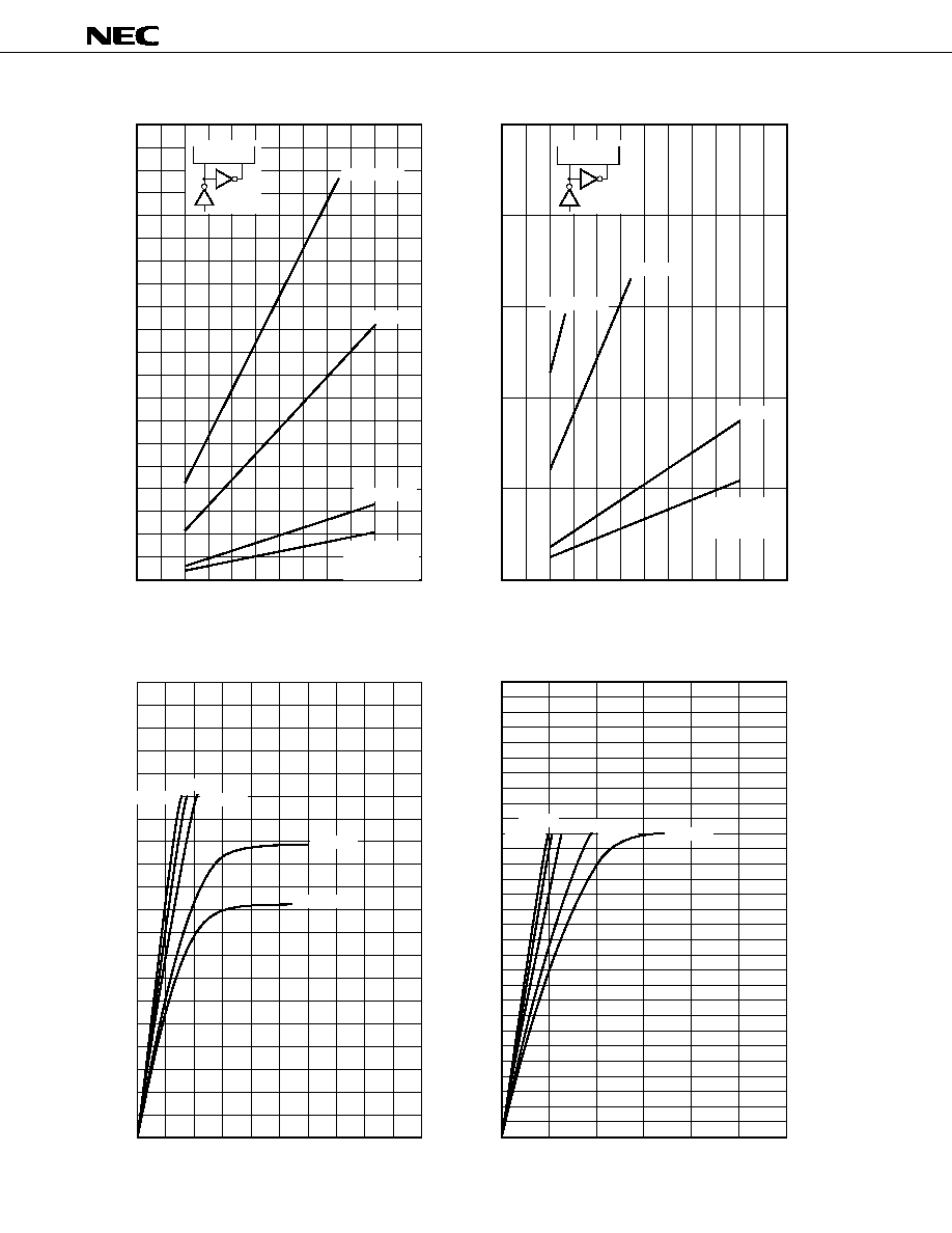
58
µ
PD75064, 75066, 75068, 75064(A), 75066(A), 75068(A)
I
DD
vs f
X
I
DD
vs f
X
2.0
1.5
1.0
0.5
0
0
2
(V
DD
= 5 V, T
a
=25 ∞C)
f
x
[MHz]
I
DD
[mA]
X1
X2
1
3
4
5
6
PCC=0000
Main system
clock
HALT mode
0.5
0.4
0.3
0.2
0.1
0
0
2
(V
DD
= 3 V, T
a
=25 ∞C)
f
x
[MHz]
I
DD
[mA]
X1
X2
1
3
4
5
6
PCC=0000
Main system
clock
HALT mode
PCC=0010
PCC=0011
40
30
20
10
0
0
2
(T
a
=25 ∞C)
V
OL
[V]
I
OL
[mA]
1
3
4
5
V
DD
=6 V
V
DD
=5 V
V
DD
=4 V
V
DD
=3 V
V
DD
=2.7 V
30
25
20
15
10
5
0
0
2
(T
a
=25 ∞C)
V
OL
[V]
I
OL
[mA]
1
3
V
DD
=6 V
V
DD
=3 V
V
DD
=5 V V
DD
=4 V
V
DD
=2.7 V
PCC=0010
PCC=0011
I
OL
vs V
OL
(Port 0)
I
OL
vs V
OL
(Ports 2, 6)
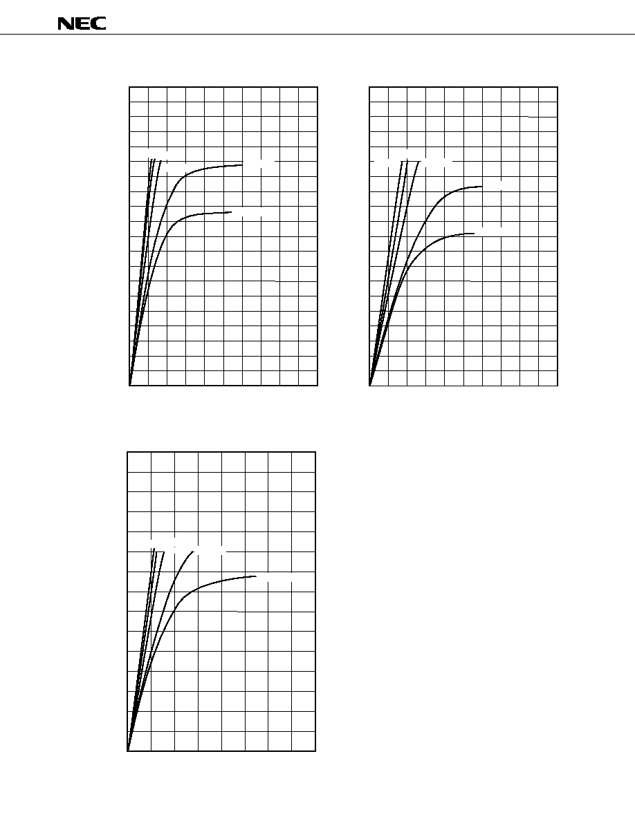
59
µ
PD75064, 75066, 75068, 75064(A), 75066(A), 75068(A)
I
OL
vs V
OL
(Port 3)
I
OL
vs V
OL
(Ports 4, 5)
40
30
20
10
0
0
2
(T
a
=25 ∞C)
V
OL
[V]
I
OL
[mA]
1
3
4
5
V
DD
=6 V V
DD
=5 V
V
DD
=4 V
V
DD
=3 V
V
DD
=2.7 V
40
30
20
10
0
0
2
(T
a
=25 ∞C)
V
OL
[V]
I
OL
[mA]
1
3
4
5
V
DD
=6 V
V
DD
=5 V
V
DD
=4 V
V
DD
=3 V
V
DD
=2.7 V
15
10
5
0
0
2
(T
a
=25 ∞C)
V
DD
- V
OH
[V]
I
OH
[mA]
1
3
4
V
DD
=6 V V
DD
=5 V
V
DD
=4 V V
DD
=3 V
V
DD
=2.7 V
I
OH
vs V
OH
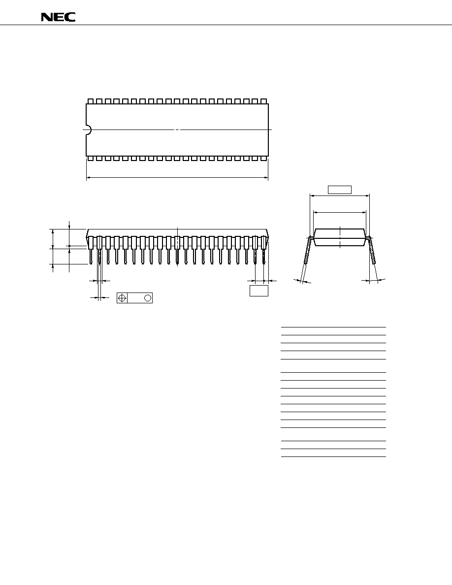
60
µ
PD75064, 75066, 75068, 75064(A), 75066(A), 75068(A)
12. PACKAGE DRAWINGS
42PIN PLASTIC SHRINK DIP (600 mil)
ITEM MILLIMETERS
INCHES
A
B
C
F
G
H
I
J
K
39.13 MAX.
1.778 (T.P.)
3.2±0.3
0.51 MIN.
4.31 MAX.
1.78 MAX.
0.17
15.24 (T.P.)
5.08 MAX.
N
0.9 MIN.
R
1.541 MAX.
0.070 MAX.
0.035 MIN.
0.126±0.012
0.020 MIN.
0.170 MAX.
0.200 MAX.
0.600 (T.P.)
0.007
0.070 (T.P.)
P42C-70-600A-1
A
C
D
G
NOTES
1) Each lead centerline is located within 0.17 mm (0.007 inch) of
its true position (T.P.) at maximum material condition.
D
0.50±0.10
0.020
M
0.25
0.010
+0.10
≠0.05
0~15∞
0~15∞
+0.004
≠0.003
+0.004
≠0.005
M
K
N
L
13.2
0.520
2) Item "K" to center of leads when formed parallel.
42
1
22
21
L
M
R
B
F
H
J
I
Remark The outline dimensions and materials of ES versions are the same as for mass-produced versions.
5
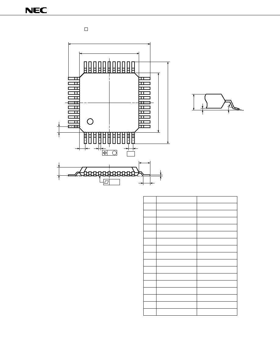
61
µ
PD75064, 75066, 75068, 75064(A), 75066(A), 75068(A)
44 PIN PLASTIC QFP ( 10)
N
A
M
F
B
33
34
22
L
44
1
12
11
23
D
C
P
detail of lead end
S
Q
5∞±5∞
G
M
I
J
H
K
P44GB-80-3B4-2
ITEM
MILLIMETERS
INCHES
A
B
C
D
F
G
H
I
J
K
L
13.6±0.4
10.0±0.2
1.0
0.35±0.10
0.15
10.0±0.2
0.535
0.039
0.039
0.006
0.031 (T.P.)
0.394
NOTE
M
N
0.12
0.15
1.8±0.2
0.8 (T.P.)
0.005
0.006
+0.004
≠0.003
Each lead centerline is located within 0.15
mm (0.006 inch) of its true position (T.P.) at
maximum material condition.
0.071
0.014
0.394
0.8±0.2
0.031
P
2.7
0.106
0.535
13.6±0.4
1.0
+0.009
≠0.008
Q
0.1±0.1
0.004±0.004
S
3.0 MAX.
0.119 MAX.
+0.008
≠0.009
+0.004
≠0.005
+0.008
≠0.009
+0.017
≠0.016
+0.017
≠0.016
+0.008
≠0.009
+0.10
≠0.05
Remark The outline dimensions and materials of ES versions are the same as for mass-produced versions.
5
62
µ
PD75064, 75066, 75068, 75064(A), 75066(A), 75068(A)
13. RECOMMENDED SOLDERING CONDITIONS
Solder the
µ
PD75064, 75066, 75068 under the soldering conditions indicated below.
For further information on the recommended soldering conditions, refer to information document "SEMI-
CONDUCTOR DEVICE MOUNTING TECHNOLOGY MANUAL (IEI-1207)".
For soldering methods and conditions other than those of recommended, consult NEC.
Table 13-1. Soldering Conditions for Surface Mounting Devices
µ
PD75064GB-
◊◊◊
-3B4 : 44-pin plastic QFP (10 x 10 mm)
µ
PD75066GB-
◊◊◊
-3B4 : 44-pin plastic QFP (10 x 10 mm)
µ
PD75068GB-
◊◊◊
-3B4 : 44-pin plastic QFP (10 x 10 mm)
µ
PD75064GB(A)-
◊◊◊
-3B4 : 44-pin plastic QFP (10 x 10 mm)
µ
PD75066GB(A)-
◊◊◊
-3B4 : 44-pin plastic QFP (10 x 10 mm)
µ
PD75068GB(A)-
◊◊◊
-3B4 : 44-pin plastic QFP (10 x 10 mm)
Soldering conditions
Peak temperature of package surface : 235
∞
C, Time : 30 seconds
max. (210
∞
C min.), Number of reflow processes : 2 or less
<Note>
(1) Start second reflow after the device temperature, which rose
because of the first reflow, has dropped to the normal level.
(2) Do not clean the flux with water after the first reflow.
Peak temperature of package surface : 215
∞
C, Time : 40 seconds
max. (200
∞
C min.), Number of reflow processes : 2 or less
<Note>
(1) Start second reflow after the device temperature, which rose
because of the first reflow, has dropped to the normal level.
(2) Do not clean the flux with water after the first reflow.
Solder temperature : 260
∞
C max., Time : 10 seconds max., Number
of reflow processes : 1
Preheating temperature : 120
∞
C max. (package surface temperature)
Pin temperature : 300
∞
C max., Time : 3 seconds max., (per one side
of device)
Soldering method
Infrared ray reflow
VPS
Wave soldering
Partial heating
Symbol
IR35-00-2
VP15-00-2
WS60-00-1
--
Caution Do not apply two or more soldering methods (except partial heating method) to the same device.
5
63
µ
PD75064, 75066, 75068, 75064(A), 75066(A), 75068(A)
Table 13-2. Soldering Conditions for Through-Hole Type Devices
µ
PD75064CU-
◊◊◊
: 42-pin plastic shrink DIP (600 mil)
µ
PD75066CU-
◊◊◊
: 42-pin plastic shrink DIP (600 mil)
µ
PD75068CU-
◊◊◊
: 42-pin plastic shrink DIP (600 mil)
µ
PD75064CU(A)-
◊◊◊
: 42-pin plastic shrink DIP (600 mil)
µ
PD75066CU(A)-
◊◊◊
: 42-pin plastic shrink DIP (600 mil)
µ
PD75068CU(A)-
◊◊◊
: 42-pin plastic shrink DIP (600 mil)
Soldering method
Wave soldering
(Only leads)
Partial heating
Soldering conditions
Soldering bath temperature : 260
∞
C max., Time : 10 seconds max.
Pin temperature : 300
∞
C max., Time : 3 seconds max. (per pin)
Caution Solder only the leads by means of wave soldering , and exercise care that the jetted solder does
not come in contact with the package.

64
µ
PD75064, 75066, 75068, 75064(A), 75066(A), 75068(A)
APPENDIX A. DEVELOPMENT TOOLS
The following development tools are provided for the development of a system which employs the
µ
PD75064, 75066, 75068, 75064(A), 75066(A), 75068(A).
Notes 1. Available for maintenance only
2. The IE-75000-R-EM is not installed in the IE-75001-R.
3. Ver. 5.00/5.00A has the task swap function, but it cannot be used with this software.
OS for IBM PC
The following products are supported as OS for IBM PCs.
OS
Version
PC DOS
TM
Ver. 5.02 to Ver. 6.1
MS-DOS
Ver. 3.30 to Ver. 5.00
Note1
, 5.0/V
Note2
IBM DOS
TM
J5.02/V
Note2
Notes 1. Ver. 5.0 and later have the task swap function, but it cannot be used with this software.
2. Only the English mode is supported.
Remark
For development tools supplied by third-party manufacturers, refer to 75X Series Selection Guide
(IF-1027).
In-circuit emulator for 75X series
Emulation board for IE-75000-R or IE-75001-R
Emulation probe for all shrink DIP versions of this series
Emulation probe for all QFP versions of this series. A 44-pin conversion
socket EV-9200G-44 is contained in this product.
PROM programming equipment
An adapter for connecting the PG-1500 to the
µ
PD75P068CU/GB.
Host machines:
PC-9800 series (MS-DOS
TM
Ver. 3.30 to Ver. 5.00A
Note3
)
IBM PC/AT
TM
(refer to OS for IBM PC)
IE-75000-R
Note1
IE-75001-R
IE-75000-R-EM
Note2
EP-75068CU-R
EP-75068GB-R
EV-9200G-44
PG-1500
PA-75P008CU
IE control program
PG-1500 controller
RA75X relocatable assem-
bler
Hardware
Software
5
65
µ
PD75064, 75066, 75068, 75064(A), 75066(A), 75068(A)
APPENDIX B. RELATED DOCUMENTS
The related documents indicated in this publication may include preliminary versions. However,
preliminary versions are not marked as such.
Documents related to device
Document
Doc. No.
User's Manual
IEU-1366
Instruction Quick Reference
--
Application Note
IEA-1296
75X Series Selection Guide
IF-1027
Documents related to development tool
Document
Doc. No.
Hardware
IE-75000-R/IE-75001-R User's Manual
EEU-1416
IE-75000-R-EM User's Manual
EEU-1294
EP-75068CU-R User's Manual
EEU-1429
EP-75068GB-R User's Manual
EEU-1428
PG-1500 User's Manual
EEU-1335
Software
RA75X Assembler Package User's Manual
Operation
EEU-1346
Language
EEU-1363
PG-1500 Controller User's Manual
EEU-1291
Other related documents
Document
Doc. No.
Package Manual
IEI-1231
Semiconductor Device Mounting Technology Manual
IEI-1207
Quality Grades on NEC Semiconductor Devices
IEI-1209
NEC Semiconductor Device Reliability/Quality Control System
--
Electrostatic Discharge (ESD) Test
--
Guide to Quality Assurance for Semiconductor Devices
MEI-1202
Microcomputer-Related Product Guide - Third Party Products
--
Caution The contents of the documents listed above are subject to change without prior notice to users.
Make sure to use the latest edition when starting design.

66
µ
PD75064, 75066, 75068, 75064(A), 75066(A), 75068(A)
[MEMO]
67
µ
PD75064, 75066, 75068, 75064(A), 75066(A), 75068(A)
NOTES FOR CMOS DEVICES
1 PRECAUTION AGAINST ESD FOR SEMICONDUCTORS
Note: Strong electric field, when exposed to a MOS device, can cause destruc-
tion of the gate oxide and ultimately degrade the device operation. Steps
must be taken to stop generation of static electricity as much as possible,
and quickly dissipate it once, when it has occurred. Environmental control
must be adequate. When it is dry, humidifier should be used. It is recom-
mended to avoid using insulators that easily build static electricity. Semi-
conductor devices must be stored and transported in an anti-static con-
tainer, static shielding bag or conductive material. All test and measure-
ment tools including work bench and floor should be grounded. The opera-
tor should be grounded using wrist strap. Semiconductor devices must
not be touched with bare hands. Similar precautions need to be taken for
PW boards with semiconductor devices on it.
2 HANDLING OF UNUSED INPUT PINS FOR CMOS
Note: No connection for CMOS device inputs can be cause of malfunction. If no
connection is provided to the input pins, it is possible that an internal input
level may be generated due to noise, etc., hence causing malfunction.
CMOS devices behave differently than Bipolar or NMOS devices. Input
levels of CMOS devices must be fixed high or low by using a pull-up or pull-
down circuitry. Each unused pin should be connected to V
DD
or GND with a
resistor, if it is considered to have a possibility of being an output pin. All
handling related to the unused pins must be judged device by device and
related specifications governing the devices.
3 STATUS BEFORE INITIALIZATION OF MOS DEVICES
Note: Power-on does not necessarily define initial status of MOS device. Pro-
duction process of MOS does not define the initial operation status of the
device. Immediately after the power source is turned ON, the devices
with reset function have not yet been initialized. Hence, power-on does
not guarantee out-pin levels, I/O settings or contents of registers. Device
is not initialized until the reset signal is received. Reset operation must be
executed immediately after power-on for devices having reset function.

µ
PD75064, 75066, 75068, 75064(A), 75066(A), 75068(A)
MS-DOS is a trademark of Microsoft Corporation.
IBM DOS, PC/AT, and PC DOS are trademarks of IBM Corporation.
No part of this document may be copied or reproduced in any form or by any means without the prior written
consent of NEC Corporation. NEC Corporation assumes no responsibility for any errors which may appear in this
document.
NEC Corporation does not assume any liability for infringement of patents, copyrights or other intellectual
property rights of third parties by or arising from use of a device described herein or any other liability arising
from use of such device. No license, either express, implied or otherwise, is granted under any patents,
copyrights or other intellectual property rights of NEC Corporation or others.
The devices listed in this document are not suitable for use in aerospace equipment, submarine cables, nuclear
reactor control systems and life support systems. If customers intend to use NEC devices for above applications
or they intend to use "Standard" quality grade NEC devices for applications not intended by NEC, please contact
our sales people in advance.
Application examples recommended by NEC Corporation
Standard: Computer, Office equipment, Communication equipment, Test and Measurement equipment,
Machine tools, Industrial robots, Audio and Visual equipment, Other consumer products, etc.
Special:
Automotive and Transportation equipment, Traffic control systems, Antidisaster systems, Anticrime
systems, etc.
M4 92.6