 | –≠–ª–µ–∫—Ç—Ä–æ–Ω–Ω—ã–π –∫–æ–º–ø–æ–Ω–µ–Ω—Ç: UPD75116A | –°–∫–∞—á–∞—Ç—å:  PDF PDF  ZIP ZIP |

Description
The
µ
PD75116(A) is one of the 4-bit single-chip micro-
computer 75X series.
The
µ
PD75116(A) is a product with the extended ROM
capacity of the
µ
PD75108(A). In addition of high-speed
operations, it can manipulate data in units of 1, 4 and 8
bits. In particular, the I/O operation of the
µ
PD75116
have been improved by a wide variety of bit control
instructions. The
µ
PD75116 is provided with interface
inputs/outputs with peripheral circuits having different
power voltages, and analog inputs and suitable for
controlling automobile electrical equipment, etc. For
the
µ
PD75116(A), an on-chip pin-compatible one-time
PROM product (
µ
PD75P116) is separately available for
system development evaluation.
Functions are described in detail in the following User's
Manual, which should be read when carrying out
design work.
µ
PD751
◊◊
Series User's Manual: IEM-992
Features
∑
Higher reliability than
µ
PD75116
∑
Architecture "75X" equivalent to 8-bit microcomputer
∑
Minimum instruction execution time (high-speed
operation): 0.95
µ
s (when operated at 4.19 MHz and
5 V)
∑
Instruction execution variable function: 0.95
µ
s/1.91
µ
s/
15.3
µ
s (when operated at 4.19 MHz)
∑
Many input/output ports: 58
∑
3-channel on-chip 8-bit timers
∑
8-bit on-chip serial interface
∑
Multi-interruptible vector interrupt function
Applications
Automobile electrical equipment, etc.
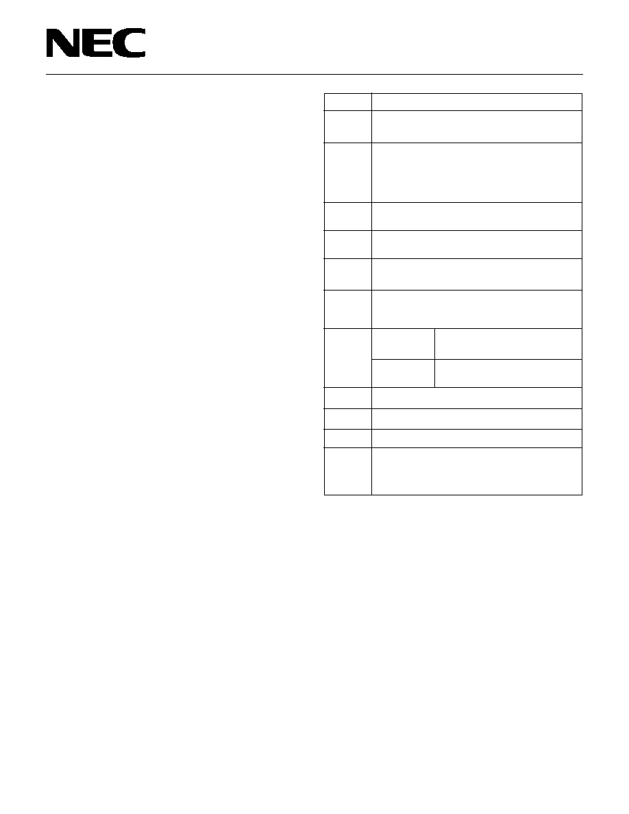
Data Sheet
µ
PD75112(A), 75116(A)
4-Bit Single Chip-Microcomputer
©NEC Corporation 1990
Qualty Grade
Special
Special
Special
Special
Package
64-pin plastic shrink DIP
(750 mil)
64-pin plastic QFP
(14
◊
20 mm)
64-pin plastic shrink DIP
(750 mil)
64-pin plastic QFP
(14
◊
20 mm)
Ordering Code
µ
PD75112CW(A)-
◊◊◊
µ
PD75112GF(A)-
◊◊◊
-3BE
µ
PD75116CW(A)-
◊◊◊
µ
PD75116GF(A)-
◊◊◊
-3BE
Remarks:
◊◊◊
is a ROM code number.
Please refer to "Quality Grade on NEC Semicon-
ductor Devices" (Document number IEI-1209) pub-
lished by NEC Corporation to know the specifica-
tion of quality grade on the devices and its recom-
mended applications.
Unless there are any particular functional differences,
the
µ
PD75116(A) is described in this document as a
representative product.
The information in this document is subject to change without notice.
The mark
5
shows major revised points.
Document No. IC-2811A
(O. D. No. IC-8261A)
Date Published March 1994 P
Printed in Japan

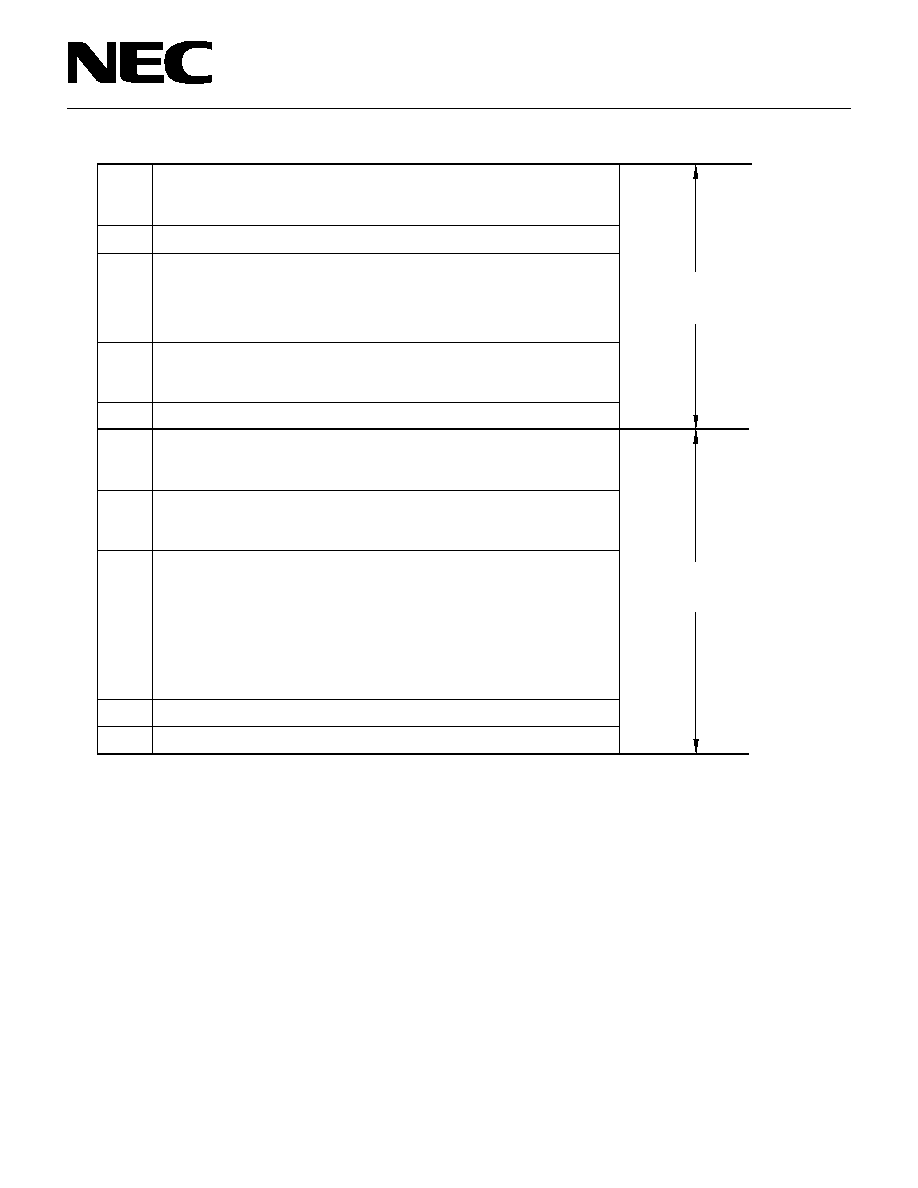
2
µ
PD75112(A), 75116(A)
Item
No. of basic instruction
Min. instruction execution time
On-chip memory
General register
Accumulator
Input/output port
Timer/counter
Serial interface
Vector interrupt
Test input
Standby
Operating temperature range
Operating voltage
Others
Package
Description
43
0.95
µ
s/1.91
µ
s/15.3
µ
s (when operated at 4.19 MHz), switchable at 3 levels
12160
◊
8 (
µ
PD75112(A)), 16256
◊
8 (
µ
PD75116(A))
512
◊
4
4 bits
◊
8
◊
4 banks (memory mapping)
Three accumulated in compliance with controlled date lengths
∑
1-bit accumulator (CY), 4-bit accumulator (A), 8-bit accumulator (XA)
58 in total
∑
CMOS input pin
:
10
∑
CMOS input/output pin (LED direct drive enable) :
32
∑
Intermediate withstand voltage N-ch open drain :
12
input/output pin (bit-wise pull-up resistor inscorporation possible)
∑
Comparator input pin (4-bit accuracy)
:
4
∑
8-bit timer/event counter
◊
2
∑
8-bit basic interval timer (applicable to watchdog timer)
∑
8-bits
∑
First LSB/first MSB switchable
∑
Two transfer modes (transmit and receiver/receive dedicated mode)
External : 3,
Internal : 4
External : 2
∑
STOP/HALT mode
-40 to +85
∞
C
2.7 to 6.0 V
∑
On-chip power-on reset circuit (mask option)
∑
On-chip bit contol memory (bit sequential buffer)
∑
64-pin plastic shrink DIP (750 mil)
∑
64-pin plastic QFP (14
◊
20 mm)
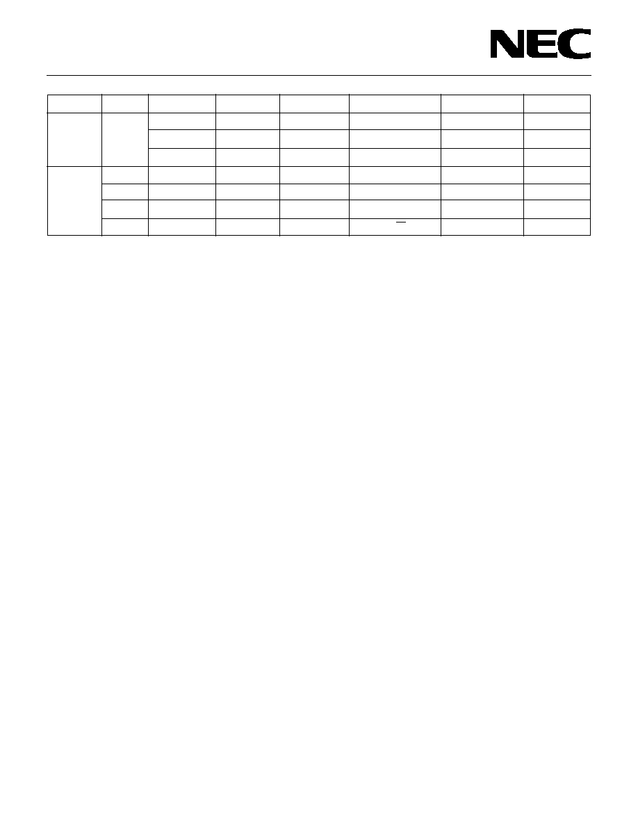
Defferences between
µ
PD75112(A), 75116(A) and
µ
PD75112, 75116
Item
Quality grade
Electrical specifications
Direct LED drive
Outline of Functions
ROM
RAM
Absolute maximum ratings
DC characteristics
µ
PD75112(A), 75116(A)
Special
Different high-level output current and low-level output current
Different low-level output voltage
Not possible
Product Name
µ
PD75112, 75116
Standard
Possible

3
µ
PD75112(A), 75116(A)
CONTENTS
1.
Pin Configuration (Top View)............................................................................................... 4
2.
Block Diagram......................................................................................................................... 6
3.
Pin Functions......................................................................................................................... 7
3.1
Port Pins...................................................................................................................................................... 7
3.2
Non-Port Pins............................................................................................................................................... 8
3.3
Pin Input/Output Circuits............................................................................................................................ 9
3.4
Recommended Connection of Unused Pins............................................................................................. 10
3.5
Caution Relating to Use of P00/INT4 Pin and RESET Pin........................................................................ 10
4.
Memory Configuration............................................................................................................. 11
5.
Peripheral Hardware Functions.............................................................................................. 14
5.1
Digital Input/Output Port......................................................................................................................... 14
5.2
Clock Generator......................................................................................................................................... 14
5.3
Clock Output Circuit.................................................................................................................................. 16
5.4
Basic Interval Timer.................................................................................................................................... 16
5.5
Timer/Event Counter................................................................................................................................. 17
5.6
Serial Interface............................................................................................................................................ 19
5.7
Programmable Threshold Port (Analog Input Port)............................................................................... 21
5.8
Bit Sequential Buffer................................................................................................................................... 22
5.9
Power-On Flag (Mask Option).................................................................................................................... 22
6.
Interrupt Functions.................................................................................................................. 23
7.
Standby Functions ............................................................................................................... 25
8.
Reset Functions..................................................................................................................... 26
9.
Instruction Set....................................................................................................................... 29
10. Mask Option Selection.......................................................................................................... 37
11. Electrical Specifications........................................................................................................ 38
12. Package Information ............................................................................................................ 48
13. Recommended Soldering Conditions ................................................................................. 51
APPENDIX A. Diffeences between
µ
PD751
◊◊
(A) Series Products
and Related PROM Products.............................................................................. 52
APPENDIX B. Development Tools ............................................................................................ 53
APPENDIX C. Related Documentations ................................................................................... 54
4
µ
PD75112(A), 75116(A)
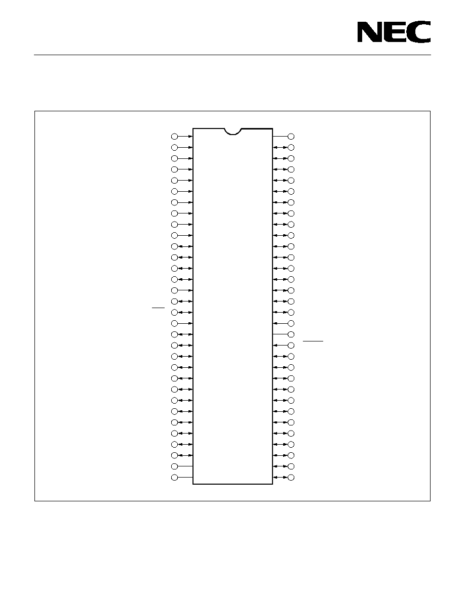
1. Pin Configuration (Top View)
64-Pin Plastic Shrink DIP (750 mil)
1
P13/INT3
2
P12/INT2
3
P11/INT1
4
P10/INT0
5
PTH03
6
PTH02
7
PTH01
8
PTH00
9
TI0
10
TI1
11
P23
12
P22/PCL
13
P21/PTO1
14
P20/PTO0
15
P03/SI
16
P02/SO
17
P01/SCK
18
P00/INT4
19
P123
20
P122
21
P121
22
P120
23
P133
24
P132
25
P131
26
P130
27
P143
28
P142
29
P141
30
P140
31
NC
32
V
DD
64
63
62
61
60
59
58
57
56
55
54
53
52
51
50
49
48
47
46
45
44
43
42
41
40
39
38
37
36
35
34
33
V
SS
P90
P91
P92
P93
P80
P81
P82
P83
P70
P71
P72
P73
P60
P61
P62
P63
X1
X2
RESET
P50
P51
P52
P53
P40
P41
P42
P43
P30
P31
P32
P33
µ
PD75112CW(A)-
◊◊◊
µ
PD75116CW(A)-
◊◊◊
5
µ
PD75112(A), 75116(A)
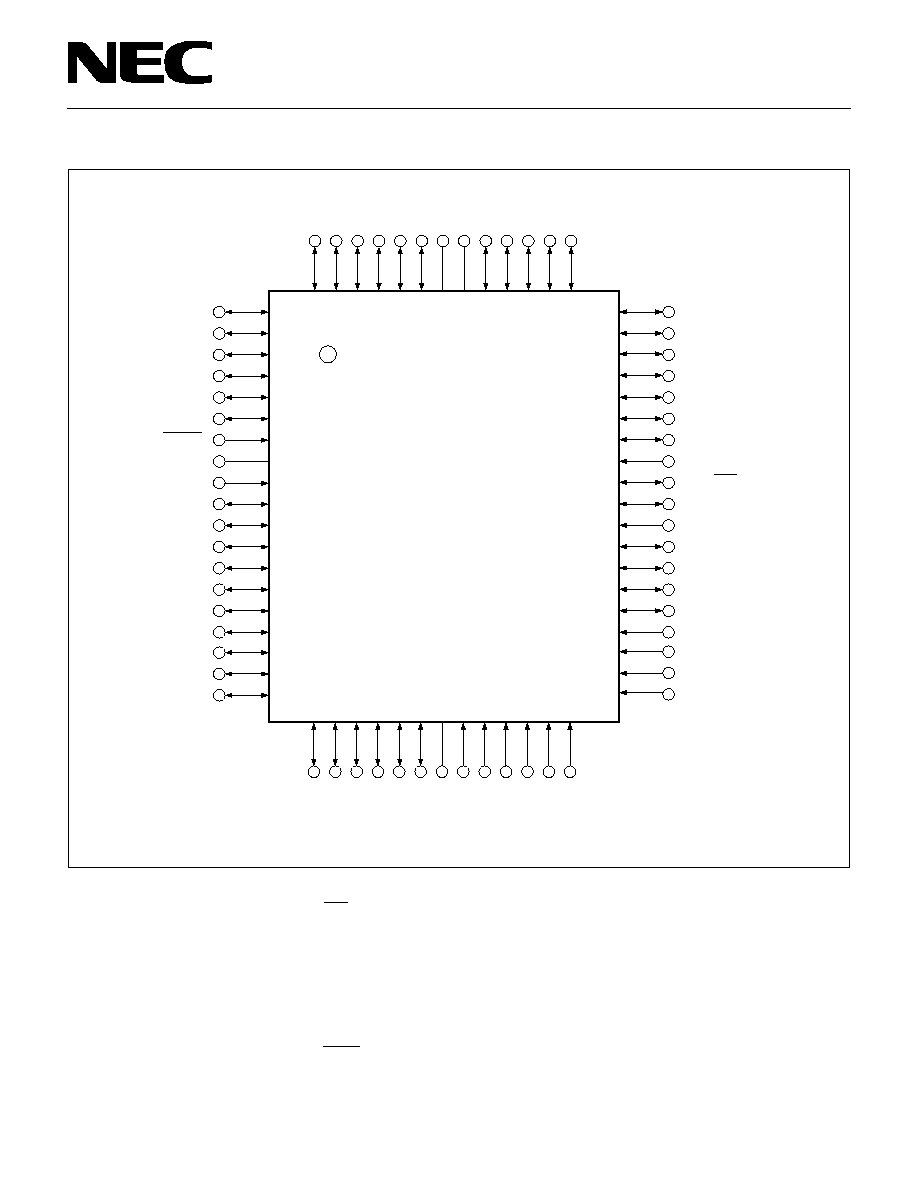
1
2
3
4
5
6
7
8
9
10
11
12
13
14
15
16
P131
P132
P133
P120
P121
P122
P123
P00/INT4
P02/SO
P01/SCK
P03/SI
P20/PTO0
P21/PTO1
P22/PCL
P23
T11
X2
X1
P41
P40
P53
P52
P51
P50
RESET
P63
P62
P61
P60
P73
P72
P71
20 21 22 23 24 25 26 27 28 29 30 31 32
64 63 62 61 60 59 58 57 56 55 54 53 52
51
50
49
48
47
46
45
44
43
42
41
40
39
38
37
36
P42
P43
P30
P31
P32
P33
V
DD
NC
P140
P141
P142
P143
P130
P81
P80
P93
P92
P91
P90
V
SS
P13/INT3
P12/INT2
P11/INT1
P10/INT0
PTH03
PTH02
17
18
19
P70
P83
P82
T10
PTH00
PTH01
35
34
33
64-Pin Plastic QFP (14
◊
20 mm)
µ
PD75112GF(A)-
◊◊◊
-3BE
µ
PD75116GF(A)-
◊◊◊
-3BE
Pin Name
P00-P03
: Port0
SCK
: Serial Clock
P10-P13
: Port1
SO
: Serial Output
P20-P23
: Port2
SI
: Serial Input
P30-P33
: Port3
PTO0, PTO1
: Programmable Timer Output
P40-P43
: Port4
PCL
: Programmable Clock
P50-P53
: Port5
PTH00-PTH03
: Programmable Threshold Input
P60-P63
: Port6
INT0, INT1, INT4
: External Vectored Interrupt Input
P70-P73
: Port7
INT2, INT3
: External Test Input
P80-P83
: Port8
TI0, TI1
: Timer Input
P90-P93
: Port9
X1, X2
: Clock Oscillation
P120-P123
: Port12
RESET
: Reset
P130-P133
: Port13
NC
: No Connection
P140-P143
: Port14
V
DD
: Positive Power Supply
V
SS
: Ground
5
6
µ
PD75112(A), 75116(A)
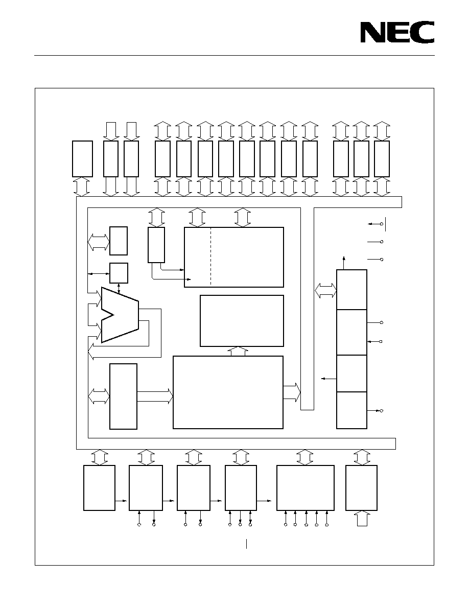
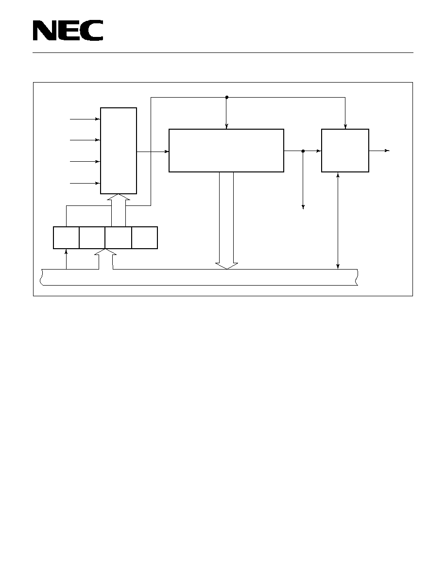
2.
Block Diagram
ROM
PROGRAM
MEMORY
12160
◊
8 BITS
(
PD75112(A))
16256
◊
8 BITS
(
PD75116(A))
µ
P00-P03
P10-P13
PORT0
PORT1
4
P20-P23
4
P30-P33
4
P40-P43
4
P50-P53
4
P60-P63
4
P70-P73
4
P80-P83
4
P90-P93
4
P120-P123
4
P130-P133
4
P140-P143
4
4
BIT SEQ.
BUFFER(16)
PORT2
PORT4
PORT3
PORT5
PORT6
PORT7
PORT8
PORT9
PORT12
PORT13
PORT14
GENERAL REG.
BANK
SP (8)
CY
ALU
RAM
DATA MEMORY
512
◊
4 BIT
DECODE
AND
CONTROL
TIMER/EVENT
COUNTER
# 0
TIMER/EVENT
COUNTER
# 1
SERIAL
INTERFACE
CLOCK
OUTPUT
CONTROL
CLOCK
DIVIDER
CLOCK
GENERATOR
STAND BY
CONTROL
CPU CLOCK
PCL/P22
f
X
/2
X1
X2
RESET
V
SS
V
DD
BASIC
INTERVAL
TIMER
INTBT
TI0
PTO0/P20
TI1
PTO1/P21
SI/P03
SI/P02
INT0/P10
INT1/P11
INT2/P12
INT3/P13
INT4/P00
4
PTH00-PTH03
SCK/P01
INTT0
INTT1
INTSIO
INTERRUPT
CONTROL
PROGRAMMABLE
THRESHOLD
PORT # 0
PROGRAM
COUNTER (14)
µ
N

7
µ
PD75112(A), 75116(A)
3. Pin Functions
3.1 Port Pins
Pin Name
P00
P01
P02
P03
P10
P11
P12
P13
P20
P21
P22
P23
P30 to P33
P40 to P43
P50 to P53
P60 to P63
P70 to P73
P80 to P83
P90 to P93
P120 to P123
P130 to P133
P140 to P143
Function
4-bit input port (PORT0)
4-bit input port (PORT1)
4-bit input/output port (PORT2)
Programmable 4-bit input/output port (PORT3)
Bit-wise input/output setting enable
4-bit input/output port (PORT4)
4-bit input/output port (PORT5)
Programmable 4-bit input/output port (PORT6)
Bit-wise input/output setting enable
4-bit input/output port (PORT7)
4-bit input/output port (PORT8)
4-bit input/output port (PORT9)
N-ch open drain 4-bit input/ output port (PORT12)
Bit-wise pull-up resistor incorporation enable
(mask option)
2 V withstand for open drain
N-ch open drain 4-bit input/ output port (PORT13)
Bit-wise pull-up resistor incorporation enable
(mask option)
12 V withstand for open drain
N-ch open drain 4-bit input/output port (PORT14)
Bit-wise pull-up resistor incorporation enable
(mask option)
12 V withstand for open drain
I/O Circuit
Type *1
B
F
E
B
B
E
E
E
E
E
E
E
E
M
M
M
Input/ Output
Input
Input/output
Input/output
Input
Input
Input/output
Input/output
Input/output
Input/output
Input/output
Input/output
Input/output
Input/output
Input/output
Input/output
Input/output
8-Bit I/O
◊
◊
q
q
q
q
q
q
q
q
At Reset
Input
Input
Input
Input
Input
Input
Input
Input
Input
Input
Input*2
Input*2
Input*2
*
1: Circles indicate Schmitt trigger inputs.
2: High impedance for open drain
High level for on-chip pull-up resistors
Dual
Function Pin
INT4
SCK
SO
SI
INT0
INT1
INT2
INT3
PTO0
PTO1
PCL

8
µ
PD75112(A), 75116(A)
PTH00 to PTH03
TI0
TI1
PTO0
PTO1
SCK
SO
SI
INT4
INT0
INT1
INT2
INT3
PCL
X1, X2
RESET
NC*2
V
DD
V
SS
3.2 Non-Port Pins
Dual
Function
Pin
P20
P21
P01
P02
P03
P00
P10
P11
P12
P13
P22
I/O
Circuit
Type*1
N
B
E
F
E
B
B
B
B
E
B
At Reset
Input
Input
Input
Input
Input
Input
Input
Input
Input/Output
Input
Input
Input/output
Input/output
Input/output
Input
Input
Input
Input
Input/output
Input
Function
Threshold voltage ariable 4-bit analogy input port.
External event pulse input for the timer/event counter or edge
detect vector interrupt input. 1-bit input enable.
Timer/event counter output.
Serial clock input/output.
Serial data output.
Serial data input.
Edge detect vector interrupt input (for detecting both rising and
falling edges).
Edge detect vector interrupt input (detected edge selectable).
Edge detect testable input (for rising edge detection).
Clock output.
Crystal/ceramic connect pin (system clock oscillation).
In case with the external clock, input a signal to X1 and the
antiphase to X2.
System reset input (low level active).
No Connection
Positive power supply.
GND potential.
* 1: Circles indicate Schmitt trigger inputs.
2: When the PWB is shared with the
µ
PD75P116, connect the NC pin to V
DD
directly.
9
µ
PD75112(A), 75116(A)
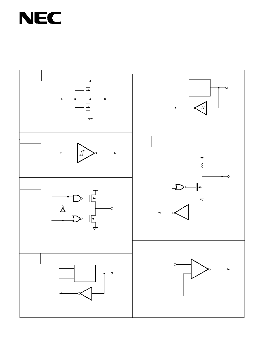
Type F
Input/output circuit consisting of a Type D push-pull output
and a Type B Schmitt-triggered input.
Type M
Pull-Up Register (Mask Option)
N-ch (+6 V
Withstand)
Middle-High Voltage Input Buffer (+6 V Withstand)
Type N
Comparator
V
REF
(Threshold Voltage)
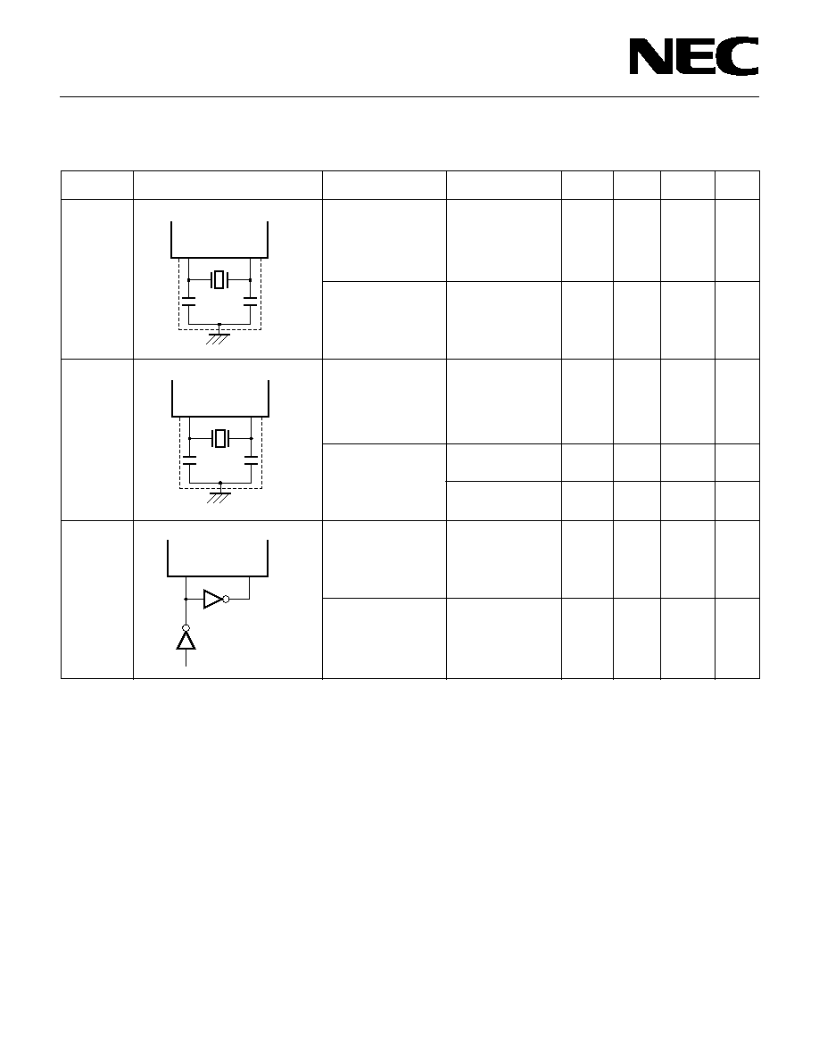
3.3 Pin Input/Output Circuits
µ
PD75116(A) pin input/output crcuit are shown in sche-
matic form.
Figure 3-1 Pin Input/Output Circuits
IN/OUT
data
output
disable
Type D
Type B
P-ch
V
DD
IN
N-ch
IN
+
≠
IN
P-ch
V
DD
OUT
N-ch
data
output
disable
IN/OUT
data
output
disable
Type D
Type A
IN/OUT
V
DD
data
output
disable
Type A
CMOS specified input buffer
Type B
Schmitt triggered-input with hysteresis characteristics
Type D
Push-pull output which can be set at output high impedance
(with both P-ch an N-ch set to OFF)
Type E
Input/output circuit consisting of a Type D push-pull output
and a Type A input buffer

10
µ
PD75112(A), 75116(A)
3.5 Caution Relating to Use of P00/INT4 Pin and RESET Pin
In addition to the functions described in sections 3.1
and 3.2, the P00/INT4 pin and the RESET pin have the
function to set the IC test mode for testing the
µ
PD75116(A) internal operations.
When a voltage larger than V
DD
is applied to one of
these two pins, the test mode is set. Thus, if noise
exceeding V
DD
is applied even during normal opera-
tions, the test mode is set and normal operations may
be discontinued.
For example, if a cable from the P00/INT4 or RESET pin
is too long, inter-wiring noise may be applied to the pin,
the pin voltage may become larger than V
DD
, causing
malfunctioning.
Thus, carry out wiring to minimize inter-wiring noise. If
the noise cannot be suppressed completely, carry out
the following countermeasure against noise using an
externally mounted component.
o Connect a diode with low V
F
(max 0.3 V)between V
DD
s
Diode with low V
F
o Connect acapacitor between V
DD
s
3.4 Recommended Connection of Unused Pins
Pin
PTH00 to PTH03
TI0
TI1
P00
P01 to P03
P10 to P13
P20 to P23
P30 to P33
P40 to P43
P50 to P53
P60 to P63
P70 to P73
P80 to P83
P90 to P93
P120 to P123
P130 to P133
P140 to P143
RESET
NC
*1: Only when a power-on reset generator is built in by mask
option, connect t V
DD
.
2: When the PWB is shared with the
µ
PD75P116, connect the
NC pin to V
DD
directly.
Recommended Connecting Method
Connect to V
SS
or V
DD
Connect to V
SS
Connect to V
SS
or V
DD
Connect to V
SS
Input state
: Connect to V
SS
or V
DD
Output state : Leave open
Connect to V
DD
*1
Leave open or connect to V
DD
*2
V
DD
V
DD
P00/INT4, RESET
V
DD
V
DD
P00/INT4, RESET
11
µ
PD75112(A), 75116(A)
4. Memory Configuration
∑
Program Memory (ROM)
12160
◊
8 bits (0000H to 2F7FH):
µ
PD75112(A)
16256
◊
8 bits (0000H to 3F7FH):
µ
PD75116(A)
∑
0000H to 0001H: Vector table for writing the
program start address by reset
∑
0002H to 000BH: Vector table for writing the
program start address by interrupt
Remarks: In all other cases, the program can be
branched by the BR PCDE and BR PCXA
∑
0020H to 007FH: Table area to be referred to
by the GETI instruction
∑
Data Memory
∑
Data area
512
◊
4 bits (000H to 1FFH)
∑
Peripheral hardware area
128
◊
4 bits (F80H to FFFH)
instructions to an address with only the
lower 8 bits of PC changed.
Figure 4-1 Program Memory Map (
µ
PD75112(A))
Address
MBE RBE
MBE RBE
MBE
MBE RBE
MBE RBE
MBE RBE
0000H
0002H
0004H
0006H
0008H
000AH
0020H
007FH
0080H
07FFH
0FFFH
7
6
0
Internal Reset Start Address
Internal Reset Start Address (Low-Order 8 Bits)
INT0/INT1 Start Address (High-Order 6 Bits)
INT0/INT1 Start Address
(Low-Order 8 Bits)
(Low-Order 8 Bits)
INTSIO Start Address (High-Order 6 Bits)
INTSIO Start Address
(Low-Order 8 Bits)
INTT0 Start Address (High-Order 6 Bits)
INTT0 Start Address
(Low-Order 8 Bits)
INTT1 Start Address (High-Order 6 Bits)
INTT1 Start Address
GETI Instruction Reference Table
CALLF
! faddr
Instruction
Entry
Address
BRCB
! caddr
Instruction
Branch
Address
BR !addr
Instruction
Branch
Address
CALL !addr
Instruction
Subroutin
Entry
Address
BRCB !caddr Instruction
Branch Address
(High-Order 6 Bits)
RBE
INTBT/INT4 Start Address (High-Order 6 Bits)
INTBT/INT4 Start Address
(Low-Order 8 Bits)
2000H
1FFFH
2F7FH
0800H
1000H
BRCB !caddr Instruction
Branch Address
BR $addr
Instruction
Relative
Branch Address
(-15 to +16)
Branch Address
Subroutine Entry
Address by GETI
Instruction
12
µ
PD75112(A), 75116(A)
Figure 4-2 Program Memory Map (
µ
PD75116(A))
Address
Remarks
:
In all other cases, the program can be
branched by the BR PCDE and BR PCXA
instructions to an address with only the lower
8 bits of PC changed.
MBE RBE
MBE RBE
MBE
MBE RBE
MBE RBE
MBE RBE
0000H
0002H
0004H
0006H
0008H
000AH
0020H
007FH
0080H
07FFH
0FFFH
7
6
0
Internal Reset Start Address
Internal Reset Start Address (Low-Order 8 Bits)
INT0/INT1 Start Address (High-Order 6 Bits)
INT0/INT1 Start Address
(Low-Order 8 Bits)
(Low-Order 8 Bits)
INTSIO Start Address (High-Order 6 Bits)
INTSIO Start Address
(Low-Order 8 Bits)
INTT0 Start Address (High-Order 6 Bits)
INTT0 Start Address (High-Order 6 Bits)
INTT1 Start Address (High-Order 6 Bits)
INTT1 Start Address
GETI Instruction Reference Table
CALLF
! faddr
Instruction
Entry
Address
BRCB
! caddr
Instruction
Branch
Address
BR !addr
Instruction
Branch
Address
CALL !addr
Instruction
Subroutin
Entry
Address
BRCB !caddr Instrucion
Branch Address
(High-Order 6 Bits)
RBE
INTBT/INT4 Start Address (High-Order 6 Bits)
INTBT/INT4 Start Address
(Low-Order 8 Bits)
2000H
1FFFH
3000H
2FFFH
3F7FH
0800H
1000H
BRCB !caddr Instruction
Branch Address
BR $addr
Instruction
Relative
Branch Address
(-15 to ≠1
+2 to +16)
BRCB !caddr Instrucion
Branch Address
Branch Address
Subroutine Entry
Address by GETI
Instruction

13
µ
PD75112(A), 75116(A)
Figure 4-3 Data Memory Map
Memory Bank
Data Memory
000H
01FH
0FFH
100H
1FFH
F80H
FFFH
Bank 0
Bank 1
Bank 15
256
◊
4
128
◊
4
256
◊
4
(32
◊
4)
General
Regoster Area
Stack Area
Data Area
Static RAM
(512
◊
4)
Peripheral Hardware
Area
Not Incorporated
14
µ
PD75112(A), 75116(A)
Table 5-1 Functions of Digital Ports
Remarks
Share the pins with SI, SO, SCK and
INT0 to 4.
Port 2 shares the pin with PTO0,
PTO1 and PCL.
On-chip pull-up registers can be
specified bit-wise by mask option.
5. Peripheral Hardware Functions
5.1 Digital Input/Output Port
The digital input/output port has the following tree types.
∑
CMOS input (PORT0, 1)
:
8
∑
CMOS input/output (PORT 2 to PORT 9)
: 32
∑
N-ch open-drain input/output (PORT 12 to PORT 14): 12
Total
52
Functions
4-bit input
4-bit input/
output
4-bit input/
output
(N-ch open-
drain, 12 V
withstand
voltage)
Port (Code)
PORT0
PORT1
PORT3
PORT6
PORT2
PORT4
PORT5
PORT7
PORT8
PORT9
PORT12
PORT13
PORT14
Operations and Features
Read or test always enable irrespectively of the operating mode
of dual-function pins.
Can be set bit-wise to the input or output mode.
Can be set in 4-bit units to the input or output mode.
Ports 4 and 5, 6 and 7, 8 and 9 can form pairs and data can be
input/output in 8-bit units.
Can be set in 4-bit units the input or output mode.
Ports 12 and 13 can form a pair and data can be input/output in 8-
bit units.
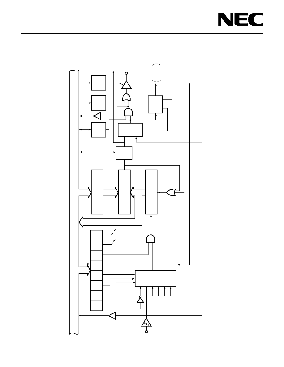
5.2 Clock Generator
The clock generator is a circuit which supplies the CPU
and peripheral hardware with various clocks and con-
trols the CPU operating mode.
The instruction execution time can be changed.
∑
0.95
µ
s/1.91
µ
s/15.3
µ
s (at 4.19 MHz operation)

15
µ
PD75112(A), 75116(A)
Figure 5-1 Block Diagram of Clock Generator
∑
Basic Interval Timer (BT)
∑
Clock Generator
∑
Timer/Event Counter
∑
Serial Interface
∑
Clock Output Circuit
S
R
Q
1/4
S
STOP F/F
HALT F/F
Q
R
1/2 1/16
1/8 to 1/4096
PCC
fx
fxx or
PCC0
PCC1
PCC2
PCC3
PCC2,
PCC3
Crear
STOP*
HALT*
4
∑ CPU
∑ Clock Output Circuit
Inter-
nal
Bus
System
Clock
Oscillator
Oscillation Stop
Frequency Divider
Selec-
tor
Frequency
Divider
Wait Release Signal from BT
RES(Internal Reset) Signal
Standby Release Signal from
the Interrupt Control Circuit
Remarks 1: f
XX
=crystal/ceramic oscillator frequency.
2: f
X
=external clock frequency.
3:
=CPU clock
4: *indicates instruction execution.
5: PCC (processor clock control register)
6: 1 clock cycle (t
CY)
of
is 1 michine cycle of the instruc-
tion. For t
CY
, see the AC characteristics in the 11."Elec-
trical Specifications".
5
16
µ
PD75112(A), 75116(A)
5.4 Basic Interval Timer
The basic interval timer has the following functions;
∑
Interval timer operation to generate reference
time interrupts
∑
Watchdog timer application to detect program
overrun
∑
Wait time selection and count when the standby
mode is released
∑
Count content read
5.3 Clock Output Circuit
The clock output circuit is a circuit to generate clock
pulses from the P22/PCL pin. It is used to supply the
peripheral LSIs with clock pulses.
∑
Clock output (PCL):
, 524 kHz, 262 kHz (at 4.19 MHz
operation)
The clock output cicuit configuration is shown as the
following.
Figure 5-2 Clock Output Circuit Configuration
PORT2.2
CLOM3
CLOM1 CLOM0
fxx/2
CLOM
0
4
3
fxx/2
4
From the Clock
Generator
Selector
Internal Bus
P22
Output Latch
Port 2 Input/
Output Mode
Specification Bit
PMGB Bit 2
P22/PCL
Output Buffer
17
µ
PD75112(A), 75116(A)
Figure 5-3 Basic Interval Timer Configuration
Remark
:
*
indicates instruction execution.
5.5 Timer/Event Counter
The
µ
PD75116(A) has a two-channel on-chip timer/
event counters.
Channels 0 and 1 of the timer/event counter have the
same configuration and functions. They differ only in
the selectable count pulse (CP) and the function of
supplying clocks to the serial interface.
The timer/event counter has the following functions:
∑
Programmable interval timer operation
∑
Output of square wave having any selected fre-
quency to PTOn pin
∑
Event counter operation
∑
Use of TIn pin as an external interrupt input pin
∑
Output of TIn pin input divided by N to PTOn pin
(frequency divider operation)
∑
Serial shift clock supply to the serial interface
circuit (channel 0 only)
∑
Count status read function
BTM3
BTM2
BTM1
BTM0
BTM
From
the Clock
Generator
*SET1
fxx/2
4
3
9
fxx/2
7
fxx/2
5
fxx/2
MPX
12
3
8
IRQBT
BT
Internal Bus
Basic Interval Timer
(8-Bit Frequency Divider)
Clear
Clear
Wait Release Signal
When the Standby Mode
is Released
BT Interrupt
Request Flag
Vector
Interrupt
Request
Signal
Set
18
µ
PD75112(A), 75116(A)
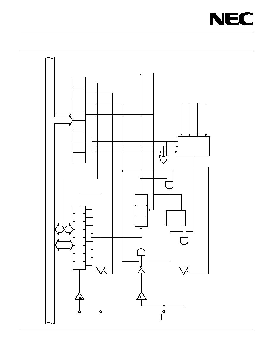
Figure 5-4 Block Diagram of Timer/Event Counter (n=0, 1)
TMn7 TMn6 TMn5 TMn4 TMn3 TMn2 TMn1 TMn0
TMn
SET 1
*1
*2
TIn
8
8
8
TMODn
Match
TOFn
Tn
CP
RES
Clear
TMn1
TMn0
IRQTn
Clear Signal
IRQTn
P2n/PTOn
To Serial Interface
*3
INTTn
TOEn
TOn
PORT2.n
TOUT
F/F
8
8
TIn
MPX
Input
Buffer
From
Clock
Generator
Timer Operation Start
Internal Bus
Modulo Register (8)
Comparator (8)
Count Register (8)
TO
Selector
TO
Enable
Flag
P2n
Output
Latch
Port2
Input/
Output
Mode
PGMB Bit 2
Output
Buffer
Edge
Detector
Set Signal
* 1: SET1: Instruction execution
2: Refer to Figure 5-1
3: Only channel 0 of the time/event counter can output a signal to the serial interface

19
µ
PD75112(A), 75116(A)
5.6 Serial Interface
The
µ
PD75116(A) incorporates the clock synchronous
8-bit serial interface. The serial interface has the follow-
ing two modes.
∑
Operation stop mode
∑
3-wire serial I/O mode (MSB/LSB top switching
possible)
Connection with the
µ
PD75116(A) and the 75X series,
78K series and various I/O devices is possible in the 3-
wire serial I/O mode.
20
µ
PD75112(A), 75116(A)
*:
SET1: Instruction execution
Figure 5-5 Block Diagram of Serial Interface
SIOM7 SIOM6 SIOM5 SIOM4 SIOM3 SIOM2 SIOM1 SIOM0
SIOM
SET1 *
8
8
Clear
R
S
Q
Over Flow
Serial Clock
Counter (3)
Serial Start
8
SIO0
SIO7
SIO
P03/SI
P02/SO
P01/SCK
MPX
fxx/2
4
10
fxx/2
TOF 0
Internal Bus
Shift Register (8)
(From Timer Channel 0)
INTSIO
IRQSIO
Set Signal
IRQSIO
Clear Signal
21
µ
PD75112(A), 75116(A)
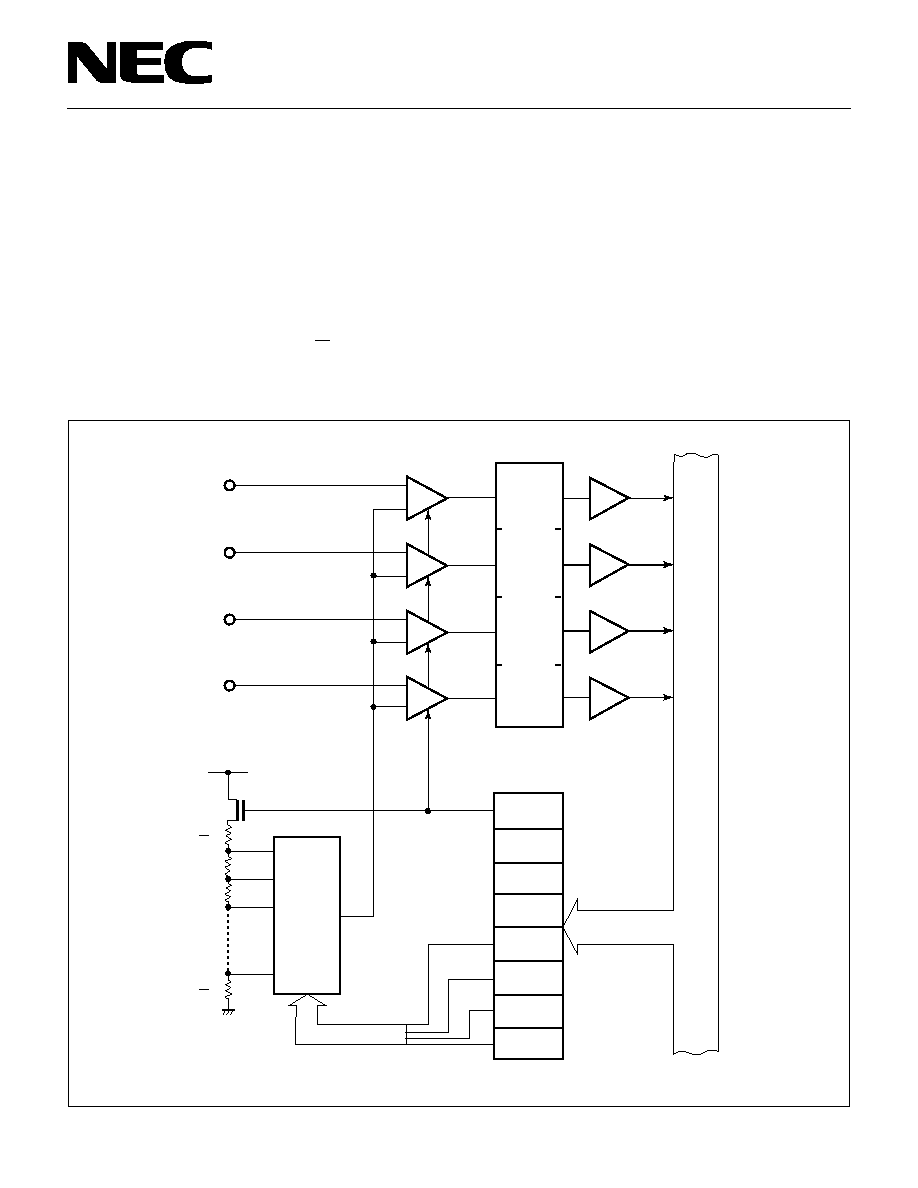
5.7 ProgrammableThreshold Port (Analog Input Port)
The
µ
PD75116(A) is equipped with 4-bit analog input
pins (PTH00 to PTH03) capable of changing the thresh-
old voltage. These pins are configured as shown in
Figure 5-6.
Sixteen threshold voltage (V
REF
) values (V
DD
◊
-V
DD
◊
) are available and analog signals can be directly
input.
The analog input port can also be used as a digital
signal input port by selecting V
DD
◊
for V
REF
.
16
0.5
16
15.5
16
7.5
Figure 5-6 Block Diagram of Programmable Threshold Port
+
≠
PTH00
+
≠
PTH01
+
≠
PTH02
+
≠
PTH03
1
2
R
4
1
2
R
MPX
V
DD
V
REF
R
R
PTHM7
PTH0
PTHM6
PTHM5
PTHM4
PTHM3
PTHM2
PTHM1
PTHM0
PTHM
8
Operation
Stop
Program-
mable
Threshold
Port
Input
Latch (4)
Input Buffer
Inter-
nal
Bus
22
µ
PD75112(A), 75116(A)
5.8 Bit Sequential Buffer ... 16 bit
The bit sequential buffer is a special data memory for
bit control. Since this buffer can easily operate bits by
sequentially changing address and bit specifications, it
can be conveniently be used for bit-wise processing of
data having long bit lengths.
Figure 5-7 Bit Sequential Buffer Format
L = F
L = C L = B
L = 8 L = 7
L = 4 L = 3
DECS L
INCS L
L = 0
BSB0
BSB1
BSB2
BSB3
3
2
1
FC3H
0
3
2
1
FC2H
0
3
2
1
FC1H
0
3
2
1
FC0H
0
Address
Bit
Symbol
L Register
Remarks: In pmen. @L addressing, the specified bit moves in
accordance with the L register.
5.9 Power-On Flag (Mask Option)
The power-on flag (PONF) is only set (1) when the
power-on reset circuit is activated and the power-on
reset signal is generated (see Figure 8-1).
PONF is mapped on bit 0 at address FD1H of the data
memory space and is manipulated by a bit manipula-
tion instruction
However, it cannot be set(1) by the SET1 instruction.

23
µ
PD75112(A), 75116(A)
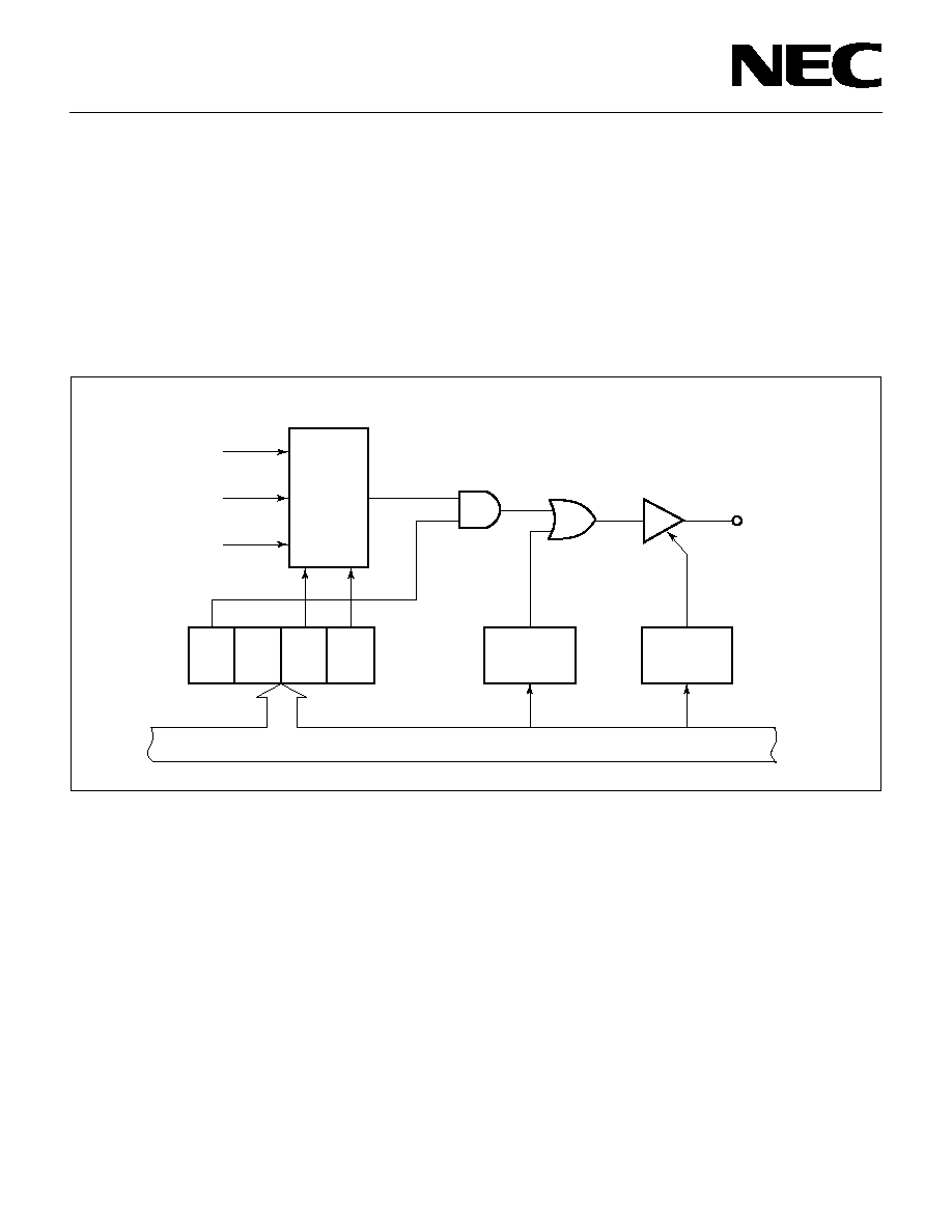
6. Interrupt Functions
There are seven types of interrupt sources for the
µ
PD75116(A) to allow multi-interruption with priority.
The
µ
PD75116(A) is also provided with two types of
edge detection testable inputs.
The
µ
PD75116 interrupt control circuit has the follow-
ing functions;
∑
Hardware controlled vector interrupt function which
enables to control by the interrupt enable flag (IE
◊◊◊
)
and the interrupt master enable flag (IME) whether an
interrupt should be enabled.
∑
Interrupt start address can be set freely.
∑
Multiple interrupt function which enables to specify
priority by the interrupt priority select register (IPS).
∑
Interrupt request flag (IRQ
◊◊◊
) test function (inter-
rupt generation can be checked by the software).
∑
Standby mode release (the interrupt to be released
can be selected by the interrupt enable flag).

24
µ
PD75112(A), 75116(A)
Figure 6-1 Block Diagram of Interrupt Control Circuit
IRQBT
2
IRQ4
IRQ0
IRQ1
IRQSIO
IRQT0
IRQT1
IRQ2
IRQ3
2
9
4
2
I S T
I P S
(IME)
IM1
IM0
INT
BT
INT4
/P00
INT0
/P10
INT1
/P11
INT2
/P12
INTSIO
INTT0
INTT1
INT3
/P13
Internal Bus
Interrupt Enable Flag (IE
◊ ◊ ◊
)
Decoder
Priority Control Circuit
Vector Table
Address
Generator
Standby Release
Signal
Interrupt
Request
Flag
Edge
Detection
Circuit
Edge
Detection
Circuit
Edge
Detection
Circuit
Edge
Detection
Circuit
Edge
Detection
Circuit
25
µ
PD75112(A), 75116(A)
STOP Mode
STOP instruction
Clock oscillation stop
Operation stop
Operation enabled only when external SCK
input and TO0 clock are set for serial clocks
(when timer/event counter 0 is set to external
TI0 input) is selected
Operation enabled only when TIn pin input is
specified for the count clock
Operation stop
Operation stop
Set instruction
Clock generator
Basic interval timer
Serial interface
Timer/event counter
Clock output circuit
CPU
Release signal
7. Stanby Functions
Two types of standby modes (STOP and HALT modes)
are available for the
µ
PD75116(A) to decrease power
consumption during standby for program.
Table 7-1 Operation Statuses in Standby Mode
HALT Mode
HALT instruction
Only CPU clock
stop
Operation (IRQBT set at reference time
intervals)
Operation enabled when aclock other than
is specified for the serial clock
Operation enabled
Clock other than CPU clock
enabled for
output
Operation stop
Operation
status
Interrupt request signal enabled by interrupt enable flag or RESET input

26
µ
PD75112(A), 75116(A)
8. Reset Functions
The reset signal (RES) generator is configured as shown
in Figure 8-1.
Figure 8-1 Reset Signal Generator
*:
PONF setting (1) by SET1 instruction is not possible.
SWA
SWB
RESET
Power-On
Reset Circuit
Mask
Option
Power-On
Flag(PONF)
Bit Control Instruction
Execution *
Internal Reset Signal (RES)
Inter-
nal
Bus
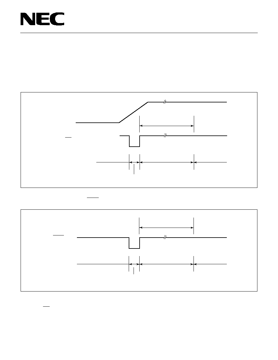
27
µ
PD75112(A), 75116(A)
The power-on reset circuit generates the internal reset
signal by rising of supply voltage. This pulse is used in
the three ways according to the specification of mask
option of SWA and SWB shown in Figure 8-1 (refer to
"10. Mask Option Selection").
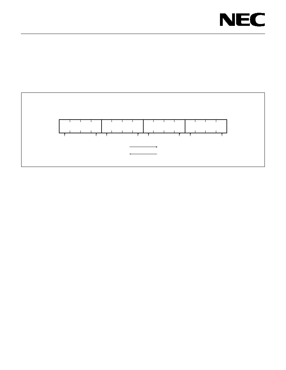
Reset operations are shown in Figures 8-2 and 8-3.
Figure 8-2 Reset Operation by Power-on Reset
*:
The wait time does not include a time from the generation
of RES signal to the start of oscillation.
Each hardware status after reset operation is shown in
Table 8-1.
Figure 8-3 Reset Operation by Reset Input
HALT Mode
0V
Supply Voltage
Internal Reset
Signal (RES)
Wait *
(Approx. 31.3 ms:4.19 MHz)
Internal Reset
Operation
Operating Mode
HALT Mode
Operation or
Standby Mode
Wait *
(Approx. 31.3 ms:4.19 MHz)
Internal Reset
Operation
Operating Mode
RESET Input
28
µ
PD75112(A), 75116(A)
Table 8-1 Hardware Statuses after Reset
* 1: Power-on reset ................... 1
RESET input in operation ... Undefined
2: Data at addresses 0F8H to 0FDH of the data memory becomes undefined due to RESET input.
PWS
Basic interval timer
Timer/ event
counter
(n = 0, 1)
Serial
interface
RESET Input in Power-On
Reset or Operation
same as left
Undefined
0
0
same as left
Undefined
Undefined
Undefined
0, 0
Undefined
0
0
FFH
0
0, 0
Undefined
0
0
0
Reset (0)
0
0
0, 0
Off
Clear (0)
0
Undefined
0
1 or undefined *2
0
Clock
generator,
clock
output
circuit
Interrupt
Digital
port
Analog
port
RESET Input in Standby Mode
Lower 6 bits of address 0000H of the program memory are set to
PC
13
to PC
8
and the content of address 0001H is set to PC
7
to PC
0
.
Hold
0
0
Bits 6 and 7 of address 0000H of the program memory are set to
RBE and MBE, respectively.
Undefined
Hold *1
Hold
0, 0
Undefined
0
0
FFH
0
0, 0
Hold
0
0
0
Reset (0)
0
0
0, 0
Off
Clear (0)
0
Undefined
0
Hold
0
Hardware
Program counter (PC)
Carry flag (CY)
Skip flag (SK0 to SK2)
Interrupt status flag (IST0, 1)
Bank enable flags (MBE, RBE)
Stack pointer (SP)
Data memory (RAM)
General registers (X, A, H, L, D, E, B, C)
Bank select registers (MBS, RBS)
Counter (BT)
Mode register (BTM)
Counter (Tn)
Modulo register (TMODn)
Mode register (TMn)
TOEn, TOFn
Shift register (SIO)
Mode register (SIOM)
Processor clock control
register (PCC)
Clock output mode
register (CLOM)
Interrupt request flag (IRQ
◊◊◊
)
Interrupt enable flag (IE
◊◊◊
)
Priority select resister (IPS)
INT0, 1 mode resisters (IM0, IM1)
Output buffer
Output latch
Input/output mode registers
(PMGA, PMGB, PMGC)
PTH00 to PTH03 input latches
Mode register (PTHM)
Power-on flag (PONF)
Bit sequential buffers (BSB0 to BSB3)
29
µ
PD75112(A), 75116(A)
*:
In the case of 8-bit data processing, only even address
can be described for "mem".
Description Method
X, A, B, C, D, E, H, L
X, B, C, D, E, H, L
XA, BC, DE, HL
BC, DE, HL
BC, DE
XA, BC, DE, HL, XA', BC', DE', HL'
BC, DE, HL, XA', BC', DE', HL'
HL, HL+, HL-, DE, DL
DE, DL
4-bit immediate data or label
8-bit immediate data or label
8-bit immediate data or label*
2-bit immediate data or label
FB0H to FBFH and FF0H to FFFH immediate data
or labels
FC0H to FFFH immediate data or labels
µ
PD75112(A)
0000H to 2F7FH immediate data or
labels
µ
PD75116(A)
0000H to 3F7FH immediate data or
labels
12-bit immediate data or label
11-bit immediate data or label
20H to 7FH immediate data (bit = 0) or labels
PORT0 to PORT9, PORT12 to PORT14
IEBT, IESIO, IET0, IET1, IE0 to IE4
RB0 to RB3
MB0, MB1, MB15
Identifier
reg
reg1
rp
rp1
rp2
rp'
rp'1
rpa
rpa1
n4
n8
mem
bit
fmem
pmem
addr
caddr
faddr
taddr
PORTn
IE
◊◊◊
RBn
MBn
9. Instruction Set
(1) Operand identifier and description method
In the operand column of each instruction, describe the
corresponding operand in accordance with the de-
scription method for the operand identifier of the in-
struction (refer to the "RA75X Assembler Package User's
Manual Language Volume" (EEU-730) for details). If
more than one description method is available, select
one of them. Capital alphabetic letters, plus and minus
signs are key words. Describe them as they are.
In the case of immediate data, describe appropriate
numeric values or labels.
Symbols of various registers and flags can be de-
scribed as labels instead of mem, fmem, pmem, bit, etc.
(Refer to the "
µ
PD751
◊◊
Series User's Manual (IEM-
922)" for details). Labels which can be described are
limited for fmem and pmem.

30
µ
PD75112(A), 75116(A)
(2) Legend in the description of operations
A
:
A register; 4-bit accumulator
B
:
B register
C
:
C register
D
:
D register
E
:
E register
H
:
H register
L
:
L register
X
:
X register
XA
:
Register pair (XA); 8-bit accumulator
BC
:
Register pair (BC)
DE
:
Register pair (DE)
HL
:
Register pair (HL)
XA'
:
Extended register pair (XA')
BC'
:
Extended register pair (BC')
DE'
:
Extended register pair (DE')
HL'
:
Extended register pair (HL')
PC
:
Program counter
SP
:
Stack pointer
CY
:
Carry flag; bit accumulator
PSW
:
Program status word
MBE
:
Memory bank enable flag
RBE
:
Register bank enable flag
PORTn :
Port n (n = 0 to 9, 12 to 14)
IME
:
Interrupt mask enable flag
IPS
:
Interrupt priority select register
IE
◊
◊◊
:
Interrupt enable flag
RBS
:
Register bank select register
MBS
:
Memory bank select register
PCC
:
Processor clock control register
.
:
Address and bit division
(
◊◊
)
:
Content addressed by
◊◊
◊◊
H
:
Hexadecimal data
31
µ
PD75112(A), 75116(A)
MB=MBE
∑
MBS
(MBS=0, 1, 15)
MB=0
MBE=0 : MB=0 (00H-7FH)
MB=15 (80H-FFH)
MBE=1 : MB=MBS (MBS=0, 1, 15)
MB=15, fmem=FB0H-FBFH,
FF0H=FFFH
MB=15, pmem=FC0H-FFFH
addr=0000H-2F7FH (
µ
PD75112(A))
=0000H-3F7FH (
µ
PD75116(A))
addr=(Current PC) -15 to
(Current PC) +16
caddr=0000H-0FFFH (PC
13
, PC
12
=00B :
µ
PD75112(A), 116(A)) or
=1000H-1FFFH (PC
13
, PC
12
=01B :
µ
PD75112(A), 116(A)) or
=2000H-2F7FH (PC
13
, PC
12
=10B :
µ
PD75112(A)) or
=2000H-2FFFH (PC
13
, PC
12
=10B :
µ
PD75116(A)) or
=3000H-3F7FH (PC
13
, PC
12
=11B :
µ
PD75116(A))
faddr=0000H-07FFH
taddr=0020H-007FH
(3) Description of symbols in the addressing area column
Remarks 1: MB indicates an accessible memory bank.
2: In *2, MB = 0 irrespectively of MBE and MBS.
3: In *4 and *5, MB = 15 irrespectively of MBE and
MBS.
4: *6 to *10 indicate addressable areas.
(4) Description of machine cycle column
S indicates the number of machine cycles required for
the instruction having skip function to execute skip
operation. The value of S varies as follows:
∑
When no skip ............................................. S = 0
∑
When 1-byte or 2-byte instruction is skipped
................................................. S = 1
∑
When 3-byte instruction (BR !addr, CALL !addr
instructions) is skipped ............................. S = 2
Note:
GETI instruction is skipped in one-ma-
chine cycle.
One machine cycle is equal to one cycle (=t
CY
)of CPU
clock. Three values are available for the one machine
cycle by PCC setting.
*1
*2
*3
*4
*5
*6
*7
*8
*9
*10
Data Memory
Addressing
Program Memory
Addressing

32
µ
PD75112(A), 75116(A)
Instructions
Mnemonic
Transfer
Table
Reference
Bit Transfer
MOV
XCH
MOVT
MOV1
Machine Cycle
1
2
2
2
2
1
2+S
2+S
1
2
1
2
2
2
2
2
2
2
2
2
1
2+S
2+S
1
2
2
2
1
2
3
3
2
2
2
2
2
2
No. of Bytes
1
2
2
2
2
1
1
1
1
2
1
2
2
2
2
2
2
2
2
2
1
1
1
1
2
2
2
1
2
1
1
2
2
2
2
2
2
Operand
A, #n4
reg1, #n4
XA, #n8
HL, #n8
rp2, #n8
A, @HL
A, @HL+
A, @HL-
A, @rpa1
XA, @HL
@HL, A
@HL, XA
A, mem
XA, mem
mem, A
mem, XA
A, reg
XA, rp'
reg1, A
rp'1 XA
A, @HL
A, @HL+
A, @HL-
A, @rpa1
XA, @HL
A, mem
XA, mem
A, reg1
XA, rp'
XA, @PCDE
XA, @PCXA
CY, fmem. bit
CY, pmem. @L
CY, @H+mem. bit
fmem. bit, CY
pmem. @L, CY
@H+mem. bit, CY
Skip Condition
Stack A
Stack A
Stack B
L=0
L=FH
L=0
L=FH
Addressing Area
*1
*1
*1
*2
*1
*1
*1
*3
*3
*3
*3
*1
*1
*1
*2
*1
*3
*3
*4
*5
*1
*4
*5
*1
Operation
A
n4
reg1
n4
XA
n8
HL
n8
rp2
n8
A
(HL)
A
(HL), then L
L+1
A
(HL), then L
L-1
A
(rpa1)
XA
(HL)
(HL)
A
(HL)
XA
A
(mem)
XA
(mem)
(mem)
A
(mem)
XA
A
reg
XA
rp'
reg1
A
rp'1
XA
A
(HL)
A
(HL), then L
L+1
A
(HL), then L
L-1
A
(rpa1)
XA
(HL)
A
(mem)
XA
(mem)
A
reg1
XA
rp'
XA
(
PC
13-8
+DE)
ROM
XA
(
PC
13-8
+XA)
ROM
CY
(fmem.bit)
CY
(pmem
7-2
+L
3-2
.bit(L
1-0
))
CY
(H+mem
3-0
.bit)
(fmem.bit)
CY
(pmem
7-2
+L
3-2
.bit(L
1-0
))
CY
(H+mem
3-0
.bit)
CY

33
µ
PD75112(A), 75116(A)
Operation
A
A+n4
XA
XA+n8
A
A
+
(HL)
XA
XA+rp'
rp'1
rp'1+XA
A, CY
A+(HL)+CY
XA, CY
XA+rp'+CY
rp'1, CY
rp'1+XA+CY
A
A
-
(HL)
XA
XA-rp'
rp'1
rp'1-XA
A, CY
A-(HL)-CY
XA, CY
XA-rp'-CY
rp'1, CY
rp'1-XA-CY
A
A
n4
A
A
(HL)
XA
XA
rp'
rp'1
rp'1
XA
A
A
n4
A
A
(HL)
XA
XA
rp'
rp'1
rp'1
XA
A
A
n4
A
A
(HL)
XA
XA
rp'
rp'1
rp'1
XA
CY
A
0
, A
3
CY, A
n-1
An
A
A
reg
reg+1
rp1
rp1+1
(HL)
(HL)+1
(mem)
(mem)+1
reg
reg-1
rp'
rp'-1
Skip if reg=n4
Skip if (HL)=n4
Skip if A=(HL)
Instructions
Mnemonic
Arithmetic
Accumulator
Operation
Increase/
Decrease
Compare
ADDS
ADDC
SUBS
SUBC
AND
OR
XOR
RORC
NOT
INCS
DECS
SKE
Operand
A, #n4
XA, #n8
A, @HL
XA, rp'
rp'1, XA
A, @HL
XA, rp'
rp'1, XA
A, @HL
XA, rp'
rp'1, XA
A, @HL
XA, rp'
rp'1, XA
A, #n4
A, @HL
XA, rp'
rp'1, XA
A, #n4
A, @HL
XA, rp'
rp'1, XA
A, #n4
A, @HL
XA, rp'
rp'1, XA
A
A
reg
rp1
@HL
mem
reg
rp'
reg, #n4
@HL, #n4
A, @HL
No. of Bytes
1
2
1
2
2
1
2
2
1
2
2
1
2
2
2
1
2
2
2
1
2
2
2
1
2
2
1
2
1
1
2
2
1
2
2
2
1
Machine Cycle
1+S
2+S
1+S
2+S
2+S
1
2
2
1+S
2+S
2+S
1
2
2
2
1
2
2
2
1
2
2
2
1
2
2
1
2
1+S
1+S
2+S
2+S
1+S
2+S
2+S
2+S
1+S
Skip Condition
Carry
Carry
Carry
Carry
Carry
borrow
borrow
borrow
reg=0
rp1=00H
(HL)=0
(mem)=0
reg=FH
rp'=FFH
reg=n4
(HL)=n4
A=(HL)
*1
*1
*1
*1
*1
*1
*1
*1
*3
*1
*1
Addressing Area
34
µ
PD75112(A), 75116(A)
Instructions
Mnemonic
Compare
Carry Flag
Operation
SKE
SET1
CLR1
SKT
NOT1
Operand
XA, @HL
A, reg
XA, rp'
CY
CY
CY
CY
Addressing Area
*1
No. of Bytes
2
2
2
1
1
1
1
Machine Cycle
2+S
2+S
2+S
1
1
1+S
1
Operation
Skip if XA=(HL)
Skip if A=reg
Skip if XA=rp'
CY
1
CY
0
Skip if CY=1
CY
CY
Skip Condition
XA=(HL)
A=reg
XA=rp'
CY=1

35
µ
PD75112(A), 75116(A)
Instructions
Mnemonic
Memory Bit
Manipulation
Branch
SET1
CLR1
SKT
SKF
SKTCLR
AND1
OR1
XOR1
BR
BRCB
BR
Operand
mem. bit
fmem. bit
pmem. @L
@H+mem. bit
mem. bit
fmem. bit
pmem. @L
@H+mem. bit
mem. bit
fmem. bit
pmem. @L
@H+mem. bit
mem. bit
fmem. bit
pmem. @L
@H+mem. bit
fmem. bit
pmem. @L
@H+mem. bit
CY, fmem. bit
CY, pmem. @L
CY, @H+mem. bit
CY, fmem. bit
CY, pmem. @L
CY, @H+mem. bit
CY, fmem. bit
CY, pmem. @L
CY, @H+mem. bit
addr
!addr
$addr
!caddr
PCDE
PCXA
No. of Bytes
2
2
2
2
2
2
2
2
2
2
2
2
2
2
2
2
2
2
2
2
2
2
2
2
2
2
2
2
3
1
2
2
2
Machine Cycle
2
2
2
2
2
2
2
2
2+S
2+S
2+S
2+S
2+S
2+S
2+S
2+S
2+S
2+S
2+S
2
2
2
2
2
2
2
2
2
3
2
2
3
3
Operation
(mem.bit)
1
(fmem.bit)
1
(pmem
7-2
+L
3-2
.bit(L
1-0
))
1
(H+mem
3-0
.bit)
1
(mem.bit)
0
(fmem.bit)
0
(pmem
7-2
+L
3-2
.bit(L
1-0
))
0
(H+mem
3-0
.bit)
0
Skip if (mem.bit)=1
Skip if (fmem.bit)=1
Skip if (pmem
7-2
+L
3-2
.bit(L
1-0
))
=
1
Skip if (H+mem
3-0
.bit)=1
Skip if (mem.bit)=0
Skip if (fmem.bit)=0
Skip if (pmem
7-2
+L
3-2
.bit(L
1-0
))=0
Skip if (H+mem
3-0
.bit)=0
Skip if (fmem.bit)=1 and clear
Skip if (pmem
7-2
+L
3-2
.bit(L
1-0
))
=1 and clear
Skip if (H+mem
3-0
.bit)=1 and clear
CY
CY
(fmem.bit)
CY
CY
(pmem
7-2
+L
3-2
.bit(L
1-0
))
CY
CY
(H+mem
3-0
.bit)
CY
CY
(fmem.bit)
CY
CY
(pmem
7-2
+L
3-2
.bit(L
1-0
))
CY
CY
(H+mem
3-0
.bit)
CY
CY
(fmem.bit)
CY
CY
(pmem
7-2
+L
3-2
.bit(L
1-0
))
CY
CY
(H+mem
3-0
.bit)
PC
13-0
addr
(Most appropriate instruction is
selected by assembler from among
BR !addr, BRCB !caddr and BR
$addr)
PC
13-0
addr
PC
13-0
addr
PC
13-0
PC
13, 12
+caddr
11-0
PC
13-0
PC
13-8
+DE
PC
13-0
PC
13-8
+XA
Addressing Area
*3
*4
*5
*1
*3
*4
*5
*1
*3
*4
*5
*1
*3
*4
*5
*1
*4
*5
*1
*4
*5
*1
*4
*5
*1
*4
*5
*1
*6
*6
*7
*8
Skip Condition
(mem.bit)=1
(fmem.bit)=1
(pmem.@L)=1
(@H+mem.bit)=1
(mem.bit)=0
(fmem.bit)=0
(pmem.@L)=0
(@H+mem.bit)=0
(fmem.bit)=1
(pmem.@L)=1
(@H+mem.bit)=1
36
µ
PD75112(A), 75116(A)
Instructions
Mnemonic
Subroutine
Stack Control
Interrupt
Control
Input/Output
CPU Control
Special
CALL
CALLF
RET
RETS
RETI
PUSH
POP
EI
DI
IN*1
OUT*1
HALT
STOP
NOP
SEL
GETI*2
Operand
!addr
!faddr
rp
BS
rp
BS
IE
◊◊◊
IE
◊◊◊
A, PORTn
XA, PORTn
PORTn, A
PORTn, XA
RBn
MBn
taddr
Skip Condition
Unconditional
Depends on the
instruction
referred to.
* 1: MBE=0 or 1 and MBS=15 must be set for execution of IN/OUT instruction.
2: TBR and TCALL instructions are assembler pseudo-instructions for GETI instruction table definition.
No. of Bytes
3
2
1
1
1
1
2
1
2
2
2
2
2
2
2
2
2
2
2
1
2
2
1
Machine Cycle
3
2
3
3+S
3
1
2
1
2
2
2
2
2
2
2
2
2
2
2
1
2
2
3
Operation
(SP-4)(SP-1)(SP-2)
PC
11-0
(SP-3)
MBE, RBE, PC
13, 12
PC
13-0
addr, SP
SP-4
(SP-4)(SP-1)(SP-2)
PC
11-0
(SP-3)
MBE, RBE, PC
13, 12
PC
13-0
00,
faddr, SP
SP-4
MBE, RBE, PC
13, 12
(SP+1)
PC
11-0
(SP)(SP+3)(SP+2)
SP
SP+4
MBE, RBE, PC
13, 12
(SP+1)
PC
11-0
(SP)(SP+3)(SP+2)
SP
SP+4, then skip unconditionally
PC
13, 12
(SP+1)
PC
11-0
(SP)(SP+3)(SP+2)
PSW
(SP+4)(SP+5), SP
SP+6
(SP-1)(SP-2)
rp, SP
SP-2
(SP-1)
MBS, (SP-2)
RBS, SP
SP-2
rp
(SP-1)(SP), SP
SP-2
MBS
(SP+1), RBS
(SP), SP
SP+2
IME (IPS.3)
1
IE
◊◊◊
1
IME (IPS.3)
0
IE
◊◊◊0
A
PORTn
(n=0-9, 12-14)
XA
PORTn+1, PORTn (n=4, 6, 8, 12)
PORTn
4
(n=2-9, 12-14)
PORTn+1, PORTn
XA (n=4, 6, 8, 12)
Set HALT Mode (PCC.2
1)
Set STOP Mode (PCC.3
1)
No Operation
RBS
n(n=0-3)
MBS
n
(n=0, 1, 15)
∑
TBR Instruction
PC
13-0
(taddr)
4-0
+(taddr+1)
∑
TCALL Instruction
(SP-4)(SP-1)(SP-2)
PC
11-0
(SP-3)
MBE, RBE, PC
13, 12
PC
13-0
(taddr)
5-0
+(taddr+1)
SP
SP-4
∑
When not TBR and TCALL
instructions, (taddr) and (taddr+1)
instructions are executed.
,
Addressing Area
*6
*9
*10
37
µ
PD75112(A), 75116(A)
10.
Mask Option Selection
The following mask options are available for the
µ
PD75116(A).
Whether or not they should be incorporated can be
selected.
(1)
Pins
Pin
P120 to P123
P130 to P133
P140 to P143
Mask Option
Bit-wise pull-up resistor incorporation enable
(2)
Power-on reset circuit and power-on flag (PONF)
One of the following three settings can be selected.
Mask Option Specification
Power-on
Reset Circuit
Incorporated
Not incorporated
Not incorporated
Switch Selection
(See Figure 8-1)
SWA
ON
ON
OFF
SWB
ON
OFF
OFF
5
Internal Reset Signal
(RES)
Generated automatically
Not generated automatically
Power-on Flag
(PONF)
Incorporated
Incorporated
Not incorporated
38
µ
PD75112(A), 75116(A)
Test Conditions
Except for ports 12 to 14
Ports 12 to 14
1 pin
All pins
1 pin
Total current of ports 0, 2 to 4, 12 to 14
* 1: When applying a voltage larger than 10 V to ports 12, 13
and 14 each, set the power impedance (pull-up resistor) to
50 k
or more.
2: Calculate each effective value using the following expres-
sion:
[Effective value]=[Peak value]
◊
duty
Note: Product quality may suffer if the absolute maxi-
mum rating is exceeded for even a single pa-
rameter or even momentarily. That is, the ab-
solute maximum ratings are rated values at
which the product is on the verge of suffering
physical damage, and therefore the product
must be used under conditions which ensure
that the absolute maximum ratings are not
exceeded.
11.
Electrical Specifications
Absolute Maximum Ratings
(Ta = 25
∞
C)
Unit
V
V
V
V
V
mA
mA
mA
mA
mA
mA
mA
mA
mA
mA
∞
C
∞
C
Symbol
V
DD
V
I1
V
I2
*1
V
O
I
OH
I
OL
*2
T
opt
T
stg
On-chip pull-up resistor
Open drain
Peak value
Effective value
Peak value
Effective value
Peak value
Effective value
Peak value
Effective value
Peak value
Effective value
Ratings
≠0.3 to +7.0
≠0.3 to V
DD
+0.3
≠0.3 to V
DD
+0.3
≠0.3 to +13
≠0.3 to V
DD
+0.3
≠10
≠5
≠30
≠15
10
5
50
25
50
25
≠40 to +85
≠65 to +150
Parameter
Power supply voltage
Input voltage
Output voltage
Output current high
Output current low
Operation temperature
Storage temperature
39
µ
PD75112(A), 75116(A)
Test Conditions
MIN.
*2
4.5
4.5
2.7
MAX.
6.0
6.0
6.0
6.0
Unit
V
V
V
V
* 1: Except system clock oscillator, programmable threshold
port and power-on reset circuit
2: Operating voltage range depends on the cycle time.
See the AC Characteristics.
3: Whether or not it should be incorporated can be selected
by mask options.
See the Power-On Reset Circuit Characteristics (Mask
Option).
5
Operating Voltage
(Ta = ≠40 to +85
∞
C)
Parameter
CPU*1
Programmable threshold port
(comparator input)
Power-on reset circuit*3
Other hardware*1
40
µ
PD75112(A), 75116(A)
Oscillate Characteristics
(Ta = ≠40 to +85
∞
C, V
DD
= 2.7 to 6.0 V)
X1
X2
Oscillator
Ceramic
oscillation
Crystal
oscillator
External
clock
MAX.
5.0*3
5.0*3
5.0*3
250
TYP.
4.19
MIN.
2.0
4
2.0
10
30
2.0
100
Test Condition
V
DD
= oscillation
voltage range
Oscillation voltage
range MIN.
V
DD
= 4.5 to 6.0 V
Recommended Constant
Parameter
Oscillator frequency
(f
XX
)*1
Oscillation stabilizing
time*2
Oscillator frequency
(f
XX
)*1
Oscillation stabilizing
time*2
X1 input frequency
(f
X
)*1
X1 input high and low
level widths (t
XH
, t
XL
)
Unit
MHz
ms
MHz
ms
ms
MHz
ns
µ
PD74HCU04
X1
X2
C2
C1
X1
X2
C2
C1
* 1: Oscillator frequency and X1 input frequency indicate only
characteristics of the oscillator. Refer to AC characteristics
for the instruction execution time.
2: The oscillation stabilizing time is necessary for oscillation
to stabilize after V
DD
reaches oscillation voltage range MIN.
or the STOP mode is released.
3: When the oscillator frequency is 4.19 MHz < f
XX
5.0 MHz,
PCC=0011 should not be selected as instruction execution
time. If PCC=0011 is selected, 1 machine cycle becomes
less than 0.95
µ
s, with the result that the specified MIN.
value of 0.95
µ
s cannot be observed.
5
Note: When using the main system clock oscillator,
wiring in the area enclosed with the dotted line
should be carried out as follows to avoid an
adverse effect from wiring capacitance.
∑
Wiring should be as short as possible.
∑
Wiring should not cross other signal lines.
∑
Wiring should not be placed close to a vary-
ing high current.
∑
The potential of the oscillator capacitor
ground should be the same as V
SS
.
Do not ground wiring to a ground pattern in
which a high current flows.
∑
Do not fetch a signal from the oscillator.
5
41
µ
PD75112(A), 75116(A)
Symbol
V
IH1
V
IH2
V
IH3
V
IH4
V
IL1
V
IL2
V
IL3
V
OH
V
OL
I
LIH1
I
LIH2
I
LIH3
I
LIL1
I
LIL2
I
LOH1
I
LOH2
I
LOL
R
L
I
DD1
I
DD2
I
DD3
Test Conditions
Except for ports listed below
Ports 0, 1, TI0, 1, RESET
Ports 12 to 14
X1, X2
Except for ports listed below
Ports 0, 1, TI0, 1, RESET
X1, X2
V
DD
= 4.5 to 6.0 V, I
OH
= ≠1 mA
I
OH
= ≠100
µ
A
V
DD
= 4.5 to 6.0 V
V
DD
= 4.5 to 6.0V, I
OL
= 1.6 mA
I
OL
= 400
µ
A
V
IN
= V
DD
V
IN
= 12 V
V
IN
= 0 V
V
OUT
= V
DD
V
OUT
= 12 V
V
OUT
= 0 V
Ports 12 to 14
4.19 MHz
crystal oscillation
C1 = C2 = 22 pF
STOP mode, V
DD
= 3 V
±
10%
On-chip pull-upresistor
Open drain
Ports 0, 2 to 9, I
OL
= 5 mA
Ports 12 to 14, I
OL
= 5 mA
Except for ports listed below
X1, X2
Ports 12 to 14 (for open drain)
Except for X1, X2
X1, X2
Except for ports listed below
Ports 12 to 14 (for open drain)
V
DD
=5 V
±
10%
V
DD
=5 V
±
10%*2
V
DD
=3 V
±
10%*3
HALT mode
Parameter
Input voltage high
Input vltage low
Output voltage high
Output voltage low
Input leakage current high
Input leakage current low
Output leakage current high
Output leakage current low
On-chip pull-up resistor
Supply current*1
DC Characteristics
(Ta = ≠40 to +85
∞
C, V
DD
= 2.7 to 6.0 V)
* 1: Current for the on-chip pull-up resistor, power-on reset circuit
(mask option) and comparator circuit is not included.
2: When operated in the hgh-speed mode with the processor clock
V
DD
=5 V
±
10%
V
DD
=3 V
±
10%
control resistor (PCC) set tp 0011.
3: When operated in the low-speed mode with the PCC set to 0000.
MIN.
0.7V
DD
0.8V
DD
0.7V
DD
0.7V
DD
V
DD
≠0.5
0
0
0
V
DD
≠1.0
V
DD
≠0.5
15
10
TYP.
0.25
0.40
40
3
0.55
600
200
0.1
MAX.
V
DD
V
DD
V
DD
12
V
DD
0.3V
DD
0.2V
DD
0.4
1.0
1.0
0.4
0.5
3
20
20
≠3
≠20
3
20
≠3
70
80
9
1.5
1800
600
10
Unit
V
V
V
V
V
V
V
V
V
V
V
V
V
V
µ
A
µ
A
µ
A
µ
A
µ
A
µ
A
µ
A
µ
A
k
k
mA
mA
µ
A
µ
A
µ
A
42
µ
PD75112(A), 75116(A)
Test Conditions
f = 1 MHz
0 V for pins except
the measured pins
Symbol
C
IN
C
OUT
C
IO
Parameter
Input capacitance
Output capacitance
Input/output capacitance
MAX.
15
15
15
Comparator Characteristics
(Ta = ≠40 to +85
∞
C, V
DD
= 4.5 to 6.0 V)
Parameter
Comparison accuracy
Threshold voltage
PTH input voltage
Comparator circuit consumption
Test Conditions
Set PTHM7 to "1".
Symbol
V
ACOMP
V
TH
V
IPTH
Power-On Reset Circuit Characteristics (Mask Option)
(Ta = ≠40 to +85
∞
C)
Parameter
Power-on reset operating voltage high
Power-on reset operating voltage low
Supply voltage rise time
Supply voltage off time
Power-on reset circuit
current consumption*2
*1: 2
17
/f
XX
(31.3 ms when f
XX
= 4.19MHz)
2: Current flow upon power-on reset or with an on-chip power-on flag
Note: Start the power supply smoothly.
t
off
t
r
V
DDL
V
DD
V
DDH
Capacitance
(Ta = 25
∞
C, V
DD
= 0 V)
Unit
mV
V
V
mA
MAX.
±
100
V
DD
V
DD
TYP.
1
MIN.
0
0
Symbol
V
DDH
V
DDL
t
r
t
off
I
DDPR
Test Conditions
V
DD
= 5 V
±
10%
V
DD
= 2.5 V
MIN.
4.5
0
10
1
TYP.
10
2
MAX.
6.0
0.2
*1
100
20
Unit
V
V
µ
s
s
µ
A
µ
A
TYP.
MIN.
Unit
pF
pF
pF
43
µ
PD75112(A), 75116(A)
Test Conditions
V
DD
= 4.5 to 6.0 V
V
DD
= 4.5 to 6.0 V
V
DD
= 4.5 to 6.0 V
V
DD
= 4.5 to 6.0 V
V
DD
= 4.5 to 6.0 V
V
DD
= 4.5 to 6.0 V
Parameter
CPU clock cycle time*
(min. instruction execution time
= 1 machine cycle)
TI0, TI1 input frquency
TI0, TI1 input high
and low-level widths
SCK cycle time
SCK high and low-level widths
SI setup time (to SCK
)
SI hold time (from SCK
)
S0 output delay time from SCK
INT0 to INT4
High and low-level widths
RESET low-level sidth
AC Characteristics
(Ta = ≠40 to +85
∞
C, V
DD
= 2.7 to 6.0 V)
MAX.
32
32
1
275
300
1000
TYP.
Symbol
t
CY
f
TI
t
TIH,
t
TIL
t
KCY
t
KH,
t
KL
t
SIK
t
KSI
t
KSO
t
INTH,
t
INTL
t
RSL
MIN.
0.95
3.8
0
0
0.48
1.8
0.8
0.95
3.2
3.8
0.4
t
KCY
/2-50
1.6
t
KCY
/2-50
100
400
5
5
Input
Output
Input
Output
Input
Output
Input
Output
Unit
µ
s
µ
s
MHz
kHz
µ
s
µ
s
µ
s
µ
s
µ
s
µ
s
µ
s
ns
µ
s
ns
ns
ns
ns
ns
µ
s
µ
s
44
µ
PD75112(A), 75116(A)
AC Timing Test Point (Except for Ports 0, 1, TI0, TI1, X1, X2 and RESET)
0.7 V
DD
0.3 V
DD
0.7 V
DD
0.3 V
DD
Test Points
Clock Timing
*: The cycle time of the CPU clock (
) is determined by the
input frequency of the ceramic crystal oscillator and the
setting of the processor clock control register (PCC). The
cycle time (t
CY
) for V
DD
is shown below.
40
32
7
6
6
5
5
4
4
3
3
2
2
1
1
0
0.5
Supply Voltage V
DD
[V]
t
CY vs.
V
DD
[V]
Operation Guaranteed
Range
Cycle Time t
CY
[ s]
µ
t
XL
t
XH
1/f
X
V
DD
≠ 0.5
0.4
X1 Input
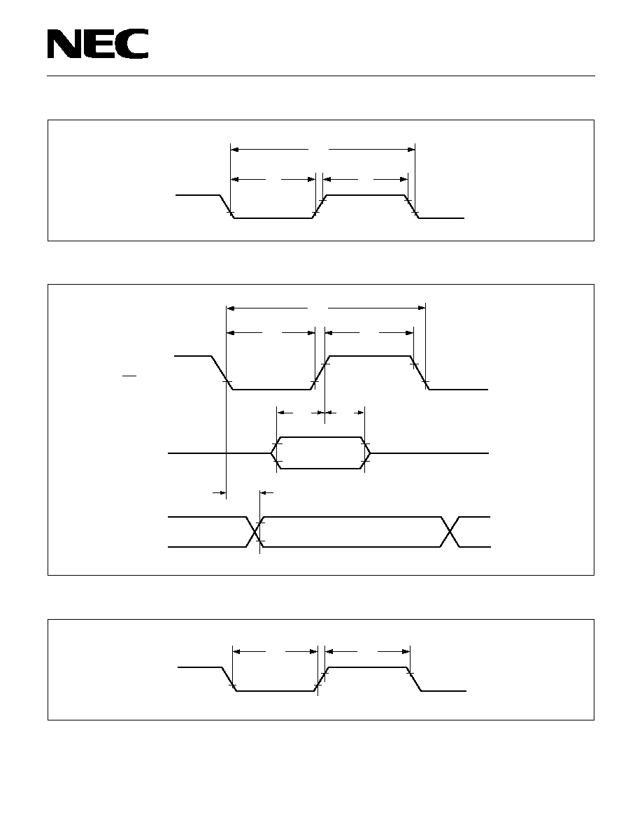
45
µ
PD75112(A), 75116(A)
TI0 and TI1 Input Timing
Serial Transfer Timing
Interrupt Input Timing
t
TIL
t
TIH
1/f
TI
TI0, TI1
0.8 V
DD
0.2 V
DD
t
KL
t
KH
SCK
SI
SO
Output Data
t
KCY
t
SIK
t
KSO
t
KSI
0.8 V
DD
0.2 V
DD
0.8 V
DD
0.2 V
DD
Input Data
t
INTL
t
INTH
INT0-INT4
0.8 V
DD
0.2 V
DD

46
µ
PD75112(A), 75116(A)
* 1: Current for the on-chip pull-up resistor, power-on circuit
(mask option) and comparator circuit is not included.
2: The oscillation stabilizing time is intended to stop the CPU
to prevent any unstable operation at the start of oscillation.
3: Depends on the following setting of the basic interval timer
mode register (BTM).
Data Memory STOP Mode Low Supply Voltage Data Retention Characteristics
(Ta = ≠40 to +85
∞
C)
RESET Input Timing
Symbol
V
DDDR
V
DDDR
t
SREL
t
WAIT
Unit
V
µ
A
µ
s
ms
ms
Parameter
Data retention supply voltage
Data retention supply current*1
Release signal set time
Oscillation stabilization
wait time*2
MAX.
6.0
10
TYP.
0.1
2
17
/f
X
*3
Wait Time
(f
XX
=4.19 MHz Valu¥s in Parentheses)
2
20
/f
XX
(approx. 250 ms)
2
17
/f
XX
(approx. 31.3 ms)
2
15
/f
XX
(approx. 7.82 ms)
2
13
/f
XX
(approx. 1.95 ms)
BTM3
BTM0
0
1
1
1
BTM1
0
1
0
1
BTM2
0
0
1
1
MIN.
2.0
0
Test Conditions
V
DDDR
= 2.0 V
Release by RESET
Release by interrupt request
t
RSL
RESET
0.2 V
DD
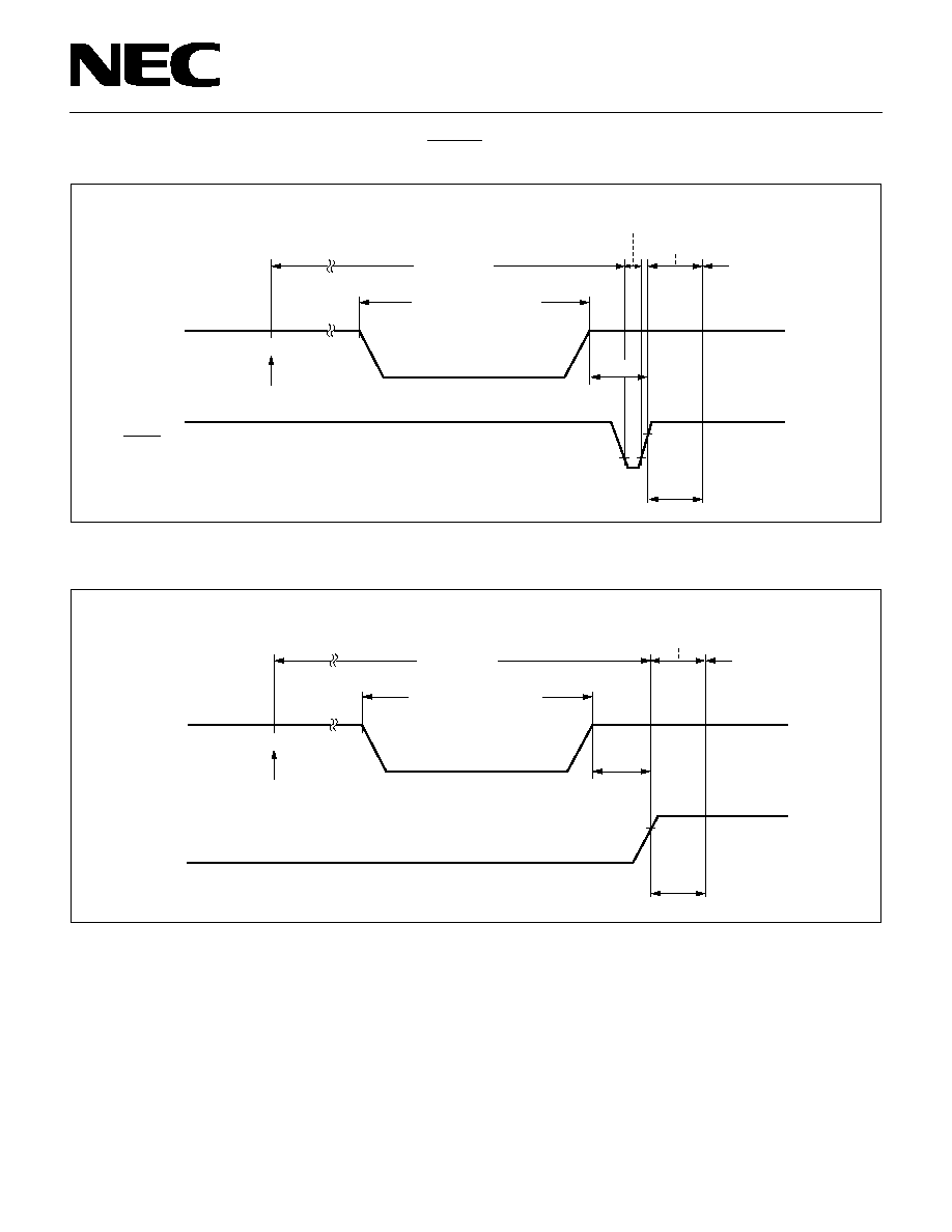
47
µ
PD75112(A), 75116(A)
Data Retention Timing (STOP Mode Release by RESET)
Data Retention Timing (Standby Release Signal: STOP Mode Release by Interrupt Signal)
STOP Mode
Data Retention Mode
STOP Instruction Execution
RESET
V
DD
Internal Reset Operation
HALT Mode
Operating
Mode
V
DDDR
t
SREL
t
WAIT
STOP Mode
Data Retention Mode
STOP Instruction Execution
V
DD
HALT Mode
Operating
Mode
V
DDDR
t
SREL
t
WAIT
Standby Release Signal
(Interrupt Request)

48
µ
PD75112(A), 75116(A)
12.
Packing Information
A
I
J
G
H
F
D
N
M
C
B
M
R
64
33
32
1
K
L
NOTE
Each lead centerline is located within 0.17 mm (0.007 inch) of
its true position (T.P.) at maximum material condition.
P64C-70-750A,C-1
ITEM MILLIMETERS
INCHES
A
B
C
D
F
G
H
I
J
K
58.68 MAX.
1.778 (T.P.)
3.2±0.3
0.51 MIN.
4.31 MAX.
1.78 MAX.
L
M
0.17
0.25
19.05 (T.P.)
5.08 MAX.
17.0
N
0~15∞
0.50±0.10
0.9 MIN.
R
2.311 MAX.
0.070 MAX.
0.020
0.035 MIN.
0.126±0.012
0.020 MIN.
0.170 MAX.
0.200 MAX.
0.750 (T.P.)
0.669
0.010
0.007
0~15∞
+0.004
≠0.003
0.070 (T.P.)
1)
Item "K" to center of leads when formed parallel.
2)
+0.10
≠0.05
+0.004
≠0.005
64 PIN PLASTIC SHRINK DIP (750 mil)
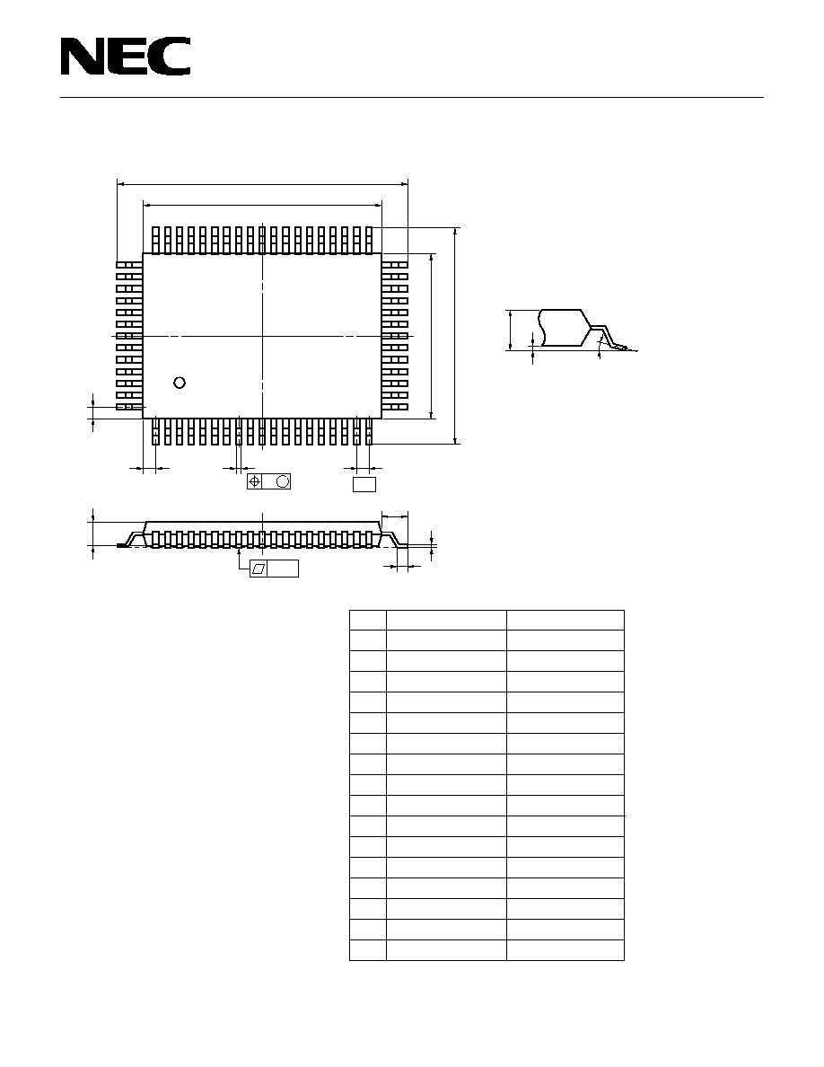
49
µ
PD75112(A), 75116(A)
N
A
M
F
B
51
52
32
K
L
64 PIN PLASTIC QFP (14
◊
20)
64
1
20
19
33
P
D
C
detail of lead end
S
Q
5∞±5∞
G
M
I
H
J
P64GF-100-3B8,3BE,3BR-1
ITEM
MILLIMETERS
INCHES
A
B
C
D
F
G
H
I
J
K
L
23.6±0.4
14.0±0.2
1.0
0.40±0.10
0.20
20.0±0.2
0.929±0.016
0.039
0.039
0.008
0.039 (T.P.)
0.795
NOTE
M
N
0.12
0.15
1.8±0.2
1.0 (T.P.)
0.005
0.006
+0.004
≠0.003
Each lead centerline is located within 0.20
mm (0.008 inch) of its true position (T.P.) at
maximum material condition.
0.071
0.016
0.551
0.8±0.2
0.031
P
2.7
0.106
0.693±0.016
17.6±0.4
1.0
+0.009
≠0.008
Q
0.1±0.1
0.004±0.004
S
3.0 MAX.
0.119 MAX.
+0.10
≠0.05
+0.009
≠0.008
+0.004
≠0.005
+0.009
≠0.008
+0.008
≠0.009
64-Pin Plastic QFP (14
◊
20) (Unit: mm) 5

51
µ
PD75112(A), 75116(A)
Recommended Condition Symbol
IR30-00-1
VP15-00-1
WS60-00-1
Table 13-2 Insertion Type Soldering Conditions
µ
PD75112CW(A)-
◊◊◊
: 64-pin plastic shrink DIP (750 mil)
µ
PD75116CW(A)-
◊◊◊
: 64-pin plastic shrink DIP (750 mil)
13.
Recommended Soldering Conditions
The
µ
PD75112(A) and 75116(A) should be soldered and
mounted under the conditions recommended in the
table below.
For detail of recommended soldering conditions, refer
to the information document "Surface Mount Technol-
ogy Manual" (IEI-1207).
For soldering methods and conditions other than those
recommended below, contact our sales personnel.
Table 13-1 Surface Mounting Type Soldering Conditions
µ
PD75112GF(A)-
◊◊◊
-3BE : 64-pin plastic QFP (14
◊
20mm)
µ
PD75116GF(A)-
◊◊◊
-3BE : 64-pin plastic QFP (14
◊
20mm)
Soldering Method
Infrared reflow
VPS
Wave soldering
Pin part heating
Soldering Conditions
Package peak temperature: 230
∞
C Duration: 30 sec. max. (at 210
∞
C above)
Number of times: Once
Package peak temperature: 215
∞
C Duration: 40 sec. max. (at 200
∞
C above)
Number of times: Once
Solder bath temperature: 260
∞
C max. Duration: 10 sec. max.
Number of times: Once
Preliminary heat temperature: 120
∞
C max. (Package surface temperature)
Pin part temperature: 300
∞
C max. Duration: 3 sec. max. (per device side)
Note: Use more than one soldering method should
be avoided (except in the case of pin part).
Soldering Method
Wave soldering (lead part only)
Pin part heating
Soldering Conditions
Solder bath temperature: 260
∞
C max. Duration: 10 sec. max.
Pin part temperature: 260
∞
C max. Duration: 10 sec. max.
Note: Wave soldering is only for the lead part in order
that jet solder can not contact with the chip.
5
Notice
A version of this product with improved recommended
soldering conditions is available.
For details (improvements such as infrared reflow
peak temperature extension (235
∞
C, number of times:
twice, relaxation of time limit), contact NEC sales
52
µ
PD75112(A), 75116(A)
µ
PD75104(A)
0000H to
0FFFH
4096
◊
8
320
◊
4
Bank 0: 256
◊
4
Bank 1: 64
◊
4
58
∑
CMOS input/output: 32
∑
+12 V withstand N-ch voltage open-drain input/output: 12
(Pull-up resistor can be on-chip by mask option.)
∑
CMOS input/output: 10
∑
Comparator: 4
Can be on-chip by mask option
2.7 to 6.0 V
∑
64-pin plastic shrink DIP (750 mil)
∑
64-pin plastic QFP (14
◊
20 mm)
Item
ROM Configuration
ROM (bit)
RAM (bit)
Instruction set
I/O line
Power-on reset circuit
Power-on flag
Supply voltage range
Package
µ
PD75P108B
PROM
0000H to
1F7FH
8064
◊
8
∑
CMOS input/output: 32
∑
+12 V withstand N-ch
open-drain input/
output: 12
Each pin can directly drive
LED: 44
None
2.7 to 6.0 V
µ
PD75106(A)
0000H to
177FH
6016
◊
8
µ
PD75108(A)
0000H to
1F7FH
8064
◊
8
Total
Input/
output
Input
Mask ROM
Differs depending on package
Special
512
◊
4
Bank 0: 256
◊
4
Bank 1: 256
◊
4
5
512
◊
4
Bank 0: 256
◊
4
Bank 1: 256
◊
4
High end
High end (Only
µ
PD75104(A) does not incorporate BR !addr instruction).
APPENDIX A. Differences between
µ
PD751
◊◊
(A) Series Products and Related PROM Prod-
ucts
µ
PD75P116
0000H to
3F7FH
16256
◊
8
∑
64-pin plastic
shrink DIP
(750 mil)
∑
64-pin ceramic
shrink DIP
(with window)
∑
64-pin plastic
QFP
(14
◊
20 mm)
∑
64-pin plastic
shrink DIP
(750 mil)
∑
64-pin plastic
QFP
(14
◊
20 mm)
Product Name
µ
PD75112(A)
0000H to
2F7FH
12160
◊
8
µ
PD75116(A)
0000H to
3F7FH
16256
◊
8
Pin connection
Quality grade
Differs depending on package
(with V
PP
pin)
Standard
5 V
±
10%

53
µ
PD75112(A), 75116(A)
APPENDIX B. Development Tools
The following tools are available for the development of systems for which the
µ
PD75116(A) is used.
IE-75000-R*1
IE-75001-R
IE-75000-R-EM*2
EP-75108CW-R
EP-75108GF-R
EV-9200G64
PG-1500
PA-75P108CW
PA-75P116GF
IE control program
PG-1500 controller
RA75X relocatable assembler
* 1: Maintenance product
2: Not incorporated in the IE-75001-R.
3: The task swap function, which is provided with Ver. 5.00/5.00A,
is not available with this software.
Remarks: For development tools manufactured by a
third party, see the "75X Series Selection
Guide" (IF-151)".
Hardware
Software
75X series in-circuit emulator
Emulation board for IE-75000R and IE-75001-R.
Emulation probe for
µ
PD75112CW(A) and 75116CW(A).
Emulation probe for
µ
PD75112GF(A) and 75116GF(A).
64-pin conversion socket EV-9200G64 added.
PROM programmer
µ
PD75P116CW PROM programmer adapter connected to PG-1500
µ
PD75P116GF PROM programmer adapter connected to PG-1500
Host machine
∑
PC-9800 series (MS-DOS
TM
Ver. 3.30 to 5.00A*3)
∑
IBM PC/AT
TM
(PC DOS
TM
Ver. 3.1)

54
µ
PD75112(A), 75116(A)
APPENDIX C. Related Documentations
List of Device Related Documentations
List of Development Tools Related Documentations
List of Other Related Documentations
Document Name
User's Manual
Instruction Application Table
Application Note
75X Series Selection Guide
Document Number
(I) Introductory Volume
(II) Remote Control Reception Volume
(III) Bar-Code Reader Volume
(IV) IC Control for MSK Transmission/Reception Volume
5
IEM-1260
--
IEM-1139
IEM-1281
IEM-1265
IEA-1278
IF-1027
Document Name
Hardware
Software
IE-75000-R/IE-75001-R User's Manual
IE-75000-R-EM User's Manual
EP-75108CW-R User's Manual
EP-75108GF-R User's Manual
PG-1500 User's Manual
RA75X Assembler Package User's Manual
PG-1500 Controller User's Manual
Document Number
Document Name
Package Manual
Surface Mount Technology Manual
Quality Grade on NEC Semiconductor Devices
NEC Semiconductor Device Reliability & Quality Control
Electrostatic Discharge (ESD) Test
Semiconductor Devices Quality Guarantee Guide
Microcomputer Related Products Guide Other Manufactures Volume
Document Number
Operation Volume
Language Volume
EEU-1416
EEU-1294
EEU-1308
EEU-1318
EEU-1335
EEU-1346
EEU-1343
EEU-1291
IEI-1213
IEI-1207
IEI-1209
--
--
MEI-1202
--
Note: The contents of the above related documents
are subject to change without notice. The lat-
est documents should be used for design, etc.

55
µ
PD75112(A), 75116(A)

M4 92.6
No part of this document may be copied or reproduced in any form or by any means without the prior written
consent of NEC Corporation. NEC Corporation assumes no responsibility for any errors which may ppear
in this document.
NEC Corporation does not assume any liability for infringement of patents, copyrights or other intellectual
propety rights of third parties by or arising from use of a device described herein or any other liability arising
from use of such device. No license, either express, implied or otherwise, is granted under any patents,
copyrights or other intellectual property rights of NEC Corporation or others.
The devices listed in this document are not suitable for use in aerospace equipment, submarine cables,
nuclear reactor control systems and life support systems. If customers intend to use NEC devices for above
applications or they intend to use "Standard" quality grade NEC devices for applications not intended by
NEC, please contact our sales people in advance.
Application examples recommended by NEC Corporation
Standard:
Computer, Office equipment, Communication equipment, Test and Measurement equip-
ment, Machine tools, Industrial robots, Audio and Visual equipment, Other consumer
products, etc.
Special:
Automotive and Transportation equipment, Traffic control systems, Antidisaster systems,
Anticrime systems, etc.
MS-DOS is a trademark of Microsoft Corporation.
PC/AT and PC DOS are trademarks of IBM Corporations.
µ
PD75112(A), 75116(A)